Embed Size (px)
Citation preview
Versatile RRAM Technology and Applications
Hagop NazarianCo-Founder and VP of Engineering, Crossbar Inc.
Flash Memory Summit 2015Santa Clara, CA 1
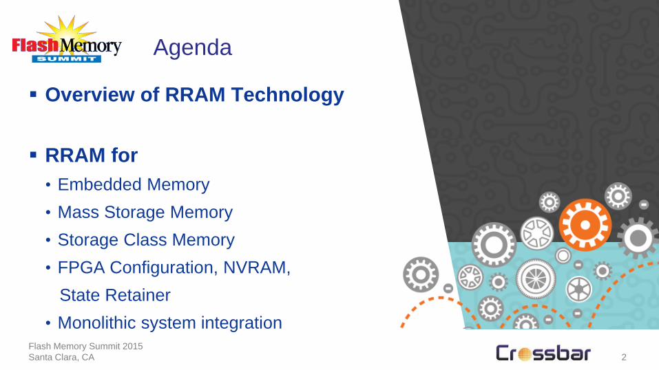
Agenda
Flash Memory Summit 2015Santa Clara, CA 2
Overview of RRAM Technology
RRAM for• Embedded Memory• Mass Storage Memory• Storage Class Memory• FPGA Configuration, NVRAM,
State Retainer• Monolithic system integration
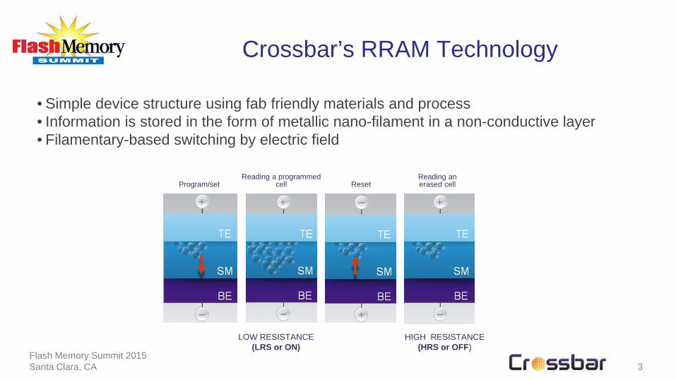
Crossbar’s RRAM Technology
Flash Memory Summit 2015Santa Clara, CA 3
• Simple device structure using fab friendly materials and process• Information is stored in the form of metallic nano-filament in a non-conductive layer• Filamentary-based switching by electric field
Program/setReading a programmed
cell ResetReading an erased cell
LOW RESISTANCE(LRS or ON)
HIGH RESISTANCE(HRS or OFF)
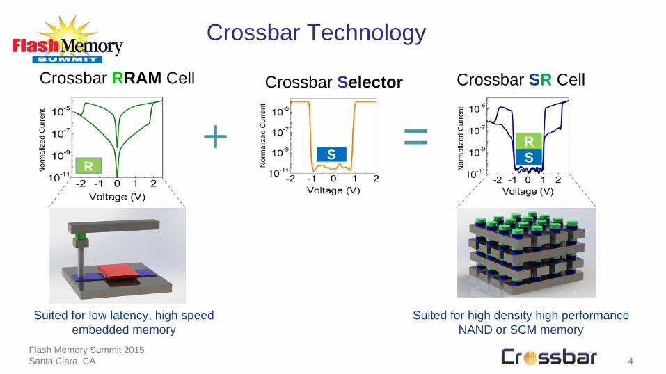
Crossbar Technology
Flash Memory Summit 2015Santa Clara, CA 4
+ =S
Crossbar Selector Crossbar SR Cell
Suited for low latency, high speed embedded memory
Suited for high density high performance NAND or SCM memory
Crossbar RRAM Cell
R SR
Nor
mal
ized
Cur
rent
Nor
mal
ized
Cur
rent
Nor
mal
ized
Cur
rent
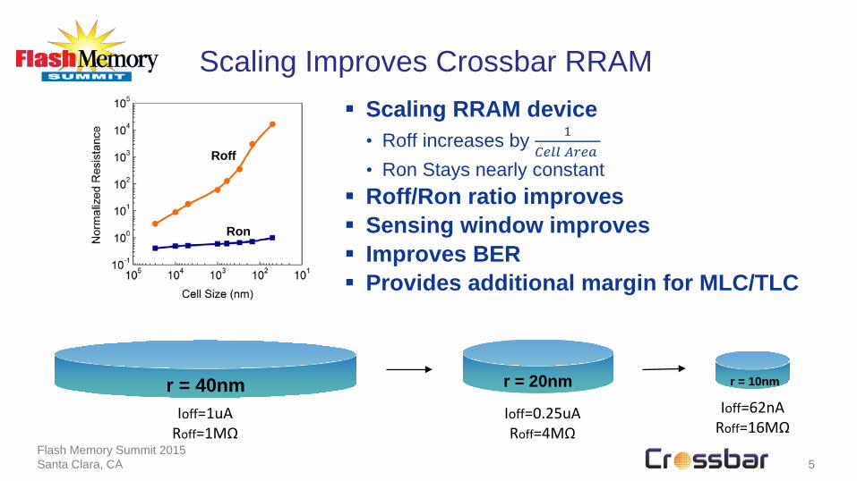
Scaling Improves Crossbar RRAM
Flash Memory Summit 2015Santa Clara, CA 5
Scaling RRAM device• Roff increases by 1
𝐶𝐶𝐶𝐶𝐶𝐶𝐶𝐶 𝐴𝐴𝐴𝐴𝐶𝐶𝐴𝐴• Ron Stays nearly constant
Roff/Ron ratio improves Sensing window improves Improves BER Provides additional margin for MLC/TLC
Roff
Ron
r = 10nmr = 40nm r = 20nmIoff=62nA
Roff=16MΩIoff=0.25uARoff=4MΩ
Ioff=1uARoff=1MΩ
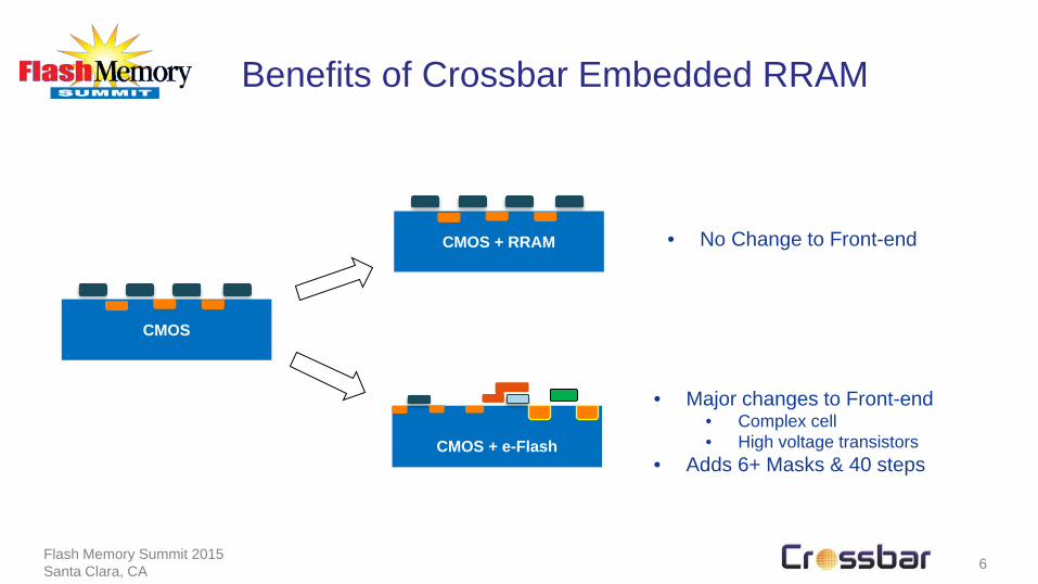
Benefits of Crossbar Embedded RRAM
Flash Memory Summit 2015Santa Clara, CA 6
CMOS
CMOS + e-Flash
• No Change to Front-end
• Major changes to Front-end• Complex cell• High voltage transistors
• Adds 6+ Masks & 40 steps
CMOS + RRAM
Benefits of Crossbar Embedded RRAM
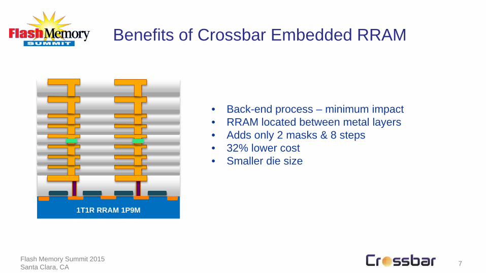
Flash Memory Summit 2015Santa Clara, CA 7
1T1R RRAM 1P9M
• Back-end process – minimum impact• RRAM located between metal layers• Adds only 2 masks & 8 steps• 32% lower cost• Smaller die size
Advantages of RRAM for Embedded Memory
Flash Memory Summit 2015Santa Clara, CA 8
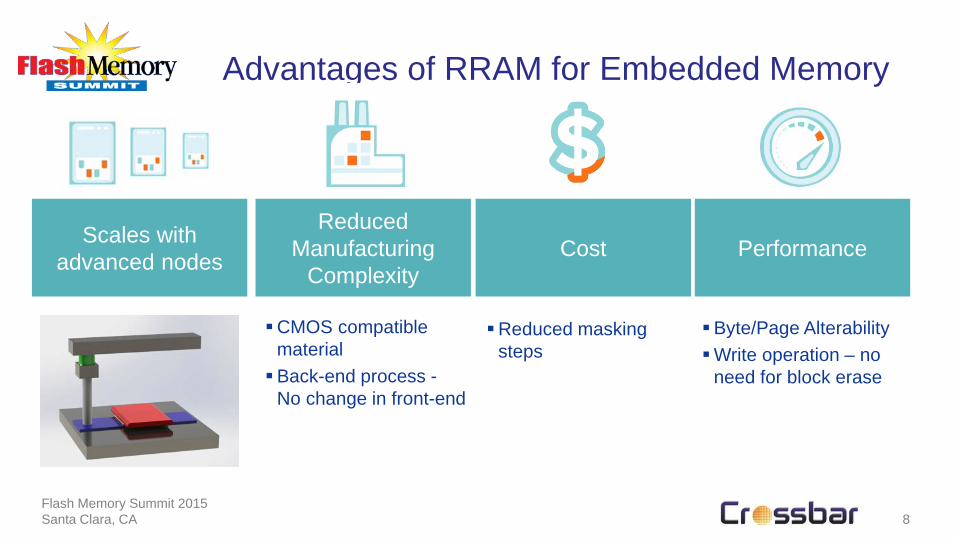
CMOS compatible material Back-end process -
No change in front-end
Scales with advanced nodes
Reduced Manufacturing
ComplexityCost Performance
Byte/Page AlterabilityWrite operation – no
need for block erase
Reduced masking steps
RRAM for Mass Storage
Flash Memory Summit 2015Santa Clara, CA 9
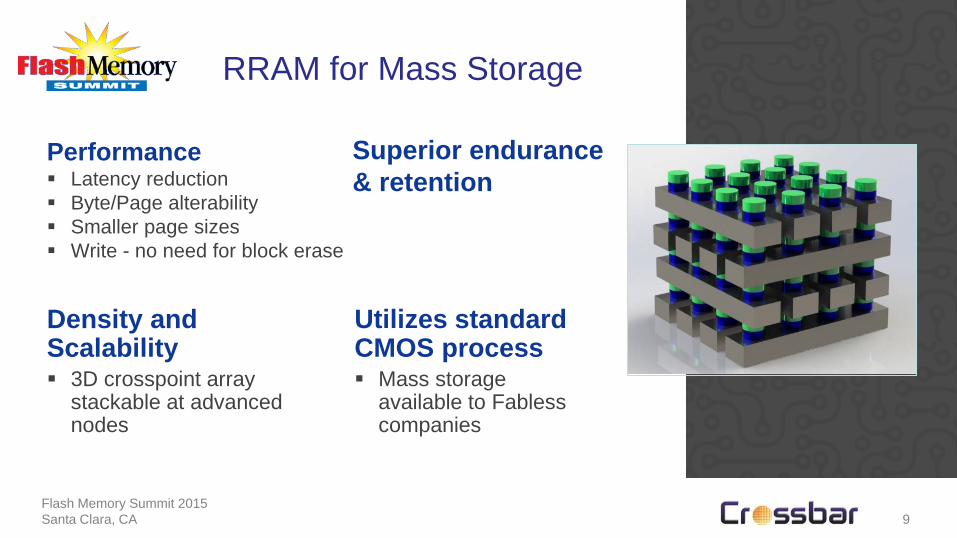
Performance Latency reduction Byte/Page alterability Smaller page sizes Write - no need for block erase
Superior endurance & retention
Density and Scalability 3D crosspoint array
stackable at advanced nodes
Utilizes standard CMOS process Mass storage
available to Fabless companies
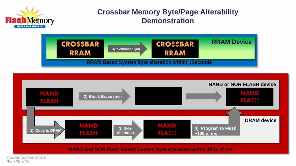
NAND and NOR Flash Based System byte alteration within 100s of ms
DRAM device
NAND or NOR FLASH device
Crossbar Memory Byte/Page Alterability Demonstration
2) Block Erase (ms)
3) Byte Alteration
NANDFLASH
NANDFLASH
RRAM Based System byte alteration within µSeconds
RRAM DeviceByte Alteration (µs)
CROSSBARRRAM
CROSSBARRRAM
NANDFLASH
NANDFLASH
Flash Memory Summit 2015Santa Clara, CA
4) Program to Flash~100 of ms
1) Copy to DRAM
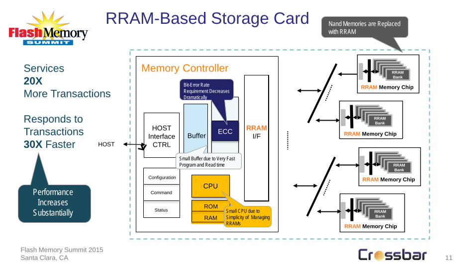
NAND-Based Storage CardServices 150K transactions per second Responds to single transaction within 150us
Services 20X More Transactions
Responds to Transactions 30X Faster
RRAM-Based Storage Card
Flash Memory Summit 2015Santa Clara, CA 11
Memory Controller
NANDI/F
HOSTInterface
CTRL
ECCBuffer
Configuration
Command
StatusROM
RAM
CPU
HOST
RRAMI/F
ECC
NANDMemory
NANDMemory
Nand Memories are Replaced with RRAM
Performance Increases
Substantially
Bit-Error Rate Requirement Decreases Dramatically
Small Buffer due to Very Fast Program and Read time
Small CPU due to Simplicity of Managing RRAMs
NANDMemoryRRAM Memory Chip
RRAM Bank
NANDMemory
RRAM Memory Chip
RRAM Bank
NANDMemory
NANDMemory
RRAM Memory Chip
RRAM Bank
RRAM Memory Chip
RRAM Bank
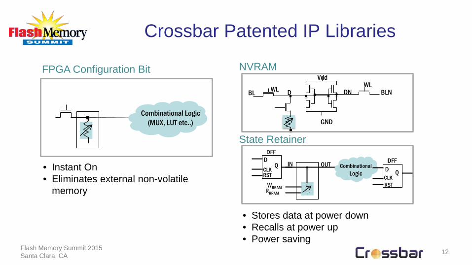
Crossbar Patented IP Libraries
Flash Memory Summit 2015Santa Clara, CA 12
Combinational Logic (MUX, LUT etc..)
FPGA Configuration Bit
• Instant On• Eliminates external non-volatile
memory RRRAM
WRRAM
RST
DQ
CLK
RST
D QCLK
Combinational Logic
DFFDFFIN OUT
WL DWL
Vdd
GND
BL DN BLN
NVRAM
• Stores data at power down• Recalls at power up• Power saving
State Retainer
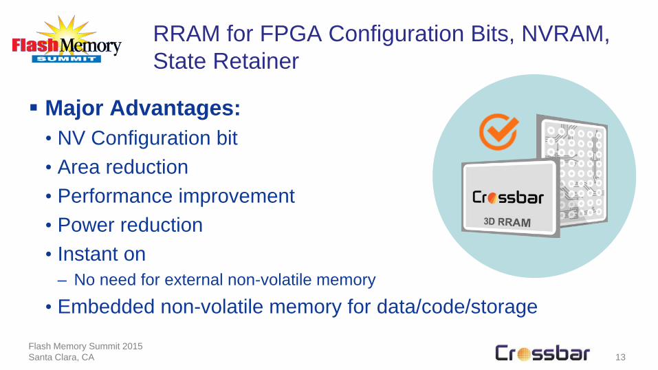
RRAM for FPGA Configuration Bits, NVRAM, State Retainer
Flash Memory Summit 2015Santa Clara, CA 13
Major Advantages:• NV Configuration bit• Area reduction• Performance improvement• Power reduction• Instant on
– No need for external non-volatile memory
• Embedded non-volatile memory for data/code/storage
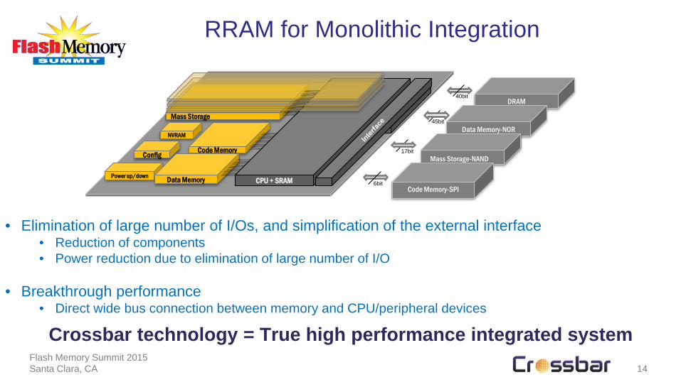
RRAM for Monolithic Integration
Flash Memory Summit 2015Santa Clara, CA 14
Code Memory
Mass Storage
Config
Power up/down
NVRAM
DRAM
• Elimination of large number of I/Os, and simplification of the external interface• Reduction of components• Power reduction due to elimination of large number of I/O
• Breakthrough performance • Direct wide bus connection between memory and CPU/peripheral devices
Crossbar technology = True high performance integrated system
Data Memory CPU + SRAM
Data Memory-NOR45bit
Mass Storage-NAND17bit
Code Memory-SPI6bit
40bit
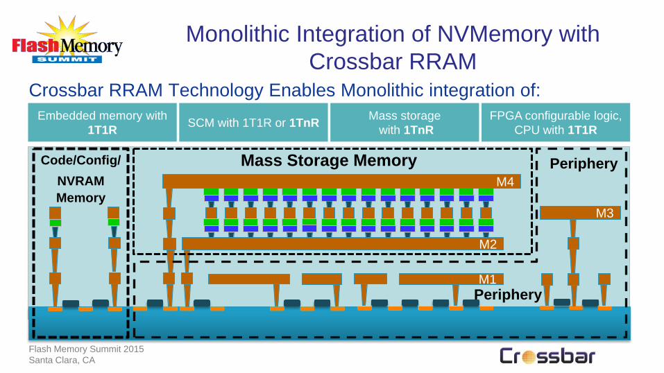
Monolithic Integration of NVMemory with Crossbar RRAM
Crossbar RRAM Technology Enables Monolithic integration of:SCM with 1T1R or 1TnR Embedded memory with
1T1RFPGA configurable logic,
CPU with 1T1RMass storage
with 1TnR
Flash Memory Summit 2015Santa Clara, CA
Mass Storage Memory
M2
Code/Config/NVRAMMemory
M4
M3
M1
Periphery
Periphery
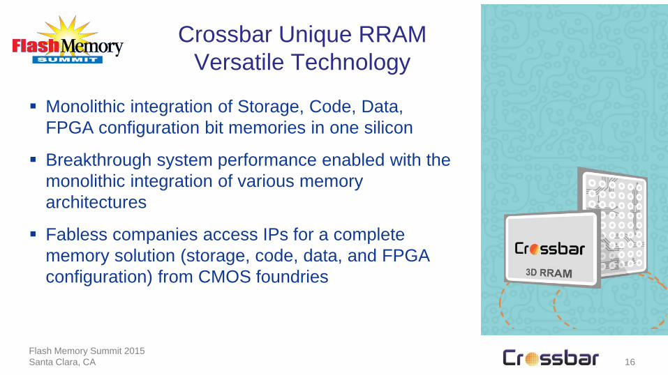
Crossbar Unique RRAM Versatile Technology
Flash Memory Summit 2015Santa Clara, CA 16
Monolithic integration of Storage, Code, Data, FPGA configuration bit memories in one silicon
Breakthrough system performance enabled with the monolithic integration of various memory architectures
Fabless companies access IPs for a complete memory solution (storage, code, data, and FPGA configuration) from CMOS foundries
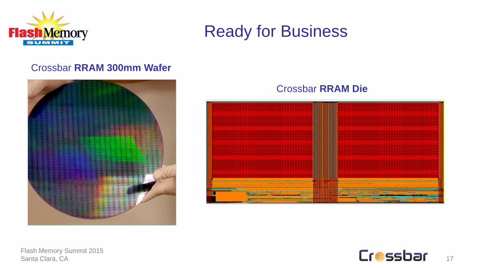
Ready for Business
Flash Memory Summit 2015Santa Clara, CA 17
Crossbar RRAM 300mm Wafer
Crossbar RRAM Die
18Flash Memory Summit 2015Santa Clara, CA
Crossbar-inc.com