Embed Size (px)
Citation preview
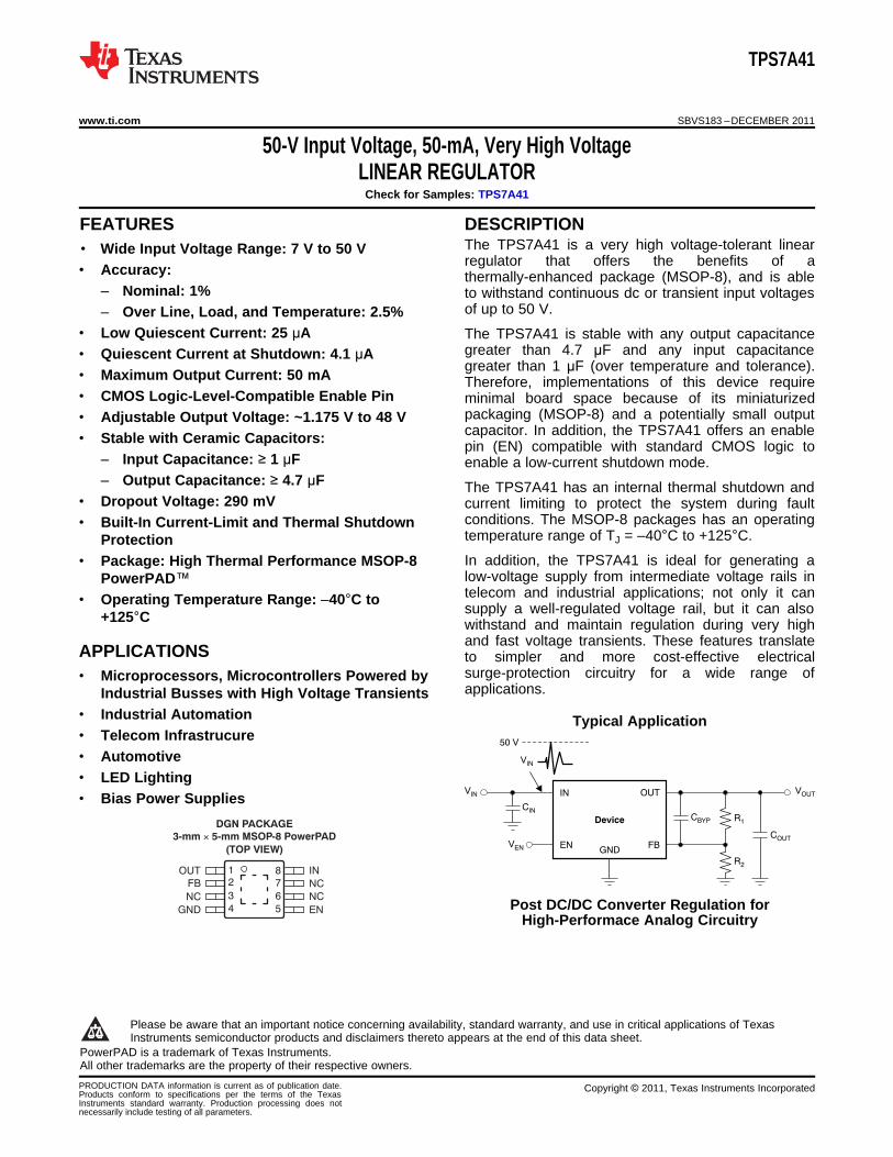
Device
OUT
FBGND
CIN
R1
CBYP
COUT
IN
EN
VIN
VOUT
R2
VEN
VIN
50 V
2
1
3
4
7
8
6
5
FB
NC
GND
OUT
EN
NC
NC
IN
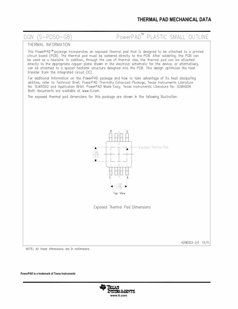
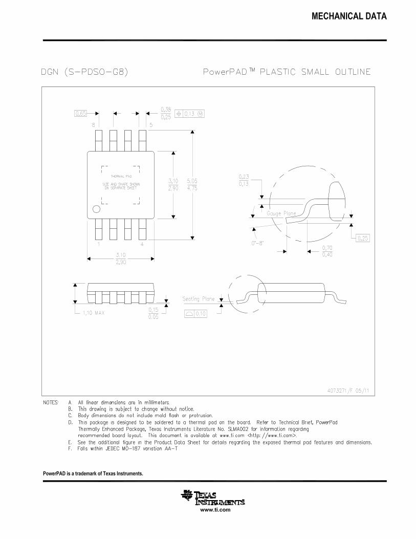
DGN PACKAGE
3-mm 5-mm MSOP-8 PowerPAD
(TOP VIEW)
´
TPS7A41
www.ti.com SBVS183 –DECEMBER 2011
50-V Input Voltage, 50-mA, Very High VoltageLINEAR REGULATOR
Check for Samples: TPS7A41
1FEATURES DESCRIPTIONThe TPS7A41 is a very high voltage-tolerant linear
23• Wide Input Voltage Range: 7 V to 50 Vregulator that offers the benefits of a• Accuracy: thermally-enhanced package (MSOP-8), and is able
– Nominal: 1% to withstand continuous dc or transient input voltagesof up to 50 V.– Over Line, Load, and Temperature: 2.5%
• Low Quiescent Current: 25 µA The TPS7A41 is stable with any output capacitancegreater than 4.7 µF and any input capacitance• Quiescent Current at Shutdown: 4.1 µAgreater than 1 µF (over temperature and tolerance).• Maximum Output Current: 50 mA Therefore, implementations of this device require
• CMOS Logic-Level-Compatible Enable Pin minimal board space because of its miniaturizedpackaging (MSOP-8) and a potentially small output• Adjustable Output Voltage: ~1.175 V to 48 Vcapacitor. In addition, the TPS7A41 offers an enable• Stable with Ceramic Capacitors: pin (EN) compatible with standard CMOS logic to
– Input Capacitance: ≥ 1 µF enable a low-current shutdown mode.– Output Capacitance: ≥ 4.7 µF The TPS7A41 has an internal thermal shutdown and
• Dropout Voltage: 290 mV current limiting to protect the system during faultconditions. The MSOP-8 packages has an operating• Built-In Current-Limit and Thermal Shutdowntemperature range of TJ = –40°C to +125°C.ProtectionIn addition, the TPS7A41 is ideal for generating a• Package: High Thermal Performance MSOP-8low-voltage supply from intermediate voltage rails inPowerPAD™telecom and industrial applications; not only it can• Operating Temperature Range: –40°C tosupply a well-regulated voltage rail, but it can also+125°C withstand and maintain regulation during very highand fast voltage transients. These features translate
APPLICATIONS to simpler and more cost-effective electricalsurge-protection circuitry for a wide range of• Microprocessors, Microcontrollers Powered byapplications.Industrial Busses with High Voltage Transients
• Industrial Automation Typical Application• Telecom Infrastrucure• Automotive• LED Lighting• Bias Power Supplies
Post DC/DC Converter Regulation forHigh-Performace Analog Circuitry
1
Please be aware that an important notice concerning availability, standard warranty, and use in critical applications of TexasInstruments semiconductor products and disclaimers thereto appears at the end of this data sheet.
2PowerPAD is a trademark of Texas Instruments.3All other trademarks are the property of their respective owners.
PRODUCTION DATA information is current as of publication date. Copyright © 2011, Texas Instruments IncorporatedProducts conform to specifications per the terms of the TexasInstruments standard warranty. Production processing does notnecessarily include testing of all parameters.
TPS7A41
SBVS183 –DECEMBER 2011 www.ti.com
This integrated circuit can be damaged by ESD. Texas Instruments recommends that all integrated circuits be handled withappropriate precautions. Failure to observe proper handling and installation procedures can cause damage.
ESD damage can range from subtle performance degradation to complete device failure. Precision integrated circuits may be moresusceptible to damage because very small parametric changes could cause the device not to meet its published specifications.
ORDERING INFORMATION (1)
PRODUCT VOUT
TPS7A4101 yyy z YYY is package designator.Z is package quantity.
(1) For the most current package and ordering information see the Package Option Addendum at the end of this document, or visit thedevice product folder on www.ti.com.
ABSOLUTE MAXIMUM RATINGS (1)
Over operating free-air temperature range (unless otherwise noted).VALUE
MIN MAX UNIT
IN pin to GND pin –0.3 +55 V
OUT pin to GND pin –0.3 +55 V
OUT pin to IN pin –55 +0.3 V
Voltage FB pin to GND pin –0.3 +2 V
FB pin to IN pin –55 +0.3 V
EN pin to IN pin –55 0.3
EN pin to GND pin –0.3 +55 V
Current Peak output Internally limited
Operating virtual junction, TJ –40 +125 °CTemperature
Storage, Tstg –65 +150 °C
Human body model (HBM) 2.5 kVElectrostatic discharge rating
Charged device model (CDM) 500 V
(1) Stresses beyond those listed under Absolute Maximum Ratings may cause permanent damage to the device. These are stress ratingsonly, and functional operation of the device at these or any other conditions beyond those indicated is not implied. Exposure toabsolute-maximum rated conditions for extended periods may affect device reliability.
THERMAL INFORMATIONTPS7A4001
THERMAL METRIC (1) DGN UNITS
8 PINS
θJA Junction-to-ambient thermal resistance 55.09
θJC(top) Junction-to-case(top) thermal resistance 8.47
θJB Junction-to-board thermal resistance —°C/W
ψJT Junction-to-top characterization parameter 0.36
ψJB Junction-to-board characterization parameter 14.6
θJC(bottom) Junction-to-case(bottom) thermal resistance —
(1) For more information about traditional and new thermal metrics, see the IC Package Thermal Metrics application report, SPRA953.
DISSIPATION RATINGSDERATING FACTOR TA ≤ +25°C POWER TA = +70°C POWER TA = +85°C POWER
BOARD PACKAGE RθJA RθJC ABOVE TA = +25°C RATING RATING RATING
High-K (1) DGN 55.9°C/W 8.47°C/W 16.6mW/°C 1.83W 1.08W 0.833W
(1) The JEDEC High-K (2s2p) board design used to derive this data was a 3-inch x 3-inch multilayer board with 2-ounce internal power andground planes and 2-ounce copper traces on top and bottom of the board.
2 Submit Documentation Feedback Copyright © 2011, Texas Instruments Incorporated
Product Folder Link(s): TPS7A41
TPS7A41
www.ti.com SBVS183 –DECEMBER 2011
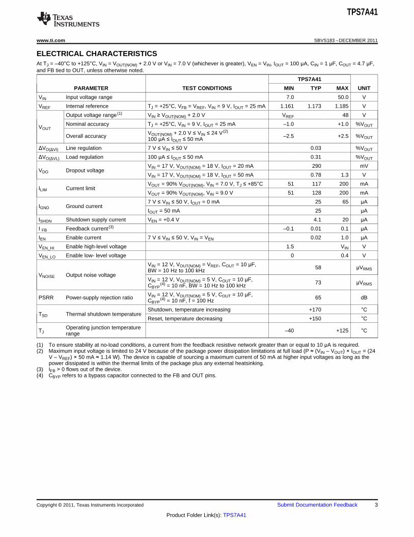
ELECTRICAL CHARACTERISTICSAt TJ = –40°C to +125°C, VIN = VOUT(NOM) + 2.0 V or VIN = 7.0 V (whichever is greater), VEN = VIN, IOUT = 100 µA, CIN = 1 μF, COUT = 4.7 μF,and FB tied to OUT, unless otherwise noted.
TPS7A41
PARAMETER TEST CONDITIONS MIN TYP MAX UNIT
VIN Input voltage range 7.0 50.0 V
VREF Internal reference TJ = +25°C, VFB = VREF, VIN = 9 V, IOUT = 25 mA 1.161 1.173 1.185 V
Output voltage range (1) VIN ≥ VOUT(NOM) + 2.0 V VREF 48 V
Nominal accuracy TJ = +25°C, VIN = 9 V, IOUT = 25 mA –1.0 +1.0 %VOUTVOUTVOUT(NOM) + 2.0 V ≤ VIN ≤ 24 V (2)
Overall accuracy –2.5 +2.5 %VOUT100 µA ≤ IOUT ≤ 50 mA
ΔVO(ΔVI) Line regulation 7 V ≤ VIN ≤ 50 V 0.03 %VOUT
ΔVO(ΔVL) Load regulation 100 µA ≤ IOUT ≤ 50 mA 0.31 %VOUT
VIN = 17 V, VOUT(NOM) = 18 V, IOUT = 20 mA 290 mVVDO Dropout voltage
VIN = 17 V, VOUT(NOM) = 18 V, IOUT = 50 mA 0.78 1.3 V
VOUT = 90% VOUT(NOM), VIN = 7.0 V, TJ ≤ +85°C 51 117 200 mAILIM Current limit
VOUT = 90% VOUT(NOM), VIN = 9.0 V 51 128 200 mA
7 V ≤ VIN ≤ 50 V, IOUT = 0 mA 25 65 μAIGND Ground current
IOUT = 50 mA 25 μA
ISHDN Shutdown supply current VEN = +0.4 V 4.1 20 μA
I FB Feedback current (3) –0.1 0.01 0.1 µA
IEN Enable current 7 V ≤ VIN ≤ 50 V, VIN = VEN 0.02 1.0 μA
VEN_HI Enable high-level voltage 1.5 VIN V
VEN_LO Enable low- level voltage 0 0.4 V
VIN = 12 V, VOUT(NOM) = VREF, COUT = 10 μF, 58 μVRMSBW = 10 Hz to 100 kHzVNOISE Output noise voltage
VIN = 12 V, VOUT(NOM) = 5 V, COUT = 10 μF, 73 μVRMSCBYP(4) = 10 nF, BW = 10 Hz to 100 kHz
VIN = 12 V, VOUT(NOM) = 5 V, COUT = 10 μF,PSRR Power-supply rejection ratio 65 dBCBYP(4) = 10 nF, f = 100 Hz
Shutdown, temperature increasing +170 °CTSD Thermal shutdown temperature
Reset, temperature decreasing +150 °COperating junction temperatureTJ –40 +125 °Crange
(1) To ensure stability at no-load conditions, a current from the feedback resistive network greater than or equal to 10 μA is required.(2) Maximum input voltage is limited to 24 V because of the package power dissipation limitations at full load (P ≈ (VIN – VOUT) × IOUT = (24
V – VREF) × 50 mA ≈ 1.14 W). The device is capable of sourcing a maximum current of 50 mA at higher input voltages as long as thepower dissipated is within the thermal limits of the package plus any external heatsinking.
(3) IFB > 0 flows out of the device.(4) CBYP refers to a bypass capacitor connected to the FB and OUT pins.
Copyright © 2011, Texas Instruments Incorporated Submit Documentation Feedback 3
Product Folder Link(s): TPS7A41
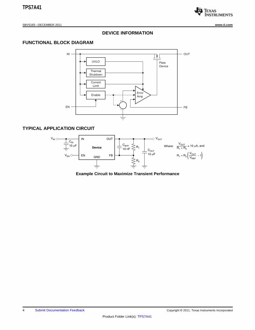
UVLO
Thermal
Shutdown
Current
Limit
EnableError
Amp
IN
EN
OUT
FB
Pass
Device
Where:VOUT
R + R1 2
³ 10 A, andm
VOUT
VREF
- 1R = R1 2
Device
OUT
FBGND
C
10 F
IN
m R1
C
10 nF
BYP
C
10 F
OUT
m
IN
EN
VIN VOUT
R2
VEN
TPS7A41
SBVS183 –DECEMBER 2011 www.ti.com
DEVICE INFORMATION
FUNCTIONAL BLOCK DIAGRAM
TYPICAL APPLICATION CIRCUIT
Example Circuit to Maximize Transient Performance
4 Submit Documentation Feedback Copyright © 2011, Texas Instruments Incorporated
Product Folder Link(s): TPS7A41
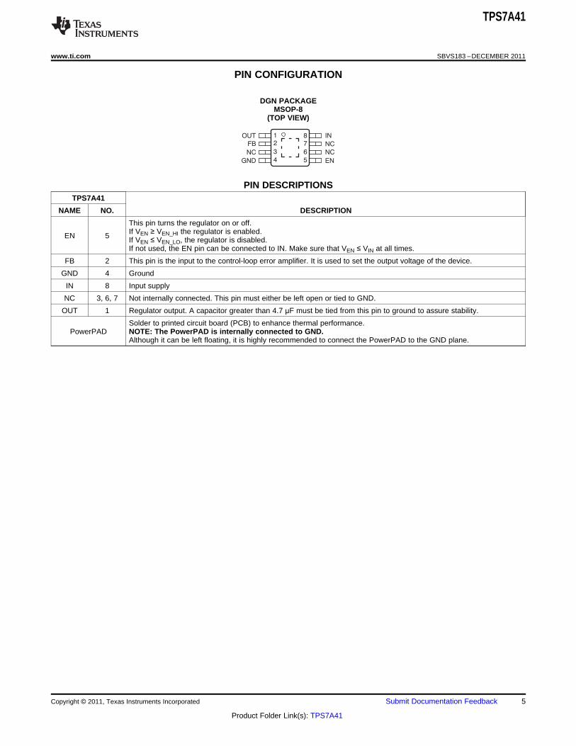
2
1
3
4
7
8
6
5
FB
NC
GND
OUT
EN
NC
NC
IN
TPS7A41
www.ti.com SBVS183 –DECEMBER 2011
PIN CONFIGURATION
DGN PACKAGEMSOP-8
(TOP VIEW)
PIN DESCRIPTIONSTPS7A41
NAME NO. DESCRIPTION
This pin turns the regulator on or off.If VEN ≥ VEN_HI the regulator is enabled.EN 5 If VEN ≤ VEN_LO, the regulator is disabled.If not used, the EN pin can be connected to IN. Make sure that VEN ≤ VIN at all times.
FB 2 This pin is the input to the control-loop error amplifier. It is used to set the output voltage of the device.
GND 4 Ground
IN 8 Input supply
NC 3, 6, 7 Not internally connected. This pin must either be left open or tied to GND.
OUT 1 Regulator output. A capacitor greater than 4.7 µF must be tied from this pin to ground to assure stability.
Solder to printed circuit board (PCB) to enhance thermal performance.PowerPAD NOTE: The PowerPAD is internally connected to GND.
Although it can be left floating, it is highly recommended to connect the PowerPAD to the GND plane.
Copyright © 2011, Texas Instruments Incorporated Submit Documentation Feedback 5
Product Folder Link(s): TPS7A41
Time (100 s/div)m
V = 12V, V = 5V
1mA
C = 10 F, C = 10nF
I = 1mA 29mAD ® ®
m
IN OUT
OUT BYP
OUT
IOUT
VOUT
10mA/div
50mV/div
−10
−7.5
−5
−2.5
0
2.5
5
7.5
10
5 10 15 20 25 30 35 40 45 50Input Voltage (V)
VO
UT
(NO
M) (
%)
−40°C+25°C+85°C
+105°C+125°C
G001
1.075
1.125
1.175
1.225
1.275
5 10 15 20 25 30 35 40 45 50Input Voltage (V)
VF
B (
V)
−40°C+25°C+85°C
+105°C+125°C
G002
0
20
40
60
80
100
5 10 15 20 25 30 35 40 45 50Input Voltage (V)
I Q (
µA)
−40°C+25°C+85°C+105°C+125°C
IOUT = 0 mA
G003
0
10
20
30
40
50
60
70
80
90
100
−40 −25 −10 5 20 35 50 65 80 95 110 125Temperature (°C)
I FB (
nA)
0
10
20
30
40
50
60
70
80
90
100
0 10 20 30 40 50Output Current (mA)
I GN
D (
µA)
− 40°C+ 25°C+ 85°C+ 105°C+ 125°C
TPS7A41
SBVS183 –DECEMBER 2011 www.ti.com
TYPICAL CHARACTERISTICSAt TJ = –40°C to +125°C, VIN = VOUT(NOM) + 2.0 V or VIN = 9.0 V (whichever is greater), VEN = VIN, IOUT = 100 µA, CIN = 1 μF,
COUT = 4.7 μF, and FB tied to OUT, unless otherwise noted.
LOAD TRANSIENT RESPONSE LINE REGULATION
Figure 1. Figure 2.
FEEDBACK VOLTAGE QUIESCENT CURRENT vs INPUT VOLTAGE
Figure 3. Figure 4.
FEEDBACK CURRENT GROUND CURRENT
Figure 5. Figure 6.
6 Submit Documentation Feedback Copyright © 2011, Texas Instruments Incorporated
Product Folder Link(s): TPS7A41
0
0.25
0.5
0.75
1
1.25
1.5
1.75
2
0 10 20 30 40 50Output Current (mA)
VD
RO
P (
V)
− 40°C+ 25°C+ 85°C
+ 105°C+ 125°C
0
0.5
1
1.5
2
2.5
−40 −25 −10 5 20 35 50 65 80 95 110 125
ON−TO−OFF
OFF−TO−ON
Temperature (°C)
VE
N (
V)
0.001
0.01
0.1
1
10
10 100 1k 10k 100k 1M 10MFrequency (Hz)
Noi
se (
µV/
Hz
)
IOUT = 100µA,VNOISE = 60µVRMSIOUT = 50mA,VNOISE = 100µVRMS
VIN = 12VVOUT = VREFCOUT = 10µFCBYP = 10nF
0
40
80
120
160
200
6 9 12 15 18 21 24Input Voltage (V)
I CL (
mA
)
− 40°C+ 25°C+ 85°C+ 105°C+ 125°C
0
10
20
30
40
50
60
70
80
90
100
10 100 1k 10k 100k 1M 10MFrequency (Hz)
PS
RR
(dB
)
IOUT = 50mAIOUT = 100µA
VIN = 12VVOUT = 5VCOUT = 10µFCBYP = 10nF
TPS7A41
www.ti.com SBVS183 –DECEMBER 2011
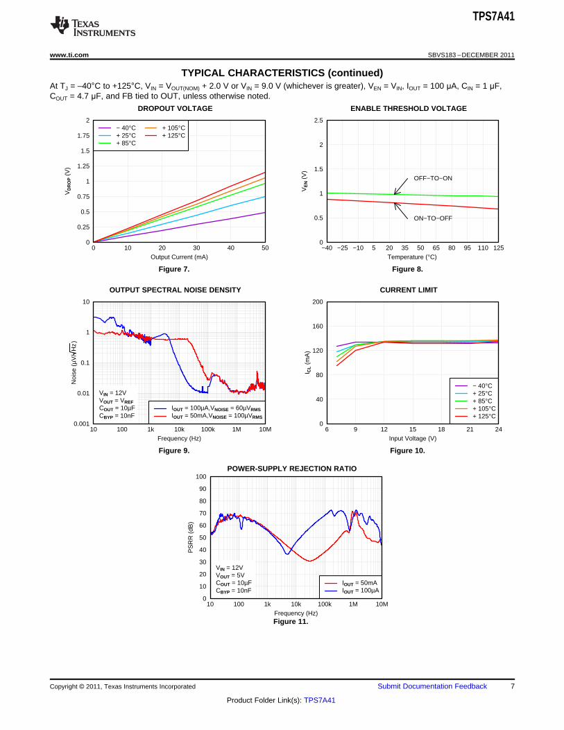
TYPICAL CHARACTERISTICS (continued)At TJ = –40°C to +125°C, VIN = VOUT(NOM) + 2.0 V or VIN = 9.0 V (whichever is greater), VEN = VIN, IOUT = 100 µA, CIN = 1 μF,COUT = 4.7 μF, and FB tied to OUT, unless otherwise noted.
DROPOUT VOLTAGE ENABLE THRESHOLD VOLTAGE
Figure 7. Figure 8.
OUTPUT SPECTRAL NOISE DENSITY CURRENT LIMIT
Figure 9. Figure 10.
POWER-SUPPLY REJECTION RATIO
Figure 11.
Copyright © 2011, Texas Instruments Incorporated Submit Documentation Feedback 7
Product Folder Link(s): TPS7A41
Device
OUT
FBGND
C
10 F
IN
m R1
C
10 nF
BYP
C
10 F
OUT
m
IN
EN
VINVOUT
R2
VOUT
VREF
- 1R = R1 2
VOUT
R + R1 2
³ 10 Am, where
TPS7A41
SBVS183 –DECEMBER 2011 www.ti.com
THEORY OF OPERATION
GENERAL DESCRIPTION
The TPS7A4101 belongs to a new generation of linear regulators that use an innovative BiCMOS processtechnology to achieve very high maximum input and output voltages.
This process not only allows the TPS7A4101 to maintain regulation during very fast high-voltage transients up to50 V, but it also allows the TPS7A4101 to regulate from a continuous high-voltage input rail. Unlike otherregulators created using bipolar technology, the TPS7A4101 ground current is also constant over its outputcurrent range, resulting in increased efficiency and lower power consumption.
These features, combined with a high thermal performance MSOP-8 PowerPAD package, make this device idealfor industrial and telecom applications.
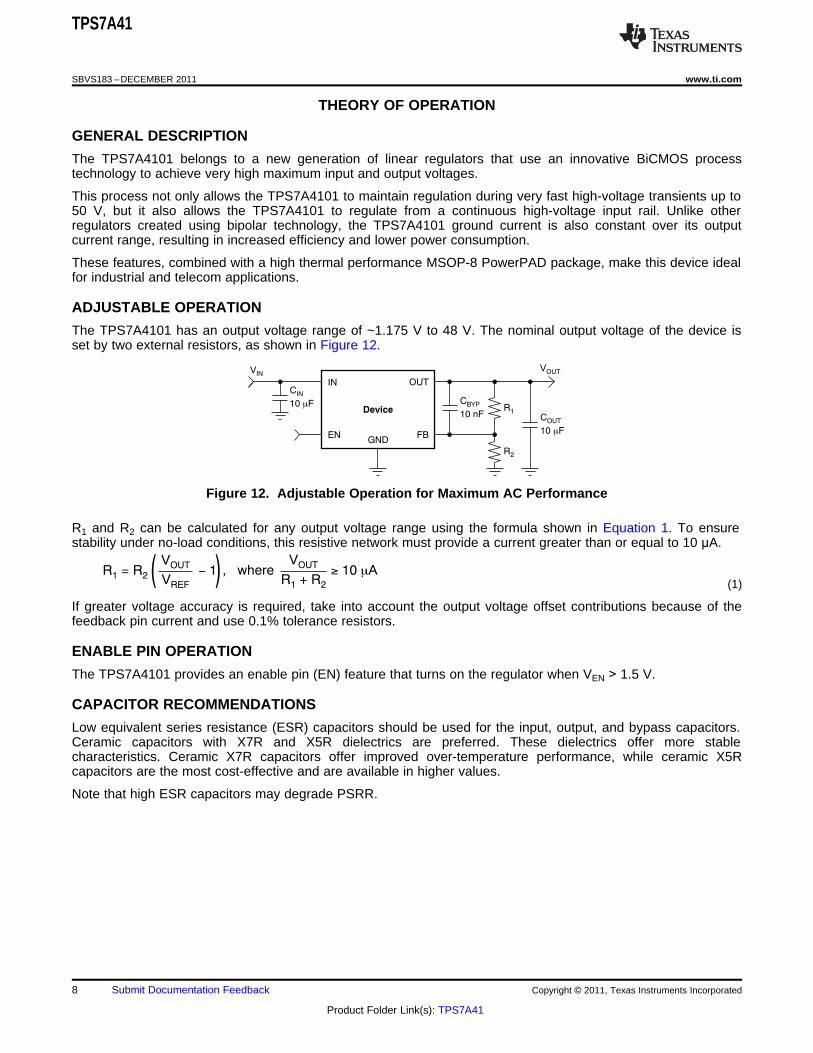
ADJUSTABLE OPERATION
The TPS7A4101 has an output voltage range of ~1.175 V to 48 V. The nominal output voltage of the device isset by two external resistors, as shown in Figure 12.
Figure 12. Adjustable Operation for Maximum AC Performance
R1 and R2 can be calculated for any output voltage range using the formula shown in Equation 1. To ensurestability under no-load conditions, this resistive network must provide a current greater than or equal to 10 μA.
(1)
If greater voltage accuracy is required, take into account the output voltage offset contributions because of thefeedback pin current and use 0.1% tolerance resistors.
ENABLE PIN OPERATION
The TPS7A4101 provides an enable pin (EN) feature that turns on the regulator when VEN > 1.5 V.
CAPACITOR RECOMMENDATIONS
Low equivalent series resistance (ESR) capacitors should be used for the input, output, and bypass capacitors.Ceramic capacitors with X7R and X5R dielectrics are preferred. These dielectrics offer more stablecharacteristics. Ceramic X7R capacitors offer improved over-temperature performance, while ceramic X5Rcapacitors are the most cost-effective and are available in higher values.
Note that high ESR capacitors may degrade PSRR.
8 Submit Documentation Feedback Copyright © 2011, Texas Instruments Incorporated
Product Folder Link(s): TPS7A41
TPS7A41
www.ti.com SBVS183 –DECEMBER 2011
INPUT AND OUTPUT CAPACITOR REQUIREMENTS
The TPS7A4101 high voltage linear regulator achieves stability with a minimum output capacitance of 4.7 µF andinput capacitance of 1 µF; however, it is highly recommended to use 10-μF output and input capacitors tomaximize ac performance.
BYPASS CAPACITOR REQUIREMENTS
Although a bypass capacitor (CBYP) is not needed to achieve stability, it is highly recommended to use a 10-nFbypass capacitor to maximize ac performance (including line transient, noise and PSRR).
MAXIMUM AC PERFORMANCE
In order to maximize line transient, noise, and PSRR performance, it is recommended to include 10-μF (orhigher) input and output capacitors, and a 10-nF bypass capacitor; see Figure 12. The solution shown deliversminimum noise levels of 58 μVRMS and power-supply rejection levels above 36 dB from 10 Hz to 10 MHz.
TRANSIENT RESPONSE
As with any regulator, increasing the size of the output capacitor reduces over/undershoot magnitude butincreases duration of the transient response.
Note that the presence of the CBYP capacitor may greatly improve the TPS7A4101 line transient response, asnoted in .
Copyright © 2011, Texas Instruments Incorporated Submit Documentation Feedback 9
Product Folder Link(s): TPS7A41
50 V
ILED
IN
Device
EN
OUT
FB
COUT
RSET
GND
EN
I =LED
VREF
RSET
TPS7A41
SBVS183 –DECEMBER 2011 www.ti.com
APPLICATION INFORMATION
TRANSIENT VOLTAGE PROTECTION
One of the primary applications of the TPS7A4101 is to provide transient voltage protection to sensitive circuitrythat may be damaged in the presence of high-voltage spikes.
This transient voltage protection can be more cost-effective and compact compared to topologies that use atransient voltage suppression (TVS) block.
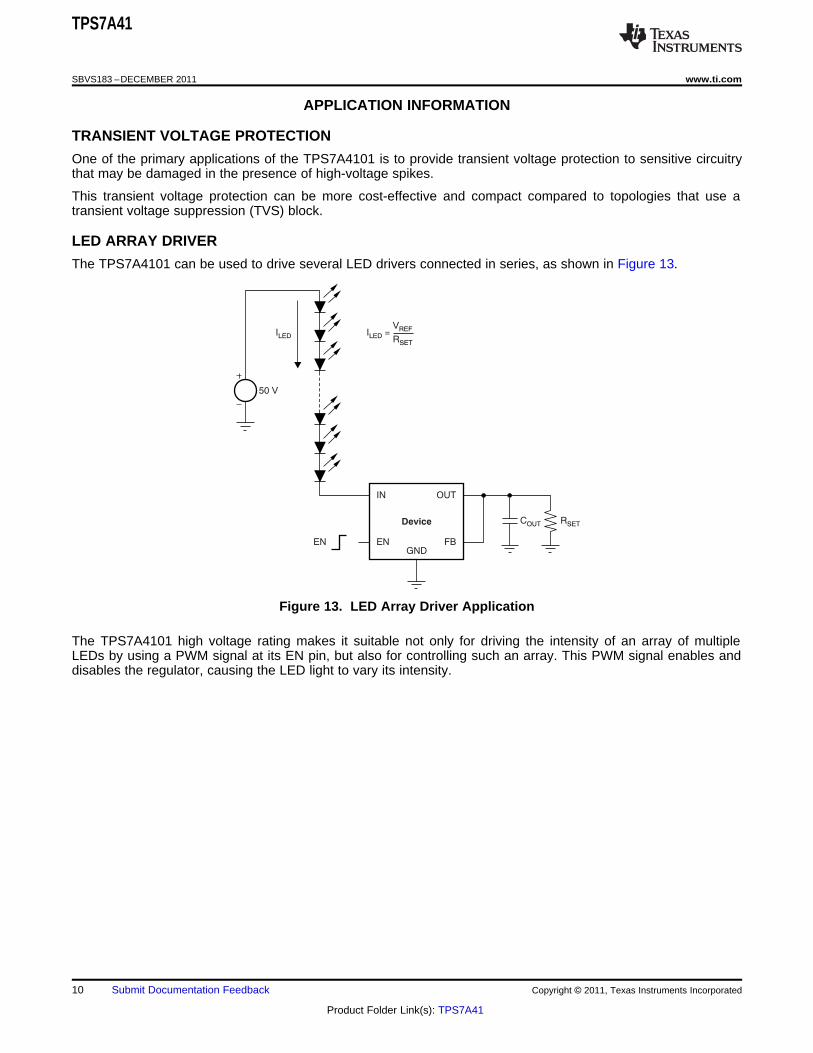
LED ARRAY DRIVER
The TPS7A4101 can be used to drive several LED drivers connected in series, as shown in Figure 13.
Figure 13. LED Array Driver Application
The TPS7A4101 high voltage rating makes it suitable not only for driving the intensity of an array of multipleLEDs by using a PWM signal at its EN pin, but also for controlling such an array. This PWM signal enables anddisables the regulator, causing the LED light to vary its intensity.
10 Submit Documentation Feedback Copyright © 2011, Texas Instruments Incorporated
Product Folder Link(s): TPS7A41
50 V
I = 0 mA
IN
Device
EN
OUT
FB
COUT RSET
GNDLow
100 V
50 V
TPS7A41
www.ti.com SBVS183 –DECEMBER 2011
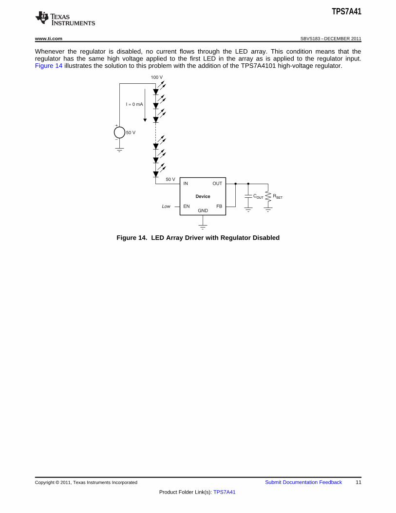
Whenever the regulator is disabled, no current flows through the LED array. This condition means that theregulator has the same high voltage applied to the first LED in the array as is applied to the regulator input.Figure 14 illustrates the solution to this problem with the addition of the TPS7A4101 high-voltage regulator.
Figure 14. LED Array Driver with Regulator Disabled
Copyright © 2011, Texas Instruments Incorporated Submit Documentation Feedback 11
Product Folder Link(s): TPS7A41
P = (V V ) I-D IN OUT OUT
TPS7A41
SBVS183 –DECEMBER 2011 www.ti.com
LAYOUT
PACKAGE MOUNTING
Solder pad footprint recommendations for the TPS7A4101 are available at the end of this product data sheet andat www.ti.com.
BOARD LAYOUT RECOMMENDATIONS TO IMPROVE PSRR AND NOISE PERFORMANCE
To improve ac performance such as PSRR, output noise, and transient response, it is recommended that theboard be designed with separate ground planes for IN and OUT, with each ground plane connected only at theGND pin of the device. In addition, the ground connection for the output capacitor should connect directly to theGND pin of the device.
Equivalent series inductance (ESL) and ESR must be minimized in order to maximize performance and ensurestability. Every capacitor (CIN, COUT, CBYP) must be placed as close as possible to the device and on the sameside of the PCB as the regulator itself.
Do not place any of the capacitors on the opposite side of the PCB from where the regulator is installed. The useof vias and long traces is strongly discouraged because they may impact system performance negatively andeven cause instability.
If possible, and to ensure the maximum performance denoted in this product data sheet, use the same layoutpattern used for TPS7A41 evaluation board, available at www.ti.com.
THERMAL PROTECTION
Thermal protection disables the output when the junction temperature rises to approximately +170°C, allowingthe device to cool. When the junction temperature cools to approximately +150°C, the output circuitry is enabled.Depending on power dissipation, thermal resistance, and ambient temperature, the thermal protection circuit maycycle on and off. This cycling limits the dissipation of the regulator, protecting it from damage as a result ofoverheating.
Any tendency to activate the thermal protection circuit indicates excessive power dissipation or an inadequateheatsink. For reliable operation, junction temperature should be limited to a maximum of +125°C. To estimate themargin of safety in a complete design (including heatsink), increase the ambient temperature until the thermalprotection is triggered; use worst-case loads and signal conditions. For good reliability, thermal protection shouldtrigger at least +35°C above the maximum expected ambient condition of the particular application. Thisconfiguration produces a worst-case junction temperature of +125°C at the highest expected ambienttemperature and worst-case load.
The internal protection circuitry of the TPS7A4101 has been designed to protect against overload conditions. Itwas not intended to replace proper heatsinking. Continuously running the TPS7A4101 into thermal shutdowndegrades device reliability.
POWER DISSIPATION
The ability to remove heat from the die is different for each package type, presenting different considerations inthe PCB layout. The PCB area around the device that is free of other components moves the heat from thedevice to the ambient air. Performance data for JEDEC low- and high-K boards are given in the DissipationRatings Table. Using heavier copper increases the effectiveness in removing heat from the device. The additionof plated through-holes to heat dissipating layers also improves the heatsink effectiveness.
Power dissipation depends on input voltage and load conditions. Power dissipation (PD) is equal to the product ofthe output current times the voltage drop across the output pass element, as shown in Equation 2:
(2)
12 Submit Documentation Feedback Copyright © 2011, Texas Instruments Incorporated
Product Folder Link(s): TPS7A41
PACKAGE OPTION ADDENDUM
www.ti.com 24-Jan-2013
Addendum-Page 1
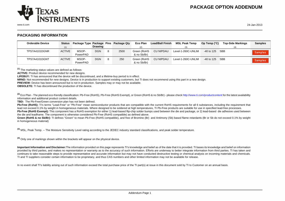
PACKAGING INFORMATION
Orderable Device Status(1)
Package Type PackageDrawing
Pins Package Qty Eco Plan(2)
Lead/Ball Finish MSL Peak Temp(3)
Op Temp (°C) Top-Side Markings(4)
Samples
TPS7A4101DGNR ACTIVE MSOP-PowerPAD
DGN 8 2500 Green (RoHS& no Sb/Br)
CU NIPDAU Level-1-260C-UNLIM -40 to 125 SBB
TPS7A4101DGNT ACTIVE MSOP-PowerPAD
DGN 8 250 Green (RoHS& no Sb/Br)
CU NIPDAU Level-1-260C-UNLIM -40 to 125 SBB
(1) The marketing status values are defined as follows:ACTIVE: Product device recommended for new designs.LIFEBUY: TI has announced that the device will be discontinued, and a lifetime-buy period is in effect.NRND: Not recommended for new designs. Device is in production to support existing customers, but TI does not recommend using this part in a new design.PREVIEW: Device has been announced but is not in production. Samples may or may not be available.OBSOLETE: TI has discontinued the production of the device.
(2) Eco Plan - The planned eco-friendly classification: Pb-Free (RoHS), Pb-Free (RoHS Exempt), or Green (RoHS & no Sb/Br) - please check http://www.ti.com/productcontent for the latest availabilityinformation and additional product content details.TBD: The Pb-Free/Green conversion plan has not been defined.Pb-Free (RoHS): TI's terms "Lead-Free" or "Pb-Free" mean semiconductor products that are compatible with the current RoHS requirements for all 6 substances, including the requirement thatlead not exceed 0.1% by weight in homogeneous materials. Where designed to be soldered at high temperatures, TI Pb-Free products are suitable for use in specified lead-free processes.Pb-Free (RoHS Exempt): This component has a RoHS exemption for either 1) lead-based flip-chip solder bumps used between the die and package, or 2) lead-based die adhesive used betweenthe die and leadframe. The component is otherwise considered Pb-Free (RoHS compatible) as defined above.Green (RoHS & no Sb/Br): TI defines "Green" to mean Pb-Free (RoHS compatible), and free of Bromine (Br) and Antimony (Sb) based flame retardants (Br or Sb do not exceed 0.1% by weightin homogeneous material)
(3) MSL, Peak Temp. -- The Moisture Sensitivity Level rating according to the JEDEC industry standard classifications, and peak solder temperature.
(4) Only one of markings shown within the brackets will appear on the physical device.
Important Information and Disclaimer:The information provided on this page represents TI's knowledge and belief as of the date that it is provided. TI bases its knowledge and belief on informationprovided by third parties, and makes no representation or warranty as to the accuracy of such information. Efforts are underway to better integrate information from third parties. TI has taken andcontinues to take reasonable steps to provide representative and accurate information but may not have conducted destructive testing or chemical analysis on incoming materials and chemicals.TI and TI suppliers consider certain information to be proprietary, and thus CAS numbers and other limited information may not be available for release.
In no event shall TI's liability arising out of such information exceed the total purchase price of the TI part(s) at issue in this document sold by TI to Customer on an annual basis.
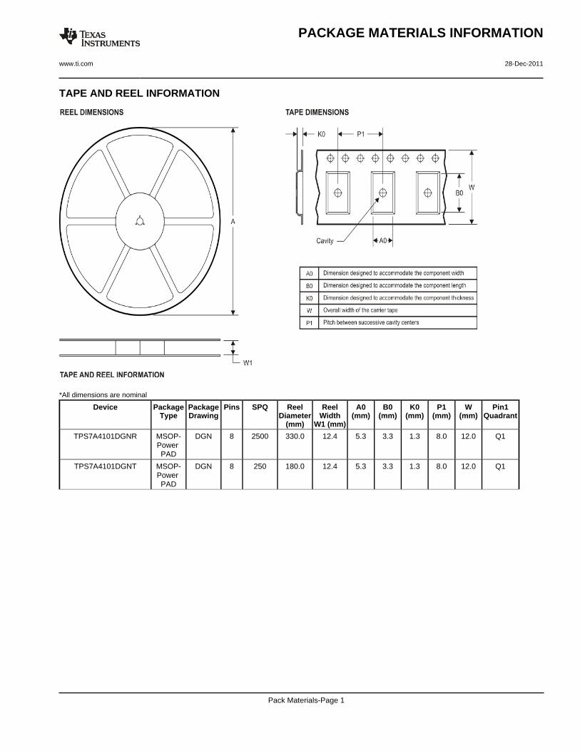
TAPE AND REEL INFORMATION
*All dimensions are nominal
Device PackageType
PackageDrawing
Pins SPQ ReelDiameter
(mm)
ReelWidth
W1 (mm)
A0(mm)
B0(mm)
K0(mm)
P1(mm)
W(mm)
Pin1Quadrant
TPS7A4101DGNR MSOP-Power PAD
DGN 8 2500 330.0 12.4 5.3 3.3 1.3 8.0 12.0 Q1
TPS7A4101DGNT MSOP-Power PAD
DGN 8 250 180.0 12.4 5.3 3.3 1.3 8.0 12.0 Q1
PACKAGE MATERIALS INFORMATION
www.ti.com 28-Dec-2011
Pack Materials-Page 1
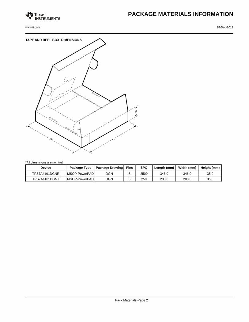
*All dimensions are nominal
Device Package Type Package Drawing Pins SPQ Length (mm) Width (mm) Height (mm)
TPS7A4101DGNR MSOP-PowerPAD DGN 8 2500 346.0 346.0 35.0
TPS7A4101DGNT MSOP-PowerPAD DGN 8 250 203.0 203.0 35.0
PACKAGE MATERIALS INFORMATION
www.ti.com 28-Dec-2011
Pack Materials-Page 2
IMPORTANT NOTICE
Texas Instruments Incorporated and its subsidiaries (TI) reserve the right to make corrections, enhancements, improvements and otherchanges to its semiconductor products and services per JESD46, latest issue, and to discontinue any product or service per JESD48, latestissue. Buyers should obtain the latest relevant information before placing orders and should verify that such information is current andcomplete. All semiconductor products (also referred to herein as “components”) are sold subject to TI’s terms and conditions of salesupplied at the time of order acknowledgment.
TI warrants performance of its components to the specifications applicable at the time of sale, in accordance with the warranty in TI’s termsand conditions of sale of semiconductor products. Testing and other quality control techniques are used to the extent TI deems necessaryto support this warranty. Except where mandated by applicable law, testing of all parameters of each component is not necessarilyperformed.
TI assumes no liability for applications assistance or the design of Buyers’ products. Buyers are responsible for their products andapplications using TI components. To minimize the risks associated with Buyers’ products and applications, Buyers should provideadequate design and operating safeguards.
TI does not warrant or represent that any license, either express or implied, is granted under any patent right, copyright, mask work right, orother intellectual property right relating to any combination, machine, or process in which TI components or services are used. Informationpublished by TI regarding third-party products or services does not constitute a license to use such products or services or a warranty orendorsement thereof. Use of such information may require a license from a third party under the patents or other intellectual property of thethird party, or a license from TI under the patents or other intellectual property of TI.
Reproduction of significant portions of TI information in TI data books or data sheets is permissible only if reproduction is without alterationand is accompanied by all associated warranties, conditions, limitations, and notices. TI is not responsible or liable for such altereddocumentation. Information of third parties may be subject to additional restrictions.
Resale of TI components or services with statements different from or beyond the parameters stated by TI for that component or servicevoids all express and any implied warranties for the associated TI component or service and is an unfair and deceptive business practice.TI is not responsible or liable for any such statements.
Buyer acknowledges and agrees that it is solely responsible for compliance with all legal, regulatory and safety-related requirementsconcerning its products, and any use of TI components in its applications, notwithstanding any applications-related information or supportthat may be provided by TI. Buyer represents and agrees that it has all the necessary expertise to create and implement safeguards whichanticipate dangerous consequences of failures, monitor failures and their consequences, lessen the likelihood of failures that might causeharm and take appropriate remedial actions. Buyer will fully indemnify TI and its representatives against any damages arising out of the useof any TI components in safety-critical applications.
In some cases, TI components may be promoted specifically to facilitate safety-related applications. With such components, TI’s goal is tohelp enable customers to design and create their own end-product solutions that meet applicable functional safety standards andrequirements. Nonetheless, such components are subject to these terms.
No TI components are authorized for use in FDA Class III (or similar life-critical medical equipment) unless authorized officers of the partieshave executed a special agreement specifically governing such use.
Only those TI components which TI has specifically designated as military grade or “enhanced plastic” are designed and intended for use inmilitary/aerospace applications or environments. Buyer acknowledges and agrees that any military or aerospace use of TI componentswhich have not been so designated is solely at the Buyer's risk, and that Buyer is solely responsible for compliance with all legal andregulatory requirements in connection with such use.
TI has specifically designated certain components as meeting ISO/TS16949 requirements, mainly for automotive use. In any case of use ofnon-designated products, TI will not be responsible for any failure to meet ISO/TS16949.
Products Applications
Audio www.ti.com/audio Automotive and Transportation www.ti.com/automotive
Amplifiers amplifier.ti.com Communications and Telecom www.ti.com/communications
Data Converters dataconverter.ti.com Computers and Peripherals www.ti.com/computers
DLP® Products www.dlp.com Consumer Electronics www.ti.com/consumer-apps
DSP dsp.ti.com Energy and Lighting www.ti.com/energy
Clocks and Timers www.ti.com/clocks Industrial www.ti.com/industrial
Interface interface.ti.com Medical www.ti.com/medical
Logic logic.ti.com Security www.ti.com/security
Power Mgmt power.ti.com Space, Avionics and Defense www.ti.com/space-avionics-defense
Microcontrollers microcontroller.ti.com Video and Imaging www.ti.com/video
RFID www.ti-rfid.com
OMAP Applications Processors www.ti.com/omap TI E2E Community e2e.ti.com
Wireless Connectivity www.ti.com/wirelessconnectivity
Mailing Address: Texas Instruments, Post Office Box 655303, Dallas, Texas 75265Copyright © 2013, Texas Instruments Incorporated