Embed Size (px)
Citation preview

© Semiconductor Components Industries, LLC, 2017
March, 2020 − Rev. 31 Publication Order Number:
FGY120T65SPD−F085/D
Field Stop Trench IGBT WithSoft Fast Recovery Diode650 V, 120 A
FGY120T65SPD-F085
Features• Very Low Saturation Voltage : VCE(sat) = 1.5 V(Typ.) @ IC = 120 A
• Maximum Junction Temperature : TJ = 175°C
• Positive Temperature Co−efficient
• Tight Parameter Distribution
• High Input Impedance
• 100% of the Parts are Dynamically Tested
• Short Circuit Ruggedness > 6 �s @ 25°C
• Copacked with Soft, Fast Recovery Extremefast Diode
• AEC−Q101 Qualified and PPAP Capable
• This is a Pb−Free Device
Benefits• Very Low Conduction and Switching Losses for a High Efficiency
Operation in Various Applications• Rugged Transient Reliability
• Outstanding Parallel Operation Performance with Balance CurrentSharing
• Low EMI
Applications• Traction Inverter for HEV/EV
• Auxiliary DC/AC Converter
• Motor Drives
• Other Power−train Applications Requiring High Power Switch
www.onsemi.com
See detailed ordering and shipping information on page 2 ofthis data sheet.
ORDERING INFORMATION
MARKING DIAGRAM
TO−247−3LDCASE 340CU
GC
E
$Y&Z&3&KFGY120T65SPD
$Y = ON Semiconductor Logo&Z = Assembly Plant Code&3 = Data Code (Year & Week)&K = LotFGY120T65SPD= Specific Device Code
C
E
G
FGY120T65SPD−F085
www.onsemi.com2
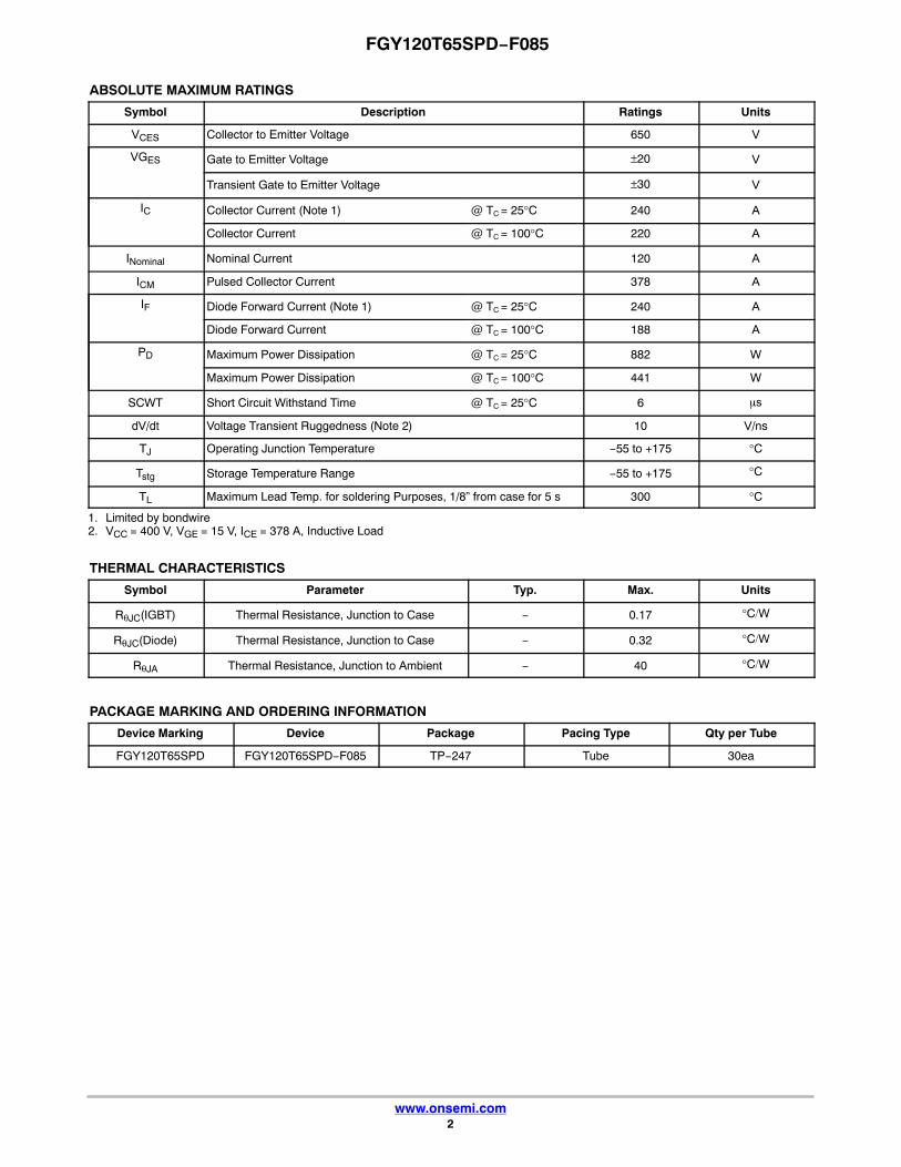
ABSOLUTE MAXIMUM RATINGS
Symbol Description Ratings Units
VCES Collector to Emitter Voltage 650 V
VGES Gate to Emitter Voltage ±20 V
Transient Gate to Emitter Voltage ±30 V
IC Collector Current (Note 1) @ TC = 25°C 240 A
Collector Current @ TC = 100°C 220 A
INominal Nominal Current 120 A
ICM Pulsed Collector Current 378 A
IF Diode Forward Current (Note 1) @ TC = 25°C 240 A
Diode Forward Current @ TC = 100°C 188 A
PD Maximum Power Dissipation @ TC = 25°C 882 W
Maximum Power Dissipation @ TC = 100°C 441 W
SCWT Short Circuit Withstand Time @ TC = 25°C 6 �s
dV/dt Voltage Transient Ruggedness (Note 2) 10 V/ns
TJ Operating Junction Temperature −55 to +175 °C
Tstg Storage Temperature Range −55 to +175 °C
TL Maximum Lead Temp. for soldering Purposes, 1/8” from case for 5 s 300 °C
1. Limited by bondwire2. VCC = 400 V, VGE = 15 V, ICE = 378 A, Inductive Load
THERMAL CHARACTERISTICS
Symbol Parameter Typ. Max. Units
RθJC(IGBT) Thermal Resistance, Junction to Case − 0.17 °C/W
RθJC(Diode) Thermal Resistance, Junction to Case − 0.32 °C/W
RθJA Thermal Resistance, Junction to Ambient − 40 °C/W
PACKAGE MARKING AND ORDERING INFORMATION
Device Marking Device Package Pacing Type Qty per Tube
FGY120T65SPD FGY120T65SPD−F085 TP−247 Tube 30ea

FGY120T65SPD−F085
www.onsemi.com3
ELECTRICAL CHARACTERISTICS OF THE IGBT TJ = 25 °C unless otherwise noted
Symbol Parameter Test Conditions Min. Typ. Max. Units
OFF CHARACTERISTICS
BVCES Collector to Emitter Breakdown Voltage VGE = 0 V, IC = 1 mA 650 − − V
�BVCES
�TJ
Temperature Coefficient of BreakdownVoltage
VGE = 0 V, IC = 1 mA − 0.6 − V/°C
ICES Collector Cut−Off Current VCE = VCES, VGE = 0 V − − 40 μA
IGES G−E Leakage Current VGE = VGES, VCE = 0 V − − ± 250 nA
ON CHARACTERISTICS
VGE(th) G−E Threshold Voltage IC = 120 mA, VCE = VGE 4.2 5.4 6.2 V
VCE(sat) Collector to Emitter Saturation Voltage IC = 120 A, VGE = 15 V − 1.5 1.85 V
IC = 120 A, VGE = 15 V, TJ = 175°C − 1.8 − V
DYNAMIC CHARACTERISTICS
Cies Input Capacitance VCE = 30 V, VGE = 0 V,f = 1 MHz
− 6810 − pF
Coes Output Capacitance − 440 − pF
Cres Reverse Transfer Capacitance − 50 − pF
RG Internal Gate Resistance f = 1 MHz − 3 − �
SWITCHING CHARACTERISTICS
Td(on) Turn−On Delay Time VCC = 400 V, IC = 120 A, RG = 5 �, VGE = 15 V,Inductive Load, TJ = 25°C
− 53 − ns
Tr Rise Time − 134 − ns
Td(off) Turn−Off Delay Time − 102 − ns
Tf Fall Time − 115 − ns
Eon Turn−On Switching Loss − 6.8 − mJ
Eoff Turn−Off Switching Loss − 3.5 − mJ
Ets Total Switching Loss − 10.3 − mJ
Td(on) Turn−On Delay Time VCC = 400 V, IC = 120 A, RG = 5 �, VGE = 15 V,Inductive Load, TJ = 175°C
− 50 − ns
Tr Rise Time − 133 − ns
Td(off) Turn−Off Delay Time − 109 − ns
Tf Fall Time − 138 − ns
Eon Turn−On Switching Loss − 9.8 − mJ
Eoff Turn−Off Switching Loss − 4.0 − mJ
Ets Total Switching Loss − 13.8 − mJ
Qg Total Gate Charge VCE = 400 V, IC = 120 A, VGE = 15 V − 162 243 nC
Qge Gate to Emitter Charge − 49 − nC
Qgc Gate to Collector Charge − 47 − nC

FGY120T65SPD−F085
www.onsemi.com4
ELECTRICAL CHARACTERISTICS OF THE DIODE TJ = 25°C unless otherwise noted
Symbol Parameter Test Conditions Min. Typ. Max Units
VFM Diode Forward Voltage IF = 120 A TJ = 25°C − 1.3 1.6 V
TJ = 175°C − 1.2 −
Erec Reverse Recovery Energy VCE = 400V, IF = 120 A,dIF/dt = 1000 A/μs
TJ = 25°C − 450 − μJ
TJ = 175°C − 3000 −
Trr Diode Reverse Recovery Time TJ = 25°C − 123 − ns
TJ = 175°C − 240 −
Qrr Diode Reverse Recovery Charge TJ = 25°C − 2.8 − μC
TJ = 175°C − 12.2 −

FGY120T65SPD−F085
www.onsemi.com5
TYPICAL PERFORMANCE CHARACTERISTICS
Figure 1. Typical Output Characteristics Figure 2. Typical Output Characteristics
Figure 3. Typical Saturation VoltageCharacteristics
Figure 4. Transfer Characteristics
Figure 5. Saturation Voltage vs. Case Temperature at Variant Current Level
Figure 6. Saturation Voltage vs. VGE
0 2 4 6 80
60
120
180
240
300
360
20V
TC = 25oC
15V12V10V
VGE = 8V
Co
lle
cto
r C
urr
en
t, I
C [
A]
Collector−Emitter Voltage, VCE [V]0 2 4 6 8
0
60
120
180
240
300
360
20V
TC = 175oC
15V12V10V
VGE = 8V
Co
lle
cto
r C
urr
en
t, I
C [
A]
Collector−Emitter Voltage, VCE [V]
0 1 2 3 4 50
60
120
180
240
300
360
Common EmitterVGE = 15V
TC = 25oC
TC = 175oC
Col
lect
or C
urre
nt, I
C [A
]
Collector−Emitter Voltage, VCE [V]
0 3 6 9 120
40
80
120
160Common EmitterVCE = 20V
TC = 25oC
TC = 175oCC
oll
ec
tor
Cu
rre
nt,
IC [A
]
Gate−Emitter Voltage,VGE [V]
25 50 75 100 125 150 1751.0
1.5
2.0
2.5
3.0
IC = 240A
IC = 60A
IC = 120A
Common EmitterVGE = 15V
Co
lle
cto
r−E
mit
ter
Vo
lta
ge
, V
CE
[V]
Collector−EmitterCase Temperature, TC [oC]
6 8 10 12 140
2
4
6
8
10
IC = 240A
IC = 120A
IC = 60A
Common Emitter
TC = −40 oC
Co
lle
cto
r−E
mit
ter
Vo
lta
ge
,VC
E [V
]
Gate−Emitter Voltage, VGE [V]

FGY120T65SPD−F085
www.onsemi.com6
TYPICAL PERFORMANCE CHARACTERISTICS (continued)
Figure 7. Saturation Voltage vs. VGE Figure 8. Saturation Voltage vs. VGE
Figure 9. Capacitance Characteristics Figure 10. Gate charge Characteristics
Figure 11. SOA Characteristics Figure 12. Turn off Switching SOA Characteristics
6 8 10 12 140
2
4
6
8
10
IC = 120A
IC = 240A
IC = 60A
Common Emitter
TC = 25 oCC
oll
ec
tor−
Em
itte
r V
olt
ag
e,V
CE
[V]
Gate−Emitter Voltage, VGE [V]
6 8 10 12 140
2
4
6
8
10
IC = 240A
IC = 120A
IC = 60A
Common Emitter
TC = 175oC
Co
lle
cto
r−E
mit
ter
Vo
lta
ge
,VC
E [V
]
Gate−Emitter Voltage, VGE [V]
0.1 1 1010
100
1000
10000
Common EmitterVGE = 0V, f = 1MHz
TC = 25oC
Cres
Coes
Cies
Cap
acit
ance
[p
F]
Collector−Emitter Voltage, VCE [V]30 0 50 100 150 200
0
3
6
9
12
15
VCC = 390V
VCC = 325V
Common Emitter
TC = 25oC
VCC = 260VG
ate−
Em
itter
Vo
ltag
e, V
GE [V
]
Gate Charge, Qg [nC]
1 10 100 10000.01
0.1
1
10
100
1000
10 ms
DC
Single Nonrepetetitive
Pulse TC = 25 oCCurves must be deratedlinearly with increase
in temperature
10�s
100�s
Co
lle
cto
r C
urr
en
t, I c
[A]
Collector−Emitter Voltage, VCE [V]
1
10
100 10001
10
100
1000
Col
lect
or C
urre
nt, I
C [A
]
Collector−Emitter Voltage, VCE [V]
1 ms
Safe Operating Area
VGE = 15V, T <= 175oCC
10

FGY120T65SPD−F085
www.onsemi.com7
TYPICAL PERFORMANCE CHARACTERISTICS (continued)
Figure 13. Turn−on Characteristics vs. GateResistance
Figure 14. Turn−off Characteristics vs. GateResistance
Figure 15. Turn−on Characteristics vs. Collector Current
Figure 16. Turn−off Characteristics vs. Collector Current
Figure 17. Switching Loss vs Gate Resistance Figure 18. Switching Loss vs Collector Current
0 10 20 30 40 5010
100
Common EmitterVCC = 400V, VGE = 15VIC = 120A
TC = 25 oC
TC = 175 oC
td(on)
tr
Sw
itch
ing
Tim
e [n
s]
Gate Resistance, RG [�]
200
0 10 20 30 40 5010
100
1000
Common EmitterVCC = 400V, VGE = 15VIC = 120A
TC = 25oC
TC = 175oC
td(off)
tf
Sw
itch
ing
Tim
e [n
s]
Gate Resistance, RG [�]
0 40 80 120 160 2001
10
100
1000
Common EmitterVGE = 15V, RG = 5 �
TC = 25 oC
TC = 175 oC
tr
td(on)
Sw
itch
ing
Tim
e [n
s]
Collector Current, IC [A]0 40 80 120 160 200
10
100
1000
Common EmitterVGE = 15V, RG = 5 �
TC = 25 oC
TC = 175 oC
td(off)
t f
Sw
itch
ing
Tim
e [n
s]
Collector Current, IC [A]
0 20 40 60 80 100 1200.1
1
10
100Common EmitterVGE = 15V, RG = 5 �
TC = 25 oC
TC = 175 oC Eon
Eoff
Sw
itch
ing
Lo
ss [m
J]
Collector Current, IC [A]0 10 20 30 40 50
1
10
Common EmitterVCC = 400V, VGE = 15VIC = 120A
TC = 25oC
TC = 175oC
Eon
EoffSw
itch
ing
Lo
ss [
mJ]
Gate Resistance, RG [�]
50

FGY120T65SPD−F085
www.onsemi.com8
TYPICAL PERFORMANCE CHARACTERISTICS (continued)
Figure 19. Forward Characteristics Figure 20. Reverse Current
Figure 21. Stored Charge Figure 22. Reverse Recovery Time
Figure 23. Collector to Emitter BreakdownVoltage vs. Junction Temperature
0.0 0.5 1.0 1.5 2.0 2.50.1
1
10
100
TC = 125 oC
TC = 25 oC
360
TC = 175 oC
Forward Voltage, VF [V]
Fo
rwar
d C
urr
ent,
IF [
A]
200 400 6000.01
0.1
1
10
100
1000
10000
65050
TC = 125oC
TC = 25oC
TC = 175oC
Reverse Voltage, V R [V]
Re
ve
rse
Cu
rre
nt,
IR
[�A
]
0 20 40 60 80 100 1200
50
100
150
200
250
300
di/dt = 1000A/�s
di/dt = 500A/�s
di/dt = 500A/�s
TC = 25oC
TC = 175oC
di/dt = 1000A/�s
Rev
erse
Rec
ove
ry T
ime,
trr
[ns]
Forward Current, IF [A]
0 20 40 60 80 100 120100
1000
10000
20000
di/dt = 500A/�s
di/dt = 1000A/�s
di/dt = 500A/�s
TC = 25 oC
TC = 175 oC
di/dt = 1000A/�s
Sto
red
Re
co
ve
ry C
ha
rge
, Q
rr [n
C]
Forward Current, IF [A]
−80 −40 0 40 80 120 160 200600
650
700
750
800IC = 1mA
CO
LL
EC
TO
R T
O E
MIT
TE
RB
RE
AK
DO
WN
VO
LTA
GE
, BV C
ES
[V]
TJ , JUNCTION TEMPERATURE (oC)

FGY120T65SPD−F085
www.onsemi.com9
TYPICAL PERFORMANCE CHARACTERISTICS (continued)
Figure 24. Transient Thermal Impedance of IGBT
Figure 25. Transient Thermal Impedance of Diode

TO−247−3LDCASE 340CU
ISSUE BDATE 28 OCT 2021
XXXX = Specific Device CodeA = Assembly Site CodeY = YearWW = Work WeekZZ = Assembly Lot Code
*This information is generic. Please refer todevice data sheet for actual part marking.Pb−Free indicator, “G” or microdot “�”, mayor may not be present. Some products maynot follow the Generic Marking.
GENERICMARKING DIAGRAM*
AYWWZZXXXXXXXXXXXXXXXXXX
MECHANICAL CASE OUTLINE
PACKAGE DIMENSIONS
98AON13773GDOCUMENT NUMBER:
DESCRIPTION:
Electronic versions are uncontrolled except when accessed directly from the Document Repository.Printed versions are uncontrolled except when stamped “CONTROLLED COPY” in red.
PAGE 1 OF 1TO−247−3LD
onsemi and are trademarks of Semiconductor Components Industries, LLC dba onsemi or its subsidiaries in the United States and/or other countries. onsemi reservesthe right to make changes without further notice to any products herein. onsemi makes no warranty, representation or guarantee regarding the suitability of its products for any particularpurpose, nor does onsemi assume any liability arising out of the application or use of any product or circuit, and specifically disclaims any and all liability, including without limitationspecial, consequential or incidental damages. onsemi does not convey any license under its patent rights nor the rights of others.
© Semiconductor Components Industries, LLC, 2018 www.onsemi.com

onsemi, , and other names, marks, and brands are registered and/or common law trademarks of Semiconductor Components Industries, LLC dba “onsemi” or its affiliatesand/or subsidiaries in the United States and/or other countries. onsemi owns the rights to a number of patents, trademarks, copyrights, trade secrets, and other intellectual property.A listing of onsemi’s product/patent coverage may be accessed at www.onsemi.com/site/pdf/Patent−Marking.pdf. onsemi reserves the right to make changes at any time to anyproducts or information herein, without notice. The information herein is provided “as−is” and onsemi makes no warranty, representation or guarantee regarding the accuracy of theinformation, product features, availability, functionality, or suitability of its products for any particular purpose, nor does onsemi assume any liability arising out of the application or useof any product or circuit, and specifically disclaims any and all liability, including without limitation special, consequential or incidental damages. Buyer is responsible for its productsand applications using onsemi products, including compliance with all laws, regulations and safety requirements or standards, regardless of any support or applications informationprovided by onsemi. “Typical” parameters which may be provided in onsemi data sheets and/or specifications can and do vary in different applications and actual performance mayvary over time. All operating parameters, including “Typicals” must be validated for each customer application by customer’s technical experts. onsemi does not convey any licenseunder any of its intellectual property rights nor the rights of others. onsemi products are not designed, intended, or authorized for use as a critical component in life support systemsor any FDA Class 3 medical devices or medical devices with a same or similar classification in a foreign jurisdiction or any devices intended for implantation in the human body. ShouldBuyer purchase or use onsemi products for any such unintended or unauthorized application, Buyer shall indemnify and hold onsemi and its officers, employees, subsidiaries, affiliates,and distributors harmless against all claims, costs, damages, and expenses, and reasonable attorney fees arising out of, directly or indirectly, any claim of personal injury or deathassociated with such unintended or unauthorized use, even if such claim alleges that onsemi was negligent regarding the design or manufacture of the part. onsemi is an EqualOpportunity/Affirmative Action Employer. This literature is subject to all applicable copyright laws and is not for resale in any manner.
PUBLICATION ORDERING INFORMATIONTECHNICAL SUPPORTNorth American Technical Support:Voice Mail: 1 800−282−9855 Toll Free USA/CanadaPhone: 011 421 33 790 2910
LITERATURE FULFILLMENT:Email Requests to: [email protected]
onsemi Website: www.onsemi.com
Europe, Middle East and Africa Technical Support:Phone: 00421 33 790 2910For additional information, please contact your local Sales Representative
◊


