Embed Size (px)
Citation preview
1
This material exempt per Department of Commerce license exception TSU
ZynqVivado 2014.2 Version
7-Series Architecture Overview
© Copyright 2014 Xilinx
After completing this module, you will be able to:
– Describe the basic slice resources available in 7-Series FPGAs
– List memory hierarchy and various memory resources available
– Identify the basic I/O resources available in 7-Series FPGAs
– List some of the dedicated hardware features of 7-Series FPGAs
– Explain the available clocking resources and mechanism
Objectives
© Copyright 2014 Xilinx7-Series Architecture Overview 11-2
2
Introduction to 7-Series FPGA and Zynq SoC
Logic Resources
I/O Resources
Memory and DSP48 Resources
XADC
Clocking Resources
Summary
Outline
© Copyright 2014 Xilinx7-Series Architecture Overview 11-3
All Xilinx FPGAs contain the same basic resources– Logic Resources
• Slices (grouped into configurable logic blocks (CLB))� Contain combinatorial logic and register resources
• Memory
• Multipliers
– Interconnect Resources• Programmable interconnect
• IOBs� Interface between the FPGA and the outside world
– Other resources• Global clock buffers
• Boundary scan logic
Through various generations, Xilinx added new architectural resources to target various
markets and application areas
Introduction
© Copyright 2014 Xilinx7-Series Architecture Overview- 4
3
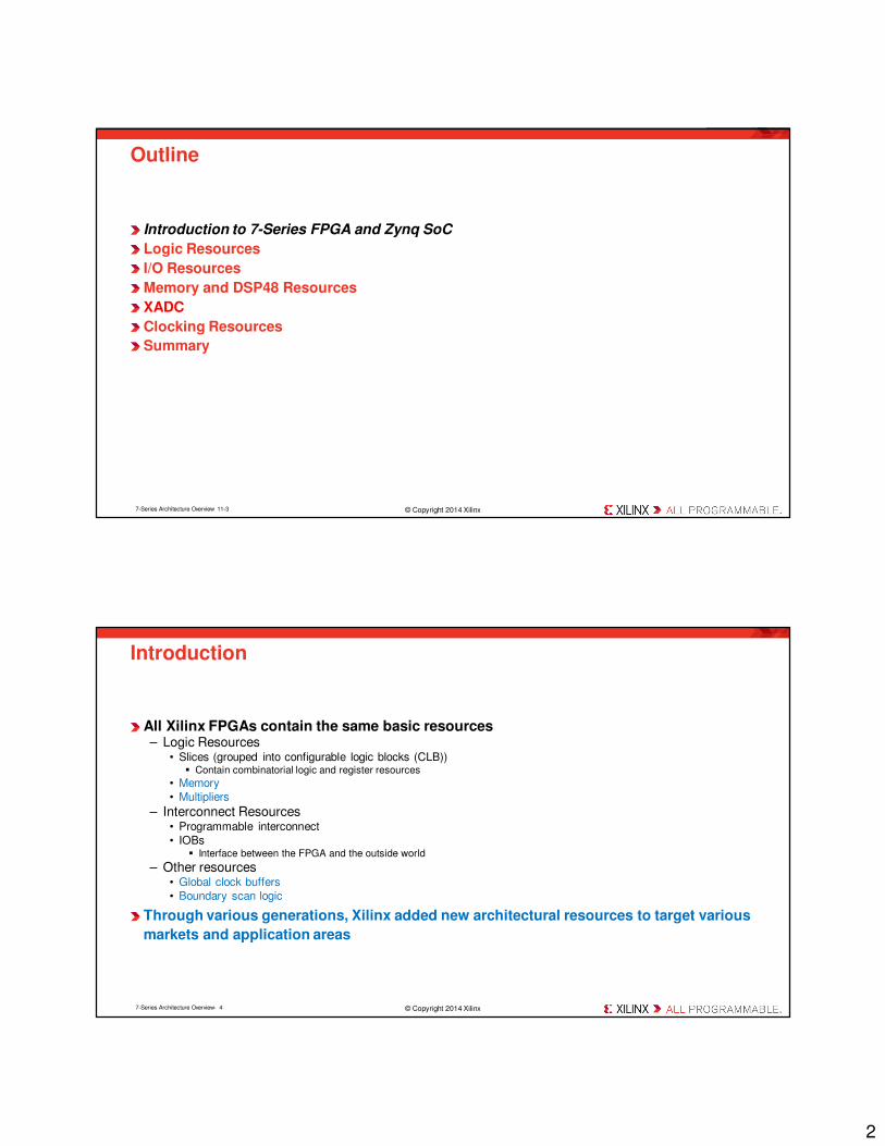
Logic Cells in K
Block RAM in Mb
DSP Slices
Peak DSP Perf. (GMACs)
Transceivers
Transceiver Perf. (Gbps)
Memory Perf. (Mbps)
User I/O Pins
I/O Voltages
Lowest Power
and CostIndustry’s Best
Price/Performance
Industry’s Highest
PerformanceMaximum Capability
All Programmable
SoC
7-Series FPGA+SoC Families
© Copyright 2014 Xilinx7-Series Architecture Overview- 5
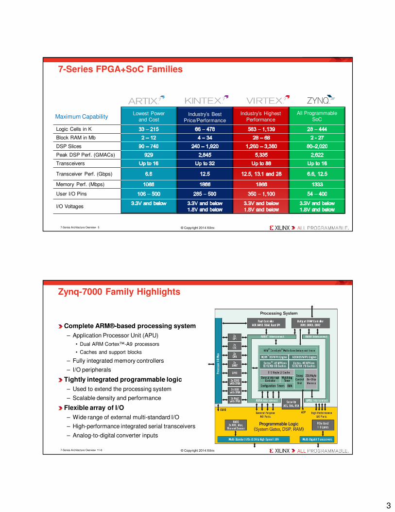
Complete ARM®-based processing system
– Application Processor Unit (APU)
• Dual ARM Cortex™-A9 processors
• Caches and support blocks
– Fully integrated memory controllers
– I/O peripherals
Tightly integrated programmable logic
– Used to extend the processing system
– Scalable density and performance
Flexible array of I/O
– Wide range of external multi-standard I/O
– High-performance integrated serial transceivers
– Analog-to-digital converter inputs
Zynq-7000 Family Highlights
© Copyright 2014 Xilinx7-Series Architecture Overview 11-6
4
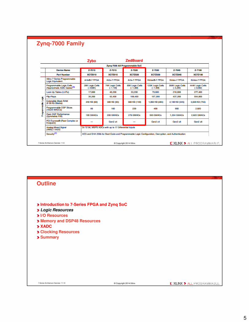
The Zynq-7000 AP SoC architecture consists of two major sections
– PS: Processing system
• Dual ARM Cortex-A9 processor based
• Multiple peripherals
• Hard silicon core
– PL: Programmable logic
• Shares the same 7-series programmable logic as
� Artix™-based devices: Z-7010, Z-7015 and Z-7020 (high-range I/O banks only)
� Kintex™-based devices: Z-7030, Z-7045 and Z-7100 (mix of high-range and high-performance I/O
banks)
The PS and the PL
© Copyright 2014 Xilinx7-Series Architecture Overview 11-7
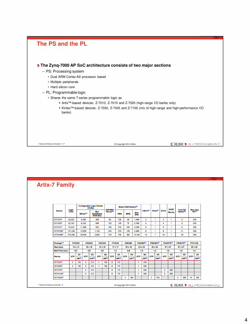
Artix-7 Family
© Copyright 2014 Xilinx7-Series Architecture Overview- 8
5
Zynq-7000 Family
© Copyright 2014 Xilinx7-Series Architecture Overview 11-9
Zybo ZedBoard
Introduction to 7-Series FPGA and Zynq SoC
Logic Resources
I/O Resources
Memory and DSP48 Resources
XADC
Clocking Resources
Summary
Outline
© Copyright 2014 Xilinx7-Series Architecture Overview 11-10
6
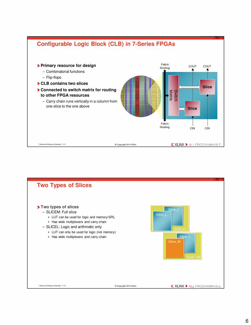
Primary resource for design
– Combinatorial functions
– Flip-flops
CLB contains two slices
Connected to switch matrix for routing
to other FPGA resources
– Carry chain runs vertically in a column from
one slice to the one above
Configurable Logic Block (CLB) in 7-Series FPGAs
© Copyright 2014 Xilinx7-Series Architecture Overview 11-11
Two types of slices
– SLICEM: Full slice
• LUT can be used for logic and memory/SRL
• Has wide multiplexers and carry chain
– SLICEL: Logic and arithmetic only
• LUT can only be used for logic (not memory)
• Has wide multiplexers and carry chain
Two Types of Slices
© Copyright 2014 Xilinx7-Series Architecture Overview 11-12
7
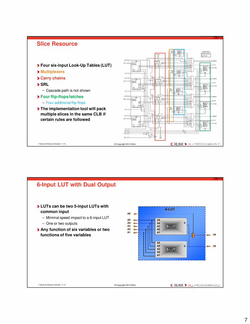
Four six-input Look-Up Tables (LUT)
Multiplexers
Carry chains
SRL
– Cascade path is not shown
Four flip-flops/latches
– Four additional flip-flops
The implementation tool will pack
multiple slices in the same CLB if
certain rules are followed
Slice Resource
© Copyright 2014 Xilinx7-Series Architecture Overview 11-13
LUTs can be two 5-input LUTs with
common input
– Minimal speed impact to a 6-input LUT
– One or two outputs
Any function of six variables or two
functions of five variables
6-Input LUT with Dual Output
© Copyright 2014 Xilinx7-Series Architecture Overview 11-14
8
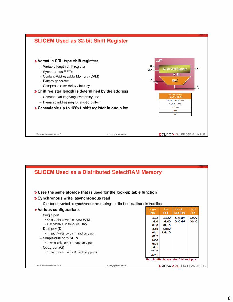
Versatile SRL-type shift registers
– Variable-length shift register
– Synchronous FIFOs
– Content-Addressable Memory (CAM)
– Pattern generator
– Compensate for delay / latency
Shift register length is determined by the address
– Constant value giving fixed delay line
– Dynamic addressing for elastic buffer
Cascadable up to 128x1 shift register in one slice
SLICEM Used as 32-bit Shift Register
© Copyright 2014 Xilinx7-Series Architecture Overview 11-15
Uses the same storage that is used for the look-up table function
Synchronous write, asynchronous read
– Can be converted to synchronous read using the flip-flops available in the slice
Various configurations
– Single port
• One LUT6 = 64x1 or 32x2 RAM
• Cascadable up to 256x1 RAM
– Dual port (D)
• 1 read / write port + 1 read-only port
– Simple dual port (SDP)
• 1 write-only port + 1 read-only port
– Quad-port (Q)
• 1 read / write port + 3 read-only ports
SLICEM Used as a Distributed SelectRAM Memory
© Copyright 2014 Xilinx7-Series Architecture Overview 11-16
9
Introduction to 7-Series FPGA and Zynq SoC
Logic Resources
I/O Resources
Memory and DSP48 Resources
XADC
Clocking Resources
Summary
Outline
© Copyright 2014 Xilinx7-Series Architecture Overview 11-17
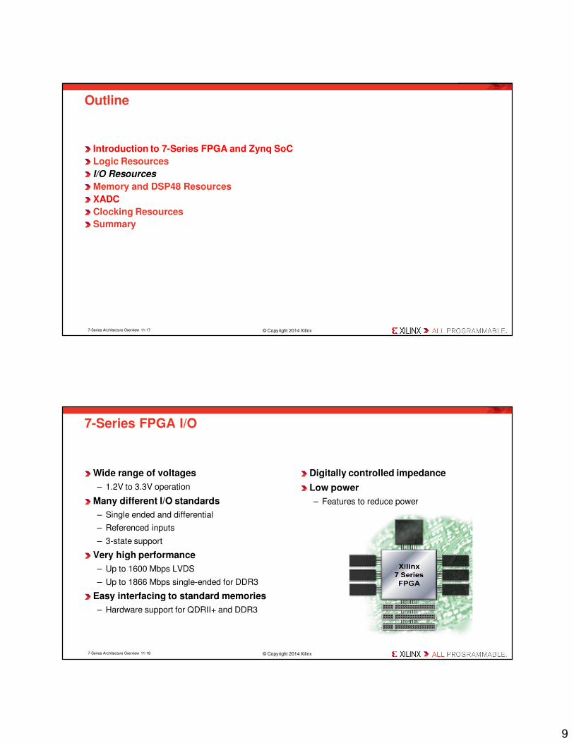
7-Series FPGA I/O
Wide range of voltages
– 1.2V to 3.3V operation
Many different I/O standards
– Single ended and differential
– Referenced inputs
– 3-state support
Very high performance
– Up to 1600 Mbps LVDS
– Up to 1866 Mbps single-ended for DDR3
Easy interfacing to standard memories
– Hardware support for QDRII+ and DDR3
Digitally controlled impedance
Low power
– Features to reduce power
© Copyright 2014 Xilinx7-Series Architecture Overview 11-18
10
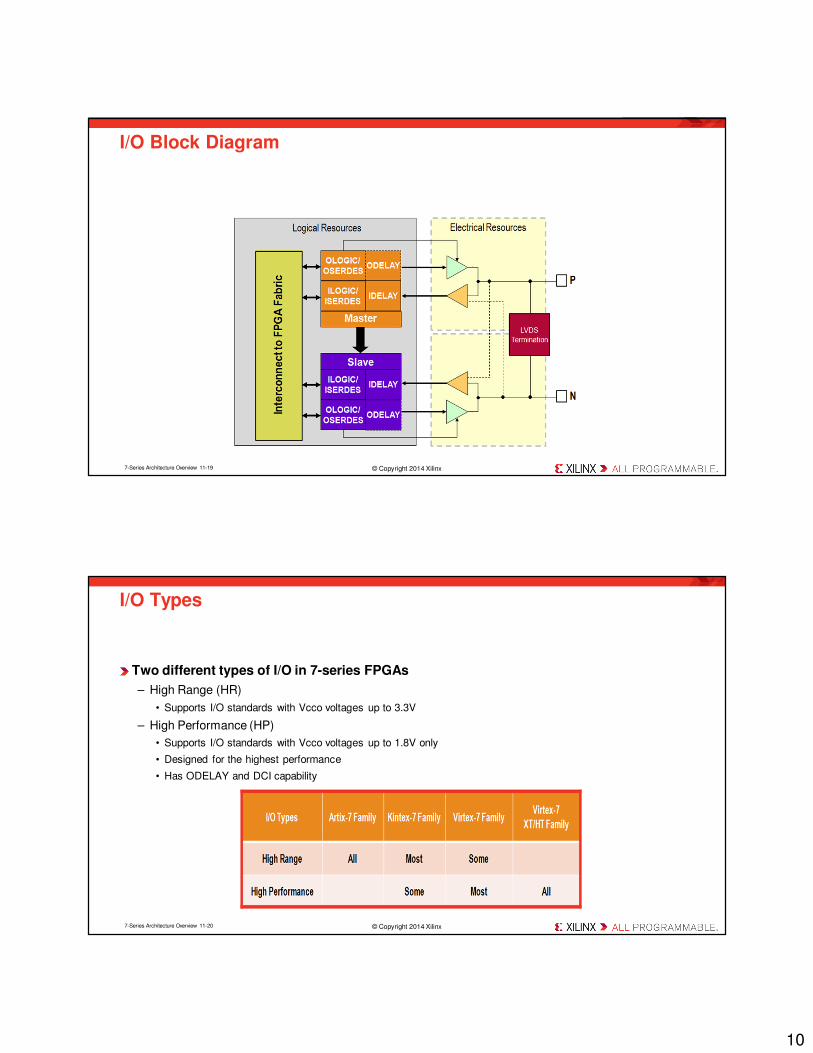
I/O Block Diagram
© Copyright 2014 Xilinx7-Series Architecture Overview 11-19
Two different types of I/O in 7-series FPGAs
– High Range (HR)
• Supports I/O standards with Vcco voltages up to 3.3V
– High Performance (HP)
• Supports I/O standards with Vcco voltages up to 1.8V only
• Designed for the highest performance
• Has ODELAY and DCI capability
I/O Types
© Copyright 2014 Xilinx7-Series Architecture Overview 11-20
11
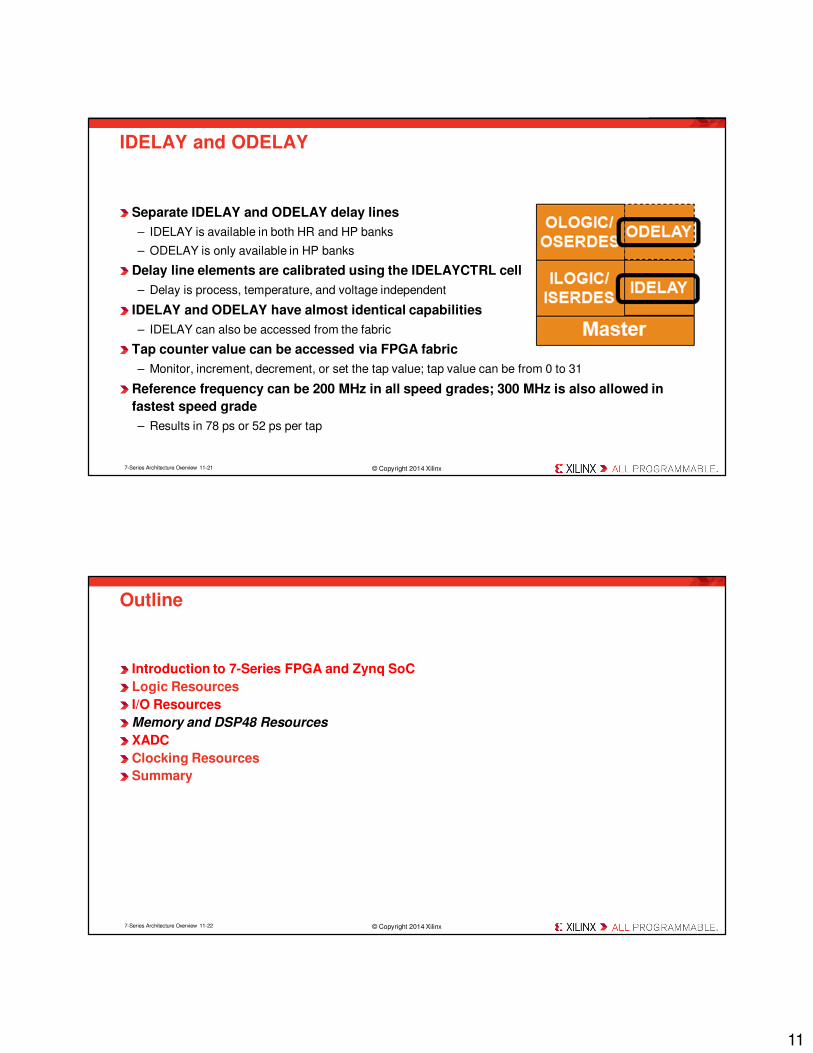
Separate IDELAY and ODELAY delay lines
– IDELAY is available in both HR and HP banks
– ODELAY is only available in HP banks
Delay line elements are calibrated using the IDELAYCTRL cell
– Delay is process, temperature, and voltage independent
IDELAY and ODELAY have almost identical capabilities
– IDELAY can also be accessed from the fabric
Tap counter value can be accessed via FPGA fabric
– Monitor, increment, decrement, or set the tap value; tap value can be from 0 to 31
Reference frequency can be 200 MHz in all speed grades; 300 MHz is also allowed in
fastest speed grade
– Results in 78 ps or 52 ps per tap
IDELAY and ODELAY
© Copyright 2014 Xilinx7-Series Architecture Overview 11-21
Introduction to 7-Series FPGA and Zynq SoC
Logic Resources
I/O Resources
Memory and DSP48 Resources
XADC
Clocking Resources
Summary
Outline
© Copyright 2014 Xilinx7-Series Architecture Overview 11-22
12
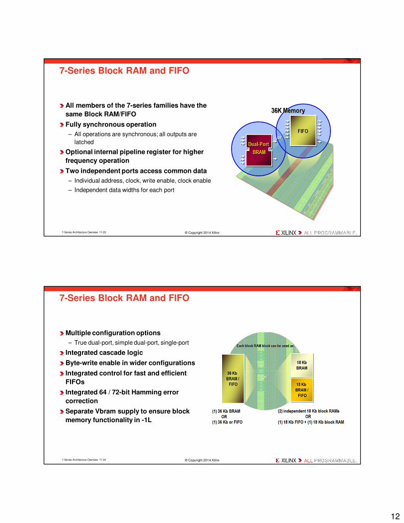
All members of the 7-series families have the
same Block RAM/FIFO
Fully synchronous operation
– All operations are synchronous; all outputs are
latched
Optional internal pipeline register for higher
frequency operation
Two independent ports access common data
– Individual address, clock, write enable, clock enable
– Independent data widths for each port
7-Series Block RAM and FIFO
© Copyright 2014 Xilinx7-Series Architecture Overview 11-23
Multiple configuration options
– True dual-port, simple dual-port, single-port
Integrated cascade logic
Byte-write enable in wider configurations
Integrated control for fast and efficient
FIFOs
Integrated 64 / 72-bit Hamming error
correction
Separate Vbram supply to ensure block
memory functionality in -1L
7-Series Block RAM and FIFO
© Copyright 2014 Xilinx7-Series Architecture Overview 11-24
13
Single read/write port
– Clock: CLKA, Address: ADDRA, Write enable: WEA
– Write data: DIA, Read data: DOA
36-kbit configurations
– 32k x 1, 16k x 2, 8k x 4, 4k x 9, 2k x 18, 1k x 36
18-kbit configurations
– 16k x 1, 8k x 2, 4k x 4, 2k x 9, 1k x 18, 512 x 36
Configurable write mode
– WRITE_FIRST: Data written on DIA is available on DOA
– READ_FIRST: Old contents of RAM at ADDRA is presented on DOA
– NO_CHANGE: The DOA holds its previous value (saves power)
Optional output register for maximum performance (DOA_REG=1)
Single-Port Block RAM
© Copyright 2014 Xilinx7-Series Architecture Overview 11-25
Two separate read/write ports
– Each port has separate clock, address, data in, data out, write
enable…
• Clocks can be asynchronous to each other
– The two ports can have different widths
• In 36-kbit configuration, one of the two ports must be 72 bits wide
� The other port can be x1, x2, x4, x9, x18, x36, or x72
• In 18-kbit configuration, one of the two ports must be 36 bits wide
� The other port can be x1, x2, x4, x9, x18, or x36
– The two ports can have different write modes
No contention avoidance when both ports access the
same address, except
– If clocked by the same clock, and the write port is
READ_FIRST, the read port gets the old data
Dual-Port Block RAM
© Copyright 2014 Xilinx7-Series Architecture Overview 11-26
14
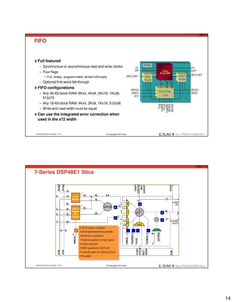
Full featured
– Synchronous or asynchronous read and write clocks
– Four flags
• Full, empty, programmable almost-full/empty
– Optional first-word-fall-through
FIFO configurations
– Any 36-Kb block RAM: 8Kx4, 4Kx9, 2Kx18, 1Kx36,
512x72
– Any 18-Kb block RAM: 4Kx4, 2Kx9, 1Kx18, 512x36
– Write and read width must be equal
Can use the integrated error correction when
used in the x72 width
FIFO
© Copyright 2014 Xilinx7-Series Architecture Overview 11-27
7-Series DSP48E1 Slice
© Copyright 2014 Xilinx7-Series Architecture Overview 11-28
15
Introduction to 7-Series FPGA and Zynq SoC
Logic Resources
I/O Resources
Memory and DSP48 Resources
XADC
Clocking Resources
Summary
Outline
© Copyright 2014 Xilinx7-Series Architecture Overview 11-29
XADC is a high quality and flexible analog interface new to the 7-series
– Dual 12-bit 1Msps ADCs, on-chip sensors, 17 flexible analog inputs, and track & holds with
programmable signal conditioning
– 1V input range
– 16-bit resolution conversion
– Built in digital gain and offset calibration
Analog Mixed Signal (AMS)
– Using the FPGA programmable logic to customize the XADC and replace other external analog
functions; for example, linearization, calibration, filtering, and DC balancing to improve data
conversion resolution
XADC and AMS
© Copyright 2014 Xilinx7-Series Architecture Overview 11-30
16
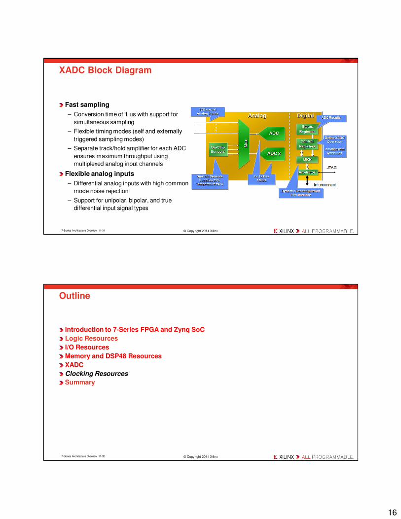
Fast sampling
– Conversion time of 1 us with support for
simultaneous sampling
– Flexible timing modes (self and externally
triggered sampling modes)
– Separate track/hold amplifier for each ADC
ensures maximum throughput using
multiplexed analog input channels
Flexible analog inputs
– Differential analog inputs with high common
mode noise rejection
– Support for unipolar, bipolar, and true
differential input signal types
XADC Block Diagram
© Copyright 2014 Xilinx7-Series Architecture Overview 11-31
Introduction to 7-Series FPGA and Zynq SoC
Logic Resources
I/O Resources
Memory and DSP48 Resources
XADC
Clocking Resources
Summary
Outline
© Copyright 2014 Xilinx7-Series Architecture Overview 11-32
17
Modern applications have complex clocking requirements
– Extremely high-performance clock signals
– Support for multiple frequency domains across a wide frequency
range
– De-skewing of clocks relative to one another
– Low jitter and precise duty cycle to maintain the widest possible
data valid window
– Lowest possible system power
Xilinx FPGAs have a rich mixture of clocking resources to
accommodate these requirements
– The perfect balance of resources at the right cost
High-Performance Clocking
© Copyright 2014 Xilinx7-Series Architecture Overview 11-33
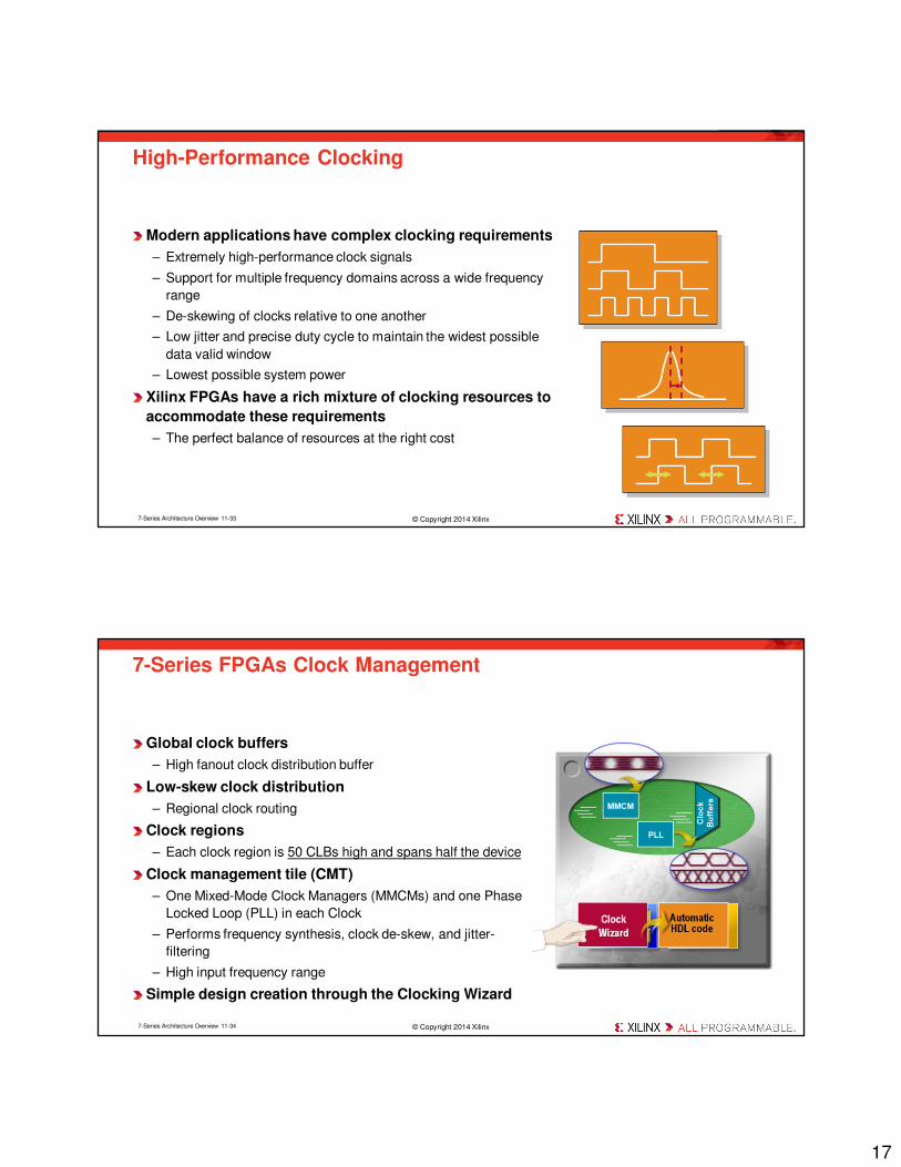
Global clock buffers
– High fanout clock distribution buffer
Low-skew clock distribution
– Regional clock routing
Clock regions
– Each clock region is 50 CLBs high and spans half the device
Clock management tile (CMT)
– One Mixed-Mode Clock Managers (MMCMs) and one Phase
Locked Loop (PLL) in each Clock
– Performs frequency synthesis, clock de-skew, and jitter-
filtering
– High input frequency range
Simple design creation through the Clocking Wizard
7-Series FPGAs Clock Management
© Copyright 2014 Xilinx7-Series Architecture Overview 11-34
18
An FPGA is a regular array of resources
– Many of these resources require clocks for synchronous operations
• Slice flip-flops, input/output flip-flops, block RAMs, DSP slices
– In order to implement synchronous designs, clocks must be distributed to these clocked elements
For synchronous operation, clocks must arrive at the clocked elements with
– Extremely low clock skew: Ensures minimal internal hold-time issues
– Low clock jitter: Allows for highest performance
– Duty cycle preservation: Important for Double Data Rate (DDR) applications
– Low insertion latency: Important for synchronous input and output interfaces
Clock Networks
© Copyright 2014 Xilinx7-Series Architecture Overview 11-35
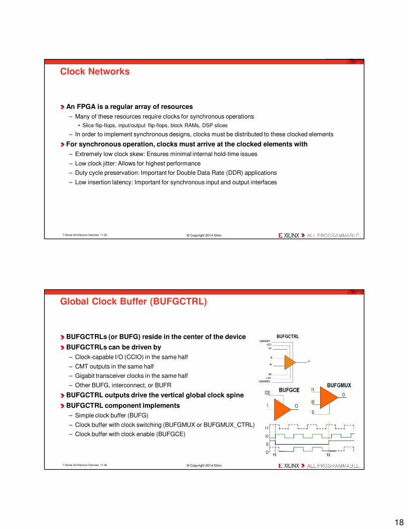
BUFGCTRLs (or BUFG) reside in the center of the device
BUFGCTRLs can be driven by
– Clock-capable I/O (CCIO) in the same half
– CMT outputs in the same half
– Gigabit transceiver clocks in the same half
– Other BUFG, interconnect, or BUFR
BUFGCTRL outputs drive the vertical global clock spine
BUFGCTRL component implements
– Simple clock buffer (BUFG)
– Clock buffer with clock switching (BUFGMUX or BUFGMUX_CTRL)
– Clock buffer with clock enable (BUFGCE)
Global Clock Buffer (BUFGCTRL)
© Copyright 2014 Xilinx7-Series Architecture Overview 11-36
19
Introduction to 7-Series FPGA and Zynq SoC
Logic Resources
I/O Resources
Memory and DSP48 Resources
XADC
Clocking Resources
Summary
Outline
© Copyright 2014 Xilinx7-Series Architecture Overview 11-37
The 7-series FPGA slices contain four 6-input LUTs, eight registers, and carry logic
– LUTs can perform any combinatorial function of up to six inputs
– Some LUTs can be configured as shift registers or memories
– Slices also contain carry logic and the MUXF7 and MUXF8 multiplexers
– The carry logic can be used to implement fast addition, subtraction, and comparison operations
The 7-series FPGA IOBs contain DDR registers as well as SERDES resources
The 7-series FPGA includes dedicated block RAM and DSP slice resources
The 7-series FPGAs include other dedicated hardware such as XADC
The Zynq-7000 processing platform is a system on a chip (SoC) processor with
embedded programmable logic fabric of either Artix or Kintex 7-series FPGA
The 7-series FPGAs includes dedicated MMCMs, PLLs, and routing resources to
improve your system clock performance and generation capability
The 7-series FPGAs include other dedicated hardware such as XADC
Summary
© Copyright 2014 Xilinx7-Series Architecture Overview 11-38