Embed Size (px)
Citation preview

STANFORD ELECTRONICS LABORATORIES
-#5 O, CO
o <
DEPARTMENT OF ELECTRICAL ENGINEERING
STANFORD UNIVERSITY - STANFORD. CA 94305
STUDY OF THE ELECTRONIC SURFACE STATE OF III-V COMPOUNDS
FINAL TECHNICAL REPORT
W. E. Spicer, Principal Investigator Telephone: (415) 497-4643
15 October 1978
NIGHT VISION LABORATORY U.S. Army Electronics Command Fort Belvoir, Virginia 22060
D D C MSfSPnc ■
Sponsored by
DEFENSE ADVANCED RESEARCH PROJECTS AGENCY DARPA ORDER NO. 2182 PROGRAM CODE NO. 4D10
CONTRACT NO. DAAK02-74-C-0069
DISTRIBUTION STATEMENT Ä
Approved for public reiocael Diitribution unlimited
79 io 04 o^a - ■.-
WNOM 1


SUMMARY
in the past tew years, we have made Intensive studies of the phvsics
0f compound semiconductor interfaces. This report contains the most im-
portant results obtained during the contract period and is divided roughly
into three parts dealing with Schottky-barrier formation, oxygen chenu-
sorption. and cesium and cesium oxide overLavers. Following the Overview.
Chapter 2 .resents a .nodel tor the surface structure of GaAs which is now
accepted. The next chapter demonstrates that Schottkv-barrier pinning is
due not to intrinsic surface states but to metal induced extrinsic states.
Chapter ft describes svnchrotron radiation studies of Au Schottkv-barrier
formation on the IV-V semiconductors and presents a model of Schottkv-bar-
rier pinning based on defect formation induced by the Au overlayer. This
model is expanded and generalized in Chapter 5. where a unified modll for
Schottkv-barrier and IIT-V-insulator interface states formation is dis-
cussed. Chapters 6 and 7 deal with core level and valence band studies
of oxvgen chemisorption and oxide formation on GaAs, GaSb, and InP. Chap-
ter 8 contains a study of thick Cs oxides (on a Cu substrate^ at liquid
nitrogen temperature, using photon energies lower than 11 eV. while Chap-
ter 9 describes a synchrotron radiation study of the interaction of oxvgen
with cesiated GaAs at room temperature, where it is shown that conventional
models of negative electron affinity devices are likely to be inadequate.
A list Of the papers published under the support of this contract is given
in the Appendix. Reprints of these publications are available.

CONTENTS
.... i l. OVERVIEW
:. SURFACE STATE BAND ON VHE Q*A§ (UO) FACE
3 COMMENT ON "RELATION OF SCHOTTKY HARRIERS CO EMPTY SURFACE STATES ON III-V SEMICONDUCTORS
4. PHOTOEMISSION STUDY 01 Au SCHOTTKY BARRIER FORMATION ON CaSb. CaAs. AND InP US INC ^ SYNCHROTRON R.\DIATION
23 tntroduction
26 Experimental
29 Results
29 S\PS Spectra
41 UPS and CFS Spectra
<>: Discussion '
5 A NEW AND UNIFIED MODEL FOR SCHOTTKY-BARRIER AND 3-5-INSULATOR INTERFACE STATES FORMAHON
78 Introduction
Do Intrinsic States Move into the Ba.,J G»p1
A Mechanism for Fermi Level Pinning hv Metal ^
or Oxvatn Deposition 82
Ceneral Approaci»
Fermi Level Pinning Versus Metal Coverage
Similarity of Fermi Level Pinning for ^ Oxvgen and Metals
Are Pinning Levels Produced Indirectlv ^
by AdatomsV
The Model lor Interlace States Formed by Adat.oms ss
Indirect Evidence tor Lattice Defect Formation „ , 38
During Oxygan uptafea , 90 During Schottky-Barrler bormation
Comparison with Thick "Device" Oxides or ^
Schottky Barriers 92
Schottky Barriers
Correlation with Practical "Device" Oxides
Summarv and Conclusions
tl

CONTENTS (Cone)
gaga
b. CHEMISORPTION AND OXIDATION STUDIES OF THE (110) SURFACES OF GaAs, GaSb, AND InP 124
Introduction 126
Experimental 130
Apparatus '•30
Procedure 13-
Resuits 13"t
r, • • 141 Discussion L *'■ Interpretation of Chemical Shifts 141
Model for Oxidation of GaAs (110) I-»8
Determination of the Escape Depth 152
Surface Chemical Shift 153
7. VALENCE BAND STUDIES OF CLEAN AND OXYGEN EXPOSED GaAs (110) SURFACES l7b
Introduction ^ll
Experimental 180
Apparatus and Procedure 1^0
Results lS1
Discussion and Conclusions 1"^
8. THE OXIDATION OF Cs - UV PHOTOEMISSION STUDIES 220
55 i Introduction --i
Experimental Details 222 5 5 L Results --^
Introduction 22-»
Low Oxygen Exposure (Regions I and II) 224
Regions of Large Oxygen Exposure (Regions II, HI and IV) 226
■IT:
Conclusions
9, OXYGEN CHEMISORPTION ON Cs COVERED GaAs (110) SURFACES -4-
APPENDIX: Publications -50
iii

Chaptor 1
OVERVIEW
For the last tew years, we have devoted much effort towards the
study of the physics and chemistry of the II1-V semiconductor surface.
The compounds we examined in detail are CaAs, CaSb, and InP. Major areas
of research include surface states on the clean surface, Schottkv-barrier
formation, oxygtri chemisorption and oxide formation, and cesium oxides on
semiconductor and metal substrates. The majoritv of our work has been on
the cleaved U10) surface, since this surface is easier to reproduce and
has a high decree of perfection (e.4. , nonstoichioraetrv is not a problem)
and an understanding of this surface should provide a solid stepping-stone
towards the understanding of other, more complex, faces. The earlv exper-
iments were conducted at the Stanford Electronics Laboratories using a
hvdrogen discharge lamp. U'hlle much useful Information was obtained, the
relatively low photon energies available (h\J < 12 iV) meant somewhat less
than optimum surface sensitlvltv and also limited the accessible range of
electronic structure to the top half of the valence band. The completion
of the Stanford Synchrotron Radiation Laboratory expanded our capabllitv
enormously since we are now able to probe both core levels and the valence
band with great surface sensitivity. Most of the experiments performed
In the last three years used synchrotron radiation as the light source.
Filled surface states In SI were first observed with photoemission
1 In 1972 by Wagner and Splcer and by Eastman and Grobman. Eastman and
Grobman" also observed filled surface state emission from GaAs. However,
much work In this laboratory failed to reproduce these observations and
led instead to the formulation of the GSCH ^Gregory, Splcer, Clracl. Har-
rison) model for the GaAs (110) surface described In Chapter 2. In this
1

model, the As surface atoms are relaxed outward and the C« surtaoe atoms
inward, with the dangling bond eleotrons associated with the turfnci As.
The emptv and tilled surface states are separated bv a lar.ce band {np,
with the filled states located helow the valence fc nd maximum. I'he mo.;or
features ot this model Is now accepted as correct, although the emptv
states located near nldgap in the first experiments were later found to
be extrinsic, due probably CO defects, wnile the intrinsic empty surface
states war« actuallv Klghat up in inacgy, balng above the conduction baud
( dgt.
Exparlaant« on ch* Ca Schottky barriar on GaSfa led to the conclusion
that LntrlnalC lurfac« states are not responsible for Schottkv-barrler
pinning, Rachar, Ch« pinning It due to •xtrinile states induced by the
aatal. Naturally, the next step L« CO discover the nature of these metal-
induced states. Our work on the An Schottky barriar (ualng svnehrotron
radiation) led to the suggestion that these states are defect related.
I'he heat of adsorption of the metal on the semiconductor is sufficient
to generate some clcuvts. Lccallsad states associated with these detects
than pin the Fermi level. In Chapter 5, the "detect" model is genera 1 iced
to apply to not only the metal-semiconductor interface but also to the
oxide-semiconductor interface. Suggestions are also made as to their
natura. The pinning levels have the following locations relative to the
valence band maximum: GaAa, 0.7 and 0.3 eV; !nP, 0.a and 1.2 eV. The
first anargy La associated with a missing anion and the second with a
missing cation. For GaSb, only an acceptor due to a missing Sb has been
Locatad at 0.1 aV.
Studies of the core levels and valence bands of the lll-V compounds
are discussed in Chapters 6 and ', respectively. In these studies, it is

found that oxygen excited by a hot filament gauge gives rise to very
different surface chemistry compared to when unexclted, molecular oxygen
is used. By observing the changes in the core level positions and heights,
the formation of As.,0 , Aso0., free As, and CA.O. at different stages of
oxidation using excited oxygen, and the sublimation of Aso0 , may be fol-
lowed. In the valence band studies, by correlating band bending, photo-
emission and partial yield (constant final state) measurements, it is
found that Fermi level pinning at midgap on GaAs is caused by extrinsic
states. It is also found that small amounts (<<1%) of oxygen coverage
can cause the photoemission spectra to show sharper structure, implying
that the oxygen has long-range effects. In fact, with a coverage of about
5%, oxvgen causes the valence band structure Co smear, indicating disorder.
The last two chapters deal with the study of Cs-O. The object of
the work is to obtain information on bulk Cs oxides and correlate this
with the Cs-O-GaAs surface in an effort to understand the physics of neg-
ative electron affinity surfaces on photocathodes. Surprisingly, synchro-
tron radiation studies of the oxidation of cesiated GaAs reveal that Cs
caused the adsorption rate of oxygen on GaAs to accelerate by as much as
six orders of magnitude, while it is by no means clear whether any Cs ox-
ides or suboxides formed. This suggests that previous models of the neg-
ative electron affinity GaAs surface, which assume formation of Cs oxides,
may be inadequate. Further work is called for.
References
I. L. F. \'agner and M. E. Spicer, Phys. Rev. Lett. 28, 1331 U1^:1) .
:. D. E. Eastman and W. D. Grobman, Phys. Rev. Lett. 2S, 1378 (1972).
■ .- -. .-^-

Chapter :
SURFACE STATE BAND ON THE GaAs (110) FACE
P. E. Gregory, W. E. Spicer. Department of Electrical Engineering*
and
S. Ciraci. W. A. Harrison. Department of Applied Physics'
Stanford University, Stanford, CA. 94305
ABSTRACT: Careful photoemission studies of surface states on the
cleavage GaAs (110) detect no filled states in the band gap. However,
empty states pin the surface Fermi level on n-type GaAs at mid-band
gap. Filled states are placed below the valence band maximum and
empty surface states In the upper half of the band gap. Calcula-
tions, using the Bond Orbital Model, agree with these results and
associate the empty and filled bands with Ga and As, respectively.
■

Recently through experimental ,'",J and theoretical studies, major advances have
been made in the understanding of Si surface states. Through photoemission studies.
a good measure of the density of filled states "" and their- dependence on crystal
face has been obtained. However, contradictory results have been reported concerning
the clean GaAs cleavage (1101 plane. Eastman and GrobmanL{EG) have reported filled
surface states lying in the bottom half of the band gap; whereas, Van Laar and Scheer
(VLSI and Oinan, Galbraith. and Fischer0(DGF) found no filled states there. Here we
report: (1) very careful experimental work which shows the bottom half of the valence
oand to be free of surface states (l.t., the filled states lie below the valence band
maximum), and empty surface states extending down to the middle of the band gap, in
agreement with DGF; ind (2) theoretical work whicn explains the large band gap between
the filled and empty surface states and rentes this to the electronic population of
surface atoms. Brief comments are nade concerning the effects of oxygen and of Cs on
the surface states and surface atoms.
The surface of GaAs has been studied by ultraviolet photoemission spectroscopy,
using a technique similar to that used by Wagner and Spicer to study Si surface
states. The cleaved (110) surfaces were usually very smooth, but two roughly cleaved
surfaces (i.e., surface containing many steps) were purposely made. The samples
studied are described in Table I. Energy distribution curves (EDCs) are given in
Figs, la and b. In most cases, the pressure was below 5 x 10*11 Torr, and measure-
ments were begun within 15 to 30 minutes after the cleave was made.
For GaAs as Si, three methods were used to identify surface states. In one,
the cleaved surface was exposed to oxygen and examined for structure near trie band
gap which is preferentially affected. In contrast to Si, where strong changes due
to removal of surface states were found, oxidation did not preferentially remove any
states in the band edge (see Fig. lb). This suggests the absence of normally filled
surface states. Another test, is to look for surface state pinning as a function of
bulk doping. As Fig. la illustrates, no pinning was found on p GaAs. This indi-
cates the absence of normally filled (donor) surface states. For the n-type samples.

the Fermi level was pinned at midgap independent of doping. This indicates normally
empt> (acceptor) surface states extending down to midgap.
The third test is to identify structure in the EDCs which cannot be explained in
terms of bulk band structure7, EDCs were taken every few tenths of an eV from 5.6 to
11.8 eV and no such structure was observed. The position in energy of all observed
structure was found to depend on hv as expected, if due to bulk band structure. No
structure was found, such as that in Si, whose energy was independent of hv. Note
in Fig. la that for the n-type samples, there is no emission originating from near
the Fermi level and that for p-type, the Fermi level comes at the valence band maxi-
mum. This position of the Fermi level for p-type material was also found by DGF on
more lightly doped p-type samples. This gives further evidence against normally
filled idonor) states lying in the band gap.
Our GaAs data is consistent with the model shown in Fig. 2. For sake of compar-
ison, the Si (111) surface states have also been indicated. Note that the GaAs sur-
face states are split into a normally filled and empty band separated by an appre-
ciable band gap. Within our experimental accuracy (±0.1 eV), we have obtained no
evidence that the filled band extends into the band gap.
Since our results differ from those of EG, we have taken extreme care in measure-
ments and have studied a number of samples . our results are in good agreement with
OGF and, in concluding that the filled band lies below the valence band gap, agree
with VLS.
y T^e Bond Orbital Model ror the electronic structure or" tetrahedrally coordinated
solids qives us a slwpla approxlmatt way or estimating me bands, and surface band s i or
these materials. The Bond Orbital Model is a tight binding calculation of the dangling
bonds. Previous calculations have left the energy matrix elements as parameters. The
Bond Orbital Model, however, computes values for the parameters V., and V, from the nulk c J
optical properties. V, is taken from the Herman-Ski 1Iman tables . S is the overlap
integral. We take S«.5, and the values of V,. V0. and V' are taken from the new formu-
lation of the Bond Orbital Model". For silicon we construct energies for individual
*\ _.' L J . ""-,-. " '^"^ --iM

sp hybrid on eacn atom as illustrated in Fig. 3a. We then form bond orbitals lowered
in aneryy by (l-S)V* and antibonding orbitals higher by (l+S)V« in each bond with V--
2.2 tV in silicon. The surface, or dangling, hybrids do not, of course, form bonds.
The bonding states then broaden into valence bands of width 4V., with V, - 1.4 eV for
silicon. The formation of conduction bands is not so simple but we take the conduction
Land edge above the top of the valence band by the observed gap of 1.14 eV. This leaves
the danglim, bond states, which broaden (due to coupling between dangling bonds through
the back-bonds) into t*0 bands, degenerate at certain symmetry directions of the surface
12 Brillioun Zone . (Surface reconstruction would split the occupied and unoccupied sur-
face oands. but we will not consider that nere.)
The electronic structure of GaAs is similarly constructed but begins with two
types of hybrids, one for Ga ans one for As, differing in energy by 2V, with V,= 1.2 eV.
The resulting bands, one completely in the bulk valence band and occupied, and the
other one empty and in the energy gap, are as shown in Fib. 3b. As polarity increases
in going to II-VI and I-VII compounds, V3 will increase and therefore the gap between
surface states could increase further in such materials.
In Fig. 4, we indicate in real space the approximate bulk and surface configura-
tions deduced from this work. In the bulk, the Ga and As atoms have a rearrangement of
charge because of the formation of the bond. At the surface, one of the four covalent
bonds per atom is broken and three remain. As a result, the net change relaxes towards
zero; i.e., a surface As has approximately five and Ga approximately three valence
electrons. Each type of surface atom contributes three electrons to the covalent bond.
This leaves each surface As with two excess electrons which form the filled surface
band lying below the top of the valence band. Al' three Ga ele-trons are taken up in
the covalent bond leaving none to populate surface states; thus, the empty surface
13 band is formed primarily from the Ga states . This model of a dangling electron pair
associated with the As atom and no dangling electrons associated with the Ga atom is
in qualitative agreement with the model proposed by Miller and Haneman13a.

Brief mention will be made of studies of the oxidation of GaAs, since this bears
on the above mentioned model. A more complete report will be given elsewhere. In
Studying n-type GaAs, we found a very striking result: within ±0.1 eV, the pinning
of the Fermi level by the empty surface states was unchanged by oxidation (see Fig.
lb). This is in strong contrast to Si where the surface state pinning is destroyeJ
by oxidation . Me suggest that this result is due to oxygen combining with the two
surface As_ electrons, reducing the energy of those electrons and removing the filled
banj while leaving the surface Ga atoms, and thus the empty surface band, largely un-
affected. We would, therefore, expect the oxygen atoms to be located roughly over
tne As atoms and a stable monolayer to be formed with 50" atomic coverage of the GaAs
corresponding to oxidation of only the As surface atoms.
One also needs to relate the surface states reported here for clean GaAs to the
Schottky barrier work on GaAs metal interfaces where surface state pinning about 0.5 eV
above the top of the valence band is typically found. We have done preliminary work
with CS on p GaAs and find that the Cs produces surface states in the band within
0.5 eV of the valence band maximum. In particular, we find that these states pin t e
surface Fermi level about 0.5 eV above the valence band maximum in agreement with
15 Uebbing and Bell. We believe that extensions of this work will have important im-
plications for practical "negative electron affinity" photocathodes.16
TABLE I
Sample Doping
18 -3 18 n 1.7 x 10 cm n-type
14 -3 14 n 6 x 10 cm n-type
19 -3 19 p 3 x 10 cm p-type
Bulk Fermi level Position above Vm(eVl
1.4
1.2
0
No. of Cleaves Studied
1 ! . . I i —,.

References
Useful discussions with Dean Eastman, Traugott Fischer. H. LUth, and Jack Rowe are
gratefully acknowledge.
* This research was supported by the Advanced Research Projects Agency of the Depart-
ment of DeTense and monitored by Night Vision Laboratory, USAECOM under contract
DAAK02-74-C-0069.
t Work supported in part by NSF.
1. L. F. Wagner and W. E. Spicer, Phys. Rev. Lett. 28. 1381 (1972); and Phys. Rev.
B9. 1512 (1974)
2. D. E. Eastman and W. D. Grobman, Phys. Rev. Lett. 28, 1378 (1972)
3. J. W. Rowe and H. Ibach, Phys. Rev. Lett. 32. 421 (1974)
4. J. A. Appelbaum and D. R. Hamann, Phys. Rev. Lett. 31, 106 (1973)
5. J. Van Laar and J. J. Scheer, Surface Science 8, 342 (1967)
6. J. H. Dinan, L. K. Galbraith and T. E. Fischer, Surface Science 26. 587 (1971)
7. R. C. Eden, Ph.D. dissertation, Stanford Univ., 1967 (unpublished); W. E. Spicer
anu R. C. Eden, 1968, Proc. IX Internationa! Conf. on Phys. of Semiconductors
(Publishing House, "Nauka"), page 65.
8 Dean Eastman, private communication, and his coworkers have studied other GaAs
samples since their original work and have obtained results in agreement with
those reported here (see for example, Phys. Rev. Lett. 29, 5208, 1972). Since
the sample of Eastman and Grobman (Ref. 2) was characterized by • bad cleave ii.e..
many cleavage steps), we purposely made bad cleaves. These did not show the surfaco
states reported in Ref. 2.
9. W. A. Harrison, Phys. Rev. B 8, 4487 (1973), and a reformulation by W. A. Harrison
and S. Ciraci, to be published, in which the effect of overlaps of two hybrids in
one band is included.
10. J. Koutecky and M. Tomasek, Phys. Rev. 120, 1212 (1960)
11. F. Herman and S. Skillman, Atomic Structure Calculations, Prentice-Hall, Englewood
Cliffs. N.J. (1963).

———— r 12. R. 0. Jones. Phys. Rev. Lett. 20, 992 (1968).
13. This division of surface states into anion-like and cation-like behavior is well
known (c.f. J.D. Levine and S. Freeman, Phys. Rev. 82, 3253 (1970)
14. C. A. Meade, Solid State Electronics 9, 1023 (1966)
15. J. J. Uebbing and R. L. Bell. Appl. Phys. Lett. U, 357 (1967)
16. R. L. Bell and W. E. Spicer. Proc. IEEE, 58, 1788 (1970)
i
10

^mmv-mmw««''^gggiiim^im
FIGURE CAPTIONS
PIG, la EDC for hv = 10.: eV for n- and p-type GaAs samples. The zero of
energy is taken at the valence band maximum. Hp indicates the
Fermi level position.
lb Effect of oxygen exposure on n-type GaAs. Note that the Fermi
FIG. :
FIG. 3
level (,E 0 is unaffected by the oxidation.
Models for surface states on the cleavage faces of Si and GaAs.
Diagram showing the formation of bulk '.bold lines] and (110] surface
(dashed lines) band structure of tetrahedraily coordinated semi-
conductors .
a) Silicon Energv parameters V. = 1.4 eV, V, ■ 2,2 eV, V, • 0 1 .. .5
b) GaAs Energy parameters V = 1.7 eV, V = 2.1 eV, V. ■ 1,2 e\
FIG. 4 GaAs surface and bulk atoms. At the surface, Ga has approximately
three valence electrons and As approximately five. The filled surface
band is associated principally with the As surface atoms; the empty
surface \ ind principally with the Ga surface atoms.
11

uj 4x10
3x10"
2xl0"J
IxlO"
Ah»» 10.8 iV
\o5LÜ2 |
;/ '~I08L02 \V 11 \ Ö
-5 -4 -3 -2 -I
INITIAL STATE ENERGY (e^)
^^-_1
Fig. 1
12
•mmmmmmmmimj

VB
VALENCE BAND
Si CB
CONDUCTION BAND
Eg = l.leV
FILLED SURFACE STATES (As)N
^2^
EMPTY SURFACE STATE (Ga)
1—Eg=l.4eV
Fig. 2
13

)■•
„j
i
- ■ .il

Chapter \
conductors- by O. E. Eastman and J. L. Freeouf
GaSb Surface States and SchottU Banker Pinning*
by P- W. Chye^ A. Babalüla/ ^
Stanford Electronics Laboratories Stanford University Stanford, Ca. 94305
ABSTRACT
Phot0em(5sio„ measurements on GaSÖ indicate no surface states in the bandoap. Oeoosttinn ,« r . »«"«e«
—- *■** z, r n,e::; 5o5 r adschottky
— ".-H.,,, the band^ap. Thu.. ^ ^ ^Vl'T" tky barrier ninnin. -^ t1me' schot-
a t- ib uitectiy demonstrated.
Surface state studies of clean cleaved (lin) f.Sh . H . ' aSb arid of cesi'uni on (110) S*Sh
•r. -eponed. These .-esuUs .htch .-epresented TOrk of tm c,eaves ,„ . T
^ Eastman and Tneeeu^ ,EF) a d , a5reement "'" ^^ ™SU"S ^i^
"tf0n ^ ^^ »•"^•"«t.ons concerned ^nottky barriers appears necessary.
"lur. , shews the high eneng, port1ons of p(,otoelectro„ ene
curvoc i'rnr^ r i s-"c, yy uismoution - >£ÖCs> .or Cean and ces.ated n-t.vpe (cannen c,n„ntr.t,o„ ,., . ^ „.-3,
«>«" Cean P-tyPe (earner concentration M x ,„17 ,„-3, ,„„, r c " '
t On .eave from PhysiCs 0epartn,ent, „„^^^ of ^^^
ff On .eave from Research .nstnute of E.ectron.cs. Sh.c uoka Universitv. H amamatsu. Japan
15

minimum photoemission threshold. Further experimental details are available elsewhere.3,4
UM EDC'S are presented with the peaks due to direct transitions in the bulk superimposed.
Fermi level positions determined to within tO.l eV using a Cu reference emitter are
marked near the high energy edges. The difference in energy of the positions of the
Fermi level on the clean n- and p-type samples is 0.65 eV. which is almost the full bandgap.
An additional determination of the n-type Fermi level based on yield measurements and the
observed width of the EDC of the clean sample, is in agreement with Fig. 1 putting the
surface Fermi level, Ef, on n-type GaSb at the conduction band minimum (CBW), This cor-
responds to a flat band situation wU., the forbidden bandgap free of empty intrinsic sur-
face states which would cause pinning. EF, on the other nand, showed empty surface states
on GaSb as having a peak near the CBM with a tail extending below midgap and located the
Fermi level on their n-type sample 0.4 eV below the CBM.
Further evidence for the intrinsic n-type Fermi level location being near the CBM
is given by following the Fermi level movement with Cs additi.m. It is evident that with
cesiation the Fermi level moved towards the valence band maximum (VBM) and eventually
moved through the bandgap by 0.55 eV and stabilised near the VBM3. in accordance with tne
Fermi level position for bulk Schottky barriers0. If the intrinsic Fermi level position
on an n-type sample were located about 0.4 eV below the CBM as reported by EF, such |
large movement would be impossible .
It appears possible to reconcile the present results with that of EF. Lapeyre9
has suggested that excitonic effects may be important in the C,a 3d transition used
by EF . detect their empty surface states. This would result in a measured emptv
surface state position appreciably below that of its true energy, and could explain
the difference between EF's location of the empty surface states using photoemission
partial yield spectroscopy and our results. EF have considered possible excitonic
or correlation effects but it appears that the energy lowering associated with these
effects are probably somewhat more than the \ 0.1 to 0.: eV suggested by them.
16

I,
The,.e „ a ,arge var.at.on .eporte. ,„ «. ,jterature ,or ^ ^ ^
level position on cleaved GaSb. mjo« .t .1 'O«. w v.ijoenetal. fpond a variation of 0.6 eV across
tue surface of a newly cleaved sample with F «».n ■.,.„. m|, ,. P e ,"th Ef f'^a,^ stab.lu-inc, at 0.) ev above the
"' " ""^ "^ P ' *™™ ^ ^ «f«* b, the u„usUany hi9h
— .vit, of GaSb Ef to oxygen (and pres.aM, other gases,. „ecent studies of the
^"ected b, ooite s™,, amounts of o,W„, .cement is seen even at ,0L 0, e,
— ■ At ,0 L 02 the Ef moved downward by about 0.S eV. Sensitivity to"^ gases
might be even greater. ,Z
Using MacRae and Gobi's sticking probability of l«s than lü"5 f ^3 ' Ieb;> I:nan 10 for oxygen 'J
7 eXP0SUreS C°— '0 "" -" '^ - '0- mono.ayer c„verage respect.ve,v.
-.-ment with «acRae and CobeU. ,ow stic.in, Pr„babn,ty, no structure due to '
oxygen was found in the EDCs(hv < n « .u\ « ^S(hN < 11.6 eV) for these exposures. We therefore sug-
gest that this unusually high sensitivitv nf F to 9 sensitlvlt> of Ef to exposure to oxygen (and pre-
;;;;::y o;h:rs) is due - - - - - ~—state .„„<„, In
such sensitivity was found.
~tor contact even when empty intrin.c surface states are nof present t
; r^ '^ ^ ^ '^ -"'"---" - -- -ved -ro the bott
—" — p,ay a predominant r„,e in determinin, Schottky barriers ,„ ,„.„
»conductors must be reeled, .n particu.ar, their conc,us,on seems on,y er y
J'-';-—ce states ,ie in the band9ap. The present „or. shws
even „hen no intrinsic surface states He in the „ap.
Tbe assistance of Hideo Sunami <. Sunam, „ gratefully acknowledged.

REFERENCES
Si ~~be »Ar« ;KtÄ
9
10,
11 .
artment
; PD-S
E-Eastmanandj-L-F—•—— 3.,^,^, J- p- Gregory and W. E. Spicer, Phys Rev 8 IS d
StPt, 15. 1975 issue). (ln PreSS' te^tively scheduled for
P. E. Gregory « E J ;Cer'P^ ^- » i. 1512 (,974); 511 (1974). ' ■ ' P Ler' b- ""«1 and u. A. Harrison, App. phys. Lett. ^
0- T-C-Mcfli"-J-^. Sei. Techno,, n, 935(1974)
•I defined in Ref 3 ,nd 81 -t C0,era9eS ' 0-3 (aS defi"" ^re, < 0 I
"CS ,nto tne dandg p r TO: d ^r" 7^ " ^ ,ead'■"' rt" »' -
-ed from S.S.. «e attribute doth f c s ^ T " GaSb' -- ^ "apor-
| empty SUrt-aCe states are ,„ the handjp 'nteraCt,0n ""' CS *"
" L.«;.5,?;^;; Gre90ry-p-c^- ■■ A- ^•»" - r. su».,«.. apP,. PhJ,s.
= ■ '• ^peyre and d, Anderson. Phys. Rev. Lett ^ u7 awj)
'■ E. Viljoen, M. S. tezar and T. E Fischer 8 c
«ye, T. Sukegawa, I. A. ßabalola H c • k ., Moaiola. H. Sunamj, p. Gregory and u t . , be published. y "• E- Spicer, to
18
¥
«. 0W„ does »t .t,rt w„ t0 GaSb (Ref. 13); other gases ^ ^ ^^ ^ ^^
--.on ., . 3i.en pressure ws ^ to ^ ^^^ ^^^^ ^^ ^ ^^^
was routinely used In this work.
»3. A. U. MacRaeandG. W. Goben.J. App,. Phys. 35. ^29 (,964)
"' P- Gregory and W. E. Splcer. Surface Scence, fn press 15- P- Chye. I. A. Babalola, T Sukeaaw^ uui - - c ■
^ukegawa and W, t. SpKer. to be published.
i
M
19

HMIHHNHRM ■ ■■■■W1"51 '^ '
FIGURE CAPTION
Fig. 1 The high energy portions of clean and cesiated GaSb EDCs. The
Fertni level (E.) of the n-type sample shows a large movement with
cesiation and the Fermi levels of the clean p- and n-type samples
differ in energy by 0.65 eV. This shows that the Fermi level of
the n-type sample lies near the CBM and indicates the absence of
empty intrinsic surface states which would cause pinning.
20

(a|DOS XjoJijqjD) (3)|\j
21
:

■
Chapter 4
PHOTOEMISSIOU STUDY OF ku SCHOTTKY BARRIES I'dRMATlON ON (uiSb, luiAs, AND Inl' USING SYNCHROTRON RADIATION
ABSTRACT
Photoemission spectrosropy, constant rinnl »tif iptCtroiCOpy, and
Ion depth profiling te.Tinlquos were applied to the studv of the lorma-
tlon of the Au Schottkv harrier on cleaved CaSh. CaAs. and InP. it was
found that the deposited Au iiUeraoted stroiu;lv with the semiconductors.
CAUSing decomposition of their suriaces. Further, the Fermi level pin-
ning was nearlv complete at <0.2 monolavor Au coverage, wium the Au was
still "atomic-like." it is luggatttd that detect states at the inter-
face are responsible for the Schottkv barrier pinning, and a mechanism
for thel-- creation is proposed. it appears that manv of the known
phenomena on Schottkv barriers can be explained using a "defect" model
as proposed here.
22
■..il

I. rntroduot um
in fho fctotottlo« of itmlwiiduetor dwiMt, ■ Mt«] w«rUytr La
oft.n „.cd in MklBt l"t..vonneo( Ion.. nh.nl. OOfitaot., or s.hottUv -on-
tact.. ItoauM of us i.portanoo. ,„. Soho,,,<v „.-u-ri..,- (s.n „«. „^n , 1„
IttbJMt of nnm.rou. thwwtlo»! and •xp.rtowtal toVMttf.tloai. Muol,
0« th. iOrUw o.^rlm.nt.l «erk mnv l,o ,ummn,M.-od tn ■ Ml of ompHMoa,
niUi, Por oovm.m ■•mlowrtuetoM, MMd and sptti«1 ihowtd ti,,,, ,
•WthW rttU often appH..: „„, ,,. tl,e nl,ofron ^„^ ^^^
flf, U approximativ equal to tW-thirtl of ,„e OIUM.ffV ^^ j , ^
exoeptlon. aro tnA.. Qaib, and InP. The bwrfr MTflM of .he oovalen,
nmterlals are relatively in.en.ttlve ,o , he mtil u.ed in fomi«, ,he
"«rrler. m oontrast. o„ , „e more LOBt« materials. Mead e, H«»3 „„.
.erved a .tron« dependence on the metal used. They slumv.1' that the
separation he,Wen the oovalent and tonlo behavior Uonlo-oova lent tran-
sition) m tt M electronetfatlvl.y difference of O.t. The index of
interface behavior i 13 then defined by I . d^/d^ «here ^ 1. the
metal olectroneKatIvlty. The covalent semiconductors then have | - 0.1,
'■vhlle insulators such as StOg have S N 1,0, hoover, the latter has
very recentlv been questioned by Schlüter4 .ho argued that S » 1 for
Mte insulators. Recently. McO.ldln et al5 pointed out that, for I tt-V
and tt-Vt compounds, the SB heUht for holes Is dependent only on the
particular anlon and Is roughly | linear function of the anton etec.ro-
neKatlvlty. This "anlon rule" applies also to materials which do no,
follow the "tw,whlrd,s" rule and to more lontc compounds such as Eal
wlilch has | « 1.0. The aluminum compounds are the exceptions.
23

Back in 1947, Dardeen proposed that, on (covalent) semiconductors,
intrinsic surface states of sufficiently high density In the band gap
stabilize the Fermi level (E ), and the barrier height is then largeiy F
in^ependont of the metal. Many years later, Heine suggested that me-
tallic like states with wave functions decaying into the semiconductor—
the tails of the metal wave functions—are responsible for E pinning. F
Photoemission and constant final state (CFS) experiments on group III-V
compounds1'" at first appeared to support the Bardeen model, but tt was
soon realized that E pinning due to imperfections and strong excitonic F
effects in the CFS spectra led to incorrect conclusions on GaSb. For
10 example, Chye ot al demonstrated directly SB pinning without the pres-
ence of intrinsic surface states in the band gap. It Is now believed
that there are no intrinsic surface states in the band gap of most group
III~V semiconductors, and therefore the SB pinning cannot be due to in-
11-13 14-18 trtnsic surface states. Rowe et al did much work on group III
metal overlayers on semiconductors and reported metal-induced surface
states. They also showed that the first metal overlayer is important In
determining the interface behavior and emphasized the need for a micro-
scopic theory of chemical bonding. It was suggested that the metal forms
covalent bonds with the semiconductor surface, giving rise to the observed
metal-induced states which pin E . F
Since the early stages of SB formation are so important, experiments
were performed to study the effects of metal overlayers from submonolayer
amounts to relatively thick coverages. In this paper, we report experi-
mental results for Au overlayers on the III-V semiconductors GaAs, GaSb,
and InP. The cleaved (110) surfaces were studied in ultrahigh vacuum In
order to avoid complications arising from irreproducibllity or
24
>nfc„

F* ll»lip»Bn»JlJ|Plii|)ljU!|)ppillt,.L:'~™r^- ' '■'- ."üiin^a™
nonstoichlometry of the Initial surface (e.g., on heat-cleaned or sput-
ter-annealed surfaces) or from surface contamination by oxides or carbon
The experimental methods are outlined in the next section. Section III
presents the experimental results which are further discussed in Section
IV where a "defect" model for Schottky barrier pinning Is presented.
25
^—

„mm^wimw^- ■ mymf,«'mfi'fw,-M--''MLVMt<iAi.mmm,^mmf
II. Experimental
Several spectroscop'.c techniques were used in this study: LTV and
soft X-ray photoemission spectroscopy (UPS and SXPS), constant final
19 state (CFS) spectroscopy, and Auger electron spectroscopy (AES) used
in conjunction with ion sputtering to yield composition profiles with
depth. All the surfaces were prepared by cleaving in stainless steel
chambers with base pressures ~10 torr, exposing the (110) surfaces
which were usually 5 x 5 mm in area. The UPS, SXPS, and CFP experiments
were all performed at the S" and 4° beam lines at the Stanford Synchro-
tron Radiation Laboratory (SSRL) where continuous radiation up to 600 eV
is available. The photoelectrons were energy-analyzed with a PHI double-
pass cylindrical mirror analyzer (CMA) set to 0.3 eV resolution and the
spectrum recorded using a Tracor-Northern Digital Signal Averager. .Au
deposition was made by one of two methods: (1) by rotating the sample
through a stream of Au emerging from an evaporator consisting of a shield
and a Au bead suspended on W wire, and (2) by placing the sample in front
of an evaporator and opening a shutter. To avoid heating of the sample
surface in method 2, the shutter was never left open for more than 20 sec
(typically, 10 sec exposures were used). The evaporation rates were mon-
itored in method 2 by means of a quartz crystal thickness monitor placed
to the side of the evaporator in front of an opening cut in the side of
the evaporator shield. This monitor was previously calibrated in a sep-
arate pump-down against another placed in front of the evaporator near
the sample position. The coverage in monolayers (t3) is then determined
from the A's of Au evaporated, with 1 monolayer defined to be one Au
atom/surface atom. Evaporation rates were not monitored in method 1,
26

but very rough estimates may be made from the current input to the evap-
orator since the evaporation rate was subsequently calibrated with the
quartz oscillator as a function of current input.
Pressure during evaporation was generally <10~9 torr. AES on a
different portion of the surface from that studied in photoemlssion showed
no contamination f r ,m oxygen or carbon. The Ion-prof Hing experiments
were performed in a system manufactured by Varian Associates and used |
single-pass CMA as the energy analyzer.
In photoemlssion spectroscopy, it Is Important to be able to estab-
lish a meaningful reference level to set the energy scale. in these ex-
periments, reference spectra were taken from Au evaporated onto a stain-
less steel substrate attached to the same sample carousel as the semicon-
ductors. The sample carousel Is grounded to the analyzer. The electron
energy (E^ measured Is relative to the Fermi energy E of the ana- F
lyzer. The binding energy relative to E , EF, is then
ij » hv - Ee - .0A (1)
where hv = photon energy and ^ = work function of analyzer. The loca-
tion of EF (and hence j^) may be found from the Fermi edge of the Au
reference. However, in a semiconductor, F. }« not the best reference r
level., as it shifts around in the band gap at the surface, due to changes
in band-bending and type (n or p) of semiconductor. Nor Is the vacuum
level a good reference, as electron affinities are not well known and
also change with the addition of adsorbates. The binding energy of a
core level In a semiconductor does not change with band-bending when
measured relative to the valence band maximum (VBM) at the surface, and
27
■MrMrm toA,

rm
we shail use tkit binding energy E^M. However, when the semiconductor
dissociates and ine individual components become metallic, the meaningful
reference level becomes the metal Sp. Thus, one needs to be careful in
interpreting spectra from mixed metallic and semiconducting states and in
comparing binding energies made on metals and semiconductors (e.g., Ga
metal and Ga in GaAs). It is important to remember that EF in a semi- B
conductor may vary from sample to sample, whereas Em! Is constant. B
Thus, the band-bending of a semiconductor with small amounts of adsorbates
may be followed using the movement of the core level since $ is very A
stable. That Is. from (1), tfj m ^. At higher coverages, other fac.
tors need to be considered, e.g.. charge transfer, changes in screening,
conversion into metallic form due to dissociation, and so on. which will
give extra contributions to ^EF. B
At the lower photon energies, ^ and its position relative to the
VBM may be very accurately determined. Our procedure is to use photo-
electron energy distribution curves (EDO's) at hv = 10.2 eV to study
EF movement and locate the VBM.10 The electron escape depth is a func-
tion of electron kinetic energy20 and is relatively long (-80 A) near 10
eV but is short compared to the depletion-layer width of several hundred
angstroms at the doping levels used here. Thus, bulk band structure fea-
tures remain up to relatively thick coverages of adsorbates. By aligning
the bulk peaks, the amount of EF movement can be measured by locating
EF on the different spectra using the Au reference. The position of g
relative to the VBM is obtained from the clean sample. The VBM on Mie
more heavily Au covered surface where VBM U masked by Au emission can
be obtained from knowledge of EF movement obtained from the 10.2 eV
EDO's.

III. ResuLcs
A. SXPS Spectra
Figures 1, 2, and 3 show SXPS spectra (taken on the -1° beam
line) of the outer core levels of Au and the III-v semiconductor sub-
strates as the Au coverage is gradually increased. Evaporation method
1 ^s used. Parts of Figs. I and 3 have been published in a previous
Paper"0 in somewhat less detail. These samples are all n-type. The
photon energies used were 165 eV for GaAs . 120 eV for GaSb, and 120 eV
for the In-Jd and 165 oV for P-2P. At 165 eV. the cross section for
Au-4f is much larger than at 120 oV, and the escape depth for rhe pho-
toelectrons21- ^ also shorter (4 vs 10 A at 120 eV) . However, the
4d cvoss section is very small at 165 eV-the Cooper ,ninimum23-thus .
it was necessary to use the loWr photon energy for studying GaSb. The
escape depths of the core levels presented here are all estimated to be
between 5 to 10 A. based on escape depth curves published by Planetta
et al22 and Lindau and Spicer.21 Thus. SXPS is extremely surface sen-
sitive (the escape depths here may be compared to those for ESGA which
are generally > 20 A). Immediately obvious from Figs. 1, 2. and 3 is
that, while for GaAs and InP both anion and cation core level emissions
decrease at roughly the same rate until a residual level is reached, for
GaSb. the Ga emission is attenuated as Au is deposited and decreases
rapidly, while the Sb emission remains strong. This increase in the
Sb/Ga ratio is already quite pronounced at a few monolayers coverage.
Chye et al"0 interpreted the Au-GaSb spectra as showing selective
removal of Sb from the interface such that a layer of Sb "floats" to the
surface of the Au. One can give an explanation of this based on fea«,
29

Au-4f Sb-4d
HKo.StV
GaSb +Au fia; = 120eV
Ga-3d Au-5d
30 20 10 VBM
BINDING ENERGY (eV)
^U^^KTu^Ä^! A PH™ — - - .v 30
...,*,,-.- .
en
>-
<
!z GÜ
<
UJ
z
Ga As+Au fiGü = 165 eV
Ga 3d
-^^
85 40 20 10 BINDING ENERGY (eV)
0 VBM
Flg. :. PHOTOEMISSION SPECTRA TAKEN AT A PHOTON ENERGY OF 165 eV FOR GaSb WITH DIFFERENT Au COVERAGES.
31
W"
20 10 VBM BINDING ENERGY (eV)
Au COVERAGES. '^ Au 4f) F0R InP ^^H DIFFERENT
32
^_ MäutÜ

24-27 bulk properties. In bulk GaSb, It is well known that crystals tend
to grow nonstoichlometric with an excess of Ga. Thus, GaSb may favor re-
moval of the Sb at the surface. It is also well known from alloy stud-
28 les that the surface composition is different from the bulk composition
in an alloy and that the component with the smallest surface free energy
is normally enhanced at the surface. Thus, the Sb the GaSb gave up upon
Au deposition moves to the surface since it has the smallest surface free
energy. Some caution must be exercised since the system studied here is
a very thin film and equilibrium probably has not been attained. There-
fore, bulk phase diagrams and properties can only serve as rough guides.
Semiconductor components are also present on the surface of Au-GaAs and
Au-InP and may be there for the same reason of minimizing the surface
free energy.
At thick Au coverage, there is an apparent enhancement of the As/Ga
ratio. This may be due to a preferential removal of As from the semicon-
ductor or may be due to several factors which become important as the Au
thickness becomes appreciable. One factor is the relative solubility of
the semiconductor elements in the Au layer. Another factor is the rela-
tive tendency to form compounds or alloys with the Au. A third factor is
the relative diffusion rate. This last factor is quite unlikely here as
29 Ga diffuses rather rapidly in Au. " It seems more likely that Ga form
compounds or alloys, thus remaining in the Au layer. One may conclude
from the increase in As/Ga ratio that at least partial dissociation of
Ga from As has occurred. It is also important to realize that, on GaSb,
the Sb/Ga enhancement is apparent at low coverages when the complicating
factors mentioned above are not yet significant. Thus, while it is clear
that, on Au-GaSb, Sb is removed preferentially, it is more difficult to
33

■
•4i4w> studies were tnadt and tne »v, ^n deoth profiling »tuuxc^ composition versus depth, ion deptn p
results shown in Figs. 4 and 5. .hod 9 was used without a thickness monitor. The
Evaporation method - was ► K» ~ "iO to 70 A based on .. ,. ^ Pic- 4 is known to be ~ w to
amount of Au evaporated in Fig. •* ^
+ ^Qr,f Hpnsitv is measured using n°} The Ar current aensn-y 80° (normal incidence «0 ). The Ar
, «# 53 5^ to the beam. A simple geometrical a Faraday cup at an anKle of o3 .5
^♦.,4n. rite calculated from sputtering ^„„■Mod The sputtering rate, ^ correction was applied, me P
J „„m^To was allowed to sit in profile was measured after the Au-covered sample was
vacuum (2 X lo"10 torr) for 20 hr. ,
The profile unambiguously shows a layer of Sb forming the top few
H„ in the form of Sb metal. AuSb2. a mixture monolayers. This layer may be in the
Sb Au alloy. Since the increase in Au signal is slight of the two, or an Sb-Au aiioy.
it I« likelv that Au is present in as the top layer is sputtered away, it is 1^1.
nt interface width (90 to 10 percent Au) is this top layer. The apparent interface
no I. „„— ..—g H,..« —g *» » nnue .«.P.
depth U «U «- A, «-. .« - .U«« - — ^ h^
knock-o„ .^ e«.^ -. . .... ^-. - - — -
., , lnt»™itlni! of semiconductor „uue «ido. It i. PO^l^e th.t sub.tan.la! Intermixing
r>n*. other broadening factor and Au has occurred at room temperature. One
u ^ the well known tendency of Au to form «hich may be important here is the
.. , " U the Au film were nonuniform in thickness, then islands or "clump. If the AU
34

"^^l■l "" "P"sir^|
DEPTH (Ä)
JOO 200
5 10 15 20 SPUTTERING TIME (min)
Fig. 4. COMPOSITIONAL DEPTH PROFILE OF Au COVERED GaSb OBTAINED USING AL'CER ELECTRONIC SPECTROSCOPE IN COMBINATION WITH ARGON ION ETCHING.
35

I.HJPIUHWJWH n
o
DEPTH (A)
100 200
10 20 30 40 50 SPUTTERING TIME (min)
60
Pia 5 COMPOSITIONAL DEPTH PROFILE OF Au COVERED GaAs OBTAINED USING AUGER ELECTRON SPECTROSCOPY IN COMBINATION WITH ARGON ION ETCHING.
36

the Interface would appear broadened. This "clumpinR" may not be very
pronounced at room temperature. The existence of region A In Fi«. -I also
argues against significant "clumping." In this region, the Ga signal
strays constant while the Sb signal increases steadily. This region also
was observed on a second Au-GaSb sample with thicker Au coverage. If
there was clumping, then one should Just observe a steady Increase in
both the Ga and Sb signal. (If such a steady Increase were observed as
in Fig. 3, one would not be able to distinguish between broadening by
intermixing or by "clumping.") in this region, too, nonstoichiometry is
likely since one semiconductor component is steadily Increasing while the
othjr is constant. This region is roughly 30 A wide. For comparison,
the depth profile for Au-GaAs is shown in Fig. 3. The sputtering rate
is 6.7 A/min. Here, nothing similar to region A is seen. Other work- 31-33 .
ers have also studied Au-GaAs depth profiles with various techniques
and observed interdiffusion, particularly at high temperatures. In gen-
eral, more Ga than As was found to be on the surface. For example, Hlraki 33
et al studied Au overlayers on semiconductors and Insulators and found
that, at room temperature, the surface is Ga rich, with an "alloyed" in-
terface while, for «u-insulator systems, the interface is sharp. Figure
3 shows the presence of both Ga and As on the surface, with somewhat more
As at the higher coverages. The discrepancy may be explained by differ-
ence in initial surface preparation (Hlraki et al33 used ion-sputter and
anneal methods rather than cleaving), by a probable difference in crystal
face (which they did not specify but was not likely to be (110)), and
possibly by differences in Au evaporation techniques. The most signifi-
cant thing in their findings is the absence of an "alloyed" Interface on
insulators. Further discussion will be postponed till Section IV.
37

*«•« ,f Fies 1 8, and 3 ahows that some levels are A close examination of Figs, L, -,
» ^„«H The Au-4f « level has a blndin« energy shifted and some are broadened. The AU ■ii7/2
m „t thick coverages, In agreement with (BE) of S4 eV relative to LF at tmcK covt ■
K„IV An However, at low coverages, the 4f'■ have a measurements on bulk Au. However,
4c n« laree is 0.8 eV on GaSb, possibly larger higher BE. This Increase is as large as
., „Ul lo-er covers. The shift I. 0.. eV on CaAS (P-rttaUy «.X-
„ ba„d-6enaing: «».. .^.« -e plotted .it. tho ™ aUenod, a„0
0.3 OV on M. A» .111 be sho« belo., a. lo. cover,eeS, the Au I. In
. atepereed or W.-1U." -ate. Thue . It appeal, «at the Au-«',
al, Ui^en in BK relative to E, OV »C eV In the dlepeteed „ ".t»-
lc.uke" atate and «ove continuously to.ard lo.er BE «a .ore Au le de-
poelted. The shift of a core level .ay be duo to ohe-loal effects such
as charge transfer or due to configuration changes or differences In
screening and relaxation. Since Au la oulte electronegative, shifts
u ^ uo i-ownrds hlffher BE as bulk Au is formed, due to chemical effects should be towards nigner .
i hi« H.i^ tr, chances In screening and relax- so the observed shift is probably due to changes
at ion,
On the GaSb cleave of Kig • I. *f »W« *> ^ ^nned **** mid-
gap after cleaving, mil. Ip is usually unpinned on n-CaSb. occasion-
ally, extrinsic states cause pinning either over the whole crystal sur-
face or over parts of it. as in Fig. 9. As Au coverage is increased.
there is llttl. change in the position of the core peaks relative to VIM.
^«n «hi** (-0.2 eV) of the Sb-4d towards higher BE. There may be a small shift (, ".-
„ut It is difficult to he certain .«h the present e^rl»ontal rosoln-
tlon. The full .Idth at haU m*Mm (WW) of these levels »Iso sho.
„„gllglh.e change. The Sh-h,^ In .etalllc sh has . BE of 3..1 .V
referred to Ep, according to ES« .oasure.ents " „ere, the surface F
38

Sb-4d5/2 has I binding energy of 31.9 eV (relative to E ) and, for
clean GaSb, a binding energy of 31.6 eV (relative to VBM). The differ-
ence in BE between ESG^ and the present measurements is within experi-
mental uncertainties, so it is not possible to tell whether Sb, AuSb.,,
or an alloy is at the surface. However, the relatively strong intensity
of the Au emission and the absence of bulk Au structure favor AuSb,, or
an alloy, with perhaps some metallic Sb mixed in. Although the bulk
Phase diagram36 for Au-Sb indicates that only Sb + AuSb2 is possible at
high concentration of Sb at room temperature, the surface phase diagram
is likely to be different, m addition, the present system may not have
reached equilibrium.
In GaAs. the Ga-3d and As-3d levels are broadened by -0.5 eV (FWHM)
for this particular cleave immediately after cleaving although most GaAs
cleaves do not show this. ms is a good example of inhomogeneoug band.
bending over the surface. Further examples will follow in the next sub-
section. This pinning due to extrinsic states from the cleaving process
has caused considerable confusion In the past, leading to erroneous con-
clusions that intrinsic sur^ce states are responsible for the SB pin- 8—1 ^
ning. The inhomogeneicy in band-bending disappears with the addition
of Au. since Au causes pinning at the same energy position over the en-
tire surface. TTms . the core levels narrow with Au deposition. There
is no observable change in the peak position of either core level (rela-
tive to VBM) although, at thick Au coverage, a tall toward higher BE In
the As-3d can be clearly seen. This tail falls at the right energy for
bulk As-3d, which has slightly higher binding energy. Once again, since
valence band spectra (Figs. 13 and 16) show that bulk Au is not present
at the surface, the surface layer is likely to be As. Ga-Au alloys, or
39

■
compounds such as AuGa,, or AuGa, and perhaps some free Ga. The surface
composition is probably such that the surface free energy is minimized.
Our preliminary data on Ga + GaAs indicate that the BE of Ga-3d in Ga
metal (relative to E„) is close to that for Ga-3d in GaAs (relative F
to VBM), so any Ga metal here would be difficult to distinguish.
For InP, the behavior of the P level with Au deposition indicates
the possible presence of free P. The P-2p level broadens by ~0.4 eV
(FWHM) with the addition of several monolayers of Au and, at thick cov-
erage, the peak position has shifted by 0.8 eV towards higher BE. No
such broadening is observed in the In-4d level, although a shift by 0.8
eV towards lower BE is observed. Once again, valence band spectra in-
dicate formation of compounds or alloys of Au. These are probably Au-In
alloys or compounds such as Auln2 or Auln, and the lack of broadening
indicates that there is one dominant compound or alloy. However, the
broadening of the P-2p indicates the presence of (at least) two differ-
ent species of P—possibly free P and a Au-P alloy. There is a sugges-
tion of excess P since, even though the P amplitude decreases at roughly
the same i-ate as In, it is broadened. This may be due to a true excess
of P removed from the semiconductor since this excess is already observed
at several monolayer coverage.
The Important conclusions to be drawn rom this subsection is (1)
Au interacts strongly even at room temperature with the semiconductor
when deposited, causing large amounts of intei-mixing with some surface
enhancements, (2) the semiconductor material removed from the crystal
may be partially or totally dissociated and may remain in the free state
or form compounds or alloys with Au, and (3) the semiconductor components
may be removed nonstoichiometrically, and the excess elements appear to
40

be Sb and (to a lesser extent) P in GaSb and InP, respectively. Ga and
As appear to be removed in nearly stoichiometric amounts in GaAs.
B. UPS and CFS Spectra
From previous work,10' one knows that a small fraction of a
monolayer of Cs can cause EF pinning on GaSb. Rowe et al's experi-
ments16'17 for group III metals on Si (111) (7x7) indicate that 70 per-
cent of E stabilization takes place for the first monolayer of metal F
coverage. It is therefore extremely important to follow the pinning
change and the surface electronic structure for the first monolayer of
metal coverage. With the photon energies available on the 8° line at
SSRL (5 to 35 eV), one can carry out such studies easily. In this sub-
section, unless otherwise noted, Au deposition method 2 was used.
In Figs. 6,7, and 8, the position of E in the band gap as
a function of Au coverage is plotted for the three semiconductors stud-
ied. The most striking thing is the extreme sensitivity of EF to Au.
It is apparent that, for coverages <0.2 monolayer, EF has already
stabilized near the positions for bulk Au on cleaved surfaces reported
by Mead and Spitzer. This sensitivity is high both for GaSb and InP,
which are unpinned here after cleaving, and for GaAs, which has EF
pinned at midgap. (Occasionally, on "good" cleaves, EF on GaAs is
unpinned.13) It is perhaps more accurate to refer to GaSb as mostly
unpinned after cleaving, since band-bending varies over the surface with
most areas being unpinned. This will be discussed below. The behavior
of E on GaSb with adsorbate is similar to that observed for Cs on F
GaSb37 where ~0.1 monolayer is sufficient to pin EF at the VBM. The
barrier height is similar to that of Au-GaSb, even though these metals
41

eV 0\^ \^\ \W."\ CBM
o.ei 5 n-GaSb (110) 1[
1 0.4 >
i
Liro.2
— Eg
= 0.67 eV
s\ ^ o 9 0, 1.0
i 1.5
o I ' n \ r U0^ 0.5 2.0 2.5 VBM
Au COVERAGE (monolayers)
Fig. 6. POSITIONS OF THE SURFACE FERMI LEVEL RELATIVE TO THE VALENCE BAND MAXIMUM ON GaSb, PLOTTED AS A FUNCTION OF Au COVERAGE.
42

UM, m.-jiuimpump.
CBM
0 0-5 1.0 1.5 2.0 2.5 Au COVERAGE (monolayers)
VBM
Fig. 7. POSITIONS OF THE SURFACE FERMI LEVEL RELATTVF Tn ruv VALENCE^BAND «AXMIH ON CAs. PLOTTED ^^1^^ COVERAGE.
43
f
m

w 0.4-
0 0.5 1-0 1.5 2.0 4.0 Au COVERAGE (rr.cno'ayers)
VBM
Fig. 8. POSITIONS OF THE SURFACE FERMI LEVEL RELATIVE TO THE VALENCE BAND MAXIMUM ON InP, PLOTTED AS A FUNCTION OF U. COVERAGE. U
44

Have Very dlfferent electronegativities, ^ barrier ^^^ ^ ^
other tw semiCo„ductors are slightly lower ^ cs ^^ for Au ^^
difference is <0.2 eV, however.
We have established here that -no a nere that .0.2 mono layer of Au at room
P-m- .o «... «cr05COplc or .,to.lc.scale„ nodei invoiving i ^
small number of stato« HC „^ -i .. 68 1S ^^ t0 «^ the experimental observa-
tions. This i3 important since practical *«!« practical devices are made with bulk me- « ««uw. but the „Uvant la5,er is the first o a ^^ ^ ^ « «.. « „e.s to conce„trate „ UMei.sta„dlns the ^ ^
U. .. cou.,, 0„ly ,„ of th(ä dunouu ^^^ ^ ^ ^ ^ ^
The «lectrlcal behnvlor (e » j-
=««« *mis^. a„d degradatlon o( the barrier ^ au ^ ^^ u,- ., th, wlM phen_a M thick iayers ^^ ^ ^^^ ^ ^ interface, enhanced intermivin.,
intermixing, compound formation in the metal layer and so on. '
a. th :" " ' " "' " SemlCündUCt0r raU"" ^ — — «- t-e ^^ e3cllpe depth d9crease] ^ ^^ ^^^ ^^ ^ ^
- «»U elrae„t3 lnc„a3e. These ^^^ MI 3MU ^ M ^
to be easily obsei-vpri r*- < orv,d. " '—an, lnportant to knOT ^^ ^ AU is
dl~ « - —e. ey .no»., tt. developnent ot tt#
--. «. can Sather such ^^ _ ^^ ^ ^ ^ ^
.»^. U U >«, that. ^ Au atons „^ ^ disper3ed s9 i|i i
-" - «no,, tha spllm„s of th6 Au.a ^^ u ^ ^ ^
«x« „f .., « unul lt approaohes the ^^ ^ ^^^ ^ ^ ^ ^
•45

Therefore, the Au distribution may be probed by following the details of
the 5d bands. If Au islands of appreciable size form, then one would ex-
pect to see bulk Au valence bands, which includes a shoulder to the lower
binding side of the upper d-band and larger splittings (>2 eV) of the
5d-peaks. Because of band structure effects at these photon energies,
the splitting of the peaks in the 5d bands is a function of photon en-
ergy.39 The splitting at «W ■ 21 eV is small (2.0 eV, Fig. 16), but
a very strong shoulder is present on the low binding side of the upper
5d-peak. The splitting at 28 eV is larger—2,3 eV—but the shoulder is
less pronounced. This shoulder is characteristic of pure bulk Au at
these photon energies. In Figs. 9 and 11, one can see that the split-
ting for <0.2 monolayer is 1.7 and 1.6 eV for GaSb and InP, respectively.
The splitting for 0.17 monolayer of Au on GaAs is larger—1.9 eV—but
still is less than the bulk value. The shoulder mentioned above is also
absent. Thus, we may conclude that, when E has stabilized, the Au on
the surface is still well dispersed and has not formed large "clumps" so
that it remains rather "atomic-like."
This observation makes all "jellium" theories of SB's suspect.
Obviously, there can be no bulk metal wave function tails that penetrate
into the semiconductor; rather, any theories would have to depend on a
much more "atomic" model of the metal atom. At higher coverages, the
splitting increases, but the valence bands still do not resemble bulk
Au, with the shoulder still absent. This is especially clear in the 21
eV EDC's shown later in this section. This is due to the formation of
compounds or alloys with the semiconductor components, so the Au atoms
do not assume the lattice structure of metallic Au.
46
mm t

•20 -16 -12 -8 -4 EF VBM
ENERGY BELOW VALENCE BAND MAXIMUM (eV)
Fig. 9. EDC'S OF GaSb AT A PHOTON ENERGY OF 30 eV AS A FUNCTION OF Au COVERAGE.
47

-8 -4 VBM ENERGY BELOW
VALENCE BAND MAXIMUM (eV)
Fig 10. EDC'S OF GaAs AT A PHOTON ENERGY OF 28 eV AS A FUNCTION OF An COVERAGE.
48

InP + Au [*-0.3eV hcj = 30eV
2.0 eV-
•20 -16 -12 -8 -4 VBM
ENERGY BELOW VALENCE BAND MAXIMUM (eV)
Fig. 11. EDC'S OF InP AT A PHOTON ENERGY OF 30 eV AS A FUNCTION OF Au COVERAGE.
49
UNM^R ■ MV

AnotluM- wuy to doturmlno thw dispersion of tht» Au atoms Is to
look for nominlform band-bond In«, l.o., "pi»tt-h" offoots, from the broud-
onlnu of the CM or In lovols. If Au "olumps," r.hon plnnln«; will lu> non-
uniform ovor tho surl'noo und I l\t> oorc lovols will bo broiulonod. This
mothiHl works oxtromoly woll whon K ohanijos I" onoruy position by lar^o
viiluos with deposition of Au. A striking oxumplo of tbo offoots of non-
uniform Im nd-bond inn; is tbo olonn OnSb svirfsu-o studlod boro. In I'l«. ^,
tboro Is ;> fall on tho low UK sldo of tbo Ga-lUI lovol (sbndod uro«), duo
to omission from portions of tbo surfuoo whoro V. Is plnnod. Tbo dop-
osltlon of o.lf) monoliiyor of Au onusod tbo tuils to dlsupponr, sun«,os t In«;
that tbo plnnliid bus booomo uniform ovor tbo smrfnoo, onoo iiifiiln Indloat-
In«; that tbo Au Is woll dlsporsod ovor tbo surfuoo. Tho i'l-'S spootru (Kl^;.
17^ also show tbls.
Cbsorvat ton of tho coro levols show that tho In—Id love»I movos
upward tixmrds lowor \\K as Au Is addod and, at l. I monolawrs. lias sb If toil
up by o.;t oV , loss than tbo 0,A oV obsorvod In SKPS at much hinhor eovor-
atfo. This possibly Is bocauso a moro dlluto In-Au alloy shows a larnor
In-ld shift and may Indicate formation of a Au-ln alloy. Tho Ua-vki lovols
on (ho othot two somlcondvictors appear to havo no rosolvablo shift.
Kltfuros V2, 13, ami 11 show tho KDC's of GaAs , liaSb. and Inl' at
-1 oV at various Au covora^os . At -I oV, tho matrix olomonts of tho semi-
conductor valonco imnd are much lar^or than at :'0 oV while tho Au "xl ma-
trix olomonts docroaso. There Is the question of whether submonolavers
(or oven several monolayers) of metal atoms can bo considered as metallic.
One common feature in these spectra Is tbo absence of a Au Form I od^e near
K up to ab»>ut two monolayers. To show this moro clearly, the top .i eV
of Flu. II Is reprixluced In Fl«. 15. Note, tn particular, the lack of
SO
(i

VBM ENERGY BELOW VALENCE BAND
MAXIMUM (eV)
i-ig. 12, BBC'S OF 6«Aa AT A PHOTON
ENERGY Of 21 oV AS A FUNCTION OF An COVERAGE.
51

VBM ENERGY BELOW VALENCE BAND
MAXIMUM (eV)
Fig. 13. EDC'S OF GaSh AT A PHOTON ENERGY OF 21 eV AS A FUNCTION OF Au COVERAGE.
52
,..--■,

•12 -10 -8 6 -4 -2 VBM ENERGY BELOW
VALENCE BAND MAXIMUM (eV)
Fig. 14. EDC'S OF InP AT A PHOTON BNERGY OF 21 eV AS A FUNCTION OF An COVERAGE.
53
0EF VBM
ENERGY BELOW VBM
Fig. 15, TOP 3 eV OF THE InP VALENCE BAND AT A PHOTON ENERGY OF 21 eV AS A FUNCTION OF Au COVERAGE.
54

mw^PWwmsmspnwwpwwp^Bpfw
emission near E below 1.1 monolayer when the barrier is already
formed. Since the escape depth near E for ftw = 21 eV is --10 A. F - ,
there should be sufficient surface sensitivity to detect any emission.
This further argues against a "jellium" type model of the SB. The evi-
dence is that the adlayer does not become metallic till coverages of 4
to 5 monolayers, quite possibly because of intermixing or diffusion.
Emission in the band gap is gradually appearing at 0.6 monolayer and
is probably from the Au 6s electrons. At coverages near half a mono-
layer, the structure in the semiconductor valence bands have disappeared,
indicating that the surface layers have become severely disordered and
possibly amorphous. Note that the Au emission at 0.6 monolayer is not
sufficiently strong to mask the semiconductor valence band emission;
note too, at several monolayers, the emission from the top 3 eV in the
EDC is from both Au and the semiconductor components, as the emission is
much higher than is observed for Au. The EDO's at ttco a 21 eV for
thicker coverages deposited using method 1 for these semiconductors are
shown together with one for Au in Fig. 16. The striking thing is that,
even for fairly thick layers, the Au-öd bands from the overlayers still
do not closely resemble that from Au—note the absence of the shoulder
mentioned previously. The metal F\>rmi edge is well established in these
EDC's.
We have supplemented our photoemission measurements with
8 9 constant final state spectroscopy ' (CFS). In CFS, one monitors the
secondary electron yield at a constant final state energy (constant re-
tarding voltage) while varying the photon energy incident on the sample.
At photon energies which cause transitions from the Ga or In d levels, d
core holes are created. Recombination of electrons with these holes
55

wmnmmr^mtm' ™P*!»i«U,iJ»M»»!Wk^JJ^ ~ ■"'1!»^»^W»II«1#IIIILU!IIU^11.P|^»II^WPWIB(^,IW lIJIUUMim^ ^
ENERGY BELOW FERMI LEVEL
fig. 16. EDC'S OF Au AND OF THICKER Au LAYERS ON GaAs, GtSb, AND InP AT A PHOTON ENERGY OF 21 «V.
56
„ mmmmmmm..

^^^****^^^^^^^^^^^^^^^^m^B^^Kgmiimm^*m*-Mi.i,,m**m .» ■■ .
gives rise to secondary Auger electrons whose final state energy does
not change with photon energy. The final state energy -.hoson here Is
4 eV.
In Figs. 17. IS, and 19. CFS spectra for Q&Sb, GaAs, and InP
are shown. The double peak structure near 19 eV are believed to be
excltonlc levels Involving transitions from the spin orbit split anion
d-core level (Ga-3d and In-4d) and empty states-possibly surface states-
above the conduction band minimum.40 The energy necessary to cause a
transition into them is lowered by the exciton binding energy (-0.5 to
1.0 eV). The transition strength is matrix element dependent.11 The
broad peaks at higher photon energies are due to transitions into the
bulk conduction band, reflecting the density of states. At still higher
photon energies in Fl-s. 17 and 19, the sharp peaks are due to sweeping
of the core d-level (primary) photoelectrons through the final state
energy of 4 eV.
In Fig. 17, the Ga-3d peak near 38 eV shows the tail (shaded)
mentioned earlier (Fig. 9). After 0.15 monolayer of Au. the peak shifts
by 0,6 eV due to movement of E? by that amount, and the tall disappears
since pinning is now uniform over the surface (see earlier discussion on
Fig. 9). Further deposition of Au fails to cause any extra E movement. F
once again demonstrating that pinning is complete at 0.15 monolayer.
Note, however, that, even though pinning is complete at 0.15 monolayer.
the surface excitons are little affected and, in particular, remain at the
same energy, showing that the final states are not shifted by the pres-
ence of Au. By 0.9 monolayer, however, much of the excitonic structure
has disappeared. The coverage for exciton extinction appears slightly
higher for the other two semiconductors; but, when pinning is complete.
57

•HWIILIU «»WiW*!>Wf.«J^*!II(«u«Mtt,,«,WU>ilW^Wi,<gpiI|^^
20.5
PHOTON ENERGY (eV)
21.9 237 25.2 28.2
648 606 565 523 0 ^82 WAVELENGTH (A)
440
Fig. 17. CONSTANT OF Au COVERAGE.
FINAL STATE SPECTRA OF GaSb AS A FUNCTION
58
miiiiii'iim

mmmmmmmw i.»ii.iiii i ■ na..» . i IIWJ ina.i n P. I>.II i »via. ■■ .,„„.„1. i mi WIII,>.'<J»V^—■ IUI.I PLUWIII
PHOTON ENERGY (eV) 19.1 20.5 21.9 23.7 25.7
648 606 565 523 482 440 WAVELENGTH (A)
'ig. 18. CONSTANT FINAL STATE SPECTRA OF GaAs AS A FUNCTION OF Au COVERAGE.
59

18 19.1 PHOTON ENERGY (eV) 20.5 21.9 23.7 25.7 28.2
690 648 606 565 523 WAVELENGTH (Ä)
482 440
Fig. 19. CONSTANT FINAL STATE SPECTRA OF InP AS A FUNCTION OF Au COVERAGE.
60
HüI >^mhäi»

«WP» ■WWJitWW:.'^ . .L r—■.™—™-
the excitons are Uttle affected. Note that, in Fig. 19, the shift in
the rn-4d is due initially to EF movement, but the shift (0.3 eV) at
4.1 monolayer is due not to ^ movement but to ccnnound or alloy for-
ma t ion.
Our results here are in contrast to Eastman and Freeouf's8'9
for Pd overlayers on GaAs (110) and In overlayers on GaAs (110), GaSb
(HO), and laAs (110) where the surface excitons were little affected by
2 to 3 metal layers. Our results are similar to Rowe et al's for group
III metal overlayers on Ge, Si. and GaAs (110) and (100) surfaces.14-18
Rowe et al had proposed that the (110) surface is anomalous; our results
here indicate that it Is not. Possibly, the discrepancy is due to some
peculiarity of Pd and In overlayers; further experiments are needed to
resolve this discrepancy.
One question that might be asked is whether the Au creates any
new empty levels. The data here show no clear evidence of new levels
arising from the deposition of Au. One explanation is that the density
of new empty states created (metal induced states) is low since <1012
states/cm2 are sufficient to pin Ep. However, if Au forms covalent
bonds with the surface atoms, as proposed for group III metals on Si
(HD,16 then one would expect creation of ~1015 states/cm2 and intro-
duce new levels into the CFS spectra. The absence of these levels near
1 monolayer suggests that covalent bonding may not be the correct de-
scription for the materials studied here.
61

ipmppwupMii-i »^»~'' il.ii.li iwilMUJi I I »•». ■-■.. ■■■".■"Or«"<-'ii™i»WJii' •iVWII» .III ■ i » |. iium NI ma ■ I>II i : ini>i.iiii inVwi >i|.iu I •!> Iü
rv' Discussion
It Is appropriate at this point *« SUmmariZe What iS *>* ***** SB s. both fr0m 0ther work and from
. . . ue Present study, (i) SR
heightS in CO-le- semiconduct0rs are nearly ind
work function . . e "^^ indeP-dent of the .etal VM and. with a x ,w exceptions, ^ eciual to ,
of the bann , t0 two-thirds band gaP (the two-thirds rule); however, for ioni
stromr m H_„^ O « i0niC mat^ials. ^rong ^ dependence is observed.-" (.)T1.
5 ^ The anion ^ie proposed by
,3
UcCaldln et al 5 ^^ u Proposed by
-al. W^ states that the SB height for hoies is d H
omy on the anion. appUes to both covaient and
such as Cd.. B m0re i0niC trials
CdSe, znse. «I, and ZnS. ^terials ^
to the twn *.»,4- e excePtlons two-thirds rule such as InP and GaSb obey the .
are made on atomically clean surfaces Ho
:r::;::::::r - ■■•■■• - - ~ni.
«v. The measurements were mnri» « were made at room temperature. At 500V «,
barrier height drops by ~o o6 .v 0 C' the
"^^ t0 — —-. and there large Increase in the Ideality f.ctor B „ ^ -.«„ current equatlon tor wij;t7;; — - - —.
sm.ss on over the barrier:
J = AV exp(-^B/kT)i:exP^V/nkT) - 1]
^re J = diode cllrrent den *
^ h effective Richardson constant 3;-eheleht,aMV = appUed_g_ran_ ■
B MS °0t ^' ^ - — - —uw M „onolayer
62

coverage to hundreds of monolayers, and. as this work shows, EF is
stabilized by the first 0.15 monolayer (or less) of metal on the III-V
semiconductors, i.e., before a clearly metallic layer fonrs; thus, a
microscopic or "atomic-scale" model based more on the interaction of Au
atoms with the semiconductor than with a well-formed Au metallic layer
is necessary to explain the data. (5) Since it is now believed that,
for most III-V semiconductors, there exist no intrinsic surface states
tn the band gap. metal-induced states must be responsible for EF sta-
bilization. Our observations lead us to the conclusion that they are
extrinsic states. Hare, it is wi.e to define what one means by extrinsic.
We define extrinsic states to be those states not present on a clean,
perfect, defect-free surface. The surface may have a reproducible re-
construction, e.g.. Si (111) 2X1. Extrinsic states may be induced by
surface strain or defects introduced by surface preparation or by the
presence of foreign atoms on the surface. (6) From CFS data, the exci-
tonic transition involving final states above the CBM are barely affected
when EF has stabilized at <0.2 monolayer coverage, and ~1 monolayer
of metal is required to remove this transition. At one monolayer cover-
age, no new transitions into final states in the band gap can be seen.
(7) There apparently is a large amount of intermixing of metal and semi-
conductor although, for insulators, Hiraki et al33 observed no "alloyed"
junction. There is thus a (possibly nonstoichiometric) removal of semi-
conductor material at the interface. For example, Sb is removed to the
surface of the Au layer on Au-GaSb to leave an excess of Ga at the in-
terface.
A successful model for SB formation must be able to explain or, at
the very least, not be inconsistent with the above observations. While
63
,
-r

It Is not possible at this time to present | definitive model which
accounts for all tlw known phenomena, many of the observations can be
explained by a "defect" model. Confirmation of this model will require
much further experimentation; hopefully, presentation of the model here
will stimulate Interest In performlnn work to test It.
Tills model Is motivated largely by obsei-vatlon 7 above. Removal of
semiconductor materials from the Interface Is likely to give rise to
large numbers of defects which can pin tf. Although I departure from
stolchlometry is unnecessary for Ky pinning (■•• bo low) . It Is almost
certain that there Is 1 nonstolchlometrlo Interface In Au-GaSb and quite
probable In some others, although small departures from stolchlometry
(o.g.. 1 percent) will be nearly Impossible to detect with &« techniques
used In this paper although they are sufficient to pr-xluce pinning.
The bulk growth properties of GftSb support an Interpretation of non-
itOlOhlonetry. It has long boen known" that high purity undoped QftSQ
Is p-type- due to nonstolchlometry. The acceptors In that semiconductor
are related to a Go. excess or an Sb deficiency, are related to vacancies,
36 and are fairly Immobile, van dor Meulen ruled out the possibility 01
a simple defect and suggested that the complex center Oa^V^, that Is,
I Ga vacancy associated with an antlslte defect of Qt on an Sb site,
gives rise to these acceptors. Those same acceptors may be responsible
for pinning E at the VBM at the surface. It appears that GaSb surface
Is highly p-type, and the deposited Au provides the energy to create the
acceptors. One point to note Is that the semiconductors are dissociated
by the Au causing considerable Intermixing; this Indicates that a sub-
stantial amount Of energy Is deposited by the Au. Now, what Is the source
of this energy?
64

When Au Is evaporated, It Is tn a higher enorjty state, with an <>M-
ergy equal to thu Ueat of subllmutlon (19 kcals mole ■ v).H7 oVat.MiO
above the metallic state at room temperature. Upon arrival at the semi-
conductor surface, the Au atoms go into a lower energy state, releasing
large amounts of energy. The amount of energy each condensed Au atom
gives up will depend on the strength of binding to the substrate, that
is, whether it forms a compound with the semiconductor, chemisorbs , sits
interstitially, goes substitutionally into the semiconductor lattice, or
bonds weakly to the semiconductor surface or to other Au atoms. This en-
ergy will—especially for the first aaaolayer of Au--be different from
the heat of sublimation of Au since. In the previous section, w» have
seen that bulk Au structure is not obtained until tens of monolayers
have been deposited. Por example, the Initial heut of adsorption of Ofl
on GaAa (110) is ^60 kcal/mole, while the heat of sublimation of bulk
Cs is «•19 kcal/mole. The excess energy carried by the deposited Au ts
released In a localized volume, thus, causing a "thermal spike" which
can create defects. Van Vechten ' has calculated the enthalpies In
forming various bulk defects and, for vacancies, the values are typically
_; to 3 eV for III-V semiconductors. At the surface, these values will
be reduced because of reduced area In his macroscopic "cavity" thus Low«
erlng the surface energy. Another way of looking at this is that, at
the surface, fewer bonds need to be broken to form a defect. Brillson
and Lindau et al ' have presented plots of the Index of interface llehavlor
S versus the heat of formation (HF'> of numerous covalont and Ionic com-
pounds, and there is a striking relation. The more ionic compounds have
high HF and Sal, while the covalent compounds have low UK and small
I (Indicating weak dependence on -A). From this, one might argue that
65

the defects formed with metal deposition are more numerous when HF is
small and that these defects are more important than the particular metal
used in determining the pinning, consistent with observations 1 and 3,
although the metal used still affects the pinning position slightly.
(This may be due to interactions between the metal and defects.) For
more ionic compounds with higher HF, fewer defects are formed, so the
dependence on rn is stronger. M
Although the defects that pin E are probably complex (see below), F
one may consider as a reasonable approximation that simple vacancies are
first formed which later interact with other lattice atoms or impurities
43 to form complexes. Van Vechten's calculations show that, in general,
the enthalpies for anion and cation vacancies are different. Therefore,
it is likely that more vacancies of one component will be formed. In his
simple model, the larger the covalent radius, the greater the enthalpy
for vacancy formation. For the semiconductors studied here, GaSb, InP,
and GaAs, respectively, ^(V,,.) = 2.56 eV, £H(V„ ) = 2.03 eV; ^H(V ) ■ o o Ga P
2.17 eV, ,*H(VT ) =3.04 eV; ^(V ) = J«(V„ ) =2.59 eV. These esti- In As Ga
mates predict that V„ should he more numerous than V . but. as Ga Sb '
mentioned previously, the Sb goes to the surface of the Au. Estimates
46 for antlsite defects predict that the enthalpy to put a larger atom at
the site of a smaller atom is greater and vice versa. Thus, It is more
likely for Ga (Ga atjm in an Sb site) than Sb to form. Some of the 0 o Ga
Ga atoms then move into vacant Sb sites to form V Ga . Now, an anion Ga Sb
vacancy Is believed to be a donor while a cation vacancy is believed to
be an acceptor; a cation on an anion site is au acceptor, whereas an an-
ion on a cation site is a donor. Thus, the V Ga , complex in GaSb Ga Sb
would give rise to acceptor levels.
66

Assuming that the defects formed introduce acceptor and donor levels
into the band gap, we can gain some insight into the behavior of E by F ^
considering two simple situations discussed in Blakemore47 (and references
therein). Consider first the case of an n-type semiconductor. When N A
acceptors are introduced at the energy Ec - EA into the band gap (E =
energy of CBM) by making the interface nonstoichiometric, then compensa-
tion occurs until NA exceeds N^, the concentration of dopants. (Note
that compensation may reduce the energy needed to create a defect.) At
that point, EF drops very rapidly and locks onto the acceptor level.
This is probably the case for GaSb.
A second case is when N donor and an equal number of acceptor
levels are introduced (for example, through creation of As and Ga vacan-
cies) at energies ED and EA measured relative to the CBM-. For an n-
type semiconductor, EF would drop very rapidly when N approaches the
dopant concentration of the crystal and, when N is much larger than
the dopant concentration, EF would come to rest at an energy interme-
diate between ED and E^ Thus, it is not necessary for nonstoichiom-
etry to exist before pinning occurs.
What are the kind of defects found at or near the surface or interface
after metal deposition? Many types of defects can occur in the compound
AB. The simplest ones are vacancies (V^) and antisite defects (.^ ,
BA). These can interact with each other or with the metal (e.g., Au) to
form complexes. All these defects may form as Au is deposited, but one
or two types of defects are likely to dominate EF pinning and particu-
larly the more immobile ones as more mobile defects can diffuse away from
the interface. Thus, as mentioned above, the V^Ga^ complex is likely
to be responsible for pinning EF in GaSb. On GaAs, Lang et al 48
67

measured eight different levels In the band gaP. two (located near mldgap
and a few tenths eV below midgap) of which are present before Irradiation
of the semiconductor with 1 MeV electrons. It Is generally accepted''
that, in isochronal annealing experiments, the lowest-temperature stages
are associated with simple defects which have high mobility, while the
highest-temperature stages are associated with defect clusters or impur-
ity complexes which have low mobility. Also, it is known that simple
defects in GaSb and InSb are unstable above 200^. Although simple de-
fects may exist in GaAs and InP, fudging from isochronal annealing data
which show that materials which have higher Debye temperatures have de-
fects with lower mobility.48 the evidence argues against their playing
an important role in SB pinning. Lang et al48 Identified one level as
being a simple Ga vacancy level. This level, however, lies in the top
part of the band gap. away from the SB pinning position. A level HI
which they believe is related to impurities may be responsible for SB
Pinning since it lies at approximately the right energy position. Also,
as mentioned earlier, the more mobile simple defects are likely to dif-
fuse away from the Interface with time, so it is more probable that the
nonmobile complexes or clusters which remain near the interface are re-
sponsible for SB pinning. Measurement of defect level positions in other
semiconductors such as InP should prove very useful.
The "defect" model presented above will explain many of the obser-
vations summarized at the beginning of this section, it explains Obser-
vation 1 from a consideration of HF and explains Observation 3 3lnce ad-
sorbates with sufficient heats of condensation or adsorption will create
defect levels which are characteristic of the semiconductor and depend
only weakly on the particular metal deposited. Observation 2 is more
68

difficult to explain but, if, for GaSb and GaAs, we assume the presence
0f VGa 0r a comPlex depending strongly on V , then the dangling
bonds in the vacancy are anion bonds; since the VBM is anion-like, it Is
quite reasonable for the energy separating between the defect level (due
to anion dangling bonds) to be dependent only on the particular anion.
The "defect" model is also a microscopic or "atomic-scale" model, and it
is not unreasonable for sufficient defect states to have formed with
<0.2 monolayer of metal to pin E_ (Observations 4 and 5). Observation r
6 may provide evidence for rejecting a model based on formation of coval-
ent bonds between the metal and the semiconductor surface in the III-V
semiconductors (other semiconductors, e.g., group TV semiconductors, may
behave differently). Since covalent bonding is expected to provide ~1015
a
surface states/cm", one might expect to see new transitions due to these
states in the CPS spectra. None were observed. The absence of pinning
in Ga-GaAs (described below) also argues against covalent bonding since
Ga should also form covalent bonds with GaAs and thus pin E whereas, F
if Ga created Ga defects, it might heal these defects and remove the pin-
ning. Note that, since only a very small fraction of the Au atoms create
a defect state, new structure in CFS spectra is not expected. Finally,
Observation 7 is related to Observation 1 and is explained quite readily
by the present model since HF is much higher for the Insulators and the
metfU is unable to create defects and remove material.
Experimentally, much work will have to be done to test the "defect"
model. One possible experiment would be to use the appropriate column
III or V metal as overlayer in the hope of eliminating pinning due to
49 the deficit of one of the components. Bachrach has studied Ga on p-
GaAs and observed no pinning. Woodall et al also reported a suppression
69
of pinning on n-GaAs. These experiments suggest that the pinning is Ga
related, possibly due to Ga vacancies as Ga metal should readily heal
VGa and thus supports the model. In has also been reported51 to form
ohmic contacts to InP. if antisite defects were involved, it is no
longer clear what might happen. Other work might be done using very
pure undoped material to eliminate the donor-vacancy complex. Theoret-
ically, a good «iculation of the enthalpies for surface defect formation
would be very helpful. Estimates of the defect level energy positions
would be invaluable.
Acknowledgment
The technical support of the Stanford Electron Tube Laboratory, in
particular that of Jack McGowan, is gratefully acknowledged.
70

References
1. C. A. Mead and W. G. Spitzer, Phys. Rev. 134, A 713 (1973).
2. C. A. Mead, Solid State Electron. 9, 1023 (1966).
3. S. Kurtin, T. C. Mc Gill, and C. A. Mead, Phys. Rev. Lett. 22, 1433
(1969).
4. M. Schlüter, Proc. 5th Annual Conf. on the Physics of Compound Semi-
conductor Interfaces, 1978.
5. J. 0. Mc Caldin, T. C. Mc Gill, and C. A. Mead, Phys. Rev. Lett. 36,
56 (1976).
6. J. Bardeen, Phys. Rev. 71, 717 (1947).
7. V. Heine, Phys. Rev. 138, A 1689 (1965).
8. D. E. Eastman and J. L. Freeouf, Phys. Rev. Lett. 34, 1624 (1975).
9. J. L. Freeouf and D. E. Eastman, CRC Crit. Rev. Solid State Sei. 5,
245 (1975).
10. P. W. Chye, I. A. Babalola, T. Sukegawa, and W. E. Spicer, Phys.
Rev. Lett. 35, 1602 (1975).
11. A. Huijser and J. van Laar, Surface Sei. 52, 202 (1975); J. van l*ar
and A. Huijser, J. Vac. Sei. Technol. 13, 769 (1976).
12. W. Gudat and D. E. Eastman, J. Vac. Sei. Technol. 13, ^ (1976).
13. W. E. Spicer, I. Lindau, P. E. Gregory, CM. Garner, P. Pianetta,
and P. W. Chye, J. Vac. Sei. Technol. 13, 780 (1976).
14. J. E. Rowe, S. B. Christman, and G. Margaritondo, Phys. Rev. Lett.
35, 1471 (1975).
15. G. Margaritondo, S. B. Christman, and J. E. Rowe, J. Vac. Sei. Tech-
nol. 13, 329 (1976).
16. G. Margaritondo, S. B. Christman. and J. E. Rowe, Phys. Rev. B 14,
5396 (1976).
71

17. J. E. Rowe, J. Vac. Set. Technol. 13, 798 (1976).
18. J. E. Rowe, G. Margaritondo and S. B. Christman, Phys. Rev. B 15,
2195 (1977).
19. Also known as Partial Yield Spectroscopy.
20. P. W. Chye, 1. Lindau, P. Pianetta, CM. Garner, and W. E. Spicer,
Phys. Rev. B 17, 2682 (1978).
21. I. Lindau and W. E. Spicer, J. Electron Spectrosc. 3, 409 (1974).
22. P. Pianetta, Ph.D. Thesis, Stanford University, 1976; P. Pianetta,
I. Lindau, C. M. Earner, and W. E. Spicer, Phys. Rev. B, in press.
23. J. W. Cooper, Phys. Rev. 128, 681 (1962).
24. Y. J. van der Meulen, Solid-State Electron. 7, 767 (1964).
25. D. Effer and P. J. Etter, J. Phys. Chem. Solids 25, 451 (1964).
26. Y. J. van der Meulen, J. Phys. Chem. Solids 28, 25 (1967).
27. H. Miki, K. Segawa, and K. Fujlbayashi, Japan J. Appl. Phys. 13,
203 (1974).
28. S. H. Overbury, P. A. Bertrand, and G. A. Somorjai, Chemical Rev.
75, 547 (1975); G. A. Somor.lai and S. H. Overbury, Faraday Discus-
sions of the Chemical Society, No. 60, p. 279 (1975).
29. V. Simic and Z. Marinkovic, Thin Solid Films 34, 179 (1976).
30. Handbook of Thin Film Technology, McGraw-Hill, 1970.
31. A. K. Sinha and J. M. Poate, Appl. Phys. Lett. 23, 666 (1973).
32. H. B. Kim, G. G. Sweeney, and T. M. S. Heng, Inst. Phys. Conf. Ser.
No. 24, 307 (1975).
33. A. Hiraki, K. Shuto, S. Kim, W. Kammura, and M. Iwani, Appl. Phys.
Lett. 31, 611 (1977).
34. L. Pauling, The Nature of the Chemical Bond, Cornell University
Press, New York, 1967.
72

35. R. B. Shalvoy, G. B. Fisher, and P. J, Stiles, Phys. Rev. B 15,
1680 (1977).
36. M. Hansen, Constitution of Binary Alloys, McGraw-Hill, New York,
1958.
37. P. W. Chye, T. Sukegawa, I. A. Babalola, H. Sunami, P. E. Gregory,
and W. E. Spicer, Phys. Rev. B 15, ^118 (1977).
38. P. W. Chye. I. Lindau, P. Pianetta, CM. Garner, and W. E. Spicer,
Phys. Lett. 63A, 387 (1977).
39. J. Freeouf, M. Erbudak, and D. E. Eastman, Solid State Commun. 13,
771 (1973).
40. J. Lapeyre and J. Anderson, Phys. Rev. Lett. 35, 117 (1975).
41. R. S. Bauer, J. Vac. Sei. Technol. 14, 899 (1977).
42. J. Derrien and F. Arnaud D'Avitaya, Surface Sei. 65, 668 (1977).
43. J. A. Van Vechten, J. Electrochem. Soc. 122, 419 (1975).
44. L. J. Brillson, Phys. Rev. Lett. 40, 260 (1978); Proc. 5th Annual
Conf. on the Physics of Ccmpound Semiconductor Interfaces. 1978.
45. I. Lindau, P. W. Chye, C. M. Garner. P. Pianetta. C. Y. Su, and W.
E. Spicer, Proc. 5th Annual Conf. on the Physics of Compound Semi-
conductor Interfaces, 1978.
46. J. Van Vechten, J. Electrochem. Soc. 122, -123 (1975).
47. J. S. Blakemore, Semiconducting Statistics, Pergamon Press, I^ndon,
1962.
48. D. V. Lang, R. A. Logan, and L. C. Kimerling, Phys. Rev. B 15, 4874
(1977).
49. R. Z. Bachrach, Proc. 5th Annual Conf. on the Physics of Compound
Semiconductor Interfaces, 1978.
73
■

50. J. M. Woodall. C. Unza. and J. L. Freeouf. Proc. 5th Annual Conf.
on the Physics of Compound Semiconductor Int»rf,.og 1978.
51. R. H. Williams. R. R. Varma, and A. McKinley. J. phys. c 10i 4545
(1977).
7-1

Chapter 5
A NEW AND UNini-D MODEL FOR SC1IOTTKY-BA11RIEII
AND 3-5-INSULATOR INTERFACE STATES FORMATION'*
W. E. Spicer, P. w. Qiye, P. R. Skeath, C. Y. Su, and I. Lindau
Stanford Electronics Laboratories Stanford University
Stanford, California 94305
Supported by the Advanced Research Projects Agency of the Department of
Defense and monitored by the Office of Naval Research under Contract No,
DAAK 02-74-C-0069 and by the Office of Naval Research, ONR N00014-75-C-
0289. Part of the work was performed at SSRL which is supported by the
National Science Foundation, NSF DMR73-07692, In cooperation with the
Stanford Linear Accelerator Center and the Department of Energy.
Stanford W. Ascherman Professor of Engineering.
75

ABSTRACT
For n- and p-dopod 3-5 compounds Fermi i ,
11» oh.n ' PlnninS and ^company- i»g phenomena of the dien MI.
■i'ee SUrfi":'; '"^ "«" '««.1«. carefully -ine photoo„lssl„n at hv ? 300 oV
vso that core as well a« x,ai ■>«"« l.«l. could be 5tudled). ^ "l""
tn the clea" surfaces and the eh.«
uucu i-0 those surfaroc <». i. auantit^ u ' '•«laces in submonolayer *-.«««, ..ve bee„ M1.1W4. rt u ^
>.«! „...^ .M.r . snan fracelon renera1' *« —
■ractlon of a «onolayar of .ithar »etal " »»yean ato„s h.ve been
r ""äti'1
SU ace- Most '»'«"«tix. ^«1
similar ^ netals and oxygen are
-: :r.:r:,::z ::::-• - -■• -- -■-■ . , Pinnin& Position is near (i) the
conduction band maximum (CBM) for inP (2) irt lnP' (2) -"id-gap for GaAs and (^ M.
valence band maximum (VBM) for cash. *
^e similarity in the pinning position on .
- - - -.U. a. o_ ZZZZ ^^ ^ -——- -e.otlo„._ r r ~ie for
tween the adatoms and the semi-
in th. «... H ,""'aranCe 0t •""««"«ot«. .to.s
lov*>7c ,..K < ,1 •»««* ^^ectronic
"' P<JSl,i0"S '" '- ~ — •« - ,Woo„düc.01,s The ' — U Havo «.. „„„^ locaU(ins
•MO.,.», I„P 00 ,, ' ««""P«' «• «. »„, 0aAs, 0., • ^ cv, mp, 0.9 and 1.2 eV rt, . *J
' Th0 flrSt C^y Siven is associated
76
'IB'TMWlWiliiiiliiiiiiiaigiii in

with a nissing anion and the second with a missing cation. For GaSb. *
only an acceptor due to a missing Sb has been located at 0.1 ev. Our
-rU is found to correlate well with that on practical Schottky barriers .
A detailed comparison is made with interface state positions and
densities found by others on practical MIS structures, and it is suggested
that the large density of these states on 3-5's as compared to Si is due
to extrinsic interface states created by stoichiometric deficits of the
3-5 semiconductor. For GaAs. the dominant state is found at 0.7 eV and
is associated with an As deficit, ^r inP. the major interface level is
about 0.1 ev below the CBM. I^ese positions are in good agreement with
the existing data obtained from a wide variety of samples.
77

INTRODUCTION
At the 1976 Physics of Compound Semiconductor Interface (PCSI) Meet-
ing, all experimental groups reported1^ ^ agreed that, on ths (110) faces
of GaAs (and other smaller band-gap 3-5 semiconduclors) , there were no
intrinsic4 surface states in the band gaps. Since the classic work by
Mead et al5 was also done on cleavage (110) faces of these semiconductors,
this had strong implications for Schottky-barrier formation. From LKHD6
and bonding considerations.7 it appeared likely that the surface states
were moved out of the band-gap region by electronic and lattice rearrange-
ment at the surface. Work since then has firmly established that this
8 9 Is the case. ' Figure 1 schematically shows the rearrangement and the
electronic structure.10 The lack of intrinsic states in the band gap
had immense Implications for the understanding of Schottky barriers (SB)
since it established that the free surface contained no intrinsic surface
states which could pin the Fermi level at the metal-semiconductor in the
manner suggested by Dardeen11 and applied by Mead ot al.5
This left quantum mechanical interaction between metal and semicon-
ductor as the most popular mechanism of Schottky-barrier pinning. Heine12
had first pointed out such a possibility and had emphasized the tunneling
of electrons from the metal into the band gap of the semiconductor, in
the period of approximately 197(3 to 1978, there have been a number of
theoretical paper., exploring in a more quantitative „anner this possibil-
ity as Well as Poking into related many-body effects.13 These papers
had one aspect in common: they assumed an ideal planar jxmction between
the semiconductor and metal. Recent oxporimental work .trolly suggests
that the situation is not so simple.14,15'16
78

In this paper, wo will propose a detailed and untflod model not
only for Soliottky-barrler pinning but for the Intorfnco states at the
semiconductor-Insulator interface of MIS (metal-insu la tor somiconduotor)
17 structures. Tills is an extension of our work as reported by Lindau et
15 al ' at last year's PCSI. Our ({enoral approach has been to (1) develop
exporimonts in which the Interaction between the adatoms (metal or oxy-
K©n) can bo followed on an atomic scale, particularly in the early stages
of Fermi-level pinning, i.e., very low (small fractions of a monolayer)
coverages, (2) systematically study the Kerml level pinning at both semi-
conductor-metal and semlconductor-oxtdo Interfaces on both n™ and p-doped
semiconductors, and (3) compare results from thick devioe-typo overlayers
and those from the atomic scale studies. Thus, in this paper, wo will
draw extensively on data from our own studies of the first steps in oxy-
3 10 IS 19 "'Ü gen adsorption ' • ' '" on GaAs, InP, and CaSb as well as on our work
on Schottky-barrler formation. '^ In addition, we will draw on work of
others on thicker "devico"-type oxides.
II. DO INTRINSIC STATES MOVK INTO THE HAND ÜAP?
As emphasized in th^ Introduction, it became clear between 1976 and
1978 that, on the (110) face of GaAs and smaller band gap 3-5 compounds,
the intrinsic surface states were swept out of the band gap due to the
rearrangement of the atoms near the surface. At once, we became concerned
that the pinning we and others'" ' had seen consistently on clean cleaved
(110) n-type GaAs might bo due to intrinsic surface states brought into
•> the band gap by a new and different reconstruction of the surface."
79

3 Starting in 1976, we have continuously attempted to test the hy-
pothesis that Intrinsic surfneo states might move into the band gap due
to new surface rearrangements. We will briefly review that work since
the negative results obtained played an important role in developing the
model of interface states which will be presented hero.
First, it was recognized by ourselves and Peter Mark that all of
the LEED work had been done on sputter-annealed (110) GaAs surfaces and
that such clean surfaces always showed Fermi level pinning near mid-gap
for n-typo samples. In contrast, no LEED had been done on cleaved sur-
faces and these were the only surfaces which showed1'2'3 no surface Fennt
level pinning (i.e., cleaved surfaces sometimes showed no pinning, whereas
sputter-anneal surfaces always showed pinning. Thus, LEED work was done
on a number of cleaved GaAs (110) surfaces and compared to the sputter
30 31 and annealed work. ' No measurable difference was found, establishing
that the same surface rearrangements did take place on both types of
surfaces. This and reL >ed work was reviewed by Skeath et al In last
30 year's PCS I.
The overall conclusion is that the pinning which is often observed
on clean cleaved n-GaAs (110) is due to extrinsic states produced by
defects formed in the cleaving process. Any comprehensive model for
extrinsic states must satisfactorily explain these states.
32 Monch has pointed out that bulk doping impurities may produce
extrinsic states at the surface; however, the density of these is not,
in general, suificiont to explain the observed pinning; thus, defect
states must be invoked, in addition. However, the bulk doping can reduce
the lumber of defects needed.
80

*»«», .„,.o ,„„,, ^hM ful, stuaylne t|io omi)ty ^^ ^^^
- ««. co..a„t „M1 . (C1.,S) o,. pirti4i M<W ^„^..„„^ ^^^^
^ ^rr, ana KU„2 .M thelr co>ro,;ors .M ^^^ ^^^ ^
«■e -«»„ stal„ prol)Io,:, ,)y 1.stam, llnd „„„,.„.. „ u _ oiMr
that th8 „rlsll,al ^„..^„^ of sucli ^^3. ^^ ^ not ^^ ^
citonic effects into acromif- u account, „owover, m the studies we undertook, we
were most interested nrn- 4M «V, , not „ th<5 llbsolulo en(!1.sj, otilie nnalstate ^^^
m «.. t^nsu^n but ln t,eol.rases ,„ thls enei.sv ^^^ ^^ ^ ^^^^
■ted ..,. «. „pty lntl,nslc surfacc ^^^ noviiig36 ^^ ^^ ^^ ^^
to P^c. tt. o,,.™ sl„,aM ^ lovel ^„^^ ^ ^^ ^
decrease In the e\-(Mta^,-,„ excitation energy for the exciton. Slnce these studles
have been reported in Hof-, < i , detau olse.hero. we »Ul restrict «„.,!„. here
to ,i,in. .-.pl.. .M dlscusslns t|M „.^^ ond ^^^^ ^w
sometimes observed on n-type cleaved .-»«i >-pc cleaved .amples was due to intrinsic surface
states moving into the band gap reKion 0l]r prc 8 P region. Our CFS measurements showed no
difference in excitation enonrv #«*• tu .aorfj foz the exciton on pinned surfaces and
unpinned surfaces. * ^ is taken as ^^ ^^^ ^^ ^
Pinning which occurs on cleaving is due to extrinsic and not intrinsic
sP-tra taken from cleave surfaces .hich did and did not show pi„ninff M7
gen or metals on thp cii,.r, sulfa„„. As «,, „„„„ oi. motai is |iddc[i ^ ^^
— lUo* to . ol«n W1,1.M „lcli .^ ^ ^^ K| ^^ ^ OTCI^^
a fu"ct^" of coverage of the foreign .ton, 38 v , roign atom. Examples aro given in Fig.
81
i

39 2 for oxyRen addition, Tho paper by Skeath ot al " in these proceedings
(fives an example for metals as does the work of Chyo ot al. Again, no
3,18,19 evidence is found for reduction of tho oxciton energy as the over-
layer is added, tdiowing that the empty intrinsic surface states are not
moving into the band gap. These data will be discussed in detail later
in this article. Thus, we conclude that the pinning observed after dep-
osition of metals or oxygen is not due to movement of the Intrinsic states
characteristic of the free surface into the band gap because of surface
rearrangement produced by the addition of oxygen or metals to the surface.
40 Mele and Joannopoulos have proposed new interface states in the band
gap due to Al on GaAs. It appears that, to detect these, one must look
at the CFS structure using excitation from the Al core levels.
III. A MECHANISM FOR FERMI LEVEL PINNI.XG BY METAL OR OXYGEN DEPOSITION
A. General Approach
Using photoemission, the Fermi level position at the surface
39 can be measured directly. It is Important to make a clear distinction
between such measurements and those (see, for example, Ref. 41) in which
Fermi level is not measured directly, I.e., when methods such as contact
potential (CPD) measurements are used. In the latter case, the changes
in tho potential barrier at the surface must be successfully separated
from those of band bending. On addition of any adatoms to the surface
of a semiconductor, both tho Fermi level position and the semiconductor
42 electron affinity will, in general, change. It is the sum of these
two effects which arc measured by CPD moasuromonts. As the comments after
Ref. 11 indlcnto, these are not always simple to sort out and serious
82
»WM«*.

mmmimimmmmm
the Fermi level position directly Thi« < M, uectly. This is illustrated in more detail
by Skeath ot al.
S* I^i ^vel Pinning vGrsus y^ n^„rr
Our general approach in this work has heen to deposit mctal in
rather smali increments and ^ ^^ ^ ^ ^ ^^^ ^^ ^^
Position with coVerage. Stalled d. ta are present in these proceeding
(Ref. 39), m last year's proceedinKs (Ref i^i amgs (Ret. 15), and elsewhere (Refs . 14
and 43). An example is given in Fie. 3a 15 4- fif. 3a. Aa can be seen, the change
in Fermi level pinning due to the metal is essentiallv «« , essentially completed at only
.*** o.i .. . „onolayer coveraee. Detaued studies ^ ^^ w ^^^ ^
AU H.v8 lMlcatea that the Au ^^ ^^ ^^^^^ ^^^ ^^ ^ M
e^»auy ato„lc ,„ „atuPe.l4,« „.». t. .lw „,.,... ^ ^ ^
U. p.»., takes plaoe be£ore . ^^^ ^^^ is ^^^ ^ ^
-to q„estlon those theoretlcal ^^^ ^^ ^^^ ^ ^ ^^
of a metal on a semiconductor.
c' n"-^^ of am i*v,i P £ , , ,, ,
It is Interesting to note thai- «-K«, * o note that there is surprisingly little
difference (~0.3 eV on roAo i on GaAs, ieS!5 011 GaSb) in the ^^ ^^u
for Cs and Au despite the very Urmm *<** ver> iarge difference in the nature of the
outermost valence wave functions of «,- lunctlons of the atoms of these two metals. Even
more striking is the similarity of the WmmH , , . ty ot the Femi level pinning position due
to oxygon and the mcta]s, in P1„ o. Fig. 3b. wo present Fermi lovel position
83

'fWffffpiSflpspBpisp»^11**-■
due to oxygon on GaSb. As can be seen, the final Fermi level pinning
position Is almost Identical to that of tho metals and the pinning is
completed at a small fraction44 of a monolayer.45 Similar results have
been obtained on QaAi and inp.3'18'19.4^-51.52.53,64(G5
In Fig. 4, we present our data on the pinning position for a
number of metals and oxygon on GaAs, InP, and GaSb. This figure has two
striking characteristics. First, the oxygen pinning position falls within
the scatter of surface Form! level positions from the metals. Second,
the pinning positions for each semiconductor fall in a distinct and
separate part of the band gap: InP In the upper part of the gap, GaAs
near mid-gap, and GaSb near the valence band maximum.
D- Are Pinning Levels Produced Indirectly by Adatoms?
Why would both metals and oxygen produce levels at approximately
the same energy? it Is very difficult, if not impossible, to rationalize
this in terms of energy levels produced directly by the adatoms . This
statement is based on the gross differences in atomic energy levels (as
well as chemistry) between the various adatoms. On the other hand, if
the pinning states are produced indirectly, for example, by the formation
of vacancies or other defects, the energy levels of these defects would
not necessarily depend on the details of the adatoms. Thus, it is at-
tractive to think of the pinning produced by the adatoms as being due to
defects produced at or near the surface of the semiconductor duo to the
deposition of the adatoms. Those defects must then be created by the
interaction of the adatoms with the semiconductor surface.
Such a suggestion raises at loast tw new questions: (1) is
there any oxporlm.nlal information sui-ostlng the formation of such
84
I ■

defects and (2) where does the activation energy come from to form such
defects? Last year, wc made some suggestions in this regard. In this
paper, we will refine and generalize those original suggestions. In ad-
dition, wo will make use of data in tite literature which relate to inter-
face states on thick-device-type oxides in order to test our suggestions.
However, first, we will present a model of the interface states produced
at. the interface of InP, GaAs , and GaSb by metal deposition or oxygen
exposure.
IV. THE MODEL FOR INTERFACE STATES FORMED BY ADATOMS
In Fig. 5, we present models for the interface states formed near
the surface of GaAs, InP, and GaSb by addition of oxygen or metals to the
surface. For each material, two levels are given and three quantities are
associated with each of these levels: (1) the energy level (measured with
respect to the valence band maximum (VBM)), (2) whether the defect is an
acceptor or donor, (3) a suggestion as to the nature of the defect.
However, it is important to emphasize that the essence of the model is
that pinning is dominated by defect levels formed due to the addition of
metals or oxygen to the surface. As Fig. 4 shows and as will be shown
when we examine practical oxides, the general systematics of pinning po-
sitions is in agreement with the specific energy levels in Fig. 5, i.e.,
the pinning levels lie in the upper part of the band gap for InP, near
mid-gap for GaAs, and near the VBM for GaSb.
Two levels were used in Fig. 4, as this is the smallest number which
can begin to give agreement with a large number of different experiments.
However, once one starts creating defect levels, it should bo recognized
85
■iimi m if--. ■!,—■—-,»,, -.. ■- . -._ .

^
p
that a large number of different defect cumbinations are possible (e.g.,
vacancies, anti-site defects, and various combinations of vacancies,
■17 etc.). Therefore, the exact enersy positions are, in general, not to
be taken too seriously within a tenth of an electron volt. HoAever, as
emphasized above, the energy position within these limits is to be taken
quite seriously.
Also indicated on Fig. 5 is the acceptor or donor nature of the de-
fect. This has been deduced by the dependence of the pinning on doping
type of the material. For example, there was a long experience of no
pinning on cleaved p-type GaAs but pinning at 0.7 eV for n-type samples.
This indicates an acceptor at 0.7 eV. Similarly, the pinning of n-type
GaSb near the VBM (see Fig. 3) must be due to an acceptor level.
The experimental and theoretical data on bulk defect levels do not
seem to be definitive enough to act as a strong guide to the nature of
the defect. Thus, we will take a simple model and assume that donors are
formed by anion (column 5) atoms in cation (column 3) sites and acceptors
are due to the inverse situation with cation atoms in anion sites. These
models should be considered as tentative.
As can be seen from the experimental results presented above (and
that which will be presented below), one type of defect is often predom-
inant in a given material after a specific treatment, e.g., the 0.7 eV
level in GaAs after cleaving and the 0.1 eV level in GaSb after adsorption
of oxygen or deposition of a metal. The pinning of the as-cleaved n-type
material at 0.7 eV together with the lack of pinning on p-type GaAs give
clear evidence of dominance of the 0.7 eV acceptor level for this surface.
Figure 3 gives strong evidence for the dominance of the 0.1 acceptor level
In Ci\Sh. A similar level lias long been associated with a deficit of Sb
86

48 which occurs in GaSb. The nature of the second defect in GaAs and GaSb
is tentatively assigned by the author's liking for symmetry and order.
In GaSb, the Sb defect appears to dominate; pinning toward mid-gap only
appears after several molecular layers of oxide have been grown. This
casts some doubt on the second level for CaSb, as it may be associated
with the oxide rather than interface. Thus, it is accompanied by a
question mark in Fig. 6.
The second (0.5 donor) level in GaAs is deduced by the systematic m
difference in pinning position due to Al, Ga, and In on n- and p-type
39 GaAs found by Skeath et al and by a similar difference reported earlier
for the pinning of n and p GaAs after the addition of a fraction of a
49 monolayer of oxygen. The energy levels on InP were deduced from stud-
19 43 44 ies of Oiye et al ' ' of the Fermi level position as a function of
oxygen or metal coverage. In Fig. 6, we present data for InP exposed to
oxygen. Again, we see that, at the larger oxygen exposures, the curves
for n- and p-type material are parallel with the p curve displaced lower
in energy by about 0.2 eV. This suggests, again, the presence of two
states. Using both the oxygen and Schottky-barrier data, the levels are
assigned as 1.2 and 0.9 eV. At least two factors suggest that the upper
level is a donor. These are the facts that the p-type material rises
above 0.9 eV for the highest oxygen exposure and that the Fermi level of
the n-type material dips to about 1.0 eV at intermedia to coverages before
rising to 1.1 eV. Both of these results can only be explained if the
donor is placed above tho acceptor to make compensation possible. How-
ever, these should only be considered tentative conclusions. Using our
detailed assignment of donors and acceptors discussed elsewhere, wo assign
the upper level to P in nn In site nnd the lowor to an In in a P site.
87

•mmmmmmmm*' n
Williams,50 on the other hand, would associate the upper level with a
missing P based on his results. An open mind must be kept until more
definitive data are available.
To summarize, the position of the levels in Fig. 5 is to be taken
seriously within 0.1 eV. Under a given set of ci-cumstances , one level
may be dominant. The assignments in terms of acceptor or donor and the
detailed nature of the defect level should be considered tentative and
subject to much future examination.
V. INDIRECT EVIDENCE FOR LATTICE DEFECT FORMATION
A. During Oxygen Uptake
We were driven to the suggestion of defect formation by evi-
dence we obtained (making full use of the capabilities of synchrotron
radiation ) of disruption of the surfaces by oxygen or metal adlayers.
In Fig. 7, we present energy distribution curves (EDO's) obtained from
photoemission studies of the valence electronic states associated within
the last few layers of GaAs at the surface ' ' ' " as a function of
oxygen exposure. Note that there is a rather abrupt transition in the
6 7 valence band for exposures of 10 to 10 L of oxygen (a few percent of
a monolayer adsorbed oxygen). For exposures below 10 L, the sharp va-
lence band structure is relatively unchanged. The transition to the
disordered state is relatively abrupt for a given sample, but the point
of transition varies by about an order of magnitude from sample to sam-
ple. This transition would make the formation of defects possible. It
roughly corresponds to the coverage at which the pinning is completed.
•
88
mmmtf'^ """"

wiwjw-mHwuiMHDimiumiM
«.. abrupt .oss M surfacc valo,lce band ^^ ^^
-o„Ely tll„t tll0 perlo(lic ^..^^^ ^ that ^^^^ is i ^^ ^^
»y «.. oW, ail5Orptl0n. In thc totrodtieuop (tM ^ ^ ^ ^^^
«y) .«. u. ... and 8„pha3l20(, t,lat there ras ^^^^^^ ^
bot.oe„ the sm-tace and bulk of the crystal lu „ . tne crjstal. such strain mlsht be re-
"^ by <iefeCt •"-"«•■ '» - "• ™ «-us. the fact that ehe,l- aor.t.n of an „xyge„ „M wlu cause ^„^^ ^ ^^^ ^^
rangeme„t (drtv.„ „ the ..„^^ „„„^^^^ and ^^ ^^^
-a.» « »U as prod„c,,g local heatlne ^ ^ ^ ^^ ^ ^^^^
Apparently, these effects sre sufficient tc cause a certn' «.ause a certain amount of
lattice disorder to snt i» o*. "ci tu set in at a few nerr-Ant- ^-P ~ iew percent of a monolayer of oxygen
covers <reme„ber thet, on the nverase, o^ens c.„ be l„c.ted omy .
or XO lattice sites npant et thls ccyernee, . „e „XJ,e„ uptnke üler.....
T"1"" M H ^ ^ re-ml lWl ^ - -""" "* P^ h^ppsltlen, "« Thus, .e haye n pnccess in .hich it is Uhel. that defects will be formed.
t. oases .here thick o«des see f„„.,, , one probably ^ ^
***** rhls stpee. :„ .Mitlon, beoause of the ^^^ ^ tiie
o^stry cf en and As, It Is hlchly likely that these „^ ^ ^
- re.cyed in e.netly sto.chlenetrlc „.entitles tM. the l„terface. The
complexity of this che.ls.cy „ wu established.18.51.«^ „ rnus, con-
"««. at the interface bet_ the Cde or chclscrbed .,,,„ seems very ,„v„r.blP tor ,„,„„„„ o< ^^^ ^^ ^ ^ ^^^ ^ ^ ^
>in-
atoms .

n. During Schottky-Barrier Formation
Making use of both synchrotron radiation3'14'43 and sputter
Auger techniques, we have consistently found sizable amounts of semicon-
ductor material in the metal of the Schottky barriers. Figure 8 gives
EDC's taken at SSRL with hv = 120 eV so that both the core levels of
the semiconductor constituents as well as the valence levels and core
levels of the gold could be followed.
The striking thing about Fig. 8 is that the Sb cores persist
strongly even after about 110 monolayers of Au have been added. In con-
trast, no detectable Ga is found near the surface at this coverage. (It
should be emphasized that the sampling depth in these experiments is
about two atomic layers.) These experiments show clearly that Sb is
removed from the semiconductor by the addition of the metal, (if pin
holes in the metal were present, both the Ga and Sb core levels should
have shown through with equal strength.) Confirmation of the movement
of the semiconductor material into the metal is given by sputter-Auger3'43
studies.
Closer examination of Fig. 8 shows that the Ga does not disap-
pear as quickly with addition of Au as one would expect (taking the short
sampling depth into account). The sputter-Auger also indicates QR in the
Au well away from the surface for a Au layer several hundred angstroms
thick. The fact that Sb is found on the surface of thick layers can be
understood in terms of minimizing surface energy (Sb has a much lower
heat of evaporation than Au or Ga) and the kinetics which removed the
3-5 material into the semiconductor originally.
I
90

CTHWPP' ■ ' w'^^»>wi»«.PiiM>»»'i.Pwiiijiiii.i)'ul,iMii'»i«Miitw>j
For GaAs and InP, both species aro also moved Into the
metal.3'14'« Both species appear on ^ ^^ ^ ^^ ^^ ^^
to be slightly more As or P.
As was suggested last year,3 we beliove the driving force for
dissolution of the 3-5 and its movement into the metal is the heat of
absorption of the metal on the surface of the semiconductor. The heat
of absorption or condensation has been habitually overlooked in consid-
ering such problems as this. It is the heat of bonding of the metal to
the free semiconductor surface. It is not to be directly compared to any
bulk compound formation; it is also much larger than the kinetic energy '
associated with the metal atom after evaporation. In general, data are
only available for the metallic heat of condensation of metals on them-
selves. These numbers can be high (-87 Kcal/mole for Au) . ^e heat of
condensation of Cs on itself is smaller (-20 Kcal/mole); however, very
beautiful measurements have been made by Derrien and Arnaud D'Avitoya55
of the heat of condensation of Cs on GaAs; these give about 60 Kcal/mole
at low coverages, i^s. on being absorbed on the semiconductor surface.
he metal gives up energy comparable to or considerably larger than the
heat of formation of the semiconductor.3 TlUs energy must be dissipated
and. in so doing, win momentarily excite the semiconductor atoms near
it. If a few atoms of the semiconductor are moved into the metal for
each hundred metal atoms bound to the surface, this can account for the
local departure from stoichiometry and resulting defect states which
produce Schottky-barrier pinning.
This process is depicted in a pictorial way in Fig. 9. Note
that, in that diagram, the defect levels are usually placed at least one
lattice site beneath the surface. IMs is becnuse a metal atom could
91
^v.^.-:„i^..j.^.^fc.,..-. I --■■—^-^-^i^.::-. ■■ . ' ,__ ■^^^^-^—■-' ^ . ' - ■ ^^|y^^.Ai.^^.,><tf^^.■^-:iJi

fill a vacancy at the surface (although not a simple anti-site defect).
Again, we can not be sure of the nature of the defect, at this time, and
thus must allow for various possibilities.
To summarize, experiment evidence for both oxygen uptake and
Schottky-barrier formation on the clean semiconductor surface shows that
the conditions are present for the formation of defect centers at or near
the surface of the semiconductor. The similarity of the Fermi level pin-
ning positions for very different metals and/or oxygen suggest strongly
that such centers are formed and produce the Schottky-barrier pinning and
Interface states at the 3-5 oxide interface.
VI. COMPARISON WITH THICK "DEVICE" OXIDES OR SCHOTTKY BARRIERS
A. Schottky Barriers
The pinning positions we obtain are, to a first approximation
(within a few tenths of an electron volt), in agreement with both the
work obtained by Mead (who used clean surfaces but very high metal dep-
osition rates) and, for practical devices in which the sample, because
of etching and transport through air, has at least a thin oxide outer
layer. To put the results more emphatically, the pinning position we
obtain with only 10 to 20 percent of a monolayer of metal is, to the
first approximation, the same as that obtained for thick (thousands of
monolayers of metal) Schottky barriers. Thus, it appears that the same
basic pinning mechanism must occur in all cases.
5 The classical work on Schottky barriers by Mead et al was
performed in a slightly different manner than our own work. ' ' The
pressure in our preparation chamber was about four orders of magnituae
92

y* *** that U, M.acrs «h«*.,, As a rusult( wo worü :ibiü to ^^ ^^
Wlo" dtpOiltlon. (..,.. ..opositlons in steps of 0.1 «»aol€^r) ,*«.«,«
«t«!«!.!«, t.o Ca,^ or ..ouuu« Uu. c-ysu, M cl.0;ltil,K . l(U.Rt. ^.^
of dtfOf C^loh .ay muM-act) in . ihort porlo(1 of ^ ^^ < ^
n**r*l -esuUs or our .o,-. a.u. Cos. or MeaU .t a,R as to pU.n^ posi-
tion a:-., o„ tho avora.o. c.ulto close. The „u.!,, d If forenco'10 I, tha t,
»*t.r UocaiUn, .tUdi« or .1. ca. a.u, In on .aAs,^-™ vho plmUllK '
Position on n-typo „.ate.-la. it fouad to l)0 abollt ..^ eV ^^ ^ ^
P-typo .„atoria,. This di.fr.no, .w , «,, pivvio(ls ^ ^ ^ ^^
b. due to the cietail. of deposition «UU *. .osult that the defect Uy, '
els ronned a.o no, the sa.ne. „oweve.-. non- ^ RUit bo dono to el|kr
this question.''
in the p«st( tt luis beon ,,.,, ^ ^„...^ ^^ ^ Schottky_
barrier pinnln, position, were so slmilal. (or motal on atcmlcnlly ^
GaAs and on p.-aotlcal surra.e. .here the se.iconductor wns usuallv cov-
ered hy at ioast a tew iayors of oxld.. K. present „ork resolves this
question in showinK that the oxide pinnln. position is «pproxi.Uely the
snme as that of the motal.
•n.ero is an interesting .sidelight to the work presented here.
Garner ot H**'" havo studil,d ^ ^^ ^ ^ ^^ ^ ^^ ^
the oxide present on the forward characteristics or Au SchottUy harriers
for.od on n-type CaAs. H1. ^^^ ^^ ^ ^ ^^ ^^
t. «reatly reduced if an As oxide is present.^ This Is consistent with
the planing of n-type CaAs holng due to an acceptor near 0.7 eV, resu.t-
l«« fro« a deficit of As. The As oxides are notoriously unstable, and
free As .„ay „o produced hy the thlcU Au deposition. Some free As nU.ht .
in turn, bo available for incorporntion in the CaAs surface region,
93

roducint; the pinning states to such a deereo that the Schottky-bnrrter
height is strongly voducod. The fact that excess As lends to remove the
pinning but Ga does not must relate to the detailed hopping probability
or other details of defect formation or reduction at room temperature.
To summarize, the model proposed here explains, to first order,
a wide range of phenomena extending from Schottky-barrier pinning pro-
duced b- a small fraction of a mono layer of metal to that obtained on a
practical semiconductor surface with a region containing a few layers of
oxides after a thick metallic deposition. This lends credance to the
underlying physical model; however, much more work must be done to def-
initively establish this model and fill in all of the details which are
now miss ing.
B. Correlation with Practical "Device" Oxides
One of the most fascinating aspects of this work has been the
correlation of our fundamental studies of oxygen chemisorption and oxi-
dation with the data on Interface states obtained from "device-like" thick
oxides intended for MOS (metal oxide semiconductor) as well as other de-
vice applications. Whereas, Schottky barriers on 3-5's have been used
practically for many decades, the practical native oxide on 3-5*3 is a
new development which has not yet reached the production stage. Thus,
a recent object of our work has been to compare our results for oxygon
adsorption in relatively small quantities on the clean, cleaved (110)
surfaces with the work from MIS-type structures where the device quali-
ties were sufficiently good so that a measure could be made of the in-
terface state density. In Table I, we present a comparison of our data
for the "saturated" pinning position obtained after the addition of a
94

fow tuntlis of a motu)lnyor or more of oxygon to the surface •' • ' • ' •" • K ' '
to the 7»ro bias or Fm-mL lovol planing position for tlu« "prkoticftl UIS
11 dovlcos." Typical data of this showing tlu> surface pinnlnu position
voraus oxposuro for a clean .surface Is ^Ivon In Kl«. l(1 for n-lypo GaAs .
In order to gain perspective, Via- 10 also contains sluilar
data on n-typo SI (111). Whereas, the oxygen removes the surface states
and plnnliiß from the Si, ' the situation is the opposite for GaAs (110). ' ' ' '
For GaAs, one goes from an unpinned to a pinned situation, indieatlnu
creation of states in the jjap by tl»e oxygen adsorption. As outlin.il In
Section II, this is not duo to the movement of the intrinsic surface
states back into thu band gap, but must, be due to the formation of ex-
trinsic states in the gap. As Section III indicates, the levels do not
appear to be associated with the oxygen, but to a level produced indi-
rectly.
In Table I, the "thick practical" data was obtained from Ret.
-0; Wieder und his coworkers have recent indications of strong inter-
face states at about 1.1 and 1,9 eV, in reasonable correlation witli the
pinning positions wo obtain wi'h a fraction of a monolayer of oxygen.
Note that the spread of pinning position for either GaAs or InP is less
than tho systematic difference in pinning positions In tue band gap be-
tween the two materials. Also given in Table I are Schottky-barrier
pinning positions for a large range of metals on the clean, cleaved (110)
faces of InP and GaA.s (CaSb Is not included in Table I since we coild
not find data for "dovico-typo" oxides) to, once again, emphnsire the
similarity between the oxide and Schottky-barrier results.
In Fig. 11, wo present; plots of Interface states dens {I y for a
thick "device" oxide from the wvM-k of Koshlga and Sugano."' It is clear
95

that a state near 0.7 cV Is playing a dominant role. Measurementa of
interface density above 0.7 eV have been difficult because of frequency
effects. However, it is now clear that, because of the strength of the
23 24 25 6G levei near 0,7 eV, it is impossible to make * '" ' direct intorfuce
state density measurements much above 0.7 eV.
Tills is in contrast to the situation on InP where Interface
state density measurements can be made through most of the band gap. As
mentioned earlier, there is evidence for Interface states about 0.1 and
0.3 eV below the conduction band minimum; " however, these seem to be
smaller in density than for GaAs since inversion can be achieved in InP
65 but not GaAs. In general. Wieder and his coworkers find the density
65 of interface states in InP to be an oi-der of magnitude less than in GaAs.
23.66 Convincing evidence is not found in the wtrk of Hasegama et al
22 or Koshiga and Sugano of a peak in the density of interface states near
0.5 eV (there may be some suggestion of such a peak in Koshiga and Sugan-
22 o's unannealed sample). However, Meiners has obtained evidence of pin-
26.27 ning in this region. Thus, it appears that the treatments used to
provide insulating layers on GaAs definitely tend to suppress the 0.5 eV
level (which we tentatively associate *ith missing Ga) and enhance the
0.7 eV level which we associate with missing As. .
In Fig. 12, we present a proposed density of semiconductor-
oxide interface states for GaAs, InP, and GaSb. For the sake of compar-
ison, SI is also included. These density of states are not to be taken
seriously in detail; rather, one should concentrate on their general
features.
Note that the density of interface states for Si is generally
"u" shaped. (These states are usually associated with the strains due
96

to tho lattioo mismatch botwon the semlcoiuluctor and oxide.) F\->r tht»
J-S's, «i superimixKso on those 'V'-shapod l)ack»:i-ound hrond penks . Tlioso
are associated with tho deficit centers proposed earlier due to mttfing
nnions or cations. It should be amphaslzed that tho absolute values of
these peaks depend on the method of providing tho insulating layer. For
example, the state near 0.7 oV in CaAs (associated with missing Am) is
clearly dominant in tho "practical" samples mentioned here;21""7,66
whereas, clear evidence of a level near 0.5 eV is only found in one
. w.ai study. Thus, it appears that it is fairly easy to suppress the 0.5
eV level (associated with a G« deficit) in preparing an MOS structure on
GaAs. but that the level at 0.7 eV associated with a deficit of As is
universally strong in the data studied to date.
A similar situation appears to occur for InP in which the level
near 1.2 cV (tentatively associated by us with an In deficit) dominates.
We found no MOS data for GaSb ; however, in our own data, the 0.1 eV level
(associated with missing Sb) clearly dominates at low oxygen coverages;
however, there is an indication of a level near 0.3 eV at thicker cover-
ages, -nus is also indicated in Fig. \2 and associated with | missing
Ga ; however, tho lack of certainty is indicated by the question mark.
VII. SUMVARY AXD OONCU'SIONS
Despite the fact that Sohottky diodes have been of practical im-
portance for over four decades , the mechanism for the Fermi level pinning
which determines tho height of tho rectifying barrier has not been defi-
nitively determined. In this paper and that by Skeath et al,39 as .sell
15 U as In the papers by I.tndau ot al ' and Chyo et al, the previous
97

•UfttVtiOttl hav.. boon oxnmtnod and ro.locuM. FMrtl.or, vro havo put forth
I now nodol basod on plnntn« by dofoct sCUos. Tho dofoct tOmutlOll Ll
caused by tho onor,Ty roloasod ^hon tho mt&l atom Is .-ho Isorbod on tho
surfaco (.see Fig. ;)) . ono point of support for tho model is tho appear-
ance of one or more eonstituents of the semloonduetor In tho moial (see
Fig. §>,
Another critical result is that the pinninR position for metals and
oxygen is essentially identical. Based on the difference in the elec-
tronic configuration for oxygon and metals us Wll as the difference in
the metals themselves which extend from Cs to Au), it is suggested that
this is only consistent with defects being produced indirectly by either
oxygen or metal adsorption. Studies of the valence band structure at the
surfaco (see Fig. 7) as a function of oxygon adsorption lend support to
this .
Using our experimental data, we p-oposp a general model shown in
Fig. 5. In that model, which is tho simplest one that is consistent with
the available data, two energy levels are present in the band gap; one
due to a missing anion is an acceptor, and the other, which is duo to a
missing cation, is a donor. A simple suggestion for the defects is that
they are anti-site defects. In the case of the acceptor for GaSb. how-
over, there is evidence that it arises from a more complex center such
as Ga on an Sb site associated with a Ga vacancy."^ It is clear that a
major effort must be made both thoorot lea 1 ly and experimentally to iden-
tify and understand these defects at or near the surface. Any possible
interactions between tho metallic wave functions and the defect levels
also need investigation. One would think that tho understanding of do-
foots in the bulk of :U5's could bo draun upon; howor, it appears that
98

mmmn im Lm^mmmm..imm
"■' •>«««... lml, twaiM„ „„„ ,)i|ik ^^ ^ ^ ^-^
"-«^ «-..««. «^Utton.. OK..,,.,.. t,lc „„„.„^„^^ ,„.
" 'K'0"0d- "• ' ■'"', -- —' '• -- " ^ ,.„„.„. lt<ldl.. soon cspecinlly approprlato.
>-"—M-,...,. ni„od t,,r tho Fomi u,voi ^^ ^^^
on „m s,„plcs u dptomlnsd 1)1.lm,1|^ij. iiv iho ^^ ^^ is ^
■ UtMt wltl, ow •Od«) since ■, ,„vf, ., . •»■ft.« do», („.,,,0.1 ,„ pto , p.t>.m, ^^
•m. ..u. fo™lRS . ccnt.,. 0„ly co„taliUn(t ^ ^^ ^ ^^
" u _ tllat s„ , pl.....t„.l.ntiaU!. ^ ^ ^ ^ «- -t- u. ^„.„^ statos; thus] t,_ is ^.^ ^^^^
of McCJldl„ .. „>- „ . „„ b|ii,ri(,r ^ p_t^ cisi)
Sir*, ou,. „o... b). iu very natl,ro appiios io ^^^^^^ ^
. wmm, the .letailed reasons for tho -«««U.„ .„ ,.ssi„ti„c t,u. 3.. „ compa„„, ,o S1 ,_TO ^ ^
"><■ - action, » flM t„at ,,., „^ ^ ^ ^^ ^ ^^
"«««- in onr (lmda„o„tal .««U. 0» „,ols for «.. ut.rfl0,
'***" *" ■"•-'""tod t» M,,. 3„„d is. ^ „,.u . ,. , n-i QBAa, a statt» near aid-^rxp
which wo associate with an As dofi^n < , As .lofici, is foum| t0 tiominiU.o; ^^.^^ ^
I-, the doninant stato U nea. the auction ^ „ilto.
- concUMc. the. is .vldoilco „^^.^ ^^ ^.^^^^ ^^
iiing- on 3-5's as wnii ..- . i J -- «» M ...o intorfaco states ., ^ oxld„ ^„„.^^ ^
duo to onersry lovols produced Lu- i,^^ . * bj rtofocts formed by putting doW tho no.al
99
k'-- .

or oNy«en on the somU-.nductor. IKnu-vor. nuoh nore work must be done to
tie do.n the .letalU.d .uture of tiu.-e deieors M well as to test and
quant ify tlie nodol .
A» Important a.peot of this model is that LI su^.sts ways oy whieh
both the Sohottky-harrler height and tho in^rfa.e state density at the
oxide unerfaee may he changed, c .g. . by t.eattn« the sample to red.ee
Or otherwise modify the interfaee state density. The work of Garner et
a I possibly gives some evidence of t h is . ^ •'",1
It should be noted that W have compared ftmi level pinning and
interface states on different crystal faces. The fact that agreement is
found under such procedures gives further evidence that the states in-
volved are defect states whxch are Bot strongly affected by the crystal
face. TMs gives further evidence that the pinning defects probably lie
Just below the surface and are due to crystal defects. Heime's68 review
of deep "accidental" defects in bulk GoAs shows a broad peak about 0.7
oV. Thus, there may be a close connection to the pinning defects created
near the surface by adlayers and defects in the bulk of the semiconductor.
100
■'■-■-:mmmm'v*km>ä

■ .
REFEKLNCES
1. J. van Laar and J. J. Scheer, Surf. Sei. 8, 312 (1987)j J. van Laar
and A. Huijser, J. Vac. Sei. Techno 1 . _13, 709 (1976).
2. W. Gudat and D. E. Eastman, J. Vac. Sei. Tochnol. l^, S31 (1976).
3. W. E. Spicer, I. Lindau, P. E. Gregory, C. V.. Garner, P. Pianetta ,
and P. Chyo, J. Vac. Sei. Technol. 13, 780 (1976).
•1. In this article, we will use this terminology; by Intrinsic surface
states, we mean surface states characteristic of the "ideal" rear-
ranged surface. The density of these intrinsic surface states should
correspond to the total density of surface atoms. The term "ex-
trinsic surface state" will be used for surface states induced by
surface defects or impurities. The density of these states will
normally correspond to the density of surface defects, imperfec-
tions, and impurities.
5. C. A. Mead and t, G. Spitzer, Fhys. Rev. 134, A713 (1964); S. Kurten,
T. C. McGtll, and C. A. Mead, Phys. Rev. Lett. 22, 1433 (1969).
6. C. B. Duke, A. Lubinsky, B. W. Lee, and P. Mark, J. Vac. Sei. Tech-
nol. 13, 761 (1976); P. Mark, G. Cisneros, M. Bonn, A. Kahn, C. B.
Duke, G. Patton, and A. R. Lubimky, J. Vac. Sei. Technol. 1^1, 883
(1977); C. B. Duko, J. Vac. Sei. Technol. 14, 870 (1977).
7. A. U. MacRae and G. W. Gobeli, in Semiconductors and Semlmetals,
Vol. 2 of Physics of 3-5 Compounds (R. K. Willardson and A. C. Boer,
cds.), Academic Press, Xew York, 1906, pp. 115-137; W. A. Harrison,
Surf. Sei. 55, 1 (1976).
8. A. Kahn, E. So, P. Mark, C. B. Duke, and R. J. Meyer, J. Vac. Sei.
Tochnol. 15, 1223 (197S) ; B. J. Mrstik, S. Y. Tong, and M. A. Van
101

Hove, th«>« proceedings; C. B< Uuke, R. J. ."'.over, A. K.ilm, L'. So,
and P. Mark, these proceedinps.
9. D. J. Chad! , J. Vac. Sei. Tochnol. 18, 1244 (1978); A. Kuljior, J.
van Uar, and T. I. Van Rooy, Phys . Lett. (UV\, 333 (1978); J. !!.
Ciielikowsky, S. G. Lottit, and M. L. Cohen. I'hys. Rev. Q 14, 172 1 %
(197G).
10. W. E. Splcor, I. t.inriau, J. N. Miller, D. T. Ling, V. Pianetva, P.
ff. Cliye, and C. M. Garner, Physica Scripta 18, 388 (1977),
11. J. Barrleon, Phys. Rev. 71, 717 (19-17).
12. V. Heine, Phys. Rev. 138, A1889 (1963).
13. J. C. Inkson, J. Phys. £5, 2599 (1972); CG, 1350 (1973); J. Vac.
Sei. Tochnol. 11, 943 (1974); S. G. Louie, J. R. Chelikowsky, and
M. L. Cohen, Phys. Rev. B15, 2154 (1977); J. M. Andrews and J. C.
Phillips, Phys. Rev. Lett. 35, 16 (1975); C. Tejedor. F. Floros, 4
and E. Louis, J. Phys. £10, 2163 (1977); E. J. Mele and J. Ü. Joan-
nopoulos, J. Vac. Sei. Technol. _15i 1370 (197S) ; H. 1. Zhaiv- am! M.
Schlüter, J. Vac. Sei. Technol. 18, 1384 (1978); W. A. Goridard III
and John J. Barton, J. Vac. Sei. Technol. 18, 1273 (1978).
14. P. W. Chye, I. Lindau, P. Pianetta, C. M. Garner, and W. E. Spicer,
Phys. Rev. B17, 26S2 (1978); P. W. Chye, I, Lindau. P. Pianetta, C.
M. Garner, C. Y. Su, and W. g, Spicer, Phys. Rev. lUS, 3545 (1978).
15. I. Lindau, P, W. Chye, C. M. Garner, p. Pianetta, C. Y. Su, and W.
E. Spicer, J. Vac. Sei. Technol. 18, 1332 (1978).
16. L. J. Brillson, Phys. Rev. Lett. 40, 260 (.1978); Phys. Rev. 818,
2431 (1978); J. Vac. Sei. Technol. 15, 1378 (1977).
102

w "■.'.I1-'»»»
17. Since, in all cases known to the authors, at least■several monolay-
ers of native oxide (i.e., oxide formed from the seiniconductor mate-
rial) occur on the semiconductor before a subsequent deposition of
a second insulator film, interface states formed in conjunction with
native oxide growth will be of universal importance. Thus, we will
concentrate our attention on these states in this paper. However,
if the native oxide is successfully removed before the new insulator
is deposited, it is anticipated that the same general mechanism of
interface state formation will occur due to the difficulty of chem-
ically bonding the insulator to the semiconductor.
18. P. Pianetta, I. Lindau, P. E. Gregory, C. M. Garner, and W, E. Spi-
cer, Surface Sei. 72, 298 (1978); P. Pianetta, I. Lindau, C. M.
Garner, and W. E. Spicer, Phys. Rev. BIS, 2792 (1978).
19. P. W. Chye, C. Y. Su, P. Skeath, I. Lindau, and W. E. Spicer (sub-
mitted for publication).
20. P. w. Chye, C. Y. Su, I. Lindau, P. Skeath, and W. |. Spicer, J.
Vac. Sei. Techno!, (these proceedings).
21. H. H. Wieder, Thin Solid Films (in press), and references therein.
22. Fusrko Koshlga and Takuo Sugano, Surface Sei. (in press).
23. H. Hasegawa, T. Sawada, and T. Sakai, Surface Sei. (in press).
24. A. Shimano, A. Moritani, and J. Nakai, Japan J. Appl. Phys. 15, 939
(1977).
25. c. R. Zeisse, L. J. Messick, and D. L. Lile, J. Vac. Sei. Technol.
14, 957 (1977).
20. L. G. Meiners, Appl, Phys. Lett. 33, 717 (1978).
27. H. H. Weider, L. G. Meiners, and D. L. Lile, private communication.
28. p. Gregory and W. E. Spicor, Phys. Rev. B12, 2370 (1975).
103
. .. . ...■- ■...,,

29. G. W. Gobeli and F. G. Allen, Phys. Rev. 137, A245 (1965); J. II.
Dlnan, L. K. Galbraith, and T. E. Fisher, Surface Sei. 26, 587
(1971); D. E. Eastman and J. L. Freeouf, Phys. Rev. Lett. 34, 1624
(1975).
30. P. Skeath, W. A. Saporstein, P. Pianetta, I. Lindau, and W, E. Spi-
cer, J. Vac. Sei. Technol. 15, 1219 (1978).
8X, P. Mark, P. Pianetta, I. Lindau, and W. E. Spicer, Surface Sei. 60,
735 (1977).
32. W. Monch and H. J. Clemens, these proceedings.
33. G. J. Lapeyre, R. J. Smith, J. Knapp, and J. Anderson, J. Physique
Colloq. 39, C4-149 (1978).
34. W. Gudat and C. Kunz, Phys. Rev. Lett. 29, 169 (1972).
35. D. E. Eastman and J. L. Freeouf, Phys. Rev. Lett. 33, 1601 (1974).
36. The soft x-ray transitions studied by these methods involve forma-
tion of an exciton (see the paper by M. Altarellij G. Bachelet, and
R. Del Sole, these proceedings) during excitation from the filled
Ga 3d core levels into the lowest available empty states. These
final states will certainly be the empty surface states provided
that they lie in or near the band gap. The problem is more diffi-
cult when the empty states lie above the CBM as appears to be the
case for the rearranged GaAs (110). However, if any new surface
reconstruction moves the surface states into the band gap, this will
certainly produce an easily detected reduction In the photon energy
necessary to excite the exciton. For metals and oxygen exposures,
the surface Fermi level has moved by largo amounts before the oxci-
tonic transition is removed by the adsorption.
104

»WWW^ WiWilw.iWMiiiiwiwwiiiiwii« mmm*
^- I. Mnc.au. P. Pi;uu,fta, w. H. ^^^ ^ c< ,. ^^^ ^ ^
cnth Intl. Vacuun, Con^vss anci ,1H- Thinl 1„rl. Conf. o„ Solid SUT-
faces. Vienna. Austria. 12-U: Sop 1.77, „. 8l8 (R, w. Ik)bro,l>msky i
P. G. Rüclonauer. V. P. VUHfa^k, and A. Hreth, oüs.) .
38. P. W. Chye. P. Pi,,,^^. r. I,llu|aU( ^ w> ^ ^^^^ ^ ^ ^
Technol . U. 917 (l!t77) .
33. P. R, Skoatll. C. Y. Sll P W r-),,.., r rj . . ^- au, i. w. Clno. I. rtmiau. and W. L". Spit-or,
these i)rocouding;'.
•>0. E. J. Melo and J. D. Joannopou los . theso prooMdlRf«,
41. L. J. Brillson. Phys. Hev. Utt. 4», 3.7 (1979). and these proceod-
inBs; soo also connnents on Rrillson's article in those proceeding.
42. For example, the maximum chan.v of .l.ctro« afftnity found on put-
ting cs on GaAs is „bout 3.0 ev compared to a maximum change in
Fermi level of about 0.7 eV. This is an extreme case, but It il-
lustrates how large the chan.o in eleotron affinity ean be compared
to the Fermi level motion at the surface.
43. P. R. Skeath. I. Lindau. P. Planetta. P. », chye. C. Y. Su, and W.
E. Splcer. to be published.
44. Patrick Chye. Ph.D. dissertation. Stanrord University. 107S (nnpu,,-
lished).
45. Wl^n several monolayers of oxide are ,™ on OaSb (see Kefs. 18 and
44). the oxide position rises to near mid-.ap. rt is not yet clear
whether this represents the oxide surface ^ level or that at the
oxide-semiconductor interface .
46. The usual definition is used for acceptors and donors, i.e.. an ac-
ceptor is uncharged when contninin, no e,ectron(s) and a donor I,
unchari;ed when It Is fiUod with eleelro„(s).
105

47. In add it ion, since the defects uro noar the lUrtftM (we will discuss
their position with IMJRrd to the r.urfaco or Interface in more de-
tail later), some interaction with the tunnel lnK wwe functions of
the metal atoms may also he Important.
■18. Y. J. Van dor Meulen, .1. Phys. Chem. Solids 2%, 29 (1967).
49. See Fig. 8 Of Kof. 3.
50. K. II. Williams, these proceedines.
51. W. B. Spicer, P. Pianelta. I. Lindau, and P. W. Chye, J. Vac. Sol.
Technol. 14, «85 (1977).
52. I. Lindau, P. Pianetta, W. E. Splccr, P. E. Greffory, C. M. Garner,
and P. W. Cljye, J. Electron Spectrosc. and Related Phenomena 13,
155 (1978).
53. Ploro Pianetta, Ph.D. dissertation, Stanford University, 197G (un-
published) .
54. C. C Chanfi, P. H. Citrin. and B. Schwartz, J. Vac. Sei. Technol.
14, 943 (1977); G. P. Swart?., J. B. Griffiths, and B. Schw-artz,
these proceedings.
55. Jacques Derrien and Francois Arnaud iVAvitoya , Surface Sei. G5, 668
(1977).
56. It is particularly interesting that Al and In act so similar. Al
displaces Ga in the first layer of GaAs (forming AL\s and Ga) where
In does not. However, the pinning positions are very similar. This
and much other informalioa (Ref. 57) establishes that the displace-
ment reaction of Al In GaAs does net play a key role in establishing
the Schottky-barrler height as suggested by Urillson (Ref. 16).
106
-r..-1 •

i»l,WU«!ll;.l."wn
57.
M
59.
00.
C>1 .
62.
83.
6J.
65.
66.
67.
68.
See comment, by T. MoGlU and W. E. Spier aft.v tlu- pnper (|{t.f. 16)
prescntod by Drlllson In those procoeil in^s.
As can bo seen from the dat., of Kef. -JO. Qi mav 1H, d, !fol.ont ,.,.,,„ ,„
and Al In thnl It takes ■ laiRe eovera^e to re.u-h the final plaalllf
P«tnt. Ikmn-or, more work must be done before thia point is elear.
A second-order but Important question Is the difference In planing
position between Au and more electro-positIve metals and Al and Cs.
C. M. Garner, J. Appl. Phys. (in press).
C. M. Garner, Ph.n. dissertation. Stanford University, 1978 (unpub-
lished).
The Schottky-barrler characteristics become very "scft" and can not
be fit by the ideal Schottky-barrler equations. This is probably
due to n Urge amount of "prttohinesa" in the ?urfnce.
EN F. Wanner atui W. K. Spicer, Phys. Hev. n 8, 1512 (1874),
W. K. Spicer, 1. Undnu, P. Pianetta, P. W. Chye, ..nd C. M. Garner.
Thin Solid Films 56. 1 (1878)1 W. K. Spicer, P. w. Chye. C. M. Gar-
ner, 1. Lindnu, and P. Pianetta, Surface Set. (in press).
H. M. Wieder, Rflvtt« communication.
II. Hnsegsuvn and T. Savada. these proceedings.
J. 0. McCaldln, T. G. McGill, and C. A. Mead, Phys. Kev. Ut«. 36,
56 (l;)7i5); j. vac. Sol. Technol . 13, SOL' (1871),
K- ****** tSSSLi NAT0 SagBaS «SSSaii "Non-Mestructlve Testing of
Semiconductor Materln Is," Frescati, Italy, L878 (J. '.Vmel, ed.) (in
press ) .
107

Figur« Captions
1. A schematic drawing of the laitico and oloctronic structure ot tlu<
GaAs (110) face after rGarrangcuent (i-olaxntion). The As surface
atoms have taken up a p bonding arrangement (with two electrons
In a -Is" filled state), while the Ga has gone from the bulk sp to
2 3 a sp" arrangement. Since the p bond angles are more acute than
the bulk sp3 bonds, the As moves outward; conversely, the Ga moves
inward. The movements are large (largo fractions of an angstrom).
'Hits rearrangement moves the filled and empty surface states out
of the band gap. H nvever, since the surface lattice Is no longer
lattice match to the bulk, there is strong strain at the surface.
2. Measurements of the oxclton producod by optical excitation from the
Ga 3d core level to the lowest lying intrinsic empty states at the
surface. For sample LD1C, the Fermi level was not pinned at the
surface; whereas, in sample MCFB, it was. As can be seen, the po-
sition of surface excltons are the same,independent of pinning.
This establishes that the pinning Is not due to Intrinsic surface
states. The upper curves In each panel Indicate the change In the
excltcn as a function of oxygen exposure. By an exposure of 10 to
10 L (a few percent of a monolayer), the exclton is no longer seen,
Tills Is roughly the exposure at which the va.ence band disorders
(as will bo shown In Fig. 7).
3
108
^'^mm^'^Mi^

3.
4.
5.
RtarLlnB with I clean cleavage face (Hü) of an n-typo GaSb crystal.
Cs (panel a) or oxygen (panel b) Is added as indicated on the abs-
cissa. In both cases, the surface Fermi level position moves through
tho band gap and pins at about 0.1 eV above the VBM for submonolayer
coverages. Similar motion of the surface Fermi level is seen in GaAs
nnd InP with oxygen and metals. However, the final pinning positions
are different.
A summary of the final surface Fermi level pinnxng positions obtained
by experiments similar to those detailed in Fig. 3 for a wide variety
of metals and oxygen on GaAs. IiP, and GaSb. The positions are lo-
cated no better than +0.1 eV. Note the striking differences in the
surface Fermi level positions between the three semiconductors.
A model of extrinsic states produced near or at the surface by per-
turbing the surface through addition of metals or oxygen to the sur-
face. Each level is tentatively associated v.ith a deficit of I anion
or cation; however, it is unlikely that the defect is a vacancy.
More likely, it Is an anti-site or more complicated defect.
The surface Fermi level position for n- and p-type InP as a function
of oxygen exposure (and approximate coverage). The initial cleaved
surfaces were pinned due to extrinsic defects; however, this appears
to have no effect on the final pinning position. The last oxygen
exposure (1012 L, then +107 L E0) was made with oxygen excited by
turning on an ionization gauge (see Refs. 3 and 18).
109
—LJ _.. ._._--

7. Enorgy distrlLnition curvos (EDCs) ft*0« tlio valonco states of QaAl
within a few atomic layers of the surface as a function of ojev^on
exposure. Up to 10 L, the structuro is rola five ly shai-p and un-
chanRed by the oxygen, Xonr 10> L, thei-e is an abrupt Losi of
structure for | >»B cV. This is associated with K partial disor-
dering of the surface in which Uttlc« defects may be formed.
8. EDCs taken as Au is very slowly (sec Ref. 11) deposited on GaAs.
hv = 120 oV so that one can clearly see the .'^ Id thd Ga 3d core
levels as well as the Au 5d valence levels. Tlie sampllii;, depth is
about two layers. Note that, even after many layers of Au have
been applied, the Sb 4d signal is relatively strong but there is
no Ga signal. This establishes the movement of Sb fron the semi-
conductor to the surface. Both an ions and cations are seen to move
to the metal surface when GaAs and InP are studied in the same man-
ner.
9. Schematic of suggested defect mechanism due to deposition of metal
atoms on clean 3-3 surfaces. This process (i.e., a defeer must be
formed) needs occur only about once for every hundred metal atoms
striking the surface in order to explain the Fermi level pinning.
10. The movement of the surface Fermi level in n-typ« cleav d SI and
GaAs. The clean Si is pinned by intrinsic surface stal is which are
removed by approximately a monolayer of oxygen and the hand bonding
disappears. In contrast, the clean GaAs (110) is originally un-
pinned but becomes pinned with the addition of a small amount of
oxygen.
110
11. Interface states from a thick MOS layer formed and measured by
Koshlya and Sugano (Rof. 22).
12. Model of interface states for GaAs, InP, and GaSb MIS Structures
based on the present work.
Ill
Öätfata»«»*«*«.... p

FILLED SURFACE STATES (As) U EMPTY SURFACE
/ \ STATES (Go)
SURFACE BULK
••^LOCATION OF EMPTY SURFACE STATE
1X2

OXIDATION OF GaAs(IIO) PARTIAL YIELD(EK «4.0eV)
SAMPLE LD1C
xl07L02
xl06L0,
xl05LO,
CLEAN
•OXIDATION OF GüAs(liO) i
I PARTIAL YIELD (EK«4.0«V)
19.0 20.0 21.0 PHOTON ENERGY (eV)
19.0 20.0 21.0
PHOTON ENERGY (eV)
in

(a) CBM
Eq=067
i VBM
COND BAND-
i
0
VAL BAND
01 0 2 03 CESIUM COVERAGE
(MCNOLAYER)
EMPTY S.S,
GaSb
(b) CBM
t Eg=067
VBM
^■\COND^BANDN-^\V\
-—,—,—,—,
• VAL BAND V//A
¥t
0 IOL IC2L I03L I04L I05L OXYGEN EXPOSURE
(LANGMUIRS)
EMPTY S.S,
GaSb
- 0.01 MONOLAYuR OXYGEN
114

eV
1.2
0.8
0.4
i
> o eV £ 0.6 5 0.4
0.2
FERMI LEVEL 0n
PIN MING Ap
CBM
GaAs(llO)
J^^L
E ^ A A A A --
■g
. Cs Al Ga In Au Oxy VBM
CBM
GoSb(nO)
0 0 0 6
t
. -Cs/ Ga Sb Äu Oxy VBM
VBM
OvERLAYER PRODUCING PlNNI NG ( Sub - Monolayor ) 115
. **, ■ na.»«»*. mw***m»mmmm

BBUBBWPSPWW
.,- ..... •.•■•■ ' ' '-■■
UN1FIED MODEL ^R '^J.v'fp^ STATES MID 5CH0TTKV BARRIERS
/CB t.Af
GaAs
0
-e^--
VB'
0.7 eV-ACCEPTOR DUE TO M.SSING As
■0.5 eV-DONO?? DUE TO MISSING Ga
InP
1.2eV-D0N0R DUE TO MISSING In
09eV-ACCEPTOR DUE TO MISSING P
•VB
(?)0.3eV CONOR DUE TO MISSING Ga (?)
O.TeV-ACCEPTOR DUE TO MISSING Sb
lib

APPROXIMATE COVERAGE o u1: 01 0,5 (aionc! avers l
CLEAN
//X /_ CBM
Eg = 1.34(eV)
10' 10- 10v 10* 10'
OXYGEN EXPOSURE (Langmuirs) O12 1012. VBM
107E.O,
117
.

SAMPLE LDIC-f 0, hz/=2leV
e*o.o3
4 2 0 ENERGY BELOW V8M (eV)
118

ficj= 120 oV 5b-4cl
«** 'S
CO
•** jQ
<
z
Au-!Jd ESTIMATE OF Au DEPOSITION (in monolayers)
> 110
12
w 3
CLEAN
30 20 10 0 BINDING ENERGY (eV)
119
"•"^■'-"•■tf^vir^wm

mmm
Go As I
ME TAL ATOM ^
Q
(K E, NOT IMPORTANT TOO or.:ALL )
HIGH MOMENTARY EXCITATION METAL-ADSORBED
GIVE UP HEAT OF CONDENSATION ~60 Kcal/mol (2.5 eV)
MISSING ATOM D
r METAL
ATOM FROM SEMI CONDUCTOR
Ga Sb i— ,.
as a
THICK METAL ST
W THICK METAL ■yi SEMICONDUCTOR
&iam tm ,A sijRFAc
EXCESS Sb
r 1 SEGREGATION OF Sb
g Sb DEFICIT ® 5b in METAL 0 Ga DEFICIT ■ Ga in METAL
120

■mmmmmm^mmmm'mimsm.
COVERAGE (monolayers) 0.5 0.6
-T^CBM
n-TYPE Si
Q
< CLEAN fO2
GO
VBiVI
(0'° ÜJ
ÜJ
CLEAN
10" 10° in8
OXYGEN EXPOSURE (Lanqmu.rs) COVERAGE (monoloyers)
0.02 0.05 0 PS n^ o.4 CBM
10° io6
EXPOSURE (LOJ
i L—(VBM 0 10
121
!_

0.2
0
10 1 I I i T
12
n-GaAs r\id =. io17crn~3
" (100) d0^l500Ä
-MID GAP
>
> O Q: UJ
ÜJ
-0.2
~0.4
ANNEALED AT300oC
-0.6
i i i i i_
VALENCE m1^ BAND ,U
-J 1 LI ) lV
INTERFACE STATE DENSITY (crn^V1)
122
r WtKKKKHUH/mtatMmmmmtmKmpmmmmnmi *—*-

ioq (INTERFACE STATES)
CBM
0 V 8 M
CBM MISSING As ACCEPTOR
0
Ga As
0.5eV ^^^0.7eV
VBM ^MISSING Ga DONOR MISSING In
S DONOR
VBM MISSING P ACCEPTOR
0.7
MISSING Ga CEM ' CONOR
0
Ga Sb f~*—0.3 eV(?)
BA*=±-0.tfV \, VBM
INTERFACE STATE: SEMICONDUCTOR OXIDE
MISSING Sb ACCEPTOR
123

Chapter 6
CnmOKRIOH AND OXIDATION STUDIES OF THE (110) SURFACES OF GaAS, Gasb, AND ml-
p. Planetta, I. Lindau, C. M. Garner, and ». 1. Spicer
Stanford Electronics Laboratories Stanford University
Stanford, CaUfornln «305
Tb, surface che.lstry of cleaved OaAS (110) (and, to a lesser
„tent, InP and O.Sb, Is studied as a function of oxyeen ensure (but,,
unedited and edited, «Itb soft X-ray pbotoe^lsslon spectroscopy. ^en
tbe deaved O.As (110) surface Is exposed to »olecuUr o^en t. tbe
ground state, obetlsorptlon to onty tbe arsenics tabes place. No bacb
bonds are broben even for large eNposure,. Roo. te»perature ojldat^
0f tbe surface can be Induce«, by exciting the oxygen, e,g.. by an lonl-
z.tlon gauge. Tbe adsorptlob of excited oxygen Is Initially tbe sa^e
., for tbe unexcltod, except SOC times faster. However, after >M« of
. „nolayer bas been adsorbed, furtber exposure to excited oxygen causes
of excited oxygen result In tbe .oration of tblcber oxides co.posed
prl-arlly of 0a.,03 wltb «all blunts of demental As (or A, bound to
only one oa, and M.fiy »ost of wblcb bas ,ubU«ed fro» tbe surface,
NO AS..0, is seen In .be tblcber oxld. because tbere Is a deficiency of
„.vgel'and any partlaUy oxldl.ed Oa present .1U reduce tbe arsenlc
oxldes, Tb. escape deptb for OaAs (U0) ™s »ensured for electron bl-
„etlc energies between 20 abd 200 eV. This raago Includes tbe .1.1.»
in tbe escape doptb wblcb Is about . I a. 00 eV, Nc cb^lca, sblft In
tbe core levels betten tbe ato«5 on tbe surface and In tbe b„,b -.
observed, OaSb (110) and InP (U0, surfaces were also studied, InP
124
'MMMMM
behaves Like GaAs. whereas the GaSb Is oxidized immediately even wh.n
exposed to only unexclted oxygen. The oxygen uptake curves for GaSb
and GaAs were compared and found to be quite different with a sticking
A -10 „* 9 v in for GaSb and 8 X 10 for coefficient, at zero coverage, of 2 X 10 for oaöD a
GaAs
Electronics Command under Contract No. DAAK OS 7«-C "^J3*
Development Administration.
L23

I. INTRODUCTION
The surface physics and chemistry of III-V compound semiconductors
have attracted considerable Interest, both experimental and theoretical.
One of the things that makes III-V compounds such as GaAs so Interesting
from a fundamental point of view is the effect of the polar nature of the
fundamentally covalent Ga-As bond on the surface properties of the crys-
tal. III-V compounds also have important practical applications such as
infrared detectors, high frequency MOS devices, and light emitting diodes.
One of the ma1or obstacles in fabricating GaAs MOS devices, as well as in
many other applications, is that it is very difficult to passivate th.
I surface. Much «ort has been done in this area, but no oxides with the
favorable properties characteristic of silicon based devices have yet
been developed. Thus, it is very important to gain more insight Into
1 the chemistry of the oxide semiconductor interface.
Crystals of the III-V compounds have the zincblende structure, and
we should note that, in terminating the lattice to create the ideal sur-
faces, one covalent bond per surface site has been broken, leaving three
I intact.2 On the (110) surface, which is the cleavage face of the III-V
semiconductors, a rearrangement of charge takes place and it becomes ener-
1 getically favorable for the surface atoms to seek a bonding configuration
I more characteristic of their covalent bonding in small molecules. To be
{ more precise, a simplified version of the currently accepted model is that
j the surface Ga now has only three electrons (in .n sp" configuration).
I all involved in back conding. while the As has five electrons (in a p g
I configuratior), three of these electrons take part in the back bonds (p3)
I and the remaining two (s2) are the "dangling bond orbmlt."2 This
charge rearrangement has two important consequences. First, the change
126

In the bonding oonfiguration of the surface atoms results in a distortion
of the lattice at the surface consistent with the planar sp~ Oa back
3 bonds and the prismatic p As back bonds, Fig. 1 (we should note this
relaxation is not total)/ ' ' Secondly, since all of the electrons on
the surface Ga are used in forming the back bonds, the Ga has no filled
surface state orbitals. The surface As atoms, on the other hand, have
two available electrons to contribute to the filled surface state band
1 2 which lies well below the valence band maximum. ' The position of the
filled and empty surface states on an energy level diagram is also shown
■ v^ , * , , 8,3.7-10 in Fig. 1 alter Gregory et al.
The basic aspects of this model can also be applied to the polar
faces in order to explain the greater cbemlcal activity of the As-termi-
nated (111) face with respect to the Ga-terminated (HI) face. However,
the experimental situation for the polar faces is not as well defined as
for the cleaved (110! surface since the surface atoms on the polar sur-
faces probably have some unsaturn ted bonds. This situation could be caused
by deficiencies in the available surface preparation techniques or funda-
mental problems arising from the polar nature of these surfaces/'' '
One of the major prediction! v.* the model of Fig. 1 is that, for the
(110) surface, oxygen is adsorbed preferentially on the arsenic atoms by
interacting with the filled surface states. Furthermore, since all the
bonding electrons associated with the surface gallium atoms are Involved
in the back bonds, the oxygen will bond to the gallium only after one or
more of the back bonds are broken."''' " The oxidation of GaAs has been
8 14 studied extensively oy ultraviolet photoemission spectroscopy (UPS),"'
ellipso-netry, " electron energy loss spectroscopy (EELS), ' ' Auger olec-
LS 11 13 IS tron spectroscopy (AES), "' ' * and low energy electron diffraction
127

(LEED).5,13 The early experimental work on the cleaved (110) surface
Rave results that were consistent with tho predictions outlined above."•
whereas recent results on the polar surfaces have been interpreted to
mean that the oxygen sticks preferentially to the surface Ga atoms.
However, the conclusions from one of the studies17 on the polar surfaces
U, based on indirect evidence vhose interpretation is open to que tion.
The interpretation given in the second set of studies1" is probably cor-
rect, but the polar faces used had unsaturated Ga bonds so that adsorp-
tion on the Ga sites does not necessarily disagree with the model of Fig.
1 (this point will be discussed at the end of Section III.B).
In our recent work7,13 on the GaAs (HO) surface, we showed defini-
tively that there is a charge transfer from surface As atoms to chemi-
sorbed oxygen. We interpreted this to mean that the oxygen is bound
preferentially to surface As atoms, in agreement with the earlier work
cited above. We have also shown that InP behaves in the same way as GaAs.
whereas the oxidation of GaSb proceeds in an entirely different manner.
In GaSb, the oxygen bonds both species breaking the Ga-6b back bonds.'
This latter effect can then be compared to the situation when the GaAs
20 (110) surface is exposed to excited oxygen.
. In this paper, we will present a detailed analysis of our previously
reported results and new data on the very heavily oxidized surface of
GaAs (110), which gives us greater insight into the oxidation of GaAs.
All the results presented here were obtained with soft X-ray photo-
emission spactroscopy (SXPS) using synchrotron radiation from the 'V
line" at the Stanford Synchrotron Radiation Project in the photon energy
range 33 eV < hv < 350 eV.21 This photon energy range is interesting
because it allows us to observe both the valence band and
128

several core levels from both the Ga and As at high resolution (0.25 eV),
By tunlm; through the available photon energies, we are able to adjust
the kinetic energies of the various levels to be roughly between 20 and
200 eV. This is possibly the most significant aspect of our experiments
because the escape length of electrons in a material is strongly depen-
dent on the electron kinetic energy, and this escape depth goes through
a minimum of <10 A for kinetic energies between 30 and 150 eV for most
materials.
The experimental methods, such as LEED, AES, and UPS, that were
used in the earlier oxidation studies all have high surface sensitivity.
However, they lack the chemical information which can be obtained from
23 X-ray photoemlssion (XPS) studies of core level shifts."' AES can be
used to look at chemical shifts, but the use of an e-beam as the excita-
tion source can desorb the oxygen or destroy the Integrity of the sur-
1S,20,24 face. This damage is minimized when using UV light or X-rays.
However, conventional \PS (hv = 1486.7 or 1253.6 eV) lacks the necessary
surface sensitivity. With SXPS, not only can we study the chemical
shift of core levels upon forming a chemical bond, but we can also per-
form these studies at submonolayer coverages due to the inherent surface 7 13
sensitivity of the technique. ' " In our experiment, we adsorb oxygen
on GaAs, GaSb, or InP and observe any core level shifts that take place
upon adsorption. We then measure the magnitude of the core level shifts
and correlate these shifts with chemical shift measurements made on bulk
oxides using conventional XPS. Tills correlation allows us to determine
the type of oxides forming at the surface in a relatively straightforward
way. The ratio of the area of the shifted to unshiftod peaks can be
used to determine coverages versus exposure as well as escape depth in-
formation.
129

In Section II, we will discuss the experimental apparatus, procedure,
and results. Section III >vlll contain the discussion. In this section,
w© will correlate the chemical shifts obtained from the surface oxidation
of GaAs (110) to the shifts obtained from ESCA measurements of bulk ox-
ides. These correlations will then be used to give a model for the oxi-
dation of GaAs (110), starting from surface chemisorption and ending with
the formation of actual bulk oxides. We will also determine the escape
depth for GaAs as a function of photon energy as well as show a differ-
ence in adsorption kinetics between GaAs (110) and GaSb (110).
II. EXPERIMENTAL
A. Apparatus
The experimental chamber consists of a stainless steel UHV bell
jar and base pressure <1 \ 10 torr. The pumping system is a 240 L/
sec ion pump plus titanium cryopump with a poppet valve for sealing the
pump from the main chamber. The chamber coatains I double pass cylindri-
cal mirror analyser (Physical Electronics), a cleaver, and a sample ma-
nipulator capable of holding four samples for cleaving, one sample for
heat cleanin« (T « 2000"C) and a substrate upon which Au or Cu may max
23 be evaporated for Fermi level (and thus binding energy) determinations.
An evaporator which contains copper and gold bends is also housed in the
chamber.
Research grade oxygen was admitted into the vacuum system
through a bakeable leak valve. For large exposures (pressures up to 750
mm 0. ) , an auxiliary pumping system was used to return the main ohiv.nber
-8 ' to pressures below ~10 torr. This system consisted of vacsorb pumps.
130
k ■-—— "— ■ - ■■"*.

an ion pump, and all the necessary gauging to measure pressures for the
gas expoaurea.
-11 -5 Pressures between 10 and 10 ' torr were measured by a Red-
head cold cathode ionizatio^ gauge (NRC) located in the main vacuum sys-
tem. This pressure range was used for exposures up to 104 L (1 L = 10~6
torr/sec) where the exposure tine was no longer than 103 sec. A hot
filament ionization gauge with Thoria coated iridium filaments (Varian)
was also located in the main vacuum system. This gauge was used initially
to check the cold cathode gauge and, more importantly, as a source of
excited oxygen when used during a gas exposure. The effect of the ion
gauge on the oxidation will be treated in a later section.
Pressures between 10 and 0.6 torr were measured by a milli-
torr gauge (Varian) located in the auxiliary pumping system. This pres-
sure range gives exposures between 104 L and *109 L. A thermocouple
gauge (Hasting DV-4) again in the auxiliary pumping system, wad used for
pressures between 1 and 20 torr, giving exposures between 10° L and 2 x
10 L. For larger exposures of up to lO12 L, a mechanical vacuum gauge
(Wallace and Tiernen) was used, measuring pressures up to 800 torr.
The synchrotron radiation is monochromatized by a grazing in-
cidence monochromator (resolution 0.2 .4) with a refocusing mirror located
26 after the exit slit." The radiation enters the chamber through a bake-
able straight through valve. The energy of the photoemitted electrons
is then determined by the double-pass cylindrical mirror analyzer oper-
ated In the retarding mode. This mode ensures a constant resolution
which is equal to 0.6^ of the electron pass energy through the analyzer.
In these experiments, we used a pass energy of 25 eV, giving an electron
energy resolution of 0.15 eV. At hv ■ 100 eV, typical hunting rates
131
wm

oloctron current In SPEAR of 20 n.
„,. 3u„„ls rro» th. olectron enerK. aralyror are «,ltft«i -1
ted mto a .04« Channel .tp.1 »vera.er (Tracer Nertnorn, us,n as a ml-
»cnanne! .«U,. ™e ener.v of .K. .etecte. eUctrons ... contreUed „y
the ^^a. averager tKreu.,. a voUa.e ra.p ^yncnrenl.ea rtth tne .e-rv
sweep. The samples that were studied in these oxperi.ents are Te^
, I y 1017 cm"3 and n = 0,8 X lO1" om" ) Wd doped, n-type GaAs (n = J.-^ N 1« cm
a - io1S cm"') from User Diode (ID) Corpora- Zn doped p-type GMs (p = b x 10 cm ) ti ^
^ f iiv 1018 cm"3) from Asarco;"" and Zn tlon- Te doped n-type GaSb (n - 1.1 < W
d„Pe. n-.VPe »P (p - » X 101' »■3) tr- VarUn «aecia^. ». «*•
and oasb M^» ™re rectan^Ur prU.a . X I X « »J. and tt. mP ..
2 x 5 . iO »3. in .11 tne samples, «U, (HO) axia -»a men, the lenK
dimension.
B. procedure
nrst, the »»plM »ere cleaved along the (110) plane* by
3lo,lv adneezlng the aa.-ple hetzen the annealed copper anvil and ««-
.„n-carhlde hnUe 0, th. cleaver, «. cleaved 3ample 1. then ln3,»cted
vla„auv to enaure the cleave has a .lrror-U.e UnUh. A set o, spectra
U ta.en for 39 < hv < 300. No. th. aa.plo Is ready to b. exposed to
oxygen. The pd»P is vnlved off fro. the »In cha.h,r with th. poppet
,.!«, partially for exposures h.lo. lo' h and co»pl.t..y for larger
exposures. The gas 1. ad.ltted and th. pressure „onitored. After th.
destr«. expostne Is reached, th. ..Jorlty of the gas Is removed with the
auxiliary pu.plng ayete». *.« the ch.-er reaches a pressure he.o.
1 v:

iH.l.M...il.i«lJJ*JflWpiWi
«40 , the poppet valve Is opened ami the main pump takes the chamber to
pressures below 5 ~ l,)"10 torr for all gas exposure3 that ^ performed _
During those exposures, the straight through valve into ehe grazing in-
cidence monochromator haS been closed and is not opened until the pres-
sure in the chamber <1 * icT9 torr. With this scheme for making ^ ^
exposures, the chamber is returned to its base pressure very quickly.
Using the technique described above, the majority of the gas is pumped
out in th» fir»; LS sec and irking pressure is achieved within 10 to 15
minutes, giving a minimum of down time between spectra.
The exposures with excited oxygen are performed with the ion
gauge in the nmin chamber turned on.29 This gauge is out of line of
sight of the sample so that the gas molecules must strike at least two
surfaces before hitting the sample. However, for the larger exposures.
it is also possible that the oxygen is deflected to the sample through
collisions with other gas molecules since the mean free path of the mol-
ecules is between 1 and 10 cm for the pressm-es used in the ion gauge ex-
posures do"" to 10-J torr). Two different ion gauge emission currents
were used in the exposures. One emission current seting was 4.0 ma (for
pressures below lo"4 torr). and the other was 0.4 m (for pressures be-
tten 10-- and to"3 torr). We did not directly determine if there TOs a
tenfold increase in the amount of excited oxygen in going from the 0.4
to 4.0 ma emission currents, but the results of the oxidation indicate
that this should be the case.30
The binding energies in these studies are measured relative to
the valence band maximum of the clean surf.ee. Binding energies with re-
spect to the Fermi level can be determined by referring the unkno^ bind-
ing energies to either the 4f levels of Au (binding energy . 84.0 oV) or
133
HMMk ■■ * ■

the Fermi level, of a gold film evaporated In altu on a substrate in eiec-
25 trical contact with the sample.
In all the figures that follow, in which we show spectra for
clean and oxidized samples on the same graph, the horizontal binding en-
ergy scale refers to the clean spectrum. The spectrum of the oxidized
samples are adjusted so that the various unshlfted peaks line up consis-
tently. This must be done because the Fermi level pinning for these sam-
ples changes as a function of oxygen exposure so that binding energies
7 21 referenced to the Fermi level vary. ' Furthermore, the structure in
the valence band also changes considerably with oxidation so that the
7 unshlfted core levels must again be used as standards. Beyond 10 L0o,
the position of the Fermi level has stopped moving so that we may use
the measured energy positions of the peaks as a consistency check.
C. Results
In Fig. 2, we show spectra for the clean and oxidized GaAs
(110) surface at hv ■ 100 eV. As we expose the surface to oxygen, we
see a single peak (E ■ 43.7 eV) growing 2.9 eV below the As-3d peak
(EN a 40.8 eV) with a proportionate decrease in the As-3d intensity.
This Is a chemically shifted peak indicating a transfer of charge fiv«
the surface As atoms to the adsorbed oxygen. Concurrent with the ap-
pearance of the shifted arsenic peak, we see the 0-2p resonance level
at a binding energy of about 3 eV. As we go to higher exposures, the
shifted As-3d peak and 0-2p level grow simultaneously until saturation
9 12 is reached between 10 and 10 LO.,. We interpret the filling in of the
valley between the shifted and unshlfted peaks as due to the overlap be-
tween these two peaks since all the observed structure can be accounted
134

T
for by thla overlap without introducing any lntermedlati states, ^e
ellminatlon of any such Intermediate states has important Implications
when It comes to understanding the type of ligand which gives rise to
the As I peak.
A„ „„.«. at the relatlve anouiit of ^^ ^ |WM M ^
surfae. can * „btalned by „^^ ^ ^ ^^ ^ ^^ ^ ^
I | N.UtM p.a.s. TH!, ls ,„„, ln Flf< 3| ^^ ^ ^^ ^ ^^ ^ M ^
I tlve unua M„ «,, sllUned and „^^ ^^ J _ ^^ ^ ^
-re. „e:,, «., su. ot the .„.. under ^ ^^ ^ ^^^ ^^
-re „o™nMd „ unUy. As ^„^^ ^ aomt ^ ^^ ^^^
inoroaaea *Uo th, „„MilJl2e<i deoreilses ,„ ^^ ^^ ^ ^j
u»,. *.„ „ «„t st.rt to .M the uttn of o:5reen ^ ^^ ^^^^ ^^
about a*, oi saturation.
I Um conalder „„ly the „to,, up ,„ an e;tposure of 5 ^ ^J
I ^2 in Plg. 3, saturation »ee^s to havo boon raacha« at about lo9 LO .
' I It, ho„ovor, m „«tod. the point at XO12 »,, .hloh glve3 . U7 ^
I inorease m ooveraee over that at 103 u,,, the apparent ..^^ ^
I sure 1. increased hy three orde.. o( ^^itude. », present, „ .in „,
I Pla<:S t00 BUC,, 'n,PhaSlS °" «"' •- PO'»' because the spectre» for 1012
i U^was obtained by exposin. a freshly de.ved surface (..„to bDl, to
I "> W, in one step, whereas au the other spectra .ere obtained by
■ exposing sample W3 Igadually t0 tocreasing a.ou„ts of oxygen.
I - *• r9l:":iVe 0,treen »"•»1.. =« also be obtained by „easuring
I the area under the 02p resonance in the valence band. ^e „ajor drawback
■ • . to this tech„ique is that the valence ba„d and the 02? signal overlap so
I that it is difficult to get reli.hto coverage infomation belo. exposures
135

"V
« "-.. » x xo W2. ^ lbove thls tmmi the ^ ^^^^ ^^
is .til. . sl8„itlc.nt tractio„ ot tha totai ^^^^^ ^ ^ ^^ ^
usad U ««,»«, o„. «„ 0
■ -■■:
b.oade.u,«. part ,t thls broadenlng u ^ ^ i nonunlformitjr ^ ^^
funot^n acres, the face of «,„ sa.ple 3incB the ^„^ ^^ ^
1. brca.en.K. by „a .„. F<:,r the e;qx)sure3 ^^ ^ ^ ^ ^ ^
brcadana a^tncally by „„ eV, ant, the ^^ ^ ^"^ ^^
energy is less than 0.Q3 eV.
The o,ld.tlc„ of the Gasb (110) surface Is she™ l„ plg. , ,„
"v » 100 .V. U ln the oa3e of GaAs> an ^ ^^^^ ^^ ^ ^^
es. can be ob.aiaed at the sa.e ph„ton e„,rey and U one spectrun, thus
facUitatms ccparisons. tt. va.euee „and extends appro^atel,, U eV
be^o, the vaience ba^i ..slBu.. ^ Ga.3d levol ,, M ^ ^^ ^^
.« 13.4 eV, the Sb-4d doublet Is at 32.1 „ («^j a„d „., eV (i<| )
»e are able to dean, see the spm orbit spum„"e „ the Sb-.d J.^.
Kerens w «„ .., abla „ 3ee u „ ^^ ^^^ ^ ^ ^ ^ ^
■erels, prl„aru7 because the spUttin. of the Sh-4d ievels is .„c mr.er
«hen that of the Od ieveis of .s or Oa. „e shouid aiso note that the .s
.or the choice of pnoton e„erBy since the variation o, cross-section for
«he 4d ievels versus photon e„ergy is rather drastic, as indicated in
Pig. 6. Here, we show spectra of oxidi^ri r*^ P r ^a oi oxiaized GaSb for several different
Photon energies, »otice that nicest ail the intensit,- is iost fro. the
4d levels over a very mll photon „^ range ^ ^^ ^ ^
section of the 3d .s is „ot as dranatio, hut is „ever.heles, also iar.e.^2
consecuentiy, » are forced to use p.o.on energies below ,.„„. 12„ .v.
As M oxidize the Cash surface. „ start to see cha„Bes in the
•Ith the CAs. But, „ore i™portantly, as we increase the exposure to
3 X 10 u>2, TO 3tart to see a detlnite broader]lns of tiie ^ iwi
137
U

toward higher binding energy, in fact, oven by 5 x 10 LO , a definite 2
shifted Ga-3d peak is seen (AEB = l.l eV) . Of course, the shifted Sb-4d
(^EB = 2.5 eV) level has also been growing at the expense of the unshifted
level. The shifted peaks for both Sb and Ga completely dominate the un-
shifted peaks for exposures above 5 x 10⁹ LO . In Figs. 2 and 5, we can
see the obvious differences between the oxidation of QaAs and GaSb. In
GaAs, only the As peak is shifted while the Ga peak is broadened. In Ga£b,
both the Sb and Ga are definitely shifted, indicating that charge transfer
from both surface Sb and Ga atoms to the oxygen has taken place. This
implies that bonds are broken between neighboring surface Ga and Sb atoms .
Another striking difference is seen if the coverage (area under
shifted Sb peak or 0-2P level) is plotted with respect to exposure (Fig.
7). The rate of oxygen adsorption from Fig. 7 does not show the saturation
behavior which is characteristic of the GaAs surface as seen in Fig. 3.
Spectra for the clean and oxygen exposed p-type InP (110) sur-
face are shown in Fig. 8. m this case, we used two different photon
energies to optimize the surface sensitivity and cross secMon for the
levels of interest. The P-2p levels are measured at hv=160 eV and the
ln-4d levels at hv = 80 eV. The indium levels, being 4d levels, have
the same geieral behavior versus photon energy as the Sb-4d levels. There-
fore, they too have a rather large variation in cross section, forcing us
to choose a photon energy not too high above threshold. As seen from Fig.
8, the InP (110) surface behaves like GaAs (110), with possible differ-
ences in the adsorption kinetics which will not be dealt with here. One
subtle difference is that we are able to resolve the spin orbit splittings
in both the phosphorous and indium levels for the clean surface. However,
they smear out upon oxygen adsorption. No shifts are observed in the
138
lummmm'mMwm'-mwß*
ln-4d levels, and a shifted P-2p level (^ a 4.4 ev) is observed which
grows with oxygen exposure. Similar results have been seen in InAs bv
34 Gudat and Eastman.
All the previous exposures were done with unexcited molecular
oxyRen. In the section that follows, we will consider the effect of
excited oxygen on the adsorption process.20 m FiR. 9, m show ^mt
happens svhen the GaAs (UO) surface is exposed to excited oxygen. In
these spectra, the exposure was carried out in exactly the same ,ay as
the previous exposures except that the ion ffauKe m« on during the ex-
posure with an emission current of 4 ma (the exposures at 106 and 107 L
used an emission current of 0.4 ma). Comparing these spectra to those
in Fig. 2. we see that the sticking probability has become much larger.
It only takes an exposure of 105 L excited oxygen to give the same effect
as an exposure of 3 x 10⁷ ^. TOis ls an increase ^ ^^ adsorption
by a factor of 500: ^ fact that oxygen, ^ ^ ^ ^^ ^ ^
m9, will stick more readily to semiconductor surfaces has been docu-
mented in the literature.15'33 what has not been seen before is the
change in chemical state due to bonding of such excited oxygen.20 As
we expose the surface to even mor« ovrif^H ^,^ even more excited oxygen, a rather striking
thing happens. At an exposure of 5 x IG5 L excited oxygen, the first
shifted peak (^.2.9 eV) stops growing, and a second shifted peak
with a binding energy shift of 4.5 eV starts to grow and soon dominates
the first shifted peak. But, what is even more striking is that the
gallium peak starts to broaden also at 5 x 10⁵ L excited oxygen- ^
higher exposures, we can see that the initial broadening at 5 x 10⁵ L
excited oxygen is due to a shifted gallium peak (^ a i.o eV) which
grows concurrently with the second shifted arsenic peak.13 This
139

simultaneous growth Is very much Like what was seen for the oxidation of
GaSb In Fl«. S. We also see In these spectra the 0-2s at 24 eV and the
0-2p at 5 eV below the valence band maximum.
In Fig. 10, we give examples of the effects of very large doses
of excited oxygen on the GaAs (110) surface. The top two curves are
12 spectra for clean GaAs (110) and for the clean surface plus 10 W.,.
The spectrum labeled "heavily oxidized" was obtained by exposing the
12 ,5 surface, which had previously been exposed to 10 L02, to 5 x 10 L
excited oxygen with the Ion gauge running at 0.4 ma emission current.
Notice that the binding energies of the peaks in this spectrum are the
same as those of Fig. 9. There are two oxidation states'of As, and
there is a shifted gallium peak. The fourth spectrum of Fig. 10 labeled
"very heavily oxidized" was obtained by exposing clean GaAs (110) to
5 x 10⁵ L excited oxygen with the emission current of the ionization
gauge set at 4.0 ma (giving a significantly larger amount of excited
oxygen than in the previous rase). In th:.s case, we see no unshlfted
gallium peak; only the shifted one. There is no unshifted arsenic peak,
but there are two other peaks shifted 0.4 and 3.2 eV with respect to the
unshifted peak Uf it were present). Note the drastic decrease in omis-
sion from the arsenic derived levels and that the emission from the 0-2p
and 0-2s levels has gone down with respect to that in the second and
third spectra .
The significance of these observations will be discussed in
the next section, where we will present a model for the oxidation of the
GaAs (110) surface from the chemisorptlon stage to the formation of bulk
oxides. In Tables I and II, we summarize the binding energies and chem-
ical shifts (for GaAs) discussed above.
140

III. DISCUSSION
A. Interpretation of Chemical Shifts
In this section, we will concentrate on trying to determine
which oxidation states of the As and Ga give rise to the chemically
shifted peaks that are observed in the photoemlsslon spectra. Consider-
able information can be obtained from the chemical shift measurements by
assuming that ligands of any given type each shift the core levels of
23 the central atom by the same amount. ' Thus, the total shift Z^E tot'
Is simply given as the sum of the individual llgand shifts, ^E ligand'
i.e.,
tot *- ligand u;
ligands
The magnitude of the ligand shift may be determined by measuring the
binding energies of several compounds containing different numbers of
these ligands. In our case, this is very useful for the case of nonsto-
ichiometrlc oxides. For stoichiometric oxides, the obvious thing to do
is to use the bulk oxides as standards. Here, we will do both in order
to determine the chemical species present on the surface after initial
chemisorption and further oxidation.
In Table III, we present binding energy shifts for the Ga and
As 3d levels in the compounds that will be used as standards. These val-
ues are taken from the literature and, rather than give absolute binding
energies, we choose instead to give the binding energy differences be-
tween the levels in the various compounds. This, in effect, avoids many
of the problems in choosing an appropriate reference level when comparing
the results from several sources. Through the «ork of Bahl et al,35 we
141

■ ■■ -
were able to determine the 3d level binding energy shifts for As, 0 and
As203 with resPect to A3- we then calculated the difference between the
Ga and As 3d levels of As^ r Ga^, GaAs , and Ga by referring to the
36 work of Leonhardt et al. ' The Gao0 /Ga shift was found to agree with
Schon's measurements to within 0.1 eV.37 The binding energies of Ga„0^
and GaAs were also measured for us by an indeoendent laboratory (using a
Hewlett-Packard 5950A ESCA spectrometer).
The llgand shifts for the standard compounds may be calculated
from the chemical shifts given in Table III. This is done in Table IV.
In the first column of Table IV, we list the compounds. In the second
column, we list the shifts of the As or Ga 3d levels in these compounds
with respect to their binding energy for the free element. A positive
chemical shift is defined as a shift to higher binding energy. Columns
four and five give the numoer and type of ligand for the compounds in
the first column. In GaAs, each gallium (or arsenic) has four arsenic
(or gallium) ligands. As^ has three single oxygen single bonds per
arsenic atom. Ga^ is coordinated by six oxygens. As.O.
has three oxygen single bonds and one oxygen double bond per arsenic.
GaAs04 has a quartz-like structure with the silicon atoms replaced by
alternating Ga and As. This results in each gallium and arsenic having
four oxygen ligands.
The ligand shifts, J^, are the shifts due to the particular
ligand j and are obtained most simply by dividing the total shift (col-
umn two) by the number of ligands (column four). When there are two types
of ligands in the compound in question, such as Ao0. which.has three -0
and one =0, we use another compound, Al-O- in this case, to determine
one set of the shifts and then we solve for the second. In the last two
14:
■•-la»

rows of Table IV, we have calculated, using the experimentally determined
shifts with Eq. (1). the shifts that we would expect from GaAsO . We 4
should note, in comparing the ligand shifts of Table IV with those given
in Table V of Ref. 35, that the shifts quoted here are only 3-d shifts,
whereas those used by Bahl et al35 are the average of the shifts of all
the core l.veis. There will be a slight discrepancy if this point is
not realized .
As mentioned in the previous discussion, when the GaAs (110)
surface is exposed to unexcited oxygen, only one shifted arsenic peak,
Asl, is seen for all coverages. This implies that only a single site is
involved in the chemisorption of unexcited oxygen. Thus, we must con-
clude that the Asl peak, with a shift of 2.9 eV with respect to GaAs (2.3
eV with respect to elemental As), is due to one oxygen atom or molecule
bonded to a surface arsenic atom. The shift of the Asl peak is much
larger than either the shift due to a single As-0 bond OE = 0.S7 eV
with respect to GaAs) or of an oxygen-arsenic double bond (^ =1.7 eV B
with respect to GaAs). in fact, the experimentallv determined shift of
2.9 eV is closer to the shift expected from three oxygens singly bonded
to each surface arsenic atom, necessitating the breaking of back bonds.
However, this latter situation implies that three, not one. chemically
shifted As 3-d peaks (^ with respect to GaAs - -0.87, -2.04, and
-3.06 eV) should be observed corresponding to the three possible oxida-
tion states which the surface arsenic atoms would then have. We would
expect to see the -0.87 and -2.04 eV peaks for low and intermediate cov-
erages and the -3.06 eV peak almost exclusively for the high coverages.
This is clearly not what we observe experimentally and, because of the
high surface sensitivity of our measurement, we would be able to see
145

such Intermediate states. Therefore, we must conclude that the ..si peak
Is due to a single arsenic oxygen bond that gives a binding energy shift
three times larger than what Is expected from an As-0 bond in an arsenic
oxide. In the case of As^O , the oxygens are more electronegative than
the arsenic, so there Is an equal transfer of charge away from the arse-
nic along each llgand. In the case of oxygen chemlsorbed to the GaAs
surface, the gallium back bonds transfer charge to the arsenic so the
oxygen is the only llgand in which there is charge transfer away from
the arsenic. That is, the single oxygen llgand does not have any compe-
tition for the charge on the arsenic. Consequently, the oxygen ligand
in this case could give a much larger shift than would bj predicted by
a simple ligand shift analysis whe^e the different electronegativities
of the various ligf.nds have not been taken into account. These same
arguments, now used to estimate the shift of the Ga-3d due to a cheml-
sorbed oxygen, would imply that Che shift should be less than 0.33 eV
(the ligand shift due to a single oxygen llgand in Gao0 ) . Consequently,
we would not expect to see a distinct chemically shifted peak for the
case of oxygen chemisorption on the surface gallium atoms. We would,
however, expect to see an asymmetric broadening of the Ga-3d level. For
exposures below 10 L0,,, as mentioned in Section III.A, there is no as-
ymmetric broadening of the Ga-3d level to better than 0.03 eV. We can
also exclude the possibility of bonding oxygen to the surface gallium
atoms by breaking back bonds because, in this situation, we should def-
initely see an asymmetric broadening of the Ga 3-d level along with in-
termediate oxidation states of the arsenic atoms, neither of which is
observed experimentally.
144

■
The AsII peak in the "heavily oxidized" curve of Fig. 10 is
shifted 4.Ü eV with respect to the arsenic in GaAs (or 4.0 eV with re-
spect to elemental As). This value is bracketed by the experimentally
determined value of 4.9 eV (4.3 eV with respect to elemental As) for
A390. and the calculated value of 4.1 eV (3.5 eV with respect to ele-
mental As) for GaAsO.. The average of these two shifts gives 4.5 eV 4
(3.9 eV with respect to elemental As), very close to the value n-eas' -ed
in this work. This seemingly fortuitous result may be interpreted as
follows. There are three single bonds and one double bond in A3,,0.,
whereas GaAsO. contains four single bonds. The fact that the shift we 4
measure lies between these two shifts is significant because, first, it
indicates there are four oxygens bound to the As and, secondly, these
bonds must have some double bond character. In the rest of the discus-
sion, we will simply refer to this compound as Aso0_. There are, how-
ever, no peaks in the spectra corresponding to GaAsO,. As mentioned
above, with reference to Fig. 9, the gallium peak starts to shift as
soon as the AsII peak appears. The magnitude of the gallium shift is
1 eV which corresponds to Gao0 (compare Tables II and III). The fact
that we start forming oxides of Ga and As at the same time clearly in-
dicates that back bonds are being broken and true oxidation of the sur-
face is occurring. We should rote again that we do not observe any
intermediate oxidation states for the gallium.
In the "very heavily oxidized" spectrum of Fig. 10, the gal-
lium peak, Gal, is still shifted by 1 eV, indicating the presence of
bulk Ga.jO . But, now, the peak labeled AsIII is shifted 0.4 eV with
respect to the unshifted arsenic peak, Ga(A3). The shift we expect
between free arsenic and arsenic in GaAs is 0.6 eV. Thus, this peak
145

oould t>«» tlin» t<> frrm A« or, nqua 11 y Ilk\»ly, «rsloMi^, bound to only on«»
Ifitlllum «torn (*r>0 llio -Cti* 11K:IIUI iohll't.* tn T«blr> IV Cor Ct« (A«) t . Tllr
lrtlt«»r cane vwniltl ntv«» rt ^Idfl of ulunit 0.4 r>V. Ilirrnforr«, ll l-i pUus-
Iblo llml Ihln p«>«k l« tin» lt> fillbon ("ruf ur^piUc or «rs^nto bouiul to,
at im>«t , on«» uttllhim utom. TUP nnoond urs^nlo |>r>MU In ll\l« xpot-lmm,
Ubulod A.ttV, l.i »hirtud -.'.t? r«V wtlh rosipool to ibo AM In OttA«. I'lil,« I*
nxai'tly tl\p M«m«» u* the» sblft iibnorvod Tor bulk Art.,0 (Tnbl«? Mi),
As« muni louc>d abov«», InP lu'lmvor« ^xnot ly 1 Iko UttA.t In llu« ohnm-
l.iorpt Ion *1rtn«*. Art In tbo CUMO for Ihr» AM 1 ponk, I lu> .•bo-nlout ililfl In
tbo P-'-Jp ^M'!,. •• ■*••' "^'^ 1* imu'h Urjior (bun ono would nxpoot by «Imply
rtddlnir iU\ -0 or «0 urtnip. Tbr> jthlft« In Ibnrin I w-o OHSOS« urn 0 ,:.t and
I" I . ^n «>V, r«'*p«>i't Ivnly. Tbls Uruer ■«bli't l.i atfttln probably .Inn to ln-
orcrtsed I'lmrs;«» transfor from llu» phosphorous ti> Ih«» oxyii«»n boottunt» of tho
low •IsetronwuBtlvlf y of M\n turrountl lit«; Indium atom!«. Thuji , I hr> .-«am«
«rtfument.i usod ;»bovr» for tinAs mny b«i uxod boro.
n\f» onxo of ()<»Sb U10> IM mui'h Mlmplor than lb;it of InP or
anA." . MoM\ tlu> tk» and Sb p«»tik!« shift ■* Imu 11 anoons 1 v . TluM'nforo, bonds
•AVii I.Jinn' brokt»i\ In ordrr to ullow i-liarun trnnsfor from both tb«> na Ilium
«ml tint Imony atoms, rfisu 11 ll\(^• In llu» slmu 1 Innnous formatton of both n'al-
llum and antimony «>xldos. This dtffprwnop In t h«> nun'hanlsins of oxygon
adsorption Is also rnflnolml as a dlffornnor» In t lu> adsorption klnt't Un
b«Mw«'r>n dn As and ilaSb. This Is most olnarly .'Jr>«>i\ by oompartHK t lu» oxygon
uptake »"ut^ps of l^ljis , ;i and T, \V«> i-an lmmt»d 1 a l«.»I y inak«> l\v^> obsnrva I Ions .
First, thn sha-uss of thosr» two ourvtvs for i^x^«')! rovnraur» vr>rsus rxposurn
arr» rnth«M' dlff«>r«»nt and, secondly, th«» (laSb adsorb«» oxjTipn moro rr»atl I 1 y
than th«1 l!aAs . Thp spoond obsi»rvalU^n »'an b«» und«<rstood by oons ld«'i,lan
thn lonloltios of {)& , As, and Sb. ThiM'w Is a larnnr .»loot ronptfa t Iv 11 v

difference between Ga and As than between Ga and Sb. This would Imply
that the GaAs bond Is stronger than that of GaSb, giving a surface that
Is more resistant to chemlsorption of oxygen. In view of this argument,
we would expect that InP would behave like GaAs since the electronegativ-
ity difference between In and P Is also large. This Is Indeed the case,
as was shown above In Fig. 8. The dependence of oxygen uptake with elec-
tronegativity Ifference that we see here agrees with the work of Mark
41 and Creighton In which they observe a decrease in oxygen uptake with
Increasing bonding ionicity.
The difference in shape between the two curves in Figs. 3 and
7 seems to be very closely tied to the fact that oxygen chemisorbs to the
GaAs surface, leaving it Intact while, for GaSb, the oxygen actually
breaks back bonds and forms oxides. Thus, for GaAs, we expect saturation
at half monolayer coverage with the rate of oxygen uptake being a func-
tion of the coverage. For GaSb, on the other hand, the coverage does not
stop at half monolayer, as seen by the vertical scale of Fig. 7 (this
scale was determined by comparing the oxygen coverages on the GaAs and
GaSb spectra from the 02p Intensity and assuming half monolayer coverage
at saturation for GaAs). In fact, the oxygen uptake for GaSb should be
controlled mainly by diffusion of oxygen through the oxide layer to the
unoxldized substrate.
At zero coverage, the approximate sticking coefficient is 2 x
-4 -10 10 for the GaSb surface and 8 x 10 for the GaAs surface. The mea-
sured sticking coefficient for GaAs is about five orders of magnitude
smaller than what is reported in the literature for the cleaved GaAs (110)
15 surface. The larger sticking probability reported in the literature
15 could possibly be due to the fact that the precautions exercised to
147

BMHMMMMMHHMMi
20 avoid effects of excited oxygen were not sufficient or that the surfaces
12 24 used were not perfect enough. ' Furthermore, in the other studies,
saturation is seen at 10 L0o, whereas at this exposure ve see less than
10^ of saturation coverage (see Fig. 3).
B. Model for Oxidation of GaAs (110)
The sequence of events leading to the formation of a thick
oxide layer on GaAs may be summarized as follows: (1) the (excited or
unexcited) oxygen is first chemisorbed on the surface As atoms with no
breaking of back bonds; (2) addition of excited oxygen leads to the
breaking of bonds between the first and second layers in the crystal
148

and the formation of less than two layers of As,,0./AsO,, and Ga„0 ; (3)
further exposure to oxygen (excited) causes the oxidation to proceed
further into the bulk, allowing the newly formed arsenic oxides to sub-
lime and leave an oxide layer mainly composed of Ga,,0 with small amounts
of bulk As20 and free As.
The chemisorption step, which is identical for both excited
and unexcited oxygen, seems to be a necessary precursor to the breaking
of back bonds. In order to break the Ga-As back bonds, we not only need
excited oxygen, but also the presence of an oxygen chemisorbed to the
arsenic dangling bond. Therefore, the energy carried to the surface by
the excited oxygen must be coupled to the strain energy due to the pre-
viously chemisorbed oxygen. In fact, if a saturation coverage of oxygen
is preadsorbed on the surface and then that surface is exposed to excited
oxygen, two layers of GaAs can be oxidized by an exposure -'O times less
than was necessary to gradually oxidize only the top layer (compare the
top curve of Fig. 9 with the "heavily oxidized curve" of Fig. 10).
The initial oxidation results in the formation of the most ox-
ygen rich oxide of arsenic, satisfying all four of the possible arsenic
bonds. This oxide, rather than Ai-O-, is formed because the part of the
substrate being oxidized is in direct contact with the gaseous oxygen
present in the chamber during exposure and enough oxygen is px-esent to
fully oxidize both the surface arsenic and gallium atoms. If the surface
is oxidized even further, the substrate peaks are no longer visible,
indicating that more than three or four molecular layers of oxide have
been formed. Tills step in the oxidation is then the start of true oxide
formation in which there is no longer a direct bonding between the GaAs
lattice and most of the oxide and interface layer. In such a situation,
U9

as soon as a gallium or arsenic atom has broken its bonds to the under-
lying lattice due to oxidation of a neighboring site, it is no longer
constrained to follow the chemistry of the GaAs surface. Instead, the
gallium and arsenic atoms are now free to follow their elemental chem-
istries. In the case of gallium and arsenic, the formation of Ga,,0 is
favored over arsenic oxide formation, as seen by comparing their respec-
tive heats of formation. Consequently, elemental gallium is oxidized
more readily than elemental arsenic. Since there is now a layer of oxide
through which the oxygen must diffuse in order to reach the substrate
crystal, the amount of oxygen available for oxidation is limited and,
consequently, the gallium will be oxidized first and then the arsenic.
This is indeed the case, as seen by the fact that the thick oxide con-
tains elemental arsenic as well as bulk As.,03 . No elemental Ga is seen
in the spectrum for the "very heavily oxidized" surface, indicating that
the Ga may even be able to reduce As,,03 to elemental As. This could ex-
plain the presence of elemental As and no elemental Ga in the thick oxide.
No As205 is present because oxygen is now scarce and the formation of the
lower oxide of arsenic is more favorable. If the substrate were heated,
resulting in a greater oxygen mobility through the oxide and, thus, a
greater oxygen concentration at the interface, the situation would be
much like that for the "heavily oxidized" spectrum, so As ,0 should then '2 5
be present in the oxide layer.
Finally, there is very little arsenic (elemental or oxide)
present in the thick oxide, indicating that the volatile As,,0„ does sub-
lime from the surface leaving an oxide rich in Ga,,03 with small amounts
of A3.,0 and elemental arsenic.
150
•***«*«|*

■
mmmmmmm1--
Caution should be exercised In trying to generalize these
results to the \K>lar faces or oven (110) faces prepared by different
techniques. For example, the work of Ranke and Jacobl1" on the polar
faces prepared either by Ion bombardment and annealln« or molecular beam
epitaxy suggests that oxygen sticks to the surface gallium atoms. How-
over, the sticking coefficients reported In those studies were signifi-
cantly higher than those for the cleaved (110) surface. These larger
sticking coefficients were attributed to the presence of Gu atoms on
the polar surface with unsaturated bonds.1J From our results on the
oxidation of GaAs (110) with excited oxygen, we saw that, as soon as a
üa-As bond is broken, i.e., as soon as an unsaturated Üa bond is created,
the Ga atom Immediately becomes oxidized. Thus, if the polar surfaces
studied by Ranke and Jacob! do Indeed have unsaturated Ga bonds, it is
not at all surprising that oxygen bonds preferentially to the Ga atoms.
In fact. It would be entirely consistent with the results of our work.
Therefore, it seems clear that the chemisorption properties of the vari-
ous faces are very dependent on the integrity of the surface which is a
function of both the fundamental properties of the particular face as
well as the surface preparation techniquo. The resistance to oxidation
exhibited by the cleaved GaAs (110) surfaces compared to the other sur-
faces or (110) surfaces prepared by techniques other than cleavage im-
plies that the cleaved surfaces are more intact, i.e.. all the surface
atoms have saturated bonds , since the resistance to oxidation is charac-
teristic of | low density of unsaturated bonds.
151

C. Determination of the Escape Depth
The relative escape depth for electrons with kinetic energies
between 20 and 200 eV may be determined from our experimental results
quite simply and elegantly by merely plotting the ratio of the areas
under the shifted and unshifted arsenic peaks, As/AsI, as a function of
photon energy. This curve is given in Fig. 11. The horizontal scale
gives the kinetic energies of the electrons in the crystal. The photon
energies that were used for each point are obtained by adding 40 eV (the
approximate As-^d binding energy) to the given kinetic energies. The
right-most vertical scale gives the actual ratio of the areas of the
unshifted to shifted As-3d peaks as measured from the spectra of GaAs
12 (110) + 10 " L0o for various photon energies. The minimum in the escape
depth curve occurs around 60 eV kinetic energy (hvalOO eV) . The error
bars associated with the points are due to the uncertainties in measur-
ing the areas under the peaks .
One assumption that allows us to calculate the absolute escape
depth, L(E), is that there is one oxygen molecule (or atom, for this
discussion the nature of the adsorbed species is irrelevant) per surface
arsenic atom by an exposure of 10 L0o. It seems adequately clear that
12 saturation is reached at 10 LO,,, but we have yet done no measurements
to determine the actual oxygen coverage at this exposure. However, from
the oxidation data of Fig. 2, it does seem to be a reasonable assumption.
The major source of error is Introduced into the calculation when we try
to fix the absolute value of the escape depth. This entails estimating
the thickness, x , of the topmost GaAs plus chemisorbed oxygen layer.
This one thickness will then allow us to give an absolute value to the
escape depth.
152
'**~mmm 3 wSSSKmmmtSaBKSBBBBw^^

Consider a system composed of two uniform layers, surfaca and
bulk. Here, we neglect the fact that the surface layer is only one mo-
lecular layer and thus not uniform. But, in the spirit of the .-alcula-
tion, this assumption will not introduce an unreasonable amount of error,
Assuming exponential attenuation of the emitted electrons and that the
number of emitted electrons is proportional to the area under the appro-
priate peak in the photoemission spectrum, we may write
L(E) = i;n (As/AsI) + 1
Using tabulated values for the radii of arsenic and oxygen, we let x =
. . , . . 42 1
t _ l.j A. Inserting this into the above equation gives the L(E)
scale on the left-hand side of Fig. 11. The second scale on the right
of Fig. 12 giving the molecular layers is obtained by dividing the nomi-
nal escape depth by the distance between the (llü) planes which is ap-
proximately 4 Ä. At the minimum, the escape depth is 5.8 ± 1.5 A or ap-
proximately 1.5 molecular layers, substantiating our claims of a very
large surface sensitivity. With this value for the escape depth, simple
calculations show that a spectral feature from the bulk can no longer be
seen if it is more than five molecular layers from the surface (this as-
sumes a detectability limit of about 2% for we11-separated peaks; if the
peaks are close together, we must assume a higher detectability limit).
D. Surface Chemical Shift 43
During the course of this work, we have studied the Ga-3d lev-
els from the clean GaAs (110) surface over a wide range of photon energies
(35 eV < hv < 240 eV). This photon energy range enables us to probe
153
■^^ISI*

between approximately 1.5 and 3 molecular layers giving, first, primar-
ily surface and, second, more bulk contributions to the spectra. If an
appreciable chemical shift in the core levels between the atoms on the
surface and in the bulk were present, it would definitely show up as a
change in the full width at half maximum of the Ga-3d levels when a pho-
ton energy corresponding to a different escape depth was used. The fact
is that we see no such effect to better than ±0.1 eV. In view of the
surface state model of Fig. 2, these results indicate that there must be
enough redistribution of charge along the back bonds, possibly involving
several molecular layers, to keep the total charge densities around the
surface atoms the same as in the bulk. This charge redistribution may,
in fact, be one of the reasons for the smearing of the spin orbit split-
ting of the Ga and As 3-d levels.
The lack of chemical shift between the surface and bulk atoms
also implies that the ligand shifts due to each back bond, i.e., the bonds
connecting the surface layer to the rest of the crystal, will be 4/3
larger than the shifts due to the bonds in the bulk. The reason for this
is, of course, that the same shift is due to three bonds for the atoms
at the surface compared to four in the bulk. This again fits in well
with the surface state model of Fig. 1 since the arsenic atoms at the
surface must have more charge and the gallium atoms less than the corre-
sponding atoms in the bulk.
ACKNOWLEDGMENT
We would like to thank Prof. W. A. Harrison for helpful discussions
and the staff of the Stanford Synchrotron Radiation Project for their
cooperation and assistance In this study.
154

«UlllUIULNI»
REFERENCES
1. For a review of the latest developments In the field of GaAs sur-
faces and devices, consult the Proceedings of the 3rd Annual Con-
ference on the Physics of Compound Semiconductor Interfaces in J.
Vac. Sei. Technol. 13, No. 4 (1976).
2. P. E. Gregory, W. E. Spicer, S. Ciraci, and W. A. Harrison, App.
Phys. Utt. 25, 511 (1974): P. E. Gregory and w. E> 3picer> ^^
Rev. B 13, 725 (1976) and Surf. Sei. 54, 229 (1976); W. E. Spicer
and P. E. Gregory, Crit. Rev. Solid State Sei. 5, 231 (1975).
3. W. A. Harrison, Surf. Sei. 55, 1 (1976).
4. H. C. Gatos and M. C. Uvine, J. Electroehem. Soe. 107,427 (I960):
H. C. Gatos, J. Appl. Phys. 32, 1232 (1961); H. C. Gatos, J. Elec-
troehem. Soe. 122, 287C (1975).
5. A. U. Mac Rae and G. W. Gobeli, in Semiconductors and Semimetals,
Vol. 2, Physics of in-v Compounds, Eds., R. K. Willardson and A.
C. Beer (Academic Press, New York, 1966), pp. 115-137; A. U. Mac
Rae, Surf. Sei. 4, 247 (1966).
6. A. R. Lubinsky, C.B.Duke. B.W.Lee, and P. Mark, Phys. Rev. Lett.
36, 1058 (1976); C.B.Duke, A. R. Lubinsky, B. W. Lee, and P. Mark,
J. Vac. Sei. Technol. 13, 761 (1976).
7. W. E. Spicer, I. Lindau, P. E. Gregory, C. M. Garner, P. Pianetta,
and P. W. Chye, J. Vac. Sei. Technol. 13, 780 (1976).
8. J. D. Levine and S. Freeman, Phys. Rev. B 2, 3255 (1970).
9. D. J. Miller and D. Haneman, Phys. Rev. B 3, 2918 (1971).
10. R. Ludeke and L. Esakl, Phys. Rev. Lett. 33, 653 (1974) and R. Lud-
eke and A. Koma, Phys. Rev. Lett. 34, 817 (1975).
155

13
14
15
16 ,
17.
18.
19.
20
21
22,
23.
11 ■ R- W. vosker, P. .Mark, and J n , , U. W Rank H
d J- D- ^-'Surf. Sci. H> 291
W. Ranke and K. Jacobl, Surf Sei r- r- i3Ci- (ta press), and ref^^n
therein. references given
P- Pianetta, i. Lindau, c M r ' l'- M' Garner, and W a mm4 Lett 35 t«. . ' a w. E. Spiceri Re
- 5)' and P- Pianetta, Ph.D. Thesis qt ^ versitv 197« , ^nesis, Stanford Uni-
lty' 19'6 (unpublished).
K. Jacobl and f. Ranke : m * nke' J-Elect-Spectrosc. S, 225(1976)j
•--•-. and G. . Russel, ^^^ B
--it2heimandH.Ibach,Sur,SciiiZj7i3(i9-
R- Ludeke and A. Koma p^+ - ' ^^ ReV- Solid State Sei. 5 389 a97„
and J. vac. Sei To „ , " (1975), Sei. Technol. 13, 241 (1976).
*' Ranke and K. Jacobi, surf Sei 47 -o ' ^ Sci- Hi 325 (1975).
^e objections to the interpretation «•pretation presented in Ref i* .
Plained in• P w ^ ^ Hef. 17 are ex- ^--^ye, P. pianetta(1<unda
4th AnnUal ^-nce on the Physics of c
^aces, Princeton v ' SemiCOndU— ^ Princeton, New Jersey, Feb 1977.
' p- Pianetta, I. Lindau ' '-• »• Garner, and w r o ..
^tt. 37, U08 (1976, PiCer' PhyS- Rev- -' b6(1976)'and -fences giventherein>
■ S. Donxach. j. Lind
' E- sP1cer, and H. Winick r v Technol.i., 1123(1975)<
iCk' J- ^ ^i.
I- Lindau and w. E. Spicer i m CtrOnSPeCtrOSC-3^09(i974). "•• Klasson T U«^-, ~ ^^•J>~*), i"-'u> J. Hedman. A Ro^n^*« » •^. oerndtsson R V-M„,,
• "• Müssen, and c MWM^i ^
«• ^^. .. EIectron spectrcs
(mo), i „ Che"- Soo-S. -ii« ""0). J. Jl. HoUander and D. A Jhl« ,
15b

, mngßm 8■^üü*BftiBiÄ^',
24. H. Ibach, Curf. Sei. 53, 444 (1975).
25. G. F. Derbenwlck, D. T. Pierce, and W. E. Spicer, Methods of Ex-
perlmental Physics (Academic Press, New York, 1974). Vol. 11, pp.
89-92.
26. F. C. Frown, R. Z. Bachrach, S. B. M. Hagstrom, N. Lien, and C. H.
Pruett, in Vacuum Ultraviolet Radiation Physics, Eds., E. E. Koch,
R. Haensel, and C. Kunz (Pergamon, New York,. 1974), pp. 785-787.
1.8 -3 27. The sample with n = 0.5 X 10 cm will be referred to sample
LD1. It was used in the work of Refs . 7 and 20. In Ref. 7, it was
17 -3 called sample II. The sample with n = 3.5 X 10 cm will be
called sample LD3; it was used in the work of Refs. 7 (Fig.l), 13,
and 20.
28. This sample was also used in the work described in Refs. 7,20, and
the work of P.W.Chye, I. A. Babalola, T. Sukegawa, and W. E. Spi-
cer, Phys. Rev. Lett. 35, 1602 (1975).
29. The Thoria-coated Iridium filament in the ion gauge allows lower
filament temperatures (<8000C) for a given emission current, rel-
ative to a Tungsten filament, so that no CO is generated by the hot
filament.
30. In all the discussions that follow, we will refer to the molecular,
unexclted oxygen simply as oxygen or 02. We will refer to the oxy-
gen excited by the ion gauge only as excited oxygen since the
detailed nature of excited oxygen has never been established. Cer-
tainly, many forms must be considered, e.g., oxygen ions, atomic
oxygen, ozone, molecular oxygen in excited form, etc.
31. A. Huijser and J. van Laar, Surf. Sei. 52, 202 (1975), and J. van
Laar and A. Huijser, J. Vac. Sei. Teehnol. 13, 769 (1976).
157

32. I. Lindau, P. Planetta, o.nd W. E. Spicer, Phys. Lett. 57A, 225
(1976), and Proceedings of the International Conference on the
Physics of X-ray Spectra. 30 Aug-2 Sep 197G, National Bureau of
Standards, Galthersburg, Maryland.
33. H. Ibach, K. Horn, R. Dorn, and H. Lufi, Surf. Sei. 38, 433 (1973);
R. J. Archer and G. W. Gobeli, J. Phys. Chem. 3ol. 26, 343 (1965).
34. w. Gudat and D. E. Eastman, J. /ac. Sei. Techno1. 13, 831 (1976).
35. M. K. Bahl, R. 0. Woodall, R. L. Watson, and K. J. Irgolic, J. Chem.
Phys. 64, 1210 (1976).
36. G. I^onhardt, A. Berndtsson, J. Hedman, M. Klasson, R. Nilsson, and
C. Nordllng, Phys. Stat. Sol. (b) 60, 241 (1973).
37. G. Schon, J. Electron Spectrosc. 2, 75 (1973),
38. surface Science laboratories (Palo Alto. Ca.), ESCA Analytical Ser-
vice Report *9-576.
39. R. W. G. Wyckoff, Crystal Structures (Interscience, New York, 1965)
Volumes 2 and 3.
40. J. Hedman, M. Klasson, R. J. Lindberg, and C. Nordllng, Electron
Spectroscopy, D. A. Shirley, Ed. (North Holland, Amsterdam, 1972),
p. 681.
41. P. Mark and W. F. Creighton, Appl. Phys. Lett. 27, 400 (1975).
42' Handbook of Chemistry and Phvsics. R. c Weast, Ed. (The Chemical
Rubber Company, Cleveland, Ohio, 1972), pp. D-45 and E-55.
43. J. E. Houston, R. L. Park, and G. E. Laramore, Phys. Rev. Lett. 30,
846 (1973), and references contained therein for other studies on
surface chemical shifts.
158
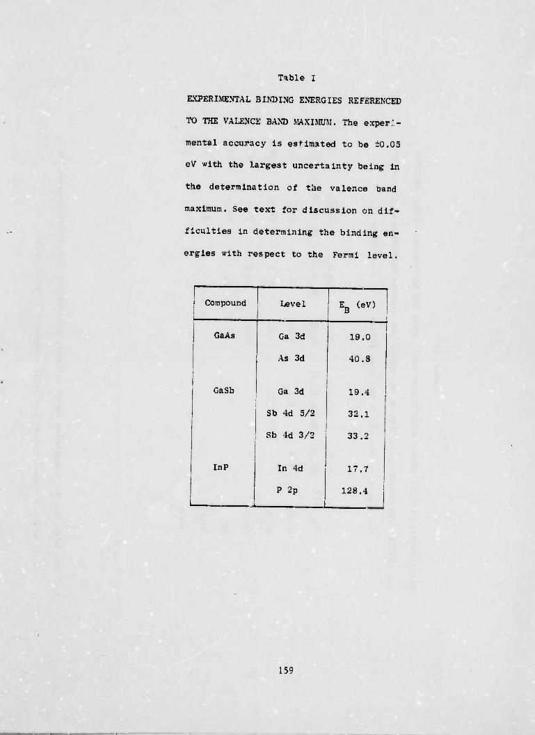
Table I
EXPERIMENTAL BINDING ENERGIES REFERENCED
TO THE VALENCE BAND MAXIMUM. The exper.-
mental accuracy is estimated to be ±0.05
©V with the largest uncertainty being in
the determination of the valence oand
maximum. See text for discussion on dif-
ficulties in determining the binding en-
ergies with respect to the Fermi level.
Compound Level E (eV) B
GaAs
GaSb
In?
Ga 3d
As 3d
Ga 3d
Sb 4d 5/2
In 4d
P 2p
19.0
40.8
19.4
32.1
Sb 4d 3/2 I 33.2
17.7
128.4
159

ja
Cd X
I
M > s
i i Q
I M oa
I M
|
o ^3
I i H o
>
i s cn
I
W
1
I a
p
X) 3 H
J H
0
n
■ C
o i »i
9 P a.
r^ Ifl M rv O M u * •
y3 r^ vO i.NJ ro CM CM PsJ CM
O CM
ul O < o v£> cn r~. ro .**** •« | t i
iB 00 ^O «*• I-...4 CM CJ <"•) CM CM ^M {SJ ><_^- f»
«3 M
CO O ro o r^ o CO •* i.Nj r^. • 1
fo n u-> «T o i—<
CM CM CM CM
yD CO tu UD VO
uT " • ■
< Lf) •(■ CM 0 CO i
a>
IA O < «a- W CM
«•■M« W ■ | ITJ CO <r i"n d >o
h cO (»5
« kO o <o i^»
CM • . i/l LD T-H
<C M
4)
tt)
« #*^^ 10 u-i 1*>o U1 M <r
O e < O CM CM CM m
i/l ul 'V ui TJ <* <. «C iS < ul
5
■M ■H • s: O U) N
J2 0) R
JZ JJ ■M
71
ä1 .c
•H •tJ c
>H C s *H
ÜJ « 1 I "0 3
>. I H P U3 0 ff) ü •H r-4 !■ 9) 0) h j=
V +j Q 3
j J R •M
■ ■o 0 1
•H -1 tfi J1 Kl 3 f B ai 3 1
i=
14 ü 3
*J >>,' a tl -s
■M CJ •H
i) s 1 0 w 71
.13
lim
»illiiMiawwMMitowidi» »II>IHII>I

Tub It» II
«MRIMENTAL lUNDlMi KNKIUIY OIKKKKKNCKS U'V), KKOM THIS WvMiK.
UCTWKKN fm SH1FTKI) AND tfHUXFnB Ql AND As M UTVIU 1XM! THK
CUM» AM) OXaXOfi QtAl (110) iURFACK. Thu «ntrlos woro
obtalmvl by subtraotlnm tbo bltullnn <>IUM-R{.»S of t bo lovols
In I!» fop row from those In tho loft most oolumiu
AL (•¥) As 11 1 i
As 1 I As 1 (li(Aa)
p. „_,. _ T" •
u;.» Us
\siva 1,8 -i.r' 0,3 1 s.a 24.0 88.0
A« III -\. a , -•., 0.1 Bl,l 80. a
As 11 i. r ■».li B8,4 Jt:. 1
A» I ~.!> ^.t.: 84.7
9*tAi) 80.8 81.8
0*1
i 1
l .0
(ft) Tbo .iosUnatlons As I. As 11 . ©to. rotor to tho UbeltUf of Plf
10,
(k) Qa<Af) rofors to As In QaAaj ^(mllarlv. tO»>Ai rofors to Qi
In liaAs ,
(0) Tho mwtlvo ,hlft moans that \s 1 I has a lar^or bladlBf onor-
|y than As IV,
IM
.

Tatale IV
EXPERIMENTAL LIGAND SHIFTS OF THE Ga AND As 3d LEVELS TOR
THE COMPOUNDS WHOSE SHIFTS WERE GIVEN IN TABLE III
Compound .^E (eV)a
e J£ (eV)'
c 11,1
Ligand
AS205
. ___——.
4.3 0 . «7 3 - 0
1.7 1 ■ 0
AS203 2.(5 o.if 3 - o
Ga(As) -(1 .8 -0,18 4 - Ga
»a03 ■2.0 0.33 6 - 0
(Ga)As l.l 0.2S 4 - As
Ga(As)04 3.8 0.S7 4 - 0
(Ga)As04d 1.3 0.33 4 - 0
L -— (a) M is the binding energy shift with respect: to
the free element.
0») Ü ts the ligand shift referenced to the free
element where CM% • t^y summed over all 1-
(C) n is the number of URands of the given kind,
(d) Note these are not experimentally determined shifts:
these shifts are calculated for the ideal structures
using the ligand shifts given in the rest Of the
table.
162

,~-^
FIGURE CAPTIONS
Mt. 1. The vooonstruotcd (110) surface with an energy level dlagrun.
showing the location of the filled (As-derived) and empty
(Ga-derived) surface states.
Fi«. 8. EDC's of clean and oxygen exposed n-type GaAs (110) at hv ,
100 eV. The exposure of 1 x 10¹² LO,, (1 L „ 10^ (:orr_sec)
was made on sample LD1. while the smaller exposures were all
on sample UW .
Fig. 3. The relative oxygen uptake of the GaAs (110) surface as a
function of exposure determined from the area under the
shifted As.3d levels U). The area of the unshifted As-3d
levels (V) is also plotted. The scale on the right assumes
saturation is reached at lO1" LO,,.
same
es
Flg. 4. The valence band of clean n-rype GaAs (110) and the I
surface exposed to the indicated exposures. These om-v
are blow-ups of the valence band region of Fig. 2.
Fig. 5. EDC's of clean and oxygen exposed n-type GaSb (110) at hv -
100 eV. Notice that both the Ga and 8b shift simultaneously
with increasing oxygen exposure.
Fig. 6. EDC's of GaSb exnosed t-.i * v in8 r,i * oo exposed to ,3 \ 10 u^ for three photon energies
showing the variation in the cross section of the Sb-ld levels
versus photon energy.
1.6 3

äwkw-
Pit. 7. The relative oxygen uptake of the GaSb (110) surface as a
function of exposure, determined from the area under the 0-2p
level. The vertical scale is obtained by comparing the areas
under the 0-2p in the spectra of Fig. 5 to the areas under the
0-2p in Fig. 2 for GaAs.
Fig. 8. EDC's of clean and oxygen exposed p-type InP (110). ^e In-4d
level was measured at hv = SO eV and the P-2P at hv = IfiO eV.
Fig. 9. EDC's of clean p-type GaAs (110) and the clean surface exposed
to excited oxygen at hv a 100 eV.
Fig. 10. EDC's of n-type GaAs (HO), LD1, for the clean surface, the
clean surface + 1012 w.,, the previous surface + 5 x 10⁵ L
excited oxygen with a 0.4 ma ion gauge emission current
("HEAVILY OXIDIZED"), and the clean surface exposed to 5xl05L
excited oxygen with 4.0 ma ion gauge emission current ("VERY
HEAVILY OXIDIZED").
Fig. 11. Plot of the ratio of the unshifted to shifted As-3d levels as
a function of electron kinetic energy for the GaAs (110) sur- 12
face + 10 L02 (right-most scale). The other two scales give
the escape depth in Angstroms and molecular layers (see text).
104

CB
Go As (110)
FILLED SURFACE STATES (As) ,N
, ^ EMPTY SURFACE / \ STATES (Ga)
SURFACE BULK
* LOCATION OF EMPTY SURFACE STATE
Fig. 1
165

OXIDATE OP n-TVPEGaAs(110UTfi(u=|o0eV
6a-3d
EXPOSURE (L02)
IxlO'2
3o 20 ~~iö~^rCLEAN
BINDING ENERGY (eV)
166
*:"~»-,SW.-i;-'V,,4,;_, 1 ■ 4 ■ ■ .
.•■-...*,., |

.
1.0-
P0.5 <
UJ en
10'
- A^AREA UNDER SHIFTED \ Asl PEAK
\^-AREA UNDER UNSHIFTED VW.
^v Ga(As) PEAK
/
.Atr
H0,5_ -0,4 a
0.3 |
0.2 |
CD
10° I08 10 EXPOSURE {L02)
10 10 12
PIG,
167

■■'■ ; ■ ■■'■ ■ ^ ..■,..,., ,
■ -r : - ■ ■ -««a
'0 5 BINDING ENERGY (eV)
PIO, 4
168

OXIDATION OF n-TYPE GaSb(IIO) at1ioj=IOOeV Sb-4d Ga-3d
2.5 eV
30 20 I0 BINDING ENERGY (eV)
EXPOSURE (L02)
=l CLEAN
Fig. 5
169
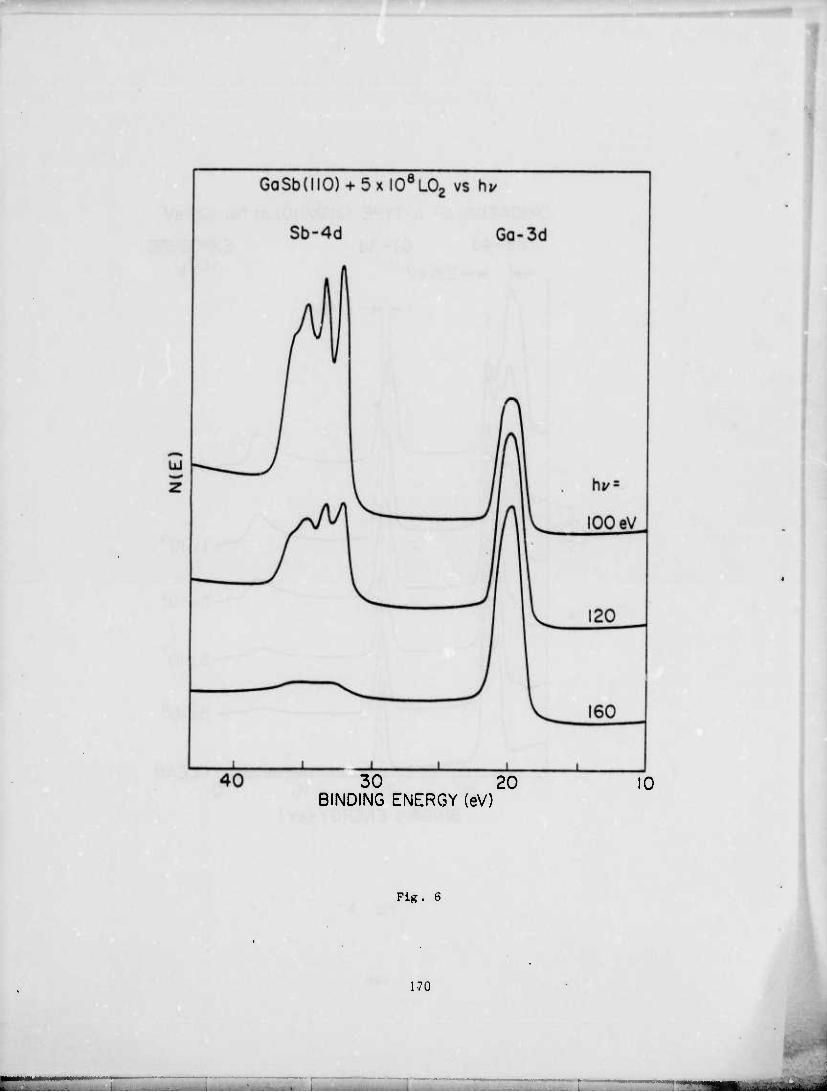
30 20 BINDING ENERGY (eV)
Fig. 6
170

I03 I04 I05 I06 I07 I08 I09 I010 10" I012
EXPOSURE (L02)
Fig. 7
171
;„,.«.,.:.,...,.

OXIDATION OF p-type InP(IIO) P-2p EXPOSURE ln-4d (tii/= (LO?) {tv* l60eV) 2 80eV)
h-4.4eV
130 "20 10 BINDING ENERGY (eV)
PIO. 8
172

v .in iiii|iip|iiiiiuiiiiiii.wiiii!iuiiJni •«- ■
OXIDATION OF p-TYPE GaAs(IIO) AT h^-IOOeV As I
^sII//Ga(As)
50.0
Gal (Ga)Äs 0-2s\/
'.OeV
30.0 20.0 10.0 BINDING ENERGY (eV)
173
»—

k40 30 20 10 BINDING ENERGY (eV)
PIG, 10
174
"^ "--""-•"•

10 <
m o <
IT)
T"
Sd3AV1 dVinD310lM
yS-i + {V) Hld3a 3dV0S3 O O
FIR. 11
175
:

Chapter 7
VALENCE BAND STUDIES OF CLEAN AND OXYGEN EXPOSED
GaAs (110) SURFACES*
by
P. Pianetta, I. Lindau. P. E. Gregory,**
C M. Garner, and W. E. Spicer
Stanford Electronics Laboratories and
Stanford Synchrotron Radiation Project Stanford University, Stanford, California 94305
ABSTRACT
We found, by correlating band bending, ultraviolet photoemission spec-
troscopy. and partial yield spectroscopy measurements, that Fermi level
Pinning at midgap of n-type GaAs (110) is caused bv extrinsic states. The
exact nature of these states is not yet clear, but the surfaces with Fermi
level pinning were strained as evidenced by a smeared valence band emission.
This smearing was removed by as little as one oxygen per 104 to 105 surface
atoms. This implies that the oxygen .s very long range effects in causing
spontaneous but small rearrangement of the surface lattice and removing sur-
face strains. When about 5Z of a monolayer of oxygen is adsorbed, a major
change in the electronic structure takes place. Again, the oxygen coverage
is very small, which suggests long range effects now leading to a fairly
large rearrangement of the surface lattice. Finally, from comparing the
oxygen induced emission for exposures greater than 107 L02. with the spectra
from gas phase photoemission measurements on molecular oxygen, we suggest
that the oxygen is chemisorbed as a molecule on the (110) surface of GaAs.
Work supported by the Advanced Research Projects kauaav .f r*. n- * Of Defense monitored by .ight Vision Labor!™ uTl^v ^c^onlcT
oT:: t^ ".OrSlI!" C^sTV^T0?691^ the ^"^ o^avTLearch No D^ ySoTfiq' AO" ? ; ? ^tional Science Foundation Contract NO.DM8 73-0769. A02 in cooperation with the Stanford Linear Accelerator Center and the U.S. Energy Research and Development Administratioi
Present address: Varian Associates. Palo Alto. California.
176

I. INTRODUCTION
The atomic structure of the GaAs (HO) surface has been the object of
numerous theoretical and experimental studies. LEED measurements1 as well
as theoretical predictions2 have suggested that the GaAs (110) surface re-
arranges with the surface arsenic atoms moving out and the surface gallium
atoms in. The exact values of these displacements are still under investi-
gation. It is not clear how useful LEED is in detecting small changes in
the surface rearrangement due to defects or oxygen adsorption. Recent
calculations have shown that the valence band electronic structure of
GaAs (HO) surfaces depends markedly on the su-face rearrangement. ' It
is difficult, at this point, to correlate diff3n .ces in the experimentally
determined valence band electronic structures to actual lattice distortions
since the calculations that have been performed consider only the extreme
cases of the fully relaxed and ideal surfaces. Small displacements from
these two extremes have not yet been considered. Consequently, we will
not attempt detailed comparisons with calculated surface densities of
states; instead, we will concentrate on looking at the differences in the
surface valence band electronic structure, as determined by photoemission,
between a large number of samples as well as the effects of exposure to
4 oxygen.
The valence band of GaAs consists of four bands extending approximately
14 eV below the valence band maximum (VBM).6 The lowest lying band (giving
a peak 9 to 14 eV below the VBM) is primarily s-like and associated with the
arsenic.7'8 The next band (giving a peak centered 6.75 eV below the VBM) is
composed of s-like states around the gallium and p-likt states around the
177

ypaiw,.p.iip«!»i.|.f»w,','.«ajii n, liiilHIIMiHMMii
7,8 arsenic. The remaining two bands (giving Che structure for the first
5 eV below the VBM and containing at least four peaks) are completely p-
7 8 like around the arsenic. ' The structures associated with these bands
can be seen in Figs. 1-4 where we show energy distribution curves (EDC's)
for the cleaved GaAs (110) surface taken at 21 eV (see below for detailed
discussion of these spectra; here, we will just use them as examples of
the general GaAs valence band structure). All the peaks are easily seen
except for the one 9-14 eV below the VBM, both because it is masked by
the scattering tail and because the cross-section for this peak (s-like)
is less than that of the p-like peaks at this photon energy. We should
also note that the band structure of GaAs has a large number of critical
points in the upper 5 eV of the valence band compared to the region 5-14
9 ]_o eV below the VBM, ' The critical points should be the part of the band
structure that is the most sensitive to any changes in the surface lattice
structure. Thus, we should expect the most significant changes to occur
in the upper 5 eV of the EDC's. The calculations of Refs. 3 and 4 show
that the top 5 eV of the valence band do indeed show the most changes due
to a rearrangement of the surface.
Another very sensitive technique which can be used to characterize
semiconductor surfaces is the measurement of band btadiaf, * '^ The
presence of band bending is seen as a difference in the position of the
Fermi level at the surface with respect to that in the bulk which is de-
termined by the doping. For GaAs (110), it has been recently shown from
contact potential difference measurements and photoemission4,14 that
the bands are flat all the way up to the surface within the experimental
178

trnfrnmimammmmiiiim»
uncertainty. This means that for p-type GaAs (110) the Fermi level is
at the VDM, while for n-type it it at the conduction band minimum (CBM).
11 18 In earlier work, ' " however, Fermi level pinning was detected in
n-type GaAs (110). This pinning was attributed to the existence of an
empty band of intrinsic surface states in the middle of the gap. These
18 results were reinforced by partial yield measurements showing strong
transitions from the Ga-3d levels to states which seemed to be located
in the middle of the gap (the partial yield results have since been ro-
iLi interpreted to be consistent with the absence of band bending).
The pi'osence or absence of intrinsic states in the gap lias impor-
tant implications bearing on surface band structure calculations. For
example, calculations based on the ideal surface result in an empty band
7 of surface states in the gap. whereas, those based on the rearranged
surface give an empty band of surface states whose center of gravity is
in the conduction band.^ Therefore, it is important to clarify some of
the present confusion as to the origin of the states that cause the Fermi
level pinning in n-type GaAs (110). Some workers have assumed the pin-
ning observed in Che earlier work was always caused by surface roughness
which was the result of bad cleaves. ' ' However, some of our previ-
ous work has shown that pinning is observed in macroscopically good
cleaves as well.4,18 Thus, the Fermi level pinning could also be caused
by states which are the result of surface strain or other microscopic
defects in the crystal.
In order to investigate more systematically the possible relation-
ship between the Fermi level pinning on clean n-type GaAs (110) with
179

surface defects or strains as well as the nature of the states causing
the pinning (i.e., whether they are actually intrinsic or extrinsic),
we performed a series of experiments where we studied photoemission and
partial yield spectroscopy measurements from four different samples
(16 total cleaves). We concentrated on the valence band electronic
structure, particularly the top 5 eV. and correlated the changes in
this structure with both the Fermi level pinning and partial veild for
the clean and oxygen exposed surfaces.
II. EXPERIMENTAL
A. Apparatus and Procedure
me experimental apparatus has been described in detail
elsewhere.5and only details which are pertinent to this experiment will
be described below.
We studied four separate samples from two suppliers. Three of
the samples ca.. from Laser Diode Corporation (LD). Those will be des-
ignated samples LDi. W2, and U*. UDl and W2 were cut from the sa.e
boule. The third can. from MCP Electronics in England (MCP). The sam-
ples were 5 mm V 5 mm X 12 mm with the (110) axis along the long dimen-
sion. All samples were n-tvpe and had the following doping: LDl and
LD2, Te doped with n = 0.5 x 1018 cm"3; LD3, Te doped with n - 3.5 ^
1017 cm"3; and, MCP, Te doped with n - 1.7 * 1018 cm"3. The MCP sample
was the same sample used by Gregory and Spicer in their earlier work.
The sample chamber consists of a stainless steel UHV bell jar,
base pressure <1 - lO"10 Torr. The pumping system is a 240 L/sec ion
130

pump plus titanium cryopump with a poppet valve for sealing the pump
from the main chamber. The samples are mounted in a carousel being
held at one end with a metal clamp which exerts a minimum amount of
pressure on them. Four cieaves, each 2 mm thick, can be taken from
each sample. The samples are cleaved by carefully squeezing them
between an annealed copper anvil and a tungsten carbide blade. A
cleave is judged to be "good" if it has a shiny, mirror-like surface.
We have since performed preliminary optical measurements and found
that the cleaves appear comparable to the "good" cleaves of Huijser
and Van Laar in terms of step density.
All cleaves were performed at pressures < 1 x 10~10 Torr, and
no hot filament or ionization gauges were used during the measurements
or oxygen exposures except as specifically noted. Gas exposures were
performed by admitting research grade oxygen into the vacuum system
through a bakeable leak valve. For large exposures, an auxiliary pump-
ing system was used to return the main chamber to pressures below \ 10~ 8
Torr. Binding energies were measured with respect to the VBM and the
position of the Fermi level with respect to the VBM was determined by
referencing to the Fermi level of a gold film evaporated in situ on a
substrate in electrical contact with the sample.
Synchrotron radiation in the range 9 to 30 eV from the "8°" line
at the Stanford Synchrotron Radiation Project was used in this work.
The radiation is first monochromated by a Seya-Namioka monochromator
and then enters the chamber through a bakeable straight through valve.
The energy of the photoemitted e_ectrons is then determined by a double
pass cylindrical mirror analyzer operated in the retarding mode. This
mode insures a constant resolution which is equal to 0.6% of the electron
pass energy. In these measurements, we used a pass energy of 25 eV,
181

püWMimBWSKWJJfipNJ'
iw^HHaaHHMiMMHMHMi
giving an electron energy resolution of 0.15 eV. Counting rates over
4 2 x 10 C/sec in the GaAs valence band at hv ■ 20 eV were typical.
B. Results
In Figs. 1-4, we show EDC's taken at 21 eV (20 eV in Fig. 4)
for several cleaves from each of samples LD1, LD2, LD3, and MCP. We
will designate successive cleaves from a given sample as cleaves A, B,
C, etc., and we will refer to cleave A from sample LD1 as "sample LDlA;"
similarly, cleave A from sample MCP is "sample MCPA," and so on. The
Fermi level at the surface is marked on each curve. The horizontal
scale gives the energy below the VBM. The position of the Fermi level
relative to the valence band maximum as well as to the peak at a binding
energy of 6.75 eV is plotted in Fig. 5. (This figure will be discussed
below.)
In Table I, we give a summary of the samples that were stud-
ied. This table includes the figure numbers where the spectra for the
various samples are located, an indication as to the sharpness of the
spectral features in the top 5 eV of the valence band for each sample
and a classification of eacli sample based on the band bending.
The first thing we should notice from Figs. 1-1 is that the
peak locations are constant from sample to sample and cleave to cleave.
Relative peak heights, on the other hand, vary considerably. As an ex-
treme example, compare sample LD1C, i.e., sample LD1, cleave C (Fig. 1)
with samples MCPA & B (Fig. 4). In Sample ID1C, there is a Ulf« peak
1.75 eV below the VBM, whereas it is relatively small on MCPA. There is,
however, better agreement in the shape of the valence band structure
is:
«w:.,,,.,. HMMHMMnNi IMMMMMMiHMHMnHII
when samples from the same boule are compared. For example, all cleaves
from the same sample are similar and all cleaves from samples LD1 and
LD2 (Fin. -). which are different samples from the same boulo, fiv« sim-
ilar results.
The next observation that will be made concerns the "sharpness"
of the individual spectra for the clean samples. This is a very subjec-
tive judgement and open to question, but we foel that the observations
are general enough that they should be of some use. In all cases, sam-
ples with the Fermi level located at the conduction band minimum are
somewhat sharper, i.e., more structure can be resolved in the top 5 eV
of the EDC. For example, compare LD1C to LD1A, B, or D; also, compare
MCPA to MCPB or MCPC. LD3A, B, or C (Fig. 4) do not exhibit significant
surface Fermi level pinning, and they have very well resolved structure
in the top of the valence band. An exception is sample LD2. Cleaves A,
C, and D from sample LD2 are as sharp as LD1C, yet they exhibit pinning
while LD1C does not. Samples LD2B and B (not shown) had a very smeared
out structure and exhibited Fermi level pinning. Thus, the most general
statement we can make concerning these observations is that, if a sample
has an unpinned Fermi level, the structure in the upper 5 eV of the va-
lence band will be well defined. If the Fermi level is pinned, the ma-
jority of samples will have a smeared out valence band.
We should also note at this point that, in the case of LD1C,
the structure in the top of the valence band became sharper after the
—' 0 sample had been in the vacuum system at 1 v 10 torr for 12 hours. In
en the case of MCPB, however, the structure did not chance noticeably ev
after 20 hours at 10 torr. In both cases, there was movement of the
183
position of the Fenni level. We are not yet sure if the sharpening f
due to some sort of surface lattice relaxation with time or if it is due
to contamination. At a base pressure of . icT10 torr. the sharpened
structure had an exposure of . 4L to the residual gas in the chamber. As
we will show below, definite effects in the valence band are observed with
the addition of less than 100 L of oxygen (in some cases, effects are seen
for exposures as low as 10 L). Consequently, the effect we are seeing
could be due to contamination.
Before discussing the position of the Fermi level as a function
of oxygen exposure, let us consider one more feature which all the samples
have in common. In Figs. 6 to 14, we show the EDO's as a function of oxy-
gen exposure for a representative number of cleaves from each sample. In
all cases, changes take place in the top 5 eV of the valence band for expo-
sures which are less than 103 L of 02. In some cases, the changes take
Place for exposures as small as 10 L 02 (see. for example, Figs. 10 and 11).
When the EDC for the clean sample is smeared out, these changes take the
form of a sharpening of the structure in the top 5 eV of the valence band
(see Figs. 8 and 10). In other cases, where the EDO's show well resolved
valence band structure in that region, the changes are more subtle, i.e.,
there might be a small variation in relative peak heights as shown in
Figs. 6, 9, 13, and 14.
Now that we have taken care of these general considerations,
we will group the spectra together according to the Fermi level pinning,
and then we will describe each group in detail. The first group contains
samples LD1C,20 MCPA, and LD3A. B. C. In all these samples, the Fermi
184

level was loc.Uod approximately at the conductiun band minimum, i.e., no
surface Fermi level pinning is observed. We have complete exposure data
only for samples LDlc and LD3C which are shown in FiSs. 7 and 14, respec-
tively. There is only one exposure for sample MCr.A. and this is shown in
Fig. 9.
The first thing to notice is that the Fermi level is about l.-l
• to l..i eV above the valence band maximum, which is approximately the lo-
cation of the conduction band minimum since the band gap of GaAs Is 1.1
oV. Thus, the F.rmi level '.s at the bulk position, and there Is no pin-
ning.
As the surface Is exposed to more and more oxygen, the Fermi
level moves closer and closer to mldgap until It stops moving downward
by about 106 L (X, (Figs. 7 and 14). These points are plotted in the
lowest curve of Fig. 5. After the initial sharpening of structure in
sample LD1C, notice that no large changes occur in the EDC's until we
reach this critical exposure at 105 to 106 L (X,. Up until this point,
the only changes seen were the changes in the top 5 eV of the valence
band and a possible splitting in the band structure feature located
10-12 eV below the VBM (this happened for sample LD1C in Fig. 7; no such
splitting was seen for LD3C in Fig. 14). At 105 to 106 L0,, a signifi-
cant amount of emission is lost from the top 3 eV of the valence band,
and most of the sharp structure in top 5 eV is gone. The valleys located
4.5 and 8.3 eV below the VBM start filling. No definite peak is se.a
yet in the 4.5 eV valley. However, for LD1C (Fig. 7), two peaks can be
clearly resolved at 8.3 and 9.7 eV below the VBM and. for LD3C (Fig. ],4),
185
_

one peak is seen ac 8.3 eV below the VBM. The peak at 6.75 eV has
so far been unaffected by the oxygen. By 10 L02, the Fenni level
has moved back towards the CBM by 0.15 eV (Fig. 5). The large
exposures have led to a further decrease in the emission at the top
of the valence band and an increase in emission from the adsorbed
oxygen. Also, at 109 L02, a more definite oxygen level begins to
appear 5 eV below the VBM. The emission from the GaAs is still so
large with respect to the new emission that it is very difficult to
find the precise location of the new structure.
The second group contains those cleaves which exhibit
Fermi level pinning at about midgap. This group is the largest and
contains LD1A, B, D; LD2A, B, C, D, E; and MCPC, D (Figs. 6, 8; 13,
15; and, 11, 12, respectively). In the majority of these cleaves,
the Fermi level is pinned 0.9 ± 0.15 eV above the VBM, and it remains
within these limits for all exposures. In two cases, LD1D (Fig. 8)
and LD1C (Fig. 15), the initial pinning was 0.6 eV above the V3M
(these two samples have not been included in Fig. 2). The effect of
oxygen on the valence states at the surface is the same as for the
first group when exposures > 106 L02 are reached, \gain, oxygen emis-
sion begins to be seen at 1Ü9 L02 as for the first group. For the
lower exposures, especially below 103 L02 in all of the LD1 and MCP
samples, the top 5 eV of the EDC sharpened dramatically even, in one
case, for an exposure as low as 10 L02. The LD2 samples, already
somewhat being sharp, show more subtle effects.
20 The third "group" contains only one sample, MCPB, and is
shown in Fig. 10. Tn this c, a, the Fermi level for the just cleaved
surface is located 0.7 eV above the VBM, putting it at midgap.
L86

■
After being in the vacuum systeni at <1 X lo" torr for 20 hours
(glvliiR nn exposure of 7 L to residual gases), the Fermi level moves
to 0.8 eV above the VDM. Upon exposure to oxygen, the Fermi level goes
to the unpinned position (CDM) by 10 LO-, remains at that position un-
2 til an exposure of 10 LO«, and then returns back to midgop by about
6 10 in. The structure at the top of the valence band sharpens
dramatically for an exposure of less than 100 LO-, as for the group IT
samples, and the Ions of intensity in the upper 5 eV of the EDC is seen
5 as early as 10 LO , even before a significant filling of either of the
two valleys (4,5 and 8.3 eV below the VBM) has taken place.
This sample presents a unique situation. If we measure the
position of the fermi level relative to the VBM, we get the behavior
described above and shown in the bottom curve of Fig. 5. If, however,
we mensure the Fermi level with respect to the peak 6.75 eV below the
VBM (labeled peak "A" in the example EDC on the top of Fig. 5), we find
that the Fermi level moves up 0.9 eV from freshly cleaved to 1 L0o expo-
3 saJWi and then remains at this position until 10 L (see top curve in
Fig. 5). If we measure the distance from the 6.75 eV peak to the VBM
and plot it vs exposure, we get the middle curve of Fig. 5 (x's), where
we have included the same plot for sample LDIC (solid circles) for com-
parison. It becomes very clear from these curves that the widtli of the
valence band at the surface is changing as well as having .i change in
the pinning. The decrease in width upon addition of oxygen implies that
structure at the top of the valence band is removed with oxygen. Fur-
thermore, the 6.75 eV peak becomes noticeably narrower by 10 W .
Neither effect was soon in the other samples. In those cases, the G.75
187

.»MM'MlJI»WHI*iWl.M,U:.
--•<">' mi armm iaiwwu|"'*uw»w!W'«»w,"Mi«»)»»>iJi'' 'IJIIWIWHIIMI»1
eV peak remained constant in width, and the distance from the 6.75 eV
peak and the VBM remained approximately constant for all oxygen exposures,
as can be seen from the example given for sample LD1C. The broadening in
the MCPB sample could be due to a very strained surface giving rise to new
structures in the EDC, which disappear with oxygen, or simply to a nonuni-
form work function across the surface of the sample, or even a combination
of both. However, since we observed this effect only once, it is very
difficult to draw more definite conclusions.
We can make a general comment with reference to Fig. 5, although
the top and bottom sets of curves are consistent with each other. Less
scattering was obtained between the data points in the top set. This indi-
cates some of the problems in using the VBM as a reference. Since the top
3 eV of the VB change in shape, using the upper edge as a reference is
clearly less reliable than using a constant structure such as t^ie 6.75 eV peak.
We now turn our attention to what happens when we use the hot fila-
ment ionization gauge during an exposure. These results are shown (for sample
LD2C) in the dashed curves of Fig. 15. The solid curves were obtained using
unexcited oxygen on sample IiD2A and are shown for comparison. The excited
oxygen speeds up the rate of chemisorption, as can be seen by comparing the
5 6 dashed curve at 10 L (excited oxygen) exposure with the solid curve at 10 L
(unexcited oxygen) exposure. In fact, the first large effects with excited
4 oxygen are seen at 3 x 10 L while, with unexcited oxygen, the first large
6 7 effects are seen between 10 and 10 L, an increase in activity by about a
factor of 100. We have discussed the increase in the rate of adsorption in
References 5 and 21. As in the exposures with unexcited oxygen, we see the
appearance of oxygen induced emission, associated with the 0-2p level, at
g exposures > 10 L. In the case of excited oxygen, however, this emission is
much more pronounced and eventually becomes the dominant feature of the EDC,
located at approximately 5 eV below the VBM of the clean sample. With unexcited
188

(i»HJH#J,jinu,*.
. ^n is at most a shoulder at even 10 L. Also oxygen, the oxygen emission is at most
-Mnn of the 0-2p emission does not become well estab- note that the position of the u ^
ll3hed «tU ft« an «*«« of «' ^ «^ o.s.n 5ince. even a.
S nt .t 8 2 eV below the VBM in both At 109 L. a peak is present at 8.-
.n 107 LO • As can be seen from the figure, to unexcited oxygen until 10 L02.
t of pe.ks are the san.e for exposure to either excited or these two sets of peaKS aie
. that at 10 L of excited oxygen. . unexcited nxySen. denote, however, that at
, nt 8 2 and 9.9 eV below the VBM disappear and a single the two peaks at 8.- ann
H, ir olace The same sequence of exposures with peak at 8.8 eV takes their place.
, inor taken at a photon energy of 25 eV. is excited oxygen for sample LD2C. taken
*■ r, Hoi-ter look at any
. , *•!,« VSM which is obscured by the ...i „., 1 fi »V below the VUM WUJ.WH structure lower than 10 e\
„.vine Figs. 15 and 16, we see that , -„,, v,,,-''leV. By comparing exf»»
„^-■ttprine peak for hv--J-ev. J scattering P atmllar except for two major *h EDC's for the two photon energies are similar the t 8 2 and 9.9 eV below the VBM is exceptions. First. the structure at 8.2 and
« for the 28 eV spectrum, whereas it not visible at 106 L excited oxygen for the
k lt 8 8 eV below the VBM is quite promi- is present at 21 eV. The peak at 8.8 is preseui. c^pond because
tlv. to the (»As valenc. band amlsalon
Uently »e are abX. te „ee dir.« ..i-»"" '- ^ W-" eV. Consequently, we
more readily using 25 eV photons.
189

The next experimental results are tliose of partial yield spec-
troscopy measurements performed on samples LDlC, .vhlcl» sliows no pinning
and MCPI3, which shows pinning at mld^ap. These spectra, shown In Plgi.
17a and 17b. .vero performed concurrently wltli the data of Plga. 7 and
10. The two sots of spectra are essentially Identical. There are some
differences in relative peak heights and shapes, but the enorgy posi-
tions of all the peaks are identical. On the clean spectra, there are
two sharp peaks at IV).7 and 80.2 eV and a third broad peak at 20.;) 0v.
Upon addition of oxygen, the three peaks remain unchanged in position
and shape up to an exposure of 10 L Of unexcltod ().,. At L0 I, the
peaks are almost got», hut there has been no shift in energy position.
7 At 10 1,, the line structure Is completely gone, leaving one broad peak
at 20.1 eV, The behavior of partial yield spectra for other samples and
cleaves was identical to the spectra shown, irrespective of any differ-
ences in the initial Fermi level pinning or behavior with oxygen expo-
sure.
III. DISCUSSION AND CONCLUSIONS
In the discussion chat follows, we will first condense the
information obtained from our valence band, Fermi level pinning, and
partial yield studies, and then correlate these results.
We have seen three main things in our data. First, Fermi .level
pinning occurred on surfaces that could be classified as good cleaves.
This implies that pinning is not necessarily caused by high step densi-
13 14 ties or surface roughness, ' but rather by more subtle types of de-
fects. Exposure of the surface to oxygen caused the Firmi level to go
190
"■^"^^^■■■"■■■■MMBMHMMI^IiHRIIiMMMAMMHiaaiHMMM

■ jiiiiwiii >■»■ 'mimmm'«
to »Idftp for .npmnec, samplos and stay the sa.ne (at mldgap) for the
pinned samplos .
Second . the top 3 oV of the BDC', .vero relatively sharp for un-
pinned samples. while fo,- pin.ed samples the structure In this n^lon
was. in KGnernl. ,„ore smeared. The exposure of the surface to less
than 10J w.2 resulted In a sharpening of the smeared structure and more
subtle chants In relative peak helots for the sharp Knc's. At expo-
sures between l,)"' to 10« ^, the top 5 eV of the valence band w.s a,a In
affected, exhibiting both a loss of emission and smearln«. for expo-
sures above 106 U)2I the top 5 eV of tho ^ ^^ ^ ^ ^ ^_
gen induced emission bocame noticeable. However, at. 81 oV. the cross-
sections are such that no clear peak from the oxygen can yet be seen -I
to 5 eV below the VBM. Through all this, the valence b.nd structures
lower than 5 eV below the VBM have remained essentially unchanged.
Third, the partial yield gave the same results for all samples,
irrespective of the initial position of the Fermi level. Addition of
as much as 10> L02 had no effect on the partial yield structure either
in peak position or height. The peaks lose intensity at 106 L0,, and
disappear by 107 L02. with no shift in the peak positions.
As we mentioned in the introduction, the top 5 eV of the valence
band should be strongly affected by the surface lattice structure, so
that movements in the positions of the surface atoms would appear as
changes in the top 5 eV of the EDC. If a su.face is strained, the
surface atoms at the strain points will be somewhat displaced from
their ideal positions. Consequently, the EDC's from such a surface
would be smeared, since the EDC would have contributions from both
191

Che ideal and strained parts of the surface. The fact that surfaces
with unpumed Fermi levels have sharp structures in the top 5 eV of
the EDC. while samples with pinned Fermi levels are initially smeared
and sharpen with exposure to oxygen, indicates that the unpinned sur-
faces are more perfect. That is. the surfaces exhibiting Fermi level
pinning are probably strained. Furthermore, since we see no differ-
ence in the partial yield results from the samples with and without
Fermi level pinning, the pinning must be due to extrinsic states.4,U
Therefore by combining the photoenission and partial yield results.
we can conclude that surface defects could be responsible for both
the Fermi level pinning and the smearing of the valence band.
The sharpening of the EDC's with oxygen occurs for exposures less
than 10 LOj, From previous work.5 we saw that at 10° LO,, the coverage
is only 5^ of saturation. Assuming saturation at half monolayer
14 2 [4.4 « 10 oxygens/cm'), the oxygen coverage causing sharpening of the
EDC's would be on the order of one oxygen per 104 to 105 surface atoms.
These rather long range eff- s associa-.ed with the oxvgen can be inter-
preted to mean that the surface strains are rather unstable so that re-
arrangements can be triggered quite easily by very few oxvgens. One
4 5 oxygen per 10 to 10 surface atoms gives a concentration on the sur-
face of approximately 4 ^ 109 to 4 . 1010 oxygens/cm2. The tvpical
concentration of lopant on the surface is on the order of 1010 atoms/cm2
for a bulk doping of 101S atoms/cm3. It is interesting that these num-
bers are close enough to indicate a possible link between the dopant and
the initial oxygen chemisorption. However, we should keep in mind that
it does take at least 10L: to 10IJ states/cm2 to pin the Fermi level at
192

I — <DJ«"«" '
mldgap. Thus, although the dopant atoms at the surface could
be responsible for triggering surface rearrangement upon oxygen chemi-
sorption, they can not be the primary cause of the Fermi level pinning
observed on the surfaces with the smeared EDC's. In addition, even
though the already sharp EDC's (i.e., with no pinning) are affected by
less than 103 L0-, the Fermi level does not start to move towards mid-
gap until exposures larger than 10 L02. This is more evidence which
implies that the sites causing the pinning or strain and thoso that
remove the strain are not necessarily the same.
:>;nny of the conclusions that luivt? been drawn so far have been rather
speculative, but the ROtt Important point that r.ust be reiterated Is thnt
the chemlsorbed oxygen has long rnngo effects on the surface, acting at
coverages as small as OH« oxygon per 10 to 10 surface atoms. The tact
that the oxygon has such largo effects for very small coverages Implies
that oxygen stimulates spontaneous rearrangement of the surface by pos-
sibly removing strains. The cause of the pinning on the cleaved samples
is extrinsic states whose source is not yol known. However, we suggest
that surface defects cause both the pinning and the smearing of the EDC's
Between 10 and 10 IiO.,. the coverage goes from I oxygon In 10 to
10 surface atoms to 5% of saturation, ami the Fermi level goes from the
CBM to mldgap (for group I samples). This latter coverage corresponds
L3 - to about 10 oxygen a tons/cm which Is approximately the numbei* of
states needed at the surface to pin the Fermi level. Thus, It is easy
to see the origin of the Fermi level pinning with exposure to oxygen,
provided, of course, that every chemlsorbed oxygen gives rise to one
new Interface state. Besides pinning the Fermi level at mldgap, an
193

oxygon exposure of V* LO,, results in the complete smenring; of the top
5 eV of the EDC's. Since the coverage is now only about one oxygen
atom per 20 surface sites (i.e.. 57. of saturation), the effects of the
oxygon are again long range. The large changes i; the EDC's imply a
relatively large rearrangement of ill the surface atoms, not just the
ones at the strain sites, as was the case before.
With these large changes taking place In the valence band, -ve
should also expect significant changes in the local dielectric constant
(or screenlnki properties) at the surface. Such changes would explain
the disappearance of the partial yield peaks In fOlng from 10 to 10
U)., . It the screening at the surface changes, the excltonlc binding
energy, which determines the position of the peaks in the partial yield
could chance. If this happened, the partial yield from the clean sur-
face would drop and new structure representative of the new excitonic
binding energy would grow. U'e could not, however, see such new struc-
ture If it was too close to the valence band. Thus, the loss of the
partial yield peaks could possibly be due Co a rearrangement of charge
in the surface layer rather than a direct interaction of the oxygen
with the surface gallium atoms. The same arguments could be applied
to explain Che disaprearance of the structure in electron energy loss
22 measurements.
With exposure to large amounts of oxygen, we saw further decrease
in the intensity from the top 5 eV of the valence band with two new
peaks 9.9 and 3.2 eV and a shoulder 4 to 5 eV below the VBM. Similar
peaks are present during the initial stages of exposure to excited oxy-
gen. This fits in with other data from chemical shift measurements
194
RU .■..:,::■ .".^Ü,.

where it was shown that the result of ex^ure to excited or unexclted
oxvgen started In the same wav. i.e., with a chemisorption stage.5
However, in the case of excited oxygen, the surface is oxidized tor
exposures above 106 L. Thus, the peaks we see in the curves for ex-
posures of 107 L of excited oxygen (Fig. 15) at 8.8 and 5 eV below the
VBM should be oxide peaks. If the excited oxvgen was found to be atomic
rather than excited molecular oxygen, the similarity in the initial ad-
sorption of the excited and the molecular oxvgen would indicate that
the molecular oxygen adsorbed dissociativelv on the GaAs (110) sur-
face. Thus, it would be verv interesting to perform an experiment to
determine the nature of the excited oxvgen. as well as an adsorption
experiment with atomic oxygen.
The .-imuluneous appearance ami frovtfa of the peaks 9.9. 8.2. ar.d '
I to 5 eV below the VBM indicates that all throe are due to a single ad-
sorption process. The splitting between the shoulder and second peak Is
■'•- to US »V and between the second and third peaks ts 1.7 eV. It is
interostln. to compare tnese peaks to those seen in ,as phase photoenus-
.ton from molecnlar oxvgen. The first three peaks in that case are the
HI, HU, and Eg levels with spllttir ffl of \ eV (RJ and -ru) and 3 eV cm lr 23,24
■": LS)' lf Te M«0«i«t« the shoulder tn our data with the -^
lovel ami the next fcwo peaks with the -n, and ^ levels, respectively,
we see that the agreement is rather good. The first splitting between
the *, and W is wichin the range o£ ^^ ^ ^^ ^ ^ ^^
splitting is 0.J eV larger than what is seen in our results. This is.
bv no means, conclusive evidence that the oxygen adsorbs as a molecule.
However, the evidence is strong enough that the suggestion must be made.
195
kt« .A*..*iji..:-.

"»«»»»«W«"""»"-1
The studies presented In this paper are rather exploratory in
nature, and their importance lies, not only in what we have learned
so far but, also, in suggestions for new work that will clarify some
of the questions that remain unanswered. For example, more work must
be done to covrelate the pinning on clean surfaces with actual physi-
cal defects such as impurities or cleavage steps. As discussed above,
these defects could also be the cause of surface strain and the re-
sulting smearing of the EDC's. Once the relationship between these
various effects is established, it will, be possible to make better and
more reproducible surfaces. LEED studies should be performed along
with the photoemtssion to see if we can detect any change in the LEED
I-V curves when we have changes in the EDC's. In order to gather more
evidence as to the nature of the adsorbed oxygen, the three oxygen in-
duced levels should be studied as a function of photon energy to see
if their cross sections are the same as for molecular oxygen, and
electron energy loss experiments to detect any molecular vibrational
levels that might be present should also be undertaken.
Finally, since theoretical calculations on the rearranged GaAs
(110) surface are starting to be published, it should not be long
until we can start making more detailed comparisons between our photo-
emission data and the calculated surface densities of states.
196

REFERENCES
1. A. R. Lublnsky, C. B. Duke, B. W. Lee, and P. Mark, Phys. Rev.
Letters 36, 1058 (1976); C. B. Duke. A. R. Lublnsky, B. W. Lee.
and P. Mark, J. Vac. Sol. Technol. 13, 761 (1976); A. R. Lublnsky.
J. Vac. Sei. Technol. 14. 910 (1977).
:. W. A. Harrison, Surface Sei. 55, 1 (1976); J. Vac. Sei. Technol.
14, 383 (1977).
3. S. C. Louie, J. R. Chelikowsky, and M. L. Cohen. J. Vac. Sei.
Technol. U, 790 (1976); J. R. Chelikowsky, S. G. Louie, and
M. L. Cohen, Phys. Rev. B (in press); C. Calandra, F. Manghi,
and C. M. Bertoni (to be published).
4. Some preliminary work aas been published in W. E. Spieer, I. Lindau.
P. E. Gregory, C. M. Garner. P. Pianetta, and P. W. Chye. J. Vac.
Sei. Technol. 13, 780 (1976) and W, E. Spieer, P. Pianetta. I. Lindau,
P. W. Chye, J. Vac. Sei. Technol. 14, 385 (1977).
5. P. Pianetta, Ph.D. thesis, Stanford University (1976).
6. L. Ley, R. A. Pollak, F. R. MeFeely, S. P. Kowalczyk. and D. A.
Shirley, Phys. Rev. B 9, 600 (1974).
7. J. D, Joannopoulos and M. L. Cohen, Phys. Rev. B 10, 5075 (1974>.
8. D. J. Chadi and M. L. Cohen, Phys. Stat. Sol. (b) 68, 405 (1975").
9. J. Chelikowsky, D. J. Chadi, and M. L. Cohen, Phys. Rev. B 8, :78b
(1973).
10. J. R. Chelikowsky and M. L. Cohen, Phys. Rev. B 14, 556 (1976).
197

11. P. E. Gregory and W. E. Splcer, Phys. Rev. B 13, 725 (1976);
P. E. Gregory, W. E. Spicer, S. Ciraci. .ind W. A. Harrison,
Appl, Phys. Letters 25_, 511 (1974).
12. J. H. Dinar». L. K. Galbraith, and T. E. Fischer, Surface Sei.
26. 587 (1971).
13. J. van Laar and A. Huijser, J. Vac. Sei. Technol. jj, 769 (1976);
A. Huijser and J. van Laar, Surface Sei. 52. 202 (1975).
U. W. Gudat and D. E. Eastman, J. Vac. Sei. Technol. JJ, 831 (1976)
and references contained therein.
15. D. E. Eastman and J. L. Freeouf, Phvs. Rev. Letters 34, lo24 (1975)
16. G. J. Lapeyre and J. Anderson. Phys. Rev. Letters 3_5. 117 (1975).
17. Here, we are discussing only clean cleaved GaAs (110) surfaces
since contamination can also cause pinning as will be discussed
below.
13. The surfaces studied in Reference 11 showed Fermi level pinning
but were not the result of "bad" cleaves, i.e.. there was no
surface roughness nor was there a large amount of microscopic
steps.
19. For a detailed explanation of the justification for this method.
see Reference 11 or G. F. Derbenwick. D. T. Pierce, and W. E.
Spicer, Methods of Experimt..ital Physics (Academic Press, New York.
1974), Vol. 11, pp. 89-92.
20. LD1C was called sample II cleave A, and MCPB was called sample III
cleave B in Reference 4. ^
21. P. Pianetta, I. Lindau, C. M. Graner, and W. E. Spicer, Phvs. Rev.
Letters 37, 1166 (1976). .#
198
" ' "■ ^ ' . I - : "

•n*r*m*mrmmmm*--
"rfJ. Vac. Sei. t.ehMl. U, 241 (1976).
-3. K. Siegbahn, C, NordHna r r i. »ordllng, 8. johmsso^ j Hednan] p ^ ^^
1969). pp. 69.73.
»• »• "■ ruc„er, c. Baker. A. D. Baker, and c R Brundie] 2£i^^
ffi2£2S^^Sä£M <W1W, ^ V0rk. 1970), pp. 36.37] „
199

Table I
LIST OF SAMPLES. Entries include Fermi level ln«.*H *
Sarr pie EF - Position
Valence Band Structur»
Group
Data Shown in
After Cleavage
After < 102 ^
Figure Numbers
(Clean) (*)2)
A midgap smeared sharpened II 1 6
LD1 B nidgap smeared no data II 1 not shown
C CBM sharp same I 1 7
D midgap smeared sharpened n
1 8
A midgap sharp sharper II 2 13,15
B mijgap smeared sharpened II not shown not shown LD2 C midgap sharp same II 2 15,16
D midgap sharp same II 2 not show?!
E mid pap sharp no data II not shown no data
A CBM sharp same I 3 not shown LD3 B CBM sharp same I 3 not shown
.
C CBM
sharp sharper I 3 14
A CBM sharp sharper I 4 9
MCP B midgap smeared sharpened III 4 10
C midgap smeared sharpened II 4 11
_
D midgap no data I
sharp II i lot shown 12
a . AD oroximn+o rx-ic-ii i- ■; „- _ „.
b. See text for discussion of what is meant by sharpness.
200

■MMMMMMMM • '
FIGURE CAPTIONS
Fig. 1, EDC'a taken at a photon energy of 21 eV for four cleaves
from Sample LD1. The gelid curve for sample LD1C was
taken 12 hours after cleaving, whereas the dotted curve
was taken within 45 minutes after cleaving.
Fig. 2. EDC's taken at hv - 21 eV for three cleaves from
Sample LD2.
Flg. J. EDC's taken at hv - 20 eV for three cleaves from
Sample LDJ.
Fig. 4. EDC's taken at hv « 21 eV for three cleaves from
Sample MCP. The solid curve for sample MCPB was taken
20 hours after cleaving, whereas the dotted curve was
taken within 30 minutes after cleaving.
Fig. 5. Summary of Fermi Level movement versus exposure for some
of the samples shown in Figs. 1-4. Here, we show the
position of ehe Fermi level, E , with respect to both
Che valence band maximum. VBM (in the bottom set of curves)
and peak "A" (in the top set of curves). The middle set of
curves show the position of the VBM with respec: to peak "A"
Samples in group I show no Fermi level pinning after cleav-
age. Pinning is seen from group II and III samples, but,
for the group III sample, it is removed by exposure to oxy-
gen (see text).
Fig. 6. EDC's for Sample LD1A, i.e.. Sample LD1 cleave A, as a
function of oxygen exposure (hv - 21 eV).
201

Fig. 7. EDC's for Sample LD1C as a function of oxygen exposure
(hv - 21 eV).
Fig. 8. EDC's for Sample LD1D as a function of oxygen exposure
(hv - 21 eV).
Fig. 9. EDC's for Sample MCPA as a function of oxygen exposure
(hv - 21 eV).
Fig. 10. EDC's for Sample MCPB as a function of oxygen exposure
(hv - 2.1 eV) .
Fig. 11. EDC's for Sample MCPC as a function of oxygen exposure
(hv - 21 eV).
Fig. 12. EDC's for Sample MCPD as a function of oxygen exposure
(hv - 21 eV). No spectra were taken of the clean sample.
Fig. 13. EDC's for Sample LD2A as a function of oxygen exposure
(hv - 21 eV).
Fig. 14. EDC's for Sample LD3C as a function of oxygen exposure.
Note, here, hv ■ 21 «V , but hv - 20 eV in Fig. 3,
so the clean spectra will be somewhat different due to
direct transition effects.
Fig. 15. Comparison of Sample LD2A, exposed to molecular unexcited
oxygen, with Sample LD2C, exposed to excited oxygen.
Fig. 16. EDC's for Sample LD2C exposed to excited oxygen
(hv - 25 eV).
Fig. 17. Partial yield measurements for (a) Sample MCPB and (h) Sample
LD1C as a function of oxygen exposure.
202

SAMPLE LD1, CLEAVES A.B.C.D ht/= 21 eV
6 14 12 10 8 6 42 0
ENERGY BELOW VBM (eV)
FT§, 1
203

r
SAMPLE LD2, CLEAVES Ä,C,D hi/= 21 eV
i
14 12 10 8 6 4 2
ENERGY BELOW VBM (eV)
4eV
0 -A—I
rt.z
204
/.■K-.IK-^J:.:-

SAMPLE LD3, CLEAVES A.B.C
hi/= 20 eV
10 8 6 4 2 0 ENERGY BELOW VBM (eV)
B
RA.3
205
•-"' i J. i——mn

SAMPLE MCR CLEAVES A, ß, C
hi/ = 21eV
16 14
LAJ
ENERGY BELOW VBM (eV)
Pic. M
206
■w^iwiwi'awiwiir^iiiillilll

mm
> 0)
< UJ
-I 1 -T SUMMARY OF FERMI LEVEL/
7 MOVEMENT vs EXPOSURE
GROUP I — LDIC •
LD3C ▲
10° I09
GROUP 2--- GR0UP3"-- MCP-B x LD2A a
MCP-C +
> 0)
CO >
.0
u^O.5
t< w-. .l^---",-"■•
CLEAN J 1 1 L
I01 I02 I03 I04 I05 I06 I07 I0Ö I09
OXYGEN EXPOSURE (Langmuirs)
107

■■BPWinRtipüm^nww»
16 14
SAMPLE LD1A4-0 hi/ = 2l eV
EXPOSURE (LOJ-
10 8 6 4 2 0 ENERGY BELOW VBM (eV)
l
pt(.
208

SAMPLE LD1C H-0 hu= 21 eV
(0)
XPOSURE (LO,.)]
I09
10
10^
8
12 10 8 6 4 2 0 ENERGY BELOW VBM (eV)
I0C
10
' XLEAN
Tip. "7
209

16
SAMPLE LOID+CX hi/ = 2leV
EXPOSURE
12 10 8 6 4 2 0 ENERGY BELOW VBM (eV)
CLEANJ
r,g, 8
210

r
1
SAMPLE MCPA + 0^ hi/=2leV
12 10 8 6 4 2 ENERGY BELOW VBM (eV)
Tip. 9
211
L

SAMPLE MCPB + 0, hi/ = 2leV
16 14 4f CLEAN-
ENERGY BELOW VBM (eV)
rig, 10
1X2

PWJM'r-r •
lü
SAMPLE MCPC +0j hj/ = 2leV
ENERGY BELOW VBM (eV)
CLEAN J
''S-
113

SAMPLE MCPD+O, ^ = 21 eV
POSURE (LOj)
10'
10*
I0:
I04
I03
16 14 12 IG 8 6 4 2 0
ENERGY BELOW VBM (eV)
10'
10-J
'(», 13,
214

SAMPLE LD2A-4-0- hv«2UV
16 14 12
POSURE (LO»)
T
10' I06
10 8 6 4 2 0 ENERGY BELOW VBM (eV)
I05
I04
F I03
F IQ2
iO
CLEAN J
'S
215

12 10 8 6 4 2 Ö ENERGY BELOW VBM (eV)
CLEAN-1
Kt 14
21b

ÜJ
Z
n-TYPE GaAs hf^ 21 eV " .•
— SAMPLE LD2A, 02 EXPOSURES / WITH HOT FILAMENT GAUGE QFF / - SAMPLE LD2C, 02 EXPOSURES /
WITH HOT FILAMENT GAUGE ON /
14 12 10 8 6 4 ENERGY BELOW VBM (eV)
0 EF-A
h 11.
217

SAMPLE LD2C +0 hu =25 eV
EXPOSURE
14 12 10 8 6 4 2 0 CLEAN
ENERGY BELOW VBM (eV)
n§ , \L>
^Äf
218

OXIDATION OFGaAs(IIO) PARTIAL YIELD (E!<=4.0eV)
SAMPLE MCPB
(a)
j_
19.0 20.0 21.0
PHOTON ENERGY (eV)
OXIDATION OF GaAs(IIO) PARTIAL YIELD(E(<=4.0eV)
SAMPLE LD1C (b)
ixl07L02
lxl06LC9
I05L0,
CLEAN
19.0 20.0 21.0 PHOTON ENERGY (eV)
^t n r^ r (^
219


I. INTRODUCTION
Recently it has become evident that ultraviolet photoemission
spectroäcopy can be used to study the process of oxidation of solids.
Of particular importance to the present work was the study of the oxi-
dation of Sr carried out by Helms and Spicer. They showed that the
oxygen ions formed in the oxidation process in the early stages of
oxidation did not remain on the surface but, rather, were located below
the surface layer of Sr atoms. On the basis of the Sr work, it
was suggested that two important criteria for the occurrance of such
behavior were: l) that the oxide be ionic in nature since, in that case,
the energy will be minimized when the oxygen ion sits beneath the sur-
face so that it receives the maximum benefit from the surrounding posi-
tive charge of the lattice and 2) the lattice be sufficiently open so
that the oxygen ion does not have to move through a large repulsive
potential barrier to gain the interior of the sample. Both criteria
were well satisfied in Sr . Concerning the second criterion, it should
be noted that Sr has a fee lattice and that the oxygen ions very neatly
fill the interstitial sites forming a Nad lattice. The Sr-Sr dis-
tance shrinks from M I to 3-oo A on oxidation. Thus, one would not
expect an appreciable activation energy for the motion of oxygen ion
into the bulk of the sample, and none was found.
Cesium also has quite an open fee lattice and is ronic. Therefore,
we would expect the oxygen to lie below a surface layer of Cs atoms.
However, as can be seen2 from Fig. 1. it has a very complex oxide phase
diagram with an unusually large number of oxides.
221
.j»,. . , «:;j . >' - - --■

Cesium oxide is also of interest because in rhin Lay«» it pro-
vides perhaps the lowest work function ma terial known. However, little
re Utionshlp has been established between the phase diagram and the
work function. In partxcular. it has not been established which of the
oxides corresponds to the low work function. Recently, interest in the
low work function cesium oxide layers has been renewed because of the
new class of negative electron affinity photoemitters which has been
developed.' These emitters depend on obtaining optimum thin cesium
oxide layers, and properties of these layers appear to limit the Ion*
wavelength threshold which can be obtained and the time-stability of the
cathodes. It appeared useful 60 «tttdy the oxidation of thick films of
Cs by UPS in order to provide background information which could be
correlated with similar studies made on the cesium oxide produced on the
surface on negative affinity photocathodes.
II. EXPERIMENTAL DETAILS
xperiment was carried out in a stainless steel ultra-high The e
vacuum system with t base pressure of about 3 X 10 Torr as measured
on a Redhead gauge. EDCs were measured using a standard retarding po-
k t.ential system.
The cesium metal was contained in a vpcuum sealed glass ampul. The
ampul contained about lA gram of Cs which had been vacuum distilled
from a 1 gram Cs ampul purchased from Electronic Space Products Inc.
The 1/3 gram ampul was placed in a copper side arm of about ?C cm total
length. After pump down and bakeout of the system the side arm Ml
crushed to break the ampu^. The Cs remained in the side arm after the
22:


HI. RESULTS
i• Introduction
Figure _a sho.s the photoeloctrie yeild of th. oxidized cesium tilm
as i function of oxyKer exposure. From u «« see that the oxidation pro-
cess up to - X iok Langmuirs (1L . 10^ Torr-sec) may be dxvided approx,-
■nately into four regions. In region I there I. only a slight increase
in vield uith exposure. At about lOL a more rapid r.te of increase is
^served, up to a.out l.rL. at which point the v^ld begins to rise rapidly
Ar 500L we enter region IV where the yield drops .lowly with exposure.
EDCs of oxidized cesium are shown in fig, : rhr,Hlsh l( , T,AO Mti of
FDCs are .resented for hV . 7.7 and hV . h .2 eV . The ^ ^ ^
taken from tw„ different runs of the experiment. The EDCs were quite re-
producible from the two runs. The EDCs are normalized so that the area
under the curve equals the yield at the indicated photon energy. Xote
that there is a scale change between Figs. 3 and k, k and 5j 7 and 3,
and ; and i.
B • Lou Oxygen Exposure (Regions I and U)
EDCs for clean Cs are shown in the bottom curves in Figs. 3 and
7. Peak A is due to unscattered electrons from the Cs valence band.
These EDCs agree very well »ith previous work on clean Cs 5'6 except
that the weak structure labeled ^ in our curves is much weaker than
the peak in the same position in the work of Smith et al. Since shoulder
B1 is at the same energy where the strong oxide peak B develops, we
believe that tne clean Cs investigated by Smith actually had a small
oxygen contamination. Our curve for 1L exposure looks more like the EDCs
of Smith than our EDCs from clean Cs . We believe that our Cs was

mmimB*mmmwmmrr****mmi*'m!&*™^
verv eltan because the Cs AUS distilled under vacuum once before iMe
•inpul »«« placed in rhe experimental chamber, and because the Ion* path
MOUBd t«0 bends wlnoh the Cs had to traverse on Us way to the sub-
strate caused further purification of the Cs . On the other hand.
Smith's apparatus featured a Une-of-sight evaporation from the Cs ampul
to the substrate.
Pvak B. has previouslv been attributed to valence electrons which
have been scattered by a sunace pUwon.5'6 Our data does not preclude
that explanation; we »tlli see a weak shoulder B, before oxidation. The
■shoulder is fairly broad and asymmetrical compared to the oxide peak B
which tends to suggest that the shoulder Bj is not caused by oxygen con-
tamination. The shoulder could be caused bv the surface plasmon as ori-
ginally proposed, or it could be due to small quantities of contaminants
in the Cs
In Figs. 3 and - it is important to note that the magnitude of peak
A does not decrease for oxygen exposures up to aOOL, although the growth
of structure below -_ eV is very dramatic. Peak A is caused by unscattcred
electrons emitted from the conduction band of cesu.m. This is exactly rhe
same behavior as was seen m the oxidation of Sr t1 As mentioned m the
introduction, in the study of oxidation of Sr it was found that, until
oxidation neared completion, the oxide was located beneath the surface and
the surface remained very metal rich. The first step in the oxidation
process was the appearance of dissolved ;= ions below the surface. The
first step in the oxidation of Cs appears to be identical to that of St
i.e.. C ions are dissolved in the Cs metal. This stage is characterUed
*»•■. ■■■ ' "


Another i moor»-in» „ »POrt«at parameter is contained in Fl,s. ,.3 _ . i
•OA function ec *h±tA ■ , " ThiS iS the • »hleh is obtained from the EDC, hv ,
it4rf«.i by subtr3ctinK the
so« photon eneri?v n^c^i * »«13 u.ed to produce the EDC. In Fir »h .„
is BI«*.«.-^ the work ^«action Plotted versus oxygen exposure At ^T
fW, ^ , , ' -■L OXySen ^osure. the yield - - -aches a Mjfi8UB and ,,, ^.^ ^
«« of about .• ev m W ^rp.ini- ev. in addition a fairlv Hi -. ■ rait1^ dlst^t EDC ^ obtained at - '-L. .Vote in oarticular th** uplf. , .„.,„ " "•" ""'"« ^ (0 .. w..„t .t .4.5 „
it appears that a fain,- di ., . Thu&
lairis dl,tlnct EDC occurs for rh^ 1 form of -. l0* WOrk action ^ 0l CeSlum <»"•. -Vote also that it ». ,
^hat th , JliSt ab0Ve ^ -^s^
IV. COXCLUSIO.VS
The oxidation of r^ ■^01 cs proceeds i„ a manner
similar to ti,.u of .. „ , * '"'■
" rt'"OU-ea ^-» '"- '«". «.. ....!. Th,s , ,., H l11 followed bv mp- ^iPitation of oxides H™,. 55' Hottever. cs differs fro,n s- „ .
1Catlng thä appearance of differenr , ■ •vhereis .« •». afferent cesium oxides: "erea^. m the oxidation of sr on,
a share ■ • ^^ —^e is observed. Second. • «harp minimum aopears in .-ho
ecl ln lhe ca»« of the Sr This work provides a -r,,.,--
U» ,M . S Püi"t " Mt^"°« " -"" —nd the
Photocathodes and other .1-«* ^ eleCtrün fitting devices. Th. Wjft lt , tn« next step in this
227
i

Investigation will be the examinntion of cesium oxide on practical
emitting surfaces.
ACKXOWLEDGEWEMTS
Valuable discussions with R. It, Boll and John BdffSComb of Varian
are gratefully acknowledged.

FIGURE CAPTIONS
1.
2b.
3.
5.
6,
3.
o.
10.
Approximate phase dlasram cs-o systein (Refi
"^"^-"-^ — ox^en expose.
EDCs of cesium oxide at 7 - ev F • ^ tor clean cesium through »m .
exposure. * -^ 0:(.vSen
»Ci of cesium oxidd at 7 7 .« . B^. - öVf- oxygen exposure from JOL to 8001 EDCs ot cesium oxide at 7.7 «, -
EDO, , ' 0XySen e:fposure f«« 2001 to 10OOL EDCs of cesium oxide at 7.7 .v f
eV f0r "^«W ovposure from IO.VL
EDCs of cesium oxide at IQ 5 ,« •« •- eV tor Ofytt« exposure for el«
^outfh 30L oxygen exposure. et-^-n cesium
EDCs of cesium oxide at IQ i eV fn
EDC^ , OXygen eXPOSU^ f-m 3a to o00L EDC. of cesium oxide at 10 2 ev f V t0r OXyKen 9^—3 from 8oa to
EDCs of cesium oxide at U 8 ev *
.0,0COL.
2J0
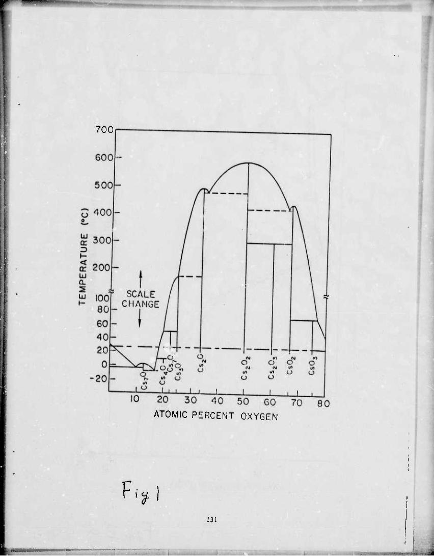
700
ATOMIC PERCENT OXYGEN
F f\ 231
■M i •• iiJiM

If» o
> > a) a>
^ N CVJ -C S O
• O
_L i
O
o
o
CO k-
13
E a» c o
LÜ rr Z) in O Q. X ÜJ
CVJ
D Z — UJ o
>- X Ü
'o
< J —oö IJJ ? -J o o
(SLioioi|d/suo.j|00|0) aiDIA
23.
F-, 2 "i £ ^V

if) o
ro
O
O
(VJ
im • —
e a* c o
UJ cr D CO O CL X UJ
z UJ
X o
(A3) NOliONnj M^OM
13}
fi i 2. b

B
« 4
c o o Q.
c
I 3 o 0)
t I o
LÜ
hv»7.7eV
0 •5 -4 -3 -2 -I
ENERGY BELOW FERMI LEVEL (eV)
0
234
f 19 5 l^uJl

-5 -4 -3 -2 -l ENERGY BELOW FERMI LEVEL (eV)
0
1.35
fi. 4-

-3 -2 ENERGY BELOW FERMI LEVEL (eV)
236
p.-* s~ m

2.0
hv «7.7 8V
> 0) I c o o sz a.
(/) c 2 I 10 o
0) CJ
c 05
0
— 1000 L — 2000 L -- 5000L
40,000 L
-7 -6 -5 -4 -3
ENERGY BELOW FERMI LEVEL (eV)
0
:37
rrjL ^

i jiiiitiwn.." " ;;"...r rLi."T[n7rir^:rtTii
-H 7 -6 -5 -4 -3 ENERGY BELOW FERMI LEVEL (oV)
238 Fr. 7
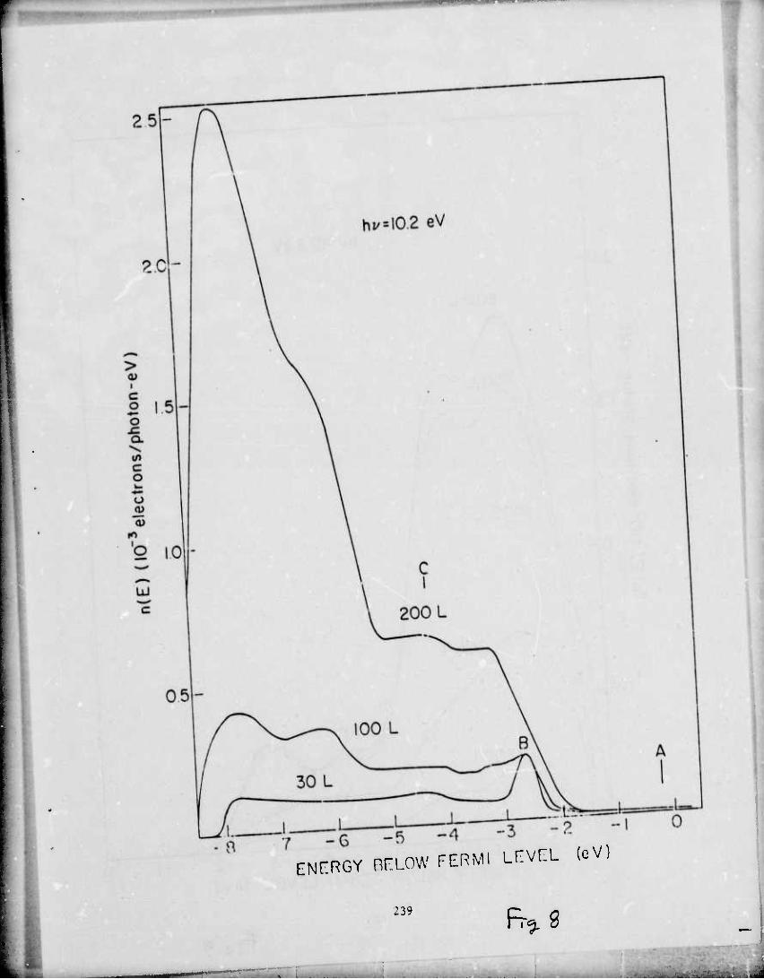
ENf.RGY BELOW FERMI LEVEL toV)
239 Fr^S

■'■ . ■ ■ ■
2 0 hi/=l0 2eV
500 L
-2 -7 -6 -5 -4 -3 ENERGY BELOW PERM! LEVEL (eV)
-I 0
f.> 9

-09 -8 -7 -G -5 -4 -3 -2
ENERGY BELOW FERMI LEVEL (eV)
0
'•t
241
i% to -h
.

Chapter 9
OXYGEN CHEMISORPTION ON Cs COVERED GaAs (ilO) SURFACES*
C. Y. Su, P. W. Chye, P. Pianetta, I. Lindau, and W. E. Spicer
Stanford Electronics Laboratories Stanford University
Stanford, California 94305, USA
Abstract
Cs covered GaAs (110) was exposed to oxygen and studied with soft
X-ray photoemission spectroscopy (SXPS). Oxygen was found to bond to
the surface As atoms with 10 times greater initial oxygen uptake. A
second Cs layer added after the Cs/GaAs (110) surface had been exposed
to oxygen brings effects similar to the oxidation of GaAs by excited
oxygen. Possible inadequacies of the conventional models of NEA photo-
cathodes assuming noninteracting substrate and Cs.,0 layer are discussed,
Work supported by the Advanced Research Pro/jects Agency of the Depart-
ment of Defense and monitored by Night Vision Laboratory, USAECOM under
Contract No. DAAK 02-74-C-0069. Work at the Stanford Synchrotron Radi-
ation Laboratory was also supported by NSF, DMR73-07692 A02, in cooper-
ation with the Stanford Linear Accelerator Center and the Department of
Energy.
iUMmwmBrt- ppf f*"-■■" ""■'■- ■' ■" '-""I •■»»«■«-f~«-'"'"—'-——»«

,„ » . V 00"Pound s.mlcnnductor '" tOPl" «««»«»7 .U»o„8s,d ln t,w UtoMtu ,
will .1,0 bo „,.„„„,„ „ <H.cu,slo„
** no8:atlve •»«««• «fftnuv rmi
s„b3,rato . ' S2Ü •"'U'Ut ""•■">""« t„o
Synohrotron Radl.tll>n Ub<)r,1to
— "**. <-, orystal ^ ., _
Photoemission of the CS-4H 1 , V91 SatUrated' at ^lch -int a monolaTOr
coverage had been reached an,^. "^W ««hed. Additional d deposited bevond thi.
111 be PUmped *™y from the surface It. lnto ^ _ ^^ a _iG • -- ^-^ .. admitted
cesium ___
with------ttheim_j:roiG- spectra. eatUrGS ^ th* ^tC^U.l«,
Figure 1 shows the EDCs of . 1 ^s of a cleaved GMs (UO) surf.,.,
unexcited molecular ov^n ^"^ * ox^en according to the «rh bv Pianett. ,t . *
lifted peak 2.9 eV below H . ^"ettaetal. Tho below the A«-3d peak (E . 40 s .VM
fingerprint for oxwen ch„m< u oxygen chemisorbed on the As of QiA. ,
these resuIf, ki. ^f uiAs. Contrasted to results, the EDCs obtained t« ,**#♦
ceslat^H r . . ««'•»At oxygen exposures o„ , ceslated GaAs (110) surface im .
unace are show in Fig. 2. At in 1 «ure (l L . 10-6 ^ ll1 L «-v-gen oxpo-
- ->•- see the chemtcallv ^^.^ ^^ ^
2«

■MMM ■
characteristic of oxygen adsorbed on GaAs . As we go to higher exposures,
the shifted A3-3d peak and the 0-2p peak grow simultaneously until satu-
ration is reached between 40 and 1000 L. A striking contrast between the
oxidation of clean GaAs and ceslated GaAs is immediately apparent here.
The oxygen uptake is many orders of magnitude faster on the ceslated
surface. Thus, the spectra at 20 and 3 y 107 L 0,, for the ceslated and
clean surfaces, respectively, are comparable.
The effect of oxygen on Cs is to shift the Cs core levels (5s and
5p in Fig. 2, Cs-4d not shown) to lower binding energy with peak shapes
unchanged. Accompanyin« the Cs core level shift is the continuous move-
ment of the shifted As-3d peak to higher binding energy. Movement of
both the Cs peaks and the shifted As-3d peak stabilize in energy position
around 40 L 02, at which point the growth in strength of the shifted As-
3d peak also slows down. This correlation indicates interaction between
the oxidizing substrate and the Cs/0 overlayer. The nature of this com-
plex Interaction will be presented elsewhere.3 As far as we are concerned
here, it is sufficient to point out that the shifted As-3d peak with en-
ergy position from 2.9 to 3.3 eV below the unshlfted peak represent the
same chemisorptlon state of oxygen on GaAs, the shift being due to the
Cs-oxygen interaction.
As shown by the curve second from the top in Fig. 2, the second Cs
dose caused several prominent effects. First, the Cs peaks and the oxy-
gen related peaks shifted to higher binding energy by 0.S eV, I.e., back
to the original binding energy for Cs on GaAs. We also see the shifted
As-3d peak broaden into two peaks: a new peak 4.5 eV below the unshlfted
peak plus the original one at 3.3 eV. Furthermore, a small shoulder ap-
pears 1.1 eV below the Ga-3d peak, as indicated by the arrow under "A"

„ and As core levels are very sim- * „ effects on the Ga and As core
in Flg. 2. T^ese t*o effects ^ ^
. the case of exposing clean GaAs to oxyg (There are also some
. u **,« VDCs are shown In Fig.
elsewhere. ) iuua,
being formed. c,.rface by the depos- 1hte that the heat brought to the surface
It is possible that r to
thot caused by excited o.y^n. ^^^
- - - —°"3houid M co"r: ;r i - - - - This again confirms that, In order
-*« (1") •"*"• " ^ t , 4 „,„ 9ub],ctln8 ine CS/C/CS j K« Pianetta et al. Aicei
" « ""'propo9ed by
v ^ a hleh oxygen exposure, the cs pe covered CaAs to a nun V. ,„ addltl„„ to tms co^e. snl.t
O.S ev to^rd 1o.er blndln. ener.y.
a . 5 there are t« ««•<>« concerning
. „ - nrst If «e tahe the relative area under tlonotOaAs. First, i „ have oxl-
»«sure of the oxygen coverage, «e unshlfted As-3d peah as a .eaaure
, „~r- of GaAs. Moreover, the ^B dued «ore than one »onolayer OaA ^^
, . a 5 oV state corresponding to MjO, hinding energy) - ■ „ 3 , eV. These « effects, again,
t„ the lo».r oxide AS203 .1th «,-»■'*'
—- "t:of rrr^ «xidntion«.«. ^— The large enhancement in the m
monies which impinged on the Tho oxvEen molecules,
bv the "hg Picture. -^ ^.^^ rtwl.o^l» o.
. top of the cs layer, suoh dissociative chOTlSorptlon ha
24^
. :_ r~

by Gresory et H* and Papa^or.opouios et al^ on Cs and bv WM on cs and by Wijers et als
on Cs, Rb. and K. once the oxygen is m * w.vy^en IS in atomic fnym t-u~ M J , 1C rorm. the Madelung energy «-. « «,«««. for 0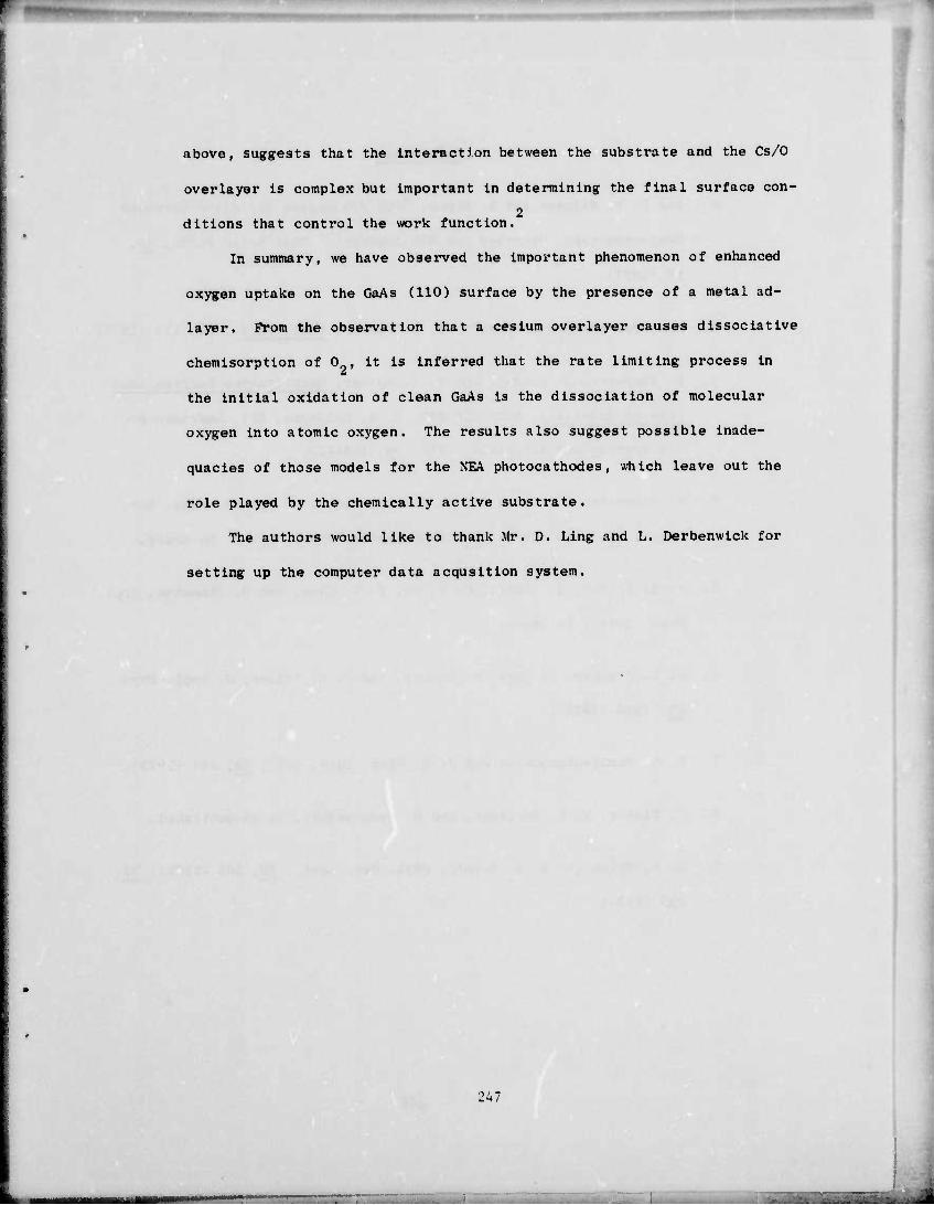
above, suggests that the Interaction between the substrate and the Cs/O
overlayer Is complex but important in determining the final surface con-
2 ditions that control the work function.
In summary, we have observed the important phenomenon of enhanced
oxygen uptake on the GaAs (110) surface by the presence of a metal ad-
layer. Prom the observation that a cesium overlayer causes dissociative
chemisorption of 0 , it is inferred that the rate limiting process in
the initial oxidation of clean GaAs is the dissociation of molecular
oxygen into atomic oxygen. The results also suggest possible inade-
quacies of those models for the KEA photocathodes, which leave out the
role played by the chemically active substrate.
The authors would like to thank Mr. D. Ling and L. Derbenwick for
setting up the computer data acqusltion system.
247
- - -■-■^ '
f .,

References
1. See C. W. Wllmsen and S. Szpak. »MM Processing for III-V Compound
Semiconductors: Overview and Bibliography," Thin Solid Films, 16.
17 (1977).
2. See, for example, review by W. E. Spicer, Appl Phys . , 12, 115 (1977)
3. P. Pianetta, I. Lindau, and W. E. Spicer. Quantitative Surface An. 1.
vsis of Materials, ASTM STP 643, X. S. Mototyr,. Ed., American Soc.
for Testing and Materials, 1978, pp. 105-123.
4. P. Pianetta, 1. Lindau, C. M. Garner, and W. E. Spicer, Phys. Rev.
Utt.. 37, 1166 (1976); 35, 1356 (1975) ; Phys. Rev. B. in press.
5- W. E. Spicer, 1. Lindau. C. Y. Su. P. w. Chye, and P. Pianetta, Appl
Phys. Lett.. in press.
6. P. E. Gregory, P. Chye. H. Sunami, and W. E. Spicer. J. Appl. Phys..
46, 3525 (1975).
7. C. A. Pa pageorgopoulos and J. M. Chen. Surf. Sei., 39, 313 (1973)
8. C. Wilers, M. R. Adriaens, and B. Feuerbacher, to be publis hed.
9. C. R. Helms and W. E. Spicer, Phys. Rev. Lett.. 28. 565 (1972); 32,
228 (1974).
248

Figure Captions
1. EDCs of clean and oxygen exposed n-type GaAs (110) at hv = 100 eV.
From Ref. 4.
2. EDCs of clean and Cs/O treated surface of n-type GaAs (110) at hv
120 eV. The arrow under "A" points to an asymmetry in the Ga-3d
peak. "«" represent equal energy spacing of 0.8 eV.
3. EDCs of clean p-type GaAs (110) and the clean surface exposed to
excited oxygen at hv = 100 eV.
249
APPENDIX
11. Publications
1. Surface State Band on GaAs (110) Face, P. E. Gregory, W. E. Spicer,
S. Clraci, and W. A. Harrison, Applied Physics Letters 25, 511
(1974).
2. The Oxidation of Cs UV Photoemission Studies, P. E. Gregory, P,
Chye, H. Sunami, and W. E. Spicer, Journal of Applied Physics 46,
Xo. 8, 3525 (August 1975).
3. Photoemission Studies of the GaAs-Cs Interface, P. E. Gregory and
W. E. Spicer, Physical Review B12, 2370 (September 1975).
4. Determination of the Oxygen Binding Site on GaAs (110) Using Soft
X-Ray-Photoemlsslon Spectroscopy, P. Pianetta, I. Lindau, C. Gar-
ner, and W. E. Spicer, Phys. Rev. Letters 35, 1356 (November 1975).
5. GaSb Surfaces States and Schottky-Barrier Pinning, P. W. Chye, I.
A. Babalola, T. Sukegawa, and W. E. Spicer, Comments - Physical
Review Letters 35, 1600 (December 1975).
6. Photoemission Study of the Formation of Schottky Barriers, W. E.
Spicer, P. E. Gregory, P. W. Chye, I.A. Babalola, and T. Sukegawa,
Applied Physics Letters 27, 617 (December 1975).
7. Photoemission Study of Surface States of the (110) GaAs Surface,
P. E. Gregory and W. E. Spicer, Phys. Rev. B13, 725 (January 1976).
8. Ultraviolet Photoer.isslon Study of Cesium Oxide Films on GaAs, P.
E. Gregory and W. E. Spicer, Journal of Applied Physics 47, 510
(February 1976).
250

HHiif
9.
C=«pou„ds. w. .. spi^, p. «. ^| p. ,, ^^ ^ ^^^^
and r. A. B^lol., ,. vac. Sei. TaCnou JJ, 233 <Ja„ua.y/rebruar),
1976)
10. PhotoemiSsion StudieS of Surface States and Schott.y-Barrier ^
-tlon on rnP. .. w. Chye, !. A. Bdbalola> T. Sukegara ( ^ ^ ^
Spicer, Phys. Rev. B13, 4439 (May i976).
11. Synchrotron Radiation Studies of Electronic Structure and Surface
Chenustry of GaAs, ^ and ^ ,. E< ^^^ ^ ^^^ p< ^
Gregory, c. M. Garner. P. Pianetta. and P. w. chye. J. Vac. Sei.
Technol. 13, 780 (July/August 1976).
12. Photoemission Study of the Adsorption of 0,, CO and H, on GaAs
(HO), P. E. Gregory and W. E. Spicer, Surface Science 54, 229-
258 (1976).
13. Oxidation Properties of GaAs (110) Surfaces, P. pianetta> r. Lln.
dau. C. M. Garner, and W. E. Spicer, Physical Review Letters 37.
1166 (1976).
14. Surface and Interface States of GaSb: A Photoemission Study. P.
W. Chye. T. Sukegawa, I. A. Babalola, „. Sunan.i. P. Gregory. and
W. E. Spicer, Physical Review B15, 2U8 (February 1977).
13. Oxygen Sorption and Excitonic Effects on GaAs Surfaces. P. Vt Cilye.
P. Pianetta. I. Lindau> and w. E. Splcer) ^ ^ ^ ^^^ ^
917-919 (July/August 1977).
251

W mmmmmm-i v-m *miwmmmimw!»u'mm
16. Surface and Interface States on GaA3 (110): Effects of Atomic and
Electronic Rearrangements, W. E. Spicer, P. Pianetta, I. Lindau,
and P. W. Chye, J. Vac. Sei. Technol. 14, No. 4, 883-893 (July/
August 1977).
17. Do the Au 5d-Bands Narrow at the Surface: Comparison with Au
Alloys, P. W. Chye, I. Lindau, P. Pianetta, C. M. Garner, and W.
E. Spicer, Physics Letters 63A, No. 3, (November 1977).
18. Studies of Surface Electronic Structure and Surface Chemistry Using
Synchrotron Radiation, W. E. Spicer, I. Lindau, J. N. Miller, D. T.
Ling, P. Pianetta, P. W. Chye, and C. M. Gamer, Physlca Scripta
16, 388 (November/December 1977).
19. Reply to "Oxidation Properties of GaAs (110) Surfaces", R. Ludeke,
P. Pianetta, I. Lindau, C. M. Garner, and W. E. Spicer, Phys. Rev.
B. 16, No. 12, 5600-5602 (December 1977),
20. Photoemission Studies of the Electronic Structure of III-V Semicon-
ductor Surfaces, I. Lindau, P. Pianetta, CM. Garner, P. W. Chye,
P. E. Gregory, and W. E. Spicer, Surface Science 63, 45-55 (1977).
21. The Surface Electronic Structure and Surface Chemistry of GaAs
(110), P. Pianetta, I. Lindau, W. E. Spicer, and C. M, Garner,
Proc. 7th Intern. Vac. Congr. and 3rd Intern. Conf. Solid Surfaces,
615-618, Vienna, (1977).
22. Oxygen Adsorption and the Surface Electronic Structure of GaAs (110),
I. Lindau, P. Pianetta, W. E. Spicer, P. E- Gregory, C. M. Garner,
and P. W. Chye, J. of Electron Spectroscopy and Related Phenomena 13,
155-160 (1978).
252

t
23. Valence Band Studies of Clean and Oxygen Exposed GaAs (110) Sur-
faces, P. Pianetta, I. Lindau, P. F. Gregory, C. If. Garner, and
W. E. Spicer, Surface Science 72. 298-320 (1978).
24. Evidence for a New Type of Metal-Semiconductor Interaction on GaSb,
P. W. Chye, I. Lindau, P. Pianetta, C. M. Garner, and W. E. Spicer,
Phys. Rev. B. 17, No. 6, 2682-2684 (March 1978).
25. The Use of Soft X-Ray Photoemission Spectroscopy to Study the Ad-
sorption of Oxygen on the (110) Surface of Gallium Arsenide and
Gallium Antimonido, P. Pianetta, I. Lindau, and W. E. Spicer,
Quantitative Surface Analysis of Materials, ASTM STP 643, N. S.
Mclntyre, Ed., American Society for Testing and Materials, 105-
123, 1978.
26. New Phenomena in Schottky Barrier Formation on III-v Compounds, I.
Lindau, P. w. chye, C. M. Garner, P. Pianetta, C. Y. Su, and W, E.
Spicer, J. Vac. Sei. Techno!. 15(4), 1332-1339 (July/August 1978).
27. UPS and LEED Studies of GaAs (110) and (111) As Surfaces, P. Skeath,
W. A. Saperstein, P. Pianetta, I. Lindau, and W. E. Spicer, J. Vac.
Sei. Technol. 15(4), 1219-1222, (July/August 1978).
28. Chemisorption and Oxidation Studies of the (110) Surfaces of GaAs,
GaSb, and InP, P. Pianetta, I. Lindau, C. M. Garner, and W. E.
Spicer, Phys. Rev. B 18, No. 6, 2792-2806 (September 1978).
29. Photoemission Study of Au Schottky-Barrler Formation on GaSb, GaAs,
and InP Using Synchrotron Radiation, P. W. Chye, I. Lindau, P. Pia-
netta, C. M. Garner, C. Y. Su, and W. E. Spicer, Phys. Rev. B 18,
No. 10, 5545-5559 (November 1978).
253

mmm
30. Core-Uvel Photoemission of the Cs-0 Adlayer of XEA GaAs Cathodes.
W. E. Spicer, I. Lindau. C. Y. Su. P. w. Chye. and P. Pianetta.
Appl. Phys, Lett. 33(11), 934-935 (December 1978).
31. Oxygen Chemisorption on Cs Covered GaAs (110) Surfaces, C. Y. Su,
P. W. Chye, P. Pianetta, l. Lindau, and W. E. Spicer, Surface
Science (Proc. fron, the ICSFS Ccnf., 5-8 July 1978. Tokyo).
32. The Surface Electronic Structure of 3-5 Compounds and the Mechanism
of Fermi Level Pinning by Ocygen (Passivation) and Metals (Schottky
Barriers), w. E. Spicer. P. w. Chye. C. M. Garner, 1. Lindau, and
P. Pianetta. Surface Science (Proc. from the ICSFS Conf.. 5-8 July
1978, Tokyo).
33. Abrupt Ga^Al^As-GaAs Quantum-Well Heterostructures Grown by Metal-
organic Chemical Vapor Deposition, R. D. Dupuis, P. D. Dapkus. C.
M. Garner, C. Y. Su. and W. E. Spicer. Appl. Phys. Lett. 34, No. 5,
338-340 (March 1979).
34. Fundamental Studies of IH-v Surfaces and the 3-5 Oxide Interface,
W. E. Spicer, I. Lindau, P. Pianetta, P. W. Chye. and C. M. Garner,
Thin Solid Films. Vol. 56, No. 1. 2, 1-18 (1979).
25.:
.-■■■ -■.■«. ■