Embed Size (px)
Citation preview
A HIGH THROUGHPUT, NONCONTACT SYSTEM FOR SCREENING SILICON WAFERS PREDISPOSED TO BREAKAGE DURING SOLAR CELL PRODUCTION
Bhushan Sopori, Przemyslaw Rupnowski, Prakash Basnyat, and Vishal Mehta National Renewable Energy Laboratory, Golden, Colorado, USA
ABSTRACT
We describe a non-contact, on-line system for screening wafers that are likely to break during solar cell/module fabrication. The wafers are transported on a conveyor belt under a light source, which illuminates the wafers with a specific light distribution. Each wafer undergoes a dynamic thermal stress whose magnitude mimics the highest stress the wafer will experience during cell/module fabrication. As a result of the stress, the weak wafers break, leaving only the wafers that are strong enough to survive the production processes. We will describe the mechanism of wafer breakage, introduce the wafer system, and discuss the results of the time-temperature (t-T) profile of wafers with and without microcracks.
INTRODUCTION
Wafer breakage is a very serious problem in the PV industry because 5%–10% of wafers break during cell/module fabrication. This problem is somewhat unique to solar photovoltaics (PV) because the PV industry uses very thin wafers and does not “prepare” them in a way that can maintain their high mechanical strength. In the microelectronics industry, wafer breakage is prevented by: (i) providing a large thickness of the wafer in comparison to the wafer size; (ii) the removal of surface damage and microcracks generated by wafer sawing; (iii) polishing one side of the wafer; and (iv) shaping the edges of the wafer. These steps are quite expensive and involve etching away 20 µm or more of silicon from each surface (in a PV wafer that is typically <200 µm thick). Because of the incomplete preparation, PV wafers are left with microcracks, which decrease their strength and make them prone to breakage when high stress is applied to wafers during handling and processing. Wafers break during handling, transport, and processing because they experience stress that exceeds the wafer strength. This problem becomes even worse with decrease in the wafer thickness and with increase in the wafer size.
Because it is now known that the strength of a PV wafer is lowered by the presence of microcracks, most monitoring approaches aim at identifying microcracks. However, this is an extremely unreliable process because the surface roughness of PV wafers is comparable to the size of the microcracks. It is also important to point out that even if it were possible to detect all the microcracks, it is not possible to predict if a wafer will break in a given process sequence, unless detailed information such as the shapes and sizes of the cracks is known [1,2].
Here, we first briefly explain the wafer breakage mechanism and then describe a noncontact technique in which a stress is applied to the wafer. The magnitude and distribution of the stress mimic the most severe stress the wafers will experience during cell fabrication by a given sequence of process steps. If the wafer has a low strength, it will break and the wafer will be removed. If the wafer survives this stress, it is highly likely to withstand the entire cell/module processing. The maximum stress that the machine applies is easily adjustable by simply controlling the power of the light source.
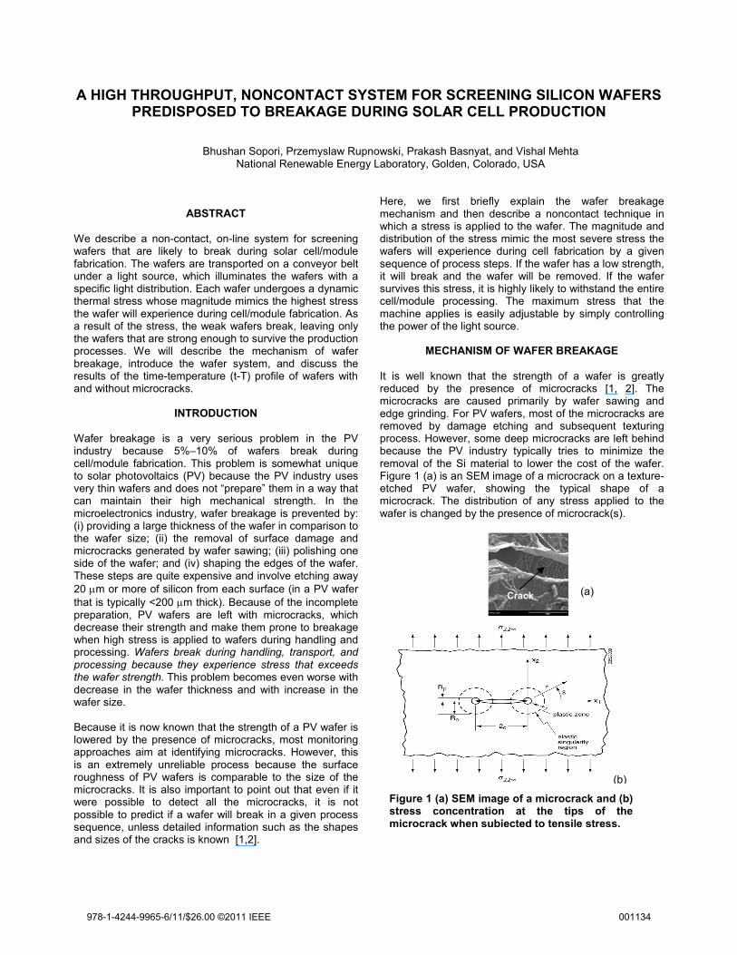
MECHANISM OF WAFER BREAKAGE It is well known that the strength of a wafer is greatly reduced by the presence of microcracks [1, 2]. The microcracks are caused primarily by wafer sawing and edge grinding. For PV wafers, most of the microcracks are removed by damage etching and subsequent texturing process. However, some deep microcracks are left behind because the PV industry typically tries to minimize the removal of the Si material to lower the cost of the wafer. Figure 1 (a) is an SEM image of a microcrack on a texture-etched PV wafer, showing the typical shape of a microcrack. The distribution of any stress applied to the wafer is changed by the presence of microcrack(s).
(b)
Crack (a)
Figure 1 (a) SEM image of a microcrack and (b) stress concentration at the tips of the microcrack when subjected to tensile stress.
978-1-4244-9965-6/11/$26.00 ©2011 IEEE 001134
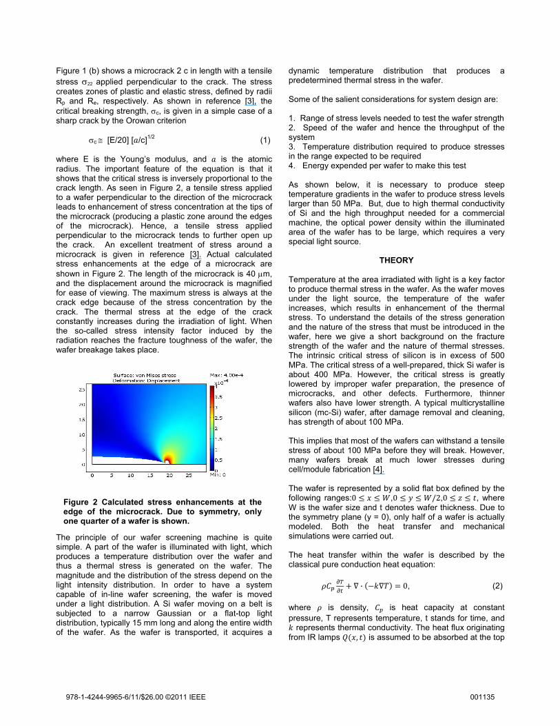
Figure 1 (b) shows a microcrack 2 c in length with a tensile stress σ22 applied perpendicular to the crack. The stress creates zones of plastic and elastic stress, defined by radii Rp and Re, respectively. As shown in reference [3], the critical breaking strength, σc, is given in a simple case of a sharp crack by the Orowan criterion
σc ≅ [E/20] [�/c]1/2 (1)
where E is the Young’s modulus, and � is the atomic radius. The important feature of the equation is that it shows that the critical stress is inversely proportional to the crack length. As seen in Figure 2, a tensile stress applied to a wafer perpendicular to the direction of the microcrack leads to enhancement of stress concentration at the tips of the microcrack (producing a plastic zone around the edges of the microcrack). Hence, a tensile stress applied perpendicular to the microcrack tends to further open up the crack. An excellent treatment of stress around a microcrack is given in reference [3]. Actual calculated stress enhancements at the edge of a microcrack are shown in Figure 2. The length of the microcrack is 40 µm, and the displacement around the microcrack is magnified for ease of viewing. The maximum stress is always at the crack edge because of the stress concentration by the crack. The thermal stress at the edge of the crack constantly increases during the irradiation of light. When the so-called stress intensity factor induced by the radiation reaches the fracture toughness of the wafer, the wafer breakage takes place.
PRINCIPLE OF OUR METHOD The principle of our wafer screening machine is quite simple. A part of the wafer is illuminated with light, which produces a temperature distribution over the wafer and thus a thermal stress is generated on the wafer. The magnitude and the distribution of the stress depend on the light intensity distribution. In order to have a system capable of in-line wafer screening, the wafer is moved under a light distribution. A Si wafer moving on a belt is subjected to a narrow Gaussian or a flat-top light distribution, typically 15 mm long and along the entire width of the wafer. As the wafer is transported, it acquires a
dynamic temperature distribution that produces a predetermined thermal stress in the wafer. Some of the salient considerations for system design are: 1. Range of stress levels needed to test the wafer strength 2. Speed of the wafer and hence the throughput of the system 3. Temperature distribution required to produce stresses in the range expected to be required 4. Energy expended per wafer to make this test As shown below, it is necessary to produce steep temperature gradients in the wafer to produce stress levels larger than 50 MPa. But, due to high thermal conductivity of Si and the high throughput needed for a commercial machine, the optical power density within the illuminated area of the wafer has to be large, which requires a very special light source.
THEORY
Temperature at the area irradiated with light is a key factor to produce thermal stress in the wafer. As the wafer moves under the light source, the temperature of the wafer increases, which results in enhancement of the thermal stress. To understand the details of the stress generation and the nature of the stress that must be introduced in the wafer, here we give a short background on the fracture strength of the wafer and the nature of thermal stresses. The intrinsic critical stress of silicon is in excess of 500 MPa. The critical stress of a well-prepared, thick Si wafer is about 400 MPa. However, the critical stress is greatly lowered by improper wafer preparation, the presence of microcracks, and other defects. Furthermore, thinner wafers also have lower strength. A typical multicrystalline silicon (mc-Si) wafer, after damage removal and cleaning, has strength of about 100 MPa. This implies that most of the wafers can withstand a tensile stress of about 100 MPa before they will break. However, many wafers break at much lower stresses during cell/module fabrication [4]. The wafer is represented by a solid flat box defined by the following ranges:0 � � � �,0 � � � �/2,0 � � , where W is the wafer size and t denotes wafer thickness. Due to the symmetry plane (y = 0), only half of a wafer is actually modeled. Both the heat transfer and mechanical simulations were carried out. The heat transfer within the wafer is described by the classical pure conduction heat equation: �� ���� � � · ������ � 0, (2)
where � is density, � is heat capacity at constant pressure, T represents temperature, t stands for time, and � represents thermal conductivity. The heat flux originating from IR lamps ���, � is assumed to be absorbed at the top
Figure 2 Calculated stress enhancements at the edge of the microcrack. Due to symmetry, only one quarter of a wafer is shown.
978-1-4244-9965-6/11/$26.00 ©2011 IEEE 001135
surface (z = t) of the wafer. All surfaces except the symmetry surface are losing heat through radiation and convection to a space being held at room temperature (Tamb). As a result of these assumptions, the boundary conditions become:
�� · � �� 0 � � � 0�"�� � ��#$� � %&��' � �()*' � � ���, � � � �"�� � ��#$� � %&��' � �()*' � � "+ ,+- .�/+-0
(3)
where: � is the normal vector to the boundary � is the conductive heat flux vector � � ���� ε is the emissivity " is the convection constant % is the Stefan-Boltzmann constant
���, �=�1+�23��� � $1 � -2++4 5 6#+�7/�2�7 �8 (4) where: �1 = maximum flux absorbed $1 = initial peak position � = standard deviation = FWHM/2.354
In the mechanical simulations the wafer was modeled as a linear elastic isotropic body with the constitutive behavior described by the Duhamel-Hook’s law: %9: � �9:;<=&;< � >?;<�� � ��#$�@, (5)
where: %9: is the stress tensor �ijkl is the stiffness tensor > is the thermal expansion coefficient ?;< is the Kronecker’s delta. Buckling was neglected, and it was assumed that the strains were small. It is important to recognize that a wafer could break when subjected to a given processing sequence. However, if the processing is made “gentler,” it can easily survive. Our wafer screening machine can be “trained” to accommodate different processing conditions through a computer-controlled knob that adjusts the relative power of lamps in the lamp source.
CHARACTERISITCS OF THE THERMAL STRESS
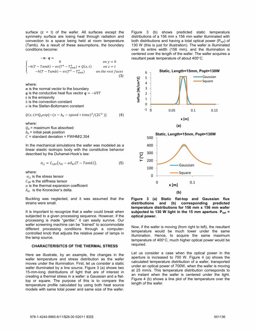
Here we illustrate, by an example, the changes in the wafer temperature and stress distribution as the wafer moves under the illumination. First, let us consider a static wafer illuminated by a line source. Figure 3 (a) shows two 15-mm-long distributions of light that are of interest in creating a thermal stress in a wafer: a Gaussian and a flat-top or square. The purpose of this is to compare the temperature profile calculated by using both heat source models with same total power and same size of the wafer.
Figure 3 (b) shows predicted static temperature distributions of a 156 mm x 156 mm wafer illuminated with both distributions and having a total optical power (Popt) of 130 W (this is just for illustration). The wafer is illuminated over its entire width (156 mm), and the illumination is centered over the length of the wafer. The wafer acquires a resultant peak temperature of about 400°C.
(a)
(b)
Now, if the wafer is moving (from right to left), the resultant temperature would be much lower under the same illumination. Hence, to acquire the same maximum temperature of 400°C, much higher optical power would be required. Let us consider a case when the optical power in the aperture is increased to 700 W. Figure 4 (a) shows the calculated temperature distribution of a wafer, transported under an optical power of 700W, when the wafer is moving at 25 mm/s. This temperature distribution corresponds to an instant when the wafer is centered under the light. Figure 4 (b) shows a line plot of the temperature over the length of the wafer.
0
100
200
300
400
500
0 0.1
T [°
C]
x [m]
Static, Length=15mm, Popt=130W
Gaussian
Square
-10123456
0 0.05 0.1 0.15
InFl
ux [W
/cm
^2]
x [m]
Static, Length=15mm, Popt=130W
GaussianSquare
Figure 3 (a) Static flat-top and Gaussian flux distributions and (b) corresponding predicted temperature distributions for 156 mm x 156 mm wafer subjected to 130 W light in the 15 mm aperture. Popt = optical power.
978-1-4244-9965-6/11/$26.00 ©2011 IEEE 001136
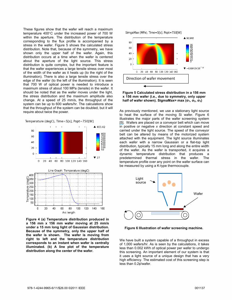
These figures show that the wafer will reach a maximum temperature 400°C under the increased power of 700 W within the aperture. The distribution of the temperature corresponding to the flux profile is accompanied by a stress in the wafer. Figure 5 shows the calculated stress distribution. Note that, because of the symmetry, we have shown only the upper half of the wafer. Again, this distribution occurs at a time when the wafer is centered about the aperture of the light source. This stress distribution is quite complex, but the important feature is that the wafer experiences a large tensile stress over most of the width of the wafer as it heats up (to the right of the illumination). There is also a large tensile stress over the edge of the wafer (to the left of the illumination). It is seen that 700 W of optical power is needed to introduce a maximum stress of about 100 MPa (tensile) in the wafer. It should be noted that as the wafer moves under the light, the stress distribution and the maximum amplitude also change. At a speed of 25 mm/s, the throughput of the system can be up to 600 wafers/hr. The calculations show that the throughput of the system can be doubled, but it will require about twice the power.
DESCRIPTION OF THE SYSTEM As previously mentioned, we use a stationary light source to heat the surface of the moving Si wafer. Figure 6 illustrates the major parts of the wafer screening system [5]. Wafers are placed on a conveyor belt which can move in positive or negative x direction at constant speed and carried under the light source. The speed of the conveyor belt can be altered by means of the motorized system attached with the equipment. The light source illuminates each wafer with a narrow Gaussian or a flat-top light distribution, typically 15 mm long and along the entire width of the wafer. As the wafer is transported, it acquires a dynamic temperature distribution that produces a predetermined thermal stress in the wafer. The temperature profile over any point on the wafer surface can be measured by using a K-type thermocouple.
RESULTS
We have built a system capable of a throughput in excess of 1,000 wafers/hr. As is seen by the calculations, it takes less than 0.002 kWh of optical power per wafer to undergo this screening. An important element of our system is that it uses a light source of a unique design that has a very high efficiency. The estimated cost of this screening step is less than 0.2¢/wafer.
Direction of wafer movement
Light source
Wafer
Figure 4 (a) Temperature distribution produced in a 156 mm x 156 mm wafer moving at 25 mm/s under a 15 mm long light of Gaussian distribution. Because of the symmetry, only the upper half of the wafer is shown. The wafer is moving from right to left and the temperature distribution corresponds to an instant when wafer is centrally illuminated. (b) A line plot of the temperature distribution along the center of the wafer.
Figure 5 Calculated stress distribution in a 156 mm x 156 mm wafer (i.e., due to symmetry, only upper half of wafer shown). SigmaMax= max (σ1, σ2, σ3)
Figure 6 Illustration of wafer screening machine.
978-1-4244-9965-6/11/$26.00 ©2011 IEEE 001137
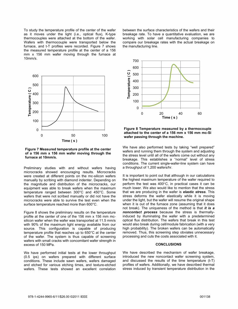
To study the temperature profile of the center of the wafer as it moves under the light (i.e., optical flux), K-type thermocouples were attached at the bottom of the wafer. Wafers with thermocouple were transported below the furnace, and t-T profiles were recorded. Figure 7 shows the measured temperature profile at the center of a 156 mm x 156 mm wafer moving through the furnace at 10mm/s.
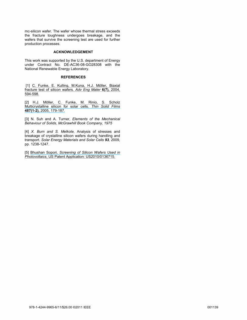
Preliminary studies with and without wafers having microcracks showed encouraging results. Microcracks were created at different points on the mc-silicon wafers manually by scribing with diamond indenter. Depending on the magnitude and distribution of the microcracks, our equipment was able to break wafers when the maximum temperature ranged between 300°C and 450°C. Some wafers that were not scribed manually or did not have the microcracks were able to survive the test even when the surface temperature reached more than 600°C. Figure 8 shows the preliminary results on the temperature profile at the center of one of the 156 mm x 156 mm mc- silicon wafer when the wafer was transported at 11.5 mm/s with 90% of the maximum light energy available from our source. This configuration is capable of producing temperature profile that reaches up to 650°C at the center of the wafer. The system is thus capable of screening wafers with small cracks with concomitant wafer strength in excess of 150 MPa. We have performed initial tests at the lower throughput (0.5 ips) on wafers prepared with different surface conditions. These include sawn wafers, wafers damaged and etched for various etching times, and texture-etched wafers. These tests showed an excellent correlation
between the surface characteristics of the wafers and their breakage rate. To have a quantitative evaluation, we are working with solar cell manufacturing companies to compare our breakage rates with the actual breakage on the manufacturing line. We have also performed tests by taking “well prepared” wafers and running them through the system and adjusting the stress level until all of the wafers come out without any breakage. This establishes a “normal” level of stress conditions. The current single-wafer-line system can have a throughput of 1,200 wafers/hr. It is important to point out that although in our calculations the highest maximum temperature of the wafer required to perform the test was 400°C, in practical cases it can be much lower. We also would like to mention that the stress that we are producing in the wafer is elastic stress. This stress deforms the wafer elastically while it is moving under the light, but the wafer will resume the original shape when it is out of the furnace zone (assuming that it does not break). The uniqueness of the method is that it is a noncontact process because the stress is thermally-induced by illuminating the wafer with a predetermined optical flux distribution. The wafers that break in this test would also break during cell/module fabrication (with a very high probability). The broken wafers can be automatically removed. Thus, this screening step obviates unnecessary processing and cuts the costs associated with it.
CONCLUSIONS
We have described the mechanism of wafer breakage, introduced the new noncontact wafer screening system, and discussed the results of the time temperature (t-T) profiles of wafers. Additionally, we have described thermal stress induced by transient temperature distribution in the
0
100
200
300
400
500
600
0 50 100
Tem
per
atu
re (
C )
Time ( s )
0
100
200
300
400
500
600
700
0 20 40 60
Tem
per
atu
re (
C )
Time ( s )
Figure 7 Measured temperature profile at the center of a 156 mm x 156 mm wafer moving through the furnace at 10mm/s.
Figure 8 Temperature measured by a thermocouple attached to the center of a 156 mm x 156 mm mc-Si wafer passing through the machine.
978-1-4244-9965-6/11/$26.00 ©2011 IEEE 001138
mc-silicon wafer. The wafer whose thermal stress exceeds the fracture toughness undergoes breakage, and the wafers that survive the screening test are used for further production processes.
ACKNOWLEDGEMENT
This work was supported by the U.S. department of Energy under Contract No. DE-AC36-08-GO28308 with the National Renewable Energy Laboratory.
REFERENCES
[1] C. Funke, E. Kulling, M.Kuna, H.J. Möller, Biaxial fracture test of silicon wafers. Adv Eng Mater 6(7), 2004, 594-598. [2] H.J. Möller, C. Funke, M. Rinio, S. Scholz Multicrystalline silicon for solar cells. Thin Solid Films 487(1-2), 2005, 179-187. [3] N. Suh and A. Turner, Elements of the Mechanical Behaviour of Solids, McGrawhill Book Company, 1975 [4] X. Burn and S. Melkote, Analysis of stresses and breakage of crystalline silicon wafers during handling and transport. Solar Energy Materials and Solar Cells 93, 2009, pp. 1238-1247. [5] Bhushan Sopori, Screening of Silicon Wafers Used in Photovoltaics, US Patent Application: US2010/0136715.
978-1-4244-9965-6/11/$26.00 ©2011 IEEE 001139


