Embed Size (px)
Citation preview
A Prototype Framework for Knowledge-Based Analog Circuit Synthesis*
Ramesh Harjani, Rob A. Rutenbar and L. Richard Carley
Department of Electrical and Computer Engineering Carnl:gie Mellon University
Pittsburgh, Pennsylvania 15213
Abstract
An organization for a knowledge-based analog (circuit synthesis tool is described. Analog circuit topologies are represented as a hierarchy of functional blocks; a planning mechanism is introduced to translate performance specifica- tions between levels in this circuit hierarchy. A prototype im- plementation, OASYS, synthesizes sized transistor schematics for simple CMOS operational amplifiers from performance specifications and process parameters, and demonstrates the workability of the a.pproach.
1. Introduction Design automation ideas from digital VLSI have only
recently begun to migrate into analog circuit design. In part this reflects the inherent complexities of the analog design process. But it also reflects the success with which some clas- sical analog applications have been supplanted by digital tech- niques; for example, digital signal processing is frequently used in place of analog filtering. There are limits to this re- placement process, however. Also, even though many of the transistors in an ostensibly analog circuit such as an analog- to-digital converter may actually belong to digital sections of the circuit, design of the analog sections typically is most time-consuming. Moreover, there is large demand for analog circuitry in system;3 applications such as telecommunications and robotics, where analog interfaces to an external er,viron- ment are coupled with digital processing systems. Hence, there is growing interest in analog design tools.
Unfortunately, the state of analog synthesis tools is quite primitive in comparison to digital synthesis tools. In the digi- tal domain, structured abstractions and hierarchy are com- monplace, and are relied upon to make seemingly large syn- thesis tasks tractable by breaking them into smaller steps. Such abstractions and hierarchy do not currently play a central role in analog design. Analog circuits are still designed, largely by hand, by experts intimately familiar with nuances of the tarl;et application and IC fabrication process.
- * This research was supported in part by the Semiconductor
Research Corporation, and by a grant from the Gould Foundation.
permission to copy without fee all or part of this material is granted provided that the copies are not made or distributed for direct commercial advantage, tbe ACM copyright notice and the title of the publication and its date appear, and noi:ice is given that copying is by permission of the Association for Computing Machinery. To copy otherwise, or to republish, requires a fw and/or specific permission.
Analog design is commonly perceived to be one of the most knowledge-intensive of design tasks: the techniques needed to build good analog circuits seem to exist solely as expertise in- vested in individual designers.
This paper describes a knowledge-based framework for an analog circuit synthesis tool. Although “knowledge-based” has come to be synonymous with “rule-based” in CAD ap- plications, our prototype implementation relies more heavily on planning mechanisms than on rule execution. We attack the behavior-tc+structure portion of the synthesis task; our goal is to produce circuit schematics including device sizes, from performance specifications for common analog functional blocks. This approach is motivated by the lack of tools to support the design of custom analog circuits. In particular, there are emerging semi-custom methodologies to lay out a given circuit schematic, but as yet no real tools to help design this schematic of sized interconnected devices from a set of performance specifications.
The paper is organized as follows. Section 2 contrasts the analog and digital domains, and summarizes related syn- thesis research. Section 3 clescribes the structure of the framework in detail, and how it is motivated by traditional analog design approaches. We introduce the critical role of hierarchy in analog circuits, and describe methods to structure and exploit analog design knowledge. Section 4 describes ex- perience with a small prototype implementation called OASYS, which designs simple CMOS operational amplifiers. We analyze the architecture of OASYS, and examine some automatically synthesized circuits it has produced. Finally, Section 5 presents some concluding observations on the workability of the approach.
2. Background Before describing the components of a framework for
analog synthesis, we review the salient differences between analog and digital design problems, and some previous ap- proaches to these problems.
2.1 Analog Design versus Digital Design Consider the task of designing a functional block to be
implemented as a single, perhaps large, cell on a VLSI circuit. The overall high-level synthesis task, for either analog or digi- tal circuits, is to interconnect a set of appropriately designed primitive components (e.g., transistors) to produce the correct behavior for the cell. We informally partition the differences between analog and digital design tasks into four categories: size, hierarchy, process, and performance constraints. We dis- cuss each of these below.
The size difference is easily stated: analog circuits tend to have fewer transistors than digital circuits. However, there
Paper 3.3 42
24th ACM/IEEE Design Automation Conference
0 1987 ACM 07:18-100X/87/0600-0042$00.75
is typically much more design time invested in each transis- tor. A complex analog cell might have 100 transistors, while a digital cell of similar functional complexity might have 1000. The difference derives from the assumed functionality of each transistor. In digital circuits, devices tend to work as switches, moving 1s and 0s between storage elements at known times. Such devices can often have the minimum size permissible in the process (to switch faster) and are electri- cally identical in their performance; only those devices on critical paths or driving large loads need to have radically dif- ferent electrical properties. Analog circuits, on the other hand, often exploit the full spectrum of capabilities exhibited by individual devices. The electrical characteristics of in- dividual transistors are more carefully designed, and in- dividual devices in a circuit may differ substantially. Moreover, macroscopic properties of the entire circuit, such as gain, frequency response, or stability, may hinge on the relationship among currents, voltages, resistances, and capacitances controlled by individual devices. Indeed, the generally smaller size of analog circuits is partially a reflection of the difficulty of managing more than several tens of devices, each of which contributes a dozen interacting electri- cal constraints to the synthesis task.
Digital and analog circuits both employ hierarchy, but in substantially different ways. In digital circuits, there is tacit agreement on the abstraction levels through which a design must pass: behavioral, functional-block, register-transfer, gate-network, switch-network, circuit, mask. These abstrac- tions play a central role in the organization of synthesis tools, which usually help translate from one abstract level to the next slightly more concrete level. There is not such a well- developed hierarchy for analog circuits, but hierarchy is im- portant nevertheless. System-level designs, such as analog-to digital (A/D) or digital-to-analog (D/A) converters are com- posed of common functional blocks, performing analog func- tions such as amplification, sample-and-hold, and so forth. These functional blocks are themselves composed of com- monly used transistor groups, e.g., differential pairs and cur- rent mirrors, each of which typically has fewer than 10 tran- sistors. Finally, we have the level of individual primitive devices: mainly transistors, capacitors, and resistors.
We observe that the analog hierarchy seems qualitatively to do less information-hiding than the digital hierarchy. For example, we can ignore the electrical characteristics of clock signals (e.g., skews, rise/fall times) at the higher levels of digi- tal synthesis, deferring them until we reach the circuit level. Analog designs, by comparison, require closer attention to seemingly low-level electrical concerns, even at the system level (e.g., (8, 131). W e a so observe that the analog hierarchy 1 is a loose hierarchy in the following sense. Suppose we require a block to perform voltage amplification. In one context, a complex circuit such ae an operational amplifier, with perhaps 20 transistors, is required; in another context, a single transis- tor may suffice. Such easy interchange of high- and low-level components appears less frequently in the digital domain.
Conceptually below the levels of hierarchy just described is the level of the fabrication process. At the higher levels of digital synthesis, process constraints appear in highly simplified forms: known constraints on attainable clock fre- quencies or drive capabilities can be factored into decisions about where extra pipeline stages may be needed, or where ex- tra space in a floorplan must be allocated for circuitry to drive large loads. In analog synthesis, such process con- straints appear in far greater detail, far earlier during the design process. For example, a particular design style for a high-level analog functional block may require components
with precisely matched electrical characteristics. If such precision cannot be attained with this process, it is simply im- possible to pursue this circuit approach. Moreover, design of individual device characteristics is largely based on parameters extracted or predicted for the process. Inaccurate consideration of the effects of a few subtle process parameters can easily compromise the behavior of the circuit. The in- fluence of process is much stronger during device-by-device design for analog circuits.
Performance constraints on the behavior of analog cir- cuits also differ radically from those of digital circuits. Digi- tal circuits are often specified using a behavioral language such as ISPS 131, which can capture the dataflow for digital quantities moving through functional blocks and storage ele- ments. For common analog circuits, the qualitative behavior is often known implicitly: an A/D converter digitizes con- tinuous signals; a phase-locked loop synchronizes the phase of different signals. The specification may take the form of a set of performance parameters that must be achieved, such as gain, bandwidth, input noise, or phase margin. That these parameters constrain continuous quantities (e.g., voltages or currents) and typically depend on the careful design of several mutually interacting devices at potentially different levels of the analog hierarchy, all conspire to make the analog syn- thesis task difficult.
2.2 Previous Approaches to Analog Design We distinguish here three approaches to tools for analog
synthesis tasks: layout-based approaches, parameterized- structure approaches, and knowledge-based approaches.
The layout-based approaches show the most direct in- fluence of digital design ideas. Semi-custom analog styles, such as transistor arrays (analogous to gate arrays) and analog standard cells provide a rapid path to silicon for analog functions already designed to the level of the primitive devices available in the technology [lS, 19, 22). Place and route tools that accommodate the sensitive electrical charac- teristics of these devices can lay out these analog chips [II]. These approaches also constrain the circuit design itself: device parameters are not continuously variable because only a limited set of device types is available.
Parameterized-structure approaches fix some portion of a circuit’s topology or layout, and parameterize the remainder. The result is a module generator for a particular functional block. Regular structures, such as switched capacitor filters, are particularly amenable to this approach [14]. Other ex- amples include the AIDE2 system 111, which uses standard cells as the basis for building module generators; experiences with a successive-approximation A/D converter generator have been discussed [2]. Seattle Silicon Technologies’
CONCORDEt” silicon compiler system includes a set of analog module generators based on parameterized custom layouts for common analog functions.
Knowledge-based approaches attempt to reason about analog circuits, either from first principles, or from detailed domain knowledge. Analog circuits have actually provided a useful domain for testing many ideas about constraint propagation (231, causal models and qualitative reasoning [9, 271, but to date most of these techniques seem to advance
the state of artificial intelligence research more than analog CAD research. Several attempts have been made to syn- thesize analog circuits. For example, Roylance (211 discusses a rule-based system to synthesize simple circuits from an abstract description of the required behavior. Ideal com- ponents are selected and dynamically connected to achieve the correct functionality. Ressler’s CIROP system [20] proposes a
Paper 3.3
43
grammar from which operational amplifiers (op amps) can be derived, and suggests a search heuristic for making choices about circuit topologies. Bowman [5] describes a rule-based system that assembles op amps from simple component pieces such as input stages and output stages. The BLADES s,ystem [12] proposes a framework in which individual subcircuit ex-
perts are coupled by a design manager to build higher-level circuits.
All these know’ledge-based approaches have drawbacks as basic models for analog synthesis. For example, Roylance [21] rederives circuit equations dynamically during synthesis.
Manipulation of the resulting symbolic algebra may be tract- able for elementary circuits, but poses a serious barrier for larger circuits. Ressler’s grammar [20] handles topological design, but not device sizing. Bowman [5] seems to avoid symbolic algebra by embedding circuit equations directly into rules, but it is unclear if the design knowledge, specific to spe- cialized amplifier sub-circuits, can be reused in other circuit- synthesis tasks. BLADES [12] suggests hierarchy, in the form of subcircuit experts, but does not suggest any mechanism by which such experts can be coordinated to actually perform high-level synthesis. None of these approaches deals ade- quately with hierarchy or process dependence as critical characteristics of analog design. Moreover, none seem to ad- mit straightforward generalizations to different types of analog circuits, or to provide mechanisms to attack complex performance concerns such as noise or stability. With respect to these techniques, there are few reports of synthesized cir- cuits that have been functionally verified, either by detailed simulation with respect to a reasonable fabrication process, or by fabrication itself.
3. A Framework for Analog Circuit Synthesis This section presents a framework for organizing the
component pieces Iof a knowledge-based analog circuit syn- thesis tool. We begin by outlining the synthesis task, and then discuss the central components of the proposed organiza- tion.
3.1 Overview
Our intent is to support high-level circuit synthesis for specific classes of analog functions. From an input consisting of detailed performance specifications, we want to produce a sized, transistor-level circuit schematic. The goal is not, however, to produce a perfectly optimal circuit in which all device sizes have been optimized. Rather, the goal is to produce a good first-cut design that is sufficiently “close” to optimal that numerical optimization tools can be applied [17].
Previous approaches to synthesis have noted the dif- ference between topological design, which interconnects devices, and sizing, which specifies the performance of in- dividual devices. We make a similar distinction. The proposed framework is based on three critical ideas:
l Circuit topologies are selected from among fixed alter- natives; they are not constructed transistor-by- transistor for each new design. The process of choosing from among these fixed alternatives for the design of a circuit topology is called design style selection (after the analogous digital synthesis task [24]).
l The fixed alternatives for circuit topologies are specified hierarchically. A topology for a high-level module (e.g., an A/D converter) is specified as an inter- connection of sub-blocks, not as an interconnection of transistors. That the topology is fixed implies only
Paper 3.3
44
Level 2
Level 3
that this arrangement of sub-blocks is fixed; the detailed design of the individual sub-blocks is not specified here. Because of this explicit hierarchy, one high-level topology of blocks can specify many device- level topologies.
l After selecting a topology to accommodate a set of per- formance specifications given at one level of the hierar- chy, we transhte these higher-level specifications into specifications for the performance of each sub-block of the topology. Informally, we are given the behavior of the interconnected sub-blocks taken as a whole, and we must deduce the specifications for each sub-block re- quired to achieve this overall behavior.
l Device sizing, in the conventional sense, occurs when this process of translation reaches the bottom of the hierarchy and specifies the behavior of individual tran- sistors.
Our framework, ss described above, is very similar in spirit (but not implementation, see Section 3.3) to one recently proposed by Brewer and Gajski [6] for digital design. It is interesting to note that our framework was influenced by the peculiar characteristics of the analog domain, and not the digital domain. For example, reuse of partial circuit topologies is extremely common in analog design, and con- tributes directly to our notions of hierarchy and design style selection. In addition, the framework in its current form solves several problems encountered in our own early im- plementations of a synthesis tool. The idea of parameterized cells is also influential here, but the addition of a hierarchical representation is essential for application to high-level syn- thesis. Without hierarchy, we would be forced to provide a parameterized topology for each of the unmanageably large number of nearly identical transistor-level variations for a given function. The following sections examine these ideas and relevant implementation concerns.
3.2 Hierarchy, Selection, Translation
Reliance on explicit hierarchy in analog design has two advantages. First, it permits the design process to be recast as a sequence of smaller design tasks, alternating between design style selection, and translation. Second, it provides a measure of generality, in that sub-blocks can be reused in dif- ferent contexts. For example, an op amp is a sub-block in many A/D converter topologies, but there need be only one set of selectors/translators for op amps.
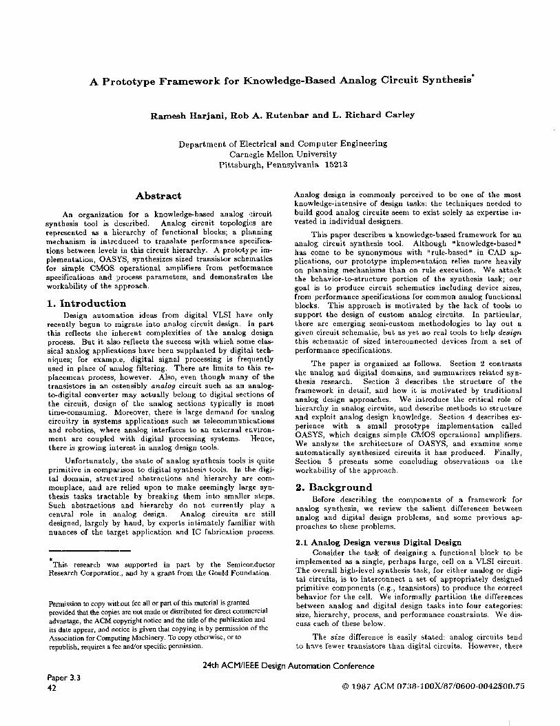
Figure 1 shows a typical analog hierarchy for a successive approximation A/D converter block. It is important to note
Level 0 sume
Appmximation
MJ
Figure 1: Hierarchy for Successive Approximation A/D Converter
that analog hierarchy is not strict, in the sense that sub- blocks on the same level in the hierarchy do not necessarily have the same complexity. For example, in the A/D con- verter hierarchy the sample-and-hold circuit might turn out to be only a single capacitor and a pair of transistors, while the comparator at the same level might include more than 20 transistors.
A hierarchical representation makes the synthesis task more tractable, but has one disadvantage. By recasting cir- cuit design as a sequence of alternating topology selection and Lranslation steps, we lose the easy ability to implement design tricks that jump across many levels of the hierarchy. Expert circuit designers often employ such tricks to push circuits close to the limits of achievable performance (e.g., 1261). Since the. hierarchy explicitly prevents the designer of one module from knowing the details of how other modules are imple- mented, we are not able to reach such extremal points in the design space of a given block.
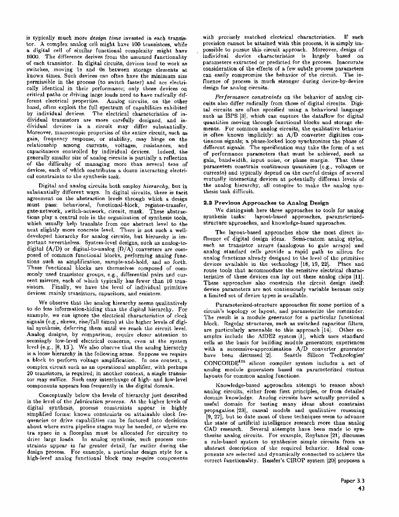
The two-step topology selection and translation process is illustrated for an abstract block in Figure 2. A particular topology is chosen because it is the one best able to be con- figured to match the specified block-level behavior; the trans- lation step then decides how the sub-blocks must behave to meet the block-level specification. An important advantage of recasting analog synthesis as a sequence of selection and translation steps is that the design task is uniform at all levels of the hierarchy: topology selection and translation oc- cur when designing a complex high-level function, and also when assembling a few transistors; only the actual implemen- tation of this two-step process will vary.
Our original motivation for using separate selection and translation steps was to avoid the need to simultaneously design the interconnection and electrical characteristics of devices. Restricting the design of sub-block interconnections to a choice among fixed alternatives allows us to concentrate on specifying the electrical characteristics of the connected sub-blocks. The hierarchical representation of topologies vastly simplifies the translation task because it tends to reduce the number of sub-blocks and simplify their connec-
Bto& - Designe
Input Performance Specification . . . . . . . . . . . . . B . . . . . . . . ~
Figure 2: Topology Selection and Translation
tions. It also simplifies the selection task, because we do not require a vast number of nearly identical topologies, differing only in low-level details.
3.3 Implementation Concerns: Applying Analog Design Knowledge
The basic framework just described, although motivated by analog design problems, shares many features with digital synthesis approaches. For example, the leverage to be gained from exploiting fixed design styles has been discussed in 14, 6] and the utility of recasting the behavior-to-structure
synthesis task as a sequence of smaller steps is also widely known [25]. However, there is one feature of the analog syn- thesis task that distinguishes it from digital synthesis: the na- ture of analog domain knowledge,
We observe that good analog designers exhibit two characteristics. First, they are adept at choosing highly simplified models of devices and device interactions to guide their choices for tradeoffs. These models, though simple, are informed by detailed knowledge of how subtleties of the fabrication process and the desired performance parameters will interact in a specific circuit topology. Second, good designers have a basic plan of attack for designing common functional blocks. These two observations suggest a way to implement the framework we have proposed. We can sum- marize these implementation choices as follows:
. For a single topology selection/translation step, design knowledge is represented in the form of circuit equa- tions and algebraic constraints involving circuit specifications.
l The process by which a high-level block specification is translated into sub-block specifications is implemented as a planning system. Plans are stored with fixed topologies, and executed when the topology is instan- tiated. Rules fire at the end of each plan step to cor- rect errors, and modify the dynamic flow of the plan.
We can justify each of these choices by referring again to the characteristics of good human designers.
Analog designers work routinely with simple algebraic descriptions (linear and non-linear) of the relationships among circuit components; expert designers choose the right descrip- tions, and prune away the relationships irrelevant to the par- ticular task at hand. Because we represent circuit topologies as statically stored templates, we can easily store the relevant circuit equations with the template, for use during the trans- lation step. Note, systems which dynamically design topologies must also re-discover these equations dynamically [21]. Unfortunately, storing circuit equations does not com-
pletely solve the problem. Real design problems are usually so under-constrained that many heuristic tradeoffs must be made to achieve a workable design that matches intended per- formance specifications. Such heuristics are the real basis of analog expertise; the critical question then is how to codify such heuristics.
We codify these heuristics as small program fragments that numerically manipulate the algebraic constraints to be satisfied at particular steps in the translation process. For ex- ample, the design of a two-stage op amp requires us to choose how to partition the total gain between the two amplifier stages. Given a gain partition, circuit equations can tell us the resulting performance of the circuit, but these equations suggest nothing about how to arrive at this partition. One workable initial heuristic is simply to assign the square root of the gain to each stage. This is easily stated algebraically, and the partition can be modified by subsequent heuristics if a
Paper 3.3 45
later situation arises which precludes this simple partition. It is also important to recognize that the hierarchical form of topology templates (only those at the bottom of the hierarchy specify transistors) means that most circuit constraints are formulated as constraints on the behavior of each abstract block as seen at its terminals.
We apply design knowledge in the form of circuit equa- tions and constrains by using plans. Two basic approaches to implementing knowledge-based systems are rules and plans. Rules codify knowledge in situation-specific IF-THEN actions; they are applicable when we know how to react to a specific design situation, but not the order in which these situations will occur. Plans ccodify knowledge in plan steps, which may be implemented as either rules, algorithms, or both. Plans specify a rough ordering of the basic design steps, and. may need to be modified at run-time depending upon the state of the design. It is important to recognize that plans and rules are not mutually exclusive: some rule-based CAD tools employ planning ideas with differing degrees of sophistication [15, 161. In our a.pplication, the translation process is ac-
complished by executing a plan stored with each topology template. The plan represents a basic order in which to at- tack the specification of sub-block behaviors. Individual plan steps in our implementation are largely algorithmic: they manipulate circuit equations and constraints numerically. Each plan step has a set of goals it expects to achieve, and a set of circuit and process relationships it knows how to manipulate to achieve these goals.
A major weakness of planning systems is that they re- quire a mechanism to dynamically modify a plan that fails to achieve its goals (this is sometimes referred to as patching a
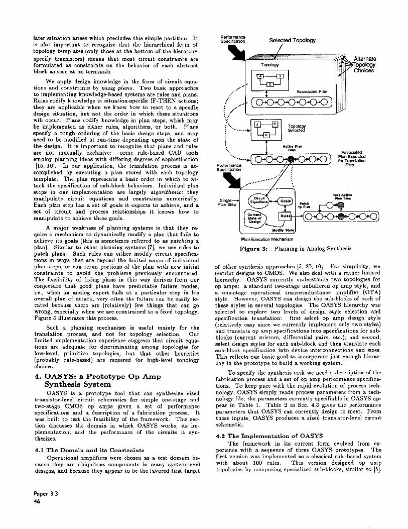
plan). Similar to &her planning systems [7], we use rules to patch plans. Such rules can either modify circuit specific% tions in ways that are beyond the limited scope of individual plan steps, or can rerun portions of the plan with new initial constraints to avoid the problems previously encountered. The feasibility of fixing plans in this way derives from our conjecture that good plans have predictable failure modes, i.e., when an analog expert fails at a particular step in his overall plan of atta.ck, very often the failure can be easily lo- cated because therl: are (relatively) few things that can go wrong, especially when we are constrained to a fixed topology. Figure 3 illustrates this process.
Such a planning mechanism is useful mainly for the translation process, and not for topology selection. Our limited implementation experience suggests that circuit equa- tions are adequate for discriminating among topologies for low-level, primitive topologies, but that other heuristics (probably rule-based) are required for high-level topology choices.
4. OASYS: a Prototype Op Amp Synthesis System OASYS is a prototype tool that can synthesize sized
transistor-level circuit schematics for simple one-stage and two-stage CMOS op amps given a set of performance specifications and a description of a fabrication process. It was built to test the feasibility of the framework. This sec- tion discusses the domain in which OASYS works, its im- plementation, and the performance of the circuits it syn- thesizes.
4.1 The Domain and its Constraints
Operational amplifiers were chosen es a test domain be- cause they are ubiquitous components in many system-level designs, and because they appear to be the favored first target
Performance specification Selected Topology
Plan Execution Mechanism
Figure 3: Planning in Analog Synthesis
of other synthesis approaches [5, 20, lo]. For simplicity, we restrict designs to CMOS. We also deal with a rather limited hierarchy. OASYS currently understands two topologies for op amps: a standard two-stage unbuffered op amp style, and a one-stage operational transconductance amplifier (OTA) style. However, OASYS can design the sub-blocks of each of these styles in several topologies. The OASYS hierarchy was selected to explore two levels of design style selection and specification translation: first select op amp design style (relatively easy since we currently implement only two styles) and translate op amp specifications into specifications for sub- blocks (current mirrors, differential pairs, etc.); and second, select design styles for each sub-block and then translate each sub-block specification into device interconnections and sizes. This reflects our basic goal to incorporate just enough hierar- chy in the prototype to build a working system.
To specify the synthesis task we need a description of the fabrication process and a set of op amp performance specifica- tions. To keep pace with the rapid evolution of process tech- nology, OASYS simply reads process parameters from a tech- nology file; the parameters currently specifiable in OASYS ap- pear in Table 1. Table 2 in Sec. 4.3 gives the performance parameters that OASYS can currently design to meet. From these inputs, OASYS produces a sized transistor-level circuit schematic.
4.2 The Implementation of OASYS
The framework in its current form evolved from ex- perience with a sequence of three OASYS prototypes. The first version was implemented as a classical rule-based system with about 100 rules. This version designed op amp topologies by composing specialized sub-blocks, similar to [5].
paper 3.3
46
Ptocess Parameters 1. Threshold Voltage (V) 2. K (PAN*)
9. C,, (fF/+m2)
3. Process Min. Width (pm) 10. Czd (fF/+m)
4. Built-in Voltage (V) 11. C&b (fF/+m)
5. Min. Drain Width (km) 12. Cjsv (fF/km) 13. Cl, (fF&m’)
6. Supply Voltage (V) o 14. fe, fr, for A = f&” 7. Oxide Thickness (A) channel length 8. Mobility (cm’?V-s) modulation
Table 1: OASYS Process ParameLers
We found that sizing here was complicated by difficulties in specifying the behavior of the sub-blocks (op amp stages) we had chosen, based on intuition, to work with. Moreover, we conld not reuse these blocks in other types of analog circuits. A second version of OASYS used well-specified reusable sub- blocks, with more explicit hierarchy; designers for blocks were still rule-based. As we evolved toward planning as a control mechanism, plan steps manipulating algebraic circuit con- straints became tedious to implement in a rule-based framework; we then abandoned a purely rule-based approach and adopted instead the current plan-based system with rules for plan modification. The current version of OASYS com-
prises about 7500 lines of Franz LISP running under UNIXtm on a VAX 111785.
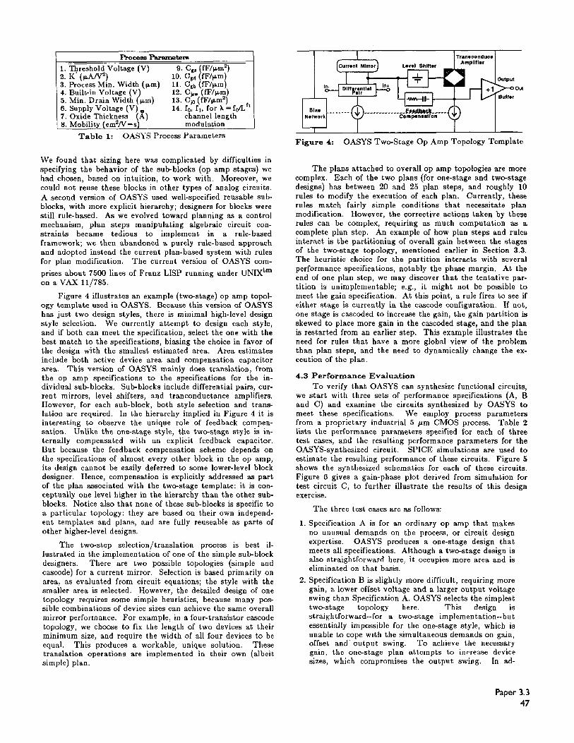
Figure 4 illustrates an example (two-stage) op amp topol- ogy template used in OASYS. Because this version of OASYS has just two design styles, there is minimal high-level design style selection. We currently attempt to design each style, and if both can meet the specification, select the one with the best match to the specifications, biasing the choice in favor of the design with the smallest estimated area. Area estimates include both active device area and compensation capacitor area. This version of OASYS mainly does translation, from the op amp specifications to the specifications for the in- dividual sub-blocks. Sub-blocks include differential pairs, cur- rent mirrors, level shifters, and tranconductance amplifiers. However, for each sub-block, both style selection and trans- lation are required. In the hierarchy implied in Figure 4 it is interesting to observe the unique role of feedback compen- sation. Unlike the one-stage style, the two-stage style is in- ternally compensated with an explicit feedback capacitor. But because the feedback compensation scheme depends on the specifications of almost every other block in the op amp, its design cannot be easily deferred to some lower-level block designer. Hence, compensation is explicitly addressed as part of the plan associated with the two-stage template: it is con- ceptually one level higher in the hierarchy than the other sub- blocks. Notice also that none of these sub-blocks is specific to a particular topology: they are based on their own independ- ent templates and plans, and are fully reuseable as parts of other higher-level designs.
The two-step selection/translation process is best il- lustrated in the implementation of one of the simple sub-block designers. There are two possible topologies (simple and cascade) for a current mirror. Selection is based primarily on area, as evaluated from circuit equations; the style with the smaller area is selected. However, the detailed design of one topology requires some simple heuristics, because many pos- sible combinations of device sizes can achieve the same overall mirror performance. For example, in a four-transistor cascode topology, we choose to fix the length of two devices at their minimum size, and require the width of all four devices to be equal. This produces a workable, unique solution. These translation operations are implemented in their own (albeit simple) pIan.
Figure 4: OASYS Two-Stage Op Amp Topology Template
The plans attached to overall op amp topologies are more complex. Each of the two plans (for one-stage and twestage designs) has between 20 and 25 plan steps, and roughly 10 rules to modify the execution of each plan. Currently, these rules match fairly simple conditions that necessitate plan modification. However, the corrective actions taken by these rules can be complex, requiring as much computation as a complete plan step. An example of how plan steps and rules interact is the partitioning of overall gain between the stages of the twostage topology, mentioned earlier in Section 3.3. The heuristic choice for the partition interacts with several performance specifications, notably the phase margin. At the end of one plan step, we may discover that the tentative par- tition is unimplementable; e.g., it might not be possible to meet the gain specification. At this point, a rule fires to see if either stage is currently in the cascode configuration. If not, one stage is cascaded to increase the gain, the gain partition is skewed to place more gain in the cascaded stage, and the plan is restarted from an earlier step. This example illustrates the need for rules that have a more global view of the problem than plan steps, and the need to dynamically change the ex- ecution of the plan.
4.3 Performance Evaluation
To verify that OASYS can synthesize functional circuits, we start with three sets of performance specifications (A, B and C) and examine the circuits synthesized by OASYS to meet these specifications. We employ process parameters from a proprietary industrial 5 pm CMOS process. Table 2 lists the performance parameters specified for each of three test cases, and the resulting performance parameters for the OASYS-synthesized circuit. SPICE simulations are used to estimate the resulting performance of these circuits. Figure 5 shows the synthesized schematics for each of these circuits. Figure 6 gives a gain-phase plot derived from simulation for test circuit C, to further illustrate the results of this design exercise.
The three test cases are as follows:
Specification A is for an ordinary op amp that makes no unusual demands on the process, or circuit design expertise. OASYS produces a one-stage design that meets all specifications. Although a two-stage design is also straightforward here, it occupies more area and is eliminated on that basis.
Specification B is slightly more difficult, requiring more gain, a lower offset voltage and a larger output voltage swing than Specification A. OASYS selects the simplest twostage topology here. This design is straightforward--for a two-stage implementation--but essentially impossible for the one-stage style, which is unable to cope wrth the simultaneous demands on gain, offset and output swing. To achieve the necessary gain, the one-stage plan attempts to increase device sizes, which compromises the output swing. In ad-
Paper 3.3
47
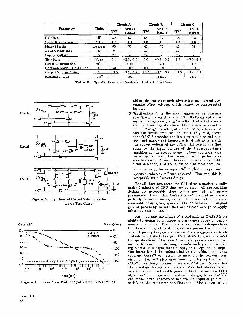
Table 2: Specificatilons and Results for OASYS Test Cases
Figure 5: Synthesized Circuit Schematics for Three Test Cases
Gain( dB) Phase(deg)
100 10' 102 103 104 106 loe
Freq(Hs)
Figure 6: Gain-Phase Plot for Synthesized Test Circuit C
dition, the one-stage style always has an inherent sys- tematic offset voltage, which cannot be compensated for here.
3. Specification C is the most aggressive performance specification, since it requires 100 dB of gain and a low output voltage swing of h2.5 volts. OASYS chooses a complex twostage style here. Comparison between the simple 2-stage circuit synthesized for specification B and the circuit produced for case C (Figure 5) shows that OASYS cascoded the input current bias and out- put load mirror and inserted a level shifter to match the output voltage of the differential pair in the first stage to the input voltage of the transconductance amplifier in the second stage. These additions were necessary to meet the more difficult performance specifications. Because this example makes more dif- ficult demands, OASYS is less able to meet specifica-
tions precisely; for example, 45O of phase margin was
specified, whereas 32O was achieved. However, this is acceptable for a first-cut design.
For all these test cases, the CPU time is modest, usually under 2 minutes of CPU time per op amp. All the resulting designs are acceptably close to the specified performance parameters. Recall that OASYS is not intended to produce perfectly optimal designs; rather, it is intended to produce reasonable designs, very quickly. OASYS satisfies our original goal of producing circuits that are “close” enough to apply other optimization tools.
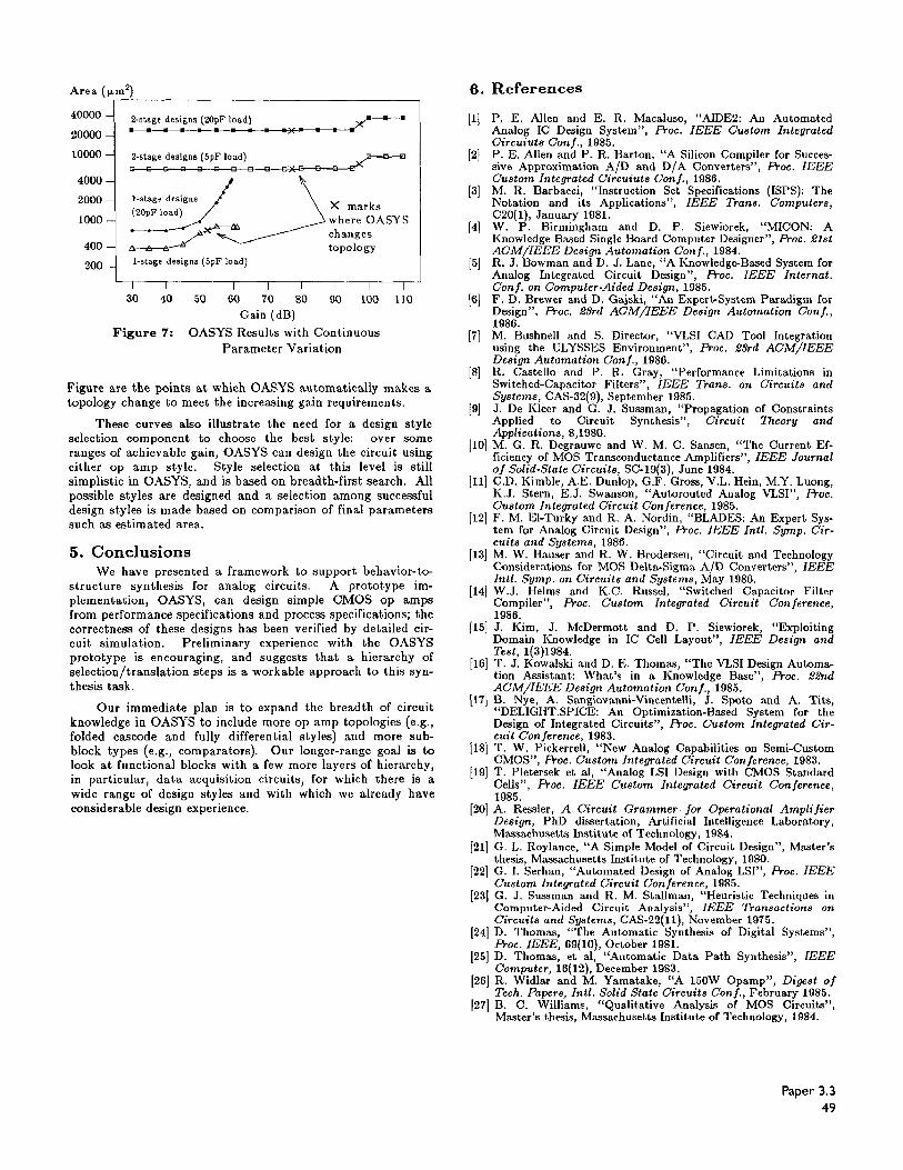
An important advantage of a tool such as OASYS is its ability to design with respect a continuo~ range of perfor- mance parameters. This is in sharp contrast to design styles based on a library of fixed cells, or even parameterizable cells, which typically have only a few variable parameters, each ad- justable over a limited range. To illustrate this, we reconsider the specifications of test case A with a slight modification: we now wish to examine the range of achievable gain when driv- ing a small load capacitance of 5pF, or a large load of 2QpF. Our intent here is to explore what gain is achievable in each topology OASYS can design to meet all the relevant con- straints. Figure 7 plots area versus gain for all the circuits OASYS can design to meet these specifications. Notice that the one-stage designs are clearly smaller, but always have a smaller range of achievable gains. This is because the OTA style has fewer degrees of freedom in design; hence, OASYS can ma.ke fewer tradeoffs to achieve the required gain while satisfying the remaining specifications. Also shown in the
Paper 3.3
48
-. 200 l-stage designs (5pF load)
I I I I I I I I I
30 40 50 60 70 80 90 too 110 Gain (dB)
Figure 7: OASYS Results with Continuous Parameter Variation
Figure are the points at which OASYS automatically makes a topology change to meet the increasing gain requirements.
These curves also illustrate the need for a design style selection component to choose the best style: over some ranges of achievable gain, OASYS can design the circuit using either op amp style. Style selection at this level is still simplistic in OASYS, and is based on breadth-first search. All possible styles are designed and a selection among successful design styles is made based on comparison of final parameters such as estimated area.
5. Conclusions We have presented a framework to support behavior-to
structure synthesis for analog circuits. A prototype im- plementation, OASYS, can design simple CMOS op amps from performance specifications and process specifications; the correctness of these designs has been verified by detailed cir- cuit simulation. Preliminary experience with the OASYS prototype is encouraging, and suggests that a hierarchy of selection/translation steps is a workable approach to this syn- thesis task.
Our immediate plan is to expand the breadth of circuit knowledge in OASYS to include more op amp topologies (e.g., folded cascade and fully differential styles) and more sub- block types (e.g., comparators). Our longer-range goal is to look at functional blocks with a few more layers of hierarchy, in particular, data acquisition circuits, for which there is a wide range of design styles and with which we already have considerable design experience.
6.
PI
PI
[31
[41
151
161
171
PI
[91
I101
IllI
Pl
1131
[I41
1151
[161
[I71
1181 [W
PO1
Pll
P21
[23l
[24l
I251
References
P. E. Allen and E. R. Macaluso, “AIDE2: An Automated Analog IC Design System”, Roe. IEEE Custom Integrated Circuiuts Conf., 1985. P. E. Allen and P. R. Barton, “ A Silicon Compiler for Succes- sive Approximation A/D and D/A Converters”, fioc. IEEE Custom Integrated Circuiuts Con J., 1986. M. R. Barbacci, “Instruction Set Specifications (ISPS): The Notation and its Applications”, IEEE Trans. Computers, CZO(l), January 1981. W. P. Birmingham and D. P. Siewiorek, “MICON: A Knowledge Based Single Board Computer Designer”, fioc. 21st ACM/IEEE Design Automation Conf., 1984. R. J. Bowman and D. J. Lane, “A Knowledge-Based System for Analog Integrated Circuit Design”, Fkoc. IEEE Internat. Con J. on Computer-Aided Design, 1985. F. D. Brewer and D. Gajski, “An Expert-System Paradigm for Design”, Roe. 23rd ACM/IEEE Design Automation ConJ., 1986. M. Bushnell and S. Director, “VLSI CAD Tool Integration using the ULYSSES Environment”, l+oe. 22rd ACM/lEEE Design Automation Conf., 1986. R. Castello and P. R. Gray, “Performance Limitations in Switched-Capacitor Filters”, IEEE Trans. on Circuits and Systems, GAS-32(9), September 1985. J. De Kleer and G. J. Sussman, “Propagation of Constraints Applied to Circuit Synthesis”, Circuit Theory and Applications, 8,198O. M. G. R. Degrauwe and W. M. C. Sansen, “The Current Ef- ficiency of MOS Transconductance Amplifiers”, IEEE Journal o J Solid-State Circuits, X-19(3), June 1984. C.D. Kimble, A.E. Dunlop, G.F. Gross, V.L. Hein, M.Y. Luong, K.J. Stern, E.J. Swanson, “Autorouted Analog VLSI”, I+oc. Custom Integrated Circuit Conference, 1985. F. M. El-Turky and R. A. Nordin, “BLADES: An Expert Sys- tem for Analog Circuit Design”, A-oc. IEEE Intl. Symp. Cir- cuits and Systems, 1986. M. W. Hauser and R. W. Brodersen, “Circuit and Technology Considerations for MOS Delta-Sigma A/D Converters”, IEEE Zntl. Symp. on Circuits and Systems, May 1986. W.J. Helms and K.C. Russel, “Switched Capacitor Filter Compiler”, Proc. Custom Integrated Circuit Conference, 1986. J. Kim, J. McDermott and D. P. Siewiorek, “Exploiting Domain Knowledge in IC Cell Layout”, IEEE Design and Test, 1(3)1984. T. J. Kowalski and D. E. Thomas, “The VLSI Design Automa- tion Assistant: What’s in a Knowledge Base”, Rot. 22nd ACM/IEEE Design Automation Conf., 1985. B. Nye, A. Sangiovanni-Vincentelli, J. Spoto and A. Tits, “DELIGHT.SPICE: An Optimization-Based System for the Design of Integrated Circuits”, Boc. Custom Integrated Cir- cuit Con Jerence, 1983. T. W. Pickerrell, “New Analog Capabilities on Semi-Custom CMOS”, Roe. Custom Integrated Circuit Con Jerence, 1983. T. Pletersek et al, “Analog LSI Design with CMOS Standard Cells”, Proc. IEEE Custom Integrated Circuit Conference, 1985. A. Ressler, A Circuit Grammer Jor Operational AmpliJier Design, PhD dissertation, Artificial Intelligence Laboratory, Massachusetts Institute of Technology, 1984. G. L. Roylance, “A Simple Model of Circuit Design”, Master’s thesis, Massachusetts Institute of Technology, 1980. G. I. Serhan, “Automated Design of Analog LSI”, Roe. IEEE Custom Integrated Circuit Conference, 1985. G. J. Sussman and R. M. Stallman, “Heuristic Techniques in Computer-Aided Circuit AnaIysis”, IEEE Transactions on Circuits and Systems, GAS-22(11), November 1975. D. Thomas, “The Automatic Synthesis of Digital Systems”, Boc. IEEE, 69(10), October 1981. D. Thomas, et al, “Automatic Data Path Synthesis”, IEEE - ~,.\_ . ~~. Computer, 16(E), December 1983.
[ZS] R. Widlar and M. Yamatake, “A 150W Opamp”, Digest OJ Tech. Papers, Intl. Solid State Circuits Conf., February 1985.
1271 B. C. Williams, L‘Qualitative Analysis of MOS Circuits”, Master’s thesis, Massachusetts Institute of Technology, 1984.
Paper 3.3
49


