Embed Size (px)
Citation preview
April 29, 2014 8:49 WSPC/Guidelines-IJMPB S021797921450088X
International Journal of Modern Physics BVol. 28, No. 15 (2014) 1450088 (11 pages)c© World Scientific Publishing Company
DOI: 10.1142/S021797921450088X
A temperature dependent study on charge dynamics in
organic molecular device: Effect of shallow traps on
space charge limited behavior
A. K. Mukherjee∗ and A. K. Kavala†
Department of Physics, Indian Institute of Technology Patna,
Patliputra Colony, Patna – 800013, India∗[email protected]
Received 11 December 2013Revised 14 January 2014Accepted 22 January 2014Published 11 April 2014
Shallow traps play a significant role in influencing charge dynamics through organicmolecular thin films, such as pentacene. Sandwich cells of pentacene capped by goldelectrodes are an excellent specimen to study the nature of underlying charge dynamics.In this paper, self-consistent numerical simulation of I–V characteristics is performedat various temperatures. The results have revealed negative value of Poole Frenkel co-efficient. The location of trap energy level is found to be located at 0.24 eV above thehighest occupied molecular orbit (HOMO) level of pentacene. Other physical parametersrelated to trap levels, such as density of states due to traps and effective carrier densitydue to traps, have also been estimated in this study.
Keywords: Mobility; shallow trap; Poole–Frenkel; pentacene.
PACS numbers: 73.40.Mr, 73.40.Sx
1. Introduction
Over these years, pentacene has proved to be a promising material for electronic
applications, despite a band gap of 2.2 eV.1 A good amount of effort has gone
in improving the morphology and overall quality of thin film of pentacene. This
has been reflected in the ever increasing values of mobility, as reported in various
communications in the past decade.2–4 Especially the organic nature, and ease
of processing, has made pentacene an exotic material of intense experimental and
theoretical research.5–8 Unfortunately, thin films of pentacene cannot be fabricated
as a single crystal, unlike silicon. On an average, the crystallite size of pentacene
are roughly 0.592 nm, 0.734 nm and 1.563 nm for a, b and c, respectively.9 Usually,
thin films of very high quality are composed of microcrystallites of pentacene. These
1450088-1
April 29, 2014 8:49 WSPC/Guidelines-IJMPB S021797921450088X
A. K. Mukherjee & A. K. Kavala
microcrystallites are oriented in all possible orientations. Such films give best value
of mobility which is, somewhere around 5 cm2/Vs.2–4 Nevertheless, it is far below
the values of mobility offered by silicon and other inorganic counterparts. There are
various reasons for low values of mobility, such as, presence of interface trap states
and interface barrier, disorder arising due to random orientation of crystallites,
charge traps present in the bulk of the semiconductor. Typically, when a hole in
pentacene hops from one crystallite to the other, the hole has a possibility to drown
in a charge trap. In the case of amorphous film of pentacene, the situation is even
more griever, as the trap density is much higher, as compared to the polycrystalline
form.
An experimental investigation on the existence of such charge traps is provided
by Seggern et al.10 Charge traps play a significant role in bringing down the ef-
fective mobility of the carrier. Therefore, parameters, such as, density of states for
traps, effective carrier density of traps and location of trap energy level in the band
diagram, are crucial in determining mobility. The charge transport properties of
pentacene can be studied in two possible geometries, namely, the organic field ef-
fect transistor (FET) setup and a sandwich cell setup. In earlier studies, various
research groups have fabricated pentacene-based sandwich cells and obtained its
I–V characteristics. Numerical modeling was also performed to match the simu-
lated data with the experimental values of current. In this regard, work by Knapp
et al. and Diao et al. could be highlighted.11,12 In all these simulations, the location
of trap energy were neither taken into account nor determined. Besides, the value
for density of trap states and mobility was assumed, so as to match the simulated
current with the experimental value. In the present communication, no such as-
sumption is made. The I–V characteristics of pentacene have been simulated for
a range of temperature. The data is analyzed to obtain many significant electronic
parameters related to traps in pentacene, such as its density of states, carrier den-
sity from traps and location of trap energy level. Besides, parameters pertaining to
mobility, such as the value of field free mobility and Poole–Frenkel coefficient have
also been worked out.
2. Theory
Numerical modeling for I–V characteristics of a sandwich device could be performed
by solving three basic equations self-consistently, namely, (a) continuity equation for
holes, (b) Poisson’s equation and (c) drift-diffusion equation. Besides, the solutions
of these three equations are also coupled with Poole–Frenkel model variation of
mobility with electric field and Langevin model for recombination.13–18 For self-
consistent solution, widely accepted methods by Newton as well as Scherfetter-
Gummel are followed in this paper.19,20 In the I–V characteristics of all organic
sandwich devices, there is a certain voltage, called knee voltage (Vo), below which
the device shows ohmic characteristics, while for values of voltage above Vo, the
current follows the traits of space-charge-limited conduction (SCLC). In this report,
1450088-2
April 29, 2014 8:49 WSPC/Guidelines-IJMPB S021797921450088X
A temperature dependent study on charge dynamics
the I–V characteristics of a two-dimensional sandwich cell is simulated. So, it would
be better to use line current density K, instead of its three-dimensional equivalent
J . The line current density K shows dependence on temperature, as well. In the
ohmic region of operation, the thermally activated nature of K is given by the
following relation21
K(T ) = qNvsµE exp(−∆Ec/kBT ) . (1)
Here, Nvs is density of states at the highest occupied molecular orbital (HOMO)
level of semiconducting molecule, q is the magnitude of electron charge, E is the
electric field, ∆Ec is the hole activation energy, kB is the Boltzmann constant and
µ is the charge-carrier-mobility. Since this paper deals with charge transport in a
pentacene sandwich cell, in which, majority carriers are holes, only hole mobility is
taken into consideration. The mobility is not a constant parameter. In general, it
depends on various factors such as electric field, temperature, dopant concentration,
presence of undesired impurities, traps, surface states etc.22–24 Taking all these
parameters into consideration, makes the extraction of field free mobility (µo) a
daunting task. However, an estimation could be made if the dependence of mobility
on one of the parameters, electric field E, is taken into account. For organic devices,
(2) shows the functional relationship between mobility and electric field.25
µ = µ0 exp(0.89γ√E) . (2)
Here, γ is the Poole–Frenkel coefficient. This relationship could be utilized to ex-
tract µ0 from the transfer characteristics of the pentacene-based FET. Although,
by the study or simulation of I–V characteristics of organic FET (OFET) values
of mobility could be extracted. But, these values are field-dependent values of mo-
bility. Determination of field inside the channel of OFET is another complicated
issue, as the field is determined by two orthogonally applied potential differences,
namely drain-source voltage (VDS) and gate-source voltage (VGS). Nevertheless,
the polarization of dielectric molecules and interface states makes the local field,
exceptionally complicated to estimate. As an oversimplification, the field due to
VDS could be taken as the effective field. This is because the drift of charge carriers
through the channel takes place from drain to source. Here, the leakage through the
gate dielectric is neglected. Mobility is involved in various other relations, which
can be further used to determine a number of important physical parameters for
the device, as explained below.
As mentioned earlier, the I–V characteristics of a two-dimensional device shows
signs of SCLC above knee voltage. It is to be noted that, the SCLC behavior in
organic molecular thin film device is trap limited. Charge traps are of various kinds
and it can be categorized in a number of ways. Based on location in a sandwich cell,
it could be interfacial trap or bulk trap.26,27 Based on the location of energy level in
the energy band diagram, a trap could be deep or shallow. Although, a number of
research work could be found on the role of deep traps and shallow traps in organic
electronic material, none clearly classifies under what condition a trap could be
1450088-3
April 29, 2014 8:49 WSPC/Guidelines-IJMPB S021797921450088X
A. K. Mukherjee & A. K. Kavala
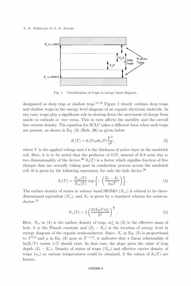
Fig. 1. Classification of traps in energy band diagram.
designated as deep trap or shallow trap.11,12 Figure 1 clearly outlines deep traps
and shallow traps in the energy level diagram of an organic electronic molecule. In
any case, traps play a significant role in slowing down the movement of charge from
anode to cathode or vice versa. This in turn affects the mobility and the overall
line current density. The equation for SCLC takes a different form when such traps
are present, as shown in Eq. (3) (Refs. 28) as given below
K(T ) = 0.57εµθs(T )V 2
d2, (3)
where V is the applied voltage and d is the thickness of active layer in the sandwich
cell. Here, it is to be noted that the prefactor of 0.57, instead of 9/8 arise due to
two dimensionality of the device.29 θs(T ) is a factor which signifies fraction of free
charges that are actually taking part in conduction process across the sandwich
cell. It is given by the following expression, for only the hole device.30
θs(T ) =Nvs(T )
Nts(T )exp
{
−
(
Et − Ev
kBT
)}
. (4)
The surface density of states in valence band/HOMO (Nvs) is related to its three-
dimensional equivalent (Nv), and Nv is given by a standard relation for semicon-
ductor.31
Nv(T ) = 2
(
2πkBTm∗
h
h2
)3
2
. (5)
Here, Nts in (4) is the surface density of trap, m∗
h in (5) is the effective mass of
hole, h is the Planck constant and (Et − Ev) is the location of energy level in
energy diagram of the organic semiconductor. Since, Nv in Eq. (5) is proportional
to T 3/2 and µ in Eq. (3) goes as T−1/2, it indicates that a linear relationship of
ln(K/T ) versus 1/T should exist. In that case, the slope gives the value of trap
depth (Et − Ev). Density of states of traps (Nts) and effective carrier density of
traps (no) at various temperatures could be obtained, if the values of θs(T ) are
known.
1450088-4
April 29, 2014 8:49 WSPC/Guidelines-IJMPB S021797921450088X
A temperature dependent study on charge dynamics
Here, the knee voltage of the I–V characteristics of these sandwich cell comes
for rescue, as it is related to θs(T ) through the following relation.19,22
Vo(T ) =qnosd
0.57ǫ0ǫrθs(T ). (6)
Here, nos is the number density of charge contributed from charge traps. In the
next section, various physical parameters for a two dimensional sandwich cell of
pentacene, such as, Nvs, Nts, θs(T ) and nos are obtained.
3. Results and Discussion
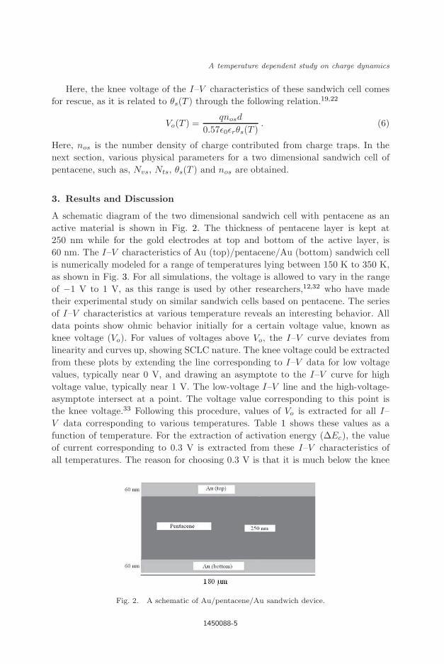
A schematic diagram of the two dimensional sandwich cell with pentacene as an
active material is shown in Fig. 2. The thickness of pentacene layer is kept at
250 nm while for the gold electrodes at top and bottom of the active layer, is
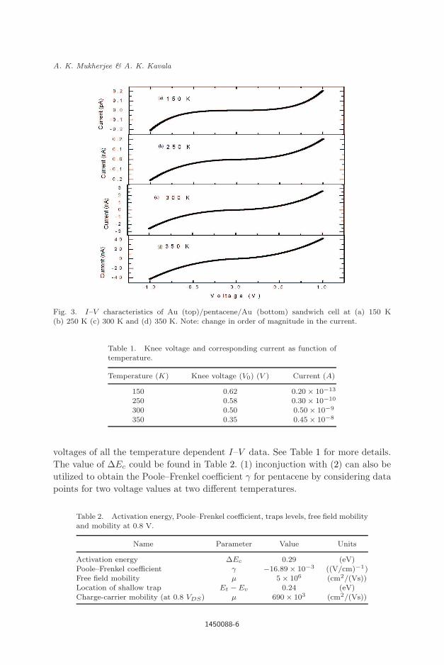
60 nm. The I–V characteristics of Au (top)/pentacene/Au (bottom) sandwich cell
is numerically modeled for a range of temperatures lying between 150 K to 350 K,
as shown in Fig. 3. For all simulations, the voltage is allowed to vary in the range
of −1 V to 1 V, as this range is used by other researchers,12,32 who have made
their experimental study on similar sandwich cells based on pentacene. The series
of I–V characteristics at various temperature reveals an interesting behavior. All
data points show ohmic behavior initially for a certain voltage value, known as
knee voltage (Vo). For values of voltages above Vo, the I–V curve deviates from
linearity and curves up, showing SCLC nature. The knee voltage could be extracted
from these plots by extending the line corresponding to I–V data for low voltage
values, typically near 0 V, and drawing an asymptote to the I–V curve for high
voltage value, typically near 1 V. The low-voltage I–V line and the high-voltage-
asymptote intersect at a point. The voltage value corresponding to this point is
the knee voltage.33 Following this procedure, values of Vo is extracted for all I–
V data corresponding to various temperatures. Table 1 shows these values as a
function of temperature. For the extraction of activation energy (∆Ec), the value
of current corresponding to 0.3 V is extracted from these I–V characteristics of
all temperatures. The reason for choosing 0.3 V is that it is much below the knee
Fig. 2. A schematic of Au/pentacene/Au sandwich device.
1450088-5
April 29, 2014 8:49 WSPC/Guidelines-IJMPB S021797921450088X
A. K. Mukherjee & A. K. Kavala
Fig. 3. I–V characteristics of Au (top)/pentacene/Au (bottom) sandwich cell at (a) 150 K(b) 250 K (c) 300 K and (d) 350 K. Note: change in order of magnitude in the current.
Table 1. Knee voltage and corresponding current as function oftemperature.
Temperature (K) Knee voltage (V0) (V ) Current (A)
150 0.62 0.20× 10⁻¹³
250 0.58 0.30× 10⁻¹⁰
300 0.50 0.50× 10⁻⁹
350 0.35 0.45× 10⁻⁸
voltages of all the temperature dependent I–V data. See Table 1 for more details.
The value of ∆Ec could be found in Table 2. (1) inconjuction with (2) can also be
utilized to obtain the Poole–Frenkel coefficient γ for pentacene by considering data
points for two voltage values at two different temperatures.
Table 2. Activation energy, Poole–Frenkel coefficient, traps levels, free field mobilityand mobility at 0.8 V.
Name Parameter Value Units
Activation energy ∆Ec 0.29 (eV)Poole–Frenkel coefficient γ −16.89× 10⁻³ ((V/cm)−1)Free field mobility µ 5× 10⁶ (cm2/(Vs))Location of shallow trap Et −Ev 0.24 (eV)Charge-carrier mobility (at 0.8 VDS) µ 690 × 103 (cm2/(Vs))
1450088-6
April 29, 2014 8:49 WSPC/Guidelines-IJMPB S021797921450088X
A temperature dependent study on charge dynamics
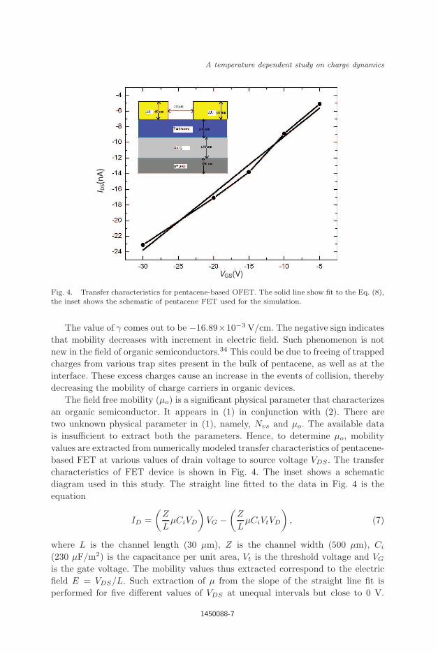
VGS(V)
Fig. 4. Transfer characteristics for pentacene-based OFET. The solid line show fit to the Eq. (8),the inset shows the schematic of pentacene FET used for the simulation.
The value of γ comes out to be −16.89×10⁻³ V/cm. The negative sign indicates
that mobility decreases with increment in electric field. Such phenomenon is not
new in the field of organic semiconductors.34 This could be due to freeing of trapped
charges from various trap sites present in the bulk of pentacene, as well as at the
interface. These excess charges cause an increase in the events of collision, thereby
decreasing the mobility of charge carriers in organic devices.
The field free mobility (µo) is a significant physical parameter that characterizes
an organic semiconductor. It appears in (1) in conjunction with (2). There are
two unknown physical parameter in (1), namely, Nvs and µo. The available data
is insufficient to extract both the parameters. Hence, to determine µo, mobility
values are extracted from numerically modeled transfer characteristics of pentacene-
based FET at various values of drain voltage to source voltage VDS . The transfer
characteristics of FET device is shown in Fig. 4. The inset shows a schematic
diagram used in this study. The straight line fitted to the data in Fig. 4 is the
equation
ID =
(
Z
LµCiVD
)
VG −
(
Z
LµCiVtVD
)
, (7)
where L is the channel length (30 µm), Z is the channel width (500 µm), Ci
(230 µF/m2) is the capacitance per unit area, Vt is the threshold voltage and VG
is the gate voltage. The mobility values thus extracted correspond to the electric
field E = VDS/L. Such extraction of µ from the slope of the straight line fit is
performed for five different values of VDS at unequal intervals but close to 0 V.
1450088-7
April 29, 2014 8:49 WSPC/Guidelines-IJMPB S021797921450088X
A. K. Mukherjee & A. K. Kavala
Extrapolation was performed to obtain the field free value of µo. It is found to be
5 × 10⁻⁶ cm2/(Vs). It is quite low with respect to the mobility values obtained
from pentacene-based OFETs, where values as large as 5 cm2/(Vs) have been re-
ported.2–4 The reason for such a mismatch are quite a few, but significant. First, for
a quantum confined lower dimensional structure, it can be shown that the phonon
limited mobility of charge carriers is significantly lower than its higher dimensional
equivalent.35 Finally, the presence of traps lowers down the mobility by a significant
margin, as it is estimated in this analysis.
Charge conduction in amorphous or polycrystalline semiconductors, especially
of organic variety, exhibits space-charge limited (SCL) behavior. This nature of
charge flow could be treated as trap free SCLC or trap limited SCLC. It is highly
likely that such a material contains charge traps within its bulk. These charge traps
can function in bidirectional manner, i.e., it could trap charge which causes current
to get limited, or it can release the trapped charge at high electric fields which
causes mobility to decrease. The decrease of mobility has already been confirmed
by the negative value of Poole–Frenkel coefficient.
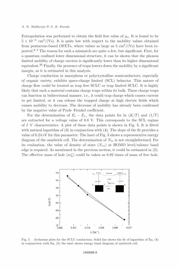
For the determination of Et − Ev, the data points for ln (K/T ) and (1/T )
are extracted for a voltage value of 0.8 V. This corresponds to the SCL regime
of I–V characteristics. A plot of these data points is shown in Fig. 5. It is fitted
with natural logarithm of (3) in conjunction with (4). The slope of the fit provides a
value of 0.24 eV for this parameter. The inset of Fig. 5 shows a representative energy
diagram of the sandwich cell. The determination of Nts is not straightforward. For
its evaluation, the value of density of state (Nvs) at HOMO level/valence band
edge is required. As mentioned in the previous section, it could be estimated in (5).
The effective mass of hole (m∗
h) could be taken as 8.92 times of mass of free hole.
1/T(K–1)
In(K/T
)
Fig. 5. Arrhenius plots for the SCLC conduction. Solid line shows the fit of logarithm of Eq. (4)in conjunction with Eq. (5) the inset shows energy band diagram of sandwich cell.
1450088-8
April 29, 2014 8:49 WSPC/Guidelines-IJMPB S021797921450088X
A temperature dependent study on charge dynamics
This value has already been determined by Coropceanu in his work.36 Since the
sandwich device in this simulation study is a two-dimensional device, the density
of states in two dimensions (Nvs) are considered. Nv and Nvs are related with each
other by the relation
Nvs = (Nv)2/3 . (8)
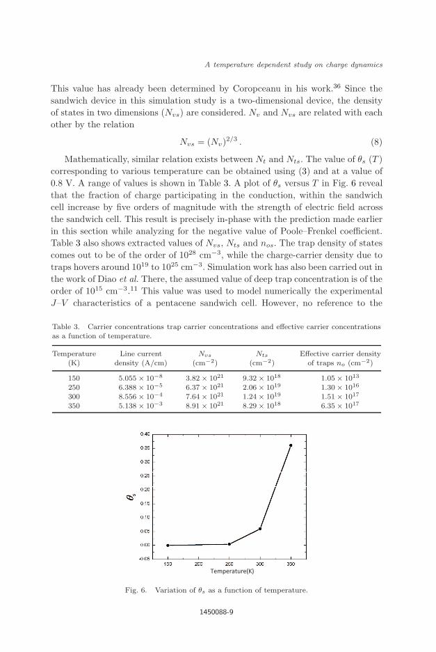
Mathematically, similar relation exists between Nt and Nts. The value of θs (T )
corresponding to various temperature can be obtained using (3) and at a value of
0.8 V. A range of values is shown in Table 3. A plot of θs versus T in Fig. 6 reveal
that the fraction of charge participating in the conduction, within the sandwich
cell increase by five orders of magnitude with the strength of electric field across
the sandwich cell. This result is precisely in-phase with the prediction made earlier
in this section while analyzing for the negative value of Poole–Frenkel coefficient.
Table 3 also shows extracted values of Nvs, Nts and nos. The trap density of states
comes out to be of the order of 1028 cm−3, while the charge-carrier density due to
traps hovers around 1019 to 1025 cm−3. Simulation work has also been carried out in
the work of Diao et al. There, the assumed value of deep trap concentration is of the
order of 1015 cm−3.11 This value was used to model numerically the experimental
J–V characteristics of a pentacene sandwich cell. However, no reference to the
Table 3. Carrier concentrations trap carrier concentrations and effective carrier concentrationsas a function of temperature.
Temperature Line current Nvs Nts Effective carrier density(K) density (A/cm) (cm−2) (cm−2) of traps no (cm−2)
150 5.055 × 10⁻⁸ 3.82× 10²¹ 9.32× 10¹⁸ 1.05× 10¹³
250 6.388 × 10⁻⁵ 6.37× 10²¹ 2.06× 10¹⁹ 1.30× 10¹⁶
300 8.556 × 10⁻⁴ 7.64× 10²¹ 1.24× 10¹⁹ 1.51× 10¹⁷
350 5.138 × 10⁻³ 8.91× 10²¹ 8.29× 10¹⁸ 6.35× 10¹⁷
Fig. 6. Variation of θs as a function of temperature.
1450088-9
April 29, 2014 8:49 WSPC/Guidelines-IJMPB S021797921450088X
A. K. Mukherjee & A. K. Kavala
role of shallow traps was made in that investigation. Besides, the location of trap
energy level was also not pointed out in that work. In the present communication,
we have obtained the location of energy level to be 0.24 eV above the HOMO level
of pentacene. And, as per the criteria described in theory section of this report, the
trap level energy so obtained belongs to the class of shallow trap.
4. Conclusion
Temperature dependent I–V characteristics of two-dimensional Au/pentacene/Au
sandwich cell has been simulated. The device shows both ohmic and SCL nature
below and above knee voltage, respectively. The temperature dependent data be-
longing to ohmic region has been analyzed to obtain a value of 0.29 eV for activa-
tion energy. Field free mobility and Poole–Frenkel coefficient (γ) are two important
physical parameters for electrical conduction through organic semiconductors. From
the numerically modeled output characteristics of pentacene-based FET, these two
parameters are extracted out and the values are 5 × 10⁻⁶ cm2/(Vs) for field free
mobility and −16.89× 10⁻³ cm/V for γ. The negative sign suggests that mobility
decreases with electric field which might be due to release of trapped charge from
the trap sites with increment in field value. Various other parameters such as den-
sity of states for traps, effective carrier density due to traps and location of trap
energy level are also determined from the temperature-dependent SCL I–V data
of the sandwich cell. The trap energy level is found to be located 0.24 eV above
the HOMO level of pentacene. It is also observed that the fraction of charge par-
ticipating in the process of conduction increases by five orders of magnitude with
temperature. Such increase in charge concentration could lead to increase in colli-
sion event, thereby decreasing the mobility. In this paper, the mobility depends on
electric field only, but it leaves a scope for an improved application of an adequately
complete model for mobility that would comprise both field and temperature de-
pendence. Analysis in this direction is already in progress.
References
1. S. J. Kang et al., Synth. Met. 156, 32 (2006).2. J. T. Lee, S. Roth and Y. W. Park, Appl. Phys. Lett. 88, 252106 (2009).3. S. Lee et al., Appl. Phys. Lett. 88, 162109 (2006).4. W. Q. Deng and W. A. Goddard III, J. Phys. Chem. B 108, 8614 (2004).5. C. D. Dimitrakopoulos and P. R. L. Malenfant, Adv. Mater. 41, 99 (2002).6. C. D. Dimitrakopoulos and D. J. Mascaro, IBM J. Res. Dev. 45, 11 (2001).7. J. M. Shaw and P. F. Seidler, IBM J. Res. Dev. 45, 3 (2001).8. H. Xu et al., Mod. Phys. Lett. B 26, 1250204 (2012).9. D. Nabok et al., Phys. Rev. B 76, 235322 (2007).
10. C. Siol, C. Melzer and H. V. Seggern, Appl. Phys. Lett. 93, 133303 (2008).11. E. Knapp and B. Ruhstaller, J. Appl. Phys. 112, 024519 (2012).12. L. Diao et al., J. Appl. Phys. 101, 014510 (2007).13. E. Knapp and B. Ruhstaller, Opt. Quant. Electron. 42, 667 (2011).
1450088-10
April 29, 2014 8:49 WSPC/Guidelines-IJMPB S021797921450088X
A temperature dependent study on charge dynamics
14. E. Knapp, R. Hausermann, H. U. Schwarzenbach and B. Ruhstaller, J. Appl. Phys.
108, 054504 (2010).15. S. Locc, Modeling of physical and electrical characteristics of organic thin film tran-
sistors, Ph.D. thesis, University of Cagliari, Cagliari (2009).16. R. J. G. Goossens, S. Beebe, Z. Yu and R. W. Dutton, IEEE Trans. Computer-Aided
Design Int. Syst. 13, 310 (1994).17. J. C. Scott, S. Karg and S. A. Carter, J. Appl. Phys. 82, 1454 (1997).18. P. W. M. Blom, M. J. M. de Jong and S. Breedijk, Appl. Phys. Lett. 71, 930 (1997).19. D. H. Rose and R. E. Bank, Numer, Math. 37, 279 (1981).20. D. L. Scharfetter and H. K. Gummel, IEEE. Trans. Electron. Dev. ED-16, 64 (1969).21. Z. Liu et al., ECS Solid State Lett. 1, Q4 (2012).22. L. G. Kaake, P. F. Barbara and X. Y. Zhu, J. Phys. Chem. Lett. 1, 628 (2010).23. J. H. Kang, D. S. Filho, J. L. Bredas and X. Y. Zhu, Appl. Phys. Lett. 86, 152115
(2005).24. L. Li, G. Meller and H. Kosina, Solid-State Electron. 51, 445 (2007).25. M. Giulianini, E. R. Waclawik, J. M. Belland and N. Motta, J. Appl. Phys. 108,
014512 (2010).26. A. A. Grinberg, S. Luryi, M. R. Pinto and N. L. Schreyer, IEEE. Trans Electron.
Dev. 36, 1162 (1989).27. A. R. Volkel, R. A. Street and D. Knipp, Phys. Rev. B 66, 195336 (2002).28. T. Miyadera et al., Appl. Phys. Lett. 93, 033304 (2008).29. A. A. Grinberg, S. Lury, M. R. Pinto and N. L. Schreyer, IEEE. Trans. Electron. Dev.
36, 1162 (1989).30. T. P. Chunjaun, S. Chen and J. Y. Lee, J. Appl. Phys. 95, 3120 (2004).31. B. G. Streetman and S. K. Banerjee, Solid State Electronic Devices (Prentice Hall,
New Delhi, 2000).32. C. Vanoni, T. A. Jung and S. Tsujino, Appl. Phys. Lett. 94, 253306 (2009).33. M. A. Lampert, Phys. Rev. 103, 1648 (1956).34. A. K. Tripathi, Ashish and Y. N. Mohapatra, Org. Elect. 11, 1753 (2010).35. T. Ando, A. B. Fowler and F. Stern, Rev. Mod. Phys. 54, 437 (1982).36. V. Coropceanu et al., Proc. Int. Symp. Super-Functionality Organic Devices, Chiba
University, Chiba, Japan, October 25–28, 2004, IPAP Conference Series, Vol. 6 (In-stitute of Pure and Applied Physics, Tokyo, 2005), p. 15.
1450088-11


