Embed Size (px)
Citation preview

490 IEEE TRANSACTIONS ON COMPUTER-AIDED DESIGN, VOL. X , NO. 5, MAY 19x9
Adaptive Mesh Generation Preserving the Quality of the Initial Grid
PAOLO CIAMPOLINI, ALESSANDRO FORGHIERI, ANNA PIERANTONI, ANTONIO GNUDI, MASSIMO v. RUDAN, MEMBER, IEEE, AND GIORGIO BACCARANI, MEMBER, IEEE
Abstract-An algorithm allowing the automatic generation of a mesh and accounting for the main physical features of the problem is pre- sented. The adaptivity is provided by a refinement strategy which pre- serves the characteristics of the initial grid, inserting new nodes only in the regions where the solution deviates from a linear behavior. A geometrical interpretation in terms of a “monitor surface” is given, and various different approaches to the problem are discussed. The efficiency of the algorithm is enhanced by means of a local solution scheme, which uses previously computed values of all the unknown quantities as boundary conditions for the newly generated nodes. Fi- nally, a few examples illustrate the performance of the algorithm.
I. INTRODUCTION RANSPORT phenomena in semiconductors are char- T acterized by physical quantities varying over short
distances compared with the device active region. The most obvious example of such quantities is given by the carrier concentration, whose dependence on the electric potential is nearly exponential. Other quantities as well, such as the carrier temperature in the so-called hydrody- namic model of semiconductors, are affected by strong variations over a small space scale.
It is well known that an accurate determination of the unknown functions in numerical solvers is strongly af- fected by the features of the discretization mesh while, at the same time, a small number of nodes is desirable in order to achieve reasonably low CPU times. Furthermore, mesh generation is the task which usually requires the strongest interaction between a simulation program and the user: experience shows that the greatest difficulties in the “field use” of such programs are often related to this operation.
For the above reasons, automatic mesh generation schemes represent a highly desirable feature for an inte- grated simulation system. Another point to be prelimi- narly highlighted is that the solution may exhibit strong variations as the boundary conditions (i.e., the applied bias) change. This shows the inadequacy of a refinement scheme based, for instance, only on the dopant distribu-
Manuscript received July 12, 1988; revised December 1 , 1988. This work was supported in part by the European Community under ESPRlT- 962 Project, by the National Council of Research under the “Progetto Fi- nalizzato MADESS.” and by SGS-Thomson Microelectronics. The review of this paper was arranged by Guest Editor M. Pinto.
The authors are with the Dipartimento di Elettronica, lnformatica e Sis- temistica, University of Bologna. 40136 Bologna, Italy.
IEEE Log Number 8826352.
tion in the device, since the latter does not account for the efect of the bias on the monitored physical quantities. We tried therefore to design algorithms and software tools ca- pable to achieve the following goals:
the user must be relieved from the burden of gener- ating the mesh; the mesh is entirely tailored to the solution charac- teristics, and is generated along with the solution of the problem; the scheme is convergent and fairly independent of the initial mesh coarseness; the main properties of the initial grid are preserved throughout the generation procedure; the software implementation is capable to support several different refinement strategies, each indepen- dent of the particular physical quantity which “drives” mesh generation; unnecessary refinement of purely ohmic regions is avoided under any bias condition; CPU times are kept low by means of a local solution algorithm.
After a description of ATMOS, the mesh generator on which the adaptive scheme is based, the implemented al- gorithms will be discussed. As a test case, a planar MOS- FET under various operating conditions is presented.
11. MESH GENERATION In order to account for the irregular geometries of non-
planar devices, triangular-element meshes are commonly used in 2-D device simulators in connection with both fi- nite element (FE) and box integration method (BIM) schemes. The increased geometrical flexibility is, how- ever, counterbalanced by a number of additional prob- lems: i ) obtuse angles and too sharp elements must be avoided; ii) the transition in the size of adjacent elements must be smooth and, iii) refinement techniques must be flexible enough as to allow for “anisotropic” refine- ments.
To overcome these problems, a mixed strategy is used in our mesh generator ATMOS, where mesh refinement is performed on a rectangular-element grid which only roughly conforms to the device geometry, and carrying out the conversion into triangles and the adaption to ge- ometry at the very last step.
The Automatic Triangular Mesh generation and Opti-
0278-0070/89/0500-0490$01 .OO O 1989 IEEE

CIAMPOLlNl er al.: QUALITY OF THE INITIAL GRID 49 I
Fig. 1. Finite-box grid for the EPROM cell: due to symmetry, only half of the grid is shown.
mization System (ATMOS) accepts the description of the device geometry by means of a number of polygons of arbitrary complexity, the only limitation being the maxi- mum number of regions of the same physical type (cur- rently ten: e.g., ten semiconductor regions, ten insula- tors, and so on). Each polygon is then analyzed in order to extract some significant geometrical information, such as the extrema of the curves and the bounds of open lines (key-points), which are then used to draw a first-tentative grid by including the whole device in a box and by draw- ing a number of lines across some of the key points. This results in a finite-difference like mesh. In order to avoid the generation of lines too close to each other, which in turn would lead to exceedingly sharp triangles, some of the key points are automatically excluded from the initial mesh. All of these points will eventually be accounted for in the final grid, as will be described later on.
The refining mechanism consists in splitting every rect- angle either into two parts, cutting it into halves along one of the two main directions, or into four parts, if both cuts are needed. The end result of this process is a “finite box” mesh, as described in [l]. This refinement mechanism virtually decouples the node densities along the two main directions, unlike many other techniques (most of them do in fact refine the triangular elements directly). This allows for a strongly anisotropic distribution of nodes over the device. As an example, Fig. 1 shows the cross section of a realistic EPROM cell and the resulting finite-box grid.
\
K, r‘......1_ ..- .._
;’ _-__..- I . , ..-- ’..-
I (C)
Fig. 2 . Triangulation patterns used by ATMOS
When the node distribution is satisfactory, the grid is converted into a triangular-element one, accounting at this step also for geometry adaption. To do so, all rectangles are divided into three sets:

492 IEEE TRANSACTIONS ON COMPUTER-AIDED DESIGN, VOL. 8, NO. 5. MAY 1989
I I I I
I I I I
(b) Fig. 3 . (a) Final mesh for the EPROM cell. (b) Expanded view of the non-
planar interface region of the EPROM cell. Thicker lines refer to the original description of boundaries and are not necessarily part of the grid.
CIAMPOLINI er al. : QUALITY OF THE INITIAL GRID
Converslon Into the
trlengular grld
Physlcal parameters
493
rectangles crossed by one (or more) boundary lines, but not including any of the key points above; rectangles crossed by one (or more) boundary lines, and including some of the key points neglected in the first tentative grid; all of the remaining rectangles.
Rectangles belonging to the first and last set are converted by adopting one of the patterns shown in Fig. 2(a) and (b) respectively, while each rectangle of the second set is split into several convex polygons, which are then triangulated by using the Delaunay scheme (Fig. 2(c)). Thus the exact position of the previously neglected key points is fully accounted for at this stage.
Prior to the conversion step, further refinements may be needed in order to control the generation of obtuses: depending on the geometrical complexity, a few obtuse angles may arise along the boundary lines. The inner zones, instead, are virtually obtuse free. Finally, triangles either belonging to an equipotential zone (such as a con- tact or a gate) or external to the device cross section are eliminated: the final grid for the EPROM cell and an ex- panded view of the non-planar interface region are shown in Fig. 3(a) and (b), respectively.
The described strategy allows the final grid to inherit some useful properties from the initial rectangular one, which are preserved throughout the whole adaptive pro- cedure:
the number of obtuse angles is kept as low as possi-
complex structures, such as multilayer and non-
strongly anisotropic refinement is feasible; regularity of the grid and of the connectivity matrix is achieved; the large majority of right triangles does indeed reduce the effective number of adjacencies to typically 4.
Among the drawbacks, it is worth mentioning the need of two different kinds of grids to be carried along during ex- ecution. This requires some more computational re- sources, in terms of both memory requirement and CPU time.
ble;
planar devices, can be managed;
111. SOFTWARE IMPLEMENTATION
HFIELDS [2] is a general purpose device simulator which, in the version used in this work, solves the basic set of the fundamental semiconductor equations over a 2-D domain. A number of different physical effects have been incorporated into HFIELDS, allowing a wide variety of realistic devices to be simulated. Recently, also a three dimensional version of the program has been developed [3], as well as the so-called hydrodynamic version, in- cluding the energy-balance equations [4]. Hence, while designing the adaptive meshing procedure, much effort has been devoted to ensure the proper flexibility of the method, in order to share the same techniques among dif- ferent versions.
Geometry
I of the 1st order grld.
t
Automatlc reflnement l-
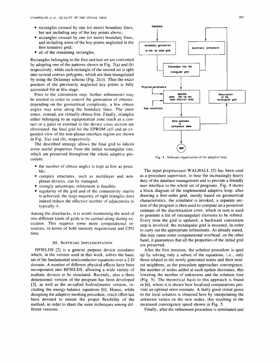
The input preprocessor WALHALL [5] has been used as a procedure supervisor, to bear the increasingly heavy duty of the database management and to provide a friendly user interface to the whole set of programs. Fig. 4 shows a block diagram of the implemented adaptive loop: after drawing a first-order grid, mostly based on geometrical characteristics, the simulator is invoked; a separate sec- tion of the program is then used to compute an a posteriori estimate of the discretization error, which in turn is used to generate a list of (rectangular) elements to be refined. Every time the grid is updated, a backward conversion step is involved: the rectangular grid is resumed, in order to carry out the appropriate refinements. As already stated, this may cause some computational overhead: on the other hand, it guarantees that all the properties of the initial grid are preserved.
After the first iteration, the solution procedure is sped up by solving only a subset of the equations, i.e., only those related to the newly generated nodes and their near- est neighbors; as the procedure approaches convergence, the number of nodes added at each update decreases, this lowering the number of unknowns and the solution time (Fig. 5). The theoretical basis to this approach is found in [ 6 ] , where it is shown how localized computations pro- vide an optimal error estimate. A fairly good initial guess to the local solution is obtained here by interpolating the unknown values on the new nodes, this resulting in the increased convergence speed shown in Fig. 5 .
Finally, after the refinement procedure is terminated and

494 IEEE TRANSACTIONS ON COMPUTER-AIDED DESIGN, VOL. 8, NO. 5. MAY 1989
60. I
0. I I 0. 2. 4. 6. 8. 10.
Number of Iterations
Fig. 5 . Plots of the solution times, of the number of unknowns and of the number of Poisson iterations versus the number of iterations of the adap- tive loop. Left scale refers to times and iterations, right scale to nodes and unknowns.
Fig. 6. Cylindrical p-n junction mesh computed at equilibrium, obtained by updating the solution only at the newly generated nodes.
the mesh has reached its final form, the whole set of equa- other nodes fixed, some clustering of nodes occurs, as tions is solved on the complete mesh to obtain a self-con- shown in Fig. 6 with reference to a cylindrical p-n junc- sistent solution. tion. Typically, a clustering occurs around the nodes be-
Another point worth addressing is the following. If the longing to the initial grid and is due to the large discreti- local solution is computed at the newly-generated nodes zation errors associated with the unknown values only, while keeping the values of the unknowns at all the computed during the first iterations. These values could

CIAMPOLINl et U / . : QUALITY OF THE INITIAL GRID 495
Fig. 7 . Partial view of the local solution (hole concentration) evaluated on the mesh of Fig. 6. The ridges on the surface originate from the nodes of the initial, coarse mesh.
not be modified during such an adaptive refinement be- cause each node was solved only once. The errors, in turn, give rise to wiggles in the carrier concentration (Fig. 7) by which more and more nodes will then be attracted.
IV. THE REFINEMENT ALGORITHM
The basic concept of the adaptive refinement scheme is that of using an intermediate solution to find a list of rect- angular elements to be directionally refined. The quan- tities taken into account are either the electric potential or the quasi-Fermi potentials. A combination of them can also be considered, thus building what is sometimes called a “monitor surface” [ 7 ] , [SI. This surface should be ca- pable to take all the main features of the solution into account: for the usual drift-diffusion model, a refinement based solely on the electric potential is often enough, while in other more sophisticated models, such as the al- ready mentioned hydrodynamic model, accounting for other quantities may be necessary. The approach based on the monitor surface makes the subsequent steps of the al- gorithm virtually independent of the quantities being con- sidered.
Once the monitor surface has been built, it is easy to compute all the first- and second-order derivatives with respect to the x and y coordinates and hence all the dif- ferential quantities that locally determine the behavior of the surface itself. These quantities are then combined in a weight function to be eventually compared with the local mesh size (given by the length A I of a rectangular ele- ment side). The comparison determines whether an ele- ment has to be refined or not and, in the former case, in which direction.
We stress that this kind of approach completely decou- ples the software implementation from the refinement strategy, which is determined only by the form of the weight function and by the definition of the monitor sur- face, which can be easily changed.
For the weight function, expressed in terms of ordinary derivatives, the following form is assumed:
N
where w n are weight-vectors and the “symbolic nth power” notation has been used. In the applications, only the first two terms of the above expression have been taken into account for the following reasons:
Every differential term in (1) has to be evaluated nu- merically, hence the higher its order, the lower the accuracy with which it can be evaluated, especially where the mesh is very coarse. As far as Poisson’s equation is concerned, HFIELDS uses a classical BIM scheme involving shape func- tions which are linear on every triangular element. Second derivatives of the electric potential are there- fore related to the error affecting a Taylor series ex- pansion of cp, when truncated to the first-order term.
The first weight function which has been considered is obtained from (1) by setting w I = 0. The weight function is then given by a linear combination of the second deriv- atives of the surface. The reason why the first derivatives in (1) were not taken into account is readily explained by observing that a refinement scheme based uniquely on them would lead to heavy refinements at large fields even when the solution is linear in space. For this class of weight functions, and for a monitor surface defined only via the electric potential, no refinement is necessary if the following condition is fulfilled:
1 -($) 2 A P m a x max ( A I ) ’ < /3
where Acpmax represents the maximum potential drop across the simulated device, /3 is a user-supplied param- eter and the expression (d2cp /d12) stands for the direc- tional second derivative of cp
= cpxr cos2 a + 2cpxy sin a cos a ( $)max
+ sin2 a (3)
a being the angle, measured from the positive direction of the x-coordinate axis, which maximizes (3). If the in- equality (2) is not satisfied, the rectangular element is marked to be refined along the horizontal or vertical di- rection, or both, depending on (d2cp/d12) and a.
A geometric interpretation of the refinement criterion can be given as follows. By letting g ( I ) be the curve gen- erated by the intersection of the surface with a plane par- allel to the z-coordinate axis, and with reference to Fig.

496 IEEE TRANSACTIONS ON COMPUTER-AIDED DESIGN, VOL. 8. NO. 5. MAY 1989
Fig. 8. Geometrical interpretation of the refinement criterion
8 , it is
1 . . - - -
( 1 + (g;)2fi2 (4 )
where p is the curvature radius of g (1 ) and 6 is the radial distance between the tangent line and the osculating cir- cumference to the curve g(Z) at a distance AZ from the point P . The requirement expressed in (2) is hence equiv- alent to:
6 cos x - C O
x = arctan (gj') (7 )
except for the normalizing factor ( 1 /Apmax). Consider- ing two curves with the same curvature, it is seen that the one affected by a smaller first derivative will satisfy re- quirement (2) more easily. For a given curvature, large first derivatives (which cause x = n / 2 ) will then en- hance the refinement effect.
The above consideration introduces another class of possible weight functions. These are built-up by account- ing for a proper expression of the surface curvature. Ge-
Fig. 9. The different distribution of nodes generated by the refinement strategy based on the second derivative (a) and by the curvature-based one (b).
ometrically this amounts to consider, as a parameter to be minimized, directly the radial distance 6 between the tan- gent line and the osculating circumference, rather than its projection (&/cos x) along the vertical direction (Fig. 8). This class of algorithms may be regarded as expressing the same conceptual approach as the formerly-discussed one, the only difference being the set of variables chosen in the series expansion of the monitor surface (physical-
CIAMPOLINI et al. : QUALITY OF THE INITIAL GRID 497
Fig. IO . Mesh computed at equilibrium, following the second derivative approach and referring to a 1-pm n-channel planar MOSFET ( N , = 2 . x lo2’ ~ m - ~ , N,, = 4. x IOt5 ~ m - ~ , implant dose nl,,,p = 1.6 X 10” cm-’ (p-type), junction depth x, = 0.2 prn, VGs = 2 V , V,, = 0 V ) .
space coordinates or intrinsic surface coordinates). The different effects of these weight functions are shown in Fig. 9, where a function built with straight horizontal seg- ments and parabolic segments has been chosen as a mon- itor surface. Curve a has been refined according to the second derivative, while the curvature approach has been used for curve b. It is seen how the weight function based on the second derivatives homogeneously refines the par- abolic region, while the curvature approach induces thin- ner elements near the parabola vertices.
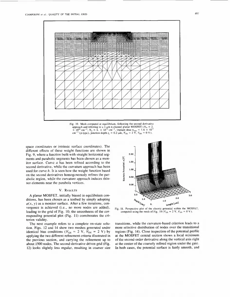
V. RESULTS A planar MOSFET, initially biased in equilibrium con-
ditions, has been chosen as a testbed by simply adopting q(x, y ) as a monitor surface. After a few iterations, con- vergence is achieved (i.e., no more nodes are added), leading to the grid of Fig. 10; the smoothness of the cor- responding potential plot (Fig. 11) corroborates the cri- terion validity.
The next example refers to a complete on-state solu- tion. Figs. 12 and 14 show two meshes generated under identical bias conditions (VGs = 2 V, V,, = 2 V ) by applying the two different refinement criteria illustrated in the previous section, and carrying the refinement up to about 1500 nodes. The second-derivative driven grid (Fig. 12) looks slightly less regular, resulting in coarser size
2.00
1.50
1.00
0.50
0.00
0.
Fig. 11. Perspective plot of the electric potential within the MOSFET, computed using the mesh of Fig. 10 ( VGs = 2 V , VDs = 0 V ) .
transitions, while the curvature-based criterion leads to a more selective distribution of nodes over the transitional regions (Fig. 14). Close inspection of the potential profile at the MOSFET central section shows a local minimum of the second-order derivative along the vertical axis right at the center of the coarsely refined region under the gate. In both cases, the potential surface is fairly smooth, and

498 IEEE TRANSACTIONS ON COMPUTER-AIDED DESIGN. VOL. 8, NO. 5. MAY 19x9
Fig. 12. Mesh of the same device as in Fig. IO , following the second de- rivative approach ( VGs = 2 V , VDs = 2 V ) .
Fig. 13. Perspective plot of the electric potential within the on-state MOS- FET, computed using the mesh of Fig. 12 (V,, = 2 V , VDs = 2 V ) .
the depleted region edges are well depicted, as shown in Figs. 13 and 15, respectively.
Although the curvature criterion would be preferable from a geometrical standpoint, we have found that signif- icant differences between the two approaches only occur when the number of nodes becomes so large as to exceed
practical limits in terms of storage and CPU time. Also, the computed values of terminal currents, as well as the nodal potentials, turn out to be in excellent agreement. Finally, the computational requirements of the two ci te- ria are fairly similar, this substantially making the two choices equivalent in many cases.

CIAMPOLINI cf ul. : QUALITY OF T H E INITIAL GRID 499
Fig. 14. Mesh of the same device as in Fig. 10, following the curvature approach ( Vcs = 2 V , VDs = 2 V ) .
2.00
I .50
1.00
0.50
0.00
0
Fig. 15. Perspective plot of the electric potential within the on-state MOS- FET, computed using the mesh of Fig. 14 ( VGs = 2 V , VDs = 2 V ) .
VI. SUMMARY A N D CONCLUSIONS In this paper a tool aimed at relieving designers from
the difficulty of generating good-quality meshes is pre- sented. The described refinement technique provides the grid with some attractive properties at the cost of a slightly increased consumption of computing resources.
The adaptive loop has been especially tailored to pre- serve such properties; its modular structure easily ac-
counts for different sets of equations and physical effects, as well as for different error estimate criteria, this allow- ing the highest flexibility. Computational efficiency has been increased by means of a local solution technique, whose stiffness has been damped by extending it to the nearest neighbors.
The proposed refinement criteria, both based on sec- ond-order differential terms, have shown good conver- gence properties and a fair attitude in generating sound meshes. From a qualitative standpoint, since gradients are involved in the expression of the current densities, the choice of the second-order terms provides a better de- scription of the unknown functions. On the other hand, even if driven by rigorous mathematical principles, the performances of mesh generators always depend on many practical tradeoffs [9], this making any quantitative com- parison with other methods difficult, and stressing the need for some “absolute” mesh-evaluating criterion.
In the next future we intend to formulate more general expressions of the refinement criteria, accounting for dif- ferent physical effects in order to make our method handle a wider range of applications.
REFERENCES
[ l ] A. F. Franz, G. A . Franz, S . Selberherr, C. Ringhofer, and P. Mar- kowich, “A generalization of the finite difference method suitable for semiconductor device simulation,” IEEE Trans. Electron Devices, vol. ED-30, pp. 1070-1082, 1983.

500 IEEE TRANSACTIONS ON COMPUTER-AIDED DESIGN, VOL. 8, NO. 5, MAY 1989
[2] G. Baccarani, R. Guenieri, P. Ciampolini and M. Rudan, ‘“FIELDS: A highly-flexible 2-D semiconductor-device analysis program,’’ in Proc. of the NASECODE IV Conf., J . J . H. Miller, Ed., pp. 3-12, 1985.
[3] P. Ciampolini, A. Gnudi, R. Guemeri, M. Rudan, and G. Baccarani, “Three-dimensional simulation of a narrow-width MOSFET,” in Proc. of the ESSDERC 87 Conf., Bologna, Italy, pp. 413-416, 1987.
[4] A. Forghieri, R. Guerrieri, P. Ciampolini, A. Gnudi, M. Rudan, and G. Baccarani, “A new discretization strategy of the semiconductor equations comprising momentum and energy balance,” IEEE Trans. Computer-Aided Design, vol. 7, pp. 231-242, 1988.
[5] M. Rudan, R. Guerrieri, P. Ciampolini, and G. Baccarani, “Discre- tization strategies and software implementation for a general purpose 2D-device simulator,” in New Problems and New Solutions for Device and Process Modelling, J . J . H. Miller, Ed. Dublin, Ireland: Boole,
[6] 1. Babuska and W. C. Rheinboldt, “Error estimates for adaptive finite element computations,” SIAM J . Numer. Anal. , vol. 15, no. 4, pp.
[7] G. Erlebacher and P. R. Eiseman, “Adaptive triangular mesh gener-
[8] P. R. Eiseman, “Alternating direction adaptive grid generation,”
[9] S . Selberherr, Analysis and Simulation of Semiconductor Devices.
pp. 110-121, 1985.
736-754, 1978.
ation,” AAIA, vol. 25, no. 10, pp. 1356-1364, 1987.
AAIA, vol. 23, no. 4, pp. 551-560, 1985.
Wien, Austria: Springer-Verlag, 1984.
* Paolo Ciampolini received the degree in electri- cal engineering from the University of Bologna in 1983.
Since then he has been working at the Dipar- timento di Elettronica, Informatica e Sistemistica (DEIS) of the same University, where he is now working toward the Ph.D. degree. At present, he is engaged in activities related to automatic mesh generation and to three dimensional simulation of semiconductor devices.
* Alessandro Forghieri received a degree in elec- trical engineering in 1986 from the University of Bologna.
After serving as an Army officer, he joined the Dipartimento of Elettronica, lnformatica e Sis- temistica of the University of Bologna, availing himself a Postdoctoral fellowship provided by SGS. At present he is engaged in research on the numerical simulation of semiconductor devices.
* Anna Pierantoni received the degree in electrical engineering from the University of Bologna in 1987.
Since then she has been working at the Dipar- timento di Elettronica, Informatica e Sistemistica (DEIS) of the same University. At present, she is engaged in an activity on the numerical simulation of semiconductor devices in three dimensions.
Antonio Gnudi received the degree in electrical engineering from the University of Bologna in 1983.
Since then he has been working at the Dipar- timento di Elettronica, Informatica e Sistemistica (DEIS) of the same univeristy. At present, he is visiting the IBM T. J . Watson Research Center, where he is engaged in an activity on the numer- ical simulation of semiconductor devices based on the higher order moments of the Boltzmann trans- port equation
*
Massimo V. Rudan (M’80) received a degree in electrical engineering in 1973 and a degree in physics in 1976, both from the University of Bo- logna. Bologna, Italy.
After serving as a Naval officer, he joined the Dipartimento di Elettronica, Informatica e Sis- temistica (DEIS), University of Bologna in 1975, where he was involved in the modeling of MOS devices. Since 1978, he has been a Professor of Quantum Electronics with the Faculty of Engi- neering at the same university, where he has been
engaged in an activity on the numerical simulation of semiconductor de- vices. In 1986 he has been a visiting scientist at the IBM Thomas J . Watson Research Center at Yorktown Heights, NY, studying the discretization techniques for the higher order moments of the Boltzmann Transport Equa- tion.
*
Giorgio Baccarani received a degree in electrical engineering in 1967, and a degree in physics in 1969, both from the University of Bologna, Bo- logna, Italy.
In 1969 he joined Bell Laboratories, Murray Hill, NJ, as a limited-term Member of the Tech- nical Staff, working in the area of electron-device processing. In 1970 he became a Research Assis- tant at the University of Bologna, where he inves- tigated the physical properties of MOS structures and transport phenomena in semiconductor mate-
rials and devices. Since 1972 he has been teaching an annual course on Quantum Electronics, and in 1980 he was appointed Full Professor of Ap- plied Electronics at the University of Bologna. In 1982 he was on a one- year assignment at the IBM Thomas J . Watson Research Center, Yorktown Heights, NY, where he investigated the feasibility of a 1 / 4 micrometer MOS process from the standpoint of the physical limitations affecting de- vice performance. From 1983 he has been heading a group involved in numerical analysis of semiconductor devices, acting as partner leader in the context of two successive EEC-supported projects in the area of CAD for VLSI. His current research interests include numerical-device simula- tion and integrated-circuit design.


