Embed Size (px)
Citation preview

FULLY INTEGRATED MEMRISTOR SYSTEM FOR NEUROMORPHIC AND ANALOG COMPUTING
UNIVERSITY OF MASSACHUSETTS AMHERST
JUNE 2022
FINAL TECHNICAL REPORT
APPROVED FOR PUBLIC RELEASE; DISTRIBUTION UNLIMITED
STINFO COPY
AIR FORCE RESEARCH LABORATORY INFORMATION DIRECTORATE
AFRL-RI-RS-TR-2022-084
UNITED STATES AIR FORCE ROME, NY 13441 AIR FORCE MATERIEL COMMAND

NOTICE AND SIGNATURE PAGE
Using Government drawings, specifications, or other data included in this document for any purpose other than Government procurement does not in any way obligate the U.S. Government. The fact that the Government formulated or supplied the drawings, specifications, or other data does not license the holder or any other person or corporation; or convey any rights or permission to manufacture, use, or sell any patented invention that may relate to them.
This report is the result of contracted fundamental research deemed exempt from public affairs security and policy review in accordance with SAF/AQR memorandum dated 10 Dec 08 and AFRL/CA policy clarification memorandum dated 16 Jan 09. This report is available to the general public, including foreign nations. Copies may be obtained from the Defense Technical Information Center (DTIC) (http://www.dtic.mil).
AFRL-RI-RS-TR-2022-084 HAS BEEN REVIEWED AND IS APPROVED FOR PUBLICATION IN ACCORDANCE WITH ASSIGNED DISTRIBUTION STATEMENT.
FOR THE CHIEF ENGINEER:
/ S / / S / NATHAN R. MCDONALD Work Unit Manager
GREGORY J. HADYNSKI Computing & Communications Division Information Directorate
This report is published in the interest of scientific and technical information exchange, and its publication does not constitute the Government’s approval or disapproval of its ideas or findings.

REPORT DOCUMENTATION PAGE
1. REPORT DATE
JUNE 2022
2. REPORT TYPE
FINAL TECHNICAL REPORT
3. DATES COVERED
START DATE
AUGUST 2018
END DATE
DECEMBER 2021 4. TITLE AND SUBTITLE
Fully Integrated Memristor System for Neuromorphic and Analog Computing
5a. CONTRACT NUMBER
FA8750-18-2-0122 5b. GRANT NUMBER
N/A
5c. PROGRAM ELEMENT NUMBER
62788F
5d. PROJECT NUMBER 5e. TASK NUMBER 5f. WORK UNIT NUMBER
R2J2 6. AUTHOR(S)
7. PERFORMING ORGANIZATION NAME(S) AND ADDRESS(ES) 8. PERFORMING ORGANIZATION REPORT NUMBER
9. SPONSORING/MONITORING AGENCY NAME(S) AND ADDRESS(ES)
Air Force Research Laboratory/RITB525 Brooks RoadRome NY 13441-4505
10. SPONSOR/MONITOR'SACRONYM(S)
AFRL/RI
11. SPONSOR/MONITOR'SREPORT NUMBER(S)
AFRL-RI-RS-TR-2022-084
12. DISTRIBUTION/AVAILABILITY STATEMENT
Approved for Public Release; Distribution Unlimited. This report is the result of contracted fundamental research deemedexempt from public affairs security and policy review in accordance with SAF/AQR memorandum dated 10 Dec 08 andAFRL/CA policy clarification memorandum dated 16 Jan 09.
13. SUPPLEMENTARY NOTES
14. ABSTRACT
The overarching goal of this project is to develop a memristor-based hardware platform for neuromorphic and analog computing. The research results at device, array, and integrated system levels are summarized in the following sections. Leveraging our previous achievements in device developments and 1T1R array integration, we have implemented all hardware memristive multilayer neural networks, integrated a 3D memristor array for parallel image and video processing, and built a new tester for time-encoded computing. We have also developed new selector devices, demonstrated 1S1R array integration, showcased reservoir computing, and proposed a unified compact model for the diffusive and drift memristors.
15. SUBJECT TERMS
Analog Computing, Neuromorphic Computing, High Performance Computing
16. SECURITY CLASSIFICATION OF: 17. LIMITATION OFABSTRACT
SAR
18. NUMBER OF PAGES
a. REPORT
U b. ABSTRACT
U C. THIS PAGE
U 19a. NAME OF RESPONSIBLE PERSON
NATHAN R. MCDONALD 19b. PHONE NUMBER (Include area code)
N/APage 1 of 2 PREVIOUS EDITION IS OBSOLETE. STANDARD FORM 298 (REV. 5/2020)
Prescribed by ANSI Std. Z39.18
49
Qiangfei Xia
University of Massachusetts Amherst 100 Natural Resources Road Amherst MA 01003

Distribution A: Approved for Public Release; Distribution Unlimited i
TABLE OF CONTENTS
SUMMARY .............................................................................................................................. 1
INTRODUCTION .................................................................................................................... 2
METHODS, ASSUMPTIONS, AND PROCEDURES ............................................................ 2
2.1. Parallel Analog Computing with Memristance as Synaptic Weights ............................. 2
2.2. Hybrid Integration for Hardware Neural Networks....................................................... 3
2.3. 3D Stacked Arrays .......................................................................................................... 4
2.4. Selector Devices for Large-scale Passive Arrays ........................................................... 4
RESULTS AND DISCUSSION ............................................................................................... 5
3.1. Dynamical Compact Models of Diffusive and Drift Memristors .................................... 5 3.1.1. Compact Modeling of a Memristor .......................................................................... 6 3.1.2. Modeling Result of Diffusive Memristors ............................................................... 7 3.1.3. Modeling Results of Drift Memristors ..................................................................... 8 3.1.4. Simulate the Spike-timing-dependent Plasticity ...................................................... 8
3.2. All-hardware 1T1R Multilayer Perceptron .................................................................... 9 3.2.1. Hardware ReLU: Design and Performance .............................................................. 9 3.2.2. Building the Two-layer All-hardware Perceptron .................................................. 10 3.2.3. Training, Inference, and MNIST Recognition ....................................................... 10
3.3. Three-dimensional Memristor Arrays for Complex Neural Networks ......................... 12 3.3.1. Design of a Three-dimensional CNN ..................................................................... 12 3.3.2. Fabrication of the Eight-layer Memristor Array .................................................... 14 3.3.3. Parallel Processing of Images and Videos ............................................................. 15
3.4. Time-encoded Computing System ................................................................................. 16 3.4.1. Power Efficiency Advantages of the Time-encoded Systems ............................... 17 3.4.2. Design of the Time-encoded Input System ............................................................ 18 3.4.3. Board-level Implementation ................................................................................... 18
3.5. Selectors and 1S1R Arrays ........................................................................................... 20 3.5.1. Tunneling Selector Design ..................................................................................... 20 3.5.2. Vertically Integrated 1S1R Cell ............................................................................. 21 3.5.3. Assessment of the Selector Capability ................................................................... 22 3.5.4. 1S1R Array with Low-current YSZ Memristors .................................................... 22 3.5.5. Timing Selector ...................................................................................................... 26

Distribution A: Approved for public release. Distribution is unlimited. ii
3.6. Reservoir Computing .................................................................................................... 28 3.6.1. Reservoir Computing System Design .................................................................... 28 3.6.2. MNIST Handwritten Digit Classification .............................................................. 29
CONCLUSION ....................................................................................................................... 30
REFERENCES ....................................................................................................................... 32
APPENDIX A – Journal Publications on FA8750-18-2-0122 ............................................... 34
APPENDIX B - Abstracts ....................................................................................................... 36
Bibliography ........................................................................................................................... 41
LIST OF SYMBOLS, ABBREVIATIONS, AND ACRONYMS .......................................... 43

Distribution A: Approved for public release. Distribution is unlimited. iii
LIST OF ILLUSTRATIONS AND TABLES
Figure 1. Our Approach Towards Parallel Computing by Using a Memristor Crossbar Array for VMM ........................................................................................................................................ 3
Figure 2. Hybrid Circuits with Both Emerging Devices and Transistors ....................................... 4
Figure 3. Non-linearity is One of the Key Requirements of a Selector Device ............................... 5
Figure 4. Experimental Data and Modeling Results for a Pt/ SiO2:Ag/Pt Diffusive Memristor .... 7
Figure 5. Experimental Data and Modeling Results for Ta/HfO2/Pt Cross Point Drift Memristor 8
Figure 6. Demonstration of the Spiking-timing-dependent Plasticity ............................................ 9
Figure 7. Design and Performance of the Hardware ReLU ......................................................... 10
Figure 8. The Two-layer Memristive Perceptron Built with Hardware Neurons and Synapses .. 11
Figure 9. In-situ Training and Inference of the Two-layer Networks ........................................... 12
Figure 10. Comparison Between Convolutional Operations in 2D and 3D Arrays ...................... 13
Figure 11. Schematic of the 3D Circuits ....................................................................................... 14
Figure 12. SEM Images of the Fabricated Eight-layer Array ....................................................... 15
Figure 13. Parallel Convolutional Kernel Operations in the 3D Circuits ..................................... 16
Figure 14. Parallel Video Processing Using the 3D Circuits ........................................................ 17
Figure 15. The Comparison of Power Efficiency Between the Amplitude- and Time-encoded Computing .............................................................................................................................. 18
Figure 16. The Design of Time-encoded Input System ................................................................ 19
Figure 17. The Time-encoded Input Measurement System .......................................................... 19
Figure 18. Tri-layer Tunneling Selector Device Performance ...................................................... 21
Figure 19. Vertically Integrated 1S1R Cell with a Tunneling Selector ........................................ 22
Figure 20. Circuit Level Modeling of 1S1R-based Crossbar Array ............................................. 23
Figure 21. YSZ-based Non-volatile Low-current Memristor ....................................................... 24
Figure 22. Electrical Performance of the Single 1S1R Cell ......................................................... 25
Figure 23. The Sneak Path Blocking Mechanism of a Timing Selector ....................................... 27
Figure 24. The Sneak Path Delay in Large Timing Selector Arrays ............................................ 29
Figure 25. Reservoir Computing System Based on Diffusive Memristor .................................... 30
Figure 26. Schematic of the Diffusive Memristor-based Dynamic Reservoir for Classifying MNIST-based Temporal Sequences ....................................................................................... 31
Distribution A: Approved for public release. Distribution is unlimited. 1
SUMMARY
This final technical report details the achievements made under the AFRL grant FA8750-18-2-0122. The overarching goal of this project was to develop a memristor-based hardware platformfor neuromorphic computing. After briefly introducing the background and rationale, the technicalapproaches are described. The research results at device, array, and integrated system levels aresummarized in the following sections. Leveraging our previous achievements in devicedevelopments and one-transistor-one-resistor (1T1R) array integration, we implemented allhardware memristive multilayer neural networks, integrated a three dimensional (3D) memristorarray for parallel image and video processing, and built a new tester for time-encoded computing.We also developed new selector devices, demonstrated one-selector-one-resistor (1S1R) arrayintegration, showcased reservoir computing, and proposed a unified compact model for thediffusive and drift memristors.

Distribution A: Approved for public release. Distribution is unlimited. 2
INTRODUCTION
The high energy consumption of traditional CMOS-based neural networks has limited their wide application. Inspired by the superior information processing capabilities of the extremely low-power human brain, neuromorphic hardware development has been an intensive research topic but has had limited success so far. The primary reason is the lack of ideal devices and circuit units that can more efficiently implement the artificial intelligent algorithms or emulate the essential properties of a synapse and a neuron, not to mention their integration into massively parallel networks. Computing systems built upon novel devices and nanotechnology offer an attractive solution to the energy efficiency, size, and weight issues.
Previously, under the AFRL grant FA8750-15-2-0044, we have developed neural network components (analog memristive devices, artificial synapses, artificial neurons), integrated large-scale 1T1R crossbar arrays for vector matrix multiplication, and demonstrated a broad spectrum of applications in analog computing and machine learning.
The goal of this project (FA8750-18-2-0122) was to further develop memristor-based hardware for analog and neuromorphic computing. The specific tasks included 1) developing selector devices and integrating 1S1R arrays; 2) building all hardware multilayer neural networks; 3) building 3D memristor array for complex neural networks; and 4) exploring new computing paradigms to enhance the computing efficiencies further.
METHODS, ASSUMPTIONS, AND PROCEDURES
2.1. Parallel Analog Computing with Memristance as Synaptic Weights Vector matrix multiplication (VMM) is a core but resource-expensive computing task in
artificial neural networks (ANN). We perform VMM in the analog domain using physical laws in a crossbar architecture. As shown in Figure 1, the current at each junction is determined by the voltage across the cell and the cell's conductance, following Ohm’s law. This represents multiplication in computing. According to Kirchhoff's current law, the current on each column is a summation of that from all cells. This in-memory computing paradigm avoids the time and energy spent on shuffling data between memory and processor in a digital system. The current sensing on all columns can be finished simultaneously, leading to substantial improvement in computing throughput. Physical computing is analog, and the network can potentially interface with analog data acquired directly from sensors, reducing the energy overhead from analog-to-

Distribution A: Approved for public release. Distribution is unlimited. 3
digital conversion (ADC). With this approach, computing can be implemented in one step [1]. We use the multilevel conductance of the memristors at each cell to represent the weights in
the neural network. The non-volatile conductance states of the two-terminal device bring in energy and area efficiencies. We often use the conductance difference in two cells (so-called “differential pairs”) in physical implementation to accommodate negative weights. Previously, we have developed a Ta/HfO2 device with nearly all required properties for in-memory computing, such as multilevel conductance, analog tuning capability, excellent stability of each conductance level, long-endurance, IV linearity, symmetric and linear weight updating, etc. [2].
2.2. Hybrid Integration for Hardware Neural Networks Although the new properties of emerging devices can benefit the energy efficiency and
computing throughput, the peripheral circuits in the computing engine should be hybrid, mixed-signal circuits that take advantage of both the novel devices and mature integrated circuit (IC) infrastructure. For most computing applications, we use a one-transistor-one-resistance switch (1T1R) architecture in which a memristor and a MOSFET (metal oxide semiconductor field effect transistor) are connected back-to-back. The transistor serves two purposes. First, it is a selector device so that the sneak path current can be efficiently suppressed. Second, the transistor can be used to limit the current flow into the 1T1R cell in a precise manner, and the programing of the memristor will be precise. As a result, integrating a pass transistor with each memristor in the array is a practical choice. While the driving circuits can individually control each transistor, it is possible to apply different gate voltages to the transistors. A single voltage pulse on a column (or a row) of a memristor will deliver different voltages on each memristor in that column (or row), achieving parallel programming and hence high efficiency.
To build multiple layer neural networks, peripheral circuits made of transistors are needed to implement neurons (activation functions), analog-digital conversions, and signal amplification and sensing (see Figure 3 for example). The activation functions (neurons) that connect different layers will be made with operational amplifiers for multiple-layer artificial neural networks, etc. However, other types of circuits, such as diodes, inverters, etc., could be employed for a different kinds of activation functions. Using commercially available electronic components is the approach we took to build a neural network with critical functionalities implemented in hardware. For this project,
Figure 1. Our Approach Towards Parallel Computing by Using a Memristor Crossbar Array for VMM Multiplication is performed via Ohm’s law as the product of the voltage applied to a row and the conductance of a cross-point cell yield a current injected into the column. The currents on each column are summed according to the Kirchhoff current law. [1]

Distribution A: Approved for public release. Distribution is unlimited. 4
we used the most popular activation function, the rectified linear unit (ReLU). The mixed-signal circuits were integrated with a back-end-of-the-line fashion, with the transistors designed by us, fabricated in a foundry, and the memristor crossbar array integrated by us.
2.3. 3D Stacked Arrays A practical approach to addressing the growing wire resistance in large crossbars is using a 3D
array. With more devices packed in a 3D array that short resistor-capacitor (RC) delays, the performance is expected to be further significantly improved. Stacking the devices into the third dimension has several other benefits. First, the packing density of the devices will be much improved. Second, it resembles the brain structure and connectivity much better since the latter is a 3D rather than a 2D design. Complex neural networks could be configured in such 3D hardware with the third dimension. Last but not least, the 3D array could be used to process 2D analog input data directly. For the state-of-the-art neural network based on the 2D topography, the input data (for example, for VMM) is fed from one edge of the array, and the output is measured along another edge. In this case, 2D data needs to be unrolled into a 1D vector, which requires excessive resources and computing time. With the 3D array, the 2D data can be processed directly, and the matrix operation will not be limited to VMM but also matrix-matrix multiplication. As a result, building the neural network hardware into the third dimension will improve computing parallelism and energy efficiency.
2.4. Selector Devices for Large-scale Passive Arrays One of the challenges of crossbar operation is the sneak path current, which potentially will
limit the array size and increase the power consumption of the array. Two approaches we adopted to restrict the sneak path: 1) using a pass transistor or 2) a selector. The transistor approach is more
Figure 2. Hybrid Circuits with Both Emerging Devices and Transistors The 1T1R crossbar array implements the resource-hungry VMM operations, while the transistor-based peripheral circuits serve as neurons and other critical functions. [3]

Distribution A: Approved for public release. Distribution is unlimited. 5
mature, but it takes a larger chip area, which is not a severe problem for computing applications where density is not the priority. In phase 1 of the AFRL project (FA8750-15-2-0044), we have adopted this approach and built large-scale 1T1R arrays for computing applications. To build large-scale, densely packed passive arrays, selector devices are indispensable. The requirements for selector devices are more stringent than those for the memristor itself. For example, an ideal selector needs to be electroforming-free, scalable, and stackable with high nonlinearity (Figure 3). It also requires high endurance, high speed, sufficient current density, low energy, and low variability. Our approach to selector devices is also unique. Unlike traditional thin-film-based selectors such as Schottky diodes, ovonic threshold switches (OTS), and metal-insulator transitions (MIT) devices, we developed a diffusive memristor by doping fast diffusive species into dielectrics. We also engineered the device stack and developed fast switching tunneling selectors. Furthermore, we integrated the selectors and low-current memristors into 1S1R arrays.
RESULTS AND DISCUSSION
3.1. Dynamical Compact Models of Diffusive and Drift Memristors In implementing computational tasks and applications, reliable, efficient, and accurate compact
models are needed for the simulation and design of large circuits. Different modeling techniques and different materials could lead to other memristor models, even for the nominally same device structure. While many aspects of memristor modeling have been widely studied, the execution time of complete physics models for understanding detailed mechanisms is much too long to be useful for circuit simulation. In addition, using specific models for different memristor types significantly complicates simulation. In this project, a comprehensive compact model based on the device physics for both drift and diffusive memristors is presented and quantitatively verified by comparison to experimental data. This model possesses the nonvolatile memory of a drift memristor and faithfully emulates the long and short-term dynamics of a diffusive memristor, utilizing different parameters for the materials used in these two device types. Spike-timing-dependent plasticity (STDP) observed in biological synapses was emulated and experimentally demonstrated by combining a drift and a diffusive memristor in a “one-selector-one-memristor”
Figure 3. Non-linearity is One of the Key Requirements of a Selector Device With proper non-linearity, the sneak path current will be effectively suppressed in a passive array. [4]

Distribution A: Approved for public release. Distribution is unlimited. 6
(1S1M) configuration. Good agreement between the simulation and the experimental data for STDP was achieved.
3.1.1. Compact Modeling of a Memristor. The model considers two different resistors in
series, the channel with metallic conductivity and the other representing an insulating gap between the channel and the uncontacted electrode. As a result, the device's resistance can be expressed by Equation 1. R(h, S) is a function of the state variables channel length h and channel area S.
Equation 1. Resistance of a Memristor Device The metallic resistance depends on the resistivity and the morphology of the conduction channel. The time derivatives of the state variables (h and S) depend on the transport rate of oxygen vacancies or ions. They are heavily influenced by the electric field, temperature, materials, etc.
Equation 2. Dynamic Equation for the State Variable h
Equation 2 describes the dynamics of state variable h. The first term of Equation 2 represents the influence of the drift force on the mobile ion distribution. To represent decay and/ or dissipation of the channel height, which comes from thermal diffusion of the oxygen vacancies and the minimization of interfacial energy, the second term was included. The two terms compete against each other and determine the conduction channel evolution during the SET and RESET processes.
Equation 3. Dynamic Equation for the State Variable S
Equation 3 also combines two terms for the conducting channel area evolution, one for drift and the other for diffusion. Meanwhile, the conduction channel tends to minimize the interfacial surface energy, so the second term was used to depict the effect of dissipation. The cross-sectional area S has a minimum area of S0, which is related to the size of an atom. When the supplied bias is removed or not strong enough, the area of the conducting channel will shrink back to S0, followed by the conduction channel rupture.
The m and n indicate the nonlinear response to voltage for the drift and diffusion, which also determines what type of memristor the model represents, drift or diffusive. Even powers of n denote a higher-order power dependence, while odd powers of n signify thermal assisted drift. Even values of m and n are used to model symmetric diffusive memristor devices and unipolar drift memristors. However, m and n need to be odd for the bipolar drift memristor. Since the model is compact, it is suitable for SPICE implementation.
(1)
(2)
(3)

Distribution A: Approved for public release. Distribution is unlimited. 7
3.1.2. Modeling Result of Diffusive Memristors To verify the model, we fabricated Pt/SiO2:Ag/Pt diffusive memristors and selected n = 2, m = 2 in Equations 2 and 3 for performing the model simulations. The simulation results agree with the measured data in Figure 4. We performed electrical pulse measurements for characterizing the switching dynamics of these devices, which exhibit a delay time for SET in Figure 4a after a one-volt pulse is applied. A low voltage (0.1 V) is used to monitor the resistance state of the device both before and after the switching pulse. The regions where the state of the memristor is read have been magnified, and the calculated pulse-switching characteristic using the model matched the experimental results reasonably well.
A characteristic I–V hysteresis plot for a Pt/SiO2:Ag/Pt diffusive memristor is shown in Figure 4d. As the voltage was swept from 0 to 1 V with a current compliance of 100 μA, an abrupt increase in current was observed at about 0.2 V. During the reverse sweep from 1 to 0 V, the device switched to its OFF state very close to 0.1 V. We collected statistical data to understand the dynamics of these devices further. 100 repeated pulse patterns were applied for each testing set, and the resulting delay/relaxation times were extracted and plotted in Figure 4e–h. Our model accurately reproduced the delay and relaxation times under different conditions, and the comparison between the simulation and experimental data is also shown in the same figures.
Figure 4. Experimental Data and Modeling Results for a Pt/ SiO2:Ag/Pt Diffusive Memristor. (a) Experimental (dashed, purple) and modeled (solid, red) pulse-switching curve. The blue curve is the input voltage pulse. (b) Figure (a) shows a magnified view of the current ranges from 0 to 10 μA in Figure (a). (c) Plot of the conduction channel length (blue) and area (red) simulated for this device over time. (d) Experimental (dashed, purple) and modeled (solid, red) switching I–V curve with current on a log scale. (e) & (f) Statistical experimental results (box plots) and simulation results (red line) of the delay time and relaxation time of this device under different pulse amplitude (0.8–1.2 V) and same 1 ms pulse length. (g) & (h) Statistical experimental results (box plots) and simulation results (red line) of the delay time and relaxation time of this device under the same pulse amplitude (1 V) and different pulse lengths (0.5–1.5 ms). [5]

Distribution A: Approved for public release. Distribution is unlimited. 8
3.1.3. Modeling Results of Drift Memristors Different switching layer materials (e.g., HfO2, SiO2) absorb moisture/protons differently. Hence, even for the same type of memristor, the bipolar drift model parameters need to be adjusted to match various materials stacks. To better demonstrate the relevance and applicability of our model, we choose HfO2 as a representative and commercial drift memristor to simulate and compare with our experimental results. We fabricated Ta/HfO2/Pt cross points and chose n = 3, m = 5 in Equations 3 and 4 for simulations since a drift memristor is characterized by bipolar switching. Different polarities of voltage bias are needed for SET and RESET processes.
As shown in Figure 5, pulse measurements were performed on these drift devices. The device was SET with a 2 V, 10 μs pulse and RESET using a −2 V, 10 μs pulse repeatedly for several cycles. The calculated pulse-switching characteristics during this process using the model matched the experimental results. The switching dynamics can be studied by examining the simulated time dependence of the state variables h and S, as shown in panel c. The characteristic I–V plot for a cross-point memristor is shown in panel d. The device current increased abruptly but returned to the HRS while sweeping the voltage back to zero (FIRST RESET). The device switched ON at a much lower voltage in the following positive sweep (FIRST SET) (0.7 V). The simulation result (dashed, purple) agrees with the measured data (solid, red).
3.1.4. Simulate the Spike-timing-dependent Plasticity Finally, we combined the drift and
diffusive memristor models to create a synapse emulator that can capture the diffusion dynamics to demonstrate STDP. We also experimentally connected a SiO2:Ag diffusive memristor in series with a Ta/HfO2/Pt drift memristor to form an artificial synapse for electrical testing. Figure 6
Figure 5. Experimental Data and Modeling Results for Ta/HfO2/Pt Cross Point Drift Memristor. (a) Experimental (dashed, purple) and modeled (solid, red) pulse-switching curve. The blue curve is the input voltage pulse. (b) A magnified view ranges from 0 300 μA in (a). (c) Plot displays the simulated conduction channel length (blue) and area (red) in this device over time. (d) Experimental (dashed, purple) and modeled (solid, red) switching I–V curves on a log current plot. [5]

Distribution A: Approved for public release. Distribution is unlimited. 9
presents the conductance change as a function of the time difference Δt between pre-synaptic and post-synaptic spikes, and the calculated results match well with the experimental data.
In summary, we demonstrated a dynamical model that can reproduce the long-term memory of drift memristors and the short-term plasticity of diffusive memristors. We showed that the model captures these devices' quasi-static and dynamic characteristics. A decent agreement has been observed between simulation results and the experimental data based on a HfO2 drift memristor and a SiO2:Ag diffusive memristor that we fabricated to verify the model. Furthermore, the spike-timing-dependent plasticity of a synapse was emulated in both experiment and simulation, showcasing our model's applicability to bio-inspired computing. Moreover, the model is compact and suitable for SPICE simulations of complex neuromorphic circuits without compatibility issues between models of different memristor types.
3.2. All-hardware 1T1R Multilayer Perceptron Previously, the multilevel conductance of a memristive device has been successfully used as
the synaptic weights in neural networks. Still, most of them relied on partial software implementation of hidden neurons. The consequence is that there is still frequent analog/digital data conversion and back-and-forth data communication during computing. In this project, we designed and implemented a compact multi-channel rectifying linear unit (ReLU) using analog components to address this issue. We characterized the performance of the hardware ReLU. We built a fully hardware-based two-layer perceptron with 64 ReLUs as the hidden neurons that connect two 128×64 1T1R memristive crossbar arrays. We have successfully achieved a 93.63% recognition accuracy in classifying MNIST (Modified National Institute of Standard and Technology) handwritten images. The fully-hardware implementation is advantageous in terms of power, area, and latency by removing the unnecessary data conversion, communication, and the corresponding circuit components.
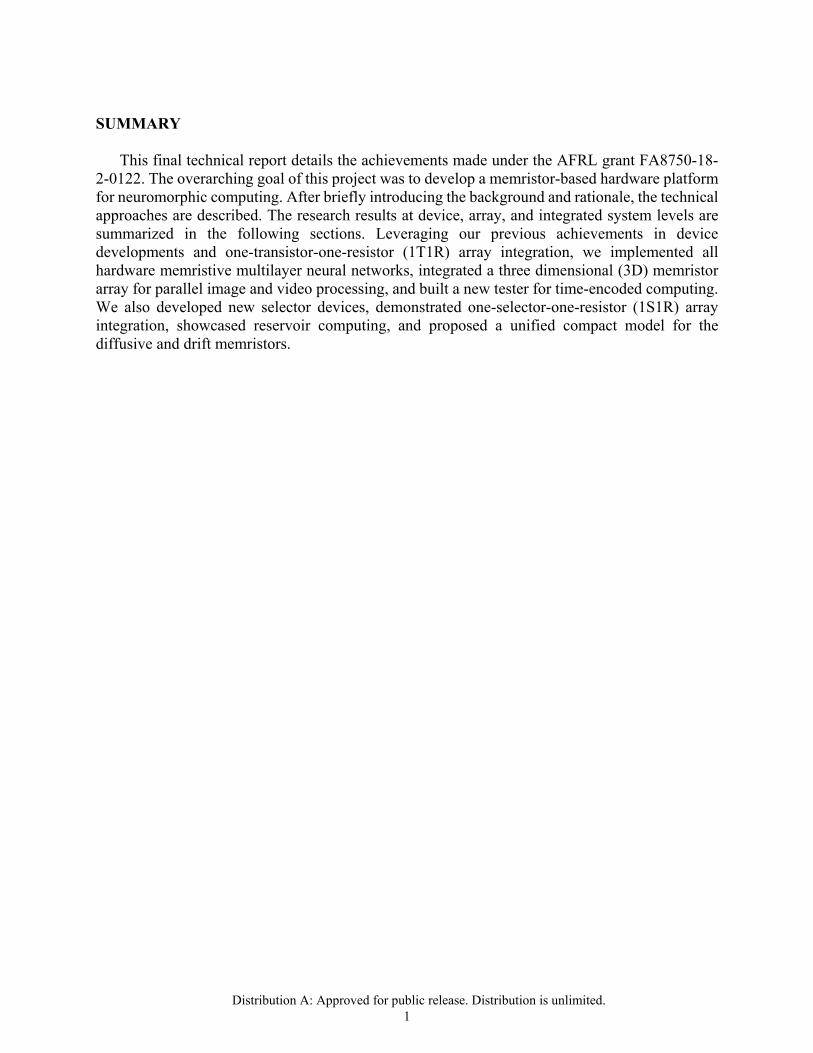
3.2.1. Hardware ReLU: Design and Performance We used off-the-shelf components to build the hardware ReLU. Each ReLU channel comprises a half-wave current rectifier, a voltage follower, and an inverting amplifier, all made with operational amplifiers (Figure 7). The first stage (current rectifier) generates a rectified output voltage directly from the input current; the second stage (voltage follower) is a unity gain buffer that is used to isolate the first stage from the next one; the third stage (inverting amplifier) provides a positive output voltage as needed by a ReLU activation function. The inverting amplifier also scales down the output voltage to the range of 0
Figure 6. Demonstration of the Spiking-timing-dependent Plasticity. Plot of the drift memristor's conductance (weight) changes with a difference in time, showing the spike-timing-dependent plasticity of an electronic synapse. [5]
Distribution A: Approved for public release. Distribution is unlimited. 10
to 0.2 V to not change the memristors' conductance in the second layer. The signal out of each of the three stages is shown in panel B. A typical DC (direct current) output characteristic of ReLU is shown in Figure 7C. As expected, the output voltage is zero when the input current is negative while linearly proportional to the current for positive inputs with excellent linearity. We also characterized the AC (analog current) performance of the ReLU, which shows a minimal delay.
3.2.2. Building the Two-layer All-hardware Perceptron The architecture of the two-layer perceptron is shown in Figure 8. We used two individual chips, and each contains a 12864 1T1R memristive crossbar array [7-9] to implement the VMM operations in the two layers. The chips were fabricated with back-end of the line (BEOL) integration and were previously used for several analog computing and machine learning applications [10-13]. The hardware ReLUs (a total of 64 channels) were built on printed circuit boards (PCB) (as described in the earlier sub-section). The original and the inverted signal out of the ReLUs were used as inputs to implement differential pairs that enable both positive and negative synaptic weights. 3.2.3. Training, Inference, and MNIST Recognition Electrical pulses with various amplitudes were sent to the first layer along the rows of the first 1T1R array as inputs. The training was conducted in-situ (and partially in software) using an in-house peripheral circuitry. Software ReLU and SoftMax activation functions were used in the hidden and output layers, respectively, and cross-entropy SoftMax was used as the loss function. We employed the root mean square propagation (RMSProp) optimizer to calculate the required amount of weight updating because of its faster convergence over the stochastic gradient descent (SGD). The weight updating of the memristor devices was realized using a one-shot blind update method, as demonstrated earlier. In
Figure 7. Design and Performance of the Hardware ReLU. (A) The designed ReLU circuit. (B) Schematic of signal propagation from the input to the output. (C) DC characteristic of the hardware ReLU. [6]

Distribution A: Approved for public release. Distribution is unlimited. 11
such an approach, one reset or set pulse is applied on the memristor electrode, and the other synchronized pulse is on the gate of the transistor [10]. The inference was entirely conducted in the hardware. The input pulses were fed into the first memristive crossbar array, and the computation results went through the hardware ReLUs then to the second crossbar array. We have classified handwritten digits in the MNIST dataset using the fully hardware-based two-layer perceptron (128 input neurons, 64 hidden neurons, and 10 output neurons) to demonstrate the functionality. To fit the hardware size, we cropped and downsampled the images in the MNIST datasets to 88-pixels. The network was trained using 60,000 images with a batch size of 50 and 2400 weight updates. Pure software training, simulation using simulated
Figure 8. The Two-layer Memristive Perceptron Built with Hardware Neurons and Synapses. (A) Schematic of the perceptron. (B) Block diagram of the implemented perceptron. (C) Circuit schematic of the perceptron. Crossbar arrays are composed of 1T1R cells, each connected in series between the selection line (SL) and bit line (BL) with the transistor gate connected to the word line (WL). (D) & (F) Optical micrographs of the 1T1R arrays used as the first and the second layers. Scale bar: 1 mm. (E) A stack of four PCBs as the hardware neurons, each containing 16 channels of ReLU activation functions. [6]
Distribution A: Approved for public release. Distribution is unlimited. 12
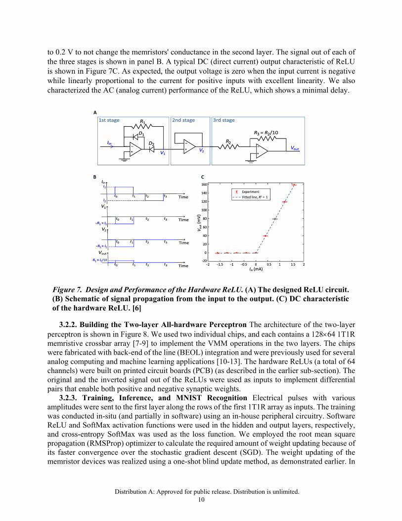
arrays (the hardware parameters were extracted and used to model the arrays), and experimental implementation with partial software ReLUs were compared. The system's training accuracy and recognition accuracy (for 10,000 test images) are shown in Figure 9, both increasing with the number of hidden neurons and the number of weights updating. With the modified MNIST dataset, we achieved 93.63% recognition accuracy with the full hardware two-layer perceptron.
The fully hardware-based two-layer perceptron inherits the benefits of using memristive devices as synapses for in-memory computing. In addition, adopting analog-based hardware neurons into the multilayer perceptron reduces the circuit complexity, leading to much better power and area efficiencies. Equally important is the much-reduced data communication between the digital and analog units. An integrated design of such an analog-based entirely hardware perceptron is needed to fully unleash the potential in power, area, and throughput. The integrated chip would have higher area efficiency, lower power consumption, and reduced parasitic capacitance and resistance compared to the board-level implementation. Based on our estimation [14-16], if built with the 65 nm CMOS node, our hardware ReLU design would improve the power efficiency by 32.8 times and area efficiency by 5.64 times compared to the digital counterpart.
3.3. Three-dimensional Memristor Arrays for Complex Neural Networks To date, most AI accelerators are based on a 2D topography, which has significant limitations that hinder the hardware's full potential. For example, the extensive external need for memory or digital cores to store partially processed results generates delays and unnecessary energy consumption. The hardware is not aware of the full-scale activity in the neural networks, and hence challenging to build fully event-driven neuromorphic hardware. The 2D topography is inefficient to host modern neural networks because of the mismatch between the full connectivity of electrodes and the more complex connections in neural networks. In this project, we have proposed, designed, and experimentally debuted the first 3D memristive neural network for computing. We built a 3D circuit with eight layers of memristors for complex neural networks. We demonstrated their applications in MNIST classification and video edge detection parallel, with software-comparable performance.
3.3.1. Design of a Three-dimensional CNN Convolutional neural networks (CNN) is one of the most popular neural networks in computer vision, natural language processing, and decision making. Traditionally for a 2D neural network, the convolutional operations are done serially (Figure 10). Processing 2D convolutions in parallel are highly desired as it can substantially
Figure 9. In-situ Training and Inference of the Two-layer Networks. (A) Training accuracy increases with the number of hidden neurons. (B) MNIST recognition accuracy also increases with the number of hidden neurons. [6]

Distribution A: Approved for public release. Distribution is unlimited. 13
accelerate its processing speed and eliminate unwanted storage of partial convolution results. Although an individual kernel operation can be reorganized and implemented by a conventional 2D crossbar array (Figure 10b), the placement of pixel-wise parallel convolutions in the same array is challenging because of the fully connected topology, which does not match the local and sparse connections in 2D convolutional layers. There are concerns about unwanted leakage current from the fully connected electrodes. On rare occasions, tiles of small arrays may be used for parallel operations (Figure 10c), but this is not a scalable solution for a larger image because of the high-volume data movement between these large groups of kernels arrays.
Alternatively, a 3D design makes it possible to host multiple kernels inside a single array, offering compact and efficient implementations of CNNs. For example, shown in Figure 10d-f are the parallel convolution operation of 12 localized kernels (marked in different colors for each row) over the input plane. These parallelly operated kernels can partially overlap without creating short circuit issues. Each 3D kernel plane is divided into individual row banks (Figure 10e) for cost-effective fabrication and flexible operations. Memristors are formed at the cross-points between the pillar input electrodes and the 3D output electrodes within each row bank. We use memristor
Figure 10. Comparison Between Convolutional Operations in 2D and 3D Arrays. The purposely designed 3D array provides a functional implementation of pixel-wise parallel convolutional kernel operations in a CNN. (a)-(c) principle of convolution in a 2D neural network, in which the kernel needs to ‘scan’ through the image multiple times to extract the features. (d)-(f), a 3D CNN can process all pixels in a massively parallel fashion and be extended to multiple kernels. [17]

Distribution A: Approved for public release. Distribution is unlimited. 14
conductance as the weights of the high-density kernels in a convolutional layer. The row banks work together, implementing the 3D array for parallel convolution operations.
Figure 11 schematically illustrates the 3D array design. In this case, each 3D row bank is physically isolated from the other, and they are connected electrically through the peripheral circuits for inference purposes. Inside each row bank, the unique 3D topology is implemented by a non-orthogonal alignment between input pillar electrodes (red) and output staircase electrodes (blue) that forms dense but localized connections in the 3D array. The staircase topography represents the stride in a convolutional operation. The local connectivity offers advantages in low IR drop and low RC products. Each memristor only shares electrodes with a few others, and the wire resistance is significantly reduced. Such local connectivity converts the entire array into a group of overlapped sub-arrays. For a 3D circuit with N stacking layers, our simulation study shows that the sneak path problem inside the 3D circuit is similar to a small NN array regardless of its lateral dimensions. At the same time, shorter electrodes led to smaller wire resistance so that better power efficiency and less current resistance (IR) drop on the electrodes are expected.
3.3.2. Fabrication of the Eight-layer Memristor Array The designed 3D array is highly stackable. Only two sets of photomasks are required for all layers (one for the odd-numbered layers and the other for the even-numbered layers), reducing the fabrication cost. As a demonstration, we fabricated 3D arrays consisting of eight monolithically integrated device layers with a 300 nm feature size in our clean room (Figure 12). We also made arrays with relatively larger feature sizes (4 μm), which yielded small series resistance. Each cell has a Pt/HfO2/Ta memristor patterned by electron beam lithography. We have tested the devices from all eight layers, and they show high reliability and excellent tunability.
Figure 11. Schematic of the 3D Circuits. The blue and red pillars represent output and input electrodes, respectively. Non-volatile memristors are formed at the intersections between two electrodes and act as electronic synapses. [17]

Distribution A: Approved for public release. Distribution is unlimited. 15
3.3.3. Parallel Processing of Images and Videos We built a four-layer CNN to classify binarized images from the MNIST handwritten digits database for demonstration purposes. The CNN model consists of one convolutional layer with four kernels (33 with ternary weights), one 22 max-pooling layers, and one fully connected layer with 200 hidden neurons and one output layer with 10 output neurons (Figure 13). The four kernels were trained offline and spatially replicated into the 3D array. The software implemented the ReLU activation functions, pooling layer, and fully connected layers. Although there is non-ideality from the devices, different output states can still be distinguished in the appearance of the noises and variations, further perfected by quantization. The inference on the MNIST test set confirms almost identical recognition accuracy between the software (98.11%) and hardware-implemented kernels (98.10%) over the 10,000 test images. We have achieved 97.91% classification accuracy without quantization, showing its robustness against noise in the 3D array.
We further demonstrated parallel video processing using the 3D circuits (Figure 14). We programmed two Prewitt filters into the hardware. The output of each kernel was recorded and combined in post-processing to produce the final video frames. Fine edge features were successfully extracted using the 3D array, and comparable results were obtained between the software and hardware-implemented kernel operations.
Fully connected layers can also be implemented in memristor arrays and be integrated with the 3D array to implement a full hardware CNN. With improved device performance and peripheral circuits, the future system could be scaled to a much larger dimension with increased power and area efficiencies. The 3D array can be monolithically integrated with 2D sensor arrays, taking analog signals and processing them directly in a massively parallel fashion. This approach will
Figure 12. SEM Images of the Fabricated Eight-layer Array. The feature size in the SEM images is 300 nm (scale bars are 2 μm and 300 nm, respectively). The image was featured on the cover of Nature Electronics (April 2020).

Distribution A: Approved for public release. Distribution is unlimited. 16
reduce the analog to digital conversions and will not require resources for the data unrolling. At the current stage, the system we built is a proof of concept that paves the way to edge intelligence with high energy efficiency.
3.4. Time-encoded Computing System In artificial neural networks, memristor arrays have been used in the VMM to improve
computing throughput and energy efficiency. In most previous work, however, the input data were encoded with the amplitude of voltages applied to the rows of memristor crossbar arrays. Although this approach utilizes Ohm’s law for multiplication directly, only the low resistance range of memristor devices was used as weights because the required IV linearity only exists in this range.
Figure 13. Parallel Convolutional Kernel Operations in the 3D Circuits. (a) We built a four-layer CNN for MNIST recognition. (b) Four convolutional kernels with ternary weights (-1, 0, 1) were obtained by ex-situ training in software and programmed into the 3D circuit. (c) Even with some device non-ideality, the distribution of all the array output (normalized) is close to the desired output states. (d) The measured conductance map of the three-row banks with parallel-processed kernels. (e) The output features can be almost fully recovered after quantization. (f) The quantized output from the 3D circuit achieved an almost identical performance as that of the software, and the raw output from the 3D circuit also shows good robustness against noise. [17]

Distribution A: Approved for public release. Distribution is unlimited. 17
The drawback is the relatively high current and hence higher power consumption. A much higher resistance range is desired for computing, but the IV relationship is usually non-linear for memristor devices with high resistance. In this project, we designed a computing system that encodes the input data to voltage durations and converts the output charge to voltages that can be read out as digital values. The linearity for multiplication is hence between the charge and the time. We implemented the time-encoded computing for large-scale 1T1R crossbar arrays with a field programmable gate array (FPGA) evaluation board and custom-designed PCBs. In such a time-encode computing system, it is possible to use higher resistance ranges of memristors and lower input voltages in VMM to improve the energy efficiency of neural networks further.
3.4.1. Power Efficiency Advantages of the Time-encoded Systems Before the system design and implementation, we first ran circuit simulations of a one-layer perceptron for a classification task with the time-encoded and amplitude-encoded inputs to estimate the power efficiency improvement. The one-layer perceptron with 13 input neurons and 3 output neurons was designed for the wine classification dataset from the UCI machine learning repository. We trained the perceptron in MATLAB, mapped the trained synaptic weights to memristor conductance, and ran the circuit simulations in LTSpice. The baseline resistance range used in the amplitude-based simulations was 1.1 to 10 kΩ. In the amplitude-encoded simulations, the input data were linearly mapped to -0.1 to 0.1 V and -0.05 to 0.05 V. In contrast, the input data was encoded in voltage durations (64 μs) with amplitudes of ±0.1 V and ±0.05 V in the time-encoded simulations. The
Figure 14. Parallel Video Processing Using the 3D Circuits. (a) For demonstration purposes, two sets of Prewitt kernels (f1 and f2) are programmed into the 3D circuits for parallel edge detection. (b) The hardware-processed video shows comparable results with fine edge features extracted from the input video. [17]

Distribution A: Approved for public release. Distribution is unlimited. 18
power efficiency from all simulations was measured in OPS/W (operations per second per Watt) and shown in Figure 15. The simulation results show that the power efficiency of the time-encoded input method is higher when the resistance range is 20 times the baseline (i.e., 22 to 200 kΩ) when the input voltage amplitudes are ±0.1 V. If the input pulse amplitude is ±0.05 V, the time-encoded approach is superior even when the resistance range is six times the baseline (i.e., 6.6 to 60k Ω). We can further improve the power efficiency by using higher resistance ranges or lower input voltages in the time-encoded input approach based on the estimation in Figure 15.
3.4.2. Design of the Time-encoded Input System The design of the time-encoded system is
shown in Figure 16. A 2-1 analog switch is connected to each row of the memristor array. One input of the analog switch is the programming voltage generated by a digital to analog converter (DAC). The other input of the analog switch is either the positive or the negative input voltage with the same amplitude generated from another two DACs. The closing time of each analog switch is controlled by one digital control voltage, which corresponds to one input data. With the control voltages, input data encoded in different pulse widths can be applied to the rows of the 1T1R memristor crossbar arrays in parallel. The gate of the transistor connected to each memristor is controlled by the gate voltage generated from DACs. Each column of the 1T1R array is connected to an integrator that converts the output charge to a voltage on the output side. The output voltages from the integrators are converted to digital values by the ADCs connected to the integrator circuits.
3.4.3. Board-level Implementation The time-encoded input system is implemented for the
128 64 memristor array in an FPGA evaluation board (ZC702) and customized PCBs. The whole system is shown in Figure 17. The FPGA evaluation board is connected to the customized motherboard. There are four sets of row boards and column boards shown in Figure 17b on top of
a
b
Figure 15. The Comparison of Power Efficiency Between the Amplitude- and Time-encoded Computing. The amplitude-encoded inputs were linearly mapped to -0.1 to 0.1 V(a) or -0.05 to 0.05 V (b) for pulses with a fixed 1 µs duration. The time-encoded inputs were encoded in 64 µs with amplitudes of ±0.1 V or ±0.05 V. (This simulation is conducted internally in the Nanodevices and Integrated Systems Laboratory at University of Massachusetts Amherst.)

Distribution A: Approved for public release. Distribution is unlimited. 19
the motherboard. There are 32 analog switches on each row board that can be connected to 32 rows of the memristor array and DACs that generate the programming voltages, input voltages, and gate voltages. On each column board, there are 16 sets of analog switches, integrator circuits, and ADCs. With the four-row boards and column boards connecting to the 128 64 memristor array, input voltages encoded in time can be applied to the 128 input rows in parallel, and 64 output voltages can be read out as digital values in parallel.
Figure 16. The Design of Time-encoded Input System. Each input is encoded into the pulse duration. An integrator at each column converts the charge into a voltage. (This figure is generated in the Nanodevices and Integrated Systems Laboratory at University of Massachusetts Amherst.)
a
b
Figure 17. The Time-encoded Input Measurement System. (a) The system includes an FPGA evaluation board, customized motherboard, row boards, and column boards. (b) Details of the four sets of row boards and column boards. (This figure is generated in the Nanodevices and Integrated Systems Laboratory at University of Massachusetts Amherst.)

Distribution A: Approved for public release. Distribution is unlimited. 20
During operation, input data stored in the DDR memory of the evaluation board will be moved to the block random access memory (BRAM) in the FPGA by a program running on the processor of the evaluation board. The function blocks in the FPGA will encode the input data to parallel control signals shown in Figure 16 and apply them to analog switches on the row boards. In the meantime, the input voltages from the DACs on the row boards will be applied to the memristor array to conduct the analog computing. The computing results from columns of memristor will be integrated by the integrator circuits and converted to digital values by the ADCs on the column boards. The digital results stored in the ADC registers will be moved to another part of the DDR memory by the FPGA function blocks after the analog computing. Output data processing after the analog computing is completed by the program running on the processor.
With the implemented time-encoded input system, the input data can be encoded in a period of 64 µs and applied to the 128 rows of the memristor array in parallel. The parallel outputs from the 64 columns of the memristor array can be captured in a period of 1 µs at the same time. This is much faster than the amplitude-based input system configuring input voltages and reading the output voltages one by one. Also, implementing the time-encoded input system is the first step to using the time-encoded inputs for the neural networks running on memristor arrays, which enables us to use higher resistance of memristor devices and achieve the power efficiency improvements estimated in Figure 15.
3.5. Selectors and 1S1R Arrays The sneak path problem is a fundamental issue in crossbar arrays and can potentially be solved
by introducing selectors into the arrays. Among the various types of selectors reported, tunneling selectors are one of the most promising ones due to the possibility of electroforming free operation, low cycle to cycle variation, high speed of operation, and theoretically infinite endurance. We proposed a tri-layer tunneling selector with a stack structure of Ge/Pt/TaN1+x/Ta2O5/TaN1+x/Pd. Here TaN1+x/Ta2O5/TaN1+x layers form the trilayer tunneling barrier structure. Ge/Pt and Pt layers are the bottom electrode (BE) and top electrode (TE). We engineered the Ge/Pt BE to provide an ultrasmooth surface on which a trilayer stack could be deposited. This tri-layer tunneling device observed a non-linearity of 3×10⁵ and 107 for one-half and one-third biasing schemes, respectively. The tunneling selector was then integrated with a Pd/Ta2O5/Ru-based memristor to realize a 1S1R cell. The 1S1R cell shows a maximum ON/OFF ratio of 100 and an NL of 104 and 106 for one-half and one-third biasing schemes.
3.5.1. Tunneling Selector Design When designing a robust tunneling selector device, one needs to think about two critical factors: (1) depositing a high-quality dielectric layer that has minimal defects and is stoichiometric and dense, which could be achieved by optimizing the deposition (sputtering in our case) recipe for the dielectric layers; and (2) having smooth surfaces and interfaces that can sustain a high electric field without breakdown.
Having taken this into account, we designed a highly non-linear tri-layer tunneling barrier (TLTB) selector device built upon the engineered smooth BE layers, as schematically shown in Figure 18. The scanning electron microscope (SEM) micrograph of the 20 μm × 15 μm crosspoint device is presented in Figure 18B. The I–V characteristics of the proposed TLTB selector device are plotted (semi-log) in Figure 18C, where the inset shows the linear plot of the same sweep cycles. The proposed TLTB selector device shows very insulating behavior under low bias (~70 pA at +1.5 V). It becomes highly conductive at a high bias (~20.4 μA at +3 V), which results in a highly

Distribution A: Approved for public release. Distribution is unlimited. 21
non-linear I–V characteristic of the proposed selector device. For a one-half-voltage scheme, NL is defined as NL1/2 = I(Vread)/I(Vread/2), and for the one-third biasing scheme NL could be given as NL1/3 = I(Vread)/I(Vread/3). The measured NL of the device is around 3×10⁵ (107) for one-half (one-third biasing) schemes, as indicated in Figure 18C. Endurance measurement was conducted on the proposed selector device for 100 million cycles without any noticeable degradation, as shown in Figure 18D, using 5 μs wide 3 V (Vread) and 1.5 V (Vread/2) pulses.
3.5.2. Vertically Integrated 1S1R Cell To demonstrate the feasibility of integrating the proposed selector device with a memristor, a vertically integrated 1S1R cell was fabricated. We used a Ru-based memristor device. For this demonstration, Ru-based memristors exhibit forming free and low power switching operations, making them suitable for a 1S1R integration application. Figure 19A presents a schematic of the vertically integrated 1S1R stack. For characterizing the Ru-based memristor device, bias was applied to the TE of the integrated cell, the ME was grounded, and the BE was left floating. Figure 19B presents the I–V characteristics of the memristor device. To SET the device, a positive dual-sweep voltage (blue lines) was applied with current compliance (Icc) set to 10 μA. Starting with a high resistance state (HRS), the device switched to a low resistance state (LRS) at 1.8 V and maintained its state during the reverse sweep. A negative dual-sweep voltage (red lines) was applied to RESET the device without any Icc. Beginning with the LRS, device RESET started at about -0.4 V, and it switched to HRS at about -1.2 V and maintained its state afterward during the reverse sweep. The linear plot of the same I–V is presented in the inset. Next, the vertically integrated 1S1R cell was electrically tested to demonstrate successful
Figure 18. Tri-layer Tunneling Selector Device Performance. (A) Schematic of the proposed selector device. (B) Scanning electron microscopy image showing a top-view image of the fabricated device. (C) A typical non-linear I–V curve of the selector device. The inset shows a linear plot of the I–V curve. (D) Endurance data measured up to 100 million cycles. [18]

Distribution A: Approved for public release. Distribution is unlimited. 22
1S-1R operations (Figure 19C). Voltage was applied to the TE, and the BE was grounded with the ME left floating. The device's non-linear I–V characteristic is presented in Figure 19C. The 1S1R cell exhibited an NL of 104 (106) for one-half (one-third) biasing scheme at Vread = 1.5 V with an ON/OFF ratio of around 50. The highest ON/OFF ratio of 100 could be achieved at Vread = 3.4 V but with a reduced NL value of 150.
3.5.3. Assessment of the Selector Capability To demonstrate the full extent of the capabilities of this selector, we performed a circuit simulation of the 1S1R based crossbar array (CBA). The SPICE model was validated by comparing the single device's experimental and simulated I–V characteristics, as shown in Figure 20A. The normalized readout margin for different sizes of the CBA is presented in Figure 20B. We considered the two most popular biasing schemes for our simulation: one-half and one-third voltage schemes. The readout margin for a 100 kbits CBA is around 20% for the one-half biasing scheme and more than 90% for the one-third biasing scheme. The one-third biasing scheme is more resilient to the sneak path current issue than the one-half biasing scheme. We can conclude from the results that the proposed selector helps mitigate the effect of the CBA’s sneak path currents.
3.5.4. 1S1R Array with Low-current YSZ Memristors Memristors possess many interesting properties. Among them, the possibility of building dense crossbar arrays for memory applications is one of the most attractive ones. However, making passive crossbar arrays is straightforward. However, using them is difficult due to the inherent limitation of sneak path currents. Sneak path currents are unwanted currents that lead to unselected cells getting activated. They arise due to the linearity present in the memristor cells. They, in turn, lead to reduced read margin of the arrays, high power consumption, and a reduction in the size of the arrays. This problem can be mitigated if inherent nonlinearity can be engineered into the memristor cells. However, the former is very difficult. An alternative approach is to use a selector cell inherently nonlinear in series with the memristor cell. We have characterized a Pt/YSZ/Zr device and have found it to possess low current and low voltage switching behavior and sufficiently high retention and fast dynamics. We successfully demonstrated the integration of a tunnel selector with the YSZ
Figure 19. Vertically Integrated 1S1R Cell with a Tunneling Selector. (A) Schematic of the 1S1R cell. (B) Typical I–V characteristics of the Pd/Ta2O5/Ru-based memristor device. (C) Typical I–V characteristics of the 1S1R cell with a highly non-linear ON state. The inset shows a linear plot of the same I–V. [18]

Distribution A: Approved for public release. Distribution is unlimited. 23
(Yttria stabilized zirconia) based memristor and built a 22 array. The YSZ device can be electroformed easily in the array, and we demonstrated certain array functions.
The Pt/YSZ/Zr cross-point memristor devices consisted of a 10 nm thick amorphous YSZ layer sandwiched between a 20 nm thick Pt bottom electrode (BE) and 40 nm thick Zr top electrode (TE). The Pt and Zr layers act as inert and active electrodes, respectively, and the YSZ layer serves as the switching matrix. A voltage was applied to the TE during electrical characterization, and the BE was grounded (right side inset of Figure 21a). The electroforming operation of the YSZ based memristor device has been shown in Figure 21a. A positive DC sweep voltage of amplitude 2 V with current compliance (Icc) of 1 μA was used to electroform the device. The device started with a very high resistance state (pristine state), reached compliance at around 1.4 V, and maintained its ON-state conductance. Figure 21b presents post-electroforming resistive switching (RS) I–V characteristics, with the first switching cycle highlighted in turquoise color. The subsequent cycles (labeled in grey) show the repeatable switching behavior of the device. Semi-log plots of the same switching cycles are given in the inset of Figure 21b. Figure 21c shows the endurance cycles of the device. For the endurance measurement, 100 ns electrical pulses with 0.8V and -1 V amplitude for SET and RESET operations, respectively, have been used with a 0.2 V, 1 μs read pulse. The device exhibited 100 million switching cycles without any significant degradation. The retention data has been plotted in Figure 21d. Two levels of each state (HRS and LRS) can be retained for up to 104 s. Here the two SET conductance and two RESET conductance levels were obtained by applying 100 μA (solid red diamonds), 500 μA (solid black diamonds) Icc, and -1.6 V (solid blue circles), -1.8 V (green filled circles) RESET stop voltages, respectively. A 100 mV read voltage was used for the retention measurements.
A trilayer tunneling selector (Pt/TaN/Ta2O5/TaN/Pt) was used in this study to make a proof of principle demonstration of the 1S1R (one-selector-one-memristor) integrated device. To test the compatibility between the memristor and the selector, a single selector-memristor integrated device was fabricated. In the vertically integrated 1S1R device, the selector was at the bottom, and
Figure 20. Circuit Level Modeling of 1S1R-based Crossbar Array. (A) SPICE simulation of single device IV sweep (solid line). (B) Normalized Readout Margin for different array sizes. [18]

Distribution A: Approved for public release. Distribution is unlimited. 24
memristor layers were deposited on top of it. To study the effect of the electroforming operation of the memristor on the performance of the integrated 1S1R devices, two different setups were used: 1) memristor was electroformed by applying an electrical bias across the TE and ME (Middle Electrode) with the BE floating (Figure 22 upper panel), essentially electroforming the memristor without the need of the selector; and 2) the electroforming operation of memristor was performed by applying an electrical bias across the TE and BE with the ME floating, essentially treating the entire 1S1R stack as one single device. Schematics with corresponding biasing schemes are provided as insets. The electroforming operation using the first method is presented in Figure 22a. A post-
electroforming RS cycle obtained by applying voltages across the TE and ME is shown in Figure 22b (solid green diamonds). The SET voltage of the memristor was around 0.7 V with Icc set to 50 μA, and the device was RESET at about -0.7 V (≈50 μA). For understanding the electrical behavior of the 1S1R devices, selector current I1S and 1S1R current I1S1R were plotted on top of each other, as shown in Figure 22b (solid black squares and solid purple circles, respectively). Figure 22c presents multiple SET and RESET switching operations of the 1S1R device. The curve represented by solid red circles is the first switching cycle, and greyed curves show subsequent RS cycling (the semi-log plot of the same data is shown in the inset). The 1S1R device exhibits a decent cycle-
Figure 21. YSZ-based Non-volatile Low-current Memristor. (a) Low-voltage electroforming and low-current first RESET operation of the YSZ memristor, the inset on the left shows a linear plot of the FRC, inset on the right shows the material stack of the device with the biasing scheme. (b) Low-voltage, low-current RS switching of the YSZ device, inset shows semi-log plot of the same. (c) Endurance data measured up to 100 million cycles. (d) Retention test of four different conductance levels. [19]

Distribution A: Approved for public release. Distribution is unlimited. 25
to-cycle uniformity. Figure 22d shows the micrograph of a fabricated 1S1R device with the electrodes marked. The second type of electroforming method (in situ electroforming operation), where the memristor was electroformed while electrically connected in series with the selector, is shown in Figure 22e. The bias voltage was applied to the TE of a new device (Dv#2) while its BE was grounded while the ME was left floating. In an actual application, when 1S1R devices are used in an array, there will be electrical access to the ME for the memristor electroforming operation. Hence, only the second method is relevant for practical applications.
Figure 22f shows the subsequent RS curves of the 1S1R device after the electroforming operation (the semi-log plot is provided in the inset). The 1S1R device was SET at around 4 V with the ON current being limited by the selector resistance; the RESET process took place at around -4.6 V (≈64 μA). To study the effect of in situ electroforming on the memristor RS operation, the two memristors from the integrated 1S1R Dv#1 and Dv#2 were tested independently (without selector) just after finishing the tests in Figure 22c, f respectively. The results have
Figure 22. Electrical Performance of the Single 1S1R Cell. (a) Electroforming operation of the memristor, left side inset shows a linear plot of the FRC, and right side inset shows biasing scheme. (b) Overlapping I–V curves of memristor, selector, and 1S1R device. (c) Low-current RS switching of the 1S1R device (Dv#1), upper inset presents a semi-log plot of the same, and lower inset shows biasing scheme. (d) micrograph of the fabricated single-1S1R integrated device. (e) In situ electroforming operation of the memristor, upper inset shows semi-log plot of the same, and the lower panel presents biasing scheme. (f) Low-current RS switching operation of the 1S1R device (Dv#2) with the semi-log plot shown in the upper inset and biasing scheme in the lower inset. [19]

Distribution A: Approved for public release. Distribution is unlimited. 26
indicated that in situ forming is beneficial in improving the uniformity of conductive filaments and is promising for implementing such 1S1R device-based arrays in real applications.
3.5.5. Timing Selector In this work, the transition dynamics based on the nonlinear delay–
voltage relation of a selector and a memristor were proposed and demonstrated to tackle the problem of sneak path currents in crossbar arrays. It was observed that the delay time of both selector and memristor is dependent on the voltage amplitude of the pulse input, and it has a directly proportional relationship. We take advantage of the fact that the voltage drop on the target device is larger than those on the sneak path devices, and hence the delay time of the target device is much shorter than those of the sneak path devices. This timing selector can help us block the sneak path currents while passing the current through the target device. A pulse with a specific amplitude was used to achieve this target, which could switch on the timing selector of the target cell but not those in the sneak paths within the pulse length.
The symbols and required electrical behaviors of a timing selector and a memristor are shown in Figure 23a and Figure 23b, respectively. The timing selector is volatile, and the memristor is non-volatile, which helps the memristor maintain its high-/low-resistance state (HRS/LRS) when zero voltage is applied. In contrast, a timing selector always remains in its HRS unless it receives an external stimulus (e.g., a voltage pulse) sufficient to switch it to its LRS. If the external voltage drops below a specific holding voltage, the selector will spontaneously change back to its HRS. The volatile-resistive switching behavior negates the need for extra operations to mute a one-selector-one-memristor (1S1R) unit when it is not selected anymore, which reduces the energy consumption and the risk of inadvertently changing the information stored in the memristor during such operations. The electrical behavior of a timing selector should also be nonpolar so that both positive and negative voltages can switch it on to ensure its compatibility with bipolar memristors.
A schematic illustrating the response of a timing selector under a voltage pulse with variable amplitude and width is shown in Figure 23c. It is required that the time delay upon a voltage to switch the selector is shorter when the voltage amplitude is larger so that the target selector can be switched on much earlier than the selectors on the sneak paths. It can be inferred that the selector is switched on only when the amplitude and width of a voltage pulse correspond to a point above the delay curve (red line in Figure 23c). An example of sneak path current in a 22 crossbar with memristors is shown in Figure 23d, assuming that the unselected bit line (BL) and word line (WL) is floating. If the unselected BL and WL are grounded, only devices sharing the same BL or WL with the target device can form sneak paths. Sneak current in a large array can always be viewed as a combination of sneak path currents in many 22 arrays. Figure 23e shows the states of timing selectors in a memristor crossbar array when the applied pulse meets the requirement shown in Figure 23f. When voltage is applied to the target 1S1R cell, no matter the unselected BL and WL are floating or grounded, the 1S1Rs in the sneak paths are under voltage( s) always smaller than that of the target 1S1R. As schematically shown in Figure 23c, the time delay of the target selector is expected to be smaller than those of the sneak path selectors.
A larger crossbar array with timing selectors was developed to understand the sneak path behavior in a crossbar circuit where all unselected WLs and BLs are floating (or equivalently connected to high-impedance terminals) as shown in Figure 24a. Assuming the wire resistance is negligible and all the sneak path selectors in an MN array have the same HRS resistance R, the equivalent circuit of sneak path devices can be simplified, as shown in Figure 24b, where all the

Distribution A: Approved for public release. Distribution is unlimited. 27
sneak path devices are connected to the same BL (WL). Due to the voltage-dividing effect, voltage drops on sneak path devices on the same WL as the target device are close to V, which suggests that N and M are desirable to have similar values when designing timing selectors crossbars. To verify the earlier analysis, delays of sneak paths in timing selector crossbar arrays of different sizes and a square shape (the number of WLs equals that of BLs) were measured. Because it is impractical to measure all possible sneak paths simultaneously, the normal crossbar was modified so that the voltage input could only trigger sneak path currents with respect to a predefined target device but not activate the target selector itself. The crossbar design is shown in Figure 24c, where a segment of the WL electrode of the target device was removed, and the delay of the output current was determined by the sneak path with the shortest delay. The measurement results indicated that the sneak path delays in large arrays were similar to that of a 4×4 array. In a 4×4 array, the estimated voltage drops on the sneak path devices sharing the same BL or WL with the target device were 3 V/7, which was close to V/2, as in the case where all unselected BLs and WLs were grounded. When the array got larger, this voltage was even closer to V/2 but always a bit smaller. As a result, in the case where the unselected WLs and BLs are floating and the numbers of WLs and BLs are the same, the delay difference between the sneak path and target device in a large time-selector crossbar array is almost the same as the case where unselected WLs and BLs are grounded. In contrast, the larger the difference between the numbers of WLs and BLs, the less
Figure 23. The Sneak Path Blocking Mechanism of a Timing Selector. (a) The symbol and required electrical characteristics of a timing selector. The blue and red curves represent the absolute value of input voltage and readout current. (b) The symbol and typical characteristics of a memristor. The blue and red curves represent the absolute value (whereas opposite polarities are normally used for SET and RESET) of input voltage and readout current. (c) The response to a voltage pulse of a timing selector. It is required that the delay of a timing selector decreases with increasing voltage amplitude. (d) A schematic of sneak path current in a crossbar array formed by memristors. (e) A schematic of the timing selector serves as a voltage-controlled switch that blocks the sneak path current while providing access to the target device. (f) The sneak path blocking mechanism in (e). Because each timing selector in the sneak path shares a relatively smaller voltage Vsneak than the target timing selector voltage Vtarget, the delay of a sneak path selector is longer than that of the target selector. [20]

Distribution A: Approved for public release. Distribution is unlimited. 28
likely the timing selector can work with the floating scheme. Hence, we successfully demonstrated a timing selector to mitigate the sneak path current issue in crossbar arrays.
3.6. Reservoir Computing This section will discuss a physical implementation of a reservoir computing (RC) system
where a diffusive memristor-based reservoir had been coupled with a drift memristor-based 1T1R (one-transistor-one-memristor) readout layer. The input to the reservoir was provided in the form of bitstreams that can be thought to represent binarized pixels. These bitstreams were provided in the form of engineered waveforms, which took advantage of the rich short-term dynamics of the device. The readout system based on the 1T1R array was trained to classify the temporal version of MNIST handwritten digits. An accuracy of 83% for the complete MNIST dataset was achieved using a hardware drift memristor-based 1T1R readout layer.
3.6.1. Reservoir Computing System Design In classical reservoir computing systems, the data provided at the input is transformed into spatiotemporal patterns in a high-dimensional space by a recurrent neural network (RNN) in the reservoir (Figure 25a). Diffusive memristors possess rich dynamics, which is why they can, in a way, remember the effect of previous electrical operations on them. However, as time passes, this memory fades. Hence when the device is being programmed, the state of the device depends not only on the programming pulse itself but also on whether other programming pulses have been applied in the past. Thus, pulses that were applied closer to the present time will have a stronger effect than those applied in the far past. There is a threshold to this effect as if the pulses were applied a sufficiently long time before the arrival of the next pulse pattern, then the device will have enough time to return to its initial high resistance state. Hence, it is reasonable to compare a diffusive memristor with a neuron having a recurrent connection with a weight less than 1 (Figure 25b). Such a recurrent node would continuously decay its state if not provided with an input. More specifically, the diffusive memristor will have a thicker filament or a higher conductivity if it is continuously subjected to pulses. In contrast, if a sufficiently long time is spent before the application of a new pulse, the filament breaks down (Figure 25c). Suppose we refer to Figure 25c and analyze the state of the diffusive memristor on the application of a pulse train. In that case, we find that when we apply two pulses (top panel) in the first and second time frames consecutively and check the state of the memristor at the fourth time frame, the memristor still has an intact filament and the conductivity is relatively high. When we apply three pulses (middle panel) in the first, second, and third time frames, respectively, the memristor has a thicker filament, indicating a higher conductivity than in the former case. On the contrary, when we apply only one pulse (bottom panel) during the first time frame and consider the state of the memristor in the fourth time frame, we find that the filament has broken down and the device's conductivity is very low. These scenarios are akin (considering that all input pulses are identical) to what will happen in the case of a recurrent node with a recurrent weight having a magnitude less than 1. In the first case, by the fourth time frame, the node's state would decrease twice. In the second case, by the fourth time frame, the node's state would decrease once. In the third case, by the fourth time frame, the node's state would decrease. Physically, a single diffusive memristor populates the reservoir of our RC system. Thus, the state of the reservoir is decided by the resistance state of the device. Once the bit-coded pulse streams are applied to the reservoir input, the state of the reservoir is dependent on the input patterns and can be used to analyze the input. When a pulse is applied, the conductance of the device will increase. If many pulses are

Distribution A: Approved for public release. Distribution is unlimited. 29
applied within a short interval, a large increase in conductance can be achieved; whereas, if the inter-pulse distance is sufficiently large, the device relaxes back to its initial high-resistance state.
3.6.2. MNIST Handwritten Digit Classification Different bitstreams were applied to a diffusive memristor, and the corresponding read currents were recorded. These bitstreams can be thought of as a representation of binarized pixels. The recorded read currents from the experiments can be thought of as reservoir responses to a combination of black and white pixels. The white and black pixels are represented by a high write pulse (1.25 V, 50 μs) and no pulse (0 V amplitude). Each MNIST handwritten digit image has 28×28 pixels. Each image is cropped to 22×20 pixels and then binarized in a software program (Figure 26a). The columns are then divided into five sets of four columns and then joined above the other to form a 110 (22×5) × 4 matrix. All these 4-bit rows in this matrix are a subset of the 4-bit patterns applied to the diffusive memristor-based RC system. The corresponding currents for each row are extracted randomly from a set of 100 measured reads current values (for a certain bit pattern). These current values are then applied to the input of 220 (110×2 memristor per differential pair) × 10 fully connected neural networks (Figure 26b). Each differential pair represents a single signed weight of the 1T1R network. The fully connected layer serves the role of the readout where the classification is performed. During readout, the output neurons of the fully connected 1T1R crossbar applied SoftMax activations to
Figure 24. The Sneak Path Delay in Large Timing Selector Arrays (a) The optical image of a 64×64 timing selector crossbar array. Scalar bar: 100 μm. (b) The equivalent circuit of an M×N timing selector crossbar array, assuming that all the timing selectors are in their HRS and have the same resistance. (c) Measurement schematic of the whole-array sneak path delay in a customized large array. All the unlabeled wires are floating. The whole-array delay is determined by the sneak path that can be switched on in the shortest time under a given voltage. (d) The measured whole-array delay time in different sizes of square arrays (the number of BLs is equal to that of the WLs) using the method in (c) when V = 1.2 V. [20]

Distribution A: Approved for public release. Distribution is unlimited. 30
the dot product of the 220 inputs and the weights associated with each output neuron. The readout layer is trained in a supervised fashion based on error backpropagation that uses the RMS prop method to minimize a cross-entropy loss that updates the conductance of 1T1R every mini-batch. This process is repeated with two epochs of passing all the 60,000 handwritten digits from the MNIST training data set, and it is then tested with 10,000 digits from the MNIST test set. An accuracy of 83% had been achieved using our RC system. CONCLUSION
In this final technical report, we summarized our achievements in the project sponsored by
AFRL under the grant FA8750-18-2-0122. We developed a unified compact model that describes both the diffusive and drift memristors on the device level. Also still phenomenal, these models are validated using experimental device behavior and can be used for circuit simulation. We also developed a new selector based on the tunneling effect and a new scheme to use the selector based on the timing. On the circuit level, we have integrated a large-scale 3-D array that was used for parallel convolutional operations. We also built a two-layer perceptron based on hardware neuron and two 1T1R arrays and demonstrated 1S1R arrays. At the system level, we built a tester that takes advantage of the time-encoded input for computing. With the new computing scheme, the high-resistance range of the memristive device can be used for computing, substantially reducing the power consumption. We demonstrated the applications of the circuits and systems and
Figure 25. Reservoir Computing System Based on Diffusive Memristor. (a) Schematic of an RC system, showing the reservoir with internal dynamics and a readout function. (b) Equivalent schematic of a simplified system where the reservoir is populated with nodes with recurrent connections having a magnitude less than 1. (c) The conductivity of the diffusive memristor is influenced by the periodic voltage stimulation that is provided on its top electrode (+) while grounding the bottom electrode (-). In the top panel, a voltage stimulus is provided in two consecutive time slots. In the middle panel, a voltage stimulus is applied in three consecutive time slots, resulting in a much thicker filament and even higher conductivity when the device state is analyzed in the fourth time slot. In the case of the bottom panel, a voltage stimulus is applied only in the first time slot. When the device state is evaluated in the fourth time slot, the filament has broken down, resulting in very low conductivity. [21]

Distribution A: Approved for public release. Distribution is unlimited. 31
projected the power and area efficiencies for the future fully integrated version built in an IC foundry.
Figure 26. Schematic of the Diffusive Memristor-based Dynamic Reservoir for Classifying MNIST-based Temporal Sequences (a) The original 28×28 image is binarized and cropped to size 22×20 before being divided into five columns and sequentially joined with each other. The resultant 110×4 input is then converted to 110 4-bit temporal voltage patterns as inputs to diffusive memristors. (b) Optical micrograph of the 128×64 1-transistor 1-memristor (1T1R) crossbar with the probe card landed. The color blocks illustrate the sub-array used for implementing the readout layer, consisting of 110×20 devices using differential pairs. (c) Scanning electron micrograph of a single 1T1R cell in (b). 1T1R cells of the same row share the common bottom bit line, while those of the same column

Distribution A: Approved for public release. Distribution is unlimited. 32
REFERENCES
1. Xia, Q., and Yang, J.J., "Memristive crossbar arrays for brain-inspired computing," Nature Materials, 18, Apr 2019, pp. 309-323.
2. Jiang, H.,Han, L., Lin, P., Wang, Z., Jang, M., Wu, Q., Barnell, M., Yang, J.J., Xin, H.L., and Xia, Q. “Sub-10 nm Ta channel responsible for superior performance of a HfO2 memristor,” Scientific Reports, 6, June 2016, Art. No. 28525.
3. Wang, Z., Li, C., Lin, P., Rao, M., Nie, Y., Song, W., Qiu, Q., Li, Y., Yan, P., Strachan, J.P., Ge, N., McDonald, N., Wu, Q., Hu, M., Wu, H., Williams, R.S., Xia, Q., and Yang, J.J., "In situ training of feed-forward and recurrent convolutional memristor networks," Nature Machine Intelligence, 1, 9, Sep 2019, pp. 434-442.
4. Xia, Q. NIST seminar, 2014. Unpublished. 5. Zhuo, Y., Midya, R., Song, W., Wang, Z., Asapu, S., Rao, M., Lin, P., Jiang, H., Xia, Q.,
Williams, R.S., and Yang, J.J., "A Dynamical Compact Model of Diffusive and Drift Memristors for Neuromorphic Computing," Advanced Electronic Materials, Oct 2021, p. 2100696.
6. Kiani, F., Yin, J., Wang, Z., Yang, J.J., and Xia, Q., "A fully hardware-based memristive multilayer neural network," Science advances, 7, 48, Nov 2021, p. eabj4801.
7. Yakopcic, C., Taha, T.M., and Hasan, R., "Hybrid crossbar architecture for a memristor based memory" In NAECON 2014-IEEE National Aerospace and Electronics Conference, Dayton, OH, USA (2014).
8. Zangeneh, M., and Joshi, A., "Performance and energy models for memristor-based 1T1R RRAM cell," In Proceedings of the great lakes symposium on VLSI, (2012).
9. Nauenheim, C., "Integration of resistive switching devices in crossbar structures," Forschungszentrum Jülich GmbH, Zentralbibliothek, Verlag, 2010
10. Li, C., Hu, M., Li, Y., Jiang, H., Ge, N., Montgomery, E., Zhang, J., Song, W., Dávila, N., Graves, C.E., Li, Z., Strachan, J.P., Lin, P., Wang, Z., Barnell, M., Wu, Q., Williams, R.S., Yang, J.J., and Xia, Q., "Analogue signal and image processing with large memristor crossbars," Nature electronics, 1, 1, Jan 2018, pp. 52-59.
11. Li, C., Belkin, D., Li, Y., Yan, P., Hu, M., Ge, N., Jiang, H., Montgomery, E., Lin, P., Wang, Z., Song, W., Strachan, J.P., Barnell, M., Wu, Q., Williams, R.S., Yang, J.J., and Xia, Q., "Efficient and self-adaptive in-situ learning in multilayer memristor neural networks," Nature communications, 9, 1, Jun 2018, pp. 1-8.
12. Wang, Z., Joshi, S., Savel’ev, S., Song, W., Midya, R., Li, Y., Rao, M., Yan, P., Asapu, S., Zhuo, Y., Jiang, H., Lin, P., Li, C., Yoon, J. H., Upadhyay, N.K., Zhang, J., Hu, M., Strachan, J.P., Barnell, M., Wu, Q., Wu, H., Williams, R.S., Xia, Q., and Yang, J.J., "Fully memristive neural networks for pattern classification with unsupervised learning," Nature Electronics, 1, 2, Feb 2018, pp. 137-145.
13. Li, C., Wang, Z., Rao, M., Belkin, D., Song, W., Jiang, H., Yan, P., Li, Y., Lin, P., Hu, M., Ge, N., Strachan, J.P., Barnell, M., Wu, Q., Williams, R.S., Yang, J.J., and Xia, Q., "Long short-term memory networks in memristor crossbar arrays," Nature Machine Intelligence, 1, 1, Jan 2019, pp. 49-57.

Distribution A: Approved for public release. Distribution is unlimited. 33
14. Yan, W., Kolm, R., and Zimmermann, H., "A low-voltage low-power fully differential rail-to-rail input/output opamp in 65-nm CMOS," In IEEE International Symposium on Circuits and Systems, Seattle, WA, USA, (2008).
15. Li, D., Zhu, Z., Ding, R., and Yang, Y., "A 1.4-mW 10-bit 150-MS/s SAR ADC with nonbinary split capacitive DAC in 65-nm CMOS," IEEE Transactions on Circuits and Systems II: Express Briefs, 65, 11, Sep 2017, pp. 1524-1528.
16. Bhide, A., Najari, O.E., Mesgarzadeh, B., and Alvandpour, A., "An 8-GS/s 200-MHz Bandwidth 68-mW $\Delta\Sigma $ DAC in 65-nm CMOS," IEEE Transactions on Circuits and Systems II: Express Briefs, 60, 7, Apr 2013, pp. 387-391.
17. Lin, P., Li, C., Wang, Z., Li, Y., Jiang, H., Song, W., Rao, M., Zhuo, Y., Upadhyay, N.K., Barnell, M., Wu, Q., Yang, J.J., and Xia, Q., "Three-dimensional memristor circuits as complex neural networks," Nature Electronics, 3, 4, Apr 2020, pp. 225-232.
18. Upadhyay, N.K., Blum, T., Maksymovych, P., Lavrik, N.V., Davila, N., Katine, J.A., Ievlev, A.V., Chi, M., Xia, Q., and Yang, J.J., "Engineering Tunneling Selector to Achieve High Non-linearity for 1S1R Integration," Frontiers in Nanotechnology, 3, Apr 2021, p. 28.
19. Upadhyay, N.K., Sun, W., Lin, P., Joshi, S., Midya, R., Zhang, X., Wang, Z., Jiang, H., Yoon, J.H., Rao, M., Chi, M., Xia, Q., and Yang, J.J., "A memristor with low switching current and voltage for 1S1R integration and array operation," Advanced Electronic Materials, 6, 5, May 2020, p. 1901411.
20. Rao, M., Song, W., Kiani, F., Asapu, S., Zhuo, Y., Midya, R., Upadhyay, N., Wu, Q., Barnell, M., Lin, P., Li, C., Wang, Z., Xia, Q., and Yang, J.J., "Timing Selector: Using Transient Switching Dynamics to Solve the Sneak Path Issue of Crossbar Arrays," Small Science, 2, 1, Jan 2022, p. 2100072.
21. Midya, R., Wang, Z., Asapu, S., Zhang, X., Rao, M., Song, W., Zhuo, Y., Upadhyay, N., Xia, Q., and Yang, J.J., "Reservoir computing using diffusive memristors," Advanced Intelligent Systems, 1, 7, Nov 2019, p. 1900084.

Distribution A: Approved for public release. Distribution is unlimited. 34
APPENDIX A – JOURNAL PUBLICATIONS ON FA8750-18-2-0122
1. Rao, M., Song, W., Kiani, F., Asapu, S., Zhuo, Y., Midya, R., Upadhyay, N., Wu, Q., Barnell, M., Lin, P., Li, C., Wang, Z., Xia, Q., and Yang, J.J., "Timing Selector: Using Transient Switching Dynamics to Solve the Sneak Path Issue of Crossbar Arrays," Small Science, 2, 1, Jan 2022, p. 2100072.
2. Zhuo, Y., Midya, R., Song, W., Wang, Z., Asapu, S., Rao, M., Lin, P., Jiang, H., Xia, Q., Williams, R.S., and Yang, J.J., "A Dynamical Compact Model of Diffusive and Drift Memristors for Neuromorphic Computing," Advanced Electronic Materials, Oct 2021, p. 2100696.
3. Kiani, F., Yin, J., Wang, Z., Yang, J.J., and Xia, Q., "A fully hardware-based memristive multilayer neural network," Science advances, 7, 48, Nov 2021, p. eabj4801.
4. Upadhyay, N.K., Blum, T., Maksymovych, P., Lavrik, N.V., Davila, N., Katine, J.A., Ievlev, A.V., Chi, M., Xia, Q., and Yang, J.J., "Engineering Tunneling Selector to Achieve High Non-linearity for 1S1R Integration," Frontiers in Nanotechnology, 3, Apr 2021, p. 28.
5. Lin, P., Li, C., Wang, Z., Li, Y., Jiang, H., Song, W., Rao, M., Zhuo, Y., Upadhyay, N.K., Barnell, M., Wu, Q., Yang, J.J., and Xia, Q., "Three-dimensional memristor circuits as complex neural networks," Nature Electronics, 3, 4, Apr 2020, pp. 225-232.
6. Upadhyay, N.K., Sun, W., Lin, P., Joshi, S., Midya, R., Zhang, X., Wang, Z., Jiang, H., Yoon, J.H., Rao, M., Chi, M., Xia, Q., and Yang, J.J., "A memristor with low switching current and voltage for 1S1R integration and array operation," Advanced Electronic Materials, 6, 5, May 2020, p. 1901411.
7. Yoon, J.H., Zhang, J., Lin, P., Upadhyay, N., Yan, P., Liu, Y., Xia, Q., and Yang, J.J., "A Low‐Current and Analog Memristor with Ru as Mobile Species," Advanced Materials, 32, 9, Mar 2020, p. 1904599.
8. Zhang, X., Zhuo, Y., Luo, Q., Wu, Z., Midya, R., Wang, Z., Song, W., Wang, R., Upadhyay, N.K., Fang, Y., Kiani, F., Rao, M., Yang, Y., Xia, Q., Liu, Q., Liu, M., and Yang, J.J., "An artificial spiking afferent nerve based on Mott memristors for neurorobotics," Nature communications, 11, 1, Jan 2020, pp. 1-9.
9. Wang, Z., Li, C., Lin, P., Rao, M., Nie, Y., Song, W., Qiu, Q., Li, Y., Yan, P., Strachan, J.P., Ge, N., McDonald, N., Wu, Q., Hu, M., Wu, H., Williams, R.S., Xia, Q., and Yang, J.J., "In situ training of feed-forward and recurrent convolutional memristor networks," Nature Machine Intelligence, 1, 9, Sep 2019, pp. 434-442.
10. Midya, R., Wang, Z., Asapu, S., Zhang, X., Rao, M., Song, W., Zhuo, Y., Upadhyay, N., Xia, Q., and Yang, J.J., "Reservoir computing using diffusive memristors," Advanced Intelligent Systems, 1, 7, Nov 2019, p. 1900084.
11. Xia, Q., and Yang, J.J., "Memristive crossbar arrays for brain-inspired computing," Nature Materials, 18, Apr 2019, pp. 309-323.
12. Wang, Z., Li, C., Song, W., Rao, M., Belkin, D., Li, Y., Yan, P., Jiang, H., Lin, P., Hu, M., Strachan, J.P., Ge, N., Barnell, M., Wu, Q., Barto, A.G., Qiu, Q., Williams, R.S., Xia, Q., and Yang, J.J., "Reinforcement learning with analogue memristor arrays," Nature electronics, 2, 3, Mar 2019, pp. 115-124.
13. Midya, R., Wang, Z., Asapu, S., Joshi, S., Li, Y., Zhuo, Y., Song, W., Jiang, H., Upadhay, N., Rao, M., Lin, P., Li, C., Xia, Q., and Yang, J.J., "Artificial neural network (ANN) to spiking neural network (SNN) converters based on diffusive memristors," Advanced Electronic Materials, 5, 9, Sep 2019, p. 1900060.

Distribution A: Approved for public release. Distribution is unlimited. 35
14. Upadhyay, N.K., Jiang, H., Wang, Z., Asapu, S., Xia, Q., and Yang, J.J., "Emerging memory devices for neuromorphic computing," Advanced Materials Technologies, 4, 4, Apr 2019, p. 1800589.
15. Li, Y., Fuller, E.J., Asapu, S., Agarwal, S., Kurita, T., Yang, J.J., and Talin, A.A., "Low-voltage, cmos-free synaptic memory based on LixTiO2 redox transistors," ACS applied materials & interfaces, 11, 42, Sep 2019, pp. 38982-38992.

Distribution A: Approved for public release. Distribution is unlimited. 36
APPENDIX B - ABSTRACTS
Timing Selector: Using Transient Switching Dynamics to Solve the Sneak Path Issue of Crossbar Arrays (Rao et al., Small Science, 2022) Sneak path current is a fundamental issue and a major roadblock to the wide application of memristor crossbar arrays. Traditional selectors such as transistors compromise the 2D scalability and 3D stack-ability of the array, while emerging selectors with highly nonlinear current–voltage relations contradict the requirement of a linear current–voltage relation for efficient multiplication by directly using Ohm’s law. Herein, the concept of a timing selector is proposed and demonstrated, which addresses the sneak path issue with a voltage dependent delay time of its transient switching behavior, while preserving a linear current–voltage relationship for computation. Crossbar arrays with silver-based diffusive memristors as the timing selectors are built and the operation principle and operational windows are experimentally demonstrated. The timing selector enables large memristor crossbar arrays that can be used to solve large dimension real-world problems in machine intelligence and neuromorphic computing. A Dynamical Compact Model of Diffusive and Drift Memristors for Neuromorphic Computing (Zhuo et al. Advanced Electronic Materials, 2021) Different from nonvolatile memory applications, neuromorphic computing applications utilize not only the static conductance states but also the switching dynamics for computing, which calls for compact dynamical models of memristive devices. In this work, a generalized model to simulate diffusive and drift memristors with the same set of equations is presented, which have been used to reproduce experimental results faithfully. The diffusive memristor is chosen as the basis for the generalized model because it possesses complex dynamical properties that are difficult to model efficiently. A data set from statistical measurements on SiO2:Ag diffusive memristors is collected to verify the validity of the general model. As an application example, spike-timing-dependent plasticity is demonstrated with an artificial synapse consisting of a diffusive memristor and a drift memristor, both modeled with this comprehensive compact model. A fully hardware-based memristive multilayer neural network (Kiani et al. Science Advances, 2021) Memristive crossbar arrays promise substantial improvements in computing throughput and power efficiency through in-memory analog computing. Previous machine learning demonstrations with memristive arrays, however, relied on software or digital processors to implement some critical functionalities, leading to frequent analog/digital conversions and more complicated hardware that compromises the energy efficiency and computing parallelism. Here, we show that, by implementing the activation function of a neural network in analog hardware, analog signals can be transmitted to the next layer without unnecessary digital conversion, communication, and processing. We have designed and built compact rectified linear units, with which we constructed a two-layer perceptron using memristive crossbar arrays, and demonstrated a recognition accuracy of 93.63% for the Modified National Institute of Standard and Technology (MNIST) handwritten digits dataset. The fully hardware-based neural network reduces both the data shuttling and conversion, capable of delivering much higher computing throughput and power efficiency. Engineering Tunneling Selector to Achieve High Non-linearity for 1S1R Integration (Upadhyay et al., Frontiers in Nanotechnology, 2021) Memristor devices have been extensively studied as one of the most promising technologies for next-generation non-volatile memory.

Distribution A: Approved for public release. Distribution is unlimited. 37
However, for the memristor devices to have a real technological impact, they must be densely packed in a large crossbar array (CBA) exceeding Gigabytes in size. Devising a selector device that is CMOS compatible, 3D stackable, and has a high non-linearity (NL) and great endurance is a crucial enabling ingredient to reach this goal. Tunneling based selectors are very promising in these aspects, but the mediocre NL value limits their applications in large passive crossbar arrays. In this work, we demonstrated a trilayer tunneling selector based on the Ge/Pt/TaN1+x /Ta2O5 /TaN1+x /Pd layers that could achieve a NL of 3×10⁵, which is the highest NL achieved using a tunnel selector so far. The record-high tunneling NL is partially attributed to the bottom electrode’s ultra-smoothness (BE) induced by a Ge/Pt layer. We further demonstrated the feasibility of 1S1R (1-selector 1-resistor) integration by vertically integrating a Pd/Ta2O5 /Ru based memristor on top of the proposed selector. Three-dimensional memristor circuits as complex neural networks (Lin et al., Nature Electronics, 2020) Constructing a computing circuit in three dimensions (3D) is a necessary step to enable the massive connections and efficient communications required in complex neural networks. 3D circuits based on conventional complementary metal–oxide–semiconductor transistors are, however, difficult to build because of challenges involved in growing or stacking multilayer single crystalline silicon channels. Here we report a 3D circuit composed of eight layers of monolithically integrated memristive devices. The vertically aligned input and output electrodes in our 3D structure make it possible to map and implement complex neural networks directly. As a proof-of-concept demonstration, we programmed parallelly operated kernels into the 3D array, implemented a convolutional neural network and achieved software-comparable accuracy in recognizing handwritten digits from the Modified National Institute of Standard and Technology database. We also demonstrated the edge detection of moving objects in videos by applying groups of Prewitt filters in the 3D array to process pixels in parallel. A Memristor with Low Switching Current and Voltage for 1S1R Integration and Array Operation (Upadhyay et al., Advanced Electronic Materials, 2020) Memristor devices could realize their full scaling (2D) and stacking (3D) potential if vertically integrated with a two-terminal selector in a one selector one memristor (1S1R) crossbar array. However, for a 1S1R-integrated device to function properly, memristor and selector should be compatible in terms of their material composition and electrical properties. A platinum (Pt)/yttria-stabilized zirconia (YSZ)/zirconium (Zr) memristor with low forming voltage (<1.5 V), low first reset current (150 µA), fast switching speed (2 ns), low voltage (<1 V) and current (50 µA) resistive switching operation, and multi-conductance state capabilities is reported. A low activation energy of oxygen vacancy diffusion (Ea,diffusion = 0.7 eV) measured in the YSZ switching layer enables the proposed memristor to have the observed low-energy operation, which renders it better compatible with a selector device than the more commonly used binary oxides. For a proof-of-principle demonstration, the device is vertically integrated with a tunneling selector and successfully performs memristor-electroforming operations with the selector in a self-compliant 1S1R integrated device. 1S1R cells into a small array (2 × 2) are further investigated and electroforming and resistive switching operations at the array level are demonstrated. A Low-Current and Analog Memristor with Ru as Mobile Species (Yoon et al., Advanced Materials, 2020) The switching parameters and device performance of memristors are predominately determined by their mobile species and matrix materials. Devices with oxygen or

Distribution A: Approved for public release. Distribution is unlimited. 38
oxygen vacancies as the mobile species usually exhibit a great retention but also need a relatively high switching current (e.g., >30 µA), while devices with Ag or Cu as cation mobile species do not require a high switching current but usually show a poor retention. Here, Ru is studied as a new type of mobile species for memristors to achieve low switching current, fast speed, good reliability, scalability, and analog switching property simultaneously. An electrochemical metallization-like memristor with a stack of Pt/Ta2O5/Ru is developed. Migration of Ru ions is revealed by energy-dispersive X-ray spectroscopy mapping and in situ transmission electron microscopy within a sub-10 nm active device area before and after switching. The results open up a new avenue to engineer memristors for desired properties. An artificial spiking afferent nerve based on Mott memristors for neurorobotics (Zhang et al., Nature Communications, 2020) Neuromorphic computing based on spikes offers great potential in highly efficient computing paradigms. Recently, several hardware implementations of spiking neural networks based on traditional complementary metal-oxide semiconductor technology or memristors have been developed. However, an interface (called an afferent nerve in biology) with the environment, which converts the analog signal from sensors into spikes in spiking neural networks, is yet to be demonstrated. Here we propose and experimentally demonstrate an artificial spiking afferent nerve based on highly reliable NbOx Mott memristors for the first time. The spiking frequency of the afferent nerve is proportional to the stimuli intensity before encountering noxiously high stimuli, and then starts to reduce the spiking frequency at an inflection point. Using this afferent nerve, we further build a power-free spiking mechanoreceptor system with a passive piezoelectric device as the tactile sensor. The experimental results indicate that our afferent nerve is promising for constructing self-aware neurorobotics in the future. In situ training of feed-forward and recurrent convolutional memristor networks (Wang et al., Nature Machine Intelligence, 2019) The explosive growth of machine learning is largely due to the recent advancements in hardware and architecture. The engineering of network structures, taking advantage of the spatial or temporal translational isometry of patterns, naturally leads to bio-inspired, shared-weight structures such as convolutional neural networks, which have markedly reduced the number of free parameters. State-of-the-art microarchitectures commonly rely on weight-sharing techniques, but still suffer from the von Neumann bottleneck of transistor-based platforms. Here, we experimentally demonstrate the in situ training of a five-level convolutional neural network that self-adapts to non-idealities of the one-transistor one-memristor array to classify the MNIST dataset, achieving similar accuracy to the memristor-based multilayer perceptron with a reduction in trainable parameters of ~75% owing to the shared weights. In addition, the memristors encoded both spatial and temporal translational invariance simultaneously in a convolutional long short-term memory network—a memristor-based neural network with intrinsic 3D input processing—which was trained in situ to classify a synthetic MNIST sequence dataset using just 850 weights. These proof-of-principle demonstrations combine the architectural advantages of weight sharing and the area/energy efficiency boost of the memristors, paving the way to future edge artificial intelligence. Reservoir Computing Using Diffusive Memristors (Midya et al. Advanced Intelligent Systems 2019) Reservoir computing (RC) is a framework that can extract features from a temporal input into a higher-dimension feature space. The reservoir is followed by a readout layer that can analyze the extracted features to accomplish tasks such as inference and classification. RC systems

Distribution A: Approved for public release. Distribution is unlimited. 39
inherently exhibit an advantage, since the training is only performed at the readout layer, and therefore they can compute complicated temporal data with a low training cost. Herein, a physical reservoir computing system using diffusive memristor-based reservoir and drift memristor-based readout layer is experimentally implemented. The rich nonlinear dynamic behavior exhibited by a diffusive memristor due to Ag migration and the robust in situ training of drift memristor arrays makes the combined system ideal for temporal pattern classification. It is then demonstrated experimentally that the RC system can successfully identify handwritten digits from the Modified National Institute of Standards and Technology (MNIST) dataset, achieving an accuracy of 83%. Memristive crossbar arrays for brain-inspired computing(Xia & Yang, Nature Materials, 2019) With their working mechanisms based on ion migration, the switching dynamics and electrical behaviour of memristive devices resemble those of synapses and neurons, making these devices promising candidates for brain-inspired computing. Built into large-scale crossbar arrays to form neural networks, they perform efficient in-memory computing with massive parallelism by directly using physical laws. The dynamical interactions between artificial synapses and neurons equip the networks with both supervised and unsupervised learning capabilities. Moreover, their ability to interface with analogue signals from sensors without analogue/digital conversions reduces the processing time and energy overhead. Although numerous simulations have indicated the potential of these networks for brain-inspired computing, experimental implementation of large-scale memristive arrays is still in its infancy. This review looks at the progress, challenges, and possible solutions for efficient brain-inspired computation with memristive implementations, both as accelerators for deep learning and as building blocks for spiking neural networks. Reinforcement learning with analog memristor arrays (Wang et al., Nature Electronics, 2019) Reinforcement learning algorithms that use deep neural networks are a promising approach for the development of machines that can acquire knowledge and solve problems without human input or supervision. At present, however, these algorithms are implemented in software running on relatively standard complementary metal-oxide-semiconductor digital platforms, where performance will be constrained by the limits of Moore’s law and von Neumann architecture. Here, we report an experimental demonstration of reinforcement learning on a three-layer 1-transistor 1-memristor (1T1R) network using a modified learning algorithm tailored for our hybrid analog-digital platform. To illustrate the capabilities of our approach is robust in situ training without the need for a model, we performed two classic control problems: the cart–pole and mountain car simulations. We also show that, compared with conventional digital systems in real-world reinforcement learning tasks, our hybrid analogue–digital computing system has the potential to achieve a significant boost in speed and energy efficiency. Artificial Neural Network (ANN) to Spiking Neural Network (SNN) Converters Based on Diffusive Memristors (Midya et al., Advanced Electronic Materials, 2019) Biorealistic spiking neural networks (SNN) are believed to hold promise for further energy improvement over artificial neural networks (ANNs). However, it is difficult to implement SNNs in hardware, in particular the complicated algorithms that ANNs can handle with ease. Thus, it is natural to look for a middle path by combining the advantages of these two types of networks and consolidating them using an ANN–SNN converter. A proof-of-concept study of this idea is performed by experimentally demonstrating such a converter using diffusive memristor neurons coupled with a 32×1 1-transistor 1-memristor (1T1R) synapse array of drift memristors. It is experimentally verified that
Distribution A: Approved for public release. Distribution is unlimited. 40
the weighted sum output of the memristor synapse array can be readily converted into the frequency of oscillation of an oscillatory neuron based on a SiOxNy:Ag diffusive memristor. Two converters are then connected capacitively to demonstrate the synchronization capability of this network. The compact oscillatory neuron comprises multiple transistors and has much better scalability than a complementary metal-oxide semiconductor (CMOS) integrate and fire neuron. It paves the way for emulating half center oscillators in central pattern generators of the central nervous system.
Emerging Memory Devices for Neuromorphic Computing (Upadhyay et al., Advanced Materials Technology, 2019) A neuromorphic computing system may be able to learn and perform a task on its own by interacting with its surroundings. Combining such a chip with complementary metal–oxide–semiconductor (CMOS)-based processors can potentially solve a variety of problems being faced by today’s artificial intelligence (AI) systems. Although various architectures purely based on CMOS are designed to maximize the computing efficiency of AI-based applications, the most fundamental operations including matrix multiplication and convolution heavily rely on the CMOS-based multiply–accumulate units which are ultimately limited by the von Neumann bottleneck. Fortunately, many emerging memory devices can naturally perform vector matrix multiplication directly utilizing Ohm’s law and Kirchhoff’s law when an array of such devices is employed in a cross-bar architecture. With certain dynamics, these devices can also be used either as synapses or neurons in a neuromorphic computing system. This paper discusses various emerging nanoscale electronic devices that can potentially reshape the computing paradigm in the near future.
Low-Voltage, CMOS-Free Synaptic Memory Based on LiXTiO2 Redox Transistors (Li et al., ACS applied materials & interfaces, 2019) Neuromorphic computers based on analogue neural networks aim to substantially lower computing power by reducing the need to shuttle data between memory and logic units. Artificial synapses containing nonvolatile analogue conductance states enable direct computation using memory elements; however, most nonvolatile analogue memories require high write voltages and large current densities and are accompanied by nonlinear and unpredictable weight updates. Here, we develop an inorganic redox transistor based on electrochemical lithium-ion insertion into LiXTiO2 that displays linear weight updates at both low current densities and low write voltages. The write voltage, as low as 200 mV at room temperature, is achieved by minimizing the open-circuit voltage and using a low-voltage diffusive memristor selector. We further show that the LiXTiO2 redox transistor can achieve an extremely sharp transistor subthreshold slope of just 40 mV/decade when operating in an electrochemically driven phase transformation regime.

Distribution A: Approved for public release. Distribution is unlimited. 41
BIBLIOGRAPHY Li, C., Han, L., Jiang, H., Jang, M., Lin, P., Wu, Q., Barnell, M., Yang, J.J., Xin, H.L., and Xia, Q., "3-Dimensional Crossbar Arrays of Self-rectifying Si/SiO2/Si Memristors," Nature Communications, 8, Jun 2017, p. 15666. Jiang, H., Belkin, D., Savel’ev, S.E., Lin, S., Wang, Z., Li, Y., Joshi, S., Midya, R., Li, C., Rao, M., Barnell, M., Wu, Q., Yang, J.J., and Xia, Q., "A novel true random number generator based on a stochastic diffusive memristor," Nature communications, 8, 1, Oct 2017, pp. 1-9. Jiang, H., Li, C., Zhang, R., Yan, P., Lin, P., Li, Y., Yang, J.J., Holcomb, D., and Xia, Q., "A provable key destruction scheme based on memristive crossbar arrays," Nature Electronics, 1, 10, Oct 2018, pp. 548-554. Yoon, J.H., Wang, Z., Kim, K.M., Wu, H., Ravichandran, V., Xia, Q., Hwang, C.S., and Yang, J.J., "An artificial nociceptor based on a diffusive memristor," Nature communications, 9, 1, Jan 2018, pp. 1-9. Midya, R., Wang, Z., Zhang, J., Savel'ev, S.E., Li, C., Rao, M., Jang, M.H., Joshi, S., Jiang, H., Lin, P., Norris, K., Ge, N., Wu, Q., Barnell, M., Li, Z., Xin, H. L., Williams, R.S., Xia, Q., and Yang, J.J., "Anatomy of Ag/Hafnia‐based selectors with 1010 nonlinearity," Advanced Materials, 29, 12, Mar 2017, p. 1604457. Kramer, A.H., "Array-based analog computation: principles, advantages and limitations," In Proceedings of IEEE Fifth International Conference on Microelectronics for Neural Networks, Lausanne, Switzerland (1996). Wang, Z., Rao, M., Han, J.W., Zhang, J., Lin, P., Li, Y., Li, C., Song, W., Asapu, S., Midya, R., Zhuo, Y., Jiang, H., Yoon, J.H., Upadhyay, N.K., Joshi, S., Hu, M., Strachan, J.P., Barnell, M., Wu, Q., Wu, H., Qiu, Q., Williams, R.S., Xia, Q., and Yang, J.J., "Capacitive neural network with neuro-transistors," Nature communications, 9, 1, Aug 2018, pp. 1-10. Yang, J.J., Strachan, J.P., Xia, Q., Ohlberg, D.A., Kuekes, P.J., Kelley, R.D., Stickle, W.F., Stewart, D.R., Medeiros‐Ribeiro, G., and Williams, R.S., "Diffusion of adhesion layer metals controls nanoscale memristive switching," Advanced materials, 22, 36, Sep 2010, pp. 4034-4038. Choi, B.J., Torrezan, A.C., Norris, K.J., Miao, F., Strachan, J.P., Zhang, M.X., Ohlberg, D.A., Kobayashi, N.P., Yang, J.J., and Williams, R.S., "Electrical performance and scalability of Pt dispersed SiO2 nanometallic resistance switch," Nano letters, 13, 7, Jul 2013, pp. 3213-3217. Joshua Yang, J., Zhang, M.X., Pickett, M.D., Miao, F., Paul Strachan, J., Li, W.D., Yi, W., Ohlberg, D.A., Joon Choi, B., Wu, W., Nickel, J.H., Medeiros-Ribeiro, G., and Williams, R.S., "Engineering nonlinearity into memristors for passive crossbar applications," Applied Physics Letters, 100, 11, Mar 2012, p. 113501. Yi, W., Perner, F., Qureshi, M.S., Abdalla, H., Pickett, M.D., Yang, J.J., Zhang, M.X.M., Medeiros-Ribeiro, G., and Williams, R.S., "Feedback write scheme for memristive switching devices," Applied physics A, 102, 4, Mar 2011, pp. 973-982. Alibart, F., Gao, L., Hoskins, B.D., and Strukov, D.B., "High precision tuning of state for memristive devices by adaptable variation-tolerant algorithm," Nanotechnology, 23, 7, Jan 2012, p. 075201. Yang, J.J., Zhang, M.X., Strachan, J.P., Miao, F., Pickett, M.D., Kelley, R.D., Medeiros-Ribeiro, G., and Williams, R.S., "High switching endurance in TaOx memristive devices, " Applied Physics Letters, 97, 23, Dec 2010, p. 232102.

Distribution A: Approved for public release. Distribution is unlimited. 42
Wulf, W.A., and McKee, S.A., "Hitting the memory wall: Implications of the obvious," ACM SIGARCH computer architecture news, 23, 1, Mar 1995, pp. 20-24. Xia, Q., Robinett, W., Cumbie, M.W., Banerjee, N., Cardinali, T.J., Yang, J.J., Wu, W., Li, X., Tong, W.M., Strukov, D.B., Snider, G.S., Medeiros-Ribeiro, G., and Williams, R.S., "Memristor-CMOS hybrid integrated circuits for reconfigurable logic," Nano letters, 9, 10, Oct 2009, pp. 3640-3645. Yang, J.J., Strukov, D.B., and Stewart, D.R., "Memristive devices for computing," Nature nanotechnology, 8, 1, Jan 2013, pp. 13-24. Yang, J.J., and Williams, R.S., "Memristive devices in computing system: Promises and challenges," ACM Journal on Emerging Technologies in Computing Systems (JETC), 9, 2, May 2013, pp. 1-20. Wang, Z., Joshi, S., Savel’ev, S.E., Jiang, H., Midya, R., Lin, P., Hu, M., Ge, N., Strachan, J.P., Li, Z., Wu, Q., Barnell, M., Li, G.L., Xin, H. L., Williams, R.S., Xia, Q., and Yang, J.J., "Memristors with diffusive dynamics as synaptic emulators for neuromorphic computing," Nature materials, 16, 1, Jan 2017, pp. 101-108. Hornik, K., Stinchcombe, M., and White, H., "Multilayer feedforward networks are universal approximators," Neural networks, 2, 5, Jan 1989, pp. 359-366. Zhang, R., Jiang, H., Wang, Z.R., Lin, P., Zhuo, Y., Holcomb, D., Zhang, D.H., Yang, J.J., and Xia, Q., "Nanoscale diffusive memristor crossbars as physical unclonable functions," Nanoscale, 10, 6, 2018, pp. 2721-2726. Esmaeilzadeh, H., Sampson, A., Ceze, L., and Burger, D., "Neural acceleration for general-purpose approximate programs," In 2012 45th Annual IEEE/ACM International Symposium on Microarchitecture, Vancouver, BC, Canada (2012). Li, Y., Wang, Z., Midya, R., Xia, Q., and Yang, J.J., "Review of memristor devices in neuromorphic computing: materials sciences and device challenges," Journal of Physics D: Applied Physics, 51, 50, Sep 2018, p. 503002. Jiang, H., Han, L., Lin, P., Wang, Z., Jang, M.H., Wu, Q., Barnell, M., Yang, J.J., Xin, H.L., and Xia, Q., "Sub-10 nm Ta channel responsible for superior performance of a HfO2 memristor," Scientific reports, 6, 1, Jun 2016, pp. 1-8. Yang, J.J., Miao, F., Pickett, M.D., Ohlberg, D.A., Stewart, D.R., Lau, C.N., and Williams, R.S., "The mechanism of electroforming of metal oxide memristive switches," Nanotechnology, 20, 21, May 2009, p. 215201. Wang, Z., Rao, M., Midya, R., Joshi, S., Jiang, H., Lin, P., Song, W., Asapu, S., Zhuo, Y., Li, C., Wu, H., Xia, Q., and Yang, J.J., "Threshold switching of Ag or Cu in dielectrics: materials, mechanism, and applications," Advanced Functional Materials, 28, 6, Feb 2018, p. 1704862. Yoon, J.H., Zhang, J., Ren, X., Wang, Z., Wu, H., Li, Z., Barnell, M., Wu, Q., Lauhon, L.J., Xia, Q., and Yang, J.J., "Truly Electroforming ‐ Free and Low ‐ Energy Memristors with Preconditioned Conductive Tunneling Paths," Advanced Functional Materials, 27, 35, Sep 2017, p. 1702010.
Distribution A: Approved for public release. Distribution is unlimited. 43
LIST OF SYMBOLS, ABBREVIATIONS, AND ACRONYMS
1S1R One selector one resistance switch 1T1R One transistor one resistance switch 3D Three dimensional AC Analog current ADC Analog to digital conversion AFRL Air Force Research Laboratory ANN Artificial neural network BE Bottom electrode BEOL Back-end of the line BL Bit line BRAM Block random access memory CBA Crossbar array CNN Convolutional neural network DAC Digital to analog conversion DC Direct current DDR Double Data Rate FPGA Field programmable gate array HRS High resistance state IC Integrated circuit LRS Low resistance state ME Middle electrode MIT Metal–insulator transitions MNIST Modified National Institute of Standard and Technology MOSFET Metal oxide semiconductor field effect transistor Mux Multiplexer OPS/W Operations per second per Watt OTS Ovonic threshold switches PCB Printed circuit board RC Resistor-capacitor RC Reservoir computing ReLU Rectified Linear Unit RMSProp Root mean square propagation RNN Recurrent neural network RS Resistive switching SGD Stochastic gradient descent SL Selection line SNN Spiking neural network SPICE Simulation Program with Integrated Circuit Emphasis STDP Spike-timing-dependent plasticity TE Top electrode TIA Transimpedance Amplifier VMM Vector matrix multiplication WL Word line


