Embed Size (px)
Citation preview
OPEN JOURNAL OF COMMUNICATIONS AND SOFTWAREIn Press
OPEN JOURNAL OF COMMUNICATIONS AND SOFTWARE
All-Optical Half-Adder and Half-SubtracterBased on Semiconductor Optical AmplifierKaramdeep Singh* and Gurmeet KaurDepartment of ECE, Punjabi University, Patiala, India.
*Corresponding author: [email protected]
Abstract:In order to overcome the bit-rate limitations caused by Electronic Signal Processing, All-OpticalSignal Processing is required. All-Optical Half-Adder and Half-Subtracter can serve as buildingblocks for All-Optical Arithmetic Logic Unit (ALU). In this paper, a demonstration of All-OpticalHalf-Adder and Half-Subtracter is done operating at 1 Gbps bit rate using Continuous Wave(CW) Lasers as carrier sources and two Semiconductor Optical Amplifiers (SOA) as basic activeelements. One of the arithmetic functions realized by this scheme i.e. Borrow Signal (AB)exhibited Max Q-factor of 21.2046 to achieve error free operation at bit rate of 1Gbps.
Keywords:All-Optical Signal Processing; Semiconductor Optical Amplifier; Cross Gain Modulation; FourWave Mixing
1. INTRODUCTION
All-Optical Signal Processing is an emerging technology which can overcome the limitations caused byslow operating speed of Electronic Signal Processing circuits. Usually in the traditional optical networks,speed of operation is limited due to Optical-Electronic-Optical conversion. By using all-Optical SignalProcessing, the Optical-Electronic-Optical conversion can be avoided, thus greatly increasing operatingbit rate as well as reducing power consumption [1–4]. A shift may be observed in the future opticalnetworks migrating from Electronic Signal Processing towards all-Optical Signal Processing. All-OpticalSignal Processing can be used for optical signal regeneration, switching, packet forwarding, time-to-live(TTL) decrementing and bit length processing etc. [1, 2, 5, 6]. Digital logic gates are required to beimplemented in optical domain in order to be used as building blocks for optical signal processing circuits[4, 6]. For instance, logic devices are required to perform networking functions such as addressing, headerrecognition and data encoding in Optical Add-Drop Multiplexers (OADM) and Optical Cross Connects(OXC) [3]. Particularly, Half-adder and Half-Subtracter obtained from all-optical logic gates have greatimportance, as they can be utilized as building blocks to construct All-Optical Arithmetic Logic Unit(ALU) [2, 3]. This paper illustrates the implementation of All-Optical Half-Adder and Half-Subtracterusing Semiconductor Optical Amplifier (SOA) as an active element. Previously, several researchershave proposed many schemes for the design of All-Optical arithmetic circuits such as Half-Adder, Half-Subtracter and Full-Adder etc. based on Periodically Poled Lithium Niobate Waveguide (PPLN), HighlyNon-linear Fiber (HNLF), Semiconductor Optical Amplifier (SOA) and Photonic Crystal (PC) as basic
1
OPEN JOURNAL OF COMMUNICATIONS ANDSOFTWARE
element [2–5, 7–29]. SOA based schemes are attractive as compared to other schemes because SOA’s areknown to exhibit various nonlinear effects, consume less power, have small size and have ability to beintegrated into integrated circuits [5].
In this paper, An All-Optical Half-Adder and Half-Subtracter implementation are illustrated whichutilizes two SOA’s operating at a bit rate of 1 Gbps without any assist light. The novelty of this work lies inthe use of Continuous Wave (CW) Laser as carrier sources. As other researchers have used Mode-LockedLaser Diodes (ML-LD) or Distributed Feedback (DFB) Lasers for implementation. In section 1, anoverview was given to the emerging All-Optical Signal processing along with introduction to all-opticalDigital Logic Gates. Section 2 describes the operation principle of Half-Adder and Half-Subtracter andnonlinear phenomena’s behind their operation i.e. Cross Gain Modulation (XGM) and Four Wave Mixing(FWM). Experimental Setup is discussed in section 3. In Section 4, Results and Discussions are presented.Section 5 concludes the paper.
2. CONCEPT AND OPERATIONAL PRINCIPLE
A half-adder is a circuit which can add two one binary numbers (e.g. A and B) and generates twooutputs Sum and Carry. Similarly, a half-subtracter subtracts two one bit binary numbers and generatesdifference and borrow [2, 7, 12]. The operation of half adder and half subtracter are illustrated in the formof truth table in Table 1 below:
Table 1. Truth Table of Half-Adder and Half-Subtracter [2]
Input Signal Half-Adder Half-SubtracterA B Carry Sum Borrow
A-BBorrowB-A
Difference
0 0 0 0 0 0 0
0 1 0 1 1 0 1
1 0 0 1 0 1 1
1 1 1 0 0 0 0
Logic Functions ABAND
A⊕BXOR
AB AB A⊕BXOR
As shown in Table 1 , The Carry can be modeled by AND logic function, Sum & difference by XORfunction. Whereas, borrow can be represented by AB or AB function depending on which of the twoinputs A and B are minuend or subtrahend. It is observed that in order to implement All-optical half-adderand half-Subtracter, three Logic functions AND (AB), XOR(A⊕B), AB and AB need to be implementedin optical domain. XOR function can be generated by ORing AB and AB functions (i.e.A⊕B = AB+AB)[2, 3, 12]. Non-linear effects such as Four Wave Mixing (FWM) and Cross Gain Modulation (XGM) areutilized to generate the logic functions in optical domain as discussed under:
2.1 Four Wave Mixing (FWM)
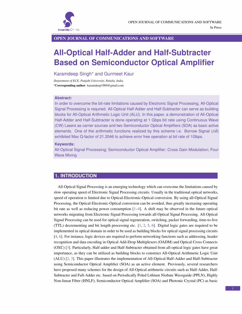
Four Wave Mixing (FWM) is used to generate AND function. Two input signals, A and B centered atdifferent center wavelengths (λ A& λ B) are coupled and fed into Semiconductor Optical Amplifier (SOA)as shown in Figure 1 .
In FWM a new signal λ FWM (λ FWM = 2 λ A - λ B) is generated which occurs due to coexistence oftwo input data signals λ A& λ B. The FWM product λ FWMis extracted with the help of a bandpass filter
2
All-Optical Half-Adder and Half-Subtracter Based on Semiconductor Optical Amplifier
Figure 1. Operation Principle of FWM and XGM [2].
centered at λ FWMwhich serves as the AND function (AB) [2, 12].
2.2 Cross Gain Modulation (XGM)
Cross Gain Modulation (XGM) is a nonlinear effect which occurs, when a high power signal (PumpSignal) and a low power signal (Probe Signal) are fed into a Semiconductor Optical Amplifier (SOA) asshown in Figure 1 . When the data bits of both pump and probe signal are ‘1’, the SOA gets saturated byhigh intensity pump signal B, due to carrier depletion. All input signals are affected by carrier densitychanges in active region of SOA. Thus, signals centered at one wavelength can affect the signal centeredat some other wavelength. This process is known as Cross Gain Modulation (XGM). As shown in Figure1 , when pump signal B is high, the SOA is saturated and the probe signal A is suppressed. Whereas,when the pump signal B is low, the probe signal appears across the output. Thus, by using XGM, functionABcan be implemented in optical domain. Similarly, ABcan be realized by simply switching roles ofpump and probe signals. As discussed earlier, XOR function can be generated by ORing AB and ABfunctions. This can be achieved by simply power coupling the outputs of AB function and AB function[2, 3, 12].
3. EXPERIMENTAL SETUP
In this section, the experimental setup used for the demonstration of All-Optical Half-Adder andHalf-Subtracter is presented. The experimental setup discussed in this section has evolved from theapproach discussed by Dai et al. [2]. The experimental setup comprises of three sub-blocks: SignalGeneration Section, Signal Processing Section and Signal Detection Section. Each Sub-block has welldefined function as given as under:
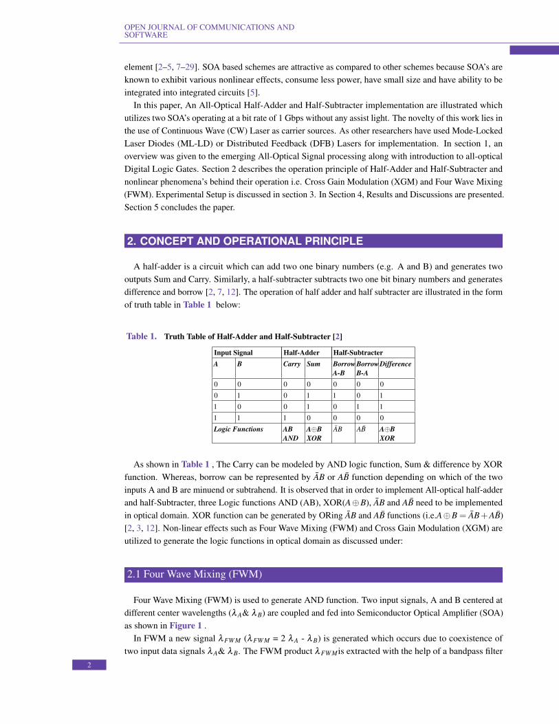
3.1 Signal Generation Section
Two Continuous Wave (CW) lasers are used to generate 0.45 ns optical pulse trains at 1550 nm (SignalA) and 1553 nm (Signal B) as shown in Figure 2 :
The signals generated by CW lasers serve as carrier signals. Two Mach-Zehnder Modulators are usedto modulate carrier signals with 1Gbps Pseudo Random Binary Sequence (PRBS) data having sequence
3
OPEN JOURNAL OF COMMUNICATIONS ANDSOFTWARE
Figure 2. Signal Generation Section [2].
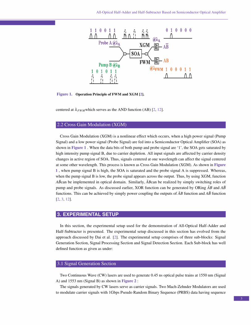
Figure 3. Signal Processing Section [2]
length 217-1. Before modulation, carrier signals are attenuated by Variable Optical Attenuator (VOA) fornormalization and aligned to single polarization by passing through Polarization Controller (PC). The useof PC is necessary, as SOA are sensitive to signal polarization orientation. After modulating the signal,the signal modulated by PRBS data B (i.e. signal B) is fed to a 20 km Single Mode Fiber (SMF), in orderto mismatch the data patterns between two branches. The two modulated pulse trains are coupled by a3dB coupler and then amplified by an Erabium Doped Fiber Amplifier (EDFA) having gain 20 dB. Thecomposite signal is then fed to Signal Processing Section.
3.2 Signal Processing Section
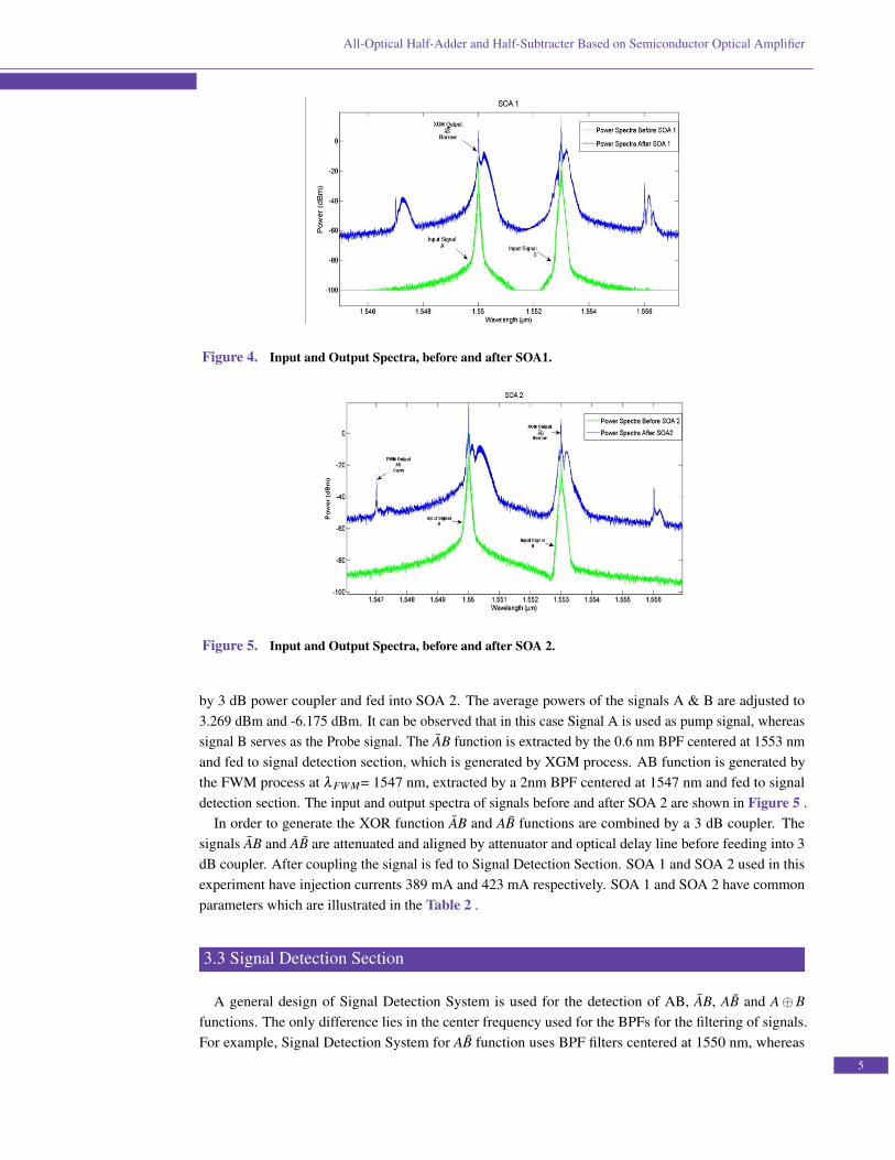
A 6 dB 1×4 splitter is used to split the signal into four branches. In each branch a 0.2 nm Band PassFilters (BPF) are used to extract the Signals A and B centered at 1550 nm and 1553 nm. To align thesignal differences and to control power, delay lines and attenuators are used. Polarization Controllers(PC) are used to align the signal to single polarization state. The optimized and controlled signals fromfirst two branches having signal A and B are fed to SOA 1. The signal A & B are attenuated to -8.271dBm and 1.128 dBm respectively. ABSignal is produced by the XGM process, which is extracted by 0.6nm BPF centered at 1550 nm and fed to signal detection section. The input and output spectra of signalsbefore and after SOA 1 are shown in Figure 4 :
In the lower portion of the signal processing section, signals form two branches A & B are coupled
4
All-Optical Half-Adder and Half-Subtracter Based on Semiconductor Optical Amplifier
Figure 4. Input and Output Spectra, before and after SOA1.
Figure 5. Input and Output Spectra, before and after SOA 2.
by 3 dB power coupler and fed into SOA 2. The average powers of the signals A & B are adjusted to3.269 dBm and -6.175 dBm. It can be observed that in this case Signal A is used as pump signal, whereassignal B serves as the Probe signal. The AB function is extracted by the 0.6 nm BPF centered at 1553 nmand fed to signal detection section, which is generated by XGM process. AB function is generated bythe FWM process at λ FWM= 1547 nm, extracted by a 2nm BPF centered at 1547 nm and fed to signaldetection section. The input and output spectra of signals before and after SOA 2 are shown in Figure 5 .
In order to generate the XOR function AB and AB functions are combined by a 3 dB coupler. Thesignals AB and AB are attenuated and aligned by attenuator and optical delay line before feeding into 3dB coupler. After coupling the signal is fed to Signal Detection Section. SOA 1 and SOA 2 used in thisexperiment have injection currents 389 mA and 423 mA respectively. SOA 1 and SOA 2 have commonparameters which are illustrated in the Table 2 .
3.3 Signal Detection Section
A general design of Signal Detection System is used for the detection of AB, AB, AB and A⊕Bfunctions. The only difference lies in the center frequency used for the BPFs for the filtering of signals.For example, Signal Detection System for AB function uses BPF filters centered at 1550 nm, whereas
5
OPEN JOURNAL OF COMMUNICATIONS ANDSOFTWARE
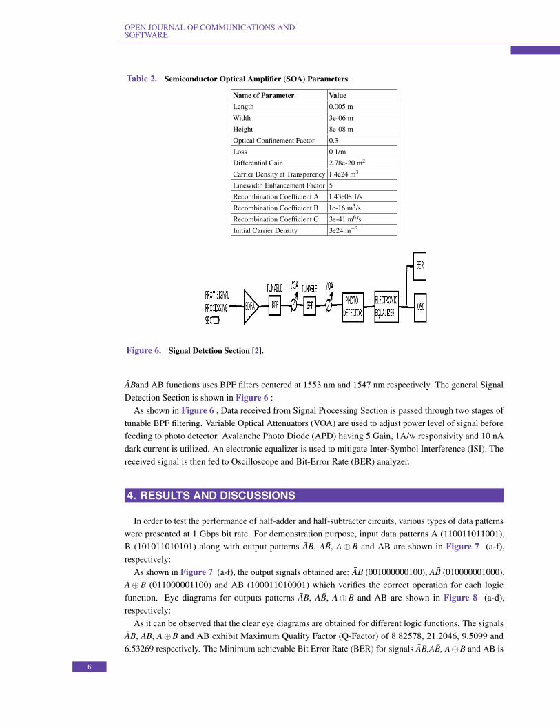
Table 2. Semiconductor Optical Amplifier (SOA) Parameters
Name of Parameter ValueLength 0.005 m
Width 3e-06 m
Height 8e-08 m
Optical Confinement Factor 0.3
Loss 0 1/m
Differential Gain 2.78e-20 m2
Carrier Density at Transparency 1.4e24 m3
Linewidth Enhancement Factor 5
Recombination Coefficient A 1.43e08 1/s
Recombination Coefficient B 1e-16 m3/s
Recombination Coefficient C 3e-41 m6/s
Initial Carrier Density 3e24 m−3
Figure 6. Signal Detction Section [2].
ABand AB functions uses BPF filters centered at 1553 nm and 1547 nm respectively. The general SignalDetection Section is shown in Figure 6 :
As shown in Figure 6 , Data received from Signal Processing Section is passed through two stages oftunable BPF filtering. Variable Optical Attenuators (VOA) are used to adjust power level of signal beforefeeding to photo detector. Avalanche Photo Diode (APD) having 5 Gain, 1A/w responsivity and 10 nAdark current is utilized. An electronic equalizer is used to mitigate Inter-Symbol Interference (ISI). Thereceived signal is then fed to Oscilloscope and Bit-Error Rate (BER) analyzer.
4. RESULTS AND DISCUSSIONS
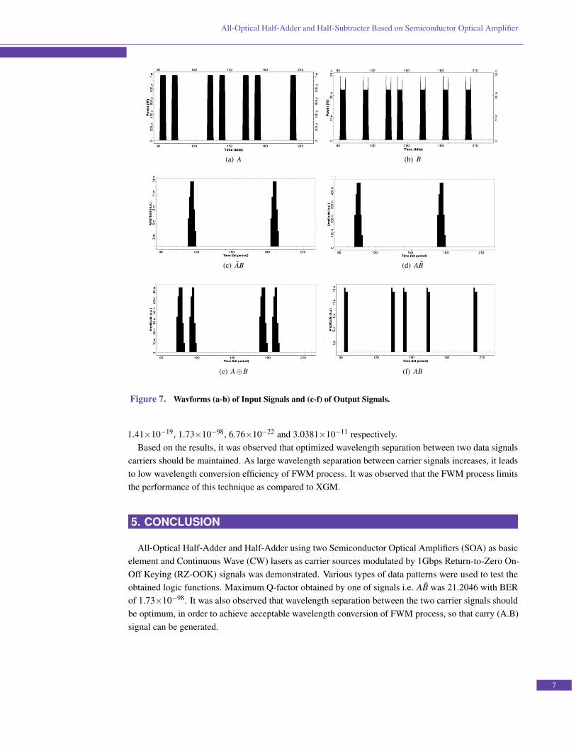
In order to test the performance of half-adder and half-subtracter circuits, various types of data patternswere presented at 1 Gbps bit rate. For demonstration purpose, input data patterns A (110011011001),B (101011010101) along with output patterns AB, AB, A⊕B and AB are shown in Figure 7 (a-f),respectively:
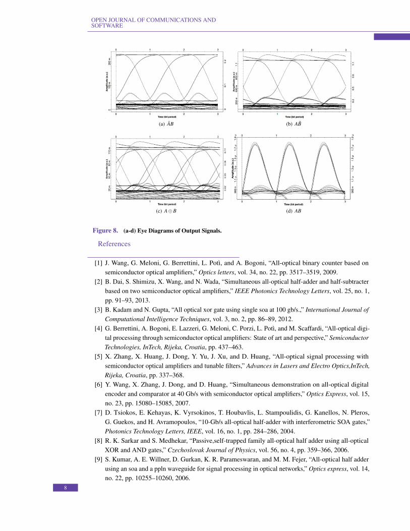
As shown in Figure 7 (a-f), the output signals obtained are: AB (001000000100), AB (010000001000),A⊕B (011000001100) and AB (100011010001) which verifies the correct operation for each logicfunction. Eye diagrams for outputs patterns AB, AB, A⊕ B and AB are shown in Figure 8 (a-d),respectively:
As it can be observed that the clear eye diagrams are obtained for different logic functions. The signalsAB, AB, A⊕B and AB exhibit Maximum Quality Factor (Q-Factor) of 8.82578, 21.2046, 9.5099 and6.53269 respectively. The Minimum achievable Bit Error Rate (BER) for signals AB,AB, A⊕B and AB is
6
All-Optical Half-Adder and Half-Subtracter Based on Semiconductor Optical Amplifier
(a) A (b) B
(c) AB (d) AB
(e) A⊕B (f) AB
Figure 7. Wavforms (a-b) of Input Signals and (c-f) of Output Signals.
1.41×10⁻¹⁹, 1.73×10−98, 6.76×10⁻²² and 3.0381×10⁻¹¹ respectively.Based on the results, it was observed that optimized wavelength separation between two data signals
carriers should be maintained. As large wavelength separation between carrier signals increases, it leadsto low wavelength conversion efficiency of FWM process. It was observed that the FWM process limitsthe performance of this technique as compared to XGM.
5. CONCLUSION
All-Optical Half-Adder and Half-Adder using two Semiconductor Optical Amplifiers (SOA) as basicelement and Continuous Wave (CW) lasers as carrier sources modulated by 1Gbps Return-to-Zero On-Off Keying (RZ-OOK) signals was demonstrated. Various types of data patterns were used to test theobtained logic functions. Maximum Q-factor obtained by one of signals i.e. AB was 21.2046 with BERof 1.73×10−98. It was also observed that wavelength separation between the two carrier signals shouldbe optimum, in order to achieve acceptable wavelength conversion of FWM process, so that carry (A.B)signal can be generated.
7
OPEN JOURNAL OF COMMUNICATIONS ANDSOFTWARE
(a) AB (b) AB
(c) A⊕B (d) AB
Figure 8. (a-d) Eye Diagrams of Output Signals.
References
[1] J. Wang, G. Meloni, G. Berrettini, L. Potı, and A. Bogoni, “All-optical binary counter based onsemiconductor optical amplifiers,” Optics letters, vol. 34, no. 22, pp. 3517–3519, 2009.
[2] B. Dai, S. Shimizu, X. Wang, and N. Wada, “Simultaneous all-optical half-adder and half-subtracterbased on two semiconductor optical amplifiers,” IEEE Photonics Technology Letters, vol. 25, no. 1,pp. 91–93, 2013.
[3] B. Kadam and N. Gupta, “All optical xor gate using single soa at 100 gb/s.,” International Journal ofComputational Intelligence Techniques, vol. 3, no. 2, pp. 86–89, 2012.
[4] G. Berrettini, A. Bogoni, E. Lazzeri, G. Meloni, C. Porzi, L. Potı, and M. Scaffardi, “All-optical digi-tal processing through semiconductor optical amplifiers: State of art and perspective,” SemiconductorTechnologies, InTech, Rijeka, Croatia, pp. 437–463.
[5] X. Zhang, X. Huang, J. Dong, Y. Yu, J. Xu, and D. Huang, “All-optical signal processing withsemiconductor optical amplifiers and tunable filters,” Advances in Lasers and Electro Optics,InTech,Rijeka, Croatia, pp. 337–368.
[6] Y. Wang, X. Zhang, J. Dong, and D. Huang, “Simultaneous demonstration on all-optical digitalencoder and comparator at 40 Gb/s with semiconductor optical amplifiers,” Optics Express, vol. 15,no. 23, pp. 15080–15085, 2007.
[7] D. Tsiokos, E. Kehayas, K. Vyrsokinos, T. Houbavlis, L. Stampoulidis, G. Kanellos, N. Pleros,G. Guekos, and H. Avramopoulos, “10-Gb/s all-optical half-adder with interferometric SOA gates,”Photonics Technology Letters, IEEE, vol. 16, no. 1, pp. 284–286, 2004.
[8] R. K. Sarkar and S. Medhekar, “Passive,self-trapped family all-optical half adder using all-opticalXOR and AND gates,” Czechoslovak Journal of Physics, vol. 56, no. 4, pp. 359–366, 2006.
[9] S. Kumar, A. E. Willner, D. Gurkan, K. R. Parameswaran, and M. M. Fejer, “All-optical half adderusing an soa and a ppln waveguide for signal processing in optical networks,” Optics express, vol. 14,no. 22, pp. 10255–10260, 2006.
8
All-Optical Half-Adder and Half-Subtracter Based on Semiconductor Optical Amplifier
[10] S. H. Kim, J. H. Kim, J. W. Choi, C. W. Son, Y. T. Byun, Y. M. Jhon, S. Lee, D. H. Woo, and S. H.Kim, “All-optical half adder using an soa and a ppln waveguide for signal processing in opticalnetworks,” Optics express, vol. 14, no. 22, pp. 10693–10698, 2006.
[11] P.-l. Li, D.-x. Huang, X.-l. Zhang, and G.-x. Zhu, “Ultrahigh-speed all-optical half adder based onfour-wave mixing in semiconductor optical amplifier,” Optics Express, vol. 14, no. 24, pp. 11839–11847, 2006.
[12] J. Wang, J. Sun, and Q. Sun, “Single ppln based simultaneous half-adder, half subtractor, and orlogic gate: Proposal and simulation,” Optics Express, vol. 15, no. 4, pp. 1690–1699, 2007.
[13] J. E. McGeehan, S. Kumar, and A. E. Willner, “Simultaneous optical digital half-subtraction and-addition using soas and a ppln waveguide,” Optics express, vol. 15, no. 9, pp. 5543–5549, 2007.
[14] Q. Liu, Z. Ouyang, C. J. Wu, C. P. Liu, and J. C. Wang, “All-optical half adder based on crossstructures in two-dimensional photonic crystals,” Optics express, vol. 16, no. 23, pp. 18992–19000,2008.
[15] J. N. Roy, “Mach–zehnder interferometer-based tree architecture for all-optical logic and arithmeticoperations,” Optik-International Journal for Light and Electron Optics, vol. 120, no. 7, pp. 318–324,2009.
[16] T. Chattopadhyay and J. N. Roy, “Design of soa-mzi based all-optical programmable logic device(pld),” Optics Communications, vol. 283, no. 12, pp. 2506–2517, 2010.
[17] D. Kumar Gayen, J. Nath Roy, R. Kumar Pal, and S. Prasad Ghosh, “All-optical incre-menter/decrementer with the help of semiconductor optical amplifier-assisted sagnac switch,” Inter-national Journal of Optomechatronics, vol. 4, no. 2, pp. 177–194, 2010.
[18] J. Menezes, W. Fraga, A. Ferreira, G. Guimaraes, A. Filho, C. Sobrinho, and A. Sombra, “All-opticalhalf-adder using all-optical xor and and gates for optical generation of sum and carry,” Fiber andIntegrated Optics, vol. 29, no. 4, pp. 254–271, 2010.
[19] J. Qiu, K. Sun, M. Rochette, and L. R. Chen, “Reconfigurable all-optical multilogic gate (xor, and,and or) based on cross-phase modulation in a highly nonlinear fiber,” Photonics Technology Letters,IEEE, vol. 22, no. 16, pp. 1199–1201, 2010.
[20] S. K. Garai and S. Mukhopadhyay, “Method of all-optical frequency-encoded binary adder systemusing nonlinear waveguide and reflecting semiconductor optical amplifiers,” Optik-InternationalJournal for Light and Electron Optics, vol. 121, no. 20, pp. 1859–1862, 2010.
[21] B. Chakraborty and S. Mukhopadhyay, “A method of implementing phase encoded optical half adderand full adder system,” Optics and Photonics Letters, vol. 3, no. 01, pp. 43–50, 2010.
[22] K. Mukherjee, “Method of implementation of frequency encoded all optical half adder, half sub-tractor and full adder based on semiconductor optical amplifiers and add drop multiplexers,” Optik-International Journal for Light and Electron Optics, vol. 122, no. 13, pp. 1188–1194, 2011.
[23] J. Shen, S. Yu, P. Liao, Z. Chen, W. Gu, and H. Guo, “All-optical full-adder based on cascaded pplnwaveguides,” Quantum Electronics, IEEE Journal of, vol. 47, no. 9, pp. 1195–1200, 2011.
[24] P. Ghosh, D. Kumbhakar, A. K. Mukherjee, and K. Mukherjee, “An all optical method of implement-ing a wavelength encoded simultaneous binary full adder–full subtractor unit exploiting nonlinearpolarization rotation in semiconductor optical amplifier,” Optik-International Journal for Light andElectron Optics, vol. 122, no. 19, pp. 1757–1763, 2011.
[25] B. Ghosh, R. R. Pal, and S. Mukhopadhyay, “A new approach to all-optical half-adder by utilizingsemiconductor optical amplifier based mzi wavelength converter,” Optik-International Journal forLight and Electron Optics, vol. 122, no. 20, pp. 1804–1807, 2011.
[26] S. K. Garai, “A novel all-optical frequency-encoded method to develop arithmetic and logic unit(alu) using semiconductor optical amplifiers,” Lightwave Technology, Journal of, vol. 29, no. 23,pp. 3506–3514, 2011.
9

OPEN JOURNAL OF COMMUNICATIONS ANDSOFTWARE
[27] L. Lei, J. Dong, Y. Zhang, H. He, Y. Yu, and X. Zhang, “Reconfigurable photonic full-adder andfull-subtractor based on three-input xor gate and logic minterms,” Electronics letters, vol. 48, no. 7,pp. 399–400, 2012.
[28] D. K. Gayen, A. Bhattachryya, T. Chattopadhyay, and J. N. Roy, “Ultrafast all-optical half adderusing quantum-dot semiconductor optical amplifier-based mach-zehnder interferometer,” LightwaveTechnology, Journal of, vol. 30, no. 21, pp. 3387–3393, 2012.
[29] M. Ghadrdan and M. A. Mansouri-Birjandi, “Concurrent implementation of all-optical half-adderand and & xor logic gates based on nonlinear photonic crystal,” Optical and Quantum Electronics,vol. 45, no. 10, pp. 1027–1036, 2013.
10


