Embed Size (px)
Citation preview
Sensors 2010, 10, 1-15; doi: 10.3390/s100100001
sensors ISSN 1424-8220
www.mdpi.com/journal/sensors
Article
An Efficient Pipeline Wavefront Phase Recovery for the
CAFADIS Camera for Extremely Large Telescopes
Eduardo Magdaleno *, Manuel Rodríguez and José Manuel Rodríguez-Ramos
Departmento de Física Fundamental y Experimental, Electrónica y Sistemas, University of La Laguna,
Avd. Francisco Sanchez s/n, 38203 La Laguna, Spain; E-Mails: [email protected] (M.R.);
[email protected] (J.M.R.-R.)
* Author to whom correspondence should be addressed; E-Mail: [email protected]; Tel.: +34-922-845-
035; Fax: +34-922-318-228.
Received: 30 November 2009; in revised form: 22 December 2009 / Accepted: 23 December 2009 /
Published: 24 December 2009
Abstract: In this paper we show a fast, specialized hardware implementation of the
wavefront phase recovery algorithm using the CAFADIS camera. The CAFADIS camera is
a new plenoptic sensor patented by the Universidad de La Laguna (Canary Islands, Spain):
international patent PCT/ES2007/000046 (WIPO publication number WO/2007/082975). It
can simultaneously measure the wavefront phase and the distance to the light source in a
real-time process. The pipeline algorithm is implemented using Field Programmable Gate
Arrays (FPGA). These devices present architecture capable of handling the sensor output
stream using a massively parallel approach and they are efficient enough to resolve several
Adaptive Optics (AO) problems in Extremely Large Telescopes (ELTs) in terms of
processing time requirements. The FPGA implementation of the wavefront phase recovery
algorithm using the CAFADIS camera is based on the very fast computation of two
dimensional fast Fourier Transforms (FFTs). Thus we have carried out a comparison
between our very novel FPGA 2D-FFTa and other implementations.
Keywords: plenoptic sensors; wavefront sensors; adaptive optics; real-time processing;
FPGA
OPEN ACCESS
Sensors 2010, 10
2
1. Introduction
The resolution of ground-based astronomical observations is strongly affected by atmospheric
turbulence above the observation site. In order to achieve resolution close to the diffraction limit of the
telescopes, AO techniques have been developed to offset wavefront distortion as it passes through
turbulent layers in the atmosphere.
AO includes several steps: detection of the phase gradients, wavefront phase recovery, information
transmission to the actuators and their mechanical movement. The next generation of extremely large
telescopes (from 50 to 100 meter diameters) will demand significant technological advances to
maintain the segments of the telescopes aligned (phasing of segmented mirrors) and also to offset
atmospheric aberrations. For this reason, faster wavefront phase reconstruction seems to be of utmost
importance, and new wavefront sensor designs and technologies must be explored. The CAFADIS
camera presents a robust optical design that can meet AO objectives even when the references are
extensive objects (elongated LGS and solar observations). The CAFADIS camera is an intermediate
sensor between the Shack-Hartmann and the pyramid sensor. It samples an image plane using a
microlens array. The pupil phase gradients can be obtained from there, and after that, the phase
recovery problem is the same as in the Shack-Hartman.
In this work, our main objective is to select a good and fast enough wavefront phase reconstruction
algorithm, and then to implement it over the FPGA platform, paving the way for accomplishing the
computational requirements of the ELT's number of actuators within a 6 ms limit, which is
atmospheric response time.
The modal estimation of the wavefront consists in using the slope measurements to fit the
coefficients of an aperture function in a phase expansion of orthogonal functions. These functions are
usually Zernike polynomials or complex exponentials, but there are other possibilities, depending on
the pupil mask. Very fast algorithms can be implemented when using complex exponential
polynomials because the FFT kernel is the same [1,2]. Zonal reconstruction consists in estimating a
phase value directly instead of the coefficients of an expansion, and they require an iterative process.
The modal algorithms produce more precise results than the zonal solution and –this is crucial- are
suited to parallelization. Consequently, this is the preferred estimation to accomplish the phase
reconstruction on technologically advanced platforms such as FPGAs or graphical processing units
(GPUs) [3]. Once the algorithm based on the expansion over complex exponential polynomials has
been selected, an efficient FFT implementation in FPGA is the core of an optimal phase reconstruction.
We will start by describing the modal Fourier wavefront phase reconstruction algorithm, and how
the Fast Fourier Transform tallies with the FPGA architecture, analyzing the obtained efficiency and
comparing it to implementations in other technologies and platforms. We design an initial 64 × 64 full
pipeline phase recovery prototype using the synthesized 2D-FFT module. The system was satisfactorily
circuit-tested using simulation data as phase gradients. Finally, we analyze the obtained efficiency and
compare it to the modal wavefront using high-end CPU.
Sensors 2010, 10
3
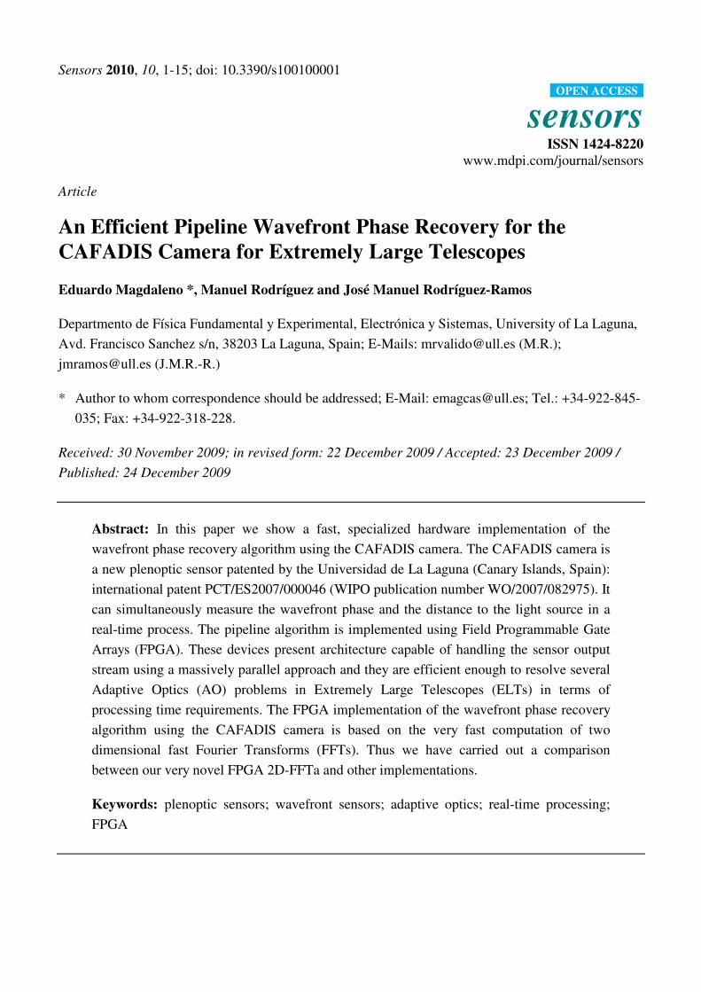
2. Background
The CAFADIS plenoptic sensor samples the signal Ψtelescope(u,v)
(complex amplitude of the
electromagnetic field) to obtain the wavefront phase map ),( vuφ . A microlens array is placed at the
focal point of the telescope (as in a pyramid sensor), sampling the image plane instead of the pupil
plane (as in a Shack-Hartmann sensor). If the f-numbers of both telescope and microlens are the same,
the detector will be filled up with images of the pupil of maximum size without overlapping.
Wavefront phase gradients at telescope pupil plane are extracted from the plenoptic frame taken by the
CAFADIS, and wavefront maps from different viewpoints are obtained. Hence, tomographic wavefront
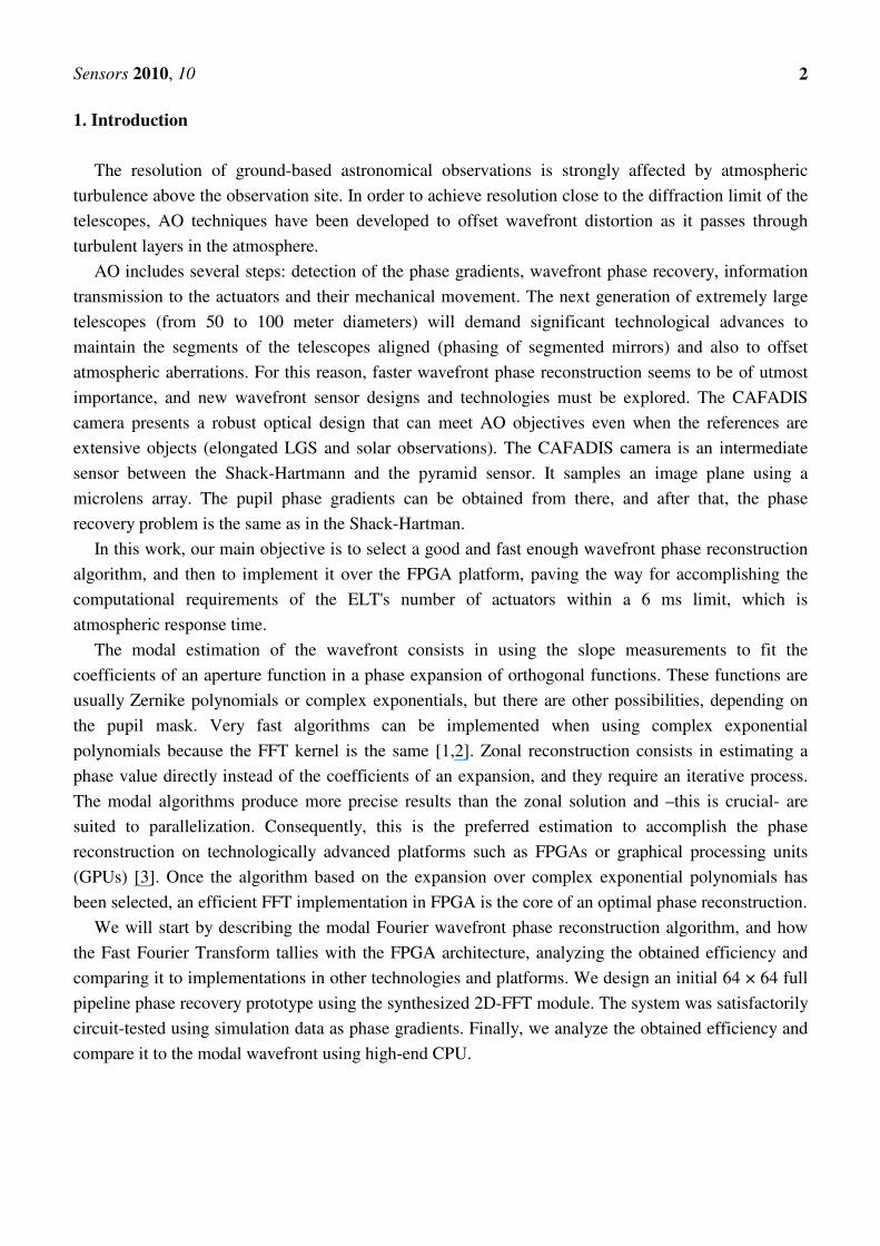
reconstruction could be accomplished from only one plenoptic frame (Figure 1) [4]. For example,
Figure 2 shows a section of the plenoptic frame obtained for CAFADIS, containing data from five
artificial laser guide stars (data simulation assuming a 10 m diameter telescope, and every subpupil
sampled by 32 × 32 pixels [4]). With this information, the CAFADIS camera has the capability of
refocusing at several distances and selecting the best focus as object distance.
Figure 1. Outline of the Plenoptic camera used as wavefront sensor.
The final phase resolution depends on the number of pixels sampling each microlens, but depth
resolution also depends on the same quantity. This implies that, increasing the phase resolution, higher
height resolution is obtained at the same time. In the extreme case, when using a pyramid sensor
(2 × 2 microlens), the phase and height resolution are maximized. At the other extreme, when using a
Shack-Hartmann wavefront sensor, the phase resolution depends on the number of subpupils, and
height resolution is minimized (and even lost).
A compromise solution might be taken: a unique plenoptic sensor, comprised by 6 × 6 subpupils
sampled by 84 × 84 pixels would be enough to get phases with 84 × 84 pixel resolution using only
one 504 × 504 pixels detector. Or even, in order to avoid detector contamination due to the neighboring
LGS images, the plenoptic image could be sampled by 12 × 12 subpupils. In this case, a 1,008 × 1,008
detector is needed [4].
Sensors 2010, 10
4
Figure 2. Section of the plenoptic frame showing the LGS on axis. The remaining, off-axis
LGS present a similar aspect.
The phase gradients at pupil plane are calculated from this plenoptic frame using the partial
derivates of the wavefront aberration estimated in [5] and implemented in FPGA in [6]. From these
gradient estimation, the wavefront phase ),( vuφ can be recovered using an expansion over complex
exponential polynomials, allowing application of 2D-FFT:
)(1
),(),(1
0,
1
0,
)(2
pq
N
qp
N
qp
qvpuN
i
pqpqpq aIFFTeN
avuZavu ∑ ∑−
=
−
=
+
===π
φ
(1)
The gradient is then written:
pq
qp
pq Zajv
iu
vuvuS ∑ ∇=∂
∂+
∂
∂=∇=
,
),(),(rrrrr φφ
φ
(2)
Making a least squares adjustment over the F function:
2
,1,)](),([ jiavuSF
v
Z
qp u
Z
pq
N
vu
pqpqrrr
∂
∂
∂
∂
= ∑∑ +−=
(3)
where Sr
are experimental data, the coefficients apq of the complex exponential expansion in a modal
Fourier wavefront phase reconstructor (spatial filter) can be written as:
{ } { }22
),(),(
qp
vuSiqFFTvuSipFFTa
yx
pq+
+=
(4)
The phase can then be recovered from the gradient data by reverse transformation of the
coefficients:
][),(1
pqaFFTvu−=φ
(5)
A filter composed of three two-dimensional Fourier transforms therefore must be calculated to
recover the phase. In order to accelerate the process, an exhaustive study of the crucial FFT algorithm
was carried out which allowed the FFT to be specifically adapted to the modal wavefront recovery
pipeline and the FPGA architecture.
Sensors 2010, 10
5
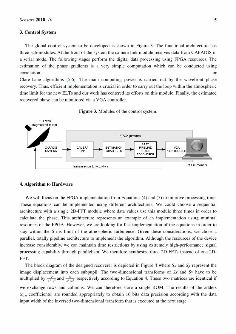
3. Control System
The global control system to be developed is shown in Figure 3. The functional architecture has
three sub-modules. At the front of the system the camera link module receives data from CAFADIS in
a serial mode. The following stages perform the digital data processing using FPGA resources. The
estimation of the phase gradients is a very simple computation which can be conducted using
correlation or
Clare-Lane algorithms [5,6]. The main computing power is carried out by the wavefront phase
recovery. Thus, efficient implementation is crucial in order to carry out the loop within the atmospheric
time limit for the new ELTs and our work has centered its efforts on this module. Finally, the estimated
recovered phase can be monitored via a VGA controller.
Figure 3. Modules of the control system.
4. Algorithm to Hardware
We will focus on the FPGA implementation from Equations (4) and (5) to improve processing time.
These equations can be implemented using different architectures. We could choose a sequential
architecture with a single 2D-FFT module where data values use this module three times in order to
calculate the phase. This architecture represents an example of an implementation using minimal
resources of the FPGA. However, we are looking for fast implementation of the equations in order to
stay within the 6 ms limit of the atmospheric turbulence. Given these considerations, we chose a
parallel, totally pipeline architecture to implement the algorithm. Although the resources of the device
increase considerably, we can maintain time restrictions by using extremely high-performance signal
processing capability through parallelism. We therefore synthesize three 2D-FFTs instead of one 2D-
FFT.
The block diagram of the designed recoverer is depicted in Figure 4 where Sx and Sy represent the
image displacement into each subpupil. The two-dimensional transforms of Sx and Sy have to be
multiplied by 22qp
ip
+and 22
qp
iq
+ respectively according to Equation 4. These two matrices are identical if
we exchange rows and columns. We can therefore store a single ROM. The results of the adders
(apq coefficients) are rounded appropriately to obtain 16 bits data precision according with the data
input width of the inversed two-dimensional transform that is executed at the next stage.
Sensors 2010, 10
6
Figure 4. Architecture of the synthesized phase recoverer.
An analysis of the equations and a parallel architecture of its implementation are taken into account.
We then break down the design into the following steps or stages:
1. Compute two real forward 2D FFT that compute FFT (Sx) and FFT (Sy)
2. Compute the complex coefficients
3. Carry out a complex inverse 2D FFT on apq
4. Flip data results
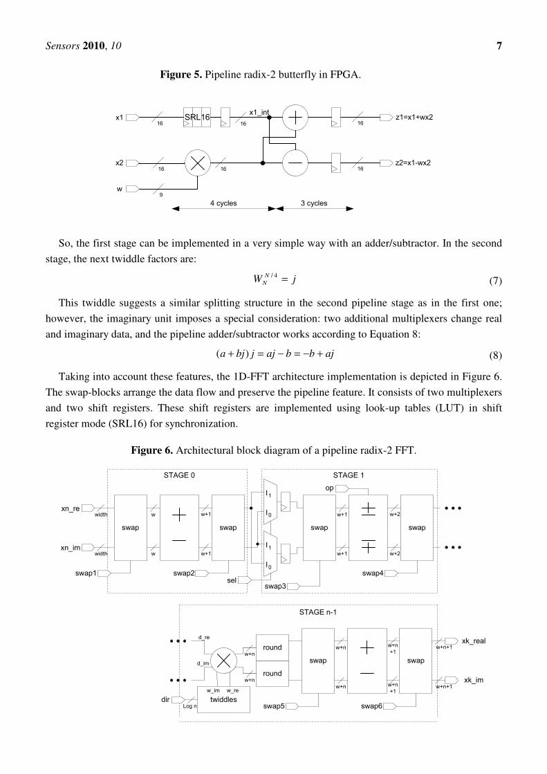
4.1. Architecture of FFT Module
Generally, each butterfly implies one complex multiplier and two complex adders. In particular,
multipliers consume much silicon area of FPGA because they are implemented with adder trees.
Various implementation proposals have been made to save area by removing these multipliers [7-10].
However, in order to implement an efficient multiplier, the last Virtex-4 FPGA devices incorporate
specific arithmetic modules, called DSP48. Each DSP48 slice has a two-input multiplier followed by
multiplexers and a three-input adder/subtractor. With these circuits, the FPGA only needs four clock
cycles to calculate the complex multiplication with up to 550 MHz in XC4VSX35 Virtex-4 [11,12].
The complete pipeline radix-2 butterfly can be implemented with this specialized multiplier. It is
necessary to use a FPGA Look-Up Table (LUT) (configured as SRL16 shift register) to preserve the
synchronism. The butterfly implemented is depicted in Figure 5 and it needs only seven clock cycles to
carry out the computation.
A pipeline radix-2 FFT can be implemented using one butterfly at each stage. The twiddle
coefficients used in each stage are stored in twiddle LUT ROMs in the FPGA. The logic resources and
the clock cycles of the FFT module is reduced in our implementation using specific butterfly modules
at the first and second stages. The first stage utilizes the feature of the twiddle factors related to the first
stages of the pipeline:
12/ =N
NW (6)
Sensors 2010, 10
7
Figure 5. Pipeline radix-2 butterfly in FPGA.
SRL1616
z1=x1+wx2
16z2=x1-wx2
16
16
9w
x1
x2
16
16
x1_int
4 cycles 3 cycles
So, the first stage can be implemented in a very simple way with an adder/subtractor. In the second
stage, the next twiddle factors are:
jWN
N =4/ (7)
This twiddle suggests a similar splitting structure in the second pipeline stage as in the first one;
however, the imaginary unit imposes a special consideration: two additional multiplexers change real
and imaginary data, and the pipeline adder/subtractor works according to Equation 8:
ajbbajjbja +−=−=+ )( (8)
Taking into account these features, the 1D-FFT architecture implementation is depicted in Figure 6.
The swap-blocks arrange the data flow and preserve the pipeline feature. It consists of two multiplexers
and two shift registers. These shift registers are implemented using look-up tables (LUT) in shift
register mode (SRL16) for synchronization.
Figure 6. Architectural block diagram of a pipeline radix-2 FFT.
swap
widthxn_re
widthxn_im
swap
w
w
w+1
w+1
0I
1I
0I
1I
swap swap
w+1
w+1
w+2
w+2
twiddles
round
round
swap swap
w+n
w+n
w+n
+1
w+n
+1
xk_im
w+n+1
w+n+1
xk_real
w+n
w+n
swap1 swap2sel
swap3
swap4
swap5 swap6
op
d_re
d_im
w_im w_re
dirLog n
STAGE 0 STAGE 1
STAGE n-1
Sensors 2010, 10
8
The system performs the calculation of the FFT with no scaling. The unscaled full-precision method
was used to avoid error propagations. This option avoids overflow situations because output data have
more bits than input data. Data precision at the output is:
1log2 ++= pointswidthinputwidthoutput (9)
The number of bits on the output of the multipliers is much larger than the input and must be
reduced to a manageable width with the use of one-cycle symmetric rounding stages (Figure 6). The
periodic signals of the swap units, op signal, and the address generation for the twiddle memories are
obtained through a counter module that acts as control unit.
4.2. Temporal Analysis for the Radix-2 FFT Module and Superior Radix
Taking into account the clock cycles of each block in Figure 6, the latency of the FFT module can
be written as:
( )
∑−
=+
+++++
++++
+=
1log
21
2
12
27214
21212
2N
nn
NNNlatency L (10)
where the first two stages are considered separately, and N and n are the number of points of the
transform and the number of stages of the module respectively. Adding the geometrical series and
grouping, finally:
K,32,16,8,11log92 2 =−+= NNNlatency (11)
When the number of points of the FFT is a power of 4, it is computationally more efficient to use a
radix 4 algorithm instead of radix 2. The reasoning is the same as in radix 2 but subdividing iteratively
a sequence of N data into four subsequences, and so on. The radix-4 FFT algorithm consists of log4N
stages, each one containing N/4 butterflies. As the first weight is 10 =NW , each butterfly involves three
complex multiplications and 12 complex sums. Performing the sum in two steps, according to [13], it
is possible to reduce the number of sums (12 to 8). Therefore, the number of complex sums to be
performed is the same (Nlog2N) as the algorithm in base 2, but the multipliers are reduced by 25%
(of (N/2) log2N to (3N/8) log2N). Consequently, the number of circuits for DSP48 use is
reduced proportionally.
When the number of points is a power of 4, the pipeline radix-4 FFT module has half the arithmetic
stages, but the swap modules need twice the amount of clock cycles to arrange the data. Then, the
latency is expressed as:
K,1024,256,64,16,13log92)4( 4 =−+= NNNradixlatency (12)
This time estimation has been conducted for other radix, as shown in the following equations:
( )
( ) K
K
,2,2,37log9216
,512,64,21log928
128
16
8
=−+=
=−+=
NNNradixlatency
NNNradixlatency (13)
Generalizing:
( )K
K
,16,8,4
,3,2,1,,25log92
1
=
==−−+=
+
i
niNiNNiradixlatency
n
i (14)
Sensors 2010, 10
9
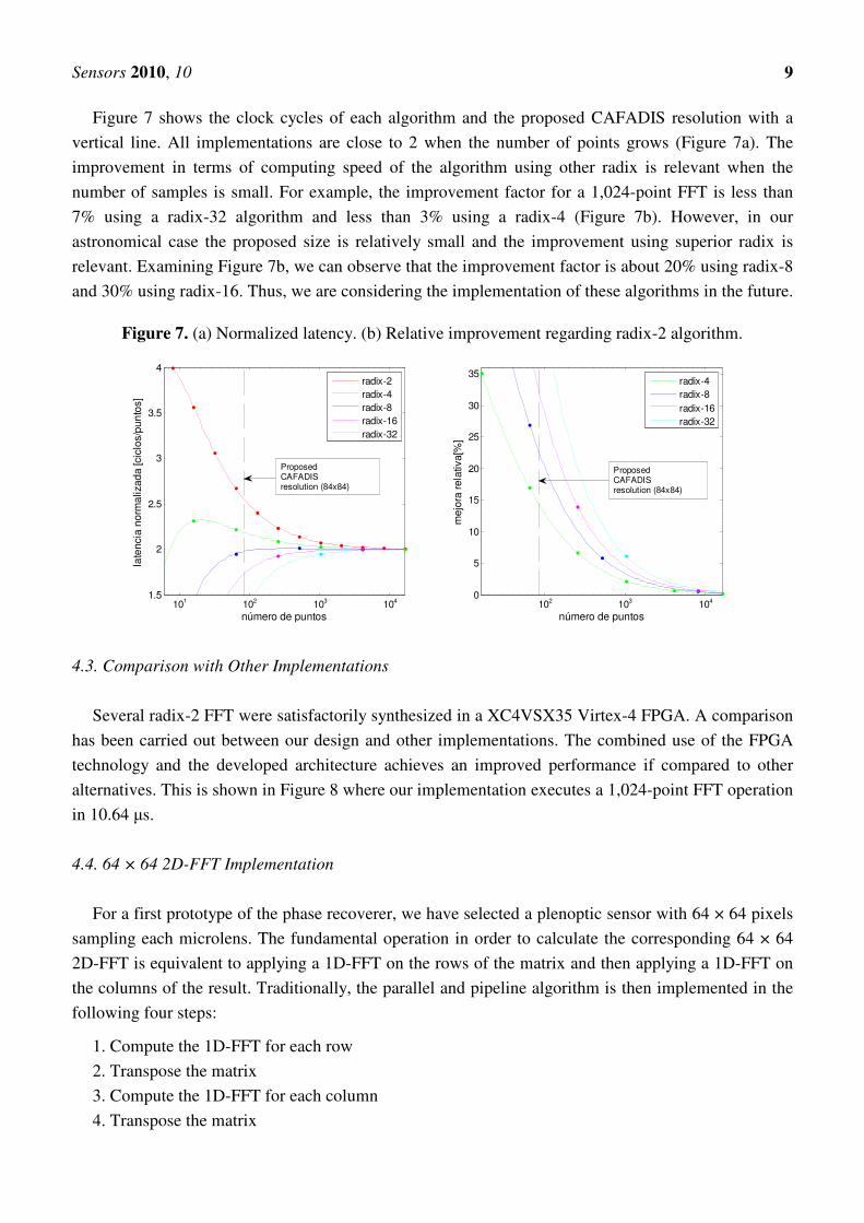
Figure 7 shows the clock cycles of each algorithm and the proposed CAFADIS resolution with a
vertical line. All implementations are close to 2 when the number of points grows (Figure 7a). The
improvement in terms of computing speed of the algorithm using other radix is relevant when the
number of samples is small. For example, the improvement factor for a 1,024-point FFT is less than
7% using a radix-32 algorithm and less than 3% using a radix-4 (Figure 7b). However, in our
astronomical case the proposed size is relatively small and the improvement using superior radix is
relevant. Examining Figure 7b, we can observe that the improvement factor is about 20% using radix-8
and 30% using radix-16. Thus, we are considering the implementation of these algorithms in the future.
Figure 7. (a) Normalized latency. (b) Relative improvement regarding radix-2 algorithm.
101
102
103
104
1.5
2
2.5
3
3.5
4
late
ncia
no
rma
liza
da
[cic
los/p
un
tos]
número de puntos
radix-2
radix-4
radix-8
radix-16
radix-32
102
103
104
0
5
10
15
20
25
30
35
número de puntos
me
jora
re
lativa
[%]
radix-4
radix-8
radix-16
radix-32
ProposedCAFADISresolution (84x84)
ProposedCAFADISresolution (84x84)
4.3. Comparison with Other Implementations
Several radix-2 FFT were satisfactorily synthesized in a XC4VSX35 Virtex-4 FPGA. A comparison
has been carried out between our design and other implementations. The combined use of the FPGA
technology and the developed architecture achieves an improved performance if compared to other
alternatives. This is shown in Figure 8 where our implementation executes a 1,024-point FFT operation
in 10.64 µs.
4.4. 64 × 64 2D-FFT Implementation
For a first prototype of the phase recoverer, we have selected a plenoptic sensor with 64 × 64 pixels
sampling each microlens. The fundamental operation in order to calculate the corresponding 64 × 64
2D-FFT is equivalent to applying a 1D-FFT on the rows of the matrix and then applying a 1D-FFT on
the columns of the result. Traditionally, the parallel and pipeline algorithm is then implemented in the
following four steps:
1. Compute the 1D-FFT for each row
2. Transpose the matrix
3. Compute the 1D-FFT for each column
4. Transpose the matrix
Sensors 2010, 10
10
Figure 9 depicts the diagram of the implemented transform module. The operation of the developed
system takes place when image data is received in serial form by rows. These data are introduced in a
block that carries out a one dimensional FFT. As this module obtains the transformed data, the
information is stored in two double-port memories (real and imaginary data). To complete the
two-dimensional FFT, the stored data is introduced in a second 1D-FFT in column format. The 2D-
FFT is then obtained from the output of this block.
Figure 8. Execution times in microseconds for various algorithms of 1024-points FFT
using different technologies.
1024-point FFT
343330
267210
184160
153,84151
137121,6
108104
89,889
8075
6840,96
36,5932
17,0912,7312,4910,64
0 50 100 150 200 250 300 350 400
Uzun FHT Virtex XCV2000E [15]
Bass VLSI FFT Processor [20]
Motorola-Pow er PC-266 MHz [17]
Sun-UltraSPARC II-300 MHz [17]
Core FFT Mentor Graphics [22]
Uzun SRFFT XCV2000E [15]
Vite Radix-4 Spartan-3 [25]
Analog Devices-ADSP-2192 [26]
Motorola-DSP56600 [16]
Uzun Radix-2 XCV2000E [15]
Texas Instruments-TMS320C67x [18]
Texas Instruments-TMS320C62x [18]
Core Amphion-CS2410 XCV400E [23]
FFT Megacore Altera [21]
Wosnitza VLSI Processor [19]
Intel PIV-1500 MHz [16]
Uzun Radix-4 XCV2000E [15]
Sacet SCT2201 [24]
Core Xilinx Radix-2 Virtex-4 Family [14]
Bahl Virtex-E [24]
Core Xilinx Radix-4 Virtex-4 Family [14]
Core Xilinx pipeline Virtex-4 Family [14]
Sukhsaw as R4SDF Virtex-E [24]
Pipeline Radix-2 Virtex-4 XC4VSX35
Time [microseconds]
Continuous data processing using a single dual-port memory (real and imaginary) is not possible.
Therefore, the new transformed data must wait for the old data to be introduced in the second FFT
block, otherwise data are overwritten. As a result, the pipeline property of the FFT architecture cannot
be used. This problem can be avoided by using two memories instead of one, where memories are
continuously commuting between write and read modes. When the odd memory is reading and
introducing data values in the second FFT module, the even memory is writing data which arrives from
the first FFT. So, data flow is continuous during all of the calculations in the two-dimensional
transform. The memory modes are always alternating and the function is selected by the counter. The
same signal is used to commute the multiplexer that selects the data entering the column transform
unit.
It is worth mentioning that the transposition step defined above (Step 2) is implemented
simultaneously with the transfer of column data vector to the memory with no delay penalty. In this
way, the counter acts as an address generation unit. The last transposition step (Step 4) is not
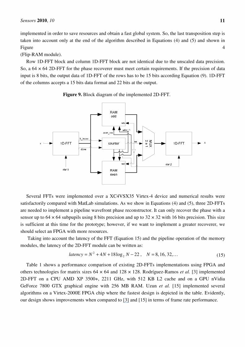
Sensors 2010, 10
11
implemented in order to save resources and obtain a fast global system. So, the last transposition step is
taken into account only at the end of the algorithm described in Equations (4) and (5) and shown in
Figure 4
(Flip-RAM module).
Row 1D-FFT block and column 1D-FFT block are not identical due to the unscaled data precision.
So, a 64 × 64 2D-FFT for the phase recoverer must meet certain requirements. If the precision of data
input is 8 bits, the output data of 1D-FFT of the rows has to be 15 bits according Equation (9). 1D-FFT
of the columns accepts a 15 bits data format and 22 bits at the output.
Figure 9. Block diagram of the implemented 2D-FFT.
Several FFTs were implemented over a XC4VSX35 Virtex-4 device and numerical results were
satisfactorily compared with MatLab simulations. As we show in Equations (4) and (5), three 2D-FFTs
are needed to implement a pipeline wavefront phase reconstructor. It can only recover the phase with a
sensor up to 64 × 64 subpupils using 8 bits precision and up to 32 × 32 with 16 bits precision. This size
is sufficient at this time for the prototype; however, if we want to implement a greater recoverer, we
should select an FPGA with more resources.
Taking into account the latency of the FFT (Equation 15) and the pipeline operation of the memory
modules, the latency of the 2D-FFT module can be written as:
K,32,16,8,22log184 2
2 =−++= NNNNlatency (15)
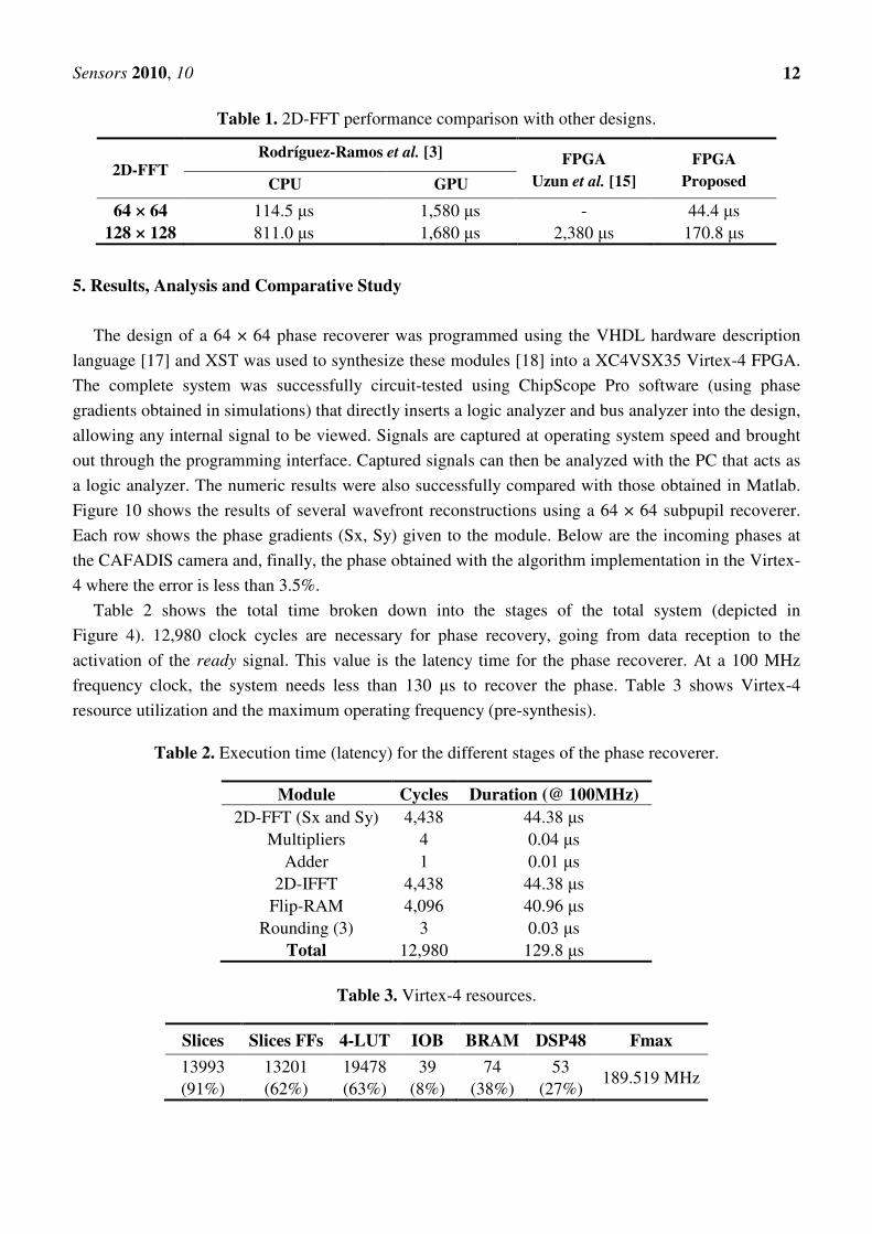
Table 1 shows a performance comparison of existing 2D-FFTs implementations using FPGA and
others technologies for matrix sizes 64 × 64 and 128 × 128. Rodríguez-Ramos et al. [3] implemented
2D-FFT on a CPU AMD XP 3500+, 2211 GHz, with 512 KB L2 cache and on a GPU nVidia
GeForce 7800 GTX graphical engine with 256 MB RAM. Uzun et al. [15] implemented several
algorithms on a Virtex-2000E FPGA chip where the fastest design is depicted in the table. Evidently,
our design shows improvements when compared to [3] and [15] in terms of frame rate performance.
Sensors 2010, 10
12
Table 1. 2D-FFT performance comparison with other designs.
2D-FFT Rodríguez-Ramos et al. [3] FPGA
Uzun et al. [15]
FPGA
Proposed CPU GPU
64 × 64 114.5 µs 1,580 µs - 44.4 µs
128 × 128 811.0 µs 1,680 µs 2,380 µs 170.8 µs
5. Results, Analysis and Comparative Study
The design of a 64 × 64 phase recoverer was programmed using the VHDL hardware description
language [17] and XST was used to synthesize these modules [18] into a XC4VSX35 Virtex-4 FPGA.
The complete system was successfully circuit-tested using ChipScope Pro software (using phase
gradients obtained in simulations) that directly inserts a logic analyzer and bus analyzer into the design,
allowing any internal signal to be viewed. Signals are captured at operating system speed and brought
out through the programming interface. Captured signals can then be analyzed with the PC that acts as
a logic analyzer. The numeric results were also successfully compared with those obtained in Matlab.
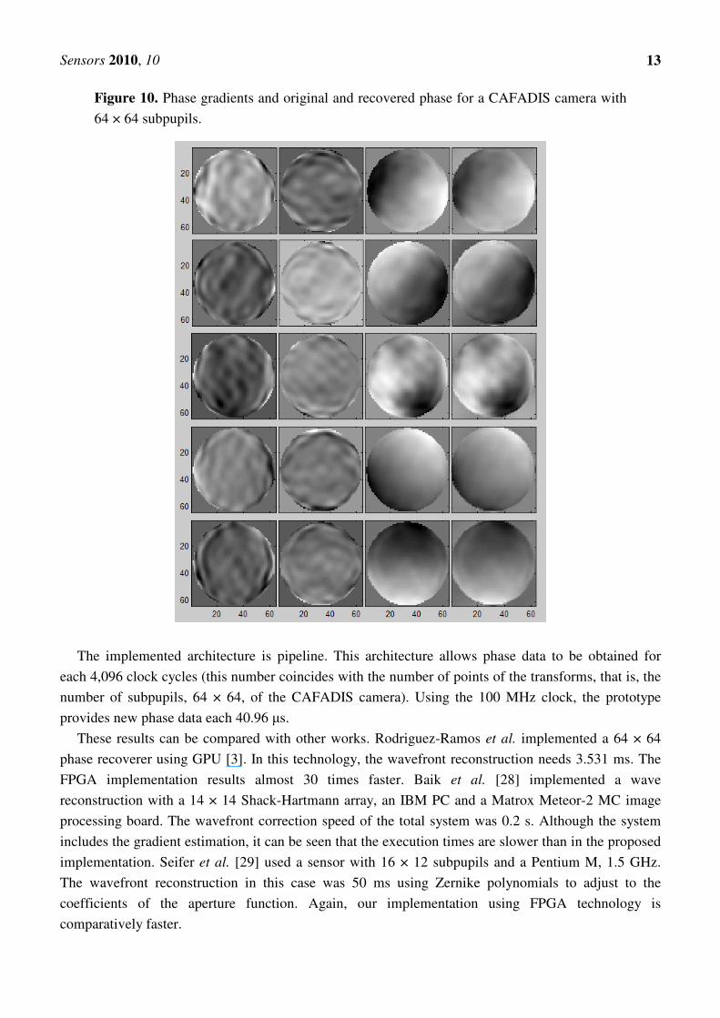
Figure 10 shows the results of several wavefront reconstructions using a 64 × 64 subpupil recoverer.
Each row shows the phase gradients (Sx, Sy) given to the module. Below are the incoming phases at
the CAFADIS camera and, finally, the phase obtained with the algorithm implementation in the Virtex-
4 where the error is less than 3.5%.
Table 2 shows the total time broken down into the stages of the total system (depicted in
Figure 4). 12,980 clock cycles are necessary for phase recovery, going from data reception to the
activation of the ready signal. This value is the latency time for the phase recoverer. At a 100 MHz
frequency clock, the system needs less than 130 µs to recover the phase. Table 3 shows Virtex-4
resource utilization and the maximum operating frequency (pre-synthesis).
Table 2. Execution time (latency) for the different stages of the phase recoverer.
Module Cycles Duration (@ 100MHz)
2D-FFT (Sx and Sy) 4,438 44.38 µs
Multipliers 4 0.04 µs
Adder 1 0.01 µs
2D-IFFT 4,438 44.38 µs
Flip-RAM 4,096 40.96 µs
Rounding (3) 3 0.03 µs
Total 12,980 129.8 µs
Table 3. Virtex-4 resources.
Slices Slices FFs 4-LUT IOB BRAM DSP48 Fmax
13993
(91%)
13201
(62%)
19478
(63%)
39
(8%)
74
(38%)
53
(27%) 189.519 MHz
Sensors 2010, 10
13
Figure 10. Phase gradients and original and recovered phase for a CAFADIS camera with
64 × 64 subpupils.
The implemented architecture is pipeline. This architecture allows phase data to be obtained for
each 4,096 clock cycles (this number coincides with the number of points of the transforms, that is, the
number of subpupils, 64 × 64, of the CAFADIS camera). Using the 100 MHz clock, the prototype
provides new phase data each 40.96 µs.
These results can be compared with other works. Rodriguez-Ramos et al. implemented a 64 × 64
phase recoverer using GPU [3]. In this technology, the wavefront reconstruction needs 3.531 ms. The
FPGA implementation results almost 30 times faster. Baik et al. [28] implemented a wave
reconstruction with a 14 × 14 Shack-Hartmann array, an IBM PC and a Matrox Meteor-2 MC image
processing board. The wavefront correction speed of the total system was 0.2 s. Although the system
includes the gradient estimation, it can be seen that the execution times are slower than in the proposed
implementation. Seifer et al. [29] used a sensor with 16 × 12 subpupils and a Pentium M, 1.5 GHz.
The wavefront reconstruction in this case was 50 ms using Zernike polynomials to adjust to the
coefficients of the aperture function. Again, our implementation using FPGA technology is
comparatively faster.
Sensors 2010, 10
14
6. Conclusions
A 64 × 64 wavefront recoverer prototype was synthesized with a Xilinx XC4VSX35 Virtex-4 as
sole computational resource. This FPGA is provided in a ML402 Xtreme DSP evaluation platform.
Our prototype was designed using ISE Foundation 8.2 and ModelSim 6.0 simulator. The system has
been successfully validated in the FPGA chip using simulated data.
A two-dimensional FFT is implemented as nuclei algorithm of the recoverer: processing times are
really short. The system can process data in much lower times than the atmospheric response. This
feature allows more phases to be introduced in the adaptive optical process. Then, the viability of the
FPGAs for AO in the ELTs is assured.
Future work is expected to be focused on the optimization of the 2D-FFT using others algorithms
(radix-8, radix-16) and the implementation of a larger recoverer into Virtex-5 and Virtex-6 devices for
the necessary 84x84 recoverer using CAFADIS camera. The prototypes could be four times faster than
with Virtex-4 FPGA devices. Moreover, the system should be tested in a telescope expected soon.
Acknowledgements
This work has been partially supported by “Programa Nacional de Diseño y Producción Industrial"
(Project DPI 2006-07906) of the “Ministerio de Educación y Ciencia" of the Spanish government, and
by “European Regional Development Fund" (ERDF).
References and Notes
1. Poyneer, L.A.; Gave, D.T.; Brase, J.M. Fast wave-front reconstruction in large adaptive optics
systems with use of the Fourier transforms. J. Opt. Soc. Am. A 2002, 19, 2100–2111.
2. Roddier, F.; Roddier, C. Wavefront reconstruction using iterative Fourier transforms. Appl. Opt.
1991, 30, 1325–1327.
3. Rodríguez-Ramos, J.M.; Marichal-Hernández, J.G.; Rosa, F. Modal Fourier wavefront
reconstruction using graphics processing units. J. Electron. Imaging 2007, 16, 123–134.
4. Rodríguez-Ramos, J.M.; Femenía, B.; Montilla, I.; Rodríguez-Ramos, L.F.; Marichal-Hernández,
J.G.; Lüke, J.P.; López, R.; Martín, Y. The CAFADIS camera: a new tomographic wavefront
sensor for adaptive optics. In Proceedings of the 1st AO4ELT Conference on Adaptive Optics for
Extremely Large Telescopes, Paris, France, June 22–26, 2009.
5. Clare, R.M.; Lane, R.G. Wave-front sensing from subdivision of the focal plane with a lenslet
array. J. Opt. Soc. Am. A 2005, 22, 117–125.
6. Rodríguez-Ramos, J.M.; Magdaleno, E.; Domínguez, C.; Rodríguez, M.; Marichal, J.G. 2D-FFT
implementation on FPGA for wavefront phase recovery from the CAFADIS camera. Proc. SPIE
2008, 7015, 701539.
7. Zhou, Y.; Noras, J.M., Shepherd, S.J. Novel design of multiplier-less FFT processors. Signal
Process. 2007, 87, 1402–1407.
8. Chang, T.S.; Jen, C.W. Hardware efficient transform designs with cyclic formulation and
subexpression sharing. In Proceedings of the 1998 IEEE ISCAS, Monterey, CA, USA, May 1998.
Sensors 2010, 10
15
9. Guo, J.I. An efficient parallel adder based design for one dimensional discrete Fourier transform.
Proc. Natl. Sci. Counc. ROC 2000, 24, 195–204.
10. Chien, C.D; Lin, C.C.; Yang, C.H.; Guo, J.I. Design and realization of a new hardware efficient IP
core for the 1-D discrete Fourier transform. IEE Proc. Circuits, Dev. Syst. 2005, 152, 247–258.
11. Hawkes, G.C. DSP: Designing for Optimal Results. High-Performance DSP Using Virtex-4
FPGAs; Xilinx: San Jose, CA, USA, 2005.
12. XtremeDSP for Virtex-4 FPGAs User Guide; Xilinx: San Jose, CA, USA, 2006.
13. Proakis, J.G.; Manolakis, D.K. Digital Signal Processing. Principles, Algorithms and
Applications, 3rd ed.; Prentice Hall: Englewood Cliffs, NJ, USA, 1996.
14. Fast Fourier Transform v3.2; Xilinx: San Jose, CA, USA, 2006.
15 Uzun, I.S.; Amira, A.; Bouridane, A. FPGA implementations of fast Fourier transforms for
real-time signal and image processing. IEE Proc. Vis. Image Signal Process. 2005, 152, 283–296.
16. Frigo, M.; Johnson, S. FFTW: An adaptive software of the FFT. In Proceedings of IEEE
International Conferences on Acoustics, Speech, and Signal Processing, Seattle, Washington, DC,
USA, May 1998; pp. 1381–1384.
17. Motorola DSP 56600 16-bit DSP Family Datasheet; Motorola: Schaumburg, IL, USA, 2002.
18. Texas Instruments C62x and C67x DSP Benchmarks; Texas Instruments: Dallas, TX, USA, 2003.
19. Wosnitza, M.W. High Precision 1024-Point FFT Processor for 2-D Object Detection; PhD thesis,
ETH Zürich: Zürich, Switzerland, 1999, doi:10.3929/ethz-a-002064853.
20. Bass, B. A low-power, high-performance 1024-point FFT processor. IEEE J. Solid-State Circuits
1999, 34, 380–387.
21. FFT Megacore Function User Guide; Altera: Hong Kong, China, 2002.
22 FFT/WinFFT/Convolver Transforms Core Datasheet; Mentor Graphics: Wilsonville, OR, USA,
2002.
23. CS248 FFT/IFFT Core Datasheet; Amphion: Kuopio, Finland, 2002.
24. Sukhsawas, S.; Benkrid, K. A high-level implementation of a high performance pipeline FFT on
Virtex-E FPGAs. In Proceedings of the IEEE Computer Society Annual Symposium on VLSI
Emerging Trends in VLSI Systems Design, Lafayette, LA, USA, February 19–20, 2004.
25. Vite, J.A.; Romero, R.; Ordaz, A. VHDL core for 1024-point radix-4 FFT computation.
In Proceedings of the 2005 International Conference on Reconfigurable Computing and FPGAs,
Puebla City, Mexico, September 28–30, 2005.
26. Analog Devices DSP Selection Guide 2003 Edition; Analog Devices: Norwood, MA, USA, 2003.
27. Baik, S.H.; Park, S.K.; Kim, C.J.; Cha, B. A center detection algorithm for Shack–Hartmann
wavefront sensor. Opt. Laser Technol. 2007, 39, 262–267.
28. Seifert, L.; Tiziani, H.J.; Osten, W. Wavefront reconstruction with the adaptive Shack–Hartmann
sensor. Opt. Commun. 2005, 245, 255–269.
© 2010 by the authors; licensee Molecular Diversity Preservation International, Basel, Switzerland.
This article is an open-access article distributed under the terms and conditions of the Creative
Commons Attribution license (http://creativecommons.org/licenses/by/3.0/).


