Embed Size (px)
Citation preview

3dODSOIIIDSO
SECOND ENLARGED EDITION
AN INTRODUCTION TO THE CATHODE RAY
OSCILLOSCOPE BY
HARLEY CARTER A.M.I.E.E.
POPULAR SERI E S
P H I L I P S' TECHN I CAL L I B RARY

L2 o
4 * ~
t.

4
I
E i
• ~ 1c.w.a• 3t c~
,. 6.ft
r
4
r
rr ♦":. 1yo..

AN INTRODUCTION TO THE CATHODE RAY OSCILLOSCOPE


AN INTRODUCTION TO THE
CATHODE RAY
OSCILLOSCOPE
BY
HARLEY CARTER A.M.I.E.E.
J. P. de Jongh, PAoDEJ Begoniastraat 54
Roosendaal
1960
Second reset and enlarged edition
POPULAR SERIES
PHILIPS TECHNICAL LIBRARY

Publisher's note: This book is published in English. French, German and Spanish
U.D.C. Nr.621.317.755 It contains 132 pages. 99 illustrations
® N. V. Philips' Gloeilampenfabrieken — Eindhoven (Holland) 1957 Printed in the Netherlands
First edition 1957 Second reset and enlarged edition 1960
The information given in this book does not imply freedom from patent rights

PREFACE TO THE SECOND EDITION
In preparing this, the second English edition, additions have been made to the text in order to include further information or explanations suggested by readers. Chapter VIII — "Some Complete Oscilloscope Circuits" — has been largely re-written. Some of the circuits described in the first edition have been replaced by new or revised designs which incorporate many interesting and novel features and employ the latest types of tubes. The whole of the text has been re-set in a larger and more legible type, and this has provided an opportunity of correcting a number of typographical errors which unfortunately existed in the first edition.
Harley Carter
London, September 1959.

PREFACE TO THE FIRST EDITION
Possibly no single piece of measuring equipment currently available is more adaptable or has a wider field of application than the cathode ray oscilloscope. It was originally developed in a comparatively crude form for laboratory use, but improvements in the design of cathode ray tubes, the development of new and ingenious circuits, and, above all, modern precision methods of tube manufacture, have made possible the production of oscilloscopes of many types. Some of these are designed for specific applications in various branches of scientific research or industrial investigation, but many more are suitable for use in testing, inspection, adjustment and repairing in both electrical and mechanical engineering practice. These "general purpose" oscilloscopes have frequently to be used by technicians and shop engineers who, while experts in their own branches of industry, may have only a nodding acquaintance with electronics. It is with this class of user particular-ly in mind that the present book has~been written. There are, however, others who may find this Introduction to the Cathode Ray Oscilloscope of interest — the serious experimenter, the technical apprentice and the student in technical training establishments, to mention only a few. To all these, and to others who seek a simple explanation of the operation of the cathode ray tube and of the principles, construction and application of the cathode ray oscillo-scope, I offer these pages. I have refrained from any attempt at mathematical treatment, and have en-deavoured to render the explanations sufficiently simple for those having only a slight knowledge of electronic circuits while at the same time avoiding offence to the more expert reader. The examples of practical applications of the oscilloscope have been selected to cover the more important basic techniques and also a wide variety of interests but, of course, this chapter does not pretend to be exhaustive. I wish to express my sincere thanks to Mr. J. Jager of Philips, Eindhoven, for his help in collecting much of the material for Chapters 3 and 4, and to the many engineers at Eindhoven from whose published work I have been allowed to quote. I am also greatly indebted to Mullard Limited, London, for permission to use a number of illustrations taken from their library of technical and educational publications and filmstrips.
Harley Carter
London, January 1957.

CONTENTS
Chapter I. INTRODUCTION . 1
Chapter II. THE CATHODE RAY TUBE 5
I. Operating Principle . 5 2. Focusing the Beam 7 3. Deflection of the Beam 10 4. Symmetrical and Asymmetrical Deflection 12 5. Intensity Modulation of the Beam 13 6. Post-deflection Acceleration 14 7. Screen Characteristics . 15 8. Cathode Ray Tube Manufacture 21 9. Methods of Displaying or Recording 23
10. Measurement of a Single Quantity . 24 11. Indicating the Relationship between two Quantities 25 12. Indicating the Relationship between two Quantities one of
which is Time 25 13. Indicating the Relationship between two Quantities neither of
which is Time 26 14. Photographic Recording 28
Chapter III. THE TIME BASE 32
1. Requirements for a Sawtooth Voltage 32 2. Basic Principles . 33 3. Methods of Generating a Sawtooth Voltage 34 4. The Flyback . 35 5. Simple Basic Circuits 36 6. Linearity 38 7. Effect of Coupling Element on Linearity . 39 8. Effect of an Amplifier on Linearity . 41 9. Methods of Improving Linearity 43
10. Methods of producing a Repeating Time Base Voltage. 46 11. Single-Stroke Time Bases . 53 12. Circular, Spiral and Radial Time Bases . 53
VII

Chapter IV. AMPLIFIERS FOR VERTICAL DEFLECTION AND PICK-UPS FOR CONVERTING NON-ELECTRICAL PHENOMENA INTO ELECTRI-CAL MAGNITUDES 54
1. Amplifiers for Vertical Deflection Voltages 54
1.1. What is Distortion? . 56 1.2. Amplitude Distortion 56 1.3. Frequency Distortion. 57 1.4. Phase Distortion. 62
2. Conversion of Non-electrical Phenomena into Electrical Magnitudes . 64
2.1. Resistance Pickups 64 2.2. Piezo-electric Pickups 65 2.3. Capacitance Pickups 65 2.4. Electro-magnetic Pickups . 65 2.5. Thermo-electric Pickups . 66 2.6. Photo-electric Pickups 66
Chapter V. POWER SUPPLY FOR CATHODE RAY OSCILLOSCOPES . 67
1. The High Tension Unit 67 2. The E.H.T. Unit . 69 3. General Hints 72
Chapter VI. PRACTICAL APPLICATIONS OF THE OSCILLOSCOPE 73
1. Calibrating the Oscilloscope. 74 2. Some simple measurements . 77 3. Measurements of Phase Relationship. 79 4. Measurement of Capacitance, Inductance and Reactance 80
VIII

5. Frequency comparison. 81 6. The Electronic Switch . 83 7. Applications involving a Circular Time Base 84 8. Frequency Comparison. 85 9. Testing the Regulation of Watches 87
10. Checking the Speed of Camera Shutters 87 11. "Echo" Methods of Measurement 88 12. Flaw Detection 88 13. Resonance Curves of Oscillatory Circuits 89 14. Hysteresis Loop Test . 90
Chapter VII. STANDARD CATHODE RAY TUBES FOR OSCILLOGRAPHY 92
Chapter VIII. SOME COMPLETE OSCILLOSCOPE CIRCUITS. 98
1. Circuit No. 1 Students' Oscilloscope incorporating Cathode Ray Tube Type DG 7-31 98
1.1. General Description . 98 1.2. Vertical Amplifier 99 1.3. Time Base Generator . 101 1.4. The Power Pack . 103 1.5. The Cathode Ray Tube Unit . 105 1.6. Power Output and Waveform Panel. 105 1.7. Layout . 106
2. Circuit No. 2 A simple Oscilloscope for the Service Engineer 109
2.1. General Description 2.2. Vertical Amplifier 2.3. Time Base Generator 2.4. Synchronising Amplifier 2.5. Calibration 2.6. Shift Controls 2.7. The Power Pack and Cathode Ray Tube Circuit 2.8. Layout
109 . 109
110 Ill 111 112 112 113
IX

3. Circuit No. 3 A Versatile Oscilloscope 115
3.1. General Description 116 3.2. Performance Specification 116 3.3. Time Base and Horizontal Amplifier 118 3.4. Vertical Amplifier . 119 3.5. Power Supply . 121
X
CHAPTER I
INTRODUCTION
The great majority of devices for measuring electric currents or voltages make use of one or another of the following phenomena:
I. The heat generated by a current when overcoming resistance. 2. The chemical reactions which occur when a current passes
through an electrolyte. 3. The forces acting upon magnets, magnetic materials, or con-
ductors carrying currents, in a magnetic field. 4. The forces setup in an electric field.
Except for a few limited applications, the first two principles are today merely of academic interest. Instruments of the electromagnetic type are, of course, familiar to the practical engineer, typical examples being moving iron and moving coil ammeters and voltmeters. These instruments are essentially current-measuring devices, although by making their resistance high, so that the current passing through them is very small compared with the total current in the circuit, they can be employed for voltage measurement. Electrostatic instruments are purely voltage-operated devices and are re-presented in engineering practice by the electrostatic voltmeters used for measuring comparatively high voltages.
Conventional instruments of the electromagnetic type are quite satisfactory for very many practical measurements, such as those of direct currents and voltages or the r.m.s. values of alternating currents and voltages, provided the quantities being measured do not change their values very rapidly.

2 INTRODUCTION CH. I
They suffer, however, from the great disadvantage that the moving system has appreciable inertia, as a result of which the instrument cannot follow instantaneously variations in the quantity being measured. Moreover, the instrument absorbs an appreciable amount of power from the circuit under examination.
This will be clear from a brief consideration of the operating principle of such an instrument. The current to be measured, flowing through the in-strument, exerts a torque on the moving element which is therefore deflected. This torque, and therefore the deflection of the moving element, is opposed by a controlling torque which may be produced, say, by gravity or by a spring. The moving element comes to rest when the deflecting torque is exactly balanced by the controlling torque, the amount of the deflection then being a measure of the deflecting torque and thus of the current through the instrument. Because of its inertia, the moving element takes an appreciable time to reach its final position, and having done so tends to over-shoot, so that there is a certain amount of oscillation of the pointer before it comes to rest atthe true reading.
In order to reduce the amount of this oscillation, some form of damping, such as a dash-pot or an eddy-current damping system is usually incorporated in the instrument. Thus, all instruments of this type are inherently sluggish to the extent that they cannot quickly respond to rapid or sudden fluctuations of voltage or current, and in all such instruments energy must be expended in overcoming the controlling torque, while the damping system, unless critically adjusted, may impose a further load on the circuit.
The need for electrical measuring instruments having a very quick response was felt early in the history of electrical engineering. At first only in the laboratory, but later in industry itself, there arose such problems as the examination of the waveforms of alternating currents and other periodic phenomena, and the investigation of "transients" — sudden pulses, usually of very short duration and occuring either singly or at random intervals.
Early attemps to meet these requirements consisted in the main of im-proved methods of applying the principle of the moving coil instrument, by keeping the inertia of the moving element extremely low, making its resonant frequency very high, and applying critical damping. The moving coil oscillo-graph of Blondel (1891) was followed in 1893 by the instrument designed by Duddell (Fig. 1). He used a single loop of fine phosphor-bronze wire as

CH. I 'INTRODUCTION 3
the moving "coil", the deflection being indicated by a beam of light reflected from a tiny morror attached to the loop. This light could be made to fall on, say, a moving photographic film, thus producing a trace or graph of the changes of the voltage applied to the instrument over a period of time.
Fig. 1. Duddell oscilloscope (1893)
A still more sensitive instrument, due to Professor Einthoven, was in-troduced in 1901 (Fig. 2). The moving element in this oscillograph was a single thin fibre of quartz, silvered or gilded to form a conductor, which was mounted in a narrow gap between the poles of a powerful magnet. Move-ment of the fibre across the gap was observed and measured either directly through a microscope or by a beam of light directed on to the fibre and reflected therefrom on to a screen or scale.
The Einthoven ("string") galvanometer C-C Direction of current S-N Direction of magnetic field a Direction of deflection
A - D - E - F Optical system
Fig. 2. Einthoven oscilloscope (1901) With acknowledgements to The Cambridge Instrument Co.
In spite of their careful design and the superb craftsmanship which went into their construction, these oscilloscopes were not capable of following variations occurring at frequencies much greater than 100 cycles per second.

4 INTRODUCTION CH. I
Moreover, they were expensive and delicately-adjusted instruments — hardly the equipment for use in the workshop or factory.
The possibility of a still more efficient oscilloscope was, however, already in existence, in the Cathode Ray Tube. During the latter part of the nine-teenth century much work had been done on the investigation of electric discharges in evacuated vessels. It had been ascertained that the discharge from cathode to anode or accelerating electrode consists of a stream of negatively charged particles — to which the name "electron" was given by Johnstone-Stoney in 1890. It was known that this stream of electrons — the so-called "cathode ray" — can be deflected by a magnetic field or by an electric field, and that although the electron stream is itself invisible to the human eye it produces luminescence when it falls upon certain chemical substances, and can also affect a photographic film.
As early as 1897 a form of cathode ray tube was used by Braun as an instrument for measuring electrical quantities. Many improvements have been introduced from time to time, and today the cathode ray oscilloscope is an indispensible tool in the hands of the scientist and the engineer.
The electron beam which forms the moving element of the instrument is, within the limits of present-day methods of measurement, inertialess; and the instrument imposes no load on the circuit under examination.
The cathode ray tube is now employed for the investigation and measure-ment of both periodic and transient electrical phenomena up to very high frequencies, and also of non-electrical phenomena, such as vibration in solids, which can be converted into variations of current or voltage.
The cathode ray tube has also made possible the art of television as we know it today, and the various systems of navigational aids now known under the collective name of "radar".
The following chapters deal with the principle and construction of the cathode ray tube itself, and with the subsidiary apparatus and circuits which, with the tube, comprise the Cathode Ray Oscilloscope. A number of practical applications of the oscilloscope are briefly described. Technical information and data on commercial cathode ray tubes suitable for use in oscilloscopes are given, and the final chapter contains the designs, circuits and specifi-cations of several complete instruments.

CHAPTER II
THE CATHODE RAY TUBE
The cathode ray oscilloscope is an instrument in which variations of voltage are displayed as a luminous trace on a screen. The complete apparatus comprises a cathode ray tube which forms the measuring and indicating portion of the instrument, and a number of subsidiary units or circuits for providing suitable power supplies, for amplifying or attenuating the voltage to be measured, and for ensuring that the instantaneous values of that voltage are displayed on the screen in succession so that the trace takes the form of a graph in which the voltage is plotted against time. In this chapter the prin-ciples upon which the cathode ray tube operates are explained and its con-struction is described.
Consideration of space precludes discussion of the stages in the develop-ment of the cathode ray tube from the crude experimental laboratory models produced in 1897 to the highly efficient mass-produced tubes of today. Neither will any attempt be made to describe all the forms of tube now available, attention being directed only to the type usually employed in oscilloscopes for general laboratory and industrial use.
1. Operating Principle
A cathode ray tube of this type consists essentially of an evacuated glass bulb, of pear-shaped form, with an elongated neck, and flattened at the wider end.
The neck portion contains an assembly of electrodes termed the "gun assembly", and the inner surface of the flattened end is coated with a chemical material to form the screen on which the trace is displayed.

6 THE CATHODE RAY TUBE CH. H
The simplest form of electron gun, shown diagrammatically in Fig. 3, comprises a heated cathode which emits electrons in the same way as the cathode of a thermionic valve, and an accelerating electrode which is main-
A — Cathode B — Accelerating electrode C — Aperture D — Electron beam
Fig. 3. Cathode ray tube with simple two-electrode gun
tamed at a high positive potential with respect to the cathode, and having a central aperture in line with the cathode. Electrons emitted from the cathode are accelerated in the direction of the accelerating electrode which collects a proportion of the electrons, the remainder passing through the aperture to the screen at a speed proportional the to accelerator potential. When these high-speed electrons strike the screen, light is produced at the point of impact.
Two pairs of metal plates, arranged mutually at right angles, are located in the neck of the tube between the accelerating electrode and the screen. If an electric field is produced between the two plates of one pair, the electron
Fig. 4. Method of deflecting the beam VV—Plates for vertical deflection
HH—Plates for horizontal deflection
A—Position of undeflected spot B—Position of spot when only
vertical deflection is applied C—Position of spot when both
vertical and horizontal deflec-tion are applied
beam is deflected towards the plate which is at a positive potential and away from the plate which is at a negative potential, so that the light spot moves across the screen, say from A to B (See Fig. 4). If, now, another electric field is set up between the two plates of the second pair, the beam is deflected

CH. II FOCUSING THE BEAM 7
in a direction at right-angles to the direction of the previous deflection, i.e. horizontally and the light spot moves in a corresponding direction e.g. from B to C.
If, therefore, the voltage applied between the two plates which produce vertical deflection is say, an alternating voltage of sinusoidal waveform, the spot will trace a vertical line on the screen. If, now, there is also applied to the other pair of plates a voltage which increases linearly from a negative maximum to a positive maximum in a time equal to that of one or more cyles of the vertical deflecting voltage and then very suddenly falls again to the negative maximum, the resultant travel of the light spot will trace out the sinusoidal waveform as shown in Fig. 5.
Fig. S. Oscillogram of a sine wave voltage A — Sine wave B — Flyback
In the same way the simultaneous variations of any two voltages may be depicted on the screen. Fig. 6, for example, is an oscillogram showing the anode voltage/anode current characteristic of a thermionic valve, reproduced from an actual photograph of the screen of a cathode ray tube.
2. Focusing the Beam
It will be seen from Fig. 3 that a considerable proportion of the electrons emitted from the cathode are collected by the accelerating electrode, and that those electrons ejected from the gun assembly form a slightly divergent beam. The spread of the beam results in a fairly large light spot on the screen. If, therefore, this simple form of gun were used, the trace on the screen would be blurred.

8 THE CATHODE RAY TUBE CH. II
Fig. 6. Oscillogram showing anode voltage/anode current characteristics of a thermionic valve
An improvement, introduced by Wehnelt, consists of a metal cylinder concentric with the cathode and maintained at a suitable negative potential. As is seen in Fig. 7, the Wehnelt cylinder (now usually referred to as the "grid") repels the electrons, thus producing a focusing effect. As a rusult, a smaller proportion of the total electron stream is collected by the accelerator and a greater proportion reaches the screen.
A further degree of focusing is achieved by introducing a further grid, between the Wehnelt cylinder or first grid and the accelerator, and applying to this second grid a positive potential of somewhat lower value than that of the accelerator potential. By correct geometrical design of the electrode system and correct adjustment of the potentials, a non-uniform field is produced which results in a finely focused beam, producing a small spot on the screen and therefore a clean, well-defined trace.
The action of the focusing field on the electron stream is akin to that of a lens on a beam of light, and the arrangement is therefore often termed an electron lens. The subject of electron optics is somewhat complex, but the action of a simple electron lens can be understood by reference to Fig. 8 which shows the positions of the second grid and accelerator, and Fig. 9 which shows the distribution of the electrostatic field produced in their vicinity.

CH. II FOCUSING THE BEAM 9
K Gt G2 A 0 I +wov 0 •••-60V
+250•••375V
Fig. 7. — Cathode ray tube with three- Fig. 8. — Cathode ray tube with four-electrode gun. K — Cathode; G — Weh- electrode gun. K — Cathode; Gl — First nelt cylinder (grid); A — Accelerator grid; G, — Second grid; A — Accelerator
In this diagram, the dotted lines represent the equipotential surfaces, the potential difference between any two adjacent equipotential surfaces being the same.
The illustration also indicates a divergent beam of electrons, originating at the point P, and entering the electric field produced by the second grid and accelerator. Point P, it should be pointed out, corresponds to the focal point produced by the action of the negative electrode or grid shown in Fig. 8. Consider first an electron in the centre of the beam and therefore travelling
Fig. 9. Focusing effect of the electric field in an electron lens system

10 THE CATHODE RAY TUBE CH. II
axially along the tube. Because its path is at every point perpendicular to the equipotential surfaces, it will not change direction but will continue along its axial path. Now consider an electron at the edge of the divergent beam, and following the path P-a. It will reach the point a with a certain velocity de-termined by the potential difference which it has traversed. On reaching a the electron is accelerated by the field, this acceleration being in the direction of the maximum potential gradient, that is to say in the direction a-c corres-ponding to the shortest distance between two adjacent equipotential sur-faces. But because of its initial velocity in the direction P-a-b, it will take a path intermediate between a-c and a-b, such as a-d. Similarly, at each succes-sive equipotential surface the path of the electron is bent further so that eventually the beam becomes convergent instead of divergent.
When, however, the electron reaches e where the field strength is decreasing and the equipotential surfaces are therefore concave, it experiences a decele-rating force away from the axis, so that instead of continuing along the path e-e1 pit follows a path such as a-e2. If the shape of the electric field has been correctly designed and adjusted — and this is achieved by suitable design of the electrode system and choice of electrode potentials — the beam will come to a focus at f, on the luminescent screen of the tube.
3. Deflection of the Beam
The principle of electrostatic deflection has been briefly described in an earlier paragraph, but must now be considered in more detail. Fig. 10 represents in diagrammatic form a simple deflecting system consisting of one pair, of plates, and it will be understood that if a difference of potential is applied between the two plates, the electron beam will be deflected in the direction of the more positive plate.
d
S
1°D x l Va
Fig. 10. Simple electrostatic deflecting system. Deflection a = 0.5 d Va
where Vd is the defecting voltage and VT is the accelerating voltage

CH. II DEFLECTION OF THE BEAM 11
The amount of the deflection of the luminescent spot on the surface of the screen depends upon several factors, the chief of which are the physical' dimensions of the deflecting system and its location with respect to the screen, and the voltages applied to the gun system and to the deflection plates.
For the system illustrated, the distance a over which the luminous spot is
deflected from the centre of the screen is given by the formula:
a=0.5 d Va
D x l Vd(mm)
where D is the distance between the centre of the deflecting system and the screen in mm
I is the length of the deflecting plates in the axial direction in mm d is the distance between the deflecting plates in mm Va is the pre-deflection accelerator voltage
and Vd is the voltage between the deflecting plates. Since it is necessary to deflect the beam in two directions — vertically and
horizontally — two pairs of deflecting plates are fitted, mutually at right-angles as shown in Fig. 11. The plates further from the screen are arranged for vertical deflection, and are usually denoted Dl, DI', while the plates nearer the screen, denoted D2i Dz are for horizontal deflection. In Britain and in
G1 G2 A D~
0 —+ + DZ Oj
Fig. 11. Complete electrode system of an oscilloscope tube. K — Cathode; Gl — First grid; G2 — Second grid; A — Accelerator; Di, Dl' — Plates for
1 vertical deflection; D2, D2' — Plates for Horizontal Deflection; S — Luminous screen; Fl — Focus of beam in the absence of deflecting voltage
America the plates for vertical deflection are denoted by y, yl and the plates for horizontal deflection by x, x'. For normal applications in which it is desired to examine the variations of a voltage with respect to time, the voltage to be examined is applied between the plates for vertical deflection (DI, DI'), while a voltage which changes linearly with respect to time is applied between plates D2 and D2'.

12 THE CATHODE RAY TUBE CH. II
4. Symmetrical and Asymmetrical Deflection There are two ways in which the deflecting voltages may be applied to the deflecting plates. In what is known as "symmetrical deflection", the voltages are so applied that the potentials at the two plates of a pair are symmetrical with respect to the accelerator potential. In "asymmetrical deflection", one plate of the D2-pair, together with the accelerating electrode of the tube and the positive terminal of the H.T. supply are connected to earth, the deflecting voltages being applied to the remaining plates. In this arrangement the field between the two plates of the D2-pair is not symmetrical with respect to earth.
Asymmetrical deflection requires a much simpler and less expensive circuit than symmetrical deflection, as will be shown later, and for this reason is to be preferred in many applications. It suffers from the disadvantage, however, that the measurements are not quite so accurate as those obtained with symmetrical deflection, and the trace is also subject to a certain amount of disortion of the type known as trapezoidal distortion. These faults can be explained as follows:
With asymmetrical deflection, in which the deflecting system is arranged as shown in Fig. 12A, the potential at the midpoint between the two deflecting plates of the D2-pair is not constant, but is the resultant of a steady potential due to the accelerator and an alternating potential the instantaneous value of which is equal to half the instantaneous value of the deflecting potential applied to the plates. This resultant voltage represents the effective accelera-tor voltage of the tube — the term Va in the formula for the deflection (see page 11). Since this voltage is not constant, the actual amount of deflection a for a given deflecting voltage will differ from the calculated deflection by a few per cent.
The trapezoidal distortion resulting from the application of an asym-metrical deflecting voltage is due to the fact that the beam, having been deflected vertically by the first pair of plates, enters the space between the second pair of plates where it is not only deflected horizontally, but is also given a certain amount of vertical deflection — towards the centre of the screen when the potential of the un-earthed plate is positive and towards the periphery of the screen when this plate is negative. The voltage applied to the second pair of plates thus affects the deflection sensitivity of the first pair of plates, so that distortion of the trace occurs.
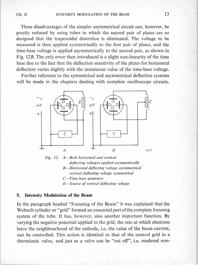
CH. II INTENSITY MODULATION OF THE BEAM 13
These disadvantages of the simpler asymmetrical circuit can, however, be greatly reduced by using tubes in which the second pair of plates are so designed that the trapezoidal distortion is eliminated. The voltage to be measured is then applied symmetrically to the first pair of plates, and the time-base voltage is applied asymmetrically to the second pair, as shown in Fig. 12B. The only error then introduced is a slight non-linearity of the time base due to the fact that the deflection sensitivity of the plates for horizontal deflection varies slightly with the instaneous value of the time-base voltage.
Further reference to the symmetrical and asymmetrical deflection systems will be made in the chapters dealing with complete oscilloscope circuits.
HCH 1
A B
Fig. 12. A—Both horizontal and vertical deflecting voltages applied asymmetrically
B—Horizontal deflecting voltage asymmetrical vertical deflecting voltage symmetrical
C—Time base generator E—Source of vertical deflecting voltage
E
OcO27
5. Intensity Modulation of the Beam
In the paragraph headed "Focusing of the Beam" it was explained that the Wehnelt cylinder or "grid" formed an esseential part of the complete focusing system of the tube. It has, however, also another important function. By varying the negative potential applied to the grid, the rate at which electrons leave the neighbourhood of the cathode, i.e. the value of the beam current, can be controlled. This action is identical to that of the control grid in a thermionic valve, and just as a valve can be "cut off", i.e. rendered non-
14 THE CATHODE RAY TUBE CH. II
conductive if a sufficiently great negative grid bias is applied, so can the beam current of a cathode ray tube be reduced to zero (and the trace on the screen blacked out) by applying a heavy negative potential to the grid.
It is thus possible to control the instant at which the trace appears on the screen and its duration, by means of a switch which applies or removes part of the negative grid bias. It is also possible to arrange that the beam current commences to flow automatically as soon as the signal to be examined is applied to the deflection plates. This arrangement provides a method of avoiding all risk of damage to the luminous screen which might occur if a bright spot were allowed to remain stationary on the screen, say due to failure of the deflecting potentials.
Another application of intensity modulation of the beam is automatic control of the brightness of the spot so that as the "writing speed", i.e. the rate at which the spot moves over the screen, increases, the brightness in-creases in proportion, thus giving a trace of more uniform luminosity. This device is particularly useful when taking photographic records of traces in which the writing speed varies considerably.
Finally, intensity modulation of the beam can be employed to produce bright spots on the trace by means of accurately timed positive-going pulses of grid voltage. These bright spots can then be used for measuring or in-dicating time intervals during the scan, particularly where very accurate time measurement is required and the linearity of the time base (horizontal deflection voltage waveform) is imperfect so that readings taken from a graticule on the screen will be inaccurate.
6. Post-deflection Acceleration
For a luminous spot of a given size and a phosphor of given efficiency, the brightness depends upon two main factors — the rate at which the electrons forming the beam current reach the screen, and the velocity of these electrons at the instant of impact, and this velocity is determined by the potential dif-ference which the electrons have traversed, i.e. by the final accelerator voltage. From the point of view of brightness of the trace, therefore, it is desirable to operate the tube at a high accelerator voltage.
However, as indicated by the simple equation given in the paragraph "Deflection of the Beam", the deflection sensitivity, that is to say the amount of deflection produced by a given change of the deflecting voltage, is inversely

CH. II SCREEN CHARACTERISTICS
Fig..;13. Photograph of oscilloscope tube with post-deflection electrodes
15
proportional to the pre-deflection accelerator voltage. Any improvement in spot brightness resulting from increasing the pre-deflection accelerator volt-age is therefore accompanied by a reduction of the deflection sensitivity.
This effect can be mitigated to a considerable extent by providing one or more auxiliary electrodes located between the deflecting system and the screen. These "post deflection" accelerating electrodes usually take the form of conductive (graphite) bands on the internal surface of the tube, as indicated in Fig. 13. They are maintained at potentials considerably higher than that of the normal pre-deflection accelerator, and thus a correspondingly brighter spot can be achieved. As, however, this additional acceleration occurs after the beam has been deflected, the deflection sensitivity of the tube is not materially affected.
7. Screen Characteristics
The pattern displayed on the face of a cathode ray tube consists, as already explained, of light emitted by the screen material when bombarded by the swiftly-moving electrons forming the beam. These screen materials are often referred to as "phosphors", but the term is not strictly accurate since the luminous effects do not consist entirely of phosphorescence. There are two main luminous effects which are produced in the screen material. The first
is the emission of light while the electrons are actually striking the screen; this is called fluorescence, and ceases immediately the electrons cease to fall upon the screen material. The second effect, correctly termed phosphor-

16 THE CATHODE RAY TUBE CH. II
escence, is the after-glow which continues for a short time after the fluor-escence has ceased.
There are very many different materials suitable for use as "phosphors". They differ in their brightness characteristics, that is to say the amount of light emitted per unit area for a given beam current density per unit area; in the colour of the emitted light; and in their "persistence", i.e. the duration of the after-glow.
Typical of the screen materials used in the modern oscilloscope tubes are those represented by the letters B, G and P in the type-numbers of the tubes described in Chapter V,II. The characteristics of the screens are given below.
Type B screen material gives a bluish luminescence of short duration Type G screen material gives a green trace of medium persistence Type P is a double-layer screen giving a bluish trace of short persistence
followed by a greenish-yellow phosphorescence of long persistence. Fig. 14 shows the persistence characteristic, the relative spectral energy
distribution and the brightness characteristic of each type of these screens.
Fig. 14 a to i. Graphs showing persistence characteristics relative spectral energy dis-tribution and brightness characteristics of types B, G and P Screens
(a) Relative spectral energy, distribution of a B-screen
X000 5000 8000 7000 Wavelength (angstroms)

CH. II SCREEN CHARACTERISTICS
~.
o ~ b 0 0
(w bs sd sijpuD3jvw) ssiv~y6ug
0 0 ssiu}y6uy eA,
17

18
0 4000
100
L U d
THE CATHODE RAY TUBE
5000 6000 7000 Wavelength (angstroms)
v
10 IIIIIIIIIh1, UIIIIIIHH1I'III
0.1
0.01 0 20 40 60
CH. II
(d)
Relative spectral energy distribution of a G-screen
80 (e) Persistence characteristic of Time otter excitation is removed (mi 1 seconds) a G-screen

CH. II SCREEN CHARACTERISTICS
(f) Brightness of a G-screen as a function of the screen current per square cm screen area, with the accelerating potential as parameter
(g) Relative spectral energy distribution of P-screen 0
h000
I
19
0.5 LO 1.5 2.0 Screen current (microamperes per sq cm)
i
5000 6000 7000 Wavelength (angstroms)

20 THE CATHODE RAY TUBE CH. II
0
ssa u;y6uq an ;otay
m
K~ 4
N
N Q
--------~~.•~~ rww voowo wws ~ IIII1l111111►.1111111111111►1111 i1►i111111►~1 ►11111111 111 w a
O ,U
d
u
d U
b q b N' 1 w
(w3 bs gad satpuv~fiw) ssa(4,&J

CH. II CATHODE RAY TUBE MANUFACTURE 21
8. Cathode Ray Tube Manufacture
The manufacture of cathode ray tubes is an industry which involves a wide variety of processes and techniques, the use of intricate and ingenious auto-matic machines, and great skill and dexterity on the part of the operators.
First of all the many different component parts of the tubes have to be made to very close dimensional tolerances and from materials of the highest purity. These include tubular nickel cathodes, the end coated with the special emissive material; heaters, made from fine tungsten wire and insulated with alundum; grids and anodes of various forms, made from special non-magnetic material; the ceramic supports upon which the electrodes are mounted; and glass parts of various shapes. After manufacture every com-ponent is gauged and inspected, faulty ones being rejected. The components are then chemically cleaned and heat-treated before they are issued to the assembly department.
In the assembly shop, where a high standard of cleanliness is maintained, specially trained skilled girls assemble the electrodes on the supporting rods, using ingenious jigs and spacing pieces to ensure that each electrode is correctly located. A liquid ceramic cement is then applied to secure each component in position. At this stage certain internal joints and connections
Fig. 15. Assembling the gun by spot welding
Fig. 16. Welding the gun assembly to the glass mount

22 THE CATHODE RAY TUBE CH. II
are made by electric spot welding, the parts to be joined being first manipul-ated into position with tweezers, as shown in Fig. 15. The next stage is to join the electrode assembly to the glass mount into which are moulded the necessary lead-in wires (See Fig. 16). These wires are themselves of a com-plex nature, for they consist of an upper portion of stout nickel wire to which the electrode system is welded, a lower portion of high conductivity copper wire which is later soldered to the appropriate contact pin in the insulating base, and a short central portion made from a special metal having the same coefficient of expansion as the glass so that it forms a vacuum-tight seal at the point where the wire passes through the glass mount. The mount also carries a central glass stem through which air is withdrawn from the bulb during the pumping process.
The assembly is now carefully inspected. Its overall dimensions and the inter-electrode clearances are checked; all welded joints are tested, and any errors in alignment are rectified.
Meanwhile the bulbs or envelopes have been prepared to receive the electrode assemblies. Blown from special quality glass, by ingenious automa-tic machines, the bulbs are carefully annealed to normalise any internal stresses set up during the blowing process. Next, each bulb is washed con-tinuously for a considerable time with a powerful acid, rinsed many times with distilled water, and carefully dried. This treatment ensures that the bulb contains no foreign substance which could contaminate and spoil the luminescent screen which is later deposited on the inner surface of the flattened end of the bulb.
The application of the luminescent screen is a highly skilled and delicate operation. The luminescent material, in the form of a fine powder, is mixed with a liquid binding agent to a thin paste. An accurately measured quantity is poured into the bulb, a deft twist of the hand ensuring that it is evenly distributed over the flat end of the bulb. The bulb is then placed in an oven where the coating is baked on and the volatile binding agent evaporated. The inner surface of the sides of the conical portion is then coated with colloidal graphite, forming a conductive layer.
Now the electrode assembly is inserted into the neck of the bulb, spring lugs on the anode making a good connection between the anode and the internal conductive coating. The whole is next mounted in a machine where gas flames play upon the neck of the tube in such a way that the glass mount

CH. II METHODS OF DISPLAYING OR RECORDING 23
and the tube neck soften and fuse together, and the excess portion of the tube neck falls away. With the electrodes thus sealed into the envelope, the only connection between the inside of the envelope and the outer air is through the thin pumping stem. The cathode ray tubes are then mounted on a rotating table, their pumping stems being connected to powerful air pumps which withdraw the air from the bulbs. While being pumped the tubes pass through a tunnel which is strongly heated to help drive off the air and other gases. On emerging from the tunnel, the getter — a chemical material previously attached to the electrode assembly — is volatilised by high frequency heating, and absorbs the last traces of gas, thus forming a vacuum of a very high order.
The pumping stem is now sealed off, and the completed tubes removed from the pumping table (See Fig. 17).
It only remains to fit the base and solder the base connections, to submit the tubes to an ageing process, and to conduct the stringent factory tests. The tubes then pass to finishing benches where the type number and other markings are etched on the tube, after which they are given a final inspection before being packed in their specially designed cartons.
9. Methods of Displaying or Recording
Information concerning any quantity which can be translated in terms of a voltage, or the relationship between two such quantities, can be displayed on the screen of a cathode ray oscilloscope. This information can be recorded in several ways — temporarily for immediate inspection, or photographical-ly as a permanent record.
Fig. 17. Sealing off the completed tube

24 THE CATHODE RAY TUBE CH. II
10. Measurement of a Single Quantity
The simplest, but not the most usual type of display is the indication of the value of a single quantity. The voltage representing the quantity to be measur-ed is applied between the two plates for vertical deflection, but the plates for horizontal deflection are not used.
In the case of a direct voltage or current, the value of the quantity under examination is indicated by the amount of the vertical deflection of the spot from its zero or no-signal position (See Fig. 18A). For alternating quantities, however, the value is indicated by the height of a vertical illuminated line which corresponds, in fact, to twice the peak amplitude of the quantity (See Fig. 18C).
These applications are, of course, identical with the function of an ordinary indicating instrument such as a voltmeter, and cathode ray tubes are, indeed, frequently used in this way instead of moving coil or moving iron instruments.
t
+V B
—V
3t
Fig. 18. A — Direct voltage is represented as a deflected spot in the absence of a horizontal deflection voltage
B — With a sawtooth voltage applied to the plates for horizontal deflection a direct voltage is represented by a horizontal line
C — In the absence of a timebase voltage, a sinusoidal alternating voltage is represented by a vertical line
D & E — With a time base applied, the sinusoidal wave-form is exhibited

CH. II INDICATING THE RELATIONSHIP BETWEEN TWO QUANTITIES 25
For such applications the cathode ray tube possesses the advantages already mentioned, namely, that the beam which acts as the movement and pointer, possesses no inertia and therefore gives an instantaneous reading; and also that the instrument imposes no load on the circuit to be measured and thus introduces no error. It also has two further advantage: first, it cannot be damaged by overloading or by incorrect connections, and second, it is an extremely simple matter, by means of suitable amplifiers or attenuators, to change the scale or range of the instrument.
11. Indicating the Relationship between two Quantities This is the more usual type of application of the cathode ray oscilloscope, and one which no other instrument can perform satisfactorily. Several different cases arise, according to the nature and properties of the phenomena con-cerned.
12. Indicating the Relationship between two Quantities one of which is Time
The simplest example in which the variation of one quantity over a period of time is displayed, is the examination of waveforms. Other examples are described in some detail in Chapter VI. For these applications the voltage to be examined is normally applied between the plates for vertical deflection, and a voltage which increases linearily with time is applied between the plates for horizontal deflection.
Two cases arise. The first is that in which the voltage to be examined is cyclic or periodic, a familiar example being a normal sinusoidal alternating voltage. In this class of application the time base voltage for horizontal deflection must be of sawtooth wave form as indicated in an earlier section, and its frequency must be equal to, or a sub-multiple of, the frequency of the voltage under examination. In order to ensure this, a part of the voltage to be examined may be fed to the circuit which generates the sawtooth volt-age, in order to synchronise the two deflecting voltages. Traces in which the time base frequency is equal to and one third of the frequency of the voltage under examination are illustrated in Fig. 18, D and E.
The second case is that in which the phenomenon to be observed is not cyclic but occurs only once, or at irregular intervals. Ideally, this class of investigation requires a single-sweep time base so that the horizontal deflec-tion is continuous from left to right during the whole period of the phenomenon.

26 THE CATHODE RAY TUBE CH. II
This can, of course, be arranged without much difficulty if the instant at which the transient commences and its duration are known, for it is then possible to adjust the speed (frequency) of the time base voltage and to trigger it automatically so that the horizontal deflection commences just before the commencement of the transient and continues throughout the period of the phenomenon. If the timing of the phenomenon cannot be predicted, it may suffice, for visual examination, to use a normal repeating time base of suitable frequency, and to trust to good fortune that the phenom-enon will occur at an appropriate time in the scanning cycle. A much better arrangement, now commonly employed, is to use the arrival of the transient signal for triggering the time base so that horizontal deflection commences, and to delay the application of the signal to the verical deflecting plates by a small fraction of a second so that the actual trace does not start until the time base is in operation. A block diagram representing this his arrangement is shown in Fig. 19. For the majority of transient investigations, however, it is desirable to produce a permanent record, and this can be obtained photo-graphically using the moving film technique described later in this chapter.
B
A . pI A — Delay circuit; B — Source of signal; C — Time base generator; Dl — Delayed transient applied to plates for vertical deflection; D2 —
D2 Triggered sawtooth voltage applied to plates for horizontal deflection
Fig. 19. Block diagram showing method of ensuring that the time base generator operates at the correct instant
to indicate a transient phenomenon
13. Indicating the Relationship between two Quantities neither of which is Time
In addition to providing information regarding a single quantity which varies with time, the cathode ray oscilloscope can be used to compare or to show the relationship between two phenomena which vary simultaneously. This is done by applying a voltage corresponding to the variation of one pheno-menon to the plates for vertical deflection, and a voltage corresponding to the variation of the second phenomenon to the plates for horizontal deflection.

CH. II RELATIONSHIP BETWEEN TWO QUANTITIES NEITHER OF WHICH IS TIME 27
Representative practical examples of the infinite variety of such applica-tions are described in Chapter VI, and it must suffice to mention here only a few.
A typical example of the comparison of two varying phenomena is the measurement of the phase difference between two sinusoidal voltages, by applying one of the voltages to one pair of deflecting plates and the second voltage to the other pair of plates. If one voltage only were applied, say to the plates for vertical deflection, the trace would appear as a straight vertical line. Similarly, if one voltage only were applied to the plates for horizontal deflection the trace would be a straight horizontal line. With the voltages applied to the two sets of plates simultaneously, the trace appears as a straight line forming the diagonal of the pattern area, as shown in the left-hand diagram of Fig. 20, provided the two voltages are in phase. If, however, there is a phase difference between the two voltages the trace will no longer be a straight line but will be a closed figure of elliptical form, the width ( minor axis) of the figure being a measure of the phase difference (See right-hand diagram of Fig. 20). By arranging that the amplitudes of the vertical and horizontal deflections are equal, the actual phase difference can be calculated from the lengths of the major and minor axes of the ellipse.
Another similar class of measurement includes what may be termed "cause
Fig. 20. Left — Diagonal trace corresponding to two alter-nating voltages of equal amplitude and in phase. Right — Elliptical figure representing two alter-nating voltages of equal amplitude but with a phase difference
28 THE CATHODE RAY TUBE CH. II
and effect' measurements, a typical example of which is the determination of the characteristic curves of a thermionic valve. To take the Ia/V9 characteris-tics, for example, a voltage proportional to the anode current is applied to the plates for vertical deflection, and an alternating signal voltage of suitable amplitude is applied to the control grid and also to the plates for horizontal deflection.
14. Photographic Recording
The luminous trace on the screen of a cathode ray oscilloscope is not only available for immediate visual examination, but it can also be photographed. The photographs can then be subjected to a more detailed examination at leisure; they can be reproduced to illustrate books, articles or lectures; and they often form useful and valuable permanent records. Many of the illustra-tions in this book, for example Figs 5 and 6, are reproduced directly from actual photographs of traces.
Photography of the trace displayed by a cathode ray oscilloscope presents a number of problems not usually encountered in studio photography. In the first plase, the amount of light produced on the screen, and available for affecting the photographic plate or film is very small, so that relatively "fast" films of special type must be used, especially for single-shot recordings and those where the writing speed is high. The type of film must also be selected with due regard to the colour of the trace.
Furthermore, it frequently happens that, owing to the small amount and low actinic quality of the light available, the films are of necessity under-exposed, and special measures then have to be taken during development and printing.
Detailed discussion of the technique of photographing oscillograms is out-side the scope of this book, and readers interested in this process are referred to the makers of photographic films, many of whom publish informative bulletins on the subject.
There are two principal methods of photographic recording. In what is known as the "single shot" method, as depicted in Fig. 21, a special camera attachment is employed and the screen is photographed in the conventional way.
If the phenomenon being investigated is repetitive so that the trace is reasonably steady, the exposure can be prolonged so that several successive

PHOTOGRAPHIC RECORDING 29 CH. II
Fig. 21. Photographic recording— single shot method A — Screen; B — Lens; C — Iris
Film direction
Fig. 22. Photographic recording — moving film technique in which no time base is required

30
Fig. 23. Cathode ray tube with beam splitting plate
THE CATHODE RAY TUB!: CH. II
conventional electron gun
D2 plates
beam splitting I D 1 plate I—plates
t
traces are superimposed on one film, and the risk of under-exposure is thus reduced at the expense of some small degree of blurring.
The second method is the "moving film" technique, and is illustrated in Fig. 22. It is chiefly employed for recording transients and also cyclic pheno-mena such as the sound of heart-beats, in which the waveforms in successive cycles are not always identical. In this method the voltage to be examined is applied to the plates for vertical deflection, but no time base voltage is applied to the horizontal deflecting plates. The film however, is caused to move at a uniform speed in the horizontal direction during the period of the exposure, this movement producing the same effect as the time base voltage.
When transient phenomena occurring at random intervals are recorded by this method, the delay circuit described in an earlier paragraph is often
Fig. 24. Oscillogram in which the lower trace is modulated to provide a time scale.

CH. II PHOTOGRAPHIC RECORDING 31
employed to avoid waste of film. In this case, the arrival of the transient signal is used to start up the film driving mechanism, and the signal which is applied to the vertical deflecting plates is delayed by a short period of time to allow the drive mechanism to achieve its normal speed.
By using a special form of cathode ray tube fitted with what is known as a "splitter plate" (See Fig. 23), two beams are formed, and one of these can be momentarily deflected vertically at a known frequency, say 50 cycles per second. This trace is then recorded below the oscillogram of the voltage under investigation, and thus provides a time scale by means of which the duration of the main trace can be measured. A typical example is reproduced in Fig. 24.

CHAPTER III
THE TIME BASE
As already mentioned, an oscilloscope must include means for generating a "sawtooth" voltage which is applied between the plates which produce the horizontal deflection of the spot. The general waveform of this voltage is indicated in Fig. 25.
1. Requirements for a Sawtooth Voltage
The requirements for this voltage are as follows: First, the voltage must first increase from zero to a maximum at a uniform
rate so that the horizontal deflection shall be a linear function of time. This part of the cycle is called the stroke, and corresponds to the region a-b in Fig. 25.
a —► time
Fig. 25. Ideal waveform for oscilloscope time base a—b = stroke b—c = flyback
Second, when the deflecting voltage has reached its maximum value, and the spot has therefore reached the end of its horizontal travel, the voltage must suddenly fall to zero in the shortest possible time, so that the spot returns to the left hand edge of the screen, ready to commence a new stroke.

CH. III BASIC PRINCIPLES 33
This period is called the flyback, and corresponds to the region b-c in Fig. 25. Third, the frequency of the sawtooth voltage must be adjustable to
permit the examination of phenomena occurring at different speeds or at different frequencies.
2. Basic Principles
There are many methods whereby such a sawtooth voltage can be generated, but before describing the methods usually employed and giving the practical circuits in which they are used, it will be of interest to describe a simple mechanical device which serves the same purpose.
In Fig. 26, P is a potentiometer connected across a direct current source, indicated as a battery, B. The negative terminal of the battery is connected to one of the plates for horizontal deflection, and the other plate is connected to the slider of the potentiometer.
Fig. 26. Simple mechanically operated sawtooth generator. Clockwise movement of the potentiometer slider from a to be constitutes the stroke, and further move-ment from b to c constitutes the flyback.
Imagine that the slider is intially at a, the negative end of the potentiometer. Both plates will then be at the same potential. If, now, the slider is rotated clockwise at uniform speed, the voltage between the plates will increase, also at uniform speed, until the slider reaches b, the positive end of the potentio-meter, when the voltage between the plates will be at a maximum, equal to the whole voltage of the battery. A very slight further movement of the potentiometer in the same direction now brings the slider to c at the negative end again, when the potential difference between the plates immediately drops to zero.
Thus, the first two requirements of a time base voltage are fulfilled. By

34 THE TIME BASE CH. III
altering the speed at which the slider rotates, the frequency of the voltage cycle can be adjusted, thus fulfilling the third requirement.
A mechanically driven time base operating on this or some similar prin-ciple would be suitable for only a very limited number of oscilloscope in-vestigations. For the majority of practical applications an automatic device containing no moving parts is essential, and this can be achieved electronical-ly in a number of ways.
3. Methods of Generating a Sawtooth Voltage
One way of producing a direct voltage which rises gradually from zero to a maximum value is shown in Fig. 27.
Here, a capacitor C is connected in series with a resistor R, across a direct voltage source. On switching on, current will flow through R to charge the capacitor C. At first the charging current is large, and most of the applied voltage is dropped in R, so that only a small voltage appears at the output
R +
Vb +C vc
Fig. 27. The "stroke" can be produced by the gradual charging of capacitor C from a direct voltage source via resistor R.
terminals. But as the capacitor becomes charged the charging current de-creases and the voltage across the capacitor appearing at the output terminals increases until, after a period of time determined by the capacitance of C and the resistance of R, practially the whole battery voltage is available at the output.
The voltage across the capacitor during the charging period, plotted against time, gives a graph of the general form shown in Fig. 28. It will be agreed that this curve is very different from the ideal straight line required for the first part of a time base voltage. But by employing only the lower part of the curve, indicated by a heavy line in Fig. 28, a reasonably good approxi-mation to a straight line is obtained.

CH. III THE FLYBACK 35
Fig. 28. Graph showing variation of voltage across a capacitor during charge. By employing only a part of the curve up to point X and then arranging for the capacitor to be rapidly discharged, an approximation to the ideal sawtooth
waveform can be produced.
4. The Flyback
We have now produced the rising portion of the sawtooth voltage, and it now remains to produce the "flyback", that is to say we must ensure that, at the point X in Fig. 28, the voltage rapidly drops to zero as shown by the dotted line.
+
Vp
R
C S 0 M
Fig. 29. By closing switch S momentarily at times corresponding to points X, Xl, XZ . . . in Fig. 28. and thus discharging the capacitor, a continuous saw-
tooth voltage is obtained.
This can be done in a crude way by means of the switch S in Fig. 29. If this switch is closed at the instant corresponding to X in Fig. 28, the capacitor is short-circuited and discharges through the switch, and the voltage across is falls to zero. The discharge is not absolutely instantaneous, but takes a finite time depending upon the value of C and the resistance of the switch. The latter can be made very small so that the discharge is for all practical pur-poses instantaneous. In practice the shape of the discharge curve will be similar to that shown in dotted line in Fig. 30.

36 THE TIME BASE
c
1 Fig. 30. Actual form of sawtooth voltage
obtainable from the arrangement
shown in Fig. 29
CH. HI
time
It has now been shown how one complete cycle of a sawtooth voltage can be obtained by the gradual charge and rapid discharge of a capacitor. It now remains to make this process continuous, by providing means for closing switch S for a very short time and opening it again, at regular intervals corresponding to the desired frequency of the sawtooth voltage.
5. Simple Basic Circuits
The simplest way of achieving this is to replace switch Sin Fig. 29 by a neon tube NT as shown in Fig. 31. When the voltage across the capacitor reaches a value corresponding to the ignition voltage of the neon tube, the tube conducts and rapidly discharges the capacitor. The voltage applied to the tube then drops to a lower voltage at which the tube becomes non-conductive again, allowing the capacitor to recharge, and the whole cycle repeats.
R
to 7 0 v~ QTN
Fig. 31. By replacing switch S in Fig. 29 by a neon tube NT,
alternate gradual charge and rapid discharge of
capacitor C occurs at regular intervals of time

CH. m SIMPLE BASIC CIRCUITS 37
Th
V.
Fig. 32. Improved circuit using a thyratron instead of a gas-filled diode as electronic switch.
The main disadvantage of this arrangement is that, with fixed values of C and R, and with a given neon tube, there is only one fixed repetition frequen-cy, since the voltage at which the neon tube fires is fixed.
In order to obtain an adjustable frequency, the neon tube may be replaced by a thyratron, as shown in Fig. 32. By varying the grid bias applied to the
II ISync
R
Th Vo
C2
Fig. 33. By applying to the grid of the thyratron positive going pulses derived from the circuit for vertical deflection, the time base can be synchronised with the phenomenon under examination

38 THE TIME BASE
Fig. 34. As an alternative to the mode of operation shown in Fig. 30, it is often desirable to use some other part of the charging curve. The output is then a steady direct voltage with a sawtooth voltage superimposed.
CH. III
time
thyratron, the voltage at which the thyratron ignites and becomes conductive can be adjusted. Another advantage obtained by using a thyratron as an electronic switch is that the time base can be easily synchronised with the phenomenon under examination, by applying a part of the vertical deflecting voltage to the grid of the thyratron. Fig. 33 shows how this may be done. The standing grid bias is first adjusted until the frequency of the time base sawtooth voltage is a little slower than that of the vertical deflection voltage. A synchronising pulse, derived from the vertical deflection voltage, is applied to the grid of the thyratron via the capacitor C2, and this pulse triggers off the time base in perfect synchronism.
6. Linearity
It has already been pointed out that the waveform of the time base voltage generated by any of the methods so far described is not absolutely linear, that is to say the graph representing the change of voltage during the stroke is not a straight line but is slightly curved as shown in Fig. 30. This means that the speed at which the spot travels across the screen is not uniform, but decreases at the end of the stroke. It can be shown mathematically that this velocity error is equal to the ratio between the voltage to which the capacitor is charged and the total voltage available for charging. For example, if an error of 10 per cent, is permissible, the capacitor must be charged to only one tenth of the applied voltage.
Some steps which may be taken to improve the linearity of the generated waveform will be described later in this chapter, but before doing so, certain other causes of non-linearity must be mentioned.
What may be termed "parasitic" non-linearity can be introduced by the coupling circuit between the time base generator proper and the deflection

CH. III EFFECT OF COUPLING ELEMENT ON LINEARITY 39
C=
Cl
0 —
Fig. 35. Sawtooth generator similar to that shown in Fig. 32, but with a resistance-capacitance coupling circuit C1R1
plates of the cathode ray tube. It is seldom that the deflecting voltage is applied directly to the deflection plates; in most cases a resistance-capacitance coupling circuit is interposed, and frequently it is also necessary to in-clude an amplifier in order to provide a sufficiently great deflecting voltage.
For example, the simple arrangement of Fig. 28 wherein the capacitor is charged to point X and then completely discharged to give the waveform shown in Fig. 30, may be replaced by an arrangement in which the capacitor is only partially discharged, giving a waveform as shown in Fig. 34. This means that the output consists of a direct voltage upon which is superimposed a sawtooth (alternating) voltage, and it may then be desirable to filter out the direct component. The basic circuit of Fig. 32 then becomes as Fig. 35.
7. Effect of Coupling Element on Linearity
The coupling circuit introduces two factors which affect linearity. In the first place, the direct voltage component appearing across the coupling capacitor CI affects the rate of charge of the main capacitor C. The error thus in-troduced can be minimised by making the value of the coupling resistor RIlarge compared with the charge resistor R. If RI is more than 10 times R, the error will be negligibly small.
The second error introduced by the coupling circuit CI RI is due to the fact that, unless the time constant (the product of CI and RI) is sufficiently

40 THE TIME BASE CH. III
high compared with the period of one cycle, the voltage at the output ter-minals will not be a true image of the voltage across C. The amount of the velocity error so introduced thus depends upon the ratio between T, the time period of one sawtooth cycle, and the product of RI and C1.
The relationship between the error and the ratio T/R1 C1 is shown in the curve reproduced in Fig. 36. From this curve suitable values of R1 and C1for various applications can be calculated. Since the value of R1 is more or less dictated by the requirement that it should be more thans 10 times the value of R the problem usually resolves itself into the calculation of a suitable value for C1.
As an example, assume that R1 is 3Mf and the sawtooth frequency is 50 c/s. It is desired to find what values should be chosen for C1 in order that the velocity error shall not exceed 10%.
From the curve of Fig. 36, for a velocity error of 10% the value of T/R1C1must not exceed 0.1.
i.e. T/R1C1 = 0.1
or Cl = 10 — 66,000 pF.
50x3x 106
Fig. 36. Percentage velocity error in the circuit of Fig. 35, as a function of the ratio T/R1C1

CH. III EI FECT OF AN AMPLIFIER ON LINEARITY 41
If the velocity error has to be restricted to 1%, the value of T/RICI must not exceed 0.01, whence CI = 0.66FF. -
8. Effect of an Amplifier on Linearity
In many time base circuits it is necessary to amplify the generated sawtooth voltage, and the amplifier itself may introduce a measure of non-linearity. Any such error due to the curvature of the valve characteristic will not be discussed at this stage for two reasons. In the first place it is not a difficult matter to design an amplifier which produces very little distortion; and in the second place, as will be shown later, it is possible to take advantage of the distortion due to the curvature of the valve characteristic, to compensate to some extent for the non-linearity of the generated sawtooth wave form.
There is, however, a further error of linearity introduced by an amplifier, and this error can be regarded as a special case of the velocity error intro-duced by coupling elements and already discussed in the previous paragraph. This is because the total impedance of the anode circuit of an amplifying valve is a composite quantity made up of the anode load, the output capaci-tance of the valve, the wiring capacitance, and the input capacitance of the following amplifying valve, if any.
Such an amplifier may be represented by the equivalent circuit shown at B in Fig. 37, where R. is the internal resistance of the valve, RQ the anode load, and CI the total capacitance and S is the mutual conductance of the valve. This equivalent circuit can be simplified to the form shown at C, where RI is the resistance of R; and Ra in parallel.
As in the case of the simple resistance-capacitance coupling circuit, it can be shown that the linearity of the output voltage Vc1 depends upon the ratio T/RICI where Tis the time period of one cycle of the sawtooth voltage.
The instantaneous values of Vc1 over one complete period Tare plotted in Fig. 38, for various values of T/RICI. It will be observed that perfect linearity is achieved only when T/R1C1 is infinitely large. At smaller values of T/R1CIthere is a velocity error during the early portion of the stroke, and this error extends over an increasing proportion of the stroke for values of T/R1C1below 100.

42 THE TIME BASE CH. III
9
Fig. 37.
Ra A: Basic circuit of sawtooth generator
followed by a single-valve ampli-A frer.
Cl is the combined capacitance of the coupling capacitor, the valve and
+Vb the wiring.
B: Equivalent circuit
Q R; Ra T B Ra is the coupling resistance i S✓g T I R{ is the internal resistance of the
valve.
C: Equivalent circuit in which R1 is C equivalent to R{ and Ra in parallel.
The significance of this can be made clear by a practical example. Assuming a time base frequency of 20 kc/s and the value of RI to be 10 k≤2, and further assuming that a degree of linearity corresponding to T/R1CI = 100 to be acceptable, the maximum permissible value of C1 will be:
T 1 _C1 (max.) = 100R1 2 x 104 x 100 x 104
— 50 pF.
if, however, the frequency is higher, say 100 kc/s, a similar calculation shows that the maximum permissible value of C1 would be only l0pF. This value, however, is smaller than the total capacitance in most normal circuits: Good linearity at this frequency can be obtained only by reducing the value of R1, and this can be achieved by reducing the anode load Ra, but only at the expense of smaller gain in the amplifier.
At very high time base frequencies, therefore, special methods of com-pensation may have to be employed, but these methods are outside the scope of the present book.
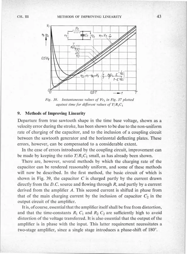
CH. III METHODS OF IMPROVING LINEARITY
VI
Y1 fc1,
0,5V1
a
R
v1i II TCt 1
wC, v,=V1
T
20 70
YC,=VI-YR=V1.4_fir+
r £ '
1-E RFr
1 0,5T ₹ T
Fig. 38. Instantaneous values of Vcl in Fig. 37 plotted against time for different values of T/R1C2
43
9. Methods of Improving Linearity
Departure from true sawtooth shape in the time base voltage, shown as a velocity error during the stroke, has been shown to be due to the non-uniform rate of charging of the capacitor, and to the inclusion of a coupling circuit between the sawtooth generator and the horizontal deflecting plates. These errors, however, can be compensated to a considerable extent.
In the case of errors introduced by the coupling circuit, improvement can be made by keeping the ratio T/R1CI small, as has already been shown.
There are, however, several methods by which the charging rate of the capacitor can be rendered reasonably uniform, and some of these methods will now be described. In the first method, the basic circuit of which is shown in Fig. 39, the capacitor C is charged partly by the current drawn directly from the D.C. source and flowing through R, and partly by a current derived from the amplifier A. This second current is shifted in phase from that of the main charging current by the inclusion of capacitor C2 in the output circuit of the amplifier.
It is, of course, essential that the amplifier itself shall be free from distortion, and that the time-constants RI CI and R2 C2 are sufficiently high to avoid distortion of the voltage transferred. It is also essential that the output of the amplifier is in phase with the input. This latter requirement necessitates a two-stage amplifier, since a single stage introduces a phase-shift of 180°.

44 THE TIME BASE CH. III
Fig. 39. Basic circuit for improving the linearity of the sawtooth voltage by means of an amplifier "A".
For perfect linearity the gain of the amplifier should be equal to 1 + R/RI. As an alternative, if absolute linearity is not required, a single valve ampli-
fier can be employed, connected as a cathode follower in order to meet the requirement that the output voltage shall be in phase with the input. The basic circuit is given in Fig. 40. The input resistance must also be high. As a practical example, using the pentode Type EF 42 which has a mutual conductance of 9.5 mA/V, and with Rk = l0kI2 and RI = 3 MI, it is possible to produce a time base voltage in which the rate of increase at the end of the charge period is only 1.8% less than at the beginning.
Vb +
0
4-Fig. 40. Circuit for improving linearity of sawtooth voltage using
only one valve, connected as a cathode follower.

CH. III METHODS OF IMPROVING LINEARITY 45
R1
vb +
Cl C
Rk
Fig. 41. Use of a pentode as charging resistance in order to improve linearity of the sawtooth voltage.
Another method of linearising the charging rate takes advantage of the fact that, over a large part of its Ia/Va characteristic, the anode current of a pentode is very nearly constant. By using a pentode instead of the charging resistance R in the basic time base circuits previously described, an almost constant charging current is supplied to the capacitor.
Fig. 42. Improved linearity of time
base voltage resulting from the Curvature
of the 'a! Vg characteristic of the
amplifying valve.

46 THE TIME BASE CH. 11I
A basic circuit showing this arrangement is given in Fig. 41. Perfect linearity cannot be achieved, since the anode current of the pentode naturally decreases more rapidly at low values of Va, but the total velocity error can be limited to about 4.8% using a pentode Type EF40 under the following conditions: Mutual conductance 1.0 mA/V; Ia = 1.0 mA; Rk = 2.5 kSZ; R1 = 3.0 MSS; R; = 5 MS2; Vb = 250 V; and V0 , the voltage to which Cis charged = 120 V.
When the sawtooth voltage has to be amplified before it is transferred to the horizontal deflecting plates of the oscilloscope tube, the curvature of the Id/V1, characteristic of the amplifying valve can be utilised to provide a measure of linearity compensation. Fig. 42 shows the influence of this non-linear characteristic on an input voltage of exponential form. Since the form of the I0/V9 characteristic is not itself exponential, perfect linearisationis not possible, but the illustration shows that considerable improvement results from the amplifying valve being controlled by a non-linear timebase voltage.
10. Methods of producing a Repeating Time Base Voltage
It has been explained that some form of automatic switch is necessary to discharge the capacitor rapidly at the end of each stroke, and two types of electronic switch for this purpose — a gas diode and a thyratron — have been described, and their limitations noted. While a thyratron permits the design of a very simple time base which can be easily synchronised by pulses of the order of 1 volt, a time base of this type is not suitable for very high sawtooth frequencies, and more satisfactory results are obtained by using vacuum valves as the electronic switch.
One method is to use one additional valve to produce a feed-back effect and the simplest of many variations of this "multi-vibrator" circuit is shown in Fig. 43, which uses a double triode, Type ECC 40. One triode section, V1, acts as the electronic switch, and the other section, V2, is the feed-back element. The operation of the circuit is as follows:
At the end of the sawtooth cycle V1 will be cut off, and capacitor C dis-charged. Capacitor C now charges via resistor R and the anode potential of V1 increases until eventually anode current begins to flow and the discharge of C commences. With increasing, anode current in V1, the voltage drop across the cathode resistor Rh increases, driving the control grid of V2 more negative so that the anode current of V2 decreases. This results in an increase
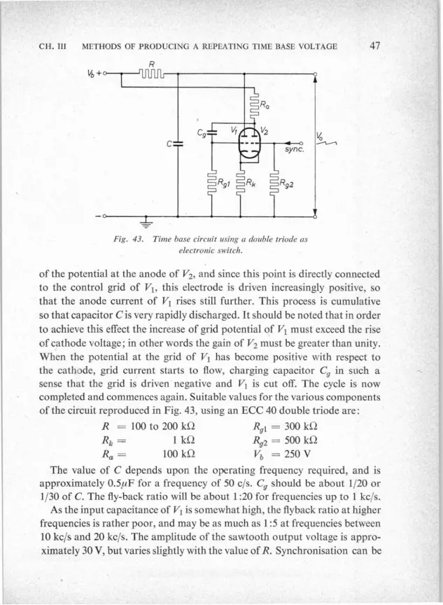
CH. III METHODS OF PRODUCING A REPEATING TIME BASE VOLTAGE 47
R
1
Fig. 43. Time base circuit using a double triode as electronic switch.
of the potential at the anode of V2, and since this point is directly connected to the control grid of V1, this electrode is driven increasingly positive, so that the anode current of VI rises still further. This process is cumulative so that capacitor C is very rapidly discharged. It should be noted that in order to achieve this effect the increase of grid potential of V1 must exceed the rise of cathode voltage; in other words the gain of V2 must be greater than unity. When the potential at the grid of Vi has become positive with respect to the cathode, grid current starts to flow, charging capacitor C9 in such a sense that the grid is driven negative and V1 is cut off. The cycle is now completed and commences again. Suitable values for the various components of the circuit reproduced in Fig. 43, using an ECC 40 double triode are:
R = 100 to 200 kL2 Rk = 1 kS2 Ra = 100 kSZ
R91 = 300 kSZ
R92 = 500 kSZ Vb =250V
The value of C depends upon the operating frequency required, and is approximately 0.5uF for a frequency of 50 c/s. C9 should be about 1/20 or 1/30 of C. The fly-back ratio will be about 1:20 for frequencies up to 1 kc/s.
As the input capacitance of V1 is somewhat high, the flyback ratio at higher frequencies is rather poor, and may be as much as 1:5 at frequencies between 10 kc/s and 20 kc/s. The amplitude of the sawtooth output voltage is appro-ximately 30 V, but varies slightly with the value of R. Synchronisation can be

48 THE TIME BASE CH. III
Fig. 44. Time base circuit similar to that of Fig. 42.
but employing two pentodes as electronic switch.
achieved by an alternating voltage of about 1 volt and of arbitrary waveform applied to the grid of V2.
A circuit similar to that in Fig. 43, but using two pentodes instead of triodes is shown in Fig. 44. Owing to the lower input capacitance of the pentode, a much better flyback ratio is obtained. Furthermore, since in this
Fig. 45. Basic circuit of blocking oscillator time base generator.

CH. III METHODS OF PRODUCING A REPEATING TIME BASE VOLTAGE 49
arrangement no coupling capacitor is required between the anode of V2 and the grid of Vt, the amplitude of the sawtooth voltage is less dependant upon the repetition frequency. Amplitude control is effected by adjusting potentio-meter R4 which varies the screen-grid voltage and hence the anode current of V2, thus controlling the mean potential of the control grid of Vi, which in turn determines the anode voltage at which Vi starts to conduct. It should be noted that the cathode of VI is at a fairly high positive potential with respect to earth, and its heater should therefore be supplied from a separate winding on the power transformer.
As an alternative to the multi-vibrator type of circuit described above requiring two valves, time bases can be built in which the feedback occurs in the circuit of a single valve. The simplest of these circuits is the blocking oscillator, the basic diagram of which is shown in Fig. 45. Although more particularly suited for generating a sawtooth voltage of one fixed frequency, and therefore not usually employed in oscilloscopes, it is included here for the sake of completeness. The essence of this arrangement is that the primary winding of transformer T is connected in the anode circuit of the triode, and the secondary in the grid circuit, in such a way that as the anode potential decreases the grid potential becomes more positive.
The operation of the circuit can best be followed by assuming that the valve is biased well beyond cut-off due to a negative charge on capacitor Cg— how this comes about will become clear later. Capacitor C charges from the HT supply via R, and the voltage across it rises exponentially in the normal manner. At the same time Cg discharges via RI so that the grid potential rises. When the grid potential has risen to just about the cut-off value, anode current begins to flow, and the resultant decrease in anode voltage causes a rise in grid voltage due to the feedback via the transformer. The anode current therefore increases, producing a further drop in anode voltage and rise in grid voltage, and the process is cumulative, allowing C to discharge rapidly through the valve. Ultimately the grid attains a positive potential, and grid current flows, re-charging Cg in such a direction that the grid is again driven negative, and the valve is cut off. The cycle then re-commences.
A somewhat similar arrangement, the squegging oscillator, is shown in Fig. 46, but the coupling between anode and grid is tighter. At the commen-cement of the cycle the circuit behaves very much like the blocking oscillator,

50 THE TIME BASE CH. III
vb +o
0 C
Fig. 46. Basic circuit of squegging oscilla-tor time base generator.
but when the anode current reaches a certain value the circuit starts to oscillate at a high frequency. The oscillations build up to a certain amplitude and then suddenly cease, the repetition frequency of these bursts of oscillation depending upon the circuit constants. A practical circuit of this type is given in Fig. 47. The valve is a double triode Type ECC 40, VI being the oscillator and V2 and its associated circuit serving as a linearising device of the type shown in Fig. 40.
The transformer should be either the primary or secondary coil of a con-ventional 470 kc/s intermediate frequency transformer wound in two identical halves and with a dust core. The built-in tuning capacitor should be removed, and the connection between the two halves of the coil should be broken. One half of the coil should be connected in the anode circuit and the other in the grid circuit.
If C is made variable in seven steps from 50,000 pF to 150 pF, and the charge resistance (R4 + R5) variable between 1.4 Mf and 0.4 MQ, the frequency range will be from 20 c/s to 20 kc/s.
The amplitude will vary between 54 V and 42 V peak-to-peak over this range of frequency adjustment, and over the control range of the charging

CH. III METHODS OF PRODUCING A REPEATING TIME BASE VOLTAGE 51
Fig. 47. Practical circuit of a squegging oscillator time base generator, employing an ECC40 double triode. The frequency can be adjusted by varying the capacit-ance of C and the charge resistance (R4 + R5). The
amplitude is adjustable by means of Rk
R1 = 10 kS2
R2 = R3 = 60 kS1
R4 = 0.4 MS2
R5 = 1.0 MSZ
Rs =2.7MSl
R7 = 1.0 MI
Rk = 10 kQ
C1 =0.22uF
C = 390 pF
C3 =4uF
resistor the flyback ratio will vary between 1 : 40 and 1 : 12 and the velocity error between —8.8 and —5.4%.
Yet another type of time base is the transitron, a basic circuit of which is given in Fig. 48. Its principle can be followed by starting at the instant of switching on, when the capacitor C is fully discharged and no anode current passes through the valve. As C charges via R, the anode voltage rises and the valve starts to pass current. The rise of anode current is accompanied
Vb+o
n
Iv
i
sync
T Fig. 48. Basic circuit of transitron time base
generator
Vo

$2 THE TIME BASE CH. III
by a decrease of screen-grid current and a consequent increase of screen-grid voltage whereby CI is charged via R1. Because of this charge on CI, the suppressor grid assumes a positive potential, with the result that the anode current increases further and the screen-grid current decreases. This process is cumulative so that capacitor C discharges rapidly through the valve. The increase of anode current produces a corresponding decrease of anode voltage. When this voltage falls to a value corresponding to the knee of the Ia/Va curve the anode current begins to decrease and the screen-grid current to increase. Increase of screen-grid current is accompanied by a decrease of screen-grid voltage so that CI discharges, the current through RIbeing at the same time reversed. The discharge of CI drives the suppressor grid negative, thus cutting-off the valve, after which the whole cycle re-commences.
Vb +
0 Z
Fig. 49. Miller-Transitron Sawtooth generator
Finally, Fig. 49 shows the basic circuit of a time base known as the Miller-transitron circuit, which differs from the simple transitron in that the capacitor C is now connected between the anode and control grid of the valve instead of between anode and cathode, while the control grid is connected to the H.T. + line via a high resistance (R 2) of the order of 2M£2.
Due to the position of capacitor C, there is heavy feedback between the anode and grid circuits. This is the well-known "Miller" effect, and one of

CH. III CIRCULAR, SPIRAL AND RADIAL TIME BASES 53
its results is that for a given value of charging current, a given voltage across the capacitor can be obtained with a much smaller capacitor than in the simple transitron.
11. Single-Stroke Time Bases
Hitherto, only repeating time base generators have been considered. For the examination of non-recurrent phenomena a time base is required the stroke of which can be started by an impulse provided from the phenomenon to be examined, and which will give only a single stroke. Such a time base can often be produced by modifying the circuit of a normal repeating time base. For many applications, however, it is preferable to employ photo-graphic recording, in which only vertical deflection due to the phenomenon under examination is employed, the horizontal sweep being obtained by movement of the film itself.
12. Circular, Spiral and Radial Time Bases
In a limited number of applications, considerable advantages accrue if the time scale of the oscilloscope is not horizontal, but is of circular, spiral or radial form.
If two sinusoidal voltages of identical frequency and amplitude, but with a phase difference of 90°, are applied to the two sets of deflecting plates, a circular trace will appear on the screen and the peripheral velocity of the spot will be uniform. In this case both sets of deflector plates are utilised for producing the time base, and the potential to be examined is used to modu-late the circumference of the trace.
If, by means of a sawtooth voltage, the amplitude of the two voltages producing a circular time base is controlled, the trace will be of spiral from, and thus gives a very long time-scale. In order to ensure that this spiral is stationary and not rotating, the time period of the controlling sawtooth voltage must be a complete multiple of that of the circular trace.
If the period of the circular trace is made very large compared with that of the sawtooth controlling voltage, the form of the trace changes from spiral to radial, thus giving a still longer time scale.
When using this type of time base it is customary to apply the voltage to be examined to the grid of the cathode ray tube. The indication then consists of variations in the brightness of the trace.

CHAPTER IV
AMPLIFIERS FOR VERTICAL DEFLECTION AND PICK-UPS FOR CONVERTING NON-ELECTRICAL PHENOMENA INTO
ELECTRICAL MAGNITUDES
In the data on standard oscilloscope tubes given in Chapter VII values are quoted for what is termed the "deflection" sensitivity. The deflection sensitiv-ity is defined as the distance through which the spot moves on the screen
when the voltage applied between a pair of deflecting plates is varied by 1 volt. It will be seen from Chapter VII that the deflection sensitivity is in the order of 0.25 mm. per volt. This means that in order to obtain a good read-able deflection very considerable voltages must be applied between the deflecting plates. For example, a vertical deflecting voltage of 40 volts peak-to-peak is required to obtain a trace only 1 cm in overall height.
A trace with a maximum amplitude of only 1 cm is not very convenient, and for accurate measurement or examination a considerably larger display is necessary so that, for most purposes, a voltage of one or two hundred volts peak-to-peak must be applied between the plates for vertical deflection.
It does not usually happen that voltages of this order are directly obtain-able from the phenomenon under investigation; indeed, the "signal" voltage is often quite small, and may even be in the order of a few millivolts only. It is therefore necessary to magnify the voltage to be examined, and this is done by introducing an amplifier between the signal source and the plates for vertical deflection.
1. Amplifiers for Vertical Deflection Voltages
The requirements which the amplifier for the vertical deflecting voltage must fulfil are in many ways much more exacting than those met with in most other branches of applied electronics. Before dealing in a general way with
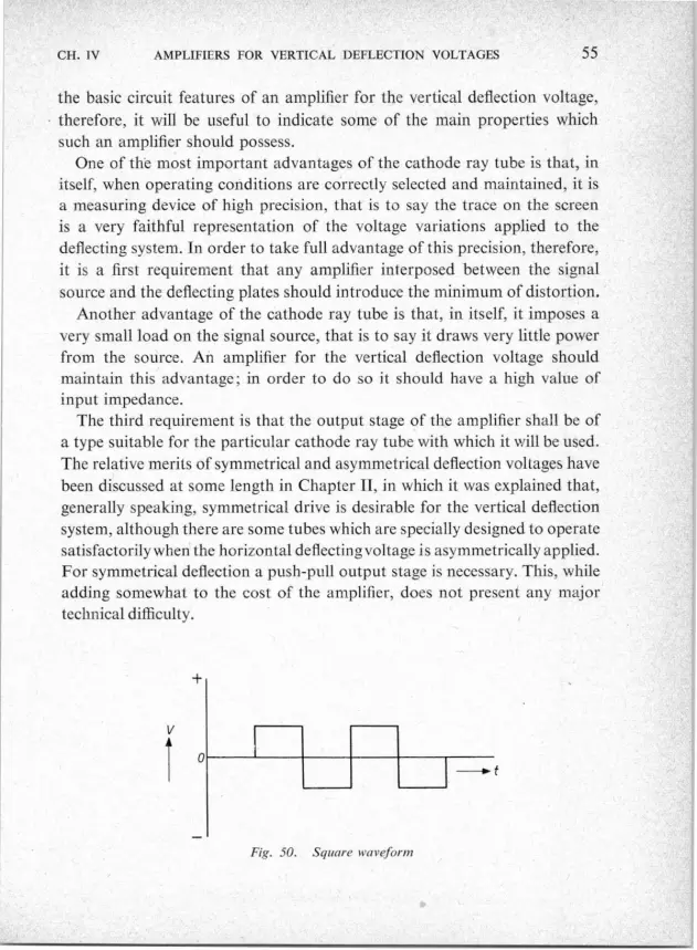
CH. IV AMPLIFIERS FOR VERTICAL DEFLECTION VOLTAGES 55
the basic circuit features of an amplifier for the vertical deflection voltage, therefore, it will be useful to indicate some of the main properties which such an amplifier should possess.
One of the most important advantages of the cathode ray tube is that, in itself, when operating conditions are correctly selected and maintained, it is a measuring device of high precision, that is to say the trace on the screen is a very faithful representation of the voltage variations applied to the deflecting system. In order to take full advantage of this precision, therefore, it is a first requirement that any amplifier interposed between the signal source and the deflecting plates should introduce the minimum of distortion.
Another advantage of the cathode ray tube is that, in itself, it imposes a very small load on the signal source, that is to say it draws very little power from the source. An amplifier for the vertical deflection voltage should maintain this advantage; in order to do so it should have a high value of input impedance.
The third requirement is that the output stage of the amplifier shall be of a type suitable for the particular cathode ray tube with which it will be used. The relative merits of symmetrical and asymmetrical deflection voltages have been discussed at some length in Chapter II, in which it was explained that, generally speaking, symmetrical drive is desirable for the vertical deflection system, although there are some tubes which are specially designed to operate satisfactorily when the horizontal deflectingvoltage is asymmetrically applied. For symmetrical deflection a push-pull output stage is necessary. This, while adding somewhat to the cost of the amplifier, does not present any major technical difficulty.
V A
+
0
Fig. 50. Square waveform

56 AMPLIFIERS AND PICK-UPS CH. IV
The last, but certainly not the least important requirement that must be met by an amplifier for the vertical deflection voltage, is concerned with the frequency band over which the amplifier can operate without serious distor-tion. An oscilloscope should be capable of depicting faithfully a voltage of any waveform, however complex. One of the most complex of waveforms —although apparently simple in geometrical shape — is the square wave such as is depicted in Fig. 50. Such a waveform, if analysed mathematically, is found to be compounded of a sine wave of the fundamental frequency, plus a large number of harmonics, that is to say sine waves having frequencies which are multiples of the fundamental frequency. In order to reproduce a square wave faithfully, the amplifier must have a level response curve for all frequencies up to at least the tenth harmonic of the highest fundamental frequency with which the oscilloscope will be expected to deal, and prefer-ably up to the twentieth harmonic. Methods of ensuring this are described in one of the following paragraphs dealing with the subject of distortion.
1.1. WHAT IS DISTORTION?
Since a prime consideration in the design of an amplifier for vertical deflec-tion is the avoidance of distortion, it may be useful at this point to consider what, in effect, constitutes distortion. The term "distortion" in its widest sense connotes any departure, in the output waveform, from the waveform of the original signal. There are a number of different types of distortion, the most important of which are defined below.
1.2. AMPLITUDE DISTORTION
In normal audio-frequency practice the word "distortion" by itself is often used to indicate what the engineer terms "amplitude distortion", by which is meant that input voltages of different amplitudes are not magnified equal-ly. This form of distortion is mainly due to the curvature of the characteristic of the amplifying valve or valves. An example, considerably exaggerated for the sake of clearness, is given in Fig. 51. Here it is seen that an input signal having a peak-to-peak value of 0.4 volt produces a change of anode current having a peak-to-peak value of 1.2 milliamperes. In a distortion-free amplifier, an input voltage having three times the amplitude, namely 1.2 volts peak-to-peak would produce a current change of 3 x 1.2 milliam-peres, or 3.6 milliamperes peak-to-peak. Is is seen, however, that in fact, due

CH. IV AMPLIFIERS FOR VERTICAL DEFLECTION VOLTAGES 57
to the non-linearity of the valve characteristic, the peak-to-peak value is only 3.3 milliamperes. In other words, amplitude distortion has occurred, and the amount of this distortion is
3.6 — 3.3 .3
3.6 xl00=3.6x1OO=8.3%.
It will be agreed that this distortion amounts to a change in the waveform, this particular example resulting from the fact that, for a large signal, the positive-going halfcycles are amplified to a greater degree than the negative-going half-cycles.
By correctly biasing the amplifying valve and by limiting the peak am-plitude of the input signal to a value which, at the working point, subtends a substantially linear portion of the valve characteristic, simple ampliude distortion in the valve can be almost completely avoided. The design cal-culations to ensure this are well known, and need no further mention here.
Fig. 51. Amplitude distortion due to non-linearity of valve characteristics
1.3. FREQUENCY DISTORTION
A much more serious form of distortion, because it is more difficult to avoid or to correct, is that known as "frequency distortion", by which is meant that input voltages of different frequencies are not amplified to the same

58 AMPLIFIERS AND PICK-UPS CH. 1V
degree. The term "frequency distortion" is not a very happy one, for it is not the frequency itself which is distorted but the waveform. It is, in effect, a special case of amplitude distortion, which is dependent upon the frequency of the signal, and it might, therefore, be well termed "frequency-dependent amplitude distortion".
This form of distortion arises mainly from the fact that the circuit of an amplifier includes a number of elements possessing capacitance, and that the reactance of a capacitor is not constant but varies with frequency. This can be explained by reference to Fig. 52, which shows at A the basic circuit of a resistance-capacitance coupled amplifier, and at B the equivalent circuit from the point of view of the amplified signal.
In this figure, Ra is the anode load of valve V1. The amplified signal voltage appearing across Ra is transferred to the grid circuit of V2 via the coupling capacitor C. R9 is the grid resistor of V2. In the equivalent circuit B, a further capacitor. Ca is shown in dotted line, in parallel with Ra. Ca represents the combined value of the output capacitance of V1, the input capacitance of V2and the various stray capacitances due to the valve holder and circuit wiring.
By suitable choice of valves and components, and care in the layout of the wiring, Ca can be kept quite small, and its reactance, which is equal to l/2rrfCa(where! = frequency and Ca is in farads) will be fairly high at low frequen-
V;
HT+
Ra
n
R9
V,
Va
HT-B
. Fig. 52. A — Basic circuit of RC coupled amplifier, B — Equivalent circuit Ra = Anode load of Vl Ry = Grid resistor of V2
C = Coupling capacitor Ca = Effective capacitance shunting Ra

CH. IV AMPLIFIERS FOR VERTICAL DEFLECTION VOLTAGES 59
cies. The impedance of the combination of Ra and Ca in parallel will there-fore not differ greatly at low frequency from the resistance of Ra, and the gain of Vi will be a close approximation to that calculated on the basis of a load equal to Ra.
Gain
1
i B -> Frequency
i I Fig. 53. General form of response curve of an RC coupled amplifier
With increasing frequency, however, the reactance of Ca decreases, so that the effective anode load of VI, which is represented by the parallel connection of Ra and Ca, becomes smaller, and the gain correspondingly less.
There is a similar variation in gain over the lower range of frequencies, but in this case the cause is the variation of the reactance of the coupling capacitor C in Fig. 52. The explanation is that the signal voltage as amplified by VI and appearing across Ra, is effectively applied across C and Rg in series, and it is only that part of the voltage which appears across Rg which forms the input to V2.
At high frequencies the reactance of C is but small, and practically the whole of the available voltage appears across Rg and is amplified by V2. At low frequencies, however, the reactance of C is greater, and the propor-tion of the total voltage which appears across Rg is therefore smaller. Valve V2 therefore receives a smaller input, and the overall gain of the amplifier at low frequencies is smaller.
It has thus been shown that the general form of the response curve of the amplifier, i.e. gain plotted against frequency, is as indicated in Fig. 53, and shows a drop of gain at the high frequency end of the waveband (A) and a drop of gain at the low frequency end of the waveband (B). In view of the necessity of so designing the amplifier that it has a substantially level response over a wide range of frequencies, steps must be taken to reduce the inherent

60 AMPLIFIERS AND PICK-UPS CH. IV
tendency to attenuation of the upper and lower frequencies, and also to provide compensation for such attenuation as cannot be avoided.
The loss of gain at the high frequency end can be reduced to some extent by operating the valves with a value of anode load, Ra, considerably smaller than that normally employed. In these circumstances the shunting effect of Ca in Fig. 52 is not so marked since its reactance, even at high frequencies, is large compared with Ra. This improvement, however, is achieved only at some sacrifice of overall gain due to the small value of the anode load, and this often necessitates additional amplifying stages. This reduction of overall gain resulting from operation with comparatively low anode load can be minimised to some extent by employing high-slope pentodes, which give a reasonable stage gain at comparatively small values of anode load.
Compensation for the drop in gain at the high frequency end of the wave-band can be applied in a number of ways. For example, part of the anode load may be made inductive, as shown in Fig. 54, the inductive component being so chosen that it resonates with Ca at a frequency near to that at which the drop in gain occurs.
Another method is to arrange that negative feedback is applied to the amplifier at low frequencies, thus reducing the gain, while at high frequencies the feedback is inconsiderable and the full amplification is available. This can be achieved by choosing a small value for the by-pass capacitor to the cathode resistor.
A third device is to reduce the effect of the stray capacitance to earth by applying positive feedback from the output of one stage to the anode of the
HT+
Fig. 54. Compensation for attenuation of high frequencies by making part of the anode load inductive
Ra = Resistive portion of anode load L = Inductive portion of anode load C = Coupling capacitor Rg = Grid resistor of following valve

CH. IV AMPLIFIERS FOR VERTICAL: DEFLECTION VOLTAGES 61
HT+ 0
Fig. 55. By applying positive feedback to the anode of the previous stage the attenuation of high frequencies
can be reduced
0
0 HT—
previous stage. An example of this is given in Fig. 55 which shows part of the circuit of a vertical deflection amplifier with push-pull output. The positive feedback is taken from the anode of the appropriate valve of the push-pull pair and is applied to the anode of the previous valve via a very small capaci-tance consisting of CI and C2 in series. Yet another method of compensating for the drop in gain at high frequencies is to introduce a cathode follower between two normal amplifying stages, and possibly also as the input valve of the amplifier. The basic circuit of a cathode follower stage is indicated in Fig. 56 in which VI is the cathode follower and V2 a normal amplifier. In the cathode follower the output is taken from a load in the cathode circuit instead of from the anode circuit. This results in very heavy negative feedback
HT+
v i
Fig. 56. Basic circuit of valve V3 connected as a cathode follower

62 AMPLIFIERS AND PICK-UPS CH. IV
being applied to the valve, which therefore has a very low output impedance. The shunting effect of the comparatively low input impedance of V2 at high frequencies thus has no significant effect. Although, due to the almost 100% feedback, the gain of the cathode follower is always less then unity, it does ensure correct impedance matching between stages over a very wide range of frequencies.
Compensation for drop in gain at the low frequency end of the waveband can be achieved in a number of ways, of which the most simple is by shunting a part of Ra by a capacitor as shown in Fig. 57. At low frequencies the reactance of the capacitor is high and its shunting effect therefore small, so that the effective load impedance is not sensibly less than the value of Ra
and maximum gain is obtained. With increasing frequency, however, the reactance of the capacitor decreases, and the effective load impedance is smaller so that the gain is reduced.
Fig. 57. Compensation for attenuation of low frequencies by shunting part of the anode load with a capacitor.
Ra = Anode load Cl = Compensating capacitor C = Coupling capacitor R9 = Grid resistor of following valve
v,
1.4. PHASE DISTORTION
HT+
RQ
Ct
C
R9
HT-
Phase distortion is the effect in which, when a signal of complex waveform is applied to the input of an amplifier, the wave form of the amplified signal differs from that of the input by reason of a change in the phase relation between the various component frequencies. This is due to the fact that, in an amplifier incorporating resistance-capacitance coupling networks, the transit times of different frequencies through the amplifier are not equal so that phase shift occurs.
This is illustrated in Fig. 58. In the left-hand graph the full line represents

CH. IV AMPLIFIERS FOR VERTICAL DEFLECTION VOLTAGES 63
Fig. 58. Distostion of a composite AC voltage due to a CR network. a) Sum voltage curve (full) and its com-ponents (dotted) in the starting position (fundamental and harmonic in phase). b) Distortion due to phase shift in a CR network
a complex waveform which, on analysis, can be shown to consist of a fund-amental sine wave and its third harmonic, these components being indicated in broken line. The right-hand graph shows how these two components appear in the output of an amplifier in which phase-shift occurs, and it is seen that there is a phase difference (in this case 30°) between them. If these two com-ponents are combined into a single resultant wave as indicated in full line, it is seen that considerable distortion has been introduced.
Phase distortion is not usually very considerable in the case of low frequen-cy inputs, but is likely to be serious at higher frequencies. Since one of the most important applications of the oscilloscope is to present a faithful trace of a waveform under examination, phase distortion is the most serious form of distortion in vertical deflection amplifiers. Since phase distortion is occasioned by the same circuit elements as those which produce frequency distortion, any steps taken to reduce the latter will also effect improvement in respect of phase distortion.
An attempt has been made in the foregoing paragraphs to indicate the principal characteristics which a vertical deflection amplifier should possess, and to outline some of the methods whereby these characteristics may be achieved. The design of an actual amplifier involves complex mathematical calculations and also the application of judicious compromise, so no instruc-tions for undertaking a complete design have been given. In the final chapter of this book, however, a number of typical oscilloscope circuits are described, and these incorporate some, at least, of the circuit devices already discussed.

64 AMPLIFIERS AND PICK-UPS CFI. IV
2. Conversion of Non-electrical Phenomena into Electrical Magnitudes
The cathode ray oscilloscope is essentially a sensitive galvanometer, and can therefore be used directly to measure or examine only electrical magnitudes, which must be applied as voltages between the deflection plates. For the examination of non-electrical phenomena it is necessary to employ some form of "pick-up" which converts the phenomena into electrical magnitudes.
A great deal of ingenuity has been displayed from time to time in devising methods of conversion, some of which involve several intermediate con-versions. Some of the principal forms of pick-up suitable for the more usual conversion operations are briefly described below. Examples of practical applications are dealt with in somewhat greater detail in Chapter VI.
2.1. RESISTANCE PICKUPS
Many non-electrical phenomena can be made to change the resistance of a suitable circuit component, and thus to change the current through the circuit of which the resistor forms a part or, what amounts to the same thing, to change the voltage drop across the resistor. This change can then be dis-played on the oscilloscope screen. Resistance pick-ups are of several types, of which the following are the most important.
(a) Compression type Resistors. In these units, variation of physical dimen-sions, of position, or of mechanical pressure cause corresponding variations of resistance. A typical example is the familiar carbon micro-phone.
(b) Temperature-sensitive Resistors. The change in resistivity which most conductors undergo with change of temperature can be exploited to form the basis of one type of pick-up for use in applications where it is required to measure variations of temperature. Both resistors having a positive temperature coefficient of resistance (i.e. those whose resistan-ce increases with rise of temperature) and those having a negative tem-perature coefficient of resistance (e.g. "thermistors" whose resistance decreases with rise of temperature) can be used in this way.
(c) Strain Gauges. These consist of fine wires, usually mounted on paper strips, cemented on to the surface of a mechanical specimen in such a way that any deformation of the specimen due to mechanical stress

CH. IV CONVERSION OF NON-ELECTRICAL PHENOMENA 65
causes elongation of the wire with corresponding reduction of cross section, both of which result in increase of resistance. Strain gauges can therefore be used for displaying change of dimensions under stress, and for measurements of weight.
2.2. PIEZO-ELECTRIC PICKUPS
When mechanical pressure is applied between a pair of opposite faces of certain crystals, notably quartz and tourmaline, a potential difference is set up between another pair of opposite faces of the crystal, and is proportional to the applied pressure. This potential difference can be amplified and applied to the vertical deflection plates of the oscilloscope, thus displaying on the screen a representation of the variation of mechanical pressure.
2.3. CAPACITANCE PICKUPS
Variations of mechanical pressure, of position, or of physical dimensions can be made to vary the distance between the plates of a small capacitor, and thus to vary its capacitance. The capacitor can be connected in an electric circuit in such a way that the variation of capacitance varies either the frequency or the amplitude of electrical oscillations, and this can be displayed on the luminescent screen.
2.4. ELECTRO-MAGNETIC PICKUPS
Variations of physical dimensions, of position or of mechanical pressure can be made to alter the configuration of a system containing an inductive element. Such a system might consist of a coil and a core or armature of magnetic material, or two mutually movable coils, or some similar combina-tion.
There are two general types of electro-magnetic pickup. In the first, the mechanical phenomenon merely varies the inductance, and therefore the reactance, of the electrical system, and these variations can be caused to vary either the frequency or amplitude of electrical oscillations. In the second type, mechanical movement or vibration can be caused to vary the position of a soft iron armature with respect to a coil having a magnetised core. The movement of the armature then induces an E.M.F. in the coil, and this, when amplified, can be applied to the deflection plates of the oscilloscope.
66 AMPLIFIERS AND PICK-UPS CH. IV
2.5. THERMO-ELECTRIC PICKUPS
The familiar thermo-couple thermometer may be used to convert change of temperature into an electrical voltage for display on the oscilloscope screen. In this device, two junctions of dissimilar metals are connected is series, one junction being maintained at a constant temperature and the other ex-posed to the temperature it is desired to measure. An E.M.F. is set up in the circuit and is proportional to the difference between the temperatures at the two junctions. This E.M.F., if necessary suitably amplified, can be applied to the deflecting plates of the oscilloscope tube.
2.6. PHOTO-ELECTRIC PICKUPS
Any of the three forms of photocell can be used to convert light into an electrical magnitude. These three types are:
(a) Photo-conductive cells, the resistance of which varies in accordance with the amount and wavelength of the light falling upon them.
(b) Photo-voltaic cells, which generate an E.M.F. when irradiated with light.
(c) Photo-emissive cells, the cathodes of which emit free electrons when light falls upon them.
These cells can be used directly for measurements of light intensity and colour, and are also employed as an intermediate stage in the examination of other non-electric phenomena such as changes of physical dimensions or position, mechanical vibration etc. In these applications the phenomenon under examination is made to vary the area of an aperture through which light passes on to the photocell, and the electrical variations so produced are amplified and applied to the deflecting system of the oscilloscope.
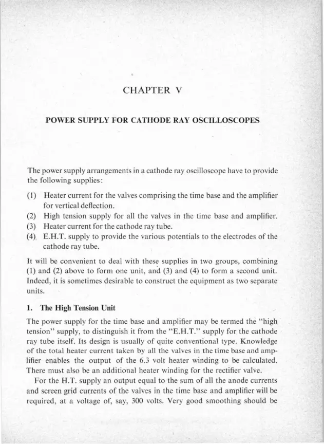
CHAPTER V
POWER SUPPLY FOR CATHODE RAY OSCILLOSCOPES
The power supply arrangements in a cathode ray oscilloscope have to provide the following supplies:
(1) Heater current for the valves comprising the time base and the amplifier for vertical deflection.
(2) High tension supply for all the valves in the time base and amplifier. (3) Heater current for the cathode ray tube. (4) E.H.T. supply to provide the various potentials to the electrodes of the
cathode ray tube.
It will be convenient to deal with these supplies in two groups, combining (1) and (2) above to form one unit, and (3) and (4) to form a second unit. Indeed, it is sometimes desirable to construct the equipment as two separate units.
1. The High Tension Unit
The power supply for the time base and amplifier may be termed the "high tension" supply, to distinguish it from the "E.H.T." supply for the cathode ray tube itself. Its design is usually of quite conventional type. Knowledge of the total heater current taken by all the valves in the time base and amp-lifier enables the output of the 6.3 volt heater winding to be calculated. There must also be an additional heater winding for the rectifier valve.
For the H.T. supply an output equal to the sum of all the anode currents and screen grid currents of the valves in the time base and amplifier will be required, at a voltage of, say, 300 volts. Very good smoothing should be

68 POWER SUPPLY FOR CATHODE RAY OSCILLOSCOPES CH. V
0T+ bbbbbD`
HT-
0
Fig. 59. Basic circuit of H.T. unit for oscilloscope
incorporated in order to keep the ripple voltage on the H.T. supply not greater than 0.5 volt peak-to-peak.
Design considerations for such a unit are well known, and the design itself should present no difficulties. No specific design is given in this chapter, but details of typical units will be found among the circuits of complete oscillo-scopes given in Chapter VIII. A basic circuit, however, is shown in Fig. 59.
A full-wave rectifier valve will, of course, be employed, and a suitable type is the EZ80, a modern miniature rectifier on the Noval nine-pin base. This valve has an indirectly-heated cathode, the heater current being 0.6 ampere at 6.3 volts. The EZ80 is rated for a maximum rectified output of 90 milliam-peres, and should be operated in conjunction with a reservoir capacitance of 5QuF. A limiting resistor should be included in series with each anode in order to avoid overloading in the event of a fault or short-circuit.
Typical operating conditions for the EZ80 are tabulated below: --
Anode voltage (r.m.s.) 2x250 2x275 2x300 2x350 V Resevoir capacitance 50 50 50 50 ,uF Limiting resistor (each anode) 125 175 215 300 S2 Rectified current 90 90 90 90 mA Output voltage 265 285 310 360 V
Regulation curves corresponding to these working conditions are repro-duced in Fig. 60. If a larger rectified output is required, type GZ32 rectifier

Cu. v THE E.H.T. UNIT 69
0 20 40 60 80 Zout (mA)
Fig. 60. Regulation curves for EZ80 full-wave rectifier
may be employed. This is a full-wave rectifier with indirectly-heated cathode, the heater rating being 2.3 amperes at 5.0 volts. This valve is on the Octal base. Performance curves for a variety of operating conditions are given in Fig. 61.
2. The E.H.T. Unit
The data of standard ocsilloscope tubes given in Chapter VII indicates that, for the smaller tubes up to 7 cm screen diameter, an E.H.T. supply at about 800 to 1,000 volts is required for normal applications, while for the larger tubes the E.H.T. potential required ranges from, say, 2,000 volts to 5,000 volts according to whether post deflection acceleration is or is not applied.
70
V ut (V)
400
300
200
170
POWER SUPPLY FOR CATHODE RAY OSCILLOSCOPES CH. V
Qa500Vnns f"""'"'1ii'11""1"t"1"
►a=350Vrms
'000ue •_ C=~:; . e.■rorurrriir■■ _ ■ee■: __ ■ r _16E[F R_50.11,rrouuo ':_■. ■■ --v~000eio■ - -•GUeem. .—e_-U." rouurrr pees_■. 'v'■■__■■e~eoreiiu.- ■iio~~e =32 F R=100JL ueeuerruu■■.. e-euu':-_ e~:—u Ginonnun o ou ue_ uoeeoiee ■ e e ieu '■~c-_ =~~■: .rr..: -•■o o ~=iiGi =60~F R-150,tL eeoeeenooe~oeoonooioe'c-~'r..~= -_ ~~pie~e■.- -.■■o oeone oeoonenoeeiu: _ ■iiee■: acne_■.. =16irF R= 50dL iiiiii.....u,""'iiii.u.u..iiii .iiii i i.C=32ftF R=100db eeeeeeeeeeeeeeeeeeeeereeeeeeeeeeeeeeeeeeeeeeeeeeie'■:--_.■e~ 60 F llllllllnlllllllllllllllllllllllllllllllllllllllllllllln.i = fi R=150JG
300Vims
50 100 150 200 250 300 rout (mA)
capacitor input -- choke input L =10 Henries
Fig. 61. Performance curves for GZ32 full-wave rectifier
a=300Vms
a=250V,ms
This in itself imposes on the E.H.T. supply unit requirements very different
from those applicable to the H.T. unit. There are, however, several other points of difference. In the first place,
the current drawn by the cathode ray tube itself is quite small — in the order of a few tenths of a milliampere. But since the potentials for the various tube electrodes are taken from a potentiometer connected across the E.H.T. supply, the standing current of this potentiometer must also be taken into consideration, and a figure of about 3 milliamperes may be taken as the normal total E.H.T. loading.
Normally a suitable half-wave rectifier valve is employed, in conjunction with a simple resistance-capacitance smoothing netwerk.
The simple basic circuit for an E.H.T. supply unit is shown in Fig. 62. No component values are given here, for these depend upon the cathode ray tube employed and the E.H.T. voltage required. Some typical designs, with component values, will be found in the various circuits for complete oscilloscopes reproduced in Chapter VIII. The following general remarks
should, however, be kept in mind: Since the output of the E.H.T. unit is quite small, the rectified E.H.T.

CH. V THE E.H.T. UNIT 71
voltage available will be approximately times (1.414 times) the r.m.s. value of the alternating voltage applied to the rectifier valve. This enables the ratio of the mains transformer to be calculated. For example, a transformer secondary winding designed to produce a voltage of 700 volts r.m.s. will result in a rectified voltage of approximately 1,000 volts prior to smoothing.
A suitable winding to provide the heater current for the rectifier valve must be provided on the mains transformer, and also an additional winding
Fig. 62. Basic circuit of E.H.T. unit for oscilloscope
to supply the heater of the cathode ray tube. This latter winding must be particularly well insulated from the transformer core and from the other windings, because it is normal practice to earth the positive terminal of the E.H.T. supply so that the cathode and heater of the cathode ray tube are at a high negative potential with respect to earth practically equal to the full E.H.T. voltage.
A suitable high voltage rectifier valve for use in the E.H.T. supply unit is Type EY51. This is a half-wave rectifier with indirectly-heated cathode. The heater, which is internally connected to the cathode, is rated at 90 milliam-peres at 6.3 volts. In order to avoid overloading the heater, with consequent risk of damage not only to the heater but also to the cathode, care should be taken in designing and building the transformer to ensure that the nominal heater voltage is not exceeded.

72 POWER SUPPLY FOR CATHODE RAY OSCILLOSCOPES CH. V
The. EY51 is a miniature all-glass valve with flying leads instead of pin connections, so that the valve may be directly soldered to the wiring of the unit. There are two leads at the lower end of the valve for the heater connec-tions, one of which is also the cathode connection. The anode lead is at the top of the valve. Care must be exercised when soldering the valve into the unit, the anode lead being soldered not closer than 10 mm. from the bulb, and the heater lead not closer than 5 mm. Great care should also be taken not to bend the anode lead near the point at which it is sealed into the bulb.
3. General Hints
As previously mentioned, it is often desirable to design the power supply for an oscilloscope as two separate units, the H.T. supply being mounted on a sub-chassis within the complete instrument, or even as an entirely separate piece of apparatus in its own case. The latter arrangement is often preferred by amateurs and experimenters, and also in laboratories, schools and technical colleges, as it allows the power unit, which is a useful piece of apparatus in itself, to be used on occasion for other purposes. The E.H.T. unit, however, is usually incorporated in the cathode ray tube unit.
In view of the high potentials involved, great care must be exercised in the matter of insulation, particularly in connection with the E.H.T. unit.
• Another important point is the avoidance of stray magnetic fields from the mains transformers. Such fields, should they penetrate into the cathode ray tube, are likely to cause interference with the deflection of the beam, and may possibly also affect focus. The mains transformers should therefore be of good design, having very small magnetic leakage. It is possible to reduce the effect of stray magnetic fields by locating and orientating the transfor-mers in such a way that the stray field does not enter the cathode ray tube, or does not enter the tube at an unfavourable angle. For example, the E.H.T. transformer may be located behind the tube and turned so that the direction of any stray field is along the axis of the tube.
The most satisfactory method, however, is to screen the transformer from the cathode ray tube, preferably with mu-metal screens. These screens may be fabricated from sheet metal or, as is often the practice in professional oscilloscopes, the cone and neck of the tube may be enclosed in a mu-metal funnel the contour of which matches that of the tube.

CHAPTER VI
PRACTICAL APPLICATIONS OF THE OSCILLOSCOPE
In Chapter II mention was made of the principal kinds of examinations and measurements for which the cathode ray oscilloscope may be employed, and these were briefly classified as follows:
1. Measurement of a single magnitude. 2. Examination of the relationship between two magnitudes.
(a) When one of the magnitudes is time, ( i) periodic or recurrent phenomena (ii) non-recurrent phenomena.
(b) When neither of the magnitudes is time. In Chapter IV it was emphasised that, in itself, a cathode ray oscilloscope
can measure or display only electrical magnitudes, and a number of typical "pick-up" devices for converting non-electrical phenomena into electrical magnitudes were described.
From these earlier references to the uses of the oscilloscope it will have become clear that the instrument is a most valuable tool, and has a wide range of application, embracing almost every branch of industrial activity and scientific research. Among the many fields of application may be men-tioned the measurements required during the design, testing and servicing of electrical equipment, and particularly electronic equipment; the investigation of mechanical problems and the examination and testing of materials in the engineering industries; and measurements and investigations in many bran-ches of physiology and neurology.
It would be impossible, in a book of this size, to attempt even to catalogue all known applications of the cathode ray oscilloscope, while to describe
74 PRACTICAL APPLICATIONS OF THE OSCILLOSCOPE CH. VI
them all many volumes would be required. In this chapter, therefore, only a brief description of a few typical examples in some of the principal fields will be given, the selection being confined, in the main, to applications most likely to be of interest to those for whom the book is primarily intended, namely the student, the amateur constructor and experimenter, and the industrial technician. Some of the examples will be quite simple, and are included mainly as practical exercises to give the student some experience in the use of the instrument. The notes do not, in most cases, set out to give complete instructions for conducting particular investigations, only the general principles being described. For more detailed instructions the reader is referred to the many specialised books and articles on the subject.
The simplest type of application is the use of the oscilloscope for measuring simple quantities such as voltage, current and resistance. This method is of little practical value, since any well-equipped laboratory or test room will contain a range of amperemeters, voltmeters and ohm-meters of conventional type. Even measurement of capacitance, inductance and reactance, all of which are possible with an oscilloscope, are seldom undertaken, as suitable direct-reading instruments are usually available.
These simple measurements do, however, provide useful exercises, and a few are therefore included here. They also serve to emphasise the fact that the oscilloscope is, in reality, only a very sensitive and accurate voltmeter, the size and shape of the display on the screen being determined solely by the values, waveforms and frequencies of the voltages applied to the deflect-ing system.
1. Calibrating the Oscilloscope
Before using an oscilloscope for quantitative measurements it is necessary to calibrate it so that the deflections can be read directly in suitable units, or are readily translated into the required units. For this purpose it is not sufficient to measure the deflection in, say, millimetres and then to calculate the corresponding electrical value by using the figures for deflection sensitivi-ty quoted by the tube makers. These sensitivity figures, which are expressed in terms of the amount of deflection in millimetres per volt of deflecting E.M.F., are nominal values only, and vary slightly from tube to tube, and also depend upon the E.H.T. voltage applied to the anode of the tube, reduction of this voltage below the specified value resulting in an increase of

CH. VI CALIBRATING THE OSCILLOSCOPE 75
Fig. 63.
A — Trace of a sinusoidal voltage applied to the horizon-
tal deflection plates
B — Trace of a sinusoidal voltage applied to the vertical
deflection plates
C — Horizontal and vertical axes of calibration scale
D — Axes and outer frame of calibration scale
E— Completed calibration scale
D
A B
C
E
deflection sensitivity, and increase of E.H.T. voltage resulting in reduced sensitivity.
The following is the conventional method for calibrating an oscilloscope: 1. Disconnect or switch off the time base (horizontal deflecting voltage). 2. Apply an alternating voltage of known value between the plates for
horizontal deflection. This voltage may be conveniently obtained from the 50 c/s mains supply via a suitable transformer, and the actual voltage should be measured by means of an accurate voltmeter. The trace will appear as a horizontal line, and the deflecting voltage must be adjusted until the length of the line corresponds approximately to the diameter of the flat portion of the screen, avoiding the edges where the screen is more or less curved. See Fig. 63 (A).
3. Mark the positions of the two extremities of the line with chinagraph pencil, and join to make a horizontal line.
4. Disconnect the horizontal deflecting plates, and apply the same voltage to the plates for vertical deflection. A vertical trace will now appear on the screen. (See Fig. 63 (B)). This trace will be longer than the horizontal trace although the deflecting voltage is the same in each case. The reason is that
76 PRACTICAL APPLICATIONS OF THE OSCILLOSCOPE CH. VI
the plates for vertical deflection are nearer the cathode of the tube than are the plates for horizontal deflection, and the deflection sensitivity is therefore greater.
5. Mark the extremities of the vertical trace with chinagraph pencil and join up as before, thus forming a cross as in Fig. 63 (C)).
6. Draw a rectangle on the tube face such that the arms of the cross bisect the four sides of the rectangle. Draw also the diagonals of the rect-angle. (See Fig. 63 (D)).
7. Measure the lengths of the horizontal and vertical lines in millimetres. The length of the horizontal line represents the peak-to-peak value of the applied voltage, or 2 times its r.m.s. value. The horizontal deflection sensitivity of the instrument in millimetres per volt is therefore obtained by dividing the length of the horizontal trace by 2.82 times the r.m.s. value of the voltage used for the calibration test. Similarly, the length of the vertical line represents times the r.m.s. value of the deflection voltage, and the vertical deflection sensitivity can be calculated in the same way. A check should now be made against the published data for the particular tube in-corporated in the instrument to confirm that the measured values of deflec-tion sensitivities are in reasonable agreement with the nominal values quoted in the data.
8. It now remains to provide a suitable scale upon which deflections and voltages can be read. There are two methods of doing this. In the first, the vertical and horizontal sides of the rectangle can be accurately divided into centimetres or smaller units such as 5 mm intervals, and the corresponding points joined up as shown in Fig. 63 (E). Horizontal and vertical deflections can then be measured in mm and the corresponding voltages obtained from a set of calibration curves. Alternatively the voltage scales may be drawn direct on the tube face. For example, suppose that the measured vertical deflection sensitivity is found to be 0.25mm/V and the measured horizontal deflection sensitivity 0.20mm/V. The vertical voltage scale could then be made by drawing horizontal lines above and below the axis at intervals of 5mm, when each division would represent 20 volts. Similarly the horizontal scale could be made by drawing vertical lines on either side of the vertical axis and spaced 4mm apart, each division again representing 20 volts.
Of course a scale drawn with chinagraph pencil on the glass face of the tube is not likely to be very accurate or very permanent. Having marked the

CH. VI SOME SIMPLE MEASUREMENTS 77
b
vertical and horizontal axes of the rectangle as described above, however, these measurements can be transferred to a square of thin perspex or other transparent material, and the scale completed in indian ink or, better still, engraved with a sharp scriber. The perspex sheet can then be clipped in front of the tube face. It must be emphasised that the calibration obtained in this way holds good only for the particular value of E.H.T. voltage used during the measurement, and it is a good plan to write on the calibration scale the voltage at which the test was taken.
Fig. 64.
(a) Connections for deflection system when measuring
voltage
(b) Trace when Visa direct voltage
(c) Trace when V is an alternating voltage
2. Some Simple Measurements
Having provided the oscilloscope with a calibration scale, some simple measurements may be undertaken in order to gain some practice in the use of the instrument. The simplest measurement is, of course, that of voltage. The voltage to be measured is applied between the plates for vertical deflec-tion, the plates for horizontal deflection being connected together and to one of the plates for vertical deflection as indicated in Fig. 64, and the time base voltage switched off. If the voltage to be measured is a direct voltage the trace will be a stationary spot, its height above or below the horizontal axis indicating the value in volts. For an alternating voltage the trace will be a vertical line the length of which gives the peak-to-peak value of the voltage. In the case of a sinusoidal voltage the r.m.s. value is calculated from the formula:
Vr.m.s. = Vvk x 0.707 or, Vnk-vk x 0.354
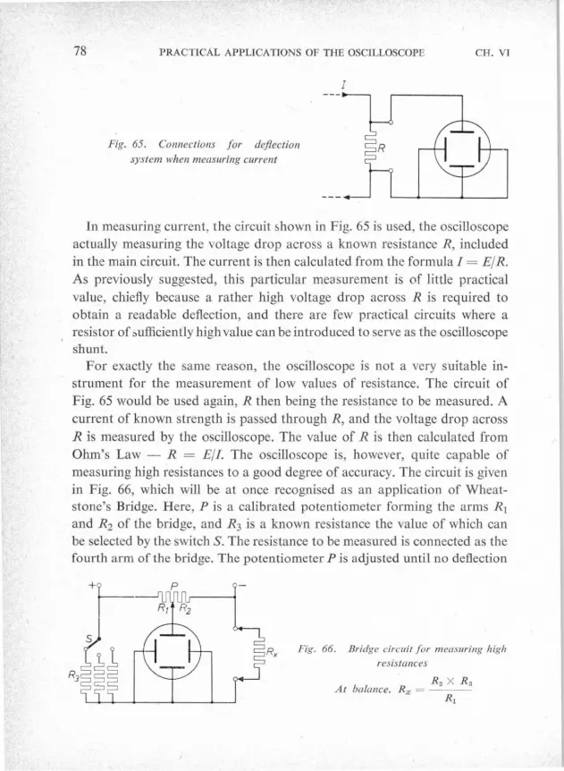
7s PRACTICAL APPLICATIONS OF THE OSCILLOSCOPE CH. VI
Fig. 65. Connections for deflection system when measuring current
I
In measuring current, the circuit shown in Fig. 65 is used, the oscilloscope actually measuring the voltage drop across a known resistance R, included in the main circuit. The current is then calculated from the formula I = E/R. As previously suggested, this particular measurement is of little practical value, chiefly because a rather high voltage drop across R is required to obtain a readable deflection, and there are few practical circuits where a resistor of sufficiently high value can be introduced to serve as the oscilloscope shunt.
For exactly the same reason, the oscilloscope is not a very suitable in-strument for the measurement of low values of resistance. The circuit of Fig. 65 would be used again, R then being the resistance to be measured. A current of known strength is passed through R, and the voltage drop across R is measured by the oscilloscope. The value of R is then calculated from Ohm's Law — R = E/I. The oscilloscope is, however, quite capable of measuring high resistances to a good degree of accuracy. The circuit is given in Fig. 66, which will be at once recognised as an application of Wheat-stone's Bridge. Here, P is a calibrated potentiometer forming the arms RIand R2 of the bridge, and R3 is a known resistance the value of which can be selected by the switch S. The resistance to be measured is connected as the fourth arm of the bridge. The potentiometer P is adjusted until no deflection
R~
H
P
R2
Rx Fig. 66. Bridge circuit for measuring high resistances
At balance. Rx — R% x R,
R1

CH. vl MEASUREMENTS OF PHASE RELATIONSHIP 79
appears on the screen. The value of the unknown resistor is then calculated from the formula:
Rx = R2 x R3/RI
Although these simple measurements may not be of very great value for single observations, they are often the basis of interesting applications in the testing of large numbers of similar components.
3. Measurements of Phase Relationship
The measurement of the phase difference between two alternating voltages of the same frequency is an important application of the cathode ray oscillosco-pe. One of the voltages is applied to the plates for horizontal deflection and the other to the plates for vertical deflection one plate of each pair being
Fig. 67. Connections for de-flection system when measuring
phase relationship V~
common to both deflecting circuits as shown in Fig. 67. Since one voltage will tend to produce a horizontal trace and the other a vertical trace, the two voltages applied simultaneously will produce a trace in the form of a sloping line provided the two voltages are either in phase or in antiphase, the slope of the line depending upon the relative amplitudes of the two voltages under examination. If the two voltages have any other phase relation the trace will be an ellipse, the slope of the major axis of the ellipse depending upon the relative amplitudes of the two voltages. Assuming that the cathode ray oscillograph is so connected that a positive-going horizontal deflecting voltage causes movement of the spot to the right and that a positive-going vertical deflecting voltage causes an upward movement of the spot, typical traces for various phase angles are given in Fig. 68.
The actual phase angle can be ascertained by first adjusting the two de-flecting voltages to equality, and then measuring the major and minor axes of the elliptical trace. The phase angle is then:
length of minor axis = 2 arc tan
length of major axis or, from Fig. 68(d)
= 2 arc tan ab/cd

80 PRACTICAL APPLICATIONS OF THE OSCILLOSCOPE
Fig. 68. Typical traces indicating phase displace-ment between two sinusoidal voltages
(a) Voltages of equal amplitude in phase (0 = 0)
(b) Voltages of equal amplitude in anti-phase (0 = 180°)
(c) Voltages of unequal amplitude in anti phase
(0 = 180°)
(d) Voltages of equal amplitude. 0 = 2 arc tan (ab/cd)
(e) Voltages of equal amplitude in quadrature
(0 = 90°)
CH. VI
Fig. 69. Connections for deflection system when measuring reactance. R is a calibrated variable resistor. A resistor of known value, later replaced by the capacitor or in-ductor under test, is connected
between A and B.
4. Measurement of Capacitance, Inductance and Reactance
The bridge method described earlier for the measurement of high resistances also forms the basis for making approximate measurements of capacitance, inductance and reactance. The circuit should be set up as indicated in Fig. 69, using the calibrated screen already prepared. In this circuit, Z is a resistor of about 40 kg), and R is a calibrated variable resistor. An alternating voltage of known frequency, (e.g. derived from the alternating current mains) is applied to the circuit as shown, and R is adjusted until the trace on the screen appears as a line coinciding with the diagonal of the rectangle on the calibration screen. In these circumstances VR = V.
The extremities of this line are now marked with a chinagraph pencil, and a rectangle with this line as diagonal is drawn as shown in Fig. 70(A). Resis-tor Z is now replaced by the capacitor or inductor it is required to measure,

CFI. VI FREQUENCY COMPARISON 81
and resistor R is again adjusted until the trace, which may be elliptical, lies within the rectangle already drawn. (See Fig. 70 (B)).
The reactance of the capacitor or inductor is equal to the value of R, and the capacitance or inductance can be calculated from the formulae:
C = 1/2itfR or L = R/2 rf
Fig. 70. A a—c is the trace when Z in Fig. 12 is a resistor and the variable resistor R is adjusted until VR = VZ
B Trace when Z in Fig. 14 is the capacitor or inductor under test and variable resistor R is readjusted so that VR = T'Z
5. Frequency Comparison
It has already been shown (see page 7) that if an alternating voltage is applied to the plates for vertical deflection and a sawtooth voltage of the same frequen-cy to the plates for horizontal deflection, the spot will trace out the voltage waveform and just one cycle of the wave will be displayed.
If the sawtooth frequency is half the frequency of the voltage under examination two complete cycles will be displayed and so forth. If, therefore, an accurately calibrated sawtooth generator of variable frequency is avail-able, it is possible, by varying the sawtooth frequency, to measure the frequen-cy of the voltage applied to the vertical deflection system.
Another method is to use, instead of a sawtooth horizontal deflecting voltage, a voltage of sinusoidal or approximately sinusoidal waveform. In the paragraph headed "Measurement of Phase Relationship" (page 79) it was shown that if alternating voltages of equal frequency but with a phase difference are applied to the two sets of deflecting plates, the resultant trace is a simple closed figure — an ellipse or circle. If, now, voltages of different frequencies are employed, traces of more complex form — the so-called Lissajous figures — will be produced. The ratio between the two frequencies

82 PRACTICAL APPLICATIONS OF THE OSCILLOSCOPE CH. VI
can be determined by inspection. The method of doing this can best be explained by reference to Fig. 71, which shows a few typical figures. Imagine horizontal and vertical lines to be drawn at the top and side of the trace as shown in the figure. Then count the number of loops in the figure which touch the horizontal line, and also the number of loops which touch the vertical line. The ratio of the frequency of the vertical deflecting voltage, fy, to the frequency of the horizontal deflecting voltage, fx is then:
fy No. of loops touching horizontal line
fx No. of loops touching the vertical line
Fig. 71. Typical Lissajous figures for various frequency ratios fy/fx.
(a) fy = fx (d) fy/fx = 1/3
(b) fy/fx = 2 (e) fy/fx = 3/ 2
(c) fy/fx = 3
a b
88795
Thus, in Fig. 71, (a) represents the trace when fy = fx; (b) is the form of trace when fy/fx = 2; (c) for fy/fx = 3; (d) for fy/fx = 1/3; and (e) for fy/fx = 3/2.
If either fy or fx is known, the other frequency can be calculated. This method is satisfactory when the frequency ratios are small and either whole numbers or simple ratios like 3/2 or 7/4; but for larger or more complex

CH. 6 THE ELECTRONIC SWITCH 83
ratios it becomes difficult to count accurately the number of loops, particular-ly if the waveforms have a considerable harmonic content which will cause distortion of the Lissajous figures.
6. The Electronic Switch
A third method of frequency comparison depends upon the use of the so-called electronic switch, which is a device for permitting two different traces to be visible on a single screen at the same time, by applying two vertical deflecting voltages alternately at intervals which are short compared with the persistence of the screen material. The electronic switch is such a useful adjunct to a cathode ray oscilloscope that its basic principle can with ad-vantage be described here. The apparatus incorporates a circuit for generat-ing a square-topped alternating voltage — usually some form of multivibra-tor circuit is employed for this purpose. This square wave is applied simul-taneously, but in anti-phase, to the control circuits of two similar amplifiers as indicated in Fig. 72,
so
that when one amplifier is operative the other is cut-off, and vice versa. The two voltages be to examined are applied to the input circuits of the two amplifiers as shown, the outputs of the amplifiers being connected to the vertical deflection plates. Two traces therefore appear on the screen in succession, and are repeated at a frequency equal to the frequency of the square wave. Owing to the persistence of the cathode ray tube phosphor, both traces will be visible at the same time of the eye.
In using the electronic switch for frequency comparison, the voltage whose
Fig. 72. Block diagram of electronic switch. SWG is a square wave generator, and A and B amplifiers. In this example the inputs to A and
B are sinusiodal voltages of frequencies fl and f 2. Both sine waves are displayed on the cathode ray tube screen

84 PRACTICAL APPLICATIONS OF THE OSCILLOSCOPE CH. VI
Fig. 73. Dual trace resulting from the connections shown in Fig. 72. The ratio f i f 2 can be determined by counting the number of complete
cycles in a given length of each trace. '
frequency it is desired to ascertain is applied to the vertical deflection plates via one arm of the electronic switch, and a voltage of known (and preferably adjustable) frequency is applied to the vertical deflection plates via the other arm of the electronic switch. The two traces then appear as in Fig. 73, and if the value of f2 is known, the value of f 1 can be calculated from the ratio of the number of cycles of f 1 and f2 which appear on a given length of time base.
7. Applications Involving a Circular Time Base
If two voltages of sinusoidal waveform and having a phase difference of 90° are applied to the plates for vertical and horizontal deflection, the resultant trace will be a closed figure of elliptical form with the two axes horizontal and vertical. If the two voltages are so adjusted that the maximum horizontal deflection is equal to the maximum vertical deflection, the ellipse becomes a circle. This circular trace is, of course, the path of a single spot which moves in a circle and completes one revolution during one complete cycle of the applied voltage. The angular displacement of the spot is thus proportional to time, and the radius of the trace is proportional to the peak value of the deflecting voltage. Finally, the existence or otherwise of a luminous spot can be controlled by the voltage applied between the cathode and first grid of the cathode ray tube. A circular trace of this kind can form a most useful time base which permits of a wide variety of applications.
Fig. 74. Basic circuit for producing a circular time base, Rl determines the radius of the trace. RZ = 1/2 sv fC2 R3 = 1/2 fC$R4 R5 is a potentiometer for adjusting the trace to a perfect circle.

CH. VI FREQUENCY COMPARISON 85
Fig. 75. Connections for deflection system when comparing the frequencies of two voltages using the circular time base
method. ° The points 1, 2, 3, 4 correspond to points 1, 2, 3, 4 in Fig. 74.
L
A
fj
B°--
A basic circuit for producing a circular time base is shown in Fig. 74. Here, an alternating voltage is applied to the input terminals, its frequency determining the time corresponding to 360° angular movement of the spot. The potentiometer RI determines the radius of the trace although, as will be indicated later, it can also be arranged that the radius is varied by a signal applied to the anode of the tube, or to one of the deflection circuits. The two combinations R2, CZ and R3, C3 in which R = 1/2nfC provide the necessary 90° phase difference between the horizontal and vertical deflecting voltages, and the potentiometer R4.R5 serves to compensate for the difference between the vertical and horizontal deflection sensitivities, and thus to ensure a truly circular trace.
A few typical examples of the use of the circular time base arrangement are given below.
8. Frequency Comparison
(a) The circuit is set up as shown in Fig. 75, the frequency of the time base input being several times less than that of the voltage under examination. The voltage to be examined is now applied between points A and B, that is to say between the deflection system and the tube anode. This voltage there-
1 1
2
U
3 Fig. 76. Traces corresponding to (a)
fife = 6 and (b) fife = '/z using the circular time base method

86 PRACTICAL APPLICATIONS OF THE OSCILLOSCOPE CH. VI
Fig. 77. Connections for the deflection system for the elliptical time base method of frequency comparison.
The points 1, 2, 3, 4 correspond to points 1, 2, 3, 4, in Fig. 74
fore varies the effective anode voltage of the tube, and with it the deflection sensitivity, with the result that the circumference of the trace will carry a number of ripples, one for each cycle of the voltage under examination. The number of ripples gives the ratio between the signal frequency fI and the timebase frequency f2. For example, in Fig. 76 (a) the ratio f1/f2 = 6. If a double trace appears the ratio is equal to the number of ripples divided by 2, and for a triple trace the number of ripples must be divided by 3 to give the frequency ratio. For example, the ratio in Fig. 76 (b) is 7/2.
(b) Alternatively, the signal voltage of frequency f could be applied in series with one pair of deflection plates as indicated .in Fig. 77. The trace will then be of elliptical form, bearing ripples as in Fig. 78. The frequency ratio is calculated in the same way as for the circular time base method, noting that it is only the upward pointing peaks of the ripples which must be counted.
Fig. 78. Trace corresponding to f l/f3 = 15, using the elliptical time base method of
frequency comparison
(c) The beam suppression method is the last method of frequency comparison which will be described. The oscilloscope is set up with a circular time base as before, but the first grid of the tube is given a heavy negative bias — approximately to cut-off point. The voltage to be exa-mined, suitably attenuated if necessary, is now applied between cathode
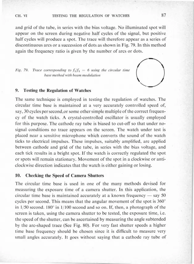
CH. VI TESTING THE REGULATION OF WATCHES 87
and grid of the tube, in series with the bias voltage. No illuminated spot will appear on the screen during negative half cycles of the signal, but positive half cycles will produce a spot. The trace will therefore appear as a series of discontinuous arcs or a succession of dots as shown in Fig. 79. In this method again the frequency ratio is given by the number of arcs or dots.
Fig. 79. Trace corresponding to f1/f2 = 6 using the circular time base method with beam modulation
9. Testing the Regulation of Watches
The same technique is employed in testing the regulation of watches. The circular time base is maintained at a very accurately controlled speed of, say, 30 cycles per second,or some other simple multiple of the correct frequen-cy of the watch ticks. A crystal-controlled oscillator is usually employed for this purpose. The cathode ray tube is biased to cut-off so that under no-signal conditions no trace appears on the screen. The watch under test is placed near a sensitive microphone which converts the sound of the watch ticks to electrical impulses. These impulses, suitably amplified, are applied between cathode and grid of the tube, in series with the bias voltage, and each tick results in a bright spot. If the watch is correctly regulated the spot or spots will remain stationary. Movement of the spot in a clockwise or anti-clockwise direction indicates that the watch is either gaining or losing.
10. Checking the Speed of Camera Shutters
The circular time base is used in one of the many methods devised for measuring the exposure time of a camera shutter. In this application, the circular time base is maintained accurately at a known frequency — say 50 cycles per second. This means that the angular movement of the spot is 360° in 1/50 second. 180° in 1/100 second and so on. If, then, a photograph of the screen is taken, using the camera shutter to be tested, the exposure time, i.e. the speed of the shutter, can be ascertained by measuring the angle subtended by the arc-shaped trace (See Fig. 80). For very fast shutter speeds a higher time base frequency should be chosen since it is difficult to measure very small angles accurately. It goes without saying that a cathode ray tube of

88 PRACTICAL APPLICATIONS OF THE OSCILLOSCOPE CH. VI
very short persistence must be used for this method of camera testing, for if the screen is of even medium persistence the calculated exposure time will be longer than the actual time by an amount approximately equal to the per-sistence time of the tube phosphor.
Fig. 80. Typical trace of a camera shutter speed test using the. circular time base method
If the time base frequency is 50 c/s the spot travels through 360° in one-fiftieth of a second, and the shutter speed is:
1 x
a sec.
360° 50
11. "Echo" Methods of Measurement
An important group of applications of the cathode ray oscilloscope is that in which the required information is indicated by the time elapsing between the transmission of an impulse and the reception of the impulse after having been reflected by some obstacle. This technique is, of course, the basis of Radar and many navigational aids. This highly specialised subject is beyond the scope of the present book, but one industrial application of the echo techni-que is included, namely the detection of mechanical faults in materials.
Fig. 81. Typical traces obtained when testing materials for flaws, using the echo method with ultrasonic impulses. (a) applied pulse (s) and echo (el) when material contains no flaw. (b) applied pulse (s), main echo (el) and secondary echo (e2) showing existence of a flaw. Distance (s — el) represents the thickness of the specimen and distance (s — e2) represents the depth at which the flaw occurs
12. Flaw Detection
a b
In one method of flaw detection, a mechanical pulse of ultrasonic frequen-cy, generated by applying a corresponding electrical pulse to a crystal trans-ducer, is applied to one face of the material under examination and, passing through the material, is reflected from the opposite face and returns to the first face where it is received, say by a piezo crystal pickup and converted

CH. VI RESONANCE CURVES OF OSCILLATORY CIRCUITS 89
again into an electrical pulse. The original pulse is caused to trigger off a normal sawtooth time base voltage, the frequency of which is so chosen that the period of the stroke is somewhat longer than the time taken for the supersonic pulse to pass across the material and return. The returning pulse, applied to the plates for vertical deflection, produces a "blip" on the screen as represented in Fig. 81 (a). If, however, there should be a blow-hole or other cavity in the material, a secondary echo will be received before the true echo, as shown in Fig. 81(b). The position of the flaw can then be accurately determined by measurement of the relative positions of the im-pulses shown on the screen.
13. Resonance Curves of Oscillatory Circuits
The cathode ray oscilloscope is a most valuable aid in the testing, adjusting and servicing of electronic equipment and particularly radio and television equipment. A single example of this type of application must suffice since the subject of radio and television servicing is so wide as to call for a complete book on its own. The example will be the examination of the response curve of a tuned circuit, as would be required in aligning the radio frequency and intermediate frequency circuits of a receiver. For this purpose it is necessary to provide a signal, the frequency of which is rhythmically varied above and below a known centre frequency, the value of which is itself adjustable. This frequency-modulated signal can, for example, be derived from the com-bination of a normal calibrated oscillator and a reactor valve, the reactor valve itself being controlled by the voltage generated by the time base. Such a device is sometimes termed a "wobbulator". The frequency-modulated signal is applied to the circuit under test, and the voltage across the tuned circuit is applied to the plates for vertical deflection. The height of the trace
~E Fig. 82. Connections for deflection system
when tracing response curves of oscillatory
circuits by means of a frequency-modulated
signal.
The instantaneous frequency f varies between
fc + f m and f0 — fm, where ! 0 is the centre or carrier frequency and f m the maximum value of
the modulating frequency

90 PRACTICAL APPLICATIONS OF THE OSCILLOSCOPE CH. VI
at any instant thus varies with the instantaneous value of the signal frequen-cy. Since the time base frequency is locked to the frequency modulation, distances along the horizontal base will be proportional to the instantaneous frequency, so that the luminous spot will trace out the response curve of the circuit under test (See Fig. 82).
14. Hysteresis Loop Test
The response curve trace described above is but one of an almost limitless number of applications in which the relationship between two variables is required to be recorded. As a final example, the tracing of the hysteresis loop curve for various specimens of magnetic material will be described. The relationship to be displayed is that between the magnetising force (H),
Fig. 83. Typical form of a B/H curve for a magnetic material
and the resultant magnetic flux (B). If the magnetising force is increased from zero to a maximum in one direction, then reduced to zero, increased to the same maximum but in the reverse direction and again brought back to zero, the change of magnetisation will lag behind the change of magnetising force, and if the two quantities are plotted as in Fig. 83, the curve will be of loop formation. The area enclosed in the loop represents a power loss in the circuit, and examination of the B/H curves of different specimens of material enables the most efficient to be selected, and also provides data of value when calculating, say, transformer windings. Fig. 84 shows one method of tracing the B/H curve of, say, a material to be used for transformer

CFI. VI HYSTERESIS LOOP TEST 91
Fig. 84. Basic Circuit for deflection system when tracing hysteresis loop
laminations. The closed magnetic circuit M is composed of laminations of the material to be tested. On this core are two windings — A, which is supplied with alternating current derived from the mains through a suitable transformer, and B in which is induced an electromotive force due to the change of magnetising current through A. The voltage drop across resistor RI is proportional to the magnetising current, and is applied to the horizontal deflection plates. The voltage developed across B, however, is not propor-tional to the flux in the core M, but to the rate at which the flux is changing. By applying this voltage to resistor R2 and capacitor C in series, however, the voltage across C will be proportional to the flux, and can therefore be applied, suitably amplified, to the vertical deflecting plates. The combination R2, C is known as an integrating circuit, and to work effectively the values of R2 and C must be so chosen that the reactance of C at the frequency used for the test is small compared with the resistance of R2.

CHAPTER VII
STANDARD CATHODE RAY TUBES FOR OSCILLOGRAPHY
The following pages contain comprehensive data of a complete range of cathode ray tubes suitable for use in oscilloscopes. They are available in sizes ranging from those with screens 4 cm in diameter to those having screens 13 cm in diameter. For each size there are several different types of screen material which differ in the colour of the trace and the persistence of the image.
Information concerning, the size and characteristics of the screen is given in the type nomenclature used for these tubes. The type number consists of two letters, followed by two groups of figures.
The first letter, D, indicates that the tube is arranged for electrostatic focusing and deflection.
The second letter, which may be B, G, R or P indicates the type of screen material according to the following code:
Type B screen gives a blue trace of high actinic value and is therefore particu-larly suitable for photographic recording. The image is of short persistence, falling to 0.1% of its maximum brightness within 20 milliseconds after the removal of the electron beam.
Type G screen gives a green trace and is preferable for visual observation since it provides a good contrast when viewed under normal lightning con-ditions. Moreover the trace is of somewhat longer persistance than that of the B screen, falling to 0.1% of its maximum brightness 48 milliseconds after the excitation is removed.

CH. VII STANDARD CATHODE RAY TUBES FOR OSCILLOGRAPHY 93
Type R screen is especially suitable for observing non-recurrent phenomena or recurring phenomena of very low frequency. The trace is of green-yellow colour and of long persistance, taking 20 seconds to die down to 0.1% of its maximum brightness.
Type P screen is again especially suitable for observing non-recurrent pheno-mena, since it takes 80 seconds for the trace to fall to 0.1% of its maximum brilliance. The screen consists of two layers of different material, one giving a bluish trace during excitation, and the other an after-glow of green-yellow colour.
The first group of figures in the type number indicates the diameter of the screen in centimetres.
The final group of figures provides a development identification and serves to distinguish between tubes of simular general characteristics but having minor variations.

c
'~ ~
x x x
oa oa oa oa oq C7 V C7 C7 C7 C7 U V
~ C7
x x
oa oa as C7 C7 C7 C7
MA
X.
RA
TIN
GS
Ano
de V
olta
ge Q
G` a V
olt
O O 0 0 O O O O A
ccel
er
Anode
Vol
t 0 0 0 0 0 0 0 0 0 0 0 0 0
OP
ER
AT
ING
CO
ND
ITIO
NS
Def
lect
ion
sens
it
P.D
.A.')
H
or.
V
ert.
Vol
t m
m/V
olt
mm
/Vol
e
'0 0 ' n 'I1 N N N N M N
00 0 0 000 0
'n ' n O
hNNNNN M V 1 M N N N N ~f M 0 0 0 0 0 0 0 0
v~ ' ', ' o, 0 f 'n N N N N 0 0 0000 0 0
v~
O
r N vi 00 vi 00 N 00 ' M M N M N M O O O O C O O
Anode
Vol
tage
0000000
O ,,-,OOO OOO 0 --~N NVN V N7
Acc
eler
A
no
de
Vol
t
O O O O O O O O 00 00 00 00 "3' d' O
O O
O O O O O 0 O O
DE
FL
EC
TIO
N
Sym
met
r. =
S
Asy
mm
etr.
= A
d N Q 00 Q Q V] V1 V1 Q Q VI V1 00
4
DIM
EN
SIO
NS
Ove
rall
le
ngth
(app
r.)
m.m
.
O O O O N N O 7 '0 '0 '0 '0 N N 0\ M
N M
N M M
N d' vi M M 7 N M M M
O O O O O 0 M
C y E
CO
CY A E
E 0 O O O O O O O t} N N N N N O
O O
Cat
hode-
Ray
T
ubes
for
O
scil
losc
opes
Types
')
N V1 ~O M M M N
N N N N N o
C7 C7 C7 C7 C7 C7 C7 t7 A A A A A A A A
M
0
C7 A
V .n '0 N N
0 0 o M
C7 C7 C7 C7 A A A A
DG
10-
74 is
sim
ilar
to
DG
10-
6 w
ith
flat
fac
e pla
te
P.D
.A.
=
Po
st D
efle
ctio
n A
ccel
erat
ion
')
See
pag
e 92
.

CH. VII STANDARD CATHODE RAY TUBES FOR OSCILLOGRAPHY 95 R
10
, 93
.5-9
Z5
5 +8F
091
C,0
L I I
E6
z•,/xou
N
oE °ia ~oo~
O °O . o
Of S a
a U
N 0 O
of
°+o
c„ °.• s N v.
0
k

96 STANDARD CATHODE RAY TUBES FOR OSCILLOGRAPHY CH. VII
0 N O O
O N
O V I

CH. VII STANDARD CATHODE RAY TUBES FOR OSCILLOGRAPHY
O o
d OI D~V
~1
Q
V
O O O
o O ~O k
or-. -o
ro
V I
97

Y'
CHAPTER VIII
SOME COMPLETE OSCILLOSCOPE CIRCUITS
In this chapter three complete cathode ray oscilloscopes are described together with their circuit diagrams. In each case the circuits are of fairly simple type and the designs are based, as far possible, on the use of commercially avail-able components of normal commercial tolerances.
The construction of any of these instruments should be well within the capacity of the serious experimenter or hobbyist.
1. Circuit No. 1 Students' Oscilloscope Incorporating Cathode Ray Tube Type DG 7-31
This oscilloscope, the complete circuit diagram of which is reproduced in Fig. 85, has been designed primarily as a simple yet reliable instrument which will meet the requirements of the science laboratories of secondary schools and technical classes. The general design and layout can be so arrang-ed that the instrument can be built by the students themselves without diffi-culty — for example, unit construction can be adopted so that one group of students may build the vertical amplifier, a second group the time base generator, a third the power supply unit and a fourth the cathode ray tube unit. For the sake of clarity the circuit diagrams of the individual units are also shown separetely in Figs. 86, 87, 88 and 89.
1.1. GENERAL DESCRIPTION
The cathode ray tube Type DG 7-31 is designed to operate satisfactorily at comparatively low E.H.T. voltages in the order of 500 volts. It has a 7-cm.

CH. VIII SOME COMPLETE OSCILLOSCOPE CIRCUITS 99
diameter screen, and gives a green trace. The circuit is so arranged that the trace is suppressed during the flyback. The vertical amplifier has a stepped attenuator giving the choice of five sensitivities ranging from 10 mV to lOOV per cm, of deflection. Its frequency characteristic is substantially linear up to 20 kc/s.
The time base generator employs the Miller Transitron circuit, and has three adjustable frequency ranges covering between them frequencies from 12 c/s to 20 kc/s. A separate synchronising amplifier stage is provided for synchronising the time base with the signal applied to the vertical amplifier. Provision is also made for disconnecting the time base generator and taking a time base voltage from an independent external source.
The power pack employs two half-wave rectifiers and provides the various potentials required for operating the cathode ray tube, the H.T. supply to the amplifier and time base generator, and three separate 6.3-volt supplies for cathode heating.
An interesting feature is the "power and waveform outlet panel" shown at the top left-hand corner of Fig. 85. This panel enables high tension and heater supplies to be drawn from the power pack and to be used for driving auxiliary equipment such as a signal generator, and also permits various waveforms appearing in the power pack to be applied to and displayed by the oscilloscope, thus forming useful class demonstrations.
1.2. VERTICAL AMPLIFIER
As will be seen from Fig. 86, the amplifier comprises two stages, the first being a pentode voltage amplifier, V3, directly coupled to an output stage consisting of the double triode V4, which supplies two output voltages in anti-phase for application to the vertical or Y deflection plates of the cathode ray tube. The input signal is applied to the control grid circuit of V3 via the stepped attenuator comprising R6, R7, Rs, R9, R10 and R11 which provides a choice of five fixed values of sensitivity, namely lOmV, lOOmV, 1.OV, l OV and 100V per cm. of vertical deflection, any one of which can be selected by means of switch S2. This arrangement makes possible quantitative measure-ments when using a calibrated graticule. Alternatively, infinitely variable control of sensitivity could be provided by replacing R7, R8, R9 and R10 by a logarithmic potentiometer of 1 megohn, retaining R6 and R1I.

100 SOME COMPLETE OSCILLOSCOPE CIRCUITS
ri.T. line
Yin SCR o
R1
R11
a a
R24
C9
earth line (chassis) I I
I I to pin 7 of OG7-31 '
I I I I
R3o
to pins 8-9 of DG 7-31
to C12 of the time base unit and pin 6 of DG7-31
Fig. 86. Amplifier circuit
CH. VIII
The two amplified outputs in antiphase are direct coupled to the vertical deflection plates and are obtained as follows: The amplified signal voltage at the anode of V3 is applied directly to the control grid of V4A, while the control grid of V4B is maintained at a standing positive voltage equal to that at the control grid of V4A, by means of the potential divider R25, R27, R28 and R29. Fine adjustment of the standing potential at the grid of V4B is obtained by the potentiometer R27 which also serves as the Y-shift control. Because V4A and V4B have a common cathode resistor R24, the output volt-ages of the two tubes are in anti-phase. These two voltages are fed to the Y plates of the cathode ray tube, the potentials of these plates varying symme-trically about that of the anode of the cathode ray tube which is taken from the junction of R26 and R30 in the Y amplifier.
A proportion of the output voltage of V4B is also taken, via R37i to the control grid of the synchronising amplifier Ve in the time base unit (see Fig. 87).
The remaining features of the V-amplifier are quite conventional. R17 and

CH. VIII SOME COMPLETE OSCILLOSCOPE CIRCUITS 101
C8 form the decoupling network for the anode of Vi i omission of decoupling capacitors in the cathode circuits of V3 and V4 permit negative feedback, thus reducing distortion; and the decoupling capacitor C9 ensures smooth opera-tion of the Y-shift control R27.
1.3. TIME BASE GENERATOR
The circuit diagram of the time base generator is reproduced in Fig. 87. Two pentodes, Type EF80 are employed, of which one, V5, is connected as a Miller Transitron oscillator while Vs is the synchronising amplifier. Dealing first with the oscillator, switch 54 enables either C13 CI4 or C15 to be selected, thus providing three frequency ranges of 13c/s to 130c/s, 125c/s to 1.3kc/s and 1.25kc/s to 20kc/s. The potentiometer R34 serves for fine adjustment of the frequency in each range. Switch S5, ganged with 84, selects either C18, C19 or C20 which, with R45, control the shape of the time base waveform.
The sawtooth output variations at the anode of V5 are taken via the blocking capacitor C10 to the network comprising R33, C11, R31, and R32, of which R33 is the X-amplitude control and R31 provides an adjustable direct voltage upon which the sawtooth waveform is superimposed, and thus serves as the X-shift control. Pulses appearing at the screen grid of V5 during the flyback are applied via C16, R42 and C17 to the grid of the cathode ray tube in order to suppress the beam, and hence the light spot, during the fly-back.
As explained under "Vertical Amplifier", part of the output signal from the vertical amplifier is applied, via R37, to the control grid of the syn-chronising amplifier V6. The anode of this valve is connected via C22 to the suppressor grid of the oscillator valve V5, and via C22 and either C18, C19 or C 16 to the screen grid circuit of the same valve. If the frequency of the time base is so adjusted that it is equal to, or is a multiple or sub-multiple of the frequency of the vertical deflection voltage, and if R37 is also suitably adjusted, the time base valve will be pulled into phase with the vertical deflection by the pulses, derived from the Y amplifier, and applied by the synchronising amplifier to the screen grid of V5.
When it is desired to use an external source of horizontal deflecting voltage in place of the in-built time base generator, the coarse time base frequency control S 3. 4. 5 should be moved to the fourth position (extreme left-hand

102 SOME COMPLETE OSCILLOSCOPE CIRCUITS CH. VIII
X input 00
N.T. line •
X in
i O~
Sctv°3
i
R31
R32
earth line (chassis
to pin 10 of DG 7-31
O-I
R37
C,2 T
R4
a a to pin 1 of the ECC83 and pin 6of the DG 7-31 to pin 2 of DG7-31
Fig. 87. Time base circuit
position) when the terminals marked "X in" are connected to the horizontal deflection system of the cathode ray tube. Alternatively, it is possible to employ the internal time base generator for supplying a sawtooth voltage to some other piece of apparatus. In this case, however, switch S3_4-5 must be moved to the desired range, and the output taken from the "X in" ter-minals.
CH. VIII SOME COMPLETE OSCILLOSCOPE CIRCUITS 103
The decoupling network R46, C2t decouples the anode and screen grid supplies to Vg and thus reduces the risk of positive feedback between the synchronising amplifier and the vertical amplifier via the high tension line.
1.4. THE POWER PACK
The circuit of the power pack is shown in Fig. 88, from which it is seen that the unit employs two half-wave rectifier tubes type EY84, working in con-junction with a mains transformer having a centre-tapped H.T. secondary wound for 300-0-300 volts and three low tension secondaries wound for 6.3 volts. The unit is designed to give a high tension output at 350 volts for the Y-amplifier and time base generator and in addition is capable of supplying up to 20 mA at 350 V for driving auxiliary equipment. Of the three low ten-sion outputs, one, rated at 1.0 A supplies the heater of the cathode ray tube; another, rated at 2.0 A supplies the heater current for the E.H.T. rectifier, while the third, rated at 2.5 A supplies the heater current for the Y-amplifier and time base generator and the filament of the indicator lamp, and can also furnish up to 0.6 A for heater supply to auxiliary equipment.
VI, the H.T. rectifier tube, takes its supply from the centre tap of the mains transformer secondary and thus utilises only half of the secondary winding; V2, on the other hand, which supplies the E.H.T. current of the cathode ray tube, utilises the whole of the transfromer secondary.
It is important to note that the two rectified outputs are effectively in series, with the chassis negative with respect to the H.T. supply but positive with respect to the E.H.T. supply. It is essential, therefore, that the chassis and instrument case is efficiently earthed.
The two resistors R3 and R2 are current limiting resistors to prevent damage to VI and V2 respectively in the event of short circuits on the output side. The values of these two resistors depend upon the D.C. resistance of the transformer windings and upon the turns ratio of the windings. The appro-priate values for any given transformer can be calculated from the following formula:
Rum = R8 + n2RP + Re y where:
RI;m = Total series resistance R8 = Resistance of transformer secondary winding

104 SOME COMPLETE OSCILLOSCOPE CIRCUITS CH. VIII
Rp = Resistance of transformer primary winding
Radd = Additional series resistance n = Primary to secondary ratio of transformer.
From the values of R d found from this formula for VI and V2, the resis-tance of RI, i.e. 10 ohms, must be deducted in order to give R2 or R3. The function of RI will be explained in the section dealing with the wave-form and power output panel. The remaining features of the circuit are quite conventional and call for no further explanation.
to socket 1 of wave form panel
300 to socket 2 of to socket 3 of wave form panel wave form panel
to pin 12 of the DG 7-31
Fig. 88. Power supply unit circuit
to Cs of the C.R.T. unit
to R1sof the C.R.T. unit

CH. VIII SOME COMPLETE OSCILLOSCOPE CIRCUITS 105
1.5. THE CATHODE RAY TUBE UNIT
The circuits associated with the cathode ray tube are shown in Fig. 89. Al-though the D.C. supply furnished by rectifier V2 has been referred to as the E.H.T. supply, the cathode ray tube is, in effect, supplied from the outputs of both Vl and V2 in series, the accelerator anode of,the cathode ray tube
₹o pin 1 to R3o of the to pin 6 of ECC83 of vertical
ECC83 . amplifier I I earth line (chassis) II
1
to 6.3V,, lA tapping in power supply unit
R,5
to C5 Ri6 power supply unit -
to &3V, lA tappini in power supply unit
R r---
~^ V7 1
1~ ~~ —I I
DG7-31 rLL 21
to slider of R33 time base unit
to CMof time base unit
Fig. 89. Cathode ray tube circuit
to R42of time base unit
being connected to the junction of R26 and R30 in the Y-amplifier (see Fig. 86), while the remaining electrodes of the cathode ray tube are supplied from the voltage dividing chain comprising R12, R13, R14, R15 and R16. Of these, R13 is the focus control and R16 the brightness control.
1.6. POWER OUTPUT AND WAVEFORM PANEL
Arrangements for drawing both high tension and low tension supplies from the power pack to feed auxiliary apparatus, and for taking vertical deflection voltages for the purpose of displaying on the oscilloscope screen the various waveforms appearing in the power pack, are provided on the small panel indicated at the top left-hand corner of the main circuit diagram, Fig. 85.

106 SOME COMPLETE OSCILLOSCOPE CIRCUITS CH. VIII
This panel carries a 4 -pm plug for the power take-off and five terminals marked 1, 2, 3, 4 and E for the waveform take-off.
As previously stated, the available power output is up to 20 mA D.C. at 350 V and 0.6 A at 6.3 V A.C.
The following waveforms are available from various combinations of terminals 1.2.3.4 and E:
A Sine wave voltage of 3.15 Vr.m.s. appearing across one half of one of the 6.3 V secondaries of the mains transformer can be taken between terminals 4 and .
Ha f wave Rectification can be demonstrated by displaying the voltage drop of approximately 1.0 V across resistor RI, and taken between terminals 1 and E.
The Effect of the Reservoir Capacitor C2 can be demonstrated by displaying the ripple voltage at the cathode of VI, taken between terminals 2 and E. In this demonstration the direct component of the voltage at this point is blocked by capacitor CI.
The Effect of the Smoothing Filter R4, C3 can be demonstrated by displaying the high tension potential (350 volts D.C.) appearing between terminals 3 and E.
1.7. LAYOUT
Finally, the photographs reproduced in Figs. 90 and 91 show an internal view and an external view of a prototype instrument which was made up for school use. Each unit is assembled on a separate sub-chassis with the con-trols situated at the front end and a tag board at the rear to which are connec-ted those points in the circuit which have to be connected to other units. The various sub-chassis are bolted to a front panel, and the whole is enclosed in a metal case. Alternatively, of course, the various units could be enclosed in separate boxes with multi-core cables for the interconnections.

CH. VIII SOME COMPLETE OSCILLOSCOPE CIRCUITS 107
POWER SUPPLY
CHASSIS
TIME BASE CHASSIS
CATHODE RAY TUBE
CHASSIS
VERTICAL AMPLIFIER
CHASSIS
POWER OUTLET
AND WAVEFORM
PANEL
Fig. 90. Internal view of oscilloscope
COARSE
Qt X-tN i 25
EIXT
SYNC
O C-AM PLITU
-t45 kcjS 2 xck-404q`-,.
Y-S TIVITY S omv~
5005
Fig. 91. External view of oscilloscope
OFF FUSE

108 SOME COMPLETE OSCILLOSCOPE CIRCUITS CH. VIII
TUBES AND ASSOCIATED COMPONENTS
2 off Rectifiers, type EY84. 1 off Pentode, type EF86. 1 off Double triode, type ECC83. 2 off Pentode, type EF80. 1 off C.R.T., type DG7-31. 2 off B9A valve-holders with retaining clips and top cap connectors. 4 off B9A nylon loaded valve-holders with screening skirts. 4 off valve screening cans. 1 off Mu-metal screening can for DG7-31. 1 off B12A valve-holder.
OTHER COMPONENTS 1 Mains transformer
Primary 10-0-200-220-240V. Secondary 300-0-300V. 120mA.
3 15-0-3 15V. 2A. 3 15-0-3 15V. 25A. 63V 1A.
2 off Cartridge fuse holders 1 off panel fuse holder 1 off 250mA cartridge fuse. 1 off 150mA cartridge fuse 1 off 2A cartridge fuse 1 off 63V indicator lamp and holder 1 off mains switch. 1 off, one wafer, one pole, five-way rotary switch. 1 off two wafer, three pole, four-way rotary switch. 4 terminals (2red, 2 black) 9 control knobs. 1 4-pin socket and plug 5 single sockets (4 red, 1 black) 3 rubber grommets (+in., ,—' in.,
a
in.).

CH. VIII SOME COMPLETE OSCILLOSCOPE CIRCUITS 109
2. Circuit No. 2 A simple oscilloscope for the service engineer
The instrument described below has been designed primarily to meet the requirements of the radio and television service engineer. While entirely adequate for this purpose, and incorporating several useful optional as-sessory features, care has been taken to avoid over-elaboration. Moreover, nearly all, if not all the components used are of types and values commonly available on the shelves of the service department.
2.1. GENERAL DESCRIPTION
The oscilloscope incorporates a Type DG 7-32 cathode ray tube with 7 cm diameter screen. It is operated at an anode voltage of 400 V, and with both the vertical and the horizontal deflecting voltages applied symmetrically.
The vertical amplifier has a maximum sensitivity of 100 mV/cm, but this can be reduced to 1000 mV/cm by means of an attenuator probe, or in-creased to 1 mV/cm by means of a pre-amplifier probe unit. The time base frequency is adjustable between 20 c/s and 20 kc/s and the sweep width between 2 cm and 8 cm. The beam is suppressed during the flyback, and provision is made for synchronising the timebase with an internal or an external signal or with the 50 c/s electricity mains.
2.2. VERTICAL AMPLIFIER
The complete circuit diagram of the oscilloscope is reproduced in Fig. 92, the centre portion of which shows the vertical amplifier. It employs two triode-pentodes, Type ECF80. The triode section of the first of these valves, (V2) is connected as a cathode follower and is coupled to the pentode section via Cs and R 16, the latter serving as a continuously variable gain control. The pentode section of V2 is resistance-capacitance coupled to the pentode section of V3, the two pentodes providing a gain of about 60 over a band-width of 2.5 Mc/s. The output of the pentode section of V3 is coupled via C12
to the grid of the triode section which operates as a phase splitter, permitting a symmetrical voltage to be taken via C 13 and C 14 to the vertical deflection plates of the cathode ray tube.
A signal can be taken from the output of the cathode follower (triode section of V2) via R 27 for synchronising the timebase. Taken from this point, the synchronisation will not be affected by operation of the gain control R16.
110 SOME COMPLETE OSCILLOSCOPE CIRCUITS CH. VIII
The control grid of the cathode follower is connected via C7 to one of the input terminals. If the signal source is connected directly to the input termi-nals of the main instrument the input resistance is 1 MO and the input capacitance 20 pF. The maximum sensitivity is 100 mV/cm and the instru-ment can handle signals up to 30 V. The frequency response is flat to within 3 dB from 2 c/s to 2.5 Mc/s.
By means of the high-impedance attenuator probe unit indicated as a separate unit at the top left-hand corner of the amplifier diagram, the overall sensitivity can be reduced to 1000 mV/cm and the maximum signal input increased to 300 V, the frequency response remaining unchanged, while the input resistance and input capacitance are 10 MO and 10 pF respectively. This probe consists of a 10 MO resistor, R11, in parallel with a variable capacitor Cs of 0.3 to 3 pF, the whole mounted in a screened box.
In view of the great interest in high fidelity sound reproduction, provision has been made for an alternative input probe unit, in the form of a pre-amplifier having a flat response between 5 c/s and 20 kc/s. The circuit is shown in Fig. 93. It comprises an EF86 pentode in a conventional circuit and gives a gain of 100 over the specified frequency range when connected to the oscilloscope by 2 feet of 75O television-type screened co-axial cable. It thus increases the overall sensitivity to 1 mV/cm (maximum signal 0.3 V), the input resistance then being 0.5 MO and the input capacitance 10 pF. A switched attenuator is incorporated in the unit, which reduces the sensitivity to 10 mV/cm and increases the maximum signal to 3 V.
2.3 TIME BASE GENERATOR The circuit of the time base generator is shown in the lower section of Fig. 92. It employs two valves — a pentode Type EF80 (V5) operated as a Miller-transitron saw-tooth oscillator, and a double triode Type ECC81 ( V4), one section of which serves to amplify the synchronising signal, the other section being a phase inverter to enable a symmetrical saw-tooth voltage to be taken via C31 and C 32 to the plates for horizontal deflection.
Switch S 2b is the coarse frequency control, and selects suitable values of cathode-to-anode capacitance to give five overlapping ranges covering 20 c/s to 20 kc/s. Switch Sea selects appropriate values of screen-to-suppressor capacitance. Variable resistor R40 is the fine frequency control.

input
CH. VIII SOME COMPLETE OSCILLOSCOPE CIRCUITS
I--
_53
C33 (1mV/cm)
(10m V%1 m) R50
R51
EFB6
_J
Fig. 93. High-gain Probe
to • oscilloscope
Input
111
The saw-tooth voltage available at the anode of V5 is about 150 V, but the horizontal sweep is continuously variable between 2 cm and 8 cm by means of the potentiometer R39 which forms part of the anode load of V5. The connection between the anode of V5 and R39 should be screened.
Negative pulses obtained from the screen of V5 and limited by the germanium diode D2 result in a flat-topped wave being developed across R36. This is applied to the grid of the cathode ray tube and has the effect of suppressing the beam during the fly-back period.
2.4 SYNCHRONISING AMPLIFIER Section V4a of the double triode is the synchronising signal amplifier, its control grid being connected via C15 to the socket marked SYNC. EXT., to which the synchronising signal should be applied. This signal may be taken from an external source, e.g. from a suitable point in the receiver under service. Alternatively, by linking the sockets EXT and INT a synchronising signal can be taken from the Y amplifier, or by linking sockets EXT and "50 c/s" the timebase can be synchronised with the frame frequency, i.e. with the 50 c/s mains.
2.5 CALIBRATION A useful provision is the series of sockets market CAL whereby 50 c/s signals of 0.1, 1.0, 10 or 50 Vpk pk can be obtained and applied to the Y amplifier in order to set the gain control to a known sensitivity.

112 SOME COMPLETE OSCILLOSCOPE CIRCUITS CI-I. VIII
2.6. SHIFT CONTROLS
No shift controls are provided in the basic design. However, these can be added by reducing the values of R25, Res, R45 and R46 to 3.9 MS2 each and introducing the potentiometers R and R49 as indicated in Fig. 94. It should be noted that when making this modification the connection to the final anode of the cathode ray tube must be moved to the junction of R8
and R9.
2.7. THE POWER PACK AND CATHODE RAY TUBE CIRCUIT
A single power transformer is employed, having a high tension secondary delivering 40 mA at 250-0-250 V and two low tension secondaries, one rated at 6.3 V 2 A and the other at 6.3 V 0.3 A. The high tension supply at about
p5
from C37 from C14 from C32
►from C13
R45o
Fig. 94. Shift Controls (optional)
+310 V for the Y amplifier and the time base generator is obtained from the full wave rectifier, Type EZ80 (V1).
The cathode ray tube is fed from this same high tension supply in series with a further supply at —300 V obtained via the metal rectifier MRl. The potentiometers R3 and R4 are, respectively, the brightness and focus controls.
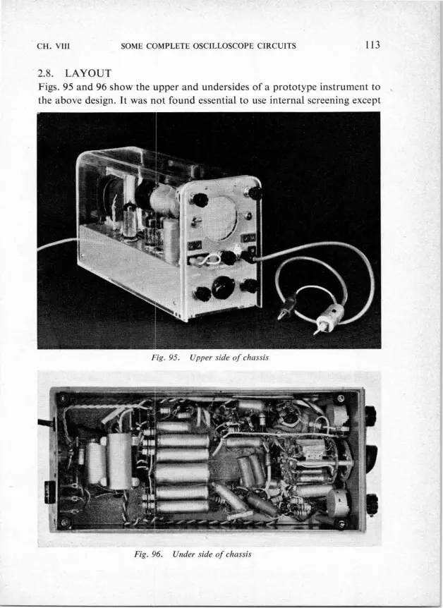
CH. VIII SOME COMPLETE OSCILLOSCOPE CIRCUITS 113
2.8. LAYOUT Figs. 95 and 96 show the upper and undersides of a prototype instrument to the above design. It was not found essential to use internal screening except
Fig. 95. Upper side of chassis
Fig. 96. Under side of chassis

114 SOME COMPLETE OSCILLOSCOPE CIRCUITS CH. VIII
for the connection between the anode of V5 and R39. It is, however, desira-ble to keep leads as short as possible, especially in the vertical amplifier, while in order to maintain the full bandwidth, stray capacitance to earth should be kept to a minimum. The Y amplifier and the time base generator should be kept reasonably far apart. In the arrangement illustrated the amplifier is on the left of the cathode ray tube and the time base generator on the right, with the power transformer at the rear of the tube.
Because the instrument is intended primarily for use in television servicing, its chassis cannot be tied to earth. Care must be taken, therefore, to ensure that the earth lead on the probe, or a separate wire from the earth socket, is taken to the earth of the circuit under test.

CH. VIII SOME COMPLETE OSCILLOSCOPE CIRCUITS 115
3. Circuit No. 3 A versatile oscilloscope in which the time base generator can be converted into an amplifier for external horizontal deflecting signals
The usefulness of a cathode ray oscilloscope is greatly enhanced if the circuit includes, in addition to the time base generator, an amplifier for horizontal deflection voltages derived from an external source. The block diagram reproduced in Fig. 97 shows such an arrangement, switch S connecting the plates for horizontal deflection either to the time base generator or to the
vertical amplifier
f timebose generator
horizontal amplifier
power supply
c i
I I
7
89556
Fig. 97. Block diagram of an oscilloscope. By means of switch S either a timebase generator or an amplifier for horizontal deflection is connected to the corresponding defection plates
of the cathode-ray tube
horizontal amplifier. This arrangement has several drawbacks, however. In the first place, the additional valves increase the cost of the apparatus, and secondly, the unit not immediately employed, although not connected to the cathode ray tube, continues to operate and thus consumes unnecessary energy while, if it is the time base generator which is not being used, there is a risk that the oscillations which it generates may cause interference in the horizontal amplifier.
These disadvantages are overcome in the instrument described below by so arranging the circuit that both the time base generator and the horizontal

116 SOME COMPLETE OSCILLOSCOPE CIRCUITS CH. VIII
amplifier employ the same valves, the cange-over from saw-tooth generator to amplifier being accomplished by re-arranging the connections by means of a 10-way change-over switch.
3.1. GENERAL DESCRIPTION
This instrument, the complete circuit diagram of which is reproduced in Fig. 98, is characterised by high sensitivity and very good time base linearity over a wide frequency range, combined with a compact and economical design. The cathode ray tube is Type DG7-32 which has a 7 cm diameter screen and is designed for symmetrical deflection voltages. Although this necessitates push-pull output stages for both vertical and horizontal de-
flection, it has been possible, by employing double triodes throughout and by using selenium rectifiers in place of thermionic diodes, to limit the tube complement to four valves and the cathode ray tube, as indicated below:
Vi ECC83 double triode — voltage amplifier for vertical deflection V2 ECC81 double triode — push-pull output valve of vertical amplifier V3 DG7-32 cathode ray tube V4 ECC81 double triode — push-pull output valve of horizontal ampli-
fier V5 ECC83 double triode — blocking oscillator and voltage amplifier for
horizontal deflection
3.2. PERFORMANCE SPECIFICATION
Sensitivity
Between vertical deflection plates, terminals T4 and T 5 10 Vr,,, /cm
Between horizontal deflection plates, terminals T, and T 8 16 Vrms/cm
At input of vertical amplifier, terminals T 2 and 7 3 10 mVrms/cm terminals T1 and T 3 (approx.) 50 mVrms/cm
At input of horizontal amplifier terminals T11 and T12 16 mVrms/cm terminals T10 and T12 (approx.) 80 mVr„ rs/cm

CH. VIII SOME COMPLETE OSCILLOSCOPE CIRCUITS 117
Between terminals T1 and T3 or between terminals T10 and T12 (approx.) 300 Vrms
Frequency response Vertical amplifier
from 0.5 c/s to 200 kc/s at 250 kc/s
Horizontal amplifier from 0.5 c/s to 200 kc/s at 250 kc/s
Maximum input voltage Between terminals T2 and T3 or between terminals T11 and T12 (approx.)
Input resistance 0-60 volt input circuits (approx.) 0-300 volt input circuits (approx.)
Input capacitance At terminals T2 or '11 (approx.) At terminals Tl or T0 (approx.)
—1 dB —3 dB
—1 dB —3 dB
60 Vrms
2M 10 MS2
5 pF 1 pF
Timebase frequencies Position on S 4 Frequency range (c/s)
1 30 000 to 120 000 2 10 000 to 40 000 3 3 000 to 12 000 4 1 000 to 4 000 5 300 to 1200 6 100 to 400 7 30 to 120 8 10 to 40 9 3 to 12
10 50 c/s sinusoidal

118 SOME COMPLETE OSCILLOSCOPE CIRCUITS CH. VIII
3.3. TIMEBASE AND HORIZONTAL AMPLIFIER
An interesting feature of the design is the timebase generator which, by means of a simple switching operation, can be converted into an amplifier for horizontal deflection, having a performance identical with that of the vertical amplifier, thus permitting phase measurements over a wide frequency range.
This unit comprises the two double triodes V4 and V5. In the "timebase" position of switch Ss the left-hand section of V5 is connected as a blocking oscillator and the right-hand section as a cathode follower, V 4 functioning as the push-pull output stage. In the "amplifier" position of Ss the left-hand section of V5 is connected as a cathode follower, and the right-hand section as a conventional voltage amplifier, the amplified signal being taken from the anode circuit to the push-pull stage. The performance of the horizontal amplifier is identical with that indicated in the paragraph describing the vertical amplifier.
When V5 is operating as timebase generator, step control of the sawtooth frequency is obtained from switch S 4 which provides a choice of capacitances. Position 10 of this switch provides a sinusoidal timebase frequency of 50 c/s. R 64 is the fine control for the sawtooth voltage.
Three alternative sources of timebase synchronising signal are provided via switch S 7. In position 1 of this switch the synchronising circuit is switched off. In position 2 the synchronising signal is taken from the output of the vertical amplifier; in position 3 from an internal 50 c/s sinusoidal source; and in position 4 from an external source via terminal Ty at which a voltage of from 0.5 to 5 V is necessary. In each case the synchronising signal is applied across a resistor in the cathode circuit of the blocking oscillator. This resistor takes the form of a germanium diode (Gin Fig. 98) which has a comparatively high resistance during the forward stroke, giving efficient synchronisation, but a low resistance during the flyback.
Two furtehr features of this unit should be noted. A neon lamp, Type Z 10 ("N" in Fig. 98) is connected between the right-hand control grid of V 4
and earth. This lamp becomes conductive during the change-over from oscillator to amplifier and vice versa, and so prevents excessively high voltages occuring between the grid and cathode of the right-hand section of V4. The voltage stabilising tube Vs, Type 85A2, performs two functions. In the first place it permits the use of charge capacitors of low working

CH. VIII SOME COMPLETE OSCILLOSCOPE CIRCUITS 119
voltage rating, and, secondly it assists in improving the linearity of the timebase.
The operation of changing over from "time base" to "horizontal amplifier" can be followed from the simplified version of the circuit of valve V 5 shown in Fig. 99 which indicates the connections made in the two positions of switch S1 which represents switch Ss in the complete circuit diagram of Fig. 98. In the following explanation the references printed in brackets indicate the corresponding components in the complete circuit diagram.
In the left-hand diagram, Fig. 99a, the connections as time base generator are shown. The left-hand triode section of V 5 is connected as a blocking oscillator, the frequency of which is adjusted by means if R 4 (R64) and by changing the value of C1 (achieved by switch S 4 in the complete circuit). The right-hand triode section is connected as a cathode follower, its cathode load bein R 1 + R 2 (R 56 + R 57). Its output voltage is applied via R 5 and R 2
(R 74 and R 57) to the attenuator P (R 75) and thence, via S1 (S5) to the output stage (V4). It should be noted that in this position of Sl the load in the anode circuit of the right-hand triode (R55 and L 2) is short-circuited.
When switch S 1 (S6)is moved to the "amplifier" position, the connections become as in Fig. 99(b). The short circuit is removed from the anode load of the right-hand triode and its cathode and the upper terminal of R1 (R56)
are earthed. This triode therefore acts as a normal amplifier and its output voltage is applied to the output stage (V4).
3.4. VERTICAL AMPLIFIER
The following description of the vertical amplifier applies also to the horizontal amplifier with, of course, the necessary changes in the reference numbers of the various components. Valves V1 and V2 constitute the vertical amplifier, the left-hand section of V1 being connected as a cathode follower and the right-hand section as a voltage amplifier. V 2 is the push-pull output stage.
Inputs up to 60 Vrms may be applied between terminals T 2 and T3 or inputs up to 300 Vrms between terminals T1 and T3. S 1 is an attenuator for step control of the input, and R 12 the fine amplitude control. Switch S 2 connects the vertical deflection plates of the cathode ray tube either direct to the two

+
+
+
+
'UlN'
-ti - F I i
U
u (
1
~ \44
1"
0,
Y
LJ~
U
IH
~N
nQ
~ Ll LJ
14)
O JUIJ I.~
u LJ Ll L~
bl b
~I
IF U
Q ►
J
~ Nw
tM~
Cir
cuit
for
swit
chin
g th
e fi
rst
tube
of
the
hori
zont
al a
mpl
ifie
r as
a t
itne
hase
osc
illa
tor
(a)
or a
s an
am
plif
ier
(b)

CH. VIII SOME COMPLETE OSCILLOSCOPE CIRCUITS 121
anodes of the output stage or, via capacitors C 7 and C 9, to terminals T 4 and T 5, thus providing direct input to the deflecting system.
R40 is the brightness control, and external beam modulation can be applied via terminal Ts, a voltage of between 0.5 and 3 V being required.
3.5. POWER SUPPLY
Since selenium rectifiers are used throughout, only a simple and inexpensive mains transformer is required, having one secondary winding for the H.T. and E.H.T. supply and two heater windings, one for the valves and one for the cathode ray tube. The H.T. secondary supplies a direct current at +360 V after rectification, and a further supply at —360 V is obtained by voltage doubling. It is recommended that the mains switch, S 8, be combined with the focusing control R35.


COMPONENTS LIST
CAPACITORS
Cl
C2~ C3
C4
C5
CB
0 1µF
32 + 32µF
0 1µF
8µF . . . . 2µF
paper
. . electrolytic . .
paper ..
. . electrolytic . . . .
.. paper ..
400V D.C.
450V D.C.
1000V D.C.
500V D.C. 600V D.C.
C7 0 25µF paper . . . . 250V D.C. C8 8µF . . electrolytic . . 500V D.C. C9 0 1µF .. .. paper .. 350V D.C.
C10 0.1µF . . . . paper 300 VD.C.
C11 0.25µF paper 400V D.C. C12 0 1µF paper . . . . 500V D.C. C13 6800pF 5% silver mica C14 680pF . . 5% silver mica
C15 68pF 5% silver mica
C16 0.1µF paper . . 500V D.C.
C17 8.2pF . . 10% silver mica C1S 0 02µF . . paper
C19 1800pF . . . . 5% silver mica C20 180pF 5% silver mica C21 8µF . . electrolytic . . 450V D.C. C22 47pF . . 10% silver mica
RESISTORS
R1
R2
. . 10 S2
. . Values to be calculat- ed as indicated on
6W (w.w.)
6W (w.w.) R16R17
R18
. . 50ki) Lin. Pot./10%
. . 82kS2
. . 100kS2 10%
1W
1W
R32
R33R 34
220k1)
. . 2MS2 Lin. Pot./ 10%
. . 2MS2 Log. Pot./1O;;
1W
R3 . . page 103 6W (w.w.) R19 . . 390kS2 10% 1W R35 . . 500kS 1W R4 I kS2 1W R20 . . 1 2kS * 5% 1W R39 . . 27kS2 10% 1W R5 . . 220kS2 1W R21 . . 100k #W R37 . . 250kS Lin. Pot./10% R6 . . 680kI * 5% 4W R22 . . 180kS2 10% 4W R38 I MU }W R7 . . 1 MS * 5% }W R23 . . 180k 1O 4W R39 180 S2 1W R8 . . 100k) * 5% #W R24 . . 68kS2 10% 1W R40 68kS2 1W R9 . . I0kS2 * 5% #W R25 . . 330k12 10% 1W R41 56kS2 6W (w.w.) R10 . . 1 kL2 * 5% 4W R26 . . 120k 10% 1W R42 1 MS2 4W
R11 . . 110 S2 * 5% 4W R27 . . 250kS Lin. Pot./10% R43 22k1) 1W R12 82kf) 1W R28 . . 22kS2 10% #W R44 82kü 1W R13 100kI2 Lin. Pot./10% R29 . . 68kS2 * 5% }W R45 270k[2 1W
R14 22kS2 1W R30 . . 330kS2 10% 1W R49 22kS2 1W R15 47kS2 IW R31 . . 250k12 Lin. Pot./10%
Fig. 85. Main circuit diagram of Students' Oscilloscope
*High Stability Resistors. (w.w.) Denotes wirewound. Tolerance ±20% except where stated.
Resistors R7, R9, R9, R19 may be replaced by single 1 Mu logarithmic potentiometer if so required.

COMPONENTS LIST R98 4 7kS qW R49af 39M1 #W
R39 25 kI2 1W linear R47 100 kS2 4W CAPACITORS RESISTORS R40 2 MS2 1W linear R48 2x 2 MS2 two-gang, linear
C1 Electrolytic 32 µF 350V R1 150 kS2 1W R41 390 kS2 aW R491 2x2 MS2 two-gang, linear
C2 Electrolytic 16 µF 350V R2 22 kL2 ¢W R42 1 MS2 ;W Rb0§ 470 kS2 1W
C3 Electrolytic 25+25 µF 300V R3 50 kS2 1W linear R43 10 MS2 4W R51§ 47 kS2 ;W
C4 Electrolytic 25+25 µF 300V R4 100 kI2 1W linear R44 12MS ;W R52§ 470 kS2 ;W
C5 Electrolytic 16 µF 350V R5 270 kS2 4W R45 4.7Mu 1W R53§ 15ku 4W
CB* Trimmer o•3 to 3 pF 500V R8 22k 1W R45at 3 9Mu ;W R54§ 120 kS2 4W
C7 Paper 0l µF 500V R7 22k 1W R49 4 7Mu aW R55§ 470 kS2 aW
C9 Electrolytic 25 µF SOY R8 2x 82k 2x 2W in parallel
C9 Ceramic 220 pF 350V R9 8 2kg 2W * Used in High-impedance Attenuator Probe.
C10 Paper 01 µF 350V R10 100 kS2 4 § Used in High-gain Pre-amplifier Probe.
C11 Ceramic 220 pF 350V R11* 10 MS2 1W t Used in Shift Control Circuit (see Fig. 94).
C12 Paper 005 µF 350V R12 1.2MS2 1W Note. All potentiometers are ± 20% tolerance.
C13 Paper 025 µF 350V R13 1 0MI IW All other resistors are + 10% tolerance.
C14 Paper 025 µF 350V R14 330 S2 #W
C15 Silver-Mica 1800 pF 350V R15 10 kS2 ¢W VALVES & TUBES
C19 Paper 0.01 µF 350V R19 10 kS2 1W linear C.R.T. . . DG7-32, with mumetal shield
C17 Paper 005 µF 350V R17 220 S2 ,—'W Vl . . . . EZ80
C18 Paper 0.01 µF 350V R18 5.6kSZ 4W V2, V3 . . 2x ECF80
C19 Silver-Mica 2200 pF 350V R19 1 Mu 1W V4 . . . . ECC81
C20 Silver-Mica 560 pF 350V R20 270 S2 aW V5 . . . . EF80 (lead from anode to RV39 must be screened)
C21 Silver-Mica 150 pF 350V R21 5 6ku #W Dl, D2 2x OA81
C22 Paper 0.1 µF 350V RE2 10 ML 2 1W MR1 . . Any suitable metal rectifier
C23 Paper 0.1 µF 350V R23 10 kS2 4W An EF86 is used in the high-gain probe.
C24 Paper 002 µF 350V R24 10 kS2 iW
C21 Paper 0.005µF 350V R25 4.7MSZ 4W OTHER COMPONENTS
C29 Silver-Mica 1200 pF 350V R25at 3.9Mu 1W
CE7 Silver-Mica 300 pF 350V R29 4 7Mu ;W T1 Mains Transformer.
C29 Ceramic 33 pF 350V R28at 3.9MQ }W Primary 10-0-200-220-240V.
C29 Paper 005 µF 350V R27 10 kS2 4W Secondary 250-0-250V. 40mA.
C30 Ceramic 33 pF 350V R29 390 12 aW 63V. 2A.
C31 Paper 025 µF 350V R29 470 S2 ;W 63V. IA.
C32 Paper 025 µF 350V R30 47 S2 aW FS1 Fuse IA.
C33§ Paper 0.1 µF 350V R31 2x 10 S 2x 1W in parallel S1 Mains switch
C34§ Electrolytic 100 µF 6V R32 1 MS2 1W S2 a/b 2-pole, 5-way switch.
C35§ Paper 01 µF 350V R33 82 kSZ 1W 5 3 Double-pole change-over switch (for high-gain probe).
R33a 10 k 1W Cathode ray tube shield.
R34 100 kS2 1W 10 panel sockets
* Used in High-impedance Attenuator R35 27 kS 4W 10 plugs to match.
Probe. R39 10 kS2 1W 6 B9A valveholders.
§ Used in High-gain Pre-amplifier Probe. R37 10 kS2 ;W 1 B12A valveholder.
1 B9A plug (for high gain probe).
1 Cathode ray tube mask.
Lineo—o
50c/s
Neutral
Sync
Cal v(pk/pk)
Attenuator probe
i
Exert
R3J
Sync amplifier
0 A
R36 1022
R33a
s
c d
T,mebase generator
C28 C24 to
Sty C27 Sweep speed
Fig. 92. Main Circuit of Service Oscilloscope
Supplies to high-gain
probe
T C29 V4b

8.2 Mf1, 1W R2 = 22 MI), }W R3 = 270 kI, 1W
R4 = 10 k), 4W
R5 = 33 k), 4W 82 k), 4W 27 k), 4W
R8 = 15 k), 4W 390 f1, IW
R10= 100 f1, 4W 47 f1, 4W
R18 = 5 k), linear, wire-round 1 Mf1, .4W
R15 = 100 M), l W 27 k), 4W
R18 = 47 k), }W R17 = 1 k), linear, carbon
3.3 k), 4W 220 k), 1W 220 k), 1W
1 Mfg, 4W 27 k), 1W 47 k), 7W, wire-wound 27 kf1, 1W 12 k), 1W 1 M), }W
12 k), }W 33 Mfg, 1W 33 Mfg, 1W
R311 = 39 k), 1 W 100 k), linear, carbon
R82 = 15 M), 1W 100 k), linear, carbon 270 k), 1W
R35 = 100 k), linear, carbon R86 = 82 k), 1W
10 k), #W 220 k), 4W 220 k), }W
R60 = 20 k), linear, carbon 27 kf1, 3W
R62 = 1 Mfg, 4W
R43 = 1 Mfg, 4W R44 = 33 Mfg, 1W
RESISTORS
R1 =
RO =
R7 =
R9 =
R11 =
R13 =
R35 =
R18 =
R19 =
R20 = R21 =
RE2 =
R23 = R24 = R35 = R29 = R27 =
R28 = R29 =
R31 =
R33 = R34 =
R37 =
R38 =
R39 =
R41 =
1 M), }W 33 M), 4W
82 k), 4W = 27 k), 1W
R49 = 12 k), 1 W 47 kf1, 7W, wire-wound
27 k), 1W R53 = 1 Mf1, }W
R53 = 2.2 k), }W Rb4 = 100 M), 1W
27 k), 4W = 1 k), linear, carbon
R57 = 56 kf1, 3W 5.6 kf1, 1W
R59 = 56 kf1, 1W = 1 M), }W
R81 = 270 kf 1, 1W = 68 k), }W
R03 = 560 k), 1W = 1 Mfg, anti-log., carbon
= 330 kfl, 1W 10 k), 4W
= 33 k), 4W R88 = 82 k), 4W RB9 = 27 kf1, 4W R70 = 15 k), 4W R71 = 390 f1, 4W R72 = 100 f1, 4W R 73 = 47 f1, 4W R74 = 56 kf1, 4W R75 = 5 k), linear ,carbon
R76 = 2.2 kf1, }W R77 = 27 kf1, }W R78 = 15 k), }W R79 = 22 kf1, 1W R80 = 270 k), 1W R81 = 22 Mfg, 4W R83 = 820 f1, 4W R83 = 3.3 kf1, 4W RB4 = 560 f1, 1W R85 = 82 Mfg, 1W
COMPONENTS LIST
R45 R48
R47
R4e
R50 R51
R55
R54
Rya
R60
R42
R94 R95 R58
R97
CAPACITORS
C1
C2
C2
C4
C5
= 5 pF, max., trimmer = 025F, 500V = 0 047µF, 300V = 05 µF, 500V = 100 µF, 125V
C9 = 05 µF, 500V = 025F, 500V = 025F, 500V = 025F, 500V
C10 = 0.25µF, 500V = 025F, 500V = 025F, 500V = 025F, 500V = 05 µF, 500V = 270 pF, 300V
05 µF, 500V = 2x 50 µF, 400V = 0047F, 300V _ 47 pF, 300V
180 pF, 300V 820 pF, 300V
3300 pF, 300V = 001µF, 300V = 0 033µF, 300V = 01 µF, 300V
033F, 330V 1 µF, 300V
50 µF, 450V 50 µF, 450V
C7
C3
C9
Cu
C12
Cls C14
C15 C19
C17
C18
C19
C20 C21 C22
C23
C24 C28
C26 =
C27 =
C28 = C29 =
C80 = 1000 pF, 500V
C3, = 2x 50 µF, 450V C32 = 025F, 500V C83 = 5 pF max., trimmer
OTHER COMPONENTS
L1
L2
V1
V2
= approx. 15 mH = approx. 15 mH = ECC83 = ECC81
V3 = DG7-32 V4 = ECC81 V5 = ECC83 V0 = 85A2 N = neon lamp Z10 F2 = 1 A fuse F2 = 01 A fuse G = germanium diode OA 55
Sell = selenium rectifier 2x 220085 in
series
Sell = selenium rectifier 2x 220085 in
series
Tr, : w1 = approx. 120 µH, wl : w2 = 25 : 1
Tr2 : wl = 110, 130, 145, 190, 220, 245V w2 = 350 V. 40 mA w8 = 63V, 1 2 A w4 =63V, 04A
T.
R
TI0
T„
fad
c1aT
Rao
Rea 1utr.
X31
~Sel,
~S6la
L Ca9
c28 R80
L ~R79 jR77
Y
} ~9
C,0
R59 Rse
PHILIPS7PU804
Fig. 98. A versatile oscilloscope incorporating cathode ray tube DG 7-32


