Embed Size (px)
Citation preview

Analog Signal Chain Guide
Amplifiers, Data Converters, Interface,
Clocks, Timing and Wireless Connectivity.
1Q 2011www.ti.com
LogicClocks and Timing
Power Management
EmbeddedProcessing
DataConverter
WirelessConnectivityInterface
Amplifier
Temperature
Pressure
Position
Speed
Flow
Humidity
Sound
Light
Identification
The RealWorld Amplifier
DataConverter

2Analog Signal Chain Guide TexasInstruments1Q2011
Analog Signal Chain Guide
Table of Contents
Amplifiers and Comparators
OperationalAmplifiers . . . . . . . . . . . . . . . . . . . . . . . . . . . . . . . . . . . . . . . . . . . . . . . . . . . . . . . . . . . . . . . . . . . . . . . . . . . . . .4-10 High-SpeedAmplifiers . . . . . . . . . . . . . . . . . . . . . . . . . . . . . . . . . . . . . . . . . . . . . . . . . . . . . . . . . . . . . . . . . . . . . . . . . . . . .11-17
AudioAmplifiers . . . . . . . . . . . . . . . . . . . . . . . . . . . . . . . . . . . . . . . . . . . . . . . . . . . . . . . . . . . . . . . . . . . . . . . . . . . . . . . . . .18-25
InstrumentationAmplifiers . . . . . . . . . . . . . . . . . . . . . . . . . . . . . . . . . . . . . . . . . . . . . . . . . . . . . . . . . . . . . . . . . . . . . . . . . .26-29
PowerAmplifiersandBuffers . . . . . . . . . . . . . . . . . . . . . . . . . . . . . . . . . . . . . . . . . . . . . . . . . . . . . . . . . . . . . . . . . . . . . . . . . . 30
Comparators . . . . . . . . . . . . . . . . . . . . . . . . . . . . . . . . . . . . . . . . . . . . . . . . . . . . . . . . . . . . . . . . . . . . . . . . . . . . . . . . . . . .31-32
Data Converters
Analog-to-DigitalConverters(ADCs) . . . . . . . . . . . . . . . . . . . . . . . . . . . . . . . . . . . . . . . . . . . . . . . . . . . . . . . . . . . . . . . . . . . . 33
Delta-SigmaADCs . . . . . . . . . . . . . . . . . . . . . . . . . . . . . . . . . . . . . . . . . . . . . . . . . . . . . . . . . . . . . . . . . . . . . . . . . . . . . .33-36
SARADCs . . . . . . . . . . . . . . . . . . . . . . . . . . . . . . . . . . . . . . . . . . . . . . . . . . . . . . . . . . . . . . . . . . . . . . . . . . . . . . . . . . . . .37-45
PipelineADCs . . . . . . . . . . . . . . . . . . . . . . . . . . . . . . . . . . . . . . . . . . . . . . . . . . . . . . . . . . . . . . . . . . . . . . . . . . . . . . . . . .46-51
Digital-to-AnalogConverters(DACs) . . . . . . . . . . . . . . . . . . . . . . . . . . . . . . . . . . . . . . . . . . . . . . . . . . . . . . . . . . . . . . . . . . . . 52
StringandR2RDACs . . . . . . . . . . . . . . . . . . . . . . . . . . . . . . . . . . . . . . . . . . . . . . . . . . . . . . . . . . . . . . . . . . . . . . . . . . . .52-58
CurrentSteeringDACs . . . . . . . . . . . . . . . . . . . . . . . . . . . . . . . . . . . . . . . . . . . . . . . . . . . . . . . . . . . . . . . . . . . . . . . . . . .59-60
DigitalPotentiometers . . . . . . . . . . . . . . . . . . . . . . . . . . . . . . . . . . . . . . . . . . . . . . . . . . . . . . . . . . . . . . . . . . . . . . . . . . . . . . 61
IntegratedADCsandDACs . . . . . . . . . . . . . . . . . . . . . . . . . . . . . . . . . . . . . . . . . . . . . . . . . . . . . . . . . . . . . . . . . . . . . . . . . . . 62
AudioConverters . . . . . . . . . . . . . . . . . . . . . . . . . . . . . . . . . . . . . . . . . . . . . . . . . . . . . . . . . . . . . . . . . . . . . . . . . . . . . . . . .63-67
AnalogFrontEnds . . . . . . . . . . . . . . . . . . . . . . . . . . . . . . . . . . . . . . . . . . . . . . . . . . . . . . . . . . . . . . . . . . . . . . . . . . . . . . . . . . 68
Medical . . . . . . . . . . . . . . . . . . . . . . . . . . . . . . . . . . . . . . . . . . . . . . . . . . . . . . . . . . . . . . . . . . . . . . . . . . . . . . . . . . . . . . .68-69
Imaging . . . . . . . . . . . . . . . . . . . . . . . . . . . . . . . . . . . . . . . . . . . . . . . . . . . . . . . . . . . . . . . . . . . . . . . . . . . . . . . . . . . . . . . . . 70
EmbeddedProcessorswithIntegratedADCs . . . . . . . . . . . . . . . . . . . . . . . . . . . . . . . . . . . . . . . . . . . . . . . . . . . . . . . . . . . . . 71
Monitoring and Control
MotorDrivers . . . . . . . . . . . . . . . . . . . . . . . . . . . . . . . . . . . . . . . . . . . . . . . . . . . . . . . . . . . . . . . . . . . . . . . . . . . . . . . . . . . .72-76
Touch-ScreenControllers . . . . . . . . . . . . . . . . . . . . . . . . . . . . . . . . . . . . . . . . . . . . . . . . . . . . . . . . . . . . . . . . . . . . . . . . . . . . . 77
Pulse-WidthModulationPowerDrivers . . . . . . . . . . . . . . . . . . . . . . . . . . . . . . . . . . . . . . . . . . . . . . . . . . . . . . . . . . . . . . . . . . 78
CurrentShuntMonitors . . . . . . . . . . . . . . . . . . . . . . . . . . . . . . . . . . . . . . . . . . . . . . . . . . . . . . . . . . . . . . . . . . . . . . . . . . . .79-80
TemperatureSensors . . . . . . . . . . . . . . . . . . . . . . . . . . . . . . . . . . . . . . . . . . . . . . . . . . . . . . . . . . . . . . . . . . . . . . . . . . . . . .81-82
4-20mATransmitters . . . . . . . . . . . . . . . . . . . . . . . . . . . . . . . . . . . . . . . . . . . . . . . . . . . . . . . . . . . . . . . . . . . . . . . . . . . . . . . . 83
Voltage References
VoltageReferences . . . . . . . . . . . . . . . . . . . . . . . . . . . . . . . . . . . . . . . . . . . . . . . . . . . . . . . . . . . . . . . . . . . . . . . . . . . . . . . . . 84

3Analog Signal Chain Guide TexasInstruments1Q2011
Analog Signal Chain Guide
Table of Contents
Clocks and Timing
ClockDistribution . . . . . . . . . . . . . . . . . . . . . . . . . . . . . . . . . . . . . . . . . . . . . . . . . . . . . . . . . . . . . . . . . . . . . . . . . . . . 85-89
ClockGeneration . . . . . . . . . . . . . . . . . . . . . . . . . . . . . . . . . . . . . . . . . . . . . . . . . . . . . . . . . . . . . . . . . . . . . . . . . . . . 90-93
Interface
Communications . . . . . . . . . . . . . . . . . . . . . . . . . . . . . . . . . . . . . . . . . . . . . . . . . . . . . . . . . . . . . . . . . . . . . . . . . . . . . . . . . . . . 94
LVDS/LVPECL/CMLRepeaters,TranslatorsandCrosspoints . . . . . . . . . . . . . . . . . . . . . . . . . . . . . . . . . . . . . . . . . . . . . 94-95
LVD/MLVDS . . . . . . . . . . . . . . . . . . . . . . . . . . . . . . . . . . . . . . . . . . . . . . . . . . . . . . . . . . . . . . . . . . . . . . . . . . . . . . . . . . . . 96-97
SERDES . . . . . . . . . . . . . . . . . . . . . . . . . . . . . . . . . . . . . . . . . . . . . . . . . . . . . . . . . . . . . . . . . . . . . . . . . . . . . . . . . . . . . . 98-99
PECL-ECLBuffers/Translators . . . . . . . . . . . . . . . . . . . . . . . . . . . . . . . . . . . . . . . . . . . . . . . . . . . . . . . . . . . . . . . . . . . . . . . 100
Consumer/Computing . . . . . . . . . . . . . . . . . . . . . . . . . . . . . . . . . . . . . . . . . . . . . . . . . . . . . . . . . . . . . . . . . . . . . . . . . . . . . . . 101
Redriver/Equalizers . . . . . . . . . . . . . . . . . . . . . . . . . . . . . . . . . . . . . . . . . . . . . . . . . . . . . . . . . . . . . . . . . . . . . . . . . . . . . . . . 101
USB . . . . . . . . . . . . . . . . . . . . . . . . . . . . . . . . . . . . . . . . . . . . . . . . . . . . . . . . . . . . . . . . . . . . . . . . . . . . . . . . . . . . . . . . 102-104
1394 . . . . . . . . . . . . . . . . . . . . . . . . . . . . . . . . . . . . . . . . . . . . . . . . . . . . . . . . . . . . . . . . . . . . . . . . . . . . . . . . . . . . . . . 105-106
DisplayPortSwitch/Redriver . . . . . . . . . . . . . . . . . . . . . . . . . . . . . . . . . . . . . . . . . . . . . . . . . . . . . . . . . . . . . . . . . . . . . . . . 107
Flatlink™3GTransmitter . . . . . . . . . . . . . . . . . . . . . . . . . . . . . . . . . . . . . . . . . . . . . . . . . . . . . . . . . . . . . . . . . . . . . . . . 108-109
PCIExpress . . . . . . . . . . . . . . . . . . . . . . . . . . . . . . . . . . . . . . . . . . . . . . . . . . . . . . . . . . . . . . . . . . . . . . . . . . . . . . . . . . 110-111
HDMI . . . . . . . . . . . . . . . . . . . . . . . . . . . . . . . . . . . . . . . . . . . . . . . . . . . . . . . . . . . . . . . . . . . . . . . . . . . . . . . . . . . . . . . . . . . 111
Industrial . . . . . . . . . . . . . . . . . . . . . . . . . . . . . . . . . . . . . . . . . . . . . . . . . . . . . . . . . . . . . . . . . . . . . . . . . . . . . . . . . . . . . . . . . 112
CANTransceivers . . . . . . . . . . . . . . . . . . . . . . . . . . . . . . . . . . . . . . . . . . . . . . . . . . . . . . . . . . . . . . . . . . . . . . . . . . . . . . . . . 112
DigitalIsolators . . . . . . . . . . . . . . . . . . . . . . . . . . . . . . . . . . . . . . . . . . . . . . . . . . . . . . . . . . . . . . . . . . . . . . . . . . . . . . . 113-114
EthernetPhysicalLayerTransceivers . . . . . . . . . . . . . . . . . . . . . . . . . . . . . . . . . . . . . . . . . . . . . . . . . . . . . . . . . . . . . . . . . . 115
SERDES . . . . . . . . . . . . . . . . . . . . . . . . . . . . . . . . . . . . . . . . . . . . . . . . . . . . . . . . . . . . . . . . . . . . . . . . . . . . . . . . . . . . . . . . 116
RS-485/RS-422 . . . . . . . . . . . . . . . . . . . . . . . . . . . . . . . . . . . . . . . . . . . . . . . . . . . . . . . . . . . . . . . . . . . . . . . . . . . . . . . 117-118
General . . . . . . . . . . . . . . . . . . . . . . . . . . . . . . . . . . . . . . . . . . . . . . . . . . . . . . . . . . . . . . . . . . . . . . . . . . . . . . . . . . . . . . . . . . . 119
UARTs . . . . . . . . . . . . . . . . . . . . . . . . . . . . . . . . . . . . . . . . . . . . . . . . . . . . . . . . . . . . . . . . . . . . . . . . . . . . . . . . . . . . . . 119-120
ESD-EMI . . . . . . . . . . . . . . . . . . . . . . . . . . . . . . . . . . . . . . . . . . . . . . . . . . . . . . . . . . . . . . . . . . . . . . . . . . . . . . . . . . . . 121-122
I2C . . . . . . . . . . . . . . . . . . . . . . . . . . . . . . . . . . . . . . . . . . . . . . . . . . . . . . . . . . . . . . . . . . . . . . . . . . . . . . . . . . . . . . . . . 123-125
RS-232 . . . . . . . . . . . . . . . . . . . . . . . . . . . . . . . . . . . . . . . . . . . . . . . . . . . . . . . . . . . . . . . . . . . . . . . . . . . . . . . . . . . . . . . . . 126
Voltage-LevelTranslators . . . . . . . . . . . . . . . . . . . . . . . . . . . . . . . . . . . . . . . . . . . . . . . . . . . . . . . . . . . . . . . . . . . . . . . . . . . 127
Radio Frequency
BroadbandRF . . . . . . . . . . . . . . . . . . . . . . . . . . . . . . . . . . . . . . . . . . . . . . . . . . . . . . . . . . . . . . . . . . . . . . . . . . . . . . . . . 128-129
WirelessConnectivity . . . . . . . . . . . . . . . . . . . . . . . . . . . . . . . . . . . . . . . . . . . . . . . . . . . . . . . . . . . . . . . . . . . . . . . . . . . . 130-134
Resources
AnalogeLab™DesignTools . . . . . . . . . . . . . . . . . . . . . . . . . . . . . . . . . . . . . . . . . . . . . . . . . . . . . . . . . . . . . . . . . . . . . . . . . . 135

4Analog Signal Chain Guide TexasInstruments1Q2011
Amplifiers and Comparators
Operational Amplifiers
High Precision, 11MHz, Low Noise, RRO, JFET Operational AmplifierOPA140, OPA2140, OPA4140Getsamples,datasheetsandappreportsat:www.ti.com/sc/device/PARTnumber (ReplacePARTnumber withOPA140, OPA2140, orOPA4140)Key Features• Verylowoffsetdrift:0 .35µV/°C• Verylowoffset:120μVmax• Lowinputbiascurrent:10pAmax• Verylow1/fnoise:250nVpp,
0 .1Hzto10Hz• Lownoise:5 .1nV/√Hzat1kHz• Gainbandwidth:11MHz• Slewrate:20V/µs
Applications• Battery-poweredinstruments• Industrialcontrols• Medicalinstrumentation• Photodiodeamplifiers• Activefilters• Automatictestsystems
TheOPA140familyisaseriesoflow-powerJFETinputamplifiersthatfeaturegooddriftandlowinputbiascurrent .Therail-to-railoutputswingandinputrangethatincludesV-allowdesignerstotakeadvantageofthelownoisecharacteristicsofJFETamplifierswhilealsointerfacingtomodern,single-supply,precisionADCsandDACs .TheOPA140achieves11MHzunity-gainbandwidthanda20V/µsslewratewhileconsumingonly1 .8mA(typ)ofquiescentcurrent .
OPA140 illustration
vid/Vn002
OPAx140
V = 18VSUPPLY
0.1Hz to 10Hz NOISE
250nVpp
5.5MHz, Low Noise, Low-Power, CMOS Operational AmplifierOPA377, OPA2377, OPA4377Getsamples,datasheetsandappreportsat:www.ti.com/sc/device/PARTnumber (ReplacePARTnumber withOPA377, OPA2377, orOPA4377)Key Features• Gainbandwidthproduct:5 .5MHz• Lownoise:7 .5nV/√Hzat1kHz• Offsetvoltage:1mV(max)• Inputbiascurrent:0 .2pA• Rail-to-railoutput• Unity-gainstable• EMIinputfiltering• Quiescentcurrent:0 .76mA/ch• Supplyvoltage:2 .2Vto5 .5V• Smallpackages:SC70,SOT-23, MSOPandDFN
Applications• Photodiodepreamps• Piezoelectricsensorpreamps• Sensorsignalconditioning• Audioequipment• Activefilters
TheOPA377familyofoperationalamplifiersarewide-bandwidthCMOSamplifiersthatprovideverylownoise,lowinputbiascurrentandlowoffsetvoltagewhileoperatingonalowquiescentcurrentof0 .76mA(typ) .
TheOPA377opampsareoptimizedforlow-voltage,single-supplyapplications .TheexceptionalcombinationofACandDCperformancemakethemidealforawiderangeofapplications,includingsmallsignalconditioning,audioandactivefilters .Inaddition,thesepartshaveawidesupplyrangewithexcellentPSRR,makingthemattractiveforapplicationsthatrundirectlyfrombatterieswithoutregulation .
Photodiode preamplifier
OPA377
CF
RF
VOUT
VB
VS

5Analog Signal Chain Guide TexasInstruments1Q2011
Amplifiers and Comparators
Operational Amplifiers
36V, Low Power, RRO, General-Purpose Operational Amplifier in microPackagesOPA171, OPA2171, OPA4171Getsamples,datasheetsandappreportsat:www.ti.com/sc/device/PARTnumber (ReplacePARTnumber withOPA171, OPA2171, orOPA4171)Key Features• MicroPackages: SingleinSOT553,dualinVSSOP-8• Lowquiescentcurrent:495μA/ch• Lownoise:14nV/√Hzat1kHz• Rail-to-railoutput• Gainbandwidth:3MHz• Lowinputbiascurrent:8pA• RFIfilteredinputs• Supplyrange:+2 .7Vto+36V, ±1 .35Vto±18V
Applications• Transduceramplifiers• Bridgeamplifiers• Straingageamplifiers• Precisionintegrators• Batterypoweredinstruments• Testequipment
TheOPA171amplifierfamilyisaseriesof36Vlow-noiseoperationalamplifiersthatfeaturesinglesupply,andmicropackageswiththeabilitytooperateonsuppliesrangingfrom+2 .7V(±1 .35V)to+36V(±18V) .Theyoffergoodoffset,driftandbandwidthwithlowquiescentcurrent .Single,dualandquadversionshaveidenticalspecificationsformaximumdesignflexibility .Unlikemostopamps,whicharespecifiedatonlyonesupplyvoltage,OPA171opampsarespecifiedfrom+2 .7Vto+36V .Inputsignalsbeyondthesupplyrailswillnotcausephasereversal .
OPA171/2171 pin configurations
1
2
3
5
4
V+
OUT
IN+
V
IN
1
2
3
4
8
7
6
5 +IN B
V+
V–
1
2
3
5
4
V+
IN
OUT
V
+IN
1
2
3
4
8
7
6
5
NC(1)
V+
OUT
NC(1)
NC(1)
IN
+IN
V
OPA171SOT-553
SO-8 AND VSSOP-8OPA171SOT23-5
OPA171SO-8
OPA2171
2.2nV/√Hz, 18MHz, Precision, RRO, 36V Operational AmplifierOPA209, OPA2209, OPA4209Getsamples,datasheetsandappreportsat:www.ti.com/sc/device/PARTnumber (ReplacePARTnumber withOPA209, OPA2209, orOPA4209)Key Features• Gainbandwidth:18MHz• Slewrate:6 .4V/µs• Inputvoltagenoise:2 .2nV/√Hzat1kHz• Quiescentcurrent:2 .5mA/chmax• Lowoffsetvoltage:150µVmax• Rail-to-railoutput•Packaging:SOT23-5,MSOP-8, SO-8,TSSOP-14
Applications• PLLloopfilters• HighperformanceADCdrivers• HighperformanceDACoutput amplifiers•Ultrasoundamplifiers•Infrareddetectoramplifiers•Activefilters
TheOPA209seriesofprecisionoperationalamplifiersachievesverylowvoltagenoisedensity(2 .2nV/√Hz)withasupplycurrentofonly2 .5mA(max) .Theseamplifiersprovidefastsettlingtimeto16-bitaccuracyevenfor10Voutputswingsinprecisiondataacquisitionapplications .ThisexcellentACperformance,combinedwithonly150μV(max)ofoffsetandlowdriftovertemperature,makestheOPA209verysuitableforfast,high-precisionapplications .
OPA209 schematic
100k 1M
S
100 1k 10k
10k
1k
100
10
1
O
RS
EO
O n Sn S2 2 2
OPA827
OPA209
6Analog Signal Chain Guide TexasInstruments1Q2011
Amplifiers and Comparators
Operational Amplifiers
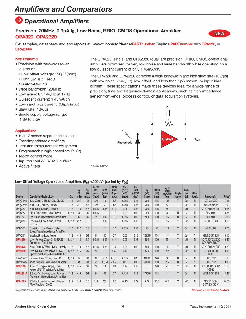
Precision, 20MHz, 0.9pA IB, Low Noise, RRIO, CMOS Operational AmplifierOPA320, OPA2320Getsamples,datasheetsandappreportsat:www.ti.com/sc/device/PARTnumber (ReplacePARTnumber withOPA320,or OPA2330)
Key Features•Precisionwithzero-crossover
distortion:Lowoffsetvoltage:150µV(max)HighCMRR:114dBRail-to-RailI/O
•Widebandwidth:20MHz•Lownoise:8 .5nV/√Hzat1kHz•Quiescentcurrent:1 .45mA/ch•Lowinputbiascurrent:0 .9pA(max)•Slewrate:10V/µs•Singlesupplyvoltagerange:
1 .8Vto5 .5V
Applications• High-Zsensorsignalconditioning• Transimpedanceamplifiers• Testandmeasurementequipment• Programmablelogiccontrollers(PLCs)• Motorcontrolloops• Input/outputADC/DACbuffers• Activefilters
TheOPA320(single)andOPA2320(dual)areprecision,RRIO,CMOSoperationalamplifiersoptimizedforverylownoiseandwidebandwidthwhileoperatingonalowquiescentcurrentofonly1 .45mA/ch .
TheOPA320andOPA2320combineawidebandwidthandhighslewrate(10V/µs)withlownoise(7nV/√Hz),lowoffset,andlessthan1pAmaximuminputbiascurrent .Thesespecificationsmakethesedevicesidealforawiderangeofprecision,time-andfrequency-domainapplications,suchashigh-impedancesensorfront-ends,processcontrol,ordataacquisitionsystems .
OPA320 diagram
Photodiode
Rf
Cf
OPA320 VOUT
Low Offset Voltage Operational Amplifiers (VOS <500µV) (sorted by VOS)
Device Description/Technology Ch.
VS(V)
(min)
VS(V)
(max)
IQ PerCh.
(mA)(max)
GBW(MHz)(typ)
SlewRate
(V/µs)(typ)
VOS(25°C)(mV)(max)
VOSDrift
(µV/°C) (typ)
IB(pA)
(max)
CMRR(dB)(min)
VN at1kHz
(nV/√Hz)(typ)
SingleSupply
Rail-to-Rail
HiRelAvail. Package(s) Price*
OPAy734/5 12V, Zero-Drift, SHDN, CMOS 1, 2 2.7 12 0.75 1.6 1.5 0.005 0.01 200 115 135 Y Out N SOT-23, SOIC 1.25 OPAy334/5 Zero-Drift, SHDN, CMOS 1, 2 2.7 5.5 0.35 2 1.6 0.005 0.02 200 110 62 Y Out N SOT-23, MSOP 1.00 OPAy333 Zero Drift, CMOS, µPower 1, 2 1.8 5.5 0.025 0.35 0.16 0.01 0.02 200 106 55 Y I/O Y SC-70, SOT-23, SOIC 0.95 OPAy277 High Precision, Low Power 1, 2, 4 4 36 0.825 1 0.8 0.02 0.1 1000 130 8 N N N SON, SOIC 0.85 OPA177 Precision Operational Amplifier 1 6 36 2 0.6 0.3 0.025 0.1 2000 130 7.5 N N N PDIP, SOIC 1.00 OPAy376 Precision, Low Noise, e-trim
Series1, 2, 4 2.2 5.5 0.95 5.5 2 0.025 0.32 10 76 7.5 Y Out N SC-70, SOT-23 0.65
OPAy381 Precision, Low Power, High-Speed Transimpedance Amplifier
1, 2 2.7 5.5 1 18 12 0.025 0.03 50 95 114 Y Out N MSOP, SON 0.75
OPAy211 Bipolar, Ultra-Low Noise 1, 2 4.5 36 4.5 45 27 0.05 0.15 125000 114 1.1 Y Out Y MSOP, SOIC, SON 5.15 OPAy330 Low-Power, Zero-Drift, RRIO
Operation Amplifier1, 2, 4 1.8 5.5 0.035 0.35 0.16 0.05 0.02 500 100 55 Y I/O N SC-70, SOT-23, SOIC,
SON, VQFN, TSSOP0.45
OPAy378 Zero-Drift, GBW 0.9MHz, Low IQ 1, 2 1.8 5.5 0.125 0.9 0.4 0.05 0.1 500 100 20 Y I/O N SC-70, SOT-23, SOIC 0.70 OPAy209 Low Noise, Low Power, 36V,
Operational Amplifier in SOT-23 1, 2, 4 4.5 36 2.5 18 6.25 0.15 1 4500 120 2.2 Y Out N SOT-23, MSOP,
SOIC0.95
OPAy227/28 Bipolar, Low Noise, Low IB 1, 2, 4 5 36 3.8 8, 33 2.3, 11 0.075 0.1 10000 120 3 N N N SOIC, PDIP 1.10 TLE2027/37 Wide Supply, Low Noise, Bipolar 1 8 38 5.3 13, 50 2.8, 7.5 0.1 0.4 90000 100 2.5 N N Y SOIC, PDIP 0.90 OPAy140 10MHz, Single-Supply, Low-
Noise, JFET Precision Amplifier1, 2, 4 4.5 36 2.0 11 20 0.12 0.35 10 120 5.1 Y Out N SOIC, MSOP, TSSOP,
SOT-231.55
OPAy211A 1.1nV/√Hz Noise, Low-Power, Precision Operational Amplifier
1, 2 4.5 36 4.5 45 27 0.125 0.35 175000 114 1.1 Y Out N MSOP, SOIC, SON 3.45
OPAx320 20MHz, Low-Noise, Low- Power, RRIO Precision CMOS
1, 2 1.8 5.5 1.6 20 10 0.15 1.5 0.9 100 8.5 Y I/O N MSOP, SON, SOT-23, SOIC
0.80
*Suggested resale price in U.S. dollars in quantities of 1,000. See www.ti.com/hirel for HiRel options. New products are listed in bold red.
7Analog Signal Chain Guide TexasInstruments1Q2011
Amplifiers and Comparators
Operational Amplifiers
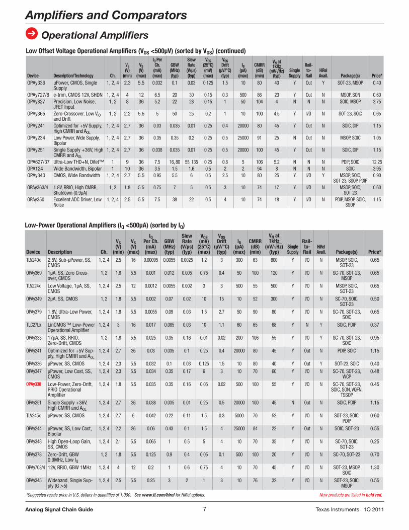
Low-Power Operational Amplifiers (IQ <500µA) (sorted by IQ)
Device Description Ch.
VS (V)
(min)
VS (V)
(max)
IQ Per Ch. (mA) (max)
GBW (MHz) (typ)
Slew Rate
(V/µs) (typ)
VOS (mV)
(25°C) (max)
VOS Drift
(µV/°C) (typ)
IB (pA)
(max)
CMRR (dB) (min)
VN at 1kHz
(nV/√Hz) (typ)
Single Supply
Rail-to-Rail
HiRelAvail. Package(s) Price*
TLV240x 2.5V, Sub-µPower, SS, CMOS
1, 2, 4 2.5 16 0.00095 0.0055 0.0025 1.2 3 300 63 800 Y I/O N MSOP, SOIC, SOT-23
0.65
OPAy369 1µA, SS, Zero Cross-over, CMOS
1, 2 1.8 5.5 0.001 0.012 0.005 0.75 0.4 50 100 120 Y I/O N SC-70, SOT-23, MSOP
0.65
TLV224x Low Voltage, 1µA, SS, CMOS
1, 2, 4 2.5 12 0.0012 0.0055 0.002 3 3 500 55 500 Y I/O N MSOP, SOIC, SOT-23
0.65
OPAy349 2µA, SS, CMOS 1, 2 1.8 5.5 0.002 0.07 0.02 10 15 10 52 300 Y I/O N SC-70, SOIC, SOT-23
0.50
OPAy379 1.8V, Ultra-Low Power, CMOS
1, 2, 4 1.8 5.5 0.0055 0.09 0.03 1.5 2.7 50 90 80 Y I/O N SC-70, SOT-23, SOIC
0.65
TLC27Lx LinCMOS™ Low-Power Operational Amplifier
1, 2, 4 3 16 0.017 0.085 0.03 10 1.1 60 65 68 Y N Y SOIC, PDIP 0.37
OPAy333 17µA, SS, RRIO, Zero-Drift, CMOS
1, 2 1.8 5.5 0.025 0.35 0.16 0.01 0.02 200 106 55 Y I/O Y SC-70, SOT-23, SOIC
0.95
OPAy241 Optimized for +5V Sup-ply, High CMRR and AOL
1, 2, 4 2.7 36 0.03 0.035 0.1 0.25 0.4 20000 80 45 Y Out N PDIP, SOIC 1.15
OPAy336 µPower, SS, CMOS 1, 2, 4 2.3 5.5 0.032 0.1 0.03 0.125 1.5 10 80 40 Y Out Y SOT-23, SOIC 0.40 OPAy347 µPower, Low Cost, SS,
CMOS1, 2, 4 2.3 5.5 0.034 0.35 0.17 6 3 10 70 60 Y I/O N SC-70, SOT-23,
WCP0.48
OPAy330 Low-Power, Zero-Drift, RRIO Operational Amplifier
1, 2, 4 1.8 5.5 0.035 0.35 0.16 0.05 0.02 500 100 55 Y I/O N SC-70, SOT-23, SOIC, SON, VQFN,
TSSOP
0.45
OPAy251 Single Supply +36V, High CMRR and AOL
1, 2, 4 2.7 36 0.038 0.035 0.01 0.25 0.5 20000 100 45 N Out N SOIC, PDIP 1.15
TLV245x µPower, SS, CMOS 1, 2, 4 2.7 6 0.042 0.22 0.11 1.5 0.3 5000 70 52 Y I/O N SOT-23, SOIC, PDIP
0.60
OPAy244 µPower, SS, Low Cost, Bipolar
1, 2, 4 2.2 36 0.06 0.43 0.1 1.5 4 25000 84 22 Y Out N SOIC, SOT-23 0.55
OPAy348 High Open-Loop Gain, SS, CMOS
1, 2, 4 2.1 5.5 0.065 1 0.5 5 4 10 70 35 Y I/O N SC-70, SOIC, SOT-23
0.25
OPAy378 Zero-Drift, GBW 0.9MHz, Low IQ
1, 2 1.8 5.5 0.125 0.9 0.4 0.05 0.1 500 100 20 Y I/O N SC-70, SOT-23 0.70
OPAy703/4 12V, RRIO, GBW 1MHz 1, 2, 4 4 12 0.2 1 0.6 0.75 4 10 70 45 Y I/O N SOT-23, MSOP, SOIC
1.30
OPAy345 Wideband, Single Sup-ply (G >5)
1, 2, 4 2.5 5.5 0.25 3 2 1 3 10 76 32 Y I/O N SOT-23, SOIC, MSOP
0.55
Low Offset Voltage Operational Amplifiers (VOS <500µV) (sorted by VOS) (continued)
Device Description/Technology Ch.
VS(V)
(min)
VS(V)
(max)
IQ PerCh.
(mA)(max)
GBW(MHz)(typ)
SlewRate
(V/µs)(typ)
VOS(25°C)(mV)(max)
VOSDrift
(µV/°C) (typ)
IB(pA)
(max)
CMRR(dB)(min)
VN at1kHz
(nV/√Hz)(typ)
SingleSupply
Rail-to-Rail
HiRelAvail. Package(s) Price*
OPAy336 µPower, CMOS, Single Supply
1, 2, 4 2.3 5.5 0.032 0.1 0.03 0.125 1.5 10 80 40 Y Out Y SOT-23, MSOP 0.40
OPAy727/8 e-trim, CMOS 12V, SHDN 1, 2, 4 4 12 6.5 20 30 0.15 0.3 500 86 23 Y Out N MSOP, SON 0.60 OPAy827 Precision, Low Noise,
JFET Input1, 2 8 36 5.2 22 28 0.15 1 50 104 4 N N N SOIC, MSOP 3.75
OPAy365 Zero-Crossover, Low VIO and Drift
1, 2 2.2 5.5 5 50 25 0.2 1 10 100 4.5 Y I/O N SOT-23, SOIC 0.65
OPAy241 Optimized for +5V Supply, High CMRR and AOL
1, 2, 4 2.7 36 0.03 0.035 0.01 0.25 0.4 20000 80 45 Y Out N SOIC, DIP 1.15
OPAy234 Low Power, Wide Supply, Bipolar
1, 2, 4 2.7 36 0.35 0.35 0.2 0.25 0.5 25000 91 25 N Out N MSOP, SOIC 1.05
OPAy251 Single Supply +36V, High CMRR and AOL
1, 2, 4 2.7 36 0.038 0.035 0.01 0.25 0.5 20000 100 45 Y Out N SOIC, DIP 1.15
OPA627/37 Ultra-Low THD+N, Difet™ 1 9 36 7.5 16, 80 55, 135 0.25 0.8 5 106 5.2 N N N PDIP, SOIC 12.25 OPA124 Wide Bandwidth, Bipolar 1 10 36 3.5 1.5 1.6 0.5 2 2 94 8 N N N SOIC 3.95 OPAy340 CMOS, Wide Bandwidth 1, 2, 4 2.7 5.5 0.95 5.5 6 0.5 2.5 10 80 25 Y I/O Y MSOP, SOIC,
SOT-23, SSOP, PDIP0.90
OPAy363/4 1.8V, RRIO, High CMRR, Shutdown (0.9µA)
1, 2 1.8 5.5 0.75 7 5 0.5 3 10 74 17 Y I/O N MSOP, SOIC, SOT-23
0.60
OPAy350 Excellent ADC Driver, Low Noise
1, 2, 4 2.5 5.5 7.5 38 22 0.5 4 10 74 18 Y I/O N PDIP, MSOP, SOIC, SSOP
1.15
*Suggested resale price in U.S. dollars in quantities of 1,000. See www.ti.com/hirel for HiRel options. New products are listed in bold red.

8Analog Signal Chain Guide TexasInstruments1Q2011
Amplifiers and Comparators
Operational Amplifiers
Low-Power Operational Amplifiers (IQ <500µA) (sorted by IQ) (continued)
Device Description Ch.
VS (V)
(min)
VS (V)
(max)
IQ Per Ch. (mA) (max)
GBW (MHz) (typ)
Slew Rate
(V/µs) (typ)
VOS (mV)
(25°C) (max)
VOS Drift
(µV/°C) (typ)
IB (pA)
(max)
CMRR (dB) (min)
VN at 1kHz
(nV/√Hz) (typ)
Single Supply
Rail-to-Rail
HiRelAvail. Package(s) Price*
OPAy137 Low Cost, FET-Input 1, 2, 4 4.5 36 0.27 1 3.5 3 15 100 76 45 Y N N SOT-23, SOIC, DIP 0.60 TLE202x Precision Low-Power
Single-Supply Operational Amplifier
1, 2, 4 4 40 0.3 1.2 0.5 0.6 2 70000 85 17 Y N Y PDIP, TSSOP 0.45
OPAy234 Low Power, Precision 1, 2, 4 2.7 36 0.35 0.35 0.2 0.25 0.5 25000 91 25 Y Out N MSOP, SOIC 1.05 OPAy334/5 Zero Drift, CMOS, SS,
SHDN1, 2 2.7 5.5 0.35 2 1.6 0.005 0.02 200 110 62 Y Out N MSOP, SOIC,
SOT-231.00
OPAy171 36V Single-Supply, Low-Noise CMOS Amplifier in SOT553
1, 2, 4 2.7 36 0.595 3 1.5 1.8 0.3 15 104 14 Y Out N SOT553, SOT-23, SOIC, VSSOP,
TSSOP
0.40
Low-Noise Operational Amplifiers (VN ≤10nV/√Hz) (sorted by VN)
Device Description/Technology Ch.
VS(V)
(min)
VS(V)
(max)
IQ PerCh.
(mA)(max)
GBW(MHz)(typ)
SlewRate
(V/µs)(typ)
VOS(25°C)(mV)(max)
VOSDrift
(µV/°C) (typ)
IB(pA)
(max)
CMRR(dB)(min)
VN at1kHz
(nV/√Hz)(typ)
Single Supply
Rail-to-Rail
HiRelAvail. Package(s) Price*
OPA161x High Performance, Bipolar Input, Audio Amp
1,2 4.5 36 4.5 80 27 0.5 — 175000 110 1 N N N SOIC 1.75
OPAy211 Bipolar, Ultra-Low Noise 1, 2 4.5 36 4.5 80 27 0.125 0.35 175000 114 1.1 Y Out Y MSOP, SOIC, SON 5.15
OPAy211A 1.1nV/√Hz Noise, Low-Power, Precision Operational Amplifier
1, 2 4.5 36 4.5 45 27 0.125 0.35 175000 114 1.1 Y Out N MSOP, SOIC, SON 3.45
OPAy209 Low-Noise, Low-Power, 36V, Operational Amplifier in SOT-23
1, 2, 4 4.5 36 2.5 18 6.25 0.15 1 4500 120 2.2 Y Out N SOT-23, MSOP, SOIC, TSSOP
0.95
TLE2027 Low-Noise Precision Operational Amplifier
1 8 38 5.3 13 2.8 0.1 0.4 90000 100 2.5 N N Y SOIC, PDIP 0.90
OPAy227/8 Precision, Low Noise, G≥5 Bipolar
1, 2, 4 5 36 3.8 8 2.3 0.075 0.1 10000 120 3 N N N PDIP, SOIC 1.10
OPAy827 Ultra-Low THD+N, High Precision, Low Noise, JFET
1, 2 8 36 5.2 22 28 0.15 1 50 104 4 N N N MSOP, SOIC 3.75
OPAy140 10MHz, Single Supply, Low Noise, JFET Precision Amplifier
1, 2, 4 4.5 36 2.0 11 20 0.12 0.35 10 120 5.1 Y Out N SOIC, MSOP, TSSOP, SOT-23
1.55
OPA627 Ultra-Low THD+N, Difet™
Unit1 9 36 7.5 16 55 0.25 0.8 5 106 5.2 N N N PDIP, SOIC 12.25
OPAy141 10MHz, Single-Supply, Low-Noise, JFET Precision Amplifier
1, 2, 4 4.5 36 2.3 10 20 3.5 2 20 120 6.5 Y Out N MSOP, SOIC, TSSOP 0.85
TLC07xA Wide-Bandwidth, High-Output-Drive Op Amp Family
1, 2, 4 4.5 16 2.5 10 16 1.4 1.2 50 80 7 Y N N PDIP, SOIC, HTSSOP 0.65
OPA177 Precision Operational Amplifier
1 6 36 2 0.6 0.3 0.025 0.1 2000 130 7.5 N N N PDIP, SOIC 1.00
OPAy376 Low Offset, 5.5MHz, ADC Buffer
1, 2, 4 2.2 5.5 0.95 5.5 2 0.025 0.26 10 76 7.5 Y I/O N SC-70, SOT-23, MSOP, SOIC, TSSOP
0.65
OPAy377 Low-Cost, Low-Noise, 5.5MHz CMOS Operational Amplifier
1, 2, 4 2.2 5.5 1.05 5.5 2 1 0.26 10 70 7.5 Y Out N SC-70, SOT-23, SOIC, TSSOP
0.40
OPAy277 High Precision, Low Power 1, 2, 4 4 36 0.825 1 0.8 0.02 0.1 1000 130 8 N N N SON, SOIC, PDIP 0.85
OPA124 Low Noise, Precision, Bipolar 1 10 36 3.5 1.5 1.6 0.5 2 2 94 8 N N N SOIC 3.95
TLC220x Precision, Low Noise, LinCMOS™
1, 2 4.6 16 1.5 1.9 2.7 0.5 0.5 100 90 8 Y Out Y SOIC, PDIP, SO 1.65
OPAy132 Wide Bandwidth, FET Input 1, 2, 4 5 36 4.8 8 20 0.5 2 50 96 8 N N N PDIP, SOIC 1.45
TLC227x Low-Noise Rail-to-Rail Operational Amplifier 2, 4 4.4 16 1.5 2.18 3.6 2.5 2 60 70 9 Y Out Y PDIP, SOIC, TSSOP 0.70
OPA121 Precision, Difet Unit 1 10 36 4.5 2 2 3 3 10 82 10 N N N SOIC 5.10
*Suggested resale price in U.S. dollars in quantities of 1,000. See www.ti.com/hirel for HiRel options. New products are listed in bold red. Preview products are listed in bold blue.

9Analog Signal Chain Guide TexasInstruments1Q2011
Amplifiers and Comparators
Operational Amplifiers
Low Input Bias Current Operational Amplifiers (IB ≤10pA) (sorted by IB)
Device Description/Technology Ch.
VS(V)
(min)
VS(V)
(max)
IQ PerCh.
(mA)(max)
GBW(MHz)(typ)
SlewRate
(V/µs)(typ)
VOS(25°C)(mV)(max)
VOSDrift
(µV/°C) (typ)
IB(pA)
(max)
CMRR(dB)(min)
VN at1kHz
(nV/√Hz)(typ)
Single Supply
Rail-to-Rail
HiRelAvail. Package(s) Price*
OPA129 Ultra-Low Bias, Difet™
Unit1 10 36 1.8 1 2.5 2 3 0.1 0.1 80 N N N SOIC 3.20
OPAx320 20MHz, Low-Noise, RRIO Precision CMOS
1, 2 1.8 5.5 1.6 20 10 0.14 5 1 114 7 Y I/O N MSOP, SON, SOT-23, SOIC
0.80
OPA124 Low Noise, High Precision 1 10 36 3.5 1.5 1.6 0.5 2 2 94 8 N N N PDIP 3.95
OPA602 High-Speed, Precision, Difet Operation Amplifier
1 10 36 4 6.5 35 1 3 2 88 13 N N N PDIP, SOIC 3.80
OPA627 Ultra-Low THD+N, Difet Unit 1 9 36 7.5 16 55 0.25 0.8 5 106 5.2 N N N PDIP, SOIC 12.25
OPAy300/1 Low Noise, 16-Bit Accu-rate, Shutdown (10µA)
1, 2 2.7 5.5 12 150 80 5 2.5 5 66 38 Y Out N SOT-23, MSOP, SOIC
0.75
OPAy140 10MHz, Low-Noise, JFET Precision Amplifier
1, 2, 4 4.5 36 2.0 11 20 0.12 0.35 10 120 5.1 Y Out N SOT-23, SOIC, MSOP, TSSOP
1.55
OPAy377 Low-Cost, Low-Noise, 5.5MHz CMOS Op Amp
1, 2, 4 2.2 5.5 1.05 5.5 2 1 0.26 10 70 7.5 Y Out N SC-70, SOT-23, SOIC, TSSOP
0.40
OPAy376 Low Offset, 5MHz, e-trim General Purpose
1, 2, 4 2.2 5.5 0.95 5.5 2 0.025 0.26 10 76 7.5 Y Out N SC-70, SOT-23, MSOP, SOIC,
TSSOP
0.65
OPAy365 High Speed, Zero Cross Over, CMOS
1, 2 2.2 5.5 5 50 25 0.2 1 10 100 13 Y I/O Y SOT-23, SOIC 0.65
OPAy336 SS, µPower, CMOS 1, 2, 4 2.3 5.5 0.032 0.1 0.03 0.125 1.5 10 80 40 Y Out Y SOT-23, MSOP, SSOP, SOIC, PDIP
0.40
OPAy340 CMOS, Wide Bandwidth 1, 2, 4 2.7 5.5 0.95 5.5 6 0.5 2.5 10 80 25 Y I/O Y MSOP, SOIC, SOT-23, SSOP,
PDIP
0.90
OPAy363/4 1.8V, RRIO, High CMRR, Shutdown (0.9µA)
1, 2 1.8 5.5 0.75 7 5 0.5 3 10 74 17 Y I/O N MSOP, SOIC, SOT-23
0.60
OPAy344 Low Power, RRIO, SS 1, 2, 4 2.5 5.5 0.25 1 0.8 1 3 10 76 32 Y I/O N SOT-23, MSOP, TSSOP, SOIC, PDIP
0.45
OPAy350 Excellent ADC Driver, Low Noise
1, 2, 4 2.5 5.5 7.5 38 22 0.5 4 10 74 18 Y I/O N PDIP, MSOP, SOIC, SSOP
1.15
OPAy703/4 12V, Low Power, SHDN, CMOS
1, 2, 4 4 12 0.2 3 3 0.75 4 10 80 45 Y I/O N MSOP, SOIC, PDIP 1.30
OPAy743 12V, 7MHz, CMOS 1, 2, 4 3.5 12 1.5 7 10 7 8 10 70 30 Y I/O N MSOP, SOT-23, SOIC, PDIP
1.00
Wide-Bandwidth Precision Operational Amplifiers (GBW >5MHz) (sorted by GBW)
Device Description/Technology Ch.
VS(V)
(min)
VS(V)
(max)
IQ PerCh.
(mA)(max)
GBW(MHz)(typ)
SlewRate
(V/µs)(typ)
VOS(25°C)(mV)(max)
VOSDrift
(µV/°C) (typ)
IB(pA)
(max)
CMRR(dB)(min)
VN at1kHz
(nV/√Hz)(typ)
Single Supply
Rail-to-Rail
HiRelAvail. Package(s) Price*
OPAy211 Bipolar, Ultra-Low Noise 1, 2 4.5 36 4.5 80 27 0.125 0.35 175000 114 1.1 Y Out Y MSOP, SOIC, SON
5.15
OPAy365 High Speed, Zero Crossover, CMOS
1, 2 2.2 5.5 5 50 25 0.2 1 10 100 13 Y I/O Y SOT-23, SOIC 0.65
TLE2037 Low-Noise High-Speed Precision Operational Amplifier
1 8 38 5.3 50 7.5 0.1 0.4 90000 100 2.5 N N Y SOIC, PDIP 0.90
OPAy350 Excellent ADC Driver, Low Noise
1, 2, 4 2.5 5.5 7.5 38 22 0.5 4 10 74 18 Y I/O N PDIP, MSOP, SOIC, SSOP
1.15
OPAy228 Precision, Low Noise, G = 5, Bipolar
1, 2, 4 5 36 3.8 33 11 0.075 0.1 10000 120 3 N N N PDIP, SOIC 1.10
OPAy827 Ultra-Low THD+N, High Precision
1, 2 8 36 5.2 22 28 0.15 1 50 104 4 N N N MSOP, SOIC 3.75
OPAx320 20MHz, Low-Noise, RRIO Precision CMOS
1, 2 1.8 5.5 1.6 20 10 0.15 1.5 0.9 100 8.5 Y I/O N MSOP, SON, SOT-23, SOIC
0.80
OPAy727/8 20MHz, e-trim Precision CMOS 1, 2, 4 4 12 6.5 20 30 0.15 0.3 500 86 23 Y N N MSOP, SON 0.95
OPAy725/6 12V CMOS Op Amp 1, 2 4 12 5.5 20 30 3 4 200 94 23 Y Out N SOT-23, SOIC, MSOP
0.60
*Suggested resale price in U.S. dollars in quantities of 1,000. See www.ti.com/hirel for HiRel options. New products are listed in bold red. Preview products are listed in bold blue.

10Analog Signal Chain Guide TexasInstruments1Q2011
Amplifiers and Comparators
Operational Amplifiers
Wide-Bandwidth Precision Operational Amplifiers (GBW >5MHz) (sorted by GBW) (continued)
Device Description/Technology Ch.
VS(V)
(min)
VS(V)
(max)
IQ PerCh.
(mA)(max)
GBW(MHz)(typ)
SlewRate
(V/µs)(typ)
VOS(25°C)(mV)(max)
VOSDrift
(µV/°C) (typ)
IB(pA)
(max)
CMRR(dB)(min)
VN at1kHz
(nV/√Hz)(typ)
Single Supply
Rail-to-Rail
HiRelAvail. Package(s) Price*
OPAy209 Low-Noise, Low-Power, 36V Operational Amplifier in SOT-23
1, 2, 4 4.5 36 2.5 18 6.25 0.15 1 4500 120 2.2 Y Out N SOT-23, MSOP, SOIC
0.95
OPA627 Ultra-Low THD+N, Difet™ Unit 1 9 36 7.5 16 55 0.25 0.8 5 106 5.2 N N N PDIP, SOIC 12.25
TLE2027 Low-Noise Precision Operational Amplifier
1 8 38 5.3 13 2.8 0.1 0.4 90000 100 2.5 N N Y SOIC, PDIP 0.90
OPAy140 11MHz, Precision, Low-Noise, JFET Amplifier
1, 2, 4 4.5 36 2.0 11 20 0.12 0.35 10 120 5.1 Y Out N SOT-23, SOIC, MSOP, TSSOP
1.55
OPAy141 10MHz, Single-Supply, Low- Noise JFET Amplifier
1, 2, 4 4.5 36 2.3 10 20 3.5 2 20 120 6.5 Y Out N MSOP, SOIC, TSSOP
0.85
TLC08x Low Noise, WideBandwidth, Bipolar
1, 2, 4 4.5 16 2.5 10 16 1.4 1.2 50 80 8.5 Y N Y MSOP, SOIC, PDIP
0.45
OPAy132 Wide Bandwidth, FET Input 1, 2, 4 5 36 4.8 8 20 0.5 2 50 96 8 N N N PDIP, SOIC 1.45
OPAy227 Precision, Low Noise, Bipolar 1, 2, 4 5 36 3.8 8 2.3 0.075 0.1 10000 120 3 N N N PDIP, SOIC 1.10
OPAy743 12V, 7MHz, CMOS 1, 2, 4 3.5 12 1.5 7 10 7 8 10 70 30 Y I/O N MSOP, SOT-23, SOIC, PDIP
1.00
OPAy363/4 1.8V, RRIO, High CMRR, Shutdown (0.9µA)
1, 2 1.8 5.5 0.75 7 5 0.5 3 10 74 17 Y I/O N MSOP, SOIC, SOT-23
0.60
TLE214x Widest Supply, Low Noise 1, 2, 4 4 44 4.5 6 42 0.5 1.7 1500000 85 10.5 Y N Y TSSOP, PDIP, SOIC
0.55
OPAy340 CMOS, Wide Bandwidth 1, 2, 4 2.7 5.5 0.95 5.5 6 0.5 2.5 10 80 25 Y I/O Y MSOP, SOIC, SOT-23, SSOP,
PDIP
0.90
OPAy376 Precision, Low-Noise, Low IQ Operational Amplifier
1, 2, 4 2.2 5.5 0.95 5.5 2 0.025 0.26 10 76 7.5 Y Out N SC-70, SOT-23, MSOP,
SOIC, TSSOP
0.65
OPAy377 Low-Noise, 5.5MHz CMOS Operational Amplifier
1, 2, 4 2.2 5.5 1.05 5.5 2 1 0.26 10 70 7.5 Y Out N SC-70, SOT-23 SOIC, TSSOP
0.40
General Purpose Amplifiers
Device Ch.
Vs (V)
(min)
Vs (V)
(max)
IQ (25°C) Per Ch. (mA) (max)
VIO (25°C) (mV) (max)
A Grade
IB (nA) (temp) (max)
GBW (MHz) (typ)
Slew Rate
(V/µS) (typ)
CMRR (dB) (min)
Vn (1kHz)
(nV/√Hz)HiRel Avail. Packages
Standard Price*
‘A’ Grade Price*
LM358 2 3 32 0.6 7 3 500 0.7 0.3 65 40 N PDIP, SOIC, SOP, TSSOP, MSOP/VSSOP 0.12 0.13
LM324 4 3 32 0.3 7 3 500 1.2 0.5 65 35 N PDIP, SOIC, SOP, TSSOP 0.12 0.16
LM2904 2 3 26 0.6 7 2 500 0.7 0.3 50 40 Y PDIP, SOIC, SOP, TSSOP, MSOP/VSSOP 0.12 0.23
LM2902 4 3 26 0.3 7 2 500 1.2 0.5 50 35 Y PDIP, SOIC, SOP, TSSOP 0.12 0.28
Standard Linear Amplifiers
Device Ch.
Vs (V)
(min)
Vs (V)
(max)
IQ (25°C) Per Ch. (mA) (max)
VIO (25°C) (mV) (max)
IB (nA)
(temp) (max)
GBW (MHz) (typ)
Slew Rate
(V/µS) (typ)
CMRR (dB) (min)
Vn (1kHz)
(nV/√Hz)Rail to-
RailShut Down
HiRel Avail. Packages Price*
LMV321 LMV358 LMV324
1 2 4
2.7 5.5 0.17 7 500 1.0 1.0 50 39 Out NoY Y Y
SC-70, SOT-23, MSOP/VSSOP, SOIC, TSSOP
0.26 0.30 0.30
LMV324S 4 2.7 5.5 0.17 7 500 1.0 1.0 50 39 Out Yes N SOIC, TSSOP 0.36
LMV931 LV932 LMV934
1 2 4
1.8 5.0 0.21 4 75 1.5 0.42 60 50 IO NoY N Y
SC-70, SOT-23, MSOP/VSSOP, SOIC, TSSOP
0.29 0.41 0.42
LMV981 LMV982
1 2 1.8 5.0 0.21 4 75 1.5 0.42 60 50 IO Yes N
NSC-70, SOT-23, MSOP/VSSOP
0.55 0.55
*Suggested resale price in U.S. dollars in quantities of 1,000. See www.ti.com/hirel for HiRel options. New products are listed in bold red.

11Analog Signal Chain Guide TexasInstruments1Q2011
Amplifiers and Comparators
High-Speed Amplifiers (>50MHz)
PGA870
6b
6b
BPF ADS6149FPGA
PGA870 functional block diagram
ThePGA870isahigh-speed,fullydifferential,14-bitADCdriverwithaDigitalVariableGainAmplifier(DVGA) .ThePGA870offerslowdistortion,awidegainrange(-11 .5dBto+20dB),andveryfastgainswitchingtime,makingitsuitableforfastgaincontrolloopapplicationsin3G/4Gradios .ThePGA870DVGAcanbeusedforhigh-speeddataconversionapplicationsthatrequire14-bitADCperfor-mancewithadjustablegainontheinputstotheADC .ThePGA870wasdesignedwithavoltage-modeoutputtoimprovegainflatnessinthepassbandandelimi-natetheneedforoutputinductors,therebyloweringBOMcosts .
Key Features• Wideband:650MHz–3dBbandwidth• Lowimpedance,voltage-modeoutput• Highlinearity:OIP3=47dBmat100MHz• HD2:–93dBcat100MHz• HD3:–88dBcat100MHz• IMD3:–99dBcatf1=90MHz,f2=100MHz• Slewrate:2800V/µs• Wideadjustablegainrange: –11 .5dBto+20dB• 0 .5dBgainresolutioncontrol•Fastgainswitchingtime:3ns
Applications•ProgrammablegainIFamplifiers• CDMA/WCDMA(3G)basestation receivers• Fullydifferential12/14/16-bitADCdrivers• HighIFsamplingreceivers• Widebandmultichannelreceivers• Testandmeasurement• High-speeddigitizercards
High-Speed, Fully Differential Programmable AmplifiersPGA870
Getsamples,datasheetsandapplicationreportsat:www .ti .com/sc/device/PGA870
OCM
+
-499
DifferentialID
+
-499
499
499
DifferentialOD
Single, Dual and Quad Fully Differential Amplifiers THS4521, THS4522, THS4524
Getsamples,datasheetsandapplicationreportsat:www .ti .com/sc/device/PARTnumber(ReplacePARTnumber withTHS4521,THS4522orTHS4524)
Key Features• Quiescentcurrent:1 .14mA/ch•Inputvoltagenoise:5nV/√Hz•Slewrate:490V/µs•Negativerail-inputandrail-to-rail output•Common-modecontrol• Bandwidth:150MHz•Packages:SO-8andMSOP-8(single), TSSOP-16(dual)andTSSOP-38(quad)
Applications• SARor∆∑ADCdrivers•Low-powerdataacquisitionsystems• HighdensityMRI/CATfrontend• Portableinstruments
TheTHS4521(single),THS4522(dual)andTHS4524(quad)arenegative-railinput,rail-to-railoutput,fullydifferentialamplifiersoperatingfromasingle+2 .7to+5Vsupply .Thelow1mA/channelquiescentcurrentandpowerdowncapabilityto1µAmakesitagoodchoiceforlowpowerapplications .Theoutputcommon-modecontrolwithlowoffsetanddriftallowsforDC-couplinginhigh-accuracydataacquisitionsystems .
THS452x functional block diagram

12Analog Signal Chain Guide TexasInstruments1Q2011
Amplifiers and Comparators
High-Speed Amplifiers (>50MHz)
THS770006 functional block diagram
TheTHS770006isalow-noise,fullydifferentialoperationalamplifierthatprovidesthehighlinearityanddynamicrangeperformancerequiredfordriving14-and16-bitADCs,inhighIFarchitectures,forwirelessinfrastructure,testandmeasurement,anddefenseapplications .TheTHS770006willsupport16bitsoffull-scale(3Vp-p)precisionupto200MHzIFinordertodrivehigh-speedADCswithverylowdistortion .TheTHS770006providesthedynamicrangeperformancethatiscompatiblewith16-bithigh-speedsignalchains,withlowerdistortionandhigherlinearitythancompetingsolutions .TheTHS770006wasdesignedwithavoltage-modeoutputtoimprovegainflatnessinthepassbandandeliminatetheneedforoutputinductors,therebyloweringBOMcosts .
Key Features•Fullydifferentialwidebandoperation: 2 .4GHzsmallsignalbandwidth 675MHzlargesignalbandwidth•Lowdistortion:IMD3of-107dBcat
100MHz,2Vpp•Highlinearity:OIP3of48dBmat
100MHz,2Vpp•Lowvoltagenoiseatflatband
(f>100kHz):1 .7nV/√Hz•Fastoverdriverecovery:7 .5nsmax•Singlesupply+5Voperation•Lowimpedance,voltage-modeoutput•Quiescentcurrent:100mA,
power-down<3mA•4mmx4mmQFNpkgw/thermalpad
Applications• 12-/14-/16-bitADCdriver/IFamps•Wirelessinfrastructures• Highspeeddigitizers• Militarycountermeasures• Defensesignalintelligence
Low Noise, Fully Differential Operational Amplifier with +6dB GainTHS770006Getsamples,datasheetsandEVMsat:www.ti.com/sc/device/THS770006
VIN-
RO
RO
VIN+
VOCM
VOCM
100Ω50Ω
50Ω100Ω
R1
R2
EORS
VS
1
Fixed Voltage Gain: +6dB
THS770006
30MHzBPF
AIN+
A
ADS5493
IN-
OPA659 functional block diagram
TheOPA659combinesaverywideband,unity-gainstable,voltage-feedbackoperationalamplifierwithaJFET-inputstagetoofferanultra-highdynamicrangeamplifierforhighimpedancebufferingindataacquisitionapplications,suchasoscilloscopefront-endamplifiers,andmachinevisionapplications,suchasphotodiodetransimpedanceamplifiersusedinwaferinspection .
Key Features•Highbandwidth:650MHz(G=+1V/V)•Highslewrate:2550V/ms(4Vstep)•ExcellentTHD:–78dBcat10MHz•Lowinputvoltagenoise:8 .9nV/√Hz•Fastoverriderecovery:8ns•Fastsettlingtime:(1%4Vstep):8ns•Lowinputoffsetvoltage:±1mV•Lowinputbiascurrent:±10pA•Highoutputcurrent:70mA
Applications• High-impedancedataacquisition inputamplifier• High-impedanceoscilloscope inputamplifier• Widebandphotodiodetransimpedance amplifier• Waferscanningequipment
Wideband, Unity-Gain Stable, JFET-Input Operational AmplifierOPA659Getsamples,datasheetsandEVMsat:www.ti.com/sc/device/OPA659
OPA659
+6V
ROUT
0.1 F 10 F
0.1 F 10 F
6V
50 Load
ID CD
CF
VOUT
RF
PhotoDiode
VB

13Analog Signal Chain Guide TexasInstruments1Q2011
Amplifiers and Comparators
High-Speed Amplifiers (>50MHz)
High-Speed Amplifiers
SHDN
SupplyVoltage
(V)ACL
(min)
BWat ACL(MHz)(typ)
BWG = +2(MHz)(typ)
GBWProduct(MHz)(typ)
Slew Rate
(V/µs)
Settling Time
0.10%(ns)(typ)
VN(nV/√Hz)
(typ)
VOS(mV)(max)
IB(µA)
(max)
IQPer Ch.
(mA)(typ)
IOUT(mA)(typ)
Distortion1VPP, G = 2
5MHz
Device Ch.HD2 (dBc)
(typ)HD3 (dBc)
(typ)HiRelAvail. Package(s) Price*
Voltage Feedback (Sorted by Ascending Gain Bandwidth Product)
THS4051/52 1, 2 N ±5, ±15 1 70 38 — 240 60 –72, G=2 –90, G=2 14 10 6 8.5 100 Y SOIC, MSOP PowerPAD™ 0.95
THS4281 1 N +2.7, ±5, +15 1 90 40 — 35 78 –69, 1MHz –76, 1MHz 12.5 30 0.5 750 30 N SOT23-5, MSOP,
SOIC 0.95
OPA2889 2 Y 5, ±5 1 115 60 75, G > 20 250 25 –80 –82 8.4 5 0.75 0.46 40 N MSOP, SOIC 1.20
THS4011/12 1, 2 N ±5, ±15 1 290 50 — 310 37 –84, G=2 –96, G=2 7.5 6 6 7.8 110 Y SOIC, MSOP PowerPAD 1.85
THS4081/82 1, 2 N ±5, ±15 1 175 70 — 230 43 –63, G=2 –73, G=2 10 7 6 3.4 85 N SOIC, MSOP PowerPAD 1.20
OPAy354/57 1, 2, 4 Y 2.5 to 5.5 1 250 90 100, G = 10 150 30 –75, 1MHz, 2Vpp
–83, 1MHz, 2Vpp 6.5 8 50pA 4.9 100 Y SOT23, SOIC
PowerPAD 0.70
OPAy890 1, 2 Y 5, ±5 1 275 92 130, G > 20 400 10 –102 –94 8 6 1.6 2.25 40 N MSOP, SOIC 0.75
OPAy830 1, 2 ,4 N +3, +5, ±5 1 310 120 110, G ≥ 10 600 42 –71 –77 9.5 1.5 10 4.25 150 N SOT23, SOIC 0.50
THS4221/22 1, 2 N 3, 5, ±5, 15 1 230 100 120, G > 10 975 25 –90 –100 13 10 3 14 100 N SOIC, MSOP
PowerPAD .95
OPA2613 2 N 5, ±6 1 230 110 125, G ≥ 20 70 40 –95 –97 1.8 1 10 6 350 N SOIC, SOIC PowerPAD 1.55
OPAy300/301 1 Y 2.7 to 5.5 1 400 80 150 80 30 –74, 1MHz, G = 2
–79, 1MHz, G = 2 3 5 0.5 12 40 N SOT23, SOIC 0.75
OPA842 1 N ±5 1 350 150 200 400 15 –94 –93 2.6 1.2 35 20.2 100 N SOT23, SOIC 1.55
OPA2652 2 N ±5 1 700 200 200, G ≥ 10 335 — –76 –66 8 7 15 5.5 140 N SOT23, SOIC 1.15
OPAy356 1, 2 N 2.5 to 5.5 1 450 100 200, G = 1 300 30 –81, 1MHz, G = 2
–93, 1MHz, G = 2 5.8 9 50pA 8.3 60 Y SOT23, SOIC,
MSOP 0.70
OPAy355 1, 2, 3 Y 2.5 to 5.5 1 450 100 200, G ≥ 10 300 30 –81, 1MHz, G = 2
–93, 1MHz, G = 2 5.8 9 50pA 8.3 60 N SOT23, SOIC,
MSOP, TSSOP 0.70
THS4631 1 N ±15 1 325 105 210, G > 20 1000 40 –76 –94 7 0.26 100pA 11.5 98 N SOIC, SOIC, MSOP PowerPAD 3.55
THS4031/32 1, 2 N ±5, ±15 1 275 100 220 100 60 –81, THD — 1.6 2 6 8.5 90 Y SOIC, MSOP PowerPAD 1.80
OPA2822 2 N 5, ±5 1 400 200 240, G ≥ 20 170 32 –95 –105 2 1.2 12 4.8 150 N SOIC, MSOP 1.35
OPA656 1 N ±5 1 400 185 230, G > 10 290 8 –74 –100 6 2 20pA 25 60 N SOT23, SOIC 3.65
OPA698 1 N 5, ±5 1 450 215 250, G ≥ 5 1100 — –74, 2Vpp –87, 2Vpp 5.6 5 10 15.5 120 Y SOIC 1.90
OPAy820 1, 4 N 5 to ±5 1 800 240 280, G ≥ 20 240 18 –90 –110 2.5 0.75 17 5.6 110 N SOIC, SOIC PowerPAD 0.90
OPA2614 2 N 5, ±6 2 180 180 290, G ≥ 20 145 35 –92, 1MHz –110, 1MHz 1.8 1 14.5 6.5 350 N SOIC, SOIC PowerPAD 1.95
OPAy690 1, 2, 3 Y 5, ±5 1 500 220 300, G > 10 1800 8 –77 –81 5.5 4 8 5.5 190 N SOT23, SOIC, SSOP 1.35
THS4271/75 1 Y 5, ±5, 15 1 1400 390 400, G > 10 1000 25 –70, 30MHz –90 3 10 15 22 160 Y SOIC, MSOP PowerPAD 2.25
OPA843 1 N ±5 3 500 — 800, G = 5 1000 7.5 –96, G = 5 –110, G = 5 2 1.2 35 20.2 100 N SOT23, SOIC 1.60
THS4304 1 N 3 to ±5 1 3000 1000 870, G > 10 1000 5 –100 –100 2.4 4 6 18 100 Y SOT23, SOIC, MSOP 2.20
OPA699 1 N 5, ±5 4 260 — 1000, G = 6 1400 7 –67, 2Vpp –87, 2Vpp 4.1 5 10 15.5 120 Y SOIC 1.95
OPA657 1 N ±5 7 350 — 1600, G > 40 700 10 –74, G = 10 –106, G = 10 4.8 1.8 20pA 14 70 N SOT23, SOIC 4.10
OPAy846 1, 2 N ±5 7 500 — 1750, G ≥ 40 625 10 –100, G = 10 –112, G = 10 1.2 0.6 19 12.6 80 N SOT23, SOIC 1.70
OPA847 1 Y ±5 12 600 — 3800, G ≥ 50 950 10 –105, G = 20 –105, G = 20 0.85 0.5 39 18.1 75 N SOT23, SOIC 2.00
Current Feedback (Sorted by Ascending Gain of +2 Bandwidth)
THS3110/11 1 Y ±5, ±15 1 100 90 — 1300 27 –53, 10MHz, ±15V
–62, 10MHz, ±15V 3 6 20 4.8 260 N SOIC, MSOP
PowerPAD 1.25
THS3112/15 2 Y ±5, ±15 1 110 110 — 1550 63 –70, ±15V –61, ±15V 2.2 8 23 4.9 270 N SOIC, SOIC PowerPAD 2.50
THS3120/1 1 Y ±5, ±15 1 130 120 — 1500 11 –53, ±15V –65, ±15V 2.5 6 3 7 475 N SOIC, MSOP PowerPAD 1.85
THS3122/25 2 Y ±5, ±15 1 160 128 — 1550 64 –69, ±15V –70, ±15V 2.2 6 23 8.4 440 N SOIC, SOIC PowerPAD 3.70
OPAy683 1, 2 Y 5, ±5 1 200 150 — 540 — –65, RL = 1k –74, RL = 1k 4.4 3.5 4 0.94 110 N SOT23, SOIC 1.20
OPAy684 1, 2, 3, 4 Y 5, ±5 1 210 160 — 820 — –66, RL = 1k –89, RL = 1k 3.7 3.5 35 1.7 120 N SOT23, SOIC,
TSSOP 1.35
OPA2677 2 N 5, ±6 1 220 200 — 2000 — –82, G = 4 –93, G = 4 2 4.54 30 9 500 N SOIC, SOIC PowerPAD, QFN 1.50
THS3091/5 1 Y ±5, ±15 1 235 210 — 5000 42 –77, ±15VRL = 1kΩ
–69, ±15VRL = 1kΩ 2 3 15 9.5 280 N SOIC, SOIC
PowerPAD 2.65
THS3092/6 2 Y ±5, ±15 1 235 210 — 5000 42 –66, ±15VRL = 1kΩ
–78, ±15VRL = 1kΩ
2 4 15 9.5 280 N SOIC, SOIC PowerPAD
4.90
*Suggested resale price in U.S. dollars in quantities of 1,000. See www.ti.com/hirel for HiRel options.

14Analog Signal Chain Guide TexasInstruments1Q2011
High-Speed Amplifiers (continued)
SHDN
SupplyVoltage
(V)ACL
(min)
BWat ACL(MHz)(typ)
BWG = +2(MHz)(typ)
GBWProduct(MHz)(typ)
Slew Rate
(V/µs)
Settling Time
0.10%(ns)(typ)
VN(nV/√Hz)
(typ)
VOS(mV)(max)
IB(µA)
(max)
IQPer Ch.
(mA)(typ)
IOUT(mA)(typ)
Distortion1VPP, G = 2
5MHz
Device Ch.HD2 (dBc)
(typ)HD3 (dBc)
(typ)HiRelAvail. Package(s) Price*
OPA2674 2 Y 5, ±6 1 250 225 — 2000 — –82, G = 4 –93, G = 4 2 4.5 30 9 500 N SOIC, SOIC PowerPAD™
1.75
OPAy691 1, 2, 3 Y 5, ±5 1 280 225 — 2100 8 –79 –93 1.7 2.5 35 5.1 190 N SOT-23, SOIC, SSOP
1.45
OPA2673 2 Y ±6 1 300 300 — 2800 — –68, 20MHz, G = 4
–72, 20MHz, G = 4
1.9 TBD 10 28 700 N QFN, MSOP PowerPAD
1.65
OPAy694 1, 2 N ±5 1 1500 690 — 1700 13 –92 –93 2.1 4.1 18 5.8 80 N SOT-23, SOIC 1.25
OPAy695 1, 2, 3 Y 5, ±5 1 1700 1400 — 4300 — –78, G = 8 –86, G = 8 1.8 3 30 12.9 120 N SOT23, SOIC 1.35
Fully Differential Amplifiers (Sorted by Ascending Gain Bandwidth Product)THS4521/2/4 1,2,4 Y 2.5, 5.5 1 145 50 95 490 13 –133, 10KHz –140, 10KHz 4.6 3.5 0.9 1.14 55 N SOIC, MSOP,
TSSOP1.10
THS4130/31 1 Y 5, ±5, ±15
1 150 90 180 52 78 –72, G = 1, ±15V
–53, G = 1, ±15V
1.3 2 6 12.3 85 N SOIC, MSOP PowerPAD
2.80
THS4502/03 1 Y 5, ±5 1 370 175 300, G > 10 2800 6.3 –83, 8MHz, G = 1
–97, 8MHz, G = 1
6 7 4.6 23 120 N SOIC, MSOP PowerPAD
4.00
THS4520 1 Y 3 to 5 1 600 400 1200 520 7 –101, 1MHz, G = 1
–101, 1MHz, G = 1
2 25 11 13 105 N QFN 1.65
THS4511 1 Y 3, 5 1 1600 1400 2000 4900 3.3 –117, 10MHz –106, 10MHz 2 5.2 15.5 39.2 61 Y QFN 4.35
THS4513 1 Y 3, 5 1 1600 1400 2800 5100 16 –110, 10MHz, –108, 10MHz 2.2 5.2 13 37.7 96 Y QFN 4.10
THS4508 1 Y 3, 5 2 2000 2000 3000 6400 2 –104, 10MHz –105, 10MHz 2.3 5 15.5 39.2 61 N QFN 4.95
THS4509 1 Y 3, 5 2 2000 2000 3000 6600 2 –104, 10MHz –109, 10MHz 1.9 5 13 37.7 96 Y QFN 3.75
PGA870 1 Y 5 — — 650 — 2900 5 –93, 100MHz –88, 100MHz — 35 — 143 50 N QFN 4.35
THS770006 1 Y 5 — — 2400 — 3100 2.2 –78, 100MHz –86, 100MHz 1.7 12.5 100 100 80 N QFN 4.10
THS770012 1 Y 5 — 900 — — 3300 2.2 -73, 100MHz -84, 100MHz 1.5 22.5 100 100 80 N QFN 4.10
Fixed and Programmable Gain (Sorted by Ascending ACL Bandwidth)THS7001/02 1, 2 Y ±4.6, ±16 2 70 85 — 85 70 –65 –80 1.7 — 8 5.5 70 N HTSSOP 5.85
OPAy832 1, 2 N 2.8 to ±5 1 90 80 — 350 45 –66 –73 9.2 7 10 4.25 120 N SOT23, SOIC 0.45
BUF634 1 N 5, ±5, ±15
1 180 — — 2000 200 — — 4 100 20 15 250 N SOIC 3.50
OPAy692 1, 3 Y 5, ±5 1 280 225 — 2000 8 –79 –94 1.7 2.5 35 5.1 190 N SOT23, SOIC, SSOP
1.15
BUF602 1 N 3.3, 5, ±5 1 1200 — — 8000 — –76 –98 5.1 30 7 5.8 60 N SOT23,SOIC 0.85
OPAy693 1 Y 5, ±5 1 1400 700 — 2500 12 –82, 10MHz –96, 10MHz 1.8 2 35 13 120 N SOT23, SOIC 1.60
THS4303 1 Y 3, 5 10 1800 — 18000 5500 — –75, 70MHz, G = 10
–80, 70MHz, G = 10 2.5 4.25 10 34 180 N MSOP
PowerPAD 2.60
THS4302 1 Y 3, 5 5 2400 — 12000 5500 — –75, 70MHz, G = 5
–85, 70MHz, G = 5 2.8 4.25 10 37 180 N MSOP
PowerPAD 2.90
PGA870 1 Y 5 — — 650 — 2900 5 –93, 100MHz –88, 100MHz — 35 — 143 50 N QFN 4.35
THS770006 1 Y 5 — — 2400 — 3100 2.2 –78, 100MHz –86, 100MHz 1.7 12.5 100 100 80 N QFN 4.10
JFET-Input and CMOS Amplifiers
OPA358 1 Y 2.7 to 3.3 1 100 10 80 55 35 — — 6.4 6 50pA 7.5 50 N SC70 0.45
OPAy380 1, 2 N 2.7 to 5.5 1 100 10 90 80 — — — 67 0.025 50pA 7.5 50 N MSOP, SOIC 1.95
OPAy354 1, 2, 4 N 2.5 to 5.5 1 250 90 100, G = 10 150 30 –75, 1MHz –83, 1MHz 6.5 8 50pA 4.9 100 Y SOT23, SOIC
PowerPAD 0.70
OPAy357 1, 2 Y 2.5 to 5.5 1 250 90 100, G = 10 150 30 –75, 1MHz –83, 1MHz 6.5 8 50pA 4.9 100 N SOT23, SOIC
PowerPAD 0.70
OPAy300/301 1, 2 Y 2.7 to 5.5 1 — 80 150 80 30 –72, 1MHz –79, 1MHz 3 5 5pA 12 40 N SOT-23, SOIC 0.75
OPAy355 1, 2, 3 Y 2.5 to 5.5 1 450 100 200, G = 10 300 30 –81, 1MHz –93, 1MHz 5.8 9 50pA 8.3 60 N MSOP 0.70
OPAy356 1, 2 N 2.5 to 5.5 1 450 100 200, G = 10 300 30 –81, 1MHz –93, 1MHz 5.8 9 50pA 8.3 60 Y SOT23, SOIC 0.70
THS4631 1 N ±15 1 325 105 210, G > 20 1000 40 –76 –94 7 0.26 100pA 11.5 98 N SOIC, SOIC & MSOP PowerPAD 3.55
OPA653 1 N 7 to 13 2 500 500 — 2675 –72, 10MHz –90, 10MHz 6.1 5 50 33.5 70 N SOT23, SON 2.95
OPA656 1 N ±5 1 400 185 230, G > 10 290 8 –74 –100 6 2 2pA 25 60 N SOT23, SOIC 3.65
OPA657 1 N ±5 7 350 — 1600, G > 40 700 10 –74, G = 10 –106, G = 10 4.8 1.8 2pA 14 70 N SOT23, SOIC 4.10
OPA659 1 N 7 to 13 2 650 335 350, G >20 2550 8 –79, 10MHz –100, 10MHz 8.9 5 50 33.5 70 N SOT23, SON 2.95
Transconductance AmplifiersOPA860 1 N ±5 1 470 — 470 3500 — –77 –79 2.4 — 5 11.2 15 N SOIC 2.45
OPA861 1 N ±5 1 80 — 400 900 — –68 –57 2.4 — 1 5.4 15 N SOT23, SOIC 1.05
*Suggested resale price in U.S. dollars in quantities of 1,000. See www.ti.com/hirel for HiRel options. New products are listed in bold red.
Amplifiers and Comparators
High-Speed Amplifiers (>50MHz)

15Analog Signal Chain Guide TexasInstruments1Q2011
High-Speed Amplifiers (continued)
SHDN
SupplyVoltage
(V)ACL
(min)
BWat ACL(MHz)(typ)
BWG = +2(MHz)(typ)
GBWProduct(MHz)(typ)
Slew Rate
(V/µs)
Set-tling Time
0.10%(ns)(typ)
VN(nV/√Hz)
(typ)
VOS(mV)(max)
IB(µA)
(max)
IQPer Ch.
(mA)(typ)
IOUT(mA)(typ)
Distortion1VPP, G = 2
5MHz
Device Ch.HD2 (dBc)
(typ)HD3 (dBc)
(typ)HiRelAvail. Package(s) Price*
Transimpedance Amplifiers (Sorted by Ascending Gain Bandwidth Product)
OPAy380 1, 2 N 2.7, 5.0 1 90 45 90 80 2000 — — 5.8 0.025 50pA 6.5 50 N MSOP, SOIC 1.95
THS4631 1 N ±15 1 325 105 210, G > 20 1000 40 –76 –94 7 0.26 100pA 11.5 98 NSOIC, SOIC and MSOP PowerPAD
3.55
OPA656 1 N ±5 1 400 185 230, G > 10 290 8 –74 –100 6 2 20pA 25 60 N SOT23, SOIC 3.65
OPA657 1 N ±5 7 350 — 1600, G > 40 700 10 –74, G = 10 –106, G = 10 4.8 1.8 20pA 14 70 N SOT23, SOIC 4.10
OPAy846 1, 2 N ±5 7 500 — 1750, G ≥ 40 625 10 –100, G = 10 –112, G = 10 1.2 0.6 19 12.6 80 N SOT23, SOIC 1.70
OPA847 1 Y ±5 12 600 — 3800, G ≥ 50 950 10 –105, G = 20 –105, G = 20 0.85 0.5 39 18.1 75 N SOT23, SOIC 2.00
Multiplexers
MPA4609 4 N 5 190 90 — — 150 — — — 0.65 0.2 — 12.5 — N TQFP 4.95
OPAy875 1, 3 Y ±3 to ±6 2 700 700 — 3100 3 –71 –90 6.7 7 ±18 11 ±70 N MSOP, SOIC 1.45
OPA4872 1 Y ±3.5 to ±6 1 1100 500 — 2300 14 –60, 10MHz –78, 10MHz 4.5 5 18 10.6 ±75 Y SOIC 2.15
Voltage-Limiting Amplifiers
OPA698 1 N 5, ±5 1 450 215 250 1100 — –82 –88 5.6 5 10 15.5 120 Y SOIC 1.90
OPA699 1 N 5, ±5 4 260 — 1000 1400 — — — 4.1 5 10 15.5 120 Y SOIC 1.95
RF/IF Amplifiers
THS9000/1 1 N 3, 5 5.8 500 — — — — — — 0.6 — — Var — N MicroMLP, SOT23 1.05
DC Restoration (Sample/Hold Amplifier)
OPA615 1 N ±5 1 710 — — 2500 — –62 –47 4.6 4 1 13 5 N SOIC, MSOP 4.55
Video Amplifiers (Sorted by Ascending G = +2 Bandwidth)
Device Description Ch. SHDN
SupplyVoltage
(V)
–3dB atG = +2
Bandwidth(MHz)
0.1dBGain
Flatness(MHz)
DiffGain(%)
DiffPhase
(°)
Slew Rate
(V/µs)
OffsetVoltage
(mV) (max)
IQPer Ch.(mA)(typ)
Input Range
(V) RROHiRelAvail. Package(s) Price*
THS7313 I2C, SD 5th-Order LPF 3 Y 2.7 to 5.5 8 4 0.07 0.12 35 35 6 0 to 2.4 Y N TSSOP-20 1.20
THS7314 SDTV, 5th-Order Butterworth
3 Y 2.85 to 5.5 8.5 4.2 0.1 0.1 36 390 5.3 0 to 2.4 Y N SOIC 0.40
THS7315 SDTV, 5th-Order But-terworth, 5.2V/V Gain
3 N 2.85 to 5.5 8.5 — 0.2 0.3 37 420 5.2 0 to 0.56 Y N SOIC 0.50
THS7374 SDTV, 6th-Order Butterworth, 6dB Gain
4 Y 2.85 to 5 9.5 — 0.5 0.5 150 380 4 –0.1 to 1.46
Y N TSSOP-14 0.55
THS7375 SDTV, 6th-Order But-terworth, 5.6V/V Gain
4 Y 2.85 to 5.5 9.5 — 0.5 0.5 150 365 4 –0.1 to 0.9 Y N TSSOP-14 0.55
OPA360 G = 2, DC-Coupled, LPF, Use with DM270/275/320
1 Y 2.7 to 3.3 9MHz 2-Pole Filter
5 0.5 1 55 80 6 GND to (V+)–1.5
Y N SC-70 0.35
OPA361 G = 5.2, DC-Coupled, LPF, TV with Detect
1 Y 2.5 to 3.3 9MHz 2-Pole Filter
5 0.5 1 55 55 5.3 GND to 0.55
Y N SC-70 0.35
THS7318 EDTV/SDTV 3 Y 2.85 to 5 20 11 0.05 0.03 80 200 3.5 0 to 2.4 Y N Wafer Scale 3.75
THS7316 HDTV, 5th-Order 3 N 2.85 to 5.5 36 — 0.1 0.1 — 390 5.8 0 to 2.3 Y N SOIC 0.55
THS4281 Low Power, High Speed, RRIO
1 N +2.7, ±5, +15
40 20 0.05 0.08 35 12.5 750 30 Y N SOT, MSOP 0.95
OPA358 Small Package, Low Cost
1 Y 2.7 to 3.3 40 12 0.3 0.7 55 6 5.2 GND –0.1 to (V+)–1
Y N SC-70 0.45
OPAy832 VFB, Fixed Gain 1, 2, 3
N +2.8, ±5 80 — 0.1 0.16 350 7 4.25 –0.5 to 1.5 Y N SOT-23, SOIC 0.70
OPAy354 VFB, Low Cost 1, 2, 4
N 2.5 to 5.5 100 40 0.02 0.09 150 8 4.9 –0.1 to 5.4 Y Y SOT-23, SOIC, MSOP, TSSOP
0.70
Amplifiers and Comparators
High-Speed Amplifiers (>50MHz)
*Suggested resale price in U.S. dollars in quantities of 1,000. See www.ti.com/hirel for HiRel options.

16Analog Signal Chain Guide TexasInstruments1Q2011
Amplifiers and Comparators
High-Speed Amplifiers (>50MHz)
Video Amplifiers (Sorted by Ascending G = +2 Bandwidth) (continued)
Device Description Ch. SHDN
SupplyVoltage
(V)
–3dB atG = +2
Bandwidth(MHz)
0.1dBGain
Flatness(MHz)
DiffGain(%)
DiffPhase
(°)Slew Rate
(V/µs)
OffsetVoltage
(mV) (max)
IQPer Ch.(mA)(typ)
Input Range
(V) RROHiRelAvail. Package(s) Price*
OPAy357 VFB, Low Cost, SHDN 1, 2 Y 2.5 to 5.5 100 40 0.02 0.09 150 8 4.9 –0.1 to 5.4 Y N SOT-23, SOIC, MSOP
0.70
OPAy830 Voltage Feedback 1, 2, 4
N +2.8, ±5.5 110 — 0.07 0.17 600 7 4.25 –0.45 to 1.2
Y N SO-8, SOT-23
0.50
OPA842 Voltage Feedback 1 N ±5 150 56 0.003 0.008 400 1.2 20.2 ±3.2 N N SOT-23, SOIC 1.55
OPAy683 Current Feedback 1, 2 Y ±5, +5 150 37 0.06 0.03 540 1.5 0.9 ±3.75 N N SOT-23, SOIC, MSOP
1.20
THS7353 I2C, Selectable SD/ED/HD/Bypass, 5th-Order LPF, 0dB Gain
3 Y 2.7 to 5.5 9/16/35/ 150
5/9/20/25 0.15 0.3 40/70/ 150/300
20 5.9 0 to 3.4 YN N TSSOP-20 1.65
OPAy684 Current Feedback 1, 2, 3, 4
Y ±5, +5 160 19 0.04 0.02 820 3.5 1.7 ±3.75 N N SOT-23, SOIC 1.35
VCA822 Wideband, Variable Gain, Linear in V/V
1 Y ±5 168 28 — — 1700 17 36 –2.1 to +1.6
N N MSOP, SOIC 2.80
THS7303 I2C, Selectable SD/ED/HD/Bypass, 5th-Order LPF, 6dB
3 Y 2.7 to 5.5 9/16/35/ 190
5/9.5/ 22/125
0.13 0.55 40/75/ 155/320
35 6 0 to 2.4 Y N TSSOP-20 1.65
OPAy355 VFB, Low Cost, SHDN 1, 2, 3
Y 2.5 to 5.5 200 75 0.02 0.05 300 9 8.3 –0.1 to 3 Y N SOT-23, SOIC, MSOP,
TSSOP
0.70
OPAy356 VFB, Low Cost 1, 2 N 2.5 to 5.5 200 75 0.02 0.05 300 9 8.3 –0.1 to 3 Y Y SOT-23, SOIC, MSOP
0.70
OPA656 VFB, JFET Input 1 N ±5 200 30 0.02 0.05 290 1.8 14 –4/+2.5 N N SOT-23, SOIC 3.65
OPAy690 Voltage Feedback 1, 2, 3
Y ±5, +5 220 30 0.06 0.03 1800 4 5.5 ±3.5 N N SOT-23, SOIC 1.35
OPAy691 Current Feedback 1, 2, 3
Y ±5, +5 225 90 0.07 0.02 2100 2.5 5.1 ±3.5 N N SOT-23, SOIC 1.45
OPAy820 Voltage Feedback 1, 4 N ±.5, ±5 230 — 0.01 0.03 240 0.75 5.6 0.9 to 4.5 N N SOT-23, SOIC 0.90
OPAy692 CFB1, Fixed Gain 1, 3 Y ±5, +5 240 120 0.07 0.02 2000 2.5 5.1 ±3.5 N N SOT-23, SOIC 1.15
THS7360 3-SD and 3-SD/ED/HD/Full-HD Filters and High Gain
6 Y 2.7 to 5 9.2/17/35/ 70/290
8/15/31/ 61/180
0.15 0.35 850 315 2.5 –0.1 to 2.3 Y N TSSOP-20 0.99
THS7364 3-SD and 3-Full-HD Filters and 6-dB Gain
6 Y 2.7 to 5 9.5/72/350 8.2/60/300 0.2 0.35 500 400 2.3 –0.1 to 2.3 Y N TSSOP-20 0.80
THS7368 3-SD and 3-SD/ED/HD/Full-HD Filters and 6-dB Gain
6 Y 2.7 to 5 9.5/18/36/ 72/375
8.2/16/30/ 60/300
0.2 0.35 600 400 2.3 –0.1 to 2.3 Y N TSSOP-20 0.95
THS7327 RGBHV Buffer, I2C, 2:1MUX
3 Y 2.7 to 5.5 9/16/35/ 75/500
4/7/15/ 38/56
0.3 0.45 1300 65 33 0 to 2.4 Y N TQFP-48 3.35
THS7347 RGBHV Buffer, I2C, 2:1MUX
3 Y 2.7 to 5.5 500 350 0.05 0.1 1300 15 26.8 0 to 2.4 Y N TQFP-48 2.75
OPAy694 Current Feedback 2 N ±5 690 — 0.03 0.015 1700 4.1 5 ±2.5 N N SOT-23, SOIC 1.25
OPAy693 CFB, Fixed Gain 1, 3 Y ±5, +5 700 200 0.03 0.01 2500 2 13 ±3.4 N N SOT-23, SOIC 1.60
VCA824 Ultra-Wideband, Variable Gain, Linear in V/V
1 Y ±5 710 135 — — 2500 17 36 2.1 to +1.6 N N MSOP, SOIC 3.50
OPA695 Current Feedback 1, 2, 3
Y ±5, +5 1400 320 0.04 0.007 4300 3 12.9 ±3.3 N N SOT-23, SOIC 1.35
BUF602 Closed-Loop Buffer-AV = ±1, 1.4GHz
1 N ±5, 3.3 N/A 240 0.15 0.04 8000 30 5.8 ±4.0 N N SOT-23, SOIC 0.85
OPA615 DC Restoration 1 N ±5 N/A N/A N/A N/A 2500 N/A 13 ± 3.5 N N SO-14, MSOP 4.55
OPA861 Transconductance 1 N ±5 N/A N/A — — 900 12 5.4 ±4.2 N N SOT-23, SOIC 1.05
SN10501 SN10502SN10503
High Speed, Rail-to-Rail
1,2,3 N 3, 5, ±5 230 100 50 0.007 0.007 25 100 ±4.0 N N SOIC, HTSSOP, MSOP Power-PAD™, 0.85"
0.70 1.20 1.65
Video MultiplexersOPA4872 4:1 MUX 1 Y ±3.5, ±6 500 120 0.035 0.005 2300 5 10.6 ±2.8 N Y SOIC 2.15
OPAy875 2:1 MUX 1, 3 Y ±3, ±6 700 200 0.025 0.025 3100 7 11 ±2.8 N N MSOP, SOIC SSOP, QSOP
1.45
*Suggested resale price in U.S. dollars in quantities of 1,000. See www.ti.com/hirel for HiRel options. New products are listed in bold red.

17Analog Signal Chain Guide TexasInstruments1Q2011
Amplifiers and Comparators
High-Speed Amplifiers (>50MHz)
Line Drivers
Device Description
BWGain = 1
(MHz)
BWGain = +2
(MHz)
SlewRate
(V/µs)
VNf >1MHz(nV/√Hz)
VOUT Swing(RLOADΩ) (min) (V)
PowerSupply
Range (V)
IQ/Amplifier
(mA) (max)
IOUT(mA)(min)
Disable/Power Control
HiRelAvail. Package(s) Price*
THS6204 Dual-Port, Differential VDSL2 Line Driver
— 114 3800 2.5 ±10.9 (100) ±5 to ±14 21.5/port ±416 Y N QFN, HTSSOP 1.40
THS6214 Dual Port, Differential VDSL2 Line Driver
— 114 3800 2.7 ±10.9 (100) ±5 to ±14 21/port ±416 Y N QFN, HTSSOP 1.40
OPA2691 Dual, Wideband, CFB Amp with Disable
280 225 2100 1.7 ±3.7 (100) +5 to ±6.0 5.3 ±190 Y N SOIC 2.30
OPA2690 Dual, Wideband, VFB Amp with Disable
500 220 1800 5.5 ±3.7 (100) +5 to ±6.0 5.8 ±190 Y N SOIC 2.15
THS6093 ADSL CPE Line Driver with Shutdown
90 — 400 2.1 1.3 to 3.7 (100) ±2.25 to ±7 9.5 ±240 Y N SOIC, HTSSOP 2.15
THS6092 ADSL CPE Line Driver 90 — 400 2.1 1.3 to 3.7 (100) ±2.25 to ±7 12 ±240 N N SOIC, SOIC PowerPAD™
2.15
THS6042 ADSL CPE Line Driver 120 95 600 2.2 ±4.1 (25) ±5 to ±15 9.5 ±300 N N SOIC, SOIC PowerPAD
4.10
THS6043 ADSL CPE Line Driver with Shutdown
120 95 600 2.2 ±4.1 (25) ±5 to ±15 9.5 ±300 Y N SOIC, HTSSOP 3.60
OPA2614 Dual, High I/O with Current Limit
— 180 145 1.8 ±4.9 (100) +5 to ±6.3 6 ±350 N N SOIC, SOIC PowerPAD
1.95
OPA2613 Dual, High I/O with Current Limit
230 110 70 1.8 ±4.7 (50) +5 to ±6.3 6 ±350 N N SOIC, SOIC PowerPAD
1.55
OPA2670 VDSL2 Line Driver with Power Control
— 420 (G=±5)
5000 3.6 ±4.8 (50) +5.5 to 12.6 15.75 ±500 Y N QFN 1.25
OPA2677 Dual, Wideband, High I/O 220 200 2000 2 ±5.0 (100) +5 to ±6.3 12 ±380 N N SOIC, SOIC PowerPAD, QFN
1.50
OPA2674 Dual Wideband, High I/O with Current Limit
250 225 2000 2 ±5.0 (100) +5 to ±6.3 9.3 ±380 Y N SOIC 1.75
THS6184 Dual-Port, Low Power Diff. xDSL Line Driver
50 40 340 3 ±4.1 (100) ±4 to ±12 4.2 ±400 Y N QFN, HTSSOP 3.75
THS6132 High-Efficiency Class-G ADSL Line Driver
80 70 300 3.5 ±9.9 (30) ±3.0 to ±16.5
3 ±400 Y N SOIC, SOIC PowerPAD, QFN
2.65
THS6182 Low-Power ADSL Line Driver
100 80 450 3.2 3.7 (25) 4 to 16.5 12.5 ±450 Y N SOIC, SOIC PowerPAD, QFN
3.70
OPA2673 Dual, High I/O with Active Off Line Control
600 450 3000 2.4 ±4.8 (100) 3.5 to 6.5 19 ±700 Y N QFN, MSOP 1.65
OPA4684 Quad Low-Power CFB Amp
250 170 750 3.7 ±3.9 (1000) +5 to ±6.0 1.8 –100/+120 N Y SOIC, TSSOP 3.30
OPA2683 Dual Very Low Power CFB Amp
200 150 400 4.4 ±4.1 (1000) +5 to ±6.0 2.06 –100/+120 Y N SOIC, MSOP, SOT-23-8
1.85
OPA2684 Dual Low-Power CFB Amp 250 170 750 3.7 ±3.9 (1000) +5 to ±6.0 1.8 –100/+130 N N SOIC, SOT-23-8 2.10
*Suggested resale price in U.S. dollars in quantities of 1,000. See www.ti.com/hirel for HiRel options. New products are listed in bold red.
Voltage-Controlled Amplifiers
Device VN
(nV/√Hz)Bandwidth(MHz) (typ)
Specifiedat VS (V)
Number ofChannels
Variable GainRange (dB)
HiRel Available Package(s) Price*
VCA8613 1.2 14 3 8 40 N TQFP-64 25.40
VCA8500 0.8 15 3.3 8 45 N QFN-64 32.00
VCA8617 1 15 3 8 40 N TQFP-64 24.00
VCA810 2.4 30 ±5 1 80 N SO-8 6.15
VCA2618 5.4 30 5 2 43 N TQFP-32 9.25
VCA2612 1.25 40 5 2 45 N TQFP-48 12.50
VCA2613 1 40 5 2 45 N TQFP-48 10.25
VCA2614 4.8 40 5 2 40 N TQFP-32 8.35
VCA2616/2611 0.95 40 5 2 40 N TQFP-48 10.25
VCA2619 5.9 40 5 2 50 N TQFP-32 8.40
VCA2615 0.7 42 5 2 52 N QFN-48 8.05
VCA2617 3.8 50 5 2 48 N QFN-32 7.95
VCA820 6 150 ±5 1 40 N MSOP-10, SO-14 2.80
VCA822 6 150 ±5 1 40V/V N MSOP-10, SO-14 2.80
THS7530 1.27 300 5 1 46 N HTSSOP-14 3.95
VCA821 8.2 420 ±5 1 40 N MSOP-10, SO-14 3.50
VCA824 8.2 420 ±5 1 40V/V N MSOP-10, SO-14 3.50
18Analog Signal Chain Guide TexasInstruments1Q2011
Amplifiers and Comparators
Audio Amplifiers
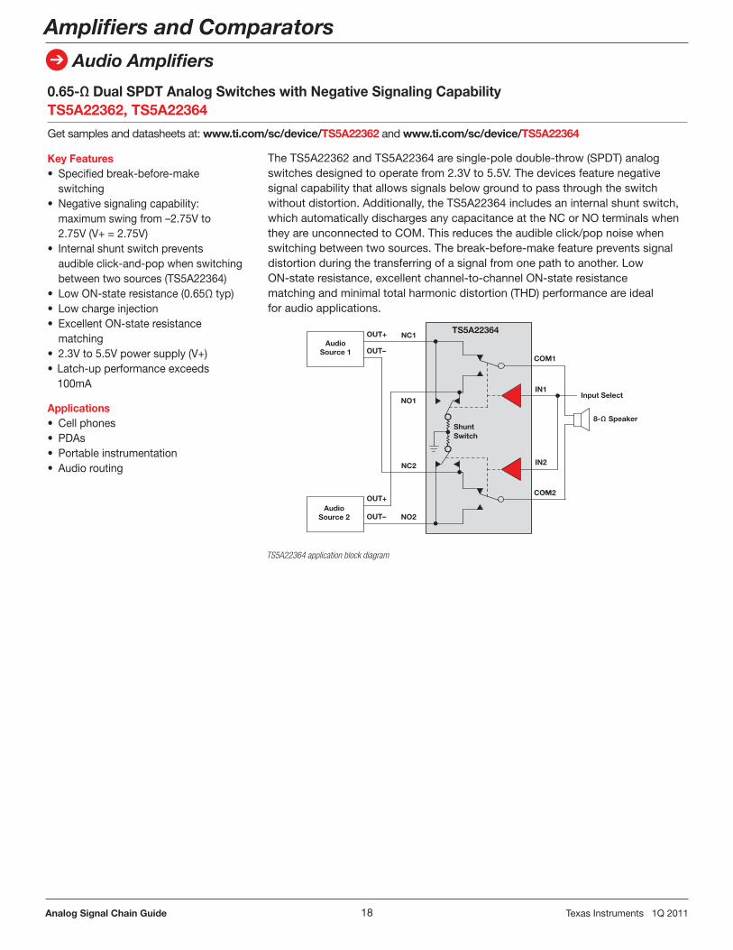
0.65-Ω Dual SPDT Analog Switches with Negative Signaling CapabilityTS5A22362, TS5A22364
Getsamplesanddatasheetsat:www.ti.com/sc/device/TS5A22362 andwww.ti.com/sc/device/TS5A22364
Key Features• Specifiedbreak-before-make switching• Negativesignalingcapability: maximumswingfrom–2 .75Vto 2 .75V(V+=2 .75V)• Internalshuntswitchprevents audibleclick-and-popwhenswitching betweentwosources(TS5A22364)• LowON-stateresistance(0 .65Ωtyp)• Lowchargeinjection• ExcellentON-stateresistance matching• 2 .3Vto5 .5Vpowersupply(V+)•Latch-upperformanceexceeds 100mA
Applications• Cellphones• PDAs• Portableinstrumentation• Audiorouting
TheTS5A22362andTS5A22364aresingle-poledouble-throw(SPDT)analogswitchesdesignedtooperatefrom2 .3Vto5 .5V .Thedevicesfeaturenegativesignalcapabilitythatallowssignalsbelowgroundtopassthroughtheswitchwithoutdistortion .Additionally,theTS5A22364includesaninternalshuntswitch,whichautomaticallydischargesanycapacitanceattheNCorNOterminalswhentheyareunconnectedtoCOM .Thisreducestheaudibleclick/popnoisewhenswitchingbetweentwosources .Thebreak-before-makefeaturepreventssignaldistortionduringthetransferringofasignalfromonepathtoanother .LowON-stateresistance,excellentchannel-to-channelON-stateresistancematchingandminimaltotalharmonicdistortion(THD)performanceareidealforaudioapplications .
TS5A22364 application block diagram
ShuntSwitch
IN2
IN1
COM2
COM1
Input Select
NC2
NC1
NO2
OUT+
OUT+
OUT–
OUT–
NO1
TS5A22364Audio
Source 1
AudioSource 2
8- SpeakerΩ

19Analog Signal Chain Guide TexasInstruments1Q2011
Amplifiers and Comparators
Audio Amplifiers
TPA2015D1 functional block diagram
TheTPA2015D1isa2 .0Wfilter-freemonoClass-DAudiopoweramplifierwithintegratedboostconverterandbatterytrackingSpeakerGuard™AGCtechnologythat:
• ProducesconsistentaudioloudnessregardlessofbatteryvoltagebydeliveringconstantoutputpowerovertheLi-ionbatteryvoltage
• Preventsearlyshutdownbylimitingcurrentatlowbatteryvoltages• Protectsspeakersbypreventingclippingoftheaudiooutput• Offersacheaperandhigherperformingsuccessortotheboostedclass-D
productportfolio
Key Features• 2 .0Winto8Ωat3 .6V(6%THD)
delivering36%louderaudiothantheleadingcompetition
• Constantoutputpowerof2 .0W(3 .6to5 .0V)resultinginconsistentaudioloudnessacrosstheLi-ionbattery
• BatterytrackingSpeakerGuard™thatprotectsspeakersbypreventingclipping
• BatterytrackingAGCthatpreventsearlyshutdownatlowbatteryvoltages(<3V)
• 2mmx2mm,0 .5mmpitch16-ballWCSPwith20%smallerpackagesizethanthecompetition
• Highefficiency(81%)(at1Wand3 .6V)resultingin34%longerbatterylife
Applications•Cellphones• PDAs• PNDs• Portableelectronics
2W Class-D Audio Amplifier with Adaptive Boost and Battery Tracking SpeakerGuard™ AGCTPA2015D1
Getsamples,datasheetsandapplicationreportsat:www.ti.com/sc/device/TPA2015D1
TheTAS5630/31isahigh-performanceanalog/PWM-inputClass-Damplifierwithintegratedclosed-loopfeedbacktechnologythatdrivesupto600Wtotalpower .Closed-looparchitectureprovideshigherPSRR,whichwillnotonlyprovidebettersoundqualitybutreducepowersupplyrequirements,allowingforimprovedsys-temperformanceandcost .Theefficiencyofthisclass-Damplifierisgreaterthan88%whilestillprovidingultra-lowTHDperformance .Theself-protectiondesignintegratesundervoltageprotection,overtemperature,clipping,short-circuitandovercurrentprotectiontosafeguardthedeviceandspeakersagainstfaultcondi-tionsthatcoulddamagethesystem .
Key Features• Integratedclosed-looparchitecture• PWMoranaloginputdevicesto
providedesignflexibility• FlatTHDatallfrequenciesandthrough
toclipping• Signalbandwidthupto80kHzforhigh-
frequencycontentfromHDsources• Ultra-low0 .03%THDat1Winto4W
Applications• Hometheater• Activespeakers• Minicombosystems• AVreceivers• DVDreceivers
300W Stereo (600W Total) Class-D Amplifier with Integrated Closed-Loop FeedbackTAS5630/TAS5631
Getsamples,datasheetsandapplicationreportsat:www.ti.com/sc/device/TAS5630,www.ti.com/sc/device/TAS5631
110 VAC 240 VAC
25 V–50 V12 V
PurePath HDTAS5630
(2.1 Configuration)
PurePath HDClass-G Power Supply
Ref. Design
3x OPA1632
±15 V
TAS5630PurePath™ HD™TAS5631
TAS5508CDigital PWMProcessor
DigitalAudioInput
AnalogAudioInput
TAS5630/TAS5631 functional block diagram
IN-
IN+
GAIN
ENB
ENDGND
VBAT SW PVOUT PVDD
OUT+
OUT-AGC
2.2 H
6.8 F - 22 F
TPA2015D1
DifferentialAudio Inputs
Gain Control
AGC Control
Boost Enable
Class-D Enable
2.2 F - 10 F
Connected to Supply

20Analog Signal Chain Guide TexasInstruments1Q2011
OPA1611/12:Bipolar-Input Audio Op AmpsKey Features• Ultra-lownoise:1 .1nV/√Hzat1kHz• Ultra-lowdistortion: 0 .000015%at1kHz• Highslewrate:27V/µs• Widebandwidth:40MHz(G=+1)• Highopenloopgain:130dB• Unitygainstable• LowIQ:3 .6mAperchannel• Rail-to-railoutput• Widesupplyrange: ±2 .25Vto±18V• Singleanddualversionsavailable inSO-8packages
OPA1602/04:Bipolar-Input Audio Op AmpsKey Features• Ultra-lownoise:2 .5nV/√Hzat1kHz• Ultra-lowdistortion: 0 .00003%at1kHz• Highslewrate:20V/µs• Widebandwidth:35MHz(G=+1)• Highopenloopgain:120dB• Unitygainstable• LowIQ:2 .6mAperchannel• Rail-to-railoutput• Widesupplyrange: ±2 .25Vto±18V• Dualversionavailable inSO-8andMSOP-8packages• Quadversionavailable inSO-14andTSSOP-14packages
OPA1641/42/44: FET-Input Audio Op AmpsKey Features• Ultra-lownoise:5 .1nV/√Hzat1kHz• Ultra-lowdistortion: 0 .00005%at1kHz• Highslewrate:20V/µs• Lowinputbiascurrent:15pA• Highopenloopgain:130dB• Unitygainstable• LowIQ:1 .8mAperchannel• Rail-to-railoutput• Widesupplyrange: ±2 .25Vto±18V• Singleanddualversionsavailable inSO-8andMSOP-8packages• Quadversionavailable inSO-14andTSSOP-14packages
1
2
3
4
Out A
–In A
+In A
V+
5
6
7
+In B
–In B
Out B
14
13
12
11
Out D
–In D
+In D
V–
10
9
8
+In C
–In C
Out C
A
Quad
D
B C
1
2
3
4
8
7
6
5
V+
Out B
–In B
+In B
Out A
–In A
+In A
V–
B
A
Dual
1
2
3
4
8
7
6
5
NC
V+
Output
NC
NC
–In
+In
V–
Single
Family of High Performance Audio Operational AmplifiersOPA16xx
Applications - OPA16xx• Professionalaudioequipment• MicrophonePreamplifiers• Analoganddigitalmixingconsoles• Broadcaststudioequipment• Audiotestandmeasurement• High-endA/Vreceivers• High-endBlu-ray™players
Getsamples,datasheetsandappreportsat:www.ti.com/sc/device/PARTnumber (ReplacePARTnumber withOPA1611, OPA1612, OPA1641, OPA1642,or OPA1644)
OPA1611/1602/1641 pin configurations
Amplifiers and Comparators
Audio Amplifiers
Audio Amplifiers – Portable
Device DescriptionAmp Class
Amplifier Input Type
Amplifier Output Type
Open/ Closed Loop
Speaker Output Power
(W)
Headphone Output Power
(W)
Load Impedance
(Ω) Supply
(V)
Half Power
THD+N at 1kHz (%)
Head- phone psRR (dB)
SpeakerpsRR (dB)
HiRelAvail. Package(s)
Price*
Headphone Amplifiers
TPA6132A2 25mW DirectPath™ Stereo Headphone Amplifier with Pop Suppression (TPA6132)
Class-AB Analog Stereo Closed — 0.025 16 2.3 to 5.5
0.025 100 — N WQFN-16 0.55
TPA6140A2 25mW Class-G DirectPath Stereo Headphone Amp with I2C Volume Control (TPA6140)
Class-G Analog Stereo Closed — 0.025 16 2.5 to 5.5
0.0025 105 — N DSBGA-16 0.95
TPA6141A2 25mW Class-G DirectPath Stereo Headphone Amp (TPA6141)
Class-G Analog Stereo Closed — 0.025 16 2.5 to 5.5
0.0025 105 — N DSBGA-16 0.85
Speaker Amplifiers – Portable
TPA6012A4 3W Stereo Audio Power Amp with Advanced DC Volume Control
Class-AB Analog Stereo Closed 3 — 3 4.5 to 5.5
0.06 — 70 N HTSSOP-24 1.35
TPA6013A4 3W Stereo Audio Power Amplifier with Advanced DC Volume Control and 2.1 Input Stereo Input Mux
Class-AB Analog Stereo Closed 3 — 3 4.5 to 5.5
0.06 — 70 N HTSSOP-24 1.45
TPA6017A2 Stereo, Cost-Effective, Class-AB Audio Amplifier
Class-AB Analog Stereo Closed 2 — 3 4.5 to 5.5
0.1 — 77 N HTSSOP-20 0.65
*Suggested resale price in U.S. dollars in quantities of 1,000.
*Expected release date: Q2 2011

21Analog Signal Chain Guide TexasInstruments1Q2011
Amplifiers and Comparators
Audio Amplifiers
Audio Amplifiers – Portable (continued)
Device DescriptionAmplifier
Class
Amplifier Input Type
Amplifier Output Type
Open/ Closed Loop
Speaker Output Power
(W)
Headphone Output Power
(W)
Load Impedance
(Ω) Supply
(V)
Half Power
THD+N at 1kHz (%)
Head- phonepsRR (dB)
SpeakerpsRR (dB)
HiRelAvail. Package(s) Price*
Speaker Amplifiers – Portable (continued)
TPA6211A1 3.1W Mono, Fully Differential, Class-AB Audio Amplifier
Class-AB Analog Mono Closed 3.1 — 3 2.5 to 5.5
0.02 — 85 N MSOP-8 PowerPAD™,
SON-8
0.65
TPA2010D1 2.5W Mono Class-D Audio Amplifier with Variable Gain (TPA2010)
Class-D Analog Mono Closed 2.5 — 4 2.5 to 5.5
0.2 — 75 N DSBGA-9 1.20
TPA2011D1 3.2W mono Class-D with Auto-Recovering Short-Circuit Protection
Class-D Analog Mono Closed 3.2 — 4 2.5 to 5.5
0.18 — 86 N DSBGA-9 0.65
TPA2015D1 2W Class-D Audio Amplifier with Adaptive Boost and Battery Tracking SpeakerGuard™ AGC
Class-D Analog Mono Closed 2 — 8 2.3 to 5.2
0.1 — 85 N DSBGA-16 1.15
TPA2028D1 3.0W Mono Class-D Audio Amplifier with Fast Gain Ramp SmartGain™ AGC and DRC
Class-D Analog Mono Closed 3 — 4 2.5 to 5.5
0.1 — 80 N DSBGA-9 0.99
TPA2037D1 Fixed-Gain 3.2W Mono Class-D with Integrated DAC Noise Filter
Class-D Analog Mono Closed 3.2 — 4 2.5 to 5.5
0.18 — 86 N DSBGA-9 0.65
TPA2039D1 Fixed-Gain 3.2W Mono Class-D with Integrated DAC Noise Filter
Class-D Analog Mono Closed 3.2 — 4 2.5 to 5.5
0.18 — 86 N DSBGA-9 0.65
TPA2026D2 3.2W/Ch Stereo SmartGain Class-D Audio Amplifier with Dynamic Range
Class-D Analog Stereo Closed 3.2 — 4 2.5 to 5.5
0.1 — 80 N DSBGA-16 1.30
TPA2100P1 19Vpp Mono Class-D Audio Amplifier for Piezo/Ceramic Speakers (TPA2100)
Class-D Analog Mono Closed — — 1.5µf Piezo 2.5 to 5.5
0.07 — 100 N DSBGA-16 1.15
Amplifier Subsystems
TPA2051D3 2.9W 3-Input Audio Subsystem with SmartGain Mono Class-D and DirectPath Headphone Amplifier
Class-AB Analog Stereo HP, Mono Speaker
Closed 2.9 0.025 4 2.5 to 5.5
0.05 80 75 N DSBGA-25 0.75
TPA2054D4A 2.4W/Ch 3-Input Audio Subsystem with Stereo Class-D and DirectPath Headphone Amplifier
Class-AB Analog Stereo HP, Stereo
Speaker
Closed 1.4 0.145 4 2.5 to 5.5
0.27 78.5 77.7 N DSBGA-25 1.30
Speaker Amplifier – Portable – Digital Input
Device DescriptionAmplifier
Class
Amplifier Input Type
Amplifier Output Type
Open/ Closed Loop
Speaker Output Power
(W)
Headphone Output Power (mW)
Load Impedance
(Ω)
Analog Supply
(V)
Digital Supply
(V)
3-D/Bass Boost
Dynamic Range Control
HiRelAvail. Package Price*
TLV320DAC3120 Digital Input Class-D Speaker Amp with miniDSP
Class-D I2S Mono Closed 2.5 60 4 2.7 to 3.6
1.65 to 1.95
Y/Y Y N 5x5mm QFN-32
1.75
*Suggested resale price in U.S. dollars in quantities of 1,000.

22Analog Signal Chain Guide TexasInstruments1Q2011
Amplifiers and Comparators
Audio Amplifiers
*Suggested resale price in U.S. dollars in quantities of 1,000. See www.ti.com/hirel for HiRel options.
Audio Amplifiers – Mid/High Power
Device DescriptionAmplifier
Class
Amplifier Input Type
Amplifier Output Type
Open/ Closed Loop
Speaker Output Power
(W)
Headphone Output Power
(W)
Load Impedance
(Ω) Supply
(V)
Half Power THD+N at 1kHz
(%)
SpeakerpsRR (dB)
HiRelAvail. Package(s) Price*
Speaker Amplifiers – Mid/High Power – Analog InputTPA1517 Stereo, Medium Power, Class-AB
Audio AmplifierClass-AB Analog Stereo Closed 6 — 4 9.5 to 18 0.15 65 N PDIP-20,
SO-20 PowerPAD™
1.15
TPA3002D2 9W Stereo Class-D Audio Power Amplifier with Volume Control (TPA3002)
Class-D Analog Stereo Closed 9 — 8 8.5 to 14 0.06 80 N HTQFP-48 3.65
TPA3003D2 3W Stereo Class-D Audio Power Amplifier with Volume Control (TPA3003)
Class-D Analog Stereo Closed 3 — 8 8.5 to 14 0.2 80 N TQFP-48 3.00
TPA3004D2 12W Stereo Class-D Audio Power Amplifier with Volume Control (TPA3004)
Class-D Analog Stereo Closed 12 — 4 8.5 to 18 0.1 80 N HTQFP-48 3.60
TPA3100D2 20W Stereo Class-D Audio Power Amplifier (TPA3100)
Class-D Analog Stereo Closed 20 — 4 10 to 26 0.11 70 Y HTQFP-48 VQFN-48
3.50
TPA3100D2-Q1 Automotive Catalog 20W Stereo Class-D Audio Power Amplifier
Class-D Analog Stereo Closed 20 — 4 10 to 26 0.11 70 N VQFN-48 4.45
TPA3101D2 10W Stereo Class-D Audio Power Amplifier (TPA3101)
Class-D Analog Stereo Closed 10 — 4 10 to 26 0.09 70 N HTQFP-48, VQFN-48
3.45
TPA3106D1 40W Mono Class-D Audio Power Amplifier (TPA3106)
Class-D Analog Mono Closed 40 — 4 10 to 26 0.2 70 N HLQFP-32 2.25
TPA3110D2 15W Filter-Free Class D Stereo Amplifier with SpeakerGuard™ (TPA3110)
Class-D Analog Stereo Closed 15 — 4 8 to 26 0.07 70 N HTSSOP-28 1.45
TPA3111D1 10W Mono Class-D Audio Power Amplifier with SpeakerGuard (TPA3111)
Class-D Analog Mono Closed 10 — 4 8 to 26 0.07 70 N HTSSOP-28 0.90
TPA3112D1 25W Filter-Free Mono Class-D Audio Amplifier with SpeakerGuard; (TPA3112)
Class-D Analog Mono Closed 25 — 4 8 to 26 0.07 70 N HTSSOP-28 0.85
TPA3113D2 6W Stereo Class-D Audio Power Amplifier with SpeakerGuard (TPA3113)
Class-D Analog Stereo Closed 6 — 4 8 to 26 0.07 70 N HTSSOP-28 0.85
TPA3121D2 15W Stereo Class-D Audio Power Amplifier with SE Outputs (TPA3121)
Class-D Analog Stereo Closed 15 — 4 10 to 26 0.08 60 N HTSSOP-24 1.45
TPA3123D2 25W Stereo Class-D Audio Power Amplifier with SE Outputs (TPA3123)
Class-D Analog Stereo Closed 25 — 4 10 to 30 0.08 60 N HTSSOP-24 1.75
TPA3124D2 15W Stereo Class-D Audio Power Amplifier with SE Outputs and Fast Mute Time (TPA3124)
Class-D Analog Stereo Closed 15 — 4 10 to 26 0.08 60 N HTSSOP-24 1.60
TAS5611A 125W Stereo/250W Mono PurePath™ HD™ Analog-Input Power Stage
Class-D Analog Up to 2 ch
Closed 125 — 4 10.8 to 13.2
0.03 80 N HTQFP-64 4.30
TAS5613A 150W Stereo PurePath HD Analog-Input Power Stage
Class-D Analog Up to 2 Ch
Closed 150 — 4 10.8 to 13.2
0.03 80 N HTQFP-64 4.90
TAS5630 Analog Input 300W Stereo (300W Total) Class-D Amplifier with Integrated Feedback
Class-D Analog Up to 4 Ch
Closed 600 — 4 10.8 to 13.2
0.03 80 N HSSOP-44, HTQFP-64
6.00

23Analog Signal Chain Guide TexasInstruments1Q2011
Amplifiers and Comparators
Audio Amplifiers
Audio Amplifiers – Mid/Hi-Power (continued)
Speaker Amplifiers – Mid/High Power – PWM Input/Powerstage
Device DescriptionAmplifier
Class
Amplifier Input Type
Amplifier Output Type
Open/ Closed Loop
Speaker Output Power
(W)
Load Impedance
(Ω) Supply
(V)
Half Power
THD+N at 1kHz (%)
Dynamic Range
HiRel Avail. Package(s) Price*
TAS5102 20W Stereo Digital Amplifier Power Stage Class-D PWM Up to 4 Ch Closed 20 4 8 to 26 <0.1 105 N HTSSOP-32 1.80
TAS5103 15W Stereo Digital Amplifier Power Stage Class-D PWM Up to 4 Ch Closed 15 4 8 to 26 <0.1 105 N HTSSOP-32 1.80
TAS5111A 70W Mono Digital Amplifier Power Stage Class-D PWM Mono Closed 70 4 16 to 30.5 0.025 95 N HTSSOP-32 2.65
TAS5112A 50W Stereo Digital Amplifier Power Stage Class-D PWM Stereo Closed 50 6 16 to 30.5 0.025 95 N HTSSOP-56 4.45
TAS5121 100W Mono Digital Amplifier Power Stage Class-D PWM Mono Closed 100 4 10.8 to 13.2 0.05 95 N HTSSOP-32 3.55
TAS5122 50W Stereo Digital Amplifier Power Stage Class-D PWM Stereo Closed 30 6 16 to 25.5 0.05 95 N HTSSOP-56 3.25
TAS5162 210W Stereo Digital Amplifier Power Stage Class-D PWM Stereo Closed 200 3 10.8 to 13.2 <0.05 110 N HSSOP-36, HTSSOP-44
4.95
TAS5176 100W (5.1 Channel) Digital Amplifier Power Stage Class-D PWM 6 Ch Closed 100 3 10.8 to 13.2 <0.05 109 N HTSSOP-44 4.75
TAS5186A 210W (5.1-Channel) Digital Amplifier Power Stage Class-D PWM 6 Ch Closed 30 3 10.8 to 13.2 0.07 105 N HTSSOP-44 5.50
TAS5261 315W Mono Digital Amplifier Power Stage Class-D PWM Mono Closed 315 3 10.8 to 13.2 <0.05 110 N HSSOP-36 5.25
TAS5342LA 100W Stereo Digital Amplifier Power Stage Class-D PWM Up to 4 Ch Closed 100 2 10.8 to 13.2 0.1 110 N HTSSOP-44 3.05
TAS5352A 125W Stereo Digital Amplifier Power Stage Class-D PWM Up to 4 Ch Closed 125 2 10.8 to 13.2 0.06 110 N HTSSOP-44 3.45
TAS5602 20W Stereo Digital Amp Power Stage w/Feedback Class-D PWM Up to 4 Ch Closed 20 4 10 to 26 <0.1 96 N HTSSOP-44 2.00
TAS5612A 125W Stereo/250W Mono PurePath™ HD™ Digital-Input Power Stage
Class-D PWM Up to 2 Ch Closed 125 4 10.8 to 13.2 0.03 103 N HTQFP-64 4.30
TAS5614A 150W Stereo/300W Mono PurePath HD Digital-Input Power Stage
Class-D PWM Up to 2 Ch Closed 150 4 10.8 to 13.2 0.03 103 N HTQFP-64 4.45
TAS5631 PWM Input 300W Stereo (600W Total) Class-D Amplifier with Integrated Feedback
Class-D PWM Up to 4 Ch Closed 600 4 10.8 to 13.2 0.04 110 N HSSOP-44, HTQFP-64
6.90
*Suggested resale price in U.S. dollars in quantities of 1,000.
Speaker Amplifiers – Mid/High Power – Digital Input
Device DescriptionAmplifier
Class
Amplifier Input Type
Amplifier Output Config.
Open/ Closed Loop
Speaker Output Power
(W)
Head-phone Output Power
(W)
Load Impedance
(Ω) Supply
(V)
Half Power THD+N at 1kHz
(%)
3-D/ Bass Boost
Dynamic Range Control
HiRel Avail. Package
Price*
TAS5704 20W Stereo Closed-Loop I2S Audio Power Amplifier with Speaker EQ and DRC (H/W Controlled)
Class-D I2S Stereo^2.1 ^4.0
Closed 20 — 4 10 to 26 <0.1 N/N No N HTQFP-64 3.00
TAS5705 20W Stereo I2S Audio Power Amplifier with Speaker EQ and DRC
Class-D I2S Stereo^2.1 Closed 20 — 6 8 to 23 <0.1 N/N 2 N HTQFP-64 2.70
TAS5706A 20W Stereo Closed-Loop I2S Audio Power Amp w/Speaker EQ and DRC
Class-D I2S Stereo^2.1 Closed 20 — 4 10 to 26 <0.1 N/N 2 N HTQFP-64 3.00
TAS5706B 20W Closed-Loop I2S Audio Power Amp w/Speaker EQ, DRC and SE Output Support
Class-D I2S Stereo^2.1 ^4.0
Closed 20 — 4 10 to 26 <0.1 N/N 2 N HTQFP-64 3.00
TAS5707 20W Stereo I2S Audio Power Amp with Speaker EQ and DRC
Class-D I2S Stereo Closed 20 — 6 8 to 26 <0.1 N/N 1 N HTQFP-48 2.55
TAS5707A 20W Stereo Digital Audio Power Amplifier with EQ and DRC
Class-D I2S Stereo Closed 20 — 6 8 to 26 <0.1 N/N 1 N HTQFP-48 2.30
TAS5708 20W Stereo Closed-Loop I2S Audio Power Amp w/Speaker EQ and DRC
Class-D I2S Stereo Closed 20 — 6 10 to 26 <0.1 N/N 1 N HTQFP-48 2.85
TAS5709 20W Stereo I2S Audio Amplifier with Speaker EQ and 2-Band DRC
Class-D I2S Stereo Closed 20 — 6 8 to 26 <0.1 Y/Y 2 N HTQFP-48 2.40
TAS5709A 20W Stereo I2S Audio Amplifier with Speaker EQ and 2-Band DRC
Class-D I2S Stereo Closed 20 — 6 8 to 26 <0.1 Y/Y 2 N HTQFP-48 2.65
TAS5710 20W Stereo Closed-Loop I2S Audio Amp w/Speaker EQ and 2-Band DRC
Class-D I2S Stereo Closed 20 — 6 10 to 26 <0.1 Y/Y 2 N HTQFP-48 2.65
TAS5711 20W Stereo I2S Audio Amplifier with Speaker EQ, DRC and 2.1 Support
Class-D I2S Stereo^2.1 Closed 20 — 4 8 to 26 <0.1 Y/N 2 N HTQFP-48 2.75
TAS5713 25W Stereo I2S Audio Amplifier with Speaker EQ and 2-Band DRC
Class-D I2S Stereo Closed 25 — 4 8 to 26 <0.1 N/Y 2 N HTQFP-48 2.85
TAS5715 25W Stereo (BTL) I2S Amp w/Speaker EQ, 2-Band DRC and DC Protection
Class-D I2S Stereo Closed 25 — 4 8 to 26 <0.1 N/Y 2 N QFN-32 2.25
TAS5717 10W Digital Audio Power Amp w/Integrated DirectPath™ Headphone Amp
Class-D I2S Stereo Closed 10 0.040/ 2Vrms
4 8 to 26 <0.1 N/N 2 N QFN-32 2.25
TAS5719 15W Digital Audio Power Amp w/Integrated DirectPath Headphone Amp
Class-D I2S Stereo Closed 15 0.040/ 2Vrms
4 8 to 26 <0.1 N/N 2 N QFN-32 2.35

24Analog Signal Chain Guide TexasInstruments1Q2011
Audio Operational Amplifiers
Device DescriptionAmplifier
Type
No. of
Chs
Supply Min ([V+] + [|V-|])
Supply Max
([V+] + [|V-|])
IQ per Channel (max) (mA)
GBW (typ)
(MHz)
Slew Rate (typ) (V/µs)
Vn at 1kHz (typ)
(nV/√Hz)
Distortion at 1kHz (typ) (%)
HiRelAvail. Package(s) Price*
Audio Operational Amplifiers
THS4521 High-Speed Operational Amplifiers Bipolar Differential Amplifier
1 2.5 5.5 1.25 95 490 4.6 0.000250% N MSOP-8, SOIC-8
1.10
THS4522 Very Low Power Dual Channel Rail-to-Rail Output Fully Differential Amplifier
Bipolar Differential Amplifier
2 2.5 5.5 1.25 95 490 4.6 0.000250% N TSSOP-16 1.85
THS4524 Very Low Power Quad Channel Rail-to-Rail Output Fully Differential Amplifier
Bipolar Differential Amplifier
4 2.5 5.5 1.25 95 490 4.6 0.000250% N TSSOP-38 3.15
Bipolar Differential AmplifiersOPA1632 Fully Differential I/O Audio Amplifier Bipolar
Differential Amplifier
1 5 32 14 180 50 4.6 0.000022% N SOIC-8, MSOP-8,
PowerPAD™
1.75
OPA1611 1.1nV/√Hz Noise, Low Power, Precision Operational Amplifier
Bipolar Operational Amplifier
1 5 36 3.6 40 27 4.6 0.000015% N SOIC-8 1.75
OPA1612 1.1nV/√Hz Noise, Low Power, Precision Operational Amplifier
Bipolar Operational Amplifier
2 5 36 3.6 40 27 4.6 0.000015% N SOIC-8 2.75
OPA1602 2.5nV/√Hz Noise, Low Power, Precision Operational Amplifier
Bipolar Operational Amplifier
1 5 36 2.6 35 20 2.5 0.000030% N SO, MSOP 1.45
OPA1604 2.5nV/√Hz Noise, Low Power, Precision Operational Amplifier
Bipolar Operational Amplifier
4 5 36 2.6 35 20 2.5 0.000030% N SO, MSOP 1.95
OPA2228 3nV/√Hz Noise, Low Power, Precision Operational Amplifier
Bipolar Operational Amplifier
1 5 36 3.8 33 11 3 0.000050% N PDIP-8, SOIC-8 1.85
OPA4228 3nV/√Hz Noise, Low Power, Precision Operational Amplifier
Bipolar Operational Amplifier
4 5 36 3.8 33 11 3 0.000050% N PDIP-14, SOIC-14
4.05
NE5534 3.5nV/√Hz Noise, Precision Operational Amplifier
Bipolar Operational Amplifier
1 10 30 8 10 13 4 0.002 N PDIP-8, SO-8, SOIC-8
0.45
NE5532 3.5nV/√Hz Noise, Precision Operational Amplifier
Bipolar Operational Amplifier
2 10 30 4 10 9 5 0.002 N PDIP-8, SO-8, SOIC-8
0.45
MC33078 High-Speed Low-Noise Operational Amplifier
Bipolar Operational Amplifier
2 10 36 2.5 16 7 4.5 0.002 Y MSOP-8, PDIP-8, SOIC-8
0.30
Amplifiers and Comparators
Audio Amplifiers
Audio PWM Processors
Device DescriptionOutput
Chs
Dynamic Range (dB)
Data Resolution
Dynamic Range
PWM Headphone
OutputVolume Control
Serial Interface
Loudness Compensation Mute EQ
Bass/Treble Tone
ControlHiRelAvail. Package Price*
TAS5001 Digital Audio PWM Processor 2 96 16, 20, 24 96 No No I2S, R, L, DSP
No Yes No No N TQFP-48 3.00
TAS5010 Digital Audio PWM Processor 2 96 16, 20, 24 96 No No I2S, R, L, DSP
No Yes No No N TQFP-48 3.75
TAS5012 Digital Audio PWM Processor 2 102 16, 20, 24 102 No No I2S, R, L, DSP
No Yes No No N TQFP-48 7.25
TAS5086 PurePath™ Digital™ Audio Six-Channel PWM Processor
6 105 16, 20, 24 105 No Yes I2S, R, L No Yes Yes No N TSSOP-38 1.90
TAS5508C 8-Channel Digital Audio PWM Processor
8 102 16, 20, 24 102 Yes Yes I2S, R, L Yes Yes Yes Yes N TQFP-64 5.00
*Suggested resale price in U.S. dollars in quantities of 1,000. See www.ti.com/hirel for HiRel options. Preview products are listed in bold blue.

25Analog Signal Chain Guide TexasInstruments1Q2011
Audio Operational Amplifiers (continued)
Device DescriptionAmplifier
Type
No. of
Chs
Supply Min ([V+] + [|V-|])
Supply Max
([V+] + [|V-|])
IQ per Channel (max) (mA)
GBW (typ)
(MHz)
Slew Rate (typ) (V/µs)
Vn at 1kHz (typ)
(nV/√Hz)
Distortion at 1kHz (typ) (%)
HiRelAvail. Package(s) Price*
FET Operational Amplifiers
OPA827 Low-Noise, High-Precision, JFET-Input Operational Amplifier
FET Operational Amplifier
1 8 36 5.2 22 28 4 0.000040% N MSOP-8, SOIC-8
3.75
OPA627 Precision High-Speed Difet™ Operational Amplifiers
FET Operational Amplifier
1 9 36 7.5 16 55 5.6 0.000030% N PDIP-8, SOIC-8 12.25
OPA1641 SoundPlus™ High-Performance, JFET-Input Audio Operational Amplifier
FET Operational Amplifier
1 5 36 2.3 11 20 5.1 0.000050% N MSOP-8, SOIC-8
0.95
OPA1641 SoundPlus High-Performance, JFET-Input Audio Operational Amplifier
FET Operational Amplifier
1 5 36 2.3 11 20 5.1 0.000050% N MSOP-8, SOIC-8
0.95
OPA1642 SoundPlus High-Performance, JFET-Input Audio Operational Amplifier
FET Operational Amplifier
2 5 36 2.3 11 20 5.1 0.000050% N MSOP-8, SOIC-8
1.45
OPA1644 SoundPlus High-Performance, JFET-Input Audio Operational Amplifier
FET Operational Amplifier
4 5 36 2.3 11 20 5.1 0.000050% N SOIC-14, TSSOP-14
1.95
OPA134 SoundPlus High-Performance, JFET-Input Audio Operational Amplifier
FET Operational Amplifier
1 5 36 5 8 20 8 0.000080% N PDIP-8, SOIC-8 1.10
OPA2134 SoundPlus High-Performance, JFET-Input Audio Operational Amplifier
FET Operational Amplifier
2 5 36 5 8 20 8 0.000080% N PDIP-8, SOIC-8 1.25
OPA4134 SoundPlus High-Performance, JFET-Input Audio Operational Amplifier
FET Operational Amplifier
4 5 36 5 8 20 8 0.000080% N SOIC-14 2.00
OPA604 FET-Input, Audio Operational Amplifier
FET Operational Amplifier
1 9 48 7 20 25 11 0.000300% N PDIP-8, SOIC-8 1.05
OPA2604 Dual FET-Input, Low Distortion Operational Amplifier
FET Operational Amplifier
2 9 48 6 20 25 11 0.000300% Y PDIP-8, SOIC-8 1.90
OPA353 High-Speed, Single-Supply, Rail-to-Rail Operational Amplifiers
FET Operational Amplifier
1 2.7 5.5 8 44 22 18 0.000600% N 5SOT-23, SOIC-8
1.00
OPA2353 High-Speed, Single-Supply, Rail-to-Rail Operational Amplifiers
FET Operational Amplifier
2 2.7 5.5 8 44 22 18 0.000600% N MSOP-8, SOIC-8
1.70
OPA4353 High-Speed, Single-Supply, Rail-to-Rail Operational Amplifiers
FET Operational Amplifier
4 2.7 5.5 8 44 22 18 0.000600% N SOIC-14, SSOP-16/
QSOP
2.50
OPA343 Single-Supply, Rail-to-Rail Operational Amplifiers
FET Operational Amplifier
1 2.5 5.5 1.25 5.5 6 25 0.000700% N 5SOT-23, SOIC-8
0.65
OPA2343 Single-Supply, Rail-to-Rail Operational Amplifiers
FET Operational Amplifier
2 2.5 5.5 1.25 5.5 6 25 0.000700% N MSOP-8, SOIC-8
1.00
OPA4343 Single-Supply, Rail-to-Rail Operational Amplifiers
FET Operational Amplifier
4 2.5 5.5 1.25 5.5 6 25 0.000700% N SOIC-14, TSSOP-14, SSOP-16/
QSOP
1.85
TLO72 Low-Noise JFET-Input General-Purpose Operational Amplifier
FET Operational Amplifier
1 7 36 2.5 3 8 18 0.003000% N PDIP-8, SO-8, SOIC-8,
8TSSOP
0.29
TLO74 Low-Noise JFET-Input General-Purpose Operational Amplifier
FET Operational Amplifier
4 7 36 2.5 3 8 18 0.003000% N PDIP-14, SO-14, SOIC-14, TSSOP-14
0.22
Amplifiers
Audio Amplifiers
*Suggested resale price in U.S. dollars in quantities of 1,000. See www.ti.com/hirel for HiRel options.

26Analog Signal Chain Guide TexasInstruments1Q2011
Amplifiers and Comparators
Instrumentation Amplifiers
Low Noise Instrumentation Amplifiers for Industrial ApplicationsINA826
ContactyourTIsalesrepresentativeformoreinformation .
Key Features• Lowoffsetvoltage:200µV• Robustinputarchitecture: Extendedinputvoltagerange:Vcc-0 .8V ±40Vinputprotection EMIhardened• ExcellentACperformance CMRR(G=1):90dBmin Inputnoise:16nV/√Hz• Industrialsupply: +2 .7to+36V,±1 .35Vto±18V Lowpower:200μA Rail-to-railoutput −40to+125°C• 8-MSOP,8-DFN,and8-SOIC
Applications•Industrialprocesscontrols•Circuitbreakers•Medicalinstrumentation•Portabledataacquisition
TheINA82636Vinstrumentationamplifierenablesaccuratesensormeasurementintheindustrialenvironmentbycombining200µVoffsetvoltageandinputcommonmoderangebeyondthepowersupplyrails .Operatingfrom2 .7Vto36Von200µAoperatingcurrent,theINA826makesiteasytoachieveprecisionmeasurementsinsingleandbipolarsupplyapplications .
INA826 functional block diagram
Key Features• Wideinputrange:±15 .5Vat ±18Vsupply• Binarygainsteps:128V/Vto1/8V/V• Lowoffsetvoltage:3µVatG=128• Near-zerogaindrift:0 .5ppm/°C• Excellentlinearity:1 .5ppm• ExcellentCMRR:140dB• Highinputimpedance• Verylow1/fnoise• Differentialsignaloutput• Overloaddetection• Inputconfigurationswitchmatrix• Wirebreaktestcurrent• ExpandableSPI™withchecksum• General-purposeI/Oport• TSSOP-24package
Applications• High-precisionsignalinstrumentation• Multiplexeddataacquisition• High-voltageanaloginputamplifier• Universalindustrialanaloginput
Zero Drift, HV Programmable Gain AmplifierPGA280Getsamples,datasheetsandappreportsat:www.ti.com/sc/device/PGA280
ThePGA280isahigh-precisioninstrumentationamplifierwithdigitally-controllablegainandsignalintegritytestcapability .Thisdeviceofferslowoffsetvoltage,near-zerooffsetandgaindrift,excellentlinearity,andnearlyno1/fnoisewithsuperiorcommon-modeandsupplyrejectiontosupporthigh-resolutionprecisionmeasurement .The36Vsupplycapabilityandwide,high-impedanceinputrangecomplywithrequirementsforuniversalsignalmeasurement .
PGA280 block diagram
GainNetwork
ADC(ADS1259)
+5V
+15V 15V
SwitchMatrixand
100 ASource
Buffer
7xGPIO
INP2
INN2
INP1
INN1
Address
MUX
SPI
PGA280
Sink and
µ
Control RegisterSPI Interface
300 Ω
+3V
150 ΩR1
(1)
3V
RG VORef
INA826
*Expected release date: Q2 2011

27Analog Signal Chain Guide TexasInstruments1Q2011
Amplifiers and Comparators
Instrumentation Amplifiers
Instrumentation Amplifiers
Device Description Gain
NonLin-
earity(%)
(max)
InputBias
Current(nA)
(max)
Offsetat
G = 100(µV)
(max)
OffsetDrift
(µV/°C)(max)
CMRRat
G = 100(dB)(min)
BWat
G = 100(kHz)(min)
Noise1kHz
(nV/√Hz)(typ)
PowerSupply
(V)
IQPer
Amp(mA)(max)
HiRelAvail. Package(s) Price*
Single Supply: Vsmax < = 5.5VINA333 Zero Drift, Low Power,
Precision1 to 10000 0.00001 0.2 25 0.1 100 3.5 50 1.8 to 5.5 0.075 Y MSOP-8,
DFN-81.80
INA337 RRIO, Auto-Zero, Low Drift 0.1 to 10000 0.01 2 100 0.4 106 1 33 2.7 to 5.5 3.4 N MSOP-8 1.95
INA338 RRIO, Auto-Zero, Shutdown 0.1 to 10000 0.01 2 100 0.4 106 1 33 2.7 to 5.5 3.4 N MSOP-10 2.10
INA326 CM >Supply, Wide Temp 0.1 to 10000 0.01 2 100 0.4 100 1 33 2.7 to 5.5 3.4 N MSOP-8 1.95
INA327 RRIO, Auto-Zero, Low Drift 0.1 to 10000 0.01 2 100 0.4 100 1 33 2.7 to 5.5 3.4 N MSOP-10 2.10
INA155 CM >Supply, SHDN, Wide Temp
10, 50 0.02 0.01 1000 5 92 110 40 2.7 to 5.5 2.1 N SO-8, MSOP-8
1.10
INA2321 RRIO, Auto-Zero, CM >Supply, Low Drift
5 to 1000 0.01 0.01 500 7 90 50 100 2.7 to 5.5 0.06 N TSSOP-14 1.75
INA321 RRIO, Auto-Zero, SHDN 5 to 1000 0.01 0.01 500 7 90 50 100 2.7 to 5.5 0.06 N MSOP-8 1.10
INA331 Low-Power, Single-Supply, CMOS
5 to 1000 0.01 0.01 500 5 90 2000 46 2.7 to 5.5 0.49 N MSOP-8 1.10
INA2331 CM >Supply, Low Drift 5 to 1000 0.01 0.01 1000 5 80 2000 46 2.7 to 5.5 0.49 N TSSOP-14 1.80
INA156 Zero Drift, Low Power, Precision 10, 50 0.02 0.01 8000 5 74 110 40 2.7 to 5.5 2.5 N MSOP-8 0.95
INA2322 Low Offset, RRO, Wide Temp, SR = 6.5V/µs
5 to 1000 0.01 0.01 10000 7 60 50 100 2.7 to 5.5 0.06 N TSSOP-14 1.65
INA2332 Dual INA321 5 to 1000 0.01 0.01 8,000 7 60 500 46 2.7 to 5.5 0.49 N TSSOP-14 1.45
INA322 RRO, SHDN, Wide Temp, Low Cost
5 to 1000 0.01 0.01 10,000 7 60 50 100 2.7 to 5.5 0.06 N MSOP-8 0.95
INA332 RRO, Wide BW, SHDN, Wide Temp, Low Cost
5 to 1000 0.01 0.01 8,000 7 60 500 46 2.7 to 5.5 0.49 N MSOP-8 0.90
INA330 Optimized for Precision 10kΩ Thermistor Applications
— — 0.23 — 0.009°C — 1 0.0001°C 2.7 to 5.5 3.6 N MSOP-10 1.65
Wide Supply: Vsmax < = 36VINA826 Precision RRIO 36V 1 to 1000 0.01 0.37 200 1 110 1100 18 2.7 to
36V0.25 N MSOP-8,
SO-8, QFN Web
INA128 Precision, Low Noise, Low Drift
1 to 10000 0 5 60 0.7 120 200 8 ±2.25 to ±18
0.75 N DIP-8, SOIC-8 3.05
INA129 Precision, Low Noise, Low Drift, AD620 Second Source
1 to 10000 0 5 60 0.7 120 200 8 ±2.25 to +18
0.75 Y DIP-8, SOIC-8 4.45
INA1412 Precision, Low Noise, Low Power, Pin Compatible with AD62121
10, 100 0 5 50 0.5 117 200 8 ±2.25 to ±18
0.8 N DIP-8, SOIC-8 3.55
INA114 Precision, Low Drift 1 to 10000 0 2 50 0.25 110 10 11 ±2.25 to ±18
3 N DIP-8, SO-16 4.80
INA115 Precision, Low Drift, w/Gain Sense Pins
1 to 10000 0 2 50 0.25 110 10 11 ±2.25 to ±18
3 N SO-16 4.20
INA131 Low Noise, Low Drift 100 0 2 50 0.25 110 70 12 ±2.25 to ±18
3 N DIP-8 3.80
INA118 Precision, Low Drift, Low Power 1 to 10000 0 5 55 0.7 107 70 10 ±1.35 to ±18
0.39 N DIP-8, SOIC-8 4.80
INA110 Fast Settle, Low Noise, Wide BW
1, 10, 100, 200, 500
0.01 0.05 1000 2.5 106 470 10 ±6 to ±18 4.5 N DIP-16, SOIC-16
7.00
INA111 Fast Settle, Low Noise, Wide BW 1 to 1000 0.01 0.02 520 6 106 450 10 ±6 to ±18 4.5 N DIP-8, SO-16 4.20
INA101 Low Noise, Wide BW, Gain Sense Pins, Wide Temp
1 to 1000 0 20 250 0.25 100 25 13 ±5 to ±20 8.5 N PDIP-14, SO-16
7.95
INA103 Precision, Fast Settle, Low Drift, Audio, Mic Pre-Amp, THD+N = 0.0009%
1 to 1000 0 12000 255 1.23 100 800 1 ±9 to ±25 12.5 N DIP-16, SO-16
5.00
INA125 Internal Ref, Sleep Mode 4 to 10000 0.01 25 250 2 100 4.5 38 ±1.35 to ±18
0.53 N DIP-16, SOIC-16
2.05
INA163 Precision, Fast Settle, Low Drift, Audio, Mic Pre Amp, THD+N = 0.002%
1 to 10000 0 12000 300 1.23 100 800 1 ±4.5 to ±18
12 SOIC-14 2.90
*Suggested resale price in U.S. dollars in quantities of 1,000. See www.ti.com/hirel for HiRel options. New products are listed in bold red. Preview products are listed in bold blue.

28Analog Signal Chain Guide TexasInstruments1Q2011
Amplifiers and Comparators
Instrumentation Amplifiers
Instrumentation Amplifiers (continued)
Device Description Gain
NonLinearity
(%)(max)
InputBias
Current(nA)
(max)
Offsetat
G = 100(µV)
(max)
OffsetDrift
(µV/°C)(max)
CMRRat
G = 100(dB)(min)
BWat
G = 100(kHz)(min)
Noise1kHz
(nV/√Hz)(typ)
PowerSupply
(V)
IQPer
Amp(mA)(max)
HiRelAvail. Package(s) Price*
Wide Supply: Vsmax < = 36VINA166 Precision, Fast Settle, Low
Drift, Audio, Mic Pre-Amp, THD+N = 0.09%
2000 0.01 12000 300 2.53 100 450 1.3 ±4.5 to ±18
12 N SO-14 5.95
INA217 Precision, Low Drift, Audio, Mic Pre-Amp, THD+N = 0.09%, SSM2017 Replacement
1 to 10000 0 12000 300 1.23 100 800 1.3 ±4.5 to ±18
12 N DIP-8, SO-16
2.50
INA125 Internal Ref, Sleep Mode 4 to 10000 0.01 25 250 2 100 4.5 38 2.7 to 36 0.53 N DIP-16, SOIC-16
2.05
INA121 Low Bias, Precision, Low Power
1 to 10000 0.01 0.05 500 5 96 50 20 ±2.25 to ±18
0.53 N DIP-8, SO-8 2.50
INA116 Ultra-Low IB 3fA (typ), with Buffered Guard Drive Pins
1 to 1000 0.01 0 5000 40 86 70 28 ±4.5 to ±18
1.4 N DIP-16, SO-16
4.20
INA122 µPower, RRO, CM to GND 5 to 10000 0.01 25 250 3 83 5 60 ±1.3 to ±18
0.09 N DIP-8, SOIC-8
2.45
INA126 µPower, <1V VSAT, Low Cost
5 to 10000 0.01 25 250 3 83 9 35 2.7 to 36 0.2 N DIP/SO/MSOP-8
1.15
INA2126 Dual INA126 5 to 10000 0.01 25 250 3 83 9 35 2.7 to 36 0.2 N DIP/SO/ MSOP-16
1.85
Digitally Programmable Gain Amplifiers
Device Description Gain
NonLinearity
at G = 100
(%) (max)
Offset(µV)
(max)
OffsetDrift
(µV/°C) (max)
CMRRat
G = 100(dB) (min)
BWat
G = 100(kHz)(typ)
Noiseat
1kHz(nV/√Hz)
(typ)
PowerSupply
(V)
IQ(mA)(max)
HiRelAvail. Package(s) Price*
PGA103 Precision, Single-Ended Input
1, 10, 100 0.01 500 2 (typ) — 250 11 ±4.5 to ±18 3.5 N SOIC-8 4.35
PGA202 High Speed, FET-Input, 50pA IB
1, 10, 100,1000
0.012 1000 12 92 1000 12 ±6 to ±18 6.5 N DIP-14 7.75
PGA203 High Speed, FET-Input, 50pA IB
1, 2, 4, 8 0.012 1000 12 92 1000 12 ±6 to ±18 6.5 N DIP-14 7.75
PGA204 High Precision, Gain Error: 0.25%
1, 10, 100, 1000
0.002 50 0.25 110 10 13 ±4.5 to ±18 6.5 N SOIC-16, PDIP-16
8.35
PGA205 Gain Drift: 0.024ppm/°C 1, 2, 4, 8 0.002 50 0.25 95 100 15 ±4.5 to ±18 6.5 N SOIC-16, PDIP-16
8.35
PGA206 High Speed, FET-Input, 100pA IB
1, 2, 4, 8 0.002 1500 2 (typ) 95 600 18 ±4.5 to ±18 13.5 N DIP-16, SOIC-16 10.80
PGA207 High Speed, FET-Input, 100pA IB
1, 2, 5, 10 0.002 1500 2 (typ) 95 600 18 ±4.5 to ±18 13.5 N DIP-16, SOIC-16 11.85
PGA112/3 Zero-Drift, Precision PGA with 2Ch MUX
1 to 200 — 100 0.9 — 380 12 +2.2V to +5.5V
0.45 N MSOP-10 1.00
PGA116/7 Zero-Drift, Precision PGA with 10Ch MUX
1 to 200 — 100 1.2 — 380 12 +2.2V to +5.5V
0.45 N TSSOP-20 1.83
PGA309 0.1% Digitally CalibratedBridge Sensor Conditioner,Voltage Output
8 to 1152 0.002 50 0.2 20 60 210 +2.7 to +5.5 1.6 N TSSOP-16 2.95
PGA308 Single Supply, Auto-Zero, Sensor Amplifier w/Pro-grammable Gain and Offset
4 to 1600 — 40 0.2 95 100 50 +2.7 to +5.5 2 N MSOP-10, DFN-10
2.00
PGA280 High Voltage, Wide Input Range, Zero-Drift PGA
1/8 to 128 0.0010 15 0.17 140 6000 22 ±5 to ±18 2.7 to 5.5
7.13 N TSSOP-24 2.90
*Suggested resale price in U.S. dollars in quantities of 1,000. New products are listed in bold red.

29Analog Signal Chain Guide TexasInstruments1Q2011
Amplifiers and Comparators
Instrumentation Amplifiers
Single-Supply, High-Speed, Precision Logarithmic AmplifierLOG114
Getsamplesanddatasheetsat:www.ti.com/sc/device/LOG114
Key Features• Advantages: Tinyforhigh-densitysystems Precisionononesupply Fastovereightdecades Fullytestedfunction• Twoscalingamplifiers• Wideinputdynamicrange: eightdecades,100pAto10mA• 2 .5Vreference• Stableovertemperature• Lowquiescentcurrent:10mA• Dualorsinglesupply:±5V,+5V• Specifiedtemperaturerange: −5°Cto+75°C•Package:smallQFN-16(4mmx4mm)
Applications• Oneterbium-dopedfiberoptic amplifiers(EDFA)• Laseropticaldensitymeasurement• Photodiodesignalcompressionamps• Log,log-ratiofunctions• Analogsignalcompressioninfrontof analog-to-digitalconverters• Absorbancemeasurement
TheLOG114isspecificallydesignedformeasuringlow-levelandwidedynamicrangecurrentsincommunications,lasers,medicalandindustrialsystems .Thedevicecomputesthelogarithmorlog-ratioofaninputcurrentorvoltagerelativetoareferencecurrentorvoltage(logarithmictransimpedanceamplifier) .
HighprecisionisensuredoverawidedynamicrangeofinputsignalsoneitherBipolar(±5V)orsingle(+5V)supply .Specialtemperaturedriftcompensationcircuitryisincludedon-chip .Inlog-ratioapplications,thesignalcurrentmaybefromahighimpedancesourcesuchasaphotodiodeorresistorinserieswithalowimpedancevoltagesource .Thereferencecurrentisprovidedbyaresistorinserieswithaprecisioninternalvoltagereference,photodiodeoractivecurrentsource .
LOG114 functional block diagram
Q1
200ΩR1
(1)1250Ω
R2
R5 R6
200ΩR3
(1)
RREF
1250ΩR4
VO4(3)
−IN4+IN4VLOGOUT
+IN5
−IN5
VO5
VCM IN
I14
1 8 6 7
I1 and I2 are current inputsfrom a photodiode
or other current source
11109(2)
14
5
3 15
13
12
16
VREF2.5V
V−
ComV REF GND
Q2A3
(4)
A1
A2
A4
LOG114
A5
IREF
I2
V+
REF
NOTES: (1) Thermally dependent R1 and R3provide temperature compensation.(2) VLOGOUT = 0.375 × log(I1/I2).(3) VO4 = 0.375 × K × log(I1/I2)K = 1 + R6/R5.(4) Differential Amplifier (A3) Gain = 6.25
Logarithmic Amplifiers
Device
ScaleFactor
(V/Decade)
Input Current Range(nA)(min)
Input CurrentRange(mA)(max)
ConformityError
(Initial 5 Decades)
(%)(max)
ConformityError
(Initial 5Decades)
(%/°C)(typ/temp)
Bandwidth(kHz)
VS(V)
(min)
VS(V)
(max)
IQPerCh.
(mA)(max)
ReferenceType
AuxiliaryOp Amps
HiRelAvail. Package Price*
LOG101 1 0.1 3.5 0.2 0.0001 38 9 36 1.5 External — N SO-8 6.95
LOG102 1 1 1 0.3 0.0002 38 9 36 2 External 2 N SO-14 7.25
LOG104 0.5 0.1 3.5 0.2 0.0001 38 9 36 1.5 External — N SO-8 6.95
LOG112 0.5 0.1 3.5 0.2 0.0001 38 9 36 1.75 2.5V Internal 1 N SO-14 7.90
LOG2112 0.5 0.1 3.5 0.2 0.0001 38 9 36 1.75 2.5V Internal 1/Ch N SO-16 11.35
LOG114 0.375 0.1 10 0.2 0.001 5000 5 10 15 2.5V Internal 2 N QFN-16 7.90
*Suggested resale price in U.S. dollars in quantities of 1,000. New products are listed in bold red.

30Analog Signal Chain Guide TexasInstruments1Q2011
Amplifiers and Comparators
Power Amplifiers and Buffers
1.5A, High-Current Power AmplifierOPA564
Getdatasheets,evaluationmodulesandappreportsat:www.ti.com/sc/device/OPA564
Key Features• Singleordualsupply:±3 .5V(7V)to
±13V(26V)• Largeoutputswing:22VPPat1 .5A
(24Vsupply)•Thermalandover-currentwarning• Adjustablecurrentlimit• Outputenable/disablecontrol• Slewrate:20V/µs•Packaging:HSOP-20PowerPAD™
TheOPA564isahigh-currentoperationalamplifieridealfordrivingupto1 .5Ainreactiveloadsandprovideshighreliabilityindemandingpower-linecommunicationsandmotorcontrolapplications .Itoperatesfromasingleordualpowersupplyof±3 .5V(7V)to±13V(26V) .Insingle-supplyoperation,theinputcommon-moderangeextendsbelowground .TheOPA564iseasytoheatsinkoverthespecifiedextendedindustrialtemperaturerange,–40°Cto+125°C .
Applications• Power-linecommunications• Valve,actuatordrivers• Synchro,servodrivers• Motordrivers• Powersupplyoutputamplifiers• Testequipment• Transducerexcitation• General-purposelinearpowerboosters
OPA564
ThermalFlag
CurrentLimitFlag
Enable Shutdown
RSET
V–
+In
–In
CurrentLimitSet
OPA564 PowerPAD™-down pinout
Power Amplifiers
DeviceIOUT(A)
VS(V)
Bandwidth(MHz)
Slew Rate(V/µs)
IQ (mA) (max)
VOS (mV) (max)
VOS Drift(µV/°C) (max)
IB(nA) (max)
HiRelAvail. Package(s) Price*
OPA445 0.015 20 to 90 2 15 4.7 5 10 0.1 N DIP-8, SO-8, SO-8 PowerPAD™ 4.75
OPA452 0.05 20 to 80 1.8 7.2 6.5 3 5 0.1 N TO220-7, DDPak-7 2.55
OPA453 0.05 20 to 80 7.5 23 6.5 3 5 0.1 N TO220-7, DDPak-7 2.55
OPA454 0.025 10 to 100 2.5 13 4 4 10 0.1 N SO-8 and HSOP-20 PowerPAD 2.75
OPA541 10 20 to 70 1.6 10 25 10 40 0.05 N TO220-11, TO3-8 11.10
OPA544 2 20 to 70 1.4 8 15 5 10 0.1 N TO220-5, DDPak-5 7.90
OPA2544 2 20 to 70 1.4 8 15 5 10 0.1 N TO220-11 12.00
OPA547 0.5 8 to 60 1 6 15 5 25 500 N TO220-7, DDPak-7 5.00
OPA548 3 8 to 60 1 10 20 10 30 500 N TO220-7, DDPak-7 6.90
OPA549 8 8 to 60 0.9 9 35 5 20 500 N ZIP-11, TO220-11 12.00
OPA551 0.2 8 to 60 3 15 8.5 3 7 0.1 N DIP-8, SO-8, DDPak-7 1.90
OPA552 0.2 8 to 60 12 24 8.5 3 7 0.1 N DIP-8, SO-8, DDPak-7 1.75
OPA561 1.2 7 to 16 17 50 60 20 50 0.1 N HTSSOP-20 2.80
OPA564 1.5 7 to 28 4 20 35 20 10 0.1 N HSOP-20 PowerPAD 2.75
OPA567 2 2.7 to 5.5 1.2 1.2 6 2 1.3 0.01 N QFN-12 1.85
OPA569 2 2.7 to 5.5 1.2 1.2 6 2 1.3 0.01 N SO-20 PowerPAD 3.10
Buffers (Sorted by Ascending BW at ACL)
Device
VS±15 (V)
VS±5(V)
VS3.3(V)
VS5
(V)
ACLStableGain(V/V) (min)
BWat ACL(MHz)
SlewRate (V/µs)
SettlingTime
0.01%(ns) (typ)
IQ(mA)(typ)
THD (FC =
1MHz)(dB) (typ)
DiffGain(%)
DiffPhase
(°)
VN at Flatband(nV/√Hz)
(typ)
VOS(mV)(max)
IB (µA)
(max)HiRelAvail. Package(s) Price*
OPA633 Yes Yes — — 1 260 2500 50 21 — — 0.1 — 15 35 N DIP-8 5.45
OPA692 — Yes — Yes 1 280 2000 12 (0.02%) 5.8 –78 0.07 0.02 1.7 2.5 35 N SOT-23-6, SOIC-8 1.15
OPA693 — Yes — Yes 1 1400 2500 12 (0.1%) 13 –84 0.03 0.01 1.8 2 35 N SOT-23-6, SOIC-8 1.30
OPA832 — Yes Yes Yes 1 92 350 45 (0.1%) 4.25 –84 0.1 0.16 9.2 7 10 N SOT-23-5, SOIC-8 0.32
BUF602 — Yes Yes Yes 1 1000 8000 6 (0.05%) 5.8 — 0.15 0.04 4.8 30 7 N SOT-23-5, SOIC-8 0.85
BUF634 Yes Yes Yes Yes 1 30 to 180 2000 200 (0.1%) 15 — 0.4 0.1 4 100 20 N DIP-8, SOIC-8TO220-5, DDPak-5 3.10
*Suggested resale price in U.S. dollars in quantities of 1,000. New products are listed in bold red.

31Analog Signal Chain Guide TexasInstruments1Q2011
Voltage References and Comparators
Comparators
Low-Power, High-Speed Comparator in Micro-PackagesTLV3201Getsamplesanddatasheetsat:www.ti.com/sc/device/TLV3201
Key Features• Fastresponsetime:35nS• Lowquiescentcurrent:40µA• Precisioninput:1mVVOStyp• Rail-to-railinputs• Push-pullandopen-drainoutputs• Singleanddualchanneloptionsin microSizepackaging: Single:SC70andSOT23 Dual:µDFNandMSOP-8• Supplyrange:2 .2Vto5 .5V
Applications• Inspectionequipment• Testandmeasurement• High-speedsamplingsystems• Telecom• Basestations• Portablecommunications
Comparators
Device Description Ch.
IQ PerCh.
(mA)(max)
OutputCurrent
(mA)(min)
tRESPLow-to-High (µs)
VS(V)
(min)
VS(V)
(max)
VOS(25°C)(mV)(max) Output Type
HiRelAvail. Package(s) Price*
TLV3501 Ultra-High Speed, Low Power 1, 2 5 20 0.004 2.7 5.5 5 Push-Pull Y SOT-23 1.50
TL714 High Speed, 10mV (typ) Hysteresis 1 12 16 0.006 4.75 5.25 10 Push-Pull N PDIP, SOIC 2.16
TL3116 Ultra Fast, Low Power, Precision 1 14.7 5 0.0099 5 10 3 Push-Pull N SOIC, TSSOP 0.95
TL712 Single, High Speed 1 20 16 0.025 4.75 5.25 5 Push-Pull N PDIP, SOIC, SOP 0.83
LM306 Single, Strobed, General Purpose 1 10 100 0.028 15 24 5 Push-Pull N PDIP, SOIC 0.77
TLV3201 Single, Dual Push-Pull/Open Drain 1,2 50 25 0.04 2.5 5.5 5 PP/Open-Drain N SC70, SOT-23 MSOP, SOIC
0.40
LM211 Single, High Speed, Strobed 1 6 25 0.115 3.5 30 3 Open-Collector/Emitter
Y PDIP, SOIC 0.20
LM311 Single, High Speed, Strobed, Differential 1 7.5 25 0.115 3.5 30 7.5 Open-Collector/Emitter
N PDIP, SOIC, SOP, TSSOP
0.18
LM111 Single, Strobed, Differential 1 6 25 0.165 3.5 30 3 Open-Collector/Emitter
Y CDIP, LCCC 1.57
LMV331 Single, Low Voltage 1 0.12 10 0.2 2.7 5.5 7 Open-Collector Y SC-70, SOT-23 0.36
LMV339 Quad, Low Voltage 4 0.075 10 0.2 2.7 5.5 7 Open-Collector N SOIC, TSSOP 0.36
LMV393 Dual, Low Voltage 2 0.1 10 0.2 2.7 5.5 7 Open-Collector Y SOIC, TSSOP 0.30
TLC352 Ultra-Low Supply Voltage 2, 4 0.15 6 0.2 1.5 18 5 Open-Drain N PDIP, SOIC, TSSOP
0.40
TLC372 Fast, Low Power 2, 4 0.15 6 0.2 2 18 5 Open-Drain Y PDIP, SOIC, TSSOP
0.33
TLV2352 Low Voltage 2, 4 0.125 6 0.2 2 8 5 Open-Drain Y PDIP, SOIC, TSSOP
0.80
LM139 Quad, Differential 4 0.5 6 0.3 2 36 2 Open-Collector Y SOIC 0.54
LM193 Dual, Differential 2 0.5 6 0.3 2 36 5 Open-Collector N SOIC 0.30
LM239 Quad, Differential 4 0.5 6 0.3 2 30 2 Open-Collector Y PDIP, SOIC 0.22
LM2901 Quad, Differential 4 0.625 6 0.3 2 30 3 Open-Collector Y PDIP, SOIC, SOP, TSSOP
0.18
*Suggested resale price in U.S. dollars in quantities of 1,000. See www.ti.com/hirel for HiRel options. New products are listed in bold red. Preview products are listed in bold blue.
TheTLV3201low-powercomparatorcombinesbest-in-classresponsetime(40ns)with40µAconsumptionmakingiteasytouseonecomparatorformultiplesockets .Atacompetitivepriceandpin-to-pincompatiblewithstandardcomparatorpinout,theTLV3201simplifiesdeviceselectionandinventorymanagement .
VIN
VREF
VOUT
V S = 5V
0.1µF µF
R 1 = 51Ω R2 = 10kΩ
TLV3201
2.2
TLV3201 PowerPAD™-down pinout

32Analog Signal Chain Guide TexasInstruments1Q2011
Voltage References and Comparators
Comparators
Comparators (continued)
Device Description Ch.
IQ PerCh.
(mA)(max)
OutputCurrent
(mA)(min)
tRESPLow-to-High (µs)
VS(V)
(min)
VS(V)
(max)
VOS(25°C)(mV)(max) Output Type
HiRel Avail. Package(s) Price*
LM2903 Dual, Differential 2 0.5 6 0.3 2 30 7 Open-Collector N PDIP, SOIC, SOP, TSSOP
0.18
LM293 Dual, Differential 2 0.5 6 0.3 2 30 3 Open-Collector Y PDIP, SOIC 0.20
LM3302 Quad, General Purpose 4 0.2 6 0.3 2 28 20 Open-Drain/Emitter
N PDIP, SOIC 0.36
LM339 Quad, Differential 4 0.5 6 0.3 2 30 3 Open-Collector N PDIP, SOIC, SOP, SSOP, TSSOP
0.16
LM393 Dual, Differential 2 0.5 6 0.3 2 30 3 Open-Collector N PDIP, SOIC, SOP, TSSOP
0.16
TL331 Single, Differential 1 0.7 6 0.3 2 36 5 Open-Collector Y SOT-23 0.18
TLC339 Quad, Low Power 4 0.02 6 1 3 16 5 Open-Drain N PDIP, SOIC, TSSOP
0.44
TLC3702 Dual and Quad, µPower 2, 4 0.02 4 1.1 3 16 5 Push-Pull Y PDIP, SOIC, TSSOP
0.34
TLC393 Low Power, LM393 Replacement 2 0.02 6 1.1 3 16 5 Open-Drain Y PDIP, SOIC, SOP, TSSOP
0.37
LP311 Single, Strobed, Low Power 1 0.3 25 1.2 3.5 30 7.5 Open-Drain/Emitter
N PDIP, SOIC, SOP 0.68
LP2901 Quad, Low Power, General Purpose 4 0.025 30 1.3 5 30 5 Open-Collector Y PDIP, SOIC 0.68
LP339 Quad, Low Power, General Purpose 4 0.025 30 1.3 5 30 5 Open-Collector N PDIP, SOIC 0.27
TLV3491 Low Voltage, Excellent Speed/Power 1, 2, 4
0.0012 5 6 1.8 5.5 15 Push-Pull Y SOT-23, SOIC, TSSOP
0.42
TLV3701 Nanopower, Push-Pull, RRIO 1, 2, 4
0.0008 1.6 36 2.5 16 5 Push-Pull Y MSOP, PDIP, SOIC, SOT-23,
TSSOP
0.60
TLV3401 Nanopower, Open- Drain, RRIO 1, 2, 4
0.00055 1.6 80 2.5 16 3.6 Open-Drain N MSOP, PDIP, SOIC, SOT-23,
TSSOP
0.60
Comparator with Integrated Functions
TLV2702 Sub-µPower, Op Amp and Comparator, RRIO 2, 4 0.0019 0.2 36 2.5 16 5 Push-Pull N MSOP, PDIP, SOIC, TSSOP
0.90
TLV2302 Sub-µPower, Op Amp and Comparator, RRIO 2, 4 0.0017 0.2 55 2.5 16 5 Open-Collector N MSOP, PDIP, SOIC, TSSOP
0.70
TLV3011 µPower, Comparator with 1.242V Reference 1 0.003 5 6 1.8 5.5 15 Open-Drain Y SC-70, SOT-23 0.75
TLV3012 µPower, Comparator with 1.242V Reference 1 0.003 5 6 1.8 5.5 15 Push-Pull N SC-70, SOT-23 0.75
*Suggested resale price in U.S. dollars in quantities of 1,000. See www.ti.com/hirel for HiRel options. New products are listed in bold red.
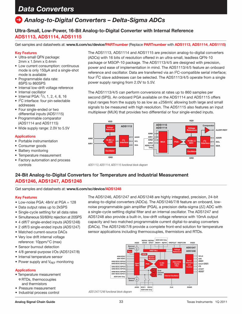
33Analog Signal Chain Guide TexasInstruments1Q2011
Data Converters
Analog-to-Digital Converters – Delta-Sigma ADCs
Ultra-Small, Low-Power, 16-Bit Analog-to-Digital Converter with Internal ReferenceADS1113, ADS1114, ADS1115
Getsamplesanddatasheetsat:www.ti.com/sc/device/PARTnumber (ReplacePARTnumber withADS1113,ADS1114,ADS1115)
Key Features• Ultra-smallQFNpackage: 2mmx1 .5mmx0 .4mm• Lowcurrentconsumption:continuous modeisonly150μAandasingle-shot modeisavailable• Programmabledatarate: 8SPSto860SPS• Internallow-driftvoltagereference• Internaloscillator• InternalPGA:2/3,1,2,4,8,16• I2Cinterface:fourpin-selectable addresses• Foursingle-endedortwo differentialinputs(ADS1115)•Programmablecomparator (ADS1114andADS1115)•Widesupplyrange:2 .0Vto5 .5V
Applications• Portableinstrumentation• Consumergoods• Batterymonitoring• Temperaturemeasurement• Factoryautomationandprocess controls
TheADS1113,ADS1114andADS1115areprecisionanalog-to-digitalconverters(ADCs)with16bitsofresolutionofferedinanultra-small,leadlessQFN-10packageorMSOP-10package .TheADS1113/4/5aredesignedwithprecision,powerandeaseofimplementationinmind .TheADS1113/4/5featureanonboardreferenceandoscillator .DataaretransferredviaanI2C-compatibleserialinterface;fourI2Cslaveaddressescanbeselected .TheADS1113/4/5operatefromasinglepowersupplyrangingfrom2 .0Vto5 .5V .
TheADS1113/4/5canperformconversionsatratesupto860samplespersecond(SPS) .AnonboardPGAavailableontheADS1114andADS1115offersinputrangesfromthesupplytoaslowas±256mV,allowingbothlargeandsmallsignalstobemeasuredwithhighresolution .TheADS1115alsofeaturesaninputmultiplexer(MUX)thatprovidestwodifferentialorfoursingle-endedinputs .
ADS1113, ADS1114, ADS1115 functional block diagram
16-BitADC
I CInterface
2
VoltageReference
Oscillator
SCL
SDA
ADDR
ADS1113
AIN1
AIN016-Bit
ADCI C
Interface
2
VoltageReference
Oscillator
ALERT/RDY
SCL
SDA
ADDR
PGA
ComparatorADS1115ADS1114
MUX
AIN1AIN2
AIN0
AIN3ADS1115
Only
VDD
GND
VDD
GND
24-Bit Analog-to-Digital Converters for Temperature and Industrial MeasurementADS1246, ADS1247, ADS1248
Getsamplesanddatasheetsat:www.ti.com/sc/device/ADS1248
Key Features•Low-noisePGA:48nVatPGA=128•Dataoutputratesupto2kSPS•Single-cyclesettlingforalldatarates•Simultaneous50/60Hzrejectionat20SPS•4diff/7single-endedinputs(ADS1248)•2diff/3single-endedinputs(ADS1247)•Matchedcurrent-sourceDACs•Verylowdriftinternalvoltage reference:10ppm/°C(max)•Sensorburnoutdetection•4/8general-purposeI/Os(ADS1247/8)• Internaltemperaturesensor•PowersupplyandVREFmonitoring
Applications•Temperaturemeasurement RTDs,thermocouples andthermistors• Pressuremeasurement• Industrialprocesscontrol
TheADS1246,ADS1247andADS1248arehighlyintegrated,precision,24-bitanalog-to-digitalconverters(ADCs) .TheADS1246/7/8featureanonboard,low-noiseprogrammablegainamplifier(PGA),aprecisiondelta-sigma(∆∑)ADCwithasingle-cyclesettlingdigitalfilterandaninternaloscillator .TheADS1247andADS1248alsoprovideabuilt-in,low-driftvoltagereferencewith10mAoutputcapacityandtwomatchedprogrammablecurrentdigital-to-analogconverters(DACs) .TheADS1246/7/8provideacompletefront-endsolutionfortemperaturesensorapplicationsincludingthermocouples,thermistorsandRTDs .
ADS1247/1248 functional block diagram
InputMux
REFP1 REFN1 VREFOUT VREFCOMREFP0/GPIO0
REFN0/GPIO1
BurnoutDetect
BurnoutDetect
DVDD
DGNDIEXC1AVSS
AIN0/IEXCAIN1/IEXC
AIN2/IEXC/GPIO2AIN3/IEXC/GPIO3
AIN4/IEXC/GPIO4AIN5/IEXC/GPIO5
AIN6/IEXC/GPIO6AIN7/IEXC/GPIO7
ADS1248 Only
SCLK
DIN
DRDY
DOUT/DRDY
CS
START
RESET
AVDD
IEXC2
VoltageReference
Internal Oscillator
SerialInterface
andControl
VBIAS
GPIO
CLK
ADS1248 Only
ADS1247
ADS1248
PGA
SystemMonitor
AdjustableDigitalFilter
12-BitADC
DualCurrentDACs
ADS1248 Only
VREF Mux

34Analog Signal Chain Guide TexasInstruments1Q2011
Data Converters
Analog-to-Digital Converters – Delta-Sigma ADCs
Industrial, 14kSPS, 24-Bit Analog-to-Digital Converter with Low-Drift ReferenceADS1259
Getsamplesanddatasheetsat:www.ti.com/sc/device/ADS1259
Key Features•Highperformance INL:0 .4ppm Referencedrift:2ppm/°C Gaindrift:0 .5ppm/°C Offsetdrift:0 .05µV/°C Noise:0 .7µVRMSat60SPS• 24-bits,nomissingcodes• Outputdataratesfrom10SPSto14kSPS• Simultaneous50/60Hzrejection at10SPS• Single-cyclesettling• Internaloscillator
Applications• Industrialprocesscontrol• Scientificinstrumentation• Testandmeasurement
TheADS1259isahigh-linearity,low-drift,24-bitanalog-to-digitalconverter(ADC)designedfortheneedsofindustrialprocesscontrol,precisioninstrumentationandotherexactingapplications .Combinedwithasignalamplifier(suchasthePGA280-p .26),ahigh-resolution,high-accuracymeasurementsystemisformedthatiscapableofdigitizingawiderangeofsignals .
ADS1259 functional block diagram
ProgrammableDigital Filter
2.5VReference
Modulator
VREFP VREFN REFOUTAVDD DVDD
DGNDAVSS
AINP
AINN
XTAL2
XTAL1/CLKIN
Controland
SerialInterface
ClockGenerator
Out-of-RangeDetection
/
DRDY
SCLK
DIN
START
CS
DOUT
CalibrationEngine
f /8CLK
SYNCOUT
ADS1259
Ultra-Small, Low-Power, SPI™-Compatible, 16-Bit Analog-to-Digital ConverterADS1118
Getsamplesanddatasheetsat:www.ti.com/sc/device/ADS1118
Key Features•Ultra-smallQFNpackage: 2mm×1 .5mm×0 .4mm•Widesupplyrange:2 .0Vto5 .5V•Lowcurrentconsumption: Continuousmode:150mA Single-shotmode:autoshutdown•Programmabledatarate: 8SPSto860SPS•Internallow-drift•Voltagereference•Internaloscillator•InternalPGA•Foursingle-endedortwodiffinputs•Internaltemperaturesensor
Applications• Portableinstrumentation• Consumergoods• Batterymonitoring• Temperaturemeasurement• Factoryautomation/processcontrols
TheADS1118isaprecisionanalog-to-digitalconverter(ADC)with16bitsofresolutionofferedinanultra-small,leadlessQFN-10packageoranMSOP-10package .TheADS1118isdesignedwithprecision,power,andeaseofimplementationinmind .Itfeaturesanonboardreferenceandoscillator .DataistransferredviaanSPI™-compatibleserialinterface .TheADS1118operatesfromasinglepowersupplyrangingfrom2Vto5 .5V .
ADS1118 functional block diagram
16-BitADC
SPIInterface
VoltageReference
Oscillator
PGA
ADS1118
MUXAIN1
AIN2
AIN0
AIN3
VDD
GND
TempSensor
DIN
DOUT/DRDY
SCLK
CS

35Analog Signal Chain Guide TexasInstruments1Q2011
Data Converters
Analog-to-Digital Converters – Delta-Sigma ADCs
Delta-Sigma (∆S) ADCs
Device
Res.(Bits)
SampleRate
(kSPS)
Number ofInput
Channels InterfaceInput Voltage
(V) VREF
Linearity(%)
Power(mW)
HiRel Avail. Package(s) Price*
ADS1113 16 0.86 1 SE/1 Diff Serial, I2C ±2.048 Int 0.0015 0.3 N MSOP-10, x2QFN-10 1.85
ADS1114 16 0.86 1 SE/1 Diff Serial, I2C PGA (2/3-16), VDD Int 0.0015 0.3 N MSOP-10, x2QFN-10 2.00
ADS1115 16 0.86 4 SE/2 Diff Serial, I2C PGA (2/3-16), VDD Int 0.0015 0.3 N MSOP-10, x2QFN-10 2.25
ADS1013 12 3.3 1 SE/1 Diff Serial, I2C ±2.048 Int 0.0244 0.3 N MSOP-10, x2QFN-10 0.90
ADS1014 12 3.3 1 SE/1 Diff Serial, I2C PGA (2/3-16), VDD Int 0.0244 0.3 N MSOP-10, x2QFN-10 1.00
ADS1015 12 3.3 4 SE/2 Diff Serial, I2C PGA (2/3-16), VDD Int 0.0244 0.3 Y MSOP-10, x2QFN-10 1.10
ADS1118 16 0.86 4 SE/2 Diff SPI™ PGA (2/3-16), VDD Int 0.0015 0.3 N MSOP-10, x2QFN-10 2.25
ADS1018 12 3.3 4 SE/2 Diff SPI PGA (2/3-16), VDD Int 0.0244 0.3 N MSOP-10, x2QFN-10 1.10
ADS1146 16 2 1 Diff Serial, SPI PGA (1-128), ±2.5 Ext 0.0015 1.4 N TSSOP-16 2.70
ADS1246 24 2 1 Diff Serial, SPI PGA (1-128), ±2.5 Ext 0.0003 2.56 N TSSOP-16 3.45
ADS1259 24 14 1 SPI 5 Int/Ext 0.00004 13 N TSSOP-20 5.60
ADS1672 24 625 1 Serial 5 Ext 0.0003 350 N TQFP-64 11.75
ADS1158 16 125 16 SE/8 Diff Serial, SPI +5, ±2.5 Ext 0.0045 42 N QFN-40 5.95
ADS1258 24 125 16 SE/8 Diff Serial, SPI 5, ±2.5 Ext 0.0015 40 Y QFN-48 7.95
ADS1174 16 52 4 Serial, SPI w/FS 2.5 Ext 0.0045 135 N HTQFP-64 9.95
ADS1178 16 52 8 Serial, SPI w/FS 2.5 Ext 0.0045 245 N HTQFP-64 15.95
ADS1274 24 128 4 Diff Simultaneous Serial, SPI w/FSYNC 2.5 Ext 0.001 30-300 N TQFP-64 13.95
ADS1278 24 128 8 Diff Simultaneous Serial, SPI w/FSYNC 2.5 Ext 0.001 60-600 Y TQFP-64 23.95
ADS1271 24 105 1 Diff Serial, SPI w/FSYNC 2.5 Ext 0.0015 35-100 N TSSOP-16 5.90
ADS1147 16 2 3 SE/2 Diff Serial, SPI PGA (1-128), ±2.5 Int/Ext 0.0015 1.4 N TSSOP-20 3.45
ADS1148 16 2 7 SE/4 Diff Serial, SPI PGA (1-128), ±2.5 Int/Ext 0.0015 1.4 N TSSOP-28 3.95
ADS1247 24 2 3 SE/2 Diff Serial, SPI 3 to +5, ±2.5 Ext 0.0003 2.56 N TSSOP-20 4.45
ADS1248 24 2 7 SE/4 Diff Serial, SPI 3 to +5, ±2.5 Int/Ext 0.0003 2.56 N TSSOP-28 4.95
ADS1252 24 41 1 SE/1 Diff Serial 5 Ext 0.0015 40 N SOIC-8 6.45
ADS1256 24 30 8 SE/4 Diff Serial, SPI PGA (1-64), 5 Ext 0.001 35 N SSOP-28 6.95
ADS1255 24 30 2 SE/1 Diff Serial, SPI PGA (1-64), 5 Ext 0.001 35 N SSOP-20 6.50
ADS1253 24 20 4 SE/4 Diff Serial 5 Ext 0.0015 7.5 N SSOP-16 6.70
ADS1254 24 20 4 SE/4 Diff Serial 5 Ext 0.0015 4 Y SSOP-20 6.70
ADS1251 24 20 1 SE/1 Diff Serial 5 Ext 0.0015 7.5 N SOIC-8 5.60
ADS1216 24 0.78 8 SE/4 Diff Serial, SPI PGA (1-128), 2.5 Int/Ext 0.0015 0.6 N TQFP-48 5.00
ADS1217 24 0.78 8 SE/4 Diff Serial, SPI PGA (1-128), 5 Int/Ext 0.0012 0.8 N TQFP-48 5.00
ADS1218 24 0.78 8 SE/4 Diff Serial, SPI PGA (1-128), 2.5 Int/Ext 0.0015 0.8 N TQFP-48 5.50
ADS1224 24 0.24 4 SE/4 Diff Serial 5 Ext 0.0015 0.5 N TSSOP-20 3.25
ADS1222 24 0.24 2 SE/2 Diff Serial 5 Ext 0.0015 0.5 N TSSOP-14 2.95
ADS1234 24 0.08 4 SE/4 Diff Serial PGA (1-128), 2.5 Ext 0.0015 3 N TSSOP-28 4.50
ADS1232 24 0.08 2 SE/2 Diff Serial PGA (1-128), 2.5 Ext 0.0015 3 N TSSOP-24 3.90
ADS1226 24 0.08 2 Diff Serial 5 Ext 0.0015 0.5 N QFN-16 2.95
ADS1225 24 0.08 1 Diff Serial 5 Ext 0.0015 0.5 N QFN-16 2.75
ADS1241 24 0.015 8 SE/4 Diff Serial, SPI PGA (1-128), 2.5 Ext 0.0015 0.5 N SSOP-28 4.20
ADS1243 24 0.015 8 SE/4 Diff Serial, SPI PGA (1-128), 2.5 Ext 0.0015 0.6 N TSSOP-20 3.95
ADS1240 24 0.015 4 SE/2 Diff Serial, SPI PGA (1-128), 2.5 Ext 0.0015 0.6 N SSOP-24 3.80
ADS1242 24 0.015 4 SE/2 Diff Serial, SPI PGA (1-128), 2.5 Ext 0.0015 0.6 N TSSOP-16 3.60
ADS1244 24 0.015 1 SE/1 Diff Serial 5 Ext 0.0008 0.3 N MSOP-10 2.95
*Suggested resale price in U.S. dollars in quantities of 1,000. See www.ti.com/hirel for HiRel options. New products are listed in bold red. Preview products are listed in bold blue.

36Analog Signal Chain Guide TexasInstruments1Q2011
Data Converters
Analog-to-Digital Converters – Delta-Sigma ADCs
Delta-Sigma (∆S) ADCs
Device
Res.(Bits)
SampleRate
(kSPS)
Number ofInput
Channels Interface Input Full-Scale (C) VREF
Linearity(%)
Power(mW)
HiRel Avail. Package Price*
Delta-Sigma (∆S) ADCs for Measuring Low-Level Currents (Photodiodes)
DDC264 20 3 64 Serial 12.5-150pC Ext 0.05 192 N BGA-100 —
DDC232 20 3 32 Serial 12-350pC Ext 0.025 224-320 N BGA-64 70.00
DDC316 16 100 16 Serial 3pC-12pC Ext 0.025 440 N BGA-64 48.25
DDC118 20 3 8 Serial 12-350pC Ext 0.025 110 N QFN-48 32.00
DDC114 20 3 4 Serial 12-350pC Ext 0.025 55 QFN-48 18.00 Wide Bandwidth Delta-Sigma (∆S) ADCs
DeviceRes. (Bits)
Sample-Rate (kSPS)
Number of Input Channels Interface
Signal Bandwidth (kHz)
SNR (dB)
THD (dB)
Power (mW)
HiRel Avail. Package Price*
ADS1672 24 625 1 Diff SPI/LVDS 305 105 –115 350 N TQFP-64 11.75
ADS1626 18 1250 1 Diff P18 w/FIFO 615 93 –101 515 N TQFP-64 15.50
ADS1625 18 1250 1 Diff P18 615 93 –101 515 N TQFP-64 14.95
ADS1601 16 1250 1 Diff Serial 615 92 –103 350 N TQFP-48 9.95
ADS1602 16 2500 1 Diff Serial 1230 91 –103 530 N TQFP-48 12.50
ADS1675 24 4000 1 Diff Serial/LVDS 1700 107 –107 510 N TQFP-64 17.95
ADS1606 16 5000 1 Diff P16 w/FIFO 2450 88 –99 570 N TQFP-64 15.50
ADS1605 16 5000 1 Diff P16 2450 88 –99 570 N TQFP-64 14.95
ADS1610 16 10MSPS 1 Diff P16 4900 86 –94 960 N TQFP-64 19.95
*Suggested resale price in U.S. dollars in quantities of 1,000. See www.ti.com/hirel for HiRel options. New products are listed in bold red. Preview products are listed in bold blue.
Delta-Sigma (∆S) ADCs (continued)
Device
Res.(Bits)
SampleRate
(kSPS)
Number ofInput
Channels InterfaceInput Voltage
(V) VREF
Linearity(%)
Power(mW)
HiRel Avail. Package(s) Price*
ADS1245 24 0.015 1 SE/1 Diff Serial 2.5 Ext 0.0015 0.5 N MSOP-10 3.10
ADS1250 20 25 1 SE/1 Diff Serial, SPI PGA (1-8), 4 Ext 0.003 75 N SOIC-16 6.95
ADS1131 18 0.08 1 SE/1 Diff Serial 0.02 Ext 0.0008 1.6 N TSSOP-16 1.95
ADS1230 20 0.08 1 SE/1 Diff Serial 0.02 Ext 0.003 3 N TSSOP-16 2.50
ADS1231 20 0.08 1 SE/1 Diff Serial 0.02 Ext 0.003 1.6 N TSSOP-16 2.10
ADS1112 16 0.24 3 SE/2 Diff Serial, I2C PGA (1-8), 2.048 Int 0.01 0.7 N MSOP-10, SON-10 2.65
ADS1110 16 0.24 1 SE/1 Diff Serial, I2C PGA (1-8), 2.048 Int 0.01 0.7 N SOT23-6 1.95
ADS1100 16 0.128 1 SE/1 Diff Serial, I2C PGA (1-8), VDD Ext 0.0125 0.3 N SOT23-6 1.80
ADS1000 12 0.128 1 SE/1 Diff Serial, I2C PGA (1-8), VDD Ext 0.0125 0.3 Y SOT23-6 0.65
ADS1281 31 4 1 Serial, I2C 5 Ext 0.00006 12 N TSSOP-24 28.95
ADS1282 31 4 1 Serial, I2C PGA (1-64), 5 Ext 0.00006 27 Y TSSOP-28 36.95

37Analog Signal Chain Guide TexasInstruments1Q2011
Data Converters
Analog-to-Digital Converters – SAR ADCs
4-ChannelMUX
CH0
CH1
CH2
CH3
ADCINMUX OUT AVDD DVDD
AGND DGND
SARADC
Data Buffers,Sequencer, and
Alarms
I CInterface
2SDA
SCL
A0
INT
PWRCON
RESETOscillator
TheADS7924featuresalow-powerADCcore,supportforlow-supplyoperationandaflexiblemeasurementsequencerthatessentiallyeliminatespowerconsumptionbetweenconversions .Additionally,throughtheuseofdedicateddataregistersandonboardprogrammabledigitalthresholdcomparators,eachinputcantriggeranalarmcondition,resultinginaninterruptgeneratedtothehostmicrocontroller .Thecombinationofdatabuffering,programmablethresholdcomparisonsandalarminterruptsminimizethetimeandpowerexpendedbythehostmicrocontrollerdedicatedtosupervisingtheADS7924 .Theresultisacompletemonitoringsystemforpower-criticalapplicationssuchasbattery-poweredequipmentandenergy-harvestingsystems .
ADS7924 functional block diagram
Key Features• Micropowermonitoring:
4-chscanning5µW/10ms: <1μAofpower-downcurrent• Programmableinterruptpin controlsshutdown/wakeup• Autopower-downcontrol PWRCONpinallowsshutdown ofexternalopamp• Widesupplyrange:
Analogsupply:2 .2Vto5 .5VDigitalsupply:1 .65Vto5 .5V
•Smallfootprint:3mm×3mmQFN
Applications• Portableandbattery-poweredsystems
MedicalRemotesensorsignalmonitoring
•Energyharvesting
12-Bit, 4-Channel MUX Input, microPower SAR ADC with Intelligent System Power ControlADS7924
Getsamples,datasheetsandEVMsat:www.ti.com/sc/device/ADS7924
TheADS7947/8/9dual-channel,low-power,8-/10-/12-bit,2-MSPSADCsofferout-standingperformance .Thewidereferenceandsupplyrangeenablesthesedevicestobeusedinbothlow-cost5Vapplicationsinadditiontolow-power3 .3Vapplica-tions .Asaresultofthehigh-precisiongainandoffsetstabilityofthedevices,thereisnoneedtocalibrategainandoffsetovertemperature,whichreducessystemcom-plexityanddevelopmenttime .Lastly,thepsuedo-differentialinputsreducetheneedforcommonmodeDCsignalconditioningcircuitry,whichlowerssystemcostandcomplexityandincreasessystemreliability .
ADS7947/8/9 functional block diagram
Key Features• ±1LSBoffsetandgaindrift(max)• 72dBSNR(12-bit,min)• True12-bitperformance• Dedicatedpower-downmodeenablepin• Autopower-downscalesto 7 .7μW/kSPSat3V• Pseudo-differentialinputs• 2 .8Vto5 .25Vsupplyrange• 2 .5Vto5 .25Vreferencerange• 1 .8Vto5Vlogicfamilycompatible• SPIinterface•3mmx3mmQFNpackage
Applications• Opticalnetworking• Instrumentationandcontrolsystems• X-Ypositioning• Portablesystems• Batterymonitoring• Highspeeddataacquisition
12-/10-/8-Bit, 2-Ch, 2MSPS, Single-Ended, Psuedo-Differential Input, microPower SAR ADCsADS7947, ADS7948, ADS7949Getsamples,datasheetsandEVMsat:www.ti.com/sc/device/PARTnumber (ReplacePARTnumber withADS7947, ADS7948, ADS7949)
SPI
AV DD DVDD
GND
AIN0P
AIN1P
AIN0N
AIN1N
PDEN
SCLK
SDO
CS
REFGNDREF
CH SEL
MUX S/HSARADC
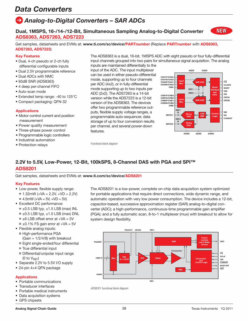
38Analog Signal Chain Guide TexasInstruments1Q2011
Data Converters
Analog-to-Digital Converters – SAR ADCs
AGND
REF
+IN[0:7]
PGAREF
PGAOUT ADCIN REF+
SDO
CS
SDI
SCLK
CONVST
BUSY/INT
RST
MuxPGA
G = 1/2/4/8 S/H CDAC
Comparator
SAR
Output Latches
and 3-State Drivers
OSC
Conversionand
Control Logic
TheADS8201isalow-power,completeon-chipdataacquisitionsystemoptimizedforportableapplicationsthatrequiredirectconnections,widedynamicrange,andautomaticoperationwithverylowpowerconsumption .Thedeviceincludesa12-bit,capacitor-based,successiveapproximationregister(SAR)analog-to-digitalcon-verter(ADC);ahigh-performance,continuous-timeprogrammablegainamplifier(PGA);andafullyautomaticscan,8-to-1multiplexer(mux)withbreakouttoallowforsystemdesignflexibility .
ADS8201 functional block diagram
Key Features• Low-power,flexiblesupplyrange: 1 .32mW(+VA=2 .2V,+VD=2 .2V) 4 .5mW(+VA=5V,+VD=5V)• ExcellentDCperformance: ±0 .5LSBtyp,±1 .5LSB(max)INL ±0 .5LSBtyp,±1 .0LSB(max)DNL ±6LSBoffseterrorat+VA=5V ±0 .1%FSgainerrorat+VA=5V• Flexibleanaloginputs: High-performancePGA (Gain=1/2/4/8)withbreakout Eightsingle-ended/fourdifferential Truedifferentialinput Differential/unipolarinputrange (0toVREF)• Separate2 .2Vto5 .5VI/Osupply•24-pin4×4QFNpackage
Applications• Portablecommunications•Transducerinterfaces• Portablemedicalinstruments• Dataacquisitionsystems• GPSchipsets
2.2V to 5.5V, Low-Power, 12-Bit, 100kSPS, 8-Channel DAS with PGA and SPI™ADS8201Getsamples,datasheetsandEVMsat:www.ti.com/sc/device/ADS8201
TheADS8363isadual,16-bit,1MSPSADCwitheightpseudoorfourfully-differentialinputchannelsgroupedintotwopairsforsimultaneoussignalacquisition .TheanaloginputsaremaintaineddifferentiallytotheinputoftheADC .Theinputmultiplexercanbeusedineitherpseudo-differentialmode,supportinguptofourchannelsperADC(4x2),orinfully-differentialmodesupportinguptotwoinputsperADC(2x2) .TheADS7263isa14-bitversionwhiletheADS7223isa12-bitversionoftheADS8363 .Thedevicesoffertwoprogrammablereferenceout-puts,flexiblesupplyvoltageranges,aprogrammableauto-sequencer,datastorageofuptofourconversionresultsperchannel,andseveralpower-downfeatures .
Functional block diagram
Key Features•Dual,4-chpseudoor2-chfully differentialconfigurableinputs•Dual2 .5Vprogrammablereference•DualADCswithNMC•93dBSNR(ADS8363)•4deepper-channelFIFO•Auto-scanmode•Extendedtemprange:-40to125°C•Compactpackaging:QFN-32
Dual, 1MSPS, 16-/14-/12-Bit, Simultaneous Sampling Analog-to-Digital Converter ADS8363, ADS7263, ADS7223Getsamples,datasheetsandEVMsat:www.ti.com/sc/device/PARTnumber (ReplacePARTnumber withADS8363, ADS7263, ADS7223)
Applications•Motorcontrolcurrentandposition
measurement•Powerqualitymeasurement•Three-phasepowercontrol•Programmablelogiccontrollers•Industrialautomation•Protectionrelays
CHA1P/CHA3CHA1N/CHA2CHA0P/CHA1CHA0N/CHA0
CMA
InputMux
CHB1P/CHB3CHB1N/CHB2CHB0P/CHB1CHB0N/CHB0
CMB
InputMux
SerialInterface
andFIFO
REF1
REF2
AVDD DVDD
CS
CLOCK
BUSY
SDI
RD
SDOA
SDOB
ControlLogic
M0
M1
CONVST
AGND DGNDRGND
2.5VREF
StringDAC
SAR ADC
SAR ADC
StringDAC
REF2
REF1
REFIO1
REFIO2

39Analog Signal Chain Guide TexasInstruments1Q2011
ADCs by Architecture
Analog-to-Digital Converters – SAR ADCs
Unipolar Input SAR ADCs
DeviceRes. (Bits)
Sample-Rate (kSPS)
Power (mW)
Number of Input
Channels InterfaceInput
Voltage (V) VREF
Linearity (%) NMC
SINAD (dB)
HiRel Avail. Package(s) Price*
18-Bit SAR ADCsADS8484 18 1,250 220 1 Diff P8/P16/P18 ±VREF (4.1V)
at VREF/2 Int/Ext 0.0011 18 98 N 7x7 QFN,
TQFP-48 23.40
ADS8486 18 1,250 10 1 Diff Serial, SPI™ VREF, ±VREF at VREF
Ext 0.0006 18 98.5 N VSSOP-10, SON-10
9.99
ADS8284 18 1,000 270 4 Diff P8/P16/P18 ±VREF (4.1V) at VREF/2
Int/Ext 0.00095 18 TBD N 8x8 QFN 22.00
ADS8481 18 1,000 220 1 SE, 1 PDiff P8/P16/P18 VREF (4.1) Int/Ext 0.0013 18 92 N 7x7 QFN, TQFP-48
19.80
ADS8482 18 1,000 220 1 Diff P8/P16/P18 ±VREF (4.1V) at VREF/2
Int/Ext 0.0011 18 98 N 7x7 QFN, TQFP-48
20.25
ADS8380 18 600 110 1 SE, 1 PDiff Serial, SPI VREF Int/Ext 0.0015 18 90 N 6x6 QFN-28 16.50
ADS8382 18 600 110 1 Diff Serial, SPI ±VREF (4.1V) at VREF/2
Int/Ext 0.0012 18 95 N 6x6 QFN-28 16.95
ADS8381 18 580 115 1 SE, 1 PDiff P8/P16/P18 VREF (4.1) Ext 0.0019 18 88 N TQFP-48 16.65
ADS8383 18 500 110 1 SE, 1 PDiff P8/P16/P18 VREF (4.1) Ext 0.0026 18 85 N TQFP-48 15.75
16-Bit SAR ADCsADS8422 16 4,000 160 1 Diff P8/P16 ±VREF (4.1V)
at VREF/2 Int/Ext 0.0023 16 92.5 N 7x7 QFN,
TQFP-48 23.95
ADS8410 16 2,000 290 1 SE, 1 PDiff Serial, LVDS VREF (4.1) Int/Ext 0.0038 16 87.5 N 7x7 QFN-48 23.00
ADS8413 16 2,000 290 1 Diff Serial, LVDS ±VREF (4.1V) at VREF/2
Int/Ext 0.0038 16 92 N 7x7 QFN-48 24.05
ADS8411 16 2,000 175 1 SE, 1 PDiff P8/P16 VREF Int 0.0038 16 85 N TQFP-48 22.00
ADS8412 16 2,000 175 1 Diff P8/P16 ±VREF (4.1V) at VREF/2
Int 0.0038 16 88 N TQFP-48 23.05
ADS8408 16 1,350 9 1 Diff Serial, SPI VREF, ±VREF at VREF
Ext 0.0006 16 — N VSSOP-10, SON-10
8.99
ADS8407 16 1,350 9 1 SE Serial, SPI VREF Ext 0.0019 16 — N VSSOP-10, SON-10
7.99
ADS8405 16 1,250 155 1 SE, 1 PDiff P8/P16 VREF Int/Ext 0.003 16 85 N TQFP-48 14.10
ADS8406 16 1,250 155 1 Diff P8/P16 ±VREF(4.1V) at VREF/2
Int/Ext 0.003 16 90 N TQFP-48 14.70
ADS8254 16 1,000 270 4 Diff P8/P16 ±VREF(4.2V) at VREF/2
Int/Ext 0.0011 16 TBD N 8x8 QFN 18.50
ADS8472 16 1,000 110 1 Diff Serial, SPI ±VREF (4.2V) at VREF/2
Int/Ext 0.00098 16 94 N 6x6 QFN-28 13.00
ADS8471 16 1,000 110 1 SE, 1 PDiff Serial, SPI VREF Int/Ext 0.0015 16 90 N 6x6 QFN-28 12.50
ADS8363 16 1,000 79 4x2/2x2 Serial, SPI ±VREF at ±VREF
Dual Int/Ext
0.009 16 92 N QFN-32 9.28
ADS8329 16 1,000 20 1 SE, 1 PDiff Serial, SPI VREF (4.2V at 5V, 2.5V at
2.7V Supply)
Ext 0.0026 16 92 N TSSOP-16 11.25
ADS8330 16 1,000 15.5 2 SE, 2 PDiff Serial, SPI VREF (5V at 5V, 2.5V at
2.7V Supply)
Ext 0.0026 16 92 N TSSOP-16, 4x4 QFN-16
11.85
ADS8555 16 800 160 1 x 6 Diff Serial, SPI/ P16/P8
±2x/±4xVREF (±1V to ±12V)
Int/Ext 0.0046 16 90 N LQFP-64, 9x9 QFN-64
16.00
ADS8556 16 800 160 1 x 6 Diff Serial, SPI/ P16/P8
±2x/±4xVREF (±1V to ±12V)
Int/Ext 0.0046 16 90 N LQFP-64, 9x9 QFN-64
16.00
*Suggested resale price in U.S. dollars in quantities of 1,000. New products are listed in bold red. Preview products are listed in bold blue.

40Analog Signal Chain Guide TexasInstruments1Q2011
ADCs by Architecture
Analog-to-Digital Converters – SAR ADCs
Unipolar Input SAR ADCs (16-Bit) (continued)
DeviceRes. (Bits)
Sample-Rate
(kSPS)Power (mW)
Number of Input
Channels InterfaceInput
Voltage (V) VREF
Linearity (%) NMC
SINAD (dB)
HiRel Avail. Package(s) Price*
ADS8371 16 750 130 1 SE, 1 PDiff P8/P16 VREF Ext 0.0022 16 87.6 N TQFP-48 12.00
ADS8370 16 600 110 1 SE, 1 PDiff Serial, SPI VREF Int/Ext 0.0015 16 90 N 6x6 QFN-28 12.50
ADS8372 16 600 110 1 Diff Serial, SPI ±VREF (4.2V) at VREF/2
Int/Ext 0.0011 16 93.5 N 6x6 QFN-28 13.00
ADS8361 16 500 150 2 x 2 Diff Serial, SPI ±2.5V at +2.5 Int/Ext 0.00375 14 83 N SSOP-24 8.75
ADS8322 16 500 85 1 PDiff P8/P16 5 Int/Ext 0.009 15 83 N TQFP-32 7.10
ADS8323 16 500 85 1 Diff P8/P16 ±2.5V at 2.5 Int/Ext 0.009 15 83 N TQFP-32 7.10
ADS8318 16 500 18 1 Diff Serial, SPI ±VREF (4.2V) at VREF/2
Ext 0.0015 16 96 N MSOP-10 9.00
ADS8319 16 500 18 1 SE, 1 PDiff Serial, SPI VREF (4.1) Ext 0.0023 16 93.8 N MSOP-10 8.00
ADS8332 16 500 10.6 8 SE, 8 PDiff Serial, SPI VREF (2.5) Int/Ext 0.0031 16 87.5 N 4x4 QFN-24, TSSOP-24
15.00
ADS8331 16 500 10.6 4 SE, 4 PDiff Serial, SPI VREF (2.5) Int/Ext 0.0031 16 87.5 N 4x4 QFN-24, TSSOP-24
13.50
ADS8328 16 500 10.6 2 SE, 2 PDiff Serial, SPI VREF (5V at 5V, 2.5V at
2.7V Supply)
Ext 0.00305 16 88.5 N TSSOP-16, 4x4 QFN-16
9.30
ADS8327 16 500 10.6 2 SE Serial, SPI VREF (4.2V at 5V, 2.5V at
2.7V Supply)
Ext 0.00305 16 88.5 N TSSOP-16 9.30
ADS8364 16 250 413 1 x 6 Diff P16 ±2.5V at +2.5 Int/Ext 0.009 14 82.5 N TQFP-64 18.10
ADS8342 16 250 200 8 SE P8/P16 ±2.5 Ext 0.006 16 85 N TQFP-48 11.30
ADS8365 16 250 190 1 x 6 Diff P16 ±2.5V at +2.5 Int/Ext 0.006 14 87 N TQFP-64 16.25
ADS8317 16 250 6 1 Diff Serial, SPI ±VREF at VREF Ext 0.0022 16 89.5 N VSSOP-8, QFN-8 5.90
ADS8326 16 250 6 1 SE, 1 PDiff Serial, SPI VREF Ext 0.0022 16 91 N VSSOP-8, QFN-8 5.90
TLC4541 16 200 17.5 1 SE Serial, SPI VREF Ext 0.0038 16 84.5 N SOIC-8, VSSOP-8 6.85
TLC4545 16 200 17.5 1 PDiff Serial, SPI VREF Ext 0.0038 16 84.5 N SOIC-8, VSSOP-8 6.85
ADS8321 16 100 5.5 1 Diff Serial, SPI ±VREF at +VREF Ext 0.012 15 84 N VSSOP-8 5.15
ADS8344 16 100 3.6 8 SE/4 Diff Serial, SPI VREF Ext 0.006 15 86 N SSOP-20 8.00
ADS8345 16 100 3.6 8 SE/4 Diff Serial, SPI ±VREF at VREF Ext 0.006 15 85 N SSOP-20 8.00
ADS8341 16 100 3.6 4 SE/2 Diff Serial, SPI VREF Ext 0.006 15 86 N SSOP-16 7.40
ADS8343 16 100 3.6 4 SE/2 Diff Serial, SPI ±VREF at VREF Ext 0.006 15 86 N SSOP-16 7.45
ADS8325 16 100 2.25 1 SE, 1 PDiff Serial, SPI VREF Ext 0.006 16 91 N VSSOP-8, QFN-8 5.90
ADS8320 16 100 1.95 1 SE, 1 PDiff Serial, SPI VREF Ext 0.012 15 84 N VSSOP-8 5.15
14-Bit SAR ADCs
ADS7891 14 3,000 85 1 SE P8/P14 2.5 Int 0.009 14 78 N TQFP-48 10.50
ADS7946 14 2,500 10 2 Pdiff Serial, SPI VREF Ext TBD 14 — N 3x3 QFN-16 2.05
ADS7945 14 2,500 10 2 Diff Serial, SPI VREF Ext TBD 14 — N 3x3 QFN-16 2.15
ADS7890 14 1,250 45 1 SE Serial, SPI 2.5 Int 0.009 14 77 N TQFP-48 10.50
ADS7263 14 1,000 79 4x2/2x2 Serial, SPI ±VREF at +VREF Dual Int/Ext
0.012 14 83 N QFN-32 6.95
ADS7279 14 1,000 15.5 1 SE Serial, SPI VREF (4.2V at 5V, 2.5V at
2.7V Supply)
Ext 0.0061 14 85.7 N TSSOP-16 4.50
*Suggested resale price in U.S. dollars in quantities of 1,000. New products are listed in bold red. Preview products are listed in bold blue.

41Analog Signal Chain Guide TexasInstruments1Q2011
ADCs by Architecture
Analog-to-Digital Converters – SAR ADCs
Unipolar Input SAR ADCs (14-Bit) (continued)
DeviceRes. (Bits)
Sample-Rate
(kSPS)Power (mW)
Number of Input
Channels InterfaceInput
Voltage (V) VREF
Linearity (%) NMC
SINAD (dB)
HiRel Avail. Package(s) Price*
ADS7280 14 1,000 13.7 2 SE Serial, SPI VREF (5V at 5V, 2.5V at
2.7V Supply)
Ext 0.0061 14 85.7 N TSSOP-16 4.50
ADS8557 14 800 160 1 x 6 Diff Serial, SPI ±2x/±4xVREF (±1V to ±12V
Int/Ext 0.0061 14 82 N LQFP-64, 9x9 QFN-64
12.00
TLC3548 14 200 20 8 SE Serial, SPI 4 Int/Ext 0.006 14 81 N SOIC-24, TSSOP-24
6.40
TLC3544 14 200 20 4 SE Serial, SPI 4 Int/Ext 0.006 14 81 N SOIC-20, TSSOP-20
6.00
TLC3541 14 200 17.5 1 SE Serial, SPI VREF Ext 0.006 14 81.5 N SOIC-8, VSSOP-8 5.00
TLC3545 14 200 17.5 1 PDiff Serial, SPI VREF Ext 0.006 14 81.5 N SOIC-8, VSSOP-8 5.00
ADS8324 14 50 2.5 1 Diff Serial, SPI ±VREF at +VREF
Ext 0.012 14 78 N VSSOP-8 4.15
ADS7871 14 40 6 8 SE/4 Diff Serial, SPI PGA (1, 2, 4, 8, 10, 16, 20)
Int 0.03 13 — N SSOP-28 5.00
12-Bit SAR ADCs
ADS7881 12 4,000 95 1 SE P8/P12 2.5 Int 0.024 12 71.5 N 7x7 QFN, TQFP-48 7.35
ADS7882 12 3,000 85 1 SE P8/P12 VREF Int/Ext 0.122 10 68.5 N TQFP-48 2.50
ADS7883 12 3,000 15 1 SE Serial, SPI VDD (2.7V to 5.5V)
Ext (VDD)
0.03 12 72 N SOT-23-6 2.50
ADS7863 12 2,000 13.5 2 x 2 Diff Serial, SPI ±2.5 at 2.5 Int/Ext 0.003 12 71 N SSOP-24, 4x4 QFN-24
4.90
ADS7865 12 2,000 13.5 2 x 2 Diff P12 ±2.5 at 2.5 Int/Ext 0.003 12 71.3 N TQFP-32 4.90
ADS7947 12 2,000 7 2 PDiff Serial, SPI VREF Ext 0.0073 12 — N 3x3 QFN-16 1.95
ADS7869 12 1,000 175 12 Diff Serial, SPI/ P12
±2.5 at +2.5 Int/Ext 0.048 11 — N TQFP-100 14.60
ADS7223 12 1,000 79 4 x 2/2 x 2 Serial, SPI ±VREF at +VREF Dual Int/Ext 0.048 12 70 N QFN-32 4.90
ADS7229 12 1,000 15.5 1 SE Serial/SPI VREF (4.2V at 5V, 2.5V at
2.7V Supply)
Ext 0.0122 12 73.7 N TSSOP-16 2.30
ADS7230 12 1,000 13.7 2 SE Serial/SPI VREF (5V at 5V, 2.5V at 2.7V
Supply)
Ext 0.0122 12 73.7 N TSSOP-16 2.50
ADS7953 12 1,000 12.5 16 SE Serial, SPI VREF (2.5V) Ext 0.024 12 71.3 N TSSOP-38 4.90
ADS7952 12 1,000 12.5 12 SE Serial, SPI VREF (2.5V) Ext 0.024 12 71.3 N TSSOP-38 4.10
ADS7951 12 1,000 12.5 8 SE Serial, SPI VREF (2.5V) Ext 0.024 12 71.3 N TSSOP-30 3.30
ADS7950 12 1,000 12.5 4 SE Serial, SPI VREF (2.5V) Ext 0.024 12 71.3 N TSSOP-30 2.50
ADS7886 12 1,000 7.5 1 SE Serial, SPI VDD (2.35V to 5.25V)
Ext (VDD) 0.03 12 71.2 N SOT-23-6, SC-70 1.70
ADS8558 12 800 160 1 x 6 Diff Serial, SPI/ P12/P8
±2x/±4xVREF (±1V to ±12V)
Int/Ext 0.0121 12 72 N LQFP-64, 9x9 QFN-64
10.00
ADS7864 12 500 52.5 3 x 2 Diff P12 ±2.5 at +2.5 Int/Ext 0.024 12 71 N TQFP-48 6.65
ADS7861 12 500 25 2 x 2 Diff Serial, SPI ±2.5 at +2.5 Int/Ext 0.024 12 70 N SSOP-24, QFN-32 4.05
ADS7862 12 500 25 2 x 2 Diff P12 ±2.5 at +2.5 Int/Ext 0.024 12 71 N TQFP-32 5.70
ADS7852 12 500 13 8 SE P12 5 Int/Ext 0.024 12 72 N TQFP-32 3.40
ADS7818 12 500 11 1 PDiff Serial, SPI 5 Int 0.024 12 70 N PDIP-8, VSSOP-8 2.50
ADS7834 12 500 11 1 PDiff Serial, SPI 2.5 Int 0.024 12 70 N VSSOP-8 2.45
TLC2552 12 400 15 2 SE Serial, SPI VREF Ext 0.024 12 72 N SOIC-8, VSSOP-8 3.95
*Suggested resale price in U.S. dollars in quantities of 1,000. New products are listed in bold red.

42Analog Signal Chain Guide TexasInstruments1Q2011
ADCs by Architecture
Analog-to-Digital Converters – SAR ADCs
Unipolar Input SAR ADCs (12-Bit) (continued)
DeviceRes. (Bits)
Sample-Rate
(kSPS)Power (mW)
Number of Input
Channels InterfaceInput
Voltage (V) VREF
Linearity (%) NMC
SINAD (dB)
HiRel Avail. Package(s) Price*
TLC2551 12 400 15 1 SE Serial, SPI VREF Ext 0.024 12 72 N SOIC-8, VSSOP-8 3.95
TLC2555 12 400 15 1 Diff Serial, SPI VREF Int 0.024 12 72 N SOIC-8, MSOP-8 3.95
TLC2558 12 400 9.5 8 SE Serial, SPI 4 Int/Ext 0.024 12 71 N SOIC-20, TSSOP-20 5.30
TLC2554 12 400 9.5 4 SE Serial, SPI 4 Int/Ext 0.024 12 71 N SOIC-16, TSSOP-16 5.30
AMC7823 12 200 100 8 SE I/O DAS Serial, SPI VREF (5.0) Int/Ext 0.024 12 74 N QFN-40 9.75
TLV2548 12 200 3.3 8 SE Serial, SPI +2, 4 Int/Ext 0.024 12 70 Y SOIC-20, TSSOP-20 4.85
TLV2544 12 200 3.3 4 SE Serial, SPI +2, 4 Int/Ext 0.024 12 70 Y SOIC-16, TSSOP-16 4.20
TLV2542 12 200 2.8 2 SE Serial, SPI VREF Ext 0.024 12 72 N SOIC-8, VSSOP-8 3.85
TLV2541 12 200 2.8 1 SE Serial, SPI VREF Ext 0.024 12 72 N SOIC-8, VSSOP-8 3.85
TLV2545 12 200 2.8 1 PDiff Serial, SPI +5.5 (VREF = VDD)
Ext 0.024 12 72 N SOIC-8, VSSOP-8 3.85
TLV2553 12 200 2.43 11 SE Serial, SPI VREF Ext 0.024 12 — Y SOIC-20, TSSOP-20 3.40
TLV2556 12 200 2.43 11 SE Serial, SPI VREF Int/Ext 0.024 12 — Y SOIC-20, TSSOP-20 3.55
ADS7817 12 200 2.3 1 Diff Serial, SPI ±VREF at +VREF Ext 0.024 12 71 N SOIC-8, VSSOP-8 1.95
ADS7816 12 200 1.9 1 PDiff Serial, SPI VREF Ext 0.024 12 72 N PDIP, SOIC, VSSOP-8 1.95
ADS7844 12 200 0.84 8 SE/4 Diff Serial, SPI VREF, ±VREF at VREF
Ext 0.024 12 72 N SSOP-20 2.90
ADS7841 12 200 0.84 4 SE/2 Diff Serial, SPI VREF , ±VREF at VREF
Ext 0.024 12 72 Y SSOP-16 2.50
ADS7842 12 200 0.84 4 SE P12 VREF Ext 0.024 12 72 N SSOP-28 3.10
ADS7822 12 200 0.6 1 PDiff Serial, SPI VREF Ext 0.018 12 71 Y PDIP, SOIC, VSSOP-8 1.55
ADS7866 12 200 0.25 1 SE, 1 PDiff Serial, SPI VDD (1.2V to 3.6V)
Ext 0.024 12 70 N SOT-23-6 1.85
ADS7829 12 125 0.6 1 PDiff Serial, SPI VREF Ext 0.018 12 71 N QFN-8 1.50
AMC7820 12 100 40 8 SE DAS Serial, SPI VREF (5.0) Int/Ext 0.024 12 72 (typ)
N TQFP-48 3.75
ADS7924 12 100 0.5 4 SE Serial, I2C VREF Ext 0.122 12 — N 3x3 QFN-16 1.25
TLC2543 12 66 5 11 SE Serial, SPI VREF Ext 0.024 12 — Y CDIP, PDIP, PLCC, SOIC, SSOP-20
4.45
TLV2543 12 66 3.3 11 SE Serial, SPI VREF Ext 0.024 12 — N PDIP-20, SOIC-20, SSOP-20
4.45
ADS7870 12 50 4.6 8 SE Serial, SPI PGA (1, 2, 4, 8, 10, 16, 20)
Int 0.06 12 72 N SSOP-28 4.15
ADS7823 12 50 0.75 1 SE Serial, I2C VREF Ext 0.024 12 71 N VSSOP-8 2.85
ADS7828 12 50 0.675 8 SE/4 Diff Serial, I2C VREF Int/Ext 0.024 12 71 Y TSSOP-16 3.35
ADS1286 12 37 1 1 PDiff Serial, SPI VREF Ext 0.024 12 72 N PDIP-8, SOIC-8 2.80
10-Bit SAR ADCs
ADS7884 10 3,000 15 1 SE Serial, SPI VDD (2.7V to 5.5V)
Ext (VDD) 0.781 10 61.7 N SOT-23-6 1.60
ADS7948 10 2,000 7 2 PDiff Serial, SPI VREF Ext 0.0146 12 — N 3x3 QFN-16 1.70
TLV1578 10 1,250 12 8 SE P/0 VREF Ext 0.1 10 60 N TSSOP-32 3.85
TLV1571 10 1,250 12 1 SE P/0 VREF Ext 0.1 10 60 N SOIC-24, TSSOP-24 3.70
TLV1570 10 1,250 9 8 SE Serial, SPI 2V, VREF Int/Ext 0.1 10 60 N SOIC-20, TSSOP-20 3.80
TLV1572 10 1,250 8.1 1 SE Serial, SPI VREF Ext 0.1 10 60 N SOIC-8 3.30
ADS7887 10 1,250 8 1 SE Serial, SPI VDD (2.35V to 5.25V)
Ext (VDD) 0.073 10 61 N SOT-23-6, SC-70 1.50
ADS7957 10 1,000 12.5 16 SE Serial, SPI VREF (2.5V) Ext 0.078 10 60 N TSSOP-38 3.90
ADS7956 10 1,000 12.5 12 SE Serial, SPI VREF (2.5V) Ext 0.078 10 60 N TSSOP-38 3.30
*Suggested resale price in U.S. dollars in quantities of 1,000. See www.ti.com/hirel for HiRel options. New devices are listed in bold red.

43Analog Signal Chain Guide TexasInstruments1Q2011
ADCs by Architecture
Analog-to-Digital Converters – SAR ADCs
Unipolar Input SAR ADCs (10-Bit) (continued)
DeviceRes. (Bits)
Sample-Rate
(kSPS)Power (mW)
Number of Input
Channels InterfaceInput
Voltage (V) VREF
Linearity (%) NMC
SINAD (dB)
HiRel Avail. Package(s) Price*
ADS7955 10 1,000 12.5 8 SE Serial, SPI VREF (2.5V) Ext 0.078 10 60 N TSSOP-30 2.70
ADS7954 10 1,000 12.5 4 SE Serial, SPI VREF (2.5V) Ext 0.078 10 60 N TSSOP-30 2.10
TLC1518 10 400 10 8 SE/7 Diff Serial, SPI +5.5 (VREF = VDD) Int/Ext 0.012 10 60 N SOIC-20, TSSOP-20 3.45
TLC1514 10 400 10 4 SE/3 Diff Serial, SPI +5.5 (VREF = VDD) Int/Ext 0.012 10 60 N SOIC-16, TSSOP-16 2.90
TLV1508 10 200 3.3 8 SE Serial, SPI +2, 4 Int/Ext 0.05 10 60 N SOIC-20, TSSOP-20 3.15
TLV1504 10 200 3.3 4 SE Serial, SPI +2, 4 Int/Ext 0.05 10 60 N SOIC-16, TSSOP-16 2.65
ADS7826 10 200 0.6 1 PDiff Serial, SPI VREF Ext 0.0048 10 62 N QFN-8 1.25
ADS7867 10 200 0.25 1SE, 1 PDiff Serial, SPI VDD (1.2V to 3.6V) Ext 0.05 10 61 N SOT-23-6 1.40
TLC1550 10 164 10 1 SE P10 VREF Ext 0.05 10 — Y PLCC-28, SOIC-24 3.90
TLC1551 10 164 10 1 SE P10 VREF Ext 0.1 10 — N PLCC-28, SOIC-24 3.35
TLV1548 10 85 1.05 8 SE Serial, SPI VREF Ext 0.1 10 — Y CDIP, LCCC, SSOP-20 2.30
TLV1544 10 85 1.05 4 SE Serial, SPI VREF Ext 0.1 10 — N SOIC-16, TSSOP-16 1.95
TLC1542 10 38 4 11 SE Serial, SPI VREF Ext 0.05 10 — Y CDIP, LCCC, PDIP, PLCC, SOIC-20 2.50
TLC1543 10 38 4 11 SE Serial, SPI VREF Ext 0.1 10 — Y PLCC/SOIC/SSOP-20 1.90
TLC1549 10 38 4 1 SE Serial, SPI VREF Ext 0.1 10 — N PDIP-8, SOIC-8 1.71
TLV1543 10 38 2.64 11 SE Serial, SPI VREF Ext 0.1 10 — N CDIP, LCCC, PDIP, PLCC, SOIC, SSOP-20
2.15
TLC1541 10 32 6 11 SE Serial, SPI VREF Ext 0.1 10 — N PDIP, PLCC, SOIC-20 3.20
8-Bit SAR ADCs
ADS7885 8 3,000 15 1 SE Serial, SPI VDD (2.7V to 5.5V) Ext (VDD) 0.156 8 49.8 N SOT-23-6 0.95
ADS7949 8 2,000 7 2 PDiff Serial, SPI VREF Ext 0.0234 12 — N 3x3 QFN-16 0.99
TLV571 8 1,250 12 1 SE P8 VREF Ext 0.5 8 49 N SOIC-24, TSSOP-24 2.35
ADS7888 8 1,250 8 1 SE Serial, SPI VDD (2.35V to 5.25V)
Ext (VDD) 0.2 8 49.5 N SOT-23-6, SC-70 0.85
ADS7961 8 1,000 12.5 16 SE Serial, SPI VREF (2.5V) Ext 0.112 8 49 N TSSOP-38 2.45
ADS7960 8 1,000 12.5 12 SE Serial, SPI VREF (2.5V) Ext 0.112 8 49 N TSSOP-38 2.05
ADS7959 8 1,000 12.5 8 SE Serial, SPI VREF (2.5V) Ext 0.112 8 49 N TSSOP-30 1.65
ADS7958 8 1,000 12.5 4 SE Serial, SPI VREF (2.5V) Ext 0.112 8 49 N TSSOP-30 1.25
TLC0820A 8 392 37.5 1 SE P8 VREF Ext 0.2 8 — N PLCC, SOIC, SSOP-20 1.90
ADS7827 8 250 0.6 1 PDiff Serial, SPI VREF Ext 0.2 8 48 N QFN-8 1.00
ADS7868 8 200 0.25 1 SE, 1 PDiff Serial, SPI VDD (1.2V to 3.6V) Ext 0.1 8 50 N SOT-23-6 0.80
TLC545 8 76 6 19 SE Serial, SPI VREF Ext 0.2 8 — N PDIP-28, PLCC-28 3.10
ADS7830 8 75 0.675 8 SE/4 Diff Serial, I2C VREF Int/Ext 0.19 8 50 N TSSOP-16 1.40
TLV0831 8 49 0.66 1 SE Serial, SPI +3.6 (VREF = VDD) Ext 0.2 8 — N PDIP-8, SOIC-8 1.40
TLC548 8 45.5 9 1 SE Serial, SPI VREF Ext 0.2 8 — N PDIP-8, SOIC-8 1.20
TLV0832 8 44.7 5 2 SE/1 Diff Serial, SPI VREF Ext 0.2 8 — N PDIP-8, SOIC-8 1.40
TLV0834 8 41 0.66 4 SE/2 Diff Serial, SPI VREF Ext 0.2 8 — N PDIP, SOIC, TSSOP-14 1.45
TLC549 8 40 9 1 SE Serial, SPI VREF Ext 0.2 8 — Y PDIP-8, SOIC-8 0.95
TLC541 8 40 6 11 SE Serial, SPI VREF Ext 0.2 8 — Y PDIP, PLCC, SOIC-20 1.50
TLV0838 8 37.9 0.66 8 S/4 Diff Serial, SPI VREF Ext 0.2 8 — N PDIP, SOIC, TSSOP-20 1.45
TLC0831 8 31 3 1 Diff Serial, SPI VREF Ext 0.2 8 — N PDIP-8, SOIC-8 1.40
TLC542 8 25 6 11 SE Serial, SPI VREF Ext 0.2 8 — N PDIP, PLCC, SOIC-20 1.50
TLC0832 8 22 12.5 2 SE/1 Diff Serial, SPI VREF Ext 0.2 8 — N PDIP-8, SOIC-8 1.40
TLC0838 8 20 3 8 SE/4 Diff Serial, SPI VREF Ext 0.2 8 — N PDIP, SOIC, TSSOP-20 1.45
TLC0834 8 20 3 4 SE/2 Diff Serial, SPI VREF Ext 0.2 8 — N PDIP-14, SOIC-14 1.45
*Suggested resale price in U.S. dollars in quantities of 1,000. See www.ti.com/hirel for HiRel options. New products are listed in bold red.

44Analog Signal Chain Guide TexasInstruments1Q2011
ADCs by Architecture
Analog-to-Digital Converters – SAR ADCs
SAR ADC Data Acquisition Systems
DeviceRes. (Bits)
Sample-Rate
(kSPS)Power (mW)
Number of Input
Channels InterfaceInput
Voltage (V) VREF Linearity (%) NMCSINAD (dB)
HiRel Avail. Package Price*
SAR ADC Data Acquisition Systems
ADS8284 18 1,000 270 4 Diff P8/P16/P18
±VREF (4.1V) at VREF/2
Int/Ext
0.00095 18 TBD N 8x8 QFN 22.00
ADS8254 16 1,000 270 4 Diff P8/P16 ±VREF(4.2V) at VREF/2
Int/Ext
0.0011 16 TBD N 8x8 QFN 18.50
ADS7871 14 40 6 8 SE/4 Diff Serial, SPI PGA (1, 2, 4, 8, 10, 16, 20)
Int 0.03 13 — N SSOP-28 5.00
ADS8201 12 100 1.32 8 SE/4 Diff Serial, SPI PGA (1, 2, 4, 8)
Ext 0.012 12 — N 4x4 VQFN 2.75
ADS7870 12 50 4.6 8 SE Serial, SPI PGA (1, 2, 4, 8, 10, 16, 20)
Int 0.06 12 72 N SSOP-28 4.15
Bipolar Input SAR ADCs
DeviceRes. (Bits)
Sample-Rate
(kSPS)
Number of Input
Channels InterfaceInput
Voltage (V) VREF
Linearity (%) NMC
SINAD (dB)
Power (mW)
HiRel Avail. Package(s) Price*
16-Bit Bipolar SAR ADCs
ADS8568 16 600 8 SE Serial, SPI/P16 ±5, ±6, ±10, ±12 Int/Ext 0.0045 16 86.5 335 N QFN-64 15.90
ADS8660 16 500 1 SE Serial, SPI/P8 +5, 10 , ±5, ±10, ±12 Int/Ext 0.0015 16 93.5 90 N TQFP-32 8.50
ADS7815 16 250 1 SE P16 ±2.5 Int/Ext 0.006 15 84 200 N SOIC-28 21.30
ADS8515 16 250 1 SE P16 ±10 Int/Ext 0.0022 16 92 100 N SSOP-28 10.95
ADS8519 16 250 1 SE Serial, SPI +4, 10, ±3.3, 5, 10 Int/Ext 0.0022 16 91 100 N SSOP-28 12.95
ADS8509 16 250 1 SE Serial, SPI +4, 10, ±3.3, 5, 10 Int/Ext 0.003 16 86 70 N SOIC-20, SSOP-28
12.95
ADS8505 16 250 1 SE P8/P16 ±10 Int/Ext 0.0022 16 86 70 N SOIC-28, SSOP-28
12.95
ADS8517 16 200 1 SE Serial, SPI/P8 4, 5, ±10 Int/Ext 0.0022 16 89 38 N SO-28, SSOP-28
13.00
ADS7805 16 100 1 SE P8/P16 ±10 Int/Ext 0.0045 16 86 81.5 N PDIP-28, SOIC-28
21.80
ADS7809 16 100 1 SE Serial, SPI +4, 10, ±3.3, 5, 10 Int/Ext 0.0045 16 88 81.5 N SOIC-20 25.00
ADS7825 16 40 4 SE Serial, SPI/P8 ±10 Int/Ext 0.003 16 83 50 N PDIP-28, SOIC-28
29.55
ADS7813 16 40 1 SE Serial, SPI +4, 10, ±3.3, 5, 10 Int/Ext 0.003 16 89 35 N PDIP-16, SOIC-16
24.70
ADS8513 16 40 1 SE Serial, SPI +4, 10, ±3.3, 5, 10 Int/Ext 0.0023 16 89.9 30 N SOIC-16 12.00
ADS7807 16 40 1 SE Serial, SPI/P8 4, 5, ±10 Int/Ext 0.0022 16 88 28 N PDIP-28, SOIC-28
32.30
ADS8507 16 40 1 SE Serial, SPI/P8 4, 5, ±10 Int/Ext 0.0022 16 88 24 N SOIC-28 13.00
*Suggested resale price in U.S. dollars in quantities of 1,000. Preview products are listed in bold blue.

45Analog Signal Chain Guide TexasInstruments1Q2011
ADCs by Architecture
Analog-to-Digital Converters – SAR ADCs
Bipolar Input SAR ADCs
DeviceRes. (Bits)
Sample-Rate
(kSPS)
Number of Input
Channels InterfaceInput
Voltage (V) VREF
Linearity (%) NMC
SINAD (dB)
Power (mW)
HiRel Avail. Package(s) Price*
14-Bit Bipolar SAR ADCs
ADS8548 14 640 8 SE Serial, SPI/P16 ±5, ±6, ±10, ±12 Int/Ext 0.006 14 83 340 N QFN-64 12.50
TLC3578 14 200 8 SE Serial, SPI ±10 Ext 0.006 14 79 29 N SOIC-24, TSSOP-24
8.65
TLC3574 14 200 4 SE Serial, SPI ±10 Ext 0.006 14 79 29 N SOIC-24, TSSOP-24
6.85
12-Bit Bipolar SAR ADCs
ADS8634 12 1,000 4 Pdiff Serial, SPI +5, 10, ±5, ±10, ±12 Int/Ext 0.021 12 TBD 22.5 N 4x4 QFN-24 2.70
ADS8638 12 1,000 8 Pdiff Serial, SPI +5, 10, ±2.5, ±5, ±10 Int/Ext 0.021 12 TBD 22.5 N 4x4 QFN-24 3.70
ADS8528 12 690 8 SE Serial, SPI/P16 ±5, ±6, ±10, ±12 Int/Ext 0.024 12 73 350 N QFN-64 9.50
ADS7835 12 500 1 SE Serial, SPI ±2.5 Int 0.024 12 72 17.5 N VSSOP-8 2.75
ADS7800 12 333 1 SE P8/P12 ±5, 10 Int 0.012 12 72 135 N CDIP SB-24 30.50
ADS8508 12 250 1 SE Serial, SPI +4, 10, ±3.3, 5, 10 Int/Ext 0.011 12 73 70 N SSOP-28, SOIC-20
10.50
ADS8504 12 250 1 SE P8/P16 ±10 Int/Ext 0.011 12 72 70 N SSOP-28, SOIC-28
10.50
TLC2578 12 200 8 SE Serial, SPI ±10 Ext 0.024 12 79 29 N SOIC-24, TSSOP-24
5.80
TLC2574 12 200 4 SE Serial, SPI ±10 Ext 0.024 12 79 29 N SOIC-20, TSSOP-20
5.30
ADS774 12 125 1 SE P12 10, 20, ±5, ±10 Int 0.024 12 68 120 N PDIP-28, SOIC-28
18.25
ADS7804 12 100 1 SE P8/P16 ±10 Int/Ext 0.011 12 72 81.5 N PDIP-28, SOIC-28
16.55
ADS7808 12 100 1 SE Serial, SPI +4, 10, ±3.3, 5, 10 Int/Ext 0.011 12 73 81.5 N SOIC-20 12.80
ADS7824 12 40 4 SE Serial, SPI/P8 ±10 Int/Ext 0.012 12 73 50 N PDIP-28, SOIC-28
13.10
ADS7812 12 40 1 SE Serial, SPI +4, 10, ±3.3, 5, 10 Int/Ext 0.012 12 74 35 N PDIP-16, SOIC-16
11.80
ADS7806 12 40 1 SE Serial, SPI/P8 +4, 5, ±10 Int/Ext 0.011 12 73 28 N PDIP-28, SOIC-28
15.05
ADS8512 12 40 1 SE Serial, SPI +4, 10, ±3.3, 5, 10 Int/Ext 0.011 12 74 24 N SOIC-16 7.00
ADS8506 12 40 1 SE Serial, SPI/P8 +4, 5, ±10 Int/Ext 0.011 12 73 24 N SOIC-28 7.00
8-Bit Bipolar SAR ADCs
ADS8614 8 1,000 4 Pdiff Serial, SPI +5, 10, ±2.5, ±5, ±10 Int/Ext 0.07 8 TBD 22.5 N 4x4 QFN-24 1.45
ADS8618 8 1,000 8 Pdiff Serial, SPI +5, 10, ±2.5, ±5, ±10 Int/Ext 0.07 8 TBD 22.5 N 4x4 QFN-24 2.05
*Suggested resale price in U.S. dollars in quantities of 1,000. Preview products are listed in bold blue.

46Analog Signal Chain Guide TexasInstruments1Q2011
Data Converters
Analog-to-Digital Converters – Pipeline ADCs
Lowest Power, 14-Bit, 250MSPS ADCADS4149, ADS4146, ADS4129, ADS4126, ADS41B49, ADS41B29
Getsamples,datasheetsandEVMsat:www.ti.com/sc/device/PARTnumber (ReplacePARTnumberwithADS4149,ADS4146,ADS4129,ADS4126,ADS41B49orADS41B29) Key Features•260mWpowerconsumption;
only201mWconsumptionat160MSPSwithdynamicpowerscaling
•Highperformance:70 .6dBSNRwith 84dBcSFDRat170MHzIF•0-6dBprogrammablegainin1dB stepsforoptimizedSNR/SFDR/ inputswing•1 .8AVDDandDVDDpowersupplies•User-selectableDDRLVDSor CMOSoutputs•6pin-compatibleoptions ADS4149,ADS4129:
14-and12-bits,250MSPS ADS4146,ADS4126:
14-and12-bits,160MSPS ADS41B49,ADS41B29:
14-and12-bits,250MSPSwithanaloginputbuffers
•7mmx7mm,48-pinQFNpackage– pincompatibletotheADS6149
Applications•Wirelesscommunication: Digitalpre-distortionfeedbackloops Widebanddigitalrepeaters• Software-definedradios• Portableman-packreceivers• High-density,multi-modereceivers• Portabletestandmeasurement equipment• Wirelesscommunication
TheADS4149wasdevelopedspecificallytobethelowestpower14-bitADCatthe250MSPSnode .Byreducingpowerconsumptionby30%comparedtothenextlowestpower14-bitADCatthisnode,theADS4149enablessystemstoreducetheirpowerconsumptionbudgetforasocketthatconsumesasignificantamountoftotalsystempower,particularlyinmulti-channelsystemssuchaswirelessbasestationsandsoftware-definedradios .
14-BitADC
OVR_SDOUT
D10_D11_M
D10_D11_P
D8_D9_M
D8_D9_P
D6_D7_M
D6_D7_P
D4_D5_M
D4_D5_P
D2_D3_M
D2_D3_P
D0_D1_M
D0_D1_P
CLKOUTM
CLKOUTP
CLKM
CLKPCLOCKGEN
INM
VCM
INP SamplingCircuit Common
Digital Functions
DDRSerializer
ReferenceControl
Interface
OEATAD
S
SF
D
NE
S
KLC
S
TE
SE
R
ADS4149
AVDD AGND DRVDD DRGND InterfaceDDR LVDS
ADS4149 functional block diagram

47Analog Signal Chain Guide TexasInstruments1Q2011
Data Converters
Analog-to-Digital Converters – Pipeline ADCs
Quad, Dual and Single 11-Bit, 200MSPS with ADC SNRBoostADS58C48, ADS58C28, ADS58B18
Getsamplesanddatasheetsat:www.ti.com/sc/device/PARTnumber (ReplacePARTnumberwithADS58C48,ADS58C28orADS58B18) Key Features• Lowestpowerconsumption availableby30% 215mW/chinCMOSmode at185MSPS 317mW/chwith60MHzSNRBoost at185MSPS•High-performanceSNRBoost3G: 60MHzsignalBW 72 .3dBFSSNRacross60MHz bandat140MHz 83dBcSFDRacross60MHzband at140MHz 75 .4dBFSSNRacross30MHz bandat140MHz 85dBcSFDRacross30MHz bandat140MHz•6dBgainin1dBstepsforSNR/SFDR trade-off•14mmx14mm,80-pinTQFPpackage•SelectableDDRLVDSorCMOS outputswithhalf-andfull-swing LVDSmodes•1 .8VAVDDandDVDDsupplies•Exportcontrolcompliant– nolicenserequired
Applications•Macro/microbasestationreceivers TD-SCDMA,CDMA,WCDMA, CDMA2k LTE,TD-LTE,WiMAX MC-GSM(relaxedSFDR specification) Multi-standard,multi-carrier•Basestationdigitalpre-distortion feedback•Software-definedradiosand repeaters•Wirelessnetworktestequipment
TheADS58C48wasdesignedtobethelowestpower11-bit,4-channelADConthemarketat200MSPSwhichincludesa60MHznoise-shapingresampler(SNRBoost) .With11-bitresolutionandamaximumspeedof200MSPS,thedeviceisfullyexportabletocontrolledcountriessuchasChinaandRussia .Bysupportingupto60MHzofSNRBoostbandwidthat185MSPSwithhighSFDR,theADS58C48enableswide-bandmulti-carrierandmulti-modereceiverswithasinglesignalchain,includingCDMA,WCDMA,TD-SCDMA,LTE,WiMAXandMC-GCSM .Andbyofferingfourchannelswithminimalpowerconsumption,thedeviceenableshigh-density2x4and4x4receiverswithoutcreatingthermalandpowerdifficulties .
ADS58C48 functional block diagram (LVDS interface)
REFERENCE
CONTROLINTERFACE
CLKPCLKM
CM
CLOCKGEN
INB_P
INB_M
OUTPUTCLOCKBUFFER
CLKOUTP/M
ADS58C48
14 bitADC
DDRSERIALIZER
11 bit
CHA<10>_P/M
DDRSERIALIZER
11bit
14 bitADC
DDRSERIALIZERSNRBoost
11 bit
14 bitADC
DDRSERIALIZER
SNRBoost11 bit
INC_P
INC_M
INA_P
INA_M
IND_P
IND_M
CHANNEL A
CHANNEL B
CHANNEL C
CHANNEL DDigital ProcessingBlock
Digital ProcessingBlock
SNRBoost
Digital ProcessingBlock
SNRBoost
Digital ProcessingBlock
CHA<8>_P/M
CHA<6>_P/M
CHA<4>_P/M
CHA<2>_P/M
CHA<0>_P/M
CHB<10>_P/M
CHB<8>_P/M
CHB<6>_P/M
CHB<4>_P/M
CHB<2>_P/M
CHB<0>_P/M
CHC<10>_P/M
CHC<8>_P/M
CHC<6>_P/M
CHC<4>_P/M
CHC<2>_P/M
CHC<0>_P/M
CHD<10>_P/M
CHD<8>_P/M
CHD<6>_P/M
CHD<4>_P/M
CHD<2>_P/M
CHD<0>_P/M
14 bitADC
14 bitADC
DD
VA
DN
G
DD
VR
DT
UO
DS
ATAD
SN
ES
KLC
ST
ES
ER
ND
P2_
BR
NS
1_B
RN
S
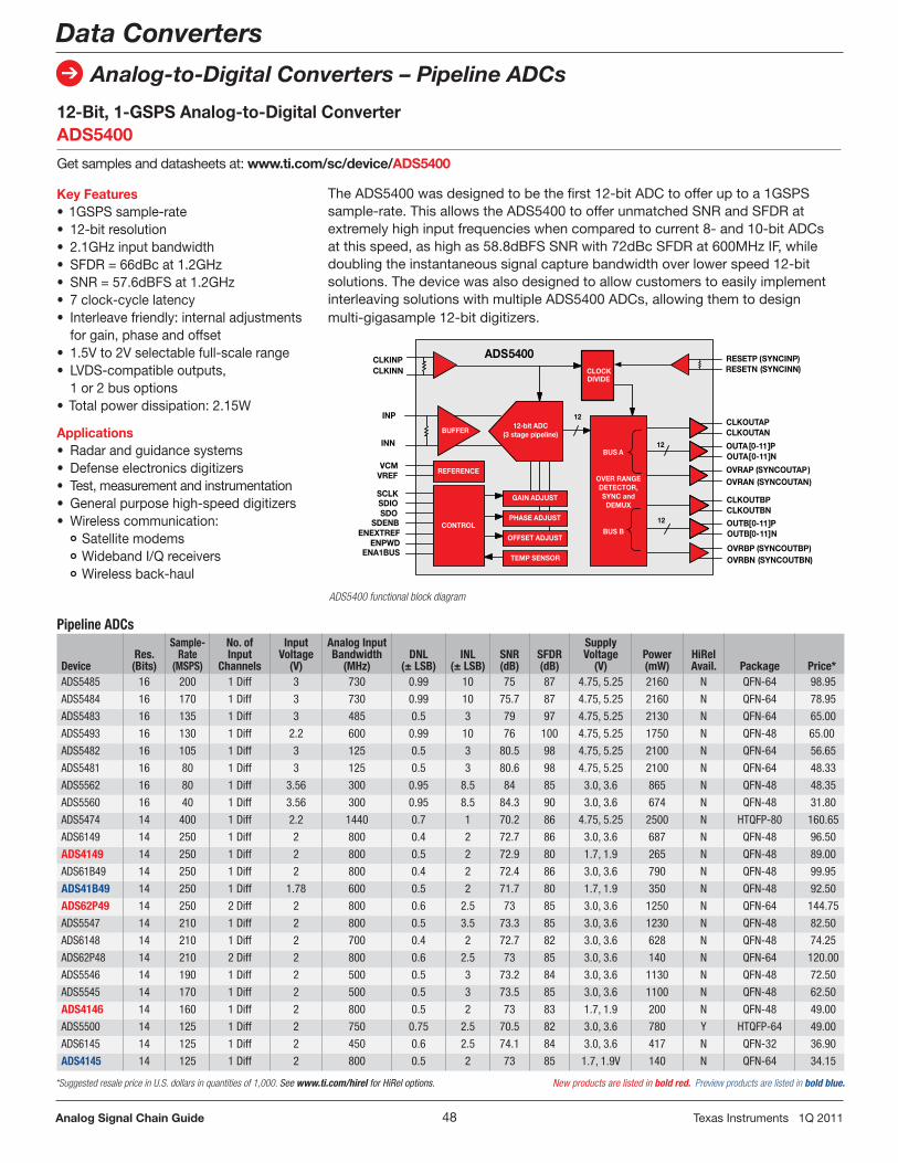
48Analog Signal Chain Guide TexasInstruments1Q2011
Data Converters
Analog-to-Digital Converters – Pipeline ADCs
*Suggested resale price in U.S. dollars in quantities of 1,000. See www.ti.com/hirel for HiRel options. New products are listed in bold red. Preview products are listed in bold blue.
12-Bit, 1-GSPS Analog-to-Digital Converter ADS5400
Getsamplesanddatasheetsat:www.ti.com/sc/device/ADS5400
Key Features•1GSPSsample-rate• 12-bitresolution• 2 .1GHzinputbandwidth• SFDR=66dBcat1 .2GHz• SNR=57 .6dBFSat1 .2GHz• 7clock-cyclelatency• Interleavefriendly:internaladjustments forgain,phaseandoffset• 1 .5Vto2Vselectablefull-scalerange• LVDS-compatibleoutputs, 1or2busoptions•Totalpowerdissipation:2 .15W
Applications• Radarandguidancesystems• Defenseelectronicsdigitizers• Test,measurementandinstrumentation• Generalpurposehigh-speeddigitizers• Wirelesscommunication: Satellitemodems WidebandI/Qreceivers Wirelessback-haul
TheADS5400wasdesignedtobethefirst12-bitADCtoofferuptoa1GSPSsample-rate .ThisallowstheADS5400toofferunmatchedSNRandSFDRatextremelyhighinputfrequencieswhencomparedtocurrent8-and10-bitADCsatthisspeed,ashighas58 .8dBFSSNRwith72dBcSFDRat600MHzIF,whiledoublingtheinstantaneoussignalcapturebandwidthoverlowerspeed12-bitsolutions .ThedevicewasalsodesignedtoallowcustomerstoeasilyimplementinterleavingsolutionswithmultipleADS5400ADCs,allowingthemtodesignmulti-gigasample12-bitdigitizers .
ADS5400 functional block diagram
INP
INN
CLKINPCLKINN
SCLKSDIOSDO
CLKOUTAPCLKOUTAN
OUTB[0-11]POUTB[0-11]N
ADS5400CLOCKDIVIDE
12-bit ADC(3 stage pipeline)
VCMVREF
12
OUTA[0-11]POUTA[0-11]N
12
12
OVRBP (SYNCOUTBP)OVRBN (SYNCOUTBN)
RESETP (SYNCINP)RESETN (SYNCINN)
SDENB
CLKOUTBPCLKOUTBN
OVRAP (SYNCOUTAP)OVRAN (SYNCOUTAN)
ENEXTREFENPWD
ENA1BUS
REFERENCE
BUFFER
CONTROL
TEMP SENSOR
OFFSET ADJUST
PHASE ADJUST
GAIN ADJUST
BUS A
OVER RANGE DETECTOR, SYNC and
DEMUX
BUS B
Pipeline ADCs
DeviceRes. (Bits)
Sample-Rate
(MSPS)
No. of Input
Channels
Input Voltage
(V)
Analog Input Bandwidth
(MHz)DNL
(± LSB)INL
(± LSB)SNR (dB)
SFDR (dB)
Supply Voltage
(V)Power (mW)
HiRel Avail. Package Price*
ADS5485 16 200 1 Diff 3 730 0.99 10 75 87 4.75, 5.25 2160 N QFN-64 98.95
ADS5484 16 170 1 Diff 3 730 0.99 10 75.7 87 4.75, 5.25 2160 N QFN-64 78.95
ADS5483 16 135 1 Diff 3 485 0.5 3 79 97 4.75, 5.25 2130 N QFN-64 65.00
ADS5493 16 130 1 Diff 2.2 600 0.99 10 76 100 4.75, 5.25 1750 N QFN-48 65.00
ADS5482 16 105 1 Diff 3 125 0.5 3 80.5 98 4.75, 5.25 2100 N QFN-64 56.65
ADS5481 16 80 1 Diff 3 125 0.5 3 80.6 98 4.75, 5.25 2100 N QFN-64 48.33
ADS5562 16 80 1 Diff 3.56 300 0.95 8.5 84 85 3.0, 3.6 865 N QFN-48 48.35
ADS5560 16 40 1 Diff 3.56 300 0.95 8.5 84.3 90 3.0, 3.6 674 N QFN-48 31.80
ADS5474 14 400 1 Diff 2.2 1440 0.7 1 70.2 86 4.75, 5.25 2500 N HTQFP-80 160.65
ADS6149 14 250 1 Diff 2 800 0.4 2 72.7 86 3.0, 3.6 687 N QFN-48 96.50
ADS4149 14 250 1 Diff 2 800 0.5 2 72.9 80 1.7, 1.9 265 N QFN-48 89.00
ADS61B49 14 250 1 Diff 2 800 0.4 2 72.4 86 3.0, 3.6 790 N QFN-48 99.95
ADS41B49 14 250 1 Diff 1.78 600 0.5 2 71.7 80 1.7, 1.9 350 N QFN-48 92.50
ADS62P49 14 250 2 Diff 2 800 0.6 2.5 73 85 3.0, 3.6 1250 N QFN-64 144.75
ADS5547 14 210 1 Diff 2 800 0.5 3.5 73.3 85 3.0, 3.6 1230 N QFN-48 82.50
ADS6148 14 210 1 Diff 2 700 0.4 2 72.7 82 3.0, 3.6 628 N QFN-48 74.25
ADS62P48 14 210 2 Diff 2 800 0.6 2.5 73 85 3.0, 3.6 140 N QFN-64 120.00
ADS5546 14 190 1 Diff 2 500 0.5 3 73.2 84 3.0, 3.6 1130 N QFN-48 72.50
ADS5545 14 170 1 Diff 2 500 0.5 3 73.5 85 3.0, 3.6 1100 N QFN-48 62.50
ADS4146 14 160 1 Diff 2 800 0.5 2 73 83 1.7, 1.9 200 N QFN-48 49.00
ADS5500 14 125 1 Diff 2 750 0.75 2.5 70.5 82 3.0, 3.6 780 Y HTQFP-64 49.00
ADS6145 14 125 1 Diff 2 450 0.6 2.5 74.1 84 3.0, 3.6 417 N QFN-32 36.90
ADS4145 14 125 1 Diff 2 800 0.5 2 73 85 1.7, 1.9V 140 N QFN-64 34.15

49Analog Signal Chain Guide TexasInstruments1Q2011
Data Converters
Analog-to-Digital Converters – Pipeline ADCs
*Suggested resale price in U.S. dollars in quantities of 1,000. See www.ti.com/hirel for HiRel options. New products are listed in bold red. Preview products are listed in bold blue.
Pipeline ADCs (continued)
DeviceRes. (Bits)
Sample-Rate
(MSPS)
No. of Input
Channels
Input Voltage
(V)
Analog Input Bandwidth
(MHz)DNL
(± LSB)INL
(± LSB)SNR (dB)
SFDR (dB)
Supply Voltage
(V)Power (mW)
HiRel Avail. Package(s) Price*
ADS6245 14 125 2 Diff 2 500 0.6 3 73.2 83 3.0, 3.6 1000 N QFN-48 60.00
ADS62P45 14 125 2 Diff 2 450 0.8 3 73.8 85 3.0, 3.6 792 N QFN-64 60.00
ADS6445 14 125 4 Diff 2 500 0.6 3 73.2 83 3.0, 3.6 1680 Y QFN-64 117.00
ADS5424 14 105 1 Diff 2.2 570 –0.95, 1.5 1.5 74 93 4.75, 5.25 1900 Y HTQFP-52 56.00
ADS5541 14 105 1 Diff 2 750 –0.9, 1.1 5 72 85.1 3.0, 3.6 739 N HTQFP-64 41.00
ADS6144 14 105 1 Diff 2 450 0.6 2.5 74.1 84 3.0, 3.6 374 N QFN-32 31.90
ADS6244 14 105 2 Diff 2 500 0.6 3 73 81 3.0, 3.6 810 N QFN-48 51.05
ADS62P44 14 105 2 Diff 2 450 0.7 2.5 73.8 86 3.0, 3.6 700 N QFN-64 61.05
ADS6444 14 105 4 Diff 2 500 0.6 3 73 81 3.0, 3.6 1350 N QFN-64 99.00
ADS5423 14 80 1 Diff 2.2 570 –0.95, 1.5 1.5 74 94 4.75, 5.25 1850 N HTQFP-52 40.00
ADS5433 14 80 1 Diff 2.2 570 –0.95, 1.5 1.5 74 97.2 4.75, 5.25 1850 N HTQFP-52 48.00
ADS5542 14 80 1 Diff 2 750 –0.9, 1.1 5 72.9 88 3.0, 3.6 674 N HTQFP-64 25.00
ADS6143 14 80 1 Diff 2 450 0.5 2 74.4 89 3.0, 3.6 318 N QFN-32 25.00
ADS6243 14 80 2 Diff 2 500 0.5 2 73.8 87.5 3.0, 3.6 700 N QFN-48 37.50
ADS62P43 14 80 2 Diff 2 450 0.5 1.5 74.3 88 3.0, 3.6 587 N QFN-64 37.50
ADS6443 14 80 4 Diff 2 500 0.5 2 73.8 87.5 3.0, 3.6 1180 N QFN-64 63.00
ADS5553 14 65 2 Diff 2.3 750 1 4 74 84 3.0, 3.6 890 N HTQFP-80 30.00
ADS6142 14 65 1 Diff 2 450 0.5 2 74.6 89 3.0, 3.6 285 N QFN-32 18.65
ADS6242 14 65 2 Diff 2 500 0.5 2 74 88 3.0, 3.6 630 N QFN-48 30.85
ADS62P42 14 65 2 Diff 2 450 0.4 1.5 74.4 88 3.0, 3.6 518 N QFN-64 30.85
ADS6442 14 65 4 Diff 2 500 0.5 2 74 88 3.0, 3.6 1180 N QFN-64 57.05
ADS5422 14 62 1 Diff 2 to 4 300 1 — 72 85 4.75, 5.25 1200 N LQFP-64 30.45
ADS5421 14 40 1 Diff 2 to 4 300 1 — 75 83 4.75, 5.25 900 N LQFP-64 20.15
ADS850 14 10 1 SE/1 Diff 2 to 4 300 1 5 76 85 4.7, 5.3 250 N TQFP-48 10.50
THS1408 14 8 1 SE/1 Diff 1.5 140 1 5 72 80 3.0, 3.6 270 Y HTQFP-48 14.85
THS1403 14 3 1 SE/1 Diff 1.5 140 1 5 72 80 3.0, 3.6 270 N HTQFP-48 11.05
THS14F03 14 3 1 SE/1 Diff 1.5 140 1 2.5 72 80 3.0, 3.6 270 N TQFP-48 12.60
THS1401 14 1 1 SE/1 Diff 1.5 140 1 5 72 80 3.0, 3.6 270 N HTQFP-48 8.90
THS14F01 14 1 1 SE/1 Diff 1.5 140 1 2.5 72 80 3.0, 3.6 270 N TQFP-48 9.65
ADS5444 13 250 1 SE/1 Diff 2.2 800 0.4 2.5 68.7 73 4.75, 5.25 2100 Y HTQFP-80 59.00
ADS5440 13 210 1 SE/1 Diff 2.2 800 0.4 2.5 69 80 4.75, 5.25 2100 Y HTQFP-80 42.00
ADS5400 12 1000 1 Diff 2 2100 0.7 2 59.1 75 4.75, 5.25 2200 Y HTQFP-100 775.00
ADS54RF63 12 550 1 Diff 2.2 2300 0.95 2.5 62.6 76 4.75, 5.25 2250 N HTQFP-80 177.00
ADS5463 12 500 1 Diff 2.2 2000 0.25 2.5 65.2 84 4.75, 5.25 2200 Y HTQFP-80 135.75
ADS6129 12 250 1 Diff 2 700 0.2 1 70.5 86 3.0, 3.6 687 N QFN-48 52.85
ADS4129 12 250 1 Diff 2 800 0.2 0.25 70.4 80 1.7, 1.9 265 N QFN-48 45.00
ADS61B29 12 250 1 Diff 2 800 0.2 1 70 86 3.0, 3.6 790 N QFN-48 56.30
ADS41B29 12 250 1 Diff 1.78 600 0.2 1 69.2 80 1.7, 1.9 350 N QFN-48 48.45
ADS62P29 12 250 2 Diff 2 800 0.2 1 70.5 85 3.0, 3.6 1250 N QFN-64 79.50
ADS5527 12 210 1 Diff 2 800 0.5 2 69 81 3.0, 3.6 1230 N QFN-48 45.00
ADS6128 12 210 1 Diff 2 700 0.2 1 70.5 82 3.0, 3.6 628 N QFN-48 41.50
ADS62P28 12 210 2 Diff 2 800 0.2 1 70.6 85 3.0, 3.6 1140 N QFN-64 62.25
ADS5525 12 170 1 Diff 2 500 0.5 1.5 70.5 84 3.0, 3.6 1100 N QFN-48 35.00
ADS4126 12 160 1 Diff 2 800 0.2 0.25 70.5 83 1.7, 1.9 200 N QFN-48 26.00
ADS5520 12 125 1 Diff 2 750 0.5 1.5 69.7 83.6 3.0, 3.6 780 N HTQFP-64 27.50
ADS6125 12 125 1 Diff 2 450 0.6 2.5 71.3 84 3.0, 3.6 417 N QFN-32 24.55
ADS4125 12 125 1 Diff 2 800 0.2 0.25 70.5 83 1.7, 1.9 140 N QFN-64 20.85
ADS6225 12 125 2 Diff 2 500 0.5 2.5 70.3 83 3.0, 3.6 1000 N QFN-64 20.85
ADS62P25 12 125 2 Diff 2 450 0.8 3 70.8 85 3.0, 3.6 792 N QFN-64 36.85
ADS6425 12 125 4 Diff 2 500 0.5 2.5 70.3 83 3.0, 3.6 1650 N QFN-64 68.60
ADS5521 12 105 1 DIff 2 750 0.5 1.5 70 86 3.0, 3.6 736 N HTQFP-64 23.00
ADS6124 12 105 1 Diff 2 450 0.5 2 71.3 84 3.0, 3.6 374 N QFN-32 20.75
ADS6224 12 105 2 Diff 2 500 0.5 2.2 70.6 81 3.0, 3.6 900 900 QFN-48 31.60

50Analog Signal Chain Guide TexasInstruments1Q2011
Data Converters
Analog-to-Digital Converters – Pipeline ADCs
Pipeline ADCs (continued)
DeviceRes. (Bits)
Sample-Rate
(MSPS)
No. of Input
Channels
Input Voltage
(V)
Analog Input Bandwidth
(MHz)DNL
(± LSB)INL
(± LSB)SNR (dB)
SFDR (dB)
Supply Voltage
(V)Power (mW)
HiRel Avail. Package(s) Price*
ADS62P24 12 105 2 Diff 2 450 0.7 2.5 71 86 3.0, 3.6 700 N QFN-64 31.60
ADS6424 12 105 4 Diff 2 500 0.5 2.2 70.6 81 3.0, 3.6 1350 N QFN-64 58.50
ADS5410 12 80 1 SE/1 Diff 2 1000 1 2 65 76 3.0, 3.6 360 N TQFP-48 19.00
ADS5522 12 80 1 Diff 2 750 0.5 1.5 69.7 82.8 3.0, 3.6 663 N HTQFP-64 16.70
ADS809 12 80 1 SE/1 Diff 1 to 2 1000 1.7 6 63 67 4.75, 5.25 905 N TQFP-48 24.95
ADS6123 12 80 1 Diff 2 450 0.5 2 71.5 89 3.0, 3.6 318 N QFN-32 16.50
ADS61B23 12 80 1 Diff 2 450 0.5 2 70 82 3.0, 3.6 351 N QFN-32 19.50
ADS6223 12 80 2 Diff 2 500 0.4 2 70.9 87 3.0, 3.6 760 N QFN-48 25.05
ADS62P23 12 80 2 Diff 2 450 0.5 1.5 71.2 88 3.0, 3.6 587 N QFN-64 25.05
ADS6423 12 80 4 Diff 2 500 0.4 2 70.9 87 3.0, 3.6 1180 N QFN-64 44.30
ADS808 12 70 1 SE/1 Diff 1 to 2 1000 1.7 7 64 68 4.75, 5.25 720 N TQFP-48 19.50
ADS5273 12 70 8 Diff 1.5 300 0.99, 1.2 3 71 85 3.0, 3.6 1003 N HTQFP-80 121.00
ADS5413 12 65 1 Diff 2 1000 1 2 68.5 79 3.0, 3.6 400 N HTQFP-48 14.75
ADS5221 12 65 1 SE/1 Diff 1 to 2 300 1 1.5 70 88 3.0, 3.6 285 N TQFP-48 13.95
ADS6122 12 65 1 Diff 2 450 0.5 2 71.6 89 3.0, 3.6 318 N QFN-32 12.00
ADS5232 12 65 2 Diff 2 300 0.9 2 70.7 86 3.0, 3.6 340 N TQFP-64 16.00
ADS6222 12 65 2 Diff 2 500 0.4 2 71.2 89 3.0, 3.6 760 N QFN-48 18.10
ADS62P22 12 65 2 Diff 2 450 0.4 1.5 71.3 88 3.0, 3.6 518 N QFN-64 18.10
ADS5242 12 65 4 DIff 1.5 300 0.95, 1 2 71 85 3.0, 3.6 660 N HTQFP-64 30.00
ADS6422 12 65 4 Diff 2 500 0.4 2 71.2 88 3.0, 3.6 1180 N QFN-64 31.65
ADS5272 12 65 8 Diff 1.5 300 0.95, 1 2 71.1 85 3.0, 3.6 984 N HTQFP-80 54.85
ADS5282 12 65 8 Diff 2 520 0.3 1.5 70 85 3.0, 3.6 616 N QFN-64 54.85
ADS807 12 53 1 SE/1 Diff 2 to 3 270 1 4 69 82 4.75, 5.25 335 N SSOP-28 11.30
ADS2807 12 50 2 SE/2 Diff 2 to 3 270 1 5 65 70 4.75, 5.25 720 N TQFP-64 18.05
ADS5271 12 50 8 Diff 1.5 300 0.9 2 70.5 85 3.0, 3.6 927 N HTQFP-80 48.00
ADS5281 12 50 8 Diff 2 52 0.3 1.5 70 85 3.0, 3.6 510 N QFN-64, HTQFP-80
48.00
ADS5220 12 40 1 SE/1 Diff 1 to 2 300 1 1.5 70 88 3.0, 3.6 195 N TQFP-48 9.85
ADS800 12 40 1 SE/1 Diff 2 65 1 — 62 61 4.75, 5.25 390 N SO-28, TSSOP-28
30.85
ADS5231 12 40 2 Diff 2 300 0.9 2 70.7 86 3.0, 3.6 285 N TQFP-64 11.75
ADS5240 12 40 4 Diff 1.5 300 0.9 2 70.5 85 3.0, 3.6 607 N HTQFP-64 20.00
ADS5270 12 40 8 Diff 1.5 300 0.9 2 70.5 85 3.0, 3.6 888 N HTQFP-80 44.00
ADS2806 12 32 2 SE/2 Diff 2 to 3 270 1 4 66 73 4.75, 5.25 430 N TQFP-64 14.10
THS1230 12 30 1 SE/1 Diff 1 to 2 180 1 2.5 67.7 74.6 3.0, 3.6 168 N SOIC-28, TSSOP-28
10.50
ADS801 12 25 1 SE/1 Diff 1 to 2 65 1 — 64 61 4.75, 5.25 270 N SO-28, SSOP-28
12.55
ADS805 12 20 1 SE/1 Diff 2 270 0.75 2 68 74 4.75, 5.25 300 N SSOP-28 9.90
THS1215 12 15 1 SE/1 Diff 1 to 2 180 0.9 1.5 68.9 81.7 3.0, 3.6 148 N SOIC-28, SSOP-28
9.85
ADS802 12 10 1 SE/1 Diff 2 65 1 2.75 66 66 4.75, 5.25 260 N SO-28, SSOP-28
12.60
ADS804 12 10 1 SE/1 Diff 2 270 0.75 2 69 80 4.7, 5.3 180 N SSOP-28 9.20
THS12082 12 8 2 SE/1 Diff 2.5 96 1 1.5 69 71 4.75, 5.25 186 Y TSSOP-32 8.40
THS1209 12 8 2 SE/1 Diff 2.5 98 1 1.5 69 71 4.75, 5.25 186 N TSSOP-32 7.90
THS1206 12 6 4 SE/2 Diff 2.5 96 1 1.8 69 71 4.75, 5.25 186 Y TSSOP-32 7.80
THS1207 12 6 4 SE/2 Diff 2.5 96 1 1.5 69 71 4.75, 5.25 186 N TSSOP-32 7.25
ADS803 12 5 1 SE/1 Diff 2 270 2 0.75 69 82 4.7, 5.3 115 N SSOP-28 7.40
ADS5517 11 200 1 Diff 2 800 0.3 1.5 66.9 84 3.0, 3.6 1230 N QFN-48 32.95
ADS58B18 11 200 1 Diff 2 600 0.25 0.5 66.2 87 1.7, 1.9 368 N QFN-48 39.95
ADS62C17 11 200 2 Diff 2 800 0.2 0.75 67 85 3.0, 3.15 1081 N QFN-64 66.00
ADS58C28 11 200 2 Diff 2 600 0.25 1 66.6 84 1.7, 1.9 505 N QFN-64 63.95
ADS58C48 11 200 4 Diff 2 600 0.25 1 66.6 84 1.7, 1.9 900 N HTQFP-80 111.95
*Suggested resale price in U.S. dollars in quantities of 1,000. See www.ti.com/hirel for HiRel options. New products are listed in bold red.

51Analog Signal Chain Guide TexasInstruments1Q2011
Data Converters
Analog-to-Digital Converters – Pipeline ADCs
*Suggested resale price in U.S. dollars in quantities of 1,000. See www.ti.com/hirel for HiRel options.
Pipeline ADCs (continued)
DeviceRes. (Bits)
Sample-Rate
(MSPS)
No. of Input
Channels
Input Voltage
(V)
Analog Input Bandwidth
(MHz)DNL
(± LSB)INL
(± LSB)SNR (dB)
SFDR (dB)
Supply Voltage
(V)Power (mW)
HiRel Avail. Package(s) Price*
ADS5510 11 125 1 Diff 2 750 1.1 5 66.8 83 3.0, 3.6 780 N HTQFP-64 14.20
ADS62C15 11 125 2 Diff 2 450 0.4 3.5 67 82 3.0, 3.6 740 N QFN-64 41.25
ADS62P15 11 125 2 Diff 2 450 0.4 3.5 67.1 85 3.0, 3.6 740 N QFN-64 18.00
ADS5411 11 105 1 Diff 2.2 750 0.5 0.5 66.4 90 4.75, 5.25 1900 N HTQFP-52 25.50
ADS5413-11 11 65 1 Diff 2 1000 0.75 1 65 77 3.0, 3.6 400 N HTQFP-48 14.75
ADS828 10 75 1 SE/1 Diff 2 300 1 3 57 68 4.75, 5.25 340 N SSOP-28 8.70
ADS5102 10 65 1 Diff 1 950 1 2.5 57 71 1.65, 2.0 160 N TQFP-48 7.10
ADS5237 10 65 2 Diff 2 300 0.1 1 61.7 85 3.0, 3.6 330 N HTQFP-64 7.50
ADS5277 10 65 8 Diff 1.5 300 0.5 1 61.7 85 3.0, 3.6 911 N HTQFP-80 32.00
ADS5287 10 65 8 Diff 2 520 0.1 1 61.7 85 3.0, 3.6 592 N QFN-64 32.00
ADS5122 10 65 8 Diff 1 22 1 2.5 59 72 1.65, 2.0 733 N BGA-257 42.85
ADS823 10 60 1 SE/1 Diff 2 300 1 2 60 74 4.75, 5.25 295 N SSOP-28 8.40
ADS826 10 60 1 SE/1 Diff 2 300 1 2 59 73 4.75, 5.25 295 N SSOP-28 8.40
ADS5103 10 40 1 Diff 1 950 0.8 1.5 58 66 1.65, 2.0 105 N TQFP-48 5.25
ADS821 10 40 1 SE/1 Diff 2 65 1 2 58 62 4.75, 5.25 390 N SSOP-28 13.05
ADS822 10 40 1 SE/1 Diff 2 300 1 2 60 66 4.75, 5.25 200 N SSOP-28 5.25
ADS825 10 40 1 SE/1 Diff 2 300 1 2 60 65 4.75, 5.25 200 N SSOP-28 5.25
THS1040 10 40 1 SE/1 Diff 2 900 0.9 1.5 57 70 3.0, 3.6 100 N SOIC-28 5.10
THS1041 10 40 1 SE/1 Diff 2 900 1 1.5 57 70 3.0, 3.6 103 N SOIC-28 5.45
ADS5203 10 40 2 SE/2 Diff 1 300 1 1.5 60.5 73 3.0, 3.6 240 N TQFP-48 9.65
ADS5204 10 40 2 SE/2 Diff 2 300 1 1.5 60.5 73 3.0, 3.6 275 Y TQFP-48 11.05
ADS5120 10 40 8 Diff 1 300 1 1.5 58 72 1.65, 2 794 N BGA-257 36.15
ADS5121 10 40 8 Diff 1 28 1 1.5 60 74 1.65, 2.0 500 N BGA-257 38.85
THS1030 10 30 1 SE/1 Diff 2 150 1 2 49.4 53 3.0, 5.5 150 N SOIC-28 3.75
THS1031 10 30 1 SE/1 Diff 2 150 1 2 49.3 52.4 3.0, 5.5 160 N SOIC-28 4.10
ADS820 10 20 1 SE/1 Diff 2 65 1 2 60 62 4.75, 5.25 200 N SSOP-28 6.75
ADS900 10 20 1 SE/1 Diff 1 to 2 100 1 — 49 53 2.7, 3.7 54 N SSOP-28 3.55
ADS901 10 20 1 SE/1 Diff 1 to 2 100 1 — 53 49 2.7, 3.7 49 N SSOP-28 3.40
THS10082 10 8 2 SE/1 Diff 2.5 96 1 1 61 65 4.75, 5.25 186 N TSSOP-32 3.70
THS1009 10 8 2 SE/1 Diff +1.5, +3.5 96 1 1 61 65 4.75, 5.25 186 N TSSOP-32 3.20
THS10064 10 6 4 SE/2 Diff 2.5 96 1 1 61 65 4.75, 5.25 186 N TSSOP-32 4.15
THS1007 10 6 4 SE/2 Diff +1.5, +3.5 96 1 1 61 65 4.75, 5.25 186 N TSSOP-32 3.70
TLV1562 10 2 4 SE/2 Diff 3 120 1.5 1.5 58 70.3 2.7, 5.5 15 N SOIC-28 4.15
ADS831 8 80 1 SE/1 Diff 1 or 2 300 1 2 49 65 4.75, 5.25 310 N SSOP-20 3.15
ADS830 8 60 1 SE/1 Diff 1 or 2 300 1 1.5 49.5 65 4.75, 5.25 215 N SSOP-20 2.75
TLC5540 8 40 1 SE 2 75 1 1 44 42 4.75, 5.25 85 N SOP-24 1.99
THS0842 8 40 2 SE/2 Diff 1.3 600 2 2.2 42.7 52 3.0, 3.6 320 N TQFP-48 5.05
TLV5535 8 35 1 SE 1 to 1.6 600 1.3 2.4 46.5 58 3.0, 3.6 106 Y TSSOP-28 2.40
ADS931 8 30 1 SE 1 to 4 100 1 2.5 48 49 2.7, 5.5 154 N SSOP-28 2.20
ADS930 8 30 1 SE/1 Diff 1 100 1 2.5 46 50 2.7, 5.25 168 N SSOP-28 2.30
TLC5510 8 20 1 SE 2 14 0.75 1 46 42 4.75, 5.25 127.5 N SOP-24 1.95
TLC5510A 8 20 1 SE 2 14 0.75 1 46 42 4.75, 5.25 150 N SOP-24 1.95

52Analog Signal Chain Guide TexasInstruments1Q2011
Data Converters
Digital-to-Analog Converters – String and R2R DACs
Key Features• Designedforhighdensityapplications 8channelsinQFN-24(4x4mm), TSSOP-16packages I2Cinterface 2 .5Vprecisionreference• Excellentlow-powerperformance (0 .28mW/ch) ±1LSB(max)INL Ultra-lowglitch0 .15nV-sec 7µssettlingtime• Widetemprange:–40°Cto+125°C• Availablein8-bit(DAC5578),10-bit (DAC6578)and12-bit(DAC7578) versionswithoutintegratedreference
Applications• PAcontrol–biascontrol• Opticalcontrol• Digitalgainandoffsetcontrol• Consumerproducts• Averagepowercontrol(APC)
DAC7678
Data Buffer A DAC Register A
Buffer Contro Control Logic
Input Control Logic Power-DownControl Logic
AVDD VREFIN REFOUT/V
12-Bit DAC
CLRLDACADDR0
SDA
SCL
2.5V Reference
V HOUTData Buffer H DAC Register H
V AOUT
GNDADDR1
12-Bit DAC
RSTSEL
Register Control
DAC7678 functional block diagram
8/10/12-Bit, 8-Channel, Ultra-Low Glitch, Voltage Output DAC with 2-Wire I2C Interface DAC7678, DACx578 familyGetsamples,datasheetsandEVMsat:www.ti.com/sc/device/PARTnumber (ReplacePARTnumber withDAC7678, DAC7578, DAC6578, DAC5578)
TheDAC7678familyisalow-power,voltage-output,eight-channel,8-/10-/12-bitfamilyofDACs .TheDAC7678includesa2 .5Vinternalreference,givingafull-scaleoutputvoltagerangeof5V .Theinternalreferencecansourceupto20mAattheVREFIN/VREFOUTpin .Thedeviceismonotonic,providesverygoodlinearity,andminimizesundesiredcode-to-codetransientvoltages(glitch) .Thesedevicesaregreatforhigh-channelcountapplicationsthatrequirealow-densityI2Cinterfacewithlowpowerandgreatperformance .
DAC7562DAC8162DAC8562
(12-Bit)(14-Bit)(16-Bit)
Data Buffer A DAC Register A
Buffer Control
Control Logic
Power-Down
ControlLogic
AVDD VREFIN REFOUT/VCLRLDAC
2.5-VReference
Data Buffer B DAC Register B V BOUT
V AOUT
GND
Input Control Logic
SYNCSCLK
DIN
DAC
DAC
Register Control
Thisisafamilyoflow-power,voltage-output,dual-channel,12/14/16-bitDACs .Thesedevicesincludea2 .5V,2ppm/°Cinternalreference,givingafull-scaleoutputvoltagerangeof2 .5Vor5V .Theinternalreferencehasaninitialaccuracyof1mVandcansourceupto20mAattheVREFIN/VREFOUTpin .Thesedevicesaremonotonic,providingexcellentlinearityandminimizingundesiredcode-to-codetransientvoltages(glitch) .Thethree-wireserialinterfaceiscompatiblewithstan-dardSPI™,QSPI™,Microwire™anddigitalsignalprocessor(DSP)interfaces .
DAC7562, DAC8162, DAC8562 functional block diagram
Key Features• Designedforlowpowerperformance intinypackages DAC7562(12-bit):0 .3LSBINL DAC8162(14-bit):1LSBINL DAC8562(16-bit):4LSBINL 2 .5Vinternalreferencewith 5ppm/°Cmax .drift Ultra-Lowglitchenergy0 .1nV-sec Powerconsumption:0 .27mW/ch• Widetemprange:–40°Cto+125°C• Tinypackages:10-pinQFN(3x3mm), 10-pinMSOP(3x5mm)
Applications• Portableinstrumentation• Closed-loopservo/processcontrol• Data-acquisitionsystems• Programmableattenuation,digitalgain
andoffsetadjustment• Programmablevoltage/currentsources
12-/14-/16-Bit, Dual-Ch, Voltage-Output DAC in Tiny QFN-10 and MSOP-10 Packages DAC8562, DAC8162, DAC7562Getsamples,datasheetsandEVMsat:www.ti.com/sc/device/PARTnumber (ReplacePARTnumber withDAC8562, DAC8162, DAC7562)

53Analog Signal Chain Guide TexasInstruments1Q2011
Data Converters
Digital-to-Analog Converters – String and R2R DACs
TheDAC8718familyisaseriesoflow-power,octal,12-/14-/16-bitdigital-to-analogconverters(DAC)availableinSPI™/Parallelinterfacescapableofsupportingunipolaroutputsupto33Vandbipolaroutputsupto±16 .5V .Theyaretrimmedinmanufacturingandhaveverylowzero-codeandgainerror .Inaddition,systemlevelcalibrationcanbeperformedtoachieve±1LSBzero/full-scaleerrorwithunipolar/bipolarsupplies .ProgrammabledualoffsetDACsallowasymmetricaloffsetofDACoutputrangesandanintegratedmultiplexerenablesanalogoutputmonitoringandcontrol .ThesefeaturesmaketheDAC8718familyidealforuseintestequipments,industrialprocesscontrolandinstrumentationapplications .
Key Features• Widestoutputvoltagerange Bipolar±16 .5Vorunipolar0to33V• Speedandaccuracy Settlingtime:10µsto0 .03%accuracy INL:±4LSB(max) AfterusercalibrationINL:±1LSB(max) Lowglitchenergy:4nV-styp• Flexibility ProgrammabledualoffsetDACs Programmablegain:4xor6x Analogmuxformonitoringoutput Widetemprange:-40°Cto+105°C QFN-48(7x7),QFN-56(8x8)and TQFP-64(10x10)• Availablein12/14/16-bitversionswith SPI™/parallelinterface
Applications• Testequipment/ATE• PLCandindustrialprocesscontrol• Instrumentation• Machineandmotioncontrol
16-Bit Octal, High Voltage Bipolar Output, Low Power, Serial Input DAC DAC8718
Getsamples,datasheetsandEVMsat:www.ti.com/sc/device/DAC8718
An og ortinoMla
OFFSET-B
AGND-B
VOUT-7
VMON
OFFSET-A
AGND-A
REF-B
Reference
Reference OFFSET
OFFSET
DAC-0
Latch-0
Power-Up/Power-Down
Control
REF-A
LDAC
RSTRSTSEL
LDACCLR
USB/BTCBUSYGPIO
D15
D0
CS
R/W
IOVDD DGND DVDD AVDD AVSS
V -0OUT
V -7OUT
OFFSET-B
Mux
CommandRegisters
CorrectionEngine
DAC-0Data
V -0OUT
A4
A0
DAC8718 functional block diagram
TheDAC8568familyarelowpower,8-channel12-/14-/16-bitDACsthatincludea2 .5V,2ppm/°Cintegratedreference,givingafullscaleoutputvoltageof2 .5or5V .OutperformingthecompetitionwithDACfeaturessuchasultra-lowglitch,excellentINL,lowestpowerdissipation,anintegratedreferencewith0 .004%initialaccuracyandcapabilitytosourceupto20mAattheVREFIN/VREFOUTpin,thisfamilyoffersapowerfulsystemsolution .TheDAC8568familyoffersBinaryInputandeitherPower-On-ResettoZeroorMid-scale .Theseproductsaregreatforprecisionappli-cationswherehighchannelcount,integrationoffeatures,smallsizeandlowpowerareparamountconsiderations .
Key Features• Highaccuracyacrosstemperature DNL:±0 .5LSB,INL:±4LSBat16-bits Lowglitchenergy:0 .1nV-styp Referencedrift2ppm/°C(typ); 5ppm/°C(max) Widetemprange:-40°Cto+105°C• Highintegrationinsmallpackage EightDACsinTSSOP-16/14packages Integratedreference2 .5V Poweronresettozero/mid-scale• Availablein12/14/16-bitversions
Applications• Automatictestequipment• Portableinstrumentation• Precisionwaveformgeneration• Industrialprocesscontrol• Medicalequipment
16-Bit, Octal, Low Glitch, Low Power DAC with 2ppm/°C Temp Drift Internal Reference DAC8568
Getsamples,datasheetsandEVMsat:www.ti.com/sc/device/DAC8568
DAC7568DAC8168DAC8568
Power-Down
AVDD VREF REFIN/V OUT
12-/14-/16-BitDAC
CLRLDACGND
DIN
SCLK
SYNC
2.5VReference
12-/14-/16-BitDAC
V HOUT
V AOUT
DAC8568 functional block diagram

54Analog Signal Chain Guide TexasInstruments1Q2011
Data Converters
Digital-to-Analog Converters – String and R2R DACs
*Suggested resale price in U.S. dollars in quantities of 1,000. See www.ti.com/hirel for HiRel options. New products are listed in bold red.
Precision DACs
Device Res. (Bits)
No. of DAC Ch.
INL (max) (±LSB)
DNL (max) (±LSB)
Mono- tonic (Bits)
SettlingTime
(µs) (typ) Interface
Power (mW) (typ)
OutputType
Output Range
Programmability
Output(V/mA) (min)
Output(V/mA) (max) VREF
HiRel Avail. Package(s) Price*
Highest Accuracy, Low-Power DACsDAC9881 18 1 2 1 18 5 SPI ™ 6 Voltage Fixed 0 5 Ext N QFN-24 16.90
DAC8814 16 4 1 1 16 0.5 SPI 0.027 Current IOUT 0 2 Ext N SSOP-28 16.95
DAC8734 16 4 1 1 16 6 SPI — Voltage ±VREF, ±2VREF, +2VREF, +4VREF
–16.5 20 Ext N QFN-40, TQFP-48
26.95
DAC8812 16 2 1 1 16 0.5 SPI 0.027 Current IOUT 0 2 Ext N TSSOP-16 8.40
DAC8822 16 2 1 1 16 0.5 P16 0.027 Current IOUT 0 2 Ext N TSSOP-18 8.65
DAC8811 16 1 1 1 16 0.5 SPI 0.027 Current IOUT 0 2 Ext N MSOP-8, SON-8
7.15
DAC8820 16 1 1 1 16 0.5 P16 0.027 Current IOUT 0 2 Ext N SSOP-28 8.50
DAC8830 16 1 1 1 16 1 SPI 0.015 Voltage +VREF 0 5 Ext Y SOIC-8 7.95
DAC8831 16 1 1 1 16 1 SPI 0.015 Voltage +VREF, ±VREF –5 5 Ext Y SOIC-14, QFN-14
7.95
DAC8832 16 1 1 1 16 1 SPI 0.015 Voltage +VREF, ±VREF –5 5 Ext N QFN-14 7.95
DAC8881 16 1 1 1 16 5 SPI 6 Voltage Fixed 0 5 Ext N QFN-20 8.00
DAC8803 14 4 1 1 14 0.5 SPI 0.027 Current IOUT 0 2 Ext N SSOP-28 12.65
DAC8802 14 2 1 1 14 0.5 SPI 0.027 Current IOUT 0 2 Ext N TSSOP-16 6.10
DAC8805 14 2 1 1 14 0.5 P14 0.0027 Current IOUT 0 2 Ext N TSSOP-38 6.11
DAC8801 14 1 1 0.5 14 0.5 SPI 0.027 Current IOUT 0 2 Ext N MSOP-8, SON-8
4.60
DAC8806 14 1 1 1 14 0.5 P14 0.027 Current IOUT 0 2 Ext N SSOP-28 5.50
DAC8806 14 1 1 1 14 0.5 P14 0.027 Current IOUT 0 2 Ext N SSOP-28 5.50
Industrial, Bipolar-Output DACsDAC8718 16 8 4 1 16 10 SPI 165 Voltage +6VREF, ±3VREF –16.5 33 Ext N QFN-48,
TQFP-64 21.95
DAC8728 16 8 4 1 16 10 P16 165 Voltage +6VREF, ±3VREF –16.5 33 Ext N QFN-56, TQFP-64
21.95
DAC8734 16 4 1 1 16 6 SPI 420 Voltage ±VREF, ±2VREF, +2VREF, +4VREF
–16.5 20 Ext N QFN-40, TQFP-48
26.95
DAC7734 16 4 2 2 16 10 SPI 50 Voltage +VREFH, -VREFL to + VREFH
–10 10 Ext N SSOP-48 31.45
DAC7744 16 4 2 1 16 10 P16 50 Voltage +VREFH, -VREFL to + VREFH
–10 10 Ext N SSOP-48 31.45
DAC7634 16 4 3 2 15 8 SPI 7.5 Voltage +VREFH, -VREFL to + VREFH
–2.5 2.5 Ext N SSOP-48 19.95
DAC7644 16 4 3 2 15 8 P16 7.5 Voltage +VREFH, -VREFL to + VREFH
–2.5 2.5 Ext N SSOP-48 19.95
DAC7654 16 4 3 1 16 12 SPI 18 Voltage +2.5, ±2.5 –2.5 2.5 Int N LQFP-64 27.25
DAC7664 16 4 3 3 16 12 P16 18 Voltage +2.5, ±2.5 –2.5 2.5 Int N LQFP-64 25.95
DAC8812 16 2 1 1 16 0.5 SPI 0.027 Current IOUT 0 2 Ext N TSSOP-16 8.40
DAC8822 16 2 1 1 16 0.5 P16 0.027 Current IOUT 0 2 Ext N TSSOP-38 8.65
DAC7642 16 2 3 2 15 8 P16 2.5 Voltage +VREFH, -VREFL to + VREFH
–2.5 2.5 Ext N LQFP-32 13.19
DAC7643 16 2 3 2 15 8 P16 2.5 Voltage +VREFH, -VREFL to + VREFH
–2.5 2.5 Ext N LQFP-32 13.19
DAC7632 16 2 3 2 15 8 SPI 2.5 Voltage +VREFH, -VREFL to + VREFH
–2.5 2.5 Ext N LQFP-32 10.45
DAC8811 16 1 1 1 16 0.5 SPI 0.027 Current IOUT 0 2 Ext N MSOP-8, SON-8
7.15
DAC8820 16 1 1 1 16 0.5 P16 0.027 Current IOUT 0 2 Ext N SSOP-28 8.50
DAC8871 16 1 1 1 16 1 SPI 0.015 Voltage -VREFL to + VREFH –18 18 Ext N SOIC-14 8.00
DAC714 16 1 1 1 16 6 SPI 525 Voltage +10, ±5, ±10 –10 10 Int N SOIC-16 14.50
DAC712 16 1 2 1 16 6 P16 525 Voltage ±10 –10 10 Int N SOIC-28, PDIP-28
14.50
DAC7731 16 1 3 3 16 5 SPI 100 Voltage +10, ±5, ±10, +VREF –10 10 Int/Ext N SSOP-24 8.20
DAC7742 16 1 3 1 16 5 P16 100 Voltage +10, ±5, ±10, +VREF –10 10 Int/Ext N LQFP-48 10.88

55Analog Signal Chain Guide TexasInstruments1Q2011
Data Converters
Digital-to-Analog Converters – String and R2R DACs
*Suggested resale price in U.S. dollars in quantities of 1,000. New products are listed in bold red.
Precision DACs (continued)
Device Res. (Bits)
No. of DAC Ch.
INL (max) (±LSB)
DNL (max) (±LSB)
Mono- tonic (Bits)
SettlingTime
(µs) (typ) Interface
Power (mW) (typ)
OutputType
Output Range
Programmability
Output(V/mA) (min)
Output(V/mA) (max) VREF
HiRel Avail. Package(s) Price*
Industrial, Bipolar-Output DACs (continued)DAC7741 16 1 3 1 16 5 P16 100 Voltage +10, ±5, ±10,
+VREF
–10 10 Int/Ext N LQFP-48 8.30
DAC7641 16 1 3 2 15 8 P16 1.8 Voltage -VREFL to + VREFH –2.5 2.5 Ext N TQFP-32 7.88
DAC7631 16 1 3 2 15 8 SPI 1.8 Voltage -VREFL to + VREFH –2.5 2.5 Ext N SSOP-20 5.95
DAC8580 16 1 64 1 16 0.35 SPI 200 Voltage ±VREF –5.5 5.5 Ext N TSSOP-16 1.85
DAC8581 16 1 64 0.5 16 0.35 SPI 200 Voltage ±VREF –5.5 5.5 Ext N TSSOP-16 1.85
DAC8228 14 8 2 1 14 10 P14 107 Voltage +6VREF, ±3VREF –16.5 33 Ext N QFN-56, TQFP-64
17.95
DAC8218 14 8 2 1 14 10 SPI 115 Voltage +6VREF, ±3VREF –16.5 33 Ext N QFN-48, TQFP-64
17.95
DAC8803 14 4 1 1 14 0.5 SPI 0.027 Current IOUT 0 2 Ext N SSOP-28 12.65
DAC8234 14 4 1 1 14 6 SPI 165 Voltage ±VREF, ±2VREF, +2VREF, +4VREF
–16.5 20 Ext N QFN-48, TQFP-64
19.95
DAC8802 14 2 1 1 14 0.5 SPI 0.027 Current IOUT 0 2 Ext N TSSOP-16 6.10
DAC8805 14 2 1 1 14 0.5 P14 0.0027 Current IOUT 0 2 Ext N TSSOP-38 6.11
DAC8801 14 1 1 0.5 14 0.5 SPI 0.027 Current IOUT 0 2 Ext N MSOP-8, SON-8
4.60
DAC8806 14 1 1 1 14 0.5 P14 0.027 Current IOUT 0 2 Ext N SSOP-28 5.50
DAC7728 12 8 1 1 12 10 P12 107 Voltage +6VREF, ±3VREF –16.5 33 Ext N QFN-56, TQFP-64
11.95
DAC7718 12 8 1 1 12 10 SPI 165 Voltage +6VREF, ±3VREF –16.5 33 Ext N QFN-48, TQFP-64
11.95
DAC7716 12 4 1 1 12 6 SPI 420 Voltage ±VREF, ±2VREF, +2VREF, +4VREF
–16 20 Ext N QFN-40, TQFP-48
10.95
DAC7614 12 4 1 1 12 5 SPI 15 Voltage -VREFL to + VREFH –2.5 2.5 Ext N SOIC-16, SSOP-20
6.70
DAC7615 12 4 1 1 12 5 SPI 15 Voltage -VREFL to + VREFH 0 2.5 Ext N SOIC-16, SSOP-20
6.70
DAC7616 12 4 1 1 12 5 SPI 2.4 Voltage -VREFL to + VREFH 0 1.25 Ext N SOIC-16, SSOP-20
5.40
DAC7617 12 4 1 1 12 5 SPI 2.4 Voltage -VREFL to + VREFH 0 1.25 Ext N SOIC-16, SSOP-20
5.40
DAC7624 12 4 1 1 12 5 P12 15 Voltage +VREFH,-VREFL to + VREFH
–2.5 2.5 Ext N PDIP-28, SOIC-28
9.75
DAC7625 12 4 1 1 12 5 P12 15 Voltage +VREFH,-VREFL to + VREFH
–2.5 2.5 Ext N PDIP-28, SOIC-28
9.75
DAC7714 12 4 1 1 12 8 SPI 45 Voltage -VREFL to + VREFH –10 10 Ext N SOIC-16 11.45
DAC7715 12 4 1 1 12 8 SPI 45 Voltage -VREFL to + VREFH –10 10 Ext N SOIC-16 11.45
DAC7724 12 4 1 1 12 8 P12 45 Voltage -VREFL to + VREFH –10 10 Ext N PLCC-28, SOIC-28
11.85
DAC7725 12 4 1 1 12 8 P12 45 Voltage -VREFL to + VREFH –10 10 Ext N PLCC-28, SOIC-28
11.85
DAC7800 12 2 0.5 1 12 0.4 SPI 1 Current IOUT 0 1 Ext N PDIP-16, SOIC-16
13.55
DAC7801 12 2 0.5 1 12 0.4 P(8+4) 1 Current IOUT 0 1 Ext N PDIP-24, SOIC-24
20.94
DAC7802 12 2 0.5 1 12 0.4 P12 1 Current IOUT 0 1 Ext N PDIP-24, SOIC-24
14.00
DAC7822 12 2 1 1 12 0.2 P12 0.027 Current IOUT 0 1 Ext N QFN-40 3.80
DAC811 12 1 0.25 0.5 12 3 P12 625 Voltage +10, ±5, ±10 –10 10 Int N CDIP SB-28, SOIC-28
11.00
DAC813 12 1 0.25 0.5 12 3 P12 270 Voltage +10, ±5, ±10, +VREF
–10 10 Int/Ext N PDIP-28, SOIC-28
12.60
DAC7811 12 1 1 1 12 0.2 SPI 0.025 Current IOUT 0 1 Ext N MSOP-10, SON-10
2.55

56Analog Signal Chain Guide TexasInstruments1Q2011
Data Converters
Digital-to-Analog Converters – String and R2R DACs
*Suggested resale price in U.S. dollars in quantities of 1,000. New products are listed in bold red.
Precision DACs (continued)
Device Res. (Bits)
No. of DAC Ch.
INL (max) (±LSB)
DNL (max) (±LSB)
Mono- tonic (Bits)
SettlingTime
(µs) (typ) Interface
Power (mW) (typ)
OutputType
Output Range
Programmability
Output(V/mA) (min)
Output(V/mA) (max) VREF
HiRel Avail. Package(s) Price*
Industrial, Bipolar-Output DACs (continued)DAC7821 12 1 1 1 12 0.2 P12 0.027 Current IOUT 0 1 Ext N QFN-20,
TSSOP-20 2.60
DAC8043 12 1 1 1 12 0.25 SPI 2.5 Current IOUT 0 1 Ext N SOIC-8 3.60
DAC7613 12 1 1 1 12 5 P12 1.8 Voltage +VREFH,-VREFL to + VREFH
–2.5 2.5 Ext N SSOP-24 2.50
TLC7528 8 2 0.5 0.5 8 0.1 P8 7.5 Current IOUT –10 10 Ext N SOIC-20, TSSOP-20
1.77
TLC7628 8 2 0.5 0.5 8 0.1 P8 20 Current IOUT –10 10 Ext N SOIC-20, PDIP-20
1.91
TLC7524 8 1 0.5 0.5 8 0.1 P8 5 Current IOUT –10 10 Ext N SOIC-16, TSSOP-16
1.55
Low-Power, Single-Supply DACsDAC8568 16 8 12 1 16 5 SPI 1.8 Voltage +VREF, +2VREF 0 5 Int/Ext N TSSOP-16 10.95
DAC8564 16 4 8 1 16 8 SPI 2.6 Voltage +VREF 0 5 Int/Ext N TSOP-16 7.65
DAC8565 16 4 8 1 16 8 SPI 2.6 Voltage +VREF 0 5 Int/Ext N TSSOP-16 7.65
DAC8554 16 4 12 1 16 8 SPI 1.6 Voltage +VREFH 0 5 Ext N TSSOP-16 6.72
DAC8555 16 4 12 1 16 8 SPI 1.6 Voltage +VREFH 0 5 Ext N TSSOP-16 6.72
DAC8534 16 4 64 1 16 8 SPI 2.7 Voltage +VREFH 0 5 Ext N TSSOP-16 8.75
DAC8574 16 4 64 1 16 8 I2C 2.4 Voltage +VREFH 0 5 Ext N TSSOP-16 12.85
DAC8544 16 4 65 1 16 8 P16 2.6 Voltage +VREFH 0 5 Ext N TQFP-48 12.20
DAC8552 16 2 8 1 16 8 SPI 0.8 Voltage +VREFH 0 5 Ext N MSOP-8 3.20
DAC8562 16 2 12 1 16 5 SPI 0.5 Voltage +2.5,+5,+VREF 0 5 Int/Ext N QFN-10, MSOP-10
3.40
DAC8532 16 2 65 1 16 8 SPI 1.35 Voltage +VREF 0 5 Ext N MSOP-8 5.35
DAC715 16 1 2 1 16 6 P16 525 Voltage Fixed 0 10 Int N PDIP-28, SOIC-28
19.85
DAC716 16 1 2 2 16 6 SPI 525 Voltage Fixed 0 10 Int N PDIP-16, SOIC-16
19.85
DAC8411 16 1 8 2 16 6 SPI 0.1 Voltage +AVDD 0 5 Ext N SC70-6 2.90
DAC8550 16 1 8 1 16 8 SPI 0.4 Voltage +VREF 0 5 Ext N MSOP-8 2.60
DAC8551 16 1 8 1 16 8 SPI 0.4 Voltage +VREF 0 5 Ext N MSOP-8 2.60
DAC8560 16 1 8 1 16 8 SPI 1.4 Voltage +2.5,+VREF 0 5 Int/Ext N MSOP-8 2.88
DAC8501 16 1 64 1 16 8 SPI 0.6 Voltage V+REF 0 5 Ext N MSOP-8 2.97
DAC8531 16 1 64 1 16 8 SPI 0.6 Voltage V+REF 0 5 Ext N MSOP-8, SON-8
2.97
DAC8541 16 1 65 1 16 8 P16 0.6 Voltage V+REF 0 5 Ext N TQFP-32 3.00
DAC8571 16 1 65 1 16 8 I2C 0.4 Voltage V+REF 0 5 Ext N MSOP-8 2.95
DAC8168 14 8 4 0.5 14 5 SPI 1.8 Voltage +VREF, +2VREF 0 5 Int/Ext N TSSOP-16, TSSOP-14
10.20
DAC8164 14 4 2 1 14 8 SPI 2.6 Voltage +VREF 0 5 Int/Ext N TSSOP-16 6.85
DAC8165 14 4 2 1 14 8 SPI 2.6 Voltage +VREF 0 5 Int/Ext N TSSOP-16 6.85
DAC8162 14 2 3 0.5 14 5 SPI 0.5 Voltage +2.5,+5,+VREF 0 5 Int/Ext N QFN-10, MSOP-10
2.50
DAC8311 14 1 4 1 14 6 SPI 0.1 Voltage +AVDD 0 5 Ext N SC70-6 2.45
DAC7558 12 8 1 0.5 12 5 SPI 2.7 Voltage +VREF 0 5 Ext N QFN-32 7.50
DAC7568 12 8 1 0.25 12 5 SPI 1.8 Voltage +VREF, +2VREF 0 5 Int/Ext N Int/Ext 8.20
DAC7678 12 8 1 0.25 12 6 I2C 2.3 Voltage +2.5,+VREF 0 5 Int/Ext N Int/Ext 6.00
DAC7578 12 8 1 0.25 12 6 I2C 2.3 Voltage +VREF 0 5 Ext N Ext 5.50

57Analog Signal Chain Guide TexasInstruments1Q2011
Data Converters
Digital-to-Analog Converters – String and R2R DACs
*Suggested resale price in U.S. dollars in quantities of 1,000. See www.ti.com/hirel for HiRel options. New products are listed in bold red.
Precision DACs (continued)
Device Res. (Bits)
No. of DAC Ch.
INL (max) (±LSB)
DNL (max) (±LSB)
Mono- tonic (Bits)
SettlingTime
(µs) (typ) Interface
Power (mW) (typ)
OutputType
Output Range
Programmability
Output(V/mA) (min)
Output(V/mA) (max) VREF
HiRel Avail. Package(s) Price*
Low-Power, Single-Supply DACs (continued)TLV5610 12 8 6 1 12 1 SPI 18 Voltage +VREF 0 5 Ext N SOIC-20,
TSSOP-20, CSP-20
10.65
TLV5630 12 8 6 1 12 1 SPI 18 Voltage +2.048,+4.096, +2 VREF
0 5 Int/Ext N SOIC-20, TSSOP-20
11.06
DAC7564 12 4 1 0.5 12 8 SPI 2.9 Voltage +VREF 0 5 Int/Ext N TSSOP-16 4.00
DAC7565 12 4 1 0.5 12 8 SPI 2.9 Voltage +VREF 0 5 Int/Ext N TSSOP-16 4.00
DAC7554 12 4 1 0.5 12 5 SPI 1.5 Voltage +VREF 0 5 Ext N MSOP-10 4.80
TLV5614 12 4 4 1 12 3 SPI 3.6 Voltage +VREF 0 5 Ext Y SOIC-16, TSSOP-16,
CSP-16
10.00
DAC7573 12 4 8 1 12 8 I2C 1.5 Voltage +VREF 0 5 Ext N TSSOP-16 7.65
DAC7574 12 4 8 12 8 I2C 1.5 Voltage +VREF 0 5 Ext N MSOP-10 6.12
DAC7562 12 2 0.75 0.25 12 5 SPI 0.5 Voltage +2.5,+5,+VREF 0 5 Int/Ext N QFN-10, MSOP-10
2.05
DAC7552 12 2 1 0.5 12 5 SPI 0.7 Voltage +VREF 0 5 Ext N QFN-16 2.35
DAC7553 12 2 1 0.5 12 5 SPI 0.7 Voltage +VREF 0 5 Ext N QFN-16 2.94
DAC7612 12 2 1 1 12 7 SPI 3.5 Voltage Fixed –2.5 2.5 Int N SOIC-8 3.10
TLV5638 12 2 4 1 12 1 SPI 4.5 Voltage +VREF 0 5 Int/Ext Y SOIC-8, CDIP-8,
LCCC-20
4.65
TLV5618A 12 2 4 1 12 2.5 SPI 1.8 Voltage +VREF 0 5 Ext Y SOIC-8, LCCC-20
5.10
DAC7551 12 1 1 0.5 12 5 SPI 0.3 Voltage +VREF 0 5 Ext N SON-12 1.40
DAC7611 12 1 1 1 12 7 SPI 2.5 Voltage Fixed 0 4.1 Int N SON-12 2.55
DAC7621 12 1 1 1 12 7 P12 2.5 Voltage Fixed –2.5 2.5 Int N SSOP-20 2.75
DAC7311 12 1 1 1 12 6 SPI 0.2 Voltage +AVDD 0 5 Ext N SC70-6 0.95
TLV5633 12 1 3 0.5 12 1 P8 2.7 Voltage +VREF 0 5 Int/Ext N SOIC-20, TSSOP-20
5.90
TLV5639 12 1 3 0.5 12 1 P12 2.7 Voltage +VREF 0 5 Int/Ext N SOIC-20, TSSOP-20
4.35
TLV5613 12 1 4 1 12 1 P8 1.2 Voltage +VREF 0 5 Ext N SOIC-20, TSSOP-20
3.30
TLV5619 12 1 4 1 12 1 P12 4.3 Voltage +VREF 0 5 Ext Y SOIC-20, TSSOP-20
4.10
TLV5636 12 1 4 1 12 1 SPI 4.5 Voltage +VREF 0 5 Int/Ext N SOIC-8, VSSOP-8
4.55
TLV5616 12 1 4 1 12 3 SPI 0.9 Voltage +VREF 0 5 Ext N VSSOP-8, SOIC-8
3.30
DAC7571 12 1 4 12 8 I2C 0.3 Voltage +VREF 0 5 Ext N SOT-23-6 1.55
DAC7512 12 1 8 1 12 8 SPI 0.3 Voltage +VREF 0 5 Ext N MSOP-8, SOT-23-6
1.45
DAC7513 12 1 8 1 12 8 SPI 0.3 Voltage +VREF 0 5 Ext N MSOP-8, SOT-23-8
1.65
DAC6578 10 8 1 0.25 10 6 I2C 2.3 Voltage +VREF 0 5 Ext N QFN-24, TSSOP-16
3.90
TLV5608 10 8 2 1 10 1 SPI 18 Voltage +VREF 0 5 Ext N SOIC-20, TSSOP-20,
CSP-20
4.90
TLV5631 10 8 2 1 10 1 SPI 18 Voltage +2.048,+4.096, +2 VREF
0 5 Int/Ext N SOIC-20, TSSOP-20
5.60
TLV5604 10 4 1 1 10 2.5 SPI 3 Voltage +VREF 0 5 Ext N SOIC-16, TSSOP-16
3.70
DAC6573 10 4 2 0.5 10 7 I2C 1.5 Voltage +VREF 0 5 Ext N TSSOP-16 3.05
DAC6574 10 4 2 0.5 10 7 I2C 1.5 Voltage +VREF 0 5 Ext N MSOP-10 3.85

58Analog Signal Chain Guide TexasInstruments1Q2011
Data Converters
Digital-to-Analog Converters – String and R2R DACs
Precision DACs (continued)
Device Res. (Bits)
No. of DAC Ch.
INL (max) (±LSB)
DNL (max) (±LSB)
Mono- tonic (Bits)
SettlingTime
(µs) (typ) Interface
Power (mW) (typ)
OutputType
Output Range
Programmability
Output(V/mA) (min)
Output(V/mA) (max) VREF
HiRel Avail. Package(s) Price*
Low-Power, Single-Supply DACs (continued)TLV5637 10 2 1 0.5 10 0.8 SPI 4.2 Voltage +VREF 0 5 Int/Ext N SOIC-8 3.95
TLV5617A 10 2 1 0.5 10 1 SPI 1.8 Voltage +VREF 0 5 Ext N SOIC-8 2.25
DAC6311 10 1 0.5 0.5 10 6 SPI 0.2 Voltage +AVDD 0 5 Ext N SC70-6 0.65
TLC5615 10 1 1 0.5 10 12.5 SPI 0.8 Voltage +VREF 0 5 Ext N PDIP-8, SOIC-8
1.90
TLV5606 10 1 1.5 1 10 3 SPI 0.9 Voltage +VREF 0 5 Ext N SOIC-8, MSOP-8
1.30
DAC6571 10 1 2 0.5 10 7 I2C 0.5 Voltage +VREF, 2VREF 0 5 Ext N SOT-23-6 1.40
TLV5629 8 8 1 1 8 1 SPI 18 Voltage +VREF, +2VREF 0 5 Ext N SOIC-20, TSSOP-20
3.15
TLV5632 8 8 1 1 8 1 SPI 18 Voltage +2.048, +4.096, +2 VREF
0 5 Int/Ext N SOIC-20, TSSOP-20
4.20
TLC5628 8 8 1 0.9 8 10 SPI 15 Voltage +VREF 0 5 Ext N PDIP-16, SOIC-16
2.45
TLV5628 8 8 1 0.9 8 10 SPI 12 Voltage +VREF 0 5 Ext N PDIP-16, SOIC-16
2.20
DAC5578 8 8 1 0.25 8 6 I2C 2.3 Voltage +VREF 0 5 Ext N QFN-24, TSSOP-16
3.00
TLV5627 8 4 0.5 0.5 8 2.5 SPI 3 Voltage +VREF 0 5 Ext N SOIC-16, TSSOP-16
2.05
DAC5573 8 4 0.5 0.25 8 6 I2C 1.5 Voltage +VREF 0 5 Ext N TSSOP-16 2.55
DAC5574 8 4 0.5 0.25 8 6 I2C 1.5 Voltage +VREF 0 5 Ext N MSOP-10 2.55
TLC7225 8 4 1 1 8 5 P8 75 Voltage +VREF –5 10 Ext N SOIC-24 2.35
TLC7226 8 4 1 1 8 5 P8 90 Voltage +VREF –5 10 Ext Y PDIP-20, SOIC-20
2.15
TLC5620 8 4 1 0.9 8 10 SPI 8 Voltage +VREF, +2VREF 0 5 Ext N PDIP-14, SOIC-14
1.75
TLV5620 8 4 1 0.9 8 10 SPI 6 Voltage +VREF, +2VREF 0 5 Ext N PDIP-14, SOIC-14
1.00
TLV5621 8 4 1 0.9 8 10 SPI 3.6 Voltage +VREF, +2VREF 0 5 Ext N SOIC-14 2.10
TLV5625 8 2 0.5 0.2 8 3 SPI 2.4 Voltage +VREF 0 5 Ext N SOIC-8 1.70
TLV5626 8 2 1 0.5 8 0.8 SPI 4.2 Voltage +VREF 0 5 Int/Ext N SOIC-8 1.90
DAC5311 8 1 0.25 0.25 8 6 SPI 0.2 Voltage +AVDD 0 5 Ext Y SC70-6 0.55
TLV5624 8 1 0.5 0.2 8 1 SPI 5 Voltage +VREF 0 5 Int/Ext N SOIC-8, MSOP-8
1.60
TLV5623 8 1 0.5 0.2 8 3 SPI 2.1 Voltage +VREF 0 5 Ext N SOIC-8, MSOP-8
0.99
DAC5571 8 1 1 0.25 8 6 I2C 0.3 Voltage +VREF 0 5 Ext N SOT-23-6 0.90
*Suggested resale price in U.S. dollars in quantities of 1,000. See www.ti.com/hirel for HiRel options. New products are listed in bold red.

59Analog Signal Chain Guide TexasInstruments1Q2011
Data Converters
Digital-to-Analog Converters – Current Steering DACs
Dual-Channel, 16-Bit, 800MSPS, Digital-to-Analog Converter (DAC)DAC3282, DAC3283
Getsamplesanddatasheetsat:www.ti.com/sc/device/DAC3282 andwww.ti.com/sc/device/DAC3283
Key Features• Dual,16-bit,800MSPSDACs• DAC3283:Single-carrierTM1WCDMA ACLR:82dBcatfOUT=122 .88MHz• 8-bitinputLVDSdatabus Byte-wideinterleaveddataload 8sampleinputFIFO Optionaldatapatternchecker• Multi-DACsynchronization• Selectable2x-4xinterpolationfilters Stop-bandattenuation>85dB• Fs/2and±Fs/4coarsemixer• Digitalquadraturemodulator correction Gain,phaseandoffsetcontrol• Temperaturesensor• 3-or4-wireserialcontrolinterface• On-chip1 .2-Vreference• Differentialscalableoutput:2to20mA• Lowpower:1 .3Wat800MSPS•Spacesavingpackage: 48-pin7mmx7mmQFN
Applications• Wirelesscommunications 3G/4Gmacrobasestations Widebandrepeaters Software-definedradios Diversitytransmitters• Testandmeasurement–ARB• 802 .16d/e• Poweramplifierlinearization
The650MSPSDAC3282and800MSPSDAC3283weredesignedtoprovideadualDACsolutionfordrivinghigh-performanceI/Qmodulators(liketheTRF3703)inassmallapackageaspossiblewithaminimalI/Ocount .TheDACswerealsodesignedtocovertheverypopularwirelessinfrastructureDACSample-Ratesof491 .52,614 .40and737 .28MSPS .Byusingonly8LVDSI/Opairsandresidingina7mmx7mm48-pinQFNpackage,theDAC3282andDAC3283reducethenumberofinputtracesbyhalfandreduceboardspacebyasmuchas80%(comparableto100-pinTQFPvs .an80-pinTQFP,theDACsreducespaceby75%;vs .64-pinQFNitsaves40%) .TheDAC3282providesa2xinterpolationfilterwithabaseband-optimizedsinccorrectionfilter .TheDAC3283provides2xand4xinterpolationfiltersalongwithahighersample-rate,butdoesnotincludethesinccorrectionfilter .Byproviding81dBcACLRat153MHzIF,theDAC3283isalsooptimizedformidandhighIFtransmitsolutions,whereastheDAC3282isoptimizedforlowIFandbasebandtransmitchains .
100
100
Pat
tern
Tes
t
De-
inte
rlea
ve
8S
amp
leFI
FO
16
16
100
x
sin(x)
x
sin(x)
x2
x2
Co
arse
Mix
erFs
/4,-
Fs/4
,Fs/
2
Pro
gra
mm
able
Del
ay(0
-15T
)
1.2 VReference
16-bDAC
16-bDAC
TempControl Interface Sensor
Again
Bgain
EXTIO
BIASJ
IOUTA1
IOUTA2
DAC3282
IOUTB1
IOUTB2
DACCLKP
DACCLKN
DATACLKP
DATACLKN
D7P
D7N
D0P
D0N
FRAMEP
FRAMEN
OSTRP
OSTRN
Aoffset
Boffset
ALA
RM
_SD
O
SD
IO
SD
EN
B
SC
LK
TX
EN
AB
LE
RE
SE
TB
AVDD33
CLK
VD
D18
DIG
VD
D18
VF
US
E
DA
CV
DD
18
GN
D
LVPECL
LVDS
Clock Distribution
LVPECL
LVDS
LVDS
FIR0FIR4
5 taps 59 taps
100
LVDS
Frame Strobe
DAC3282 functional block diagram

60Analog Signal Chain Guide TexasInstruments1Q2011
Data Converters
Digital-to-Analog Converters – Current Steering DACs
Current Steering DACs
DeviceRes. (Bits) Supply (V)
Update Rate (MSPS)
Settling Time (ns)
Number of DACs
Power (mW) (typ)
DNL (±LSB) (max)
INL (±LSB) (max)
HiRel Avail. Package(s) Price*
DAC5681 16 1.8/3.3 1000 10.4 1 650 2 4 N QFN-64 27.50
DAC5681Z 16 1.8/3.3 1000 10.4 1 800 2 4 N QFN-64 30.95
DAC5682Z 16 1.8/3.3 1000 10.4 2 1300 2 4 N QFN-64 31.95
DAC5688 16 1.8/3.3 800 11 2 1750 2 4 N QFN-64 29.95
DAC5689 16 1.8/3.3 800 11 2 1750 2 4 N QFN-64 28.95
DAC3283 16 1.8/3.3 800 10.4 2 1150 2 4 N QFN-48 26.95
DAC3282 16 1.8/3.3 625 10.4 2 950 2 4 N QFN-48 24.95
DAC5687 16 1.8/3.3 500 12 2 750 4 4 Y HTQFP-100 22.50
DAC5686 16 1.8/3.3 500 12 2 450 9 12 N HTQFP-100 19.75
DAC5670 14 1.8/3.3 2400 — 1 2000 0.8 1.5 Y BGA-252 45.00
DAC3172 14 1.8/3.3 500 — 2 300 0.5 1 N QFN-48 15.95
DAC5675 14 3 400 5 1 820 2 4 Y HTQFP-48 29.45
DAC5672A 14 3.0 to 3.6 275 20 2 330 3 4 Y TQFP-48 13.25
DAC904 14 3.0 to 5.0 165 30 1 170 1.75 2.5 N SOP-28, TSSOP-28 6.25
DAC2904 14 3.3 to 5.0 125 30 2 310 4 5 N TQFP-48 20.19
DAC3162 12 1.8/3.3 500 — 2 300 0.25 0.5 N QFN-48 12.60
DAC5674 12 1.8/3.3 400 20 1 420 2 3.5 N HTQFP-48 15.00
DAC5662A 12 3.0 to 3.6 275 20 2 330 2 2 Y TQFP-48 10.70
DAC902 12 3.0 to 5.0 165 30 1 170 1.75 2.5 N SOP-28, TSSOP-28 6.25
THS5661A 12 3.0 to 5.0 125 35 1 175 2 4 N SOP-28, TSSOP-28 6.25
DAC2902 12 3.3 to 5.5 125 30 2 310 2.5 3 N TQFP-48 15.41
DAC2932 12 2.7 to 3.3 40 25 2 29 0.5 2 N TQFP-48 7.95
DAC3152 10 1.8/3.3 500 — 2 300 0.1 0.25 N QFN-48 9.15
DAC5652A 10 3.0 to 3.6 275 20 2 290 1 0.5 Y TQFP-48 7.60
DAC900 10 3.0 to 5.0 165 30 1 170 0.5 1 Y SOP-28, TSSOP-28 4.25
THS5651A 10 3.0 to 5.0 125 35 1 175 0.5 1 N SOP-28, TSSOP-28 4.25
DAC2900 10 3.3 to 5.5 125 30 2 310 1 1 N TQFP-48 6.00
DAC908 8 3.0 to 5.0 165 30 1 170 0.5 0.5 N SOP-28, TSSOP-28 2.90
THS5641A 8 3.0 to 5.0 100 35 1 100 0.5 1 N SOP-28, TSSOP-28 2.90
TLC5602 8 4.75 to 5.25 30 30 1 80 0.5 0.5 N SOP-20 1.55
*Suggested resale price in U.S. dollars in quantities of 1,000. See www.ti.com/hirel for HiRel options. New products are listed in bold red. Preview products are listed in bold blue.

61Analog Signal Chain Guide TexasInstruments1Q2011
Data Converters
Digital-to-Analog Converters – Digital Potentiometers
TheTPL0102isatwochannel,linear-taperdigitalpotentiometerwith256wiperpositions .Eachpotentiometercanbeusedasathree-terminalpotentiometerorasatwo-terminalrheostat .TheTPL0102isofferedwiththreedifferentvaluesofend-to-endresistances:10kΩ,50kΩ,and100kΩ .Ithasnon-volatilememorywhichcanbeusedtostorethewiperpositionwhichisloadedwithin300µsafterpowerup .TheinternalregistersoftheTPL0102canbeaccessedusingtheI2Cinterface .TheTPL0102hasanominaltemperaturecoefficientof35ppm/°C .Itisavailableinindustry’ssmallest14-pinmicroQFNaswellas14-pinTSSOPpackagewithaspecifiedtemperaturerangeof-40°Cto+85°C .
Key Features• Accuracyandspeed Lowtempcoefficient:35ppm/°C ±20%resistancetolerance Fastpower-upresponsetimeto wipersetting:<300µs• Usageflexibility Programmablenonvolatilememory 2 .7Vto5 .5Vsingle-supplyoperation ±2 .25Vto±2 .75Vdual-supplyoperation 10kΩ,50kΩ,100kΩend-to-end resistance Operatingtemperature-40°Cto+85°• Industry’ssmallestpackage 14-pinmicroQFN(2x2mm) 14-pinTSSOP
Applications• Adjustablepowersupplies• Adjustablegainampsandoffsettrimming• Precisioncalibrationofsetpointthresholds• Sensortrimmingandcalibration• Mechanicalpotentiometerreplacement
256-Tap Dual Potentiometer with I2C Interface in Industry’s Smallest Package TPL0102
ContactyourTIsalesrepresentativeformoreinformation .
I2C INTERFACEVOLATILE
REGISTERS
NON-VOLATILE REGISTERS
A0 A1 A2 HA
LA
HB
LB
WA
WB
VDD VSS
GND
SDA
SCL
TPL0102 functional block diagram
TheTPL0202isatwochannel,linear-taperdigitalpotentiometerwith256wiperpositions .Eachpotentiometercanbeusedasathree-terminalpotentiometerorasatwo-terminalrheostat .TheTPL0202isofferedwiththreedifferentvaluesofend-to-endresistances:10kΩ,50kΩ,and100kΩ .Ithasnon-volatilememorywhichcanbeusedtostorethewiperpositionwhichisloadedwithin300µsafterpowerup .TheinternalregistersoftheTPL0202canbeaccessedusingtheSPI™interface .TheTPL0102hasanominaltemperaturecoefficientof35ppm/°C .Itisavailableinindustry’ssmallest14-pinmicroQFNaswellas16-pinQFNpackagewithaspecifiedtemperaturerangeof-40°Cto+85°C .
Key Features• Accuracyandspeed Lowtempcoefficient:35ppm/°C ±20%resistancetolerance Fastpower-upresponsetimeto wipersetting:<300µs• Usageflexibility Programmablenonvolatilememory 2 .7Vto5 .5Vsingle-supplyoperation ±2 .25Vto±2 .75Vdual-supplyoperation 10kΩ,50kΩ,100kΩend-to-end resistance Operatingtemperature-40°Cto+85°• Industry’ssmallestpackage 14-pinmicroQFN(2x2mm) 16-pinQFN
Applications• Adjustablepowersupplies• Adjustablegainampsandoffsettrimming• Precisioncalibrationofsetpointthresholds• Sensortrimmingandcalibration• Mechanicalpotentiometerreplacement
256-Tap Dual Potentiometer with SPI™ Interface in Industry’s Smallest Package TPL0202
ContactyourTIsalesrepresentativeformoreinformation .
SPI™ INTERFACEVOLATILE
REGISTERS
NON-VOLATILE REGISTERS
HA
LA
HB
LB
WA
WB
VDD
GND
CS\
DIN
SCLk
TPL0202 functional block diagram
*Expected release date: Q1 2011
*Expected release date: Q2 2011

62Analog Signal Chain Guide TexasInstruments1Q2011
Data Converters
Integrated ADCs and DACs
AMC7824 functional block diagram
TheAMC7824isacompleteanalogmonitoringandcontrolcircuitincluding8-channel,12-bitADC,four12-bitDACs,fourout-of-rangealarms,plusintelligentcontrolforuserdefinedadjustments .Internalsensorsmonitorchiptemperature,anduptotworemotesensordiodetemperatures .TheAMC7824isidealformulti-channelapplicationswherelowpowerandsmallsizearecriticalandisavailablein48-leadQFNand48-leadTQFPpackagesandisfullyspecifiedoverthe–40°Cto+105°Ctemperaturerange .
Key Features• Highintegration Four12-bitDACswith programmableoutputs 8channel,500ksps,12-bitADC Tworemoteand1localtemp . sensors Internalprecisionreference2 .5V• SmartandeasycontrolwithEEport andlookuptables Autodown-loadofADC,DACand tempsenseparametersfromexternal EEPROMwithEEPortviaI2C Internallook-uptableseliminate theneedforlocalmicrocontroller• Widetemprange:-40°Cto105°C• Packages:48-pinQFN(6x6), 48-pinTQFP(7x7)
Applications• RFPAcontrol• Basestationsystems• Industrialcontrol• Opticalcontrol• Generalpurposeanalogand monitoring
12-Bit Analog Monitoring and Control Solution AMC7824
Getsamples,datasheetsandEVMsat:www.ti.com/sc/device/AMC7824
ADC_REF_IN/CMP
CH0
CH1
CH2
CH3
Sin
gle
-End
ed/
Diff
eren
tial
Sin
gle
-End
ed/
ALR
CH4/ALR0
CH5/ALR1
CH6/ALR2
CH7/ALR3
D1+
D2+
D1-
D2-
ALARM
DAV
RESET
CLR_DAC3
CLR_DAC2
CLR_DAC1
CLR_DAC0
EE
R
SD
A_E
E
SC
L_E
E
CN
VT
EE_CMP
SD
A
SC
L
DG
ND
IOV
DD
DV
DD
A0 A1
A2
AV
DD
DAC0_OUT
DAC1_OUT
DAC2_OUT
DAC3_OUT
REF_DAC
REF_OUT
AG
ND
AV
CC
LocalTemperature
Sensor
RemoteTemperature
SensorDriver
Look-up Table for DACs(4 x 39 words)
ControlLogic I C Compatible Interface2 )
Control/Limits/StatusRegisters
Trigger
Reference(2.5V)
AMC7824
ADC
DAC-0
DAC-1
DAC-2
DAC-3
ICLR-0
ICLR-1
ICLR-2
ICLR-3
LOAD -DAC
-LimitsOut-ofAlarm
I C (EEPORT)2
Integrated ADCs and DACs: Analog Monitoring and Control Devices
Device
ADC/DAC Res
(Bits)
No. ADC
Inputs
No. DAC
Outputs
ADC Sample-
Rate (Ksps)
ADC Input Range
(V)
DAC Output Voltage - (max) (V)
Number of Local and Remote
Temp SensorsNo. of GPIOs Interface Additional Features
HiRel Avail. Package(s) Price*
AMC7820 12 8 SE 3 100 0 to 5 +5V None/None None SPI™ 9 Op Amps, Thermistor
Current Source
N TQFP-48 4.70
AMC7823 12 8 SE 8 200 0 to 5 +5V 1/None 6 SPI Precision Current Source
N QFN-40 6.00
AMC7812 12 (16 SE) or (12 SE, 2DE)
12 500 –5 to 5 +5V/+12.5V 1/2 8 SPI or I2C Out-of-Range Alarms
N QFN-64 9.95
AMC7824 12 (8 SE) or (4SE, 2DE)
4 500 –5 to 5 +5V/+12.5V 1/2 None I2C Lookup Tables, EEPROM Port
N QFN-48, TQFP-48
6.00
AMC7891 10 8 SE 4 500 –5.5 to 5.5 +5V 1/None 12 SPI Out-of-Range Alarms
N QFN-36 4.50
*Suggested resale price in U.S. dollars in quantities of 1,000. All parts have a built-in internal reference. New products are listed in bold red. Preview products are listed in bold blue.

63Analog Signal Chain Guide TexasInstruments1Q2011
Data Converters
Audio Converters
TLV320AIC3256 functional block diagram
TheTLV320AIC3256isaveryflexiblelow-powerandlow-voltagestereoaudioCODECwithintegratedminiDSP .TheminiDSPcanrunadvancedaudioprocessingalgorithms,likeechoandnoisecancellation,whileoffloadingthehostprocessor .TheAIC3254supportsPowerTune™technology,whichletstheusersetthepowerconsumptionvs .SNRtrade-offunderanyusagecase .ItalsointegratesanLDOthatallowssingle-supplyoperation(1 .9Vto3 .6V) .Itacceptsvoltagesdownto1 .5V(1 .1VforthedigitalI/O)anditsextremelow-powerconsumption(4 .1mWstereoplayback)extendsbatterylifeinportableapplications .Digitalmicrophonesupportisalsoprovidedforimprovedsystemlevelnoiseimmunity .Additionally,ithasaPLLthatacceptsanyinputclockbetween512kHzto50MHzandhasexcellentSNRandTHDperformance .Amplifierfunctionalitysuchasmicbias,pre-ampandstereoheadphonedriversareintegratedinthecodectoreducesolutionsizeandpartscount .WithintegratedDirectPath™technology,ampshaveDCbiasat0V,sotheDCblockingcapscanberemoved,resultinginasmallersolutionwithbetterlow-frequencyaudioresponse .
Key Features•PowerTune™technologyadjustable
powervs .SNR(stereo,48Ksps): DAC:5mWat84dB->TBDdBat TBDmW ADC:5mWat86dB->16mWat 93dB•Analoganddigitalmicsupport
(PDMformat)•EmbeddedminiDSP•IntegratedDirectPath™stereo
headphonesdriver•IntegratedLDOsallowsingle-supply
operation(1 .65V–1 .95V)
Applications•Cellphones•Portablenavigationdevices(PND)•MP3players•Portablemediaplayer(PMP)•Headsets
Very Low-Power Stereo Codec with miniDSP and DirectPath™ HP AmplifierTLV320AIC3256
Getsamples,datasheetsandapplicationreportsat:www .ti .com/sc/device/TLV320AIC3256
_Select
IN1_R
IN2_R
IN3_R
IN3_L
IN2_L
IN1_L
LeftADC
DRC
tplLeftDAC
AGC
ADCSignalProc.
DACSignalProc.
RightADC
DRC
tprRightDAC
AGC
ADCSignalProc.
DACSignalProc.
Vol . Ctrl
Vol . Ctrl
DataInterface
Gain Adj.
Gain Adj.
0…+47.5 dB
0.5 dB steps
0…+47.5 dB
0.5 dBsteps
-6...+14dB
1dB steps
-6...+14dB
1dB steps
-6...+14dB
1dB steps
-6...+14dB
1dB steps
SPI™/ I2CControl Block
Pin Muxing / Clock Routing
Sec.I2S I/F
PrimaryI2S Interface
DigMic
Interrupt
ALDO
DLDO
PLL
MicBias
Ref
MicBias
Ref
tcel
eS
OD
L
Supplies
niO
DL
dd
VD
ddV
A
ddV
OI
ssV
A
ssV
D
ssV
OI
IS
OM/
AD
S
OSI
M
KL
CS
KLC
M
OIP
G
TU
OD
NID
KL
CB
KLC
W
miniDSP miniDSP
HPL
LOL
HPR
LOR
Reset
-30...0 dB
-30...0 dB
ChargePump
GND_Sense
MicDet
VNEG
Fly_N
PC_
SS
VD
Fly_P
PC
_D
DV
D
PH_
dd
VR
D
SS/
LC
S

64Analog Signal Chain Guide TexasInstruments1Q2011
Data Converters
Audio Converters – ADCs
Audio Analog-to-Digital Converters
Device Description
ADC SNR (typ) (dB)
Inputs/Outputs
Max Sample-
Rate (kHz)Resolution
(Bits)Digital Audio
Interface
Power Consumption
(mW)HiRel Avail. Package Price*
Battery-PoweredTLV320ADC3001 92dB SNR Low-Power Stereo ADC 92 3/0 96 24 L, R, I2S, DSP, TDM,
PCM17 N DSBGA-16 1.45
TLV320ADC3101 92dB SNR Low-Power Stereo ADC with Digital Mic Support
92 6/0 96 24 L, R, I2S, DSP, TDM, PCM
17 N VQFN-24 1.55
PCM1870A 90dB SNR Low-Power Stereo Audio ADC with Microphone Bias, ALC, Sound Effect, Notch Filter
90 2/0 50 16 L, R, I2S, DSP 13 N DSBGA-24 1.70
Line-PoweredPCM1802 105dB SNR Stereo ADC with Single-Ended Inputs 105 2/0 96 24 L, R, I2S 225 N DSBGA-16 3.35
PCM1803A 103dB SNR Stereo ADC with Single-Ended Inputs 103 2/0 96 24 L, R, I2S 55 N VQFN-24 1.10
PCM1804 112dB SNR Stereo ADC with Differential Inputs 112 2/0 192 24 L, R, I2S, DSP 225 N DSBGA-24 3.95
PCM1808 99dB SNR Stereo ADC with Single-Ended Inputs 99 2/0 96 24 L, I2S 62 N TSSOP-14 1.00
PCM1850A 101dB SNR Stereo ADC with 6x2 Ch MUX and PGA 101 6 x 2/2 96 24 L, R, I2S 160 N TQFP-32 5.15
PCM1851A 101dB SNR Stereo ADC with 6x2 Ch MUX and PGA 101 6 x 2/2 96 24 L, R, I2S 160 N TQFP-32 5.15
PCM4201 112dB SNR Low-Power Mono Audio ADC 112 1/0 108 24 PCM, DSP 40 N TSSOP-16 2.50
PCM4202 118dB SNR Stereo Audio ADC 118 2/0 216 24 PCM, DSD 300 Y SSOP-28 4.95
PCM4204 118dB SNR 4-Channel Audio ADC 118 4/0 216 24 PCM, DSD 600 N HTQFP-64 7.95
PCM4220 123dB SNR Stereo Audio ADC with PCM Output 123 2/0 216 24 L, I2S, TDM 305 N TQFP-48 9.95
PCM4222 124dB SNR Stereo Audio ADC with PCM/DSD and Modulator Outputs
124 2/0 216 24 L, I2S, TDM, DSD 305 N TQFP-48 14.95
Audio Digital-to-Analog Converters
Device Description
DAC SNR (typ) (dB)
Inputs/Outputs
Max Sample-
Rate (kHz)Res. (Bits)
Digital Audio
Interface
Power Consumption
(mW)IC
IntegrationHiRel Avail. Package(s) Price*
Battery-Powered
PCM1773 98dB SNR Low-Power Stereo DAC with Line-Out (H/W Control)
98 0/2 48 24 L, I2S 6.5 — N TSSOP-16, VQFN-20
1.35
PCM1774 93dB SNR Low-Power Stereo DAC with HP Amplifier (S/W Control)
93 0/2 50 16 L, R, I2S, DSP 7 — N QFN-20 1.50
TLV320DAC3100 Low-Power Stereo Audio DAC with Mono Class-D Speaker Amplifier
95 2/4 192 32 L, R, I2S, TDM, DSP
13 Class-D Speaker Amp
N QFN-32 1.45
TLV320DAC3101 Low-Power Stereo Audio DAC with Stereo Class-D Speaker Amplifier
95 2/4 192 32 L, R, I2S, TDM, DSP
13 Class-D Speaker Amp
N QFN-32 1.75
TLV320DAC3120 Low-Power Audio DAC with miniDSP and 2.5W Mono Class-D Speaker Amplifier
95 2/2 192 32 L, R, I2S, TDM, DSP
10 Class-D Speaker Amp, miniDSP
N QFN-32 1.75
TLV320DAC32 Low-Power Stereo DAC with 4 Outputs, HP/Speaker Amplifier and 3-D Effects
95 2/4 96 24 L, R, I2S, DSP, TDM
18 Class-AB Speaker Amp
N QFN-32 1.35
TLV320AIC3253 Ultra-Low Power Stereo Audio Codec with Embedded miniDSP
100 4/2 192 32 L, R, I2S, TDM, DSP
4.5 miniDSP N VQFN-24, DSBGA-25
2.95
TSC2102 "SMART" 4-Wire Touch-Screen Controller with Stereo DAC with HP Amplifier
96 0/2 53 24 I2S, R, L, DSP 11 Touch-Screen Controller, Class-AB Speaker Amp
N TSSOP-32 3.75
Line-Powered
DSD1792A 132dB SNR Highest Performance Stereo Audio DAC (S/W Control)
127 0/2 192 24 L, R, I2S, TDMCA, DSD
205 — N SSOP-28 10.65
DSD1796 123dB SNR Stereo DAC (S/W Control) 123 0/2 192 24 L, R, I2S, TDMCA, DSD
115 — N SSOP-28 2.95
PCM1602A 105dB SNR 6-Channel Audio DAC 105 0/6 192 24 L, R, I2S 171 — N LQFP-48 2.80
*Suggested resale price in U.S. dollars in quantities of 1,000. See www.ti.com/hirel for HiRel options.
Audio Converters – DACs

65Analog Signal Chain Guide TexasInstruments1Q2011
Data Converters
Audio Converters – DACs
Audio Digital-to-Analog Converters (continued)
Device Description
DAC SNR (typ) (dB)
Inputs/Outputs
Max Sample-
Rate (kHz)Res.
(Bits)
Digital Audio
Interface
Power Consumption
(mW)IC
IntegrationHiRel Avail. Package(s) Price*
Line-Powered (continued)
PCM1606 103dB SNR 6-Channel Audio DAC 103 0/6 192 24 L, R, I2S, TDM 250 — N SSOP-20 2.00
PCM1609A 105dB SNR 8-Channel Audio DAC 105 0/8 192 24 L, R, I2S 224 — N LQFP-48 3.20
PCM1681 105dB SNR 8-Channel Audio DAC with TDM Mode
105 0/8 200 24 L, R, I2S, TDM, DSP
386 — Y HTSSOP-28 1.65
PCM1690 113dB SNR 8-Channel Audio DAC with Differential Outputs
113 0/8 192 24 L, R, I2S, TDM, DSP
558 — N HTSSOP-48 2.60
PCM1691 111dB SNR 8-Channel Audio DAC with Single-Ended Output
111 0/8 192 24 L, R, I2S, TDM, DSP
558 — N HTSSOP-48 2.50
PCM1780 106dB SNR Stereo DAC (S/W Control) 106 0/2 192 24 L, R, I2S 80 — N SSOP-16, QSOP
1.00
PCM1781 106dB SNR Stereo DAC (H/W Control) 106 0/2 192 24 R, I2S 80 — N SSOP-16, QSOP 1.10
PCM1782 106dB SNR Stereo DAC (S/W Control) 106 0/2 192 24 L, R, I2S 80 — N SSOP-16, QSOP 1.00
PCM1789 113dB SNR Stereo DAC 113 0/2 192 24 L, R, I2S, DSP 154 — N TSSOP-24 1.90
PCM1792A 132dB SNR Highest Performance Stereo DAC (S/W Control)
127 0/2 192 24 L, R, I2S, TDMCA, DSD
205 — N SSOP-28 10.65
PCM1794A 132dB SNR Highest Performance Stereo DAC (H/W Control)
127 0/2 192 24 L, R, I2S 205 — N SSOP-28 10.65
PCM1795 32-Bit, 192kHz Sampling, Advanced Segment, Audio Stereo DAC
123 0/2 200 32 L, R, I2S, TDMCA, DSD
110 — N SSOP-28 3.95
PCM1796 123dB SNR Stereo DAC (S/W Control) 123 0/2 192 24 L, R, I2S, TDMCA, DSD
115 — N SSOP-28 2.95
PCM1798 123dB SNR Stereo DAC (H/W Control) 123 0/2 192 24 L, R, I2S 115 — N SSOP-28 2.95
PCM4104 118dB SNR 4-Channel Audio DAC 118 0/2x2 192 24 I2S, TDM 200 — Y TQFP-48 4.95
Audio Converters – Codecs
Audio Codecs
Device Description
ADC SNR (typ) (dB)
DAC SNR (typ) (dB)
Inputs/Outputs
Max Sample-
Rate (kHz)
Res. (Bits)
Digital Audio Interface
Power Consumption
(mW)IC
IntegrationHiRel Avail. Package(s) Price*
Battery-Powered
TLV320AIC1106 PCM Codec With Microphone Amps and Speaker Driver
62 68 1/1 8 13 PCM 13.5 — N TSSOP-20 2.70
TLV320AIC12K Low-Power Mono Voice Band Codec with 8-Ohm Speaker Amplifier
84 92 3/3 26 16 DSP, SMART TDM 11.2 Class-AB Speaker Amp
N TSSOP-30, QFN-32
1.60
TLV320AIC24K Low-Power Stereo Voice Band Codec 84 92 5/3 26 16 DSP, SMART TDM
20 — N TQFP-48 2.45
TLV320AIC3007 Low-Power Stereo Codec with Integrated Class-D Amplifier
87 93 7/6 96 24 L, R, I2S, TDM, DSP
15 Class-D Speaker Amp
N WQFN-40 2.35
TLV320AIC3100 Low-Power Audio Codec with 2.5W Mono Class-D Speaker Amplifier
91 95 3/3 192 32 L, R,I2S, TDM, DSP
13 Class-D Speaker Amp
N QFN-32 1.95
TLV320AIC3101 Low-Power Stereo Codec with 6 Inputs, 6 Outputs, Speaker/HP Amp and Enhanced Digital Effects
92 102 6/6 96 24 L, R, I2S, DSP, TDM
14 Class-AB Speaker Amp
N QFN-32 2.10
TLV320AIC3104 Low-Power Stereo Codec with 6 Inputs, 6 Outputs, HP Amp and Enhanced Digital Effects
92 102 6/6 96 24 L, R, I2S, DSP, TDM
14 — Y QFN-32 1.95
TLV320AIC3105 Low-Power Stereo Codec with 6 Inputs, 6 Outputs, HP Amp and Enhanced Digital Effects
92 102 6/6 96 24 L, R, I2S, DSP, TDM
14 — N QFN-32 1.95
*Suggested resale price in U.S. dollars in quantities of 1,000. See www.ti.com/hirel for HiRel options.

66Analog Signal Chain Guide TexasInstruments1Q2011
Data Converters
Audio Converters – Codecs
*Suggested resale price in U.S. dollars in quantities of 1,000. See www.ti.com/hirel for HiRel options.
Audio Codecs (continued)
Device Description
ADC SNR (typ) (dB)
DAC SNR (typ) (dB)
Inputs/Outputs
Max Sample-
Rate (kHz)
Res (Bits)
Digital Audio Interface
Power Consumption
(mW)IC
IntegrationHiRel Avail. Package(s) Price*
Battery-Powered (continued)
TLV320AIC3106 Low-Power Stereo Codec with 10 Inputs, 7 Outputs, HP Amplifier and Enhanced Digital Effects
92 102 10/7 96 24 L, R, I2S, DSP, TDM
14 — Y VQFN-48, BGA-80
MicroStar Junior™
2.25
TLV320AIC3107 Low-Power Stereo Codec with Integrated Mono Class-D Amplifier
92 97 7/6 96 24 L, R, I2S, DSP, TDM
14 Class-D Speaker Amp
N WQFN-40, DSBGA-42
2.55
TLV320AIC3110 Low-Power Audio Codec with 1.3W Stereo Class-D Speaker Amplifier
90 95 3/4 192 32 L, R, I2S, TDM, DSP
13 Class-D Speaker Amp
N QFN-32 2.25
TLV320AIC3111 Low-Power Audio Codec with Embedded miniDSP and Stereo Class-D Speaker Amplifier
90 95 3/4 192 32 L, R, I2S, TDM, DSP
13 Class-D Speaker Amp
miniDSP
N QFN-32 2.95
TLV320AIC3120 Low-Power Audio Codec with miniDSP and 2.5W Mono Class-D Speaker Amp
90 95 3/2 192 32 L, R, I2S, TDM, DSP
10 Class-D Speaker Amp
N QFN-32 2.25
TLV320AIC3204 Very Low-Power Stereo Audio Codec with PowerTune™ Technology
93 100 6/4 192 32 L, R, I2S, TDM, DSP
4.1 — N QFN-32 2.25
TLV320AIC3253 Ultra-Low Power Stereo Audio Codec with Embedded miniDSP
— 100 4/2 192 32 L, R, I2S, TDM, DSP
4.5 miniDSP N VQFN-24, DSBGA-25
2.95
TLV320AIC3254 Very Low-Power Stereo Audio Codec with miniDSP and PowerTune Technology
93 100 6/4 192 32 L, R, I2S, TDM, DSP
4.1 miniDSP N QFN-32 3.95
TLV320AIC36 Low-Power Stereo Audio Codec for Portable Audio/Telephony
92 100 8/8 192 32 L, R, I2S, TDM, DSP
10 miniDSP N BGA-80 MicroStar
Junior
4.25
TSC2100 "SMART" 4-Wire Touch-Screen Controller with Stereo DAC/Mono ADC with HP/Speaker Amplifier
88 96 2/2 53 24 I2S, R, L, DSP 11 Touch-Screen Controller, Class-AB
Speaker Amp
N QFN-32, TSSOP-32
3.70
TSC2101 "SMART" 4-Wire Touch-Screen Controller, St. DAC/Mono ADC with HP/Speaker Amplifier
88 95 6/5 53 24 I2S, R, L, DSP 11 Touch-Screen Controller, Class-AB
Speaker Amp
N VQFN-48 4.50
TSC2111 "SMART" 4-Wire Touch-Screen Controller, St. DAC/Mono ADC, 6 Audio Inpits and HP/Speaker Amplifier
88 95 6/5 53 24 I2S, R, L, DSP 19 Touch-Screen Controller, Class-AB
Speaker Amp
N VQFN-48 4.35
TSC2117 4-Wire Touch-Screen Controller with Low-Power Mono ADC/Stereo DAC
90 95 3/4 192 24 I2S, R, L, TDM, DSP
13 Touch-Screen Controller, Class-D
Speaker Amp, miniDSP
N VQFN-48 5.15
Line-Powered
PCM3052A 24-Bit Stereo Audo Codec with Mic Amp, Bias, MUX and PGA
101 105 2/2 96 24 I2S 228 — N VQFN-32 3.00
PCM3060 24-Bit Asynchronous Stereo Audio Codec with 96/192kHz Sampling Rate
99 105 2/2 192 24 R, L, I2S 160 — N TSSOP-28 2.10
PCM3168A 24-Bit Multichannel Audio Codec 6 Ch-In/8 Ch-Out with 96/192kHz Sampling Rate
107 112 6/8 192 24 R, L, I2S, TDM, DSP
1160 — Y HTQFP-64 4.60
PCM5310 4 Ch/4 Ch Audio Codec with 2Vrms Driver 95 100 12/6 192 24 I2S, LJ, RJ 360 — N HTQFP-64 3.40
67Analog Signal Chain Guide TexasInstruments1Q2011
Data Converters
Audio Interface and Sample-Rate Converters
Interface and Sample-Rate Converters
Device Description
No. of SRC
Channels THD+N
(dB)
Sample-Rate
(max) InputsDigital Audio
Interface Control
Interface
Dynamic Range (dB)
AES Receive/ Transmit
HiRel Avail.
Power Supply
(V) Package Price*S/PDIF/AES3 Transmitter DIT4192 192kHz Digital Audio Transmitter — — 192 — AES/EBU, S/PDIF,
I2S, R, L H/W, SPI™ — —/Yes N 3.3, 5.0 TSSOP-28 2.05
DIT4096 96kHz Digital Audio Transmitter — — 96 — AES/EBU, S/PDIF, I2S, R, L
H/W, SPI — —/Yes N 3.3, 5.0 TSSOP-28 1.55
S/PDIF/AES3 ReceiverDIR9001 96kHz Digital Audio Receiver — — 96 — AES/EBU, S/PDIF,
I2S, R, L H/W — Yes/No Y 3.3 TSSOP-28 1.95
S/PDIF/AES3 TransceiverDIX4192 Digital Audio Interface Transceiver — — 216 4 Differential
InputsAES/EBU, S/PDIF,
I2S, R, L I2S, SPI — Yes/Yes N 2.9, 3.7 TQFP-48 3.95
DIX9211 Digital Audio Interface Transceiver — — 216 Up to 12 Single Ended Inputs
AES/EBU, S/PDIF, I2S, R, L
I2S, SPI — Yes/Yes N 2.9, 3.6 LQFP-48 2.95
Sample-Rate ConverterSRC4184 4-Channel, Asynchronous Sample-
Rate Converter 4 –125 212 — I2S, R, L, TDM SPI 128 — N 1.8, 3.3 TQFP-64 7.50
SRC4190 192kHz Stereo, Asynchronous Sample-Rate Converter
2 –125 212 — I2S, R, L, TDM H/W 128 — Y 3.3 SSOP-28 4.50
SRC4192 High-End Sample-Rate Converter 2 –140 212 — I2S, R, L, TDM H/W 144 — N 3.3 SSOP-28 7.50
SRC4193 High-End Sample-Rate Converter 2 –140 212 — I2S, R, L, TDM SPI 144 — N 3.3 SSOP-28 8.50
SRC4194 4-Channel, Asynchronous Sample-Rate Converter
4 –140 212 — I2S, R, L, TDM SPI 144 — N 1.8, 3.3 TQFP-64 12.50
Sample-Rate Converter with Integrated TransceiverSRC4382 Combo Sample-Rate Converter 2 –125 216 — AES/EBU, S/PDIF,
I2S, R, L I2S, SPI 128 Yes/Yes N 1.8, 3.3 TQFP-48 7.50
SRC4392 High-End Combo Sample-Rate Converter
2 –140 216 — AES/EBU, S/PDIF, I2S, R, L
I2S, SPI 144 Yes/Yes N 1.8, 3.3 TQFP-48 9.95
Audio Line Drivers and Receivers
Device DescriptionFixed/Variable
Gain
Supply Min
([V+] + [|V-|])
Supply Max
([V+] + [|V-|])
GBW (typ)
(MHz)
Slew Rate (typ)
(V/µs)
Distortion at 1kHz (typ)
(%)HiRel Avail. Package(s) Price*
Audio Line DriversDRV134/DRV135 Audio-Balanced Line Driver Fixed–2V 9 36 1.5 15 0.00050 N SOIC-16, PDIP-8, SOIC-8 1.95
DRV602/DRV603 3-VRMS DirectPath™ Pop-Free Variable Input Gain Line Driver with Diff Inputs
Variable 3 5.5 8 4.5 0.01000/ 0.00100 N TSSOP-14 0.70/0.85
DRV604 2VRMS Line Driver and Headphone Amp with Adjustable Gain
Variable 3 3.7 8 4.5 0.00100 N HTSSOP-28 1.00
Audio Line ReceiversINA134 Audio Differential Line Receiver Fixed – 0dB (G=1) 8 36 3.1 14 0.00050 N PDIP-8, SOIC-8 1.05
INA137 Audio Differential Line Receiver Fixed – ± 6dB (G=1/2 or 2)
8 36 4 14 0.00050 N PDIP-8, SOIC-8 1.05
INA2134 Audio Differential Line Receiver Fixed – 0dB (G=1) 8 36 3.1 14 0.00050 N PDIP-14, SOIC-14 1.70
INA2137 Audio Differential Line Receiver Fixed – ± 6dB (G=1/2 or 2)
8 36 4 14 0.00050% N PDIP-14, SOIC-14
1.70
Audio Line Drivers
PGAs
Device Description Gain Range (dB)Noise (Ein) with
G=30dBTHD+N with Gain = 30dB (percent)
Power Supply
HiRel Avail. Package Price*
Microphone Preamplifiers
PGA2500 Digitally Controlled Microphone Preamplifier 0dB, and 10dB to 65dB in 1dB Steps -128dBu 0.004000% ±5 N SSOP-28 7.95
PGA2505 Digitally Controlled Microphone Preamplifier 0dB and 9dB to 60dB in 3dB Steps -123dBu 0.000600% ±5 N SSOP-28 8.75
Digitally Controlled Microphone Preamplifiers
*Suggested resale price in U.S. dollars in quantities of 1,000. See www.ti.com/hirel for HiRel options.

68Analog Signal Chain Guide TexasInstruments1Q2011
TheAFE5851isthefirst16-channelAFEavailablefortheultrasoundmarket .Thedevicefeatures39mW/channelat32 .5MSPSandcontains16variable-gainampli-fiers(VGAs),followedbyeight12-bit,65MSPSanalog-to-digitalconverters(ADCs) .EachADCissharedbetweentwoVGAsandeachVGAdifferentialoutputissampledatalternateclockcyclestooptimizepowerdissipation .TheADChasscalablepowerconsumptiontoenhancethelowerpowerwithlowersamplingrates .Thehighchannelcountandlow-powerfeaturesoftheAFE5851allowforincreasedchanneldensityinhandheldultrasoundsystems .
BoththeAFE5851andAFE5801canbeprecededbyanoff-chiplow-noiseamplifier(LNA),whichcanbeontheprobeorbeatransformer .Thisnewarchitectureenablescustomerstohavemorethan40percentlesspoweranda70percentsmalleranalogfront-endfoot-printforhand-heldultrasoundsystems .
Key features
• IntegratedVCA,PGA,LPF,12-bit65MSPSADC
•AFE5801:
8channels
50mWperchannelat30MSPS
58mWperchannelat50MSPS
•AFE5851:
16channels
39mWperchannelat32 .5MSPS
•DigitalgaincontrolremovesexternalDACforsmallerfootprintandminimizednoise
•Packaging:9x9mmQFN
Applications
• Ultrasound
Integrated 8- and 16-Channel Analog Front Ends for Handheld UltrasoundAFE5801, AFE5851Getsamples,datasheetsandevaluationmodulesat:www.ti.com/sc/device/AFE5801orwww.ti.com/sc/device/AFE5851
16 Channels
SPI™
IN1CH1
IN16CH16
LVDSOUTClamp
andLPF
Logic/Controls
Reference
ADCVCA/PCA
TheAFE5807andAFE5808aretwonewfullyintegratedanalogfrontends(AFEs)withcontinuouswave(CW)modeformid-tohigh-end,SpectralDopplerultrasoundequip-ment .TheAFE5808hasbest-in-classnoiseperformanceat0 .75nV/√
—H—z,149mW/ch,
65MSPSanda14-bitADCwith77dBFSSNR .TheAFE5807isalow-powersolutionwith88mW/chat1 .1nV/√
—H—z,40MSPS,and12-bitsampling .
TheAFE5807/08containseightchannelsofalownoiseamplifier(LNA),VoltageControlledAttenuator(VCA),ProgrammableGainAmplifier(PGA),LowPassFilter(LPF)and12-/14-bitanalog-to-digitalconverterwithLVDSdataoutputsandaconversionrateofupto65MSPS .ItspassiveCWmixerenablesuserstosimplifytheCWbeam-formerdesignandachievesatisfactoryCWperformanceatlowpowerconsumption .
Key features
• IntegratedCWdopplermixerandsummingamplifier
• AFE5807:low-powersolution88mW/chat1 .1nV/√
—H—z,40MSPS,
12-bitsampling• AFE5808:high-performancesolution
0 .75nV/√—H—z,149mW/ch,65MSPS,
14-bitsamplingwith77dBFSSNR• Bothintegrateeightchannelsofthe
followingcomponents:LNAwith24/18/12dBgainsettingsVCA/PGAw/totalmaxgainof54dB3rdorderLPFw/selectableband
widthof10,15,20,and30MHz12-and14-bitADCwithLVDS
outputupto65MSPSProgrammablemodestooptimize
powerandperformanceforvarious imagingmodes
Applications• Ultrasound
Integrated 8-Channel Analog Front Ends for Spectral Doppler UltrasoundAFE5807, AFE5808Getsamples,datasheetsandevaluationmodulesat:www.ti.com/sc/device/AFE5807orwww.ti.com/sc/device/AFE5808
AFE5807/8 diagram
Data Converters
Analog Front Ends – Medical
AFE5807/8
LVDSLNA ADC
SummingAmplifier16 Phases
Generator16 x 8
Crosspoint SW
CW Mixer
SPI™ Logic
CW I/QVOUT
1X CLK
3rd Order FilterPGAVCA
Ch. 1•
•
•
•
•
•
Ch. 8
Ch. 1•
•
•
•
•
•
Ch. 8
AFE5851 functional diagram

69Analog Signal Chain Guide TexasInstruments1Q2011
Low-Power, 8-Channel, 24-Bit Analog Front End for Biopotential MeasurementsADS1298
Getsamplesanddatasheetsat:www.ti.com/sc/device/ADS1298
Key Features• Eightlow-noisePGAsandeight high-resolutionADCs(ADS1298)• Lowpower:0 .75mW/channel• Input-referrednoise:4µVPP (150HzBW,G=6)• Inputbiascurrent:200pA• Datarate:250SPSto32kSPS• CMRR:–115dB• Programmablegain:1,2,3,4,6,8or12•Built-inrightlegdriveamplifier,lead-off detection,WCT,testsignals
Applications•Medicalinstrumentation (ECGandEEG),including: Patientmonitoring;holter,event, stress,andvitalsignsECG,AED, telemedicine,fetalECG Bispectralindex(BIS),evokedaudio potential(EAP),sleepstudymonitor• High-precision,simultaneous, multichannelsignalacquisition
TheADS1294/6/8areafamilyofmultichannel,simultaneoussampling,24-bit,delta-sigma(∆S)analog-to-digitalconverters(ADCs)withabuilt-inprogrammablegainamplifier(PGA),internalreferenceandonboardoscillator .TheADS1294/6/8incorporateallofthefeaturesthatarecommonlyrequiredinmedicalelectrocardiogram(ECG)andelectroencephalogram(EEG)applications .
Withitshighlevelsofintegrationandexceptionalperformance,theADS1294/6/8familyenablesthecreationofscalablemedicalinstrumentationsystemsatsignificantlyreducedsize,powerandoverallcost .
ADS1298 functional block diagram
PGA1
MUX
ADC1
ADC8
Oscillator
REF
TestResp
PaceDetect
RLD
SPI™ &
Control
Temp
Wilson
Lead Off
ADS1298
PGA8
Data Converters
Analog Front Ends – Medical
Biopotential Sensing (ECG/EEG) Delta-Sigma ADCs
DeviceRes. (Bits)
Sample-Rate (kSPS)
Number of Input Channels Interface
Input-Referred Noise (µVpp)
Common Mode Rejection (dB)
Power (mW)
HiRel Avail. Package(s) Price*
ADS1298 24 32 8 Diff SPI™ 4 115 6 N BGA-64, TQFP-64 23.95
ADS1296 24 32 6 Diff SPI 4 115 5.1 N BGA-64, TQFP-64 17.95
ADS1294 24 32 4 Diff SPI 4 115 3.6 N BGA-64, TQFP-64 11.95
ADS1198 16 8 8 Diff SPI 12 100 4.5 N BGA-64, TQFP-64 8.00
ADS1196 16 8 6 Diff SPI 12 100 3.9 N BGA-64, TQFP-64 11.95
ADS1194 16 8 4 Diff SPI 12 100 3 N BGA-64, TQFP-64 15.95
*Suggested resale price in U.S. dollars in quantities of 1,000. New products are listed in bold red.
Analog Front Ends for Ultrasound
Product Channels Integration Power Noise ADC SNR Package(s) Price*
AFE5808 8 LNA+VCA+LPF+ADC+ CW 136mW/Ch at 40 MSPS 0.75nV/√—Hz 77dBFS 135-pin, 15x9mm 68.00
AFE5807 8 LNA+VCA+LPF+ADC+ CW 88mW/Ch at 40 MSPS 1.1nV/√—Hz 74dBFS 135-pin, 15x9mm 62.00
AFE5805 8 LNA+VCA+LPF+ADC 122mW/Ch at 40 MSPS 0.85nV/√—Hz 70dBFS 135-pin, 15x9mm 56.00
AFE5804 8 LNA+VCA+LPF+ADC 101mW/Ch at 40 MSPS 1.23nV/√—Hz 69dBFS 135-pin, 15x9mm 58.00
AFE5801 8 VCA+LPF+ADC 58mW/Ch at 50 MSPS 5.0nV/√—Hz (without LNA) 66dBFS 64-pin, 9x9mm 52.00
AFE5851 16 VCA+LPF+ADC 39mW/Ch at 32.5 MSPS 5.0nV/√—Hz (without LNA) 66dBFS 64-pin, 9x9mm 92.00

70Analog Signal Chain Guide TexasInstruments1Q2011
Data Converters
Analog Front Ends – Imaging
Imaging Analog Front End Devices
Device Description AFE TG VDSNR (dB)
Bits Out
MSPS (MHz)
Pd (mW)
VS(V)
DNL (±LSB)
INL (±LSB)
Gain (dB)
HiRel Avail. Package Price*
Single-Channel AFEVSP2582 Single Ch., 12b,
36MSPSY — — 78 12 36 85 2.7 to 3.3 0.5 2 –9 to +35 N QFN-36 3.20
Multi-Channel AFEVSP2590 2 Ch., 16b,
41MSPS SNRY — — 75 16 41.5 290 2.7 to 3.3 0.8 32 –3 to +50 N BGA-159 18.00
AFE for Line SensorVSP5010 2 Ch., 12b,
31MSPSY — — 78 12 30 290 3 to 3.6 0.5 2 0 to +24 N LQFP-64 11.83
VSP7502 4 Ch., 16b, 54MSPS, LVDS Output
Y 3 — 78 16 54 400 1.8V core, 3.3V I/O
1 32 0 to +40 N NFBGA-159 22.00
TI Covers the Image Capture SpectrumTI’sproductlinecoversabroadspectrumofimagecaptureapplicationswithdiverserequirements .Portfolioofferings,applicationsupport,productqualityandmanufac-turingexcellenceallowyoutocustomizeimagingsystemsforspecificapplicationswithconfidence .TI’simagingproductsareoptimizedtoworktogether,yetalsoallowyoutomix-and-matchwiththird-partycomponentswhenrequired .Usetheguidesandinformationfeaturedinthisbrochuretomakethebestselectionsforyourneeds .
DSP/DaVinci
™
and Sitara™
SoC
AFE/ADC
Digital Bits
Analog e-Packets
Image SensorCCD or CMOS
Image Sensor:Convertsphotonstoelectronsstoredinthepixel• CCDoutputrequirescorrelateddouble
sampling(CDS)• CMOSoutputrequiressampleandhold
(S/H)
Imaging AFE/ADC:Conditionsanddigitizessensoroutput•Samplesandconditionsthesensor
output(CDSorS/H)• DigitizesthesignalforDSP• OptionalAFEsensorsupportfunctions ProvidesCMOS-leveltimingsignals forsensoroperation Providesvoltagelevel-shifting
AFELens
+ Motors
CC
D o
r CM
OS
Imag
e Senso
r
Photo Flash
CCDVerticalDriver
CCDTiming
Generator
DSP/DaVinci ™
SoC
Typical imaging block diagram
Image sensor and imaging AFE/ADC
*Suggested resale price in U.S. dollars in quantities of 1,000.
71Analog Signal Chain Guide TexasInstruments1Q2011
Data Converters
Embedded Processors with Integrated ADCs
Embedded Processors with Integrated ADCs
DeviceADC
ChannelsADC
Resolution
ADC Sample-
RateMax
Speed Flash ROM RAMStandby Current
Active Current MAX GPIO Timers
HiRel Avail. PWM Price*
MSP430™MSP430G2131 8 10 200 16 1 0 0.125 0.5 0.22 10 2 N 2 0.49
MSP430F1122 5 10 200 8 4 0 0.25 0.7 0.2 14 2 N 3 1.65
MSP430F5505 8 10 200 25 16 0 6 2.6 0.16 31 5 N 18 1.75
MSP430F5510 12 10 200 25 32 0 6 2.6 0.16 47 5 N 18 1.90
MSP430F2272 12 10 200 16 32 0 1 0.5 0.27 32 3 N 6 2.20
MSP430F233 8 12 200 16 8 0 1 0.3 0.27 48 3 N 6 2.15
MSP430F2410 8 12 200 16 56 0 4 0.3 0.27 48 3 N 10 4.60
MSP430F5524 12 12 200 25 64 0 6 2.6 0.16 47 5 N 18 3.55
MSP430F5525 16 12 200 25 64 0 6 2.6 0.16 63 5 N 18 3.66
MSP430F2013 4 16 4 16 2 0 0.125 0.5 0.22 10 2 N 2 1.20
MSP430F478 5 16 32 8 48 0 2 1.1 0.28 48 3 N 6 5.00
MSP430F47176 6 16 32 16 92 0 8 1.1 0.35 68 3 N 6 5.90
MSP430F47187 7 16 32 16 116 0 8 1.1 0.35 68 3 N 6 7.55
C2000™TMS320F28021 13 12 2000 40 64 0 10 N/A N/A 22 9 N 1 2.20
TMS320F28027 13 12 4600 60 64 0 12 N/A N/A 22 9 N 1 2.85
TMS320F28022 13 12 3800 50 32 0 12 N/A N/A 22 9 N 1 2.25
TMS320F280200 13 12 2000 40 16 0 6 N/A N/A 22 8 N 0 1.85
TMS320F28235 16 12 12500 150 512 0 68 N/A N/A 88 16 N 6 14.55
TMS320F2809 16 12 12500 100 256 0 36 N/A N/A 35 14 N 4 12.95
TMS320F28035 16 12 4600 60 128 0 20 N/A N/A 45 12 N 1 4.41
TMS320F28232 16 12 12500 100 128 0 52 N/A N/A 88 14 N 4 12.88
TMS320F28031 16 12 2000 60 64 0 16 N/A N/A 45 12 N 1 2.97
TMS320F2806 16 12 6250 100 64 0 20 N/A N/A 35 14 N 4 8.70
TMS320F28015 16 12 3750 60 32 0 12 N/A N/A 35 10 N 2 3.25
Stellaris®
LM3S1165 4 10 500 50 64 0 16 0 0 43 6 N 6 3.15
LM3S5662 4 10 500 50 128 0 32 0 0 33 5 N 6 4.65
LM3S8933 4 10 1000 50 256 0 64 0 0 36 6 N 0 6.40
LM3S2276 6 10 1000 50 64 0 32 0 0 33 5 N 8 3.30
LM3S317 6 10 250 25 16 0 4 0 0 30 5 N 6 2.20
LM3S618 6 10 500 50 32 0 8 0 0 30 5 N 6 2.35
LM3S1608 8 10 500 50 128 0 32 0 0 52 6 N 0 3.35
LM3S3748 8 10 1000 50 128 0 64 0 0 61 6 N 8 5.05
LM3S8538 8 10 1000 50 96 0 64 0 0 36 6 N 0 6.20
LM3S1651 16 10 1000 80 128 0 32 0 0 67 7 N 6 4.45
LM3S5651 16 10 1000 80 128 0 32 0 0 67 7 N 6 5.25
LM3S9781 16 10 1000 80 128 0 64 0 0 65 7 N 0 7.20
ARM® Cortex® R4
TMS570LS10106 24 12 1000 160 1024 0 128 N/A N/A 114 32 N 32 20.46
TMS570LS10116 24 12 1000 160 1024 0 128 N/A N/A 114 32 N 32 21.26
TMS570LS10206 24 12 1000 160 1024 0 160 N/A N/A 114 32 N 32 20.66
TMS570LS10216 24 12 1000 160 1024 0 160 N/A N/A 114 32 N 32 21.46
TMS570LS20206 24 12 1000 160 2048 0 160 N/A N/A 114 32 N 32 23.16
TMS570LS20216 24 12 1000 160 2048 0 160 N/A N/A 114 32 N 32 23.96
*Suggested resale price in U.S. dollars in quantities of 1,000.

72Analog Signal Chain Guide TexasInstruments1Q2011
Monitoring and Control
Motor Drivers
Brushless DC Motor Pre-driver with Dual Shunt Amplifiers and a Buck ConverterDRV8301
Getsamplesanddatasheetsat:www.ti.com/sc/device/DRV8301
Key Features• Gatedriverwith8-60Vsupplyvoltage and1 .7Agatecurrent• Dualshuntcurrentamplifierswith outputoffsetupto3V• Integratedbuckconverterwith3 .5-60V input,adjustableoutput,upto1Aload• Bootstrapstructurewithtricklecharge• Intelligentgatedriverandcross conductionprevention• OCprotectionofexternalFETswith programmablecycle-by-cyclecurrentlimit• Independentcontrolofsixexternal MOSFETs• SPI™interfaceforprogrammability
Applications• Three-phasepermanentmagnet synchronousmotors• CPAP• E-bike• Powertools
TheDRV8301isagatedriverICforthree-phasemotordriveapplications .Itprovidesthreehalfbridgedrivers,eachcapableofdrivingtwoN-typeMOSFETs,oneforthehighsideandoneforthelowside .Itsupportsupto2 .3Asinkand1 .7Asourcepeakcurrentcapabilityandonlyneedsasinglepowersupplywithawiderangefrom8to60V .TheDRV8301includestwocurrentshuntamplifiersforaccuratecurrentmeasurement .TheDRV8301alsohasanintegratedswitchingmodebuckconverterwithadjustableoutputandswitchingfrequencytosupportMCUoradditionalsystempowerneeds .
DRV8301 simplified application diagram
ChargePump
Regulator
CP2
CP1
PVDD1
Phase A(repeated for B &C)
Low Side Gate Drive
SL_A
GH_A
GL_A
SH_AINH_A
INL_A
OSC
OCTW
EN_GATE
SCLK
DTC
BuckConverter
VSENSE
PH
Motor
SP1
SN1
SP2
SN2
SO1 SO2
CurrentSense
Amplifier 2
SDI
FAULT
SDO
VDD_SPI
AGND
EN_BUCK
SCS
REF
Offset½ Vref
Offset½ Vref
Rshunt1
GND
PVDD2
TrickleCharge
PVDD1
GVDD
BST_A
BST_BK
DC_CAL
PWRGDSS_TR
RT_CLK
COMP
ThermalPad
DVDD
AVDD
Gate Driver Control
&Fault
Handling(PVDD_UV,
CP_UV,OTW, OTSD,OC_LIMIT)
PGND
GND PGNDAGND
Timingand
ControlLogic
High Side Gate Drive
CurrentSense
Amplifier 1
*Expected release date: Q2 2011

73Analog Signal Chain Guide TexasInstruments1Q2011
Monitoring and Control
Motor Drivers
Dual Full-Bridge PWM Motor DriverDRV8412, DRV8432
Getsamplesanddatasheetsat:www.ti.com/sc/device/DRV8412andwww.ti.com/sc/device/DRV8432
Key Features• High-efficiencypowerstage (upto97%)withlowRDSon MOSFETs(110mΩatTJ=25°C)• Operatingsupplyvoltageupto52V• DRV8412(powerpaddown):upto 2x3Acontinuousoutputcurrent (2x6Apeak)indualfull-bridgemode or6Acontinuouscurrentinparallel mode(12Apeak)•DRV8432(powerpadup):upto2x7A continuousoutputcurrent(2x12A peak)indualfull-bridgemodeor14A continuouscurrentinparallelmode (24Apeak)• Integratedprotectionfeatures programmablecycle-by-cycle currentlimit two-stagethermalprotection
Applications• BrushedDCandsteppermotors• Roboticandhapticcontrolsystems• Actuatorsandpumps• Precisioninstruments• TECdrivers
TheDRV8412/32arehigh-performance,integrateddualfull-bridgemotordriverwithanadvancedprotectionsystem .BecauseofthelowRDS(on)oftheH-BridgeMOSFETsandintelligentgatedrivedesign,theefficiencyofthesemotordriverscanbeupto97%,whichenablestheuseofsmallerpowersuppliesandheatsinks,andaregoodcandidatesforenergyefficientapplications .
DRV8412 simplified application diagram
GVDD
GVDD
PVDD
PVDD
M
M
Controller
RESET_AB
PWM_B
OC_ADJ
GND
GND_A
GND_B
OUT_B
PVDD_B
AGND
VREG
M3
M2
BST_B
BST_C
PVDD_C
OUT_C
RESET_CD
PWM_D
VDD
GVDD_C
OUT_D
PVDD_D
BST_D
GVDD_D
PWM_C GND_D
M1 GND_C
GVDD_B
OTW
FAULT
PWM_A
GVDD_A
BST_A
PVDD_A
OUT_A
Simplified Application Diagram

74Analog Signal Chain Guide TexasInstruments1Q2011
Monitoring and Control
Motor Drivers
Brushless DC Motor Controller ICDRV8710
Getsamplesanddatasheetsat:www.ti.com/sc/device/DRV8710
Key Features•Three-phasebrushlessDC motorcontroller Built-inspeedcontrolloop,including speedandphasecomparators andloopfilters ClockinputordirectPWMinputs forspeedcontrol• DrivesexternalN-channelFETs• Differentialhallsensorinputs• FGamplifier• Serialcontrolinterface•EEPROMparameterstorage•Supportstwocommutationmodes: standard120°communication and120°singlehallcommutation
Applications• Printers• Scanners• Officeautomationmachines
TheDRV8710providesintegratedcontrolandpowerstagepre-driveforathree-phasebrushlessDCmotor .Motorspeediscontrolledbyacompletelyintegrateddigitalspeedcontrolloop,usinganexternalclockinputtosetmotorspeed .AdjustmentofoperatingparametersisviaEEPROMprogramming,whichcanbesetatthefactoryorthroughaserialinterface .Useoftheserialinterfaceisnotrequiredfornormaldeviceoperation .
Charge Pump
Thermal Shut down
U_HSGATE
U_LSGATE
GND
SCLK
0.01uF
VM
U
CP1
CP2
VCP
SDATA SCS
VM
V_HSGATE
V_LSGATE
V
W_HSGATE
W_LSGATE
W
Hall Amp
+
-U_H-
U_H+
U Hall
V Hall
W Hall
HSENSE
VCP
Hall Amp
+
-V_H-
V_H+
Hall Amp
+
-WU_H-
W_H+
Phase W pre-driver
Phase V pre-driver
Phase U pre-driver
VCP
FG Amp
+
-FGIN- / TACH
FGIN+
FG sense
RIsense
ISENIlimit Comp
+
-
VM
VM
FGFBREF
(optional)
FG Comp
+
-
Reset
Serial Interface
51.2 MHz Oscillator
REF
+5V
OCP Comp
+
-
REF
Linear Reg
VGD
VCPVGD
VCPVGD
VGD
VM
VGD
OCP Comp
+
- REF
Linear Reg
VDD
VM
VREG
+5V
CLK51
OTS
PUC
CLKIN/PWMIN
BRKn
Speed Control
DIR
ENBLn
Linear Reg
VINT
VM
VINT
GND
FAULTn/SDATO
Logic
FGOUT/LOCKn
Optional
Optional
Optional
DRV8710 functional block diagram

75Analog Signal Chain Guide TexasInstruments1Q2011
Monitoring and Control
Motor Drivers
Stepper Motor Controller ICDRV8825
Getsamplesanddatasheetsat:www.ti.com/sc/device/DRV8825
Key Features•PWMmicrosteppingmotordriver Built-inmicrosteppingindexer Five-bitwindingcurrentcontrol allowsupto32currentlevels• 2 .5Amaximumdrivecurrentat 24V,25°C• 8Vto45Voperatingsupply voltagerange• Advancedon-chipprotection Over-current Thermal Under-voltage
Applications• Automatictellermachines• Moneyhandlingmachines• Videosecuritycameras• Printers• Scanners• Officeautomationmachines• Gamingmachines
TheDRV8825providesanintegratedmotordriversolutionforprinters,scannersandotherautomatedequipmentapplications .ThedevicehastwoH-bridgedriversandcandriveaBipolarsteppermotor .EachoftheoutputdriverblockconsistsofN-channelpowerMOSFETconfiguredasfullH-bridgestodrivethemotorwindings .TheDRV8825cansupplyupto2 .5Apeakor1 .75ARMSoutputcurrent(withproperheatsinkingat24Vand25°C) .
DRV8825 functional block diagram
StepMotor
ISENB
ISENA
BOUT2
AOUT2
BOUT1
AOUT1
VMB
VMA
VMVM
VCP
CP1
CP2
nFAULT
nHOME
nSLEEP
nRESET
MODE2
MODE1
MODE0
DIR
STEP
AVREF
V3P3OUT
BVREF
nENBL
GND GND
HS GateDrive
IntVCC
LS GateDrive
Indexer/ControlLogic
MotorDriver
B
MotorDriver
A
ChargePump
ThermalShutdown
3.3 V
3.3 V
0.22 µF
0.22 µF
InternalReference
and Registers

76Analog Signal Chain Guide TexasInstruments1Q2011
Monitoring and Control
Motor Drivers
Motor Drivers
Device Description StatusSupply Voltage
IOUTCont.
IOUTPeak Motors Supported Interface
HiRel Avail. Price*
DRV8412 Dual Full Bridge for a Single Bipolar Stepper Motor or 2x Brushed DC (No Heat Sink Required)
Released 0V to +52V 3A 6A Dual Brushed DC, Bipolar Stepper Motor,
4x Solenoids
PWM Input N 3.85
DRV8432 Dual Full Bridge for a Single Bipolar Stepper Motor or 2x Brushed DC (Heat Sink Required)
Released 0V to +52V 7A 12A Dual Brushed DC, Bipolar Stepper Motor,
4x Solenoids
PWM Input N 5.50
DRV8312 3-Phase Motor Driver (No Heat Sink Required)
Released 0V to +52V 3.5A 6.5A PMSM, BLDC PWM Input N 3.30
DRV8332 3-Phase Motor Driver (Heat Sink Required) Released 0V to +52V 8A 13A PMSM, BLDC PWM Input N 4.70
DRV8301 3-Phase Motor Driver Includes 2 Channels of Current Sense Feedback and a Buck Converter
Sampling +8V to +60V Ext. FETs
Ext. FETs
PMSM, BLDC PWM Input N 2.50
DRV8800 Single DC Motor Driver w/Brake Released +8V to +36V 2.8A — Brushed DC PH/EN N 1.25
DRV8801 DRV8800 with Current Sense Output Released +8V to +36V 2.8A — Brushed DC PH/EN N 1.25
DRV8811 1/8-Step with Adjustable Mixed-Decay Released +8V to +38V 1.75A 2.5A Bipolar Stepper Motor Indexer N 1.80
DRV8812 Dual H-Bridge with On-Chip, 4-Level PWM Current Regulation
Released +8V to +45V 1.1A 1.6A Bipolar Stepper Motor PH/EN N 1.65
DRV8813 Dual H-Bridge with On-Chip, 4-Level PWM Current Regulation
Sampling +8V to +45V 1.75A 2.5A Bipolar Stepper Motor PH/EN N 2.30
DRV8814 DRV8813 with Brake Function Sampling +8V to +45V 1.75A 2.5A Dual Brushed DC PH/EN N 2.30
DRV8821 Dual 1/8-Step Stepper w/Auto Decay Mode Selection
Released +8V to +32V 1.5A 1.5A Dual Bipolar Stepper Motor Indexer N 2.00
DRV8823 Quad H-Bridge w/Direct SPI™ Control Released +8V to +32V 1.5A 1.5A Dual Bipolar Stepper Motor,Quad DC Motor
Serial SPI
N 2.00
DRV8824 1/32-Step Indexer Released +8V to +45V 1.1A 1.6A Bipolar Stepper Motor Indexer N 1.65
DRV8825 1/32-Step Indexer Sampling +8V to +45V 1.75A 2.5A Bipolar Stepper Motor Indexer N 2.30
DRV8828 On-Chip, 32-Level PWM Current Regulation
Released +8V to +45V 2.1A 3A Half-Winding Bipolar, Stepper Motor
PH/EN N 1.65
DRV8829 On-Chip, 32-Level PWM Current Regulation
Sampling +8V to +45V 3.5A 5A Half-Winding Bipolar, Stepper Motor
PH/EN N 2.30
DRV8840 DRV8829 with Brake Function Sampling +8V to +45V 3.5A 5A Brushed DC PH/EN N 2.30
DRV8841 Dual H-Bridge with 4-Level PWM Current Regulation
Sampling +8V to +45V 1.75A 2.5A Dual Brushed DC,Bipolar Stepper Motor,
4x Solenoids
IN/IN N 2.30
DRV8842 Single H-Bridge with 32-Level PWM Current Regulation
Sampling +8V to +45V 3.5A 5A Brushed DC, Half-Winding Bipolar
Stepper Motor, 2x Solenoids
IN/IN N 2.30
DRV8830 Low-Voltage Single Brushed DC Released +2.7V to +6.0V
1A 1A Brushed DC Serial (I2C) N 0.85
DRV8832 Low-Voltage Single Brushed DC Released +2.7V to +6.0V
1A 1A Brushed DC 2x Solenoids
IN/IN N 0.85
DRV8833 Dual H-Bridge for Low-Voltage Application
Sampling +2.7V to +10.8V
800mA 2A Dual Brushed DC,Bipolar Stepper Motor,
4x Solenoids
IN/IN N —
DRV8809 Motor Driver with 3 Integrated DC/DC Converters
Released +8V to +40V 800mA 3A Dual Bipolar Stepper Motor, Quad DC Motor
Serial (SPI) N 5.40
DRV8810 DRV8809 w/Different Power-Up Timing Released +18V to +40V
800mA 3A Dual Bipolar Stepper Motor,Quad DC Motor
Serial (SPI) N 5.40
*Suggested resale price in U.S. dollars in quantities of 1,000.

77Analog Signal Chain Guide TexasInstruments1Q2011
Monitoring and Control
Touch-Screen Controllers
Non-Audio Touch-Screen Controllers
DeviceTouch Panel
Res.(Bits) Interface Features ESD VREF
Supply Voltage (V)
Power Consumption (mW)
HiRel Avail. Package(s) Price*
ADS7843 4-Wire 12(8) Serial, SPI™ X, Y, AUX 2kV Ext 2.7 to 5.25 1.8 N SSOP-16 1.70
ADS7845 5-Wire 12(8) Serial, SPI X, Y, AUX 2kV Ext 2.7 to 5.25 1.8 N SSOP-16 4.20
ADS7846 4-Wire 12(8) Serial, SPI X, Y, Pressure, VBAT, Temp, AUX
2kV Int 2.7 to 5.25 1.8 N SSOP-16, QFN-16 TSSOP-16, BGA-48
2.05
TSC2000 4-Wire 8, 10, 12
Serial, SPI Processor, X, Y, Pressure, VBAT,
Temp, AUX, DAC
2kV Int 2.7 to 3.6 6.2 N TSSOP-16, QFN-16, BGA-48
2.55
TSC2003 4-Wire 12(8) Serial, I2C X, Y, Pressure, VBAT, Temp, AUX
2kV A , 2kV C Int 2.7 to 5.25 1.8 N TSSOP-16 2.25
TSC2004 4-Wire 12(10) Serial, I2C Processor, X, Y, Pressure, Temp, AUX
18kV A, 15kV C
Ext Analog: 1.2 to 3.6, VI/O: 1.2 to 3.6
0.075 (typ) Std 0.6, (typ) Enhanced
N 2.5x2.5 WCSP-18, QFN-20
2.00
TSC2005 4-Wire 12(10) Serial, SPI Processor, X, Y, Pressure, Temp, AUX
18kV A, 15kV C
Ext Analog: 1.6 to 3.6, VI/O: 1.2 to 3.6
0.075 (typ) Std 0.6, (typ) Enhanced
N 2.5x3.0 WCSP-18 2.20
TSC2006 4-Wire 12(10) Serial, SPI Processor, X, Y, Pressure, Temp, AUX
18kV A, 15kV C
Ext Analog: 1.2 to 3.6, VI/O: 1.2 to 3.6
0.075 (typ) Std 0.6, (typ) Enhanced
N QFN-20 1.90
TSC2007 4-Wire 12(8) Serial, I2C Processor, X, Y, Pressure, Temp, AUX
25kV A, 15kV C
VDD 1.2 to 3.6 0.04 (typ) N 1.5x2.0 WCSP-12, TSSOP-16
1.75
TSC2008 4-Wire 12(8) Serial, SPI Processor, X, Y, Pressure, Temp, AUX
25kV A, 15kV C
VDD 1.2 to 3.6 0.04 (typ) N 1.5x2.0 WCSP, QFN-16
1.75
TSC2014 4-Wire 12(10) Serial, I2C Processor, X, Y, Pressure, Temp, AUX
18kV A, 15kV C
Ext Analog: 1.2 to 3.6, VI/O: 1.2 to 3.6
0.075 (typ) Std 0.6, (typ) Enhanced
N 2.5x2.5 WCSP-18, QFN-20
2.00
TSC2046 4-Wire 12(8) Serial, SPI X, Y, Pressure, VBAT, Temp, AUX
2kV A, 2kV C Int Analog: 2.2 to 5.25, VI/O: 1.5 to 5.25
1.8 Y TSSOP-16, QFN-16, BGA-48
1.95
TSC2046E 4-Wire 12(8) Serial, SPI X, Y, Pressure, VBAT, Temp, AUX
18kV A, 15kV C
Int Analog: 2.2 to 5.25, VI/O: 1.5 to 5.25
0.7 N TSSOP-16, QFN-16, BGA-48
2.20
TSC2200 4-Wire 8, 10, 12
Serial, SPI Processor, X, Y, Pressure, VBAT, Temp, KP, AUX, DAC
2kV Int 2.7 to 3.6 6.2 N TSSOP-16, QFN-16, BGA-48
2.60
TSC2017 4-Wire 12 Serial, I2C Processor, X, Y, Pressure, Temp, AUX
25kV A, 15kV C
VDD 1.6 to 3.6 37µW N 1.6mm x 1.6mm WCSP
1.95
gnissecorP-er
P
PINTDAV
I C2
SerialInterface
andControl
VDD/REF
X+XY+Y
AUXTEMP
Mux
PENIRQ
DAV
SARADC
InternalClock
TouchScreenDriversInterface
RESET
AD0
SCL
SDA
1
TheTSC2014isaverylow-powertouch-screencontrollerdesignedtoworkwithpower-sensitive,handheldapplicationsthatarebasedonadvancedlow-voltageprocessors .Itworkswithasupplyvoltageaslowas1 .2V,whichcanbesuppliedbyasingle-cellbattery .Itcontainsacomplete,ultralow-power,12-bit,analog-to-digital(A/D)resistivetouch-screenconverter,includingdriversandthecontrollogictomeasuretouchpressure .
TSC2014 functional block diagram
Key Features• 4-wiretouch-screeninterface• Ratiometricconversion• Single1 .2Vto3 .6Vsupply• Preprocessingtoreducebusactivity• High-speedI2C-compatibleinterface• Automatictouchdetection• Register-basedprogrammable: 10-bitor12-bitresolution Samplingrates Systemtiming• On-chiptemperaturemeasurement• Autopower-downcontrol
Applications• Cellphones• Portableinstruments• MP3players,pagers• Multiscreentouchcontrol
1.2V to 3.6V, 12-Bit, Nanopower, 4-Wire Touch-Screen Controller with I2C InterfaceTSC2014Getsamplesanddatasheetsat:www.ti.com/sc/device/TSC2014
*Suggested resale price in U.S. dollars in quantities of 1,000. See www.ti.com/hirel for HiRel options. New products are listed in bold red.
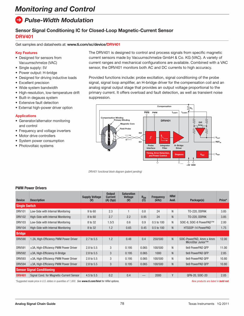
78Analog Signal Chain Guide TexasInstruments1Q2011
Monitoring and Control
Pulse-Width Modulation
Sensor Signal Conditioning IC for Closed-Loop Magnetic-Current SensorDRV401
Getsamplesanddatasheetsat:www.ti.com/sc/device/DRV401
Key Features• Designedforsensorsfrom Vacuumschmelze(VAC)• Singlesupply:5V• Poweroutput:H-bridge• Designedfordrivinginductiveloads• Excellentprecision• Widesystembandwidth• High-resolution,low-temperaturedrift• Built-indegausssystem• Extensivefaultdetection•Externalhigh-powerdriveroption
Applications• Generator/alternatormonitoring andcontrol• Frequencyandvoltageinverters• Motordrivecontrollers• Systempowerconsumption• Photovoltaicsystems
TheDRV401isdesignedtocontrolandprocesssignalsfromspecificmagneticcurrentsensorsmadebyVacuumschmelzeGmbH&Co .KG(VAC) .Avarietyofcurrentrangesandmechanicalconfigurationsareavailable .CombinedwithaVACsensor,theDRV401monitorsbothACandDCcurrentstohighaccuracy .
Providedfunctionsinclude:probeexcitation,signalconditioningoftheprobesignal,signalloopamplifier,anH-bridgedriverforthecompensationcoilandananalogsignaloutputstagethatprovidesanoutputvoltageproportionaltotheprimarycurrent .Itoffersoverloadandfaultdetection,aswellastransientnoisesuppression .
DRV401 functional block diagram (patent pending)
IntegratorFilter
ProbeInterface
H−BridgeDriver
VOUT
REFIN
ICOMP2
RS
ICOMP1
Compensation
DiffAmp
Timing, Error Detection,and Power Control
Degauss VREFVREF
GND+5V
IS2
IS1
DRV401
IP
Compensation Winding
Magnetic Core
Primary Winding
Field Probe
PWM PWM
PWM Power Drivers
Device DescriptionSupply Voltage
(V)
Output Current(A) (typ)
Saturation Voltage
(V)RON(Ω)
Frequency (kHz)
HiRel Avail. Package(s) Price*
Single Switch
DRV101 Low-Side with Internal Monitoring 9 to 60 2.3 1 0.8 24 N TO-220, DDPAK 3.85
DRV102 High-Side with Internal Monitoring 8 to 60 2.7 2.2 0.95 24 N TO-220, DDPAK 3.85
DRV103 Low-Side with Internal Monitoring 8 to 32 1.5/3 0.6 0.9 0.5 to 100 N SOIC-8, SOIC-8 PowerPAD™ 2.00
DRV104 High-Side with Internal Monitoring 8 to 32 1.2 0.65 0.45 0.5 to 100 N HTSSOP-14 PowerPAD 1.75
Bridge
DRV590 1.2A, High-Efficiency PWM Power Driver 2.7 to 5.5 1.2 0.48 0.4 250/500 N SOIC-PowerPAD, 4mm x 4mm MicroStar Junior™
12.00
DRV591 ±3A, High-Efficiency PWM Power Driver 2.8 to 5.5 3 0.195 0.065 100/500 N 9x9 PowerPAD QFP 11.00
DRV592 ±3A, High-Efficiency H-Bridge 2.8 to 5.5 3 0.195 0.065 1000 N 9x9 PowerPAD QFP 2.85
DRV593 ±3A, High-Efficiency PWM Power Driver 2.8 to 5.5 3 0.195 0.065 100/500 N 9x9 PowerPAD QFP 10.80
DRV594 ±3A, High-Efficiency PWM Power Driver 2.8 to 5.5 3 0.195 0.065 100/500 N 9x9 PowerPAD QFP 10.80
Sensor Signal Conditioning
DRV401 Signal Cond. for Magnetic-Current Sensor 4.5 to 5.5 0.2 0.4 — 2000 Y QFN-20, SOIC-20 2.05
*Suggested resale price in U.S. dollars in quantities of 1,000. See www.ti.com/hirel for HiRel options. New products are listed in bold red.

79Analog Signal Chain Guide TexasInstruments1Q2011
Monitoring and Control
Current Shunt Monitors
OUT
ININ+
GND
LoadSupply:+1.8V to +5.5V
Shunt
R1 R2
1.6M 1.6M
PRODUCT 1 2
INA216A1INA216A2INA216A3INA216A4
64k32k16k8k
GAIN
2550100200
R = R
TheINA216isahigh-sidevoltage-outputcurrentshuntmonitorthatcansensedropsacrossshuntsatcommon-modevoltagesfrom+1 .8Vto+5 .5V .Fourfixedgainsareavailable:25V/V,50V/V,100V/Vand200V/V .Thelowoffsetofthezerø-driftarchitectureenablescurrentsensingwithmaximumdropsacrosstheshuntaslowas10mVfull-scale,orwithwidedynamicrangesofmorethan1000:1 .Thesedevicesoperatefromasingle+1 .8Vto+5 .5Vpowersupply,drawingamaximumof25mAofsupplycurrent .TheINA216seriesarespecifiedoverthetemperaturerangeof–40°Cto+125°C,andofferedinachip-scalepackage .
INA216 functional block diagram
Key Features• Highaccuracy Voltageoffset:30µV(typ), 100µV(max) Offsetdrift:0 .05μV/°C(max) 0 .2%gainerror(max) CMRR:90dB(min) 20mVtotalerror(max)• 25µA(max)supplycurrent• 0 .8mmx0 .8mmWCSP•CMandsupplyvoltagerange +1 .8Vto+5 .5V
Applications• Cellphones• GPS• Handheldradios• Notebooks/netbooks/tablets
Chip-Scale, Low-Power Unidirectional Current Shunt MonitorINA216
Getsamplesanddatasheetsat:www.ti.com/sc/device/INA216a1
Two-Wire
VS
ADC
INA220
GND
V
I
VIN+
VIN-
A0
A1
SDA DATASCL CLK
C0.1 F
BYPASS+5V
High-SideShunt
Low-SideShunt R1F
R2F
CF
Load
Interface
Supply (0 to 26V)
(Supply Voltage)Bus Voltage Input
Power Register
Current Register
Voltage Register
+3.3V to
TheINA220isacurrentshuntandpowermonitorwithatwo-wireinterface .TheINA220monitorsbothshuntdropandsupplyvoltage .Aprogrammablecalibrationvalue,combinedwithaninternalmultiplier,enablesdirectreadoutsinamperes .AnadditionalmultiplyingregistercalculatespowerinWatts .Thetwo-wireinterfacefeatures16programmableaddresses .TheseparateshuntinputontheINA220allowsittobeusedinsystemswithlow-sidesensing .
TheINA220sensesacrossshuntsonbusesthatcanvaryfrom0Vto26V,usefulforlow-sidesensingorCPUpowersupplies .Thedeviceusesasingle+3Vto+5 .5Vsupply,drawingamaximumof1mAofsupplycurrent .TheINA220operatesfrom–40°Cto+125°C .
Key Features• Loworhigh-sidesensing• Bidirectional• Sensecurrent,voltageandpower
overI2C• -0 .3to26Vcommon-moderange• Accuracy:±1%(max)over-25°Cto+85°C• 100μVoffset(max)and40mVFSR• +3Vto+5 .5Vsupplyvoltage• 12-bitresolution• Programmablefiltering•Programmablecalibrationregister
Applications• Servers• Telecomequipment• Automotive• Powermanagement•Batterychargers•Powersupplies•Testequipment
Bidirectional Current/Power Monitor with I2CINA220
Getsamples,datasheetsandEVMsat:www.ti.com/sc/device/INA220
INA220 functional block diagram

80Analog Signal Chain Guide TexasInstruments1Q2011
Monitoring and Control
Current Shunt Monitors
Current Shunt Monitors
Device Description Gain (V/V)
Offset (µV) (max)
OffsetDrift
(µV/ºC) (max)
CMRR(dB) (typ)
BW(kHz)(typ)
Output Voltage
Swing (V) (min)
PowerSupply
(V)
IQ(mA)(max)
HiRel Avail. Package(s) Price*
Voltage-Output, High-Side Current Shunt MonitorsINA19x –16V to +80V CMV 20, 50, 100 2000 2.5 120 500,
300, 200V(+) –0.2 2.7 to 18 0.9 Y SOT-23-5 0.80
INA20x Dual Comparator, 1.2V VREF –16V to +18V CMV
20, 50, 100 2500 3.5 123 500, 300, 200
V(+) –0.25 2.7 to 18 2.2 N TSSOP/SO-14, MSOP-10,
MSOP/SO/DFN-8
0.45
INA27x –16V to +18V CMV, Filtering Provision 14, 20 2000 2.5 120 130 V(+) –0.2 2.7 to 18 0.9 Y SO-8 0.40
Current-Output, High-Side Current Shunt MonitorsINA138 +2.7V to 36V CMV Range 1 to 100 1000 1 120 800 0 to V(+) –0.8 2.7 to 36 0.045 Y SOT-23-5 0.65
INA168 +2.7V to 60V CMV Range 1 to 100 1000 1 120 800 0 to V(+) –0.8 2.7 to 60 0.045 Y SOT-23-5 0.80
INA139 +2.7 to 40V CMV Range 1 to 100 1000 1 115 440 0 to V(+) –1.2 2.7 to 40 0.125 Y SOT-23-5 0.65
INA169 +2.7 to 60V CMV Range 1 to 100 1000 1 120 440 0 to V(+) –1.2 2.7 to 60 0.125 Y SOT-23-5 0.80
Bidirectional Current Shunt MonitorsINA170 +2.7 to 60V CMV 1 to 100 1000 1 120 440 0 to V(+) –1.2 2.7 to 40 0.125 N MSOP-8 0.95
INA209 Voltage Current, Power Over I2C, 0 to +26V CMV
1, 2, 4, 8 100 0.1 120 — — 3 to 5.5 1.5 N TSSOP-16 2.50
INA219 Low Cost, Voltage Current, Power Over I2C, 0 to +26V CMV
1, 2, 4, 8 100 0.1 120 — — 3 to 5.5 1.5 N SOT-23-8 0.99
INA21x Zero Drift, Bidirectional, –0.3V to +26V CMV
50, 100, 200, 500, 1000
35 0.5 140 14 V(+) –0.1 2.7 to 26 0.1 Y SC-70 0.65
INA28x Zero Drift, Bidirectional, –16V to +80V CMV
50, 100, 200, 500, 1000
10 0.05 100 14 V(+) –0.1 2.7 to 18 0.9 N SO-8, DFN-10 0.95
INA220 High-or Low-Side I2C Current/Power Monitor, 0 to +26 V CMV
1, 2, 4, 8 100 0.16 120 — — 3 to 5.5 1 N MSOP-10 0.99
INA199 Zero Drift, High or Low Side Current Monitor, –0.3V to +26V CMV
50, 100, 200 150 0.5 120 14 V(+) –0.2 2.7 to 26 0.1 N SC-70, QFN-10 0.50
TMP512/513 High-Side I2C Monitor with Integreated Temp Sensor
1, 2, 4, 8 100 0.2 120 — — 3 to 26 1.4 N SO-14, SO-16 1.45
*Suggested resale price in U.S. dollars in quantities of 1,000. See www.ti.com/hirel for HiRel options. New products are listed in bold red.

81Analog Signal Chain Guide TexasInstruments1Q2011
Monitoring and Control
Temperature Sensors
Remote Temperature Sensors
Device Description Feature
Remote Sensor
AccuracyOver Temp
Range(˚C) (max)
Local Sensor AccuracyOver Temp
Range(˚C) (max)
Remote Sensor
Temp Range(˚C)
SupplyVoltage
(V)
IQ(µA)(typ)
HiRel Avail.) Package(s) Price*
TMP400 Remote and Local Temp Sensor with Programmable Non-Ideality Factor
n-Factor Correction, Series Resistace Cancellation, Alert Flag
1 2.5 –40 to +125 2.7 to 5.5 420 N QSSOP-16 0.85
TMP401 Programable Remote and Local Temperature Sensor
Series Resistance Cancellation, Fault Detection, Alert Flag
1 3 –40 to +150 3.0 to 5.5 350 N MSOP-8 0.85
TMP411 Remote and Local Temp Sensor with Programmable Non-Ideality Factor
n-Factor Correction, Series Resistance Cancellation, Fault Detection, Alert Flag
1 2.5 –40 to +150 2.7 to 5.5 350 N MSOP-8 0.45
TMP421 Remote and Local Temp Sensor in SOT-23-8
n-Factor Correction, Series Resistance Cancellation, Fault Detection
1 2 –40 to +150 2.7 to 5.5 400 N SOT-23-8 0.55
TMP422 2x Remote and Local Temp Sensor in SOT-23-8
n-Factor Correction, Series Resistance Cancellation, Fault Detection
1 2 –40 to +150 2.7 to 5.5 400 N SOT-23-8 0.65
TMP423 3x Remote and Local Temp Sensor in SOT-23-8
n-Factor Correction, Series Resistance Cancellation, Fault Detection
1 2 –40 to +150 2.7 to 5.5 400 N SOT-23-8 0.75
TMP431 Remote and Local Temp Sensor with Programmable n-Factor and Beta Correction
Beta Correction, n-Factor Correction, Series Resistance Cancellation, Fault Detection, Alert Flag
1 2.5 –40 to +150 2.7 to 5.5 700 N MSOP-8 0.45
TMP432 2x Remote and Local Temp Sensor with Programmable n-Factor and Beta Correction
Beta Correction, n-Factor Correction, Series Resistance Cancellation, Fault Detection, Alert Flag
1 2.5 –40 to +150 2.7 to 5.5 700 N MSOP-10 0.55
TMP435 Programable Addresss Remote and Local Temp Sensor
Beta Correction, n-Factor Correction, Series Resistance Cancellation, Fault Detection, Alert Flag
1 2.5 –40 to +150 2.7 to 5.5 700 N MSOP-10 0.60
TMP441 Remote and Local Temp Sensor with Beta Correction in SOT-23-8
Beta Correction, n-Factor Correction, Series Resistance Cancellation, Fault Detection
1 2 –40 to +150 2.7 to 5.5 400 N SOT-23-8 0.55
TMP442 2x Remote and Local Temp Sensor with Beta Correction in SOT-23-8
Beta Correction, n-Factor Correction, Series Resistance Cancellation, Fault Detection
1 2 –40 to +150 2.7 to 5.5 400 N SOT-23-8 0.65
TMP512 2x Remote and Local Temp Sensor with Integrated Current Shunt
Beta Correction, n-Factor Correction, Series Resistance Cancellation, Fault Detection, Alert Flag
1 2.5 –40 to +150 3 to 26 1000 N S0-14 1.45
TMP513 3x Remote and Local Temp Sensor with Integrated Current Shunt
Beta Correction, n-Factor Correction, Series Resistance Cancellation, Fault Detection, Alert Flag
1 2.5 –40 to +150 3 to 26 1000 N S0-16 1.55
*Suggested resale price in U.S. dollars in quantities of 1,000. New products are listed in bold red.
TheTMP112leadstheindustryindigitaltemperaturesensoraccuracy,lowpowerandpackagesize .TheperformanceoftheTMP112offersaccuracyof±0 .5°Candaresolutionof0 .0625°C,makingiteasytoachieveprecisionthermalmanagementoutofthebox .Theadditionalcalibrateddriftslopespecificationallowsdesignerstoachieveevenbetterthan±0 .5°Caccuracyoveruser-specifiedtemperaturerangeswithasingle-pointcalibrationtechnique,makingtheTMP112thehighestaccuracydigitaltemperaturesensorintheworldandbringingnewflexibilitytoportabledesign .
TMP112 functional block diagram
1.0
0.8
0.6
0.4
0.2
0
0.2
0.4
0.6
0.8
1.0
T
50 25 0 25 50 75 100 125
Temperature Error vs Temperature
Key Features•Accuracy:
±1 .0°C(max)from–40°Cto+125°C
±0 .5°C(max)from0°Cto+65°C
•Vs=1 .4Vto3 .6V
•Power=10µAactive,1µAshutdown
•Ultra-smallSOT563package(1 .6mmx1 .6mm)
Applications•Digitalalternativetothermistors•Portablemedicalandmetering• Coldjunctioncompensation• Greenenergycontrols• Pharmaceuticalandfoodmonitoring
High-Accuracy, Low-Power, Digital Temp SensorTMP112Getsamplesanddatasheetsat:www.ti.com/sc/device/TMP112

82Analog Signal Chain Guide TexasInstruments1Q2011
Monitoring and Control
Temperature Sensors
Temperature Switches
Device Description
Trip Point Accuracy(˚C) (typ)
Hysteresis (˚C)
Specified Temp Range (˚C)
Supply Voltage
(V)
IQ (µA)(max)
HiRel Avail. Package(s) Price*
TMP300 Comparator-Output Temperature Switch with Additional Analog Output
±2 5 or 10 –40 to +125 1.8 to 18 110 N SC70-6, SOT-23-6
0.50
TMP302 Low-Power, High-Accuracy Temperature Switch ± 0.2 5 or 10 –40 to +125 1.4 to 3.6 15 N SOT-563 0.30
TMP303 Low-Power, High-Accuracy Temperature Switch with Push-Pull Output
±0.2 1, 2, 5 or 10
–40 to +125 1.4 to 3.6 15 N SOT-563 0.30
Fan Controllers
Device DescriptionAccuracy(˚C) (typ) Input
Fan Control Modes Output
IQ (mA)
Supply Voltage (V) Interface
HiRel Avail. Package Price*
AMC6821 ±1˚C Remote and Local Temp Sensors with Integrated Fan Controller
±1 1 Local and 1Remote Temp
Programmable,Automatic
and Fixed RPM
ProgrammablePWM Frequencyand Duty Cycle
2 (Active) 2.7 to 5.5 I2C/SMBus
Y SOP-16 4mm x 5mm
0.99
Temperature Sensors
Device Description
AccuracyOver Temp
Range(˚C) (max)
SpecifiedTemp Range
(˚C)
TempResolution
(Bits)
SupplyVoltage
(V)
IQ(µA)(typ)
HiRel Avail. Package(s) Price*
I2C/SMBus InterfaceTMP20 Analog Output Temperature Sensor 2.5 –55 to +130 N/A 2.7 to 5.5 2.6 N SOT563-6, SC70 0.30
TMP100 Digital Temp Sensor 2, 3 –25 to +85–55 to +125
9 to 12 2.7 to 5.5 45 Y SOT-23-6 0.75
TMP101 Digital Temp Sensor with Prog. Thermostat/Alarm Function
2, 3 –25 to +85–55 to +125
9 to 12 2.7 to 5.5 45 N SOT-23-6 0.80
TMP102 Ultra-Low-Power Digital Temp Sensor in Micro Surface Mount Pkg.
2, 3 –25 to 85–40 to 125
12 1.4 to 3.6 7 N SOT563-6 0.80
TMP105 Chipscale Digital Temp Sensorwith 1.8V to 3.0V Logic
2, 3 –25 to +85–40 to +125
9 to 12 2.7 to 5.5 50 N 1mm x 1.5mm WCSP-6
0.85
TMP106 Chipscale Digital Temp Sensorwith 2.7V to 5.0V Logic
2, 3 –25 to +85–40 to +125
9 to 12 2.7 to 5.5 50 N 1mm x 1.5mm WCSP-6
0.85
TMP112 Ultra-Low-Power, High-Accuracy Digital Temp Sensor in SOT563 package
0.5 , 1 0 to 65 –40 to +125
12 1.4 to 3.6 7 N SOT563-6 0.85
TMP275 Ultra-High-Accuracy Digital Temp Sensor
0.5, 1 +10 to +85–40 to +125
9 to 12 2.7 to 5.5 50 N MSOP-8, SOIC-8 1.25
TMP175 Digital Temp Sensor with 2-Wire Interface, 27 Addresses
1.5, 2 –25 to +85–40 to +125
9 to 12 2.7 to 5.5 50 N MSOP-8, SOIC-8 0.85
TMP75 Industry-Standard Sensor with2-Wire Interface, 8 Addresses
2 –25 to +85 9 to 12 2.7 to 5.5 50 N MSOP-8, SOIC-8 0.70
SPI™ InterfaceTMP121 1.5˚C Accurate Digital Temp
Sensor with SPI Interface1.5, 2 –25 to +85
–40 to +12512 2.7 to 5.5 35 Y SOT-23-6 0.90
TMP122 1.5˚C Accurate Programmable Temp Sensor with SPI Interface
1.5, 2 –25 to +85–40 to +125
9 to 12 2.7 to 5.5 50 Y SOT-23-6 0.99
TMP123 1.5˚C Accurate Digital Temp Sensor with SPI Interface
1.5, 2 –25 to +85–55 to +125
12 2.7 to 5.5 35 N SOT-23-6 0.90
TMP124 1.5˚C Accurate Programmable Temp Sensor with SPI Interface
1.5, 2 –25 to +85–40 to +125
9 to 12 2.7 to 5.5 50 N SOIC-8 0.70
TMP125 2˚C Accurate Digital Temp Sensor with SPI Interface
2, 2.5 –25 to +85–40 to +125
10 2.7 to 5.5 36 N SOT-23-6 0.80
Single-Wire, SensorPath InterfaceTMP141 Digital Temp Sensor with
Single-Wire SensorPath Bus2, 3 –25 to +85
–40 to +12510 2.7 to 5.5 110 N SOT-23-6,
MSOP-80.80
*Suggested resale price in U.S. dollars in quantities of 1,000. See www.ti.com/hirel for HiRel options. New products are listed in bold red.

83Analog Signal Chain Guide TexasInstruments1Q2011
Monitoring and Control
4-20mA Transmitters
Precision Voltage-to-Current Converter/TransmitterXTR111
Getsamples,datasheets,evaluationmodulesandappreportsat:www.ti.com/sc/device/XTR111
Key Features• Widesupplyrange:7Vto44V• Currentorvoltageoutput• Accuracy:0 .015%• Outputerrordetectionanddisable• Adjustable3Vto15Vsub-regulator• Nonlinearity:0 .002%• Offsetdrift:1µV/°C• Lowsupplycurrent:550µA• Packaging:DFN-10,MSOPPowerPAD™
Applications• Universalvoltage-controlled
currentsource• Currentorvoltageoutputfor
3-wiresensorsystems• PLCoutputprogrammabledrivers• Current-modesensorexcitation
TheXTR111isaprecisionvoltage-to-currentconverterdesignedforstandard0-20mAor4-20mAanalogsignalsandcansourceupto36mA .Itisidealfor3-wiresensorsandfortheanalogoutputsofcontrolsystemslikeprogrammablelogiccontrollers(PLCs) .Sensorexcitationandcommonvoltage-to-current(source)applicationswillbenefitfromitshighaccuracy(0 .015%) .
3V
REGF
RegulatorOut
SignalInput
REGS
24V
I- Mirror
VSP
GS
D
VG
IS
Output DisableOutput Failure
0mA to 20mA4mA to 20mA
OD
EF
VIN
RSET
ISET
SETGND
IOUT = 10( )VVINRSET
IOUT = 10 • ISET
Load
IOUT
(± Load Ground)
XTR111 functional block diagram
4-20mA Transmitters and Receivers
Device DescriptionSensor
Excitation
LoopVoltage
(V)Full-Scale
Input Range
OutputRange(mA)
AdditionalPower
Available(V at mA)
HiRel Avail. Package(s) Price*
2-Wire, 4-20mA TransmittersXTR105 100Ω RTD Conditioner with Linearization Two 800µA 7.5 to 36 5mV to 1V 4-20 5.1 at 0.5 N DIP-14, SOIC-14 4.60
XTR106 Bridge Conditioner with Linearization 5V and 2.5V 7.5 to 36 5mV to 1V 4-20 5.1 at 1 N DIP-14, SOIC-14 4.00
XTR108 10Ω to 10kΩ RTD Conditioner, 6-Channel Input MUX, Extra Op Amp Can Convert to Voltage Sensor Excitation, Calibration Stored in External EEPROM
Two 500µA 7.5 to 24 5mV to 320mV 4-20 5.1 at 2.1 N SSOP-24 3.35
XTR112 1kΩ RTD Conditioner with Linearization Two 250µA 7.5 to 36 5mV to 1V 4-20 5.05 at 1 N SOIC-14 4.00
XTR114 10kΩ RTD Conditioner with Linearization Two 100µA 7.5 to 36 5mV to 1V 4-20 5.05 at 1 N SOIC-14 4.00
XTR115 IIN to IOUT Converter, External Resistor Scales VIN to IIN VREF = 2.5V 7.5 to 36 40µA to 250µA 4-20 4.9 at 1 N SOIC-8 1.25
XTR116 IIN to IOUT Converter, External Resistor Scales VIN to IIN VREF = 4.096V 7.5 to 36 40µA to 250µA 4-20 4.9 at 1 N SOIC-8 1.05
XTR117 Current Loop, 7.5 to 40V, 5V Voltage Regulator VREG= 5V 7.5 to 40 40µA to 250µA 4-20 4.9 at 1 N MSOP-8, DFN-8 0.90
Bridge Conditioner with Digital Calibration for Linearization, Span and Offset Over TemperaturePGA309 Complete Digitally Calibrated Bridge Sensor
Conditioner, Voltage Output, Calibration Stored in External EEPROM, One-Wire/Two-Wire Interface
VEXC = VS, 2.5V 4.096V
2.7 to 5.5 1mV/V to 245mV/V
0.05V-4.9V at VS = +5V
— N TSSOP-16 2.95
PGA308 Single Supply, Auto-Zero, Sensor Amplifier with Programmable Gain and Offset
— 2.7 to 5.5 0.2V to 4.1V 0.03V to 5.44mA
at VS = +5V
— N MSOP-10, DFN-10
2.00
Industrial Current/Voltage DriversXTR110 Precision V-to-I Converter/Transmitter, Selectable I/O
RangesVREF = 10V 13.5 to 40 0V to 5V,
0V to 10V0-20, 4-20
5-20— N DIP-16, SOL-16 7.10
XTR111 Precision V-to-I Converter/Transmitter, Adjustable VREG 3V to 15V
VREG = 3 to 15V 8 to 40 0V to 12V 0-20, 4-20, 5-20
3V to 15V N DFN/MSOP-10 1.10
XTR300 Industrial Analog Current/Voltage Output Driver — <34 V(–)+3 to V(+)–3Prog VOUT
±17V ±24mA
— N 5x5 QFN/TSSOP-20
2.45
4-20mA Current Loop ReceiverRCV420 4-20mA Input, 0V to 5V Output, 1.5V Loop Drop VREF = 10V +11.5/–5
to ±184-20mA 0V to 5V — N DIP-16 3.55
*Suggested resale price in U.S. dollars in quantities of 1,000. New products are listed in bold red.

84Analog Signal Chain Guide TexasInstruments1Q2011
Voltage References
Voltage References
3ppm/°C Drift, 0.05% Accurate, Low-Noise, Precision Series Voltage ReferencesREF5020, REF5025, REF5030, REF5040, REF5045, REF5050, REF5010
Getsamples,datasheetsandappreportsat:www.ti.com/sc/device/PARTnumber(ReplacePARTnumberwithREF5020, REF5025, REF5030, REF5040, REF5045, REF5050orREF5010)
Key Features• Highaccuracy:0 .05%• Lowtemperaturedrift:3ppm/°C(max)• Verylownoise:3µVPP/V• Highoutputcurrent:±10mA• Widesupplyrange:2 .7Vto18V• Industrialtemperaturerange:
–40°Cto+125°C•Packaging:SO-8,MSOPcomingsoon
Applications• Testandmeasurement• 16-bitdataacquisitionsystems• Medicalandpatientmonitoring• Industrialprocesscontrol
TheREF50xxbringsanewlevelofprecisiontotheTIseriesvoltagereferenceline .Offering3ppm/°C(max)driftand0 .05%initialaccuracyandverylownoise,theREF50xxisdesignedforindustrial,medicalandtestapplicationsthatrequireperformanceovertemperature .
1
2
3
4
8
7
6
5
DNC(1)
NC(2)
TRIM/NR
DNC(1)
VIN
TEMP
GND
VOUT
REF50xx
SO-8, MSOP-8
REF50xx package diagram
Model Voltage Out
REF5020 2 .048VREF5025 2 .5VREF5030 3 .0VREF5040 4 .096VREF5045 4 .5VREF5050 5VREF5010 10V
Voltage References
Device Description Output (V)
InitialAccuracy
(%) (max)
Drift(ppm/°C)
(max)
Long-TermStability
(ppm/1000hr)(typ)
Noise0.1 to 10Hz(µVp-p/V)
(typ)
IQ (mA)
(max)
Tempera-ture
Range (°C)
OutputCurrent
(mA)HiRel Avail. Package(s) Price*
REF50xx High Accuracy Bandgap Reference
2.048, 2.5, 3.0, 4.096, 4.5, 5, 10
0.05 3 5 3 1 –40 to +125 ±10 Y SOIC-8 2.95
REF50xxA High Accuracy Bandgap Reference
2.048, 2.5, 3.0, 4.096, 4.5, 5, 10
0.1 8 5 3 1 –40 to +125 ±10 Y SOIC-8 1.35
REF33xx microPower, Tiny Bandgap
1.25, 1.8, 2.048, 2.5, 3.0, 3.3
0.15 30 — 28 0.005 –40 to +125 ±5 N SC-70, SOT-23-3
0.85
REF32xx Low Drift, Low Power, Small Bandgap
1.25, 2.048, 2.5 3.0, 3.3, 4.096
0.2 7 55 13 0.120 –40 to +125 ±10 Y SOT-23-6 1.70
REF31xx Series Bandgap 1.25, 2.048, 2.5 3.0, 3.3, 4.096
0.2 15 70 13 0.115 –40 to +125 ±10 N SOT-23-3 1.10
REF30xx Series Bandgap 1.25, 2.048, 2.5, 3.0, 3.3, 4.096
0.2 50 24 11 0.05 –40 to +125 25 Y SOT-23-3 0.60
REF29xx Series Bandgap 1.25, 2.048, 2.5, 3.0, 3.3, 4.096
2 100 24 11 to 16 0.05 –40 to +125 25 N SOT-23-3 0.49
REF02A Low Drift, Buried Zener 5 0.3 15 50 0.8 1.4 –40 to +85 +21, –0.5 N SOIC, PDIP 1.45
REF02B Low Drift, Buried Zener 5 0.2 10 50 0.8 1.4 –40 to +85 +21, –0.5 N SOIC, PDIP 2.05
REF102A Low Drift, Buried Zener 10 0.1 10 20 0.5 1.4 –25 to +85 +10, –5 N SOIC, PDIP 1.75
REF102B Low Drift, Buried Zener 10 0.05 5 20 0.5 1.4 –25 to +85 +10, –5 N SOIC, PDIP 3.25
REF102C Ultra-Low Drift, Buried Zener
10 0.025 2.5 20 0.5 1.4 –25 to +85 +10, –5 N SOIC, PDIP 4.50
Shunt
REF1112 µPower, 1.25V Shunt 1.25 0.2 30 60 20 0.0015 –40 to +125 0.0012 to 5
N SOT-23-3 0.85
Current Reference
REF200 Dual-Current Referencewith Current Mirror
100µA/Channel ±1 25 (typ) — 1nAp-p — –25 to +85 50µA to 400µA
N PDIP-8, SOIC-8
2.60
*Suggested resale price in U.S. dollars in quantities of 1,000. See www.ti.com/hirel for HiRel options. New products are listed in bold red.

85Analog Signal Chain Guide TexasInstruments1Q2011
Clocks and Timing
Clock Distribution (Fan-Out Clock Buffers, Zero-Delay Buffers)
Clock DistributionCDCLVC11xx
Getsamplesanddatasheetsat:www.ti.com/sc/device/CDCLVC1102
Key Features• Familyofhigh-performance 1:2/3/4/6/8/10/12LVCMOSclock fan-outbuffers• Verylowpin-to-pinskew<50ps• Verylowadditivejitter<100fsRMS (12kHzto20MHz)• Supplyvoltage:3 .3Vor2 .5V• fmax=250MHzfor3 .3V• fmax=180MHzfor2 .5V• Operatingtemperaturerange: –40°Cto+85°C•Availablein8-,14-,16-,20-,24-pin TSSOPpackage(allpin-compatible)
Applications• Generalpurposecommunication, Industrialandconsumerapplications
TheCDCLVC11xxisamodular,high-performance,low-skew,general-purposeclockbufferfamilydesignedwithamodularapproachinmind .Thereare7differentFan-Outvariations,(1:2to1:12)available .Allofthedevicesarepin-compatibletoeachotherforeasyhandling .Allfamilymemberssharethesamehigh-performingcharacteristicslikelowadditivejitter,lowskewandwideoperatingtemperaturerange .TheCDCLVC11xxsupportsanasynchronousoutputenablecontrol(1G)thatswitchestheoutputsintoalowstatewhen1Gislow .
CDCLVC11xx functional block diagram
Y0CLKIN
1G
Y1
Yn
LVCMOS
LVCMOS
LVCMOS
LVCMOS
Clock Distribution CDCLVD12xx/21xx
Getsamplesanddatasheetsat:www.ti.com/sc/device/CDCLVD1204
Key Features• Familyofhigh-performance 2:4/8/12/16ordual1:2/4/6/8 universal-to-LVDSclockfan-out buffers• Verylowadditivejitter<300fsRMS (10kHz-20MHz)• Lowoutputskewof20ps(max)• UniversalinputsacceptLVDS, LVPECLandLVCMOS• Selectableclockinputs–controlpin• LVDSoutputs,ANSIEAI/TIA-644A standard-compatible• Clockfrequencyupto800MHz• 2 .375Vto2 .625Vdevicepowersupply• LVDSrefvoltage,VAC_REF,availablefor capacitivecoupledinputs• Industrialtemprange:–40°Cto+85°C
Applications• Telecommunications/networking• Medicalimaging• Testandmeasurementequipment• Wirelesscommunications• General-purposeclocking
TheCDCLVD12xx/21xxclockbuffersdistributeoneortwoselectableclockinputs,(IN0,IN1),to4,8,12or16pairsofdifferentialLVDSclockoutputs(OUT0,OUT3)withminimumskewforclockdistribution .Thebufferscanaccepttwoclocksourcesintoaninputmultiplexer .TheinputscaneitherbeLVDS,LVPECLorLVCMOS .
TheCDCLVD12xx/21xxarespecificallydesignedfordriving50transmissionlines .Whendrivingtheinputsinsingle-endedmode,theappropriatebiasvoltage(VAC_REF)shouldbeappliedtotheunusednegativeinputpin .
CDCLVD12xx/21xx functional block diagram
ReferenceGenerator
VCC
INP1
INN1
INP0
INN0
EN
GND GND
OUTP [0...3]
OUTN [0...3]
OUTP [4...7]
OUTN [4...7]
200kΩ
200kΩ
VAC_REF0VAC_REF1
VCCVCC VCC

86Analog Signal Chain Guide TexasInstruments1Q2011
Clocks and Timing
Clock Distribution (Fan-Out Clock Buffers, Zero Delay Buffers)
Clock DistributionCDCLVP12xx/21xx
Getsamplesanddatasheetsat:www.ti.com/sc/device/CDCLVP1204
Key Features• Familyofhigh-performance 2:4/8/12/16ordual1:2/4/6/8 universal-to-LVPECLclockfan-out buffers• UniversalinputsacceptLVPECL, LVDSandLVCMOS/LVTTL• Maximumclockfrequency:2GHz• Verylowadditivejitter<100fsRMS (10kHz-20MHz)• 2 .375-Vto3 .6-Vdevicepowersupply• Lowoutputskewof30ps(max)• LVPECLreferencevoltage,VAC_REF• Availableforcapacitive-coupled inputs• Industrialtemperaturerange: –40°Cto+85°C
Applications• Wirelesscommunications• Telecommunications/networking• Medicalimaging• Testandmeasurementequipment
TheCDCLVP12xx/21xxarehighlyversatile,lowadditivejitterbuffersthatcangenerateupto16copiesofLVPECLclockoutputsfromoneoftwoselectableLVPECL,LVDSorLVCMOSinputsforavarietyofcommunicationapplications .Thedeviceshaveamaximumclockfrequencyupto2GHz .TheCDCLVP12xx/21xxfeatureanon-chipmultiplexer(MUX)forselectingoneoftwoinputsthatcanbeeasilyconfiguredsolelythroughacontrolpin .Theoveralladditivejitterperformanceis<100fsRMS(10kHzto20MHz)andoveralloutputskewisaslowas30ps,makingthedeviceaperfectchoiceforuseindemandingapplications .
CDCLVP12xx/21xx functional block diagram
4
VCC
GND
OUTP [3...0]
INP0
INN0
INP1
INN1
IN_SEL
VAC_REF
OUTN [3...0]LVPECL
ReferenceGenerator
IN_M
UX
4

87Analog Signal Chain Guide TexasInstruments1Q2011
Clocks and Timing
Clock Distribution (Fan-Out Clock Buffers, Zero-Delay Buffers)
Clock Distribution
Device Description Input LevelOutput Level
Frequency(MHz)
VCC(V)
Propagation Delay
Output Skew (max) (ps)
Char. Temp. (ºC)
HiRel Avail. Package(s) Price*
Fan-Out Clock Buffers (Non-PLL) Differential-EndedCDCLVP1102 Low-Jitter 1:2 Universal-to-
LVPECL BufferLVPECL/LVDS/LVCMOS LVPECL 0 to 2GHz 2.5/3.3 450ps (max) 10ps –40 to 85 N QFN-16 2.50
CDCLVP1204 Low-Jitter, 2-Input Selectable 1:4 Universal-to-LVPECL Buffer
LVPECL/LVDS/LVCMOS LVPECL 0 to 2GHz 2.5/3.3 450ps (max) 15ps –40 to 85 N QFN-16 3.30
CDCLVP1208 Low-Jitter, 2-Input Selectable 1:8 Universal-to-LVPECL Buffer
LVPECL/LVDS/LVCMOS LVPECL 0 to 2GHz 2.5/3.3 450ps (max) 20ps –40 to 85 N QFN-28 5.00
CDCLVP1212 Low-Jitter, 2-Input Selectable 1:12 Universal-to-LVPECL Buffer
LVPECL/LVDS/LVCMOS LVPECL 0 to 2GHz 2.5/3.3 550ps (max) 25ps –40 to 85 N QFN-40 6.50
CDCLVP1216 Low-Jitter, 2-Input Selectable 1:16 Universal-to-LVPECL Buffer
LVPECL/LVDS/LVCMOS LVPECL 0 to 2GHz 2.5/3.3 550ps (max) 30ps –40 to 85 N QFN-48 8.50
CDCLVP2102 Low-Jitter, Dual 1:2 Universal-to-LVPECL Buffer
LVPECL/LVDS/LVCMOS LVPECL 0 to 2GHz 2.5/3.3 450ps (max) 10ps (Within Bank)
–40 to 85 N QFN-16 3.30
CDCLVP2104 Low-Jitter, Dual 1:4 Universal-to-LVPECL Buffer
LVPECL/LVDS/LVCMOS LVPECL 0 to 2GHz 2.5/3.3 450ps (max) 15ps (Within Bank)
–40 to 85 N QFN-28 5.00
CDCLVP2106 Low-Jitter, Dual 1:6 Universal-to-LVPECL Buffer
LVPECL/LVDS/LVCMOS LVPECL 0 to 2GHz 2.5/3.3 550ps (max) 20ps (Within Bank)
–40 to 85 N QFN-40 6.50
CDCLVP2108 Low-Jitter, Dual 1:8 Universal-to-LVPECL Buffer
LVPECL/LVDS/LVCMOS LVPECL 0 to 2GHz 2.5/3.3 550ps (max) 25ps (Within Bank)
–40 to 85 N QFN-48 8.50
CDCLVD1204 Low-Jitter, 2-Input Selectable 1:4 Universal-to-LVDS Buffer
LVPECL/LVDS/LVCMOS LVDS 0 to 800 2.5 1.5ns (typ) 20ps –40 to 85 N QFN-16 2.85
CDCLVD1208 Low-Jitter, 2-Input Selectable 1:8 Universal-to-LVDS Buffer
LVPECL/LVDS/LVCMOS LVDS 0 to 800 2.5 1.5ns (typ) 20ps –40 to 85 N QFN-28 3.85
CDCLVD1212 Low-Jitter, 2-Input Selectable 1:12 Universal-to-LVDS Buffer
LVPECL/LVDS/LVCMOS LVDS 0 to 800 2.5 1.5ns (typ) 20ps –40 to 85 N QFN-40 4.75
CDCLVD1216 Low-Jitter, 2-Input Selectable 1:16 Universal-to-LVDS Buffer
LVPECL/LVDS/LVCMOS LVDS 0 to 800 2.5 1.5ns (typ) 20ps –40 to 85 N QFN-48 5.70
CDCLVD2102 Low-Jitter, Dual 1:2 Universal-to-LVDS Buffer
LVPECL/LVDS/LVCMOS LVDS 0 to 800 2.5 1.5ns (typ) 20ps (Within Bank)
–40 to 85 N QFN-16 3.00
CDCLVD2104 Low-Jitter, Dual 1:4 Universal-to-LVDS Buffer
LVPECL/LVDS/LVCMOS LVDS 0 to 800 2.5 1.5ns (typ) 20ps (Within Bank)
–40 to 85 N QFN-28 4.00
CDCLVD2106 Low-Jitter, Dual 1:6 Universal-to-LVDS Buffer
LVPECL/LVDS/LVCMOS LVDS 0 to 800 2.5 1.5ns (typ) 20ps (Within Bank)
–40 to 85 N QFN-40 5.00
CDCLVD2108 Low-Jitter, Dual 1:8 Universal-to-LVDS Buffer
LVPECL/LVDS/LVCMOS LVDS 0 to 800 2.5 1.5ns (typ) 20ps (Within Bank)
–40 to 85 N QFN-48 6.00
CDCLVD1213 Low-Jitter, 1:4 Universal-to-LVDS Buffer with Selectable Output Divider
LVPECL/LVDS/CML LVDS 0 to 800 2.5 1.5ns (typ) 20ps –40 to 85 N QFN-16 4.00
CDCP1803 1:3 LVPECL Clock Buffer with Programmable Divider
LVPECL/LVDS LVPECL 0 to 800 3.3 320 to 600ps 30ps –40 to 85 Y QFN-24 3.15
CDCLVP215 Dual 1:5 High-Speed LVPECL Clock Buffer
LVPECL LVPECL DC to 3.5GHz
2.5/3.3 230 to 370ps 30ps –40 to 85 N LQFP-32 5.55
CDCLVP110 1:10 LVPECL Clock Buffer LVPECL/HSTL LVPECL 0 to 3.5GHz 2.5/3.3 230 to 370ps 30ps –40 to 85 N LQFP-32 5.50
CDCLVP111 1:10 LVPECL Clock Buffer with Selectable Input
LVPECL LVPECL DC to 3.5GHz
2.5/3.3 230 to 370ps 30ps –40 to 85 N LQFP-32/QFN-32 5.55
CDCLVD110A Programmable 1:10 LVDS Clock Buffer
LVDS LVDS 0 to 900 2.5 3ns 30ps (typ) –40 to 85 N TQFP-32 5.50
CDCL1810 1:10 LVDS-to-CML Clock Buffer LVDS CML 0 to 650 1.8 3ns 64ps –40 to 85 N QFN-48 6.45
SN65EL11 1:2 ECL/PECL Buffer ECL/PECL ECL/PECL
>2.5GHz 5 265ps (typ) 15 –40 to 85 N SOIC-8/MSOP-8 1.35
SN65EL16 1:1 ECL/PECL Buffer ECL/PECL ECL/PECL
>2.5GHz 5 250ps (typ) 20 –40 to 85 N SOIC-8/MSOP-8 1.35
SN65ELT20 1:1 TTL-to-PECL Buffer TTL PECL 400 (Typ) 5 1250ps (max) — –40 to 85 N SOIC-8/MSOP-8 1.45
SN65ELT21 1:1 PECL-to-TTL Buffer TTL PECL 0 to 400 5 3000ps (typ) — –40 to 85 N SOIC-8/MSOP-8 1.40
SN65ELT22 2:2 TTL-to-PECL Buffer TTL PECL 0 to 1GHz 5 1100ps (max) 90 –40 to 85 N SOIC-8/MSOP-8 1.45
SN65ELT23 2:2 PECL-to-TTL Buffer PECL TTL 0 to 500 5 3500ps (typ) — –40 to 85 N SOIC-8/MSOP-8 1.40
SN65EPT21 1:1 LVTTL-to-LVPECL Buffer LVTTL LVPECL 0 to 600 3.3 1900ps (max) 250 –40 to 85 N SOIC-8/MSOP-8 1.80
SN65EPT22 2:2 LVTTL-to-LVPECL Buffer LVTTL LVPECL 0 to 4GHz 3.3 420ps (typ) 50 –40 to 85 N SOIC-8/MSOP-8 1.80
SN65EPT23 2:2 LVPECL-to-LVTTL Buffer LVPECL LVTTL >300 3.3 1900ps (max) 110 –40 to 85 N SOIC-8/MSOP-8 1.80
*Suggested resale price in U.S. dollars in quantities of 1,000. See www.ti.com/hirel for HiRel options. New devices are listed in bold red.

88Analog Signal Chain Guide TexasInstruments1Q2011
Clocks and Timing
Clock Distribution (Fan-Out Clock Buffers, Zero-Delay Buffers)
Clock Distribution (continued)
Device Description Input LevelOutput Level
Frequency(MHz)
VCC(V)
Propagation Delay
Output Skew (max) (ps)
Char. Temp. (ºC)
HiRel Avail. Package(s) Price*
Fan-Out Clock Buffers (Non-PLL) Differential-EndedSN65EPT21 1:1 LVTTL-to-LVPECL Buffer LVTTL LVPECL 0 to 600 3.3 1900ps (max) 250 –40 to 85 N SOIC-8/MSOP-8 1.80
SN65EPT22 2:2 LVTTL-to-LVPECL Buffer LVTTL LVPECL 0 to 4GHz 3.3 420ps (typ) 50 –40 to 85 N SOIC-8/MSOP-8 1.80
SN65EPT23 2:2 LVPECL-to-LVTTL Buffer LVPECL LVTTL >300 3.3 1900ps (max) 110 –40 to 85 N SOIC-8/MSOP-8 1.80
SN65LVEL11 1:2 ECL/PECL Buffer ECL/PECL ECL/PECL
0 to 1.5GHz 3.3 265ps (typ) 18 –40 to 85 N SOIC-8/MSOP-8 1.45
SN65LVELT22 2:2 LVTTL-to-LVPECL Buffer LVTTL LVPECL 0 to 3.5GHz 3.3 450ps (typ) 50 –40 to 85 N SOIC-8/MSOP-8 1.45
SN65LVELT23 2:2 LVPECL-to-LVTTL Buffer LVPECL LVTTL >180 3.3 2200ps (max) 150 –40 to 85 N SOIC-8/MSOP-8SOIC-8/MSOP-8
2.30
SN65LVEP11 1:2 ECL/PECL Buffer ECL/PECL ECL/PECL
0 to 3GHz 2.5/3.3 240ps (typ) 15 –40 to 85 N SOIC-8/MSOP-8 2.20
Single-Ended
CDC3RL02 1:2 Square/Sine-to-Square Wave Buffer with LDO
SINE/SQUARE
SQUARE 10 to 52 1.8 12ns (typ) 500ps –40 to 85 N DSBGA-8 0.90
CDC3S04 1:4 Sine-to-Sine Wave Buffer with LDO SINE SINE .01 to 52 1.8 3ns (max) 50ps –30 to 85 N DSBGA-20 1.80
CDCLVC1102 Low-Jitter, 1:2 LVCMOS Fan-Out Clock Buffer
LVCMOS LVCMOS 0 to 250 2.5/3.3 0.8 to 2ns 50ps –40 to 85 N TSSOP-8 0.90
CDCLVC1103 Low-Jitter, 1:3 LVCMOS Fan-Out Clock Buffer
LVCMOS LVCMOS 0 to 250 2.5/3.3 0.8 to 2ns 50ps –40 to 85 N TSSOP-8 1.05
CDCLVC1104 Low-Jitter, 1:4 LVCMOS Fan-Out Clock Buffer
LVCMOS LVCMOS 0 to 250 2.5/3.3 0.8 to 2ns 50ps –40 to 85 N TSSOP-8 1.20
CDCLVC1106 Low-Jitter, 1:6 LVCMOS Fan-Out Clock Buffer
LVCMOS LVCMOS 0 to 250 2.5/3.3 0.8 to 2ns 50ps –40 to 85 N TSSOP-14 1.50
CDCLVC1108 Low-Jitter, 1:8 LVCMOS Fan-Out Clock Buffer
LVCMOS LVCMOS 0 to 250 2.5/3.3 0.8 to 2ns 50ps –40 to 85 N TSSOP-16 1.80
CDCLVC1110 Low-Jitter, 1:10 LVCMOS Fan-Out Clock Buffer
LVCMOS LVCMOS 0 to 250 2.5/3.3 0.8 to 2ns 50ps –40 to 85 N TSSOP-20 2.25
CDCLVC1112 Low-Jitter, 1:12 LVCMOS Fan-Out Clock Buffer
LVCMOS LVCMOS 0 to 250 2.5/3.3 0.8 to 2 ns 50ps –40 to 85 N TSSOP-24 2.60
CDC318A 1:18 LVTTL Clock Buffer with I2C Control LVTTL LVTTL 0 to 100 3.3 1.2 to 4.5ns 250ps 0 to 70 N SSOP-48 2.10
CDC319 1:10 LVTTL Clock Buffer with I2C Control LVTTL LVTTL 0 to 140 3.3 1.2 to 3.6ns 250ps 0 to 70 N SSOP-28 1.75
CDCV304 1:4 PCI-X Compliant LVTTL Clock Buffer LVTTL LVCMOS 0 to 200 2.5/3.3 1.8 to 3.0ns 100ps –40 to 85 N TSSOP-8 1.20
CDCVF310 1:10 LVTTL Clock Buffer (2 Banks of 5 Outputs)
LVTTL/LVCMOS
LVTTL/LVCMOS
0 to 200 2.5/3.3 1.0 to 2.8ns (VDD = 3. V), 1.3 to 4.0ns (VDD = 2.5 V)
150ps at 3.3V, 230ps
at 2.5V
–40 to 85 N TSSOP-24 2.05
CDCVF2310 1:10 LVTTL Clock Buffer (2 Banks of 5 Outputs) with 25Ω input resistors
LVTTL/LVCMOS
LVTTL/LVCMOS
0 to 170 (VDD = 2.5V),
0 to 200 (VDD = 3.3 V)
2.5/3.3 1.3 to 2.8ns (VDD = 3.3 V), 1.5 to 3.5ns (VDD = 2.5 V)
100ps at 3.3V, 170ps
at 2.5V
–40 to 85 N TSSOP-24 2.05
Mixed: Differential and Single-Ended
CDCM1804 1:3 LVPECL + 1:1 LVCMOS Buffer with Dividers
LVPECL LVPECL/LVCMOS
800 3.3 600ps (LVPECL), 2.6ns (LVCMOS)
30ps (LVPECL),
1.6ns (LVCMOS)
–40 to 85 N QFN-24 5.90
CDCM1802 1:1 LVCMOS + 1:1 LVPECL Buffer with Dividers
LVPECL LVPECL/LVCMOS
800 3.3 600ps (LVPECL), 2.6ns (LVCMOS)
1.6ns (typ) –40 to 85 N QFN-16 4.70
CDCE18005 3:5 LVPECL/LVDS/LVCMOS Buffer with Dividers
LVPECL/LVDS/
LVCMOS
LVPECL/LVDS/
LVCMOS
DC to 1.5GHz
3.3 4ns 75ps –40 to 85 N QFN-48 6.00
*Suggested resale price in U.S. dollars in quantities of 1,000. New devices are listed in bold red.

89Analog Signal Chain Guide TexasInstruments1Q2011
Clocks and Timing
Clock Distribution (Fan-Out Clock Buffers, Zero-Delay Buffers)
Device Description Input LevelOutput Level
Frequency(MHz)
VCC(V)
Jitter (Peak-to-Peak [P-P] or Cycle-to-
Cycle [C-C]) Phase Error
Char. Temp. (ºC)
HiRel Avail. Package(s) Price*
Zero-Delay Buffers (PLL-Based)
Differential-Ended
CDCV850 1:10 Differential Clock Driver
SSTL_2/Universal
SSTL_2 60 to 140 2.5 C-C: ±30ps (100 to 133MHz )
–80/150ps (133MHz )
–40 to 85 N TSSOP-48 2.20
CDCV855 1:4 Differential Clock Driver
SSTL_2/LVTTL SSTL_2 60 to 180 2.5 C-C: ±50ps (100 to 180MHz )
±100ps (100 to
180MHz )
–40 to 85 N TSSOP-28 1.15
CDCV857 1:10 PLL Differential Clock Driver for DDR 200/266/333, SSC
SSTL_2/LVTTL SSTL_2 60 to 200 2.5 C-C: ±75ps (100 to 200MHz )
–150/50ps (200MHz )
0 to 85 N TSSOP-48 4.20
CDCV857A 1:10 PLL Differential Clock Driver for DDR 200/266/333, SSC
SSTL_2/LVTTL SSTL_2 60 to 180 2.5 C-C: ±50ps (100 to 180MHz )
±100ps (100 to
180MHz )
0 to 85 N TSSOP-48, µBGA-56
2.90
CDCV857B 1:10 PLL Differential Clock Driver for DDR 200/266/333, SSC
SSTL_2/LVTTL SSTL_2 60 to 200 2.5 C-C: ±50ps (100 to 200MHz )
±50ps (min/max) (100 to
200MHz )
0 to 70 N TSSOP-48, µBGA-56
3.65
CDCV857BI 1:10 PLL Differential Clock Driver for DDR 200/266/333, SSC
SSTL_2/LVTTL SSTL_2 60 to 200 2.5 C-C: ±50ps (100 to 200MHz )
±50ps (min/max) (100 to
200MHz )
–40 to 85 N TSSOP-48, µBGA-56
3.35
CDCVF857 1:10 PLL Differential Clock Driver for DDR 200/266/333/400, SSC
SSTL_2/LVTTL SSTL_2 60 to 220 2.5 C-C: ±35ps (133 to 200MHz )
±50ps (min/max) (100 to
200MHz )
–40 to 85 N TSSOP-48, QFN-48, µBGA-56
3.60
CDCU877 1:10 PLL Differential Clock Driver for DDR2 Applications, SSC
SSTL_18 SSTL_18 10 to 400 1.8 C-C: ±30ps (190 to 340MHz )
±50ps –40 to 85 N µBGA-52, QFN-40
3.05
CDCU877A 1:10 PLL Differential Clock Driver for DDR2 Applications, SSC
SSTL_18 SSTL_18 10 to 400 1.8 C-C: ±30ps (190 to 340MHz )
±50ps –40 to 85 N µBGA-52, QFN-40
3.05
CDCU877B 1:10 PLL Differential Clock Driver for DDR2 400/533, SSC
SSTL_18 SSTL_18 10 to 340 1.8 C-C: ±30ps (190 to 340MHz )
±50ps –40 to 85 N µBGA-52 3.05
CDCUA877 1:10 PLL Differential Clock Driver for DDR2 400~800, SSC, 8-mA Output
SSTL_18 SSTL_18 125 to 410 1.8 C-C: ±40ps (200 to 333MHz )
±50ps –40 to 85 N µBGA-52 3.35
CDCU2A877 1:10 PLL Differential Clock Driver for DDR2 400~800, SSC, 16-mA Output
SSTL_18 SSTL_18 125 to 410 1.8 C-C: ±40ps (160 to 410MHz )
±50ps 0 to 70 N µBGA-52 3.05
Single-Ended
CDCVF2505 1:5 PLL Clock Driver for SDR/PC133+, SSC
LVTTL LVTTL 24 to 200 3.3 C-C: |70|ps (typ) (66 to 200MHz )
±150ps (66 to 200MHz )
–40 to 85 Y TSSOP-8, SOIC-8
0.95
CDCVF2509A 1:9 PLL Clock Driver for SDR/PC133+, SSC
LVTTL LVTTL 50 to 175 3.3 C-C: |65|ps (typ) (100 to 166MHz )
±125ps (66 to 166MHz )
0 to 85 N TSSOP-24 3.90
CDCVF2510A 1:10 PLL Clock Driver for SDR/PC133+, SSC
LVTTL LVTTL 50 to 175 3.3 C-C: |65|ps (typ) (100 to 166MHz )
±125ps (66 to 166MHz )
0 to 85 N TSSOP-24 2.60
Clock Distribution (continued)
*Suggested resale price in U.S. dollars in quantities of 1,000. See www.ti.com/hirel for HiRel options.

90Analog Signal Chain Guide TexasInstruments1Q2011
Clocks and Timing
Clock Generation (Crystal Oscillator Replacements, Jitter Cleaners)
Clock Generator/Jitter Cleaner with Integrated Dual VCOCDCE6200x
Getsamplesanddatasheetsat:www.ti.com/sc/device/CDCE62005
Key Features• Fullyintegratedsynthesizer–PLL, VCO,partiallyintegratedloopfilter• Twouniversal(LVPECL/LVDS/LVCMOS inputs),oneauxiliary/XTALinput• Upto5fullyconfigurableoutputs upto1 .175GHz(LVPECL,LVDSor 2-LVCMOS)• IntegratedRMSjitter<500fs (10kHz-20MHz)•On-chipEEPROMdeterminesdefault stateatpower-up;fullyprogrammable viaSPI™port
Applications• Dataconverteranddataaggregation clocking• Wirelessinfrastructure• Switchesandrouters• Medicalelectronics• Militaryandaerospace• Industrial• Clockgenerationandjittercleaning
TheCDCE6200xisahigh-performanceclockgeneratoranddistributorfeaturinglowoutputjitter,ahighdegreeofconfigurabilityviaaSPI™interfaceandprogrammablestart-upmodesdeterminedbyon-chipEEPROM .Specificallytailoredforclockingdataconvertersandhigh-speeddigitalsignals,theCDCE6200xachievesjitterperformance<1psRMSjitter(10kHzto20MHz) .Itincorporatesasynthesizerblockwithpartiallyintegratedloopfilter,aclockdistributionblockincludingprogrammableoutputformatsandaninputblockfeaturinganinnovativesmartmultiplexer .Theclockdistributionblockincludesuptofiveindividuallyprogrammableoutputsthatcanbeconfiguredtoprovidedifferentcombinationsofoutputformats(LVPECL,LVDS,LVCMOS) .
CDCE62005 functional block diagram
OutputU0P
U0N
U1P
U1N
U2P
U2N
U3P
U3N
U4P
U4N
CP
/1:/2:HiZ
/1:/2:HiZ
PrescalerFeedbackDivider
InputDivider
ReferenceDivider
AUXOUT
PRI_IN
SEC_IN
XTAL /AUX_IN
EEPROMInterface
&Control
REF_SELECT/Power_down
/SYNC
SPI_LESPI_CLK
SPI_MISOSPI_MOSI
EXT_LFPEXT_LFN
Output
Output
Output
Output

91Analog Signal Chain Guide TexasInstruments1Q2011
Clocks and Timing
Clock Generation (Crystal Oscillator Replacements, Jitter Cleaners)
Clock Oscillator Replacements CDCE9xx
Getsamplesanddatasheetsat:www.ti.com/sc/device/CDCE949
Key Features• Fullyprogrammableclocksynthesizer with3 .3V/2 .5V/1 .8VI/Os• Upto4internalfractionalPLLsenable 0-PPMclockgeneration• Upto9low-jitter,low-skewLVCMOS outputsupto230MHz• Flexibleinputclockingconcept Externalcrystal:8MHzto32MHz On-chipVCXO:pull-range±150ppm Single-endedLVCMOSupto 160MHz
Applications• D-TV,HD-TV,STB,IP-STB,DVD- players,DVDrecorders,printers• General-purposefrequency synthesizing• DSP,DaVinci™andOMAP™attach audioandvideoclocking
TheCDCE(L)9xxaremodularPLL-basedlow-cost,high-performance,programmableclockgenerators/synthesizers .Theygenerateupto9outputclocksfromasingleinputfrequency .Eachoutputcanbeprogrammedin-systemforanyclockfrequencyupto230MHz,usinguptofourindependentconfigurablePLLs .
TheCDCE9xxhaveseparateoutputsupplypinsforVDDOUT2 .5Vand3 .3V,whereastheCDCEL9xxsupports1 .8V .TheinputacceptsanexternalcrystalorLVCMOSclocksignal .Ifanexternalcrystalisused,anon-chiploadcapacitorisadequateformostapplications .Thevalueoftheloadcapacitorisprogrammablefrom0to20pF .Additionally,anon-chipVCXOisselectable,allowingsynchronizationoftheoutputfrequencytoanexternalcontrol(PWM)signal .
CDCE949 functional block diagram
Y4
Y5
VDD GND
Vctr
VDDOUT
SDA/SCL
Y1VCXOXO
LVCMOS
3Y2
Y3
PLL1
PLL2
Y6
PLL3
Y8
Y7
Y9
PLL4
EEPROMProgramming
and
Crystal or
Clock Input
LVCMOS
LVCMOS
LVCMOS
LVCMOS
LVCMOS
LVCMOS
LVCMOS
LVCMOS
LVCMOS
Dividerand
OutputControl

92Analog Signal Chain Guide TexasInstruments1Q2011
Clocks and Timing
Clock Generation (Crystal Oscillator Replacements, Jitter Cleaners)
Clock Oscillator Replacements CDCM6100x
Getsamplesanddatasheetsat:www.ti.com/sc/device/CDCM61004
Key Features• Inputfrequencyrange: 21 .875MHzto28 .47MHz•Outputfrequencyrange: 43 .75MHzto683 .264MHz•Devicesettingsmanagedthrough acontrolpinstructure(prescalerand feedbackdivider,outputdivider,` outputtype)•Supportscommonfrequenciesutilized indatacom,telecomandconsumer applications•Low-jitteroutputs<1psRMS (10kHzto20MHz),~25pspk-pk
Applications•Precisionclockgeneratorfor: Datacom/telecom/networking Wirelessinfrastructure High-frequency,high-costXO replacement
TheCDCM6100xisahighlyversatile,low-jitterfrequencysynthesizerthatcangenerateuptofourlow-jitterclockoutputs(selectablebetweenLVPECL,LVDSorLVCMOSoutputs)fromalow-frequencycrystalinputforavarietyofwirelineanddatacommunicationapplications .TheCDCM6100xfeaturesanonboardPLLthatcanbeeasilyconfiguredsolelythroughcontrolpins .Theoveralloutputrandomjitterperformanceis<1psRMS(10kHz-20MHz),makingthisdeviceaperfectchoiceforuseindemandingapplicationssuchasSNET,Ethernet,FibreChannelandSAN .
OSC/PLL
CDCM61001
CDCM61002
CDCM61004
LVPECL/LVDSLVCMOS/
PR[1,0] OD[2,0]
XTAL
Out
put
Div
ider
Pre
scal
er
CDCM6100x functional block diagram
Clock Generation
Device DescriptionInput Level
Output Level
Frequency(MHz)
VCC(V)
Jitter (Peak-to-Peak [P-P] or Cycle-to-Cycle [C-C])
Phase Error
Output Skew (max) (ps)
Char. Temp. (ºC)
HiRel Avail. Package Price*
Crystal Oscillator (XO) Replacements – Differential-Ended
CDCE421A Flexible Low-Jitter Clock Generator, 10MHz to 1.1GHz
Crystal/LVCMOS
LVDS/LVPECL 11 to 1100 3.3 — <1ps rms — –40 to 85 N Die/QFN-24 7.10
CDC421A100 Low-Jitter 100MHz Clock Generator for PCI Express
Crystal/LVCMOS
LVPECL 100 3.3 — <1ps rms — –40 to 85 N QFN-24 7.00
CDC421A106 Low-Jitter 106.25MHz Clock Generator for Fibre Channel
Crystal/LVCMOS
LVPECL 106.25 3.3 — <1ps rms — –40 to 85 N QFN-24 7.00
CDC421A125 Low-Jitter 125MHz Clock Generator for Ethernet
Crystal/LVCMOS
LVPECL 125 3.3 — <1ps rms — –40 to 85 N QFN-24 7.00
CDC421A156 Low-Jitter 156.25MHz Clock Generator for 10G Ethernet
Crystal/LVCMOS
LVPECL 156.25 3.3 — <1ps rms — –40 to 85 N QFN-24 7.00
CDC421A212 Low-Jitter 212.5MHz Clock Generator for Fibre Channel
Crystal/LVCMOS
LVPECL 212.5 3.3 — <1ps rms — –40 to 85 N QFN-24 7.00
CDC421A250 Low-Jitter 250MHz Clock Generator for PCI Express
Crystal/LVCMOS
LVPECL 250 3.3 — <1ps rms — –40 to 85 N QFN-24 7.00
CDC421A312 Low-Jitter 312.5MHz Clock Generator for 10G Ethernet
Crystal/LVCMOS
LVPECL 312.5 3.3 — <1ps rms — –40 to 85 N QFN-24 7.00
*Suggested resale price in U.S. dollars in quantities of 1,000.

93Analog Signal Chain Guide TexasInstruments1Q2011
Clocks and Timing
Clock Generation (Crystal Oscillator Replacements, Jitter Cleaners)
Clock Generation (continued)
Device DescriptionInput Level
Output Level
Frequency(MHz)
VCC(V)
Jitter (Peak-to-Peak [P-P] or Cycle-to-Cycle
[C-C])Phase Error
Output Skew (max) (ps)
Char. Temp. (ºC)
HiRel Avail. Package(s) Price*
Crystal Oscillator (XO) Replacements - Single EndedCDCE913 1.8V Programmable 1-PLL, 3
Output Clock Synthesizer with 2.5/3.3V Outputs
Crystal/LVCMOS
2.5/3.3V LVCMOS
0 to 230 1.8/3.3 60ps (typ) — 150 –40 to 85 N TSSOP-14 1.60
CDCEL913 1.8V Programmable 1-PLL, 3 Output Clock Synthesizer with 1.8V Outputs
Crystal/LVCMOS
1.8V LVCMOS
0 to 230 1.8/3.3 60ps (typ) — 150 –40 to 85 Y TSSOP-14 1.60
CDCE925 1.8V Programmable 2-PLL, 5 Output Clock Synthesizer with 2.5/3.3V Outputs
Crystal/LVCMOS
2.5/3.3V LVCMOS
0 to 230 1.8/3.3 60ps (typ) — 150 –40 to 85 N TSSOP-16 1.95
CDCEL925 1.8V Programmable 2-PLL, 5 Output Clock Synthesizer with 1.8V Outputs
Crystal/LVCMOS
1.8V LVCMOS
0 to 230 1.8/3.3 60ps (typ) — 150 –40 to 85 N TSSOP-16 1.80
CDCE937 1.8V Programmable 3-PLL, 7 Output Clock Synthesizer with 2.5/3.3V Outputs
Crystal/LVCMOS
2.5/3.3V LVCMOS
0 to 230 1.8/3.3 60ps (typ) — 150 –40 to 85 Y TSSOP-20 2.15
CDCEL937 1.8V Programmable 3-PLL, 7 Output Clock Synthesizer with 1.8V Outputs
Crystal/LVCMOS
1.8V LVCMOS
0 to 230 1.8/3.3 60ps (typ) — 150 –40 to 85 Y TSSOP-20 2.15
CDCE949 1.8V Programmable 4-PLL, 9 Output Clock Synthesizer with 2.5/3.3V Outputs
Crystal/LVCMOS
2.5/3.3V LVCMOS
0 to 230 1.8/3.3 60ps (typ) — 150 –40 to 85 Y TSSOP-24 2.35
CDCEL949 1.8V Programmable 4-PLL, 9 Output Clock Synthesizer with 1.8V Outputs
Crystal/LVCMOS
1.8V LVCMOS
0 to 230 1.8/3.3 60ps (typ) — 150 –40 to 85 N TSSOP-24 2.35
CDCE706 3.3V Programmable 3-PLL, 6 Output Clock Synthesizer
Crystal/LVCMOS/
Differential
2.5/3.3V LVCMOS
0 to 300 3.3 60ps (typ) — 200 –40 to 85 N TSSOP-20 3.85
CDCE906 3.3V Programmable 3-PLL, 6 Output Clock Synthesizer
Crystal/LVCMOS/
Differential
2.5/3.3V LVCMOS
0 to 167 3.3 60ps (typ) — 200 0 to 70 N TSSOP-20 2.20
CDCS501 1:1 Spread Spectrum Clock Generator
LVCMOS 3.3V LVCMOS
40 to 108 3.3 110ps (typ) — — –40 to 85 N TSSOP-8 0.45
CDCS502 1:1 Clock Generator with Optional SSC
Crystal 3.3V LVCMOS
8 to 108 3.3 100ps (typ) — — –40 to 85 N TSSOP-8 0.95
CDCS503 1:1 Clock Buffer/Multiplier with Optional SSC
LVCMOS 3.3V LVCMOS
8 to 108 3.3 110ps (typ) — — –40 to 85 N TSSOP-8 0.50
Mixed: Differential and Single-EndedCDCM61001 1:1 Low-Jitter, Integrated VCO
Clock GeneratorCrystal/LVCMOS
LVPECL/LVDS/2-LVCMOS
43.75 to 683.28; LVCMOS up to
250MHz
3.3 <1ps rms — — –40 to 85 N QFN-32 4.20
CDCM61002 1:2 Low-Jitter, Integrated VCO Clock Generator
Crystal/LVCMOS
LVPECL/LVDS/2-LVCMOS
43.75 to 683.28; LVCMOS up to
250MHz
3.3 <1ps rms — 50 –40 to 85 N QFN-32 5.00
CDCM61004 1:4 Low-Jitter, Integrated VCO Clock Generator
Crystal/LVCMOS
LVPECL/LVDS/2-LVCMOS
43.75 to 683.28; LVCMOS up to
250MHz
3.3 <1ps rms — 60 –40 to 85 N QFN-32 6.50
CDCE62002 2:2 Low-Jitter, Integrated VCO Clock Generator
Crystal/LVCMOS/
Differential
LVPECL/LVDS/2-LVCMOS
4.25 to 1175 3.3 <1ps rms — 75 –40 to 85 N QFN-32 6.60
CDCE62005 3:5 Low-Jitter, Integrated VCO Clock Generator
Crystal/LVCMOS/
Differential
LVPECL/LVDS/2-LVCMOS
4.25 to 1175 3.3 <1ps rms — 75 –40 to 85 N QFN-48 7.50
Jitter Cleaners – Internal VCOCDCE62002 2:2 Low-Jitter, Integrated VCO
Clock GeneratorCrystal/
LVCMOS/Differential
LVPECL/LVDS/2-LVCMOS
4.25 to 1175 3.3 <1ps rms — 75 –40 to 85 N QFN-32 6.60
CDCE62005 3:5 Low-Jitter, Integrated VCO Clock Generator
Crystal/LVCMOS/
Differential
LVPECL/LVDS/2-LVCMOS
4.25 to 1175 3.3 <1ps rms — 75 –40 to 85 N QFN-48 7.50
CDCL6010 1:10 LVDS-to-CML Jitter Cleaner and Distributor
LVDS CML 15 to 1250 1.8 <1ps rms — 64 –40 to 85 N QFN-48 8.05
Jitter Cleaners – External VCXOCDCM7005 2:5 Ultra-Low-Jitter Clock
Synchronizer and Jitter CleanerLVCMOS/LVPECL
LVCMOS/LVPECL
0 to 1500 3.3 <1ps rms –200/+100ps 50 –40 to 85 Y BGA-64/QFN-48
9.50
CDCE72010 2:10 Ultra-Low-Jitter Clock Synchronizer and Jitter Cleaner
LVPECL/LVDS/
LVCMOS
LVPECL/LVDS/
LVCMOS
0 to 1500 3.3 <1ps rms — 50 –40 to 85 N QFN-64 10.95
*Suggested resale price in U.S. dollars in quantities of 1,000. See www.ti.com/hirel for HiRel options.

94Analog Signal Chain Guide TexasInstruments1Q2011
Interface
Communications – LVDS/LVPECL/CML Repeaters, Translators and Crosspoints
8x8 4.25Gbps Crosspoint Switch SN65LVCP408
Getsamplesanddatasheetsat:www.ti.com/sc/device/SN65LVCP408
Key Features• Upto4 .25Gbpsoperation• Non-blockingarchitectureallowseach outputtobeconnectedtoanyinput• 30psofdeterministicjitter• Selectabletransmitpre-emphasis perlane• Selectablereceiveequalization• Inputselectricallycompatiblewith CMLsignallevels•Abilityto3-stateoutputs
Applications• High-speedsignalswitchingand
signalconditioning• High-speeddatabuffering• XAUI802 .3aeprotocolbackplane
redundancy• High-speednetworkroutingin
wirelessbasestations• Passing3GSDIpathologicaldata
patternforvideo
TheSN65LVCP408isan8×8non-blockingcrosspointswitchinaflow-throughpin-out,allowingforeaseinPCBlayout .VMLsignalingisusedtoachieveahigh-speeddatathroughputwhileusinglowpower .Eachoftheoutputdriversincludesa8:1multiplexertoallowanyinputtoberoutedtoanyoutput .Internalsignalpathsarefullydifferentialtoachievehighsignalingspeedswhilemaintaininglowsignalskews .TheSN65LVCP408incorporates100Ωterminationresistorsforthoseapplicationswhereboardspaceisapremiumalongwithbuilt-intransmitpre-emphasisandreceiveequalizationforsuperiorsignalintegrityperformance .
TheSN65LVCP408ischaracterizedforoperationfrom–40°Cto+85°C .
SN65LVCP408 functional block diagram
8x 1MUX
2x 1MUX
8x 1MUX
PRE
8 x 8 MUX
3-State_0
3-State_7
0Y0Z
2
3
2424
24
3
PRE
7Y7Z
2
EQ
EQ
EQ
EQ
SWT
I2CIF
Reg
iste
rs
RT
RT
RT
RT
OA
VBB
ADDR1ADDR2
SCLSDA
RESNI2C_EN
VBB
OB
7A
7B
A. VBB: Receiver input internal biasingB. RT: Internal 50-Ω receiver termination (100-Ω differential)

95Analog Signal Chain Guide TexasInstruments1Q2011
Interface
Communications – LVDS/LVPECL/CML Repeaters, Translators and Crosspoints
Interface
Communications – LVDS/LVPECL/CML Repeaters, Translators and Crosspoints
LVDS/LVPECL/CML Repeaters, Translators and Crosspoints
Device Description
No. of Tx
No. of Rx
Input Signal
Output Signal
Signaling Rate
(Mbps)
Jitter Max (ps)
Part-to-Part Skew Max
Tx tpd Typ. (ns)
Rx tpd Typ. (ns)
ICC Max (mA)
ESD HBM (kV)
HiRel Avail. Package(s) Price*
Crosspoint Switch Family
SN65LVCP22 2x2 Crosspoint Switch: LVDS Outputs
2 2 LVPECL, LVDS, CML
LVDS 1000 105 100 0.65 0.65 85 5 N SOIC-16, TSSOP-16
2.70
SN65LVCP23 2x2 Crosspoint Switch: LVPECL Outputs
2 2 LVPECL, LVDS, CML
LVPECL 1300 100 100 0.65 0.65 65 5 N SOIC-16, TSSOP-16
5.20
SN65LVCP40 Dual 1:2 Mux with Equalizer and Pre-Emphasis
6 6 LVPECL, LVDS, CML
CML 4000 30 500 1 1 254 4 N QFN-48 17.40
SN65LVCP402 2x2 Crosspoint Switch with Rx-Eq
2 2 CML VML 4250 30 300 0.5 0.5 115 4 N 2QFN-24 7.15
SN65LVCP404 4x4 Crosspoint Switch with Rx-Eq
4 4 CML VML 4250 30 300 0.5 0.5 220 4 N QFN-48 10.55
SN65LVCP408 8X8 Crosspoint Switch with Rx-Eq
8 8 CML VML 4250 30 300 0.5 0.5 350 3 N HTQFP-64 15.90
SN65LVDS122 2x2 Crosspoint Switch: LVDS Output
2 2 LVPECL, LVDS, CML
LVDS 1500 65 150 0.9 0.9 100 4 N 1SOIC-16 TSSOP-16
4.75
SN65LVDS250 4x4 Crosspoint Switch: LVDS Output
4 4 LVPECL, LVDS, CML
LVDS 2000 50 150 0.9 0.9 145 3 N TSSOP-38 8.30
Repeaters/Translators
SN65CML100 LVDS/LVPECL/CML-to-CML Repeater/Translator
1 1 LVPECL, LVDS, CML
CML 1500 70 100 0.8 — 12 5 N SOIC-8, VSSOP-8
2.55
SN65LVCP418 8-Channel Repeater with Rx-Eq
8 8 CML VML 4250 30 300 0.5 0.5 350 3 N HTQFP-64 15.90
SN65LVDS100 LVDS/LVPECL/CML to LVDS Repeater/Translator
1 1 LVPECL, LVDS, CML
LVDS 2000 65 100 0.8 — 30 5 N SOIC-8, VSSOP-8
2.55
SN65LVDS101 LVDS/LVPECL/CML-to LVPECL Repeater/Translator
1 1 LVPECL, LVDS, CML
LVPECL 2000 65 100 0.9 — 90 5 N SOIC-8, VSSOP-8
2.55
SN65LVDS16/17 2.5V/3.3V Oscillator Gain Stage/Buffer (Single Ended Diff Inputs)
1 1 LVPECL LVDS 2000 10 130 0.63 — 48 2 N QFN-8 2.55
SN65LVDS18/19 2.5V/3.3V Oscillator Gain Stage/Buffer (Single Ended Diff Inputs)
1 1 LVPECL LVDS 1000 10 130 0.63 — 36 2 N QFN-8 1.95
SN65LVDS20 2.5V/3.3V LVDS Repeater with Enable
1 1 LVPECL LVDS 4000 45 130 0.63 — 45 3 N QFN-8 3.30
SN65LVP16/17 2.5V/3.3V Oscillator Gain Stage/Buffer (Single Ended Diff Inputs)
1 — LVPECL LVPECL 2000 10 130 0.63 — 30 2 N QFN-8 2.55
SN65LVP18/19 2.5V/3.3V Oscillator Gain Stage/Buffer (Single Ended Diff Inputs)
1 — LVPECL LVPECL 1000 10 130 0.63 — 20 2 N QFN-8 1.95
SN65LVP20 2.5V/3.3V LVPECL 1 1 LVPECL LVPECL 4000 10 130 0.63 — 45 3 N QFN-8 4.40
*Suggested resale price in U.S. dollars in quantities of 1,000.

96Analog Signal Chain Guide TexasInstruments1Q2011
Interface
Communications – LVDS/MLVDS
LVDS
Device Description
No. of Tx
No. of Rx
Input Signal
Output Signal
Signaling Rate (Mbps)
Part-to-Part Skew Max (ps)
Tx tpd Typ. (ns)
Rx tpd Typ. (ns)
ICC Max (mA)
ESD HBM (kV)
Supply Voltage
(V)HiRel Avail. Package(s) Price*
Single Family
SN65LVDS1 Driver 1 — LVTTL LVDS 630 — 1.7 — 8 15 3.3 N SOIC-8, SOP-5 0.47
SN65LVDS2 Receiver — 1 LVDS LVTTL 400 — 1.7 2.6 7 15 3.3 N SOIC-8, SOP-5 0.47
SN65LVDS179 Full-Duplex Transceiver, No Enables
1 1 LVDS, LVTTL
LVTTL, LVDS
400Tx/150Rx — 1.7 3.7 12 12 3.3 Y SOIC-8, VSSOP-8
1.35
SN65LVDS180 Full-Duplex Transceiver, with Enables
1 1 LVDS, LVTTL
LVTTL, LVDS
400Tx/150Rx — 1.7 3.7 12 12 3.3 Y SOIC-14, TSSOP-14
1.35
Dual Family
SN65LVDS9638 Driver 2 — LVTTL LVDS 400 800 1.7 — 13 8 3.3 N HTSSOP-8, SOIC-8,
VSSOP-8
1.15
SN65LVDS9637 Receiver — 2 LVDS LVTTL 400Tx/150Rx 1000 — 2.1 10 8 3.3 N HTSSOP-8, SOIC-8,
VSSOP-8
1.15
SN65LVDS049 Transceiver, Driver and Receiver Enable
2 2 LVDS, LVTTL
LVTTL, LVDS
400 100 1.3 1.9 35 10 3.3 N TSSOP-16 1.00
SN65LVDS050 Transceiver, Driver and Receiver Enable
2 2 LVDS, LVTTL
LVDS, LVTTL
400Tx/150Rx — 1.7 3.7 20 12 3.3 N SOIC-16, TSSOP-16
2.00
SN65LVDS051 Transceiver, Driver Enable Only
2 2 LVDS, LVTTL
LVDS, LVTTL
400Tx/150Rx — 1.7 3.7 20 12 3.3 Y SOIC-16, TSSOP-16
2.00
SN65LVDS1050 Transceiver with 2.7V Supply
2 2 LVDS, LVTTL
LVTTL, LVDS
400Tx/150Rx — 1.7 3.7 20 12 2.7 N TSSOP-16 2.00
SN65LVDS22 Multiplexed LVDS Repeater
2 2 LVDS LVDS 250 — 4 4 20 12 3.3 N SOIC-16, TSSOP-16
2.80
Quad Family
SN65LVDS047 Driver with Flow-Through Pinout
4 — LVTTL LVDS 400 1000 1.8 — 26 8 3.3 N SOIC-16, TSSOP-16
1.30
SN65LVDS31 Driver, AM26LS31 Footprint
4 — LVTTL LVDS 400 800 1.7 — 35 8 3.3 Y SOIC-16, TSSOP-16,
SOP-16
1.50
SN65LVDS3487 Driver, MC34987 Footprint
4 — LVTTL LVDS 400 800 1.7 — 35 8 3.3 N SOIC-16 1.50
SN65LVDS391 Driver with Flow-Through Pinout
4 — LVTTL LVDS 630 1500 1.7 — 26 15 3.3 N SOIC-16, TSSOP-16
1.50
SN65LVDS048A Receiver with Flow-Through Pinout
— 4 LVDS LVTTL 400 1000 — 2.4 15 10 3.3 N SOIC-16, TSSOP-16
1.30
SN65LVDS32 Receiver, AM26LS32 Footprint
— 4 LVDS LVTTL 400Tx/150Rx 1000 — 2.1 18 8 3.3 Y SOIC-16, TSSOP-16 SOP-16
1.50
SN65LVDS3486 Receiver, MC3486 Footprint
— 4 LVDS LVTTL 400Tx/150Rx 1000 — 2.1 18 8 3.3 N SOIC-16 1.50
SN65LVDS390 Receiver with Flow-Through Pinout
— 4 LVDS LVTTL 630 1000 — 2.5 18 15 3.3 N SOIC-16, TSSOP-16
1.50
SN65LVDS348 High-Speed Receiver with Flow-Through Pinout
— 4 CMOS, ECL,
LVCMOS, LVDS, LVECL, LVPECL, PECL
LVTTL 560 1000 4 — 20 15 3.3 N SOIC-16, TSSOP-16
1.65
*Suggested resale price in U.S. dollars in quantities of 1,000. See www.ti.com/hirel for HiRel options.

97Analog Signal Chain Guide TexasInstruments1Q2011
Interface
Communications – LVDS/MLVDS
LVDS
Device Description
No. of Tx
No. of Rx
Input Signal
Output Signal
Signaling Rate
(Mbps)
Part-to-Part
Skew Max (ps)
Tx tpd Typ. (ns)
Rx tpd Typ. (ns)
ICC Max (mA)
ESD HBM (kV)
Supply Voltage
(V)HiRel Avail. Package Price*
8-Channel Family
SN65LVDS389 Driver 8 — LVTTL LVDS 630 1500 1.7 — 70 15 3.3 N TSSOP-38 2.90
SN65LVDS388A1 Receiver — 8 LVDS LVTTL 630 1000 — 2.5 40 15 3.3 N TSSOP-38 2.90
16-Channel Family
SN65LVDS387 Driver 16 — LVTTL LVDS 630 1500 1.7 — 95 15 3.3 N TSSOP-64 5.55
SN65LVDS386 Receiver — 16 LVDS LVTTL 630 1000 — 2.5 70 15 3.3 N TSSOP-64 5.55
*Suggested resale price in U.S. dollars in quantities of 1,000. See www.ti.com/hirel for HiRel options.
MLVDS
Device
No. of Tx
No. of Rx
Rx Type
Half/ Full
Duplex Input Signal Output Signal
Signaling Rate
(Mbps)
Part-to-Part
Skew Max (ps)
Tx tpd Typ. (ns)
Rx tpd Typ. (ns)
ICC Max (mA)
ESD HBM (kV)
TIA/ EIA-899
Standard Compliance
HiRel Avail. Package(s) Price*
SN65MLVD2 — 1 1 — M-LVDS LVTTL 200 1000 — — 25 9 Yes N SON-8 1.95
SN65MLVD3 — 1 2 — M-LVDS LVTTL 200 1000 — — 25 9 Yes N SON-8 1.95
SN65MLVD200A 1 1 1 Half LVTTL, M-LVDS
LVTTL, M-LVDS
100 1000 2.5 3.6 24 8 Yes N SOIC-8 1.55
SN65MLVD201 1 1 1 Half LVTTL, M-LVDS
LVTTL, M-LVDS
200 1000 1.5 4 24 8 Yes N SOIC-8 1.85
SN65MLVD202A 1 1 1 Full LVTTL, M-LVDS
LVTTL, M-LVDS
100 1000 2.5 3.6 24 8 Yes N SOIC-14 1.55
SN65MLVD203 1 1 1 Full LVTTL, M-LVDS
LVTTL, M-LVDS
200 1000 1.5 4 24 8 Yes N SOIC-14 1.85
SN65MLVD204A 1 1 2 Half LVTTL, M-LVDS
LVTTL, M-LVDS
100 1000 2.5 3.6 24 8 Yes N SOIC-8 1.55
SN65MLVD205A 1 1 2 Full LVTTL, M-LVDS
LVTTL, M-LVDS
100 1000 2.5 3.6 24 8 Yes N SOIC-14 1.55
SN65MLVD206 1 1 2 Half LVTTL, M-LVDS
LVTTL, M-LVDS
200 1000 1.5 4 24 8 Yes N SOIC-8 1.85
SN65MLVD207 1 1 2 Full LVTTL, M-LVDS
LVTTL, M-LVDS
200 1000 1.5 4 24 8 Yes N SOIC-14 1.85
SN65MLVD047 4 0 — — LVTTL M-LVDS 200 1000 1.5 — 60 12 Yes N SOIC-16, TSSOP-16
1.45
SN65MLVD048 0 4 1, 2 — M-LVDS LVTTL 250 1000 — 6 25 8 Yes N VQFN-48 3
SN65MLVD128 8 1 — — LVTTL M-LVDS 200 800 1.5 1.5 140 8 Yes N TSSOP-48 3.8
SN65MLVD129 8 2 — — LVTTL M-LVDS 200 800 1.5 1.5 140 8 Yes N TSSOP-48 3.8
SN65MLVD040 4 4 1, 2 Half LVTTL, M-LVDS
LVTTL, M-LVDS
250 600 2.4 6 90 8 Yes N VQFN-48 3.6
SN65MLVD080 8 8 1 Half LVTTL, LVDS LVTTL, M-LVDS
250 1000 2.4 6 180 8 Yes N TSSOP-64 4.75
SN65MLVD082 8 8 2 Half LVTTL, LVDS LVTTL, M-LVDS
250 1000 2.4 6 180 8 Yes N TSSOP-64 4.75
SN65LVDM179 1 1 — Full LVTTL, LVDM LVTTL, LVDM 500 1000 1.7 3.7 15 12 — N SOIC-8, VSSOP-8
1.7
SN65LVDM0502 2 2 — Full LVTTL, LVDM LVTTL, LVDM 500 1000 1.7 3.7 27 12 — Y SOIC-16, TSSOP-16
2.2
SN65LVDM22 2 2 — — LVDM LVDM 250 — 4 4 27 12 — N SOIC-16, TSSOP-16
2.5
SN65LVDM31 4 0 — — LVCMOS LVDM 150 1000 2.3 — 40 12 — N SOIC-16 1.55
SN65LVDM1676 16 16 — Half LVTTL, LVDM LVTTL, LVDM 630 1000 2.5 3 175 15 — N TSSOP-64 7.75

98Analog Signal Chain Guide TexasInstruments1Q2011
Interface
Communications – SERDES
Dual-Channel 0.47Gbps to 6.25Gbps Multi-Rate TransceiverTLK6002
Getsamplesanddatasheetsat:www.ti.com/sc/device/TLK6002
Key Features• Dual-channel470Mbpsto6 .25Gbps continuous/multi-ratetransceiver• SupportsallCPRIandOBSAIdata rates• Integratedlatencymeasurement function,accuracyof±814ps• CPRI/OBSAIautomatedratesense (ARS)function• Serial-sidethree-taptransmit de-emphasisandreceive adaptiveequalizationtoallow extendedbackplanereach• Programmableoutputswingonserial output• Interfacetobackplane,copper cablesoropticalmodules• Hotplugprotection•JTAG;IEEE1149 .1/1149 .6test interface
Applications•WIinfrastructure–CPRIand
OBSAIlinks•Non-standardlinks•High-speedpoint-to-point
transmissionsystems•Point-to-pointcablelinks
TheTLK6002isamemberofaportfolioofmulti-gigabittransceivers,intendedforuseinultra-high-speedbi-directionalpoint-to-pointdatatransmissionsystems .ItisspecificallyintendedforbasestationRRH(RemoteRadioHead)applications,butmayalsobeusedinotherhighspeedapplications .TheTLK6002supportsaserialinterfacespeedof0 .470Gbpsto6 .25Gbps .RatesupportincludesallCPRIandOBSAIrates(0 .6144/0 .768/1 .2288/1 .536/2 .4576/3 .072/4 .9152/6 .144Gbps)usingasinglefixed-referenceclockfrequency(either122 .88MHzor153 .6MHz) .
TheTLK600220-bitparallelinterfaceoperatesin1 .5Vor1 .8VHSTLsingle-endedformat .The20-bitinterfaceallowslow-speedsignalsontheparallelside,thereforeenablingtheuseoflow-costFPGAsinthesystemdesign .
TLK6002 functional block diagram
20-B
itR
egis
ter
8B/1
0BE
nco
der Parallel
toSerial
Channel ATDA_[19:0]
TXCLK_A20
-Bit
Reg
iste
r
CO
MM
AD
etec
t an
d8B
/10B
Dec
od
ing
Serial
toParallel
Channel ARDA_[19:0]
RXCLK_A
20-B
itR
egis
ter
CO
MM
AD
etec
t an
d8B
/10B
Dec
od
ing
Serial to
Parallel
Channel BRDB_[19:0]
RXCLK_B
20-B
itR
egis
ter
8B/1
0BE
nco
der Parallel to
Serial
Channel BTDA_[19:0]
TXCLK_B
2 x 2 MUX
2 x 2 MUX
TXAP
TXAN
RXAPRXAN
RXBPRXBN
TXBPTXBN

99Analog Signal Chain Guide TexasInstruments1Q2011
Interface
Communications – SERDES
SERDES (Serial Gigabit Transceivers)
Device Description Data Rate Serial I/F1 Parallel I/F Power Special Features HiRel Avail. Price*
TLK1501 Single-Ch. 16:1 SERDES
0.6 to 1.5Gbps 1-CML 16-LVTTL 200mW Built-In Testability N 8.40
TLK2501 Single-Ch. 16:1 SERDES
1.6 to 2.5Gbps 1-CML 16-LVTTL 300mW Built-In Testability N 12.60
TLK2701 Single-Ch. 16:1 SERDES
1.6 to 2.5Gbps 1-CML 16-LVTTL 300mW Built-In Testability and K Character Control N 12.60
TLK2711 Single-Ch. 16:1 SERDES
1.6 to 2.5Gbps 1-VML 16-LVTTL 350mW MicroStar Junior™ BGA Packaging Y 10.50
TLK3101 Single-Ch. 16:1 SERDES
2.5 to 3.125Gbps 1-VML 16-LVTTL 350mW Built-In Testability N 16.85
TLK2521 Single-Ch. 18:1 SERDES
1.0 to 2.5Gbps 1-VML 18-LVTTL <550mW Low Power and Built-In Equalization N 12.60
TLK1521 Single-Ch. 18:1 SERDES
0.6 to 1.3Gbps 1-VML 18-LVTTL <350mW Low Power and Built-In Equalization N 10.50
TLK4120 Four-Ch. 18:1 SERDES
0.5 to 1.3Gbps 4-VML 18-LVTTL <350mW Four-Channel Version of TLK1521 N 24.00
TLK4250 Four-Ch. 18:1 SERDES
1.0 to 2.5Gbps 4-VML 18-LVTTL <550mW Four-Channel Version of TLK2521 N 32.00
TLK4015 Four-Ch. of 16:1 Xcvr 0.6 to 1.5Gbps/Ch.
4x-CML 16-LVTTL/Ch. 1W Four-Channel Version of TLK1501 N 29.40
TLK1211 Single-Ch. 10:1 Gigabit Ethernet
0.6 to 1.3Gbps 1-LVPECL 10-LVTTL 200mW Fast Relock for PON N Web
TLK2541 Single-Ch. 20:1 Txcr 1.0 to 2.6Gbps 1-LVPECL 20-LVTTL 625mW Supports Independent 1 and 2.5Gbps Tx/Rx EPON OLT Channels
N Web
TLK1201AI Single-Ch. 10:1 Gigabit Ethernet Xcvr
0.6 to 1.3Gbps 1-LVPECL 10-LVTTL 200mW Industrial Temperature N 4.85
TLK2201BI Single-Ch. 10:1 Gigabit Ethernet Xcvr
1.2 to 1.6Gbps 1-LVPECL 10-LVTTL 200mW JTAG; 5-Bit DDR Mode, Industrial Temperature Qualified
N 4.65
TLK2201AJR Single-Ch.10:1 Gigabit Ethernet Xcvr
1.0 to 1.6Gbps 1-LVPECL 10-LVTTL 200mW MicroStar Junior™ 5mm x 5mm LGA N 4.25
TLK2208B Eight-Ch. of 10:1 Gigabit Ethernet Xcvr
1.0 to 1.3Gbps 8-VML 4/5-Bit/Ch. (Nibble DDR Mode), 8/10-Bit/Ch. (Multiplex Ch.
Mode)
1W JTAG, MDIO Supported N 31.50
TLK2226 Ch. 16:1 Gigabit Ethernet Xcvr
Six-1.0 to 1.3Gbps
6-VML 4/5-Bit RTBI or RGMII <1.5W MDIO Supported 100-FX Mode Support N 19.65
TLK3118 Four-Ch. 10/8:1 Xcvr with (XAUI) Full Redundancy
2.5 to 3.125Gbps/Ch.
4x 3.125 Gbps
LVPECL (XAUI)
8/10-HSTLx4 (XGMII) <2W Full Redundancy for Four Channels (XAUI) N 80.00
TLK3134 Four-Ch. Multi-Rate Xcvr
0.6 to 3.75Gbps 4x 3.125 Gbps CML
(XAUI)
8/10-HSTLx4 (XGMII) 400mW/Ch.
Built-In Ref. Clock Jitter Cleaner N 35.00
TLK3132 Two-Ch. Multi-Rate Xcvr
0.6 to 3.75Gbps 2x 3.125 CML
8/10-HSTLx2 400mW/Ch.
Built-In Ref. Clock Jitter Cleaner N Web
TLK3131 Single-Ch. Multi-Rate Xcvr
0.6 to 3.75Gbps 1x 3.125 CML
8/10-HSTLx2 400mW/Ch.
Built-In Ref. Clock Jitter Cleaner N Web
TLK6002 Dual-Ch Multi-Rate Xcvr
0.47 to 6.25Gbps 2x 6.25Gbps CML
20-HSTL 500mW/Ch.
Integrated Latency Measurement Function for CPRI/OBSAI
N Web
*Suggested resale price in U.S. dollars in quantities of 1,000. See www.ti.com/hirel for HiRel options.

100Analog Signal Chain Guide TexasInstruments1Q2011
Interface
Communications – PECL-ECL Buffers/Translators
PECL/ECL Buffers/Translators
Device
No. of Tx
No. of Rx
Input Signal
Output Signal Frequency
Tpd typ (pS)
ICC Max (mA)
ESD HBM (kV)
Supply Voltage
(V) HiRel Avail. Package(s) Pinout Price*
SN65EL11 2 1 ECL/PECL
ECL/PECL 1.25GHz 265 32 3 5 N SOIC-8, TSSOP-8 MC10EL11, MC100EL11 Web
SN65EL16 1 1 ECL TTL 2GHz 250 23 3 5 N SOIC-8, TSSOP-8 MC10EL16, MC100EL16 Web
SN65ELT20 1 1 TTL PECL 500Hz 820 16 3 5 N SOIC-8, TSSOP-8 MC10ELT20, MC100ELT20 Web
SN65ELT21 1 1 TTL PECL 150Hz 3000 25 3 5 N SOIC-8, TSSOP-8 MC10ELT21, MC100ELT21 Web
SN65ELT22 2 2 TTL PECL 500Hz 1200 22 3 5 N SOIC-8, TSSOP-8 MC10ELT22, MC100ELT22 Web
SN65ELT23 2 2 PECL TTL 150Hz 3500 27 3 5 N SOIC-8, TSSOP-8 MC10ELT23, MC100ELT23 Web
SN65EPT21 1 1 LVTTL LVPECL 1.25GHz 420 26 3 3.3 N SOIC-8, TSSOP-8 MC10EPT21, MC100EPT21 Web
SN65EPT22 2 2 LVTTL LVPECL 1.25GHz 420 50 3 3.3 N SOIC-8, TSSOP-8 MC10EPT22, MC100EPT22 Web
SN65EPT23 2 2 LVPECL LVTTL 1.25GHz 420 25 3 3.3 N SOIC-8, TSSOP-8 MC10EPT23, MC100EPT23 Web
SN65LVEL11 2 1 ECL ECL 1.5GHz 265 26 3 2.5 to 3.3 N SOIC-8, TSSOP-8 MC10LVEL11, MC100LVEL11 Web
SN65LVELT22 2 2 LVTTL LVPECL 400Hz 350 33 3 3.3 N SOIC-8, TSSOP-8 MC10LVEL22, MC100LVEL22 Web
SN65LVELT23 2 2 LVPECL LVTTL 100Hz 3500 27 3 3.3 N SOIC-8, TSSOP-8 MC10LVELT23, MC100LVELT23 Web
SN65LVEP11 2 1 ECL/PECL
ECL/PECL 3GHz 240 45 3 2.5-3.3 N SOIC-8, TSSOP-8 MC10LVEP11, MC100LVEP11 Web
PECL/ECL 1:2 Fanout Buffer SN65LVEP11
Getsamplesanddatasheetsat:www.ti.com/sc/device/SN65LVEP11
Key Features• 1:2PECL/ECLfanoutbuffer• Supportforclockfrequencies >3 .0GHz• 240pstypicalpropagationdelay• Qoutputwilldefaultlowwheninputis openoratVEE• Drop-incompatibleto MC10LVEP11,MC100LVEP11• LVDSinputcompatible
Applications• Clock/databuffering• Clockfanout• Leveltranslation• High-speednetworkroutinginwireless
basestations
TheSN65LVEP11isadifferential1:2PECL/ECLfanoutbuffer .Thedeviceincludescircuitrytomaintainknownlogiclevelswhentheinputsareinanopencondition .Single-endedclockinputoperationislimitedtoVCC≥3VinPECLmode,orVEE≤3VinNECLmode .Thedeviceishousedinanindustry-standardSOIC-8packageandisalsoavailableinaTSSOP-8packageoption .
SN65LVEP11 functional block diagram
1 8
2 7
3 6
4 5
+
+
Q0 VCC
VEE
D
D
Q0
Q1
Q1
*Suggested resale price in U.S. dollars in quantities of 1,000.
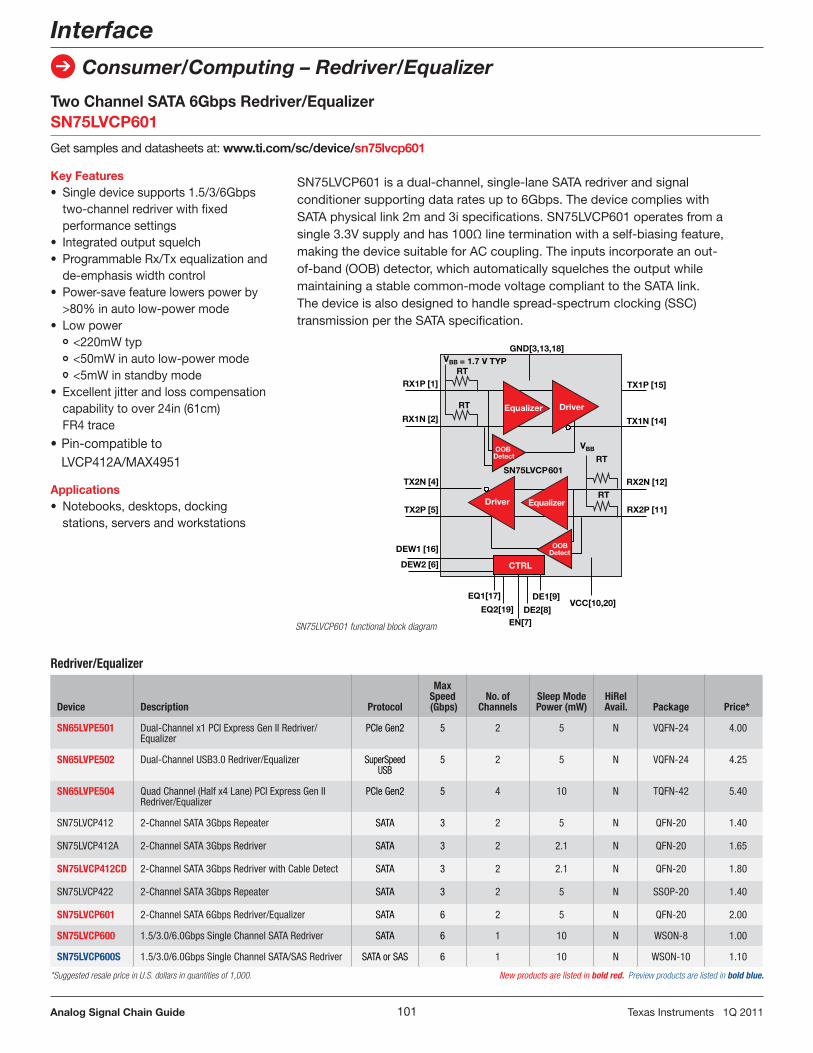
101Analog Signal Chain Guide TexasInstruments1Q2011
Interface
Consumer/Computing – Redriver/Equalizer
Device Description Protocol
Max Speed (Gbps)
No. ofChannels
Sleep Mode Power (mW)
HiRel Avail. Package Price*
SN65LVPE501 Dual-Channel x1 PCI Express Gen II Redriver/Equalizer
PCIe Gen2 5 2 5 N VQFN-24 4.00
SN65LVPE502 Dual-Channel USB3.0 Redriver/Equalizer SuperSpeed USB
5 2 5 N VQFN-24 4.25
SN65LVPE504 Quad Channel (Half x4 Lane) PCI Express Gen II Redriver/Equalizer
PCIe Gen2 5 4 10 N TQFN-42 5.40
SN75LVCP412 2-Channel SATA 3Gbps Repeater SATA 3 2 5 N QFN-20 1.40
SN75LVCP412A 2-Channel SATA 3Gbps Redriver SATA 3 2 2.1 N QFN-20 1.65
SN75LVCP412CD 2-Channel SATA 3Gbps Redriver with Cable Detect SATA 3 2 2.1 N QFN-20 1.80
SN75LVCP422 2-Channel SATA 3Gbps Repeater SATA 3 2 5 N SSOP-20 1.40
SN75LVCP601 2-Channel SATA 6Gbps Redriver/Equalizer SATA 6 2 5 N QFN-20 2.00
SN75LVCP600 1.5/3.0/6.0Gbps Single Channel SATA Redriver SATA 6 1 10 N WSON-8 1.00
SN75LVCP600S 1.5/3.0/6.0Gbps Single Channel SATA/SAS Redriver SATA or SAS 6 1 10 N WSON-10 1.10
Redriver/Equalizer
Two Channel SATA 6Gbps Redriver/Equalizer SN75LVCP601
Getsamplesanddatasheetsat:www.ti.com/sc/device/sn75lvcp601
Key Features• Singledevicesupports1 .5/3/6Gbps
two-channelredriverwithfixedperformancesettings
• Integratedoutputsquelch• ProgrammableRx/Txequalizationand de-emphasiswidthcontrol• Power-savefeaturelowerspowerby >80%inautolow-powermode• Lowpower <220mWtyp <50mWinautolow-powermode <5mWinstandbymode• Excellentjitterandlosscompensation capabilitytoover24in(61cm) FR4trace
•Pin-compatibleto LVCP412A/MAX4951
Applications• Notebooks,desktops,docking stations,serversandworkstations
SN75LVCP601isadual-channel,single-laneSATAredriverandsignalconditionersupportingdataratesupto6Gbps .ThedevicecomplieswithSATAphysicallink2mand3ispecifications .SN75LVCP601operatesfromasingle3 .3Vsupplyandhas100Ωlineterminationwithaself-biasingfeature,makingthedevicesuitableforACcoupling .Theinputsincorporateanout-of-band(OOB)detector,whichautomaticallysquelchestheoutputwhilemaintainingastablecommon-modevoltagecomplianttotheSATAlink .Thedeviceisalsodesignedtohandlespread-spectrumclocking(SSC)transmissionpertheSATAspecification .
SN75LVCP601 functional block diagram
RX1P [1]
CTRL
RT
RT
VBB
= 1.7 V TYPVBB
RT
RT
SN75LVCP601
TX1P [15]
RX1N [2] TX1N [14]
RX2N [12]
RX2P [11]
TX2N [4]
TX2P [5]
EN[7]DE2[8]
DE1[9]VCC[10,20]
GND[3,13,18]
EQ1[17]
EQ2[19]
DEW1 [16]
DEW2 [6]
Equalizer Driver
EqualizerDriver
OOBDetect
OOBDetect
*Suggested resale price in U.S. dollars in quantities of 1,000. New products are listed in bold red. Preview products are listed in bold blue.

102Analog Signal Chain Guide TexasInstruments1Q2011
Interface
Consumer/Computing – USB
SuperSpeed USB Transceiver with PIPE3 and ULPI Interfaces TUSB1310
Getsamplesanddatasheetsat:www.ti.com/sc/device/TUSB1310
Key Features• SuperSpeedUSB(USB3 .0)compliant One5 .0GbpsSuperSpeedconnection One480MbpsHS/FS/LSconnection• Receiversensitivityoflessthan
50mVdifferentialpeak-to-peakistwiceasgoodasrequiredbythespecification,allowingforsimplerboardlayoutandlongercableusagetoensurebroadercompatibility
• Digitalinterface PIPE3forSuperSpeedsignalpath ULPIforhigh-speed,full-speed
andlow-speedsignalpath
Applications• Surveillancecameras• High-speeddataacquisitionsystems
TheTUSB1310isasingle-port,5 .0GbpsUSB3 .0physicallayertransceiveroperatingoffofasinglecrystaloranexternalreferenceclock .TheTUSB1310providesaclocktoUSBlinklayercontrollers .ThesinglereferenceclockallowstheTUSB1310toprovideacost-effectiveUSB3 .0solutionwithfewexternalcomponentsandaminimumimplementationcost .
TUSB1310 functional block diagram
(8-bit 60MHz)
(16-bit 250MHz)
CLKOUT
ULPI
PIPE
SSTX P/N
DP/DM
SSRX P/N
Crystal
TUSB13105.0 Gbps
CP
U/F
PG
A
Link
Co
ntro
ller
SP3T Switch with Impedance Detection Micro-USB Switch to Support USB, UART, Audio and ChargerTSU5511
Getsamplesanddatasheetsat:www.ti.com/sc/device/TSU5511
Key Features• Compatibleaccessories USBdatacable UARTcable Charger(dedicatedorhost/hub) Stereoheadsetwithmic• IntegratedLDOsforVREFandmicbias• USBpathsupportsUSB2 .0highspeed• Audiopathprovidesnegativerail supportandclick/popreduction• 1 .8VcompatibleI2Cinterface• ESDperformancetestedperJESD22 2000Vhumanbodymodel (A114-B,ClassII) 1000Vcharged-devicemodel(C101)• ESDperf .DP/D</ID/VBUStoGND ±8kVcontactdischarge (IEC61000-4-2) ±15kVairgapdischarge
(IEC61000-4-2)
Applications•Cellulartelephones
TheTSU5511isdesignedtointerfacecellphoneUART,USBandaudiochipswithexternalperipheralsviaamicro-USBconnector .TheswitchfeaturesimpedancedetectionforidentificationofvariousaccessoriesthatareattachedthroughDPandDMofthemicro-USBport .Whenanaccessoryispluggedintothemicro-USBport,theswitchusesadetectionmechanismtoidentifytheaccessory .Itwillthenswitchtotheappropriatechannel:data,audioorUART .
MicroUSB
INT
SDA
SCL
UART_RX
USB_DM_
USB_DP
AUDIO_L
AUDIO_R
MIC
GND
10nF
ID
VBUS
Logic&I2C
Noise Filter Cap
0.6V
ADC
DP/ DMComparators...
ISET
200 k
LDO
2.3, 2.6V
2.21k
DM
DP
DSS
680
SwitchMatrix
SupplyDetect
NegativeRail andClick/Pop
Free
VSUPPLY
UART
UART_TX
USB
AUDIO
Processor
= pin on MUIC1
3.5 V
75 A
TSU5511 functional block diagram *Expected release date: Q2 2011

103Analog Signal Chain Guide TexasInstruments1Q2011
USB PortHS/FS Signals
(480Mbps)SS Signals
(5Gbps)
USB 2PHY
USB SSPHY
ARM®
Cortex®-M3Memory
Subsytem
SATA Port(1.5 or 3.0 Gbps)
USB Controller Interface
SATA IIPHY
SATA II Controller
Interface
Consumer/Computing – USB
SuperSpeed USB-to-SATA bridge TUSB9261
Getsamplesanddatasheetsat:www.ti.com/sc/device/TUSB9261
Key Features• Interfacesupportsinteroperability
withallhostplatformsandthe latesthigh-performancestoragedrivestoenableultra-fast,sync-and-gouserexperience
SATArevision2 .6-compliant USB2 .0HS/FSandUSB3 .0SS AttachedSCSIprotocol Massstorageclassbulk-only transport HIDclass Firmwareupdatesupport• Receiversensitivityoflessthan
50mVdifferentialpeak-to-peak istwiceasgoodasrequiredby thespecification,allowingforsimplerboardlayoutandlongercableusagetoensurebroadercompatibility
TheTUSB9261isaSuperSpeedUSBfunctioncontrollerwithintegratedUSB-complianttransceivers .ItisintendedasaUSB-to-SATAbridgeforstoragedevicesusingtheSATAinterface .TheTUSB9261isdesignedtouseboththefastperformanceofthestatemachineandtheprogrammabilityandflexibilityoftheembeddedmicrocontroller(MCU)andfirmware .WiththeelaboratebalancebetweentheMCUandthestatemachine,itprovidesabridgesolutiontomeetbothperformanceandflexibilityrequirementsofnext-generationexternalstoragedevices .
TUSB9260 functional block diagram
Applications• Externalstorage:
SSDs
HDDs Opticaldrives
SuperSpeed USB Host Controllers TUSB7320/40
Getsamplesanddatasheetsat:www.ti.com/sc/device/TUSB7320 orwww.ti.com/sc/device/TUSB7340
Key Features• USB3 .0-compliantxHCIhost controller• Downstreamportssupport SuperSpeed,high-speed, full-speed/low-speedconnections• Eachdownstreamport Maybeindependentlyenabledor disabled Hasadjustmentsfortransmitswing,
de-emphasisandequalizationsettings
Maybemarkedasremovable/ non-removable Hasindependentpowercontroland overcurrentdetection• Best-in-classadaptivereceiver equalizerdesign
TheTUSB7320/40areUSB3 .0xHCI-complianthostcontrollersthatsupportuptofourdownstreamports .Bothpartsareavailableinapin-compatible100-pinRKMpackage .TheTUSB7320/40interfacetothehostsystemviaaPCIex1Gen2interfaceandprovideSuperSpeed,high-speed,full-speedorlow-speedconnectionsonthedownstreamUSBports .
TUSB7320/40 functional block diagram
SS USB Deviceor
HS/FS/LS USBDevice
SS USB Deviceor
HS/FS/LS USBDevice
SS USB Deviceor
HS/FS/LS USBDevice
SS USB Deviceor
HS/FS/LS USBDevice
PC
TUSB7340PCIe
ToUSB 3.0
Host Controller
Applications• PCIehostadd-incards• DesktopPCs• NotebookPCs

104Analog Signal Chain Guide TexasInstruments1Q2011
Interface
Consumer/Computing – USB
USB
Device Description
MaxUSB
SpeedApplication Processor
Interface ESD HBM (kV)HiRel Avail. Package(s) Price*
USB Transcivers (PHYs)
TUSB1105 Advanced USB Full-Speed Transceiver Full Single or Differential ±15 N QFN-16 0.55
TUSB1106 Advanced USB Full-Speed Transceiver Full Differential ±15 N QFN-16, TSSOP-16
0.55
TUSB1210 USB 2.0 ULPI Transceiver High ULPI ±2 N QFN-32 Call
TUSB1211 USB 2.0 ULPI Transceiver with USB Charger Detection
High ULPI ±2 N BGA-36 Call
TUSB1310 SuperSpeed USB Transceiver SuperSpeed ULPI and PIPE3 ±0.5 N BGA-167 6.00
TUSB2551A Advanced USB Full-Speed Transceiver Full Single ±15 N QFN-16 0.55
Device Description
MaxUSB
SpeedIntegrated
MCU
OutEnd-
Points
InEnd-
PointsMCU Code Space (kB)
HiRel Avail. Package(s) Price*
USB Peripherals (Functions)
TUSB3210 General-Purpose Function Controller Full 8052 3 3 8 N LQFP-64 1.15
TUSB3410 USB-to-Serial Bridge Full 8052 3 3 16 Y LQFP,-32, QFN-32 1.20
TUSB6250 USB-to-IDE (ATA/ATAPI) Bridge High 8051 WARP 4 4 32 N TQFP-80 1.95
TUSB9260 USB-to-SATA Bridge SuperSpeed Cortex®-M3 5 5 64 N HTQFP-64 3.00
TUSB9261 USB-to-SATA Bridge SuperSpeed Cortex-M3 5 5 64 N HTQFP-64 3.00
Device DescriptionMax
USB Speed Local BusMax No.
Host PortsHiRel Avail. Package(s) Price*
USB Host and On-the-Go (OTG)
TUSB6020 USB 2.0 High-Speed On-the-Go Local Bus Interface Bridge Controller High VLYNQ™ 1 Y BGA-80, TQFP-80
6.00
TUSB7320 PCI Express to SuperSpeed USB xHCI with 2 USB 3.0 Ports SuperSpeed PCIe Gen2 2 N mRQFN-100 Call
TUSB7340 PCI Express to SuperSpeed USB xHCI with 4 USB 3.0 Ports SuperSpeed PCIe Gen2 4 Y mRQFN-100 Call
Device Description
MaxUSB
SpeedIntegrated
MCUDownstream
PortsHiRel Avail. Package(s) Price*
USB Hubs and Compound Devices
TUSB2036 2/3-Port USB Full-Speed Capable Hub Full — 3 N LQFP-32 1.15
TUSB2046B 4-Port USB Full-Speed Capable Hub Full — 4 Y LQFP-32,QFN-32
1.20
TUSB2077A 7-Port USB Full-Speed Capable Hub Full — 7 N LQFP-48 1.95
TUSB2136 2-Port USB Full-Speed Capable Hub with Integrated 8052 MCU Full 8052 2 N LQGP-64 4.10
TUSB8040 4-Port USB SuperSpeed Hub SuperSpeed — 4 N BGA-167, QFP-80
Call
*Suggested resale price in U.S. dollars in quantities of 1,000. See www.ti.com/hirel for HiRel options. New products are listed in bold red. Preview products are listed in bold blue.

105Analog Signal Chain Guide TexasInstruments1Q2011
Interface
Consumer/Computing – 1394
TPA2+TPA2−
TPB2+TPB2−
TPA1+TPA1−
TPB1+TPB1−
TPB0+TPB0−
BilingualCable Port 0
BilingualCable Port 1
BilingualCable Port 2
CPSLPSCNAPINT
LCLKLREQCTL0CTL1
D0
D5
D1D2D3D4
D6D7
RESETzLKON/DS2
PDBMODE
Received DataDecoder/Retimer
Arbitrationand Control
State MachineLogic
TransmitData
Encoder
Crystal Oscillator,PLL System,and Transmit
Clock Generator
PCLK
PC0PC1PC2
SESM
DS0DS1
TESTMTESTW
VoltageRegulator
XI
TPA0+TPA0−
Bias Voltageand
CurrentGenerator
R0R1TPBIAS0TPBIAS1TPBIAS2
LinkInterface
I/O
Key Features• FullysupportsprovisionsofIEEE
P1394brevision1 .33+at1Gbsignalingrates
• FullysupportsprovisionsofIEEE1394a-2000and1394-1995standardforhigh-performanceserialbus
• FullyinteroperablewithFireWire®,i .LINK®,andSB1394™,implementationofIEEEStd1394
• Providesthreefullybackward- compatible,(1394a-2000fully compliant)bilingualP1394bcableportsatupto800Mbps
• Providesthree1394a-2000fullycompliantcableportsat100/200/400Mbps
• Power-downfeaturestoconserveenergyinbattery-poweredapplications
• Low-powersleepmode• Datainterfacetolink-layercontroller
pin-selectablefrom1394a-2000mode(2/4/8parallelbitsat49 .152MHz)or1394bmode(8parallelbitsat98 .304MHz)
Applications• Storagedevices• Consumerelectronics• DesktopPCs
IEEE P1394b Three-Port Cable Transceiver ArbiterTSB81BA3EGetsamples,datasheets,evaluationmodulesandappreportsat:www.ti.com/sc/device/TSB81BA3E
TSB81BA3E block diagram
TheTSB81BA3Eprovidesthedigitalandanalogtransceiverfunctionsneededtoimplementathree-portnodeinacable-basedIEEE1394network .Thetransceiversincludecircuitrytomonitorthelineconditionsasneededfordeterminingconnectionstatus,forinitializationandarbitration,andforpacketreceptionandtransmission .
106Analog Signal Chain Guide TexasInstruments1Q2011
Interface
Consumer/Computing – 1394
1394
Device Description PortsVoltage
(V)Data Rate
(Mbps)HiRel Avail. Package(s) Price*
1394 PHY
TSB41AB1 IEEE 1394a One-Port Cable Transceiver/Arbiter 1 3.3 Up to 400 N HTQFP-48/64,BGA-64/80 MicroStar Junior™
1.50
TSB41AB2 IEEE 1394a Two-Port Cable Transceiver/Arbiter 2 3.3 Up to 400 N HTQFP-64 1.85
TSB41AB3 IEEE 1394a Three-Port Cable Transceiver/Arbiter 3 3.3 Up to 400 Y HTQFP-80 3.00
TSB41BA3D S400-Capable 1394b Physical Layer (PHY) 3 3.3 Up to 400 N HTQFP-80 6.40
TSB81BA3E IEEE P1394b Three-Port Cable Transceiver Arbiter 3 1.8, 3.3 Up to 800 Y BGA-168,HTQFP-80
5.40
Device Description FIFOVoltage
(V)Data Rate
(Mbps)HiRel Avail. Package Price*
1394 Link Layer
TSB12LV32 General-Purpose Link Layer Controller (GP2Lynx) 4 3.3 Up to 400 Y LQFP-100 6.05
TSB42AC3 High-Performance 1394-1995 Link Layer for Industrial and Bridge Applications
10 3.3 Up to 400 N TQFP-100 9.50
TSB82AA2B 1394b OHCI-Lynx™ Controller 11 3.3 Up to 800 Y LQFP-144 2.65
Device Description FIFO PortsVoltage
(V)Data Rate
(Mbps)HiRel Avail. Package(s) Price*
1394 Integrated Devices
TSB43AB21A OHCI 1.1, 1394a Link Layer Controller Integrated with 1394a, 400 Mbps, 1-Port PHY
9 1 3.3 Up to 400 Y TQFP-128 4.45
TSB43AB22A OHCI 1.1, 1394a Link Layer Controller Integrated with 1394a, 400 Mbps, 2-Port PHY
9 2 3.3 Up to 400 N TQFP-128 3.80
TSB43AB23 OHCI 1.1, 1394a Link Layer Controller Integrated with 1394a, 400Mbps, 3-Port PHY
9 3 3.3 Up to 400 Y TQFP-128, LQFP-144 4.25
TSB43EB42 IEEE Std 1394a-2000 Consumer Electronics Solution — 2 1.5, 3.3 Up to 400 N BGA-144 MicroStar Junior™
7.95
TSB83AA22C IEEE Std 1394b-2002 PHY and OHCI Link Device 11 2 1.95, 3.3 Up to 800 N BGA-168 8.50
TSB83AA23 Integrated IEEE-1394.B OHCI Link and 3-Port S800 PHY 11 3 1.95, 3.3 Up to 800 N NFBGA-167 9.00
XIO2213B x1 PCIe-to-1394b OHCI Host Controller and 3-Port S800 PHY 8 3 1.5, 1.95, 3.3 Up to 800 N NFBGA-167, BGA-168 5.75
XIO2221 x1 PCIe-to-1394b OHCI Host Controller and 1-Port S800 PHY 8 1 1.5, 3.3 Up to 800 N NFBGA-167 4.90
*Suggested resale price in U.S. dollars in quantities of 1,000. See www.ti.com/hirel for HiRel options. New products are listed in bold red.

107Analog Signal Chain Guide TexasInstruments1Q2011
Interface
Consumer/Computing – Display Port Switch/Redriver
DisplayPort 1:2 Switch with Integrated TMDS Translator SN75DP122A
Getsamplesanddatasheetsat:www.ti.com/sc/device/sn75dp122A
Key Features• Oneinputporttooneoftwo
outputports• IntegratedTMDSleveltranslatorwith
receiverequalization• DPportsupportsdataratesupto
2 .7Gbps• DPportsupportsdual-mode
DisplayPort• DPportoutputwaveformmimics
inputwaveformcharacteristics• TMDSportsupportsdataratesup
to2 .5Gbps• IntegratedI2ClogicblockforDVI/
HDMIconnectorrecognition
Applications• Personalcomputermarket DesktopPC NotebookPC Dockingstation Standalonevideocard
TheSN75DP122Aisaonedual-modeDisplayPortinputtoonedual-modeDisplayPortoutputoroneTMDSoutput .TheTMDSoutputhasabuilt-inleveltranslatorcompliantwithDigitalVideoInterface(DVI)1 .0andHighDefinitionMultimediaInterface(HDMI)1 .3b .TheDisplayPortoutputfollowstheinputsignalinamannerthatprovidesthehighestlevelofsignalintegritywhilesupportingtheEMIbenefitsofspread-spectrumclocking .ThroughtheSN75DP122A,dataratesofupto2 .7Gbpsthrougheachlinkforatotalthroughputofupto10 .8Gbpscanberealized .TheSN75DP122AsupportsDisplayPortSpec1 .1a .InadditiontotheswitchingoftheDisplayPorthigh-speedsignallines,theSN75DP122Aalsosup-portstheswitchingofthebidirectionalauxiliary(AUX),HotPlugDetect(HPD)andCableAdapterDetect(CAD)channels .
SN75DP122A functional block diagram
Computer/Notebook/Docking Station
DisplayPortEnabled
Monitor or HDTV
HDMI/DVIMonitor or HDTV
DP++
DP++
TMDS
GPU SN75DP122A
Device Description
No. ofDisplayPortDual Mode
Inputs
No. ofTMDS
Outputs
No. ofDisplayPortDual Mode
OutputsHiRel Avail. Package(s) Price*
SN75DP118 Display Port 1:1 Repeater 1 — 1 N VQFN-36 1.20
SN75DP119 Embedded DisplayPort (eDP) Repeater 1 — 1 N VQFN-14, VQFN-36 0.80
SN75DP119LV 1.1V Embedded DisplayPort (eDP) Repeater 1 — 1 N VQFN-14 Call
SN75DP120 Display Port 1:1 Dual-Mode Repeater 1 — 1 N VQFN-36 1.50
SN75DP121 2-Lane Embedded DisplayPort (eDP) 2:1 Signal Conditioner 1 — 2 N QFN-32 Call
SN75DP122A DisplayPort 1:2 Switch with Integrated TMDS Translator 1 1 1 N QFN-56 1.90
SN75DP128A DisplayPort 1:2 Switch 1 — 2 N QFN-56 1.65
SN75DP129 DisplayPort to TMDS Translator 1 1 — N VQFN-36 1.30
SN75DP130 5.4Gbps DisplayPort Redriver 1 — 1 N QFN-48 Call
SN75DP139 DisplayPort to TMDS Translator 1 1 — N VQFN-48 1.05
SN75DP219 2-Lane Embedded 5.4Gbps DisplayPort (eDP) Signal Conditioner 1 — 1 N QFN-14 Call
SN75DP221 2-Lane Embedded 5.4Gbps DisplayPort (eDP) 2:1 Signal Conditioner 1 — 2 N QFN-32 Call
SN75DP222 5.4Gbps DisplayPort 2x2 Redriver 2 — 2 N QFN-64 Call
DisplayPort Switch/Redriver
*Suggested resale price in U.S. dollars in quantities of 1,000. Preview products are listed in bold blue.

108Analog Signal Chain Guide TexasInstruments1Q2011
Interface
Consumer/Computing – Flatlink™ 3G Transmitter
FlatLink™ LVDS Transmitters
Device Description
ParallelInputs or Outputs
SerialChannels
DataThroughput
(Mbps)PLL Frequency
(MHz)
SupplyVoltage
(V) HiRel Avail. Package Price*
FlatLink LVDS Receiver
SN75LVDS86A FlatLink Receiver 21 3 1428 32 to 68 3.3 N TSSOP-48 2.40
SN75LVDS82 FlatLink Receiver 28 4 1904 31 to 68 3.3 N TSSOP-56 2.45
FlatLink™ 10-135MHz LVDS Transmitter SN75LVDS83B
Getsamplesanddatasheetsat:www.ti.com/sc/device/sn75lvds83b
Key Features• LVDSdisplaySERDESinterfaces
directlytoLCDdisplaypanels withintegratedLVDS
• 1 .8Vupto3 .3Vtolerantdata inputstoconnectdirectlyto low-power,low-voltageapplicationandgraphicprocessors
• Transferrateupto135Mpps (megapixelspersecond);pixel clockfrequencyrange10MHz to135MHz
• Suitedfordisplayresolutions rangingfromHVGAuptoHD withlowEMI
• 28datachannelsplusclockIn low-voltageTTLto4datachannelsplusclockoutlow-voltagedifferential
• Consumeslessthan1mW whendisabled
Applications• LCDdisplaypaneldrivers• UMPCandnetbookPCs• Digitalpictureframe
TheSN75LVDS83BFlatLink™LVDStransmittercontainsfour7-bitparallel-loadserial-outshiftregisters,a7xclocksynthesizer,andfivelow-voltagedifferen-tialsignaling(LVDS)linedriversinasingleintegratedcircuit .Thesefunctionsallow28bitsofsingle-endedLVTTLdatatobesynchronouslytransmittedoverfivebalanced-pairconductorsforreceiptbyacompatiblereceiver,suchastheSN75LVDS82andLCDpanelswithintegratedLVDSreceiver .
SN75lvds83b functional block diagram
7Y0PY0M
7Y1PY1M
7 Y2PY2M
CLKIN CLKOUTPCLKOUTM
SHTDN
7Y3PY3M
CLKSEL
D0, D1, D2, D3D4, D6, D7
D8, D9, D12, D13D14, D15, D18
D19, D20, D21, D22D24, D25, D26
D27, D5, D10, D11D16, D17, D23
Parallel-Load 7-BitShift Register
Control Logic
7X Clock/PLL
Rising/Falling Edge
A, B, ...GShift/Load>CLK
Parallel-Load 7-BitShift Register
A, B, ...GShift/Load>CLK
Parallel-Load 7-BitShift Register
A, B, ...GShift/Load>CLK
Parallel-Load 7-BitShift Register
A, B, ...GShift/Load>CLK
7CCLK>CLKCLKINH
Device Description
ParallelInputs or Outputs
SerialChannels
DataThroughput
(Mbps)
PLL Frequency
(MHz)
SupplyVoltage
(V) HiRel Avail. Package(s) Price*
FlatLink LVDS Transmitter
SN75LVDS84A FlatLink Transmitter 21 3 1575 31 to 75 3.3 N TSSOP-48 2.35
SN75LVDS83B FlatLink 10-135MHz Transmitter 28 4 3780 10 to 135 3.3 N BGA-56 MicroStar Junior™, TSSOP-56
2.60
*Suggested resale price in U.S. dollars in quantities of 1,000.

109Analog Signal Chain Guide TexasInstruments1Q2011
Interface
Consumer/Computing – Flatlink™ 3G LVDS Transmitter
FlatLink™ LVDS (continued)
Device Description
ParallelInputs or Outputs
SerialChannels
DataThroughput
(Mbps)
PLL Frequency
(MHz)
SupplyVoltage
(V) HiRel Avail. Package Price*
FlatLink 3G LVDS Receiver
SN65LVDS302 Programmable 27-Bit Display Serial Interface Receiver
27 3 1755 4 to 65 1.8 N BGA-80 MicroStar Junior™
2.25
SN65LVDS304 QVGA-VGA 27-Bit Display Serial Interface Receiver
27 2 810 4 to 30 1.8 N BGA-80 MicroStar Junior
2.05
SN65LVDS306 QVGA-HVGA 27-Bit Display Serial Interface Receiver
27 1 405 4 to 15 1.8 N BGA-80 MicroStar Junior
1.85
SN65LVDS308 QVGA-VGA 27-Bit Display Serial Interface Receiver
27 2 810 4 to 30 1.8 N BGA-48 MicroStar Junior
1.85
SN65LVDS310 QVGA-HVGA 27-Bit Display Serial Interface Receiver
27 1 405 4 to 15 1.8 N BGA-48 MicroStar Junior
1.75
FlatLink 3G LVDSVDSLVDSFlatLink 3G LVDS Transmitter
Device Description
ParallelInputs or Outputs
SerialChannels
DataThroughput
(Mbps)
PLL Frequency
(MHz)
SupplyVoltage
(V) HiRel Avail. Package Price*
SN65LVDS301 Programmable 27-Bit Display Serial Interface Transmitter
27 3 1755 4 to 65 1.8 N BGA-80 MicroStar Junior
2.25
SN65LVDS303 QVGA-VGA 27-Bit Display Serial Interface Transmitter
27 2 810 4 to 30 1.8 N BGA-80 MicroStar Junior
2.05
SN65LVDS305 QVGA-HVGA 27-Bit Display Serial Interface Transmitter
27 1 405 4 to 15 1.8 N BGA-80 MicroStar Junior
1.85
SN65LVDS307 QVGA-VGA 27-Bit Display Serial Interface Transmitter
27 2 810 4 to 30 1.8 N BGA-48 MicroStar Junior
1.85
SN65LVDS311 Programmable 27-Bit Display Serial Interface Transmitter
27 3 1755 4 to 65 1.8 N DSBGA-49 2.10
*Suggested resale price in U.S. dollars in quantities of 1,000. See www.ti.com/hirel for HiRel options. New products are listed in bold red.
Panelbus™ (DVI) Transmitters and Receivers
Device DescriptionVoltage
(V)
Receiver/Transceiver Channels
Parallel Outputs
DataSpeed(Mbps)
ICC (mA)
HiRel Avail. Package Price*
TFP401A DVI Receiver, 165MHz , HSYNC Jitter Immunity 3.3 3 48 495 400 Y HTQFP-100 4.00
TFP403 DVI Receiver 3.3 3 48 495 400 N HTQFP-100 5.45
TFP410 DVI Transmitter, 165MHz 3.3 3 6 495 250 Y HTQFP-64 3.00

110Analog Signal Chain Guide TexasInstruments1Q2011
Interface
Consumer/Computing - PCI Express
x1 PCI Express to PCI Bus Translation Bridge XIO2001
Getsamplesanddatasheetsat:www.ti.com/sc/device/xio2001
Key Features• Full×1PCIExpressthroughput• FullycompliantwithPCIExpress
toPCI/PCI-Xbridgespecification,revision1 .0
• FullycompliantwithPCIExpressbasespecification,revision2 .0
• FullycompliantwithPCIlocal busspecification,revision2 .3
• PCIExpressadvancederror reportingcapabilityincluding ECRCsupport
• SupportforD1,D2,D3hotand D3cold
• Utilizes100MHzdifferentialPCI Expresscommonreference clockor125MHz
• Single-endedreferenceclock (optionalspread-spectrum referenceclockissupported)• Robustpipelinearchitectureto
minimizetransactionlatency•FullPCIlocalbus66MHz/32-bit
throughputsupportforsixsubordinatePCIbusmasters withinternalconfigurable2-levelprioritizationscheme
Applications• Notebooks,desktops,docking
stations,serversandworkstations
TheXIO2001isasingle-functionPCIExpresstoPCItranslationbridgethatisfullycomplianttothePCIExpresstoPCI/PCI-Xbridgespecification,revision1 .0 .Fordownstreamtraffic,thebridgesimultaneouslysupportsuptoeightpostedandfournon-postedtransactions .Forupstreamtraffic,uptosixpostedandfournon-postedtransactionsaresimultaneouslysupported .
ThePCIExpressinterfacesupportsa×1linkoperatingatfull250MBP/spacketthroughputineachdirectionsimultaneously .Also,thebridgesupportsadvancederrorreportingincludingextendedCRC(ECRC)asdefinedinthePCIExpressbasespecification .
XIO2001 functional block diagram
PCI ExpressTransmitter
PCI ExpressReceiver
PCI Bus Interface
Configuration andMemory Register
GPIO
SerialEEPROM
SerialIRQ
ResetController
ClockGenerator
PowerMgmt

111Analog Signal Chain Guide TexasInstruments1Q2011
Interface
Consumer/Computing – PCI Express
PCI Express
Device Description
SupplyVoltage
(V) PCIeParallel Bus
Width
Speed(max)
(Mbps)HiRel Avail. Package Price*
PCI Express PHY
XIO1100 x1 PCI Express PHY, Compliant with the PCI Express Base Specification Revision 1.1
3.3, 1.8, 1.5
x1 8, 16 2500 N BGA-100 7.00
Device Description
SupplyVoltage
(V) PCIePCI Bus Masters
Wake/Beacon Support
HiRel Avail. Package(s) Price*
PCI Express Bridge
XIO2001 x1 PCI Express to PCI Bus Translation Bridge 3.3, 1.5 x1 6 Yes N BGA-144, BGA-169 MicroStar Junior™
5.50
Device Description
SupplyVoltage Range
(V) Architecture
rON (typ) (Ω)
tpd (typ) (ns)
HiRel Avail. Package Price*
PCI Express Signal Switches
TS2PCIE2212 2-Channel PCIe 2:1 Multiplexer/Demultiplexer Passive FET Switch 1.7 to 1.9 2:1 10 0.25 N BGA-48 1.65
TS2PCIE412 4-Channel PCIe 2:1 Multiplexer/Demultiplexer Passive FET Switch 1.5 to 2.1 2:1 12.5 0.25 N QFN-42 0.95
PCI Bridges
Device DescriptionSpeed (MHz)
Expansion Interface
(Bits) Hot
Swap Voltage
(V) HiRel Avail. Package(s) Price*
PCI2050B 32-Bit, 66MHz, 9-Master PCI-to-PCI Bridge 66 32 Yes 3.3, 5 N QFP-208, QFP-208, BGA-257 9.50
PCI2250 32-Bit, 33MHz PCI-to-PCI Bridge, Compact PCI Hot-Swap Friendly, 4-Master
33 32 Friendly 3.3, 5 N LQFP-176, QFP-160 6.10
PCI2060 32-Bit, 66MHz, 9-Master, Asynchronous PCI-to-PCI Bridge
66 32 Yes 3.3, 5 N BGA-257 9.50
*Suggested resale price in U.S. dollars in quantities of 1,000. New products are listed in bold red.
Device DescriptionNo. of Inputs
No. of Outputs
Intra-PairSkew
(max) (ps)
Inter-Pair Skew
(max) (ps) ICC
(max)
ESD HBM(kV)
HiRel Avail. Package(s) Price*
TMDS141 HDMI Hider 1 1 50 100 150 5 N QFN-40 1.75
TMDS361B 3-to-1 DVI/HDMI Active Switch 3 1 40 100 215 12 N TQFP-64 1.50
TMDS261B 2-to-1 DVI/HDMI Active Switch 2 1 40 100 215 12 N TQFP-64 1.35
TMDS442 4-to-2 DVI/HDMI Active Switch 4 2 50 100 550 5 N TQFP-128 3.45
TS3DV416 2-to-1 Analog FET Switch for HDMI/DVI 2 1 — — 0.6 2 N TSSOP-48, TVSOP-48
0.90
TS3DV520E 2-to-1 Analog FET Switch for HDMI/DVI 2 1 — — 0.6 14 N QFN-56, QFN-42 1.00
TMDS
Consumer/Computing – HDMI
Device Description
SupplyVoltage
(V) PCIeDownstream
PCIe Ports
Wake/Beacon Support
HiRel Avail. Package Price*
PCI Express Packet Switch
XIO3130 x1 PCI Express 4-Port Fanout Packet Switch 3.3, 1.5 x1 3 Yes N BGA-196 10.95

112Analog Signal Chain Guide TexasInstruments1Q2011
Interface
Industrial – CAN Transceivers
CAN Transceivers
Device Description IsolatedSupplyVoltage I/O Levels
Short-Circuit Protection (V)
ESD (kV)
Operating Temp Range (°C)
HiRel Avail. Price*
SN65HVD251/SN55HVD251
Improved Replacement for PCA82C250 and PCA82C251/Small QFN Package
No 5V 5V CMOS –36 to 36 ±14 –40 to 125/ –55 to 125
Y 0.90
SN65HVD1040 Improved TJA1040 with Better ESD and Bus Wake Up
No 5V 5V TTL –27 to 40 ±12 –40 to 125 Y 0.60
SN65HVD1050 Improved TJA1050 with Better ESD No 5V 5V TTL –27 to 40 ±8 –40 to 125 Y 0.45
ISO1050DUB 2.5kVrms Isolated CAN Transceiver Yes 5V 5V TTL –27 to 40 ±4 –55 to 105 N 1.55
ISO1050DW 5kVrms Isolated CAN Transceiver Yes 5V 5V TTL –27 to 40 ±4 –55 to 105 N 1.95
SN65HVD230 Standby Mode, Slope Control No 3.3V 3.3V TTL –4 to 16 ±16 –40 to 85 Y 1.45
SN65HVD231 Sleep Mode, Slope Control No 3.3V 3.3V TTL –4 to 16 ±16 –40 to 85 Y 1.45
SN65HVD232 Cost Effective No 3.3V 3.3V TTL –4 to 16 ±16 –40 to 85 Y 1.10
SN65HVD233 Standby Mode, Diagnostic Loop-Back No 3.3V 3.3V TTL –36 to 36 ±16 –40 to 125 Y 1.50
SN65HVD234 Standby Mode, Sleep Mode No 3.3V 3.3V TTL –36 to 36 ±16 –40 to 125 N 1.45
SN65HVD235 Standby Mode, Auto Baud Loop-Back No 3.3V 3.3V TTL –36 to 36 ±16 –40 to 125 N 1.50
DeviceNet™ CAN
SN65HVD252 DeviceNet Compliant/Low Propagation Delay CAN Device
No 5V 5V TTL –36 to 40 ±12 –40 to 85 N 0.80
SN65HVD253 DeviceNet Compliant/Low Propagation Delay CAN Device with Auto Baud Loop-Back
No 5V 5V TTL –36 to 40 ±12 –40 to 85 N 0.80
Industrial CAN Transceiver SN65HVD252/253
Getsamplesanddatasheetsat:www.ti.com/sc/device/SN65HVD252 andwww.ti.com/sc/device/SN65HVD253
Key Features• DeviceNet™compliantsupporting64 DeviceNetnodes• Loopbackfunction(HVD253)• Bus-faultprotectionof–36Vto+40V• Power-up/downglitch-freebusI/O•3 .3Vcompatiblereceiveroutput
Applications• DeviceNetnetworks• Industrialautomation• HVACnetworks• Securitysystems• Telecombasestationstatus andcontrol• CANopendatabus• SDSdatabus• CANkingdomdatabus
TheSN65HVD252andSN65HVD253CANtransceiversmeetorexceedthespecificationsofDeviceNet™andarecompatibletotheISO11898-2:2003standardforuseinapplicationsemployingacontrollerareanetwork(CAN) .Thisdeviceprovidesdifferentialtransmitandreceivecapabilityatsignalingratesupto1Mbps .Designedforoperationinharshindustrialenvironments,thesedevicesfeaturebus-pinvoltageprotectionfrom–36Vto+40V,driveroutputcurrentlimitingandovertemperaturedrivershutdown .
TheVREFpinoftheSN65HVD252isaVCC/2voltagereferenceforsystemsthatusesplittermination .TheABpinoftheSN65HVD253implementsalisten-onlyloopbackfeaturethatallowsthelocalnodecontrollertosynchronizeitsbaudratewiththatoftheCANbus .Inloopbackmode,thedriverdifferentialoutputsareplacedinhigh-impedancestate,whilethereceiverbusinputsremainactive .
SN65HVD252/53 functional block diagrams
VCC /2
TXD 1 8
2
5
6
7GND
RXD
S
CANH
CANL
VREF
3
4
VCC
TXD 1 8
2
5
6
7GND
RXD
S
CANH
CANL
AB
3
4
VCC
SN65HVD252 SN65HVD253
*Suggested resale price in U.S. dollars in quantities of 1,000. See www.ti.com/hirel for HiRel options. New products are listed in bold red.

113Analog Signal Chain Guide TexasInstruments1Q2011
Interface
Industrial – Digital Isolators
Isolated 3.3V Full-and Half-Duplex RS-485 TransceiversISO15/35
Getsamplesanddatasheetsat:www.ti.com/sc/device/ISO15andwww.ti.com/sc/device/ISO35
Key Features• 4000Vpeakisolation,560VpeakVIORM• UL1577,IEC60747-5-2 (VDE0884,Rev2)• IEC61010-1,IEC60950-1andCSA
approved• 1/8UL–upto256nodesonabus• MeetsorexceedsTIA/EIARS-485
requirements• Signalingratesupto1Mbps• Thermalshutdownprotection• Lowbuscapacitance–16pF(typ)• 50kV/µstypicaltransientimmunity• Fail-saferec .forbusopen,short,idle•3 .3Vinputsare5Vtolerant
Applications• Securitysystems• Chemicalproduction• Factoryautomation• Motor/motioncontrol• HVACandbuildingautomation networks• Networkedsecuritystations
TheISO15isanisolatedhalf-duplexdifferentiallinetransceiver,whiletheISO35isanisolatedfull-duplexdifferentiallinedriverandreceiverforTIA/EIA485/422applications .TheISO15MandISO35Mhaveextendedambienttemperatureratingsof–55°Cto+125°C,whiletheISO15andISO35arespecifiedover–40°Cto+85°C .
Thesedevicesareidealforlongtransmissionlines,sincethegroundloopisbroken,toallowforamuchlargercommon-modevoltagerange .Thesymmetricalisolationbarrierofthedeviceistestedtoprovide2500Vrmsofisolationfor60sbetweenthebus-linetransceiverandthelogic-levelinterface .
ISO15/35 functional block diagram
1
2
3
4
5
6
7
8 9
10
11
12
13
14
15
16
R
RE
D
GND1
nc
Vcc2
B
A
nc
GND2
DE
Vcc1
GND1 GND2
GND2GND1
DE
B
A
13
12
R
5
3
D6
4RE
Gal
vani
c Is
ola
tio
n
DW Package
1
2
3
4
5
6
7
8 9
10
11
12
13
14
15
16
R
RE
D
GND1
Y
Vcc2
B
Z
A
GND2
DE
Vcc1
GND1 GND2
GND2GND1
DW Package
Functional Diagram
DE
B
A
Z
Y
13
14
12
11
R
5
3
D6
4RE
Gal
vani
c Is
ola
tio
n
Functional DiagramISO35
ISO15
Low-Power 5kVrms Dual Digital Isolator ISO7520C
Getsamplesanddatasheetsat:www.ti.com/sc/device/ISO7520C
Key Features• Highestsignalingrate:1Mbps• Propagationdelay<20ns• Lowpowerconsumption• Wideambienttemperature:
–40°Cto+105°C• Safetyandregulatoryapprovals: 5kV(rms)for1minuteperUL1577 CSAcomponentacceptance
notice5A IEC60747-5-2(VDE0884Rev .2) IEC60601-1,60950-1and
61010-1end-equipmentstandards• 50kV/µstransientimmunitytypical• Operatesfrom3 .3Vor5Vsupplyand logiclevels
TheISO7520providesdoublegalvanicisolationofupto5KVrmsfor1minuteperUL .Thisdigitalisolatorhastwoisolatedchannelswithunidirectionalchannelconfigurations .Eachisolationchannelhasalogicinputandoutputbufferseparatedbyasiliconoxide(SiO2)insulationbarrier .Usedinconjunctionwithisolatedpowersupplies,thesedevicespreventnoisecurrentsonadatabusorothercircuitsfromenteringthelocalgroundandinterferingwithordamagingsensitivecircuitry .
ISO7520
GND
NC
VCC1
INA
INB
NC
GND1
NC
16
15
14
13
12
11
10
9
1
2
3
4
5
6
7
8
GND2
NC
VCC2
OUTA
OUTB
NC
NC
GND2
ISO7520 functional block diagram
Applications• Opto-couplerreplacementin:• Medicalapplicationsfor IEC60601-15kVrmsrated• Industrialfield-bus ProfiBus Modbus®
DeviceNet™databuses• Servocontrolinterfaces• Motorcontrol

114Analog Signal Chain Guide TexasInstruments1Q2011
Interface
Industrial – Digital Isolators
Digital Isolators
Device Description
Isolation Rating
Vrms (UL, VDE, CSA)
Channel Direction
Data Rate (Max) Mbps
Transient Immunity (Min)
(kV/µs)
Supply Voltage
(V)HiRel Avail. Price*
ISO721/M Single Channel 2500Vrms 1/0 100/150 25 3.3, 5 Y 1.40
ISO722/M Single Channel with Output Enable 2500Vrms 1/0 100/150 25 3.3, 5 N 1.40
ISO150 Dual Channel Configurable 2400Vrms Config 80 1.6 5 N 8.10
ISO7220A/B/C/M Dual Channel 2500Vrms 2/0 1/5/25/150 25 3.3, 5 Y 0.95
ISO7221A/B/C/M Dual Channel 2500Vrms 1/1 1/5/25/150 25 3.3, 5 Y 0.95
ISO7230A/C/M Triple Channel 2500Vrms 3/0 1/25/150 25 3.3, 5 N 1.40
ISO7231A/C/M Triple Channel 2500Vrms 2/1 1/25/150 25 3.3, 5 N 1.40
ISO7240A/C/CF/M Quad Channel (F=Failsafe Low) 2500Vrms 4/0 1/25/25/150 25 3.3, 5 Y 1.75
ISO7241A/C/M Quad Channel 2500Vrms 3/1 1/25/150 25 3.3, 5 Y 1.75
ISO7242A/C/M Quad Channel 2500Vrms 2/2 1/25/150 25 3.3, 5 N 1.75
ISO7420/0F/1/1F Gen II Dual Channel (F=Failsafe Low) 2500Vrms 2/0 and 1/1 1 25 3.3, 5 Y 1.50
ISO7431 Gen II Triple Channel 2500Vrms 2/1 TBD 25 3.3, 5 N TBD
ISO7440/1 Gen II Quad Channel 2500Vrms 4/0 and 3/1 TBD 25 3.3, 5 N TBD
ISO7520C/1C Dual Channel 5000Vrms 2/0 and 1/1 1 25 3.3, 5 N 1.70
ISO7531 Triple Channel 5000Vrms 2/1 TBD 25 3.3, 5 N TBD
ISO7540/1 Quad Channel 5000Vrms 4/0 and 3/1 TBD 25 3.3, 5 N TBD
ISO3082/ISO3088 Isolated Half Duplex 5V RS-485 2500Vrms 2/1 0.2/20 25 5 N 2.60
ISO3080/ISO3086 Isolated Full Duplex 5V RS-485 2500Vrms 2/1 0.2/20 25 5 N 2.60
ISO15/M Isolated Half Duplex 3.3V RS-485 2500Vrms 2/1 1 25 3.3 N 3.00
ISO35/M Isolated Full Duplex 3.3V RS-485 2500Vrms 2/1 1 25 3.3 N 3.00
ISO1176 Isolated PROFIBUS RS-485 2500Vrms 2/1 40 25 5 N 3.35
ISO1050DUB Isolated CAN Transceiver 2500Vrms 1/1 1 25 5 N 1.55
ISO1050DW Isolated CAN Transceiver 5000Vrms 1/1 1 25 5 N 1.95
ISO3086T Isolated 5V RS485 with Transformer Driver 2500Vrms 2/1 20 25 5 N TBD
ISO35T Isolated 3.3V RS485 with Transformer Driver
2500Vrms 2/1 1 25 3.3 N TBD
ISO1176T Isolated PROFIBUS with Transformer Driver 2500Vrms 2/1 40 25 5 N TBD
ISO55XX Isolated Gate Drivers 5000Vrms N/A 10 25 3.3, 5 N TBD
AMC1200 Isolated Amplifier with G=8 2500Vrms N/A N/A 10 –0.3 to 6 N 2.25
AMC1203 Isolated 2nd-Order ∆∑ Modulator 2500Vrms N/A 20 15 5 N 3.35
AMC1204 Isolated 20MHz ∆∑ Modulator, 16-Bit 2500Vrms N/A 20 15 3.3, 5 N 3.45
*Suggested resale price in U.S. dollars in quantities of 1,000. See www.ti.com/hirel for HiRel options. New products are listed in bold red. Preview products are listed in bold blue.

115Analog Signal Chain Guide TexasInstruments1Q2011
Interface
Industrial – Ethernet Physical Layer Transceivers
Industrial 10/100 Ethernet PHY TLK100
Getsamplesanddatasheetsat:www.ti.com/sc/device/TLK100
Key Features• Operatesfrom–40°Cto+85°C• Lowpowerconsumption, <200mWtypical• Advancedcablediagnostics• Error-freeoperationupto200 metersundertypicalconditions• 3 .3VMACinterface• Auto-MDIXfor10/100Mbps• Energydetectionmode• 25MHzclockout• MIIserialmanagementinterface (MDCandMDIO)• BusI/Oprotection–±16kV JEDECHBM• IEEE1149 .1JTAG• IEEE802 .3compliant•Auto-MDIX/auto-negotiation/ auto-polarity•48-pinTQFPpackage (7mm×7mm)
Applications• Industrialcontrolsandfactory automation•Generalembeddedapplications
TheTLK100isasingle-portEthernetPHYfor10BaseTand100BaseTXsignaling .Itintegratesallofthephysical-layerfunctionsneededtotransmitandreceivedataonstandardtwisted-paircables .ThisdevicesupportsthestandardMediaIndependentInterface(MII)fordirectconnectiontoamediaaccesscontroller(MAC) .
TheTLK100isdesignedforpower-supplyflexibilityandcanoperatewithasingle3 .3Vpowersupplyorwithcombinationsof3 .3V,1 .8Vand1 .1Vpowersuppliesforreducedpoweroperation .
TheTLK100usesmixed-signalprocessingtoperformequalization,datarecoveryanderrorcorrectiontoachieverobustoperationoverCAT5twisted-pairwiring .ItnotonlymeetstherequirementsofIEEE802 .3,butmaintainshighmarginsintermsofcrosstalkandaliennoise .
TLK100 functional block diagram
scitengaM
MPU/CPU
MIITLK100
25-MHzClockSource
StatusLEDs
54-JR
10BASE-Tor
100BASE-TX
1
Industrial Ethernet Physical Layer Transceiver
Device Description
Supply Voltage
(V)
Cable Reach
(m)Power (mW)
ESD(kV)
Operating Temp Range
(°C) HiRel Avail. Package Price*
TLK100 Single-Port 10/100 Mbps Ethernet PHY 3.3, 1.8, 1.1 200 189** ±16 –40 to +85 N TQFP-48 2.25
*Suggested resale price in U.S. dollars in quantities of 1,000.**Triple supply power

116Analog Signal Chain Guide TexasInstruments1Q2011
Interface
Industrial – Industrial SERDES
Industrial Serializers
Device DescriptionSupply
Voltage (V)
I/O Voltage
(V) Parity
Input Data Rate
(Mbps)Temperature
Range
Low Voltage Detector
HiRel Avail. Price*
Industrial Eight-Channel Digital Serializers
SN65HVS880 Nominal 24V Digital-Input Serializer 18 to 30 0 to 30 No 1 –40 to 85 Yes: 15V N 1.90
SN65HVS881 0-34V Digital-Input Serializer with Parity 10 to 34 0 to 34 Yes 1 –40 to 125 Yes: 15V N 2.00
SN65HVS882 0-34V Digital-Input Serializer 10 to 34 0 to 34 No 1 –40 to 125 No N 2.00
SN65HVS885 0-34V Digital-Input Serializer for 5V Systems 4.5 to 5.5 0 to 34 No 1 –40 to 125 No N 1.80
Eight-Channel, 0-34V Digital-Input Serializer with 5V Vcc for Industrial Digital Inputs SN65HVS885
Getsamplesanddatasheetsat:www.ti.com/sc/device/SN65HVS885
Key Features• Eightdigitalsensorinputs• High-inputvoltageupto34V• Selectabledebouncefilters from0msto3ms• Flexiblecurrent-limitedinputs
–0 .2mAto5 .2mA• Fieldinputsprotectedto15kVESD• Single5Vsupply• Outputdriversforexternal statusLEDs• Cascadableformoreinputsin multiplesofeight• SPI™-compatibleinterface•Overtemperatureindicator
Applications• IndustrialPCs• DigitalI/Ocards• High-channel-countdigital inputmodules• DecentralizedI/Omodules
TheSN65HVS885isaneight-channel,digital-inputserializerforhigh-channeldensitydigitalinputmodulesinindustrialandbuildingautomation .Operatingfroma5Vsupply,thedeviceacceptsfieldinputvoltagesofupto34V .Incombinationwithgalvanicisolators,thedevicecompletestheinterfacebetweenthehighvoltagesignalsonthefieldsideandthelow-voltagesignalsonthecontrollerside .Inputsignalsarecurrentlimitedandthenvalidatedbyinternaldebouncefilters .
Withtheadditionoffewexternalcomponents,theinputswitchingcharacteristiccanbeconfiguredinaccordancewithIEC61131-2forType1,2and3sensorswitches .
Upontheapplicationofloadandclocksignals,inputdataislatchedinparallelintotheshiftregisterandafterwardsclockedoutserially .
SN65HVS885 functional block diagram
Ser
ializ
er
&
Channel0
Channel 7
Vcc
GND
RLIM
RE0IP0
RE7IP7
HOT
SIP
SOP
CLK
LDCE
DB0DB1
DebounceFilter
CurrentSense
VoltageSense
Adj.CurrentThresholds
DebounceSelect
ThermalProtection
*Suggested resale price in U.S. dollars in quantities of 1,000. New products are listed in bold red.

117Analog Signal Chain Guide TexasInstruments1Q2011
Interface
Industrial – RS-485/RS-422
Device DescriptionDR/RX Duplex
Supply (V) Isolated
Signaling Rate (Mbps)
ESD (kV)
Receiver Fail-Safe Nodes
HiRel Avail. Package(s) Price*
SN65HVD10/11/12 High/Mid/Low Speed Slew-Rate Control
1/1 Half 3.3 No 32/10/1 16 Short, Open, Idle 256 Y PDIP/SOIC-8 1.50
SN65HVD13 High Signaling Rate, High Hysteresis
1/1 Half 3.3 No 50 7 Short, Open, Idle 96 N MSOP/SOIC-8 TBD
SN65HVD30/31/32 No Enables 1/1 Full 3.3 No 26/5/1 16 Short, Open, Idle 256 Y SOIC-8 1.45
SN65HVD33/34/35 With Enables 1/1 Full 3.3 No 26/5/1 16 Short, Open, Idle 256 Y SOIC-14 1.45
SN65HVD37 Low Power, High Hysteresis 1/1 Full 3.3 No 20 7 Short, Open, Idle 256 N SOIC-14 TBD
ISO15/M Isolated 3.3V Half Duplex Transceiver
1/1 Half 3.3 Yes 1 16 Short, Open, Idle 256 N SOIC-16 3.00
ISO35/M Isolated 3.3V Full Duplex Transceiver
1/1 Full 3.3 Yes 1 16 Short, Open, Idle 256 N SOIC-16 3.00
ISO35T Isolated 3.3V Transceiver with Transformer Driver
1/1 Full 3.3 Yes 1 16 Short, Open, Idle 256 N SOIC-16 TBD
SN65HVD08 Wide Supply Range: 3V to 5.5V
1/1 Half 3 to 5.5 No 10 16 Short, Open, Idle 256 N PDIP/SOIC-8 1.65
RS-485/RS-422
SymPol™ Transceiver SN65HVD96
Getsamplesanddatasheetsat:www.ti.com/sc/device/SN65HVD96
Key Features• Communicatewithouterrorson normalorreversed-wirebuslines• Upto5Mbpssignaling• Industrialtemperaturerange: –40°Cto+85°C• Symmetricpolarityreceiver• Receiverhysteresis>100mV• Connectupto32nodesononebus• Transientprotectiononbuspins ±12kVhumanbodymodel ±25Vrepetitivetransientpulse• Additionalreliabilityfeatures: Busstandofffrom–35Vto+40V Driveroutputshort-circuit currentlimit Automaticthermalshutdownand
recovery
Applications• Camera:surveillanceanalog• Camera:surveillanceIPnetwork• HVAC–heating,ventilating andairconditioning
TheSN65HVD96isspecificallydesignedtomeettherequirementsforatransceiverthatoperateswithnoerrorsifthetwisted-pairsignalwiresareconnectednormallyorreversed .Thisallowsforerror-freeoperationinapplicationswherethesignalwiresmaybecomeinadvertentlyreversedduringinstallationormaintenance .Thisfeatureiscorrectedinternallysonointerventionfromthecontrolleroroperatorisrequired .
SimilartoRS-485,thesetransceiverscanbeusedforpoint-to-point,multi-dropormulti-pointnetworks .SymPol™devicesarenotbackwardscompatiblewith,butareanupgradeto,existingRS-485networks .Thepin-outisidenticaltotheindustry-standardSN75176transceiver,allowingdirectupgradefromRS-485toSymPol .
SN65HVD96 functional block diagram
Temp.SHDN
R1
2
3
4
5
6
7
8
RE
DE
D
D A or B
B or AB
A
R
VOD
[VID]
VCC
B
A
GND
Driver signaling (DE=high)
Passive
Passive
Active
Active
Receiver detecting (RE=low)
*Suggested resale price in U.S. dollars in quantities of 1,000. See www.ti.com/hirel for HiRel options. New products are listed in bold red. Preview products are listed in bold blue.
118Analog Signal Chain Guide TexasInstruments1Q2011
Interface
Industrial – RS-485/RS-422
Device DescriptionDR/RX Duplex
Supply (V) Isolated
Signaling Rate (Mbps)
ESD (kV)
Receiver Fail-Safe Nodes
HiRel Avail Package(s) Price*
SN65HVD1780/1/2 Up to ±70V Protected, Wide Supply Range: 3.3V to 5V
1/1 Half 3.3 to 5 No 0.115/1/10 16 Short, Open, Idle 320 N PDIP/SOIC-8 1.85
SN65HVD1785/6/7 ±70V Protected, Wide –20V to +25V Common Mode
1/1 Half 5 No 0.115/1/10 16 Short, Open, Idle 256 N PDIP/SOIC-8 1.85
SN65HVD1794 ±70V Protected, Bus-Pin Invert/Wide Common Mode
1/1 Half 5 No 0.115 16 Short, Open, Idle 256 N PDIP/SOIC-8 1.95
SN65HVD3082E/5E/8E Ultra-Low Power, Optimized for Low, Medium and High Speeds
1/1 Half 5 No 0.2/1/20 16 Short, Open, Idle 256 Y SOIC/PDIP/MSOP-8
0.90
ISO3082/8 ±4kV Isolated RS-485 Optimized for Low and High Speeds
1/1 Half 5 Yes 0.2/20 16 Short, Open, Idle 256 N Wide SOIC-16 2.60
SN65HVD485E Half Duplex Transceiver 1/1 Half 5 No 10 15 Open 64 Y PDIP/SOIC/MSOP-8
0.75
SN65HVD20/21/22 ±27V Protected and –20V to +25V Common Mode
1/1 Half 5 No 25/5/0.5 16 Short, Open, Idle 256 N PDIP/SOIC-8 1.40
SN65HVD23/24 Receiver Equalization and –20V to +25V Common Mode
1/1 Half 5 No 25/3 16 Short, Open, Idle 256 N PDIP/SOIC-8 1.95
SN65LBC176A Low Power, Fast Signaling, ESD Protection
1/1 Half 5 No 30 12 Open 32 Y PDIP/SOIC-8 2.65
SN65LBC184 ESD Protection IEC 4-2 Air, Contact and IEC 4-5 Surge
1/1 Half 5 No 0.25 30 Open 128 N PDIP/SOIC-8 1.30
SN65LBC182 ESD Protection HBM, IEC4-2 Air and Contact
1/1 Half 5 No 0.25 15 Open 128 N PDIP/SOIC-8 1.05
SN65HVD1791/2/3 ±70V Protected, Wide –20V to +25V Common Mode
1/1 Full 5 No 0.115/1/10 16 Short, Open, Idle 256 N SOIC-14 1.90
SN65HVD3080E/3E/6E Ultra-Low Power, Optimized for Low, Medium and High Speeds
1/1 Full 5 No 0.2/1/20 15 Short, Open, Idle 256 N SOIC-14, MSOP-10
1.20
ISO3080/6 ±4kV Isolated, Optimized for Low and High Speeds
1/1 Full 5 Yes 0.2/20 16 Short, Open, Idle 256 N Wide SOIC-16 2.60
ISO3086T Isolated 5V Transceiver with Transformer Driver
1/1 Full 5 Yes 20 16 Short, Open, Idle 256 N Wide SOIC-16 TBD
SN65LBC180A High Signaling Rate with Enables
1/1 Full 5 No 30 15 Open 32 Y PDIP/SOIC-14 1.50
SN65LBC172A/174A Quad Drivers, High Signaling Rate
4/0 — 5 No 30 12 — — N PDIP/SOIC-16,SOIC-20
2.65
AM26LV31E Quad Drivers, High Signaling Rate, IEC 4-2 ESD
4/0 — 3.3 No 64 15 — — Y SO/SOIC/TSSOP/QFN-16
0.90
SN65LBC173A/175A Quad Receivers, High Signaling Rate, Low Power
0/4 — 5 No 50 6 Short, Open, Idle 32 N PDIP/SOIC-16 1.65
AM26LV32E Quad Receivers, High Signaling Rate, IEC 4-2 ESD
0/4 — 3.3 No 64 15 Short, Open, Idle 10 Y SO/SOIC/TSSOP/QFN-16
1.05
SN65HVD09 9-Channel Parallel Bus Transceivers
9/9 Half 5 No 20 12 Open 32 N TSSOP-56 3.50
PROFIBUS Transceivers
HVD1176 PROFIBUS (EN 50170) Transceiver
1/1 Half 5 No 40 10 Short, Open, Idle 160 N SOIC-8 1.55
ISO1176 Isolated PROFIBUS Transceiver
1/1 Half 5 Yes 40 16 Short, Open, Idle 160 N SOIC-16 3.35
ISO1176T Isolated PROFIBUS Transceiver with Transformer Driver
1/1 Half 5 Yes 40 4 Short, Open, Idle 160 N SOIC-16 TBD
ControlNet™ Transcievers
SN65HVD61 ControlNet Transceiver 1/1 Half 5 No 10 16 Short 64 N SOIC-14 5.10
SymPol™ Transceivers
SN65HVD96 SymPol Transceiver 1/1 Half 5 No 5 12 Short, Open, Idle 32 N SOIC-8 1.20
RS-485/RS-422 (continued)
*Suggested resale price in U.S. dollars in quantities of 1,000. See www.ti.com/hirel for HiRel options. New products are listed in bold red. Preview products are listed in bold blue.

119Analog Signal Chain Guide TexasInstruments1Q2011
RS-485/RS-422 (continued)
Interface
General – UARTs
Dual UART With 64-Byte FIFO TL16C752C
Getsamplesanddatasheetsat:www.ti.com/sc/device/TL16C752C
Key Features• ST16C654/654Dpin-compatiblewith additionalenhancements (PFBpackageonly)• Supportsupto24MHzcrystal inputclock(1 .5Mbps)• Supportsupto48MHzoscillator inputclock(3Mbps)for5Voperation• Supportsupto32MHzoscillator inputclock(2Mbps)for3 .3V operation• Supportsupto24MHzinputclock (1 .5Mbps)for2 .5Voperation• Supportsupto16MHzinputclock (1Mbps)for1 .8Voperation• ProgrammablereceiveFIFOtrigger
levelsforsoftware/hardwareflowcontrol
• Software/hardwareflowcontrol ProgrammableXon/Xoffcharacters Programmableauto-RTSand
auto-CTS• Characterizedforoperation from–40°Cto+85°C,available incommercialandindustrial temperaturegrades
TheTL16C752Cisadualuniversalasynchronousreceiver/transmitter(UART)with64-byteFIFOs,automatichardware/softwareflowcontrolanddataratesupto3Mbps .ItincorporatesthefunctionalityoftwoUARTs,eachUARThavingitsownregistersetandFIFOs .ThetwoUARTsshareonlythedatabusinterfaceandclocksource;otherwisetheyoperateindependently .AnothernamefortheUARTfunctionisasynchronouscommunicationselement(ACE),andthesetermsareusedinterchangeably .Ithasatransmissioncontrolregister(TCR)thatstoresreceivedFIFOthresholdlevelstostart/stoptransmissionduringhardwareandsoftwareflowcontrol .
TL16C752C functional block diagram
BAUDRateGen 16-Byte RX FIFO
UART Channel A
UART Regs
UART Regs
RX
TX TXA
CTSA
OPA, DTRA
DSRA, RIA, CDA
RTSA
RXA
16-Byte TX FIFO
BAUDRateGen 16-Byte RX FIFO
UART Channel B
RX
TX16-Byte TX FIFO TXB
VCC
GND
CTSB
OPB, DTRB
DSRB, RIB, CDB
RTSB
RXB
XTAL2
XTAL1
RESET
RXRDYB
RXRDYA
TXRDYB
TXRDYA
INTB
INTA
IOW
IOR
CSB
CSA
D7-D0
A2-A0
Data BusInterface
Crystal OSC
Buffer

120Analog Signal Chain Guide TexasInstruments1Q2011
Interface
General – UARTs
UARTs
Device Description Channel(s) FIFOs Voltage (V)Characterized
Temp. (°C)HiRel Avail. Package(s) Price*
TL16C2550 Dual UART with Programmable Auto-RTS and Auto-CTS
2 16-Byte 1.8/2.5/3.3/5 –40 to 85 N QFN-32, TQFP-48 2.20
TL16C2552 Dual UART with Programmable Auto-RTS and Auto-CTS
2 16-Byte 1.8/2.5/3.3/5 –40 to 85 N PLCC-44 2.90
TL16C2752 Dual UART with Customizable Trigger Levels
2 64-Byte 1.8/2.5/3.3/5 –40 to 85 N PLCC-44 3.50
TL16C450 Single UART 1 None 5 0 to 70 N PLCC-44 1.50
TL16C451 Single UART with Parallel Port 1 None 5 0 to 70 N PLCC-68 3.10
TL16C452 Dual UART with Parallel Port 2 None 5 0 to 70 N PLCC-68 2.55
TL16C550C Single UART with Hardware Autoflow Control
1 16-Byte 3.3/5 –40 to 85 N PLCC-44, LQFP-48, TQFP-48
1.65
TL16C550D Single UART with Hardware Autoflow Control
1 16-Byte 2.5/3.3/5 –40 to 85 N QFN-32, LQFP-48, TQFP-48, BGA-24
1.30
TL16C552A Dual UART with Parallel Port 2 16-Byte 5 –40 to 85 Y PLCC-68, LQFP-80 3.60
TL16C554A Quad UART with 16-Byte FIFO 4 16-Byte 3.3/5 –40 to 85 N PLCC-68, LQFP-80, LQFP-64
5.50
TL16C750 Single UART with Hardware Autoflow Control, Low-Power Modes
1 64-Byte 3.3/5 –40 to 85 N PLCC-44, LQFP-64 3.90
TL16C752B Dual UART with Hardware Autoflow Control, Low-Power Modes
2 64-Byte 3.3 –40 to 85 Y LQFP-48 2.60
TL16C754B Quad UART with Hardware Autoflow Control, Low-Power Modes
4 64-Byte 3.3/5 –40 to 85 N PLCC-68, LQFP-80 7.10
TL16C752C Dual UART with Hardware Autoflow Control, Low-Power Modes
2 64-Byte 1.8/2.5/3.3/5 –40 to 85 N QFN-32, TQFP-48 2.40
TL16C754C Quad UART with Hardware Autoflow Control, Low-Power Modes
4 64-Byte 1.8/2.5/3.3/5 –40 to 85 N LQFP-64 6.00
TL16PC564B/BLV Single UART with PCMCIA Interface 1 64-Byte 3.3/5 0 to 70 N LQFP-100 7.35
TL16PIR552 Dual UART with Dual IrDA and 1284 Parallel Port
2 16-Byte 5 0 to 70 N QFP-80 7.65
TL28L92 Dual UART with X86 or 68K Interface 2 16-Byte 3.3/5 –40 to 85 N QFP-44 6.00
Related Device
TIR1000 Standalone IrDA Encoder and Decoder
— — 2.7 to 5.5 –40 to 85 N SO-8, TSSOP-8 1.15
*Suggested resale price in U.S. dollars in quantities of 1,000. See www.ti.com/hirel for HiRel options.

121Analog Signal Chain Guide TexasInstruments1Q2011
Interface
General – ESD/EMI
A1
B1
A2
B2GND
IO1 IO2
GND
IO1 1
IO2 2
3GND
IO1 IO2
GND
YFM Package
DCK Package Circuit Diagram
2-Channel ESD-Protection Array for AC-Coupled/Negative-Rail Data InterfacesTPD2E007
Getsamplesanddatasheetsat:www.ti.com/sc/device/tpd2e007
Key Features• ESDprotectionexceedsIEC61000-4-2
(level4) ±15kVhuman-bodymodel(HBM) ±8kVIEC61000-4-2contact
discharge ±15kVIEC61000-4-2air-gas
discharge•4 .5Apeakpulsecurrent (8/20msPulse)• 15pFlinetoGNDcapacitance•Low50nAleakagecurrentYFMG4• 2-channeldevice• Space-savingPicoStar™
andDCKpackage(0 .8mmx0 .8mm[0 .4mmpitch])
Applications• Cellphones,PDAs• Audiointerfaceconnections• Consumerelectronics
(DVRs,set-topboxes,TVs)• Industrialinterfaces
(RS-232,RS-485,RS-422,LVDS) TPD2E007 package illustrations
TheTPD2E007isdesignedtooffersystem-levelESDsolutionsforawiderangeofportableandindustrialapplications .Theback-to-backdiodearrayallowsAC-coupledornegative-goingdatatransmission(audiointerface,LVDS,RS-485,RS-232,etc .)withoutcompromisingsignalintegrity .ThePicoStar™packageisintendedtobeembeddedinsidetheprintedcircuitboard,whichsavesboardspaceinportableapplications .ThisdeviceexceedsIEC61000-4-2(Level4)ESDprotectionandissuitabletoprovidesystem-levelESDprotectionforthevaluableinternalICswhenplacedneartheconnector .
TheTPD2E007isofferedin4-bumpPicoStarand3-pinDCKpackages .ThePicoStarpackage(YFMG4),withonly0 .15mm(max)packageheight,isrecommendedforultra-spacesavingapplicationswherepackageheightisakeyconcern .ThePicoStarpackagecanbeusedineitherembeddedPCBboardapplicationsorinsurface-mountapplications .Theindustry-standardDCKpackageoffersastraightforwardboardlayoutoptioninlegacydesigns .
HDMI Companion Chip with Step-Up DC/DC, I2C Level Shifter and High-Speed ESD ClampsTPD12S015
Getsamplesanddatasheetsat:www.ti.com/sc/device/tpd12s015
Key Features•HDMI1 .3datarate•HDMIhigh-speeddifferentialsignals– 3dBbandwidthexceeds6 .4Gbps•Excellentmatchingcapacitance (0 .05pF)ineachdifferentialsignalpair• Internalboostconvertertogenerate 5Vfroma2 .3-to5 .5Vbatteryvoltage•Directionlesslevelshiftinginthe CEC,SDA,SCLandHPDpaths•SeamlesstypeCconnectorrouting withflow-throughpinmapping• IEC61000-4-2(Level4)system- levelESD• Industrialtemperaturerange: –40°Cto+85°C
TPD12S015 illustration
TheTPD12S015isanintegratedHDMIESDsolution .ThedevicepinmappingmatchestheHDMItypeC/Dconnectorwithfourdifferentialpairs .Thisdeviceofferseightlow-capacitanceESDclamps,allowingHDMI1 .3datarates .TheintegratedESDclampsandresistorsprovidegoodmatchingbetweeneachdifferentialsignalpair,whichallowsanadvantageoverdiscreteESDclampsolutionswherevariationsbetweenESDclampsdegradethedifferentialsignalquality .
2.3V-5.5V
1.65V-3.6V
5V, 55mA
3.3V or 5V
InterfaceTPD12S015
DC/DCConverter
8 ChannelESD
(Single TerminalESD IOs)
4 Channel+ Level Shift+ Edge-Rate
Control Circuit
Applications•Smartphones•Multimediaphones•Digitalcamcorders•Digitalstillcameras•Portablegameconsoles

122Analog Signal Chain Guide TexasInstruments1Q2011
Interface
General – ESD/EMI
ESD/EMI
Device DescriptionNumber of Channels
I/O Capacitance
(pF)VBR (min)
(V)HiRel Avail. Package(s) Price*
ESD DevicesSN65220 USB 2.0 FS 2 35 7 Y DSBGA-4, SOT-23-6 0.26
SN65240 USB 2.0 FS 4 35 7 N PDIP-8, TSSOP-8 0.24
SN75240 USB 2.0 FS 4 35 7 N PDIP-8, TSSOP-8 0.42
TPD4E002 USB 2.0 HS 4 11 6 N SOT-5 0.14
TPD2E001 USB 2.0 HS 2 1.5 11 N SOT-5, SON-6 0.15
TPD2E007 Audio, RS-232, RS-485, CAN 2 10 ±14 N DCK-3, DSLGA-4 0.20
TPD2E009 USB 2.0 FS, Ethernet, FireWire®, eSATA 2 0.7 7 N SOT-23-3, SOT-3, SON-6 0.15
TPD2EUSB30 USB 3.0 SS, LVDS, eSATA 2 0.7 7 N SOT-3 0.15
TPD2S017 USB 2.0 HS, FireWire, LVDS 2 1 11 N SOT-6 0.14
TPD3E001 USB 2.0 HS, USB 2.0 OTG 3 1.5 11 N SOT-5, SON-6 0.15
TPD4E001 USB 2.0 HS, Ethernet, FireWire, eSATA 4 1.5 11 N SOT-6, SON-6 0.17
TPD4E002 Transient Overvoltage Protection 4 11 6.1 N SOT-5 0.14
TPD4E004 USB 2.0 HS, Ethernet, FireWire, eSATA 4 1.6 6 N SOT-6, SON-6 0.22
TPD4S009 eSATA, LVDS Signaling 4 0.8 9 N SOT-23-6, SC70-6, SON-6 0.26
TPD4S010 eSATA, LVDS Signaling 4 0.8 9 N SON-10 0.21
TPD4S012 USB 2.0 HS, Ethernet, FireWire, eSATA 4 0.8 6 N SON-6 0.21
TPD4S1394 FireWire Live Insertion Protection 4 1.5 4.2 N X2SON-8 0.23
TPD6E001 USB 2.0 HS, Ethernet, FireWire, eSATA 6 1.5 11 N QFN-10, QFN-12 0.20
TPD6E004 USB 2.0 HS, Ethernet, FireWire, eSATA 6 1.6 6 N QFN-8 0.27
TPD7S019 VGA, DVI-I 7 2.5 9 N SSOP/QSOP-16 0.19
TPD8E003 LCD Display, Keypad, Memory 8 9 6 N WSON-8 0.18
TPD8S009 HDMI, DisplayPort 8 0.9 9 N SON-15 0.55
TPD12S520 HDMI 12 0.9 9 N TSSOP-38 0.44
TPD12S521 HDMI 12 0.9 9 N TSSOP-38 0.47
TPD12S015 HDMI 12 1.3 9 N DSBGA-28 0.80
EMI DevicesTPD2F702 Audio EMI Filter 2 1.2 ±14 N DSBGA-5 0.15
TPD4F003 LCD Display, Keypad, Memory 4 200 6 N WSON-8 0.18
TPD4F202 LCD Display, Keypad, Memory 4 108 6 N DSBGA-10 0.17
TPD6F002 LCD Display, Keypad, Memory 6 100 6 N SON-12 0.21
TPD6F003 LCD Display, Keypad, Memory 6 200 6 N WSON-12 0.21
TPD6F202 LCD Display, Keypad, Memory 6 108 6 N DSBGA-15 0.21
TPD8F003 LCD Display, Keypad, Memory 8 200 6 N SON-15 0.25
TPD8F303 SIM Card EMI Filter 3 20 6 N WSON-8, SON-8 TBD
*Suggested resale price in U.S. dollars in quantities of 1,000. See www.ti.com/hirel for HiRel options. Preview products are listed in bold blue.

123Analog Signal Chain Guide TexasInstruments1Q2011
Interface
General – I2C
Low-Voltage, 8-Bit I2C, SMBus I/O Expander with Interrupt Output, Reset and Configuration RegistersTCA6408A
Getsamplesanddatasheetsat:www.ti.com/sc/device/TCA6408A
Key Features• VCCrangeof1 .65Vto5 .5VonI2C andI/Oside• Bidirectionalvoltage-leveltranslation
andGPIOexpansionbetween: 1 .8VSCL/SDAand1 .8V,2 .5V,3 .3V
or5VPPort 2 .5VSCL/SDAand1 .8V,2 .5V,3 .3V
or5VPPort 3 .3VSCL/SDAand1 .8V,2 .5V,3 .3V
or5VPPort 5VSCL/SDAand1 .8V,2 .5V,3 .3V
or5VPPort• 400KHzoperation
Applications• Housekeepingfunctions Temperature,fan,audiocontrol Humiditysensors LEDstatus Hardwarecontrolmonitor• Keypadcontrol(upto4x4keypad
or16buttons)
TCA6408 functional block diagram
ADDR
P7
P6
P5
P3
P2
P1
P4
GND
INT
SDA
SCL
TCA6408A
SDA
SCL
INT
GND
Keypad
A
B
ENABLE
MasterController
5
6
7
9
10
11
12
14
15
13
2
8
161
RESET3
RESET
VCCI(1.8V)
10kΩVCC VCCP
( 4)
P0
ALARM(see Note D)
(Subsystem 1)
100kΩ (x3)
(e.g., Alarm)
4
VCCPVCCI
VCCI
This8-bitI/Oexpanderforthetwo-linebidirectionalbus(I2C)isdesignedtoprovidegeneral-purposeremoteI/OexpansionformostmicrocontrollerfamiliesviatheI2Cinterface(serialclock[SCL]andserialdata[SDA]) .
ThemajorbenefitofthisdeviceisitswideVCCrange .Itcanoperatefrom1 .65Vto5 .5VontheP-portsideandontheSDA/SCLside .ThisallowstheTCA6408Atointerfacewithnext-generationmicroprocessorsandmicrocontrollersontheSDA/SCLside,wheresupplylevelsaredroppingdowntoconservepower .Incontrasttothedroppingpowersuppliesofmicroprocessorsandmicrocontrollers,somePCBcomponentssuchasLEDsremainata5Vpowersupply .

124Analog Signal Chain Guide TexasInstruments1Q2011
Interface
General – I2C
Enhanced I2C Controlled Keypad Scan ICTCA8418E
Getsamplesanddatasheetsat:www.ti.com/sc/device/TCA8418E
Key Features• Operatingpower-supplyvoltagerange
of1 .65Vto3 .6V• SupportsQWERTYkeypadoperation
plusGPIOexpansion• 18GPIOscanbeconfiguredintoeight inputsandtenoutputstosupportan 8-to10-keypadarray(80buttons)• 15kVhumanbodymodelESD
protectiononGPIOlines• Lowstandby(idle)current consumption:3mA• Pollingcurrentdrain70mAfor onekeypressed• 10byteFIFOtostore10key pressesandreleases•Verysmallpackage:WCSP(YFP): 2mmx2mm;0 .4mmpitch
Applications• Smartphones• PDAs• GPSdevices• MP3players• Digitalcameras
TCA8418E functional block diagram
CPU/MCU12C Master
VCC
SDAP0P1P2P3P4P5P6P7
P8
P9
P10
P11
P12
P13
General PurposeI/O for Hot Key
Inputs
SCL
IRQ
RESET
TheTCA8418Eisanenhancedkeypadscandevice .Itcanoperatefrom1 .65Vto3 .6Vandhas18general-purposeinputs/outputs(GPIO)thatcanbeusedtosupportupto80keysviatheI2Cinterface[serialclock[SCL],serialdata[SDA]) .
Thekeycontrollerincludesanoscillatorthatdebouncesat50msandmaintainsa10byteFIFOofkey-pressandreleaseeventsthatcanstoreupto10keyswithoverflowwrapcapability .Aninterrupt(INT)outputcanbeconfiguredtoalertkeypressesandreleaseseitherastheyoccuroratmaximumrate .Also,fortheYFPpackage,aCAD_INTpinisincludedtoindicatethedetectionofCTRL-ALT-DEL(i .e .,1,11,21)key-pressaction .

125Analog Signal Chain Guide TexasInstruments1Q2011
Interface
General – I2C
I2CBuffer/Repeaters
Device Description No. of
Outputs
fSCLK (max) (kHz)
HiRel Avail. Package(s) Price*
P82B715 I2C Bus® Extender 2 400 N PDIP-8, SOIC-8 1.60
P82B96 Dual Bidirectional Bus Buffer 2 400 N MSOP-8, PDIP-8, SOIC-8, TSSOP-8 1.60
PCA9515A Dual Bidirectional I2C Bus and SMBus Repeater 2 400 N MSOP-8, PDIP-8, SOIC-8, SON-8, TSSOP-8 0.95
PCA9517 Level-Translating I2C Bus Repeater 2 400 N MSOP-8, SOIC-8 1.05
PCA9518 Expandable Five-Channel I2C Hub 5 400 N SOIC-20, SSOP-20, SSOP-20/QSOP, TSSOP-20 0.85
TCA4311 Hot Swappable 2-Wire Bus Buffers 2 400 N MSOP-8, SOIC-8 1.45
I/O Expanders
Device Description I/O Bits
fSCLK (max) (kHz)
HiRel Avail. Package(s) Price*
PCA6107 Remote 8-Bit I2C and SMBus Low-Power I/O Expander with Interrupt Output, Reset and Configuration Registers
8 400 N SOIC-8 1.05
PCA9534A Remote 8-Bit I2C and Low-Power I/O Expander with Interrupt Output and Configuration Registers
8 400 N QFN-16, SOIC-16, SSOP-16, SSOP-16/QSOP, TSSOP-16, TVSOP-16
0.75
PCA9536 Remote 4-Bit I2C and SMBus I/O Expander with Configuration Registers 4 400 N DSBGA-8, MSOP-8, SOIC-8 0.60
PCA9538 Remote 8-Bit I2C and SMBus Low-Power I/O Expander with Interrupt Output, Reset and Configuration Registers
8 400 N SOIC-16, SSOP-16, TSSOP-16, TVSOP-16 1.00
PCA9554A Remote 8-Bit I2C and SMBus I/O Expander with Interrupt Output and Configuration Registers
8 400 N QFN-16, SOIC-16, SSOP-16, SSOP-16/QSOP, TSSOP-16, TVSOP-16
0.85
PCA9557 Remote 8-Bit I2C and SMBus Low-Power I/O Expander with Reset and Configuration Registers
8 400 N QFN-16, SOIC-16, SSOP-16, TSSOP-16, TVSOP-16 0.90
PCF8574A Remote 8-Bit I/O Expander for I2C Bus 8 400 N PDIP-16, SOIC-16, QFN-20, TSSOP-20, TVSOP-20 1.00
PCF8575 Remote 16-Bit I2C and SMBus I/O Expander with Interrupt Output 16 400 N QFN-24, SOIC-24, SSOP-24, SSOP-24/QSOP, TSSOP-24, TVSOP-24, VQFN-24
1.45
PCF8575C Remote 16-Bit I2C and SMBus I/O Expander with Interrupt Output 16 400 N SOIC-24, SSOP-24, SSOP-24/QSOP, TSSOP-24, TVSOP-24, VQFN-24
1.45
TCA6408A Low-Voltage 8-Bit I2C and SMBus I/O Expander with Interrupt Output, Reset and Configuration Register
8 400 N QFN-16, TSSOP-16, BGA-20 MicroStar Junior™ 0.75
TCA6416A Low-Voltage 16-Bit I2C and SMBus I/O Expander with Interrupt Output, Reset and Configuration Registers
16 400 N 24-BGA MicroStar Junior, QFN-24, TSSOP-24 0.85
TCA6424A Low-Voltage 24-Bit I2C and SMBus I/O Expander with Interrupt Output, Reset and Configuration Registers
24 400 N QFN-32 0.95
TCA6507 Low-Voltage 7-Bit I2C and SMBus LED Driver with Intensity Control and Shutdown
7 400 N BGA-12 MicroStar Junior, QFN-12, TSSOP-14 0.75
TCA9535 Remote 16-Bit I2C and SMBus, Low-Power I/O Expander with Interrupt Output and Configuration Registers
16 400 N QFN-24, TSSOP-24 1.00
TCA9539 Remote 16-Bit I2C And SMBus, Low-Power I/O Expander with Interrupt Output, Reset and Configuration Registers
16 400 N QFN-24, TSSOP-24 1.10
TCA9555 Remote 16-Bit I2C And SMBus I/O Expander with Interrupt Output and Configuration Registers
16 400 N QFN-24, TSSOP-24 1.20
TCA8418 I2C Controlled Keypad Scan IC 18 400 N QFN-24 1.20
TCA8418E I2C Controlled Keypad Scan IC with Integrated ESD 18 400 N DSBGA-25 1.20
Switches/Multiplexers
Device Description
tpd (max)
(ns)
fSCLK (max) (kHz)
HiRel Avail. Package(s) Price*
PCA9543A Two-Channel I2C Bus Switch with Interrupt Logic and Reset 0.3, 1 400 N SOIC-14, TSSOP-14 0.80
PCA9544A 4-Channel I2C and SMBus Multiplexer with Interrupt Logic 0.3, 1 400 N BGA-20 MicroStar Junior, QFN-20, SOIC-20, TSSOP-20, TVSOP-20
0.95
PCA9545A 4-Channel I2C and SMBus Multiplexer with Interrupt Logic and Reset Functions
0.3, 1 400 N BGA-20 MicroStar Junior, QFN-20, SOIC-20, TSSOP-20, TVSOP-20
0.95
PCA9546A 4-Channel I2C and SMBus Multiplexer with Reset Functions 0.3, 1 400 N QFN-16, SOIC-16, TSSOP-16, TVSOP-16, BGA-20 Microstar Junior, TVSOP-20
0.85
PCA9548A 8-Channel I2C Switch with Reset 0.3, 1 400 N SOIC-24, SSOP-24, TSSOP-24, TVSOP-24, VQFN-24 1.15
TranslatorPCA9306 Dual Bidirectional I2C Bus and SMBus Voltage-Level Translator 1.5 400 Y 8-SM8, 8-US8 0.26
TCA9406 Dual Bidirectional I2C Bus and SMBus Voltage-Level Translator 1.1 1,000 N 8-SSOP, 8-USSOP, 8-WCSP TBD*Suggested resale price in U.S. dollars in quantities of 1,000. See www.ti.com/hirel for HiRel options. Preview products are listed in bold blue.

126Analog Signal Chain Guide TexasInstruments1Q2011
Interface
General – RS-232
RS-232 Device
Data Rate (kbps) Drivers Receivers
ESD HBM (kV)
Supply Voltage(s) (V)
ICC (max) (mA)
HiRel Avail.
Package(s) Price*
TRS202E 120 2 2 IEC61000-4-2 5 15 N PDIP-16, SOIC-16, TSSOP-16 0.54TRS207 120 5 3 ±15 5 20 N SOIC-24, SSOP-24 1.08TRS208 120 4 4 ±15 5 20 N SOIC-24, SSOP-24 1.08TRS211 120 4 5 ±15 5 20 N SOIC-28, SSOP-28 1.08TRS213 120 4 5 15 5 20 N SOIC-28, SSOP-28 1.08TRS222 200 2 2 ±15 5 10 N PDIP-18, SOIC-18 1.26TRS232E 250 2 2 IEC61000-4-2 5 10 N PDIP-16, SOIC-16, TSSOP-16 0.58TRS3221E 250 1 1 IEC61000-4-2 5 1 N SSOP-16, TSSOP-16 0.88TRS3222E 250 2 2 IEC61000-4-2 5 1 N SOIC-20, SSOP-20, TSSOP-20 1.28TRS3223E 250 3 3 IEC61000-4-2 5 1 Y SOIC-20, SSOP-20, TSSOP-20 1.12TRS3227E 1000 1 1 IEC61000-4-2 5 1 N SSOP-16 1.20TRS3232E 250 2 2 IEC61000-4-2 5 0.3 Y SOIC-16, SSOP-16, TSSOP-16 0.96TRS3237E 1000 5 3 IEC61000-4-2 5 1 N SOIC-28, SSOP-28, TSSOP-28 1.33TRS3238E 250 5 3 IEC61000-4-2 5 1 N SOIC-28, SSOP-28, TSSOP-28 1.20TRS3243E 500 3 5 IEC61000-4-2 5 1 N SOIC-28, SSOP-28, TSSOP-28, QFN-32 0.88TRS3253E 1000 3 5 IEC61000-4-2 3.3 or 5 1 N QFN-32 CALL TRS3318E 460 2 2 IEC61000-4-2 5 1 N SSOP-20, TSSOP-20 1.68TRS3386E 250 3 2 IEC61000-4-2 5 1 N SOIC-20, TSSOP-20 1.92TRSF23243 250 3 5 ±15 5 1 N SSOP-48, TSSOP-48 3.42TRSF3221E 1000 1 1 IEC61000-4-2 5 1 N SSOP-16, TSSOP-16 1.26TRSF3222E 1000 2 2 IEC61000-4-2 5 1 N SOIC-20, SSOP-20, TSSOP-20 1.44TRSF3223E 1000 2 2 IEC61000-4-2 5 1 N SOIC-20, SSOP-20, TSSOP-20 1.44TRSF3232 1000 2 2 ±15 5 1 N SOIC-16, SSOP-16, TSSOP-16 1.26TRSF3238E 1000 5 3 IEC61000-4-2 5 2 N SOIC-28, SSOP-28 1.62TRSF3243 1000 3 5 ±15 5 1 N SOIC-28, SSOP-28, TSSOP-28 1.62TRSF3253 1000 3 5 ±15 5 1 N SOIC-28, SSOP-28, TSSOP-28 1.62GD65232 120 3 5 — ±9, 5 38 N PDIP-20, SOIC-20, SSOP-20, TSSOP-20 0.29GD75232 120 3 5 — ±9, 5 30 N PDIP-20, SOIC-20, SSOP-20, TSSOP-20 0.27GD75323 120 5 3 — ±12, 5 32 N SOIC-20 0.41LT1030 120 4 — — ±5 1 N PDIP-14, SOIC-14 1.44SN65C1406 120 3 3 — ±12, 5 0.45 N SOIC-16 1.80SN75154 120 4 4 — 5 or 12 35 N PDIP-16, SOIC-16 0.72SN75155 120 1 1 2 ±12 14 N PDIP-8, SOIC-8 0.72SN751701 120 1 1 — ±5, 9, 12 11.9 N SOIC-8 1.30SN75185 120 3 5 10 ±12, 5 30 N PDIP-20, SOIC-20, SSOP-20, TSSOP-20 0.45SN75186 120 1 1 — ±12, 5 10 N SOIC-24 1.80SN75188 120 4 — 2 ±9 25 N PDIP-14, SOIC-14 0.22SN75189A 120 — 4 — 5 26 N PDIP-14, SOIC-14 0.22SN75196 120 5 3 10 ±12, 5 20 N PDIP-20, SOIC-20 0.68SN752232 120 6 10 — 5 ±50 N SSOP-48, TSSOP-48 0.90SN75C1406 120 3 3 2 ±12, 5 0.45 N PDIP-16, SOIC-16 0.86SN75C185 120 3 5 2 ±12, 5 0.75 N PDIP-20, SOIC-20 1.08SN75C188 120 4 — 2 ±12 0.16 N PDIP-14, SOIC-14, SSOP-14 0.31SN75C189A 120 — 4 — 5 0.7 N PDIP-14, SOIC-14, SSOP-14 0.31SN75C23243 250 6 10 15 3.3 or 5 0.02 N SSOP-48, TSSOP-48 3.42SN75LBC187 120 3 5 — 5 30 N SSOP-28 3.60SN75LBC241 100 4 5 — 5 8 N SOIC-28 2.16SN75LP1185 256 3 5 15 5, ±12 1 N PDIP-20, SOIC-20, SSOP-20 1.78SN75LP196 256 5 3 15 5, ±12 1 N PDIP-20, SOIC-20, SSOP-20, TSSOP-20 1.78SN75LPE185 256 3 5 15 5, ±12 1 N PDIP-24, SOIC-24, SSOP-24, TSSOP-24 1.89SN75LV4737A 128 3 5 4 3 or 5 20.7 N SSOP-28 2.61TL145406 120 3 3 2 ±12, 5 20 N PDIP-16, SOIC-16 0.94UA9636A 120 2 — — ±12 36 N PDIP-8, SOIC-8 0.36UC5170C 120 — — — — — Y PLCC-28 3.15UC5180C 120 — 8 — 4.75 to 5.25 35 N PLCC-28 3.00UC5181C 120 — 8 — 4.75 to 5.25 35 N PLCC-28 3.15
*Suggested resale price in U.S. dollars in quantities of 1,000. See www.ti.com/hirel for HiRel options.

127Analog Signal Chain Guide TexasInstruments1Q2011
Interface
General – Voltage-Level Translators
Single-Supply Translators
Device Bits Trans Low (V) Trans High (V) VCC (V) DIR Pins Bus Hold OE Pinstpd (max)
(ns)HiRel Avail. Price*
SN74AUP1T57 3 2.5 3.3 2.3 to 3.6 No No No 6.2 N 0.24
SN74AUP1T58 3 2.5 3.3 2.3 to 3.6 No No No 6.2 N 0.24
SN74AUP1T97 3 2.5 3.3 2.3 to 3.6 No No No 6.2 N 0.24
SN74AUP1T98 3 2.5 3.3 2.3 to 3.6 No No No 6.2 N 0.40
Dual-Supply Translators
Device BitsTrans
Low (V)Trans
High (V) VCCA (V) VCCB (V) DIR Pins Bus Hold OE Pinstpd (max)
(ns)HiRel Avail. Price*
TXB0101 1 1.2 5 1.2 to 3.6 1.65 to 5.5 Auto No 1 4.5 N 0.44
TXB0102 2 1.2 5 1.2 to 3.6 1.65 to 5.5 Auto No 1 4.5 N 0.39
TXB0104 4 1.2 5 1.2 to 3.6 1.65 to 5.5 Auto No 1 4 Y 0.55
TXB0104-Q1 4 1.2 5 1.2 to 3.6 1.65 to 5.5 Auto No 1 7 N 0.65
TXB0106 6 1.2 5 1.2 to 3.6 1.65 to 5.5 Auto No 1 4 Y 0.70
TXB0108 8 1.2 5 1.2 to 3.6 1.65 to 5.5 Auto No 1 4 N 0.80
TXS0101 1 1.8 5 1.65 to 3.6 2.3 to 5.5 Auto No 1 7.5 N 0.44
TXS0102 2 1.8 5 1.65 to 3.6 2.3 to 5.5 Auto No 1 4.6 N 0.33
TXS0104E 4 1.8 5 1.65 to 3.6 2.3 to 5.5 Auto No 1 4.6 N 0.65
TXS0108E 8 1.2 5 1.2 to 3.6 1.65 to 5.5 Auto No 1 4.8 N 0.80
SN74AVC1T45 1 1.2 3.3 1.2 to 3.6 1.2 to 3.6 1 No No 2.8 N 0.31
SN74AVC2T45 2 1.2 3.3 1.2 to 3.6 1.2 to 3.6 1 No No 2.4 Y 0.42
SN74AVCH1T45 1 1.2 3.3 1.2 to 3.6 1.2 to 3.6 1 Yes No 2.8 N 0.31
SN74AVCH2T45 2 1.2 3.3 1.2 to 3.6 1.2 to 3.6 1 Yes No 2.4 N 0.40
SN74AVC2T245 2 1.2 3.3 1.2 to 3.6 1.2 to 3.6 2 No 1 2.4 N 0.46
SN74AVC4T245 4 1.2 3.3 1.2 to 3.6 1.2 to 3.6 2 No 2 2.9 Y 0.65
SN74AVC8T245 8 1.2 3.3 1.2 to 3.6 1.2 to 3.6 1 No 1 2.5 Y 0.55
SN74AVC16T245 16 1.2 3.3 1.2 to 3.6 1.2 to 3.6 2 No 2 2.7 Y 1.50
SN74AVC20T245 20 1.2 3.3 1.2 to 3.6 1.2 to 3.6 2 No 2 2.9 N 1.60
SN74AVC24T245 24 1.2 3.3 1.2 to 3.6 1.2 to 3.6 6 No 6 2.7 N 1.75
SN74AVC32T245 32 1.2 3.3 1.2 to 3.6 1.2 to 3.6 4 No 4 2.7 N 1.80
SN74AVCH4T245 4 1.2 3.3 1.2 to 3.6 1.2 to 3.6 2 Yes 2 2.9 Y 0.70
SN74AVCH8T245 8 1.2 3.3 1.2 to 3.6 1.2 to 3.6 1 Yes 1 2.5 N 1.10
SN74AVCH16T245 16 1.2 3.3 1.2 to 3.6 1.2 to 3.6 2 Yes 2 2.7 N 1.50
SN74AVCH20T245 20 1.2 3.3 1.2 to 3.6 1.2 to 3.6 2 Yes 2 2.9 N 1.60
SN74AVCH24T245 24 1.2 3.3 1.2 to 3.6 1.2 to 3.6 6 Yes 6 2.7 N 1.75
SN74AVCH32T245 32 1.2 3.3 1.2 to 3.6 1.2 to 3.6 4 Yes 4 2.7 N 4.00
SN74AVC4T774 4 1.2 3.3 1.2 to 3.6 1.2 to 3.6 4 No 1 2.4 N 0.70
SN74LVC1T45 1 1.8 5 1.65 to 5.5 1.65 to 5.5 1 No No 3.9 N 0.29
SN74LVC2T45 2 1.8 5 1.65 to 5.5 1.65 to 5.5 1 No No 3.9 N 0.40
SN74LVC8T245 8 1.8 5 1.65 to 5.5 1.65 to 5.5 1 No 1 4.2 N 0.80
SN74LVCH8T245 8 1.8 5 1.65 to 5.5 1.65 to 5.5 1 Yes 1 4.2 N 0.80
SN74LVC16T245 16 1.8 5 1.65 to 5.5 1.65 to 5.5 2 No 2 4.2 N 1.65
SN74LVCH16T245 16 1.8 5 1.65 to 5.5 1.65 to 5.5 2 Yes 2 4.2 N 1.65*Suggested resale price in U.S. dollars in quantities of 1,000. See www.ti.com/hirel for HiRel options.

128Analog Signal Chain Guide TexasInstruments1Q2011
Radio Frequency
Broadband RF
TheTRF371125isahighlylinearandintegrateddirect-conversionquadraturedemodulatoroptimizedfor3G/4Gwirelessinfrastructureequipment .TheTRF371125integratesbalancedIandQmixers,LObuffersandphasesplitterstoconvertanRFsignaldirectlytoIandQbaseband .Theon-chipprogrammablegainamplifiers(PGAs)allowadjustmentoftheoutputsignallevelwithouttheneedforexternalvariablegain(attenuator)devices .TheTRF371125integratesprogrammablebasebandlow-passfiltersthatattenuatenearbyinterference,eliminatingtheneedforanexternalbasebandfilter .Housedina7mmx7mmQFNpackage,theTRF371125providesthesmallestandmostintegratedreceiversolutionavailableforhigh-performanceequipment .
Key Features• Frequencyrange:0 .7to4 .0GHz• Noisefigureof13 .5dB(gain=40dB)• IIP3of24dBm(gain=40dB)• IIP2of60dBm(gain=40dB)• BasebandPGAwith24dBofgain
rangein1dBsteps• Software-programmablebaseband
filter(1dBcorner)• ReceivesRFsignalbandwidthsfrom
1 .4MHzto30MHz• IntegratedADCdriver•DCoffsetcorrectioncapability
Applications• Cellularbasestationreceivers• Software-definedradios(SDRs)• Testequipment• Wirelesslocalloops• High-linearitydirectdown-conversion
receivers
High-Linearity Direct-Conversion Quadrature DemodulatorTRF371125
Getsamples,datasheetsandevaluationmodulesat:www.ti.com/sc/device/TRF371125
TRF371125Quadrature Demodulator
GC5016GC5316GC5018
AFE8406
ADS5232ADS62P42ADS5282
TCI6xxx
SerDes
TLK2501TLK3134
ADC
ADC
TRF3761
LNA
LO2
RFAntenna
900
VCOPLL
DDCDSP
TRF371125 functional block diagram
TheTRF372017isahighperformancedirectup-conversiondevice,integratingahighlinearity,lownoiseIQmodulatorandaninteger-fractionalPLL/VCO .TheVCOusesintegratedfrequencydividerstoachieveawide,continuoustuningrangeof300MHz–4800MHz .TheLOisavailableasanoutputwithindependentfrequencydividers .ThedevicealsoacceptsinputfromanexternalLOorVCO .Themodulatorbasebandinputscanbebiasedeitherinternallyorexternally .InternalDCoffsetadjustmentenablescarriercancellation .Thedeviceiscontrolledthrougha3wireserialprogramminginterface(SPI™) .Acontrolpininvokespower-savemodetoreducepowerconsumptionwhilekeepingtheVCOlockedforfaststartup .
Key Features•FullyintegratedPLL/VCOandIQ modulator•LOfrequencyfrom300MHzto4 .8GHz•76dBcsingle-carrierWCDMAACPRat –8dBmchannelpower•OIP3of26dBm•P1dBof11 .5dBm•Integer/fractionalPLL•Phasenoise–132dBc/Hz•Lownoisefloor:–160dBm/Hz•Inputreferencefrequencyrange: upto160MHz
Applications• Wirelessinfrastructure
CDMA:IS95,UMTS,CDMA2000,TD-SCDMA
TDMA:GSM,IS-136,EDGE/UWC-136LTE
• Wirelesslocalloop• Point-to-pointwirelessaccess• WirelessMANwidebandtransceivers
Integrated IQ Modulator PLL/VCOTRF372017
Getsamples,datasheetsandevaluationmodulesat:www.ti.com/sc/device/TRF372017
TRF372017 functional block diagram
RDiv
PFD
Presc
aler
div
p/p+1
Lock
det
Serial
Interfac
e
CLKDATA
LE
REFIN
CP_OUT
VTUNE
LO_O
UT
VCCs
GNDs
Div1/2/4/
8
Pwr
save
PS
From
SPI
BBI
BBQ
RFOUTDiv2/4/8
Poly-Phase
contro
lFrom
SPI
Vcm D/A
From
SPI
Vcm D/A
From
SPI™
ChargePump
EXT_V
CO
RF
Divider
N-Divider
From
SPI
LD
2 Submit Documentation Feedback Copyright © 2010, Texas Instruments Incorporated

129Analog Signal Chain Guide TexasInstruments1Q2011
Radio Frequency
Broadband RF
Device
Tx LO Frequency
(min) (MHz)
Tx LO Frequency
(max) (MHz)
Tx Output Noise Floor
(dB)Tx Output IP3 (dBm)
Rx LO Frequency
(min) (MHz)
Rx LO Frequency (max) (MHz)
Rx Noise Figure (dB)
Rx Input IP3
(dBm)
Rx BB Filter Cutoff
(min) (MHz)
Rx BB Filter Cutoff
(max) (MHz)
Rx BB Max Passband
(typ) (MHz)HiRel Avail. Price*
TRF2443 165 350 –166 29.5 140 330 4.3 9.5 2 11 30 N 24.00
High-Performance Frequency Synthesizers
High-Performance Quadrature Modulators
DeviceFrequency
(min) (MHz)Frequency
(max) (MHz)OIP3
(dBm)P1dB(dBm)
Noise Floor(dBm/Hz)
I/Q Common-Mode Voltage (typ) (V)
HiRel Available Price*
TRF370315 350 4000 23 9.5 –160 1.5 N 4.95
TRF370317 400 4000 26.5 12 –163 1.7 N 5.35
TRF370333 350 4000 21 9.5 –160 3.3 N 4.95
TRF370417 50 6000 26.5 12 –163 1.7 N 5.35
Integrated Quadrature Modulator
DeviceFrequency
(min) (MHz)Frequency
(max) (MHz)OIP3
(dBm)P1dB(dBm)
Noise Floor(dBm/Hz)
LO Phase Noise(1MHz Offset, 2.3GHz ) (dBc/Hz)
I/Q Common-Mode Voltage (typ) (V)
HiRel Available Price*
TRF372017 300 4800 26 12 –163 –132 1.7 N 5.50
Integrated Quadrature Demodulators
Device
Divide by 1 Divide by 2 Divide by 4HiRel
Available Price* Fstart Fstop Fstart Fstop Fstart Fstop
TRF3761-A 1499 1608 749.5 804 374.75 402 N 5.45
TRF3761-B 1595 1711 797.5 855.5 398.75 427.75 N 5.45
TRF3761-C 1660 1790 830 895 415 447.5 N 5.45
TRF3761-D 1740 1866 870 933 435 466.5 N 5.45
TRF3761-E 1805 1936 902.5 968 451.25 484 N 5.45
TRF3761-F 1850 1984 925 992 462.5 496 N 5.45
TRF3761-G 1920 2059 960 1029.5 480 514.75 N 5.45
TRF3761-H 2028 2175 1014 1087.5 507 543.75 N 5.45
TRF3761-J 2140 2295 1070 1147.5 535 573.75 N 5.45*Suggested resale price in U.S. dollars in quantities of 1,000. New products are listed in bold red. Preview products are listed in bold blue.
DeviceFrequency Range (Optimized) (GHz)
BB Filter Bandwidth (min) (MHz)
BB Filter Bandwidth (max) (MHz)
IIP2 (typ) (dBm)
IIP3 (typ) (dBm)
HiRel Available Price*
TRF3710 1.7 to 2.0 0.615 1.92 60 21 N 10.45
TRF371109 0.7 to 1.0 0.700 15.0 60 24 N 11.15
TRF371125 1.7 to 2.7 0.700 15.0 60 24 N 11.15
TRF371135 3.3 to 3.8 0.700 15.0 60 24 N 11.15
High-Performance IF Transceiver

130Analog Signal Chain Guide TexasInstruments1Q2011
Radio Frequency
Wireless Connectivity
ZigBee® RF4CE System-on-ChipCC2533Getsamples,datasheetsandappreportsat:www.ti.com/sc/device/CC2533Key Features• Upto96kBflashwith20Kerase cyclestosupportover-the-air updates,largeapplications• Upto6kBRAMforcomplexremote controlapplications• Lessthan1μAcurrentconsumptionin powerdownwithsleeptimerrunning• UART,I2CandSPI™interfaces• IRgenerationandmodulationengine
Applications• Remotecontrols• Set-upboxes,TVs,Blu-ray™players• 3Dglasses• Smartenergy
TheCC2533isacost-effective,lowpower,andtruesystem-on-chipsolutionspecificallytailoredtoIEEE802 .15 .4/RF4CEapplications .TheCC2533comesinthreedifferentversions:CC2533-F32/64with32/64KBflashmemoryand4KBofRAMandtheCC2533-F96with96KBFlashand6KBofRAM .TheCC2533combinesafullyintegratedhigh-performanceRFtransceiverwithanindustry-standardenhanced8051MCUandpowerfulsupportingfeaturesandperipherals .
CC2533 application circuit
R301
C251
C261
C262
C252
C253
L252
L261
XTAL
C221 C231
LATX
C321
C331
C401
Optional 32-kHz Crystal
1 NC
2 SCL
3 SDA
4 NC
5 P1_5CC2533
DIE ATTACH PAD
10 DVDD2
9 P1_1
8 P1_2
7 P1_3
6 P1_4
RBIAS 30
AVDD4 29
AVDD1 28
AVDD2 27
RF_N 26
AVDD5 21
XOSC_Q1 22
XOSC_Q2 23
AVDD3 24
RF_P 25
0_1P11
7_0P21
6_0P31
5_0P41
4_0P51
N_TESER
02
0_0P91
1_0P81
2_0P71
3_0P61
04LP
UO
CD
931
DDV
D
836_1P
737_1P
630_2P
136
DDVA
231
Q_K23CS
OX/4_2P
332
Q_K23CS
OX/3_2P
432_2P
531_2P
2-V to 3.6-VPower Supply
Power-Supply Decoupling Capacitors Are Not ShownDigital I/O Not Connected
Antenna(50 )
L251
Single-Mode Bluetooth® Low Energy System-On-ChipCC2540Getsamples,datasheetsandappreportsat:www.ti.com/sc/device/CC2540Key Features• Trueone-chipsingle-modeBluetooth® lowenergysolution• OptimizedRFperformanceincluding Tx/Rxpowerandselectivity• Extensiveperipheralsetincluding USB,DMA,GPIO,USARTs,ADC, timers• Flexiblelowpowermodestomaximize systemlifetimewhenbatterypowered
Applications• Mobile/laptopaccessories• Sportsandfitness• Consumerhealthandmedical• Proximity
TheCC2540isacost-effective,lowpower,trueSystem-on-Chip(SoC)solutionforsingle-modeBluetooth®lowenergyapplications,includingmobileaccessories,sportsandfitness,consumerhealth,sensorsandactuators,remotecontrols,HID,proximity,andmore .TheCC2540combinesa1MbpsGFSKRFtransceiver,offeringsuperiorrangeoverthecompetitionwithaperipheralrich8051MCUcore .ThishighlyintegratedandlowcostSoC,coupledwithTI’sBluetoothlowenergystack,offersatrueone-chipintegratedsolution .
CC2540 application circuit
DGND_USB
USB_P
USB_N
DVDD_USB
P1_5
DVDD2
P1_1
P1_2
P1_3
P1_4
R301
C251
C261
C262 C253
C252
L251
L261
L252 L253
XTAL1
C221 C231
2LATX
C321
C331
C401
Optional 32-kHz Crystal (1)
CC2540
DIE ATTACH PAD
RBIAS
AVDD4
AVDD1
AVDD2
RF_N
AVDD5
XOSC_Q1
XOSC_Q2
AVDD3
RF_P
0_1P
7_0P
6_0P
5_0P
4_0P
N_TESE
R
0_0P
1_0P
2_0P
3_0P
LP
UO
CD
1D
DV
D
6_1P
7_1P
0_2P
6D
DV
A
1Q_
K23C
SO
X/4_2
P
2Q_
K23C
SO
X/3_2
P
2_2P
1_2P
Antenna(50 )
1
2
3
4
5
6
7
8
9
10
11 12 13 14 15 16 17 18 19 20
21
22
23
24
25
26
27
28
29
30
31323334353637383940

131Analog Signal Chain Guide TexasInstruments1Q2011
PurePath™ Wireless™ 2.4GHz RF System-on-Chip For Wireless Digital Audio StreamingCC8520Getsamples,datasheetsandappreportsat:www.ti.com/sc/device/CC8520
Key Features• Embeddedaudionetworkprotocol withstate-of-thearterrorcorrection andconcealementtechniques• Uncompressedwireless44 .1/48kHz stereoaudio• Autonomousoperation• UART,I2CandSPI™interfaces• FreePurePath™Wireless™
configuratorPCtool
Applications• Wirelessheadphones/headsets• Wirelessspeakersystems• Wirelesssignalcablereplacement• Wirelesshometheatresystems
TheCC8520isusedtobuildalosslesswirelessaudiolink .OneCC8520actsasaudiosourceandtheotherasaudiosink .I2Sdataistakenasinputontheaudiosourceside,audiodataistransmittedwithoutlosstotheaudiosinkwhichthenoutputstheI2Saudiodata .
CC8520 application circuit
Audio Device CC8520
MSP430™
or Stellaris® MCU
32-KHz
UART Filter
26-MHzClock
Battery
CC2560
PAN1325 Module
CC2560-PAN1325 Bluetooth® system
Bluetooth® v2.1 + EDR (Enhanced Data Rate) TransceiverCC2560-PAN1325Getsamples,datasheetsandappreportsat:www.ti.com/cc2560-pan1325Key Features• FullyqualifiedBluetooth®v2 .1+EDR (enhanceddatarate)• +10dBmTxpowerwithtransmit powercontrol• -93dBmreceiversensitivity• SupportforBluetoothpower savingmodes• Integratedantenna (PAN1315availablewithoutantenna)• HWandSWpre-integrationwithTI’s MSP430™andStellaris®platforms• Bluetooth,FCC,CE,ICcertified• Dimensions:9mmx9 .5mmx1 .8mm• Bluetooth+ANT®,andBluetooth +BLEfootprint-compatiblemodules availablein1H11and2H11respectively
Applications• Cablereplacement• Wirelesssensors• Medicaldevices• Computerperipherals• Industrialcontrol• Consumerdevices
TheCC2560-PAN1325isahighly-integratedclass2HCImodulewithincreasedoutputpowercapabilitiesofferedbyPanasonicutilizingTI’sCC2560Bluetooth®2 .1+EDRTransceiver .BasedonTI’s7thgenerationBluetoothtechnology,thesolutionprovidesbest-in-classBluetoothRFperformanceof+10dBmTxpowerand-93dBmreceiversensitivity .Thissolutionisprovidedasamoduletohelpcustomersreducedevelopmenttime,lowermanufacturingcosts,saveboardspace,easecertification,andminimizeRFexpertiserequired .Forevaluationanddevelopment,variousplatformsareavailablewhichintegratethePanasonicmodule,Bluetoothstack,Profiles(SPPforMSP430™,SPP+A2DPforStellaris®),andsamplesourceapplicationsrunningonaTIhostcontroller(MSP430,Stellaris) .
CC2560-PAN1325 system block diagram
Radio Frequency
Wireless Connectivity
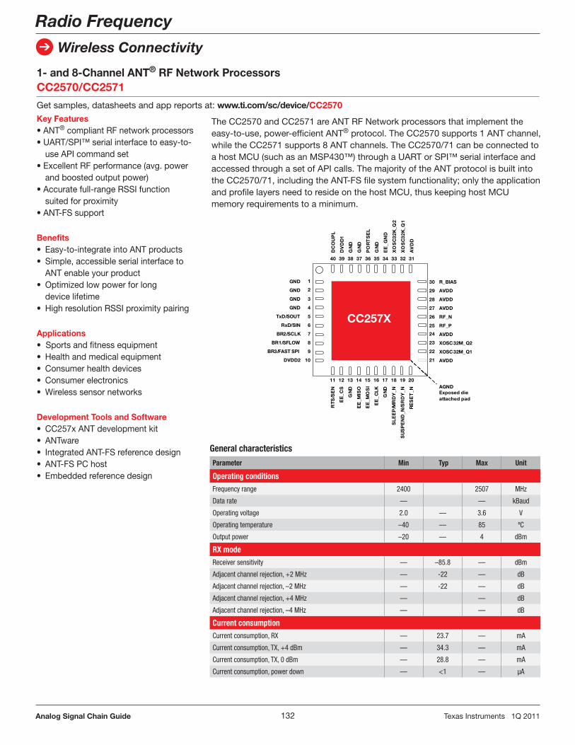
132Analog Signal Chain Guide TexasInstruments1Q2011
1- and 8-Channel ANT® RF Network ProcessorsCC2570/CC2571
Getsamples,datasheetsandappreportsat:www.ti.com/sc/device/CC2570
Key Features•ANT®compliantRFnetworkprocessors•UART/SPI™serialinterfacetoeasy-to- useAPIcommandset•ExcellentRFperformance(avg .power andboostedoutputpower)•Accuratefull-rangeRSSIfunction suitedforproximity•ANT-FSsupport
Benefits• Easy-to-integrateintoANTproducts• Simple,accessibleserialinterfaceto ANTenableyourproduct• Optimizedlowpowerforlong devicelifetime• HighresolutionRSSIproximitypairing
Applications•Sportsandfitnessequipment• Healthandmedicalequipment• Consumerhealthdevices• Consumerelectronics• Wirelesssensornetworks
Development Tools and Software• CC257xANTdevelopmentkit• ANTware• IntegratedANT-FSreferencedesign• ANT-FSPChost• Embeddedreferencedesign
TheCC2570andCC2571areANTRFNetworkprocessorsthatimplementtheeasy-to-use,power-efficientANT®protocol .TheCC2570supports1ANTchannel,whiletheCC2571supports8ANTchannels .TheCC2570/71canbeconnectedtoahostMCU(suchasanMSP430™)throughaUARTorSPI™serialinterfaceandaccessedthroughasetofAPIcalls .ThemajorityoftheANTprotocolisbuiltintotheCC2570/71,includingtheANT-FSfilesystemfunctionality;onlytheapplicationandprofilelayersneedtoresideonthehostMCU,thuskeepinghostMCUmemoryrequirementstoaminimum .
General characteristicsParameter Min Typ Max Unit
Operating conditionsFrequency range 2400 2507 MHz
Data rate — — kBaud
Operating voltage 2.0 — 3.6 V
Operating temperature –40 — 85 ºC
Output power –20 — 4 dBm
RX modeReceiver sensitivity — –85.8 — dBm
Adjacent channel rejection, +2 MHz — -22 — dB
Adjacent channel rejection, –2 MHz — -22 — dB
Adjacent channel rejection, +4 MHz — — dB
Adjacent channel rejection, –4 MHz — — dB
Current consumptionCurrent consumption, RX — 23.7 — mA
Current consumption, TX, +4 dBm — 34.3 — mA
Current consumption, TX, 0 dBm — 28.8 — mA
Current consumption, power down — <1 — μA
Radio Frequency
Wireless Connectivity
AGNDExposed die attached pad
7
6
5
4
3
2
1 30
29
28
27
26
11 12 13 14 15 16 17
25
24
23
22
21
18 19 20
10
9
8
35 34 33 32 313637383940
GND
GND
GND
GND
TxD/SOUT
RxD/SIN
BR2/SCLK
BR1/SFLOW
BR3/FAST SPI
DVDD2
RT
S/S
EN
EE
_CS
GN
D
EE
_MIS
O
EE
_MO
SI
EE
_C
LK
GN
D
SL
EE
P/M
RD
Y_N
SU
SP
EN
D_N
/SR
DY
_N
RE
SE
T_N
R_BIAS
AVDD
AVDD
AVDD
RF_N
RF_P
AVDD
XOSC32M_Q2
XOSC32M_Q1
AVDD
DC
OU
PL
DV
DD
1
GN
D
GN
D
PO
RT
SE
L
GN
D
EE
_G
ND
XO
SC
32
K_Q
2
XO
SC
32
K_Q
1
AV
DD
CC257X

133Analog Signal Chain Guide TexasInstruments1Q2011
Radio Frequency
Wireless Connectivity
WLAN 802.11 b/g/n and Bluetooth® v2.1 + EDR Transceiver WL1271-TiWiGetsamples,datasheetsandappreportsat:www.ti.com/wl1271-tiwi
Key Features•IEEE802 .11b/g/ncompliant•TypicalWLANTransmitpower: +20dBm,11Mbps,CCK(b) +14 .5dBm,54Mbps,OFDM(g) +12 .5dBm,65Mbps,OFDM(n)•TypicalWLANReceiversensitivity: -89dBm,11Mbps -76dBm,54Mbps -73dBm,65Mbps•Bluetooth®v2 .1+EDR(enhanceddatarate) IncreasedBluetoothtransmitpower: +9 .5dBm -92dBmreceiversensitivity•Best-in-classWLANandBluetooth coexistencetechnologyona single-chip•EnhancedLowPower(ELP)technology forextendedbatterylife•OnboardTCXO,powerregulation,and U .FLantennaconnector•HWandSWpre-integrationwith
TI’sAM/DM37x(ARM®Cortex®-A8),AM18xx(ARM9™),andOMAP™4(ARMCortex-A9)platforms
•SW-upgradableforANT®&BLE•FCC/IC/CEcertified•Dimensions:13mmx18mmx1 .9mm
Applications• Industrialandhomeautomation• Pointofsaleandpointofpurchase• Videoconferencing,videocamera andVoIP• Consumerdevices• Medicaldevices• Securityandsurveillance
TheWL1271-TiWiisafully-integratedhighperformancemoduleofferedbyLSResearchutilizingTI’ssingle-chipWL12712 .4GHzIEEE802 .11b/g/nandBluetooth®2 .1+EDRTransceiver .BasedonTI’s6thgenerationWLANtechnologyand7thgenerationBluetoothtechnology,theintegratedsolutionprovidesbest-in-classcoexistencecapabilitiescoupledwithTI’sEnhancedLowPower(ELP)technology .Thissolutionisprovidedasamoduletohelpcustomersreducedevelopmenttime,lowermanufacturingcosts,saveboardspace,easecertification,andminimizeRFexpertiserequired .Forevaluationanddevelopment,variousplatformsareavailablewhichintegratetheLSResearchmodule,Linuxdrivers,Bluetoothstack,andsamplesourceapplicationsrunningonaTIhostprocessor(AM/DM37x,AM18x,OMAP™4) .
WL1271-TiWi system block diagram
ARM®-basedTI Host Processor
32-KHzClock
UARTFilter
FrontEnd
Module
38.4-MHzClock
Battery
WL1271Bluetooth®
SDIO WLAN
TiWi Module

134Analog Signal Chain Guide TexasInstruments1Q2011
Wireless Connectivity
Device Description Frequency
Range Device Type
Data Rate (Max) (max) (kbps)
TX Power (max) (dBm)
RX Current (Lowest)
(mA)
Sensitivity (Best) (dBm)
Wakeup Time (PD--
>RX/TX) (µS)
Flash Size (KB)
RAM Size (KB) Package(s) Price*
CC1100E Low-Power Sub-1GHz RF Transceiver for China and Japan frequency bands
Sub 1-GHz Transceiver 500 12 15 -112 240 — — VQFN-20 1.70
CC1101 Low-Power Sub-1GHz RF Transceiver Sub 1-GHz Transceiver 500 12 14 -112 240 — — VQFN-20 1.65
CC1110 Sub 1-GHz System-on-Chip with MCU and 8kB Flash memory
Sub 1-GHz System-on-Chip
500 10 16.2 -110 330 8, 16, 32
1, 2, 4 VQFN-36 2.10
CC1111 Sub 1-GHz System-on-Chip with MCU, 8kB Flash memory and USB 2.0
Sub 1-GHz System-on-Chip
500 10 16.2 -110 330 8, 16, 32
1, 2, 4 VQFN-36 2.30
CC1190 Sub-1GHz RF Front End 850MHz-950MHz
RF Front End — 27 3.0 — — — — VQFN-16 See Distributors
CC2420 CC2420 2.4GHz Transceiver 250 0 18.8 -95 1200 VQFN-48 3.30
CC2500 Low Cost, Low-Power 2.4GHz RF Transceiver Designed for Low-Power Wireless Apps in the 2.4GHz ISM B
2.4GHz Transceiver 500 1 12.8 -104 240 — — VQFN-20 1.40
CC2510 2.4GHz Radio Transceiver, 8051 MCU and 8 kB Flash memory
2.4GHz System-on-Chip
500 1 15.7 -103 340 8, 16, 32
1, 2, 4 VQFN-36 1.95
CC2511 2.4GHz Radio Transceiver, 8051 MCU, 8kB Flash Memory and Full-Speed USB Interface
2.4GHz System-on-Chip
500 1 15.7 -103 340 8, 16, 32
1, 2, 4 VQFN-36 2.15
CC2520 Second Generation 2.4GHz ZigBee®/IEEE 802.15.4 RF Transceiver
2.4GHz Transceiver 250 4 18.5 -98 500 — — VQFN-28 1.80
CC2530 Second Generation System-on-Chip Solution for 2.4GHz IEEE 802.15.4/ RF4CE/ZigBee
2.4GHz System-on-Chip
250 4 20.5 -97 600 32, 64, 128, 256
8 VQFN-40 2.75
CC2531 System-on-Chip Solution for IEEE 802.15.4 and ZigBee Applications
2.4GHz System-on-Chip
250 4 20.5 -97 600 128, 256
8 VQFN-40 3.20
CC2533 A True System-on-Chip Solution for 2.4GHz IEEE 802.15.4 and ZigBee Applications
2.4GHz System-on-Chip
250 4 21.6 -97 600 32, 64, 96
4, 4, 6 VQFN-40 2.55
CC2540 2.4GHz Bluetooth® Low Energy System-on-Chip Solution
2.4GHz System-on-Chip
1000 4 19.6 -93 530 128, 256
8 VQFN-40 2.95
CC2560-PAN1315
Bluetooth 2.1 + EDR Transceiver, Class 2 HCI Module
2.4GHz Module 2178 10 — -93 — — — Surface Mount Module:
6.5x9x1.8 mm³
See Distributors
CC2560 - PAN1325
Bluetooth 2.1 + EDR Transceiver, Class 2 HCI Module, Integrated Antenna
2.4GHz Module, Integrated Antenna
2178 10 — -93 — — — Surface Mount Module:
9.5x9x1.8 mm³
See Distributors
CC2567-PAN1317
Dual-mode Bluetooth 2.1 + EDR and ANT® Transceiver Module
2.4GHz Module 2178 +10 — -93 — — — Surface mount Module:
6.5x9x1.8 mm³
See Distributors
CC2567-PAN1327
Dual-mode Bluetooth 2.1 + EDR and ANT Transceiver Module with Integrated Antenna
2.4GHz Module, Integrated Antenna
2178 +10 — -93 — — — Surface mount Module:
9.5x9x1.8 mm³
See Distributors
CC2590 2.4GHZ RF Front End 2.4GHz RF Front End
10 3.4 1 — — VQFN-16 1.55
CC2591 2.4GHz RF Front End 2.4GHz RF Front End
20 3.4 1 — — VQFN-16 1.75
CC2595 RF Front-End Transmit Power Amplifier for 2.4GHz ISM Band Systems
2.4GHz RF Front-End
20 1 — — QFN-16 0.65
CC8520 PurePath™ Wireless™ 2.4GHz RF SoC for Wireless Digital Audio Streaming
2.4GHz Network processor
5000 4 25 -83/-87 NA Yes Yes VQFN-40 3.75
WL1271-TiWi WLAN IEEE 802.11 b/g/n and Bluetooth 2.1 + EDR Transceiver Module
2.4GHz Module 6500 +20.0 (802.11b)
+14.5 (802.11g)
+12.5 (802.11n)
100 -89 (802.11b)
-76 (802.11g)
-73 (802.11n)
— — — Surface Mount Module:
13x18x1.9 mm³
See Distributors
Radio Frequency
Wireless Connectivity
*Suggested resale price in U.S. dollars in quantities of 1,000. New products are listed in bold red.

135Analog Signal Chain Guide TexasInstruments1Q2011
Analog eLab™ Design Tools
Design and Evaluation Tools
TI’sAnalogeLab™DesignCenterofferssupportandtrainingfornewandexperiencedanalogdevicedevelopersforavarietyofanalogdesignneeds,allfocusedonthedevelopmentanddesignofanalogdevices .AttheAnalogeLab,designengineerscanlearnwithtrainingandwebcastsessions,selectproductsthroughparametricanalysis,designwithour“Pro”series,simulatewithdifferentmodelresources,andobtainfreesamplesofTIproductswithin24hours .www.ti.com/analogelab
Learn
• OnlineTraining• AnalogeLab™ Videocasts• KnowledgeBase andDocument Finder• ApplicationNotes/ Technical Documents
Select
• ClocksandTiming QuickSearch• InterfaceQuickSearch• PowerManagement PowerQuickSearch DiscoverHowT2 ModulesCanReduce YourOutput Capacitance BatteryChargers QuickSearch• DataConverters AnalogtoDigital Converters DigitaltoAnalog Converters• Audio NewPurePath™ Audio™Power StageSelectionTool AudioQuickSearch• RF/IFComponent QuickSearch• AnalogSwitches QuickSearch• TranslationDevice SelectionTool• SelectionGuides• End-Equipment Solutions• ParametricSearch• CompetitorCross- ReferenceSearch
Design
• TIProSeries SwitcherPro™ DesignSoftware•SwitcherProInfo•DownloadNow•UseOnlineNow•LearnHowto CreateaDesignwith SwitcherPro •ADCPro™Evaluation Software •ClockPro™ ProgrammingSoftware •MDACBufferPro™ DesignSoftware•UpdatedFilterPro™ v3 .0DesignSoftware• ReferenceDesigns• TIGadgetsandWidgets• Calculatorsand OtherUtilities• NewPCBThermal Calculator• HardwareDesign ToolsandSoftware• Quality,Reliability andLead(Pb)-Free• RoHSContentand DeliverySchedule• PackagingInformation
Simulate
• TINA-TI™ Powerfuland Easy-to-UseCircuit SimulationProgram• CompleteSPICE ModelLibraries• IBISandBSDL ModelLibraries
Sample
• Pricingand Availability• RequestSamples• TIeStore BrowseEvaluation Modules• TIWorldwide SalesandSupport Offices• Distributors• Sales Representatives
Texas Instruments
Design CenterAnalog TM

SLYB174A
TI Worldwide Technical Support
InternetTI Semiconductor Product Information Center Home Pagesupport.ti.com
TI E2E™ Community Home Pagee2e.ti.com
Product Information CentersAmericas Phone +1(972)644-5580
Brazil Phone 0800-891-2616
Mexico Phone 0800-670-7544
Fax +1(972)927-6377 Internet/Email support.ti.com/sc/pic/americas.htm
Europe, Middle East, and AfricaPhone EuropeanFreeCall 00800-ASK-TEXAS (0080027583927) International +49(0)8161802121 RussianSupport +7(4)959810701
Note:TheEuropeanFreeCall(TollFree)numberisnotactiveinallcountries.Ifyouhavetechnicaldifficultycallingthefreecallnumber,pleaseusetheinternationalnumberabove.
Fax +(49)(0)8161802045Internet support.ti.com/sc/pic/euro.htmDirectEmail [email protected]
JapanPhone Domestic 0120-92-3326
Fax International +81-3-3344-5317 Domestic 0120-81-0036
Internet/Email International support.ti.com/sc/pic/japan.htm Domestic www.tij.co.jp/pic
AsiaPhone International +91-80-41381665 Domestic Toll-FreeNumber Note:Toll-freenumbersdonotsupport
mobileandIPphones. Australia 1-800-999-084 China 800-820-8682 HongKong 800-96-5941 India 1-800-425-7888 Indonesia 001-803-8861-1006 Korea 080-551-2804 Malaysia 1-800-80-3973 NewZealand 0800-446-934 Philippines 1-800-765-7404 Singapore 800-886-1028 Taiwan 0800-006800 Thailand 001-800-886-0010Fax +8621-23073686Email [email protected]@ti.comInternet support.ti.com/sc/pic/asia.htm
A122010
Important Notice:TheproductsandservicesofTexasInstrumentsIncorporatedanditssubsidiariesdescribedhereinaresoldsubjecttoTI’sstandardtermsandconditionsofsale.CustomersareadvisedtoobtainthemostcurrentandcompleteinformationaboutTIproductsandservicesbeforeplacingorders.TIassumesnoliabilityforapplicationsassistance,customer’sapplicationsorproductdesigns,softwareperformance,orinfringementofpatents.Thepublicationofinformationregardinganyothercompany’sproductsorservicesdoesnotconstituteTI’sapproval,warrantyorendorsementthereof.
©2011TexasInstrumentsIncorporatedPrintedinU.S.A.by(Printer,City,State)
Theplatformbar,ADCPro,AnalogeLab,C2000,ClockPro,ControlNet,DaVinci,Difet,DirectPath,E2E,eLab,FilterPro,FlatLink,LinCMOS,MDACBufferPro,MicroStarJunior,MSP430,OHCI-Lynx,OMAP,Panelbus,PicoStar,PowerPAD,PowerTune,PurePath,PurePath™Audio,PurePath™Digital,PurePath™HD,PurePath™Wireless,QSPI,Sitara,SmartGain,SoundPlus,SpeakerGuard,SwitcherPro,SymPol,TINA-TIandVLYNQaretrademarksandStellarisisaregisteredtrademarkofTexasInstruments.ANTisaregisteredtrademarkofDynastreamInnovations,Inc.ARM9isatrademarkandARMandCortexareregisteredtrademarksofARMLimited.TheBluetoothwordmarkandlogosareownedbytheBluetoothSIG,Inc.,andany
useofsuchmarksbyTexasInstrumentsisunderlicense.Blu-rayisatrademarkofBlu-rayDiscAssociation.DeviceNetisatrademarkofOpenDeviceNetVendorAssociation,Inc.FireWireisaregisteredtrademarkofAppleComputerIncorporated.I2CBusisaregisteredtrademarkofNXPB.V.Corporation.i.LINKisaregisteredtrademarkofSonyCorporation.MicrowireisaregisteredtrademarkofNationalSemiconductorCorporation.ModbusisaregisteredtrademarkofModbusOrganization,Inc.SB1394isatrademarkofCreativeTechnologyLtd.SPIisatrademarkofMotorola,Inc.ZigBeeisaregisteredtrademarkoftheZigBeeAlliance.Allothertrade-marksarethepropertyoftheirrespectiveowners.

IMPORTANT NOTICE
Texas Instruments Incorporated and its subsidiaries (TI) reserve the right to make corrections, modifications, enhancements, improvements,and other changes to its products and services at any time and to discontinue any product or service without notice. Customers shouldobtain the latest relevant information before placing orders and should verify that such information is current and complete. All products aresold subject to TI’s terms and conditions of sale supplied at the time of order acknowledgment.
TI warrants performance of its hardware products to the specifications applicable at the time of sale in accordance with TI’s standardwarranty. Testing and other quality control techniques are used to the extent TI deems necessary to support this warranty. Except wheremandated by government requirements, testing of all parameters of each product is not necessarily performed.
TI assumes no liability for applications assistance or customer product design. Customers are responsible for their products andapplications using TI components. To minimize the risks associated with customer products and applications, customers should provideadequate design and operating safeguards.
TI does not warrant or represent that any license, either express or implied, is granted under any TI patent right, copyright, mask work right,or other TI intellectual property right relating to any combination, machine, or process in which TI products or services are used. Informationpublished by TI regarding third-party products or services does not constitute a license from TI to use such products or services or awarranty or endorsement thereof. Use of such information may require a license from a third party under the patents or other intellectualproperty of the third party, or a license from TI under the patents or other intellectual property of TI.
Reproduction of TI information in TI data books or data sheets is permissible only if reproduction is without alteration and is accompaniedby all associated warranties, conditions, limitations, and notices. Reproduction of this information with alteration is an unfair and deceptivebusiness practice. TI is not responsible or liable for such altered documentation. Information of third parties may be subject to additionalrestrictions.
Resale of TI products or services with statements different from or beyond the parameters stated by TI for that product or service voids allexpress and any implied warranties for the associated TI product or service and is an unfair and deceptive business practice. TI is notresponsible or liable for any such statements.
TI products are not authorized for use in safety-critical applications (such as life support) where a failure of the TI product would reasonablybe expected to cause severe personal injury or death, unless officers of the parties have executed an agreement specifically governingsuch use. Buyers represent that they have all necessary expertise in the safety and regulatory ramifications of their applications, andacknowledge and agree that they are solely responsible for all legal, regulatory and safety-related requirements concerning their productsand any use of TI products in such safety-critical applications, notwithstanding any applications-related information or support that may beprovided by TI. Further, Buyers must fully indemnify TI and its representatives against any damages arising out of the use of TI products insuch safety-critical applications.
TI products are neither designed nor intended for use in military/aerospace applications or environments unless the TI products arespecifically designated by TI as military-grade or "enhanced plastic." Only products designated by TI as military-grade meet militaryspecifications. Buyers acknowledge and agree that any such use of TI products which TI has not designated as military-grade is solely atthe Buyer's risk, and that they are solely responsible for compliance with all legal and regulatory requirements in connection with such use.
TI products are neither designed nor intended for use in automotive applications or environments unless the specific TI products aredesignated by TI as compliant with ISO/TS 16949 requirements. Buyers acknowledge and agree that, if they use any non-designatedproducts in automotive applications, TI will not be responsible for any failure to meet such requirements.
Following are URLs where you can obtain information on other Texas Instruments products and application solutions:
Products Applications
Audio www.ti.com/audio Communications and Telecom www.ti.com/communications
Amplifiers amplifier.ti.com Computers and Peripherals www.ti.com/computers
Data Converters dataconverter.ti.com Consumer Electronics www.ti.com/consumer-apps
DLP® Products www.dlp.com Energy and Lighting www.ti.com/energy
DSP dsp.ti.com Industrial www.ti.com/industrial
Clocks and Timers www.ti.com/clocks Medical www.ti.com/medical
Interface interface.ti.com Security www.ti.com/security
Logic logic.ti.com Space, Avionics and Defense www.ti.com/space-avionics-defense
Power Mgmt power.ti.com Transportation and www.ti.com/automotiveAutomotive
Microcontrollers microcontroller.ti.com Video and Imaging www.ti.com/video
RFID www.ti-rfid.com Wireless www.ti.com/wireless-apps
RF/IF and ZigBee® Solutions www.ti.com/lprf
TI E2E Community Home Page e2e.ti.com
Mailing Address: Texas Instruments, Post Office Box 655303, Dallas, Texas 75265Copyright © 2011, Texas Instruments Incorporated


