Embed Size (px)
Citation preview
Anodic Bonded Graphene
Adrian Balan1, Rakesh Kumar1, Mohamed Boukhicha1, Olivier
Beyssac1, Jean-Claude Bouillard1, Dario Taverna1, William
Sacks1, Massimiliano Marangolo2, Emanuelle Lacaze2, Walter
Escoffier3, Jean-Marie Poumirol3 and Abhay Shukla1
1 Universite Pierre et Marie Curie-Paris 6, CNRS-UMR7590, Institut de Mineralogieet de Physique des Milieux Condenses, 140 rue de Lourmel, Paris, F-75015 France2 Universite Pierre et Marie Curie-Paris 6, CNRS-UMR7588, Institut desNanosciences de Paris, 140 rue de Lourmel, Paris, F-75015 France3 Laboratoire National des Champs Magnetiques Intenses, INSA UPS CNRS, UPR3228, Universite de Toulouse, 143 avenue de Rangueil, 31400 Toulouse, France
E-mail: [email protected]
Abstract. We show how to prepare graphene samples on a glass substrate with theanodic bonding method. In this method, a graphite precursor in flake form is bonded toa glass substrate with the help of an electrostatic field and then cleaved off to leave fewlayer graphene on the substrate. Now that several methods are available for producinggraphene, the relevance of our method is in its simplicity and practicality for producinggraphene samples of about 100 µm lateral dimensions. This method is also extensibleto other layered materials. We discuss some detailed aspects of the fabrication andresults from Raman spectroscopy, local probe microscopy, and transport measurementson these samples.
Confidential: not for distribution. Submitted to IOP Publishing for peer review 14 February 2010pe
er-0
0569
705,
ver
sion
1 -
25 F
eb 2
011
Author manuscript, published in "Journal of Physics D: Applied Physics 43, 37 (2010) 374013" DOI : 10.1088/0022-3727/43/37/374013
Anodic Bonded Graphene 2
1. Introduction
The discovery of graphene [1, 2] has led to a frenetic development of the field[3],
motivated by the spectacular results obtained by various groups and also by the
potential that graphene may have with respect to future applications in microelectronics.
Several methods [4] have now been developed for producing graphene, including
the original methods of epitaxial growth on SiC substrates[1] and micro-mechanical
cleaving[2]. More recent methods include exfoliation [5, 6] and CVD growth on metallic
substrates[7, 8].
Each of these methods is relevant for specific applications and here we present a
method of fabrication of graphene that we have developed which may be classified as
a variant of micro-mechanical cleaving. As we have shown in an earlier publication[9]
we obtain high quality samples of few layer graphene on Pyrex glass substrates. The
quality is seen both from the Raman spectra and from transport measurements. The
dimensions that we obtain are typically from a few tens to a few hundred microns for
monolayer and bilayer samples while we have obtained trilayer samples of mm size[9].
A further advantage of this method is that it can be used, as in the case of micro-
mechanical cleaving, for fabricating ultra-thin samples of virtually any layered material
in a straightforward manner.
Our aim in this paper is to provide a critical analysis of this method including
aspects of fabrication such that the reader may have the necessary elements for
replicating it, followed by results of characterization of samples thus obtained. In section
2 we give a brief introduction to the anodic bonding method and its application to the
fabrication of ultra-thin samples of layered materials. In section 3 we give results from
the Raman characterization of these samples including examples of Raman ’mapping’.
In section 4 we show results from local probe microscopy on these samples and discuss
some Scanning Tunneling Microscopy (STM) results. Finally in section 5 we discuss
some transport measurements on simple Field Effect Transistor (FET) devices.
2. Anodic bonding and sample fabrication
Anodic bonding is a much employed technique in the silicon industry [10] and is still
widely used [11] for bonding glass to conductive material owing to the good bond quality
(silicon-on-insulator bonding or SOI bonding). It allows the joining of two solids without
intervening layers like glue and is typically performed between a sodium-bearing glass
substrate (for example Pyrex 7740 from Corning) and a silicon wafer, the two materials
being fairly well matched in terms of thermal expansion. At high temperatures, (¿
200◦C) Na2O in Pyrex glass decomposes into one O−2 and two Na+ ions. The mobility
of the smaller sodium ions is high and the presence of an electric field (the applied
potential difference being typically of the order of 1.7 kV) across the glass substrate
[12] makes them migrate towards the cathode at its back. They leave behind a negative
space charge in the region of the interface arising from the static oxygen ions. These
peer
-005
6970
5, v
ersi
on 1
- 25
Feb
201
1
Anodic Bonded Graphene 3
create an electrostatic field with the positive charges in the silicon wafer. Since the
space charge layer is typically a few hundred nanometers to a few microns thick, the
field created across this layer is very high and pulls the wafer into intimate contact with
the substrate, ultimately leading to the formation of stable Si-O-Si bonds and resulting
in a wafer bonded to the glass substrate.
Conducting materials which readily oxidize can thus be bonded to Pyrex substrates
through a similar mechanism. In the case of graphite the initial bonding is
predominantly electrostatic in nature as we will show with the help of our Raman
results in section 3. This is also borne out by the fact that the Raman spectra do not
show any sign of formation of graphene oxide. The nature of the two surfaces to be
bonded is of importance and a thorough cleaning of the glass substrate with standard
laboratory procedure is necessary. We use graphite flake precursors of mineral origin.
HOPG graphite for example is not an ideal precursor as graphene obtained from it
rarely exceeds lateral dimensions of a few micrometers. We have had good results both
from flakes obtained from Madagascar graphite as well as small (typically mm size)
graphite inclusions in calcite. The flake must be carefully cleaved before being put into
contact with the clean glass surface so as to insure a clean interface. The substrate must
contain alkali ions which are mobile under certain conditions and we have used various
borosilicate glasses and obtained good results. The surface to be bonded of course needs
to be optically polished. Other than these precautions, the bonding can be carried out
in normal laboratory surroundings.
We have consistently obtained good results for an interface temperature of 200-
250◦C and an applied potential difference between the cathode on the glass substrate
and the anode in contact with graphite in the range of 1700-1800 kV. The typical
time of application of the potential difference is ten minutes at the end of which the
flake is effectively bonded to the substrate. The last step in the procedure is to cleave
the flake off the glass substrate using either a scalpel blade or adhesive tape or both.
Visual identification with the help of a microscope is then sufficient to isolate graphene
remaining on the substrate often in the company of thicker graphite flakes. This
identification is somewhat more difficult than in the case of a SiO2/Si substrate because
it is based only on optical contrast. This is the reason that our optical micrographs do
not resembles the ’standard’ ones for graphene on SiO2/Si substrates. With experience
one can identify monolayer samples, and few layer samples are easily visible.
3. Raman spectroscopy
Raman spectroscopy has fast become a method of choice both for characterizing
graphene samples as shown by several early papers [13, 14], as well as studying electron
phonon coupling in graphene [15] and its variation with doping. Indeed the 2D lineshape
is very sensitive to the number of layers in the graphene sample. The lineshape also
depends on the nature of the substrate [16, 9], typically in a bilayer the multiple peak
nature is more obvious in graphene bilayers on SiO2/Si substrates. Here we show
peer
-005
6970
5, v
ersi
on 1
- 25
Feb
201
1
Anodic Bonded Graphene 4
(a) (b) (c)
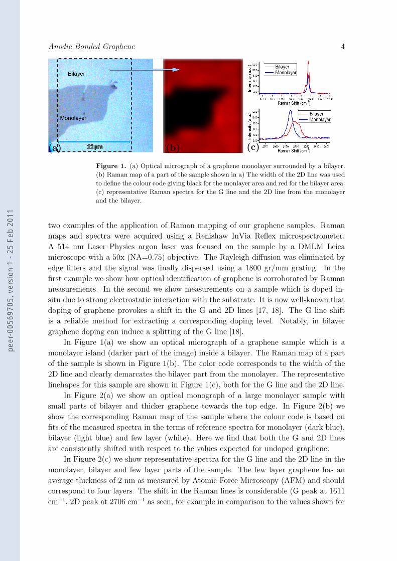
Figure 1. (a) Optical micrograph of a graphene monolayer surrounded by a bilayer.(b) Raman map of a part of the sample shown in a) The width of the 2D line was usedto define the colour code giving black for the monlayer area and red for the bilayer area.(c) representative Raman spectra for the G line and the 2D line from the monolayerand the bilayer.
two examples of the application of Raman mapping of our graphene samples. Raman
maps and spectra were acquired using a Renishaw InVia Reflex microspectrometer.
A 514 nm Laser Physics argon laser was focused on the sample by a DMLM Leica
microscope with a 50x (NA=0.75) objective. The Rayleigh diffusion was eliminated by
edge filters and the signal was finally dispersed using a 1800 gr/mm grating. In the
first example we show how optical identification of graphene is corroborated by Raman
measurements. In the second we show measurements on a sample which is doped in-
situ due to strong electrostatic interaction with the substrate. It is now well-known that
doping of graphene provokes a shift in the G and 2D lines [17, 18]. The G line shift
is a reliable method for extracting a corresponding doping level. Notably, in bilayer
graphene doping can induce a splitting of the G line [18].
In Figure 1(a) we show an optical micrograph of a graphene sample which is a
monolayer island (darker part of the image) inside a bilayer. The Raman map of a part
of the sample is shown in Figure 1(b). The color code corresponds to the width of the
2D line and clearly demarcates the bilayer part from the monolayer. The representative
linehapes for this sample are shown in Figure 1(c), both for the G line and the 2D line.
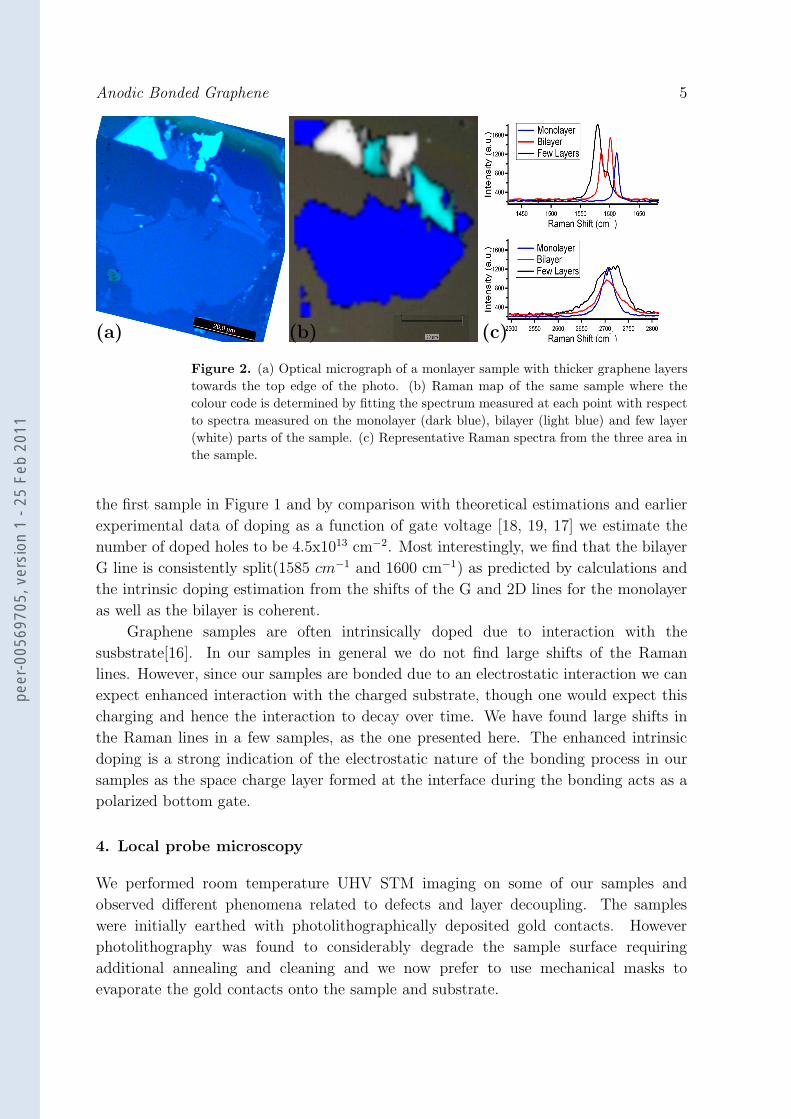
In Figure 2(a) we show an optical monograph of a large monolayer sample with
small parts of bilayer and thicker graphene towards the top edge. In Figure 2(b) we
show the corresponding Raman map of the sample where the colour code is based on
fits of the measured spectra in the terms of reference spectra for monolayer (dark blue),
bilayer (light blue) and few layer (white). Here we find that both the G and 2D lines
are consistently shifted with respect to the values expected for undoped graphene.
In Figure 2(c) we show representative spectra for the G line and the 2D line in the
monolayer, bilayer and few layer parts of the sample. The few layer graphene has an
average thickness of 2 nm as measured by Atomic Force Microscopy (AFM) and should
correspond to four layers. The shift in the Raman lines is considerable (G peak at 1611
cm−1, 2D peak at 2706 cm−1 as seen, for example in comparison to the values shown for
peer
-005
6970
5, v
ersi
on 1
- 25
Feb
201
1
Anodic Bonded Graphene 5
(a) (b) (c)
Figure 2. (a) Optical micrograph of a monlayer sample with thicker graphene layerstowards the top edge of the photo. (b) Raman map of the same sample where thecolour code is determined by fitting the spectrum measured at each point with respectto spectra measured on the monolayer (dark blue), bilayer (light blue) and few layer(white) parts of the sample. (c) Representative Raman spectra from the three area inthe sample.
the first sample in Figure 1 and by comparison with theoretical estimations and earlier
experimental data of doping as a function of gate voltage [18, 19, 17] we estimate the
number of doped holes to be 4.5x1013 cm−2. Most interestingly, we find that the bilayer
G line is consistently split(1585 cm−1 and 1600 cm−1) as predicted by calculations and
the intrinsic doping estimation from the shifts of the G and 2D lines for the monolayer
as well as the bilayer is coherent.
Graphene samples are often intrinsically doped due to interaction with the
susbstrate[16]. In our samples in general we do not find large shifts of the Raman
lines. However, since our samples are bonded due to an electrostatic interaction we can
expect enhanced interaction with the charged substrate, though one would expect this
charging and hence the interaction to decay over time. We have found large shifts in
the Raman lines in a few samples, as the one presented here. The enhanced intrinsic
doping is a strong indication of the electrostatic nature of the bonding process in our
samples as the space charge layer formed at the interface during the bonding acts as a
polarized bottom gate.
4. Local probe microscopy
We performed room temperature UHV STM imaging on some of our samples and
observed different phenomena related to defects and layer decoupling. The samples
were initially earthed with photolithographically deposited gold contacts. However
photolithography was found to considerably degrade the sample surface requiring
additional annealing and cleaning and we now prefer to use mechanical masks to
evaporate the gold contacts onto the sample and substrate.
peer
-005
6970
5, v
ersi
on 1
- 25
Feb
201
1
Anodic Bonded Graphene 6
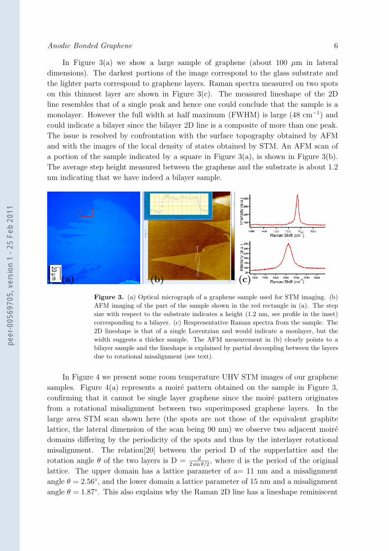
In Figure 3(a) we show a large sample of graphene (about 100 µm in lateral
dimensions). The darkest portions of the image correspond to the glass substrate and
the lighter parts correspond to graphene layers. Raman spectra measured on two spots
on this thinnest layer are shown in Figure 3(c). The measured lineshape of the 2D
line resembles that of a single peak and hence one could conclude that the sample is a
monolayer. However the full width at half maximum (FWHM) is large (48 cm−1) and
could indicate a bilayer since the bilayer 2D line is a composite of more than one peak.
The issue is resolved by confrontation with the surface topography obtained by AFM
and with the images of the local density of states obtained by STM. An AFM scan of
a portion of the sample indicated by a square in Figure 3(a), is shown in Figure 3(b).
The average step height measured between the graphene and the substrate is about 1.2
nm indicating that we have indeed a bilayer sample.
(a) (b) (c)
Figure 3. (a) Optical micrograph of a graphene sample used for STM imaging. (b)AFM imaging of the part of the sample shown in the red rectangle in (a). The stepsize with respect to the substrate indicates a height (1.2 nm, see profile in the inset)corresponding to a bilayer. (c) Respresentative Raman spectra from the sample. The2D lineshape is that of a single Lorentzian and would indicate a monlayer, but thewidth suggests a thicker sample. The AFM measurement in (b) clearly points to abilayer sample and the lineshape is explained by partial decoupling between the layersdue to rotational misalignment (see text).
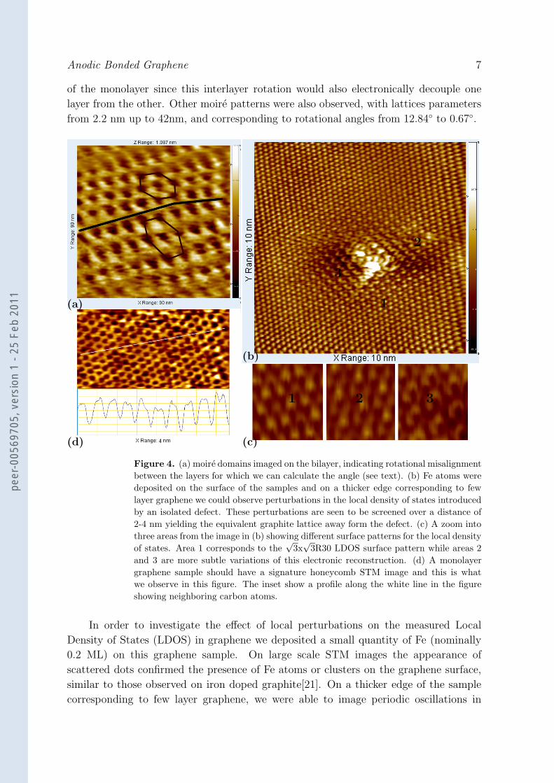
In Figure 4 we present some room temperature UHV STM images of our graphene
samples. Figure 4(a) represents a moire pattern obtained on the sample in Figure 3,
confirming that it cannot be single layer graphene since the moire pattern originates
from a rotational misalignment between two superimposed graphene layers. In the
large area STM scan shown here (the spots are not those of the equivalent graphite
lattice, the lateral dimension of the scan being 90 nm) we observe two adjacent moire
domains differing by the periodicity of the spots and thus by the interlayer rotational
misalignment. The relation[20] between the period D of the supperlattice and the
rotation angle θ of the two layers is D = d2 sin θ/2
, where d is the period of the original
lattice. The upper domain has a lattice parameter of a= 11 nm and a misalignment
angle θ = 2.56◦, and the lower domain a lattice parameter of 15 nm and a misalignment
angle θ = 1.87◦. This also explains why the Raman 2D line has a lineshape reminiscent
peer
-005
6970
5, v
ersi
on 1
- 25
Feb
201
1
Anodic Bonded Graphene 7
of the monolayer since this interlayer rotation would also electronically decouple one
layer from the other. Other moire patterns were also observed, with lattices parameters
from 2.2 nm up to 42nm, and corresponding to rotational angles from 12.84◦ to 0.67◦.
(a)
(d)
(b)
(c)
3
1
2
1 2 3
Figure 4. (a) moire domains imaged on the bilayer, indicating rotational misalignmentbetween the layers for which we can calculate the angle (see text). (b) Fe atoms weredeposited on the surface of the samples and on a thicker edge corresponding to fewlayer graphene we could observe perturbations in the local density of states introducedby an isolated defect. These perturbations are seen to be screened over a distance of2-4 nm yielding the equivalent graphite lattice away form the defect. (c) A zoom intothree areas from the image in (b) showing different surface patterns for the local densityof states. Area 1 corresponds to the
√3x
√3R30 LDOS surface pattern while areas 2
and 3 are more subtle variations of this electronic reconstruction. (d) A monolayergraphene sample should have a signature honeycomb STM image and this is whatwe observe in this figure. The inset show a profile along the white line in the figureshowing neighboring carbon atoms.
In order to investigate the effect of local perturbations on the measured Local
Density of States (LDOS) in graphene we deposited a small quantity of Fe (nominally
0.2 ML) on this graphene sample. On large scale STM images the appearance of
scattered dots confirmed the presence of Fe atoms or clusters on the graphene surface,
similar to those observed on iron doped graphite[21]. On a thicker edge of the sample
corresponding to few layer graphene, we were able to image periodic oscillations in
peer
-005
6970
5, v
ersi
on 1
- 25
Feb
201
1
Anodic Bonded Graphene 8
the local density of states induced by an isolated defect corresponding very probably
to a Fe cluster (Figure 4(b)). The defect induces oscillations with a global three fold
symmetry corresponding to similar earlier observations [22]. The supperlattices formed
have a lattice parameter√
3 times greater and are rotated with 30◦ with respect to the
graphite lattice (√
3x√
3R30 LDOS reconstruction). These oscillations are screened out
away from the defect over distances of 2-4 nm.
The rich screening pattern surrounding such defects, has attracted theoretical
attention in the past in the case of graphite and requires the calculation of local density of
states. This is obtained by solving for the electronic structure of the graphite/graphene
lattice with the relevant local perturbations (a non trivial problem). We observe here
that the internal structure of the defect (a closer look will reveal that there are two
maxima in the STM image of the defect) provokes different patterns in the oscillations
as explained by Mizes et al. [22]. In Figure 4(c) we show three different examples of
these patterns.
Finally in Figure 4(d) we show an STM image of the expected honeycomb structure
from a monolayer graphene sample. Though this honeycomb structure is a signature of
an uncoupled graphene layer we have also observed it in few layer graphene, and even
in graphite. This is possible [23] if the imaged portion under the STM tip is indeed
decoupled from the underlying layers.
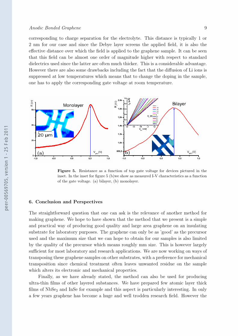
5. Transport measurements
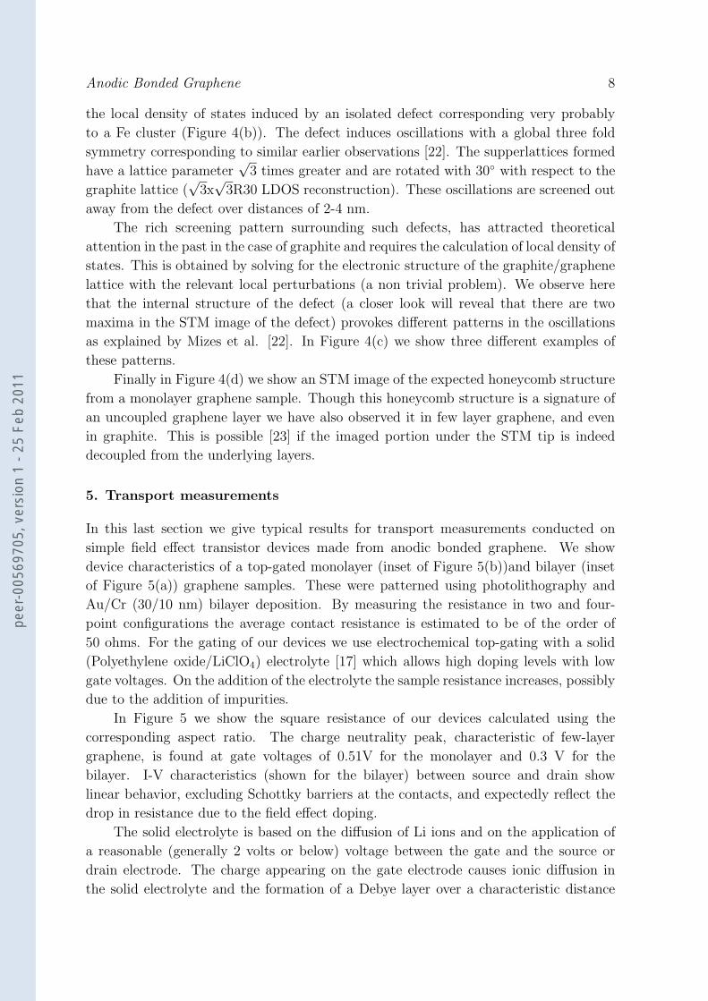
In this last section we give typical results for transport measurements conducted on
simple field effect transistor devices made from anodic bonded graphene. We show
device characteristics of a top-gated monolayer (inset of Figure 5(b))and bilayer (inset
of Figure 5(a)) graphene samples. These were patterned using photolithography and
Au/Cr (30/10 nm) bilayer deposition. By measuring the resistance in two and four-
point configurations the average contact resistance is estimated to be of the order of
50 ohms. For the gating of our devices we use electrochemical top-gating with a solid
(Polyethylene oxide/LiClO4) electrolyte [17] which allows high doping levels with low
gate voltages. On the addition of the electrolyte the sample resistance increases, possibly
due to the addition of impurities.
In Figure 5 we show the square resistance of our devices calculated using the
corresponding aspect ratio. The charge neutrality peak, characteristic of few-layer
graphene, is found at gate voltages of 0.51V for the monolayer and 0.3 V for the
bilayer. I-V characteristics (shown for the bilayer) between source and drain show
linear behavior, excluding Schottky barriers at the contacts, and expectedly reflect the
drop in resistance due to the field effect doping.
The solid electrolyte is based on the diffusion of Li ions and on the application of
a reasonable (generally 2 volts or below) voltage between the gate and the source or
drain electrode. The charge appearing on the gate electrode causes ionic diffusion in
the solid electrolyte and the formation of a Debye layer over a characteristic distance
peer
-005
6970
5, v
ersi
on 1
- 25
Feb
201
1
Anodic Bonded Graphene 9
corresponding to charge separation for the electrolyte. This distance is typically 1 or
2 nm for our case and since the Debye layer screens the applied field, it is also the
effective distance over which the field is applied to the graphene sample. It can be seen
that this field can be almost one order of magnitude higher with respect to standard
dielectrics used since the latter are often much thicker. This is a considerable advantage.
However there are also some drawbacks including the fact that the diffusion of Li ions is
suppressed at low temperatures which means that to change the doping in the sample,
one has to apply the corresponding gate voltage at room temperature.
(a) (b)
Figure 5. Resistance as a function of top gate voltage for devices pictured in theinset. In the inset for figure 5 (b)we show as measured I-V characteristics as a functionof the gate voltage. (a) bilayer, (b) monolayer.
6. Conclusion and Perspectives
The straightforward question that one can ask is the relevance of another method for
making graphene. We hope to have shown that the method that we present is a simple
and practical way of producing good quality and large area graphene on an insulating
substrate for laboratory purposes. The graphene can only be as ’good’ as the precursor
used and the maximum size that we can hope to obtain for our samples is also limited
by the quality of the precursor which means roughly mm size. This is however largely
sufficient for most laboratory and research applications. We are now working on ways of
transposing these graphene samples on other substrates, with a preference for mechanical
transposition since chemical treatment often leaves unwanted residue on the sample
which alters its electronic and mechanical properties.
Finally, as we have already stated, the method can also be used for producing
ultra-thin films of other layered substances. We have prepared few atomic layer thick
films of NbSe2 and InSe for example and this aspect is particularly interesting. In only
a few years graphene has become a huge and well trodden research field. However the
peer
-005
6970
5, v
ersi
on 1
- 25
Feb
201
1
Anodic Bonded Graphene 10
discovery of graphene has opened up the general field of two dimensional materials and
their intriguing properties and this field is still largely unexplored.
We acknowledge assistance from F. Gelebart and M. Morand, discussions with V.
Etgens and F. Mauri and funding from DRITT(UPMC) and by E.U. EuroMagNet II
program under contract 228043.
References
[1] Claire Berger, Zhimin Song, Tianbo Li, Xuebin Li, Asmerom Y. Ogbazghi, Rui Feng, ZhentingDai, Alexei N. Marchenkov, Edward H. Conrad, Phillip N. First, and Walt A. de Heer.Ultrathin epitaxial graphite: 2d electron gas properties and a route toward graphene-basednanoelectronics. The Journal of Physical Chemistry B, 108(52):19912–19916, Dec 2004. doi:10.1021/jp040650f.
[2] K. S. Novoselov, D. Jiang, F. Schedin, T. J. Booth, V. V. Khotkevich, S. V. Morozov, and A. K.Geim. Two-dimensional atomic crystals. Proceedings of the National Academy of Sciences ofthe United States of America, 102(30):10451–10453, 2005.
[3] A. H. Castro Neto, F. Guinea, N. M. R. Peres, K. S. Novoselov, and A. K. Geim. The electronicproperties of graphene. Rev. Mod. Phys., 81(1):109–162, Jan 2009.
[4] A. K. Geim. Graphene: Status and Prospects. Science, 324(5934):1530–1534, 2009.[5] Yenny Hernandez, Valeria Nicolosi, Mustafa Lotya, Fiona M. Blighe, Zhenyu Sun, Sukanta De,
McGovernI T., Brendan Holland, Michele Byrne, Yurii K. Gun’Ko, John J. Boland, Peter Niraj,Georg Duesberg, Satheesh Krishnamurthy, Robbie Goodhue, John Hutchison, Vittorio Scardaci,Andrea C. Ferrari, and Jonathan N. Coleman. High-yield production of graphene by liquid-phaseexfoliation of graphite. Nat Nano, 3(9):563–568, Sep 2008.
[6] Dmitriy A. Dikin, Sasha Stankovich, Eric J. Zimney, Richard D. Piner, Geoffrey H. B.Dommett, Guennadi Evmenenko, SonBinh T. Nguyen, and Rodney S. Ruoff. Preparation andcharacterization of graphene oxide paper. Nature, 448(7152):457–460, Jul 2007.
[7] Alfonso Reina, Xiaoting Jia, John Ho, Daniel Nezich, Hyungbin Son, Vladimir Bulovic, Mildred S.Dresselhaus, and Jing Kong. Large area, few-layer graphene films on arbitrary substrates bychemical vapor deposition. Nano Letters, 9(1):30–35, Dec 2008. doi: 10.1021/nl801827v.
[8] Keun Soo Kim, Yue Zhao, Houk Jang, Sang Yoon Lee, Jong Min Kim, Kwang S. Kim, Jong-Hyun Ahn, Philip Kim, Jae-Young Choi, and Byung Hee Hong. Large-scale pattern growth ofgraphene films for stretchable transparent electrodes. Nature, 457(7230):706–710, Feb 2009.
[9] Abhay Shukla, Rakesh Kumar, Javed Mazher, and Adrian Balan. Graphene made easy: Highquality, large-area samples. Solid State Communications, 149(17-18):718 – 721, 2009.
[10] George Wallis and Daniel I. Pomerantz. Field assisted glass-metal sealing. Journal of AppliedPhysics, 40(10):3946–3949, 1969.
[11] Emilie Collart and Abhay Shukla Marc Morand Ccile Malgrange Nathalie Bardou Ali MadouriJean-Luc Pelouard Frdric Glbart. Spherically bent analyzers for resonant inelastic x-rayscattering with intrinsic resolution below 200 mev. Journal of Synchrotron Radiation, 12(4):473–478, 2005.
[12] Kevin B. Albaugh. Electrode phenomena during anodic bonding of silicon to sodium borosilicateglass. Journal of The Electrochemical Society, 138(10):3089–3094, 1991.
[13] A. C. Ferrari, J. C. Meyer, V. Scardaci, C. Casiraghi, M. Lazzeri, F. Mauri, S. Piscanec, D. Jiang,K. S. Novoselov, S. Roth, and A. K. Geim. Raman spectrum of graphene and graphene layers.Phys. Rev. Lett., 97(18):187401, Oct 2006.
[14] D. Graf, F. Molitor, K. Ensslin, C. Stampfer, A. Jungen, C. Hierold, and L. Wirtz. Spatiallyresolved raman spectroscopy of single- and few-layer graphene. Nano Letters, 7(2):238–242, Jan2007. doi: 10.1021/nl061702a.
peer
-005
6970
5, v
ersi
on 1
- 25
Feb
201
1
Anodic Bonded Graphene 11
[15] Nicola Bonini, Michele Lazzeri, Nicola Marzari, and Francesco Mauri. Phonon anharmonicities ingraphite and graphene. Phys. Rev. Lett., 99(17):176802, Oct 2007.
[16] C. Casiraghi, S. Pisana, K. S. Novoselov, A. K. Geim, and A. C. Ferrari. Raman fingerprint ofcharged impurities in graphene. Applied Physics Letters, 91(23):233108, 2007.
[17] Das A., Pisana S., Chakraborty B., Piscanec S., Saha S K., WaghmareU V., NovoselovK S.,KrishnamurthyH R., GeimA K., FerrariA C., and SoodA K. Monitoring dopants by ramanscattering in an electrochemically top-gated graphene transistor. Nat Nano, 3(4):210–215, Apr2008.
[18] Paola Gava, Michele Lazzeri, A. Marco Saitta, and Francesco Mauri. Probing the electrostaticenvironment of bilayer graphene using raman spectra. Phys. Rev. B, 80(15):155422, Oct 2009.
[19] Paola Gava, Michele Lazzeri, A. Marco Saitta, and Francesco Mauri. Ab initio study of gapopening and screening effects in gated bilayer graphene. Phys. Rev. B, 79(16):165431, Apr2009.
[20] J. M. Campanera, G. Savini, I. Suarez-Martinez, and M. I. Heggie. Density functional calculationson the intricacies of moire patterns on graphite. Phys. Rev. B, 75(23):235449, Jun 2007.
[21] E. Bourelle, Y. Kaburagi, Y. Hishiyama, and M. Inagaki. Stm study of surfaces of kish graphitedoped by iron. Carbon, 39(13):1955 – 1962, 2001.
[22] H. A. MIZES and J. S. FOSTER. Long-Range Electronic Perturbations Caused by Defects UsingScanning Tunneling Microscopy. Science, 244(4904):559–562, 1989.
[23] Guohong Li, Adina Luican, and Eva Y. Andrei. Scanning tunneling spectroscopy of graphene ongraphite. Phys. Rev. Lett., 102(17):176804, Apr 2009.
peer
-005
6970
5, v
ersi
on 1
- 25
Feb
201
1


