Embed Size (px)
Citation preview
UNIVERSITY OF JOENSUU
DEPARTMENT OF PHYSICS
DISSERTATIONS 37
Applied diffractive optics withelectron beam lithography
Janne Simonen
ACADEMIC DISSERTATION
To be presented, with permission of the Faculty of Science of the University ofJoensuu, for public criticism in Auditorium M1 of the University, Yliopistokatu7, Joensuu, on July 4th, 2003, at 12 noon.
JOENSUU 2003

Julkaisija Joensuun yliopistoPublisher University of Joensuu
Toimittaja Timo Jaaskelainen, Ph.D., ProfessorEditor
Ohjaajat Jari Turunen, Dr. Tech., ProfessorSupervisors Markku Kuittinen, Ph.D., Professor
Department of Physics, University of JoensuuJoensuu, Finland
Esitarkastajat Fredrik Nikolajeff, Ph.D., Associate Professor
Reviewers The Angstrom Laboratory, Uppsala UniversityUppsala, Sweden
Seppo Honkanen, Ph.D., Associate ProfessorOptical Sciences Center, University of ArizonaTucson, USA
Vastavaittaja Hiroyuki Ichikawa, Ph.D., Associate ProfessorOpponent Department of Electrical and Electronic Engineering
Ehime UniversityMatsuyama, Japan
Vaihto Joensuun yliopiston kirjasto, vaihdotPL 107, 80101 JOENSUUPuh. 013–251 2677, telefax 013–251 2691Email: [email protected]
Exchange Joensuu University Library, exchangeP.O. Box 107, FIN–80101 JOENSUUTelefax +358 13 251 2691Email: [email protected]
Myynti Joensuun yliopiston kirjasto, julkaisujen myyntiPL 107, 80101 JOENSUUPuh. 013–251 2652, 251 2677, telefax 013–251 2691Email: [email protected]
Sale Joensuu University Library, sale of publicationsP.O. Box 107, FIN–80101 JOENSUUTelefax +358 13 251 2691Email: [email protected]
ISSN 1458–5332ISBN 952–458–295–3
Joensuun yliopistopaino 2003

Janne Simonen∗; Applied diffractive optics with electron beam lithography —University of Joensuu, Department of Physics, Dissertation 37, 2003. — 81 p.ISBN 952–458–295–3Keywords: diffraction, diffractive optics, electron beam lithography.
∗Address: Department of Physics, University of Joensuu, P.O. Box 111, FIN–80101, Joen-suu, Finland
Abstract
In this thesis rigorous and approximative grating theories are employed in the design ofdiffractive surface–relief gratings for various applications. The structures are fabricatedas binary profiles into silicon and semi–continuous profiles into fused silica by electronbeam lithography and plasma etching, and their optical performance is evaluated.
A novel method for the fabrication of subwavelength waveguide Bragg gratings andphotonic band–gap structures into silicon–on–insulator substrates is presented. Combin-ing high–resolution electron beam lithography with optical lithography, the method showsgreat promise for integrated optical applications in the field of optical telecommunications.
The fabrication of continuous surface profiles into fused silica substrates with a processemploying a negative analog resist is introduced and further utilized in several applica-tions. High–efficiency transmission gratings for spectrometric applications in the visibleand ultraviolet region are fabricated and experimentally characterized. The principle ofpartially coherent excimer beam shaping with a periodic diffractive element is introducedand experimentally demonstrated. Propagation–invariant Bessel beams are produced bytwo methods: a Bessel beam with uniform axial intensity is generated with a two–elementsystem and a Bessel–Gauss laser resonator is constructed with a specifically designedresonator mirror.
Two novel fabrication methods for the fabrication of high–resolution multilevel surface–relief gratings into fused silica with electron beam lithography and reactive ion etchingare presented, and possible applications enabled by them are discussed.

iv
Preface
As a young boy I took great interest in understanding life, universe and everything. I readall the science magazines and science fiction I could get my hands on. Science seemed socool to me that, in the fifth grade, I decided to become a Physicist. A theoretical Physicist.I would attain profound knowledge of how the universe works. So I grew up and wentinto the University, and reached the last stages of my undergraduate studies. Then I sawhow Maxwell’s equations are solved, and transformed instantly into an experimentalist.Having done an experimental thesis, I now have fantasies of a theoretical career.
A result of the childhood dream, this book would not be here without the help andsupport of a large number of people. First, my supervisors, professors Jari Turunenand Markku Kuittinen gently guided me through the maze of diffractive optics, which isgratefully acknowledged. I also wish to express my gratitude to Prof. Timo Jaaskelainenfor the chance to work at the Department of Physics at the University of Joensuu.
The crux of the dissertation is the fabrication of analog surface profiles, based on thesemi–occult method passed on to me by Ph.D. Pasi Laakkonen, whose guidance is greatlyappreciated. May the god of RIE be with you.
I also wish to thank the personnel of the Department of Physics, and especially thefollowing former and present members of the diffractive optics group: Pertti Paakkonen,Marko Honkanen, Jani Tervo, Tuomas Vallius, Konstantins Jefimovs, Ville Kettunen, PasiVahimaa, Henna Elfstrom, Samuli Siitonen, Tuire Kautto, Olga Svirko, Jari Lautanen andJari Rasanen.
Part of the work was done in collaboration with other research groups, namely SannaYliniemi, Timo Aalto, Paivi Heimala and Matti Leppihalme at VTT Microelectronics, andTimo Kajava and Matti Kaivola at the University of Helsinki, whose efforts are greatlyappreciated.
I am greatly indebted to my reviewers, Prof. Seppo Honkanen and Prof. Fredrik Niko-lajeff for their constructive critisism and valuable comments regarding the thesis.
Credit should also be given to the staff of the company Nanocomp, who have providedme with interesting side projects and some cash for my services.
Finally, my dear wife Minna deserves my deepest gratitude for giving me love andkicking my butt in just the right proportions.
Joensuu March 3, 2004
Janne Simonen

Contents
1 Introduction 1
2 Mathematical modeling of diffractive elements 42.1 Principles of the electromagnetic theory of light . . . . . . . . . . . . . . . 4
2.1.1 Wave propagation . . . . . . . . . . . . . . . . . . . . . . . . . . . . 52.1.2 Pseudoperiodic fields and Rayleigh expansions . . . . . . . . . . . . 7
2.2 Rigorous grating analysis methods . . . . . . . . . . . . . . . . . . . . . . . 82.2.1 Fourier modal method . . . . . . . . . . . . . . . . . . . . . . . . . 82.2.2 The C method . . . . . . . . . . . . . . . . . . . . . . . . . . . . . 122.2.3 Discussion . . . . . . . . . . . . . . . . . . . . . . . . . . . . . . . . 14
2.3 Paraxial design methods . . . . . . . . . . . . . . . . . . . . . . . . . . . . 142.3.1 Thin element approximation . . . . . . . . . . . . . . . . . . . . . 142.3.2 Optical map transform . . . . . . . . . . . . . . . . . . . . . . . . . 152.3.3 Iterative Fourier transform algorithm . . . . . . . . . . . . . . . . . 162.3.4 Zeroth–order coding . . . . . . . . . . . . . . . . . . . . . . . . . . 18
2.4 Partially coherent fields . . . . . . . . . . . . . . . . . . . . . . . . . . . . . 192.4.1 Gaussian Schell–model beams . . . . . . . . . . . . . . . . . . . . . 20
3 Electron beam lithography 213.1 Resist technology . . . . . . . . . . . . . . . . . . . . . . . . . . . . . . . . 213.2 Leica LION LV1 . . . . . . . . . . . . . . . . . . . . . . . . . . . . . . . . 223.3 Proximity effect . . . . . . . . . . . . . . . . . . . . . . . . . . . . . . . . . 233.4 Discussion . . . . . . . . . . . . . . . . . . . . . . . . . . . . . . . . . . . . 24
4 Binary diffractive elements 264.1 Subwavelength Bragg gratings in silicon waveguides . . . . . . . . . . . . . 26
4.1.1 Design . . . . . . . . . . . . . . . . . . . . . . . . . . . . . . . . . . 274.1.2 Fabrication . . . . . . . . . . . . . . . . . . . . . . . . . . . . . . . 284.1.3 Experimental results . . . . . . . . . . . . . . . . . . . . . . . . . . 334.1.4 Discussion . . . . . . . . . . . . . . . . . . . . . . . . . . . . . . . . 33
4.2 Photonic crystals . . . . . . . . . . . . . . . . . . . . . . . . . . . . . . . . 34
v

vi
4.2.1 Modeling . . . . . . . . . . . . . . . . . . . . . . . . . . . . . . . . 344.2.2 Fabrication . . . . . . . . . . . . . . . . . . . . . . . . . . . . . . . 34
4.3 Discussion . . . . . . . . . . . . . . . . . . . . . . . . . . . . . . . . . . . . 35
5 Analog diffractive elements 375.1 Introduction . . . . . . . . . . . . . . . . . . . . . . . . . . . . . . . . . . . 375.2 Fabrication . . . . . . . . . . . . . . . . . . . . . . . . . . . . . . . . . . . 38
5.2.1 Sample preparation, exposure and development . . . . . . . . . . . 385.2.2 Proportional reactive ion etching . . . . . . . . . . . . . . . . . . . 395.2.3 Discussion . . . . . . . . . . . . . . . . . . . . . . . . . . . . . . . . 40
5.3 Transmission gratings for microspectrometry . . . . . . . . . . . . . . . . . 415.3.1 Optimization . . . . . . . . . . . . . . . . . . . . . . . . . . . . . . 415.3.2 Fabrication . . . . . . . . . . . . . . . . . . . . . . . . . . . . . . . 435.3.3 Experimental results . . . . . . . . . . . . . . . . . . . . . . . . . . 445.3.4 Discussion . . . . . . . . . . . . . . . . . . . . . . . . . . . . . . . . 46
5.4 Excimer beam shaping . . . . . . . . . . . . . . . . . . . . . . . . . . . . . 465.4.1 Element design . . . . . . . . . . . . . . . . . . . . . . . . . . . . . 475.4.2 Numerical simulations . . . . . . . . . . . . . . . . . . . . . . . . . 485.4.3 Experimental results . . . . . . . . . . . . . . . . . . . . . . . . . . 505.4.4 Discussion . . . . . . . . . . . . . . . . . . . . . . . . . . . . . . . . 51
5.5 Propagation–invariant field generation . . . . . . . . . . . . . . . . . . . . 535.5.1 Introduction . . . . . . . . . . . . . . . . . . . . . . . . . . . . . . 535.5.2 Two–element system for Bessel beam generation . . . . . . . . . . . 545.5.3 Bessel–Gauss resonator . . . . . . . . . . . . . . . . . . . . . . . . . 59
5.6 Discussion . . . . . . . . . . . . . . . . . . . . . . . . . . . . . . . . . . . . 64
6 Multilevel and hybrid diffractive elements 666.1 Fabrication . . . . . . . . . . . . . . . . . . . . . . . . . . . . . . . . . . . 66
6.1.1 Depth–modulated binary gratings . . . . . . . . . . . . . . . . . . . 676.1.2 Four–level structures . . . . . . . . . . . . . . . . . . . . . . . . . . 69
6.2 Possible applications . . . . . . . . . . . . . . . . . . . . . . . . . . . . . . 706.2.1 Depth–modulated binary structures . . . . . . . . . . . . . . . . . . 716.2.2 Four–level structures . . . . . . . . . . . . . . . . . . . . . . . . . . 71
6.3 Discussion . . . . . . . . . . . . . . . . . . . . . . . . . . . . . . . . . . . . 71
7 Conclusions 72
References 74

Chapter I
Introduction
Vision is undoubtably the most important of the human senses. The eye is a remarkablepiece of evolutionary engineering [1]—left without it, our race would have perished longago in the struggle for survival of the fittest. No meaning would be found in the adage“seeing is believing”, and “windows into the soul” would be totally unnecessary, as no onewould be looking in. As it is, we are fortunate enough to be able to experience the worldin glorious 3–D and vibrant colors, and to get a glimpse of the vastness of the universe byobserving distant stars flickering in the night sky.
Considering all this, it is no wonder that even in ancient times humans were intriguedby the true nature of light. Starting with Greek philosophers, the authority in the westerncivilization over knowledge conserning reality was gradually transferred to the Church,and finally to experimental scientists practising the discipline of physics. The branch ofphysics dedicated to the study of light, called optics, has during the approximately twothousand years of its existence invented several sequentially more accurate explanationsfor the observed behaviour of light [2].
Probably the simplest and one of the oldest ways of explaining light is ray–optics,which describes light as a ray propagating in a straight line which reflects, refracts orabsorbs when it encounters a change in the optical properties of the medium. This simplepicture is still very usable, and is routinely employed for example in designing a widevariety of optical systems [3,4] and creating spectacular computer–generated graphics formovies [5]. However, it fails to explain some important phenomena, such as interferenceand diffraction. To this end, we need the wave theory of light, where light is treated as ascalar wave with both amplitude and phase at any point in space [6]. Unfortunately, thepolarization properties of light are still unexplained until we resort to the electromagnetictheory, which considers light an electromagnetic vector field [7]. Hence, light is in fact nodifferent from other electromagnetic waves, such as X–rays, microwaves or radio waves.
By employing these theories, nearly all questions dealt with in modern optics, anddefinitely all questions pondered in this thesis, can be answered. What remains is to ex-plain the interaction of light with individual atoms. These problems force us to introducethe photon, the quantum of light, and quantum electrodynamics, which describes lightas photons propagating through all possible paths in space simultaneously [8]. Althoughstrongly counterintuitive in the vein of all quantum theories, it is still the most accurateway of explaining all optical phenomena. However, the concept of photon is completely re-
1

2 1. Introduction
dundant in view of this thesis, save the measuring of light intensity with a photodetector,which is a semiconductor–based photon counter1.
In this thesis we consider diffraction, an inevitable property of all wave motion de-finable as deviation from rectilinear propagation. This can be caused by the edges ofobstructions, but a beam of light propagating in free space also undergoes diffractivespreading. Long regarded as a nuisance in designing optical systems, diffraction can alsobe exploited in controlling light, which is exactly the principle behind diffractive optics. Inthis very modern field of optics microstructures are employed in the generation of opticalsignals difficult or impossible to produce with traditional optics [9, 10]. These so calleddiffractive elements are typically very compact and easy to mass produce, and the designmethods are well established to cater for a cornucopia of applications ranging from laserbeam splitting and shaping to security holograms and spectral filtering. The elementsare usually realized as wavelength–scale depth modulation on the surface of a transparentsubstrate.
Mathematically, the design and analysis of diffractive elements can be a dauntingtask, but the evolution of computers has enabled the application of rigorous numericalmethods capable of describing the behaviour of light in structures comprising nano–scalefeatures [11, 12]. As it turns out, this extreme–sounding resolution is frequently requiredfor the best possible control of light; hence, the fabrication methods for diffractive opticalelements utilize state–of–the–art equipment often borrowed from the integrated electronicsindustry [10,13,14].
Currently, the tool of choice for achieving nano–scale resolution is electron beam lithog-raphy [15]. It employs a focused beam of electrons to pattern a substrate, and is utilizedto produce the masks needed in the semiconductor industry for ultraviolet projectionlithography. The standard microchip fabrication processes result in surface profiles of twodepth–levels, which in diffractive optics are called binary elements. These enable variousapplications, but for full control of light arbitrary surface profiles are required.
The topic of this thesis is the fabrication of binary, analog and multi–level diffractivesurface–relief structures into fused silica and silicon substrates. The exposures are mainlycarried out with electron beam lithography followed by reactive ion etching to transferthe profile from the resist layer into the substrate.
Maxwell’s equations are the starting point of Chapter 2, where the basic properties ofelectromagnetic waves are introduced. Two rigorous methods for the analysis of diffractivestructures, the Fourier modal method and the C method, are described, and solving thedesign problem in the paraxial domain is briefly outlined. Moreover, to gain understandingof real–life light sources, the fundamendals of partially coherent fields are presented.
The basic principles of electron beam lithography are the topic of Chapter 3, containinga description of the utilized lithography system, resist technology, and the proximity effect.The advantages and disadvantages of electron beam lithography in diffractive optics arediscussed.
Chapter 4 begins the experimental part of the thesis by introducing a novel fabri-cation method for binary subwavelength structures on silicon–on–insulator waveguides.Combining the high resolution of electron beam lithography with optical lithography, the
1In fact, the human eye can be regarded as an imaging photodetector, a device capable of detectingthe direction, energy and quantity of photons incident on the pupil.
3
method is employed in the fabrication of waveguide Bragg gratings and photonic crystalstructures operating in the optical communications wavelength window.
In diffractive optics continuous surface profiles are often needed to achieve the requiredphase modulation of field. To this end, a method for the fabrication of analog profileswith electron beam lithography and reactive ion etching into fused silica is introducedin Chapter 5, and further employed in several applications. A transmission grating formicrospetrometry designed with rigorous diffraction theory is demonstrated to producehigh efficiency over a wide spectral range of visible light. Beam shaping of partiallycoherent light from an excimer laser is shown to be feasible with a periodic diffractiveelement. Furthermore, two setups producing approximately propagation–invariant beamswith very high light–efficiency are presented.
Finally, two novel fabrication methods employing double–mask etching are introducedin Chapter 6. These methods enable surface profiles impossible to generate with themethods described in the previous chapters, considerably widening the spectrum of signalsin the reach of diffractive optical elements. Several possible applications enabled by themethods are described.
Part of the results appearing in this thesis have already been presented in the followingrefereed publications:
1. J. Turunen, P. Paakkonen, M. Kuittinen, P. Laakkonen, J. Simonen, T. Kajava,and M. Kaivola, “Diffractive shaping of excimer laser beams,” J. Mod. Opt. 47,2467–2475 (2000).
2. P. Laakkonen, M. Kuittinen, J. Simonen, and J. Turunen,“ Electron-beam-fabricatedasymmetric transmission gratings for microspectroscopy,”Appl. Opt. 39, 3187–3191(2000).
3. P. Paakkonen, J. Simonen, M. Honkanen, and J. Turunen, “ Two-element diffractivesystem for generation of Bessel fields,” J. Mod. Opt. 49, 1943–1953 (2002).
4. P. Heimala, T. Aalto, S. Yliniemi, J. Simonen, M. Kuittinen, J. Turunen, and M.Leppihalme, “Fabrication of Bragg Grating Structures in Silicon,” Phys. Scripta
T101, 92–95 (2002).
These articles are referred to by the numbers [12,16–18] throughout the thesis, and the re-sults described therein are presented in Chapters 4 and 5. Several other articles conserningthe subjects presented herein are under preparation.

Chapter II
Mathematical modeling of diffractive elements
Diffractive elements are microstructures employed in the modulation of the properties oflight. Since the structures often comprise wavelength–scale features, accurate analysis ofthe problem requires that light be treated as an electromagnetic wave. Thus, we beginby introducing Maxwell’s equations, which describe the properties of an electromagneticfield. Building on these, we take a closer look at two rigorous grating analysis methodsfacilitating accurate simulation of most diffractive structures. Several approximate designmethods are briefly described, and the theoretical part of this thesis concludes with thefundamentals of partially coherent fields.
2.1 Principles of the electromagnetic theory of light
In this thesis we mainly consider stationary time–harmonic fields of monochromatic light,which can be expressed in the form
A(r, t) = <{A(r) exp(−iωt)} , (2.1)
where A(r) is the amplitude of the field vector, r = (x, y, z) is the position vector, ωdenotes angular frequency, t is time and < stands for the real part of the complex function.In the case of an electromagnetic field, A(r) may be replaced by E(r), H(r), D(r), B(r)or J(r), which are the electric field, the magnetic field, the electric displacement, themagnetic induction and the electric current density, respectively. If these vector quantitiesare to describe an electromagnetic field, they must satisfy the following well–known setof equations, called Maxwell’s equations [7, 19,20]
∇× E(r) = iωB(r) (2.2)
∇× H(r) = J(r) − iωD(r) (2.3)
∇ · D(r) = ρ(r) (2.4)
∇ · B(r) = 0, (2.5)
where ρ is the electric charge density. In this time–invariant form Maxwell’s equationsare valid in vacuum and in any continuous medium. Assuming a linear isotropic medium,
4

2.1 Principles of the electromagnetic theory of light 5
we have a set of constitutive relations between the field quantities
D(r) = ε(r)E(r) (2.6)
B(r) = µ(r)H(r) (2.7)
J(r) = σ(r)E(r), (2.8)
where ε(r), µ(r) and σ(r) are permittivity, magnetic permeability and the conductivityof the medium, respectively. The quantities ε(r) and µ(r) may be written as
ε(r) = εr(r)ε0 (2.9)
µ(r) = µr(r)µ0, (2.10)
where εr(r) is the relative permittivity, µr(r) is the relative permeability, and ε0 and µ0
are the permittivity and permeability of vacuum, respectively.Often only non–conductive (i.e. dielectric) and non–magnetic media are considered,
in which case ρ(r), σ(r), J(r) and µ(r) and vanish, simplifying Maxwell’s equationssomewhat. In this case the refractive index of the material is defined as n(r) =
√
εr(r).Note that in reality εr depends on the frequency, i.e. n = n(r, ω).
Diffractive structures are practically always interfaces between two media. SinceMaxwell’s equations are valid only in a continuous medium, we need a set of boundaryconditions to connect the fields. Derived from the integral form of Maxwell’s equations,the boundary conditions are
n12 · (B2 − B1) = 0 (2.11)
n12 · (D2 − D1) = 0 (2.12)
n12 × (E2 − E1) = 0 (2.13)
n12 × (H2 − H1) = 0. (2.14)
Here n12 is the unit normal vector pointing from medium 1 to medium 2. Hence thetangential components of E and H are continuous across the boundary.
Since in optics we are in the region of very high frequencies, it is not practical tomeasure the exact magnitudes of the electromagnetic field vectors. As a measure of thedirection of energy flow, we have the Poynting vector S = E × H , and the intensity ofthe field is obtained from the time–average
〈S(r, t)〉 =1
2<{E(r) × H
∗(r)} . (2.15)
However, in some special cases the above equation can give physically questionable results,e.g., having negative values, and therefore it should be used with care [21].
2.1.1 Wave propagation
By substituting the constitutive relations into equations (2.2)–(2.5) and taking the curlof both sides of Eq. (2.2) one obtains, after using Eq. (2.3), the following equation for theelectric field in a uniform medium
∇2E(r) + k2n2
E(r) = 0 (2.16)

6 2. Mathematical modeling of diffractive elements
where k = ω/c = 2π/λ is the wave number and λ and c are the vacuum wavelength oflight and the speed of light in vacuum. This is called the Helmholtz equation, and is alsovalid for the magnetic field H(r). The simplest solution to this is the harmonic planewave
E(r) = E0 exp(ik · r), (2.17)
where |k| = k. Since the Helmholtz equation is linear, any superposition of plane wavesis also a solution, and the equation is also valid for all the cartesian components of theelectric and magnetic field separately.
By taking the Fourier transform of Eq. (2.16) for the x–component of the electric field,and solving the resulting differential equation we have a solution in the form
Ex(x, y, z) =
∫∫
∞
−∞
T (u, v) exp{i2π[ux+ vy + w(z − z0)]} du dv, (2.18)
where
T (u, v) =
∫∫
∞
−∞
Ex(x, y, z0) exp[−i2π(ux+ vy)] dx dy (2.19)
is known as the angular spectrum of the field at the plane z = z0. Equation (2.19)describes the field as a superposition of plane waves, and Eq. (2.18) enables us to to findthe field at any plane z > z0 when the field at z = z0 is known. The parameter w can beeither real or imaginary:
w =
{
√
k2n2 − (u2 + v2) when u2 + v2 ≤ k2n2,
i√
(u2 + v2) − k2n2 otherwise,(2.20)
and respectively, we have either waves propagating in the directions k = (u, v, w), orexponentially decaying evanescent waves. This presentation can be used separately forthe x– and y–components of the electric field, after which we can solve Ez and H fromMaxwell’s equations for a fully rigorous solution.
Another propagation formula can be found by considering a case when the amplitudesof the angular spectrum are significant only when the angle between the wave vector andthe z–axis is small. Then we may employ the following paraxial approximation
w ≈ kn−u2 + v2
2kn. (2.21)
Inserting this into the angular spectrum representation of Eqs. (2.18) and (2.19) andchoosing z0 = 0, we obtain the Fresnel diffraction formula
Ex(x, y, z) =exp(ikz)
iλz
∫∫
∞
−∞
Ex(x′, y′, 0) exp
{
iπ
λz
[
(x− x′)2 + (y − y′)2]
}
dx′ dy′.
(2.22)This formula is often useful in finding analytical solutions to beam propagation problems.If the geometry is rotationally symmetric, the formula reduces to
Ez(ρ, z) =2π exp(ikz)
iλzexp
(
iπ
λzρ2
)∫
∞
0
ρ′Ex(ρ′, 0) exp
(
iπ
λzρ′
2
)
J0
(
k
zρρ′)
dρ′, (2.23)
where J0 denotes the zero order Bessel function of the first kind.

2.1 Principles of the electromagnetic theory of light 7
PSfrag replacementsx
z
n1 n3n2(x, z)
θ
h
d
T−1
T0
T+1
R−1
R0
R+1
Figure 2.1: Geometry of the grating diffraction problem.
2.1.2 Pseudoperiodic fields and Rayleigh expansions
Considering a grating of thickness h with a periodic permittivity distribution illuminatedby an infinite plane wave at an angle θ as illustrated in Fig. 2.1, each scalar field componentof the diffracted field satisfies the Floque–Bloch theorem [11]
U(x+ d, z) = exp(iα0d)U(x, z), (2.24)
where α0 = kn1 sin θ. The field is thus laterally periodic with period d apart from a phasefactor determined by the constant α0, and is thus called pseudoperiodic.
Substitution of Eq. (2.24) into the angular spectrum representation of Eq. (2.19) leadsto the following condition for the lateral propagation coefficient of the pseudoperiodicfield:
αm = α0 +2πm
d, (2.25)
where m is an integer. Therefore the pseudoperiodicity of the field discretizes the angularspectrum, i.e. the diffracted plane waves only have a discrete set of allowed propagationdirections. The angular spectrum representation of the scattered field now reduces to thefollowing Rayleigh expansions in the regions z < 0 (region 1) and z > h (region 3)
U1(x, z ≤ 0) =∞∑
m=−∞
Rm exp[i(αmx− rmz)] (2.26)
U3(x, z ≥ h) =∞∑
m=−∞
Tm exp{i[αmx+ tm(z − h)]}, (2.27)
where
rm =√
(kn1)2 − α2m (2.28)
tm =√
(kn3)2 − α2m . (2.29)

8 2. Mathematical modeling of diffractive elements
Imaginary values of rm and tm indicate evanescent waves.Let us consider the propagation directions of the plane waves in the Rayleigh ex-
pansion. Denoting the propagation angle of each order by θm and using the conditiontm = kn3 cos θm, we obtain the grating equation for the transmitted diffraction orders
n3 sin θm = n1 sin θ +mλ
d. (2.30)
The same result can also be reached by purely geometric considerations of a plane waveilluminating a periodic structure. It is worth noting that the directions θm in Eq. 2.30only depend on the grating period—the shape of the period only controls the distributionof energy between the diffraction orders.
The complex amplitudes Rm and Tm of the reflected and transmitted fields can becalculated from
Rm =1
d
∫ d
0
U(x, 0) exp(−iαmx) dx (2.31)
Tm =1
d
∫ d
0
U(x, h) exp(−iαmx) dx, (2.32)
which can be squared to obtain the diffraction efficiencies of each order.
2.2 Rigorous grating analysis methods
Although scattering of light by inhomogeneous media is a well–defined problem, only afew analytical solutions exist [7]. Therefore one must resort to numerical methods, whichinvolve solving wave equations in the structure and using the electromagnetic boundaryconditions to match the fields at the boundaries. Several rigorous numerical approachesto the problem have been devised, and of these modal methods have gained popularityfor their relatively simple implementation and applicability to various situations. In thefollowing we will introduce two modal methods, the Fourier modal method and the Cmethod, which together facilitate efficient and accurate analysis of most diffractive struc-tures.
2.2.1 Fourier modal method
The Fourier modal method, also known as the Fourier–expansion method, is based onsolving the waveguide modes of the structure by dividing the profile into lamellar slicesand presenting the permittivity distribution of each slice as a Fourier series [22–25]. Afterthe modes in each layer have been solved from eigenvalue equations, the resulting fieldsare matched at the boundaries with the boundary conditions to arrive at the final result.
Let us consider the y–invariant geometry of Fig. 2.2. A unit amplitude plane wave isincident from region 1 on the grating region 2 at an angle θ. Region 2 is divided into Jlayers where the refractive index n = n2(x). Because of the y–invariance of the gratingand the field, we can utilize the so called TE/TM decomposition [11]. In TE polarizationonly the y–component Ey of the electric field is non–vanishing, whereas in TM polarizationthe same holds for the magnetic field. Since the other field components, Hx and Hz (or

2.2 Rigorous grating analysis methods 9PSfrag replacements
x
z
n1
n3
n2(x, z)
θ
h
d
z1
z2
zJ−1
zJ
0
1
2
3
Figure 2.2: The y–invariant lamellar geometry in the Fourier modal method.
Ex and Ez in TM polarization), can be solved from Maxwell’s equations, it is sufficientto analyze the behaviour of only the y–component of the field in the grating. Moreover,all polarization states can be represented by a superposition of these polarizations iny–invariant geometries.
Considering TE polarization, the incident field is of the form U(x, z) = Ey(x, z). Sincethe relative permittivity in each lamellar layer is z–invariant, we can separate the variables,U(x, z) = X(x)Z(z), yielding
d2
dx2X(x) + [k2εr(x) − γ2]X(x) = 0, (2.33)
where γ is the separation constant. The z–dependence obeys a reduced Helmholtz equa-tion
d2
dz2Z(z) + γ2Z(z) = 0, (2.34)
the solutions to which in layer j between the boundaries zj and zj+1 are found to be ofthe form
Z(z) = ajm exp [iγ(z − zj)] + bjm exp [−iγ(z − zj+1)] , (2.35)
where ajm and bjm are the unknown amplitudes of themth mode propagating in the positive
and negative z–directions, respectively. For X(x) there is a discrete set of solutions, andthe field may be represented as a superposition of these pseudoperiodic modes Xm(x).Since the grating is periodic, we can express the permittivity distribution as a Fourierseries
εr(x) =∞∑
m=−∞
εm exp(i2πmx/d), (2.36)
where
εm =1
d
∫ d
0
εr(x) exp(−i2πmx/d) dx (2.37)

10 2. Mathematical modeling of diffractive elements
The solution we are looking for is pseudoperiodic, and of the form
X(x) =∞∑
l=−∞
Pl exp(iαlx), (2.38)
where the Fourier coefficients Pl are unknown. Inserting Eqs. (2.36) and (2.38) intoEq. (2.33) and using the orthonormality of the functions exp(iαmx) in the interval [0, d],we obtain a matrix equation
MP = γ2P (2.39)
where the vector P contains the coefficients Pl and matrix M comprises elements
Mlm = k2εl−m − α2
mδlm. (2.40)
Here δlm is the Kronecker delta. The mode eigenvalues γm are seen to be the eigenvaluesof the matrix M and the coefficients Plm are obtained from the corresponding eigenmatrixPl,m. In TM polarization the matrix equation is of slightly different form.
Expressing the field in region 1 (z < 0) as a Rayleigh expansion, we have
E1
y(x, z) = exp[i(α0x+ r0z)] +∞∑
m=−∞
Rm exp[i(αmx− rmz)]. (2.41)
In region 3 (z > h) we obtain the mode expansion
E3
y(x, z) =∞∑
m=−∞
Tm exp{i[αmx+ tm(z − h)]}, (2.42)
and inside the jth grating layer the field is of the form
Ejy(x, z) =
∞∑
m=1
{
ajm exp[iγj
m(z − zj)] + bjm exp[−iγjm(z − zj+1)]
}
Xjm(x). (2.43)
Demanding that the field and its derivatives be continuous across the boundaries z = 0and z = h, we obtain, after some algebra, the following matrix equation
J∏
j=1
[
Pj PjEj
PjΓj −PjΓjEj
] [
PjEj Pj
PjΓjEj −PjΓj
]−1 [
I 0t 0
] [
T
R
]
−
[
0 I0 −r
] [
T
R
]
=
[
I 0r 0
] [
A
0
]
,
(2.44)
where tmn = tmδmn, rmn = rmδmn, Ejmn = exp[iγj
m(zj+1−zj)]δmn, Γmn = γjmδmn, Am = δ0,l
and the vectors T , R and A contain the amplitudes of Tm, Rm and Am, respectively.Choosing a finite set of base functions exp(iαkx), we can truncate Eq. 2.44 to a finitematrix equation, and we are able to solve the vectors T and R, which was our goal. Inaddition to all the propagating modes, also a sufficient number of evanescent modes mustbe included in the set of base functions to ensure convergence.

2.2 Rigorous grating analysis methods 11
PSfrag replacements
x
z
Figure 2.3: Geometry of the y-invariant waveguide grating analyzed with FMM.
The grey areas between the waveguides are Gaussian absorbers.
In TM polarization the field and its normal derivative divided by permittivity mustbe continuous. This difference results in minor modifications to the matrix equations.
The efficiencies of the reflected and transmitted diffraction orders are obtained fromthe z–component of the time–averaged Poynting vector
ηRm= <(rm/r0)|Rm|
2 (2.45)
and
ηTm= C<(tm/t0)|Tm|
2 (2.46)
where C = 1 in TE and C = (n1/n3)2 in TM polarization. For evanescent waves the
coefficient rm (or tm) is imaginary, thus they carry no energy in the z–direction.
The Fourier modal method can also be applied to the case of planar waveguide grat-ings. Let us assume that the waveguide can be considered y–invariant and the light ispropagating inside the waveguide to the positive z–direction. By stacking the waveguideson top of each other with an absorbing layer between them, we achieve a structure whichis periodic in the x–direction, facilitating the use of FMM. The geometry is illustratedin Fig. 2.3. The waveguide grating is analyzed by slicing the waveguide stack in the z–direction as described above. If the distance between adjacent waveguides is large enough,no energy leaks to the absorbers, and the results obtained by FMM are rigorous. Sincethe waveguide gratings typically comprise thousands of periods, the analysis is computa-tionally demanding, but this can be partly overcome by utilizing the S matrix transferalgorithm [26].

12 2. Mathematical modeling of diffractive elements
PSfrag replacements
x
z
θ
d0
n1
n2 a(x)
1
2
Figure 2.4: The geometry of the diffraction problem in the C method.
2.2.2 The C method
Deviced for the analysis of continuous grating profiles, the C method was originally intro-duced by Chandezon et al. in the early 1980’s [27, 28]. Instead of the FMM approach ofsplitting the profile into z–invariant slices, the main idea is to map the analog profile intoa planar surface. This coordinate transformation makes applying boundary conditionsnumerically simple although the wave equation in turn becomes more complex.
Since the original publication, numerous enhancements for the method have beenpublished and most of them can be found in Refs. [29] and [30]. In the following wewill briefly introduce the greatly refined C method utilizing adaptive spatial resolutionintroduced by Granet et al. [31] for the efficient analysis of continuous surface profiles.
Let us consider a periodic continuous profile a(x) illuminated at angle θ by a unit–amplitude plane wave, as illustrated in Fig. 2.4. In TM polarization the x– and z–components of the magnetic field vanish, and the y-component satisfies the followingHelmoltz equation
∂2
∂x2Hy(x, z) +
∂2
∂z2Hy(x, z) + k2n2Hy(x, z) = 0 (2.47)
To transform the profile a(x) into a planar surface, the cartesian coordinates are replacedby a curvilinear coordinate system defined by
x = F (u) (2.48)
z = a[F (u)] + v, (2.49)
and the derivatives are respectively denoted
dx
du= f (2.50)
da
du= h. (2.51)

2.2 Rigorous grating analysis methods 13
This leads, after some algebra, to the following Helmholtz equation in the curvilinearcoordinate system
1
f
(
h1
fh+ f
)
∂2
∂v2Hy(u, v)−
1
f
(
h1
f
∂
∂u+
∂
∂u
1
fh
)
∂
∂vHy(u, v)
+1
f
∂
∂u
1
f
∂
∂uHy(u, v) + k2n2Hy(u, v) = 0.
(2.52)
Owing to the pseudoperiodicity of the grating, we can replace the magnetic field Hy(u, v)by an expansion
Hy(u, v) =∑
m
Hm exp [i(αmu+ γv)] , (2.53)
where γ is the eigenvalue of the mode. Denoting
H ′
y(u, v) =1
i
∂
∂vHy(u, v), (2.54)
we obtain an eigenvalue problem in matrix form[
−αf−1α + fk2n2 00 I
][
HH′
]
= γ
[
−hf−1α− αf−1h hf−1h + fI 0
][
HH′
]
. (2.55)
To solve the diffraction problem completely we need to match the field expansions inregions 1 and 2 at z = a(x). In each region, the field can be expressed as a superpositionof the modes of the form given in Eq. 2.53; in region 1 we have
Hy,1(u, v) =∑
l
Al
∑
m
H+
ml,1 exp[i(αmu+ γ+
l,1v)] +∑
l
Rl
∑
m
H−
ml,1 exp[i(αmu+ γ−l,1v)],
(2.56)where the complex amplitudes of the illuminating and the reflected field are denoted byAl = δ0,l and Rl, respectively. For the transmitted field in region 2 we obtain
Hy,2(u, v) =∑
l
Tl
∑
m
H+
ml,2 exp[i(αmu+ γ+
l,2v)], (2.57)
where H±
ml are the elements of the eigenvector matrix H± and the signs + and − refer tothe modes propagating in either positive or the negative direction of the z–axis.
Taking into account the boundary conditions, i.e. the continuity of the tangentialcomponents of the magnetic and the electric field vectors across the surface a(u), andsolving the tangential components of the electric field from Maxwell’s equations, we arriveat a complete system of linear equations,
[
H+
1 H−
1
G+
1 G−
1
] [
A
R
]
=
[
H+
2 H−
2
G+
2 G−
2
] [
T
0
]
, (2.58)
where the elements of G±s are
G±
s =1
n2s
[hf−1αH± − (f + hf−1h)H±Γ±], (2.59)

14 2. Mathematical modeling of diffractive elements
and the subscripts of G and H denote the corresponding region. The diagonal matrix Γcomprises the eigenvalues γ, and the vector A, consist of the complex amplitudes of theincident field. We are now finally in a position to solve the complex amplitudes of thetransmitted and the reflected fields: the vectors T and R, respectively.
As the using the map transform requires continuous profiles, any vertical side wallsmust be approximated with an almost vertical transition, but high profiles may still haveconvergence problems. Therefore it is necessary to utilize adaptive spatial resolution toensure convergence, as done in Refs. [31, 32].
The efficiencies of the diffraction orders are obtained from the time–averaged z–component of the Poynting vector, as previously presented for the Fourier modal methodin Eqs. (2.45) and (2.45). The method described above can also be generalized for alayered structure of arbitrary continuous profiles [33].
2.2.3 Discussion
Neither of the methods described above should be regarded as a universal approach forsolving all grating problems. Instead, the FMM and the C method are complementary,both with their own strengths and weaknesses [29, 32, 34]. The FMM is a natural choicein the case of binary structures and volume gratings, whereas the C method is perfectlysuited for the analysis of continuous profiles and multilayer coated gratings. Using theright tool for a given application, more accurate results can be obtained in less time.
2.3 Paraxial design methods
In practical diffractive optics the problem one often faces is simple to state: given a lightsource with known properties, how can we produce a desired intensity distribution? Beamshaping and splitting are the most commonly encountered applications of diffractive opticsin the paraxial domain, where also the design methods are well established. Often theaim is to achieve the best possible diffraction efficiency into the signal window, in whichcase phase–only elements are the tool of choice [35].
If the rigorous diffraction theory is used, the design has to be made by parametricoptimization, which may be impractical in the case of complicated signals. Consideringparaxial geometry and element features well above the wavelength scale, scalar treatmentcan be applied along with the thin element approximation, which is the basis of the designmethods described in this section.
2.3.1 Thin element approximation
The most basic but often used method for the approximative analysis of diffractive el-ements is the so called thin element approximation. This approximation is very usefulprovided that the thickness of the structure is of the order of the wavelength and theminimum features are larger than 10λ. It utilizes the complex amplitude transmittance
approach, which states that the scalar incident field U in(x, 0) and the transmitted fieldU t(x, h) are simply related as
U t(x, h) = t(x)U in(x, 0), (2.60)

2.3 Paraxial design methods 15
where t(x) is the complex–amplitude transmission function and h the thickness of theelement. The function t(x) is determined by calculating the optical path through theelement at each point
t(x) = exp[ik
∫ h
0
n(x, z)dz] (2.61)
where n is the complex refractive index of the element. The complex refractive index isdefined by
n(x, z) = n(x, z) + iκ(x, z), (2.62)
where n is the real refractive index and κ is the absorbtion coefficient.If the material is non–conductive, i.e. κ = 0, the element only affects the phase of
the incident field, and we speak of a phase–only element. All the diffractive structures inthis thesis are of this type. If the structure is periodic, we can express t(x) as a Fourierexpansion
t(x) =∞∑
m=−∞
Tm exp(i2πmx/d), (2.63)
where the Fourier coefficients Tm are obtained from
Tm =1
d
∫ d
0
t(x) exp(−i2πmx/d) dx, (2.64)
and the period of the grating is denoted by d. Now the diffraction efficiencies for each ofthe m diffraction orders are given by
ηm = |Tm|2. (2.65)
The propagation directions of the diffraction orders can be derived from the grating equa-tion (2.30).
2.3.2 Optical map transform
The principle of the optical map transform [36–39] is illustrated in the case of a one–dimensional signal in Fig. 2.5. The problem is to determine an element phase φ(x), which,when applied to the incident intesity distribution I1(x, 0), produces the goal intensitydistribution I2(x, z). The idea of the optical map transform is to divide both of theintensity distributions into N pieces, each containing the same amount of energy. Afterthis, the problem reduces to finding a phase φ(x) which deflects the light incident on pointxn to the respective point x′n at the signal plane, i.e. determining the optical mappingx 7→ x′.
Assuming a phase function reduced between 0 and 2π (diffraction order m = −1),N → ∞ and paraxial geometry, we obtain the following equation for the deflection angleθ from the grating equation
sin θ(x) = −λ
d(x)=x
z, (2.66)
where d(x) is the local period, defined by
1
d(x)=
1
2π
dφ(x)
d(x). (2.67)

16 2. Mathematical modeling of diffractive elements
PSfrag replacements
x x′
z
NN
a(x)
11 2
23
3
Figure 2.5: Principle of the optical map transform.
Combining the above equations we have
dφ(x) =k
λz(x′ − x)dx′. (2.68)
The mapping x 7→ x′ can now be found by integration
∫ xj
xj+1
I1(x) dx =
∫ x′
j
x′
j+1
I2(x′) dx′. (2.69)
The optical map transform is a very useful design tool provided that the geometry issafely paraxial, albeit the elements designed with it can be sensitive to fabrication andalignment errors. Also the 2π phase transitions introduced in the fabrication of the profile,unaccounted for by the thin element approximation, will produce some intensity rippleinto the signal [40].
2.3.3 Iterative Fourier transform algorithm
The iterative Fourier transform algorithm (IFTA) is one of the most used methods fordesigning diffractive optical elements in the paraxial domain. Presented by Gerchbergand Saxton [41] in the 1970’s, it is based on the fact that the signal field and the complexamplitude transmittance function of the element form a Fourier transform pair, as shownin Sec. 2.3.1. Later it has been modified by Fienup [42,43] and Wyrowski and Bryngdahl[44–46] to facilitate synthesis of multilevel and binary phase–only elements with fabricationconstraints.
The iterative loop in this simple yet powerful method works as illustrated in Fig. 2.6.Starting from the known intensity distribution at the signal plane, we construct the com-plex amplitude of the field by adding some initial phase to the amplitude information.Taking an inverse Fourier transform, we obtain the field at the element plane. In the

2.3 Paraxial design methods 17
PSfrag replacements
U(x, y, zs)
U(x, y, zs) U(x, y, 0)
U(x, y, 0)
START
END
constraints constraintsat z = zs at z = 0
target signalintensity
final solution
addphase
result not
result
acceptable
acceptable
F
F−1
Figure 2.6: Iterative Fourier–Transform algorithm. The left–hand column repre-
sents the signal plane and the element plane is on the right. Execution starts from
the top.
usual case of a phase–only element we replace the amplitude modulation with unit illumi-nation, and possibly apply fabrication constraints like quantization and minimum allowedfeature size. Then we travel back to the signal plane with a Fourier transform. Therewill be some noise both outside the signal and in the signal orders, and we will removeit by resetting the field amplitude to the goal amplitude distribution. By continuing theiteration this way the algorithm eventually converges to a local minimum representing theelement phase which produces the goal intensity distribution at the signal plane.
In order to achieve good diffraction efficiency and uniformity of the signal, the iterationstrategy has to be fine–tuned. For example, by allowing non–zero values for the intensityoutside of the signal, the uniformity can be greatly improved, albeit with a slight loss oflight efficiency. Also, the choice of initial phase can have a drastic effect on the quality ofthe result since the algorithm converges to the nearest solution.
One should bear in mind that, as a method based on the complex amplitude transmit-tance approach, IFTA is valid only when the geometry is paraxial. The main advantagesof the method are its computational efficiency provided by the use of the Fast FourierTransform algorithm, and versatility concerning possible constraints imposed by both theelement and the signal.

18 2. Mathematical modeling of diffractive elements
2.3.4 Zeroth–order coding
In diffractive optics non–absorbing elements are often employed in order to achieve max-imum diffraction efficiency. Although the noise caused by neglecting the amplitude in-formation can be moved outside of the signal window W, it tends to concentrate in theimmediate vicinity of W. This can be highly undesirable in some applications, leading,for example, in stray light illuminating unwanted detectors in free–space interconnects.
It is possible to fabricate elements which also encode the amplitude information withmethods including a separate layer of variable absorption [47] and modulation the trans-mission of a resist layer by ion–implantation [48]. With these techniques all the noise canbe removed from the signal plane but the accurate fabrication of the elements can provedifficult. Since the elements absorb some of the incident energy, they are also susceptibleto heat–induced damage.
The noise around W can also be eliminated with a phase–only element by extending thesignal window with a zero frame in the desing stage. Unfortunately this complicates boththe optimization process and resulting element profile, and also has an adverse effect on thediffraction efficiency. These problems can be partly overcome by simulating amplitude–modulation by encoding the desired complex–amplitude into a carrier grating. Here wewill focus on utilizing the zeroth–order, which facilitates on–axis pattern projection [49].
The fundamendal idea of complex–amplitude coding is to realize the required complex–amplitude transmittance function by modulating the carrier grating parameters locally.Let us assume that the grating is x– and y–periodic with periods dx and dy and each of theperiods comprises a valley of area a and depth h. According to the complex–amplitudetransmittance approach, the complex amplitude of the zeroth order is given by
T = 1 − f + f exp[−ik(n− 1)h], (2.70)
where f = a/(dxdy) is the fill factor and n is the refractive index of the grating medium.According to this, the shape of the valley has no effect on the complex amplitude of thezeroth order, but it can be shown using rigorous diffraction theory [49] that this is notthe case.
As the complex amplitude can be separated into a function of amplitude A and phaseφ,
T = A exp(iφ), (2.71)
we obtain the following equations
f = 1 −1 − A2
2(1 − A cosφ)(2.72)
and
exp[ik(n− 1)h] =A
fexp(iφ) + 1 −
1
f. (2.73)
Using these relations we can now encode the desired complex–amplitude modulation intolocal modulations of the carrier grating height and fill factor.
In other words, it is possible to use a non–absorbing substrate for a diffractive structurewhich modulates both the amplitude and the phase of the zero order by deflecting theexcess light to higher diffraction orders, although, depending on the design, the fabricationmight require sophisticated multilevel technology.

2.4 Partially coherent fields 19
2.4 Partially coherent fields
The picture of light as a monochromatic electromagnetic wave described in the previoussections is very useful when analysing the behaviour of light from a single–mode laser [50].However, in the real world all light sources, even lasers, have a finite spectral width andtherefore, strictly speaking, coherent light is a non–physical approximation [51]. Hence,some basic insight in coherence theory is needed to understand the concept of partiallycoherent light, for example in the case of the excimer laser beams considered in Sec. 5.4.
Observing a coherent field at position r, we gain a good understanding of the behaviorof the field everywhere in space and time. If the field is measured to be sinusoidal, it willbe sinusoidal everywhere. For partially coherent fields, this is not the case—instead, wecan see only partial correlation between the measurements performed at different positionsor different times. The field is thus called partially coherent, and its properties are bestdescribed using statistical methods.
Often the main point of interest with partially coherent fields are the spectral prop-erties of the field. Therefore it is natural to consider the field in the space–frequencydomain, i.e., as a function of frequency rather than time [52]. For simplicity, we shallconsider only scalar fields, as the mathematics of partially coherent electromagnetic fieldsis rather cumbersome.
A central quantity in the space–frequency representation is the cross–spectral densityfunction defined by
W (r1, r2, ω) = 〈U ∗(r1, ω)U(r2, ω)〉e, (2.74)
where 〈〉e denotes ensemble average over all possible field realizations. As a measure ofthe field intensity at frequency ω, we introduce
S(r, ω) = W (r, r, ω) = 〈|U(r, ω)|2〉e, (2.75)
which is the power spectrum of the field at position r. To quantify the degree of coherencein the field, we use the complex degree of spectral coherence
µ(r1, r2, ω) =W (r1, r2, ω)
√
S(r1, ω)S(r2, ω), (2.76)
which satisfies0 ≤ |µ(r1, r2, ω)| ≤ 1. (2.77)
Depending on the value of µ, the field is called spatially coherent (|µ = 1|), incoherent(|µ = 0|) or partially coherent at that frequency.
The modeling of the propagation of a partially coherent field in a homogeneous mediumis done by propagating the cross–spectral density with a suitably modified version ofa propagation formula, for example the angular spectrum representation or the Fresneldiffraction formula introduced in Sec. 2.1.1. Considering the interaction of the field with adiffractive grating, the complex amplitude transmittance approach introduced in Sec. 2.3.1is simple to reformulate for partially coherent light. For a thin element with a deterministictransmittance function t(x), the transmitted cross–spectral density is of the form
W (x1, x2) = Win(x1, x2)t∗(x1)t(x2), (2.78)
where Win(x1, x2) is the incident cross–spectral density.

20 2. Mathematical modeling of diffractive elements
2.4.1 Gaussian Schell–model beams
Often the beam emitted by a laser source has a Gaussian transverse intensity distribution,but its divergence is larger than expected in view of the formula for the divergence angleof a Gaussian beam, namely
θ =λ
πw(z0), (2.79)
where w(z0) is the 1/e2 beam radius at its focal plane. This can be explained by thefact that the laser has multiple independent transverse modes making the beam partiallycoherent. Beams of this type can be successfully modeled as Gaussian Schell–modelbeams [53].
For a Gaussian Schell–model source, both the intensity and the spatial coherence areGaussian, thus the complex degree of spatial coherence obeys
µ(x1, x2, y1, y2, 0, 0) = exp{
−[(x1 − x2)2 + (y1 − y2)
2]/2σ2
0
}
(2.80)
and the spectrum of the field becomes
S(x, y, 0) = S0 exp[
−2(x2 + y2)/w2
0
]
, (2.81)
where the intensity halfwidth w0 and the spatial coherence length σ0 are assumed inde-pendent of the frequency ω, which is omitted for brevity. Now the cross–spectral density
W (x1, x2, y1, y2, z0, 0) =√
S(x1, y1, 0)S(x2, y2, 0) µ(x1, x2, y1, y2, 0, 0), (2.82)
can be written in the form
W (x1, x2, y1, x2) = S0 exp[
−(x12 + x2
2 + y12 + y2
2)/w2
0
]
× exp{
[(x1 − x2)2 + (y1 − y2)
2]/2σ2
0
}
.(2.83)
The beam divergence angle is of the same form as with a Gaussian beam,
θ =λ
πwc
, (2.84)
but is in fact larger, since1
w2c
=1
w20
+1
σ20
. (2.85)
If the beam is anisotropic, w0 and σ0 are inequal in the x– and y–directions, hence thedivergence angles are also different. This model of an anisotropic partially coherent beamis used in designing the beam shaping element for the excimer laser in Sec. 5.4.

Chapter III
Electron beam lithography
Since the early days of diffractive optics, the methods used to fabricate diffractive elementshave evolved remarkably. Starting from the ruling machine and holographic methods, theneed to achieve ever greater resolution and higher versatility has pushed the field throughUV–projection lithography to direct–write methods like laser, ion beam, x–ray and elec-tron beam lithography [10,13,14]. Although invented over 40 years ago, modern electronbeam lithography systems are still state–of–the–art in the patterning of nanostructures,and they are extensively used in the production of masks for integrated electronic circuitfabrication. In this work, e–beam lithography was used almost exclusively, with the ex-ception of the optically exposed waveguides in Chap. 4. In the following we will take acloser look at the principles of electron beam lithography.
3.1 Resist technology
In most lithographic methods the main principle is to use a material that is sensitiveto exposure with the given exposure technology, i.e., photons, electrons or ions. Thismaterial, called resist, undergoes chemical changes when exposed, and is developed afterexposure. Depending on the resist type, exposure either increases (positive resist) ordecreases (negative resist) the solubility, which allows us to achieve the desired surfaceprofile.
The sensitivity of the resist to the exposure is usually non–linear, and depending on thegradient of the sensitivity curve resists can be classified into high– and low–contrast resists.High–contrast resists produce steep sidewalls and very high resolution, and are mainlyused for binary exposures (see Chap. 4), whereas low–contrast resists enable accuratecontrol of the development speed with the exposure dose, and are thus very useful in thefabrication of continuous surface profiles (Chap. 5).
A commonly used electron beam resist is PMMA (polymethyl methacrylate), a pos-itive high–contrast polymer resist developed by IBM at the end of the 1960’s [54]. Itprovides high resolution and is fully exposed with a relatively low dose. Furthermore,after development in a solution of methyl isobutyl ketone (MIBK) and isopropanol, theresist is cleanly removed from the exposed areas, making the further processing of thesubstrate easier. PMMA was used in the binary exposures described in the next chapter.The other resist used in this work, X AR–N 7720/18, is a chemically amplified negative
21

22 3. Electron beam lithography
low–contrast resist specifically designed for the fabrication of continuous surface profiles.It was extensively employed in Chap. 5.
As typically neither the resist nor the substrate is conductive, the electrons must beprovided with a way to migrate away from the exposed areas. If this is not done, theaccumulated charges will distort the writing beam and ruin the exposure. The solutionis to deposit a thin layer of metal, often copper, aluminum, or chromium, on top of (orbelow) the resist with a vacuum evaporator1. The metal layer has no significant effect onthe exposure, and can be removed by wet etching before the development of the resist.
3.2 Leica LION LV1
Patterning of all the diffractive elements in this work was done using the Leica LIONLV1 low voltage lithography tool [55]. It comprises substrate holders with an interfero-metrically controlled xy–stage, high quality vacuum units, a vibration isolated electronoptical column, a data processing system, an exposure control unit and control electronicswith the operating software. The electron beam is generated at the top of the columnby heating the cathode of the Shottky field emitter and suppressing the electrons intothe column. The electrons are accelerated with a high voltage and guided through anaperture plate. The final beam current is controlled by selecting the aperture size fromthe available 120, 60, 30 and 17 µm—larger apertures give larger beam currents but themaximum resolution is achieved with the smallest apertures.
After the aperture the beam is guided down the column with electrostatic lenses. Thebeam is not focused in the column, i.e., there are no intermediate cross–overs. Owing tothis, the Coulomb interactions between the electrons are minimized and the alignment ofthe beam is simple. Just before the substrate the electrons achieve their final energy, whichcan be freely selected between 1 and 20 keV. This has the advantage of reducing sensitityto external magnetic fields and it also enables low–energy applications [56]. Finally, thebeam is focused onto the substrate by measuring the distance between the focusing lensand the substrate with a laser. The minimum achievable diameter of the focused electronbeam is 2–5 nm depending on the acceleration voltage and aperture size. The effectivebeam size, however, is somewhat larger due to the proximity effect, which will be explainedlater.
The LION has two alternative exposure strategies for patterning the resist. The con-ventional method is the so–called Stop and Go mode. Prior to exposure the data iscompiled to the machine format, consisting of trapezoids, which are exposed in succes-sion by deflecting the beam. The area of the trapezoid is filled with exposed points in arectangular grid, and the distance between these points, called stepsize, is predefined inthe data. The stepsize is usually on the order of 50 nm, depending on feature size, resistthickness and beam current. The exposure dose is controlled by dwell time t [s], which isthe exposure time of one spot in the step size grid, and is defined as
t =DS2
I, (3.1)
where D is the dose [C/m2], I is the beam current [A] and S is the step size [m]. The
1Using a sputter is not a viable option, as it produces enough UV–radiation to expose the resist.

3.3 Proximity effect 23
minimum dwell time allowed by the electronics of the LION is 0.375 µs, which imposes ahard limit on the parameters in the above equation, and has to be taken into account inpreparation of the exposure data.
Figure 3.1: Principle of the Stop and Go exposure. The data is divided into working
fields of max. 180 µm×180 µm, which are further divided into trapezoids, and filled
with exposed spots in the step size grid.
Since the maximum beam deflection in LION is 90 µm, the substrate has to be movedwhen exposing areas larger than 180 × 180 µm. These square areas, called working fields,are exposed sequentially by moving the substrate with the interferometrically controlledstage (see Fig. 3.1). Unfortunately, there is always some error, however small, in thealignment between consecutive fields, and this leads to the best known problem in e–beam lithography: the stitching error. In diffractive optics this can cause light scatteringinto undesired diffraction orders and background noise, and is especially fatal in the caseof waveguide Bragg gratings discussed in section 4.1.
One way to avoid stiching errors completely is to use the so–called Continuous PathControl mode (CPC) of the LION [57]. In CPC mode the stage is moved continuouslyunder the beam, which is deflected only by the amount needed to compensate for theerrors in the stage position. It is a unique exposure strategy, but in the applicationsdescribed in this thesis it would not have offered any significant advantages over the Stopand Go mode, and thus was not utilized.
3.3 Proximity effect
As the electron beam penetrates the resist layer, it undergoes a complicated scatteringprocess. Hitting a molecule, a high–energy electron scatters into an arbitrary directionand creates a flow of secondary electrons. Since these do not have enough energy to travelvery far, they only contribute to the effective spreading of the electron path along withthe forward–scattering of the primary electrons. However, some of the primary electronscan penetrate the resist and scatter back from the surface of the underlying substrate.This results in considerable spreading of the exposed area compared to the spot size ofthe exposing beam. The effect is called the proximity effect [58–63], and has traditionally

24 3. Electron beam lithography
been modelled with a double Gaussian function [64]
f(r) =1
π(1 + η)
[
1
α2exp(−r2/α2) +
η
β2exp(−r2/β2)
]
, (3.2)
where α and β are the characteristic widths of forward and backward scattering, and η isthe ratio of the exposure energy between these two types of scattering. These parameterscan be obtained experimentally [65], or from Monte Carlo simulations [66, 67]. The finalexposing energy incident on the resist is then simply the convolution of the exposed patternand the proximity function. However, for very–high–resolution e–beam lithography thedouble–Gaussian model is strongly deficient; instead, three or more Gaussians should beused [68,69].
It should be stressed that the proximity effect is an intrinsic part of electron beamlithography and can never be completely eliminated, although it can be significantly re-duced by proper data preparation and tailoring of process parameters. For linear binarydata it is often sufficient to reduce the exposed linewidth to compensate for the spreadingof electrons in the resist. In the case of multilevel exposures, however, the doses have tobe modified in order to achieve the desired surface profile. In this thesis, all the exposedcontinuous profiles were relatively simple, and therefore the double–Gaussian model in-troduced before was not used. As the local shape of the profile was practically alwaysblazed, we only enhanced the dose contrast of the smaller periods to match the largerperiods. The required dose correction was experimentally determined. This method canbe used down to period of about one micron, below which reducing the proximity effectreally does require more sophisticated modeling. Also complicated surface profiles, suchas pixelized elements with a small pixel size are impossible to accurately fabricate withoutproper proximity correction.
Another way to reduce the proximity effect is to lower the acceleration voltage of thee–beam system. If the energy of the electrons is carefully adjusted the electron beamis completely absorbed in the resist and does not scatter back from the surface of thesubstrate. In addition, this also facilitates exposing the resist to a desired depth, whichcan be used to produce surface profiles with undercut [56].
Finally, it should be noted that modeling the spatial exposure energy distribution inthe resist is not enough, as development is also a process affecting the shape of the obtainedresist profile [63]. Moreover, we have experimentally found out that during etching (seeSec. 5.2) the sidewalls of blazed profiles have a tendency to improve in verticality. Thereason for this is unknown, but we suspect that the blazed profile causes a directionalpreference towards the sidewall in the plasma bombardment of the substrate.
3.4 Discussion
Although certainly a high–tech tool, an electron beam lithography system is relatively easyto operate and produces high–resolution diffractive optics quite conveniently. The mainchallenge usually lies in preparing the exposure data and calibrating the process to achievethe desired results. Unfortunately, the cost of the system can be prohibitive comparedto, for example, direct–write laser lithography equipment. Moreover, the low writingspeed makes patterning large areas impractical. For these reasons the origination costs of
3.4 Discussion 25
diffractive elements can be quite high, but this must be accepted if the resolution providedby other methods is insufficient. However, replication of the master element exposed byelectron beam lithography in plastics is often possible in large scale by hot embossing orinjection moulding [10], in which case the cost of the original element becomes immaterial.
It is worth mentioning that as a Gaussian beam system, the LION cannot be considereda high–thoughput lithography tool even in comparison to other electron beam systems.Instead of raw speed, its design goal was to offer high resolution and low–energy operation,which make it a versatile tool for the research of diffractive optics [56]. Other types of e–beam systems with higher throughput include variable shaped beam, electron projectionlithography and parallel maskless systems, the last of which has even been suggested asa future replacement of optical lithography in the semiconductor industry [15].

Chapter IV
Binary diffractive elements
Binary diffractive elements with sub–micron resolution are routinely fabricated in SiO2, asubstrate of choice for applications operating on visible light. In this chapter, however, wetake a closer look at fabricating binary structures in silicon substrates. Although opaqueat optical wavelengths, silicon is transparent at the wavelengths used in telecommunica-tion, namely around 1550 nm. It is also attractive as it is the standard material in themicroelectronics industry and thus the integration technologies for it are well developed.
In the following, we will present a novel fabrication method facilitating the fabricationof Bragg gratings and photonic crystal structures on silicon–on–insulator waveguides. Themethod is shown to achieve subwavelength resolution and high aspect ratios.
4.1 Subwavelength Bragg gratings in silicon waveguides
Bragg gratings are periodic refractive index modulations or structural corrugations inwaveguides, having the property of selectively reflecting a narrow band of wavelengths.For this reason they are widely used especially in wavelength division multiplexing (WDM)systems in optical telecommunications [70]. Usually the Bragg gratings are implementedas a refractive index modulation in optical fibers, resulting in a system with low insertionlosses. These all–fiber systems can be used to make a variety of devices, such as filters,add/drop multiplexers and dispersion compensators [71].
In this section, however, we consider Bragg gratings fabricated as surface corrugationson silicon waveguides. A silicon based waveguide technology enables economical massproduction of compact grating devices and facilitates easy integration of different gratingsinto more complex optical components. Moreover, the grating strength is not bound bythe often limited refractive index modulation, and the grating dimensions are easier tocontrol with a planar process. Also, both passive and active functions, e.g., thermal,electrical or micromechanical tuning and optical receiving can be integrated with thegratings.
So far, the applications of integrated Bragg gratings have been limited to relativelysimple structures, such as input/output couplers and external cavity lasers. The majorreason for this is the demanding fabrication technology — the fabrication of preciselycontrolled, spatially coherent and relatively long grating structures is not straightforward.Integrating the grating with the waveguide requires two mutually aligned and notably
26

4.1 Subwavelength Bragg gratings in silicon waveguides 27
PSfrag replacements
SiO2
Si
Si
g
G
w
Figure 4.1: Cross–section of the rib–type waveguide on a SOI substrate. The total
thickness of the topmost silicon layer G = 10 µm and the thickness of the embedded
oxide layer is 1 µm.
different lithography steps, one for the large dimension waveguide and the other for theextremely short period grating structure. Several techniques for producing the gratingpattern have been described in the literature. These include mold–assisted nanolithog-raphy, phase mask photolithography, interference lithography and direct electron beamwriting.
Due to the high refractive index of silicon (n = 3.44) at the λ = 1.55 µm wavelength,the period of the first order Bragg grating is only λ/2n = 225 nm. A few methodscapable of fabricating such structures have been published [72, 73]. In the following wewill describe the fabrication of a novel type of an integrated grating structure, where thegrating extends beyond the edges of the waveguide on both sides of the waveguide. Thisincreases the effective refractive index modulation, and thus the strength of the grating.
4.1.1 Design
Since the refractive index of silicon is high compared to the surrounding oxide layers,achieving single mode operation typically requires core dimensions in the range of a fewhundred nanometers. However, by tailoring the dimensions of a rib–type waveguide care-fully, both large core size and single mode operation can be obtained simultaneously. Thisalso allows mode matching between the waveguide and the optical fiber, minimizing modalcoupling losses. The reflection losses at the ends of the waveguide can be eliminated withan antireflection coating.
We used silicon–on–insulator (SOI) substrates with a 10 µm thick active silicon layeron top of a 1 µm thick buried oxide layer [74]. Simulating the waveguide structure witha full vectorial multi–grid finite difference method (MG–FDM), we determined that inorder to achieve single mode operation in the 1.55 µm wavelength window and goodmode matching with optical fibers the waveguide width should be w = 9 µm and theheight of the rib g = 4.8 µm (see Fig. 4.1).
In an integrated waveguide grating the structural corrugation induces a periodic ef-fective refractive index into the waveguide, and the grating strength depends on the

28 4. Binary diffractive elements
d
PSfrag replacements g
G
w h
c
Figure 4.2: Three–dimensional structure of an etched waveguide grating.
magnitude of the index modulation. To model this, we used one–dimensional film stackmethod [75] and quasi–rigorous two–dimensional diffraction theory (see Sec. 2.2.1). Weevaluated two different system geometries; in the first case the grating is only on top ofthe waveguide and in the second it extends to both sides of the waveguide, as illustratedin Fig. 4.2.
According to simulations, the extended grating provides roughly two times highereffective index modulation than the non–extended grating [18]. However, the modulationis still rather small, being about 4 × 10⁻⁴ for a 1 µm deep grating, and therefore a largenumber of periods is needed to obtain over 99% reflection.
More accurate analysis was carried out with the quasi–rigorous theory [26]. The waveg-uide dimensions used in the calculations were: width w = 7 µm, height G = 10 µm,g = 5 µm, grating period d = 220 nm and fill factor c/d = 0.5. The results were alsocompared with the traditional thin–film stack methdod. The effect of the grating depthto the reflectance of a 30 000–period grating can be seen in Fig. 4.3 for three differentdepths. According to the results, a depth of 1 µm should be used to achieve nearlyperfect reflectance.
The simulations also confirmed the expected sensitivity of the operation of the gratingsto the stiching error in the e–beam exposure. As shown in Fig. 4.4, even errors of 10 nmin the alignment of consequtive exposure windows can shift the reflectance peaks of thegrating by 0.5 nm. As the width of the peaks can be less than this, the grating may becomecompletely transparent for the design wavelength. Therefore it is absolutely critical thatthe stiching error is minimized in the e–beam exposure.
4.1.2 Fabrication
The fabrication of the waveguide gratings was a two–part process. In the first part, thegrating structure was etched into the silicon wafer, and in the second part, the rib–typewaveguide was processed on top of the grating. In the following we will take a detailedlook at the individual steps of the fabrication process.
The first step of the fabrication was the thermal oxidation of the SOI wafer to thedepth of 115 nm to produce a mask layer for the silicon etching. This was necessarybecause resist masks cannot produce high aspect ratios in silicon, whereas oxide masks

4.1 Subwavelength Bragg gratings in silicon waveguides 29
1527.5 1528 1528.5 1529 1529.5 1530 1530.5 1531 1531.50
0.2
0.4
0.6
0.8
1
1527.5 1528 1528.5 1529 1529.5 1530 1530.5 1531 1531.50
0.2
0.4
0.6
0.8
1
1527.5 1528 1528.5 1529 1529.5 1530 1530.5 1531 1531.50
0.2
0.4
0.6
0.8
1
PSfrag replacements
λ [nm]
λ [nm]
λ [nm]
Refl
ecta
nce
Refl
ecta
nce
Refl
ecta
nce
h = 500 nm
h = 1000 nm
h = 1500 nm
Figure 4.3: Reflectances of waveguide Bragg gratings with three different etch
depths h. Solid line, rigorous analysis; dashed line, thin–film stack method. Courtesy
of J. Tervo [26].

30 4. Binary diffractive elements
1527.5 1528 1528.5 1529 1529.5 1530 1530.5 1531 1531.50
0.1
0.2
0.3
0.4
0.5
0.6
0.7
0.8
0.9
1
PSfrag replacements
λ [nm]
Refl
ecta
nce
Figure 4.4: Same as Fig. 4.3, but with stitching errors −10 nm (thin line) and +20
nm (thick line). Courtesy of J. Tervo [26].
can. Then, the substrate was coated with a 210 nm layer of PMMA AR–P 661 resist.The resist layer was baked in a convection oven at 210◦C for 30 min. Conductive coatingof the substrate was found to be unnecessary, as the electron beam easily penetrates thethin oxide layer.
We exposed gratings with periods 225 and 450 nm, the target being linewidth 112 nm.The step size was 25 nm, the exposed linewidth 100 nm and the exposure doses were 63and 127 µC/cm2. A special exposure strategy was used to minimize stiching error—eachgrating was exposed twice, and in the second exposure the working fields were moved50 µm (half the used field size) relative to the first exposure. This way every grating lineis a sum of two exposures with half the final dose, and any positional errors get averagedout. We also considered triple and quadruple exposures, but in our tests we were not ableto observe any stiching even in the double exposure, whereas it was sometimes clearlyvisible in the single exposures. A SEM micrograph of a developed grating structure isshown in Fig. 4.5.
After exposure, the substrate was developed for 60 s in a 1:2 solution of developerAR 300–47 and isopropanol, and the development was stopped by immersion into iso-propanol for 30 s. To improve the hardness of the resist mask in the silicon oxide etching,the substrate was baked at 110◦C for 30 min. The resist pattern was then transferredinto the oxide layer by dry etching in LAM Research’s parallel plate plasma etcher usingCHF3, CF4 and He as etching gases. The patterned silicon dioxide layer acted as an etchmask for the inductively coupled plasma (ICP) etching of silicon. A continuous processat room temperature with SF6 as an etching gas was used. The flow of passivation gas,C4F4, was increased linearly to inhibit the strong underetching in the beginning of theprocess and also the sideward etching during the process to ensure smooth sidewalls.
Figures 4.6 and 4.7 show SEM micrographs of the etched grating structures. Thetarget depth was 1 µm. From the figures it is evident that the process can provide highly

4.1 Subwavelength Bragg gratings in silicon waveguides 31
Figure 4.5: SEM micrograph of a Bragg grating in resist. The grating period is
225 nm and the linewidth is 135 nm. Small linewidth fluctuations can be observed.
vertical sidewalls, excluding the small dip at the top of the gratings caused by slightunderetching at the beginning of the process. However, the depths of the grating groovesin the grating with the smaller 225 nm period are not uniform. This is due to minorlinewidth fluctuations in the exposure, which in etching translates to depth variationsowing to the aspect ratio dependend etching (ARDE) effect [76]. In plasma etchingmethods, such as ICP, the etching rate slows down the smaller the linewidth is and thedeeper the etch goes. The aspect ratio for the 225 nm grating varies between 6 and 10,and for the 450 nm grating it is 5.3.
After optimizing the exposure parameters to minimize the linewidth fluctuation, weachieved the developed grating shown in Fig. 4.8. The stepsize of the exposure was reducedto 12.5 nm, and the exposed line to 50 nm. Using a doubled dose of 127 µC/cm2, theproximity effect expands the line to the required 112 nm. The linewidth fluctuation isnotably reduced.
The integration of the waveguide with the etched grating was done as follows. Thesubstrate with the grating was coated with a 1 µm thick oxide layer by plasma–enhancedchemical vapour deposition (PECVD). The waveguide structure was patterned with op-tical lithography and transferred with plasma etching into the oxide layer. After etching,the oxide covered the parts of the substrate became the ribs of the waveguides. A con-tinuous ICP process with SF6 was used to ensure minimal surface rougness. Note thatthermal oxidation could not be used as it would have ruined the silicon grating. Com-pared to a thick layer of photoresist, the oxide mask provides better sidewall verticalityand smoothness of the etched walls.

32 4. Binary diffractive elements
Figure 4.6: Bragg grating with period 450 nm etched into silicon.
Figure 4.7: Bragg grating with period 225 nm etched into silicon.
Figure 4.8: SEM micrograph of a Bragg grating in resist. The grating period is
225 nm and the linewidth is 110 nm, and exposure parameters have been optimized
to minimize linewidth fluctuations.

4.1 Subwavelength Bragg gratings in silicon waveguides 33
Figure 4.9: SEM micrographs of waveguide grating test structures with period
675 nm. The grating orientation was turned 90 degrees with respect to the real
component to obtain an image of the cross–section.
4.1.3 Experimental results
Figure 4.9 shows the etching result of a 675 nm test grating etched to the depth of 1.1 µmand combined with a waveguide. It is evident from the figure that the grating quality ontop of the waveguide is satisfactory, but outside the waveguide the quality is suboptimal.With smaller grating periods the result was even worse. The reason for this is the imperfectdry etching of the oxide mask before the etching of the waveguide. The remaining oxideacts as a mask in the waveguide etching process, and ruins the shape of the grating asidethe waveguide. Because of this, the reflectance spectra of the waveguides could not becompared to the simulation results, and are not presented here.
4.1.4 Discussion
We have demonstrated a novel method for the fabrication of waveguide Bragg gratingson SOI substrates combining an e-beam and an optical exposure. The sidewall quality ofboth the gratings and the waveguide was shown to be satisfactory, however, the quality ofthe grating outside the waveguide was suboptimal. There are two potential modificationsto improve the grating quality: either empoying wet etching instead of dry etching of theoxide, or limiting the grating to the top of the waveguide.
Because of its low througput, electron beam lithography is not suitable for the mass–production of Bragg gratings. An better alternative for commercial use is optical lithog-raphy with a phase mask. In this technique a binary phase mask splits an UV beam intotwo diffraction orders (m = ±1), which produce a sinuoidal interference pattern on theresist placed in close proximity with the mask. The resulting exposed profile has a periodwhich is half of that of the mask, facilitating easy fabrication of the mask by modernlithographic tools. However, with small grating periods the zeroth order of the mask willbecome a problem, but this can be overcome by coating the grating with a thin high–indexdielectric film [77].

34 4. Binary diffractive elements
4.2 Photonic crystals
Photonic crystals are periodic structures inhibiting the propagation of light at certainfrequencies to certain directions [78]. Since their discovery in the late 1980’s, they havearoused great interest in the field of integrated optics. The effort has concentrated espe-cially on the fabrication of photonic crystal structures operating at the telecommunicationswavelength of 1550 nm. Their applications include ultra–high density optical componentsincluding low–loss waveguide bends, directional couplers and zero–threshold laser cavi-ties. The fabrication of practical photonic crystals in silicon with a total band gap in thenear–infrared region has proved challenging since the dimensions have to be well belowone micron and controlled by the precision of approximately 10 nm.
Usually photonic crystals are fabricated as a two–dimensional lattice of holes in awaveguide, but in principle the waveguide Bragg gratings described in the previous sec-tion can be considered one–dimensional photonic crystals. In the following we utilize thefabrication process described above to produce two–dimensional photonic crystals in sil-icon. Here again the high refractive index of silicon is an asset, as it improves the bandgap properties, but on the other hand, the required feature size is much smaller than itwould be in fused silica.
4.2.1 Modeling
The structures were simulated with a quasi–three–dimensional finite–difference time do-main (FDTD) algorithm [79, 80]. The results imply that a 1–µm–high waveguide in-evitably exhibits multimodal properties, but light coupling to shallower single–modewaveguides is still too inefficient with current technology. Moreover, photonic crystalwaveguides with lower height do not exhibit proper light transmission.
Based on the simulations, we chose trigonal lattice geometry, with target airhole di-ameters 270, 300 and 330 nm, and designed functional waveguide chips combining atraditional waveguide with a photonic crystal waveguide.
4.2.2 Fabrication
The fabrication process is similar to that used in the previous section, the differencebeing the data used in the e–beam exposure. Moreover, the silicon layer on the SOIsubstrate was 1 µm thick. Although the holes were designed to be circular, we exposed50 nm squares with step size 10 nm and doses 125–2000 µC/cm2. This strategy givesconsiderable savings in both data size and the exposure time, and, by exploiting theproximity effect, we achieve exposed circles with diameters 105, 135 and 175 nm, which,according to our tests, would expand to the goal diameters of 270, 300 and 330 nm. Awaveguide was formed by removing a row of holes from the data.
Since also these structures are very sensitive to the stiching error, we utilized thedouble exposure strategy described Sec. 4.1.2 in the case of waveguide Bragg gratings. Inaddition, the accurate cylindrical shape of the airholes is critical for the operation of thewaveguide making the exposure very sensitive to any astigmatism in the e-beam focusingsystem, but this can be avoided by careful calibration of the beam parameters prior toexposure. We also used a slightly defocused beam to fine–tune the diameter of the holes.

4.3 Discussion 35
Figure 4.10: SEM micrograph of etched photonic crystal test structures in silicon
with period d = 325 nm and filling ratio 40%.
In the ICP etching the holes expanded approximately 160 nm, producing results suchas shown in Fig. 4.10. The process had to be carefully controlled, since the wall thicknessbetween holes was as thin as 150 nm (see Fig. 4.11).
The integration of photonic crystal structures with waveguides is still in progress, butpart of an optical chip exposed in resist is illustrated in Fig. 4.12. Light will propagateinside the conventional waveguide from the left and enter the photonic crystal waveguide,where only predefined modes can propagate.
4.3 Discussion
The fabrication method developed for the generation of waveguide Bragg gratings wasshown to be applicable also to photonic crystal structures without complications, al-though the e–beam exposures are extremely time–consuming. Unlike in the case of Bragggratings, optical exposure of the structures is not possible using a phase mask in op-tical lithography, making mass production more difficult. However, the exposure areasrequired for functional photonic crystal components are small enough to facilitate the useof electron beam lithography.

36 4. Binary diffractive elements
Figure 4.11: SEM micrograph of the cross–section of an etched photonic crystal
structure in silicon. The wall thickness is 150 nm.
Figure 4.12: SEM micrograph of a conventional waveguide (width 1 µm) joined
with a photonic crystal waveguide. The structures are in resist and the hole diameter
is 100 nm.
Chapter V
Analog diffractive elements
Although the fabrication technologies for binary–phase diffractive elements are well es-tablished, there are optical functions beyond their reach. For example, assuming normalincidence, signals that are not symmetrical in respect to the optical axis are in general im-possible1 to generate without resorting to surface profiles of more than two phase–levels.In this chapter we consider the possibilities offered by continuous or analog diffractivestructures. We begin by taking a look at the available techniques for fabricating ana-log structures and introduce a fabrication method based on direct–write electron beamlithography and proportional reactive ion etching [82]. After that, we employ the processin several applications: spectroscopic gratings, excimer beam shaping and the generationof propagation–invariant beams.
5.1 Introduction
As noted previously, many of the microlithographic processes used in diffractive opticshave been adopted from the integrated electronics industry. Naturally this implies thatthe processes have been originally optimized for the production of binary structures only.However, currently a growing number of methods for fabricating multilevel and analogprofiles is available [10], including, but not limited to, interferometry, diamond turning,melting, multiple mask lithography, gray–scale projection lithography, laser micromachin-ing, focused ion beam milling, laser ablation, laser–assisted wet eching, and direct–writelaser lithography.
None of the methods described above can reach the resolution offered by direct–writeelectron beam lithography [83]. With a low contrast resist and variable–dose exposure,a multilevel or analog profile can be produced in a resist layer [84–86]. Unfortunately,the low contrast of the resist makes it more sensitive to the proximity effect described inSec. 3.3. Moreover, the resist layer is not durable enough for use in the real world, sothe profile must be transferred into the substrate. For this purpose, proportional reactiveion etching has been proposed [87, 88]. In this process the etching rate of the substratediffers from that of the resist, producing depth–scale streching (or shrinking) of the surfaceprofile. An attractive consequence of the stretching is the fact that a thinner resist layer
1With the exception of gratings with features below the wavelength scale, for example the blazedbinary gratings demonstrated in Ref. [81]
37
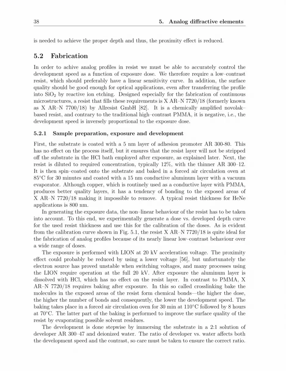
38 5. Analog diffractive elements
is needed to achieve the proper depth and thus, the proximity effect is reduced.
5.2 Fabrication
In order to achive analog profiles in resist we must be able to accurately control thedevelopment speed as a function of exposure dose. We therefore require a low–contrastresist, which should preferably have a linear sensitivity curve. In addition, the surfacequality should be good enough for optical applications, even after transferring the profileinto SiO2 by reactive ion etching. Designed especially for the fabrication of continuousmicrostructures, a resist that fills these requirements is X AR–N 7720/18 (formerly knownas X AR–N 7700/18) by Allresist GmbH [82]. It is a chemically amplified novolak–based resist, and contrary to the traditional high–contrast PMMA, it is negative, i.e., thedevelopment speed is inversely proportional to the exposure dose.
5.2.1 Sample preparation, exposure and development
First, the substrate is coated with a 5 nm layer of adhesion promoter AR 300-80. Thishas no effect on the process itself, but it ensures that the resist layer will not be strippedoff the substrate in the HCl bath employed after exposure, as explained later. Next, theresist is diluted to required concentration, typically 12%, with the thinner AR 300–12.It is then spin–coated onto the substrate and baked in a forced air circulation oven at85◦C for 30 minutes and coated with a 15 nm conductive aluminum layer with a vacuumevaporator. Although copper, which is routinely used as a conductive layer with PMMA,produces better quality layers, it has a tendency of bonding to the exposed areas ofX AR–N 7720/18 making it impossible to remove. A typical resist thickness for HeNeapplications is 800 nm.
In generating the exposure data, the non–linear behaviour of the resist has to be takeninto account. To this end, we experimentally generate a dose vs. developed depth curvefor the used resist thickness and use this for the calibration of the doses. As is evidentfrom the calibration curve shown in Fig. 5.1, the resist X AR–N 7720/18 is quite ideal forthe fabrication of analog profiles because of its nearly linear low–contrast behaviour overa wide range of doses.
The exposure is performed with LION at 20 kV acceleration voltage. The proximityeffect could probably be reduced by using a lower voltage [56], but unfortunately theelectron source has proved unstable when switching voltages, and many processes usingthe LION require operation at the full 20 kV. After exposure the aluminum layer isdissolved with HCl, which has no effect on the resist layer. In contrast to PMMA, XAR–N 7720/18 requires baking after exposure. In this so called crosslinking bake themolecules in the exposed areas of the resist form chemical bonds—the higher the dose,the higher the number of bonds and consequently, the lower the development speed. Thebaking takes place in a forced air circulation oven for 30 min at 110◦C followed by 8 hoursat 70◦C. The latter part of the baking is performed to improve the surface quality of theresist by evaporating possible solvent residues.
The development is done stepwise by immersing the substrate in a 2:1 solution ofdeveloper AR 300–47 and deionized water. The ratio of developer vs. water affects boththe development speed and the contrast, so care must be taken to ensure the correct ratio.

5.2 Fabrication 39
0 100 200 300 400 500 60040
60
80
100
120
140
160
180
Depth [nm]
Dos
e [µ
C/c
m2 ]
Figure 5.1: Achieved profile depth after development as a function of exposure
dose in resist X AR–N 7720/18. Measured from a 10–level blazed grating with the
period of 100 µm exposed into a 800–nm layer or resist with linear dose at 20 kV
acceleration voltage.
The first development step is typically 60 seconds, after which the sample is rinsed in waterfor 15 seconds, and the resulting profile depth is measured with a profilometer or an AFM,depending on the feature sizes. The development and successive depth–measurement isthen repeated until the goal depth is achieved. A typical development time for a 850 nmresist layer is 120 seconds, the maximum depth is 600 nm and the depth error is less than20 nm.
5.2.2 Proportional reactive ion etching
In order to transfer the resulting surface profile into the SiO2 substrate we employ areactive ion etcher (RIE) March Instruments CS–1701 with a CHF3 atmosphere. Thefinal profile depth is controlled by the etching ratio between the resist and the substrate.This can be adjusted by modifying the pressure, the gas flow and the power of the radiofrequency generator. In general, lowering the pressure or the gas flow (which also lowersthe pressure) results in a smaller etching ratio, whereas lowering the power has the oppositeeffect. In this thesis we used etching ratios between 1.3 and 3.9, depending on the requiredprofile depth—lower ratios give better surface quality but involve using thicker resistlayers, which in turn enhances the proximity effect and makes achieving high lateralresolution difficult. The RF generator power was typically 258 W, the pressure 45–65mTorr and the gas flow 7–20 sccm.
In practice the chamber is first pre–heated with oxygen plasma for one hour, afterwhich a dummy sample is etched to check the etching ratio. Then either the final elementis developed to the corresponding depth and etched, or, if the required depth is too high

40 5. Analog diffractive elements
Figure 5.2: SEM micrograph of a blazed grating with a period of 2 µm and depth
870 nm etched into fused silica.
considering the resist thickness, the etching parameters are adjusted and another dummyis etched. The etching speed of the resist depends on both the etching parameters and thethickness of the substrate; with typical etching parameters, the etching speed is about 15nm/min for a 0.5 mm substrate and half of that for a 3 mm substrate, making the totaletching times 1 and 2 hours, respectively. The goal depth of the profile is achieved withbetter than 2.5% accuracy.
In the literature the contamination of the substrate has been described as a potentiallyvery difficult problem [87]. The chemical processes behind this are quite complicated, andmanifest themselves by producing pronounced surface roughness, effectively making thesubstrate diffuse. This is obviously unacceptable in optical applications, however, it wasnot a major problem for us. One of the reasons is probably the small amount of resistpresent in the chamber, as the resist outside the exposed area is completely removed inthe development process. Furthermore, placing a 3 mm thick insulating SiO2 mask platebelow the substrate for the duration of the etching has been found essential in order toensure contamination–free results, although this is also responsible for the relatively longetching times required in the process.
5.2.3 Discussion
As a testament to the process described above, Fig. 5.2 is presented. The nearly blazedgrating was exposed with 8 doses between 40 and 180 µC/cm2 calibrated to produce alinear profile, provided that the period of the grating is large. However, even with a periodof 2 µm, the accuracy of the etched profile is respectable. Especially notable is the verticalsidewall, which is achieved without any kind of proximity compensation. Analysis withthe C method has shown that the diffraction efficiency of the profile is close to that ofa perfectly blazed grating, thus, utilizing proximity correction would only complicate thedata preparation without notable benefit. Obviously, if the element contains a variety of

5.3 Transmission gratings for microspectrometry 41
different local periods, proximity compensation is essential to achieve the correct deptheverywhere in the element area.
The fabrication process is not without problems, and especially the reproducibilityof the proportional etching is sometimes hard to achieve. This can be attributed to thesensitivity of the etching process to several variables, including chamber pressure andcontamination, the flowing speed of the cooling water, and external humidity, all of whichare difficult to accurately control in the present setup.
5.3 Transmission gratings for microspectrometry
Miniature spectrometers based on diffractive gratings are often found at the heart ofvarious enviromental and chemical sensors. The aim of their operation might be to identifyand compare only a few spectral lines, yet they must be compact and fully utilize thelimited spatial resolution of their CCD detectors. To fulfill these demands, a highlydispersive grating with a high diffraction efficiency over a broad wavelength range isrequired.
From the early days of diffractive optics, reflection–type gratings have been extensivelyused in spectroscopy, a trend which continues even today. However, occasionally it is moreconvenient to employ transmission–type gratings, for example in the case of an on–axisimaging spectrograph [89].
It is well–known that binary surface–relief gratings operating at the Bragg angle canproduce diffraction efficiencies exceeding 95%, but unfortunately their angular and wave-length selectivity make them unsuitable for most spectroscopic applications. Thereforeit is worthwhile to investigate the application of continuous profiles, and in particular,asymmetric profiles, since they are known to produce the best spectral response over awide wavelegth range.
5.3.1 Optimization
As described in Sec. 3.3, the proximity effect will prevent us from fabricating an idealblazed profile, especially when the features are near the wavelength scale. Here we mod-elled the rounding of the profile as a convolution of the ideal profile pi(x) with a singleGaussian function
g(x) =
√
(2/π)
wexp(−2x2/w2), (5.1)
where w is the 1/e2 width of the Gaussian, and will be considered a rounding parameterin the following. Now the final profile can be calculated simply from
p(x) = pi(x) ∗ g(x), (5.2)
where ∗ denotes convolution. It is possible to reduce the proximity effect by deconvolution,but we chose an alternative approach of taking the rounding into account in the designstage.
As a starting point for the optimization process, we used an ideal blazed profile,pi(x) = hx/d, where d is the grating period an h is the height. In the sense of the scalar

42 5. Analog diffractive elements
0 0.2 0.4 0.6 0.8 10
0.1
0.2
0.3
0.4
0.5
0.6
0.7
0.8
0.9
PSfrag replacements
x/d
h[A
.U.]
Figure 5.3: Simulated grating profiles p(x). Dashed curve, w = 0.3; continuous
curve, w = 0.5; dashed–dotted curve, w = 0.7.
theory, the optimum height of a blazed grating can be obtained from
h =λ
n1 − n2
, (5.3)
where n1 and n2 are the refractive indices of the substrate and the surrounding medium,respectively. However, for small gratings periods and large incident angles the scalartheory fails, hence, we will optimize the profile height h with rigorous diffraction theory.It is worth noting that in view of 5.2, the parameter h can be unambigusly optimized alsofor the rounded profiles.
For the rounding parameter w we selected three values, 0.3, 0.5, and 0.7, based onprevious fabrication test runs. The resulting three surface profiles can be seen in Fig. 5.3.It is intuitively clear that the rounding strongly reduces the efficiency at normal incidence,and consequently we chose the incidence angle θin as the second optimization parameter.We anticipated, considering the effective tilt of the originally vertical sidewall, that theoptimimum value of θin would grow along with w.
The grating was set to work on the spectral region of 400–750 nm. Because of the highdispersion requirement, the grating period must be on the order of the wavelength—thus,we used the Fourier modal method in the optimization of the grating profile. Becauseoptimization using the FMM is computationally demanding, we chose three target wave-lengths, namely 400, 550, and 750 nm, and maximized the overall diffraction efficiencyat these wavelengths. Since the grating was intended to operate on arbitrarily polar-ized white–light, we optimized for both TE and TM polarization simultaneously. Thecontinuous grating profile was approximated with a 16–layer structure in the calculations.
The dispersion requirements determine the grating period, but care must be taken toensure that adjacent diffraction orders do not overlap in the selected spectral range. As

5.3 Transmission gratings for microspectrometry 43
400 450 500 550 600 650 700 7500.2
0.3
0.4
0.5
0.6
0.7
0.8
PSfrag replacements
λ [nm]
η
Figure 5.4: Diffraction efficiencies of optimized grating profiles. Dashed curve,
w = 0.3; continuous curve, w = 0.5; dash–dotted curve, w = 0.7.
θin is an optimization parameter, the period cannot be estimated accurately. Assumingthat θin ∼ 20◦ (as it turns out to be), we selected the grating period d = 1.75 µm.
The results of the optimization are given in Table 5.1, along with the minimum andmaximum deflection angles θmin and θmax in the selected spectral band. Since the directionof the −2 diffraction order always differs at least 1◦ from the direction of the utilized order−1, no overlap occurs. The average efficiency curves for the two polarization states arepresented in Fig. 5.4. For all three profiles the efficiency remains above 50% all throughthe spectral band, reaching the maximum of about 70% near λ = 500 nm.
5.3.2 Fabrication
Based on preliminary fabrication tests, we selected the optimized profile with w = 0.5and h = 765 µm for fabrication. The grating was exposed as a four–level structure intoa 500–nm thick resist layer, and the doses were chosen to be linearly divided between 20and 180 µC/cm2. After development and subsequent etching (with an etching ratio of
Table 5.1
Optimized incidence angle θin and relief height h with corresponding minimum and maximum
deflection angles θmin and θmax for spectral range 400–750 nm.
w θin [deg] h [nm] θmin [deg] θmax [deg]0.3 20.5 882 5.6 17.30.5 23.8 765 10.3 22.20.7 25.7 733 12.9 25.0

44 5. Analog diffractive elements
Figure 5.5: SEM migrograph of the fabricated grating profile.
3.87) into the SiO2 substrate, the profile height was measured to be h = 780 nm, whichdiffers only 15 nm from the optimized value.
It is worth stressing that employing a thin resist layer in combination with a highetching ratio reduces the proximity effect and thus enables better control of the profileshape. However, etching with a high etching ratio can produce some surface roughness,as is evident from the SEM migrograph in Fig. 5.5. Fortunately, in this case, the surfacequality was quite acceptable, as will be seen from the experimental results.
Although we only used four depth levels in the exposure, the resulting profile, as seenin Fig. 5.6, is reasonably blazed. The minor surface roughness is also evident in this figure.
5.3.3 Experimental results
Instead of white light, we decided to measure the diffration efficiency of the −1 order ofour grating with a selection of laser sources. The wavelengths were λ = 488, 514, 543,568, 633, and 676 nm, and both TE and TM polarization were used. The results can beseen in Fig. 5.7.
As assumed in the optimization, the grating was illuminated through the substrate—since the angle of incidence was θin = 24◦, the angle of incidence into the substrate wasθ′in = 36◦, in accordance with Snell’s law. To eliminate the contribution of reflection fromthe first surface in the efficiency measurements, we used a reference beam incident on thesame angle and taken through a nonmodulated region of the same substrate.
We also modelled the operation of the measured profile with the C method, and theresults are shown in Fig. 5.7. Considering that the measurement of the grating profilefrom a SEM micrograph is prone to small errors, the agreement of the experimental andthe calculated results is remarkable. Moreover, this agreement allows us to be confidentthat the full wavelength versus diffraction efficiency data are reliable.
The measured diffraction efficiencies are about 4% less than the optimized ones, andthere appears to be a slight shift of the maximum of the efficiency curve toward shorterwavelengths. This can be explained by small fabrication errors in the profile shape.

5.3 Transmission gratings for microspectrometry 45
0 0.2 0.4 0.6 0.8 1 1.2 1.4 1.60
0.1
0.2
0.3
0.4
0.5
0.6
0.7
0.8
PSfrag replacements
x [µm]
h[A
.U.]
Figure 5.6: Fabricated grating profile determined with SEM (continuous curve)
and the corresponding theoretical model (dashed curve).
400 450 500 550 600 650 700 7500.4
0.45
0.5
0.55
0.6
0.65
0.7
0.75
PSfrag replacements
λ [nm]
η
Figure 5.7: Calculated efficiencies for the grating profile in Fig. 5.6 and measured
efficiencies (crosses, TE polarization; circles, TM polarization) for selected wave-
lengths. Continuous curve, average of TE and TM polarizations; dashed curve, TE
polarization; dashed–dotted curve, TM polarization.

46 5. Analog diffractive elements
−60 −40 −20 0 20 40 600
1
2
3
4
5
6
7
8
9
PSfrag replacements
x [mm]
I[A
.U.]
Figure 5.8: Intensity distribution of a He–Ne laser beam in the far field of the
grating. Measurement distance 5.5 m; detector size 2 mm × 2 mm.
For the characterization of the signal–to–noise ratio we illuminated the grating witha He–Ne laser (λ = 633 nm) and measured the lateral intensity distribution of the −1diffraction order in the far field. The result is shown in Fig. 5.8 on a logarithmic scale.Because the noise was not expected to depend strongly on the wavelength, only onewavelength was used in the measurement.
5.3.4 Discussion
Combining the fabrication of continuous profiles combined with an accurate numericalmethod, we have demonstrated the feasibility of transmission–type spectrometric grat-ings operating on visible light. The spectral efficiency of the grating is comparable tocommercially available volume holographic gratings, and it is suitable for commercialapplications.
5.4 Excimer beam shaping
Output signals produced by diffractive optical elements usually consist of a set of discretespots, which are easy to generate with a periodic element. However, often a continuoussignal is required, for example in the case of transforming a Gaussian beam into a flat–top intensity distribution in the far field. Employing a periodic element in such a casewill result in a speckle–like intensity distribution, since the coherent diffraction ordersproduced by the element will interfere with each other. These fluctuations can be virtuallyeliminated by designing the element with the geometrical map transform method, but theoperation of the element is exceedingly sensitive to lateral alignement errors.

5.4 Excimer beam shaping 47
In the case of partially coherent beams, such as high–power excimer laser beams, thesituation is somewhat different. As proposed by Turunen [90], the intereference effectsobtained using a periodic element are expected to decrease when the input beam is notfully coherent. In the following we provide experimental proof that the principle is indeedfeasible [91].
5.4.1 Element design
Let a periodic diffractive element be illuminated by a Gaussian Schell–model source,described in Sec. 2.4.1. The grating acts as a beam splitter, and produces m diffractionorders with the complex–amplitudes Tm. In a one–dimensional case, according to thecomplex–amplitude transmittance approach for partially coherent light of Eqs. (2.78) and(2.63), the cross–spectral density immediately behind the grating is
W (x1, x2) = Win(x1, x2)∑
m,n∈S
T ∗
mTn exp[−i2π(mx1 − nx2)/d], (5.4)
where S is the set of signal orders of the grating, and Win(x1, x2) is the cross–spectraldensity of the Gaussian Schell–model source. Placing the element at the front focal planeof a positive lens with focal length f (or in the far–field), we obtain the cross–spectraldensity at the back focal plane from
W (u1, u2) =1
fλ
∫∫
∞
−∞
W (x1, x2) exp[−i2π(u1x1 − u2x2)/fλ] dx1 dx2. (5.5)
Substitution of the Gaussian Schell–model cross–spectral density into (5.4) and insertingthe result into (5.5) yields, after lengthy calculations
W (u1, u2) =w0
wF
∑
m,n∈S
T ∗
mTn exp{
−[(u1 +mu0)2 + (u2 + nu0)
2]/w2
F
}
× exp{
−[(u1 − u2)2 + (m− n)2u2
0]/2σ2
F
}
,
(5.6)
where wF = Fλ/πw0β is the radius of a single diffraction order in the Fourier plane,σF = σ0wF/w0 is the corresponding coherence width, and u0 = fλ/d is the separationbetween two adjacent diffraction orders. Finally, the intensity distribution I(u) = W (u, u)takes the form
I(u) =w0
wF
∑
m,n∈S
T ∗
mTn exp{
−[(u+mu0)2 + (u+ nu0)
2]/w2
F
}
× exp[
−(m− n)2u2
0/2σ2
F
]
.
(5.7)
This intensity distribution is expected to be a set of Gaussian diffraction orders. Whenthe focal length f is decreased, the orders will overlap and produce strong interferencein the case of a fully coherent source. As the degree of spatial coherence is reduced, theinterference will diminish, and at full incoherence, the overlapping diffraction orders willproduce a good approximation of a flat–top intensity distribution. Different intensitydistributions can be achieving by suitably tailoring the distribution of energy between theorders.

48 5. Analog diffractive elements
0 20 40 60 80 100 120 140 160 180 2000
1
2
3
4
5
6
7
8
PSfrag replacements
x [µm]
Phas
e[rad
]
Figure 5.9: Phase function of the designed 1 → 9 beam splitter.
5.4.2 Numerical simulations
Based on the theory discussed above, we performed numerical simulations of the opticalset–up. The iterative Fourier–transform algorithm described in Sec. 2.3.3 was employedto design a continuous profile generating nine adjacent diffraction orders containing over99% or the incident energy. The resulting grating period is illustrated in Fig. 5.9. For thesimulations, we selected the wavelength λ = 248 nm, the focal length of the lens f = 500mm, and the beam halfwidth at the focal plane wF = 6.58 µm. Here we have fixed wF forbetter comparison of the results with different source coherence properties, and thereforewe have to adjust the source beam size w0 = fλ/πwFβ for different degrees of spatialcoherence in the simulations.
As previously described, the diffraction orders are separated provided that u0 À wF ,i.e., d¿ Fλ/wF ≈ 19 mm. In this case the element acts as a beam splitter irrespectiveof the state of coherence of the illuminating beam. When the grating period d is increased,the orders begin overlapping, which produces interference if the source is coherent. Thisis illustrated in Figs. 5.10 and 5.11 for grating periods d = 15 mm and d = 30 mm, andfor several degrees of spatial coherence α.
As expected, strong interference effects are observed for fully coherent illumination.The shape of the interference pattern is non–symmetric, and changes rapidly when theelement is moved laterally, as the relative phases of the diffraction orders change (notshown). Reducing the degree of spatial coherence also reduces the interference effects,and also makes the signal more independent of the lateral position of the element.
In Fig. 5.10 the diffraction orders do not overlap, and therefore a flat–top is not ob-tained even when α is decreased. However, in Fig. 5.11 the orders overlap, and as aconsequence a good approximation of a flat–top distribution is achieved when α = 0.1.Moreover, the flat–top is insensitive to the lateral shifting of the element, thus making the

5.4 Excimer beam shaping 49
0
20
40(a)
0
10
20
30In
tens
ity(b)
−0.06 −0.04 −0.02 0 0.02 0.04 0.060
10
20
30
u [mm]
(c)
Figure 5.10: Simulated intensity distributions at the focal plane of the lens. Grat-
ing period d = 15 mm. (a) α = ∞, (b) α = 0.7 and (c) α = 0.3. The intensity is in
arbitrary units.
0
50
100(a)
0
20
40
Inte
nsity
(b)
−0.06 −0.04 −0.02 0 0.02 0.04 0.060
20
40
u [mm]
(c)
Figure 5.11: Simulated intensity distributions at the focal plane of the lens. Grat-
ing period d = 30 mm. (a) α = ∞, (b) α = 0.3 and (c) α = 0.1. The intensity is in
arbitrary units.
50 5. Analog diffractive elements
−15 −10 −5 0 5 10 150
0.02
0.04
0.06
0.08
0.1
x [mm]
Inte
nsity
Figure 5.12: Measured lateral intensity distribution of the excimer laser source
before the focusing lens.
alignment of the system trivial. It is worth stressing that this is a major advantage com-pared to elements designed with the optical map transform—as stated before, althoughtheir performance is respectable, they are exceedingly sensitive to alignent errors.
5.4.3 Experimental results
To demonstrate the idea of partially coherent Gaussian to flat–top beam shaping, we de-signed and fabricated the 1 → 9 beam splitter. The laser source was a Lambda PhysikCOMPex 205 excimer laser operating at λ = 248 nm. Since the beam is anisotropic,i.e. its source parameters w0 and σ0 are different in orthogonal directions, we only usedx direction in the experiments. Fig. 5.12 shows the beam profile measured immediatelybefore a lens with focal length f = 500 mm, and at its focal plane. From these measure-ments we obtained, by numerical fitting of Gaussian profiles into the measured intensitydistributions, the parameters w0 = 7.8 mm and wF = 0.15 mm, yielding α = 0.032 andσ = 0.25 mm.
The demonstration element was designed to produce nine equal–intensity diffractionorders, and was fabricated as a continuous profile into a fused silica substrate. The periodof the element was d = 200 µm, making it relatively easy to fabricate, as the shape of theperiod is quite smooth.
The experimental set–up is illustrated in Fig. 5.14. The element was placed in thepath of the converging laser beam, and different diffraction order separations u0 can beachieved by adjusting the distance ∆z between the element and the observation plane.The measured intensity distributions with different separations ∆z are shown in Fig. 5.15,indicating a resonable agreement with the simulations. The small discrepancy can partlybe explained with a 2% depth–scale error in the fabricated profile, and partly by the fact

5.4 Excimer beam shaping 51
−1 −0.5 0 0.5 10
1
2
3
4
5
u [mm]
Inte
nsity
Figure 5.13: Measured time–averaged lateral intensity distribution of the excimer
laser source at the focal plane of the lens.
PSfrag replacements
∆z
excimer
lens beam splitter focal plane
Figure 5.14: The setup employed in the experiments of excimer beam shaping.
that the excimer laser is not an exact Gaussian Schell–model source.When the element is far from the focal plane of the lens, the diffraction orders are
partially separated. Reducing ∆z causes the orders to begin overlapping and a good flat–top beam is generated. Further decrease of ∆z reduces the width of the flat–top, butonly slightly reduces the intensity ripple because the diffraction orders have non–uniformintensities.
5.4.4 Discussion
We presented a novel method for partially coherent beam shaping utilizing a periodicelement. Compared to elements designed with the optical map transform, the gratingdescribed above is trivial to align making it attractive for practical applications. Thedesign of the element is that of a beam splitter with overlapping diffraction orders, butsince the light source is not fully coherent, no harmful interference will occur. The conceptwas proven experimentally with a multi–mode excimer laser source. Obvious applicationsfor the beam shaping technology include laser machining and surgery.

52 5. Analog diffractive elements
−2 −1.5 −1 −0.5 0 0.5 1 1.5 20
0.1
0.2
0.3
0.4
0.5
0.6
0.7
0.8
u [mm]
Inte
nsity
Figure 5.15: Measured (solid line) and simulated (dashed line) lateral intensity
distribution at the focal plane of the lens. Distance from the element ∆z = 190 mm.
The intensity is in arbitrary units.
−2 −1.5 −1 −0.5 0 0.5 1 1.5 20
0.1
0.2
0.3
0.4
0.5
0.6
0.7
0.8
0.9
u [mm]
Inte
nsity
Figure 5.16: Measured (solid line) and simulated (dashed line) lateral intensity
distribution at the focal plane of the lens. Distance from the element ∆z = 110 mm.
The intensity is in arbitrary units.

5.5 Propagation–invariant field generation 53
5.5 Propagation–invariant field generation
Fields retaining their transverse intensity distributions upon propagation are called propa-gation–invariant or diffraction–free [92, 93]. The obvious example is the plane wave, butother, more interesting cases exist. In this section we demonstrate propagation–invariantbeams produced by two different schemes. In the first one we employ two diffractiveelements to transform an incident Gaussian beam into a Bessel beam with an uniformintensity distribution along the propagation axis [17]. The second method is based on asuitably designed diffracting mirror placed inside a laser cavity—the output beam of thelaser is a Bessel beam apodized by a Gaussian function.
5.5.1 Introduction
In the sense of the scalar theory, a propagation–invariant field can be defined as
U(x, y, z) = F (x, y)eiβz, (5.8)
where F (x, y) is an arbitrary function and β is the propagation constant. From this it isimmediately obvious that the amplitude of the field does not change upon propagation.Solutions of the Helmholtz equation which are of this form can be found [92] by presentingthe angular spectrum of Eq. (5.8) in polar coordinates2. A change of variables u = f cosφand v = f sinφ in Eq. (2.18) and insertion of (5.8) results in condition
∫
∞
0
∫
2π
0
fA(f, ϕ){exp(ikx∆z) − exp[iΦ(x, y, z)]} exp[if(x cosϕ+ y sinϕ)] df dϕ = 0,
(5.9)which must hold for all A(f, ϕ) 6= 0. The difference in the curly brackets thus vanishes,and we can write Φ(x, y, z) = βz, where β is a constant. This results in
fA(f, ϕ) = A(ϕ)δ(f − α), (5.10)
where A(ϕ) is an arbitrary azimuthal function with complex values. The angular spectrumrepresentation now yields
U(ρ, φ, z) = exp(iβ∆z)
∫
2π
0
A(ϕ) exp[iαρ cos(ϕ− φ)] dϕ (5.11)
where α2 + β2 = k2. Presenting the azimuthally periodic angular spectrum A(ϕ) as anazimuthal Fourier series
A(ϕ) =∞∑
m=−∞
Am exp(imϕ), (5.12)
where the Fourier coefficients are
Am =1
2π
∫
2π
0
A(ϕ) exp(−imϕ) dϕ. (5.13)
2An alternative method is to present the Helmholtz equation in polar coordinates, as done on page508 of Ref. [94]

54 5. Analog diffractive elements
Defining Cm = 2πimAm, we finally obtain
U(ρ, φ, z) = exp(iβ∆z)∞∑
m=−∞
CmJm(αρ) exp(imφ), (5.14)
where Jm is the Bessel function of order m. This implies that all propagation–invariantfields can be represented as superpositions of Bessel fields with intensity distributionsproportional to J2
m. The angular spectrum, and thus the far field intensity distribution ofa Bessel beam is a ring, called Montgomery’s ring because of the studies of self–imagingfields by Montgomery [95,96]. Furthermore, as α is the only radial component of the wavevector, the solution (5.14) comprises waves with wave vectors k on the surface of a conewith cone angle θ, such that
α = k sin θ ≈ kθ. (5.15)
The approximation is valid when the beam is paraxial.
The zeroth–order Bessel field has a very long and narrow focus—the radius of the focalspot is
r0 = 0.383λ
sin θ, (5.16)
which can easily be less than the wavelength, making Bessel fields very useful in ap-plications requiring precision alignment. However, since each intensity ring around thefocus has approximately the same amount of energy, Bessel fields must be regarded asstrictly non–physical. For this reason only finite–aperture approximations of propagation–invariant beams can be realized.
Several methods for producing Bessel fields have been proposed. The original setup[93] employed an annular aperture and a focusing lens to generate converging conicalwaves, but in the sense of light efficiency, refractive or diffractive axicons [97, 98] arebetter suited for the task. Axicons, however, cannot produce an uniform axial intensitydistribution, and to rectify this, tandem diffractive systems have been proposed [99,100].In these, incident light is converted into an annulus, which is then focused into a conicalwave. Controlling the intensity distribution of the annulus, uniform axial intensity canbe achieved. Also, by replacing one of the mirrors in a laser resonator with a suitablydesigned diffractive mirror, it is possible to construct an active source for Bessel–Gaussbeams [101]. The latter two methods are discussed in more detail in the following.
5.5.2 Two–element system for Bessel beam generation
The principle of the two–element system for J0 field generation is illustrated in Fig. 5.17.The first element, illuminated with a collimated Gaussian beam, distributes the incidentintensity into an annular ring at the plane of the second element. The envelope of its radialintensity distribution follows a 1/r law, where r denotes the radial coordinate. Moreover,we introduce a super–Gaussian apodization for the intensity distribution so that
I(r, 0) =A
rexp
{
−2[(r − rc)/W ]P}
, (5.17)
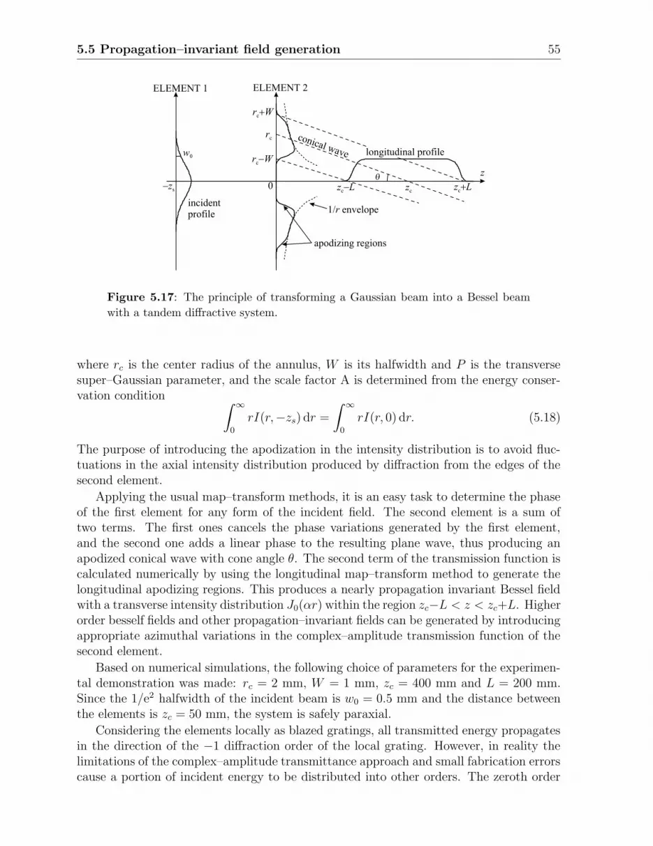
5.5 Propagation–invariant field generation 55
Figure 5.17: The principle of transforming a Gaussian beam into a Bessel beam
with a tandem diffractive system.
where rc is the center radius of the annulus, W is its halfwidth and P is the transversesuper–Gaussian parameter, and the scale factor A is determined from the energy conser-vation condition
∫
∞
0
rI(r,−zs) dr =
∫
∞
0
rI(r, 0) dr. (5.18)
The purpose of introducing the apodization in the intensity distribution is to avoid fluc-tuations in the axial intensity distribution produced by diffraction from the edges of thesecond element.
Applying the usual map–transform methods, it is an easy task to determine the phaseof the first element for any form of the incident field. The second element is a sum oftwo terms. The first ones cancels the phase variations generated by the first element,and the second one adds a linear phase to the resulting plane wave, thus producing anapodized conical wave with cone angle θ. The second term of the transmission function iscalculated numerically by using the longitudinal map–transform method to generate thelongitudinal apodizing regions. This produces a nearly propagation invariant Bessel fieldwith a transverse intensity distribution J0(αr) within the region zc−L < z < zc+L. Higherorder besself fields and other propagation–invariant fields can be generated by introducingappropriate azimuthal variations in the complex–amplitude transmission function of thesecond element.
Based on numerical simulations, the following choice of parameters for the experimen-tal demonstration was made: rc = 2 mm, W = 1 mm, zc = 400 mm and L = 200 mm.Since the 1/e2 halfwidth of the incident beam is w0 = 0.5 mm and the distance betweenthe elements is zc = 50 mm, the system is safely paraxial.
Considering the elements locally as blazed gratings, all transmitted energy propagatesin the direction of the −1 diffraction order of the local grating. However, in reality thelimitations of the complex–amplitude transmittance approach and small fabrication errorscause a portion of incident energy to be distributed into other orders. The zeroth order

56 5. Analog diffractive elements
of the first element is the most obvious concern, as it propagates along the optical axis,but also the −2 order of the second element interferes with the −1 order at the opticalaxis when z < 300 mm. The former problem was dealt with in the experimental setup,described later, but the latter may case some fluctuations in the intensity distribution ofthe Bessel beam.
Fabrication
The gratings were fabricated as continuous–profile elements on 0.5 mm thick fused silicasubstrates. The goal depth was 1376 nm, designed for operation at the He–Ne wavelengthof λ = 633 nm. Since the smallest features are well below 50 µm, some proximity correc-tion had to be used. In this case we expanded the dose range by decreasing the lowestdose used to expose the locally blazed gratings. The thickness of the resist layer was 700nm, the profile depth after development 385 nm, and, after etching for one hour in CHF3
plasma with gas flow 20 sccm and RF power 258 W, measurements made with an atomicforce microscope indicated profile heigths of 1110–1240 nm and 1240 nm for the first andsecond element, respectively. The sidewalls of the blazed profile were nearly vertical, evenwith the smallest local periods at the outer edges of the elements.
Experimental results
The laser beam was expanded and collimated to achieve the correct width at the firstelement, and the correct distance between the elements was determined by the size ofthe far–field Montgomery’s ring. The tandem system is very sensitive to the correctcollimation of the incident beam, a fact found by simulation and verified in the testing ofthe experimental setup.
The interference of the zeroth order of the first element with the Bessel field, asdiscussed above, was nearly perfectly avoided by placing a linear blazed grating with aperiod of 64 µm in the central area of the second element. This grating deflects practicallyall incident light into the −1 diffraction order at an angle of 0.57◦, thus passing the centralregion of the Bessel field.
The axial intensity distribution was measured from images grabbed at various distanceswith a CCD camera. The experimental and theoretical intensity distributions are shownin Fig. 5.19, where the small fabrication errors in the fabricated profile heights have beentaken into account in the simulations. Fig. 5.20 shows a CCD image of the transverseintensity distribution at z = zc proving, that the alignment of the tandem system hassucceeded without complicated alignment instruments.
Discussion
We have demonstrated a light–efficient way of producing Bessel beams with a two–elementsystem. The axial intensity of the zero–order beam was shown to be almost uniform,a feature impossible to obtain with traditional setups. Moreover, the lateral intensitydistribution was of excellent quality even without complicated systems for the alignmentof the optical setup.

5.5 Propagation–invariant field generation 57
(a)
0 0.1 0.2 0.3 0.4 0.5 0.6 0.70
0.2
0.4
0.6
0.8
1
1.2
0 0.1 0.2 0.3 0.4 0.5 0.6 0.70
50
100
150
200
250
300Phase Intensity
PSfrag replacements
r [mm]
I(r
,−z s
)/I(0
,−z s
)φ
1 (r)
(b)
0 0.5 1 1.5 2 2.5 3 3.50
0.005
0.01
0.015
0.02
0.025
0.03
0 0.5 1 1.5 2 2.5 3 3.5−1200
−1000
−800
−600
−400
−200
0
200Phase Theor.Goal
PSfrag replacements
r [mm]
I(r,−zs)/I(0,−zs)
φ1(r)
I(r
,0)/
I(0
,−z s
)φ
2 (r)
(c)
100 200 300 400 500 600 700 8000
2
4
6
8
10
12Theor.Goal
PSfrag replacements
r [mm]
I(r,−zs)/I(0,−zs)
φ1(r)
I(r, 0)/I(0,−zs)
φ2(r)
z [mm]
I(0
,z)/
I(0
,−z s
)
Figure 5.18: Phase transmittance functions and intensity at the first element (a),
phase transmittance function, theoretical and goal intensities at the second element
(b), and theoretical and goal longitudinal intensity distributions (c).

58 5. Analog diffractive elements
150 200 250 300 350 400 450 500 550 600 650 7000
2
4
6
8
10
Simul.Experim.
PSfrag replacements
z [mm]
I(0,z
)/I(0,−z s
)
Figure 5.19: Measured and simulated axial intensity distributions.
Figure 5.20: A CCD image of the transverse intensity distribution produced by
the tandem system at z = zc.

5.5 Propagation–invariant field generation 59
5.5.3 Bessel–Gauss resonator
In traditional laser resonators, the mirrors are spherical, and the output beam is Gaussian(or more accurately, a Gauss–Hermite beam [50]). However, Belanger [102] and Leger[103] introduced the idea of suitably designing the resonator mirrors to produce a nearlyarbitrary transverse intensity distribution. If the mirrors are designed to conjugate thephase of the desired mode, no other mode can easily resonate. In the following sectionthis method is applied to the design and fabrication of a laser resonator producing aBessel–Gauss beam as the fundamental resonant mode [101]. This can also be done byusing a reflective or refractive axicon in the resonator, but the method is less versatileconsidering mode selection [104].
Bessel–Gauss beams
As stated in Sec. 5.5.1, propagation–invariant Bessel beams are non–physical because oftheir infinite extent. When the Bessel beam is apodized by a Gaussian envelope function,we have a Bessel–Gauss beam [105,106], which, in addition to being physically realizableis also mathematically convenient. The cross–section of the Bessel–Gauss beam of orderm at the beam waist can be defined as
U(r, ψ) = AJm(αr) exp(−r2/w2
0) exp(−imψ), (5.19)
where A is a scaling parameter and w0 is the 1/e2 halfwidth (waist) of the Gaussianenvelope function. The Bessel–Gauss beam thus inherits some of the properties of theGaussian beam, namely beam waist
w2(z) = w2
0
[
1 +
(
λz
πw20
)2]
(5.20)
and the radius of wavefront curvature
R(z) = z
[
1 +
(
πw20
λz
)2]
. (5.21)
Furthermore, the axial phase delay of the field compared to a plane wave is expressed as
Φ(z) = βz − tan−1
(
λz
πw20
)
, (5.22)
where β = k − α2/2k is the propagation constant of the Bessel beam.
Resonator design
Let us consider a two–mirror resonator, where M1 is the fully reflecting and M2 the semi–transparent output mirror of the resonator of length d. The goal of the resonator designis to have a Bessel–Gauss field Um(r, ψ, 0) as its fundamendal resonant mode. Placing thebeam waist at the output mirror M2, we obtain the field at mirror M1 by propagating thefield by distance d. Separating the field in radial and azimuthal parts
Um(r, ψ, z) = um(r, z) exp(imφ), (5.23)

60 5. Analog diffractive elements
we can, in accordance with Eq. (2.60), write the complex amplitude reflectance functionof mirror M1 as
t1,m(r) =u∗m(r, d)
um(r, d). (5.24)
Thus the phase of the field is conjugated, ensuring field propagation back to M2. Respec-tively, the complex amplitude reflectance function of mirror M1 is of the form
t2,m(r) =um(r, 0)
u∗m(r, 0). (5.25)
Since the radial phase Um(r, 0) of the Bessel–Gauss field is binary, containing only values0 and π, the reflectance function t2,m(r) must represent a planar mirror. Using the Fresnelpropagation formula (2.22) to propagate the Bessel–Gauss field distance d, we can expressthe complex amplitude reflectance function of mirror M1 as
t2,m(r) = exp[i2Φ(d)] exp[
ik(r2 + θ2d2)/λR(d)]
× Jm
(
αr
1 + iλd/πw20
)
J−1
m
(
αr
1 − iλd/πw20
)
,(5.26)
where θ = α/k is the paraxial cone angle.Because of the following properties of Bessel functions,
∣
∣
∣
∣
Jm(z)
Jm(z∗)
∣
∣
∣
∣
= 1 (5.27)
and
arg
{
Jm(z)
Jm(z∗)
}
= 2 arg{Jm(z)} (5.28)
We can write the phase–only transmittance function t1,m(r) as
t1,m(r) = exp[iφ2,m(r)], (5.29)
where
φ2,m(r) = 2Φ(d) +kθ2d2
R(d)+
kr2
R(d)+ 2 arg
{
Jm
(
αr
1 + iλd/πw20
)}
(5.30)
With this result, we are now in a position to design a mirror for a resonator producing aBessel–Gauss beam of order m as its fundamental resonant mode, when the other mirroris planar.
Numerical simulations
The Bessel–Gauss beam generated by the resonator is a good approximation of an idealBessel field over a distance L = w0/θ. In order to produce a distinctly non–Gaussian beamwith transversal intensity rings, the halfwidth of the central peak r0 = 2.405/θk shouldbe small enough. Thus, the setup is a compromise between a long Bessel beam and thenumber of intensity rings—the longer the beam the more it resembles a Gaussian insteadof a Bessel beam. Keeping this in mind, we selected the following beam parameters:

5.5 Propagation–invariant field generation 61
0 100 200 300 400 500 600 7000
0.2
0.4
0.6
0.8
1
0 100 200 300 400 500 600 700−1
0
1
2
3
4
5
PSfrag replacements
(a)
(b)
r [µm]
r [µm]
Am
plitu
de
[A.U
.]P
has
e[r
ad]
Figure 5.21: Simulated radial amplitude (a) and phase (b) of the beam waist at
the planar mirror. Courtesy of H. Elfstrom.
r0 = 109 µm, θ = 3.4 mrad, beam waist at mirror M2 w0 = 300 µm, and the modeof the beam m = 0. The pump laser wavelength was chosen to be λ = 1064 nm. Theapproximate propagation–invariant distance of the Bessel–Gauss is now L = 8 cm. Toguarantee good discrimination between different resonant modes, the resonator should notbe much longer than this. Hence, we selected the resonator length to also be L = 8 cm.
The resonator performance was simulated with a standard method known as the Fox–Li algorithm [107]. The algorithm begins by propagating an arbitrary field at mirror M1 tomirror M2 by any suitable propagation formula. Then the complex amplitude reflectancefunction of the mirror is applied, and the field is propagated further back to mirror M1.The iteration is repeated until the field converges to a solution representing a resonantmode of the cavity. The algorithm somewhat resembles the iterative Fourier–transformalgorithm, a difference being the fact that the field in the Fox–Li algorithm is (usually)not propagated to the far field. Another difference is the need of active amplification ofthe field, as some of the energy is lost both outside the mirror apertures and through thesemi–transparent output mirror of the resonator.
The simulated radial phase and amplitude distributions at the planar mirror are il-lustrated in Fig. 5.21, proving that the fundamental mode of the resonator is indeed aBessel–Gauss beam with two intensity rings and the characteristic binary phase. Thepropagation of the beam intensity distribution can be seen in Fig. 5.22. It is clear fromthe figures that the beam is not strictly propagation–invariant even within the resonator,but this is the expected behaviour. Larger mirrors and pump beam waist would enable alonger Bessel–Gauss beam.

62 5. Analog diffractive elements
0 100 200 300 400 5000
0.2
0.4
0.6
0.8
1
0 100 200 300 400 5000
0.2
0.4
0.6
0.8
0 100 200 300 400 5000
0.05
0.1
0.15
0.2
0.25
0 200 400 600 800 10000
0.005
0.01
0.015
PSfrag replacements
(a) (b)
(c) (d)
r [µm]r [µm]
r [µm]r [µm]
Inte
nsi
ty[A
.U.]
Inte
nsi
ty[A
.U.]
Inte
nsi
ty[A
.U.]
Inte
nsi
ty[A
.U.]
Figure 5.22: Simulated radial intensity at distances (a) z = 0 cm , (b) z = 4 cm,
(c) z = 8 cm, and (d) z = 16 cm from the beam waist. Note the expanded x–scale
in (d). Courtesy of H. Elfstrom.

5.5 Propagation–invariant field generation 63
PSfrag replacements
M1
M2
M3
Pump laser
Output
Crystal
Figure 5.23: Linear cavity Bessel–Gauss resonator geometry. The beam is ex-
tracted from the resonator with the Brewster plate M3.
Resonator setup
To construct an operational Bessel–Gauss resonator, at least a pump laser, a lasingmedium, the diffractive mirror M1 and a planar mirror M2 are needed. In addition,we need to be able to extract the output beam out of the resonator. Since pumpingthrough the diffractive mirror is not feasible due to the diffraction effects, the pumpinghas to be performed through the semi–transparent planar mirror. However, since theoptimal Bessel–Gauss beam is achieved at the beam waist located at the planar mirror,the output beam should also be extracted through the planar mirror. Because using thesame semi–transparent mirror for both pumping and output is obviously impractical, weneed to develop the resonator further.
One solution for the problem described above is to extract the output beam fromthe center of the resonator with a glass plate at Brewster angle in respect to the beam,so that part of the converging beam incident from the diffractive mirror is deflected outof the resonator, as illustrated in Fig. 5.23. By this means the beam waist is producedoutside the resonator facilitating easy characterization of the beam. However, some ofthe energy is lost by reflection to the opposite direction. The resonator is pumped with2 W diode laser through the semi–transparent mirror M2 fabricated directly on a 1.2 mmthick Nd:YVO4 crystal, which provides the lasing. After achieving lasing in this resonatorsetup, we opted for an alternative solution: the V–cavity depicted in Fig. 5.24.
In the V–cavity setup the Brewster plate is removed and another semi–transparentplanar mirror M3 is introduced. Provided that the V–angle is small and that the mirrorsM2 and M3 are equidistant from mirror M1, beam waists of equal size are producedon both planar mirrors, i.e., the setup is symmetrical. Now the beam can easily beextracted through mirror M3, although the alignment of the cavity becomes slightly morechallenging. As both of the resonators described above are optically equivalent, giventhat the distances between mirrors are the same, the simulation results discussed aboveare still valid for the V–cavity resonator.

64 5. Analog diffractive elements
PSfrag replacements
M1
M2
M3
Pump laser
Output
Crystal
Figure 5.24: V–cavity Bessel–Gauss resonator geometry. The beam is extracted
through the semi–transparent planar mirror M3.
Fabrication
The diffractive mirror was fabricated as an analog profile into fused silica with the processdescribed in Sec. 5.2. The radius of the element was 1150 µm and the smallest featureat the edge of the element 115 µm, which can be seen from the radial phase distributionof the element depicted in Fig. 5.25. The element was exposed with 32 phase levels toachieve an analog profile, and the goal depth was 532 nm. After development into a 800nm resist layer, the depth of the resist profile was measured with a profilometer to be 240nm, and after etching in CHF3 plasma with gas flow 12 sccm and pressure 53 mtorr for60 minutes, the depth of the etched profile was 510 nm.
Finally, the element was made reflective by sputter–coating it with gold. To improveadhesion, a 5–nm layer of chromium was sputtered between the substrate and the goldlayer. Thickness of 100 nm of the gold layer was determined by rigorous modeling toreflect more than 99% of incident light.
Since we did not employ the double–exposure strategy described in Sec. 4.1.2, somestitching error was evident on the element. This causes minor scattering of light, andtherefore reduces the diffraction efficiency of the element, which was taken into accountin considering the light amplification in the resonator.
Discussion
As the alignment of the V–cavity with a wavelength invisible to the human eye cannotbe regarded as an easy task, the testing of the resonator is still underway at the timeof writing. Both the distances and angles between the mirrors must be aligned veryaccurately, along with the lateral placement of the diffractive mirror.
5.6 Discussion
The fabrication method based on the e–beam exposure of resist X AR-N 7720/18 andsubsequent etching into fused silica was shown to be an excellent technique facilitat-ing the generation of continuous–profile diffractive elements. Several applications were

5.6 Discussion 65
0 200 400 600 800 1000 12000
1
2
3
4
5
6
7
x [µm]
Pha
se
PSfrag replacements
r [µm]Phase [rad]
Figure 5.25: The radial phase of the diffractive resonator mirror.
successfully demonstrated with high–diffraction efficiency and good signal quality. More-over, high–resolution blazed gratings were shown to be achievable with accurate controlof the profile shape. The same process has also been employed in the fabrication of alarge amount of diffactive elements outside this thesis both commercially and in researchprojects [108,109].

Chapter VI
Multilevel and hybrid diffractive elements
One might assume that with the fabrication methods described in the previous chaptersany surface profile that can be designed could be fabricated. Obviously, this is not thecase, and in this chapter we consider two types of profiles that are clearly out of reachof the previous methods. The first one is a four–level profile with high resolution andvertical sidewalls, and the other a binary profile with analog modulation of groove depth.The fabrication methods employ double masks—one uses an analog resist mask on topof a binary metal mask, whereas the second method uses two metal masks of differentmetals. Possible applications for the techniques are also discussed.
6.1 Fabrication
Both of the fabrication methods consist of first making a chromium mask on the substrateand then spin–coating the substrate again and making another exposure on top of thefirst one. The only difference is the type of the second mask—in the first approach it isbinary, and in the second it is analog. In the following we will describe the fabricationprocesses in detail.
The edge areas of the SiO2 substrate are first coated with a 30 nm layer of chromium,and then the substrate is spin–coated with a layer of AR–P 661 resist and vacuum–evaporated with a 20 nm conduction layer of copper. In addition to the diffractive element,also four alignment crosses are exposed with the e–beam on the edges of the substrate.After resist development, a 30 nm layer of chromium is evaporated on the central areaof the substrate, whereas a layer of gold is deposited on the edge areas. The resist isstripped away in acetone, and the result is a metal mask covering the exposed areas ofthe substrate: chromium in the element area and gold (on top of chromium to improvecontrast in SEM) as the alignment marks on the edges. This, so called lift–off process(see Fig. 6.1), is a standard way of making metal masks for projection lithography orfurther etching into the substrate.
Next, the substrate is spin–coated with either a binary resist (AR–P 661) or an analogresist (AR–N 7720/18). Because the resist is non–conductive, it has to be removed fromtop of the alignment marks to make them visible in the SEM mode of the LION. This isdone by covering the element and etching the substrate in oxygen plasma. After this, aconductive metal layer (chromium or aluminum, depending on the resist) is evaporated
66

6.1 Fabrication 67
PSfrag replacements
(a)(b)(c)(d)
Figure 6.1: The lift–off process. A resist layer with metal coating (a) is exposed
and developed (b), and coated with a metal layer (c). Removal of the resist results
in a binary metal mask (d).
Figure 6.2: Fabrication of depth–modulated binary structures. A chromium mask
produced by lift–off (a) is spin–coated with analog resist. After exposure and de-
velopment (b) the sample is etched, until goal depth is achieved (c). Finally, the
chromium mask is removed (d).
on top of the resist.The second exposure is made on top of the first. The LION can automatically detect
the alignment marks and adjust its coordinate system to compensate for the alignmenterror. After this, the process is different depending on the type of the second mask.
6.1.1 Depth–modulated binary gratings
In the case of analog resist we follow the procedures described in Chapter 5, until we havean analog profile developed in the resist on top of a binary chromium mask, as shownin Fig. 6.2. Then we simply etch through both masks simultaneously, until the goaldepth of the binary part of the profile is achieved. At this stage the resist layer has beencompletely etched away but the chromium mask has to be removed separately by wet–etching. The end result is a binary profile with an analog modulation of the depth of thegroove. SEM micrographs of fabricated test structures can be seen in Figs. 6.3 and 6.4.It is evident from the figures that the achieved lateral resolution, 200 nm, is well beyondthe continuous resist masks described in Chap. 5.
A possible problem with the method is obtaining an even resist layer on the metalmask. Since the analog resist must have reasonable viscosity to produce a thick enough

68 6. Multilevel and hybrid diffractive elements
Figure 6.3: SEM micrograph of an etched depth–modulated binary grating with a
grating period of 800 nm and depth modulation period 4 µm.
Figure 6.4: SEM micrograph of an etched depth–modulated binary grating with a
grating period of 400 nm and depth modulation period 4 µm.

6.1 Fabrication 69
Figure 6.5: Fabrication of four–level diffractive profiles. Two metal masks produced
by double lift–off (a) are etched step by step. After first etching step (b), part of the
chromium mask is removed (c), after the second step the aluminum mask is removed
(d) and finally the remaining part of the chromium is removed (e).
layer the metal mask has a greater effect on the distribution of the resist on the substrate.If necessary, thinner resist layers can be used along with a higher etching ratio.
6.1.2 Four–level structures
The process with the binary resist for the second exposure, presented in Fig. 6.5, issomewhat more complicated. The method is similar to the one developed by David [110],differing only in the use of wet etching instead of dry etching to remove chromium mask.First, we repeat the lift–off process described above, only using aluminum instead ofchromium as the mask metal. After stripping the resist we end up with two metal maskspartially overlapping each other. The etching is a three–step process. After the firstetching step we remove those parts of chromium which are not covered by aluminumby wet–etching. After the next dry–etching step we remove the aluminum layer withhydrochloric acid, and after the third etching step and removing the remaining parts ofthe chromium mask we have a four–level profile with vertical sidewalls and very highresolution.
Since the alignment of the second exposure is very accurately executed with the e–beam system, it might seem that the process is easy to calibrate. A few additional factors,however, have to be taken into account to ensure acceptable quality of the final profile.Firstly, the initial wet–etching of chromium has to be carefully controlled to preventundesired etching of the chromium covered by aluminum. This can be compensated forby adjusting the wet–eching time or the linewidths of the exposure accordingly. Secondly,a high–quality aluminum layer can prove difficult to produce—pinholes are sometimesformed in the sputtering process and subsequently etched into the substrate material.Other metals can naturally also be used, provided that the two metals can be wet–etchedseparately.
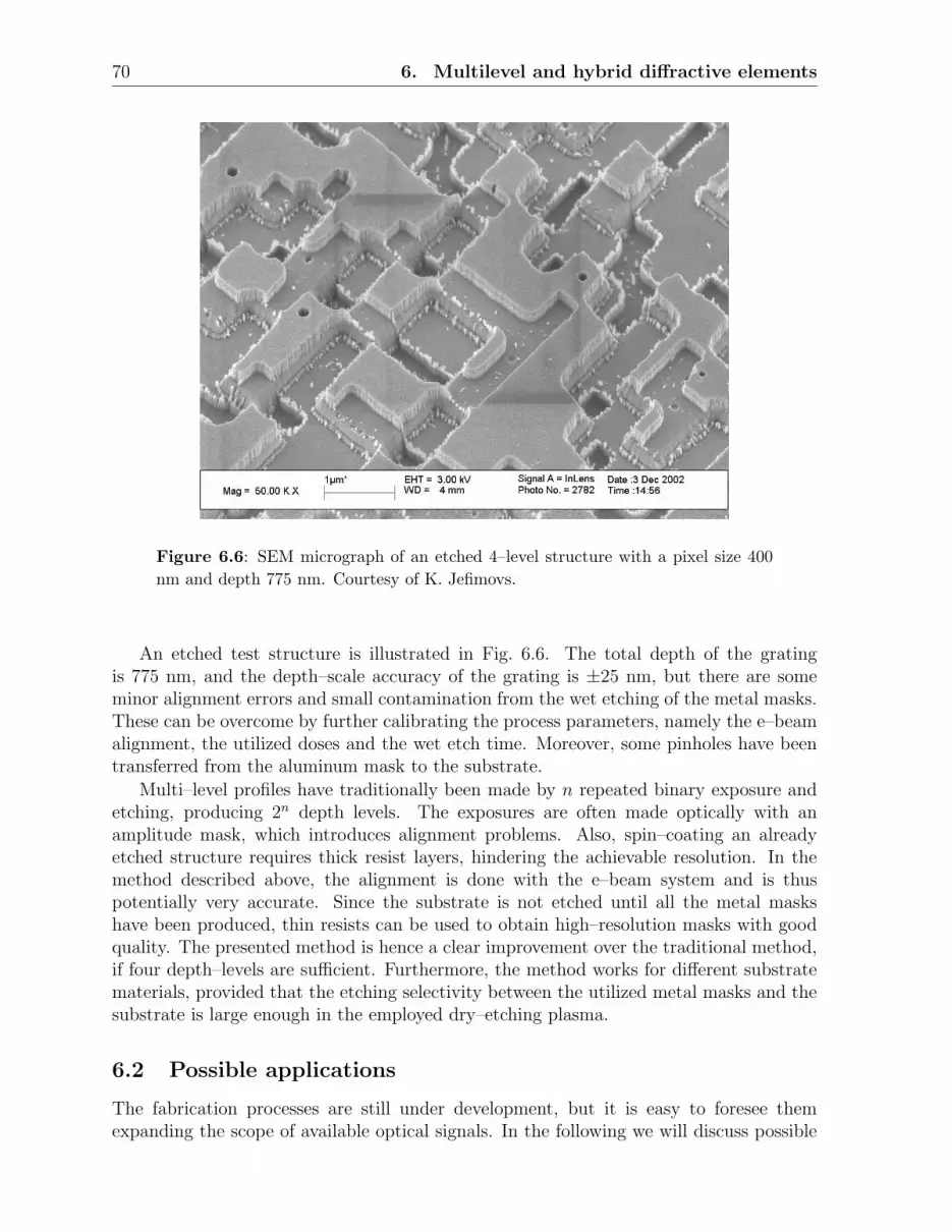
70 6. Multilevel and hybrid diffractive elements
Figure 6.6: SEM micrograph of an etched 4–level structure with a pixel size 400
nm and depth 775 nm. Courtesy of K. Jefimovs.
An etched test structure is illustrated in Fig. 6.6. The total depth of the gratingis 775 nm, and the depth–scale accuracy of the grating is ±25 nm, but there are someminor alignment errors and small contamination from the wet etching of the metal masks.These can be overcome by further calibrating the process parameters, namely the e–beamalignment, the utilized doses and the wet etch time. Moreover, some pinholes have beentransferred from the aluminum mask to the substrate.
Multi–level profiles have traditionally been made by n repeated binary exposure andetching, producing 2n depth levels. The exposures are often made optically with anamplitude mask, which introduces alignment problems. Also, spin–coating an alreadyetched structure requires thick resist layers, hindering the achievable resolution. In themethod described above, the alignment is done with the e–beam system and is thuspotentially very accurate. Since the substrate is not etched until all the metal maskshave been produced, thin resists can be used to obtain high–resolution masks with goodquality. The presented method is hence a clear improvement over the traditional method,if four depth–levels are sufficient. Furthermore, the method works for different substratematerials, provided that the etching selectivity between the utilized metal masks and thesubstrate is large enough in the employed dry–etching plasma.
6.2 Possible applications
The fabrication processes are still under development, but it is easy to foresee themexpanding the scope of available optical signals. In the following we will discuss possible

6.3 Discussion 71
applications enabled by these methods.
6.2.1 Depth–modulated binary structures
The depth–modulated binary structures enable some applications impossible with the pre-viously existing fabrication methods. The method is perfectly suited for the fabricationof elements utilizing zero–order coding of complex amplitude, such as those describedin Ref. [49]. Since the theory behind the elements is based on thin–element approxi-mation, the minimum features of the grating would be larger than one micron, makingthe fabrication relatively simple. To our knowledge, zero–order elements have only beendemonstrated as linear gratings, not as pixelized structures, whereas both types of struc-tures would be equally simple to achieve with the new method.
Another very promising application would be the polarizing beam splitter describedby Tervo in Sec. 7.4.2 of Ref. [111]. Although the illustrated profile has also surfacemodulation in addition to depth modulation, it is possible to avoid it by redesigning theelement. Unfortunately the phase modulation requires maximum depth of about 7 µmin fused silica, which is unreachable by the 30 nm chromium mask currently used in thefabrication. By further development of the fabrication process and possibly by using ahigher index material, the required profile is achievable.
6.2.2 Four–level structures
It was recently found out by Kettunen (to be published) that the sensitivity of a binarypixel element to fabrication errors can be significantly reduced by introducing a third phaselevel into the design. The idea is to divide the areas of zero phase shift to adjacent stripeswith zero and 2π phases. According to thin element approximation, this has no effect onthe signal of the element, provided that the depth of the element is accurately realized.However, if there is some depth–scale error, or, if the wavelength doesn’t match the designwavelength, the diffraction efficiency of the grating is notably improved compared to theoriginal binary design.
The three phase–levels should be achieved with good depth–scale accuracy and thesidewalls should be as vertical as possible to ensure optimum performance of the element.For this reason the analog resist approach of Sec. 5 is not suitable for the fabrication;instead, the double–metal method can easily produce the required three–level profile.
Furthermore, the described method is perfectly suited for the fabrication of pixelizedgratings operating in the resonance domain, where the features of the element are in thewavelength scale. As the signals in this domain are non–paraxial, rigorous diffractiontheory has to be employed instead of IFTA.
6.3 Discussion
Both of the fabrication methods described above show great promise and enable applica-tions previously thought challenging or even impossible to realize. With some fine–tuningof process parameters results of good quality can be consistently achieved.

Chapter VII
Conclusions
The emphasis of this thesis was the fabrication of diffractive surface profiles with electronbeam lithography. After presenting the necessary theory, the principles of e–beam lithog-raphy were described. Several fabrication methods were developed, and further utilized invarious applications. SEM micrographs and optical measurement results were presented.
All the theory required for the analysis of fabricated elements was derived from thebasic principles of the electromagnetic theory of light. For the rigorous analysis, twonumerical methods were discussed, namely the Fourier modal method and the C method,which together facilitate accurate analysis of all structures described in this work. Basedon the thin element approximation, the paraxial methods employed in the design of theelements were briefly introduced. Furthermore, the basic properties of partially coherentbeams were discussed.
A novel method for the fabrication of subwavelength Bragg gratings on silicon–on–insulator (SOI) waveguides was developed and experimentally demonstrated. It was shownto reach the required resolution and side wall quality, but combining the gratings withthe waveguides still needs some fine–tuning. The same technology was also successfullyutilized in fabricating photonic band–gap structures. Both types of structures can be usedin the production of optical chips integrating various optical functions, which is a subjectof great interest in optical telecommunications.
A method for the fabrication of analog surface profiles with a low–contrast resist andproportional reactive ion etching was introduced and employed in several applications. Atransmission grating operating on visible light was shown to have high efficiency over awide wavelength scale. The element has already aroused commercial interest.
Partially coherent beam shaping was demonstrated with a multi–mode excimer laserutilizing a periodic diffractive beam–splitter. The element is trivial to align and energy–efficient, and especially since the method is applicable to any reasonably directional par-tially coherent field, the invention is expected to find applications in fields such as lasermachining and surgery.
A propagation–invariant zero–order Bessel beam with a nearly uniform axial intensitydistribution was produced with high diffraction efficiency using two diffractive elements.Moreover, the principle of producing Bessel–Gauss beams with a suitably designed laserresonator mirror was described. A resonator mirror was fabricated, and simulation resultswere provided. Experimental testing of the element is still underway at the time of writing.
72

73
Depth–modulated binary gratings were demonstrated with a novel fabrication methodemploying simultaneous etching through an analog resist and a binary metal mask. Thetechnique can reach sub–wavelength resolution and enables completely new applications,including polarizing beam splitters and high–efficiency zero–order coding. We are notaware of other methods capable of producing similar surface profiles.
A method for the fabrication of four–level structures with very high resolution andaccurate depth–scale control was introduced, utilizing two metal masks of different metalswet and dry etched. A possible application is for example improving the depth–errortolerance of binary elements.
References
[1] R. Dawkins, Climbing Mount Improbable (W.W. Norton & Company, New York,1996).
[2] E. Hecht, Optics, 3rd ed. (Addison Wesley, Reading, 1998).
[3] Zemax website (May 14, 2003), http://www.zemax.com/zemax/.
[4] OSLO website (May 14 2003), http://www.lambdares.com/products/oslo/.
[5] Softimage website (May 14 2003),http://www.softimage.com/Products/Xsi/v3/Film/.
[6] J. W. Goodman, Introduction to Fourier Optics, 2nd ed. (McGraw–Hill, New York,1996).
[7] M. Born and E. Wolf, Principles of Optics, 7th ed. (Cambridge University Press,Cambridge, 1999).
[8] R. Feynman, The Strange Theory of Light and Matter (Penguin Books, London,1985).
[9] J. Turunen and F. Wyrowski, eds., Diffractive Optics for Industrial and Commercial
Applications (Wiley–VCH, Berlin, 1997).
[10] H. P. Herzig, ed., Micro–Optics: Elements, Systems, and Applications (Taylor &Francis, Cornwall, 1997).
[11] R. Petit, ed., Electromagnetic Theory of Gratings (Springer–Verlag, Berlin, 1980).
[12] J. Turunen, M. Kuittinen, and F. Wyrowski, “Diffractive optics: electromagneticapproach,” Chap V in Progress in Optics, Vol. XL, E. Wolf, ed. (Elsevier, Amster-dam, 2000).
[13] P. Rai-Choudhury, ed., Microlithography, Vol. 1 of Handbook of Microlithography,
Micromachining and Microfabrication (SPIE Optical Engineering Press, Belling-ham, 1997).
74

REFERENCES 75
[14] P. Rai-Choudhury, ed., Microlithography, Vol. 2 of Handbook of Microlithography,
Micromachining and Microfabrication (SPIE Optical Engineering Press, Belling-ham, 1997).
[15] T. R. Groves, D. Pickard, B. Rafferty, N. Crosland, D. Adam, and G. Schubert,“Maskless electron beam lithography: prospects, progress, and challenges,” Micro-
electr. Eng. 61–62, 285–293 (2002).
[16] P. Laakkonen, M. Kuittinen, J. Simonen, and J. Turunen, “Electron–beam–fabricated asymmetric transmission gratings for microspectroscopy,” Appl. Opt. 39,3187–3191 (2001).
[17] P. Paakkonen, J. Simonen, M. Honkanen, and J. Turunen, “Two–element diffractivesystems for generation of Bessel fields,” J. Mod. Opt. 49, 1943–1953 (2002).
[18] P. Heimala, T. Aalto, S. Yliniemi, J. Simonen, M. Kuittinen, J. Turunen, andM. Leppihalme, “Fabrication of Bragg grating Structures in Silicon,” Phys. Scripta
T101, 92–95 (2002).
[19] J. C. Maxwell, A Treatise on Electricity and Magnetism, Vol. 1, 3rd ed. (Dover,New York, 1954).
[20] J. C. Maxwell, A Treatise on Electricity and Magnetism, Vol. 2, 3rd ed. (Dover,New York, 1954).
[21] J. Turunen and A. T. Friberg, “Self–imaging and propagation–invariance in electro-magnetic fields,” Pure Appl. Opt. 2, 51–60 (1993).
[22] C. B. Burckhardt, “Diffraction of a plane wave at a sinusoidally stratified dielectricgratings,” J. Opt. Soc. Am. 56, 1502–1509 (1966).
[23] F. G. Kaspar, “Diffraction by thick, periodically stratified gratings with complexdielectric constant,” J. Opt. Soc. Am. 63, 37–45 (1973).
[24] K. Knop, “Rigorous diffraction theory for transmission phase gratings with deeprectangular grooves,” J. Opt. Soc. Am. 68, 1206–1210 (1978).
[25] M. G. Moharam, E. B. Grann, D. A. Pommet, and T. K. Gaylord, “Formulation forstable and efficient implementation of the rigorous coupled–wave analysis of binarygratings,” J. Opt. Soc. Am. A 12, 1067–1076 (1995).
[26] J. Tervo, M. Kuittinen, P. Vahimaa, J. Turunen, T. Aalto, P. Heimala, and M. Lep-pihalme, “Efficient Bragg waveguide–grating analysis by quasi–rigorous approachbased on Redheffers’s star product,” Opt. Commun. 198, 265–272 (2001).
[27] J. Chandezon, D. Maystre, and G. Raoult, “A new theoretical method for diffractiongratings and its numerical application,” J. Optics 11, 235–241 (1980).

76 REFERENCES
[28] J. Chandezon, M. T. Dupuis, and G. Cornet, “Multicoated gratings: a differentialformalism applicable in the entire optical region,” J. Opt. Soc. Am. 72, 839–846(1982).
[29] L. Li, J. Chandezon, G. Granet, and J.-P. Plumey, “Rigorous and efficient grating-analysis method made easy for optical engineers,” Appl. Opt. 38, 304–313 (1999).
[30] J. P. Plumey and G. Granet, “Generalization of the coordinate transformationmethod with application to surface–relief gratings,” J. Opt. Soc. Am. A 16, 508–516 (1999).
[31] G. Granet, J. Chandezon, J.-P. Plumey, and K. Raniriharinosy, “Reformulationof the coordinate transformation method through the concept of adaptive spatialresolution,” J. Opt. Soc. Am. A 18, 2102–2108 (2001).
[32] T. Vallius, “Comparing the FMM with the C method: analysis of conducting mul-tilevel gratings in TM polarization,” J. Opt. Soc. Am. A 19, 1555–1562 (2002).
[33] T. Vallius and M. Kuittinen, “Novel electromagnetic approach to photonic crystalswith use of the C method,” J. Opt. Soc. Am. A 20, 85–91 (2003).
[34] T. Vallius, Advanced numerical diffractive optics, PhD thesis (Joensuu, 2002).
[35] F. Wyrowski, “Upper bound of the diffraction efficiency of diffractive phase ele-ments,” Opt. Lett. 16, 1915–1917 (1991).
[36] C. N. Kurtz, H. O. Hoadley, and J. J. DePalma, “Design and synthesis of randomphase diffusers,” J. Opt. Soc. Am. 68, 1080–1092 (1973).
[37] O. Bryngdahl, “Optical map transformation,” Opt. Commun. 10, 164–169 (1974).
[38] O. Bryngdahl, “Geometrical transformations in optics,” J. Opt. Soc. Am. 54, 1092–1099 (1974).
[39] J. N. Cederquist and A. M. Tai, “Computer–generated holograms for geometrictransformations,” Appl. Opt. 23, 3099–3104 (1984).
[40] T. Vallius, V. Kettunen, M. Kuittinen, and J. Turunen, “Step–discontinuity ap-proach for non–paraxial diffractive optics,” J. Mod. Opt. 48, 1195–1210 (2001).
[41] R. W. Gerchberg and W. O. Saxton, “A practical algorithm for the determinationof phase from image and diffraction plane pictures,” Optik 35, 237–246 (1972).
[42] J. R. Fienup, “Iterative method applied to image reconstruction and to computer–generated holograms,” Opt. Eng. 19, 297–305 (1980).
[43] J. R. Fienup, “Phase retrieval algorithms: A comparison,”Appl. Opt. 21, 2758–2769(1982).
[44] F. Wyrowski and O. Bryngdahl, “Iterative Fourier–transform algorithm applied tocomputer holography,” J. Opt. Soc. Am. A 5, 1058–1065 (1988).

REFERENCES 77
[45] F. Wyrowski and O. Bryngdahl, “Digital holography as part of diffractive optics,”Rep. Prog. Phys. 54, 1481–1571 (1991).
[46] F. Wyrowski, “Design theory of diffractive phase elements in the paraxial domain,”J. Opt. Soc. Am. A 10, 1553–1561 (1993).
[47] D. C. Chu, J. R. Fienup, and J. W. Goodman, “Multi–emulsion on–axis computergenerated hologram,” Appl. Opt. 12, 1386–1388 (1973).
[48] K. W. Wong, W. C. Yip, and L. M. Cheng, “Recording complex holograms onphotoresist using an ion–implantation method,” Appl. Opt. 32, 4955–4959 (1993).
[49] V. Kettunen, P. Vahimaa, and J. Turunen, “Zeroth–order coding of complex ampli-tude in two dimensions,” J. Opt. Soc. Am. A 14, 808–815 (1997).
[50] A. E. Siegman, Lasers (University Science Books, Mill Valley, 1986).
[51] L. Mandel and E. Wolf, Optical Coherence and Quantum Optics (Cambridge Uni-versity Press, Cambridge, 1995).
[52] E. Wolf, “New theory of partial coherence in the space–frequency domain. Part I:spectra and cross spectra of steady state sources,” J. Opt. Soc. Am. 72, 343–351(1982).
[53] F. T. Foley and M. S. Zubary, “The directionality of Gaussian Schell–model beams,”Opt. Commun. 26, 297–300 (1978).
[54] S. Hatzakis, “Electron resist for microcircuits and mask making,” J. Electrochem.
Soc. 116, 1033–1037 (1969).
[55] Nanocomp website (May 14 2003),http://www.nanocomp.fi/production/lion.htm.
[56] W. Brunger, E.-B. Kley, B. Schnabel, I. Stolberg, M. Zierbock, and R. Plontke, “Lowenergy lithography; energy control and variable energy exposure,”Microelectr. Eng.
27, 135–138 (1995).
[57] B. Niemann, T. Wilhein, T. Schliebe, R. Plontke, O. Fortagne, I. Stolberg, andM. Zierbock, “A special method to create gratings of variable line density by lowvoltage electron beam lithography,” Microelectr. Eng. 30, 49–52 (1996).
[58] T. H. P. Chang, “Proximity effect in electron beam lithography,” J. Vac. Sci. Tech-
nol. 12, 1271–1275 (1975).
[59] F. Nikolajeff, J. Bengtsson, M. Larsson, M. Ekberg, and S. Hard, “Measuring andmodeling the proximity effect in direct–write electron–beam lithography kinoforms,”Appl. Opt. 34, 897–903 (1995).
[60] S. V. Dubonos, B. N. Gaifullin, H. F. Raith, A. A. Svintsov, and S. I. Zaitsev,“Proximity correction for 3D structures,” Microelectr. Eng. 27, 195–198 (1995).

78 REFERENCES
[61] L. Grella, E. D. Fabrizio, M. Gentili, M. Baciocchi, and R. Maggiora, “Proximitycorrection for e–beam patterned sub–50–nm diffractive optical elements,” Micro-
electr. Eng. 35, 495–498 (1997).
[62] Z. Cui and P. D. Prewett, “Proximity correction of chemically amplified resists forelectron beam lithography,” Microelectr. Eng. 41/42, 183–186 (1998).
[63] Y. Hirai, H. Kikuta, M. Okano, T. Yotsuya, and K. Yamamoto, “Automatic doseoptimization system for resist cross–sectional profile in a electron beam lithography,”Jpn. J. Appl. Phys. 39, 6831–6835 (2000).
[64] K. A. Valiev, The Physics of Submicron Lithography (Plenum Press, New York,1992).
[65] S. A. Rishton and D. P. Kern, “Point exposure distribution measurements for prox-imity correction in electron beam lithographyon a sub–100–nm scale,” J. Vac. Sci.
Technol. 5, 135–141 (1987).
[66] D. F. Kyser and N. S. Viswanathan, “Monte Carlo simulation of spatially distributedbeams in electron beam lithography,” J. Vac. Sci. Technol. 12, 1305–1308 (1975).
[67] K. Lee, G. Cho, and D. Choi, “Monte Carlo simulation of energy dissipation inelectron beam lithography including secondary electron generation,” J. Appl. Phys.
67, 7560–7567 (1990).
[68] S. J. Wind, M. G. Rosenfield, G. Pepper, W. W. Molzen, and P. D. Gerber, “Prox-imity correction for electron beam lithography using a three–Gaussian model of theelectron energy distribution,” J.Va. Sci. Technol. B 7, 1507–1512 (1989).
[69] M. Gentili, L. Grella, A. Lucchesini, L. Luciani, L. Mastrogiacomo, andP. Musumeci, “Energy density function determination in very–high–resolutionelectron–beam lithography,” J. Vac. Sci. Technol. B 8, 1867–1871 (1990).
[70] A. Othonos and K. Kalli, Fiber Bragg Gratings: Fundamental and Applications in
Telecommunications and Sensing (Artech House, Boston, 1996).
[71] R. Ramaswami and K. N. Sivarajan, Optical Networks: A Practical Perspective
(Morgan Kaufmann, San Fransisco, 1997).
[72] A. Fernandez, H. Nguyen, J. Britten, R. Boyd, M. Perry, D. Kania, and A. Hawry-luk, “Use of interference lithography to pattern arrays of submicron resist structuresfor field emission flat panel displays,” J. Vac. Sci. Technol. B 15, 729–735 (1997).
[73] M. Naydenkov and B. Jalali, “Fabrication of high–aspect ratio photonic bandgapstructures on silicon–on–insulator,” Integrated Optics Devices IV, Proc. SPIE 3936,33–41 (2000).
[74] T. Aalto, P. Heimala, and P. Katila, “Integrated optical switch based on SOI–technology,” Phys. Scripta T79, 123–126 (1999).
REFERENCES 79
[75] L. A. Weller-Brophy and D. G. Hall, “Analysis of waveguide gratings: applicationof Rouard’s method,” J. Opt. Soc. Am. A 2, 863–871 (1985).
[76] R. A. Gottscho, C. W. Jurgensen, and D. J. Vitkavage, “Microscopic uniformity inplasma etching,” J. Vac. Sci. Technol. B 10, 2133–2147 (1992).
[77] P. Laakkonen, M. Kuittinen, and J. Turunen, “Coated phase masks for proximityprinting of Bragg gratings,” Opt. Commun. 192, 153–159 (2001).
[78] Special issue of J. Opt. Soc. Am. B 10, 280–424 (1993).
[79] H. Ichikawa, “Electromagnetic analysis of diffraction gratings by the finite–differencetime-domain method,” J. Opt. Soc. Am. A 15, 152–157 (1998).
[80] A. Taflove and S. C. Hagness, Computational Electrodynamics: The Finite–
Difference Time–Domain Method, 2nd ed. (Artech House, Boston, 2000).
[81] P. Lalanne, S. Astilean, P. Chavel, E. Cambril, and H. Launois, “Design and fabri-cation of blazed binary diffractive elements with sampling periods smaller than thestructural cutoff,” J. Opt. Soc. Am. A 16, 1143–1156 (1998).
[82] P. Laakkonen, J. Lautanen, V. Kettunen, J. Turunen, and M. Schirmer, “Multileveldiffractive elements in SiO2 by electron beam lithography and proportional etchingwith analog negative resist,” J. Mod. Opt. 46, 1295–1307 (1999).
[83] C. Vieu, F. Carcenac, A. Pepin, Y. Chen, M. Mejias, A. Lebib, L. Manin-Ferlazzo,L. Couraud, and H. Launois, “Electron beam lithography: resolution limits andapplications,” Appl. Surf. Sci. 164, 111–117 (2000).
[84] T. Fujita, H. Nishihara, and J. Koyama, “Blazed gratings and Fresnel lenses fabri-cated by electron–beam lithography,” Opt. Lett. 7, 578–580 (1982).
[85] E.-B. Kley, “Continuous profile writing by electron and optical lithography,”Micro-
electr. Eng. 34, 261–298 (1997).
[86] T. Shiono, T. Hamamoto, and K. Takahara, “High–efficiency blazed diffractiveoptical elements for the violet wavelength fabricated by electron–beam lithography,”Appl. Opt. 41, 2390–2393 (2002).
[87] W. Daschner, M. Larsson, and S. H. Lee, “Fabrication of monolithic diffractiveoptical elements by the use of e–beam direct write on an analog resist and a singlechemically assisted ion–beam–etching step,” Appl. Opt. 34, 2534–2538 (1995).
[88] M. Eisner and J. Schwider, “Transferring resist microlenses into silicon by reactiveion etching,” Opt. Eng. 35, 2979–2982 (1996).
[89] T. Hyvarinen, E. Herrala, and A. Dall’Ava, “Direct sight imaging spectrograph:a unique add–on component brings spectral imaging to industrial applications,”Digital Solid State Cameras: Designs and Applications, Proc. SPIE 3302, 165–175(1998).

80 REFERENCES
[90] J. Turunen, ”Osittain koherentin valonsateen intensiteettijakauman diffraktiivinenmuokkaus”, Patent pending (JT & TJ Photonics 2000).
[91] J. Turunen, P. Paakkonen, M. Kuittinen, P. Laakkonen, J. Simonen, T. Kajava,and M. Kaivola, “Diffractive shaping of excimer laser beams,” J. Mod. Opt. 47,2467–2475 (2000).
[92] J. Durnin, “Exact solutions for nondiffracting beams. I. The scalar theory,” J. Opt.
Soc. Am. A 4, 651–654 (1987).
[93] J. Durnin, J. J. Miceli, Jr., and J. H. Eberly, “Diffraction-free beams,” Phys. Rev.
Lett. 58, 1499–1501 (1987).
[94] G. B. Arfken and H. J. Weber, Mathematical Methods for Physicists, 5th ed. (Aca-demic Press, New York, 2001).
[95] W. D. Montgomery, “Self–imaging objects of infinite aperture,” J. Opt. Soc. Am.
57, 772–778 (1967).
[96] W. D. Montgomery, “Algebraic formulation of diffraction applied to self imaging,”J. Opt. Soc. Am. 58, 1112–1124 (1968).
[97] J. H. McLeod, “The axicon: a new type of optical element,” J. Opt. Soc. Am. 44,592–597 (1954).
[98] S. Y. Popov, A. T. Friberg, M. Honkanen, J. Lautanen, J. Turunen, and B. Schn-abel, “Apodized annular–aperture diffractive axicons fabricated by continuous–path–control electron beam lithography,” Opt. Commun. 154, 359–367 (1998).
[99] M. Honkanen and J. Turunen, “Tandem systems for efficient generation of uniform-axial intensity Bessel fields,” Opt. Commun. 154, 368–375 (1998).
[100] A. G. Sedukhin, “Beam–preshaping axicon focusing,” J. Opt. Soc. Am. A 15, 3057–3066 (1988).
[101] P. Paakkonen and J. Turunen, “Resonators with Bessel–Gauss modes,” Opt. Com-
mun. 156, 359–366 (1998).
[102] P. A. Belanger and C. Pare, “Optical resonators using graded–phase mirrors,” Opt.
Lett. 16, 1057–1059 (1991).
[103] J. R. Leger, D. Chen, and Z. Wang, “Diffractive optical element for mode shapingof a Nd:Yag laser,” Opt. Lett. 19, 108–110 (1994).
[104] J. Rogel-Salazar, G. H. C. New, and S. Chavez-Cerda, “Bessel–Gauss beam opticalresonator,” Opt. Commun. 190, 117–122 (2001).
[105] F. Gori, G. Guattari, and C. Padovani, “Bessel–Gauss beams,” Opt. Commun. 64,491–495 (1987).

REFERENCES 81
[106] C. Palma, R. Borghi, and G. Cincotti, “Beams originated by J0–correlated Schell–model planar sources,” Opt. Commun. 125, 113–121 (1996).
[107] A. G. Fox and T. Li, “Resonant modes in a maser interferometer,” Bell Sys. Tech.
J. 40, 453–458 (1961).
[108] P. Laakkonen, High–efficiency diffractive optics with electron beam lithography, PhDthesis (Joensuu, 2000).
[109] S. N. Khonina, V. V. Kotlyar, V. A. Soifer, P. Paakkonen, J. Simonen, and J. Tu-runen, “An analysis of the angular momentum of a light field in terms of angularharmonics,” J. Mod. Opt. 48, 1543–1557 (2001).
[110] C. David, “Fabrication of stair–case profiles with high aspect ratios for blazeddiffractive optical elements,” Microelectr. Eng. 53, 677–680 (2000).
[111] J. Tervo, On electromagnetic treatment of free–space propagation and paraxial
diffractive optics, PhD thesis (Joensuu, 2002).


