Embed Size (px)
Citation preview
Approaches to Fabricating High-Efficiency Ultra-Thin CdTe Solar Cells
by
Wei Xia
Submitted in Partial Fulfillment
of the
Requirements for the Degree
Doctor of Philosophy
Supervised by
Professor Ching W. Tang
Department of Chemical Engineering
Arts, Sciences and Engineering
Edmund A. Hajim School of Engineering and Applied Sciences
University of Rochester
Rochester, NY
2012
ii
Biographical Sketch
The author was born in Wuhan, Hubei Province, China on August 5, 1981. He
attended the University of Science and Technology Beijing from 1999 to 2003 and
graduated with a Bachelor of Engineering degree in 2003. Afterwards, he started his
graduate studies at the Institute of Process Engineering, Chinese Academy of Sciences
and was awarded a Master’s degree in Chemical Engineering in 2006. He came to the
University of Rochester in the summer of 2007 to pursue his Ph.D. studies in Chemical
Engineering. His thesis research was to fabricate high-efficiency ultra-thin CdTe solar
cells under the supervision of Professor Ching W. Tang.
List of Publications and Articles Submitted for Publication:
1. W. Xia, H. N. Wu, H. Lin, C.W. Tang, Low-resistance back contact for CdTe/CdS thin
film photovoltaic cells, US Patent, Application No. 61/540264.
2. H. Lin, W. Xia, H. N. Wu, C. W. Tang, Photovoltaic cells with improved electrical
contact, US Patent App. Publ, US 20110240123 A1; WO 2011123117 A1.
3. W. Xia, C. Wang, Irfan, H. Lin, H.N. Wu, Y. Gao and C.W. Tang, Te/Cu bi-layer:a
low-resistance back contact buffer for thin film CdS/CdTe solar cells with good device
stability, Sol. Energy Mater. Sol. Cells, 2012, to be submitted.
4. W. Xia, H. Lin, H.N. Wu and C.W. Tang, Enhanced performance of ultra-thin CdTe
solar cells with a back contact buffer layer of MoOx. Thin Solid Films, 2012, submitted.
iii
5. W. Xia, H. Lin, H.N. Wu and C.W. Tang, Effects of high-temperature annealing on
ultra-thin CdTe solar cells, Thin Solid Films, 520 (2011) 563.
6. W. Xia, J. A. Welt, H. Lin, H.N. Wu, M.H. Ho and C.W. Tang, Fabrication of Cd1-
xZnxS films with controllable zinc doping using a vapor zinc chloride treatment, Sol.
Energy Mater. Sol. Cells, 94 (2010) 2113.
7. H. Lin, W. Xia, H.N. Wu, C.W. Tang, CdS/CdTe solar cells with MoOx as back
contact buffers, Appl. Phys. Lett., 97 (2010) 123504.
8. Irfan, W. Xia, H. Lin, C.W. Tang, H. Ding and Y. Gao, Nitric-phosphoric acid etching
effects on the surface chemical composition of CdTe thin film, Thin Solid Films, 520
(2012) 1988.
9. H. Lin, Irfan, W. Xia, H.N. Wu, Y. Gao and C.W. Tang, MoOx back contact for
CdS/CdTe thin film solar cells: preparation, device characteristics, and stability, Sol.
Energy Mater. Sol. Cells, 99 (2012) 349.
10. Irfan, H. Lin, W. Xia, H.N. Wu, C.W. Tang and Y. Gao, The effect of MoOx inter-
layer on thin film CdTe/CdS solar cell, Sol. Energy Mater. Sol. Cells, 105 (2012) 86.
iv
Acknowledgements
I would like first to thank my academic advisor Professor Ching W. Tang for his
guidance, encouragement, and patience from the very beginning of my graduate studies,
without which this work would not have been possible. I have learned from him not only
the necessary skills and techniques for scientific research, but more importantly, the
correct way of scientific thinking and attitude. Professor Wayne Knox, Professor
Mitchell Anthamatten, Professor David Harding and Professor Gary Wicks, both of
whom are my Ph.D. thesis committee members, are highly appreciated for their guidance
and suggestions on my research.
Special thanks go to Mr. Joseph Madathil and Dr. David Weiss. I thank them for their
selfless guidance and patient help. I benefit a lot from their rich research experience.
Special thanks go to Mr. Mike Culver for his expert technical support for my research. I
am also grateful to Ms. Sandra Wilson, Mr. Larry Kuntz, Ms. Gina Eagan and Ms.
Jennifer Condit for their administrative support.
I would like to thank all my colleagues, Hao Lin, Hsiang-Ning Wu, Minlu Zhang,
Kevin Klubek, Hui Wang, Sang Min Lee, Felipe Angel, Chi-Sheng Chang, Yung-Hsin
Lee, Chris Favaro, Lisong Xu, Guy Mongelli, Charles Chen, Laura Ciammuruchi,
Aanand Thiyagarajan, Michael Beckley and other group alumni.
My deep gratitude goes to my parents, my sisters and their families, and my wife, Yingrui
Zhang. They are always there supporting and encouraging me with their best wishes.
v
Abstract
This thesis is an investigation of the fabrication, characterization and performance of
high-efficiency and ultra-thin CdTe solar cells with an aim of reducing the material usage
and cell manufacturing cost. Several approaches have been successfully carried out to
directly or indirectly improve the device performance. Major achievements are listed
below:
1) A close-spaced sublimation (CSS) process with an improved control of the
deposition temperature-time profile was developed to fabricate high-quality ultra-
thin CdTe films. Three key factors in the CSS process including oxygen pressure,
substrate temperature and thermal etch duration were optimized.
2) A two-stage post-deposition treatment including a high temperature annealing
(HTA) followed by a vaporous cadmium chloride treatment (VCC) was
developed and optimized for the growth of high-quality CdTe films. The effects
of HTA and VCC on ultra-thin CdTe solar cells were revealed by a combination
of characterization techniques, including photoluminescence.
3) In a collaborative effort two new back contact buffers, MoOx and Te/Cu, were
identified and applied in ultra-thin CdTe solar cells. Substitution of a
conventional acid etching method with the new back contact buffers was found to
enhance the cell efficiency from ~10% to ~13.5%. Moreover, the new buffers
improved the reproducibility of cell fabrication.
vi
A low-resistance electrical back contact based on the Te/Cu buffer and Ni as
electrode was developed. A thermal activation process was found necessary to
promote ohmic contact formation. Cu diffusion into the Te layer and CdTe bulk
layer occurred during the thermal activation process and must be controlled to
prevent excessive diffusion into the CdS/CdTe junction. The effects of Cu
concentration and Te thickness on device performance and cell stability were
systematically investigated and a cell efficiency as high as ~15% with good
stability has been achieved using an optimized Te/Cu buffer.
4) A novel vaporous zinc chloride treatment was developed for the formation of Cd1-
xZnxS from CdS films. Compared with conventional fabrication methods, the
VZC method features simple setup and operation and is capable of producing Cd1-
xZnxS films with a homogenous structure. The Zn to Cd doping ratio in Cd1-
xZnxS can be easily controlled by adjusting the process parameters. By replacing
CdS with a more transparent Cd1-xZnxS as the window layer, CdTe solar cells
with a higher (12-14%) short-circuit current, Jsc, have been demonstrated.
vii
Contributors and Funding Sources
This work was supervised by a dissertation committee consisting of Professor Ching
Tang (advisor), Professor Mitchell Anthamatten and Professor David Harding from the
Department of Chemical Engineering, Professor Wayne Knox and Professor Gary Wicks
from the Institute of Optics.
The development, optimization and characterizations of MoOx back contact buffer in
Chapter 4 were mainly conducted by Hao Lin. The optimization of metal electrode
deposition was conducted by Hsiang Ning Wu. The experimental work of a new vapor
zinc chloride treatment for Cd1-xZnxS fabrication was mainly conducted by Jonathan A.
Welt. All other work conducted for the dissertation was completed by me independently.
The Department of Chemical Engineering provided a Fellowship to support my
graduate study. Rohm & Haas, now a part of Dow Chemical, provided funding support
for this thesis work for two years. Eastman Kodak Company provided many important
components for building the deposition systems used in my Ph.D study. Sunflux Inc.
provided CdS coated substrates for making CdTe solar cells.
viii
Table of Contents
1. Introduction ............................................................................................................1
1.1 Background of thin film CdS/CdTe solar cells ................................................. 1
1.2 Fabrication of thin film CdS/CdTe solar cells .................................................. 3
1.3 Deficiencies of thin film CdS/CdTe solar cells ................................................ 8
1.4 Developing ultra-thin CdTe solar cells and its challenges................................ 9
1.5 Summary ......................................................................................................... 13
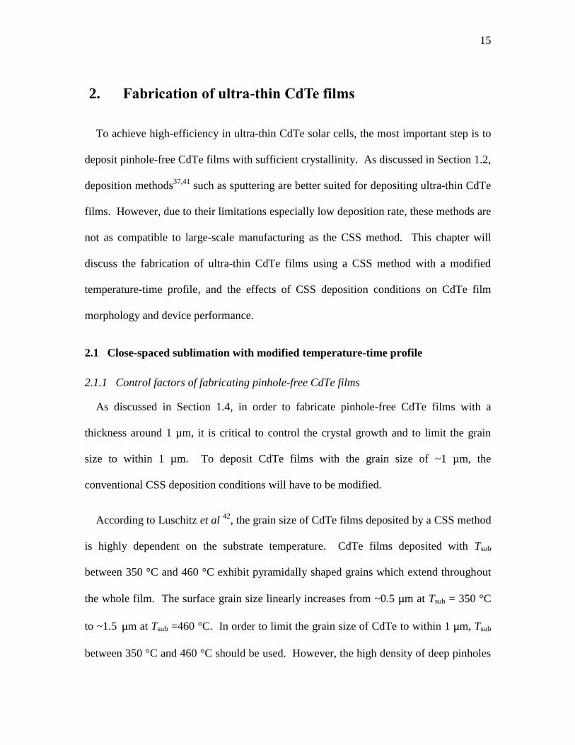
2. Fabrication of ultra-thin CdTe films ....................................................................15
2.1 Close-spaced sublimation with modified temperature-time profile................ 15
2.1.1 Control factors of fabricating pinhole-free CdTe films ............................ 15
2.1.2 Modified temperature-time profile for depositing ultra-thin CdTe films . 16
2.1.3 Comparison between conventional and modified temperature-time profile18
2.2 Effects of deposition conditions on ultra-thin CdTe film ............................... 21
2.2.1 Oxygen pressure ....................................................................................... 21
2.2.2 Substrate temperature ............................................................................... 25
2.2.3 Thermal etch duration ............................................................................... 29
2.3 Summary ......................................................................................................... 32
3. Post-deposition treatments on ultra-thin CdTe films ...........................................34
3.1 Vaporous cadmium chloride treatment ........................................................... 34
3.2 VCC process optimization .............................................................................. 38
3.2.1 Annealing duration and temperature ........................................................ 38
3.2.2 Oxygen partial pressure ............................................................................ 46
3.2.3 Ambient pressure ...................................................................................... 50
3.3 High temperature annealing ............................................................................ 54
3.3.1 Effects of HTA ......................................................................................... 55
3.3.2 Optimization of HTA process ................................................................... 58
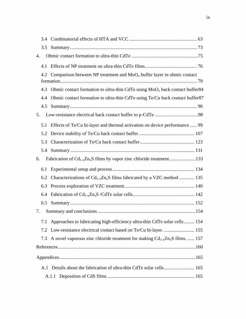
ix
3.4 Combinatorial effects of HTA and VCC ........................................................ 63
3.5 Summary ......................................................................................................... 73
4. Ohmic contact formation to ultra-thin CdTe .......................................................75
4.1 Effects of NP treatment on ultra-thin CdTe films ........................................... 76
4.2 Comparison between NP treatment and MoOx buffer layer in ohmic contact
formation ................................................................................................................. 79
4.3 Ohmic contact formation to ultra-thin CdTe using MoOx back contact buffer84
4.4 Ohmic contact formation to ultra-thin CdTe using Te/Cu back contact buffer87
4.5 Summary ......................................................................................................... 96
5. Low-resistance electrical back contact buffer to p-CdTe ....................................98
5.1 Effects of Te/Cu bi-layer and thermal activation on device performance ...... 99
5.2 Device stability of Te/Cu back contact buffer .............................................. 107
5.3 Characterization of Te/Cu back contact buffer ............................................. 123
5.4 Summary ....................................................................................................... 131
6. Fabrication of Cd1-xZnxS films by vapor zinc chloride treatment ......................133
6.1 Experimental setup and process .................................................................... 134
6.2 Characterizations of Cd1-xZnxS films fabricated by a VZC method ............. 135
6.3 Process exploration of VZC treatment .......................................................... 140
6.4 Fabrication of Cd1-xZnxS /CdTe solar cells ................................................... 142
6.5 Summary ....................................................................................................... 152
7. Summary and conclusions .................................................................................154
7.1 Approaches to fabricating high-efficiency ultra-thin CdTe solar cells ......... 154
7.2 Low-resistance electrical contact based on Te/Cu bi-layer. ......................... 155
7.3 A novel vaporous zinc chloride treatment for making Cd1-xZnxS films. ...... 157
References ..................................................................................................................160
Appendices .................................................................................................................165
A.1 Details about the fabrication of ultra-thin CdTe solar cells ......................... 165
A.1.1 Deposition of CdS films ........................................................................ 165
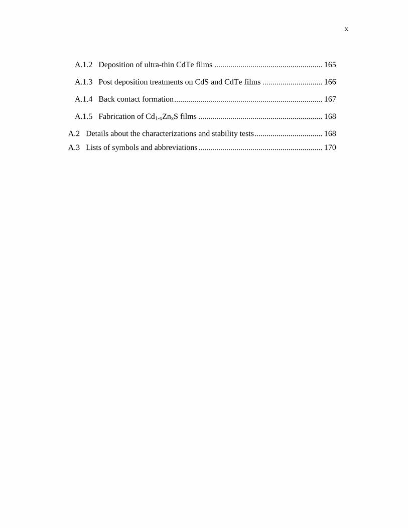
x
A.1.2 Deposition of ultra-thin CdTe films ...................................................... 165
A.1.3 Post deposition treatments on CdS and CdTe films .............................. 166
A.1.4 Back contact formation .......................................................................... 167
A.1.5 Fabrication of Cd1-xZnxS films .............................................................. 168
A.2 Details about the characterizations and stability tests .................................. 168
A.3 Lists of symbols and abbreviations .............................................................. 170
xi
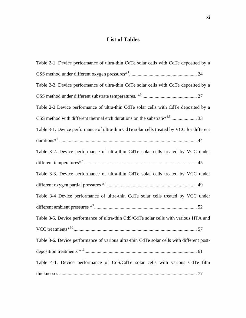
List of Tables
Table 2-1. Device performance of ultra-thin CdTe solar cells with CdTe deposited by a
CSS method under different oxygen pressures*1........................................................ 24
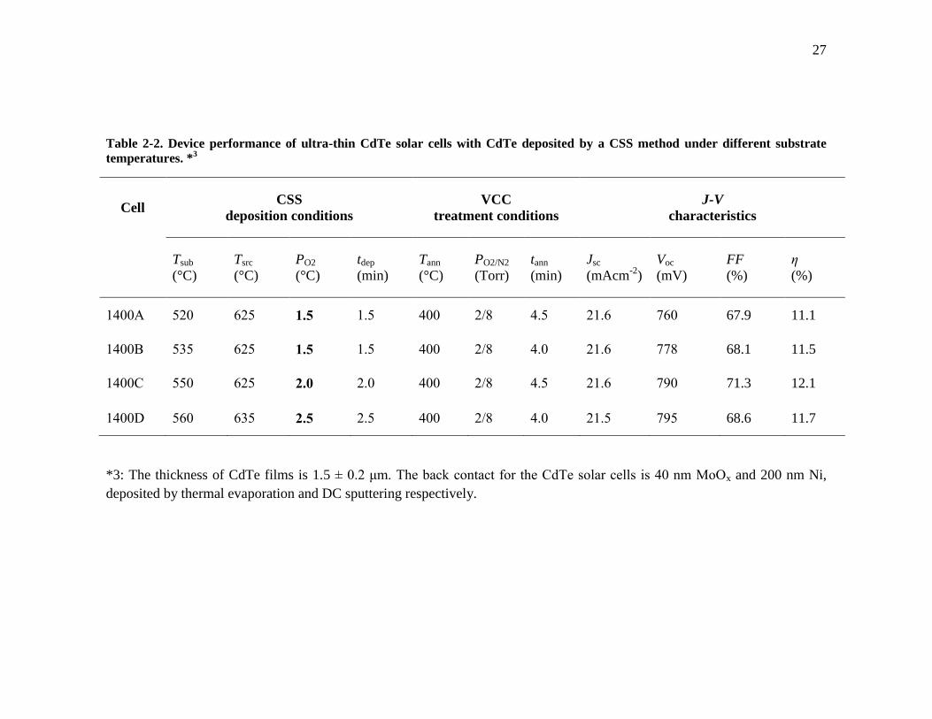
Table 2-2. Device performance of ultra-thin CdTe solar cells with CdTe deposited by a
CSS method under different substrate temperatures. *3 ............................................. 27
Table 2-3 Device performance of ultra-thin CdTe solar cells with CdTe deposited by a
CSS method with different thermal etch durations on the substrate*4,5
..................... 33
Table 3-1. Device performance of ultra-thin CdTe solar cells treated by VCC for different
durations*6 .................................................................................................................. 44
Table 3-2. Device performance of ultra-thin CdTe solar cells treated by VCC under
different temperatures*7 .............................................................................................. 45
Table 3-3. Device performance of ultra-thin CdTe solar cells treated by VCC under
different oxygen partial pressures *8 ........................................................................... 49
Table 3-4 Device performance of ultra-thin CdTe solar cells treated by VCC under
different ambient pressures *9 ..................................................................................... 52
Table 3-5. Device performance of ultra-thin CdS/CdTe solar cells with various HTA and
VCC treatments*10
...................................................................................................... 57
Table 3-6. Device performance of various ultra-thin CdTe solar cells with different post-
deposition treatments *13
............................................................................................. 61
Table 4-1. Device performance of CdS/CdTe solar cells with various CdTe film
thicknesses .................................................................................................................. 77
xii
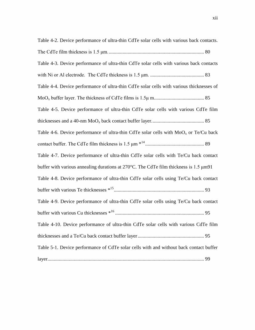
Table 4-2. Device performance of ultra-thin CdTe solar cells with various back contacts.
The CdTe film thickness is 1.5 μm. ............................................................................ 80
Table 4-3. Device performance of ultra-thin CdTe solar cells with various back contacts
with Ni or Al electrode. The CdTe thickness is 1.5 μm. ........................................... 83
Table 4-4. Device performance of ultra-thin CdTe solar cells with various thicknesses of
MoOx buffer layer. The thickness of CdTe films is 1.5μ m........................................ 85
Table 4-5. Device performance of ultra-thin CdTe solar cells with various CdTe film
thicknesses and a 40-nm MoOx back contact buffer layer. ......................................... 85
Table 4-6. Device performance of ultra-thin CdTe solar cells with MoOx or Te/Cu back
contact buffer. The CdTe film thickness is 1.5 μm *14
............................................... 89
Table 4-7. Device performance of ultra-thin CdTe solar cells with Te/Cu back contact
buffer with various annealing durations at 270°C. The CdTe film thickness is 1.5 μm91
Table 4-8. Device performance of ultra-thin CdTe solar cells using Te/Cu back contact
buffer with various Te thicknesses *15
........................................................................ 93
Table 4-9. Device performance of ultra-thin CdTe solar cells using Te/Cu back contact
buffer with various Cu thicknesses *16
....................................................................... 95
Table 4-10. Device performance of ultra-thin CdTe solar cells with various CdTe film
thicknesses and a Te/Cu back contact buffer layer ..................................................... 95
Table 5-1. Device performance of CdTe solar cells with and without back contact buffer
layer............................................................................................................................. 99
xiii
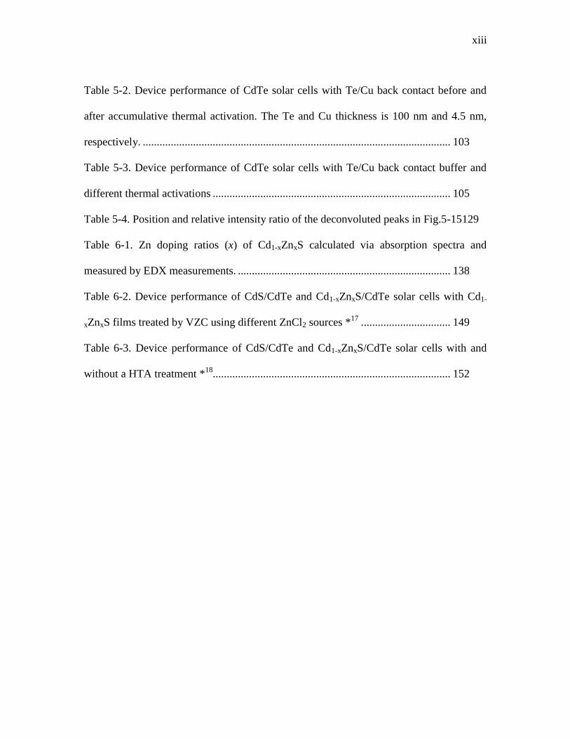
Table 5-2. Device performance of CdTe solar cells with Te/Cu back contact before and
after accumulative thermal activation. The Te and Cu thickness is 100 nm and 4.5 nm,
respectively. .............................................................................................................. 103
Table 5-3. Device performance of CdTe solar cells with Te/Cu back contact buffer and
different thermal activations ..................................................................................... 105
Table 5-4. Position and relative intensity ratio of the deconvoluted peaks in Fig.5-15129
Table 6-1. Zn doping ratios (x) of Cd1-xZnxS calculated via absorption spectra and
measured by EDX measurements. ............................................................................ 138
Table 6-2. Device performance of CdS/CdTe and Cd1-xZnxS/CdTe solar cells with Cd1-
xZnxS films treated by VZC using different ZnCl2 sources *17
................................ 149
Table 6-3. Device performance of CdS/CdTe and Cd1-xZnxS/CdTe solar cells with and
without a HTA treatment *18
..................................................................................... 152
xiv
List of Figures
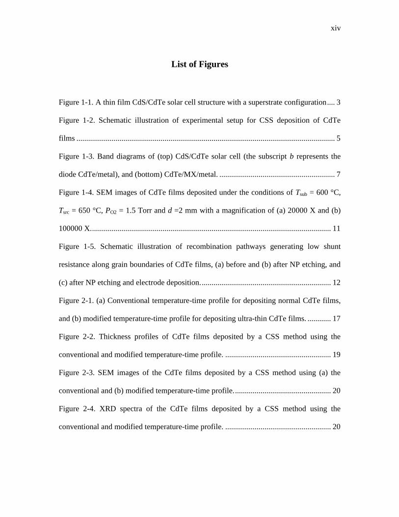
Figure 1-1. A thin film CdS/CdTe solar cell structure with a superstrate configuration .... 3
Figure 1-2. Schematic illustration of experimental setup for CSS deposition of CdTe
films .................................................................................................................................... 5
Figure 1-3. Band diagrams of (top) CdS/CdTe solar cell (the subscript b represents the
diode CdTe/metal), and (bottom) CdTe/MX/metal. ........................................................... 7
Figure 1-4. SEM images of CdTe films deposited under the conditions of Tsub = 600 °C,
Tsrc = 650 °C, PO2 = 1.5 Torr and d =2 mm with a magnification of (a) 20000 X and (b)
100000 X. .......................................................................................................................... 11
Figure 1-5. Schematic illustration of recombination pathways generating low shunt
resistance along grain boundaries of CdTe films, (a) before and (b) after NP etching, and
(c) after NP etching and electrode deposition. .................................................................. 12
Figure 2-1. (a) Conventional temperature-time profile for depositing normal CdTe films,
and (b) modified temperature-time profile for depositing ultra-thin CdTe films. ............ 17
Figure 2-2. Thickness profiles of CdTe films deposited by a CSS method using the
conventional and modified temperature-time profile. ...................................................... 19
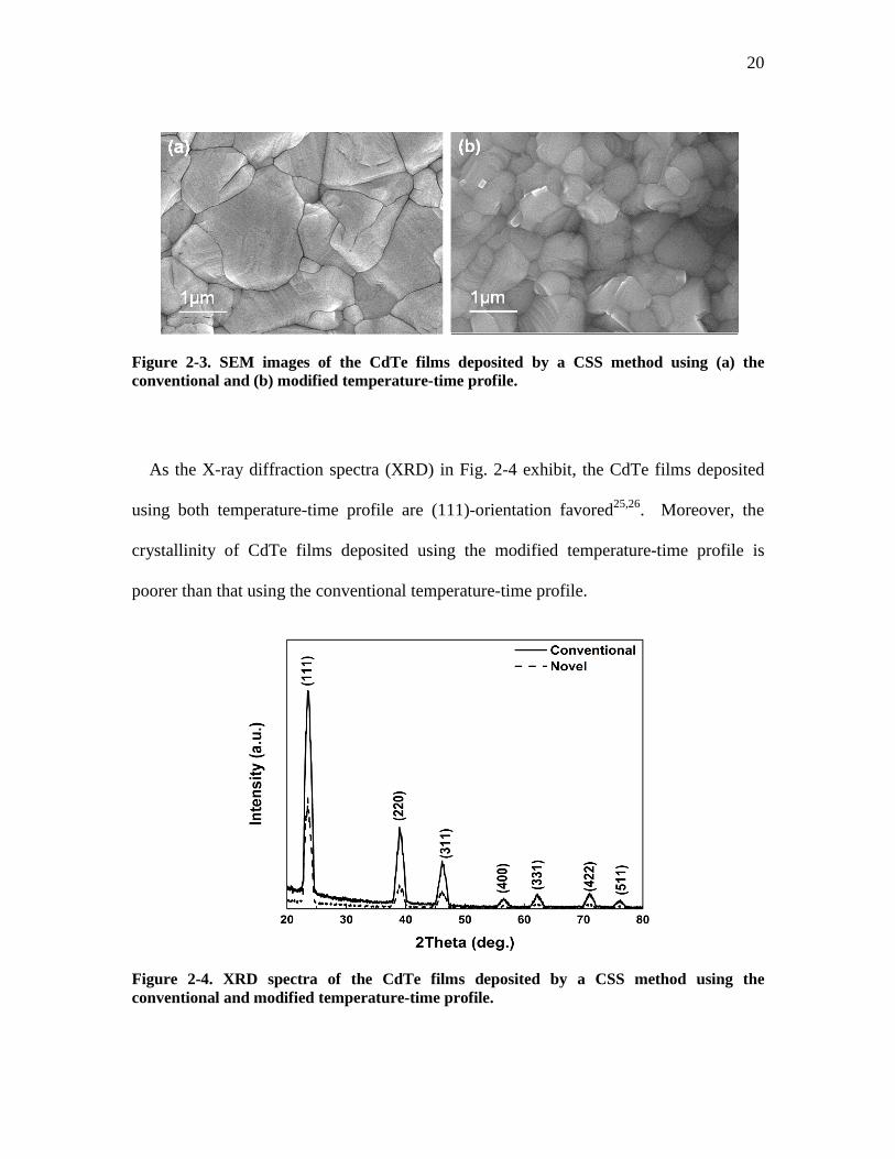
Figure 2-3. SEM images of the CdTe films deposited by a CSS method using (a) the
conventional and (b) modified temperature-time profile. ................................................. 20
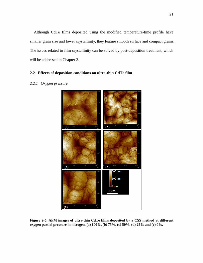
Figure 2-4. XRD spectra of the CdTe films deposited by a CSS method using the
conventional and modified temperature-time profile. ...................................................... 20
xv
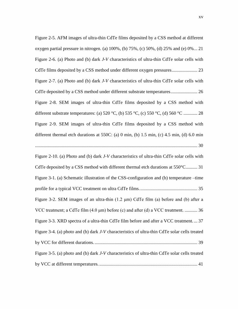
Figure 2-5. AFM images of ultra-thin CdTe films deposited by a CSS method at different
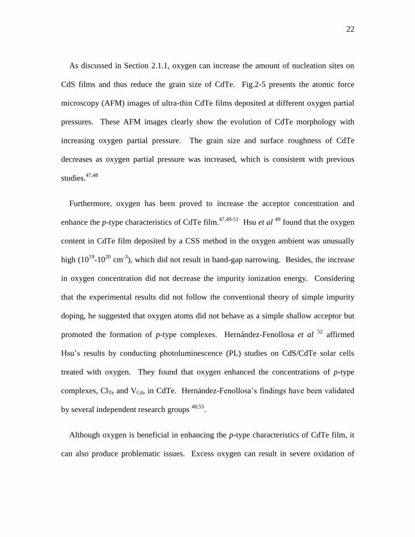
oxygen partial pressure in nitrogen. (a) 100%, (b) 75%, (c) 50%, (d) 25% and (e) 0%. .. 21
Figure 2-6. (a) Photo and (b) dark J-V characteristics of ultra-thin CdTe solar cells with
CdTe films deposited by a CSS method under different oxygen pressures ...................... 23
Figure 2-7. (a) Photo and (b) dark J-V characteristics of ultra-thin CdTe solar cells with
CdTe deposited by a CSS method under different substrate temperatures ....................... 26
Figure 2-8. SEM images of ultra-thin CdTe films deposited by a CSS method with
different substrate temperatures: (a) 520 °C, (b) 535 °C, (c) 550 °C, (d) 560 °C ............ 28
Figure 2-9. SEM images of ultra-thin CdTe films deposited by a CSS method with
different thermal etch durations at 550C: (a) 0 min, (b) 1.5 min, (c) 4.5 min, (d) 6.0 min
........................................................................................................................................... 30
Figure 2-10. (a) Photo and (b) dark J-V characteristics of ultra-thin CdTe solar cells with
CdTe deposited by a CSS method with different thermal etch durations at 550°C .......... 31
Figure 3-1. (a) Schematic illustration of the CSS-configuration and (b) temperature –time
profile for a typical VCC treatment on ultra CdTe films. ................................................. 35
Figure 3-2. SEM images of an ultra-thin (1.2 μm) CdTe film (a) before and (b) after a
VCC treatment; a CdTe film (4.0 μm) before (c) and after (d) a VCC treatment. ........... 36
Figure 3-3. XRD spectra of a ultra-thin CdTe film before and after a VCC treatment. ... 37
Figure 3-4. (a) photo and (b) dark J-V characteristics of ultra-thin CdTe solar cells treated
by VCC for different durations. ........................................................................................ 39
Figure 3-5. (a) photo and (b) dark J-V characteristics of ultra-thin CdTe solar cells treated
by VCC at different temperatures. .................................................................................... 41
xvi
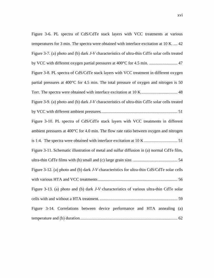
Figure 3-6. PL spectra of CdS/CdTe stack layers with VCC treatments at various
temperatures for 3 min. The spectra were obtained with interface excitation at 10 K. .... 42
Figure 3-7. (a) photo and (b) dark J-V characteristics of ultra-thin CdTe solar cells treated
by VCC with different oxygen partial pressures at 400°C for 4.5 min. ........................... 47
Figure 3-8. PL spectra of CdS/CdTe stack layers with VCC treatment in different oxygen
partial pressures at 400°C for 4.5 min. The total pressure of oxygen and nitrogen is 50
Torr. The spectra were obtained with interface excitation at 10 K. .................................. 48
Figure 3-9. (a) photo and (b) dark J-V characteristics of ultra-thin CdTe solar cells treated
by VCC with different ambient pressures. ........................................................................ 51
Figure 3-10. PL spectra of CdS/CdTe stack layers with VCC treatments in different
ambient pressures at 400°C for 4.0 min. The flow rate ratio between oxygen and nitrogen
is 1:4. The spectra were obtained with interface excitation at 10 K ................................ 51
Figure 3-11. Schematic illustration of metal and sulfur diffusion in (a) normal CdTe film,
ultra-thin CdTe films with (b) small and (c) large grain size. .......................................... 54
Figure 3-12. (a) photo and (b) dark J-V characteristics for ultra-thin CdS/CdTe solar cells
with various HTA and VCC treatments ............................................................................ 56
Figure 3-13. (a) photo and (b) dark J-V characteristics of various ultra-thin CdTe solar
cells with and without a HTA treatment. .......................................................................... 59
Figure 3-14. Correlations between device performance and HTA annealing (a)
temperature and (b) duration. ............................................................................................ 62
xvii
Figure 3-15. SEM images for: CSS-deposited ultra-thin CdTe film (a) without any
treatment, (b) with VCC treatment, (c) with HTA treatment, and (d) with HTA+VCC
treatments. ......................................................................................................................... 63
Figure 3-16. PL spectra with surface excitation for: CSS-deposited ultra-thin CdTe film
without any treatment, with VCC or HTA or HTA+VCC treatment. .............................. 65
Figure 3-17. PL spectra and the corresponding deconvoluted PL peaks for CSS-deposited
ultra-thin CdTe film (a) without any treatment, (b) with HTA treatment, (c) with VCC
treatment and (d) with HTA+VCC treatments. PL spectra were obtained with interface
excitation at 40 K .............................................................................................................. 67
Figure 3-18. PL spectra with interface excitation showing the evolution of: (a) the
interface defect band, and (b) the CdTe1-xSx band with various HTA and VCC treatments.
........................................................................................................................................... 68
Figure 3-19. Absorption at the band edge region for ultra-thin CdTe films with various
HTA and VCC treatments, (b) the x values of CdTe1-xSx in relation to the bandgap of
CdTe1-xSx........................................................................................................................... 71
Figure 3-20. Spectral response for ultra-thin CdS/CdTe solar cells with various HTA and
VCC treatments ................................................................................................................. 72
Figure 4-1. (a) Photo and (b) dark J-V characteristics of CdS/CdTe solar cells with 1.5-
5.0 μm CdTe thickness using NP treatment in back contact formation. ........................... 77
Figure 4-2. SEM images of ultra-thin CdTe film before (a: top view, c: cross-section view)
and after NP etching (25 s) (b: top view, d: cross-section view) ...................................... 78
xviii
Figure 4-3. Comparison of the (a) photo and (b) dark J-V curves, and (c) diode factor
extraction of a NP cell and a MoOx cell. The CdTe film thickness is 1.5 μm. ................. 80
Figure 4-4. Effect of thermal stress on efficiency for ultra-thin CdTe solar cells with
different back contacts. The CdTe film thickness is 1.5 μm............................................. 81
Figure 4-5. (a) Photo and (b) dark J-V characteristics of ultra-thin CdTe solar cells with
different back contacts and Ni or Al electrode ................................................................. 82
Figure 4-6. (a) Photo and (b) dark J-V characteristics of ultra-thin CdTe solar cells with
different thicknesses of MoOx buffer layer. ...................................................................... 84
Figure 4-7. (a) Photo and (b) dark J-V characteristics of ultra-thin CdTe solar cells with
different thicknesses of CdTe and 40 nm MoOx back contact buffer. .............................. 86
Figure 4-8. (a) Photo and (b) dark J-V characteristics of ultra-thin CdTe solar cells with
MoOx or Te/Cu back contact buffer. The CdTe film thickness is 1.5 μm. ...................... 88
Figure 4-9. (a) Photo and (b) dark J-V characteristics of ultra-thin CdTe solar cells with
Te/Cu back contact buffer with different thermal activation conditions. The CdTe film
thickness is 1.5 μm ............................................................................................................ 90
Figure 4-10. (a) Photo and (b) dark J-V characteristics of ultra-thin CdTe solar cells using
Te/Cu back contact buffer with different Te thicknesses. The Cu thickness is 1.1 nm. ... 92
Figure 4-11. (a) Photo and (b) dark J-V characteristics of ultra-thin CdTe solar cells using
Te/Cu back contact buffer with different Cu thicknesses. The Te thickness is 100 nm. .. 94
Figure 4-12. (a) Photo and (b) dark J-V characteristics of ultra-thin CdTe solar cells with
different thicknesses of CdTe and a Te/Cu back contact buffer layer. The thickness of Te
and Cu are 100 nm and 1.1 nm respectively ..................................................................... 96
xix
Figure 5-1. (a) Photo and (b) dark J-V characteristics of CdTe solar cells with and without
a back contact buffer. ...................................................................................................... 100
Figure 5-2. (a) Photo and (b) dark J-V characteristics of CdTe solar cells with Te/Cu back
contact before and after accumulative thermal activation. ............................................. 102
Figure 5-3. (a) J-V characteristics of CdTe solar cells with Te/Cu back contact buffer
before and after thermal activation at different temperatures. (b) Expanded view of the
power-quadrant. .............................................................................................................. 104
Figure 5-4. (a) J-V characteristics of CdTe solar cells with Te/Cu back contact buffer and
thermal activation at different temperatures; (b) expanded view of the power-quadrant.
......................................................................................................................................... 106
Figure 5-5. Device degradation (a) Jsc, (b) Voc, (c) FF and (d) η of CdTe solar cells with
Te/Cu back contact buffer in thermal stress tests. The Te thickness is 100 nm. The Cu
thickness is 0~9.0 nm. ..................................................................................................... 109
Figure 5-6. J-V characteristics (a) photo and (b) dark of CdTe solar cells using Te/Cu
back contact buffer with different Cu thicknesses before and after a thermal stress test at
200 °C for 9h. The Te thickness is 100 nm. .................................................................. 111
Figure 5-7. Efficiency degradation of CdTe solar cells using Te/Cu back contact buffer
with different Cu/Te molar ratios in the thermal stress test (200 °C, 0~9h) ................... 113
Figure 5-8. Device degradation (a) Jsc, (b) Voc, (c) FF and (d) η of CdTe solar cells with
Te/Cu back contact buffer in thermal stress test. The Cu thickness is 1.1 nm. The Te
thickness is 50~300 nm. .................................................................................................. 116
xx
Figure 5-9. Device degradation (a) Jsc, (b) Voc, (c) FF and (d) η of CdTe solar cells with
Te/Cu back contact buffer in thermal stress test at different temperatures. The Cu and Te
layers are 1.1 nm and 100 nm thick respectively. ........................................................... 118
Figure 5-10. Device degradation (a) FF and (b) η of CdTe solar cells with Te/Cu back
contact buffer in light soaking test. The Cu layer was varied from 0 to 9.0 nm. The Te
layer was 100 nm thick. .................................................................................................. 120
Figure 5-11. Device degradation (a) FF and (b) η of CdTe solar cells with Te/Cu back
contact buffer in light soaking test. The Te layer was varied from 50 to 100 nm. The Cu
layer was 1.1 nm thick. ................................................................................................... 122
Figure 5-12. (a) and (b) CdTe film, (c) and (d) 100 nm Te on top of CdTe film, (e) and (f)
100 nm Te/CdTe after a thermal activation at 225 °C for 4 min. ................................... 123
Figure 5-13. XPS peak shift of Te3d and Cu2p during the in-situ annealing at 260 °C for
certain duration between two consecutive XPS measurements. The sample structure is:
glass substrate/ FTO/CdS/CdTe/50 nm Te/4 nm Cu. ..................................................... 125
Figure 5-14. Normalized PL spectra of CdS/4.0 μm-CdTe/100 nm-Te/1.1 nm-Cu/200
nm-Ni without and with thermal activation; with thermal activation and 9h thermal stress
test. PL spectra were obtained with interface excitation at 40 K .................................... 126
Figure 5-15. PL spectra and the corresponding deconvoluted PL peaks of CdS/4.0 μm-
CdTe/100 nm-Te/1.1 nm-Cu/200 nm-Ni (a) without and (b) with a thermal activation; (c)
with a thermal activation and 9h of thermal stress test; (d) the evolution of the Cu+-VCd
band. PL spectra were obtained with interface excitation at 40 K ................................. 129
xxi
Figure 6-1. (a) Schematic illustration of a two zone tube furnace setup and (b) a typical
temperature profile for VZC treatment ........................................................................... 134
Figure 6-2. XRD spectra of FTO substrate, CdS film on FTO substrate before and after a
VZC treatment ................................................................................................................ 135
Figure 6-3. SEM images of (a) as-deposited CdS film and (b) CdS film treated by a VZC
treatment. ........................................................................................................................ 136
Figure 6-4. Transmission spectra of a CdS film and the CdS film treated by VZC and
(inset) the extraction of bandgaps of the CdS film from absorption measurement before
and after a VZC treatment............................................................................................... 138
Figure 6-5. EDX spectra of a CdS film before and after a VZC treatment .................... 139
Figure 6-6. Relation between the bandgap of Cd1-xZnxS films and different annealing
temperatures (the annealing duration was 2 min) ........................................................... 140
Figure 6-7. Relation between the bandgap of Cd1-xZnxS films and different annealing
durations (the annealing temperature was 360 °C) ......................................................... 141
Figure 6-8. Relation between the bandgap of Cd1-xZnxS films and varios nitrogen flow
rates (the annealing temperature and duration were 360 °C and 2 min respectively) .... 141
Figure 6-9. Photo J-V characteristics of CdTe solar cells with CdS and Cd1-xZnxS window
layers. .............................................................................................................................. 142
Figure 6-10. Spectral response curves of CdTe solar cells with CdS and Cd0.95Zn0.05S,
Cd0.60Zn0.40S as the window layers. ................................................................................ 143
Figure 6-11. (a) Photo and (b) dark J-V characteristics of CdTe solar cells with i-
SnO2/CdS, i-SnO2/Cd0.91Zn0.09S and Cd0.95Zn0.05S window layers. ............................... 144
xxii
Figure 6-12. Photo J-V characteristics of CdTe solar cells with 150 nm i-
SnO2/Cd0.90Zn0.10S, 100 nm i-SnO2/Cd0.91Zn0.09S, 50 nm i-SnO2/Cd0.92Zn0.08S and
Cd0.95Zn0.05S window layers. .......................................................................................... 145
Figure 6-13. Photo and dark J-V characteristics of CdTe solar cells with 100 nm i-
SnO2/CdS, 100 nm i-SnO2/Cd0.90Zn0.10S, 100 nm i-SnO2/Cd0.81Zn0.19S and 100 nm i-
SnO2/Cd0.68Zn0.32S window layers. ................................................................................. 146
Figure 6-14. (a) Photo and (b) dark J-V characteristics of CdTe solar cells with CdS film
and Cd1-xZnxS film as window layers. The Cd1-xZnxS films were made by VZC treatment
using hydrated or ultra-dry ZnCl2 source. ....................................................................... 148
Figure 6-15. (a) photo and (b) dark J-V characteristics of Cd1-xZnxS/CdTe solar cells with
and without a HTA treatment (550 °C, 40 min) ............................................................. 151
Figure A-1 Spectrum of Solux solar simulator and AM 1.5 solar spectrum. ................. 170
1
1. Introduction
1.1 Background of thin film CdS/CdTe solar cells
A solar cell is a device which can convert solar energy directly into electric energy.
According to “Marketbuzz TM
2012: Annual world solar photovoltaic industry report”,
the world solar photovoltaic (PV) market installations reached a consolidated figure of
27.4 GW in 2011, representing an annual growth of 40% over the previous year.1,2
However, more than 80% of the current PV production is based on single-crystal silicon.
The high cost of single-crystal silicon based PV remains to be the main barrier which
limits their applications. It is also the driving force for developing low-cost PV
technologies such as thin film solar cells. In silicon-based PV, the wafer cost accounts
for over 50% of the total module cost.3 Replacing wafers by thin-film of semiconductor
can greatly reduce the manufacturing costs. Additional benefits include lower energy
consumption for solar cell production and consequently a shorter energy payback time.
Cadmium telluride (CdTe) has been regarded as a very promising material for thin-film
solar cells. The maximum power that a solar cell can theoretically deliver is proportional
to the product of the short circuit current (Jsc) and open circuit voltage (Voc) produced by
the cell under illumination. The Jsc decreases with increasing bandgap whereas the Voc
increases. The maximum theoretical efficiency of a single-junction solar cells is around
27% which corresponds to a bandgap of 1.5 eV4, which is a good match with the 1.45 eV
bandgap of CdTe. Furthermore, CdTe is a direct bandgap semiconductor with a strong
absorption coefficient of 104~10
5 cm
-1 in the range of 300~850 nm, which means that
2
more than 99% of the photons with energy greater than the bandgap will be absorbed
within 2 m.5 Thus the raw material usage and therefore cost per unit area for CdTe
solar cell is expected to be low. Moreover, high-quality polycrystalline CdTe films can
be deposited via a number of fabrication techniques including sputtering,6 close-space
sublimation (CSS),7 high vacuum thermo-evaporation,
8 and electro-deposition.
9 The CSS
method in particular is relatively simple and has been adopted for high-speed, large-area
manufacturing of CdTe PV modules.10
Thin film CdTe solar cells are based on a heterojunction formed between p-CdTe and
n-type semiconductor, typically II-VI compound such as n-CdS, n-CdSe, n-ZnSe or n-
Cd1-xZnxS.11
Among these compounds, CdS is the most commonly used. Fahrenbruch et
al.11
compared the physical properties of several II-VI heterojunctions and their
applications in the solar cell. The p-CdTe/n-CdS heterojunction possesses one of the
smallest lattice mismatch of 9.7% and thermal expansion mismatch of 9%. A power
conversion efficiency of 18.5% can be expected from CdS/CdTe solar cells,12
which is
among the highest in thin film photovoltaics.
A typical configuration of thin film CdS/CdTe solar cell is shown in Fig. 1-1.13
It is
known as the superstrate configuration with light illumination through the substrate,
which is typically a soda lime or borosilicate glass with a thickness of 2~4 mm. The
glass substrate provides mechanical support for the entire cell and protection against the
environment for the active layers. Transparent conducting oxide (TCO) on the glass
substrate acts as the front contact to the device. Indium tin oxide (ITO) and fluorine
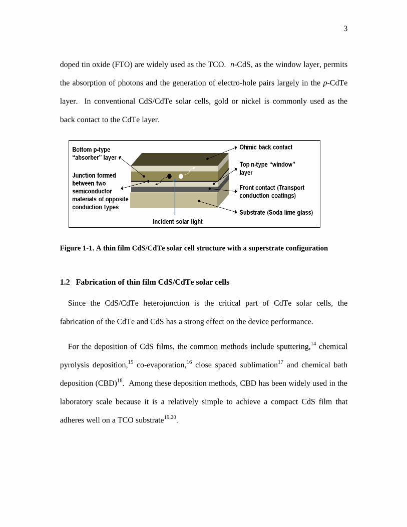
3
doped tin oxide (FTO) are widely used as the TCO. n-CdS, as the window layer, permits
the absorption of photons and the generation of electro-hole pairs largely in the p-CdTe
layer. In conventional CdS/CdTe solar cells, gold or nickel is commonly used as the
back contact to the CdTe layer.
Figure 1-1. A thin film CdS/CdTe solar cell structure with a superstrate configuration
1.2 Fabrication of thin film CdS/CdTe solar cells
Since the CdS/CdTe heterojunction is the critical part of CdTe solar cells, the
fabrication of the CdTe and CdS has a strong effect on the device performance.
For the deposition of CdS films, the common methods include sputtering,14
chemical
pyrolysis deposition,15
co-evaporation,16
close spaced sublimation17
and chemical bath
deposition (CBD)18
. Among these deposition methods, CBD has been widely used in the
laboratory scale because it is a relatively simple to achieve a compact CdS film that
adheres well on a TCO substrate19,20
.
4
In a CBD process, CdS film is produced via the decomposition of thiourea in an
alkaline solution of cadmium salts according to the reaction (Eqn.1-1) 20
.
(1-1)
In this reaction, cadmium acetate (Cd(CH3CO2)2) and thiourea provide the cadmium
and sulfur ions, respectively in an alkaline solution with ammonium hydroxide (NH4OH)
and ammonium acetate (CH3CO2NH4) as the pH buffers. The CdS film growth rate is
determined by the initial concentration of metal ions and the bath temperature.
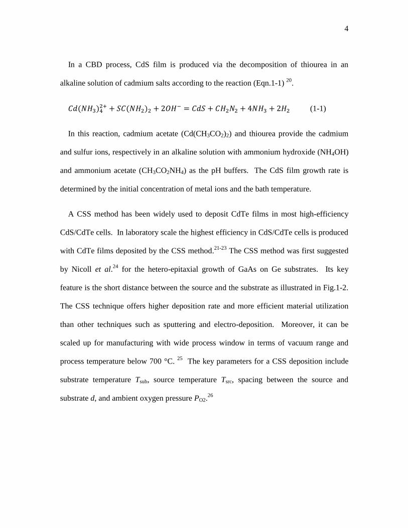
A CSS method has been widely used to deposit CdTe films in most high-efficiency
CdS/CdTe cells. In laboratory scale the highest efficiency in CdS/CdTe cells is produced
with CdTe films deposited by the CSS method.21-23
The CSS method was first suggested
by Nicoll et al.24
for the hetero-epitaxial growth of GaAs on Ge substrates. Its key
feature is the short distance between the source and the substrate as illustrated in Fig.1-2.
The CSS technique offers higher deposition rate and more efficient material utilization
than other techniques such as sputtering and electro-deposition. Moreover, it can be
scaled up for manufacturing with wide process window in terms of vacuum range and
process temperature below 700 °C. 25
The key parameters for a CSS deposition include
substrate temperature Tsub, source temperature Tsrc, spacing between the source and
substrate d, and ambient oxygen pressure PO2.26
5
Figure 1-2. Schematic illustration of experimental setup for CSS deposition of CdTe films
(1-2)
To improve the crystallinity quality of the CdTe films produced by the CSS or other
methods, it is necessary to subject the as-deposited CdTe films to various post-deposition
thermal treatments, including the CdCl2 treatment. A CdCl2 treatment usually leads to
prominent grain growth in CdTe films as a result of vapor phase induced re-
crystallization 27
described in the reaction shown in Eqn. 1-2.12,20
For CdTe films
deposited with a high substrate temperature, though the average grain size is large, a
CdCl2 treatment can still promote grain boundary re-growth and eliminate small grains.
It is believed that the presence of Cl2 promotes the crystalline growth of CdTe by means
of local vapor phase transport.20
In addition to enhancing the CdTe grain structures, a CdCl2 treatment can also cause
inter-diffusion of sulfur and tellurium ions at the CdTe/CdS interface resulting in
improved junction characteristics.28
Moreover, a CdCl2 treatment can also create VCd-Cl
6
complexes, known to be shallow acceptors in CdTe films.28
Generally, a typical CdCl2
treatment includes three steps as follows:
1) Apply a layer of CdCl2 on top of CdTe film either by dip-coating or by
evaporation;
2) Anneal the CdS/CdTe/CdCl2 stack layers in air at 380~420 °C for 20~40 min;
3) Remove CdCl2 residues from the treated CdTe films.
A CdCl2 treatment has also been applied to improve crystallinity and optical properties
of the CdS window layer.29,30
Back contact formation is the last step in the cell fabrication. In the band diagram
shown in Fig.1-3a 31
, a contact barrier, Φb, for holes exists at the CdTe/metal interface,
which can be calculated using Eqn. 1-3,
(1-3)
where Eg, χ and φm represent the bandgap of CdTe, the electron affinity of CdTe and the
work function of the contact metal, respectively. Because of the high work function of
CdTe (5.6~5.7 eV), the contact between CdTe and most common metals (with a work
function lower than that of CdTe) invariably results in a barrier, Φb, which is too high to
allow the hole carriers to transport across the p-CdTe/metal junction efficiently.
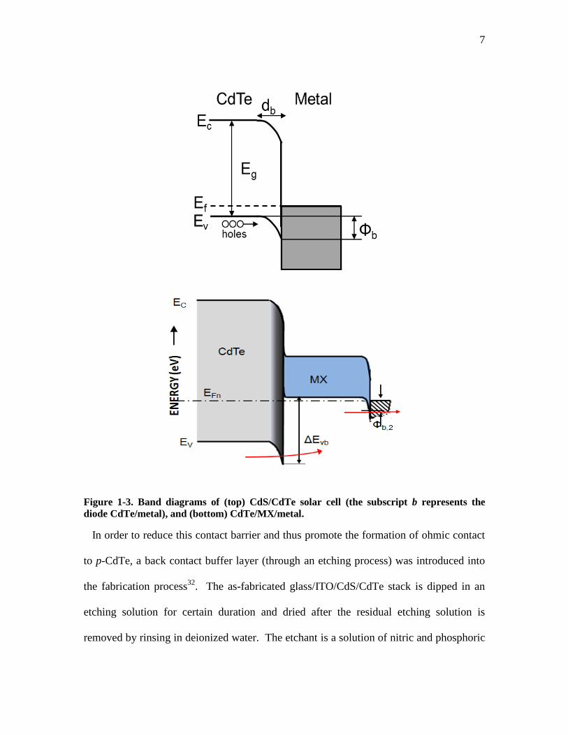
7
Figure 1-3. Band diagrams of (top) CdS/CdTe solar cell (the subscript b represents the
diode CdTe/metal), and (bottom) CdTe/MX/metal.
In order to reduce this contact barrier and thus promote the formation of ohmic contact
to p-CdTe, a back contact buffer layer (through an etching process) was introduced into
the fabrication process32
. The as-fabricated glass/ITO/CdS/CdTe stack is dipped in an
etching solution for certain duration and dried after the residual etching solution is
removed by rinsing in deionized water. The etchant is a solution of nitric and phosphoric
8
acids 32
, commonly known as NP solution, or a solution of bromine and methanol 28
,
named as BM solution. In addition to solution treatments, direct introduction of a buffer
layer MX (MX = CuxTe, ZnTe, Sb2Te3, Ni2P, Te, etc.) between p-CdTe and the back
contact metal can also produce a low-resistance back contact2. As Fig.1-3b
2 shows, the
high space charge density in the MX layer at the MX/metal junction can allow tunneling
of charge carriers. Cu and Sb from the MX layer are known to form shallow acceptors in
CdTe. Besides the high work function of MX layer also reduce the energy barrier for the
hole transfer at the CdTe/MX junction.
1.3 Deficiencies of thin film CdS/CdTe solar cells
The potential environmental hazard of CdS/CdTe solar cells resulting from the toxicity
of cadmium compounds is one of its deficiencies. Acute inhalation exposure to high
levels of cadmium in humans may cause effects on the lung such as pulmonary and
bronchial irritation. Chronic inhalation and oral exposure to cadmium results in a build-
up in the kidneys which can result in kidney diseases and reproductive effects 33
.
According to experimental investigations and life cycle analysis of cadmium in CdTe PV
productions, if CdTe PV modules are used under normal conditions 34
, no emission of
any kind can be generated. The emission of cadmium from CdTe PV modules during
accidents (e.g. fire 35
, breakage) is negligible. But the possible emission of cadmium
during the Cd mining and PV manufacturing and recycling cannot be completely avoided.
9
In order to reduce the environmental hazards resulting from cadmium compounds,
several approaches have been adopted in the research and manufacturing of CdS/CdTe
solar cells:
1) Reducing the cadmium content of CdS/CdTe solar cells;
2) Increasing the raw material utilization in the fabrication of CdS/CdTe solar cells;
3) Minimizing the emission of cadmium in the cadmium mining and PV
manufacturing process;
4) Developing advanced technologies to recover cadmium from the recycled CdTe
PV modules and from cadmium waste generated from PV manufacturing.
1.4 Developing ultra-thin CdTe solar cells and its challenges
Reducing the thickness of CdTe film, a.k.a. developing ultra-thin CdTe solar cells (~1
µm), is a primary solution to reduce cadmium usage. Additional advantages include
extending the tellurium supply, which is a limited reserve, and reducing the material cost
as well as the waste treatment cost.36
Furthermore, reduction of the CdTe layer thickness
also makes it easier to incorporate the CdTe layer in tandem solar cells and potential PV
glazing devices. 37
In most high-efficiency CdTe solar cells the CdTe thickness is typically in the range of
5 to 10 µm 21,38
. A thick absorber layer can avoid pinholes, which can result in shorting
the cell.37
However, the recombination loss of charge carriers in a thicker CdTe layer is
more prominent. 37
Moreover, a thicker CdTe layer also has a larger series resistance.
These drawbacks can adversely affect cell performance.
10
Reducing the thickness of CdTe layer from 5~10 µm to ~1 µm can alleviate the as-
mentioned drawbacks. Due to the high absorption coefficient of CdTe, the minimum
thickness required to directly absorb ~90% of the incident irradiation is approximately 1
µm.39
Theoretical calculation of carrier generation in CdS/CdTe solar cells by Amin et al
40 shows most of the charged carriers are generated within the first 1 µm-CdTe layer from
the CdS/CdTe junction, and beyond this region the carrier generation is reduced by two
orders of magnitude. Therefore, in principle, only 1~2-µm CdTe layer is needed to
produce highly efficient CdS/CdTe solar cells.
So far, the most popular methods for fabricating ultra-thin CdTe film are magnetron
sputtering deposition and metal organic chemical vapor deposition (MOCVD). Gupta et
al 41
fabricated an 11.8%- CdTe solar cell in which the CdTe layer thickness was 0.9 µm.
The CdTe film was deposited by magnetron sputtering. Jones et al 37
achieved an
efficiency of 11.4% in an ultra-thin CdTe solar cell in which the 1-µm-thick CdTe layer
was deposited by MOCVD. Both the magnetron sputtering and MOCVD methods
require complicated setup and costly maintenance; moreover, the deposition rates of
CdTe using these methods are very low (<100 nm/min), which is not applicable in large-
scale PV manufacturing. Because of the many advantages of the CSS technique as
mentioned, it is important to explore the optimized deposition conditions for ultra-thin
CdTe film using a CSS method.
11
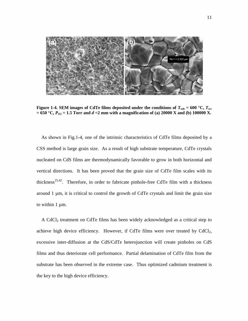
Figure 1-4. SEM images of CdTe films deposited under the conditions of Tsub = 600 °C, Tsrc
= 650 °C, PO2 = 1.5 Torr and d =2 mm with a magnification of (a) 20000 X and (b) 100000 X.
As shown in Fig.1-4, one of the intrinsic characteristics of CdTe films deposited by a
CSS method is large grain size. As a result of high substrate temperature, CdTe crystals
nucleated on CdS films are thermodynamically favorable to grow in both horizontal and
vertical directions. It has been proved that the grain size of CdTe film scales with its
thickness25,42
. Therefore, in order to fabricate pinhole-free CdTe film with a thickness
around 1 µm, it is critical to control the growth of CdTe crystals and limit the grain size
to within 1 µm.
A CdCl2 treatment on CdTe films has been widely acknowledged as a critical step to
achieve high device efficiency. However, if CdTe films were over treated by CdCl2,
excessive inter-diffusion at the CdS/CdTe heterojunction will create pinholes on CdS
films and thus deteriorate cell performance. Partial delamination of CdTe film from the
substrate has been observed in the extreme case. Thus optimized cadmium treatment is
the key to the high device efficiency.
12
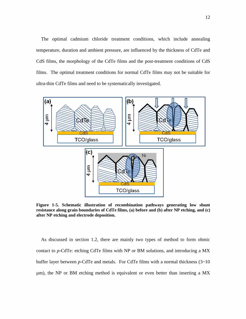
The optimal cadmium chloride treatment conditions, which include annealing
temperature, duration and ambient pressure, are influenced by the thickness of CdTe and
CdS films, the morphology of the CdTe films and the post-treatment conditions of CdS
films. The optimal treatment conditions for normal CdTe films may not be suitable for
ultra-thin CdTe films and need to be systematically investigated.
Figure 1-5. Schematic illustration of recombination pathways generating low shunt
resistance along grain boundaries of CdTe films, (a) before and (b) after NP etching, and (c)
after NP etching and electrode deposition.
As discussed in section 1.2, there are mainly two types of method to form ohmic
contact to p-CdTe: etching CdTe films with NP or BM solutions, and introducing a MX
buffer layer between p-CdTe and metals. For CdTe films with a normal thickness (3~10
µm), the NP or BM etching method is equivalent or even better than inserting a MX
13
buffer layer in forming ohmic contact to p-CdTe. However, as illustrated in Fig.1-5 43
,
one of the drawbacks of NP or BM treatment is that the tellurium rich layer on CdTe
films resulting from the treatment produces low shunt resistance along grain boundaries,
which leads to large leakage current and thereof low Voc. The drawback will be amplified
if the CdTe film is not compact enough (Fig. 1-5b) or the etching duration is too long or
the CdTe film is too thin. Alternative methods are required to replace the conventional
back contact formation schemes.
1.5 Summary
As a promising and commercialized PV technology, CdTe solar cells still face a lot of
challenges including increasing material cost as a result of limited tellurium supplies, and
environmental hazards associated with potential cadmium emission and waste
management.
Developing ultra-thin CdTe solar cells with the CdTe thickness of ~1 μm or less is a
feasible approach to solving the challenges. Reducing the thickness of CdTe from 4~6
μm to ~1 μm will reduce the materials cost, alleviate the environmental impact of
cadmium compound, and improve manufacturing productivity.
Reducing the thickness of CdTe while maintaining the high-efficiency (15~17 %) is
technically challenging and will require significant development efforts, including the
following:
1) Improving the fabricating techniques for the production of ultra-thin CdTe films
with high throughput.
14
2) Addressing the low-crystallinity and corresponding defects issues of ultra-thin
CdTe films deposited at low substrate temperature.
3) Developing new back contact materials to replace the conventional solution
etching method which is not applicable to ultra-thin CdTe cells.
This thesis work is aimed to producing high-efficiency ultra-thin CdTe solar cells by
providing solutions to these issues.
15
2. Fabrication of ultra-thin CdTe films
To achieve high-efficiency in ultra-thin CdTe solar cells, the most important step is to
deposit pinhole-free CdTe films with sufficient crystallinity. As discussed in Section 1.2,
deposition methods37,41
such as sputtering are better suited for depositing ultra-thin CdTe
films. However, due to their limitations especially low deposition rate, these methods are
not as compatible to large-scale manufacturing as the CSS method. This chapter will
discuss the fabrication of ultra-thin CdTe films using a CSS method with a modified
temperature-time profile, and the effects of CSS deposition conditions on CdTe film
morphology and device performance.
2.1 Close-spaced sublimation with modified temperature-time profile
2.1.1 Control factors of fabricating pinhole-free CdTe films
As discussed in Section 1.4, in order to fabricate pinhole-free CdTe films with a
thickness around 1 µm, it is critical to control the crystal growth and to limit the grain
size to within 1 µm. To deposit CdTe films with the grain size of ~1 µm, the
conventional CSS deposition conditions will have to be modified.
According to Luschitz et al 42
, the grain size of CdTe films deposited by a CSS method
is highly dependent on the substrate temperature. CdTe films deposited with Tsub
between 350 °C and 460 °C exhibit pyramidally shaped grains which extend throughout
the whole film. The surface grain size linearly increases from ~0.5 µm at Tsub = 350 °C
to ~1.5 µm at Tsub =460 °C. In order to limit the grain size of CdTe to within 1 µm, Tsub
between 350 °C and 460 °C should be used. However, the high density of deep pinholes
16
in the CdTe films deposited with Tsub between 350 °C and 460 °C can impair the device
performance and stability.
CdTe films deposited with Tsub > 460 °C, which has been widely used in the state-of-
the-art process of CSS deposition, are featured by irregularly shaped grains, a high
surface roughness and non-uniformly distributed grain size. Bulk diffusion processes
including recrystallization and grain growth result in the as-mentioned morphological
characteristics. Although the grain size of CdTe films is much larger than 1 µm and not
uniform, it is better to choose Tsub > 460 °C because the resulting films are more dense
and compact. It will be necessary to reduce the grain size through other means.
The introduction of oxygen into the CSS deposition of CdTe films was due to Tyan et
al 44
. Apparently incorporating oxygen in the deposition ambient can increase the
amount of nucleation sites on the CdS film and thus reduce the grain size of CdTe film
grown on top of the CdS film. O2 react with CdS to form CdO which serve as nucleation
sites for CdTe growth 45
. By tailoring the O2 partial pressure in the ambient, it is possible
to deposit ultra-thin CdTe film at a high substrate temperature to produce crystalline
CdTe films with a grain size < 1 µm while retaining good film quality.
2.1.2 Modified temperature-time profile for depositing ultra-thin CdTe films
Fig.2-1a shows typical temperature profiles of depositing CdTe films with a thickness
of 3~8 µm. Tsub was maintained at 600 °C during the preheating step and the deposition
process in order to achieve high Voc 46
. The deposition rate was set at1~1.5 µm/min by
adjusting Tsrc, d and PO2.
17
Figure 2-1. (a) Conventional temperature-time profile for depositing normal CdTe films,
and (b) modified temperature-time profile for depositing ultra-thin CdTe films.
In order to deposit ultra-thin CdTe films with a thickness of 1~1.5 µm, a new
temperature-time profile was used, as shown in Fig.2-1b. Tsub was reduced from 600 °C
to 525 °C. Compared with the conventional temperature-time profile in which Tsrc was
18
unchanged during the deposition process, in the new temperature profile, Tsrc was varied
from 550 °C to 625 °C. Before Tsrc reached the maximum value, Tscr-Tsub ranged from 0
to 100 °C. Small Tscr-Tsub leaded to a low deposition rate and might result in dense film
at the beginning of the deposition, a critical step to reduce pinhole formation. The
average deposition rate was ~500 nm/min.
The ramping rate of the source was decreased from 300 °C /min to 100 °C/min. Since
the heat transfer was more thorough with a longer ramping duration, the thermal
equilibrium between the graphite holder and the CdTe granules was more easily to
achieve.
2.1.3 Comparison between conventional and modified temperature-time profile
As shown in Fig. 2-2, in terms of roughness or roughness/thickness ratio, the CdTe
films deposited by a CSS method with the new temperature-time profile have a much
smoother surface than the film deposited with the conventional temperature-time profile.
Small roughness of the film deposited by a CSS method with the new temperature-time
profile indirectly suggests small grain size from low deposition rate.
Fig.2-3 shows the SEM images of CdTe films deposited using the conventional and
new temperature profile. The terrace-type texture on the CdTe grains, which is similar to
the CdTe grains shown in the SEM images in Fig.1-4, indicates good film crystallinity.
The grain size of the CdTe film deposited using the modified temperature-time profile is
much smaller than that using the conventional temperature-time profile. The difference
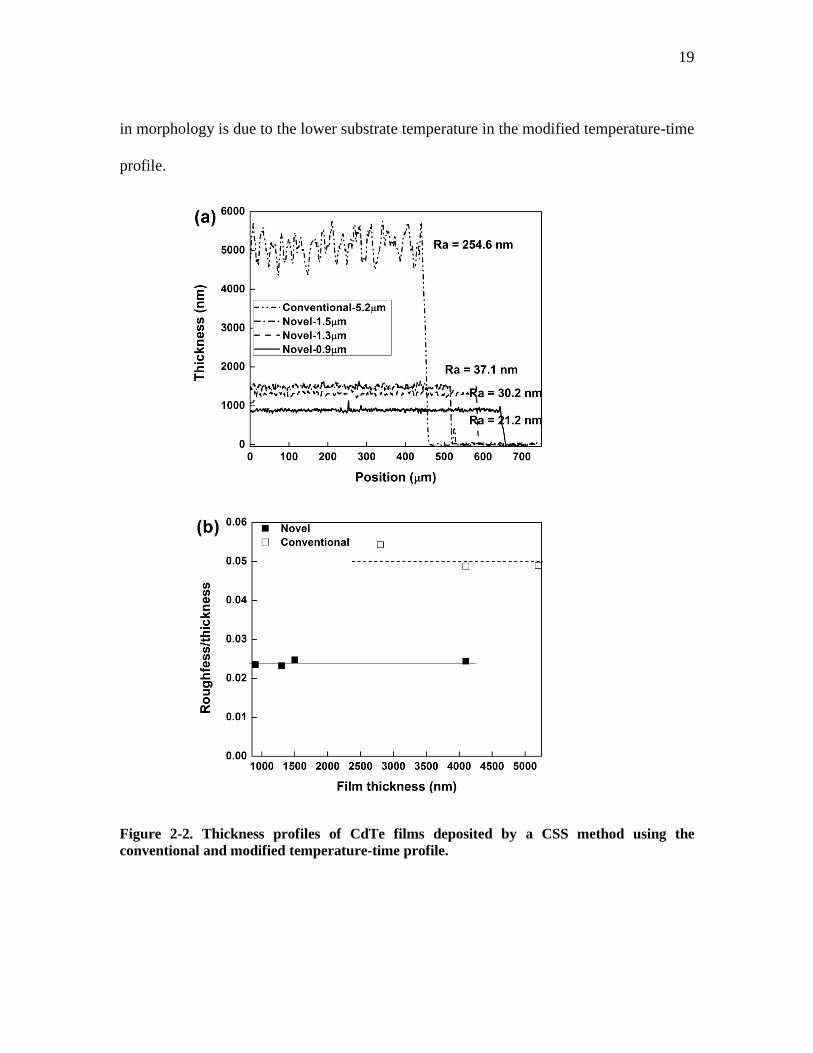
19
in morphology is due to the lower substrate temperature in the modified temperature-time
profile.
Figure 2-2. Thickness profiles of CdTe films deposited by a CSS method using the
conventional and modified temperature-time profile.
20
Figure 2-3. SEM images of the CdTe films deposited by a CSS method using (a) the
conventional and (b) modified temperature-time profile.
As the X-ray diffraction spectra (XRD) in Fig. 2-4 exhibit, the CdTe films deposited
using both temperature-time profile are (111)-orientation favored25,26
. Moreover, the
crystallinity of CdTe films deposited using the modified temperature-time profile is
poorer than that using the conventional temperature-time profile.
Figure 2-4. XRD spectra of the CdTe films deposited by a CSS method using the
conventional and modified temperature-time profile.
21
Although CdTe films deposited using the modified temperature-time profile have
smaller grain size and lower crystallinity, they feature smooth surface and compact grains.
The issues related to film crystallinity can be solved by post-deposition treatment, which
will be addressed in Chapter 3.
2.2 Effects of deposition conditions on ultra-thin CdTe film
2.2.1 Oxygen pressure
Figure 2-5. AFM images of ultra-thin CdTe films deposited by a CSS method at different
oxygen partial pressure in nitrogen. (a) 100%, (b) 75%, (c) 50%, (d) 25% and (e) 0%.
22
As discussed in Section 2.1.1, oxygen can increase the amount of nucleation sites on
CdS films and thus reduce the grain size of CdTe. Fig.2-5 presents the atomic force
microscopy (AFM) images of ultra-thin CdTe films deposited at different oxygen partial
pressures. These AFM images clearly show the evolution of CdTe morphology with
increasing oxygen partial pressure. The grain size and surface roughness of CdTe
decreases as oxygen partial pressure was increased, which is consistent with previous
studies.47,48
Furthermore, oxygen has been proved to increase the acceptor concentration and
enhance the p-type characteristics of CdTe film.47,49-51
Hsu et al 49
found that the oxygen
content in CdTe film deposited by a CSS method in the oxygen ambient was unusually
high (1019
-1020
cm-3
), which did not result in band-gap narrowing. Besides, the increase
in oxygen concentration did not decrease the impurity ionization energy. Considering
that the experimental results did not follow the conventional theory of simple impurity
doping, he suggested that oxygen atoms did not behave as a simple shallow acceptor but
promoted the formation of p-type complexes. Hernández-Fenollosa et al 52
affirmed
Hsu’s results by conducting photoluminescence (PL) studies on CdS/CdTe solar cells
treated with oxygen. They found that oxygen enhanced the concentrations of p-type
complexes, ClTe and VCd, in CdTe. Hernández-Fenollosa’s findings have been validated
by several independent research groups 48,53
.
Although oxygen is beneficial in enhancing the p-type characteristics of CdTe film, it
can also produce problematic issues. Excess oxygen can result in severe oxidation of
23
CdTe source and laterally non-uniform deposition. Rose et al 54
revealed that source
oxidation can decrease sublimation from the source and reduce the reproducibility and
manufacturing-suitability of the process. Vora et al 55
found that higher oxygen partial
pressure resulted in larger oxygen concentration gradient in the CSS system and thus
different reaction rates between oxygen and Cd vapor at different positions.
Figure 2-6. (a) Photo and (b) dark J-V characteristics of ultra-thin CdTe solar cells with
CdTe films deposited by a CSS method under different oxygen pressures
24
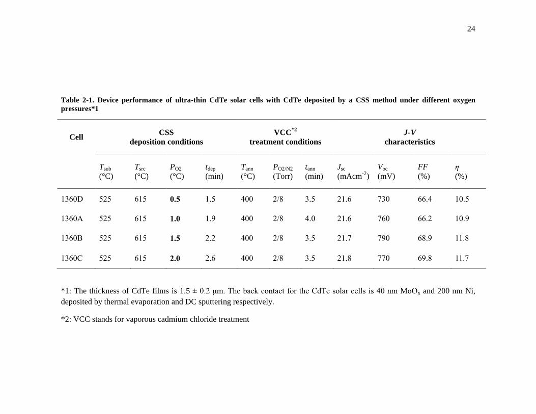
Table 2-1. Device performance of ultra-thin CdTe solar cells with CdTe deposited by a CSS method under different oxygen
pressures*1
Cell CSS
deposition conditions
VCC*2
treatment conditions
J-V
characteristics
Tsub
(°C)
Tsrc
(°C)
PO2
(°C)
tdep
(min)
Tann
(°C)
PO2/N2
(Torr)
tann
(min)
Jsc
(mAcm-2
)
Voc
(mV)
FF
(%)
η
(%)
1360D 525 615 0.5 1.5 400 2/8 3.5 21.6 730 66.4 10.5
1360A 525 615 1.0 1.9 400 2/8 4.0 21.6 760 66.2 10.9
1360B 525 615 1.5 2.2 400 2/8 3.5 21.7 790 68.9 11.8
1360C 525 615 2.0 2.6 400 2/8 3.5 21.8 770 69.8 11.7
*1: The thickness of CdTe films is 1.5 ± 0.2 μm. The back contact for the CdTe solar cells is 40 nm MoOx and 200 nm Ni,
deposited by thermal evaporation and DC sputtering respectively.
*2: VCC stands for vaporous cadmium chloride treatment
25
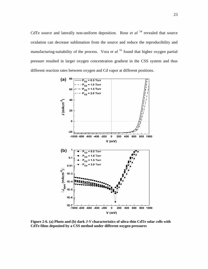
Figure 2-6 shows the photo and dark J-V characteristics of CdTe solar cells with CdTe
films deposited under different oxygen pressures. The cell fabrication details and device
performance are listed in Table.2-1. In order to compensate the effects of chamber
pressure on deposition rate, the deposition durations were adjusted accordingly so that the
as-deposited CdTe films had similar thicknesses. Based on the J-V characteristics and
device performance, the optimum oxygen pressure is 1.5 Torr which produces the highest
efficiency. If the oxygen pressure is much lower, e.g. 0.5 Torr, the CdTe solar cell has a
lower Voc of 730 mV, which is consistent with the larger leakage current. The inferior
device performance is presumably due to the lower density of nucleation sites and less
effective doping effect. If the oxygen pressure is higher, e. g. 2.0 Torr, the device
efficiency is almost not affected, although the Voc is slightly lower.
2.2.2 Substrate temperature
As discussed in Section 2.1.1, in order to deposit pinhole-free CdTe films, it is better to
choose Tsub > 460 °C and to reduce the grain size through other means. As discussed in
Section 2.2.1, oxygen can reduce the CdTe grain size by increasing the density of
nucleation sites on CdS films. With a low substrate temperature of 525 °C, the optimum
oxygen pressure is ~1.5 Torr. However, low Tsub can result in poor crystallinity and thus
more defects and impurities, which is detrimental to device performance. In order to
compensate the effects of poor crystallinity, a post-deposition annealing treatment is
required to improve film quality, which will be discussed in detail in Chapter 3.
Alternatively, CdTe film crystallinity can be enhanced by increasing Tsub. Although
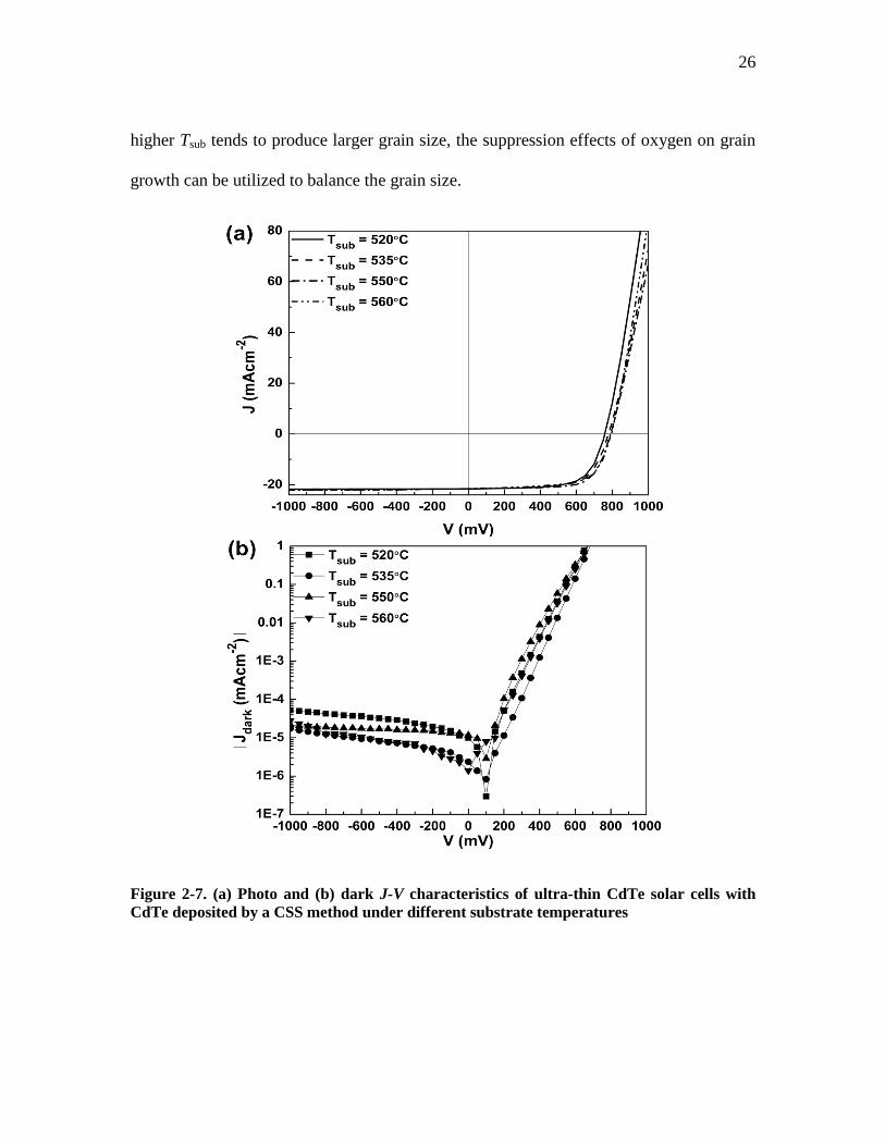
26
higher Tsub tends to produce larger grain size, the suppression effects of oxygen on grain
growth can be utilized to balance the grain size.
Figure 2-7. (a) Photo and (b) dark J-V characteristics of ultra-thin CdTe solar cells with
CdTe deposited by a CSS method under different substrate temperatures
27
Table 2-2. Device performance of ultra-thin CdTe solar cells with CdTe deposited by a CSS method under different substrate
temperatures. *3
Cell CSS
deposition conditions
VCC
treatment conditions
J-V
characteristics
Tsub
(°C)
Tsrc
(°C)
PO2
(°C)
tdep
(min)
Tann
(°C)
PO2/N2
(Torr)
tann
(min)
Jsc
(mAcm-2
)
Voc
(mV)
FF
(%)
η
(%)
1400A 520 625 1.5 1.5 400 2/8 4.5 21.6 760 67.9 11.1
1400B 535 625 1.5 1.5 400 2/8 4.0 21.6 778 68.1 11.5
1400C 550 625 2.0 2.0 400 2/8 4.5 21.6 790 71.3 12.1
1400D 560 635 2.5 2.5 400 2/8 4.0 21.5 795 68.6 11.7
*3: The thickness of CdTe films is 1.5 ± 0.2 μm. The back contact for the CdTe solar cells is 40 nm MoOx and 200 nm Ni,
deposited by thermal evaporation and DC sputtering respectively.
28
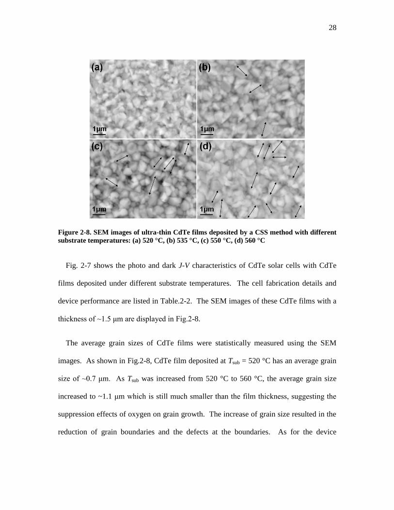
Figure 2-8. SEM images of ultra-thin CdTe films deposited by a CSS method with different
substrate temperatures: (a) 520 °C, (b) 535 °C, (c) 550 °C, (d) 560 °C
Fig. 2-7 shows the photo and dark J-V characteristics of CdTe solar cells with CdTe
films deposited under different substrate temperatures. The cell fabrication details and
device performance are listed in Table.2-2. The SEM images of these CdTe films with a
thickness of ~1.5 μm are displayed in Fig.2-8.
The average grain sizes of CdTe films were statistically measured using the SEM
images. As shown in Fig.2-8, CdTe film deposited at Tsub = 520 °C has an average grain
size of ~0.7 μm. As Tsub was increased from 520 °C to 560 °C, the average grain size
increased to ~1.1 μm which is still much smaller than the film thickness, suggesting the
suppression effects of oxygen on grain growth. The increase of grain size resulted in the
reduction of grain boundaries and the defects at the boundaries. As for the device
29
performance, the cells with CdTe film deposited at higher Tsub (550~560 °C) show higher
Voc and FF than that at lower Tsub (520~535 °C). However, in order to balance the grain
growth for Tsub = 560 °C, the oxygen pressure has to be increased to 2.5 Torr. Higher
oxygen pressure will readily result in more oxides (CdO, CdTeO3) on the CdTe surface
and increase the series resistance of the cell, which explains the fact that cell 1400D has
lower FF than cell 1400C, as shown in Table 2-2.
2.2.3 Thermal etch duration
In order to increase the density of nucleation sites on glass/FTO/CdS substrate (or CdS
substrate for short), facilitate the growth of CdTe crystal and therefore reduce the amount
of pinholes in CdTe films, oxygen was introduced in the CSS process. Apart from the
introduction of oxygen, a surface pre-treatment on CdS substrate at elevated temperature,
named thermal etch, is also important and necessary56
. In addition to promote the
formation of nucleation sites, thermal etch also cleans the substrate surface prior to CdTe
growth. Rose et al 48
also found that the thermal etch could alter the stoichiometry of the
surface.
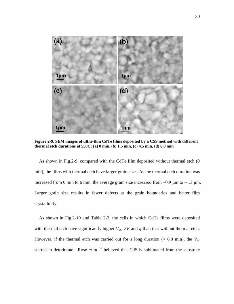
Fig. 2-9 shows the SEM images of CdTe films with a thickness of ~1.5 μm deposited
with a thermal etch on the CdS substrate at 550 °C for different durations. The photo and
dark J-V characteristics of CdTe solar cells using these CdTe films are displayed in Fig.2-
10. The cell fabrication details and device performance are listed in Table.2-3.
30
Figure 2-9. SEM images of ultra-thin CdTe films deposited by a CSS method with different
thermal etch durations at 550C: (a) 0 min, (b) 1.5 min, (c) 4.5 min, (d) 6.0 min
As shown in Fig.2-9, compared with the CdTe film deposited without thermal etch (0
min), the films with thermal etch have larger grain size. As the thermal etch duration was
increased from 0 min to 6 min, the average grain size increased from ~0.9 μm to ~1.3 μm.
Larger grain size results in fewer defects at the grain boundaries and better film
crystallinity.
As shown in Fig.2-10 and Table 2-3, the cells in which CdTe films were deposited
with thermal etch have significantly higher Voc, FF and η than that without thermal etch.
However, if the thermal etch was carried out for a long duration (> 6.0 min), the Voc
started to deteriorate. Rose et al 55
believed that CdS is sublimated from the substrate
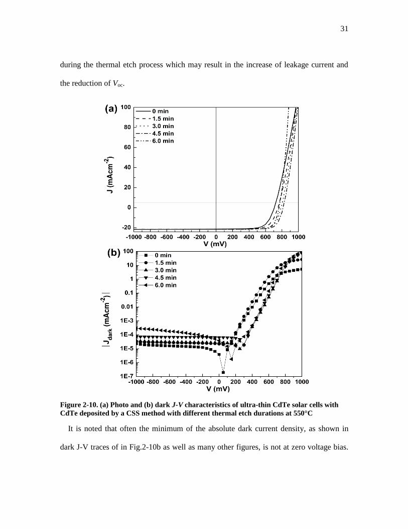
31
during the thermal etch process which may result in the increase of leakage current and
the reduction of Voc.
Figure 2-10. (a) Photo and (b) dark J-V characteristics of ultra-thin CdTe solar cells with
CdTe deposited by a CSS method with different thermal etch durations at 550°C
It is noted that often the minimum of the absolute dark current density, as shown in
dark J-V traces of in Fig.2-10b as well as many other figures, is not at zero voltage bias.
32
This anomaly may be due to measurement errors related to hysteresis of the J-V traces
which is due to charge trapping in some of the cells. Another possible cause for the
voltage offsets is leakage light from room light during the dark J-V measurements.
2.3 Summary
To fabricate pin-hole free CdTe films with a thickness of ~1 μm by a CSS method, it is
important to control the growth of CdTe crystals and limit the grain size to <1 μm. Since
the conventional temperature-time profile of a CSS method features high deposition rate
(>1 μm/min) and high substrate temperature (~600 °C), it is inherently difficult to
fabricate ultra-thin CdTe films with a good reproducibility. With the modified
temperature-time profile, ultra-thin CdTe films with a small roughness/thickness ratio
and very few pinholes can be reproducibly deposited.
Three key parameters, oxygen pressure, substrate temperature and thermal etch
duration, have been systematically investigated. Although low substrate temperature
(<525 °C) is favorable for the deposition of pinhole-free ultra-thin CdTe films, the poor
crystallinity in these films and associated defects are problematic. By optimizing the
substrate temperature, oxygen pressure, and thermal etch of CdS, ultra-thin CdTe films
with very few pinholes and good film crystallinity have been fabricated.
33
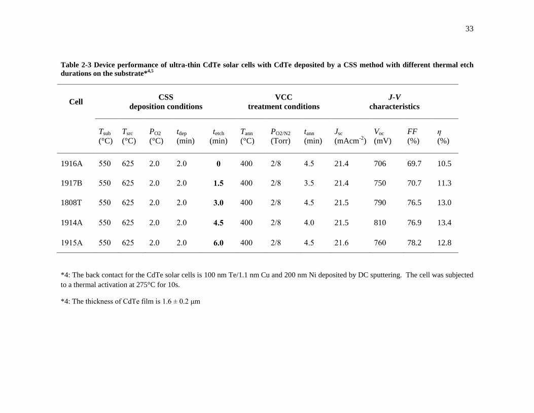
Table 2-3 Device performance of ultra-thin CdTe solar cells with CdTe deposited by a CSS method with different thermal etch
durations on the substrate*4,5
Cell CSS
deposition conditions
VCC
treatment conditions
J-V
characteristics
Tsub
(°C)
Tsrc
(°C)
PO2
(°C)
tdep
(min)
tetch
(min)
Tann
(°C)
PO2/N2
(Torr)
tann
(min)
Jsc
(mAcm-2
)
Voc
(mV)
FF
(%)
η
(%)
1916A 550 625 2.0 2.0 0 400 2/8 4.5 21.4 706 69.7 10.5
1917B 550 625 2.0 2.0 1.5 400 2/8 3.5 21.4 750 70.7 11.3
1808T 550 625 2.0 2.0 3.0 400 2/8 4.5 21.5 790 76.5 13.0
1914A 550 625 2.0 2.0 4.5 400 2/8 4.0 21.5 810 76.9 13.4
1915A 550 625 2.0 2.0 6.0 400 2/8 4.5 21.6 760 78.2 12.8
*4: The back contact for the CdTe solar cells is 100 nm Te/1.1 nm Cu and 200 nm Ni deposited by DC sputtering. The cell was subjected
to a thermal activation at 275°C for 10s.
*4: The thickness of CdTe film is 1.6 ± 0.2 μm
34
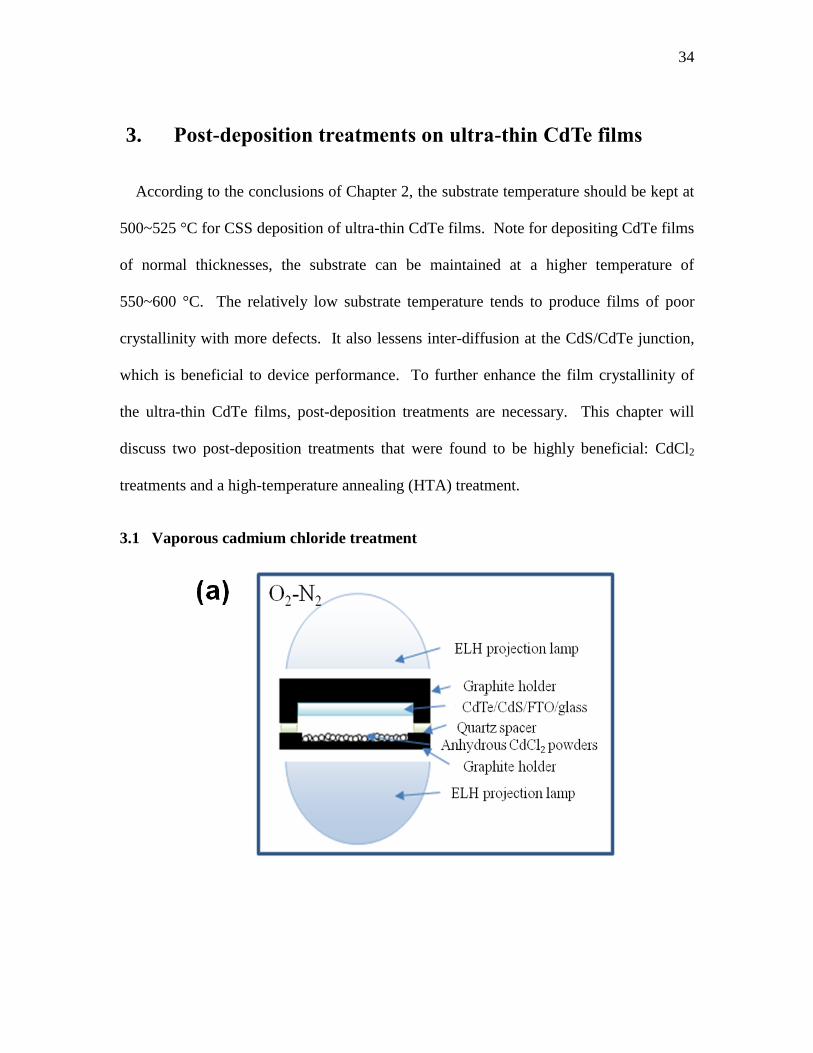
3. Post-deposition treatments on ultra-thin CdTe films
According to the conclusions of Chapter 2, the substrate temperature should be kept at
500~525 °C for CSS deposition of ultra-thin CdTe films. Note for depositing CdTe films
of normal thicknesses, the substrate can be maintained at a higher temperature of
550~600 °C. The relatively low substrate temperature tends to produce films of poor
crystallinity with more defects. It also lessens inter-diffusion at the CdS/CdTe junction,
which is beneficial to device performance. To further enhance the film crystallinity of
the ultra-thin CdTe films, post-deposition treatments are necessary. This chapter will
discuss two post-deposition treatments that were found to be highly beneficial: CdCl2
treatments and a high-temperature annealing (HTA) treatment.
3.1 Vaporous cadmium chloride treatment
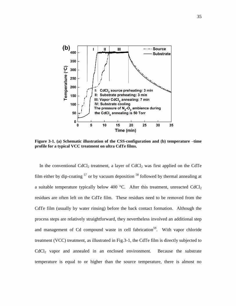
35
Figure 3-1. (a) Schematic illustration of the CSS-configuration and (b) temperature –time
profile for a typical VCC treatment on ultra CdTe films.
In the conventional CdCl2 treatment, a layer of CdCl2 was first applied on the CdTe
film either by dip-coating 57
or by vacuum deposition 58
followed by thermal annealing at
a suitable temperature typically below 400 °C. After this treatment, unreacted CdCl2
residues are often left on the CdTe film. These residues need to be removed from the
CdTe film (usually by water rinsing) before the back contact formation. Although the
process steps are relatively straightforward, they nevertheless involved an additional step
and management of Cd compound waste in cell fabrication59
. With vapor chloride
treatment (VCC) treatment, as illustrated in Fig.3-1, the CdTe film is directly subjected to
CdCl2 vapor and annealed in an enclosed environment. Because the substrate
temperature is equal to or higher than the source temperature, there is almost no
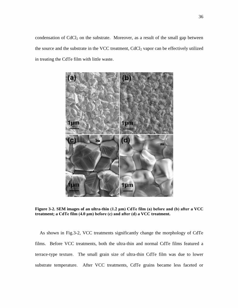
36
condensation of CdCl2 on the substrate. Moreover, as a result of the small gap between
the source and the substrate in the VCC treatment, CdCl2 vapor can be effectively utilized
in treating the CdTe film with little waste.
Figure 3-2. SEM images of an ultra-thin (1.2 μm) CdTe film (a) before and (b) after a VCC
treatment; a CdTe film (4.0 μm) before (c) and after (d) a VCC treatment.
As shown in Fig.3-2, VCC treatments significantly change the morphology of CdTe
films. Before VCC treatments, both the ultra-thin and normal CdTe films featured a
terrace-type texture. The small grain size of ultra-thin CdTe film was due to lower
substrate temperature. After VCC treatments, CdTe grains became less faceted or
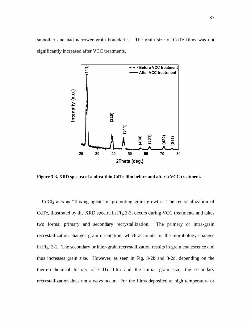
37
smoother and had narrower grain boundaries. The grain size of CdTe films was not
significantly increased after VCC treatments.
Figure 3-3. XRD spectra of a ultra-thin CdTe film before and after a VCC treatment.
CdCl2 acts as “fluxing agent” in promoting grain growth. The recrystallization of
CdTe, illustrated by the XRD spectra in Fig.3-3, occurs during VCC treatments and takes
two forms: primary and secondary recrystallization. The primary or intra-grain
recrystallization changes grain orientation, which accounts for the morphology changes
in Fig. 3-2. The secondary or inter-grain recrystallization results in grain coalescence and
thus increases grain size. However, as seen in Fig. 3-2b and 3-2d, depending on the
thermo-chemical history of CdTe film and the initial grain size, the secondary
recrystallization does not always occur. For the films deposited at high temperature or
38
containing native oxide, little observable grain growth occurs during VCC treatments.
Under such a circumstance, the surface energy has been already minimized or pinned by
the presence of the oxide.
In addition to recrystallizing CdTe films, VCC treatments also influence the inter-
diffusion at the CdS/CdTe junction, which can be characterized by UV/Vis spectroscopy
and PL spectroscopy.
3.2 VCC process optimization
3.2.1 Annealing duration and temperature
Annealing duration and temperature are two important factors in a VCC treatment.
They determine the amount of CdCl2 vapor flux that will react with the CdS/CdTe stack
layers. The amount of CdCl2 vapor flux increases with the increasing annealing duration
and/or temperature. Neither under-treatment nor over-treatment will produce the
optimum device performance. The optimized annealing duration and temperature are
determined by several factors including the thermo-chemical history of CdS and CdTe
films, thickness and crystallinity of CdTe films. In terms of the effects of VCC
treatments, prolonging annealing duration at a given temperature above the sublimation
point of CdCl2 is equivalent to elevating annealing temperature for a fixed duration.
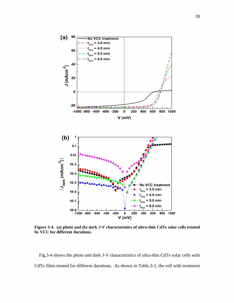
39
Figure 3-4. (a) photo and (b) dark J-V characteristics of ultra-thin CdTe solar cells treated
by VCC for different durations.
Fig.3-4 shows the photo and dark J-V characteristics of ultra-thin CdTe solar cells with
CdTe films treated for different durations. As shown in Table.3-1, the cell with treatment
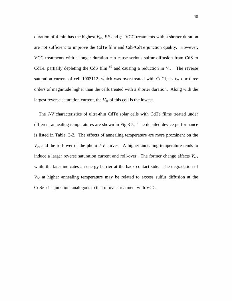
40
duration of 4 min has the highest Voc, FF and η. VCC treatments with a shorter duration
are not sufficient to improve the CdTe film and CdS/CdTe junction quality. However,
VCC treatments with a longer duration can cause serious sulfur diffusion from CdS to
CdTe, partially depleting the CdS film 60
and causing a reduction in Voc. The reverse
saturation current of cell 1003112, which was over-treated with CdCl2, is two or three
orders of magnitude higher than the cells treated with a shorter duration. Along with the
largest reverse saturation current, the Voc of this cell is the lowest.
The J-V characteristics of ultra-thin CdTe solar cells with CdTe films treated under
different annealing temperatures are shown in Fig.3-5. The detailed device performance
is listed in Table. 3-2. The effects of annealing temperature are more prominent on the
Voc and the roll-over of the photo J-V curves. A higher annealing temperature tends to
induce a larger reverse saturation current and roll-over. The former change affects Voc,
while the later indicates an energy barrier at the back contact side. The degradation of
Voc at higher annealing temperature may be related to excess sulfur diffusion at the
CdS/CdTe junction, analogous to that of over-treatment with VCC.
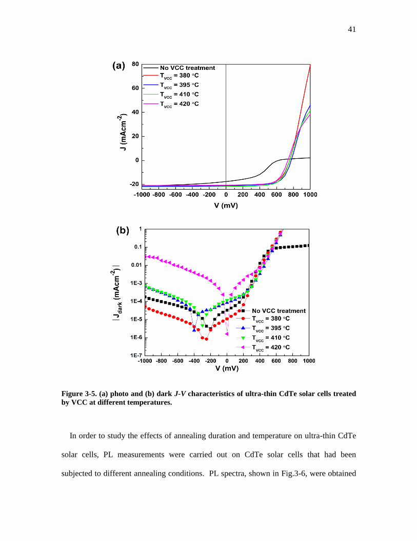
41
Figure 3-5. (a) photo and (b) dark J-V characteristics of ultra-thin CdTe solar cells treated
by VCC at different temperatures.
In order to study the effects of annealing duration and temperature on ultra-thin CdTe
solar cells, PL measurements were carried out on CdTe solar cells that had been
subjected to different annealing conditions. PL spectra, shown in Fig.3-6, were obtained
42
with excitation (He-Ne laser, 633 nm) directly at the CdS/CdTe interface through the
glass substrate. The sample was cryogenically cooled to 10 K. Similar trend in the PL
spectra was observed for CdS/CdTe stack layers with VCC treatments at various
temperatures and with VCC treatments at same temperature for various durations. Only
PL spectra with VCC treatments at various temperatures are discussed here.
Figure 3-6. PL spectra of CdS/CdTe stack layers with VCC treatments at various
temperatures for 3 min. The spectra were obtained with interface excitation at 10 K.
As shown in Fig.3-6, the reference cell without any VCC treatments features a broad
peak at ~1.43 eV which has been attributed to the defects at the CdS/CdTe interface 17
.
After VCC treatment, the 1.43 eV peak shifts to lower energy. This peak shift is caused
by the evolution of the 1.43 eV defect band and a band located at ~1.38 eV. The 1.38 eV
band has been attributed to the formation of CdTe1-xSx at the CdS/CdTe junction 17
.
43
It is known that CdCl2 treatment can reduce the lattice mismatch between CdS and
CdTe by promoting inter-diffusion at the CdS/CdTe junction and the formation of CdTe1-
xSx. As a result, the lattice mismatch between CdS and CdTe is reduced along with the
defects at the interface, including dislocations and dangling bonds. The decrease in
intensity of the 1.43 eV defect band is due to a reduction of lattice mismatch and the
evolution of the CdTe1-xSx band. Though the PL spectra are normalized for a better
comparison in Fig.3-6, the intensity decay of 1.43 eV defect band is still very obvious.
The PL measurements show that the sulfur diffusion due to the VCC treatment at the
highest temperature of 420 °C is the strongest. Since excessive sulfur diffusion can
create pinholes in the CdS films and compromise Voc, the PL spectra are consistent with
the analyses on J-V characteristics.
Lee et al 27
investigated the effects of annealing temperature and CdCl2 treatment on
CdS/CdTe solar cells. They found that the grain size in CdTe films increases with
increasing annealing temperature. In addition, they were able to correlate the annealing
temperature with device performance. Similarly, we have observed that the device
performance is increased with increasing annealing temperature but only up a certain
temperature threshold, beyond which the device will deteriorate. Nakamura et al 61
has
reported similar findings.
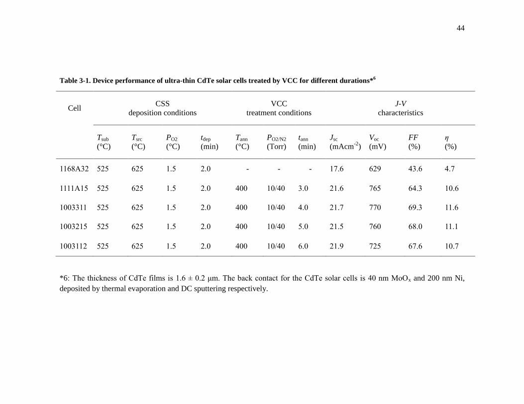
44
Table 3-1. Device performance of ultra-thin CdTe solar cells treated by VCC for different durations*6
Cell CSS
deposition conditions
VCC
treatment conditions
J-V
characteristics
Tsub
(°C)
Tsrc
(°C)
PO2
(°C)
tdep
(min)
Tann
(°C)
PO2/N2
(Torr)
tann
(min)
Jsc
(mAcm-2
)
Voc
(mV)
FF
(%)
η
(%)
1168A32 525 625 1.5 2.0 - - - 17.6 629 43.6 4.7
1111A15 525 625 1.5 2.0 400 10/40 3.0 21.6 765 64.3 10.6
1003311 525 625 1.5 2.0 400 10/40 4.0 21.7 770 69.3 11.6
1003215 525 625 1.5 2.0 400 10/40 5.0 21.5 760 68.0 11.1
1003112 525 625 1.5 2.0 400 10/40 6.0 21.9 725 67.6 10.7
*6: The thickness of CdTe films is 1.6 ± 0.2 μm. The back contact for the CdTe solar cells is 40 nm MoOx and 200 nm Ni,
deposited by thermal evaporation and DC sputtering respectively.
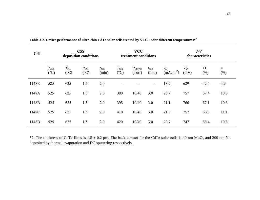
45
Table 3-2. Device performance of ultra-thin CdTe solar cells treated by VCC under different temperatures*7
Cell CSS
deposition conditions
VCC
treatment conditions
J-V
characteristics
Tsub
(°C)
Tsrc
(°C)
PO2
(°C)
tdep
(min)
Tann
(°C)
PO2/N2
(Torr)
tann
(min)
Jsc
(mAcm-2
)
Voc
(mV)
FF
(%)
η
(%)
1148E 525 625 1.5 2.0 - - - 18.2 629 42.4 4.9
1148A 525 625 1.5 2.0 380 10/40 3.0 20.7 757 67.4 10.5
1148B 525 625 1.5 2.0 395 10/40 3.0 21.1 766 67.1 10.8
1148C 525 625 1.5 2.0 410 10/40 3.0 21.9 757 66.8 11.1
1148D 525 625 1.5 2.0 420 10/40 3.0 20.7 747 68.4 10.5
*7: The thickness of CdTe films is 1.5 ± 0.2 μm. The back contact for the CdTe solar cells is 40 nm MoOx and 200 nm Ni,
deposited by thermal evaporation and DC sputtering respectively.
46
3.2.2 Oxygen partial pressure
Most CdCl2 treatments, including our VCC treatment, require a thermal annealing
process in air to complete the activation8,60,62,63
.
McCandless et al 30
found that oxygen concentration during VCC treatments does not
appear to affect the solar cell efficiency, although it does influence the consumption of
the CdS layer. The oxygen concentration they explored ranges from 0.01 Torr to 570
Torr out of 760 Torr. At very high oxygen concentration (570 Torr), S diffusion at
CdS/CdTe junction is greatly enhanced forming CdTe1-xSx where x is increased from 0.7%
to 2.9%. Zhou et al 64
found that CdTe solar cells treated by a VCC method in an
ambient without oxygen perform poorly with a low Voc of 550 mV and a FF of 46%.
They showed that oxygen ambient is needed to yield substantial enhancement in Voc (up
to 780 mV) and FF (up to 66%). The optimized range of oxygen partial pressure was
5~15%. They did not observe significant S diffusion at the CdS/CdTe junction nor
depletion of the CdS layer.
We studied the effects of oxygen partial pressure on ultra-thin CdTe solar cells in VCC
treatments. The oxygen concentration in an oxygen/nitrogen mixture was varied from 0%
to 80%. The total pressure was 50 Torr. The J-V characteristics, PL spectra and device
performance are shown in Fig.3-7, 3-8 and Table 3-3 respectively.
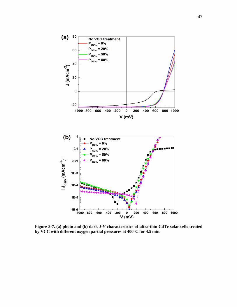
47
Figure 3-7. (a) photo and (b) dark J-V characteristics of ultra-thin CdTe solar cells treated
by VCC with different oxygen partial pressures at 400°C for 4.5 min.
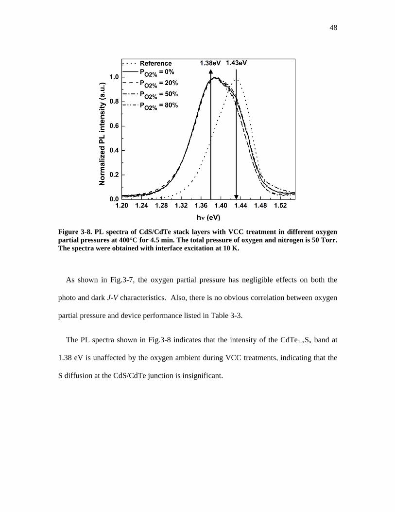
48
Figure 3-8. PL spectra of CdS/CdTe stack layers with VCC treatment in different oxygen
partial pressures at 400°C for 4.5 min. The total pressure of oxygen and nitrogen is 50 Torr.
The spectra were obtained with interface excitation at 10 K.
As shown in Fig.3-7, the oxygen partial pressure has negligible effects on both the
photo and dark J-V characteristics. Also, there is no obvious correlation between oxygen
partial pressure and device performance listed in Table 3-3.
The PL spectra shown in Fig.3-8 indicates that the intensity of the CdTe1-xSx band at
1.38 eV is unaffected by the oxygen ambient during VCC treatments, indicating that the
S diffusion at the CdS/CdTe junction is insignificant.
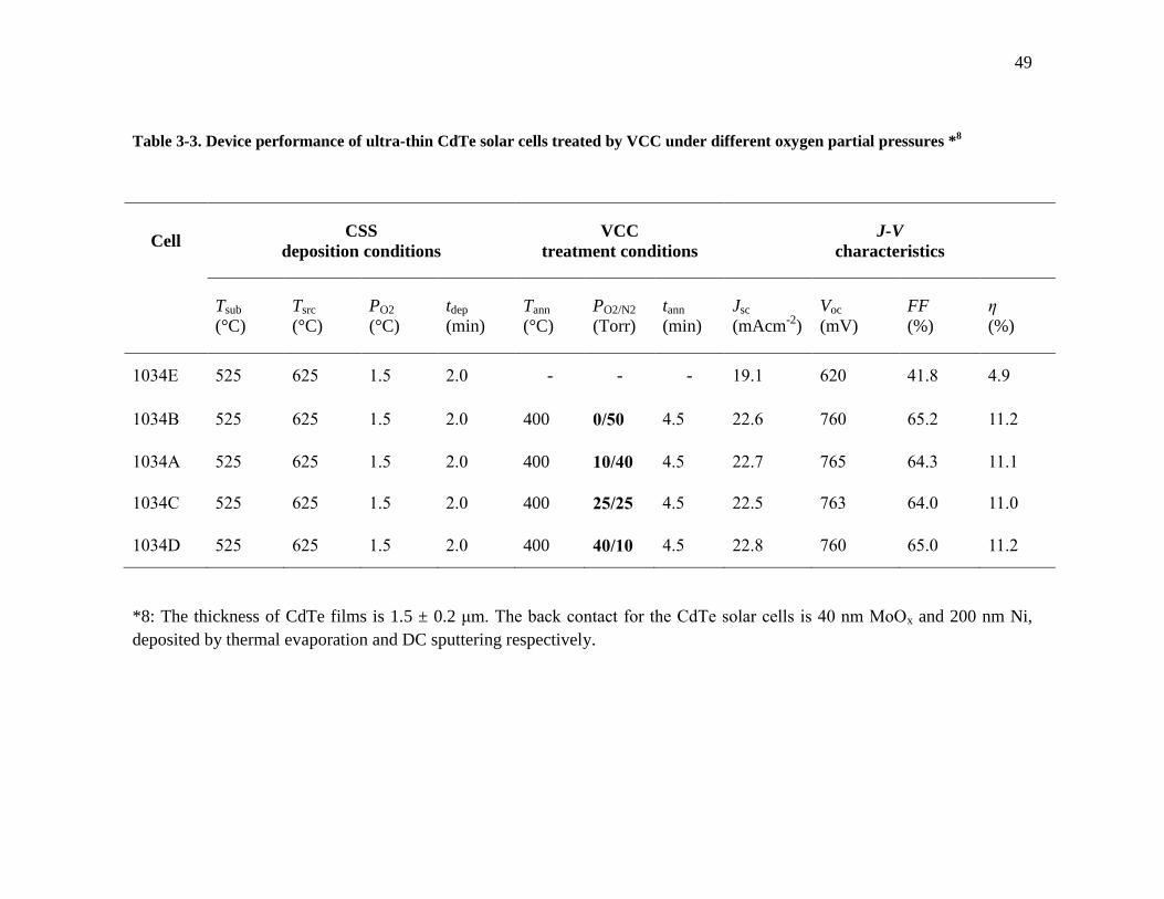
49
Table 3-3. Device performance of ultra-thin CdTe solar cells treated by VCC under different oxygen partial pressures *8
Cell CSS
deposition conditions
VCC
treatment conditions
J-V
characteristics
Tsub
(°C)
Tsrc
(°C)
PO2
(°C)
tdep
(min)
Tann
(°C)
PO2/N2
(Torr)
tann
(min)
Jsc
(mAcm-2
)
Voc
(mV)
FF
(%)
η
(%)
1034E 525 625 1.5 2.0 - - - 19.1 620 41.8 4.9
1034B 525 625 1.5 2.0 400 0/50 4.5 22.6 760 65.2 11.2
1034A 525 625 1.5 2.0 400 10/40 4.5 22.7 765 64.3 11.1
1034C 525 625 1.5 2.0 400 25/25 4.5 22.5 763 64.0 11.0
1034D 525 625 1.5 2.0 400 40/10 4.5 22.8 760 65.0 11.2
*8: The thickness of CdTe films is 1.5 ± 0.2 μm. The back contact for the CdTe solar cells is 40 nm MoOx and 200 nm Ni,
deposited by thermal evaporation and DC sputtering respectively.
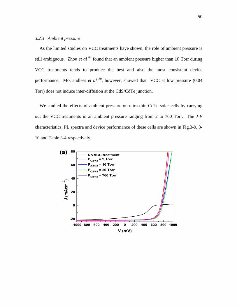
50
3.2.3 Ambient pressure
As the limited studies on VCC treatments have shown, the role of ambient pressure is
still ambiguous. Zhou et al 64
found that an ambient pressure higher than 10 Torr during
VCC treatments tends to produce the best and also the most consistent device
performance. McCandless et al 30
, however, showed that VCC at low pressure (0.04
Torr) does not induce inter-diffusion at the CdS/CdTe junction.
We studied the effects of ambient pressure on ultra-thin CdTe solar cells by carrying
out the VCC treatments in an ambient pressure ranging from 2 to 760 Torr. The J-V
characteristics, PL spectra and device performance of these cells are shown in Fig.3-9, 3-
10 and Table 3-4 respectively.
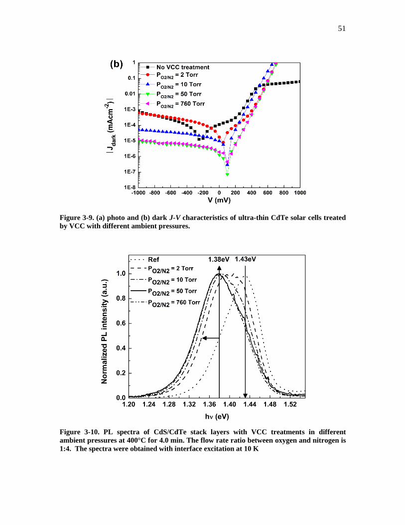
51
Figure 3-9. (a) photo and (b) dark J-V characteristics of ultra-thin CdTe solar cells treated
by VCC with different ambient pressures.
Figure 3-10. PL spectra of CdS/CdTe stack layers with VCC treatments in different
ambient pressures at 400°C for 4.0 min. The flow rate ratio between oxygen and nitrogen is
1:4. The spectra were obtained with interface excitation at 10 K
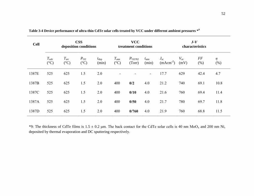
52
Table 3-4 Device performance of ultra-thin CdTe solar cells treated by VCC under different ambient pressures *9
Cell CSS
deposition conditions
VCC
treatment conditions
J-V
characteristics
Tsub
(°C)
Tsrc
(°C)
PO2
(°C)
tdep
(min)
Tann
(°C)
PO2/N2
(Torr)
tann
(min)
Jsc
(mAcm-2
)
Voc
(mV)
FF
(%)
η
(%)
1387E 525 625 1.5 2.0 - - - 17.7 629 42.4 4.7
1387B 525 625 1.5 2.0 400 0/2 4.0 21.2 740 69.1 10.8
1387C 525 625 1.5 2.0 400 0/10 4.0 21.6 760 69.4 11.4
1387A 525 625 1.5 2.0 400 0/50 4.0 21.7 780 69.7 11.8
1387D 525 625 1.5 2.0 400 0/760 4.0 21.9 760 68.8 11.5
*9: The thickness of CdTe films is 1.5 ± 0.2 μm. The back contact for the CdTe solar cells is 40 nm MoOx and 200 nm Ni,
deposited by thermal evaporation and DC sputtering respectively.
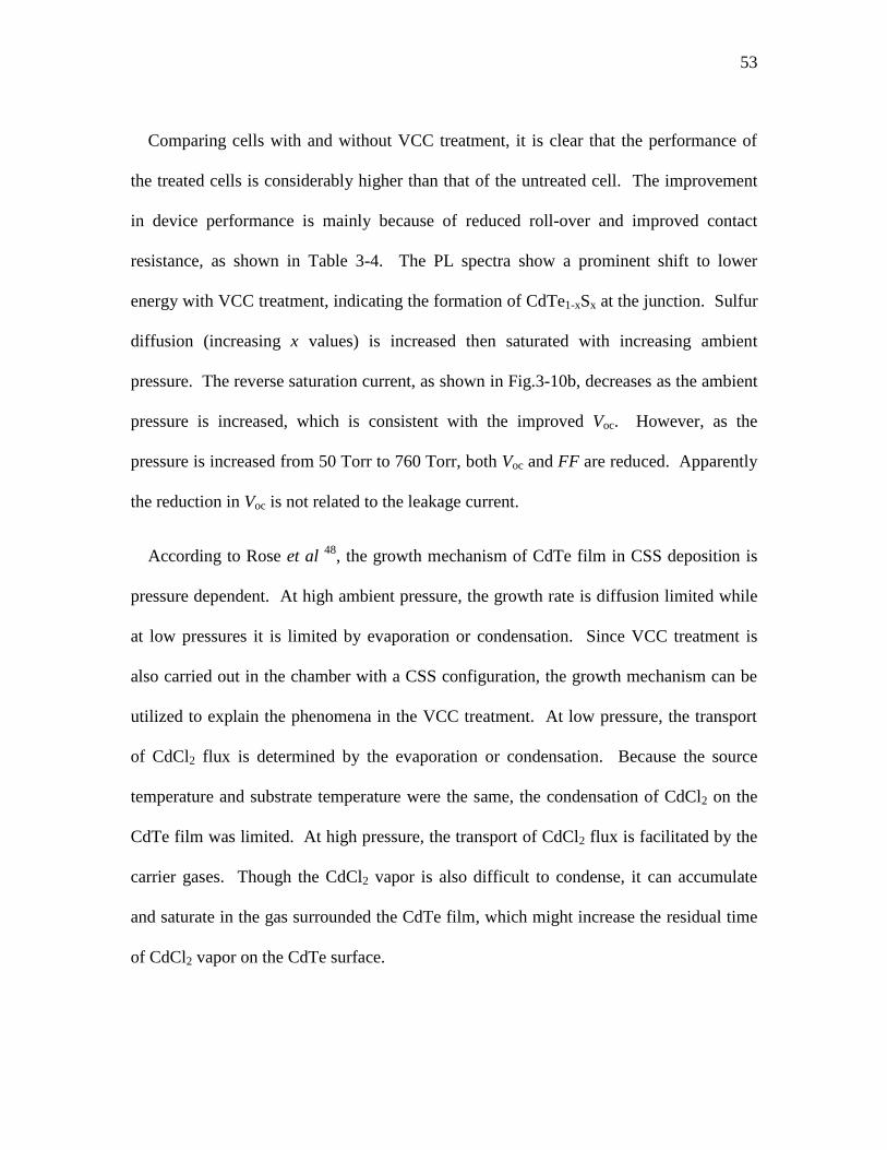
53
Comparing cells with and without VCC treatment, it is clear that the performance of
the treated cells is considerably higher than that of the untreated cell. The improvement
in device performance is mainly because of reduced roll-over and improved contact
resistance, as shown in Table 3-4. The PL spectra show a prominent shift to lower
energy with VCC treatment, indicating the formation of CdTe1-xSx at the junction. Sulfur
diffusion (increasing x values) is increased then saturated with increasing ambient
pressure. The reverse saturation current, as shown in Fig.3-10b, decreases as the ambient
pressure is increased, which is consistent with the improved Voc. However, as the
pressure is increased from 50 Torr to 760 Torr, both Voc and FF are reduced. Apparently
the reduction in Voc is not related to the leakage current.
According to Rose et al 48
, the growth mechanism of CdTe film in CSS deposition is
pressure dependent. At high ambient pressure, the growth rate is diffusion limited while
at low pressures it is limited by evaporation or condensation. Since VCC treatment is
also carried out in the chamber with a CSS configuration, the growth mechanism can be
utilized to explain the phenomena in the VCC treatment. At low pressure, the transport
of CdCl2 flux is determined by the evaporation or condensation. Because the source
temperature and substrate temperature were the same, the condensation of CdCl2 on the
CdTe film was limited. At high pressure, the transport of CdCl2 flux is facilitated by the
carrier gases. Though the CdCl2 vapor is also difficult to condense, it can accumulate
and saturate in the gas surrounded the CdTe film, which might increase the residual time
of CdCl2 vapor on the CdTe surface.
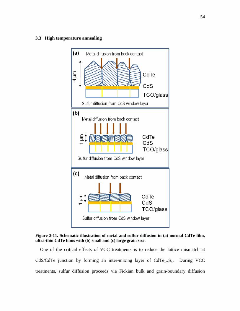
54
3.3 High temperature annealing
Figure 3-11. Schematic illustration of metal and sulfur diffusion in (a) normal CdTe film,
ultra-thin CdTe films with (b) small and (c) large grain size.
One of the critical effects of VCC treatments is to reduce the lattice mismatch at
CdS/CdTe junction by forming an inter-mixing layer of CdTe1-xSx. During VCC
treatments, sulfur diffusion proceeds via Fickian bulk and grain-boundary diffusion
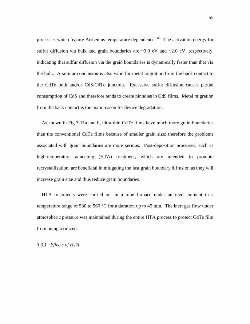
55
processes which feature Arrhenius temperature dependence. 65
The activation energy for
sulfur diffusion via bulk and grain boundaries are ~3.0 eV and ~2.0 eV, respectively,
indicating that sulfur diffusion via the grain boundaries is dynamically faster than that via
the bulk. A similar conclusion is also valid for metal migration from the back contact to
the CdTe bulk and/or CdS/CdTe junction. Excessive sulfur diffusion causes partial
consumption of CdS and therefore tends to create pinholes in CdS films. Metal migration
from the back contact is the main reason for device degradation.
As shown in Fig.3-11a and b, ultra-thin CdTe films have much more grain boundaries
than the conventional CdTe films because of smaller grain size; therefore the problems
associated with grain boundaries are more serious. Post-deposition processes, such as
high-temperature annealing (HTA) treatment, which are intended to promote
recrystallization, are beneficial in mitigating the fast grain boundary diffusion as they will
increase grain size and thus reduce grain boundaries.
HTA treatments were carried out in a tube furnace under an inert ambient in a
temperature range of 530 to 560 °C for a duration up to 45 min. The inert gas flow under
atmospheric pressure was maintained during the entire HTA process to protect CdTe film
from being oxidized.
3.3.1 Effects of HTA
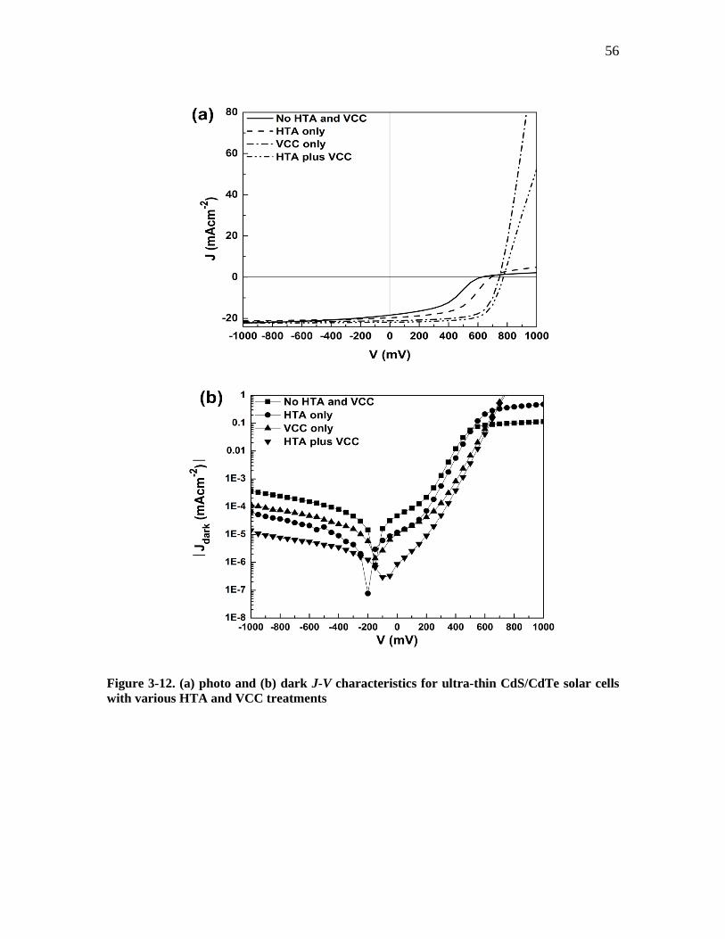
56
Figure 3-12. (a) photo and (b) dark J-V characteristics for ultra-thin CdS/CdTe solar cells
with various HTA and VCC treatments
57
Table 3-5. Device performance of ultra-thin CdS/CdTe solar cells with various HTA and VCC treatments*10
Cell HTA*11
VCC*12
Device performance
Rsh
(Ω)
Rs
(Ω)
Jsc
(mAcm-2
)
Voc
(mV)
FF
(%)
η
(%)
1168A N N 1363 770 18.4 630 42.4 4.9
1168B Y N 3078 257 19.6 690 52.0 7.0
1168C N Y 8681 40 21.1 750 67.2 10.6
1168D Y Y 14971 52 21.9 778 68.2 11.6
*10: The thickness of CdTe films is 1.5 ± 0.1 μm. The back contact for the CdTe solar cells is 40 nm MoOx and 200 nm Ni,
deposited by thermal evaporation and DC sputtering respectively.
*11: The CdTe films were subjected in N2 at 550 °C for 40 min.
*12: The VCC treatment was carried out at 400 °C in 10 Torr O2/40 Torr N2 for 4 min.
58
Fig.3-12a and b show the photo and dark J-V characteristics of ultra-thin CdTe solar
cells with various heat treatments. Compared to the reference cell (without any
treatment), the cell with HTA alone exhibits significant improvement in Voc, Jsc and FF,
although it is still substantially inferior to the cell with just VCC treatment. Combining
HTA and VCC treatments further enhances the cell performance over the VCC treatment
alone, yielding the best device performance, as shown in Table 3-5. The improvement in
Voc is consistent with the reduction of reverse saturation current shown in Fig. 3-12b.
Table 3-5 includes the dynamic shunt resistance, Rsh, and dynamic series resistance, Rs,
calculated from the slope of dJ/dV at Jsc and Voc, respectively. The cell with both HTA
and VCC treatments yields excellent Rsh and Rs, as well as the highest efficiency of
11.6%. The improvement in Rs is consistent with the finding that heat treatment on CdTe
films at elevated temperature reduces film resistivity.66,67
3.3.2 Optimization of HTA process
In order to confirm the beneficial effects of HTA treatments, the same annealing
treatment as shown in Table 3-5 was applied on ultra-thin CdTe solar cells with different
CdTe thickness. The J-V characteristics and device performance are shown in Fig.3-13
and Table 3-6, respectively.
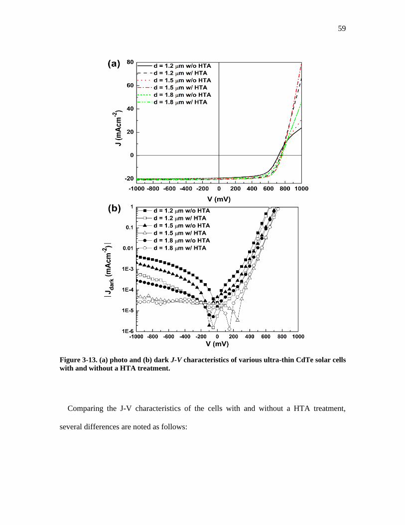
59
Figure 3-13. (a) photo and (b) dark J-V characteristics of various ultra-thin CdTe solar cells
with and without a HTA treatment.
Comparing the J-V characteristics of the cells with and without a HTA treatment,
several differences are noted as follows:
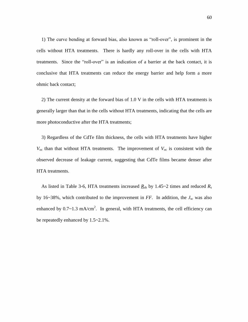
60
1) The curve bending at forward bias, also known as “roll-over”, is prominent in the
cells without HTA treatments. There is hardly any roll-over in the cells with HTA
treatments. Since the “roll-over” is an indication of a barrier at the back contact, it is
conclusive that HTA treatments can reduce the energy barrier and help form a more
ohmic back contact;
2) The current density at the forward bias of 1.0 V in the cells with HTA treatments is
generally larger than that in the cells without HTA treatments, indicating that the cells are
more photoconductive after the HTA treatments;
3) Regardless of the CdTe film thickness, the cells with HTA treatments have higher
Voc than that without HTA treatments. The improvement of Voc is consistent with the
observed decrease of leakage current, suggesting that CdTe films became denser after
HTA treatments.
As listed in Table 3-6, HTA treatments increased Rsh by 1.45~2 times and reduced Rs
by 16~38%, which contributed to the improvement in FF. In addition, the Jsc was also
enhanced by 0.7~1.3 mA/cm2. In general, with HTA treatments, the cell efficiency can
be repeatedly enhanced by 1.5~2.1%.
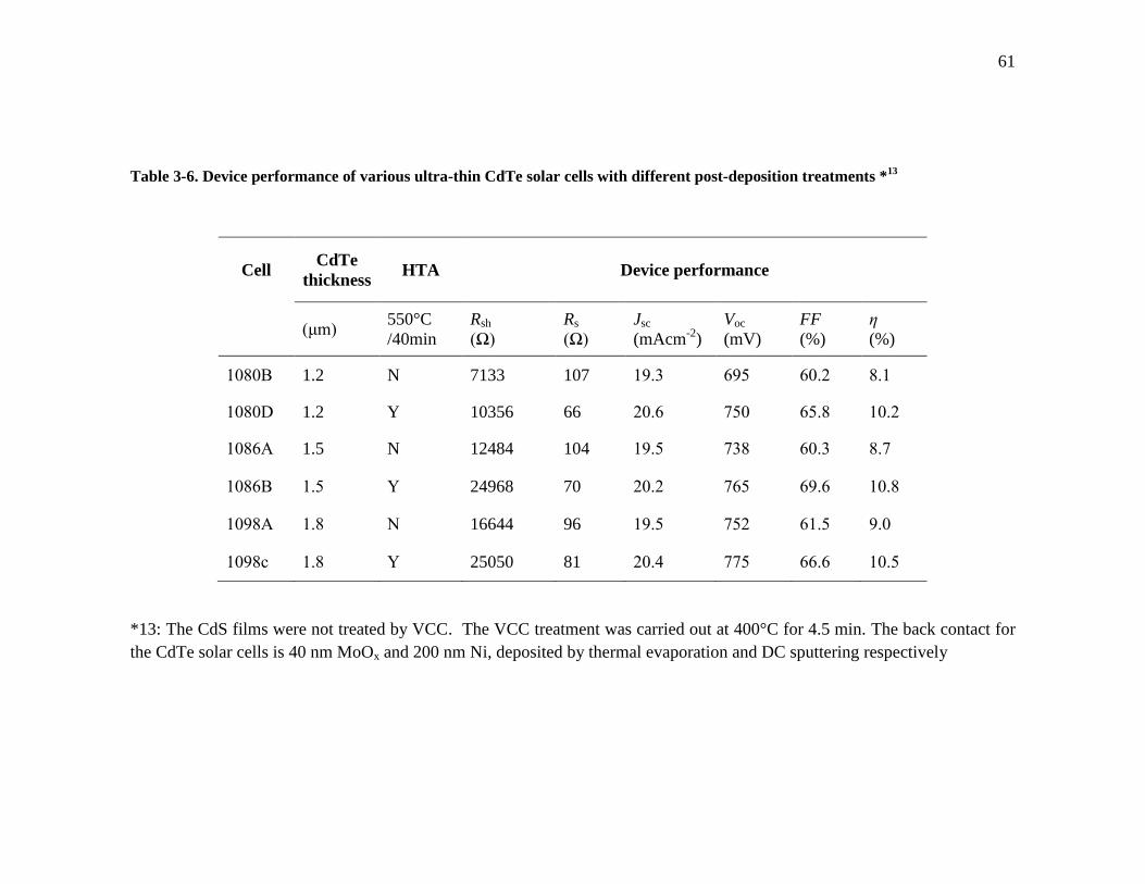
61
Table 3-6. Device performance of various ultra-thin CdTe solar cells with different post-deposition treatments *13
Cell CdTe
thickness HTA Device performance
(μm) 550°C
/40min
Rsh
(Ω)
Rs
(Ω)
Jsc
(mAcm-2
)
Voc
(mV)
FF
(%)
η
(%)
1080B 1.2 N 7133 107 19.3 695 60.2 8.1
1080D 1.2 Y 10356 66 20.6 750 65.8 10.2
1086A 1.5 N 12484 104 19.5 738 60.3 8.7
1086B 1.5 Y 24968 70 20.2 765 69.6 10.8
1098A 1.8 N 16644 96 19.5 752 61.5 9.0
1098c 1.8 Y 25050 81 20.4 775 66.6 10.5
*13: The CdS films were not treated by VCC. The VCC treatment was carried out at 400°C for 4.5 min. The back contact for
the CdTe solar cells is 40 nm MoOx and 200 nm Ni, deposited by thermal evaporation and DC sputtering respectively
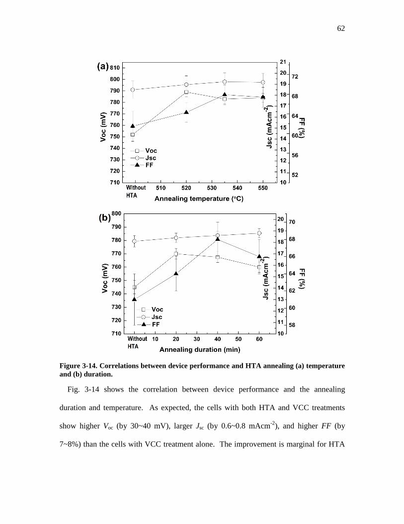
62
Figure 3-14. Correlations between device performance and HTA annealing (a) temperature
and (b) duration.
Fig. 3-14 shows the correlation between device performance and the annealing
duration and temperature. As expected, the cells with both HTA and VCC treatments
show higher Voc (by 30~40 mV), larger Jsc (by 0.6~0.8 mAcm-2
), and higher FF (by
7~8%) than the cells with VCC treatment alone. The improvement is marginal for HTA
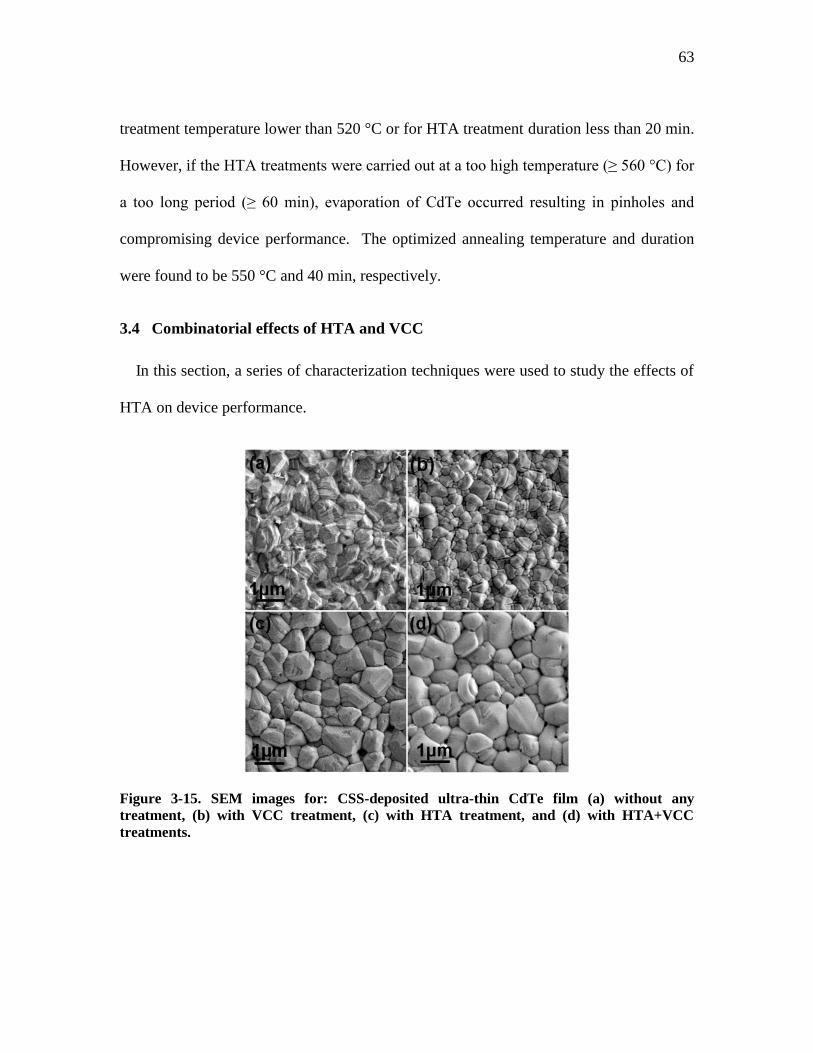
63
treatment temperature lower than 520 °C or for HTA treatment duration less than 20 min.
However, if the HTA treatments were carried out at a too high temperature (≥ 560 °C) for
a too long period (≥ 60 min), evaporation of CdTe occurred resulting in pinholes and
compromising device performance. The optimized annealing temperature and duration
were found to be 550 °C and 40 min, respectively.
3.4 Combinatorial effects of HTA and VCC
In this section, a series of characterization techniques were used to study the effects of
HTA on device performance.
Figure 3-15. SEM images for: CSS-deposited ultra-thin CdTe film (a) without any
treatment, (b) with VCC treatment, (c) with HTA treatment, and (d) with HTA+VCC
treatments.
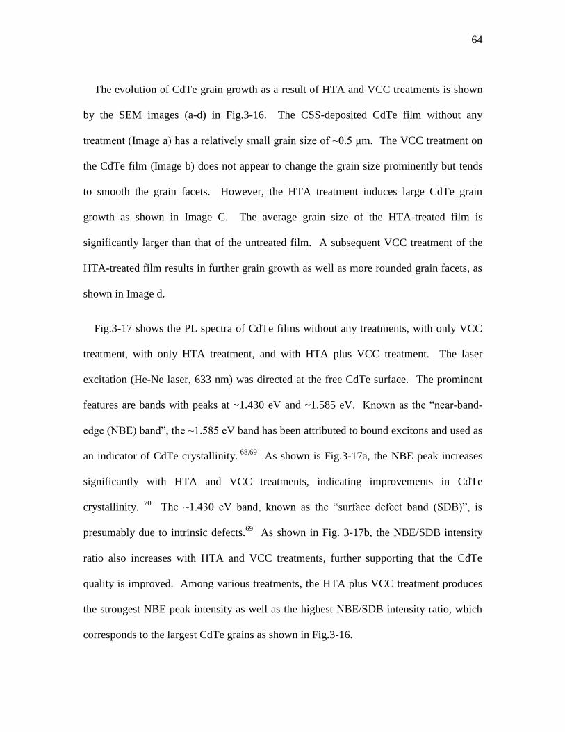
64
The evolution of CdTe grain growth as a result of HTA and VCC treatments is shown
by the SEM images (a-d) in Fig.3-16. The CSS-deposited CdTe film without any
treatment (Image a) has a relatively small grain size of ~0.5 μm. The VCC treatment on
the CdTe film (Image b) does not appear to change the grain size prominently but tends
to smooth the grain facets. However, the HTA treatment induces large CdTe grain
growth as shown in Image C. The average grain size of the HTA-treated film is
significantly larger than that of the untreated film. A subsequent VCC treatment of the
HTA-treated film results in further grain growth as well as more rounded grain facets, as
shown in Image d.
Fig.3-17 shows the PL spectra of CdTe films without any treatments, with only VCC
treatment, with only HTA treatment, and with HTA plus VCC treatment. The laser
excitation (He-Ne laser, 633 nm) was directed at the free CdTe surface. The prominent
features are bands with peaks at ~1.430 eV and ~1.585 eV. Known as the “near-band-
edge (NBE) band”, the ~1.585 eV band has been attributed to bound excitons and used as
an indicator of CdTe crystallinity. 68,69
As shown is Fig.3-17a, the NBE peak increases
significantly with HTA and VCC treatments, indicating improvements in CdTe
crystallinity. 70
The ~1.430 eV band, known as the “surface defect band (SDB)”, is
presumably due to intrinsic defects.69
As shown in Fig. 3-17b, the NBE/SDB intensity
ratio also increases with HTA and VCC treatments, further supporting that the CdTe
quality is improved. Among various treatments, the HTA plus VCC treatment produces
the strongest NBE peak intensity as well as the highest NBE/SDB intensity ratio, which
corresponds to the largest CdTe grains as shown in Fig.3-16.
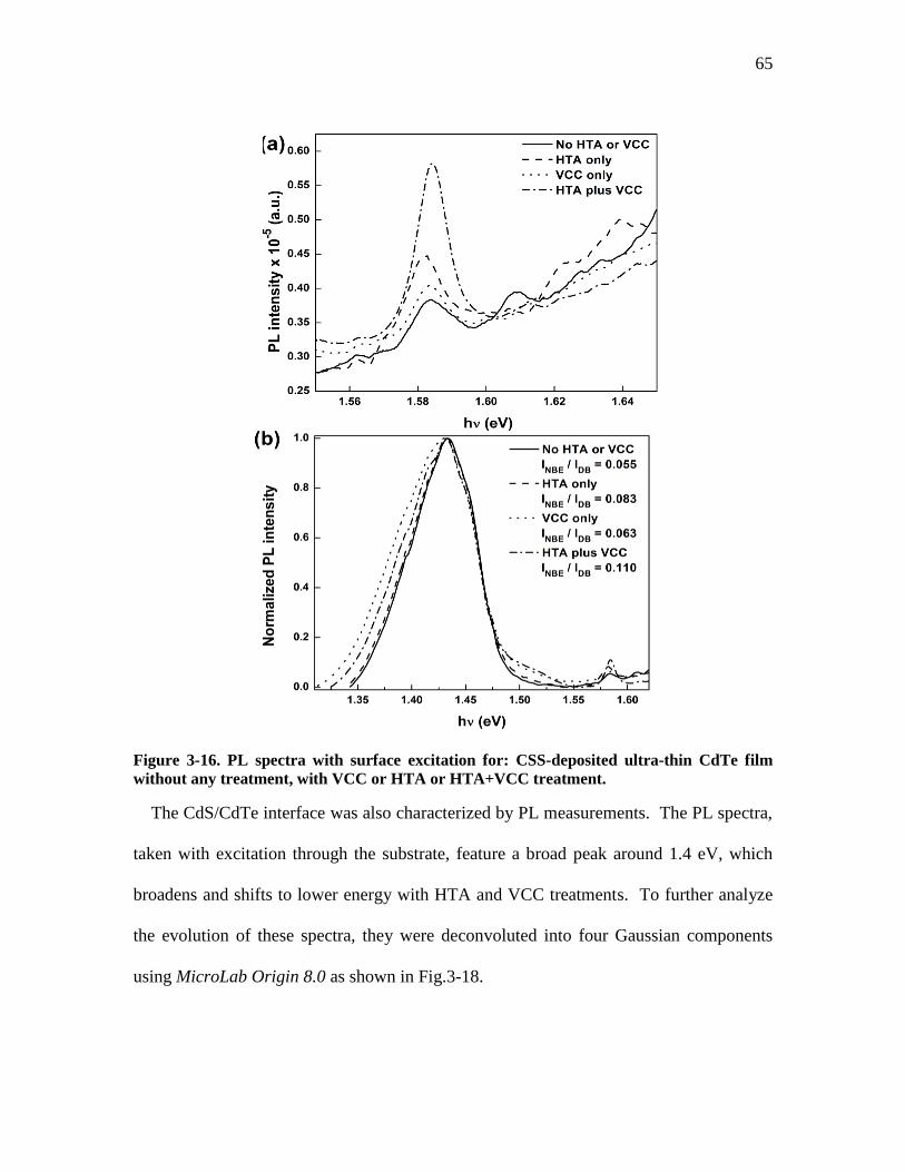
65
Figure 3-16. PL spectra with surface excitation for: CSS-deposited ultra-thin CdTe film
without any treatment, with VCC or HTA or HTA+VCC treatment.
The CdS/CdTe interface was also characterized by PL measurements. The PL spectra,
taken with excitation through the substrate, feature a broad peak around 1.4 eV, which
broadens and shifts to lower energy with HTA and VCC treatments. To further analyze
the evolution of these spectra, they were deconvoluted into four Gaussian components
using MicroLab Origin 8.0 as shown in Fig.3-18.
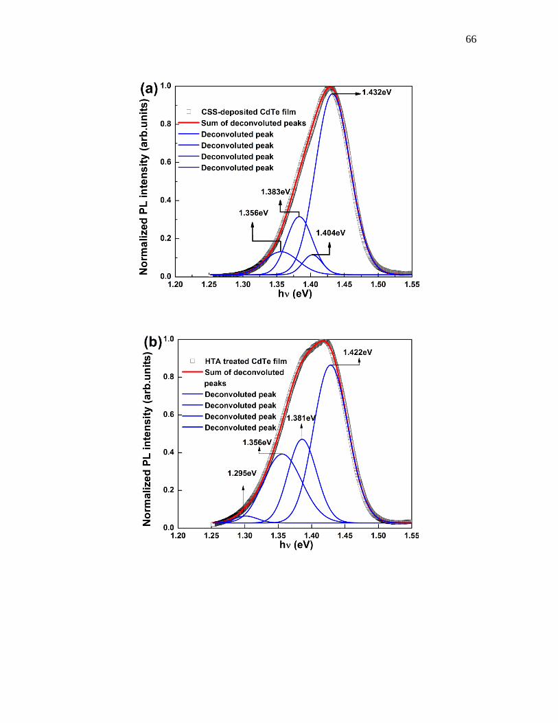
66
67
Figure 3-17. PL spectra and the corresponding deconvoluted PL peaks for CSS-deposited
ultra-thin CdTe film (a) without any treatment, (b) with HTA treatment, (c) with VCC
treatment and (d) with HTA+VCC treatments. PL spectra were obtained with interface
excitation at 40 K
68
Figure 3-18. PL spectra with interface excitation showing the evolution of: (a) the interface
defect band, and (b) the CdTe1-xSx band with various HTA and VCC treatments.
69
The deconvoluted components with peaks at ~1.43, ~1.38, ~1.35, and ~1.30 eV have
been attributed to various species in the literature. The ~1.43 eV band is the surface
defect band also observed from the free surface in Fig.26. The ~1.38 eV band has been
assigned to CdTe1-xSx 71
and the ~1.35 eV band to cadmium vacancy complexes 69
. The
small ~1.30 eV band, which is only observed in CdTe with treatments, has not been
identified yet.
Fig.3-19a shows that the intensity of the defect band is reduced with HTA and VCC
treatments, indicating that the defect concentration at the CdS/CdTe interface is reduced.
72 As discussed in Section 3.1, VCC treatments can promote sulfur diffusion from CdS to
CdTe. As shown in Fig.3-19b, the intensity of the ~1.38 eV band increases significantly
with VCC treatments, a clear evidence that CdTe1-xSx is being formed near the interface.
Note that the ~1.38 eV band for the films with HTA and HTA+VCC treatments is
considerably weaker compared to the film with VCC treatments only. The phenomenon
suggests that additional HTA treatment can mitigate excess sulfur diffusion in the VCC
treatment.
In order to further analyze the effects of HTA treatments on sulfur diffusion, ultra-thin
CdTe films with various heat treatments were characterized by UV/Vis absorption
spectroscopy. Fig.3-20a shows the absorption of ultra-thin CdTe films near the
absorption edge region. It is clearly that the absorption edge shifts to lower energy with
post-deposition treatments, especially with VCC treatments. The red shift is consistent
with the formation of CdTe1-xSx, a low bandgap component resulting from the
70
incorporation of sulfur in CdTe films with VCC treatments. As illustrated in Fig. 3-20a,
the bandgap of CdTe1-xSx was extracted from the absorption spectra using a linear fit at
the threshold region 73
. Using the extracted bandgap of CdTe1-xSx and an established
relation between the bandgap and stoichiometry of CdTe1-xSx62
:
(4)
the values of x are calculated and presented in Fig.3-20b with relation to the bandgap of
CdTe1-xSx.
As displayed in Fig.3-20b, a HTA treatment itself can promote the sulfur diffusion
from CdS to CdTe because of high temperature, causing the x value in CdTe1-xSx to
increase from 0.8% in the cell without any treatments to 1.3% in the cell with just HTA
treatment. However, as for the efficiency in promoting sulfur diffusion, a HTA treatment
is less effective than a VCC treatment with the latter producing an apparently higher x
value of 2.3% in the cell with just VCC treatment despite shorter treatment duration.
Furthermore, it is noteworthy that a HTA treatment prior to a VCC treatment can
suppress sulfur diffusion resulting from the VCC treatment. It can be seen in the cell
with HTA plus VCC treatment where x value in CdTe1-xSx is only 1.8%. The trend
reflected in Fig.3-20b is very similar to that in Fig.3-19b.
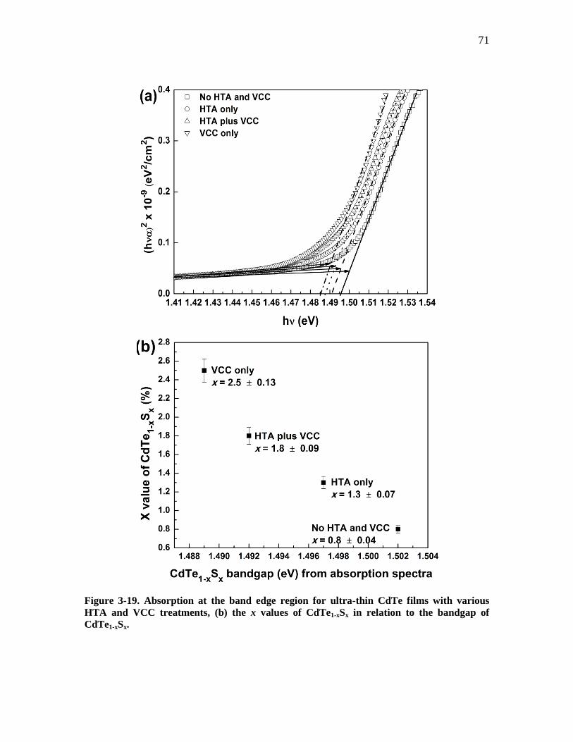
71
Figure 3-19. Absorption at the band edge region for ultra-thin CdTe films with various
HTA and VCC treatments, (b) the x values of CdTe1-xSx in relation to the bandgap of
CdTe1-xSx.
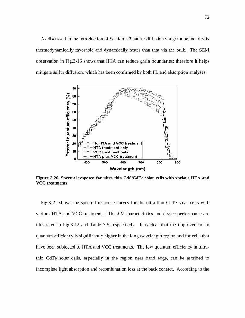
72
As discussed in the introduction of Section 3.3, sulfur diffusion via grain boundaries is
thermodynamically favorable and dynamically faster than that via the bulk. The SEM
observation in Fig.3-16 shows that HTA can reduce grain boundaries; therefore it helps
mitigate sulfur diffusion, which has been confirmed by both PL and absorption analyses.
Figure 3-20. Spectral response for ultra-thin CdS/CdTe solar cells with various HTA and
VCC treatments
Fig.3-21 shows the spectral response curves for the ultra-thin CdTe solar cells with
various HTA and VCC treatments. The J-V characteristics and device performance are
illustrated in Fig.3-12 and Table 3-5 respectively. It is clear that the improvement in
quantum efficiency is significantly higher in the long wavelength region and for cells that
have been subjected to HTA and VCC treatments. The low quantum efficiency in ultra-
thin CdTe solar cells, especially in the region near band edge, can be ascribed to
incomplete light absorption and recombination loss at the back contact. According to the
73
analysis of the absorption edge in Fig. 3-20, the red shift in the band edge region is
because of the formation of CdTe1-xSx which is enhanced with HTA and VCC treatments.
It is believed that the increase of quantum efficiency in high-wavelength region can be
partly due to CdTe1-xSx. On the other hand, HTA and VCC treatments can reduce defects
both on the surface and in the CdS/CdTe junctions. The reduction of surface defects on
the back contact can also contribute to the increase of quantum efficiency.
3.5 Summary
Compared with conventional solution based cadmium chloride treatment, vaporous
cadmium chloride treatment consumes much less cadmium compound, creates less
cadmium waste, and is more compatible with vacuum based manufacturing processes.
Three key parameters of VCC treatments on ultra-thin CdTe solar cells, annealing
temperature/duration, oxygen partial pressure and ambient pressure, have been studied.
Using J-V and PL measurements, the correlation between device performance and
treatment conditions has been established.
Apart from VCC treatments, another post-deposition treatment named high-
temperature annealing was introduced in the device fabrication process. We have shown
that the HTA process prior to a VCC treatment is useful for producing high-quality ultra-
thin CdTe films. SEM, optical absorption and PL measurements show that substantial
growth in CdTe grain size and reduction in defects related to grain boundary and
excessive sulfur diffusion are realized with combined HTA and VCC treatments. An

74
efficiency of about 11.6% has been demonstrated for ultra-thin CdS/CdTe solar cells
processed with these post-deposition treatments.
75
4. Ohmic contact formation to ultra-thin CdTe
As discussed in Section 1.4, the formation of a low-resistance electrical contact or
ohmic contact to CdTe solar cells was a major obstacle. Self-compensation hampers
efforts to achieve high p-doping in CdTe. The large work function of CdTe limits the
choice of metals as the contact electrode. A conventional method for forming ohmic
contact uses etching solutions such as nitric-phosphoric acid (NP) or bromine-methanol
(BM) 74
solutions to create a p+ tellurium rich surface, which provides a buffer layer with
a work function adequate for making ohmic contact to the underlying CdTe layer.
However the solution method for making ohmic contacts is not applicable for ultra-thin
CdTe solar cells, because, through preferential etching on CdTe grain boundaries 75
, it
creates shunting paths in the CdTe film, which can seriously deteriorate the device
performance. Furthermore, it is particularly difficult to control the final CdTe layer
thickness and uniformity with solution etching.37
Among the alternatives to NP or BM
method, Cu/Au 36
and graphite paste mixed with CuxTe 39
have been applied for the
fabrication of ultra-thin CdTe solar cells with efficiencies of 11~12%. Cu+ can readily
substitute for Cd2+
in CdTe to form CuCd complex which acts as a shallow acceptor and
enhances the p-type characteristics of CdTe. In addition, CuxTe can reduce the energy
barrier at the CdTe/metal junction to facilitate the hole transfer by producing tunneling
states at the CdTe/CuxTe and CuxTe/metal interfaces.2
Although the Cu containing back contact can form a low-resistance contact to p-CdTe
and improve cell efficiency, it also can cause serious cell instability. Cu can be depleted
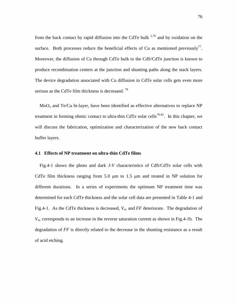
76
from the back contact by rapid diffusion into the CdTe bulk 2,76
and by oxidation on the
surface. Both processes reduce the beneficial effects of Cu as mentioned previously77
.
Moreover, the diffusion of Cu through CdTe bulk to the CdS/CdTe junction is known to
produce recombination centers at the junction and shunting paths along the stack layers.
The device degradation associated with Cu diffusion in CdTe solar cells gets even more
serious as the CdTe film thickness is decreased. 78
MoOx and Te/Cu bi-layer, have been identified as effective alternatives to replace NP
treatment in forming ohmic contact to ultra-thin CdTe solar cells79-81
. In this chapter, we
will discuss the fabrication, optimization and characterization of the new back contact
buffer layers.
4.1 Effects of NP treatment on ultra-thin CdTe films
Fig.4-1 shows the photo and dark J-V characteristics of CdS/CdTe solar cells with
CdTe film thickness ranging from 5.0 μm to 1.5 μm and treated in NP solution for
different durations. In a series of experiments the optimum NP treatment time was
determined for each CdTe thickness and the solar cell data are presented in Table 4-1 and
Fig.4-1. As the CdTe thickness is decreased, Voc and FF deteriorate. The degradation of
Voc corresponds to an increase in the reverse saturation current as shown in Fig.4-1b. The
degradation of FF is directly related to the decrease in the shunting resistance as a result
of acid etching.
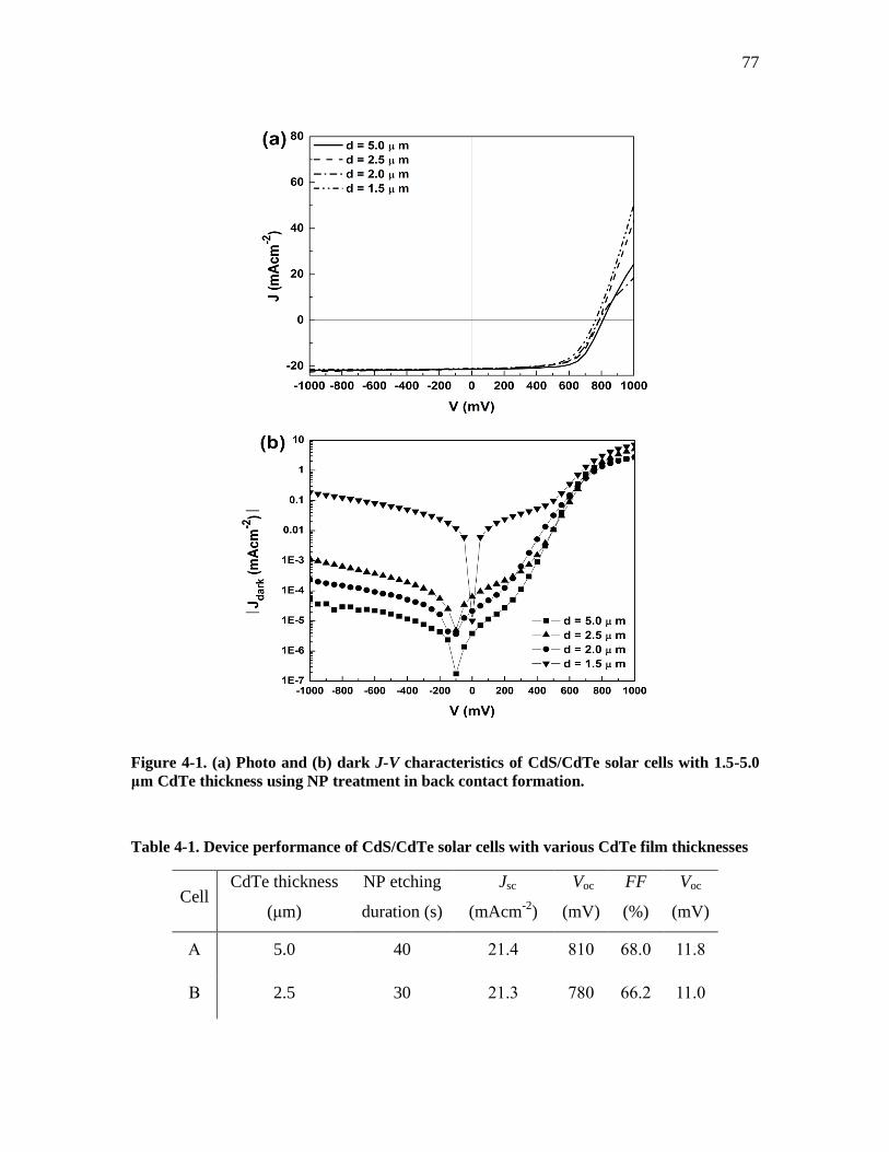
77
Figure 4-1. (a) Photo and (b) dark J-V characteristics of CdS/CdTe solar cells with 1.5-5.0
μm CdTe thickness using NP treatment in back contact formation.
Table 4-1. Device performance of CdS/CdTe solar cells with various CdTe film thicknesses
Cell CdTe thickness
(μm)
NP etching
duration (s)
Jsc
(mAcm-2
)
Voc
(mV)
FF
(%)
Voc
(mV)
A 5.0 40 21.4 810 68.0 11.8
B 2.5 30 21.3 780 66.2 11.0
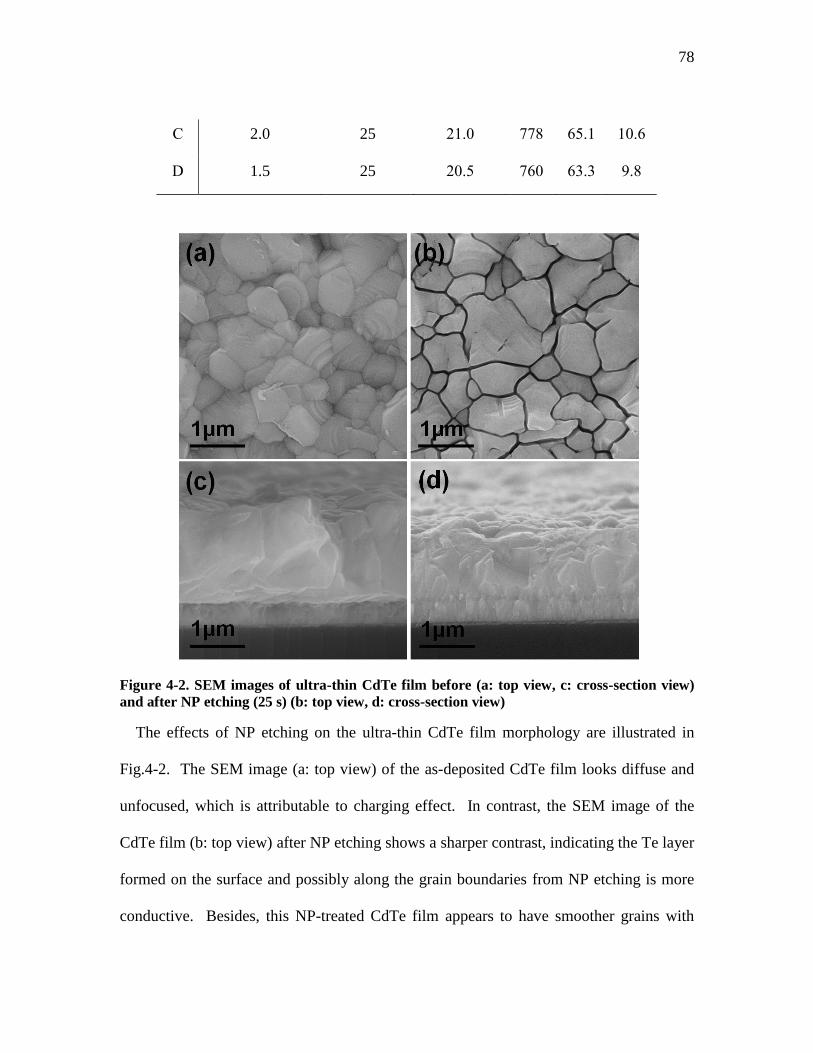
78
C 2.0 25 21.0 778 65.1 10.6
D 1.5 25 20.5 760 63.3 9.8
Figure 4-2. SEM images of ultra-thin CdTe film before (a: top view, c: cross-section view)
and after NP etching (25 s) (b: top view, d: cross-section view)
The effects of NP etching on the ultra-thin CdTe film morphology are illustrated in
Fig.4-2. The SEM image (a: top view) of the as-deposited CdTe film looks diffuse and
unfocused, which is attributable to charging effect. In contrast, the SEM image of the
CdTe film (b: top view) after NP etching shows a sharper contrast, indicating the Te layer
formed on the surface and possibly along the grain boundaries from NP etching is more
conductive. Besides, this NP-treated CdTe film appears to have smoother grains with
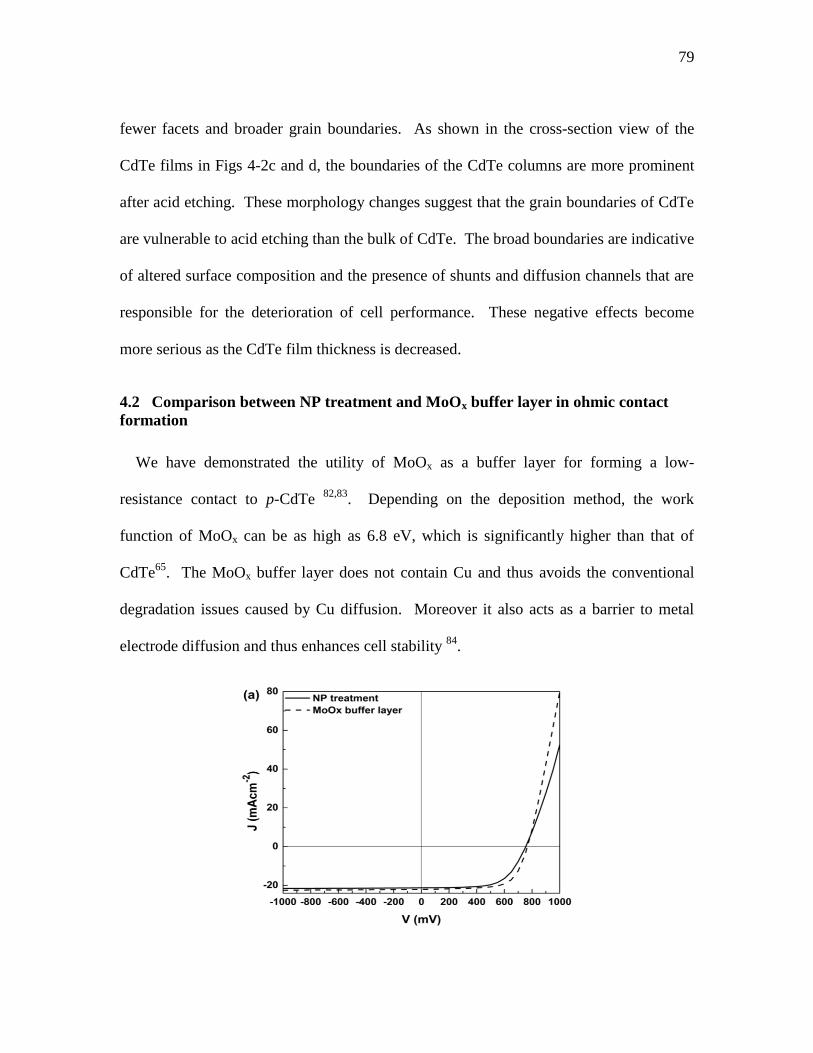
79
fewer facets and broader grain boundaries. As shown in the cross-section view of the
CdTe films in Figs 4-2c and d, the boundaries of the CdTe columns are more prominent
after acid etching. These morphology changes suggest that the grain boundaries of CdTe
are vulnerable to acid etching than the bulk of CdTe. The broad boundaries are indicative
of altered surface composition and the presence of shunts and diffusion channels that are
responsible for the deterioration of cell performance. These negative effects become
more serious as the CdTe film thickness is decreased.
4.2 Comparison between NP treatment and MoOx buffer layer in ohmic contact
formation
We have demonstrated the utility of MoOx as a buffer layer for forming a low-
resistance contact to p-CdTe 82,83
. Depending on the deposition method, the work
function of MoOx can be as high as 6.8 eV, which is significantly higher than that of
CdTe65
. The MoOx buffer layer does not contain Cu and thus avoids the conventional
degradation issues caused by Cu diffusion. Moreover it also acts as a barrier to metal
electrode diffusion and thus enhances cell stability 84
.
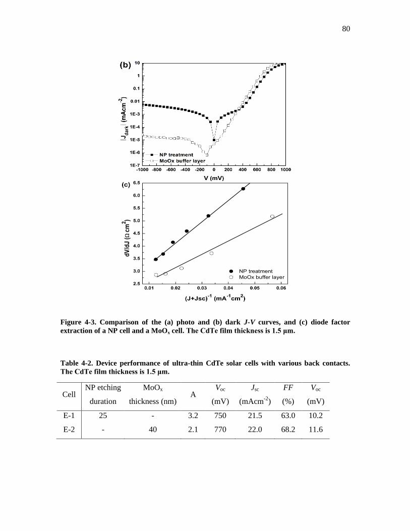
80
Figure 4-3. Comparison of the (a) photo and (b) dark J-V curves, and (c) diode factor
extraction of a NP cell and a MoOx cell. The CdTe film thickness is 1.5 μm.
Table 4-2. Device performance of ultra-thin CdTe solar cells with various back contacts.
The CdTe film thickness is 1.5 μm.
Cell NP etching
duration
MoOx
thickness (nm) A
Voc
(mV)
Jsc
(mAcm-2
)
FF
(%)
Voc
(mV)
E-1 25 - 3.2 750 21.5 63.0 10.2
E-2 - 40 2.1 770 22.0 68.2 11.6
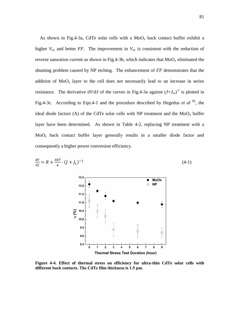
81
As shown in Fig.4-3a, CdTe solar cells with a MoOx back contact buffer exhibit a
higher Voc and better FF. The improvement in Voc is consistent with the reduction of
reverse saturation current as shown in Fig.4-3b, which indicates that MoOx eliminated the
shunting problem caused by NP etching. The enhancement of FF demonstrates that the
addition of MoOx layer to the cell does not necessarily lead to an increase in series
resistance. The derivative dV/dJ of the curves in Fig.4-3a against (J+Jsc)-1
is plotted in
Fig.4-3c. According to Eqn.4-1 and the procedure described by Hegedus et al 85
, the
ideal diode factors (A) of the CdTe solar cells with NP treatment and the MoOx buffer
layer have been determined. As shown in Table 4-2, replacing NP treatment with a
MoOx back contact buffer layer generally results in a smaller diode factor and
consequently a higher power conversion efficiency.
(4-1)
Figure 4-4. Effect of thermal stress on efficiency for ultra-thin CdTe solar cells with
different back contacts. The CdTe film thickness is 1.5 μm.
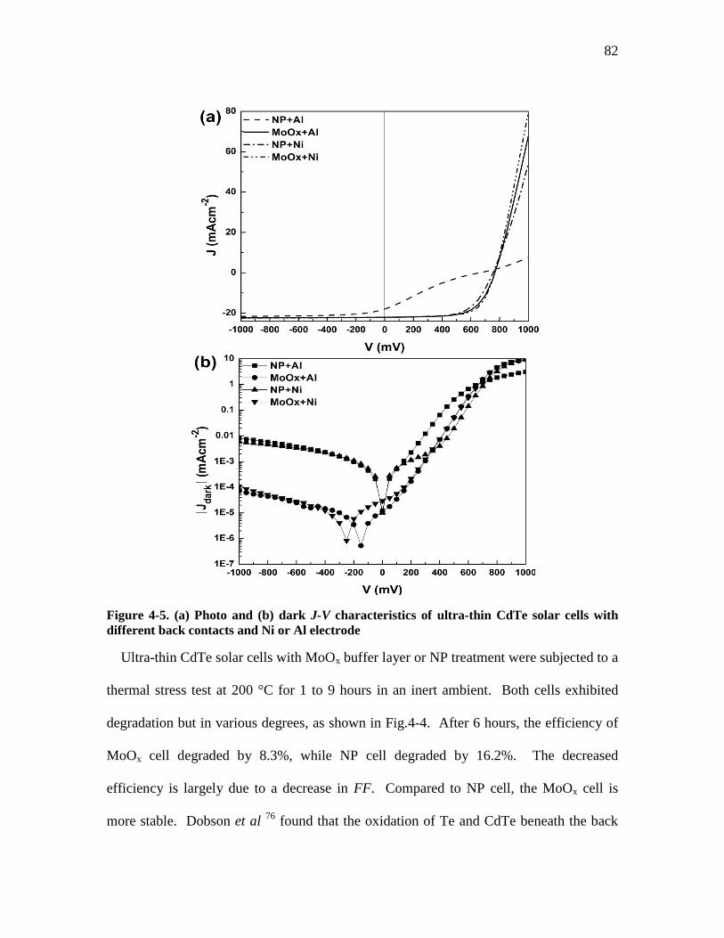
82
Figure 4-5. (a) Photo and (b) dark J-V characteristics of ultra-thin CdTe solar cells with
different back contacts and Ni or Al electrode
Ultra-thin CdTe solar cells with MoOx buffer layer or NP treatment were subjected to a
thermal stress test at 200 °C for 1 to 9 hours in an inert ambient. Both cells exhibited
degradation but in various degrees, as shown in Fig.4-4. After 6 hours, the efficiency of
MoOx cell degraded by 8.3%, while NP cell degraded by 16.2%. The decreased
efficiency is largely due to a decrease in FF. Compared to NP cell, the MoOx cell is
more stable. Dobson et al 76
found that the oxidation of Te and CdTe beneath the back
83
contact and the diffusion of metal from the back contact are two primary degradation
mechanisms. The ease of oxidation of the Te-rich layer is probably the reason why the
NP cells are inferior in stability relative to the MoOx cell.
Fig.4-5 shows the photo and dark J-V characteristics of ultra-thin CdTe solar cells with
various back contacts compositions. Table 4-3 lists the photovoltaic parameters. In
general, Ni forms a relatively ohmic contact with the NP-treated ultra-thin CdTe films.
With Al, a low work function metal, the contact is blocking with serious roll-over in the
J-V characteristics and poor Voc and FF. Both NP cells show large leakage currents.
However, as Fig.4-5a shows, both Ni and Al produce an ohmic contact with MoOx as the
buffer, resulting in fairly good FF (66-68%). The leakage current of the MoOx cell is
about two orders of magnitude lower than that of the NP cell.
Table 4-3. Device performance of ultra-thin CdTe solar cells with various back contacts
with Ni or Al electrode. The CdTe thickness is 1.5 μm.
Cell
NP etching
duration
MoOx
thickness (nm)
Electrode/work
function (eV)
Voc
(mV)
Jsc
(mAcm-2
)
FF
(%)
η
(%)
E-1 25 - Ni/5.4 750 21.5 63.0 10.2
E-3 25 - Al/4.3 660 18.0 20.9 2.5
E-2 - 40 Ni/5.4 770 22.0 68.2 11.6
E-4 - 40 Al/4.3 770 21.9 65.5 11.1
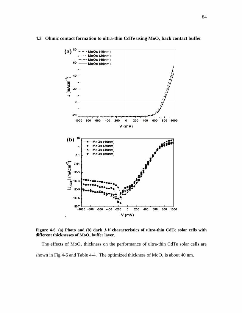
84
4.3 Ohmic contact formation to ultra-thin CdTe using MoOx back contact buffer
.
Figure 4-6. (a) Photo and (b) dark J-V characteristics of ultra-thin CdTe solar cells with
different thicknesses of MoOx buffer layer.
The effects of MoOx thickness on the performance of ultra-thin CdTe solar cells are
shown in Fig.4-6 and Table 4-4. The optimized thickness of MoOx is about 40 nm.
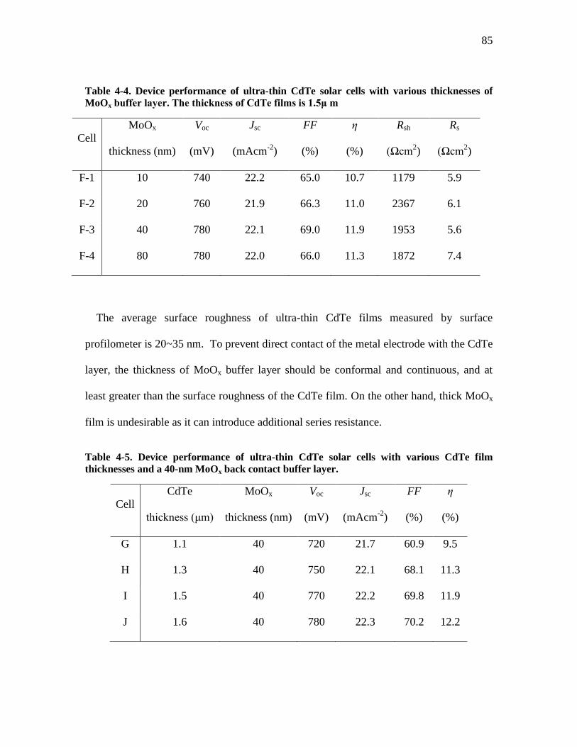
85
Table 4-4. Device performance of ultra-thin CdTe solar cells with various thicknesses of
MoOx buffer layer. The thickness of CdTe films is 1.5μ m
Cell
MoOx
thickness (nm)
Voc
(mV)
Jsc
(mAcm-2
)
FF
(%)
η
(%)
Rsh
(Ωcm2)
Rs
(Ωcm2)
F-1 10 740 22.2 65.0 10.7 1179 5.9
F-2 20 760 21.9 66.3 11.0 2367 6.1
F-3 40 780 22.1 69.0 11.9 1953 5.6
F-4 80 780 22.0 66.0 11.3 1872 7.4
The average surface roughness of ultra-thin CdTe films measured by surface
profilometer is 20~35 nm. To prevent direct contact of the metal electrode with the CdTe
layer, the thickness of MoOx buffer layer should be conformal and continuous, and at
least greater than the surface roughness of the CdTe film. On the other hand, thick MoOx
film is undesirable as it can introduce additional series resistance.
Table 4-5. Device performance of ultra-thin CdTe solar cells with various CdTe film
thicknesses and a 40-nm MoOx back contact buffer layer.
Cell
CdTe
thickness (μm)
MoOx
thickness (nm)
Voc
(mV)
Jsc
(mAcm-2
)
FF
(%)
η
(%)
G 1.1 40 720 21.7 60.9 9.5
H 1.3 40 750 22.1 68.1 11.3
I 1.5 40 770 22.2 69.8 11.9
J 1.6 40 780 22.3 70.2 12.2
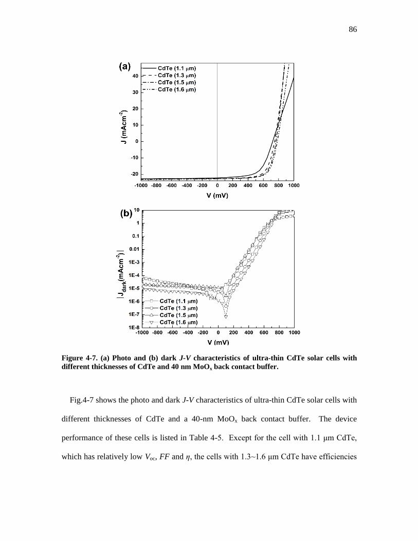
86
Figure 4-7. (a) Photo and (b) dark J-V characteristics of ultra-thin CdTe solar cells with
different thicknesses of CdTe and 40 nm MoOx back contact buffer.
Fig.4-7 shows the photo and dark J-V characteristics of ultra-thin CdTe solar cells with
different thicknesses of CdTe and a 40-nm MoOx back contact buffer. The device
performance of these cells is listed in Table 4-5. Except for the cell with 1.1 μm CdTe,
which has relatively low Voc, FF and η, the cells with 1.3~1.6 μm CdTe have efficiencies
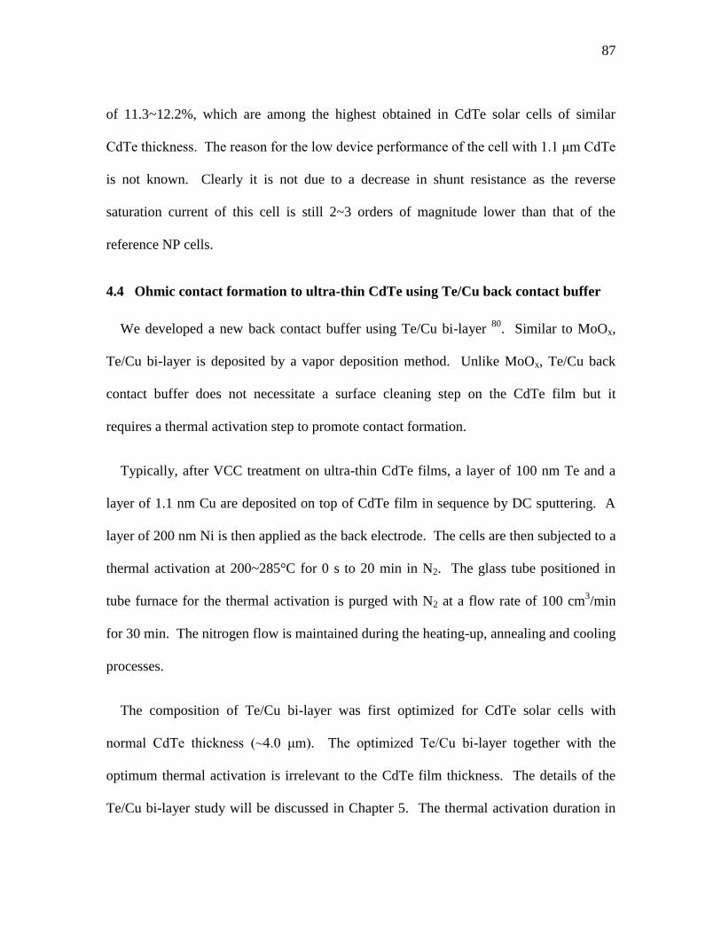
87
of 11.3~12.2%, which are among the highest obtained in CdTe solar cells of similar
CdTe thickness. The reason for the low device performance of the cell with 1.1 μm CdTe
is not known. Clearly it is not due to a decrease in shunt resistance as the reverse
saturation current of this cell is still 2~3 orders of magnitude lower than that of the
reference NP cells.
4.4 Ohmic contact formation to ultra-thin CdTe using Te/Cu back contact buffer
We developed a new back contact buffer using Te/Cu bi-layer 80
. Similar to MoOx,
Te/Cu bi-layer is deposited by a vapor deposition method. Unlike MoOx, Te/Cu back
contact buffer does not necessitate a surface cleaning step on the CdTe film but it
requires a thermal activation step to promote contact formation.
Typically, after VCC treatment on ultra-thin CdTe films, a layer of 100 nm Te and a
layer of 1.1 nm Cu are deposited on top of CdTe film in sequence by DC sputtering. A
layer of 200 nm Ni is then applied as the back electrode. The cells are then subjected to a
thermal activation at 200~285°C for 0 s to 20 min in N2. The glass tube positioned in
tube furnace for the thermal activation is purged with N2 at a flow rate of 100 cm3/min
for 30 min. The nitrogen flow is maintained during the heating-up, annealing and cooling
processes.
The composition of Te/Cu bi-layer was first optimized for CdTe solar cells with
normal CdTe thickness (~4.0 μm). The optimized Te/Cu bi-layer together with the
optimum thermal activation is irrelevant to the CdTe film thickness. The details of the
Te/Cu bi-layer study will be discussed in Chapter 5. The thermal activation duration in
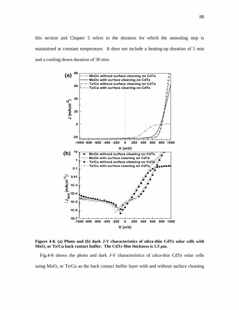
88
this section and Chapter 5 refers to the duration for which the annealing step is
maintained at constant temperature. It does not include a heating-up duration of 5 min
and a cooling-down duration of 30 min.
Figure 4-8. (a) Photo and (b) dark J-V characteristics of ultra-thin CdTe solar cells with
MoOx or Te/Cu back contact buffer. The CdTe film thickness is 1.5 μm.
Fig.4-8 shows the photo and dark J-V characteristics of ultra-thin CdTe solar cells
using MoOx or Te/Cu as the back contact buffer layer with and without surface cleaning
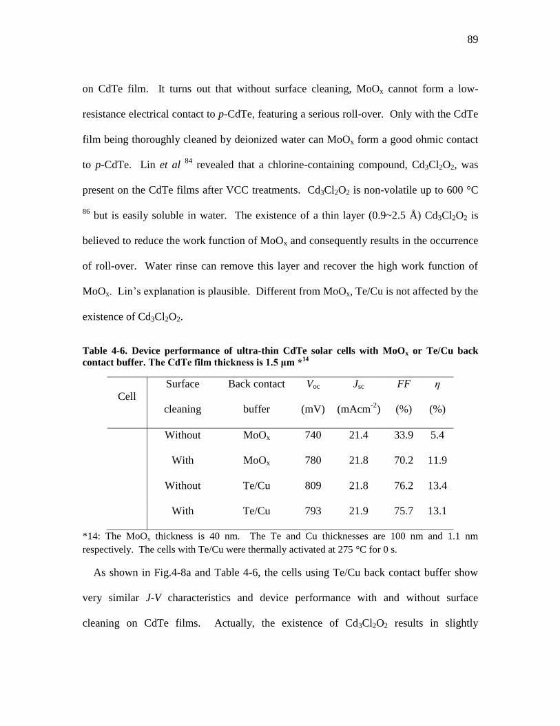
89
on CdTe film. It turns out that without surface cleaning, MoOx cannot form a low-
resistance electrical contact to p-CdTe, featuring a serious roll-over. Only with the CdTe
film being thoroughly cleaned by deionized water can MoOx form a good ohmic contact
to p-CdTe. Lin et al 84
revealed that a chlorine-containing compound, Cd3Cl2O2, was
present on the CdTe films after VCC treatments. Cd3Cl2O2 is non-volatile up to 600 °C
86 but is easily soluble in water. The existence of a thin layer (0.9~2.5 Å) Cd3Cl2O2 is
believed to reduce the work function of MoOx and consequently results in the occurrence
of roll-over. Water rinse can remove this layer and recover the high work function of
MoOx. Lin’s explanation is plausible. Different from MoOx, Te/Cu is not affected by the
existence of Cd3Cl2O2.
Table 4-6. Device performance of ultra-thin CdTe solar cells with MoOx or Te/Cu back
contact buffer. The CdTe film thickness is 1.5 μm *14
Cell
Surface
cleaning
Back contact
buffer
Voc
(mV)
Jsc
(mAcm-2
)
FF
(%)
η
(%)
Without MoOx 740 21.4 33.9 5.4
With MoOx 780 21.8 70.2 11.9
Without Te/Cu 809 21.8 76.2 13.4
With Te/Cu 793 21.9 75.7 13.1
*14: The MoOx thickness is 40 nm. The Te and Cu thicknesses are 100 nm and 1.1 nm
respectively. The cells with Te/Cu were thermally activated at 275 °C for 0 s.
As shown in Fig.4-8a and Table 4-6, the cells using Te/Cu back contact buffer show
very similar J-V characteristics and device performance with and without surface
cleaning on CdTe films. Actually, the existence of Cd3Cl2O2 results in slightly
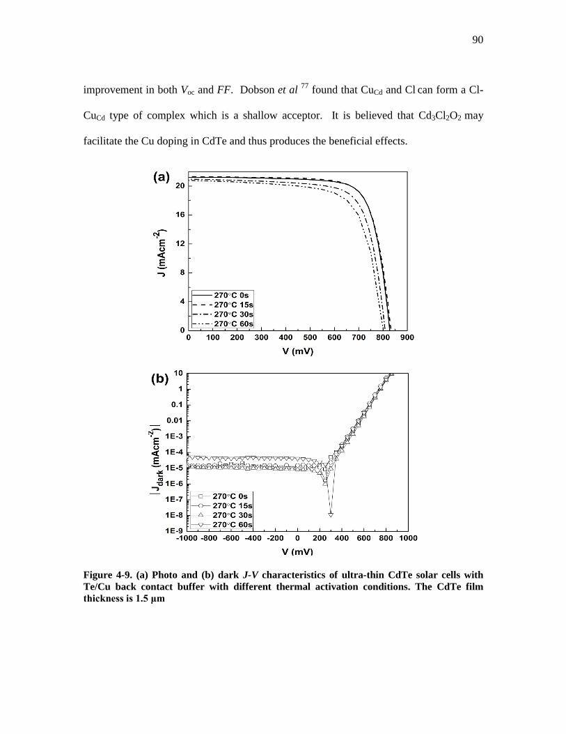
90
improvement in both Voc and FF. Dobson et al 77
found that CuCd and Cl can form a Cl-
CuCd type of complex which is a shallow acceptor. It is believed that Cd3Cl2O2 may
facilitate the Cu doping in CdTe and thus produces the beneficial effects.
Figure 4-9. (a) Photo and (b) dark J-V characteristics of ultra-thin CdTe solar cells with
Te/Cu back contact buffer with different thermal activation conditions. The CdTe film
thickness is 1.5 μm
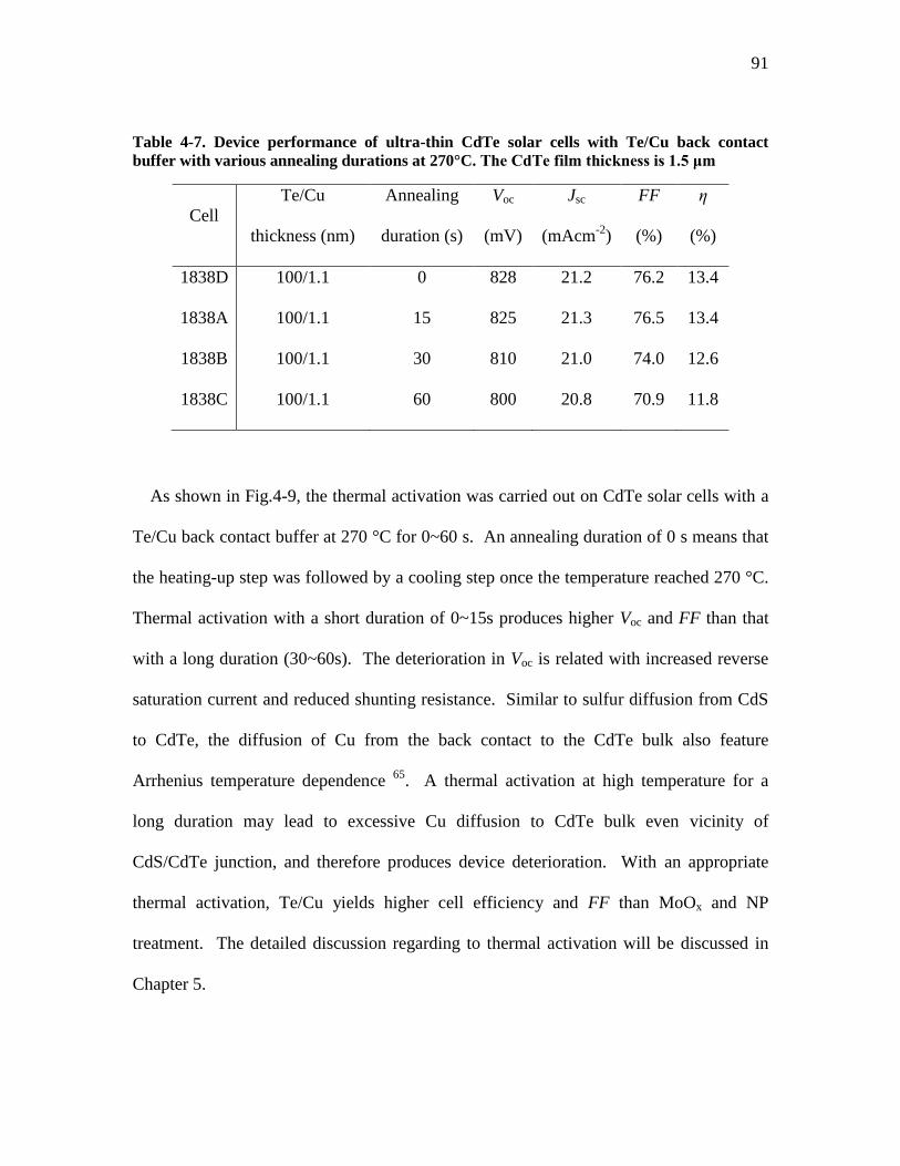
91
Table 4-7. Device performance of ultra-thin CdTe solar cells with Te/Cu back contact
buffer with various annealing durations at 270°C. The CdTe film thickness is 1.5 μm
Cell
Te/Cu
thickness (nm)
Annealing
duration (s)
Voc
(mV)
Jsc
(mAcm-2
)
FF
(%)
η
(%)
1838D 100/1.1 0 828 21.2 76.2 13.4
1838A 100/1.1 15 825 21.3 76.5 13.4
1838B 100/1.1 30 810 21.0 74.0 12.6
1838C 100/1.1 60 800 20.8 70.9 11.8
As shown in Fig.4-9, the thermal activation was carried out on CdTe solar cells with a
Te/Cu back contact buffer at 270 °C for 0~60 s. An annealing duration of 0 s means that
the heating-up step was followed by a cooling step once the temperature reached 270 °C.
Thermal activation with a short duration of 0~15s produces higher Voc and FF than that
with a long duration (30~60s). The deterioration in Voc is related with increased reverse
saturation current and reduced shunting resistance. Similar to sulfur diffusion from CdS
to CdTe, the diffusion of Cu from the back contact to the CdTe bulk also feature
Arrhenius temperature dependence 65
. A thermal activation at high temperature for a
long duration may lead to excessive Cu diffusion to CdTe bulk even vicinity of
CdS/CdTe junction, and therefore produces device deterioration. With an appropriate
thermal activation, Te/Cu yields higher cell efficiency and FF than MoOx and NP
treatment. The detailed discussion regarding to thermal activation will be discussed in
Chapter 5.
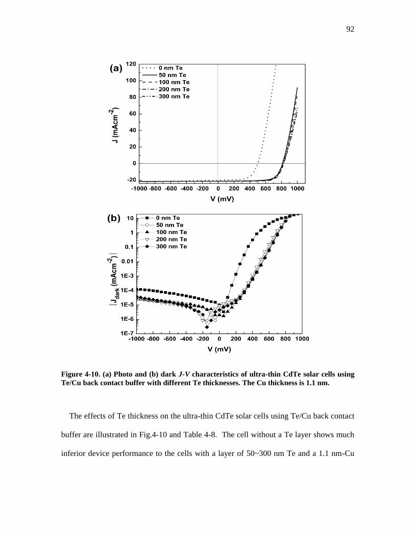
92
Figure 4-10. (a) Photo and (b) dark J-V characteristics of ultra-thin CdTe solar cells using
Te/Cu back contact buffer with different Te thicknesses. The Cu thickness is 1.1 nm.
The effects of Te thickness on the ultra-thin CdTe solar cells using Te/Cu back contact
buffer are illustrated in Fig.4-10 and Table 4-8. The cell without a Te layer shows much
inferior device performance to the cells with a layer of 50~300 nm Te and a 1.1 nm-Cu
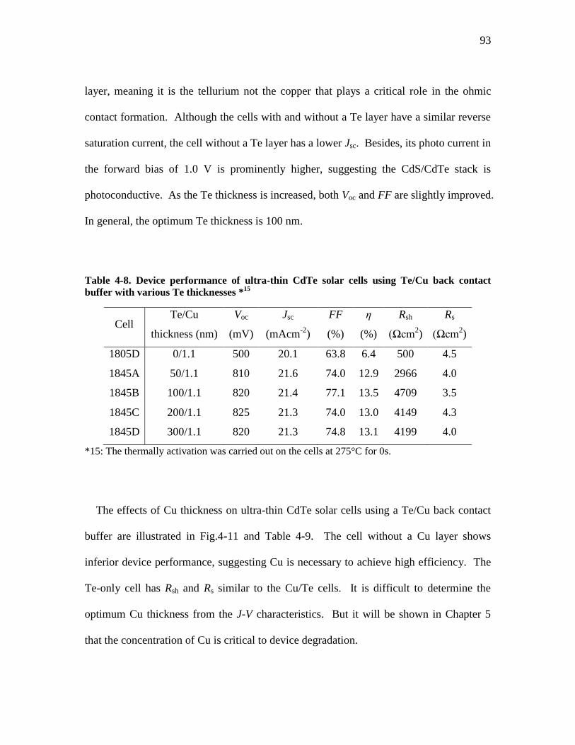
93
layer, meaning it is the tellurium not the copper that plays a critical role in the ohmic
contact formation. Although the cells with and without a Te layer have a similar reverse
saturation current, the cell without a Te layer has a lower Jsc. Besides, its photo current in
the forward bias of 1.0 V is prominently higher, suggesting the CdS/CdTe stack is
photoconductive. As the Te thickness is increased, both Voc and FF are slightly improved.
In general, the optimum Te thickness is 100 nm.
Table 4-8. Device performance of ultra-thin CdTe solar cells using Te/Cu back contact
buffer with various Te thicknesses *15
Cell Te/Cu
thickness (nm)
Voc
(mV)
Jsc
(mAcm-2
)
FF
(%)
η
(%)
Rsh
(Ωcm2)
Rs
(Ωcm2)
1805D 0/1.1 500 20.1 63.8 6.4 500 4.5
1845A 50/1.1 810 21.6 74.0 12.9 2966 4.0
1845B 100/1.1 820 21.4 77.1 13.5 4709 3.5
1845C 200/1.1 825 21.3 74.0 13.0 4149 4.3
1845D 300/1.1 820 21.3 74.8 13.1 4199 4.0
*15: The thermally activation was carried out on the cells at 275°C for 0s.
The effects of Cu thickness on ultra-thin CdTe solar cells using a Te/Cu back contact
buffer are illustrated in Fig.4-11 and Table 4-9. The cell without a Cu layer shows
inferior device performance, suggesting Cu is necessary to achieve high efficiency. The
Te-only cell has Rsh and Rs similar to the Cu/Te cells. It is difficult to determine the
optimum Cu thickness from the J-V characteristics. But it will be shown in Chapter 5
that the concentration of Cu is critical to device degradation.
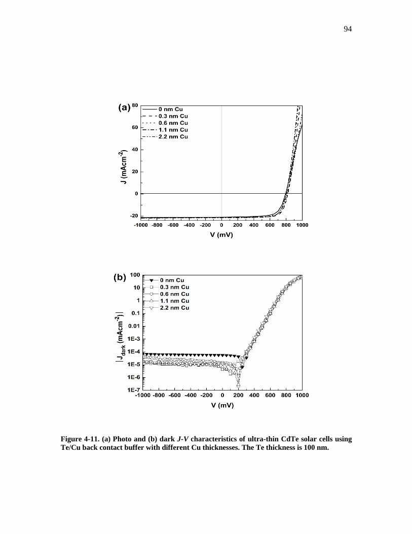
94
Figure 4-11. (a) Photo and (b) dark J-V characteristics of ultra-thin CdTe solar cells using
Te/Cu back contact buffer with different Cu thicknesses. The Te thickness is 100 nm.
95
Table 4-9. Device performance of ultra-thin CdTe solar cells using Te/Cu back contact
buffer with various Cu thicknesses *16
Cell Te/Cu
thickness (nm)
Voc
(mV)
Jsc
(mAcm-2
)
FF
(%)
η
(%)
Rsh
(Ωcm2)
Rs
(Ωcm2)
1805D 100/0.0 790 21.0 71.0 11.8 1361 4.7
1845A 100/0.3 815 21.2 75.0 13.0 3397 3.9
1845B 100/0.6 810 21.1 73.7 12.6 1717 3.5
1845C 100/1.1 800 21.3 74.4 12.7 4315 3.9
1845D 100/2.2 810 21.1 74.7 12.8 3277 4.9
*16: The thermally activation was carried out on the cells at 275°C for 0s.
Table 4-10. Device performance of ultra-thin CdTe solar cells with various CdTe film
thicknesses and a Te/Cu back contact buffer layer
Cell CdTe
thickness (μm)
Te/Cu
thickness (nm)
Voc
(mV)
Jsc
(mAcm-2
)
FF
(%)
η
(%)
K 0.9 100/1.1 790 20.4 69.0 11.1
G 1.2 100/1.1 790 20.7 70.8 11.6
H 1.4 100/1.1 790 21.6 76.5 13.1
I 1.5 100/1.1 820 21.5 76.4 13.5
J 1.7 100/1.1 830 21.5 76.8 13.7
Fig.4-12 shows the photo and dark J-V characteristics of ultra-thin CdTe solar cells
with different thickness of CdTe. The Te/Cu thickness ratio for these cells is held at
100:1.1. The device performance is listed in Table 4-10. The efficiency of these cells is
among the highest ever achieved using ultra-thin CdTe films as the absorber 87
. As far as
we know, this is the first time a fill factor as high as 76~77% in ultra-thin CdTe solar cell.
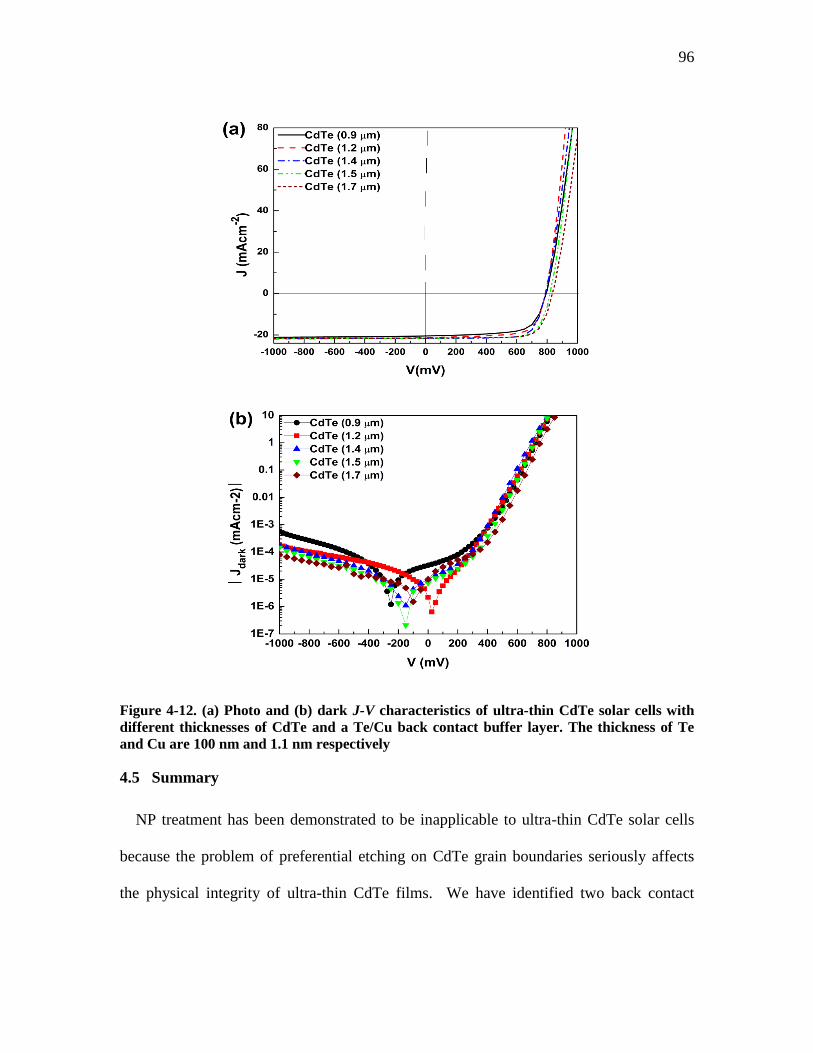
96
Figure 4-12. (a) Photo and (b) dark J-V characteristics of ultra-thin CdTe solar cells with
different thicknesses of CdTe and a Te/Cu back contact buffer layer. The thickness of Te
and Cu are 100 nm and 1.1 nm respectively
4.5 Summary
NP treatment has been demonstrated to be inapplicable to ultra-thin CdTe solar cells
because the problem of preferential etching on CdTe grain boundaries seriously affects
the physical integrity of ultra-thin CdTe films. We have identified two back contact
97
buffers, MoOx and Te/Cu, which are suitable for the fabrication of ultra-thin CdTe solar
cells. Compared with the NP method, our dry methods by physical vapor deposition
avoid etching damage on CdTe films and are better suited for large scale in-line
manufacturing of CdTe PV modules.
As a back contact buffer, MoOx can be produced to match the high work function of p-
CdTe, thus it enables the formation of an ohmic back contact and enhances the efficiency
of the CdTe solar cells, featuring high FF and Voc. MoOx is compatible with various
metal electrodes including metals with a low work function or high reactivity with CdTe.
We have also demonstrated that CdTe solar cells with MoOx as the back contact buffer is
relatively stable.
In another approach, Te/Cu was developed as a contact buffer for application in ultra-
thin CdTe solar cells. Te, prepared by vapor deposition directly on CdTe, has been found
to be highly effective as a high work function buffer, and in addition it limits Cu
diffusion into the underlying CdTe layer. Efficiencies up to 13.1% have been
demonstrated in CdTe solar cells with the CdTe thickness as low as 1.4 μm.
98
5. Low-resistance electrical back contact buffer to p-CdTe
Among the approaches to achieving high-efficiency and long-lifetime thin film
CdS/CdTe solar cells, the formation of a low-resistance and stable ohmic contact to p-
CdTe is critical, and perhaps the most difficult. In general, a metal forming an ohmic
contact to p-CdTe should have a work function aligned at least with the top of the CdTe
valence band. However, since p-CdTe has a work function as high as 5.7 eV, most
common metals are incapable of matching the work function and thus are not useful for
making ohmic contact to p-CdTe.
One strategy to overcome this difficulty is to chemically modify the CdTe surface and
create a degenerate p+ Te-rich layer by chemical etching with bromine-methanol (BM)
solution or nitric-phosphoric (NP) acid solution. The etching process produces a highly
conductive Te layer with a thickness determined by the etching conditions and the CdTe
surface morphology. There are several key issues associated with the etching process
including the tendency of over etching along grain boundaries resulting in the creation of
electrical shunts in the CdTe layer.
Alternatively, semiconductor materials MX, such as CuxTe88
, NiTe289
, ZnTe:N90
,
ZnTe:Cu91
, Sb2Te392
and As2Te393
, have been variously used as the contact buffer placed
between the p-CdTe layer and the metal electrode. The MX layer is presumed to enhance
charge tunneling across the MX/metal junction, and to reduce the energy barrier at the
CdTe/MX junction through the creation a heavily p-doped CdTe surface. Cu and Sb
from the MX layer are known to form shallow acceptors in CdTe. Among the MXs,
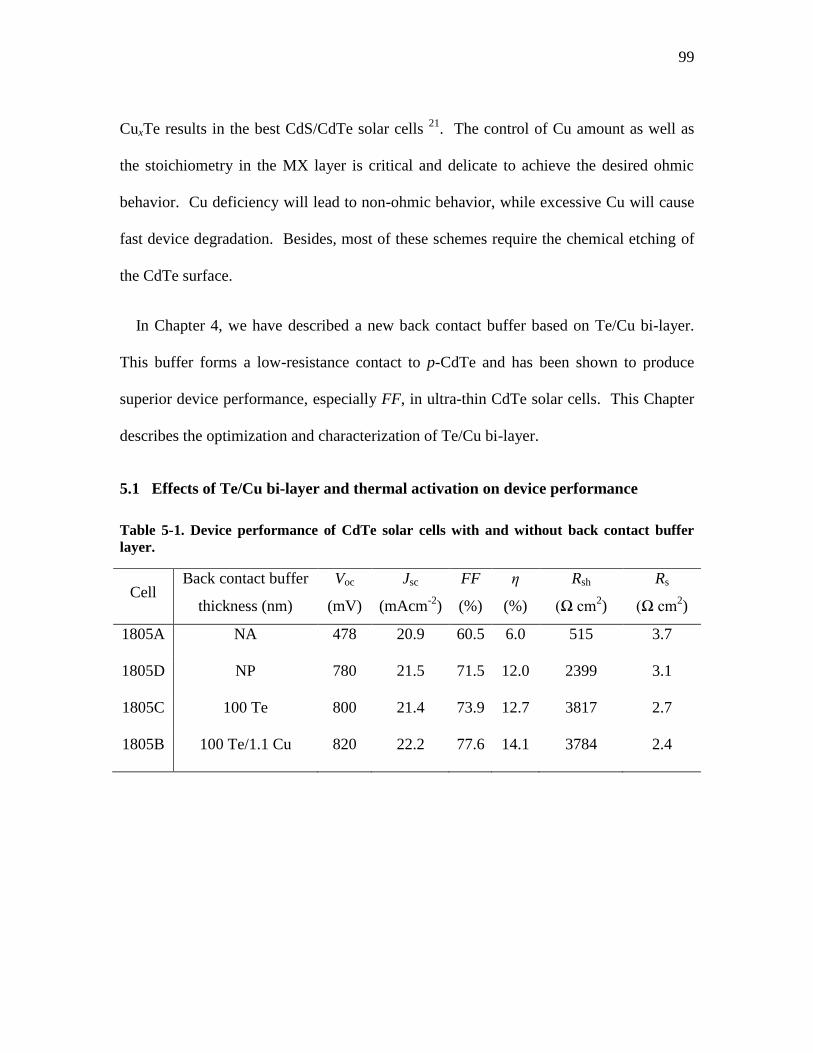
99
CuxTe results in the best CdS/CdTe solar cells 21
. The control of Cu amount as well as
the stoichiometry in the MX layer is critical and delicate to achieve the desired ohmic
behavior. Cu deficiency will lead to non-ohmic behavior, while excessive Cu will cause
fast device degradation. Besides, most of these schemes require the chemical etching of
the CdTe surface.
In Chapter 4, we have described a new back contact buffer based on Te/Cu bi-layer.
This buffer forms a low-resistance contact to p-CdTe and has been shown to produce
superior device performance, especially FF, in ultra-thin CdTe solar cells. This Chapter
describes the optimization and characterization of Te/Cu bi-layer.
5.1 Effects of Te/Cu bi-layer and thermal activation on device performance
Table 5-1. Device performance of CdTe solar cells with and without back contact buffer
layer.
Cell Back contact buffer
thickness (nm)
Voc
(mV)
Jsc
(mAcm-2
)
FF
(%)
η
(%)
Rsh
(Ω cm2)
Rs
(Ω cm2)
1805A NA 478 20.9 60.5 6.0 515 3.7
1805D NP 780 21.5 71.5 12.0 2399 3.1
1805C 100 Te 800 21.4 73.9 12.7 3817 2.7
1805B 100 Te/1.1 Cu 820 22.2 77.6 14.1 3784 2.4
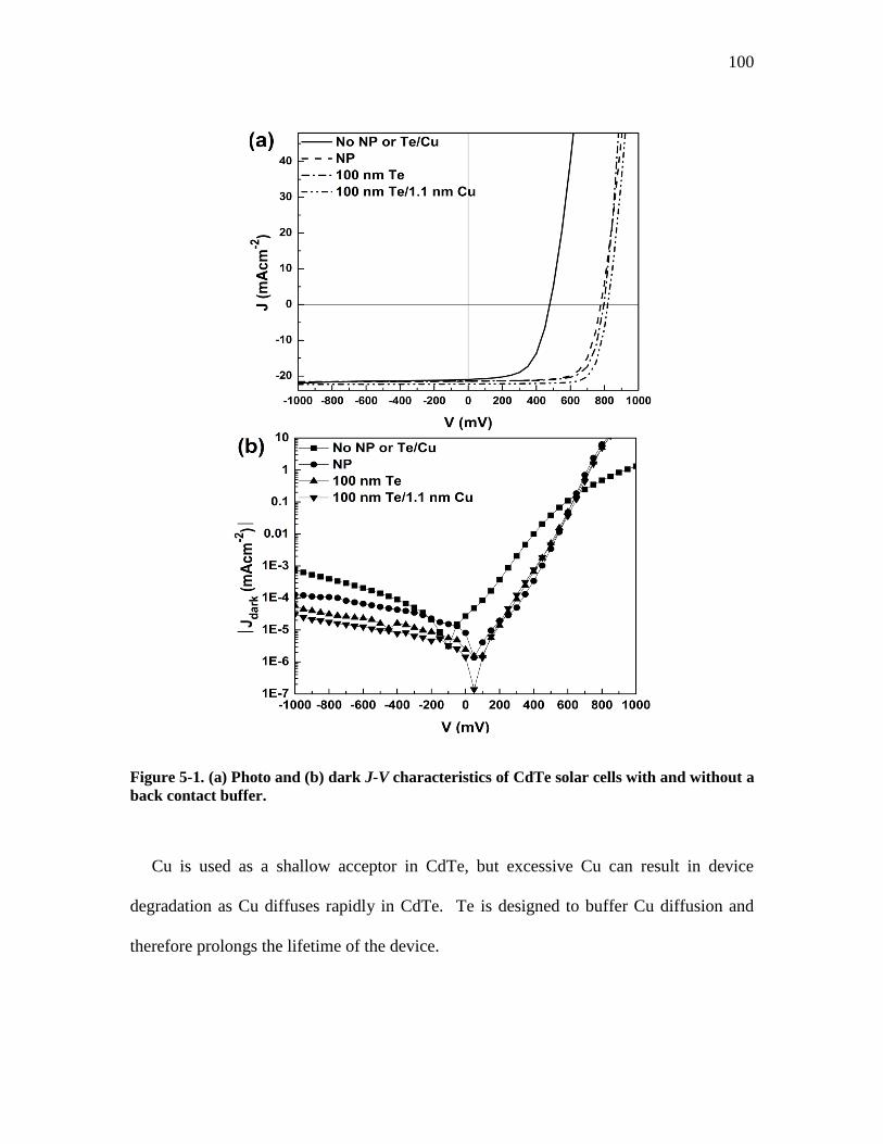
100
Figure 5-1. (a) Photo and (b) dark J-V characteristics of CdTe solar cells with and without a
back contact buffer.
Cu is used as a shallow acceptor in CdTe, but excessive Cu can result in device
degradation as Cu diffuses rapidly in CdTe. Te is designed to buffer Cu diffusion and
therefore prolongs the lifetime of the device.
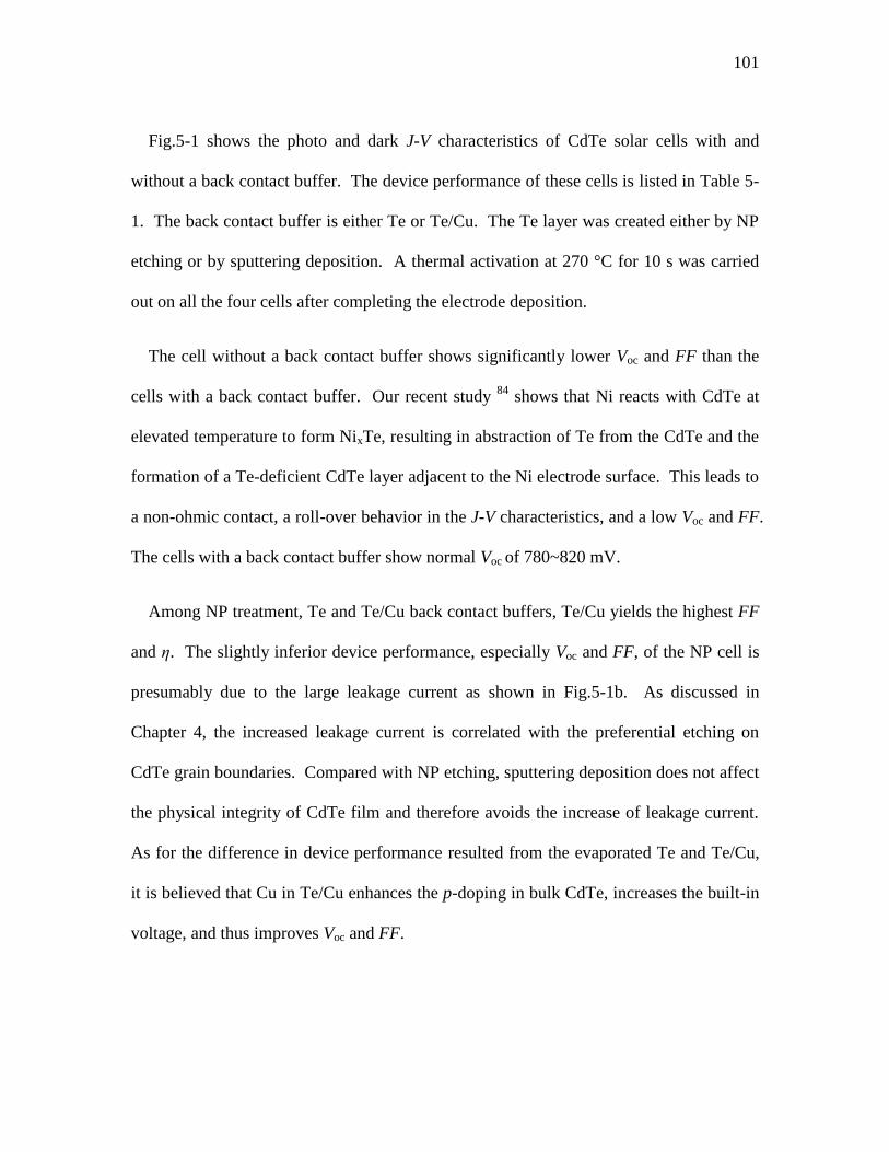
101
Fig.5-1 shows the photo and dark J-V characteristics of CdTe solar cells with and
without a back contact buffer. The device performance of these cells is listed in Table 5-
1. The back contact buffer is either Te or Te/Cu. The Te layer was created either by NP
etching or by sputtering deposition. A thermal activation at 270 °C for 10 s was carried
out on all the four cells after completing the electrode deposition.
The cell without a back contact buffer shows significantly lower Voc and FF than the
cells with a back contact buffer. Our recent study 84
shows that Ni reacts with CdTe at
elevated temperature to form NixTe, resulting in abstraction of Te from the CdTe and the
formation of a Te-deficient CdTe layer adjacent to the Ni electrode surface. This leads to
a non-ohmic contact, a roll-over behavior in the J-V characteristics, and a low Voc and FF.
The cells with a back contact buffer show normal Voc of 780~820 mV.
Among NP treatment, Te and Te/Cu back contact buffers, Te/Cu yields the highest FF
and η. The slightly inferior device performance, especially Voc and FF, of the NP cell is
presumably due to the large leakage current as shown in Fig.5-1b. As discussed in
Chapter 4, the increased leakage current is correlated with the preferential etching on
CdTe grain boundaries. Compared with NP etching, sputtering deposition does not affect
the physical integrity of CdTe film and therefore avoids the increase of leakage current.
As for the difference in device performance resulted from the evaporated Te and Te/Cu,
it is believed that Cu in Te/Cu enhances the p-doping in bulk CdTe, increases the built-in
voltage, and thus improves Voc and FF.
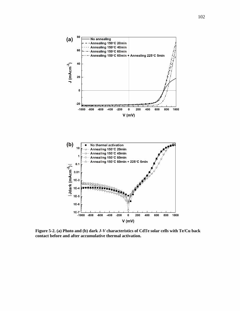
102
Figure 5-2. (a) Photo and (b) dark J-V characteristics of CdTe solar cells with Te/Cu back
contact before and after accumulative thermal activation.
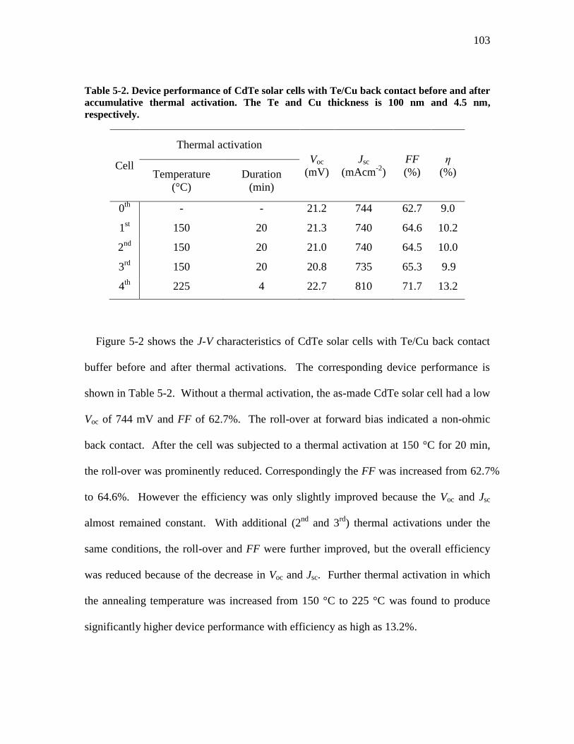
103
Table 5-2. Device performance of CdTe solar cells with Te/Cu back contact before and after
accumulative thermal activation. The Te and Cu thickness is 100 nm and 4.5 nm,
respectively.
Cell
Thermal activation
Voc
(mV)
Jsc
(mAcm-2
)
FF
(%)
η
(%) Temperature
(°C)
Duration
(min)
0th
- - 21.2 744 62.7 9.0
1st 150 20 21.3 740 64.6 10.2
2nd
150 20 21.0 740 64.5 10.0
3rd
150 20 20.8 735 65.3 9.9
4th
225 4 22.7 810 71.7 13.2
Figure 5-2 shows the J-V characteristics of CdTe solar cells with Te/Cu back contact
buffer before and after thermal activations. The corresponding device performance is
shown in Table 5-2. Without a thermal activation, the as-made CdTe solar cell had a low
Voc of 744 mV and FF of 62.7%. The roll-over at forward bias indicated a non-ohmic
back contact. After the cell was subjected to a thermal activation at 150 °C for 20 min,
the roll-over was prominently reduced. Correspondingly the FF was increased from 62.7%
to 64.6%. However the efficiency was only slightly improved because the Voc and Jsc
almost remained constant. With additional (2nd
and 3rd
) thermal activations under the
same conditions, the roll-over and FF were further improved, but the overall efficiency
was reduced because of the decrease in Voc and Jsc. Further thermal activation in which
the annealing temperature was increased from 150 °C to 225 °C was found to produce
significantly higher device performance with efficiency as high as 13.2%.
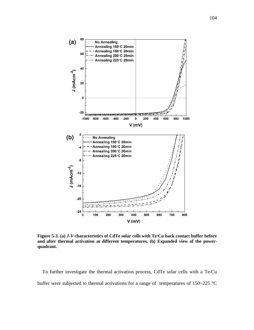
104
Figure 5-3. (a) J-V characteristics of CdTe solar cells with Te/Cu back contact buffer before
and after thermal activation at different temperatures. (b) Expanded view of the power-
quadrant.
To further investigate the thermal activation process, CdTe solar cells with a Te/Cu
buffer were subjected to thermal activations for a range of temperatures of 150~225 °C
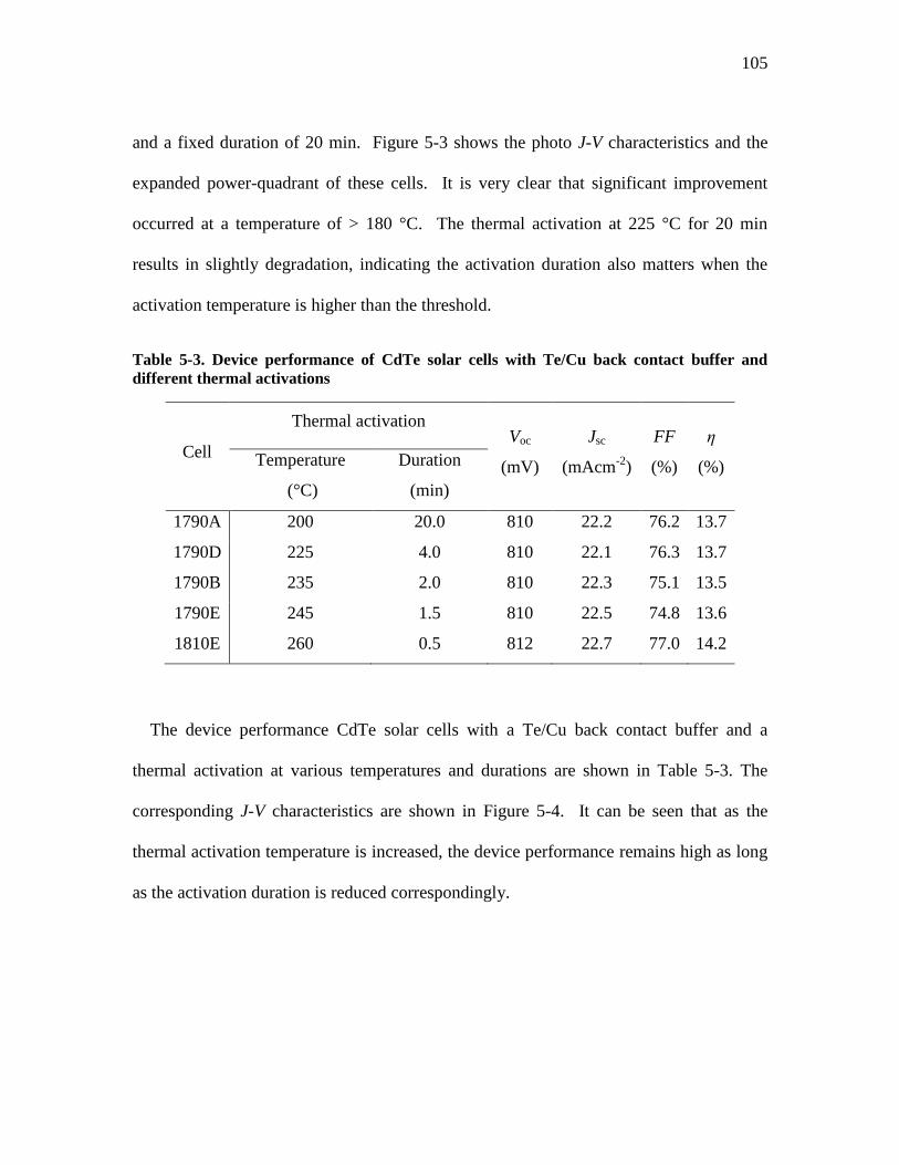
105
and a fixed duration of 20 min. Figure 5-3 shows the photo J-V characteristics and the
expanded power-quadrant of these cells. It is very clear that significant improvement
occurred at a temperature of > 180 °C. The thermal activation at 225 °C for 20 min
results in slightly degradation, indicating the activation duration also matters when the
activation temperature is higher than the threshold.
Table 5-3. Device performance of CdTe solar cells with Te/Cu back contact buffer and
different thermal activations
Cell
Thermal activation Voc
(mV)
Jsc
(mAcm-2
)
FF
(%)
η
(%) Temperature
(°C)
Duration
(min)
1790A 200 20.0 810 22.2 76.2 13.7
1790D 225 4.0 810 22.1 76.3 13.7
1790B 235 2.0 810 22.3 75.1 13.5
1790E 245 1.5 810 22.5 74.8 13.6
1810E 260 0.5 812 22.7 77.0 14.2
The device performance CdTe solar cells with a Te/Cu back contact buffer and a
thermal activation at various temperatures and durations are shown in Table 5-3. The
corresponding J-V characteristics are shown in Figure 5-4. It can be seen that as the
thermal activation temperature is increased, the device performance remains high as long
as the activation duration is reduced correspondingly.
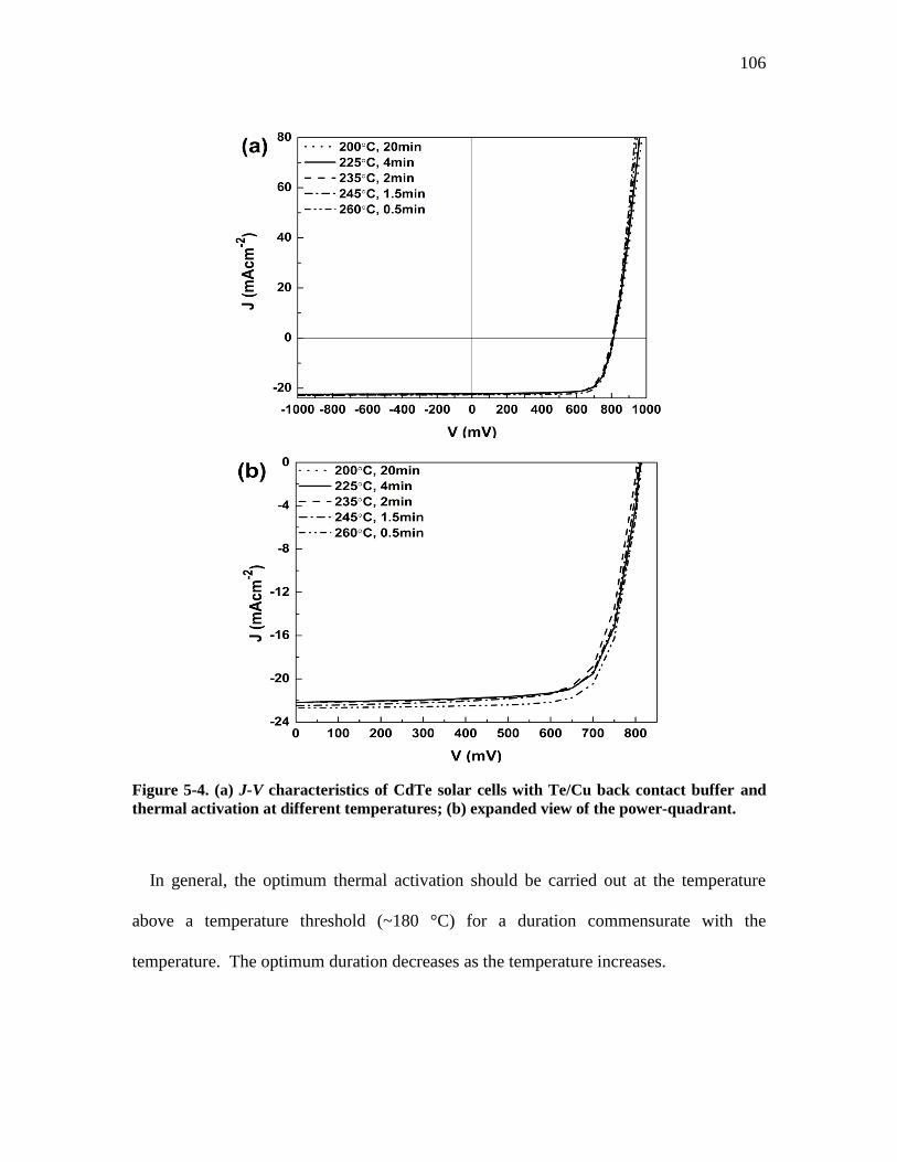
106
Figure 5-4. (a) J-V characteristics of CdTe solar cells with Te/Cu back contact buffer and
thermal activation at different temperatures; (b) expanded view of the power-quadrant.
In general, the optimum thermal activation should be carried out at the temperature
above a temperature threshold (~180 °C) for a duration commensurate with the
temperature. The optimum duration decreases as the temperature increases.
107
5.2 Device stability of Te/Cu back contact buffer
The instability of CdS/CdTe solar cells can be attributed to several causes including
degradation in CdS/CdTe junction and the back contact, and the development of shunting
defects in CdTe 76
. In general, the beginning of cell degradation occurs with the
development of “roll-over” in the J-V characteristics causing a decrease in Voc and FF.
The Jsc is generally less affected.
Among the possible degradation mechanisms of the back contact, the most suspicious
one is metal diffusion from the back contact into the CdS region 76
. For the Cu-
containing back contacts, it is well-known that Cu diffuses fast in CdTe especially along
grain boundaries 65
. At the CdS/CdTe junction, Cu was proposed to form recombination
centers and shunt pathways, limiting the device lifetime76,77,94
. For Te/Cu back contact
buffers developed in this work, the Cu/Te molar ratio ranges from 0.008 to 0.25, which is
much smaller than that in CuxTe (1 ≤ x ≤ 2). The Cu concentration is deliberately
reduced to avoid excess Cu diffusion to the CdTe bulk layer and the CdS/CdTe junction.
Te is designed to buffer Cu diffusion and to further control Cu diffusion.
In order to evaluate the device stability of CdTe solar cells with a Te/Cu back contact
buffer, the cells were subjected to two testing environments. The thermal stress test was
conducted at 200 °C in a tube furnace filled with pure nitrogen. The light soaking test
was carried out in a custom-made light box with compact fluorescence lamps with a light
intensity of ~1 kW/m2.
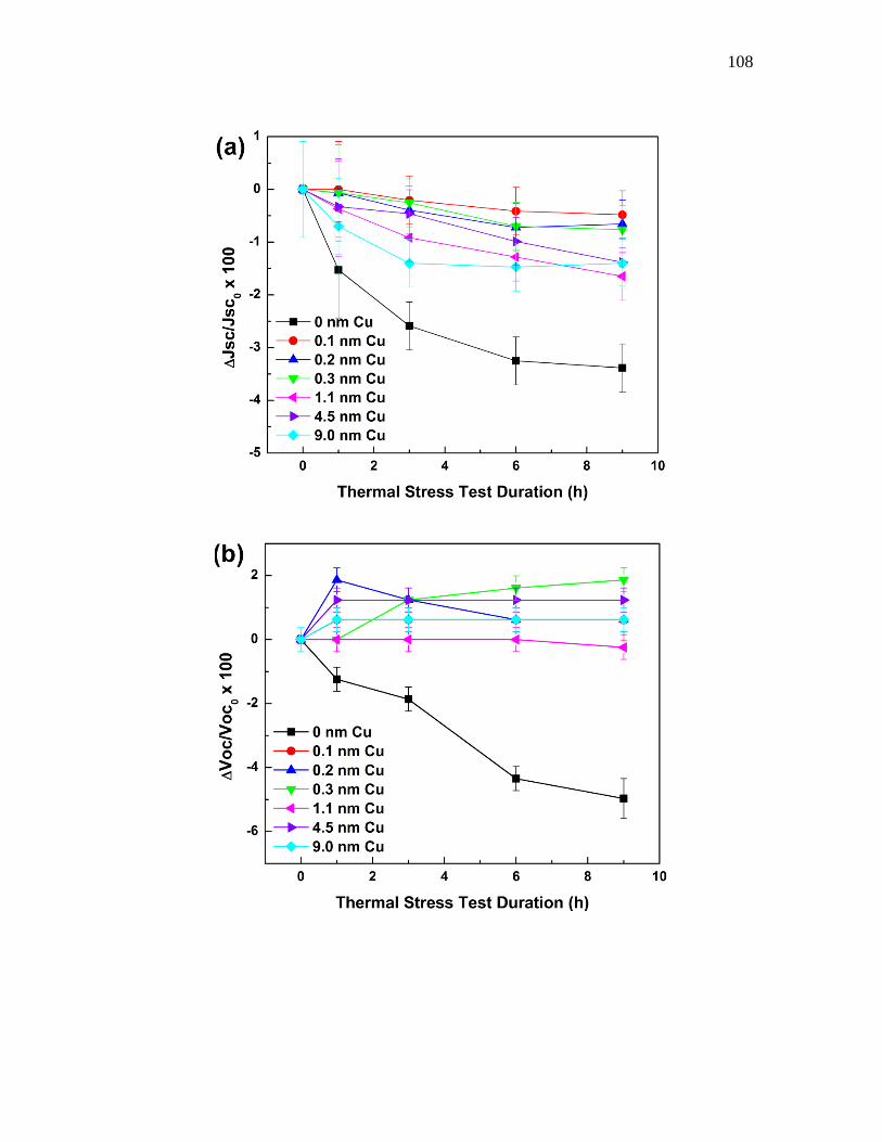
108
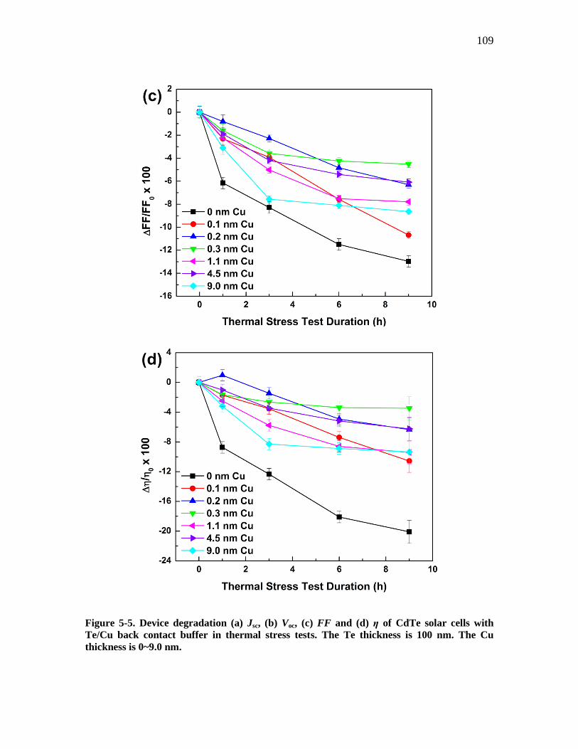
109
Figure 5-5. Device degradation (a) Jsc, (b) Voc, (c) FF and (d) η of CdTe solar cells with
Te/Cu back contact buffer in thermal stress tests. The Te thickness is 100 nm. The Cu
thickness is 0~9.0 nm.
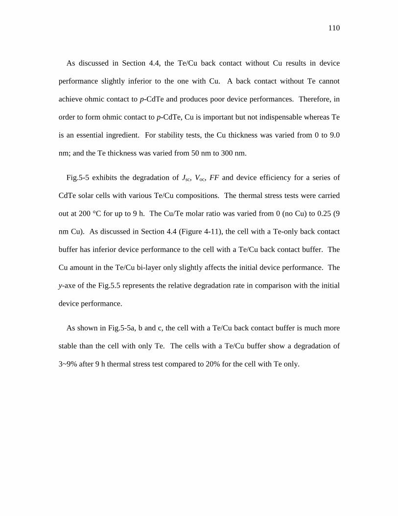
110
As discussed in Section 4.4, the Te/Cu back contact without Cu results in device
performance slightly inferior to the one with Cu. A back contact without Te cannot
achieve ohmic contact to p-CdTe and produces poor device performances. Therefore, in
order to form ohmic contact to p-CdTe, Cu is important but not indispensable whereas Te
is an essential ingredient. For stability tests, the Cu thickness was varied from 0 to 9.0
nm; and the Te thickness was varied from 50 nm to 300 nm.
Fig.5-5 exhibits the degradation of Jsc, Voc, FF and device efficiency for a series of
CdTe solar cells with various Te/Cu compositions. The thermal stress tests were carried
out at 200 °C for up to 9 h. The Cu/Te molar ratio was varied from 0 (no Cu) to 0.25 (9
nm Cu). As discussed in Section 4.4 (Figure 4-11), the cell with a Te-only back contact
buffer has inferior device performance to the cell with a Te/Cu back contact buffer. The
Cu amount in the Te/Cu bi-layer only slightly affects the initial device performance. The
y-axe of the Fig.5.5 represents the relative degradation rate in comparison with the initial
device performance.
As shown in Fig.5-5a, b and c, the cell with a Te/Cu back contact buffer is much more
stable than the cell with only Te. The cells with a Te/Cu buffer show a degradation of
3~9% after 9 h thermal stress test compared to 20% for the cell with Te only.
111
Figure 5-6. J-V characteristics (a) photo and (b) dark of CdTe solar cells using Te/Cu back
contact buffer with different Cu thicknesses before and after a thermal stress test at 200 °C
for 9h. The Te thickness is 100 nm.
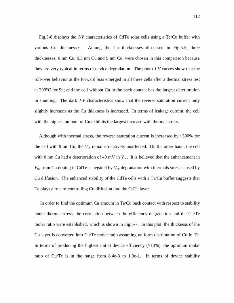
112
Fig.5-6 displays the J-V characteristics of CdTe solar cells using a Te/Cu buffer with
various Cu thicknesses. Among the Cu thicknesses discussed in Fig.5.5, three
thicknesses, 0 nm Cu, 0.3 nm Cu and 9 nm Cu, were chosen in this comparison because
they are very typical in terms of device degradation. The photo J-V curves show that the
roll-over behavior at the forward bias emerged in all three cells after a thermal stress test
at 200°C for 9h; and the cell without Cu in the back contact has the largest deterioration
in shunting. The dark J-V characteristics show that the reverse saturation current only
slightly increases as the Cu thickness is increased. In terms of leakage current, the cell
with the highest amount of Cu exhibits the largest increase with thermal stress.
Although with thermal stress, the reverse saturation current is increased by ~300% for
the cell with 9 nm Cu, the Voc remains relatively unaffected. On the other hand, the cell
with 0 nm Cu had a deterioration of 40 mV in Voc. It is believed that the enhancement in
Voc from Cu doping in CdTe is negated by Voc degradation with thermals stress caused by
Cu diffusion. The enhanced stability of the CdTe cells with a Te/Cu buffer suggests that
Te plays a role of controlling Cu diffusion into the CdTe layer.
In order to find the optimum Cu amount in Te/Cu back contact with respect to stability
under thermal stress, the correlation between the efficiency degradation and the Cu/Te
molar ratio were established, which is shown in Fig.5-7. In this plot, the thickness of the
Cu layer is converted into Cu/Te molar ratio assuming uniform distribution of Cu in Te.
In terms of producing the highest initial device efficiency (>13%), the optimum molar
ratio of Cu/Te is in the range from 8.4e-3 to 1.3e-1. In terms of device stability
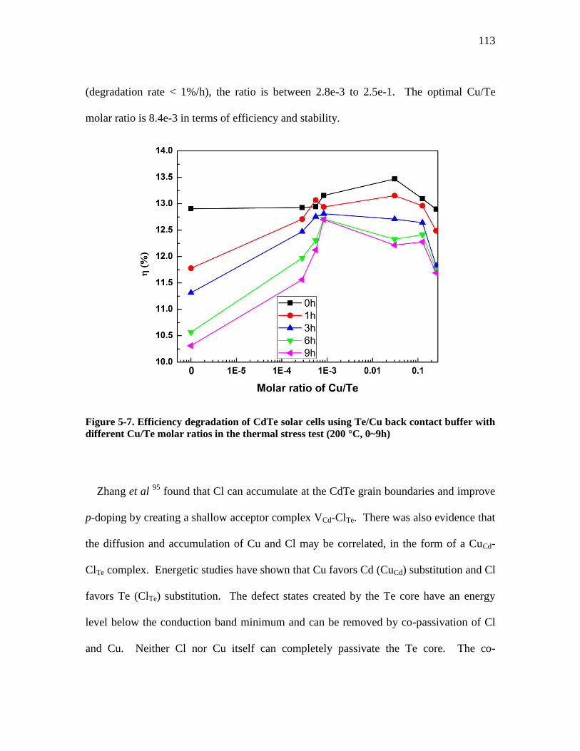
113
(degradation rate < 1%/h), the ratio is between 2.8e-3 to 2.5e-1. The optimal Cu/Te
molar ratio is 8.4e-3 in terms of efficiency and stability.
Figure 5-7. Efficiency degradation of CdTe solar cells using Te/Cu back contact buffer with
different Cu/Te molar ratios in the thermal stress test (200 °C, 0~9h)
Zhang et al 95
found that Cl can accumulate at the CdTe grain boundaries and improve
p-doping by creating a shallow acceptor complex VCd-ClTe. There was also evidence that
the diffusion and accumulation of Cu and Cl may be correlated, in the form of a CuCd-
ClTe complex. Energetic studies have shown that Cu favors Cd (CuCd) substitution and Cl
favors Te (ClTe) substitution. The defect states created by the Te core have an energy
level below the conduction band minimum and can be removed by co-passivation of Cl
and Cu. Neither Cl nor Cu itself can completely passivate the Te core. The co-
114
passivation of Cl and Cu on the defects states of Te core may be beneficial for device
stability 96
. According to Zhang’s theory, Cu may be important for stabilized back
contact, therefore Te/Cu is more stable than Te.
Fig.5-8 exhibits the degradation of Jsc, Voc, FF and efficiency of CdTe solar cells under
thermal stress tests at 200 °C for up to 9 h. The Te thickness of the Cu/Te buffer was
varied from 50 nm to 300 nm. Clearly the cell with only 50 nm-Te is very unstable with
respect to thermal stress. After 9 h thermal stress test, all the device parameters,
especially FF, have deteriorated significantly.
The degradation rate decreased with increased Te thickness, implying that the
degradation mechanism might be related to Cu diffusion. Considering 50 nm is on the
order of CdTe film roughness, some local areas of CdTe film with a high roughness may
not be completely covered with Te, which allows Cu to diffuse in readily. In addition,
Cu concentration in Te/Cu also determines the Cu diffusion. Fig. 5-5 demonstrates that
the Te/Cu with a thicker Cu layer (4.5~9.0 nm) is less stable than that with a thinner Cu
layer (0.2~1.1 nm), which affirms the speculation.
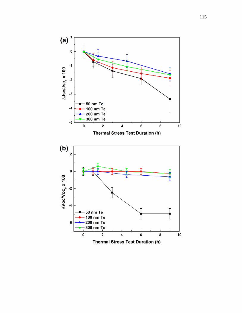
115
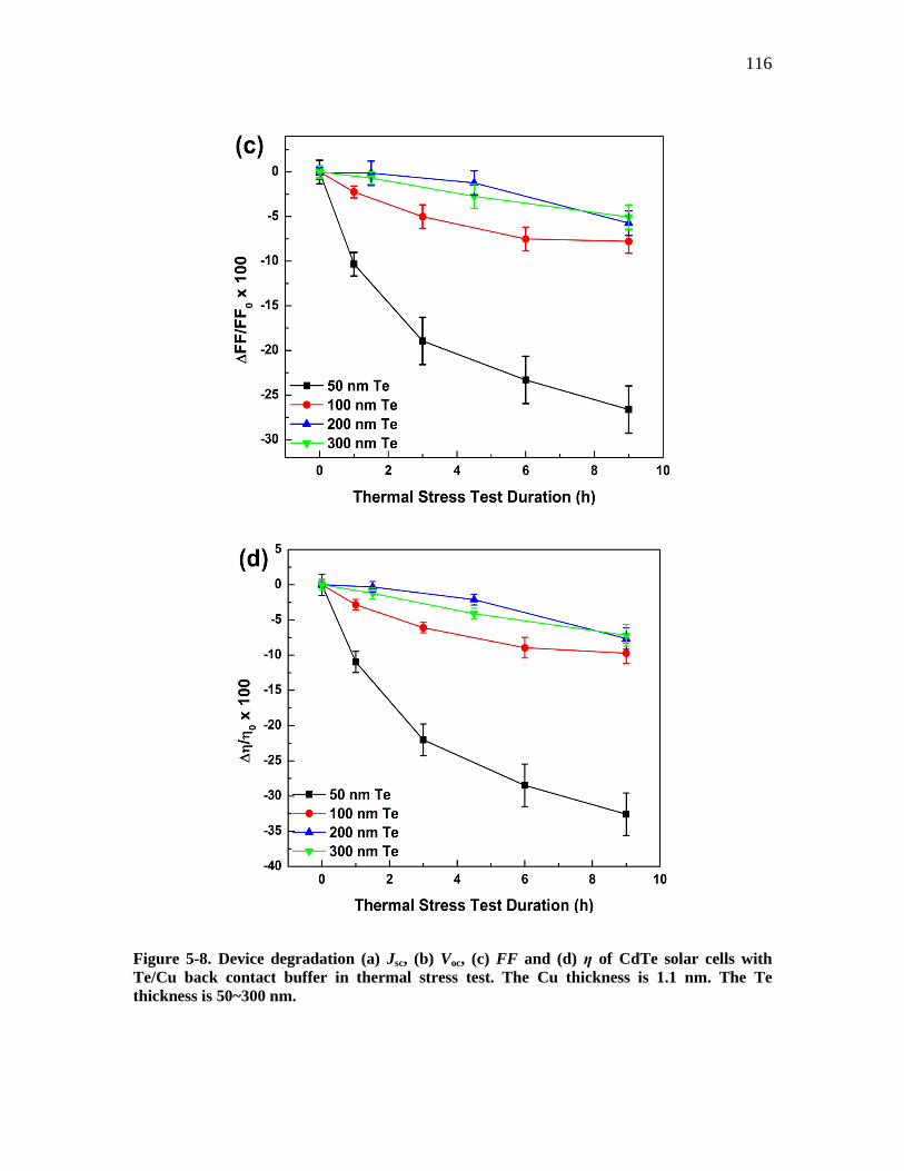
116
Figure 5-8. Device degradation (a) Jsc, (b) Voc, (c) FF and (d) η of CdTe solar cells with
Te/Cu back contact buffer in thermal stress test. The Cu thickness is 1.1 nm. The Te
thickness is 50~300 nm.
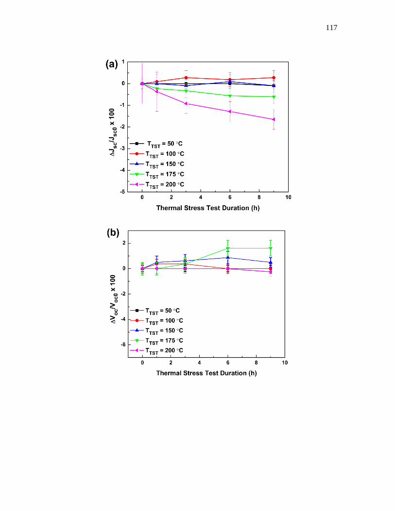
117
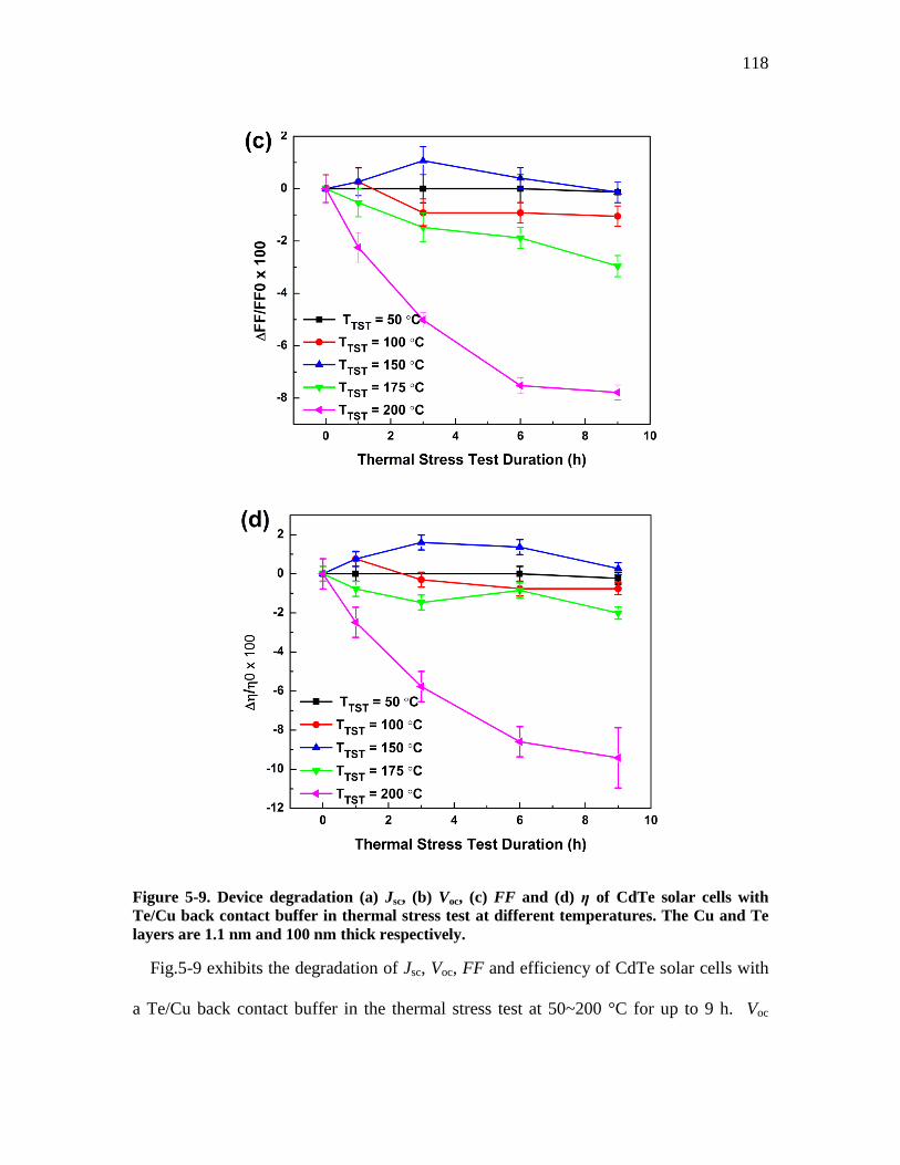
118
Figure 5-9. Device degradation (a) Jsc, (b) Voc, (c) FF and (d) η of CdTe solar cells with
Te/Cu back contact buffer in thermal stress test at different temperatures. The Cu and Te
layers are 1.1 nm and 100 nm thick respectively.
Fig.5-9 exhibits the degradation of Jsc, Voc, FF and efficiency of CdTe solar cells with
a Te/Cu back contact buffer in the thermal stress test at 50~200 °C for up to 9 h. Voc
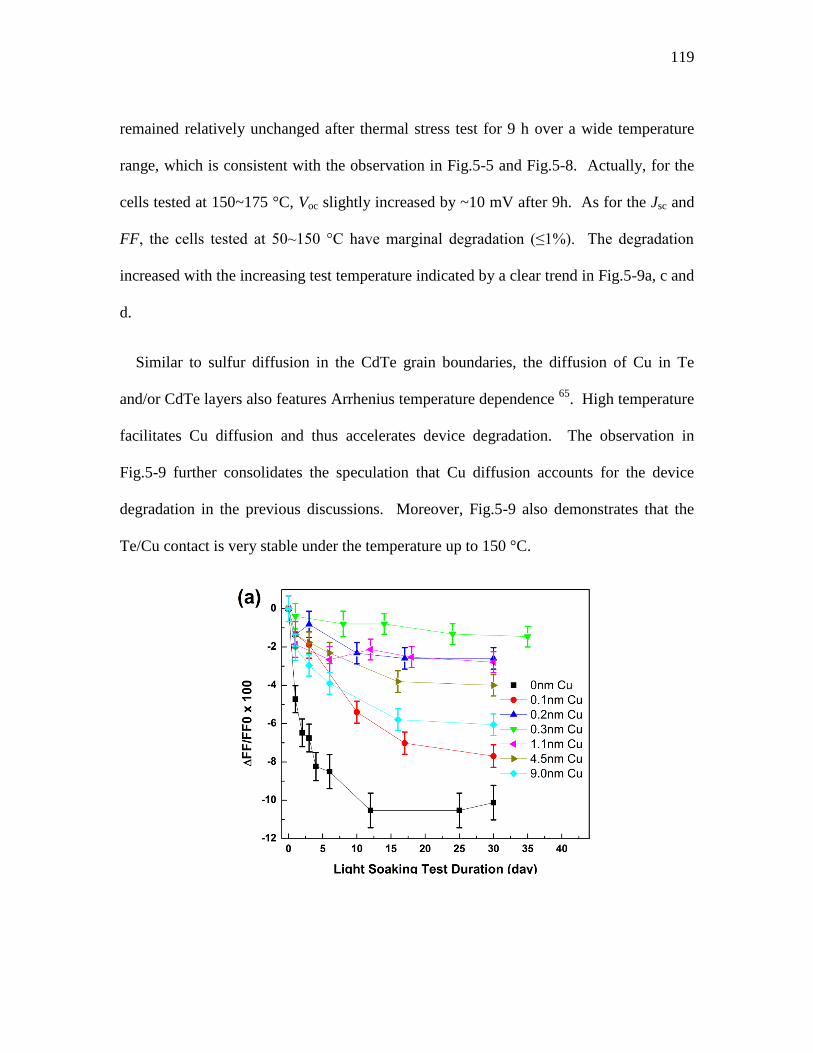
119
remained relatively unchanged after thermal stress test for 9 h over a wide temperature
range, which is consistent with the observation in Fig.5-5 and Fig.5-8. Actually, for the
cells tested at 150~175 °C, Voc slightly increased by ~10 mV after 9h. As for the Jsc and
FF, the cells tested at 50~150 °C have marginal degradation (≤1%). The degradation
increased with the increasing test temperature indicated by a clear trend in Fig.5-9a, c and
d.
Similar to sulfur diffusion in the CdTe grain boundaries, the diffusion of Cu in Te
and/or CdTe layers also features Arrhenius temperature dependence 65
. High temperature
facilitates Cu diffusion and thus accelerates device degradation. The observation in
Fig.5-9 further consolidates the speculation that Cu diffusion accounts for the device
degradation in the previous discussions. Moreover, Fig.5-9 also demonstrates that the
Te/Cu contact is very stable under the temperature up to 150 °C.
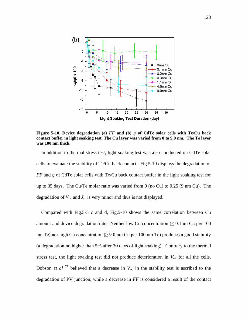
120
Figure 5-10. Device degradation (a) FF and (b) η of CdTe solar cells with Te/Cu back
contact buffer in light soaking test. The Cu layer was varied from 0 to 9.0 nm. The Te layer
was 100 nm thick.
In addition to thermal stress test, light soaking test was also conducted on CdTe solar
cells to evaluate the stability of Te/Cu back contact. Fig.5-10 displays the degradation of
FF and η of CdTe solar cells with Te/Cu back contact buffer in the light soaking test for
up to 35 days. The Cu/Te molar ratio was varied from 0 (no Cu) to 0.25 (9 nm Cu). The
degradation of Voc and Jsc is very minor and thus is not displayed.
Compared with Fig.5-5 c and d, Fig.5-10 shows the same correlation between Cu
amount and device degradation rate. Neither low Cu concentration (≤ 0.1nm Cu per 100
nm Te) nor high Cu concentration (≥ 9.0 nm Cu per 100 nm Te) produces a good stability
(a degradation no higher than 5% after 30 days of light soaking). Contrary to the thermal
stress test, the light soaking test did not produce deterioration in Voc for all the cells.
Dobson et al 77
believed that a decrease in Voc in the stability test is ascribed to the
degradation of PV junction, while a decrease in FF is considered a result of the contact
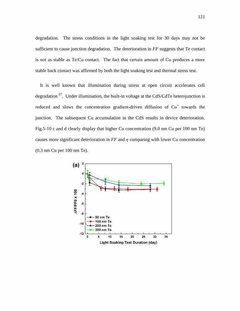
121
degradation. The stress conditions in the light soaking test for 30 days may not be
sufficient to cause junction degradation. The deterioration in FF suggests that Te contact
is not as stable as Te/Cu contact. The fact that certain amount of Cu produces a more
stable back contact was affirmed by both the light soaking test and thermal stress test.
It is well known that illumination during stress at open circuit accelerates cell
degradation 97
. Under illumination, the built-in voltage at the CdS/CdTe heterojunction is
reduced and slows the concentration gradient-driven diffusion of Cu+ towards the
junction. The subsequent Cu accumulation in the CdS results in device deterioration.
Fig.5-10 c and d clearly display that higher Cu concentration (9.0 nm Cu per 100 nm Te)
causes more significant deterioration in FF and η comparing with lower Cu concentration
(0.3 nm Cu per 100 nm Te).
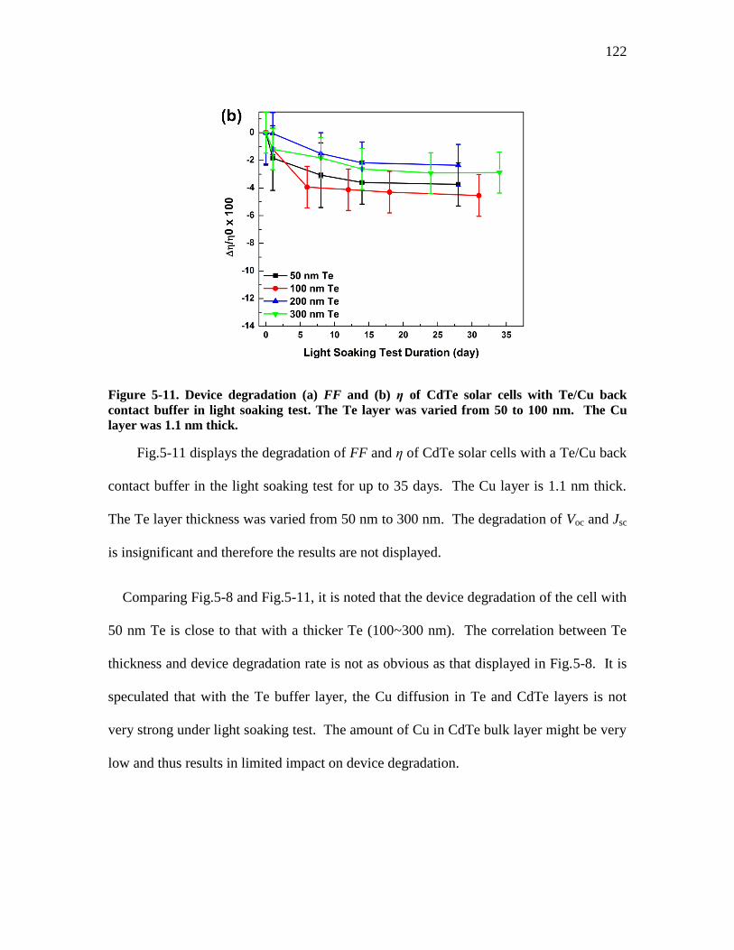
122
Figure 5-11. Device degradation (a) FF and (b) η of CdTe solar cells with Te/Cu back
contact buffer in light soaking test. The Te layer was varied from 50 to 100 nm. The Cu
layer was 1.1 nm thick.
Fig.5-11 displays the degradation of FF and η of CdTe solar cells with a Te/Cu back
contact buffer in the light soaking test for up to 35 days. The Cu layer is 1.1 nm thick.
The Te layer thickness was varied from 50 nm to 300 nm. The degradation of Voc and Jsc
is insignificant and therefore the results are not displayed.
Comparing Fig.5-8 and Fig.5-11, it is noted that the device degradation of the cell with
50 nm Te is close to that with a thicker Te (100~300 nm). The correlation between Te
thickness and device degradation rate is not as obvious as that displayed in Fig.5-8. It is
speculated that with the Te buffer layer, the Cu diffusion in Te and CdTe layers is not
very strong under light soaking test. The amount of Cu in CdTe bulk layer might be very
low and thus results in limited impact on device degradation.
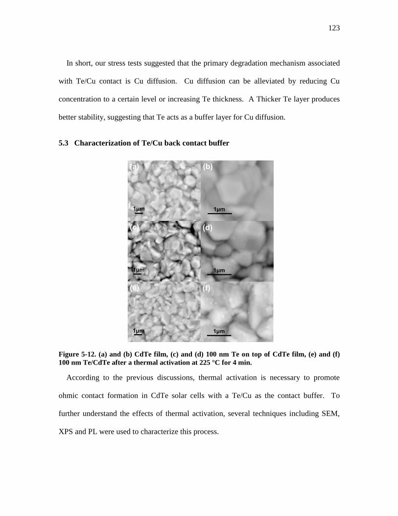
123
In short, our stress tests suggested that the primary degradation mechanism associated
with Te/Cu contact is Cu diffusion. Cu diffusion can be alleviated by reducing Cu
concentration to a certain level or increasing Te thickness. A Thicker Te layer produces
better stability, suggesting that Te acts as a buffer layer for Cu diffusion.
5.3 Characterization of Te/Cu back contact buffer
Figure 5-12. (a) and (b) CdTe film, (c) and (d) 100 nm Te on top of CdTe film, (e) and (f)
100 nm Te/CdTe after a thermal activation at 225 °C for 4 min.
According to the previous discussions, thermal activation is necessary to promote
ohmic contact formation in CdTe solar cells with a Te/Cu as the contact buffer. To
further understand the effects of thermal activation, several techniques including SEM,
XPS and PL were used to characterize this process.
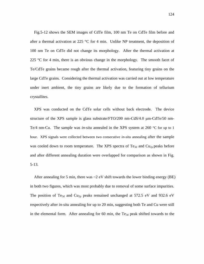
124
Fig.5-12 shows the SEM images of CdTe film, 100 nm Te on CdTe film before and
after a thermal activation at 225 °C for 4 min. Unlike NP treatment, the deposition of
100 nm Te on CdTe did not change its morphology. After the thermal activation at
225 °C for 4 min, there is an obvious change in the morphology. The smooth facet of
Te/CdTe grains became rough after the thermal activation, featuring tiny grains on the
large CdTe grains. Considering the thermal activation was carried out at low temperature
under inert ambient, the tiny grains are likely due to the formation of tellurium
crystallites.
XPS was conducted on the CdTe solar cells without back electrode. The device
structure of the XPS sample is glass substrate/FTO/200 nm-CdS/4.0 μm-CdTe/50 nm-
Te/4 nm-Cu. The sample was in-situ annealed in the XPS system at 260 °C for up to 1
hour. XPS signals were collected between two consecutive in-situ annealing after the sample
was cooled down to room temperature. The XPS spectra of Te3d and Cu2p peaks before
and after different annealing duration were overlapped for comparison as shown in Fig.
5-13.
After annealing for 5 min, there was ~2 eV shift towards the lower binding energy (BE)
in both two figures, which was most probably due to removal of some surface impurities.
The position of Te3d and Cu2p peaks remained unchanged at 572.5 eV and 932.6 eV
respectively after in-situ annealing for up to 20 min, suggesting both Te and Cu were still
in the elemental form. After annealing for 60 min, the Te3d peak shifted towards to the
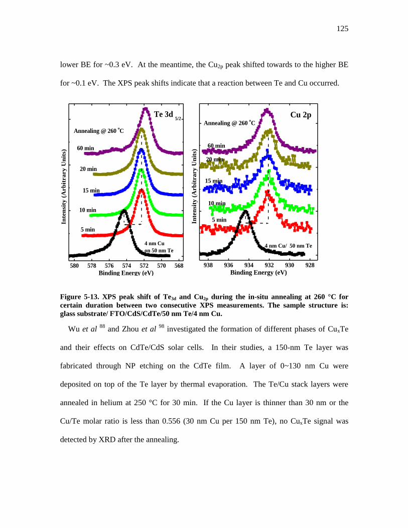
125
lower BE for ~0.3 eV. At the meantime, the Cu2p peak shifted towards to the higher BE
for ~0.1 eV. The XPS peak shifts indicate that a reaction between Te and Cu occurred.
Figure 5-13. XPS peak shift of Te3d and Cu2p during the in-situ annealing at 260 °C for
certain duration between two consecutive XPS measurements. The sample structure is:
glass substrate/ FTO/CdS/CdTe/50 nm Te/4 nm Cu.
Wu et al 88
and Zhou et al 98
investigated the formation of different phases of CuxTe
and their effects on CdTe/CdS solar cells. In their studies, a 150-nm Te layer was
fabricated through NP etching on the CdTe film. A layer of 0~130 nm Cu were
deposited on top of the Te layer by thermal evaporation. The Te/Cu stack layers were
annealed in helium at 250 °C for 30 min. If the Cu layer is thinner than 30 nm or the
Cu/Te molar ratio is less than 0.556 (30 nm Cu per 150 nm Te), no CuxTe signal was
detected by XRD after the annealing.
580 578 576 574 572 570 568
Annealing @ 260 oC
60 min
20 min
15 min
10 min
5 min
4 nm Cu
on 50 nm Te
Te 3d 5/2
Inte
nsi
ty (
Arb
itra
ry
Un
its)
Binding Energy (eV)
938 936 934 932 930 928
Annealing @ 260 oC
60 min
20 min
15 min
10 min
5 min
4 nm Cu/ 50 nm Te
Cu 2p
Inte
nsi
ty (
Arb
itra
ry
Un
its)
Binding Energy (eV)
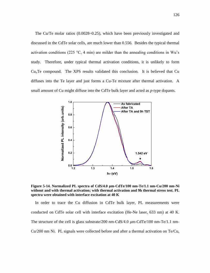
126
The Cu/Te molar ratios (0.0028~0.25), which have been previously investigated and
discussed in the CdTe solar cells, are much lower than 0.556. Besides the typical thermal
activation conditions (225 °C, 4 min) are milder than the annealing conditions in Wu’s
study. Therefore, under typical thermal activation conditions, it is unlikely to form
CuxTe compound. The XPS results validated this conclusion. It is believed that Cu
diffuses into the Te layer and just forms a Cu-Te mixture after thermal activation. A
small amount of Cu might diffuse into the CdTe bulk layer and acted as p-type dopants.
Figure 5-14. Normalized PL spectra of CdS/4.0 μm-CdTe/100 nm-Te/1.1 nm-Cu/200 nm-Ni
without and with thermal activation; with thermal activation and 9h thermal stress test. PL
spectra were obtained with interface excitation at 40 K
In order to trace the Cu diffusion in CdTe bulk layer, PL measurements were
conducted on CdTe solar cell with interface excitation (He-Ne laser, 633 nm) at 40 K.
The structure of the cell is glass substrate/200 nm-CdS/4.0 μm-CdTe/100 nm-Te/1.1 nm-
Cu/200 nm Ni. PL signals were collected before and after a thermal activation on Te/Cu,
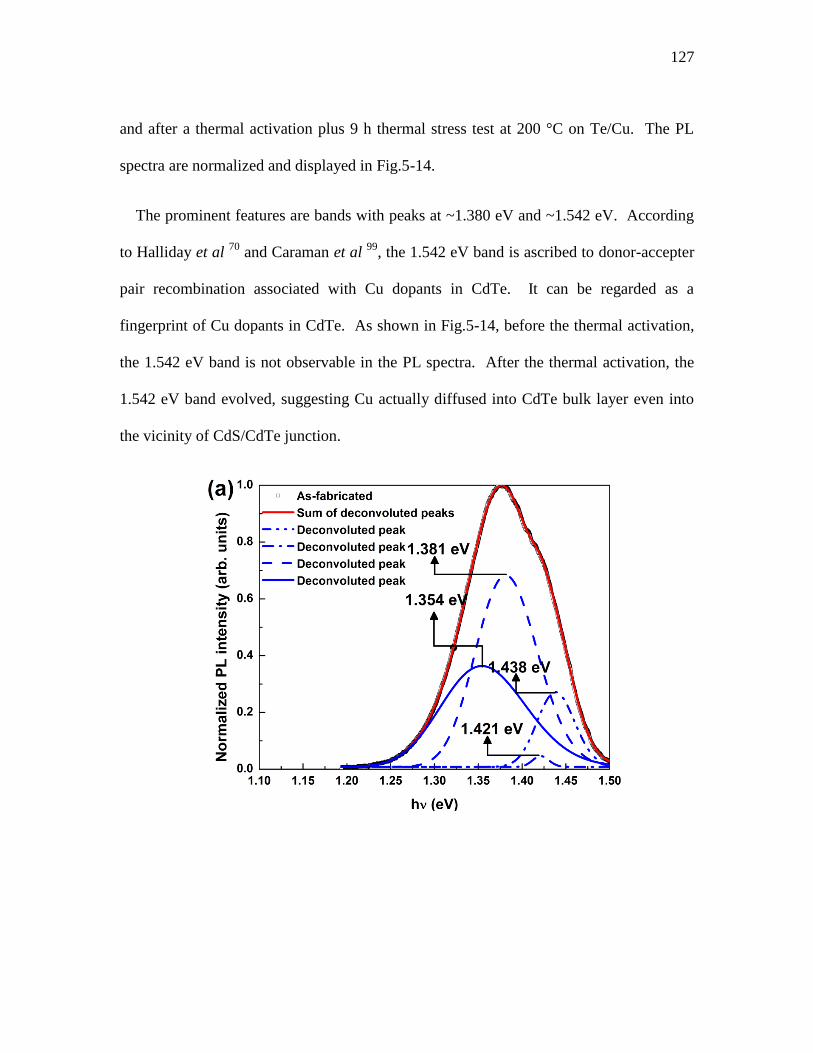
127
and after a thermal activation plus 9 h thermal stress test at 200 °C on Te/Cu. The PL
spectra are normalized and displayed in Fig.5-14.
The prominent features are bands with peaks at ~1.380 eV and ~1.542 eV. According
to Halliday et al 70
and Caraman et al 99
, the 1.542 eV band is ascribed to donor-accepter
pair recombination associated with Cu dopants in CdTe. It can be regarded as a
fingerprint of Cu dopants in CdTe. As shown in Fig.5-14, before the thermal activation,
the 1.542 eV band is not observable in the PL spectra. After the thermal activation, the
1.542 eV band evolved, suggesting Cu actually diffused into CdTe bulk layer even into
the vicinity of CdS/CdTe junction.
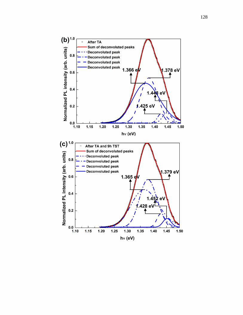
128
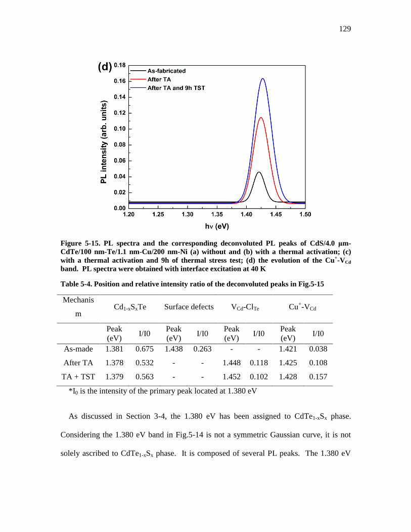
129
Figure 5-15. PL spectra and the corresponding deconvoluted PL peaks of CdS/4.0 μm-
CdTe/100 nm-Te/1.1 nm-Cu/200 nm-Ni (a) without and (b) with a thermal activation; (c)
with a thermal activation and 9h of thermal stress test; (d) the evolution of the Cu+-VCd
band. PL spectra were obtained with interface excitation at 40 K
Table 5-4. Position and relative intensity ratio of the deconvoluted peaks in Fig.5-15
Mechanis
m Cd1-xSxTe Surface defects VCd-ClTe Cu
+-VCd
Peak
(eV) I/I0
Peak
(eV) I/I0
Peak
(eV) I/I0
Peak
(eV) I/I0
As-made 1.381 0.675 1.438 0.263 - - 1.421 0.038
After TA 1.378 0.532 - - 1.448 0.118 1.425 0.108
TA + TST 1.379 0.563 - - 1.452 0.102 1.428 0.157
*I0 is the intensity of the primary peak located at 1.380 eV
As discussed in Section 3-4, the 1.380 eV has been assigned to CdTe1-xSx phase.
Considering the 1.380 eV band in Fig.5-14 is not a symmetric Gaussian curve, it is not
solely ascribed to CdTe1-xSx phase. It is composed of several PL peaks. The 1.380 eV
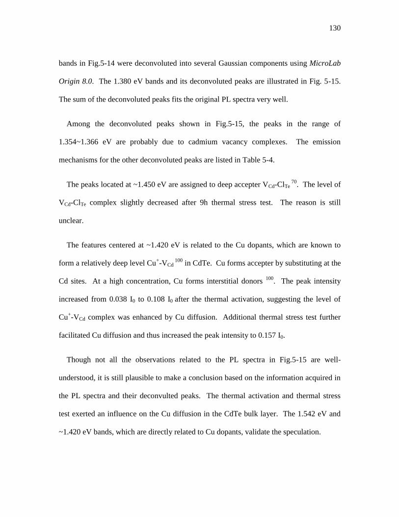
130
bands in Fig.5-14 were deconvoluted into several Gaussian components using MicroLab
Origin 8.0. The 1.380 eV bands and its deconvoluted peaks are illustrated in Fig. 5-15.
The sum of the deconvoluted peaks fits the original PL spectra very well.
Among the deconvoluted peaks shown in Fig.5-15, the peaks in the range of
1.354~1.366 eV are probably due to cadmium vacancy complexes. The emission
mechanisms for the other deconvoluted peaks are listed in Table 5-4.
The peaks located at ~1.450 eV are assigned to deep accepter VCd-ClTe 70
. The level of
VCd-ClTe complex slightly decreased after 9h thermal stress test. The reason is still
unclear.
The features centered at ~1.420 eV is related to the Cu dopants, which are known to
form a relatively deep level Cu+-VCd
100 in CdTe. Cu forms accepter by substituting at the
Cd sites. At a high concentration, Cu forms interstitial donors 100
. The peak intensity
increased from 0.038 I0 to 0.108 I0 after the thermal activation, suggesting the level of
Cu+-VCd complex was enhanced by Cu diffusion. Additional thermal stress test further
facilitated Cu diffusion and thus increased the peak intensity to 0.157 I0.
Though not all the observations related to the PL spectra in Fig.5-15 are well-
understood, it is still plausible to make a conclusion based on the information acquired in
the PL spectra and their deconvulted peaks. The thermal activation and thermal stress
test exerted an influence on the Cu diffusion in the CdTe bulk layer. The 1.542 eV and
~1.420 eV bands, which are directly related to Cu dopants, validate the speculation.
131
In conclusion, the thermal activation mainly has two impacts on the Te/Cu back
contact buffer. It promotes the crystallization of Te layer and results in Cu diffusion in
the Te and CdTe layer. No reaction occurs between Cu and Te during a typical thermal
activation process.
5.4 Summary
Te/Cu bi-layer was developed as an effective back contact buffer to p-CdTe in the
fabrication of ultra-thin CdTe solar cells. The first intent is to avoid NP treatment, which
is prone to produce shorts in ultra-thin CdTe solar cells. Another intent is to address the
instability issue related to Cu as a dopant in CdTe.
Unlike NP treatment, Te/Cu does not necessitate acid etching. As a contact buffer,
Te/Cu performs better than the Te buffer produced by NP treatment in terms of efficiency
enhancement, particularly for ultra-thin cells.
The effects of Te and Cu thickness on Te/Cu back contact buffer have been
systematically studied. The optimized Te and Cu thicknesses are 100 nm and 0.3~2.2 nm
respectively. The optimum temperature and duration to activate the Te/Cu buffers are
225~260 °C and 4~0.5 min respectively. Higher thermal activation temperature
corresponds to a shortened duration. The temperature threshold for thermal activation is
~180 °C. With the optimum conditions as mentioned, CdTe solar cells using a Te/Cu
back contact with Voc up to 856 mV, FF up to 78.6% and η of 14.8% have been
demonstrated.
132
The stability of CdTe solar cells with a Te/Cu back contact buffer have been evaluated
under thermal stress and light soaking tests. Neither low Cu concentration (<0.1 nm Cu
per 100 nm Te) nor high Cu concentration (>9.0 nm Cu per 100 nm Te) results in good
device stability. The device instability is due to Cu diffusion which was proved by XPS
and PL. With an appropriate Cu amount (0.2~1.1 nm) and Te thickness (100~300 nm),
the Te/Cu back contact is stable.
133
6. Fabrication of Cd1-xZnxS films by vapor zinc chloride
treatment
As n-type semiconductors with a large and viable bandgap between 2.42 and 3.54 eV,
the ternary Cd1-xZnxS compounds have been used as a window layer to form
heterojunction solar cells with CdTe101
, Cu(In, Ga)Se2 (CIGS)102
, CuGaSe2103
, CuInSe2104
and Si105
. For commercial CdS/CdTe and CdS/CIGS solar cells, CdS is the standard
window layer despite its relatively low bandgap (2.42 eV) and considerable absorption in
the short wavelength region (below 500 nm). To maximize the blue response in these
solar cells, the CdS layer thickness is usually kept at a minimum, typically on the order of
~100 nm. Although thinner CdS films are favorable, they are impractical because of
excessive pinhole formation and possible electrical shunting across the heterojunction.
These issues can affect adversely the Voc and FF. Replacing CdS with Cd1-xZnxS is a
viable alternative because Cd1-xZnxS can provide a more transmissive window without
compromising the thickness. Oladeji et al.101
and others106,107
have already demonstrated
that the spectral response in the 400-600 nm wavelength region can be prominently
improved by substituting Cd1-xZnxS for CdS in CdTe solar cells.
Various methods have been used to fabricate Cd1-xZnxS films, which can be
categorized into physical vapor deposition (PVD) and solution deposition method (SD).
The PVD methods including metal organic chemical vapor deposition 108
and molecular
beam epitaxial 109
require complicated apparatus and costly maintenance. While the SD
methods, including chemical spray deposition 110,111
, co-evaporation 112
, photochemical
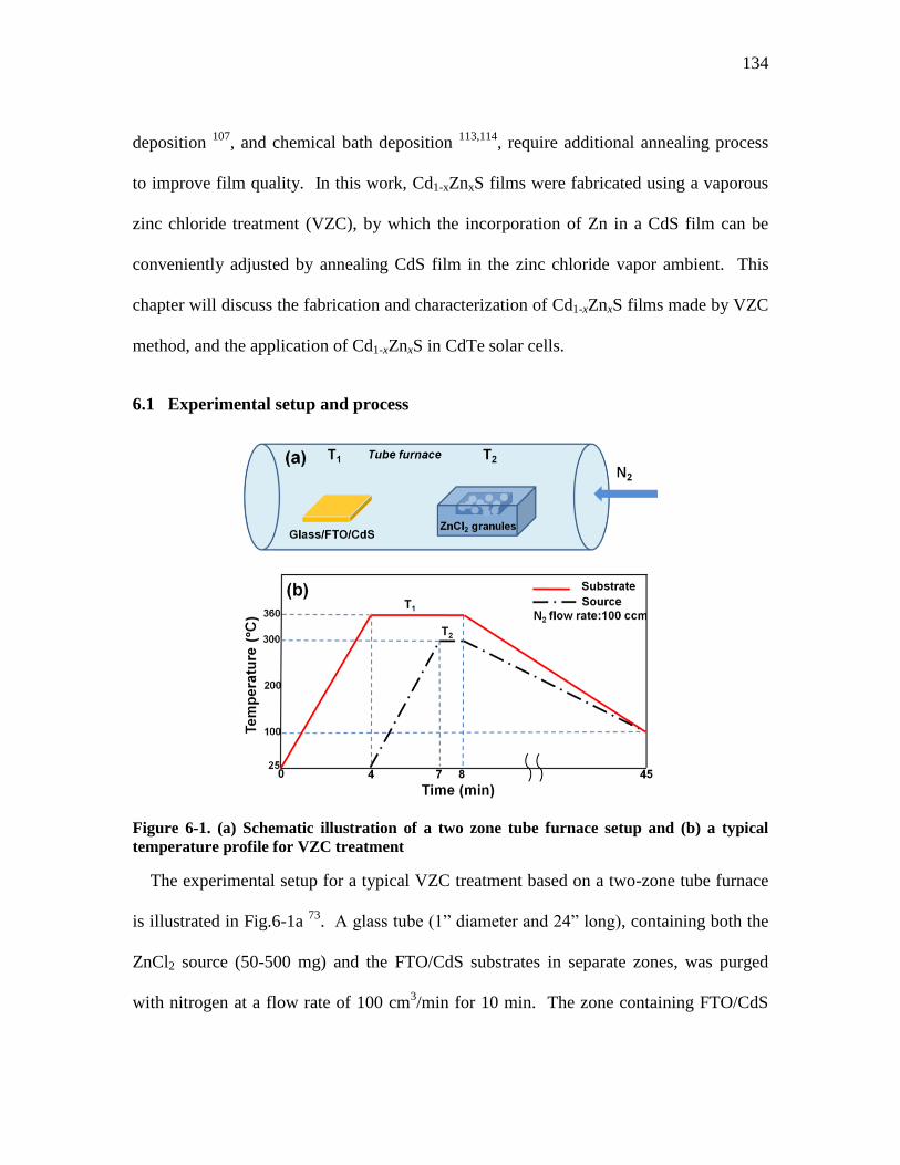
134
deposition 107
, and chemical bath deposition 113,114
, require additional annealing process
to improve film quality. In this work, Cd1-xZnxS films were fabricated using a vaporous
zinc chloride treatment (VZC), by which the incorporation of Zn in a CdS film can be
conveniently adjusted by annealing CdS film in the zinc chloride vapor ambient. This
chapter will discuss the fabrication and characterization of Cd1-xZnxS films made by VZC
method, and the application of Cd1-xZnxS in CdTe solar cells.
6.1 Experimental setup and process
Figure 6-1. (a) Schematic illustration of a two zone tube furnace setup and (b) a typical
temperature profile for VZC treatment
The experimental setup for a typical VZC treatment based on a two-zone tube furnace
is illustrated in Fig.6-1a 73
. A glass tube (1” diameter and 24” long), containing both the
ZnCl2 source (50-500 mg) and the FTO/CdS substrates in separate zones, was purged
with nitrogen at a flow rate of 100 cm3/min for 10 min. The zone containing FTO/CdS
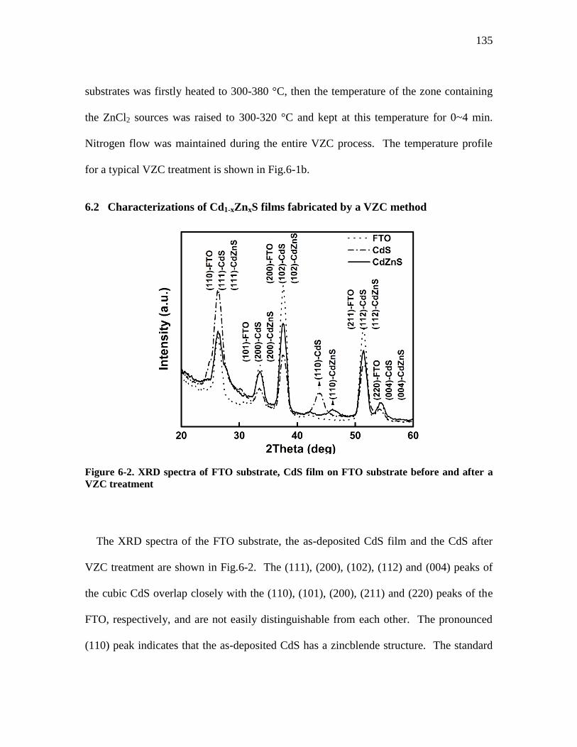
135
substrates was firstly heated to 300-380 °C, then the temperature of the zone containing
the ZnCl2 sources was raised to 300-320 °C and kept at this temperature for 0~4 min.
Nitrogen flow was maintained during the entire VZC process. The temperature profile
for a typical VZC treatment is shown in Fig.6-1b.
6.2 Characterizations of Cd1-xZnxS films fabricated by a VZC method
Figure 6-2. XRD spectra of FTO substrate, CdS film on FTO substrate before and after a
VZC treatment
The XRD spectra of the FTO substrate, the as-deposited CdS film and the CdS after
VZC treatment are shown in Fig.6-2. The (111), (200), (102), (112) and (004) peaks of
the cubic CdS overlap closely with the (110), (101), (200), (211) and (220) peaks of the
FTO, respectively, and are not easily distinguishable from each other. The pronounced
(110) peak indicates that the as-deposited CdS has a zincblende structure. The standard
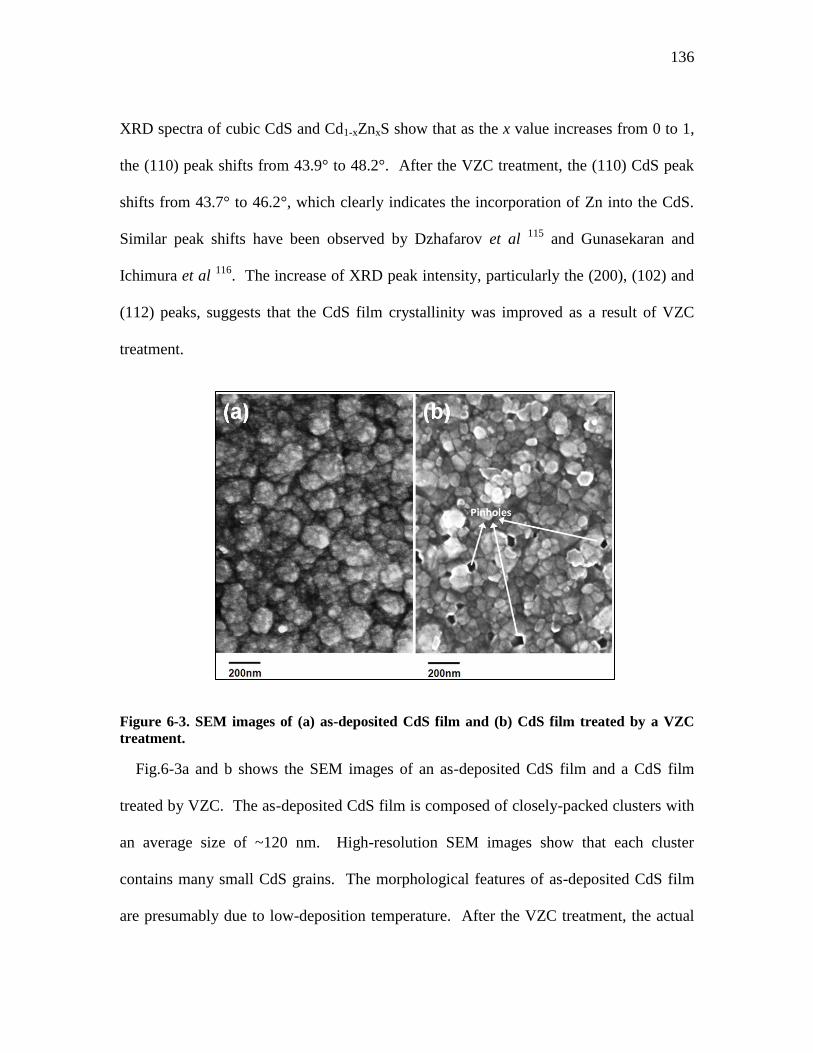
136
XRD spectra of cubic CdS and Cd1-xZnxS show that as the x value increases from 0 to 1,
the (110) peak shifts from 43.9° to 48.2°. After the VZC treatment, the (110) CdS peak
shifts from 43.7° to 46.2°, which clearly indicates the incorporation of Zn into the CdS.
Similar peak shifts have been observed by Dzhafarov et al 115
and Gunasekaran and
Ichimura et al 116
. The increase of XRD peak intensity, particularly the (200), (102) and
(112) peaks, suggests that the CdS film crystallinity was improved as a result of VZC
treatment.
Figure 6-3. SEM images of (a) as-deposited CdS film and (b) CdS film treated by a VZC
treatment.
Fig.6-3a and b shows the SEM images of an as-deposited CdS film and a CdS film
treated by VZC. The as-deposited CdS film is composed of closely-packed clusters with
an average size of ~120 nm. High-resolution SEM images show that each cluster
contains many small CdS grains. The morphological features of as-deposited CdS film
are presumably due to low-deposition temperature. After the VZC treatment, the actual
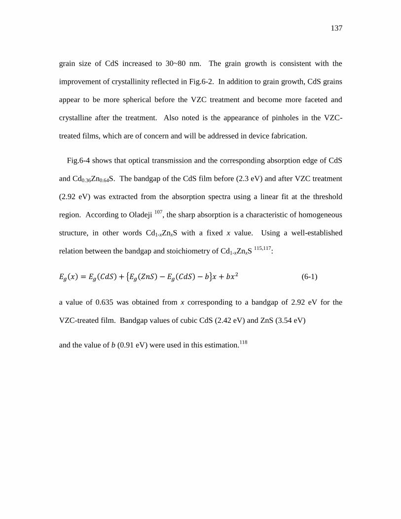
137
grain size of CdS increased to 30~80 nm. The grain growth is consistent with the
improvement of crystallinity reflected in Fig.6-2. In addition to grain growth, CdS grains
appear to be more spherical before the VZC treatment and become more faceted and
crystalline after the treatment. Also noted is the appearance of pinholes in the VZC-
treated films, which are of concern and will be addressed in device fabrication.
Fig.6-4 shows that optical transmission and the corresponding absorption edge of CdS
and Cd0.36Zn0.64S. The bandgap of the CdS film before (2.3 eV) and after VZC treatment
(2.92 eV) was extracted from the absorption spectra using a linear fit at the threshold
region. According to Oladeji 107
, the sharp absorption is a characteristic of homogeneous
structure, in other words Cd1-xZnxS with a fixed x value. Using a well-established
relation between the bandgap and stoichiometry of Cd1-xZnxS 115,117
:
(6-1)
a value of 0.635 was obtained from x corresponding to a bandgap of 2.92 eV for the
VZC-treated film. Bandgap values of cubic CdS (2.42 eV) and ZnS (3.54 eV)
and the value of b (0.91 eV) were used in this estimation.118
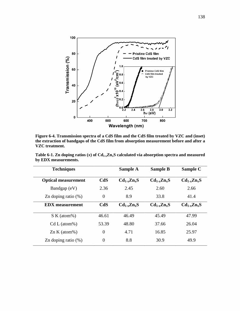
138
Figure 6-4. Transmission spectra of a CdS film and the CdS film treated by VZC and (inset)
the extraction of bandgaps of the CdS film from absorption measurement before and after a
VZC treatment.
Table 6-1. Zn doping ratios (x) of Cd1-xZnxS calculated via absorption spectra and measured
by EDX measurements.
Techniques Sample A Sample B Sample C
Optical measurement CdS Cd1-xZnxS Cd1-xZnxS Cd1-xZnxS
Bandgap (eV) 2.36 2.45 2.60 2.66
Zn doping ratio (%) 0 8.9 33.8 41.4
EDX measurement CdS Cd1-xZnxS Cd1-xZnxS Cd1-xZnxS
S K (atom%) 46.61 46.49 45.49 47.99
Cd L (atom%) 53.39 48.80 37.66 26.04
Zn K (atom%) 0 4.71 16.85 25.97
Zn doping ratio (%) 0 8.8 30.9 49.9
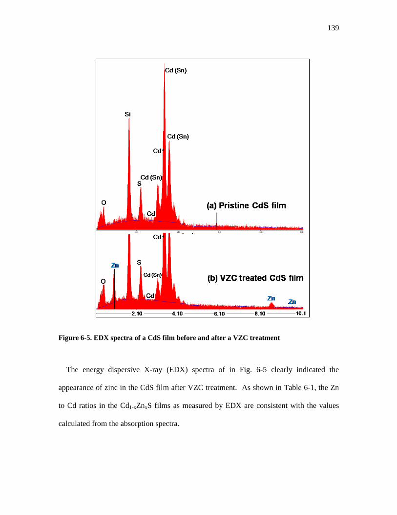
139
Figure 6-5. EDX spectra of a CdS film before and after a VZC treatment
The energy dispersive X-ray (EDX) spectra of in Fig. 6-5 clearly indicated the
appearance of zinc in the CdS film after VZC treatment. As shown in Table 6-1, the Zn
to Cd ratios in the Cd1-xZnxS films as measured by EDX are consistent with the values
calculated from the absorption spectra.
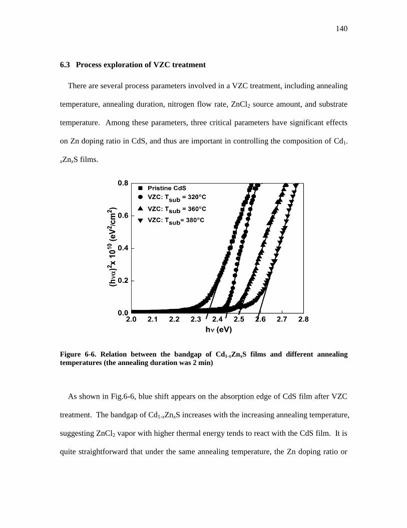
140
6.3 Process exploration of VZC treatment
There are several process parameters involved in a VZC treatment, including annealing
temperature, annealing duration, nitrogen flow rate, ZnCl2 source amount, and substrate
temperature. Among these parameters, three critical parameters have significant effects
on Zn doping ratio in CdS, and thus are important in controlling the composition of Cd1-
xZnxS films.
Figure 6-6. Relation between the bandgap of Cd1-xZnxS films and different annealing
temperatures (the annealing duration was 2 min)
As shown in Fig.6-6, blue shift appears on the absorption edge of CdS film after VZC
treatment. The bandgap of Cd1-xZnxS increases with the increasing annealing temperature,
suggesting ZnCl2 vapor with higher thermal energy tends to react with the CdS film. It is
quite straightforward that under the same annealing temperature, the Zn doping ratio or
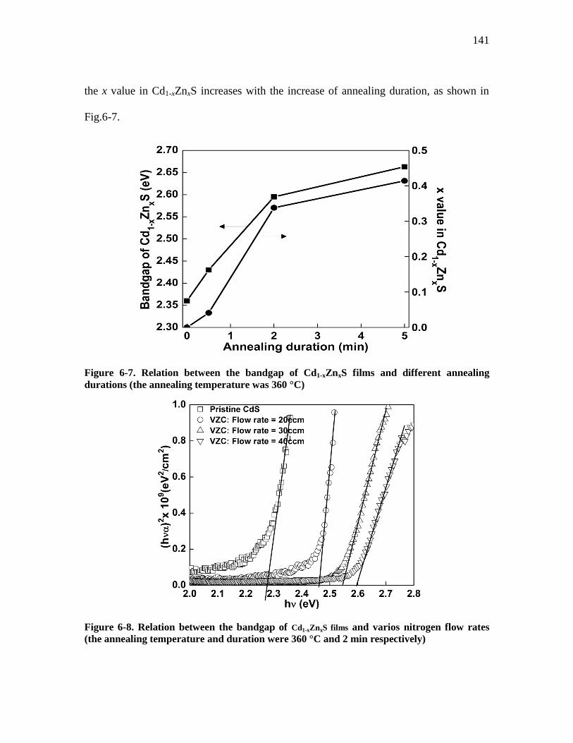
141
the x value in Cd1-xZnxS increases with the increase of annealing duration, as shown in
Fig.6-7.
Figure 6-7. Relation between the bandgap of Cd1-xZnxS films and different annealing
durations (the annealing temperature was 360 °C)
Figure 6-8. Relation between the bandgap of Cd1-xZnxS films and varios nitrogen flow rates
(the annealing temperature and duration were 360 °C and 2 min respectively)
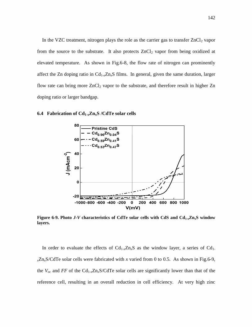
142
In the VZC treatment, nitrogen plays the role as the carrier gas to transfer ZnCl2 vapor
from the source to the substrate. It also protects ZnCl2 vapor from being oxidized at
elevated temperature. As shown in Fig.6-8, the flow rate of nitrogen can prominently
affect the Zn doping ratio in Cd1-xZnxS films. In general, given the same duration, larger
flow rate can bring more ZnCl2 vapor to the substrate, and therefore result in higher Zn
doping ratio or larger bandgap.
6.4 Fabrication of Cd1-xZnxS /CdTe solar cells
Figure 6-9. Photo J-V characteristics of CdTe solar cells with CdS and Cd1-xZnxS window
layers.
In order to evaluate the effects of Cd1-xZnxS as the window layer, a series of Cd1-
xZnxS/CdTe solar cells were fabricated with x varied from 0 to 0.5. As shown in Fig.6-9,
the Voc and FF of the Cd1-xZnxS/CdTe solar cells are significantly lower than that of the
reference cell, resulting in an overall reduction in cell efficiency. At very high zinc
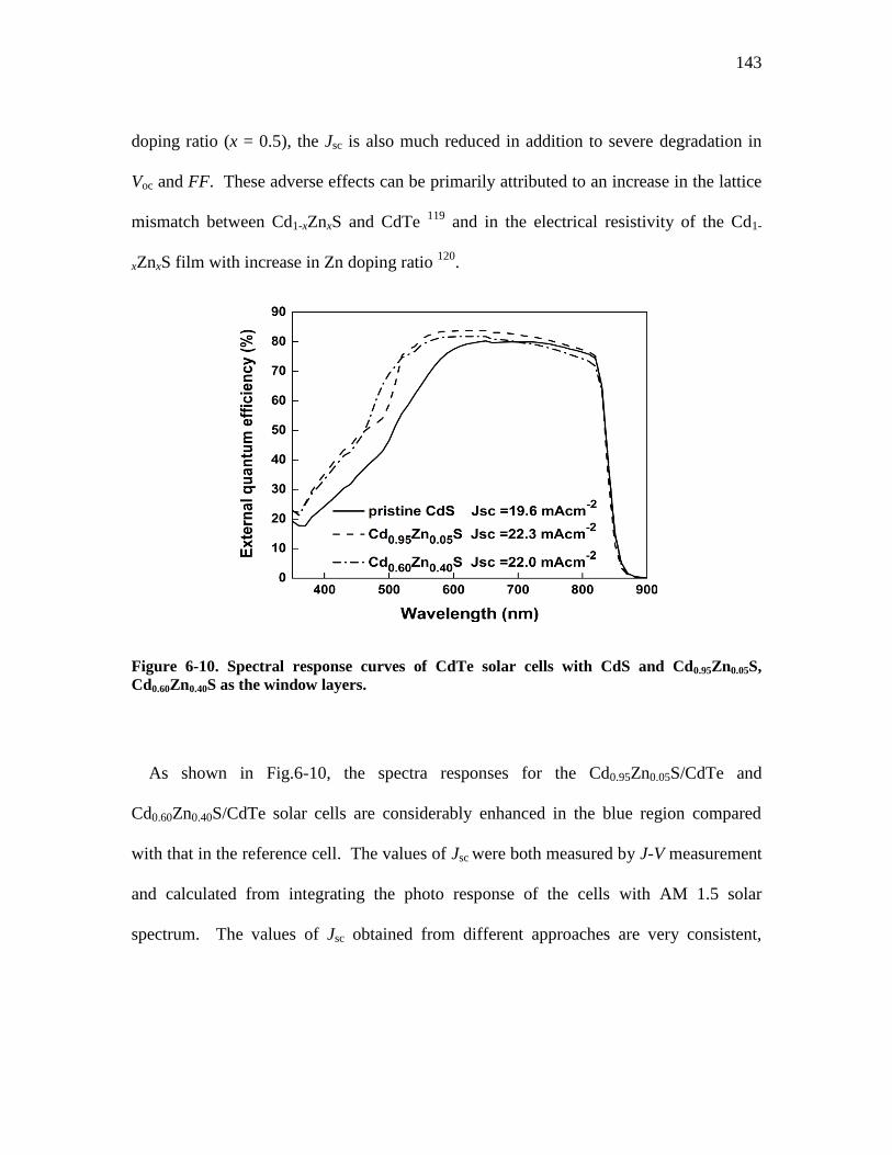
143
doping ratio (x = 0.5), the Jsc is also much reduced in addition to severe degradation in
Voc and FF. These adverse effects can be primarily attributed to an increase in the lattice
mismatch between Cd1-xZnxS and CdTe 119
and in the electrical resistivity of the Cd1-
xZnxS film with increase in Zn doping ratio 120
.
Figure 6-10. Spectral response curves of CdTe solar cells with CdS and Cd0.95Zn0.05S,
Cd0.60Zn0.40S as the window layers.
As shown in Fig.6-10, the spectra responses for the Cd0.95Zn0.05S/CdTe and
Cd0.60Zn0.40S/CdTe solar cells are considerably enhanced in the blue region compared
with that in the reference cell. The values of Jsc were both measured by J-V measurement
and calculated from integrating the photo response of the cells with AM 1.5 solar
spectrum. The values of Jsc obtained from different approaches are very consistent,
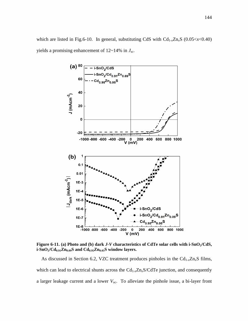
144
which are listed in Fig.6-10. In general, substituting CdS with Cd1-xZnxS (0.05<x<0.40)
yields a promising enhancement of 12~14% in Jsc.
Figure 6-11. (a) Photo and (b) dark J-V characteristics of CdTe solar cells with i-SnO2/CdS,
i-SnO2/Cd0.91Zn0.09S and Cd0.95Zn0.05S window layers.
As discussed in Section 6.2, VZC treatment produces pinholes in the Cd1-xZnxS films,
which can lead to electrical shunts across the Cd1-xZnxS/CdTe junction, and consequently
a larger leakage current and a lower Voc. To alleviate the pinhole issue, a bi-layer front
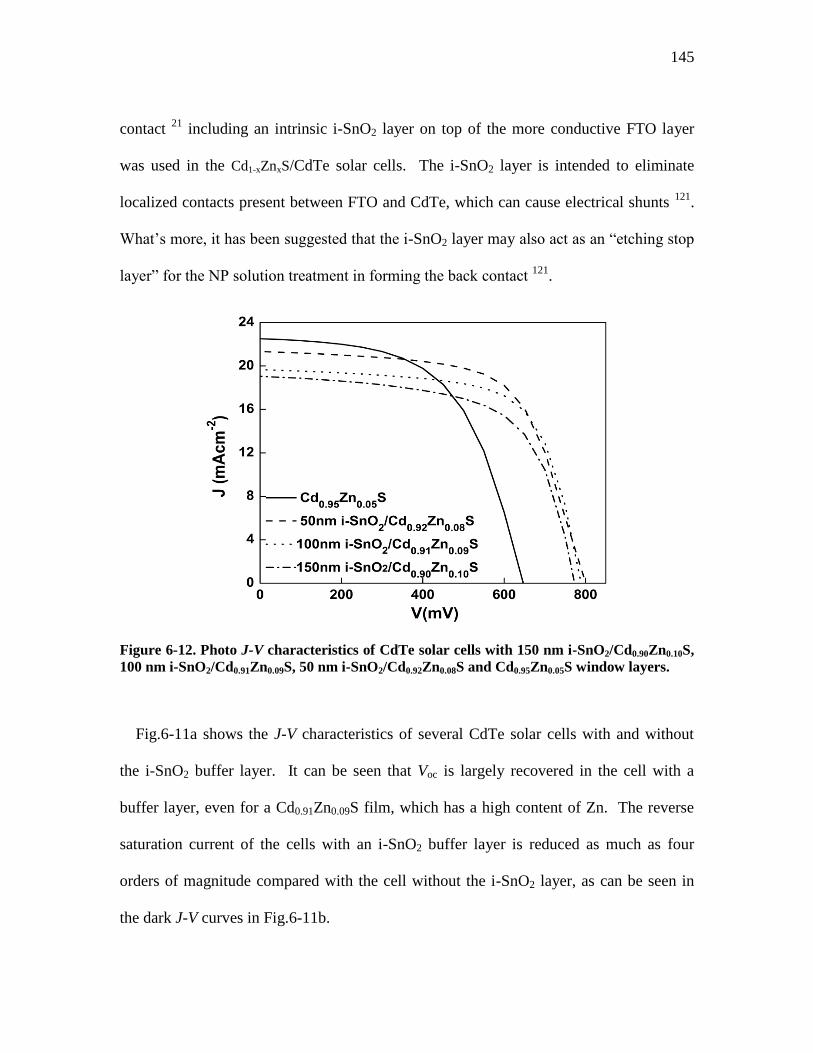
145
contact 21
including an intrinsic i-SnO2 layer on top of the more conductive FTO layer
was used in the Cd1-xZnxS/CdTe solar cells. The i-SnO2 layer is intended to eliminate
localized contacts present between FTO and CdTe, which can cause electrical shunts 121
.
What’s more, it has been suggested that the i-SnO2 layer may also act as an “etching stop
layer” for the NP solution treatment in forming the back contact 121
.
Figure 6-12. Photo J-V characteristics of CdTe solar cells with 150 nm i-SnO2/Cd0.90Zn0.10S,
100 nm i-SnO2/Cd0.91Zn0.09S, 50 nm i-SnO2/Cd0.92Zn0.08S and Cd0.95Zn0.05S window layers.
Fig.6-11a shows the J-V characteristics of several CdTe solar cells with and without
the i-SnO2 buffer layer. It can be seen that Voc is largely recovered in the cell with a
buffer layer, even for a Cd0.91Zn0.09S film, which has a high content of Zn. The reverse
saturation current of the cells with an i-SnO2 buffer layer is reduced as much as four
orders of magnitude compared with the cell without the i-SnO2 layer, as can be seen in
the dark J-V curves in Fig.6-11b.
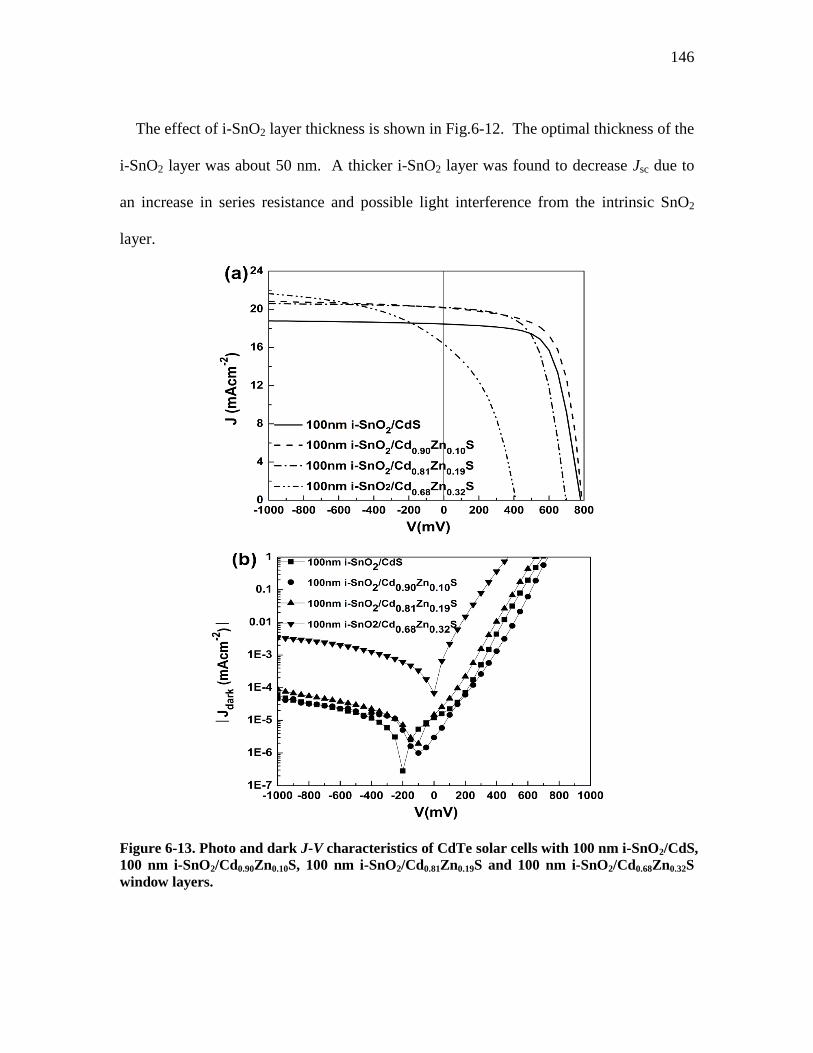
146
The effect of i-SnO2 layer thickness is shown in Fig.6-12. The optimal thickness of the
i-SnO2 layer was about 50 nm. A thicker i-SnO2 layer was found to decrease Jsc due to
an increase in series resistance and possible light interference from the intrinsic SnO2
layer.
Figure 6-13. Photo and dark J-V characteristics of CdTe solar cells with 100 nm i-SnO2/CdS,
100 nm i-SnO2/Cd0.90Zn0.10S, 100 nm i-SnO2/Cd0.81Zn0.19S and 100 nm i-SnO2/Cd0.68Zn0.32S
window layers.
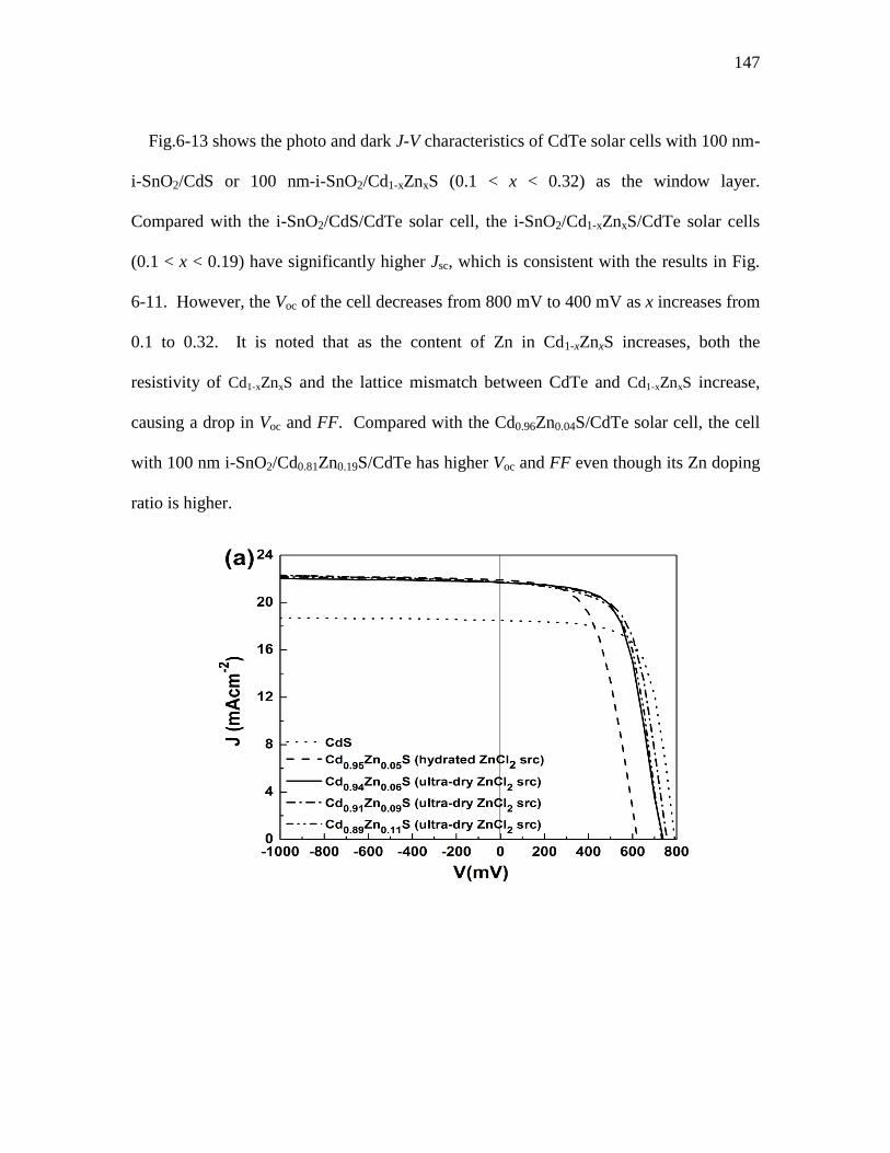
147
Fig.6-13 shows the photo and dark J-V characteristics of CdTe solar cells with 100 nm-
i-SnO2/CdS or 100 nm-i-SnO2/Cd1-xZnxS (0.1 < x < 0.32) as the window layer.
Compared with the i-SnO2/CdS/CdTe solar cell, the i-SnO2/Cd1-xZnxS/CdTe solar cells
(0.1 < x < 0.19) have significantly higher Jsc, which is consistent with the results in Fig.
6-11. However, the Voc of the cell decreases from 800 mV to 400 mV as x increases from
0.1 to 0.32. It is noted that as the content of Zn in Cd1-xZnxS increases, both the
resistivity of Cd1-xZnxS and the lattice mismatch between CdTe and Cd1-xZnxS increase,
causing a drop in Voc and FF. Compared with the Cd0.96Zn0.04S/CdTe solar cell, the cell
with 100 nm i-SnO2/Cd0.81Zn0.19S/CdTe has higher Voc and FF even though its Zn doping
ratio is higher.
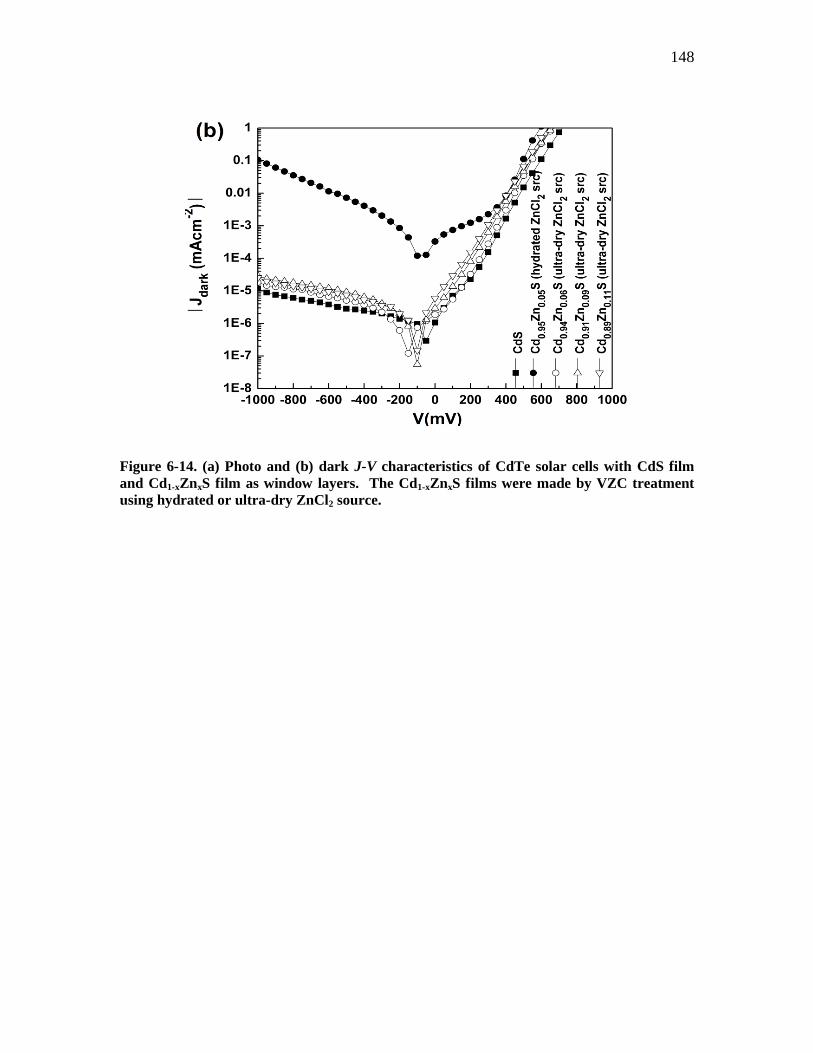
148
Figure 6-14. (a) Photo and (b) dark J-V characteristics of CdTe solar cells with CdS film
and Cd1-xZnxS film as window layers. The Cd1-xZnxS films were made by VZC treatment
using hydrated or ultra-dry ZnCl2 source.
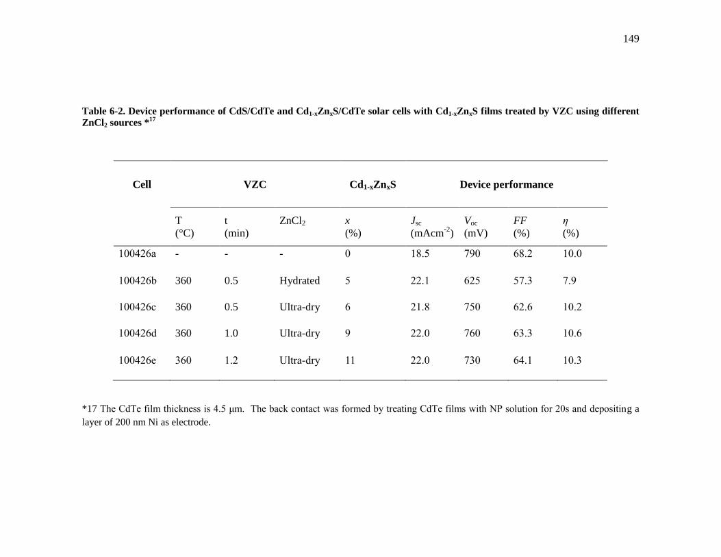
149
Table 6-2. Device performance of CdS/CdTe and Cd1-xZnxS/CdTe solar cells with Cd1-xZnxS films treated by VZC using different
ZnCl2 sources *17
Cell VZC Cd1-xZnxS Device performance
T
(°C)
t
(min)
ZnCl2
x
(%)
Jsc
(mAcm-2
)
Voc
(mV)
FF
(%)
η
(%)
100426a - - - 0 18.5 790 68.2 10.0
100426b 360 0.5 Hydrated 5 22.1 625 57.3 7.9
100426c 360 0.5 Ultra-dry 6 21.8 750 62.6 10.2
100426d 360 1.0 Ultra-dry 9 22.0 760 63.3 10.6
100426e 360 1.2 Ultra-dry 11 22.0 730 64.1 10.3
*17 The CdTe film thickness is 4.5 μm. The back contact was formed by treating CdTe films with NP solution for 20s and depositing a
layer of 200 nm Ni as electrode.
150
As a very hydroscopic compound, ZnCl2 tends to absorb moisture easily. At elevated
temperature, ZnCl2 can react with H2O (Eqn. 6-2 and 6-3) and generate HCl vapor which
can etch CdS films and create pinholes.
(6-2)
(6-3)
Reducing the exposure time of ZnCl2 source to the air and decreasing the hydration
content in the ZnCl2 source can alleviate the above reactions, and therefore help to reduce
the detrimental effects of HCl vapor.
Fig.6-14 shows the J-V characteristics of Cd1-xZnxS /CdTe solar cells in which the Cd1-
xZnxS films were made by VZC treatment using hydrated ZnCl2 (purity 98%) and ultra-
dry ZnCl2 (purity 99.99%). For the same Zn doping ratio (5~6%), the cell with Cd1-xZnxS
treated using ultra-dry ZnCl2 source has significantly higher Voc and better FF than that
using hydrate ZnCl2 source, affirming the negative effects of moisture in ZnCl2 source.
However, as Table 6-3 shows, the device performance of CdTe solar cells in which Cd1-
xZnxS films were made by VZC treatment using ultra-dry ZnCl2, especially Voc and FF, is
still inferior to the reference CdS/CdTe solar cell. Thus reducing the hydration content in
ZnCl2 source alone cannot solve all the issues associated with Cd1-xZnxS/CdTe solar cells.
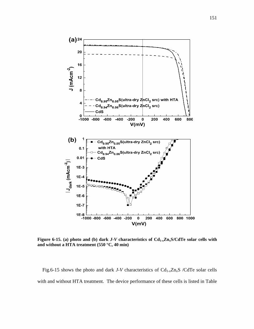
151
Figure 6-15. (a) photo and (b) dark J-V characteristics of Cd1-xZnxS/CdTe solar cells with
and without a HTA treatment (550 °C, 40 min)
Fig.6-15 shows the photo and dark J-V characteristics of Cd1-xZnxS /CdTe solar cells
with and without HTA treatment. The device performance of these cells is listed in Table
152
6-3. The Cd1-xZnxS films were made by VZC treatments using ultra-dry ZnCl2 source.
Interestingly, HTA resulted in enhancements of 50 mV and 3.6% in the Voc and FF of the
cell respectively. HTA can not only improve the crystallinity of CdTe film but also
reduce film resistivity, which may result in the enhancement of device performance.
Table 6-3. Device performance of CdS/CdTe and Cd1-xZnxS/CdTe solar cells with and
without a HTA treatment *18
Cell VZC Cd1-xZnxS Device performance
T
(°C)
t
(min)
ZnCl2
x
(%)
Jsc
(mAcm-2
)
Voc
(mV)
FF
(%)
η
(%)
1204a - - - 0 19.1 790 67.9 10.2
1204b 360 0.5 Ultra-dry 5 21.8 750 62.6 10.2
1204c*19
360 0.5 Ultra-dry 6 21.9 800 66.2 11.6
*18: The CdTe film thickness is 4.5 μm. The back contact was formed by treating CdTe films
with NP solution for 20s and depositing a layer of 200 nm Ni as electrode.
*19: After CdTe film was deposited, the cell was subjected to HTA at 550°C for 40min..
6.5 Summary
A useful technique using vapor zinc chloride treatment to fabricate Cd1-xZnxS films has
been demonstrated. The incorporation of Zn in CdS has been proved by a series of
characterization techniques including XRD, absorption spectroscopy and EDX. The Zn
doping ratio can be readily controlled by adjusting VZC treatment temperature, duration,
nitrogen flow rate or the combination of both.
153
Substituting CdS with Cd1-xZnxS in CdTe solar cells produces an increase of in Jsc, up
to 12~14%. Inserting an intrinsic SnO2 as the front contact buffer was found to improve
Voc, presumably due to a reduction of the shunting defects. Also, the use of ultra-dry
ZnCl2 granules as the ZnCl2 source was found to be beneficial in reducing the pinhole
formation during VZC treatments. The HTA process after CdTe deposition also
improved Voc.
154
7. Summary and conclusions
This work is an investigation of (1) approaches to fabricating high-efficiency ultra-thin
CdTe solar cells, (2) low-resistance electrical back contact buffer based on Te/Cu bi-layer,
and (3) a novel vapor zinc chloride treatment method for making Cd1-xZnxS films.
7.1 Approaches to fabricating high-efficiency ultra-thin CdTe solar cells
Three approaches were investigated to realize this objective, including the fabrication
of high-quality ultra-thin CdTe films using an improved close-spaced sublimation method,
an effective post-deposition treatment comprised of high-temperature annealing and
vapor chloride treatment, and novel back contact formation based on MoOx and Te/Cu
back contact buffers.
1) The conventional CSS method, featuring high deposition rate (>1 μm/min), and
high substrate temperature, is not suitable for reproducibly making ultra-thin
CdTe films without pinholes. The modified CSS method using an improved
temperature-time profile control is able to deposit compact ultra-thin CdTe films
with very few pinholes and a low roughness/thickness ratio. Three critical
parameters including oxygen pressure, substrate temperature and thermal etch
duration have been systematically studied. The best parameter combination to
produce pinhole-free CdTe films with good crystallinity is high substrate
temperature and oxygen pressure plus appropriate thermal etch prior to CdTe
deposition.
155
2) A two-stage post-deposition treatment was found to be beneficial for producing
high-efficiency ultra-thin CdTe cells. The high temperature annealing (HTA) step
further enhances CdTe grain growth and reduces defects related to grain
boundaries and excess sulfur diffusion during VCC treatment. The VCC step
passivates the recombination centers along the grain boundaries and reduces
lattice mismatch at the heterojunction. The combination of HTA and VCC steps
yields higher efficiency than either HTA or VCC step alone.
3) In the conventional back contact formation using nitric-phosphoric acid (NP)
solution, CdTe films, especially ultra-thin films suffer preferential etching on
grain boundaries which results in pinholes and electrical shunting. In a
collaborative effort, two back contacts based on MoOx and Te/Cu have been
developed to replace the NP etching treatment. Deposited by thermal evaporation
or sputtering, MoOx and Te/Cu avoid damages on ultra-thin CdTe films caused by
acid etching. The high work function of MoOx and Te alters the effective electron
affinity at the CdTe/metal interface and thus reduces the energy barrier for the
hole transfer. Appropriate amount of Cu is deliberately introduced into the back
contact to enhance p-type doping in CdTe.
Combining three approaches, CdS/CdTe solar cells with efficiency of 11.2~13.4 %
have been demonstrated with CdTe films of only 0.9~1.5 µm
7.2 Low-resistance electrical contact based on Te/Cu bi-layer.
156
Te/Cu bi-layer was developed to replace NP treatment as a more reliable and effective
back contact for CdTe solar cells. Similar to the Te-rich layer generated by NP treatment
on CdTe surface, evaporated Te plays the same role to change the effective electron
affinity of CdTe. Cu is deliberately introduced into the back contact because appropriate
Cu diffusion can enhance the p-type doping in the CdTe layer. Different from NP
treatment, Te/Cu bi-layer avoids damages on CdTe films caused by acid etching, which is
of particular importance to ultra-thin CdTe solar cells.
It has been found that thermal activation is necessary to promote ohmic contact
formation. Thermal activation on Te/Cu below the threshold temperature of 180 °C
cannot form an ohmic contact and only produces insignificant improvement in device
performance. The optimum thermal activation duration decreases from 20 min to 10 s as
the activation temperature is increased from 200 °C to 270 °C. As a result of the ohmic
contact formation, the device performance especially Voc and FF is greatly enhanced.
SEM images show that the crystallinity of Te layer is improved with thermal activation.
XPS analyses reveal that Cu diffuses into the Te layer with thermal activation above the
threshold temperature. No reaction occurs until the activation duration is extended to one
hour. PL spectra clearly show that Cu diffusion can reach vicinity of CdS/CdTe junction
under certain activation condition.
Apart from thermal activation, the concentration of Cu in Te/Cu bi-layer and Te
thickness also play an important role. The amount of Cu in Te/Cu does not affect the
initial device performance but has a profound impact on device stability. Neither low Cu
157
concentration (<0.1 nm Cu per 100 nm Te) or high Cu concentration (>9.0 nm Cu per
100 nm Te) produces good device stability. Based on the thermal stress test and light
soaking test, the optimum Cu concentration is (0.2~2.2 nm Cu per 100 nm Te). The
thickness of the Te layer is also a critical factor. Good device stability can be only
achieved with Te thickness greater than 50 nm. The overall device stability increases as
the Te thickness is increased. It is concluded that the primary degradation mechanism
associated with Te/Cu contact is the Cu diffusion. The Cu diffusion can be alleviated by
reducing Cu concentration to certain level, increasing Te thickness or reducing stress
temperature
In general, Te/Cu has been proved to be an excellent back contact buffer for CdTe
solar cells. CdTe solar cells with efficiencies up to 14.8% and low efficiency degradation
rate (<0.4% /h at 200°C) have been demonstrated.
However, the understanding of the formation of Te/Cu back contact is still lacking.
More characterizations will be needed to quantitatively determine the Cu diffusion profile
in bulk CdTe and to understand how Te retards Cu diffusion.
7.3 A novel vaporous zinc chloride treatment for making Cd1-xZnxS films.
As an effective window layer, Cd1-xZnxS has been used in thin film CIGS and CdTe
solar cells. However, the conventional methods to fabricate this ternary semiconductor
including co-sputtering, co-evaporation, and MOCVD require complicated apparatus and
costly maintenance. A novel method named vaporous zinc chloride treatment was
158
developed to fabricate Cd1-xZnxS. The VZC method features simple setup and easy
operation.
Cd1-xZnxS film with a homogeneous structure has been proved by a series of
characterization techniques including XRD, absorption spectroscopy and EDX. The Zn
to Cd doping ratio can be controlled by adjusting VZC treatment temperature, duration,
nitrogen flow rate or the combination of these process parameters.
Although pinholes were founded in the Cd1-xZnxS film made by VZC, their negative
effects on the CdTe solar cells can be largely eliminated by several approaches as follows:
1) Inserting an intrinsic SnO2 layer between FTO and Cd1-xZnxS to reduce localized
contact between CdTe and front electrode.
2) Reducing the amount of hydration or moisture in ZnCl2 source by replacing
hydrated ZnCl2 with ultra-dry ZnCl2.
3) Applying a high temperature annealing process on the as-made Cd1-xZnxS /CdTe
stack layers before VCC treatment.
With Cd1-xZnxS substituting CdS as the window layer, CdTe solar cells with a 12-14%
higher Jsc and without compromising in Voc and FF have been demonstrated.
More characterizations including SEM, EDX and XRD will need to be carried out to
further reveal the effects of moisture on VZC treatment and the impacts of HTA on
Cd1-xZnxS /CdTe solar cells. In addition, high quality Cd1-xZnxS films with appropriate

159
Zn doping ratio will be applied to ultra-thin CdTe solar cells to further improve the cell
efficiency.
160
References
(1)http://www.solarbuzz.com/news/recent-findings/world-solar-photovoltaic-market-
grew-274-gigawatts-2011-40-yy (accessed July, 14th, 2012)
(2)Fahrenbruch, A. L. Mater. Res. Soc. Symp. Proc. 2007, 1012, 283.
(3)Green, M. A. J. Mater. Sci.-Mater. EL 2007, 18, S15.
(4)Hovel, H. J. Semicond. and Semimetals; Academic: New York, 1975; Vol. 11.
(5)Morales-Acevedo, A. Sol. Energy Mater. Sol. Cells 2006, 90, 2213.
(6)Wang, S. L.; Lee, S. H.; Gupta, A.; Compaan, A. D. phys. stat. sol. (c) 2004, 1, 1046.
(7)Gordillo, G.; Florez, J. M.; Hernandez, L. C. Sol. Energy Mater. Sol. Cells 1995, 37,
273.
(8)Romeo, A.; Buecheler, S.; Giarola, M.; Mariotto, G.; Tiwari, A. N.; Romeo, N.; Bosio,
A.; Mazzamuto, S. Thin Solid Films 2009, 517, 2132.
(9)Barker, J.; Binns, S. P.; Johnson, D. R.; Marshall, R. J.; Oktik, S.; ÖZsan, M. E.;
Patterson, M. H.; Ransome, S. J.; Roberts, S.; Sadeghi, M.; Sherborne, J.; Turner, A. K.;
Woodcock, J. M. Int. J. Sol. Energy 1992, 12, 79.
(10) Ferekides, C. S.; Balasubramanian, U.; Mamazza, R.; Viswanathan, V.; Zhao, H.;
Morel, D. L. Sol. Energy 2004, 77, 823.
(11) Fahrenbr.Al; Vasilche.V; Buch, F.; Mitchell, K.; Bube, R. H. Appl. Phys. Lett. 1974,
25, 605.
(12) Romeo, N.; Bosio, A.; Canevari, V.; Podesta, A. Sol. Energy 2004, 77, 795.
(13) Emziane, M.; Durose, K.; Halliday, D. P.; Bosio, A.; Romeo, N. J. Appl. Phys. 2006,
100, 013513/1.
(14) Fraser, D. B.; Melchior, H. J. Appl. Phys. 1972, 43, 3120.
(15) Cha, D.; Kim, S.; Huang, N. K. Mater. Sci. Eng B-Solid State Mater. Adv. Technol.
2004, 106, 63.
(16) Pizzarello, F. A. J. Appl. Phys. 1964, 35, 2730.
(17) Aguilar-Hernandez, J.; Contreras-Puente, G.; Morales-Acevedo, A.; Vigil-Galan, O.;
Cruz-Gandarilla, F.; Vidal-Larramendi, J.; Escamilla-Esquivel, A.; Hernandez-Contreras,
H.; Hesiquio-Garduno, M.; Arias-Carbajal, A.; Chavarria-Castaneda, M.; Arriaga-Mejia,
G. Semicond. Sci. .Technol. 2003, 18, 111.
(18) Chu, T. L.; Chu, S. S.; Schultz, N.; Wang, C.; Wu, C. Q. J. Electrochem. Soc 1992,
139, 2443.
(19) McCandless, B. E.; Dobson, K. D. Sol. Energy 2004, 77, 839.
(20) Bosio, A.; Romeo, N.; Mazzamuto, S.; Canevari, V. Prog. Cryst. Growth Charact.
Mater. 2006, 52, 247.
(21) Wu, X. Z. Sol. Energy 2004, 77, 803.
(22) Britt, J.; Ferekides, C. Appl. Phys. Lett. 1993, 62, 2851.
(23) Aramoto, T.; Kumazawa, S.; Higuchi, H.; Arita, T.; Shibutani, S.; Nishio, T.;
Nakajima, J.; Tsuji, M.; Hanafusa, A.; Hibino, T.; Omura, K.; Ohyama, H.; Murozono, M.
Jpn. J. Appl. Phys. 1997, 36, 6304.
(24) Nicoll, F. H. J. Electrochem. Soc 1963, 110, 1165.
161
(25) Falcao, V. D.; Pinheiro, W. A.; Ferreira, C. L.; Oliveira Cruz, L. R. d. Mater. Res.
2006, 9, 29.
(26) Alamri, S. N. phys. stat. sol. (a) 2003, 200, 352.
(27) Lee, J.-H.; Lee, H.-Y.; Park, Y.-K.; Shin, S.-H.; Park, K.-J. Jpn. J. Appl. Phys. 1998,
37, 3357.
(28) Ferekides, C. S.; Marinskiy, D.; Viswanathan, V.; Tetali, B.; Palekis, V.; Selvaraj, P.;
Morel, D. L. Thin Solid Films 2000, 361, 520.
(29) Song, W.; Mao, D.; Feng, L.; Zhu, Y.; Aslan, M. H.; Collins, R. T.; Trefny, J. U.
Mater. Res. Soc. Symp. Proc. 1996, 426, 331.
(30) McCandless, B. E.; Hichri, H.; Hanket, G.; Birkmire, R. W. In Photovoltaic
Specialists Conference, 1996., Conference Record of the Twenty Fifth IEEE 1996, p 781.
(31) Albin, D. S.; Demtsu, S. H.; McMahon, T. J. Thin Solid Films 2006, 515, 2659.
(32) Tyan, Y.-S. US Patent No.4319069, 1982.
(33) http://www.epa.gov/ttn/atw/hlthef/cadmium.html (accessed April, 20th, 2012).
(34) Fthenakis, V. M. Renewable Sustainable Energy Rev. 2004, 8, 303.
(35) Fthenakis, V. M. In The 19th European PV Solar Energy Conference; EU PVSEC:
Paris, France, 2004; Vol. 5BV.1, p 32.
(36) Gupta, A.; Parikh, V.; Compaan, A. D. Sol. Energy Mater. Sol. Cells 2006, 90, 2263.
(37) Jones, E. W.; Barrioz, V.; Irvine, S. J. C.; Lamb, D. Thin Solid Films 2009, 517,
2226.
(38) Britt, J.; Ferekides, C. Appl. Phys. Lett. 1993, 62, 2851.
(39)Amin, N.; Isaka, T.; Okamoto, T.; Yamada, A.; Konagai, M. Jpn. J. Appl. Phys. 1999,
38, 4666.
(40) Amin, N.; Sopian, K.; Konagai, M. Sol. Energy Mater. Sol. Cells 2007, 91, 1202.
(41) Gupta, A.; Compaan, A. D. In Photovoltaic Specialists Conference, 2005.
Conference Record of the Thirty-first IEEE 2005, p 235.
(42) Luschitz, J.; Lakus-Wollny, K.; Klein, A.; Jaegermann, W. Thin Solid Films 2007,
515, 5814.
(43) Jaegermann, W.; Klein, A.; Mayer, T. Adv. Mate. 2009, 21, 4196.
(44) Tyan, Y. S.; Vazan, F.; Barge, T. S. In Photovoltaic Specialists Conference, 1984.,
Conference Record of the Seventeenth IEEE 1984, p 840.
(45) Romeo, N.; Bosio, A.; Tedeschi, R.; Canevari, V. Mater. Chem. and Phys. 2000, 66,
201.
(46) Li, X. S.; Albin, D. S.; Asher, S.; Moutinho, H.; Keyes, B.; Matson, R. J.; Hasoon, F.
S.; Sheldon, P. In The 13th NREL photovoltaics program review meeting; AIP:
Lakewood, CO, 1996; Vol. 353, p 376.
(47) Rose, D. H.; Levi, D. H.; Matson, R. J.; Albin, D. S.; Dhere, R. G.; Sheldon, P. In
Photovoltaic Specialists Conference, 1996., Conference Record of the Twenty Fifth IEEE
1996, p 777.
(48) Rose, D. H. The effect of oxygen on CdTe-absorber solar cells deposited by close-
spaced sublimation. University of Colorado, Boulder, 1997.
(49)Hsu, T. M.; Jih, R. J.; Lin, P. C.; Ueng, H. Y.; Hsu, Y. J.; Hwang, H. L. J. Appl. Phys.
1986, 59, 3607.
162
(50) Emziane, M.; Durose, K.; Halliday, D. P.; Bosio, A.; Romeo, N. J. Appl. Phys. 2006,
100.
(51) Emziane, M.; Durose, K.; Halliday, D. P. Appl. Phys. Lett. 2005, 87, 261901/1.
(52) Hernandez-Torres, M. E.; Silva-Gonzalez, R.; Casarrubias-Segura, G.; Gracia-
Jimenez, J. M. Sol. Energy Mater. Sol. Cells 2006, 90, 2241.
(53) Valdna, V. Sol. Energy Mater. Sol. Cells 2005, 87, 369.
(54) Rose, D. H.; Hasoon, F. S.; Dhere, R. G.; Albin, D. S.; Ribelin, R. M.; Li, X. S.;
Mahathongdy, Y.; Gessert, T. A.; Sheldon, P. Prog. Photovoltaics Res. Appl. 1999, 7,
331.
(55) Vora, N.; Dhere, R. Mater. Res. Soc. Symp. Proc.2010, 1210, 55.
(56) Mahathongdy, Y.; Albin, D. S.; Wolden, C. A.; Baldwin, R. M. In NCPV
Photovoltaic Program Review, 1999. AIP Conference; The American Institute of Physics:
Denver, CO, 1998, p 236.
(57) Nakamura, K.; Fujihara, T.; Toyama, T.; Okamoto, H. Jpn. J. Appl. Phys. 2002, 41,
4474.
(58) Emziane, M.; Durose, K.; Romeo, N.; Bosio, A.; Halliday, D. P. Thin Solid Films
2005, 480, 377.
(59) Zhao, H.; Palekis, V.; Selvaraj, P.; Morel, D. L.; Ferekides, C. S. In Photovoltaic
Specialists Conference, 2002. Conference Record of the Twenty-Ninth IEEE New Orleans,
LA, 2002, p 668.
(60) McCandless, B. E.; Youm, I.; Birkmire, R. W. Prog. Photovoltaics Res. Appl. 1999,
7, 21.
(61)Nakamura, K.; Gotoh, M.; Fujihara, T.; Toyama, T.; Okamoto, H. Sol. Energy Mater.
Sol. Cells 2003, 75, 185.
(62) McCandless, B. E.; Moulton, L. V.; Birkmire, R. W. Prog. Photovoltaics Res. Appl.
1997, 5, 249.
(63) Ringel, S. A.; Smith, A. W.; Macdougal, M. H.; Rohatgi, A. J. Appl. Phys. 1991, 70,
881.
(64) Zhou, T. X.; Reiter, N.; Powell, R. C.; Sasala, R.; Meyers, P. V. In Photovoltaic
Energy Conversion, 1994. IEEE First World Conference; IEEE: Waikoloa, Hawaii, 1994;
Vol. II, p 103.
(65) McCandless, B. E.; Sites, J. R. Cadmium Telluride Solar Cells; John Wiley & Sons,
2011; Vol. 14.
(66) Ayoub, M.; Hage-Ali, M.; Koebel, J. M.; Zumbiehl, A.; Klotz, F.; Rit, C.; Regal, R.;
Fougeres, P.; Siffert, P. Nuclear Science, IEEE Transactions on 2003, 50, 229.
(67) Takahashi, M.; Uosaki, K.; Kita, H.; Suzuki, Y. J. Appl. Phys. 1985, 58, 4292.
(68) Aguilar-Hernández, J.; Contreras-Puente, G.; Vidal-Larramendi, J.; Vigil-Galán, O.
Thin Solid Films 2003, 426, 132.
(69) Ahmadbitar, R.; Moutinho, H.; Abulfotuh, F.; Kazmerski, L. Renewable Energy
1995, 6, 553.
(70) Halliday, D. P.; Eggleston, J. M.; Durose, K. J. Cryst.Growth 1998, 186, 543.
(71) Moutinho, H. R.; Al-Jassim, M. M.; Levi, D. H.; Dippo, P. C.; Kazmerski, L. L. J.
Vac. Sci. Technol. A. 1998, 16, 1251.
163
(72) Myers, T. H.; Schetzina, J. F.; Edwards, S. T.; Schreiner, A. F. J. Appl. Phys. 1983,
54, 4232.
(73) Xia, W.; Welt, J. A.; Lin, H.; Wu, H. N.; Ho, M. H.; Tang, C. W. Sol. Energy Mater.
Sol. Cells 2010, 94, 2113.
(74) Dobson, K. D.; Paulson, P. D.; McCandless, B. E.; Birkmire, R. W. Mater. Res. Soc.
Symp. Proc. 2003, 763, 107.
(75)Kraft, D.; Thissen, A.; Broetz, J.; Flege, S.; Campo, M.; Klein, A.; Jaegermann, W. J.
Appl. Phys. 2003, 94, 3589.
(76) Dobson, K. D.; Visoly-Fisher, I.; Hodes, G.; Cahen, D. Sol. Energy Mater. Sol. Cells
2000, 62, 295.
(77) Dobson, K. D.; Visoly-Fisher, I.; Hodes, G.; Cahen, D. Adv. Mater. 2001, 13, 1495.
(78) Yun, J. H.; Kim, K. H.; Lee, D. Y.; Ahn, B. T.; Ohno, T. R. In Photovoltaic
Specialists Conference, 2002. Conference Record of the Twenty-nine IEEE; IEEE: New
Orleans, LA, 2002, p 543.
(79) Lin, H.; Xia, W.; Wu, H. N.; Tang, C. W.; US Patent Application No. 20110240123
A1, 2011
(80) Xia, W.; Wu, H. N.; Lin, H.; Tang, C. W.; US Patent Application No. 61/540264,
2011
(81) Xia, W.; Lin, H.; Wu, H. N.; Tang, C. W. Thin Solid Films 2011, 520, 566.
(82) Lin, H.; Xia, W.; Wu, H. N.; Tang, C. W. Appl. Phys. Lett.2010, 97, 123504.
(83) Zhang, M.; Irfan; Ding, H.; Gao, Y.; Tang, C. W. Appl. Phys. Lett.2010, 96.
(84) Lin, H.; Irfan; Xia, W.; Wu, H. N.; Gao, Y.; Tang, C. W. Sol. Energy Mater. Sol.
Cells 2012, 99, 349.
(85) Hegedus, S. S.; Shafarman, W. N. Prog. Photovoltaics Res. Appl. 2004, 12, 155.
(86) Waters, D. M.; Niles, D.; Gessert, T. A.; Albin, D. S.; Rose, D. H.; Sheldon, P. In
World Conference and Exhibition on Photovoltaic Solar Energy Conversion, 1998.
Conference Record of the Second IEEE; IEEE: Vienna, Austria, 1998, p 1043.
(87) Plotnikov, V. V.; DoHyoung, K.; Wieland, K. A.; Compaan, A. D. In Photovoltaic
Specialists Conference (PVSC), 2009 34th IEEE 2009, p 001435.
(88) Wu, X.; Zhou, J.; Duda, A.; Yan, Y.; Teeter, G.; Asher, S.; Metzger, W. K.; Demtsu,
S.; Wei, S.-H.; Noufi, R. Thin Solid Films 2007, 515, 5798.
(89) Rotlevi, O.; Dobson, K. D.; Rose, D.; Hodes, G. Thin Solid Films 2001, 387, 155.
(90) Makhratchev, K.; Price, K. J.; Ma, X.; Simmons, D. A.; Drayton, J.; Ludwig, K.;
Gupta, A.; Bohn, R. G.; Compaan, A. D. In Photovoltaic Specialists Conference, 2000.
Conference Record of the Twenty-Eighth IEEE 2000, p 475.
(91) Tang, J.; Mao, D.; Ohno, T. R.; Kaydanov, V.; Trefny, J. U. In Photovoltaic
Specialists Conference, 1997., Conference Record of the Twenty-Sixth IEEE 1997, p 439.
(92) Schmidt, T.; Durose, K.; Rothenhäusler, C.; Lerch, M. Thin Solid Films 2000, 361–
362, 383.
(93) Romeo, N. US Patent 12/452427, 2010.
(94) Hegedus, S. S.; McCandless, B. E. Sol. Energy Mater. Sol. Cells2005, 88, 75.
(95) Zhang, L.; Da Silva, J. L. F.; Li, J.; Yan, Y.; Gessert, T. A.; Wei, S.-H. Phys. Rev.
Lett. 2008, 101, 155501.
164
(96) Paudel, N. R.; Kwon, D.; Young, M.; Wieland, K. A.; Asher, S.; Compaan, A. D. In
Photovoltaic Specialists Conference (PVSC), 2010 35th IEEE 2010, p 001009.
(97) Visoly-Fisher, I.; Dobson, K. D.; Nair, J.; Bezalel, E.; Hodes, G.; Cahen, D. Adv.
Func. Mater. 2003, 13, 289.
(98) Zhou, J.; Wu, X.; Duda, A.; Teeter, G.; Demtsu, S. H. Thin Solid Films 2007, 515,
7364.
(99) Caraman, I.; Rusu, G. I.; Leontie, L. J. Optoelectron. Adv. Mater. 2007, 9, 1546.
(100) Okamoto, T.; Matsuzaki, Y.; Amin, N.; Yamada, A.; Konagai, M. Jpn. J. Appl.
Phys. 1998, 37, 3894.
(101) Oladeji, I. O.; Chow, L.; Ferekides, C. S.; Viswanathan, V.; Zhao, Z. Sol. Energy
Mater. Sol. Cells 2000, 61, 203.
(102) Bhattacharya, R. N.; Contreras, M. A.; Egaas, B.; Noufi, R. N.; Kanevce, A.; Sites,
J. R. Appl. Phys. Lett. 2006, 89.
(103) Reddy, K. T. R.; Reddy, P. J. J. Phys. D-Appl. Phys. 1992, 25, 1345.
(104) Ram, P. R.; Thangaraj, R.; Agnihotri, O. P. Bull. Mat. Sci. 1986, 8, 279.
(105) Chandrasekhar, S.; Martinuzzi, S.; Nataren, F. Z. Can. J. Phys. 1985, 63, 716.
(106) Hussain, O. M.; Reddy, P. S.; Naidu, B. S.; Uthanna, S.; Reddy, P. J. Semicond. Sci.
Techno. 1991, 6, 690.
(107) Oladeji, I. O.; Chow, L. Thin Solid Films 2005, 474, 77.
(108)Clayton, A. J.; Irvine, S. J. C.; Jones, E. W.; Kartopu, G.; Barrioz, V.; Brooks, W. S.
M. Sol. Energy Mater. Sol. Cells 2012, 101, 68.
(109) Wu, B. J.; Cheng, H.; Guha, S.; Haase, M. A.; De Puydt, J. M.; Meis-Haugen, G.;
Qiu, J. Appl. Phys. Lett. 1993, 63, 2935.
(110) Shaiw-Yih, Y.; Alan, L. F.; Richard, H. B. J. Appl. Phys. 1978, 49, 1294.
(111) Agnihotri, O. P.; Gupta, B. K. Jpn. J. Appl. Phys. 1979, 18, 317.
(112) Lee, J. H.; Song, W. C.; Yi, J. S.; Yang, K. J.; Han, W. D.; Hwang, J. Thin Solid
Films 2003, 431, 349.
(113) Abdinov, A.; Mekhtiev, N.; Mamedov, G.; Amirova, S. Semicond. 2006, 40, 1442.
(114)Zhou, J.; Wu, X.; Teeter, G.; To, B.; Yan, Y.; Dhere, R. G.; Gessert, T. A. phys. stat.
sol. (b) 2004, 241, 775.
(115) Dzhafarov, T. D.; Ongul, F.; Karabay, I. J. Phys. D-Appl. Phys. 2006, 39, 3221.
(116) Gunasekaran, M.; Ichimura, M. Jpn. J. Appl. Phys. 2005, 44, 7345.
(117) Kwok, H. L. J. Phys. D-Appl. Phys. 1983, 16, 2367.
(118) Kuroyanagi, A. Thin Solid Films 1994, 249, 91.
(119) Chu, T. L.; Chu, S. S.; Britt, J.; Ferekides, C.; Wu, C. Q. In Photvoltaic Specialists
Conference, 1991. Conference Record of the Twenty Second IEEE Las Vegas, NV, 1991,
p 1136.
(120) Burton, L. C.; Hench, T. L. Appl. Phys. Lett. 1976, 29, 612.
(121) Compaan, A. D.; Sites, J. R.; Birkmire, R. W.; Ferekides, C. S.; Fahrenbruch, A. L.
In Proceedings of the Symposium on Photovoltaics for the 21st century; The
Electrochemical Society: Seattle, WA, 1999; Vol. 1, p 241.
165
Appendices
A.1 Fabrication of ultra-thin CdTe solar cells
A.1.1 Deposition of CdS films
CdS films were deposited on fluorine-doped tin oxide (FTO) glass substrate
(Pilkington, TEC-15) using a chemical bath deposition method described by Chu et al18
.
The procedure for our batch-wise preparation was as follows: the concentration of
ammonium hydroxide, ammonium acetate, cadmium acetate, thiourea were typically 0.4
M, 20 mM, 1 mM and 5 mM, respectively. NH4Ac (405 mg), CdAc2 (200 mg) and NH4
H2O (40.5 ml, 28.0~30.0% as NH3) were firstly added to de-ionzied water (DIW, 684 ml),
stirred in a beaker (1000 ml) and heated to 92 °C on a hotplate. The FTO glass substrates
with a dimension of 1.5” × 1.5” mounted on strips of stain steel plates were immersed in
the solution. The preheated thiourea solution (286 mg in 25 ml DIW, 90°C) was then
added into the solution. The solution was left stirring for 40 min before the substrates
with the CdS deposits were removed from the bath. The substrates were cleaned
ultrasonically in DIW for 5 min to remove loose CdS particulates on the substrates. They
were then further rinsed with DIW and dried with nitrogen. The typical thickness of CdS
deposited under the above conditions was 150 nm.
A.1.2 Deposition of ultra-thin CdTe films
Polycrystalline CdTe films were deposited on the CdS coated substrates by the close
spaced sublimation 39
. The CdTe source was CdTe granules (Alfa Aesar, 99.99%). The
heating sources were halogen lamps (ELH, 300 W) mounted on the graphite plates,
166
which also serve as the source and substrate holders. A temperature-time profile for a
typical deposition run is shown in Fig. 2-1b. The substrate and source temperatures were
controlled independently by temperature controllers (Omega, CN 7800). The substrate
temperature was maintained at 525°C. The source temperature was varied from 550°C to
625°C. The deposition duration is 2 min. The deposition chamber ambient was typically
1.5 Torr oxygen. Under these conditions, the deposition rate of the CdTe films was
approximately 0.5 μm/min.
A.1.3 Post deposition treatments on CdS and CdTe films
Vapor CdCl2 (VCC) treatments were conducted on CdS and CdTe films in a CSS
system (Fig. 3-1a) similar to that used for the deposition of CdTe films. The CdCl2
source was ultra-dry CdCl2 granules (Alfa Aesar, 99.998% metals basis). The heating
sources were halogen lamps (ELH, 300 W) mounted on the graphite plates, which also
serve as the source and substrate holders. A temperature-time profile for a typical
deposition run is shown in Fig. 3-1b. Both the source and substrate temperatures were
maintained at 400 °C. The ambient during VCC treatments was an O2:N2 (1:4) ambient
of 10 Torr. The typical treatment durations for CdS and CdTe films were 6 min and 4.5
min respectively.
Prior to the VCC treatment, a high-temperature annealing (HTA) treatment was
conducted on CdTe films in a tube furnace under nitrogen at a temperature of 550°C for
40 min. Nitrogen flow (flow rate: 100 cm3/min) under atmospheric pressure was
maintained during the entire process. The ramping rate of the tube furnace was 80°C/min.
167
After the annealing process, the furnace was cooled down to room temperature with an
average cooling rate of 17 °C/min.
A.1.4 Back contact formation
For NP treatment: after a VCC treatment, the CdTe films were etched in a solution (NP
solution) of nitric and phosphoric acids with a volumetric ratio of 2.2 (HNO3): 175
(H3PO4): 70 (H2O) for 25 s, following by rinsing in DIW and drying with nitrogen.
For MoOx back contact buffer: the CdTe films were rinsed in DIW and dried with
nitrogen. The back contact layer was formed by depositing a 40 nm-MoOx film on CdTe
films by thermal evaporation of MoOx powder (Alfa Aesar, 99.95%) with a deposition
rate of 5~7 Å/s in a vacuum level of 10-5
Torr.
For Te/Cu back contact buffer, a layer of Te (100 nm) and a layer of Cu (1.1 nm) were
deposited on CdTe films in sequence by DC sputtering using a Te target (0.125” x 2”,
99.9%) and a Cu target (0.063” x 2”, 99.9%) respectively. The vacuum level before the
sputtering deposition was 10-5
Torr. The deposition rates for Te and Cu were 7Å/s and 1
Å/s respectively.
For electrode deposition: after the formation of the back contact buffer, a layer of 200
nm Ni was deposited onto the buffer layer by DC sputtering with a deposition rate of 8
Å/s to form the back contact electrode.
For thermal activation on the Te/Cu back contact buffer: the cell completed with Ni
electrode deposition was subjected to an annealing process. The typical annealing
168
temperature and duration are 225 °C and 4 min respectively. The average ramping rate
and cooling rate were 45 °C/min and 10 °C/min, respectively. The annealing durations
mentioned in the thesis were the durations for which the annealing temperature was
stabilized at the temperature set-point.
A.1.5 Fabrication of Cd1-xZnxS films
Cd1-xZnxS films were fabricated by a vaporous zinc chloride (VZC) treatment in a two-
zone tube furnace. A glass tube (1” diameter and 24” long) containing both the ZnCl2
source (Alfa Aesar, ultra-dry: 99.999%, or hydrate: 99.99%)(50-500 mg) and the
FTO/CdS substrates in separate zones was first purged with nitrogen to get rid of oxygen
in the system. The VZC treatment was carried out at atmosphere pressure under a
continuous nitrogen flow of about 100 cm3/min. A temperature-time profile for a typical
treatment run is shown in Fig. 6-1b.
A.2 Details about the characterizations and stability tests
The SEM images in Fig.1-4, 2-3, 3-2, 3-16, 4-2, and 6-3 were obtained using a
scanning electron microscope (Zeiss, Supra 40 VP, operating voltage: 20 kV). The SEM
images in Fig.2-8, 2-9, and 5-12 were obtained using a scanning electron microscope
(Hitachi, TM 3000, operating voltage: 15 kV).
AFM images (Fig. 2-5) were obtained using an atomic force microscope (NT-MDT,
Solver Next).
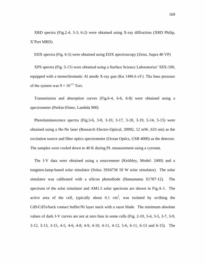
169
XRD spectra (Fig.2-4, 3-3, 6-2) were obtained using X-ray diffraction (XRD Philip,
X’Pert MRD).
EDX spectra (Fig. 6-5) were obtained using EDX spectroscopy (Zeiss, Supra 40 VP)
XPS spectra (Fig. 5-13) were obtained using a Surface Science Laboratories’ SSX-100,
equipped with a monochromatic Al anode X-ray gun (Kα 1486.6 eV). The base pressure
of the system was 9 × 10-11
Torr.
Transmission and absorption curves (Fig.6-4, 6-6, 6-8) were obtained using a
spectrometer (Perkin-Elmer, Lambda 900)
Photoluminescence spectra (Fig.3-6, 3-8, 3-10, 3-17, 3-18, 3-19, 5-14, 5-15) were
obtained using a He-Ne laser (Research Electro-Optical, 30992, 12 mW, 633 nm) as the
excitation source and fiber optics spectrometer (Ocean Optics, USB 4000) as the detector.
The samples were cooled down to 40 K during PL measurement using a cyrostat.
The J-V data were obtained using a sourcemeter (Keithley, Model: 2400) and a
tungsten-lamp-based solar simulator (Solux 3SS4736 50 W solar simulator). The solar
simulator was calibrated with a silicon photodiode (Hamamatsu S1787-12). The
spectrum of the solar simulator and AM1.5 solar spectrum are shown in Fig.A-1. The
active area of the cell, typically about 0.1 cm2, was isolated by scribing the
CdS/CdTe/back contact buffer/Ni layer stack with a razor blade. The minimum absolute
values of dark J-V curves are not at zero bias in some cells (Fig. 2-10, 3-4, 3-5, 3-7, 3-9,
3-12, 3-13, 3-15, 4-5, 4-6, 4-8, 4-9, 4-10, 4-11, 4-12, 5-6, 6-11, 6-13 and 6-15). The
170
voltage offsets were probably due to measurement errors related to hysteresis of the J-V
traces which is due to charge trapping in some of the cells. Another possible cause for
the voltage offsets is light leakage (from room light) during the dark J-V measurement.
Figure A-1 Spectrum of Solux solar simulator and AM 1.5 solar spectrum.
Spectral response measurements (Fig. 3-21 and 6-10) were obtained using a calibrated
¼ m monochromator (ARC SpectroPro 275).
In thermal stress tests, CdTe solar cells were annealed at 200 °C in atmospheric
nitrogen ambient for up to 9 h. In light soaking tests, CdTe solar cells were stressed
under the illumination of about 100 mW/cm2 provided by compact fluorescent lamps.
The light soaking test temperature was maintained at ~45 °C due to illumination.
A.3 Lists of symbols and abbreviations
A: didoe factor
171
AFM : atomic force microscopy
BE : binding energy
BM : bromine-methanol
CBD: chemical bath deposition
CIGS : Cu(In, Ga)Se2
CSS : close spaced sublimation
d : distance between source and substrate in a CSS deposition
EDX: energy dispersive X-ray spectroscopy
EQE : external quantum efficiency
FF : fill factor
FTO: flurine doped tin oxide
HTA: high-temperature annealing
ITO : indium tin oxide
Jsc : short-circuit current
J-V: current-voltage curve
MOCVD: metal organic chemical vapor deposition
172
NBE : near band edge
NP : nitric-phosphoric acid
PL: photoluminescence
PO2: oxygen pressure in a CSS deposition
Rs: dynamic series resistance
Rsh: dynamic shunting resistance
PVD: physical vapor deposition
SD: solution deposition
SDB: surface defect band
SEM: scanning electron microscopy
TCO : transparent conducting oxide
Tsrc : source temperature in a CSS deposition
Tsub: substrate temperature in a CSS deposition
VCC: vaporous cadmium chloride treatment
Voc: open-circuit voltage
VZC: vaporous zinc chloride treatment

173
XPS: X-ray photoelectron spectroscopy
XRD : X-ray diffraction
η: energy conversion efficiency


