Embed Size (px)
Citation preview
ARGOSystems AS210Time & Frequency Standard
The ARGOSystems AS210 consists of either a 6-slot rack mount mainframe or aS-slot portable mainframe and several plug-in modules. The mainframe is aTektronix TM-506 or a TM-515 which has been electrically and mechanicallymodified to accommodate an Efratom FRK Rubidium Frequency Standard in thepower supply section behind the main motherboard.
The AS210-01A Module Controller is a double wide plug-in containing amicroprocessor that controls the remaining three (or four) plug-in modules that areplaced in the mainframe.
The complete list of available modules is shown below. Seryice manuals areavailable for each mainframe and plug-in (but a few have proven hard to find).
AS21O
AS2lOA-PM
AS210-RM, -LM
AS210-01A
AS210-02
AS210-03
AS210-04
AS210-05
AS210-06
AS210-08
AS210-20
Efratom FRK
Brief List of System Errors
Portable Mainframe
Mainframe (manual not found yet)
Module Controller
Frequency Comparator
Frequency Generator
Digital Delay Generator
Standby Battery
Microwave Frequency Generator
Distribution Amplifier (manual not found yet)
Time Clock (manual not found yet)
Low Noise Rubidium Frequency Standard
Dennis Tillman 711712007 8107 PM
IrllIIIItIIII
C:\MY DOCUMENTS\,ARGOSvstems AS2 1 0 Errors.doc Last printed 112812007 12:03 AM
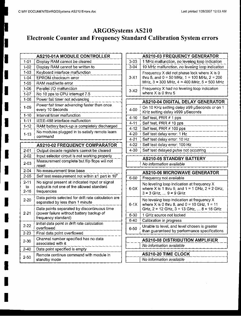
ARGOSystems AS210Electronic Counter and Frequency Standard Calibration System errors
AS21O.O1A MODULE GONTROLLER1-01 Displav RAM cannot be cleared1-02 Disolav RAM cannot be written to1-03 Keyboard interface malfunction1-04 EPROM checksum error1-05 RAM read/write error1-06 Parallel l/O malfunction1-07 No 10 pps to CPU interrupt 7.51-08 Power fail timer not advancinq
1-09 Power fail timer advancing faster than onceevery 10 Seconds
1-10 lnterval timer malfunction1-11 I EEE-4BB interface malfunction1-12 RAM batterv back-up is completely discharqed
1 -13 No modules plugged in to satisfy remote learncommand
AS21 O.O2 FREQUENCY COMPARATOR2-01 Output decade registers cannot be cleared2-42 Input selector circuit is not workinq properlv
2-03 Measurement complete but flip flops will notreset
2-04 No measurement time base2-05 Self test measurement not within t1 part in 10"2-11to
2-16
No signal present at indicated input or signaloutput is not one of the allowed standardfrequencies
2-20 Data points selected for drift rate calculation areseparated by less than 1 minute
2-21Data points separated by discontinuous time(power failure without battery backup offrequency standard)
2-22 lnitialdata point in drift rate calculationoverflowed
2-23 Final data point overflowed
2-30 Channel number specified has no dataassociated with it
2-40 Data point specified is emptv
2-50 Remote continue command with module instandby mode
AS21 O.O3 FREQUENCY GENERATOR3-03 1 MHz malfunction, no levelinq loop indication3-04 10 MHz malfunction, no leveling loop indication
3-X1Frequency X did not phase lock where X is 0thru 5, and 0 = 50 MHz, 1 = 100 MHz,2 = 200MHz, 3 = 300 MHz, 4 = 400 MHz, 5 = 500 MHz
3-X2 Frequency X had no leveling loop indicationwhere X is 0 thru 5
AS21O-04 DIGITAL DELAY GENERATOR
4-00 On 10 KHz setting delay >99 pSeconds or on 1KHz setting delay >999 pSeconds
4-10 Self test, PRR # 1 pps4-11 Self test, PRR # 10 pps4-12 Self test, PRR I 100 pps4-20 Self test delay error: 1 Hz4-21 Self test delav error: 10 Hz4-22 Self test delay error: 100 Hz4-30 Self test delayed pulse not occurrins
AS21 O.O5 STANDBY BATTERYNo i nform atio n avai I able
AS21O.O8 DISTRIBUTION AMPLIFIERNo information available
AS21O-20 TIME CLOCKNo information available
AS21 0-06 MICROWAVE GENERATOR6-00 Frequency not available
6-0xNo leveling loop indication at frequency XwhereX is 1 thru 9, and 1= 1GHz,2=2GHz,3=3GH2 , . . . 9 -9GHz
6-1XNo leveling loop indication at frequency Xwhere X is 0 thru B, and 0 = 10 GHz,1 = 11GHz,2= 12GHz,3 = 13 GHz, . . . B = 18 GHz
6-30 1 GHz source not locked6-40 Calibration in prooress
6-50 Unable to level, and levelchosen is greaterthan guaranteed by performance specifications
AS 21AA-PM
PORTABLE MAINFRAMEt:lrIIIIIIIII
Revised 8/84
IIirIIIIII1..
;
IIIIII
Al'l r ights reserved. No part of this publication nay bereproduced, stored in a retrieval system, or transmitted,in any forrn or by any means, electronic, mechanica'l ,photocopying, recording and/or othenrise without theprior written permission of ARGOSystens, Inc. This man-ual may not be lent, resold, hired out or othen'vise dis-posed of by way of trade in any form of binding or coverother than that in which i t is publ ished, 'wi thout theprior consent of ARG0Systems, Inc.
ARG0Systems, Inc. / 884 Hermosa Court , Sunnyvale, Cal i fornia 94086Telephone (Area Code 408) 737-2000 / Telex No. 352077
lvl83-0004
5-35-35-45-45-65-8
IIll
IIIIIIIITIIIIIII
M83-0004
Chapter
TABLE OF CONTENTS
Ti t le
Preface
GENERAL INFORMATION
1-l Introduct lonL-Z AS2IOA-PM Physica'l and Electrical Description
INSTALLATION
2-l Introduction2-? AS210A-PM Locking Bar Removal and Instal lat ion
Procedure
OPERATION
3-1 Introduction3-2 AC Operat ing Vol tage Select ion
THEORY OF OPERATION
4-L Introduction!-2 DC Voltage Suppl ies4-3 External Reference Selector Circuit, M
MAINTENANCE AND CALIBRATION
5-1 Introduction
SECTION I5-2 Preventive Maintenance
SECTION I I5-3 Performance Testing5-4 Internal Frequency Standard Accuracy Test5-5 Test Procedure5-6 Internal Freguency Standard Drift Test5'7 Test Procedure }{hen using AS210-01 Module contro'l ' ler5-8 Test Procedure !{hen using nszto-oln Moduie controller
SECTION I I I5-9 Cal ibrat ion/Al ignment procedures5-10 AS210A-PM Portable Mainframe Disassembly procedure
for Power Module Renoval and Installati ln5-11 Access to Mainframe Circui ts5'L2 As210 Internal Frequency standard cal ibrat ion
Page
v
1-1
1-11-1
2-l
2-L
2-L
3-1
3-13-1
4-1
4-14-14-3
5-1
5-1
5-2
5-9
5-95-1 I5 -12
- i -
MB3-0004
II
.-lChapter I
IIIIT
,l: : '
IIIIIII
'l
6
TABLE OF CONTENTS (Continued)
T i t l e
5-13 AS210 Internal Rubidium Standard Output FrequencyAdjustment
5-14 AS210 Tine Base Selector Phase-Locked 0scil latorAl ignment Procedure
SECTION IV5-15 Troubleshooting Procedures5-16 Power Supply Fai lure5-I7 Compensation of Crystal Aging
ILLUSTRATED PART LIST
6-l Introduction6-2 Manufacturer's List Code to Nanre
Page
5-14
5-14
5-165-165-16
6-1
6-16- 15
t- l l -
II
tt
l'IIIIIII
lvl83-0004
PageFi gure
1 .1
3 .1
4 .1
5 .1
5 .2
5 .3
5 .4
5 .5
5 .6
5 .1
6 .2
6 .3
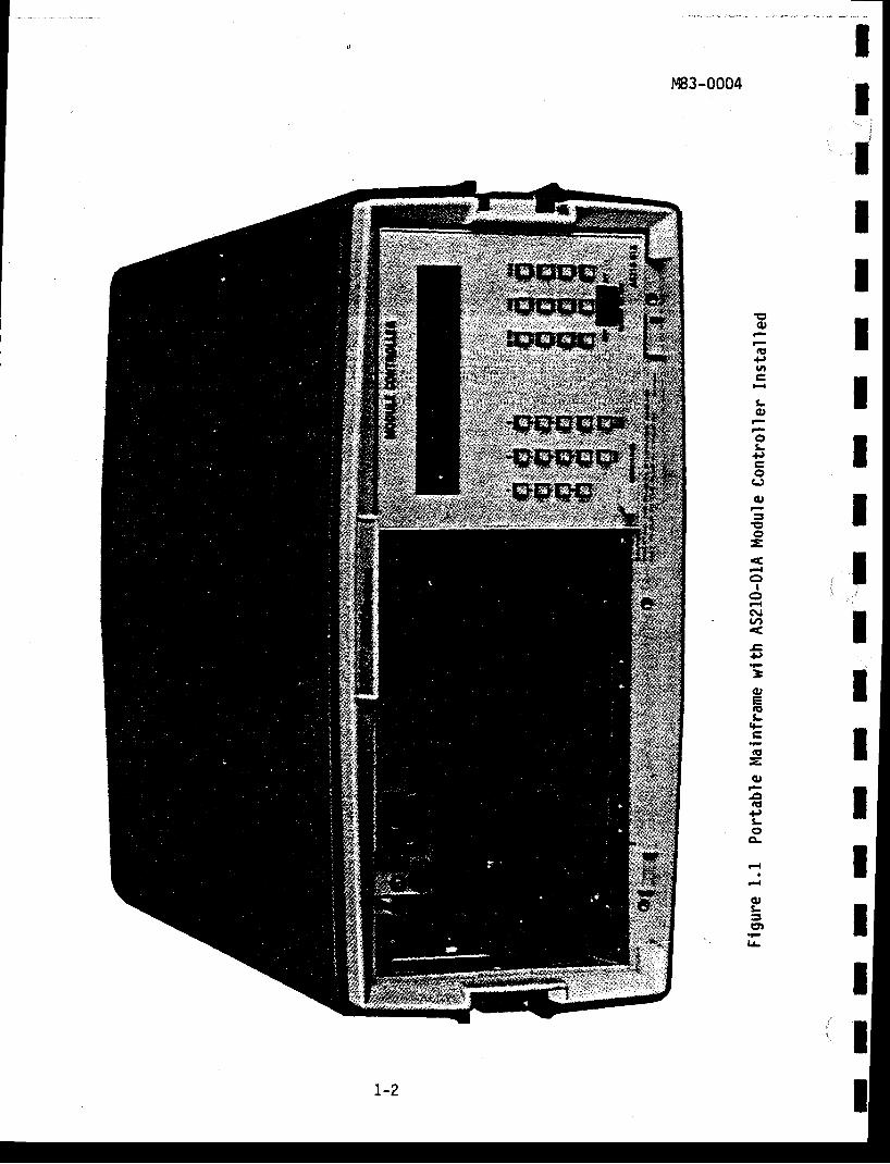
Portable Mainframe with AS210-01A Module control ler Instal led l -?
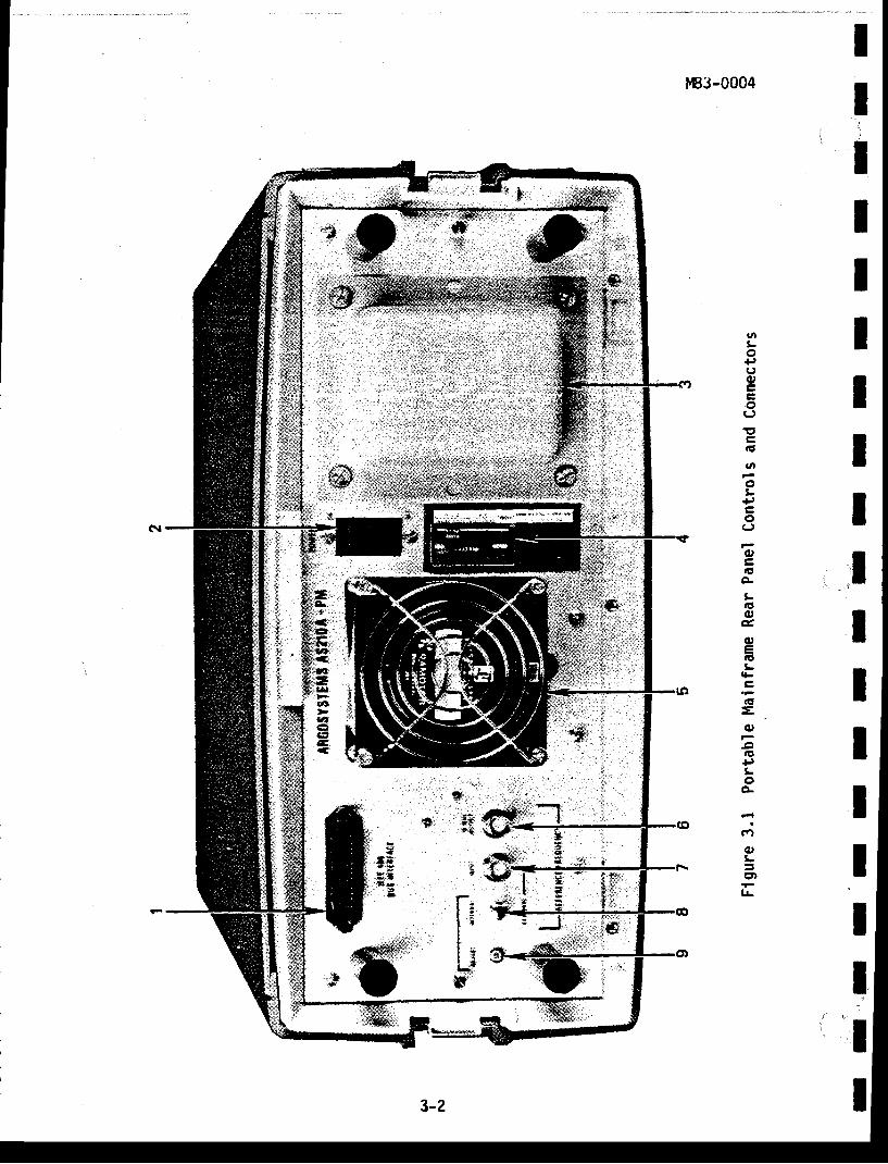
Portable Mainframe Rear Panel Controls and Connectors 3-2
AS210A-PM Functional Block Diagrarn 4-z
AS210 Internal Frequency Standard Test Configuration 5-s
As210 lnternal Frequency standard Drift Test configuration s-7
Flow Diagram of the Calibration/Alignment Procedure for
LIST OF FIGURES
Ti t l e
the AS210 System Mainfrane
B'lock Diagram of Rubidiun Frequency Standard CalibrationConfi gurati on
Power Modu'le l ' | ir ing Diagram
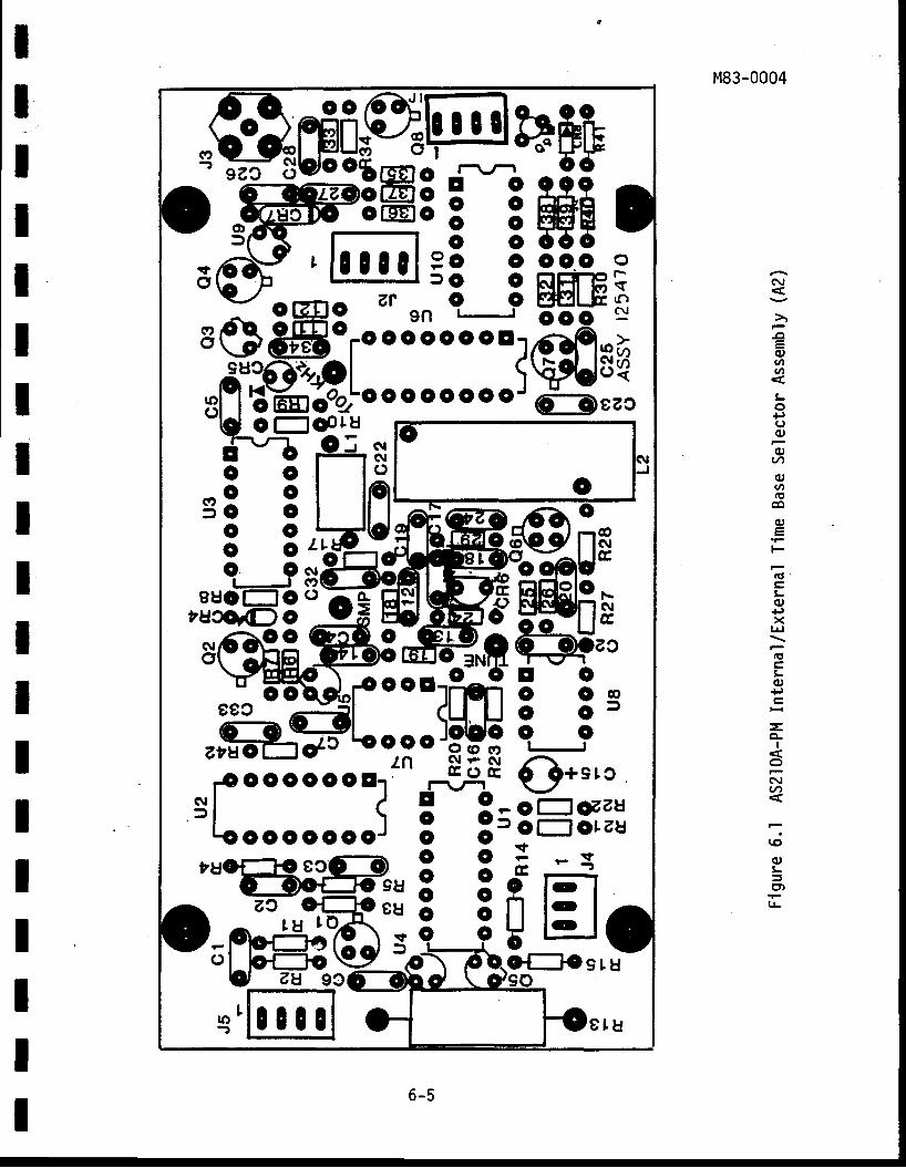
Internal/External Tinn Base Selector Assenrbly A2,Schematic Diagran
AS210A-PM Internal/External Tine Base Selector Assembly A2
AS210A-PM Portable Mainfranre Assenbly
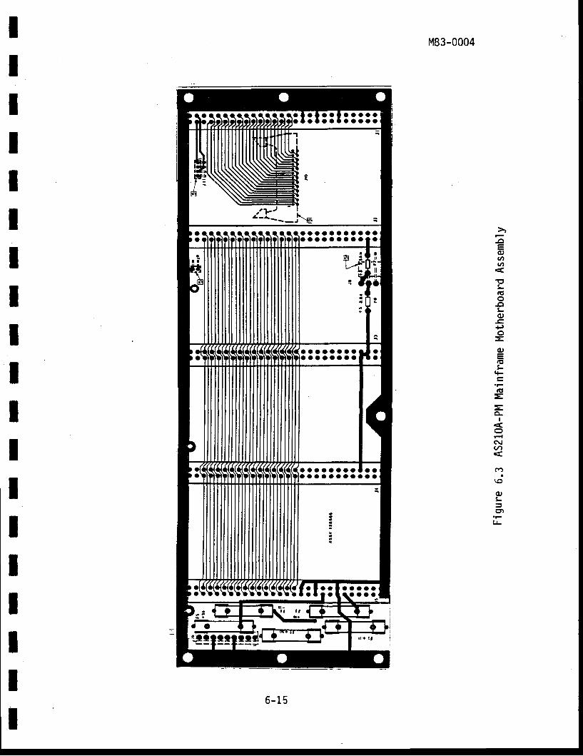
AS210A-PM l'lai nframe }lotherboard Assembly
IIIITIIII
5-10
5-13
5-18
5-19
6-5
6-L2
5-15
- l I I -
Tabl e
1-1
3-1
5-1
5-2
5-3
5-4
5-5
5-6
AS210 Mainframe Specificailons
AszlOA-PM Portable Mainfrane controls and connectors
Preventive Maintenance Checks and Services
lequired Test Equipnrent for the Internal FrequencyStandard Accuracy Test
Required Test Equipnrent for the Internal FrequencyStandard Drift Test
I.:!. Equipnent for the Aszl0 Internal Frequency standardCal ibrati on Confi guration
Test Equipment for Alignnent of the External rime BaseSelector Phase-Locked Oscil lator
Error Code Listing
LIST OF TABLES
Ti t le
M83-0004
Page
5-4
5-14
5-15
5-17
1-4
3-3
5-2
tI1
IIItIIIIIIIIIIIII
5-3
- 1 V -
tIl'III
M83-0004
PREFACE
manual 'contains the operat ion and maintenance instruct ions forPortab'le Mainframe. The data contained herein is arranged as
General Informatlon
I nstal I ati on
Operation
Theory of Operation
Cal ibrat ion and Maintenance
I l lus t ra ted Par ts L is t
tI
Thi s
the AS210A-PM
fol I ows:
Chapter 1
Chapter 2
Chapter 3
Chapter 4
Chapter 5
Chapter 6
Reference Publ ications
AS210-01A
AS210-02
AS210-03
AS210-04
AS210-05
AS210-06
AS210-08
AS210-20
ItIIIIII
Module Control ler 0peration and Maintenance Hanual
Frequency Conparator 0peration and Maintenance Manual
Frequency Generator 0peration and Maintenance Manual
Digital Delay Generator 0peration and MaintenanceStandby Battery Operation and Maintenance lt ianual
Microwave Generator 0peration and llaintenance Manual
D is t r ibu t ion Ampl i f i e r Opera t ion and Ma in tenanceTime Clock 0peration and Maintenance Manual
Manual
Manua l

IItIIIIIIIIIIIIIIIt
t-2
IIIIIItIIIIItIII
M83-0004
CHAPTER 1
GENERAL INFORMATION
1-1 INTRODUCTION
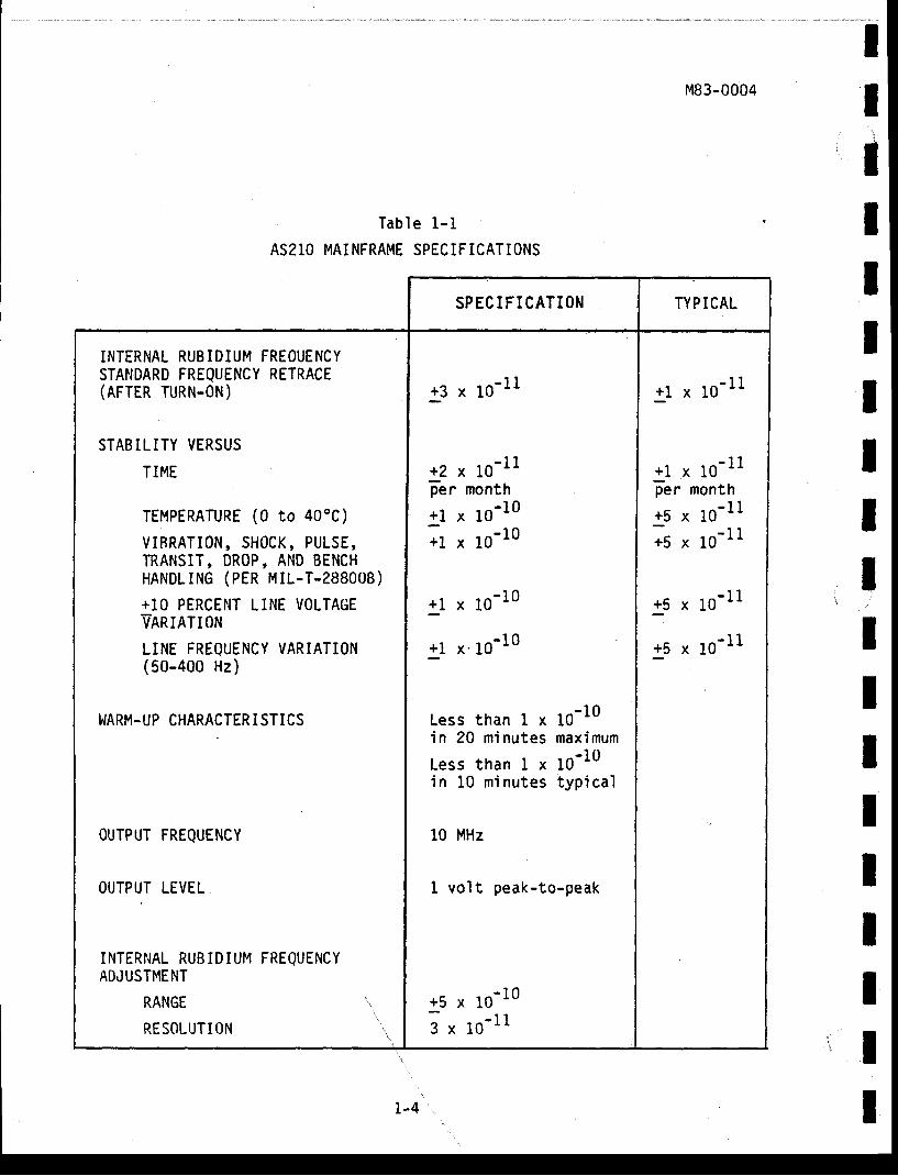
The heart of the AS210 Electronic Counter and Frequency StandardCalibration System is the AS210A-PM l{ainframe shown in Figure 1.1. TheAS210A-PM Portab'le l ' lainframe can support the double width AS210-01A Modu'leControl ler and three single width AS210-type plug- ins. The highly accuratnRubidium frequency standard that provides the tinre base for the system's fre-quency measurement circuits is housed within the rnainframe. The rnainfraneand all plug-in modules are completely progranmable through .an IEEE-488interface. The AS210-01A and other plug-in modules of the AS210 series aredescribed in separate manuals available from ARGOSystems.
ASzlOA-PM PHYSICAL AND ELECTRICAL DESCRIPTIOiI
The AS210A-PM Portable Mainframe consists of two main pieces: arugged chassis with covers and a power nodule assembly. The povrer moduleslides into the rear of the chassis and is secured by two captured mountingscrews. AS2l0-type modules are inserted into the front of the chassis tomate with the poyter module. The AS210A-PM Portable Mainfrane wil l sl ideeas i l y under an a i r l ine seat wh i le t rave l ing .
The portable nainframe chassis includes a module locking bar whichprevents the modules from sliding out, front and rear covers to piotect theinstrument during travel, and a convenient heavy-duty carrying handle. Thepower module contains the highly accurate rubidium frequency standard, powersupply, internal /external t ime base selector c i rcui t ry, and the motherboard.The internal/external t ime base selector assembly pennits the ASZ10 systemto be phase- locked to an external f requency.standard
I
M83-0004 -
IItIII
IIIIIIII
Eo
rtt+,UIE
Lo
oL+)goc)o
!o=
oI
ocl. a/,
+)
-gEqt!
g
G'=(u
AGl+tt-oo-
(uL
CD
Lr.
L.?
M83-0004
The blower fan and power transformer are located on the rear panel.
Connectors and controls located on the rear panel are a 10 MHz reference fre-
quency output, internal/external frequency select switch, IEEE-488 interface
connector, power switch, external frequency reference input, and internal
frequency a(iustment. The power module may be removed from the.chassis and
modu les ins ta l led fo r ma in tenance purposes . . Tab le 1 -1 i s an e lec t r i ca l /
mechanica' l speci f icat ion for the nainframe in the AS210 Electronic Counter
and Frequency Standard Calibration system.
tIIIIItIIIIIIIII
II
'l
IIIIItIIIIIIIt
1l
I
M83-0004
Tab le 1 -1
AS21O MAINFRAMT SPECIFICATIONS
SPEC IF ICATION TYPICAL
INTERNAL RUBIDIUM FREOUENCYSTANDARD FREQUENCY RETRACE(AFTER TURN-oN)
STABILITY VERSUS
TIME
TEMPERAIURE (0 to 40"C)
vIBRATI0N, SHoCK, PULSE,TRANSIT, DROP, AND BENCHHANDLING (PER MIL.T-z88OOB)+10 PERCENT LINE VOLTAGETRntRrtonLINE FREQUENCY VARIATION(50-a00 Hz)
WARM.UP CHARACTER ISTICS
OUTPUT FREQUENCY
OUTPUT LEVEL
INTERNAL RUBIDIUM FREQUENCYADJUSTMENT
RANGE
RESOLUTION
t ' l
+3 x 10 - r r
+2 x lo-11!-er month+1 x 1o-10It , to-10
-10
-10
Less than tx10-10in 20 minutes maximum
Less than tx10-10in 10 minu tes typ ica l
MHz
vol t peak-to-peak
10
10X .
+1
!
10
+5x
3x
10-10
10-1 1
+1 x 10-11
+1 x 10-11p'er month+5 x 10-11is , ro-11
+5 x 1o-11
+5 x 10-11
l-4
M83-0004
l:llll,
IItIIIIII
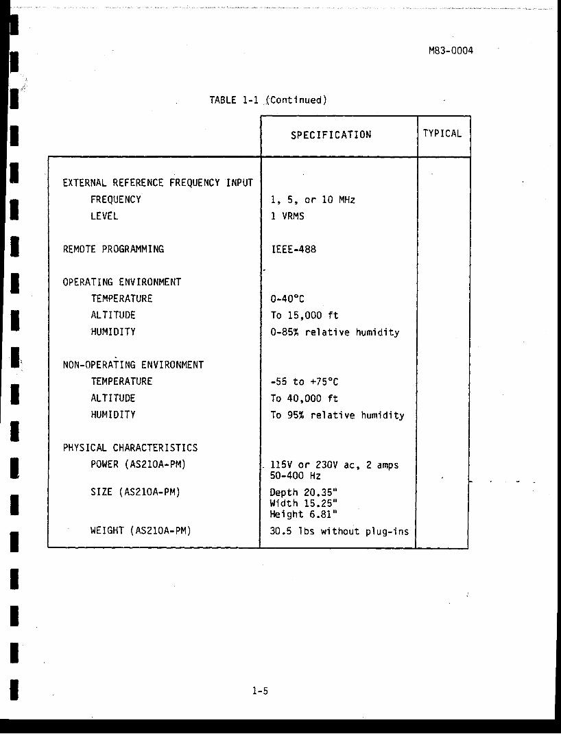
TABLE 1-1 _(Cont inued)
SPECIF ICATION TYPICAL
EXTERNAL REFERENCE FREQUENCY INPUT
FREQUENCY
LEVEL
REMOTE PROGRAMMING
OPERATING ENVIRONMENT
TEf-lPERATURE
ALTITUDE
HUMIDITY
NoN-oPERAit Nq ENvtRoNMENT
TEMPERATURE
ALTITUDE
HUI4IDITY
PHYS ICAL CHARACTERISTICS
P0WER (AS210A-PM)
srzE (Asz10A-PM)
t , lETGHT (AS210A-PM)
1 , 5 , o r 10
1 VRMS
MHz
IEEE.488
0-40"cTo 15,000 f t0-85% rel at'i ve humi di ty
-55 to +75"C
To 40,000 ft
To 95% relat ive humidi ty
1 l5V or 230V ac ,50-400 Hz
Depth 20 .35"w id th 15 .25uHei gh t 6 .81 u
30.5 lbs w i thout
2 amps
p l ug - i ns
1-5

I:,,J'l
IIIIIIIIIIIItI,l
I
rl
IItIIII
I
M83-0004
CHAPTER 2
INSTALLATION
2-L INTRODUCTION
The AS210A-PM Portable Mainfrane supports modules of the AS210
ser ies. Power and signal interface is provided to the modules automat ical ly
when they are plugged ln. The malnframe has a self-contained poyrer supplyand requires a source of 115 Vac prime power. The rear panel has a BNC con-nector for an external reference frequency standard. l'lhen an external stand-ard is used, the rear panel INT/EXT switch is set to the EXT position. TheAS210-05 Standby Battery Module may be installed on-line to supply power to
the rubidiun frequency standard and the AS210-20 Tine Clock Module for aminimun of three hours durlng ac power interruptions,
CAUTION
Do not attempt instal lat ion ofTektronix plug-in modules inthe AS210 Mainfrane. Severedamage to plug-in and mainframewi l l resu l t .
?-2 AS21OA-PM LOCKING BAR REMOVAL AND INSTALLATION PROCEDURE
The AS210A-PM Por tab le Ma in f rame lock ing bar i s use fu l du r ingtransit to secure the modules of the AS210 system in the mainframe. Toremove the locking bar, s inply loosen the three retaining screws across theface of the locking bar and remove. To instal l the locking bar, reverse f .he
above procedure.
2-t

IIIIII
itI
l
tIIIIII
.lI
Il''III
III
M83-0004
CHAPTER 3
OPERATION
3-1 INTRODUCTION
}IARNING
Be sure that there is at leastthree inches clearance betweenthe fan of the nainframe andany obstruction, before oper-a t ing the ins t runent .
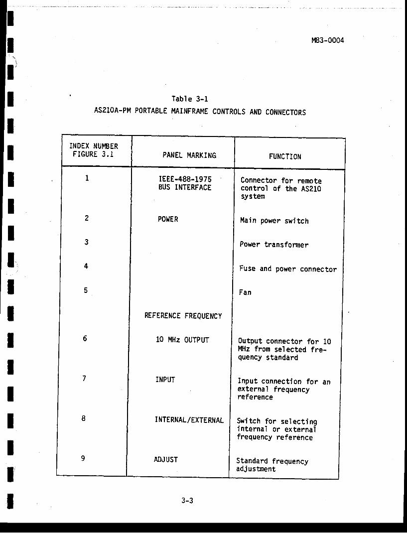
The AS210A-PM Portable Mainframe performs no functions by itself.Detai ls of operat ion for the various plug-in modules are contained in a sep-arate publication (see Preface). The only operator interface with the nain-frame is the internal/external reference switch which is used to select thefrequency reference. Figure 3.1 is the il lustration of the AS210A-PM port-able Mainframe rear view. Table 3-1 describes the controls and connectors ofthe AS210A-PM and is keyed to Figure 3.1.
3-2 lc 0PERATING V0LTAGE SELECTIoN
0n the AS210A-PM rear pane l , the fuse and vo l tage se lec to r i slocated to the r ight of the fan. See Figure 3.1 and Table 3-1.
To select the ac operat ing vol tage, s l ide the plast ic cover open onthe voltage.selector and rotate the fuse-pul' l down. Remove the fuse andvol tage select board. Posi t ion the vol tage select board so that the desiredpr inted vol tage is on the top' lef t s ide of the board. Push the board f i rmlyinto the module s lot . Rotate the fuse-pul l back into normal posi t ion andinstall the proper value fuse. The AS210A-PM Mainframe is now ready foropera t ion .
IItIIt
3-1
IIIIIIII
la3-0004
IIIII
,nLo.P(){,Bo
c.)
EgG'
rnoL+,goc)
(t)gc'a-!ra(ue(l,
.ttLg
.E=o
,llPtoo-
(r1
oL
ED
lr
.,fII
II
M83-0004
Tab le 3 -1ASzIOA-PM PORTABLE MAINFRAI'IE CONTROLS AND CONNECTORS
3-3
l:Itlrl1
ItIIIIIl'I
INDEX NUMBERFIGURE 3 . I PANEL MARKING
rEEE-488-1975BUS INTERFACE
REFERENCE FREQUENCY
10 l-lHz OUTPUT
INTERNAL/EXTERNAL
Connector for remotecontrol of the AS210system
Main power switch
Power transfonner
Fuse and power connector
Fan
Output connector for l0MHz from selected fre-guency standard
Input connection for anexternal frequencyreference
Switch for select inginternal or externalfrequency reference
Standard frequencyadjustment

IttIIIIItIIItItIIIt
4-1
tIIIIIIIIIIIIIII
M83-0004
CHAPTER 4
THEORY OF OPERATION
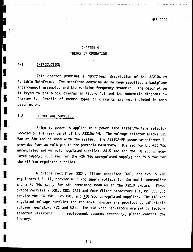
INTRODUCTION
This chapter provides a functlonal description of the ASZI0A-pt4Portable Malnframe. The mainfrarne contains dc vol tage suppl les, a backplaneinterconnect assembly, and the rubidium frequency standard. The descriptionis keyed to the block diagrarn in Figure 4.1 and the schematic diagrams inChapter 5. Detai ls of comnon types of c i rcui ts are not included in th isdescri ption.
4-2 DC VOLTAGE SUPPLIES
Prime ac power is appl ied to a power l ine f i l ter /vol tage selectorlocated on the rear panel of the AS210A-PM. The voltage selector allows 115Vac or 230 Vac be used with the system. The AS210A-PM power transformer TLprovides four ac voltages to the portable mainframe: 9.9 Vac for the +ll Vdcunregulated and +5 vo'lt regulated supplies; 24.5 Vac for the +31 Vdc unregu-lated supply; 20.5 Yac for the +26 Vdc unregulated supply; and 39.5 Vac forthe {8 Vdc regulated suppl ies.
A br idge rect i f ier (CR3), f i l ter capaci tor (C4), and two +5 Vdcregu' lators (Ug-u+), provide a +5 Vdc supply vol tage for the rnodule control lerand a +5 Vdc suppy for the remaining modules in the AS210 system. Threebr idge rect i f iers (CRl, CRz, CR4) and four f i l ter capaci tors rcL, CZ, C3, CS)provide the +31 Vdc, +26 Ydc, and +18 Vdc unregu'lated supp'l ies. The +lg Vdcregulated vol tage suppl ies for the AszlO system are provided by adjustablevol tage regulators (Ul and U2). The +18 vol t regulators are set by factoryselected resistors. If replacement becomes necessary, please contact thefactory.
IM83-0004
IIIItIIIIIIIIII
|q
0rto
a
Jt)o
,oco
(J
=
=o-I
SJu1
sl'
(lJ
gt
= Fo x
f . -ssd;-:-
o
o
ul(,zu,Eul
utE
rIFIL
7it.
2Hq! ! dE3+
:!EEHef H",:
IIIII
M83-0004
4-3 EXTERNAL REFERENCE SELECTOR CIRCUIT
The AS210 system can be used with the 10 MHz internal rubidiumfrequency standard or an external f requency standard of 1,5, or 10 MHz. Theexternal reference frequency input is located on the rear panel of the main-frame. The external reference signal is accepted automatically by the timebase circuitry when the reference frequency select switch is in the EXT posi-
t ion. The external reference signal is d iv ided by 100 in f requency div iderUl and shaped into a 250 nanosecond pulsewidth s ignal by one-shot U2 forapplication to phase detector U3. The phase detector compares the inputstandard signal with a ramp signal produced by the VCO so that the VCO islocked to the standard. The 10 MHz VCO output is div ided by 100 in dualdecade div ider U5. The output of U6 (100 kHz) dr ives ramp generators Q3, Q4.The VCO output is app'l ied to a reference selector gate which is controlled b-vthe rear panel INT/EXT reference switch. The signal from the pulse shaper isalso avai lable to the microprocessor. I f the reference frequency se1ectswitch is in the EXT posi t ion, and no signal is appl ied to the external f re-quency reference input, an effor message is generated. When the referencefrequency select switch is in the. INT position, control transistors Ql and Q5turn the power off to the external reference frequency circuitry. In theexternal position, the +26 Vdc voltage supply for the rubidium frequencystandard is disconnected so that interference does not occur to the VCOoutput.
I
IIIIIITIIIt

II1
ItIIIIIItIIIIIIII
tI
l
II
M83-0004
CHAPTER 5MAINTENANCE AND CALIBRATION
5-1 INTRODUCTION
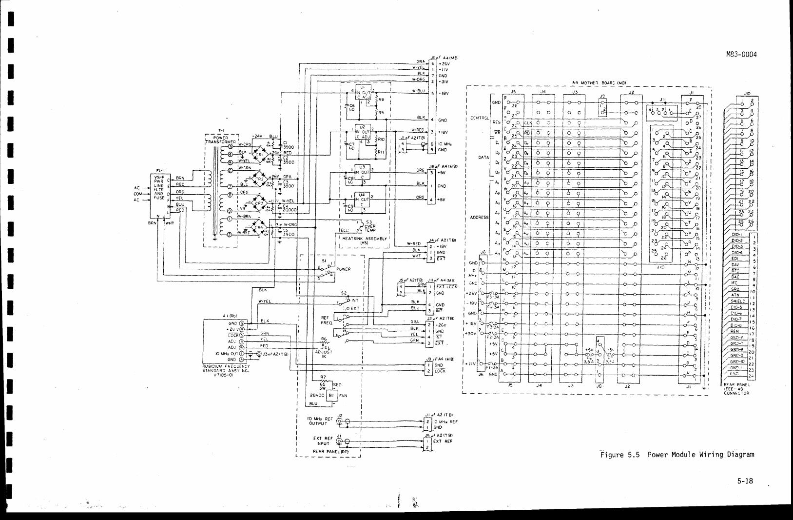
The purpose of th is chapter is to provide maintenance and cal ibra-tion data for the AS210A-PM Portable Mainfrarne. Sectiorr I covers routinepreventive naintenance procedures. Section II outtines performance tests forthe mainframe. Sect ion I I I contains the cal ibrat ion/al ignment procedures,and Sect ion Mescr ibes t roubleshoot ing data. Figures 5.5 and 5.6 are theschematic diagrans for the AS210A-PM. P'lease contact the factory for anyass is tance requ i red in the ma in tenance o r se rv ic ing o f the ma in f rames .
tIIIIItIIIIII
5-1
M83-0004
SECTION I
5-2 PREVEiITIVE MAINTENANCE
Table 5-1 l ists preventive maintenance checks and services whlchshould be performed regularly.
Table 5- l
PREVENTIVE MAINTENANCE CHECKS AND SERVICES
IIIIIIIIIIIIII
ITEM PROCEDURE
CABLES
CLEANLINESS
CORROSION
PRESERVATION
Visual ly inspect cables for strained, cut , f rayed, orothenvise damaged insulation.
Make sure the exterior surfaces of the unit are clean.I f necessary , c lean ex te r io r su r faces as fo l l ows :A. Renove the dust and loose dirt with a clean soft
c l oth.
B. Renove dust or dirt from p'lugs and jacks with abrush.
i . - . WARNING
Use only wann soapy water forc'leaffif ' all plastic parts.
' Many sofvents'wil l cairse theplastic to becorm brltt le.
Make sure exterior surfaces of unit are free of rustand corrosion,
Inspec t ex te r io r su r faces o f the un i t fo r ch ippedpaint or corrosion. I f necessary, spot-paint surfacesas fo l lows:
A. Renove rust and corrosion from metal surfaces byl ight ly sanding then with sandpaper.
B. Brush two coats of paint on base metal to protecti t f ron fur ther corrosion.
5-2
Il'III
M83-0004
SECTION I I
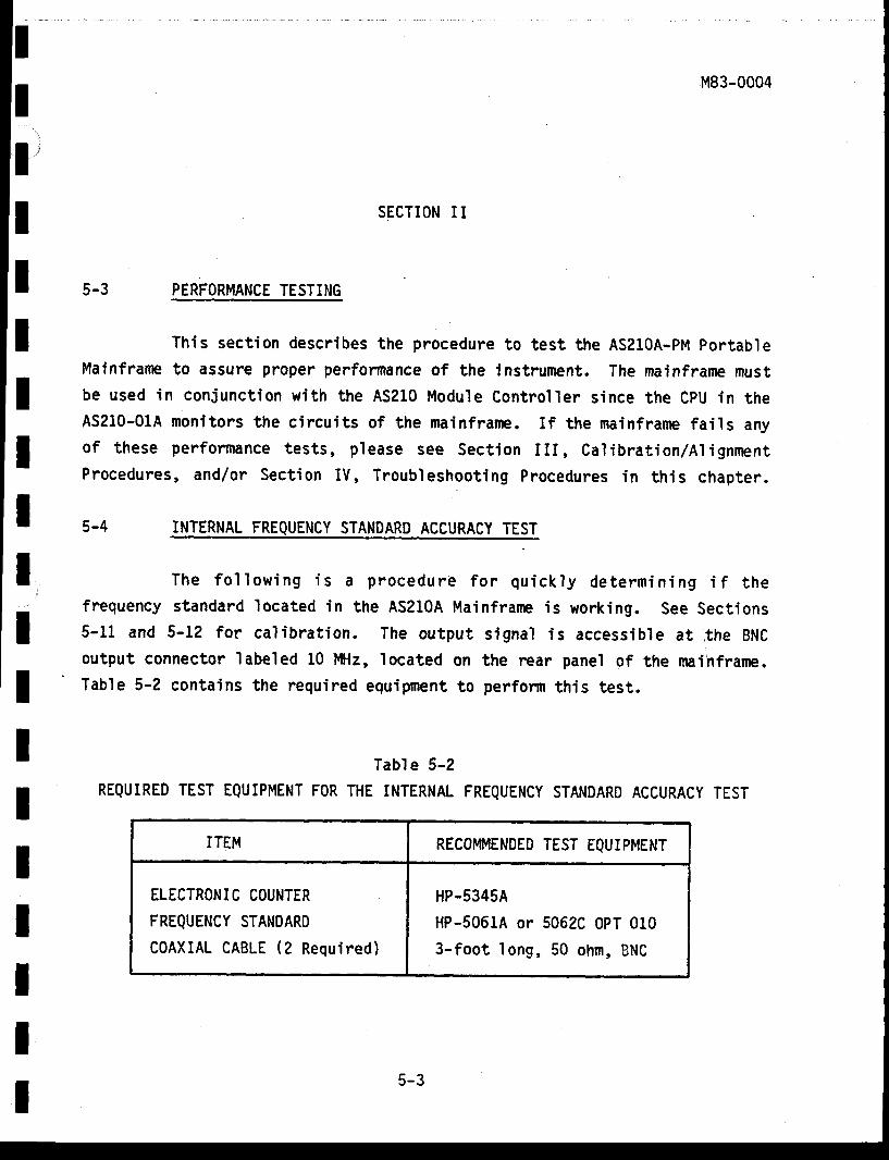
5-3 PERFORMANCE TESTING
This section describes the procedure to test the AS210A-PM Portab'leMainframe to assure proper perfornance of the instrument. The mainframe mustbe used in conjunct ion wi th the AS210 Module Control ler s ince the CPU in theAS2I0-01A nonitors the circuits of the rnainframe. If the mainframe fails anyof these performance tests, p lease see Sect ion I I I , Cal ibrat ion/Al ignmentProcedures, and/or Sect ion IV, Troubleshoot ing Procedures in th is chapter.
LNTERNAL FREQUENCY STANDARD ACCURACY TEST
The fo l low ing i s a p rocedure fo r qu ick ly de te rmin ing i f thefreguency standard located in the AS210A Mainfrann is working. See Sections5-11 and s-t? for cal ibrat ion. The output s ignal is accessible at i the BNCoutput connector labeled 10 MHz, located on the rear panel of the nnainframe.Table 5-2 contains the required equipment to perform this test.
Table 5-2REQUIRED TEST EQUIPMENT FOR THE INTERNAL FREQUENCY STANDARD ACCURACY TEST
ITEM REC0I'|MENDED TEST EQUIPMENT
ELECTRONIC COUNTER
FREQUENCY STANDARD
C0AXIAL CABLE (2 Required)
HP-5345A
HP-5061A or 5062C OPT 010
3-foot long, 50 ohm, BNC
I
5-4
IIIIII
5-3
tt
M83-0004
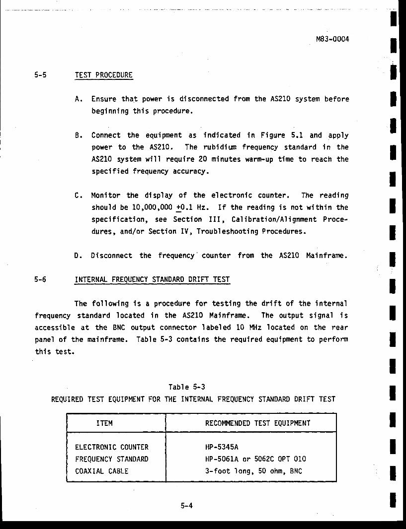
5-5 TEST PROCEDURE
A. Ensure that power is disconnected fron the AS210 system before
beginning this procedure.
B. Connect the equipment as indicated in Figure 5.1 and applypower to the AS210. The rtbidium frequency standard in the
AS210 systen wil l require 20 minutes v{arm-up time to reach the
specified frequency accuracy.
C. Monitor the display of the electronic counter. The reading
should be 10,000,000 +0.1 Hz. I f the reading is not wi th in the
speci f icat ion, see Sect ion I I I , Cal ibrat i on/Al ignnent Proce-
dures, and/or Sect ion IV, Troubleshoot ing Procedures.
D. Disconnect the freguency'counter from the AS210 Mainframe.
INTERNAL FREQUENCY STANDARD DRIFT TEST
The following is a procedure for testing the drift of the internal
frequency standard located in the AS210 Mainfranp. The output signal is
accessible at the BNC output connector labeled 10 l0lz located on the rear
panel of the mainframe. Table 5-3 contains the required equipment to perforrn
this test .
Table 5-3
REQUIRED TEST EQUIPMENT FOR THE INTERNAL FREQUENCY STANDARD DRIFT TEST
ITEM RECOI'IMENDED TEST EQUIPMENT
ELECTRONIC COUNTER
FREQUENCY STANDARD
COAXIAL CABLE
HP-5345A
HP-5061A or 5062C OPT 010
3-foot long, 50 ohm, BNC
It
a
I
IIIItII5-6
tIttIIIIIIIIIIIIItI
M83-0004
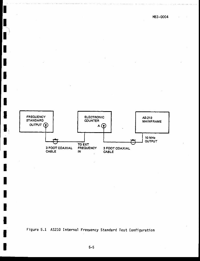
FREOUENCYSTANDARD
ELECTRONICCOUNTER
AS210MAINFRAME
10 MHzOUTPUT
3 FOOT COAXIALCAELE
TO EXTFREOUENCYIN
3 FOOTCOAXIALCASLE
Frequency Standard Test ConfigurationF igure 5 .1 AS210 In te rna l
5-5
M83-0004
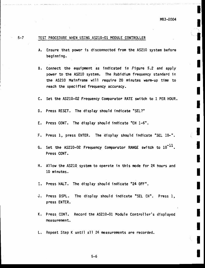
5-7 TEST PROCEDURE WHEN USING AS21O-01 MOOULE CONTROLLER
A. Ensure that power is disconnected from the AS210 system before
begi nni ng.
B. Connect the equipment as indicated in Figure 5.2 and applypower to the AS210 system. The Rubidium frequency standard in
the AS210 Mainframe will reguire 20 minutes warm-up tine to
reach the specified frequency accuracy.
C. Set the AS210-02 Frequency Comparator RATE switch to I PER H0UR,
D. Press RESET, The display should indicate "SEL?"
E. Press C0NT. The display should indicate "CH 1-6".
F. Press 1, press ENTER. The display should indicate "SEL 10-".
G. Set the AS210-02 Frequency Comparator RANGE switch to 10-11.
Press CONT.
H. Allow the AS210. system to operate in this rnde for 24 hours and10 minutes.
I . Press HALT. The display should indicate "24 OFF..
J . Press OSPL. The d isp lay shou ld ind ica te USEL CH" . Press 1 ,press ENTER.
K. Press C0NT. Record the AS210-01 Module Control ler 's displayed
measurement.
L. Repeat Step K unti l all 24 measurements are recorded.
II;
ttIIIIIIIttIIIIII
M83-0004
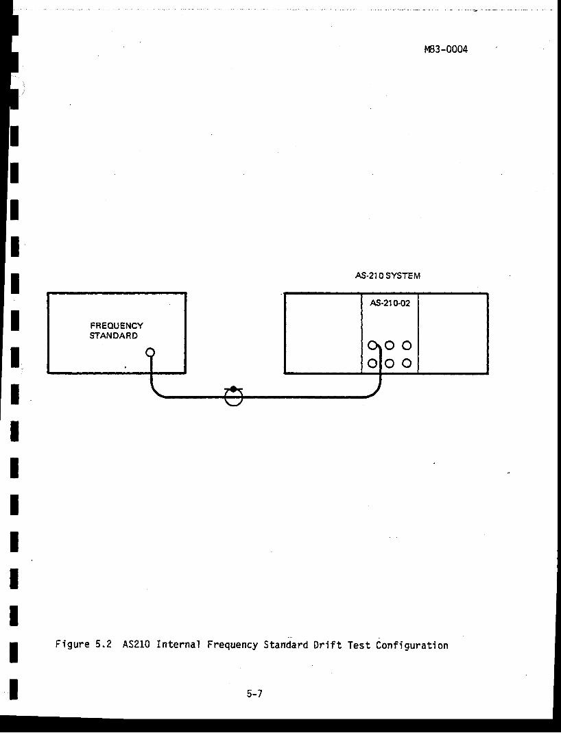
lrllIIIIIIIII
AS.21O SYSTEM
ooolo o
AS.21S02
Figure 5.2 AS210 Internal Frequency Standard Dr i f t Test Conf igurat ion
5-8
M83-0004
M. Conpute the Z4-hour AS2l0 internal frequency standard drift
rate using the following equation and the results recorded from
steps K and L.
ftt tt56
"t Y = Drift rate Per daY
wi th X i = 0 , L ,2 , . . . ,23i t 1 1 2 r 3 . . . , 2 4
Yi = As210 measurement at the ith hou"
- IY iY =ff
TEST PROCEDURE I,JHEN USING AS2IO-O1A I'IOOULE CONTROLLER
A. Repeat steps A through I of paragraph 5-7.
B. Press CALC. The display wi l l be blank.
C. Press "YEAR". .
D . The d isp lay w i l ' l i nd ica te "SEL CHn.
E. Press uC0NTu. '
F . "DP 1" w i l l appear in d isp lay .
G. Press "2" , "DP 2" w i l l appear in d isp lay .
H. Press "C0NT", last data point wi l l automat ical ly be selected.
I . Dr i f t ra te i s d isp layed in d isp lay .
IIIIIIIIItIIIIII5-8
ItIIIII
MB3-0004
SECTION I I I
5-9 CAL IBRATIONIAL IGNMENT PROCEDURES
|',ARNING
The fol lowing cal ibrat ion/al ignment procedures (Chapter! , Sect ion I I I ) and Troubleshoot ing Procedures (Chapter5, Sect ion IV) are for use by gual i f ied personnel of l ly .To avoid personal injuryn do not perform any servicingother than that of routine maintenance (Chapter 5, Sec-t ion I ) and performance test ing (Chapter 5, 'sect ion I I )unless you are qual i f ied to do so.
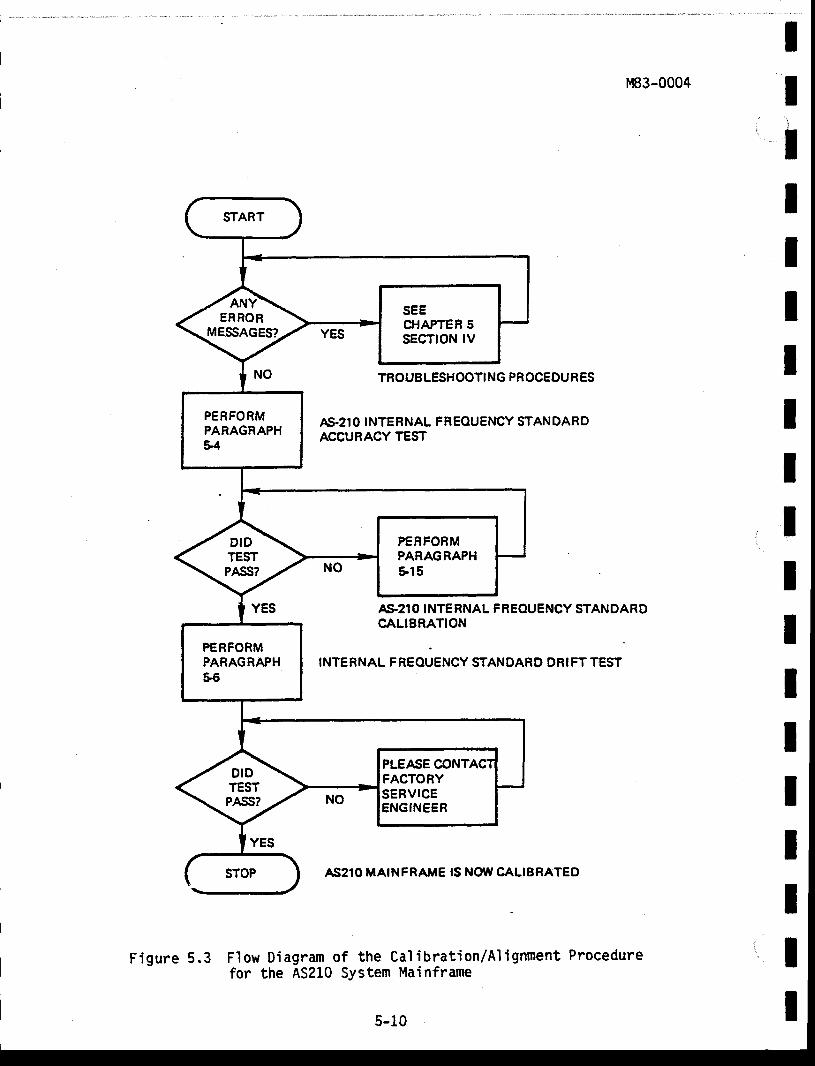
Figure 5.3 is a f ' low diagram of the cal ibrat ion/al ignment procedurefor the AS210A-PM P.ortable Mainframe. Use this flow diagram with the theoryof operat ion in Chapter 4, the text in th is chapter, and the i l lustratedparts l is ts in Chapter 5. Please note i t is not necessary to disassemble theAS210 sys tem to de te rmine i f ca l ib ra t ion /a l ignment i s needed . For anyassistance needed in perfonning this cal ibrat ion/al ignment procedure, p leasecontact the factory.
ASzlOA-PM PORTABLE MAINFRAME DISASSEMBLY PROCEDURE FOR POI.IERMODULE REMOVAL AND INSTALLATION
}TARNING
Dangerous voltages exist at several points throughoutthe power module. When the power module must be oper-ated with the chassis removed, do not touch exposedconnections or components. Disconnect power beforecleaning the system or replacing parts.
II
ITIII 5-9
SEECHAPTER 5SECTION IV
TROUB LESHOOTI NG PROCEDU R ES
AS.21O INTERNAL FREOUENCY STANDARDACCURACY TEST
A$210 INTERNAL FREOUENCY STANDARDCALIBRATION
INTERNAL F REOUENCY STANDARD DRI FT TEST
AS2IO MAINFRA'TIE IS NOTI' CALIERATED
Figure 5.3 Flow Diagram of the Cal ibrat ion/Al ignment Procedurefor the AS210 System Mainframe
5-10
AD6
IIIIIIIIIIIIIII
M83-0005
A t 5
DA!
N Q F D
l F q
R E N
E O t
6RE*TruY
b-25bla
broo
+rsv {bsH? CI
r4H?
+5V
Q I2 N Z 2 Z ? A
c r 5 R l o.o4? lK
NOTES: Unless otherwise speci f ied
l . In terpret drawing in accordancewi th s tandard prescr ibed byMI L-STD-1OO
?. A l I r es i s tance va lues a re i r ,ohms, 1,/41{, 15 percent
3 . A l l capac i t ance va lues a re i nUF
4. { -denotes s ignal ground
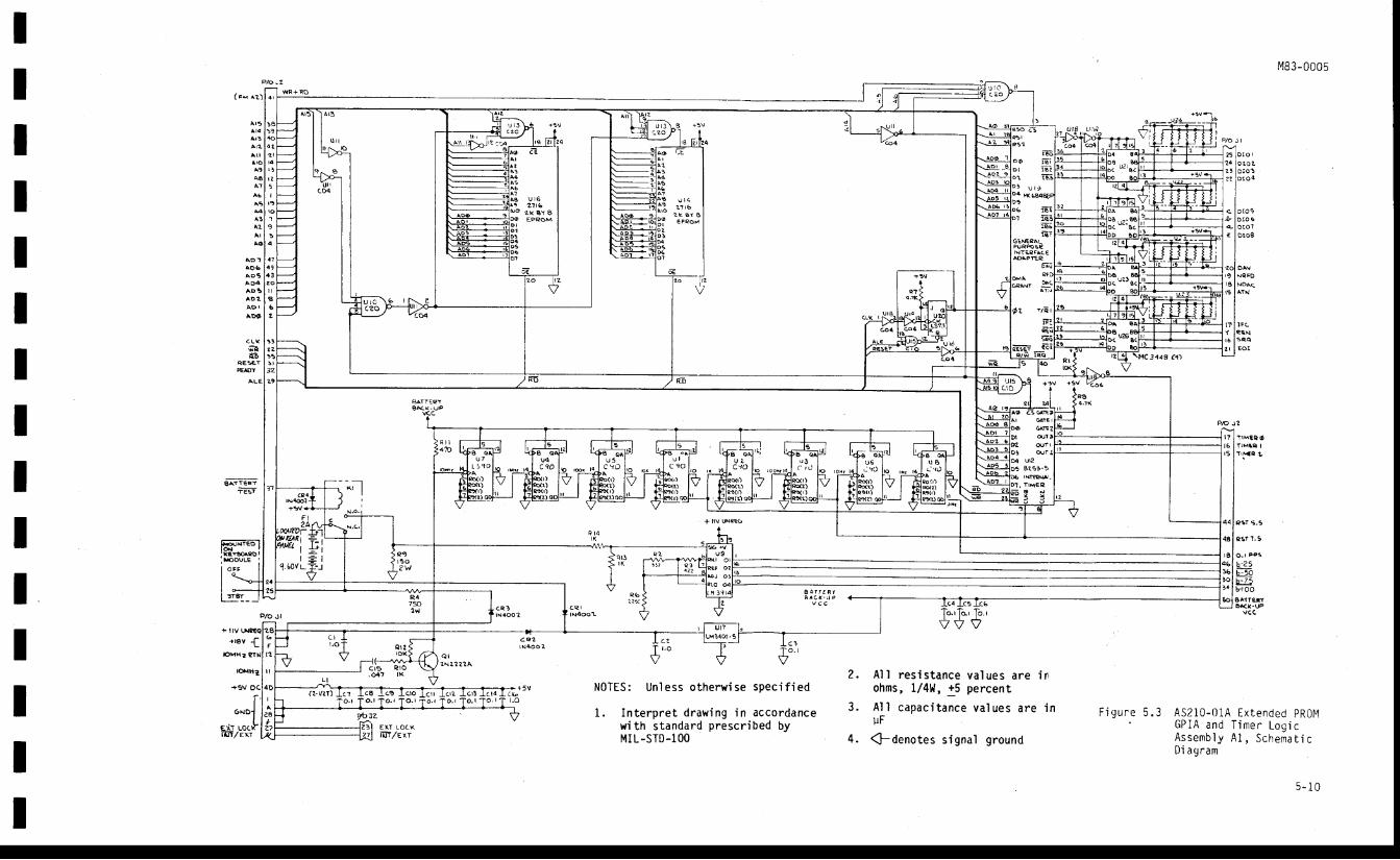
A5210-01A Ex tended PR0MGPIA and T imer - Log i cAssemb ly A1 , Sche rna t i cDi agram
F i g u r e 5 . 3EXI LOCXiEi lExr
5 - 1 0

IIIITIIItIIIIII
!20ao a5CFU
Pt6 PtO
!1 JZ
IIIIIIIIIIIt
a l 5
A r )Atz
A EAOIA O 6AD5
aoaAO?A O I
N0TES: Unless otherwise speci f ier l
l . In terpret drawing in accordancewi th s tandard prescr ibed byMI L-STD-I OO
2. A l I r es i s tance va lues a re i nohms, l,/41,f , j5 percent
MB3-0005
Al l capaci tance values are inUF
$denotes s ignal ground
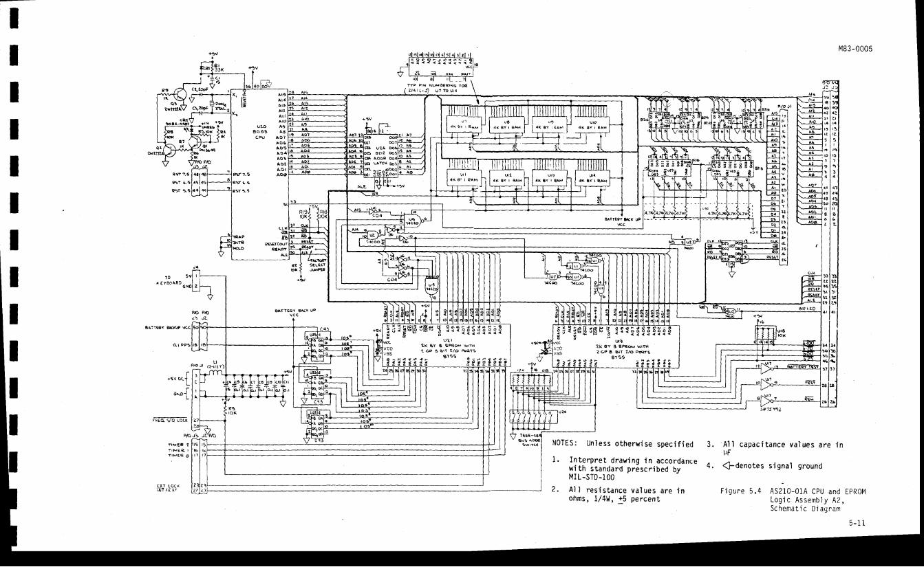
F igu re 5 .4 AS210-0 IA CPU and EPROMLog ic Assemb ly A2 ,Schemat i c D iag ram
9/Or-: l o1 , '1 Rl , rJ s1 ' "1 r-l 'r
1 ' "
l , '
l{
aftg(or9taor
TOx E Y E o A R D
6
sTlEQr ryr upv c q
n*o{
FREO 51D LOLT
PO da
n s E c 1l r M € e Ir r M E C O
' z l 6 1 6 l ' d r q ' i . l s l 4 . l : l t
J; ? e Pt* *: -Ffr!ai na orN Fr
*1i",,:]^"*5"-;X]rYP P iN NWgECIN6 FOQ2 1 4 | L - t U ? I O U l a
t . (ooj l -e I I Al5 r luz
i? i1 " f rB l |s lg t t '5 : l? ? i Er l ! i iu z l
2K gY g EFRS $jrrHy33 i i" s ",i'io ;rr
- B l 5 5 g i r n r o
d f f P F R P
i ; i ; €13 cFE, : : r l l f $ l l l ac c
d . a O J N . t t J
4 .

IIIII A O @
A D IA p 2A 0 3AO4A D 5A O 6A D ?
A l 5A5
AOe oqE
OFF
- STANOBY
BAT IN
bAT OUT
n alilaal
ItIIIII
f € 5 f
QEM
' q l - - \ - l t 4 3 r . 3 ,
| 6 . 3 . 9 . 5 l
t
l e 3 9 t l
It l?o4t4941
aql9
435zali
l l
P I
5
6
I
SEG AS E G BS E G C< E G D5 E G q
S E G D P
AO
A ZA 3BOBIb2B366
g RL?
F ii:k E > c r
R L z
O T S D Q 9
olsoQ g
D!SOC'lDr soc 6oISoRSDrsoQ +OTS DR 3o l soRzolsoc ID! lDeO
+5v DcG N D
YEARc R 8
N0TES: Unless otherwise speci f ied
1. In terpret drawing in accordancewi th s tandard prescr ibed byMIL.STD-1OO
| 2 .1 A f l LEOs a re l oca ted i n- designated swi tch
3 . A l l r es i s tance va lues a re i nohns, 1,/4W, 15 percent
4 . A l1 capac i t ance va lues a re i n
{-denotes s ignal groundAl ' l t ransis tors are PN 3644
7. 0n U5 connect Pin 4 to +5VPin 11 to ground
MB3-0005
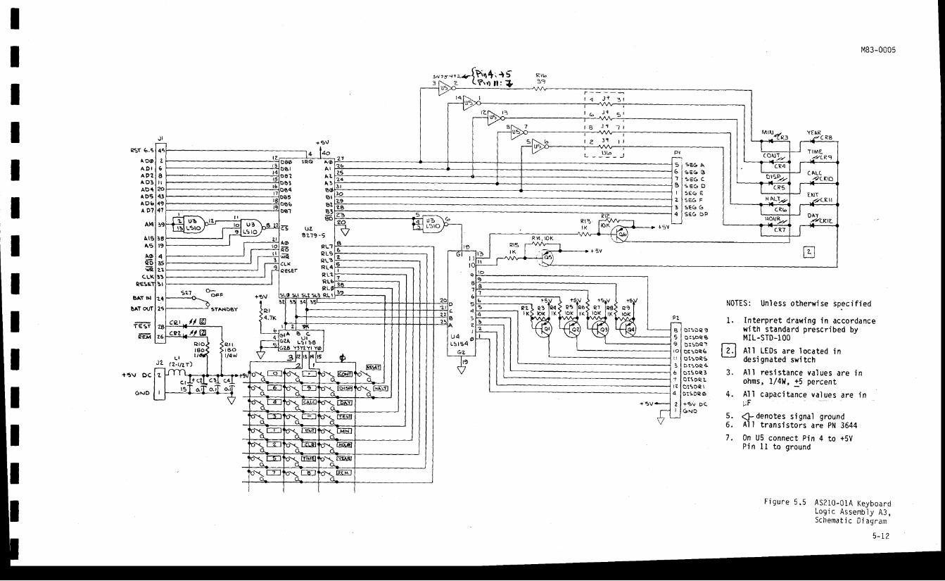
F igu re 5 .5 ASZ I0 -0 iA Keyboa rdLog i c Assemb ly A3 ,Schemat i c D i ag ram
s-12
6 .

osoaDI sCQ
DrsoclDr50€lD{s9ct
IIIIIIIItI
$to A
3€o E
sg<r (
sEO DgEO E
9eC' F
3EO 6
s€6 De
M83-0005
lol l
36
'iYFtCAL Prrl M)MglitilGFOC 01 TIrRU Urz
N0TES: Unless otherrv ise speci f ied
l . In terpret drawing in accordancewi th s tandard prescr ibed byMIL .STD- IOO.
2 . A l I r es i s tance va lues a re i no h m s , l / 8 W , 1 5 p e r c e n t .
3 . A11 capac i t ance va lues a re i nu F .
4 . { - deno tes s i gna l g round .
5 . A l l t r ans i s to rs a re PN3644 .
6 . U3 th rough U lz a re 7 segmen td i sp lays , HP5082-7730 .
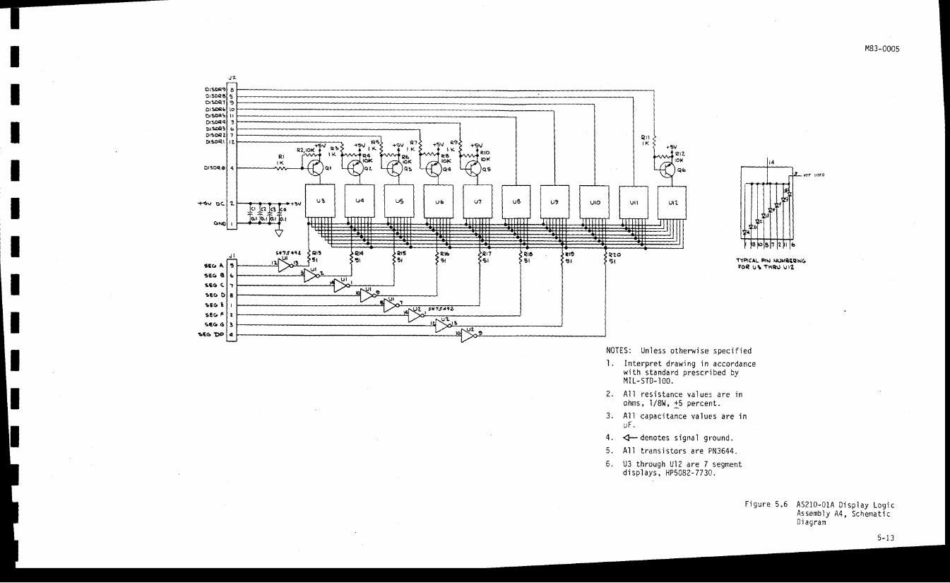
F i g u r e 5 . 6 A S 2 1 0 - 0 l A D i s p l a y L o g i cAssemb ly 44 , Schemat i cDi agram

M83-0005
+9
a "
t a
l 3
t z
Ir9to
9
4
+t
A07AD6AD5A D 4A D 3A0zA D I400
A r 5
A13A , ?A l lAIO
A 9A 8
A 5
A 3
A?A I
AO
WF
IIIIIIIIIIIt
Y,/ff, + RD
SATTEFYaACX-uP
Va
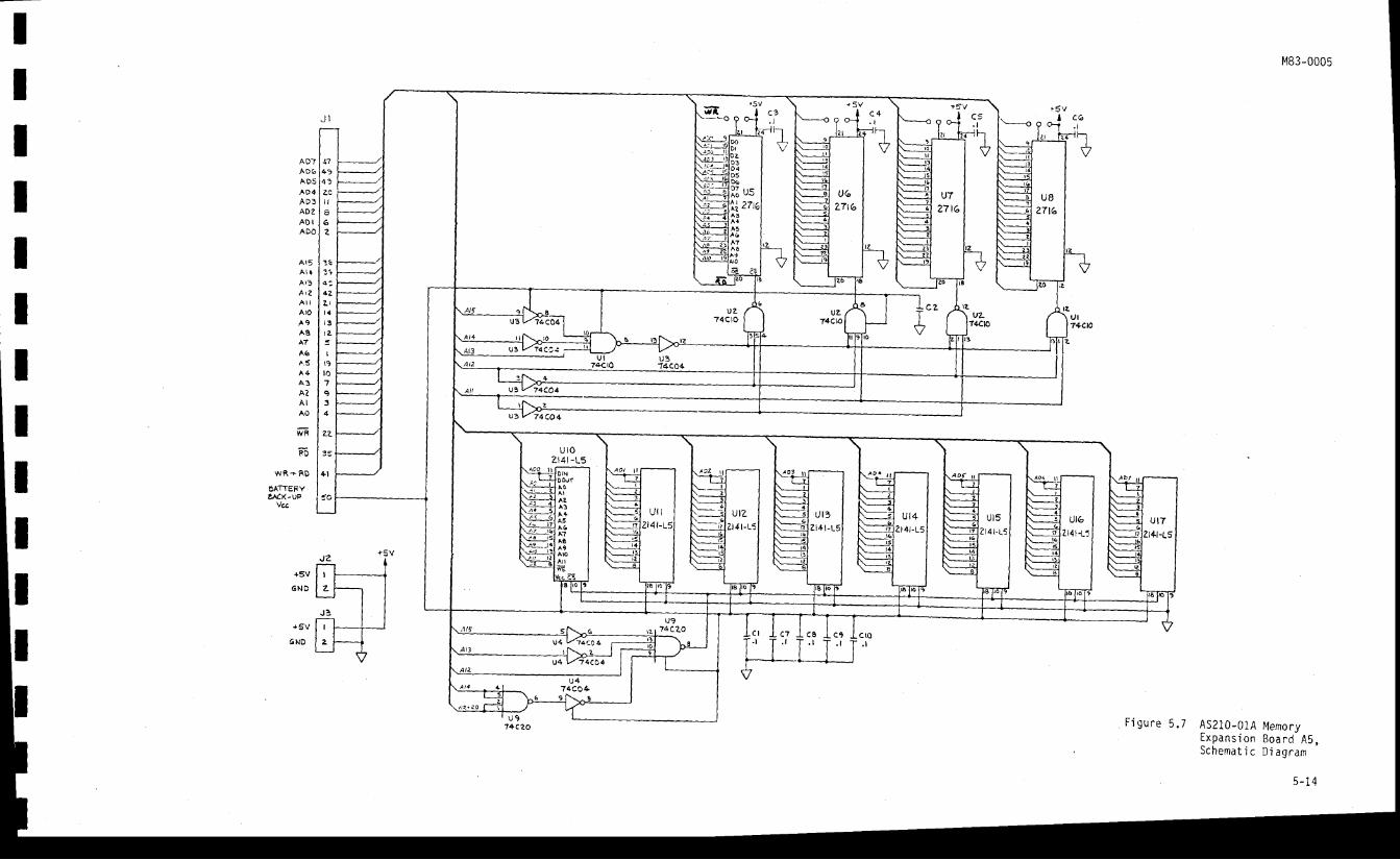
A5210-01A MemonvExpans ion Boa rd A5 ,Schemat i c Di agram
U 914CZO
s- 14
F i g u r e 5 . 7

IIIIIItIIIIIII
Itl''IIIIIIl,IIIIItItI
M83-0004
Two thumbscrews on the rear panel secure the power module to thechassis. Loosen the thumbscrews and place the mainfranre on end with thepower module on the botton. Lift the chassis vertically to separate thepovrer module from the chassis. It may be necessary to use force between thenotherboard and the chassis to loosen the power module. Do not operate thesystem with the chassis removed any longer than necessary. Reinsta'l l thepower module to protect the interior from dust and to avoid personnel shockhazards, as wel l as provide proper vent i lat lon.
When reinstal l ing the power module ln the chassls, set the chassiswith the power module compartment facing up. Align the power modu'le guidepins wi th their respect ive holes in the chassis. Tighten the thumbscrews ofthe power module with a straight-blade screwdriver. Plug-in modules nay novtbe ins ta l led .
5-11 ACCESS TO MAINFRAME CIRCUITS
A. Ensure that the powerprocedure.
is d isconnected before beginning this
Follow the procedure described in paragraph 5-9 of this chapterto remove the power module from the AS210 chassis.
c. using a phi l l ips screwdriver, remove the two screws holding theinternal/external t ime base circuit card.
D. Ti l t the internal /external t ime base select c i rcui t board up.Th is exposes f i l t e r capac i to rs and b r idge rec t i f i e rs fo rt roubleshoot ing. This also provides access to the tuning coi ll oca ted on the in te rna l , /ex te rna l t ime base c i rcu i t board .
B .
5 -11
M83-0004
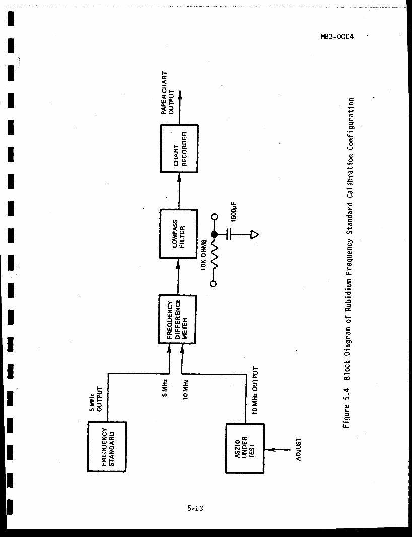
5-12 AS2t0 INTERNAL FREQUE!'|CY STANDARD CALIBRATIoN
The highly accurate internal rubidium frequency standard of the
AS210 system is al igned in i t ia l ly at the factory. Figure 5.4 shows the cal i -
bration test equipment setup. Table 5-4 l ists the recomnended test equipment
to calibrate the rubidiurn frequency standard. The output frequency (10 MHz)
of the rubidium which is being calibrated or tested is compared to the output
freguency (5 MHz) of a reference standard by the Tracor 537A Frequency Dif-
ference Meter. Refer to the Tracor 537A operator's manual for specific oper-
ation procedures for this instrument. The output of the Tracor instrunent is
a voltage proportional to the difference in frequency of the test source and
the reference source. This voltage is put through a ' lowpass
fi l ter and then
applied to an HP-7132A chart recorder. This Hew'lett-Packard instrunent uses
HP-928A-A444 strip chart paper. The chart recorder gives a chart record of
the frequency difference versus tine. l lhen the Tracor 537A unit is selected
to an accuracy of I part in tO10 and the HP-7132A unit is properly adiusted
to center the recording pen at the center of the strip chart, a range of- l n - 1 1
:5 x 10'- parts wi th a resolut ion qf 1 x 10 " parts per minor div is ion on
the str lp chart is achievable. The paper chart output of th is cal ibrat ion
process shows the difference in frequency between the frequency standard and
the output frequency of the AS210 unit under test as well as the frequency
drift in t ime between the two sources. The AS210 Rubidium Frequency Standard
should be wanned-up sufficiently before any alignnent is attenpted. See
paragraph 5-13 of this chapter for the rubidium frequency standard output
frequency adJustment procedure.
ItI
III
II
5-L2
II
,i
IIIIIIIIIIItIIII
(E
( , Fr E fl r l F- fd o
sl
:e,3oN
=o
^.RE =o O
HEFHE
o c tz Eu r <e2HFlJ. (,t
ofr.[3 E
tvt83-0004
o
C'L5lt!
o(J
o+,.qL.a
C'(J
EL.u
\JgG'+,tt,
(,(lJ
I(uLlr
==t
a
t
o
G'Lcnttl
J(J
o@
sl'
lr)
ot-
It
M83-0004
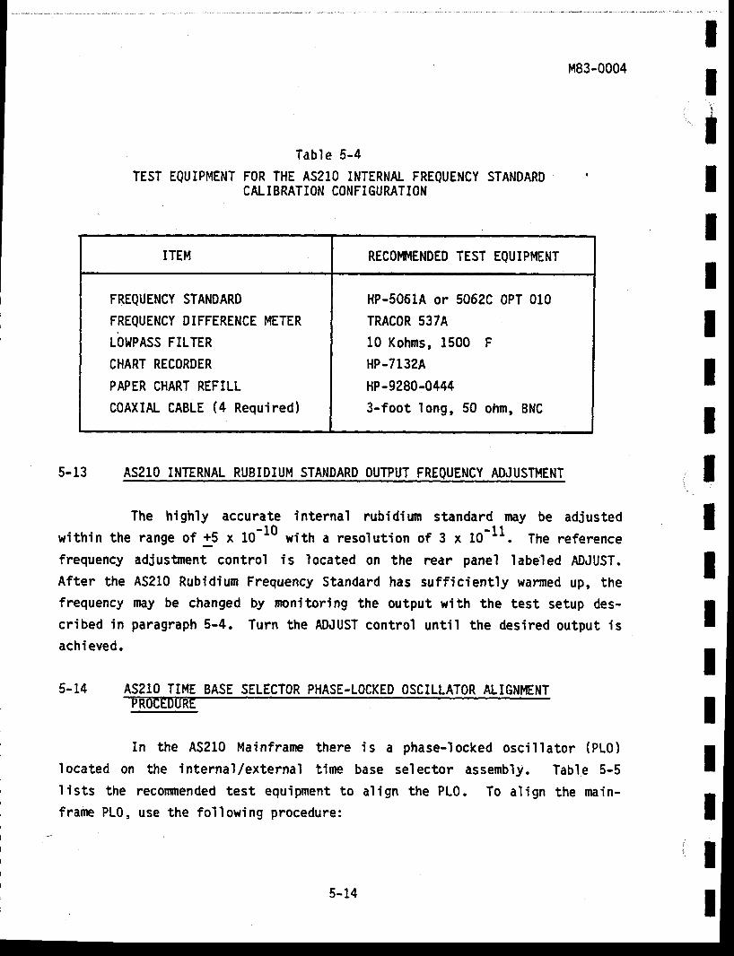
Table 5-4
TEST EQUIPMENT FOR THE AS21O INTERNAL FREQUENCY STANDARDCAL IBRATION CONFIGURATION
5-13 AS210 INTERNAL RUBIpIUM STAIDARp oUTPUT FBEQUENCY ADJUSTITENT
The highly accurate internal rubidium standard may be adjustedwithin the range of 15 x 1o-10 with a resolution of 3 x 10-11. The referencefrequency adiustment control is located on the rear panel labeled ADJUST.After the AS210 Rubidium Frequency Standard has sufficiently wanned up, thefrequency may be changed by nonitoring the output with the test setup des-cribed in paragraph 5-4. Turn the AD.IUST control until the desired output isachi eved.
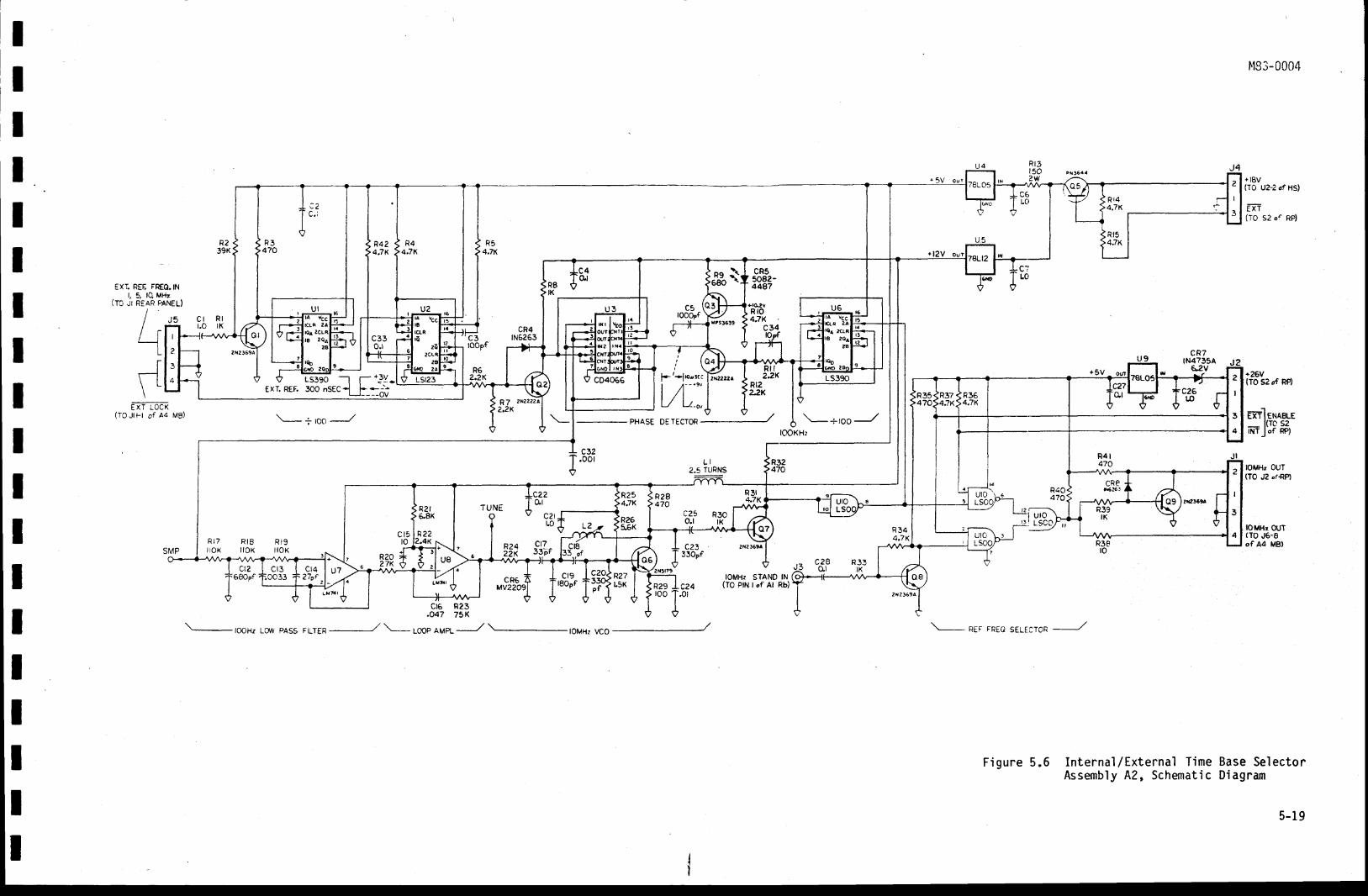
5-14 AS21O TIME BASE SELECTOR PHASE-LOCKED OSCILLATOR ALIGNMENTPROCEDURE
II'l
ttIIII
,ltIIIIII
i l
In the AS210 Mainfrane there
located on the interna'l/external t ime
I ists the recornnended test equipment to
frane PLO, use the fol ' lowing procedure:
is a phase- locked osc i l la to r (PLO)
base selector assembly. Table 5-5
al ign the PLO. To al ign the main-
ITEM REC0I,|I'IENDED TEST EQUIPMENT
FREQUENCY STANDARD
FREQUENCY DIFFERENCE METER
rbupass FILTERCHART RECORDER
PAPER CHART REFILL
C0AXIAL CABLE (4 Required)
HP-5061A or 5062C OPT 010
TRACOR 537A
10 Kohns, 1500 F
HP-7132A
HP-9280-0444
3-foot long, 50 ohm, BNC
5-14
A.
IIIIIIItItIIIIIIIII
M83-0004
0btain access to the mainframe internal/external t lme base se'l-ector assembly by apply ing the disassembly procedures discussed
in f i rs t par t o f th is sec t ion .
B. Apply an RF signal to input BNC on the rear pane'| . The input's ignal must be 1,5, or 10 MHz of a leve l equal to or greaterthan 1.0 VRMS.
C. Set the reference frequency internal/external selector switchlocated on the rear pane'| , to the EXT poslt ion.
D. } . l i t h the osc i ' l l oscope , mon i to r the TUNE tes t po in t on theinternal/external t ime base selector assembly. The TUNE testpoint shou' ld have a dc vol tage between +2y and +8 Vdc. I f th isvol tage is not wi th in +2V and +8 Ydc, then go to E. Othervisego to F.
E. l, l i th L2 at fu11y CCl.f, adjust in a Ct{ direction. The tune TP
should start at a +12 Vdc level . Adust L2 unt i l the level on
the TUNE test point passes through a mininum dc level. Con-tinue a4justment unti l a level of +8 Vdc is obtained.
F. Reassenb'le the mainframe.
Table 5-5
TEST EQUIPI"IENT FOR ALIGNMENT OF THE EXTERNALTIME BASE SELECTOR PHASE-LOCKED OSCILLATOR
ITEM RECOI'}IENDED TEST EQUIPMENT
FREQUENCY SYNTHESIZER
OSCILLOSCOPE I.IITH PROBES
COAXIAL CABLE
HP-8656A
Tektronix 465 or Equivalent
3-foot long, 50 ohm, BNC
5- 1s
l',l83-0004
SECTION IV
5-15 TR0UBLESH00TjNG PRoCEDURES
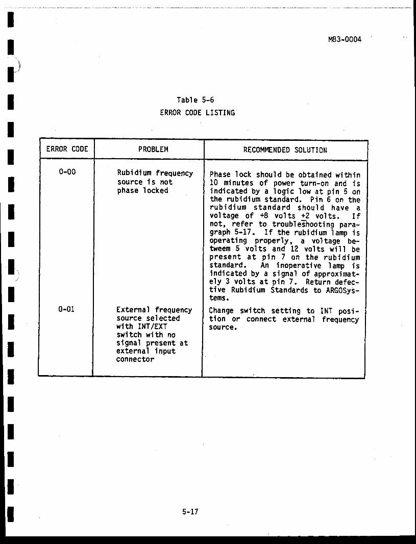
Troubleshooting of the AS210 system mainframe is facil i tated by
error codes displayed on the AS210 Module Control ler . Table 5-6 correlates
the error code displayed on the moduJe control ' ler when a fault occurs to the
ma1func t ion . An exp lana t ion o f the p rob lem is p rov ided w i th poss ib le
sol ut ions.
5-16 POWER SUPPLY FAILURE
If a power fa i lure occurs in any of the suppl ies, check the fuses
located on the front of the notherboard. Fuse Fl is a five anpere SLO-BLO
and fuses F}-FS are three ampere SL0-810. If one of the +5 volt regulated
supp' l ies fa i ls and fuse F1 is not open, then check fuses F6 and F7 located
on the lower center part of the motherboard. If the same problem arises
after replacing' the fuse(s), check the load on the fai led supply for shorts.
5-t7 COMPENSATION OF CRYSTAL AGING
Remove power module from chassis as described in paragraph 5-9.
Monitor the dc voltage on pin 6 of the rubidium frequency standard; that
voltage should be approximately +8 volts +2 volts. If the quartz crysta1
osci' l lator voltage approaches the end of the control range, a correction of
the crystal osci l lator base frequency must be made. This is acconpl ished
by a(justing the oscil lator trimner. The trinmer is located on the side of
the rubidium under the phi l l ips screw, which is v is ib le when looking at the
side of the power supply where the rubidiurn is ' located.
A clockwise adiust-
ment of the trinrner causes an increase in control voltage. The adiustment
should be made af ter the uni t has been operated for at least one hour. The
control vol tage should be set for 8 Vdc.
IItIIIIIIIIItIIII
Il
I5-15
IIIIIII
r483-0004
IIIIIIIIIIII
Table 5-6
ERROR CODE LISTING
ERROR CODE PROBLEM RECOMI{ENDED SOLUTION
0-00
0-01
Rubidium frequencysource is notphase locked
External frequencysource selectedwith INT/EXTswitch with nosignal present atexternal inputconnector
Phase lock should be obtained within10 minutes of power turn-on and isind ica ted by a log ic low a t p in 5 onthe rubidium standard. Pin 6 on therub id ium s tandard shou ld have avol tage of +8 vol ts +2 vol ts. I fnot, refer to troubleFhooting para-graph 5-17. I f the rubidiurn lamp isoperating properly, a voltage be-tweem 5 vol ts and LZ vol ts wi l l bepresen t a t p in 7 on the rub id iumstandard. An inoperative Ianrp isindicated by a s ignal of approximat-ely 3 vol ts at p in 7. Return defec-tive Rubidium Standards to ARG0Sys-tens.
Change switch setting to INT posi-tion or connect external frequencysource.
5-17

II
r ' 1'-l
IIIIII
{lIIIIIII
'. II
IIIIIIIIIIII
EXT. REE FR€Q.INr, 5 lq M|tr
(TO JI REAR PANEL)
EXT LOCK(TOJ lF l o f Aa MB)
14il
c r R lr.o rK
t q
R239t(
a ?
Kb
2.2K
cR4rN6263
R7 2N2222^22K
cl6 R?3.o47 75 K
Hz Lolv pAss FttrER / \_ Loop toMH: VCo
+5V
REF FREG SELT.CTOR
Figure 5 .6 In te rna l /Ex terna l T imeAssembly A2, Schematic
uroL9C
I1 3 l
R27r.5K
2N5r79
R29roo
IOMHz STAND lN(TO PIN I of At Rb)c24
.01
IIII
O r-scao f -tY€xT. REF. 3OO nSEC-l b --'-
I t - - - -ov
R l 7 R t g R t 9r i oK l l oK i l oK
cR7tN4735A
G2v
N33-0004
+l8v(TO u2-2 of HS)
ETT-(TO 52 o' RP)
+26v(TO 52df RP
rr-leNqa.e_ l(rc s2tNT J of FP)
IOMHI OUT(TO J2 or{P)
|oMH: OUT(TO J5-8ofA4 MBI
Base SelectorDi agram
5-19

M83-0004
trf Aztr8)
GND
r t€v
lO MHr
G N O
4
c
5
9
I oroII
C C N 7 9 C L lI REst_Lno
[- c,I1 0 ,
0ArAl
lo 'Lo'
A4 MOTHER EOAR, (MS)- - *
, . lJ 0 I
Aj
A,
Arr
i ^ l+26v1 - (F
B L K
G R A
co[,{AC
IIIIIItIIII
J S c f A 4 l M B l+5V
A2 (T 8 !+ l8V
6ND
EIT
J 5 o f A 2 { T 6 J l l a f A a ( M B )
E X I L C C X
t e
23a <
P
I
2
5€'73
, o
t a
GND
GNOiNT
f A2rT8)+26v
GNDNTL x | -
h
t a
l 4
t 3r 6t 7r gl 9
A | (Rb)
6NC. 2 8
LOCK
AD-I
AOJ
io MH- ctrr
GND
R U B I f I U M F F : C U I N 3 YSTATiDARD ASSY T iC.
i l 7 t 85 -O l
( E r
F R E Q
x bA D u U S T
IK
EXT REFINPUT
J t
_ _ i'ilI.-I"] _,'
REN
J3or A2 (T B)Il ll r l
i:J6
i 2-3rf 5 v
+ 5 Vo / A 4 ( M B )
GND
LO-ER
f A 2 ( T B )EXT REF
2 l
?.:
f i gure S. S Power Modul e t 'Ji r i ng D'i igram
R!AP PANE !rEE t - 49COt'iNgC TOR
l c , o f A 4 | M e ,
6-l ' zevI l . i l v
T i G N O
i "1,- '^ ' l l . - i *-BLU
Re i
Re IgLK
j
IIII
J ? I { t o t A 2 f i g )'$,litrft' G€---_--__-{ilro MH: REFn*o
-n'-7-i,l
e /---=
? l \
"d-a
z =
o " o. 2 5
1 2 5
2 3
aY
z l
20
r9
ie
?3 / -
5-18

6-1
IIIIIIItIIIIIIIII
M83-0004
CHAPTER 6
ILLUSTRATED PARTS LIST
INTRODUCTION
This sect ion contains an i l lustrated parts l ist for the AS210A-PMPortable Mainfrane. The assembly number and title are listed at the top ofthe parts l ist . The parts l ists are divided into six 'columns and arrangedin the fol lowing order:
Colunn 1Column 2Column 3Column 4Column 5Column 6
Itern Nunber
Quantity per AssenblyManufacturer's CodePart NunberDescript ionReference Designation
6-1
M83-0004
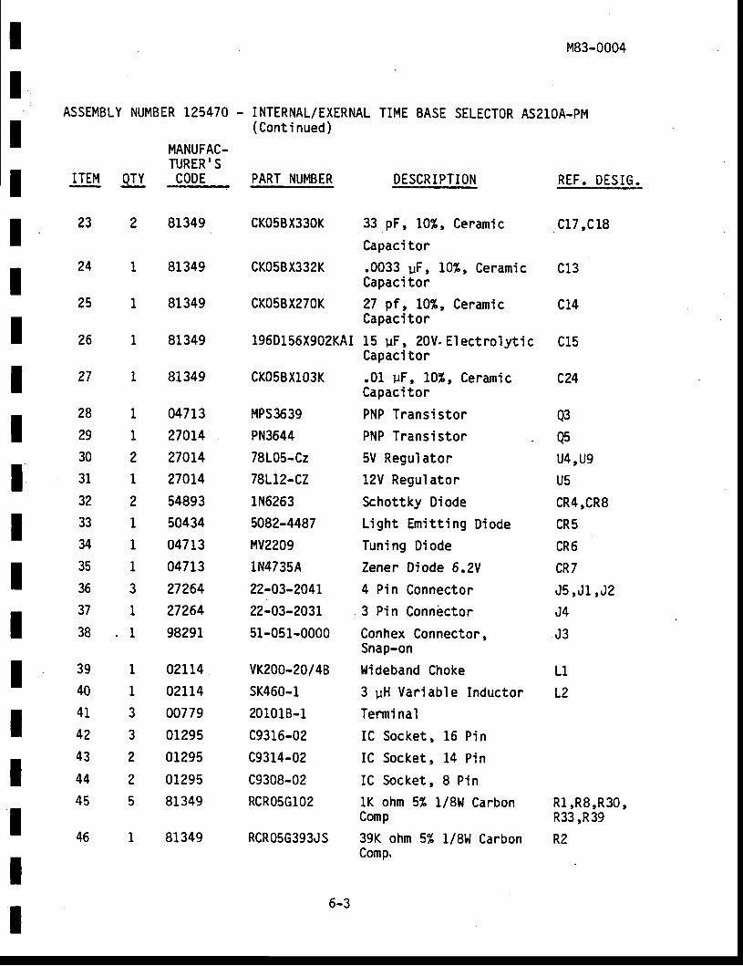
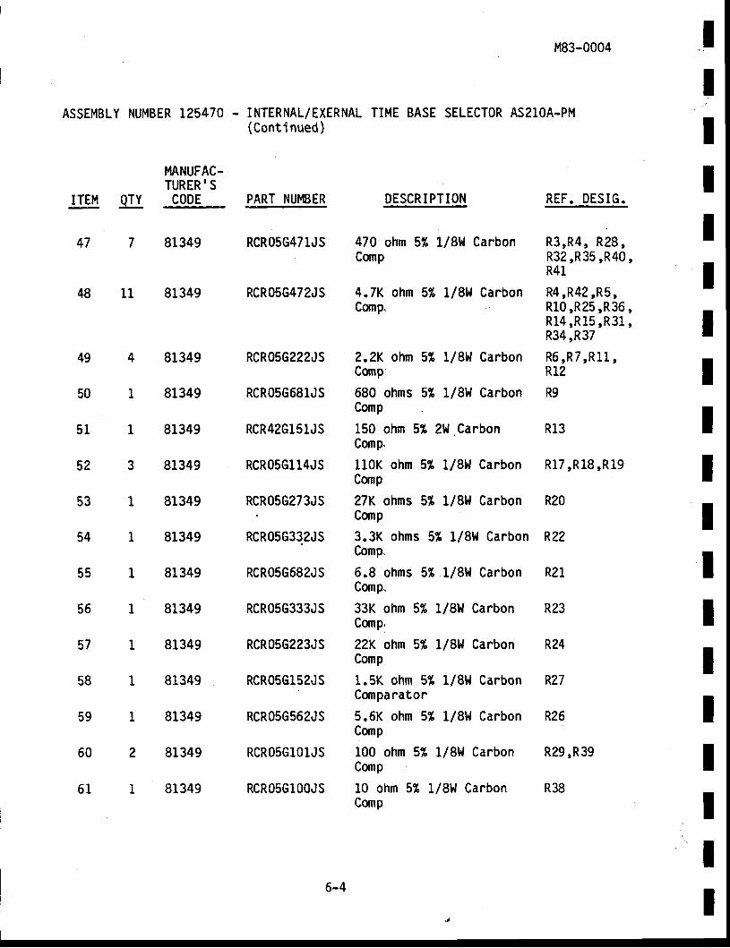
ASSEMBLY NUMBER L25470 . INTERNAL/EXERNALTIME BASE SELECTOR ASzlOA-PM
IIIIIIIItIIIIIIItII
ITEM
I
2
3
4
5
6
7
I
9
10
11
L2
13
14
15
16
L7
18
19
20
2t
22
g.
1
REF
REF
REF
?
1
1
1
2
4
2
1
I
5
7
I
I
2
1
2
2
1
MANUFAC.TURER.SCODE
33472
33472
33472
33472
0t295
01295
01295
02735
270t4
270t4
?70t4
270t4
81349
5L642
81349
81349
81349
81349
81349
81349
81349
81349
PART NUMBER
t25473
t?5471
t25472
L25474
741S390N
741S123N
74LS00N
cD4066A
741CN
?N23694
2N22224
2N5179
cKo5BX473K
300-50-501-105M
cK05BX104K
CKOsBXlOlK
CKOsBX473K
CKO5BXlO2K
CKOsBXl5lK
CKOsBXlOOK
CKOsBX33lK
CKO5BX68lK
REF. DESIG:
ul,u6u2ul0U3u7,u8Ql ,Q7,Q8,Q9
Q2,Q4
a6c16
c1rc6rc7,c26,C2c2,c33,C4,C27,c22,C25,C?8c3
cl6
c32,C5
c19
c34,C30
c20,c23
ct2
DESCRIPTION
PlrB 125473
Schemati c
Master Pattern
Si l k screen
Dual Decade Counter
Dual One Shot
Quad MND Gate
Qrad FET Switch
0P Amp
NPN Transistor
NPN Transistor
NPN Transistor
.047 pF l0%, CeramicCapaci tor
l t f ,20X,CeramicCapaci tor
.1. pF, 10X, CeramicCapaci tor
100 pf , 10%, CeranicCapaci tor
.047 uF 10f , CeranicCapaci tor
.001 pF, 10%, CeramicCapaci tor
150 pF, 10%, CeramicCapaci tor
10 pF, 109, CeramicCapaci tor
330 pf , 10%, CeramicCapaci tor
680 pf , 10%, CeramicCapaci tor
6-2
ASSEMBLY NUMBER L25470 .
MANUFAC-TURER' SCODE
I NTERNAL/EXERNAL( Conti nued )
PART NUMBER
33 pF, 10%, Ceramic
Capaci tor
.0033 pF, 1.0X, CeramicCapaci tor
27 pf, 10%, CeramicCapaci tor
15 uF, zOU. Electrolyt icCapaci ton
.01 uF, l07t,, CeramicCapaci tor
PNP Transistor
PNP Transistor
5V Regulator
12V Regul ator
Schottky Diode
Light Emit t ing Diode
Tuning Diode
Zener Diode 5.2V
4 Pin Connector
3 Pin Connbctor
Conhex Connector,SnaP-6n
l,Jideband Choke
3 pH Var iable Inductor
Termi nal
IC Socket, 16 Pin
IC Socket, 14 Pin
IC Socket, 8 P' in
lK ohm 5% L/8W CarbonComp
39K ohm 5X 1/8bl CarbonComp,
M83-0004
REF. DESIG.
c l7 ,c18
c13
c14
c15
c?4
Q3a5u4,u9U5cR4,CR8cR5cR5cR7J5,J l ,J2J4J3
Rl ,R8,R30 ,R33,R39
R2
TIME BASE SELECTORAS21OA.PM
DESCRIPTIONITEM
27
2829303132333435363738
39404l42434445
46
81349
81349
81349
81349
81349
047r.3270L4
270r4
270L4
54893
50434
04713
047t3
?7264
27264
9829I
02It4
02114
00779
0L295
0t295
01295
81349
81349
gL
?3
?4
25
CKO5BX33OK
cKo5BX332K
cK05BX270K
196D156X902K4I
cKo5BXl03K
MPS3539
PN3644
78105-Cz
78LI2-CZ
1N6263
5082-4487
MV2209
1N4735A
22-03-2041
?2-03-2031
51-051-0000
vK200-20/48
sK460-1
201018-1
c9315-02
c9314-02
c9308-02
RCR05G102
RCRO5G393JS
L1
L2
1
1
2
I
2
I
1
1
3
I
1
IIIIIIII
I
1
3
3
2
2
5
6-3
TII
ASSEMBLYNUMBER T25470 -
ITEM lIL
MANUFAC-TURER' SCODE
I NTERNAL/ EXERNAL(Conti nued)
PART NUMBER
RCR05G471JS
RCR05G472JS
RCR05G222JS
RCR05G681JS
RCR42G151JS
RCR05G114JS
RCR05G273JS
RCR05G33.2JS
RCR05G682JS
RCR05G333JS
RCR05G223JS
RCR05G152JS
RCR05G562JS
RCR05G101JS
RCR05G100JS
M83-0004
TIME BASE SELECTOR AS21OA.PM
DESCRIPTION
IIIIIIIIIIIIIIIIIII
47 81349
81349
81349
81349
81349
81349
81349
81349
81349
81349
81349
81349
81349
81349
81349
470 ohm 5I Ll9?ll CarbonComp
4.7K ohm 5% llSU CarbonCornp.
2.2K ohm 5% L/8W CarbonCornp
680 ohms 5% Ll8lUl CarbonComp
150 ohm 5% zW.CarbonComp,
110K ohm 5% 1/8bJ CarbonComp
27K ohms 5% 1/8bl CarbonComp
3.3K ohms 5X 1/8}{ CarbonComp.
6.8 ohms 5f 1/81.1 CarbonComp.
33K ohm 5% 1/8t.l CarbonComp:
22K ohm 5X 1/8t'l CarbonComp
1.5K ohm 5t 1/8Ul CarbonCornparator
5.6K ohm 5% l/8W CarbonCornp
100 ohm 5% I/8W CarbonComp
10 ohm 5% I/8W CarbonComp
REF. DESIG.
R3,R4, R28 ,R32,R35 ,R40,R41
R4,R42 ,R5,R10,R25 ,R36 ,R14 ,R15,R31,R34,R37
R6,R7,R1.1 ,R12
R9
R13
R17 ,R 18 ,R 1.9
R20
R22
R21
R23
R24
R27
R26
R29,R39
R38
11
49
50
51
52
53
54
55
56
57
58
59
60
61
6-4
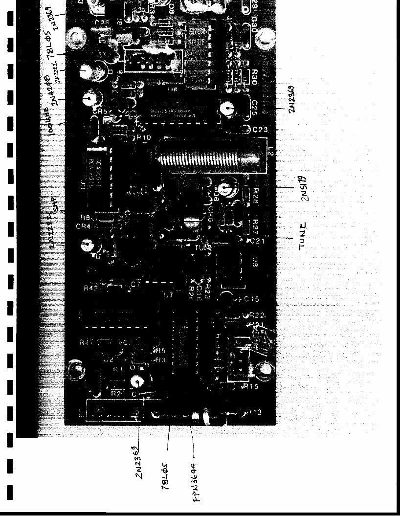
a-,\r.X€
. J.s' . F . -r,. J' d
N '
ER;,q\ .'- . { - . .
FulzN
d2t ,r
h { -s+J \S)S .{tl,\ 2
a-\L
snNzN

ItIIIII
a
t .
M83-0004
$J
-oa)anan
!o(J(l)
oat1
ottG'coo
C'
L(l,
xlrl
C'
Lo
=o-I
GIat,
t o
(ut-
L7)
IIIIIIIIIT
I
923 (J-ereffiEnFF;#tf-i Fjr=d ',llll';! 3 333 o
:Hsffi#wr-f,"egglooooolltEgut-U oEoPtIEta 9+*l-
-3 3l 16l o
H'ffiffilaffi^q#'-Eifup'.-:dEs,fooo1ffi6 6q
,fuF'ooe"rdE! S=.,S =ln,€E,s
P;:,=Loooooooo) i !=!-;;t;,ffiHmr
*'llmrl etu
6-5
ITEM g]!
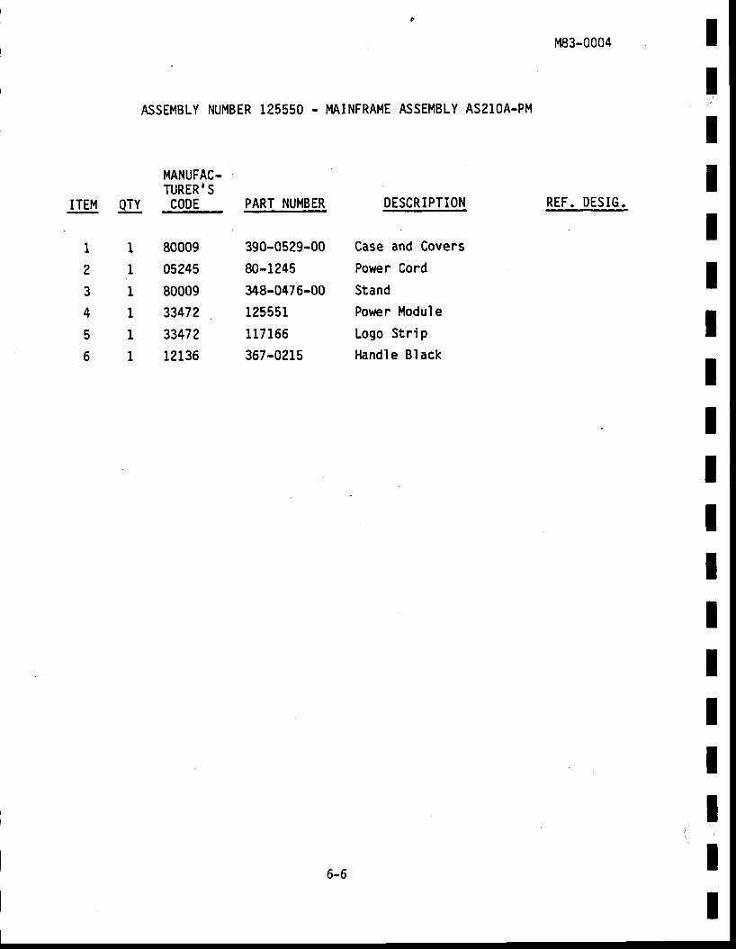
ASSEMBLY NUMBER 125550 . MAINFRAME ASSEMBLY AS21OA-PM
MANUFAC.TURER I SCODE PART NUMBER DESCRIPTION
M83-0004
REF. DESIG.
IIIIIIIIIItItIIIIII
80009
05245
80009
33472
33472
12136
390-0s29-00
80-1245
348-0476-00
125551
117166
367-02ts
Case and Covers
Power Cord
Stand
Power Module
Logo Strip
Hand'le Bl ack
6-6
IItIIIIIIIIIIIIIIII
2
3
4
5
6
7
8
9
10
11
L?
13
14
15
16
T7
18
19
20
2l
22
23
rrEM gIJ,
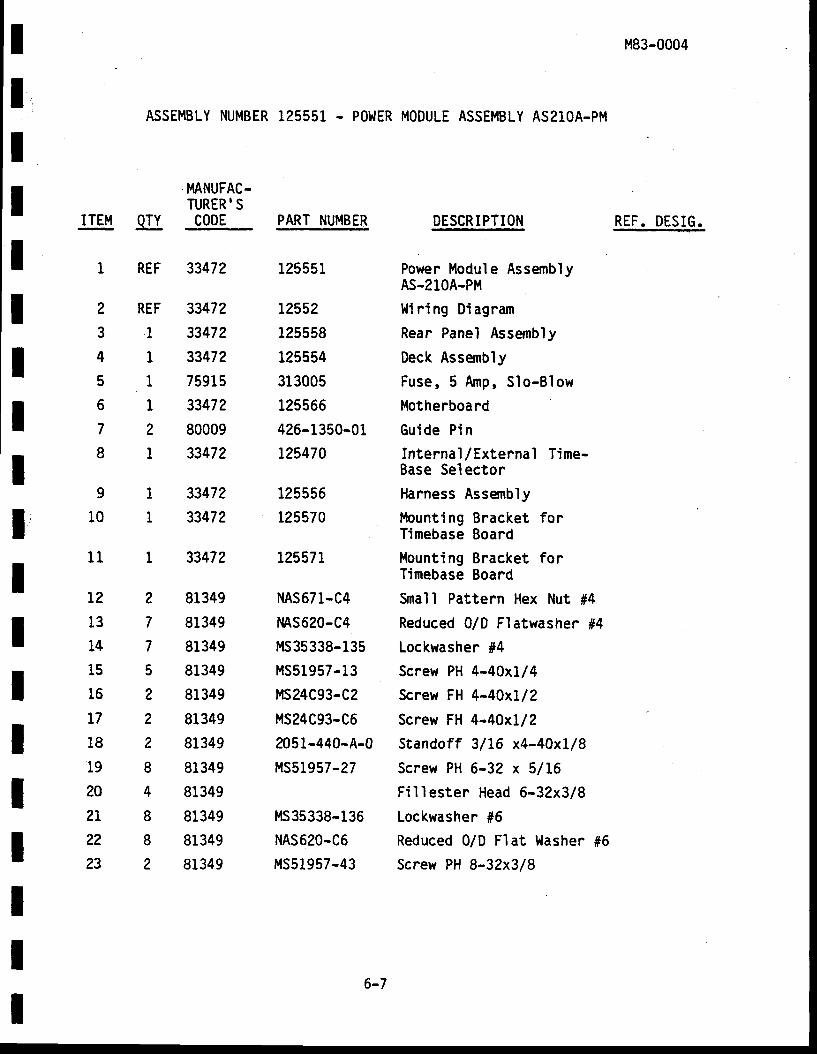
ASSEMBLY NUMBER125551 - PoWERMODULE ASSEMBLY ASzlOA-PM
MANUFAC.TURER' SCODE
M83-0004
REF. DESIG.
REF
I
1
1
1
2
I
33472
33472
33472
33472
75915
33472
80009
33472
3347?
33472
33472
81349
81349
81349
81349
81349
81349
81349
81349
81349
81349
81349
81349
PART NUMBER
125551
L2552
125558
125554
313005
1.25s66
426-1350-01
125470
125555
t25570
12s571
NAS671-C4
MS620-C4
MS35338-135
MS51957-13
MS24C93-C2
l'1S24C93-C6
2051-440-A-0
MSs1957-27
MS35338-136
NAS620-C6
MSs19s7-43
DESCRIPTION
Power Module AssemblyAS-2104-Pt'l
hli ri ng Di agram
Rear Panel Assembly
Deck Assembly
Fuse ,5 funp , S lo -B low
Mothenboard
Guide P in
Internal/External Time-Base Selector
Harness Assembly
llounting Bracket forTimebase Board
t' lounting Bracket forTimebase Board
9nal I Pattern Hex Nut #4
Reduced 0/0 Flatwasher #4Lockwasher #4Screw PH 4-40x1/4
Screw FH 4-40xL/2
Screw FH 4-40x1/2
Standoff 3/16 x4-4AxL/8
Screw PH 6-32 x 5/16
Fi l lester Head 6-32x3/8
Lockwasher #6Reduced 0/D F'lat Washer #6Screw PH 8-32x3/8
I
I
?
7
7
5
2
2
2
8
4
I
8
2
6-7
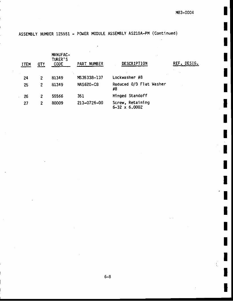
ASSEMBLY NUMBER 125551 - P0ltlERMODULEASSEMBLY AS210A-PM (Continued)
MNUFAC-TURER' S
ITEM QTY CODE
8134981349
5s56680009
M83-0004
DESCRIPTION REF. DESIG.
Lockwasher #8
Reduced 0/D Flat Washer#8
Hinged Standoff
Screw, Retaining6-3? x 6.0002
IIII
?
2
2425
262272
PART NUMBER
t'ls35338-137
NAS620-C8
351
213-0726-00
IIIIIIItIIIIIII
6-8
IIIIIIItIIIIIIII
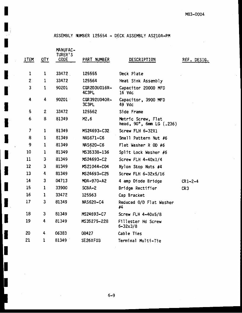
ASSEMBLY NUMBER1255s4 - D.ECK ASSEMBLY ASzlOA-PM
M83-0004
REF. DESIG.
cR1-2-4cR3
MANUFAC.TURER' SCODE PART NUMBERITEM
5
6
7
8
9
l0
11
t2
13
14
L5
l5
t7
1B
19
20
?t
33472
33472
90201
90201
33472
81349
81349
81349
81349
81349
81349
81349
81349
047L3
33900
33472
81349
81349
81349
06383
81349
I23
1
1
1
.a]I
2I
3
4
4
1
125s5s125564
cGR203U016R-4C3PL
cGR392U040R-3C3PL
t25562
M2.6
MS24693-C32
NAS67t.-C6
MS620-C6
MS3s338-135
MS24693-C2
MS2l044-C04
1"1S24693-C25
MDA-970.42
scBA-2125553
MS620-C4
MS24693-C7
t4s35275-228
48427
sE26XF03
DESCRIPTION
Deck Plate
Heat Sink Assembly
Capaciton 20000 MFD15 Vdc
Capacitor, 3900 MFD49 Vdc
Side Frame
Itbtric Screw, Flathead, 90o, 6rm LG (.236)
Screw FLH 6-32X1
Small Pattern Nut #5Flat Washer R 0D #6
Split Lock l,Jasher #6Screw FLH 4-40x1/4
Nylon Stop Nuts #4Screw FLH 6-32x5l16
4 amp Diode Br idge
Bridge Rect i f ier
Cap Bracket
Reduced 0/D F] at Washer#4
Screw FLH 4-40x5/8
Fi l lester Hd Screw6-32x3/8
Cab le T ies
Terminal Mult i -Tie
1
1
I
1
3
3
4
3
1
I
3
6-9
M83-0004 IIIIIIIIIIItIIIIIII
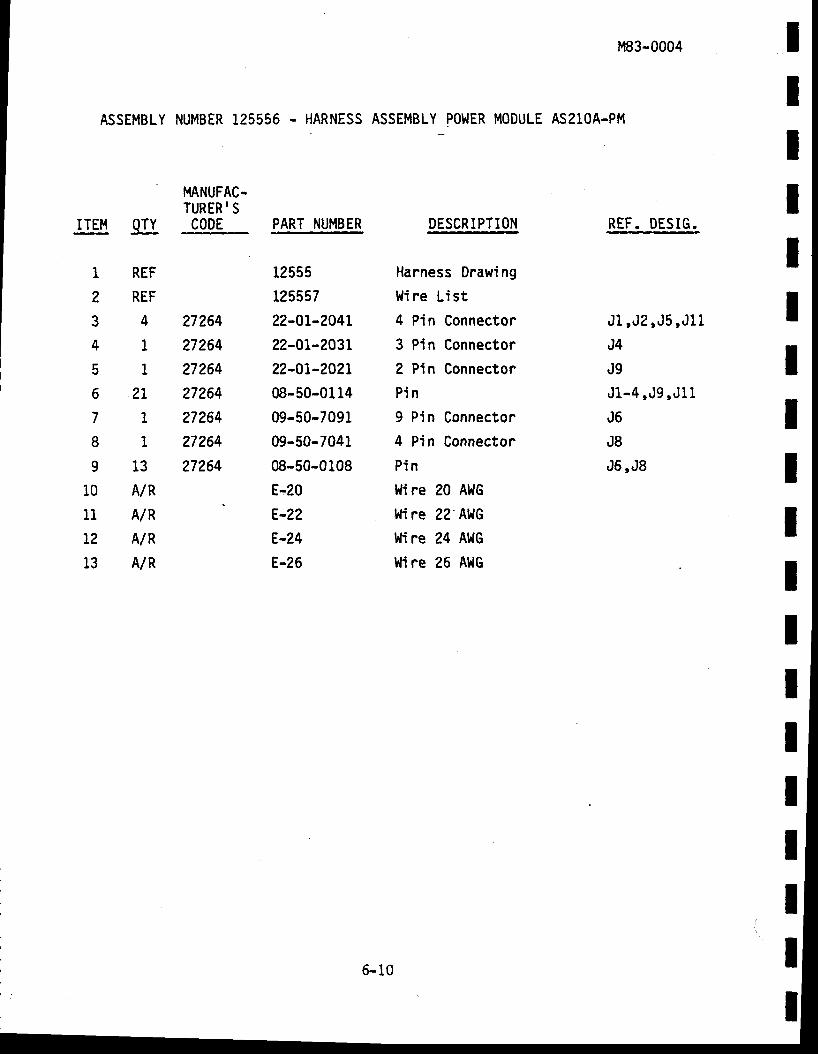
ASSEMBLY NUMBER 125556 - HARNESS ASSEMBLY POI{ERMODULE ASzlOA.PM
rTEM g.
MANUFAC.TURER.SCODE PART NUIIBER DESCRIPTION
Harness Drawing
|rJi re Li st
4 Pin Connector
3 Pin Connector
2 Pin Connector
P in
9 Pi n Connector
4 Pin Connector
P in
tfi re 20 A}lG
t,{i re 22 At'lG
t.Ii re 24 Al'lG
lli re 26 AllG
REF. DESIG!.
J l , J2 ,J5 ,J l1J4
J9
J1-4 ' ,J9 'J11J5
J8
J5,J8
1
2
3
4
5
6
7
8
9
10
1t
t2
13
REF
REF
4
I
1
2L
1
1
13
A/R
A/R
A/R
A/R
27?64
27264
27264
27264
27264
27264
27264
12555t25557?2-0L-?O4L22-0L-203r22-01-202t08-50-01.1409-s0-709109-50-704108-50-0108E-20E-22E-24E-26
6-10
IIIIIIItIIIIIIIIIII
1
2
3
4
5
6
7
I
9
10
11
L2
13
14
15
16
17
18
19
20
2L
22
23
24
25
rrEM g]!
ASSEMBLY NUMBER125558 - REARPANEL ASSEMBLY AS21OA.PM
MANUFAC.TURER,SCODE PART NUMBER DESCRIPTION
M83-0004
REF. DESIg .
R6
R7
F1
I 33472
REF 33472
REF 3347?
L 33472
4 33472
1 05345
I 09353
1 95345
L 23935
I 23936
I 77969
2 91836
L 33472
1 09353
2 33472
L 33472
r 32997
I 73138
I 75915
I 00779
4 81349
2 81349
4 81349
2 8t349
2 81349
12s559
125550
12s557
t254L4
117173
85-1507
920l-J3-E
6.14
8L24
5508
RC#z-1l6},G
KC-79-35
150X75047301-P3YZQ-E
117301
1U352-01
3006P-1-1022
RH-5-5}J65
313005
L497
MS51957-50
MS519s7-4
MS620-C2
MS35338-134
MS671-C2
Pane l , Rear
Si lkscreen, Rear Panel
Wi re L is t
Power Transformer
Standoff, Legs
Equipment Rating Label
Switch, Rocker, DPDT
EMI L ine F i l te r
Fan
Fi nger Guard
Grorrnet, Rubber, Black.188
BNC Bulkhead Receptacle
ARG0Systens I.D. Label
Switch Toggle DPDT
Standoff, Stud Mount
Cable Assembly IEEE
Trimpot, Panel l, lount ,lK ohm
65 ohm 5% L%
Fuse ,5 amp, S lo -B lo
Solder Lug
Screw PH 6-32x1-l/4
Screw PH 2-56x5/I6
Reduced 0/D Fl atwasher #2Spl ' i t Lockwasher #2Nut, Snall Pattern #2
6-11
ASSEMBLY NUMBER 125558. REAR PANEL ASSEMBLYAS210A-PM (Cont inued)
IYTANUFAC-TURER,SCODE PART NUMBER
il83-0004
REF. DESIG.
IIIIIIIIIIIIIIIIIIt
ITEM
262728293031
-ary"
8
3
1
4
8
L2
81349
81349
81349
81349
81349
81349
MS671-C5
r4s51957-29
MS51957-30
M524693-C?7
MS35338-136
MS620-C6
DESCRIPTION
Nut, Smal l Pattern #6
Screw PH 6-32x7 /L6Scnew PH 6-32xL/2
Screw FH 6-32x7/16
Lockwasher #6
Reduced 0/D Flat Washer#6
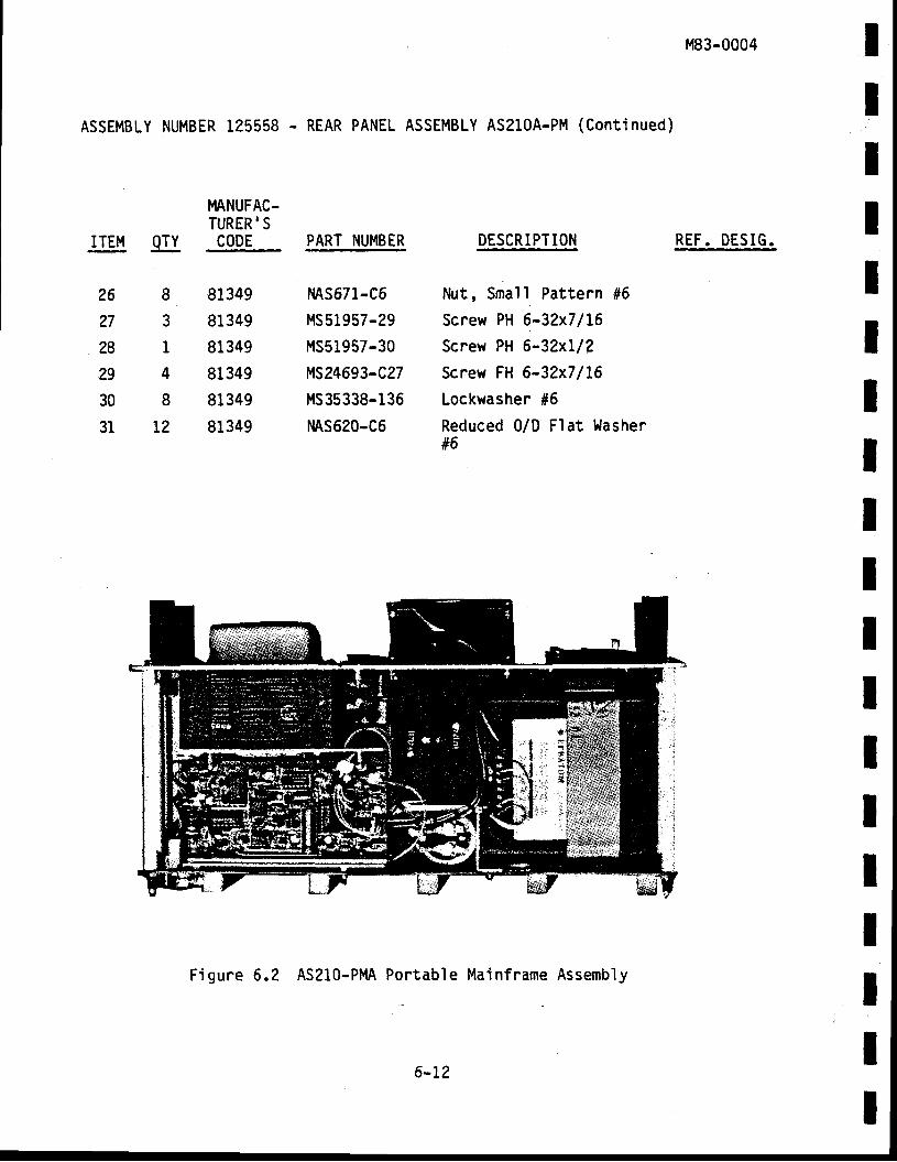
Figure 6.2 AS210-PMA Portable Mainframe Assembly
6-I2
ASSEMBLY NUMBER 125564 . HEAT SINK ASSEMBLY ASzlOA.PM
MANUFAC-TURER'Sc00E
M83-0004
REF. DESIG.
u3, u4U2
U1
rTEM gTY,
1
2
3
4
5
6
7
2
1
1
1
2
1
I
I
9
10
11
L2
13
l4
15
16
L7
18
19
20
?L
2?
23
q?0
11
9
2
2
2
1
1
1
I
1
1
I
PART NUMBEE
Lt7L74
260-0907-00
LL7t72-0L
tt7L72-02
uA78H05SC
UATSHGASC
UAT9HGSC
1415-5
300-50-601-105M
MS51957-30
MS620-C6
MS35338-136
MS671-C6
MS51957-14
MS620-C4
t'ts35338-135
RN55D2211FS
RN55DXXXXFS
RN55D4221FS
RN55DXXXXFS
MS51957-36
MS51957-27
MS51957-28
24
33472
80009
33472
33472
18100
18100
18100
81349
81349
81349
81349
81349
81349
81349
81349
81349
81349
81349
81349
81349
81349
81349
81349
R9
R8
Rl1
R10
DESCRIPTION
Heat Sink
Thermal Switch
Spacer, Mount ing
Spacer, Mount ing
Voltage Regulator
5 amp Vol tage Regulator
5 amp Negat'ive Adj .Vol tage Regulator
Solder Lug #6I fd 20X CeramicCapaci tor
Screw PH 6-32x1/?
Fl at }Jashen Reduced 0/D#6
Spl i t Lockwasher #6Snal I Pattern Nut #6Screw PH 4-40 x 5/16
Reduced 0/D Flat lrlasher#4
Spl it Lockwasher #42.2LK ohm 1% 1/81,1FS ohm 1% 1/8}{4.22K ohm lX 1/8WFS ohm lX 1/8l{Screw PH 6-32x1-L/2
Screw PH 6-32x5/16
Screw PH 5-32x3/8
IIIII
6-13
ITEM gT,
ASSEMBLY NUMBER 125566 . MOTHERBOARD ASSEHBLY AS21OA-PM
MANUFAC-TURER. SCODE PART NUMBER DESCRIPTION
t25567
125568
K500-l 1-56Y25
27503.5
10207t
t802752-0?-0s
313003
09-88-1041
?2-95-?A4L
22-05-202t
09-60-1091
v29-L202
Motherboard P}.lB
Master Pattern
55 Pin Connector(no ears)
Fuse, Ax ia l
Fuse Cl i p, PC ltlount
Terminal , Bi furcated
Fuse ,3 amp, S lo -B lo
4 Pin con R+6nglg
4 Pin R Angle Connector
2 Pin R Angle Connecton
9 Pin Connector
Connecton, 25 Pin
M83-0004
REF. DESIG.
J1-J5
F1.F5
J8
J11
J4
J6
IIItIIIIIIItIIIIItI
I
2
3
4
5
6
7
8
9
10
11
t2
1
REF
5
2
t0
4
5
1
1.1
I
1
33472
33472
1781
75915
75915
7t279
7591.5
27264
27264
27?64
27264
27264
6-14
M83-0004
-ct(l)3nan
Et-G'oaL(l)
o
(u.E'L
G'=
o,-I
oNa/,
CN
to
(u!
g)
l!
o l o l o o l o o o o .o a a o o o o a o o
o a a a a a l a a a a a a a a o o a a a o a o . o oo
" l" l ]ott t" l t t i l?l?l?l?l?t?1. o o o o oo. o I o
a o o o a o a oo o o a a a o
a o a o . t a a a a o ao o o o o o a a a a o
a o o a o
I
IIIt
IIII
II
6-15
6-? }.TANUFACTURER.S LIST CODE TO I.IAI,IE
M83-0004
mater ia ls used
order by code.Th is sec t ion
in the AS210 sys tem.
contains al l manufacturer 's codes for
The codes a re l i s ted in numer ica l
6 -16
III
FAIFISHILM
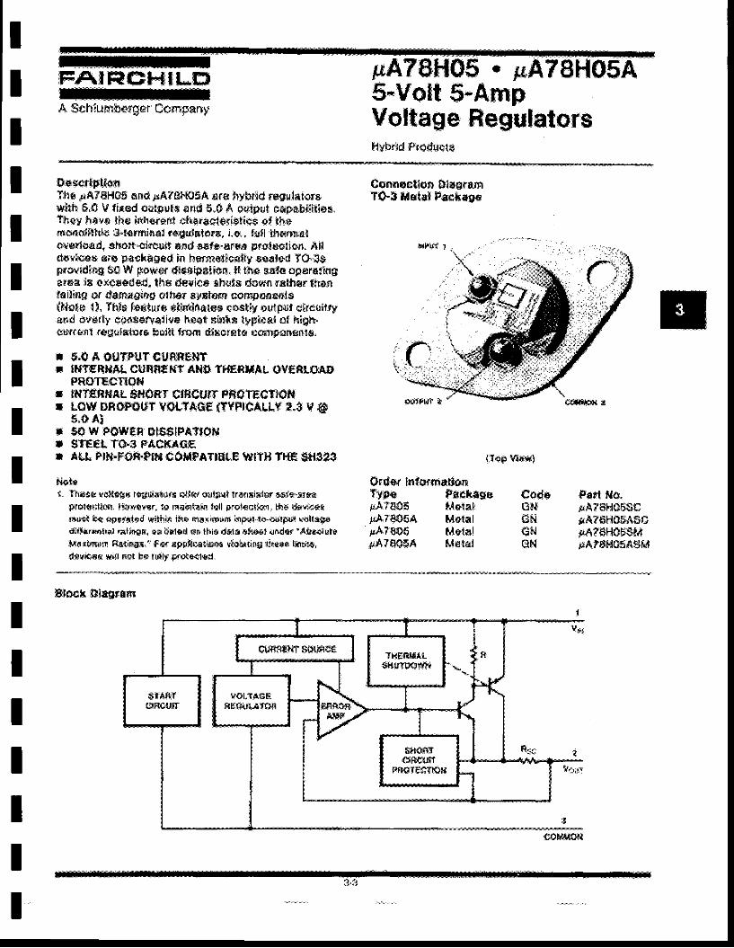
& Scln$urmfuer6e,r' fr*rr*p*rry
#AF#f*ffS * $AfffiHfi5AS-Vm*t S*&rnpV ltmgs ,ffisgr*trfits,rstiybr{d Prddust*
IIIIIIIIt
ff*wtrtpffa*rTlt* ;+e7fiF{*6 *nd pfuif WffiSA sr.* h$fu,r$d rs#ujlfil#fs,**gl.r &;0 V fix,ed'$*stprlxs and $.F S *n*tpui #*pebi#i1iss,?*sy hall.* *kr krhererit eh*y**{*rF*tis* *f tF$ransan**ihic, s'terrft l{, g{ r*fi el$st6rw, i,e,- **x$l *l*pncnslova***ad, aheaf 'gj***$f alld *nf,s-*rs* pr**ssfl{}n. r4l$*trldce.e 'ers p4eksged ifl tee*cs?si**wl}!r sesJ*nd Ytr-gepr<ru*d?r*p s* hS psx**r *As#i#****r,*, li ths asfs sF,ersitftn$esec iig sr{,€fl#d. d- the S*|fie# xhsts Ssr*n *,s*.}*er lfl$n*r inirup tr d*fft#Nrrg **116r .ex**tsrsx *sny.Fsfi sffie{f,l*req t}, Th*m f*g*ur* **iriftl:rels* sneftFy'*u,tput eHr,*u,itryemd tl*erly #s.it**a{T.fitis* I'seat ekitrx typ*ce;lnf hipfu
$r,r&nt r*6*[o**r* hui{* !r*rn &*e6r@t& ri*{fp&n?&f{8,
.$-* * *uTr{JT *UHAffi#*T*t'{trgntrs*. n{rnffiHY Ahts ffi*finH&t" *$€eL*AspffigT€#F*pN*$lrffiRffi*L S$**RT Sfffi*t $T p#STESffiOlt*LfiW effSFprlT rfstY*fiH {rrpffi&LLY s.$ y ffi6.t! *6S W p&rfif Hn, bffi€npAY$,fi f*STEH$-T#l$ F,fte,ffififfiAt.t FlreF#*"FH* dstitFATta*-n wgrf{ T}{€ trrs.ftg
!*Etss- Ths$e Ers&sj** t**#41{{}F,* d*eg *{$*st*raeraia;tmr ra:ls"xr€*
Sft)t4*{Stirtf!, ffi!+$r.Kr" ts mah{aj*# {lxll g}rc'bestkifl. lfiE Sasifrrsi**'|a*i h4,.. @sFel#d x**hln t$ss rnmxkprrm krFJiit!'ts-#ut#{} : risl isssdiffsrxr*rttfli ra,tk*g*, *m lFeJ*d on thlx dplra *&*st *Jftd€s *A&rg'*lr*tp
$dsrisww ffi*ti@r*," fcr npp***tlo*ei $o&atrlng i*?stsa llrfidbs,*$sls6# rsNl r$Gt hs.Fu{ty Wsp*l"sd.
{?sP w*r{i
#rdn* In{srla**$p*rtrYps F*ehnes,iA?,M5 Mwtra[FA?ffifiA Me'tslBAFWS ldwtxlEAIS*SA Fdnlal
Sunnffpu*rn &*e$r,alfiTStr tlut*d F** *S*
Iu
**
***
#n**ffit{$frfilqldGH
,Fsft fi{{}"*lA?#l"l$6###&7#}'lSF&,Sfi*tA'ff#Fl#SSM,**&3&til&$ASffi
#sl,**r.*t*
ffi$**il* Si*s*,sm
ITTIITT
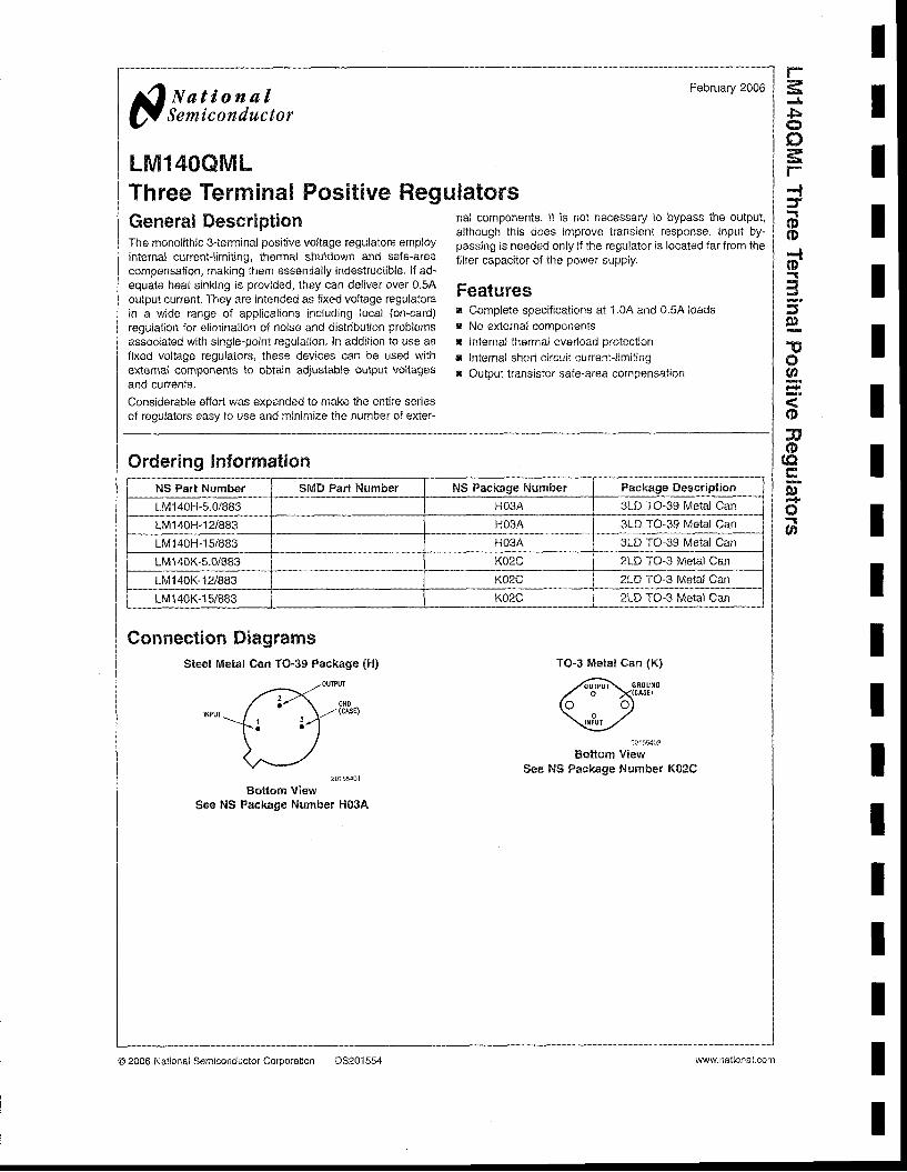
Not iona lSemiconductor
February 2006
LMl4OQMLThree Terminal Positive RegulatorsGeneral DescripticnThe monolithic 3-terminal positive voltage regulator$ employinternal current-limiting, thermal shuidown and saie-areacompensation, making them es*entialiy indestructible. l{ ad-equate heat sinking is provided, they can deliver over 0.5Aoutput current" They are intended as {ixed voltage regulatorsin a wide range of applications including local (on-card)regulation for elimination of noise and di$tributisn problerd$associated with single-point regulation. In addition to u$e asfixed voltage regu'ator$, these devices san be used withext€rnal cofiponents to obtain adiustable output voltagesand currents.
Considerable effort wa$ expended to make the entire seriesof regulators easy to use and minimize the number of exter-
nal components. lt is not necessary to bypass the output,although this does improve transient response. Input by-passing is needed on,y il the regulator i$ located far from thefilte. capac;tor of the power supply^
Featuresl Complete specificat;on$ at 1.0A and 0.5A load$r N0 external cornoongntsr Internal thermal averload protectionr Internal short circuit cufrent-limitingr Output transistor safe-area compen$ation
Connection DiagramsSteel Metal Can TO-39 Package {H)
GND(cAsE)
Soitsm View$ee llS Packagf lJurnber K02C
211154!1
Bottom View$ee N$ Paskags Number H03A
0rdering InformatianNS Part Number SMD Parl Number NS Package Number Package Description
tM140H-5.01S83 HOSA sLD TO-39 Metal Carl
LM140i"r-121883 HOSA SLD TO-3S Metal Can
LM140H-15/883 H03A 3tD T0-39 Metal Can
LM140K-5.0iS83 KO2C zLD TO-3 Metal Can
LM140K-121883 KO2C zLD TO-3 Metal Can
LM140K,15/883 KO2C zLD T0-3 Metal Can
TO-3 MetaN Can {K}
IIIIIIIIIIIIIIIIIII
I
5=r
sc3,.JiF
r-{
.l
oCIJo'-
-l
*\t
.ft
tE,
a=!:
o.r|
GKI
n}'.tg,
O2006 National SemiconductorCorporatiqn DS201554
LM 123-LM223-LM323IIIITIIIIItIIIIIIII
l o ( A )
5
4
3
2
1
0
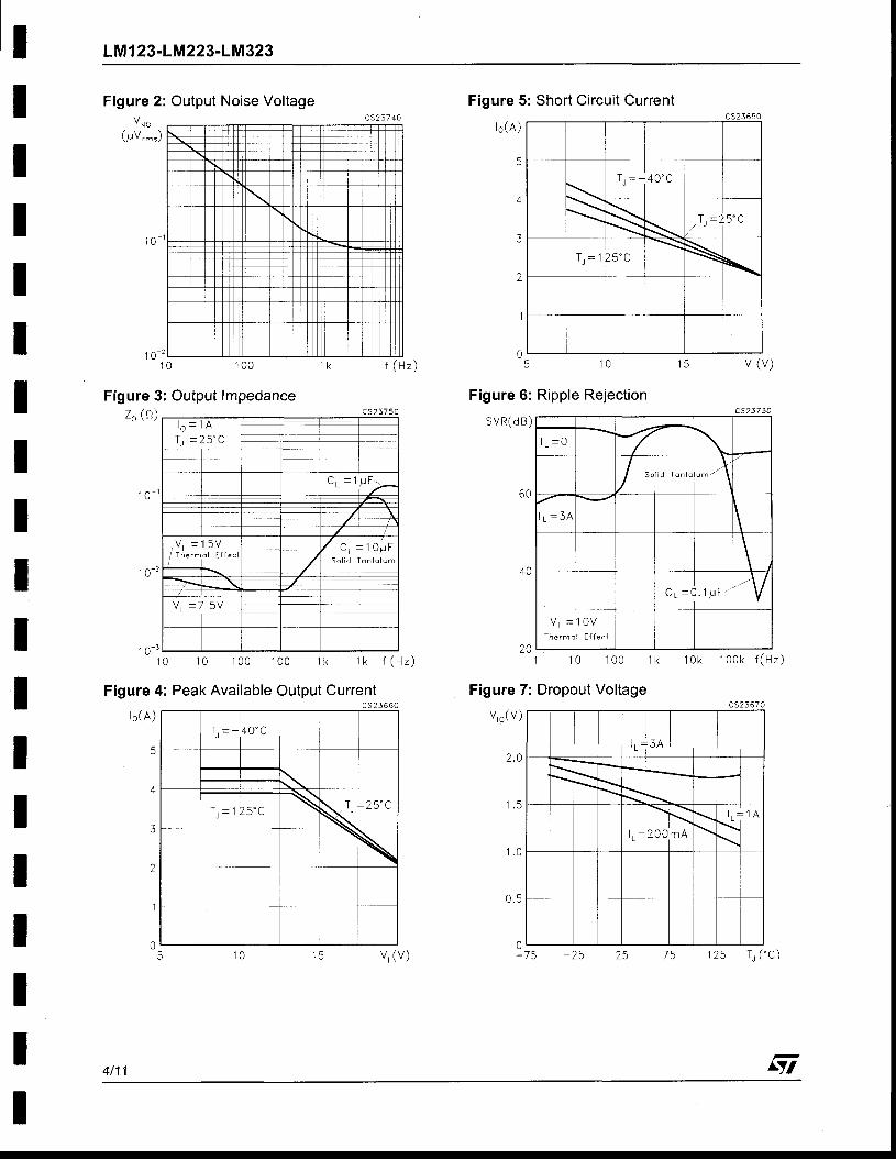
Figure 2: Output Noise VoltageVro
(pv . - , )
1 0 0
zo (0)
1 0 - '
1 0-2
1 O-3
Figure 3: Output lmpedance
1 o
T ,A
u , - t u r -
, V = 1 5 V
/ T h e r m l o l t f f e c J
'.*;::l:
-V = 7 , 5 V
cs23660
l r = - 4 u u
\
T _' J - f , L\ v 2 5 ' C
\
\
Figure 5: Short Circuit Current
l o ( A )
5
4
3
2
1
05 1 0
Figure 6: Ripple Rejection
svR( d B )
1 1 0 1 0 0 1 k
Figure 7: Dropout Voltage
vro(v )
2 . 4
1 . 5
1 . 0
t ) . 5
9
1 0 1 0 1 0 0 1 0 0 1 k 1 k l ( N z \
Figure 4: Peak Available Output Current
1 0 k 1 0 0 k f ( H z )
125 TL ( "C)
4111
ar L - w
ls. l i d T o n t a-\
L _ J ^
\
\
1 ttF vV r = 1 0 V
T h e r m c l E f l e c
1 5 v , ( v )
97
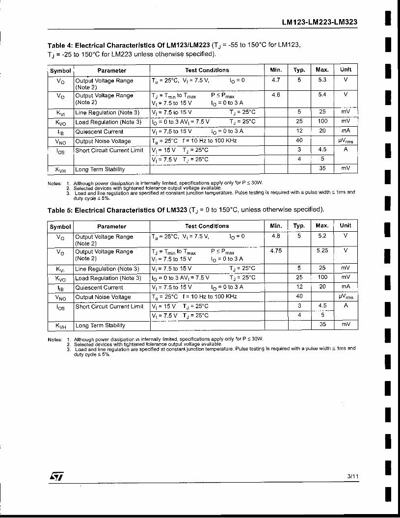
LM 123-LM 223-LM323 tTabfe 4: Efectrical Characteristics Of LM123|LM223 (TJTt= -25 to 150"C forLM223 unless otherwise specif ied).
= -55 to 150'C for LM123, IIIIIIIIIIIIIIIIII
Notes: 1. Although power dissipation is internally limited, specifications.apply only for P < 30W.2. Selected devices with tightened tolerance output voltage available.3. Load and line regulatioi are specified at conitant junction temperature. Pulse testing is required with a pulse width < 1ms and
duty cycle < 5%.
Table 5: ElectricalGharacteristics Of LM323 (Tr = 0 to 150'C, unless othen'vise specified)'
Notes: 1. Although power dissipation is internally limited, specifications.apply only for P < 30W.2. Selected devices with tightened tolerance output voltage available.3. Load and line regulatioi are specified at conitant junclion temperature. Pulse testing is required with a pulse width < 'l ms and
duty cycle S 5%.
Symbol Parameter Test Gonditions M in . Tvp. Max. Unit
Ve Output Voltage Range(Note 2)
Ta= 25'C, V1 = 7.5 V, lo = 0 4 .7 5.3
V6 Output Voltage Range(Note 2)
TJ = Tmin to Tr", P S Pmax
V r = 7 . 5 t o 1 5 V l o = 0 t o 3 A
4 . b 5.4
Kvr Line Regulation (Note 3) Vr = 7.5 to 15 V Tt = 25 'C 5 25 mV
Kvo Load Regulation (Note 3) l o = 0 to 3AV, = 7 .5Y T l = 25 "C zc 1 0 0 mV
I re Quiescent Currenl V r = 7 . 5 t o 1 5 V 1 6 = 0 t o 3 A 1 2 20 mA
Vno Output Noise Voltage Ta= 25"C '( = 1Q Hz to 100 KHz 40 FVrms
los Short Circuit Current Limit V r = 1 5 V T l = 2 5 ' C J 4.5
V r = 7 . 5 V T , t = 2 5 " C 4
Kvn Long Term Stability J C mV
Symbol Parameter Test Gonditions M in . Tvp' Max. Uni t
Ve Output Voltage Range(Note 2)
Ta = 25"C, V; = 7.5 V, lO = 0 4.8 5 5.2
vo Output Voltage Range(Note 2)
TJ = Tmin to T,nu, P < Pr""
V r = 7 . 5 t o 1 5 V l o = 0 t o 3 A
4.75 5.25
Kvr Line Regulation (Note 3) Vr = 7.5 to 15 V Tl = 25 'C 25 mV
Kvo Load Regulation (Note 3) lo = 0to 3 AV' = 7.5Y T; = 25"C 25 1 0 0 mV
I re Quiescent Current V r = 7 . 5 t o 1 5 V l o = 0 t o 3 A 12 20 mA
Vno Output Noise Voltage Ta = 25 'C I = 10 Hz to 100 KHz 4Q FVrms
los Short Circuit Current Limit Vr = 15 V Tl = 25"C 4.5 A
V r = 7 . 5 V T r = 2 5 ' C 4
KvH Long Term Stabil ity 35 mV
g7 3t11
I
sii, LM123lLM223LM323
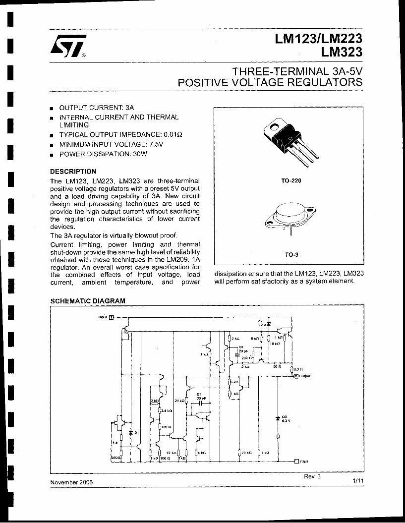
THREE.TERMINAL 3A-5VPOS ITIVE VOLTAGE REGULATORS
IItIIItItIIIIIII
r OUTPUT CURRENT 3A
r INTERNAL CURRENT AND THERMALLIMITING
r TYPICAL OUTPUT IMPEDANCE: 0.014
r MINIMUM INPUT VOLTAGE: 7.5V
r POWER DISSIPATION: 30W
DESCRIPTIONThe LM123. LM223. LM323 are three-terminalpositive voltage regulators with a preset 5V outputand a load driving capability of 3A. New circuitdesign and processing techniques are used toprovide the high output current without sacrificingthe regulation characteristics of lower currentdevices.The 3A regulator is virtually blowout proof.
Current l imit ing, power l imit ing and thermalshut-down provide the same high level of reliabilityobtained with these techniques in the LM209, 1Aregulator. An overall worst case specification forthe combined effects of input voltage, loadcurrent, ambient temperature, and power
dissipation ensure that the LM123, LM223,1M323will perform satisfactorily as a system element.
SCHEMATIC DIAGRAM
TO-220
TO-3
November 2005Rev .3
1 t 1 1
LM123-LM223-LM323
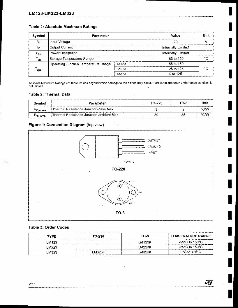
Table 1: Absolute Maximum Ratings
Symbol Parameter Value Unit
V1 Input Voltage 20lo Outout Current Internally Limited
Ptot Power Dissioation Internally Limited
Tsto Storage Temperature Range -65 to 150
Top"."
Operating J unction Temperature Range LM123 -55 to 150
LM223 -25 to 125
LM323 0 to 125
Absolute Maximum Ratings are those values beyond which damage to the device may occur. Functional operation under these condition isnot implied.
Table 2: Thermal Data
Figure 1:Connection Diagram (top view)
cs057 1 0
T0-220
Table 3: Order Codes
ryPE TO-220 TO-3 TEMPERATURE RANGE
LM123 LM123K -55'C to 150'C
LM223 LM223K -25"C to 150'C
LM323 LM323T LM323K 0'C to 125'C
Symbol Parameter TO-220 TO-3 Unit
Rtnj-o"" Thermal Resistance Junction-case Max J 2 'clw
Rttj-amb Thermal Resistance Junction-ambient Max CU JC "ciw
I
MANUFACTURER'S LIST CODE
MANUFACTURER
M83-0004
TO NAME
ADDRESS
P.0 . Box 3608Har r isburg , PA 17105
1202 South 2nd StreetMi lwaukee, WI 53204
Si l i cone Produc ts Bus iness Depar tmentWaterford, NY f2188PH0NE: 518-237-3330
TR}, l Semiconductor Div is ion14520 Aviat ion BoulevardLawndale, CA 90260
Semiconductor Group13500 North Central ExpresswayP.0.Box 225A12 MlS 49Dal las, TX 75265
Fer roxcub D iv i s ion5083 Kings HighwaySaugerties, NY 12477
Amphenol Div i s ion2801 South. 25th AvenueBroadv iew, IL 60153
Sol id S ta te D iv is ionRoute 202Somervi I le, NJ 08876
Elec t ron ics D iv i s ion18435 Susana RoadRancho Dominguez, CA 9022LPH0NE: 213-537-4750
L icon D iv i s i on6615 West I rv i ng Park RoadChicago, IL 60634
Semiconducton Products Sector5005 East McDowel I RoadPhoen ix , AZ 85008PH0NE z 602-?44-7100
00779
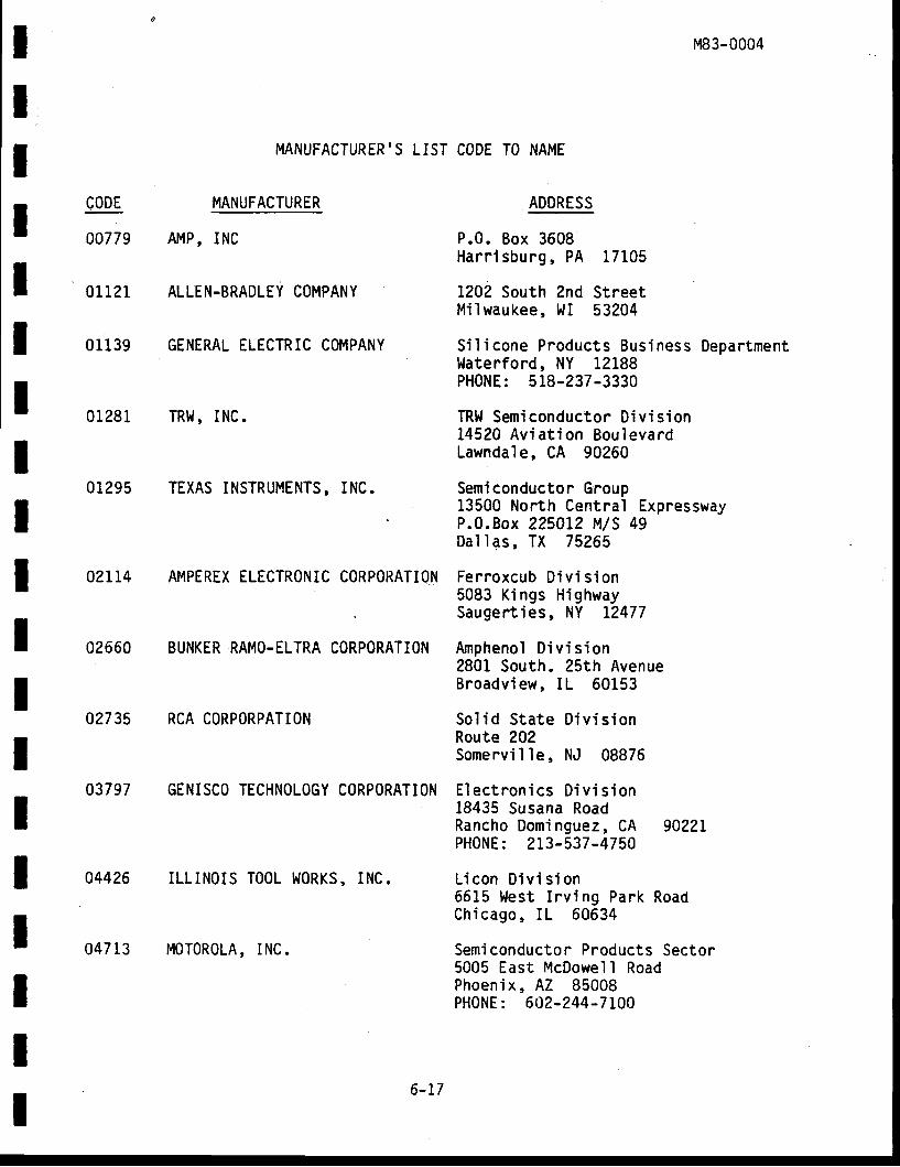
01 121
01139
MP, INC
ALLEN.BRADLEY COMPANY
GENERAL ELECTRIC COMPANY
IIIIIIIIII
01281 TRl, l , INC.
01295 TEXAS INSTRUMENTS, INC.
021 14 AMPEREX ELECTRONIC CORPORATION
BUNKER RAMO-ELTRA CORPORATION02660
02735 RCA CORPORPATION
03797 GENISCO TECHNOLOGY CORPORATION
04426 ILLINOIS TOOLWORKS, INC.
04713 MOTOROLA, INC.
6-17
M83-0004 IIIIIIIItIIIIIIIIII
CODE
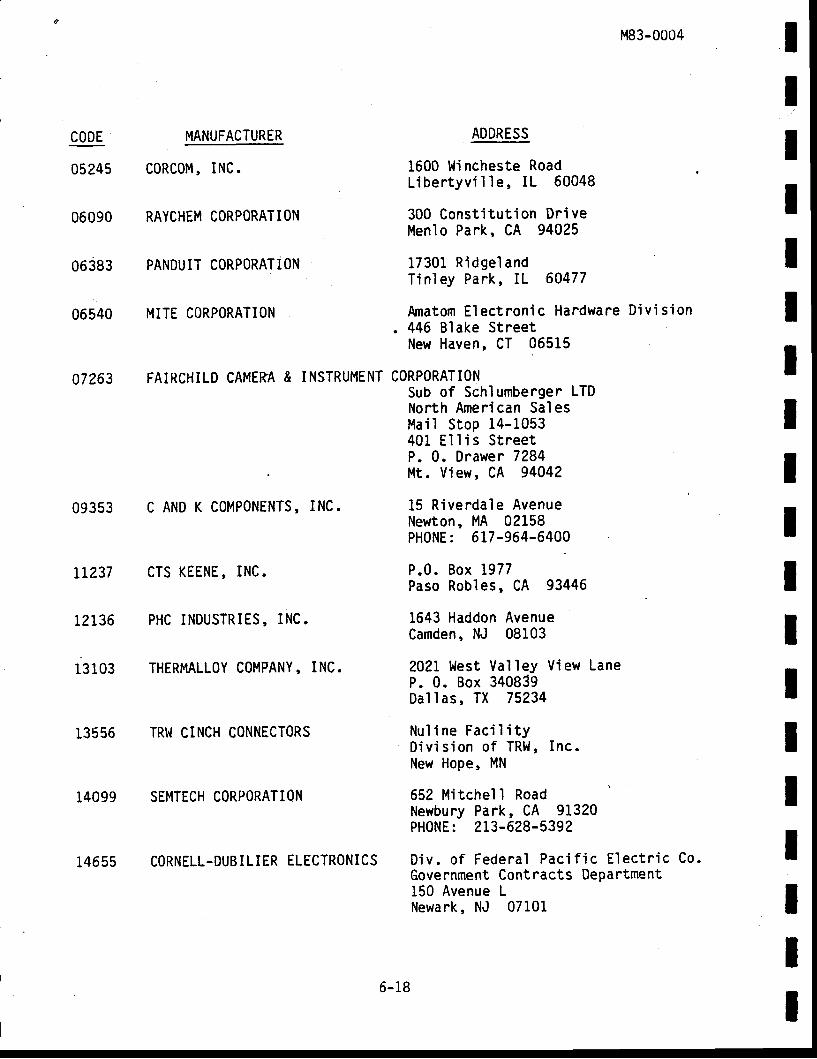
05245
06090
06383
06540
tL237
12136
13103
A7263 FAIRCHILD CAMERA & INSTRUMENT
09353 C AND K COMPONENTS, INC.
MANUFACTURER
cORcoM, INc.
RAYCHEM CORPORATION
PANDUIT CORPORATION
MITE CORPORATION
CTS KEENE, INC.
PHC INDUSTRIES, INC.
THERMALLOY COMPANY, INC.
1600 l'|i ncheste RoadL iber tyv i l le , IL 60048
300 Const ' i tut ion Dr iveMenlo Park, CA 94025
17301 R idge landTinley Park, IL 60477
Amatom Electronic Hardware Div ' i s ' ion. 446 Blake Street
New Haven, CT 06515
CORPORATIONSub of Schlumberger LTDNorth American SalesMai l Stop 14-1053401 E l l i s S t ree tP. 0 . Drawer 7284Mt. View, CA 94042
15 R iverda le AvenueNewton, MA 02158PH0NE: 617-964-6400
P.0 . Box 1977Paso Robles, CA 93446
1643 Haddon AvenueCamden, NJ 08103
2021 West Val ley View LaneP. 0. Box 340839Dal las, TX 75234
Nu l ine Fac i l i t yDi v i s i on of TR! ' l , Inc.New Hope, MN
652 Mi tche l l RoadNewbury Park, CA 91320PHONE: 213-628-5392
Div . o f Federa l Pac i f i c E lec tn ic Co .Government Contracts Department150 Avenue LNewark, NJ 07101
ADDRESS
13556 TRt.l CINCH C0NNECToRS
14099 SEMTECH CORPORATION
14655 CORNELL.DUBILIER ELECTRONICS
6-18
IIIIIIIIItIIIIII
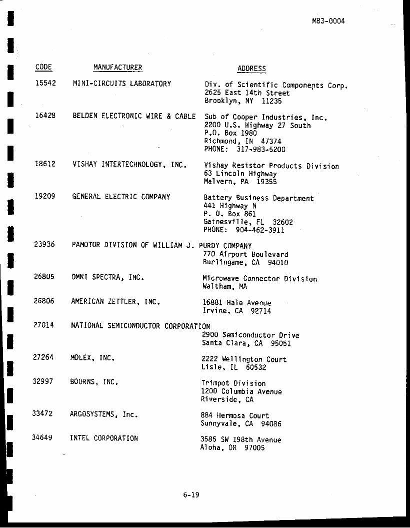
16428
26806
270L4
27264
32997
33472
34649
M83-0004
CODE MANUFACTURER ADORESS
15542 MINI-CIRCUITS LABORATORY Div . o f Sc ien t i f i c Componepts Corp .2625 East l.4th StreetBrook lyn , NY 11235
18612
BELDEN ELECTRONIC bIIRE & CABLE sub of coopen Industr ies, Inc.220A U.S. Highway ?7 South.P.0. Box 1.980Richmond, IN 47374PH0NE: 317-983-5200
vISHAY INTERTECHNOL0GY, INc . v ishay Res is to r pnoducts D iv is ion63 Lincoln HighwayMal vern, PA 19355
GENERAL ELECTRIC C0MPANY Battery Business Department441 Highway N
. P . 0 . Box 861Ga inesv i l l e , FL 3ZA0ZPHONE: 904-462-3911
PAMOT0R DIVISI0N 0F I,IILLIAM J. PURDY C0MpANy770 Ainport BoulevardBur l ingame, CA 94010
19209
23936
26805 OMNI SPECTRA, INC. Microwave Connector Div i s iontrlaltham, MA
16881 Hale AvenueIrv ine, CA 92714
AMERICAN ZETTLER, INC.
NATIONAL SEMICONDUCTOR CORPORATION2900 Semiconductor Dr iveSanta Clara, CA 95051
??22 Vel l ington CourtL is le , IL 60532
Tn impot D iv i s ion1200 Columbia AvenueRivers ide , CA
884 Hermosa CourtSunnyva'le, CA 94086
3585 St' l 198th AvenueAl oha, 0R 97005
M0LEX, INC.
B0URNS, INC.
ARG0SYSTEI'IS, Inc.
INTEL CORPORATION
6-19
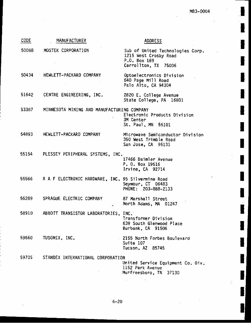
50434 HEWLETT-PACKARO COMPANY
CENTRE ENGINEERING, INC.
MINNESOTA MINING AND MANUFACTURING COMPANY
CODE MANUFACTURER
50088 MOSTEK CORPORATION
51642
53387
54893 HEWLETT.PACKARD COMPANY
55154 PLESSEY PERIPHERAL SYSTEI4S, INC.
55566 R A F ELECTRoNIC HARDWARE, INC.
M83-0004
ADORESS
Sub o f Un i ted Techno log ies Corp .1215 West Crosby RoadP.0 . Box 169Carrol l ton, TX 75006
Optoel ectroni cs Di v i s ion640 Page Mi I I RoadPalo A l to , CA 94304
2820 E. College AvenueState Col lege, PA 16801
Elec t ron ic Produc ts D iv is ion3M CenterSt. Pau' l , MN 55101
Micnowave Semiconductor Div i s ion350 West Tr imble RoadSan Jose, CA 95131
L7466 Daimler AvenueP. 0 . Box 19616Inv ine , CA 9?714
95 Si I vermi ne RoadSeymour, CT 06483PHONE: 203-888-2133
87 Marshal l StreetNorth Adams, M 0L247
I NC.Trans former D iv is ion639 South Glenwood PlaceBurbank, CA 91506
2155 North Forbes BoulevardSuite 107Tucson, AZ 85745
tIIIIIIIIIIIIIIIII
56289
58910
SPRAGUE ELECTRIC COMPANY
ABBOTT TRANSISTOR LABORATONTES,
59660 TUSONIX, INC.
59705 STANOEX INTERNATIONALCORPORATIONUni ted Serv ice Equ ipment Co. D iv .1152 Park AvenueMurfreesbono, TN 37130
6-?O
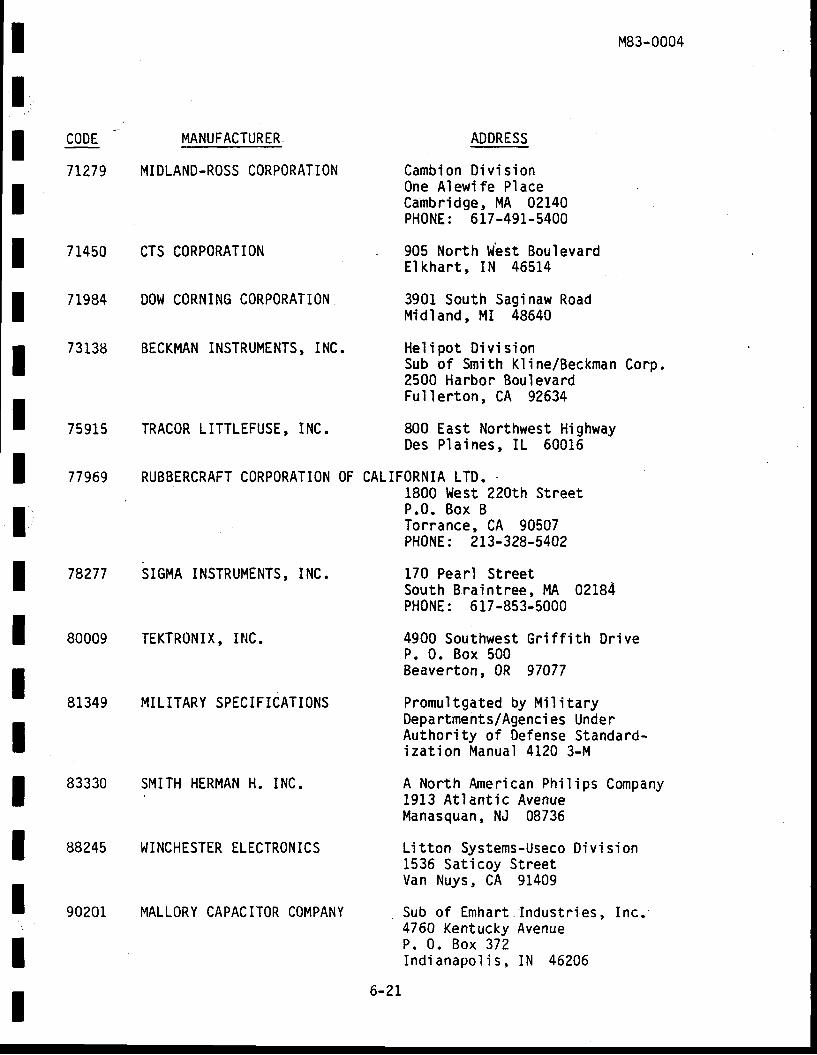
IIIIIIIIIIIIII
7 1450
71984
73138
t 83330
88245
CTS CORPORATION
DOI^I CORNING CORPORATION
SMITH HERMAN H. INC.
t. l INCHESTER ELECTRONICS
CODE MANUFACTURER
7I279 MIDLAND-ROSS CORPORATION
M83-0004
ADDRESS
Cambi on Di v i s ionOne A lewi fe P laceCambridge, MA 02140PH0NE: 617-491-5400
905 North W'est BoulevardEl khar t , IN 46514
3901 South Sagi naw RoadMid land, MI 48640
He l ipo t D iv i s ionSub of Smith Kl ine/Beckman Conp.2500 Harbor BoulevardFu l le r ton , CA 9?634
800 East Northwest HighwayDes P la ines , IL 60016
CALIFORNIA LTD. -1800 l.lest ?20th StreetP .0 . Box BTorrance, CA 90507PH0NE: 213-3?8-5402
170 Pearl StreetSouth Braintree, MA 02184PHONE: 617-853-5000
4900 Southwest Gri f f i th Dr iveP. 0 . Box 500Beaverton, 0R 97A77
Promultgated by Mi l i taryDepartments/Agenci es UnderAuthor i ty of Defense Standard-iza t ion Manua l 4120 3-M
A Nor th Amer ican Ph i l ips Company1913 At lan t ic AvenueManasquan, NJ 08736
Li t ton Systems-Useco Divi s ion1536 Sat icoy StreetVan Nuys" CA 91409
Sub o f Emhar t lndus t r ies , Inc . '4760 Kentucky AvenueP. 0 . Box 372Indi anapol i s, IN 46206
6-?r
BECKMAN INSTRUMENTS, INC.
75915
77969
TRACOR LITTLEFUSE, INC.
RUBBERCRAFT CORPORATION OF
78277 SIGMA INSTRUMENTS, INC.
8OOO9 TEKTRONIX, I I IC.
81349 I ' I ILITARY SPECIFICATIONS
II
a
II
90201 MALLORY CAPACITOR COMPANY
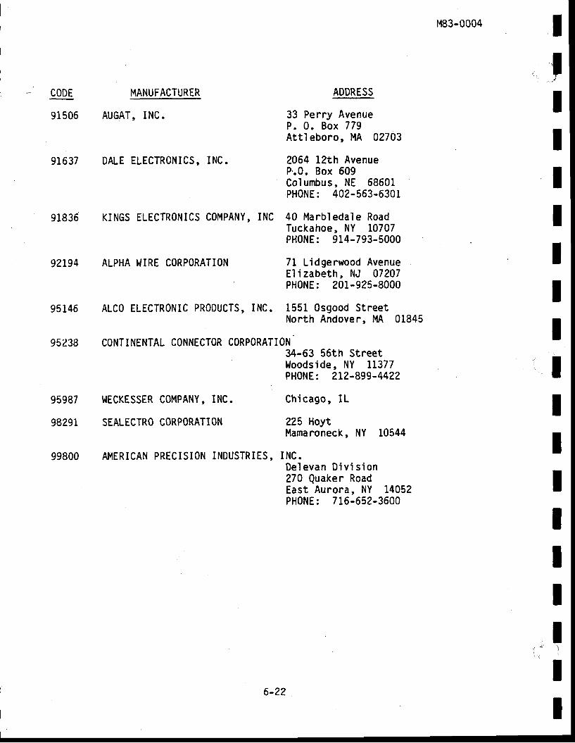
M83-0004 IIj
III
IIItI
91506
91637
91836
92194
95146
95?38
95987
9829t
99800
MANUFACTURER ADDRESS
AUGAT, INC. 33 PerrY AvenueP. 0 . Box 779Attleboro, MA 02703
DALE ELECTRONICS, INC. 2064 lzth AvenueP'.0. Box 609Columbus, NE 58601PHONE: 402-563-6301
KINGS ELECTR0NICS COMPANY, INC 40 Marbledale RoadTuckahoe, NY L0707PHONE: 9L4-793-5000
ALPHA WIRE C0RPORATI0N 71 Lidgerwood AvenueEl i zabeth, NJ 07207PHONE: 20L-925-8000
ALC0 ELECTR0NIC PR0OUCTS, INC. 1551 Osgood StreetNorth Andover, M 01845
CONTINENTAL CONNECTOR CORPORATION34-63 56th Streettloodside, NY IL377PHONE: ?12-899-4422
Ch icago , IL
225 HoytMamaroneck, NY 10544
AMERICAN PRECISION INDUSTRIES, INC.De levan D iv i s ion270 Quaken RoadEast Aurora, NY 14052PH0NE: 7L6-652-3600
WECKESSER COMPANY, INC.
SEALECTRO CORPORATION
ItIIIIIII
: .
6-?2


IIIIIIIIIIIIIItItII
tITITtIIITITIIIIl,It
M83-0005
"$t
b&
g. ;
{g,
I
TsN&li
tib. &.*;
#xfg,x1ls,
I
F!,
fr$L
$ig
##&*
i,,i1
E,]
$_&s
AS 210-0 1AMODULE CONTROLLER
Rev i sed 7 /E5

IIIIITI
MB3-0005
r$,
*
IIIIIIIIII
Al l r igh ts reserved. No par t o f th is pub l i ca t ion may bereproduced, stored in a retr ieval system, or t ransmit ted,ln any fo rm or by any means, e lec t ron ic , mechan ica l ,photocopying, recording and/or otherwi se wi thout thepr ior wr i t ten perrnission of ARG0Systems, Inc. This man-ua1 may no t be len t , reso ld , h i red ou t o r o therw ise d is -posed of by way of t rade in any form of binding or covero ther than tha t in wh ich i t i s pub l i shed, w i thout thepr ior consent of ARG0Systems, Inc.
ARG0Systems, Inc. / 884 Hermosa Court , Sunnyva' le, Cal i fornia 94086Te]ephone (Area code 408) 737-2000 / Te]ex l lo ' 35?077

ItIIIIIIIIIIIIIIIII
Chapter
M83-0005
IABLE OF CONTENTS
T i t le
Preface
GENERAL INFORMATION
1-1 Introduct iont -Z Phys ica l and E lec t r i ca l Descr ip t ion
INSTALLATION
2-l Introduct ion
OPERATION
3-1 Introduct ion3-2 Control s and Indicators3-3 0perat ing Instruct ions3-4 Set Time on the Control ler 's Internal Clock3-J Determine IEEE-488 Address of Modu'le Controller3-6 Frequency Error Measurement3-7 Display Frequency ltleasurments from Memory3-8 Dr i f t Ca lcu la t ions3-9 \et t ing Time on AS210-20 Clock3-1.0 Reading ATime in the AS210-20 Clock3-11 Remote Control3-12 AS210-01A Remote Time Corrnands3-13 Setting the AS210-01A Time - Remote Command3-1.4 Reading the AS210-01A Time - Remote Conmand3-15 Frequency Generator lvlodule Remote Cornmands (AS210-03)3-16 Digital Delay Generator lt lodule Remote Corunands (AS210-04)3-17 Frequency Comparator Module Remote Cornmands (AS210-02)3-18 Remote Measurement Conrnands3-19 Remote Determination of Number of Data Points Taken3-20 Remote Drift Rate Ca]culation Command3-21 Remote Two Point Drift Rate Calculation Corrnand3-22 Remote Data Point Readout3-23 Remote Learn Cornmand3-24 Remote Sel f-Test Command3-25 AS210 Service Requests3-26 Reading the 45210-20 Time - Remote Cornmand3-27 Setting Time In the AS210-20 - Remote Connand3-28 Reading ATime From the AS210-20 - Remote Conmand3-29 Synchronizing I pps In the AS210-20 - Remote Conmand3-30 Memory Battery 0peration3-31 Microwave Frequency Generator Module - Remote Cormands
Page
V
1-1
1-11-1
2-L
2-r
3-1
3-13-23-23-2.3-93-93-1 13- t23-133-143-153-183-183-183-183-193-193-193-213-213-223-?43-253-253-263-263-263-263-283-283-29
xT,ilx
IItItIIIIII
- 1 -
MB3-0005IIIIIIIItIIItIIIIIt
5-2
5-3
Chapte r
4
TABLE OF C0NTENTS (Con t i nued )
T i t l e
THEORY OF OPERATION
4- I In t roduc t ion4-2 Modu le Func t iona l Descr ip t ion4-3 Keyboard Log ic , C i rcu i t Card A34-4 D isp lay Log ic C i rcu i t Card , A44-5 Modu le Contno l le r CPU and Memory Assembl ies4-6 Ex tended PROM GPIA and T imer Log ic C i rcu i t Card ,4-6 .1 S tandby Bat te ry C ' i rcu ' i t s4-6 .2 Power -o f f T imer C ' i rcu i t4 -6 .3 In te rva l T ' imer4-7 CPU and EPR0I ,1 Log ic C i rcu i t Card , A24-8 Memory Expans ion C i rcu i t Card , A5
Page
A 1.+- r
4-r4-rA A+ - J
4-44-4
A1 4-44-44-54-54-64-7
5-1
5-1
MiNTENANCE AND CALIBRATION
5-1 In t roduc t ' ion
SECTION I
5 -? Prevent ive Main tenance
SECTION I I
5-3 Performance Tests
SECTION I I I
5 -4 Troub leshoot ing Procedure5-5 Access to AS210-01A Modu le Cont ro l le r5-6 Troubleshoot ing of the Memory Standby5-7 Replacement Procedure for the Standby
Battery
ILLUSTRATED PARTS LIST
6-1 In t roduc t ' ion6-2 Manufac tu re r ' s Code L is t
Batte ryMemory Standby
5-55-55-5
5-8
6-1
6-16-19
- t ' l -
IItIIIIIIItIIIIIIIT
MB3-0005
.,&s6
a
a
Pl
vFj gure-
i .1
3 .1
3 .2
< {
4.L -
5 .1
5 .2
5 .3
5 .4
5 .5
5 .6
5 .7
6 .1
6 .2
6 .3
6 .4
6 .5
L IST OF ILLUSTRATIONS
T' i t l e
AS210-01A Modu le Con tno l l e r
AS210-01A Fnont Pane l Contno ls and Ind ica tors
0pera t i ona l F l ow D j agram
IEEE-488 In te r face Bus Address Se lec t Swi tch
Modu le Contno l le r Func t iona i B lock D ' iagram
Flow Diagram o f the Troub leshoot ing Procedure fon theAS210-01A l4odu le Contno l le r
Top Vi ew of ASZi0-01A
AS210-01A Extended PR0M GPIA and T imer Log ic Assemb)yA1, Schemat jc D iagram
AS210-01A CPU and EPROM Log ic Assembl y A2, Schemat ' i c D iagram
AS210-01A Keyboard Log' ic Assembly A3, Schemat ' ic D j agrarn
AS210-01A Disp lay Log ic AssemblJ A4, Schemat ic D iagr "am
AS210-01A Memory Expans ion Board A5, Schemat ic D jagram
AS210-01A Modu le Cont ro l le r Assembly , A1
4S210-01A Modu le Con t ro l le r Assembly , A2
AS210-0 iA Keyboard Log ic Assembly , A3
AS210-01A D isp lay Log ic Assembly , A4
AS210-01A Memory Expans ' ion Assembly , A5
P age
1-2
3-4
3-5
3- i6
4-2
5-4
5-9
5- 10
5-1 1
5-12
5- i3
5- 14
6-7
6- i0
6 -1 3
6- 15
6-18
la
$
fiI$
- l l l -
MB3- 0005IIItIIIIIIITIItIIII
Tab l e
1-1
3-1
3-2
3-3
3-4
5-1
5-2
5-3
LIST OF TABLES
Ti t le
AS210-01A Env i ronmenta l and Phys ica l Data
AS210-0 iA Fron t Pane l Cont ro ls and Ind ica tons
Error Code Di sp1 ays
AS210-01A GPIB Message Set
Ser i a l Pol I Status Descr i pt i on
Prevent ive Main tenance Checks and Serv ices
Ernor Code L is t ing
Common Pnob lems and Poss ib le Prob lem Locat ion' i n the AS210-01A Modu I e Cont rol I e r
P age
1-3
3-2
3-4
3-17
3-27
5-2
5-6
5-7
- t v -
IIIIIIIIIIIIIIIIIII
M83-0005
PREFACE
Th js manua l con ta ins ins ta l la t ion , opera t ion , and ma in tenance
ins t ruc t ions fo r the AS210-01A Modu le Cont ro l le r . The da ta conta ined here in
is a r ranged as fo l lows:
Chapter 1
Chapter 2
Chapter 3
Chapter 4
Chapter 5
Chapter 6
Ref erence Publ i cat ' ions
AS21OA-PM
AS2lORM, LM
AS210-02
AS210-03
AS210-04
AS210-05
AS210-06
AS210-08
AS210-20
General Informat ion
I nstal I at i on
0perat i on
Theory of 0perat ion
Main tenance and Ca l ib ra t ion
I1 ' lus t ra ted Par ts L i s t
Portab' le Mainframe 0perat ion and l la intenance Manua' l
Mainframe Operat ion and Maintenance Manual
Frequency Comparator Operat ion and Maintenance Manual
Frequency Generator 0perat ion and Maintenance Manual
D ig i ta l De lay Genera tor Opera t ion and Main tenance Manua l
Standby Battery Operat ion and Maintenance Manual
Microwave Generator 0perat ion and Maintenance Manual
D is t r ibu t ion Ampl i f ie r Opera t ion and Main tenance Manua l
T ime C lock Opera t ion and Main tenance Manua l

IItItIIIIIIIttIIIII
IIIII
CHAPTER 1
GENERAL INFORMATION
M R ? . N N N A
1-1 I NTRODUCTI ON
The AS210-01A Modu ' le Con t ro ' l l e r , i l l us t ra ted in F igure l .L , p rov idescontrol of the other modu' les in an AS210 Electronic Counter and FrequencyStandard Ca l ib ra t ion sys tem, The modu le a lso prov ides se l f - tes t . capab i l i t yfo r i t se l f and o ther modu ' les ins ta l led in the main f rame. A bu i l t - in memorybattery al lows the uni t to retain data through a . Themodule control ler can be progranrmed through i ts f ront panel keyboard orthrough the IEEE-488 interface. Descr ipt ions of other modules in the AS210ser ies are descr ibed in separate publ icat ions avai ' lable f rom ARGOSystems andl is ted in the Pre face .
PHYSICAL AND ELECTRICAL DESCRIPTION
The module contro ' l ' ler contains a f ront panel keyboard, LED display,and pushbutton controls for operat ing the AS21O modules. Interface with somemodu les is t ransparent f rom an opera tor ' s v iewpo in t as the bu i l t - in mic ropro-cessor hand les the t ransmiss ion o f ins t ruc t ions and process ing o f da ta . Inthe case of the AS210-02 Frequency Comparator Module and the AS210-20 TimeClock, the module control ler interfaces direct ly wi th the operator. The pro-grams for calculat ing dr i f t rate are wr i t ten into the control ler memory andare put into act ion by keyboard control . The circui t ry of the module ismounted on f ive pr inted circui t card assembl ies. Power is provided by theAS210 Mainframe. The module control ' ler provides control and processing func-t ions on1y , thus no spec i f i ca t ion o f i t s opera t ion is app l i cab le ou ts ide o fenv i ronmenta l and phys ica l da ta . Th is in fonnat ion is p rov ided in Tab le 1 -1 .
t-2
IIIIIttIIItItI 1,1

M83-0005
IIt
l:ItlrIItIIIIIIIt
Tab le 1 -1
AS21O-O1A ENVIRONMENTAL AND PHYSICAL DATA
OPERATING TEMPERATURE
POI^IER
I,lE I GHT
0 to 40"C
AS210 Mainframe
3 pounds
t -3

I
ItItItlrIIIIIIIIII
MB3-0005
CHAPTER 2
INSTALLATION
2-L INTRODUCTION
The AS210-01A Modu le Cont ro l le r p lugs jn to the AS210 Ma ' in f rame.
The modu le i s e lec t r i ca l l y connected th rough the rear connector and mechan i -
ca l1y re ta ined v ia a f ron t pane l lock ing bar on the main f rame. Power and
signal interface is provided through the AS210 Mainframe. The modu' le rnust be
inser ted in to the r igh t s ide o f the ma in f rame. Th is i s the on ly ' l oca t ion
des igned fo r i t .
N0TE 1 : Power mus t be o f f i n the AS210 Ma in f rame when the modu]econt ro l le r i s removed or ins ta ' l led .
NOTE 2 : Due to the h igh re ten t ion fo rce o f the modu le cont ro lJer 'scard edge connec to r , i t w i l l be necessary to remove theadj acent s i ng' l e wi dth modu' le, reach behi nd the modul e con-t ro ' l 1e r , and pu l l i t ou t wh i ' l e ac tua t ing the f ron t pane lre lease mechan ism (F igure 3 .1 ) .
CAUTION
Do not attemotin a Tek t ron ixresu l t .
to use the AS210 ser ies modu lesma i nf rame as severe damage wi 1
' l
z-r

3-1
IIIItIItIIIIIItIIII
M83-0005
CHAPTER 3
OPERATION
I NTRODUCTI ON
The AS210-01A Modu le Cont ro l le r mon i to rs and cont ro ' l s the modu les
o f the AS210 ser ies . The mic roprocessor i s loca ted in the modu le cont ro ' l le r
and opera tes in con junc t ion w i th each o f the modu ' les ins ta l led to t ransmi t
and rece ive da ta , p rocess the da ta , and per fo rm var ious ca lcu la t ions re la t i ve
to the modu le 's opera t ion . Most o f these func t ions are t ransparent to the
operator. Both the f requency comparator module and the t ime clock module,
however , opera te in con junc t ion w i th the cont ro l le r . Th is chapter conta ins
operat ing in.struct ions for the use of the module control ler wi th the AS210-02
Frequency Comparator Modu' le, and the AS210-20 Time Clock Module. These in-
s t ruc t ions are essent ia l l y dup l i ca ted in the AS210-02 and AS210-20 manua ls .
The opera t ing ins t ruc t ions prov ided are keyed to F igure 3 .2 ,0pera t iona l F low
Diagram. A standby battery, located on the rear panel , is used tb reta ' in the
data in memory i f ac power is d ' isconnected. A sel f - test can be started by
the operator wi th the f ront panel SELF-TEST pushbutton. This act jvates a
rout ine that scans the other modules in the system, except the AS2i0-05
Standby Battery Module and the AS210-08 Distr jbut ' ion Ampl i f ier . The sel f -
tes t rou t ine de tec ts e r ro rs and d isp ' lays a fau l t - loca t ing code on the f ron tpane l LED d isp lay . l ^ lhen an er ro r i s found, the program ha l ts and d isp lays an
er ror code. The rou t ine w i i l con t inue when the CONT func t ion bu t ton is
pressed. Tab le 3 -2 i s an er ro r l i s t ing . I f the A5210-06 Mic rowave Genera tor
Modu le i s in the sys tem, a Y IG f i l t e r tun ing ca l ib ra t ion i s done as par t o f
the sel f - test .
3 -1
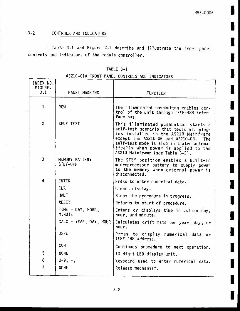
M83-0005
3-? CONTROLS AND INDICATORS
Tab le 3 -1 and F igure 3 .1 descr ibe and i l l us t ra te the f ron t pane lcont ro ls and ind ica tors o f the modu le cont ro l le r .
TABLE 3-1AS21O-O1A FRONT PANEL CONTROLS AND INDICATORS
IIIIIItIIIIIIIIIIII
INDEX NO.F IGURE.
3 .1 PANEL MARKING FUNCTION
5
6
7
i
2
3
4
REM
SELF TEST
MEMORY BATTERYSTBY-OFF
ENTER
CLR
HALT
RESET
TIME -MINUTE
CALC .
DSPL
CONT
NONE
0-9 , -
NONE
DAY, HOUR,
YEAR, DAY,HOUR
The i l lumina ted pushbut ton enab les con-trol of the uni t through IEEE-488 inter-face bus .
Th is i l l umina ted pushbu t ton s ta r ts ase l f - tes t scenar io tha t tes ts a l l p lug-i ns i ns ta ' l I ed i n the AS210 Ma i n f rameexcept the AS210-05 and AS210-08. These l f - tes t mode is a lso in i t ia ted au toma-t i ca l l y when power i s app ' l i ed to theAS210 Main f rame (see Tab le 3 -2) .
The STBY pos i t i on enab ' les a bu i l t - i nmicroprocessor battery to supply powerto the memory when ex terna l power i sdi sconnected.
Press to enter numerical data.
C lears d isp lay .
Stops the procedure in progress.
Returns to start of procedure.
En te rs o r d isp lays t ime in Ju l ian day ,hour , and minu te .
Ca lcu la tes dr i f t ra te per year , day , o rhour .
Press to d i sp l ay numer i ca l da ta o rIEEE-488 address .
Cont inues procedure to nex t opera t ion .10-d i g i t LED d i sp ' lay un i t .Keyboard used to enter numerical data.Re lease mechan ism.
3-?
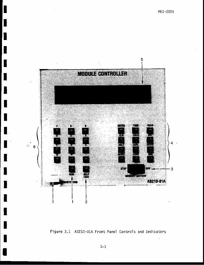
M83-0005IIIIIIIIIIItIIIIII
Figure 3 .1 AS210-01A Front Pane l Cont ro ls and Ind ica tors
)\+
)
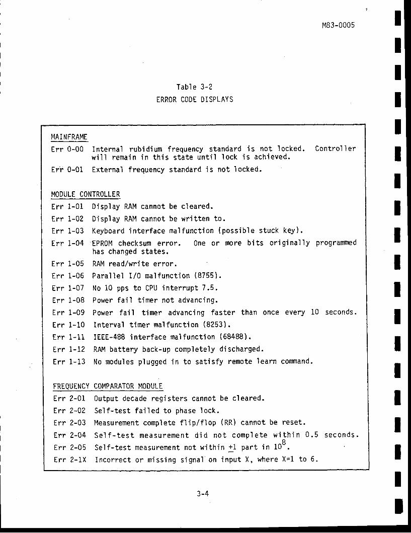
MB3-0005 IIIIIIIIIIIIIIIIIII
Tab le 3 -2
ERROR CODE DISPLAYS
I{AI NFRAME
Err 0-00 Internal rubidium frequency standard is not locked. Control lerw i l l remain in th is s ta te un t i l lock i s ach ieved.
Err 0-01 External f requency standard is not locked.
MODULE CONTROLLER
Err 1 -01 D isp lay RAM cannot be c leared .
Err 1-02 Display RAM cannot be wri t ten to.
Er r L -03 Keyboard in te r face mal func t ion (poss ib le s tuck key) .
Er r 1 -04 EPROM checksum er ror . One or more b i ts o r ig ina l ]y p rogrammedhas changed states.
Err 1-05 RAM read/wri te error
Er r 1 -06 Para l le l I /0 ma l func t ion (8755) .
Er r L -07 No 10 pps to CPU in temupt 7 .5 .
Er r 1 -08 Power fa i l t imer no t advanc ing .
Err 1-09 Power fa i ' l t imer advancing faster than once every 10 seconds.
Er r 1 -10 In te rva l t imer ma l func t ion (8253) .
Err 1- l .L IEEE-488 interface malfunct ion (68488).
Err 1-1.2 RAM battery back-up completely discharged.
Err 1-13 No modu' les plugged in to sat isfy remote learn conmand.
FREQUENCY COMPARATOR MODULE
Err 2 -01 Output decade reg is te rs cannot be c leared .
Erc 2 -02 Se l f - tes t fa i led to phase lock .
Err 2-03 Measurement complete f l ip/ t top (RR) cannot be reset.
Er r 2 -04 Se l f - tes t rneasurement d id no t comp le te w i th in 0 .5 seconds .
Er r 2 -05 Se l f - tes t measurement no t w i th in +1 par t in 10" .
Er r 2 -1X Incor rec t o r m iss ing s igna l on inpu t X , where X= l to 6 .
3 -4
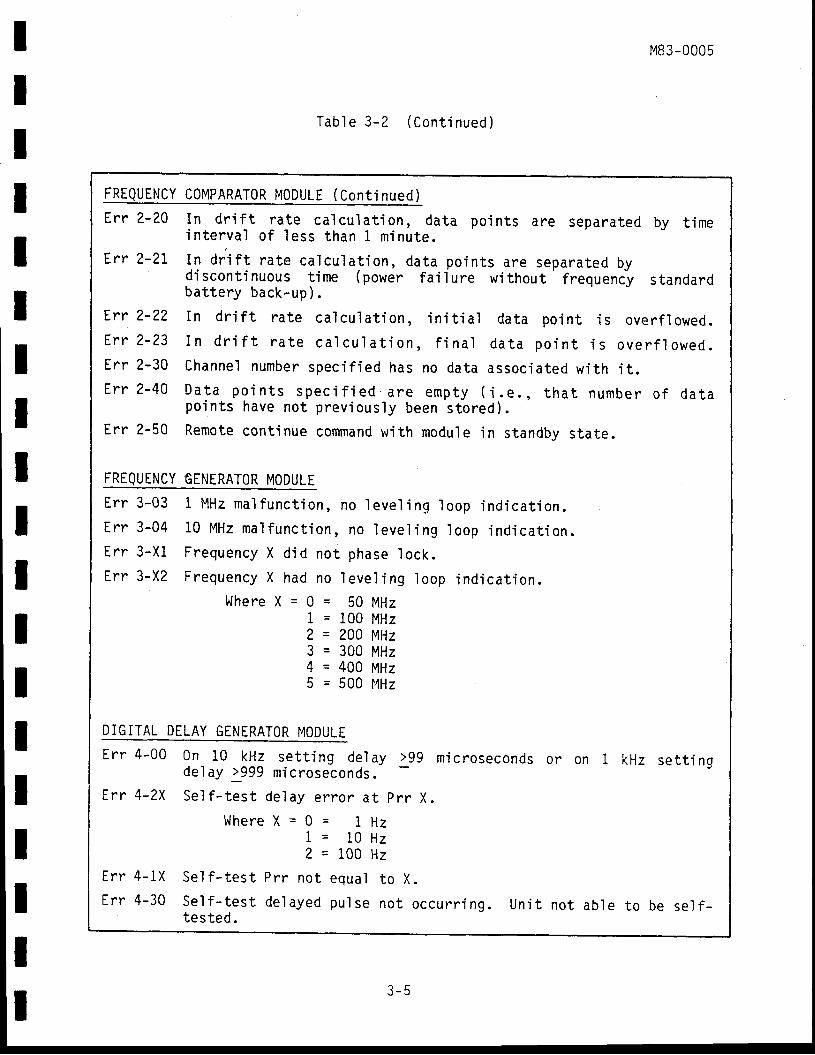
IIItTItIIIIIIIIIIII
MB3-0005
Tab le 3 -2 (Con t inued)
FREQUENCY COMPARATOR I4ODULE (Cont inued)
Er r 2 -2Q In d r i f t ra te ca lcu la t ' ion , da ta po in ts a re separa ted by t imein te rva ' l o f less than 1 minu te .
Erc ? -21 In d r i f t ra te ca lcu la t ion , da ta po in ts a re separa ted byd iscont inuous t ime (power fa i lu re w i thout ' f requency s tandardbat te ry back-up) .
Er r 2 -22 In d r i f t ra te ca lcu la t ion , i n i t i a l da ta po in t i s over f lowed.Er r 2 '23 I n d r i f t ra te ca l cu l a t i on , f i na i da ta po i n t i s over f l owed.Er r 2 -30 channe l number spec i f ied has no da ta assoc ia ted w i th i t .E rc 2 -40 Data po in ts spec i f i ed a re empty ( i .e . , tha t number o f da ta
po in ts have no t p rev ious ly been s to red) .Err 2-50 Remote cont inue command vl i th module in standby state.
FREQUENCY GENERATOR MODULEErr 3-03 1 MHz ma1 funct i on , no I evel ' i ng
' l oop i ndi cat i on .
E r r 3 -04 10 MHz ma l func t ion , no leve l i ng loop ind ica t ion .Er r 3 -X1 Frequency X d id no t phase lock .Er r 3 -X2 Frequency X had no leve l ing loop ind ica t ion .
WhereX=0= 50MHz1 = 100 MHz2 = 2QA MHz3 = 300 MHz4 = 400 MHz5 = 500 t4Hz
DIGITAL DELAY GENERATOR I4ODULEErr 4 -00 0n 10 l l t l se t t ing de ' lay >99 mic roseconds or on 1 kHz se t t ing
de lay >999 mic roseconds .Er r 4 -?X Se l f - tes t de lay e r ro r a t p r r X .
WhereX=0= 1Hzl= 10Hz2=100H2
Er r 4 -1X Se l f - tes t P r r no t equa l to X .Er r 4 -30 Se l f - tes t de layed pu lse no t occur r ing . Un i t no t ab le to be se l f -
tes ted .
3 -5
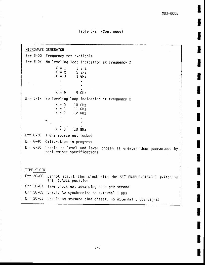
I',183-0005 ItI
Tab l e 3 -2 (Cont ' inued )
IItIIIIIIIIIIIII
MICROI,dAVE GENERATOR
Err 6 -00 Frequency no t ava i lab leEr r 6 -0X No leve l ing loop ind ica t ion a t f requency X
X=1 lGHz2 GHz3 GHz
g iHz)oop ind ica t ion a t f requency X
10 GHz11 GHz
" : "
X=8 18GHzErr 6 -30 1 GHz source no t locked
Er r 6 -40 Ca l ib ra t ion in p rogress
Er r 6 -50 Unab le to leve l and ' leve l chosen i s g rea te r than guaran teed byper fo rmance spec i f i ca t ions
TIME CLOCK
Er r 20 -00 Canno t ad jus t t ime c lock w i th the SET ENABLE/D ISABLE sw i t ch i nthe D ISABLE pos i t i on
Er r 20 -01 T ime c lock no t advanc ing once pe r second
Er r 20 -0? Unab le to synch ron ize to ex te rna l 1 pps
Er r 20 -03 unab le to measure t ime o f f se t , no ex te rna l 1 pps s igna l
X=2X=3
X=g
Er r 6 -1X No leve l ing
X=0X=1X=?
3-6
A.
B.
3 -4
IIIIIIIIIIIIIIIIIII
M83-0005
3-3 OPEP.ATING INSTRUCTIONS
The fo1 1 ow ing p rocedures and F igure 3 .2 p rov ide the opera t ing
ins t ruc t ions fo r the modu le con t ro l l e r . Spec i f i ca l l y , these ins t ruc t ions
tel I the operator how to:
A . Set t ime on the cont ro l ' le r ' s in te rna l c ' lock
B. Determine the IEEE-488 bus address
C. Perform FREQ ERROR measurements wi th the Frequency ComparatorModul e
D. Display measurements f rom memory
E. Per fo rm DRIFT ca lcu la t ions
F. Set t ime on the AS210-20 T ime C lock Modu le
G. Measure At ime on the AS210-20 T ime C lock modu le
H. Synchron ize the AS210-20 T ime C lock Modu le
The ' l i gh ted pushbut tons are the on ' l y ones tha t can be used dur ing a rou t ine .
The CLR pushbut ton on ly c lears the d isp lay . In the fo ' l low ing procedures , the' le t te rs
o r numbers in paren theses re fe r to s teps on F igure 3 .2 .
SET TIME ON THE CONTROLLER'S iNTERNAL CLOCK
Press the T IME func t ion bu t ton (1 ) . T ime on in te rna l c lock
wi ' l l be di spl ayed (2 ) .
Press the i l l umina ted DAY but ton (3 ) .
C. Enter the number o f the Ju l ian day w i th the keyboard and press
the ENTER func t ion bu t ton (4 ) . T ime on the in te rna ' l c lock
wi l l be d isp layed. The d isp lay w i l l re tu rn to SEL? a f te r
approx imate ly f i ve seconds i f no o ther t ime bu t ton is se lec ted .
?- -7
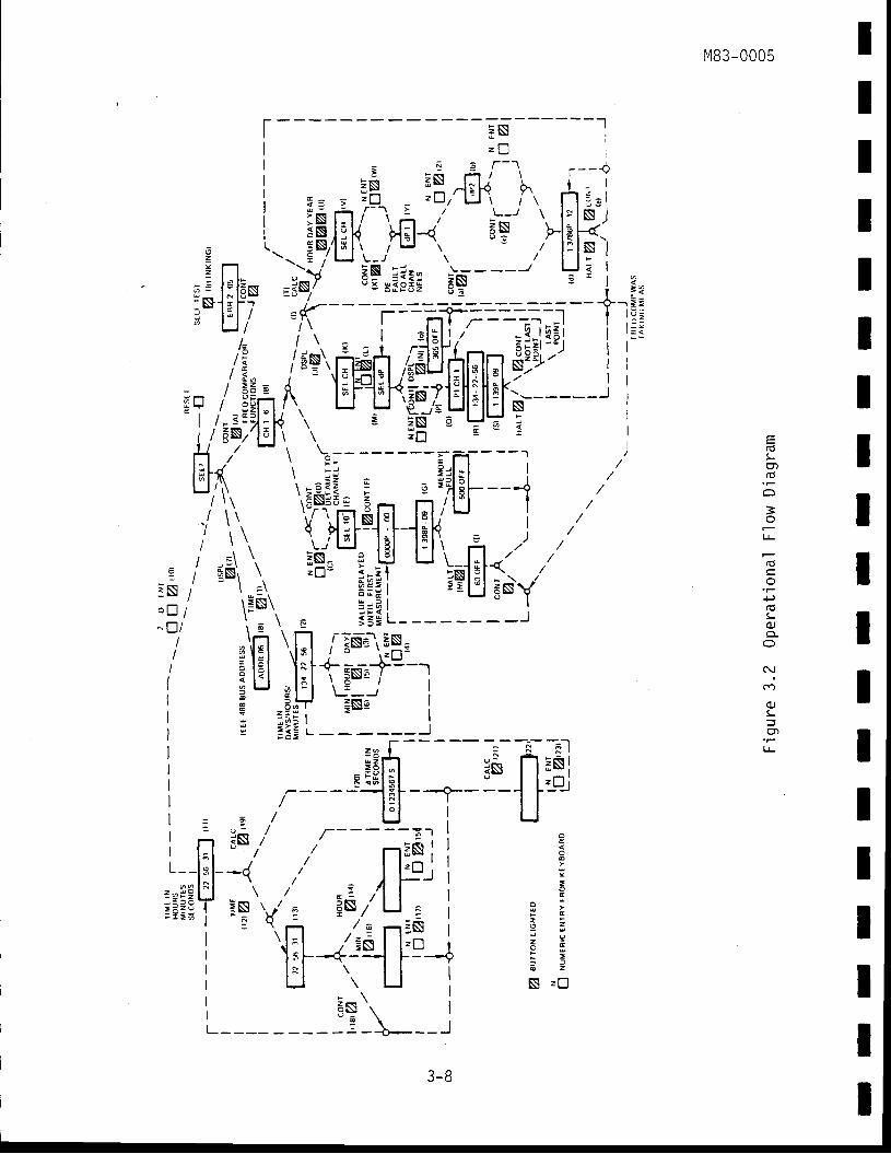
IIIIIttIIIIIItIIIII
q
.oL
rtr
=
lJ-
(o
+J
5-a)
c\l
co
r-
lr
, 2-E=
t = z
II
II
I
I
)I
IIIII
II
I, J
slr
r4B3-0005
:Ei ;& 'sf#\,| 3: : 7F'. , =ori E \.-ri 'tr
t
, l-_ iN,fti ,,€"1, ',!;' ,)tlri llla. *;i aP-il:; Es-
--J 'l;*tfi i[. _i=ffF:,s*4,T,{$il:"F€-"Sffi::H,n,
-"'*it,;- ;=#--l
,.\", 'tnsff1gloi u= .) ,
:i i' *$',)i, *-E=ET o\*frby"- : i \ -=t s 33!L-- - - - r-i
e'{:l \J-:Lf-TE=--i elel l;[*,*y--li E-Ei.??-:Y-==J-
=i;h :s n:sl _
i u ,/ ru-T---lj't ll :.r'' ,,'
-n:sl I i
:;itti =**"r'. ;S r'1J ,' i = ii
't.l=+<jqT-Ej i i
i U '. U I N=;I __::)r_ j
Eiie I= N ,- l
::UJ
o
E
z
9
2
{ - x
D.
IIIIIII
M83-0005
Press the i l l um' ina ted H0UR but ton (5 ) and en ter the hour num-
ber rc-24) wi th the keyboard. Press ENTER (4 ) . Time on the
in te rna l c lock w i l l be d isp ' layed . The d isp lay w i l l re tu rn to
SEL? af ter approximately f ive seconds i f no other t ime button
i s sel ected.
E. Press the i l l umina ted MINUTE but ton (6 ) , en ter the cor rec t
minute wi th the keyboard, then press ENTER (4).
F . The correct t ime i s now entered i n the modu' l e control ' l er ' s
in te rna ' l c lock and d isp layed on the LED d isp lay (21 .
G. The t ime w i l l remain d isp layed fo r f i ve seconds and au tomat i -
cal ' ly return to "SEL?. " To recal I t ime di sp1ay, press TI I ' IE
func t ion bu t ton (1 ) .
3 -5 DETERMINE IEEE.488 ADDRESS OF MODULE CONTROLLER
Press the l i gh ted DSPL bu t ton (7 \ to d isp lay the IEEE-488 bus
address o f the modu le cont ro l le r (8 ) . Th is address is se t in te rna l l y w i th a
DIP swi tch . The IEEE-488 bus cont ro l i s used as descr ibed in the Remote Con-
t ro l sec t ion o f th is chapter . The IEEE-488 bus address w i l l au tomat ica l l y
c lear f rom the d isp lay a f te r f i ve seconds.
3-6 FREQUENCY ERROR MEASUREMENT
A. Connect the f requency source(s) to be measured to the f ront
panel BNC connector(s) on the AS210-02 Frequency Comparator
Modu l e .
II
l-IIIIIIIIII 3-9
IIIIIIIIIIIIIIIIIIt
R
n
M83-0005
Set the RATE sw i tch on the AS210-02 Frequency Compara to r
Module to l4AX for cont inuous samp' l ing or l PER H0UR for samp' l -' i ng once per hour . The sampl ing ra te i s a lso a func t ion o f
the resol ut i on sel ected as fo] I ows:
Resol ut i on
dT--o
10-
10- 10
10-11
Samples Per Hour in l ' lAX lvlode
Approximately 3600
Approximately 600
Approximately 70
7
The memory of the modul e control ' ler
can store 500 samp' les:
therefore, the l PER H0UR mode may be more usefu'l than the l ' lAX
mode when data for severa' l days elapsed t ime is desired. Up
to sllJlputs_ c311.-!-e_ :_9ry:gt9_9__!-o__Jh_e_-f-nequency, -cgmp_arator.
For ' the purposes o f th is p rocedure , i t i s assumed tha t on ly
Channe l 1 i s be ing used. When more than one s igna l i s con-
nected, the sequence operates so that each channel is observed
for one ga te per iod (a func t ion o f the reso lu t ion se lec ted) ,
then the next channel is observed. I t can be seen that as
more inputs a re connected less samples per hour a re taken per
input when in the MAX mode.
Press l i gh ted C0NT pushbu t ton (A) and CH 1-6 shou ld be
d isp ' layed (B) .
D. Enter a channel number f rom 1 to 6 wi th the keyboard and EIITER
func t ion bu t ton (C) . I f on ly channe l 1 i s used ,1 i s au tomat -
ica l1y se lec ted by the program, by press ing the C0NT but ton .
E. Press CONT (D) and SEL 10- shou l d be d ' i sp ]ayed (E) . Se l ec t
the des i red f reouency reso lu t jon w i th the RANGE swi tch on the
AS210-02 Frequency Comparator Module.
3 - i0
IIIIIII
M83-0005
F. Press CONT (F) . The f requency o f fse t measurement rou t ine nowproceeds. 0000P-00 w i l l be d isp layed un t i l the f i rs t measure-ment i s made. Thereaf te r , the channe l number and f reQuencyof fse t (e r ro r ) w i l l be d isp layed fo r each measurement as i t i smade unti 1 500 measurements have been taken. A di spl ay of 1398P-09 , as shown in F igure 3 .2 (G) , i nd ica tes a f reouencyoffset of 398 x 10-9 on channe] 1. when 500 measurernentshave been comple ted w i thout in te r rup t ion , the program vr i l lha' l t automat i ca1
' ly and 500 oFF wi I I be di sp1 ayed , i ndi cat i ng
tha t 500 da ta po in ts have been taken and the program is in anOFF cond i t ion . The measurement cyc ' le can a lso be s topped w i ththe HALT func t ion bu t ton . The da ta po in t number and oFF w i l lbe d isp layed ( I ) . Measurements can be resumed by press ing
CONT.
3-7 OiSPUY FREQUENcY MEAsUREMENTs FROM MEMORY
Press HALT (H) ( i f p rogram is runn ing) and then DSpL (J ) . SELCH shou ld be d isp layed (K) .
A.
B.
IIIIIIIIItI
C. Enter a da ta po in t number w i th the keyboard and ENTER func t ionbutton or push CONT to read the f i rst data point in mernory.The number o f da ta po fn ts taken dur ing the measurement cyc lecan be found by press ing DSPL (N) . The number o f da ta po in tsand oFF shou ld be d isp layed (0 ) . For example , 365 oFF. Thed isp lay w i l l now re tu rn to SEL dP (M) .
Enter a channe l number
but ton (L ) o r push CONT
now be di sp1 ayed ( t '1) .
A f te r a da ta po in t number and ENTERi s pressed, the di sp' l ay wi I I readpoint number and channel number (a)
t ime the data point measurement was
wi th the keyboard and ENTER func t ionto se lec t channe l one. SEL dP shou ld
but ton is p ressed, o r C0NTout in sequence the da ta(e .9 . , P1 CH1) , then the
taken ( R)
D.
3- 11
IMB3-0005
I(e.g. , 134-?2-56), then the frequency measurement at that data
po in t (S ) (e .g . , 1 139P-09) i s d isp layed I
E . The measurement p rocess can be resumed by press ing HALT. I f
f requency compar isons have no t been in pnocess , the rou t ine
wi l l re tu rn to ( f ) and e i ther more da ta po in ts d isp layed or a
dr i f t ra te ca lcu la t ion per fo rmed. I f C0NT is p ressed, the
nex t da ta po in t in memory w i1 ' l be d isp layed as in paragraph D.
I f the las t da ta po in t has been d isp layed , the rou t ine w i l l
re tu rn to (M) and a new data po in t can be se lec ted .
3-8 DRIFT CALCULATIONS
A. At any t ime af ter two or more data points have been col ' lected
over a t ime interval of more than one minute, a f requency'
d r i f t ca lcu la t ion can be made.
B. Press HALT, then press CALC func t ion bu t ton (T) . Press HOUR,
DAY, o r YEAR func t ion bu t ton (U) to se lec t per iod fo r d r i f t
ca l cu l a t i on .
C . SEL CH w i l l be d isp layed (V) . En te r the des i red channe l
number wi th the keyboard and ENTER funct ion button ( t , I ) . ( t t
CONT i s p ressed (X ) , a ' l l channe l s w i l ' l be computed f o r
f requency dr i f t . )
D . dP 1 w i l l be d isp layed (Y) . Enter the des i red number fo r the
data po in t w i th the keyboard and ENTER func t ion bu t ton (Z) .
The number entered can be anything with ' in the data f ie ld f rom
1 to 500 depend ing on the reso lu t ion se lec ted , leng th o f mea-
surement , t i me , number o f da ta po i n ts , e tc . I f C0NT i sp ressed (a ) the d r i f t ca lcu la t ion w i l l au tomat i ca ]1y be made
on the f i r s t th rough las t da ta po in ts . I f C0NT is no tp ressed , then dP 2 w i l l be d isp layed (b ) . En te r the des i red
da ta po in t number as w i th dP 1 (Z) .
IIItItIIIIIIIII
3-12
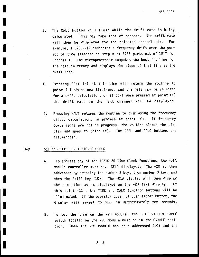
r
A.
IIIIIIIIIIIIIIIIIII
t"t83-0005
The cALC bu t ton w i l l f l ash wh i le the d r i f t ra te i s be ing
ca lcu la ted . Th is may take tens o f seconds. The dr j f t ra te
wi ' l I then be di sp1 ayed f or the se1 ected channel ( d ) . For
example , 1 3786P-12 ind ica tes a f requency dr i f t over therPer -
iod o f t ime se lec ted in s tep B o f 3786 par ts ou t o f 10 - ' fo r
Channe l 1 . The mic roprocessor computes the bes t f i t l i ne fo r
the da ta in memory and d isp ' lays the s ' lope o f tha t l ine as the
dr i f t ra te .
F . Press ing CONT (e) a t th is t ime w i l l re tu rn the rou t ine to
po in t (U) where new t imef rames and channe ' l s can be se lec ted
fo r a d r i f t ca ]cu la t ion , o r i f CQNT were p ressed a t po in t (X )
the d r i f t ra te on the nex t channe l w i I I be d i sp1 ayed .
G.. Pressing HALT returns the rout ine to disp' laying the f requency
of fse t ca lcu la t ions in p rocess a t po in t (G) . I f f reouency
compar isons are no t in p rogress , the rou t ine b lanks the d is -
p ' lay and goes to po in t ( f ) . The DSPL and CALC but tons are
i l l umina ted .
3 -9 SETTING ^TIME ON AS210-20 CLOCK
To address any of the AS210-20 Time Clock funct ions, the -01A
modu le cont ro l le r must have SEL? d isp layed. The '20 is then
addressed by pressing the number 2 key, then number 0 key, and
then the ENTER key (10) . The -01A d isp ' lay w i l l then d isp lay
the same t ime as is d isp layed on the -20 t ime d isp lay . A t
th i s po in t (11 ) , the T iME and CALC func t ion bu t tons w i l l be
i l ' l umina ted . I f the opera tor does no t push e i ther bu t ton , the
di sp1 ay w'i ' l 1 revert to SEL? i n approximately ten seconds .
B . To se t the t ime on the -?0 modu le , the SET ENABLE/DISABL[
swi tch loca ted on the -20 modu le must be in the ENABLE pos i -
t ion . When the -20 modu le has been addressed (10) and the
3-13
IIIIIIIIIIIIIIIIItI
A.
t ime i s be ing d isp layed (11) ,
the T IME func t ion bu t ton (12) .
ed (12) the -01A d isp lay w i l l(13 ) . The H0UR (14) , MIN (16)
t183-0005
the t ime can be se t by . push ing
When the TIME button i s Dress-
ho ld the las t t ime d isp layed
, and CONT (18) bu t tons w i l l be
3- 10
i l luminated . The hour can be changed by pness ing the HOURbut ton (14) . The -01A d isp lay w i1 ' l be b lanked and the des i red
hour en tered v ia the numer ic keys and the ENTER but ton (15) .
The -20 d isp lay w i l l update immedia te ly bu t the -01A d isp lay
w i l l re tu rn to the las t t ime d isp layed (13) .
The change t ime rou t ine can be ex i ted by press ing the C0NTbut ton (18) . The -01A w i l l show the -20 c lock t ime fo r
approx imate ly 10 seconds (11) . I f no ac t ion i s taken , the-01A w i l l t hen go back to d isp ' l ay ing the SEL? message .
I f the change rou t ine was no t ex i ted , the m inu tes can bechanged by press ing the MIN but ton (16) . The -01A d isp ' laywi l l be b lanked and the des i red minu tes en tered v ia the num-er ic keys and the ENTER but ton (17) . When the ENTER but ton(17) i s p ressed, the seconds are se t to zero , the new minuteva lue i s en te red and bo th the -20 and -01 d isp lays (11) w i l l
show the upda ted t ime. I f no fu r the r opera to r ac t ion i staken, the -01 d isp lay w i l l re tu rn to SEL? in approx ina te lyten seconds. The SET ENABLE/ DISABLE switch on the -20 should
always be returned to the DISABLE posi t ion.
READING ATIME ON THE AS21O-20 CLOCK
To read the t ime di f ferent ia l between the L pps signal gener-
ated by the -20 circui t ry and the external 1 pps app' l ied tothe -20 1 pps IN connector, the -20 module is addressed bypress ing 2 ,0 , ENTEP. (10) and then p ress ing the CALC bu t ton(19) . The -01A w i l l t hen d isp lay the t ime d i f fe rence in sec -onds between the r is ing edge of the -20 I pps s ignal and the
3- 14
II
M83-0005
r i s ing edge o f the ex te rna l I pps s igna l (20 ) . A f te r f i ve
seconds, i f the opera tor has no t taken any fu r ther ac t ion , the
-01A w j l l d i sp lay the -20 t ime (11) . A f te r d i sp lay ing the
t ime for approximately ten seconds, the -01A wi l l return to
d isp iay ing the SEL? message .
B. I f i t i s des i red to synchron ize , o r change the o f fse t o f , the' in te rna l 1 pps w i th respec t to the ex terna l 1 pps , the fo l low-
ing sequence o f opera t ions wou ld be per fo rmed. P lace the SET
ENABLE/DISABLE swi tch on the -20 to the ENABLE pos i t ion ' Then
address the -20 module (10) and -oo to the At ime mode by press-
ing the CALC but ton (19) . The -01A w ' i1 l d isp lay the At ime(20) . Press the CALC but ton aga in (21) and the d isp lay w i l l
go b lank (22) . Enter the des i red o f fse t , f rom 0 to 999999.9
microseconds, v ia the numer ic keyboard and press the ENTER' bu t ton (23) . When enter ing the des i red o f fse t , do no t p ress
the decimal point but ton. The numbers pressed are automat i -
ca ' l l y r i gh t i us t i f i ed . For example , p ress ing 1 , Z , 3 , and
then ENTER, en ters an o f fse t o f 12 .3 mic roseconds. When the
ENTER but ton is p ressed, the mic roprocessor in the -01A com-
pu tes the d i f fe rence be tween the measured o f f se t and the
des i red o f fse t , then ins t ruc ts the -20 modu le to make a one-
t ime change in the phase to achieve the desired of fset . Af ter
the ad ius tment i s made, the o f fse t w i ' l l aga fn be measured and
d isp layed (20) on the -01A d isp lay . The SET ENABLE swi tch on
the -20 shou ld a lways be re tu rned to the DISABLE pos i t ion
after adjustments are complete.
3- 11 REI4OTE CONTROL
The AS210 sys tem can be remote ly cont ro l led v ia an IEEE-488 ins t ru -
menta t ion bus . The DIP swi tch AZU?4 must be se t to the des i red address (see
F igure 3 .3 ) . Tab le 3 -3 l i s t s the ac t i ve con t ro l le r commands w i th wh ich the
AS210 w i1 l respond. The ASCI I charac ter s t r ings sent to the AS210 when i t i s
in the l is ten mode can be terminated in one of two ways.
IIIIIIIIIIIIIItII 3- 15
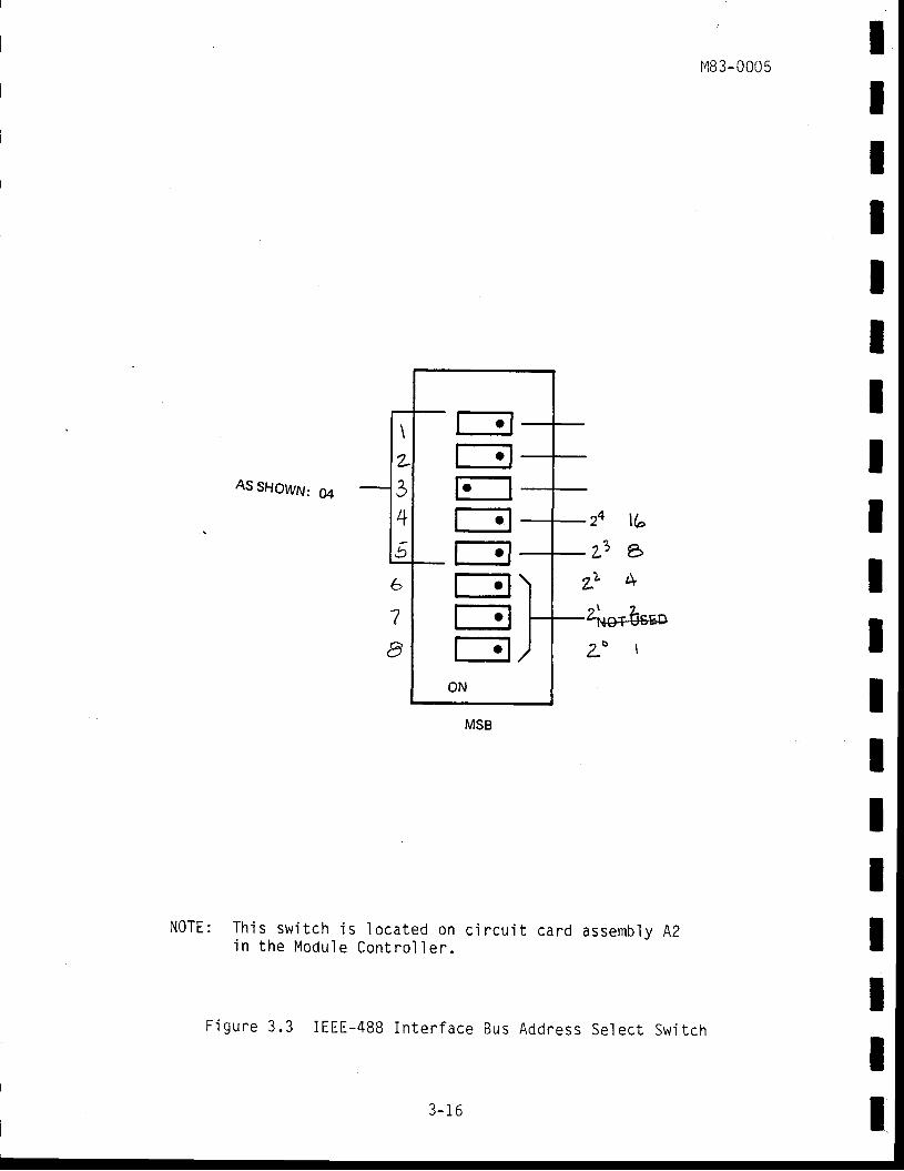
M83-0005IIIIIIIIIIIIIItIIII
AS SHOWN: 0a
24
. r 7t-
LL
MSB
NOTE: Th i s sw i t ch ' i s l oca ted on c i ncu i t ca rd assemb ly A2in t he Modu le Con t ro l l e r .
F igure 3 .3 IEEE-488 In ten face Bus Addness serec t sw i tch
tb
s46
7
I
t-?rrll. lrrlt-?f.lf.lr;1
ON
. ( - t h
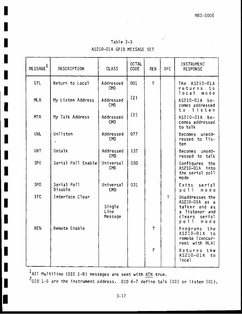
tIIIIIIIItIIIIIIII
M83-0005
Tab l e 3 -3
AS21O-O1A GPIB MESSAGE SET
lRt t Mu l t i l i ne (D I0 1 -8 ) messages a re sen t w i th ATN t rue .2OtO t -S a re the ins t rument address . D I0 6 -7 de f ine ta l k (10) o r l i s ten (01) .
MESSAGEl DESCRIPTION CLASSOCTALCODE REN IFC
INSTRUMENTRESPONSE
GTL
MLA
MTA
UNL
UNT
SPE
SPD
IFC
REN
Return to Local
My Listen Address
Ta lk AddressMy
Unl i s ten
Unta' lk
Ser ia l Po l l Enab le
Ser ia l Po l lD i sab l e
In te r face C lear
Remote Enabl e
AddressedCMD
AddressedCMD
AddressedCI{D
AddnessedCMD
AddressedCMD
Uni versa lCMD
Uni versa lCMD
Si ng' l eL ineMessage
001
(21
(2)
077
r37
030
031
T
T
F
T
The A5210-01Are tu rns toI oca l mode
ASZ 10-01 A be-comes addressedto I i s ten
AS2 l0 -01A be-comes addressedto tal k
Becomes unadd-ressed to l i s -ten
Becomes unadd-ressed to ta ]k
Conf i gures theAS210-01A intothe ser ia l po11mode
Exi tspo11
se r i a lmode
Unaddresses theAS210-01A as ata lke r and asa l i s tener andc l ea rs se r i a lpo l l mode
Programs theAS210-01A toremote ( concur-rent wi th MLA)
Retu rns theAS210-01A toI oca l
3- 17
M83-0005
B. A l ine feed charac ter (car r iaqe le tu rns are ignored) .
The fo l low ing paragraphs descr ibe the programming syn tax tha t shou ld be fo l -lowed by a control ler and the syntax of responses by the AS210 system. Com-mas shou ld be inc luded in the commands as shown. When the AS210 is in theremote control mode, the REM funct ion button on the module control ler f rontpane l i s i l l umina ted .
IIIIITItIIIIIIIIIII
3-L2
3- 13
AS21O-O1A TII '1E REMOTE COMMANDS
SETTiNG THE AS21O-O1A TIME . REMOTE COMMAND
T,Dxxx , Hxx , l4xx
3- i4
3- 15
where
53 ,Lx ,Fywhere 53 = modu]e
L = output
T = set t ime command
D = day (up to 3 d ig i t number )H = hour (1 o r 2 d ig i t number <
M = minu te (L o r 2 d ig i t numberx = integer number
(con t ro l le r to AS210)
24)< 60)
<LF>+
( con t ro l le r to AS210)
READING THE AS21O-O1A TIME - REMOTE COI4MAND
I?
response f rom AS210: xxx-xx-xx<CR>
Days Hours Minu tes EOI
FREQUENCY GENERAToR MoDULE REMoTE COMMANpS (AS210-03)
x=1=l =l =Q =$ =S =
sel ect command
I evel sel ect
1mV10 mV20 mV32 mV40 mV50 mV
3- 18
II
M83-0005
ItI
J= 100mV$= 500mV9 = 1000 mV
F = frequency sel ect
Y=1= lMHzl= 10MHzl= 50MHz4 = 100 MHz5 = 200 MHz6 = 300 MHz7 = 400 MHz8 = 500 MHz
3-16 DIGITAL DELAY GENERATOR MODULE REMOTE COMMANDS (AS21O-04)
where
54 ,Dxxxxx,Py ( control I er to AS210 )
54 = modul e sel ect command
D = del ay sel ect
x = de lay in 10 's o f nanoseconds
p=(0<x<99999)
rate sel ect= lpps= 10 pps= 100 pps= lK pps= 10K pps
3- 17
3- 18
FREQUENCY COMPARATOR MODULE RE}4OTE COMMANDS (AS21O.O2)
REI'IOTE MEASUREMENT COMMANDS
where
SZ,Ax ,Ry , Iz (con t ro l le r to AS210)
52 = modu le se lec t command
A = accuracy range sel ect
x=1=par ts in108
Z = par ts in 109
3 = par ts in to10
4 = par ts in 1011
IIIIItIIIIIIII
pul se
y=12345
3- 19
T -
A serv ice reques t i s sen t whenAfter each frequency measurement
bus in the fo l low ing fo rmat :
xAyyyyP -zz<CR> <LF>
f
EOI
measurement rate sel ect
Y=1=MAX?=!PERH0UR
inpu t channe l se lec t
z = # of inputs to be measured
the data memory is
is made, the measured
M83-0005
(L<z<6)
fu l I (paragraph 3-21 ) .va lue i s p laced on the
IIIIIIIIIIItIIIItII
f t=
X
vzA
where = input channel number= mant i ssa= exponent= ASCI I space
maxlmum
I per hour
control I er must read the
measurement rate sel ect
Before the next measurement is taken, the interfacemeasured value from AS210-01A Modu' le Control ler ,
I f the measurement command is sent wi th ao f Ry w i th e i ther
Y=34
The measurement va lue w i l l no t be p laced on the bus . The va ' lue is s to red inmemory. The measurements wi l l be taken at the rate se' lected. The measure-ments can be hal ted, and the data examined at any t ime, by the commands' l i s ted i n the f o l I owi ng paragraphs.
3-20
IIIIIIIIIIIIItIItII
M83 -0005
3- 1g REMOTE DEJTRMINATION OF NUMBER OF DATA POINTS TAKEN
Any t ime dur ing the AS210-02 measurement sequence the measurement
cycle may be interrupted and the number of data points taken read out.
52? (cont ro l le r to AS210)
The AS210 wi l l then report the number of data points taken in the fo l lowingformat:
xxx OFF <CR><LF >4
EOI
The AS210-02 may be commanded
fol lowing command:
ASC I I SPACE
x < 500)
i ts current measurement cyc' le by the
where A =
(1 1
to resume
3-20
S2,G0 (cont ro l le r to AS210)
REMOTE DRIFT RATE CALCULATION COMMND
52? ,Fw, Ix , Xy , Yz (cont ro l le r to AS210)
52? = Modul e se] ect command
f = Dr i f t rate cal cul at ion interva' l se]ect
w = 1 = dr i f t rate per year2 = drift rate per day3 = dri ft rate per hour
Channel number sel ect
x = input channe l tha t ca lcu la t ion is to be made on(1 < x < 6 )
= In i t ia l da ta po in t se lec ty = da ta po in t number (1 < y < 500) ( I f th is par t
o f the command s t r ing is omi t ted , the in i t ia lda ta po in t w i l l de fau l t to 1 . )
where
3-? t
M83-0005
| = F ina l da ta po in t se lec t
z = da ta po in t number (Z < z < 500) ( I f th i s par to f the command s t r ing i i omi t ted , the f ina lda ta po in t w i l l de fau l t to the las t po in ttaken. )
Th is d r i f t ra te ca lcu la t ion may take tens o f seconds, to per fo rm. When theca lcu la t ion i s comp le te , a se rv ice reques t w i l l be sen t (va lue 76) . The ca ] -cu la ted va lue can then be read.
The dr i f t rate number is reported by the Asz10 in the fo l lowingformat
x(-)yyyyP-zz<CR><LF>
EOI
where x = channe' l numbery = mant issa o f d r i f t ra tez = exponent
Th is command ins t ruc ts the AS210 to per fo rm a dr i f t ra te ca lcu la t ion us inga l l o f the da ta po in tsbetween and inc lud ing those spec i f ied by Xy and yz .The ca lcu la t ion per fo rmed is a leas t mean square er ro r s t ra igh t l ine f i t .
3 -21 REMOTE Tl,lO POINT DRIFT RATE CALCULATION COMMAND
whereS2?,Cw, Ix ,Xy , Yz (con t ro l le r to AS210)52? = Module select commandf , = Dr i f t ra te ca lcu la t ion in te rva l se lec t
w = 1 = dr i f t rate per year2 = drift rate per day3 = dr i f t rate per hour
IIIItIIIIIIIIIIIIII
3-22
IIIIIIIIIIIIIIIIIII
M83-0005
| = Channe l number se lec t
x = inpu t channe l tha t ca lcu la t ion i s to be madeon (1 < x < 6 )
f , = In i t i a l da ta po in t se lec ty = da ta po in t number (1 < y < 500) ( t t t f r t s par t
o f the command s t r ing- i s lm i t ted , the in i t ia lda ta po in t w i l ' l de fau l t to 1 . )
| = F ina l da ta po in t se lec t
z = da ta po in t number Q < z < 500) ( I f th is par tof the command s tri n!- i s- omi tted , the f i nalda ta po i n t w i I ' l de fau l t to the I as t po in ttaken. )
Th is d r i f t ra te ca lcu la t ion is per fo rmed qu ick ly . The ca1cu la ted va lue canbe read a' lmost i rnmediately af ter sending the command.
The dri f t rate number i s reported by the AS210 i n the fo'l ' lowi
ngformat
x ( - )yyyyP-zz<CR><LF>f
EOI
wherex=channe lnumbet
y = mant issa o f d r i f t ra te
z = exponent
Th ' i s command ins t ruc ts the AS210 to per fo rm a dr i f t ra te ca lcu la t ion us ingon ly the two da ta po in ts spec i f ied by Xy and Yz . The ca lcu la t ion per fo rmed
is
oz-otF--_---F-t z ' ' l
3-23
TtIIIIII
s2?S2? =
M83-0005
where D2DtrzTt
3-22 REMOTE DATA POINT READOUT
where
The AS210 reports al I
fo l I owing format:
a=[ =c=z=e=
f requency d i f fe rence da ta o f po in t Yz
frequency df f ference data of point Xy
t ime data po in t Yz was measured
t ime data point Xy was measured
, DX ( contro ' l I er to AS210 )modu'le sel ect cornmand
data channel sel ect
x = channe l number (1 < x < 6 )
da ta po in ts taken for the par t i cu la r channe l in the
(F i rs t da ta po in t ) Pxxx CHy<CR><LF>aaa-bb-cc<CR> <LF>L(F.zzzzP-#.Cn, <uF>
(Las t da ta po in t ) Pxxx CHy<CR><LF>aaa-bb-cc<CR> <LF>L(i)zzzzP-ee<CR> <LF>
A
EOI
where x = data point number (1 < x r f 500y = channel number (1 < y-< 6T
IIIIIIIIIII
day data point was-tak6nhour da ta po in t was takenminute data point was takenmant issa of f requency di f ference dataexponent of f requency di f ference data
3-24
tIIIIIIIIIIIIIIIIII
M83-0005
where modul e generat i ng the error
error code
3-25 AS21O SERViCE REQUESTS
When the ,ASZ10 needs to cormun ica te w i th the cont ro l le r , i t enab les
the SRQ cont ro l f ine and when the ser ia l po11 is enab ' led , sends ou t a s ta tus
by te descr ib ing the reason fo r a le r t ing the cont ro l le r . Tab ' le 3 -4 g ives a
l ist ing of the ser ia l po' l ' l s tatus bytes that can be generated by the AS210
and the i r mean ing .
3-26 READING THE AS21O-20 TIME - REMOTE COMMAND
S20 ,T? ( control I er to AS210 )
s20,T ,HXX,MXX,SXX <CR><LF>t ( response f rom AS210)
EOI
3-27 SETTING TIME IN THq ,AS210-2L- REMOTE_C0MMAND
NOTE
The t ime on the AS210-20 Modul e can on' ly be set whenthc SET ENABLE/DISABLE SWitCh ON thc AS21O.2O FTONTPane l i s in the ENABLE pos i t ion . Th is p revents so f t -ware/hardware malfunct ions in devices on the GPIB fromresett ing the t ime or resynchroniz ing the L pps outputof the AS210-20.
S2O ,T , HXX , MXX , SXX (cont ro l le r to AS210)
READING ATII'IE FROM THE AS21O-20 . REMOTE COMMAND
x=y=
3-28
S20,0? (con t ro l le r to AS210)
szo,D,0.XXXXxxx s <cR><LF>r ( response
EOI
3-26
from AS210)
M83-0005
3-23 REMOTE LEARN COMMAND
L? (cont ro l ' le r to AS210 )
For each module present in the system, the f ront panel contro ' l set t ings are
given back to the control ler in the exact format needed to command those mod-
u ' les . As 61 eXo i lp l€ , i f modu les 2 ,3 , and 4 were p resen t , the fo l low ing
might be returned bY the AS210:
s2 ,A1,R l , I2<CR><LF>
s3 ,LB,F2<CR><LF>s4,098316,P5<CR><LF>
i
EOI
I f the A5210-06 module were i in the system, i t s s ta tus wou ld be rePor ted as :
s6 ,LX,FX<CR><LF>
I f the AS21O-20 modu le were in the sys tem, i t s s ta tus wou ldbe repor ted as :
s20,T,HXX,MXX,SXX<CR><LF>
3-24 REMOTE SELF-TEST COMMAND
C? (cont ro l le r to AS210)
Th is causes the ASZ10 to en ter the se l f - tes t cyc ' le . When the se l f - tes t cyc le
is comp le te ,6n SRQ is sen t (see paragraph 3 -22) . I f any e r ro rs a re found ,
an SRQ ' is sent (see paragraph 3-2?l fo l lowed by the speci f ic error message in
the f o' l l owi ng format:
ERR x-YY<CR><LF>f
E0 i
ItIIIIIIIIItIItIIII
3-25
IIIIIIIIIIIIIIItI
M83-0005
Tab l e 3 -4
SERIAL POLL STATUS DESCRIPTION
*Af te r se r ia l po l1 i s comp le te , AS210 mus t be pu t jn ta l k mode and thespec i f i c message read ou t .
B IT8
B iTt
BITR
BITF
BIT4
BIT?
BIT2
BITI STATUS DESCRIPTION
0
0
0
0
0
0
0
0
0
0
n
0
n
1
1
I
1
I
1
1
I
1
i
1
i
I
0
U
0
0
0
n
0
0
0
0
0
0 0
0
1
nU
0
0
0
0
0
0
0
U
0
1
0
0
0
0
0
0
0
n
0
1
I
1I
I
1
0
0
0
0
I
1
1
1
0
0
0
0
nu
0
0
1
1
0
0
1
1
0
0
I
0
0
0
1
0
1
0
I
0
1
0
I
n
Frequency standard error*
AS210-01A module error*
AS210-02 module error*
AS210-03 module error*
AS210-04 module error*
AS210-06 modu l e ca l i b ra t i on comp l e te /error condr ' t ion corrected
AS210-06 l4odule Error*
Remote programmi ng syntax error
AS210 se l f - tes t cyc le i s comple te
The AS210 frequency comparator measurementcyc le i s compie te
The frequency standard has gone from anun locked to a locked cond i t ion
The dr i f t ra te ca lcu la t ion is comple te*
AS2l0-20 modu le e r ro r *
3 -27
3-29
3-30
M83-0005
SYNCHRONIZING 1 pps IN THE AS210-20 -- REM0TE C0MllAl lD
S20,DXXXXXXX (cont ro l le r to AS210)
7 d ig i ts represent ing the des i red At ime in ten ths o f ami c rosecond.
MEMORY BATTERY OPERATION
IIIIIIIIIIIIIIIIIIt
The MEMORY BATTERY switch enables an internal n ickel cadium batteryto supply power to the random access memory (RAM) circui ts and internal c lockwhen placed in the STANDBY posi t ion. The OFF posi t ion of the MEMORY BATTERYswi tch d isconnects the in te rna l ba t te ry f rom the c i rcu i t . Th is sw i tch shou ldbe le f t in the OFF pos i t ion when the AS210 is no t in opera t ion or dur ingequipment storage. In the STANDBY posi t ion, f requency measurements wi l l besaved in memory for a per iod of three hours dur ing system transport or l inepower fa ' i l u ies.
CAUTION
I f the AS210 system is to be without power for a per iodin excess of four hours, p lace the MEMORY BATTERY inthe OFF posi t ion. The MEM0RY BATTERY may be damagedf rom pro longed d ischarge and a cor ros ive a lka l i mayleak f rom the n icke l cad ium bat te r ies . The leakagewi l I cause damage to the su r round i ng e ' l ec t r i ca lc i rcui t ry .
For more informat ion regarding the MEMORY BATTERY, refer to Theory of 0pera-t ion , Sec t ion 4 -6 .1 .
NOTEIn the event battery leakageac id so lu t ion may be used tocorrosion from the batter ies
is encountered , a bor icneut ra l i ze and c lean theand e lec t r i ca l c i r cu i t s .
3 -28
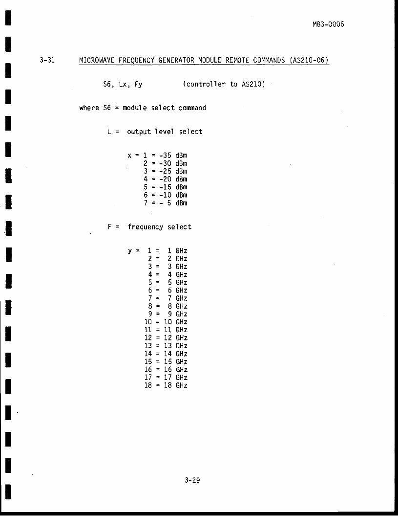
tIIIIIIIIIIIIIIIIII
MB3-0005
3-31 MICROWAVE FREQUENCY GENERATOR MODULE REMOTE CoMMNDS (A5210-06)
56, Lx , Fy (cont ro l le r to AS210)
where 56 = modul e sel ect command
l- = output I evel sel ect
-35 dBm-30 dBm-25 dBm-20 dBm-15 dBm-10 dBm-5dBm
f = frequency sel ect
1 GHz2 GHz3 GHz4 GHz5 GHz6 GHz7 GHz8 GHz9 GHz0 GHz1 GHz? GHZ3 GHz4 GHz5 GHz6 GHz7 GHz8 GHz
x=1=l =l={ =$ =$ =J =
Y= ]=l=l=4 ,=$=$=J=$=$=
1 .0=111 =112=t13=114=115=116=1L7=L18=1
3-29

IIIIIIIIIIIIIIIIIII
l:ItllllIIIIIIIItII
M83-0005
CHAPTER 4
THEORY OF OPERATION
4-L I NTRODUCTION
This chapter conta ins a theory d iscuss ion o f the AS210-01A Modu le
Cont ro l le r . The un i t i s p reprogrammed to cont ro l modu les o f the AS210 E lec-
t ron ic Counter and Frequency Ca l ib ra t ion sys tem. The o ther modu les o f th is
ser ies a re descr ibed in separa te pub l i ca t ions l i s ted in the pre face . The
AS210-01A opera tes as the cont ro l and d iagnos t ic center when ins ta l led in the
AS210 Main f rame wi th the o ther modu les . The modu les can a lso be remote ly
programmed v ia an IEEE-488 in te r face bus . In th is case, con t ro l i s de fer red
to the bus . The modu le i s phys ' i ca l1y compr ised o f f i ve c i rcu i t card assem-
b l ies A l th rough A5. The fo ' l low ing descr ip t ion per ta ins to the hardware
aspects o f these c i rcu i t a reas and is keyed to F igure 4 .1 , l4odu le Cont ro l le r
Func t iona l B lock D iagram. The c i r "cu i t card pre f ixes are used to ident i f y the
loca t ion o f the c i rcu i t on the schemat ic d iagrams o f Chapter 5 .
4-2 MODULE FUNCTIONAL DESCRiPTION
The modu le con t ro l le r cons is ts o f a CPU,16K x 8 e rasab ' le p rogram-
mable read on ' l y memory (EPR0M) fo r s to rage o f the program,4K x 8 random
access memory (RAM) used as data memory and scratch pad, and an IEEE-488
interface for remote control of the system. When the uni t has been address-
ed over the IEEE-488 bus, control of the system is deferred to the IEEE-488
con t ro l le r (€ .g . , keyboard te rm ina l ) . When the REM bu t ton on the modu le con-
t ro l le r f ron t pane l i s i l l umina ted , the IEEE-488 in te r face i s a lways ' in con-
t ro l o f the un i t and sys tem. Norma1 ly , the sys tem is cont ro l led th rough themodu le con t ro l le r ' s f ron t pane l keyboard . A keyboard log ic un i t and d isp lay
c i rcu i t p rov ide fo r manua l en t ry and d isp lay o f da ta . Data is en tered v ia
4-1
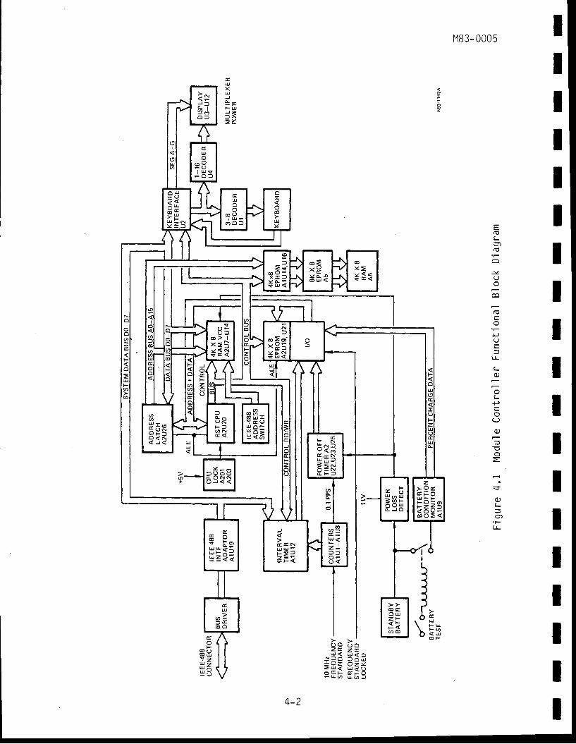
IIIIIIIIIIIIIIIIIII
ro
a
-:<
+J
:LL
L6 \
t-+)
-E
<r
l_
lJ-
M83- 0005
e
< ! i
r l '
\
>a zd.- H * H : < P
EE; E;EF
Esiaz-u,z
uXUJL ,
t s U: 3> E
4-2
IIIIIIIIIIIIIIIIIII
M83-0005
the keyboard and d isp ' layed on a 10-d ig i t LED d isp ' lay . Programs fo r en t ry o f
the da ta , ca lcu la t ion o f f requency dr i f t ra te , and se l f -d iagnos is o f the
system res'i de ' in the f i rmware (EPR0M l ogi c ) .
4 -3 KEYBOARD LOGIC CIRCUIT CARD A3
The purpose o f the keyboard log ic c i r cu i t i s t ransmf ss ion o f
keyboard entr ies to the CPU, recept ion of d isplay data f rom the CPU, and
interface between the CPU, RAM, keyboard, and display. Keyboard interface
A3U2 is the bas ic component o f the keyboard ' log ic c i rcu i t card . A3U2 t rans-
mi ts the keyboard en t r ies to the CPU over the CPU bus DBO to DB7. SLO
through SL1 on A3U2 scan the keyboard , v ia decoder A3U1, and the d isp lay v ia
display MUX A3U4. The SLO through SL1 outputs of A3U2 can be in one of four
s ta tes , "0 " , "1 " , "2 " , o r "3 " . These s ta tes a re decoded by A3U1 as fo l lows :
Sta te . '0 . ' d i i ves RESET and HALT but tons . S ta te "1 ' t d r i ves CONT, DISP, DAY,
SELF TEST, MIN, H0UR, YEAR, and REM bu t tons . S ta te "2 " d r i ves " . " ,9 , CALC,
" - " , ENT, CLR, T IME, and r rBr r bu t tons . S ta te r r3 r r d r i ves "0 " r "6 " r "4 " , "3 " ,
"1" , "2 " , "5 " , and t tT t t bu t tons . Press ing one o f the above bu t tons connects
the dr iv ing s igna l to one o f the sense inputs RL0-RL7 on A3U2. The CPU is
then in te r rup ted by A3U2 and t ransmi ts the swi tch pos i t ion to the CPU. D is -
p lay da ta i s t ransmi t ted f rom the CPU to the RAM in A3U2. The d isp lay is
dr iven and refreshed by A3U2 without disturbing the CPU. 0utputs SLO through'SL3 from A3U2 are appl ied to I of 16 decoder A3U4, The outputs of A3U4 turn
on display dr iver t ransistors A3Q1 through A3Q6 and A4Q1 through A4Q6 on the
d isp lay log ic c i rcu i t card A4. These t rans is to rs a re tu rned on one a t a t ime
whi le the seven-segment d isp ' lay da ta fo r the tu rned-on d ig i t i s on the A0-A3
and 80-83 ou tpu ts o f A3U2. The LEDs f rom the pushbut tons are hand led l i ke
segments on the numeric readout except that the CPU turns on the appropr iate
segments (numera ls ) . The LEDs in the SELF-TEST and REM but tons are dr iven
separa te ly f rom I /0 por ts on A2U19 o f the CPU c i rcu i t card .
4-3
l '{83-0005
4-4 DISPLAY LOGiC C IRCUIT CARDA4
The purpose o f the d isp ' lay log ic c i rcu i t i s d r iv ' ing segments o f the
modu le cont ro l le r ' s 10-d ig i t readout in accordance w i th s igna ' l s f rom the key-
board log ic card A3. The LED dr iver inpu ts DISDRO through DISDR9 have been
decoded in the keyboard log ic card as descr ibed in paragraph 4-3 . DISDRO
through DISDR4 and DISDR9 tu rn on t rans is to rs A4Q1 th rough A4Q6 prov id ing
f ive vo1ts to LEDs A4U3 th rough A4U7 and A4UL2. The remain ing LEDs (A4U8
through A4U11) a re supp l ied by the t rans is to r d r ivers in the keyboard log ic
card, A3. The segment data (SEG A through SEG DP) is provided by the data
outpu ts o f A3U2 in the keyboard log ic card descr ibed in paragraph 4-3 . Seg-
ment data is provided to the LEDs through dr ivers A4Ul and A4UZ simulta-
neous' ly wi th power to the appropr iate digi t .
MODULE CONTROLLER CPU AND MEMORY ASSEMBLIES
The cont ro l le r CPU and memory is cons t ruc ted on th ree c i rcu ' i t card
assmbl ies A1 , A2 , and A5 . AZ con ta ins the s ing le ch ip CPU, 4K o f EPROM, 4K
of RAM, counters , I /0 dev ices , and dr ivers . A1 conta ins 4K o f EPR0M, a p ro-
grammable t imer, counters, IEEE-488 interface and standby battery c i rcui t .
A5 contains 8K of EPR0M.
IIIIIIIIIIIItIIItII
4-5
4-6
4-6 .1
EXTENDED PROM GPIA AND TIMER LOGIC CIRCUIT CARD A1
STANDBY BATTERY CIRCUITS
Loss o f AC power wou ld resu ' l t in the loss o f da ta in the RAM. A
s tandby 9 .6 vo l t ba t te ry i s ' loca ted in the modu le cont ro l le r to p rov ide power
to the RAM circui ts in the event of a power loss. The backup battery sup-p l ies power to the power -o f f t imer c i rcu i ts as we l l as the RAM. The AS210-05
Standby Bat te ry Modu le must a lso be ins ta l led in the main f rame and se t in the
standby pos' i t ion for the power-of f t imer to funct ion. The standby battery
modu le i s needed to ma in ta in the Rub id ium f requency s tandard in the power -o f f
mode. The system clock is updated to the correct t ime when normal poweris
4-4
IIIIIIIIIIIIIII
l '183-0005
is res to red . Loss o f normal power to the modu le i s de tec ted in a power lossde tec t ion c i r cu i t cons is t ing o f A lCRl and A1CR2 wh ich a l lows the 9 .6 vo ' l tmodule control ler bat tery to supp' ly power to the RAM and power-of f t imer whenthe + l l v UNREG l ine to board A1 goes ou t . The 9 .6 vo l t modu le con i ro l ' l e rba t te ry vo ' l tage ' i s regu la ted to f i ve vo l ts th rough A lU l7 and app l ied to theba t te ry backup V* te rm ina l o f the c i r cu i t ca rd . Th is vo l tage i s a lsoappl ied to t ransistor A1Ql which gates the 10 MHz standard f requency to thepower -o f f t imer c i rcu i t . Re lay A1K1 is used to check the cond i t ion o f themodu' le control ler memory battery. When a BATTERY TEST signal is received therelay c ' loses, app' ly ing the module control ' ler bat tery vol tage to load resistorA1R9 and ba t te ry cond i t ion mon i to r A lU9. Th is dev ice has been ca ] ib ra ted v iaA1R3, ALR2, and A1R6 fo r four charge cond i t ions , b -100, b -75 , b -50 , and b-25 ,wh ich are d isp layed on the modu le cont ro l le r ' s d isp ' lay dur ing the se l f - tes trou t ine . The charge cond i t ion is mon i to red by the CPU th rough ou tpu ts 01 ,02 , 03 , and Q4 o f A1U9.
4-6.2 POWER-OFF TIMER CIRCUIT
Part of the power-of f t imer is comprised of t ransistor dr iver A1Q1,and frequency div iders AlUL through A1U8. The frequency div ider receives the10 MHz standard f requency signal f rom the AS210 Mainframe which is appl ied tothe d iv ide r and d iv ided by 10B,107 , 106 ,105 , and 104 . The 0 .1 pps s igna l(+10) dr ives counters AZU22, AZV?3, and A2U25. The binary output of thesecounters represents t ime in 10-second increments. This data (PAO throughPA7, PB0-PB3) is fed to the I /0 ports of AZ|JZI. The t ime data is provided tothe CPU over data bus AD0-AD7. The power-of f t ime is calculated by the CpUwhen power i s res to red and the CPU is rese t . The cur ren t va lue (power
restored) of AZU22 , A2lJ23, and A2U25 , i s read, then the va] ue read j ustbefore power fa i lure is subtracted to arr ive at the power-of f t ime.
I 4-6.3 TNTER'AL TrMER
III
The 10 Hz and 1000 Hz s igna ls
used by the in te rva l t imer A1U12. The
are c lock 0 and c lock 2 respec t ive ly ,
t imer i s con t ro l led by the CPU v ' ia the
4-5
M83-0005ItttIIIIIIIIIIIIItI
CPU data bus ADO through AD7. When a XR- s ignal is received over the control
bus and the t imer i s appropr ia te ly addressed by address b i ts A0 and A l , a
va lue i s loaded in to the t imer f rom the CPU da ta bus . When a RD s jgna l i s
rece ived, the t imer sends the CPU a counter va lue over the CPU data bus . The
t imer also produces three clocks (one is used) for use by the I /0 on c ' i rcui t
card A2.
The remaining port ions of c i rcu' i t card A1 are the 4K x 8 EPR0M
(AlU14 and A1U16) and the IEEE-488 in te r face . A lU l4 and A1U16 are an ex ten-
sion of the EPR0tr ls I ocated on ci rcui t card AZ used for program storage.
A1U19 is a genera' l purpose interface adapter that provides an IEEE-488 bus
capabi ' l i ty for the AS210 system. A1U21 through A2U23 and A1U26 are bidirec-
t ional latches control led by the GPIA A1U19. A1U21 and ALUZZ receive and
transmit data f rom the IEEE-488 data bus DI01 through DI08. The GPIA is
addressed by the CPU via A0, A1, and A2. Data is t ransfered to and from the
CPU and the GPIA over the CPU data bus ADO through AD7. Bus control s jgnals
f rom and to the GPIA are supp l ied th rough b id i rec t iona l d r ivers A1U23 and
A1U26. The CPU control bus contains the CLK, RD-, FR-, RESET, READY, and ALE
signals used by the interval t imer, extended PR0Ms and GPIA.
4-7 CPU AND EPROM LOGIC CIRCUIT CARD, A2
The CPU and EPROM card contains the CPU, f requency standard lock
detect ion, external standard lock detect ion, INTIEXT t imebase detect ion, CPU
reset, RAM, EPR0M, and I /0. The cPU, A2U20, is an B-bi t data/16-bi t address
bus dev ice . 0ne-ha l f o f the 16-b i t address is mu l t ip lexed w i th the e ' igh t
da ta b i ts . An address la tch , AZU26, i s enab ied by the Address La tch Enab le
(ALE) s ignal f rom the CPU to latch the lower eight address bi ts when they are
avai lable on the data bus. EPROMs A2U19 and A2U21 contain their own ALE in-
put, therefore, the data/address bus can be appl ied direct ly to these EPROMs.
The I /0 ports on AZUl9 receive the mainframe standby battery charge condi t ion
from circui t card AL and a preset IEEE-488 bus address f rom DIP switch A2tJ24
(see F igure 3 .3 ) . Th is i s an 8 -b i t sw i tch tha t uses the f i ve LSBs to se t a
b inary address f rom 0-31, When th is address ' i s rece ived over the IEEE-488
4-6
IIIIIIIIIItIIIIIIII
M83-0005
bus , the CPU is in fo rmed tha t da ta i s ava i lab le to i t f rom the IEEE bus . Thebus can be used to remote ly cont ro l the modu le cont ro l le r and a l l o ther mod-u les o f the AS210 ser ies . The CPU con t ro l bus i s app l ied to RAMs AZUTthrough A2U14, to the EPR0Ms, to the keyboard interface in A3 and to theinterval t imer in A1. l , lhen cal ' led, programs stored in the EPR0Ms are fetchedby the CPU to perform data processing funct jons. The I /O ports on A1U21receive a signa'l from the mainframe mEa"TID-mR'which alerts the CpU to anun lock cond i t ion in the 10 t r lHz f requency s tandard c i rcu i ts . When an ex terna lf requency standard is being used, an EXT LOCK signa' l is received by AZUZLf rom the ex terna l t ime base se ]ec tor c i rcu i ts in the AS210 l ' l a in f rame, wh ichin fo rms the CPU o f a locked cond i t ion . The INT/EXT s igna l f rom the main f rameis t ransferred to the CPU via l /0 AZU?L to inform the CPU of the use of ihein te rna l Rub id ium f reouency s tandard or an ex terna l s tandard . Trans is to rsA2Q1, Q2, and Q3 are a par t o f a power loss c i rcu i t to sense a power loss andlock up the CPU v ia the mET input . Th is p revents the CPU f rom process ingdata incorrect ly when power is restored. The 2 MHz crystal is part of theCPU c lock c i r cu i t .
MEI\IORY EXPANSION CIRCUIT CARD A5
The AS210-01A contains the memory expansion card A5 to accommodatethe addi t ional sof tware/ f i rmware for operat ing the AS210-06 and AS210-20p lug- ins , and to per fo rm the leas t -mean-squares curve f i t rou t ine fo r thedr i f t rate cal cul at i on. l , lhen f u ' l 1y popu' lated, U5 through U8 (EpRoM) ni t tcon ta in an add i t iona l 8K o f p rogram s torage, and u10 th rough U17 (RAM) w i l lcon ta in an add i t iona l 4K words o f var iab le s to rage. As used in the AS210-01.A,th is board w i l l con ta in th ree EPROMs (U5, U6 , U7) and i t s assoc ia ted addressdecod ing c i rcu i t ry . The remain ing EPROMs and RAM s torage w i l l be used fo rfu tu re expans ion .
4-7

IIIIIIIIIIIIIIIIIII
5-1
tTIIIItIItIIIItIIII
M83-0005
CHAPTER 5
MAINTENANCE AND CALIBRATION
I NTRODUCT I ON
The purpose o f th is chapter i s to p rov ide main tenance and ca l ib ra-
t ion da ta fo r the AS210-01A Modu ' le Cont ro l le r . Sec t ion I covers rou t ine pre-
vent ive main tenance procedures . Sec t ion I I ou t l ines per fo rmance tes ts fo r
the modu le cont ro ' l le r and Sect ion I I I descr ibes t roub leshoot ing da ta . The
AS21.0-01A Modu le Cont ro l le r does no t requ i re any ca l ib ra t ion . F igures 5 .3
th rough 5 .7 a re the schemat ic d iagrams o f the AS210-01A. P lease contac t the
fac tory fo r any ass is tance requ i red in the main tenance or serv ic ing o f theAS2 10-01A.
5 -1
M83-0005
SECTION I
5-2 PREVENTIVE MAINTENANCE
Table 5-1 l i s ts p revent ive main tenance checks and serv ices wh ich
shou ld be per fo rmed regu la r ly .
Tab le 5 -1
PREVENTIVE MAINTENANCE CHECKS AND SERVICES
III
IIII
IIIItIIIIIIt
ITEM PROCEDURES
CABLES
CLEANLI NESS
CORROS I ON
P RESERVATI ON
Visua ' l ] y inspec t cab les fo r s t ra ined, cu t , f rayed, o r o therdamaged i nsul .at i on.
Make sure the ex ter io r sur faces o f the un i t a re c lean. I fnecessary , c ' lean ex ter io r sur faces as fo l lows:
A. Remove the dus t and loose d i r t w i th a c lean so f t c lo th .
B . Remove dus t o r d i r t f rom p lugs and jacks w ' i th a b rush.
I,IARNING
Use on' ly warm soapy water for c leaning al ' lp lasFpar ts . Many so lvents w i l l causethe p las t i c to become br i t t le .
Make sure ex ter io r sur faces o f un i t a re f ree o f rus t andcor ros i on .
Inspect exter ior surfaces of the uni t for chipped p-a' int orcor ros ion . I f necessary , spo t -pa in t sur faces as fo l lows:
A . Remove rus t and cor ros ion f rom meta l su r faces byl igh t ly sand ing them wi th sandpaper .
B . Brush two coats o f pa in t on base meta l to p ro tec t i tf rom further corros' ion.
5 -?
IIIIIIItIIIIIIIIIIt
5-3 PERFORMANCE TESTS
F igure 5 .1 i s a
determine i f the AS2L0-0LA
contact the factory for any
SECTION I I
f l ow chart for the performance
l4odu le Cont ro l le r i s opera t ing
ass i s tance reou i red .
M83-0005
tes ts requ i red toproper ly . P l ease
5-3
ENTER SELF.TEST
1} MEMORY BATTERY ONON AS2IGO1 SHOULD BEIN OFF POSITION FORSYSTEM COLD START2} CHECK SELF TESTcrFcurTs rN As21G01
T €RROR COOELISTINGS ANO THENTHE TROUBLESHOOTINGSECTION IN THE APPROPRIAAS2IO MODULE OPERATIONAND MAINTENANCE MANUAL
AS2IO SYSTEMPASS SELF
SEE THE AS2IO MODULEOPERATION ANDMAINTENANCE MANUALS
RUN THEPER FORMANCETESTS FOR EACH OFTHE AS2TOSYSTEM MODULES
CONSULT THE TROUBLE.SHOOTING SECTION INTHE APPROPRIATE AS2lOMODULE OPERATION ANDMAINTENANCE MANUAL
RUN A IEEE488TEST PAOGRAM
I} CHECK ADORESS OFAS210 0TPSWTTCH U242) CHECK IEEE488INTERFACE IC A1 U.I9
THE AS21$01 MOOULE CONTROLLERIS NOW OPERATING PROPERLY.
M83-0005 IIIIIIIIIIIIIIIIIII
Flow Diagram o f the Troub leshoot ing Procedurefor the AS210-01A Modu l e Cont ro l I e r
F i gu re 5 .1
5-4
5-4
IIIIIIIIIItIIIIIIII
M83-0005
SECTION I I I
TROUBLESHOOTING PROCEDURE
Troub leshoot ing o f the modu le cont ro l le r i s genera l ' l y l im i ted to
observa t ' ion o f the er ro r codes d isp layed on the f ron t pane l . Tab ' le 5 -2 l ' i s ts
the error codes that are displayed when a malfunct ion occurs wi th recommended
so lu t ions . Tab le 5 -3 conta ins common prob lem symptoms w i th poss ib le ' loca-
t ions o f ma l func t ions .
5-5 ACCESS TO AS21O-O1A MODULE CONTROLLER
Please reference the AS210 Mainframe Manual for the disassemb' ly
procedure of ' the AS210 system to ' a l low access to the AS210-01A Module Con-
t ro l le r . Access to the modu le c i rcu i t ry i t se ' l f i s ga ined by remov ing the two
meta l s ide covers w i th a smal l s t ra igh t -b lade screwdr iver . P lace the modu ' le
on i t s s ide so tha t the cover i s fac ing up . S tar t ing w i th the end toward the
edge connector , inser t the screwdr iver in to one o f the s lo ts where the cover
mates w i th the modu le chass is and pry the cover up . I t w i l l be necessary to
move toward the f ron t pane l o f the modu le wh i ' le cont inu ing the pry ing ac t ion
to ' loosen one s ide o f the cover f rom the modu le , then the o ther s ide . Repeat
th is techn ique to remove the cover on the o ther s ide o f the modu le a lso .
s-6 TROUBLESHOOTING THE STANDBY MEMORY BATTERY
I f the Er ro r Code , Er r 1 -12 , con t fnues to appear dur ing se l f - tes t
and the system has been operated for at least four hours wi th the memory bat-
tery in the of f posi t ion, then check fuse F1 located on the A1 c ' i rcui t board
in the modu le con t ro l le r . I f the fuse F l i s no t b lown then the memory
battery may need to be replaced.
5-s
RECOMMENDED SOLUTIONPROBLEMERROR CODE
check RAMs (A2U7-A2UL4) andassoc ia ted c i rcu i t s
Check RAMs (A2U7-A2U14) andassoc ia ted c i rcu i t s
Poss iu te s tuck key
check EPROMs (n tu t+ , A1uL6 ,A2U19, AZU?I, A5U5 throughthrough A5U8)
Check RAMs (A2U7-AZU14) andassoc ia ted c i rcu i t s
check 8755 's (nZUtg , A2U21)
Check in te rna l t imer (A lU l2)
Check counters (A1U1-A1U8)
Check counters (A1U1-A1U8)
Check in te rva l t imer (A lU12)
Check IEEE-488 i n te r facer .c. (A1ule)
Press CONT; charge batterYby cont inu ing to run AS210system; i f batterY does notcharge, refer to Sect ion 5-6
Instal I AS210-type modul esto sa t i s fy th i s command
Disp lay RAM cannot be c leared
Disp lay RAM cannot be wr i t ten to
Keyboard interface mal funct ion
EPR0M checksum error; one or moreb i ts o r ig ina l l y p rogrammed haschanged states
RAM read/wri te error
Para l le l I /0 ma l func t ion
No L0 pps to CPU in te r r ruPt 7 .5
Power fa i i t imer no t advanc ing
Power fa i l t imer advanc ing fas te rthan once every 10 seconds
In terva l t imer ma l func t ion
IEEE-488 in te r face mal func t ion
RAM battery back-up comPletelYd' ischarged
No modul es p'l ugged i n tosati sfy remote I earn command
1-05
1-06
1-07
1-08
1-09
1-10
1- 11
L-t2
M83-0005 III
Tab l e 5 -2
ERROR CODE LISTiNG
IIIItIIIIIIIIIII
5-6
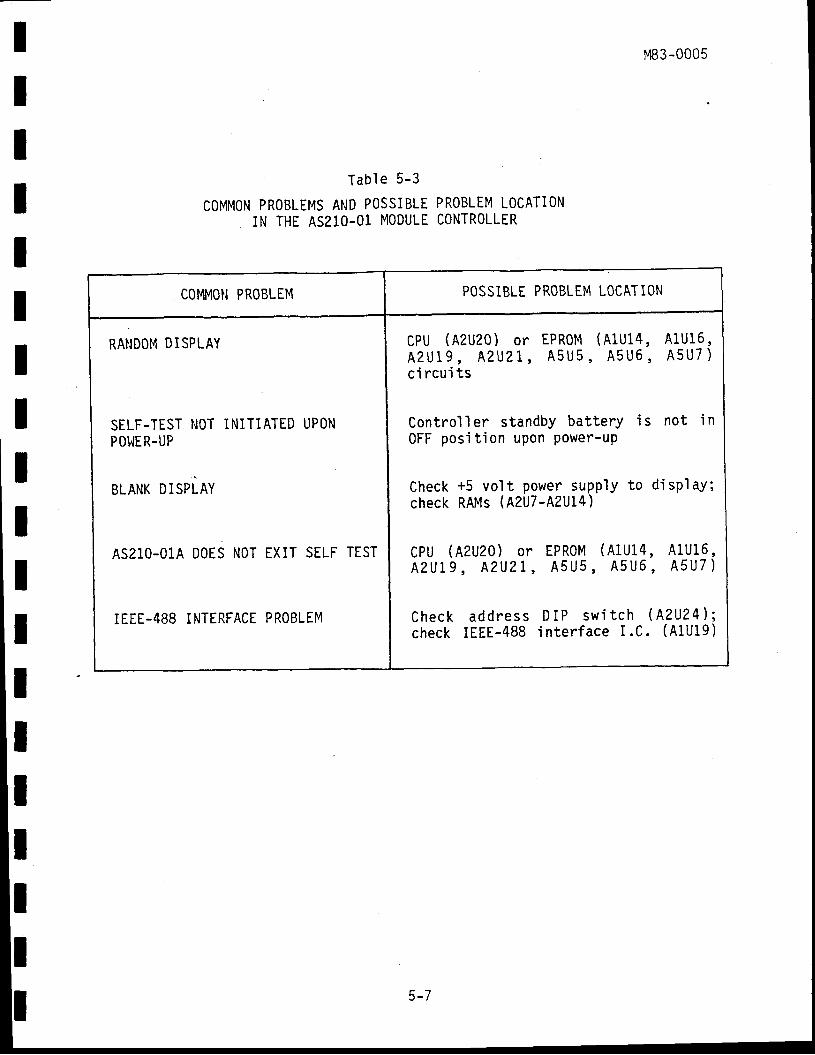
IIIIIIIIIIIIIIIIII
M83-0005
Tab le 5 -3
COMMON PROBLEMS AND POSSIBLEIN THE AS210-01 MODULE
PROBLEM LOCATIONCONTROLLER
COMMON PROBLEM POSSIBLE PROBLEM LOCATION
RANDOM DISPLAY
SELF-TEST NOTPOI'IER-UP
BLANK DISPLAY
INITIATED UPON
AS21O.O1A DOES NOT EXIT SELF TEST
IEEE-488 INTERFACE PROBLEM
CPU (A2U20) o r EPR0M (n fUfq , A lU l6 ,A2U19, A2U2 L , A5U5 , A5U6 , A5U7 )c i rcu' i ts
Contro'l l er standby battery j s not i nOFF posi t ' ion upon power-uP
Check +5 vo' l t power supp' ly to display;check RAMs (A2U7 -AZUL4)
CPU (LZUZO) or EPROM (A1Ul4 , A lU16,Az tJ rg , Az lJz l , A5U5, A5U6, A5U7 )
Check address D IP sw i tch (AZUZ4 l ;check IEEE-488 in te r face I .C . (A1Ui9)
5-7
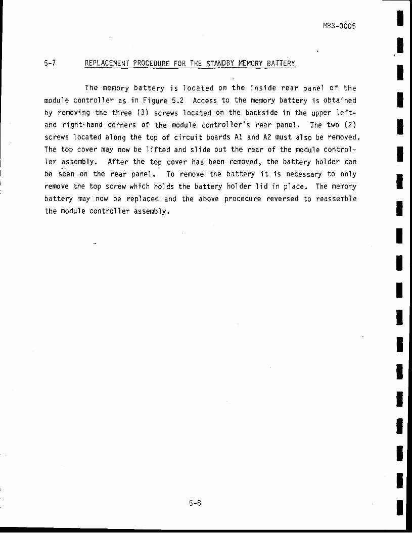
M83-0005
F 1
3 - l REPLACEMENT PROCEDURE FOR THE STANDBY MEMORY BATTERY
The memory ba t te ry i s loca ted on the ins ide rear pane l o f the
modu le cont ro l le r as in F ' igure 5 .2 Access to the memory ba t te ry i s ob ta ined
by removing the three (3) screws located on the backside in the upper lef t -
and r igh t -hand corners o f the modu le cont ro ' l le r ' s rear pane1. The two (2 )
screws located along the top of c i rcui t boards Al . and A2 must also be removed.
The top cover may noh, be l i f ted and sl ide out the rear of the module control-' ler
assembly. Af ter the top cover has been removed, the battery holder can
be seen on the rear pane1. To remove the battery i t is necessary to only
remove the top screb/ which holds the battery holder l id in p1ace, The memory
battery may now be replaced and the above procedure reversed to reassemble
the modul e control 1 er assemb' ly.
IIIIIIIIIIIIIIIttIt5-8
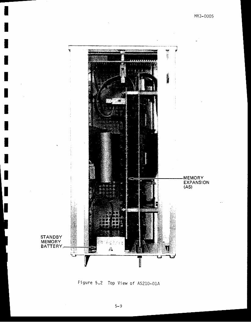
---
IIIIIIIII
M83-0005
MEMORYEXPANSION(A5)
STANDBYMEMOHYBATTERY
F igu re 5 .2 Top V iew o f AS210 -01A

IIIIIIIIIItIIIIIIII
M83-0005
CHAPTER 6
ILLUSTRATED PARTS LIST
6-1 INTRODUCTION
This chapter conta ins an i l l us t r :a ted par ts l i s t fo r the AS210-01AModu le Cont ro l le r . The assembly numbers and assembly t i t le a re l i s ted a t thetop o f the par ts l i s ts . The par ts l i s ts a re d iv ided in to s ix co lumns andarranged i n the fo1 I owi ng order:
Column l . - I tem Number
Co lumn 2 - Quant i t y per assembly .
Col umn 3 - Manufacturer 's Code
Col umn 4 - Part Number
Co lumn 5 - Descr ip t ion
Column 6 - Reference Des iqnat ion
6-1
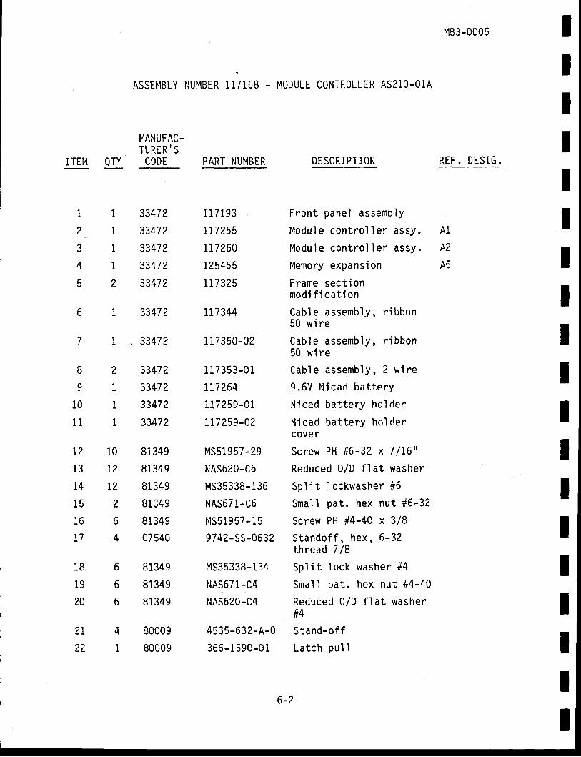
ITEM QTY
ASSEMBLY NUMBER,r irut - I . IODULE CONIROLLER AS21O.O1A
MANUFAC.TURER.SCODE PART NUMBER DESCRIPTION
M83-0005
REF. DESIG.
A1
A2
A5
IIIIITIIIIIIIITIIII
1
2
3AT
5
'lI
8
9
10
11
l2
13
14
15
16
t ]
t8
19
20
2t
22
2
1
1
1
10
I2
L2
2
6
4
6
6
6
41L
33472
33472
33472
33472
33472
3347 2
. 33472
33472
33472
33472
33472
81349
81349
81349
81349
81349
07540
81349
81349
81349
80009
80009
11 7193
rr7255LL7260
t25465
LL732s
LL7344
1 1 7350-02
1 I 7353-0 1
1L7264
117259-01
tt7259-02
MS51957-29
NAS620-C6
MS35338-136
NA567 I -C6
MSs1957-1 5
9742-SS-0632
MS35338-134
NA567 1 -C4
NAS620-C4
4535-632-A-0
366-1690-01
Front panel assembly
Modu'l e contro'l I er assy.
Modu' l e control 1 er assy.
Memory expansion
Frame sect ionmodi f i cat i on
Cab le assembly , r ibbon50 wi re
Cab' le assembly, r i bbon50 w i re
Cab le assembly , 2 w i re
9 .6V N icad ba t te ry
Nicad battery ho' lder
Nicad battery ho1derc0ver
Screw PH #6-32 x 7 / !6"
Reduced 0/D f ' lat washer
Sp l i t lockwasher #6
Sma' l l pat . hex nut #6-32
Screw PH #4-40 x 3/8
Standof f , hex , 6 -32thread 7/8
Sp l i t l ock washer #4
Smal l pat . hex nut #4-40
Reduced 0/D f l at washer#4
Stand-of f
Latch pul 1
6-2
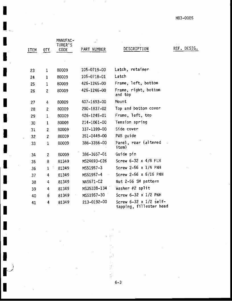
zI
I
4
4
4
6
4
IIIIIIIIIIIIItIII
i
IJ
rTEM !A
MANUFAC-TURER'SCODE
M83-0005
REF. DESIG.
23
24
25
26
?7
28
29
30
31
32
33
34
35
36
37
38
39
40
41
80009
80009
80009
80009
80009
80009
80009
80009
80009
80009
80009
80009
81349
81349
81349
81349
81349
81349
81349
1I
1
I
2
4
2
I
i
2
2
1
PART NUI4BER
105-0719-00
10s-0718-01
426-L245-00
426-t246-00
407-1 693-00
200-1837-02
426-t245-0r
214-1061-00
337-1399-00
351-0449-00
386-3356-00
386-3657-01
MS24693-C26
MS51957-3
MSs1957-4
NAS671-C2
MS35338-134
MS51957-30
213-0192-00
DESCRIPTION
Latch, retainer
Latch
Frame, lef t , bot tom
Frame, r ight , bot tomand top
Mount
Top and bottom cover
Frame , ' l eft, top
Tens ion spr ing
Side cover
PWB gu ide
Pane1 , rear (al teredi tem)
Gu ide p in
Screw 6-32 x 4/8 FLH
Screw 2-56 x 1/4 PNH
Screw 2-56 x 5/16 PNH
Nut 2-56 SM pattern
Washer #2 sp l i t
Screw 6-32 x L/2 PNH
Screw 6-32 x L/2 self-tapp ing , f i l ' l es te r head
6-3
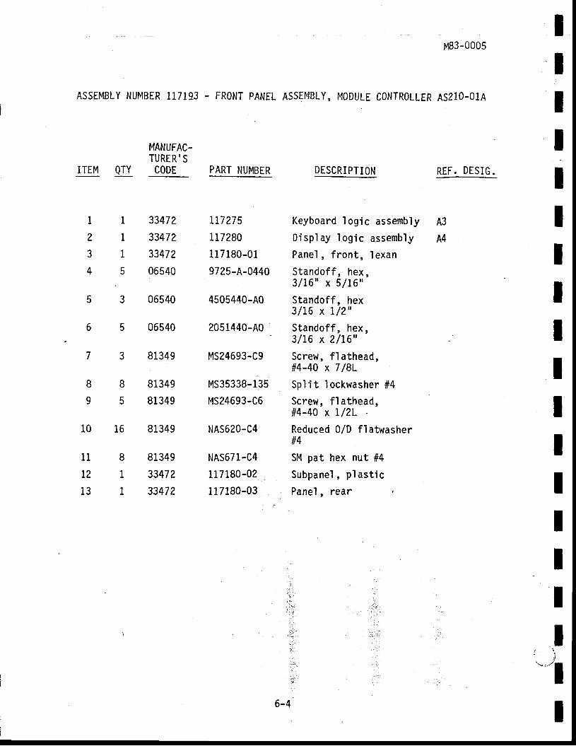
ASSEMELY NUMBER 117T93 . FRONT PANEL
M83-0005
ASSEMBLY, MODULE CONTROLLER AS21O-O1A
IIIIIITEM QTY
MANUFAC-TURER'SCODE PART NUMBER DESCRIPTION REF. DESIG.
1
2
3
4
1
1
1
5
8
1
1
8
9
I
5
33472
33472
3347?
06540
06540
06540
81349
81349
81349
81349
81349
33472
33472
117275
117280
117180-01
9725-A-0440
4505440-A0
2051440-A0
MS24693-C9
MS35338-135
MS24693-C6
NAS620-C4
NAS671-C4
117180-02
11 7 180-03
Keyboard logic assembiyD isp lay ' log ic assemblyPanel , f ront , ' lexan
Standoff , hex,3/16" x 5/16"
Standoff , hex3 /16 x 1 /2 "
Standof f , hex ,3/16 x 2/L6"
Screw, f ' l athead,
#4-40 x 7 /8LSpl i t
' lockwasher #4
Screw, f lathead,#4-4A x l lZL
Reduced 0/D fl atwasher#4
SM pat hex nut #4
Subpane l , p las t i c
Pane l , rear
IIIIIIIIIII
A3
A4
10
11
L2
13
16
i,':,
6-4
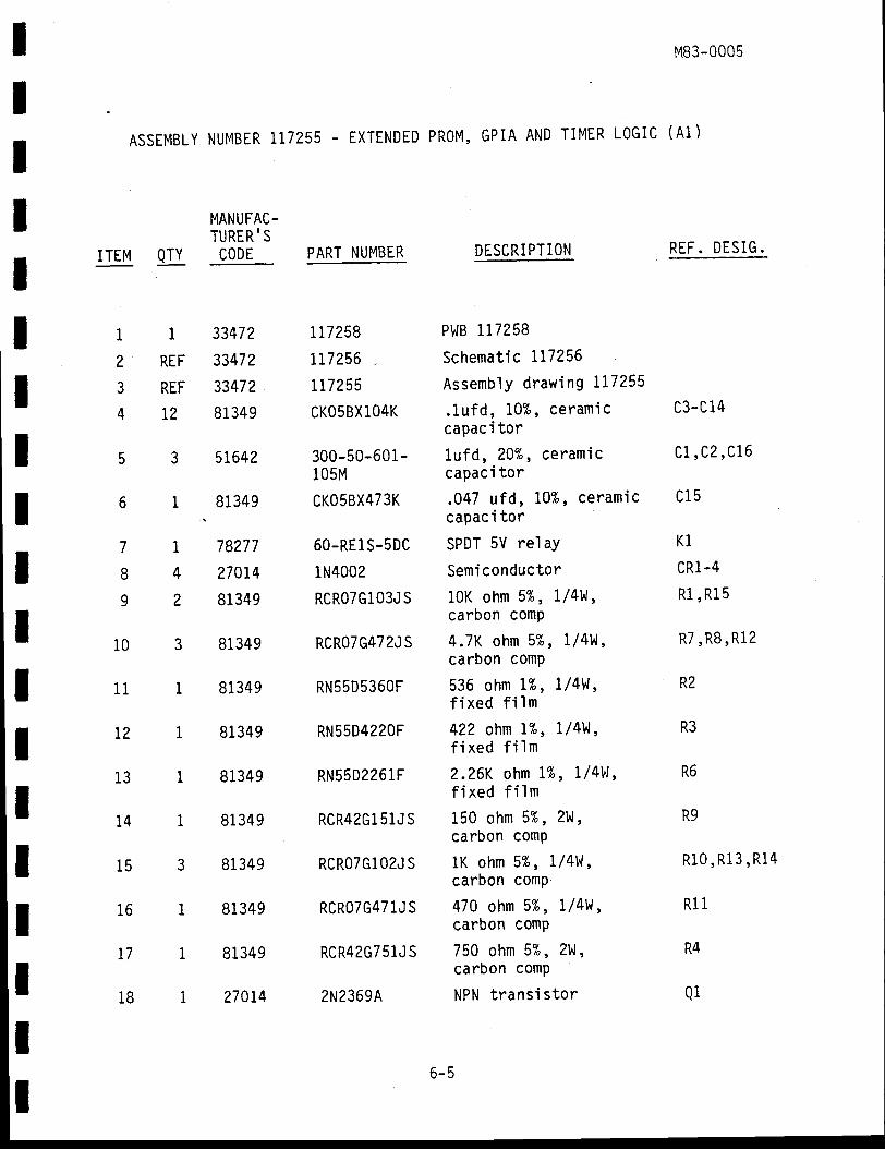
IIIIIIItIIITIIIIIII
1
REF
REF
t2
3
1
1
4
2
3
I
1
1
1
3
1
I
i
ITEM QTY
ASSEMBLY NUMBER 7T7255. EXTENDED PROM,GPIA AND T IMER LOGIC (A1)
MANUFAC.TURER.SCODE PART NUMBER
LT7?58
tr7256
tr7255
CKO5BXlO4K
300-50-601 -105M
CKO5BX473K
60-RE1S-5DC
iN4002
RCR07G1 03J S
RCRO7G472J S
RN55D536OF
RN55D422OF
RN55D2261 F
RCR42G1 51J S
RCROTGl OzJ S
RCR07G47 1J S
RCR42G751J S
2N2369A
DESCRIPTION
PWB 117258
Schematic 117256
Assembly d rawing 117255
.1u fd , 10%, ceram' iccapac i tor
1u fd , 20%, ceramiccapaci tor
.047 u fd , I0%, ceramiccapac i tor
SPDT 5V re'lay
Semi conductor
10K ohm 5%, 1 ' /4W,carbon comp
4 .7K ohm 57" , 1/4I,l ,carbon comp
536 ohm 1%, l /4W,f i xed f i lm
422 ohn !%, I/4\1,f i xed f i lm
2.26K ohm 1% , L/4V1,f i xed f i lm
150 ohm 5%, ?W,carbon comp
lK ohm 5%, l /4W,carbon comp'
470 ohm 5%, I /4W,carbon comp
750 ohm 5%, 2W,carbon comp
NPN t rans i s to r
MB3-0005
REF. DESIG.
c3-c14
c1. ,c2,c16
cl5
K1
cR1-4
R1,R15
R7,R8,R12
R2
R3
R6
R9
R10,R13,R14
Rl1
R4
Q1
1
2
3
4
5
6
7
8
9
10
11
T2
13
14
15
16
t7
18
33472
33472
33472
81349
51642
81349
78277
270t4
81349
81349
81349
81349
81349
81349
81349
81 349
81349
270r4
6-5
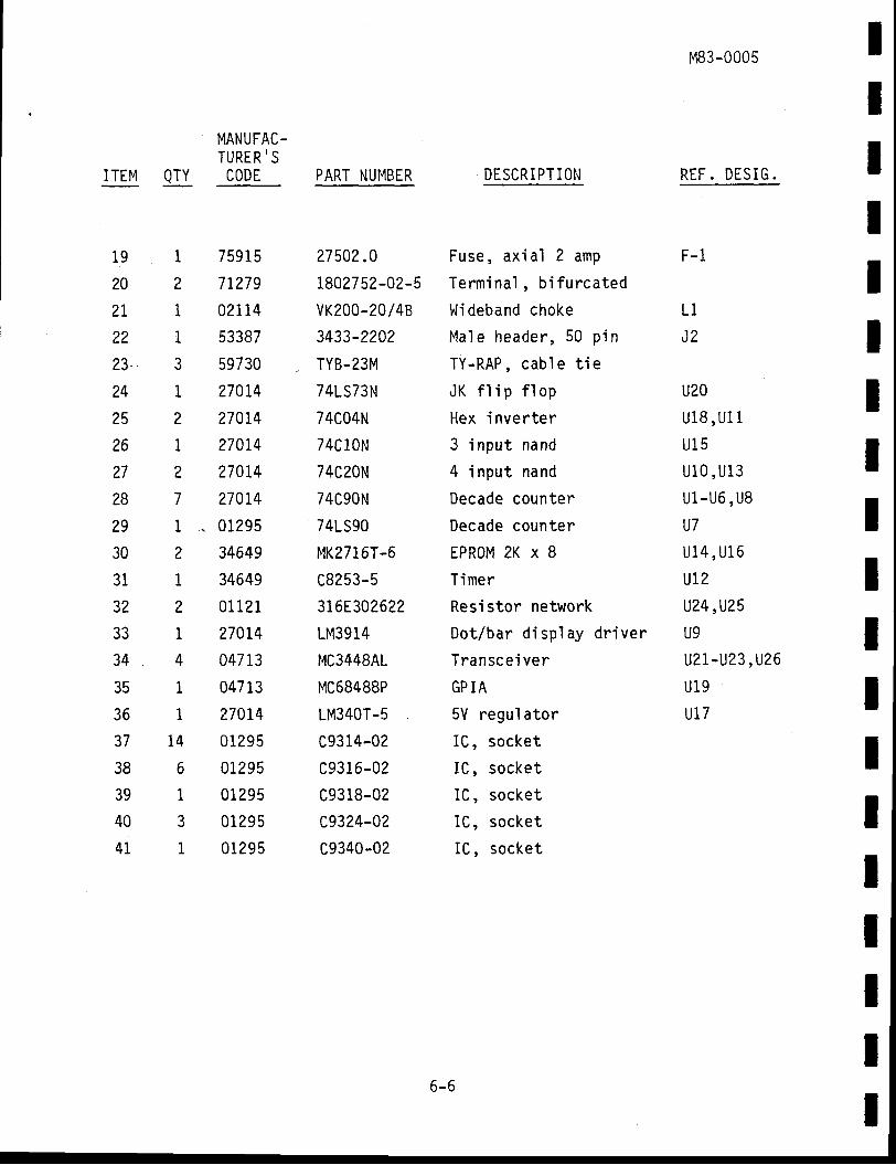
ITEM QTY
MANUFAC.TURER'SCODE PART NUMBER
IIIIIIIIIIItIIIIIII
DESCRI PTI ON
Fuse, ax ia l 2 amp
Termina l , b i fu rca ted
Wideband choke
Male header , 50 p in
TY-RAP , cab'l e ti e
JK f l i p f ' l op
Hex inverter
3 input nand
4 input nand
Decade counter
Decade counter
EPROM 2K x 8
T imer
Resi stor network
Dot /bar d isp lay d r iver
Transce i ver
GP iA
5V regul ator
IC, socket
IC , socke t
IC, socket
IC, socket
IC , socke t
M83-0005
REF. DESIG.
F-1
L1
J2
u20u18,Ul1ul5u10 , u l3ul -u6,u8U7ul4 ,U16u12v?4,v25U9v2L-V?3,U26u19u17
19
20
2T
22
23
24
25
26
27
28
29
30
31
32
33
34
35
36
37
38
39
40
41
I
2
1
1
31
?
I
2
7
I
2
I
2
1
4I
I
1
L4
6
I?
I
75915
71279
021 14
53387
59730
270t4
27014
27074
270I4
270t4
01295
34649
34649
01 121
270t4
047 13
047 13
270L4
01295
01295
01295
01295
01295
27502.0
1802752-02-5
vK200-20/4B
3433-2202
TYB-23M
74LS73N
74C04N
74C10N
74C20N
74C90N
741S90
t4K2716T-6
c8253-5
316E302622
1M3914
r4c3448AL
MC68488P
LM340T-5
c9314-02
c9316-02
c9318-02
c9324-02
c9340-02
6-6
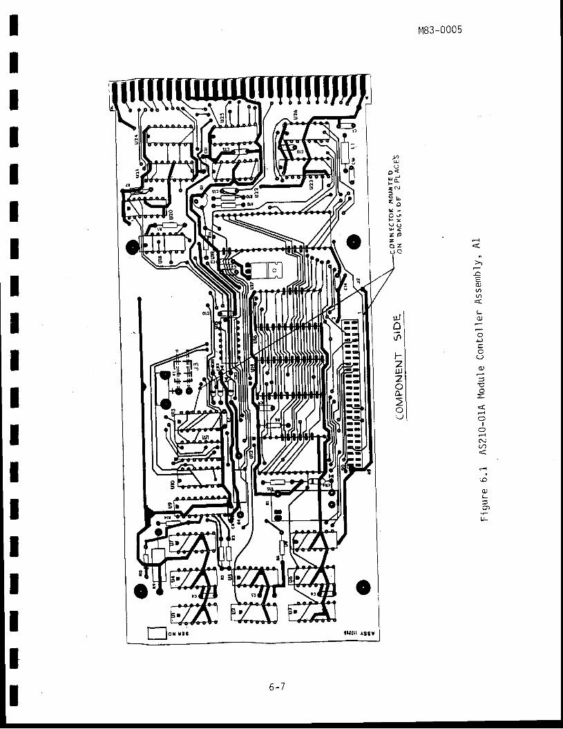
M83-0005
II
-cE
U1(n
Ld t
o+J
c)
3
I
(\i
t-
LL
uJ lal- l
o lIIr - t
2 lllj I2 lo lr l
>lv lu l
s+0
tl
*tlii hqf
II
II
II
. 1O - l
I-lo','i
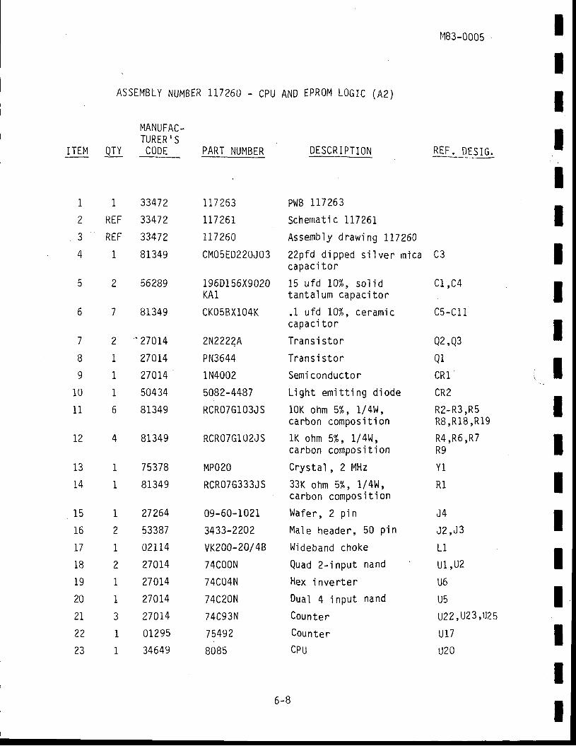
ASSTMBLY NUMBER IT7260 . CPU ANDEPR0M LOGrc (A2)
IIIIIIItIIIIIIItIII6-8
r183-0005
REF. DESIG.ITEM QTY
MANUFAC-TURER'SC()DE
I
I
4
6
B
9
10
i1
12
1 ?
14
15
16
L7
18
19
IU
2T
l t
/ <
1
REF
REF
i
z
I
11I
t
6
4
1L
I
I
i
2
1
2
11
J
i1I
3347?
33472
33472
8 i349
56289
81349
'274r4
27A14
27014
50434
81349
81349
75378
81349
27264
53387
OzI I4
270I4
27014
270L4
27074
0 i295
34649
/ .?
cl ,c4
c5-c11
Q2,Q3
Q1CR1
CR2
R2-R3,R5R8,R18,R19
R4,R6,R7R9
Y1
R1
'| /l
U T
J2 ,J3
L1
u1,u2UO
il6
u22,U23,U2-5u17u20
PART NUMBER
1I7 ?_63
TT7 26I
71726A
cMO5ED220J03
196D1 56X9020KAi
CKO5BXlO4K
2N2222A
PN3644
1N4002
5082-4487
RCROTGl O3JS
RCR07 Gl 02J S
MPO2O
RCR07G333J S
09-60-1 021
3433-2202
vK200-20/ 48
74C00N
74C04N
74C20N
74C93N
75492
8085
DESC3ITION
Pl^lB 117263
Schemati c l l l267
Assembly dnawi ng 1I7260
22p fd d ipped s j l ven micacapac i ton
15 u f d I0%, so l idtan ta l um capac i to r
.1 u fd 107" , cenamiccapac i to r
Tnans i sto r
Tran s i s to r
Semi conducto r
Li ght emit t i ng di ode
10K ohm 5%, L l 4W,carbon compos' i t i on
lK ohm 5%, 1 /4W,carbon compos i t ion
Cnystal , 2 l{Hz
33K ohm 5%, I / 4Vl ,carbon compos i t ionWafer , 2 p in
Ma le header , 50 p in
Wideband choke
Quaa 2- i nput nand
Hex i nverterDua l 4 input nand
Counter
Counten
CPU
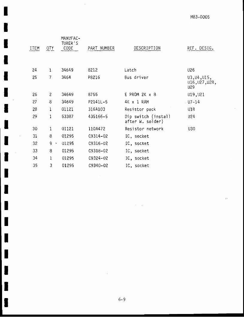
?4 1
257
IIIIII
ITEM _qry
MANUFAC-TURER'SCODE PART NUMBER
82r?
P8216
87 55
P21411-5
316A103
435 166- 5
110A472
c9314-02
c9316-02
c93 18-02
c9324-02
c9340-02
DESCR I PTI ON
Latch
Bus d r i ve r
tPR0M2Kx8
4Kx lRAM
Res i s to r pack
Di p sw i tch ( i ns ta l Ia f te r W. so lder )
Res i s to r ne twork
IC, socket
IC, socket
IC, socket
iC , socke t
IC , socke t
MB3-0005
REF. DESIG .
u26u3,u4,u15,UI6 , t )27 ,U28,v29u19 , t jz1
u7-14u18u24
u30
I?6
27
2B
IY
? 1
3?
J +
t
8
1'II
I
8
9
81I
34649
3464
34649
34649
01 121
53387
01121
01295
01295
01295
01295
01 295
IIIIIIIIIIII 6 -9
M83-0005
II
c!
-c^tlla
(-a)
(-]J
13
E
d
I .
NI(n
c!
L
LL
oc :
ct t _
fl-t-.t-,
ffi
c_c
[_ lo"" , ,
6 - 10
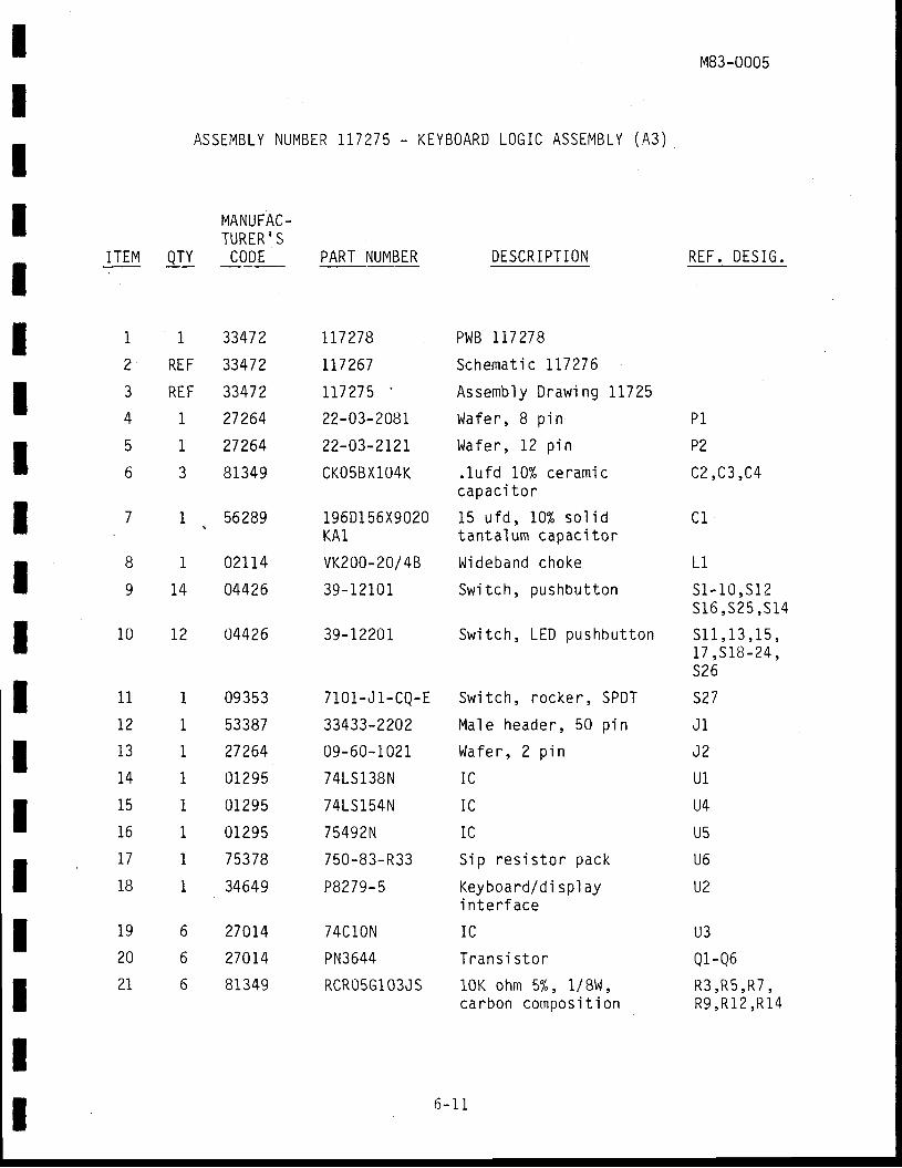
IIIIIIIItI
ASSEMBLY NUMBERrr7275 - KEYBOARD LOGICASSEMBLY (A3)
MANUFAC-TURER. SCODE PART NUMBER
M83-0005
REF. DESIG.
P1
P2
c2,c3,c4
c1
t l
s1-10 ,s12s16 ,S25 ,S14
s l1 ,13 ,15 ,17 ,S1B-24 ,s26
s27J1
J2
U1
U4
U5
U O
v2
U3
Ql -Q6R3,R5,R7,R9,R12,R14
DESCR I PTI ON
PWB i17278
Schemat'i c 1L7276
Assembly Drawi ng 11725
Wafer , 8 p in
Wafer , 12 p in
. lu fd 10% ceramiccapac i to r
15 u fd , l 0% so l idtan ta lum capac i to r
Wideband choke
Swi tch , pushbr . r t ton
Swi tch , LED pushbu t ton
Swi tch , rocker , SPDT
Male header , 50 p in
Wafen , Z p inTt -
t l
I ' .
S ip res i s t o r pack
Keyboand/d i sp1 ay' i n te r f ace
IC
Trans i s t o r
10K ohm 5%, 1 /BW,ca rbon compos i t i on
iTEM QTY
I
7
46
6
7
1
REF
REF
L
I?
I
3347 2
33472
33472
27264
27264
81349
56289
O?TT4
044?6
04426
09353
53387
27?64
01295
01295
01295
75378
34649
270I4
270I4
81349
rI7 278TT7 ?67rr7 27522-03-208r22-03-212rCKO5BXl04K
19601 56X9020KAl
uK200-20/ 48
39-12101
39-1220r
710 i -J 1 -CQ-E
33433-2242
09-60- 1 02 1
741S138N
74LS 1 54 N
75492N
750-83- R33
P8279-5
74C10N
PN3644
RCRO5Gl O3J S
T210
81
914
19
20
2t
II
11
T21 ?
14
15
16I tI I
18
1
f
I
1
1
1
11
6
6
6
II 6 -11
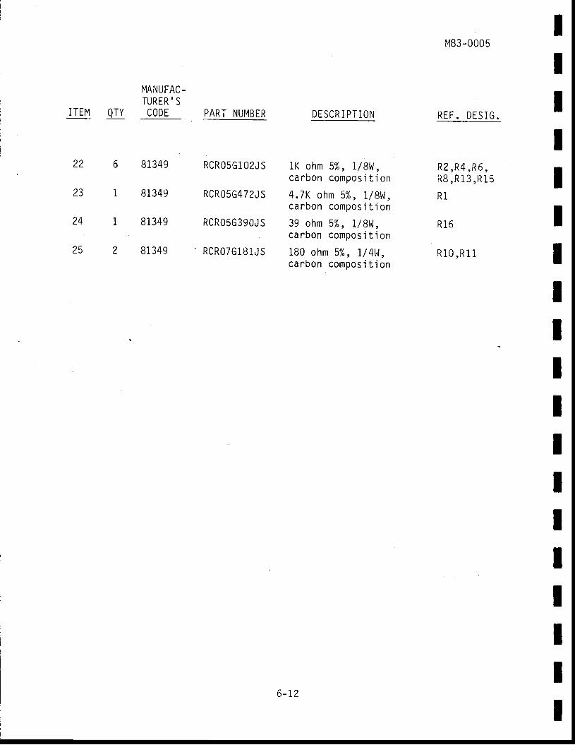
DESCR I PTI ON
lK ohm 5%, l /9W,carbon compos i t j on
4 .7K ohm 5%, 1 /8W,carbon compos j t i on
39 ohm 5%, 1 /8W,ca rbon compo s i t ' i on
180 ohm 5%, L /4W,ca rbon compo s ' i t i on
t'{83-0005
REF. DESIG .
R2,R4 ,R6 ,R8,R13,R15
R1
R16
R10,R11
IIIITEM QTY
MANUFAC-TURER'Snnntr PART NUMBER
RCRO5Gl O2JS
RCRO5G4 7 2J S
RCRO5G39OJ S
RCR07G181JS
22
l 5
24
25
6
1
I
2
81349
81 349
8 i349
8i 349
IIIIIIIIIIIIIIII
6 -12
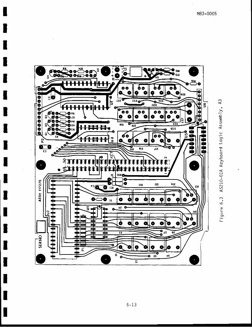
M83-0005II
cn
-o
atn
Et-
-od t
\Z
cI
O
NI
ca
(U(-
lJ-
III
9ts lts
ridriltrlrrtulllttt;
III
oooggoooo
ttt
(\IN
thU,
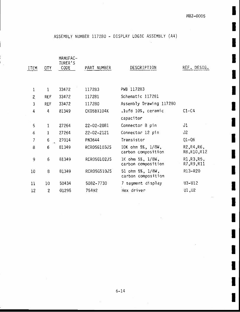
ASSEMBLY NUMBER117280 - DTSPLAY LOGIC ASSEMBLY (A4)
M83-0005
REF. DESIG .
IIIIIIIIIItIIIIIIII
I TEM
I
2
4
a
6
7
8
QTY
i
REF
REF
4
'tL
I
6
6
6
8
10
2
10
11
T2
MANUFAC.TURER'SCODE
33472
33472
33472
81349
27264
27264
270L4
81349
81349
81349
50434
01295
PART NUMBER
117283
rt7287
117280
CKO5BXl04K
22-02-2081
22-02-2121
PN3644
RCRO5Gl O3J S
RCRO5Gl OzJ S
RCRO5G5 lOJS
5082- 7730
7549?
C1- C4
J1
J2
Q1.Q6R2,R4,R6,R8,R10,R12
R1 ,R3 ,R5,R7,R9,R11
R1 3- R20
u3-ui 2u1,u2
DESCR I PTION
PWB 1L7283
Schemati c I1728I
Assembly Dnawing 117280
.1u fd 10%, ce ramic
capac i to r
Connec to r 8 p in
Connector 12 p i n
Trans ' i s to r
10K ohm 5%, L /9W,carbon cornpos i t ion
lK ohm 5%, 1 /8W,canbon compos i t ion
51 ohm 5%, 1 /8w,carbon compos i t ' i on
7 segment di sp1 ay
Hex d r i ven
6- 14
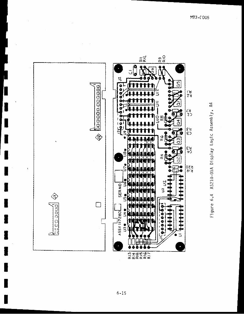
M83-C005
He
T,4,v
\ioll o ll 0 l
l:llrl
, / . ( l l
- :J -9d d - d d
r<r
=OJU).J'l
()
J
(n
OI
d
<r
aL
IJ.
ZUz)
9 E€ )
I
r O * c 0 n \ 9 Nd d.G. a( ((
I
I
6 - 15
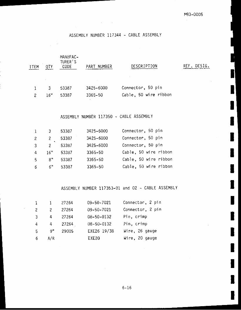
ASSEMBLY NUMBER 117344 - CABLE ASSEMBLY
M83-0005
REF. DESIG.iTEM QTY
MANUFAC.TURER,SCODE
53387
53387
53387
53387
53387
53387
53387
53387
27264
27264
77 264
27264
29005
PART NUMBER
3425-6000
3365- 50
3425-6000
3425-6000
3425-6000
3365-50
3365-50
336 5- 50
09- 50- 7021
09-50-7021
08-50-01 32
08- 50-0132
EXE26 T9/38
EXE2O
ASSEMBLY NUMBER 117350 - CABLE ASSEMBLY
DESCRIPT ION
Connec to r , 50 p in
Cabl e, 50 wi re r i bbon
Connector ,
Connector ' ,
Con nec t o r ,
Cab ' le , 50
Cab1e,50
Cab1e,50
50 p in
50 p'i n
50 p'i n
wi re ri bbon
w'i ne ri bbon
wi ne ni bbon
and 02 - CABLE ASSEMBLY
Connec to ro 2 p i n
Connec to r , 2 p i n
P i n , c r imp
P i n , c r imp
l ,J i ne, 26 gauge
W' i re , 20 gauge
I
2 16"
IIIIIIItIIIIIII
13
?2< /
416F A
66
1 11 I
22
34
44
5 9"
6 A/R
t l
t l
t l
ASSEMBLY NUMBER i17353.01
6 - 16
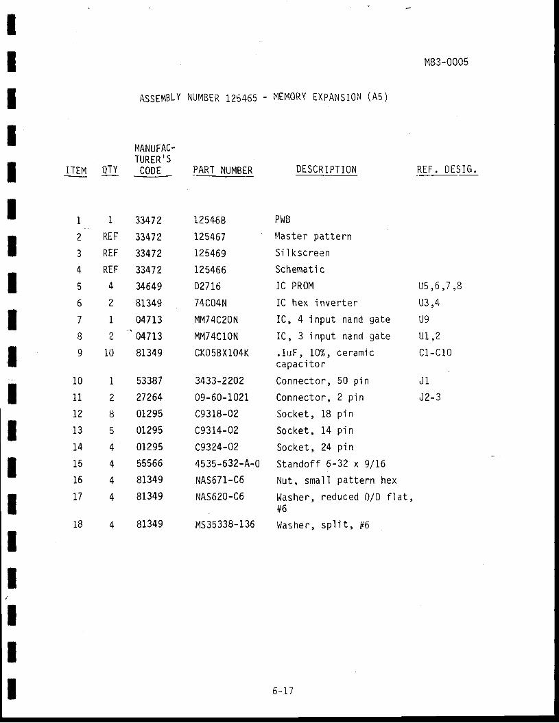
IIIIItIIIIIIIIIIIII
ASSEMBLY NUMBER1 25465. IVIEMORY EXPANSION (A5 )
M83-0005
REF. DESIG .
u5,6 ,7 ,8U3,4
U9
u1,2L I . U I ( J
J1
J2 -3
MANUFAC-TURER,S
ITEM QTY CODE
I
2
3
4
5
61
8
9
10
11
I2
131 'r r t
15
161 1L I
18
I
l_
REF
REF
REF
4
2
1
2
10
I
a
8
5
4
4
4
4
4
33472
33472
33472
33472
34649
81349
04713
047 13
81349
s3387
27264
01295
01295
01295
55566
81349
81349
81349
PART NUMBER
125468
r25467
125469
125466
D27L6
74C04N
MM74C20N
MM74C10N
CKO5BXlO4K
3433-2202
09-60- I 021
c93 i8-02
c9314-02
c9324-02
4535-632-A-0
NAS671-C6
NAS620-C6
MS35338- 1 36
DESCR i PTI ON
PWB
Masten pa t te rn
S i l kscneen
Schemati c
IC PROM
IC hex inver te r
IC , 4 ' i npu t nand ga te
IC, 3 i nput nand ga te
.1uF,10%, cenamiccapac i to r
Connector " , 50 p i n
Connector" , 2 pin
Socke t , 18 p i n
Socket , 14 p i n
Socke t , 24 p in
Standoff 6-32 x 9/16
Nut , smal I pa t te rn hex
Washer , reduced 0 /D f la t ,#6
Washer , SP l i t , #6
6 -17
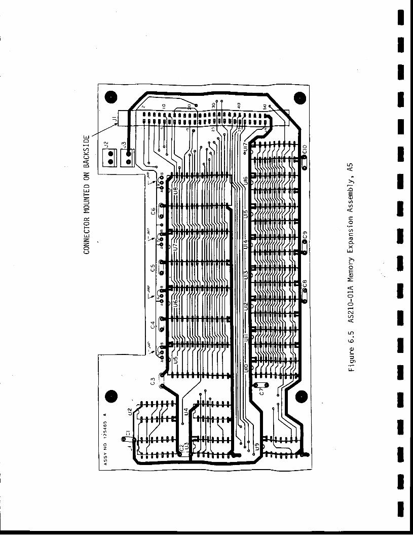
III
III
II
(utntn
tn
(o
Xt!
L
=
F{
I
F{
C\]a
to
(o
o,L
lJ-
l!
tt1v.
coz.
ollJt-
=O
OF.
t!zz.o(J
III
M I i t l | ! !
c=
rfllLell
ItIIIITIItIIIIIIIII
6-2 MANUFACTURER'S CODE L IST
Th i s sec t i on ' i nc l udes a l I
AS210 sys tem. The l i s t i s a r ranged
M83-0005
manu fac tu re r ' ' s o f ma te r i a l s used ' i n t he
i n .nume r i ca l o rde r by code .
6 - 19
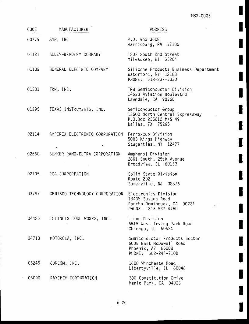
01281 TRt^ l , INC.
01295 TEXAS INSTRUMENTS, INC.
02114 AMPTREX ELECTRONIC CORPORATION
02660 "** ' *
RAMO-ELTRA CORPORATION
02735 RCA CORPORPATION
03797 GENISCO TECHNOLOGY C()RPORATION
04426 ILL INOIS TOOL WORKS, INC.
04713 MOTOROLA. INC.
MANUFACTURER
AIUIP , I NC
ALLEN.BRADLEY COMPANY
GENERAL ELECTRIC COMPANY
CORCOM, INC .
RAYCHEM CORPORATION
M83-0005
ADDRESS
P.0 . Box 3608Har r i sbu rg , PA 17105
1202 Sou th Znd S t ree tM'i I wau kee , l , ' l I 53204
S i I j cone P roduc ts Bus ' i ness Depar tmen tWaten fo rd , NY 12188PHONE : 5 18 -237 -3330
TRW Semi conductor Di v i s i on14520 Av ia t i on Bou levandLawnda l e , CA 90260
Semi conduc to r Group13500 Nor th Cen t ra l Exp r "esswayP.0.Box 225A12 M/S 49Da1 I as , TX 75265
Fe r roxcub D ' i v i s ' i on5083 K jngs H ighwaySauger t i es, NY 12477
Ampheno l D i v j s i on2801 Sou th . 25 th AvenueBroadv iew , I L 60153
So l i d S ta te D i v i s i onRoute 202Somenv ' i l 1e , NJ 08876
E l ec tnon i cs D i v i s i on18435 Susana RoadRancho Domi nguez, CA 90221PH0NE: 213 -537 -4750
L i con D ' i v i s i on6615 Wes t I r v i ng Pa rk RoadCh ' i cago , I L 60634
Semiconduc to r Pnoduc ts Sec ton5005 East McDowel I RoadPhoen i x , AZ 85008PH0NE: 602-244-7100
1600 h] ' incheste RoadL ibe r t yv i l l e , I L 60048
300 Cons t i t u t ' i on D r i veMen lo Pank , CA 94025
IIa f l n F
00779
01 121
0 i 139
05245
06090
IIIIttIIIIIIIIIII6-20
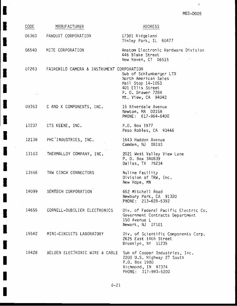
IIIIIIIIIIIIIIItIII
CODE
06 383
06540
07 263
1T237
1 ? ' t ? A
i 31 03
f
MB3-0005
MANUFACTURER ADDRESS
PANDUIT CORPORATION 17301 R idge landT i n l ey Park , IL 60477
Amatom E l ec t ron i c Hardware D i v i s i on446 B lake St ree tNew Haven, CT 06515
MITE CORPORATION
FAIRCHILD CAMERA & INSTRUMENT CORPORATIONSub o f Sch lumberge r LTDNor th Amer i can Sa lesMa i l S top 14 -1053401 E l l i s S t ree tP . 0 . Dnawer 7284Mt . V iew , CA 94042
C AND K COMP0NENTS. INC . 15 R i ve rda le AvenueNewton , MA 02158PHONE : 617 -964-6400
CTS KEENE, INC. P .0 . Box 1977Paso Rob les , CA 93446
PHC ' INDUSTRIES , INC . 1643 Haddon AvenueCamden , NJ 08103
THERMALL0Y C0MPANY, INC . 2021 Wes t Va11ey V iew LaneP. 0 . Box 340839Da l 1 as , TX 75?34
TRt, l C i NCH CONNECTORS Nul i ne Faci I ' i tvDi vi s' i on of TRI^J , I nc .New Hope , MN
SEMTECH C0RP0RATI0N 652 M i t che l l RoadNewbury Pa rk , CA 91320PH0NE: 213-628-5392
C0RNELL-DUBIL IER ELECTRONICS D ' i v . o f Fede ra l Pac ' i f i c E lec t l i c Co .Governmen t Con t rac ts Depar tmen t150 Avenue LNewark , NJ 07101
MIN I -C IRCUITS LAB0RATORY D iv . o f Sc ien t i f i c Componen ts Co rp .2625 Eas t 14 th S t ree tBnook l yn , NY 11235
1 ' l ( r i A
14099
146 55
75542
16428 BELDEN ELECTRONIC WIRE & CABLE Sub o f Coope r I ndus t r i es , I nc .2200 U .S . H ighway 27 Sou thP .0 . Box 1980R i chmond , IN 47374PHONE: 317 -983 -5200
6-21
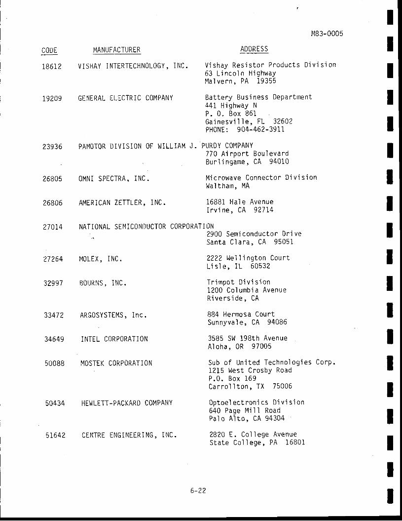
IICODE I'lANUFACTURER
T86T2 V ISHAY INTERTECHNOLOGY, INC.
19209 GENERAL ILICTRIC COMPANY
23936 PAMOTOR DIV IS ION OF WILL IAM J .
M83-0005
ADDRESS
Vi shay Res i s to r Produc ts D i v i s i on63 L inco ln H ' ighwayMal ve rn , PA 19355
Bat te r "y Bus i ness Depar tment441 H ighway NP. 0 . Box 861Gai nesvi 1 1 e, FL 32602PHONE: 904-462-3911
PURDY COMPANY770 A i rpor t Bou levardBur l i ngame, CA 94010
Mic rowave Connec to r D iv i s ionWal tham, MA
16881 Ha l e AvenueI rv i ne , CA 92714
2900 Semi conductor " Dr i veSanta C1 a na , CA 95051
22?2 Wel l ing ton Cour tL i s l e , IL 60532
Tr impot D i v i s j on1200 Co l umb ' ia AvenueRivers ide , CA
884 Hermosa CourtSunnyva l e , CA 94086
3585 S|. l 198th AvenueA1 oha , 0R 97005
Sub o f Un i ted Techno log ies CorP .1215 West Crosby RoadP.0 . Box 169Car ro l 1 ton , TX 75006
Optoe1 ectnoni cs Di v i s i on640 Page Mi 1 1 RoadPa lo A l to , CA 94304
2820 E. Col lege AvenueSta te Co1 1 ege, PA 16801
26805
26806
27074
27264
32997
3347?
34649
50088
OMNI SPECTRA, INC.
AMERICAN ZETTLER, INC .
NAT I ONAL
M0LEX, INC .
BOURNS, INC .
ARGOSYSTEMS, Inc .
INTEL CORPORATION
MOSTEK CORPORATION
SEMICONDUCTOR CORPORATI ON
IIIIIIIIIIIIIIIII
50434 HE!'JLETT.PACKARD COMPANY
51642 CENTRE ENGINEERING, INC .
6-22
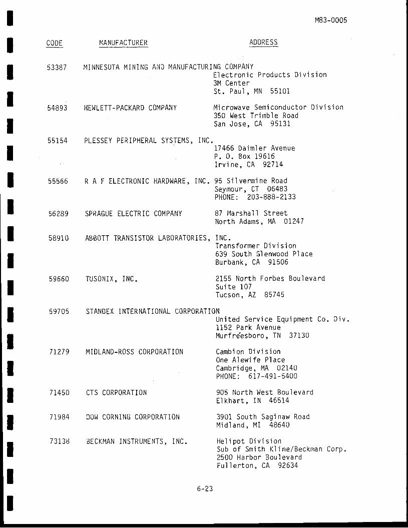
IIIIIIIIIIIIIIIIIII
54893 HEWLETT-PACKARD COMPANY
55154 PLESSEY PTRIPHERAL SYSTEMS, INC .
5 5566
17466 Da imle r AvenueP. 0 . Box 19616I rv ' ine , CA 92714
R A F ELECTR0NIC HARDWARE, INC, 95 S i l ve rmine RoadSeymour, CT 06483PHONE: 203-888-2133
SPRAGUE ELECTRIC COMPANY 87 I4ANShAI I S t rECtNorth Adams, l4A 0l?47
ABBOTT TRANSISTOR LABORATORIES, INC.Trans fo rmer " D iv i s ion639 South Gl enwood Pl aceBurbank , CA 91506
TUSONIX, INC. 2155 Nonth For^bes Bou levardSu i te 107Tucson, AZ 85745
56289
5891 0
59660
59705 STANDEX INTERNATIONAL CORPORATION
CODE MANUFACTURER
53387 MINNESOTA MIN ING AND MANUFACTURING COMPANY
M83-0005
ADDRESS
El ec t non ' i c Pr oduc ts D i v i s i on314 Cente rS t . Pau l , MN 55101
M' i c rowave Semiconduc to r D iv i s ion350 f ,Jest Tr i rnbl e RoadSan Jose , CA 95131
Un i ted Se rv j ce Equ ipmen t Co . D i v .1152 Park AvenueMur f reesbo ro , TN 37130
Camb ion D i v i s i onOne Al ewi fe Pl aceCambr i dge , MA 02140PH0NE : 617 -491-5400
905 l ' l o r th Wes t Bou l eva rdE l kha r t , IN 46514
3901 Sou th Sag i naw RoadMid l and , M I 48640
He l i po t D i v ' i s i onSub o f Sm j th K l i ne /Beckman Co rp .2500 Ha rbo r Bou leva rdFu l 1 e r ton , CA 92634
7T279 MIDLAND.ROSS CORPORATION
71450
7 1984
7 3138
CTS CORPORATION
DOI^J CORNING CORPORATION
BECKMAN INSTRUMENTS, INC .
6-23
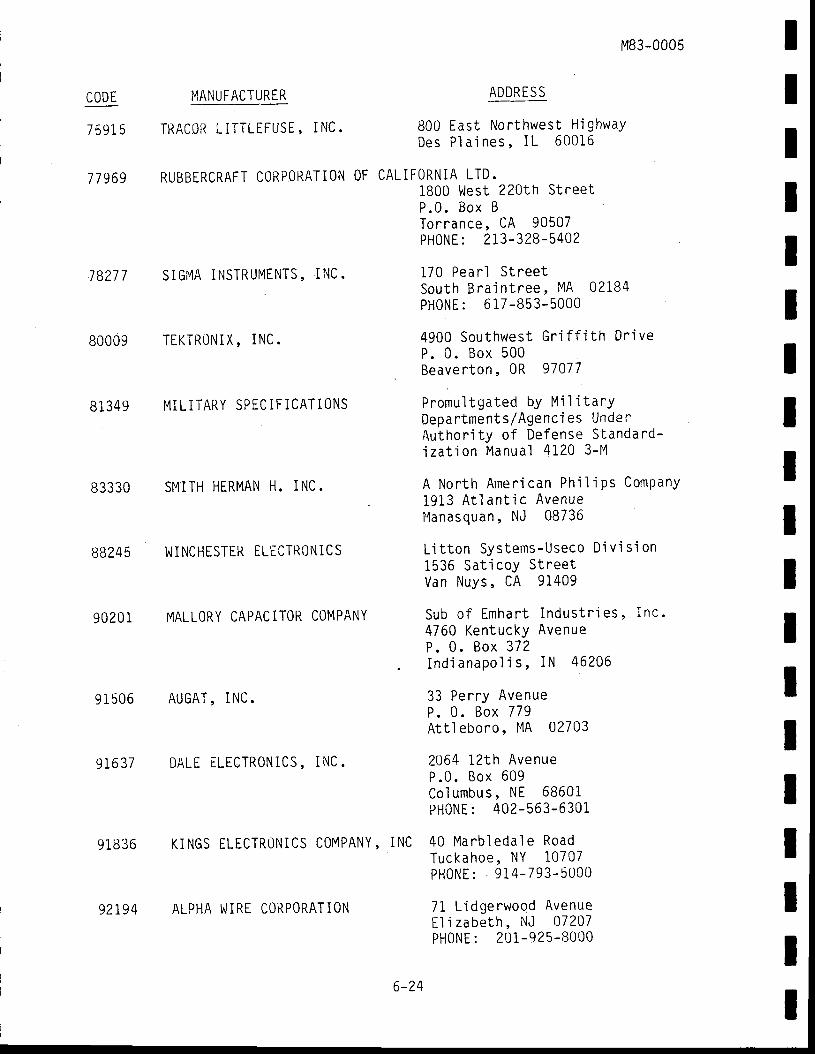
t IIIIIIIIIItIIIIIIIt
a n n g
7591 5
77969
MANUFACTURER
TRACOR L ITTLEFUST, INC .
RUBBERCRAFT CORPORATION OF
M83-0005
ADDRESS
800 East Nor thwest H ighwaYDes P l a ' i nes , IL 60016
CALIF( )RNIA LTD.1800 l, iest ?20th StreetP .0 . Box BTor rance, CA 90507PH0NE z 213-328-5402
170 Pear l S t ree tSou th Bra in t ree , MA 02184PHONE: 617-853-5000
4900 Sou thwes t Gn i f f i t h Dr i veP. 0 . Box 500Beaver ton , 0R 97077
Promul tgated bY Mi 1 i tarYDepar tments /Agenc i es UndenAuthon i ty o f Defense SIandard-i za t ion Manua l 4120 3 -M
A Nor th Arner i can Ph ' i1 ips Company1913 A t lan t ' i c Avenuel '4anasquan, NJ 08736
L i t ton Sys tems-Useco D i v i s i on1536 Sat icoY StneetVan Nuys , CA 91409
Sub o f Emhar t Indus t r ies , Inc .4760 KentuckY AvenueP. 0 . Box 372
- Ind i anaPo l i s , IN 46206
33 Per ry AvenueP. 0 . Box 779At t l eboro , l4A 02703
2064 12 th AvenueP.0 . Box 609
78277 S IGMA iNSTRUMENTS, INC.
8OOO9 TEKTRONIX , INC .
81349 I ' I I L ITARY SPECIF ICATIONS
83330 SI '4 ITH HERMAN H. INC.
88245 I ' I INCHESTER ELECTRONICS
90201 MALLORY CAPACITOR COMPANY
91506 AUGAT, INC .
91637 DAL I ELECTRONICS, INC .
91836
Co l umbus , NE 68601PH0NE: 402 -563-6301
KINGS ELECTRONICS COMPANY, INC 40 Marb leda le RoadTuckahoe , NY 10707PHONE: 914 -793 -5000
ALPHA WIRE C0RPORATiON 71 L idge rwood AvenueEf i zabeth, NJ 07207PH0NE: 201-925-8000
9219q
6-24


II
;ti
l.IIIIIIk
AS2l O-O2FREQUENCY
COMPARATOR MODULE
-l
I
IIItIIF

IIIIIIIIttItIIIItII
TI
itl
lI
Al l r ights reserved. No part of th is publ icat ion may bereproduced, stored in a retrieval s;/stem, or transmitted,in any form or by any means, electronic, mechanical ,photocopying, recording and/or otherui se without thepr ior wr i t ten permission of ARG0Systems, Inc. This man-ual may not be lent, resold, hired out or otherwise dis-posed of by way of trade in any form of binding or coverother than that in which i t is publ ished, wi thout theprior consent of ARG0Systems, Inc.
IIIIItItTItIIJI
ARG0Systems, Inc. / 884 HennosaTelephone (Area Code 408)
Court , Sunnyvale, Cal i fornia737-2000 / Telex No. 352077

IIIIIIIIItItIIItII
tI
tl"
iIIIIII
5-35-35-3
5-65-65-8
IIIIII*
TABLE OF CONTENTS
T i t l e
GENERAL INFORMATION
1.1 INTRODUCTIONL-? PHYSICAL AND ELECTRICAL DESCRIPTION
INSTALLATION
2.L INTRODUCTION
OPERATION
3-1 INTRODUCTION3-2 CoNTRoLS, INDICAT0RS,3.3 OPERATING PROCEDURES
THEORY OF OPERATION
4-I INTRODUCTION
AND CONNECTORS
MAINTENANCE AND OPERATION
5.1 INTRODUCTION
SECTION I5-2 PREVENTIVE MAINTENANCE
SECTION I I5-3 PERFORI4ANCE TESTING5-4 rNPUT FREQUENCY PERF0RMANCE TESTS5-5 TEST PROCEDURE
SECTION I I I5-6 CALIBRATION/ALIGNMENT PROCEDURE5-7 ACCESS T0 AS210-02 FREQUENCY CoMPARAToR5-8 200 MHz PLO ALIGNMENT PROCEDURE
SECTION IV5-9 TROUBLESHOOTING PROCEDURES
ILLUSTRATED PARTS LIST
6-1 INTRODUCTION
Page
iv
1-1
1-11-1
2-t
2-L
4-1
4-1
3-1
3-13-13-1
I-t--5-1
5-1
MODULE
5-10
6-1
6-L
l_
LIST OF ILLUSTRATIONS
T i t le
AS210-02 Frequency Comparator
AS210-02 Front Panel Controls, Indfcators, and Connectors
Operational Flow Diagram
Frequency Comparator Functional Block Diagram
AS210-02 Frequency Comparator Input FrequencyPerformance Test Configuration
Flow Diagram of Cal ibrat ion/Al ignnent Procedure forAS210-02 Frequency Comparator
AS210-02 Frequency Comparator Microprocessor Interfaceand Input Select Schematic Diagram, AL
AS210-02 Frequdncy Comparator Input MultiplexerSchematic Diagram, A1A1
AS210-02 Frequency Comparator 200 MHz Phase-LockedOsci' l ' lator and Time Base Select Schematic Diagram
*Frequenep€omparator Modul e-- ----- -
AS210-02 Frequency Comparator t{icroprocessor Interfaceand Input Select Assembly, Al
AS210-02 Frequency Comparator 200 MHz Phase-Locked0sci l lator and Time Base Select Assembly, A2
AS210-02 Frequency Comparator Input Mul t iplexerAssembly, Al.Al.
IIIII
Fi gure
1 .1
3 .1
3 .2
4 .1
5 .1
5 .2
5 .3
5 .4
5 .5
Page
L-2
3-2
3-6
4-2
5-5
5-7
5-13
5-14
5-1 5
6-4
6-8
6-13
6-1 5
IIIt
IIII
6 .L
6 .?
IIII
'a
II
6.3
6 .4
I- l t -
It
.t
IIItIIIIIItIIII
t_
Tabl e
1-1
3-1
5-1
5-2
5-3
LIST OF TABLES
Tit l e
AS210;02 Equiprent Specification
AS210-02 Front Panel Controls, Indicators, and Connectors
Preventive Maintenance Checks and Services
Required Test Equiprent for the Input FrequencyPerformance Test
Required Test Equipnent for the 200 MHz PLOAlignment Procedure
Error Code Listing
Visual Indicators
Page
1-3
3-3
5-2
5-3
5-8
5-11
5-t2
5-4
5-5
- i i i -
PREFACE
This manual contains operation and maintenance instructions forAS210-02 Frequency Comparator. The data contained herein is arranged asfol I ows :
IIIIIIIIII
IttIIII
Chapter 1
Chapter 2
Chapter 3
Chapter 4
Chapter 5
Chapter 6
General InformationInstal I ationOperation
Theory of 0perationMaintenance and Cal ibrationI l lustrated Parts List
Reference Publ ications
AS210-- Mainfrrame lnstpueLion-Manua'lAS210-01 Module Controller Instruction ManualAS210-03 Frequency Generator Instruction ManualAS210-04 Digital Delay Generator Instruction ManualAS210-05 Standby Battery Instruction Manual
---t
- l v-
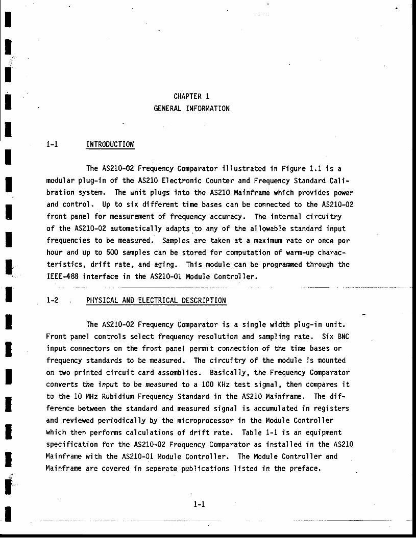
1-1
IIiIIIII
CHAPTER 1
GENERAL INFORMATION
INTRODUCTION
The AS210-02 Frequency Comparator i l lustrated in Figure 1.1 is a
modular plug-in of the AS210 Electronic Counter and Frequency Standard Cali-bration system. The unit plugs into the AS210 Mainframe which provides power
and control. Up to six different t ime bases can be connected to the AS210-02
front panel for measurenent of frequency accuracy. The internal circuitry
of the AS210-02 automatically adapts.to any of the allowable standard input
frequencies to be measured. Samples are taken at a maximum rate or once per
hour and up to 500 samples can be stored for computation of wann-up charac-
teristics, drift rate, and aging. This module can be programmed through the
IEEE-488 interface in the AS210-01 Module Controller.
L-2 PHYSICAL AND ELECTRICAL DESCRIPTION
The AS210-02 Frequency Comparator is a single width plug-in unit.
Front panel controls select frequency reso'lution and sampling rate. Six BNCinput connectors on the front panel permit connection of the tirp bases or
frequency standards to be measured. The circuitry of the module is mounted
on tr,ro printed circuit card assemblies. Basically, the Frequency Comparator
converts the input to be measured to a 100 KHz test signal, then compares it
to the 10 MHz Rubidium Frequency Standard in the AS210 Mainfranp. The dif-ference between the standard and reasured signal is accumulated in registers
and reviewed periodically by the microprocessor in the Module Controllerwhich then perfonns calculat ions of dr i f t rate. Table 1-1 is an equipmentspecification for the AS210-02 Frequency Comparator as installed in the AS210Mainframe with the AS210-01 Module Control ler . The Module Control ler andMainframe are covered fn separate publications l isted in the preface.
tttIIIIIItI
1-1
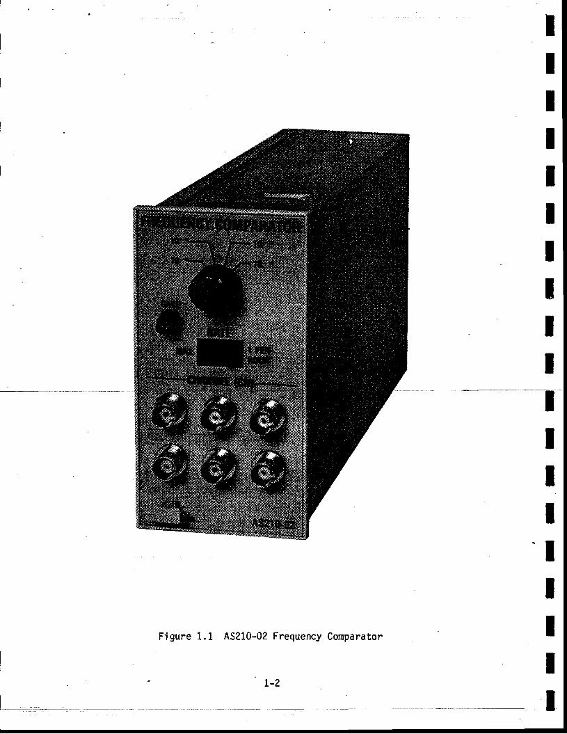
tIIIIIIItI
Figure 1.1. AS210-02 Frequency Comparator
III
'l
III
L-2
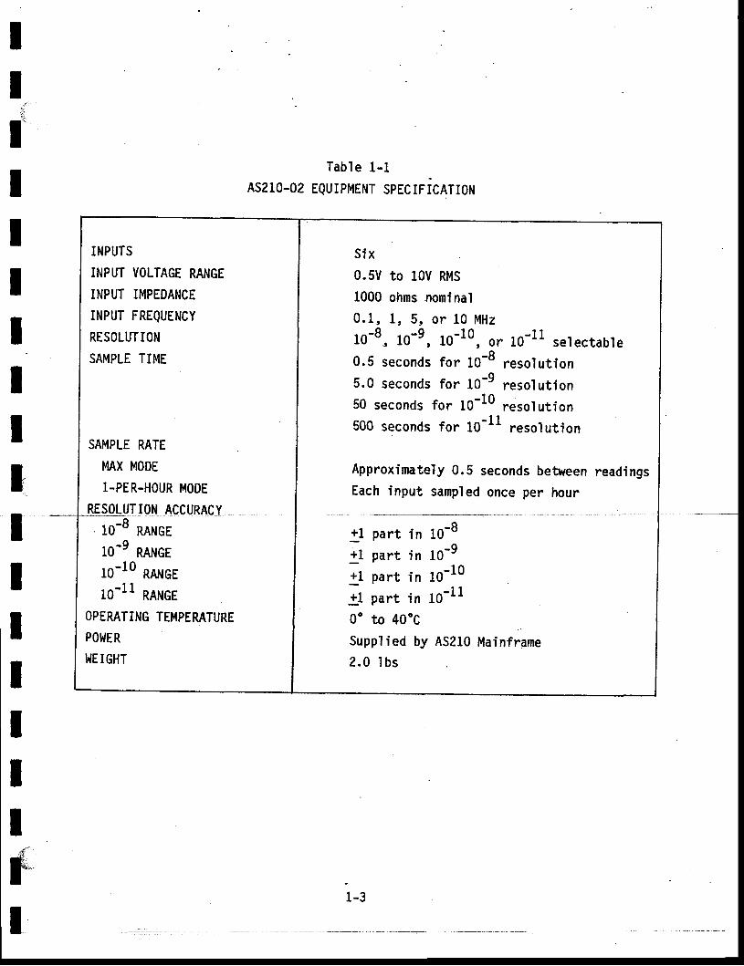
II
i:r
fIIIIIIlIIIIIII
Tab le 1 -1AS210-02 EQUTPMENT SPECIFiCATT0N
1-3
INPUTS
INPUT VOLTAGE RANGEINPUT IMPEDANCE
rNPtff FREQUENCY
RESOLUTION
SAMPLE TIME
SAMPLE RATE
MAX MODE
l.PER-HOUR MODERE IqN AECURAE-Y. 1o-8 RANGE
to-9 nRHoE10-10 RANGEro-11 RANGE
OPERATING TEMPERATUREPOhIERt,lEIGHT
5ix
0.5V to 10V RMS1000 ohms nominal0 .1 , 1 , 5n o r 10 MHzl0-8, 10-9, 10-10, or 10-11 selectable0.5 seconds for 10-8 resolut ion5.0 seconds for l0-9 resolut ion50 seconds for 10-10 resolution500 seconds for 10-11 resol ution
Approximately 0.5 seconds between readingsEach input sampled once per hour
+1 part in 10-8+1 part in 10-9+1 part in 10-10
11l part in tO-lloo to 4o"cSupplied by AS210 Mainframe2.0 I bs
F

IIIIIIIIIIIIIIIIII
__ l
IIIII
2-L
CHAPTER 2
INSTALLATION
INTRODUCTION
The AS210-02 Frequency Comparator plugs into the AS210 Mainframe.
The module is electrica'l ' ly connected through the rear connector and mechani-
cal ly retained via a f ront panel locking bar on the Mainframe. A release
mechanism is located in the lower left hand corner of the front pane1. Power
and sfgnal interface is provided through the Mainframe. The signals to be
measured are connected to the BNC connectors located on the front panel.
NOTE I.:
IIIIIIIIIIII
The Frequency Comparator Module is held in the
connector with high retention force. In order
the module, it may be necessary to pull on thepanel RANGE switch while the release mechanism
card edge
to remove
fronti s pu l led .
N0TE 2: Ensure that power is turned OFF in the AS210 Mainframe
before instal l ing or removing the AS210-02.
CAUTION
Do not attempt to useTektronix Mainframe as
the AS210 ser ies modules in a
severe damage wi l ' l resul t.
2-L

IIIIItIIII
IIIIIIII
3-1
IIIIIItIII
CHAPTER 3
OPERATION
INTRODUCTION
This chapter describes the operation of the AS210-02 Frequency
Comparator. This modu' le works in conjunct ion wi th the AS210-01 Module Con-
trol ' ler when they are instal led in an AS210 system. Figure 3.1 and Table
3-1 i l lustrate and descr ibe the operator controls, indicators, and connectors
of the Frequency Comparator. The operating instructions are essentia'l ly
ident ' ical to those provided in the manual for the Module Control ' ler s ince
most of the operator contnols are located on that uni t . .
3-2 CONTROLSINDICATORSAND CONNECTORS
Figure 3.1 i l lustrates the f ront panel of the AS210-02, and is
indexed to Table 3-1.
3-3 OPERATING PROCEDURES
The fol lowing paragraphs and Figure 3.2 are the operat ing instruc-
tions for the Frequency Comparator. Figures in ( ) refer to Figure 3.2
0perat ional Flow Diagram. Speci f ical ly, these instruct ions te l l the operator
how to perform frequency error measurements, display measurements from mernory,
and perfonn dr i f t ca1culat ions. 0nly the l ighted pushbuttons can be used
dur ing a rou t ine . CLR is fo r d isp lay c lear ing on ly .
IIIIIIIII
3-1
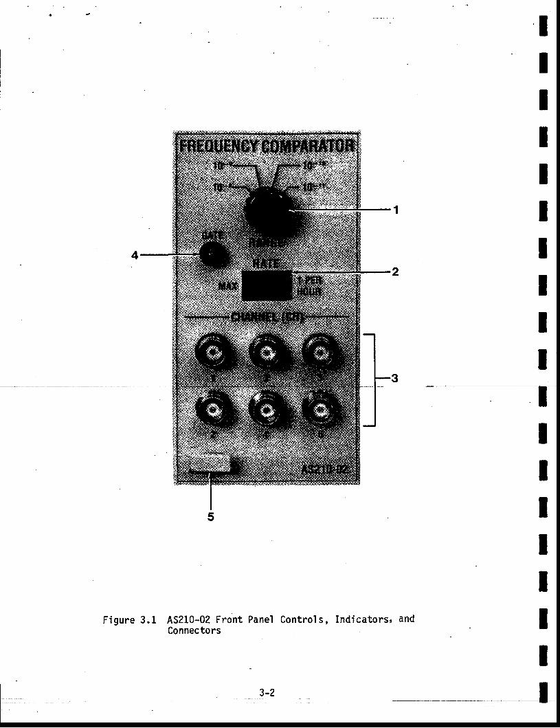
AS210-02 FrontConnectors
Panel Controls, Indicators, and
IIIIIIIIIIIIItIIII
Figure 3 .1
3-2
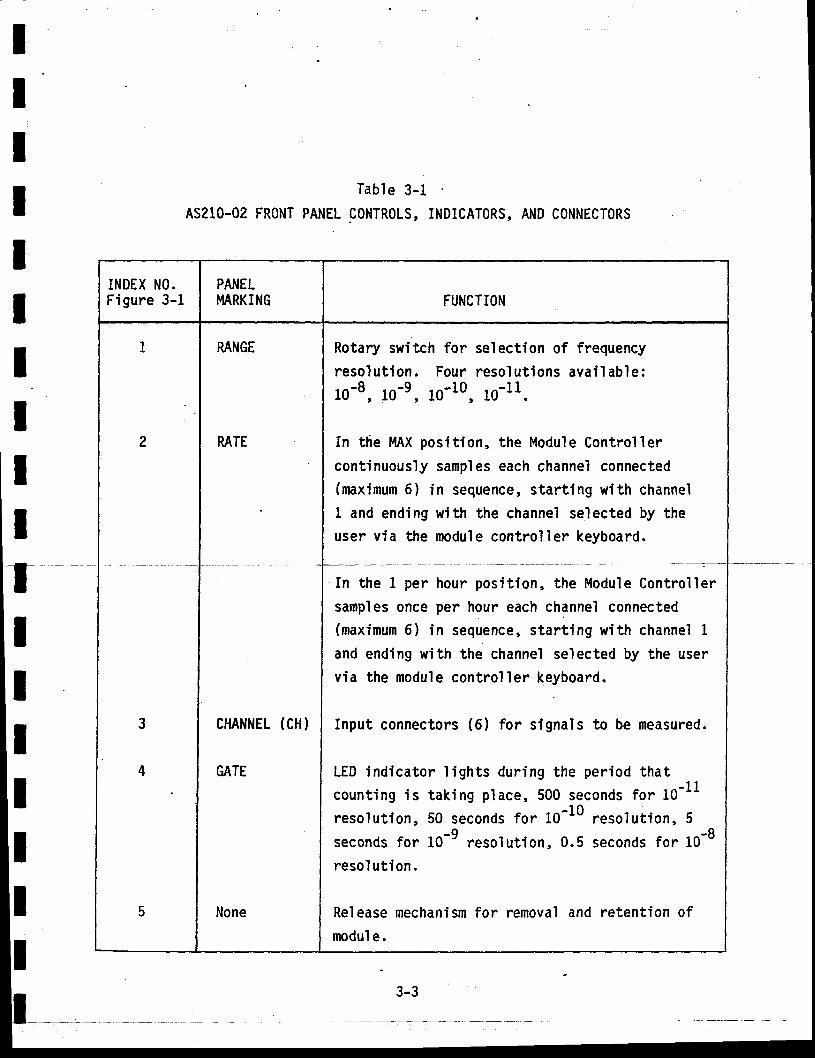
IIIIIIIIII
IIIIIII
Table 3-1
AS21O-02 FRONT PANEL CONTROLS, INDICATORS, AND CONNECTORS
INDEX NO.Figure 3- l
CHANNEL (CH)
GATE
Rotary switch for selection of frequency
reso lu t ion . Four reso lu t ions ava iJab le :
lo-8, 1o-9, 10-10, 10-11.
In the lf iX position, the Module Controller
continuously samples each channel connected(maximum 6) in sequence, starting with channel1 and ending witb the channel selected by theuser v ia the module control ler keyboard.
' In the I per hour posi t ion, the Module Control ler
samples once per hour each channe'l connected(maximum 6) in sequence, start ing wi th channel 1
and ending with the channel selected by the uservia the module controller keyboard.
Input connectors (6) for signals to be measured.
LED indicator I ights dur ing the per iod that
count ing is taking place, 500 seconds for 10-11resolut ion, 50 seconds for 10-10 resolut ion, 5
seconds for 10-9 resolut ion, 0.5 seconds for 10-8
resol ut ion.
Release mechanism for removal and retention of
modul e.
A.
III
III
B.
FREQIINCY E8F0R IEASUREMENT
Connect the frequency source to be measured to the front panel
connectors on the AS210-02 Frequency Comparator modul e.
Set the RATE switch on the AS210-02 Frequency Comparator module toMAX for continuous sanpling or 1 PER H0UR for sample once per hour.The sampl ing rate is also a funct ion of the resolut ion selected asfol I ows:
Resol ut ion
10-8-o
10"
10-10
10-11
Sanples per hour fnMAX Mode
Approximately 3600
Approximately 600
Approximately 70
7
The menory of the Module Controller can store 500 samples, there--.f6Fe-the
l PER H0UR mode may be more ulFfdl-Eh=an the MAX nrode whendata for several days elapsed t' ime is desired. Up to six inputscan be connected to the Frequency Comparator. For the purposes ofth is procedure, i t is assumed that only channel L is being used.When more than one signal is connected, the sequence operates sothat each channel is observed for one gate period (a function ofthe resolut ion selected), then the next channel is observed. I tcan be seen that as more inputs are connected, less samples perhour are taken per input when in the MAX mode.
C. Press l ighted CONT pushbutton (R) anA CH 1-6 should be displayed(B) .
D. Enter a channel number from 1 to 6 with the keyboard and press theENTER funct ion button (C). The number of channels should be
IIItIItIII
3-4
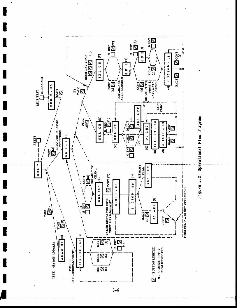
l- *' t&sH-;-"]i ^ :tr ;-l ^t/\ +=^' g$m:];"l%,'[lyII[_
oa ril *;7' E$;E a$ifif ? 3 iH&l;lc,* , Ei fus' ia- H,, /r i--- tntl___ry___] iI;8. /,$ffsfugffi{l :, I gp €ETi_*EiJlk',,,, ." B"gR/f|;1l*|l.,r ti ,l 5Yr'liJ i \ ;. i f
Hff'\ \;--, l-;Ep_1 1 3\,\ ,,,',,,,i,.*.filg11 f:1,,1, i i, s\\
'\ j-il ;ru; it t:t\ s ..)ig n=\ \ss\ ', \:E/U[eH E 5-Iil4" ii
Ea- \=$',, i: trT="==*l:Y]F\e \
s\hl ),1 jl iNI:H=g|:J =al il-tc*;/---r grfrs -;? X"' i n5Hr !ltl
E I L---- --J " Nr =
I
IIIIIIIIII
IIIIIII
@
I
N
N
I
o
I
oro
3-6
displayed on the LED display. I f only one channel is used, channelL is automat ical ly selected by the program, by pressing the C0NTbutton.
E. Press CONT (D) and SEL 10- should be displayed (E). Se' lect thedesired frequency resoTution with the RANGE switch on the AS210-02Frequency Comparator module.
F. Press C0NT (F). The frequency offset measurement routine nowproceeds. 0000P-00 wil l be displayed unti l the first measurementis made. Thereafter, the channel number and frequency offset (error)
wil l be displayed for each measurement as it is made unti l 500 mea-surements have been taken. A display of 1 398P-09 as shown in Figure3.2 (G) indicates a f requency of fset of 398 x 10-9 on channel l .l^lhen 500 measurements have been completed without interruption, theprogram wi l l hal t automat ical ly and 500 oFF wi l l be displayed,indicating that 500 data points have been taken and the progrdm isin an OFF condition. The measurement cycle can also be stopped atany time with the HALT (H) function button. The data pbint numberand oFF wi l l be displayed ( I ) . Measurement can be resumed bypressing CONT.
DISPLAY FREQUENCY MEASUREMENTS FROI4 MEI4ORY
A. Press HALT (H) ( i f program is running) and then DSPL (J) . SEL CHshou ld be d isp layed (K) .
B. Select a channel number with the keyboard and press the ENTERfunct ion button (L). SEL dP should now be displayed (14).
C. Select a data point number with the keyboard and press the ENTERfunction button. The number of data points taken during the mea-surement cyc' le can be found by pressing DSPL (N). The number ofda ta po in ts and oFF shou ld be d isp layed (0 ) . For example ,365 oFF.The display wi l l now,return to SEL dp (10.
IIIIIIIIIIIIIIIIII
3-5
tIIITIIIII
D.
tIttIIII
'D . Press CONT (P) and the display wi l l read out in sequence the data
point number and channel number (Q) (e.9. , Pl CH 3), then the t ime
the data point measurement was taken (R) (e.9. , t34-22-56), then
the f requency o f fse t (e r ro r ) a t tha t da ta po in t (S) (e .9 . ,4
139P-09) .
E. The measurement process can be resumed by press'ing HALT. If
frequency comparisons have not been in progress, the routine wil l
return to (B) and a channel number can be selected.
DRIFT CALCULATIONS
A.
B.
At any time after two or more
a time interval of more than L
can be made.
Press HALT, then select the CALC function
HOUR, DAY, or YEAR funct ion button (U) to
cal cul at i on.
data points have been col lected over
minute, a f requency dr i f t calculat ' ion
button (T). Press
select per iod for dr i f t
SEL CH wi l l be displayed (V). Select the desired channel number
with the keyboard and press the ENTER funct ion button (W). ( t f
C0NT is pressed (X), a l l channe' ls wi l ' l be computed for f requency
dri ft. )
DP 1 wi l l be displayed (Y). Select the desired number for data
point one with the keyboard and press the ENTER function button(Z). The number entered can be anything within the data f ie ld
from 1 to 500, depending on the resolut ion selected, length of
measurement, number of data points, t ime, etc. I f C0NT is
pressed (a) tne dr i f t calcu' lat ion wi l l automat ical ly be made on
the f i rst and last data points. I f C0NT is not pressed, then dP
2 w i l l be d isp layed (b ) . En ter the des f red second da ta po in t
number as wi th dP t (Z).
3-7
E. The dr i fd rate wi l l now be displayed for the selected channel (d).
For example, 1 3786P-LZ indicates a frequency drift.over the' period of t ime selected in step 2 of 3786 parts out of 1012.
F. Pressing C0NT (e) at th is t ime wi l l return the rout ine to thepoint (U) where new t ime frames, channels, and data points can be
selected for a dr i f t calculat ion.
G. Pressing HALT returns the routine to displaying the frequency
offset calculat ions in process at point (G). I f f requency compari-
sons are not in progress, the rout ine returns to display CH 1-6 at
po in t (B ) .
IIItIIIItIIIIIIIIt
3-8
IIIIIITIIIIIIIItIII
CHAPTER 4
THEORY OF OPERATION
4-1 INTRODUCTION
This chapter describes the theory of operation for the AS210-02
Frequency Comparator. The descr ipt ion is keyed to Figure 4.1, Funct ional
Block Diagram and the schematics in Chapter 5. The three circui t boards are
designated A1, A1A1, and A2. Detai ls of cornmon types of c i rcui ts (power
suppl ies, etc.) have been omit ted. Reference is made in the descr ipt ion to
data that comes from and is returned to the CPU. The CPU is located in the
AS210-01 l4odule Control levr that is used in conjunct ion wi th the Frequency
Comparator. Detai ls regarding the operat ion of the Module Control ler may be
obtained from the Module Control ler manual.
The Frequency Comparator circuit obtains the signal to be measured
and compares it with the 10 MHz Rubidium frequency standard. Resolution of
Parts in 1O-11 is achieved through the use of a 200 MHz phase- locked
osci l lator (PLO) in the count ing- c i rcui t . The frequency comparator c i rcui ts
consist of the 10 MHz standard div is ion c i rcui t , input s ignal conversion
circui t , c lock c i rcui t , and data processing circui t . The standard input
signal can be 0.1, 1, 5, or 10 MHz. Up to s ix inputs may be accommodated by
the AS210-02. The input signal is frequency divided to 100 KHz and used to
phase' lock the 200 MHz PLO. The PLO signal is gated by the c lock enable
signal derived from the 10 MHz reference standard. Pulses from the 200 MHz
PLO are counted in the accumulator c i rcui t that is per iodical ly scanned by
the CPU. Resolut ion changes are made by varying the c lock enable per iod.
Six input channels are app' l ied to the Input l ' lu l t ip lexer Assembly
AlAL. The input select data is obtained from latch A1U10 which holds
4-L
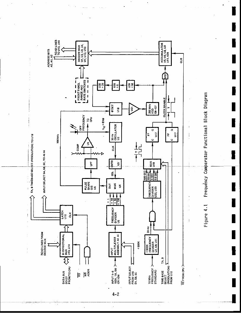
tIITIIIIII
IIIIItII
=r
t B
z
F or - 3 5H 8 =
6
{F
! uL 6
1 uS =@ l
ozU
=8o G
FC'U
4 3 65=a?ES
=@ 4
l==5 g 34 0 ,= 9 5
eXJ Yo f< I =f 5Po o I
8 := )J a i
?5U c }G F
f r lP IdrU
E l" J
l J
ir3.a?t*-"
(dr-g),6
a&IoEI
(gEo+)(Jc5
Dr-
s.o+)(tts6. oFo
(J
(Jc-(u=c,L
Lr-
<f
(u!5g)
lJ-
I1
irqJJ6
zUYoJo
ozUl
J
+lT-
F
zF
JooU
F
oo
6
46FoUJUqt-
z
i l _! c )
Ju6uo6U-=F6
F
F FE
x3-5qsU J - -
H$5q F N
o D f
9 ol f .J €> l e
3qs8 ; - j< : ) l
. . r
4 f
o
Gsau >J JG d
r t r E? i u i2=?
o F
fre3x3E9I H 1..-. n L O l
4-2
IIIIIIIIIIIIIIIIIII
' in format ion f rom the Module Control ler 's CPU select ing the channel to be ana-
lyzed. The CPU data is appl ied to the A1U10 via bidirect ional MUX A1U13 and
AlU14. This channel number is init ially selected by the operator at the l, lod-
ule.Control ler . The input channels may also be sequent ia l ly scanned by the
CPU. The Module Control ler manual contains more detai ls regarding the CPU
operation. The selected input signa'l is next applied to frequency divider
A1U6. The input s ignal may be 0.1, 1, 5, or 10 MHz. The frequency div ider
A1U6 contains +1, +10, i50, and +100 outputs. A 100 KHz output f rom
AlU6 is desired regardless of the f requency of the input s ignal . This is
achieved by a 100 KHz search circui t consist ing of mult ip lexer A1U4' pulse
shaper A1U5, a low pass f i l ter , comparator AlUl , osci l lator A1U2, and counter
A1U3. The output of A1U4 is pulse shaped by one-shot A1U5 and applied to a'
low pass f i l ter . The f i l ter 's output is a dc vol tage that is proport ional to
frequency. This vol tage is appl ied to the var iable input of comparator A1Ul.
The reference input of AlUl is set to a voltage that causes the comparator to
go high when the var iable dc input is equivalent to a 100 KHz signal . When
the comparator is low, a ground is provided to an LED that l ights to indicate
oFF FREQ. The low is also sent to the CPU. Whi le the comparator 's output is--tor-Fmt 100 fHzf;-a*30-Flz-oscillator Atu2;-ts-en-abted;--The osciltator
increments counter A1U3 which sequent ia l ly selects inputs to the mult ip lexer
A1U4. The select l ine sequent ia l ly outputs the mult ip lexer 's +1., +10, +50,
and +100 input unt i l the 100 KHz signal is found. hlhen the l ine containing
the 100 KHz signal is located, the search loop stops as comparator A1Ul goes
high, inhibi t ing A1U2. Assuming an input s ignal of 1 MHz, the +10 mult ip lex
input l ine wi l l contain the 100 KHz. I f the input were 5 MHz, the +50 mult i -
p lex input l ine would contain the 100 KHz signal , etc. The 200 MHz VC0,
A2Q6, A2Q7 is phase locked to the 100 KHz signal by phase detector A2U18.
A2U?0, AZU25, and A?tJ26 divide the 200 MHz signal to 100 KHz. The output of
A2U18, fi l tered and amplif ied by AZUZL, tunes the VCO. Any changes that
occur in the input signal are therefore reflected in the output of the 200
MHz VCO. The 200 MHz output is appl ied to an accumulator c i rcui t consist ing
of 6 dual decade counters A2U5, A2116, A2U8, AZU?, A2U11, and AZU24. If the
200 MHz osci l lator is gated into the accumulator for 0.5 seconds, 100 x 106R
or 10'pulses would be counted. This corresponds to a f requency resolut ion
4-3
of 1 x 10⁻⁸ or 1 pulse out of 108 pulses. Simi lar ly, i f the osci l lator weregated for periods of 5, 50, or 500 seconds, frequency resolutions of 10-9,
10-10, and 10-11 are obtained. In order to plovide a precise c lock gat ing
per iod, the 10 MHz Rubidium reference standard.s ignal is d iv ided by 500 in
frequency div ider A1U7, A1U9, and A1U11. The 20 Hz signal is appied to
divider A2U22-AZU23 that has four outputs: +10, +100, +1000, and +10000
corresponding to sampling periods of 0.5 seconds, 5 seconds, 50 seconds, and
500 seconds. The four signals are applied to time base multiplexer A2U19.
Select l ines are obtained from the CPU depending on the resolution selected
by the operator at the Module Control' ler. If, for example, the resolution
Selected was 10-9, the 5 second period l ine would be output by the mu'lt i-plexer. Flip-flop A2UL7 goes high on the leading edge of the pulse train and
thus provides a S-second gating pulse for clock gate A2U27. This permitso
10" pulses to be counted in the accumulator (provided that the input fre-
quency were exact). The accumulator's o.utput is read by the CPU via a decod-
ing multiplexer (A2U1-A2U4, AZU7, A2U10, A2U13, AZUt4l. The other inputs to
the multiplexers are the front panel RANGE switch and RATE switch. The CPU
scans the switches ten tires per second to determine the correct data to be
appl iedtothe-rranious*muLt ip.1exersprereiouslJdescr ibed.Whena-
mE) is received from the CPU, the accumulator is read and cleared. The TE rsignal also turns off the front panel GATE LED through driver A2Q1. The
accumulator's contents are transmitted through the data bus to the Modul" _
Control ler where calculat ions are perfonned. These calculat ions al low the
operator to determine frequency drift over variable periods of t ime with
varying degrees of resolut ion. This process is explained more ful ly in the r
sect ion on operat ion and in the Module Control ler Manual. I
IIIIIIIIII
tIIII
4-4
IIItIIIIIIIIIItIII
CHAPTER 5
MAINTENANCE AND OPERATION
INTRODUCTION
The purpose of this chapter is to provide maintenance and
cal ibi"ation data for the AS210-02 Frequency Comparator. Section I covers
routine preventive maintenance procedures. Section II outl ines performancd
tests for the Frequency Compar:ator. Section III contains the calibration/
alignment procedures for the AS210-02 module, and Section IV describes
troubleshooting data. Please contact the factory for any assistance required
in the maintenance or servicing of the AS210-02.
I5-1
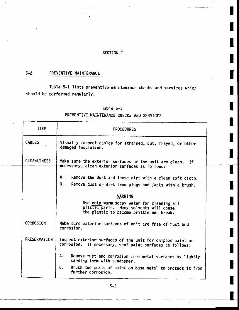
SECTION I
5-2 PREVENTIVE MAINTENANCE
Table 5-1 l is ts prevent ive maintenance checks and services whichshould be perfonned regularly.
Iable 5-1PREVENTIVE MAINTENANCE CHECKS AND SERVICES
tIIIIIIttI
IIIIIItI
ITEM PROCEDURES
CABLES
CLEANLINESS
Visual ly inspect cablesdamaged insulat ion.
lilake sure the exterior
for strained, cut, frayed, or other
surfaces of the unit are clean. If
CORROSION
PRESERVATION
r |esessdry, stean exEerlor surraces as t0 l lows:
A. Remove the dust and loose dirt with a clean soft cloth.B. Remove dust or dirt from plugs and jacks with a brush.
}IARNINGUse only wann soapy water for cleaning allplasTT-parts. Miny solvents wil I caisethe plastic to become britt le and break.
ttlake sure exterior surfaces of unit are free of rust andcorrosi on .
Inspect exterior surfaces of the unit for chipped paint orcomosion. If necessary, spot-paint surfaces' as fbl l ows :
A. Remove rust and corrosion from metal surfaces by I ightlysanding them with sandpaper.
B. Brush two coats of paint on base metal to protect it fromfurther corrosion.
5-2
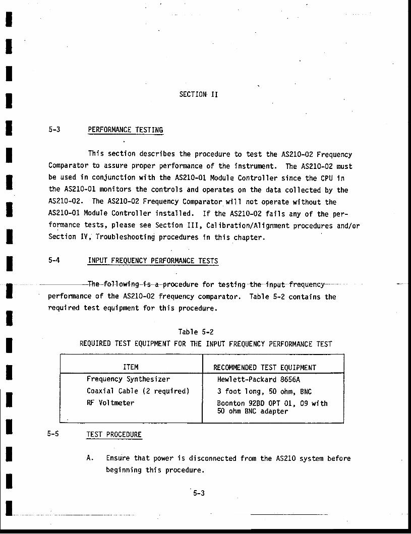
I
SECTION II
PERFORMANCE TESTING
This section describes the procedure to test the AS210-02 FrequencyComparator to assure proper performance of the instrument. The AS210-02 mustbe used in conjunct ion wi th the AS210-01 Module Control ler s ince the CPU inthe AS210-01. monitors the controls and operates on the data collected by theAS210-02. The AS210-02 Frequency Comparator wil l not operate without theAS210-01 Module Control ler instal led. I f the AS210-02 fai ls any of the per-formance tests, p lease see Sect ion I I I , Ca] ibrat ion/Al ignment procedures and/orSect ion IV, 'Troubleshoot in j procedures in th is chapter.
5-4 INPUT FREQUENCY PERF0RMANCE TESTS
--The- fol :l owi n g -i s a- pr.oeedu re fo r tes?tn5the-i n put f req uency'performance of the AS210-02 frequency comparator. Table 5-2 contains therequired test equipment for this procedure.
Table 5-2REQUIRED TEST EQUIPMENT FOR THE INPUT FREQUENCY PERFORMANCE TEST
TEST PROCEDURE
A. Ensure that power is disconnected from the AS210 system beforebeginning this procedure.
II
tI
ITEM RECOMMENDED TEST EQUiPMENTFrequency Synthesizer
Coaxial Cable (2 required)RF Voltmeter
Hewlett-Packard 8656A
3 foot long, 50 ohm, BNCBoonton 92BD OPT 01, 09 with50 ohm BNC adapter
5-5
5-3
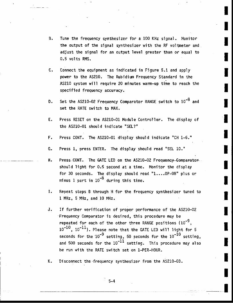
II
B. Tune the frequency synthesizer for a 100 KHz signal . Monitor
the output of the signal synthesizer with the RF vo'ltmeter andadiust the signal for an output level greater than or equal to
0 .5 vo l ts RMS.
C. Connect the equipment as indicated in Figure 5.1 and app' lypovrer to the AS210. The Rubidium Frequency Standard in theAS210 system will require 20 minutes wann-up time to reach the
specified frequency accuracy.
D. Set the AS210-02 Frequency Comparator RANGE switch to 10-8 andset the RATE switch to MAX.
tIIII
IIIIIItI
III
E.
F .
G .
I .
J .
Press RESET on the AS210-01 Module Control ler . The display of
the AS210-01 should indicate "SEL?"
Press C0NT. The AS210-01 display should indicate "CH 1-6."
Press L, press ENTER. The display should read USEL 10."
H. Pr+ss*e0N[I-The-,GATE LEIL on-the -AS210-02 Frequeney-eonpapator -' - I
should l ight for 0.5 second at a t ime. l4oni tor the display Ifo r 30 seconds. The d isp lay shou ld read "1 . . . .0P-08" p1us or
minus ! . part in L0-8 dur ing th is t ime
Repeat steps B through H for the frequency synthesizer tuned to1 MHz, 5 MHz, and 10 MHz.
If further verif ication of proper perfonnance of the AS210-02Frequency Comparator is desired, this procedure may be
repeated for each of the other three RANGE positions (10-9,
10-10, 10-11) . P lease no te tha t the GATE LED wi l l ' l i gh t fo r 5
seconds for the'10-9 set t ing, 50 seconds for the 10-10 sett ing,and 500 seconds for the tO- i l set t ing. This procedure may also
be run with the RATE switch set on l-PER-H0UR.
Disconnect the. f requency synthesizer f rom the AS210-03.K .
5-4
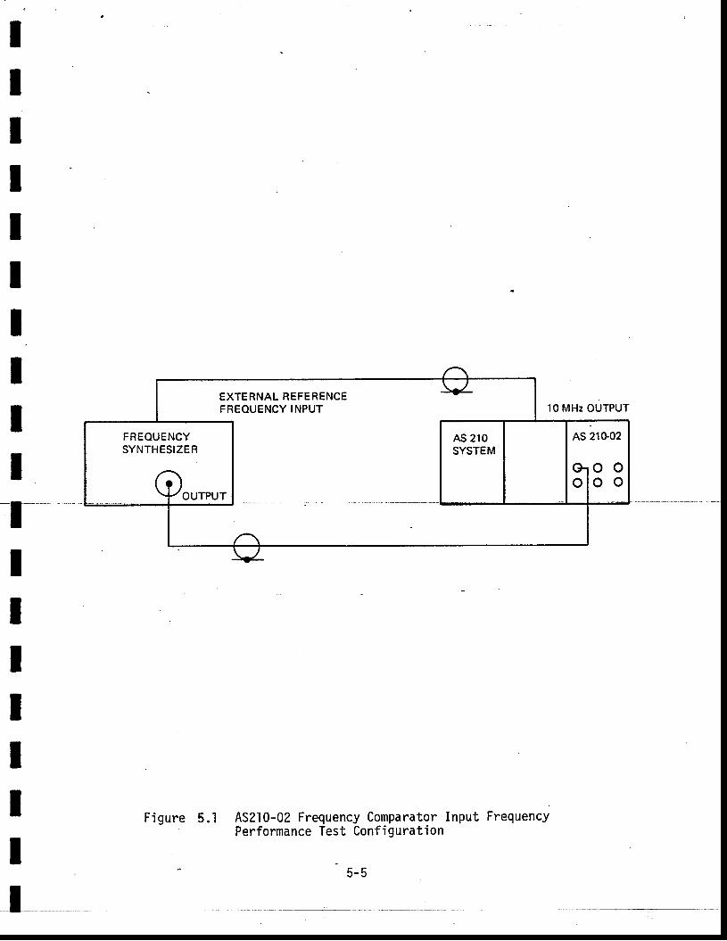
tITItIIIII
IIIIIII
Figure 5.1 AS2l0-02 Frequency Comparator Input FrequencyPerformance Test Configuration
EXTERNAL REFERENCEFREOUENCY INPUT
FREOUENCYSYNTHESIZER
I5-5
SECTION I I I
5-6 CAL I BRATION/AL IGNMENT PROCEDURE
WARNING
The following Calibration/Alignrnent Procedures (Chapter 5,
Sect ion I I I ) , and Troubleshoot ing Procedures (Chapter 5,
Section IY) are for use by qualif ied personnel only. To
avoid personal injury,- do not perfonn any servicing other
than that of Routine Maintenance (Chapter 5, Section I, and
Perforrnance Testing (Chapter 5, Section II) unless you are
qual i f ied to do so.
Figure 5.2 is a flow diagram of the Calibration/Alignment Procedure*--forthrAs2t0-02 Frequency-0ornparator. Usrthirftordiagram-with*the- theory--
of operation in Chapter 4, the text in this chapter, and the i ' l lustrated
parts l ists in Chapter 6. The Rubidium frequency standar:d calibration proce-
dure which is contained in the AS210 mainfrane operation and maintenance man-
ual is also referenced in this flow diagram. Please note it is not necessary
to disassemble the AS2l0.system to determine if the ca.l ibration/alignment is
needed. For any assistance needed in performing this cal ibrat ion/al ignment
procedure, please contact the factory.
5-7 ACCESS T0 AS40-02 FREQW
Please reference the AS210 mainframe manual for the disassembly
procedure of the AS210 system to allow access to the AS210-02 Frequency Com-
parator module. Access to the module circuitry itself is gained by removing
the two metal side covers with a small straight-blade screwdriver. Place the
module on one of its sides so that one coveris facing up. Starting with the
5-6
tIIIIItIII
IIIIIIII
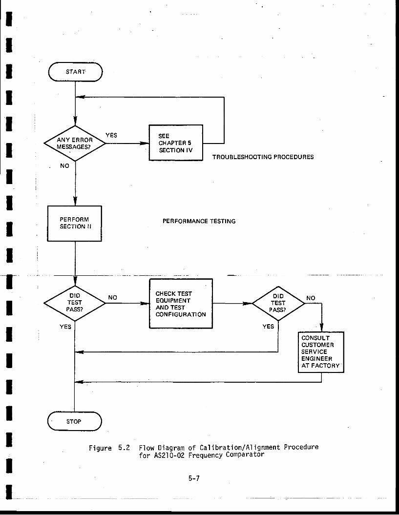
IIIIIIIIIIIIItIIItI
Figure 5.2 Flow Diagram of Cal ibrat ion/Al ignment Procedurefor ASZI 0-02 Frequency Comparator
ANY ERRORMESSAGES?
PERFORMSECTION II
CHECK TESTEOUIPMENTAND TESTCONFIGURATION
CONSULTCUSTOMERSERVICEENGINEERAT FACTORY
TROUBLESHOOTI NG PROCE DU RES
PERFORMANCE TESTING
5-7
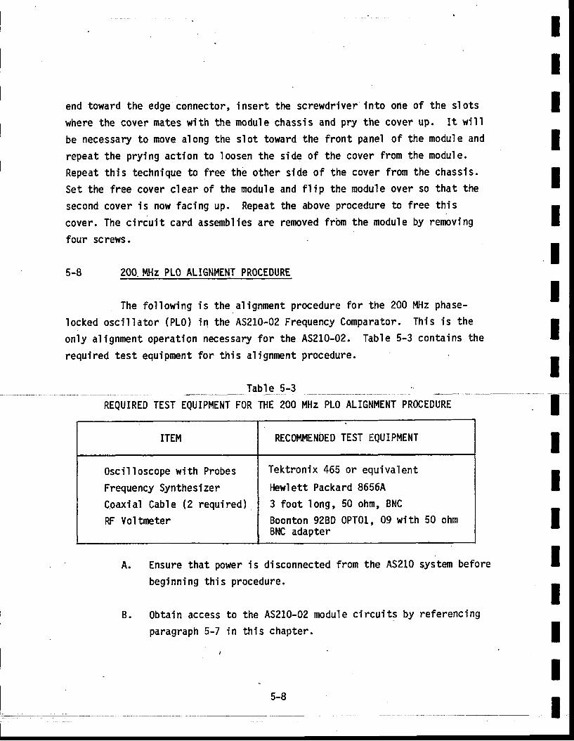
II
end toward the edge connector, insert the screwdriver' into one of the slots
where the cover mates with the module chassis and pry the cover up. It wil l
be necessary to move al ong the sl of toward the front panel of the modul e and
repeat the prying action to loosen the side of the cover from the module.
Repeat this technique to free'the other side of the cover from the chassis.
Set the free cover clear of the module and fl ip the module over so that the
second cover is now facing up. Repeat the above procedure to free this
cover. The circuit card assemblies are removed frbm the module by removing
four screws.
2OO. ilIHz PLO ALIGNMENT PROCEDURE
The fol lowing
locked osci l lator (PLO)
only al ignment operat ion
required test equipment
is the alignment procedure for the 200 MHz phase-
in the AS210-02 Frequency Comparator. This is the
necessary for the AS210-02. Table 5-3 contains the
for this alignnent procedure.
Table 5-3
REQUIRED TEST EQUIPMENT FOR THE 200 MHz PLO ALIGNI'{ENT PROCEDURE
A. Ensure that power is disconnected from the AS210 system before
beginning this procedure.
B. Obtain access to the AS210-02 module circuits by referencing
paragraph 5-7 1n this chapter.
II
tI
ITEM RECOIIMENDED TEST EQUIPMENT
0sci l loscope with Probes
Frequency Synthesizer
Cpaxial Cable (2 required)
RF Volfineter
Tektronix 465 or equivalent
Hewlett Packard 8656A
3 foot long, 50 ohm, BNC
Boonton 92BD 0PT01, 09 with 50 ohmBNC adapter
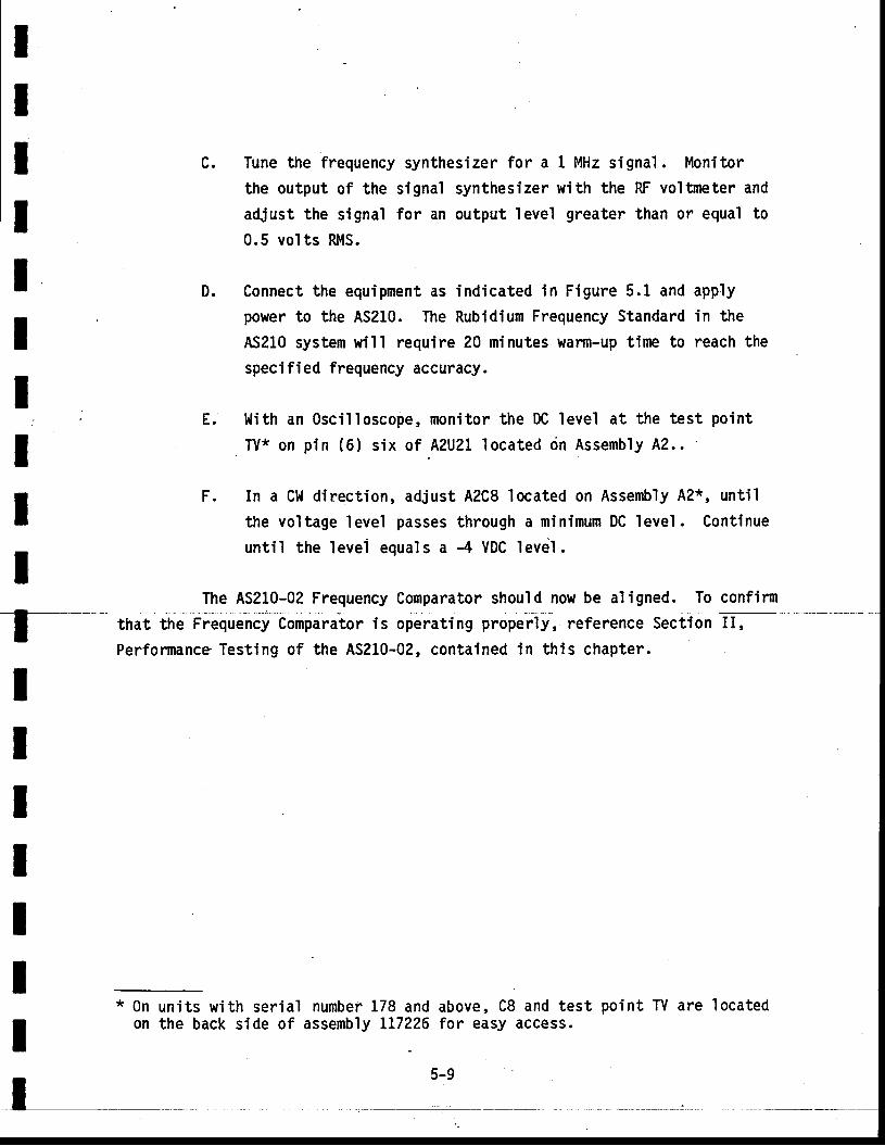
c.
IIIIIItIII
Tune the frequency synthesizer for a 1 MHz signal. Monitor
the output of the signal synthesizer with the RF voltmeter and
adust the signal for an output level greater than or equal to
0.5 vol ts RMS.
D. Connect the equipment as indicated in Figure 5.1 and applypower to the AS2t0. The Rubidium Frequency Standard in the
AS210 system will require 20 minutes warm-up time to reach the
specified frequency accuracy.
E. l, l i th an 0scil loscope, monitor the DC level at the test point
TV* on pin (6) six of AZU?L located dn Assemb'ly A2..
F. In a Cl,| direction, adjust A2C8 located on Assembly A2*, unti l
the vol tage level passes through a minimum DC level . Cont inue
unt i l the levei equals a -4 VDC levei l .
The AS210-02 Frequency Comparator should now be aligned. To confirm
f that the Frequency Comparator is operating properly, reference Section
Perfonnance Testing of the AS210-02, contained in this chapter.
IIt
I I '
*0non
IIIt
units wi th ser ia lthe back side of
number 178 and above, C8 and testassembly LL7226 for easy access.
5-9
point TV are located
SECTION IV
5-9 TROUBLESHOOTING PROCEDURES
Troubleshooting of the Frequency' Comparator is facil i tated by a
comb'ination of error codes displayed on the Module Controller and LED indicat-
ors on the trvo c i rcui t card assernbl ies. The circui t cards are i l lustrated in
F igures 6 .2 (A1) 6 .3 (A2) , and 6 .4 (A1A1) . Tab le 5 -4 cor re la tes the er ro r
codes, displayed on the Module Control le i" when a faul t occurs, to the mal-
func t ion . An exp lanat ion o f the prob len is p rov ided w i th .poss ib le so ' lu t ions .
Tab le 5 -5 i s a l i s t o f v isua l ind ica tors on c i rcu i t cards A1 and A2 and the
mean ing o f the i r ind ica t ions . F igures 5 .3 , 5 .4 , and 5 .5 a re schemat ic d ia -
grams of assembl ies A1, A1A1, and A2, respect ively.
IItIIIIIIIIIIIIIIII
5-10
IIIIIIIIItTIIIIIIII
, €
Table 5-4
IRROR CODE LISTING
ERROR CODE PROBLEM REC0'I\4MENDED SOLUTI0N
2-0t
2-02
2-03
2-04
2-05
2-LLto
2-16_
2-20
?-2t
2-2?
2-?3
2-30
2-40
2-50
0utput decade registers cannotbe cl eared
Input selector c i rcui t not workingproper ly (See Table 5-5, A1CR1)
Measurement complete, f l ip f lopswi l l not resetl'lo measurement timebase
I Se l f
I nottest measurement a
wi th in +1 par t in 10" .
No signal present at indicated(1-6) input or s ignal output isnot--one of 'the -allowab:le standardfrequenciesData points selected for dr i f trate calculat ion are separatedby less than 1 minute.
Data points separated bydi sconti nuous time ( powerfai lure wi thout battery backupof frequency standard).In i t ia l data point in dr i f trate calculat ion overf lowed.
Final data point overf lowed.
Channel number specified hasno data associated with i t .Data point speci f ied is empty.Renote conti nue comand wi thmodule in standby mode.
Check A2U5, U6, U9, U11,u15 , A1U10, U13 , U14 ,A lA lU l , U2 , U3 .
I Check AZULT or A1U10, U13,
I u14.I Check 10 MHz standard,I A lQ l , U l1 , U9 , U7 , o rI A2U15, U23 , U?2 , U19 , o r
I u17.I Check 200 MHz phase lockI loop or counters A2U5,I U6 , U9 , U l l , A lA lU l , U2 ,
I U3. See paragraph 5-18.
I Check input s ignal andI input s ignal f requency
I on-the-indieated inputrI
Choose new data pointsaccuracy of dri ft ratecal cul at ion improvedby increasing t imebetween measurements.
5-1 1
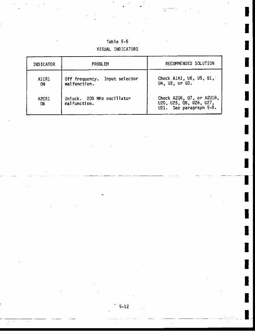
Tabl-e 5-5
VISUAL INDICATORS
IIIIIIIIIIIIIIIIII
IND ICATOR PROBLEM RECOMMENDED SOLUTION
AlCRlON
A2CRlON
Off frequency. Input selectormal functi on.
Un lock . 200 MHz osc i l la to rmal functi on .
Check A1A1, U6 , U5 , U l , 'U4 , U2 , o r U3 .
Check AZQ6, Q7, or A2U18,UaO, .U25, Q8, V26 , U27 ,Uzl. See paragraph 5-8.
5- t2
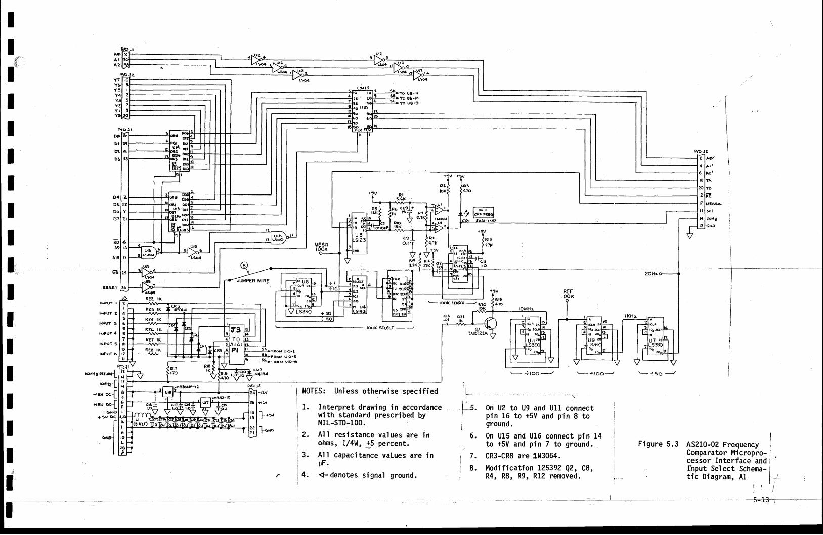
I
DO
DI
w
tfIIII
AEA lA?
Y 5Y4Y3Y?Y I
T D U B . I ITO 06-10
To u6-9
N0TES: Un'less otherwise specified
1. Interpret drawing in accordancewith standard prescribed byMIL-STD-100.
A l l res is tance va lues are inohms, U4W, :5 percent.
Al I capacitance vaLues are inrf.{- denotes signal ground.
0n U2 to U9 and Ull connectpin 16 to +5V and pin 8 toground.
6. 0n U15 and U16 connect plnto +5V and pin 7 to ground.
CR3-CR8 are 1N3064.
Modification 125392 Q2, C8,R4, R8, R9, R12 removed.
?fo J2
AO,
A I ,
I
T
A15
WR
,l#al
al
TA
TA
AS210-02 FrequencyComparator Micropro-cessor Interface andIhput Select Schema-t ic Diagram, Al
R?Z IXI t tPo,r I
tNPoT 2
trrpuT 5
brPuT 4
INPUr 9
INPUT6
,*,ln1renn{rptlltrl-
-,en o<{r-
tta\, Dca6NO
. +3v OC
TNz,Zzz.^
ITII
s -: loo --./ - * t o o J \- +60 ----J
?lo J2.-r2V iI
- Li.IiI
] * -
]*o l 42 .
3 . 7 .
8 . If-
2
4
o
t8
20
t?
17
t l
nt3
\_ toox seAftt_q16 Jeroz' I
4365I1to?t zt l
t zNl l
M
EJ6FI
lrlA
1ftloL
4.
I
Figure 5.3

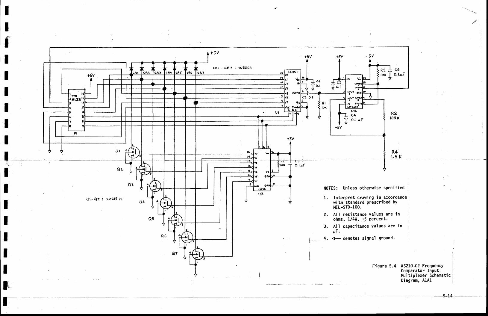
IIrIIIIII
+IIIIItIG.
c l
T o,' +cL+ o.r
+5v
O, l *F
R41.5 K
NOTES: Unless otherwise sPeci f ied
1. Interpret drawing in accordancewith standard prescribed bYMIL-STD-100.
Al l resistance values are inohms, 1/4V1, 15 percent.
Al l capaci tance values are inaF .
4. G- denotes signal ground.
Os
or -o? i t eL tEDEo4
Q52.
3 .
t--
QZ
Figure 5.4 AS210-02 FrequencYComparator InPutMultiplexer SchematicDiagram, AlAl
+5V
cRf - cR7 z lN3O4
+5V
cz o.lI
+5V +5V
R2+tor
$
c6O.l.r F
T o. t urv
- - t 3
5-14

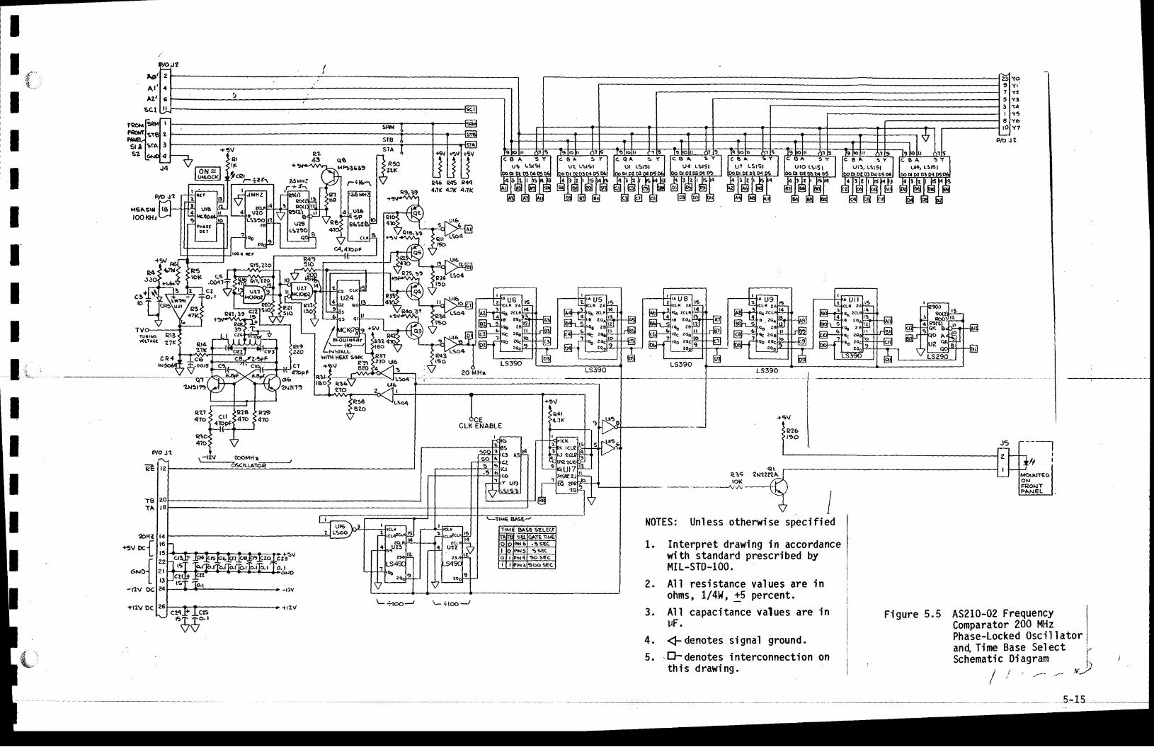
P{5 R.lS P444:tK 4XK 4,1k
Ar 'A?,
scttIIIII
M€ASII'
looxH:
Ifu.
tul rilG Pl3yoLtAG€
??K
IIIII
Plo J7,\
-tzv ?ooMH"C6CILLAT(EE
e36loK
._,____-_4r.V\
N0TES: Unless otherwise speci f i
1. Interpret drawing fn accordancewith standard prescribed byMIL-STD-100.
?. Al l resistance values are inohms, l /4W,15 percent.
3. Al l capaci tance values are inuF.
4. .( denotes signal ground.
5. .EFdenotes interconnection onth is d rawing .
Figure 5.5 AS210-02 FrequencYComParator 200 l4HzPhase-Locked Osci l lator
Ied
zttu, l6ND
-tzv
an4 Time Base SelectSchematic Diagram
/ i t ? ' / -I
I'l il )
{-r/
t?J..,!u _lH3 I ir59o
t4t6t5222 ll324

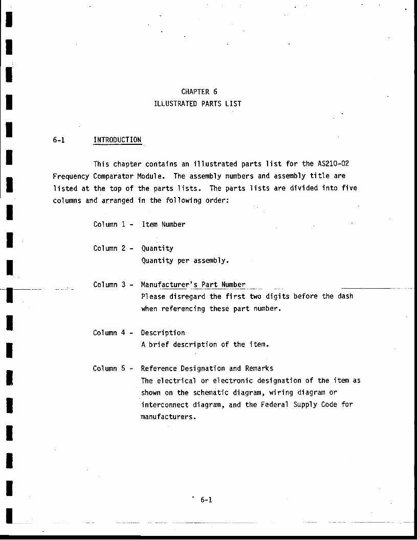
IIIIIIIIII
IIIIIII
CHAPTER 6
ILLUSTRATED PARTS LIST
6-1 INTRODUCTION
This chapter contains an i l lustrated parts l is t for the AS210-02
Frequency Comparator Module. The assembly numbers and assembly tit le are
l isted at the top of the parts l is ts. The parts l is ts are div ided into f ive
columns and arranged in the fo l lowing order:
Co lumn l - I temNumber
.Column 2 - Quantity
Quantity per assembly.
Column 3 - Manufacturer's Part Number
Please disregard the first two digits before the dash
when referencing these part number.
Column 4 - Descr ipt ionA br ief descr int ion of the i tem.
Column 5 - Reference Designation and Remarks
The electr ical or e lectronic designat ion of the i tem as
shown on the schematic diagram, wiring diagram or
interconnect diagram, and the Federal Supply Code for
manufacturers.
l__6-1
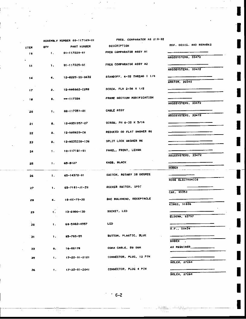
ItII TEII
l 0
l.l
l {
2 0
2 l
22
23
21
23
L
t .
1 .
8 .
e .
8 i
t .
t .
ess€lr8LY NUIISER 00- l | 7f 69-0t
OTY PART NUT1BER
FREO. COIIPARATOR Ag 2IO-02
OESCRIPTION
FREO COTPNRATOR ASEY AI
FREO COTIPARTIOR ASSY A2
STAilOOFF, 5-32 'HR€AO I l/'t
scREU, FLH 2-36 X tr2
FRA|I€ SECTrON ||ODlFlceTloN
CABLS ASSY
sCREU, PH 6-32 X 5/15
REDUCED OO FLAT IIASHER 16
SPLIT LOCX IJASHER 15
PA}IEL, FRO}IT, LEXA}I
KNOB, ALNCK
REF. DESTG. AND REI ' IARKS
EffiE5TsrEtrs, 33472
nncosvsiEtts, rrrze
ARGOSYSTET{S, 3347e
EEEoswretts, sg*ee
ffiEosvsrens, -lze
NOEEX
IIIIIIII
2 .
0 .
0 t - l 1 7 2 2 0 - 0 t
01 -t | 72?5-01
I 2-822s-SS- 0532
t2-r{6S662-C2Re
*r-l t7326
00-l t 7351 -01
t2-H9Sl95?-27
t2-Hts620-c5
I 2-fi93533S- t 36
t o - i l 7 1 8 1 - 0 1
65-812?
l 7
t g
6 .
65- | 4378-0 t
6 5 - 7 1 0 l - J l - z o
t g-|(c-7?-35
| 3-O085-t 3D
60-30s2-4957
65-765-55
t 6-nG | 70
t7-22-Ot -2121
1?-22-Ol-2011
SIJITCI{, ROTARY 30 DECREE
ROCI(ER SUIICH, SPDT
AHC BULKHEAO, RECEPTACLE
SOCI(ET, LED
LED
BUTTOII, PLfiSTIC, BLUE
cotx CABLE, 50 OHtt
COilil€CTOR, PLUG, '2 PIN
CONI{ECTOR, PLUG ' PIN
ROSE EL€CTRONICS
c e K , 0 9 3 5 3
KINGS, 9 I836
ELDEI'|A, 03797
H . P . , 5 0 4 3 {
IIBBEX
AS REOUIRED
lroLEX, 27251
IItIIII_l
t .
29
3 0
0 ,
t .
L
t .
33
35
t ,
6:2
noLEX, 27254
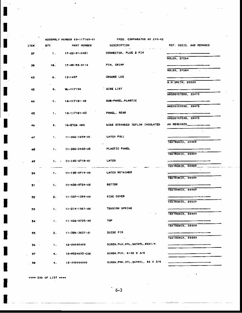
tIIIIIIIItItItIIItI
ASSE|IBLY i lUi lBER 00- l 1 7169-01
OTY PERT ilUlIBER
17-22-Ol-2021
t 7-o3-S0-0t t a
t 3 - l { 97
uL-t r7r9. l
t 0 - l l T r g l - 0 2
t 0 - l r 7 l 8 l - 0 3
'16-ET26 AUG
t t - 366 -1690 -01
t i -3e6-24 02-05
I r - | 0 5 - 0 7 | 8 - 0 1
FnEO. COITPARATOR AS 210-02
OESCRIPTIOTI.-
CONNECIOR, PLUC 2 PIN
Ptt t , cRr lP
CROI'I{D LUC
. U IRC L IST
sUB-PTT{€L, PLESTIC
PANEL, REAR
IJIRE STRANDED TEFLON II{SULATED
LA'CH PULL
PLASTIC PANEL
LATCT{
TENTRONIX, 8OOO9
TEt(TROlr tX, 80009
ffi
R€F, O€SIC, AHD REINRKS
t't0LEx, 27264
IroLEX, 27264
H . H . S n I T H , 8 3 3 3 0
ARGOSYSTEI{S, 33472
ARGOSYSTEHS, 33472
aRCOS?STEI{S, 33472
AS REOUIRED
TEXTRONIX , SOOO9
TEKIPOHTX, 90009
TEKTRONIX , SOOO9
TEXIRONTX, 8OTO9
TEI(TPOHTX, 80009
TEKTROT{|X, 80009
1 .
{g
s6
7?
5A
t .
a ,
4 ,
' r t - l 03-07t 9- 00
I l -a26-072.t- 0O
I l -337-r399-00
I l -2ta- l 061 -00
t | -a26-0725-00
't t -385-3657- 01
1 2 -0000000 0
t 2-lts2a693-c26
t 2 - 0 0 0 0 0 0 0 0 0
LIICH RETAIXER
s0TTofi
SIDE COVER
TENSIOH SPRtilG
TOP
CUIDE P IH
SCREU, FLH, sTL, SH'IITL, IzXI /4
SCREU,FLH, 6-32 X 3/8
9CREU,Pt lH,STL,SHTI{TL, 16 x 3/g
*t+ ' r EHD 0F LlSl + ' t**
6-3
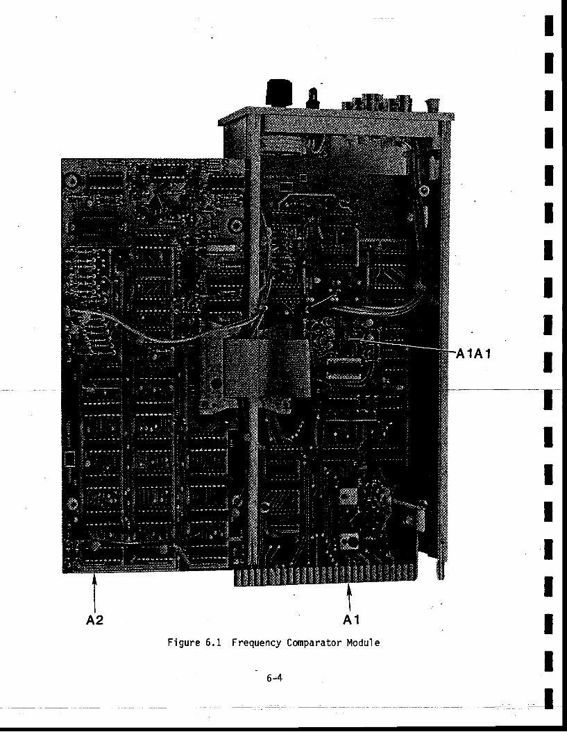
A1
Figure 6.1 Frequency Comparator Module
IIIIIIIItIIIIIIItI
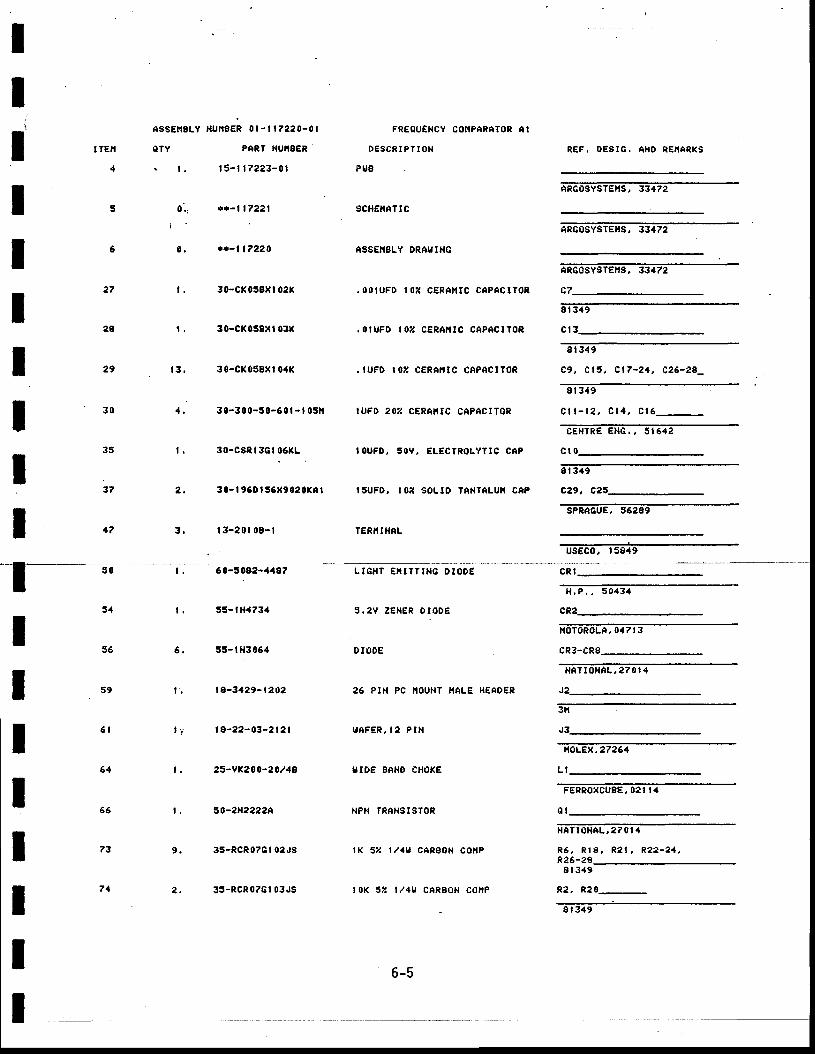
IIIIIItIIt
I TEN
4
5
6
27
2A
29
3 0
35
37
1?
AssEllELY i lUm8E; 0r-r t?220-01
OTY PART ilUrl8€R
. t . t s - t t 7 2 2 3 - 0 1
*+- t l? .221
t*- l 17220
3o-cK05BXt 02K
30-cK058l{t 031(
30-c(058x1 0.tK
30-300-50-60t -t 0slt
3o-csR,t 3cr 06KL
30- | 96Dt 56X902oxnr
t3 -201 0E- t
FREOUENCY CO}IPARATOR EI
DESCRIPT ION
PU8
SCHEIIAT I C
TSSE}T8LY ORAUIflG
,OOIUFD lOZ CERAf lTC CAPACITOR
.O IUFD IOZ CERANIC CAPACITOR
. IUFD IOZ CERANIC CAPTCITOR
IUFD 20z CEREfi IC CAPACITOR
IOUFD, sOV, ELECTROL?T IC CEP
T5UFD, IOZ SOLTD TEf lTELUT CAP
TER}ITHAL
R E F . D € S I G , A I { D R E N A R K S
ARGOSYSTEIIS, 33472
ARCOSYSTEHS. 33472
tRGosYsTEilS, 33472
c ?
8 t 349
c t 3
8 t 3 4 9
c9, c l5, c l7-2+, c25-28_
9 t 349
c t t - t 2 , c t 4 , c r 6 _
CEHTRE EHG. , 5 I 642
c r 0
8 t349
c29, C25_
SPRAGUE, 56289
0. ,
I
0 .
3 .
Co:ioai:irei
55- | ll.t734
55-t H3064
la-3129-1202
I e-22- 03-2 | 2 |
25-VR200-20/19
30-2x2222A
35-RCn07Cr 02.rS
35-RCR07Ct 03JS
L IC f lT e i l t TT tNC D tOOg
5 .2V ZEHER D IOD€
DIODE
26 PII I PC NOUNT I{ALE H€ADER
UEFER, I 2 P IN
UIDE BAI{D CHOKE
NPN TRAI{SIgTOR
tK 52 r /4U CARgoN COi lP
toK 52 t / { u CAR80N co f lP
H , P . , 5 0 4 3 4
cn2-
cR l
IIIIIIII
I.toToRoLt, 0.t7 | 3
NNT IOHAL ,ATOI4
l 7 J3
;toLEx,2726a
L I
FERROXCUSE, 02I T4
e t
HETIOHAL ,2T O I , I
R6 , R ra , e2 t , R22 -?1 ,R26-2
8 t 3 4 9
R2 , R2O
6-5
I | 3rt9
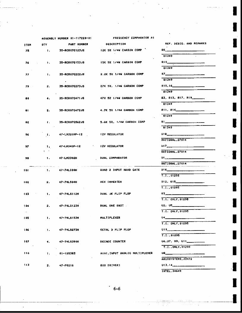
ITEN
73
76
77
79
e0
8 l
a2
96
9?
98
ItIIItIIIIIIIIIIII
U I
U2,2 ,t 0 4
t 0 5
nssEr8Lt NU}'EER 0l- l 17220-01
CTY PdNT ilUNgER
t . 35-RCRo?Gl23JS
FREEUENCY COIIPARATOR AI
OESCRIPT ION
r2K 5Z l / . ru CARBO}I COi lP '
tsK 52 l /au CARBOH CO|IP
2,2K 5 ' t t /au CARBON COIIP
2?K 57., t//tu CARBOX eOHP
170 52 t/.fg CAR8oH coltP
1,7K 32 t /4ta CARBOH COiP
5 .6K 52 , t / 4U CAR8oN Co rP
I 2V R€CULATOR
T2V RECULA'OR
OUAL CONPfiRATOf,
R€F. OESIG. END REITARKS
I | 3.r9
3S-RCR07Gt 53JS
33-RCR0?C222.rS
35-RCn07G2?3.tS
35-RCR07Ga7l JS
33-RCn07C472JS
35-RCR07C552.'S
a7-Lr32 0lrP- | 2
17-Ln3+2P-12
a7-Lfi3302X
8r 349
R7
8t3{9
R t 5 , l 5
8t 3 {9
n 3 , R r 3 , R l 7 , R l 9 _
8 t 3 4 9
R l t ,
e r 3 4 9
R I
8 t 3 4 9
t .
t :
t ,
u t 8
NrT t0NAL ,270 t 4
u l 7
XET IONAL ,2TOI 4
u rl t tT loHAL.270t 4
{7-7.3LS00}l
a7-7tL30.ltl
a7-?aLSl t2H
a7-7aLS | 23lt
.t?-?.lLSl53ll
{7-74L3273N
,17-7.tLs390H
0t-|25:t83
1?-P82r6
OUAD 2 TNPUT NNHD GATE
HEX I}IY€RTER
DUAL .'I( FLTP FLOP
DUAL O}IE SHOT
iULTIPLEXER
OCTAL D FLIP FLOP
D€CAD€ COUNTER
AIAI, I i lPUT Ai lELOC I ' IULTIPLEX€R
gUS DRTVER]
T , L O X L Y , 0 t 2 9 5
U5
T , I . , 0 r 2 9 5
U I 2 , U
T , I . . 0 1 2 9 5
u3
T , t . o t { L Y , 0 t 2 9 5
U'
r . t . o H L Y , 0 1 2 9 s
u l 0
T . l . , 0 r 2 9 5
u 6 , u 7 , u 9 , u l l _
T . I . ,01{LY, 0 r 295
ARG0SYSTEXS, 33472
u t 3 , 1 . 1
6-6
lHTEL,3/ t6t9
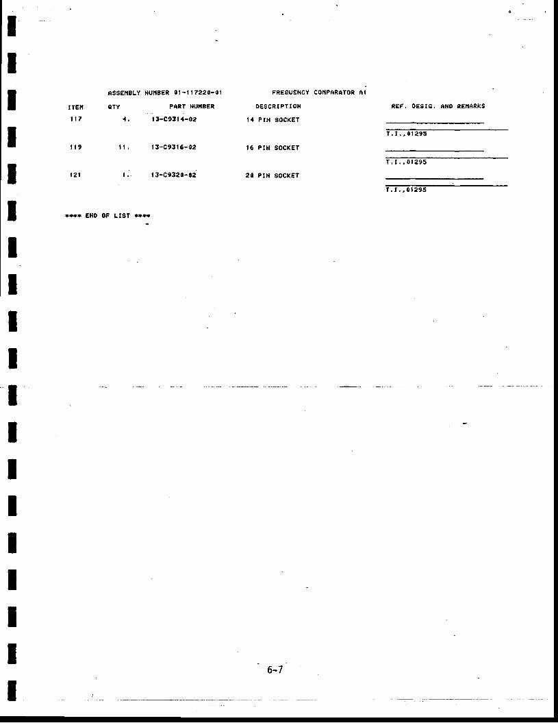
IIIIItIIII
ASSEnBLY NUnBER 0l- l I 7220-01
OTY PART I{U}I8ER
1, | 3-C93t 4-02
| 3-C93 | 5- 02
t 3-c9320-02
FREOUENGY COHPARATOR E;
DESCRTPTTOT{
I{ PT}I SOCKET
16 P I I { SOCXET
20 P tH SOCKET
REF, O€SIC. THD REIIARKS
t . t . , 0 r 2 9 5
t . r r EHD 0F LlgT . . r .
IItIIIIII
6-7
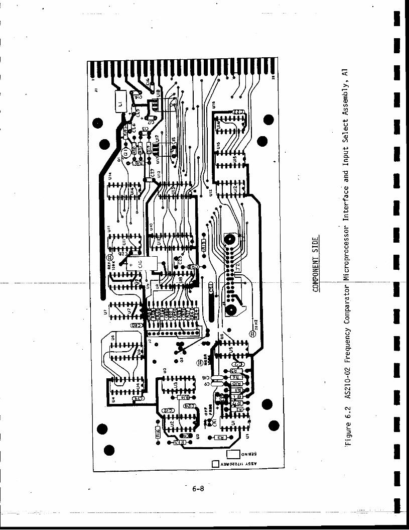
II
II
-oo)anv,
+)(J(l,
ot/,
+)
g
!c(g
' c ,o(o
lF!-c,. + )g
' r .oanta0.,()o!
ot(J
E
LoP(os-,uqEo
CJ
(Jg(u
(ul-
II
C\'lo
I, o
GIa
' c\l
r\o
(I.,!5o,
U-
Ionursfl ^ruozz.tt ̂ ssv
t
G 9
2
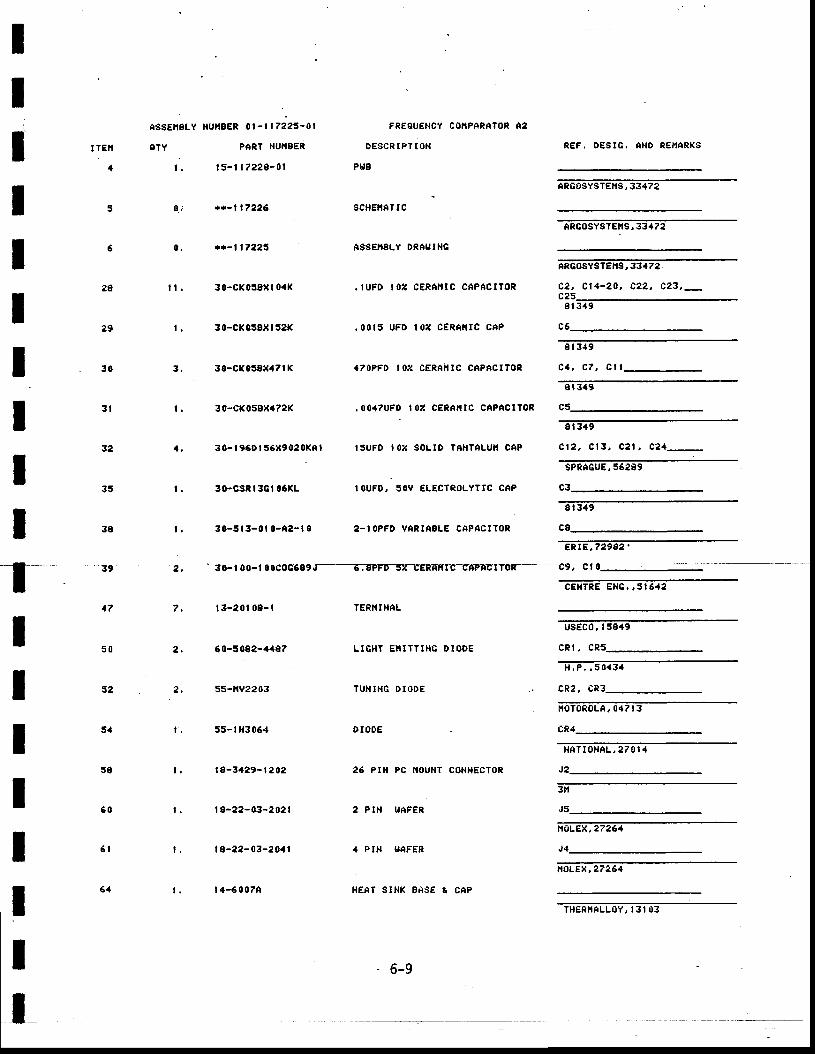
IIIIIItIII
I TEII
4
5
6
2A
29
3 0
3 l
32
35
38
nssEl,tBLY llUllS€R 0l -l | 7225-01
OTY PERT flUT'I8ER
| . l 5 - l 17229 -01
*t- l 17226
r r - l |7225
3o-cr039xr 04(
30-cl(058xt 521(
30-Cr058X,l7l K
30-cr05Exa72K
3o- | 96Dr 56N9020K41
3o-csnl 3Gr 06xL
30-5r3-0t 0-42-t 0
| 3 -20r 08- t
60-5082-448?
55-|lV2203
55-t 1r3064
I 8-3429-t 202
r 0-22-03-2021
| 8-22-03-20a1
t 4-6 0 074
FREOUENCY COfiPITRATOR A2
OESCRIPITOI{
PUB
SCHEIIATIC
ASSE}I8LY DRTUtItG
. IUFD IOZ CER i I . I IC CAPACITOR
.0015 UFD t0z cERAt t r c ccP
{?OPFD IOZ CERNHTC CAPACITOR
.0047uFD | 0z CERATIC CAPnCITOR
ISUFD IOU SOLID TA}ITALUII CAP
IOUFD, sOY ELECTROLYTTC CAP
2-1 OPFD VARtESLE CAPACITOR
REF. D€SIG. AND REI . IARKS
ARGDSYSTEIIS, 33472
0 i
ARGOSYSTEItS, 33472
ARCOSYSTEIIS, 33.t72
c 2 , c t 4 - 2 0 , c 2 2 , c 2 3 , _c25
8 t 349
I | 3.19
c 4 , c 7 , c r r _
Er 349
8 l3 ,19
c 1 2 , C t 3 , C 2 l , C 2 4
SPR6GUE, 56289
c3
8 t349
C B
ERI8 ,72982 '
l - -_-3e
ttIIIII
ITOF - . 'C9;
Cl
7 , T€RIt INAL
LIGHT EITITTIHE DIODE
TUII I I IG DIODE
DTOOE
26 PrH PC lOUf lT COi l I {ECTOR
2 PIH I IAFER
4 PIH IJAFER
HEAT SII I ( BASE i CNP
CEI {TRE EHG. ,5 I6 ' 2
usEco, | 58,f9
c R l , c R q
H . P . , 5 0 . + 3 4
cRe, cR3
HOTOROLA,047 t3
cR{
HATIONAL ,2TO I 4
J2
J5
f ioLEX,2726.r
J4
t'toLEx,27264
t .
6-9
TH€R}1ALLOY, I3I 03
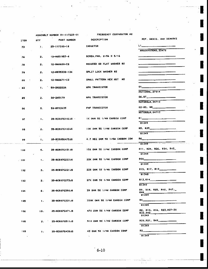
I TEN
?3
?6
7A
?9
8 0
g3
85
86
97
98
99
t 0 0
| 0 l
r 0 2
t 0 3
| 0.t
t 0 g
t 0 5
r 0 8
r 0 9
ASSEI ' |BLY t lUi lEER 0l- l l?225-01
OTY PART flUNgEN
t . 2 s - l l 7 3 0 s - t 0
t2-,tss1957-{
t2-lrAs620-c2
t 2-11335338- | 3.t
t2-lrns67l -e2
30-21122224
t0-21{5179
50-fiPs3639
35-RCR07Cl02. 'S
3s-ncR0?ct 03Js
35-R.CR03C4?5,JS
. FREE{,E||CY COfiPeReTOn n2
O€sCR I PT ION
INDUCTOR
scREu,Pf iH, 2-56 X 5/15
REDUCED OD FLAT UAgH€R 12
SPLIT LOCK UASHER TE
S}IALL PTTTER}I HEX NUT 12
HPN TRAT{gISTOR
}IP}I TRiNSISTOR
P}IP TRANSISTOR
fK oHtf 3?t l /4n ctR80| | coi lP
toK oHli 52 1/1U CARgOlt CollP
,1.? ltEG oHll 5i l/8u cAR8oll col'l
REF, DESTC. ANO RETIARKS
ARcoSYBTEiE, -3.t2
NATIONAL .2TO I '
06, c7
ltoToRoLA, 04713
02-05,
HOTORoLA, 0{71 3
s 1 3 4 9
R5, R35
8t 349
t3{9
a1319
R t 5 , R t 7 , R l 9 .
8r3a9
R I 3 , R T
8r 349
R 9 , R t 9 , R 2 5 , R { 0 , R 4 7 , -R48
8t 349
I r 3,t9
R 8 , R r 0 , R t 6 , R 2 3 , R 2 7 - 3 0R33 . R {2
8 t 3 4 9
R20 ,R21 , R+9 -
L I
IIIIIIIIII
R I
;:::-:.., ;...;"., ;;. - - I35-RCR07Gr5r J9
35-[CR07G223. 'S
35-RCR07G22t JS
35-RCR07G273JS
35-tCR07G3t0.lS
35-RCR07G33l . rS
35-RCn07G47l JS
35-RCR07C5r r . rS
35-RCR 07G/r30.rS
f50 oHn 52t t /1U CARBOH COIIP
22K OHlf Sz r/4u cARBOll coltP
220 0Hlt 5it l/4u cARSoll collP
27K OHtt 3'/. lt'a! CARBOX COIIP
39 oHft 32 1/1V CAR8oN COrP
33oK OHlt sz l/1rl cAR8ol{ co}tP
{70 SHff 321 t/1u CAR60N COIIP
5to oHn 3z t /1u cARBOll COIIP
rl3 oH|f 32 l/1V CARBOH COIIP
I
R5 IIIIIII
_t6-10
8t 3. t9
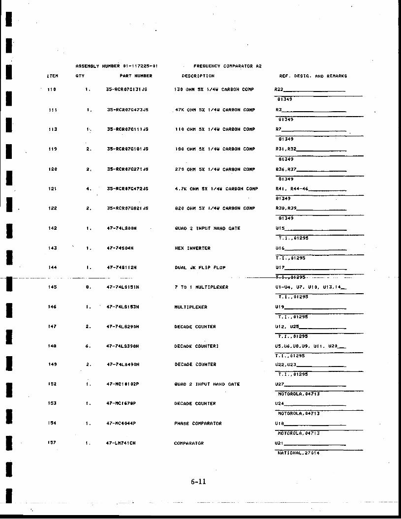
II
i
IIIIIItI
ASSEI8LY l {Un€ER 0l- r |?225-01
OTY PERI I|UIIBER
35 -RCR07c t 3 r JS
35-RCR07G{73JS
35-RCR07Gr | | JS
35-RCR07Ct 8r JS
35-RCR07C27t J3
35-RCR07G{72,1S
35-RCR07G82r JS
{7-?4LS00r{
47-7.f S0.rt{
.17-7tst t2 l {
. FREOUENCY COIIPARATOR A2
DESCRIPT IO ' {
f30 oHn s i t l /1v CAR9oH conP
.47K OHl l s ' t l l /4U CARBOH COIIP
| | 0 oHlt 52 | /{u cARBolt cottP
r80 oHJt 32 1/4U CARBoN COftP
270 oHt{ 5* t/4U CAR€o}| COiP
{.71( oHr, t 5u l / {u CAR9oN coiP
820 oH|| 5'l l/1U CnR80N COI'P
OUND 2 INPU1 HAHD GAT€
HEX INVERTER
OUEL JX FLIP FLOP
REF. DESIC . AND RE} iARKS
R22
8 t 3 { 9
8 t 3 4 9
R7
8 t 349
R3I , R3?
8r3{9
e35, R37
8 t 349
R4 t , Ra4 -46_
8r 3 {9
R38
8 t 3 4 9
T . I . , 0 t 2 9 5
u t 6
T . t . , 0 r 2 9 5
u t 7
IT-t--oru9s
a?-7.tLStSt| l
.r7-74LSt 53H
.7-74L9290r{
a7-7.1L9390t1
a7-7{Ls490H
az-| lct 0t 02P
a7-ltct678P
47-4C1011P
a7-Ll l7.t l CH
7 TO I ITULTIPLEXER
IIULTIPLEXER
D€CAO€ COU}ITER
DECAOE COUNTERI
D€CAO€ COUHTER
SUAD 2 IHPUT NNND CATE
DECADE COUHTER
PHASE CONPARATOR
COI{PARATOR
u 1 - u { , u 7 , u t 0 , u r 3 , r 4 _
T . t . , 0 t 2 9 5
2 ,
t .
IIIIIIII
u t 9
T . I . , 0 r 2 9 5
ur2 , u25
T . t . , 0 t 2 9 5
U 5 , U 6 , U E , U 9 , U I I , U 2 O -
T . I , , 0 t 2 9 5
u22,U2
l . I , , 0 r 2 9 5
U2?
roToRoLA,047t 3
u24
r.roToRoLA, 047 | 3
u t 8
f io roRoLf i ,047r3
ua l
6-1 1
N A T I O N I L , 2 T O I , I
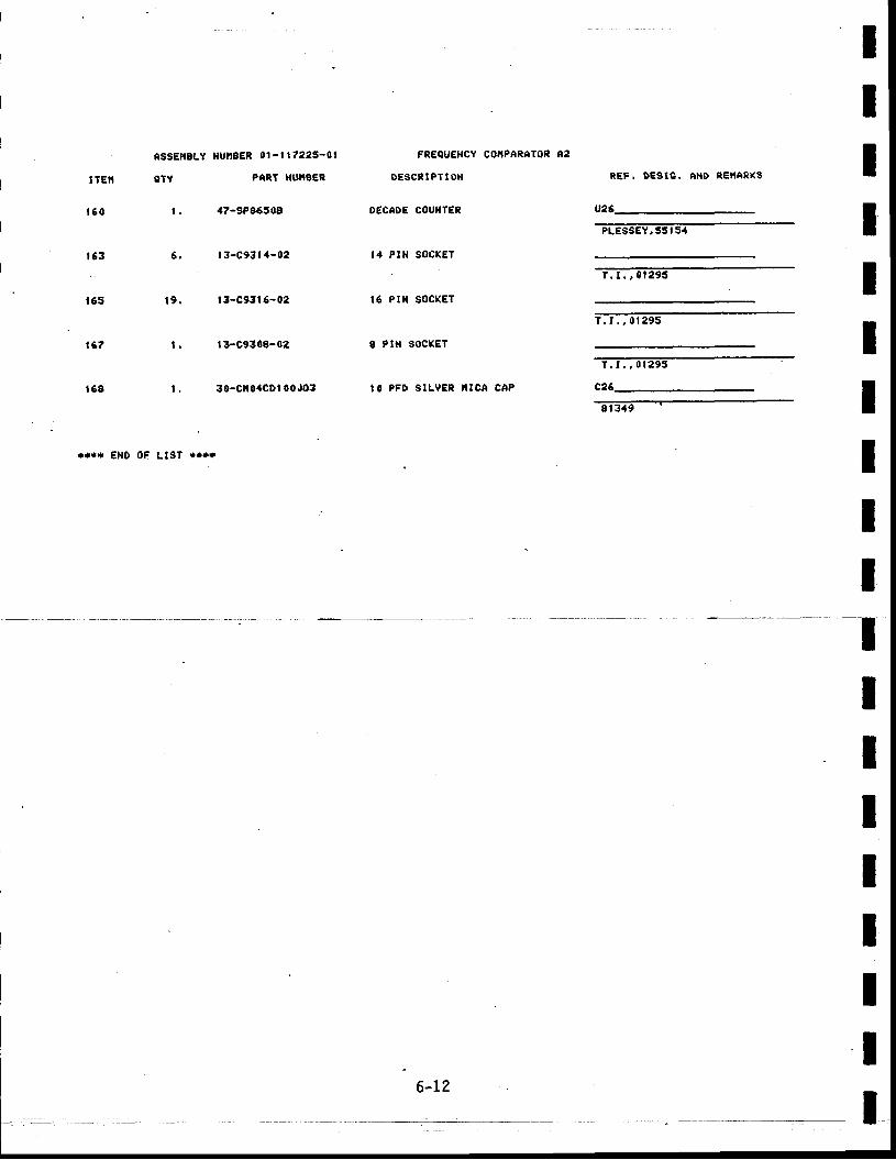
ITEIT
t 5 0
t 6 3
t65
t 6 ?
t68
..** ciNo 0F LtsT *.. t
e ssEllSLY lluttEER 01 - t | 7225- 0 t
ETY PERT HI'IIBER
| . ,37-SPe6509
6 . l 3 -C9314 -02
t9 . l 3 -C9315 -02
l . l3-C9308-02
| . 30-Cl t0 ' fCDl00.103
FREOUEilCY COIIPARATOR A2
DESCR IPT I OH
D€CAOE COUT{TSR
l. l PIH SOCKET
16 PTN SOCKET
I Plfl SOCKET
IO PFD SILV€R } I ICA CAP
REF, DESTC. AHD NENARKS
PLESSEY, 55I 5{
T . t . , 0 t 2 9 5
T . t . , 0 1 2 9 5
8 t349
6- I2
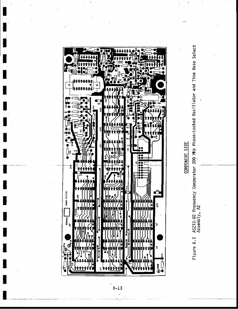
!
(\l
-o(uaa
+)(Joo
at1
oof6co(u
F'oc(q
Io+)(o
(JoO-o(u
-v(Jo
JIc,,o(q
4N
oo(\l
5-o+,(os.(g
oCJ
(Jg(u5(tq,J-
lJ-
NO
IO
<\Jv)
s)r.o
a)9.=o,
lJ-
lJl la lH l^lF Iz, l!.il= lo lo-t= lo tC-)I
II
III
6-13
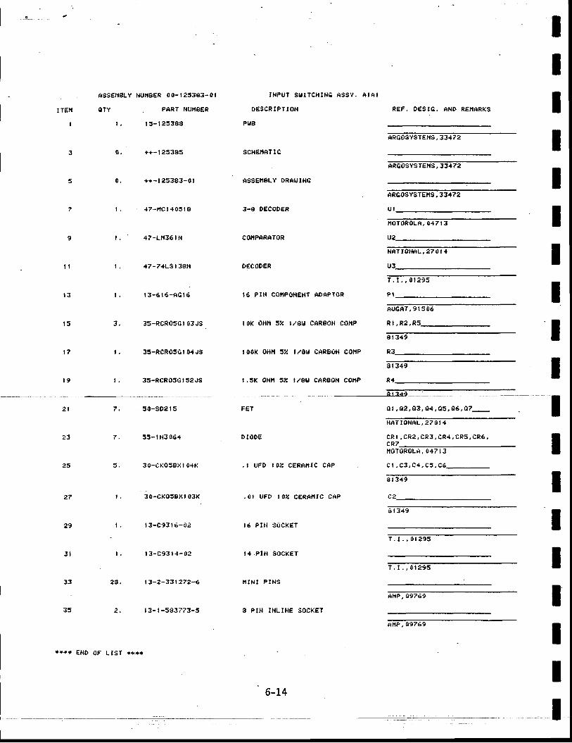
IIII TEII
I
3
7
I
l l
t 3
l 5
t ?
l 9
2 l
2 3
25
27
29
3 l
33
35
ASSgltgLY NUI ' iSER 00- l t53g3-01
OTY . PART I{UI'IBER
| 5- t 253SA
++-l 25385
++ - t25383 -01
{ i - r l c l 4 0 5 r B
47-Lt'135 | il
+7-?4LS | 38t{
t 3 -6 t6 - f iG16
3S-Rr :R05G l U3JS .
35-RCR85GT 04.,|S
35-RCRBSGT 52.rS
INPUT SUITCHI IT I : A5S? , A IA I
0gscR tP r toH
PU8
scHEltAt I c
ASSEI,ISLY DRAIJIHG
3-8 DECODER
COIIPARATOR
DECODER
16 PIN CO}IPOHEH' AOTPTOR
'| 0K oHH 5Z t?AU CARBOH COI{F
t00K oHil 52 l/su cARBo|l cor{P
, ,5K oHn 32 l /8U CARBOH COIiP
REF. OES IG. AND REf ' IARKS
ARG0S'/STEHS, 33. t72 IIIIIII
ARGOSYSTEtTS, 33.172
AR60SYSTEtls, 33472
U I
noToRt l LF ,047 t3
u2
}|Ar IOHAL,270 t , {
U3
T , t . , 0 t 2 9 5
P !
AUCAT,9 I 506
R I , R 2 , R 5
8 | 3,{9
P3
s t 3 4 9
50-sD2 | 5
55-t t {3 06{
3 o-c|.g58,1t 04li
3o-cr(o58Nt 03K
| 3-C93 | 5-01
| 3-C93 | 4-0:
| 3-?-33 | ?72-6
| 3- | -5S37?3-5
F€T
D IODE
, I UFD I OZ CERAI'IIC CAP
.0t uFo r0z cERAf ' l lc cAP
t5 P l l l socKET
t4 .P lH s t l c kET
I ' I tN I P INS
8 P IN IHL IHE SDCKET
H A T I O N A L , 2 T O I 4
cR | , cR2 , CR3 , eR4 , NRs, CR6 ,cr<7l rBToRoLA,047r3
c t , c 3 , c 4 , c 5 , c 5
8 r 3 4 9
IIIIIIIII
'a | 349
r , t . . 9 t 2 9 5
7 . L , 0 t 2 9 5
AnP ,09759
*$** END 0F LIST ****
6-L4
At4P,09769
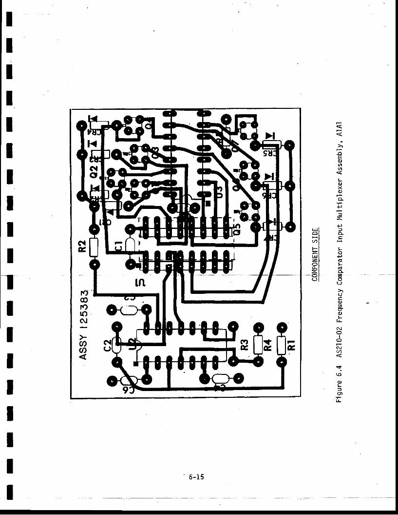
o(uo@
Lox(u
+J
5z+)=o.g
H
r-o+)(d!(do-
o(J
oE,(u=c,I
l!
C\lO
IO
$tar-,
r+tJ)
(l,!5c')
LJ-
It
tI
LUoa,/l
Fz.UJz,
- 6 -15
I TEII
t
HSS€rSLY l tUl tBER 00- l 1735t-01
OTY PAPT T{UI{BEP
2 . r 7 -3399 -6000
6. |6-3365/26
t**t EHo OF LISF **,ri
CABLE NSSEIIBLY
DESCRIPTIOI{
COHNECTOR, 2.6 PTH
CA9LE, 26 I I IRE; RISB0N
REF. DESIC. AI{O PE}IARKS
IIIIItItTI
tttITtII

l) I
IIIIIIttIItIIIIIII

IIIItIIIIIIIIIIItII
AS2 | O-O3FREO,UENCY
GENERATOR MODULE
IIfIIIIIIItIIItIIIfT

iI
€
IIIIIII
tIIIIII.#rI
Al l r ights reserved. No part of th is pub' l icat ion may bereproduced, stored fn a retrieval system, or transmitted,in any form or by any means, electronic, mechanical ,photocopyi ng, necordi ng and/or otherui se wi thout thepr ior wr i t ten permission of ARGOSystems, Inc. This man-ual may not be lent , resold, h i red out or otherwise dis-posed of by way of trade in any fonn of binding or coverother than that in which i t is publ ished, wi thout thepr ior consent of ARG0Systems, Inc.
ARG0Systems, Inc. / 884 Hermosa Court , Sunnyva' le, Cal i fornia 94086Telephone (Area Code 408) 737-?000 / Telex No. 352077

II
€-
IIIIIIIkIIIIIIIfI
Chapter
TABLE OF CONTENTS
T i t l e
Preface
GENERAL INFORMATION
1.1 INTRODUCTION1.2 PHYSICAL AND ELECTRICAL DESCRIPTION
INSTALLATION
2.1 INTRODUCTION
OPEMTION
3-1 INTRODUCTION3-? CONTROLS AND CONNECTORS3.3 OPERATING INSTRUCTIONS
THEORY OF OPERATION
4.1 ' INTRODUCTION4.2 OVERALL DESCRIPTION4.3 FREQUENCY GENERATION4.4 PHASE LOCK SIGNAL4.5 PHASE LOCKING4-6 OUTPUT AMPLITUDE LEVELING
MAINTENANCE AND CALIBRATION
5-1 INTRODUCTION
SECTION I5-2 PREVENTIVE MAINTENANCE
SECTION I I5-3 PERFORMANCE TESTING5.4 RF OUTPUT FREQUENCY PERFORMANCE TEST5-5 TEST PROCEDURE5-6 RF OUTPUT LEVEL PERFORMANCE TEST5.7 TEST PROCEDURE
SECTION I I I5-8 CALIBRATION/ALIGNMENT PROCEDURE5-9 ACCESS T0 AS210-03 FREQUENCy cENEMT0R5.10 PLO ALIGNMTNT PROCEDURE5-11 OUTPUT LEVEL ALIGNMENT PROCEDURE
Page
v i
1-1
1-11-1
2-L
2-t
3-t
3-13-13-1
4-1
4-L4-14-34-34-54-5
5-1
5-1
5-2
5-105-1 05-125-1 3
5-35-35-35-65-6
MODULE
TABLE 0F C0NTENTS (Cont inued)
T i t l e
SECTION IV5.12 TROUBLESHOOTING PROCEDURES
ILLUSTRATED PARTS LIST
6-1 INTRODUCTION
Page
IIItItItIII
5-1 5
6-1
6-1
IIItIII
- i i -
t
Il*.IIIIIII
Fi gure
1 .1
3 .1
4 .L
4 .2
5 .1
5 .?
5 .3
5 .4
5 .5
5 .6
5 .7
5 .8
5 .9
5 .10
5 .11
LIST OF ILLUSTRATIONS
Ti t ]e page
AS210-03 Frequency Generator Modul e l-Z
AS210-03 Control s and Connectors 3-2
Frequency Generator Functional Block Diagram 4-z
Voltage Control led Osci l lator (VC0) Block Diagram 4-4
AS210-03 Frequency Generator RF Output FrequencyTest Conf igurat ion 5-5
AS210-03_Frequency Generator RF Output Voltage LevelTest Conf igurat ion 5-7
Flow Diagram of Cal ibrat ion/A' l ignment prodedure forAS210-03 Frequency Generator 5-11
AS210-03 Frequency Generator; Microprocessor Interface,A1, Schematic Diagram S-Ll
AS210-03 Frequency Generator; Frequency Generating5-18Circui ts, A1, Schematic Diagram
AS210-03 Frequency Generator 500 MHz, VCO, A1A1,Schematic Diagram 5-19
AS210-03 Frequency Generator 400 MHz, VCO, ALAZ,Schematic Diagram 5-20
AS210-03 Frequency Generator 300 MHz, VCO, A1A3,Schematic Diagram s-ZL
AS210-03 Frequency Generator 200 tlHz, VCO, A1A4,Schematic Diagram S-Zz
AS210-03 Frequency Generator 100 MHz, VCO, A1A5,Schematic Diagram S-23
AS210-03 Frequency Generator 50 MHz, VCO, A1A6,Schematic Diagram S-?4
IIttItIfI
- 1 1 r -
t i gure
6 .1
6 .2
6 .3
LIST 0F ILLUSTRATI0NS (Cont inued)
T i t l e
AS210-03 Frequency Generator
AS210-03 Frequency Generator Assembly, A1
AS210-03 Frequency Generator VCO Circuit CardAssembl ies A1A1 (500 MHz), AlA2 (400 MHz), and
- 1 V -
Page
6-5
6-1 1
6-19
6-26
IIIIItIIItIIIIIIIII
A1A3 (300 MHz)
6.4 AS210-03 Frequency Generator VCO Circuit CardAssernbl ies A1A4 (200 MHz), A1A5 (100 MHz), and41A6 (50 MHz)
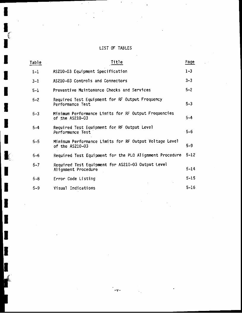
Il_
'{
IItIIII
tIItI
Tabl e
1-1
3-1
5-1
5-2
5-3
5-4
5-5
LIST OF TABLES
.T i t l e
AS210-03 Equipment Speci f icat ion
AS210-03 Control s and Connectors
Preventive Maintenance Checks and Services
Required Test Equipment for RF Output FrequencyPerformance Test
Minimum Performance Limits forof the AS210-03
RF Output Frequencies5-4
Page
1-3
3-3
5-2
5-3
5-6
5-9
5-L2
5-14
5-15
5-16
kI
5-6
5-7
5-8
5-9
Required Test Equiprnent for RF 0utput LevelPerformance Test
Minimum Performance Limits for RF 0utput Vo'ltage Levelof the As210-03
Required Test Equipment for the PLO Alignment Procedure
Required Test Equiprrent for AS210-03 Output LevelA'l ignment Procedure
Error Code List ing
V isua l Ind ica t ions
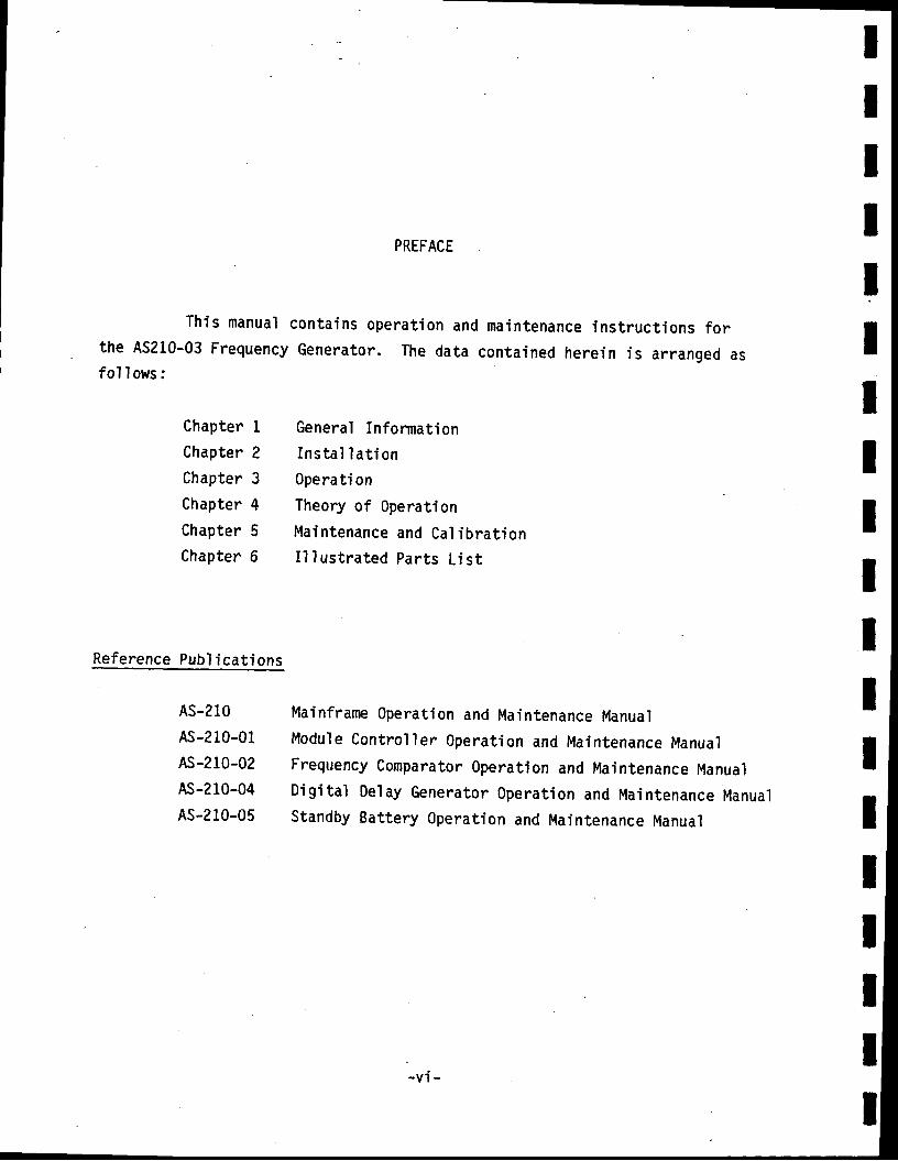
This manualthe AS210-03 Frequencyfol I ows :
PREFACE
contains operat ion andGenerator. The data
maintenance instruct ions forcontained herein is arranged as
IIItIIIIIIIIIIIIIII
Chapter 1Chapter 2Chapter 3
Chapter 4
Chapter 5Chapter 6
Reference Publ icat ions
AS-210
AS-210-01
AS-210-02
AS-210-04
AS-210-05
General InformationIns ta l la t ionOperati onTheory of OperationMaintenance and Cal ibrat ionI l lus t ra ted Par ts L is t
Mainframe 0peration and Maintenance ManualModule Control ler Operat ion and Maintenance ManualFrequency comparator 0peration and Maintenance Manua'lDigi ta l Delay Generator Operat ion and Maintenance ManualStandby Battery 0peratfon and Maintenance Manual
-v l -
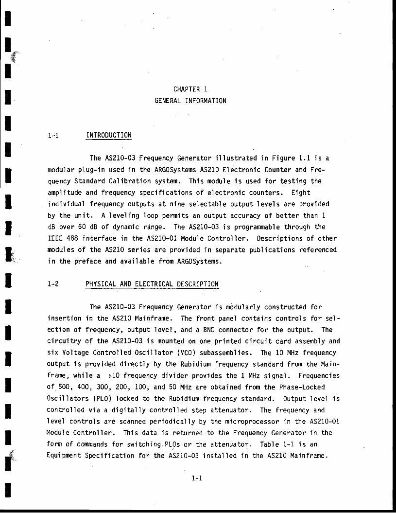
Il*I
1-1
IIIIItlIIIIIItfI
CHAPTER 1
GENERAL INFORMATION
INTRODUCTION
The AS210-03 Frequency Generator i l lustrated in Figure 1. .1 is a
modular plug- in used in the ARG0Systems AS210 Electronic Counter and Fre-quency Standard Cal ibrat ion system. This module is used for test ing the
amp' l i tude and frequency speci f icat ions of e lectronic counters. Eight
indiv idual f requency outputs at n ine selectable output levels are provided
by the uni t . A level ing loop permits an output accuracy of bet ter than 1
dB over 60 dB of dynamic range. The AS210-03 is programmable through the
IEEE 488 interface in the AS210-01 Module Control ler . Descr ipt ions of othermodules of the AS210 ser ies are provided in separate publ icat ions referenced
in the preface and available from ARG0Systems.
L-2 PHYSICAL AND ELECTRICAL DESCRIPTION
The AS210-03 Frequency Generator is modularly constructed forinsert ion in the AS210 Mainframe. The front pane' l contains controls for sel-ect ion of f requency, output level , and a BNC connector for the output. Thecircui t ry of the AS210-03 is mounted on one pr inted circui t card assembly andsix Vol tage Control led 0sci l lator (VCO) subassembl ies. The 10 MHz frequencyoutput is provided direct ly by the Rubidium frequency standard f rom the Main-frarne, whi le a +10 frequency div ider provides the 1 MHz signal . Frequenciesof 500, 400, 300, 200, 100, and 50 MHz are obtained from the Phase-LockedOsci l lators (PLO) locked to the Rubidium frequency standard. 0utput level iscontrol ' led v ia a digi ta l ly control led step at tenuator. The frequency andlevel controls are scanned per iodical ly by the microprocessor in the AS210-01Module Control ' ler . This data is returned to the Frequency Generator in theform of commands for switching PL0s or the at tenuator. Table 1-1 is anEqu ipment Spec i f fca t ion fo r the AS210-03 ins ta l led in the AS210 Main f rame.
1-1
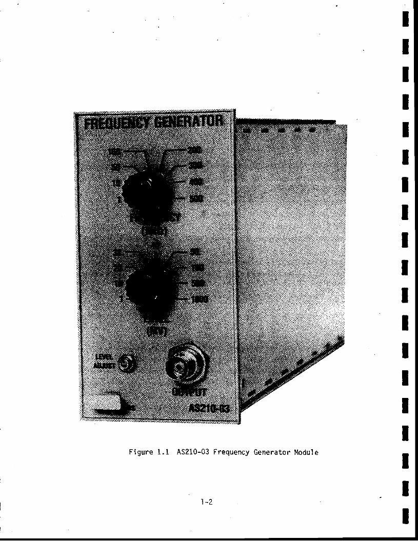
IIIIIIIIIItIIIIIIII
Figure 1.1 AS210-03 Frequency Generator Module
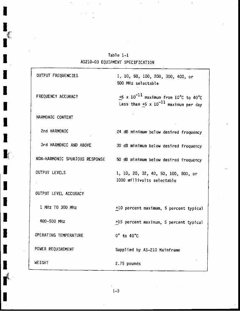
II
€=
IIIIIIt
IIIIItIft
Tabl e 1-1.AS210-03 EQUIPMENT SPECIFICATIoN
OUTPUT FREQUENCIES
FREQUENCY ACCURACY
HARMONIC CONTENT
2nd HARM0NIC
3rd HARMONIC AND ABOVE
NON-HARIv|ONIC SPURI0US RESP0NSE
OUTPUT LEVELS
OUTPUT LEVEL ACCURACY
1 MHz T0 300 MHz
400-500 MHz
OPERATING TEMPERATURE
POl^lER REQUIREMENT
l,lE IGHT
1, 10 ,50 , 1 .00 ,200 ,300 ,400 , o r500 MHz selectable
- 1 1+6 x 10 "' maximum from l0"C to 40'CIess tnan r5 x 10-11 maximum per day
24 dB minimum below desired frequency
30 dB minimum below desired frequency
50 dB minimum below desired frequency
1, 10 , 20 , 32 , 40 , 50 , .100, 500, o r1000 mi l I i vo l ts se lec tab le
+10 percent maximum, 5 percent typical
115 percent maximum, 5 percent typica'l
o' to 4o'c
Suppl ied by AS-210 Mainf rame
2 .75 pounds
1-3

IIIIIIIItIIIIIIIIII
Il*qIIIIIIIli
IIIIIIIfI
2-L
CHAPTER 2
INSTALLATION
INTRODUCTION
The AS210-03 Frequency Generator Module plugs into the AS210Mainframe. The module is electr ical ly connected through a rear edge con-nector and. mechanical ly retained via a f ront pane' l locking bar.
NOTE 1: Because of the high retention force of the rear card edgeconnector, it may be necessary to pul1 on the RF LEVEL
switch knob at the same time as the release mechanism ispulled, to remove the Frequency Generator from the Main-f rame. (See F igure 3 .1 . )
NOTE 2: The power in the AS210 Mainframe must be turned OFF wheninsert ing or removing the Frequency Generator Module.
CAUTION
AS210 ser ies plug- ins wi l l not work in Tektronix
Ttvl-500 seri es mai nframes. Severe damage wi 1 1 resu'l ti f operat ion in th is mode is at tempted.
Power and signal interface is provided through the Mainframe. The signaloutput is f rom a BNC connector on the f ront pane1.
2-L

IIIIIIIIIIIIIIIIIII
IluIIIIIII
3-1
CHAPTER 3
OPERATION
INTRODUCTION
This chapter contains operat ion data and instruct ions for theFrequency Generator. Operator interface is provided through three controlsand a connector on the f ront panel of the module. The AS210-03 is designedto be used in conjunct ion wi th the AS210-01 Module Control ler . However, th isinterface is t ransparent to the user of the Frequency Generator. Chapter 5,Ma in tenance and Ca l ib ra t ion , exp la ins the se l f -d iagnos t ic capab i l i t y o f theAS210-03 when used with the Module Control ler .
3-2 CONTROLS AND CONNECTORS
Figure 3.1 is a front pane'l photograph of the Frequency Generatorwith index numbers keyed to Table 3-1.
3-3 OPERATING INSTRUCTIONS
ItIIIIIfI
Select thequi red. Athe LEVELwithin the
The AS.210-03 is connected via 50 ohm cabledesired standard frequency and choose thelevel adjustment is provided on the front
(mV) cont ro l . Spec i f i c p rocedures fo r th isMaintenance chapter.
wi th a BNC connector.
output I eve'l as re-pane' l for cal ibrat ing
al ignment are contained
3-1
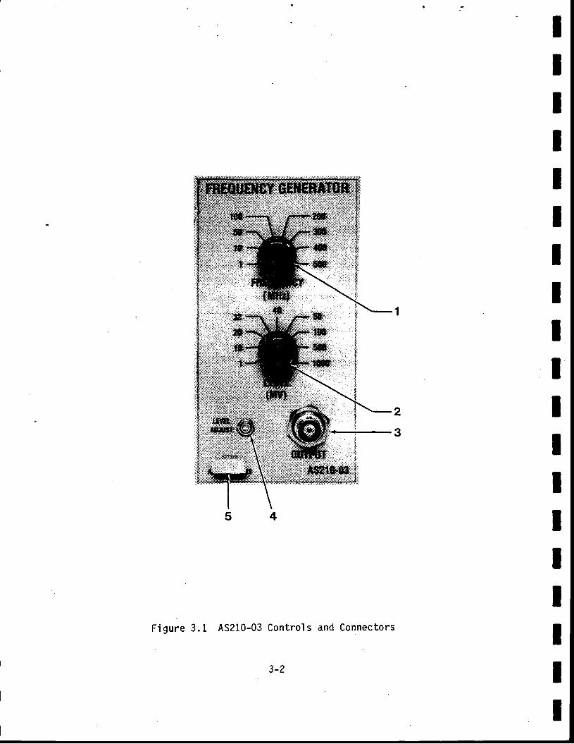
IIIIIIIIIIIIIIIIIII
Figure 3.1 AS210-03 Controls and Connectors
3-2
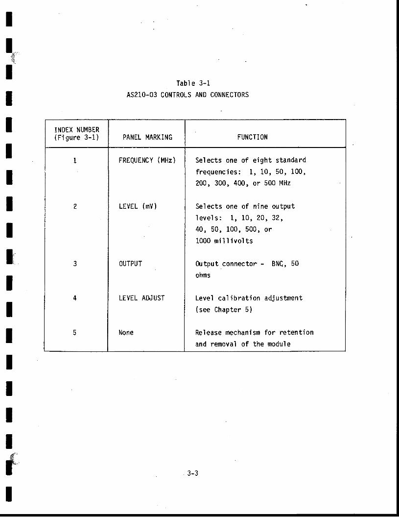
Il*IItIIIIIIIIIII
Tabl e 3-1
AS21O-03 CONTROLS AND CONNECTORS
I$I
INDEX NUMBER(F igure 3-1) PANEL MARKING FUNCTION
FREQUENCY (MHz)
LEVEL (mV)
OUTPUT
LEVEL ADJUST
None
Selects one of e ight standard
f requenc ies : 1 . , 10 , 50 , 100,
200, 300, 400, or 500 MHz
Selects one of n ine output
leve ls : L , 10 , 20 ,32 ,
40 ,50 , 100 ,500 , o r
1000 mi l l i vo l t s
&rtput connector - BNQ, 50
ohms
Level cal ibrat ion adjustment(see Chapter 5)
Release mechanism for retent ion
and removal of the module
3-3

Il_
€
tIIIIII
4-L
CHAPTER 4
THEORY OF OPERATION
INTRODUCTION
This chapter provides a descr ipt ion of the c i rcui ts used in the
Frequency Generator. The circui t descr ipt ion is keyed to a funct ional b lock
diagram and the schematic diagrams inc ' luded in Chapter 5. Detai ls of coi lmon
type c i rcu i ts (power supp ' l ies , e tc . ) a re no t inc luded in th is descr ip t ion .
4-2 OVERALL DESCRIPTION
The Frequency Generator circuit consists of the front pane'l
controls and the ci rcui t card assembl ies. AL is the main c i rcui t board
assembly, the VCOs are A1A1 through A1.A6. Figure 4.1 is a funct ional b lock
diagram of the module depicting how the generator produces standard frequency
outpu ts o f 1 , 10 , 50 , 100,200,300, 400" and 500 MHz. Fron t pane l con t ro ls
select the desired frequency and output level . The Frequency Generator 's
front panel switches are interrogated 10 times per second by the module con-
trol ler of the AS210 System. The frequency and level data are shi f ted' f rom
the modu le cont ro ' l le r ' s Cent ra l Process ing Un i t (CPU) in to la tches (A1U11-
frequency, AlUS-level) on the generator through a bidirect ional mult ip lexerA1U4, and A1U6. The CPU RD signa'l determines the direction of data flowthrough the mult ip lexer. Address bi ts A8 and A15 from the CPU are used to
load frequency or level data from the data bus. The output of the frontpanel f requency select switch is also mult ip lexed with test data in A1U5 byaddress bi t A0. Test data informs the CPU whether the PL0s are locked andthat the output is leveled for sel f - test purposes.
IIIIIII
t4-I
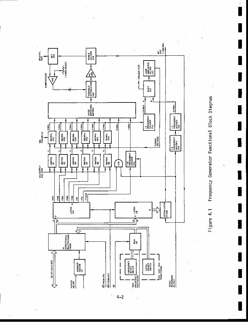
IIT
J
u l F
= v
fl t o
;38 d
IIIIItItIII
6!-q).q
J
oco
,o
o+)o
lJ-
!-o+)(dL(ug(u
C)
o
!LL
sr(ur-ctt
lJ-
l--ll---;I;t
l d
IEJFIx I o 3
t_ _ _vdQ >
F q ' {
=
t =
l
=
l c I
Iz. . . i :X ! ) c
3;!
G o:B
rE=ioG nP H
e E - :
< uz xo 5
a d =
u z zF > l
4-2
tI
Il*III
IIkIIIItTIffi
4-3 FREQUENCY GENERATION
The frequency generat ion c i rcui ts consist of s ix phase- locked
osci l ' lators (Pl-O), f requency reference div iders, PLO vo' l tage supp' ly gat ingcircui ts and the I and 10 MHz gat ing c i rcui t . The PLO circui t ry is composedof s ix vol tage control led osci l lators (VC0) wi th a common frequency div ider,phase conparator, and loop ampl i f ier / f i l ter . Six of the standard outputs areprovided by the VC0s A1AX (with X equal ing I through 6 for AlA1 through 41A6).These are the 500, 400, 300, 200, 100, and 50 MHz outputs. The 10 MHz outputis obtained direct ' ly f rom the reference input. The 1 MHz output is obtainedby div id ing the 10 MHz reference input by 10. 0n1y one output f requency canbe obtained from the generator at a tinre. When the front panel switch is setfo r 50 , 100, 200, 300,400, o r 500 MHz, the app l icab le l ine f rom the f re -quency latch Alu11 (F50, F100, F200, F300, F400, or F500) act ivates one ofs ix t rans is to r sw i tches (Q6-Q1) . The swi tches a l low 11 vo l ts to be app l iedto the appropriate VCO. Each VCO (Figure 4.2 and schematic diagrams Figures5.4 through 5.11) is ident ical except for the f requency-determining circui telements. Component designators for the VCOs wil ' l be preceded by A1AX (with
X equa'l ing L through 6) to differrentiate them from main board components. Avaractor-control led t ransistor osci l lator (A1AXQ1, AlAXQz) is tuned by avol tage from the phase detector A1U17 through the loop f i l ter /ampl i f ier A1U21.The RF output of the osci l lator is provided at connector AlAXJ1.
4-4 PHASE LOCK SIGNAL
The RF output of a l l the PLOs is div ided by 10 in AlAXUl, buf feredbv AlAXQ3 and div ided again by AlAXU2 (except in the 50 MHz pLO). Thefrequency div is ion accompl ished by AIAXU2 is detennined by the osci l latorfrequency. A 5 MHz osci l lator output is desired from AIAXUZ, therefore thediv is ion rat io fs f /n = 5 MHz. For example, the 400 MHz pLO requires a+8 f requency d iv is ion (n = 8 ) a t A1A2u2 s ince i t has been prev ious lydiv ided by 10 at A1A2u1. In the case of the 50 MHz pL0, the or ig inald iv i s ion by 10 y ie lds 5 MHz.
4-3
t
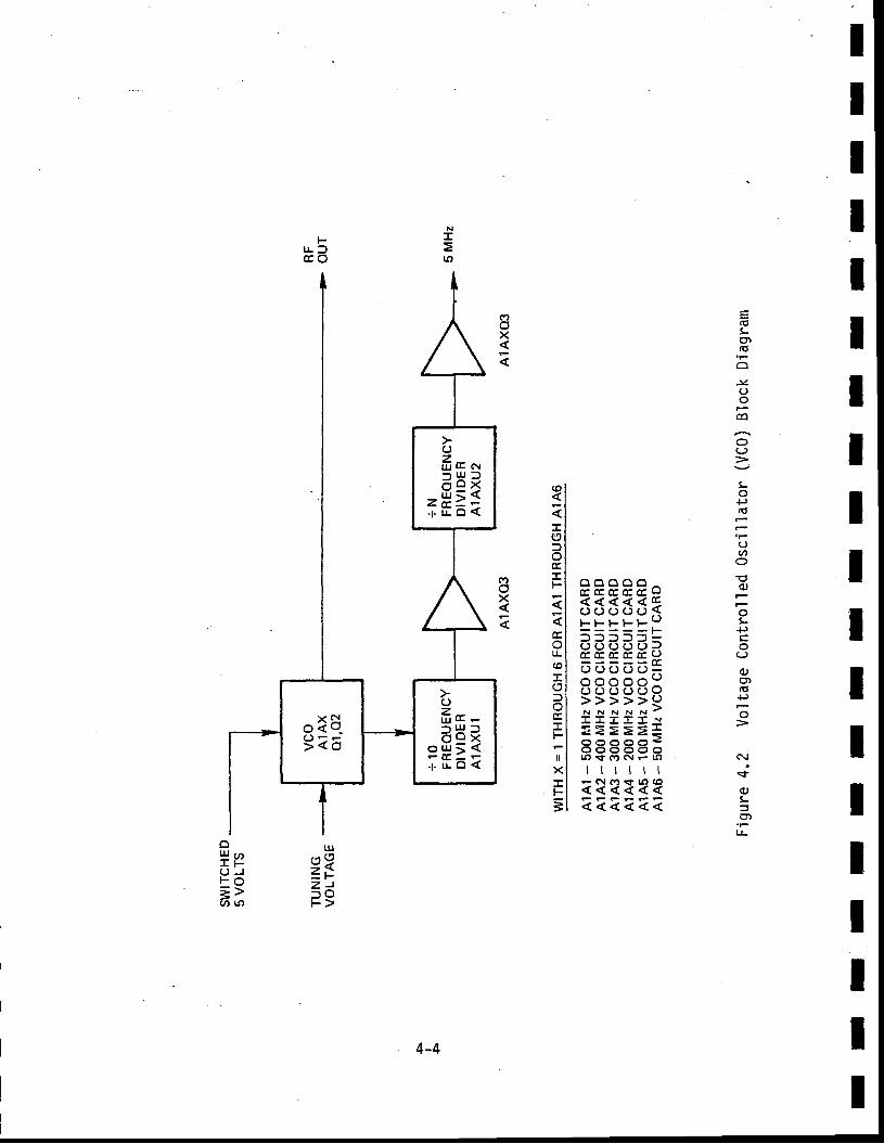
IIIIIIIIIIIItIIItII
(g!(')ao
o.:a(Jo6
OC-)
!o+t.o
(Jan
O
€(u
o!-+t
o(J
q)(t)foP
o
AJ
sf
(u5-
u-
(7,
x
E
(o l< lEI-r- |6 l: ) lo lc l
P F i ooooo^v I e p e F E : t J
- t
3 31 633sSf51 33S33=r J - l ( r ( E C C c c E q ). ^ l - _ t y- l c ) ( ) o ( J o =* i ooooo :: l ( J o o ( J C ) ! ?: lY I r u N r u r N 2g I T T 7 ? T N
i t E = = = = *' - l BBBBSS
l l I l O s f c / , N e l J )
x l t t t l t lr l e N 0 t s r r l t ( Otr!
F F F
= l
4
=ro
ut
>3z Jf , oF >
H p4 F( J JF O= >an g,
O
fr-*-FH*f tr6e
Oz_l l l g e
f H l
3E=3. q . t l O {
o {8.9Ea
4-4
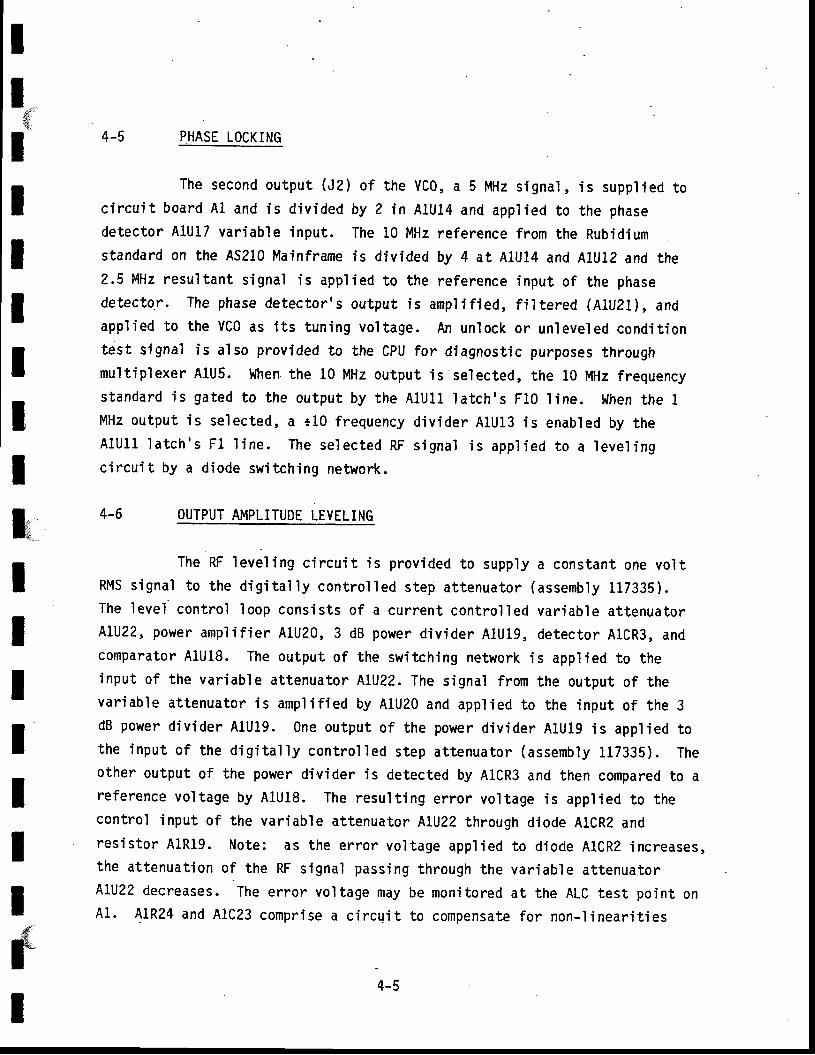
Il*IIIItIIktIIIIIIfI
4-5 PHASE LOCKING
The second ou tpu t (J2) o f the vc0 , d 5 MHz s ignar , i s supp l ied toc i rcu i t board 41 and is d iv ided by 2 in A1u14 and app l ied to the phasedetector A1U17 var iable input. The 10 MHz reference from the Rubidiumstandard on the AS210 Mainframe is divided by 4 at A1U14 and A1U12 and the2.5 l4Tz resul tant s ignal is appl ied to the reference input of the phasedetecto.r . The phase detector 's output is ampl i f ied, f i l tered {Atuzl) , andappl ied to the VCO as i ts tuning vol tage. An unlock or unleveled condi t iontest s ignal is a lso provided to the CPU for diagnost ic purposes throughmu' l t ip lexer A1U5. When the 10 MHz output is selected, the 10 MHz frequencys tandard is ga ted to the ou tpu t by the A lU1 l la tch 's F10 ' l ine . When the 1MHz output is selected, a *10 frequency div ider A1u13 is enabled by theAlu11 la tch 's F l l ine . The se lec ted RF s igna l i s app] ied to a leve l ingcircui t by a diode switching network.
4-6 OUTPUT AMPLITUDE LEVELING
The RF level ing c i rcui t is provided to supply a constant one vol tRMS signal to the di9i ta11y control led step at tenuator (assembly 117335).The level-control loop consists of a current control led var iab' le at tenuatorAMz, power ampl i f ier A1U20, 3 dB power div ider A1U19, detector A1CR3, andcomparator AlU18. The output of the switching network is appl ied to theinput of the var iable at tenuator A1U22. The signal f rom the output of thevar iable at tenuator is ampl i f ied by A1U20 and appl ied to the input of the 3dB power div ider AlU19. One output of the power div ider A1U19 is app' l ied tothe input of the digi ta l ly control led step at tenuator (assembly 117335). Theother output of the power divider is detected by A1CR3 and then compared to areference vol tage by A1U18. The resul t ing error vol tage is appl ied to thecontrol input of the variable attenuator AllJZZ through diode A1CRZ andresistor A1R19. Note: as the error vol tage appl ied to diode A1CR2 increases,the at tenuat ion of the RF signal passing through the var iable at tenuatorALU22 decreases. The error voltage may be monitored at the ALC test point onA1. AlR24 and A1C23 comprise a c i rc-ui t to compensate for non- l inear i t ies
4-5
in the attenuator. A front panel contro'l ( lf ) aOjusts the output leve'l bydetermining the reference voltage of the comparator. Comparator AlUl.5 pro-vides an output to the CPU for diagnost ic purposes. A1U15 determines whenthe signal level , detected by A1CR3, exceeds the threshold establ ished bydiv iders AlRl , A1R3, A1R4, and AlR9. The output of A1U15 goes low to i l lum-inate LED AlCRl when an unleveled condi t ion exists. This informat ion is alsosent to the CPU. An unlocked condi t ion at A1U17 also provides an indicat ionthrough Aluls to the CPU. The at tenuator level of the output s ignal is d ig-itally controlled by the data from the leve'l latch A1ug. The RF outputsignal is therefore provided at the frequency and amplitude selected by thefront panel controls.
IIItIIIIIIIIIIIIIII
4-6
Il*IIIIttIkIIIIIIIft
CHAPTER 5
MAINTENANCE AND CALIBRATION
5-1 INTRODUCTION
The purpose of th is chapter is to provide maintenance and cal ibra-
tfon data for the AS210-03 Frequency Generator. Section I covers routine
prevent ive maintenance procedures. Sect ion I I out l ines performance tests
for the Frequency Generator. Sect ion I I I contains the cal ibrat ion/al ignment
procedures for the AS210-03 module, and Sect ion IV descr ibes t roubleshoot ing
data. Figures 5.4 through 5.11 are the schematic diagrams of the Frequency
Generator Module. Please contac. t the factory for any.assistance required in
the maintenance or servic ing of the AS210-03.
5-1
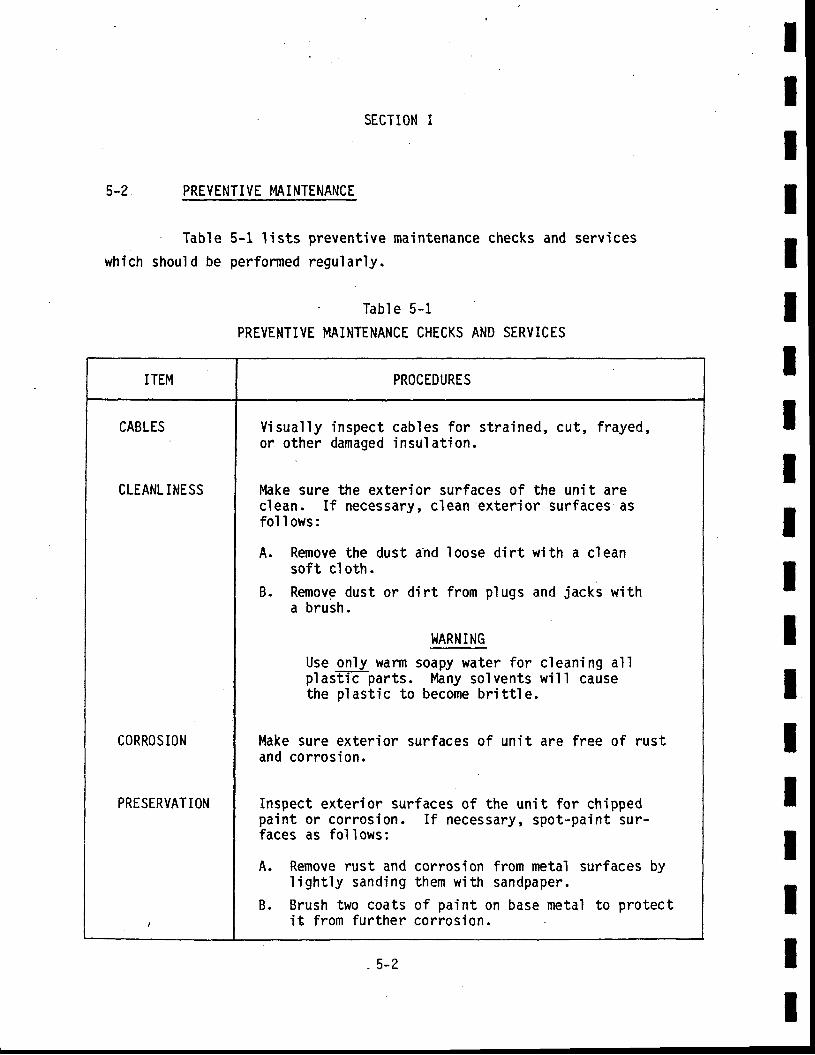
SECTION I
5-2 PREVENTIVE MAINTENANCE
Table 5-1 l is ts prevent ive maintenance checks and services
which should be performed regular ly.
' Tabl e 5-1
PREVENTIVE MAINTENANCE CHECKS AND SERVICES
tIIItIIIItIIIIIIIII
ITEM PROCEDURES
CABLES
CLEANL INESS
CORROSION
PRESERVATION
Visual ly inspect cables for strained, cut , f rayed,or other damaged insulat ion.
lvlake sure the exterior surfaces of the unit areclean. I f necessary, c lean'exter ior surfaces asfol I ows:
A. Remove the dust ahd loose dirt with a cleansoft cl oth.
B. Remove dust or di r t f rom plugs and jacks wi tha brush.
WARNING
Use only warm soapy water for cleaning a1'lplasFparts. l ' / tany solvents wil l causethe plast ic to become br i t t le.
Make sure exterior surfaces of unit are free of rustand corrosion.
Inspect exterior surfaces of the unit for chippedpaint or corrosion. I f necessary, spot-paint sur-faces as fol ' lows:
A. Remove rust and corrosion from meta'l surfaces byl igh t ly sand ing them wi th sandpaper .
B. Brush two coats of paint on base metal to protecti t f rom further corrosion
5-2
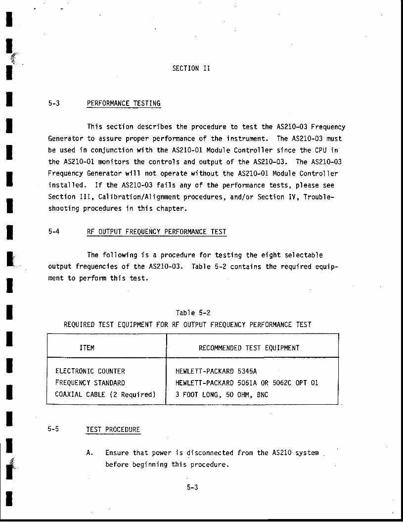
Il*'I SECTION I I
I 5-3 PERF'RMAN'E TE'TING
I
ment to perform this test.
I This section describes the procedure to test the AS210-03 FrequencyI
Generator to assure proper performance of the instrunrent. The AS210-03 must
I be used in conjunct ion wi th the AS210-01 Module Control ler s ince the CPU inI the AS210-01 monitors the controls and output of the AS210-03. The AS210-03
I Frequency Generator wi l l not operate wi thout the AS210-0L Module Control ler
r instal led. I f the AS210-03 fai ls any of the performance tests, p lease see
I Sect ion I I I , Cal ibrat ion/Al ignment procedures, and/or Sect ion IV, Trouble-
I shoot ing procedures in th is chapter.
I 5-4 RF ouTpur FREQUENcv eERFoRMANcE TEsrI
The fol lowing is a procedure for test ing the eight selectableoutput f requencies of the AS210-03. Table 5-2 contains the required equip-
ItIIII$I
Tabl e 5-2
REQUIRED TEST EQUIPMENT FOR RF OUTPUT FRIQUENCY PERFORMANCE TEST
5.5 TEST PROCEDURE
A. Ensure that power is disconnected from the AS210 system
before beginning this procedure.
5-3
ITEM RECOMMENDED TEST EQUIPMENT
ELECTRONIC COUNTER
FREQUENCY STANDARD
COAXIAL CABLE (2 Requi red)
HEWLETT.PACKARD 5345A
HEWLETT.PACKARD 5061A OR 5062C OPT 01
3 FOOT LONG, 50 OHM, BNC
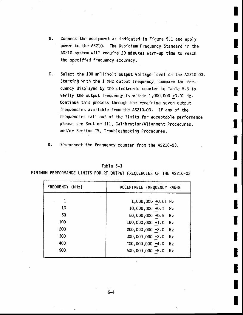
IIIIIIIIItIIItItIII
B.
c.
D.
Connect the equipment as indicated in Figure 5.1 and applypovrer to the AS210. The Rubidium Frequency Standard in theAS210 system will require 20 minutes wann-up time to reachthe specified frequency accuracy.
Select the 100 mi l l ivol t output vol tage leve' l on the AS2l0-03.Starting with the L MHz output frequency, compare the fre-quency disptayed by the electronic counter to Table 5-3 tover i fy the output f requency is wi th in 1. ,000,000 +0.01 Hz.Continue this process through the remaining seven outputfrequencies avai lable f rom the AS210-03. I f any of thefrequencies fa l l out of the l imi ts for acceptable performanceplease see Sect ion I I I , Cal ibrat ion/Al ignment procedures,
and/or Sect ion IV, Troubleshoot ing Procedures.
Disconnect the frequency counter from the AS210-03
Tabl e 5-3MINIMUM PERFoRMANCE LIMITS FoR RF oUTPUT FREQUENCTES 0F THE AS210-03
FREQUENCY (MHz) ACCEPTABLE FREQUENCY RANGE
I
10
50
100
200
300
400
500
1.,000,000 +0.01 Hz10,000,000 +0.L Hz50,000,000 +0.5 Hz
100,000,000 +1.0 Hz200,000,000 +2.0 Hz300,000,999 +3.0 Hz400,000,000 +4.0 Hz500,000,000 +5.0 Hz
5-4
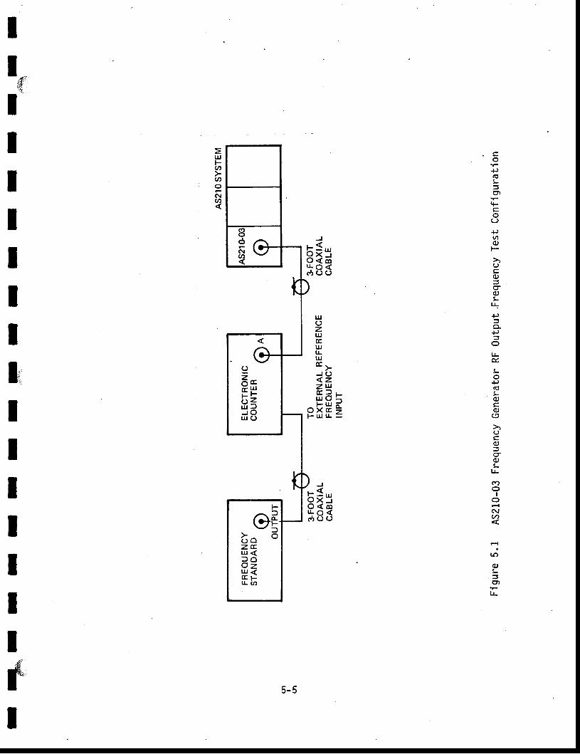
o
(o!-=
tF
(_).Ptn(IJ
F
(u
(ur-++J
+J
O
lJ-&.!o
+J(or-o(u
(J
(uoo!.
lJ-
=IuF(n
tno(1a
It
.€'
IIIIIIII'IIIIIIIsT
|.lJ()ztuEIJJt!u.l
J ( )<zz v ttre Il -ut f ,
O ) < E >F- u.l tl. =
cf)o
Io(\It/,
F{
lr)
(l,!=gt
lJ.
J
x5< c oo<( J O
FooIL
cl
g7e,; L ul - F
H=J Our c)
C ) Oz Eu r <l oO zu r <( r FlL (l!
5-5
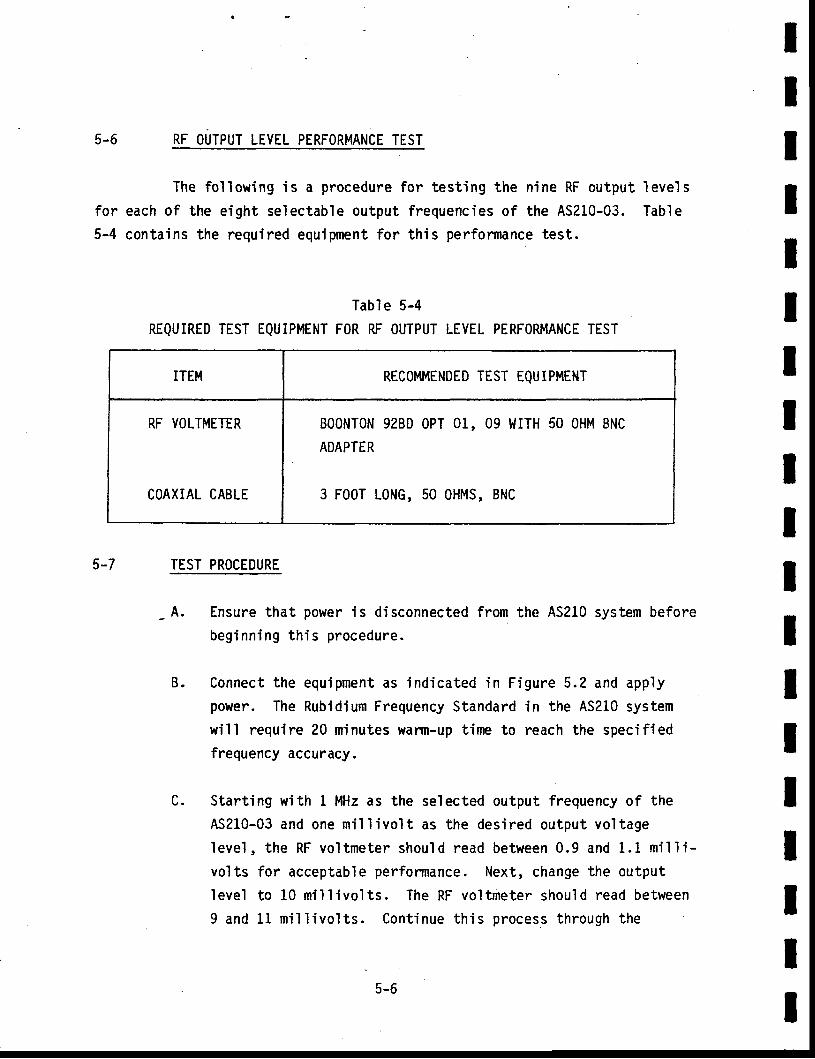
RF OUTPUT LEVEL PERFORMANCE TEST
The fol lowing is a procedure for test ing the nine RF output levels
for each of the eight selectable output f requencies of the AS210-03. Table
5-4 contains the required equipment for this performance test.
Table 5-4
REQUIRED TEST EQUIPMENT FOR RF OUTPUT LEVEL PERFORMANCE TEST
5-7 TEST PROCEDURE
Ensure that power is disconnected from the AS210 system before
beginning this procedure.
Connect the equipment as indicated in Figure 5.2 and applypower. The Rubidium Frequency Standard in the AS210 systemwil ' l require 20 minutes warm-up tire to reach the specified
frequency accuracy.
Starting with 1 MHz as the selected output frequency of theAS210-03 and one mi l l ivol t as the desired output vol tage
leve l , the RF vo l tmeter shou ld read be tween 0 .9 and 1 .1 mi l l i -
vol ts for acceptable performance. Next, change the output
level to 10 mi l l ivol ts. The RF vol tmeter should read between
9 and 11 mi l l i vo ' l t s . Cont inue th is p rocess th rough the
tIIIIIIIItIIIIIIIIt
A.
B.
c.
ITEM RECOMMENDED TEST EQUIPMENT
VOLTMETER
COAXIAL CABLE
BOONTON 92BD OPT 01, 09 WITH 50 OHM BNC
ADAPTER
3 FOOT LONG, 50 OHMS, BNC
5-6
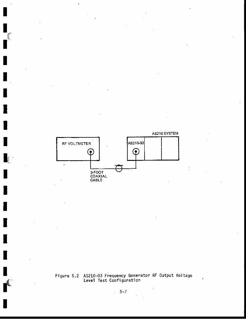
AS210-03 Frequency Generator RF Output Vol tageLevel Test Conf igurat ion
II
€-
IIIIItIJrIIIIIII
I
AS21O SYSTEM
RF VOLTMETER
5-7
F igure 5 .2
IIIIIIIIIIIIIIIIIII
D.
remaining six output levels comparing the readings to Table5-5 for acceptable perfonnance. Select the 10 MHz outputfrequency and repeat the procedure for each RF vortage 1evel.cont inue this process unt i l a l l output levels for each outputfrequency have been ver i f ied to be within the speci f ied l imi tsof rable 5-5. I f any of the levels fa l l out of the range foracceptable perfonnance, please see sect ion I I I , cal ibrat ion/Al ignment Procedures, and/or Sect ion IV, Troubleshoot ingProcedures.
Disconnect the RF voltmeter from the AS210-03 outputconnector.
5-8
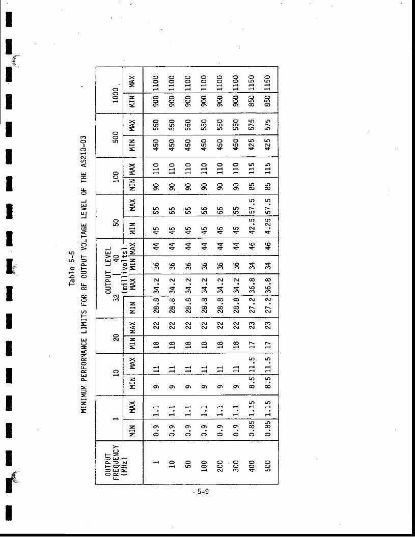
ooo
x=
o o o o o o o oo o o o o o | r ) l r )F{ F{ r-l i-{ F{ Fl Fl Fl
J F { F t J r { F { F t F l
z,=
o o o o o o o oo o o o o o l r ) l r ,o t o r o r o r o r o r c o o
ootr'
><=
o o o o o o t r ) t r )|r, |r, rJ) u) trt tr) l\ r\LC, tl) rI) Lt) tl) rJ'' lJ' lr,
==
o o o o o c , l r ) r ot r , l r ) l r ) l r ) u ) l r ) ( \ J $ t$ + < f + + s f s f +
oo
><
=o o o o o o | r ) r f )F{ F{ F{ F{ F{ Fl el t{
F{ r{ F{ r-l r-{ F{ r-{
z,H
= 88888833
o|J)
x=
lr' lr)
l r ) t r ) t r r r o t r ) l o l \ t \K ) t r r r J ) u ) r l ) u ) r J ) L r )
z,H
=
rt Lo' (\l
rJ, ro ro |r) tr, |r) $Is f S r + + + s t < f +
Jtd> olrJ sfJ
F -
o-F
o(\I(Y)
xn =- 2 .c H> =- -. > <- {E =
< . + + s f + . r f r . o r . o+ r + + t + s f + s f +
r.o (0 ro r.o r.o ro <f <f(Y) (f) ('' co fi) (o (n (Yt
$ l G t N < \ t G l ( \ l c o o
+ r + $ < f < + < f ( O ( O(t, (f, co c4 (f) (f) (?) ct)
z=
@ @ o o c o @ @ ( ! ( \ l
@ @ @ @ @ @ r \ l \(\t (\, aJ <\, (\J 6.1 C\t (\l
o(\l
x=
6J (\J (\J (\.t Sl (\l (') (nst (\t <\J <\t ct (\l (\l sl
z.= @ 6 c O O @ C O r \ l \
Fl Ft Fl F{ Fa Fl F{
o
><=
rf) rr'
F{ F{ F{ F{ Ft Ft Fl
F{ F{ F{ Fl Ft t{ F{ F{
z,=
rr, lr,q l o t o t o r o t o r o c o
F{
x,=
Lr, lr,F{ Fl i-{ Ft F{ Fl Fl
r-l F{ F{ r-{ F{ H el Fl
z,H
=
t.ct lJ)o r o ) o r o t o l o r @ @
o o o o o o o o
c)I- Z,= l l J ^o - = NF c r -= r ! =o d -
lJ-
d o o o o _ o o oF r l r ) 0 o o o o
F{ Nl af) t+ Lf)
5-9
COO
IoFa(\J<,r1
lrj
t-|J-oJt!
LrlJ
LrlaFJO
tor l -
l . r r =o-( u F
a oc'F U -
e,
d.OlJ-
.rlt-
=J
|flCJz.=&,olJ-d.|JIo-
===H
zH
=
II
€'
IIIIIIIkIIIIIIIsI
SECTION I I I
5-B CALIBRATION/ALIGNMENT PROCEDURE
|'IARNING
The fol lowing Cal ibrat ion/Al ignment Procedures (Chapter
5, Sect ion I I I ) , and Troubleshoot ing Procedures (Chapter
5, Sect ion IV) are for use by qual i f ied personnel only.To avoid personal in jury, do not perform any servic ingother than that of Rout ine Maintenance (Chapter 5, Sect ionI ) , and Per fo rmance Tes t ing (Chapter 5 , Sec t ion I I ) un lessyou are qual i f ied to do so.
Figure 5.3 is a f low diagram of the Cal ibrat ion/Al ignment Procedurefor the AS210-03 Frequency Generator.. Use this f ' low diagram with the theoryof operat ion in Chapter 4, the text in th is chapter, and the i l lustratedparts l is ts in Chapter 6. The AS210 internal f requency standard cal ibrat iondata, contained in the AS210 mainframe operat ion and maintenance manual, isa ' lso referenced in th is f low diagram. Please note i t is not necessary todisassemble the AS210 system to deterrnine i f cal ibrat ion/al ignment is needed.For any assistance needed in perfonning this cal ibrat ion/al ignment procedure,please contact the factory.
5-9 ACCESS T0 AS210-03 FREQUENCY GENERAToR MoDULE
Please reference the AS210 mainframe manual for the disassernblyprocedure of the AS210 system to allow access to the AS210-03 Frequency Gen-erator module. Access to the module c i rcui t ry i tsel f is gained by removingthe two metal s ide covers wi th a smal l straight-blade screwdriver. Place themodule on one of i ts s ides so that one cover is facing up. Start ing wi th theend toward the edge connector, insert the screwdriver into one of the s lots
IIIIIIIIIIIIIIItIII
5-10
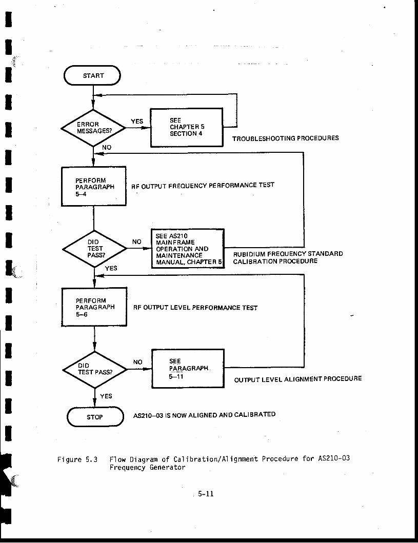
IIl€IIItII
IIIIII
k,
TROU BLESHOOTING PROCEDU RES
RUBI DIUM FREOUENCY STANDARDCALIBRATION PROCEDURE
OUTPUT LEVEL ALIGNMENT PROCEDURE
AS21O-03 IS NOW ALIGNED AND CALIBRATED
F igu re 5 .3 F low D iag ram o f Ca1 ib ra t i on /A l i gnmen t P rocedure fo r AS210-03Frequency Generator
SEECHAPTER 5sEcTloN 4
RF OUTPUT FREOUENCY PERFORMANCE TESTPERFORMPARAGRAPH5*4
SEE AS21OMAINFRAMEOPERATION ANDMAINTENANCEMANUAL, CHAPTER
RF OUTPUT LEVEL PERFORMANCE TESTPERFORMPARAGRAPH5-6
SE-EPAIIAGRAPH '5-11
5- 11
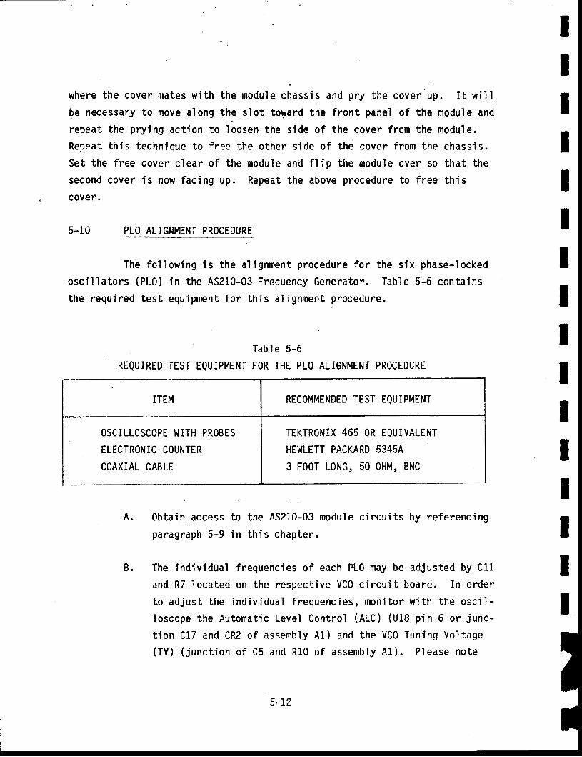
where the cover mates wi th the module chassis and pry the cover up. I t wi l l
be necessary to move al ong the sl of toward the front panel of the modul e and
repeat the prying action to loosen the side of the cover from the module.
Repeat th is technique to f ree the other s ide of the cover f rom the chassis.
Set the f ree cover c lear of the module and f l ip the module over so that the
second cover is now facing up. Repeat the above procedure to free this
cover.
5-10 PLO ALIGNMENT PROCEDURE
The fol lowing is the al ignment procedure for the s ix phase- locked
osci l lators (PLO) in the AS210-03 Frequency Generator. Table 5-6 containsthe required test equipment for th is al ignment procedure.
Table 5-6
REQUIRED TEST EQUIPMENT FOR THE PLO ALIGNMENT PROCEDURE
Obtain access to the AS210-03 module circuits by referencing
paragraph 5-9 in th is chapter.
B. The individual frequencies of each PLO may be adjusted by Cl1
and R7 located on the respect ive VCO circui t board. In order
to ad jus t the ind iv idua l f requenc ies , mon i to r w i th the osc i l -
Ioscope the Automat ic Level Control (ALC) (U18 pin 6 or junc-
t ion C17 and CR2 of assembly A1) and the VCO Tuning Vol tage(TV) ( junc t ion o f C5 and RLO o f assembly A1) . P lease no te
IIIIIIIIIIIIIIII
A.
ITEM RECOMMENDED TEST EQUIPMENT
OSCILLOSCOPE l. l ITH PROBES
ELECTRONIC COUNTER
COAXIAL CABLE
TEKTRoNIX 465 0R EQUIVALENT
HEWLETT PACKARD 5345A
3 FOOT LONG, 50 OHM, BNC
5-12
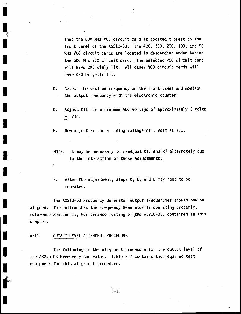
II rI that the 500 MHz VCO circui t card is located closest to the
I front panel of the AS210-03. The 400, 300, 200, 100, and 50
MHz VCO circui t cards are located in descending order behind
r the 500 MHz VCO circui t card-. The selected VCO circui t card
wi l l have CR3 d imly 1 i t . A l l o ther VCO c i rcu i t cards w i l l
r have CR3 br igh t ly 1 i t .
I C. Select the desired frequency on the front panel and monitor
r the output frequency w'ith the electronic counter.
I D. Adjust Cl l for a minimum ALC vol tage of approximately 2 vol ts
+1 VDC.
IE. Now adjust R7 for a tuning vol tage of 1 vol t +1 VDC.
I
a- N0TE: It may be necessary to readiust Cll and R7 alternately due
f to the interaction of these adiustments.
Ir
F. After PLO adjustment, steps C, D, and E may need to be
I repeated.I
I The AS210-03 Frequency Generator output frequencies shoul d now be
I al igned. To conf i rm that the Frequency Generator is operat ing proper ' ly ,
r reference Sect ion I I , Perfonnance Test ing of the AS210-03, contained in th is
I chapter.
I 5-1r ourpur LEvEL ALIGNMENT pRocEDURE!
I The fol lowing is the al ignment procedure for the output level oft the AS210-03 Frequency Generator. Table 5-7 contains the required test
equipment for th is a ' l ignment procedure.
5-13
I$I
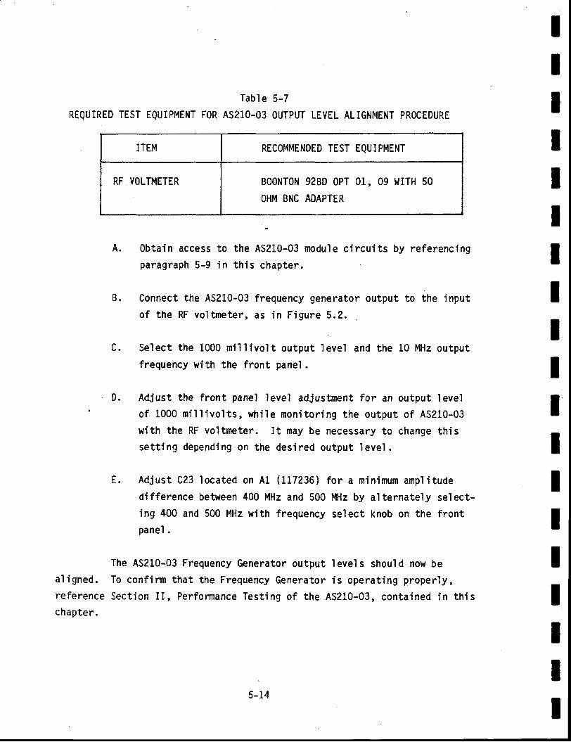
Table 5-7REQUIRED TEST EQUIPMENT FOR AS21O-03 OUTPUT LEVEL ALIGNMENT PROCEDURE
ITEM RECOMMENDED TEST EQUIPMENT
RF VOLTMETER BOONTON 92BD OPT 01, 09 WITH 50
OHM BNC ADAPTER
0btain access to the AS210-03 module c i rcui ts by referencingparagraph 5-9 in th is chapter.
Connect the AS210-03 frequency generator output to the input
of the RF vo' l tmeter, as in Figure 5.2.
C. Select the 1000 mi l l ivol t output level and the 10 MHz outputfrequency with the front panel.
D. Adjust the front panel level adjusfinent for an output levelof 1000 mi l l ivol ts, whi le monitor ing the output of AS210-03with the RF voltmeter. It may be necessary to change thissett ing depending on the desired output Ievel .
E. Adjust C23 located on Al (117236) for a minimum ampl i tudedifference between 400 MHz and 500 MHz by alternately select-ing 400 and 500 MHz with frequency select knob on the frontpanel .
The AS210-03 Frequency Generator output I evel s shoul d now beal igned. To conf i rm that the Frequency Generator is operat ing proper ly,reference Sect ion I I , Perfonnance Test ing of the AS210-03, contained in th ischapter.
5-L4
IIIIIIIIIIIIItIItII
A.
B.
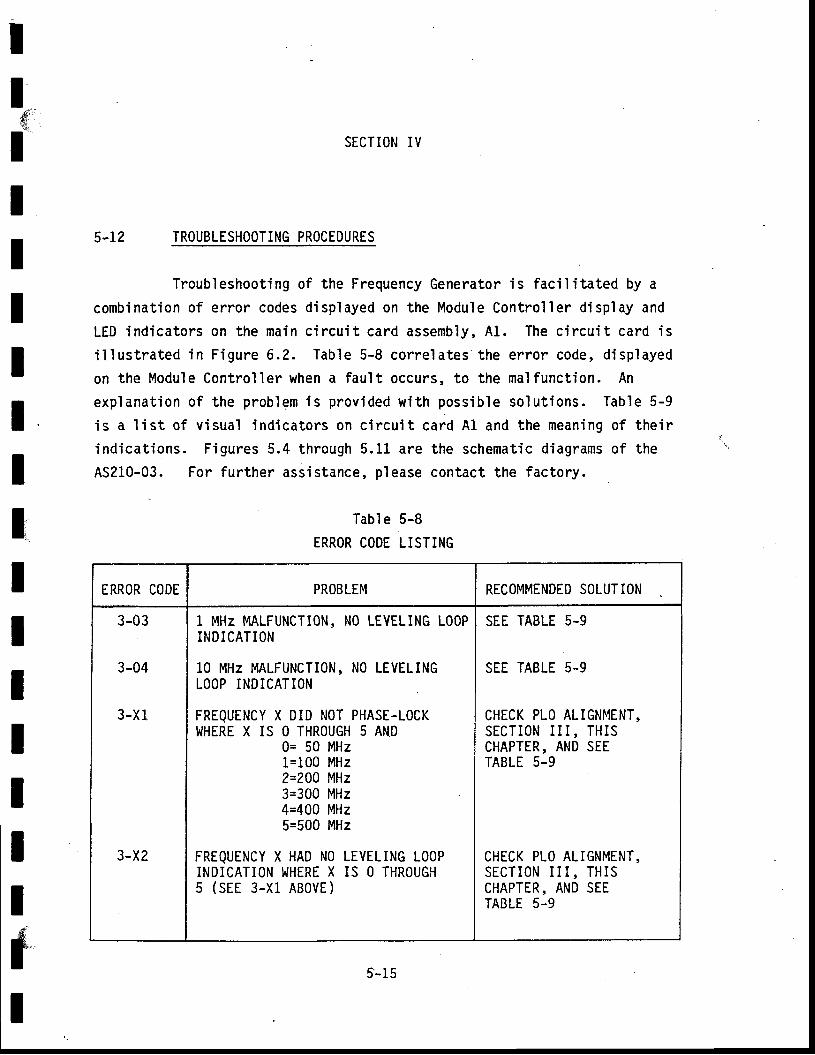
IIf SECTION IV
II
s-rz TROUBLESHOOTING PROCEDURES
Troubleshoot ing of the Frequency Generator is faci l i tated by a
I combinat ion of error codes displayed on the Module Control ler d isplay andI
LED indicators on the main c i rcui t card assembly, A1. The circui t card is
I i l l us t ra ted in F igure 6 .2 . Tab le 5 -8 cor re la tes the er ro r code, d isp layed
- on the Module Control ler when a fau' l t occurs, to the malfunct ion. An
I exp lanat ion o f the prob lem is p rov ided w i th poss ib le so lu t ions . Tab le 5 -9
t is a l is t of v isual ' ind' icators on circui t card AL and the meaning of their i
indicat ions. Figures 5.4 through 5.11 are the schematic diagrams of the
I AS21O-03. For fur ther assistance, please contact the factory.
tII
Table 5-8
ERROR CODE LISTING
IITIt$I
ERROR CODE PROBLEM RECOMMENDED SOLUTION
3-03
3-04
3-X1
3-X2
L MHz MALFUNCTI0N, N0 LEVELING L00PINDICATION
10 MHz MALFUNCTION, N0 LEVELINGLOOP INDICATION
FREQUENCY X DID NoT PHASE-L0CKl,lHERE X IS 0 THROUGH 5 AND
0= 50 MHz1=100 MHz2=200 l4{z3=300 MHz4=400 MHz5=500 MHz
FREQUENCY X HAD NO LEVELING LOOPINDICATION WHERI X IS O THROUGH5 (SEE 3 .X1 ABOVE)
SEETABLE
TABLE
5-9
SEE 5-9
CHECK PLO ALIGNMENT,SECTION I I I , TH ISCHAPTER, AND SEETABLE 5.9
CHECK PLO ALIGNMENT,SECTION I I I , TH ISCHAPTER, AND SEETABLE 5-9
5 -1 5
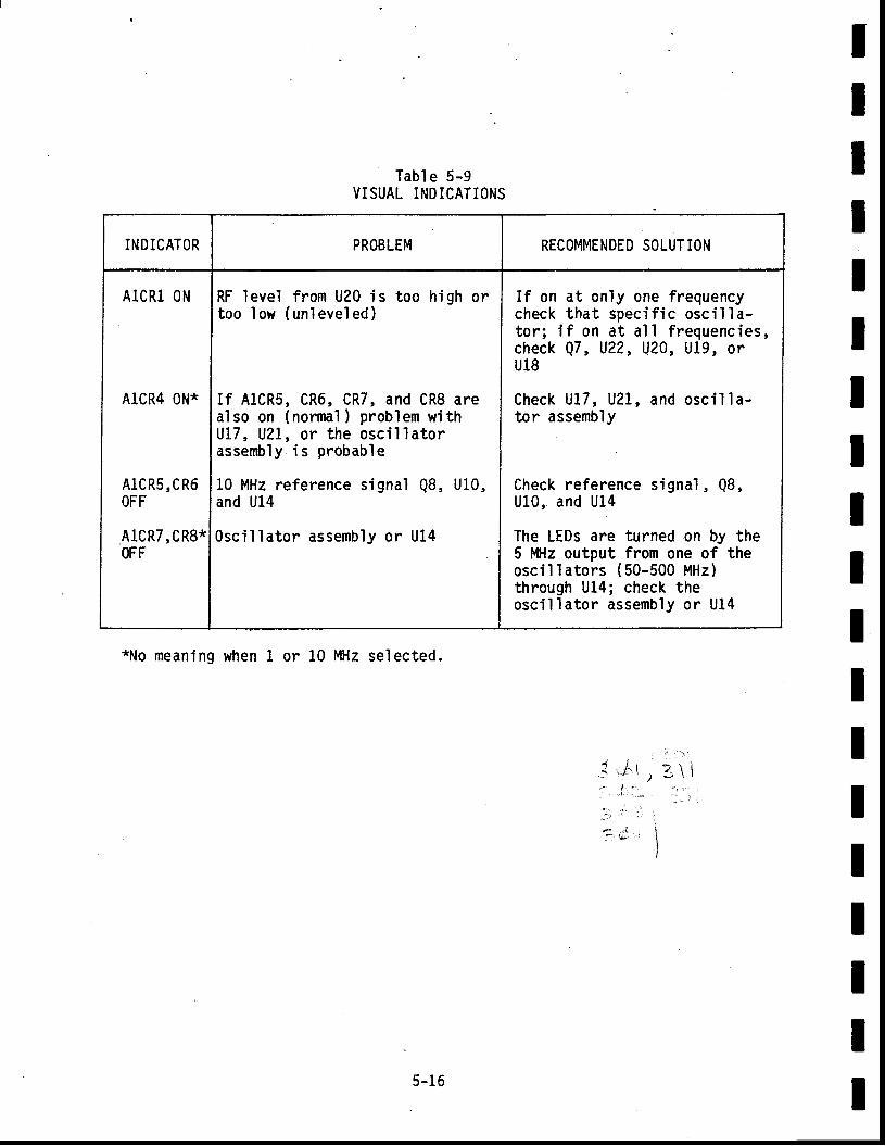
Table 5-9VISUAL INDICATIONS
tIIIIIIItIIIItTtIIt
*No meaning when L or 1.0 MHz selected.
. : ' - / 't . -
i: :
' ' . : " : t
. - ' . . ' ., i
1iII
INDICATOR PROBLEM RECOMMENDED SOLUTION
AlCRl ON
ALcR4 0N*
A1CR5, C R6OFF
AlCR7, CR8*OFF
RFtoo
level f rom U20 isI ow ( unl evel ed )
hi gh or
I f A1CR5, CR6, CR7, and CR8 areal so on ( norma'l ) probl em wi thUL7, U2L, o r the osc i l la to rassembly is probable
10 MHz reference signal Q8, U10,and U14
Osc i l la to r assembly o r U14
If on at only one frequencycheck tha t spec i f i c osc i l la -tor ; i f on at a ' l l f requencies,check Q7, U22, U20, U1.9 , o ru18
Check UL7, U2L, and osci l la-tor assembly
Check reference signal , Q8,U10, and U14
The LEDs are turned on by the5 MHz output from one of theosc i l la to rs (50-500 MHz)through U14; check theosci l lator assembly or U14
5-16
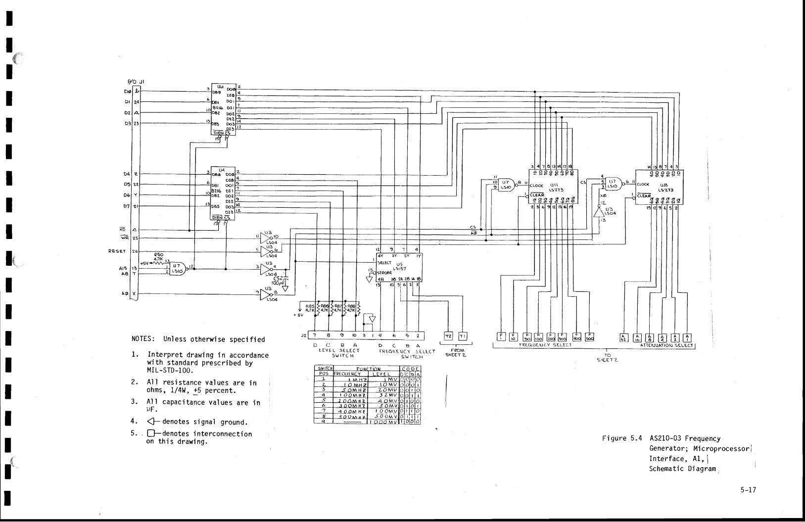
IIl€"
Al5AB
tIIIIIIt
IIIIIIIf
\o: L
. u 3\Ls04i 3
{I
t ;IX.
L^,
IFb
NR,
P E S E T
I
!
AS210-03 FrequencyGenera tor ; M ic roprocessor iIn te r face , A1 , ISchemat ic D iagram
Unless o therw ise spec i f ied
In terpret drawing in accordancewi th s tandard prescr ibed byMI L -STD-1 OO.
A l l r es i s t ance va lues a re i nohms , L /4W,15 pe rcen t . iA l l capac i tance va lues a re i n
8 9 t o 3 1 4 6 b 2
D C B AL T V E L 5 E L t C T
5\, / l rc H
D C B AF R T O I I L I J C Y 5 L L L C T
E\.i ITCH
L-----r-----J
FEOMSHEET ?-
FREG-UEi ' ICY sELEC1
1.
? .
3 .
TOS.raET Z
uF.4. ( - denotes s i gnal ground.
5 . . fFdeno tes i n te rconnec t i onon th i s d raw ing .
ATTEI\IUATIOIO SLLECT
9VJ lTCt F I I N T T l . ) NP O q R f O I I E N ' Y F V F
2 N |rJ.H.7 I O M V5 S O M H Z L O M V ) l I4 I o o m H ? 3 Z M V I5
6 A N O M H ? 5 O M VUri
4 O O-M.!l16 n ( ) r ^ u :
I O O M Vi D 0 m v
t l ld t
-iaal otD
F igure 5 .4
5-17

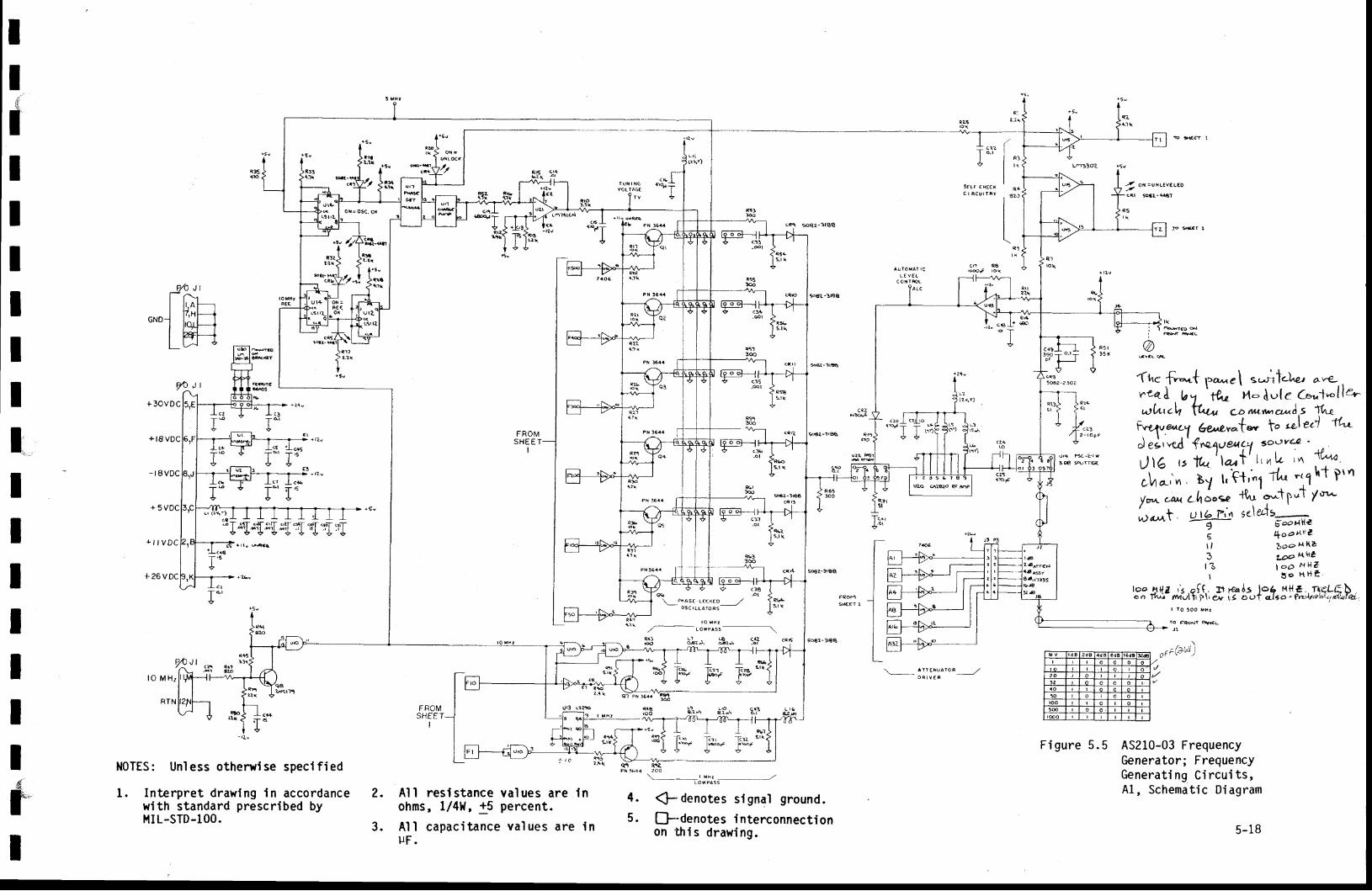
T
e/o 'trl- r-'--'l l l , A f _ _ rI |7.HL----JGND-1 I,qHI PtrHL- L'--t e
+ t8 vDc
- t 8 v D c
+ 5 V o C
I
II€
IIIIIIIt.IIITIII$I
*T:7l o . r II l F
" l tsrrr cxecx
I c
c t R c u r T R Y 8 ?f
o r =ur rev : r to
cit 5o8z- 44e1
A U T O T A T I C
L € V E LC O N I r c L
c
<20_ l .
I
A I I E N U A T O F '
o R t v € R
I T O 5 O o N H t
ro FrcNr 9!€L
c R z
_Q^(t^," {,-^t 1>auc\ .-'tt t"- ^vs.,vea I bz
' , t t^" H- lul e (c'J*l ler
wLttc\ tt4- cb tv4tuncr*tA.s theY't4r.euq 6a,eroln )o taled 1t'r
Jes,"ed ' {*pte-ut ' i sa lv&e ' ,^t t ' l ' , 1 ' 14 1u 'q
J\6 t t 1L4 laa
It I-',,. .j kfl,"1 il ":1hl Ptnr/v* ca choo* *tnr 1^1P"T Y'r'^
,la,tt U 16 Plr se\edS---4- foot"{tt..
s 4ocPAt&l l 3oo r ' l t }
3 r ^ e * H tl i l o 6 N t 1 7r 5 o H H * '
'3f "1s "ffr?,$r: -l r F, l?f, j y F*d,:,"qr "F*,
3 € stur.r€R
-l--I
: I I l 1 I 1 I . L l 1'"T;TJ,T.5lt[:Tf Tf ,gT rT :rTe 9 9 9 9 + S g C
T(.
ll
I
lL-
s€€T t
Ql Pr l€ .a
(*r5
I
N0TES: Unless otherr lse specl f ied
l . Interpret drawlng in accordancewith standard prescribed byHIL-STD-100.
Al l reslstance values are inohms, l /4U, +5 percent.
A l l capac i tance va lues are inuF .
L--_Tlfl^.,{-- ,,-/
4. (- denotes s ignal ground.
5. [--denotes interconnectionon 'th I s drawi ng.
2.
3.
Figure 5.5 AS210-03 FrequencyGenerator; FrequencyGenera t ing C i rcu i ts ,A1, Schematic Diagram
(5
€3
\ p N A s E - L m x E D , / f R s 4- ' o s c r L e a t o n s . - | a l k
l o M x t
,/ LowPAss -----\
:3 b1..,. P... -cL? "f
3oo
16-6-6|.----.r L*t--
5-18

IIIIIIIIIIIIIIIIIII
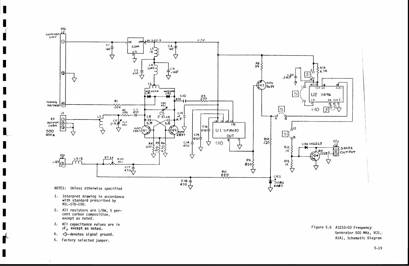
c'.l u.
RrzIK
Rf3tx
C 1410
II
{
IIIIIIIt,IIIIIII
s{rTcHeot l o v
R FoulPUrOdEl^
500MH=
r-''lt l
?o! I'TLV
t ' tI 1
tr(I '
R2/@
tr +lo tr
Mh72851 tri
u : t t R'7 ZX
S M H Zour Put
AS210-03 Frequency,Generator 500 MHz, VC0, iAlAl , Schematic Diagram
E I A SA O J
Jr.,",c R 3
4 1 A 1NOTES: Un less o therw ise spec i f ied
1. Interpret drawing in accordancewith standard prescr ibed byMI L.STD-1 OO.
2 . A l l res is to rs a re 1 /8W, 5 per -cent carbon compos i t ion ,except as noted.
3 . A l l capac i tance va lues are inpFr except as noted.
4. $denotes s ignal ground.5. Factory selected jumper.f
I
NNE lO t t lff/.r lrc R t c q L
C L R Q O C L K I
UZ 7 4tsbLo q l ccx i
c9,4 \NCZL3
F igu re 5 .6
5-1 9

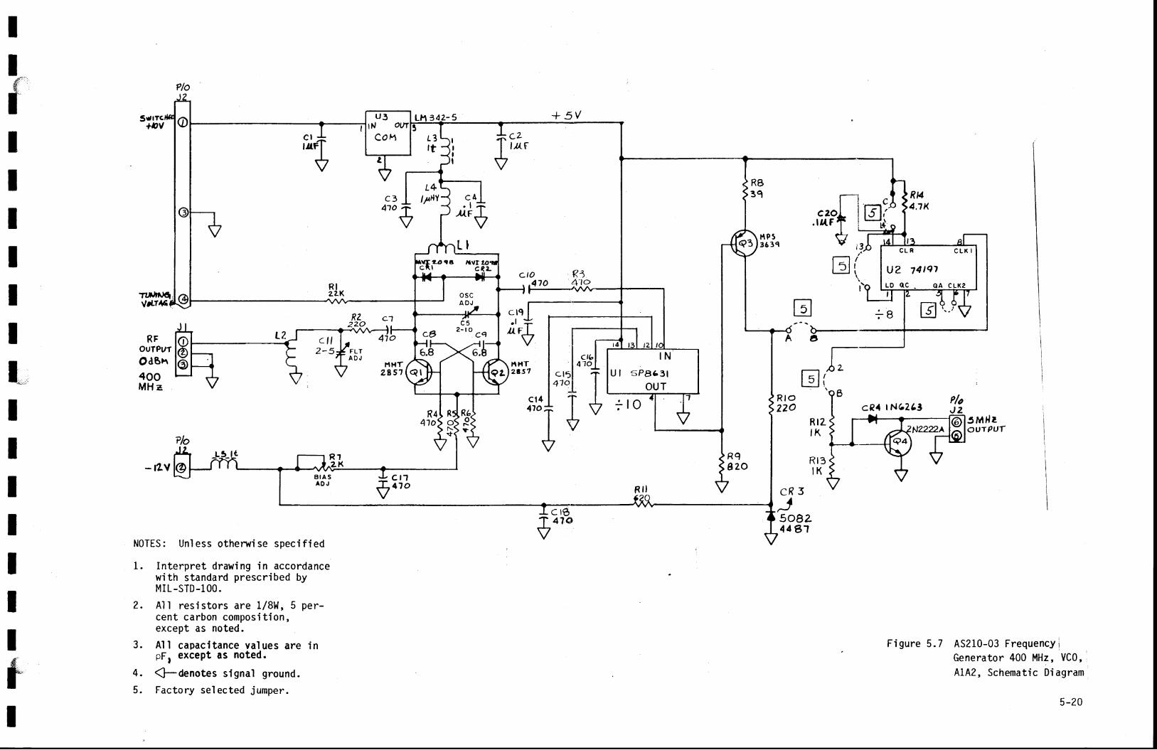
R83q
F L TA D J
rlo
II{'€,".
lIIIIIItIIIIIII#
fI
+5v
trJRtl4.1K
n 0 53 6 3 q r ?
It
ITuJnqVrailc
RTOUTPUT
OdBn400MHz
-av
NOTES: Unless otheni l ise speci f ied
1. Interpret drawing in accordancewith standard prescr ibed byMIL-STD-100.
?. Al l resistors are 1/81l l , 5 per-cent carbon composi t ion,except as noted.
3 . A l l capac i tance va lues are inpFf excePt as noted.
4. Gaenotes s ignal ground.
5. Factory selected jumper.
R220
tr
I.IHT2857 s,F
RrzIK
Rr3IK
R l o? 2 0
CR31
5o^824481
AS210-03 Frequency iGenerator 400 MHz, VCO,ALA?, Schematic Diagram
c to R i
: : c l ' l
v470
C L R C L X I
U? 74 tc7
cR4 1N6243
F igure 5 .7
5-20

IIItIIIIIIIIIIIIIIt
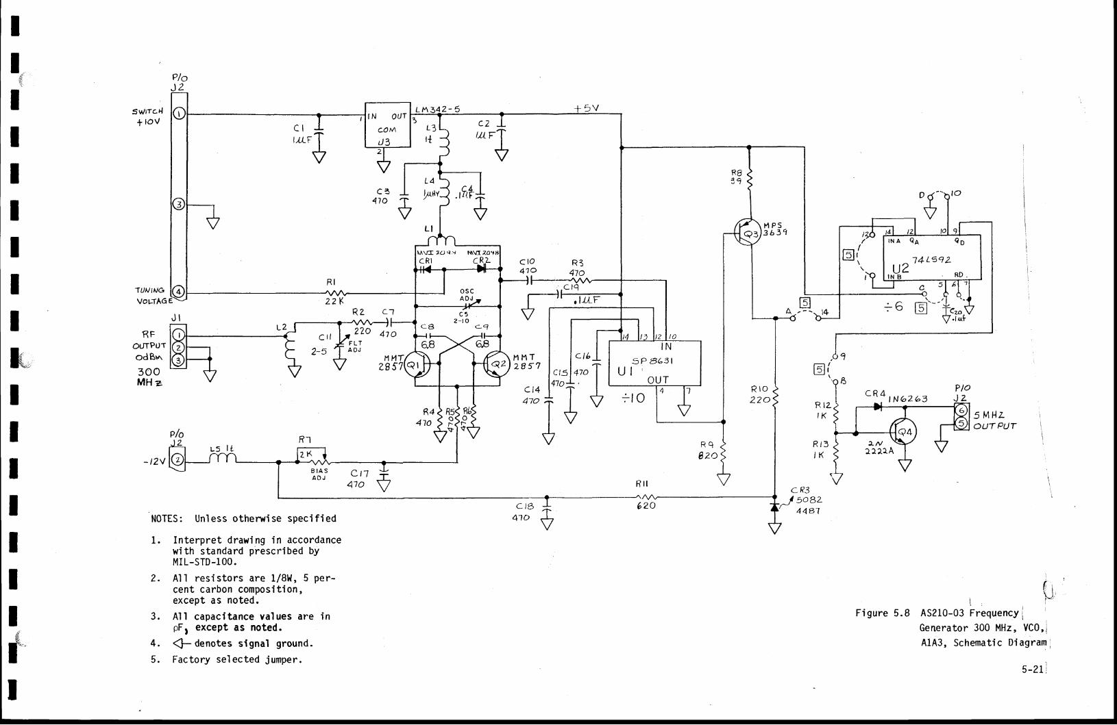
IIIIIIIII
IIItIII
P/o2
M P 53 6 3 q
c l o4 1 0
lUN ING
VoLTA6
R FOTJTPUTodBn
30oMHz
2 2 K
220c t l
2-sr L I
A O JNHT
zB 5?lf l 1 1 T28s7
c t4470
l c rb I
f;:l"I.+vR6o '
F - ,$s
5 MHLOUT PUT
l ,Figure 5.8 AS210-03 Frequency
ploRI
u : l f- tzv
E t A SA D J
N0TES: Unless othernise speci f ied
Interpret drawing in accordancewith standard prescr ibed byMI L-STD-100.
Al l resistors are 1/81{, 5 per-cent carbon composi t ion,except as noted.
Al l capaci tance values are inpFt except as noted.
$ denotes signal ground.
Factory sel ected jumper.
h , a V
w t l
41o V C R 3./l soaz'
4 4 4 1
2.
3 .
4 .
5 .
Generator 300 MHz, VCO,iAlA3, Schematic Diagram ;
t N A Q n Q s
)J214zoqB N$tt20
c R 4 | N 6 2 6 3
Z Nr.1e1A
f5-21i
r .t i It i .

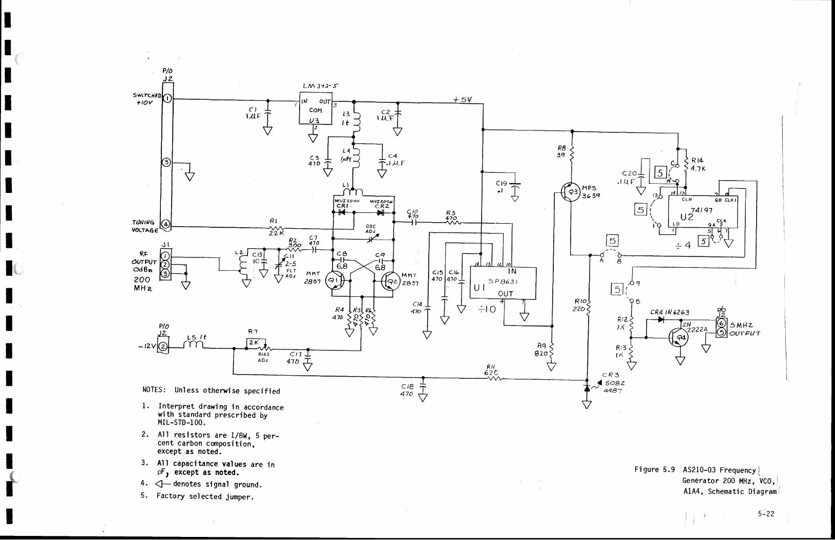
P/oJZ
L/!^ 3.i2-. '
C 2 0 L- , / T \
/_ttr |Y
cR4 tN 6263
R 1 44 . 1 K
222A
AS210-03 Frequency IGenerator 200 MHz, VC0,1A1A4, Schematic Diagram i
tri. l
| 1P5363q
rd^r,rqVOLTAo€
RFOUTPUTodBrr
20o^MHz
2 2 R
Pto
L 5 , t
N0TES: Unless otherwise speci f ied
1. Interpret drawing in accordancewith standard prescr ibed byMI L.STD-1 OO.
2. Al I resistors are L/8H, 5 per-cent carbon composi t ion,except as noted.
3. Al l capaci tance values are inpF t except as noted.
4. { - denotes s ignal ground.5. Factory selected jumper.
r:rL] 4
5l-Ilrllj
li
Rr3tK
R5B:$ ,
R4470
R'7
IIItIIIftI
trlrl< . tL
l t <
c R 3
J soaz'
448- i
i vIL0qt' MVr,aagAc R l . c R z .
C L R Q B C L K I
14t 91| 2
, - o " -
" o t a t *
Rt
t l
F igure 5 .9
5-22

IIIItIItIIIIIIIItII
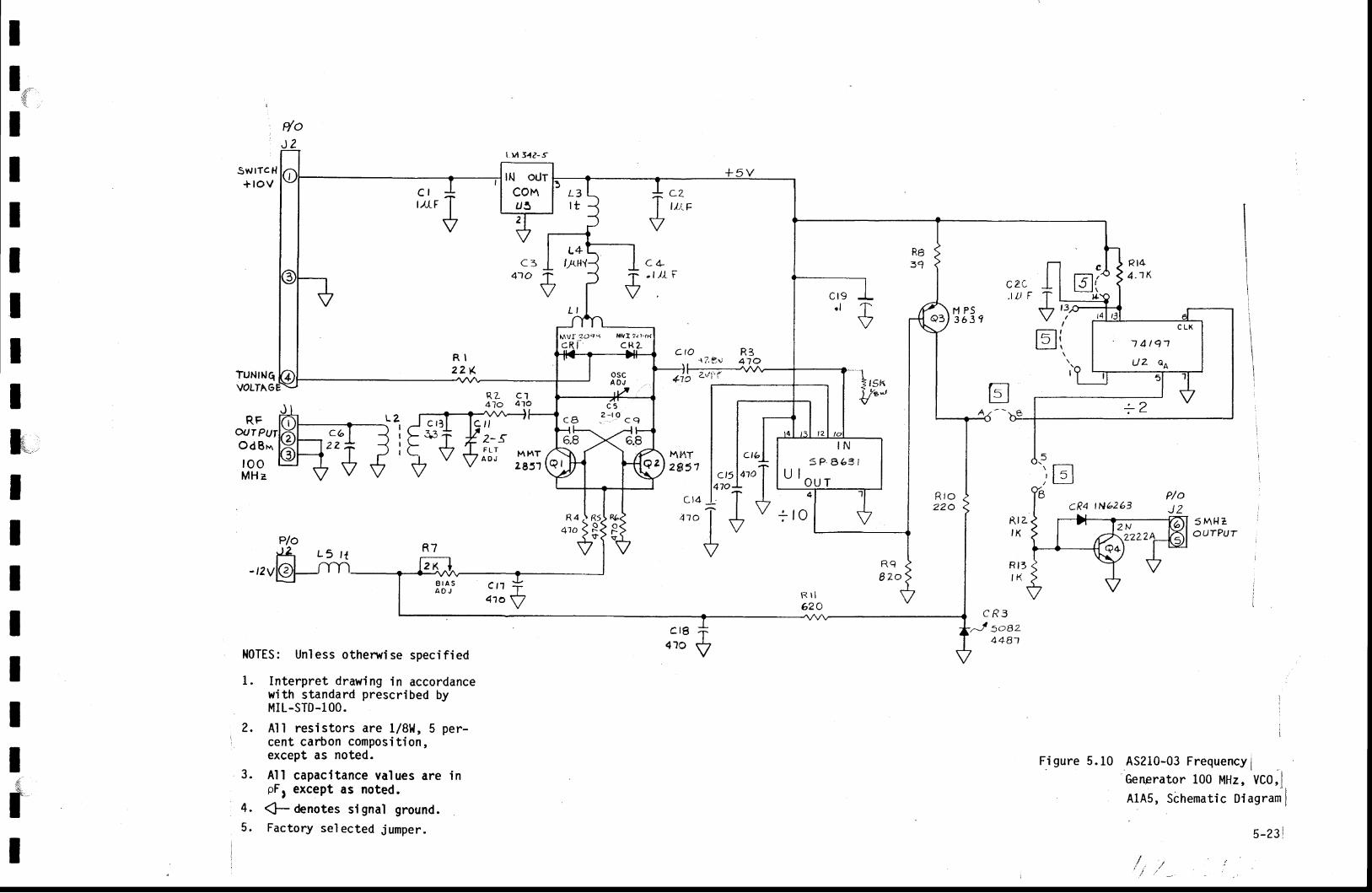
Il{,I
M P S3 6 3 1
9,L c'l41o 4]o
IIIIII
PloJ 2
R7
IIIIIIIfI
R t 44 . 1 K
czf - I. taF T
V
TuNtNqVOLIAG
RP'OUT PIJO d B n
rooMHz
Ec t t
2-Sf;j M)4r
285'r
R l zI X
R t 3l K
2 N 5 M H ZOUTPIJT
PloL 5 , 7
cR3.J loaz
4481
NOTES: Unless otherrv ise speci f ied
1. Interpret drawing in accordancewith standard prescribed byMIL-STD.1OO.
2. A'l l resistors are 1/81,{, 5 per-cent carton composi t ion,except as noted.
3. Al l capacl tance values are inpF, except as noted.
4. (- Oenotes sl gnal ground.5. Factory selected jumper.
cr *ttIF I
V
c t o R 3- t 7 . t r ; 41O
4ib z'/rr
crr f41o V
f zoq s loVI ?r ) 'rXC L K
1 4 t q 1
Uz ea
tri
)trcR4 tN6263
2222
/,, ,t
i
i
AS210-03 Frequency IGenprator 100 MHz, VCO,l ,A1A5, SLhematic Dlagram I
F igure 5 .10
5-23

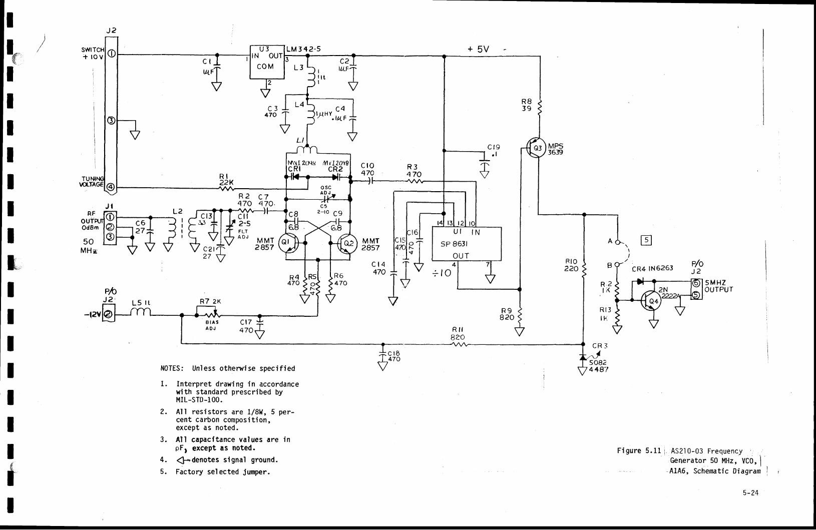
t^u zoqc MvI20,t0cRr cR2
UI IN
sP 8631
OUT
,,'TV
Il l tI
+c l7470
)
kIIIIIIIHIIIIIIIfI
LM 3 .12 -5 +5V
MPS3639
R3470
R2470
c l l2-5FLTA O J
c7470 ,
RFOUTOdBm
50M H g
MMT2857
MMT2857
c t4470
R.2IK
sMHZOUTPUT
Figure 5 .11 i . AS210-03 Frequency,Generator 50 MHz, VCO, IAlA6, Schematic Diagram
L5 l t R7 2K
B I A SA O J
N0TES: Unless othenr ise speci f ied
1. Interpret drawing in accordancewith standard prescr ibed byMIL-STD-100.
2. Al l resistors are 1/8b{, 5 per-cent carbon composi t ion,except as noted.
3. Al l capacl tance values are inpF, except as noted.
4. 4!-r 'denotes slgnal ground.
5. Factory selected jumper.
R9820
Rt3I |r.
CR i l
R f f8ZO
| 47017 soSa
448' l
5-24

IIIIIIIIIIIItIIIIII
Il*I
6-1
ItIItIIIItIIIIII
CHAPTER 6
ILLUSTRATED PARTS LIST
TNTRODUCTION
This chapter contains an i l lustrated parts l is t for the AS210-03
Frequency Generator Module. The assembly numbers and assembly tit le are
l isted at the top of the parts l is ts. The parts l is ts are div ided into f ive
columns and arranged in the fo l lowing order:
Co lumn l - I temNumber
Column 2 -
Column 3 -
Column 4 -
Quanti ty
Quant i ty per assembly.
Manufacturer's Part Number
Please disregard t f re f i rst two digi ts before the dash
when referencing these part number.
Descr ipt i on
A br ief descr ipt ion of the i tem.
Column 5 - Reference Designation and Remarks
The electr ical or e lectronic designat ion of the i tem as
shown on the schematic diagram, wir ing diagram or
interconnect diagram, and the Federal Supp' ly Code for
manu r'. lcturers .
6-1
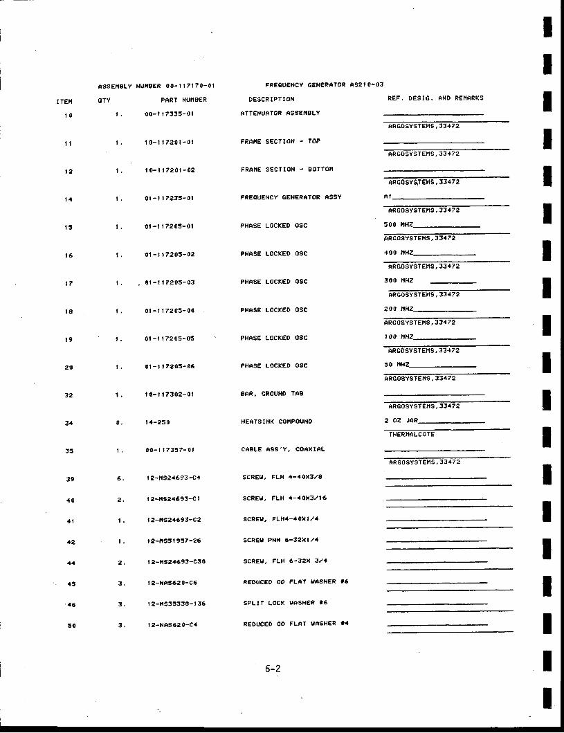
35
39
{ 0
a l
12
11
{3
a6
5 0
f issEnBLY l lu l tgER 00- | | 7t 70-01
OTY PAPT NUI'IB€R
t , 00 - l r 7335 -01
t 0 - l r 7 2 0 1 - 0 t
r o - l r 7 2 0 r - 0 2
0 r - l r 7 2 3 5 - 0 ,
0 l - t t 7205 -01
0 1 - r r 7 2 0 3 - 0 2
0 t - t t 7 2 0 5 - 0 3
0 l - t 1 7 2 0 5 - 0 . 1
0 1 - r t 7 2 0 5 - 0 5
0 t - t t 7 2 0 5 - 0 6
t 0 - r t 7 3 0 2 - 0 1
l . t -250
0 0 - r r 7 3 5 7 - 0 1
t 2-l{s2,{693-C4
r 2-11324593-C I
| 2-fiSz4693-C2
t 2-FS5 | 957-26
t 2-t{S2.1693-C30
| 2-NrS62 0-C6
r 2-fis3533e- t 36
| 2-HnS620-Ca
FREOUENCY GEHEPATOR AS2I O-03
t }E3CPIPT ION
ATTEHUATOR A99EI'BLY
FRHlrE SECTIOf{ - 70P
FRAr' r€ sEeTtoN - SoTTol t
FRESUENCY GEN€RRTOR ASS?
PHASE LOCXED OSC
PHASE LOCKED OSC
PHASE LOCXED OSC
PHASE LOCKED OSC
PHASE LOCK€O OSC
PHASE LOCKED OSC
BAR, GROUND TAB
HEATSI}IK COITPOUNO
CAALE ASS 'Y , COAXIAL
scREu, FLH 4-40X3/8
scREu , FLH 4 -40X3 /16
scRE[f , FLH4-1AXl/1
SCREII PHH 6-32111/1
scREu, FLH 6-32X 321
REOUCEO OO FLAT UESfiER T6
SPLIT LOCX UASHER 16
REOUCED OO FLAT UNSHER 14
REF. D€SIG. Nf iD REi lNRKS
AFGOSYSTEI'lS , 33472
ARGOSY'STEt'rS , 33472
ARc0gYsJEt't5, 33472
eRGOSvSTEt ' rS; 33472
s00
AFCOSvSTEftS, 33472
400 ltHz_
ARgOSYSTEI'tS, 33472
300 l'lHz
ARCOSYSIEr ' ls , 33472
20o nH?-.
ARGOSYSTET{S, 33472
t 00 lrHz
ARCoSYSTEnS, 33472
30 ttl{
ARGOSYgTE|S , 33472
ARGoSYSTET'lS , 33472
2 0z JAR_
THEFI,IALC''E
ARG0SYST€r ' rS , 33472
IIIIIIIIIITIIIIIIII
A '
6-2
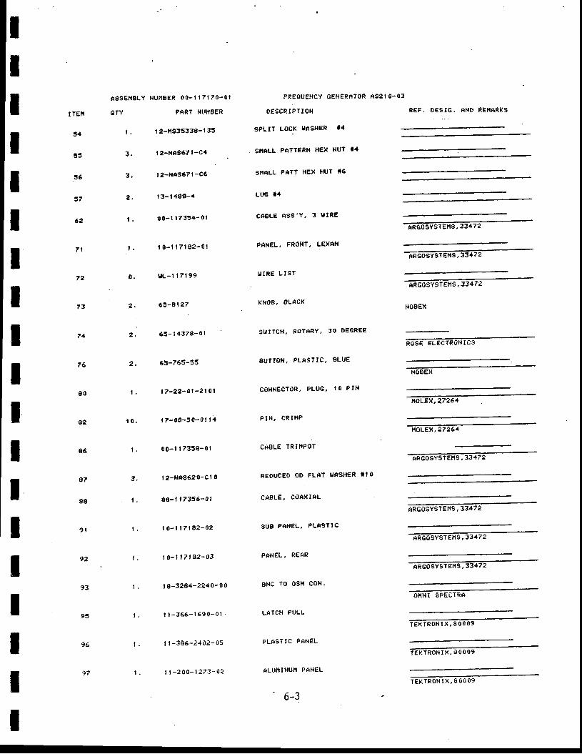
IIIIIIIIIItIIttIItI
I T€N
!4
56
37
62
7 l
72
7 3
71
76
8 0
a?
86
0rY
AssEf.rgLY NU|IBER 00- | I 7 l 70-01 F R E O U E N C Y G E N S R A T O R A S 2 I O . 0 3
3 ,
{
g7
8A
l .
3 .
3 .
2 .
1 .
t .
0 ,
? .
2 ,
2 ,
L
1 0 .
t .
L
t .
PART IIUI'I8ER
I 2-HS35338-t 35
1 2-NAS67 | -e4
| 2-f{ts6? | -C6
t 3- t 488-4
00 - l 173 !4 -01
1 0 - l l 7 l s 2 - 0 1
u L - l 1 7 1 9 9
53 -8 | e7
6 ! - t 4376 -O t
65-765-55
t?-22-01 -21 0l
l ? -08 -5A -O t t 4
00 - l t 7358 -01
r2- l les620-ct 0
00 - l t 7356 -01
l 0 - l l 7 l 9 2 - 0 2
t 0 - l t ? t 9 2 - 0 3
r 8-3284-2240-00
' r t - 366 - t 690 -01
| | - 386 -2402 -05
| | - 2 00 - | 273 - 02
D E S C P I P T I O I I
SPLTT LOCI( I||ASHER 14
SNTLL PATTERN HEX HUT I.T
SI.IALL PATT HEX NUT 16
LUG T4
C A E L € A S s ' , Y , 3 U I R E
PANEL, FROT{T, LEXNfl
U I R E L I S T
KNOB, BLAC(
STI I1CH, ROTARY, 30 DEGREE
BUTTO'I , PLASTIC,
CONN€CTOR, PLUC,
PIH, CRII ' 'P
CABLE TRII ' IPOT
REOUCEO OD FLAT
L'rrBLE. COAXIAL
BLUE
I O P I H
UASHER I I O
SUE PAHEL, PLASTTC
P'IHEL, REAR
B|tc TO osn coH.
LATCH PULL
PLAST IC PANEL
ALUI'IINU}t PANEL
' 6-3
R€F . DES IG , AND RE I IARKS
-ffi
ffi
ffi
HBBEX
F O S E E L E C T R O N I C S
--R"d6'tr9ffi'sls3a?2
ffivsrexs. :s+za
ffi
T E r ( T R 0 N t x , 8 0 0 0 9
T E N T R O N I X , S O O 0 9
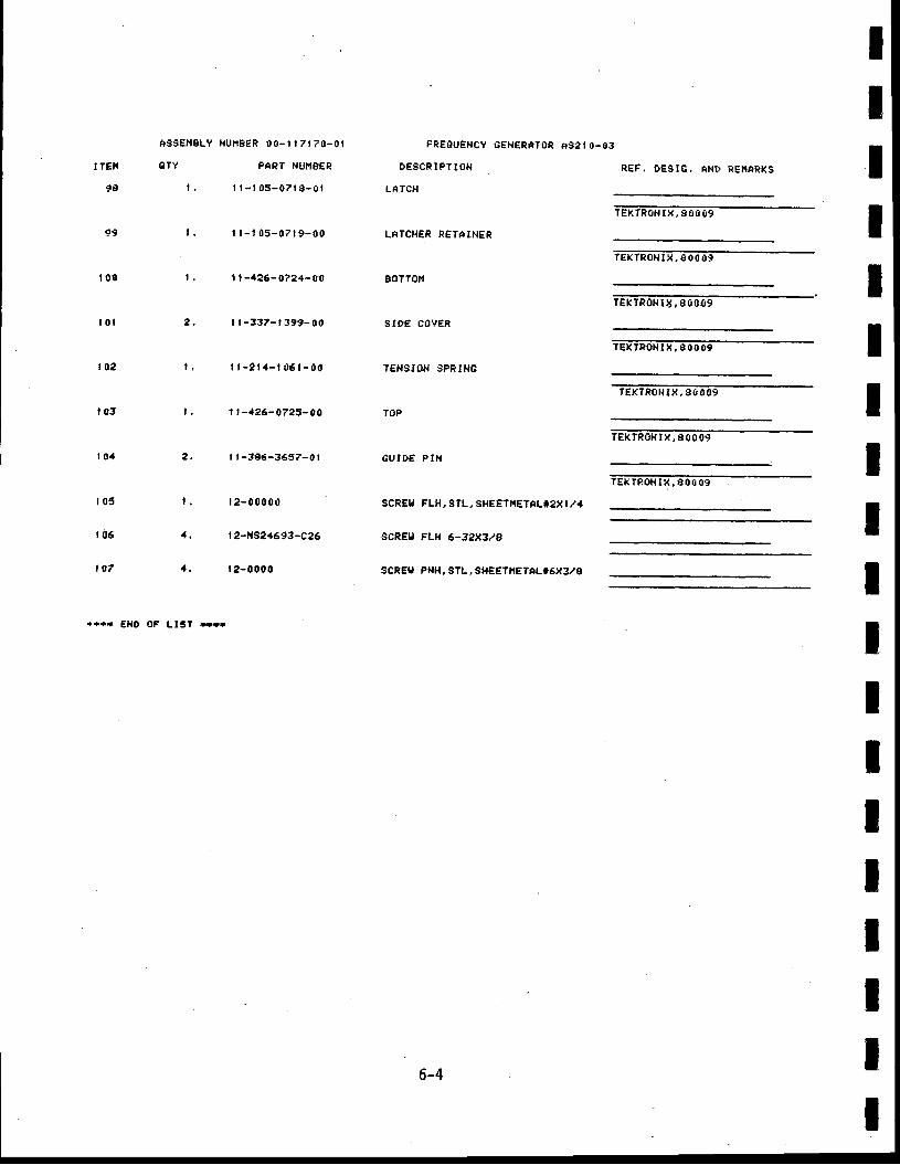
I TE'{
9A
99
1 0 0
| 0 l
t 0 2
, 0 3
l 0 1
t 0 5
r 0 6
t 0 7
ASSEI.TgLY HUIiBER 00- l | 7t 70-01
ATY PART NI-I}ISER
l , t t - t 0 5 - 0 7 t e - 0 1
r . I l - t 0 5 - 0 7 1 9 - 0 0
1 | -426- 072{- 00
| | -337-r 399-00
I t - 2 1 4 - t 0 6 t - 0 0
1 ' -126-0723-AO
r l - Ja6 -3557 -01
| 2 - 0 0 0 0 0
| 2-1ts2.1693-C26
l 2 - 0 0 0 0
FREOUENCY GENERATOR AS2 IO-03
DESCR IPT TON
LATCH
LATCHSR RETAINER
BOTTOII
stDE cov€R
T€NSI0lr SPRIIIC
TOP
GUIDE P IN
SCREU FLH, STL, SHEETI{E'CLI2XI /4
scREB FLH 6-32X3/8
SCREU PNH, STL, SH€ETil€TELI6X3/8
REF. DESIC, AND REI 'ARKS
TEXTRONIX , SOOOg
TEXIRONIX ,80009
TEKIR0HIg , S0009
TEXTRONlX ,80009
TEKTRONIX ,SOO09
T€ I (TROH IX ,8O O 09
TEXTROH I X, 8 00 09
tIItItIItItIItIIIII
*i ir El.lo oF LIST m*
6-4
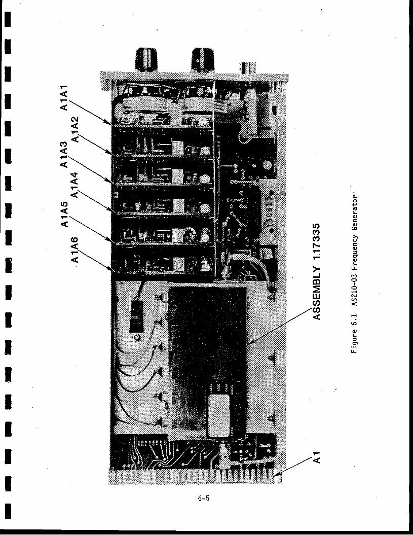
l-o
P.uLoE(u(t
(Jcq,=(toL
LL
(f)
oI
o(\lv1
F.l
(o
Q)L5qt
tL
roC')g)Fl-
JmIJJaU)
iit6+,ir
[ir,sry,.tBi;ii'lisis
ol
F.
$
r.
(oF
F
a)f
lo
ItIIttItIIIIIIIIItI
;i-fl1:j.,- i.i
6-5
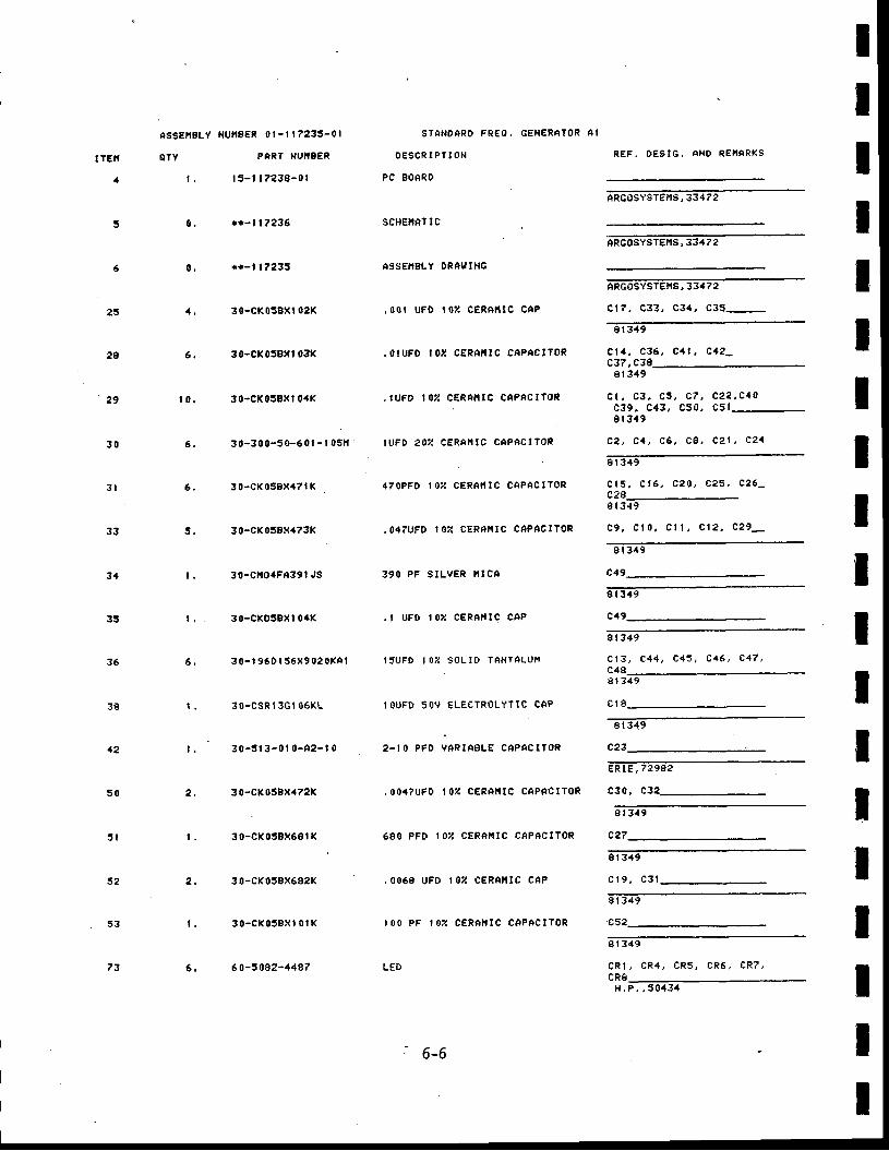
t TEII
1
q
6
25
2e
' 2 9
3 0
3 l
33
3+
35
36
3B
12
5 0
5 l
5 2
53
73
ASSETiBLY f lU| '8ER 0l- l | 7235-01
ATY PART XUITBER
r . l 5 - l 1 7 2 3 8 - 0 1
* i - t | 7236
*i - f | 7235
30-cK05BXr 02K
30-cK05g,lf 031(
30-c,(058x1 0{K
30 -300 -50 -60 t - l 0s t l
3 0-cK 058X.r7 | K
30-cK058X473K
3o-CnO.+Fn39l JS
3o-cKospxl 04K
3 0- t 960 | 56X9 02 oXA t
30-csRt 3Gr 06KL
30 -313 -01 0 -42 - l 0
30-CK05Bxr l72X
3 0 - c K 0 5 B X 6 6 l l ( .
3 0-cK 058X682K
3o -cK0J8X l 0 tK
60-30a2-148?
S T A N O A R O F R € O ,
O E S C R I P T I O N
PC EOARD
scHEl'tAT I C
ASSEI.IBLY DRAUITIG
GEHERATOR A I
. 00 t UFO I 0Z C€RAt t lC CeP
,O tUFO IOZ CSRAI I IC CAPACITOR
. lUFD r 0Z C€RAr . r lC CaPACr foR
IUFD zO'E CERAI,IIC CAPACITOR
47OPFO l OZ CERAI ' ITC CAPACITOR
.04?UFD IOZ CERA} ' IC CAPACITOR
390 PF S ILVER I , I ICA
. t UFD I OZ CERAII IC CAP
IsUFD IOZ SOL ID TANTALU ' '
IOUFD 5OV ELECTROLYT IC CEP
2- I O PFD VARIASLE ,CAPECTYOR
,0069 UFD r0z cERnf i Ic cAP
I O O P F I O Z C E R A I ' I C C A P A C I T O R
L E D
R € F . D E S I C . A N D P E } I A R K S
IIIIIIItITIIIIIIIII
e 7 ,c5 0 ,
c 8 ,
f ,RG0SYSTET1S, 33472
ARG0SYSTEI ' lS, 334?2
ARC0SYSTET'tS, 33472
c t7 , c33 , c34 , C35_
8 r 3 4 9
Cl , t , C36, C{ l , C . lz -c37, C38.
8 r 3,19
c l , c 3 , c 5 ,c39, C43,8 t 3 a 9
c 2 , c 4 , c 6 ,
c 2 2 , C 4 0c 5 l -
cz't , c24
8 t 3 4 9
c t 5 , c t 6 , c 2 0 , c 2 5 , C 2 6 -c28--8 t 3 4 9
c 9 , c t 0 , c r t , c 1 2 , c 2 9 _
8 t 349
c49
8 | 3.19
c49
8 r 3 4 9
c r 3 , c 4 4 / C 4 s , C 4 6 , C 4 7 ,c488 t 3 4 9
c 1 8
B r349
c23
E R 1 E , 7 2 9 8 2
.004?uF0 r03 cERAn Ic CAP iC IToR C30 ,
8 t 3 4 9
680 PFD I OZ CERANIC CEPECITOR c2?
8 r 3 4 9
c 1 9 , C 3 l
8 t 3 4 9
913 . t 9
c R t , c R 4 , C R s , C R 6 , C R Z ,cRg
6-6
H , P , , 5 0 4 3 4
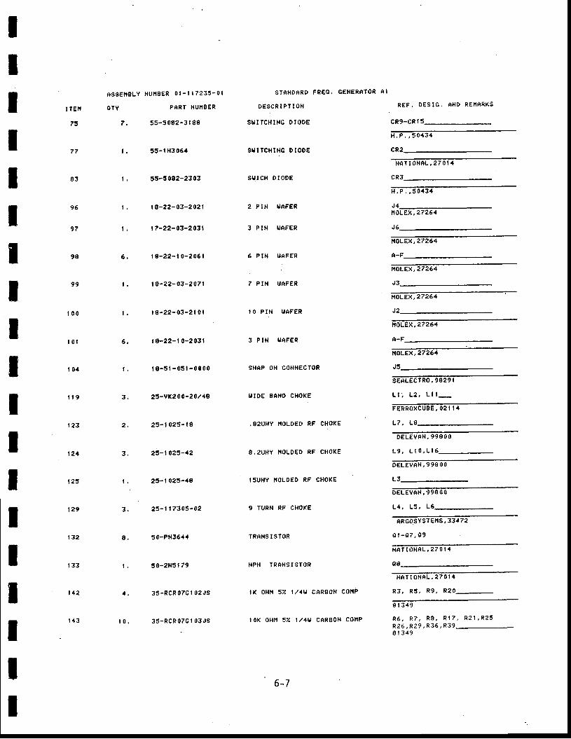
It
A S S E T { 8 L Y H U I ' I B E R O I - I I ? 2 3 5 - O I S T A N D A R D F R E O ' G E N E R ' T T D R A I
I
I r rEn orY PART HUl lgER D€scRrPTIoH
?s 7 , 55 -5082 -3188 S I ' I I TCHINC 0 I0DE
ItIIIIf | 04 | , lE -51 -051 -0000 SNAP oH C0 r l l lEcToR
R E F . D E S I G , A H D R E } I A R K S
cR9-CR I
H . P , , 5 0 4 3 4
? 7 l . 5 5 - 1 N 3 0 6 4 9 U I T C H I H G D I O O E
83 l , 55 -5082 -2303 S I ' ICH D IoDE
96 r . 18 -22 -03 -2021 2 P IN L IAFER
9? t , t7-22-03-2031 3 PIN LIAFER
9 8 6 , 1 8 - 2 2 - 1 0 - 2 0 6 1 6 P I N L I A F E R
99 r . ta-22-03-207 I 7 PIN I 'AF€R
r 0 0 r , t 8 - 2 ? - 0 3 - 2 1 0 1 l 0 P I N T A F E R
| 0 r 6 . l € -22 - l 0 -2031 3 P IN ITAFER
N A T T O N A L , E T O I 4
eR3
H . P , , 5 0 . t 3 4
l '10L8X,27264
J 6
r.r0LEx, 27254
A - F
r ' r0LEX, 27264
J3
noLEJl,27264
l,toLEX, 2726.1
J5
SErlLEcTRo, 9829 I
f l 9 3 , 23 -VK2 IO-20 /49 u tD€ EAND CHOKE L l : L2 ' L l l -
FERROXCUBE, O2 I I 4IItItlt
f 2 3 2 , 2 5 - l 0 2 5 - 1 8
t21 3. 25-1023-12
t25 | , 2r-1023-t .e
t32 8. 50-Pt{364{
| 33 r . 50-2t{5t 79
ARC0SYSTET4S, 33472
0 | - 8 7 , 0 9TRA} IS ISTOR
N P N T R A N S I S T O R
.82UH? I ' IOLOED RF CHOKE
8,zUHY I ' IOLDED RF CHOKE
tsUHY I . IOLDED RF CHOKE
DELEVAN,998OO
L 9 , L t o , L l 6
L 7 , L
DELEVAN, 998 O O
DELEVAN,998OO
129 3 . 25 -117305 -02 9 TURN RF CHOXE L r l , Ls ' L6 -
H A T I O N A L , 2 T O I 4
o8
N A T I O N A L , 2 T O I 4
1 4 2 1 , 3 5 - R C R O 7 G 1 0 2 J S l K o H r 5 z t / 4 u c A R g ' N c . l l p R 3 , R 5 , R 9 , R 2 0 -
8 t 3 4 9
1 4 3 | 0 . 3 5 - R c R 0 7 c 1 0 3 J s t 0 K o H l ' l 3 z t / 4 t t c A R B o N c D t ' l P R 6 , R 7 , R 8 ' R l ? ' R 2 l ' R 2 5R 2 5 , R 2 9 , R 3 6 , R 3 9 -8 1 3 4 9
I 6-7
I
J2-
i loLEX, 27254
A-F
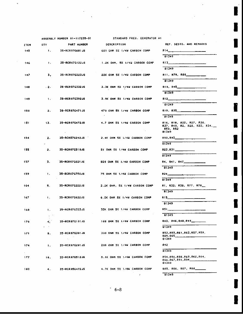
f i s sEnBLY HU l lEER 0 l - t 17235 -01
CTY PART NUNBER
35-RCR 07C6€ t JS
35-RCR 0?G | 22,JS
35-RCR 07C223JS
35-RCR07G332. 'S
35-RCR07G392JS
35-RCR07G.f?t JS
35-RCR07C472JS
35-RCR07c2,l2JS
35-RCR07G5r 0JS
35-RCR07C82r JS
35-RCR07C750.rS
35-RCR07G222JS
35-RCR 07G622 JS
35-RCR 07C333 JS
35 -RCR07Gt 0 l JS
35 -RCR07G30 l JS
35 -RCR07620 r JS
33 -RCR07G5 l2JS
35-RCR 05G472 JS
S IA I {DARD FREO, GE i lERATOR A I
DESCR lPr lOf l
680 0H! l 3 i : t /4u CARB0N C0rP
| ,2K ol{ l t , 5 i l l /4u ' :ARBON C0l tP
22K OHlt 52 t /4U CARBON Co| lP
3.3K oHn 52 t /4U CARBOT{ CO|IP
3 .9X oH f l SZ l / 1Y CARBoN Co iP
t70 oHi l 524 l /1U CAR8oN COttP
{.7 BHft 5r1 l / , tu CAR8oN COiP
2.1K OHtt 5 ' t l /4U CaRBOH COi lP
5t oHtt 3Z 1/4t" CAREO}| CollP
820 oHf i 3 'A l /4U CARSoN CorP
75 oHl l 52 l /1U CARBOI| COFP
2,2K oHr ' t , 5 'A 1/1U CARB0N COttP
6,2K oHn 5Z r /4 la CAR8oN COfiP
33K OHfl 5 ' r l l / lU CAREOH COiP
t00 oH | l 32 l / 4u cARaoN co l tP
300 oHn 3z r /4u cAR8ol{ conP
200 DHft 5z l /4u GARBON CottP
5. f x oHi l sz l /1u cAR8ol{ col lP
4.7K oHr,r 5Z l /au CARBoN COl, lP
R E F . D € S T C . A N D R E I ' I A R K S
R r 4
8 1 3 4 9
R t 3
8 r 3 { 9
Ri l , R79, R80+_
8 r 3 4 9
Rl 0, R45_
8 t 3 { 9
I | 3. t9
R t9 , R35_
8t 3,19
R f 5 , R f 8 , e , 2 2 , R 2 7 , R 3 0 ,R 3 7 , R 4 0 , R 2 , R 2 8 , R 3 3 , R 3 a , _
R50 , R528 l 349
R 9 0 , R 9 3
8 1 3 { 9
R 2 3 , R 3 r _
8 t 349
R4 , R . t l , R47
8 t 349
R24#
8 t 3 4 9
R t , R 3 2 ; R 3 8 , R 7 7 , R ? a -
st 3.19
8 1 3 { 9
R 5 t
8 r 3 4 9
R . 4 3 , R 4 6 , R . t 8 , R . 1 9
8 t 3 4 9
R 5 3 , R 3 5 , R 6 r , R 6 3 , R 5 7 , R 5 9 ,R89 , R658 1 3 4 9
R92
8 t 3 4 9
R 5 4 , R 5 6 , R 5 8 , R 6 o , R 6 2 , R 6 4 ,R 6 6 , R b 7 , R 9 1 , R 9 48 1 3 4 9
R 8 5 , R 8 6 , R 8 7 , R B 8 -
IIIItIIttIIIIIIIIII
R I
3 ,
t .
,t"'
6-8
8 t 3 4 9
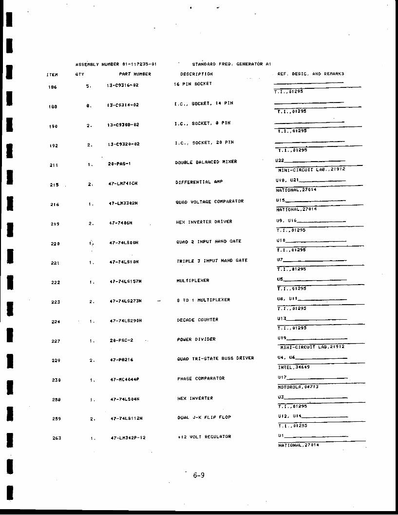
IIIIItIIITItTIIIttt
I TEI{
1 8 6
1 8 8
t 9 0
t 9 2
? 1 1
2 t 5
215
2 r 9
220
22r
222
223
224
227
229
2 3 0
258
239
263
ASS€ I ' | 8LY HU iSER 0 l - t 17235 -01
OTY PART NUTSER
5 . | 3 -C931 6 -02
| 3-C93l , l -02
| 3-C930S-02
| 3-C9320- 02
20-PAS-l
4?-Lfl?.f I ca{
,t7-Li3302t{
47-?. t 06N
a7-?{LS0 0t{
{7-7t lLSI0f{
t7-?.{Lst 571{
{7-7{L5273N
{7-74LS29 0N
20-PSC-2
a7-PAat5
.t7-llC4044P
47-7{LS0.tN
47-7.+LSl tAN
47-Ln312P-12
. STANOARD FREO. GEHERATOR AT
D € S C R T P T I O N
16 P IN SOCKET
t , C , , S O C K E T , 1 4 P I H
t . c . , s o c K E t , I P l t {
r . C , , S O C K E T , 2 0 P I N
DOUSLE BALANCED I I IXER
DTFFERETITIAL ENP
OUAD VOLTAGE COITPARATOR
H€X IN }ERTER DRIVER
OUEO 2 INPUT NEi lD GATE
TRIPLE 3 THPU' XNHD GETE
fIULTI PLEXER
8 TO T NULTIPLEXER
DECAOE COUIITER
POUER D IV IOER
qUAD TR I .STAT€ EUSS DRTVER
PHASE COI. iPARATOR
HEX ITIVERTER
OUfiL J- |< FLIP FLOP
+ I2 VOLT REGULATOR
R E F , D E g I G , A I . I D R E X E R K 5
r . I . , 0 1 2 9 5
ffireur8 , U2 t
N A T t U N A L , 2 T O I 4
U 9 , U I 6
7 , I . , 0 1 2 9 5
u t 0
T . I , , 0 1 2 9 5
T . 1 . . 0 1 2 9 5
T , 1 . , 0 1 e 9 5
ua, u l t
T . r , , 0 1 2 9 5
T . r , , 0 i 2 9 5
u l 9
l t IN t -E tRcu tT LAg , 2 t 91 2
u. l , u5
INTEL ,34649
trotonoca, o.tz t g
u t 2 , u l
T , I . , 0 1 2 9 5
U I
u l 3
u 1 7
2 ,
t .
6-9
N A T I O N A L , 2 T O I ' t
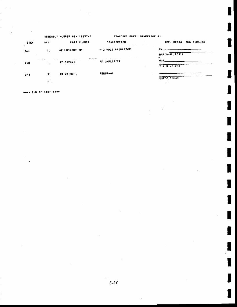
I TEN
264
268
2 ? 0
rr . r Et{O 0F LtgT .4. .
ASSEnBLY NUI,IBER 01-l | 7235-01
OTY PIRI XUNBER
t , {7 -L l t32o l tP-12
r , 47-C42820
3 ; l 3 - 2 0 1 0 9 - l
STAT{DARO FR€o. CEXENETOR AI
D E S C R I P T T O H
. I2 VOLT REGULATOR
RF AT{PLIFIER
TERJ{INAL
R € F , D E S I C , A } I D R € } I A R K S
iETronAu azot +
u2
T . R . U , , 0 l 2 8 l
GEco,-, t seig
6-10
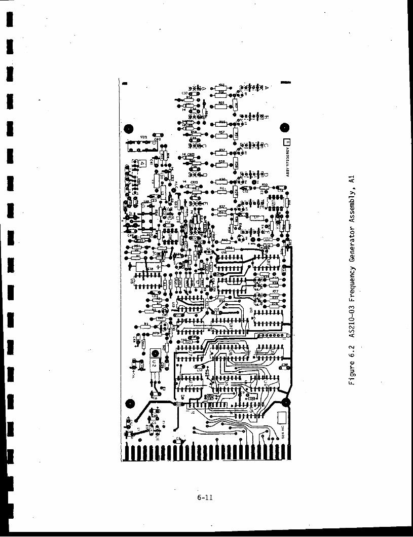
';-'$ft'
io= ck.[u:{g. Firrr :' l 3{ Nts:f-.-[rf e' U\r3 c: rm
lF"F-.q4
i6.,1.+S#1ft
r.c\'ataI
t
I' : e,a\'\',l rI,,Rt)qj|
ffiffi,Wffil*FeE{-4$'l"ffi-rE:L e+#,AI +H++$//+
itF#ffiHTre)g
flrm
| -
p:ili>I ca3(Et .rrcl!-c r
| 'ffi3&I s_._'*it
l?---t =+:I lTlm s:c:.|oI ll--C'.d//t
l'ruwI *S#HF,
inffiriei ffdi:ffil$r-96' .t N
rltinulillhl
ri
a(l,(/lo
Lo
P(ltL(l)
q)(9
(.)(u(toL
t-L
C7)
IO
(\lttl
(\l
\o(uL
g)
lJ-
c - Fc.>=.€' ? . ?
lr r r lllll
6-1 1
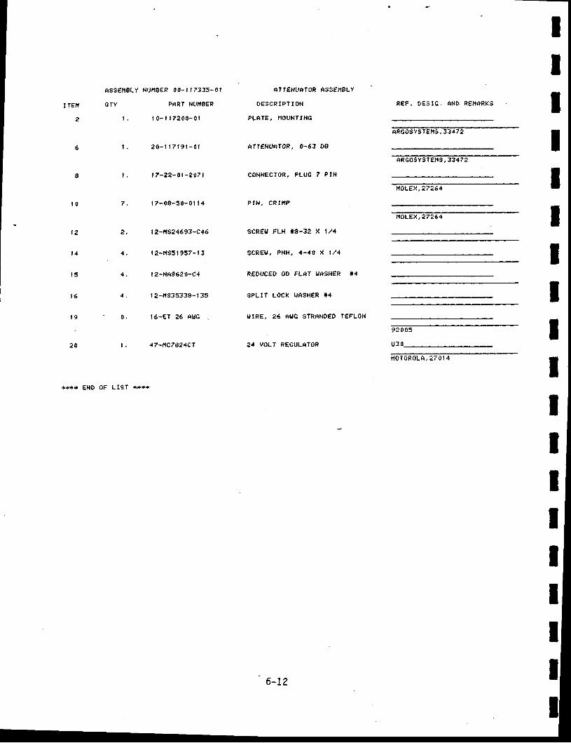
AS6Ef' |BLv NUil8EP 00-l 1 7335-0t
orY PnRT NtrtrBER
l , r 0 - r 1 7 2 0 0 - 0 |
ATTENIIATOR ASSET,ISLY
OESCRIPT IOT{
PLATE, I IOUIITIHG
*IT€NUATOR, 0-63 DB
CONNECTOR, PLUC 7 PIN
PTH, CRII ' IP
scPglJ FLH *8-32 X l /4
SeRELf, PHH, 4-40 X l /4
REDUCED OO FLAT UASTIEP 14
SPLIT LOCK hIASHER T4
I l t IPE, 26 AIJG STRANDED TEFLOH
24 VDLT PEEULATDR
BEF, OEsIC. AI{D RSI" IAPKS
AREBSVSTEXS, 33472
IIIIIIII
I T€II
2
6
I
t 0
t 2
, 1
t 5
l 6
t 9
2 0
L
l ,
v ,
2 ,
4 ,
t .
2 0 - t 1 7 1 9 1 - 0 1
17-22-0t -2n7 |
t 7-08-50-0 i l 4
| 2-HSz4693-C46
t 2-lts5 | 957- l 3
| 2-HAS620-C4
| 2-t1S35338- ' 35
I6-ET 26 At , 'G
47- i lC7A24tT
ARB0SYSTEI ' rS, 3347:
ll(rLEX ,272€4
r ' roLEx,27264
4 ,
4 ,
0 ,
93005 ItIIIIIIII
u 3 0
f ' toT0F0LA , 27 0l 4
** ' | . * END 0F LIST ****
6-t?
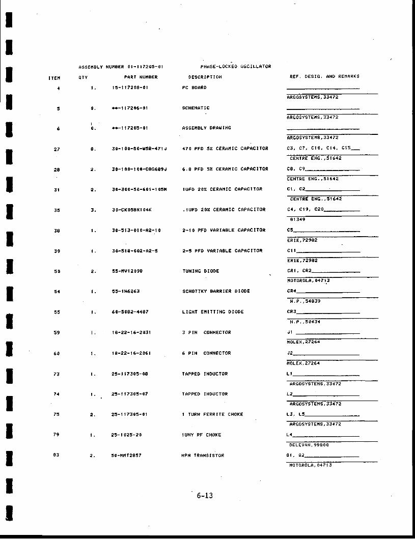
ItIIIIItIITIIIIIIIt
I TEN
1
5
5
2 7
28
3 l
35
38
39
5 0
5.1
55
59
6 0
?3
71
73
79
83
ASSE iEL? NU | iEER 0 l - l 17205 -01
OTY PART NUI ' '8ER
t . l 5 - 1 1 7 2 0 S - 0 1
.,.t- | | 72 06- 0l
* r - | | 7 2 0 5 - 0 |
30 - t 00 -50 -u5R-47 t J
30- l 00-t 00-c0G689.,
30 -300 -50 -601 - t 05 l l
30-cK058Xt 041(
3 0 - 5 r 3 - 0 1 0 - A 2 - t 0
30-5t 8-002-42-5
55- i lVt 2098
55- | n6253
60-5082-4487
t 0-22- | 6-2 03 |
la-22-t6-2061
25 - t t 7305 -08
2 t - r t 7305 -07
23 - t t 7305 -0 t
25- | 025-20
3 0-f l l iT2857
PHSTSE-LI ]CKEO OSCILLATOR
OESTRTPT ION
PC EOARO
SCHEfiAT IC
ASSEI ' IBLY DRAII ING
470 PFD 5Z CERAIT IC CAPACITOR
6 ,8 PFD 52 CERSIT IC CAPACITON
tuFD 20 i l cERnn l c cePAS lToR
, IUFD 29z CERANIC CAPACITOR
2 . IO PFO VARIABLE CTPACITOR
2-5 PFD VTNIASLE CEPRCITOR
TU} I ING D IODE
SCHOTTKY gANRIER DTOD€
L IGHT E } I ITT IHG O IOOE
3 PIN COXIIECTOR
6 PIr{ COI{}fECToR
IAPPED I} IDUCTOR
TAPPED I I IDUCTOR
,I TUR}I FERRITE CHOKE
IUHY RF CHOI(E
HPN TRAI{SISTOR
R E F . D € S I G . A N D R E f ' I A R K 5
tRGOSYSTEnS, 33472
ARG0SYSTEITS, 334?2
ARG0SYSTEIIS, 33.172
c 3 , c 7 , c l 0 , c l { , c l 5 -
cEt t lRE EHG. ,5 f 542
c8, c9_
C E N T R E E N G . , 5 I 6 4 2
c t , c
CE} ITRE ENG. ,5 I542
r : 4 , C t 9 , C 2 0
813 . t 9
ER I E , 72982
c t l
ER18 ,72982
cR l , cRz_
ttoT0RoLA, 047.1.3
H . P , , 5 4 8 3 9
H . P , , 5 0 4 3 t
noLEx,2?264
noLEx,27264
L I
ARG0S'/STEt ' tS, 33472
ARC0SYSTEHS, 33472
L3 , L5
ARG0SYSTET'tS, 33472
L 4
D E L E V A H , 9 9 8 O O
o t ,
0 .
I
0 .
J I
6-13
r 0ToRoLA , 0 .47 t 3
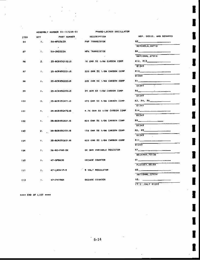
ITEI
81
8?
96
9?
,€
99
t 0 0
| 0 l
1 0 2
r 0 3
1 0 4
t 0 5
t 0 9
l l I
1 t 3
OTY
t .
l .
2 ,
t .
t .
L
3 .
L
t .
2 ,
t .
L
t ,
L
ASSEII 'L? l lut lBgR 0l- l 17205-01 PHASE-LOCXED OSCILLATOR
DESCRIP I ION
PNP IRNXgISTOR
NPII TRAI{SISTOR
tK oHi 52 l /89 CAR8oN COiP
220 oHfl 3'a 1/8U CAREolr COIIP
22K OHlt 37. t/su CAR8oN COftP
39 oHr{ 32 l /AV CARB0N COrP
470 0Hlr s i t l /8u CARB0N C0nP
4,7K OHi l SZ t /8V CARgoN COIIP
820 oHr,r 52 l /8u cARgoH cotP
r50 oHi l 32 l /Al CeRBOt{ CO}IP
620 oHi 37, l/gl caR8oH cottP
2K OHII VERIAELE RESISTOR
o€cAo€ couNrER
5 VOLT REGULATOR
OECAD€ COUNTER
PARI NU'T8ER
50-tP33639
30-2N2222A
35-RCR05Cl 02JS
35-RCR05G22t JS
33-RcR05G223JS
35-RCR 03C39 0 JS
35-RCR 05G47 | JS
35-RCR05Ga72,rS .
35-RCt05G82 l JS
3 ! -RC t05C t5 l J3
35-RCnO!G621 J9
35-92-PAR-21(
.t7-sP8630
{7-Lti3a I P-5
a7-7a r 96H
REF, DEgIC. A}ID REI ' IARKS
r, toTOROLA, 047 | 3
o4
HATIONEL , zT ( ) I {
9 r 3 4 9
8 t 3 4 9
81 349 i
IIIItItIItII
R I
R 2 ,
R t l
R 8 - l
8 1 3 4 9
R3 , R4 , R6 - -
8 1 3 4 9
R t a
8 1 3 4 9
R9
8 | 3.+9
I | 3 . f 9
8 t 349
R,?
sEcK iAH ,73 l 38
u t
P L E S S E Y , 5 5 I 5 4 IIIIII)
U3
N A T I O H A L , 2 T O I . I
u2,( T , I . , 0 N L Y 0 1 2 9 5
.r . r EHD OF LlgT . r . r
6-14
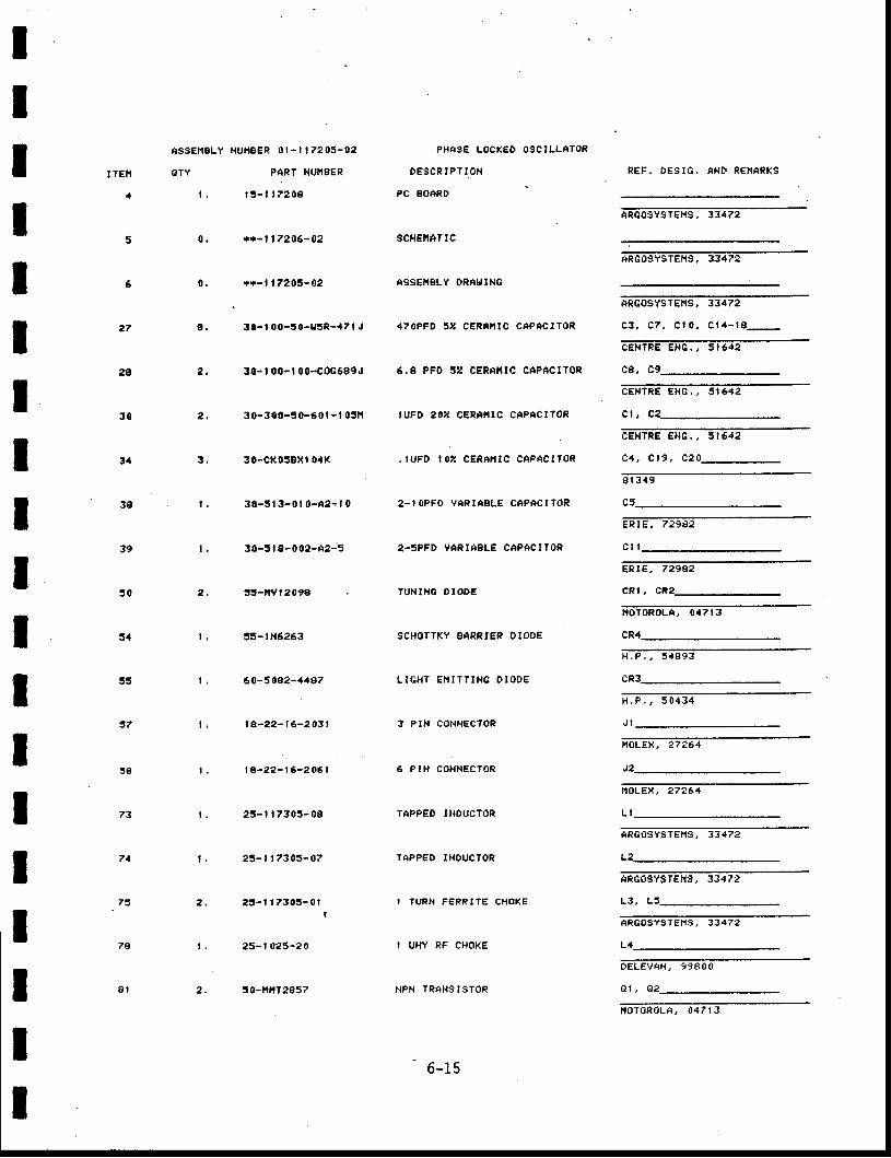
IIIIIIIIIIItIIIItII
ASS€n8LY HUr . l gER 0 t - l t 7205 -02 PHAg€ LOC|(ED OSCILLATOR
I TEI! OTY PiRT I{UI , IBER DESCRIPTIOH REF, DEs IG . AHD RENARKS
4 t . t t - 1 t 7 2 0 8 PC EOARD
ARcOSYgTEtrs, 33472
5 0. ' .*- l 17206-62 scHEltATlc
6 0. trr-l 17205-62 A9SEItSLY ORAIIINC
ARr:0SYSTEl lS, 33472
ARG0SYSTEI{S, 33472
2? 9 . 30 - t 00 -50 -u5R-471 . , . f 7opFD 52 CERn f i tC CAP iC ITOR C3 , C7 , C lo , C l . f - 18 -
C E N T R E E N E . , 5 1 6 4 2
2A 2, 30-100-100-c0G689J 6.8 PFD 52 CERAIiIC CAPACIToR c8, c9.
CENTRE EHG, , 5 I 642
30 2, 30-300-50-601-105t1 t tJFD 202- cERAti IC CAPnCIToR Cl , c?
. CENTRE ENC. , 51642
3 4 3 , 3 o - c x 0 5 B x t o 4 x . | U F D l 0 2 c E R A l . | I c c A P A c I T o R c 4 , c | 9 , c 2 0 -
8 l 349
38 t . 3O-51 3-01 0-42-1 0 2- l oPFO vARtAgLE CAPACITOR
ERIE , 72982
39 l . 30 -518 -002 -42 j5 2 -5PFD VARIABLE CaPACIT0R c l l
ERIE, 72952
r0 2, l l - l lY lzoga TUNt| lG DIODE c R l , c R
n o T o R o L A , 0 4 ? t 3
5 4 l . 5 5 - t H 6 2 6 3 SCHOTTXY SARRIER DIOOE
H . P . , 5 4 S 9 3
55 l . 60-5092-44S7 LIGHT €I^I ITTINC DIOO€
37 t . ra-22-16-203r 3 PIH CONHECTOR
ss t , la-2?-16-2061 6 PIN COHHEeToR
73 r , 25 -117305 -08 TAPPED IHOUCTOR
71 t , 25 -117305 -07 TAPPED INOUCTOR
73 2 , 2 t - 1 t7305 -0 t t t uRN FERRITE CHOKEI
H . P . , 5 0 4 3 4
J I
t ' t o L E x , 2 7 2 6 4
t { o L E X , 2 7 2 6 4
L t
AR6OSYSTEl.rs, 33479
L2
ARGgSYSTEfiS, 33472
L 3 , L 5
ARG09YSTEt l5 , 33472
L 4? 8 r , 2 5 - 1 0 2 5 - 2 0
8r 2. t0-nf lT2g57
' UHY RF CHOKE
NPN TRAHSISTOR
D E L E V A N , 9 9 A O O
H O T 0 R o L A , 0 4 7 | 3
6-15
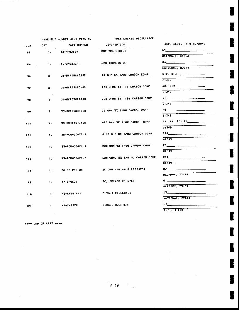
I TE'I
82
84
96
9?
9{l
99
t 0 0
r o l
l 02
I 0 3
t 0 6
r 0 8
t t 0
l z l
t s sE [BLY NUTBER 0 l - l 17205 -02
OTY PART NUI'IBER
L 50-ftP33639
30-2N22224
35-RCR05Gl 02JS
33-RCR03Gt 5t ,JS
3s-RCR056223JS
35-ReR 05G39 0 J3
3S-RCR05G47t JS
35-RCR 05G472 JS'
35-RCR05G82t JS
35-RCnO5G62' JS
36-ez-PAe.-2K
,f 7-sP8630
46-Ll l34l P-5
17 -?1197H
r i i . €ND 0F L lsT * r t r
PHASE LOCKED O9CILLATOR
O€5CRIPT IOH
PNP TRTHgIgTOR
NP}I TRAI{SISTOR
tK olil{ 52 l/8t eARBOH ColtP
, !0 oHt ls 32 l /g CAR8oN COttP
22K OHfIS 32 | /SV CARBOI{ CO}IP
39 oHtt 5u l,/8u ctRBOH COI'IP
4?0 oHn 32 l/au CAR8oH COf'tP
4,7f( oH| l 32 l /8u CARBOH COt ' lP
920 oHil 32 l/eu cnRBoH COIIP
8 t 3 4 9
620 Ol{ f t , 32 l /E U, CARSOI{ cot tP Rt l
2K OHTI VARIABLE R€SISTOR
tC, DECADE COUHTER
5 VOLT R€GULATOR
OECAOE COUNTER
8 r 3 4 9
R7
REF, DES IG. A ' I$ PEI {ARKS
o3
I t C r T o R O L A , 0 4 7 t 3
H A T I O H A L , 2 T O I 4
R I 2 , R I
9 r 3 4 9
R 2 , R t O
8 t 349
R I
8 | 3.a9
8 r 3 4 9
R 3 , R 4 , R 5 , R6-
R t 4
g E c x t t A N , 7 3 l 3 9
P L E S s E Y , 5 5 I 5 4
N A T I O N A L , 2 T O I . I
tIIIIIIIIIItU I
u2-
T , t . , 0 1 2 9 5
IITIIII
6-1 6
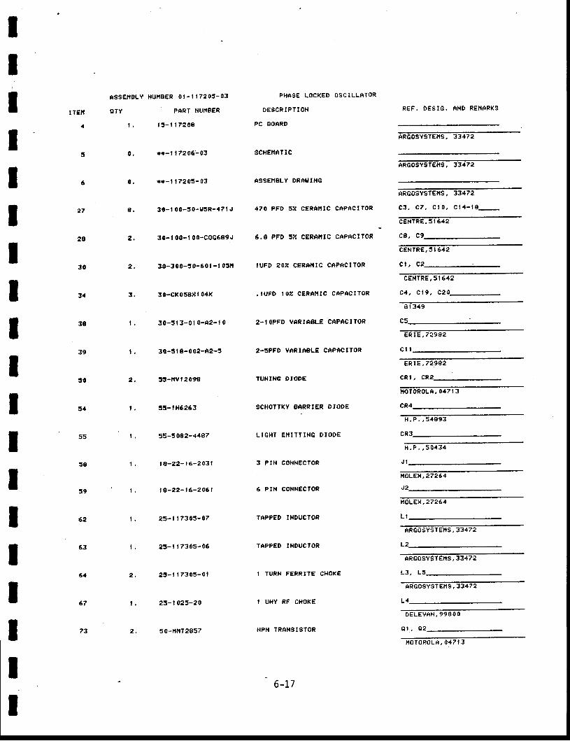
L 4
ItIIIIIIIIIIIIIIIII
ASSEHBLY l lUl lBER 0l- l l?205-03 PHASE LOC(ED OSCILLATOR
r TET{ CTY
. I ' t 5 - 1 1 7 2 0 8
PART I . IUI . IBER DESCRIPTION
!o 2, ! ! - t tv t209a
5a 1 , 53 - l l { 6263
67 t. 23-t023-20
73 2, s0-l1nT2857
TUNII{C DTODE
SCHOTTXY BARRIER DIODE
I UHY RF CHOKE
NPN TRANSISTOR
6-r7
REF, DESIG . NHD RE I IARKS
I toroRoLA, 047,l 3
H , P , , 5 4 S 9 3
cR3
H . P . , 5 0 4 3 4
J I
noLE l,27264
- t t
t ' roLEX, 27264
L I
ARGOSYSTEI ' IS, 33472
L2
rPGosYSTElrS, 33472
L 3 , L
ARGOSYSTEI ' tS, 33472
O E L E V A N , 9 9 S O O
0 r , 0 2
l . l0ToRoLA, 0471 3
PC BOARD
f rRG09YSTEtts, 33472
5 0. { r i - l | 7206:03 SCHEITATIC
6 0. 'm- l 1?203-03 ASSEI1BLY DRAL, l t {G
ARcOSYgTEt{9, 33472
ARG0SYSTEI'lS, 33472
2? e . 3e - t o0 -50 -u5R-4? t . , 470 PFD 52 CERAI ' IC CAPAe ITOR c3 ' c7 , e t0 , c t a -18 -
CENTRE,5 I 642
2s 2, 30-t00-t00-coc6s9J 6.{t PFD 52 CERAIIIC CAPACITOR C8, C9
CENTR€, 5 I 642
3 0 2 , 3 0 - 3 0 0 - 3 0 - 6 0 1 - 1 0 3 f ' l l u F D 2 o z c E R t i l r c c A P A c t r o R c l , c 2 .
CEXTRE, 5 I 642
3 . 3 . 3 0 - c | ( 0 5 8 x | 0 4 x , | U F o | o u c E R A H I c c A P A e t T o R c 4 , c l 9 , c 2 o -
9 t 3 4 9
3S | . 30-513-01 0- f i2- l 0 2- t oPFD VARIABLE CnPACITOR
ElllE,72982
39 t , 3.0-319-002-42-3 2-5PFD VARIaBLE CAPACITOR cl t
eRtE,729S2
c R l , c R
55 l , 55 -5082 -4 , t s7 LTGHT E I " I ITTTNG D IODE
5A 1, le-22-t6-2031 3 PIN CONNECTOR
J9 l . la-22-16-2061 5 PtN CONNECTOR
62 l . 25- l 17305-07 TaPPED I I {DUCTOR
63 t , 25-t 17305-06 TAPPED IXDUCTOR
6a 2 , 25 -117305 -01 | TURN FERRTTE CHO(E
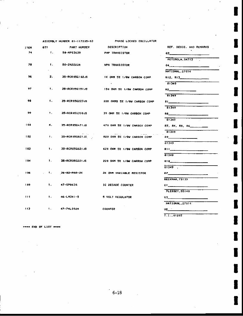
T TE'I C TY
?1
7e
96
9?
98
99
t 0 0
t 0 2
t 0 3
| 0.1
t 0 6
t 0 9
t t l
t t 3
fissEtrELY r{uf.rBER 0r -r | 7205-03 PHASE LOCX€D OSCTLLATOR
o€scR tPTloN
PHP TRNNSISTOR
flPTI TRANSISTOR
I K ot{l{ 52 t,rgu cARBoH co||P
tlo oHn 3/. t/gy chRgoH ConP
22t( OH'iS 32 |/8U CARBOil COrP
39 oHtt 32 t/€u cAngoil coHP
470 oHlr 3z t /au cARBoH CotrP
820 0Hlt 32 l/gu ceRgoN coltP
620 oHlt sz llgu cARgox coilP
220 oHn 32 lleu cARBoH coilP
2I( OH}I YARTASLE REgISTOR
IC DECADE COUNTER
5 VOLT PEGULATON
COUHTER
IIIIIIIItIII
2 ,
1 .
PART NUI19ER
30-trPs3639
30-2N2222A
35-ReR05€t 02JS
35-RCRorct 5r J3
33-nCR05c223.rS
35-RCR056390JS
35-RCR05C47t JS
35-RCR05CA2t JS
35-RCRO:t86e r JS
35-RCRO5G22t JS
36-92-PtR-?K
.i7-sPs630
46-LH34 | -5
t7-74L992r{
REF. DESTG, AND REI{ARI(S
o3
L
t .
t .
r . roToRoLA,047t3
t {AT loHAL ,270 t4
R r 2 , R r 3 .
813.19
R2-
8 l 3 . f 9
R I
8 r 3 { 9
PE
8t 349
R3, R4, R5, R6_
8 r 3 4 9
R9
8 t 3 4 9
R t l
9r 3.ft
s1319
R7
aEexhAN, 73 | 39
u l
PLESSEY, 55 | . r 0
u3
HAT IOHAL, 17 O I 4
u2 IIIIIII
T . r , , 0 t 2 9 5
nrr El{D OF LIST r**r
6-18
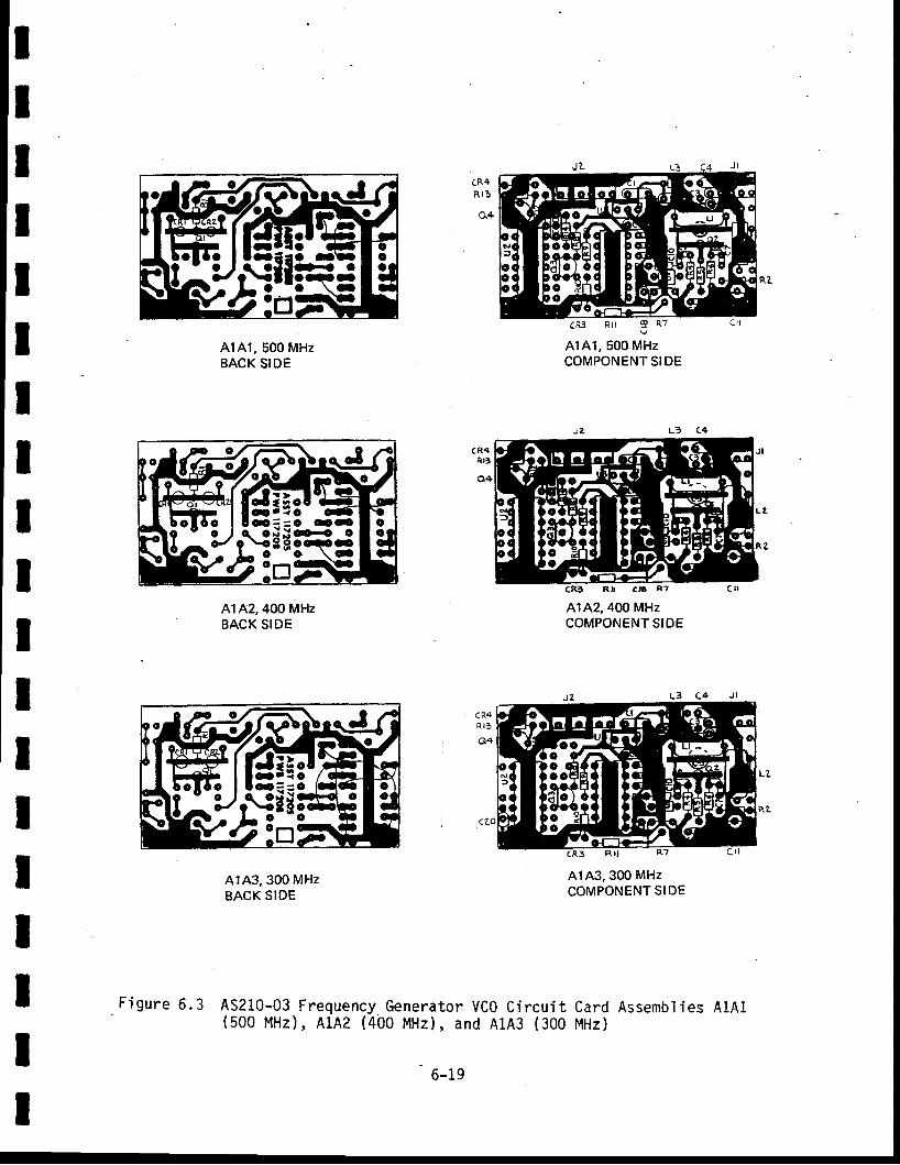
IIIIIIIIItIIIITIIII
A1A1, 5OO MHZBACK SIDE
CR4R r 3 .
q.t
cR4Rr3
o4
A1A2,400 MHzBACK SIDE
AlA2,400 MHzCOMPONENT SIDE
A143,300 MHzCOMPONENT SIDE
A1A3,3O0 MHzBACK SIDE
AS210-03 Frequency Generator VCO Circui t Card Assembl ies A1A1(500 MHz) , A1A2 (400 MHz) , and A1A3 (300 MHz)
CR3 Rrr 3 * t
AIAl , 5OO MHZCOMPONENT SI DE
(#f,=
O Co c tCOraoaico \
F igure 6 .3
6-19
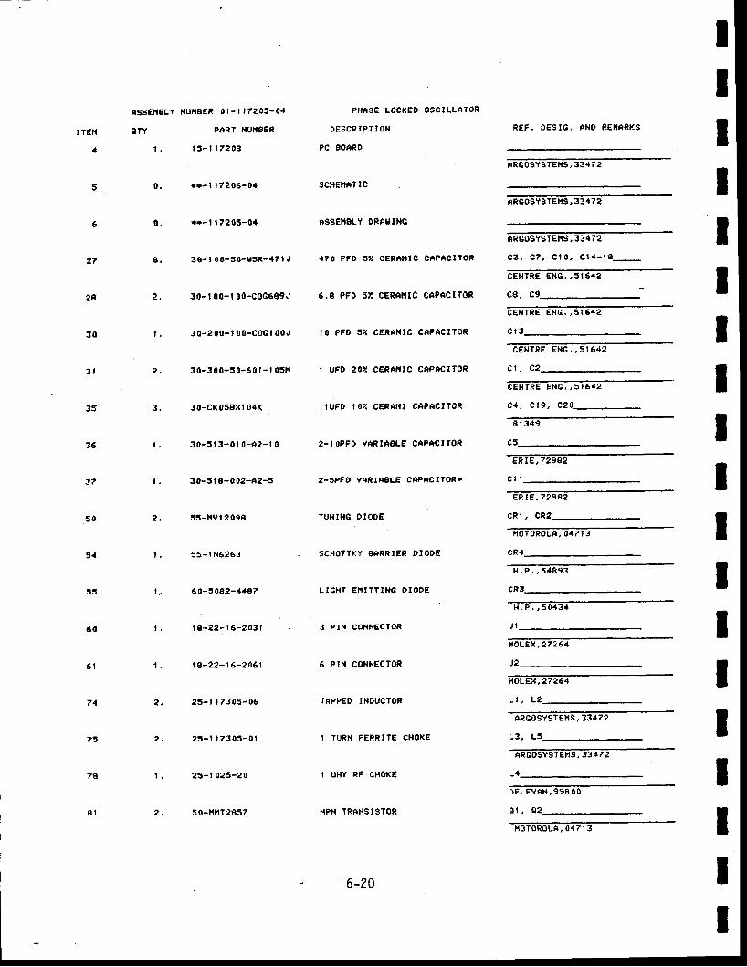
I TEI{
4
5
6
27
2A
3 0
3 l
35
35
l7
3 0
5.1
55
60
5 l
71
7U
7A
s l
eSSEttBLY l lu l lgER 0l- t 17205-0' l
OTY PART T{UT'BER
t . l 5 - l 1 7 ? 0 9
i r - l 17906 -0 t
rr - l t7205-04
30- l 00-50-U5R-47t J
30-t 00-t 00-coc689J
30-200- l 0o-cocl 00. ,
30 -300 -30 -601 - t 05 f l
30-cK05BXl 04K
30 -5 f3 -0 t 0 -A2 - l 0
30-5 | a-002-n2-5
53-rVr 209S
55-r H6253
60 -50e2 -a497
la-?2-16-203 |
ta-22-t6-2t61
25 - t t 7305 -06
2 ! - r ' r 7 3 0 5 - 0 1
25- l 025-20
50-ilnT2857
PHA9E LOCXED OSCILLATOR
0g3cR lPTlol {
PC BOAPD
scH€lttl I c
ASSEI.IBLY DRAI'IX8
4?0 PFD 52 CEnArrC CaPiCITOR
6,9 PFo 5Z C€RAl l lC CAPACITOe
t O PFD 52 CERAIITC CAPACITOR
I UFD 202 CERA}IIC CAPACITOR
, IUFD 'OZ CERATI I CAPACITOR
2-I OPFD VTFTASLE CAPECITOR
2-s?FO VARTnSLE CAPnCIIORT
TUfl t l lc DIooE
SCHOTTI(Y BARRIER DIOOE
LICHT EII ITTI I IC OIODE
3 PIN CONNECTOR
6 PIN CONNECTOR
TAPPED THOUCTOR
' TURN FERRITE CHOKE
,I UHY RF CITOK€
HPII TPANSISTOR
REF, DES IC, AT{O REIIARI(S
ARCoSYSTEH9, 33472
ARCOSYSTEnS, 33+72
ARC0SYSTEI{9, 33472
c 3 , c 7 , c l 0 , c t 4 - 1 8 _
CEHTRE €NC. , r l 5 . t a
c3, c9
CENTRE ENC. ,5 I5 . t 2
c r 3
C E X T R E E N C , , 5 I 6 4 2
c r , c2_
C E N T P E E N O , , 5 I 6 . 1 2
c4 , c r9 , c20
8 t 3 4 9
c5
ERIE,729s2
c t t
ERtE,729e2
cRr , cR2_
f i o roRoLA ,047 t3
cR.1-
H . P . , 5 4 3 9 3
H . P , , 5 0 . f 3 a
.r l
noLEx,27264
J2-
H0LEX,27264
L I , L 2
ARC0SY9TEt'tS, 33472
L 3 , L
ARCOSYglEng, 334?2
L 4
D € L E V A H , 9 9 8 O O
s l ,
IIIIIIIIIIIIIIIITII
6-20
! | s roRoLA,047r 3
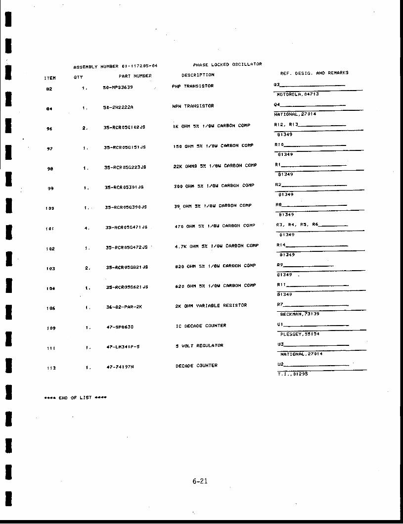
IIIIIIIIIIIIIITIIII
I TEI{
a2
ga
96
97
9€
99
1 0 0
t o t
t 0 2
r 0 3
t 0 a
r 0 6
t 0 9
t t l
i l 3
ASSEt lSLy HU! . ISEP O l -1 . t 7205 -04 PHASE LODTED BSL ' I LLATOR
OTY PART NUI ' ISER DESCRIPTIOTT
1, 5O-l lPS3639 , PNP TRANSISTOR
3n-21t22224
35 -RCR05C l 02JS
39 -RCR05G l5 t Js
35-RCR 05G223 JS
35-RCR0530l JS
35-RCR 05G390JS
35-RCR05G47l JS
35-RCR 05G472 JS
35-RCR05Cg2l J3
33-RCRO5662t JS
36-82-PAR-2X
47-9P9630
a7-Ln34 | P-5
17-711 9711
NPN TRANSTSIOR
lx oHn 52 l /8u cARgoN col lP
,50 oHl.l JZ 1/8U CnRAON COf'lP
22K OHlts 52 I /gu gARBOtt COtlP
300 oHft 32 l/au CARS0H COftP
39, OHtf 37. l/Au eaRBoN COIIP
470 oHtl s7. t/au cARsoH COilP
4,7K oHt l 5z t /8U CAR€ON COI ' IP
€20 olflt 5?. llgu CARBOH COttP
620 oHr sz l/av CARBOH COftP
2K OHiI VARIABLE RESISTOR
IC D€CAOE COUHTER
5 VOLT nECULATOn
OECADE COUNTER
R S F . D E S I G . t N D R E I I A R K S
l {oToR0LA, 04? t 3
o4
f f i l toxeta lut
s r349
8 r 3 { 9
8 t 3 { 9
9 t 3 4 9
RA
9 r 3 4 9
R3 , R4 , R5 , R6 -
9 r 3 4 9
9 1 3 4 9
R l t
2 ,
R I
R t 4
2 .
t .
t .
L
t .
1 ,
U I
s1349
R 7
8ECK| |AN ,73 | 39
PLESSEY,55 I 54
-TErroxat-, ezot+
u2
, I . , 0 r 2 9 5
fir. El{D OF LlsT *..*
6-2L
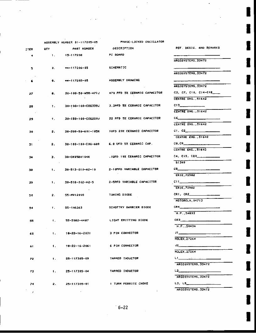
I TEII
1
5
6
27
2A
29
30
3 l
34
38
39
5 0
t4
t t
6 0
6 l
72
73
IIIIIIIIItIIIIItIII
L 3 ,?4
rSSEr.tgLY NU|I8€R 0l - l | 72 05- 05
CTY PTRT NUI.I8€R
17-l 17204
*{ - t t7206-0s
i f - l | 7205- 05
30- t 0o-30-u3R-a71. ,
30-t 00-t 00-coc339J
30-lt0-t 00-coc220.,
30-300-50-601- l 051t
30-t 00-t 00-coG-589
3o-cl(05Bxl 04x
30-513-01 0- t2 - l 0
3 0-5 | 8- 0 02-A2-5
55-f{V | 2 098
!3- | 116253
!J-308e-4487
I e-22- t 6-2 03 I
1g-22-16-2061
25 - l r 7303 -09
25 - l r 7305 -04
25 -1 t 7305 -O l
PHAS€.LOCXED OSCILLATOP
bEscnrprroH
PC BOARD
SCHE}tAT TC
ASSE'IgLY ORAUTHC
1?O PFD 52 CERANIC CAPfrCITOR
3,3PFD 52 CERT}I IC CAPACITOR
22 PFD 32 CERAIIIC CTPACTTOR
IUFD 2OZ CERAITIC CAPACITOR
6 .8 UFD 52 CERANTC CAP,
. IUFD IOZ CERfi I I IC CAPACITOR
2-I OPFD YARTABL€ CAPACI?OR
2-5PFD VARIABLE CAPACITOR
TUNING D IODE
SCHOITKY BARRIER OIOO€
LTGHT E ' I ITT ING O IODE
3 PIH CONI{ECTOR
6 PI} I CONXECTOR
IA?P€D IIIOUCTOR
TAPPED IHOUCTOR
I TURN FERRITE CHOKE
P€F, DESIG. Ti lD R€i lAPTS
ARGSSYSTEI{S , 33472
f lRCOSYSTEHS, 33,472
ARGOSYSTEHS, 33472
c 3 , c 7 , c r 0 , c l a - c l a _
C E H T R E E N G . , 5 I 6 4 2
cr 3-
C E N T R E E N G , , 5 I 6 4 2
C E N T R E E N E . , 5 I 5 4 2
c r , c 2
CENTRE ENC, ,5 I6 .12
r:8, C9
C E N T R E E N o . , 5 I 6 4 2
c { , c l 9 , 020_
8 t 3 { 9
ERrE,729A2
c t t
ERt€ ,72982
cP t , cR2_
t loToRoLA, 047 | 3
cR4
H , P . , 5 4 8 9 3
cR3-
H . P . , 5 0 4 3 4
J I
noLEx,27264
noLEx,27264
L I
eRG0sYSlEfts,33472
ARGOSY9TEI, ' |5, 33472
AR60SYgrElrS, 33472
' 6-?2
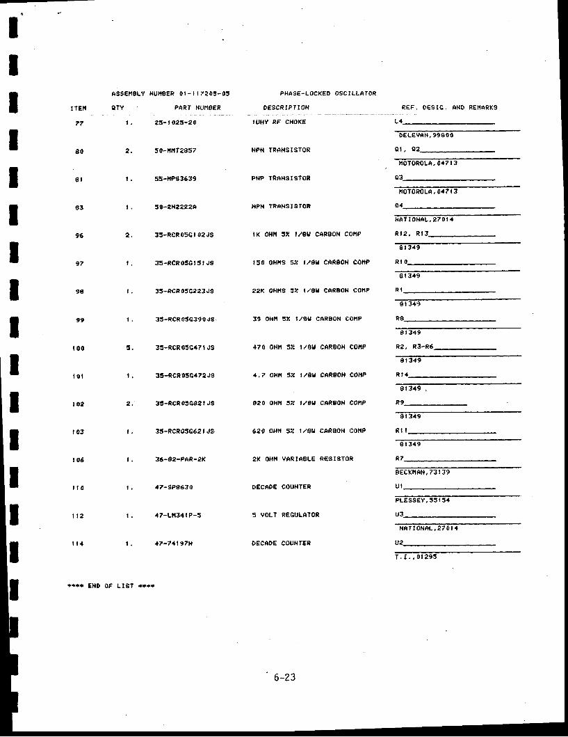
IIIIIIIIIIIIIIt
ASS€|48LY lrUr.fSER 0r - | r 7205-05 PHTSE-LOCXED OgCILLATOR
O E S C R I P T I O NI TE'I OTY
?7
80
€ l
tt3
96
9?
9e
99
t 0 0
l 0 l
l 0 2
r 0 3
t 0 6
l t 0
I t 2
1 t 4
o t ,2 ,
PART HUT49ER
2J-t 023-20
50-ilfi12857
55-!rPS3639
38-2t1?222A
3s-ReR056r 02JS
35 -RCR05Gr5 r , r 9
35-RCR 05C223.JS
35-RCR 05C39 0 JS.
35-RCR05G47r JS
3t-RCR056472 JS
35-RCR03GA2r JS
35-RCPO5G62' JS.
36-8z-PAR-2K
a7-5Pe630
47-Lfi34 | P-5
{?-74f 97H
'UHY RF CHOXE
NPN TRAHSISTOR
PHP TRAH3IgTON
I{Pil TRNNSISTOR
tK oHtt 32 llau cARgol{ ConF
,50 oHns 52 l/8u cARpoil cottP
22X OHI{S 52 t/eg CARBON COf'tP
39 OHn 3Z t/€l'l CARSOH EOItP
.t70 oHlr 52 r/gu CAR9oN conP
a,7 oHl. r 52 t /eu CARBOH COtrP
e20 oHtr 37. t/8u eARgoH cofrP
620 oHn 52 t/gu cARSoll collP
2X OHII VARTESLE R€SISTOR
O€CAOE COUHTER
5 VOLT RECULATOR
DECADE COUNTER
P€F, 0€SIG. n i lO REf iARt(S
L{
o€LEv{N,99S00
r'roroRoLA, 047 | 3
r 'r0ToRoLA,047t 3
o4
l { A 7 I o H A L , 2 7 0 l t
R r 2 , R r 3
st349
8 t 349
R t
s 1 3 4 9
RA
8 t 3 { 9
91349
R t a
e r 3 r 9 ,
R9
8 t 3 4 9
R t r
8 r 3 4 9
R,7
B€IX|AH, 73 | 39
u t
PLESSEY, Ss I 54
r t:l
NAT IONAL ,2TOI 4
u2-
7 , t . , 0 t 2 9 5
2 ,
R I
R2,
r i { . END 0F LIST r+rr
6-23
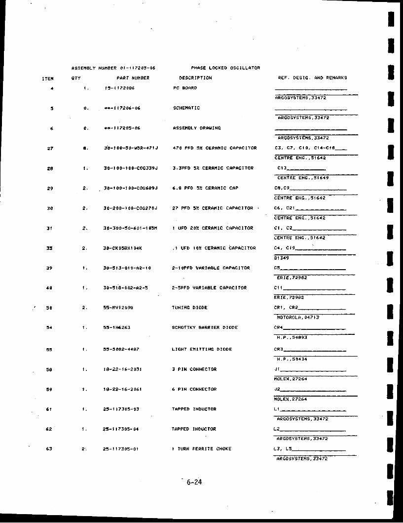
IIIIItIIIIIIIIIIII
I'Eil
a
5
5
27
2g
29
30
3 l
3t
39
{ 0
5 0
54
J5
58
59
6 l
62
63
AS9EnSLY HU||EER 0l - | 17205-06
OTY PART IiUI,ISEP
| . t ' - t r720e6
* * - l l?206-06
r*- | | 7205-06
3b-t oo-50-u5n-471 J
30-t 00-t 00-coc339J
30-t o0-t 00-coc689J
30-200-r 00-coc270J
30-300-5 0-6 0, -.1 0lr ' l
3o-cx05Bxlo. iK
30-513-01 0-42- l 0
3 0-5 r 8- 0 02-e2-5
55-HVl 209S
55-t N6263
t5-5082-44A7
| 8-22- | 6-2 03 |
, 9-22- r 6-2 05 |
25- t t7305-03
25-r | 730s- 04
2 5 - l 1 7 3 0 5 - 0 1
PHAS€ LOCKED OSCILLATOR
OESCRIPT I ON
PC BOARD
SCHENATIC
ASSEI{BLY OPAUTNC
47O PFO 5Z CERfi I I IC CAPACITOR
3,3PFD 32 CERA'{ IC CAPACITOR
6.€ PFO 5'T CERAII IC CAP
27 PFD 52 CERAI{ IC CAPTCITOR .
I UFD 2OZ CERAI. I IC CAPACITOR
. r UFD r02 CERAHTC bnpnc r rop
2-I OPFD YERIEELE CAPACITOR
2-5PFD VNRIABLE CAPTCITOR
TUHTNG D IODE
SCHOTTKY AARRIER DIOOE
L IGHT E I I I tY IH6 D IOOS
3 PIN COHNECTOR
6 PIN COHHECTOR
TAPPED TNDUCTOR
TAPPED INOUCTOR
I TURN FERRITE CHOKE
REF. OES IE, AI{D RET' IARKS
ARGOgYgTEt{S, 33472
ARCOSYSTEflS, 33472
ffic 3 , c 7 , c l 0 , c r t ' c r 8 _
C E N T R E E N C . , 5 I 6 { 2
c t 3
CEHTRE EXc , , 5 l 6 . f 9
c8, c9
C E H T R E E ' { G , , 5 I 6 4 4
c 5 , c 2 l
C E N T R E E H G . , 5 1 6 4 2
c r , c 2
C E N T R € E N G , , 5 I 6 4 2
c 4 , c t 9
8 r 3 4 9
c
ERTE,729E2
c t l
ERlE,729g2
C R I , C R
noToRoLA,047 l3
cRt
H , P , , 5 + a 9 3
cR3
H . P , , 5 0 4 3 {
J I
ttoLgx,27264
noLEx.27264
L '
A R G O S Y S T E f t s , 3 3 4 7 e
L2
ARGOSYSTEFIS,33472
L 3 ,
6-?4
APGOSYSTEltS,334Tt
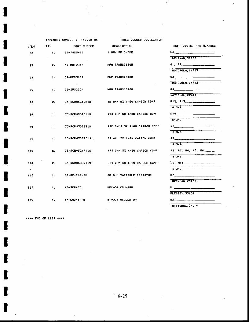
II
A S S E I I B L Y I . I U I 1 8 E R O I . t I 7 2 0 5 - 0 6 P H A S E L O C K E D O S C I L L A T B R
I ITEr q rY PART NUI IEEP DEScRIPTIoN R E F . O E S I G , A N D R E I I A R K S
66 'r . 23-t 023-20
?3 2 ' 50-ltttr2857
?1 t . !0-f{Ps3639
?a t, Ja-2N2?22A
T UHY RF CHOKE
NPN TRTNSISTOR
PNP TRNNSISTOR
NPN TRNISISTOR
L.f
IIIIII
D€LEVAH,998OO
o t , o 2
noToRoLA,047|3
HoTOROLA, 047 | 3
o4-
NAT IOHAL, 27 0 | .r
96 2 . 35 -RCR05C|02JS lK oH t l 32 t / 8V CARSoN Co f iP R l2 , R l3
8 t 3 { 9
97 | ' 35-RCR05Gl5t JS 150 OHI{ 52 l , 'e ta CARBOH eOl lP
8 r 3 4 9
9A t . 35-RCR05G223JS 22( OHt ' lS rU l /gu CAR80[{ cOnP Rl
8i 3. t9
99 1 , 35-RCR05C390JS 39 OHt ' r J2 , l /AU CARSON COl ' tP
I | 3'49
f 0o 5 . 35-RCR05G47!JS 470 oHr ' r 5 ra t /gU CARBOH COt ' lP R2, R3, R4, P5, R6_
8 1 3 4 9
I l 0 r z , 3 5 - R c R 0 5 c s 2 r J s s 2 0 o H t t s ; t t / g u c A R B o H c o t ' t P ? 9 , R t l
8r 3 t9
I tos l , 36-e2-PAR-2r( 2K oHn yARIABLE REstsroR R7
I - BECK|4AN,73 t39
lo7 l , 47 -SPg630
I| 09 1 . a7-Lt t34l P-5
I
OECADE COUNTER
5 VOLT PEGULNIOR
U I
PLESSEY, 55 | 54
u3-
N A T I O N A L , 2 T O I 4
+*fi El.lD OF LlSl {*t*
IIIIII
- 6 -25
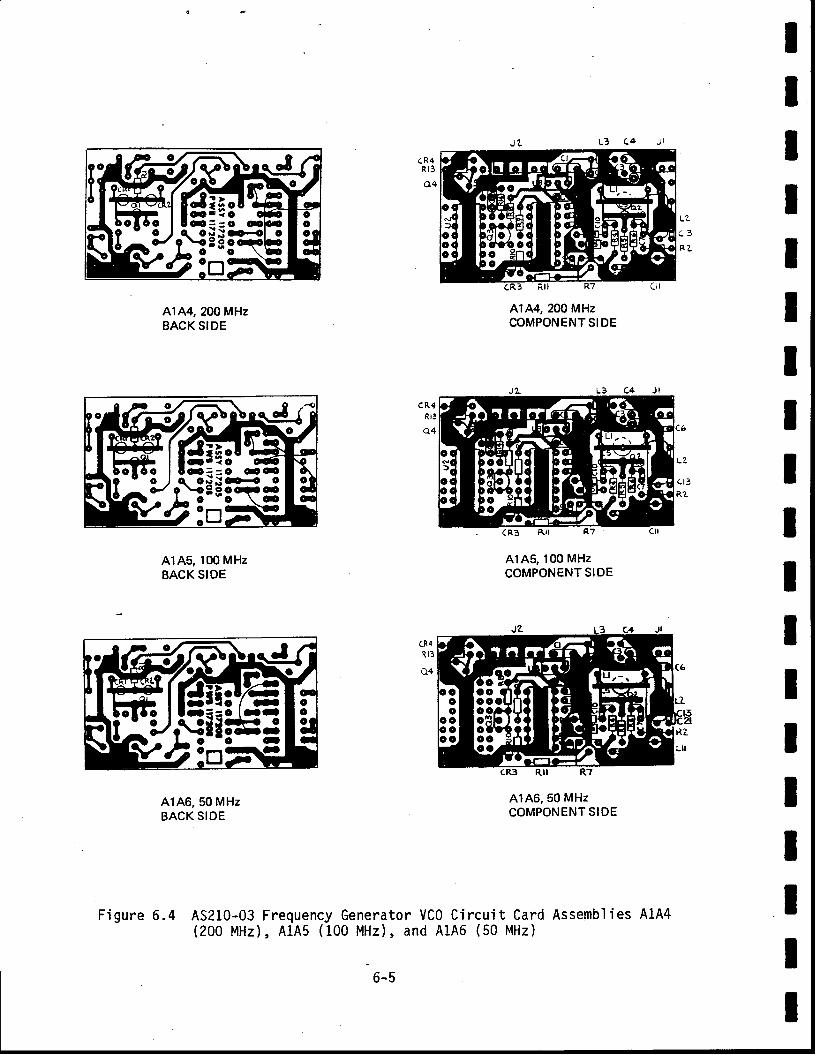
IIIIIIIIIIIIIIIIIII
cR4R l3
LZ
K C
A1A4, 2OO MHZBACK SIDE
A1A4, 2OO MHZCOMPONENT SI DE
A1A5, lOO MHZCOMPONENT SIDE
41A6, 50 MHZCOMPONENT SIDE
AlA5, 1@ MHzBACK SIDE
A146, 50 MHzBACK SIDE
Figure 6.4 AS210-03 Frequency Generator VCO Circui t Card.Assembl ies A1A4(200 MHz) , A l .A5 (100 MHz) , and A lA6 (50 MHz)
ocococ
IIIIIIIIIIIIIIIIIII
I TEI.'
I
a
4
ASSEI ' iSLY l rU| |8€R 00-t | /354-01
OTY PAFT I IUTIgER
' 2 . . t 7 - 2 2 - 0 r - 2 0 3 1
3 , 25 -56 -590 -b5 , i 38
0. I t i -ET :6 At l r :
6 . t ? - 0 s - 5 0 - 0 t r 4
r { * r E N O O F L I S T + * + *
CABLE ASSEI IBLY
O E 5 C R I P T I O H
3 PI l r Co l i l . rEcTgR
S H I E L D I I { G S E A D
? 5 A U G , S T R A I { D E D , T E F L O H
CR!TtP TER' I IHAL
REF, OEs tG . AHO RE} IAEKs
r l oLEx , ! l ! 64
U' IRE
F E R R o X C U S E , 0 2 i l t
tC rL0R AS FOLLOt lS r RED._? I O L E T , B L f i C iA L P H f l , 2 9 O O 5
n o L E x , 2 7 2 6 4
6-27
t TE'I OTY
5
6
7
CAELE ASSEI1ELY
DESCRIPTION
OSN CONN€CTOR, STRTICHT
OgH CONH€CTOR, RIGHT AHGLE
,095 sE t t t -R t c lD c rBLE
R€F . OESIG . THD RE I {ARKg
S E A L E C T R O , 9 S : 9 I
S E A L E C T R O , 9 8 2 9 l
r i r . EHD OF LlSt ***r
6-?8
ASSE|"TELY HUftS€R 00- | | 7357-01
OTY PARI NUI'IBEP
l , l 7 -15 -624 -9184 -31
0 . | 6 -RGU-31 6
t . 1 7 - 5 1 - 3 2 ' 3 - 3 1 8 4
s**. EHD 0F LIST ****
CABLE ASSEI . IELY
o€scRtPTloH
CONNEC?OR
coAx UIRE, 50 oHl{
CONNECTOR
REF, DES I8. ANO REI ' iAPKSI TETI
1
S E A L E C T R O , 9 S I 9 I
AS REOUIRED2
3
SEALEETRO, 9829i
6-29
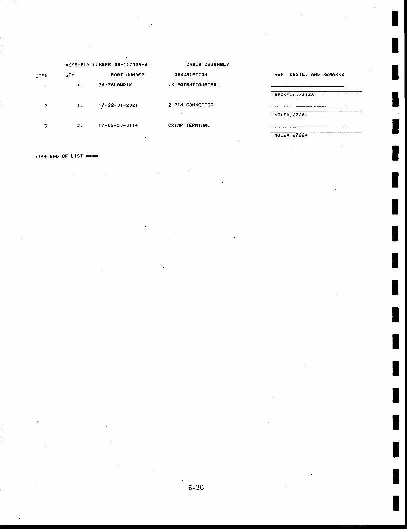
Ass€f18LY NUr ' r8ER 0 0- l | 7358- 01
t rEl t QTV
I
3
r*r* Et{O 0F LIST ****
R E F . T ' E S I G . A N C ! R E N A R K S
EEEI(FIAH, 73 I 38
noLEx,iz7264
ngLEx,272A4
6-30


Il,ttIIIIIl:IIIIII
: AS2l O-O4DIGITAL DELAY
GENERATOR MODULE
M84-0018
I
Revi sed 8/84
AS2IO-O4DIGITAL DELAY
GENERATOR MODULE
M84-0018
Revised B/84

-:
Irlrl1IItIIIIIi:r,;,,
M84-0018 IIIIItIIIIIIIIIIIII
Al l r fghts reserved. No part of th is publ icat ion may bereproduced, stored in a retrieval system, or transmitted,in any form or by any means, electronic, mechanical ,photocopying, recording and/or othenrise without thepr ior wr i t ten permission of ARG0Systems, Inc. This man-iral may not be lent , resold, h i red out or otherwise dis-posed of by way of trade in any form_of binding or coverother than that in which i t is publ ished, wi thout theprior consent of ARG0Systems, Inc.
ARG6Systems, Inc. / 884 Hermosa Court , 'sunnyvale, Cal i fornia 94086-Telephone (Area Code 408l, 737'2000 / Telex No- 352077

Il.
J
IIIIIIIli
tItIIIIII
Chapter
TABLE OF CONTENTS
Ti t le
Preface
GENERAL INFORMATION
1-1 Intnoduct ionL-2 Physical and Electr ical Descr ipt ion
INSTALLATION
2-L Introduction
OPERATION
3-1 Introduct ion3-Z Control s and Connectors3-3 0perat ing Instruct ions
THEORY OF OPERATION
4-1 Introduction4-2 Clock Circui ts4-3 Data Interfacing Circui ts4-4 Reference Pulse and Delayed Pulse Generation4-5 Sel f -Test Circui ts
MAINTENANCE AND CALIBRATION
5-1 Introduction
SECTION
5-2 Prevent ive Maintenance
SECTION I I
5-3 Performance Test ing5-4 AS210-04 Time Interval5-5 Test Procedure5-6 AS210-04 Reference and
Performance Tests5-7 Test Procedure
Performance Test
De'layed Output Pul sewi dths
M84-0018
Page
v
1-1
1-11-1
2-L
2-L
3-1
3-13-13-1
4-1
4-14-14-3
Ci rcui ts 4-34-5
5-1
5-1
5-2
5-35-35-4
5-45-7
IIIIIttIIIIIIItIIII
IT
]
M84-0018
Page
5-95-95-1 I
5-L2
5-13
6-1
6-16-16
IIIIIIIli
IIIIIII
i
I',
Chapter
TABLE 0F CONTENTS (Cont' inued)
T' i t l e
SECTION I I I
Cal ibrat ion/Al ignment ProcedureAccess to AS210-04 Digi ta l Delay Generator ModulePLO Al ignment ProcedureAS210-04 Reference and Delayed Output PulsewidthA1 ignment Procedure
5-85-95-105- 11
SECTION IV
5-12 Troubleshoot ing Procedures
ILLUSTRATED PARTS LIST
6-1 Introduct ion6-2 Manufacturer 's Code List
I- 1 1 -
M84-0018
Page
r-2
3-2
4-2
5-8
5-10
5-15
5-16
6-4
6-9
6-13
IIILi gure
1.1
3 .1
4.t r
4.2
4 .3
5 .1 .
5 .2
5 .3
5 .4
5 .5
6 .1
6 .2
6 .3
LIST OF ILLUSTRATIONS
T i t le
AS210-04 Digi ta l DelaY Genenator
AS210-04 Front Panel Control s and Connectors
Data Interface and Clock Circui ts
Reference and Delay Pulse Generator c i rcui t Diagram andTimi ng Diagram
Sel f-Test Ci rcuit
Test Configuration for Time Interval Performance Testof the AS210-04
Test Configuration for Reference and Delayed 0utputPulsewidth Performance Test of the AS210-04
Flow D' iagram of the Cal ibrat ion/Al ignment Procedurefor the AS210-04 Digi ta l Delay Generator
AS210-04 Phase-Locked Osci l lator and Program ControlAssembly, A1, Schematic Diagram
AS210-04 Processing and 0utput Circui ts Assembly ' A2'Schematic Diagram
AS2io-04 Digi ta l Delay
AS210-04 Digi ta l DelaY
AS210-04 Di gi tal De'l aY
4-4
4-6
5-5
IIIIIIIIIIIIIITI
Generator
Generator Assembly, A1
Generator Assembly, A2
- ' t 1 1 -
Il.
M84-0018
IIIIIItl)IIIIIII
i
I
Iab l e
1-1
3-1
5-1
5-2
5-3
5-4
LIST OF TABLES
Ti t le
AS210-04 EQUIPMENT SPECIFICATI0N
AS21O-04 FRONT PANEL CONTROLS AND CONNECTORS
PREVENTIVE MAINTENANCE CHECKS AND SERVICES
REQUIRED TEST EQUIPMENT FOR THE TIME INTERVALPERFORMANCE TEST OF THE AS21O.O4
AS21O-04 DIGITAL DELAY GENERATOR SI.IITCH SETTINGS ANDCORRESPONDING TIME INTERYAL TOLERANCE LIMITS
REQUIRED TEST EQUIPMENT FOR REFERENCE AND DELAYEDOUTPUT PULSEI,IIDTHS OF THE AS21O-04
REQUIRED TEST EQUIPMENT FOR THE PLO ALIGNMENT PROCEDURE
REQUIRED TEST EQUIPMENT FoR THE AS210-04 REFERENCE ANDDELAYED OUTPUT PULSE }IIDTH ALIGNMENT PROCEDURE
ERROR CODE LISTING
VISUAL INDICATORS
Page
1-3
3-3
5-2
5-3
5-6
5-7
5-1 I5-5
5-6
5-7
5-8
5-12
5-13
5-14
I -1 V -
M84-0018
PREFACE
Th ' is manua l con ta ins ins ta l la t ion , opera t ion and main tenance
instruct ions for the AS210-04 Digi ta l Delay Generator. The data contained
here in i s a r ranged as fo l lows:
Il,IIIIII
Chapter 1
Chapter 2
Chapter 3
Chapter 4
Chapter 5
Chapter 6
Reference Publ i cat ions
General Informat ion
Instal I at ion
Operati on
Theory of Operation
Maintenance and Cal ibrat ion
I l lus t ra ted Par ts L is t
Portable f, lainframe 0peration and Maintenance Manual
Mainframe 0peration and Maintenance Manual
Module Control ler Operat ion and Maintenance Manual
Frequency Comparator 0peration and Maintenance Manual
Frequency Generator 0peration and Maintenance Manual
Standby Battery Operat ion and Maintenance Manual
Microwave Generator Operat ion and Maintenance Manual
Distr ibut ion Ampl i f ier Operat ion and Maintenance Manual
Time Clock Operat ion and Maintenance Manual
AS21OA-PM
AS210RM, LM
AS210-01A
AS2t0-02
AS210-03
AS210-05
AS210-06
AS210-08
AS210-20
tt,IItIIttII

Il,
:
ItIIIIIl,IIIIIII
}
I'I
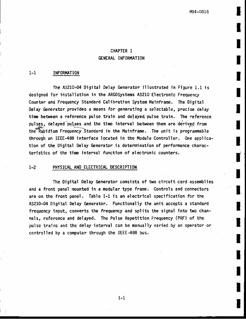
M84-0018
CHAPTER 1
GENERAL INFORMATION
1-1 INFORMATION
The AS210-04 Digi ta l Delay Generator i l ' lustrated in Figure 1.1 is
designed for installation in the ARG0Systems AS210 Electronic Frequency
Counter and Frequency Standard Calibration System Mainframe. The Digital
Delay Generator provides a means for generating a selectable, precise delay
time between a reference pulse train and deJaye( pulse train. Ih.
reference
pulsgs, delayed pulses and the time interval between them are derived from
the'"froicium Frequ.ilFsrundard in the Mainframe. The unit is programmablea
through an IEEE-488 interface located in the Module Control ler . One appl ica-
tion of the Digital Delay Generator is determination of performance charac-
teristics of the time interval function of electronic counters.
PHYSICAL AND ELECTRICAL DESCRIPTION
The Digital Delay Generator consists of two circuit card assemblies
and a front panel mounted in a modular type frame. Controls and connectors
are on the front panel . Table 1-1 is an electr ical speci f icat ion for the
AS210-04 Digital Delay Generator. Functionally the unit accepts a standard
frequency input, converts the frequency and splits the signal into two chan-
nels, reference and delayed. The Pulse Repetit ion Frequency (PRF) of the
pulse t ra ins and the delay interval can be manual ly var ied by an operator or
controlled by a computer through the IEEE-488 bus.
IIItIIIIIIIIIIIIIII
L-2
1-1
Il-.
t
IIIIIIIli
IIIIIII
J
l-'Figure 1.1 AS210-04 Digi ta l Delay Generator
M84-0018
L-2
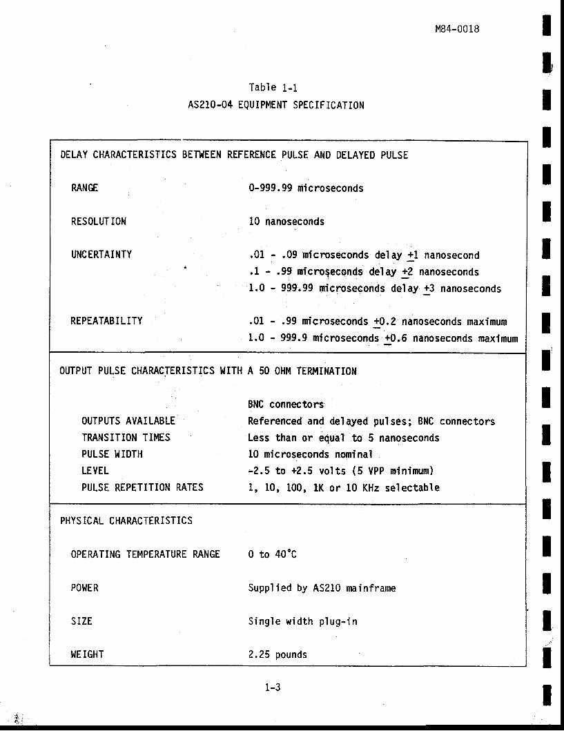
M84-0018 tI'IIIIIItl'IIItItIIt
Tab le 1 -1
AS21O-04 EQUIPMENT SPECIFICATION
DELAY CHARACTERISTICS BETI.IEEN
RANGE
RESOLUTION
U}.ICERTAINTY
REPEATABILITY
REFERENCE PULSE AND DELAYED PULSE
0-999.99 microseconds
10 nanoseconds
.01 - .09 microseconds delay +1 nanosecond
.1 - .99 microgeconds delay +2 nanoseconds' :1.0 - 999.99 microseconds delay a3 nanoseconds
.01 - .99 microseconds +0.2 nanoseconds maximum
1.0 - 999.9 microseconds r0.6 nanoseconds maximum
ourpuT puLsE CHARACIERISTICS l{ITH A 50 oHM TERMINATI0N
BNC connectors
OLTPUTS AVAILABLE Referenced and delayed pulses; BNC connectors
TRANSITION TIMES Less than or equ'al to 5 nanosecondsPULSE WIDTH 10 microseconds nominal
LEVEL -2.5 to +2.5 vol ts (5 VPP minimum)
PULSE REPETITION RATES 1, 10, 100, LK or 10 KHz selectable
PHYS ICAL CHARACTERISTICS
OPERATING TEMPERATURE RANGE O to 4O.C
POl.lER
SIZE
t,lE IGHT
Suppl ied by AS210 mainframe
Sing le w id th p lug- in
2 .25 pounds
1-3

II
)
ItIIIIIl:IIIIIIIlrI
M84-0018
CHAPTER 2
INSTALLATION
2-t INTRODUCTION
The AS210-04 Digital Delay Generator module plugs into the AS210
Mainframe. The module is electrically connected through the rear connector
and nechanically retained via a front panel locking bar on the mainframe.
Power and singal interface is provided through the mainfrane.
N0TE 1: Because of the high retention force of the rear card edge
connector, it may be necessary to pull on the RATE control at
the same tire as the release mechanism is pulled to remove the
0igital Delay Generator module from the mainframe.
NOTE 2: The power in the AS210 Mainfranre must be turned off when
inserting or removing the Digital Delay Generator.
cAurIoil
AS210 series plug-ins wi l l not work in Tektronix
T14500 series mainframes. Severe damage will result
if operation in this mode is attemPted.
The signals are output through two BNC connectors. The cables should be
equal length to avoid 'delay errors. There is a delay of approximately
1.5 nanoseconds/foot in RG58/U cable.
ItIIIIIIIli
IIIIIIIII
2-I

IIIttTIIII'IIIIIII
i
II
M84-0018
CHAPTER 3
OPERATION
INTRODUCTION
0perator interface with the AS210-04 Digital Delay Generator
is provided through two controls and two connectors on the front panel of the
module. The CPU interface is transparent to the operator. This chapter con-
tains a f ront panel i l ' lustrat ion keyed to a table explaining the funct ion of
the controls and connectors. The operating procedures provide applications
and instructions for use of the Digital Delay Generator.
CONTROLS AND CONNECTORS
Figure 3.1 is a f ront panel photograph of the Digi ta l Delay
Generator with index numbers keyed to Table 3-1.
OPERATING INSTRUCTIONS
The AS210-04 is connected via 50 ohm cable with BNC connectors.
See installation notes. Select the desired delay from 000.00 to 999.99
microseconds with the thumbwtreel switch. Select the desired Pulse Repetit ion
Frequency (PRF) of both outputs with the MTE switch.
NOTES
Maximum delay 98 microseconds on 10K Hz range
Maximum delay 998 microseconds on IK Hz range
Fast r ise-t ime may cause r inging on unterminated cable
IIIIIIIIIT'IItIII
II
3-1
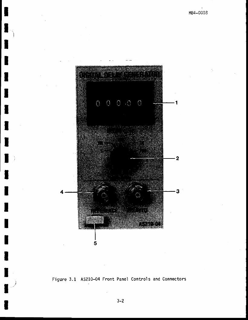
IIIIIIIIItIIItIIIII
Figure 3.1 AS210-04 Front Panel Controls and Connectors
M84-0018
3-2
M84-0018 Ili
IIIIIIIIIIIIIIITI
TABLE 3.1
AS21O-04 FRONT PANEL CONTROLS AND CONNECTORS
INDEXFIGURE
N0.3-1 PANEL MARKING FUNCTION
4
DELAY (microseconds)
RATE(Hz)
DELAYED
REFERENCE
None
Thumbwheel swi tich sel ects del ay i n
microseconds betneen the REFERENCEpulse and DELAYED pulse outputs.
Sel ects trhequency (PRF)
si gnal s.
The delayedis selectedselected by
pulse repetition fre-of' the output pul se
pulse output. Theby item 2, delayitem 1.
The reference pulse output.PRF is selected by item 2.
Release mechanism
3-3

II
l
IIIIIIIli
IIIIIIIl)I
M84-0018
CHAPTER 4
THEORY OF OPERATION
4-1 TNTRODUCTION
This chapter provides an analysis of the c i rcui ts used in the
Digi ta l Delay Generator. The circui t descr ipt ions are keyed to block dia-
grams, timing diagrams, and the schematic diagrams of the Maintenance chapter.
Detai ls of conunon circui ts (power suppl ies, etc.) are not included in th is
descr i pt ion.
The main c i rcui t ry of the AS210-04 is contained on two circui t card
assemblies designated Al and A2. The Digital Delay knerator module receives
a 10 lft lz standard input signal from the Rubidium Frequency Standard on the
AS210 Mainframe and produces two pulsed signal outputs. The PRF of the
pulsed signals and the tine delay between them are selectable. The AS210-04
is used in conJunction with the AS210-01 Module Controller which provides the
CPU control and interface.
4-2 CLOCK CIRCUITS
The AS210-04 has a 100 MHz clock which is used for the timing and
generat ion of the dual pulse t ra ins (Figure 4.1). The 10 MHz standard input
is divided by two at AlU12 to produce a 5 MHz reference input for phase
detector A1U13. The phase detector output goes to loop amplif ier/f i l ter
A1U14 providing the tun'ing vo'ltage for the 100 MHz Voltage-Controlled 0sci1-
lator (VCg) A1Q2 and AlQ3. The 100 MHz signal is d iv ided by 20 at A1U19 and
A1U20 then appl ied to the var iable input of AlU13. The VCO is thus phase
locked to the 10 MHz frequency standard. One output of the VCO is sent to
dr iver A1U21 which translates the s ignal to ECL levels needed for the delay
producing circui ts. The second output of the V00 is div ided by 10 at A1U20,
IIIIIIIIIIIIIIIII"JII
4-1
GulXu,J - r
PEH3 = Ee=E
:t
2"o
Eit Ogs;3
oIzFruart
(J
;
atiHcc-:,Ht5:gE?
HoSl isP9:E O <
J I E
Efis- E=i .< t uJ .
= F i @ x
d533' 1 l l aSRBEf t 2 =
?i t=
I M84-0018
1,,IIItI
=oo
6
rI
L
p hF u lN FI qY J
PH
o{I
tg
G
4
,nP
3(JL
(J.
JZt,oc)€crtt
ouG'
Io+J
|oPG'o
sf
a)L5g)
b..
I
l j
IIIIIIt
I
IIL
-'lJl!zG
Fz
G
$tC E F
r o <5??
6oZ Eu r <
. ! l lo3g?o t E Fe [ 6
vtat! ut( E e
- o <6?r
P O I< f rio @ o
4-2
converted to TTL at AlQ4 and applied to the frequency-division circuit con-
s is t ing o f A1U16, A1U17, A lu lg , and A1U19. S igna ls o f L Hz , 10 Hz,100 Hz '
KHz and 10 KHz are produced by th is div is ion c i rcui t and appl ied to PRF
select mult ip lexer Al ,U15. The mult ip lexer is addressed by the CPU which
scans bidirectional multiplexer A1U2 and A1U3 ten times per second to deter-
mine the status of the front panel RATE and Delay switches. The 100 MHz
clock, 10 KHz clock and one of the f ive PPS outputs (selected via A1U15) are
sent to the tining and reference circuits.
4-3 DATA INTERFACING CIRCUITS
The MTE switch and DELAY thumbwheel switches are connected to the
CPU data bus via multiplexers AZUL?, AZUL4, A2U25-U27 and A2U37-U39 (Figure
4.1). The 8-bi t data bus (D11A-D138) connects to a bidirect ional mul. t ip lexer
AlU2 and A1U3 which is addressed by the CPU (address bits A7, A15) and con-
trolled by tne nb' signal from the CPU. Counters A2U31-U34 and A2U20 (Figure
4.2) are loaded with data from the DELAY thumbwheel as follows. The BCD
thunbwlreel data is applied to the multiplexer addressed by the CPU as des-
cribed above. This data is sent over the data bus and returned under program
control to be latched into AIU7, AlUg and AlUll (Figure 4.1). l. lhen these
latches are appropriately addressed by the CPU their data is loaded into tJ|e
counters.
4-4 REFERENCE PULSE AND DELAYED PULSE GENERATION CIRCUITS
The product of the Oigital Delay Generator is two pulse trains at a
selected PRF (RATEI and selected tine delay between pulse- trains. Refer to
Figure 4.2 throughout the fo l lowing discussion. The signi f icant s ignals,
developed by previously descr ibed circui ts, are the 100 MHz phase locked
clock s ignal , the selected rate (PPS) and the delay data dialed by the
operator into the thumbwheels and returned to the unit via the CPU data bus.
Four bi ts of the delay data (PAl-PDl) are loaded into +10 counter AZUZA.
This is a high speed ECL counter and the data is converted to ECL levels
pr ior to loading in A2U20. The 100 MHz clock s ignal is a lso converted to tCL
and appl ied to the counter 's c lock input ' The 86'and Sdoutput of A2u20 are
Il,IIIIItI
IIIIIIIIlr
4-3
M84-0018
---
II
l. F .6 9 6 4
o H ; H i . . . 5: * { u { 4 4Ed Eg Eia
s il l r iE
G'LE )Itt
ocnE
1t
ct
t!Ltt,C'
tr:+)5C'L
L)
!o
.lJ|lt!(u(uclt
o.n5o-
.tt
oa1tccto.Jg
(l,
u&.
sl
rir
(1,3-=(t,
|.|.
fi+++ffi|5
i_T
IIIIIIIIIIII
iI
T
i < EE dE3
iiitl[fiI1
K a 8 3 d
4-4
t g: Pez
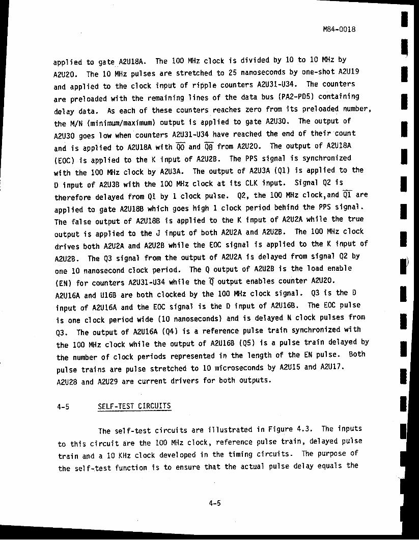
IIIIItIIIIIIItI
MB4-0018
applied to gate A2U18A. The 100 MHz clock is divided by 10 to 10 MHz by
AZU?g. The 10 MHz pulses are stretched to 25 nanoseconds by one-shot A2U19
and applied to the clock input of ripple counters A2U31-U34. The counters
are preloaded with the remaining l ines of the data bus (PA2-PD5) containing
delay data. As each of these counters reaches zero from its preloaded number,
the M/N (ninimum/maximum) output is applied to gate A2U30. The output of
A2U30 goes low when'counters A2U31-U34 have reached the end of their count
and is applied to A2U18A with 6"and Q['from A2U20. The output of A2U18A
(EgC) is applied to the K input of AZUZB. The PPS signal is synchronized
with the 100 MHz clock by A2U3A. The output of A2U3A (Ql) ls applied to the
D input of A2U3B with the 100 l4flz clock at its CLK input. Signal Q2 is
therefore delayed from Ql by 1 clock pulse. Q2, the 100 MHz clockrand 0f are
appl ied to gate A2U18B which goes high 1 c lock per iod behind the PPS signal .
The false output of A2U18B is applied to the K input of A2U2A while the true
output is applied to the J input of both AZUlA and A2U2B. The 100 t' lHz clock
drives both A2U2A and AZUZB whlle the EOC signal is applied to the K input of
AZU2B. The Q3 signal from the output of A2U2A is delayed from signal Q2 by
one l0 nanosecond clock period. The Q output of A2U2B is the load enable
(EN) for counters A2U31-U34 white tne 8 output enables counter A2U20.
AZU16A and U16B are both clocked by the 100 &tlz clock signal- Q3 is the D
input of A2u16A and the EOc signal is the D input of A2u16B. The EoC pulse
is one clock period wide (10 nanoseconds) and is delayed N clock pulses from
Q3. The output of A2U16A (Q4) is a reference pulse train synchronized with
the 100 l ' lHz clock while the output of A2U16B (Q5) is a pulse train delayed by
the number of clock periods represented in the length of the EN pulse. Both
pulse trains are pulse stretched to 1.0 mic'roseconds by A2U15 and A2U17.
A2U28 and A2U29 are current driverns for both outputs.
4-5 SELF-IEST CIRCUITS
The se l f - tes t c i rcu i ts a re i l l us t ra ted in F igure 4 .3 . The inputs
to th is c i rcui t are the 100 MHz clock, reference pulse t ra in, delayed pulse
train and a 10 KHz clock developed in the t iming circui ts- The purpose of
the sel f - test funct ion is to ensure that the actual pulse delay equals the
4-5
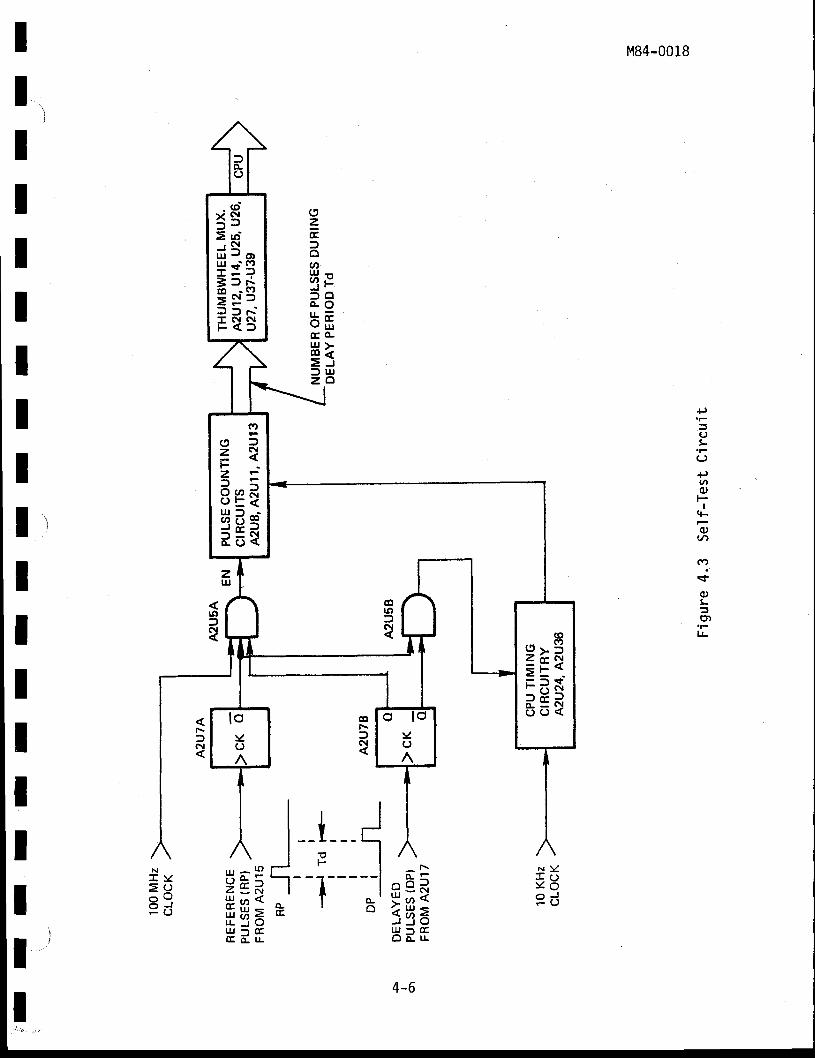
M84-0018
II
+,=(J!-
(J
+)IA(l)
FI
h
ott,
CY)
sf
(uL5ctl
lJ-
Ili
IItIII
N ) Zf UY oPd
_ No - =
o9dt ,n <luetu -r (rO E t - u
oo-CE
sE:H r n 4
FTEr,rj - CC( E E | l -
N
I Y= ( Jo Qo r {
- ( 0xS= J
= r dI N
LU - Ct)H dq= f F .6 - s t=r f= = r . 'Fts
(?
9R=Z F
EriH3eeat
3Ett r?&E5*
ozEf,o(n
3Ff , oo - ou - Fv lllE o -u J >9<= . J:) u.lz 6
4-6
M84-0018
dialed- in thumbwheel set t ing. Reference pulses f rom A2U15 and delayed
pulses f rom A2U17 are appf ied to the D input of A2U7B and A2U7A respec-
t i ve ly . The 100 MHz c lock s igna l i s app l ied to the c ' lock inputs o f bo th
f ' l ip- f lops s imultaneously. The DP output f rom A2U7B is thus delayed from
the Rp output of A2U7A by a time equal to t,he programmed de'lay time between
the two pulse t ra ins. l , lhen these two signals (RP and DP) are input to gate
A2Ul5 wi th the 100 MHz clock the output is a pulse (EN) whose durat ion
equals the t ime delay Td. The EN signal is appl ied to the enable input of
pulse counter A2U8 which is dr iven by the 100 MHz clock. The output of
A2U8 represents the number of 100 MHz pulses counted during the delay
per iod Td. This count, accumulated by A2U8, A2U11 and A2U13, goes to
thumbwheel mult ip lexers AZU12, AZU14, AZU25, A2U26, AZV27, A2U37, A2U38'
A2U3g where i t is scanned by the cPU. The cPU is also scanning the thumb-
wheel settings as part of the normal program and makes a comparison between
the two readings. An error determinat ion is displayed as a faul t on the
modul e control I er' s di spl ay uni t .
IIIIIIIITIIIIIIIIiI
4-7

II
i
ItIIIIIll
tIItIIt
!
tj
I
5-1
M84-0018
CHAPTER 5
MAINTENANCE AND CALIBRATION
INTRODUCTION
The purpose of th is chapter is to provide maintenance and cal ibra-
tion data for the AS2l0-04 Digital Delay Generator. Section I covers routine
preventative maintenance procedures. Section II outl ines performance tests
for the Digi ta l Delay Generator. Sect ion I I I contains the cal ibrat ion/al ign-
ment procedures for the AS210-04 module, and Siction IV describes trouble-
shooting data. Figures 5.4 and 5.5 are the schematic diagrams for the
Digital Delay Generator. The two truth tables on Figure 5.5 are for the
Thumbwfreel switch and MTE switch. For example, if the thunbwheel switch is
set at 300.00 nicroseconds and the MTE switch is set at 1 KHz then input
lines A5 on AZU27, 85 on AZU37, RA on AZUL?, RB on A2U14, and RC on A2U26
wi l l f loat h igh. A1l other input l ines wi l l be low. Please contact the
factory for any assistance required in the maintenance or servicing of the
AS210-04.
I1,IIIIIIIIIIIIIIIII5-1
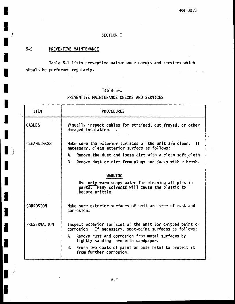
IItIIItIIIItIItIIII
I
PREVENTIVE MAINTENANCE
Table 5-1 l is ts prevent ive
perfonned regularly.
M84-0018
SECTION I
maintenance checks and services which
5-Z
should be
Table 5-1
PREVENTIVE MAINTENANCE CHECKS AND SERVICES
ITEM PROCEDURES
CABLES
CLEANLINESS
CORROSION
PRESERVATION
Visual ly inspect cables for strained, cut f rayed, or otherdamaged insulat ion.
Make sure the exterior surfaces of the unit are clean. Ifnecessary, clean exterior surfacs as follows:
A. Renove the dust and loose dirt with a clean soft cloth.
B. Renove dust or dirt from plugs and jacks with a brush.
l'lARNING
Use only warm soapy water for c leaning al l p last icparti lMany solvents wil l cause the plastic tobecome britt le.
Make sure exterior surfaces of unit are free of rust andcorrosion.
Inspect exterior surfaces of the unit for chipped paint orcorrosion. If necessary, spot-paint surfaces as follows:
A. Remove rust and corrosion from metal surfaces byl ight ly sanding them with sandpaper.
B. Brush two coats of paint on base metal to protect itf rom further corrosion.
J
5-Z
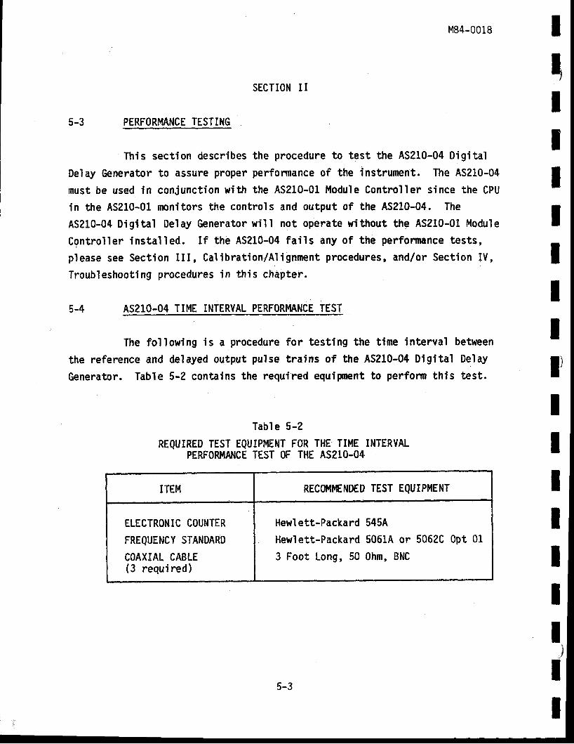
M84-0018
SECTION I I
5-3 PERFORMANCE TESTING
This section describes the procedure to test the AS2L0-04 Digital
Delay Generator to assure proper performance of the instrunent. The AS210-04
must be used in conjunction witjt the AS210-01 Module Controller since the CPU
in the AS210-01 monitors the controls and output of the AS210-04. The
AS210-04 Digital Delay Generator wil l not operate without the AS210-01 Module
Controller installed. If the AS210-04 fails any of the perfornance tests,
please see Sect ion I I I , Cal lbrat ion/Al ignment procedures, and/or Sect ion IV,
Troubleshootlng procedures in this chapter.
5-4 AS21O-04 TIME INTERVAL PERFORMANCE TEST
The following is a procedure for testing the time interval betweeh
the reference and delayed output pulse tralns of tlte ASZI0-04 Digital Dqlay
Generatnr. TabI e 5-2 contains the required equipnpnt to perform this test.
Table 5-2
REQUIRED TEST EQUIPMENT FOR THE TIME INTERVALPERFORMANCE TEST OF THE AS21O-04
ItIIIIIII
IIIIItI
j
II
ITEM REC$ft,lElltlED TEST EQUIPMENT
ELECTRONIC COUNTER
FREQUENCY STANDARD
COAXIAL CABLE(3 required)
Hewlett-Packard 545A
Hewlett-Packard 5061A or 5062C Opt 01
3 Foot Long, 50 Ohm, BNC
5-3
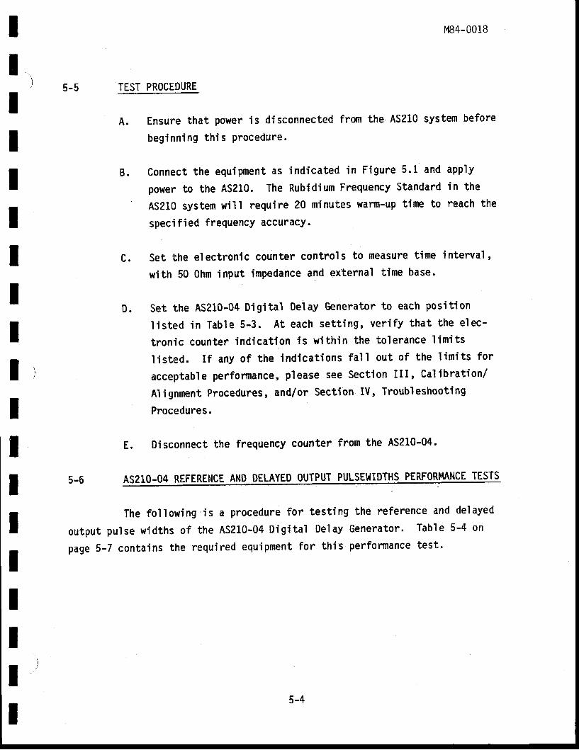
5-5
III
c.
III
D.IIli
M84-0018
TEST PROCEDURE
A. Ensure that power is disconnected from the AS210 system before
beginning this Procedure.
B. connect the equipment as indicated in Figure 5.1 and app' ly
power.to the As210. The Rubidium Frequency standard in the
AS210 system will require 20 minutes wann-up time to reach the
specified frequency accuracy-
Set the electronic counter controls to measure time interval,
with 50 Ohm input impedance and external t ime base.
Set the AS210-04 Digital Delay Generator to each position
l isted in Table 5-3. At each sett ing, ver i fy that the elec-
tronic counter indicat ion is wi th in the to lerance l imi ts
l is ted. I f any of the indicat ions fa l l out of the l imi ts for
acceptable performance, please see Sect ion I I I , Cal ibrat ion/
Alignment Procedures, and/or section IY, Troubleshooting
Procedures.
Disconnect the frequency counter from the AS210-04.
AS2t0-04 REFERENCE AND DELAYED OUTPUT PULSEIIIIDTHS PERF0RI'4A$EE-IEISTS
E.
tt
The fol lowing' is a procedure for test ing
output pulse widths of the AS210-04 Digi ta l Delay
page 5-7 contains the required equipment for th is
the reference and
Generator. Tabl e
performance test.
del ayed
5-4 on
5-4
ItII
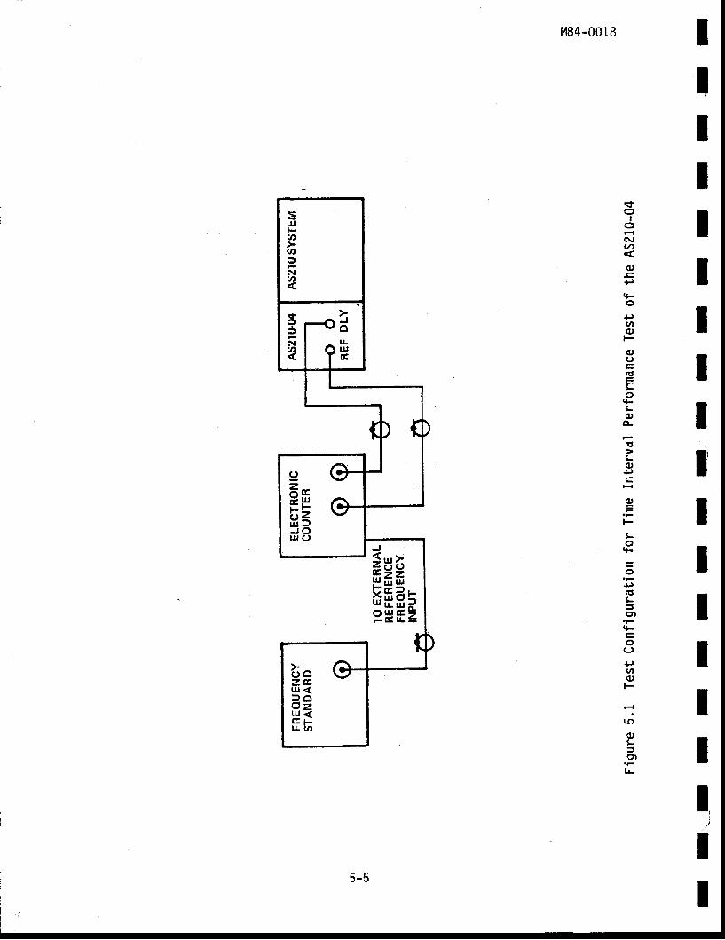
M84-0018
tI
It
1I
=uJat
@(3
(!
?
t6N(a
o:
?H-1
${
Izoc()ulru
frs*8FH5PHE=
bo O-z ErlJ <l oozHf,r! ul
5-5
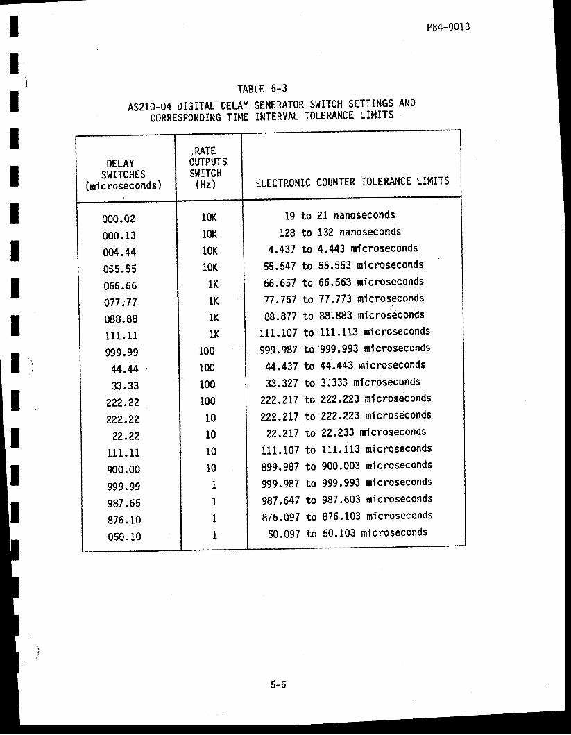
II
i
IIIIIII
M84-0018
TABLE 5-3
AS21O-04 DIGITAL DELAY GENERATOR S}lITCH SETTINGS ANDCORRESPONDING TIME INTERVAL TOLERANCE LIMITS
li
tIt
DELAYSt,lITCHES
(microseconds)
. RATEOUTPUTSSt{ITCH
(Hz) ELECTRONIC COUNTER TOLERANCE LIMITS
000.02
000.13
004.44
055.55
066.66
077;77
088.88
111 .11
999.99
44.44
33.33
2?2.22
222.22
22.22
111 . 11
900.00
999.99
987.65
876 .10
050.10
10K
10K
10K
10K
1K
1K
1K
1K
100
100
100
100
10
10
10
101
111
19
I?B
4,437
55. s47
66.657
77.767
88.877
111 .107
999.987
M.437
33.327
?2?.2L7
222.217
22.2L7
111 .107
899.987
999.987
987.647
876.097
50.097
to 2t nanoseconds
to 132 nanosecondsto 4.443 microseconds
to 55.553 rnicroseconds
to 66.663 microseconds
to 77.773 microseconds
to 88.883 microseconds
to 111.113 microseconds
to 999.993 microseconds
to 44.443 microseconds
to 3.333 microsecondsto 2?2.223 microsecondsto 222.223 microsdcondsto 22.233 microseconds
to 111.113 microseconds
to 900.003 microseconds
to 999.993 microseconds
to 987.603 microseconds
to 876.103 microseconds
to 50.103 microseconds
5-6
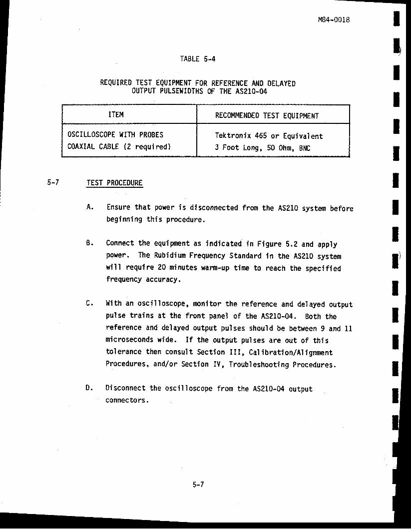
Il,IIItII
IIIII
c.
D.
M84-0018
REQUIRED TESTOUTPUT
IABLE 5-4
EQUIPMENT FOR REFERENCE AIIO DELAYEDPULSE}IIOTHS OF THE AS21O-04
5-7 TEST PROCEDURE
A.
B.
Ensure that power is disconnected from the AS210 system beforebeginning this procedure.
Connect the equipnrent as indicated in Figure 5.2 and applypower. The Rubidium Frequency Standard in the AS2l0 systemwill require 20 minutes wann-up tire to reach the specifiedfrequency accuracy.
!{ith an oscil loscope, monitorn the reference and delayed outputpulse trains at the front panel of the AS2l0-04. Both thereference and delayed output pulses should be between 9 and 1lmicroseconds wide. If the output pulses are out of thistolerance then consult Section III, Cal ibrafion/AlignnentProcedures, and/or Section IV, Troubleshooting Procedures.
Disconnect the oscil loscope from the ASZ10-04 outputconnectors.
Il'
ITEM RECOMMENOED TEST EQUIPMENT
OSCILLOSCOPE I,JITH PROBES
C0AXIAL CABLE (2 required)Tektronix 465 or Equivalent3 Foot Long, 50 0hm, BNC
5-7
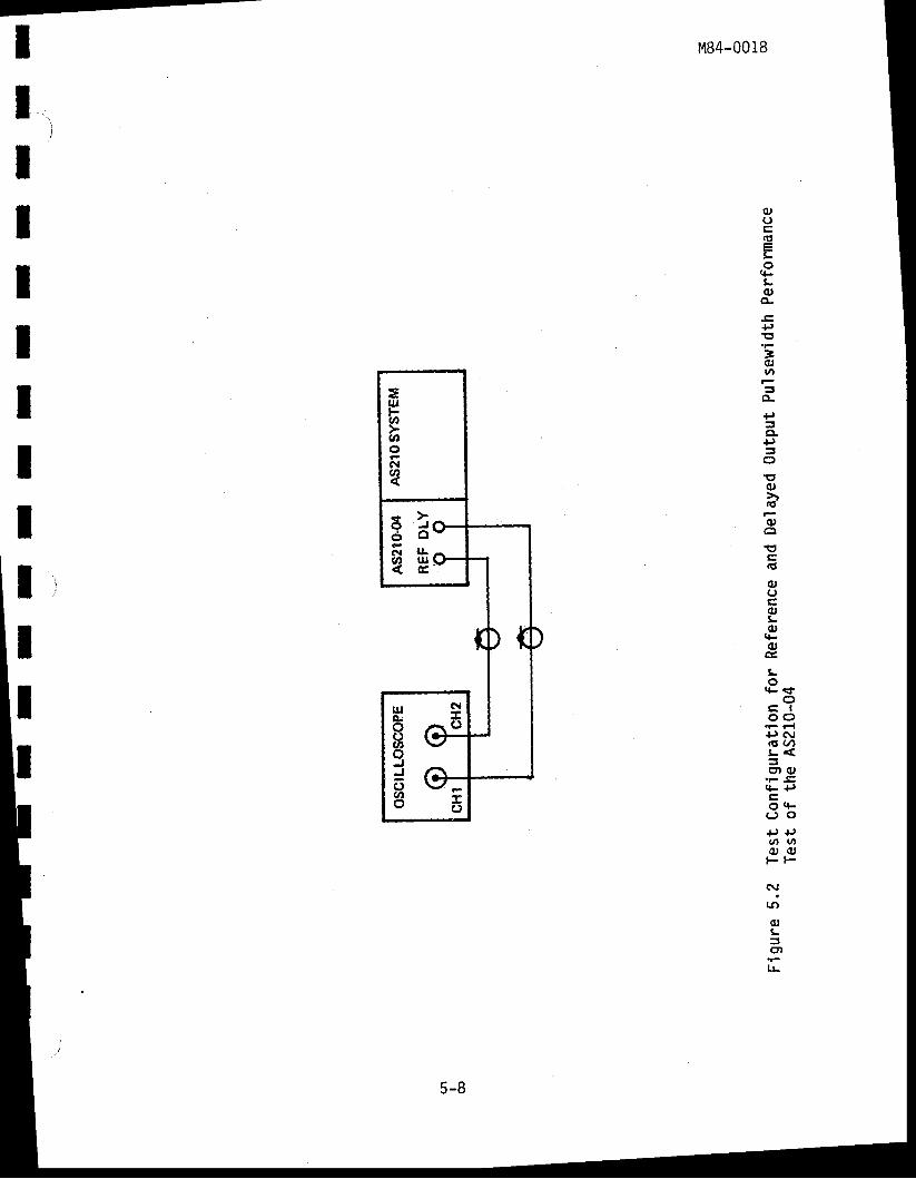
-
I1,.IIIIIIIti
III
(l)()q
sLcl
L(uo-
+'fg
3utn
5o-.tJ:to.+,Op(uItt
(l,
1tc(€(l,(J
(u3-(uQ'
d,
Loq- !+
og lo o+, (\r6 1L <or(u
.r -S
Eo q -( J o
sltr)(uL=ol
tt-
M84-0018
=utFu,u,of\ltn
1(
g !o-E go-
u rE
go,o
deat7 ;o6
5-8
IIIIIIIIIl!
IIII
M84-0018
5-8
SECTION I I I
cALIBRATI0N/ALrGNr4E[T PR0CEDURE
I.IARNING
The following Cal ibration/Al ignment Procedures(Chapter 5, Sect ion I I I ) and Troubleshoot ing
Procedures (Chapter 5" Section IV) are for use byqualif ied personnel only. To avoid personal
injury, do not perform any servicing other than
that of Routine Maintenance (Chapter 5, Section I)
and Perfonnance Testlng (Chapter 5, Section II)
unless you are qual i f ied to do so.
Figure 5.3 is a f low diagram of the Cal ibrat ion/Al ignnnnt Procedurefor the AS210-04 Digital Delay Generator. Use this flow diagram with thetheory of operat ion in Chapier 4, the text in th is chapter, and the i l lus-trated parts l ists in Chapter 6. The AS210 internal frequency standardcalibration data, contained in the AS210 mainfranp operation and maintenancemanual, is a lso referenced in th is f low diagram, Please note that i t is notnecessary to diassemble the AS210 system to determine if calibration/alignmentis needed. For any assistance needed in performing this callbration/alignmentprocedure, please contact the factory.
5-9 ACCESS TO AS21O-04 DIGITAL DELAY GENERATOR MODULE
Please reference the AS210 mainframe manual for the disassemblyprocedure of the AS210 system to allow access to the AS210-04 Digital DelayGenerator module. Access to the module c i rcui t ry i tsel f is gained by remov-ing the two metal s ide covers wi th a smal l straight-blade screwdriver. Place
the module on one of i ts s ides so that one cover is facing up. Start ing wi ththe end toward the edge connector, insert the screwdriver into one of theslots where the cover mates wi th the module chassis and pry the cover up. I twil l be necessary to move along the slot toward the front panel of the module
5-9
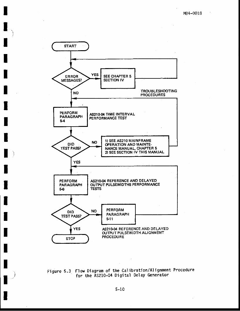
IIIIIIIIIIIIIIIIIIt
Figure 5 '3 Flow Diagram of t ! r9 cal ibrat ion/Al ignment Procedurefor the ASZ10-04 Digital Delay Generator
AS21GO4 REFERENCE AND DELAYEDOUTPUT PULSEWI DTH ALIGNMENTPROCEDURE
MB4-0018
TROUBLESHOOTINGPROCEDURES
SEE CHAPTER 5SECTION IV
AS21SO4 T{ME INTERVALPERFORMANCE TEST
1) SEE AS21O MAINFRAMEOPERATION AND MAINTE.NANCE MANUAL, CHAPTER 52I SEE SECTION IV THIS MANUAL
AS21GO4 REFERENCE AND DELAYEDOUTPUT PU LSEWI DTHS PER FORMANCETESTS
5-10
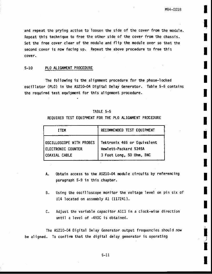
and repeat the prying action to loosen
Repeat this technique to free the other
Set the free cover clear of the module
second cover is now facing up. Repeat
cover.
the s ide
s ide o f
and f l ip
the above
of the cover from
the cover from the
the module over soprocedure to free
M84-0018
the modul e.
chass i s .
that the
thi s
IIIII5-10 PLO ALIGNMENT PROCEDURE
The following is the alignment procedure for the phase-locked
osci l lator (PLO) in the AS210-04 Digi ta l Delay Generator. Table 5-5 contains
the required test equipment for this alignment procedure.
TABLE 5-5
REQUIRED TEST EQUIPMENT FOR THE PLO ALIGNMENT PRMEDURE
ITEM REC0MIIENDED TEST EQUIPI"IENT
OSCILLOSCOPE I.IITH PROBES
ELECTRONIC COUNTER
COAXIAL CABLE
Tektronix 465 or EquivalentHewlett-Packard 5345A3 Foot Long, 50 Ohm, BNC
0btain access to the AS210-04 npdule circuits by referencing
paragraph 5-9 in this chapter.
B. Using the osci l loscope monitor tJre vol tage level on pin s ix of
U14 located on assembly A1 (LL724L).
C. Ad jus t the var iab le capac i to r A1C3 in a c lock-w ise d i rec t ion
unt i l a leve l o f -4VDC is ob ta ined.
The AS210-04 Digi ta l Delay Generator output f requencies should now
al igned. To conf i rm that the digi ta l delay generator is operat ing
IIIIttIIIIIIJ
II
A.
5- 11
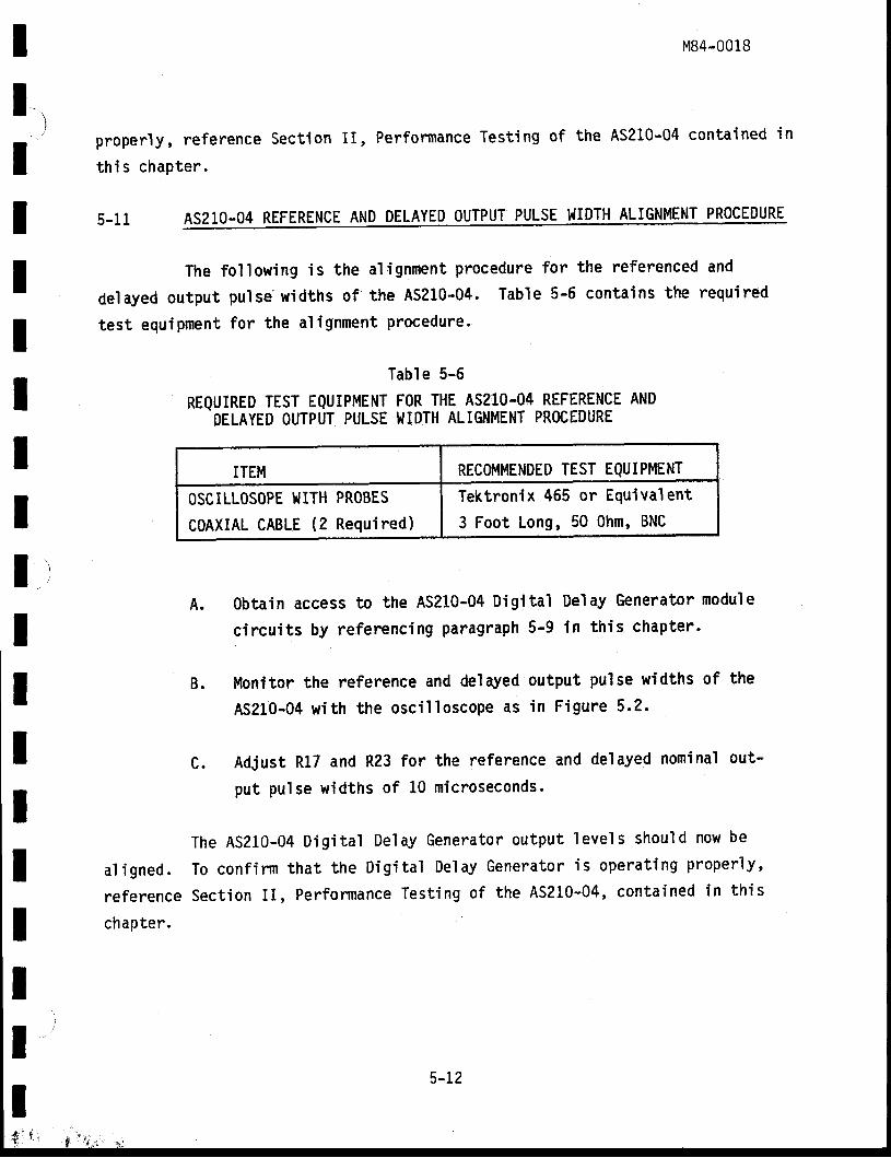
A.
B.
c.
IIIIIIIItIIIIIIIIIIj * I r ,
M84-0018
properly, reference Section II, Performance Testing of the AS21'0-04 contained in
th is chapter .
5-1 1 AS210-04 REFERENCE AND DELAYED oUTPUT PULSE lMH ALIGNMENT PRoCEDURE
The following is the alignment procedure for the referenced and
delayed output pulse"widths of the AS210-04. Table 5-6 contains the required
test equipment for the al ignment procedure.
Table 5-6
REQUIRED TEST EQUIPMENT FOR THE AS21O-04 REFERENCE ANDDELAYED OUTPUT PULSE WIDTH ALIGNMENT PROCEDURE
Obtain access to the AS210-04 Digital Delay Generator module
circui ts by referencing paragraph 5-9 in th is chapter.
Monitor the reference and delayed output pulse widths of the
AS210-04 with the osci l loscope as in Figure 5.2.
Adjust R17 and R23 for the reference and delayed nominal out-
put pulse widths of 10 microseconds.
The AS210-04 Digi ta l Delay Generator output levels should now be
al igned. To conf i rm that the Digi ta l Delay Generator is operat ing proper ly '
reference Sect ion I I , Performance Test ing of the AS210-04, contained in th is
chapter.
ITEM RECOMMENDED TEST EQUIPMENT
OSCILLOSOPE I{ITH PROBES
C0AXIAL CABLE (2 Required)
Tektronix 465 or Equivalent
3 Foot Long, 50 0hm' BNC
5-L2
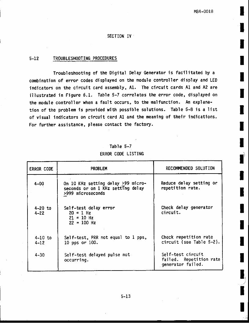
M84-0018
SECTION IV
5-L2 TROUBLES}IOOTING PROCEDURES
Troubleshooting of the Digital Delay Generator is facil i tated by a
combination of error codes displayed on the module controller display and LED
indicators on the ci rcui t card assembly, A1. The circui t cards Al and A2 are
i l lustrated in Figure 6.1, Table 5-7 corcelates the error code, displayed on
the module control ler when a faul t occurs, to the malfunct ion. An explana-
t ion of the problem is provided with possible solut ions. Table 5-8 is a l is t
of v isual indicators on circui t card A1 and the meaning of their indicat ions.
For further assistance, please contact the factory.
Table 5-7
ERROR CODE LISTING
IIItIIIttl'IIIIIIl,
,,,j
II
ERROR CODE PROBLEM RECOMMENDED SOLUTION
4-00
4-204-22
4-104-L2
4-30
0n 10 KHz setting delay >99 micro-seconds or on 1 KHz settTng del ay>999 microseconds
Self-test delay error?O= lHz21=10H222 = 100 Hz
Sel f-test, PRR not10 pps or 100.
Sel f-test del ayedoccurr i ng.
equal
pul se
PPs '
not
Reduce delay setting orrepetit ion rate.
Check del ay generatorci rcui t .
Check repetit ion ratec i rcu i t ( see Tab le 5 -2 ) .
Sel f - test c i rcui tfa i l ed. Repet i t ion rategenerator fa i l ed.
5-13
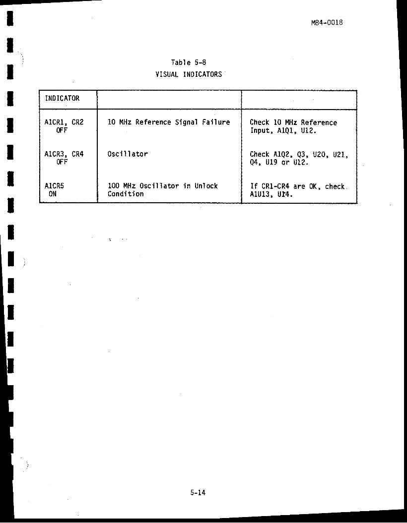
II
r
IIIIII
il
li
III
Tabl e 5-8
VISUAL INDICATORS
M84-0018
INDICATOR
AlCRl, CRzFF
A1CR3, CR4OFF
AlCR5ON
10 MHz Reference Signal Failure
Osci l I ator
100 MHz Osci l lator in UnlockCondit ion
Check 10 MHz ReferenceInput , A lQ l , U12.
Check A lQz, Q3, U20, U21,Q4, U19 or U12.
If CRI-CR4 are 0K, checkA1U13, Ul4.
5-14

It
J
IIIIIIIll
tIII
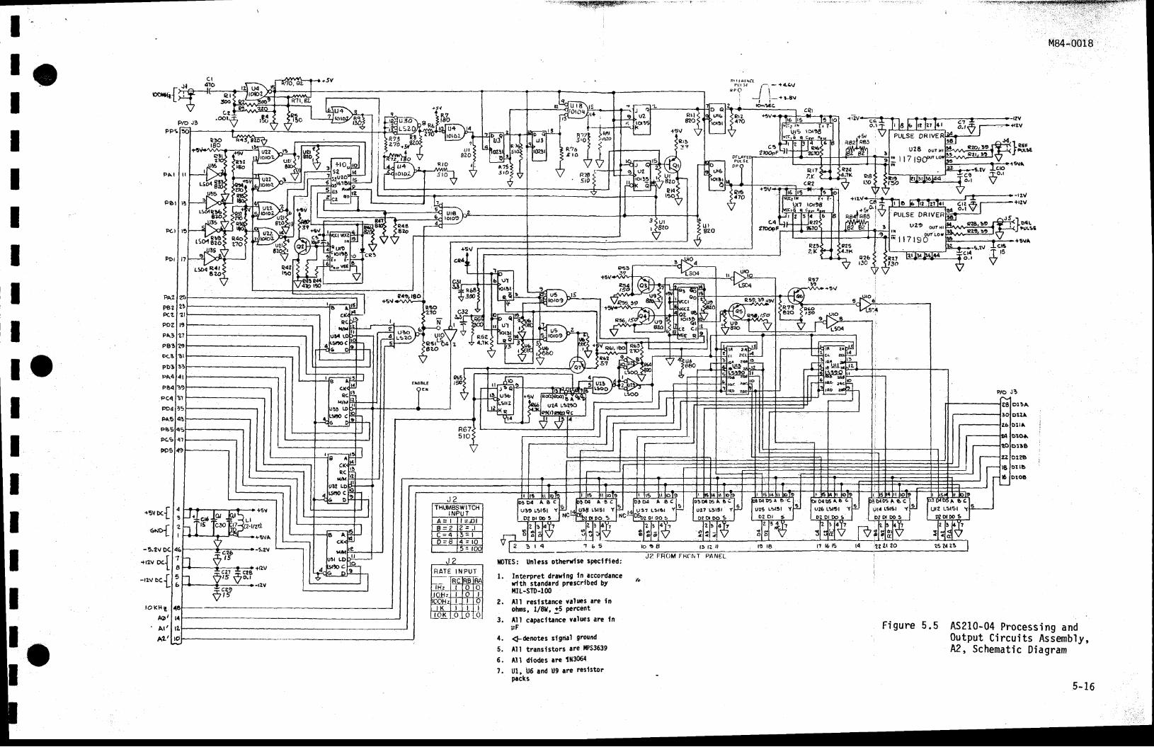
II
"- *.rF"=:!9€EEXt!SgHElt& .P.
MITES: Unless otherrlge specified,
l. Interpret dravlng ln accordarrcefith standard Prescrlbed bYillt-sTD.l00
2. Al l reslstance values are inohms, l/81{, 15 Percent
3. All capaclt nce Yalues are lnU F
+denotes slgdal ground
All translstors are llPS3639
All diodes rre ttl3064
Ul, U6 and U9 rre reslstorpacks
e l50o
c2
PfO JV'*',v
PPS
IIrl
PAZ
PB?Pcz
?az
PA3
PB3pc3
PD3PA4
IIIIIII
Pczl
pD4
FA.5
trBE
pc5DrSg
ouBDI IB
*sux{
^t{
-E-zV DC
*,tu oa{
I O K H l
M t' A l '
ALI
r o t B t r t? l l
FHCT\ T PANEL
t ? 1 6 6 t 4 Z?212o
4 .5 .6 .7 .
Figure 5.5 AS210-04 processing andOutput Circui ts Assembly,A2, Schematic Diagram
- J l
"*,.{tsIIIIII
a f R t . a -
u_15 iot?6
2t
c 1
zq3r
PULSE ORIVE
u?9 ourttout low
i l 7 t 9 0
4)
it; lr l
P/O J'
5-16

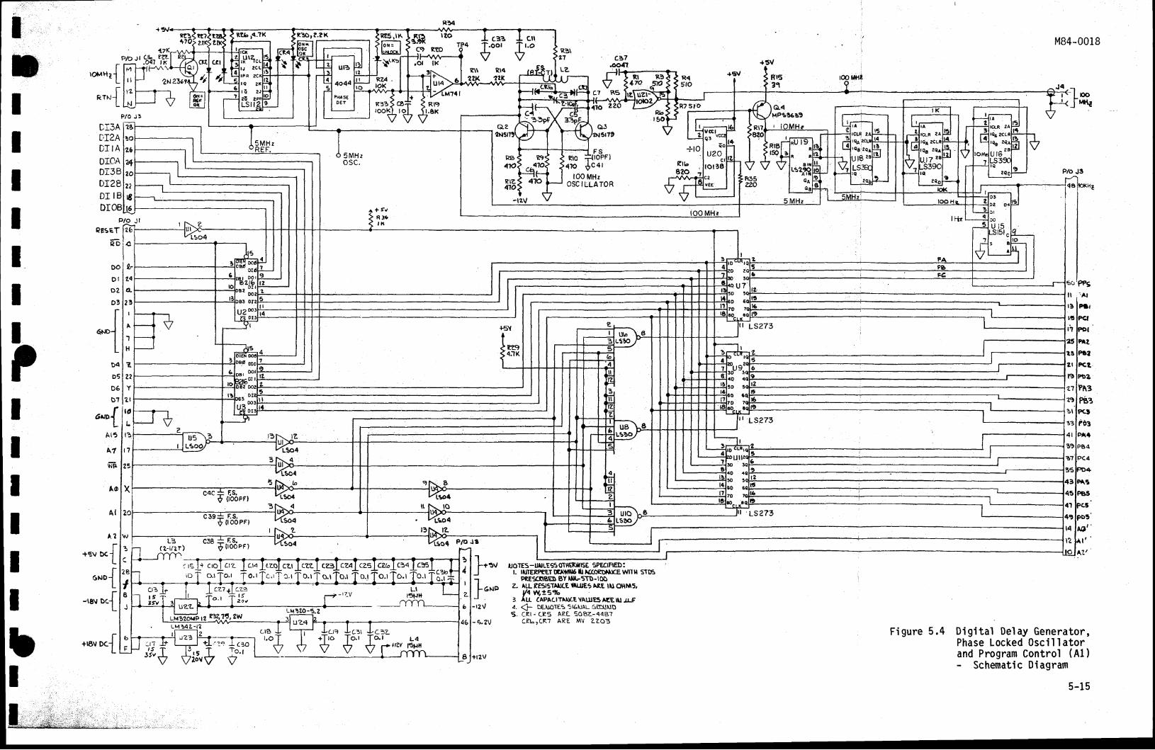
l-i.---
M84-0018
Figure 5.4 Digi ta l Delay Generator,Phase Locked 0sci l latorand Program Control (A1)- Schematic Diagram
,** ,{
"'u{
osr'Sdh 1?llia ffit-a,rrl-1 , , | 2Nz
l'"1--1-J-L\l-r--- vI
IIIII
Di3AL,I1A
D I I ADICADrSBDT2BDr lDI
PESET
p/o Jl
E 6 l a
Ip
DO
D ID2
D3rIleuo-1II
L
D4
D5
D6
D?
o*{L
At5
9r
L4o-
l aI
?
?2
? l
vL
AI
743p6:
P03Ptt
I t
r3),ri
l3
7 l
19
< t
a
3tIItItI
A I
t 2
*-,u *{
nuo{
-'ru o{
**u o.{
L3(2-i lzr)
c4c * ES,+ (looPFl
c38 * Es.dr (IOOPF)
B
tI
I
I l].*"l]"*6 l - t 2 V
UOTES_U.ILE55O1}IERW6E SPECIFIED:I. IUIERPRET DTA\|{N6 [ t((ffiD}TTE WIIU STDIS
PRES(TIBED BY IIII,.5TD-IOAz. Ar.l- TEsIsTAJCE tAUlE5 ARE lU OHMs,
1/< w,!5ao3 ALT TAPACITAITCE VAUIES AirE IU .U-F4. + DetloTE1 5tGuAL GErtiND5. CRt.CRs ARL 5OBZ-44A?
cRr"cR-7 ARE MV ZZo3
LM32O-5,2
.LC1l
l v . '
Vs" cazo'l t-4
cr9
l +csT'v
I L5273
r r L s z T 3
ca9* F.s.+ 000PFl
o . l - l - o . r I o . r l o . l
+rzy 16}lll
461-q.?v
5-15

tIItIItIIIItIttIIIt
M84-0018
CHAPTER 6
ILLUSTRATED PARTS LIST
6-1 INTRODUCTION
Th. is chapter conta ins an i l l us t ra ted par ts f i s t fo r the D ig i ta l
Delay Generator Module. The assembly numbers and assembly t ' i t ' le are l is ted
at the top o f the par ts l i s ts . The par ts l i s ts a re d iv ided in to s ix co lumns
and ar ranged in the fo l low ing onder :
Col umn 1 - Item Number
Column 2 - Quant i tY Per assemblY.
Column 3 - Manufacturer 's Code
Col umn 4 - Part Number
Column 5 - Descr iPt ion
Co1umn 6 - Reference Designat ion
6-1
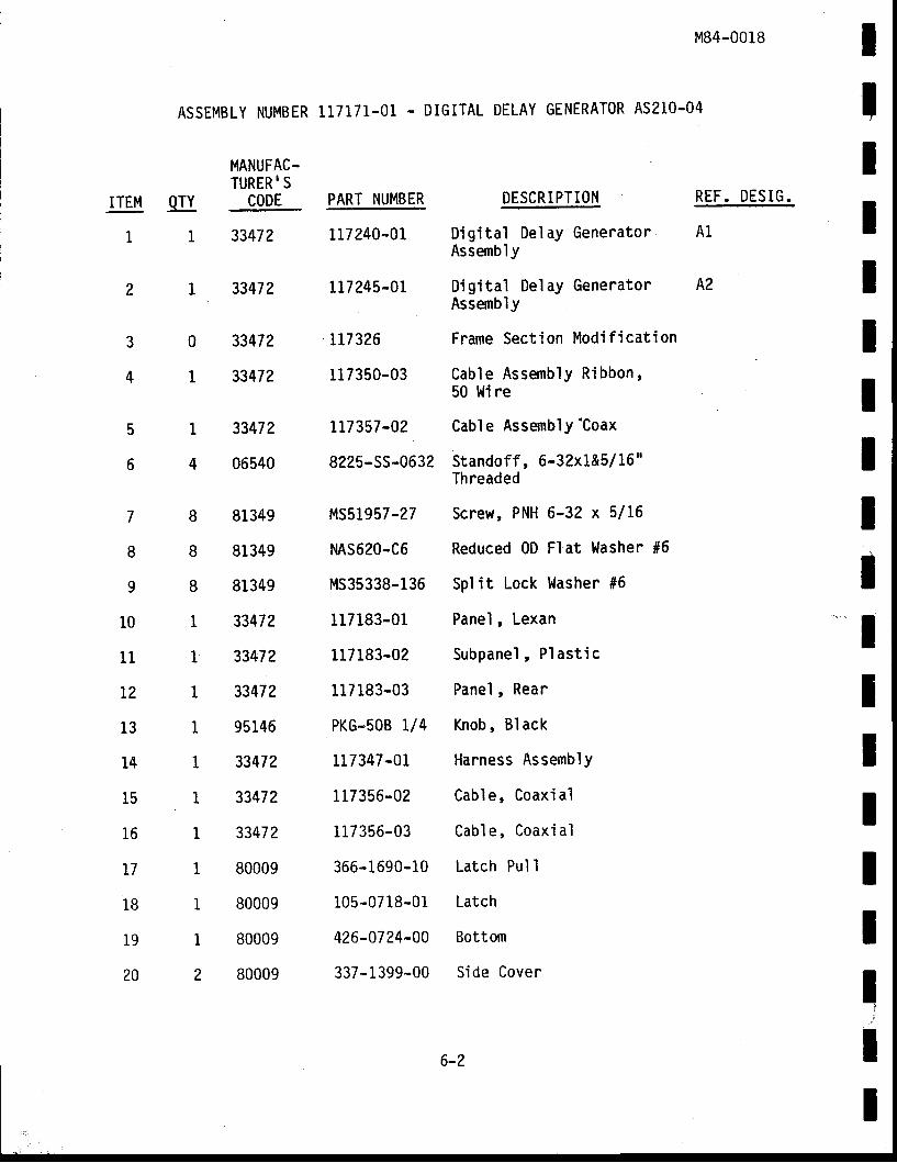
ASSEMBLY NUMBER1 1717 1-01 . DIGITAL DELAYGENERATOR AS21O.O4
M84-0018
REF. DESIG.
A1
A2
IIIIIIIIIIIttttII
i
II
MANUFAC-TURER. S
CODE PART NUMBERITEM
7
8
9
10
11
L2
13
14
15
16
L7
18
19
20
qu.I
1
33472
33472
33472
33472
33472
06540
81349
81349
81349
33472
33472
33472
95146
33472
3347?.
3347?
80009
80009
80009
80009
0
1
3
4
5
6
1
4
117240-01
L17245-0L
LL7326
117350-03
rL7357-02
8225-SS-0632
MS51957-27
MS620-C6
MS35338-136
117183-0r
117183-02
117183-03
PKG-sOB 1/4
117347-01
117356-02
117356-03
366-1690-10
105-07 18-01
426-0724-00
337-1399-00
DESCR I PTION
Digi ta l Delay GeneratorAssembl y
Digi ta l Delay GeneratorAssembly
Frame Sect ion Modif icat ion
Cable Assembly Ribbon'50 tli re
Cable Assembly 'Coax
Standoff , 6-32x1&5/16'Threaded
Screw, PNH 6-32 x 5/16
Reduced 0D Fl at Washer #6
Spl it Lock Washer #6
Pane l , Lexan
Subpane l , P las t i c
Pane l , Rear
Knob, Bl ack
Harness Assembly
Cabl e, Coaxi a l
Cab le , Coax ia l
Latch Pul I
Latch
Bottom
Side Cover
I
8
I
1
I
1
1
1
1
1
1
1
1
2
6-2
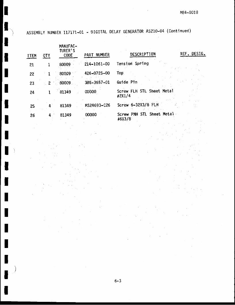
IIIIIIIIIIItItIItIt
M84-0018
ASSEMBLY NUMBER 117171-01. DIGITAL DELAYGENERAT0R AS210-04 (Cont inued)
ITEM QTY
21 1
22 1
232
24 1
MANUFAC.TURER I S
CODE DESCRIPTION REF. DESIG.
80009
80009
80009
81349
PART NUMBER
214-1061-00
426-0725-00
386.3657-01
00000
MS24693-C26
00000
Tension Spr ing
Top
Guide P in
Screw FLH STL Sheet Metal#zXLl4
Scnew 6-32X3/8 FLH
Screw PNH STL Sheet Metal#6X3/8
4 81349
4 81349
25
26
6-3
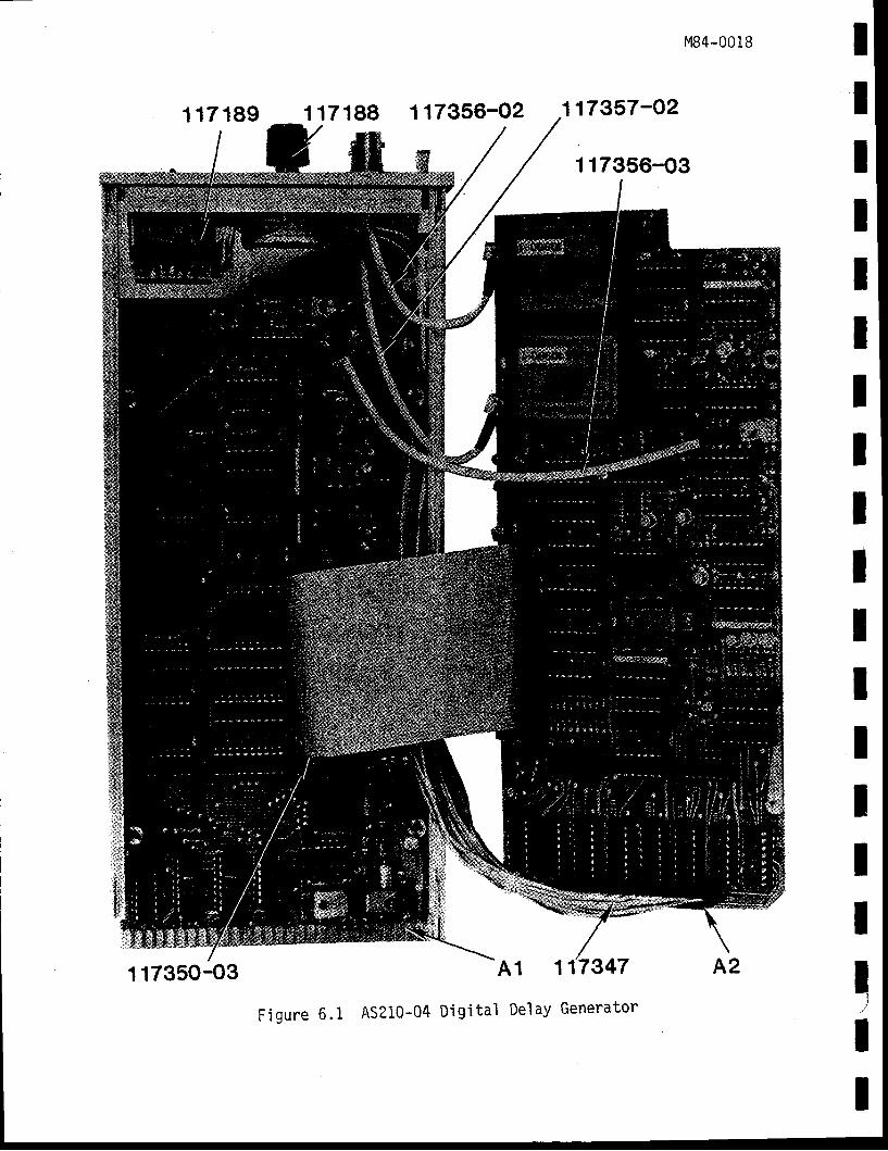
M84-0018 IIIIIIIItIItIIIII,J
II
1 17189 117188 117356-02
A1 117947
117357-O2
1 1 735G-O3
117350-03
Fi gure 6.1 AS210-04 Digi ta l Delay Generator
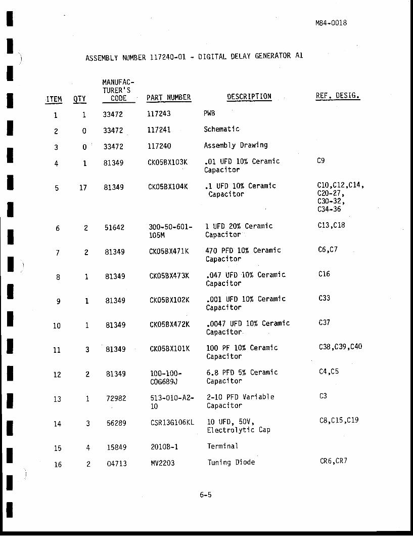
IIIIIIIItItIIIIIIII
ASSEMBLY NUMBER 117240.01. DIGITAL DELAY GENERATOR A1
MANUFAC.TURER. S
CODE PART NUMBER DESCRIPTION
Pt.lB
Schematic
Assembly Drawing
.01 UFD 10% CeramicCapaci tor
.1 UFD L0% CeramicCapaci tor
I UFD 20% CeramicCapaci tor
470 PFD L0% CeramicCapaci tor
.047 UFD 10% CeramicCapaci tor
.001 UFD 10% CeramicCapaci tor
.0047 UFD 10% CeramicCapacitor
100 PF 10% CeramicCapaci tor
6.8 PFD 5% CeramicCapaci tor
2-10 PFD Var iab leCapaci tor
10 uFD, 50V,E lec t ro ly t i c CaP
Termi nal
Tun'i ng D'iode
M84-0018
REF. DESIG.
c9
c10,c12,c1.4,c2a-?7,c30-32,c34-36
c13,C18
c6,c7
c16
c33
c37
c38,C39,C4o
c4,c5
C3
c8,c15,C19
ITEM QTY
11
20
30
41
L17243
lt724l
rL7240
CKO5BXlO3K
CKOSBXl04K
300-50-601-105M
CKO5BX471K
CKO5BX473K
CKO5BXlO2K
CKO5BX472K
cKO5BXL01K
100-100-coc689J
513-010-A2-10
csR13G106KL
20108-1
MV2203
T7
3347?.
33472
33472
81349
81349
5t642
81349
81349
81349
81349
81349
81349
72982
56289
15849
047 13
10
11
L?
13
14
15
16
4
2
6-5
cR6,CR7
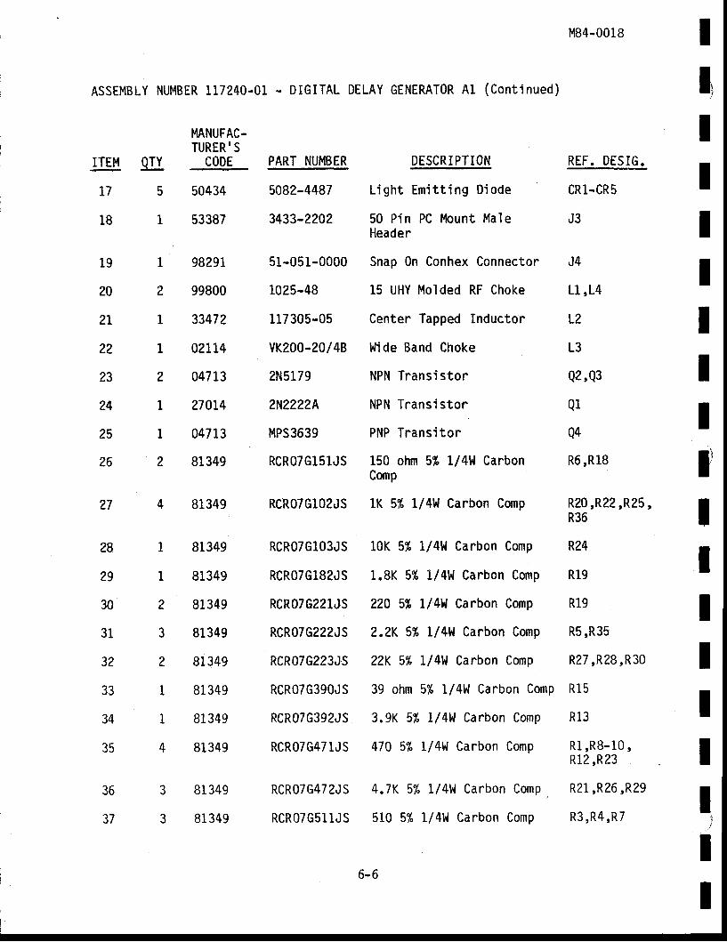
ASSEMBLY NUMBER 117240.01 - DIGITAL DELAYGENERAT0R A1 (Cont ' inued)
IIIIIIIIIli
IItIIIIi
II
3
3
M84-0018
REF. DISIG.
cRl-CR5
J3
J4
L l ,14
L2
L3
Q2, Q3
Q1
Q4
R6,R18
R20,R22,R25 ,R36
R24
R19
R19
R5,R35
R27 ,R28,R3o
R15
R13
Rl ,R8-10 ,R12,R23
R21,R26,R29
R3,R4,R7
MNUFAC-TURER' S
CODE PART NUMBERrrEM g]I.
175
18 1
19 1
202
21 1
22 1
232
24 1
25 1
?62
28 I
29 I
302
31 3
322
33 1
34 1
354
5082-4487
3433-2202
51-051-0000
1025-48
117305-05
vK200-20/48
2N5179
2N22224
MPS3639
RCR07G151J5
RCROTGlO2JS
RCR07G103JS
RCR07Gl82JS
RCR07G221JS
RCR07G222JS
RCR07G223JS
RCROTG39OJS
RCR07G392JS
RCR07G47 lJS
RCR07G472JS
RCR07G5l1JS
50434
53387
9829L
99800
33472
02114
047 13
270t4
04713
81349
81349
81349
81349
81349
81349
81349
81349
81349
81349
B1 349
81 349
DESCRIPTION
Ligh t Emi t t ing D iode
50 Pin PC Mount MaleHeader
Snap 0n Conhex Connecton
15 UHY Molded RF Choke
Center Tapped Inductor
l,li de Band Choke
NPN Transistor
NPN Transistor
PNP Transi tor
150 ohm 5% Ll4W CarbonComp
tK 5% 1/4W Carbon Comp
10K 5% 1/4}{ Carbon Comp
1.8K 5% 1/4W Carbon Comp
220 5% 1/4U Carbon Comp
?.2K 5% 1/4W Carbon Comp
22K 5% 1l4l,l Carbon Comp
39 ohm 5% l/4Vl Canbon Comp
3.9K 5% 1/4W Carbon Comp
470 5% 1/4W Carbon Comp
4.7K 5% 1 /4W Carbon Comp,
510 5% 1/4W Carbon Comp
27
36
37
6-6
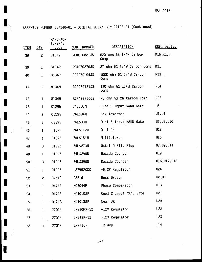
IIIIIIIIIIIIIIIIItI
gu2
ASSEMBLY NUMBER LL7?40-OL- DIGITAL DELAY GENERATOR Al (Cont inued)
MANUFAC-TURER.S
CODE
M84-0018
REF. D IS IG.
R16,R17 ,
R34
R32
U5
ul ,u4
u6 , u8, ulo
uLz
u15
u7,u9,u l1
u19
u l6 ,U l7 ,U l8
u24
u2,u3
ul3
U2T
u20
u22
u23
ul4
R31
R33
1
1
ITEM
38
39
40
81349
81349
81349
81349
81349
01295
01295
01295
01295
01295
01295
0129s
0L295
01295
34649
04713
04713
047 13
270r4
270r4
?70t4
PART NUMBER
RCR07G82lJS
RCROTG2TOJS
RCROTGlO4JS
RCR07Gl21JS
RCR42G750JS
74LS00N
74LS04N
74LS30N
7415112N
74LS1s1N
741S273N
74tS290N
741S390N
uA7952CKC
P8216
MC4044P
MC 10102P
MC10138P
LM320MP.12
Lt4342P-L2
1M741 CN
DESCRIPTION
820 ohm 51, Ll4U CarbonComp
27 ohm 5% l/4W Carbon Comp
100K ohm 5% l/4W CarbonComp
120 ohm 5% 1/4l.| CarbonComp
75 ohm 5% 2W Carbon Comp
Quad 2 Input NAND Gate
Hex Inverter
Dual 6 Input -NAND
Gate
Dual JK
Mul ti p' l exer
0c ta l D F l ip F ' lop
Decade Counten
Decade Counter
-5.2V Regul ator
Buss Dr iver
Phase Companator
Quad 2 Input NAND Gate
Dual JK
-12V Regu l a to r
+12V Regul ator
0p Amp
41
42
43
44
45
46
47
48
49
50
51
52
53
54
55
56
57
58
6-7
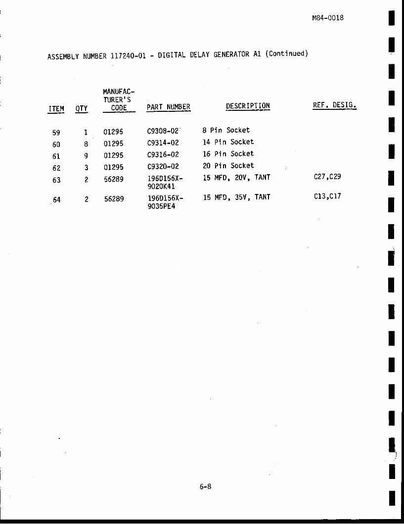
ASSEMBLY NUMBER 117240-01 - DIGITAL DELAYGENERATOR A1 (Cont inued)
IIIIIIIIIJIIIIIIt,II
1
8
9
3
2
DESCRIPTION
8 Pin Socket
14 Pi n Socket
16 Pi n Socket
20 Pi n Socket
15 MFD, 20U, TANT
15 MFD, 35V, TANT
M84-0018
REF. DESIG.
c27,C29
c13,C17
ITEl,l g.
59
60
61
62
63
64
MANUFAC.TURER,S
CODE
0L295
01295
01295
0129s
56289
56289
PART NUMBER
c9308-02c9314-02c9316-02c9320-021960156X-9020K41196D156X-9035PE4
6-8
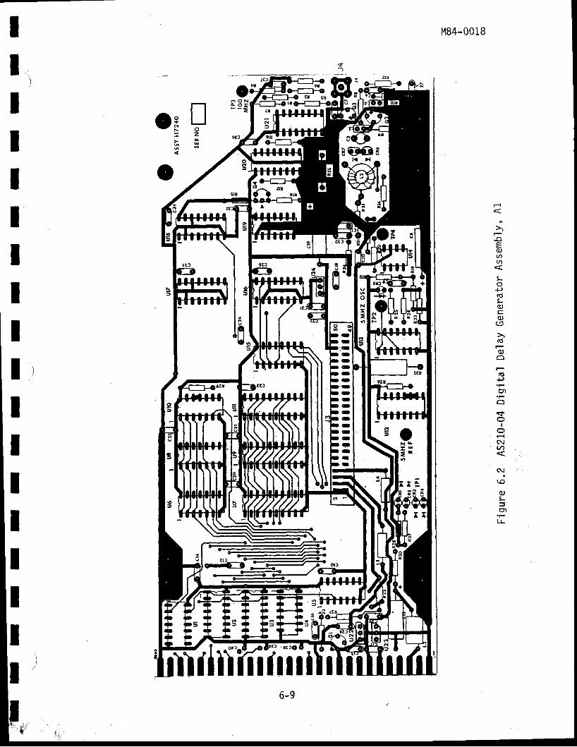
M84-0018
CFF
IIIIII
H
q(uq(/I
LoP(gLq)
q,(5
q)O
16+)
cl
=rC)
I(fr-lNtJ1
C\I
t o
L:J
U-
Ilj
tIIIItI
IIIJI' 8e ro o
lulilitt J
IESE
o
IE
O(-.(--ID
--OO|lO|l
--lCOOOale-
scI
r t
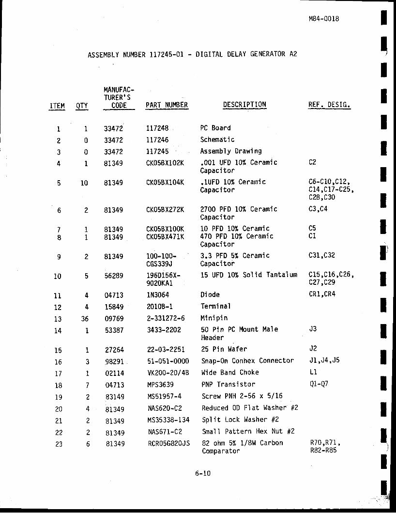
I IIIIIIII
10
M84-0018
REF. DESIG.
C2
c6-c10 ,cL?,cL4,CL7 -C25,c28, C 30c3,c4
c31,C32
cts,c1.6,c26,c27,C29cRl,CR4
J3
J2
JL ,J4 ,J5L1
Q1-Q7
R70,R71 ,R82-R85
A5SEMBLY NUMBER117245-OL - DIGITAL DELAY GENERATOR A2
MANUFAC-TURER'S
CODE PART NUMBERrTEM lLI
1
2
3
4
1
0
0
1
tL724B
rL7246
L17245
cKo58X102K
CKO5BXlO4K
CKO5BX272K
CKO5BXlOOKcK05BX471K
100-100-cGs339J
196D156X-9020K41
1N3064
2010B-1
2-331272-6
3433-2202
22-03-2251
51-051-0000
vK200-20/48
MPS3639
MS51957-4
NAS620-C2
MS35338-134
NAS671.C2
RCR05G820JS
II
78
33472
33472
33472
81349
81349
81349
8134981349
81349
56289
04713
15849
09769
53387
27264
98291
A?LT4
04713
83149
81349
81349
81 34981349
DESCR I PTION
PC Board
Schemati c
Assembly Drawi ng
.001 UFD 10% CeramicCapaci tor
.1UFD 10% CeramicCapaci tor
2700 PFD 10% CeramicCapaci tor
10 PFD 10% Ceramic470 PFD 10% CeramicCapaci tor
3.3 PFD 5% CenamicCapaci tor
15 UFD 10% Sol id Tantalum
Di ode
Tenni nal
M in ip in
50 Pin PC Mount MaleHeader
25 ?1n t lafer
Snap-0n Conhex Connector
Wide Band Choke
PNP Trans is to r
Screw PNH 2-56 x 5/16
Reduced 0D Fl at Vlasher #2
Spl i t Lock Washer #2
Srnal I Pattern Hex Nut #2
82 ohm 5% 1/8tl CarbonComparator
6-10
c5c1 I
IIItIIII
j
I
10
11
t2
13
14
4
4
36
1
15
16
L7
18
19
20
2T
22
23
1
3
I
7
2
4
2
2
6
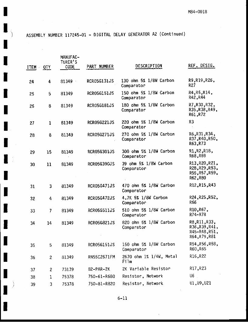
IIIIIIIIIIIIIIIIIII
3
4
7
L4
ASSEMBLY NUMBER 1L7245-OL. DIGITAL DELAY GENERATOR A2 (CONtiNUCd)
MANUFAC-TURER' S
CODE PART NUMBER DESCR IPTION
130 ohm 5% L/8W CarbonComparator
150 ohm 5% 1/8l,l CarbonComparator
180 ohm 5% 1/8tl CarbonComparator
220 ohm 5% L/8W CarbonComparator
270 ohm 5% 1/8tl CarbonComparator
300 ohm 5% 1/8H CarbonComparaton
39 ohm 5% 1/8t.l CarbonComparator
470 ohm 5% I|SW CarbonComparator
4.7K 5% 1/8H CarbonComparator
510 ohm 5% I/8W CarbonComparator
820 ohm 5% l/8W CarbonComparator
150 ohm 5% L/8W CarbonComparator
2670 ohm I1" I/4W, MetalF i lm
2K Var i ab l e Res i s to r
Res is to r , Network
Res is to r , Network
6-1 I
M84-0018
REF. DESIG.
R9,R19,R26,R27
R4,R5,R14,R42,R44
R7,R30,R32,R35,R38,R49 ,R61 ,R72
R3
R6,R31 ,R34,R37,R4o,R5o,R63,R73
R1 ,R2,R18 ,R68,R69
Rl3 ,R20,R21 ,R2g,R29,R53,R55,R57 ,R59,R62,R80
Rl .2 ,RL5,R43
R24,R25,R52,R66
R10,R67,R74-R78
R8,R11,R33,R36,R39,R41 ,R45-R48,R51 ,R64 ,R79,R81
R54,R56,R58,R60,R65
R16 , R22
R17,R23
U6
ul ,u9,u21
1
8
15
I1
24
25
26
27
28
29
30
31
32
33
ITEM EJ.
4
5
8
RCR05G131JS
RCR05G1.51JS
RCROsG181JS
RCR05G221JS
RCRO5G27lJS
RCR05G3Ol.JS
RCR05G390JS
RCR05G471JS
RCR05G472JS
RCR05G5l 1JS
RCR05G821JS
RCRO5Gl 51JS
RN55C267 1 FM
82.PAR-2K
750-61-R680
750-81-R820
81 349
81349
81349
81349
81349
81349
81349
81349
81349
81349
81349
81349
81349
7 3139
75378
75378
34
35
36
37
38
39
5
2
2
1?
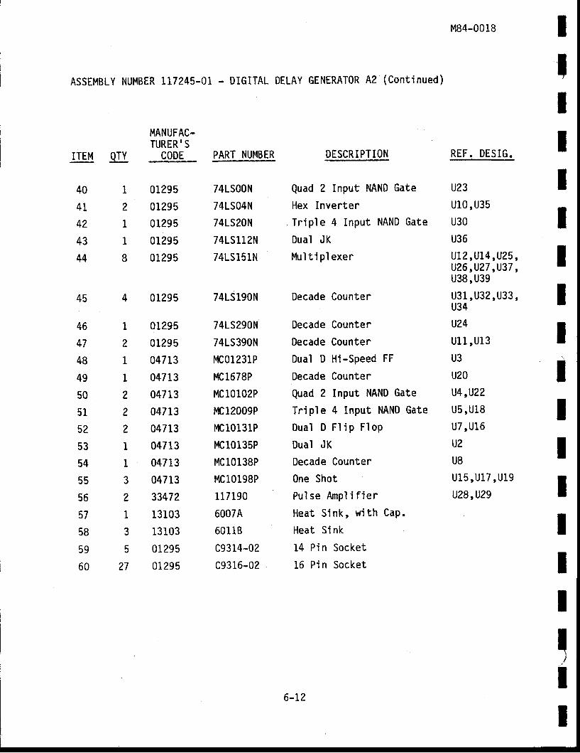
ASSEMBLY NUMBER 117245.01 - DIGITAL DELAYGENERAT0R AZ (Cont inued)
M84-0018
REF. DESIG.
u23uLO, u35u30u36uL?,Ul{ ,U25,u26,U27,U37 ,u38, U39u3l. , u32 , u33 ,u34U?4
u].1,u l3U3
u20u4,u22u5 , u18u7 , ul6U2U8
u15,U l7 ,U l9
u28,U29
IIIIIIIIIIIIIItI
!II
ITEM EI
MANUFAC-TURER' S
CODE PART NUMBER
40
41
4?
43
44
45
46
47
48
49
50
51
52
53
54
55
56
57
58
59
60
1
2
1
1
8
4
1
2
1
I
2
2
2
1
I
3
2
1
3
5
27
01295
01295
01295
01295
01295
01295
01295
01295
04713
04713
04713
a4713
04713
04713
04713
04713
33472
13103
13103
01295
01 295
74LS00N
74LS04N
74LS20N
741S112N
741S151N
741S190N
741S290N
741S390N
MC01231P
MC1678P
l,lC10t02P
MC12009P
MC10131P
tlC10135P
MC10138P
MC10198P
117190
60074
60118
c9314-02
c9316-02
DESCR IPTION
Quad 2 Input NAND Gate
Hex Inverter
Tr ip le 4 Input NAND Gate
Dual JK
Mul t i p l exer
Decade Counter
Decade Counter
Decade Counter
Dual D Hi-Speed FF
Decade Counter
Quad 2 Input NAND Gate
Tr ip le 4 Input NAND Gate
Dua l D F l ip F lop
Dual JK
Decade Counter
One Shot
Pul se funpl i f ier
Heat S ink , w i th Cap.
Heat Si nk
14 Pi n Socket
16 Pi n Socket
6-L2
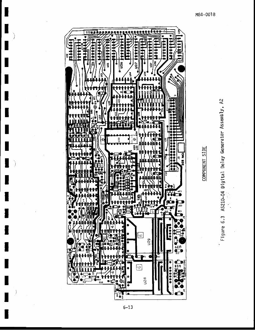
M84-00.| 8
c\l
a
oq,at',tn
LoP(oL(u
Lll ctfl (uH l ( 5..nl
t >Fl fttz , l Ftrtl (uz,l aA IEl (dol +,(-)l .r
g). F
osfo '
IOt-{
i J :tJl
cr'.
(o(U!
. F
u-
Il.IIIIIIIti
IIIIIIIII
ASSEMBLYNUMBER 117350-03 . CABLE ASSEMBLY
M84-0018
REF. DESIG.
Six Inches
REF. DESIG.
Five Inches
REL. DEsIG._
I;
IIIIIII
ITEM
1
2
ITEM
-au20
0
1
1
1
2
3
MANUFAC-TURER I S
CODE
53887
53887
MANUFAC-TURERI S
CODE PART NUMBER
81349
02660
98291
MANUFAC-TURER.S
CODE PART NUMBER
P1LT NUMBE.B DESCRIPTION
3425-6000 Connector, 50 Pin
3365/50 Cab le , 50 Wi re , R ibbon
ASSEMBLY NUMBER LL7356.02 - CABLE ASSEMBLY
u. DESCRIPTION
RGU-316 Coaxi al Cabl e
86350 Connector, BNC Bulkhead
51-328-3188 Connector
ASSEMBLY NUMBER117356-03 - CABLE ASSEMBLY
ITEM
1
z3
81 349
02660
98291
!It. pESCLIPTI0_N
Coax ia l Cab le , 50 ohm
Connectot', BNC Bulkhead
Connector
IIIIItIt,j
II
0
1
1
RGU-316
86350
51-328-3188
6-14
ItIrI
III
MANUFAC.TURER,S
CODE DESCRIPTION
M84-0018
REF. DESIq.
REF. DESIG,
ITEM
rTEM W.
ASSEMBLY NUMBER1 17 357-02. CABLE ASSEMBLY
g. PART NUMBEE
RG-183
51-328-3188 Connector
PART IUMBER
117188
r17347
117189-01
22-01-2251
08-50-0114
16-ET 26 Al^lG
p_E_sg$I_PTI0N
Switch, Rotary 30 Degree
Hi ne Li st
Switch, Thumbwheel
Connector, 25 Pin
P in , Cr imp '
lr|i re, 26 AlrlG Stranded
0
2
1
2
81349
9829r
ASSEMBLY NUMBER117347-01 - HARNESS, DIGITAL, DELAY GENERATOR
MANUFAC-TURER' S
CODE
I
234
5
6
1
0
1
1
25
0
33472
33472
33472
27264
27?64
81349
IIIIIl j
I6-15
6-2
i n the
This sect ion contains
AS210 system. The codes
al1 manufacturer 's codes
are l i s ted in numer ica l
MANUFACTURER'S LIST CoDE T0 XAItE
M84-0018
for mater ia ls used
order by code.
lltIIIIItIIII
III
6-16
IIIIIIII
CODE
00779
01121
01139
MANUFACTURER,S LIST
MANUFACTURER
AMP, INC
ALLEN.BRADLEY COMPANY
GENERAL ELECTRIC COMPANY
M84-0018
CODE TO NAME
ADDRESS
P.0. Box 3608Har r i sburg , PA 17105
1202 South 2nd StreetMi lwaukee, t ' l l 53204
Si l icone Products Business Departmentlr{aterford, NY 12188PHONE: 518-237-3330
TR}l Semiconductor Div is ion14520 Av ia t ion Bou levardLawndale, CA 90260
Semiconductor Group13500 North Central ExpresswaYP.0.Box 225012 M/S 49Da' l l as, TX 75265
Fer roxcub D iv is ion5083 Kings HighwaySaugerties, NY L2477
Arnphenol Di vi si on2801 South. 25th AvenueBroadv iew, IL 60153
Sol id S ta te D iv is ionRoute 202Somervi l le, NJ 08876
E lec t ron ics D iv i s ion18435 Susana RoadRancho Dominguez, CA 9022IPH0NE: 213-537-4750
L icon D ' i v is ' ion6615 blest I rv ing Park RoadChicago, IL 60634
Semiconductor Products Sector5005 East McDowel I RoadPhoen ix , AZ. 85008PH0NE: 602-244-7100
IlrIttIItI
, j
II
01281 TR[.l , INC.
01295 TEXAS INSTRUMENTS, INC.
02L1.4 AMPEREX ELECTRONIC CORPORATION
02660 BUNKER RAMO-ELTRA CORPORATION
02735 RCA CORPORPATION
03797 GENISCO TECHNOLOGY CORPORATION
04426 ILLINOIS TOOL I ' IORKS, INC.
04713 MOTOROLA, INC.
6-r7
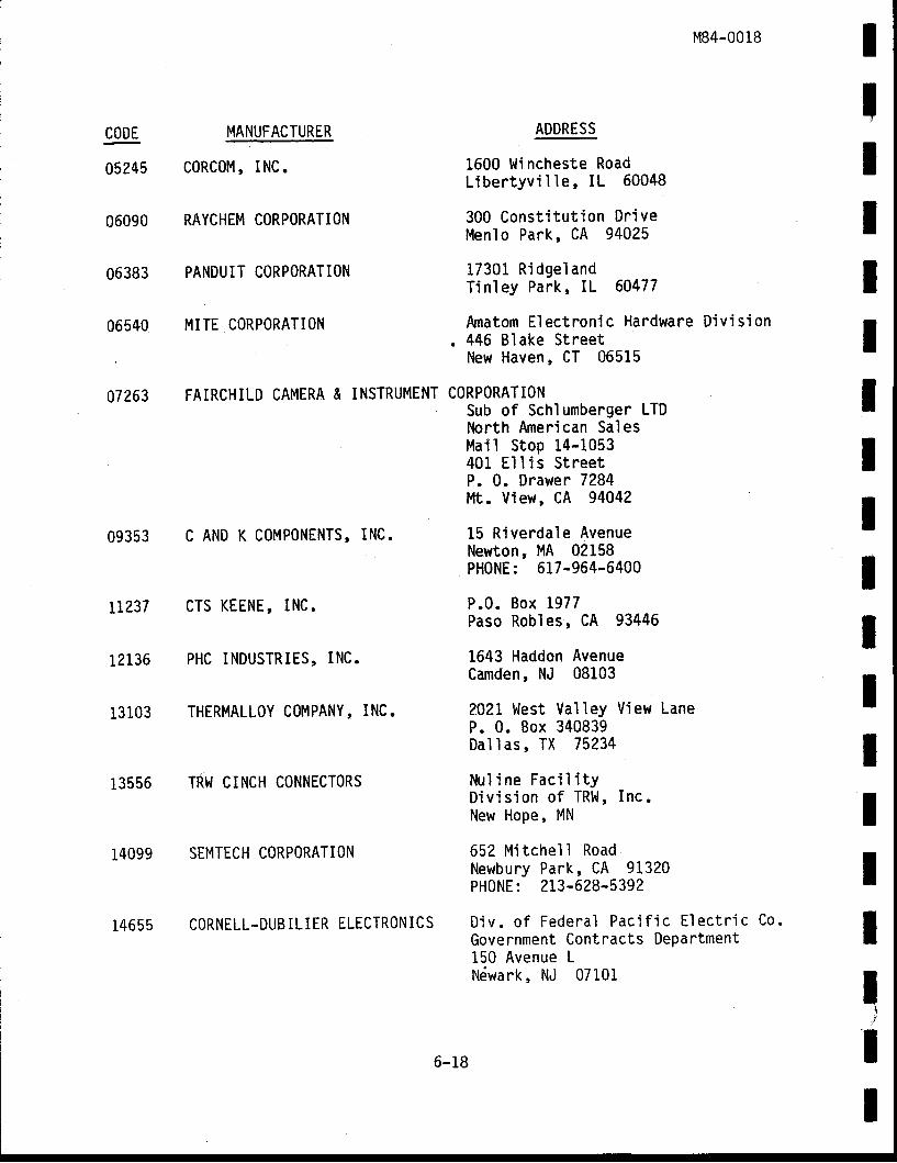
CODE
05245
06090
06383
06540
r1237
12136
13103
07263 FAIRCHILD CAMERA & INSTRUMENT
09353 C AND K CoMPoNENTS, INC.
MANUFACTURER
cORcOM, INc .
RAYCHEM CORPORATION
PANDUIT CORPORATION
MITE CORPORATION
cTs KEENE, INC.
PHC INDUSTRIES, INC.
THERMALLOY COMPANY, INC.
M84-0018
ADDRESS
1600 tl i ncheste RoadL iber tyv i l le , IL 60048
300 Const i tu t ion Dr iveMenlo Park, CA 94025
17301 R idge landTinley Park, IL 60477
Anatom E'l ectroni c Hardware Di vi si on. 446 Blake Street
l lew Haven, CT 06515
CORPORATIONSub of Schl umberger LTDl,lorth American SalesMai 1 Stop 14-1053401 E l l i s S t ree tP. 0. Drawer 7284I'tt. View, CA 94042
15 Riverdale AvenueNewton, MA 02158PH0NE z 617-964-6400
P.0 . Box 1977Paso Robl es, CA 93446
1643 Haddon AvenueCamden, NJ 08103
2021 t lest Val ley View LaneP. 0. Box 340839Dal 1 as, TX 75234
Nu l ine Fac i l i t yD iv is ion o f TRl l | , Inc .New Hope, MN
652 M' i tchel I RoadNewbury Park, CA 91320PH0NE z 213-628-5392
D'i v . of Federal Paci f i c El ect ni c Co .Government Contracts DePartment150 Avenue LNtiwark , NJ 07101
IIIIIIIIIIIIIIIII
I
II
13556 TRI'I CINCH CONNECTORS
14099 SEMTECH CORPORATION
14655 CORNELL-DUBILIER ELECTRONICS
6-18
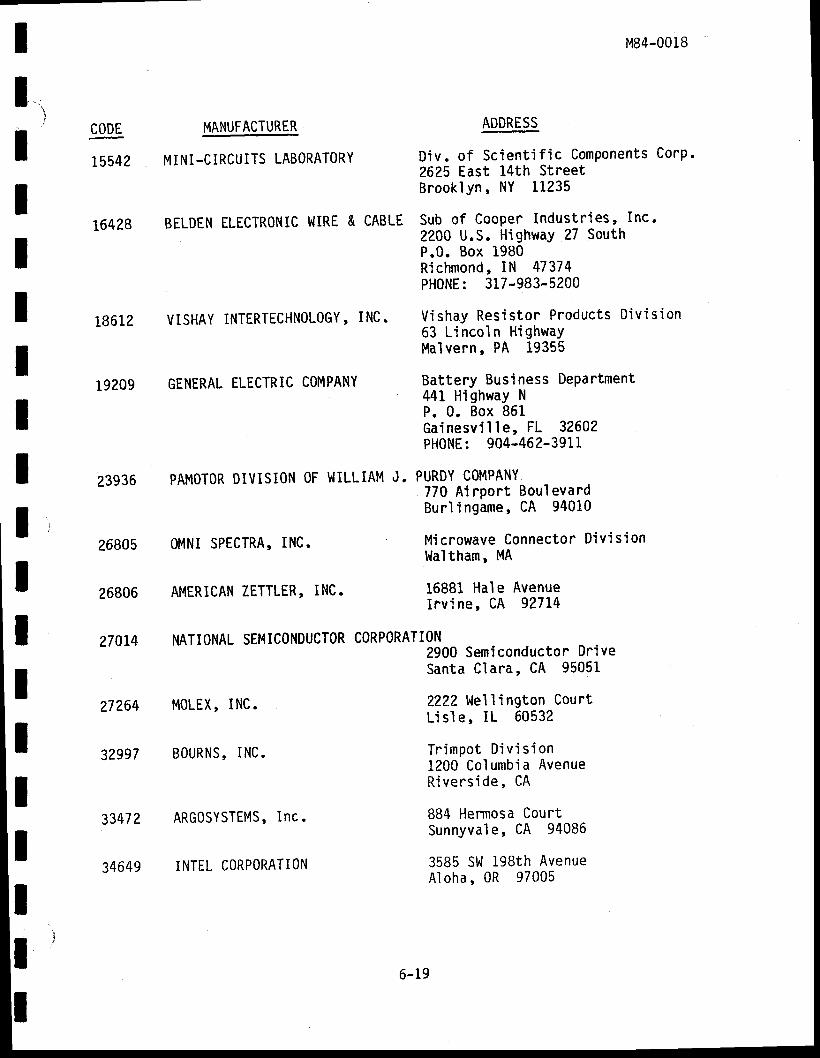
Il1
ItI
CODE
15542
16428
18612
19209
23936
26805
26806
27Ar4
27264
32997
33472
34649
M84-0018
MANUFACTURER ADDRESS
MINI-CIRCUITS LAB0RATORY Div. of scient i f ic components corp.2625 East 14th StreetBrooklyn, NY LL235
BELDEN ELECTR0NIC l r l IRE & CABLE Sub of Cooper Industr ies, Inc '2200 U.S. HighwaY 27 SouthP.0. Box 1980Richmond, IN 47374PH0NE: 317-983-5200
VISHAY INTERTECHN0LOGY, INC. Vishay Resistor Products Div is ion63 Li ncol n H'ighwaYMal vern, PA 19355
GENERAL ELECTRIC CQMPANY Battery Business Department441 Highway NP. 0. Box 861Gainesvi l le, FL 32602PHONE: 904-462-3911
PAMOTOR DIVISION OF I,IILLIAM J. PURDY COMPANY770 Ai rpont Boul evardBurl ingame, CA 94010
0l4NI SPECTRA, INC. Microwave Connector Div is iont,laltham, MA
AMERICAN ZETTLER, INC. 16881 Hale AvenueIrv ine, CA 92714
ttItIIItIIIIli
I
NATIONAL SEMICONDUCTOR
MOLEX, INC.
B0URNS, INC.
ARGOSYSTEMS' Inc.
INTEL CORPORATION
CORPORATION2900 Semiconductor DriveSanta Clara, CA 95051
2222 Vlell ington CourtL ' i s1e , IL 60532
Tr impot D iv i s ion1200 Columbia AvenueRivers ide , CA
884 Hermosa CourtSunnYvale, CA 94086
3585 St,l 198th AvenueA1 oha, 0R 97005
6-19
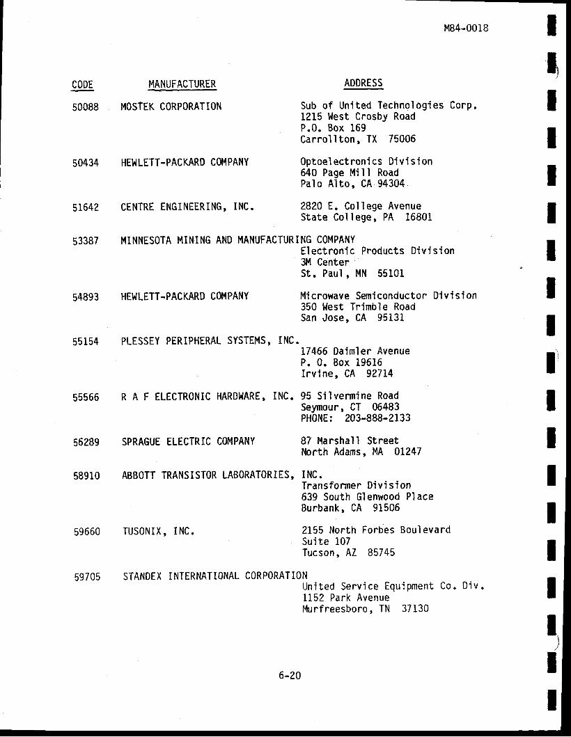
MOSTEK CORPORATION
HEULETT.PACKARD COMPANY
CENTRE ENGINEERING, INC.
53387 MINNESOTA MINING AND MANUFACTURING COMPANY
M84-0018
ADDRESS
Sub of Uni ted Technologies Corp.1215 West Crosby RoadP.0 . Box 169Car ro l l ton , TX 75006
Optoel ectronics Div i s ion640 Page Mi I I RoadPalo Al to, CA 94304
2820 E. Col lege AvenueState Col lege, PA 16801
Electronic Products Div is ion3M CenterSt . Pau l , MN 55101
Microwave Semiconductor Div is ion350 ldest Trimbl e RoadSan Jose, CA 95131
MANUFACTURER
IIIIItIII
54893 HEWLETT-PACKARD COMPANY
55154 PLESSEY PERIPHERAL SYSTEMS, INC.
55566
17466 Daimler AvenueP. 0 . Box 19616Irv ine, CA 92714
R A F ELECTRONIC HARDI'IARE, INC. 95 Silvermine RoadSeymour, CT 06483PH0NE: 203-888-2133
SPRAGUE ELECTRIC COMPANY 87 Harshall StreetI'lorth Adams, MA 0L247
ABBOTT TRANSISTOR LABORATORIES, INC.Transformer Div is ion639 South Glenwood PlaceBurbank, CA 91506
TUS0NIX, INC. 2155 Nor th Forbes Bou levardSu i te 107Tucson, AZ 85745
56289
58910
l'ITtIIII
j
I
59660
59705 STANDEX INTERNATIONAL CORPORATIONUni ted Serv ice Equ ipment Co. D iv .1152 Park AvenueMurfreesboro, TN 37130
I6-?.0
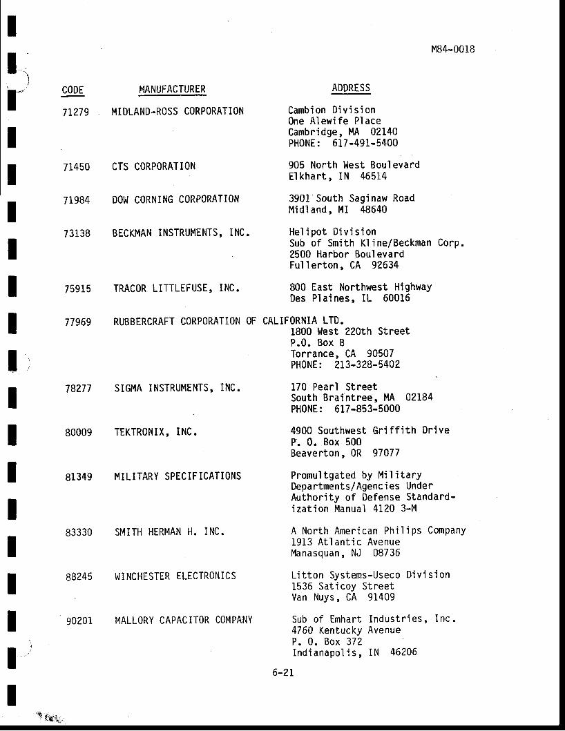
II .
l*MANUFACTURER
MIDLAND-ROSS CORPORATION
CTS CORPORATION
DOl.l CORNING CORPORATION
BECKMAN INSTRUMENTS, INC.
TRACOR LITTLEFUSE, INC.
RUBBERCRAFT CORPORATION OF
M84-0018
ADDRESS
Camb'ion Di vi si onOne A lewi fe P laceCambridge, MA 02140PH0NE: 617-491-5400
905 North West Boul evardEl khar t , IN 46514
3901 South Saginaw RoadMidland, MI 48640
Hel i pot D'ivi si onSub of Smith Kl ine/Beckman Corp.2500 Harbor BoulevardFul ler ton, CA 92634
800 East Northwest HighwayDes Pl a i nes, IL 60016
CALIFORNIA LTD.1800 West 220th StreetP.0 , Box BTorrance, CA 90507PHONE: 213-328-5402
170 Pearl StreetSouth Braintree, MA 02184PHONE: 617-853-5000
4900 Southwest Gri f f i th Dr iveP. 0. Box 500Beaverton, 0R 97077
Promultgated by Mi l i tarYDepartments/Agenci es UnderAuthor i ty of Defense Standand-iza t ion Manua l 4120 3-M
A North Ameri can Phi 1 i Ps ComPanY1913 At lan t ic AvenueManasquan, NJ 08736
L ' i t ton Sys tems-Useco D iv is ion1536 Sat icoy StreetVan Nuys, CA 91409
Sub o f Emhar t Indus t r ies , Inc .4760 Kentucky AvenueP. 0 . Box 372Ind ianapof i s , IN 46206
6-?r
IIIIIIli
IItI
CODE
7t279
71450
71984
73138
75915
77969
ItI
'j
tT
78277 SIGMA INSTRUMENTS, INC.
8OOO9 TEKTRONIX, INC.
81349 MILITARY SPECIFICATIONS
83330 SMITH HERMAN H. INC.
88245 t , l lNCHESTER ELECTRONICS
4 {giii
90201 MALLORY CAPACITOR COMPANY
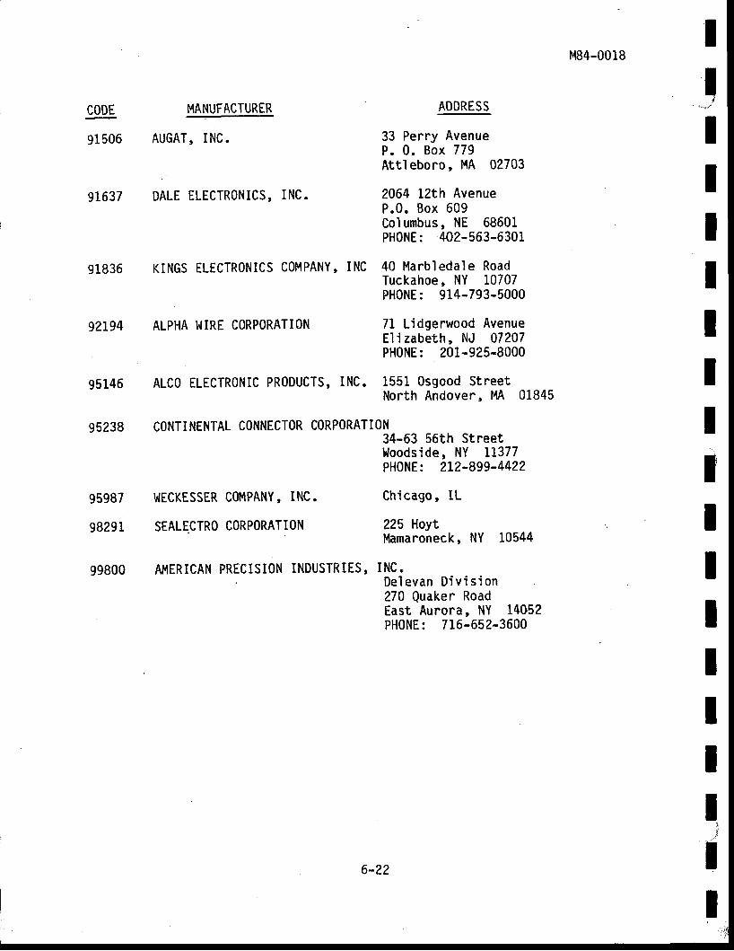
M84-0018
MANUFACTURER ADDRESS
91506 AUGAT, INC. 33 Perry AvenueP. 0 . Box 779Attl eboro, MA 02703
INC. 2064 Izt'h AvenueP.0 . Box 609Col umbus, NE 68601PHONE: 402-563-6301
9L637 DALE ELECTRONICS,
91836 KINGS ELECTR0NICS C0MPANY, INC 40 Marb' ledale RoadTuckahoe, NY L0707PH0NE: 914-793-5000
92t94 ALPHA t.tIRE CORPORATION 71 Lidgerwood AvenueEl izabeth, NJ 07207PHONE z 20t-925-8000
95146
95238
ALC0 ELECTRONIC PRODUCTS, INC. 1551. Osgood StreetNorth Andover, lf i 01845
CONTINENTAL CONNECTOR CORPORATION
T,|ECKESSER CO$'IPANY, INC.
SEALECTRO CORPORATION
34-53 56th Streett{oods' ide, NY LL377PHONE: 2L2-899-4422
Chicago, IL
225 Hoytlrdamaroneck, NY 10544
IIIIItIIIIIIIIT
j
Tt
95987
98291
99800 AMERICAN PRECISIONINDUSTRIES, INC.De levan D iv is ion270 Quaker RoadEast Aurora, NY 14052PH0NE: 716-652-3600
6-22


I
M84-0017
AS2 10-O5STANDBY BATTERY
I
Ft:l:ItItItlrIIIIIIIIII
Revised 8/84
M84-0017 IJIIIIIITIIIIIItItI
All rights reserved. $o part of this publication may bereproduced, stored in a retrieval system, or transmitted,in any foym or by any neans, electronic, mechanical,photocopying, recording and/or sthenrise without theprior written perrnission of ARG0Systems, Inc. This man-ual nay not be lent, resold, hired out or otheruise dis-posed of by way of trade in any form of binding or coverother than that in which it is published, wilhout theprior consent of ARG0Systems, Inc.
ARG0systems, rnc. / 884 Hermosa court, sunnyvale, california 94086Telephone (Area Code 4081 737-2000 / Telex No. 352077
IIttIIIIIItIItIIIII
M84-0017
thapter
TABLE OF CONTENTS
Tiil e
Preface
GENERAL INFORMATION
1-1 Introductionl-2 Physical and Electr ical Descr ipt ion
INSTALLATION
2-L Introduction
OPERATION
3-1 Introduction
THEORY OF OPERATION
4-l Introduction
MAINTENANCE AND CALIBRATION
5-1 Introduction
SECTION I5-? Preventive Maintenance
SECTION I I5-3 Performance Tests
SECTION I I I5-4 Cal ibrat ion/Al ignment procedures5-5 Access to ASZ10-05 Standby Battery5-6 Charge Indicator Al ignmenl procedirre
SECTION IV5-7 Troub' leshoot ing procedures
ILLUSTRATED PARTS LIST
6-1 Introduct ion
6-2 Manufac turer ' s Code L is t
Page
i i i
1 -1
1-11-1
2-1
2-t
3-1
3-1
4-1
4-1
5-1
5-1
5-2
5-3
5-45-45-4
5-5
6-1
6-1
6-12
LIST OF ILLUSTRATIOf.IS
T i t l e
M84-0017
Page
t-2
3-3
4-2
5-6
6-2
6-8
6-9
Page
IIIIIIIIItIIttIIIII
Figure
l. .1
3 .1
4 .1
5 .1
6 .1
6 .2
6 .3
AS210-05 Standby Battery Modul e
Standby Battery Controls and Indicators
Standby Battery Functional 81ock Diagram
45210-05 Standby Battery Schematic Design
AS210-05 Standby Battery Module Assembly
45210--05 Standby Battery Interconnect Assembly
45210-05 Standby Battery Charging Assembly
LIST OF TABLE5
Ti t ' le
Standby Battery Controls and Indicators
Prevent ive Maintenance Checks and Services
Tabl e
3-?
5-2
3-1
5-1
- ' t 1 -
i s
IIIItIt
This manualinstruct ions fon thearranged as fo l lows:
M84-0017
PREFACE
conta ins ins ta l la t ion , opera t ion and majn tenance45210-05 Standby Battery. . The data contained herein
Chapten LChapter 2Chapter 3Chapter 4Chapter 5Chapter 6
General InformationInstal I at i onOperati onTheory of Operat.ionMaintenance and Cal ibrat ionI l lustrated parts List
IIIII
Reference publ ications
AS210A-'M portabre Mainframe operation and Maintenance ManualAS210RM'LM r"rarnfrarne 0peration and Maintenance ManuarAS210-01'A Modure controiler 0peration and Maintenance4s210-02 Frequency comparator 0peration and Maintenance ManuarA5210-03 Frequency Generator Operation and Maintenance ManualA5210-04 Digi ta l Delay Generator Operat ion and Ma. intenance Manual4s210-06 Microwave Generator Operation and Maintenance ManualAs210-08 Distr ibut ion funp' l i f ier 0perat ion and Maintenance ManualAS210-20 Time crock Operat ion and Maintenance Manual
IIItItI
- i i i -

IIITIIIIItttIIIIIII
tIIItIIIIIItIIIIIII
M84-0017
CHAPTER ].
GENERAL INFORMATION
1-1 INTRODUCTION
The AS210-05 Standby Battery module is designed for use with theAs210 Electronic counter and Frequrincy Standard calibration system Mainfrarne.The standby Battery is i l lustrated in Figure 1.1. This modr.rle can be pluggedinto any one of the !!1eg.-!qggttorrs on the As210 Mainframe that is not beingoccupied by another mo'dule. The Standby Battery supplies power to the Rubi-dium Frequency Standard in the Mainframe during an A.c. power failure or whenthe AS210 is in transit fr"om one location to another. The use of the standbyBattery during trransit avoi'ds the 10-minute wann-up necessary for achievingmaximum frequency ac.uiiiy or i pu"t in t0-10. The standby battery is alsoneeded to keep the power off t ime clock functional during power drops or tran-si t condi t ions- The uni t can be used to maintain :1 part in 10-9 accuracyfor. periods up t9 -three ( four typical ) hours and have accuracy wi thi ̂ iit i 10-10in 30 seconds af ter powe" is resumed. This manual covers the instal lat ion,operation and maintenance of the standby battery.
b? PHYSICAL AND ELECTRICAL DESCRIPTION
The Standby Battery is constructed in a s ingle width modularplug- in f rame. Rechargeable lead-acid batter ies are mounted on one side ofan internal mount ing plate. A pr inted circui t card assenbly wi th the chargingind ica tor and cont ro l c i rcu i ts i s mounted on the oppos i te s ide o f th is mount ingp1ate. l4ounted on the front panel is the STANDBY/0FF switch. In standby, theswitch places the module in an automat ic; ;a; to suppty p"r"" as soon as pr imepower is disconnected. Also found on the front panel is the TEST pushbutton*i. lc.I" which' when pressed, tests the condition of the battery. Four LEDind ica tors p rov ide a v isua l means o f de termin ing the charge cond i t ion o f thebatter ies ' A srnal l knob in the lower lef t hand corner of the f ront panel isused for removal and retent ion of the module in the mainframe.
f - i
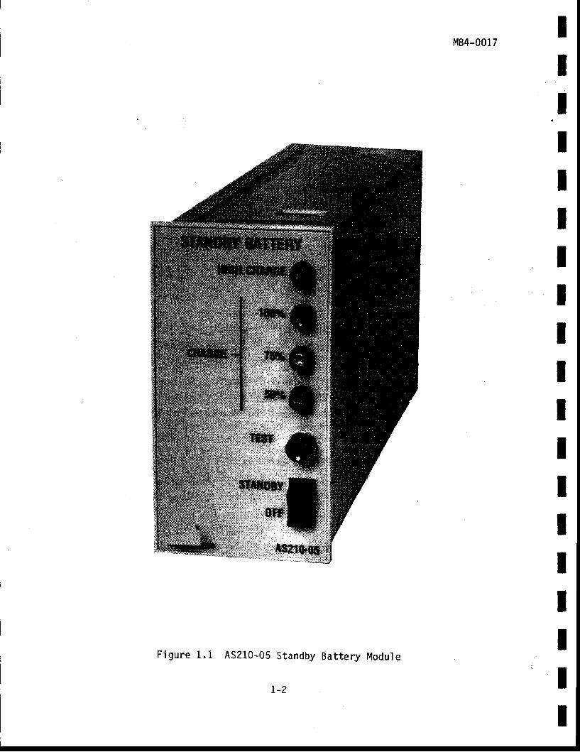
M84-0017
AS210-05 Standby
L-2
F igure 1 .1 Battery Module
II
?- t
IIIIIIIIIIIIII
CHAPTER 2INSTALLATION
INTRODUCTION:
The Standby Battery is a plug- in module of the Electronic Counterand Frequency Standard Ca'l ibration system. The module is retained by arernovable locking bar on the mainframe. The Standby Battery requires nospecial power or handl ing. I t wi l l nonnal ly be instal led dur ing t ransi t ofthe instrument or w]ren prime power has been disconnected.
M84-0017
NOTE 1.:
NOTE 2: Prior to shipnent, the battery wil l be disconnected atthe factory by removing the 5 amp fuse. Reinstail the5 amp fuse careful' ly to avoid shorting the batterybefore operation,
N0TE 3: The standby Battery Module shourd not be reft in thestandby posi t ion when the moaure is not prugged intothe AS210 mainfiame. Hhen inserted into the mainframe,the modure shourd not be ref t in the standby posi t ionfor pe. iods in excess of three houns, when mainframepowen is of f . I f one of the above condi t ions occurs,damage coulo resurt to the intennar battery pack whichwould require replacement of bat ter jes.
This module cannot be instal led in a Tektronix mainframe.
2-1

IIIIIIIItItIIIIII
;l
M84-0017
CHAPTER 3
OPERATION
3-1 INTRODUCTION
This chapter describes the operation of the standby battery module.Figure 3'1 and rable 3-1 i l lustrate and describe the front panel controls andindicators. No operator interface fs required other than observation of thecharge condition and placinE the unit in ttre standb3r or off mode.
l,IIIIIIIIt
I
3-1
M84-0017IIIIIItIII
Table 3-1STANDBY BATTERY CONTROLS AND INDICATORS
IIIIItIII
.:l
INDEX NO.F IGURE 3 .1 PANEL MARKING
STANDBY/OFF
LED fndicator i l luminates when therodulg is in the high charge ratemode (250 mA).
L-EP. indicato. is 0N when battery isful ly charged. Lights when iai i switchrs pressed to check charge condit ion.
LED indicator is 0N when battery is{oy.e.75 percent of fu l ly charglacondi t ion. L ights when iwi t i f r - ispressed to cheik crrarge ionjifion.
LED indicator is 0N when battery isabove 50 percent of ful lv charqeOcondit i .on. L ights when iwi tcn" ispressed to check charge condi t ion.
Momentary switch is pressed to checkbattery charge condition. See iterns2 , 3 , and 4 . -
Switch for select ing the STANDBy or OFFrnode of the module. In the SfnlJOgyposi t ion the batter ies are automat ical lyinserted in the c i rcui t wfren- j r i *" po"""i s los t o r d isconnected .
Re lease mechan ism used fo r p lug- in ,removal and retent ion of t t re m6aute.
3-2
IIIIIIIIIIIItIIItII
Figure 3.1 Standby Battery Controls and Indicators
M84-0017
3
4
3-3

II)l
ItItIII
1 , '
IIIIIII
:lI
I
IIIIIIIIIIIItIIIIII
M84-0017
CHAPTER 4THEORY OF OPERATION
4-1 INTRODUCTION
This chapter contains a functional description of the StandbyBattery. Figure 4.1. is a functional block d,iagranr. Refer to the schematicdiagram, Figure 5.L for nore c i r rcui t detai ls.
The primary purpose of the Standby Battery Module is to supply +Z6V
$_ry9 !o tle*Rubidgqr fr-gquency- stal{a1d when prime power is removeJ. Th;module also provides a regulated charging current for the batteries. Themodule is comprised of a switching circui t , charging circui t and displaydriver circuit. b{hen prime power is lost fron the mainfrane, relay Kl. in theswitching circui t goes to the l l .C. posi t ion, a l lowing current to f : low fromthe.battery through the standby switch to the Rubidiun frequency standard inthe mainframe. A low voltage dropout relay, K2, disconnects the battery fromthe standard when voltaEe falls below 20V dc, preventing the batteries frornbeing destroyed. The dropout circuit is disabled when the battery voltagerises above 24Y dc. While prime power is being maintained, 31V dc from themainframe po$,er supply is appl ied to the charging circui t . A 250 mA chargingcurrent is maintained through ser ies pass transistor Ql. Var iable resistorR7 forms a vol tage div ider wi th R9 and RL0. This turns Q1 6FF when thebattery vol tage reaches 28.6V dc. The HIGH CHARGE lamp wi l l remain OFF unt i lthe battery vol tage drops below 27"5V dc. A t r ick le charge is appl ied to thebattery through R16 when the high charge circui t is OFF. Whi le the chargeris in the high current mode the HIGH CHARGE LED indicator is l ighted on thefront panel . When the battery vol tage equals 28.2Y dc, a vol tage' l i rn i terc i rcu i t cons is t ing o f Q4 shunts the t r i ck le charg inE cur ren t to g round. Thevo l tage l im i t i s se t w i th R l l wh ich fo rms a vo l tage d iv ider w i th zener CRZ
4-1
IIIIIIIII
IIIIIII
ert'Ig).rt
a.v,C)ooo
t!
o.tJu=
t!
L'c,P+t.t'co
-o.9G(o+,at1
st(uL5o)u-
M84-0017
r----1I
- - - - 1rIIIIIIIL
FDoo-oE,o
=c.': q\2.
Eit>PaRdb an
IIJF
H3d=> J
u t , :g," E;f-te'
(ltl-o
@ozFvt
I r-1--lIfx-li
LlJ . '
Fit l(9!
Fr$sEr;=F
r---1ln l
bSoa-o'llJ
u ) vF E:e'<6 I
|nC)
L---J
4-2
III
M84-0017
and R6' t ' lhen the TEST button on the module's front panel is pressed, thebattery vol tage is appl ied to the display dr iver c i rcui t . This c i rcui t con-sists of a load resist 'or R5, regulator u2 and dot/bar dispray dr iver ICdevice ul . The dispray dr iver is car ibrated by Rr5 to r ight three LEDindicators on the rnodule's front panel . At 25v dc the green 100 percent larnpis l it, at approximately z4y dc the yeilow 75 pe.rcent ranp is rit. The red50 percent lamp is i l luminated at approximately 23y dc. when the battery,sTEST switch is pressed, a 100 ohm load is nraintained by RS in order to testthe battery under load condition when it is not connected to the Rubidiumstandard.
IIttIIItIItIIIII 4-3

IItIIIttIIIItIIIIII
II
j
I'
M84-0017
CHAPTER 5MAINTET{rANCE AND CALIBRATI0N
5-1 INTRODUCTION
The purpose of this chapter is to provide maintenance and calibra-tion data for the As210-05 standby Battery. section I covers ro,tine pre-ventive maintenance procedures. section II ouilines performance tests forrthe standby Battery. Section III contafns the caribration/arignment proce-dures fon the Asel0-05 module and section IV describes troubleshooting data.Please contact the factory for any assistance required in the maintenance orservicing of the AS2l0-09.
IlIIIIIIIItI
5-1
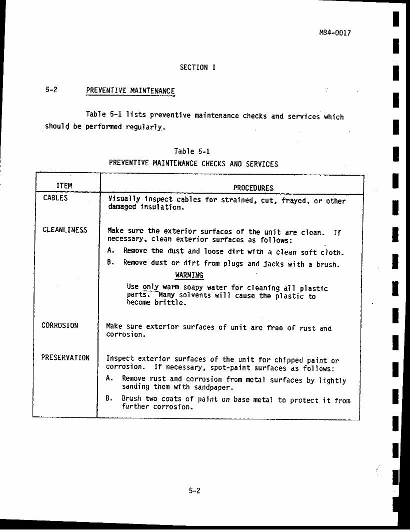
M84-0017
SECTION I
5-2 PREVENTI VE II,IAINTENANCE
Tab'le 5-1 l ists preventive maintenance checks and services whichshoul{ be pertormed r"egularly..
Table 5-1PREVENTIVE MAIIITENAI{CE CHECKS AND SERVICES
IIIIIIIIIItIIIIII
CLEANLINTSS
CORROSION
PRESERVATION
visually.inspect, cables for strained, cut, frrqyed, or otherdamaged insulation.
Use.only.varm soapy water for c leaning al l p last icparts. Many_solvents wi l l cause the plast i f tobecome brltt le.
Make sure exterior surfaces of unit are free of rust andcorrosion.
Make sure the exterior surfaces ofnecessary, clean exterior surfacesA. Renove the dust and loose dirtB. Rernove dust or dirt from plugs
},ARNING
the uni t are c lean. I fas fo l lows:
with a c lean soft c loth.and jacks wi th a brush.
pa in t o rfol I ows:by I ight ly
to protect i t f rom
Inspect exterior surfaces of the unit for chippedcorrosion. I f necessary, spot-paint surfaces' asA. Remove rust and corrosion from metal surfaces
sanding them with sandpaper.B. Brush two coats of paint on base metal
further corrosion.
5-2
II M84-0017
IIIItIIIITtIIIIII
SECTION II
prnronmAuce rrsts
Performance testing for the AS2l,0-05 standby Battery is limited tothe front panel test button' upon pressing the'front panel test, button, LEDswill l ight corresponding to the percent of char,,ge the battery contains. Tocharge the AS210-05, simply run the A5210 system with the standby batteryinstalled unti l the high charge LED goes out or cycres on and off.
5-3
IM84-0017
SECTION I I I
CAL IBRATION/ALIGNMENT PROCEDURES
I,JARNING
The following Calibration/Alignnent procedures (Chapter 5,Section III) and Trpubleshooting procedures (Chapter 5,Section IY) are for use by qualif ied personnel only. Tsavoid personal injury, do not perforrn any servicing otherthan that.of Routine Maintenance (Chapter 5, Section I)and Perfonnance Testing (Chapter 5, Section II) unlessyou are qualif ied to do so.
ACCESS TO AS21O-05 STAIIOBY BATTERY
Please reference the AS210 mainframe manual for the disassemblyprocedure of the AS210 system to allow access to the AS210-05 Standby Batterymodu:le. Access to the module circuitry itself is gained by removing the twometal side covers with a small straight-blade screwdriver. Place the moduleon one of its sides so that one cover is facing up. Star.t ing with the endtoward the edge connector, insert the screwdriver into one of the slots wherethe cover mates with the module chassis and pry the cover up. It wil l benecessary to move along the slot toward the front panel of the module andrepeat the prying action to loosen the side of the cover from the module.Repeat this technique to free the other side of the cover from the chassis.Set the free cover clear of the module and fl ip the module over so that thesecond cover is now facing up. Repeat the above procedure to free thiscover.
tIIIIIIItIIITIII
..'l
I5-4
5-6
User adjustment shoul dpreset at factory. I f a l ignmentfactory.
no t be requ i red . In i t ia lis considered necessary,
adjustments arepl ease contact the
III
M84-0017
5-7
SECTION IV
TROUBLESHOOTING PROCEDURES
WARNING
Use extreme care when troubleshoot ing the module. Thebatter ies can del iver a short c i rcui t current of 250amperes. I f accident ly shorted, severe burns couldresult. Never bypass the 5 ampere fuse or replace itwi th a larger value.
The charge indicators on the front panel of the module provide theoperator with the primary troubleshooting data. The indicators are the 100percent, 75 percent, 50 percent and HIGH CHARGE LEDs de,scribed in Chapter 3.The charge percentage indicators give an approximation of the amount ofcharge on the battery. After the battery has been fully charged, all of thecharge percentage indicators should be i l luminated. If they are not and ithas.been determined that the battery is fully charged, check Ul, U2 or theLEDs. The determination of battery condition wil l have to be made with anexternal charge tester before these components can be declared defective.The HIGH CHARGE indicator should only be on when the battery is being in i -t ia l ly charged; thereafter i t cycles on and of f . I f the indicator does notgo of f (and start cycl ing on and of f ) af ter a maximum of 12 hours of charg-ing, check the battery and charging circui t . I f the indicator does not comeon, check the 5 ampere fuse and the LED. The LED is part of the chargingcircui t , therefore the battery wi l l not charge i f defect ive. When the TESTbut ton is p ressed, LED CRL0 on the c i rcu i t board shou ld i l l umina te . I f i tdoes not,check the 5 ampere fuse, battery charge condi t ion, test switch andU?.
IITIIIItIIItItII
5-5

IIIItIIII,lIIIIItI
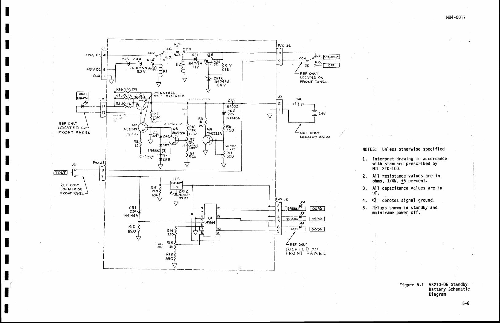
N . O . I C R l t A 5N.O. | - \cR3 cR.A c.R5 |o:-Y' f -+t-
R gy l ru< i l rnt ^ t 4?s re r ! ) J
' - f - l l v6 . 2 V - ' - ' J K f
c R r 2I N474q A
2 4 VRlb,zlg,2w
I M S T A L L\ . r ' 1 7 H l l € A T S , N KEl{;.trzuq3la
RZ, lo, - lW
R 5tooloW \,+t31",-
ZI
45
65
IIIIIIITtItIIItIItI
-l rro ."
MB4-001 7
AS210-05 StandbyBattery SchematicDi agram
r N4COZcez?.2V
IN4'?4EA
LOCAT€D oNFRoNT PANEL
PEF ONLY
LOCATED ON A I
,f@
|1ffi1
Eo%1
Q ZM J E 5 2 I
? i i ' ; i /
R3l k
R I O I W2?K? . i ' /
R ??KCHARGEL I M I T
Rgezo
R67 5 0
R8,21
o- :** 'c R 8
NOTES: Unless otherwise speci f ied
1. Interpret drawing in accordancewith standard prescribed bYMIL.STD-100.
2. A11 resistance values are inohms, t /4u, 15 percent.
3. A: l l capaci tance values are inuF.
4. 4- oenotes signal ground.5. Relays shown in standby and
mainfrann power off.
Plo Jz l
P/o Jz
cR l22v
rN4't48A:=-r-.*N_l
,/Rr28ZO Rl4
210
R t 52K
R , 3b80
/
/*.. ou*L O C A T E D 6 NFRONT PANEL
5-6
F igure 5 .1

ItIIIIIIIIIIIItIIII
M84-0017
? CHAPTER 6
ILLUSTRATED PARTS LIST
6-1 INTRODUCTION
This chapter contains an i l lustrated parts l is t for the ASZ10-05Standby Battery. The assembly numbers and assembly tit le are l isted at thetop of the parts l is ts. The parts l is ts are div ided into s ix columns andarranged in the fo l lowing order:
Col umn 1 - Item Number
Column 2 - Quantity per assembly.
Column 3 - Manufacturer,s Code
Col umn 4 - Part Number
Column 5 - Descr ipt ion
Column 6 - Reference Designat.ion
6-1
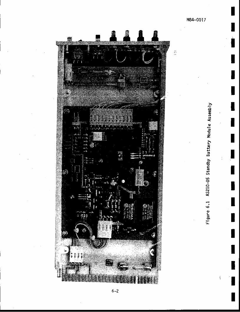
M84-001 7
II
4E(I,ov7
(u=Eo=
i,(l,.P+rC'co
D!c.tt+ttt1
(oo
toGItt1
r.0
(l,L
ctl
U.
IIT
,,1IIItIII
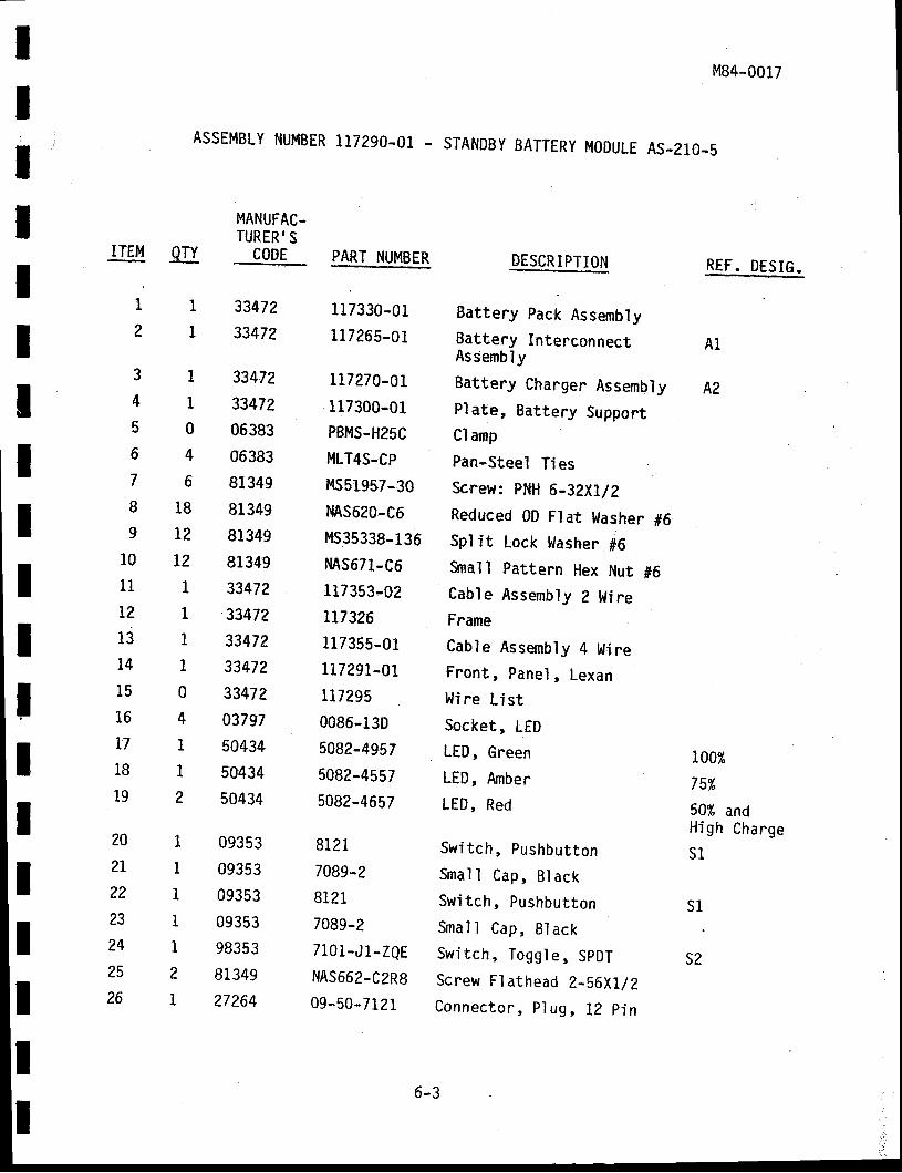
A1
A2
ItItIIttIIIIIIItIII
ASSEMBLY NUMBER117290.01 - STANDBY BATTERY MODULE AS-210-5
MANUFAC-TURER'S
CODE DESCRIPTION
Battery pack AssembljrBattery InterconnectAssembly
Battery Charger AssemblyPlate, Battery SupportCl amp
Pan-Steel TiesScnew: PNH 6-3ZXl/zReduced 0D Fl at Washer #6Spl it Lock ttasher #6Smal I Pattern Hex Nut #6Cable Assembly 2 l,f ireFrame
Cable Assembly 4 hlireFront, Panel , LexanWine L is tSocket, LEDLED, GreenLED, AmberLED, Red
Switch, PushbuttonSmal l Cap, B lackSw' i tch, Pushbutton
Smal l Cap, B lackSwi tch , Togg le , SpDTScrew Flathead Z-S6XL/?Connec to r , P lug , lZ p in
M84-0017
REF. DESIG.%
rrEfvt _qu
1
?
3
4
5
6
7
I
9
10
11
t2
13
I4
15
16
17
l8
19
20
2t
22
23
24
25
26
I 33472I 3347?
L 33472L 334720 063834 063836 81349
18 81349t2 81349t2 81349L 334721 33472l 33472| 334720 334724 037971 504341 s04342 50434
1 093531 093531 09353
I 093531 983532 81349I ?7264
P4RT NUMBER
117330-01
117265-Ot
tI727}-aL
117300-01PBI'15-H25C
MLT4S-CP
MS51957-30
$tAs620-C6
Ms35338-136
MS671-C6
117353-02
It7326
11735s-0r
1L7291-AL
tt7295
0086-13D
5082-4957
5082-4557
5082-4657
8I2L
7089-2
8121
7089-2
7101-J1-ZQE
MS662-C2R8
09-50-7121
100%
75%
50% andHigh Charges1
s1
S2
6-3
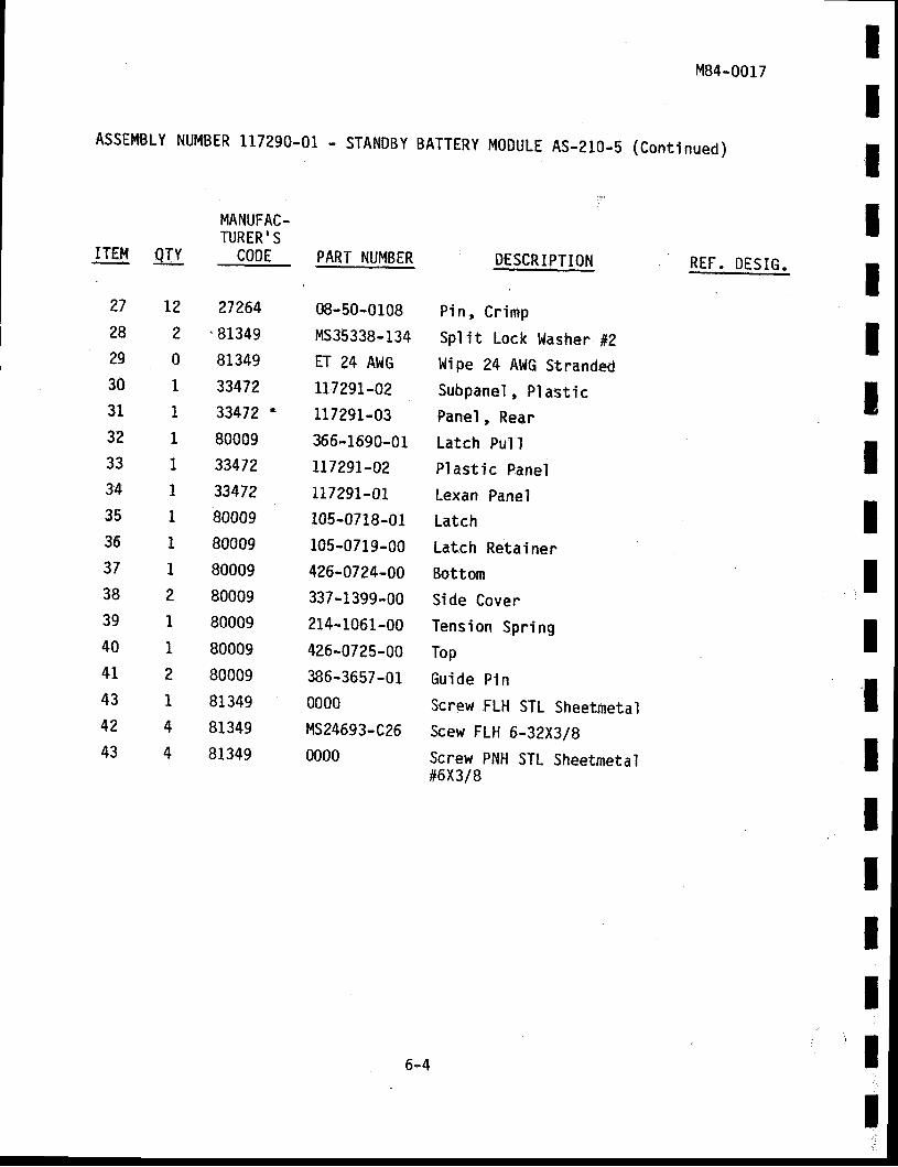
M84-0017
REF. DESIG.
IIIttIIIIIIItIIII
'l
I
ASSEMBLY NUMBER 117290.01 . STANDBY BATTERY M0DULE AS-210-5 (Continued)
ITEI'I
MANUFAC-TURER'S
CODE
27
28
?e
30
31
3;2
33
34
35
36
37
38
39
40
41
43
42
43
g
L2
2
0
1
1
1
I
I
I
1
I
?
1
1
2
1
4
4
27264" 81349
81349
33472
33472 ,
80009
33472
33472
80009
80009
80009
80009
80009
80009
80009
81349
81349
81349
PART NUMBER
08-50-0108
MS35338-134
ET 24 A}'IG
tt729I-02
u7291-03
366-1690-01
t17291-A2
LL7?9t-01
105-0718-01
105-0719-00
426-0724-00
337-1399-00
214-1061-00
426-0725-00
386-3657-01
0000
MS24693-C26
0000
DESCRIPTION
Pi n , Cr imp
Spl i t Lock Washer #?Wipe 24 A}{G StrandedSubpane l , P las t i cPanel , Rear
Latch Pul IPlast ic PanelLexan PanelLatch
Latch Retainer
Bottom
Side CoverTension Spr ingTop
Guide P in
Screw FLH STL SheetmetalScew FLH 6-32X3/gScrew PNll STL Sheetmetal#6X3/8
6-4
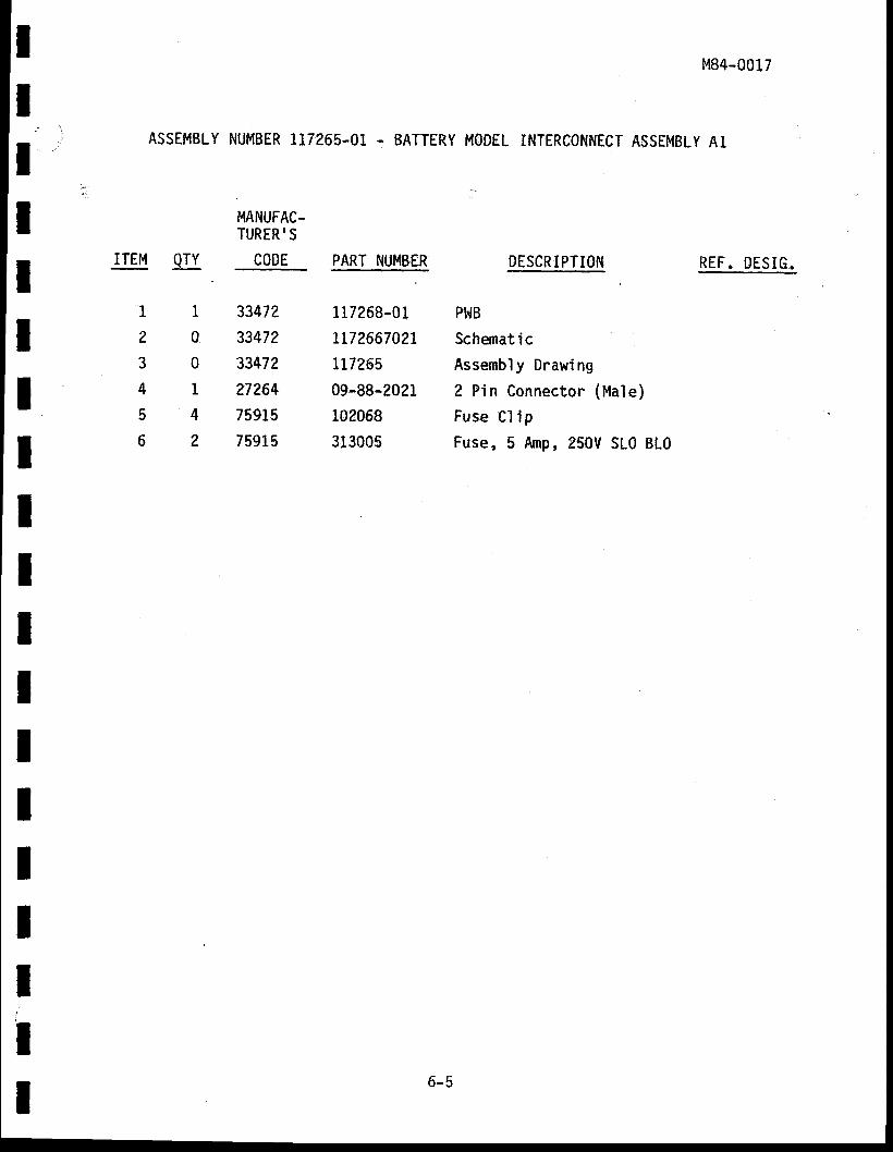
tI
i
IIIIIIltIIIIIIIII
ITEM
ASSEMBLY NUMBER 117265.01 - BATTERY MODELINTERCONNECT ASSEMBLY A1
MANUFAC-TURER I S
CODE PART NUMBER!r.
M84-0017
DESCIIPTI0N REF. DESIG.
P!{B
Schematic
Assembly Drawing
2 Fin Connector (Male)
Fuse C l ip
Fuse, 5 Amp,.250V SLO BLO
1
2
3
4
5
6
I
0
0
1
4
2
33472
33472
33472
27264
75915
75915
117268-01
LL72667021
117265
09-88-2021
102068
31.3005
6-5
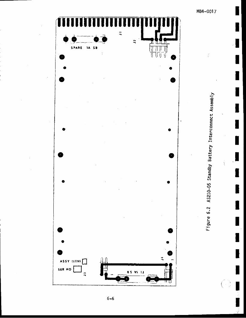
M84-001 7
ltfl I:l
"It
"ol€
{l+,
EI
5r3-(u
EII
t(u
EIi l
EI(t)
slGI.4
;lrA
5lb-
III
l:I' '
IJ .
cc
c
ti-cc
c
t_[olS P A R E 5 A S B
cc
cassv ruzss f l
t.* *o f] 8 S V 9 r '
6-6
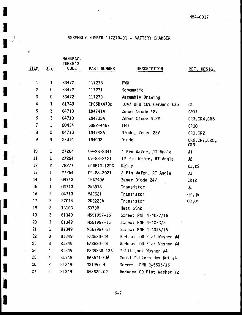
It
\
ItASSEMBLY NUMBER117270-01 - BATTERY CHARGER
M84-0017
REF. DESIG.
IIItII
MANUFAC-TTJRER'S
CODE PART NU}IBER
II
IrEM gU.
1
2
3
4
5
6
7
8
9
10
11
L2
13
14
15
16
t7
18
19
20
2t
22
23
?425
26
27
1
0
0
1
1
3
I
2
4
1
1
2
I
1
1
22
?
2
3
1
I
8
4
4
2
4
33472
33472
33472
81349
04713
04713
50434
04713
270L4
27264
27264
78277
27264
04713
04713
04713
270't4
13103
81349
81349
81349
81 349
81349
8134981349
81349
81 349
tt7273
LL7?7I
Lt7270
CKO5BX473K
1N4741A
1N4735A
s082-4487
1N4748A
1N4002
09-88-2041
09-88-2t2L
60RErS-120C
09-88-2A2L
1N47494
2N4918
MJE521
2N2222A
60738
MS51957-16
MS51957-15
MS51957-14
NAS620-C4
Ms620-C4
MS35338- 1 35MS671-Cf*
MS1957-4
NAS620-C2
DESCRIPTION
Pl,|B
Schemati c
Assembly Drawing
.047 UFD 10% Ceramic Cap
Zener Diode 18VZener Diode 6..2V
LED
Diode, Zener 22Y
Di ode
4 Pi'n l, lafer, RT Angle12 Pin l, lafer, RT Angle
Re'lay
2 Pin Wafer, RT Angle
Zener Diode 24V.Transi stor
Transi storTransi stor
Heat Si nk
Screw: PNH 4-40X7l16
Screw: PNH 4-40X3/8
Screw: PNH 4-40X5/16
Reduced 0D Fl at Washer #4Reduced 0D Fl at Washer #4Sp' f i t Lock Washer #4Srnal l Pattern Hex Nut #4Screw: PNH 2-56X5l16
Reduced 0D Flat Washer #2
c1CR11
cR3,CR4,CR5
cR1.0
cRl. ,cRz
cR6,CR7,CRg,cR9
J1
J2
K l ,K2
J3
cR12
Q1
Q2,Q5Q3,Q4
IIIIIIII
6-7
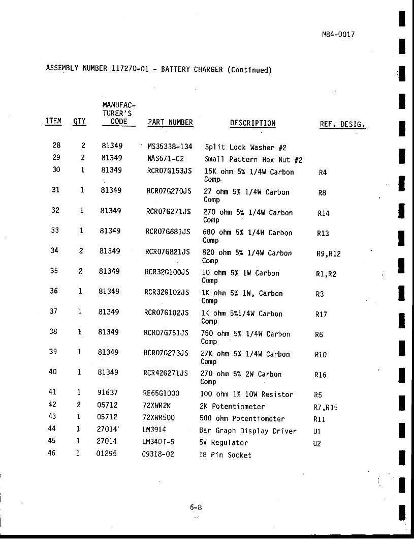
ASSEMBLY NUMBER TL727O.OL . BATTERY CHARGER (Cont inued)
M84-0017
REF. DESIG.
IIIIIIItIIIIIIIIIII
ITEM _ATY.
MANUFAC.TURER'S
CODE PART NUMBER DESCR I PTION
Sp1 it Lock Washe? #zSmal I Pattern Hex Nut #Z15K ohm 5% L/4W CarbonComp,
27 ohn 5% Ll4Vl CarbonComp
270 ohm 5% t/4W CarbonComp
680 ohm 5% L/4W CarbonComp
820 ohm 57, 7/4W CarbonComp
10 ohm 5% l}l CarbonComp
lK ohm 5% 11,,|, CarbonComp
1K ohm 57"L/4W CarbonComp
750 ohm 5% I/4W CarbonComp
27K ohm 5% I/4W Car.bonComp
270 ohm 5% 2W CarbonComp
100 ohm 1% 10t{ Resistor
2K Potent iometer
500 ohm Potent iometerBar Graph D isp lay Dr iver5V Regul ator
18 Pin Socket
282
292
30 1
31 1
32 1
33 1
342
352
36 I
37 1
38 I
39 1
40 1
41 I
4?2
43 1
44 145 1
46 1
81349
81349
81349
81349
81349
81349
81349
81349
81349
81349
81349
81349
81349
91637
05712
057t2
27014'
270t4
01295
MS35338-134
MS671-C2
RCR07G153JS
RCR07c270JS
RCR07G271JS
RCR07G681JS
RCR07c82tJS
RCR32GlOOJS
RCR32G1O2JS
RCR07G102JS
RCR07G751,lS
RCR07G273JS
RCR42G271JS
RE6sG1000
7?XWR?K
72XhlR500
1M3914
LM340T-5
c9318-02
R4
R8
R14
Rl3
R9, R 12
Rl ,R2
R3
R17
R6
R10
R16
R5
R7,R15
R11
U1
U2
6-8
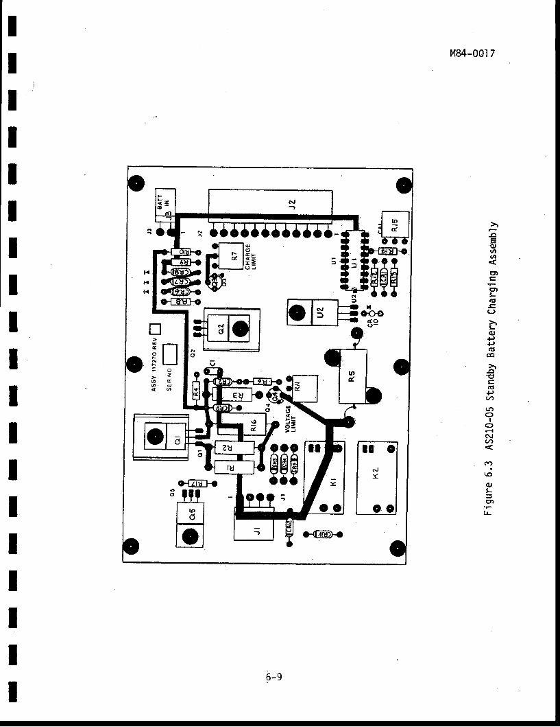
M84-001 7
tItI
:
II
€(l,tntn
t'rco!!-G'
g(J
LG.,+tP|ttco
-oEc|tt+,(t,
u)O
IoFI
GJlr'>
C'
(o(uL=ttl
l!
?9gBaa;
6-9
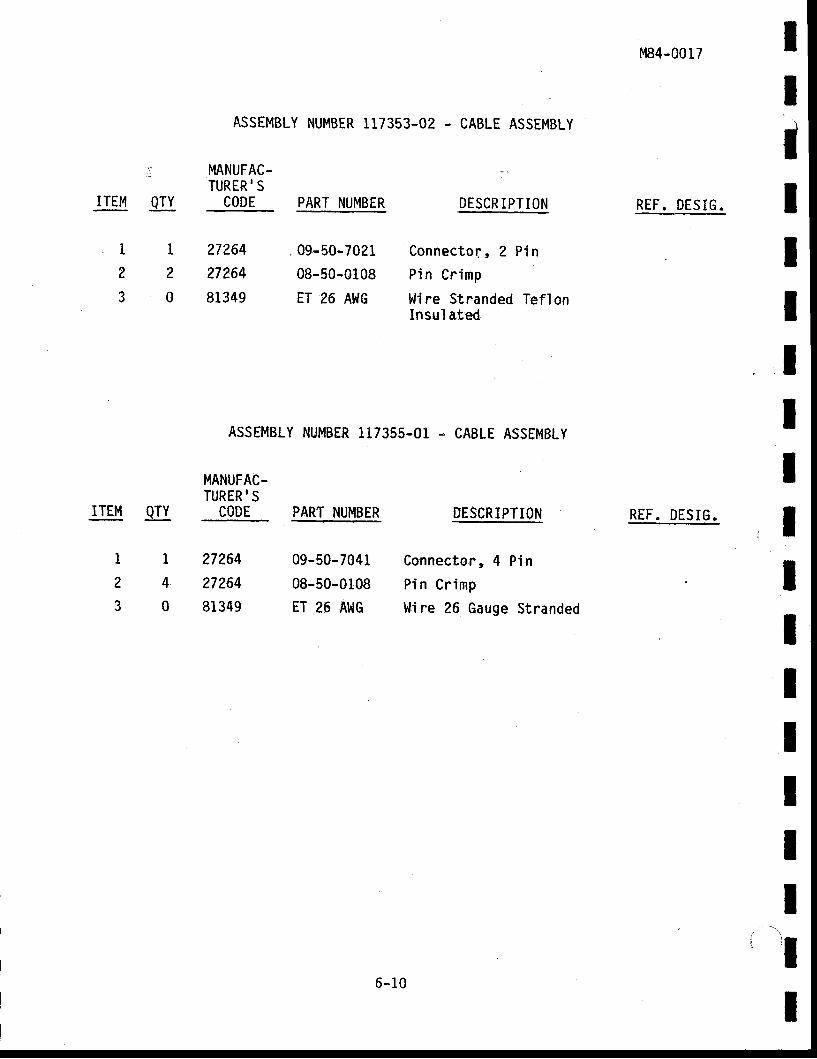
ASSEMBLY NUMBER117353-02 -
PART NUMBER
CABLE ASSEMBLY
DESCR IPTION
Connector, 2 Pin
Pin Cr imp
Wire Stranded TeflonInsul ated
DESCRIPTION
Connector, 4 Pin
P in Cr implli re 26 Gauge Stranded
M84-0017
REF. DESIG.
REF. DESIG.
IIIIIIIII
,lIIItIII
i -,1
I
MANUFAC-TURER'S
CODEJTEM lIL
120
ITEM .AII
1
4
0
123
27264
27264
81349
09-50-7021
08-50-0108
ET 26 AI'JG
ASSEMBLY NUMBER 117355-01 - CABLE ASSEMELY
MANUFAC-TURER' S
CODE PART NUI'IBER
123
27264
27264
81349
09-50-7041
08-50-0108
ET 26 A}IG
6 -10
IIIIIIIIIIIIIIIIIIt
M84-0017
6-2
in the
l,raxuFAcTURER,S LIST CODE T0 NAME
This sec t ion conta insAS210 system. The codes
a l l manufac turer ' s codes fo r mater ia lsare l is ted in numerical order by code.
6 -1 1
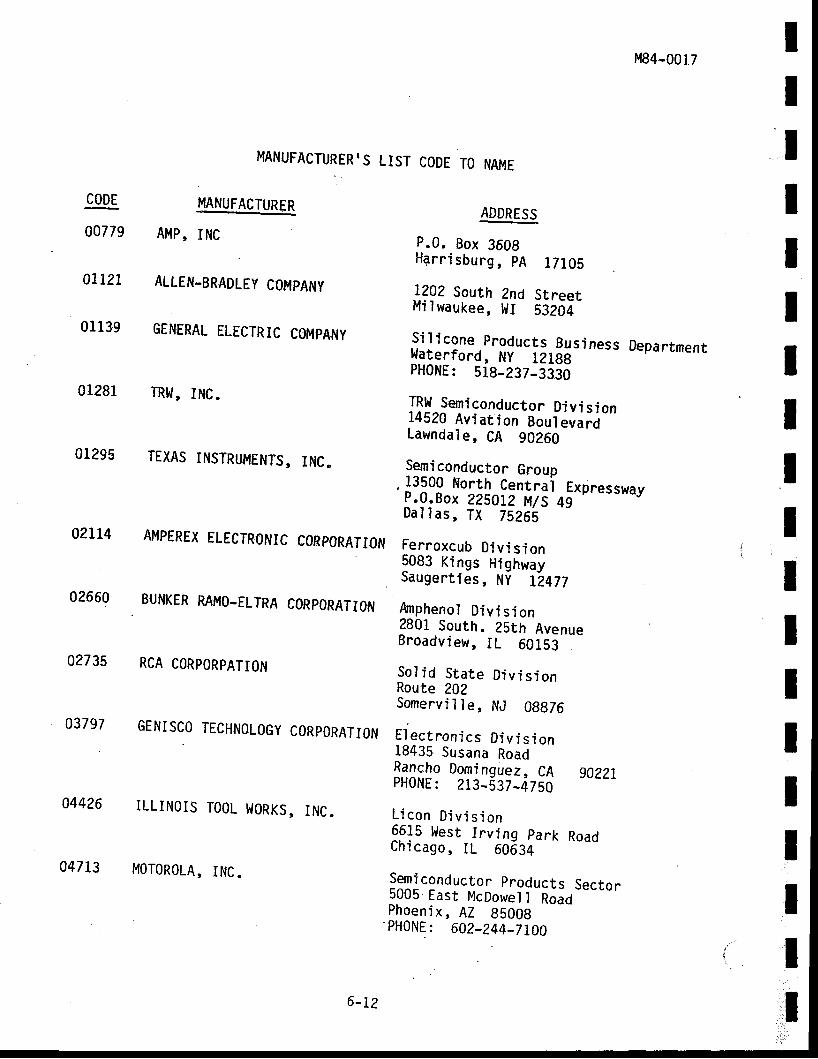
M84-0017IITItIIIIIIIIIItII
MANUFACTURER'S LIST CODE TO NAME
CODE
CI4779
0tL2t
01139
01281
01295
O?LI4
02660
02735
MANUFACTURER
AMP, INC
ALLEN-BRADLEY COI,IPANY
GENERAL EI.ECTRIC COfiPAfiY
ADDRESS
P.0. Box 360gHar r isburg , pA 17105
-1-202 South 2nd StreetMilwaukee, HI S3Z0i
Si I icone pr.oducts, Business DepartmentWater fo rd , Ny l21gg
- - - Yvru '
PHONE: 518-Z3Z-3330TRI,I, INC. TRhl semiconductor Division
14520 Avi ation goutevard-"Lawndale, CA 90?60
TEXAS INSTRUMENTS, INC. Semiconductor Group.13500 North Centrai Expresswav
P.0_.Box ZZSOLZ M/S 49 - r ' rYs ' rsr
Dal las, TX 75265AMPEREX ELECTRONIC CORPORATION FCTTOXCUb DiViSiON
5083 Kings Highway>augert ies, Ny L2477
BUNKER RAMO-ELTRA CORPORATION AMPhENOI DiViSiON_2801 South. Z5th AvenueBroadview, IL 60153
RCA C0RP0RPATI0N Sol id State Div is ionRoute 202Somenvi' l ' le,
NJ 09976GENIsc' TE'HN'L'G' . 'R' 'RATI,N Electronics Div is ion
18435 Susana Roadl.ql:!o Dominguez, CA IOZZIPH0NE: 213-537_4750
ILLIN0IS T00L t . loRKS, INC. L icon D iv is ion6615 West I rv ing park RoadChicago, IL 60634
Semiconductor products Sector5005 East McDowel t noaaPhoen ix , AZ 9500g'PHONE:
60?-244-7L00
03797
04426
047T3 MOTOROLA, INC.
6-12
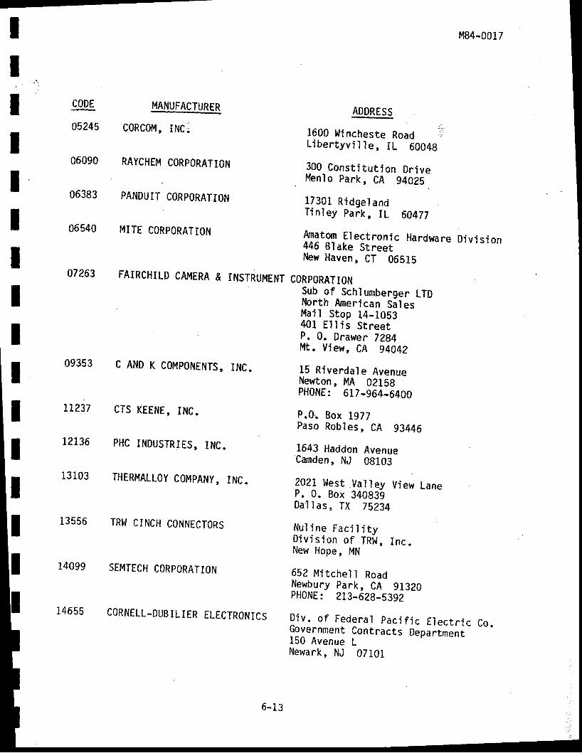
I M84-0017
Ii
IIIIIIIIIIIIt
CODE
05245
06090
06383
06540
07263 FAIRCHILD CAI,,IERA & INSTRUMENT
09353 C AND K C0|'{P0NENTS, INC.
MANUFACTURER
cORc0M, INC.
RAYCHEM CORPORATION
PANDUIT CORPORATIO$I
MITE CORPORATION
CTS KEENE, INC.
PHC INDUSTRIES, INC.
THERMALLOY COMPANY, INC.
ADDRESS
1600 l,Ji ncheste Road 'L iber tyv i l le " IL 60048
300 Const i tut ion Dr ive. Menlo park, CA g40ZS.
17301 R idge landTinley pank, IL 6A477
Sqtor Electronic Hardware Divis ion446 Blake Street
- '
New llaven, CT 06515
CORPORATIONSub of Schl umberger LTDNorth Anerican SilesMai I Stop 1.4-1053401 E l l i s S t ree tP. 0, Drawer 7Zg4Ittt" View, CA g4A4Z
15 Riverdale AvenueNewton, MA 0215gPHONE: 617-964-6400
P.0r Box 1977Paso Robles, CA 93446
1643 Haddon Avenue'Camden, NJ 09103
2021 West Val ley View LaneP. 0. Box 340g39Dal las, TX 75234
Nu l ine Fac i l i t vD iv is ion o f TRi l , Inc ,New Hope, MN
652 Mi tche l l RoadNewbury Park, CA 91320PH0NE: 213-628-5392
Div . o f Federa l pac i f i c E lec t r i c Co.Govennment Contracts Deparir"ni-150 Avenue LNewarkn NJ 07101
LT237
12t36
13103
13556 TRt,, CINCH CONNECTORS
T4099 SEMTECH CORPORATION
14655 CORNELL-DUBILIER ELECTRONICS
6-13
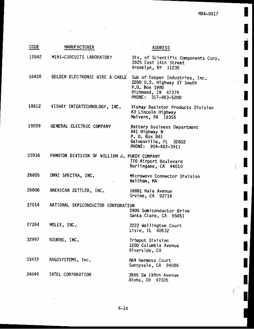
IIIIIIIII
,lIIIIIII
M84-0017
CODE MANUFACTURER ADDRESS
15542 PIINI-CIRCUITS LABORATORY Div . o f Sc ien t i f i c Components Corp .2625 East 14th StreetBrooklyn, NY 11235
18612
BELOEN ELECTRONIC WIRE & CABLE sub of cooper Industr ies, Inc.2200 U.S. Highway 27 SouthP.0. Box 1980Ri ctmond , I N 47 37 4PHONE: 317-983-5200
VISHAY INTERTECHNOL0GY, INc. v ishay Resistor products Div is ion63 Lincoln HighwayMalvern, PA 19355
GENERAL ELECTRIC C0$'IPANY Battery Business Department441 Highway NP. 0, Box 861Gainesvi l le, FL 32602PHONE: 904-462-3911
PAI4OTOR DIVISION OF },'ILLIAM J. PURDY COMPANY770 Ai rport Boul evardBurl ingame, CA 94010
0MNI sPEcrRA, INc. Microwave connector Div is ion!'faltham, MA
APIERICAN ZETTLER, INC. 16881 Hale AvenueIrv ine, CA 92714
NATIONAL SEMICONDUCTOR CORPORATION
19209
23936
26805
26806
?10t4
27264
32997
M0LEX, INC.
B0URNS, INC,
2900 Sem'iconductor DriveSanta Clara, CA 95051.
2222 Ve'l l ington CourtLis le, IL 60532
Tr impot D iv is ion1200 Columbia AvenueRivers ide , CA
884 Hermosa CourtSunnyvale, CA 94086
3585 Sl,l 198th AvenueA loha ,0R 97005
16428
33472
34649
ARG0SYSTEMS, Inc.
INTEL CORPORATION
6-14
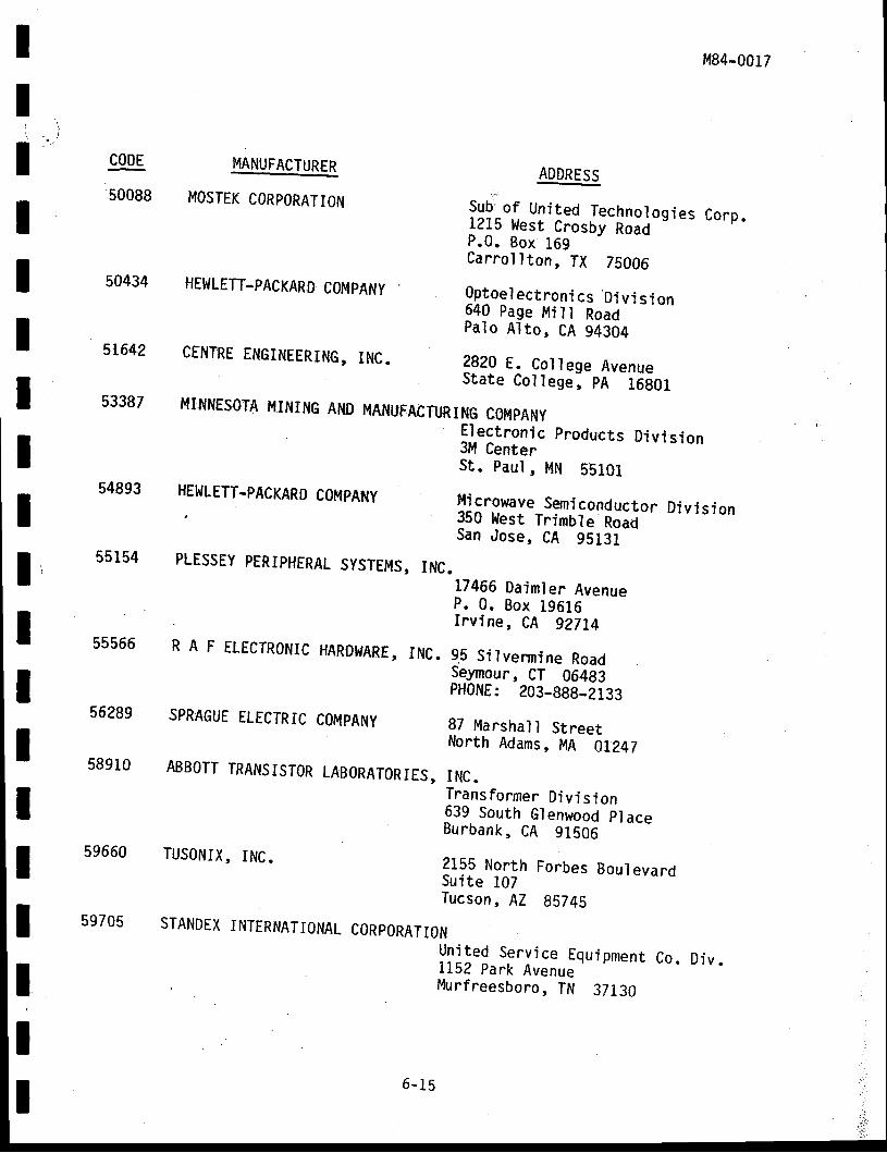
IIItIIIIII'ITIIIItII
M84-0017
50434 HEWLETT.PACKARD COMPANY
CENTRE ENGINEERING, INC.
MINNTSOTA MINING AND MANUFACTURING COMPANY
CODE
50088
MI\NUFACTURER
MOSIEK CORPORATION
51642
53387
54893 HEI^'LETT-PACKARD COMPANY
55154
55566
ADDRESS_
*?-. t Uni ted Technotog. ies Corp.1215 West Crosby Road J.-- vv ' , '
P.0. Box 169Carrol lton, TX 25006
9p!ogt ectroni cs 'Di
v i s i on640 Page Mi l l RoadPalo Al to, CA 94304
2820 E. Col lege Avenuestate Col lege, pA 16901
El.ectronic products Divi sion3M CenterSt . Pau l , MN 55101
l,l icrowave Semiconductor Division350 West Trimble RoadSan Jose, CA 95131
56289
58910
PLESSEY PERIPHERAL SYSTEMS, If{C.17466 Daimlen AvenueP. 0. Box 19616Irv ine, CA gZ7t4
R A F ELECTR'NIC HARDWARE, INC. 9.5 Silvermine RoadSeymour, CT 06493PH0NE: 203-888-2133
SPRAGUE ELECTRIC COMPANY 87 Marshal] StreetNorth Adams, l,tA 0I?47
ABBOTT TRANSISTOR LABORATORIES, INC.fransformer Div is ion639 South Glenwood placeBurbank, CA 91506
2155 North Forbes Boul evandSui te 107Tucson, AZ 95745
STANDEX INTERNATIONAL CORPORATION
9i ! "0 Serv ice Equipment Co. Div .1152 Park Avenuevlur f reesboro, TN 37130
59660 TUSONIX, INC.
59705
6-1s
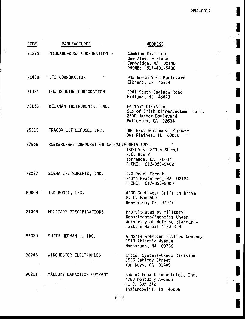
71450
71,984
73138
75915
Ttgag
CODE MAI{UFACTURER
71279 MIDLAND.ROSS CORPORATION
M84-0017
ADDRESS
Cambion D iv is ionOne Alewife PlaceCambridge, MA 02140PHONE: 617-491-5400
905 North l{est BoulevardElkhart , IN 46514
3901 South Saginaw RoadMidland, MI 48640
Hel ipo t D iv is ionSub of Smith Kline/Becknan Corp.2500 Harbor Boul evardFul
' lerton, CA 92634
800 East Northwest HighwayDes Plaines, IL 60016
CALIFORNIA LTD.1800 l,lest 220th StreetP.0 . Box BTorrance, CA 90507PHONE: 2L3-328-5402
1.70 Pearl StreetSouth Braintree, MA 02184PH0NE: 617-853-5000
4900 Southwest Gri f f i th Dr iveP. 0. Box 500Beaverton, 0R 97077
Promultgated by Mi l i taryDepartments/Agencies UnderAuthor i ty of Defense Standard-izat ion Manual 4120 3-M
A North American Phi l ips Company1913 At lan t ic AvenueManasquan, NJ 08736
Li t ton Systems-Useco Divi s ion1536 Sat icoy StreetVan Nuys, CA 91409
Sub o f Emhar t Indus t r ies , Inc .4760 Kentucky AvenueP. 0 . Box 372Ind ianapo l is , IN 46206
6-16
CTS CORPORATION
DOI.I COR$IING CORPORATION
BECKMAN INSTRUMENTS, INC.
TRACOR LITTLEFUSE, INC.
RUBBERCRAFT CORPORATION OF
IIIItI
il
IIIIIII
'l
I
'78277 SIGMA INSTRUMENTS, INC.
TEKTR0NIX, INC.
81349 MILITARY SPECIFICATIONS
83330 SMITH HERMAN H. INC.
88245 l^,INCHESTER ELECTRONICS
90201 MALLORY CAPACITOR COMPANY
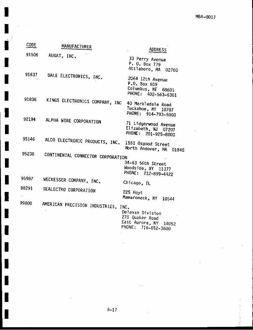
IIIt
M84-0017
CODE
91506
91637 DALE ELECTRO}IICS, INC.
91836
ADDRES:
33 Perry AvenueP. 0. Box 179Attleboro, MA 02703
2064 l?th AvenueP.0. Box 609Col umbus, NE 6g601PH0NE: 402-563-6301
KINGS ELECTRONICS COMPANY, INC 40 MArb]CdAIC ROAdTuckahoe, Ny LOIOTPH0NE: 9t4-793-5000
ALPHA }|IRE C0RP0RATION Tl.Lidgerwood AvenueEJ_izabeth, lrU O7ZO7PH0NE: 20I-925_8000
ALC0 ELECTR0NIC PRODUCTS, INC. 1551 0sgood Streetl,lorth Andover, plA 01g45
CONTINENTAL CONNECTOR CORPORATION34-63 56th StreetWoodside, Ny tl317PHONE: Zt}-gsg-4422
I{ECKESSER COIIPANY, INC.
SEALECTRO CORPORATION
AMERICAN PRECISION INDUSTRIES, INC.De levan D iv is ion270 Quaker RoadEast Aurora, Ny 14052PH0NE: tt6-652-3600
MANUFACTURER
AUGAT, INC.
95987
98291
IIIIIIIIITIIIIT
92194
95146
9s238
Chicago, IL
225 HoytMamaroneck, Ny lOS44
6-L7

II--ti.tIIIIIIItIIIIII
i ' l
I


AS2 1 0-06
MICROWAVE FREQUENCY
GENERATOR MODULE
M84-0008
Revised 6 February l9B5

M84-0008
Al l r ights reserved. No part of th is publ icat ion may bereproduced, stored in a retr ieval system, or t ransmit ted,in any form or by any means, electronic, mechanical ,photocopying, recording and/or otherwise without the pr iorwr i t ten permission of ARG0Systems, Inc. This manual maynot be len t , reso ld , h i red ou t o r o therw ise d isposed o f byway of trade in any form of binding or cover other thantha t in wh ich i t i s pub l i shed, w i thout the pr io r consentof ARG0Systems, Inc.
IIIIIIIII
ARGOSystems, Inc. / 3L0 N. Mary Ave., Sunnyvale, Cal i fornia 94086Telephone (Area Code 4081 737-2000/Telex No. 352077

M84-0008
Secti on
TABLE OF CONTENTS
Ti t le
PREFACE
GENERAL INFORMATION
1.1 In t roduc t ionL.2 Phys ica l and E lec t r i ca ' l Descr ip t ion
INSTALLATION
?.1 In t roduc t ion
OPERATION
3.1 In t roduc t ion3.2 Control s and Connectors3 .3 0pera t ing Ins t ruc t ions
THEORY OF OPERATION
4.1 In t roduc t ion4 .2 0vera l l Descr ip t ion4.3 Frequency Genera t ion C i rcu i t ry4 .4 Leve l Cont ro l C i rcu i t ry4 .5 Se l f -Tes t C i rcu i t ry
MAINTENANCE AND CALIBRATION
5.1 In t roduc t ion5.2 Prevent ive Maintenance Checks and Services5.3 Performance Test ing 0verview5.4 RF 0utput Frequency Performance Test5.5 Test Procedure5.6 RF 0utput Level Performance Test5.7 Test Procedure5.8 Ca l ib ra t ion /A l ignment Procedures Overv iew5.9 Access to AS210-06 Microwave Frequency
Generator l lodul e5.10 +15 Power Supply Al ignment5.11 Troubleshoot ing Procedures 0verview
Page
v
1-1
1-11-1
?-t
2-t
3-1
3-13-13-1
4-1
4-L4-14-34-44-5
5-1
5-15-?5-35-35-45-45-75-11
s-115-1 35-14
IIIIIIIII
I
Sect ion
M84-0008
TABLE 0F C0NTENTS (Continued)
T i t l e
ILLUSTRATED PARTS LISTS
6.1 In t roduc t ion6.2 Manufac turer ' s Code L is t
6 -1
6-16-20
- l I -
IIIIIIIIIIIIIIIIttI
M84-0008
Fi gure
1-1
z-r
3-1
3-2
4-1
5-1
5-Z
5-3
5-4
5-5
6-1
6-2
6-3
LIST OF ILLUSTRATIONS
Ti t le
A5210-06 Microwave Frequency Generator lr lodul e
Connect Diagram for AS210-06 3-Foot, Low-LossCable Assembly and for Level ing Detector
45210-06 Module Front Panel Controls and Connectors
A5210-06 Level ing Detector Connectors
Microwave Frequency Generator lt lodul e FunctionalBl ock Diagram
A5210-06 Microwave Frequency Generator lvlodu'le RF OutputFrequency Test Conf igurat ion
A5210-06 Microwave Frequency Generator Module RF 0utputLevel Test Conf i gurat ion
Flow Diagram of the Cal ibrat ion/Al ignment Procedurefor the A5210-06 Microwave Frequency Generator lvlodule
AS210-06 Control Circui t Card Schematic Diagram
4S210-06 Chass is In te rconnect D iagram
45210-06 Module Showing Control Circui t and Assembly
A5210-06 Module Showing Microwave Subsystem
A5210-06 Control Circui t Card (A2) Assembly Diagram
Page
t -?
2-3
3-2
3-4
4-1
5-5
5-8
5-r2
5-1 7
5-18
6-?
6-3
6-1 5
- i i i -
M84-0008
IIITIIIIIIIIIIIIIII
Tabl e
1-1
3-1
3-2
5-1
5-2
5-3
5-4
5-5
45210-06 Equipment Speci f icat ions
AS210-06 Module Front Panel Controls and Connectors
A5210-06 Leveling Detector Connectors
Prevent ive Maintenance Checks and Services
Required Test Equipment for the Internal FrequencyStandard Accuracy Test
Minimum Performance Limits for RF 0utput Frequenciesof the A5210-06
Mfnimum Performance Limits for RF Output Level ofthe A5210-06
Required Test Equipment for +15 Vol t Power SupplyA1 i gnment
Er ror Code L is t ing
V i sua l Ind ica t ions
LIST OF TABLES
Ti t le Page
l-4
3-3
3-5
5-2
5-3
5-6
5-10
5-13
5-1 5
5-16
5-6
5-7
- l v -
IIItIIttIIlIIIIIIII
M84-0008
PREFACE
This manua l con ta ins the ins ta l la t ion , opera t ion , and main tenanceinstructions for the AS210-06 Microwave Frequency Generator lr|odule Thedata conta ined here in i s a r ranged as fo l lows:
Sect ion 1 General Informat ion
Sect ion 2 Ins ta l la t ion
Sect ion 3 Operat ion
Sect ion 4 Theory of Operat ion
Sect ion 5 Maintenance and Ca' l ibrat ionSect ion 6 I l lus t ra ted Par ts L is t
RTFERENCE PUBLICATIONS
MODIL NO.
AS2lO.PM
AS21O-RM, LM
AS210-01A
AS210-02
AS210-03
AS210-04
AS210-05
AS210-08
AS210-20
PUBLICATION T ITLE
Portable Mainframe Operat ion and Maintenance ManualMainframe 0perat ion and Maintenance ManualIttodule Control ler Operation and Maintenance l4anualFrequency Comparator 0peration and Maintenance ManualFrequency Generator 0peration and lr{aintenance ManualDigi ta l Delay Generator Operat ion and Maintenance ManualStandby Battery Operation and Maintenance Manual
Distr ibut ion Ampl i f ier 0perat ion and I 'h intenance ManualTime Clock Operatfon and Maintenance Manual

IIIItItIIIIIIIIIIII
M84-0008
SECTION 1
GENERAL INFORMATION
1.1 INTRODUCTION
The A5210-06 Microwave Frequency Generator lv lodule, i l lustrated inFigure L-1. , is a modular p ' lug- in uni t used in the ARG0Systems AS210 Elec-tronic Counter and Frequency Standard Cal ibrat ion System. This module isused for test ing the anpl i tude and frequency speci f icat ions of microwavefrequency counters. I t provides output f requencies f rom 1 to 18 GHz in 1 GHzincrements wi th selectable output power levels f rom -5 to -35 dBm in 5 dBsteps. An internal ALC circui t combined with the level ing detector at theend of a low-loss f lexib ' le microwave cable provides an output power- leve1accuracy at the load of bet ter than +2 dB over a 30 dB dynamic range.
The A5210-06 is compat ib le wfth ei ther the AS210A-PM PortableMainframe, the AS210-RM Rackmount Mainframe, or the AS2l0-LM LaboratoryMainframe. The A5210-06 is programmab' le through the IEEE-488 interfacein the AS210-01A Modu le Cont ro l ' le r . Descr ip t ions o f o ther modu les o f theAS210 ser ies are provided in separate publ icat ions referenced in the prefaceand avai lable f rom ARG0Systems.
r .2 PHYSICAL AND ELECTRICAL DESCRIPTION
The A5210-06 Microwave Frequency Generator Module is modular lyconstructed for insert ion into a cornpat ib le AS210 mainframe. The module 'sfront panel contains a thumbwheel switch for select ion of operat ing f re-quency , a ro ta ry sw i tch fo r se lec t ion o f ou tpu t leve l , a CAL LED, a p rec is ionN outpu t s igna l connector , and a BNC leve l ing s igna l connector .
1 -1
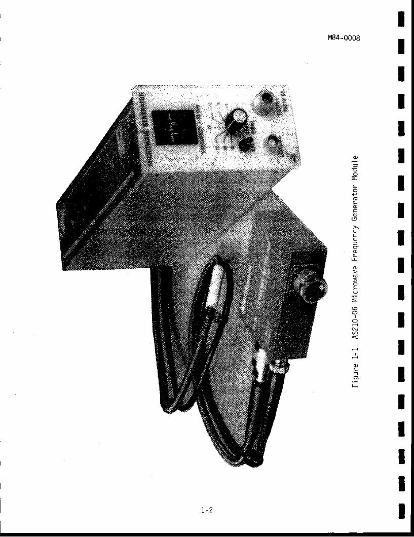
M84-0008
IIII
(lJr
E
r-o
+J(6L,(u(u(5
c(l)
q"c)!
tl-
c)(o=!
=
IOtC\a
fr
I
(u!
U-
t -2
ItItIItIItII
M84-0008
Internal ly, the module consists of one each of the fo i lowing:
o
a
a
O
O
a
1 GHz phase- locked osc i l la to r (PLO)
1 GHz, 1 watt ampl i f ierY IG tuned mul t ip l ie r
Y IG co i l d r i ver
Microwave switch
Pr in ted c i rcu i t card fo r con t ro l c i rcu i t ry .
The 1 GHz PLO is phase- locked direct ly to the 10 MHz output f requency fromthe Rubidium frequency standard provided by the AS210 mainframe. The 1 GHzPLO has two outputs. The f i rst is the RF sample port , which the microwaveswitch and control circuitry switches directly to the output connector of themodule. The second output is the RF output port , which is ampl i f ied andde l ivered to the input Y IG tuned mul t ip l ie r . Harmon ics o f the 1 GHz inputsignal f ron 2 to 18 GHz are avai lab' le at the output of the YIG tuned mult i -p l ie r . The YIG co i l d r i ver se lec ts the des i red harmon ic , wh ich the mic rowaveswitch directs to the output connector of the module. At the output connectoro f the modu le , a l l 18 ou tpu t f requenc ies f rom I to 18 GHz are ava i lab le .
A 3- foo t f lex ib le cab le assembly compr ised o f a low- loss mic rowavecable and BNC level ing cable is at tached to the A5210-06. At the end of thelow- loss cab le assembly i s a leve l ing de tec tor . The leve l ing de tec torcontains a 3 dB power div ider and a microwave detector for the precis ion ALCloop. The f inal leveled output of the microwave frequency generator is theRF OUT port of the level ing detector.
The frequency and level controls are scanned per iodical ly by themicroprocessor in the AS210-01A Module Control ler . The data is returned tothe A5210-06 Microwave Frequency Generator lvlodule in the form of commands forse lec t ing opera t ing po in ts fo r the ALC and YIG tun ing c i rcu i ts . Tab le l - l i san equipment speci f icat ion for the A5210-06 instal led in a compat ib le AS2l0Mainframe with the AS210-01A Module Control ler .
1 -3
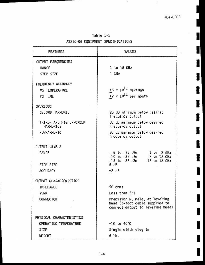
M84-0008
Tabl e
A5210-06 EQUIPMENT
1-1
SPTCIFICATIONS
IIIIIIItIIIIIItI
FEATURES VALUES
OUTPUT FREQUENCIES
RANGE
STEP SIZE
FREQUENCY ACCURACY
VS TEMPERATURI
VS TIME
SPURIOUS
SECOND HARMONIC
THIRD- AND HIGHER.ORDERHARMONICS
NONHARMONIC
OUTPUT LEVELS
RANGE
STEP SIZE
ACCURACY
OUTPUT CHARACTERISTICS
IMPEDANCE
VSl,|R
CONNECTOR
PHYS ICAL CHARACTERISTICS
OPERATlNG TEMPERATURE
SIZE
l,lE I GHT
toGHz
1ol1 maximum
1011 per month
20 dB minimum belowfrequency output
30 dB minimum belowfrequency output
30 dB minimum belowfrequency output
-5 to -35-10 to -35-15 to -355dB+2 dB
I
I
GHz18
!6+2
desi red
desi red
desi red
dBm l to SGHzdBm 8 to 12 GHzdBm l2 to 18 GHz
50 ohms
Less than 2 :1
Prec is ion N , ma1e, a t l eve l inghead (3-foot cable suppl ied toconnect output to level ing head)
+10 to 40"C
Sing le w id th p lug- in
6 lb .
I -4
IIItIIIIII
M84-0008
SECTION 2
INSTALLATION
2.L INTRODUCTION
The AS210-06 Microwave Frequency Generator Module plugs into acompat ib le AS210 Mainframe. The module is electr ical ly connected througha rear edge connector and mechanical ly retained with a f ront panel lockingbar .
NOTE
Because of the high retent ion force of therear card edge connector, the LEVEL switchknob may need to be pul I ed at the same timeas the re lease mechan ism is pu l led , to removethe A5210-06 Microwave Frequency Generatorlv lodule f rom the mainframe (see Figure 3-1).
NOTE
The power in the AS210 Mainframe must beOFF when insert ing or removing the A5210-06Microwave Frequency Generator Module.
CAUTION
AS210 ser ies p lug- ins w i l l no t work inTektronix IM-500 ser ies mainframes.Severe damage w i l l resu l t i f opera t ionin th is mode is a t tempted.
2-1
IIIIIIIItIIIIIIIIII
1.
2 .
3 .
M84-0008
Power and signal interfaceThe 3-foot, low-loss microwave cableconnected as shown in Figure 2-1.
AS210-06
is provided through the mainframe.assembly and level ing detector are
The f lexible cable assembly and level ing head connect to theas shown in Figure 2-1.
NOTE
When ins ta l l ing the low- loss mic rowave
cable assembly and ARGOSystems Level ingDetector, p lease observe the fol lowing:
The low-loss microwave cable has amin imum bend rad ius o f 1 .5 inches .I f the cab le i s bent to less thanthe 1 .5 inch min imum rad ius , the
cab le is e lec t r i ca l per fo rmance w i l lbe degraded, and fa i lu re cou ldresu l t .
The connector mating force for thePrecis ion N connectors of the low-loss mic rowave cab le shou ld be 8 to12 pounds.
Do not use the cable assembly as ahand l e .
?-2
M84-0008
IrrlI
IIII
t-o.P(J(u.Poo(tlc
(u(u
J
!-o
11-
.ocrO
DE(utl,th
(u-o@c)thoo
JI-o
J
Poot,r-
Icf)
r{)o
IO-l(\jat1
t-o
rF
E(cL(tl(o
aP(Ja)ggo
(J
F{
tC\T
(uL3q)
u-
zz9 -A J. i <u t=(r uJ
8, I
[ : ; ;r , o < oF J c ) <
g;-isB
II
oZ 2I rr u.l| a l l J
( ) > h c oZuruJ <COJCCCJ
o
s Ao : *F v
o GU <
u 1 9{ J @z ?- lU
U
z
c
i,pL
2-3

3.1
ItIIIIIIIIIIIIIIItI
M84-0008
STCTION 3
OPERATION
INTRODUCTION
Thi s sect ion contains operat ion data and instruct ions for theAS210-06 Microwave Frequency Generator Module. 0perator interface is pro,vided through two controls, two connectors, and an LED on the front pane'l ofthe modul e. The A5210-06 i s desi gned to be used wi th the AS210-01A Modul eControl ler . However, th is interface is t ransparent to the user of theA5210-06. The A5210-06 operat ing software, located in the AS210-01A, has aYIG f i l ter cal ibrat ion sof tware rout ine that is executed upon detect ing anun leve led ou tpu t s igna l . Th is so f tware rou t ine w i l l se l f -ca l ib ra te the y IG
f i l te r tun ing in the A5210-06 dur ing normal opera t ing cond i t ions . Sec t ion 5 ,Main tenance and Ca l ib ra t ion , exp la ins the se l f -d iagnos t ic capab i l i t y o f theA5210-06 when used with the AS210-01A Module Control ler .
3 .2 CONTROLS AND CONNECTORS
Figure 3-1 is a f ront panel v iew of the A5210-06 MicrowaveFrequency Generator lbdule wi th indexed numbers keyed to Table 3-1.Figure 3-2 is a top v iew of the level ing detector showing connectorsand indexed numbers keyed to Table 3-2.
3 .3 OPERATING INSIRUCTIONS
The A5210-06 Microwave Frequency Generator lrtodule is connected tothe instrument under test v ia the RF OUT port located on the level ing detectorassembly. The RF OUT port is a precfs ion N male connector that wi l l matedirect ly wi th the input connector found on most microwave counters used today.I f the input connector of the instrument under test is not a type N female
3-1
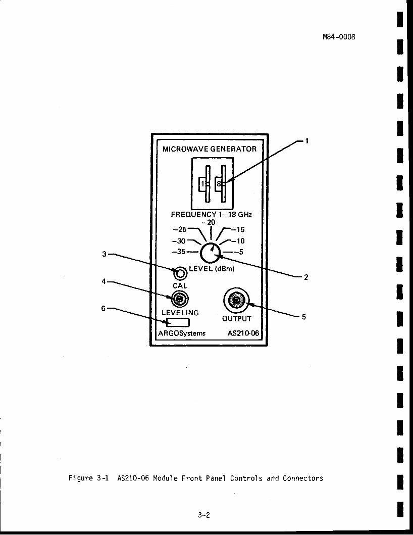
MICROWAVE GENERATOR
FREOUENCY 1-18 GHz-20
-25-. I r-15- \ t . /-30AYr-10_35-I f_l__s
LEVEL (dBml
LEVELING
ARGOSystems AS21(}06
M84-0008
IIIIIIIIIIIIIIIIIII
Figure 3-1 A5210-06 Module Front PanelContro ' ls and Connectors
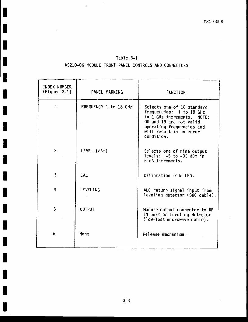
ItIIttIIItIIIIItIII
M84-0008
Tab le 3 -1
A5210-06 MODULE FRONT PANEL CONTROLS AND CONNECTORS
INDEX NUMBER(F igure 3 -1 ) PANEL MARKING FUNCTION
FREQUENCY 18 GHz
LEVEL (dBm)
CAL
LTVEL I NG
OUTPUT
None
Sel ects one of 1.8 standardfrequencies: 1 to 18 GHzin L GHz increments. N0TE:00 and 19 are not val idoperat ing f requencies andwi l l resu l t in an er ro rcondi t i on .
Se lec ts one o f n ine ou tpu t' leve ls : -5 to -35 dBm in5 dB increments.
Ca l ib ra t ion mode LED.
ALC return s ignal input f romI evel i ng detector ( BNC cabl e) .
Modul e output connector to RFIN por t on leve l ing de tec tor( low- loss mic rowave cab le ) .
Re lease mechan ism.
3-3
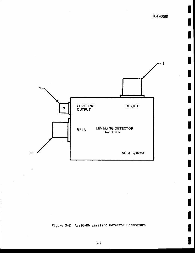
Mtl4-0008
LEVEL ING RF OUTOUTPUT
LEVELING DETECTOR1-18 GHz
Figure 3-2 A5210-06 Level ing Detector Connectors
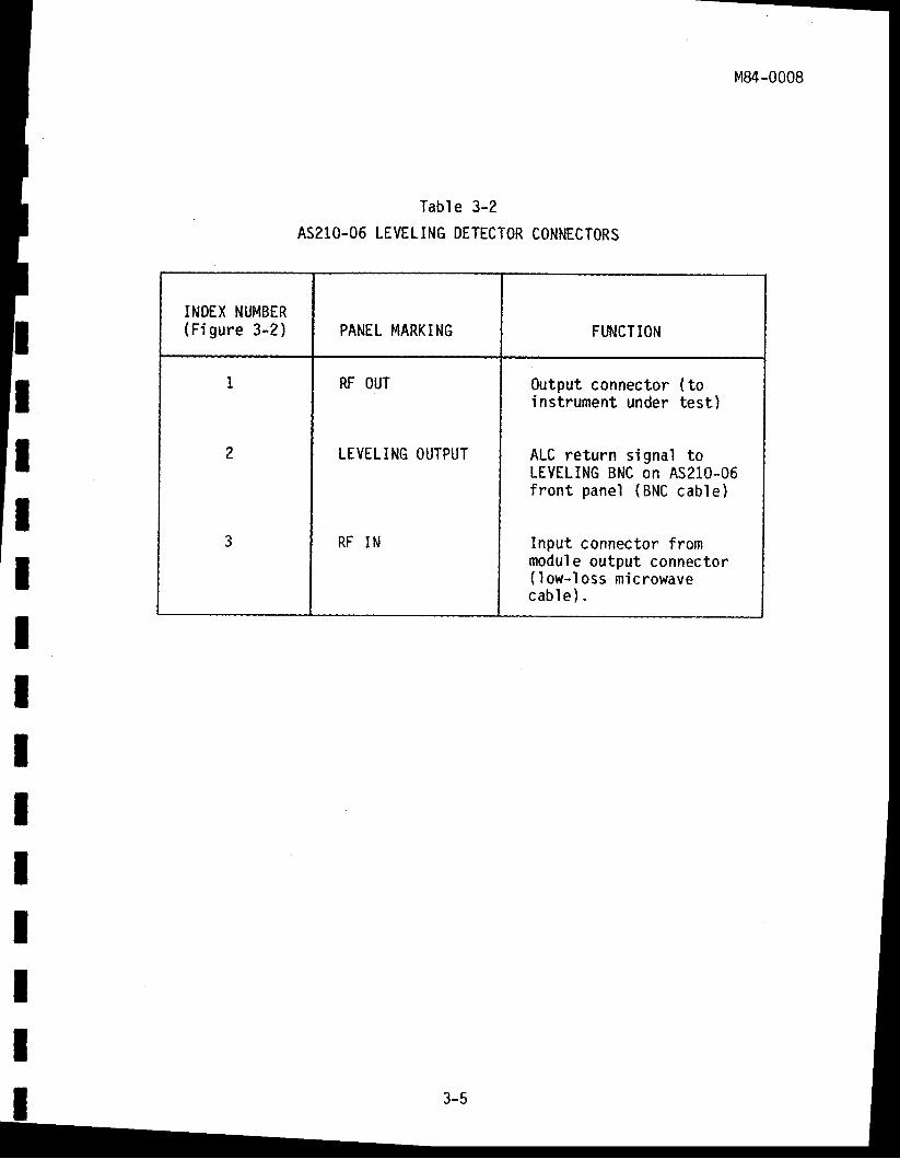
M84-0008
Table 3-2
A5210.06 LEVELING DETECTOR CONNECTORS
III
ilIIIIIIIII
INDEX NUMBER(F i gure 3-2) PANEL MARKING FUNCTION
RF OUT
LEVELING OUTPUT
RF IN
Output connector ( toinstrument under test)
ALC return signal toLEVELING BNC on A5210-06f ron t pane l (BNC cab le)
Input connector frommodul e output connector( low- loss mic rowavecab le ) .
3-5
-
MB4-0008
or precis ion type N female, then an appropr iate between-ser ies adapter wi l lhave to be used. Select the desired output frequency with the thumbwheelswitch, and choose the required output level with the rotary switch. The CALLED wi l l f lash approximately once per second i f the YIG f i l ter cal ibrat ionroutine has been init iated. i lhen the A5210-06 Microwave Frequency GeneratorModule has recal ibrated the output s ignal , the CAL LED wi l l s top f lashing andwill re*ain off. The A5210-06 is now ready to perform the desired test. Ifthe A5210-06 is not able to generate the desired output s ignal level , the CALLED wi l l s top f lash ing and w i l l remain l i t . Ihe AS210-01A Modu le Cont ro l le rw i l l sense th is fau l t and w i l l d isp lay an er ro r code. I f th is cond i t ionoccurs, consul t Sect ion 5, Maintenance and Cal ibrat ion.
IIIIIIIIIIIIII3-6
IIIIIIIIIIIIIIIIIII
45210-06
keyed to
i ncl uded
supp l i es )
4 .2
SECTION 4THEORY OF OPERATION
TNTRODUCTION
This sec t ion prov ides a descr ip t ionMicrowave Frequency Generator lvlodule.the funct ional b lock diagram (Figure
in Sect ion 5. Detai ls of common typeare no t inc luded in th is descr ip t ion .
OVERALL DESCRIPTION
M84-0008
of the c i rcui ts used in theThe c i rcu i t descr ip t ion is
4-1) and the schematic diagrarns
c i rcu i ts (such as power
The A5210-06 Microwave Frequency Generator l '4odule consists of thefront panel controls and connectors (A4), a control c i rcui t card assembly(A21, and a mic rowave subsys tem (A1, A5, A6, A7) . F igure 4- l i s a func t iona lblock diagram of the module, depict ing how the generator produces standardfrequency outputs of 1 to 18 GHz in 1 GHz increments over a 30 dB dynamicran9e.
The A5210-06 front panel controls select the desired frequency andoutput level . These front panel controls are interrogated by the AS210-01AModule Control ler v ia the microprocessor interface circui t ry located on thecontrol c i rcui t card assembly (A2l ' . The AS210-01A then reads two 12-bi twords f rom the A5210-06, corresponding to the level and frequency desired.
NOTE
The cal ibrat ion EPROM is matched to theA5210-06 module and the level ing detectorand should not be interchanged with other
4-L
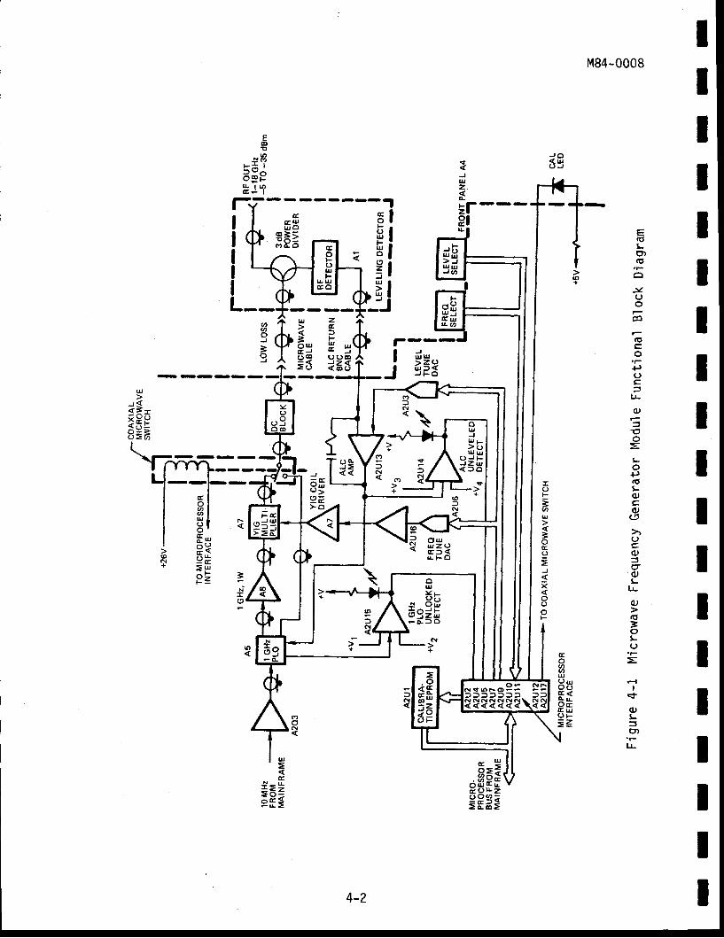
II
M84-0008
J O<ui( J J
Eo
6l! c)
F * ll ) v aOPt rl t | | l )cr+ |
t-Y---------.!
q
JUz .A
Er ---
IIIItI
E(oLq)(o
ox(,o
G'go+,(Jc
Lr
o)tEo=Lo
*J(oLoCqJa
uc(uao(uL
tL
(u(d=o!(,=
I+(uL5o)
lr
E.
an.Au! lu9 ( Jl r <4 [O aE U()F
= =
C)F
=ou
=
=J
sx
o
5l
fiZT4l
Eg3F=
:J
J!uu
e3?J F O
rI
J
:506=;r (\ - - - - - --|
/TfTlr-----J
xu,
> o
- - l - r -
F
3
r
tt@U()EcoI=oF
U
4.Eq,
Fz
UY sPirV UJ FZ u> o
N
8gF T
"frsFgEHS
oUJU r>c)U UJ FZ ul o
I
O Uu Z o( r t <L F O
4-2
IIIItIIIII
M84-0008
cal ibrat ion EPR0Ms. Automat ic cal ibrat ion
software and test f ix ture are avai lable
from ARGOSystems to calibrate and load
EPROMs. Consul t the factory for addi t ional
informat i on.
The AS210-01A then loads these two words back to the A5210-06 controlc i rcui t ry. I f the AS210-01A determines that the A5210-06 is operat ing inan un leve led cond i t ion , the YIG f i l te r tun ing ca l ib ra t ion so f tware rou t inewi l l f ind the new operat ing words for the A5210-06 and wi l l re load thisinformat ion to the control c i rcui t ry.
The control c i rcui t card assembly consists of the microprocessorinterface (A2u2, A?U4, A2U5, A2tJ7, AlUg, A2U10, A2U11, A2UI2, A2u17), aca l ib ra t ion EPR0M (A2U1) , a f requency tune d ig i ta ' l - to -ana log conver te r(DAC) (A2U6) , a f requency tune dr iver ampl i f ie r (A2U16) , a leve l tune DAC(A2U3) , an ALC ampl i f ie r (A2U13) , a I GHz PLO un locked de tec t compara tor(A2U15) , an ALC un leve led de tec t compara tor (A2U14) , a l0 MHz (A2Q3) amp-l i f ier for the 1 GHz reference frequency, and pou/er supply c i rcui t ry (Azulg,A2U19 ) .
The microwave subsystem consists of the I GHz PLO (A5), the 1 GHzI wat t ampl i f ie r (A6) , the YIG tuned mul t ip l ie r (A7) , a coax ia l m ic rowaveswi tch , a DC b ' lock , a low- loss f lex ib le cab le assembly , and an ARG0Systemslevel detector. The level detector contains a 3 dB power div ider and RFdetector.
4 .3 FREQUENCY GENERATION CIRCUITRY
The output frequencies of the A5210-06 Microwave Frequency GeneratorModule are generated by the microwave subsystem (A1, A5 - A7) and selected bythe cont ro l c i rcu i t card assembly (AZ) . The 10 MHz s igna l f rom the Rub id iumf requency s tandard in the AS210 Main f rame is ampl i f ied on the cont ro l c i rcu i tcard assembly (A2) and used as the reference frequency for the I GHz pLO (A5).
4-3
M84-0008
The 1 GHz PLO has two outputs. The f i rst output is the RF sampleport , which the microwave switch and control c i rcui t ry switches direct ly tothe output connector of the module. The second output is the RF output port,which is amp' l i f ied by the 1 GHz, 1 watt power ampl i f ier (A6) and is used todr ive the input por t o f the y IG tuned mul t ip l ie r (A7) .
The YIG tuned mult ip l ier contains a step recovery diode (harmonicgenerator) matched to a YIG bandpass f i l ter . Harmonics of the 1 GHz inputsignal f ron 2 to 18 GHz are avai lable at the output of the yIG tuned mult i -p l ier , and the desired output s ignal is selected by the yIG coi l dr iver. Thefrequency tune DAC (A2U6) located on the control c i rcui t card assemblyaccepts the 12-bi t f requency tuning word f rom the AS210-01A Module Control lerand tunes the YIG coi l dr iver to select the desired output harmonic. The 2to 18 GHz band is switched to the module output connector by the microwaveswitch and control c i rcui t ry.
A DC block is included on the output of the microwave switch toprevent any' low-level DC signals f rom feeding through to the output andof fse t t ing the prec is ion ALC c i rcu i t ry .
The ful l 1 to 18 GHz output f requency range of the A5210-06 isavai lable at the output connector of the module. The desired output s ignali s de l i vered to the leve l de tec tor (A1) by a low- loss f lex ib le cab le . Thelevel detector contains a 3 dB power div ider and microwave detector. Theoutput power is div ided in hal f , wi th one port ion being used as the outputsignal of the system and the other hal f being detected for the precis ion ALCcircui t ry.
LEVEL CONTROL CIRCUITRY
ItIIIIIItIIIIIIIIII
4.4
control
12-b i t
The precis ion ALC circui t ry ofc i rcu i t card assembly (A2) . The
Ievel tuning word f rom the module
the A5210-06 is located on thelevel tune DAC (A2U3) accepts thecont ro l le r and c rea tes a vo l tage
4-4
IIIIIIIIIIIIIIIIttI
M84-0008
re ference fo r the ALC amp' l i f ie r (A2U13) . The ALC ampl i f ie r (A2U13) i s aprec is ion opera t iona l ampl i f ie r des igned to be an in tegra tor . Th is ampl i -f ier dr ives a vol tage-control led at tenuator located in the I GHz PLO (A5) insuch a way as to make the detected RF power (a dc voltage) the same value asthe voltage reference created by the level tune DAC (A2U3). The detected RFpower is fed back from the level detector through a BNC cable to the input ofthe ALC ampl i f ier on the control c i rcui t card assembly.
4 .5 SELF.TEST CIRCUITRY
Two sel f - test s ignals are avai lab' le to the AS210-01A ModuleControl ler v ia the AS210 Mainframe motherboard. The f i rst is a I GHz PLOunlocked de tec t s igna l , wh ich w i l l be ind ica ted as an er ro r message on theAS210-01A d isp lay . The second is an ALC un leve led de tec t s igna l , wh ich , i fthe A5210-06 is in the 2 to 18 GHz band, w i l l in i t ia l l y s ta r t the YIG f i l te rtun ing ca l ib ra t ion so f tware rou t ine in the AS210-01A. I f the YIG f i l te rtun ing ca l ib ra t ion fa i l s to leve l the ou tpu t power , an er ro r message w i l l beshown on the AS210-01A display. I f the A5210-06 is in the 1 GHz bando theALC un leve led de tec t s igna l w i l l resu l t in an er ro r message on the AS210-01Adisplay. Refer to Sect ion 5, Maintenance and Cal ibrat ion, for informat ionabout c lear ing any er ro r messages v f r i le opera t ing the A5210-06 Mic rowaveFrequency Generator lbdule.
NOTE
The A5210-06 level ing detector must beterminated in to 50 ohms dur ing se l f , tes t .I f the un i t i s no t te rmina ted in to 50 ohms,false error codes may resul t .
4-5

IIIIIIIIIIIIIIIttTI
\
M84-0008
SECTION 5
MAINTENANCE AND CALIBRATION
INTRODUCTION
This sect ion provides maintenance and ca' l ibrat ion data for theAS210-06 Microwave Frequency Generator lv lodule. Part I covers rout ineprevent ive maintenance procedur,es. Part I I out l ines performance tests.Part I I I contains the cal ibrat ion/ a l ignnrent procedures for the A5210-06,and Part IV descr ibes t roubleshoot ing data. Figures 5-4 and 5-5 are theschematic diagrams of the A5210-06. Please contact the factory for anyassistance required in the maintenance or servic ing of the A5210-06.
IIIIIIIIt
I
5-1
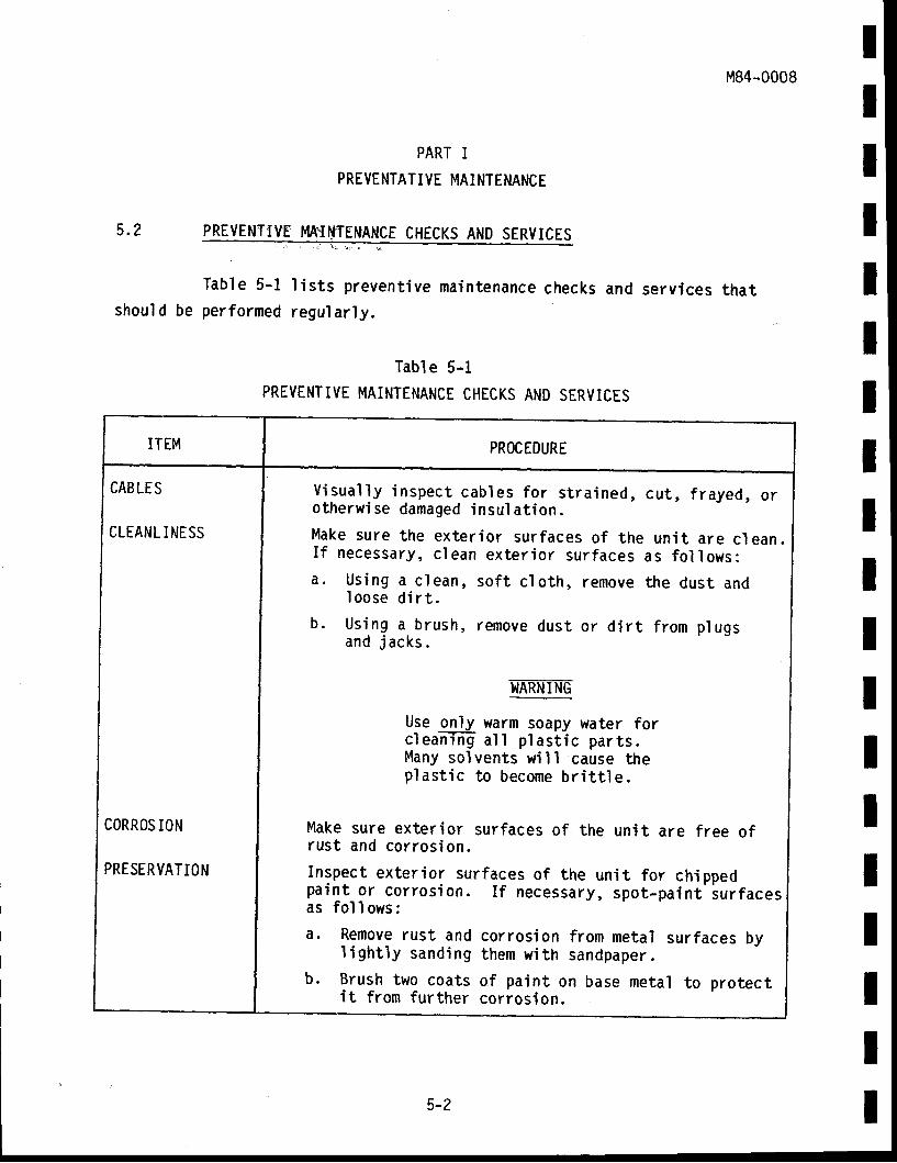
M84-0008IIIIIIIIIIIIIIIII
PART IPREVENTATI VE MAI NTENANCE
5.2 PREVENTIV.E IvIFII$TEIfANCE cHEcKs AND sERvIcEs
Table 5-f l is ts prevent ive maintenance checks and services thatshould be performed regular ly.
Table 5-1PREVENTIVE MAINTENANCE CHECKS AND SERVICES
II
CABLES
CLEANL INESS
CORROS ION
PRESERVATION
Visua l ly inspec t cab les fo r s t ra ined, cu t , f rayed, o rotherwise damaged insulat ion.Make sure the exter ior surfaces of the uni t are c lean.I f necessary , c lean ex ter io r sur faces as fo l lows:a . Us ing a c lean, so f t c lo th , remove the dus t and
loose d i r t .b . Us ing a b rush, remove
and jacks .dus t o r d i r t f rom p lugs
Use only brarm soapy water forc leanTn$ a l l p las t i c par ts .Many sol vents wi I I cause thep las t ic to become br i t t le .
Make sure exter ior surfaces of the uni t are f ree ofrus t and cor ros ion .
Inspect exter ior surfaces of the uni t for chippedpa in t o r cor ros ion . I f necessary , spo t -pa in t ' iu r facesas fol l ows:
a. Remove rust and corrosion from metal surfaces byl igh t ly sand ing them wi th sandpaper .
b. Brush two coats of paint on base metal to protecti t f rom further corrosion.
5-2
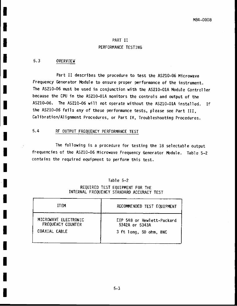
5.4
IIIIIIIItIIIIItItII
M84-0008
PART I I
PERFORMANCE TESTING
5.3 OVERVIEl.l
Part II describes the procedure to test the A5210-06 MicrowaveFrequency Generator lbdule to ensure proper perfornance of the instrument.The A5210-06 must be used in conjunct ion wi th the AS210-01A Module Control lerbecause the CPU in the AS210-01A monitors the control s and output of theA5210-06. The A5210-06 wi l l not operate wi thout the AS210-01A instal led. I fthe 45210-06 fai ls any of these performance tests, p lease see part I I I ,Ca l ib ra t ion /A l ignment Procedures , o r Par t IV , Troub leshoot ing Procedures .
RF OUTPUT FREQUENCY PERFORMNCE TEST
The fol lowing is a procedure for test ing the 18 selectable outputfrequencies of the AS210-06 Microwave Frequency Generator l r lodule. Table 5-2contains the required equipment to perform this test .
Tabl e 5-2
REQUIRED TEST EQUIPMENT FOR THEINTERNAL FRIQUENCY STANDARD ACCUMCY TEST
ITEM RECOI{'IENDED TEST EQUI PMENT
MICROI.JAVE ELECTRON ICFREQUENCY COUNTER
COAXIAL CABLE
EIP 548 or Hewlet t -Packard5342A or 5343A
3 f t long , 50 ohm, BNC
5-3
M84-0008
5 .5 TEST PROCEDURE
A- Ensure that power is disconnected from the AS210 system beforebeginning this procedure.
B. connect the equipment as indicated in Figure 5-1, and applypower to the 4s210. The Rubidium frequency standard in theAs210 system wi l l require 20 minutes warm-up t ime to reach thespeci f ied f requency accuracy.
c. select the -15 dBm output power lever on the As210-06 frontpanel . start ing wi th 1 GHz dialed into the thumbwheel switchfor the output frequency, compare the frequency displayed bythe microwave counter to Table 5-3 to verify that the outputfrequency is wi th in the acceptable f requency range for 1 GHz.cont inue this process through the remaining 17 output f requen-cies avai lable f rom the As210-06. I f any of the f requenciesfal l out of the l fmits for acceptable performance, p ' leasesee Par t I I I , Ca l ib ra t ion /A l ignment p rocedures , o r par t IV ,Troubl eshoot ing Procedures.
D. Disconnect the microwave frequency count.er from the ASz10-06.
RF OUTPUT LEVEL PERFORMNCE TEST
IIIIIIIIItIIIIIIIII
5.6
for each
notes to
The fol lowing is a procedure for test ing theof the 18 selectable output f requencies of theTable 5-4 give the required equipment for th is
seven RF output I evel sA5210-06. The foot-performance test.
5-4
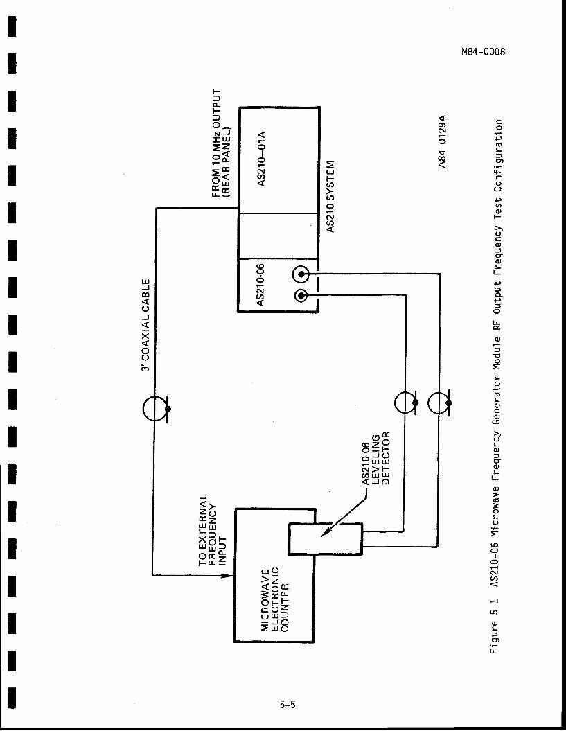
M84-0008
coP(ot-3ol
l+-coL)
Ptho
F
(JE(l)
(to!'
lr-
+,5o.lJ
oLd
c,
!
zLo
+J'oL(l)c(l)
C'
(u5g(l)L
L
(uto3oLC'
=(o
IOd
<\Jtt)
Fl
Ilf,
(uL=o)
tL
o)(\l
?\t@
9zYx=b= u J u Jc ! > F(/' UJ UJ<Jo
=UJF(n(noC-lU)
(c'ooslct)
FfaFlo^p J- rrJ=z^<=o-
=t}J UJ
tg
IUJo(JJ
xo(J
(It
II
J
E!! tlJ
;gi
oI
oGI(n
u ro) z
spFoF=E ( ) =g3d> U J C J
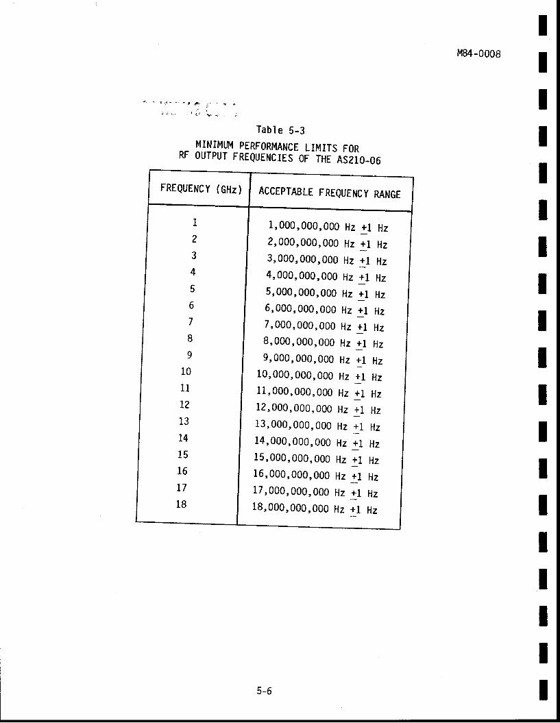
Mt|4-0008
IIIIIIIIIIIIIIIIIII
Tab le 5 -3MINIMIXVI PERFORMANCE
RF OUTPUT FREQUENCIESLIMITS FOR
0F THE A5210_06
FREQUENCy (GHz) ACCEPTABLE FREQUENCY RANGE
I
2
3
4
5
6
7
8
9
l0
11
t2
13
t4
l5
l6
17
18
1,000,000,000 Hz +l Hz2,000,000,000 Hz +1 y12
3,000,000,000 Hz +1 1174,000,000,000 Hz +L 1175,000,000,000 Hz +1 y76,000,000,000 Hz +l 1177,000,000,000 Hz +I y178,000,000,000 Hz +I y179,000,000,000 Hz +1 117
1.0,000,000,000 Hz l l Hz1.1,000,000,000 t iz +1 11212,000,000,000 Hz +l 11713,000,000,000 Hz +1 9714,000,000,000 Hz +l 11715,000,000,000 Hz +1 y1y16,000,000,000 Hz +l y1717,000,000,000 Hz +1 y1y18,000,000,000 Hz +1 117
5-6
M84-0008
5 .7 TEST PROCEDURI
A. Ensure that power is disconnected from the AS210 system andthe HP power meter before beginning this procedure.
Connect the equipment as indicated in Figure 5-2. Use anHP8481A Power Sensor as the power head. Turn power on totfte AS210 system and the HP power meter. t lait for theAS210-01A Module Control ler to display SEL?. I f the AS210-01Aresponds w i th an er ro r message, consu l t Par t I I I , Ca l ib ra t ion /Al ignment Procedures, or Part IV, Troubleshoot ing Procedures.Note that ERR 0-00 indicates that the Rubidium frequencystandard in the AS210 system is not phase locked and wi l lrequire a maximum of 20 minutes warm-up t ime to achievephase 1 ock.
Start ing wi th 1 GHz as the selected output f requency of theA5210-06 and -5 dBm as the desired output level , the micro-wave power meter shoul d read between -3 and -7 dBm foracceptable performance. Next, change the output f requency to2 GHz and repeat the measurement. Cont inue this process through8 GHz.
B .
the
dBm.-12
0 .
E .
ITtIIII
Return
to -10
-8 and
Return the
to -15 dBm.-13 and -17
Turn power
output frequency to 1 GHz.The microwave power meter
dBm. Repeat this procedure
output f requency to 1 GHz.The microwave power meter
dBm. Repeat thi s procedure
Change the output I evel
should read between
through 12 GHz.
Change the output I evel
shoul d read between
through 18 GHz.
off to both the HP power meter and the AS210 system.F .
5-7
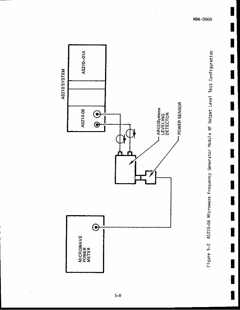
IIIIIII
IIIII
II
Eo
P(oL=(t)
r|-coc)Pr^(u
F
q,
(uJ
P3o-
P=O
LLd.
(u5
o=Lo
P.UL(ucq)(.'
()E(u5qoL
l!
(lJ
(o3o5-(,=\oO
Ior-l$Ja
NI
tr,
a1-:'o)
tJ-
Eo
? ( nF Z; ( 9 = u rgzY (n
s ) - i i r C C
8gF 5E i l u r O< J o a -
=UJ
?n
aoc{U)
M84-0008
oI
o(\I@
ul
E-tFutu tg=h>x>
(oodNo
5-8
M84-0008
G. Connect the equipment as indicated in Figure 5-2. Use anHP8484A Power Sensor as the power head. Turn power on tothe AS210 system and the HP power meter. Wait for theAS210-01A Module Control ler to display SEL?. I f the AS210-01Aresponds w i th an eyror message, consu l t Par t I I I , ca l ib ra t ion /Al ignment Procedures, or Part IV, Troubleshoot ing Procedures.Note that ERR 0-00 indicates that the Rubidium frequencystandard in the AS210 system is not phase locked and wi l lrequire a maximum of 20 minutes warm-up t ime to achieve phaseI ock .
H. Turn the output f requency to 1 GHz. Change the output levelto -20 dBm. The microwave power meter shou'ld read between-18 and -22 dBn. Repeat th is procedure through 18 GHz.
the
dBm.-37
J .
K.
L .
IIIIIIIIIII
I . Return the output f requency to I GHz.to -25 dBm. The microwave power meter-23 and -17 dBm. Repeat th i s procedure
Return the output frequency to 1 GHz.to -30 dBm. The microwave power meter-28 and -32 dBm. Repeat th i s procedure
Change the output I evel
shoul d read between
through 18 GHz.
Change the output I evelshoul d read between
through 18 GHz.
Returnto -35-33 and
output f requency to I GHz. Change the output levelThe microwave power meter should read between
dBm. Repeat th is procedure through 18 GHz.
Tab le 5 -4 i s a l i s t ing o f the min imum per fo rmance ' l im i ts fo rthe RF output level measurements of the A5210-06. If any ofthe
' levels fa ' l ' l out of the range for acceptable performance,
see Par t I I I , Ca l ib ra t ion /A l ignment Procedures or par t IV ,Troub leshoot ing Procedures .
Disconnect the microwave power meter f rom the A5210-06.M.
5-9
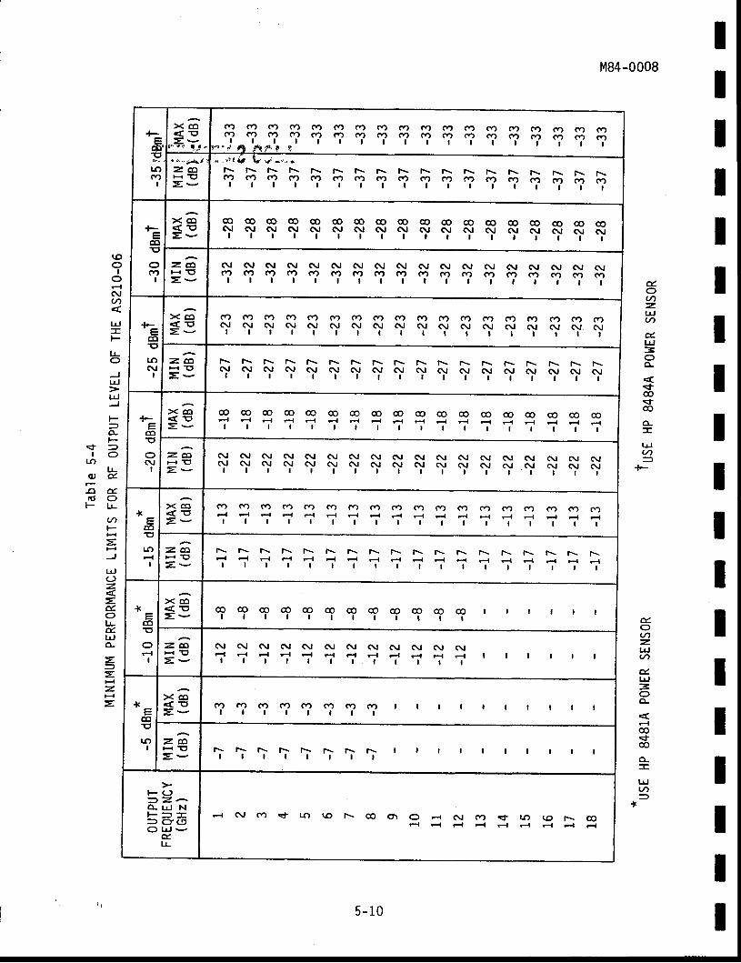
M84-0008
tI
IIIItIII
E,oat1=lfJatl
d.IJ=oo
<t@cf,@
o--|J.lat)=
EoaJ'>ztrJ(/,Eu,=Oo-
F{
cosf@
o-
trla=
*
tI
{--s'.(t
LO(f)
I
>< co< E= v
f e 4 ! ! a
(y) co (o cr) cf, (f) co (f) oo (o (f, (7) (y, (7) co (f) (f, (na? a a a c., c? Q (,, fv) .? co a c? q, c"t a6 (f,| | | | | r | | | | | | t
' i ' t ' f t f" ' r s * r t s
= c DH ' < t= v
\ \ l\ l\ f\ l\ l\ F t\ t\ l.\ l\ f\ l\ N N N t\o? a (Y) (Y, (Y) Q (f, (Y) (Y) (f, c7) o? (f) (y) cr) ;., (f) (?)| | | | | | | | | | r | | ' f ' f
f I r
" ..y;r {t qL ."*' *-.. *
cctE
o(Y)
I
> < 6< E= v
co co @ @ co @ o 6 @ @ @ @ @ @ @ @ o @ql ry (\t Nt (\r GJ ql Nt (\l (\J Ct (\t ct C{ nr c\l (\, (\J| | | | | | r | | | | |
- i - i - i - t - r I
= aH r ( ]
= v
(\l 6J (\t (\, c.l (\t (\t it At Nt Nl c! s.t Gt Gt (\r (\J (\'(f) (Y) (Y) (n (Y) 14 (Y) (Y) (Y) (Y, (o cD cf) (n (a cr, (f) (f}
l l t l l t l t t t l t l t t i t l
coEtr,NI
I
x c o< E= v
(7) (f, (f) cf) ca (') co (Y) (Y) (f) c7) (y) (\o cD (Y) cf) (', c7)ql qi (\t GJ 6J c! (\J (\t (\t (\t (\.t (\l Nr (\t (\l (\l (\t (\J| | | | I I I t | | t I r I
' t t I I
^ lZ,CA I f\ N f\ l\ t\ N l\ l\ f\ f\ l\ f\ f\ l\ t\ l\ N t\=ro I N N <r, ry c.t GJ Gl i\ iv <rr <rj <rJ N i\J 6J (\, (\t (\,= - | | | | r | | ' a a | | ' a - a - a - i I r | |
co.o
oC\I
I
x c o< != v
@ @ @ @ @ @ @ @ c o o @ @ o c o @ o @ @Fl Fl Fl F{ F{ F{ F{ Ft Ft F{ Fr Fl r-{ r-{ e{ J df t l t l t t t t t t l r t l t r l
z @x Et v
(\l c! c\J (\l N 6J ^t (\, (\J <\J <\J <\, C! (\t (\t 6J (\t (\lNl c\t (\,t GJ C\,t Nt ry c\r (\t (\l Nl GJ NJ (\J N C.' (\t (\J
| | | | | I r I I | | ! | - i - i - i
I r
Ecop
lr)Fl
I
*x c o< i o= v
(Y) ff) ca co co cf, co (') co (n cn co cD co (o cD (r, coFa d F{ F{ F{ F{ Ft Ft F{ F{ F{ F{ F{ F{ H Hl t l t t t t t t t t t t t t l l r
z 6H P
= v
l\ l\ r\ r\ l\ I\ r\ l\ t\ r\ r\ r._ N l-_Fl Fl F{ Fl r-{ F{ F{ F{ F{ Ft Ft F{ r-{ Fi Ft F{ H Flt t t t t l l t t t t t t t t t t l
co'o
oFl
I
*x c o< != - IIlc 9 c 9 o o a @ o c o c o @ @ 6 c o
r t t t t t t t r t i r
z c os 1 J= v
(\t (\t il (\t c\l cl (\I (\t (! (\l (\J 6JF{ Fa r{ Fl r{ Fl r-l Ft Ft F{ F{ | t | | | |r t t l t l t t t t t l
*cctT'
|r)I
x 6< E= v
(Y) (Y) (O CO (Y) (n (Y) (n | | | t | | | | | |t t t t t t t l
z 6H E
= - b \ \ r : - F f \ l \ l \ | | | | | I | | | |t t t t t t t l
F ( J3 Z ao - l ! NF = -= o (5O b J v
d.lr-
F{ N' cf) r+ to r.o N @ ot o Ft (\t cD <f Lo (o r\ @Fl F{ Fl Ft Ft F{ Fl Fa r-{
r.oo
IoF{
s,(r)
UJ-F
LoJtd
lrlJ
F
At--
s f =r o
tf)tr-
q J d
- a dc t o
F tr-
U)F-H
=J
IrJC)z=&olr&uJo-
==H
=H
=
5-10
5.8
IIIIIItIIIIIItIIItI
M84-0008
PART I I I
CALIBMTION/AL IGNMENT PROCEDURES
OVERVIEI{
MAITNE
The fol I owi ng cal i bration/al i gnment procedures(Sect ion 5 , Par t I I I ) and Troub leshoot ing
Procedures (Sect ion 5, Part IV) are for use byqua l i f ied personne l on ly . To avo id persona l
injury, do not perform any servicing other than
that of rout ine maintenance (sect ion 5, Part I )
and performance test ing (Sect ion 5, Part I I )
un less you are qua ' l i f ied to do so .
F igure 5-3 is a f low d iagram o f the Ca l ib ra t ion /A l ignment Procedure
for the AS210-06 Microwave Frequency Generator Module. Use this flow diagramwith the theory of operat ion in Sect ion 4, the text in th is sect ion, and thei l lus t ra ted par ts l i s ts in Sec t ion 6 . The AS210 in te rna l f requency s tandardca l ib ra t ion da ta , con ta ined in the AS210 main f rame opera t ion and main tenance
manual, is a lso referenced in th is f low diagram. Note that the AS210 systemneed no t be d isassembled to de termine i f ca l ib ra t ion /a l ignment i s necessary .For any ass is tance needed in per fo rming th is ca l ib ra t ion /a l ignment p rocedure ,
please contact the factory.
5 .9 ACCESS T0 A5210-06 MICR0WAVE FREQUENCY GENERAToR M0DULE
Please refer to the AS210 mainframe manual for the AS210 systemdisassembly procedure al lowing access to the A5210-06 Microwave Frequency
Generator Module. fccess to the module c i rcui t ry i tsel f is gained by using
a smal l straight-blade screwdriver to remove the two metal s idecovers. Place
the modu le on one o f i t s s ides so tha t one cover i s fac ing up .
5-1 1
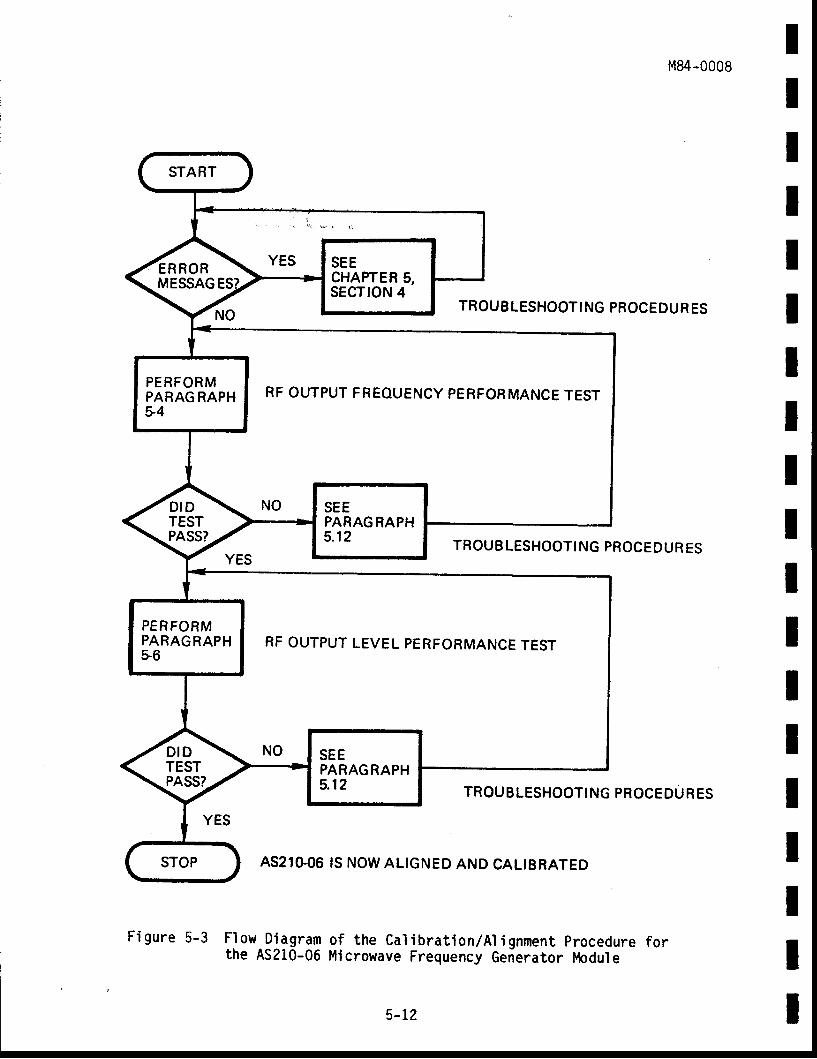
M84-0008
TROUB LESHOOTI NG PROCE DUR ES
TROUB LESHOOTI NG PROCEDUR ES
TROU B LESHOOTI NG PROCEDU R ES
IIIIIIIIIIIIIIII
Figure 5-3 Flow-Diagram of the Cal ibrat ion/Al ignment Procedure forthe A5210-06 Microwave Frequency Generator tr, lodule
AS2TGO6 IS NOW ALIGNED AND CALIBRATED
IIt
ERRORMESSAG
SEECHAPTER 5,sEcTroN 4
RF OUTPUT FREQUENCY PERFORMANCE TESTPERFORMPARAGRAPHu4
RF OUTPUT LEVEL PERFORMANCE TESTPERFORMPARAGRAPHs6
5-12
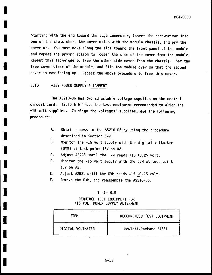
A.
B.
c.D.
IIIIIIItIIIItIIIITI
M84-0008
Start ing wi th the end toward the edge connector, insert the screwdriver intoone of the s lots where the cover mates wi th the module chassis, and pry thecover up. You must move along the slot toward the f ront panel of the moduleand repeat the prying act ion to loosen the side of the cover f rom the module.Repeat th is technique to f ree the other s ide cover f rom the chassis. Set thefree cover c lear of the module, and f l ip the module over so that the secondcover is now facing up. Repeat the above procedure to free this cover.
5.10 +15V POI. IER SUPPLY ALIGNMENT
The A5210-06 has two adiustable voltage supplies on the controlc i rcui t card. Table 5-5 l is ts the test equipnent recormended to al ign the+15 vo l t supp l ies . To a l ign the vo l tages ' supp l ies , use the fo l low ingprocedure:
0btain access to the A5210-06 bydescr ibed in Sec t ion 5-9 .
I 'bni tor the +15 vol t supply wi th(DVM) at test point l5V on A2.Adjust AZR28 until the DVM readsMoni to r the -15 vo l t supp ' l y w i th15V on A2.
E. A{ust A2R31 unt i l the DVM reads -15 a0.25 vol t .F. Remove the DVM, and reassemble the A5210-06.
Tabl e 5-5
REQUIRED TEST EQUIPI'IENT FOR+15 VoLT PO}IER SUPPLY ALIGNMENT
ITEM RECOMMENDED TEST EQUIPMEITT
DIGITAL VOLTMETER Hew'l ett-Packard 3455A
using the procedure
the di gi ta'l vol tmeter
+15 10 .25 vo l t .
the DVM at test point
5- 13
M84-0008
PART IVTROUBLESHOOTING PROCEDURES
5.15
Troubleshooting the A5210-06 Microwave Frequency Generator l, loduleis facil i tated by a combination of error codes displayed on the nrodulecontrol ler d isplay and by LED indicators on the control c i rcui t card assem-b ly ' A2 . The cont ro l c i rcu i t card is i l l us t ra ted in F igure 6-3 . Tab ' le 5 -6correlates the error code, displayed on the module control ler when a faul toccurs, to the malfunct ion. An explanat ion of the problem is provided withposs ib le so lu t ions . Tab le 5 -7 i s a l i s t o f v isua l ind ica tors on C i rcu i t CardA2 and of the indicators 'nreaning. Figures 5-4 and 5-5 are the schematicdiagrams of the A5210-06. For fur ther assistance, contact the factory.
NOTE
The A5210-06 leveling detector must beterminated into 50 ohms dur ing sel f - test .I f the uni t is not terminated into 50 ohns,fal se error codes may resul t.
IIIIIIIItIIIIIIIIII
OVERVIEITt
5-14
IIIItIIIIIIIIII
M84-0008
Table 5-6
ERROR CODE LISTING
ERROR CODE PROBLEM RECOYf'IENDED SOLUT IO}I
ERR 6-00
ERR 6-OX
ERR6-1X
ERR 6-30
ERR 6-40
ERR 6-50
Frequency not avai lable
No leve l ing loop ind i -cation at frequency X
X=1.\=2X=3
1 GHz2 GHz3 GHz
GHz
No leve l ing loop ind i -cation at frequency X
X=0
X=1
X=2
10 GHz
11 GHz
12 GHz
X=8 18GHz
GHz source not I ocked
Cal ib ra t ion in p rogress
Unab le to leve l , andleve l chosen isgreater than guaran-teed by performancespeci f i cati ons
Select proper output frequency.
The A5210-06 may require 10minutes warm-up t ime to stabi l -ize the YIG mult ip l ier andassociated circui t ry. Af ter10 minutes warm-up, in i t iatesel f-test from the front panelof the AS210-01A Module Control-ler . I f the same error condi t ionoccurs dur ing or af ter sel f - test ,or both, then check the ALC cir-cui t ry A2U3, A2U13, AZU14, A2Q1,and 42Q2. Al so check the microwaveswitch control c i rcui t ry A2U11 andA2VL7.
Same as ERR 6-0X.
Check 10 MHzput shoul d be
ampl i f ier A2Q3; out-approximately 0 dBm.
None. Let cal ibrat ion rout inef i n i sh .
Select proper output power level .
5 -15
INDICATOR PROBLEM RECOFilENDED SOLUTION
AzCR1
AzCR2
CAL LED(FrontPanel )
ALC Unleveled
PLO Unl ocked
Cal i brat ionProgramIni t iated
Check A2U3, A2U13, A2Q1, A2Q2,A2Ut4, and A2U16.
Check A2Q3 and A2U15.
Normal operation; see Section 3fo r descr ip t ion .
M84-0008IIIIIIIIIIIIIItIIIt
6 1 $ : - - " . t g l
" ; ; . ; . , ; e j
Table 5-7
VISUAL IIIDICATIONS
5-16
un-EiEr-Eo f 'o.a-{87
,rl - )il
7' tEue'4 *"ff'"i3ip lUt3
Pt ?
r 5
t7
ttl
ooD l
0()o l
oo0 l
OOO AOoo, alDOz A20O3 13OOa Aaoq a5DO6 A6
{ r a lcE A8
A 9vPP Arovcc6No dE
o l02o3
D505,0706
CLR
o l oD o ro l rDoaD t a
ro Ih Sw7
FA,JLAr-'l
Lffh,*J
oo loo4DogDo5oo362
Il3 Rt2
K
^t
lO MHz (rO PLO)
FROM DIGITAL AND
Gls
+26V (TO^nilAVE Sw)1 rgY llg YrG_corL bnrvenl+ .sV (TO pLO)
M84-0008
POW€R 6trp
PLOUNLOCKED
cR2:o82 -.487
i r t- , . , . I u,: U 2
i j t
IIIIIII
IIIIII
PLO TUNE VOLT (T0 PLo)
ALC \OLTAGE (TO PI-O)
J I
lO MHz
q22a 7 0
c92fo
"F
c loC 2 p |
ALC J411,., {ro .n"n *t..to"i
tgl
5r"-?1.
fr''\)t-fl
TO .CAL,,
LED FRoNT PAi€L
-t8v (ro elo)
l o oDATA I R5
l u 6l D tL
Amh t c
A6
^"rrarrI
.o2f
R9a . 7 K
cr9r320v
A?'t ? l
R 3 0t . f Kt f
6TD R€TURN FMlwAv€ CMpf,TS
610 R€rrRx roAchas9s
YIG TUNE IIOLT(TO YrG CO|L DRVR)
NOTES, UIILESS OTHERWISE SPECFIEDI, IITERPRET DWG IN ACCORDAI{CE WITH MIL-STD_IOO2, ALL ffiSTSToRS Am N c/,lut t/gw, 5Z
CAPACITORS ARE lt{ lF
E r-ow rrER[rAL EMF RrsrsroRs4. ANALOG SGNAL GND SEPARATE
El $ oenores DlGrrAr AND Pov{ER6 + D€I{OTES ANALoG GND
m -,-,- DENorEs GuARD RING
AS2l 0-06Card
f A oADDRESSI Al
L A z
tI
IJIA7HroL
t 2N28F
R2€t ? lt Z
R27t.5x
r-coNrRoL LwR
Figure 5-4

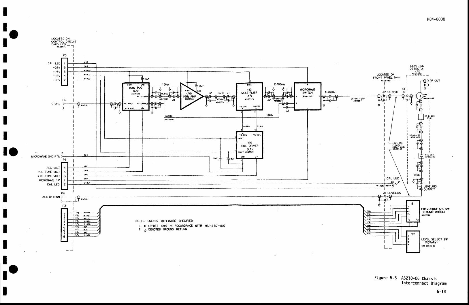
II
loIIIIIIIIO
LOCATED ONCONTROL CIRCUITCARD (A2) _ _
ASr2577a I
CAL LEO+26v. t8v_ t e v+ t 8 V
3MICROWAVE GND RTN >
ALC VOLTPLO TLI'€ VOLTYIG TTJNE VOI-TMICROWAVE 5W
CAL LED
ALC RETLRN
LocArED oilFRONT PAT€L (A4)
Asr2tSaO
T_I
J2 OUTPUT
LEVELINGDETECTOR
(At )ASt2t540
l - - - - - - - - r. l
ur-|{r-clpAS r2t537
LOW IOSSFLEXIBL€CABL€ ASSYAS125547
CAL
IIIIItI
LEO':4y'
NOTES, UT.ILESS OTHERWISE SPECIFIED
I, INTERPR€T DWG IN ACCORDANCE WITH MIL-STO_IOO2. + oEr'rorEs GRoiJND RETURN
JI LEVELING
LEVEL SSLECT SW{ROTARY)
c rs-r4r7E'ol
Figure 5-5 ASZI0-06 ChassisInterconnect Diagram
MB4-0008
ttav GnOlGHz PLO
(A 5)Asr?t'55
RF OUTPUT
NPUI tr sAr?te
+
MCROtvA/EswlTcH
I ISI-2-O
2
!16 cof, Yr6 CO|L
-YI'IT
YIGCOIL DRIVER
(A7)+voll ASl2523
G I O C V
5I
4I3a67I
lo5-18

ItIIItIIIIIItIIIITI
M84-0008
SECTION 6
ILLUSTRATED PARTS LISTS
6.1 INTRODUCTION
This sect ion contains i l lustrated parts l is ts for the A5210-06Microwave Frequency Generator Module. The assembly number and assembly t i t leare l i s ted a t the top o f each par ts l i s t . The par ts l i s ts a re d iv ided in tos ix co1umns and ar ranged in the fo ' l low ing order :
Col umn I - Item Number
Column 2 - Quant i ty per Assembly.
Col umn 3 - Manufacturer 's Code
Col umn 4 - Part Number
Co lumn 5 - Descr ip t ion
Column 6 - Reference Designat ion
6-1
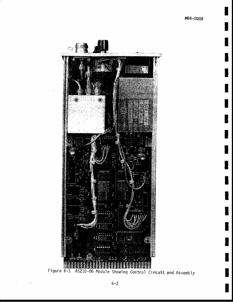
MB4-0008IIIIIIIIIIIItIIIIII
#*
6-1 AS210-06 Modu le ShowinqF i gure
6-2
Cont ro l C i rcu i t and Assembly
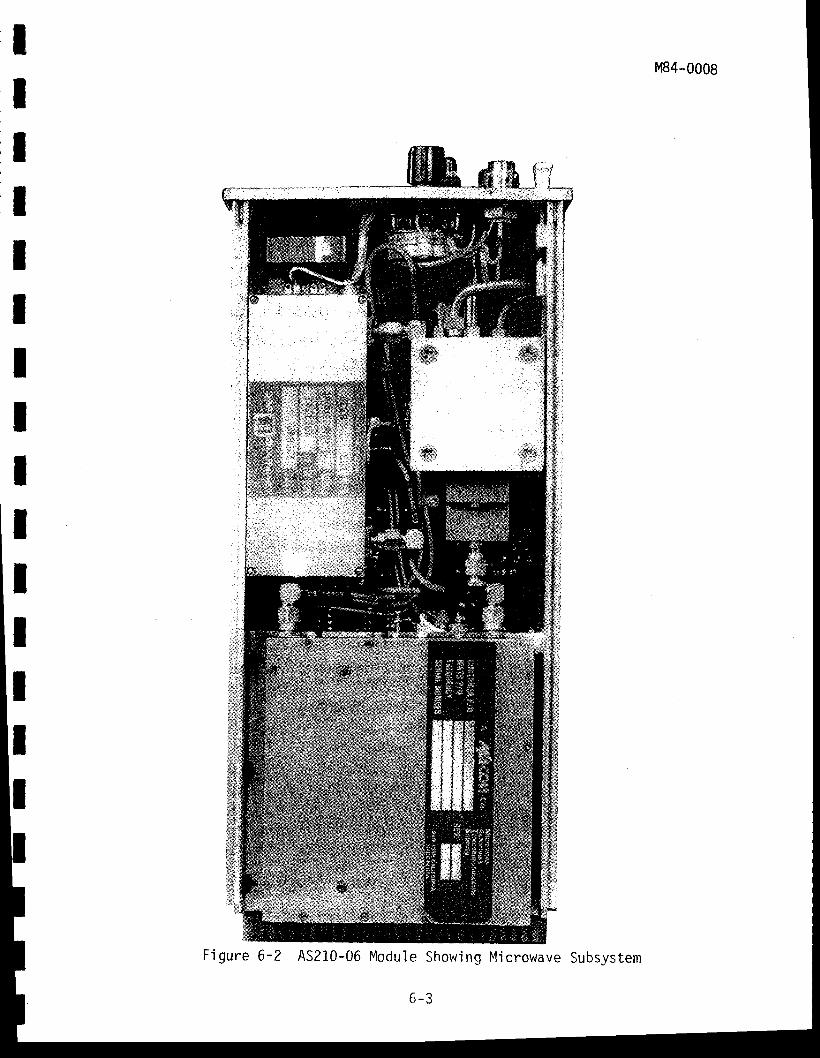
M84-0008ll
lrItilIIIIIlrIIIII
e Showing Microwave Subsystem
o - J
A5210-06 Module
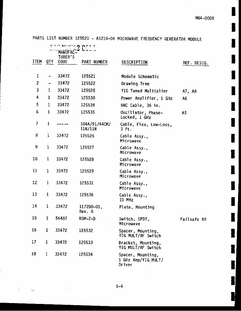
PARTS LIST NUMBER 125520 - A5210.06
L f a * ' i r y { r f | 1
" " '"l,tnlrUrAd:.v ;- * -' "TURER.S
r2552t1255?212552s125530
125538
125535
r04A/9L/44CM/11N/11N
125526
1255?7
L255?8
L25529
125531
125536
11 7200-01 ,Rev. A
RSM-2-D
L25532
125533
125534
Module Schematic
Drawing Tree
YIG Tuned Mul t ip l ie r
Power Ampl i f ier , 1 GHzBNC Cab le ,36 in .
0sc i l la to r , Phase-Locked, 1 GHz
Cable , F lex , Low-Loss ,3 f t .
Cab le Assy . ,Microwave
Cab l e Assy . ,Microwave
Cab le Assy . ,Microwave
Cab l e Assy . ,Microwave
Cab le Assy . ,Microwave
Cab le Assy . ,10 MHz
Pla te , Mount ing
Switch, SPDT,Mi crowave
Spacer, Mount ing,YIG MULTIRF Switch
Bracket, Mount ing,YIG MULT/RF Switch
Spacer, Mount ing,1 GHz Amp/YIc MULT/0r iver
M84-0008
REF. DESIG.
A7, Ag
A6
A5
Fai l safe A9
MICR0WAVE FREQUENCYGENERATOR MODULE
tIIIIIITIIIIIIIII
ITEM QTY CoDE PART NUMBER DESCRIPTION
1
2
3
4
5
6
7
8
9
10
11
L2
13
14
15
16
t7
18
;
1
1
1
1
1
1
1
1
1
1
1
1
1
1
1
33472
33472
3347?
33472
3347?
33472
33472
33472
33472
33472
33472
33472
33472
54487
33472
33472
33472
6-4
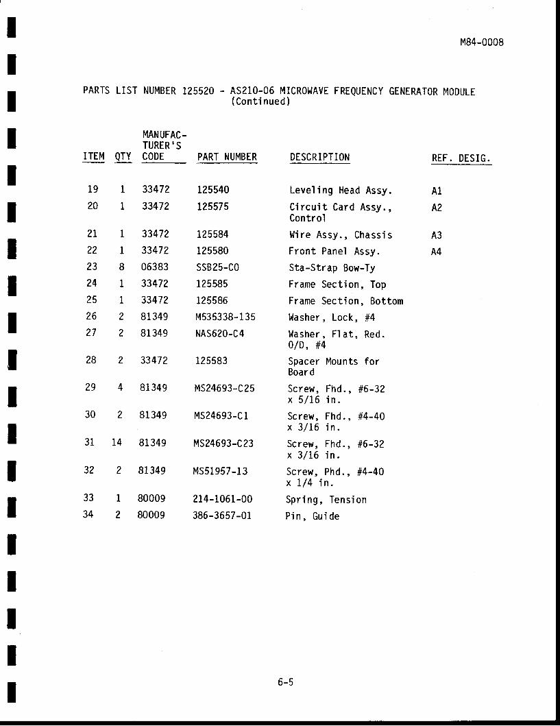
14
IIIIItttIIIIIItIIII
M84-0008
PARTS LIST NUMBIR 125520 . A5210-06 MICROWAVE( Cont i nued )
FREQUENCY GENERATOR MODULE
MANUFAC-TURER'S
ITEM QTY CODE PART NUMBER DESCRIPTION
Level ing Head Assy.
C i rcu i t Card Assy . ,Control
Wi re Assy . , Chass is
Front Panel Assy.
Sta-Strap Bow-Ty
Frame Sect ion, Top
Frame Sect ion, Bottom
Washer , Lock , #4
l . lasher , F la t , Red.0/0, #4Spacer Mounts forBoard
Screw, Fhd., #6-32x 5 /16 in .
Screw, Fhd. , #4-40x 3 /16 in .
Screw, Fhd. , #6-32x 3 /16 in .
Screw, Phd. , #4-40x L /4 in .
Spr ing , Tens ion
P in , Gu i de
REF. DESIG.
19
20
2L
22
23
24
25
?6
27
?8
29
30
31
32
33
34
1
1
33472
33472
33472
33472
06383
3347?
33472
81 349
81 349
3347?
81 349
81 349
81 349
81 349
80009
80009
125540
L25575
125584
125580
ssB25-C0
125585
125586
M535338-135
NA5620-C4
125583
MS24693-C25
MS24693-C 1
MS24693-C23
MS51957-13
214-1061-00
386-3657-01
A1
A2
A3
A4
1
1
8
1
1
2
?
1
2
6-5
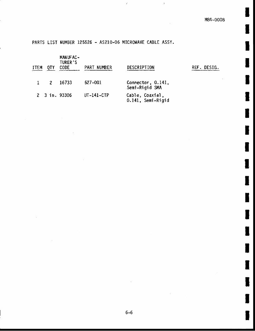
PARTS LIST
ITEM QTY
L2
2 3 in .
16733
93306
NUMBER L25526 - AS210-06
MANUFAC.TURER'SCODE PART NUMBER
MICROWAVE CABLE ASSY.
DESCRIPTION
Connector , 0. 141 ,Semi-Rigid SMA
Cab le , Coax ia l ,0 .141 , Semi -R ig id
M84-0008
REF. DESIG .
527 -00t
UT-141.CTP
ItItIIIIIIIIIIIIIII6-6
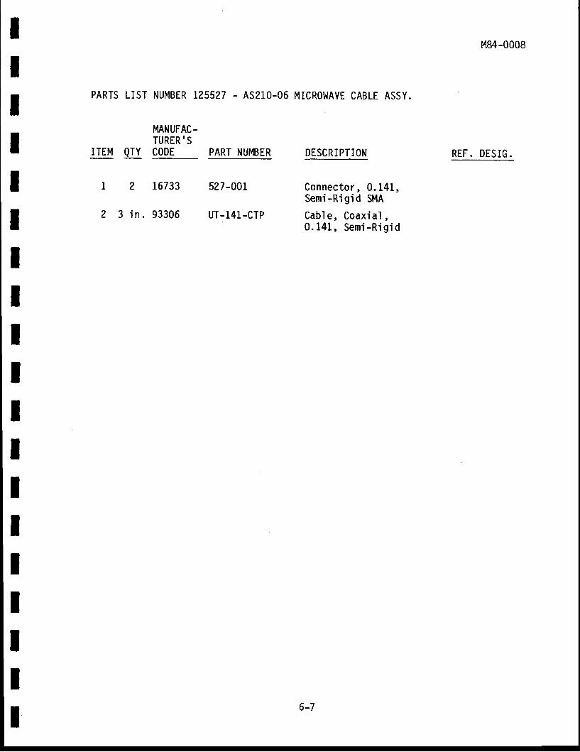
IIIIIIIIIItIItIItII
M84-0008
PARTS LIST NUMBER 125527 - A5210.06MICROWAVE CABLE ASSY.
MANUFAC.TURER'S
ITEM QTY CODE PART NUMBER DESCRI PTION REF. DESIG.
L 2 16733
2 3 in . 93306
527-001
UT-141.CTP
Connector , 0. 141 ,Semi-Rigid SMA
Cab le , Coax ia l ,0 .141 , Semi -R ig fd
6-7
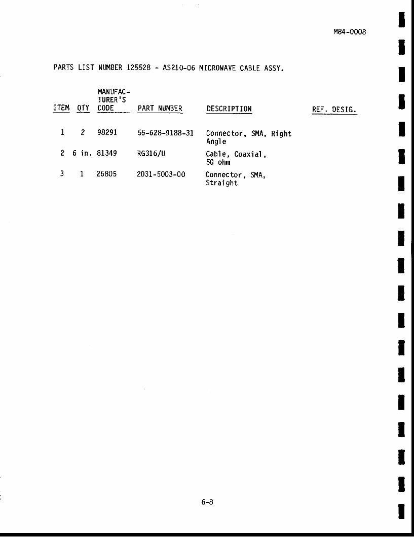
IItIIIIIIIIIIIIIIII
PARTS LIST NUMBER 125528 - AS210-06MICROI{AVE CABLE ASSY.
MANUFAC-TURER'S
ITEM QTY CODE PART NUMBER DESCR I PT ION
M84-0008
REF. DESIG.
I
26
3
2 98291
in . 81349
1 26805
55-628-9188-31
RG316/U
2031 -5003-00
Connector, Sl4A,Angl e
Cab le , Coax ia l ,50 ohm
Connector, SMA,Strai ght
Ri ght
6-8
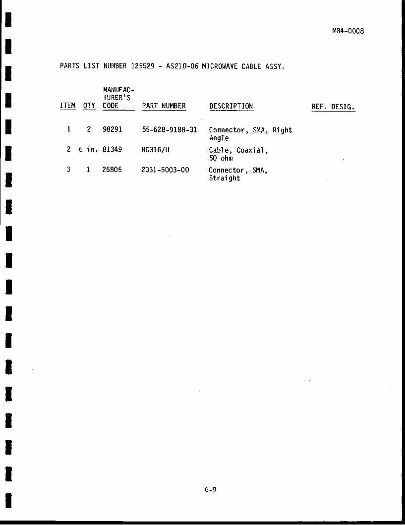
tllIlrIIIIIIIIIItIIIIII
PARTS LIST NUMBER 125529 - A5210-06 MICROI,IAVE CABLE ASSY.
MANUFAC-TURER'S
ITEM QTY CODE PART NUMBER DESCRIPTION
M84-0008
REF. DESIG.
L2
2 6 in .
31
98291
81349
26805
55-628-9188-31
RG316/U
2031-5003-00
Connector, SMA,Angl e
Cab le , Coax ia l ,50 ohm
Connector, SMA,Strai ght
Ri ght
6-9
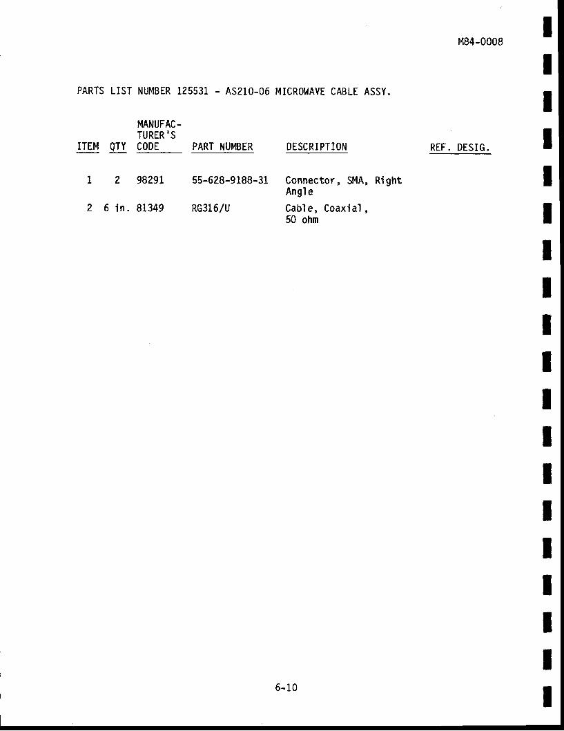
PARTS LIST NUMBER 125531 - AS210-06
MANUFAC-TURER'SCODE PART NUMBER
MICROWAVE CABLEASSY.
DESCRI PTION
Connector, SMA, RightAngl e
Cab le , Coax ia l ,50 ohm
MB4-0008
REF. DESIG.
IIIIIItIItIIIIIIIII
ITEM QTY
L 2 9829L
2 6 in. 81349
55-628-9188-31
RG316/U
6-10
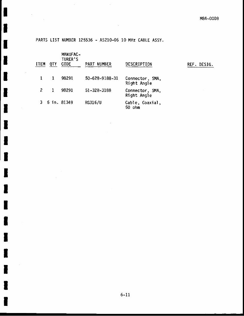
tl-
ItIrItItIIIIIttIIIIIII
PARTS LIST NUMBER 125536 . A5210-06 10 MHz CABLE ASSY.
ITEM QTY
MANUFAC.TURER'SCODE PART NUMBER DESCRIPTION
M84-0008
REF. DESIG.
1 1 98291
2 1 98291
3 6 in . 81349
50-628-9188-31
51-328-3188
RG316/U
Connector, SMA,Ri ght Angl e
Connector, SMA,Ri ght Angl e
Cab le , Coax ia l ,50 ohm
6-1 1
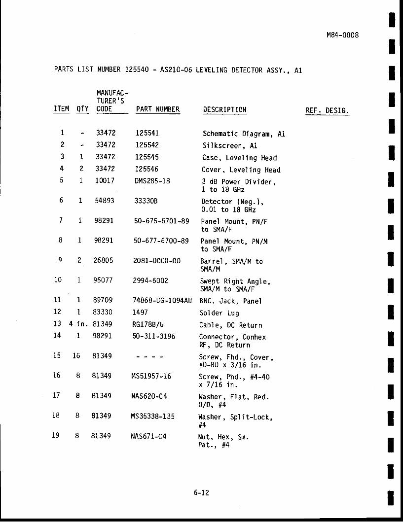
PARTS LIST NUMBER 125540 . AS2l0-06LEVELING DETECTOR ASSY., A1
MANUFAC-TURER ,SCODE PART NUMBER DESCRIPTIONQTYITEM
M84-0008
REF. DESIG.
IIIIIIIIIIIIIIIIIII
7
8
9
1-2-314251
33472
33472
33472
33472
1001 7
54893
98291
9829I
26805
95077
89709
83330
81349
98?9I
81 349
81349
81 349
81 349
81 349
I
1
1
2
1
I
I
4 in .
I
16
8
8
8
8
t25541
t25542
125s45
125546
DMS285-18
333308
50-67 5-6701 -89
50-677 -6700-89
2081-0000-00
2994-6A02
74868-UG-1094AU
t497
RG1788/U
50-31 1-3196
MS51957-16
NAS620-C4
MS35338-1 35
NAS671-C4
Schematic Diagram, Al
S i l kscreen, A l
Case, Level ing Head
Cover , Leve l ing Head3 dB Power Div ider,I to 18 GHz
Detec tor (Neg. ) ,0.01 to 18 GHz
Panel Mount, PN/Fto SMA/F
Panel Mount, PN/Mto SMA/F
Barrel , SMA/M toSMA/M
Swept Right Angle,SMA/M to SMA/F
BNC, Jack , Pane l
Sol der Lug
Cable, DC Return
Connector, ConhexRF, DC Return
Screw, Fhd. , Cover ,#0-80 x 3 /16 in .
Screw, Phd., #4-40x 7 /L6 in .
Washer , F la t , Red.0/D, #4
l ' lasher, Spl i t -Lock,#4
Nut , Hex , Sm.Pat . , #4
10
11
I2
13
14
15
16
t7
18
19
6- t2
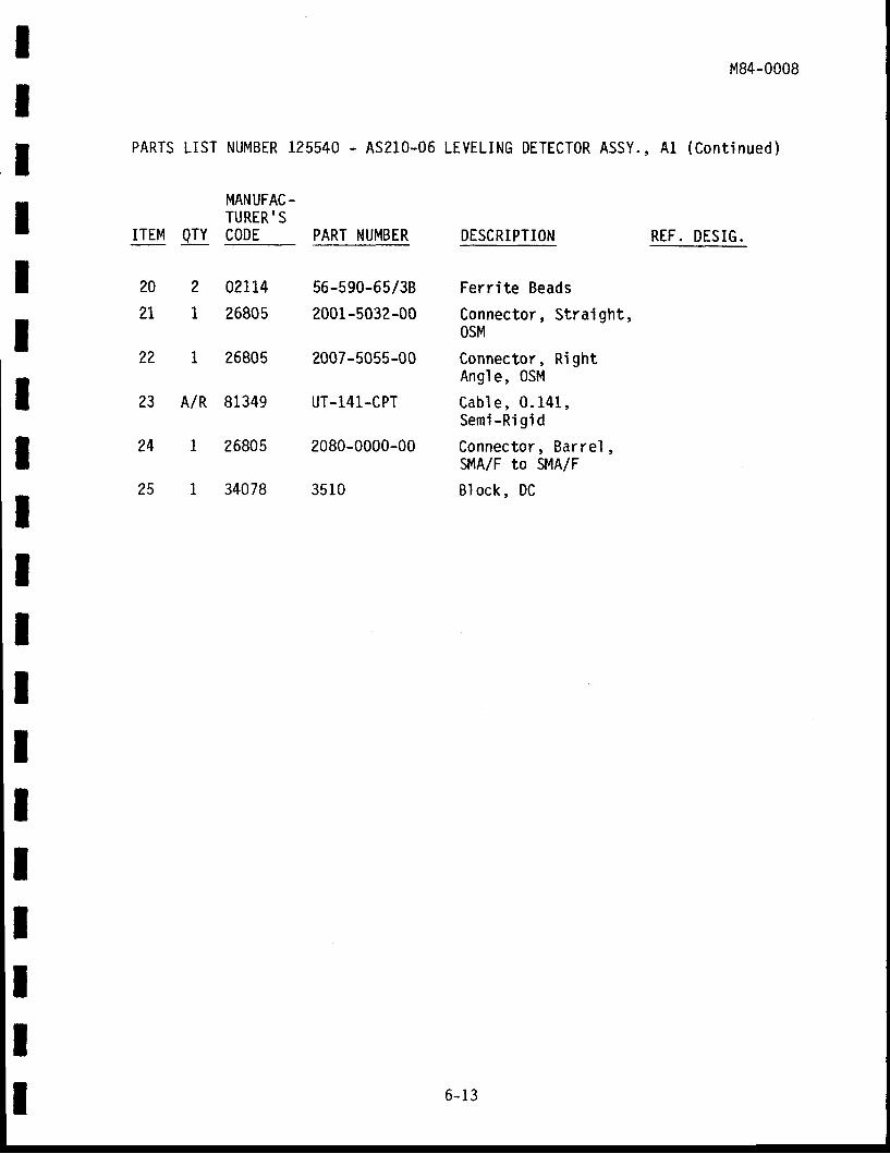
IIIIIIIIIIIItItIIII
20 2 02tt4
2L 1 26805
?? 1 26805
?3 A/R 81349
24 1 26805
25 1 34078
56-590-65/38
2001-5032-00
2007-5055-00
UT-141-CPT
2080-0000-00
3510
Ferr i te Beads
Connector, Straight,0sMConnector, Ri ghtAngle, OSM
Cabl e, 0. 141. ,Semi -Ri gi d
Connector , Bar re l ,SMA/F to Si'lA/F
Bl ock , DC
M84-0008
PARTS LIST NUMBER 125540 - A5210-06LEVELING DETECTOR ASSY.,A l (Cont inued)
ITEM QTY
MANUFAC-TURER'SCODE PART NUMBER DESCRIPTION REF. DESIG.
6-13
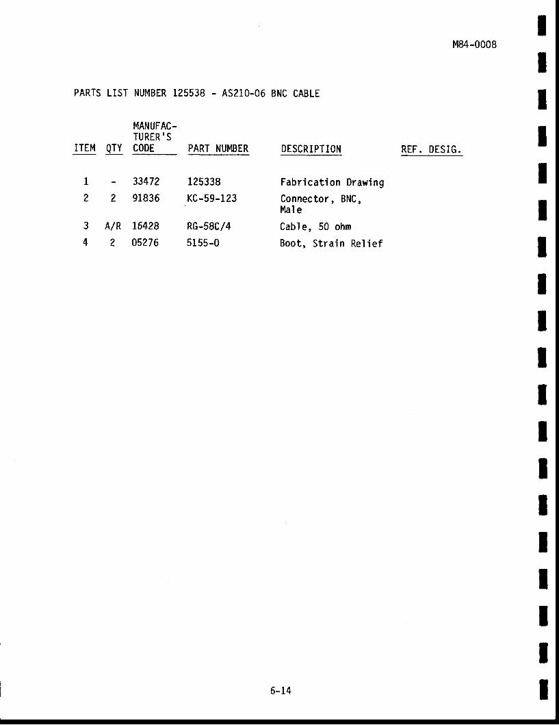
M84-0008IIIIIIIIIIIIIIII
PARTS LIST NUMBER 125538 - A5210-06 BNC CABLE
MANUFAC.TURER'S
ITEM QTY CODE PART NUMBER DESCRIPTION
I
?
- 33472
2 91836
A/R 16428
2 05276
125338KC-59-123
Rc-58C/451 55-0
REF. DESIG.
3
4
Fabricat ion Drawing
Connector, BNC,Mal e
Cable, 50 ohm
Boot, Strain Re' l ief
III6-14
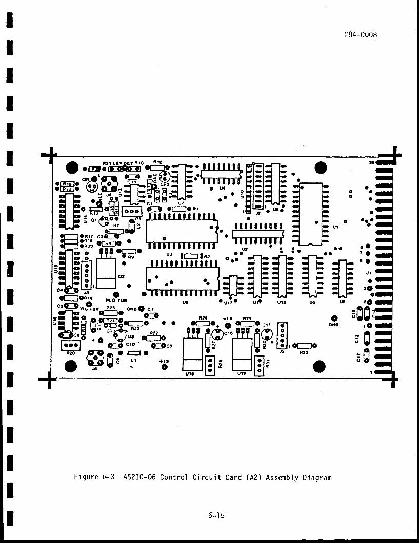
MB4-0008IIItIIIIIIIIIIIIIII
Figure 6-3 A5210-06 Cont ro l C i rcu i t Card (R2) Rssembly D iagram
oc
c co o
o
o c o ou r o
2A
:88,rO
ofio l O
i8
tJQ
oof{o
In i l t i l l !
c C7 O8 O
J I
o a
'f,*,utv2
o oc r o
ffi;
or O
iiH,cc=cJ5 n32
oc=o??? r-lU
o
'3 t
.f,1-- b
iF- l FI |-q^,F
ut2
u3 tt-t ! nel l l tn ! f l i l l r !
3 Jll"H"
H,U.:.
6-t 5
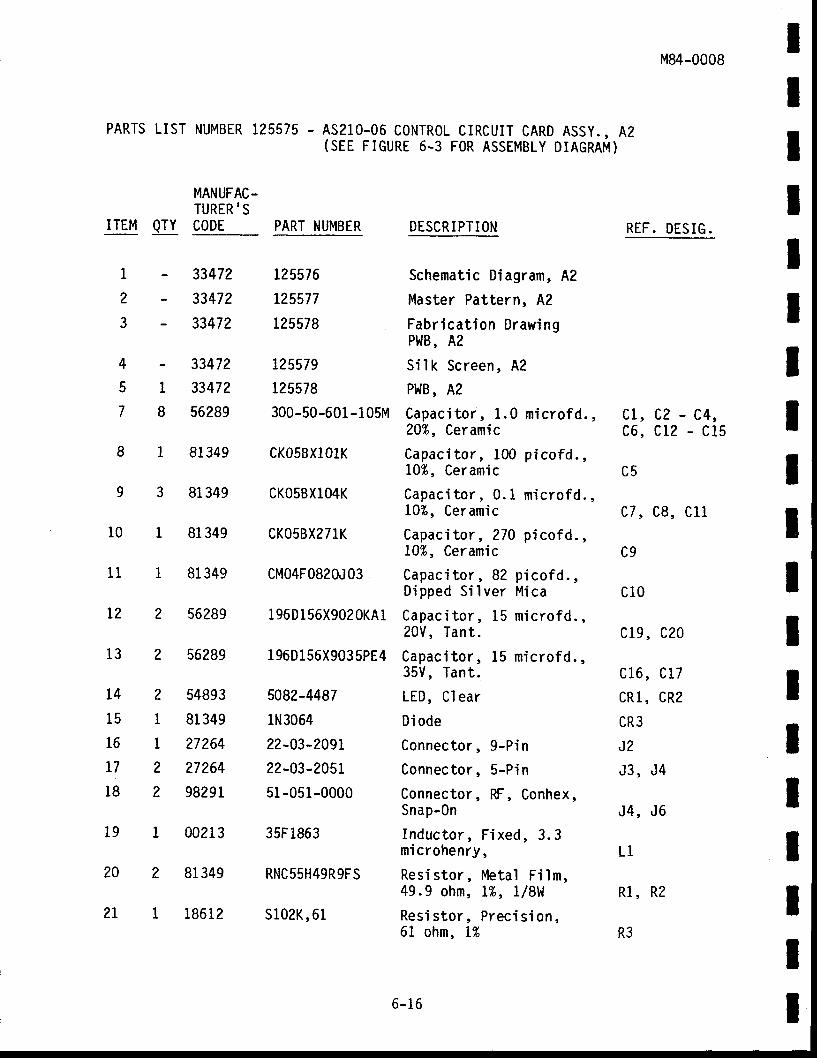
PARTS LIST NUMBER 125575 - A5210.06 CONTROL CIRCUiT CARD ASSY., A2(SEE FIGURE 6-3 FOR ASSEMBLY DIAGRAM)
MANUFAC-TURER,S
ITEM QTY CODE PART NUMBER DESCRIPTION
1
?
3
- 33472- 33472- 33472
M84-0008
REF. DESIG .
IIIIIt
4-
51
78
33472
33472
56289
1 81349
3 81349
1 81349
1 81349
2 56289
2 54893
1 81349
L 27264
2 ?7264
2 98291
00213
81 349
18612
L25576
L25577
L25578
125579
L25578
300-50-601-105M
CKO5BXlOlK
CKOsBXlO4K
CKO5BX2TIK
cM04F0820J03
196D156X902oKA1
196D156X903 5PE4
5082-4487
1N3064
22-03-?09r
22-03-?05I
51-051-0000
35F1863
RNC55H49R9FS
s102K,61
Schematic Diagram, A2
Master Pattern, A2
Fabricat ion DrawingP}lB, A2
Si lk Screen, A2
Pl.lB, A2
Capaci tor , 1. 0 mi crofd. ,20%, Ceramic
Capac i to r , 100 p ico fd . ,10%, Ceramic
Capac i to r , 0 .1 mic ro fd . ,1.0%, Ceramic
Capaci tor , ?70 picofd. ,10%, Ceramic
Capac i to r , 82 p ico fd . ,D ipped S i lver Mica
Capac i to r , 15 m ic ro fd . ,20V, Tant .
Capac i to r , 15 mic ro fd . ,35V, Tant .
LED, C lear
Di ode
Connector, 9-Pin
Connec to r ,5 -P in
Connector, RF, Conhex,Snap-0n
Induc to r , F ixed ,3 .3mi crohenry,
Res is to r , Meta l F i lm,49 .9 ohm, L%, 1 /8W
Res is to r , P rec is ion ,61 ohm, l%
c l , c? - c4,c6, c12 - C15
c5
c7, c8 , c1 l
c9
c10
c19, C20
c16, Cl .7cRI , CRzcR3J2J3, J4
J4, J6
L1
R1, R2
R3
IIItIIIIIIIII
10
l1
l2
13
L4
15
16
t7
18
19
20
2t
56289
6-16
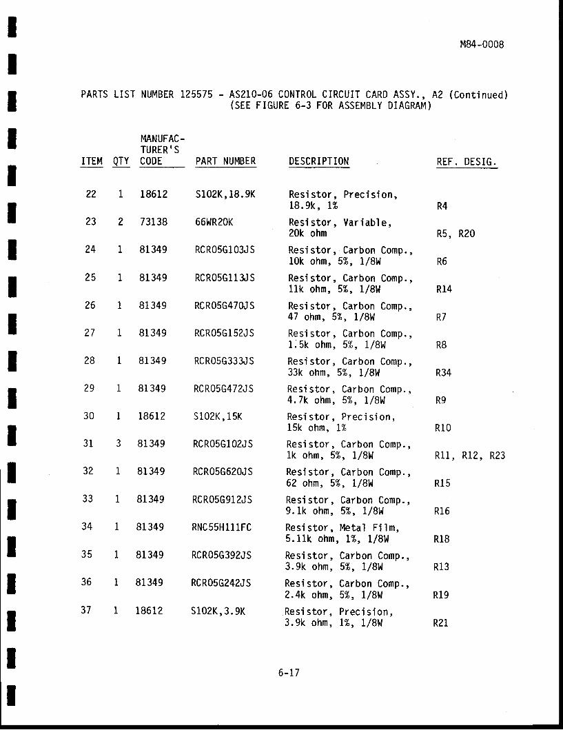
IIItIIIIIIIIIIIIIII
M84-0008
PARTS LIST NUMBER 125575 - A5210-06 CONTR0L CIRCUIT CARD ASSY., A2 (Cont inued)(SEE FIGURE 6-3 FOR ASSEMBLY DIAGRAM)
MANUFAC-TURER ,SCODE PART NUMBER REF. DESIG.ITEM QTY
?2 1
232
24 I
25 1
26 1
27 1
?8 I
29 1
30 1
31 3
32 I
33 1
34 I
35 1
36 1
37 1
r86L2 S102K,t8.9K
73138 66WR20K
81349 RCR05GI03JS
81349 RCR0sGllUS
81349 RCR05G470JS
81349 RCR05G152JS
81349 RCR05G333JS
81349 RCR05G472JS
18612 S102K,15K
81349 RCR05G102JS
81349 RCR05G620JS
81349 RCR05G912JS
81349 RNC55H1l tFC
81349 RCR05G392JS
81349 RCR05G242JS
18612 S102K,3 .9K
DESCRI PTION
Res i s to r , Prec is ion ,18 .9k , 1%
Res i s to r , Var iab l e ,20k ohm
Resi stor, Carbon Comp.,LOk ohm, 5%, 1/8l. l
Resi stor, Carbon Comp.,l lk ohm, 5%, 1/8l' l
Resi stor, Carbon Comp.,47 ohm, 5%, 1/8W
Resi stor, Carbon Comp.,1.5k ohm, 5%, l /Bt ,J
Resi stor, Carbon Comp. ,33k ohm, 5%, 1/8W
Res i s to r , Carbon Comp. ,4 .7k ohm, 5%, 1 /8W
Res is to r , P rec is ion ,15k ohm, L%
Res i s to r , Carbon Comp. ,lk ohm, 5%, 1/81,1
Res is to r , Carbon Comp. ,62 ohm, 5%, L/8W
Resi stor, Carbon Comp.,9 .Lk ohm, 5%, L /8W
Resi stor , Meta'l Fi I m,5 . l1k ohm, t%, 1 l8W
Res is to r , Carbon Comp. ,3 .9k ohm, 5%, 1 /8W
Res is to r , Carbon Comp. ,2.4k ohm, 5%, 1/8l . l
Res is to r , P rec is ion ,3 .9k ohm, L%, 1 /8W
R4
R5, RzO
R6
R14
R7
R8
R34
R9
R10
R11, R l2 ,
R l5
R16
Rt8
R13
R19
R21
R23
6- t7
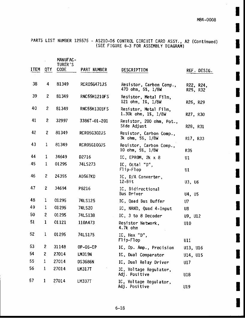
PARTS LIST NUMBER 125575 - AS21O-06 CONTROL(SEE FIGURE 6-3
M84-0008
CIRCUIT CARD ASSY. , AZ (Cont inued)FOR ASSEMBLY DIAGMM)
IIIIIIIItIIIIIIIIII
ITEM QTY
MANUFAC.TURER'SCODE PART NUMBIR DESCRIPTION
Resistor, Carbon Comp.,470 ohm, 5%, l/8W
Res is to r , Meta l F i lm,121 ohm, L%, t /8W
Resi stor, lvktal Fi lm,1 .30k ohm, l%, I /8W
Res is to r , 200 ohm, Pot . ,Side Adjust
Resistor, Carbon Comp.,3k ohm, 5%, L/8W
Res is to r , Carbon Comp. ,10 ohm, 5%, L/8W
IC, EPR0M, 2k x 8IC , 0c ta1 "0 " ,F1 i p-Fl op
IC, D/A Converter,12-Bi t
IC , Bi d i rec t iona' lBus Drfver
IC, Quad Bus Buffer
IC, NAND, Quad 4- Input
IC, 3 to B Decoder
Resi stor Network4 .7k ohm
IC, Hex "D" ,Fl i p-Fl op
IC , 0p . Anp . , P rec is ion
IC, Dual Comparator
IC, Dual Relay Dr iver
IC, Vol tage Regul ator,Adj . Posi t ive
IC , Vol tage Regu'l ator,Adj . Posi t ive
REF. DESIG.
R22, R24,R25, R32
R26, Rzg
R27, R30
R28, R31
R17, R33
R35
U1
U1
u3, u6
U4, U5U7U8u9, u12u10
u11u13, Ul6u14, U l5u l7
u18
u19
38
39
40
4L
81349
81349
81 349
3?997
81349
81 349
34649
01 295
24355
34694
01 295
01 295
01 295
01 121
01 295
31 148
270r4
270I4
270L4
27A14
RCR05G471JS
RNC55H1210FS
RNC55H1301FS
3386T-01-201
RCR05G302J S
RCR05G100lS
02716
74L5273
AD567KD
P8216
741S125
741S20
741S138
110A473
741S175
0P-05-EP
LM319N
DS3686N
LM31 7T
LM337T
2
2
2
I
42
43
44
45
46
47
48
49
50
51
52
53
54
55
56
57
1
1
?
2
I
I
2
1
1
2
?
1
1
1
6-18
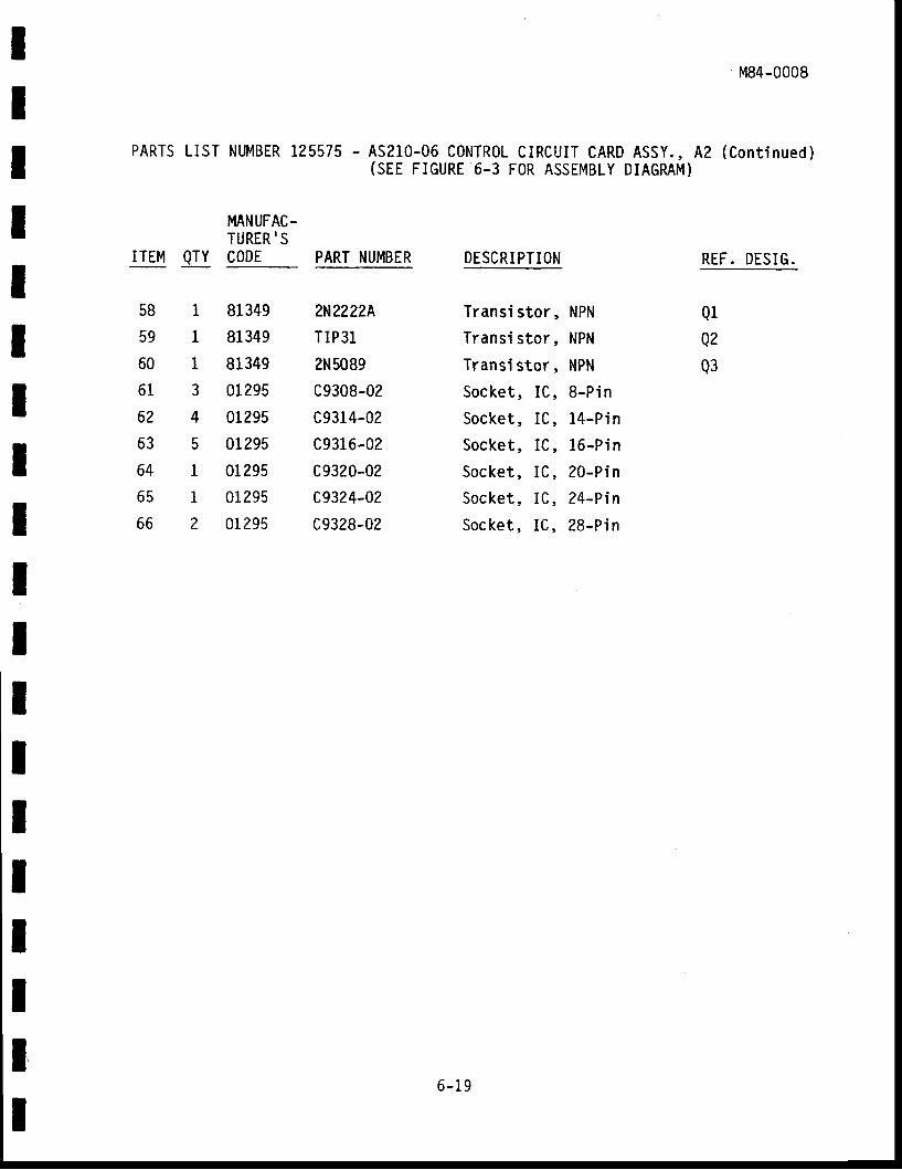
Ql
Q2
Q3
IIIIIIIIIIIItIIIIII
PARTS LIST NIJMBER 125575 . A5210-06 CONTROL(SEE FIGURE 6-3
M84-0008
CIRCUIT CARD ASSY. , A2 (Cont inued)FOR ASSEMBLY DIAGRAM)
ITEM QTY
MNUFAC-TURER.SCODE PART NUMBER REF. DESIG.DESCRI PTION
Transi stor,
Trans i s to r ,
Transi stor ,Socket , IC ,
Socket , IC ,
Socket, IC,
Socket , IC ,
Socket , IC ,
Socket , IC ,
58
59
60
61
62
63
64
65
66
1
I
1
3
4
5
1
1
2
81349
81349
81349
0L?95
01 295
0L295
01 295
01295
01 295
2N2222A
TIP3 l
2N5089
c9308-02
c9314-02
c9316-02
c9324-02
c9324-02
c9328-02
NPN
NPN
NPN
8-Pi n
14-Pi n
16-P i n
20-Pi n
24-Pin
28-Pi n
6-19
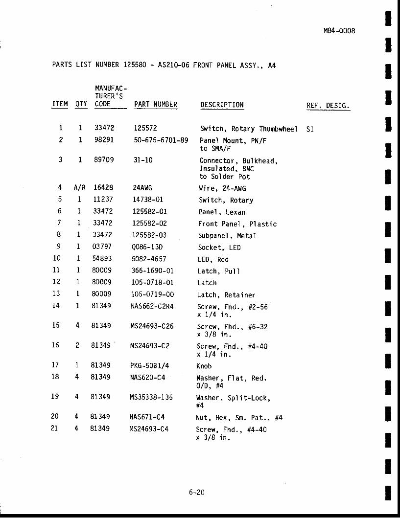
NUMBER 125580 - A5210-06FRONT PANEL ASSY., A4
MANUFAC-TURER'SCODE PART NUMBER DESCRI PTION
M84-0008
REF. DESIG.
IIIIIIIIIIIIIIIIIII
S1I
2
t 33472
I 9829I
1 89709
A/R L6428
T 1L237
L 33472
t 33472
r 3347?
L 03797
1 54893
I 80009
1 80009
I 80009
1 81349
4 81349
2 81349
I 81349
4 81349
4 81349
4 81349
4 81349
L25572
5A-675-6701-89
31-10
24Al,lG
14738-01
12558?.-0t
L?.5582-02
125582-03
Q086- 1 3D
5082-4657
366-1690-01
105-0718-01
105-0719-00
NAS662-C2R4
MS24693-C26
MS24693-C2
PKG.5OB 1/4
NAS620-C4
MS35338-1 35
NAS671-C4
MS24693-C4
Switch, Rotary Thumbwheel
Panel Mount, PN/fto SMA/F
Connector, Bulkhead,Insulated, BNCto So'lder Pot
t . l i re ,24-AWG
Switch, Rotary
Pane l , Lexan
Fron t Pane l , P las t i c
Subpanel, Metal
Socket, LED
LED, Red
Latch, Pul I
Latch
Latch, Retainer
Screw, Fhd. , #?-56x l /4 in .
Screw, Fhd., #6-32x 3 /8 in .
Screw, Fhd., #4-4Ax 1 /4 in .
Knob
Washer , F la t , Red.0/D, #4
l , lasher , Sp l i t -Lock ,#4
Nut , Hex , S f i . Pa t . , #4
Screw, Fhd. , #4-40x 3 /8 in .
3
4
5
6
7
I
9
10
11
t2
13
L4
15
16
t7
18
19
?0
ZL
6-20
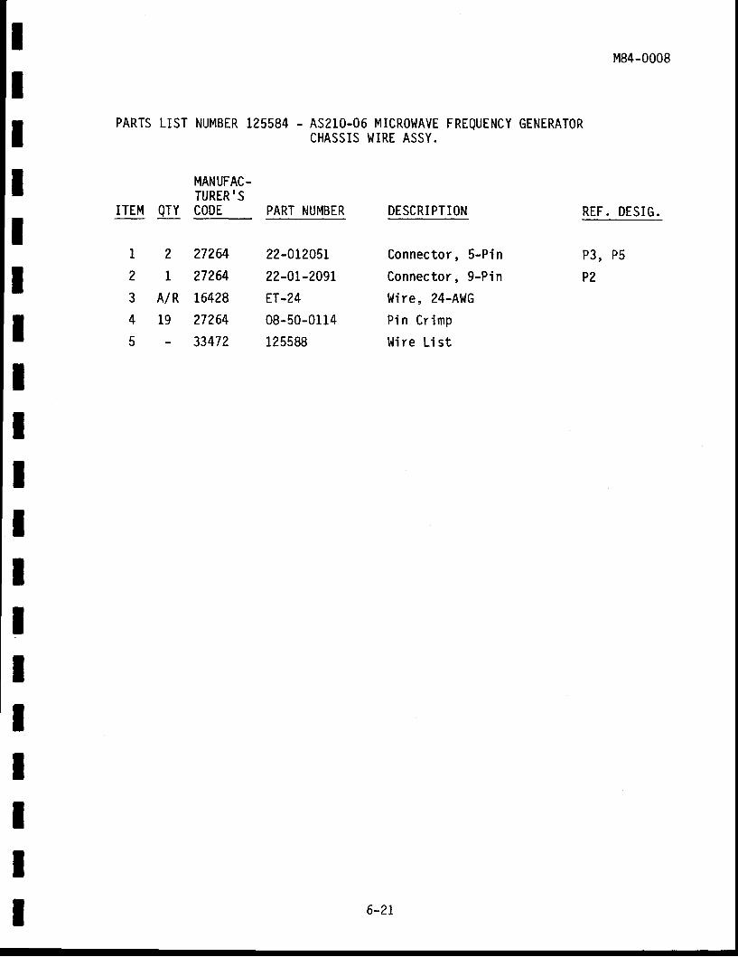
IM84-0008
PARTSLrsT NUMBER 125584 - AS210-06 MICRoWAVE FREQUENCY GENERATORCHASSIS ll |IRE ASSY.
MANUFAC-TURER'SCODE PART NUMBERITEM QTY DESCRI PTI ON
Connec to r ,5 -P in
Connector, 9-Pin
[ i re ,24-AWG
Pin Cr imp
Wire L i s t
REF. DESIG.
P3, P5
P2
I
z345
2 27264
I 27264
A/R t6428
19 27264- 33472
22-0L205L
22-01-209L
ET.24
08-50-0114
125588
III 6-21
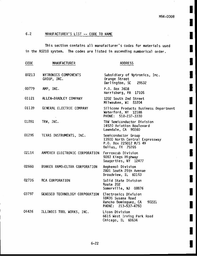
6.2 IIANUFACTURER'S LIST .- CODE TO NAME
This sect ion contains
AS210 system. The codes
M84-0008
a l l manufac turer ' s codes fo r mater ia ls usedare l i s ted in ascend ing number ica l o rder .
IIIIIItIIIIIIIIIIII
in the
CODE MANUFACTURER
00213
00779
OlLzI
01139
01 281
01295
NYTRONICS COMPONENTSGROUP, INC.
MP, INC.
ALLEN-BRADLEY COMPANY
GENERAL ELECTRIC COMPANY
TRl.l , INC.
TEXAS INSTRUMENTS, INC.
021t4
02660
02735
03797 GENISCO TECHNOLOGY CORPORATION
AMPEREX ELECTRONIC CORPORATION
BUNKER RAMO-ELTRA CORPORATION
RCA CORPORATION
ADDRESS
Subs id ia ry o f Ny t ron ics , Inc .Orange StreetDarl fngton, SC 29532
P.0 . Box 3608Har r isburg , PA 17105
1202 South 2nd StreetMilwaukee, I'lI 53204
Si l icone Products Business Departmentl, later f ord , NY 12188PHONE: 518-237-3330
TRl. l Semiconductor Div is ion14520 Avi ation Boul evardLawndale, CA 90260
Semiconductor Group13500 North Central ExpresswayP.0. Box 2250L2 l4/S 49Dal 1 as, TX 75?65
Fer roxcub D iv i s ion5083 Kings HighwaySaugerties, NY L2477
Amphenol Div is ion2801 South 25th AvenueBroadview, IL 60153
Sol i d State Di vi si onRoute 202Somervi l le, NJ 08876
Elec t ron ics D iv is ion18435 Susana RoadRancho Dominguez, CA 90??LPH0NE: 213-537-4750
L icon D iv is ion6615 West I rv ing Park RoadChicago, IL 60634
04426 ILLINOIS TOOL WORKS, INC.
6-22
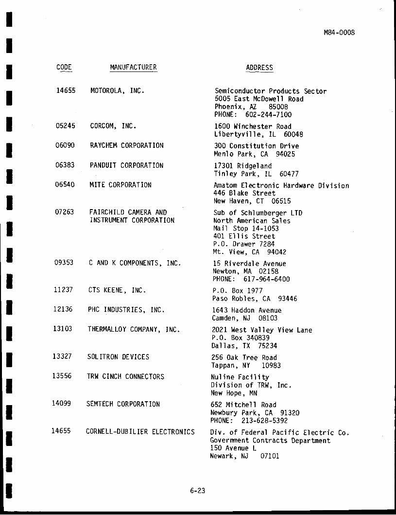
ItIIIIIII
05245
06090
06383
06540
07263
M84-0008
MANUFACTURER
14655 M0T0R0LA, INC.
CORCOM, INC.
RAYCHEM CORPORATION
PANDUIT CORPORATION
MITE CORPORATION
FAIRCHILD CAMERA ANDINSTRUMENT CORPORAT ION
C AND K COMPONENTS, INC.
CTS KEENE, INC.
PHC INDUSTRI IS, INC.
THERMALLOY COMPANY, INC.
SOLITRON DEVICES
TRl'l CINCH CONNECTORS
SEMTECH CORPORATION
CORNELL.DUB IL IER ELECTRONICS
Semiconductor Products Sector5005 East lt lcDowell RoadPhoeni\, NL 85008PH0NE: 602-244-7100
1600 Winchester RoadLibertyvi l le, IL 60048
300 Const i tut ion Dr ivel'lenl o Park, CA 94025
17301 Ri dgel andTinley Park, IL 60477Amatom Electronic Hardware Divis ion446 Bl ake StreetNew Haven, CT 06515
Sub of Schl umberger LTDNorth &nerican SalesMai l Stop 14-1053401 E l l i s S t ree tP.0 . Drawer 7284Mt. View, CA 94042
15 R iverda le AvenueNewton, MA 02158PH0NE: 617-964-6400
P.0 . Box 1977Paso Robles, CA 93446
1643 Haddon AvenueCamden, NJ 08103
2021 West Val ley View LaneP.0. Box 340839Dal las, TX 75234
256 Oak Tree RoadTappan, NY 10983
Nu l ine Fac i l i t yD iv is fon o f TRt . | , Inc .New Hope, MN
652 Mi tchel I RoadNewbury Park, CA 91320PHONE: 213-628-5392
Div . o f Federa l Pac i f i c E lec t r i c Co.Government Contracts Department150 Avenue LNewark, NJ 07101
ADDRESS
IIIIIIIIII
09353
t r237
12136
131 03
L3327
13556
14099
14655
6-?3
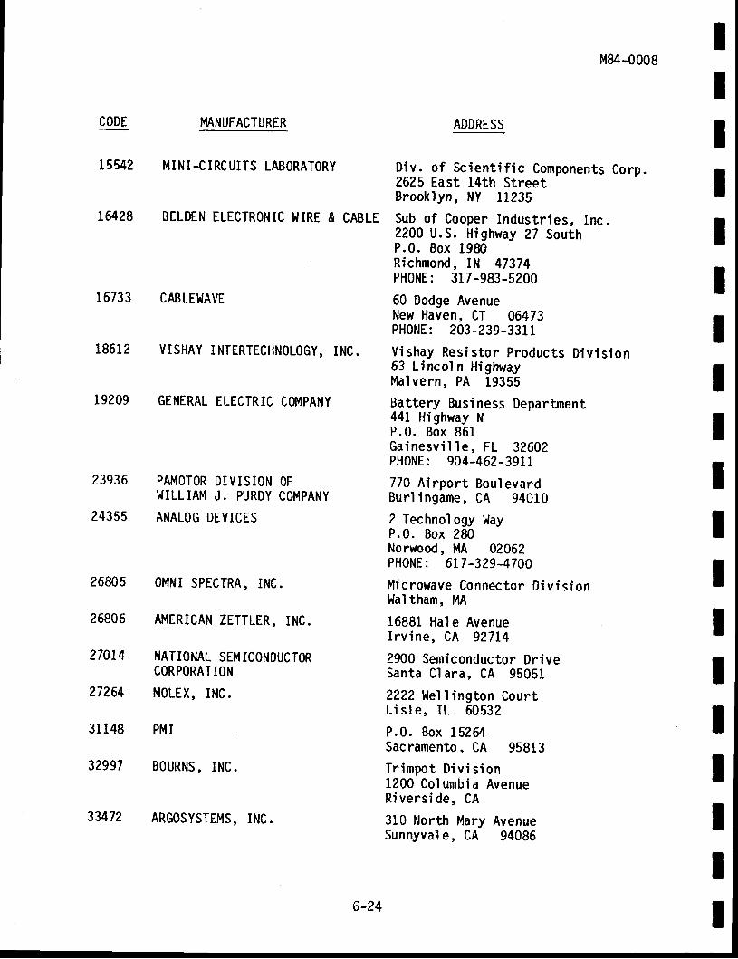
CODE
L5542
L6428
16733
18612
19209
IYIANUFACTURER
MINI.C IRCUITS LABORATORY
BELDEN ELECTRONIC t.|IRE & CABLE
CABLEI.JAVE
VISHAY INTERTECHNOLOGY, INC.
GENERAL ELECTRIC COMPANY
PAMOTOR DIVISION OFI{ILLIAM J. PURDY COMPANYANALOG DEVICES
OMNI SPECTRA, INC.
AMERICAN ZETTLER, INC.
NATIONAL SEMICONDUCTORCORPORATION
MOLEX, INC.
PMI
BOURNS, INC.
ARGOSYSTEMS, INC.
M84-0008
ADDRESS
Div. of Scient i f ic Components Corp.2625 East 14th StreetBrooklyn, NY 11235
Sub of Cooper Industr ies, Inc.2200 U.S. Highway 27 SouthP.0. Box 1980Richmond, IN 47374PHONE: 317-983-5200
60 Dodge AvenueNew Haven, CT 06473PH0NE : 203-239-331 1Vishay Resistor Products Div is ion63 Lincol n HighwayMalvern, PA 19355Battery Busi ness Department441 Highway NP.0 . Box 861Gainesvi l le, FL 32602PHONE: 904-462-3911
770 Airport Boul evardBurl ingame, CA 940102 Technol ogy l'layP.0. Box 280Norwood, l,tA 02062PH0NE: 617-329-470A
Microwave Connector Div is ionWaltham, MA
16881 Hal e AvenueIrv ine, CA 92714
2900 Semiconductor DriveSanta Cl ara, CA 95051
2222 llel I ington CourtLi s l e, IL 60532
P.0 . Box 15264Sacramento, CA 95813Tr impot D iv is ion1200 Columbia AvenueRivers ide , CA
310 Norti Mary AvenueSunnyval e, CA 94086
IIIIIIIIIIIIIIIIIII
23936
24355
26805
26806
27014
27?64
31148
32997
33472
6-24
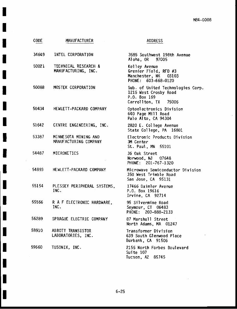
IIIIIIIIIIIIIIItIII
CODE
34649
s002 1
50088
50434
51642
53387
54487
54893
551 54
55566
56289
58910
59660
MANUFACTURER
INIEL CORPORATION
TECHNICAL RESEARCH &MANUFACTURING, INC.
MOSTEK CORPORATION
HEI.ILE IT-PACKARD COMPANY
CENTRE ENGINEERING, INC.
MINNESOTA MINING ANDMANUFACTURING COMPANY
MICRONETICS
HE I,ILETT.PACKARD COMPANY
PLESSEY PERIPHIRAL SYSTEMS,INC.
R A F ELECTRONIC HARDI.IARE,INC.
SPRAGUE ELECTRIC COMPANY
ABBOTT TMNSISTORLABORATORIES, INC.
TUSONIX, INC.
M84-0008
ADDRESS
3585 Southwest 198th AvenueAl oha, 0R 97005
Kel' ley AvenueGrenier Field, RFD #3Manchester, NH 03103PHONE: 603-668-0120
Sub. of Uni ted Technologies Corp.1215 l, lest Crosby RoadP.0 . Box 169Carrol I ton, TX 75006
0ptoel ectronics Div is i on640 Page Mi l l RoadPalo Al to, CA 94304
2820 E. College AvenueState Col lege, PA 16801
Elec t ron ic Produc ts D iv is ion3M CenterSt . Pau l , MN 55101
36 Oak StreetNorwood, NJ 07648PH0NE: 201-767-1320
Microwave Semiconductor Div i s ion350 I' lest Trfmble RoadSan Jose, CA 95131
17466 Daimler AvenueP.0 . Box 19616Irv ine, CA 927L4
95 S i lvermine RoadSeymour, CT 06483PH0NE: 203-888-2133
87 Marshal I StreetNorth Adams, MA 0L247
Transformer Di vi si on639 South Gl enwood Pl aceBurbank, CA 91506
2155 North Forbes BoulevardSuite 107Tucson, M 85745
6-25
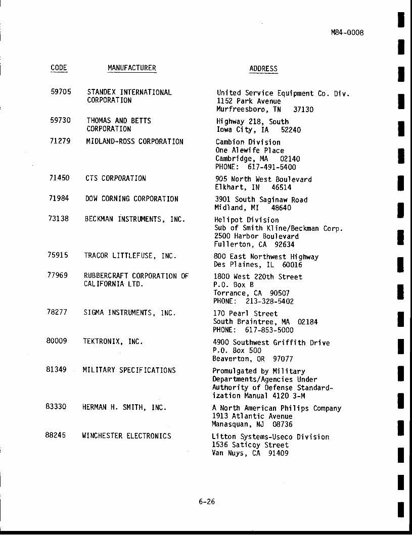
MANUFACTURER
STANDEX INTERNATIONALCORPORATION
59730
7t279
714s0
71984
731 38
7591 5
77969
78277
80009
81349
83330
88245
THOMAS AND BETTSCORPORATION
MIDLAND.ROSS CORPORATION
CTS CORPORATION
DOI.I CORNING CORPORATION
BECKMAN INSTRTJMENTS, INC.
TRACOR LITTLEFUSE, INC.
RUBBERCRAFT CORPORATION OFCALIFORNIA LTD.
SIGt\' lA INSTRUMENTS, INC.
TEKTRONIX, INC.
MILITARY SPECIFICATIONS
HERMAN H. SMITH, INC.
l. l INCHESTER ELECTRONICS
MB4-0008
ADDRESS
United Service Equipment Co. Div.1152 Park AvenueMurfreesboro, TN 37130Highway 218, SouthIowa City, IA 52240
Cambion D iv is ionOne Alewife PlaceCambridge, MA 02140PH0NE: 6L7-491-5400
905 North l, lest BoulevardElkhar t , IN 465143901 South Saginaw RoadMidland, MI 48640He'l i pot Di vi si onSub of Smith Kl ine/Beckman Corp.2500 Harbor Boul evardFul ler ton, CA 92634800 East Northwest HighwayDes P la ines , IL 600161800 l.lest 220th StreetP .0 . Box BTorrance, CA 90507PH0NE: 213-328-5402
170 Pearl StreetSouth Braintree, MA 02184PH0NE: 617-853-5000
4900 Southwest Gri f f i th Dr iveP.0. Box 500Beaverton, 0R 97077
Promulgated by Mi l i taryDepartments/Agenci es UnderAuthority of Defense Standard-izat ion Manual 4120 3-M
A North American Phil ips Company1913 Atl antic AvenueManasquan, NJ 08736
Li t ton Systems-Useco Divis ion1536 Sat icoy StreetVan Nuys, CA 91409
IIIIIIIIItIttIIIIII6-?6
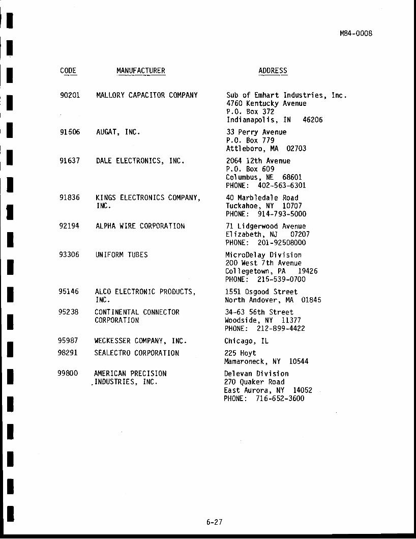
M84-0008
IIIIItTIIIIIItIIII
CODE MANUFACTURER
90201 MALLORY CAPACITOR COMPANY Sub of Emhart Industr ies, Inc.4760 Kentucky AvenueP.0 . Box 372Indianapol is , IN 46206
33 Perry AvenueP.0 . Box 779Attleboro, MA 02703
2464 lzth AvenueP.0 . Box 609Col umbus, NE 68601PH0NE: 402-563-6301
40 Marbledale RoadTuckahoe, NY L07A7PH0NE: 914-793-5000
71 Lidgerwood AvenueEl izabeth, NJ 07207PH0NE: 2QI-92508000
MicroDelay D iv is ion200 tlest 7th AvenueCol legetown, PA 19426PH0NE: 215-539-0700
1551 0sgood StreetNorth Andover, M 01845
34-63 56th StreetWoodside, NY 11377PHONE: 2L2-899-442?
Chicago, IL
225 HoytMamaroneck, NY 10544
Delevan D iv is ion270 Quaker RoadEast Aurora, NY L4052PH0NE: 7L6-652-3600
ADDRESS
91 506
91637
91836
9?t94
93306
95146
952 38
95987
98291
99800
AUGAT, INC.
OALE ELECTRONICS, INC.
KINGS ELECTRONICS COMPANY,INC.
ALPHA I.JIRE CORPORATION
UNIFORM TUBTS
ALCO ELECTRONIC PRODUCTS,INC.
CONTINENTAL CONNECTORCORPORATION
WECKESSER COMPANY, INC.
SEALECTRO CORPORATION
MERICAN PRECISIONINDUSTRIES, INC.
6-27

IIIIIIIIIIIIIIIIIII


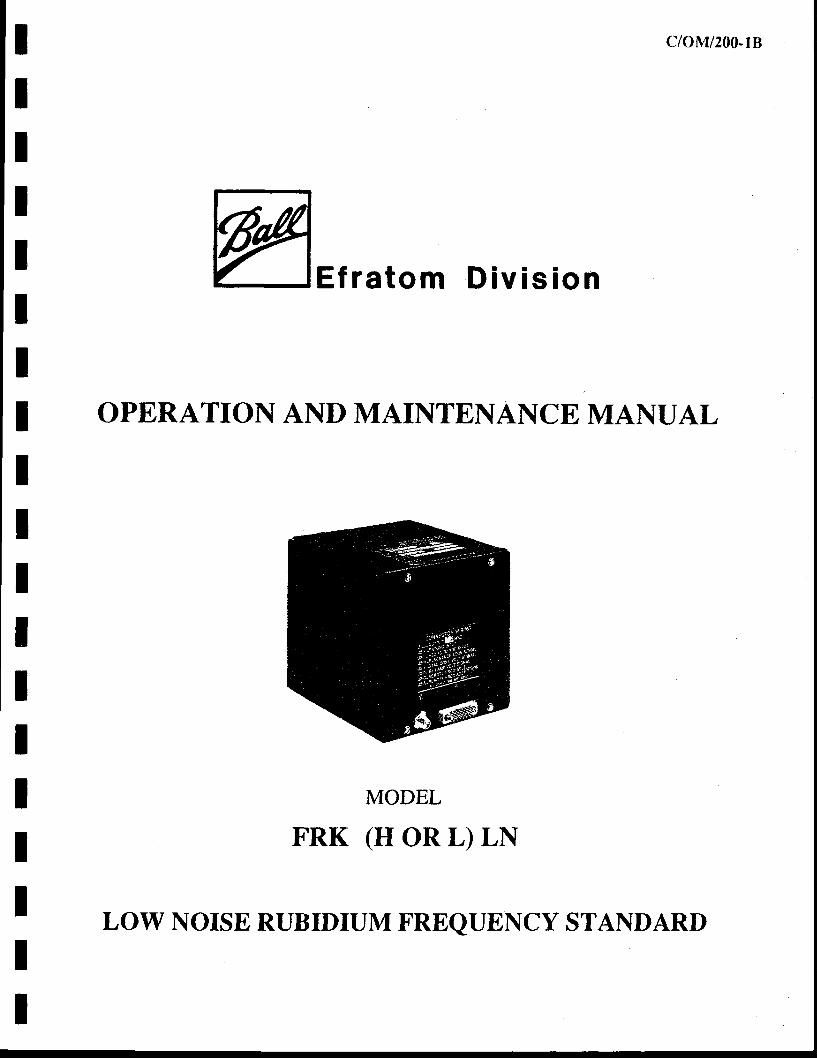
ctoM/za0-rc
Efratom Division
OPERATION AND MAINTENANCE MANUAL
MODEL
FRK (H OR L) LN
LOW NOISE RUBIDIUM FREQUENCY STANDARD

tIIIIIIIIIIIIItII
i '
II
1t l*
LIMITEDWARRANTY
"The seller warrants that each article of goods sold by it will at the time of shipment be free fromdefects in materials furnished and workmanship performed by the seller. This warranty and seller'sliability are limited either to granting credit or repairing or replacing, at seller's option, withreasonable promptpss after rctum to seller of any article which is disclosed to seller's satisfactionto be defective, and only if said arricle is retumed to the seller promptly after discovery of zuchdefect and in no event later than 72 months (or zuch other time period as may be specified in writ-ing as a wiuranty period for a particular article) from the date of delivery thereof. Normal transpor-tation charges in cormection with an article retumed shall be at the seller's expense, but only if theseller is responsible under the terms of this warranty. This waranty does not extend to any articlewhich has been subject to misuse, neglect or accident, nor does it extend to any article which hasbeen repaired or altered by other than the seller. THIS WARRANTY IS IN LIEU OF ALLOTHER WARRANTIES EXPRESSED OR IMPLIED, INCLUDING ANY WARRANTYOF FITNESS FOR A PARTICULAR PURPOSE. THE RIGHTS AND RBMEDIESPROVIDED HEREIN ARE EXCLUSIVE AND IN LIEU OF ANY OTHER RIGHTS ORREMBDIES. IN NO EVENT SHALL SELLER BE LIABLE FOR CONSEQUBNTIALDAMAGBS'I.
Ball Corporation, Efratom Division, will be happy to answer any application or usage questionswhich will enhance your use of this unit. Please address your reguests or correspondence to: BallCorporation., Efratom Division, 3 Parker, kvine, Califomia 9nft-1ffi5, Attention: SalesDepartrnent, or call Ql4> 770-5000, Fax (714) 770-V463.
European customers may contact: Ball Efratom Elektronik GmbH, Fichtenstrasse 25, 8011Hofolding, West Germany, Telephone: 49-8 1 -049040, Fax: 49-8 1 -0499 18.
@1989 Ball Corporation., Efratom Division. Alt rights reserved.
FRK-( )LN IICONTENTS
I
t . lt .21.3r.41.51.6
INTRODUCTION & SPECIFICATIONS
Introduction 1-1Manual Content l-lConnectors l-2Electrical Protection l-2Available Options l-2Specifications I-3
tr INSTALLATION & OPERATION
2.1 Intrcduction 2-l2.2 Shipping and Receiving Information 2-l2.3 Mounting 2-l2.4 PowerRequirements 2-22.5 Installation Consi&rations 2-22.6 Frequency and Monitoring Signal Ouputs 2-22.7 Normal Operation 2-32.8 Functional Operation Test Equipment 2-42.9 Operational Frequency Accuracy Test 2-42.10 Short-Term Stability Test (Allan Variance) 2-6
Itr THEORY OF OPERATION
3.13.23.33.43.53.63.73.83.9
IntroductionGeneral Theory of QerationResonatorSimplifi ed Block DiasrdmSerfo Board AssemblvLamp BoardPower SupplyOscillator BoardSynthesizer Board
MAINTENANCE
4.1 Introduction4.2 Test Equipment4.3 Performance Tests4.4 !'ield.Maintenance,Troubleshooting,&
Repair
3-l3-r3-63-73-73-93-93-103-rr
4-l4-t4-l
4-5
2.1
LIST OFILLUSTRATIONS
Winchester Connector and PinArrangementOptional Coaxial Connector with Push-onPin Connector and Pin ArrangementQerational Frequency AccuracyTest Set-upDerivation of Modulation SignalFRK Block DiagramOptical Pumping Process IllustratedInterconnection of Servo PCBModification, and 5 MHz LN Oscillator 3-12Output Level Test Configuration 4-2Frequency Offset & Lnng-term StabilityTest Configuration 4-zShort Term Stability & Signal Output
IIIItIIIIIIIIIIII
2-3
2-3
2-43-23-43-5
2.2
2.3
3. t3.23.33.4
4.14.2
4.3
4.44.54.64.7
4.8
4.94.104.1r
4.124.r34. t4
1 .12.r4.1 -4.2
TestsFRK BaseplateFRK-OLN Wiring DiagramFRK Troubleshooting OverviewSnap Diode Access Hole on ResonatorAssemblyLamp Adjustment Ports
4-34-64-8
4-10
4-tl4-13
Demodulator Output (Seno Board) 4-15Signal Waveform at TP6 4-16Waveform & Amplitude Traces for Servo& SvnthesizerBoards 4-19Waieform, Sewo Board (TP-3) 4-25Waveform, Servo Board CfP-6) 4-25Environmental Test Chamber Set-up 4-n
LIST OF TABLESSpecifications l-3Functional Operation Test Equipment 2-4Required Test Equipment 4-lResonator Disconnect Points 4-7
APPENDD(A
Drawing List, Schematics, Assembly Drawings, andPafis Lists
APPENDD( B
FRK Remote Frequency AdjustmentModification Procedure
IIIIIIIIIIIIIIIII
FRK-( )LN
SECTION I
INTRODUCTION AND SPECIFICATION
r.I INTRODUCTION.
The Efratom Model FRK-(H or L)LN Rubidium Frequency Standard (RFS) is a compact, atomicresonance-controlled oscillator which provides an extremely pure and stable sinusoidal signal of 5 or10 MHz, at I Vrms into a 50 ohm load (refer to Section 1.5 for other available options). The unit isdesigned for use in high-perforrnance communication systems, frequency standard equipment, ad-vanced navigation equipment, and all other equipment and systems which require extremellprecisefrequenciesltime intervals. With the proper input power provided and suitable cooling provisions,the FRK-( )LN can be operated as a free-standing frequency standard for laboratory and testingPu4)OSeS.
NOTEThroughout this manual the models FRK-HLN & FRK-LLNwill be referred to as model FRK-( )LN, indicating that thetext or diagram references both models. If only one model is tobe referenced, the full model designation will be printed out.
1.2 MANUAL CONTENT.
This manual contains information regarding the operation and field maintenance of the ModelFRK -( ) LN,5 MHz Rubidium Frequency Standard (RFS), with a Final Assembly No. 703-200-8.A Model FRK-( ) IN with a Final Assembly No. other inannZ-200-8 is amodified unitproducinga 10 MHz output, or has some other feature not standard to model 703-200-8. If a modified unitdiffers operationally from the standard unit an addendum will be included with this manual describ-ing the differences. Note the information in the addendum prior to reading the manual to determinewhat qpecial qpecification or operation aspects may exist. If an addendum has not been included fora modified unit, it can be assumed that the modification does not affect the unit's operation.
Sections I and tr contain general information conceming the unit. It is recommended that thesesections be read completely prior to attempting operation. Section III provides the general theory ofoperation for the technician or engineer who requires a more thorough understanding of the unit'soperation. Section IV provides the required information for performing fretd maintenance on theunit. An Outline Drawing, Schematic Diagrams, Assembly Drawings and Parts Lists are providedin the Appendix.
I
Il - l
FRK-( )LN
1.3 CONNECTORS.
All necessary connectors for inputs, output and monitor signals are easily accessible from the outercover of the unit. The unit is manufactured using either a Winchester connector, P/N SRE-2gpJ,which mates with SRE-20SI and a SMA-Epe coaxial connector. For other connector configurations,refer to unit label for pin out information. (Other optional connectors are available; contact theEfratom sales departnent).
1,4 ELECTRICAL PROTECTION.
The unit is protected against reverse polarity input power by both an intemal fuse and diode. The outputand monitor signals are short-circuit protected.
1.5 AVAILABLE OPTIONS
(a) Extemal (remote) Frequency Adjustment Option.
(b) AdditionalMagneticShielding.
(c) Low Operating Temperarure Option:
FRK-HLN < 4E-10 from -55oC to +65oCFRK-LLN < 6E-10 from -55"C to +65oC
r.6 SPECIFICATIONS.
Pertinent performance specifications for the Models FRK-LLN and FRK-HLN are listed in Table l.l.
tIIIIIIIIIIIIIIIIII1-2
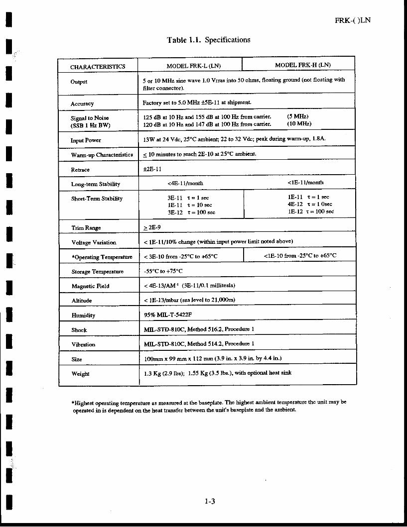
Il.I
FRI(-OLN
IIIIIIIIItIIII
,::,
II
Table 1.1. Specifications
*Highcst operating temperature as measured at the baseplate. The highest ambienr ten{terature the unit may be
operated in is depcndent on the beat transfer befween the unit's baseplate and the ambient.
CHARACTERISTICS MODELFRK-L(LIO MODELFRK-H (L}O
Output 5 or lO MIIz sine wave 1.O Vrms into 50 ohms, floating ground (not floating with
fi.lter connector).
AccuracY Factory set to 5.0 MHz +5E-ll at shipment.
Signal to Noise(SSB I Hz BYr)
125 dB at lOHz and 155 dB at 100 Hz from carrier. (5 MIIz)
120 dB at lO Hz and 147 dB at IOO Hz from carricr' (lO MlIz)
Input Power 13W at 24Ydc,25"C ambient;22to32 Vdc; peakduring warm-up, 1.8A.
Warm-up Cbaracteristic s < l0 minutes to reach 2E-10 at 25oC ambient.
Retrace rzB-ll
Long-term Stability <4E-1|lmonth <lE-1l/month
Sho*-Term Stability 3 E - 1 1 t = l s e cl E - l l t = 1 O s e c3E-L2 r = 10O sec
l E - I l t = l s e c4E-12 r = l OseclE-12 r = 100 sec
Trim Range >2F.-9
Voltage Variation < lE-lLllOVo change (within input power limit noted above)
* Operating Tenrperature < 3E-lO from -25"C to +65oC <1E-10 from -25oC to +65"C
Storage Temperature -55"C to +75"C
Magnetic Field < 4E-13lAM-' (3E-1 1/0. 1 millitesla)
Altitude < 1E-13/mbar (sea level to 2l,000m)
Humidity 95%MIL:|-5422F
Shock MILSTD-81OC, Method 516.2, Procedure I
Vibration MILSTD-8I0C. Method 514.2, Procedure I
Size lfi)mm x 99 mm x 112 mm (3.9 in x 3.9 in by 4.4 in')
Weight 1.3 Kg Q9lbs); 1.55 Kg (3'5 lbs.)' with optiqnal tosaf sink
t-3

FRK-( )LN
This page intentionally left blank.
IIIIIIIfI
FRK-( )LN
SBCTION II
INSTALLATION AND OPERATION
2.T INTRODUCTION.
This section of the manual contains information regarding the installation and operation of the EfratomFRK-( )LN. It is recommended that this section be read carefully prior to attempting operation of theunit.
2.2 SHIPPING AND RECEIVING INFORMATION.
The Model FRK-( )LN is packaged and shipped in a foam-packed container. The unit was inspectedmechanically and electrically prior to shipment. Upon receipt of the unit, athorough inspection shouldbe made to ensure that no damage has occurred during shipping. If any damage is discovered, contactBall Corporation, Efratom Division, 3 Parker,Irvine, CA.92718-1605. Telephone (7L4) 770-5000;Telex 685-635. European customers should contact BaIl Efratom Elektronik GmbH, Fichtenstrasse 25,8011 Hofolding, West Germany, Telephone 08104190 40. If reshipment of the unit is necessary, theoriginal container and packing should be used. If the original container is not available, a suitablecontainer with foam-packing is recommended.
2.3 MOUNTING.
The unit's baseplate has been drilled and tapped to accommodate installation. The unit should bemounted with the aluminum thermal baseplate in contact with a flat metal surface. Mounting screwsmust not be allowed to penetrate the baseplate more than 0.2 inches (5mm). It is recommended that themounting surface be designed to permit free access to the unit's frequency adjust potentiometer. Referto outline drawing 703-203-l in the appendix for mounting dimensions.
The heat transfer characteristics of the mounting surface must be adequate to timit the rise of the unit'sbaseplate to < +65t. The maximum allowable environmental temperature (Ta), for this mounting is:
Ta=654C- (V . x I " x \ )
Where: V- = Supply Voltage in volts
I" = Supply Current in amperes
q = Thermal Resistance between unit and ambient, (eC/watt).
2-l
FRK-( )LN
NOTEAn add-on heat sink is an available option from Efratom;order Model 70223, Air Cooled Heat Sink.
2.4 POWER REQUIREMENTS.
The Model FRK-( )LN requires an extemal power source capable of providing between +22 and +32Vdc, with a minimum of 1.8 ampere output. The positive input voltage for the unit is to pin L with thenegative return voltage on pin P of the connector.
In order to obtain the cleanest output signal close to the carrier, the maxmum ac ripple on the supplyvoltage must be less than I mV peak-to-peak. If it is acceptable for the output frequency to containspurious multiples of the powerline frequency (50, 60, or 400 Hz), the ripple can be higher, but in nocase should the supply voltage AC +/- peak exceed the upper or lower input power limit of the unit.
2.5 INSTALLATION CONSIDERATIO NS.
Some considerationmust be givento the operating location of the unit regardless of its application. Tominimize frequency offsets and/or non-harmonic distortion, the unit should not be installed nearequipment generating strong magnetic fields such as generators, transformers, etc.
CAUTIONCARE MUST BE TAKEN TO ENSURE THAT THE MAXIMUMOPERATING TEMPERATURE Is NoT EXCEEDED, (+65"C ASMEASURED ATTHE I'NIT'S BASEPLATE). IN ADDMON, THEUNIT'S OIITER COVER IS A SPECIALLY DESIGNED MAGNETICSHIELD; DAMAGE TO THE OUTER CovER COULD CHANGE ITSSHIELDING CHARACTERISTICS.
2.6 FREQUENCY AND MONTTORTNG SIGNAL OUTPUTS.
Figure 2.1 illustrates the standard Model FRK-( )LN coaxial connector Jl with Winchester connector12, and Presents a brief functional description of the pin connections. Figure 2.2 ptesents the sameinformation for the optional 8-pin, wirewrap or press-fit connector with coaxial connector.
Jl 5 or l0 MHz OUTPUTJ2 A. Optional remote frequency adjust
C. Optional remote frequency adjustD. Rb LAMP VOLTAGE SIGNALF. TTAL CONT VOLTAGE SIGNALH. RESONANCE LOCK SIGNALL. +22 TO +32 VDC INpI-rfP. GROUND (connected to enclosure)
IIIIIIIIIIItIIIIIIt2-2
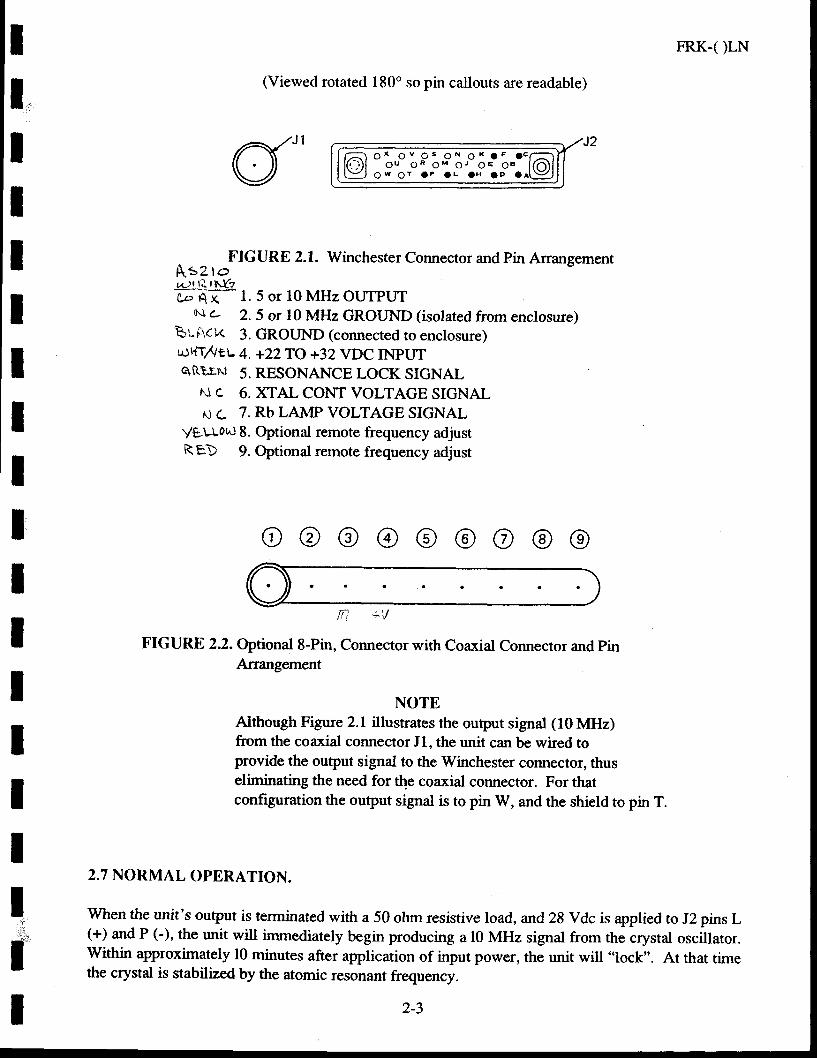
Il,IIIIIIIIIIIIIItfI
FRK-( )LN
(Viewed rotated 180o so pin callouts are readable)
6" @:e':::i::iiisi^@,J2
FIGURE 2.1. Winchester Connector and Pin ArrangementAszror,or llttrfzc.<,l{x* 1. 5 or 10 MHz OUTPUT
t \ c- 2.5 ot l0 MHz GROUND (isolated from enclosure)Bt-Ftcx 3. GROUND (connected to enclosure)Ld'{t4tL 4, +22TO +32 VDC INPUTsRtshl 5. RESONANCE LOCK SIGNAL
I{ C 6. XTAL CONT VOLTAGE SIGNALN c 7. Rb LAMP VOLTAGE SIGNAL
VEu.uot^}8. Optional remote frequency adjustRED 9. Optional remote frequency adjust
e@@@@@o@@
nrV
FIGURE 2.2. optional 8-Pin, Connector with coaxial connector and pinArangement
NOTEAlthough Figure 2.1 illustrates the ouq)ut signal (10 MHz)from the coaxial connector Jl, the unit can be wired toprovide the output signal to the Winchester connector, thuseliminating the need for tle coaxial connector. For thatconfiguration the oulput signal is to pin W, and the shield to pin T.
2.7 NORMAL OPERATION.
When the unit's output is terminated with a 50 ohm resistive load, and 28 Vdc is applied to J2 pins L(+) and P (-), the unit will immediately begin producing a l0 MHz signal from the crystal oscillator.Within approximately l0 minutes after application of input power, the unit will "lock". At that timethe crystal is stabilized by the atomic resonant frequency.
2-3
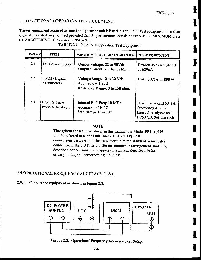
DC POWERSUPPLY
HP5371A
UUT
FRK-( X-W
2.n FUNCTIONAL OPERATION TEST EQUIPMENT.
The test equipment required to functionally test the unit is listed in Table 2.1 . Test equipment other thanthose items listed may be used provided that the performance equals or exceeds the MIMMUM USECHARACTERISTICS as stated in Table 2.1.
TABLE 2.1. Functional Operation Test Equipment
PARA# ITEM MIIYM{JM USE C HARACTERISTICS TEST EQUIPMENT
2.1
2.2
2.3
DC Power Supply
DMM (DigitalMultimeter)
Freq. & TimeInterval Analyzer
Output Voltage: 22 to 30YdcOutput Curenr: 2.0 Amps Min.
Voltage Rurge : 0 to 30 VdcAccuracy: + l.25%oResistance Range: 0 to 150 ohm.
Intemal Ref. Freq: 10 MHzAccuracy: t 1E-12Stability: parts in l0r2
Hewlett-Packard 64338or 6296A
Fluke 8020A or 80004
Hewlett-Packard 5371AFrequency & TimeInterval Analyzer andHP5371A Software Kit
NOTEThroughout the test procedures in this manual the Model FRK-( )LNwill be referred to as the Unit Under Test, (UUT). Allconnections described or illustrated pertain to the standard Winchesterconnector; if the UUT has a different connector arrangement, make thedescribed connections to the appropriate pins as described :ui.2.6or the pin diagram accompaning the UUT.
2.9 OPERATIONAL FREQUENCY ACCURACY TEST.
2.9.1 Connect the equipment as shown in Figure 2.3.
Figure 2.3. Operational Frequency Accuracy Test Serup.
IIItIIIIIIIIIIIIIIIz-4
IIIIIIIIIIItIIItIII
FRK-( )LN
2.9.2 Adjust the DC power supply controls to obtain a28 + 1.4 Vdc indication on the DMM.
2.9.3 Allow sufficient time for equipment to stabilize.
NOTEThe UUT requires 10 minutes stabilizationto obtain the following frequencyaccuracy: + 2E-LA of the final frequency(calibrated frequency), or the frequencybefore turn off, (if tum off was within24 hours and at the same environmentaltemperature). If the [[.IT was in storage,the worse case enor = + 2E-10 warm-up ++ last calibration accuracy or + 5E-10factory setting at shipment, whichever isapplicable + *aging specification.
The UUT requires I hour stabilizationtime to obtain the following accuracy:+ 2E-11 of final frequency or frequencyat tum off (if tum off was within 24hours and at the same environmentaltemperature). If LruT was in storage, theworse case error = + 2E-11 warm-up +/-last calibration accuracy or + 5E-11factory setting at shipment, whichever isapplicable + *aging specification.
* Aging Specification: FRK-HLNS 1X10'tt /monthFRK-LLN S 4X10-tt /month
2-9-4 Follow the instnrctions in the FIP5371A Frequency and Time Interval Analyzer OperationManual to begin the test.
2.9.5 Allow sufficient time for the HP5371A to indicate the UUT OFFSET for the data you require.Verify that the UUT frequency offset is within the tolerance stated in the NOTE following Step2.9.3.
NOTEIf the UUT is not within the stated tolerance limits.perform the Frequency Adjustment procedure, paragraph4.6.5.1 through 4.6.5.2.
2-5
FRK-( )LN
2.10 SHORT.TERM STABILITY TEST (ALLAN VARIANCE)
NOTEIf you have just completed 2.9 through2.9.5, and the Allan Variance indications(as displayed by the HP5371A) areof the required averaging times, the testresults as indicated are valid. It2.gwas not performed continue with 2.10.1
2.10.1With the equipment connected as shown in Figure 2.3, andthe required stabilization timeallowed, (refer to NOTE following 2.9.3), begin the test.
2.10.2 Allow sufficient time for the HP537IA to display the required data for the averaging times, andverify that UUT Allan Variance is within tolerances listed in Table l.l SPECIFICATIONS.
IIIIIIItIIItIIIIIII2-6
IIIIIIItIIIIIIIIIII
FRK-( )LN
SECTION III
THEORY OF OPERATION
3.1 INTRODUCTION.
This section of the manual contains a general theory of operation and circuit analysis of the ModelFRK-( )LN Rubidium Frequency Standard. A block diagram, (Figure 3.2) has been included to helpclarify the text. Schematic diagrams are included in the Appendix.
3.2 GENERAL THEORY OF OPERATION.
The unit's highly frequency-stable 5 or 10 MHz output signal is obtained from a 5 or 10 MHzVoltage Controlled Crystal Oscillator (VCXO), whose frequency is referenced and locked to theatomic "Resonance Frequency" of Rubidium (f*r).
3.2.1 ATOMIC REFERENCE FREQUENCY.
The atomic reference frequency is provided by the 6.834 GHz ground-state hyperfine transition ofthe Rb87 (rubidium). The VCXO is locked to the f"o at approximately 6.834 GHz, by synthesizng amicrowave signal, from the 10 MHz VCXO output, having a frequency in the vicinity of f*r. Themicrowave signal is used to excite the rubidium atoms that are contained within a microwave cavity(resonance cell). The frequency synthesis scheme is designed so that the VCXO frequency is ex-actly 10 MHz when the microwave frequency is equal to f*0. The frequency of the signal applied tothe microwave cavity can be maintained equal to f by generating an error signal to servo theVCXO through its control voltage.
3.2.2 RUBIDIUM LAMP.
Light from a nrbidium lamp is generated by anrf excited plasma discharge. The light passesthrough the resonance cell, where it interacts with the mbidium atoms contained therein. Some ofthe light is incident upon a silicon photo detectorphotocell within the resonance cell. When theapplied microwave frequency is equal to the f*r, the rubidium atoms resonate within the microwavefield in the cavity; this causes the light reaching the photo detector to decrease. This behavior isillustrated by the left, uppermost curve in Figure 3.1.
3-L
FRK-( )LN
t l 'I t lt l lt t lt t lI t lt t l
$
F-zu,EE,
ooFo-r(L
tql 5t 6
]E
Figure 3.1. Derivation of Modulation Signal
3-3
IIIIIIIIIIIIIIIIIIt
FRK-( )LN
3.2.3 OPTICAL PUMPING. The rubidium oscillator is a passive device, meaning that the atomsthemselves do not produce a self-sustaining oscillation. Nevertheless, the atoms can be viewed intheir simplest form as a high-Q, (Q -10t) series-resonant tank curcuit that is resonant at the hy-perfine frequency (-6.8 GHz for rubidium atoms). The voltage source driving the tank is themicrowave input coming from the Modulator/Synthesizer, andthe LCR components are the rubid-ium atoms contained in the optical package. The atomic resonance is detected by optical means andinvolves a process known as Optical Pumping, by which atoms are raised to a higher state throughthe absorption of light energy.
The two lower levels, A and B, are the ground state hyperfine levels. Statistically speaking, therubidium atoms will be equally divided between these two levels. If the atoms are irradiated withmicrowave energy at the hyperfine frequency, then those atoms in level A will make a transition tolevel B and vice- versa, without changing the overall distribution between the rwo levels (statisti-cally). [The hyperfine frequency (f *r) is related to the hyperfine energy level separation E (oules)= h'f
", (Hz) where h = Plank's Constant = 6.6226 x 10⁻³a joule/Flzl. A third and higher energy
state exists which is referred to as level C.
Level C is an optically excited state of the atom which is normally vacant; (for rubidium, this Clevel state can be excited by infrared light energy at the proper wavelength). Transitions to level Care known as "optical transitions" and can occur from either of the two hyperfine energy levels Aor B. If only the spectral wavelength corresponding to one of the hyperfine levels is introduced,only the atoms at that hyperfine level will make the transition to level C. This condition can begenerated by filtering out the spectral wavelength corresponding to one of the hyperfine levels.
If the light energy injected into the resonance cell corresponds to the wavelength required for levelA to C transitions, the rubidium atoms at the A level will absorb some of the light. The absorption oflight raises those atoms to the C level energ-y state. After a short time the atoms which were raisedto the C level will ernit a photon of the same wavelength that caused the energy level to increase;they then retum to the ground state hyperfine level, redistributing themselves (statistically) equallybetween level A and B. The atoms which retum to level A wiil again absorb the light and be raisedto level C, where they will remain for the short time before emitting the photon and again redistrib-uting themselves between the two hyperfine energy levels A and B. By this means, Optical Pump-ing can be used to produce a population difference between the two hyperfine levels, whereby alt ofthe atoms are pumped into one hyperfine level (for the preceeding situation, level B). Once thiscondition exists, there are no atoms left in level A to be excited to level C and the light is not theproper wavelength to excite the atoms in level B to level C, therefore the light is unattenuated afterpassing through the resonance cell.
As discussed earlier, if a microwave field corresponding to the hyperfine frequency were applied,the atoms at level B would make a transition to level A and be available for excitation to level C bythe light beam. Since each excitation of an atom in level A is accomplished by the absorption of alight photon, the net effect of applying the microwave field is to cause attenuation of the light beam.Figure 3.3 pictorially illustrates the Optical pumping process.
FRK-( )LN
o 1 j4>>d E oe . 6 a
"uc-< (,1F JJ l--o 2r - z2 0o o3HFo
lco
i---;r U
i aii - rl . r! i ' "i 6; o! >r l D 1i N \I ,\_
ieti >
i tr Da oI Gi lrl: 3 'i8i {
ni:63f,F ( 'l o <c i h
iee*z <E 3C J E3
I
P(r.CfIE-D@NTROL
Figure 3.2. FRKBlock Diagram
34
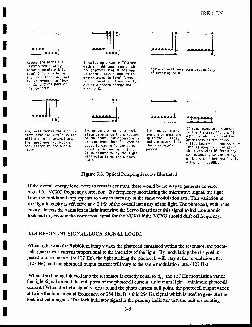
IIIIIITItIITIIIIIII
t-LlI_-.a a a a ^
Assume the atorns ared i s t r i bu ted equa l lYb e t w e e n l e v e l s A & 8 .Level C is much higher;the t ransi t ions A-C andB-C corresPond to l ines' in the opt ica l Par t ofthe spectrum
They w i l I remain there fo r ashor t t ime (as l i t t1e as tenm i I I i o n t h o f a s e c o n d ) a n dthen emi t energy , d ropp ingback e i ther to the A or B5 L d L E .
I r radiat ing a sample of atomswith a l ight beam from whichthe spectral l ine BC has beenfiltered , causes photons toexcite atoms in level A butnot in
' level 8. Atoms excited
out of A absorb energy andr i se t o C .
The proportion going to eachstate depends on the structureof the atoms, but occasional iyan atorn drops into B. When itdoes, i t can no longer be ex-c i ted by the inc ident l ight .I f i t r e tu rns t o A , t he l i gh tw i l l r a i se i t t o t he C s ta teaga in -
Again i t w i l ' l haveof d ropp ing to B .
FRK-( )LN
some probabi l i ty
It-c
I f sorc atoms are returnedt o t h e A s t a t e ,
' l i g h t w i l l
aga in be absorbed, and thebr igh tness o f the t rans-m i t t e d b e a m w i l l d r o p s h a r p i y .T h i s i s d o n e b y i r a d i a t i n gthe a toms w i th RF f requencycor respond ing to the energyo f t r a n s i t i o n b e t w e e n l e v e l sA and B; t 6 .8GHz.
-17......! I
_ a
II
. . . a a t . l
6 . .
t -II
4'l .
J' r a a ? a a - av * * . 1. - l r
G i v e n e n o u g h t i m e ,every atom must endu p i n t h e B s t a t e ,a n d t h e m a t e r i a l i sthen comple te iypumpeo.
Figure 3.3. Optical Pumping Process Illustrated
If the overall energy level were to remain constant, there would be no way to generate an errorsignal for VCXO frequency correction. By frequency modulating the microwave signal, the lightfrom the rubidium lamp appears to vary in intensity at the same modulation rate. This variation inthe light intensity is effective at < 0.lVo of the overall intensity of the light. The photocell, within thecavity, detects the variation in light intensity; the Servo Board uses this signal to indicate atomiclock and to generate the correction signal for the VCXO if the VCXO should drift off frequency.
3.2.4 RESONANT SIGNAL/LOCK SIGNAL LOGIC.
When light from the Rubidium lamp strikes the photocell contained within the resonator, the photo-cell generates a curent proportional to the intensity of the light. By modulating the rf signal in-jected into resonator, (at 127 Hz), the light striking the photocell will vary at the modulation rate,(127 Hz), and the photocell output crurent will vary at the same modulation rate, (127 Hz).
When the rf being injected into the resonator is exactly equal to fRb, the 127 Hz modulation variesthe light slgnal around the null point of the photocell curent. (minimum light = minimum photocellcurrent.) When the light slgnal varies around the photo crurent null point, the photocell output variesat twice the fundamental frequency,or 254Hz.Itis this 254llzsignal which is used to generate thelock indicator signal. The lock indicator signal is the primary indicator that the unit is operating
3-5
FRK-( )LN
normally. If the rf signal, (which is synthesized from the 10 MHz VCXO), drifts off frequency (rf
indicatis if the rf is < f"o or > f*o and this phase information is used to servo the VCXO in theproper direction so that d= f*r. This principle is illustrated in the lower three sine waves labeledMODLJLATION (127H2), in Figure 3.1.
3.3 RESONATOR (Schematic Drawing No.703-221)
The function of the Resonator is to provide the correct signal to the Servo board in order to controlthe frequency of the crystd oscillator.
3.3.I STEP RECOVERY DIODE.
The 60 MHz and 5.3125 MHz signals from the Synthesizer board are applied to a Step RecoveryDiode, CRl. When CRl conducts, it produces the harmonics of the 60 MHz and 5.3125 MHzsignals (mixed). The fundamental frequency and the harmonic frequencies are input to the resonantcell via a resonant loop. The resonant cell and loop are tuned to select the l l4th harmonic whichcorresponds to the resonant frequency of nrbidium. The "Reqponse of the Atoms" is detected bythe photocelt CR2 which supplies the correcting signal to the servo board.
3.3.2 RESONATOR COIL.
The resonator coil provides a magnetic field around the resonator cavity. This magnetic field iscalled the "C-Field". The strength of the C-Field is controlled by the voltage divider network onthe power supply board comprised of R19 through R22. The adjustment of the C-Field is used forfine tuning of the FRK's output frequency.
3.3.3 RESONATOR CAVITY.
The resonator cavity temperature is elevated and maintained between 75oC and 78oC dependingupon actual requirements of the particular FRK.
3.3.4 RESONATOR THBRMOSTAT.
The operation of the resonator thermostat is typical of the heater conffol circuitry used in the unit.The resonator thermostat circuit consists of Ql and Ul along with associated circuitry mounted onboard 6, part of the resonator assembly, in conjuction with the resonator heater ffansistors, Q2 andQ3 and resonator thermistor mounted on the resonator assembly, and select resistor R15 mountedon the power supply board.
Ul is an op amp with a resistive bridge network on its inputs. The elements of the bridge networkare Rl, R5, and the thermistor. In one leg of the bridge is the thermistor sensing the temperature of
tIIIIIIIIIIItIIIIII3-6
IIIIIIIIIIIIIIIIItI
FRK-( )LN
the resonator; in the other leg of the bridge is select resistor R15.
For a given resistance value of Rl5, the Op Amp will drive the resonator heaters until the clesiredtemperature is achieved. When the desired temperature is achieved, the bridge network will obtain abalanced condition. With the bridge in balanced condition, the op amp begins to regulate the powerto the heater transistors, effectively maintaining the resonator at the proper temperature. In order tocontrol the temperature overshoot, aportion of the oulput from Ul, pin 1 is fed back to the input,this slows down the rate of change sensed at the input by the changing resistance of the thermistor.Transistor Ql functions as a cunent limiter for the heater circuit. Ql senses the current through theheater by detecting the voltage drop across R13. If the heater curent becomes too high, Ql beginsto conduct which causes the bias to the heater to decrease. Rll limits the heater current whenhigher input voltage are present so that the maximum heater power is approximately constant.
3.4 SIMPLIFIED BLOCK DIAGRAM.
As illustrated by the simplified block diagram Figure 3.2,the Model FRK contains a servo boardassembly, the lamp board assembly, a power supply assembly, a crystal oscillator assembly, thesynthesizer board assembly, and the physics package (resonator assembly, Rb lamp, etc.).
3.5 SERVO BOARD, ASSEMBLY Al. (Schematic Drawing No. 100120).
The primary function of the servo circuit is to provide the crystal control voltage at E8 for the 10MHz VCXO. The control voltage is derived by comparing the phase of the L27 Hzmodulationsignal with the phase of the photocell signal at El and E5. The secondary function is to provide themonitoring signal for the Rb lamp operation atB4, the atomic resonant lock circuit at E7 and theVCXO monitor control voltage atBg.
3.5.I127 AND 254H2 REFERBNCE SIGNALS.
CMOS oscillator/divider U3 on the servo board, provides the 127 and254Hz reference signals andthe l27Hz modulation signal for the rf introduced into the resonator. The oscillator frequency of8.128 KHz is determined by Cl7,R19 and Select-in-test resistor R20. The divider portion of U3divides the oscillator frequency into the required 127 and254 Hz signals .The l27Hz referencesignal is routed from U3, pin 4 to pin I I of synchronous demodulator U4; and to the input of U6,pin 2 through the RC network R37-C24. The RC nerwork Ft37-Cz4plus the feedback network R38-C25 andthe output RC filters (R39, C26,F.40 on the servo board, andC2 andCl2on the synthe-sizer board) serve to waveshape the 127 Hz signal into the sinewave which is coupled to the synthe-sizer to modulate the rf.
The 254 Hz reference signal is routed from U3, pin 5 to pin 9 of synchronous demodulator U4. It isthe 254 Hz reference signal and the 727 Hz reference signal which control the timing of the synchro-nous switch U4.
3-7
FRK-( )LN
3.5,2 PHOTOCELL OUTPUT SIGNAL.
The photocell ouqrut, (DC bias together with 254 Hz when the unit is in the normal locked mode ofoperation, or 127 Hz while the unit is obtaining a lock), is routed to E1 and E5 on the servo boardA1. El and E5 tie to the input of dual stage amplifier Ul at pins 5 and 6 respectively. The output ofthe first stage of amplification is capacitively coupled to the input of the second stage of amplifica-tion U1, pin 8 and routed to E4. B[ provides the Rb Lamp Monitor signal to the front panel connec-tor.
The output of the second stage of amplification is capacitively coupled to the input of the lock-monitor circuit, pn 12 of U6; to the input of the 127 Hz Filter, pin 3 of lJz.lJz,pins 5,6, and 7 setthe conditions for the power supply to switch from+22 Vdc to +17 Vdc after the Rb Lamp obtains"conect mode ignition". When the unit is operating in its normal,locked condition the output ofpin 1 of the 127 Hz filter is a254 Hz sinewave. This oulput is coupled to pin 12 of the synchronousdemodulator U4.
3.5.3 SYNCHRONOUS DEMODULATOR. U4.
U4 is a triple two-channel CMOS analog switch which functions as a synchronous demodulator.The 127 and 254H2 reference srgnal at pins 11 and 9 respectively, control the synchronous switch-ing of two of the switches, while the third switch is controlled by the level of signal atlJ4,pin 10,from the lock monitor circuit, U6. h addition to the reference signals at U4, pins 9 and 11, the filteroutput atU4 ptn L2, and the output of the lock monitor amplified at U4 pin 5, the synchronousdemodulator also has a 6.8 volt reference level applied to pins 5 and 13 from the dividing/regulatingnetwork on the +17Vdc line at 82,83.
3.5.4INTEGRATOR U5.
U5 functions as an integrator. It's output voltage changes at a rate determined by the differentialinput voltage. For example, an input differential of -200 mV causes an output voltage change of+200 mV/sec. The change will continue until the differential input is nullified, (crystal retums tocenter frequency), or until the Op amp reaches it's maximum ouq)ut voltage. The output of theintegrator U5 is the crystal control voltage used to control the frequency of the VCXO via varactorA4-CR3. Part of the integrator oulput is also routed to the sweep conffol circuit at U6, pin 5.
3.5.5 SWEEP CONTROL CIRCUIT, U6.
U6 pins 5, 6, and 7 function as a comparator which controls the up/down sweep. When the unit isnot locked to the atomic resonance, the output of U6 at pin 7 is fed back to the input of U5 via thesynchronous demodulator U4, pin 2. This feed back signal causes the integrator U5 output tosweep the entire voltage range about once every forty seconds; this sweeps the VCXO frequencyuntil atomic resonance lock is achieved.
IIIIIIIIIIIIItIIIII3-8
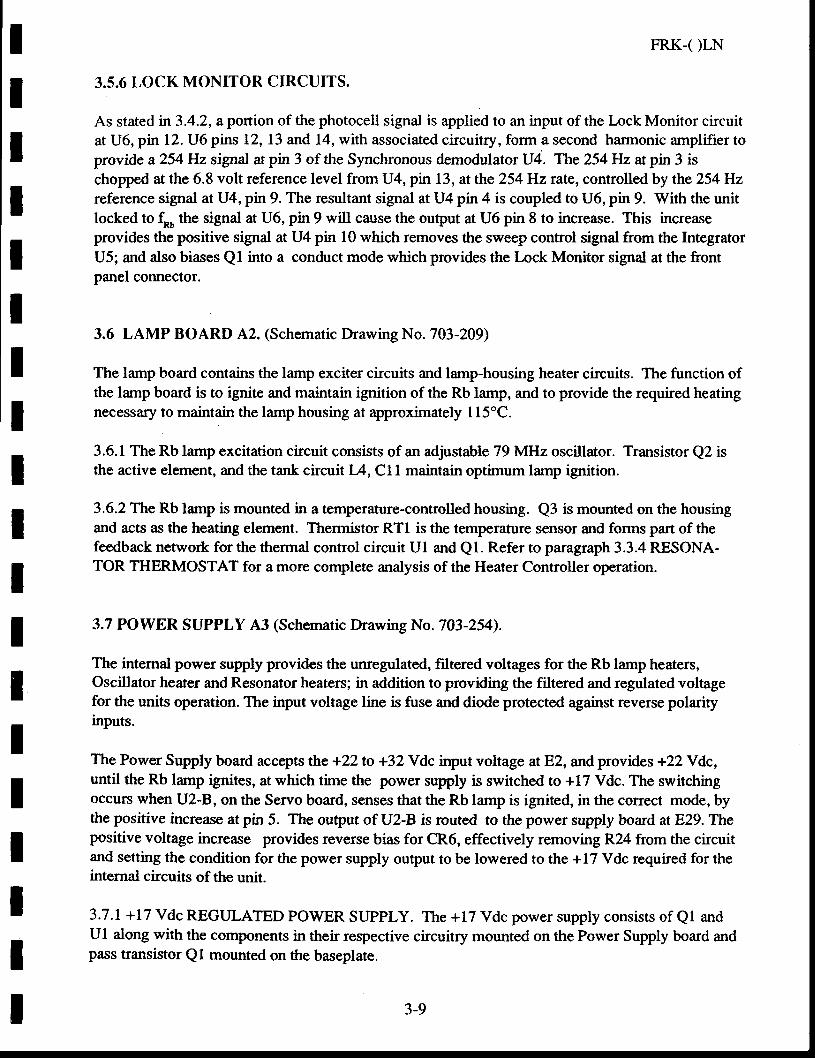
IIIIIIIIII
FRK-OLN
3.5.6 LOCK MONITOR CIRCUITS.
As stated rn3.4.2, a portion of the photocetl signal is applied to an input of the Lock Monitor circuitat U6, pin 12. U6 pins L2,13 and l4,with associated circuitry, form a second harmonic amplifier toprovide a254 Hz signal at pin 3 of the Synchronous demodulatorlJ4. The254Hz atpin 3 ischopped at the 6.8 volt reference level from U4, pin L3, at the 254 Hz rate, controlled by the 254 Hzreference signal atU4,pin 9.The resultant signal atu4 pin 4 is coupled to U6, pin 9. With the unitlocked to f*, the signal at U6, pin 9 will cause the output at U6 pin 8 to increase. This increaseprovides the positive signal atU4 pin 10 which removes the sweep control signal from the IntegratorU5; and also biases Ql into a conduct mode which provides the Lock Monitor signal at the frontpanel connector.
3.6 LAMP BOARD A2. (Schematic Drawing No. 703-209)
The lamp board contains the lamp exciter circuits and lamp-housing heater circuits. The function ofthe lamp board is to ignite and maintain ignition of the Rb lamp, and to provide the required heatingnecessary to maintain the lamp housing at approximately 115"C.
3.6.1 The Rb lamp excitation circuit consists of an adjustable 79 MHz oscillator. Transistor Q2 isthe active element, and the tank circuit lA,CLl maintain optimum lamp ignition.
3.6.2 The Rb lamp is mounted in a temperature-controlled housing. Q3 is mounted on the housingand acts as the heating element. Thermistor RTI is the temperature sensor and forms part of thefeedback network for the thermal control circuit Ul and Q1. Refer to paragraph 3.3.4 RESONA-TOR THERMOSTAT for a more complete analysis of the Heater Controller operation.
3.7 POWER SUPPLY A3 (Schematic Drawing No. 703-254).
The intemal power supply provides the unregulated, filtered voltages for the Rb lamp heaters,Oscillator heater and Resonator heaters; in addition to providing the filtered and regulated voltagefor the units operation. The input voltage line is fuse and diode protected against reverse polarityinputs.
The Power Supply board accepts the +22to +32 Vdc input voltage atE2, and provides +22Ydc,until the Rb lamp ignites, at which time the power supply is switched to +17 Vdc. The switchingoccurs when U2-8, on the Servo board, senses that the Rb lamp is ignited, in the correct mode, bythe positive increase at pin 5. The output of ll2-B is routed to the power supply board atB}9.Thepositive voltage increase provides reverse bias for CR6, effectively removing R24 from the circuitand setting the condition for the power supply output to be lowered to the +17 Vdc required for theinternal circuits of the unit.
3.7.1+17 Vdc REGULATED POWER SUPPLY. The +17 Vdc power supply consists of Ql andUl along with the components in their respective circuitry mounted on the Power Supply board andpass transistor Ql mounted on the baseplate.
3-9
FRK-( )LN
The +22 to +32 Vdc input is routed across the 3 amp fuse Fl to the voltage divider circuit consisting
of R5, R7. The input voltage is dropped to approximately 3 Vdc which is coupled through CR3 to
Ul pin 2. Before power is applied, Ul pins 2,3, and 6 were at ground potential. With 3 volts at
Ul, pin 2 and U1, pin 3 still at ground potential, the resultant offset causes Ul, pin 6 to go low,
tuming on the power transistor Ql. The *17 volt line is fed back through CR4 and R9 to the
reference zener diode, CR5. CRs develops approximately 6.3Vdc at Ul, pul'2. In addition,the 17
volt line is fed back to the voltage divider consisting of R6, R8 and R10 to apply a voltage to Ul,
pin 3. The voltage divider determines the voltage ratio of the 17 volt line to the voltage reference
diode CR5, thus sefting the voltage level of the 17 volt line.
Transistor Ql on the power supply board functions as a crurent limiter by sensing the voltage drop
across R14. If the current through the pass transistor becomes excessive, Ql begins to conduct
decreasing the emitter-base bias on the pass transistor, thus limiting the current flow.
3.8 OSCLLATOR BD, A4 (Schematic Drawing No.703-103 ).
The purpose of the Oscillator board is to provide a stable 5 or l0 MHz signal (depending on con-figuration) to the ouput connector, and a 10 MHz signal to the synthesizer board. The Oscillatorboard consists of the 5 MHz or 10 MHz Voltage Controlled Crystal Oscillator CVCXO), the crystaloven and thermal control circuitry, and a buffer amplifier.
3.8.1 VCXO HEATER. The 5 or 10 MHz VCXO crystals are mounted in a temperature controlledoven. The oven is heated by the heater transistor Q9. The crystal heater controller operation is basi-cally the same as discussed lul.3.3.4, with RTI acting as the temperature sensor, balancing out R37and Select Resistor R42. Transistor Q8 is a current limiter which senses the current through theheater by detecting the voltage drop across R49.
3.8.2 5 MHz or l0 MHz VCXO. The oscillator consists of the 5 or 10 MHz SC-Cut crystal Yl, andtransistors Ql and Q2 with associated circuitry. Q2 is the actual oscillator circuit, with Ql settingthe gain of the oscillator by controlling the bias at the base of Q2. The frequency of oscillation is de-termined by the capacitive tuning network consisting of C5, C6,C7 and varactor CRl. The 5 MHzsignal from the VCXO is the driving signal for the Field Effect Transistor (FET) Q3. FET Q3provides the feedback for the oscillator circuit and is used as a low-noise linear amplifier to drive theouQut buffer (Q4,5).
3.8.3 Buffers
3.8.3.1 5 MHz LN Oscillator (5 MHz buffer and 10 MHz doubler). The 5 MHz LN Oscillatordrives the Cascade Buffer made up of Q4 and Q5. Its output is transformer coupled (through Tl) tothe output connector (Jl). Phase complimentary signals of equal amplitude are picked offthe collec-tor and emitter of Q5 and fed to the frequency doubler (Q6, Q7).This stage feeds 10 MHz to theSynthesizer PCB.
3.8.3.2 10 MHz LN Oscillator. The 10 MHz LN Oscillator drives the Cascade Buffer, which ismade up of Q4 and Q5. Its output is transformer coupled (through T1) to the output connector (J1).The signal at the emitter of Q5 drives the intemal buffer Q7, which in tum feeds 10 MHz to the
IIIIIIIIIIIIIIIIIII3-10
IIIItIIIII
FRK-( )LN
Synthesizer PCB.
3.8.4 VCXO Control Voltage (electronic tuning)
3.8.4.1 10 MHz LN Oscillator
The control voltage from the Servo PCB is routed to the Oscillator PCB terminal E9. From here the
voltage is fed to CRl via the resistor network made up of R50, 51, and 52. CR2 is a reversed bias
varicap, capable of electronically tuning the frequency of the crystal (Yl). The trim range of the
crystal is designed to compensate for crystal aging over a period of several years, as well as tem-
perature compensation of the Oscillato( over its entire temperature range.
C7 and C8 match the Crystal Tuning Sensitivity to the varicap (CRl). C6 mechanically tunes the
crystal center frequency and can be used to compensate for crystal aging during maintenance.
3.8.4.2 5 MHz LN Oscillator
The circuit functions very similar to the 10 MHz unit, the major difference is that an integrator stage
(U1) has been added, resulting in a slower loop time constant. This feature takes full advantage of
the crystal's outstanding reduced phase noise close to the carrier frequency. The intercorurection of
the Servo PCB, as well asthe Servo modification, and the 5 MHz LN Oscillator are shown in Figure
34.
3.9 SYNTHESIZER A5. (Schematic Drawing No."703-2L8).
The l0 MHz signal from the crystal oscillator is applied to the input of a frequency tripler consisting
of Q3, Q4 and associated circuitry. The 30 MHz signal is capacitively coupled through C13 to
transformer T1. The |n Hzfrom the Servo assembly is injected into the rf signal via varactor CR6.
The interaction of CR6 with the tuned tank circuit on the primary of Tl serves to phase modulate
the rf at a L27 Hz rate. The secondary of T1 is center tapped to provide a split phase signal that
drives the bases of Q5 and Q6. The result is a 60 MHz signal that is amplified by Q7, Q8 which are
class A inverting amplifiers.
A portion of the 10 MHz signal from the crystal oscillator is applied to the base of Q2. Q2 converts
the sinewave to a TTL compatible trigger signal. Power for the TTL circuits is provided by the
voltage regulator VRl. VRl is a 3 pin, +5V regulating IC. The 10 MHz TTL signal is divided
down :rr-IJz and U3, and recombined in Ul. The final TTL signal from Ul is a 5.3125 MHz signal.
This 5.3 125 MHz signal is mixed with the 60 MHz ouqput of Q8, and routed to the Step Recovery
diode in the Resonator circuit.
tIIIIIIII 3-1 I
FRK-( )LN ItItIIItII
III
- @ ilcxo
I I SWEEP
*'Y. iJT
@l
I6 lrt U{ Oodbbr pCB I
IIIIII
. SERVOJT'MPERS... 10 MH! FRK* r'ifiY3{&TiiF$,Xroio'
Figure 3-4.Interconnection of Senro PCB, Servo modification, and 5 MHz LN Oscillator
SERVO BOARD I OSCILLATOR BOARDI
I
I
I
I
I
I
I
I
3-t2
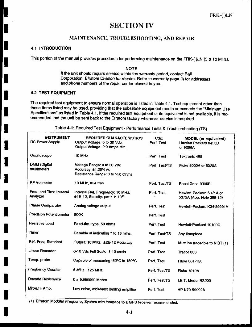
It
ItItIIIIIIItII
FRK-( )LN
SECTION IV
MAINTENANCE, TROUBLESHOOTING, AND REPAIR
4.1 INTRODUCTION
This portion of the manual provides procedures lor performing maintenance on the FRK-( )LN (S & 10 MHz).
NOTElf the unit should require service within lhe wananty period, contact BaflCorporation, Efratom Division for repairs. Refer to wananty page (i) for addressesand phone numbers of the repair center closest lo you.
4.2 TEST EQUIPMENT
The required test equipment to ensure normal operation is listed in Table 4.1. Test equipment other thanthose items listed may be used, providing that the substitute equipment meets or exceeds the "Minimum UseSpecifications" as listed in Table 4.1. lf the required test equipment or iis equivalent is not available, it is rec-ommended that the unit be sent back to the Efratom fac{ory whenever service is required.
(1) Elralom Modular Frequency System wlth Intarface to a GPS recelver recommended.
Table 4-1: Required rest Equipment - Performance Tests & Trouble-shooting fls)
INSTRUMENT REQUIRED CHARACTER|SflCS USE MODEL (orequlvalent)DC PowerSupply OtxBx Voftage:0 to 3o Vdc. Pert. Test Hewfett-packarO d+ggg
Output Vohage: 2.0 Amps Min. or 6296A
oscllloscope 10 MHz perf. Test rektronix 465
DMM (Dlgltal Voltage Range: 0 to 30 Vdc Perf. TesVTS Fluke 8o@A or 8020Amuldmet€r) Accuracy: *1.ZSo/" lv,
Resistance Range:0 to 150 Otrms
RF Voltmeter 10 MHz, true rms perf. TesVTS Racal Dana ggOOB
Freq. and Tlme Interval Intemal Ref. Frequency: 10 MHz, Perf. Test Hewlett-packard 5371A orAnalyzer r1E-12, stability:parts In 10t2 5372A (App. Note 358-12)
Phase Comparator Anafog vollage output Pert. Test Hewfefi-packard K34-S9991A
Preclsion Potentlometer 50OK perf. Test
Reslstve Load Feed-thru type, 50 ohms Perf. Test Hewlett-packard 101ooC
Tlmer Capabte of Indfcadng 1 to 15 mlns. Pert. TesUTS Any tnnplece
Ref' Freq- Standard Output: 10 MHz, t2E-lzAccuracy Perf. TEst Musr be traceable to NIST (1)
Llnsar Recorder 0-10 Vdc Full scale, 1-10 cm/hr perf. Test rracor 888
Temp. probe capable of measuring -500c to 150"c Perf. Test Fluke g0T-150
Frequency counter 5 MHz. 125 MHz perf. Tesurs Fluke l9toA
Decade Reslstance o > 9.999999 Mohm pert. Tesurs l.E.T. Model HS20o
Mixer/lF Amp. Low nolse, wldeband limiting ampltfier Perf. Test Hp K79-59992A
4-1
FRK-( )LN
4.3 PERFORMANCE VEBIFICATION TESTS
4.3.1 Output LevetTest
(1) Connect the UUT as shown in Figure 4-1.
(2) Apply dc power and allow the UUT to stabitize (> 10 minutes).
(3) Measure output levelwith a rf voltmeter, using a 50 ohm resistive terminalion.Record the voltage levelof output.
(4) Observed voltage levelmust be i Vrms. +10%.
Figure 4-1. Output LevelTest Configuration
4.3.2 Frequency Offset Test
(1) Connect the Unit (UUT) and the test equipmenl as illustrated in Figure 4-2. (As an attemative, theHP5371A may be used to measure lrequency offset. Conlact a Xp tietd engineer for details.)
(2) Adjust charl recorder pen position to center scale for 0 volts input.
Figure 4-2. Frequency Offset Test & Long-term Stability Test Configuration
(3) Ensure that the eguipment has had suflicient lime to warm-up. (The UUT requires t hour lostabilize.)
NOTEThe maximum temperafure fluctualion must not exceed 2" C.
(4) Monitor phase comparalor output voltage on the chart recorder for 15 minutes. Calculate thetheJractional frequency otlset (Af/f) from the phase comparator output voltage change over time(AV/AI) according to the equation:
AV1
At 10 MHz' Vo- ,
4-2
IIIIIIIIIIIIIIIIIIT
CHART RECORDER2V R'LL SCALE
10 MHz OUTPUT
Fractional Frequency Offset =
tItItIIItIIIIIIIIII
FRK-( )LN
Where: AV/AI = Slope of phase comparator output in volts/sec over a 15 min. interval (t in sec.).V^ - = Oulput voltage swing of phase comparator for 360" phase shifl.
P - P
AVFor lhe HP K34-59991A, the fraclional frequency offset = X 5E-8 sec/volt.
At
(5) Verify that the fractionalfrequency ofiset is within ihe required limit.
4.3.3 Frequency Retrace Test
(1) Connect the UUT as shown in Figure 4-2.
(2) Apply dc input power to the UUT.
(3) Allow al least t hour for the UUT to stabilize. Measure and record the output frequency offsetper Sec{ion 4.3.2, Step 4.
(4) Disconnect input power to the UUT tor 24 * 2 hours.
(5) Apply dc input power to the UUT.
(6) Atter one hour of operation, measure and record the output lrequency offset per Section 4.3.2,Step 4.
(7) Determine the absolute value of the difference between lhe offsets marked in Step 3 and Slep 6.The difference must be *2E-11.
4.3.4 Short-lerm Slability (Rool Allan Variance)Test
(1) Connect lhe UUT as shown in Figure 4-3.
CHANNEL A
NOTE:The 1 sec. Allan Variance of the Adjustable Frequency Standard must bemuch better than the 1 sec. Allan Variance of the UUT.
Figure 4-3. Short Term Stability and SignalOutput Tests.
HP 5371N53724FREOUENCYANDTIME INTERVAL
ANALYZER
4-3
FRK-( )LN
(2) Apply dc input power. Allow UUT to stabitize (about t hour).
(3) Refer to the HP 5371N5372A manual and Application Note 358-12, for specific details regardingmeasurement of Root Alfan Variance using the HP5371N5372A. ff necessary, contact loial Hpfield engineer for assistance. Tune HP 1058 to produce 10 Hz lF frequency. Measure the rootAllan Variance (A.V.) at 1.0 second using 100 data samples. The measured A.V. must be< 3 x 1E-l1 (for FRK-H. Since the dominant source of frequency inslability at 1 sec. through 100sec' is white FM noise, root Allan Variance at 10 sec. and 100 sec. can be calculated usirig theexpressions:
A' V' 1,-ro.*.) = A'V' (t-t re') / t/ 10
(A' V' s-roo"*.1= A.V. (r-r rc.) / {-100)
The calculated A.V. for 10 sec. must be < 1E-11 (4E-12for FRK-H). The calculated A.V. for 100sec must be < 3E-12 (1E-12 for FRK-H).
4.3.5 Long-term Stability Test
Long-lerm stabifity refers lo slow changes in the average frequency, wilh lime due to secufar changes in uuTphysics and or electrical circuitry. Long-lerm stability is usually expressed as fraclional frequency o:lfset (Aflf),for a given period of time. The daily fractional frequency otfsets can be plotted to show the'long-ierm staOnity.
NOTEThe long-term stability lest should be performed only after the UUT has beenoperating continuously a minimum of 48 hours. The frequency of the UUT shouldbe measured and recorded each day to estabrish the drift rate.
(1) Connect the equipment as shown in Figure 4-2.
(2) Per Seclion 4.3.2, Step 4, compule and record the fractional frequency offset every24 hours over a period of 1 S days.
NOTEIt is recommended to plot the daily offset graphically and use this plot to estimatelong-term aging (drift rate).
(3) Atler completion of 1 month of aging, compule the drift rate of the UUT over the 1 monthperiod.
(4) lf the drift rate over 1 month is < 4E-11 (tE-l1 for FRK-H), the UUT has passed.
(5) lf the dritt rate is : 4E-11 (1E-l1 for FRK-H) , the UUT has failed and must be retested (repeatstep 2).
(6) Depending on the off-time since the last operation, the environmentalexposure, and therepairs performed, the unit may need to repeat this test a second time before meeting theoriginal manufacturer's specilications.
IIItIIIIIIIIIIIIIII
ITtItItIIItIIIIIIII
FRK-( )LN
4.4 FIELD MAINTENANCE, TROUBLESHOOTING, AND REPAIR
4.4.1 FIELD MAINTENANCE
Field maintenance consists of compensating for crystal aging and frequency adjustment. These are routineadjustments that may be made periodically to compensate for aging effects.
4.4.1.'l Crystal Aging CompensationNOTE
The etfects of crystal aging can be seen on a volimeter. Attach a voltmeterprobe to the crystal volts output monilor line of the FRK. A meter indication of<+4 Vdc or >+12 Vdc, indicales an adiustment of lhe crystaloscillator base freguencyis required.
(1) Ensure that the UUT has been operating continuously for at least t hour.
(2) Locate the crystaltrim adiustment on the FRK.
(3) Unscrew the Philips head screw plug that acts as the adjustment access cover. The trimmercapacitor adiustment screw will now be visible.
NOTEFor the 5 MHz LN unit COUNTERCLOCKWISE rotation of the adjustmentwill INCREASE the controlvollage, while CLOCKWISE rotation witt DECREASEthe control voltage.For the 1O MHz LN unit CLOCKWISE rotation of the adjustment wilt TNCREASEthe controlvoltage, while COUNTERCLOCKWISE rotation will DECREASE the controlvoltage.
(4) Using a non-metallic alignment tool, SLOWLY adiust the trimmer capacitor as necessary toobtain a +8 Vdc indication on a meter.
4.4.1 .2 Frequency Adjuslmenl
(1) Monitor the fractional frequency oflset per section 4.3.2.
(2) Adiust POT (R21) on power supply board (accessed through baseplate) to obtain a fractionalfrequency otfset that is within the required limits.
4.4.2 TRAUBLESHOOTING AND REPAIR
]roylleshgoting and repair consists of testing and repair of the FRK. This sec'tion contains information onfault identification and removal, repair, replac-ement, and calibration of the assemblies of the FRK.
NOTE;THESE PROCEDURES ARE NOT ROUTINE ADJUSTMENTS AND PERFORMINGTHEM SHOULD BE CONSTDERED ONLY IN THE EVENT OF UNfT FAILURE.
a. Troubleshooting Flowcharts
A series of flow charts is provided to aid in the isolation of faults. Flowcharts are presented in logical lault iso-lation order and must be perlormed in the proper sequence given. The troubleshooting/repair procedures lorthe various subassemblies of the FRK are-presented'atter eich tlowchart and are deslgned to permit therepairtechnician to identify the fauft and replace and/or repair the subassembly.
4-5
COVER RETAINER SCFEW
FRK-OLN
b. FRK DisassemblY
CAUTIONAll FBK disassembly operations musl be performed wilh power removedfrom the unit. Disassemble assemblies only as needed to make repairs.
(1) Detach the cover from the FRK assembly by removingtrlf2mm screws on the connector faceof the unit, then remove lour 2mm screws thal hold the bollom of the cover to the baseplate (seeFigure 4-4). Once all six retaining screws are removed, hold the baseplate while gently pullingon the cover (it may be necessary to move the cover slightly from side to side as the FRKintemalassembly is removed from the case).
(2) Remove any of the outside PCB assemblies by removing he M2x6 screws that fasten the boardsto lhe FRK lrame at each com€r (the servo and synlhesizer boards have additional screws lhatmust also be unfastened).
(3) Once the mounling screws are removed, fabelallwires and coax (shielded wire) connections,and then remove each one (a soldering iron is required).
(4) Disassembfe the baseplate of the FRK by removing the lamp inspection cover and all otherscrews on the outside lace ol the baseplate. This frees the baseplate from the frame.
NOTEThe Ql Pass Transistor will slill be connected. Pulling the baseplate awayfrom the frame rapidly may unintentionally break the wire connection of thetransistor.
s . j$
IIIItIIIIIIIIIItItt
#@6s
tr
/f\Lu'\ )4wFRAME CHANNEC ATTACHMENT SCREW
Figure 4-4. FRK Baseplate
4_6
II :.
I
FRK-( )LN
(5) The lamp board assembly and lhe melal container that is the exterior of the resonator assemblyare located inside the frame channel. These two assemblies are accessed by removing fourM2x6 screws from lhe four nut blocks lhat are located inside the frame channel. The resonatorboard is located inside the mu-metal canister of the resonator assembly. Figure 4-5 is a wiringdagram that illustrates how the FRK boards and lhe physics package are connected together.
(6) Before the lamp assembly can be removed from the baseplate end of the FRK unit, all wiresmust be disconnected from each end of Cl and C2. These feedthrough capacitors (which areframe mounted) must be removed completely from the frame. Once this has been accomplished,removal of lhe two M2x6 screws at the opposite comers of the lamp PCB allows it to be lifted
away from the interior frame channel.
(7) Remove the resonator assembly from the @nneclor end of the unit by unsoldering the 10 wireshat connect the resonator to the other board assemblies of the unit. Disconnect the wires fromthe locations shown in Table 4-2.
Table 4-2. Resonator Disconnect Points
ItIIIIItIIIIIItI
Servo Bd. Power Supply Bd.A1El A3E21AlEs A3E22
A3E2343E24A3E25A3E2643E27A3E28
Synthesizer Bd.A5E6A5E7
(8) Remove lhe M2x6 screws at each comer of the resonator assembly PCB, allowing the entireresonator assembly to be removed from the interior frame channel.
(9) The inner shield lid of the resonator can is assembled to the can with a tight mechanical fit.The lid is removed by gently lapping around the circumferance of the lids exposed lip.
(10) S€parate lhe resonator assembly's PCB from the inner shield can by removing the three M2nuts spaced around the light entry hole in the PCB.
(11) Having completed these steps, the resonator housing, with the heater control PCB attached,can be removed from the inner shield can for service.
The FRK can now be visually inspected for burned components or broken connections. Placed on a lestbench and powered up, signaltraes can also be obtained from the test points on the various board assem-bfies (referto Section 4.4.2.5, Detailed FRK Circuit Desctiptions).
NOTEDisassembly of the FRK should be performed only toto the level necessary to identify a fault (or faults). Excessiveclisassembly may inlroduce other problems into the unit,making it impossible to repair.
After repairs have been completed, and the FRK reassembled, refer to Section 4.3lor Performance Verifica-tion Tests that must be performed before the FRK is returned to service. Refer to Section 4.4.2.6 is alignmentis required for any of the repaired or replaced assemblies.
4-7

LItI
RED AI.ID BI.AGK TWISTED
FRK-( )LN
TD A1EE
P@ EtO/-)TO M- BLU-E @-OT,o oo.., i@z
-,i TP6 i coro<, A5 ." 'Tro f f i, : - i l c * r . TP5
i --"'- To o' coAx. rpi -.f i AS SHIEIOI
III
IIIIIII
IPE
b$ls
e si
*g
nsQ
n't
e99iHgHigjs"
I wrRE Lisr -l
i* Eq{_ j_ rs_l se_,al-olnr] _ _ryrq!er,_=: 1 iArEt iA6E9 i RED ( 2E )ipr|olocEr i
i__t__L^t_u-. _11q1?_rEEp-- (_4ljil_89-- JJ ; ^ r E : : a r E t 6 ; B u J ( 2 4 ) l c N D I; - - - -' 4 t A t E + ] A ] E B : . ' € L ( 2 4 ) t R b t , l p M O N r O R I
lslr_q-leF_-i.qr_@
E6 Iol
Figure 4-5. 5 MHz FRK-( )LN Wiring Diagram
4-8
WIRE LIST I@--J1-5 IORN (2+) l+2E \EC TNPUI :+-+ : -+-+
i El-r I BLU (24\ j eHo
i 21 i A1€7 i As€rr I SntEr-o ----fi-:---f------

lrrl
IIIIIII
FRK-( )LN
c. FRK Assembly Repair
lf troubleshooting has indicated that the FRK assembly has faifed and the assembly must be repaired insteadof being replaced, lhe following sections provide repair guidelines.
SN6WRMAP3 SOLDER, per QSS-571, and a 35 to 40 watt soldering iron should be used to accomplish thesofdering that might need lo be done on the FRK.
CAUTIONExcessive heat can cause the eiched circuit wiring to separatefrom the board material.
lf it becomes necessary to solder in the generalarea of any of the high trequency contacts in the unit (lermi-nalpoints), clean the contacts immediately upon completion of the soldering.
The adjustments, repair, or alignments required by the fault isolation flowcharts should be followed by theretesting of the procedure that led to the fault isolation to ensure the unit is functioning as required.
d. Overall FRK Troubleshooting (Fautt lsolation Flowchart)
Figure 4-6 is the overall troubleshooting flowchart that should be followed to locate a fault in the FRK unit. Foradditional information, refer to the assernbly drawings and schematics presented in Appendix B, and lo thetext in the following sections that describes the operation of the maior FRK boards and circuils.
(1) Rubidium Lamp Replacement
Although this is seldom a cause for failure in the FRK (refer to 4.4.2.5(2) for symptoms), theRubidium lamp is replaceable. The Rubidium lamp is accessed by removing lhe two screws holdingthe Lamp Cover Plate lo the baseplate (reler to Figure 4-8). A slotled access plate is beneath thecover plate. Once the access plate has been rernoved, the base of the lamp housing is visible.
CAUTIONThe lamp housing is at the electrical potentiaf of the unit (28 Vdc) and a short willoccur if an attempt to remove the lamp is made with power applied to the unit. Thelamp housing is extremely hot, as well. Extreme care must be exercised whenremoving the lamp to avoid burns.
Once all power to the unit is off, carefully unscrew the rubidium lamp and tift it from the housing (usea pair o{ needle nose pliers for this task). Make sure the replacement lamp is clean and that itssurface is free of any oils or grease and screw the bulb into the housing. Once the bulb is firmlyseated in lhe housing, replace the access plate and the Lamp Correr Plate, and replaoe the twoscrews previously removed.
Apply power to the FRK and, after allowing sufficient warm-up time, run a performance lesl to ensurethat the unit is fully functional.
.kI
4-9
II
- l v o c T o12 voc?
FRK-( )LN
IIItIIIItII
Figure 4-6. FRK Troubleshooting OveMew
4-10
I
IIIIIIIIIIItI
4.4.2.1 Detailed FRK Circuit Description
a. Resonator Assembly (schemati c703-221)
The function of the resonator assembly is to compare the mulliplied arfdsynthesized dutput frequency of thecrystal oscillator to the ground-state hyperfine transition frequency of 87Rb. lt provides a 127 Hz enor signal tothe servo board to lock the crystal lrequency lo lhe atomic transition.
(1.) Microwave Gavity - The microwave (resonator) cavity is constructed ol silver plated copp€r and housedin a mu metalshield. lt contains lhe rubidium resonanoe cell. The photocellis mounted in the bottom of thecavtty and placed behind lhe Rb glass cell, directly in the light path of the Rb spectrallamp. The step recov-ery diode with coupling loop and the condenser assembly are located at the open end of the cavtty. Cavitytemperature is maintained by the resonator thermostat circuit. The G-field coil is wound on the outside of thecopper microwave cavig.
(2.) Step Recovery Diode - The 60 MHz and 5.3125 MHz from the multiplier are summed at the ouprrt of themultiplier/synthesizer board and then applied to the step rscovery diode. This diode, CR1, produces eldctro-magnetic radiation having {requencies given by the expression (60 n + 5.3125 m) MHz, where n = a positiveinteger and m = an integer. The diode is part ot a tuned coupling loop, tuned to the 114th harmonic ol 60 MHz( n = 114 ); the coupling loop is inside a microwave cavity thal is tuned to the same frequency. The bandwidthof the microwave cavity assembly is wide in comparison with the bandwidth of the atomic transition (< 1 kHz),so that the atoms funclion as a narrow-band filter for the microwave signal. The diode can be replaced bygaining access to the light entry end of the resonator assembly PCB. An access hole in the PCB providesclearance to remove first the diode retaining sc.rew and then the diode itsalf (reler to Figure 4-7).
Figure 4-7. Snap Diode Access Hole on Resonator Assembly
(3.) Photocell - The photocell current is proportionalto the total light incidenl on the photocell CR2. Minimumcurrent results when a microwave field corresponding to the Rb hyperfine frequency is applied simultaneouslywith pumping light. Photocell problems are unlikely (always check the lamp assembly and power supply first),but manifest themselves as instable lamp monitor dc voltages, or as sporadic noise on lhe servo board's TP1resonance signal. The photocell is replaced as part ol the complete resonator assembly.
(SHOWN AFTEB I.AMP BOARD REMOVAL)
4 - l I
IIIIIIIIIItIIIIII
ryK1)t}i(4.) C-Field Coit - The C-field coil is wound on the microwave cavity and provides a dc magnetic field (the C-field) within the resonalor cavity. Variation of this magnetic field allows fine tuning of the 10 MHz output fre-quency by shifting lhe Rb irequency hyperfine transilion by the second order Zeeman effect. The "C-field"strength is determined by arnent trom three sources:
R17 on the power supply board supplies a fixed current to the coil.
R21, the 24 lum potentiometer, on lhe power supply PCB, provides a variable cunent for frequencyadjustment.
The temperature compensation circuit formed by Q2, Q3, Rl3 and R16 provides a cunent lhalvaries with temperature. The power to heat the microwave cavity increases approximately 40 mW forevery degree cenligrade decrease of the ambient temperature. This results in a cunent changethrough resonator heater transistors Q2 and Q3, and through R13 on the resonator thermostalassembly. The voltage across R13 is routed to R16 on the power supply board and back to the C-lield coil. Decreases in ambient air lemperature'causes the voltage across R13 to rise, providing '
more C-field cunent, and raising lhe output frequency.
The mosl common C-field problem is an open winding. An ohmeter is used to check lor lhis situation byremoving power to the FRK and measuring from A3E27 to A3E19. A good C{ield coilwill give a reading olapproximately 30 ohms.
(5.) Resonator Thermostat (part of resonator board assembly, refer to schematic 703-221]r- the resonatorthermostat consists of Ul, Ql, and associated circuitry on lhe resonalor PCB. and Q2, Q3, and RT1mounted on the resonalor cavity housing. Ul is the temperature control element, Ql is a current limitingelement, and Q2 and Q3 are the heal source.
Ul and the resistive bridge network on its inputs form the temperature control section. El receives +12 Vdcfrom the power supply board to power this sec'tion. R5 and R7 form a lixed voltage divider that relerences U1,pin 3. Thermistor RT1 and the series combination of R1 and the temperature select resistor lorm a voltagedivider on lhe other op-amp input, Ul, pin 2. The feedback network of R8 and C4 serves to controt Ul'soutput response when the inputs reach equilibrium.
During lhe high power dissipation period of the warm-up cycle, the current through Q2 and Q3 must belimited to a safe levelof -1 amp. This is done by sensing the cunent draw of Q2 and Q3 at R13. An increasein heater cunent causes an increase in voltage at the base of Q1. As Ql tums on, il shunts a portion of e2'sbase drive cunent to ground, allowing only the preset maximum cunent to flow. R11 and R12 form a voltagedivider network thai provides tor the presel maximum cunent to be automatically shifted up or down, depend-ing on lhe heater supply voltage. This is done to maintain a reasonably constant power dissipation duringwarm-up over the range of input voltage to the FRK.
As the thermostat circuit reaches equilibrium, the voltage output of U1 drops to a levellhat operates Q2 in avemier controlmode. The cunent through Q2 and Q3 folds back to a nominal 100 mA. The cunent foldbackreduces the voltage drop across R13 to the poinl where.Ql does nol conduct and effectivety drops out of thecircuit.
The resonator assembly is protected lrom a runaway heater control problem by thermalluse F1, mounted onthe resonator cavity housing.
b. Lamp, Assembly A2, (Schematic 703-209)
The lamp assembly consists of the lamp oscillalor circuit, the lamp housing assembly, the lamp thermostatcircuit, and the rubidium lamp. The function of the lamp assembly is to ignite and maintain the electrodelessplasma gas discharge of the rubidium lamp, and to maintain the temperature of the lamp housing at approxi-mately 115"C.
4-12
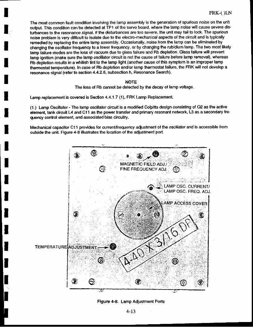
IIIIIIIIIIIIIItII
FRK-( )LN
The most common fault condition involving the lamp assembly is the generation o{ spurious noise on the unitoutput. This condition can be detected at TPl of the servo board, where the lamp noise will cause severe dis-turbances to the resonance signal. lt the disturbances are too severe, the unit may lail to lock. The spuriousnoise problem is very difficult to isolate due to the electro-mechanical aspects of the circuit and is typicallyremedied by replacing the entire lamp assembly. Occasionally, noise from the lamp can be eliminated bychanging the oscillator frequency to a lower freguency, or by changing the rubidium lamp. The two most likelylamp failure modes are the loss of vacuum due to glass lailure and Rb depletion. Glass failure will preventlamp ignilion (make sure the lamp oscillator circuit is not the cause of failure before lamp removal), whereasRb depletion results in a whitish tint to the lamp light (another cause of this symptom is an improper lampthermostat temperature). In case of Rb depletion and/or lamp thermostat {ailure, the FRK will not develop aresonance signal (refer to section 4.4.2.6, subsection h, Resonance Search).
NOTEThe loss of Rb cannoi be delected by the decay of lamp voltage.
Lanp replacement is covered is Section 4,4.1.7 (1), FRK Lamp Replacement.
(1.) Lamp Oscillator - The lamp oscillator circuit is a modified Colpitts design consisting of Q2 as the acliveelement, tank circuit L4 and Cl1 as lhe power transler and primary resonant network, L3 as a secondary fre-quency controlelement, and associated bias circuitry.
Mechanical capacitor C11 provides for current/frequency adjustment of the oscillator and is accessible fromoutside the unit. Figure 4-8 illustrates the location of the adiustment port.
6t i.1, LAMP OSC. CURRENT/...I.AMP OSC. FREQ. ADJ.
ACCESS.COVER
w
Figure 4-8. Lamp Adiustmenl Ports
' ' i t ' ' .' ' - ',&tqj
i:: ,,, .,,',@
4-13
FRK-( )LN
Adjusling C11 tunes the oscillator's frequency over a range of approximately 70 MHz to 90 MHz. Within thisrange of adjustment there are specific optimum frequencies that should be used (refer to Section 4.4.1 .7.2,Lamp Osciflalor Tuning, part b, FRK Alignment Prbcedures). The operational frequency that is chosen is de-termined by linding the highest frequency setting that produces optimum ignition characteristics and noisefree operation. In normal stabilized operation, the oscillator curent draw from the regutated suppfy (E2) is anominal 120 mA.
(2.) Lamp Thermostat - the lamp thermostat consists of Ul, Ql, R5 and associated circuitry on the pCB, andQ3 and RT1 mounted on the lamp housing. Ul is the temperature control elemenl, RTl is part of the resistivebridge network at Ul's inputs, Ql is a cunent limiting element, and Q3 is the heat source element.
Op-Amp Ul is controlled by a balanced bridge circuit on its inputs. R3 and R6 form a fixed voltage divider thatbiases Ul, pin 3. Thermistor RT1 and the series combination of R4 and R5 form the dynamic leg of thebridge. RTl senses the lemperature on the lamp housing and potentiometer R5 selecis the stabilized tem-perature. The R5 potenliometer is accessible from outside the unit. Figure 4-14 illustrates the location of theadjustment port.
The operation of current limiter Ql and heater transistor Q3 is essentiatly the same as the resonator thermo-siat circuit, which is discussed in detailin Section 4.4.2.5, part e.
c. Servo Board, Assembly Al (schematic i0017)
The primary function of the servo circuit is to amplify and demodulate the pholocelloutput to generate thecrystal_control voltage at E8 for the 10 MHz VCXO. The control voltage is derived by comparing the phase ofthe 127 Hz modulalion signalwith lhe phase of the photocell signal at E1 and E5. Second'ary functions are toprovide lhe monitoring signal for the Rb lamp operalion al E4, the atomic resonant lock circuit at E7 and theVCXO controf voltagre monitor at E9.
(1.) Preamplifier - The photocelt output, (dc bias together with the 254 Hz error signal when the unit is in thenormaf locked mode of operation, or 127 Hzenor signalwhile the unit is obtaininga lock), is routed to E1 andE5 on the servo board A1. E1 and E5 tie to the input of dual stage amplifier Ul aipins 5 and 6 respec'tively.The output ol the first stage of amplification is capacitively coupled to ine input of the second stage of amptitication (Ul, pin 8) and directly coupled to E4 and U2-B, pin 5. E4 provides the Rb Lamp Monitor signalto inefront panel connector.
U2-B senses the vohage at E4 and determines if lhe Rb lamp has ignited and if it is in 'Correct Mode lgni-iion'. Proper lamp ignition (<3 minules after tum-on) will cause U2-6 output, El1, to switch from <1 Vdl to>15 Vdc. The El1 voltage is fed to the power supply (Board 3, E2g), vyhere it switches the regulated unitpower trom 22 Vdc to 17 Vdc.
The output of the second amplifier (Ul, Pin 13) is connected to Test Point fIP) 1, the primary oscilloscopemonitoring point of the FRK. Ul, pin 13, is also capacitively coupled to U2-A, the 127 Hz active bandpassfilter, and to U6, the 254 Hz active bandpass fifter.
(2.) Reference SignalGeneralion - 127 and254Hz Reference Signals - CMOS oscillator/divider U3 on ihel9rvo b9ard, provides the 127 and254 Hz reference signals and the 127 Hzsignalwhich modulates the rfinjected into the resonator. The primary oscillator freguency of 8.128 Khz is deGrmined by C17, Rlg andselec't-in-test resistor R20. The divider portion of U3 dividei the primary oscillator frequerrcy into the required1.27 and254 Hz signals. The 127 Hz reference signal is routed from Ub, pin 4 to pin it of synchronous'demodufator u4 and to pin 2, of U6, through the RC nelwork Rg7tC24. Tire RC network Bi7rczq, thefeedback network R38/C25, and the output RC filters (R39, C26, R40 on the servo board, and C2, RS, andC12.on the synthesizer board) serve to waveshape the 127 Hz signal into the sinewave that is coupled to thesynthesizer to modulate the rf. R40 of the output RC lilter is also used to adiust the modulation level to themultiplier and the phase of the conection signal at Tp3.
The 254 Hz reference signal is routed lrom U3, pin 5 to pin g of synchronous demodulator U4. The 254 Hzreference signal is correlated with the photocell output to detect unit lock.
IIIIItIIIIIIIIIIIII4-t4
IJ,IItIIIIl'
FRK-0LN
The dc vollage of approximately 6.8 Vdc generated by CR2 is also a reference signal. This DC level is usedto bias the ac signafs that are processed by U4 and U5, and to bias op-amps U6 and U5.
{3.) '127 Hz Signal Processing - As explained in the "pre-amplifiern section, lhe 127 Hz signal processing
starts at the photooell inputs El and E5. Ul-A and Ul-B provide two stages of high gain amplification. Theoutput of Ul-8, pin 13, feeds both active bandpass filters, U2-A, the 127 Hz, and U6, the 254 Hz.
NOTEFor troubleshooting purposes it is usually best to control the rubidiumfoop manually. Connect a potentiometer of 10 Kohms, or more, acrossC?2 on the servo board. Disconnect the wire soldered to E8 and connectthis wire to the wiper of the potentiometer. This technique provides for manualcontrolof the VCXOs output frequency and criticalservo functions.
The servo conection signal is amplitude modulated onto a 127 Hz subcanier that passes through lhe 127 Hzfilter, U2-A. When the system is locked, this signal (TP-z) appears as a 25,4 Hz sine wave, with a noticeable127 Hz component. From TP2, the signalis routed to the synchronous demodulator U4, pin 12.
U4 is a triple two-channel CMOS analog switch that lunctions as a synchronous amplitude demodulator. The127 and 254 Hz reference signals at pins 11 and 9 respeclively, control the synchronous switching ol two oflhe switches. A third swilch is controlled by the level of the signal at U4, pin 10, from the lock delec-tor circuit,U6, pin 8. U4, pins 5 and 13, receive the 6.8 Vdc reference level from CR2. When the unit sweeps nearatomic loc*, U4, pin 10 receives a "high" signal (>12 Vdc) that switches the output of the 127 Hz filter U2-A tothe output of lhe derpdulator, [J4, pin 15, for dynamic tracking. The demodulalor outpul is monilored at TP3and appears as shown in Figure 4-15.
The signal from [J4, pin 15 is direc'l coupled to U5, pin 2. U5 func'lions as the servo loop integrator. lts ontputvoltage changes at a rate determined by the differential input vollage. For example, an input differential of-200 mV causes an output voltage change of +200 mV/sec. The ctrange will continue unlilthe differentialinput is nullified, (the crystal retums to center frequency), or until the Op amp reaches its maximum outputvoltage.
The output of the integrator, E8, is the crystal-controlvoltage that steers the frequency o{ the VCXO bymeans of a varac'tor diode in the oscillator tuning circuit. A portion of the integrator output is routed lo thesweep controlcircuit at U6, pin 5.
TP-3 NormalSignal 1 volVdiv., 50 ms./div.
Figure 4-9. Demodulator Output (Servo Board)
(4.) Lock Circuil - A portion of the photocell signal is applied to an input of the Lock Monitor circuit at U6, pin12. U6-D, with its associated ciro.ritry, forms a 254 Hz active bandpass litter that connects to pin 3 of the syn-chronous demodulator U4. The output signal at U4, pin 4 is coupled lo U6, pin 9, and is monitored at TP6(refer to Figure 4-10). With the unit locked, the negative offset at U6, pin 9 will cause the output at U6, pin 8to go high. This provides the positive signal at U4, pin 10lhat removes lhe sweep signal from the integrator,U5. lt also biases Ql into a conduct mode that provides the Lock Monitor signal at the front panel connector(pin H for the Winchestor connector, pin 5 lor the 8-pin connector with coax). \A/hen the unit is locked, theLoc* Monilor line as a resistance of 150 ohms to ground. Otherwise the Lock Monitor is an open circuit.
IIIIIII
- l
II 4-t5
FRK-( )LN IIIIIIIIIIItIttIIII
NormalSignal 1 volUdiv., 1 volVdiv, 2 ms./div
Figure 4-10. Signal Wavelorm at Tp6
(5.) Sweep Circuit - To allow the FRK to compensate for severaf years of crystal aging, in addition to fre-quency offsets of the crystalcaused by environmentalchanges (e.g., tempeiature |nairgesl, the trim range ofthe oscillator is very wide compared to the width of the atomic resonan@. To aid servo icquisition, the crlsfalfrequency is swept over the entire trim range until atomic resonance can be detected.
This is accomplished by switching the inlegralor input (U5, pin 2) to U6, pin 7 viaU4 (the unit is unlockedwhen U6, pin 14 is low). U6-B functions as a high hysteresis voliage comparalor. The trigger points areconlrolled by 851 and R52 and the voltage reference. The lower trigger point is approximately 1.5 Vdc, thehigher trigger point is approximalely 16 Vdc. tf the output of U5 is elilal io or lower than the lower triggerpoint,lhe output of U6 becomes 0 Vdc, resulting in about a -.7 Ydcdifferential to the integralor. WitiFZC = tM and cl8 = 1 pF its output will rise .7 V/s until the upper trigger point of 16 Vdc is reachld. At this point, theo.utput of U6 will go high, resulting in about a +.7 Vdc ditterentialat the integrator input. This willdecreaseUS's output by .7 V/s. The result is a sweep time of about 40 s. Due to the iast sweep, atomic resonance canbe detected for only 100 ms at a time during each sweep cycle. Reliable transition from sweep to locked op-eration is lacilitated by GR3.
!. e.oryer Supply, board assembly A3 (sdrematic 70$254) - the intematpower supply provides the unregu-lated'.fillered voltages for the Rb lamp heaters, tre crystal heater, and the resonator heaters, in addition ioproviding lhe filtered and regulated voltage to the uniG electronics. The input voltage line is fuse and diodeprotected againsl reverse polarity inputs.
]he power supPly board accepts the +22to +32 Vdc input voltage at E2, and provides regulated +22Vdc atE12, E17 , and El 8, until the Rb lamp ignites, at which time the power supply is switched to +1 7 Vdc. Theswitching occurs when U2-8, on the servo board, senses that the Rb hmj is ignited, in the conect mode, bythe positive increase at U2-8, pin 5. The output of U2-B is routed to the pb*"r-"ufpg board at E29. Thepositive
Ygltage increase provides reverse bias for CR6, etfec-tively removing R24 trom the circuit and settingthe.condition for the power supply oulput to be lowered to the +17Vdc requi-red for the intemal circuits of theunit.
{1') Regulated Power Supply - The +17 Vdc power suppty consists of Qt and U1 along with the componentsin their respective circuitry m-ounted on the power supfly board and pass transitor e1, which is mounted onthe baseplate ol the FRK.
The +22 to +32 Vdc input is routed across the 3 amp luse (Fl ) to the voltage divider circuit that consists of!L::ojlf:[q:t iglqg" is droppedto approximately 3 Vdc, which is coupted rhroush cR3 to Ul, pin 2.
"TItj,"^Ty^"j:t^?l!.T"d' Ul, pins 2, 3 and 6, were at ground potential. With g volts at Ui pin 2, and Ut, pin e
;tl'1":,gj::^T.1,f?t:nlial' the resuhant otfset causes Ul, pin 6 io go low, tuming on the power transistor ei.I ne +l / volt line is fed back through CR4 and R9 to the referenie zener diodb, cRs. bRs develops approxi-
4-16
Il,
FRK-( )LN
mately 6.3 Vdc at U1, pin 2. In addition, the 17 volt line is fed back to the voltage divider consisting of R6, RBand Rl0 lo apply a voltage lo U1, pin 3. The vollage divider determines the voltage ratio ol the 17 volt line tothe voltage reference diode CRS, thus setting the voltage level of the 17 volt line.
Transistor Ql on the power supply board functions as a current limiter by sensing the voltage drop acrossRl4. lf the cunent through the pass transistor becomes excessive, Ql begins to conduct, decreasing theemitler-base bias on the pass transisitor, thus limiting lhe current flow.
e. CrystalOscillator (VCXO)Assembly (schemalic 703-103-5) - the purpose of the 5 or 10 MHz oscillator isto provide a clean and stable output frequency to the output conneclor, and a 10 MHz signal to the synthe-sizer. To optimize lhe reduction of phase noise the crystal is selected to match the output frequency. Theoscillator board contains the Voltage Controlled Grystal Oscillator (VCXO), the crystal oven andthermalcontrol, and a bufler amplifier. The output signals are transformer coupled to the output connedor Jl and tothe synthesizer circuil. In the case of lhe 5 MHz Ln Oscillator a doubler circuit is used to generate the 10 MHzsignal to the Synthesizer.
(1.) Crystal Oscillator - the oscillator incorporates an AT Cut 3rd-overlone crystal, with an operating tempera-ture of aboul80"C. The cryslal is mounted in the crystal housing assembly, which is heater controlled to lheoperating temperature of the crystal. The frequency adjustment is via L2, C6, 7 and 8. L2 is used for coarseadjustment and Q7l8 for fine adjustment of the sweep range and center frequency. Roughly a 1E-6 adjust-ment is expected {or a crystal control voltage range of 1.0 to 14 volts. These voltages correspond to thesweep mode of the crystal oonlrol voltage, which is approximately 1.0 to 14 vohs.
The gain stage of the oscillalor is lormed by Q2, with C4 and Ll selected to provide a resonant frequency ofabout 70 - 80% of the nominal crystal frequency. The output butfer stage has Q3 as a source lollower tobuffer the crystal network from the loading of the following butfer stages.
The AGG stage utilizes Ql to form an AGC circuit, which controls the output voltage of the oscillator at thesource of Q3 to approxirnately 1.2 Vpp. C5 is used to adiust the AGC voltage at lhe collector of Ql to 0.5 Vdcfor nominal conditions. This provides the capability of decreasing or increasing the oscillator toop gain byadjusting the bias condition ol Ql.
(2.) Crystal Butler Section - the output bufier amplifier section consists of Q5 and Q4.
Q6 is a FET device used as a high input impedance decoupling stage between the oscillator circuit and theoutput drivers. The 10 MHz signal at the gate of Q6 is a nominal 1.4 v.p.p.
The cascade anangement guarantees maximum decoupfing between input and output. T1 is tuned to 5 or 10MHz by C16, 17 and matches the output impedance of Q4 lo the nominal 50 ohm load on Jl.
The 10 MHz signal for the Synthesizer is generated by either the freguency doubler Q6, 7 (driven by compli-mentary signals ol Q5), or by the buffer lormed by Q7, depending on the configuration. T2 is tuned to 10 MHzviaQ22.
(3.) Crystal Thermostat - the crystal oven lhermostat circuit consists ol l)2, Q8, and associated circuitry onthe P.C.B, and Qg and RT1 mounted on the oven assembly. U2 is the temperature control element, QB is acunent limiting element, and Q9 is the heat source.
U2 and the resistive bridge network on its inputs form the temperature control section. Thermistor RTl,mounted on the crystaloven, is the sensing element in the input network, R40 and R43 set the referencevoltage. R42 functions as the lemperature select component. During warmup, the oven heater transistor Q1would be destroyed by runaway cunent if not for Q8, which serves as a current limiter. ln the current limitmode, Q8 senses the voltage across R49 to determine Q1's emiiler current. As the R49 voltage approaches-.4 Vdc, Q5 starts conduc-ting, reducing lhe voltage at Q9's base to the level required to throttle Q9's currentto a nominal 400 mA. The power delivered to the oven in the warm-up mode is kept constant over the rangeof supply voltages by the R46, R48 network. The higher the supply voltage, the less maximum current isallowed in Q9.
IlIIIIIIIIIItIIII 4-17
FRK-( )LN
f. Synthesizer - Board Assembly A5 (schematic 703-285-1)
The synthesizer assembly contains a frequency multiplier circuit and a frequency synthesis section. Q3through Q8 make up the multiplier section and Q2, Ul, and U2 perfomr the synthesis.
(1.) Multiplier - the 10 MHz signal from the crystal oscillalor is applied to the input of a lrequency triplerconsisting of Q3, Q4, and associaled circuitry. C9 and L3 are tuned to 30 MHz. R12limils the Q of the tank toabout 30. The 30 MHz signal is capacitively coupled through C13 to transformer T1. At this point, the 127 Hzmodulation signal, biased at a nominal6.5 Vdc, comes into E5 and modulates the rf signal via varactor CR6.The interaction of CR6 with the tuned tank circuit on the primary of T1 serves to phase modulate the rf at a127 Hz rate. The secondary of T1 is center tapped to provide a split phase signalthat drives the doublercircuit of Q5 and Q6. The result is a 60 MHz signalthat is amplified by Q7 and Q8. C17lL5, C21lLl, andC2TlLl0 are tuned to 60 MHz. Q7 and Q8 are Class A inverting amplifiers. The 60 MHz signal at E6 drives thesnap diode in the physics package through a coax cable. C29 matches the coax-cable to the driver stage.R31 and R34 provide the bias voltage lor the snap diode.
Refer to Figure 4-11 for waveform and amplitude illustrations for the multiplier circuits test points (T.P. 2, 3,4 ,5 ,6 ,8 ) .
The adiuslable parameters ol the multiplier circuit include L3, Tl, L5, L8, Ll1, C29, and R34. Adjustments ofthese component values should not be necessary except if other components are replaced during repairs. lnthis event, see sec'tion 4.4.2.6, subsection 1., which covers the alignment procedures for the synthesizer,board A5.
(2.) Synthesizer Circuitry - the 10 MHz input signal from the crystal oscillator is applied to the base of Q2. Q2converts the sine wave input to a fiL compatible trigger signal. This signal is coupled into U2-A, Pin 1. U2-Afunclions as a divide by'2" bfock, with a 5 MHz TTL signat coming out on pin 3. One branch of the 5 MHzsignalgoes to U2-8, pin 13. U2 functions as a divide by'16'block, producing a 312.5KHzTTL signaloutputfrom pin 8 and passing to Ul. Ul-C is an "exclusive OR" gate which mixes the 5 MHz and 312.5 KHz inputsignals to produce an output at pin 8 that contains the upper and lower mixing products,4.6875 MHz and5.3125 MHz. The signals are then routed across tuned lank Ll 1 /C30. This tank is tuned at 5.31 75 MHz andselects this frequency from the two that are injected. The capacitive coupling of C26 and the filtering action ofLl1/C30 converts the TTL signal at TP7 into a sine wave signal referenced lo ground at TP-9. Finally, thesignalleaves TP-9 and is summed with the 60 MHz at E6, from which both frequencies are routed to the steprecovery diode.
Refer to Figure 4-11 lor waveform and amplitude illustrations lor TPI ,TP7, and TP9 of the synthesizercircuit.
IIIIIIIIIIIIIIltIII4-18
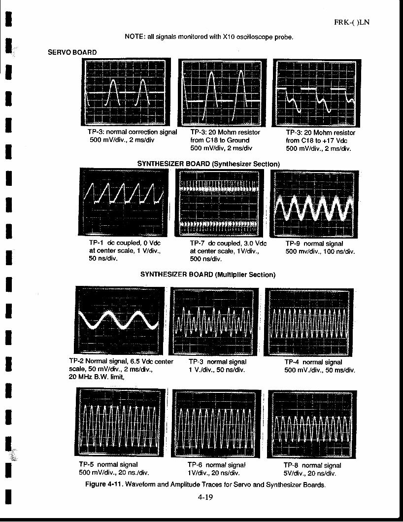
II,:,:IItIIIIItIIIIIl,gIt
SERVO BOARD
TP-3: normal conection signal500 mV/div., 2 ms/div
TP-1 dc coupled, 0 Vdcal center scale, 1 V/dv.,50 ns/div.
TP-2 Normalsignal, 6.5 Vdc centerscale, 50 mV/div.,2 ms/div.,20 MHz B.W. limit,
TP-S normalsignal500 mV/div., 20 ns./div.
Figure 4-11. Waveform and
TP-3:20 Mohm resistorfrom C18 to Ground500 mV/div,2 ms/div
SYNTHESIZER BOARD (Synthesizer Section)
NOTE: all signals monitored with X10 oscilloscope probe.
FRK-( )LN
TP-3:20 Mohm resislorfrom Cl8 to +17 Vdc500 mV/div.,2 ms/div.
TP-9 normalsignal500 mv/div., 100 ns/div.
TP-4 normalsignal500 mV./div., 50 ms/div.
TP-7 dc coupled, 3.0 Vdcat center scale, 1V/div.,500 n9div.
SYNTHESIZER BOARD (Multiplier Section)
TP-3 normalsignal1 V./div., 50 ns/div.
TP-6 normalsignal1V/div., 20 ns/div.
Amplitude Traces for Servo and
TP-8 normalsignalSV/div., 20 ns/div.
Synthesizer Boards.
4-19
b.
FRK-( )LN
4.4.2.2 FRK Alignment Procedures
NOTEIt is not necessary to perform all alignment procedures each timethe FRK is repaired. Perform only those alignments that pertainto the board, or assembly, that has been repaired or replaced.
a. Regulated Voltage Supply:
(1) Before power is applied to the FRK, connect a voltmeter across C2 of the Power Supply,Assembly A3. Observe the meter while applying power. At the instant of tum-on the voltmetershould read - 23Ydc. Within 3 minutes lhe lamp should ignite, switching the regulated voltage toa lower level. lf the unit has been warmed up previously to this test, the lamp will ignite instantlyupon applying power and no voltage transition will be seen. The regulator output voltage at C2should be 17.3 Vdc t .3 V. after lamp ignition.
+ iY ' 3+v(2) lf the measured voltage falls outside the range ol 17.3 Vdc t .3V, an adjustment will be
necessary. Locate R6 on the power supply board, assembly A3. Increasing the value of R6 willincrease the regulator output voltage.
Lamp Temperature Setting:
(1) Apply power to the FRK and allow at least 15 minutes for temperature stabilization.
(2) Remove the lamp access cover lrom the base plate.
(3) Measure the temperature of the lamp housing by placing a temperature probe next to therubidium lamp. Allow time for the temperalure probe readings to stabilize. Tum off the power tothe unit momentarily and record the probe reading. Remove the probe and reapply power. Thetemperature measured should be a nominal 1 13"C t 2"C. ll the recorded temperature is out ofspecification, an adjustment is necessary. Locate the temperature access hole in the baseplateand adjust A2R5. Repeat the temperature measurement and adjustment step untilthe properlamp housing temperature is obtained.
Lamp Oscillator Tuning
(1) Tuning the lamp oscillator requires that the regulated voltage supply to the lamp board (C2-1) beintemrpled and a 0 to 500 milliamp meter be installed in series.
(2) Locale the frequency access hole in the baseplate and insert an isolated tip driver untilmechanical capacitor Cl1 is engaged.
(3) The oscillalor frequency can be monitored using a scope probe as an antenna. By holding theprobe in close proximity to the rubidium lamp the probe signalcan drive a frequency counterdireclly or after amplification from an oscilloscope buffer amplifier.
(a) Apply power to the unit and allow at least 15 minutes for stabilization. Adjusting C11 will changethe oscillator current and frequency.
(a) Set the lamp oscillalor cunent to the low side of 125 to 145 mA, to a point that gives anoscillator lrequency of 91.5, 87.0, 84.5, 79.A,78.5,77.5,76.5,71.0 or 69.5 MHz. Attersetting the frequency, remove power to the unit for 5 minuies. Then re-apply power andvedty normal ignition and operation.
IIIIIIIIIIIIIIIIIII
c,
4-20
IIIIIIIII
FRK-OLN
(b) lf parasitic oscillations (i.e. spurs) appear at AI TPl (see 4.4.1 .7 .1 {21), set the lamposcillator frequency as far away from the parasitic poinl as practical.
Resonator Temperature Setting :
(1) Apply power to the FRK and allow at least 15 minutes for temperature stabilization.
(2) Locate the resonator temperature probe hole in the power supply board, assembly A3 (seeFigure 4-19). Remove any foam or other material that prevents clear vision of the glass resonatorcellthrough the probe hole. lnstallthe temperature probe and read the temperature. Theresonator temperature should be +74"C t 3oC.
(3) lf the temperature reading does not conform to the specitied range, an adjustmenl is necessary.Locate R15 on the power supply board, assembly A3. Decreasing the value of Rl5 will increasethe temperature of the resonator. Allow 5 minutes of stabilization time between temperaturereadings and adjustment steps.
e. CrystalOscillator, Board Assembly 4 .
CRYSTAL OVEN TEMPERATURE SETTINGS
(1) Apply power to the FRK and allow al least 15 minutes for temperalure stabilization.
(2) Locate the crystal oven assembly on the crystal oscillator board, assembly A4. There is a labelon the top ol each oven assembly and a slotted crystal inspection window. The label and thecrystal are marked with a tuming point temperature in "C. The oven temperature, as monitoredwith a temperalure probe, should be set at or slightly above the temperature marked on thecrystalto optimize unit temperature coetficient. In the event no temperature reference can befound on the crystal, set lhe oven within +75oC and +82"C.
(3) lf the reading oblained with the temperature probe does nol correspond with lhe parametersdescribed in Section 2., an adiustment is required.
(4) Locate R42 on the crystaf oscillator board, assembly 44. Increasing the value of R8 wifl lower theoven temperature. Allow 5 minutes of temperature stabilization after changing the setting of R8lR42 before monitoring the resull.
TRANSFORMER TUNING -!ths/,t tky*qo^ Tl(1) Connect an oscilloscope probe to J1 (rf connector). Slowly tum the slug foq@rnfilthe 10 MHz
signal at Jl reaches a minimum.
(2) Connect an oscilloscope probe at E6. AdjuslT2lor a maximum signal.
TRIM RANGE SETTINGS
Belore conecting the trim range, the crystal oven needs to be set to the correct temperature (see above).Allow >1 hour of warm-up at the correct crystal temperature setting before correcting the trim range. Discon-nect the yellow wire that is terminated at E9 and fofd it back out of the way.
NOTEDo not allow the bare end of the wire to touch the chassis or other circuitry.
4-21
FRK-( )LN
(1) Adjust C6 in 3 or 4 turns from ffush. lnstall a 27pF capacitor in C8. Tack in a selectinductor into L2. (Start with a 25 windings inductor.)
(2) Check for unit oscillation by measuring AGC voltage at the collector of e1. (.3V to .7V).
(3) Run the output of the board (from E4 and E5) into a frequency counter. (Function:frequency; resolulion: .1 Hz - house standard, or 10 MHz unil run into back.)
Run a jumper from E8 to ground. (This will establish the low end of the frequency range.)
Run lhe same iumper from E8 to a 20 volts line. (This will establish the high end of thefrequency range.)
Satisfactory tuning requires a range greater than or equal to 2.5Hzfor a S MHz unit,5 Hz lor a 10 MHz unit.
(4) C8 sels the range. (lncreasing CB increases the frequency sweep range. tt alsodecreases the board oscillation frequency).
12 sets the center frequency. (lncreasing L2 windings decreases the board oscillationfrequency.)
The freguency must be sel so that the center of the freguency range is5.000000 MHz, or 10.000000 MHz.
(5) Peak translormer T1 so that the output from E6 is greater than 2.5V peak-to-peak.
(6) Peak translormerT2 and select resislor Rl9 (100 ohms) so that the output fromE4 into a 50 ohm road is about equarto 3.0 votts peak-to-peak.
The linal step is to reconnecl the yellow wire to terminal E9.
f. Synthesizer Board Alignment, Assembly A5
TRANSFORMER TUNING
(1) Connect a dc voltmeter to EG through a 1o Kohm isolation resistor. Apply power to theFRK Adiust potentiometer R34 for the maximum dc voltage. Tune inductois L3, T1, L5and LB in sequence for the maximum dc voltage at E6.
(2) Atlach an oscilfoscope probe to TP9. Tune L11 for a maximum signal of 5.312 MHz.
OUTPUT COAX MATCHTNG
(1) lf lhe synthesizer has been replaced, transfer the C29 value from the old board.
(2) lt rhe Resonator assembry has been repraced, serect c2g.
(3) Connecl a dc voltmeter to EO through a 10 Kohm isolation resistor. Apply power to theFRK. Adjust potentiometer R34 for the maximum dc voltage.
(4) Sefect C29 tor the maximum dc voltage at E6.
RESISTANCE TUNING
Refer to the Synthesizer board alignment procedure under'Resonance Search."
IIIIIIIIIIIIIIIIIII4-22
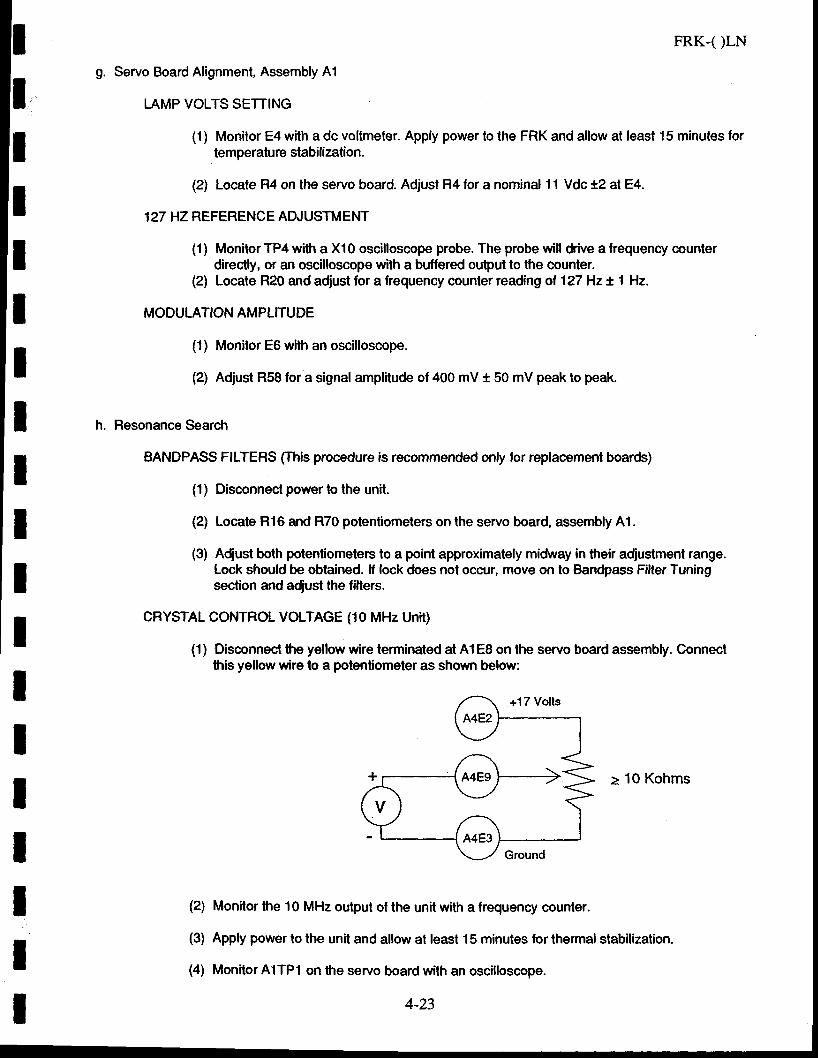
Ir
l:Itlll1IIIIIIIII
FRK-( )LN
Servo Board Alignment, Assembly A1
LAMP VOLTS SETTING
(1) Monitor E4 with a dc voltmeter. Appfy power to the FRK and allow at least 15 minutes fortemperature stabilization.
(2) Locate R4 on the servo board. Adjusl R4lor a nominal 1 1 Vdc *2 al E4.
127 HZ REFERENCE ADJUSTMENT
(1) Monitor TP4 with a Xl0 oscilloscope probe. The probe will drive a frequency counterdirectly, or an oscilloscope with a buffered output to the counter.
(2) Locate R20 and adiust for a frequency counler reading ol127 Hz * 1 Hz.
MODULATION AMPLITUDE
(1) Monitor EO with an oscilloscope.
(2) Adjust R58 for a signal amplitude ol400 mV * 50 mV peak to peak.
h. Resonance Search
BANDPASS FILTERS fthis procedure is recommended only for replacemenl boards)
(1) Disconnecl power to the unit.
(2) Locate R16 and R70 potentiometers on the servo board, assembly A1.
(3) Adjust both potentiometers to a poini approximately midway in their adjustment range.Lock should be obtained. lf lock does not ocour, move on to Bandpass Filter Tuningsec'tion and adlust the filters.
CRYSTAL CONTHOL VOLTAGE (10 MHz Unit)
(1) Disconnect lhe yellow wire terminated at A1E8 on the servo board assembly. Connectthis yellow wire to a potentiometer as shown hlow:
> 10 Kohms
(2) Monilor the 10 MHz output of the unit with a frequency counter.
(3) Apply power to the unit and allow at least 15 minutes for thermal stabilization.
(4) Monitor AITPI on the servo board with an oscilloscope.
4-23
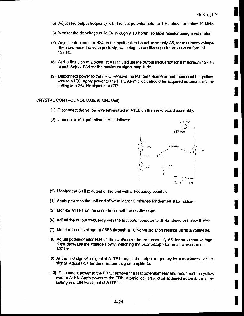
(5)
(6)
(7)
IIIIIIII
(8)
(e)
FRK-( )LN
Adjust the output lrequency with the lest potentiometer to 1 Hz above or befow 10 MHz.
Monitor the dc voltage at A5E6 through a 10 Kohm isolation resistor using a voltmeter.
Adjust potentiometer R34 on the synthesizer board, assembly A5, for maximum voltage,then decrease the voltage slowly, watching the oscilloscope for an ac waveform ol127 Hz.
At the first sign of a signal at A1TP1, adjust the output frequency for a maximum 127 Hzsignal. Adjust R34 for lhe maximum signal amplitude.
Disconnecl power to the FRK. Remove the test potenliometer and reconnect the yellowwire to AlE8. Apply power to the FRK. Alomic lock shoufd be acquired automaticafly, re-sulting in a254 Hz signal at AlTP1.
CRYSTAL CONTROL VOLTAGE (5 MHz Unit)
(1) Disconnect the yellow wire terminated at A1E8 on the servo board assembly.
(2) Connect a 10 k potentiometer as follows: A4 E2
GND E3
(3) Monitor the 5 MHz output of the unit with a frequency counter.
(a) Apply power to the unit and allow at least 15 minutes for thermal stabilization.
(5) Monitor AITP1 on the servo board with an oscilloscope.
(6) Adjust the output lrequency with the test potenliometer to .5 Hz above or below 5 MHz,
(7) Monilorthe dc voltage at A5E6 through a 10 Kohm isolation resistor using a voltmeter.
(8) Adjust potentiometer Fl34 on the synthesizer board, assembly A5, for maximum voltage,then decrease the vollage slowfy, watching the oscilloscope for an ac waveform o{127 Hz.
(9) At the first sign of a signal at AlTPl, adjust the output frequency for a maximum 127 Hzsignal. Adjust R34 for the maximum signal amptitude.
(10) Disconnect power to the FRK. Remove the test potentiometer and reconnect the yellowwire to AlE8. Apply power to the FRK. Atomic lock should be acquired automatically, re-sulting in a 254 Hz signal at AtTPl.
IIIIIIIIIII4-24
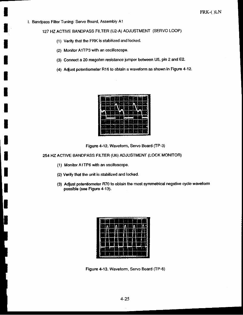
IIIIIIIIIIIII
i. Bandpass Fitter Tuning: Servo Board, Assembly 41
127 HZACTIVE BANDPASS FILTER (Uz-A)ADJUSTMENT (SERVO LOOP)
(1) Verify that the FRK is stabilized and locked.
(2) Moniior AITPS with an oscilloscope.
(3) Connect a 20 megohm resistance iumper between U5, pin 2andE?.
( ) Adiust potentiometer Rl6 to obtain a wave{orm as shown in Figure 4-12.
Figure 4-12. Waveform, Servo Board (TP-3)
2S4HZACT|VE BANDPASS FILTER (U6) ADJUSTMENT (LOCK MONITOR)
(1) Monitor A1TPO with an oscilloscope.
(2) Verify that the unit is stabilized and locked.
(3) Adjust polenliometer R70 to obtain lhe mosl symmetrical negative cycle waveformpossible (see Figure &13).
Figure 4-13. Waveform, Servo Board (TP-6)
4-25
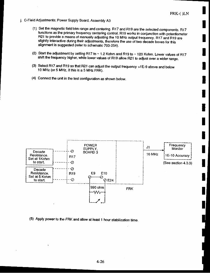
FRK-( )LN
j. C-Field Adjustments: Power Supply Board, Assembly A3
(1) Set the magnetic field trim range and centering. R17 and Rl9 are the selec'ted components. Rl7functions aq lhe primary frequency center;ng control. R19 works in conjunction with potentiometerR21 to provide a means of manually adjusling the 10 MHz output frequency. RtZ anA Rl9 areslightly interactive during their adjustments, therefore the use of two decade boxes for thisalignment is suggested (reter to schematic 703-254).
(2) Stari the adiustment by setting R17 to - 1.2 Kohm and R19 to - 120 Kohm. Lower values of R17shift lhe frequency higher, while lower values ol R19 allow R21 to adjust over a wider range.
(3) Sefect R17 and R19 so that R21 can adjust lhe output frequency >1E-g above and below10 MHz (or 5 MHz, if this is a S MHz FRK).
(4) Connect the unit in the test configuration as shown below.
IIIIIIIIIIIIII
DecadeResistance.
Set at 1 Kohmto slart.
DecadeResislance.
Set at 5 Kohmto start.
i POWEFT: ^ SUPPLY,
i n tz- - - - - - i - - v
i- - - - - : ; - Q
i ntgI- i -@
(See section 4.3.3)
E9 ElO
(5) Apply power to the FRK and allow at least t hour stabilization time.
4-26
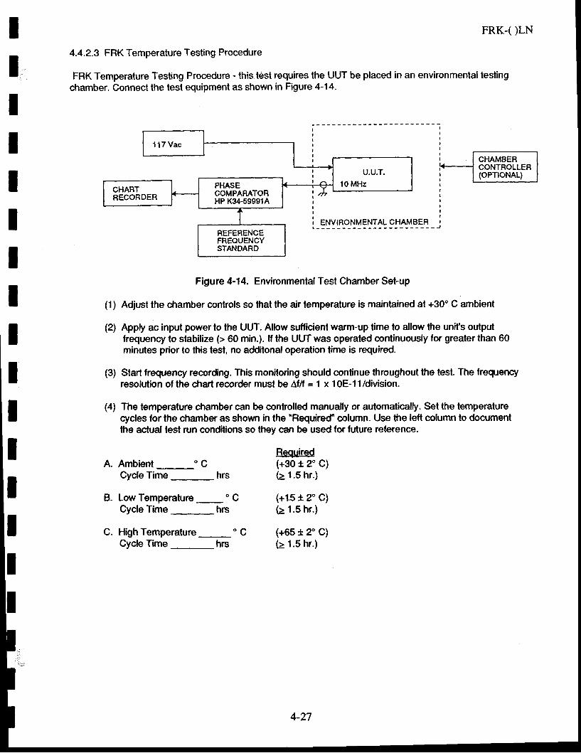
III
FRK-( )LN
4.4.2.3 FRK Temperature Testing Procedure
FRK Temperature Testing Procedure - this test requires the UUT be placed in an environmental testingchamber. Connect the test equipment as shown in Figure 4-14.
Figure 4-14. Environmental Test Chamber Set-up
(1) Adjust the chamber controls so that the air temperature is maintained at +30" C ambient
(2) Apply ac input power to the UUT. Allow sufficient warm-up time to allow the unit's outputfrequency lo slabilize (> 60 min.). lf the UUT was operated continuously for greater than 60minutes prior to this test, no additonal operation time is required.
(3) Start frequency recording. This monitodng shoufd continue throughout the test. The frequencyresolution of the chart recorder must be Lllt = 1 x 10E-1l/division.
(4) The temperalure chamber can be controlled manually or ar.rtomatically. Set the temperaturecycles for lhe chamber as shown in the "Required' column. Use the left column to documentthe ac{ual test run conditions so they can be used for future relerence.
RequiredA. Ambient " C (+30 t 2" C)
Cycle Time _ hrs (2 1.5 hr.)
B. LowTemperature_"C (+15*2"C)Cycle Time _ hrs b 1.5 hr.)
C. High Temperature _" C (+65 t 2" C)Cycle Time _ hrc E 1.5 hr.)
II
IIIII
TIIII
1 l7 Vac
4-27

IIIIIIIIIIIIIIIIII
A2A3
A4A5
IItI
ItItItlrItItIItI
tII
FRK-( )LN
DRAWING NO.
703-200-001PL 703-200-1
703-202-LL703-203-r
703-102-TABPL 703-102-L,2703-103-TAB703-103-5
r00r20PL 100120-001100117
743-208-t, -2PLTW-208-r703-2A9
743-253-TABPL703-253-r703-254
703-2t7PL703-217703-218
70E-22A-TABPL703-220-l703-221-L & -3
APPENDIX
LIST OF DRAWINGS
DESCRIPTION
FINAL ASSY, FRKPARTS LIST. FRK
WIRING DIAGRAM, LNOOUTLINE DRAWING. FRK
ASSY. LN OSCLLATORPARTS LIST, LN OSCILLATORSCHEMATIC, 5 MHz LN OSCILATORSCHEMATIC, 10 MHz LN OSCILLATOR
ASSY, SERVOPARTS LIST, SERVO BDSCHEMATIC, SERVO
ASSY, LAMP BDPARTS LIST, IAMP BD ASSEMBLYSCHEMATIC. LAMP BD
ASSY, POWER STIPPLYPARTS LIST, POWER STJPPLYSCHEMATIC, POWER SI]PPLY
ASSY, SYNTHESTZERPARTS L[ST, SYNTHESIZERS CHEMATIC, SYNTHESIZER
ASSY, RESONATOR HEATERPARTS LIST, RESONATOR HEATERSCHEMATIC. RESONATOR HEATER
PAGE NO.
A6A7,g ,g ,A10A1 l
AtzAl3 ,14 ,75A16
417A18, Al9420
A.21422,23424
425426,27 ,29A:29
A.30A.31432
A-1
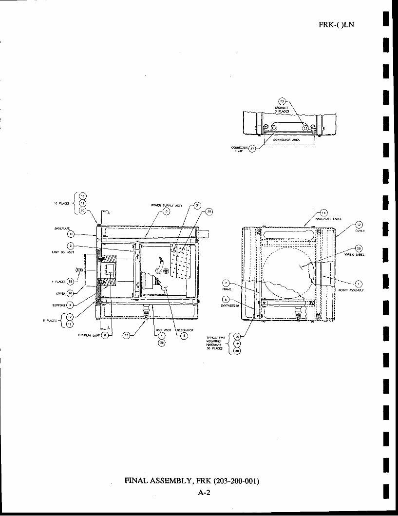
FRK-( )LN
rG,o Puc6.s f ali
L6\\
LA[? 80. ASSt
FINAL ASSEMBLY, FRK (203-200-001)
A-2
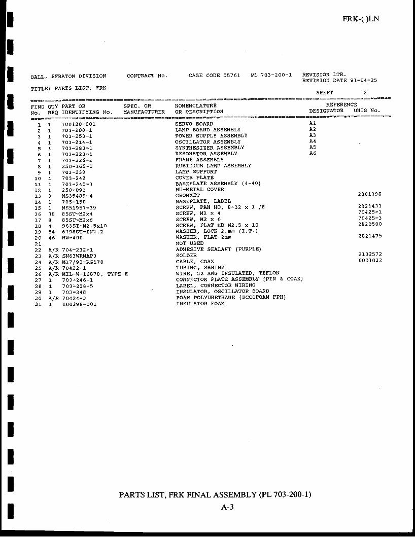
I
FRK-0LN
REVISTON LTR.REVISION DATE 91-04-25
SHEET 2
I BALL, EFRATOM DIVISION CONTRACT NO. CAGE CODE 55761 P L 7 0 3 - 2 0 0 - 1
FIND QTY PART OR SPEC. OR NOMENCINTURE
No. REQ IDENTfFYTNG No. MANUFAC?URER OR DESCRfPTIoN=====================
SERVO BOARDLAMP BOARD ASSEMBLYPOWER SUPPLY ASSEMBLVOSCILLATOR ASSEMBLYSYNTHESIZER ASSEMBLYRESONATOR ASSEI,IBLYFRAME ASSEMBLYRUBIDIT]M I,AHP ASSEMBLYI,AMP SUPPORTCOVER PI,ATEBASEPLATE ASSEMBLY (4*40)MU-}.'ETAL COVERGROMMETNAMEPLATE, LABELSCREW, PAN HD, 8-32 x I 18SCREW, M2 x 4scREtJ, 142 x 6ScREw, FLAT HD M2,5 x 10WASHER, LOCK 2 .mn ( f .T . )WASHER, FLAT 2hrTtNOl USEDADHESTVE SEALANT (PURPLE)SOLDERCABLE, COAXTUBING, SHRINKWIRE, 22 AWG INSULATED, TEFLONCoNNECTOR PLATE ASSEI.{BLY (PIN & COAX)
LABEL, CONNECTOR WIRINGINSULATOR, OSCILI,ATOR BOARDFOAU POLYURETI{ANE (ACCOFOAM FPH)INSUI,ATOR FOAM
PARTS LIST. FRK FINAL ASSEMBLY (PL 703-2OO-1)
IIIIItIIIIIIIIII
REFERENCEDESIGNATOR UNIS No.
1 1 1 0 0 1 2 0 - 0 0 12 r 703 -208 -L3 1 7 0 3 - 2 5 3 - 14 r 7 0 3 - 2 1 4 - 15 1 7 0 3 - 2 8 3 - l -5 1 703 -223 - l7 I 703 -226 -7I 1 2 5 0 - 1 6 5 - 19 1 703 -239
10 7 703 -2421 1 1 7 0 3 - 2 4 5 - 3L2 L 250 -0911 3 3 M S 3 5 4 8 9 - 4L 4 1 7 0 5 - 1 5 07s 1 1 ,1551957 -3916 38 85ST-M2X4L7 I 85S r -M2x618 4 963ST- l { 2 .5x1o1 9 5 4 6 7 9 8 S T - r N 2 . 22 0 4 5 M W - 4 0 02 T22 A lR 704 -232 -123 A/R SN63WRMAP32 4 A / R M 1 7 / 9 3 - R G 1 7 82s A lR 70422 -126 A /R M IL -W-15878 , TYPE E27 L
'7 03-246-L
2 a t " 7 0 3 - 2 3 8 - 52 9 r 7 0 3 - 2 4 83 O A l R 7 0 4 2 4 - 33 1 1 1 0 0 2 9 8 - 0 0 1
A I
A3
A5A O
2 8 0 1 3 9 8
28214337 0425 - r7 0425-32 8 2 0 5 0 0
282L475
2LO25726 0 0 1 0 3 2
A-3

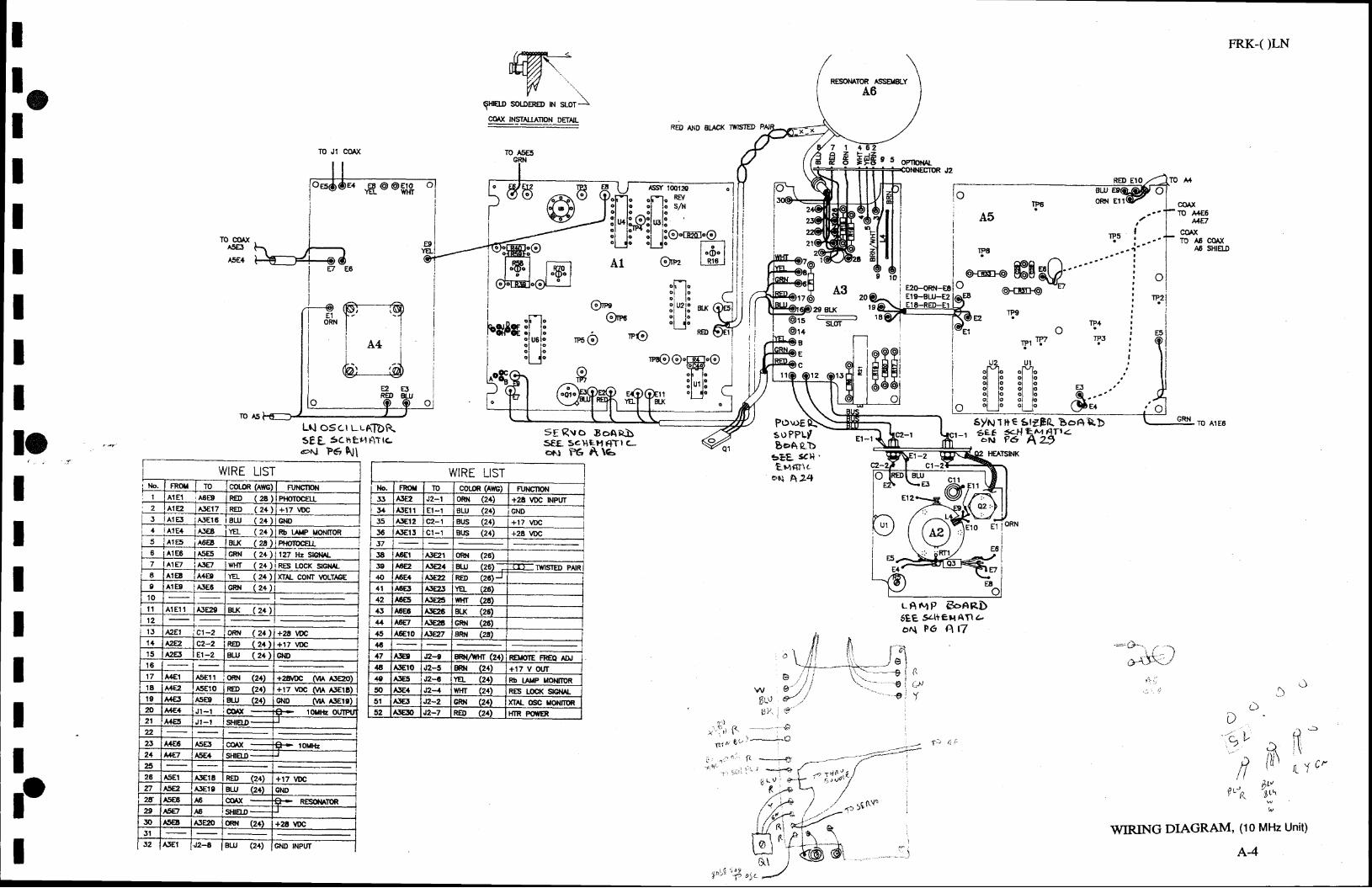
FRK-OLN
qHELD soLJ; ," ,rr\lo
ItII OrP,
O'tP6
ns@ nQ
A320
F 8LK-=-
s!07
l rI
, . o'"ElE
l€_E 1stK
lcLN oscl uurTDRsEL ScBer4RTtcer.-i F6 hll
sERvo 3oAeb,sEE- scutH 6Tl <-o+l ir6 A \e
I
PDwEsr:PPLttboAP-b
seE scR'Eqgrtc.
6A 424
-1 ":s #w'oHFATSINK
II
UAlr,tP B6ARD5EE si+eHAfiz-6111 PG Q |7
-*9 ' - , r - -* . r
t , l , - |
;'\F-7ri ...
5J$LrtB!;. D
L ) " \:1\
,) l l \i t ' .
! {ALv
fL"g 'g*
\
1 'r)
ii: \rL , { Q,
WIRING DIAGRAM, (10 MHz Unit)
A-4
RESOMTOR ISS€IIBLYA6
RED AJ.IO BLACK TWF'ED
'* .ff. @ @fil* F{/Atelol tt lolw
t@t2c, Wr S/N
ASSr
6/rurne 6IZEL BoA&b
WIRE LIST
2 t. A1E2. I AJ€17J lArEs i l rEro i auu4 rAlE/+ iAtEE irs_
6 tArE6 t rSE: i lcRN7 lA1E7 !AJF/ lwrfi
WIRE LIST'No.
FROI Io coLm 0rvc) N,'NGIION
33 AJg2 J2-1 oRfl (2+\ +2E VI)c NPUT5,r AJ€I 1 E l -1 BLU (24) GND
J5 AJET2 c2-1 Btrs +17 vDc56 AJE15 BIJS (24) +2E VDC57J6 A5€t A3E21 oRr{ (26)39 A6E2 ssE2l BU' (26) TTTTW|STED PAIR40 A5E4 AJV2 RED (26)J
11 A6E AJE2:' \EL (28)
42 A6E5 AI€2!' wHr eE)rts A6E6 A,€26 BLK |.26I41 t6E'l AJE2A cRr,f (€6).t5 ASE|O ^JET7 BRN EE),+617 A5E9 J2-9 BRil,/VrHr (24) REI|oTE FR€O ATU4A AJE1O J2-5 BRN (21) + 1 7 V4 AJE J24 \€L e+l R! l ltP ltot{tToR50 AJE4 J2-.f WHT Q1\ RES LOCX SGML
51 AIES ,fi2-2 cR[,f e$ rtAL oac uoNfIoR52 A]En J2-7 RED (21' HTR FOTER
IF A '
E 7 |
EEo
r#tzt 9 NA A5e9 GND20 t#1 J1-1 rCOl0( ---+€!- .|0|r}{z OUTPU21 A.tE5 t - t SHET.D?223 ATE6 A5E3 coA)( toMttz21 ,87 A5€4 sHrEtD -a26 A5€1 A}ElE RED (.21I +t7 vDc27 A5E2 A'E'9 BU' (211 GN9?.4 A5E6 A6 coN( li{- RESo|I|ATOR29 A5E7 A5 stflEutJO A5€B A.fE20 omr (24) l+26 YDC5132 A5E1 J2-6 BU., (21) GIID INPUT
lr
$'r!i ,".S s:*

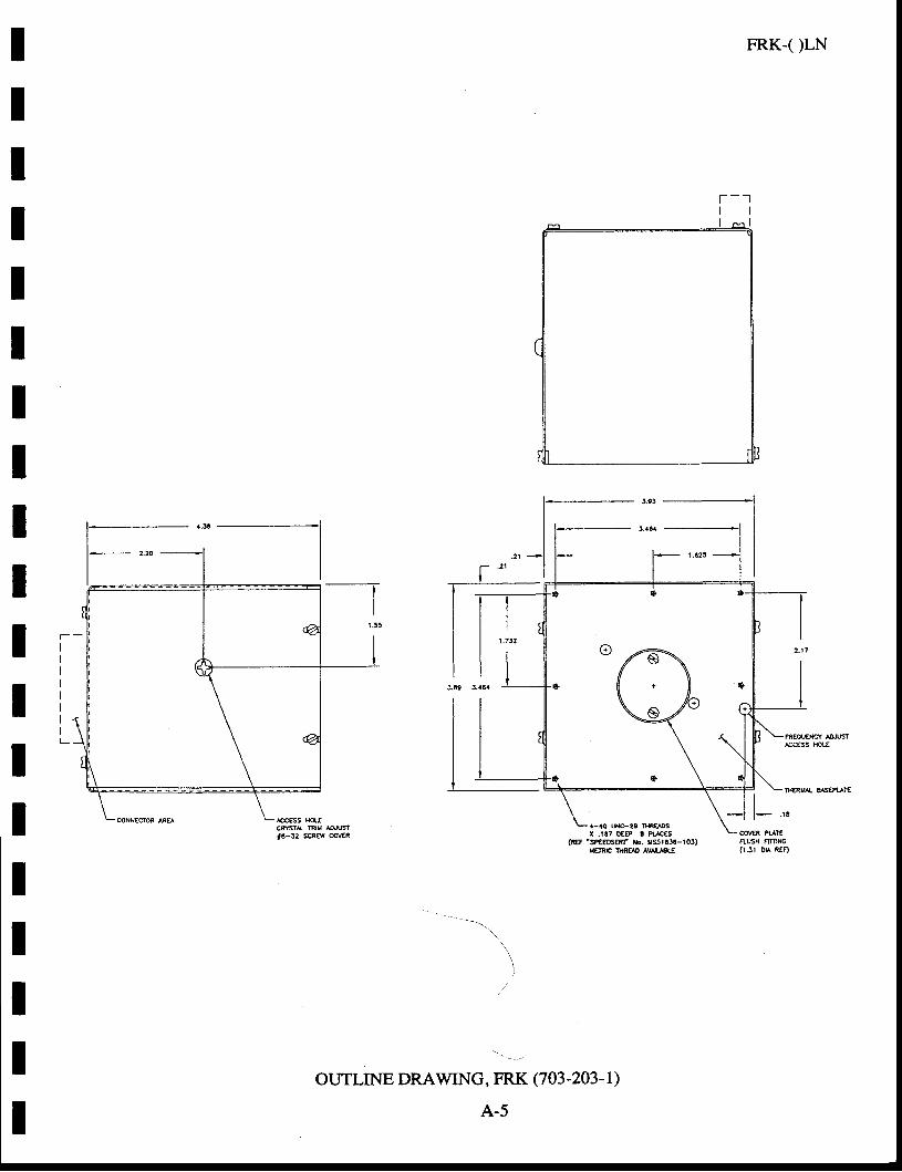
FRK-( )LN
lr-:''*ll-l--t
I
=1- g lH€RuLt lt l-l l- .rr
ffR PLAT€flusH nmNc{I.JI DA REO
'{-& w-2a HElosx.t t7 oEEP ! PW€s
'sPEtDsERf lro. rs5rE36-toJ)uEfRrc lHRao AvarrSLE
BAFIAIE
[cE$ notlcffi[ w Mlt6-12 scFEv cotrR
Glr
ourLINE DRAWING, FRK (703-203-L)
\
A-5

II
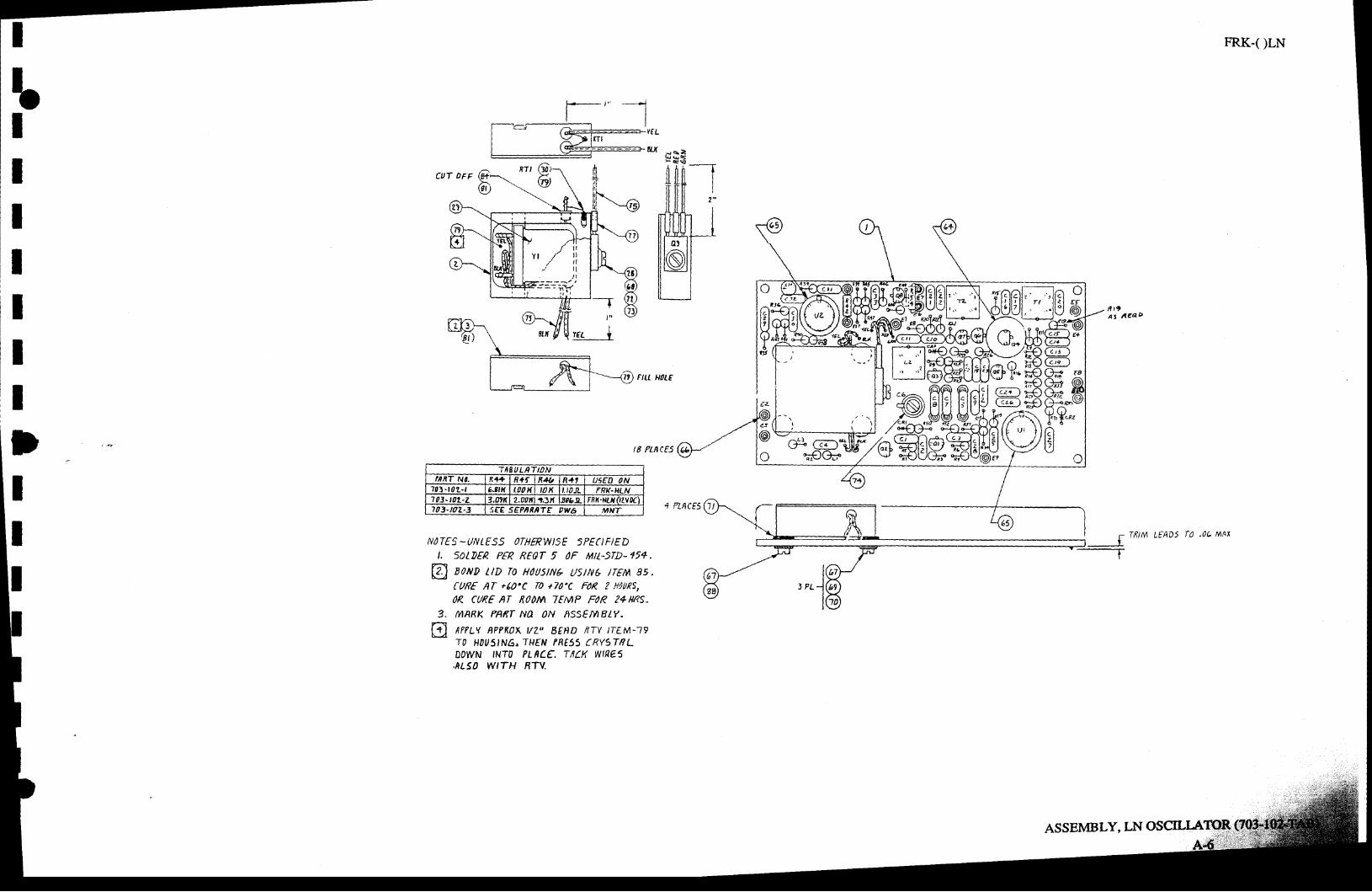
FRK-( )LN
: l r , \J
a
FIII
tII
t8 PLAC€'^ L t _(7{ (la)
*€)()*e 2 v v L t
TNBULNTNNnflT N0. R1+ R+f 84{t n+ , USED ON
70f . | 0z-r 5.ttK ,.40 N to rl ,.IO]L FRK.HLN7n.taL-z 7,mrl 2,0aAaar $nbL Fnx-HI NIzVM)703-toz.3 'EE SEPNR0TE DW6 MNT
NOT€5 -UNLESS ATHERWISE 5PE(IFIEDl, ')LDER p€B RE?T 5 0F hilt-5TD-154.
B?ND UD r0 H0UstN6. u5try6 trElA 85.(UftF AT r(2'C rD +70'C FdR ? HAaRS,OR CUR€ AT SOOM TFMP FOR 24HRS.
triARK PAKr NA 0N nSSEmEly.
A??LU NPPROX '/2' EEND NTV ITEM-1gTO HOU5IN6. THEIT' fRE55 CRVSTOLDDWN INTO PLAL€, T/|ft W\fr€,s,ALSO WITH RT!'.
4 PLACES
?
G]N '
LTADS r0 .06 M^x
ASSEMBLY, LN OSCILI.ATCIR
r TK|M
,r-l;

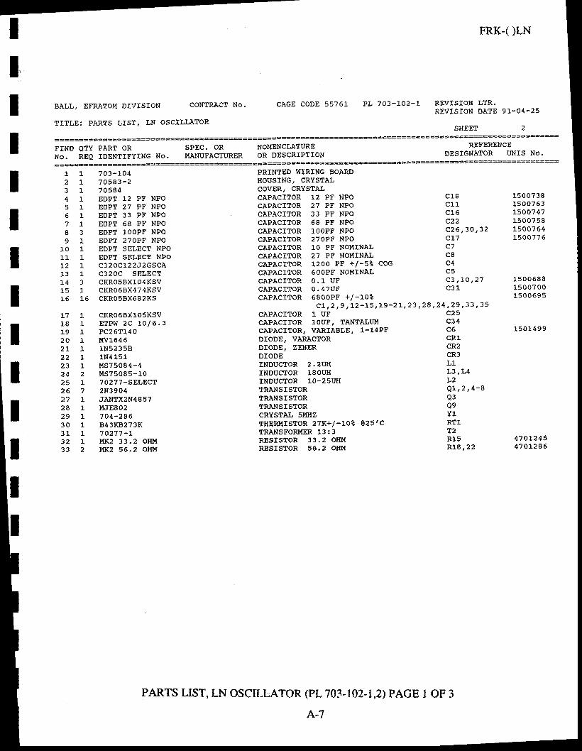
Il,
BALL, EFRATOM DIVTSION CONTRACT NO.
TITLE: PARTS LIST, LN OSCTLLATOR
FRK.0LN
PL 703-IO2-1 REVISION LTR,REVIS ION DATE 91 -04 -25
SHEET 2
CAGE CODE 55761
SPEC. OR NOMENCLATIJREMANUFACTURER OR DESCRIPTION
IIIIIIIIIII
FIND QlY PART ORNo. RgQ IDSNTIFYING NO.
REFERENCEDESIGNATOR UNIS NO.
12
56
89
1 01 1L Z
1 3
A D
1
11
11I
1J
111
I
1L 6
7 03 -LO470583-270584EDPT 12 PF NPOEDP! 27 PF NPOEDPT 33 PF NPOEDPT 68 PF NPOEDPT 1OOPF NPOEDPT 27OPF NPOEDPT SELECT NPOEDPT SELECT NPOc3 20c122J2GSCAc320c sELacTcKR05BXl04KSVcKRo6DX474KSVCKRO5BX682KS
PRINTED WIRING BOARDHOUSING, CRYSTALCOVER, CRYSTALCAPACITOR 12 PF NPOCAPACITOR 27 PF NPOCAPACITOR 33 PF NPOCAPACITOR 68 PT NPOCAPACITOR 1OOPF NPOCAPACITOR 27OPI 'NPOCAPACITOR 10 PF NOUINALCAPACITOR 27 PT NO}.IINALCAPACT?OR 12oO PF +/-st cocCAPACITOR 6OOPF NOUINALCAPACITOR 0.1 UFCAPACITOR O.47UFCAPACTTOR 68OOPF +l- l .Oz
CAPACITOR 1 UFCAPACITOR IOUF, TANTALUUCAPACITOR, VARIABLE, 1-14PTDIODE, VARACTORDIODE, ZENERDIODEINDUCTOR 2.zUHTNDUCTOR 18OUHINDUCTOR 10-2sIJHTRANSISTORTRANSISTORTRANSISTORCRYSTAL sI.IHZTHERUTSTOR 27K+/ -LOz 825'l CTRANSFORMER 13:3RESTSTOR 33.2 oHURESTSTOR 56.2 oHtq.
c18c 1 1c15c 2 2c 2 6 , 3 0 , 3 2c L 7c7c8c4c5c 3 , 1 O , 2 7c 3 1
1 5 0 0 7 3 81 5 0 0 7 5 315007471 5 0 0 7 5 815007 641 5 0 0 7 7 6
1 5 0 0 6 8 81 5 0 0 7 0 01 5 0 0 6 9 5
1 5 0 1 4 9 9
470r245470L2A6
c ! , 2 , 9 , 1 2 - 1 5 , 1 9 - 2 1 - , 2 3 , 2 8 , 2 4 , 2 9 , 3 3 , 3 5
L71 8192 02 t2 22 32 4z a2 62 72 A2 93 03 13 23 3
1 CKRO6BX10sKSV1 E ? P W 2 C L O l 6 . 31 PC25T1401 MV16461 1 N 5 2 3 5 81 1 N 4 1 5 11 M S 7 5 0 8 4 - 42 MS?50S5-10L 70277-SELECT7 2N39041 JANrX2N48571 MJEBO2L 704 -2861 843KB273Kt 70277 -L1 MK2 33.2 oHl. l2 VtKz 56.2 oHM
c25c 3 4c6cRlcR2cR3L1L3,L4L Z
Q L t 2 r 4 - 8Q 3Qey 1RT1
R15R,Lg,22
PARTS LIST, LN OSCI-LATOR (pL 703-102-t,2\ pAcE 1 OF 3
A-7
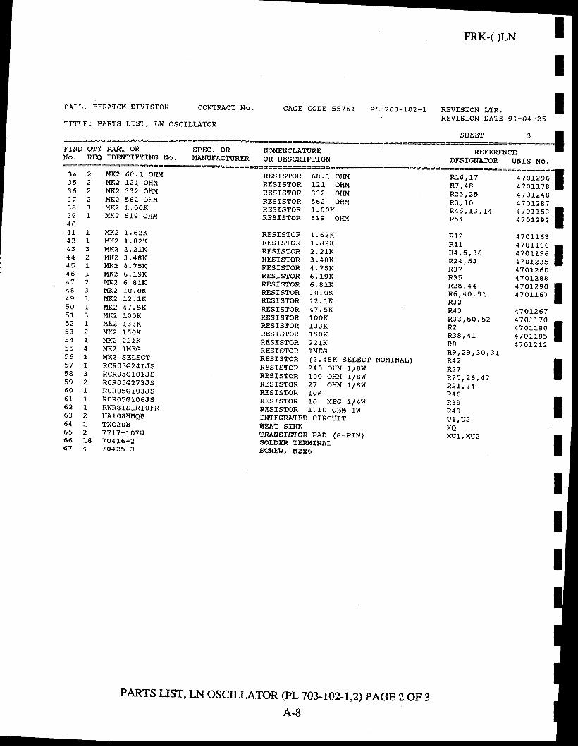
I
BALL, EFRATOM DMSION CONTRACT No.
TITLE: PARTS LTST, LN OSCILLATOR
CAGE CODE 55761 PL.?03-102- r
FRK-( )LN
IREvrsroN LrR. IREVTSTON DArE 91-04-25
=========::::1========::=====lFIND ery pART oR spEc. oR NoMENcLATURE nEFERENcE rNo. REQ TDENTIFYING No. MANUFAC?URER oR DESCRIPTToN DESTGNAToR uNIs No.=====================
34 2 W2 68.1 oHl r t35 2 W2 121 oHM36 2 t4X2 332 oHM37 2 NIK? 562 oHM3 8 3 M K 2 1 . O O K39 1 !IK2 619 oHI{4 04L 1 MK2 1. 62r(4 2 1 M K 2 1 . 8 2 K43 3 I ' IK2 2.2LK4 4 2 M K 2 3 . 4 8 K45 1 l ,rK2 4. ?5K4 5 1 M K 2 6 . 1 9 K4 7 2 M K 2 6 . 8 1 K4 8 3 M K z L O . O K4 9 1 M K 2 1 2 . 1 K5 0 1 u K 2 4 7 . 5 K51 3 MK2 100K52 1 MKz 133K53 2 UK2 150K54 1 UK2 221Ks5 4 MK2 ll,tEc56 ], MK2 SELECT57 1 RcR05c241JS58 3 RCRosct olJss9 2 RCR05G273JS60 1 RcRosct_o3Js6t t- RCR05G106JS62 1 RWR81S1R10rR63 2 UAlosHI{QB64 t- Txc2oB6 s 2 7 7 1 7 - 1 0 7 N66 18 704L6-267 4 70425-3
RESISTOR 68,1 OHMRESISTOR 121 OKMRESISfOR 332 OHI{RESISTOR 562 OIIMRESISTOR 1 .00KRESISTOR 619 OITM
RESTSTOR 1 .62KRESISTOR 1 .82KRESIS rOR 2 .2LKRESISTOR 3 .48KRESISTOR 4 .75KRESISTOR 6 .19KRESTSTOR 6 .81KRESISTOR 10 ,0KRESISTOR 12 .1KRESTSTOR 47 .5KRESISTOR lOOKRESISTOR 133KRESTSTOR I5OKRESISTOR 221KRESISTOR I.MEGRESISTOR (3.48K SELBCT NOI4INAL)RESISTOR 240 oHl, t 1/8wRESISTOR 100 ogu 1/8wRESISTOR 27 oHM 1/8WRESISTOR 1OKRESISTOR 10 ME,G L/4WRESTSTOR 1.10 oHM 1WINTEGRATED CIRCUITHEAT STNK?RANSTSTOR PAD (8-PIN)SOLDER TERMTNALSCREW, li[zx5
l ;; 'r ' ' tn i;sl*; IRr2 4701163
l"i',,u l;311;: IR 2 4 , 5 3 4 7 O I tR 3 7 4 7 0 1 2 6 0R35 47AL2A8
l?l;li,, llSii:9 IR43 470t267R33,s0,s2
l ; : l l j , ;R 3 8 , 4 1 4 7 0 1 1
R8 470L2R 9 , 2 9 , 3 0 , 3 1R42P.27R2O,26 , 4 ' t IR 2 1 , 3 4R 4 6R39R49u1-,u2 IxQxu]-, xuz
I
R 1 6 , 1 7R '7 , 48R 2 3 , 2 5R 3 , 1 O
47 072964 7 0 1 1 7 84 7 0 L 2 4 8470L287
III
PARTS LIST, LN OSCLLATOR (pL 703_102_1,2)pAcE 2 oF 3A-8
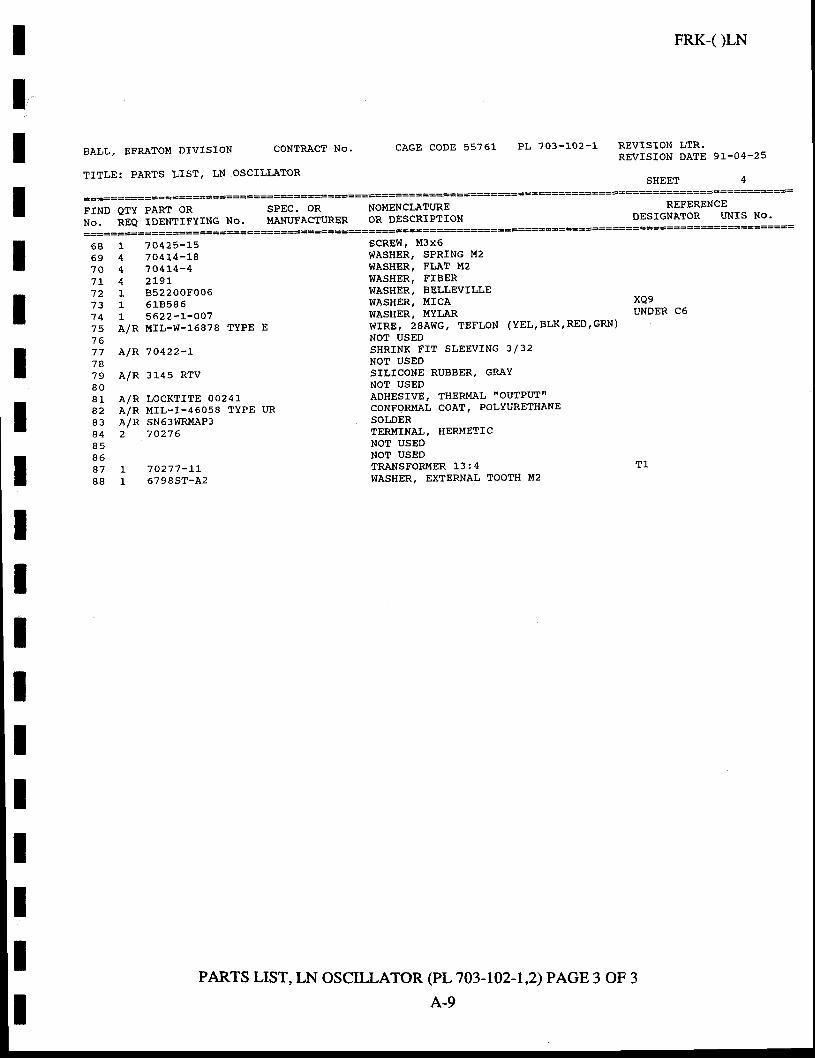
N o .
IIIItIIIIIIIIIIIIII
BALL, EFRATOM DIVISION CONTRACT
TITLE: PARTS LIST, LN.OSCILLATOR
FIND QgY PART OR SPEC. OR
NO. REQ IDENTIFYING NO. MANUFACTURER==============
6 8 I 7 0 4 2 5 - 1 s59 4 704L4 -L87 0 4 1 0 4 L 4 - 47L 4 2L9l' 72 1 B52200F0067 3 1 5 1 8 5 8 67 4 1 5 6 2 2 - 1 - 0 0 ?75 A /R MrL -W-16878 TYPE E/ o
7 7 A l R 7 O 4 2 2 - r7 A79 A /R 314s RTVO U
81 A /R LOCKTTTE 00241a2 A /R MrL - I - 46058 TYPE uR83 A/R SN63WRMAP38 4 2 7 0 2 7 68 5o o
a 7 r 7 0 2 7 7 - l L88 1 67985T-A2
CAGE CODE 55?51 PL 703 -102 -1
NOMENCLATUREOR DESCRIPTION
SCREW, M3x6WASHER, SPRING M2WASHER, FIAT I42WASHER, FIBERWASHER, BETLEVILLEWASHBR, MICAWASI{ER, UYI,ARWIRE, 28AWG, TEFLON (YEL,BLK,RED,GRN)
NOT USEDSHRINK TIT SLEEVING 3/32NOT USEDSILICONE RUBBER, GRAYNOT USEDADHESIVE, THERMAL ilOUTPUTtr
CONFORMAL COAT, POLYURETHANESOLDERfERMINAI, HERMETICNOT USEDNOT USEDfRANSFOR},TER 13:4WASHER, EXTERNAL TOOTH I.{2
FRK-( )LN
REVISION LTR.REVISION DATE 91-04-25
SHEET 4
XQ9T'NDER C6
T 1
REFERENCEDESIGNATOR UNIS NO.
================
PARTS LIST, LN OSCILLATOR (pL 703-102-t,2) PAGE 3 OF 3
A-9

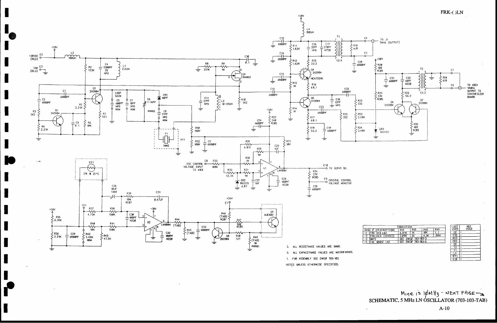
l@
IIIIIII
FRK-( )LN
-i-0 Jl
5LtHz (OUTPUT)
+20voc 12(RED)
t'et ill e----l
-
R 1 533.2
Q12N3904
I
II€ATSIM
R 1 56 8 . 1
T$944
El cnvstrL co.trRotVOLTAGE MONITOR
3. ALL RESISTANCE VALI.ES ARE OI$/S.
2. ALL CAPACITANCE VALUES ARE MICROFARADS.
1. FoR ASSEMBLY SEE DWG# 703-102.
N0TES: UNLESS oIHERWISE SPECIFIED.
I c20
I eaooerI:
+29'l
RzS100
RC05
LOOPGAINc5
6OOPFNPONOM
I l tt,"t6-zsvuI
I
a1
lOPFNPONOM
c8z t f t
ftP0r'0M
FIIIIIIIlo
R3427K
RC05
c286800PFI
$4rqe- ts l /MH3 ^ uExT ?QGe -sSCHEMATIC, 5 MHz LN OSCILLATOR (703-103-TAB)
A-10
c16 I C17
! ' R54I s tc
E5 TO A5E110MHzUJTruT TOSYNTT€SIZERBOARD
OSC CONTROI.VOLTAGE INPUT
TO A1E8
4.75K 150K I C30
t?3,, +:::,,,10K
R423 .48KNOM
R49(rAB)
1WRWRSI
TABIJLATION{ R 4 4 R45 R 4 9
:i-7Fd-rern r IiI- 6 - 6 l K 1K r . 12 (FRK-HLN (12VDC}} 3.09K 2K IK - 6 0 4
J tlrtN I th t-tk
-5 (FRK IOMHZ LN} t b - t - t o J -
LASTt,SFD
NOTUSED
U2
R53cR3
l 1t 4
R T l

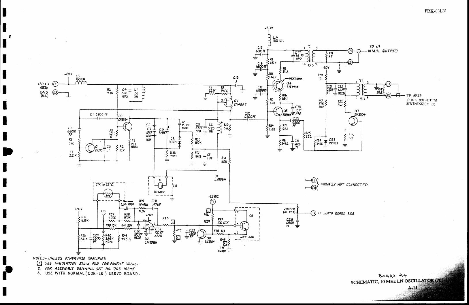
II
3
IIIIIItpIIIIIIII
FRK-( )LN
t 4 .r80 uH
TO J'{a Mb- @urrur1
firt31.2
+AYL3IBO UH .,-f€ITSlNr
\r O*+ZD YDLGED) ? c13(o800n
r-lFI
=
, aNlto+GND k-j!__,6t-u) \-/ I
03zN4gt7
RelNKn@,LctS
05 T \ZPF?NNOFNPO
o7zNE9|0+ct 6800 ?r
CZIDDUUrF
fil) leL
' ?111 a )< .a
I e ' r r s E J E I
NOTFs- UNLESS OTHERWISE SFECIFIED
@f srr rnBuATloN Btl(K FnR cnt{tplN€NT vAtuE.Z. FOR ASS€MBU DRAWIN| SFF NO. 703- IOZS3- usE wtTH NoRMAL ( NON -LN ) sERyO BoARD .
RN66.1
Rl+r,0 r(
a a
C 1OPF^rPo -'Yrl,1
6WPF
R72ZtN O M
R4z2tK
Rtlt00K
U ILMIOSH '--@)
^ > NrnMrLtY NoT C7NNECTED49)
JVM?tT(lr i3+)
(28
TO SENYA EDNKD AIEB
6000 TP F :
t
*eoY
t r pT6800IPF=
T I
31ffi ro^,8+f 3;3 - lo MFh Dur pur ro
5YNTHESIZER BD
p6 { t CB3
R39 C3t =t0 MEIt .+7UF
HJe aoz
BoARb A+
SCHEMATIC, 10 MHz IN

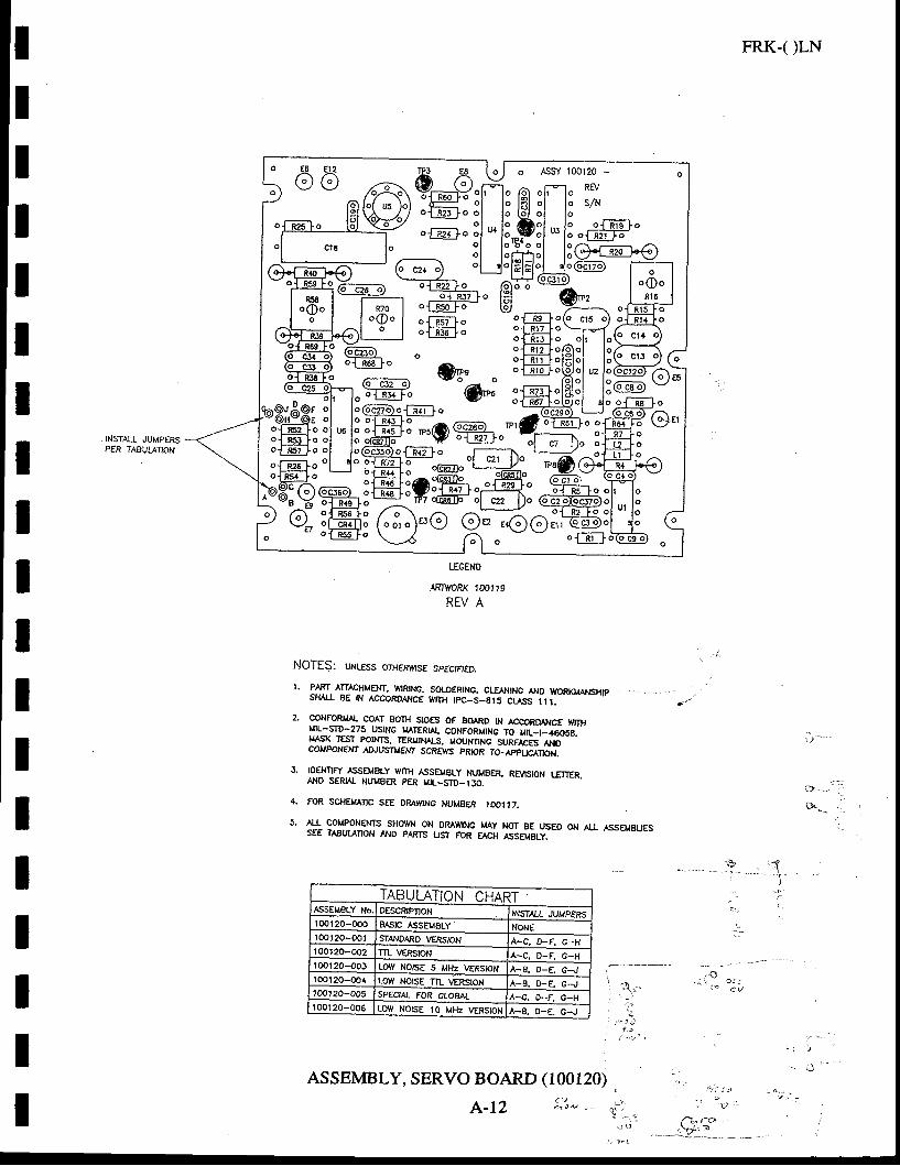
::'
IIIItIIIIIIIIIIIIII
FRK-( )LN
INSTALL \'UMPERSPER IABUL{IION
LEGEND
ARTWORK 1001 t9
RIV A
NOTES: uNL€ss oruEnus€ spEcrRED.
I. PART.ATTICHM6IT, WIRINC. SOI."OERING, CLE$IINC AIO YIORKIIANSI.IIPsrt'r4 B€ rt{ AcconoAr.rcE wTH rpc_s_als cr,lss iri.-2. CONFORMAL CO\T 801H SIOES OF BOARO tN ACCORD ITCE yrIIH
MIL-ST0-275 USINC I{AIERT L coNFoRMtNc to utt__t_+oosa.MASX IESr PONTS. IERMI.I l.S. MoUNilNG SUnr,rces rlrO
-
COMPONENr /IAJUSIMEIIII SCREITS pRtOR fO_eppLrclnOn.
J. IDE}MF' ASSEMBLY WMI ASSA,IBLY NUMBER. REVISION IENB,A.IO SERIAL NUMBER PER MIL-SID-IJO.
4. FOR SCHE},ANC SEE DRAWTNG NUMSER ,OOiI7.
5. ALL COMPONA.ITS SHOI/N ON ORAWTNG IJAY NOT BE USEO ON A[ ASSEUEUESsEE rAButAnoN a{o pARTs usr FoR acH rsseubuy. --
r:-.
c>..-i>..,
TABULATION CHARTASSEMBLY No 0ESCR|PnON INSIAL JUMPERStoo120-@O EASIC ASSEMBLY NONE100120-oot STANDAFD VERSION A-C, D-e c-H1 00 t 20-oo2 T]L VERSION A-C. D-F, G-Htoot20-oDJ tOW N9ISE 5 MHz VERStor{ A-8. O-€, c-{loot20-oo4 LOW NOTSE TIL \€RSION A-8. o-E. G-J,oot20-oo5 SPECIAL FOR GLOEAL A-C, 0*F. c-Ht oo t 20-006 LOW NOISE 10 MHz VERSTONA-8, O-E, 6-J
ASSEMBLY, SERVO BOARD (100120)
3 ..-{!
' J, . . . 1 r
,-9
/ ' 1 t i
a \ ) . .4 1 1 p -
'l t_1
t - 1 . r
"'i.lA-12
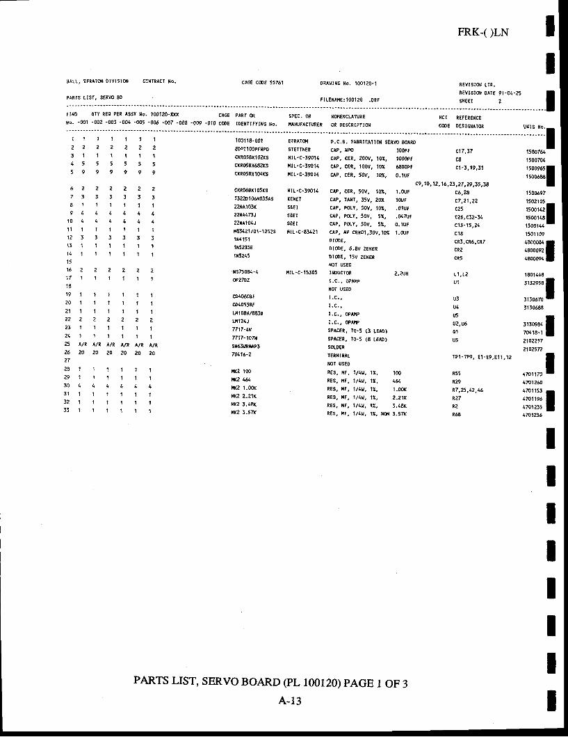
FRK-( )LN
BALL. EFRAIoI| olv ls lol l CoII IRACT Io.
PARIS t IST, SERVO 8D
CAGE C00E 5576',1 0RAl r lUG No. 100120.1
FI tENAxE:100120 .Dgr
R€VISIOII tIR.REVISt0 l oATE 9 l -04-25SHEET 2
II
FIllD oTY REo PER ASSY tlo. 100120-lxx CAGE PARI OR
[o. -001 -002 .003 -004 -005 -006 -007 -008 -009 -010 cooE IDE],lTttytNG ro.
SPEC. OR NOT,IEITCLATURE
NAIIUFACIURER OR DESCRIP'IOII
I ICI REFERE}ICE
C@€ DESICITAIOR :::: r:.11 1 r 1 t 1 1
2 2 2 2 2 2 2
3 1 1 1 1 1 14 5 5 5 5 5 5
5 9 9 9 9 9 9
6 2 2 2 2 2 2
7 t t 3 3 3 3
8 1 1 1 1 1 , 19 4 4 1 1 4 4
1 0 4 \ t t 4 1
1 1 1 | | | 1 11 2 3 3 3 3 3 3
1 3 1 1 1 1 t l
1 1 1 t 1 ' t 1 1'15
1 6 2 2 2 2 2 ?
1 7 1 1 1 1 1 1l 8
1 9 1 1 1 1 1 1
2 0 1 t , l 1 1 12 r 1 t t 1 . t 1
2 2 2 2 2 2 2 2
2 3 1 1 1 1 1 1
? L l l , t 1 t l25 AlR AlR ^/R ^/e A/F. AtR26 20 20 20 20 20 2027
2 8 1 1 1 t 1 t
2 9 1 1 1 1 1 13 0 4 4 4 1 4 4
3 1 1 1 , 1 t 1 13 2 t , t 1 1 , 1 13 3 1 . t 1 1 1 1
1001 18-001
EDPTlOOPFIIPO
cKR05BX102XSc(R05Bx682Xs
c(i058X104KS
cKR068X105(S
t3220106r.1035AS
22[A10]X
22tA173J
22[A104J
t{81421/01 - 1 2525tN4151
1x5235s
1115245
ils75084-4@2782
cD40608F
c040538F
LI108B/8838
Lll124J
n17-Ix
7717-107x
s$63m|.t^P3
70115-2
t|(2 100nKz 461ilK2 L00Kl|le 2.21Kr{K2 3.48KilK2 3.57K
EFRAToI LC.S. FABRTCAilO$ SERVO BOARDSTETTIIER CAP, IIPO IOOPFtilt-c-390t4 cAp, cER, 200v, 10t. 1000prxrl.c-19014 cAp, c€R, 100v, 10x 6800ptf { r r -c -390f4 c P , cER, 50v , 10u, o , luF
c17,t7c8ct -3,19, t1
1500704
f:ffi11500697
1502105
ttoo'torl1500t44 r
,roo'rool
i*-l::*:l3130588
#ri I2102217
li l t -c-19014
KENEI
S&E Is&ElstEl
rar L-c-83/.21
cAP, C€R, 50V, 10t, 1.0uFcAP, rAXr, 35V, 201 1OJFcAP, POLY, sOV, 10X,, .01UFcAP. POLY. 50v, 51, .04rurcAP, POLY, 50V, 57., o.luFcAP, XF CRH01,30V,102, 1 .WFD I O E .0 toE, 6 .8V zEfERDroE, 15v ZENER
c9,10, 12, 16,?3,27, 29,35,38c6, ?8
c7 i21,22c25
c26,c32-14c13-15,24
cR3,CR6,CR7
cR2
cR5
L 1 , 1 2u1
t n
U4u5u2,u601
U5
r P 1 - T P 9 , E 1 - E 9 , 8 1 1 , 1 2
R55
R29
R7,25 ,42,46R27
R2R6E
NOT USEDlilt-c-15305 tl lDucroR 2.2uH
t.c,, oPAt{PNOI USED
I . C . ,
I.C., oPAt{p
1 .c . , oP i lPSPACER, TO-5 (3 LEAO)SPACER, rO-5 (8 IEAD)SOLDER
T€$IIIIAL
I0I USEo
RES, t1F, 1/1V, 12,, 100RES. fiF, t,/4U, 11, 164RES, t(F, 't/tV, 17,, 1.00KRES, nF. l , /4 t , 1X. 2 .21KRES, |tF, 1/4y, lX. 3.48KRES, t{F, 1/4U, tt, [ofi 3.57K
,*',^l4701 260
iilxr IIIII
PARTS LrST, SERVO BOARD (pL 100120) pAcE I OF 3
IA-13
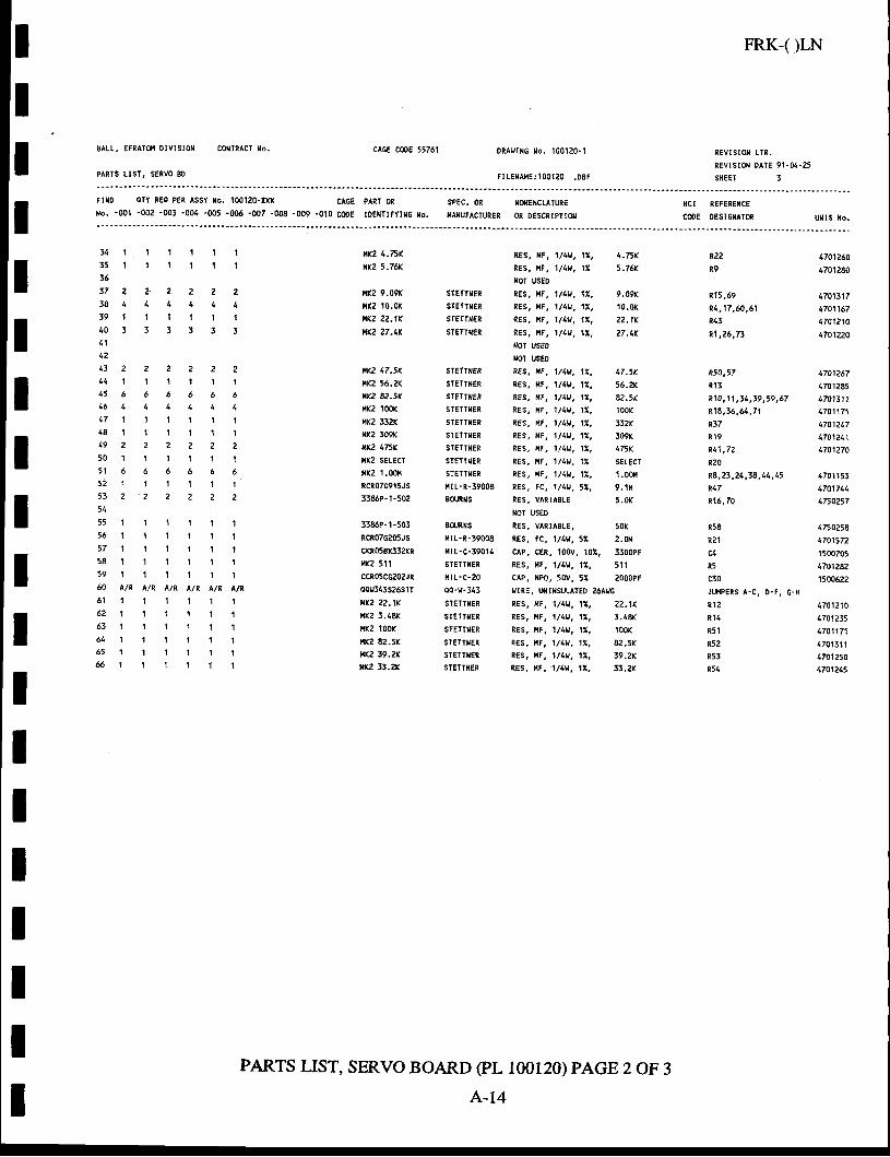
tII
FRK-( )LN
8ALL, EFRATSI 0lvlStoN CoI 'RACI No.
PARTS LISI, SERVO BD
oRAt lxc l io . 1001e0- l
FtLE[rdiE: 100120 .DBF
REVISIOI I L IR.
REVTStOT oATE 91-01-25
SHEET 3
CAGE COE 55761
fll{o oTY R€0 PER ISSY [o. 100120-lXX CA6E PART OR
No. -001 -002 -003 -004 .005 -006 -007 -008 -009 -010 CooE rDE[TlrylNG ilo.SPEC. OR IICT{ENCLATURE
xAlutAcTuRER oi DESCRIPTt0{
HCI REF€REIICE
COE OESIGXATOR U [ l S N o .
34 1
35 136
3 7 2
3 8 4
59 1
4 0 3
44 11 5 646 1
17 11 A l
5 0 |
52 '1
5 3 2
54
5 6 |
57 158 1
3 l 3
4
t
3
1 ' t 11 1 11 1 ' l
nK? 1.?5K
rK? 5.76K
x(2 9.09(
r{K2 10.0(
t4K2 22.1K
t4K2 27.4K
nKz 47.5K
l1K2 56.2KnKz 82.5KltKz l00K
!t,(2 332{r{xz l09K
t4K2 475K
IKz SELECT
irKz t.00r{
RCR07G915JS
5386P- 1 -502
3386P- 1 -503
RCR07c205JS
cKR058x332xn
i'r(z 511
ccR05ccz02JR
0ot'J43s26slT
i l x2 22 . lK
lrKz 3.48(
||K2 100(
rr2 82.5K|,|K2 ]9.2(nKz 33.2K
SI€IINER
STEIINER
STETTIER
SIETTII€R
STETII{ER
STETTI{ERSTE'T}'ER
STETTNER
S'EIINENsTEII[€t
STETT}IER
SIETINER
STETIIIERxr L-R-39008
80utIs
8U,RTS
il r L-R-59008
l{l L-c-59014
SIETIXER
l I L -C-2000-rl-343
STETTIIER
SIETIXER
SIETTN€R
STEIT}IERSTEITIIERSTElIIIER
1701317
4701167
470121A
1701220
lm1267
1701285
17013111701171
470121747012111701270
4701 15347017411750257
4750258
1m1572
1500705
4701282
1500622
4701210
17sl235
4701171
470111 I1701250
4741?l5
RES, r,rF, 1/41'. lZ, 4.75KRES, r{t, 1/49, 11 5.76XXOT USED
RES, t4F, 1/1$, 1L 9.A9KRES, l|F, 1/4!1, 11, ',t0.0(
RES, nf, 1t49, tX, 22.1KRES, r,rF, 1/4y, 11, 27.4Kilor us€oNOT USEORES, $F, 1/1V, 17,, 17.5xR€S, Ir, l/49, t l, 56.2KRES, t4F, l l IU, lZ, 82.5(.RES, itF, 1,/4H. 11, 100KRES, nF, '/111, 12, t32XRES, r,rF, 1/4U, 11, 309KRES, At, 1t4U, 12, 475KRES, HF, ',t l4u. 1U SELECTRES, '{F, 1/49, 11, 1.00f.1RES, fC, 1 /4U, 51 , 9 .1 t ' lRES, VARTABLE 5 .0KIOr USEo
RES, VARIABLE, 50t(RES, fC, 1/49, 51 2.0trcAP, CER, 100V, 101, 3300PfRES, l t r , 1 /4U, t l , 511cAP, XPo, 50V, 51 2000Ptl,ltRE, uilmsuLAIED 26AU6
RES. ltf, 1,/49, ',t1, 22.1XRES, irF, 1/49. 't1, 3.1ARES, r{F, ', l l4g, t l, '100(
RES, t{F, 1/4U, 11, 82.5KRES, lrF, 1,/4y, 1I, 39.2KRES, ttiF, It(U, 11. 33.2K
R22 4101260R9 4701280
4
1
3
Ri5 ,69R/ r , t7 ,60 ,61
R43
R'l,26,7t
R50,57
R 1 l
R1O,11 , t4 ,59 ,59 ,67R18,36,64 ,71
R37R 1 9
n t 1 , 7 2
R20
R8,23,21,38,11,45
R47R16,70
R58
R21
R5
c50
JU,iPERS A-C. D-t, G-HR l 2
R 1/r
R51
R52R53R54
1
4,|1
1
61
2 2 2 21 1 1 16 6 6 64 4 1 1
1 r l . tl t 1 1
2 2 2 2
1 1 1 1
6 5 6 61 1 1 l
2 2 2 2
1 t 1 1
1 1 1 1
1 1 1 1l 1 ' t t
III 5 9 1 1 1 ' t . t 1
60 AlR A/R AlR AlR AlN AlR6 1 1 1 1 1 1 , t
6 2 1 1 1 t t , l6 3 1 ' r 1 1 r 1
6 4 1 1 t6 5 t 1 1
6 6 1 1 1
IItI
tPARTS LIST, SERVO BOARD (pL 100120) pAcE 2 AF 3
A-14
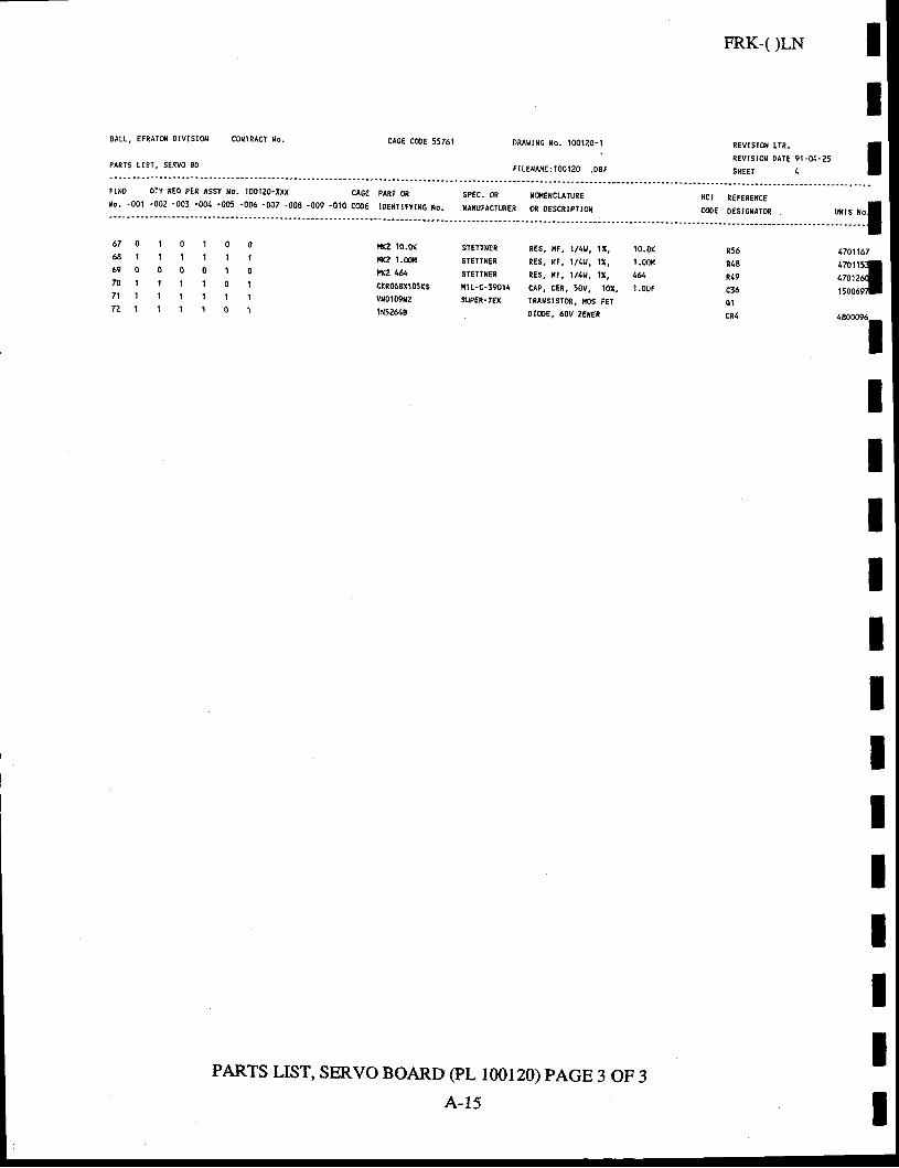
FRK-( )LN ttI
SALL, EFRAToi l DlVlSl0{ Coi lTRACI lo.
PARIS LIST, SERVO BO
DRAI'I[G lto. 100120-1
FILEI |A IE:100120 .DBf
REVISIO}I LTR.REVrSlOll DA'E 9l-04-25SHEEI 1
cAcE c00E 55761
fllJD 01Y nEO PER ASSY xo. 100|20-Ixx CAG€ PAR' OT SPEC. 0R |ld.iEllcLAluREro' -001 '002 '003 -004 '005 -006 -007 -008 -009 -010 cooE tDEilTtryti lG ro. i lANUFACTURER oR oEscRtpiloN
' ICI REFERE}ICE
c@E DESTCXATOR UtllS l lo
6 7 0 1 0 1 0 0
6 € 1 1 t 1 1 l
6 9 0 0 0 0 . t 0
7 0 1 1 1 1 0 17 t 1 1 1 1 , t 1
7 ? 1 1 1 . t 0 1
N(2 10.0K
firc l.00fl
NK? lU
c(R068X105t(s
w0109f12
1r{52648
stElr[ER e,ES, tiF, t lIU, 12, 10.0(STETTNER RES. trf. 1/4tJ, tX, 1.00nSTETTXER RES, t4F, 1/49, lt, t&il l t-c-!9014 cAP, CEn, 50V, 102, t.OufSUP€R-TEX TRAXSISTOR, I{OS FEI
DtoE, 60v zEfgR
R56
r18
n49
c36a l
cn4
;#il
PARTS LIST, SERVO BOARD (pL 100120) PAGE 3 OF 3
o*oo"r
IIIIIIIIIItIIA-15
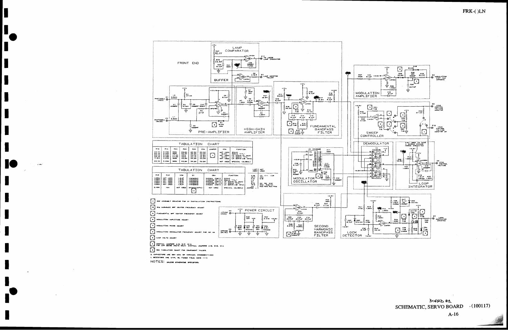
IllItItItItlo
FRK-OLN
L A M Pi . ' C O M P A R A T O Rsz.tr
FRONT ENDa 7 - 4 t
i i I v l s , b I V l s r I i ir r l l l " l ' l ' " ' l l ij i L 'I a a t 2 , A V 4l l o " @ d - : J v u; ( e L U € ) v ,
; ( a € o )
i
pl * , ,* osctuyq.E.*y M,. i l E, R i im:x
O * var5 sr
I . I l6fu tMrr a4 H. o{u r4 Lot Fts wta 4t tiar^u si3 ^_a r o_r
L:l e re^rtq q{r rq cffir vM1
1@&trs E XV U& O @C (@.sxqr '
r Esratqa ^E V.w. E rtrc .tu (xr _)
NOTES: rus or..ore Fcrro
ig r*,;31rr*
ii L--nt -r ii I I .:,i.
T . . l u r' v {
I I r I ^ . '| [---l r^r
SWEEPCONTROLLEfI
6"o i . ,"I l...-."I3I ' v cdr.e{ t-\ | v(r^4t l . l ; d l Y d t iI t 4 i
I C 1 . C 1 5. . T U F
ff i trF,,. t ^,, Jo ; "e " f r u
I t l[, -.4
T,a'*V
T A B U L A T T O N C H A R T
n]h--r'
lN s€ivo (6 *:)
u *ivo (! h.)
wcr[ (4€&)
TABULATTON CHART
'NF\(NF!
l:!
u r€ivo (a ht)L t r SSVO.TtL 'w gvo (r s.)
sftCl{ (4€&)
F) * ^t*t ayrF rd ot rEruird rsriEtr6
R - * " r f f i * @ s r
f"l r**t* F o.ra rts@y Esy
Gl *.^-* sru .*y
Gl *.. , ,* Es M'
ul
SoqeU ql.
SCHEMATIC, SERVO BOARD , ( IOO117)
A-16
N:l
l . . , u F
c ! 4. . tuF -r
LOCK IDETECTOR . .Y."
I r ] r u
i i t '
I ; ' ' ' t t
--+-.+-: i
i il l
l ; il i ;
I i i' , ' iI
IIIIII
a 1 2
ra2 ia l ras iaa
.? ' PowER CTRCUIT
TI
eI t ]
crt cfa-aarv .aa tv .a .?w- rHH. :;: t ,.;.,'-l
? l|..w
Lrti:s
SECONDHARMONICBANDPASSFTLTER i
loI
&
rior v rx
t , tODULRTOR vOSCILLATOR
n ) c " I
i 1 5 - H; v
, i . c p t t . o t x

IIIIIIIIIIIIIIIIIII
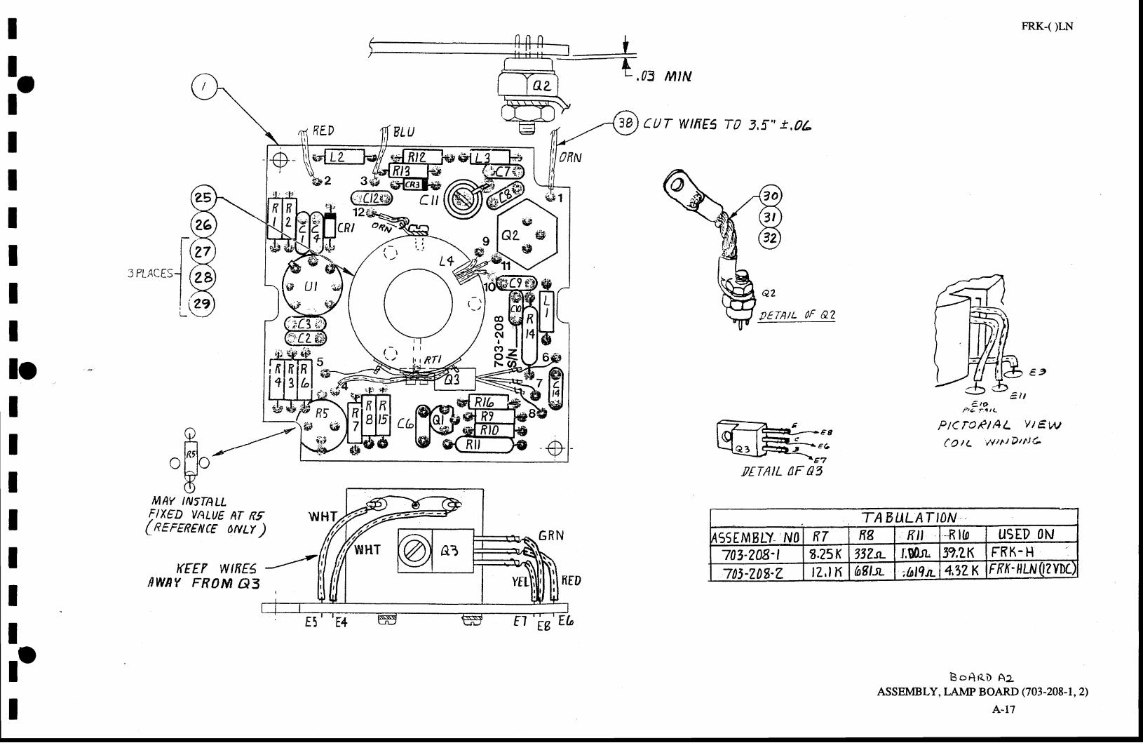
l.IIIIIII
IIIIIII
3 PLACES
IGIX
lQaI,X,Jg
lr
Or-l
c l*'loE
MAY INTMLLrlx€D VALUE Ar ft'(REFER€NcE outr )
KFEI wtfrEs -/f lWAY FRAM A3
0ftN
03 MIN
f uT wlfrEs T0 3,5'., t,0L
FRK-( )LN
E2
€ t oP t 1 T a t L
plcfc,etAL v/ EVJCO tL 'y ' l t i lDrtJL
BoARD AzASSEMBLY, LAMP BOARD (703-2484,2)
A-t7
GI OEF
@oNI
(r)oN
rcTAIL BF O3
TAB ULAT I| .N455EMBLY 'NO RT f8 Kn -fi lb UgED ON
7A3-708-l 8.25K 53Zn- IWL 3?,ZK FKK. H:7A3-708-Z IZ,IK b9l* ;{tlcltt 4,12KFKITflLNO?YDC,
lr

IIIIIIIttttIIIIIIII
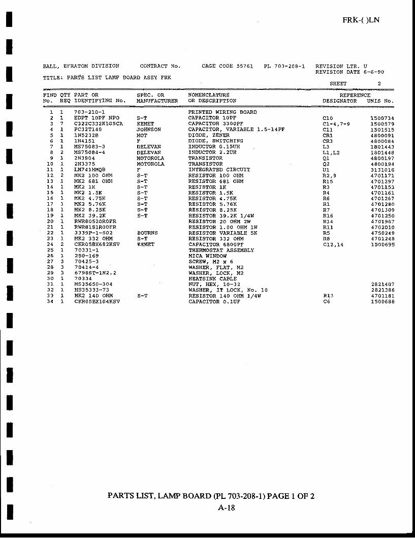
III
BALL, EFRATOM DIVISION CONTRACT No.
TITLE: PAR{S LIST LAMP BOARD ASSY FRK
CAGE CODE 55761
FRK-( )LN
PL 703 -208 - ] - REV IS ION LTR. UREVISION DATE 6-6-90
SHEET 2
I FTND QTY PART ORNo. REQ IDENTIFYING NO.
SPEC. OR NOMENCLATUREMANUFACTURER OR DESCRIPTION
REFERENCEDESIGNATOR UNTS No.
Rl ,3
IItIIIIIItIIIII
1 1 703-2LO-t2 L EDPT ].OPF NPO3 7 C322C332KLG5CA4 1 PC32T1405 1 1N523286 1 1 N 4 L 5 17 L M S 7 5 0 8 3 - 3I 2 M S 7 5 0 8 4 - 49 1 2 N 3 9 0 4
1 0 1 2 N 3 3 7 511 1 LU741HMQB72 2 vtKz 100 oHlr13 L MK2 681 oHM14 1 MK2 1K1 5 L M K 2 1 . 5 Kr.6 I t tK2 4.7sK! 7 r M K 2 5 . 7 6 K1 8 L l t K 2 I . 2 5 K1.9 l " MK2 39.2K20 1 RWR80520R0FR2L 1 RWRSLS1ROOFR2 2 1 3 3 3 9 P - r . - 5 0 223 1 MK2 332 0Hl424 2 CKRo5BX682KSV2 5 l . 7 0 3 3 1 - 126 l . 2 50-15927 3 70425-328 3 7041-4-42 9 3 6 7 9 8 S r - 1 N 2 . 23 0 L 7 0 3 3 43 1 L M S 3 5 6 5 0 - 3 0 43 2 t M S 3 5 3 3 3 - 7 333 1 MK2 140 oHM34 1 CKR05BX104KSV
PRINTED WIRING BOARDCAPACITOR 1OPFCAPACITOR 33OOPFCAPACITOR, VARIABLE 1.. 5-L4PFDIODE, ZENERDTODE, SWITCHINGINDUCTOR O.15UHINDUCTOR 2.2UHIIRANSISTORTRANSISTORINTEGRATED CIRCUITRESISTOR ]"OO OHMRESTSTOR 681 OHMRESISTOR lKRESIS IOR 1 .5KRESISTOR 4 .75KRESTSTOR 5.76KRESIS IOR 8 .25KRESISTOR 39 .2K I / 4WRESISTOR 20 OHM 2WRESISTOR 1.OO OHM 1WRESISTOR VARTABLE 5KRESISTOR 332 OHMCAPACITOR 68OOPFTHERMOSTAT ASSEMBLYI{ICA WINDOWscREw, u2 x 6WASHER, FLAT, M2WASHER, LOCK, I{2HEATSINK CABLENUr ; HEX , 10 -32WASHER, IT LOCK, No. 1,0RESISTOR 14O OI{r4 1/4WCAPACITOR O.1UF
S-TKEMETJOHNSONMOTFDELEVANDELEVANl40toRoLAMOTOROLAFD - I
s-Ts-Ts-Ts-Ts-Ts-rs-T
BOURNSs-TKBMET
c10c L - 4 , 7 - 9a 1 ' l
cR1n D 1
Y 1
L l , L 2Q1Q2uLP.2,9R t 5R3R4R6R1R7R l 6K I {
Rlr .R5R8cL2 t14
15007 3 41 5 0 0 5 7 91 q n 1 c 1 c
4 8 0 0 0 9 14 8 0 0 0 8 4r .8 014 4 31 .8014 484 8 0 0 1 9 74 8 0 0 I 9 43 1 3 1 0 1 " 64 7 0 I t 7 I470L2974 7 0 1 1 5 34 7 0 1 1 6 1470 !26747012804 7 0 1 3 0 9470L250470L96747 02A).O47 50249470I2481 5 0 0 6 9 5
242L407282L3864 70L l - 811 5 0 0 6 8 8
s- f
PARTS LIST, LAMP BOARD (pL 703-208-1) pAcE 1 OF 2A_18
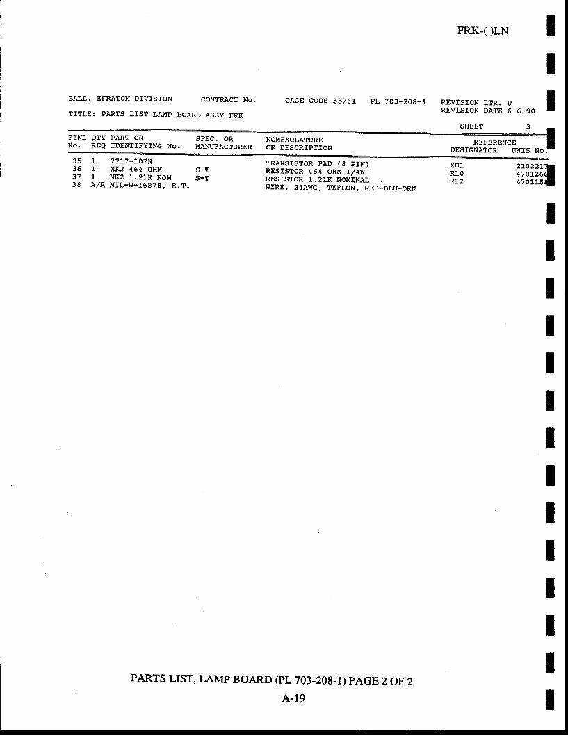
BAI.L, EFRATOM DMSfON CONTRACT No.
TITLE: PARTS L]SI LAMP BoARD ASSY TRK
CAGE CODE 55761 PL 7O3-2O8-1 REVTSION LTR. UREVTSION DATE 5-6-90
FIND QTY PART ORNO. REQ TDENTIFYING No.
SPEC. ORMANUTACIURER
NOII{ENCLAIcUREOR DESCRIPTION
REFERENCEDESIGNATOR UNIS Noi
3 5 L 7 7 L 7 - ! O 7 N36 r, ttr(2 454 oHM37 1 MK2 L .2 l -K NOM38 A/R MIL-W-16878,
BRANSISTOR PAD (8 PrN)RESISTOR 464 oHVr L/4WRESISTOR ]-. 21K NOMINAIWIRE. 24AWc, TETLON, RED-BLU-ORN
PARTS LrST, LAMP BOARD (pL 703_208_1) pAcE 2 OF 2
A_19
iil"iillxuLR10RL2
s-Tc- f i
I
ItII
II
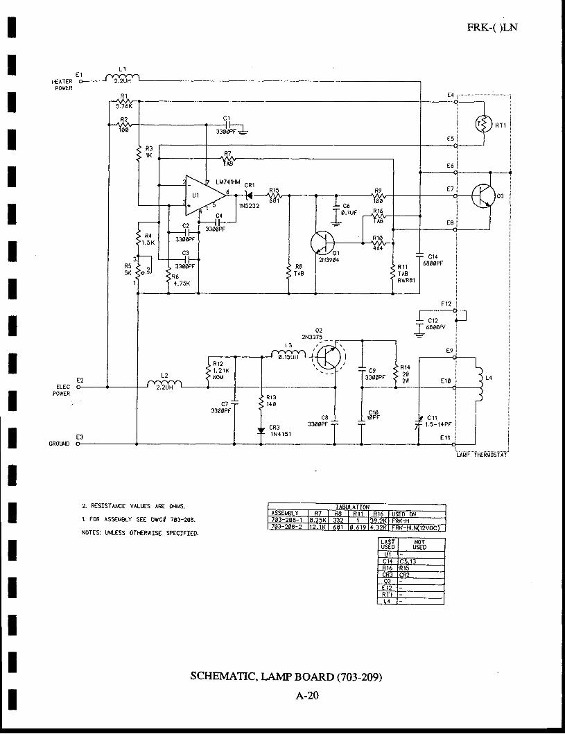
FRK-( )LN
H€TTERPOWIR
x l J
140
c83300PF
LTJ
1 N 4 1 5 ' l
2. RESISTANCE V^LUES ̂RE OHMS.
1. FOR ASSEMBLY SEE DWG# 703-2A8.
NOTES: I,.h{LESS OTI{RWISE SPECIFIEO.
SCHEMATIC, LAMP BOARD (703-209)
A-20
LASTI r (Fn
NOTUSED
U 1t 2
R 1 R
c
R T IL i l
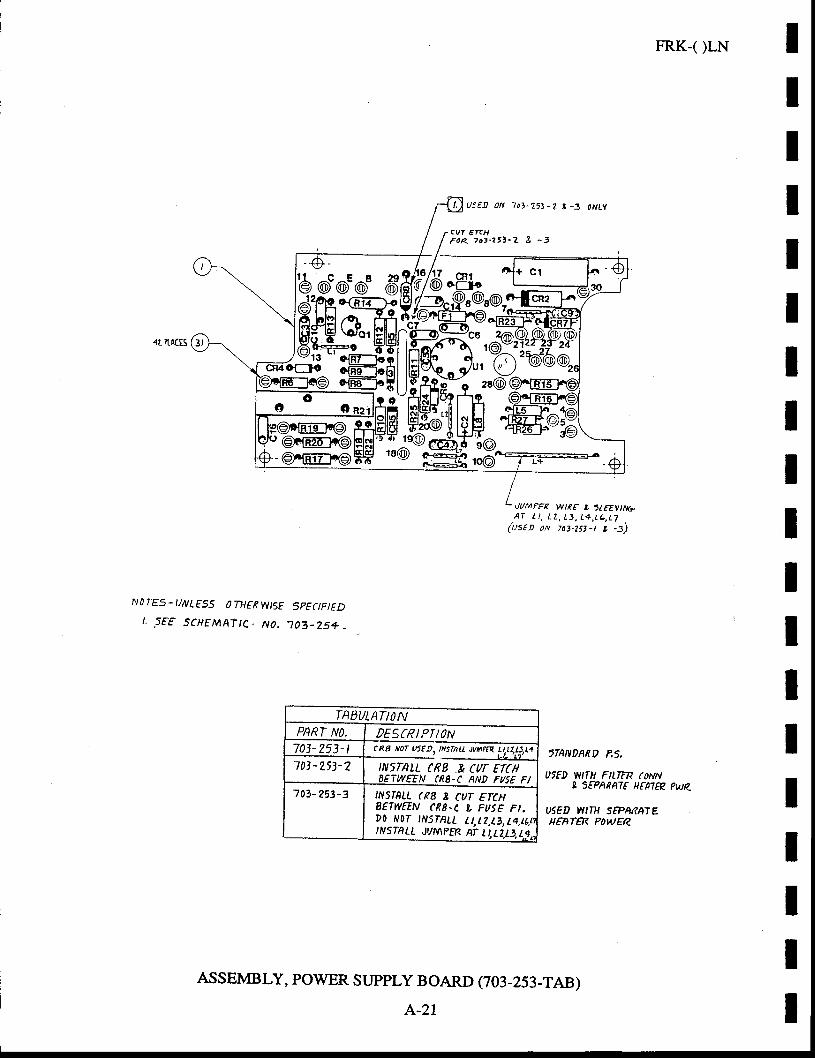
FRK-( )LN
'6-d@'@' 6
G,
€Fffin@@rtErr.€) ilffitr
NOTES.UNLESS OTH€RWISE
I , sFE SCHEMATIC. NO,
SPECIFIED
1 0 a - 2 5 + .
'TANDARD FS,
USED WITH FILffR (ONN9 5€PARATE HFAT€P Pwe
U'ED WITH SEPARATEH€NTER POWER
IItIII
ASSEMBLY, powER slrpply BOARD (703_253_TAB)
A-21
I . cv t € fcH
I/::::::::l:lo c'i "F;-[ffi"-ffi@-G{@@^@.#ffiI
TABULATIONPART NO, DESRIPTION703- 253- t cR8 NoT UtED, tNstALL rVM?ER LLtl!1,14
70t-253-? IN'TALL (R8 & (W ETCHqETWtrN CRI-C AND fI/58 FI
101- 253-3 INSTALL (R8 2 CUT FTUB€TWEEN CRg-C L FUSE FI.D0 i lor ,NSTALL Lt,tz,t3,t4.tL,ttvsTnLL JUMPER Ar ttLl.Lj,L.g,
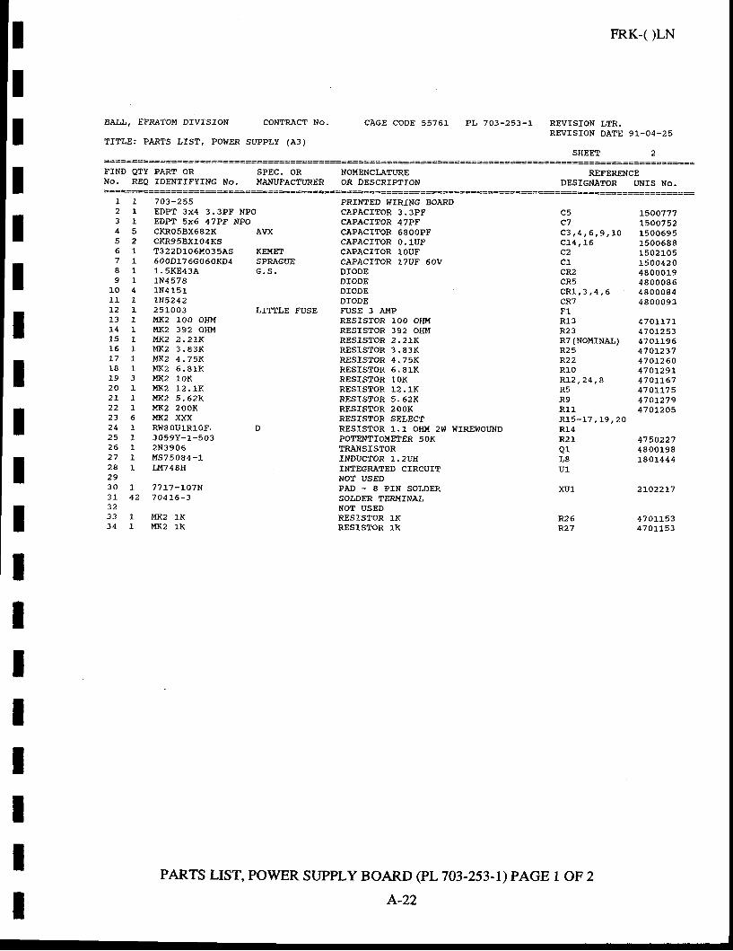
IrItItIIIIIItIII
FRK-( )LN
BAI,I., EFRATO}1 DIVISION CONTRACT No. CAGE CODE 55761 PL 703-253-1 REVISTON IJTR.REVISION DATE 9 ] . -04-25
TrTLE: PARTS I,IST, POWER sUPPty (A3)SHEET 2
FIND QTY PART OR SPEC. OR NOMENCI,ATURE REFERENCEDESIGNATOR UNIS No,No. REQ fDENTfFYING No. ilANUf'ACTURER OR DESCRfPTTON
1
J
4557I9
101 1
L J
141516L718L 92 A2 !2 2
2 5z o
z a
3 05 L
3 23 33 4
PARTS LIST, POWER SUppLy BOARD (pL703-253-1) pAcE I OF 2
1
L
L
L
11
7 03-255EDPT 3X4 3.3PF NPOEDPT 5x5 47PF }IPOCKRO5BX682K AVXcKR95BX104K5T322DlO5l4035AS KE!,iET6OODl76GO6OKD4 SPRAGUE1 . 5 K 8 4 3 A G . S .1N4 5781N4 t 5L7N5242251003 LITTLE FUSEl{Kz 1Oo oHI'{MK2 392 O}IMr, f r<2 2.21KM K 2 3 . 8 3 Kyi l<2 4.75Kl,rK2 6 . 81KMI(2 1OXMK2 12 .1Ky[x2 5.62r<t tK2 200KMK2 XXXRW80U1R10F, D3059Y-1 -5032N3 9 06MS75084 -1LM748H
PRTNTED WTRING BOARDCAPACITOR 3.3PFCAPACUOR 47PFCAPACITOR 68OOPFCAPACITOR O.1UFCAPACITOR ].OUFCAPACTTOR LTVF 6OVDIODEDTODEDIODEDIODEFUSE 3 AMPRESTSTOR 100 oEURESISTOR 392 OHMRESTSTOR 2.21XRESISTOR 3 .83KRESTSTOR 4.75KRESISTOR 6.8] .KRESTSTOR 1OXRESISTOR ] .2.1KRESTSTOR 5.52XRESISTOR 2OOKRESTS?OR SEI,ECTRESISTOR 1.1 OH}T 2W WIREWOTJNDPOTENTIOII{ETER 5OXTRANSISTORTNDUCTOR 1.2UHINTEGRATED CIRCUITl{o? usEDP A D - S P I N S O L D E RSOLDER ?ERD{TNALNOT USEDRESISTOR 1XRESISTOR 1K
c5c7c 3 r 4 r 6 , g r l oc 7 4 , 7 6c2c1cR2cR5c R l , 3 , 4 , 6cR7F1R13R23R7 (NOI\!rNAL)R25P.22R1081 ,2 t 24 tAR5xvR11P' t5-r7 ,L9,2OR14R21Q1L8U1
xu l 2 ro22L7
L500777r50075215006951500588r .502105150042 048 000194 8 0 0 0 8 64 8 000844 800093
470 t t 7 r470t25347 0LL9647 0]-2374701260470129 147 0tL6747 0LL7 547 0L279470I205
475022748 00198180144 4
1 7717 -107N42 7 04 ) . 6 -3
1 MK2 1K1 l,tK2 1K
R26 47 0\1534 7 0 1 1 5 3
A-22
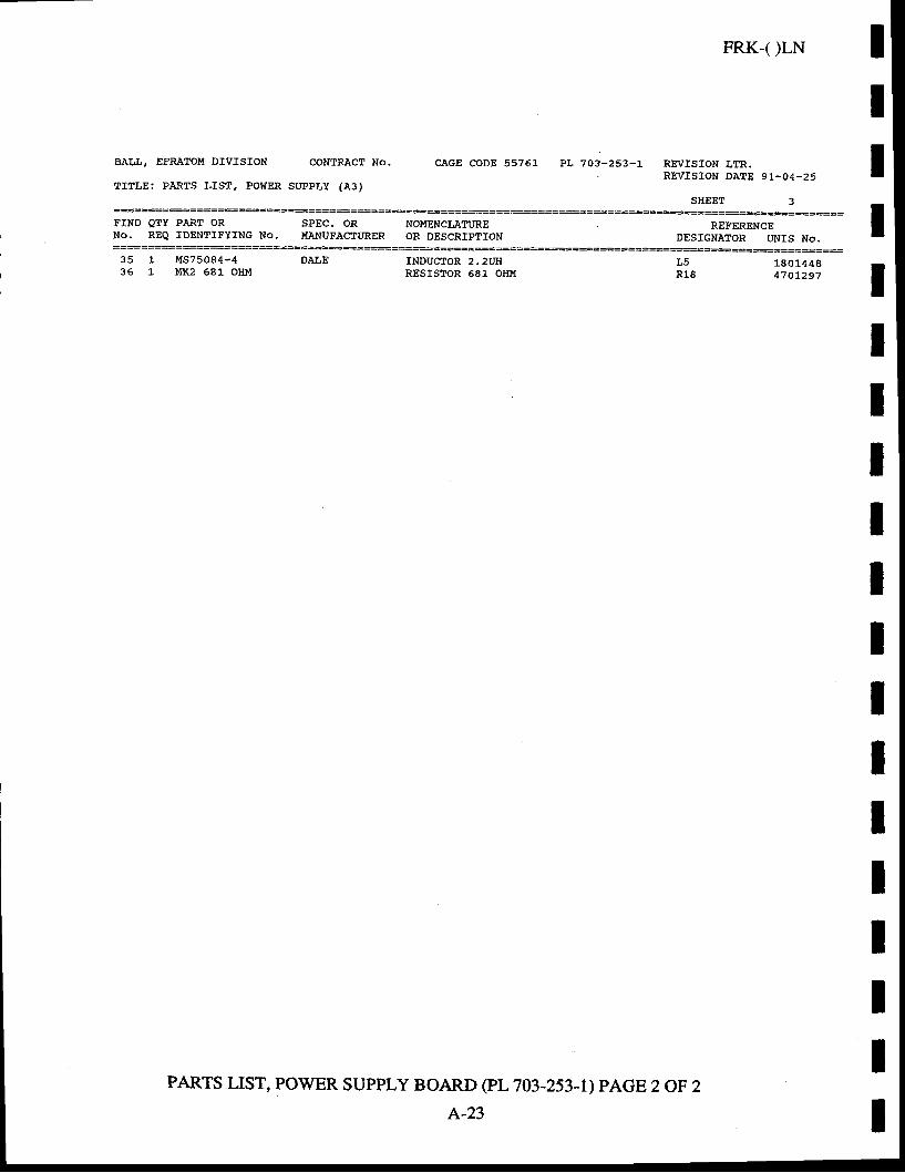
BALI,, EFRATOM DTVISTON
TITLE: PARTS I,TST, POWER
CONTRACT No.
SUPPLY (A3)
FRK-( )LN
CAGE CODE 55751 PL 703-253-1 REVTSION LTR.. REVISION DATE 9L-O4-25
IIIIIIIIIIIIIIIIIII
SHEET 3
F'IND QTY PART OR SPEC. OR NOMENCI,ATT'RE REFERENCEDESTGNATOR UNTS NO.NO. REQ IDENTIFYING NO. I'IANUFACTURER OR DESCRTPTTON
35 1 I '1575084-4 DALE36 1 MK2 681 oltlrl
INDUCTOR 2.2UHRESTSTOR 681 oH}{
L5 1801448r r o 4701297
PARTS LIST, POWER SUppLy BOARD (pL703-253-l) pAcE 2 OF 2
A-23
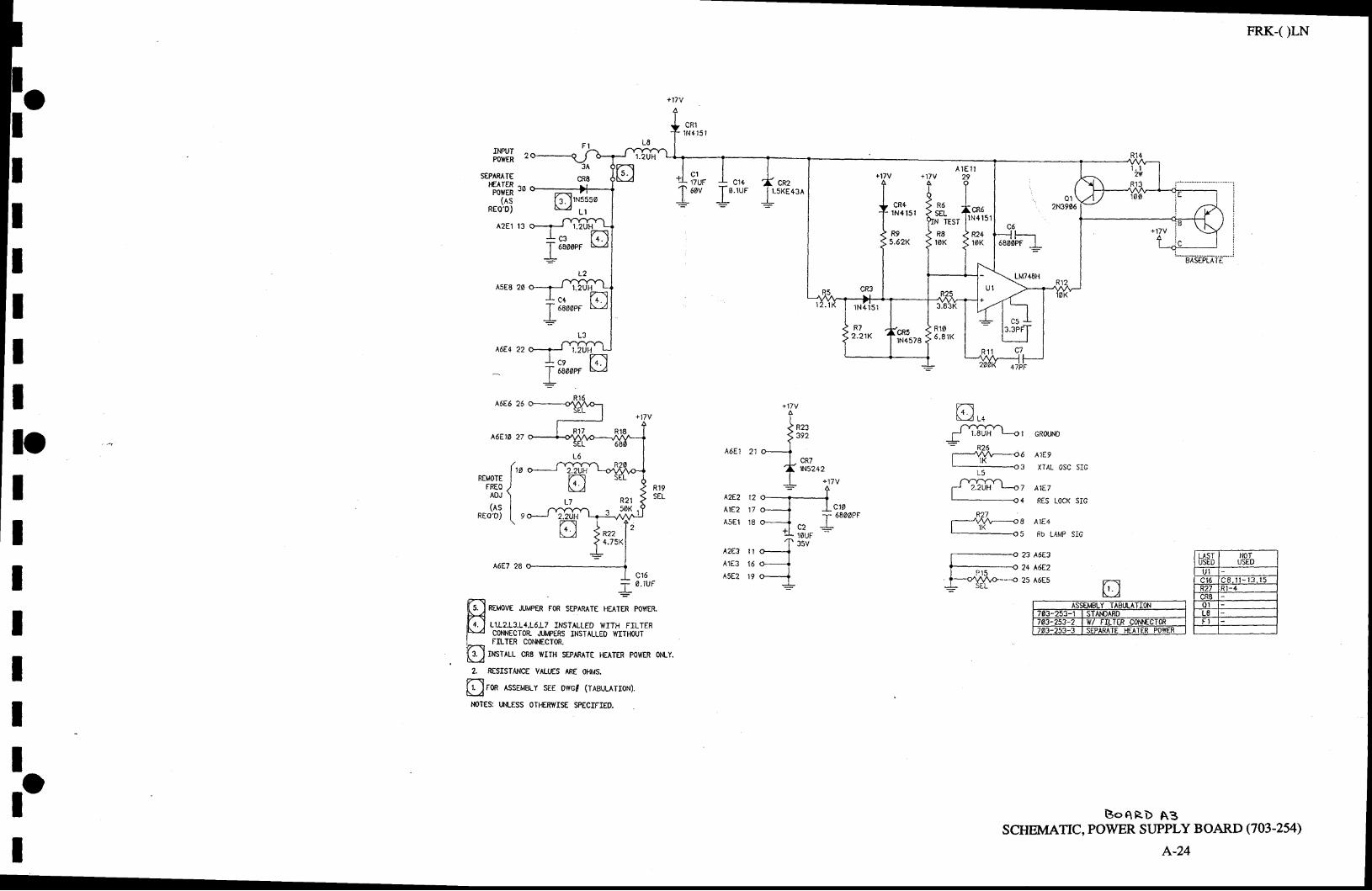
ItllIIIIII
ITFUT .POWER
S€PARATETEATER raPOWER ""
(AsREo'D)
AzEt 13
firuisso. v L t
1 .
c1+.1UF r .5KE43A
17UF6gv r cR2
I
f oaooerI-
L Z
IUH
c4 Gl6860PF v
'L
R106 . 8 1 K
A6E4 22
A6E6 26
45E10 ?7
+ c g
I eaaaerI
rJt ' ,. |
u+r-rrYn.\
r 1.8uH L--or
&:L5
arrrY.\- 2.2UH L---o7 A1E7I-4 RES L0CK SIc
8 A1E4
5 Rb LAMP sIG
f--*---__oxe6E3f- r,Js
-----{ 2+ A6E2
fo^tr*-_o 2s A6Es-
+17y
t{ !3;1
-I cR7
f :r'i.sz+z
| + ' l7v- fH
I l n r ao-...--._. -J_v'v
| 1- 6800PFH ^ ^ |
+ l w 1 -
t l?v'"--*1"---1"-1 :
GROUNO
A1E9
XTAL OSC SIC(,'REMoTE I
FREO /ADJ
)(As I
REo'o) ( e
A2E2 12
AlE2 17
A5E1 18
A2E3 t1
A1E3 15
A5E2 19
itrTlhll
neuov6 .LTMPER FoR SEPARATE HE^rER powER.
l[+. ] lr.lz.le.l+,16.17 TNSTALLED wrrH FTLTERI.v CONNECTOR JIJI.,IPERS INSTALLED WITHOUT',_ rrlren coNNEcroR.
f,c. J rHsrru- cRB wITH SEeARATE HEATER powER otry.
2. RESTSTANCE VALL€S ARE OHMS.rz\I.J. lron ^ssEMBLy sEE D\vc, (TABULATToN).
rcTES: l.h{-ESS oT|{RVISE SPECfFIEo.
IloI
BoeRD A3SCHEMATIC, PO\ryER SUPPLY BOARD (703-254)
FRK-( )LN
cRllN+ t51
)eLI'l TES
R810K
BASEPLATE
LASTUSED
ll0rUSEB
C 1 6
R2t R' t -4
O I
L8F '
A-24

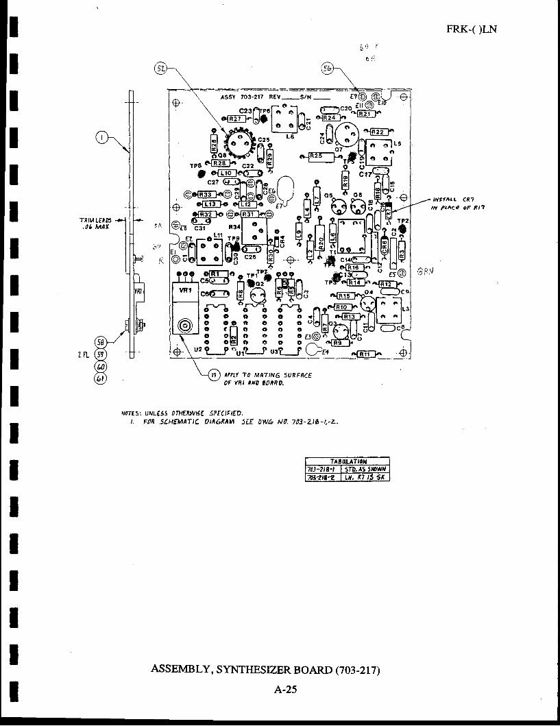
IIItIItIIIIIIIIIIII
|',otSr UNLE5S 0THE$NISEI. FOB STHEMAT'C
SPEC'FIED.o,A6RAn 5EE DWG N0. 703-Zt6-t.-2.
ASSEMBLY, SYNTHESTZER BOARD (7 03 -217 )
FRK-( )LN
,TI"ALL CR1
tt P.Ace oF Rl1
AssY 703-217 REv_s/N_ Ee@ @L/ @e \€ffi'[!s"ffi,*ffiildffiffi.'"i"o"6b7 ^ fi 3'E-
:ffi.?"Fq*fuH$+ffiffi,Ji6jfiE3ffisFu*HN#CIFf;.ffi"fifl|;hffin *fffil H3PtgSJ H'FU3 :S#ijHt$s[:gy'^.ffiffi;'J: inl tii.:HfeT""#q
o ogro o o 3tl(9di*4c'5u2 t-P ''ufl-f u.t--F L--rt nfnj-l^ 49
IITLr TO METING SURFfrCEOF YRI AI{O BOARO.
A-25
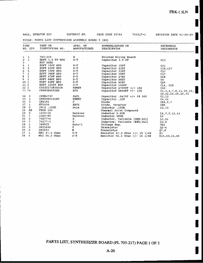
FRK-( )LN I
BALL, EFRATOM DrV CONTRACT NO. CAGE CODE 55761
TITLE: PARTS LIST SYNTHESIZER ASSEMBLY BOARD 5 (A5)
7 032t'l -L
IREVISION DATE 91-04- ' '
I
FINDNO. QTY
PART ORIDENTIFYING NO.
SPEC. ORMANUFACTURER
NONMENLCATURE ORDESCRIPTION
REFERENCEDESIGNATOR I
E
D - f
l - 12 I3
a zo r
7 L8 19 11 0 1)_r 212 ).1 3 1 4
L 4 2a 5 z
1 6 3L 7 1r o z19 AR2 0 52 7 12 2 22 3 2
2 5 32 6 2
2 8 4
D - f
s-Ts-Ts-Tb - I '
b- l '
s-Ts-TKEMETAVX
s&81KEMETFKNOXDa Ie
DelevanDelevanEf,
N a t n r l ,FMS-TS-T
7 03-2L9EDPT 3 .9 PF NPONOT USEDEDPT ].5PF NPOEDPT 22PF NPOEDPT 33PF NPOEDPT 39PF NPOEDPT 47PF NPOEDPT 68PF NPOEDPT 82PF NPOEDPT 1OOPF NPOco52c272K2g5CACKRO5BX582KS
22N4473JCKRO5BXlO4KSI N 4 1 5 1MV1638IM-z . 15UHTYPE 1201 0 2 5 - 3 81 0 2 5 - 5 07 0 2 7 7 - 4
7 0 2 7 7 - 37 805CT2N2369A2 N 3 5 5 3MK2 47 .5 OhnsMK2 56 .2 Ohms
Printed Wiring BoardCapac i to r 3 .9 PF
Capacitor 15PFCapacitor 22PFCapacitor 33PFCapacitor 39PFCapacitor 47PFcapacitor 68pf'Capacitor 82PFCapacitor IOoPFCapacitor 27OOPF +/- LOZCapac i to r 68OoPF + / - 7OZ
Capac i to r .O47UF + / - 5? 5OVCapac i to r .1UFDiodeDiode, varactorInductor .15UHThermal Joint conpoundInductor 5.5UHInductor 18UHInductor, variable (GRN,YeL)fnductor, Variable (RED,YeI)Voltage Reg.TransistorTransistorRes is to r 47 .5 Ohrns + / - 1 ,2 I /4WRes is to r 56 .2 Ohns + l - lZ t l4V l
c 1 3
c 2 1cL9,C27
c17cL8
c29c L 4 , C 2 B
c L , 3 , 4 , 7 , 8 , L L , L 5 , L 6 ,2 0 , 2 2 , 2 4 , 2 5 , 2 6 , 3 7c 2 , 1 2c 5 , c 6c R A , 5 , 7!KO
L 6 , 1 0
L 4 , 7 , 9 , L 2 , L 3L2L 3 , 1 1L 5 , 8VR1Q 2 - 4
Q ] , 8R1P . r g , 2 O , 2 4 , 2 8
IIIIIIIIIIIIIIt
PARTS LIST, SYNTHESIZER BOARD (PL7O3-217) PAGE 1 OF 3
A-26
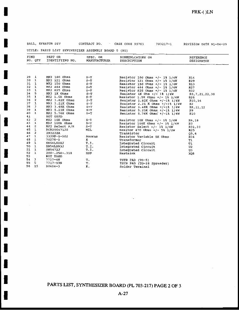
ItI
FRK-( )LN
REVIS ION DATE 91 -04 -29BALL, EFRATOM
TITLE: PARTS
DIV CONTRACT NO.
LIST SYNTHESIZER ASSEMBLY BOARD
CAGE CODE 55761
5 ( A s )
7 03217 -1,
t F INDNO. QTY
PART ORIDENTIFYING NO.
SPEC. ORMANUFACTURER
NONI,IENLCATURE ORDESCRTPTION
REFERENCEDESTGNATOR
1
351 5
IIIIIIIIItIIIII
3 03 1J Z
3 4J f ,
J O
1 a
J O
3 94 0+ I
4 34 4A A
4 6
4 84 95 05 1525 35 45 55 6
I
1
1
51
1J
11
I
I
MK2 l-00 OhnsMK2 121 OhnsMK2 15O OhnsMK2 4 64 OhrnsMK2 825 OhmsMK2 LK OhnsMR2 L.5K OhmsMK2 1 .82K OhnsMR2 2.21"K OhnsM K 2 3 . 4 8 K O h n sMK2 5 .23K OhnsMK2 5 .76K oh r r sNOT USEDMK2 1OK OhnsMK2 1OOK OhrnsMK2 Se1ect A/RRCR2OG47 lJS2N2222}.3 3 39P-1 -5027 027 8 -7SN54LSOOJsNs4LS93JSN5472J2 0 0 - , 2 5 0 - . 3 1 8NOT USED7 7 t 7 - 4 N
77 r7 - 93N
9 0 4 1 6 - 3
S-Ts-Ts-TD - I
D - ' I '
s-T) - rs-TS-TS-Ts-TS-T
s-Ts-T5 - - t
MIL
BournsET . I .r i
T T
HSP
Res is to r 1Oo Ohns + / - 72 L /AWRes is to r 121- Ohms + / - LZ L /4WRes is to r 150 ohns + / - IZ t /4WRes is to r 464 Ohms + / - IZ L /4wRes is to r 825 Ohns + / - LZ 1 /4WRes is to r 1K ohn + / - 7Z t /4wRes is to r 1 .5K Ohms + / - . LZ L l4WRes is to r 1 .82K ohns + / -72 L /4WR e s i s t o r 2 . 2 L K O h n s + / - 1 8 1 / 4 WRes is to r 3 .48K Ohns + / - tZ L /4WRes is to r 5 .23K Ohns + / -72 r /4WRes is to r 5 .?6K Ohms + / - !Z ] - l4W
Res is to r l -OK Obns + / - LZ I /4WRes is to r looK ohns + / - LZ 7 /4WRes is to r Se lec t + / - lZ 7 /4WRes i to r 4?0 Ohns + / - 5>" \ /2WTransistorResistor Variabl-e 5K OhmsTransfornerIntegrated Circuitfntegrated circuitIntegrated CircuitHeatsink
TSTR PAD (TO-5)TSTR PAD (TO-1"8 Spreader)Solder Terninal
R14R29R13
R32R 5 , 7 , 2 r . , 2 2 , 3 0R26R 1 5 , 1 6K Z
R 8 , 1 1 , 1 2
K T U
R 6 , 1 8K J
R 3 1 , 3 3R25Q 5 , 6R 3 4T1u1v2U3xQ8
rm
K .
PARTS LIST, SYNTHESIZER BOARD (PL 7A3-2I7) PAGE 2 OF 3
A-27
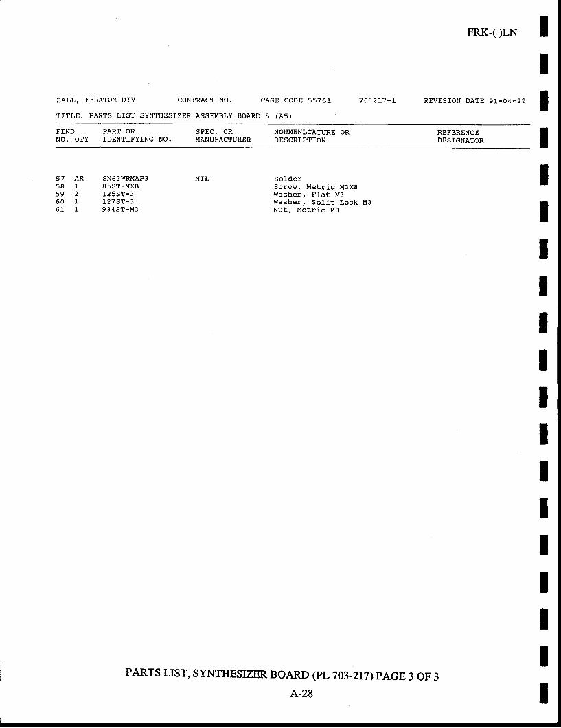
BALL, EFRATOM DIV
rITLE: PARTS LIST
CONTRACT NO.
SYNTHESIZER ASSEMBLY
CAGE CODE 55761
BOARD 5 (A5)
FRK-( )LN I
IREVrsroN DATE e1-04-2e
I7 032L7 -r
FINDNO. QTY
PART ORIDENTIFYTNG NO.
SPEC. ORMANUFACTURER
NONMENLCATURE ORDESCRIPTION
REFERENCEDESIGNATOR I
5 85 95 0O I
AR
I
L
SN53I,{RMAP385ST-MX8125ST-3127 ST-3934ST-M3
UIL SolderScrew, Metr ic M3X8l{asher, FIat I t13Washer, SpJ- i t Lock M3Nut, Metr ic M3
PARTS LIST, SYNTHESIZER BOARD (PL7O3-217) PAGE 3 OF 3
IIIIIIIIIIIIIIIA-28
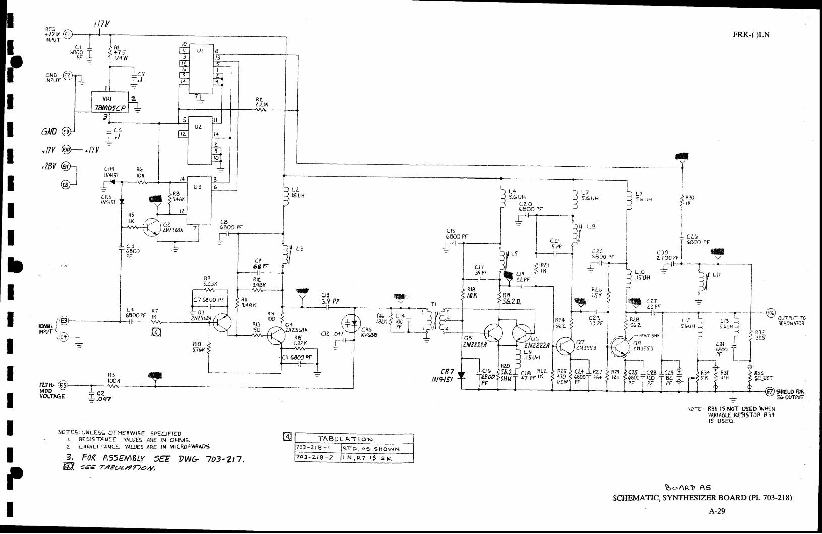
R7IK
Gfn QY L LGI , I
*17y gft *t7l
_nv @1@
t27Hz @.:--MODVOLTAGE
It
l:ItIbIIIIIIIII
FRK-( )LN
cR4lN+r5l
#t_j
II
hlo
rox
=r D q
rN+l5l
L 45.6 UH
LLO6000 PF
L 75,/. UH
L?i6 trH
Lro. I 5UH
Rl0r K
L L GGBN PF
CEGBOO F
gozzNa36eA L8
( z L6300 PF
c 3 0L1 OO ?F
--Jr l
=i-ri.--i
+ t l: l - - \
l -, - 1
*rc
L , 't {Y
',L3K
ct9L L T T
r t a
1.9 PFL46800 Pt
Lb tJH -
--1.Ur/'-
1gfl|t1- TARE5CNNTORQ4
2J{ 236?ARt5LALfi
a6-2N2222hL6. 1 5 U H
a7aN 3553
CL+66rA?F
Ras410u!_w
.CVo'4800
PF
RZO5l,z0Htl
Ii
IJ-r-zgT 8 aI P F
cL| | Lzg(tffi-Tln? r l ? r
P,?7+6+T
I
I'{ 4
i nrt. A1 R
fl145K,+8PF't'i'
Ri3SILFCT
'IIELD FOREbOUTNT
IIOTF-6 : UNLESE 6TTHEEWtSE SpEetFfEDAEs}STNNtE YALUES AFE IN OHMS,CAPAT.ITANCI, Y/|UEs ARE 'N MICROtrARADs
NOTT- R1I 15 NOT t'sED WHTNYA.RTAbLE fiEtlsToR Rl+t9 usEO.
boAR.) A5
,SCHEMATIC, SYNTHESTZER BOARD (PL 7 A3 -218)
+17l/
: ( l i2NZ)6?A
L n o
Kv6ta G '?N2Z22n
T A E U L A T I O N7 0 3 - z t 8 - t STD, A5 sHow-N7 0 3 - z t g - 2 L N ) R ? t s s K3, F2R ASSEttlBLr S€F
W, s€€ T"+Eut una,y,DWG 703-2,7.
A-29

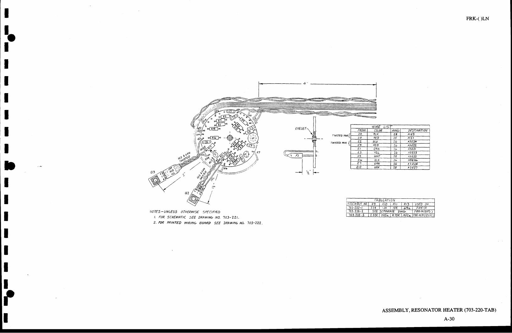
Il.IIIIIIIbIIIIIIII
- ]-M'TED |AIR
TWISnE PA'{
FRK-( )LN
ASSEMBLY, RESONATOR HEATER (703-220-TAB)
A-30
/,JOTEs-UNLESS OTHEBWI5E SP€AFED
I. FOR SCXEMAT|C 5FE DRAWING NO. 703.221.
2. FOR PRNTED WIRING BOARD 5€E DRAWINL NO. 1OJ.222.
A-Y t
WIRE LISFROM I COIOR AWGES 'LK z8E 9 8m 2A A I E IE2 8LU ZG A3€4 R€D ZL AJ EZZ
O R N zle 3 rEL ,41€23E 2 ?8€(. E t K 26 A'EZ6E'7 6RN 2b A1 €28Eto 8RN 28 A 3 € 2 2

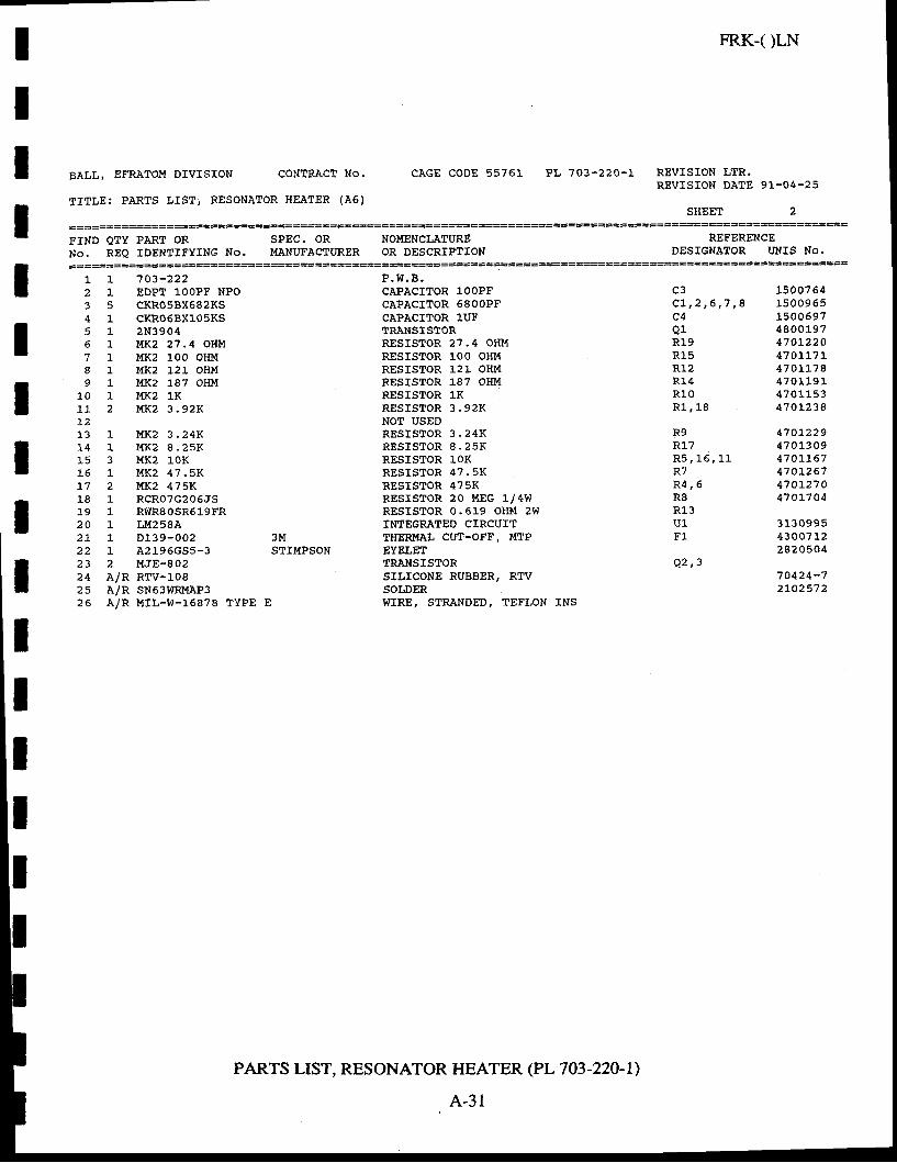
ItIIIIII
ItIIII
CONTRACT NO. CAGE CODE 55761 PL
FRK-( )LN
7O3-22O- I REV IS ION LTR.REVISION DATE 91-04-25
BALL, EFRATOM DIVISION
ITTLE: PARfS LISTI RESONATOR HEATER (A6)
FIND QTY PART OR SPEC. OR NOHENCLATURE
No. REQ IDENTTFYTNG No. MANUFACIURER oR DESCRTPTfON
SHEET 2
REFERENCEDESTGNATOR I'NIS No.
1
2
567I9
a u1 1L Z
t-4I f ,
I b
I 7I O
L 92 02 L2 2Z J
2 5
2 6
11f,
1
703-222EDPT 1OOPF NPOCKROsBX682KSCKRO6BXlOsKS2N3904l.{K2 27.4 0H}1MK2 100 oHl.tMK2 121 OTIMl{K2 187 O}nlMI(2 1KM K 2 3 . 9 2 K
} {K2 3 .24KM K 2 8 . 2 5 XMK2 1OKl {Kz 47 .5KuK2 475KRCRO7G206JSRWR8OSR519FRt!{2 s8AD139-OO2A2 196GS5-3l,rJE-8 02RTv-108SN63WRMAP3UIL-Vi-15878 TYPE
P . W . B .CAPACITOR 1OOPFCAPACITOR 68OOPFCAPACITOR 1UTTRANSISTORRESISTOR 27.4 OIIMRESISTOR 1OO OHMRESISTOR 121 OHURESTSTOR 187 oHl.{RESISIOR 1KRESTSTOR 3 .92KNOf USEDRESTSTOR 3 .24KRESISTOR 8 ,25KRESISTOR lOKRESISTOR 47.5KRESISTOR 475KRESTSTOR 20 !{EG 1/4WRESISTOR 0.619 oHM 2WTNTEGRATED CIRCUITTHERI.'AL cUT-oFF, UTPEYELETTRANSISTORSTLICONE RUBBER, RTVSOTDERWIRA, STRANDED, TEFLON INS
c3c L , 2 , 6 , 7 . , 8
Q 1R19K r f ,
R12R14R10R 1 , 1 8
R9K L I
R 5 , 1 6 , 1 1K /
R 4 , 6R8RX3T I 1
Q 2 , 3
1 5 0 0 7 6 4l s009 651 5 0 0 5 9 74 8 0 0 1 9 747012204707L'7L470t1784 7 0 1 1 9 14 7 0 1 1 5 347 AL238
470722947 013494 7 0 L L 6 747 0r25747 0727 0470L704
313 099543 007 122 8 2 0 5 0 4
70424-72LO2572
1t
I
11
I
1
A /RA IRl / p
3l,ISTIIi,IPSON
E
PARTS LIST, RESONATOR HEATER (PL703-220-r)
A-3r

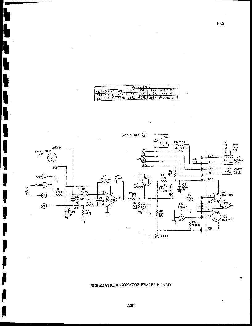
OTIELD ADJ
llllllIIIIIIIIIIIII
TH€2fitEroe,8f l
C.FITLDc0tL
It10T0-CELL
Eb20 ME6
o l \axlflx=, tl
3.1Lr OLMJE. EOZ
u tilr€ -802'
fiaoT-PF I
t@
Rt0
@ch
TA UIATIONASj'(M9LI NO, n9 R t 0 R'I f l r1 u5€o 0N10 t - 7 0 - 3.2 X t ,0x t 0 K . L l t l FKK .11
101- 2L0 - > ?.7Lx Sff t 1.75K , 102 t FRr. HtlJ('lyr(
C 7as00PF
Rt5
SCHEMATIC, RESONATOR HEATER BOARD

IIIIIIIItIItIIIIIII


