Embed Size (px)
Citation preview
Atomistic Simulations of Dislocation Nucleation-ControlledPlasticity in FCC Metallic Nano-Objects: Role of Topology,
Surface Morphology and Internal Interfaces
Atomistische Simulationen zur Versetzungs-Nukleationskontrollierten Plastizitat in kubisch flachenzentrierten
metallischen Nanoobjekten: Rolle der Topologie,Oberflachenmorphologie und inneren Grenzflachen
Der Technischen Fakultat
der Friedrich-Alexander-Universitat Erlangen-Nurnberg
zur
Erlangung des Doktorgrades Dr.-Ing.
vorgelegt von
Zhuocheng Xieaus Chengdu, China
Als Dissertation genehmigtvon der Technischen Fakultatder Friedrich-Alexander-Universitat Erlangen-Nurnberg
Tag der mundlichen Prufung: 01.12.2020Vorsitzende/r des Promotionsorgans: Prof. Dr.-Ing. habil. Andreas Paul Froba
Gutachter/in: Prof. Dr.-Ing. Erik BitzekProf. Dr. rer. nat. Karsten Albe
Zhuocheng XieAtomistic Simulations of Dislocation Nucleation-Controlled Plasticity in FCC Metallic
Nano-Objects: Role of Topology, Surface Morphology and Internal Interfaces
ABSTRACT Metallic nano-objects are regarded as promising candidates for biosensors, catalystsand nanomechanical devices due to their high surface-to-volume ratio and superior mechanicalproperties compared to their bulk counterparts. Plasticity in confined dimensions is controlled bysurface dislocation nucleation. The dislocation activation at the free surfaces and following inter-action and multiplication govern the plastic deformation processes of the nano-objects. Computa-tional modeling particularly atomistic simulations plays an essential role in understanding defor-mation mechanisms at nanoscale, which can provide useful suggestions for material design anddevelopment.
The objectives of this thesis are to understand the role of topology, surface morphology and in-ternal interfaces in surface dislocation nucleation-controlled plasticity of FCC metallic nano-objects.For these purposes, large-scale experimentally-informed molecular dynamics simulations were per-formed on metallic nanowires with parallel and five-fold twin boundaries along the wire axis andnanoporous gold with realistic and artificial network structures. The influence of above-mentionedaspects on the mechanical response of these nano-objects was investigated at the atomic-level.
Parallel twin boundaries along the wire axis show significant effects on strengthening and lo-calization of plastic deformation of nanowires by interacting with surface-nucleated dislocationsunder tension. Surface roughness and facet orientation have significant effects on the dislocationactivation and deformation localization processes of the nanowires during the simulated tensiletests. Single-crystalline and five-fold twinned nanowires show elastic instability under compres-sion resulting in severe and localized plastic deformation. Five-fold twinned nanowires exhibitkink formation and bending mediated plasticity under compression in contrast to the shear slipmediated plasticity in the single-crystalline nanowires. The bent five-fold twinned nanowires afterforce-controlled bending tests show worse reversibility upon bend deformation than the single-crystalline counterparts due to the formation of sessile dislocation locks and grain boundaries in-stead of reversible twinning dislocations in the single-crystalline nanowires.
Nanoporous gold shows strongly size-dependent elastic and plastic responses under compres-sion. Particularly, the effects of surface-induced stress on elastic behavior and surface disloca-tion nucleation are pronounced in sub-10 nm dimensions. In NPG with ligament size of sub-ten-nanometer dimensions and 30 nm, dislocation starvation and dislocation interaction and multipli-cation dominate the plastic flow, respectively. Nanoporous gold shows size-dependent deforma-tion mechanisms, i.e., the formation of small-angle grain boundaries and stacking fault tetrahedradue to the nucleation and interaction of full dislocations was only observed in the compressedporous structure with ligament size of 30 nm. Moreover, the topology- and surface morphology-dependent mechanical responses in nanoporous structures were explained at the atomic-level. Re-alistic nanoporous structure shows early yielding due to the heterogeneity of stress and ligamentsize distributions. The artificial gyroid nanoporous structure exhibits symmetric surface morphol-ogy which leads to the symmetric stress states and nucleation events.
In addition, the outcomes of large-scale experimentally informed atomistic simulations on thenano-objects were correlated with experiments. The importance of realistic geometry in modelingmechanical response of nanomaterials with internal interfaces and heterogeneous microstructureswas demonstrated.
Zhuocheng XieAtomistische Simulationen zur Versetzungs-Nukleations kontrollierten Plastizitat in
kubisch flachenzentrierten metallischen Nanoobjekten: Rolle der Topologie,Oberflachenmorphologie und inneren Grenzflachen
ZUSAMMENFASSUNG Metallische Nano-Objekte gelten aufgrund ihres hohen Oberflachen-zu-Volumen-Verhaltnisses und ihrer uberlegenen mechanischen Eigenschaften gegenuber vergleich-baren massiven Proben als vielversprechende Kandidaten fur Biosensoren, Katalysatoren und nanomech-anische Bauelemente. Die Plastizitat in begrenzten Dimensionen wird durch die Nukleation vonOberflachenversetzungen gesteuert. Die Versetzungsaktivierung an den freien Oberflachen unddie anschließende Versetzungsinteraktion und -multiplikation bestimmen die plastischen Verfor-mungsprozesse der Nano-Objekte. Die Computermodellierung, insbesondere die atomistische Sim-ulation, liefert einen wesentlichen Beitrag zum Verstandnis von Verformungsmechanismen auf derNanoskala, wodurch nutzliche Vorschlage fur Materialdesign und -entwicklung abgeleitet werdenkonnen.
Die Ziele dieser Arbeit sind es, ein besseres Verstandnis uber die Rolle von Topologie, Oberflachen-morphologie und von internen Grenzflachen bei der nukleationskontrollierten Plastizitat von Oberflachen-versetzungen in kfz metallischen Nano-objekten zu erlangen. Zu diesem Zweck wurden groß-skalige, molekulardynamische Simulationen an experimentell-informierten Datensatzen durchgefuhrt.Die Simulationen umfassen die Untersuchung von metallischen Nanodrahten mit parallelen undfunffachen Zwillingsgrenzen entlang der Drahtachse, sowie von nanoporosem Gold mit realistis-chen und kunstlichen Netzwerkstrukturen. Der Einfluss der oben genannten Aspekte auf die mech-anische Reaktion der Nano-Objekte wurde dabei auf atomarer Ebene untersucht.
Die Untersuchungen an den Nanodrahten zeigen, dass parallele Zwillingsgrenzen entlang derDrahtachse unter Zugbelastung durch ihre Wechselwirkung mit Versetzungen, die an der Oberflachenukleiert wurden, zu einer signifikanten Festigkeitssteigerung und Lokalisierung der plastischenVerformung fuhren. Die Oberflachenrauhigkeit und Facettenorientierung der Nanodrahte bein-flusst dabei maßgeblich die Versetzungsaktivierung und Lokalisierungg der Plastizitat wahrendder simulierten Zugversuche. Unter Druckbelastung zeigen einkristalline und funffach verzwill-ingte Nanodrahte eine elastische Instabilitat, was zu einer starken und lokalisierten plastischenVerformung fuhrt. Die funffach verzwillingten Nanodrahte versagen dabei durch Knickbildungund biegeinduzierte Plastizitat, wohingegen die einkristallinen Nanodrahte durch plastisches Ab-scheren versagen. Die, nach der kraftkontrollierten Belastung, gebogenen funffach verzwillingtenNanodrahte zeigen bei der Entlastungeine geringere Reversibilitat der plastischen Verformung alsihre einkristallinen Pendants. Dies ist auf die Bildung von immobilen Versetzungskonfiguratio-nen und Korngrenzen anstelle von reversiblen Zwillingsversetzungen in den einkristallinen Nan-odrahten zuruckzufuhren.
Nanoporoses Gold (NPG) zeigt ein stark großenabhangiges elastisches und plastisches Verfor-mungsverhalten unter Druck. Dabei beeinflusst insbesondere die Oberflachenspannung das elastis-che Verhalten und die Keimbildung von Oberflachenversetzungen bei Großendimensionen unter10 nm. Bei NPG mit einer Ligamentgroße unterhalb von 10 nm und bei einer Ligamentgroßevon 30 nm ist das plastische Verhalten hauptsachlich durch einen Mangel an Versetzungen undVersetzungsinteraktions- bzw. -multiplikationsmechanismen bestimmt. Nanoporoses Gold zeigtgroßenabhangige Verformungsmechanismen. So wird bspw. die Bildung von Kleinwinkelkorn-grenzen und von Stapelfehlertetraedern, welche auf der Keimbildung und Interaktion von vollstandi-gen Versetzungen beruht, nur in der komprimierten porosen Struktur mit einer Ligamentgroße von30 nm beobachtet. In der Arbeit wird weiterfuhrend das Topologie- und Oberflachenmorphologie-abhangige mechanische Verhalten der nanoporosen Strukturen auf atomarer Ebene erklart. Dieexperimentell-informierte, realistische nanoporose Struktur zeigt in der simulierten Kompression

fruhzeitiges plastisches Fließen, was auf die die Heterogenitat der Spannungs- und Ligamentgroßen-verteilung zuruckgefuhrt werden kann. Die kunstliche-erzeugte gyroidale nanoporose Struktur be-sitzt dagegen eine symmetrische Oberflachenmorphologie die zusymmetrischen Spannungszustandenund Nukleationsereignissen fuhrt.
Die Ergebnisse der groß-skaligen experimentell informierten atomistischen Simulationen wer-den in der Arbeit korrelativ mit entsprechenden experimentellen Befunden verglichen. Dadurchwird die Wichtigkeit der Verwendung einer realistischen Probengeometrie bei der Modellierungdes mechanischen Verhaltens von Nanomaterialien mit internen Grenzflachen und heterogenenMikrostrukturen demonstriert.
Statement of Contribution
I declare that the thesis has been composed by myself and that the work has not be submittedfor any other degree or professional qualification. I confirm that the work submitted is my own,except where work which has formed part of jointly-authored publications has been included. Mycontribution and those of the other authors to this work have been explicitly indicated below. Anycontributions from colleagues in the collaboration are also explicitly referenced in the text. I confirmthat appropriate credit has been given within this thesis where reference has been made to the workof others.
The data presented in Section 4.1 Tensile tests on Au nanowire and 5.1 Deformation mecha-nisms of nanowires with parallel twins was obtained in the simulations carried out by myselfunder supervision of Erik Bitzek and the experiments carried out by Jungho Shin under super-vision of Daniel S. Gianola in Materials Department, University of California Santa Barbara. Themechanisms of dislocation-twin boundary interactions in Au bi-crystalline twinned nanowires pre-sented in Subsection 5.1.1 Effect of twin boundaries and the influence of size and strain rate onthe above mentioned mechanisms presented in Subsection 4.1.2 Bi-crystalline twinned nanowiresand Subsection 5.1.5 Influence of simulation parameters were obtained from the investigationscarried out by Jakob Renner in Lehrstuhl Werkstoffkunde und Technologie der Metalle, Friedrich-Alexander-Universitat Erlangen-Nurnberg. I played a major role in the preparation and executionof the simulations, and the data analysis and interpretation are entirely by own work. The dis-cussions with Julien Guenole in Laboratoire d’Etude des Microstructures et de Mecanique desMateriaux, Universite de Lorraine and Aruna Prakash in Institute of Mechanics and Fluid Dynam-ics, Technische Universitat Bergakademie Freiberg helped the interpretation of the work presentedin Subsection 5.1.3 Influence of twin boundary location.
The study presented in Section 4.1 Tensile tests on Au nanowire and 5.1 Deformation mecha-nisms of nanowires with parallel twins was partially published in Acta Materialia as “Origins ofstrengthening and failure in twinned Au nanowires: Insights from in-situ experiments and atom-istic simulations” by Zhuocheng Xie, Jungho Shin, Jakob Renner, Aruna Prakash, Daniel S. Gianola,Erik Bitzek. Erik Bitzek and Daniel S. Gianola conceived the study and were in charge of overalldirection and planning. All authors provided critical feedback and helped shape the research, anal-ysis and manuscript. I carried out research design, investigation, interpretation, writing - originaldraft, writing - review editing and visualization.
The work presented in Section 4.2 Compression tests on Ag nanowire, 4.3 Bending tests onAg nanowire and 5.2 Deformation mechanisms of nanowires with five-fold twins was obtainedin the simulations carried out by myself under supervision of Erik Bitzek and the experimentsby Nadine Schrenker under supervision of Erdmann Spiecker in Institute of Micro- and Nanos-tructure Research, Friedrich-Alexander-Universitat Erlangen-Nurnberg. I played a major role inthe preparation and execution of the simulations, and the data analysis and interpretation areentirely by own work. The discussions with Duancheng Ma in Lehrstuhl Allgemeine Werkstof-feigenschaften, Friedrich-Alexander-Universitat Erlangen-Nurnberg helped the interpretation ofthe work presented in Section 4.2 Compression tests on Ag nanowire and Subsection 5.2.1 Elasticinstability and buckling under compression.
The study presented in Section 4.2 Compression tests on Ag nanowire, 4.3 Bending tests onAg nanowire and 5.2 Deformation mechanisms of nanowires with five-fold twins was partiallypublished in ACS Nano as “Microscopic Deformation Modes and Impact of Network Anisotropyon the Mechanical and Electrical Performance of Five-fold Twinned Silver Nanowire Electrodes”.Erik Bitzek and Erdmann Spiecker conceived the study and were in charge of overall direction
and planning. I carried out research design, investigation, interpretation, writing - original draft,writing - review editing and visualization.
The work presented in Part II Nanoporous gold was obtained in the simulations carried out bymyself under supervision of Erik Bitzek, the experiments carried out by Thomas Przybilla undersupervision of Erdmann Spiecker in Institute of Micro- and Nanostructure Research, Friedrich-Alexander-Universitat Erlangen-Nurnberg and the tomography and sample reconstruction carriedout by Thomas Przybilla and Benjamin Apeleo Zubiri in Institute of Micro- and Nanostructure Re-search, Friedrich-Alexander-Universitat Erlangen-Nurnberg, Aruna Prakash and Stephen T. Kellyand Hrishikesh A. Bale in Carl Zeiss X-ray Microscopy, Pleasanton, USA. Julien Guenole and Iprepared and executed the simulations. The data analysis and interpretation are entirely by ownwork.
The study presented in Part II Nanoporous gold is in preparation for publication. Erik Bitzekand Erdmann Spiecker conceived the study and were in charge of overall direction and planning. Icarried out research design, investigation, interpretation, writing - original draft and visualization.
Contents
1 Introduction 1
2 Theoretical background and literature review 42.1 Deformation mechanisms of FCC metals . . . . . . . . . . . . . . . . . . . . . 4
2.1.1 Dislocations in FCC crystals . . . . . . . . . . . . . . . . . . . . . . . . 42.1.2 Dislocation movement . . . . . . . . . . . . . . . . . . . . . . . . . . . 72.1.3 Dislocation-dislocation interactions . . . . . . . . . . . . . . . . . . . 82.1.4 Twinning . . . . . . . . . . . . . . . . . . . . . . . . . . . . . . . . . . . 10
2.2 Small-scale plasticity . . . . . . . . . . . . . . . . . . . . . . . . . . . . . . . . 122.2.1 Fundamental theories . . . . . . . . . . . . . . . . . . . . . . . . . . . 122.2.2 Experiments . . . . . . . . . . . . . . . . . . . . . . . . . . . . . . . . . 152.2.3 Molecular dynamics simulations . . . . . . . . . . . . . . . . . . . . . 20
2.3 Surface dislocation nucleation . . . . . . . . . . . . . . . . . . . . . . . . . . . 232.3.1 Nucleation criteria . . . . . . . . . . . . . . . . . . . . . . . . . . . . . 232.3.2 Experiments . . . . . . . . . . . . . . . . . . . . . . . . . . . . . . . . . 252.3.3 Atomistic simulations . . . . . . . . . . . . . . . . . . . . . . . . . . . 26
2.4 Dislocation-twin boundary interactions . . . . . . . . . . . . . . . . . . . . . 272.4.1 Experiments . . . . . . . . . . . . . . . . . . . . . . . . . . . . . . . . . 272.4.2 Molecular dynamics simulations . . . . . . . . . . . . . . . . . . . . . 32
2.5 Scientific questions of this thesis . . . . . . . . . . . . . . . . . . . . . . . . . 34
3 Methods 363.1 Atomistic simulations . . . . . . . . . . . . . . . . . . . . . . . . . . . . . . . 36
3.1.1 Interatomic potentials . . . . . . . . . . . . . . . . . . . . . . . . . . . 363.1.2 Boundary conditions . . . . . . . . . . . . . . . . . . . . . . . . . . . . 38
3.2 Simulation setups . . . . . . . . . . . . . . . . . . . . . . . . . . . . . . . . . . 393.2.1 Sample preparation . . . . . . . . . . . . . . . . . . . . . . . . . . . . . 393.2.2 Loading conditions . . . . . . . . . . . . . . . . . . . . . . . . . . . . . 43
3.3 Visualization and analysis . . . . . . . . . . . . . . . . . . . . . . . . . . . . . 443.3.1 Structural analysis . . . . . . . . . . . . . . . . . . . . . . . . . . . . . 443.3.2 Topology and surface morphology analyses . . . . . . . . . . . . . . 45
I Nanowires 47
4 Results 494.1 Tensile tests on Au nanowires . . . . . . . . . . . . . . . . . . . . . . . . . . . 49
4.1.1 Single-crystalline nanowires . . . . . . . . . . . . . . . . . . . . . . . 494.1.2 Bi-crystalline twinned nanowires . . . . . . . . . . . . . . . . . . . . . 504.1.3 Multi-twinned nanowires . . . . . . . . . . . . . . . . . . . . . . . . . 594.1.4 Nanowires with surface roughness . . . . . . . . . . . . . . . . . . . . 60
4.2 Compression tests on Ag nanowires . . . . . . . . . . . . . . . . . . . . . . . 654.2.1 Single-crystalline nanowires . . . . . . . . . . . . . . . . . . . . . . . 654.2.2 Five-fold twinned nanowires . . . . . . . . . . . . . . . . . . . . . . . 684.2.3 Nanowires with different lengths . . . . . . . . . . . . . . . . . . . . . 73
4.3 Bending tests on Ag nanowires . . . . . . . . . . . . . . . . . . . . . . . . . . 764.3.1 Single-crystalline nanowires . . . . . . . . . . . . . . . . . . . . . . . 764.3.2 Five-fold twinned nanowires . . . . . . . . . . . . . . . . . . . . . . . 79
5 Discussion 865.1 Deformation mechanisms of nanowires with parallel twins . . . . . . . . . . 86
5.1.1 Effects of twin boundaries . . . . . . . . . . . . . . . . . . . . . . . . . 865.1.2 Influence of cross-sectional shape . . . . . . . . . . . . . . . . . . . . 935.1.3 Influence of twin boundary location . . . . . . . . . . . . . . . . . . . 945.1.4 Comparison with experiments . . . . . . . . . . . . . . . . . . . . . . 965.1.5 Influence of simulation parameters . . . . . . . . . . . . . . . . . . . . 97
5.2 Deformation mechanisms of nanowires with five-fold twins . . . . . . . . . 1035.2.1 Elastic instability and buckling under compression . . . . . . . . . . 1035.2.2 Reversibility of plastic deformation under bending . . . . . . . . . . 1065.2.3 Resulting microstructures in buckled and bent nanowires . . . . . . 108
6 Conclusions 113
7 Outlook 115
II Nanoporous gold 116
8 Results 1188.1 Geometrical characterizations of samples . . . . . . . . . . . . . . . . . . . . 118
8.1.1 Surface morphology . . . . . . . . . . . . . . . . . . . . . . . . . . . . 1188.1.2 Topology . . . . . . . . . . . . . . . . . . . . . . . . . . . . . . . . . . . 119
8.2 Compression tests on nanoporous gold . . . . . . . . . . . . . . . . . . . . . 1238.2.1 Deformation behavior of experimentally-informed samples . . . . . 1238.2.2 Deformation behavior of geometrically-constructed samples . . . . . 1248.2.3 Deformation behavior of scaled-down samples . . . . . . . . . . . . . 125
9 Discussion 126
9.1 Size effects on deformation behavior . . . . . . . . . . . . . . . . . . . . . . . 1269.1.1 Young’s modulus . . . . . . . . . . . . . . . . . . . . . . . . . . . . . . 1269.1.2 Yield strength . . . . . . . . . . . . . . . . . . . . . . . . . . . . . . . . 1279.1.3 Flow stress . . . . . . . . . . . . . . . . . . . . . . . . . . . . . . . . . . 1299.1.4 Deformation mechanisms . . . . . . . . . . . . . . . . . . . . . . . . . 131
9.2 Influence of geometry on deformation behavior . . . . . . . . . . . . . . . . 1389.2.1 Topology-dependent mechanical properties . . . . . . . . . . . . . . 1389.2.2 Surface-morphology-dependent stress distribution . . . . . . . . . . 139
9.3 Comparison with experiments . . . . . . . . . . . . . . . . . . . . . . . . . . 143
10 Conclusions 145
11 Outlook 147
Appendix 149
A Supplementary material 150
References 152

List of frequently used symbols
A Cross-sectional areaa0 Lattice parameterb Burgers vectorb f Burgers vector of full dislocationbp Burgers vector of partial dislocationCij Elastic constantsD Characteristic sizeDc Critical sized Diameter of nanowireE Young’s modulusE0 Cohesive energyEeff Effective Young’s modulusEs Young’s modulus of solidEsp Energy given by a harmonic spring potentialF Applied forceF Force rateFbend Bending forceG Shear modulusg Genusg Scaled genus densityI Second moment of areaK Spring constantKeff Effective length factorkB Boltzmann constantL Ligament size of nanoporousl Length of nanowireQ Activation free energyQ0 Activation free energy at zero-stress and -temperatureRarea Area ratio between larger and smaller grainsrcore Dislocation core radiusSv Surface area per unit solid volumeT TemperatureTm Melting temperaturet TimeV Volumeγ(hkl) Surface energy of (hkl) planeγsf Stacking fault energyγisf(110) Intrinsic stacking fault energyγusf(112) Unstable stacking fault energyγut(112) Unstable twinning energy
∆t Timestepε Strainε Strain rateθ Bending angleθrevers Reversible bending angleκ1 Minimum principal curvatureκ2 Maximum principal curvatureν Nucleation rateν0 Attempt frequencyρdislocation Dislocation densityσ Stressσ0 Athermal stressσc Activation stressσeff Effective yield strengthσRSS Resolved shear stressσrr Atomic stress along radial directionσs Yield strength of solidσvon Mises Von Mises stressσxx Atomic stress along x directionσy Yield strengthτ Resolved shear stressτth Theoretical critical shear stressφ Relative densityΩ Activation volume
List of frequently used abbreviations
3D Three-dimensionalAFM Atomic force microscopyCN Coordination numberCNA Common neighbor analysisCTB Coherent twin boundaryDDD Discrete dislocation dynamicsDFT Density functional theoryDIC Digital image correlationDVC Digital volume correlationDXA Dislocation analysisEAM Embedded atom methodET Electron tomographyFCC Face centered cubicFE Finite elementFFT Fast Fourier transformationFIB Focused ion beamFIRE Fast Inertial Relaxation EngineGB Grain boundaryGND Geometrically necessary dislocationGNT Geometrically necessary twinGSF Generalized stacking faultHCP Hexagonal closed packedHRTEM High-resolution transmission electron microscopyIMD ITAP Molecular DynamicsISD Interfacial shape distributionISF Intrinsic stacking faultLAMMPS Large-scale Atomic/Molecular Massively Parallel SimulatorMEMS Micro-electromechanical systemsMD Molecular dynamicsMS Molecular staticsNEB Nudged elastic bandNPG Nanoporous goldNPT Isothermal-isobaric ensembleNVE Microcanonical ensembleNVT Canonical ensembleNW NanowireOVITO Open Visualization ToolPBC Periodic boundary conditionsPET Polyethylene terephthalatePVD Physical vapor deposition
RSS Resolved shear stressSAGB Small-angle grain boundarySEM Scanning electron microscopySF Stacking faultSFT Stacking fault tetrahedronSSD Statistically-stored dislocationTB Twin boundaryTEM Transmission electron microscopyUSF Unstable stacking faultUT Unstable twinningXRT X-ray tomography
1 Introduction
1. Introduction
Nanotechnology opens a new era of human history, its applications have dominated ourdaily life from computer to automobile, from medicine to renewable energy. In 1959,Richard Feynman envisioned manifold possibilities at small scale in his famous lecture“There’s Plenty of Room at the Bottom: An Invitation to Enter a New Field of Physics” [1].Since then, the magnificent development of synthesis, observation and characterizationtechniques, especially the invention of scanning tunneling microscope in 1981 [2], drovethe growth of nanotechnology. Today, nanotechnology has been widely used in manyfields, e.g., processors built with sub-10 nm nanoelectronic devices using extreme ultra-violet lithography provide high and power-efficient computational capabilities. Nanoma-terials show extraordinary physical and chemical properties due to their high surface-to-volume ratio. Nanoparticles have been used for cancer diagnosis and therapy since theirsurface plasmon resonance enhances light scattering and absorption [3]. Nanowires havebeen applied in solar cell to achieve higher efficiency of electron collection through an in-crease in surface area [4].
Nanomechanics is a branch of nanotechnology studying fundamental mechanical prop-erties of nanomaterials, which provides a scientific foundation of nanotechnology. Nano-materials show strong size effects on mechanical properties since the governing deforma-tion mechanisms are varying at different characteristic length scales [5–7]. At the nanoscale,the mechanical response of a material is significantly different from its bulk counterpart,e.g., defect-free metallic nanowires show ultra-high-strength close to theoretical strengthsince the plastic deformation is controlled by surface dislocation nucleation [8]. It is essen-tial to gain a comprehensive understanding of size-dependent deformation mechanisms ofnanomaterials, in order to optimize the design strategies for mechanical systems and de-vices at nanoscale and the architectural control of microstructure for structural materials ata large-scale. Computational modeling is an indispensable tool for accurately simulatingand predicting the mechanical response of nanomaterials at the nanoscale. The contri-bution of individual mechanisms on mechanical properties can be disentangled and thepreferable mechanism at each characteristic length scale can be precisely determined usingsimulation techniques.
Internal interfaces such as grain boundaries have been shown to play an essential role indetermining the mechanical properties of nanocrystalline materials [9]. The combined ef-fects of the extrinsic and intrinsic length scales on mechanical properties of nanocrystallinehave been revealed in experiments and simulations [7]. However, the influence of inter-nal interfaces such as twin boundaries on the mechanical response of nano-objects undercomplex loading conditions is still not fully understood. Over the past decade, materialsscientists designed and developed a new class of materials of heterogeneity in microstruc-ture, crystal structure, and chemical composition [10–12]. The heterogeneous materialsat nanoscale show excellent functional and mechanical properties due to the combinationof high surface- or interface-to-volume ratio and structural heterogeneity. E.g., gradientnanostructures possess superior combinations of strength and ductility because of largestrain gradients near interfaces to accommodate incompatible plasticity in soft and hard
1
1 Introduction
domains [11]. For heterogeneous materials, strain gradients due to three-dimensional (3D)structural and mechanical heterogeneity are an essential feature for modeling mechanicalresponse. However, routine experimental characterization methods are not able to capture3D microstructure comprehensively. Extra geometric information to quantitatively charac-terize 3D microstructure is crucial to be implanted in heterogeneous material modelings.Moreover, the combined effect of size-dependent materials properties and microstructuralheterogeneity should also be evaluated in material modelings since size effects play a cru-cial role at the nanoscale.
In this thesis, the role of topology, surface morphology and internal interfaces in sur-face dislocation nucleation controlled plasticity of FCC metals was studied using atomisticsimulations. Nanowires with and without twin boundaries were constructed based onexperimentally-informed cross-sectional shapes and arrangements of twins. By compar-ing simulation results on single-crystalline and twinned nanowires, the influence of twinboundaries on the mechanical response in confined dimensions is better understood. Sim-ulated compression tests were performed on nanoporous structures which were generatedusing three-dimensional reconstructed geometries obtained from electron or X-ray tomog-raphy techniques. By comparing the results of the experimentally-informed simulationswith simulations on geometrically constructed nanoporous samples and samples scaled-down by different factors, a better understanding of the influence of topology, surfacemorphology and characteristic size on the deformation behavior of nanoporous structuresis achieved. The in-situ computational microscopic outcomes were also correlated with thein-situ electron microscopic observations to explain the deformation mechanisms of post-mortem defect structures after mechanical testing in atomic- and femtosecond-resolution.
The scientific questions are addressed regarding the following topics in this thesis: (i)Deformation behavior of Au nanowires under tension. Especially, how do parallel twinboundaries along the wire axis strengthen the nanowires? How does surface roughnessinfluence the surface dislocation nucleation and strengthening effect of longitudinal twinboundaries of nanowires? What is the influence of dislocation-twin boundary interactionon the localization of plastic deformation of nanowires with parallel twin boundaries alongthe wire axis? How do cross-sectional shape and twin boundary location influence the lo-calization of plastic deformation of nanowires with a longitudinal twin boundary? (ii)Deformation behavior of Ag nanowires under compression. In particular, what is the in-fluence of wire length on the elastic instability of nanowires? What is the effect of elasticinstability on the following localization of plastic deformation of nanowires? Why kinkingoccurred in the five-fold twinned nanowires rather than the single-crystalline nanowires?What are the mechanisms of grain boundary formation in the kinked node? (iii) Deforma-tion behavior of Ag nanowires under bending. In particular, what is the influence of lon-gitudinal five-fold twin boundaries on the resulting microstructures of nanowires underbending? What is the effect of longitudinal five-fold twin boundaries on the reversibilityof plastic deformation of bent nanowires after load removal? (iv) Deformation behaviorof nanoporous gold under compression. Especially, how does size influence the elasticresponse, yielding and plastic flow behaviors of nanoporous structures? How does sizeinfluence the deformation mechanisms? How do topology and surface morphology influ-ence the mechanical response of nanoporous structures?
2
1 Introduction
This thesis is organized as follows. In chapter 2, the relevant theories of dislocation andsmall-scale plasticity are briefly introduced. The literature of experiments and atomisticsimulations of nanomechanical testing, surface dislocation nucleation and dislocation-twinboundary interaction is reviewed. In chapter 3, the methods of atomistic simulations, simu-lation setups and data analyses are introduced. Then the main part of this thesis is dividedinto two parts based on different studied nano-objects. In the first part, the simulation re-sults and discussion of nanowires under different loading conditions are introduced. Inthe second part, the simulations on nanoporous gold under compression are presentedand the simulation results are discussed. At the end of each part, the main outcomes aresummarized and an outlook for future work is presented.
3
2 Theoretical background and literature review
2. Theoretical background and literaturereview
In this chapter, the theories of deformation mechanisms of face-centered cubic (FCC) crys-tals in confined dimensions are introduced. Section 2.1 presents the basics of dislocationtype, movement and interaction in FCC metals. In section 2.2, the governing deforma-tion mechanisms in small-scale ranging from micrometer to nanometer are summarized.The numerical models for nucleation criteria in confined dimensions and experimentaland modeling observations of surface dislocation nucleation are reviewed in section 2.3.The deformation mechanisms of nanostructures with internal interfaces, especially twinboundaries, are introduced from both experimental and modeling aspects in section 2.4.The interactions between dislocation and twin boundary and the effects of twins on me-chanical properties and deformation behavior of FCC metals are reviewed. Finally, in sec-tion 2.5, the scientific questions of this thesis are presented, which will be addressed in thefollowing chapters.
2.1. Deformation mechanisms of FCC metals
In this section, the basics of dislocation in FCC metals are introduced. Dislocation typesand a conventional notation for featuring dislocations are introduced in subsection 2.1.1.Glide of dislocation on slip plane in FCC crystals and corresponding critical resolved shearstress (RSS) for slip are introduced in subsection 2.1.2. In subsection 2.1.3, dislocation locksand stair-rod dislocations resulting from dislocation interactions are summarized. Twining,as another important deformation mechanism in FCC metals, is introduced in subsection2.1.4.
2.1.1. Dislocations in FCC crystals
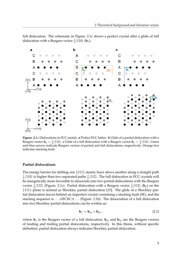
In crystalline solids, imperfections such as point, line, planar and volume defects are widelyexisted and have an effect on the mechanical properties. Line defects also known as dis-locations are the main carriers of plastic deformation in crystalline materials. A more de-tailed introduction of dislocations can be found in the textbooks [13, 14]. The followingparagraphs focus on dislocations in FCC crystals.
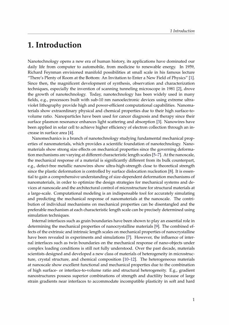
Full dislocations
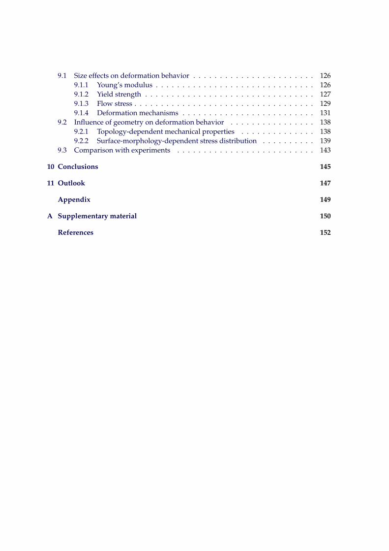
In FCC crystals, atoms in the 111 planes are in the most close-packed arrangement andcontain three 〈110〉 close-packed directions. The sequence of the close-packed layers is. . . ABCABC . . . in FCC crystals (Figure. 2.1a). Glide of dislocation with a Burgers vector12 〈110〉 on the 111 plane is the most energetically favorable in FCC crystals. The crystalstructure remains perfect after the glide of a 1
2 〈110〉 dislocation except the slip leaves behinda step on the crystal surface, therefore the dislocation is termed as perfect dislocation or
4
2 Theoretical background and literature review
full dislocation. The schematic in Figure. 2.1c shows a perfect crystal after a glide of fulldislocation with a Burgers vector 1
2 〈110〉 (b f ).
A
B
C
A
B
C
A
B
C
B
C
A
SF
A
B
C
A
B
C
bp bf
bp
bf
a b c
[112][110]
-
[111]-
Figure. 2.1.: Dislocations in FCC metals. a Perfect FCC lattice. b Glide of a partial dislocation with aBurgers vector bp = 1
6 〈112〉. c Glide of a full dislocation with a Burgers vector b f =12 〈110〉. Green
and blue arrows indicate Burgers vectors of partial and full dislocations, respectively. Orange boxindicates stacking fault.
Partial dislocations
The energy barrier for shifting one 111 atomic layer above another along a straight path12 〈110〉 is higher than two separated paths 1
6 〈112〉. The full dislocation in FCC crystals willbe energetically more favorable to dissociate into two partial dislocations with the Burgersvector 1
6 〈112〉 (Figure. 2.1c). Partial dislocation with a Burgers vector 16 〈112〉 (bp) on the
111 plane is termed as Shockley partial dislocation [15]. The glide of a Shockley par-tial dislocation leaves behind an imperfect crystal containing a stacking fault (SF), and thestacking sequence is . . . ABCBCA . . . (Figure. 2.1b). The dissociation of a full dislocationinto two Shockley partial dislocations can be written as:
b f = blp + btp , (2.1)
where b f is the Burgers vector of a full dislocation, blp and btp are the Burgers vectorsof leading and trailing partial dislocations, respectively. In this thesis, without specificdefinition, partial dislocation always indicates Shockley partial dislocation.
5
2 Theoretical background and literature review
Another important partial dislocation in FCC metals is Frank partial dislocation [16],which is classified as intrinsic or extrinsic by removing or adding an atomic layer in theperfect stacking sequence. The Frank partial dislocation has a Burgers vector 1
3 〈111〉. It isan edge dislocation and can not glide under applied stress since the Burgers vector of theFrank partial dislocation is not contained in any 111 plane.
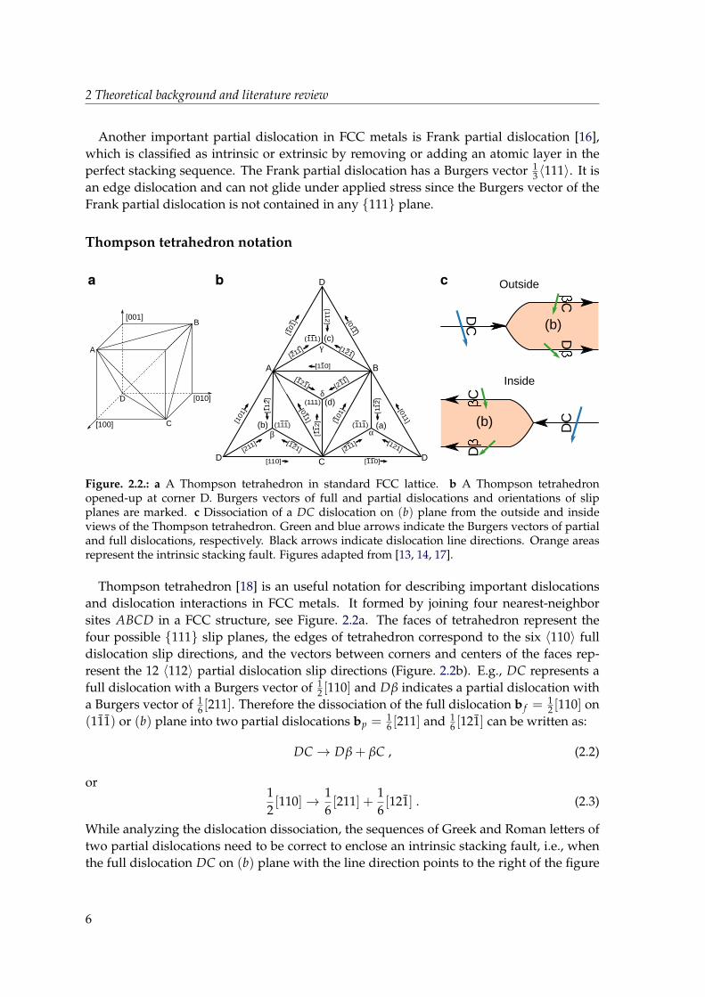
Thompson tetrahedron notation
[011] [1
01]
[121] [211]
[112]
(111)
γ
(111)
δ
(111) (111)
β(b) (a)
(d)
(c)[121]
[101]
[110]
[011]
[211]
[112]
[110]
[011]
[112]
[121][211]
[110]
[121]
[101]
[211]
[112]
α
DD C
A B
D
A
B
C
D
[100]
[010]
[001]
a b c
(b)
DC
DC(b)
D
C
CD
Outside
Inside
Figure. 2.2.: a A Thompson tetrahedron in standard FCC lattice. b A Thompson tetrahedronopened-up at corner D. Burgers vectors of full and partial dislocations and orientations of slipplanes are marked. c Dissociation of a DC dislocation on (b) plane from the outside and insideviews of the Thompson tetrahedron. Green and blue arrows indicate the Burgers vectors of partialand full dislocations, respectively. Black arrows indicate dislocation line directions. Orange areasrepresent the intrinsic stacking fault. Figures adapted from [13, 14, 17].
Thompson tetrahedron [18] is an useful notation for describing important dislocationsand dislocation interactions in FCC metals. It formed by joining four nearest-neighborsites ABCD in a FCC structure, see Figure. 2.2a. The faces of tetrahedron represent thefour possible 111 slip planes, the edges of tetrahedron correspond to the six 〈110〉 fulldislocation slip directions, and the vectors between corners and centers of the faces rep-resent the 12 〈112〉 partial dislocation slip directions (Figure. 2.2b). E.g., DC represents afull dislocation with a Burgers vector of 1
2 [110] and Dβ indicates a partial dislocation witha Burgers vector of 1
6 [211]. Therefore the dissociation of the full dislocation b f =12 [110] on
(111) or (b) plane into two partial dislocations bp = 16 [211] and 1
6 [121] can be written as:
DC → Dβ + βC , (2.2)
or12[110]→ 1
6[211] +
16[121] . (2.3)
While analyzing the dislocation dissociation, the sequences of Greek and Roman letters oftwo partial dislocations need to be correct to enclose an intrinsic stacking fault, i.e., whenthe full dislocation DC on (b) plane with the line direction points to the right of the figure
6
2 Theoretical background and literature review
and is viewed from the outside of the Thompson tetrahedron (Figure. 2.2c), the orders ofpartial dislocations follow a Greek-Roman rule, namely, Greek letters are to the outside ofthe intrinsic fault and Roman letters are to the inside of the intrinsic fault. If the dislocationsare view from the inside of the tetrahedron then the order is reversed, see Figure. 2.2c.
2.1.2. Dislocation movement
Glide and climb are the two basic types of dislocation movement. For FCC crystals, glideoccurs when the dislocation line and the Burgers vector of a dislocation are contained in a111 plane. Climb occurs when the dislocation moves out of the 111 plane, and thusnormal to the Burgers vector. Climb of dislocation needs assistance of diffusion at hightemperatures, therefore, dislocation movement is dominated by glide at lower tempera-tures. In this thesis, climb of dislocation is rarely observed since most of the works aredone at room temperature. Only theory of dislocation glide is introduced in the followingparagraphs. More detailed introduction of climb mechanism can be found in the textbooks[13, 14].
Resolved shear stress
Applied forceSlip plane normal
Slip directionΦ
Applied force
Figure. 2.3.: Illustration of the geometry of slip in a single crystal under uniaxial tension. Figureadapted from [14].
Glide of dislocation results in slip, and slip results in formation of step in crystal surface.In order to achieve a slip, a characteristic shear stress in the slip direction is required. Asillustrated in Figure. 2.3, for a single crystal cylinder with a cross-sectional area A underuniaxial tensile force F, the tensile stress in the loading axis is σ= F
A . In the slip direction,the force F resolves into F cos λ, where λ is the angle between the applied force and theslip direction. The area of the slip plane in this cylinder is A/ cos φ, where φ is the anglebetween the applied force and the normal to the slip plane. Thus the resolved shear stress
7
2 Theoretical background and literature review
τ on the slip plane in the slip direction is:
τ =FA
cos λ cos φ , (2.4)
where cos λ cos φ is termed as Schmid factor [19]. The critical resolved shear stress requiredto start slip is denoted as τc.
Cross-slip
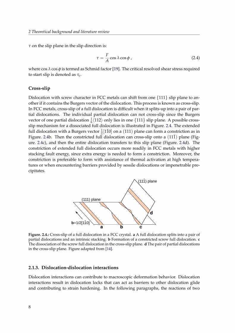
Dislocation with screw character in FCC metals can shift from one 111 slip plane to an-other if it contains the Burgers vector of the dislocation. This process is known as cross-slip.In FCC metals, cross-slip of a full dislocation is difficult when it splits-up into a pair of par-tial dislocations. The individual partial dislocation can not cross-slip since the Burgersvector of one partial dislocation 1
6 〈112〉 only lies in one 111 slip plane. A possible cross-slip mechanism for a dissociated full dislocation is illustrated in Figure. 2.4. The extendedfull dislocation with a Burgers vector 1
2 [110] on a (111) plane can form a constriction as inFigure. 2.4b. Then the constricted full dislocation can cross-slip onto a (111) plane (Fig-ure. 2.4c), and then the entire dislocation transfers to this slip plane (Figure. 2.4d). Theconstriction of extended full dislocation occurs more readily in FCC metals with higherstacking fault energy, since extra energy is needed to form a constriction. Moreover, theconstriction is preferable to form with assistance of thermal activation at high tempera-tures or when encountering barriers provided by sessile dislocations or impenetrable pre-cipitates.
a b c
d
(111) plane
(111) plane-
b=1/2[110]-
Figure. 2.4.: Cross-slip of a full dislocation in a FCC crystal. a A full dislocation splits into a pair ofpartial dislocations and an intrinsic stacking. b Formation of a constricted screw full dislocation. cThe dissociation of the screw full dislocation in the cross-slip plane. d The pair of partial dislocationsin the cross-slip plane. Figure adapted from [14].
2.1.3. Dislocation-dislocation interactions
Dislocation interactions can contribute to macroscopic deformation behavior. Dislocationinteractions result in dislocation locks that can act as barriers to other dislocation glideand contributing to strain hardening. In the following paragraphs, the reactions of two
8
2 Theoretical background and literature review
extended full dislocations in different 111 slip planes result in Lomer-Cottrell lock andHirth lock are introduced.
(111)
(111)-
1/6[211]
1/6[2-
1
1/6[112]-
1/6[211]
Stair-rod d
1/6[0
a b
δ
β
Figure. 2.5.: a Two dissociated full dislocations with b f =12 [110] on (111) plane and b f =
12 [101] on
(111) plane. b Formation of a stair-rod dislocation with a Burgers vector of 16 [011] after interaction
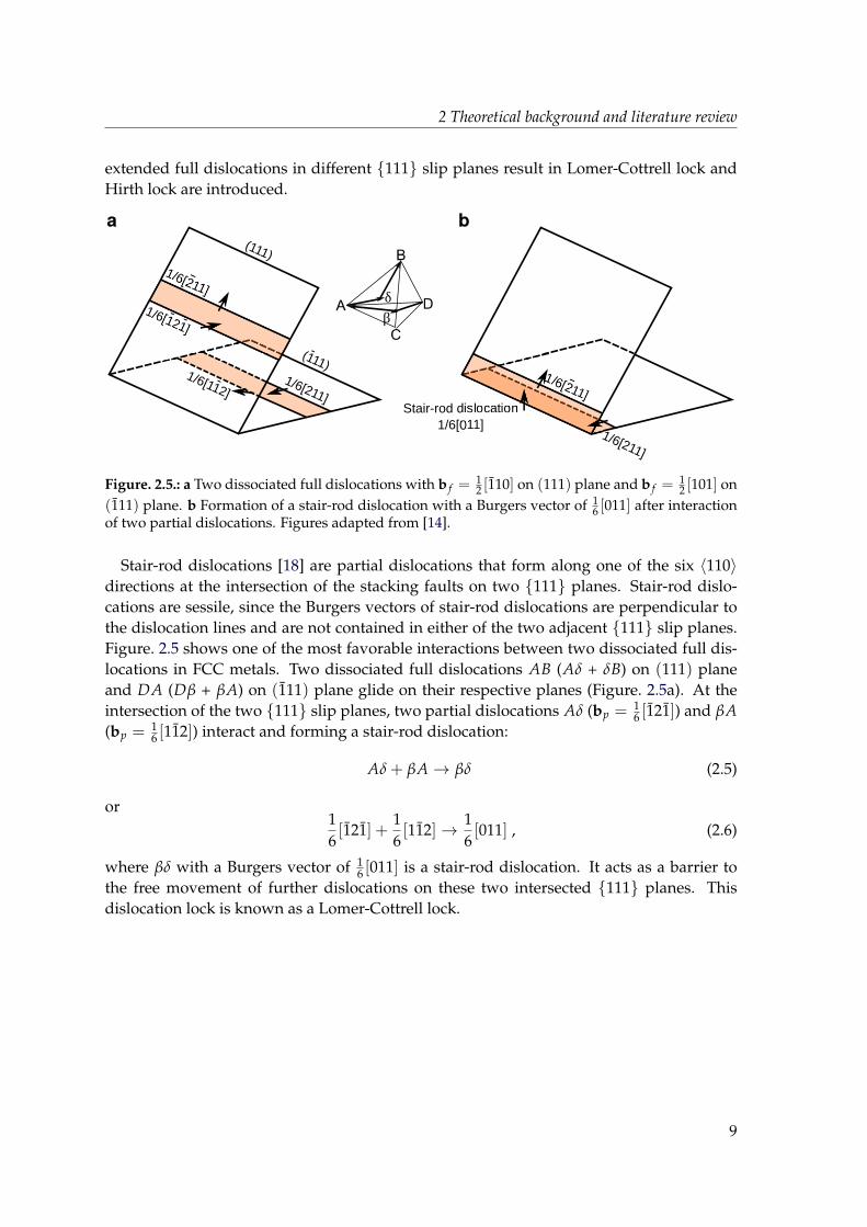
of two partial dislocations. Figures adapted from [14].
Stair-rod dislocations [18] are partial dislocations that form along one of the six 〈110〉directions at the intersection of the stacking faults on two 111 planes. Stair-rod dislo-cations are sessile, since the Burgers vectors of stair-rod dislocations are perpendicular tothe dislocation lines and are not contained in either of the two adjacent 111 slip planes.Figure. 2.5 shows one of the most favorable interactions between two dissociated full dis-locations in FCC metals. Two dissociated full dislocations AB (Aδ + δB) on (111) planeand DA (Dβ + βA) on (111) plane glide on their respective planes (Figure. 2.5a). At theintersection of the two 111 slip planes, two partial dislocations Aδ (bp = 1
6 [121]) and βA(bp = 1
6 [112]) interact and forming a stair-rod dislocation:
Aδ + βA→ βδ (2.5)
or16[121] +
16[112]→ 1
6[011] , (2.6)
where βδ with a Burgers vector of 16 [011] is a stair-rod dislocation. It acts as a barrier to
the free movement of further dislocations on these two intersected 111 planes. Thisdislocation lock is known as a Lomer-Cottrell lock.
9
2 Theoretical background and literature review
(111)
(111)-
1/6[211]
1/6[2-
1
1/6[121]-
1/6[211]
Hirth d
1/3
a b
A
C
D
B
δβ
Figure. 2.6.: a Two dissociated full dislocations with b f = 12 [110] on (111) plane and b f = 1
2 [110]on (111) plane. b Formation of a Hirth dislocation with a Burgers vector of 1
3 [010] after interactionof two partial dislocations. Figures adapted from [14].
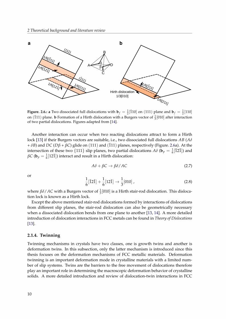
Another interaction can occur when two reacting dislocations attract to form a Hirthlock [13] if their Burgers vectors are suitable, i.e., two dissociated full dislocations AB (Aδ
+ δB) and DC (Dβ + βC) glide on (111) and (111) planes, respectively (Figure. 2.6a). At theintersection of these two 111 slip planes, two partial dislocations Aδ (bp = 1
6 [121]) andβC (bp = 1
6 [121]) interact and result in a Hirth dislocation:
Aδ + βC → βδ/AC (2.7)
or16[121] +
16[121]→ 1
3[010] , (2.8)
where βδ/AC with a Burgers vector of 13 [010] is a Hirth stair-rod dislocation. This disloca-
tion lock is known as a Hirth lock.Except the above mentioned stair-rod dislocations formed by interactions of dislocations
from different slip planes, the stair-rod dislocation can also be geometrically necessarywhen a dissociated dislocation bends from one plane to another [13, 14]. A more detailedintroduction of dislocation interactions in FCC metals can be found in Theory of Dislocations[13].
2.1.4. Twinning
Twinning mechanisms in crystals have two classes, one is growth twins and another isdeformation twins. In this subsection, only the latter mechanism is introduced since thisthesis focuses on the deformation mechanisms of FCC metallic materials. Deformationtwinning is an important deformation mode in crystalline materials with a limited num-ber of slip systems. Twins are the barriers to the free movement of dislocations thereforeplay an important role in determining the macroscopic deformation behavior of crystallinesolids. A more detailed introduction and review of dislocation-twin interactions in FCC
10
2 Theoretical background and literature review
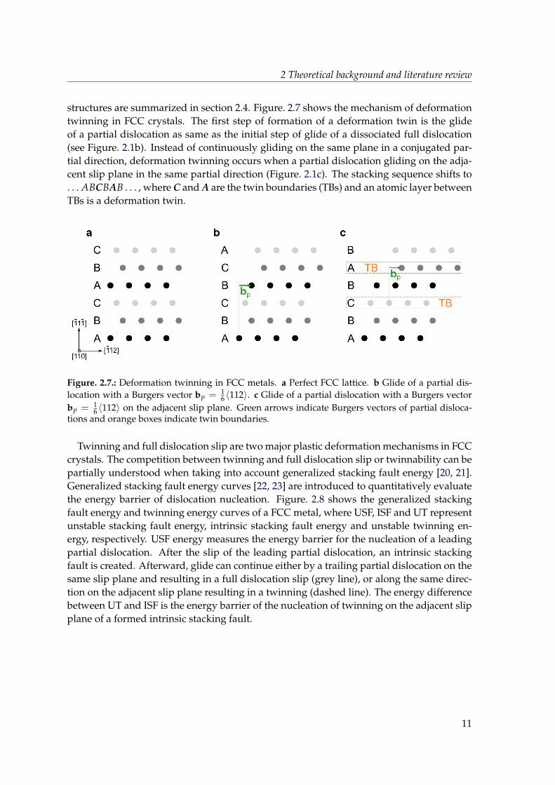
structures are summarized in section 2.4. Figure. 2.7 shows the mechanism of deformationtwinning in FCC crystals. The first step of formation of a deformation twin is the glideof a partial dislocation as same as the initial step of glide of a dissociated full dislocation(see Figure. 2.1b). Instead of continuously gliding on the same plane in a conjugated par-tial direction, deformation twinning occurs when a partial dislocation gliding on the adja-cent slip plane in the same partial direction (Figure. 2.1c). The stacking sequence shifts to. . . ABCBAB . . . , where C and A are the twin boundaries (TBs) and an atomic layer betweenTBs is a deformation twin.
A
B
C
A
B
C
A
B
C
B
C
A
bp
a b c
[112][110]
-
[111]-
Figure. 2.7.: Deformation twinning in FCC metals. a Perfect FCC lattice. b Glide of a partial dis-location with a Burgers vector bp = 1
6 〈112〉. c Glide of a partial dislocation with a Burgers vectorbp = 1
6 〈112〉 on the adjacent slip plane. Green arrows indicate Burgers vectors of partial disloca-tions and orange boxes indicate twin boundaries.
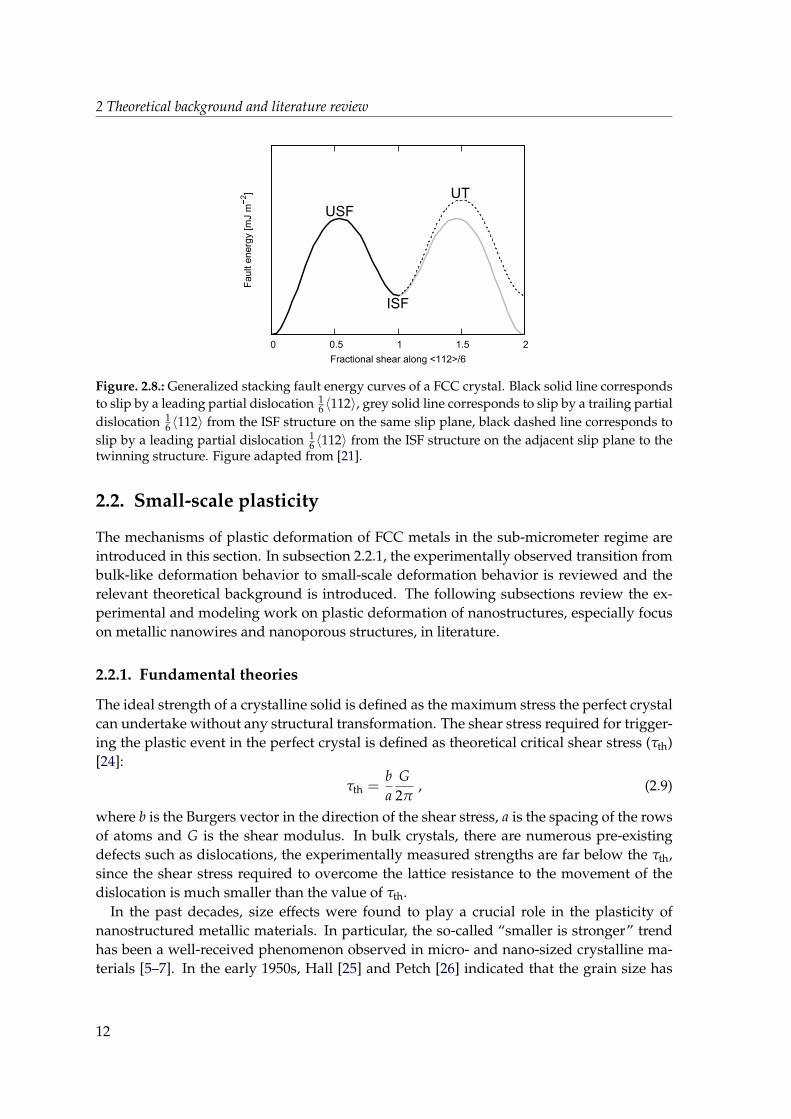
Twinning and full dislocation slip are two major plastic deformation mechanisms in FCCcrystals. The competition between twinning and full dislocation slip or twinnability can bepartially understood when taking into account generalized stacking fault energy [20, 21].Generalized stacking fault energy curves [22, 23] are introduced to quantitatively evaluatethe energy barrier of dislocation nucleation. Figure. 2.8 shows the generalized stackingfault energy and twinning energy curves of a FCC metal, where USF, ISF and UT representunstable stacking fault energy, intrinsic stacking fault energy and unstable twinning en-ergy, respectively. USF energy measures the energy barrier for the nucleation of a leadingpartial dislocation. After the slip of the leading partial dislocation, an intrinsic stackingfault is created. Afterward, glide can continue either by a trailing partial dislocation on thesame slip plane and resulting in a full dislocation slip (grey line), or along the same direc-tion on the adjacent slip plane resulting in a twinning (dashed line). The energy differencebetween UT and ISF is the energy barrier of the nucleation of twinning on the adjacent slipplane of a formed intrinsic stacking fault.
11
2 Theoretical background and literature review
0 0.5 1 1.5 2
Fault e
nerg
y [m
J m
2]
Fractional shear along <112>/6
USF
UT
ISF
Figure. 2.8.: Generalized stacking fault energy curves of a FCC crystal. Black solid line correspondsto slip by a leading partial dislocation 1
6 〈112〉, grey solid line corresponds to slip by a trailing partialdislocation 1
6 〈112〉 from the ISF structure on the same slip plane, black dashed line corresponds toslip by a leading partial dislocation 1
6 〈112〉 from the ISF structure on the adjacent slip plane to thetwinning structure. Figure adapted from [21].
2.2. Small-scale plasticity
The mechanisms of plastic deformation of FCC metals in the sub-micrometer regime areintroduced in this section. In subsection 2.2.1, the experimentally observed transition frombulk-like deformation behavior to small-scale deformation behavior is reviewed and therelevant theoretical background is introduced. The following subsections review the ex-perimental and modeling work on plastic deformation of nanostructures, especially focuson metallic nanowires and nanoporous structures, in literature.
2.2.1. Fundamental theories
The ideal strength of a crystalline solid is defined as the maximum stress the perfect crystalcan undertake without any structural transformation. The shear stress required for trigger-ing the plastic event in the perfect crystal is defined as theoretical critical shear stress (τth)[24]:
τth =ba
G2π
, (2.9)
where b is the Burgers vector in the direction of the shear stress, a is the spacing of the rowsof atoms and G is the shear modulus. In bulk crystals, there are numerous pre-existingdefects such as dislocations, the experimentally measured strengths are far below the τth,since the shear stress required to overcome the lattice resistance to the movement of thedislocation is much smaller than the value of τth.
In the past decades, size effects were found to play a crucial role in the plasticity ofnanostructured metallic materials. In particular, the so-called “smaller is stronger” trendhas been a well-received phenomenon observed in micro- and nano-sized crystalline ma-terials [5–7]. In the early 1950s, Hall [25] and Petch [26] indicated that the grain size has
12
2 Theoretical background and literature review
a strong impact on the strength of polycrystalline metals and the well-known Hall-Petchpower law relation:
σy = σ0 + kD−n , (2.10)
was introduced to measure the yield strength (σy) of a bulk metal with the grain size (D),where σ0 is the bulk strength of the same material, k and n are two independent positiveconstants.
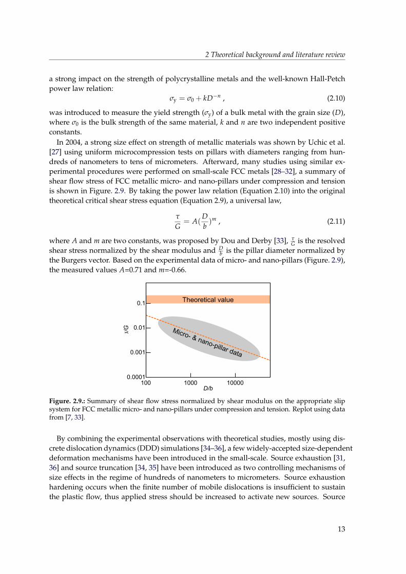
In 2004, a strong size effect on strength of metallic materials was shown by Uchic et al.[27] using uniform microcompression tests on pillars with diameters ranging from hun-dreds of nanometers to tens of micrometers. Afterward, many studies using similar ex-perimental procedures were performed on small-scale FCC metals [28–32], a summary ofshear flow stress of FCC metallic micro- and nano-pillars under compression and tensionis shown in Figure. 2.9. By taking the power law relation (Equation 2.10) into the originaltheoretical critical shear stress equation (Equation 2.9), a universal law,
τ
G= A(
Db)m , (2.11)
where A and m are two constants, was proposed by Dou and Derby [33], τG is the resolved
shear stress normalized by the shear modulus and Db is the pillar diameter normalized by
the Burgers vector. Based on the experimental data of micro- and nano-pillars (Figure. 2.9),the measured values A=0.71 and m=-0.66.
0.1
0.01
0.001
0.0001100 1000 10000
D/b
/G Micro- & nano-pillar data
Theoretical value
Figure. 2.9.: Summary of shear flow stress normalized by shear modulus on the appropriate slipsystem for FCC metallic micro- and nano-pillars under compression and tension. Replot using datafrom [7, 33].
By combining the experimental observations with theoretical studies, mostly using dis-crete dislocation dynamics (DDD) simulations [34–36], a few widely-accepted size-dependentdeformation mechanisms have been introduced in the small-scale. Source exhaustion [31,36] and source truncation [34, 35] have been introduced as two controlling mechanisms ofsize effects in the regime of hundreds of nanometers to micrometers. Source exhaustionhardening occurs when the finite number of mobile dislocations is insufficient to sustainthe plastic flow, thus applied stress should be increased to activate new sources. Source
13
2 Theoretical background and literature review
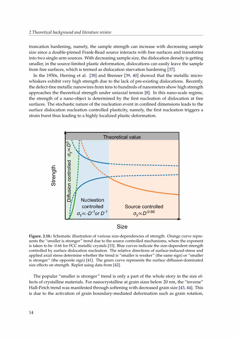
truncation hardening, namely, the sample strength can increase with decreasing samplesize since a double-pinned Frank-Read source interacts with free surfaces and transformsinto two single-arm sources. With decreasing sample size, the dislocation density is gettingsmaller, in the source-limited plastic deformation, dislocations can easily leave the samplefrom free surfaces, which is termed as dislocation starvation hardening [37].
In the 1950s, Herring et al. [38] and Brenner [39, 40] showed that the metallic micro-whiskers exhibit very high strength due to the lack of pre-existing dislocations. Recently,the defect-free metallic nanowires from tens to hundreds of nanometers show high strengthapproaches the theoretical strength under uniaxial tension [8]. In this nano-scale regime,the strength of a nano-object is determined by the first nucleation of dislocation at freesurfaces. The stochastic nature of the nucleation event in confined dimensions leads to thesurface dislocation nucleation controlled plasticity, namely, the first nucleation triggers astrain burst thus leading to a highly localized plastic deformation.
Size
Str
en
gth
eoretical value
Source controlled
σy∝D-0.66
Figure. 2.10.: Schematic illustration of various size-dependencies of strength. Orange curve repre-sents the “smaller is stronger” trend due to the source controlled mechanisms, where the exponentis taken to be -0.66 for FCC metallic crystals [33]. Blue curves indicate the size-dependent strengthcontrolled by surface dislocation nucleation. The relative directions of surface-induced-stress andapplied axial stress determine whether the trend is “smaller is weaker” (the same sign) or “smalleris stronger” (the opposite sign) [41]. The green curve represents the surface diffusion-dominatedsize effects on strength. Replot using data from [42].
The popular “smaller is stronger” trend is only a part of the whole story in the size ef-fects of crystalline materials. For nanocrystalline at grain sizes below 20 nm, the “inverse”Hall-Petch trend was manifested through softening with decreased grain size [43, 44]. Thisis due to the activation of grain boundary-mediated deformation such as grain rotation,
14
2 Theoretical background and literature review
grain boundary migration and sliding in this length scale. A “smaller is weaker” trendwas also introduced in defect-free nano-objects with sub-hundred-nanometer dimensions[41, 42], see Figure. 2.10. In this regime, the surface-to-volume ratio is quite high, theelastic response [45] and the activation processes of surface dislocation nucleation [41, 42]are highly influenced by the surface-induced stress. The strengthening or weakening instrength [41, 42] and softening or stiffening in Young’s modulus [45] are determined by thecombined effects of surface-induced stress and applied axial stress. Moreover, the influenceof surface morphology such as roughness, steps and edges on weakening effect becomesclearly visible in the very small volume where surface diffusion could take over the plastic-ity [46, 47]. A more detailed introduction of surface dislocation nucleation is summarizedin section 2.3.
2.2.2. Experiments
The recent developments of nanomechanical testing and characterization methods togetherwith advanced fabrication techniques of high quality nano-objects allow us to gain in-sight into small-scale plasticity. Major efforts have been undertaken to develop in-situ andex-situ mechanical testing setups. E.g., nanoindentation has been widely used to locallymeasure the hardness and stiffness of materials [48, 49], microcompression of pillars andparticles can also be achieved using nanoindentation equipment with a flat punch [27].Three-point bending test using atomic force microscopy (AFM) tip has been applied ondouble clamped nanowires [50]. For tensile testing, various micro-electromechanical sys-tems (MEMS) [51–53] were developed to perform in-situ mechanical testing on nanowiresin scanning electron microscopy (SEM), transmission electron microscopy (TEM) and X-ray diffraction. For a more detailed introduction of mechanical testing methods in thesmall-scale, one can refer to a review paper in this field [54]. In the following paragraphs,previous experimental studies on the mechanical behaviors of nanowires and nanoporousstructures are reviewed. For the influence of internal interfaces such as twin boundaries onmechanical behaviors of nano-objects, a literature review is presented in section 2.4.
Nanowires
Metallic nanowires (NWs) exhibit excellent mechanical properties, conductivity and op-tical transmittance are regarded as promising building blocks for flexible and stretchableelectronic devices [8, 50, 55–57]. NWs show extremely high yield strengths close to theirtheoretical value, since the plasticity of these defect-free samples requires the nucleation ofdislocations at free surfaces [8, 21, 50]. The mechanical behaviors of FCC NWs have beenextensively studied in experiments under different loading conditions.
Nanoindentation using AFM tip has been widely used in nanomechanical testing ofNWs. In 2003, Li et al. [58] performed nanoindentation tests on Ag NWs with diametersaround 40 nm on a substrate. The wires were synthesized using wet chemical synthesismethods. The peak nanoindentation depth was 15 nm, the nanoindentation elastic mod-ulus was calculated following the Oliver-Pharr procedure [48]. The measured hardnessand elastic modulus values of the Ag NWs were about 0.87 GPa and 88 GPa, respectively.
15
2 Theoretical background and literature review
A pronounced size-dependent hardness was observed, Ag NWs showed more than twotimes higher hardness than their bulk counterparts. In 2005, Wu et al. [50] performed three-point bending tests on Au NWs ranging in diameters from 40 nm to 250 nm, which weresynthesized electrochemically. The NWs were double clamped by electron-beam-induceddeposition, and a lateral load was applied by an AFM tip. The tested Au NWs showed astrong size effect on the yield strength which is up to 100 times higher than bulk Au. Astrain-hardening in plasticity was characterized, the authors attributed this hardening be-havior to the operative dislocation motion and pile-up down to sub-hundred nm. Recently,the three-point bending tests using the AFM tip were performed on Au NWs under in-situcoherent X-ray diffraction [59]. The combination of these techniques could improve ourunderstanding of the small plastic deformation of nanostructures.
In-situ tensile tests have been performed on FCC metallic NWs fabricated by variousapproaches. In 2009, Richter et al. [8] fabricated 〈110〉-oriented FCC metallic NWs withdiameters ranging from 20 to 250 nm via physical vapor deposition under molecular beamepitaxy conditions. The wires show excellent crystal quality with well-defined side facetsand no detectable defects. Before testing the wires were gripped by electron-beam-induceddeposition, and the in-situ tensile tests at a constant strain rate were performed in SEM. Thelocal strain was measured by digital image correlation (DIC) of the SEM images obtainedduring the tensile testing. For more detailed experimental procedures, one can refer to thispaper [60]. The defect-free NWs showed ultra-high yield strength close to the theoreti-cal value. Similar fabrication and mechanical testing procedures were also reported in theworks on Au [61, 62] and Pd [63, 64] NWs. Sedlmayr et al. [61] showed two twinning-mediated plastic deformation modes in Au NWs under tension, one is continuous plasticflow due to the formation of numerous small twins distributed along the wire axis, andanother is pronounced stress drop because of the formation of one dominated twin. Asreported by Lee et al. [62], a conjugated twin formed after the primary twin extendedover about 60 nm during the tensile test of a Au NW with a diameter of 20 nm. The au-thors claimed the activation of the conjugate slip system was stimulated by the internalbending stress introduced by the primary twin. In both studies, Au NWs exhibited signif-icant amounts of plastic strain between 5% and 12%. The works on Pd NWs are relevantto thermal activation of dislocation nucleation and non-linear elasticity on the small-scalewhich are reviewed in section 2.3. It is necessary to mention that the boundary conditionsof the above reviewed tensile testing technique and other similar micro-electromechanicaldevices need to be critically evaluated. As reported by Shin et al. [65], by combining in-situtensile test with Bragg coherent X-ray diffraction, additional deformations such as bend-ing and torsion superposed with the tensile strain during the tensile tests of individualAu NW were identified. The superposed strain may have an impact on surface nucleationcontrolled deformation mechanisms.
Alternative fabrication and tensile testing procedures on NWs were reported in literature[66–68]. Ultra-small Au NWs and nano-particles with diameters below 10 nm were fabri-cated using complex chains formed through aurophilic attraction [69]. In order to performin-situ tensile tests on these sub-10 nm nano-objects in TEM, the samples were attachedby a scanning tunneling microscope (STM) tip as one end and then cold welded with aAu thin foil substrate as another end. The STM probes were retracted from the Au sub-
16
2 Theoretical background and literature review
strate and a tensile deformation was introduced to the attached samples [66]. Zheng et al.[66] performed the in-situ tensile tests on a Au nanocrystal with sub-10 nm diameter along〈100〉 direction. The individual slip of dislocation from free surfaces was directly observedand the stress concentration near the surface steps was captured using the lattice distortionanalysis [70]. The authors claimed that the free surfaces and surface-induced stress had sig-nificant effects on deformation mechanisms and structural transformation after unloading.Wang et al. [67] performed similar experiments on Au nanocrystals along 〈111〉 directionand dislocation-originated stacking fault tetrahedra (SFTs) were first time observed in thesmall-scale. Similar experimental procedures were applied on a Ag nanocrystal with a 59-nm-diameter under 〈112〉-oriented tensile loading [68]. A super-elongation without soft-ening in the Ag nanocystal was observed, where crystal slip served as a stimulus to surfacediffusional creep at room temperature. The above reviewed experiments provide a betterunderstanding of deformation mechanisms in sub-10 nm regime. However, the appliedforce can not be measured accurately due to the limitation of the experimental techniques,therefore the influence of above mentioned deformation mechanisms on macroscopic me-chanical properties of nano-objects is still unknown.
For a more detailed introduction of mechanical behaviors of NWs from an experimentalperspective, one can refer to the review papers [71, 72].
Nanoporous gold
In the past decade, nanoporous gold (NPG) has received considerable attention due tothe nanoscale dimensions, foam-like open porous three-dimensional (3D) architecture andhigh surface-to-volume ratio, featuring its potential use as an actuator [73, 74], catalyst[75, 76] or sensor [77, 78] material. Furthermore, NPG gained attention as a model materialto study mechanical size effects in metallic nano-foams and small-scale mechanics [10, 79–84], since the ligament size can be tailored within the nanometer-to-micrometer range bythe synthesis route or additional thermal post-annealing treatments [10, 85, 86] withoutchanging the solid fraction of the network itself significantly [80, 87]. For more detailedfabrication techniques of NPG one can refer to Erlebacher et al.’s works [88–90] and a recentreview [87].
NPG shows a strong dependency of yielding and flow behavior on the ligament size.In experimental data from uniaxial compression [10, 79–81, 83, 84], a “smaller is stronger”trend has been confirmed. In 2005, Biener et al. [79] performed nanoindentation tests onNPG with ligament size about 100 nm and solid fraction about 42%. The hardness of the in-vestigated NPG was roughly 10 times higher than its macro-scale counterparts. Biener et al.[80] further studied the size effect on yield strength by conducting nanoindentation tests onNPG with different ligament sizes of 10, 25 and 50 nm but the same solid fraction (≈ 25%).Furthermore, they performed a microcompression test on a NPG pillar prepared using FIBmilling with a 4 µm diameter, 40 nm ligament size and 30% solid fraction. The porouspillar showed a similar strength level as the fully dense counterparts. Volkert et al. [81] re-ported compression tests on FIB-prepared NPG micropillars with different ligament sizes,the “smaller is stronger” trend fitted with the source limited mechanisms (σ ∝ D−0.61) wasobserved. Jin et al. [83] fabricated millimeter-sized poly-crystalline NPG with ligament
17
2 Theoretical background and literature review
sizes ranging from 15 to 55 nm and performed compression tests on these bulk samples.The measured yield strength was significantly lower than the previous nanoindentationexperiments [79, 80]. Briot et al. [84] reported the first fabrication of bulk single-crystallineNPG without internal defects, and tensile tests were performed on these bulk samples.The strengths measured in tension and compression of the bulk NPG samples were muchlower than the values obtained from the previous nanoindentation tests [79, 80], but higherthan the millimeter-scale poly-crystalline samples [83] due to the absence of grain bound-aries which act as stress concentrators and failure initiation sites. Interestingly, the bulkNPG samples fractured in brittle under tension in the macroscopic level. However, at thenano-scale, ductile behavior such as extensive elongation and necking was observed inmost of the ligaments along the tensile loading direction. In addition to the size-dependentmechanical properties, Dou and Derby [91] analyzed defect structures of NPG with liga-ment sizes ranging from 5 to 10 nm under compression in TEM. Deformation twinning andpartial dislocations localized at the junctions between the ligaments. The defect structureswere attributed to the strain gradient plasticity in NPG where the strain gradient was ac-commodated by geometrically necessary twins and partial dislocations. Wang et al. [92]observed dislocation-type grain boundary in NPG with ligament size smaller than 10 nmin high-resolution TEM (HRTEM).
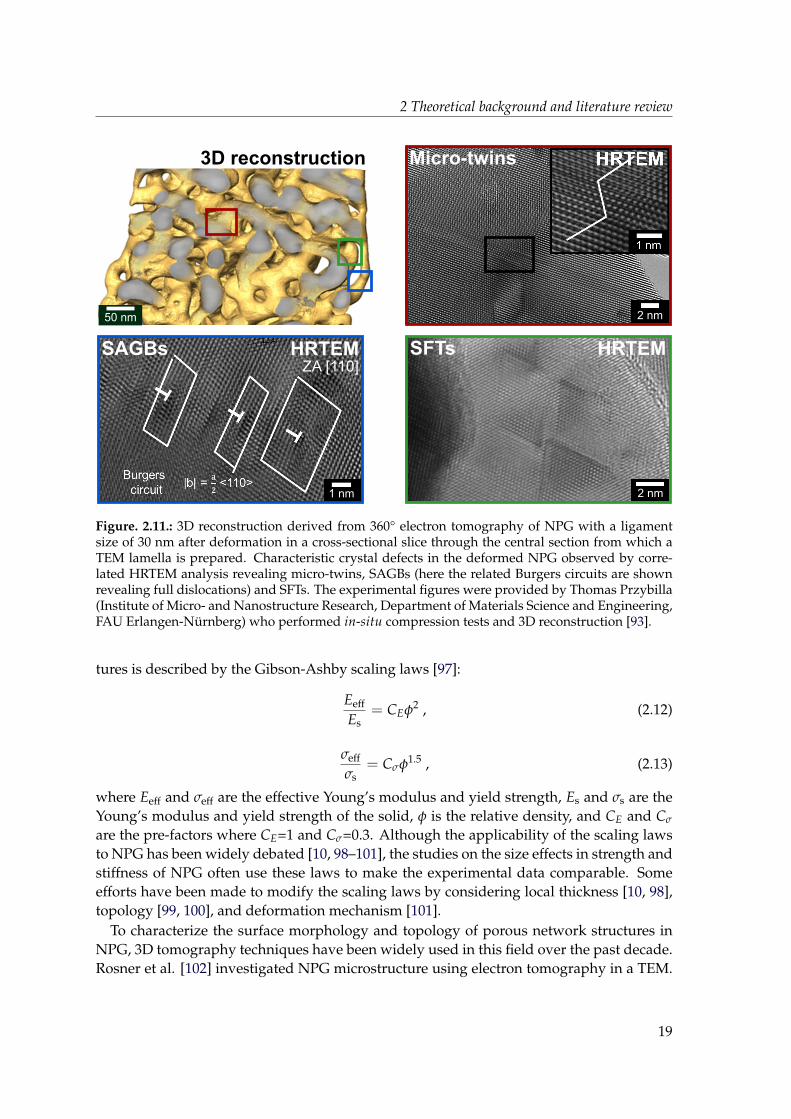
Recently, Przybilla et al. [93] reported size-dependent resulting microstructures of com-pressed NPG with ligament sizes ranging from 30 nm to 300 nm. In-situ compressiontests and non-destructive 3D reconstruction using electron tomography were performedon a 〈137〉-oriented NPG pillar with a 400 nm diameter, 35% solid fraction and 30 nm lig-ament size. More detailed sample preparation and experimental setups can be found in[93]. In addition to the observation of deformation twinning which was also reported inNPG with ligament size smaller than 10 nm [91], small-angle grain boundaries (SAGBs)and stacking fault tetrahedra (SFTs) were observed in the deformed NPG. Additionally,in-situ compression tests and non-destructive 3D reconstruction using X-ray tomographywere performed on a 〈013〉-oriented NPG pillar with a 4 µm diameter, 39% solid fractionand 300 nm ligament size and bulk-like deformation mechanism, namely formation of dis-location networks, was identified in the deformed sample.
There is still a discrepancy on the size-dependent elastic modulus of NPG using differ-ent experimental techniques [10, 82, 94, 95]. In 2007, Mathur et al. [82] calculated Young’smodulus of NPG with ligament sizes ranging from sub-10 to 40 nm by mechanical test-ing of free standing thin films of NPG using a buckling-based method [96]. They founda dramatic rise in the effective Young’s modulus of NPG with decreasing ligament size,especially below 10 nm. Hodge et al. [94] studied the influence of Ag coating distribu-tion on the elastic modulus of NPG by using the nanoindentation technique. A dramaticchange was observed in Young’s modulus as the Ag concentration changed from 1 to 20at.%. Furthermore, they compared Young’s modulus values of pure NPG samples withligament sizes of 50 and 150 nm, no notable size-effect on Young’s modulus was observedin this scale regime. Mameka et al. [10, 95] measured effective Young’s modulus of NPGas the storage modulus in a dynamic mechanical analyzer, and they found a clear trend of“smaller is stiffer” which was close to Mathur et al.’s observations [82].
The impact of the solid fraction on the effective mechanical properties of porous struc-
18
2 Theoretical background and literature review
1 nm
HRTEMZA [110]
1 µm
50 nm
2 nm
HRTEMSFTs
2 nm
Micro-twins
SAGBs
3D reconstruction
Figure. 2.11.: 3D reconstruction derived from 360° electron tomography of NPG with a ligamentsize of 30 nm after deformation in a cross-sectional slice through the central section from which aTEM lamella is prepared. Characteristic crystal defects in the deformed NPG observed by corre-lated HRTEM analysis revealing micro-twins, SAGBs (here the related Burgers circuits are shownrevealing full dislocations) and SFTs. The experimental figures were provided by Thomas Przybilla(Institute of Micro- and Nanostructure Research, Department of Materials Science and Engineering,FAU Erlangen-Nurnberg) who performed in-situ compression tests and 3D reconstruction [93].
tures is described by the Gibson-Ashby scaling laws [97]:
Eeff
Es= CEφ2 , (2.12)
σeff
σs= Cσφ1.5 , (2.13)
where Eeff and σeff are the effective Young’s modulus and yield strength, Es and σs are theYoung’s modulus and yield strength of the solid, φ is the relative density, and CE and Cσ
are the pre-factors where CE=1 and Cσ=0.3. Although the applicability of the scaling lawsto NPG has been widely debated [10, 98–101], the studies on the size effects in strength andstiffness of NPG often use these laws to make the experimental data comparable. Someefforts have been made to modify the scaling laws by considering local thickness [10, 98],topology [99, 100], and deformation mechanism [101].
To characterize the surface morphology and topology of porous network structures inNPG, 3D tomography techniques have been widely used in this field over the past decade.Rosner et al. [102] investigated NPG microstructure using electron tomography in a TEM.
19
2 Theoretical background and literature review
From the 3D reconstruction of the NPG structure, they identified the bicontinuous networkof branched ligaments and the inhomogeneous distributions of ligament diameter andshape. Fujita et al. [103] performed electron tomography on NPG and quantitatively ana-lyzed topology and morphology of the porous network structure. They found that the porechannels and ligaments were inverses of each other in 3D space and the bicontinuous net-work structure had a near-zero surface curvature on average. Chen et al. [85, 104] appliedX-ray tomography on NPG using synchrotron X-ray sources. They quantified the 3D mor-phology of the porous structure using interfacial shape distribution (ISD) and found thatthe interfacial morphology of NPG became increasingly anisotropic with coarsening timeand the surface energy tended to minimize during the coarsening process. Mangipudi et al.[99, 105] applied FIB-tomography on NPG structures. They characterized the morphologyand topology of NPG using ligament and pore size distributions, ISD functions, interfacenormal distributions, and genus. Furthermore, they performed finite-element (FE) sim-ulations on the reconstructed NPG and compared with other artificial porous structures,pronounced topology-dependent mechanical properties of NPG were captured.
2.2.3. Molecular dynamics simulations
To study the deformation mechanism in confined dimensions, molecular dynamics (MD)is a powerful technique. By correlating with experimental observations, MD simulationscan provide physical explanations of atomic-resolution deformation mechanisms. Com-paring with other modeling techniques in the continuum scale and ab initio, MD providesrelatively physical descriptions of small-scale plasticity and comparable simulation cellsize with experiments. However, the limitations of MD simulations should not be ignored,which include limited timescale (usually nanoseconds, therefore can not simulate diffusioncontrolled mechanisms), the accuracy of interatomic potential and realistic geometry.
Nanowires
MD simulations are widely-used in studying deformation mechanisms of FCC metallicNWs [61, 62, 106–115]. In the following paragraphs, MD simulations of FCC metallic NWsunder uniaxial loading conditions (tension and compression) and complex loading condi-tions (bending and torsion) are reviewed. For a more detailed introduction of MD simula-tions on NWs, one can refer to a review paper [21].
Under uniaxial loading conditions, FCC metallic NWs show orientation and loading di-rection dependence of the operative deformation mechanisms which can be explained andpredicted by the generalized stacking fault energies and considering the Schmid factorsfor leading and trailing partial dislocations [21, 62, 114]. In 2003, Diao et al. [106] per-formed tensile tests on 〈100〉-oriented Au NWs with diameters smaller than 2 nm. A phasetransformation from a FCC structure to a body centered tetragonal (BCT) structure wasobserved under tension, which was attributed to surface stress. Diao et al. also studiedsize-dependent Young’s modulus [116], yield strength asymmetric in tension and com-pression [117] and size-independent critical resolved shear stress [110] on 〈100〉-orientedAu NWs at low temperatures (0 or 2 K). Liang et al. [107] showed that 〈100〉-oriented Cu
20
2 Theoretical background and literature review
NW with 100-oriented side facets is unstable at 300 K. The wire transformed to 〈110〉-oriented NW with 111-oriented side facets which are believed to be energetically morefavorable (which has been demonstrated by the geometry of naturally grown FCC metallicNWs [8]). Formation of deformation twinning and pseudoelastic behavior was observed infurther deformation of 〈110〉-oriented Cu NW. Similar twinning and pseudoelasticity werealso reported by Park et al. [108] in simulated tensile tests of 〈110〉-oriented Au, Cu andNi NWs. In addition, they found the Au wire with lower stacking fault energy was shownto form twins with interior stacking faults, while the higher stacking fault energy Cu andNi NWs formed defect-free twins. Liang et al. [109] applied the generalized stacking fault(GSF) energy to evaluate twinnability [20] of Au, Cu, Ni and Al 〈110〉-oriented NWs with111-oriented side facets. Al NW with the lowest twinnability among all tested NWsshowed nucleation of full dislocation which led to irreversible deformation. However, thetwinnability parameter [20] only considers the GSF energy, which fails to explain and pred-icate further NW simulations [21], since the parameter was obtained by averaging over allorientations in a polycrystal. The Schmid factors for leading and trailing partial disloca-tions in uniaxial loading conditions of single-crystalline NWs should also be taken intoaccount [21, 62, 114].
In addition to the axial orientation of NWs, geometrical parameters, such as facet orien-tation [21] and aspect ratio [118], should also be considered when setting up MD simula-tions. The atomic samples with similar axial and facet orientations as the naturally grownNWs are indispensable to mimic the observed deformation behavior in experiments. Sedl-mayr et al. [61] performed MD simulations on 〈110〉-oriented Au NWs with the similarhexagonal cross-sectional shape as the experimental NWs and explained the two twinning-mediated deformation modes as observed in in-situ tensile testing. According to the twin-ning mechanisms obtained from MD simulations, the two deformation modes were corre-sponded to the layer-by-layer propagation to parallel and accelerated formation of coalesc-ing nanotwins. It became a trend to perform MD simulations on experimentally-informedNWs with identical axial and facet orientations as in experiments [62, 66, 119]. Those sim-ulations successfully mimicked the observed deformation behavior in experiments andexplained deformation mechanisms in the atomic-level. Wu et al. [118] showed that thelength of NWs plays an essential role in determining the fracture behavior. The length ofthe wire determines the total amount of energy that is available to drive plastic deforma-tion to failure, therefore the longer wire stores more elastic energy which drives localizeddislocation activities [118].
Metallic NWs under complex loading conditions, such as bending [115, 120] and torsion[112, 113], were also studied using MD simulations. Zheng et al. [120] conducted MD sim-ulations of bending on 〈100〉-oriented Cu NWs with square cross-section. The plastic defor-mation was dominated by full dislocation slip and twinning, and the plasticity was alwaysinitiated from the compressive side of the NWs. Nohring et al. [115] performed bend-ing tests on 〈110〉-oriented Au and Cu NWs with the experimentally-informed hexagonal-shaped cross-section. Formation of geometrically necessary wedge-shaped twins in thetensile part of the NWs and full dislocations in the compressive part were reported. Due tothe strain dependent unstable stacking fault energy, the plasticity initiated from the tensilepart of the NWs. After load removal, bent NWs showed spontaneous pesudoelasticity due
21
2 Theoretical background and literature review
to the reversible twinning dislocations stored in the wedge-shaped twins. Weinberger etal. [112, 113] reported torsion of 〈110〉-oriented Au and Al NWs, where they observed theformation of perfect screw dislocations parallel to the wire axis on 111 slip planes, thatwas also reported in experiments of thin rods [121].
Nanoporous metals
Deformation mechanisms of nanoporous metals under different loading conditions werestudied using MD simulations. Currently, most MD simulations were performed on nanoporousstructures that were constructed artificially. Phase field methods [101, 122–127] simu-late the spinodal decomposition as a diffusion phenomenon at the interface between twophases based on numerically solving the Cahn-Hilliard equation. Monte-Carlo methods[128–131] simulate the phase separation of a binary mixture by examining numerous con-figurations and selecting the ones based on thermodynamic preference. MD-based meth-ods [132, 133] heat the fully condensed systems above the melting temperatures and thenremove a part of the phases according to a certain criterion. Other artificial porous struc-tures such as honeycomb [134] and inserting pores [135–138] were also reported in liter-ature. In the following paragraphs, previous works on the mechanical behavior of NPGmostly under compression and tension are reviewed.
Crowson et al. [122, 123] performed molecular statics (MS) and MD simulations on NPGwith average ligament sizes ranging from 1.3 to 3.6 nm. A surface relaxation driven me-chanical instability for NPG samples was reported and attributed to the surface stress. Sunet al. [101] applied tensile loading on spinodal NPG samples with various ligament sizesand relative densities. They found that NPG primarily failed through plastic necking andrupture of the ligaments along the loading direction. Lomer-Cottrell locks formed at thejunctions between ligaments and hindered subsequent dislocation activities thus enhanc-ing the strength of the junctions. Farkas et al. [124] performed simulated tensile and com-pressive tests on a spinodal NPG sample with an average ligament size of 1.8 nm and asolid fraction of 25%. A tension-compression asymmetry was observed and explained bysurface stress that sets ligaments under compression and providing a bias favoring yield-ing in compression. Rodriguez-Nieva et al. [136] studied the mechanical behavior of NPGconstructed by inserting pores with an average pore-to-pore distance 17.7 nm under dif-ferent compressive strain rates. At the beginning of the plastic deformation, dislocationloops were nucleated from pores and then interacted with each other leading to strainhardening. They found the von Mises stress as a power-law function of dislocation density(σvon Mises ∝ ρ0.5
dislocation) in the severe plastic deformation which features Taylor hardening.Ngo et al. [129, 131] performed load-unload compression tests on a NPG with a ligamentsize of 3.15 nm and a solid fraction of 29.7%. They observed lower stiffness and yieldingstrength of NPG compared to the predictions by the Gibson-Ashby scaling laws. They at-tributed these anomalous mechanical properties of NPG to the large surface-induced stress.Furthermore, a strong strain hardening was observed under compressive load which wasaccompanied by dislocation storage and dislocation interaction. Ruestes et al. [125] per-formed a compression test on a NPG sample with an average ligament diameter of 1.8nm and a solid fraction of 25%. Stress followed a quadratic power law function of dislo-
22
2 Theoretical background and literature review
cation density after the plastic plateau, indicating that the Taylor hardening model maynot suitable in NPG. Furthermore, Hirth and Frank partial dislocations and Lomer-Cottreldislocation locks formed and would contribute to hardening, twinning, as well as full dis-locations were also observed. Ruestes et al. [126] performed a nanoindentation test onpolycrystalline NPG with 11 nm average ligament size and 35 nm average grain size. Simi-lar characteristic defects were observed as their previous compression tests [125]. Guillotteet al. [133] performed tensile tests on MD-based constructed NPG with a ligament size of3.7 nm and a solid fraction of 43%. A ductile plastic deformation under tension was ob-served. Beets et al. [127] found tension-compression asymmetry in plastic behavior in NPGsamples with average ligament sizes varying from 5.5 nm to 14.4 nm. This asymmetry be-came more pronounced in NPG with smaller ligaments since the effect of surface-inducedstress is more significant in the structure with a higher surface-to-volume ratio. They ob-served higher dislocation density in smaller samples and samples subjected to tension.
Except for mechanical responses of NPG under tension and compression, shock responsesof NPG using MD simulations were also reported in literature [130, 132, 134, 135, 137,138]. However, this type of loading condition is not widely reported in experiments ofnanoporous metals, therefore the simulations results are often lack comparison.
Although numerous MD simulations investigated the mechanical behaviors of NPG,there is no systematic study on the size-dependent deformation mechanisms in NPG. Theligament sizes of previous simulated samples range from 1 nm to 15 nm, the deforma-tion mechanisms of NPG with larger ligament size are still unknown. Moreover, most MDsimulations were performed on idealized porous structures, such as spinodal structures,which exhibit much lower strength and stiffness compared to realistic NPG networks [99].Therefore, the deformation mechanisms of realistic NPG structures are still needed to beexplored to characterize the true mechanical behavior of nanoscale porous structures.
2.3. Surface dislocation nucleation
The plasticity of nanostructure in confined dimensions is controlled by surface dislocationnucleation. In subsection 2.3.1, the classic nucleation theory for surface dislocation nucle-ation is introduced and the efforts on developing analytical models for predicting criticalnucleation stress are reviewed. Surface dislocation nucleation is a thermally activated pro-cess and is highly sensitive to surface conditions. In the followed subsections, experimentsand atomistic simulations on temperature and surface-state dependence of surface dislo-cation nucleation are reviewed.
2.3.1. Nucleation criteria
Classic nucleation models usually only consider elastic energy and stacking fault energy,e.g., Chen et al. [139] estimated a transition diameter between full and partial dislocationnucleation from grain boundaries in nanocrystalline Al. The shear stress to expand a partialdislocation is:
τp =2aGbp
D+
γs f
bp, (2.14)
23
2 Theoretical background and literature review
where γs f is the stacking fault energy, bp is the Burgers vector of a partial dislocation, G isthe shear modulus, D is the grain size. For a full dislocation the shear stress is:
τf =2aGb f
D, (2.15)
where b f is the Burgers vector of a full dislocation and a is a parameter between 0.5 and1.5 reflecting the orientation dependence of the line tension energy. For pure edge andscrew dislocations a values are 0.5 and 1.5, respectively. The critical diameter (Dc) for thetransition between full and partial dislocation nucleation is:
Dc =2aG(b f − bp)bp
γs f. (2.16)
In bulk dimensions, the activation volume of a typical Frank-Read source is between 100-1000 b3 [140], However, in small-scale, the activation volume associated with surface dis-location nucleation is characteristically in the range of 1-10 b3 [141], therefore the surfacedislocation nucleation is highly sensitive to thermal effect. Moreover, surface contributionssuch as image force and the energy of surface ledge creation following dislocation nucle-ation at free surface are not considered in classic nucleation models [142].
Recently, analytical models of surface dislocation nucleation have been developed fromdifferent perspectives. Within the framework of continuum mechanics, the activation en-ergy of surface dislocation nucleation has been modeled by individual contributions of thenucleated dislocation. Weinberger et al. [142, 143] developed a continuum-based surfacedislocation nucleation model which considered individual contributions such as the linetension energy Elt, stacking fault energy γsf, image force Eif, surface ledge energy Esl. Theenergy barrier to expanding a dislocation from free surface to a radius rcore can be writtenas:
Edislocation(rcore, σ) = Elt + γsf + Ebf + Eif + Esl , (2.17)
where Ebf is the energy contribution to overcome back force from internal defects (such aspre-existing dislocations or grain boundary). However, this dislocation-based continuummodel suffers from the uncertainties on the dislocation core radius (rcore) employed [41].
Within the framework of atomistic modeling, the activation energy of surface dislocationnucleation has been calculated using reaction pathway sampling methods and then fedinto finite-temperature transition-state theory (TST) [144]. Zhu et al. [141] investigated theprobabilistic nature of thermally activated surface dislocation nucleation and developed ageneral analytical model. This model is based on activation free energy (Q) and activationvolume (Ω) which were calculated using nudged elastic band (NEB) method [145]. Ac-cording to TST, at a given temperature T and stress σ, the rate of dislocation nucleation ν
is:
ν = Nν0 exp(−Q(σ, T)kBT
) , (2.18)
where N is the number of equivalent surface nucleation sites, ν0 is the attempt frequency,kBT is the thermal energy, and Q(σ, T) is the activation free energy. The stress and temper-
24
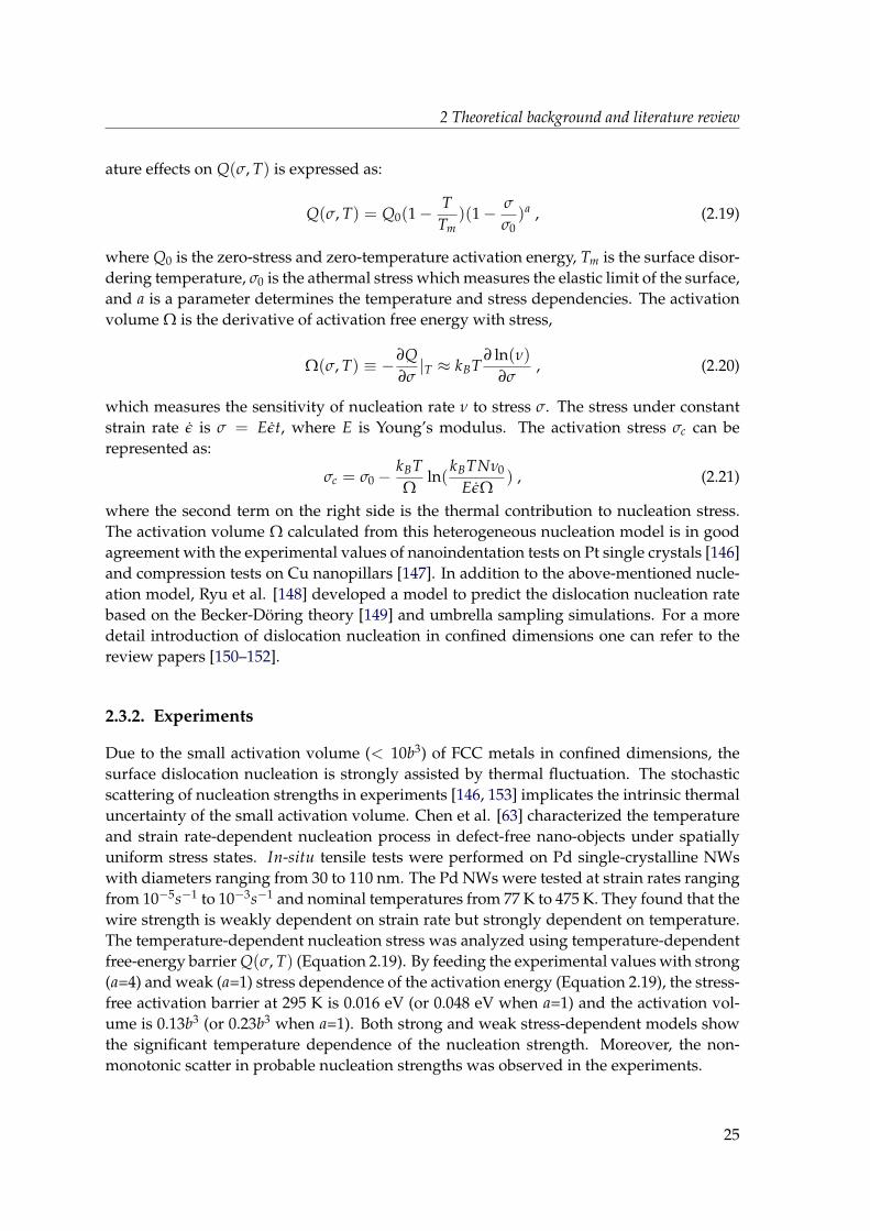
2 Theoretical background and literature review
ature effects on Q(σ, T) is expressed as:
Q(σ, T) = Q0(1−T
Tm)(1− σ
σ0)a , (2.19)
where Q0 is the zero-stress and zero-temperature activation energy, Tm is the surface disor-dering temperature, σ0 is the athermal stress which measures the elastic limit of the surface,and a is a parameter determines the temperature and stress dependencies. The activationvolume Ω is the derivative of activation free energy with stress,
Ω(σ, T) ≡ −∂Q∂σ|T ≈ kBT
∂ ln(ν)∂σ
, (2.20)
which measures the sensitivity of nucleation rate ν to stress σ. The stress under constantstrain rate ε is σ = Eεt, where E is Young’s modulus. The activation stress σc can berepresented as:
σc = σ0 −kBTΩ
ln(kBTNν0
EεΩ) , (2.21)
where the second term on the right side is the thermal contribution to nucleation stress.The activation volume Ω calculated from this heterogeneous nucleation model is in goodagreement with the experimental values of nanoindentation tests on Pt single crystals [146]and compression tests on Cu nanopillars [147]. In addition to the above-mentioned nucle-ation model, Ryu et al. [148] developed a model to predict the dislocation nucleation ratebased on the Becker-Doring theory [149] and umbrella sampling simulations. For a moredetail introduction of dislocation nucleation in confined dimensions one can refer to thereview papers [150–152].
2.3.2. Experiments
Due to the small activation volume (< 10b3) of FCC metals in confined dimensions, thesurface dislocation nucleation is strongly assisted by thermal fluctuation. The stochasticscattering of nucleation strengths in experiments [146, 153] implicates the intrinsic thermaluncertainty of the small activation volume. Chen et al. [63] characterized the temperatureand strain rate-dependent nucleation process in defect-free nano-objects under spatiallyuniform stress states. In-situ tensile tests were performed on Pd single-crystalline NWswith diameters ranging from 30 to 110 nm. The Pd NWs were tested at strain rates rangingfrom 10−5s−1 to 10−3s−1 and nominal temperatures from 77 K to 475 K. They found that thewire strength is weakly dependent on strain rate but strongly dependent on temperature.The temperature-dependent nucleation stress was analyzed using temperature-dependentfree-energy barrier Q(σ, T) (Equation 2.19). By feeding the experimental values with strong(a=4) and weak (a=1) stress dependence of the activation energy (Equation 2.19), the stress-free activation barrier at 295 K is 0.016 eV (or 0.048 eV when a=1) and the activation vol-ume is 0.13b3 (or 0.23b3 when a=1). Both strong and weak stress-dependent models showthe significant temperature dependence of the nucleation strength. Moreover, the non-monotonic scatter in probable nucleation strengths was observed in the experiments.
25
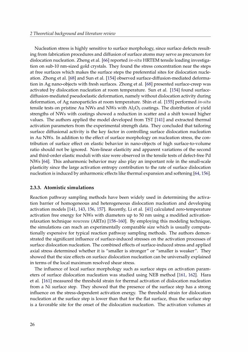
2 Theoretical background and literature review
Nucleation stress is highly sensitive to surface morphology, since surface defects result-ing from fabrication procedures and diffusion of surface atoms may serve as precursors fordislocation nucleation. Zheng et al. [66] reported in-situ HRTEM tensile loading investiga-tion on sub-10 nm-sized gold crystals. They found the stress concentration near the stepsat free surfaces which makes the surface steps the preferential sites for dislocation nucle-ation. Zhong et al. [68] and Sun et al. [154] observed surface-diffusion-mediated deforma-tion in Ag nano-objects with fresh surfaces. Zhong et al. [68] presented surface-creep wasactivated by dislocation nucleation at room temperature. Sun et al. [154] found surface-diffusion-mediated pseudoelastic deformation, namely without dislocation activity duringdeformation, of Ag nanoparticles at room temperature. Shin et al. [155] performed in-situtensile tests on pristine Au NWs and NWs with Al2O3 coatings. The distribution of yieldstrengths of NWs with coatings showed a reduction in scatter and a shift toward highervalues. The authors applied the model developed from TST [141] and extracted thermalactivation parameters from the experimental strength data. They concluded that tailoringsurface diffusional activity is the key factor in controlling surface dislocation nucleationin Au NWs. In addition to the effect of surface morphology on nucleation stress, the con-tribution of surface effect on elastic behavior in nano-objects of high surface-to-volumeratio should not be ignored. Non-linear elasticity and apparent variations of the secondand third-order elastic moduli with size were observed in the tensile tests of defect-free PdNWs [64]. This anharmonic behavior may also play an important role in the small-scaleplasticity since the large activation entropy contribution to the rate of surface dislocationnucleation is induced by anharmonic effects like thermal expansion and softening [64, 156].
2.3.3. Atomistic simulations
Reaction pathway sampling methods have been widely used in determining the activa-tion barrier of homogeneous and heterogeneous dislocation nucleation and developingactivation models [141, 143, 156, 157]. Recently, Li et al. [41] calculated zero-temperatureactivation free energy for NWs with diameters up to 50 nm using a modified activation-relaxation technique nouveau (ARTn) [158–160]. By employing this modeling technique,the simulations can reach an experimentally comparable size which is usually computa-tionally expensive for typical reaction pathway sampling methods. The authors demon-strated the significant influence of surface-induced stresses on the activation processes ofsurface dislocation nucleation. The combined effects of surface-induced stress and appliedaxial stress determined whether it is “smaller is stronger” or “smaller is weaker”. Theyshowed that the size effects on surface dislocation nucleation can be universally explainedin terms of the local maximum resolved shear stress.
The influence of local surface morphology such as surface steps on activation param-eters of surface dislocation nucleation was studied using NEB method [161, 162]. Haraet al. [161] measured the threshold strain for thermal activation of dislocation nucleationfrom a Ni surface step. They showed that the presence of the surface step has a stronginfluence on the stress-dependent activation energy. The threshold strain for dislocationnucleation at the surface step is lower than that for the flat surface, thus the surface stepis a favorable site for the onset of the dislocation nucleation. The activation volumes at
26
2 Theoretical background and literature review
the threshold strain are 11b3 and 8b3 for the nucleation in a Ni crystal at surface steps andflat surfaces, respectively. Brochard et al. [162] reported the influences of surface step andtemperature on the dislocation nucleation from a surface step in Al and Cu metals. Theeffect of surface step height was revealed, the threshold strain increases with increasingstep height in smaller steps where the local effects dominate. In higher steps (> 2− 3 stepheight) where the stress concentration prevails, the threshold strain decreases when thestep height increases.
The temperature-dependent nucleation process is studied using MD simulations in finitetemperatures [163–165]. Rabkin et al. [163] performed MD simulations on single crystallinenanopillars. They found that the largest thermal strains occur at edges or isolated atomicstripes where the surface atoms are loosely bound, thus nucleation is more preferable atthese sites. The authors attributed the temperature-dependent yield strength to the aver-age vibration amplitude of the loosely bound atoms. Cao et al. [164] studied the influenceof cross-sectional shape and temperature on the yield strength of Cu nanopillars. Theyfound that the sharp corners give rise to large local stress concentration and act as prefer-able nucleation sites. Strong temperature dependence of the yield strength was observedand attributed to the small activation volume. Chachamovitz et al. [165] performed MDsimulations on Mo nanoparticles to study the stress-dependent activation parameters fordislocation nucleation. The authors proposed the exponent a=1.5 for the activation free en-ergy of spontaneous nucleation (Equation 2.19 without temperature term). The calculatedactivation entropies using the suggested activation parameters are in good agreement withthe values obtained from the statics simulations [156].
2.4. Dislocation-twin boundary interactions
Twinning plays an important role in determining the mechanical behaviors of FCC metals.Twin boundary (TB) acts as a barrier to the free movement of dislocation. In the followingsubsections, experimental and modeling works on FCC metals in confined dimensions arereviewed. The strengthening effect of the twin boundary and dislocation-twin boundaryinteractions are highlighted.
2.4.1. Experiments
Twinned nanocrystals or nanotwinned metals show a combination of high strength withhigh ductility, two properties which are commonly regarded as mutually exclusive [166–168]. The interactions between gliding dislocations and twin boundaries increase the strengthand ductility of nanocrystalline metals [166–168]. Twinning mechanisms and dislocation-TB interaction in nanocrystalline metals have been widely studied in both experiments[167, 169] and theoritical studies [170–173]. Dehm et al. [174–176] performed microcom-pression experiments on 〈110〉-oriented single crystalline and twinned bi-crystalline mi-cropillars with a longitudinal TB to differentiate the contributions of grain boundaries(GBs) and TBs on mechanical behavior. They observed no significant strengthening ef-fect of TB. They proposed several scenarios to explain such behavior according to the pre-existing dislocation sources and the relative orientation of the TB. Recent microcompres-
27
2 Theoretical background and literature review
sion tests show that the 〈110〉-oriented twinned bi-crystalline micropillars exhibit higheryield strength than the single crystalline micropillars [177, 178]. Malyar et al. [178] pro-posed a double-hump dislocation shape due to the pre-existing TB and resulting in aslightly higher stress level. For a more detailed introduction of the mechanisms of dislocation-TB interactions in micro- and macro-scales, one can refer to a review paper [179]. Thefollowing paragraphs focus on the effect of TB on mechanical behaviors in confined di-mensions.
Nanowires with five-fold twins
Modern materials synthesis techniques have enabled the fabrication of twinned NWs withdifferent twin arrangements such as five-fold twins and parallel twins [180–190]. Exper-imental studies on the mechanical properties of 〈110〉-oriented Ag five-fold twinned (FT)NWs with longitudinal TBs were reported in [180, 181, 183]. Wu et al. [180] reported three-point bending tests using a lateral force AFM method [50] on Ag FTNWs with diametersranging from 16 to 35 nm. The FTNWs exhibited high elastic strain followed by abruptlybrittle failure. By applying thermal annealing, the pentagonal TBs were gradually elim-inated and the wires showed more ductile behavior than the FTNWs. Lucas et al. [181]studied plastic deformation of Ag FTNWs with diameters of 15 to 40 nm by nanoindenta-tion using an AFM tip. Formation of necking and surface atomic steps were observed fromthe AFM images of the residual indent. The maximum stress measured by nanoindenta-tion is about 2 GPa and then the stress drop to 1.4 GPa followed by a series of yieldingevents with smaller stress decreased until fracture. Qin et al. [183] reported a dislocation-mediated fully reversible plasticity in Ag FTNWs. In-situ tensile tests were performedusing MEMS-based testing system on Ag FTNWs (with diameters ranging from 48 to 121nm) and single-crystalline NWs (with diameters ranging from 71 to 152 nm). Only FT-NWs showed undergo stress relaxation on loading and complete plastic strain recoveryon unloading. From the in-situ TEM images, dislocations were terminated at the TBs andgradually retracted during the recovery. Zhu et al. [191], Filleter et al. [192] and Schrenkeret al. [193, 194] showed that the pre-existing TBs give rise to pronounced strain-hardeningby impeding the propagation of the surface nucleated dislocations in Ag FTNWs. Zhu etal. [191] performed in-situ tensile tests on Ag FTNWs with diameters from 34 to 130 nmin SEM. They reported size effects on Young’s modulus, yield strength and maximum ten-sile strength, these three properties enhanced as the NW diameter decreased. The authorsalso observed pronounced strain hardening in most FTNWs and attributed this behaviorto the presence of internal TBs. Filleter et al. [192] observed strain hardening of Ag FTNWsunder tension with the evidence of in-situ TEM images. For thin FTNWs with diameters<100 nm, strain hardening and multiple plastic zone formation were observed. The thickerFTNWs exhibited earlier deformation localization thus had fewer local plastic zones. Theauthors attributed the localized plasticity to the formation of new dislocation sources fromcomplex defect structures.
Recently, Schrenker et al. [193, 194] performed ex-situ mechanical tests on Ag FTNWnetworks which were doctor bladed on a polyethylene terephthalate (PET) substrate. Thewires along the coating direction were pulled by applying tensile strain on the substrate.
28
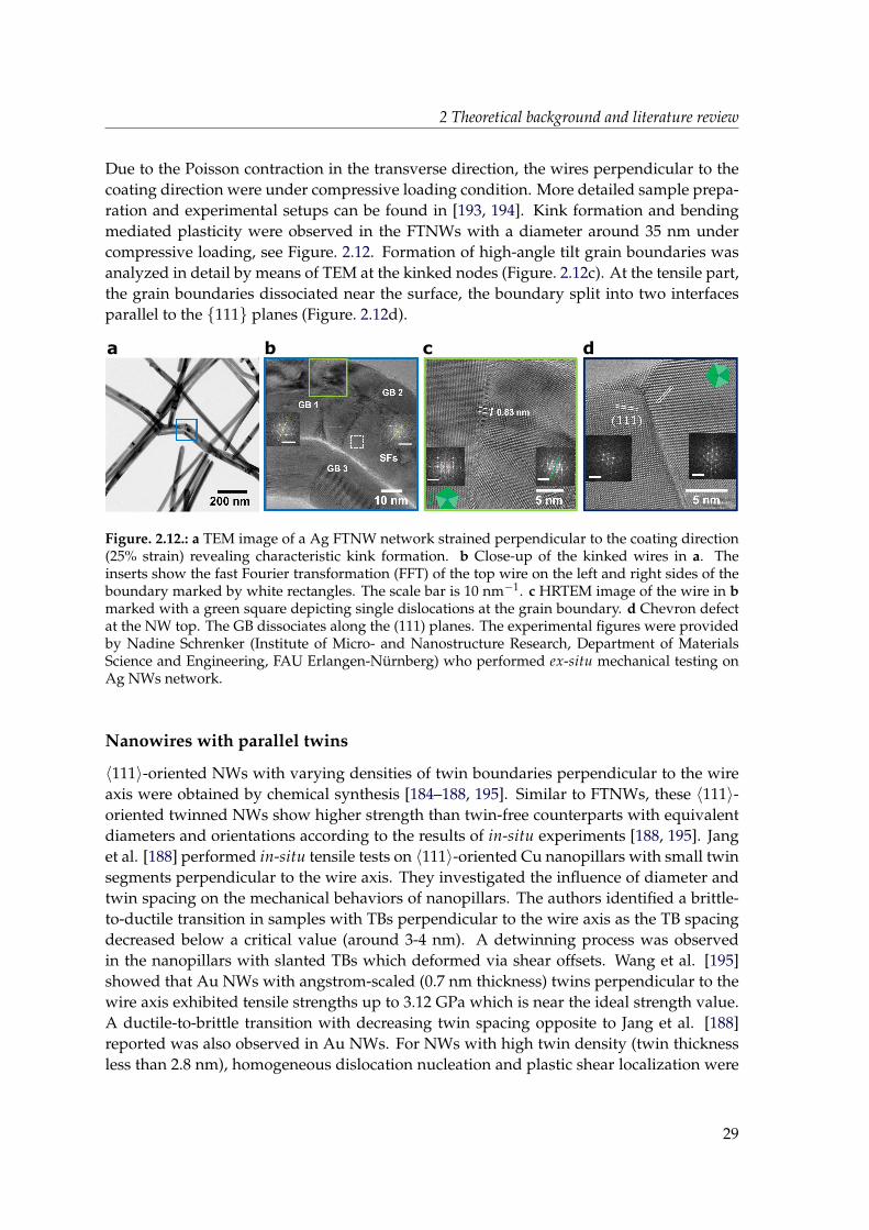
2 Theoretical background and literature review
Due to the Poisson contraction in the transverse direction, the wires perpendicular to thecoating direction were under compressive loading condition. More detailed sample prepa-ration and experimental setups can be found in [193, 194]. Kink formation and bendingmediated plasticity were observed in the FTNWs with a diameter around 35 nm undercompressive loading, see Figure. 2.12. Formation of high-angle tilt grain boundaries wasanalyzed in detail by means of TEM at the kinked nodes (Figure. 2.12c). At the tensile part,the grain boundaries dissociated near the surface, the boundary split into two interfacesparallel to the 111 planes (Figure. 2.12d).
a b c d
Figure. 2.12.: a TEM image of a Ag FTNW network strained perpendicular to the coating direction(25% strain) revealing characteristic kink formation. b Close-up of the kinked wires in a. Theinserts show the fast Fourier transformation (FFT) of the top wire on the left and right sides of theboundary marked by white rectangles. The scale bar is 10 nm−1. c HRTEM image of the wire in bmarked with a green square depicting single dislocations at the grain boundary. d Chevron defectat the NW top. The GB dissociates along the (111) planes. The experimental figures were providedby Nadine Schrenker (Institute of Micro- and Nanostructure Research, Department of MaterialsScience and Engineering, FAU Erlangen-Nurnberg) who performed ex-situ mechanical testing onAg NWs network.
Nanowires with parallel twins
〈111〉-oriented NWs with varying densities of twin boundaries perpendicular to the wireaxis were obtained by chemical synthesis [184–188, 195]. Similar to FTNWs, these 〈111〉-oriented twinned NWs show higher strength than twin-free counterparts with equivalentdiameters and orientations according to the results of in-situ experiments [188, 195]. Janget al. [188] performed in-situ tensile tests on 〈111〉-oriented Cu nanopillars with small twinsegments perpendicular to the wire axis. They investigated the influence of diameter andtwin spacing on the mechanical behaviors of nanopillars. The authors identified a brittle-to-ductile transition in samples with TBs perpendicular to the wire axis as the TB spacingdecreased below a critical value (around 3-4 nm). A detwinning process was observedin the nanopillars with slanted TBs which deformed via shear offsets. Wang et al. [195]showed that Au NWs with angstrom-scaled (0.7 nm thickness) twins perpendicular to thewire axis exhibited tensile strengths up to 3.12 GPa which is near the ideal strength value.A ductile-to-brittle transition with decreasing twin spacing opposite to Jang et al. [188]reported was also observed in Au NWs. For NWs with high twin density (twin thicknessless than 2.8 nm), homogeneous dislocation nucleation and plastic shear localization were
29
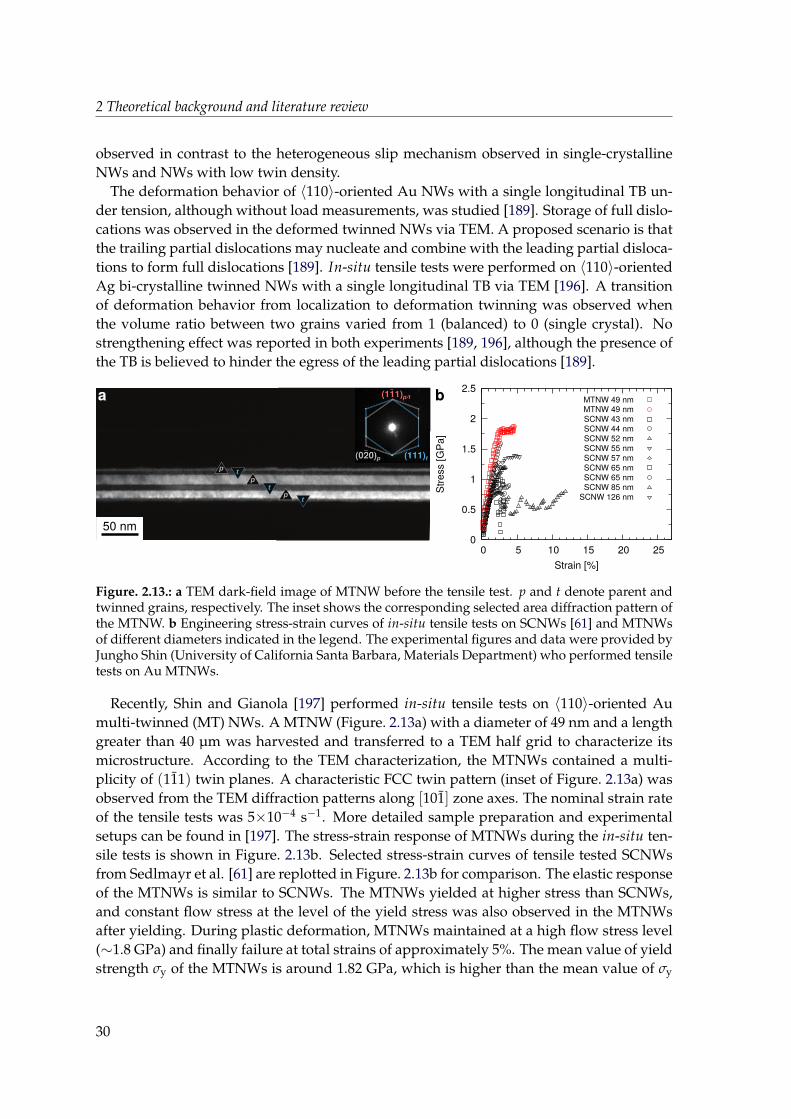
2 Theoretical background and literature review
observed in contrast to the heterogeneous slip mechanism observed in single-crystallineNWs and NWs with low twin density.
The deformation behavior of 〈110〉-oriented Au NWs with a single longitudinal TB un-der tension, although without load measurements, was studied [189]. Storage of full dislo-cations was observed in the deformed twinned NWs via TEM. A proposed scenario is thatthe trailing partial dislocations may nucleate and combine with the leading partial disloca-tions to form full dislocations [189]. In-situ tensile tests were performed on 〈110〉-orientedAg bi-crystalline twinned NWs with a single longitudinal TB via TEM [196]. A transitionof deformation behavior from localization to deformation twinning was observed whenthe volume ratio between two grains varied from 1 (balanced) to 0 (single crystal). Nostrengthening effect was reported in both experiments [189, 196], although the presence ofthe TB is believed to hinder the egress of the leading partial dislocations [189].
0
0.5
1
1.5
2
2.5
0 5 10 15 20 25
Str
ess [
GP
a]
Strain [%]
SCNW 43 nmSCNW 44 nmSCNW 52 nmSCNW 55 nmSCNW 57 nmSCNW 65 nmSCNW 65 nmSCNW 85 nm
SCNW 126 nm
MTNW 49 nmMTNW 49 nm
b
50 nm
tp
t
t
p
p
a
(111)p/t-
(020)p-
(111)t
Figure. 2.13.: a TEM dark-field image of MTNW before the tensile test. p and t denote parent andtwinned grains, respectively. The inset shows the corresponding selected area diffraction pattern ofthe MTNW. b Engineering stress-strain curves of in-situ tensile tests on SCNWs [61] and MTNWsof different diameters indicated in the legend. The experimental figures and data were provided byJungho Shin (University of California Santa Barbara, Materials Department) who performed tensiletests on Au MTNWs.
Recently, Shin and Gianola [197] performed in-situ tensile tests on 〈110〉-oriented Aumulti-twinned (MT) NWs. A MTNW (Figure. 2.13a) with a diameter of 49 nm and a lengthgreater than 40 µm was harvested and transferred to a TEM half grid to characterize itsmicrostructure. According to the TEM characterization, the MTNWs contained a multi-plicity of (111) twin planes. A characteristic FCC twin pattern (inset of Figure. 2.13a) wasobserved from the TEM diffraction patterns along [101] zone axes. The nominal strain rateof the tensile tests was 5×10⁻⁴ s−1. More detailed sample preparation and experimentalsetups can be found in [197]. The stress-strain response of MTNWs during the in-situ ten-sile tests is shown in Figure. 2.13b. Selected stress-strain curves of tensile tested SCNWsfrom Sedlmayr et al. [61] are replotted in Figure. 2.13b for comparison. The elastic responseof the MTNWs is similar to SCNWs. The MTNWs yielded at higher stress than SCNWs,and constant flow stress at the level of the yield stress was also observed in the MTNWsafter yielding. During plastic deformation, MTNWs maintained at a high flow stress level(∼1.8 GPa) and finally failure at total strains of approximately 5%. The mean value of yieldstrength σy of the MTNWs is around 1.82 GPa, which is higher than the mean value of σy
30
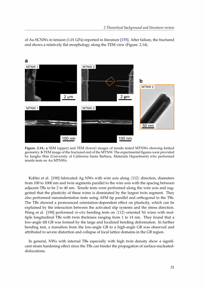
2 Theoretical background and literature review
of Au SCNWs in tension (1.01 GPa) reported in literature [155]. After failure, the fracturedend shows a relatively flat morphology along the TEM view (Figure. 2.14).
a
50 nm
b
MTNW 2
2 m
MTNW 1 MTNW 2
MTNW 1 MTNW 2
2 m 2 m2 m
100 nm100 nm
Figure. 2.14.: a SEM (upper) and TEM (lower) images of tensile tested MTNWs showing kinkedgeometry. b TEM image of the fractured end of the MTNW. The experimental figures were providedby Jungho Shin (University of California Santa Barbara, Materials Department) who performedtensile tests on Au MTNWs.
Kobler et al. [190] fabricated Ag NWs with wire axis along 〈112〉 direction, diametersfrom 100 to 1000 nm and twin segments parallel to the wire axis with the spacing betweenadjacent TBs to be 2 to 40 nm. Tensile tests were performed along the wire axis and sug-gested that the plasticity of these wires is dominated by the largest twin segment. Theyalso performed nanoindentation tests using AFM tip parallel and orthogonal to the TBs.The TBs showed a pronounced orientation-dependent effect on plasticity, which can beexplained by the interaction between the activated slip systems and the stress direction.Wang et al. [198] performed in-situ bending tests on 〈112〉-oriented Ni wires with mul-tiple longitudinal TBs with twin thickness ranging from 1 to 14 nm. They found that alow-angle tilt GB was formed by the large and localized bending deformation. In furtherbending test, a transition from the low-angle GB to a high-angle GB was observed andattributed to severe distortion and collapse of local lattice domains in the GB region.
In general, NWs with internal TBs especially with high twin density show a signifi-cant strain hardening effect since the TBs can hinder the propagation of surface-nucleated-dislocations.
31
2 Theoretical background and literature review
2.4.2. Molecular dynamics simulations
MD simulations were correlated with in-situ mechanical testing on twinned NWs and ex-plained the experimental observations [183, 188, 192, 195]. In the following paragraphs,the previous simulation works on FCC NWs with five-fold twins and NWs with paralleltwins are reviewed.
Nanowires with five-fold twins
The mechanical behavior of FTNWs was investigated using MD simulations [183, 192, 199–201]. Cao et al. [199] performed MD simulations on 〈110〉-oriented Cu FTNWs and single-crystalline NWs with square cross-section under tension. TBs act as the barriers for thefree movement of dislocations and strengthen the NWs. In addition, the FTNWs showedbrittle failure and low elongation ductility compared to the single-crystalline NWs whichdeformed via deformation twinning. Leach et al. [200] observed a similar mechanicalresponse of FTNWs under tension in MD simulations as reported in [199]. Pentagonal-shaped Ag FTNWs showed a higher yielding strength and more brittle fracture than thesingle-crystalline NWs with rhombic and hexagonal cross-sections. Filleter et al. [192] em-ployed MD simulations to explain the strain hardening and multiple plastic zone formationin the thin Ag FTNWs in the in-situ tensile tests. According to the MD simulations, disloca-tion nucleated from a local stress concentrator, which led to the formation of a linear chainof stacking fault decahedrons in the FTNWs. The internal TBs caused local strain harden-ing in the thin FTNWs, and the wires also showed significantly enhanced flow stress andductility since the dislocation activity was confined by stacking fault decahedrons chainpropagation. Qin et al. [183] performed MD simulations to explain the dislocation nucle-ation and retraction governed recoverable plasticity in the in-situ mechanical testing onAg FTNWs. The MD simulations indicated that the repulsive force from the TBs and theintrinsic stress field due to the pentagonal twin was the driven forces for the reversiblemovement of surface-nucleated partial dislocations. The authors also demonstrated thatthe TBs played a similar role in bi-crystalline twinned NWs with a single longitudinal TBas in the FTNWs. Niekiel et al. [201] studied the mechanical response of metallic FTNWsand single-crystalline NWs with diameters ranging from 2 to 50 nm. A significant strength-ening effect due to the presence of pentagonal TBs was observed under tension but notunder compression. FTNWs show complex size-dependent Young’s modulus, namely insmaller FTNWs Young’s modulus increases with the decrease of size, but Young’s modu-lus is size-independent in larger wires. This behavior was rationalized by considering theimposed effect of elastic anisotropy and size-dependent surface-induced stress. The elasticanisotropy led to a stress-inversion from compressive to tensile stress in the center of theFTNWs under tension, thus the pore formation was observed before the tensile fracture.
Nanowires with parallel twins
MD simulations were performed on the 〈111〉-oriented twinned NWs to investigate theeffect of TBs perpendicular to the wire axis on deformation behavior [188, 195, 202–204].
32
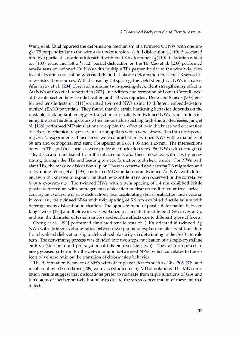
2 Theoretical background and literature review
Wang et al. [202] reported the deformation mechanism of a twinned Cu NW with one sin-gle TB perpendicular to the wire axis under tension. A full dislocation 1
2 〈110〉 dissociatedinto two partial dislocations interacted with the TB by forming a 1
2 〈110〉 dislocation glidedon 100 plane and left a 1
6 〈112〉 partial dislocation on the TB. Cao et al. [203] performedtensile tests on twinned Cu NWs with multiple TBs perpendicular to the wire axis. Sur-face dislocation nucleation governed the initial plastic deformation then the TB served asnew dislocation sources. With decreasing TB spacing, the yield strength of NWs increases.Afanasyev et al. [204] observed a similar twin-spacing-dependent strengthening effect inAu NWs as Cao et al. reported in [203]. In addition, the formation of Lomer-Cottrell locksat the intersection between dislocation and TB was reported. Deng and Sansoz [205] per-formed tensile tests on 〈111〉-oriented twinned NWs using 10 different embedded-atommethod (EAM) potentials. They found that the strain hardening behavior depends on theunstable stacking fault energy. A transition of plasticity in twinned NWs from strain soft-ening to strain hardening occurs when the unstable stacking fault energy decreases. Jang etal. [188] performed MD simulations to explain the effect of twin thickness and orientationof TBs on mechanical responses of Cu nanopillars which were observed in the correspond-ing in-situ experiments. Tensile tests were conducted on twinned NWs with a diameter of50 nm and orthogonal and slant TBs spaced at 0.63, 1.05 and 1.25 nm. The intersectionsbetween TBs and free surfaces were preferable nucleation sites. For NWs with orthogonalTBs, dislocation nucleated from the intersections and then interacted with TBs by pene-trating through the TBs and leading to neck formation and shear bands. For NWs withslant TBs, the massive dislocation slip on TBs was observed and causing TB migration anddetwinning. Wang et al. [195] conducted MD simulations on twinned Au NWs with differ-ent twin thicknesses to explain the ductile-to-brittle transition observed in the correlativein-situ experiments. The twinned NWs with a twin spacing of 1.4 nm exhibited brittleplastic deformation with homogeneous dislocation nucleation multiplied at free surfacescausing an avalanche of new dislocations thus accelerating shear localization and necking.In contrast, the twinned NWs with twin spacing of 5.6 nm exhibited ductile failure withheterogeneous dislocation nucleation. The opposite trend of plastic deformation betweenJang’s work [188] and their work was explained by considering different GSF curves of Cuand Au, the diameter of tested samples and surface effects due to different types of facets.
Cheng et al. [196] performed simulated tensile tests on 〈110〉-oriented bi-twinned AgNWs with different volume ratios between two grains to explain the observed transitionfrom localized dislocation slip to delocalized plasticity via detwinning in the in-situ tensiletests. The detwinning process was divided into two steps, nucleation of a single-crystallineembryo (step one) and propagation of this embryo (step two). They also proposed anenergy-based criterion for the detwinning in bi-twinned NWs, which correlates to the ef-fects of volume ratio on the transition of deformation behavior.
The deformation behavior of NWs with other planar defects such as GBs [206–208] andincoherent twin boundaries [209] were also studied using MD simulations. The MD simu-lation results suggest that dislocations prefer to nucleate from triple junctions of GBs andkink-steps of incoherent twin boundaries due to the stress concentration of these internaldefects.
33
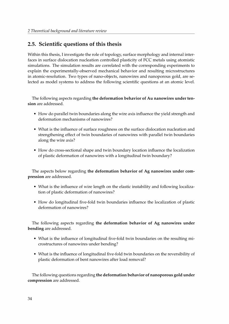
2 Theoretical background and literature review
2.5. Scientific questions of this thesis
Within this thesis, I investigate the role of topology, surface morphology and internal inter-faces in surface dislocation nucleation controlled plasticity of FCC metals using atomisticsimulations. The simulation results are correlated with the corresponding experiments toexplain the experimentally-observed mechanical behavior and resulting microstructuresin atomic-resolution. Two types of nano-objects, nanowires and nanoporous gold, are se-lected as model systems to address the following scientific questions at an atomic level.
The following aspects regarding the deformation behavior of Au nanowires under ten-sion are addressed.
• How do parallel twin boundaries along the wire axis influence the yield strength anddeformation mechanisms of nanowires?
• What is the influence of surface roughness on the surface dislocation nucleation andstrengthening effect of twin boundaries of nanowires with parallel twin boundariesalong the wire axis?
• How do cross-sectional shape and twin boundary location influence the localizationof plastic deformation of nanowires with a longitudinal twin boundary?
The aspects below regarding the deformation behavior of Ag nanowires under com-pression are addressed.
• What is the influence of wire length on the elastic instability and following localiza-tion of plastic deformation of nanowires?
• How do longitudinal five-fold twin boundaries influence the localization of plasticdeformation of nanowires?
The following aspects regarding the deformation behavior of Ag nanowires underbending are addressed.
• What is the influence of longitudinal five-fold twin boundaries on the resulting mi-crostructures of nanowires under bending?
• What is the influence of longitudinal five-fold twin boundaries on the reversibility ofplastic deformation of bent nanowires after load removal?
The following questions regarding the deformation behavior of nanoporous gold undercompression are addressed.
34
2 Theoretical background and literature review
• What is the effect of size on the elastic, yielding and flow behaviors of nanoporousstructures?
• What is the effect of size on the deformation mechanisms of nanoporous structures?
• How does topology influence the mechanical response of nanoporous structures?
• How does surface morphology influence the surface dislocation nucleation controlledplasticity of nanoporous structures?
35
3 Methods
3. Methods
This chapter presents the computational methods that were applied in this work. In sec-tion 3.1, the basics of atomistic simulations which include molecular dynamics and staticsmethods, interatomic potentials and boundary conditions are briefly introduced. In section3.2, detailed setups of atomistic simulations include sample preparations and loading con-ditions are presented. Visualization techniques and defect and structural characterizationmethods are described in section 3.3. Finally, section 3.4 presents setups of finite elementsimulations include sample preparations and loading conditions.
3.1. Atomistic simulations
Molecular dynamics (MD) is a computational modeling method for studying the time-dependent movements of atoms and molecules. In MD simulations, Newton’s equations ofmotion are integrated numerically for determining the trajectories of atoms and molecules,where forces between the atoms are calculated using interatomic potentials. MD simula-tions have remarkable resolutions in space, time and energy, therefore are widely usedin materials science to provide mechanistic insights into experimentally observed phe-nomena. More detailed introductions of MD simulations are available in the textbooks[210–212]. In this work, the massively-parallel MD software packages IMD (ITAP molecu-lar dynamics) [213, 214] and LAMMPS (Large-scale Atomic/Molecular Massively ParallelSimulator) [215] were used. All MD simulations in this work were performed at 300 K,where the temperature T and pressure P are controlled with Nose-Hoover thermostat andbarostat [216, 217]. The time step ∆t of all MD simulations is 1 fs.
Molecular statics (MS) is termed as a method for searching local minima and the tran-sition paths between them in the potential energy landscape. In computational materialsscience, MS simulations are often used to obtain the energetically minimized structures asinitial states for subsequent MD simulations or calculate the activation criterion of mate-rials processes. Line-search-based methods such as conjugate gradient (CG) and damped-dynamics methods like the Fast Inertial Relaxation Engine (FIRE) [218, 219] are two of thecommonest energy minimization algorithms. In this work, the FIRE algorithm was em-ployed to minimize the energy of the starting configurations, since FIRE shows faster per-formance and can achieve lower energy structures than CG [219]. Force norm (correspondsto the Euclidean norm of the 3 × N force vector) is taken as a representative measure forthe degree of relaxation. The energy minimization stops when the force norm falls below10−8 eV/A or 10−6 eV/A for ultra-large systems. Quasi-static simulations with finite strainincrements and subsequent structural relaxation by energy minimization using FIRE wereperformed to study the elastic response of materials.
3.1.1. Interatomic potentials
Interatomic potentials are mathematical models for calculating the interatomic energy be-tween atoms. Embedded atom method (EAM) [220, 221] type interatomic potentials are
36
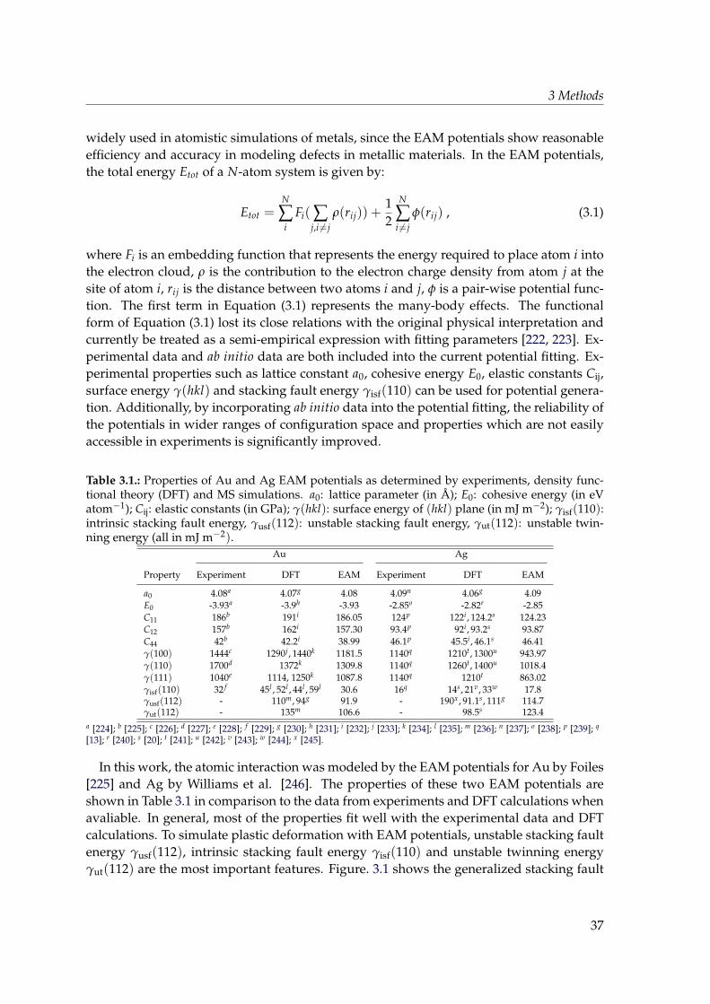
3 Methods
widely used in atomistic simulations of metals, since the EAM potentials show reasonableefficiency and accuracy in modeling defects in metallic materials. In the EAM potentials,the total energy Etot of a N-atom system is given by:
Etot =N
∑i
Fi( ∑j,i 6=j
ρ(rij)) +12
N
∑i 6=j
φ(rij) , (3.1)
where Fi is an embedding function that represents the energy required to place atom i intothe electron cloud, ρ is the contribution to the electron charge density from atom j at thesite of atom i, rij is the distance between two atoms i and j, φ is a pair-wise potential func-tion. The first term in Equation (3.1) represents the many-body effects. The functionalform of Equation (3.1) lost its close relations with the original physical interpretation andcurrently be treated as a semi-empirical expression with fitting parameters [222, 223]. Ex-perimental data and ab initio data are both included into the current potential fitting. Ex-perimental properties such as lattice constant a0, cohesive energy E0, elastic constants Cij,surface energy γ(hkl) and stacking fault energy γisf(110) can be used for potential genera-tion. Additionally, by incorporating ab initio data into the potential fitting, the reliability ofthe potentials in wider ranges of configuration space and properties which are not easilyaccessible in experiments is significantly improved.
Table 3.1.: Properties of Au and Ag EAM potentials as determined by experiments, density func-tional theory (DFT) and MS simulations. a0: lattice parameter (in A); E0: cohesive energy (in eVatom−1); Cij: elastic constants (in GPa); γ(hkl): surface energy of (hkl) plane (in mJ m−2); γisf(110):intrinsic stacking fault energy, γusf(112): unstable stacking fault energy, γut(112): unstable twin-ning energy (all in mJ m−2).
Au Ag
Property Experiment DFT EAM Experiment DFT EAM
a0 4.08a 4.07g 4.08 4.09n 4.06g 4.09E0 -3.93a -3.9h -3.93 -2.85o -2.82r -2.85C11 186b 191i 186.05 124p 122i , 124.2s 124.23C12 157b 162i 157.30 93.4p 92i , 93.2s 93.87C44 42b 42.2i 38.99 46.1p 45.5i , 46.1s 46.41γ(100) 1444c 1290j, 1440k 1181.5 1140q 1210t, 1300u 943.97γ(110) 1700d 1372k 1309.8 1140q 1260t, 1400u 1018.4γ(111) 1040e 1114, 1250k 1087.8 1140q 1210t 863.02γisf(110) 32 f 45l , 52l , 44l , 59l 30.6 16q 14s, 21v, 33w 17.8γusf(112) - 110m, 94g 91.9 - 190x , 91.1s, 111g 114.7γut(112) - 135m 106.6 - 98.5s 123.4
a [224]; b [225]; c [226]; d [227]; e [228]; f [229]; g [230]; h [231]; i [232]; j [233]; k [234]; l [235]; m [236]; n [237]; o [238]; p [239]; q
[13]; r [240]; s [20]; t [241]; u [242]; v [243]; w [244]; x [245].
In this work, the atomic interaction was modeled by the EAM potentials for Au by Foiles[225] and Ag by Williams et al. [246]. The properties of these two EAM potentials areshown in Table 3.1 in comparison to the data from experiments and DFT calculations whenavaliable. In general, most of the properties fit well with the experimental data and DFTcalculations. To simulate plastic deformation with EAM potentials, unstable stacking faultenergy γusf(112), intrinsic stacking fault energy γisf(110) and unstable twinning energyγut(112) are the most important features. Figure. 3.1 shows the generalized stacking fault
37
3 Methods
(GSF) energy curves of the Au and Ag EAM potentials. The GSF energy curve was initiallyintroduced to predict dislocation core structures [22] and was later used in measuring cri-teria for dislocation nucleation [23]. Unstable stacking fault (USF) energy measures theenergy barrier for the nucleation of a leading partial dislocation, e.g., a0
6 [112] on (111) slipplane, in a FCC crystal. After the gliding along a0
6 [112], an intrinsic stacking fault (ISF) iscreated. Afterwards, gliding can continue either by a trailing partial dislocation a0
6 [211]on the same slip plane forming a full dislocation slip (grey line) or along the same a0
6 [112]vector on the adjacent slip plane resulting in twinning (dashed line). The energy differencebetween UT and ISF is the energy barrier of the nucleation of a twin on the adjacent slipplane of an existing ISF.
To simulate surface dislocation nucleation controlled plastic deformation in nano-objects,the energies of energetically preferable free surfaces and surface ledges left behind by dis-location slip should be taken into account in quantitatively determining the nucleationcriterion. However, it should be mentioned that the surface energies of the Au and AgEAM potentials show some deviations with the experimental and DFT values, as shownin Table 3.1. Moreover, currently, there is no accessible data on the surface ledge energy ofAu and Ag from both experiments and DFT calculations. In general, the materials proper-ties related to the surface dislocation nucleation obtained from all simulations in this workshould be only qualitatively compared with experiments.
0
20
40
60
80
100
120
140
0 0.5 1 1.5 2
Fault e
nerg
y [m
J m
−2]
Fractional shear along <112>/6
0
20
40
60
80
100
120
140
0 0.5 1 1.5 2
Fault e
nerg
y [m
J m
−2]
Fractional shear along <112>/6
Au Aga b
USF
UT
ISF
USFUT
ISF
Figure. 3.1.: Generalized stacking fault energy curves of a Au and b Ag EAM potentials. Black solidline corresponds to slip by a leading partial dislocation 1
6 〈112〉, grey solid line corresponds to slipby a trailing partial dislocation 1
6 〈112〉 on the same slip plane from a existing ISF, black dashed linecorresponds to slip by a leading partial dislocation 1
6 〈112〉 on the adjacent slip plane from the ISFto a twinning structure.
3.1.2. Boundary conditions
Boundary conditions (BC) define how atoms be treated at the ends of the simulation cell. Inthis work, the following boundary conditions are applied individually and cooperatively.
38
3 Methods
Period boundary conditions
In both MD and MS simulations, the most common boundary conditions in use are periodboundary conditions (PBC). The simulation cell is periodic, which means atoms interactacross the boundary, and they can pass through one end of the cell and re-appear on theother end. Therefore, the cell size should be large enough (>2×cutoff radius) in periodicdirections to avoid interactions between atoms and their images. Meanwhile, the shape ofa periodic simulation cell must fill all space by translational operations of the central cellin three dimensional. The advantage of PBC is that the surface effects can be eliminatedtherefore mimic the behavior of a “bulk” material.
Free boundary conditions
To study materials in confined dimensions, free-BC are applied to allow the freedom ofatoms at free surfaces, e.g., for simulating wires, 1D PBC should be applied along the wireaxis and free-BC in other directions.
Force boundary conditions
Force-BC is a special case of free-BC, extra forces can be applied on the atoms to mimicmodeling samples under external loading conditions.
3.2. Simulation setups
In this work, atomistic simulations were performed on nano-objects to study the defor-mation behavior of these materials under different loading conditions. For constructionsof atomic nanostructures, experimental information includes crystallographic orientationand geometry is indispensable. In subsection 3.2.1, the sample preparations of metallicnanowires (NWs) based on wire axial orientation and surface facet orientation obtainedfrom experiments and nanoporous gold (NPG) reconstructed using 3D non-destructivetomography techniques are introduced in detail. To mimic nanostructures under experi-mental stress states, different loading conditions are introduced in atomistic simulations,see subsection 3.2.2.
3.2.1. Sample preparation
The sample preparation of a nano-object for atomistic simulations has three steps. The firststep is constructing a “bulk” atomic structure in a defined crystallographic orientation.The second step is introducing free surfaces by “cutting” the periodic structure followingcertain criteria. The last step is minimizing the energy of the structure and then relaxing itat finite temperatures.
39
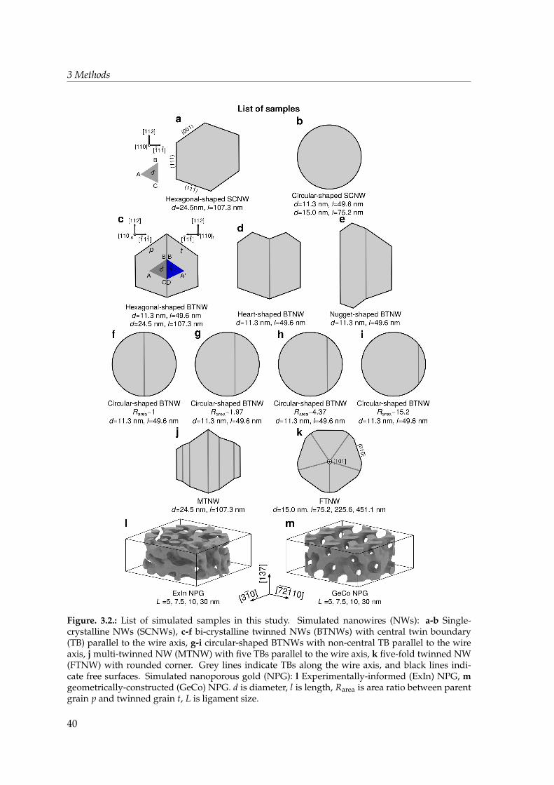
3 Methods
B B'
A
'
CD'
A'
[110]p [111]- -
[112]-
[110]t[111]- -
[112]-
Figure. 3.2.: List of simulated samples in this study. Simulated nanowires (NWs): a-b Single-crystalline NWs (SCNWs), c-f bi-crystalline twinned NWs (BTNWs) with central twin boundary(TB) parallel to the wire axis, g-i circular-shaped BTNWs with non-central TB parallel to the wireaxis, j multi-twinned NW (MTNW) with five TBs parallel to the wire axis, k five-fold twinned NW(FTNW) with rounded corner. Grey lines indicate TBs along the wire axis, and black lines indi-cate free surfaces. Simulated nanoporous gold (NPG): l Experimentally-informed (ExIn) NPG, mgeometrically-constructed (GeCo) NPG. d is diameter, l is length, Rarea is area ratio between parentgrain p and twinned grain t, L is ligament size.
40
3 Methods
Nanowires
The simulated NWs were constructed based on wire axial orientations and cross-sectionalshapes obtained from experimental NWs which are produced via physical vapor deposi-tion (PVD) [8] or wet chemical synthesis [247]. For Au NWs which are fabricated usingPVD, the wires grow parallel to 〈110〉 crystallographic orientation and have no detectabledefects. The cross-sectional shape of Au single-crystalline (SC) NWs is a hexagon, the wireshave four 111 and two 100 crystal planes on the side facets [8]. Faceted Au NWs con-sist of 111- and 100-oriented facets to minimize the surface energy, since 111 facetshows the lowest surface energy followed by 100 facet according to the experimentaland theoretical data [248]. The [110]-oriented hexagonal-shaped SCNW, see Figure. 3.2a,was constructed based on the above mentioned experimental observations.
During the growth procedures via PVD, planar defects such as stacking faults and twinboundaries (TBs) parallel to the wire axis can form in Au NWs. Au bi-crystalline twinned(BT) NWs (Figure. 3.2c-e) were constructed based on experimental cross-sectional shapes[249] which are consisted of 111- and 100-oriented facets. For Au multi-twinned (MT)NWs, see Figure. 3.2j, the construction was based on the size of each twin segment deter-mined in the experimental sample [197]. In comparison with faceted NWs, the influence ofrandom facet orientation on deformation behavior of NWs was investigated via circular-shaped NWs (see Figure. 3.2b, f), although circular cross-section is not energetic favorable.Moreover, the influence of TB location on deformation behavior of BTNWs was studiedusing circular-shaped NWs (see Figure. 3.2f-i) to avoid bringing more variables, like dif-ferent cross-sectional areas and ratios between primary surface facets, when changing TBlocation.
For Ag five-fold twinned (FT) NWs which are fabricated using wet chemical synthesis,the wire axis is parallel to 〈110〉 crystallographic orientation. During the growth proce-dures, the addition of polymer adheres to the 100-oriented side facets and acts as cap-ping agent, thus leading to the growth of the wires along 〈110〉 direction [247]. The cross-sectional shape of experimental FTNWs is close to a pentagon with roundish corners at thetriple junctions between TBs and free surfaces [182, 183, 250]. The simulated FTNW wasconstructed based on the experimental characterizations, see Figure. 3.2k.
NWs with surface roughness were produced by randomly removing a certain percentageof atoms from the outer layers, e.g., L2R0.33 rough surface indicates one-third of atoms(R0.33) in the two outermost (L2) surface layers were randomly removed.
Nanoporous gold
NPG samples in experiments were prepared by Thomas Przybilla (Institute of Micro- andNanostructure Research, Friedrich-Alexander-Universitat Erlangen-Nurnberg). Tomogra-phy and sample reconstruction were carried out by Thomas Przybilla, Benjamin ApeleoZubiri (Institute of Micro- and Nanostructure Research, Friedrich-Alexander-UniversitatErlangen-Nurnberg), Aruna Prakash (Institute of Mechanics and Fluid Dynamics, Tech-nische Universitat Bergakademie Freiberg), Stephen T. Kelly and Hrishikesh A. Bale (CarlZeiss X-ray Microscopy, Pleasanton, USA).
41
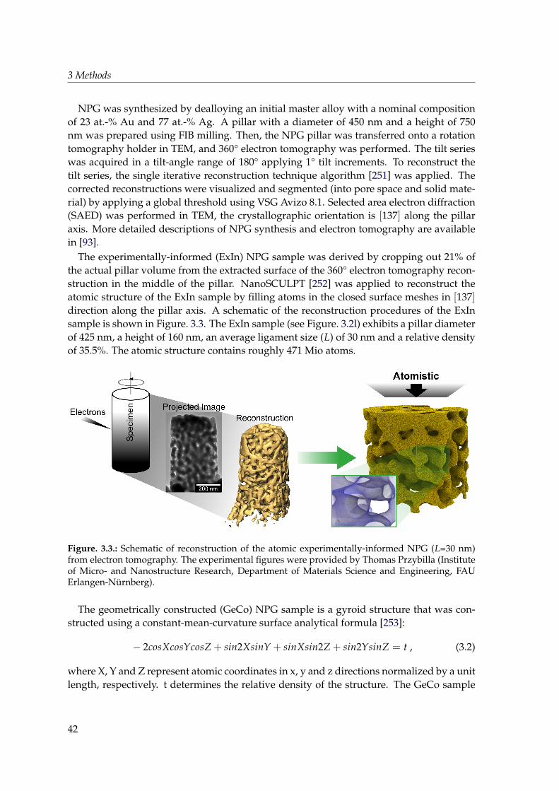
3 Methods
NPG was synthesized by dealloying an initial master alloy with a nominal compositionof 23 at.-% Au and 77 at.-% Ag. A pillar with a diameter of 450 nm and a height of 750nm was prepared using FIB milling. Then, the NPG pillar was transferred onto a rotationtomography holder in TEM, and 360° electron tomography was performed. The tilt serieswas acquired in a tilt-angle range of 180° applying 1° tilt increments. To reconstruct thetilt series, the single iterative reconstruction technique algorithm [251] was applied. Thecorrected reconstructions were visualized and segmented (into pore space and solid mate-rial) by applying a global threshold using VSG Avizo 8.1. Selected area electron diffraction(SAED) was performed in TEM, the crystallographic orientation is [137] along the pillaraxis. More detailed descriptions of NPG synthesis and electron tomography are availablein [93].
The experimentally-informed (ExIn) NPG sample was derived by cropping out 21% ofthe actual pillar volume from the extracted surface of the 360° electron tomography recon-struction in the middle of the pillar. NanoSCULPT [252] was applied to reconstruct theatomic structure of the ExIn sample by filling atoms in the closed surface meshes in [137]direction along the pillar axis. A schematic of the reconstruction procedures of the ExInsample is shown in Figure. 3.3. The ExIn sample (see Figure. 3.2l) exhibits a pillar diameterof 425 nm, a height of 160 nm, an average ligament size (L) of 30 nm and a relative densityof 35.5%. The atomic structure contains roughly 471 Mio atoms.
Figure. 3.3.: Schematic of reconstruction of the atomic experimentally-informed NPG (L=30 nm)from electron tomography. The experimental figures were provided by Thomas Przybilla (Instituteof Micro- and Nanostructure Research, Department of Materials Science and Engineering, FAUErlangen-Nurnberg).
The geometrically constructed (GeCo) NPG sample is a gyroid structure that was con-structed using a constant-mean-curvature surface analytical formula [253]:
− 2cosXcosYcosZ + sin2XsinY + sinXsin2Z + sin2YsinZ = t , (3.2)
where X, Y and Z represent atomic coordinates in x, y and z directions normalized by a unitlength, respectively. t determines the relative density of the structure. The GeCo sample
42
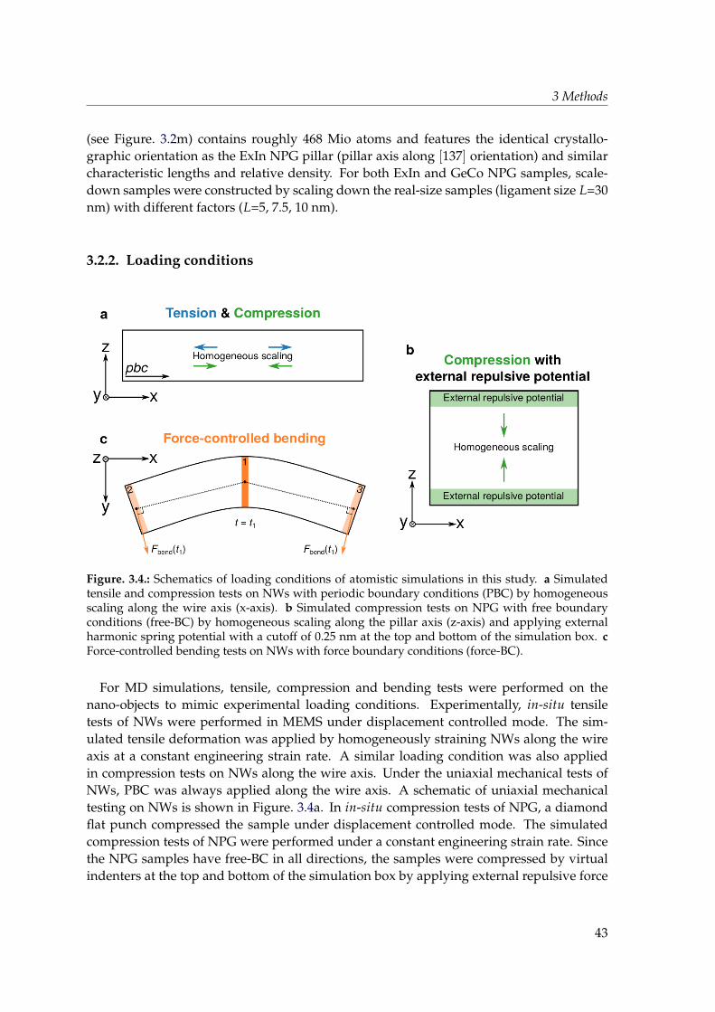
3 Methods
(see Figure. 3.2m) contains roughly 468 Mio atoms and features the identical crystallo-graphic orientation as the ExIn NPG pillar (pillar axis along [137] orientation) and similarcharacteristic lengths and relative density. For both ExIn and GeCo NPG samples, scale-down samples were constructed by scaling down the real-size samples (ligament size L=30nm) with different factors (L=5, 7.5, 10 nm).
3.2.2. Loading conditions
Figure. 3.4.: Schematics of loading conditions of atomistic simulations in this study. a Simulatedtensile and compression tests on NWs with periodic boundary conditions (PBC) by homogeneousscaling along the wire axis (x-axis). b Simulated compression tests on NPG with free boundaryconditions (free-BC) by homogeneous scaling along the pillar axis (z-axis) and applying externalharmonic spring potential with a cutoff of 0.25 nm at the top and bottom of the simulation box. cForce-controlled bending tests on NWs with force boundary conditions (force-BC).
For MD simulations, tensile, compression and bending tests were performed on thenano-objects to mimic experimental loading conditions. Experimentally, in-situ tensiletests of NWs were performed in MEMS under displacement controlled mode. The sim-ulated tensile deformation was applied by homogeneously straining NWs along the wireaxis at a constant engineering strain rate. A similar loading condition was also appliedin compression tests on NWs along the wire axis. Under the uniaxial mechanical tests ofNWs, PBC was always applied along the wire axis. A schematic of uniaxial mechanicaltesting on NWs is shown in Figure. 3.4a. In in-situ compression tests of NPG, a diamondflat punch compressed the sample under displacement controlled mode. The simulatedcompression tests of NPG were performed under a constant engineering strain rate. Sincethe NPG samples have free-BC in all directions, the samples were compressed by virtualindenters at the top and bottom of the simulation box by applying external repulsive force
43
3 Methods
according to a harmonic spring potential:
Esp = K(r− rc)2 r < rc, (3.3)
where Esp is the energy given by the spring potential, K is the spring constant K=1 eV/A2,r is the distance from the particle to the wall, and rc is the cutoff distance rc=2.5 A. Thedirection of the force is parallel to the axis of compression. A schematic of the compressiontests on NPG is shown in Figure. 3.4b.
For force-controlled bending on NWs, the procedure is to mimic stresses akin to a three-point bending test without effects of artificial PBC and stress concentrations due to thepresences of indenters and clamps. A schematic of the simulated bending test is shownin Figure. 3.4c. The bending moments were introduced by applying forces on atoms atthe two ends (regions 2 and 3) of the NWs in the direction of the cross-product betweenthe bending axis and the vector connecting the mass centers of regions 1 and two ends.The magnitude of the force was linearly increased with time. The applied forces wereinstantaneously removed to study the unloading behavior of the bent NWs. More detailedinformation of this bending loading condition is introduced in [115].
3.3. Visualization and analysis
In this work, atomistic simulations were visualized using the Open Visualization Tool(OVITO) [254]. The structural characterization methods, include coordination number(CN), common neighbor analysis (CNA) [255, 256], dislocation analysis (DXA) [257, 258]and atomic stress tensor, are introduced in subsection 3.3.1. Topology and surface mor-phology of NPG samples were analyzed using Amira, and for a sanity check of the results,an open-source tool Libigl [259] was used.
3.3.1. Structural analysis
To analyze the deformation mechanisms of crystalline structures, structural characteriza-tion is crucial. The methods which were used in this work for defect characterization arebriefly introduced in the following paragraphs.
Coordination number (CN)
The CN counts the number of neighbors for each atom that within a given cutoff rangearound its position. In this work, the CN was used to identify atoms at the outermost layerof nanostructures, for atoms in FCC crystal CN=12 and for atoms at free surfaces CN< 12.For atoms at 111 and 100-oriented free surfaces, CNs are 9 and 8, respectively.
Common neighbor analysis (CNA)
The CNA is an algorithm to compute a fingerprint for pairs of atoms. The local environ-ment of a pair of atoms is classified by three indices, jkl, where j is the number of neighbors
44
3 Methods
common to both atoms, k is the number of bonds between shared neighbors, l is the num-ber of bonds in the longest bond chain formed by the k bonds between common neighbors.For example, FCC crystal has only bonded pairs of type 421, and HCP crystal has equalnumbers of type 421 and type 422. In conventional CNA, a fixed cutoff is used to detectwhether a pair of atoms is bonded or not. With the adaptive CNA [260], an optimal cutoff isdetermined automatically for each individual atoms. Further structural analysis methodswere developed depending on CNA to characterize crystalline and non-crystalline struc-tures [257, 261, 262].
Dislocation analysis (DXA)
The DXA is an algorithm to identify dislocation line defects and determine their Burgersvectors in an atomic structure. Based on the CNA, atoms in a dislocation core are classi-fied as non-crystalline atoms and excluded from further construction of Burgers circuits.A triangulated interface which encloses the dislocation core is constructed. Then Burgerscircuits are constructed on the triangulated interface and a dislocation line is produced byconnecting each circuit’s center of mass. A more detailed description of the DXA method isintroduced in [257, 258]. By using the DXA, Burgers vector, dislocation character (edge orscrew) and dislocation length can be extracted from an atomic crystalline structure. How-ever, the crystallographic orientation of the atomic structure is not taken into account in theDXA, therefore, the Burgers vectors obtained from the DXA need to be reassigned manu-ally according to the Thompson tetrahedron notation [18].
Atomic stress
The atomic stress tensor is calculated using virtual stress tensor normalized by the atomicvolume calculated from the Voronoi tessellation [263]. The stress per-atom has no physicalsignificance since the expression of atomic stress has a virtual part due to momentum (thekinetic energy term) [264]. However, atomic stress is useful in atomistic simulations aftersummation and average. The atomic stress tensors can be used to evaluate global stresstensor and calculate von Mises and resolved shear stress fields. In this work, the atomicstress is averaged by the nearest neighbors to visualize stress fields at 300 K.
3.3.2. Topology and surface morphology analyses
To characterize the geometry of NPG structures, 3D images and reconstructed surfacemeshes obtained from non-destructive techniques were post-processed. Analyses for topol-ogy and surface morphology of NPG are introduced in the following paragraphs.
Topology
The local topology properties, like local thickness and nodal connectivity were character-ized by the skeletonization of the bicontinuous structures using the Auto Skeleton moduleimplemented in Amira. The algorithm extracts the centerline of the porous structures from3D image data and then converts it to a spatial graph consists of nodes and segments. The
45
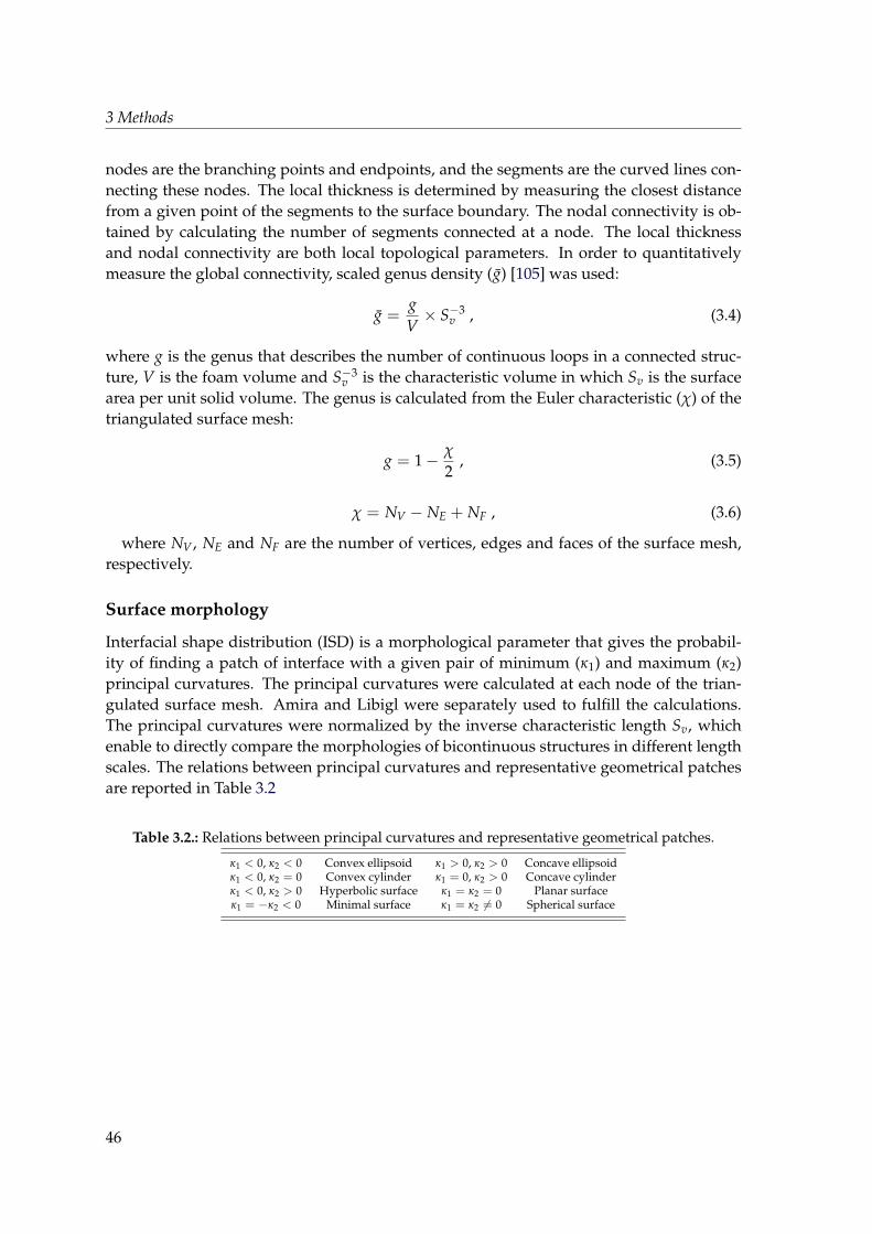
3 Methods
nodes are the branching points and endpoints, and the segments are the curved lines con-necting these nodes. The local thickness is determined by measuring the closest distancefrom a given point of the segments to the surface boundary. The nodal connectivity is ob-tained by calculating the number of segments connected at a node. The local thicknessand nodal connectivity are both local topological parameters. In order to quantitativelymeasure the global connectivity, scaled genus density (g) [105] was used:
g =gV× S−3
v , (3.4)
where g is the genus that describes the number of continuous loops in a connected struc-ture, V is the foam volume and S−3
v is the characteristic volume in which Sv is the surfacearea per unit solid volume. The genus is calculated from the Euler characteristic (χ) of thetriangulated surface mesh:
g = 1− χ
2, (3.5)
χ = NV − NE + NF , (3.6)
where NV , NE and NF are the number of vertices, edges and faces of the surface mesh,respectively.
Surface morphology
Interfacial shape distribution (ISD) is a morphological parameter that gives the probabil-ity of finding a patch of interface with a given pair of minimum (κ1) and maximum (κ2)principal curvatures. The principal curvatures were calculated at each node of the trian-gulated surface mesh. Amira and Libigl were separately used to fulfill the calculations.The principal curvatures were normalized by the inverse characteristic length Sv, whichenable to directly compare the morphologies of bicontinuous structures in different lengthscales. The relations between principal curvatures and representative geometrical patchesare reported in Table 3.2
Table 3.2.: Relations between principal curvatures and representative geometrical patches.
κ1 < 0, κ2 < 0 Convex ellipsoid κ1 > 0, κ2 > 0 Concave ellipsoidκ1 < 0, κ2 = 0 Convex cylinder κ1 = 0, κ2 > 0 Concave cylinderκ1 < 0, κ2 > 0 Hyperbolic surface κ1 = κ2 = 0 Planar surfaceκ1 = −κ2 < 0 Minimal surface κ1 = κ2 6= 0 Spherical surface
46
Part I.
Nanowires
Part I Nanowires: 4 Results
This part presents the deformation behavior of 〈110〉-oriented single-crystalline and twinnednanowires under tension, compression and bending. By comparing simulation results onsingle-crystalline and twinned nanowires under different loading conditions, the influenceof twin boundaries on mechanical properties and deformation mechanisms of nano-objectswere investigated in detail. The outcomes of this part would enhance the understandingof deformation mechanisms of twinned nano-objects and suggest design strategies for me-chanical systems and flexible and stretchable electronic devices at the nanoscale.
The influence of pre-existing parallel twins along the wire axis on the yield strength andlocalization of plastic deformation was investigated by performing simulated tensile testson Au single-crystalline, bi-crystalline twined and multi-twinned nanowires. The inter-actions between surface-nucleated dislocations and twin boundaries were investigated byextracting and characterizing dislocations to explain the strongly localized plastic deforma-tion in twinned nanowires. The strengthening effect of twin boundaries was investigatedby correlating the stress-strain response with the evolution of dislocation density duringthe deformation processes. The effects of cross-sectional shape, as well as location of twinboundary on the localization of plastic deformation of bi-crystalline twinned nanowires,were investigated. To mimic the effect of thermal activation on surface dislocation nucle-ation, namely lowering the nucleation stress and leads to a broader distribution of criticalstresses, surface roughness was introduced in the simulated wires. The transferability ofidentified mechanisms of dislocation-twin boundary interactions and following localiza-tion behaviors was evaluated by varying simulation parameters, such as size, aspect ratio,strain rate, interatomic potential and surface roughness. By comparing with the correlativein-situ tensile tests, the origins of strengthening and failure in multi-twinned nanowiresunder tension were discussed in detail.
The influence of pre-existing five-fold twins along the wire axis on deformation mecha-nisms of nanowires was investigated by performing simulated compression and bendingtests on Ag single-crystalline and five-fold twinned nanowires. The effects of elastic in-stability on dislocation nucleation and further localization of plastic deformation of thenanowires under compression were studied. The unbending tests were performed on thebent nanowires by instantaneously removing load to study the reversibility of plastic de-formation of these wires and the influence of longitudinal five-fold twins on the reversibil-ity. The mechanisms of formation of resulting microstructures in buckled nanowires undercompression and bent nanowires under bending were investigated. The influence of sim-ulation parameters, i.e., size, strain/force rate and surface roughness, on the deformationbehavior and resulting defect structures of the five-fold twinned nanowires were investi-gated.
In the following, the results for tensile tests on Au nanowires and compression andbending tests on Ag nanowires are described separately in Chapter 4. The deformationmechanisms of twinned nanowires with longitudinally parallel and five-fold twins underdifferent loading conditions and the comparison with the correlative in-situ experimentsare discussed in Chapter 5.
48
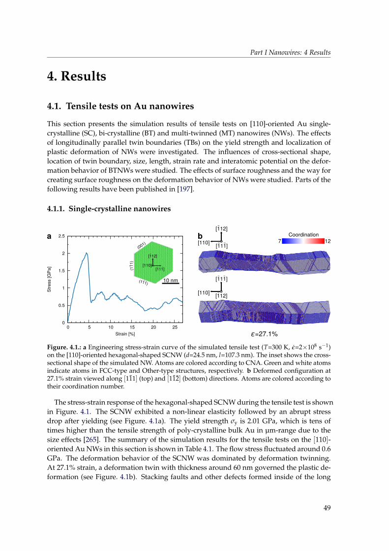
Part I Nanowires: 4 Results
4. Results
4.1. Tensile tests on Au nanowires
This section presents the simulation results of tensile tests on [110]-oriented Au single-crystalline (SC), bi-crystalline (BT) and multi-twinned (MT) nanowires (NWs). The effectsof longitudinally parallel twin boundaries (TBs) on the yield strength and localization ofplastic deformation of NWs were investigated. The influences of cross-sectional shape,location of twin boundary, size, length, strain rate and interatomic potential on the defor-mation behavior of BTNWs were studied. The effects of surface roughness and the way forcreating surface roughness on the deformation behavior of NWs were studied. Parts of thefollowing results have been published in [197].
4.1.1. Single-crystalline nanowires
a
[110][111]
-
[112]-
10 nm(111)
(001)
--
(111
) -
0
0.5
1
1.5
2
2.5
0 5 10 15 20 25
Str
ess [G
Pa]
Strain [%]
Coordination
7 12[110][111]- -
[112]-
[111]- -
[112]-[110]
b
ε=27.1%
Figure. 4.1.: a Engineering stress-strain curve of the simulated tensile test (T=300 K, ε=2×10⁸ s−1)on the [110]-oriented hexagonal-shaped SCNW (d=24.5 nm, l=107.3 nm). The inset shows the cross-sectional shape of the simulated NW. Atoms are colored according to CNA. Green and white atomsindicate atoms in FCC-type and Other-type structures, respectively. b Deformed configuration at27.1% strain viewed along [111] (top) and [112] (bottom) directions. Atoms are colored according totheir coordination number.
The stress-strain response of the hexagonal-shaped SCNW during the tensile test is shownin Figure. 4.1. The SCNW exhibited a non-linear elasticity followed by an abrupt stressdrop after yielding (see Figure. 4.1a). The yield strength σy is 2.01 GPa, which is tens oftimes higher than the tensile strength of poly-crystalline bulk Au in µm-range due to thesize effects [265]. The summary of the simulation results for the tensile tests on the [110]-oriented Au NWs in this section is shown in Table 4.1. The flow stress fluctuated around 0.6GPa. The deformation behavior of the SCNW was dominated by deformation twinning.At 27.1% strain, a deformation twin with thickness around 60 nm governed the plastic de-formation (see Figure. 4.1b). Stacking faults and other defects formed inside of the long
49
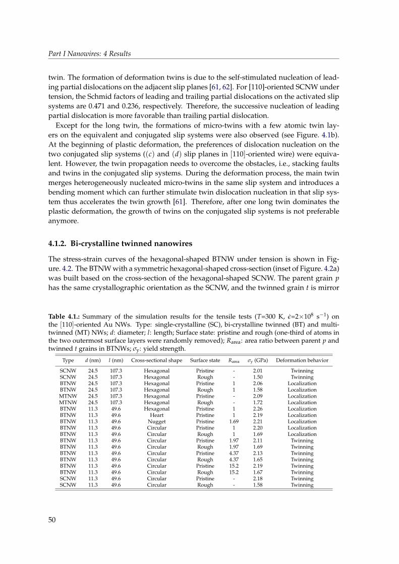
Part I Nanowires: 4 Results
twin. The formation of deformation twins is due to the self-stimulated nucleation of lead-ing partial dislocations on the adjacent slip planes [61, 62]. For [110]-oriented SCNW undertension, the Schmid factors of leading and trailing partial dislocations on the activated slipsystems are 0.471 and 0.236, respectively. Therefore, the successive nucleation of leadingpartial dislocation is more favorable than trailing partial dislocation.
Except for the long twin, the formations of micro-twins with a few atomic twin lay-ers on the equivalent and conjugated slip systems were also observed (see Figure. 4.1b).At the beginning of plastic deformation, the preferences of dislocation nucleation on thetwo conjugated slip systems ((c) and (d) slip planes in [110]-oriented wire) were equiva-lent. However, the twin propagation needs to overcome the obstacles, i.e., stacking faultsand twins in the conjugated slip systems. During the deformation process, the main twinmerges heterogeneously nucleated micro-twins in the same slip system and introduces abending moment which can further stimulate twin dislocation nucleation in that slip sys-tem thus accelerates the twin growth [61]. Therefore, after one long twin dominates theplastic deformation, the growth of twins on the conjugated slip systems is not preferableanymore.
4.1.2. Bi-crystalline twinned nanowires
The stress-strain curves of the hexagonal-shaped BTNW under tension is shown in Fig-ure. 4.2. The BTNW with a symmetric hexagonal-shaped cross-section (inset of Figure. 4.2a)was built based on the cross-section of the hexagonal-shaped SCNW. The parent grain phas the same crystallographic orientation as the SCNW, and the twinned grain t is mirror
Table 4.1.: Summary of the simulation results for the tensile tests (T=300 K, ε=2×10⁸ s−1) onthe [110]-oriented Au NWs. Type: single-crystalline (SC), bi-crystalline twinned (BT) and multi-twinned (MT) NWs; d: diameter; l: length; Surface state: pristine and rough (one-third of atoms inthe two outermost surface layers were randomly removed); Rarea: area ratio between parent p andtwinned t grains in BTNWs; σy: yield strength.
Type d (nm) l (nm) Cross-sectional shape Surface state Rarea σy (GPa) Deformation behavior
SCNW 24.5 107.3 Hexagonal Pristine - 2.01 TwinningSCNW 24.5 107.3 Hexagonal Rough - 1.50 TwinningBTNW 24.5 107.3 Hexagonal Pristine 1 2.06 LocalizationBTNW 24.5 107.3 Hexagonal Rough 1 1.58 LocalizationMTNW 24.5 107.3 Hexagonal Pristine - 2.09 LocalizationMTNW 24.5 107.3 Hexagonal Rough - 1.72 LocalizationBTNW 11.3 49.6 Hexagonal Pristine 1 2.26 LocalizationBTNW 11.3 49.6 Heart Pristine 1 2.19 LocalizationBTNW 11.3 49.6 Nugget Pristine 1.69 2.21 LocalizationBTNW 11.3 49.6 Circular Pristine 1 2.20 LocalizationBTNW 11.3 49.6 Circular Rough 1 1.69 LocalizationBTNW 11.3 49.6 Circular Pristine 1.97 2.11 TwinningBTNW 11.3 49.6 Circular Rough 1.97 1.69 TwinningBTNW 11.3 49.6 Circular Pristine 4.37 2.13 TwinningBTNW 11.3 49.6 Circular Rough 4.37 1.65 TwinningBTNW 11.3 49.6 Circular Pristine 15.2 2.19 TwinningBTNW 11.3 49.6 Circular Rough 15.2 1.67 TwinningSCNW 11.3 49.6 Circular Pristine - 2.18 TwinningSCNW 11.3 49.6 Circular Rough - 1.58 Twinning
50
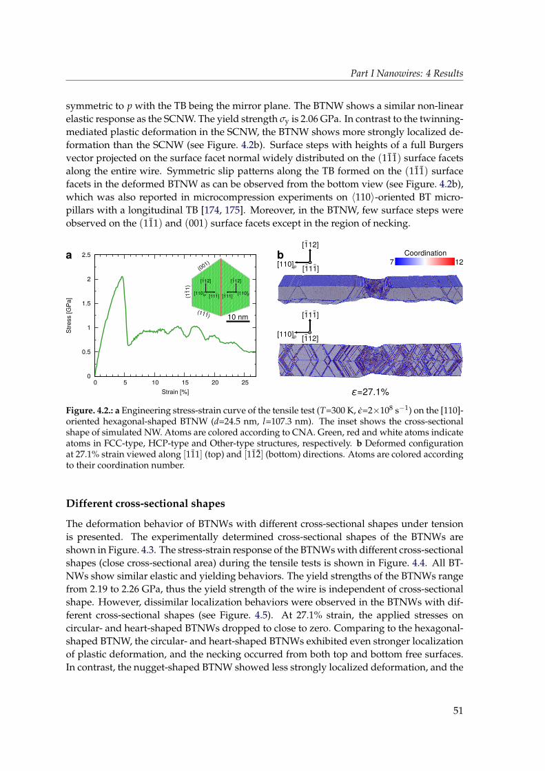
Part I Nanowires: 4 Results
symmetric to p with the TB being the mirror plane. The BTNW shows a similar non-linearelastic response as the SCNW. The yield strength σy is 2.06 GPa. In contrast to the twinning-mediated plastic deformation in the SCNW, the BTNW shows more strongly localized de-formation than the SCNW (see Figure. 4.2b). Surface steps with heights of a full Burgersvector projected on the surface facet normal widely distributed on the (111) surface facetsalong the entire wire. Symmetric slip patterns along the TB formed on the (111) surfacefacets in the deformed BTNW as can be observed from the bottom view (see Figure. 4.2b),which was also reported in microcompression experiments on 〈110〉-oriented BT micro-pillars with a longitudinal TB [174, 175]. Moreover, in the BTNW, few surface steps wereobserved on the (111) and (001) surface facets except in the region of necking.
a Coordination
7 12[110]p [111]- -
[112]-
[111]- -
[112]-[110]p
b
ε=27.1%
0
0.5
1
1.5
2
2.5
0 5 10 15 20 25
Str
ess [G
Pa]
Strain [%]
(111)
(001)
--
(111
) - [110]p [111]
-
[112]-
[110]t[111]- -
[112]-
10 nm
Figure. 4.2.: a Engineering stress-strain curve of the tensile test (T=300 K, ε=2×10⁸ s−1) on the [110]-oriented hexagonal-shaped BTNW (d=24.5 nm, l=107.3 nm). The inset shows the cross-sectionalshape of simulated NW. Atoms are colored according to CNA. Green, red and white atoms indicateatoms in FCC-type, HCP-type and Other-type structures, respectively. b Deformed configurationat 27.1% strain viewed along [111] (top) and [112] (bottom) directions. Atoms are colored accordingto their coordination number.
Different cross-sectional shapes
The deformation behavior of BTNWs with different cross-sectional shapes under tensionis presented. The experimentally determined cross-sectional shapes of the BTNWs areshown in Figure. 4.3. The stress-strain response of the BTNWs with different cross-sectionalshapes (close cross-sectional area) during the tensile tests is shown in Figure. 4.4. All BT-NWs show similar elastic and yielding behaviors. The yield strengths of the BTNWs rangefrom 2.19 to 2.26 GPa, thus the yield strength of the wire is independent of cross-sectionalshape. However, dissimilar localization behaviors were observed in the BTNWs with dif-ferent cross-sectional shapes (see Figure. 4.5). At 27.1% strain, the applied stresses oncircular- and heart-shaped BTNWs dropped to close to zero. Comparing to the hexagonal-shaped BTNW, the circular- and heart-shaped BTNWs exhibited even stronger localizationof plastic deformation, and the necking occurred from both top and bottom free surfaces.In contrast, the nugget-shaped BTNW showed less strongly localized deformation, and the
51
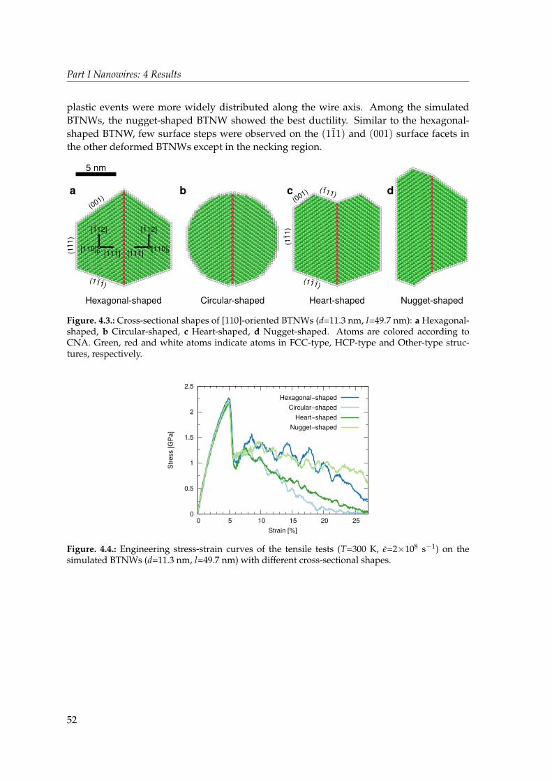
Part I Nanowires: 4 Results
plastic events were more widely distributed along the wire axis. Among the simulatedBTNWs, the nugget-shaped BTNW showed the best ductility. Similar to the hexagonal-shaped BTNW, few surface steps were observed on the (111) and (001) surface facets inthe other deformed BTNWs except in the necking region.
(001)
Hexagonal-shaped
a c d
(111) --
(111
) -
(111) --
(111
) -
(001) (111)
-
[110]p [111]-
[112]-
[110]t[111]- -
[112]-
5 nm
b
Circular-shaped Heart-shaped Nugget-shaped
Figure. 4.3.: Cross-sectional shapes of [110]-oriented BTNWs (d=11.3 nm, l=49.7 nm): a Hexagonal-shaped, b Circular-shaped, c Heart-shaped, d Nugget-shaped. Atoms are colored according toCNA. Green, red and white atoms indicate atoms in FCC-type, HCP-type and Other-type struc-tures, respectively.
0
0.5
1
1.5
2
2.5
0 5 10 15 20 25
Str
ess [G
Pa]
Strain [%]
Hexagonal−shaped
Circular−shaped
Heart−shaped
Nugget−shaped
Figure. 4.4.: Engineering stress-strain curves of the tensile tests (T=300 K, ε=2×10⁸ s−1) on thesimulated BTNWs (d=11.3 nm, l=49.7 nm) with different cross-sectional shapes.
52
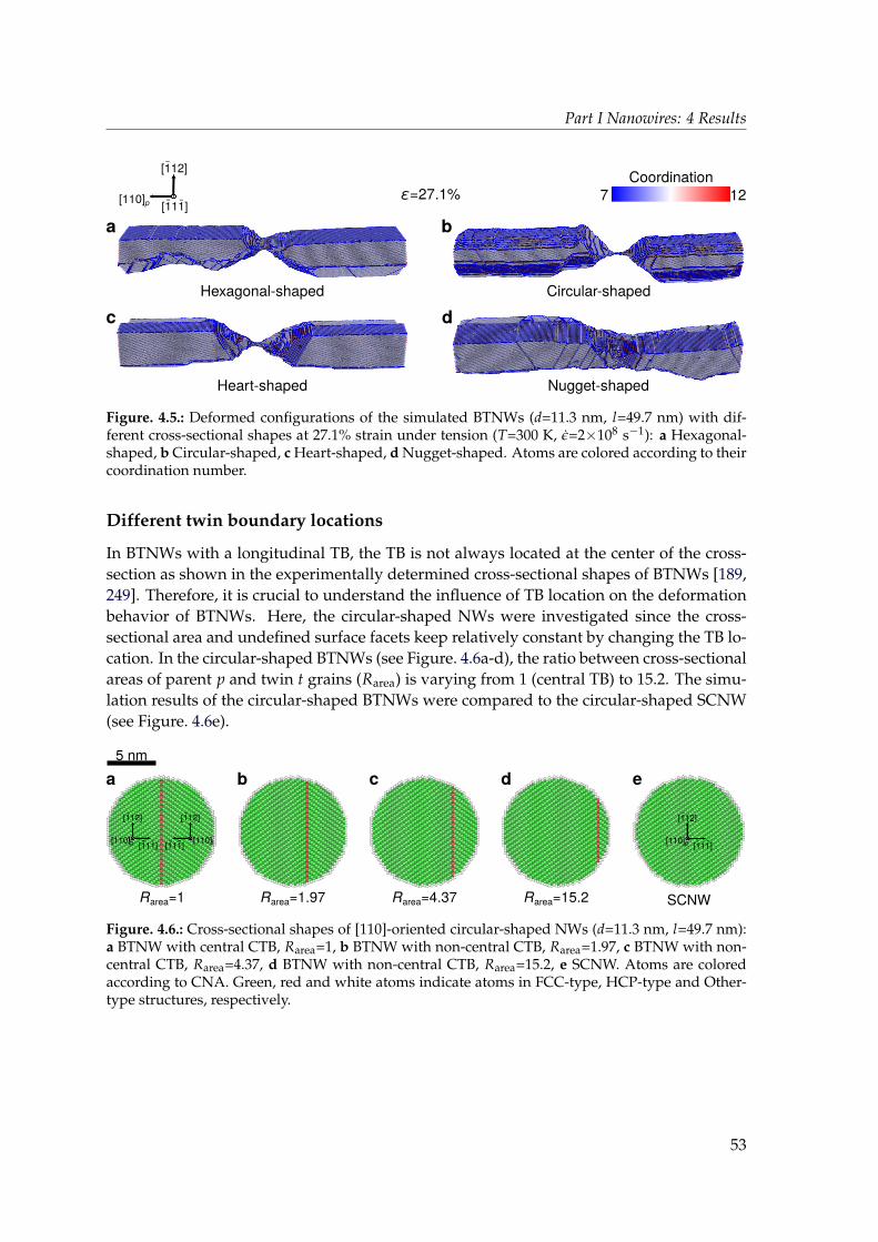
Part I Nanowires: 4 Results
[110]p [111]- -
[112]-
a b
c
Coordination7 12
Circular-shaped
Heart-shaped Nugget-shaped
ε=27.1%
d
Hexagonal-shaped
Figure. 4.5.: Deformed configurations of the simulated BTNWs (d=11.3 nm, l=49.7 nm) with dif-ferent cross-sectional shapes at 27.1% strain under tension (T=300 K, ε=2×10⁸ s−1): a Hexagonal-shaped, b Circular-shaped, c Heart-shaped, d Nugget-shaped. Atoms are colored according to theircoordination number.
Different twin boundary locations
In BTNWs with a longitudinal TB, the TB is not always located at the center of the cross-section as shown in the experimentally determined cross-sectional shapes of BTNWs [189,249]. Therefore, it is crucial to understand the influence of TB location on the deformationbehavior of BTNWs. Here, the circular-shaped NWs were investigated since the cross-sectional area and undefined surface facets keep relatively constant by changing the TB lo-cation. In the circular-shaped BTNWs (see Figure. 4.6a-d), the ratio between cross-sectionalareas of parent p and twin t grains (Rarea) is varying from 1 (central TB) to 15.2. The simu-lation results of the circular-shaped BTNWs were compared to the circular-shaped SCNW(see Figure. 4.6e).
a
5 nm
b c d e
[110]p [111]-
[112]-
[110]t[111]- -
[112]-
[110]p [111]-
[112]-
Rarea=1 Rarea=1.97 Rarea=4.37 Rarea=15.2 SCNW
Figure. 4.6.: Cross-sectional shapes of [110]-oriented circular-shaped NWs (d=11.3 nm, l=49.7 nm):a BTNW with central CTB, Rarea=1, b BTNW with non-central CTB, Rarea=1.97, c BTNW with non-central CTB, Rarea=4.37, d BTNW with non-central CTB, Rarea=15.2, e SCNW. Atoms are coloredaccording to CNA. Green, red and white atoms indicate atoms in FCC-type, HCP-type and Other-type structures, respectively.
53
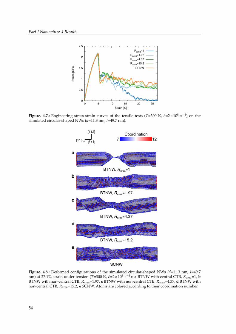
Part I Nanowires: 4 Results
0
0.5
1
1.5
2
2.5
0 5 10 15 20 25
Str
ess [G
Pa]
Strain [%]
Rarea=1
Rarea=1.97
Rarea=4.37
Rarea=15.2
SCNW
Figure. 4.7.: Engineering stress-strain curves of the tensile tests (T=300 K, ε=2×10⁸ s−1) on thesimulated circular-shaped NWs (d=11.3 nm, l=49.7 nm).
[110]p [111]- -
[112]-
a
b
c
Coordination7 12
d
e
BTNW, Rarea=1
BTNW, Rarea=4.37
BTNW, Rarea=1.97
BTNW, Rarea=15.2
SCNW
Figure. 4.8.: Deformed configurations of the simulated circular-shaped NWs (d=11.3 nm, l=49.7nm) at 27.1% strain under tension (T=300 K, ε=2×10⁸ s−1): a BTNW with central CTB, Rarea=1, bBTNW with non-central CTB, Rarea=1.97, c BTNW with non-central CTB, Rarea=4.37, d BTNW withnon-central CTB, Rarea=15.2, e SCNW. Atoms are colored according to their coordination number.
54
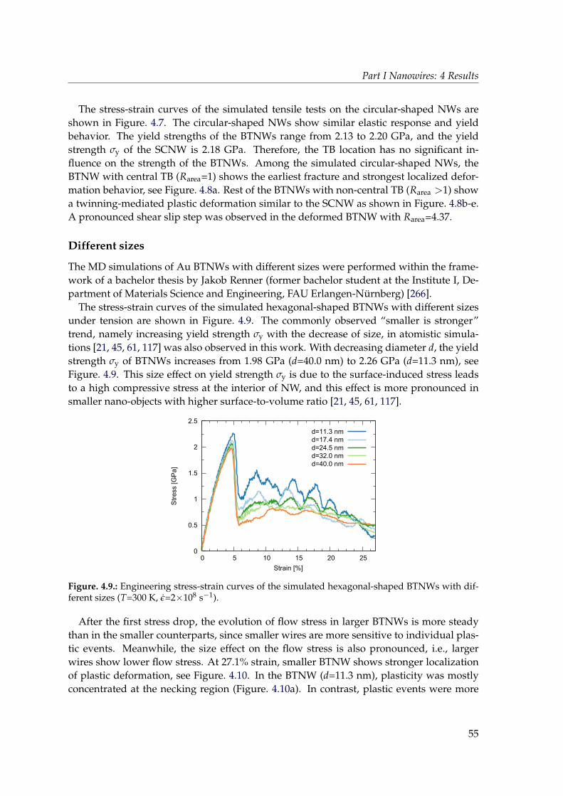
Part I Nanowires: 4 Results
The stress-strain curves of the simulated tensile tests on the circular-shaped NWs areshown in Figure. 4.7. The circular-shaped NWs show similar elastic response and yieldbehavior. The yield strengths of the BTNWs range from 2.13 to 2.20 GPa, and the yieldstrength σy of the SCNW is 2.18 GPa. Therefore, the TB location has no significant in-fluence on the strength of the BTNWs. Among the simulated circular-shaped NWs, theBTNW with central TB (Rarea=1) shows the earliest fracture and strongest localized defor-mation behavior, see Figure. 4.8a. Rest of the BTNWs with non-central TB (Rarea >1) showa twinning-mediated plastic deformation similar to the SCNW as shown in Figure. 4.8b-e.A pronounced shear slip step was observed in the deformed BTNW with Rarea=4.37.
Different sizes
The MD simulations of Au BTNWs with different sizes were performed within the frame-work of a bachelor thesis by Jakob Renner (former bachelor student at the Institute I, De-partment of Materials Science and Engineering, FAU Erlangen-Nurnberg) [266].
The stress-strain curves of the simulated hexagonal-shaped BTNWs with different sizesunder tension are shown in Figure. 4.9. The commonly observed “smaller is stronger”trend, namely increasing yield strength σy with the decrease of size, in atomistic simula-tions [21, 45, 61, 117] was also observed in this work. With decreasing diameter d, the yieldstrength σy of BTNWs increases from 1.98 GPa (d=40.0 nm) to 2.26 GPa (d=11.3 nm), seeFigure. 4.9. This size effect on yield strength σy is due to the surface-induced stress leadsto a high compressive stress at the interior of NW, and this effect is more pronounced insmaller nano-objects with higher surface-to-volume ratio [21, 45, 61, 117].
0
0.5
1
1.5
2
2.5
0 5 10 15 20 25
Str
ess [G
Pa]
Strain [%]
d=11.3 nm
d=17.4 nm
d=24.5 nm
d=32.0 nm
d=40.0 nm
Figure. 4.9.: Engineering stress-strain curves of the simulated hexagonal-shaped BTNWs with dif-ferent sizes (T=300 K, ε=2×10⁸ s−1).
After the first stress drop, the evolution of flow stress in larger BTNWs is more steadythan in the smaller counterparts, since smaller wires are more sensitive to individual plas-tic events. Meanwhile, the size effect on the flow stress is also pronounced, i.e., largerwires show lower flow stress. At 27.1% strain, smaller BTNW shows stronger localizationof plastic deformation, see Figure. 4.10. In the BTNW (d=11.3 nm), plasticity was mostlyconcentrated at the necking region (Figure. 4.10a). In contrast, plastic events were more
55
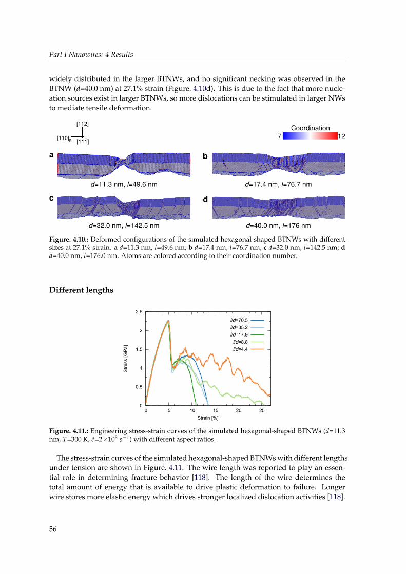
Part I Nanowires: 4 Results
widely distributed in the larger BTNWs, and no significant necking was observed in theBTNW (d=40.0 nm) at 27.1% strain (Figure. 4.10d). This is due to the fact that more nucle-ation sources exist in larger BTNWs, so more dislocations can be stimulated in larger NWsto mediate tensile deformation.
[110]p [111]- -
[112]-
a b
c
Coordination7 12
d
d=17.4 nm, l=76.7 nmd=11.3 nm, l=49.6 nm
d=32.0 nm, l=142.5 nm d=40.0 nm, l=176 nm
Figure. 4.10.: Deformed configurations of the simulated hexagonal-shaped BTNWs with differentsizes at 27.1% strain. a d=11.3 nm, l=49.6 nm; b d=17.4 nm, l=76.7 nm; c d=32.0 nm, l=142.5 nm; dd=40.0 nm, l=176.0 nm. Atoms are colored according to their coordination number.
Different lengths
0
0.5
1
1.5
2
2.5
0 5 10 15 20 25
Str
ess [G
Pa]
Strain [%]
l/d=70.5
l/d=35.2
l/d=17.9
l/d=8.8
l/d=4.4
Figure. 4.11.: Engineering stress-strain curves of the simulated hexagonal-shaped BTNWs (d=11.3nm, T=300 K, ε=2×10⁸ s−1) with different aspect ratios.
The stress-strain curves of the simulated hexagonal-shaped BTNWs with different lengthsunder tension are shown in Figure. 4.11. The wire length was reported to play an essen-tial role in determining fracture behavior [118]. The length of the wire determines thetotal amount of energy that is available to drive plastic deformation to failure. Longerwire stores more elastic energy which drives stronger localized dislocation activities [118].
56
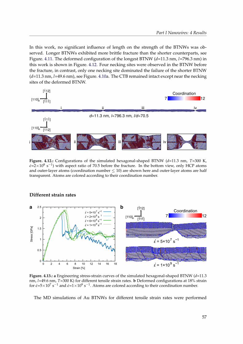
Part I Nanowires: 4 Results
In this work, no significant influence of length on the strength of the BTNWs was ob-served. Longer BTNWs exhibited more brittle fracture than the shorter counterparts, seeFigure. 4.11. The deformed configuration of the longest BTNW (d=11.3 nm, l=796.3 nm) inthis work is shown in Figure. 4.12. Four necking sites were observed in the BTNW beforethe fracture, in contrast, only one necking site dominated the failure of the shorter BTNW(d=11.3 nm, l=49.6 nm), see Figure. 4.10a. The CTB remained intact except near the neckingsites of the deformed BTNW.
[110]p [111]- -
[112]-
Coordination7 12
d=11.3 nm, l=796.3 nm, l/d=70.5
i ii iii iv
i ii iii iv
[111]- -
[112]-[110]p
Figure. 4.12.: Configurations of the simulated hexagonal-shaped BTNW (d=11.3 nm, T=300 K,ε=2×10⁸ s−1) with aspect ratio of 70.5 before the fracture. In the bottom view, only HCP atomsand outer-layer atoms (coordination number ≤ 10) are shown here and outer-layer atoms are halftransparent. Atoms are colored according to their coordination number.
Different strain rates
[110]p [111]- -
[112]-a b
Coordination
7 12
0
0.5
1
1.5
2
2.5
0 2 4 6 8 10 12 14 16 18
Str
ess [
GP
a]
Strain [%]
ε.= 5×10
7s1
ε.= 5×10
7s1
ε.= 2×10
8s1
ε.= 6×10
8s1
ε.= 1×10
9s1
ε.= 1×10
9s1
Figure. 4.13.: a Engineering stress-strain curves of the simulated hexagonal-shaped BTNW (d=11.3nm, l=49.6 nm, T=300 K) for different tensile strain rates. b Deformed configurations at 18% strainfor ε=5×10⁷ s−1 and ε=1×10⁹ s−1. Atoms are colored according to their coordination number.
The MD simulations of Au BTNWs for different tensile strain rates were performed
57
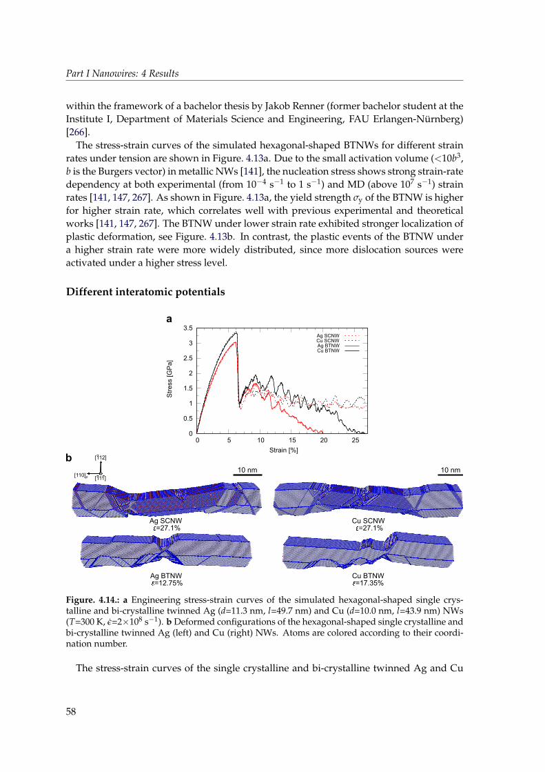
Part I Nanowires: 4 Results
within the framework of a bachelor thesis by Jakob Renner (former bachelor student at theInstitute I, Department of Materials Science and Engineering, FAU Erlangen-Nurnberg)[266].
The stress-strain curves of the simulated hexagonal-shaped BTNWs for different strainrates under tension are shown in Figure. 4.13a. Due to the small activation volume (<10b3,b is the Burgers vector) in metallic NWs [141], the nucleation stress shows strong strain-ratedependency at both experimental (from 10−4 s−1 to 1 s−1) and MD (above 107 s−1) strainrates [141, 147, 267]. As shown in Figure. 4.13a, the yield strength σy of the BTNW is higherfor higher strain rate, which correlates well with previous experimental and theoreticalworks [141, 147, 267]. The BTNW under lower strain rate exhibited stronger localization ofplastic deformation, see Figure. 4.13b. In contrast, the plastic events of the BTNW undera higher strain rate were more widely distributed, since more dislocation sources wereactivated under a higher stress level.
Different interatomic potentials
a
b
Ag BTNW =12.75%
Cu BTNW =17.35%
0
0.5
1
1.5
2
2.5
3
3.5
0 5 10 15 20 25
Str
ess [G
Pa]
Strain [%]
Ag SCNWCu SCNWAg BTNWCu BTNW
Ag SCNW =27.1%
Cu SCNW =27.1%
[110]p
[112]-
[111]- -
10 nm 10 nm
Figure. 4.14.: a Engineering stress-strain curves of the simulated hexagonal-shaped single crys-talline and bi-crystalline twinned Ag (d=11.3 nm, l=49.7 nm) and Cu (d=10.0 nm, l=43.9 nm) NWs(T=300 K, ε=2×10⁸ s−1). b Deformed configurations of the hexagonal-shaped single crystalline andbi-crystalline twinned Ag (left) and Cu (right) NWs. Atoms are colored according to their coordi-nation number.
The stress-strain curves of the single crystalline and bi-crystalline twinned Ag and Cu
58
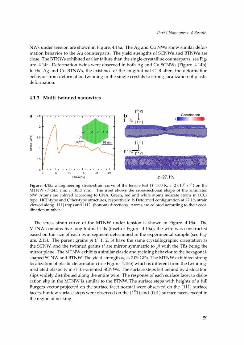
Part I Nanowires: 4 Results
NWs under tension are shown in Figure. 4.14a. The Ag and Cu NWs show similar defor-mation behavior to the Au counterparts. The yield strengths of SCNWs and BTNWs areclose. The BTNWs exhibited earlier failure than the single-crystalline counterparts, see Fig-ure. 4.14a. Deformation twins were observed in both Ag and Cu SCNWs (Figure. 4.14b).In the Ag and Cu BTNWs, the existence of the longitudinal CTB alters the deformationbehavior from deformation twinning in the single crystals to strong localization of plasticdeformation.
4.1.3. Multi-twinned nanowires
a Coordination
7 12[110]p [111]- -
[112]-
[111]- -
[112]-[110]p
b
ε=27.1%
0
0.5
1
1.5
2
2.5
0 5 10 15 20 25
Str
ess [G
Pa]
Strain [%]
p1 t1 p2 t2 p3 t3
[110]p [111]-
[112]-
10 nm
Figure. 4.15.: a Engineering stress-strain curve of the tensile test (T=300 K, ε=2×10⁸ s−1) on theMTNW (d=24.5 nm, l=107.3 nm). The inset shows the cross-sectional shape of the simulatedNW. Atoms are colored according to CNA. Green, red and white atoms indicate atoms in FCC-type, HCP-type and Other-type structures, respectively. b Deformed configuration at 27.1% strainviewed along [111] (top) and [112] (bottom) directions. Atoms are colored according to their coor-dination number.
The stress-strain curve of the MTNW under tension is shown in Figure. 4.15a. TheMTNW contains five longitudinal TBs (inset of Figure. 4.15a), the wire was constructedbased on the size of each twin segment determined in the experimental sample (see Fig-ure. 2.13). The parent grains pi (i=1, 2, 3) have the same crystallographic orientation asthe SCNW, and the twinned grains ti are mirror symmetric to pi with the TBs being themirror plane. The MTNW exhibits a similar elastic and yielding behavior to the hexagonal-shaped SCNW and BTNW. The yield strength σy is 2.09 GPa. The MTNW exhibited stronglocalization of plastic deformation (see Figure. 4.15b) which is different from the twinning-mediated plasticity in 〈110〉-oriented SCNWs. The surface steps left behind by dislocationslips widely distributed along the entire wire. The response of each surface facet to dislo-cation slip in the MTNW is similar to the BTNW. The surface steps with heights of a fullBurgers vector projected on the surface facet normal were observed on the (111) surfacefacets, but few surface steps were observed on the (111) and (001) surface facets except inthe region of necking.
59
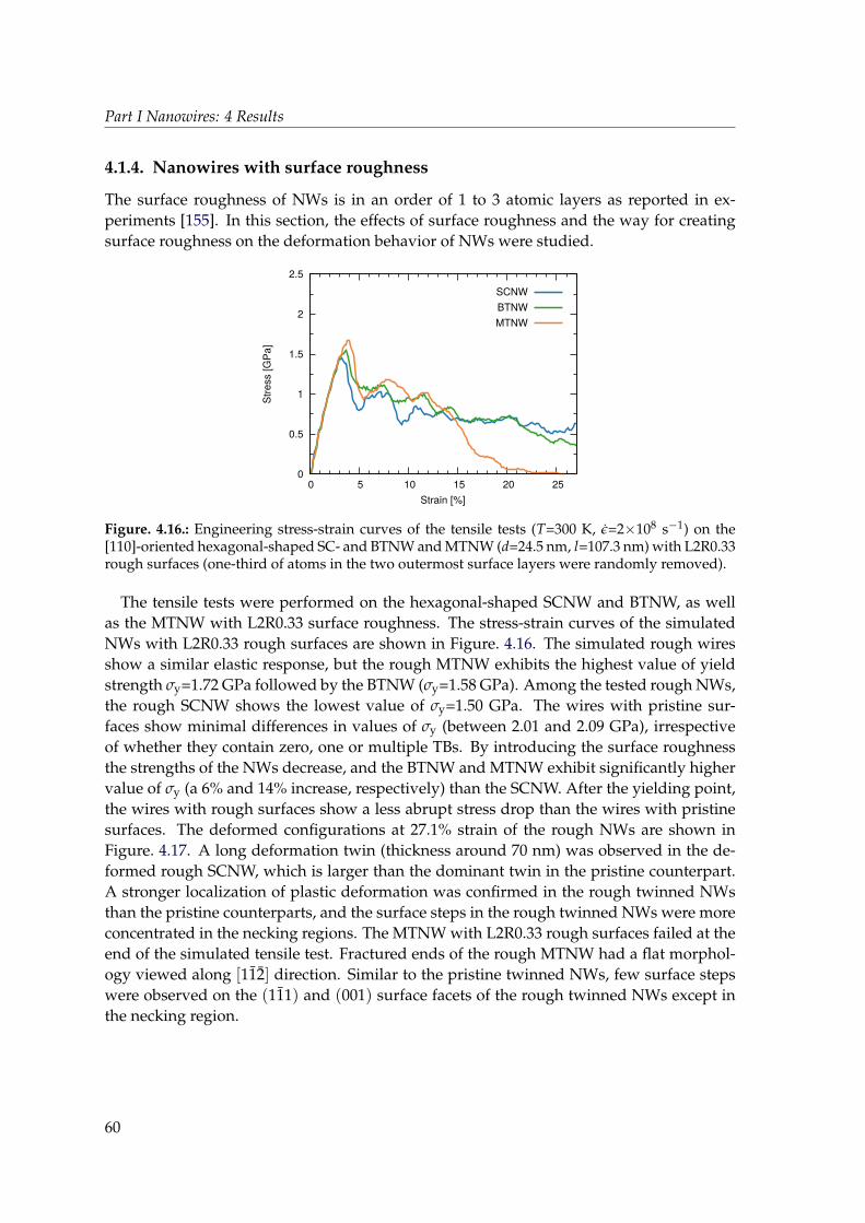
Part I Nanowires: 4 Results
4.1.4. Nanowires with surface roughness
The surface roughness of NWs is in an order of 1 to 3 atomic layers as reported in ex-periments [155]. In this section, the effects of surface roughness and the way for creatingsurface roughness on the deformation behavior of NWs were studied.
0
0.5
1
1.5
2
2.5
0 5 10 15 20 25
Str
ess [G
Pa]
Strain [%]
SCNW
BTNW
MTNW
Figure. 4.16.: Engineering stress-strain curves of the tensile tests (T=300 K, ε=2×10⁸ s−1) on the[110]-oriented hexagonal-shaped SC- and BTNW and MTNW (d=24.5 nm, l=107.3 nm) with L2R0.33rough surfaces (one-third of atoms in the two outermost surface layers were randomly removed).
The tensile tests were performed on the hexagonal-shaped SCNW and BTNW, as wellas the MTNW with L2R0.33 surface roughness. The stress-strain curves of the simulatedNWs with L2R0.33 rough surfaces are shown in Figure. 4.16. The simulated rough wiresshow a similar elastic response, but the rough MTNW exhibits the highest value of yieldstrength σy=1.72 GPa followed by the BTNW (σy=1.58 GPa). Among the tested rough NWs,the rough SCNW shows the lowest value of σy=1.50 GPa. The wires with pristine sur-faces show minimal differences in values of σy (between 2.01 and 2.09 GPa), irrespectiveof whether they contain zero, one or multiple TBs. By introducing the surface roughnessthe strengths of the NWs decrease, and the BTNW and MTNW exhibit significantly highervalue of σy (a 6% and 14% increase, respectively) than the SCNW. After the yielding point,the wires with rough surfaces show a less abrupt stress drop than the wires with pristinesurfaces. The deformed configurations at 27.1% strain of the rough NWs are shown inFigure. 4.17. A long deformation twin (thickness around 70 nm) was observed in the de-formed rough SCNW, which is larger than the dominant twin in the pristine counterpart.A stronger localization of plastic deformation was confirmed in the rough twinned NWsthan the pristine counterparts, and the surface steps in the rough twinned NWs were moreconcentrated in the necking regions. The MTNW with L2R0.33 rough surfaces failed at theend of the simulated tensile test. Fractured ends of the rough MTNW had a flat morphol-ogy viewed along [112] direction. Similar to the pristine twinned NWs, few surface stepswere observed on the (111) and (001) surface facets of the rough twinned NWs except inthe necking region.
60
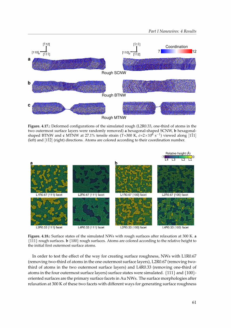
Part I Nanowires: 4 Results
[110]p [111]- -
[112]-
[111]- -
[112]-[110]p
Rough SCNW
Rough BTNW
Rough MTNW
a
b
c
Coordination7 12
Figure. 4.17.: Deformed configurations of the simulated rough (L2R0.33, one-third of atoms in thetwo outermost surface layers were randomly removed) a hexagonal-shaped SCNW, b hexagonal-shaped BTNW and c MTNW at 27.1% tensile strain (T=300 K, ε=2×10⁸ s−1) viewed along [111](left) and [112] (right) directions. Atoms are colored according to their coordination number.
L1R0.67 111 facet L2R0.67 111 facet
L2R0.33 111 facet L4R0.33 111 facet
Relative height (Å)0-7
Figure. 4.18.: Surface states of the simulated NWs with rough surfaces after relaxation at 300 K. a111 rough surfaces. b 100 rough surfaces. Atoms are colored according to the relative height tothe initial first outermost surface atoms.
In order to test the effect of the way for creating surface roughness, NWs with L1R0.67(removing two-third of atoms in the one outermost surface layers), L2R0.67 (removing two-third of atoms in the two outermost surface layers) and L4R0.33 (removing one-third ofatoms in the four outermost surface layers) surface states were simulated. 111 and 100-oriented surfaces are the primary surface facets in Au NWs. The surface morphologies afterrelaxation at 300 K of these two facets with different ways for generating surface roughness
61
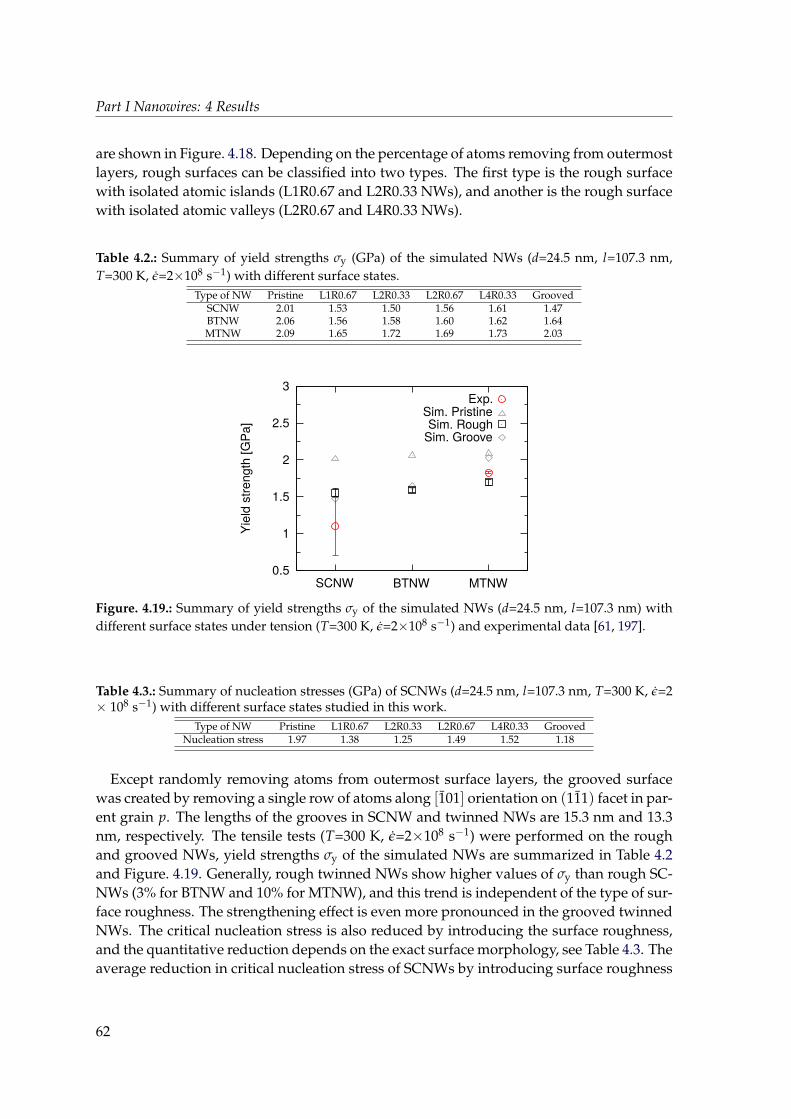
Part I Nanowires: 4 Results
are shown in Figure. 4.18. Depending on the percentage of atoms removing from outermostlayers, rough surfaces can be classified into two types. The first type is the rough surfacewith isolated atomic islands (L1R0.67 and L2R0.33 NWs), and another is the rough surfacewith isolated atomic valleys (L2R0.67 and L4R0.33 NWs).
Table 4.2.: Summary of yield strengths σy (GPa) of the simulated NWs (d=24.5 nm, l=107.3 nm,T=300 K, ε=2×10⁸ s−1) with different surface states.
Type of NW Pristine L1R0.67 L2R0.33 L2R0.67 L4R0.33 GroovedSCNW 2.01 1.53 1.50 1.56 1.61 1.47BTNW 2.06 1.56 1.58 1.60 1.62 1.64MTNW 2.09 1.65 1.72 1.69 1.73 2.03
0.5
1
1.5
2
2.5
3
Yie
ld s
trength
[G
Pa]
Exp.Sim. PristineSim. Rough
Sim. Groove
SCNW BTNW MTNW
Figure. 4.19.: Summary of yield strengths σy of the simulated NWs (d=24.5 nm, l=107.3 nm) withdifferent surface states under tension (T=300 K, ε=2×10⁸ s−1) and experimental data [61, 197].
Table 4.3.: Summary of nucleation stresses (GPa) of SCNWs (d=24.5 nm, l=107.3 nm, T=300 K, ε=2× 10⁸ s−1) with different surface states studied in this work.
Type of NW Pristine L1R0.67 L2R0.33 L2R0.67 L4R0.33 GroovedNucleation stress 1.97 1.38 1.25 1.49 1.52 1.18
Except randomly removing atoms from outermost surface layers, the grooved surfacewas created by removing a single row of atoms along [101] orientation on (111) facet in par-ent grain p. The lengths of the grooves in SCNW and twinned NWs are 15.3 nm and 13.3nm, respectively. The tensile tests (T=300 K, ε=2×10⁸ s−1) were performed on the roughand grooved NWs, yield strengths σy of the simulated NWs are summarized in Table 4.2and Figure. 4.19. Generally, rough twinned NWs show higher values of σy than rough SC-NWs (3% for BTNW and 10% for MTNW), and this trend is independent of the type of sur-face roughness. The strengthening effect is even more pronounced in the grooved twinnedNWs. The critical nucleation stress is also reduced by introducing the surface roughness,and the quantitative reduction depends on the exact surface morphology, see Table 4.3. Theaverage reduction in critical nucleation stress of SCNWs by introducing surface roughness
62
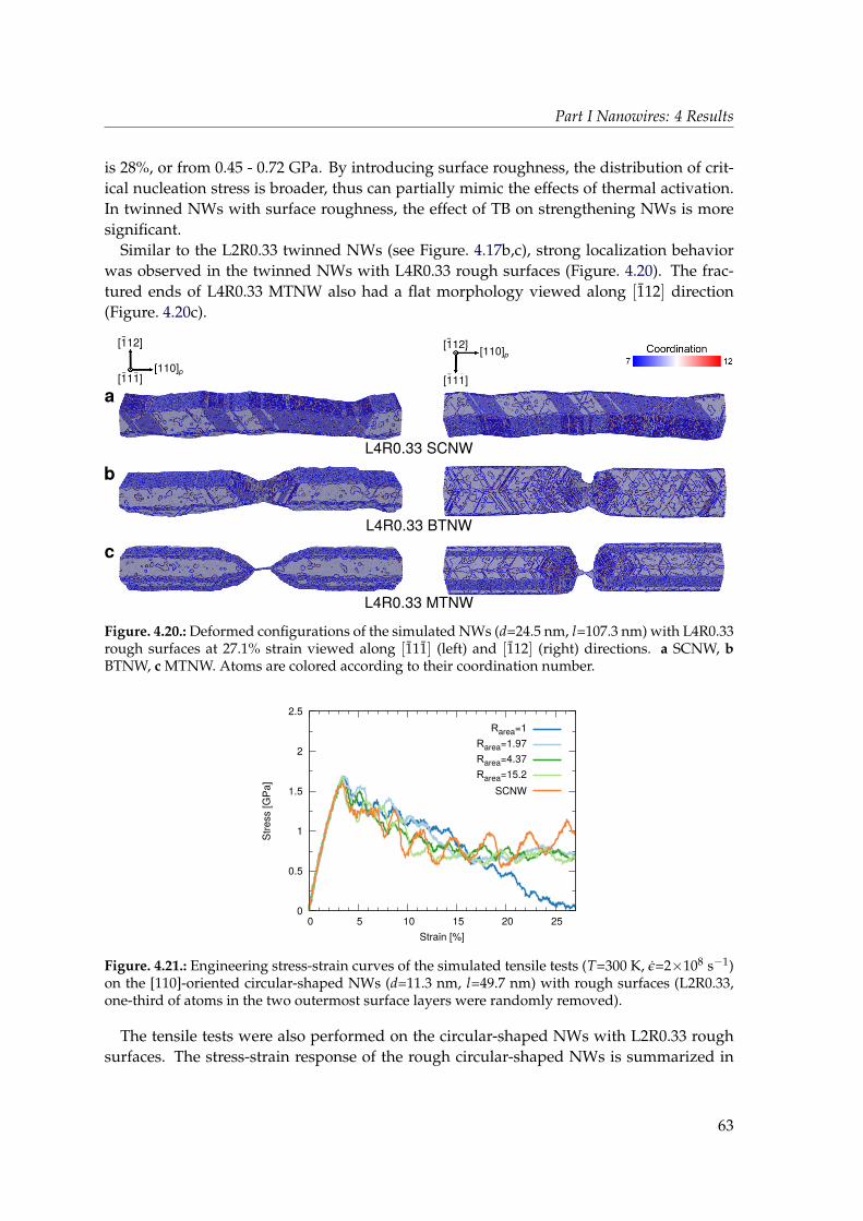
Part I Nanowires: 4 Results
is 28%, or from 0.45 - 0.72 GPa. By introducing surface roughness, the distribution of crit-ical nucleation stress is broader, thus can partially mimic the effects of thermal activation.In twinned NWs with surface roughness, the effect of TB on strengthening NWs is moresignificant.
Similar to the L2R0.33 twinned NWs (see Figure. 4.17b,c), strong localization behaviorwas observed in the twinned NWs with L4R0.33 rough surfaces (Figure. 4.20). The frac-tured ends of L4R0.33 MTNW also had a flat morphology viewed along [112] direction(Figure. 4.20c).
[110]p[111]- -
- -[112]
[111]- -
[112][110]p
L4R0.33 SCNW
L4R0.33 BTNW
L4R0.33 MTNW
a
b
c
Figure. 4.20.: Deformed configurations of the simulated NWs (d=24.5 nm, l=107.3 nm) with L4R0.33rough surfaces at 27.1% strain viewed along [111] (left) and [112] (right) directions. a SCNW, bBTNW, c MTNW. Atoms are colored according to their coordination number.
0
0.5
1
1.5
2
2.5
0 5 10 15 20 25
Str
ess [G
Pa]
Strain [%]
Rarea=1
Rarea=1.97
Rarea=4.37
Rarea=15.2
SCNW
Figure. 4.21.: Engineering stress-strain curves of the simulated tensile tests (T=300 K, ε=2×10⁸ s−1)on the [110]-oriented circular-shaped NWs (d=11.3 nm, l=49.7 nm) with rough surfaces (L2R0.33,one-third of atoms in the two outermost surface layers were randomly removed).
The tensile tests were also performed on the circular-shaped NWs with L2R0.33 roughsurfaces. The stress-strain response of the rough circular-shaped NWs is summarized in
63
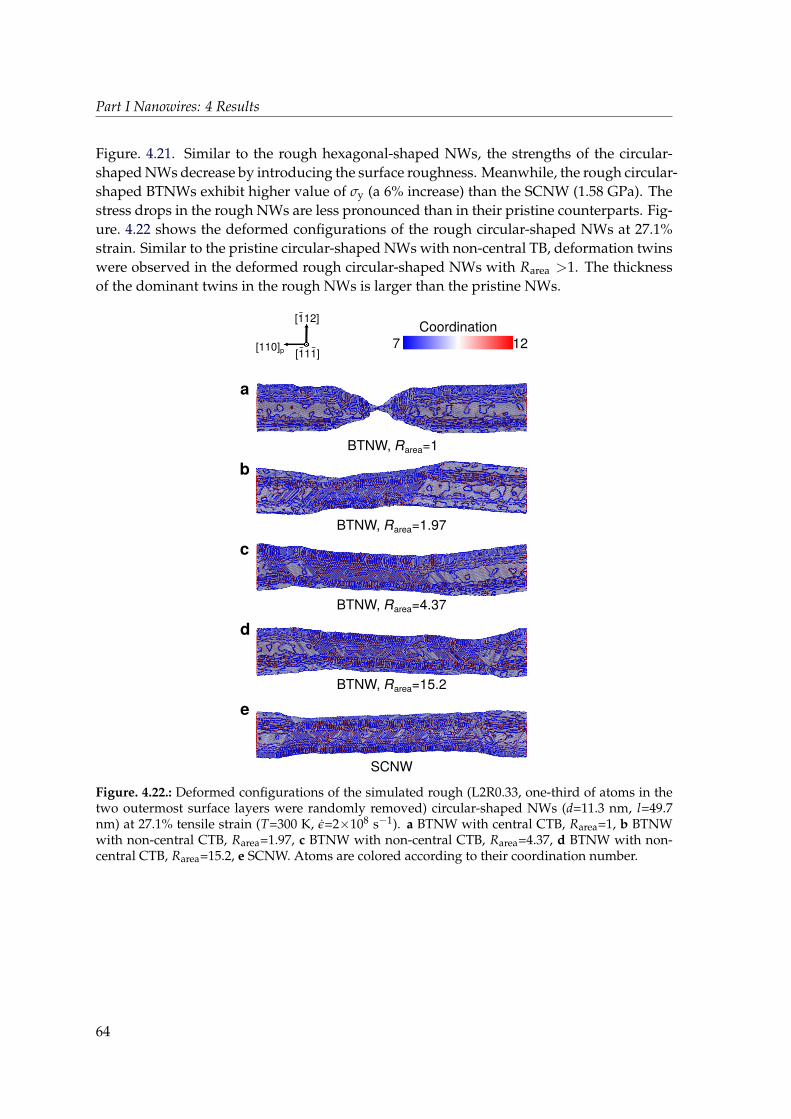
Part I Nanowires: 4 Results
Figure. 4.21. Similar to the rough hexagonal-shaped NWs, the strengths of the circular-shaped NWs decrease by introducing the surface roughness. Meanwhile, the rough circular-shaped BTNWs exhibit higher value of σy (a 6% increase) than the SCNW (1.58 GPa). Thestress drops in the rough NWs are less pronounced than in their pristine counterparts. Fig-ure. 4.22 shows the deformed configurations of the rough circular-shaped NWs at 27.1%strain. Similar to the pristine circular-shaped NWs with non-central TB, deformation twinswere observed in the deformed rough circular-shaped NWs with Rarea >1. The thicknessof the dominant twins in the rough NWs is larger than the pristine NWs.
[110]p [111]- -
[112]-
a
b
c
Coordination7 12
d
e
BTNW, Rarea=1
BTNW, Rarea=4.37
BTNW, Rarea=1.97
BTNW, Rarea=15.2
SCNW
Figure. 4.22.: Deformed configurations of the simulated rough (L2R0.33, one-third of atoms in thetwo outermost surface layers were randomly removed) circular-shaped NWs (d=11.3 nm, l=49.7nm) at 27.1% tensile strain (T=300 K, ε=2×10⁸ s−1). a BTNW with central CTB, Rarea=1, b BTNWwith non-central CTB, Rarea=1.97, c BTNW with non-central CTB, Rarea=4.37, d BTNW with non-central CTB, Rarea=15.2, e SCNW. Atoms are colored according to their coordination number.
64
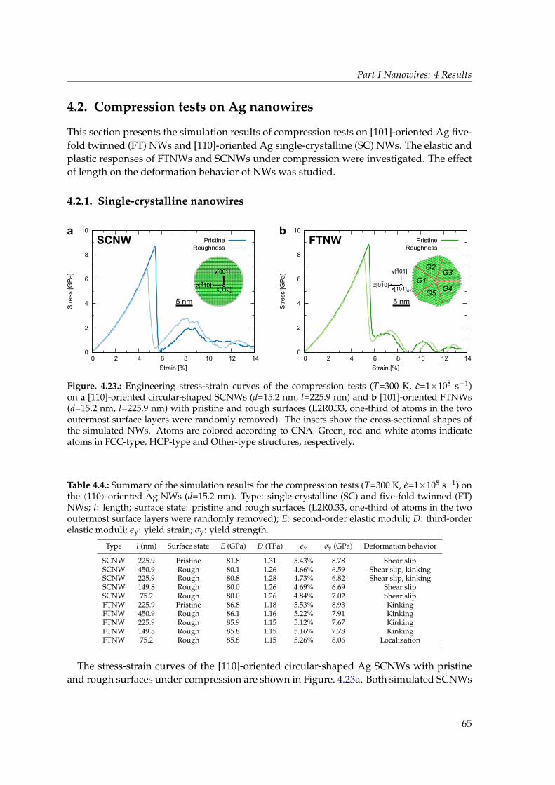
Part I Nanowires: 4 Results
4.2. Compression tests on Ag nanowires
This section presents the simulation results of compression tests on [101]-oriented Ag five-fold twinned (FT) NWs and [110]-oriented Ag single-crystalline (SC) NWs. The elastic andplastic responses of FTNWs and SCNWs under compression were investigated. The effectof length on the deformation behavior of NWs was studied.
4.2.1. Single-crystalline nanowires
0
2
4
6
8
10
0 2 4 6 8 10 12 14
Str
ess [
GP
a]
Strain [%]
Pristine
Roughness
0
2
4
6
8
10
0 2 4 6 8 10 12 14
Str
ess [
GP
a]
Strain [%]
Pristine
Roughness
a
5 nm
b
y[101]-
z[010]x[101]G1
- G1
G2G3
G4G5
5 nm
FTNWSCNW
Figure. 4.23.: Engineering stress-strain curves of the compression tests (T=300 K, ε=1×10⁸ s−1)on a [110]-oriented circular-shaped SCNWs (d=15.2 nm, l=225.9 nm) and b [101]-oriented FTNWs(d=15.2 nm, l=225.9 nm) with pristine and rough surfaces (L2R0.33, one-third of atoms in the twooutermost surface layers were randomly removed). The insets show the cross-sectional shapes ofthe simulated NWs. Atoms are colored according to CNA. Green, red and white atoms indicateatoms in FCC-type, HCP-type and Other-type structures, respectively.
Table 4.4.: Summary of the simulation results for the compression tests (T=300 K, ε=1×10⁸ s−1) onthe 〈110〉-oriented Ag NWs (d=15.2 nm). Type: single-crystalline (SC) and five-fold twinned (FT)NWs; l: length; surface state: pristine and rough surfaces (L2R0.33, one-third of atoms in the twooutermost surface layers were randomly removed); E: second-order elastic moduli; D: third-orderelastic moduli; εy: yield strain; σy: yield strength.
Type l (nm) Surface state E (GPa) D (TPa) εy σy (GPa) Deformation behavior
SCNW 225.9 Pristine 81.8 1.31 5.43% 8.78 Shear slipSCNW 450.9 Rough 80.1 1.26 4.66% 6.59 Shear slip, kinkingSCNW 225.9 Rough 80.8 1.28 4.73% 6.82 Shear slip, kinkingSCNW 149.8 Rough 80.0 1.26 4.69% 6.69 Shear slipSCNW 75.2 Rough 80.0 1.26 4.84% 7.02 Shear slipFTNW 225.9 Pristine 86.8 1.18 5.53% 8.93 KinkingFTNW 450.9 Rough 86.1 1.16 5.22% 7.91 KinkingFTNW 225.9 Rough 85.9 1.15 5.12% 7.67 KinkingFTNW 149.8 Rough 85.8 1.15 5.16% 7.78 KinkingFTNW 75.2 Rough 85.8 1.15 5.26% 8.06 Localization
The stress-strain curves of the [110]-oriented circular-shaped Ag SCNWs with pristineand rough surfaces under compression are shown in Figure. 4.23a. Both simulated SCNWs
65
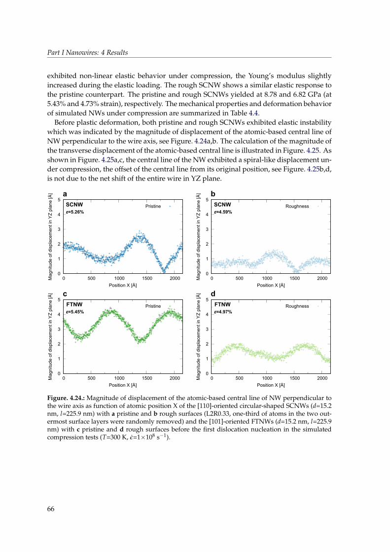
Part I Nanowires: 4 Results
exhibited non-linear elastic behavior under compression, the Young’s modulus slightlyincreased during the elastic loading. The rough SCNW shows a similar elastic response tothe pristine counterpart. The pristine and rough SCNWs yielded at 8.78 and 6.82 GPa (at5.43% and 4.73% strain), respectively. The mechanical properties and deformation behaviorof simulated NWs under compression are summarized in Table 4.4.
Before plastic deformation, both pristine and rough SCNWs exhibited elastic instabilitywhich was indicated by the magnitude of displacement of the atomic-based central line ofNW perpendicular to the wire axis, see Figure. 4.24a,b. The calculation of the magnitude ofthe transverse displacement of the atomic-based central line is illustrated in Figure. 4.25. Asshown in Figure. 4.25a,c, the central line of the NW exhibited a spiral-like displacement un-der compression, the offset of the central line from its original position, see Figure. 4.25b,d,is not due to the net shift of the entire wire in YZ plane.
0
1
2
3
4
5
0 500 1000 1500 2000Ma
gn
itud
e o
f d
isp
lace
me
nt
in Y
Z p
lan
e [
Å]
Position X [Å]
Roughness
0
1
2
3
4
5
0 500 1000 1500 2000Ma
gn
itud
e o
f d
isp
lace
me
nt
in Y
Z p
lan
e [
Å]
Position X [Å]
PristineSCNW SCNW ε=5.26%
ε=4.59%
a b
FTNW FTNW ε=5.45%
ε=4.97%
0
1
2
3
4
5
0 500 1000 1500 2000Ma
gn
itud
e o
f d
isp
lace
me
nt
in Y
Z p
lan
e [
Å]
Position X [Å]
Pristine
0
1
2
3
4
5
0 500 1000 1500 2000Ma
gn
itud
e o
f d
isp
lace
me
nt
in Y
Z p
lan
e [
Å]
Position X [Å]
Roughness
c d
Figure. 4.24.: Magnitude of displacement of the atomic-based central line of NW perpendicular tothe wire axis as function of atomic position X of the [110]-oriented circular-shaped SCNWs (d=15.2nm, l=225.9 nm) with a pristine and b rough surfaces (L2R0.33, one-third of atoms in the two out-ermost surface layers were randomly removed) and the [101]-oriented FTNWs (d=15.2 nm, l=225.9nm) with c pristine and d rough surfaces before the first dislocation nucleation in the simulatedcompression tests (T=300 K, ε=1×10⁸ s−1).
66
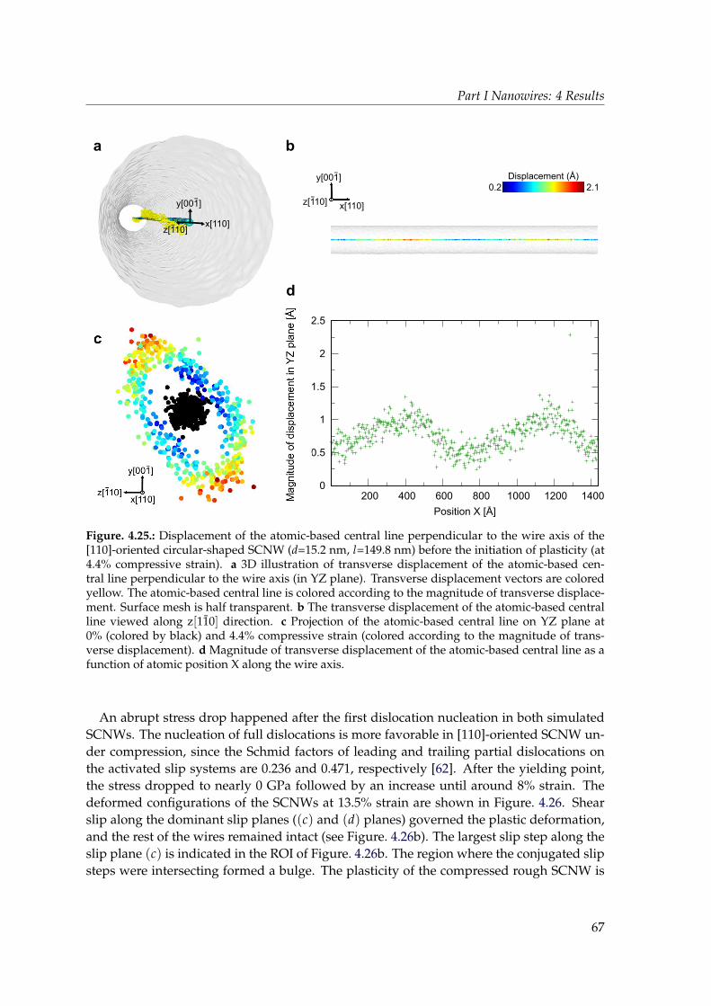
Part I Nanowires: 4 Results
0.2 2.1Displacement (Å)y[001]
x[110]z[110]-
-
0
0.5
1
1.5
2
2.5
200 400 600 800 1000 1200 1400
Position X [Å]
a b
d
y[001]
x[110]z[110]
-
-
Figure. 4.25.: Displacement of the atomic-based central line perpendicular to the wire axis of the[110]-oriented circular-shaped SCNW (d=15.2 nm, l=149.8 nm) before the initiation of plasticity (at4.4% compressive strain). a 3D illustration of transverse displacement of the atomic-based cen-tral line perpendicular to the wire axis (in YZ plane). Transverse displacement vectors are coloredyellow. The atomic-based central line is colored according to the magnitude of transverse displace-ment. Surface mesh is half transparent. b The transverse displacement of the atomic-based centralline viewed along z[110] direction. c Projection of the atomic-based central line on YZ plane at0% (colored by black) and 4.4% compressive strain (colored according to the magnitude of trans-verse displacement). d Magnitude of transverse displacement of the atomic-based central line as afunction of atomic position X along the wire axis.
An abrupt stress drop happened after the first dislocation nucleation in both simulatedSCNWs. The nucleation of full dislocations is more favorable in [110]-oriented SCNW un-der compression, since the Schmid factors of leading and trailing partial dislocations onthe activated slip systems are 0.236 and 0.471, respectively [62]. After the yielding point,the stress dropped to nearly 0 GPa followed by an increase until around 8% strain. Thedeformed configurations of the SCNWs at 13.5% strain are shown in Figure. 4.26. Shearslip along the dominant slip planes ((c) and (d) planes) governed the plastic deformation,and the rest of the wires remained intact (see Figure. 4.26b). The largest slip step along theslip plane (c) is indicated in the ROI of Figure. 4.26b. The region where the conjugated slipsteps were intersecting formed a bulge. The plasticity of the compressed rough SCNW is
67
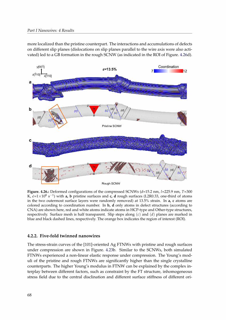
Part I Nanowires: 4 Results
more localized than the pristine counterpart. The interactions and accumulations of defectson different slip planes (dislocations on slip planes parallel to the wire axis were also acti-vated) led to a GB formation in the rough SCNW (as indicated in the ROI of Figure. 4.26d).
ε=13.5%
a
(c)
D C
B
(a) (d)(d)
(c)
(c)(d)
(c)
Coordination
7 12
(d)
(c)
(c)
D C
B
(a)
(c)(c) (c) (d)
(d)
Figure. 4.26.: Deformed configurations of the compressed SCNWs (d=15.2 nm, l=225.9 nm, T=300K, ε=1×10⁸ s−1) with a, b pristine surfaces and c, d rough surfaces (L2R0.33, one-third of atomsin the two outermost surface layers were randomly removed) at 13.5% strain. In a, c atoms arecolored according to coordination number. In b, d only atoms in defect structures (according toCNA) are shown here, red and white atoms indicate atoms in HCP-type and Other-type structures,respectively. Surface mesh is half transparent. Slip steps along (c) and (d) planes are marked inblue and black dashed lines, respectively. The orange box indicates the region of interest (ROI).
4.2.2. Five-fold twinned nanowires
The stress-strain curves of the [101]-oriented Ag FTNWs with pristine and rough surfacesunder compression are shown in Figure. 4.23b. Similar to the SCNWs, both simulatedFTNWs experienced a non-linear elastic response under compression. The Young’s mod-uli of the pristine and rough FTNWs are significantly higher than the single crystallinecounterparts. The higher Young’s modulus in FTNW can be explained by the complex in-terplay between different factors, such as constraint by the FT structure, inhomogeneousstress field due to the central disclination and different surface stiffness of different ori-
68
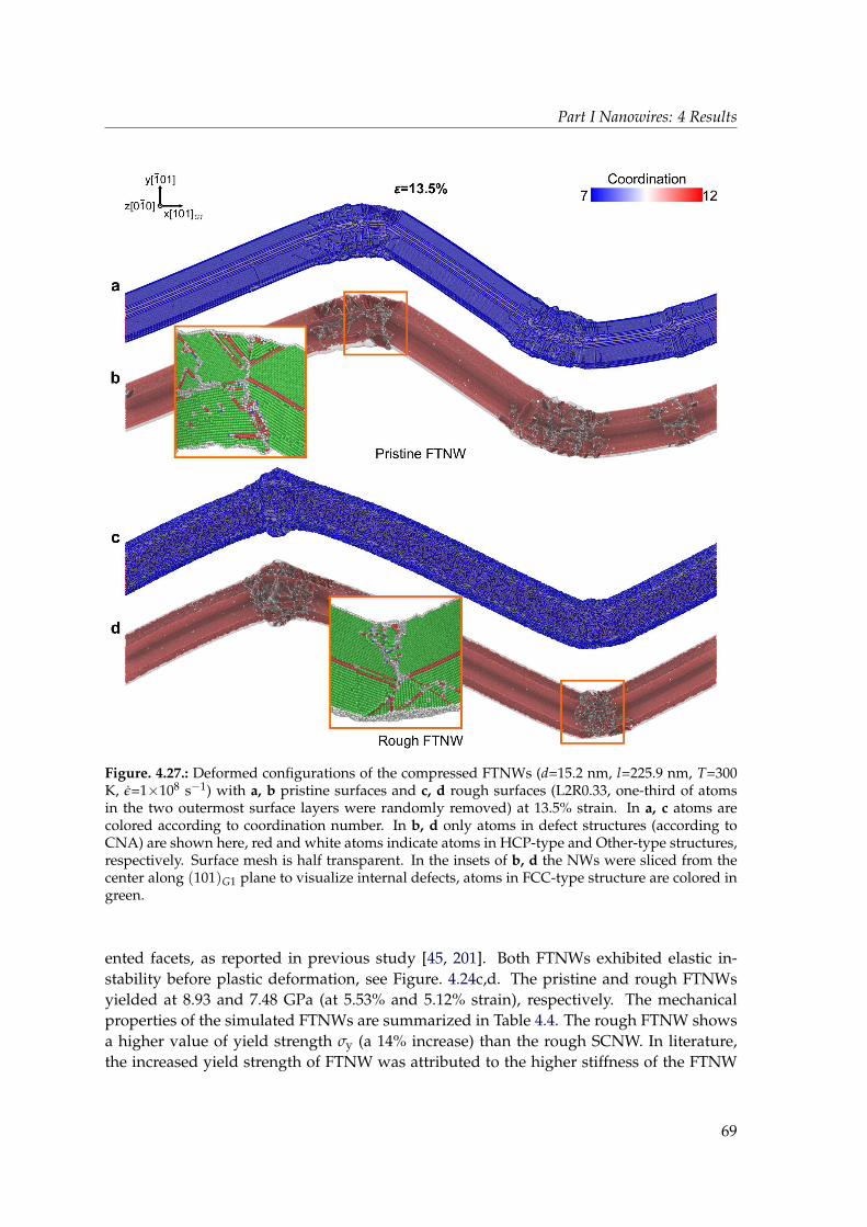
Part I Nanowires: 4 Results
c
ε=13.5%
Pristine FTNW
Rough FTNW
Coordination
7 12
a
Figure. 4.27.: Deformed configurations of the compressed FTNWs (d=15.2 nm, l=225.9 nm, T=300K, ε=1×10⁸ s−1) with a, b pristine surfaces and c, d rough surfaces (L2R0.33, one-third of atomsin the two outermost surface layers were randomly removed) at 13.5% strain. In a, c atoms arecolored according to coordination number. In b, d only atoms in defect structures (according toCNA) are shown here, red and white atoms indicate atoms in HCP-type and Other-type structures,respectively. Surface mesh is half transparent. In the insets of b, d the NWs were sliced from thecenter along (101)G1 plane to visualize internal defects, atoms in FCC-type structure are colored ingreen.
ented facets, as reported in previous study [45, 201]. Both FTNWs exhibited elastic in-stability before plastic deformation, see Figure. 4.24c,d. The pristine and rough FTNWsyielded at 8.93 and 7.48 GPa (at 5.53% and 5.12% strain), respectively. The mechanicalproperties of the simulated FTNWs are summarized in Table 4.4. The rough FTNW showsa higher value of yield strength σy (a 14% increase) than the rough SCNW. In literature,the increased yield strength of FTNW was attributed to the higher stiffness of the FTNW
69
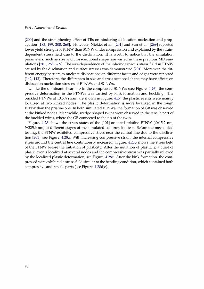
Part I Nanowires: 4 Results
[200] and the strengthening effect of TBs on hindering dislocation nucleation and prop-agation [183, 199, 200, 268]. However, Niekiel et al. [201] and Sun et al. [269] reportedlower yield strength of FTNW than SCNW under compression and explained by the strain-dependent stress field due to the disclination. It is worth to notice that the simulationparameters, such as size and cross-sectional shape, are varied in these previous MD sim-ulations [201, 268, 269]. The size-dependency of the inhomogeneous stress field in FTNWcaused by the disclination and surface stresses was demonstrated [201]. Moreover, the dif-ferent energy barriers to nucleate dislocations on different facets and edges were reported[142, 143]. Therefore, the differences in size and cross-sectional shape may have effects ondislocation nucleation stresses of FTNWs and SCNWs.
Unlike the dominant shear slip in the compressed SCNWs (see Figure. 4.26), the com-pressive deformation in the FTNWs was carried by kink formation and buckling. Thebuckled FTNWs at 13.5% strain are shown in Figure. 4.27, the plastic events were mainlylocalized at two kinked nodes. The plastic deformation is more localized in the roughFTNW than the pristine one. In both simulated FTNWs, the formation of GB was observedat the kinked nodes. Meanwhile, wedge-shaped twins were observed in the tensile part ofthe buckled wires, where the GB connected to the tip of the twin.
Figure. 4.28 shows the stress states of the [101]-oriented pristine FTNW (d=15.2 nm,l=225.9 nm) at different stages of the simulated compression test. Before the mechanicaltesting, the FTNW exhibited compressive stress near the central line due to the disclina-tion [201], see Figure. 4.28a. With increasing compressive strain, the internal compressivestress around the central line continuously increased. Figure. 4.28b shows the stress fieldof the FTNW before the initiation of plasticity. After the initiation of plasticity, a burst ofplastic events localized at several nodes and the compressive stress was partially relievedby the localized plastic deformation, see Figure. 4.28c. After the kink formation, the com-pressed wire exhibited a stress field similar to the bending condition, which contained bothcompressive and tensile parts (see Figure. 4.28d,e).
70
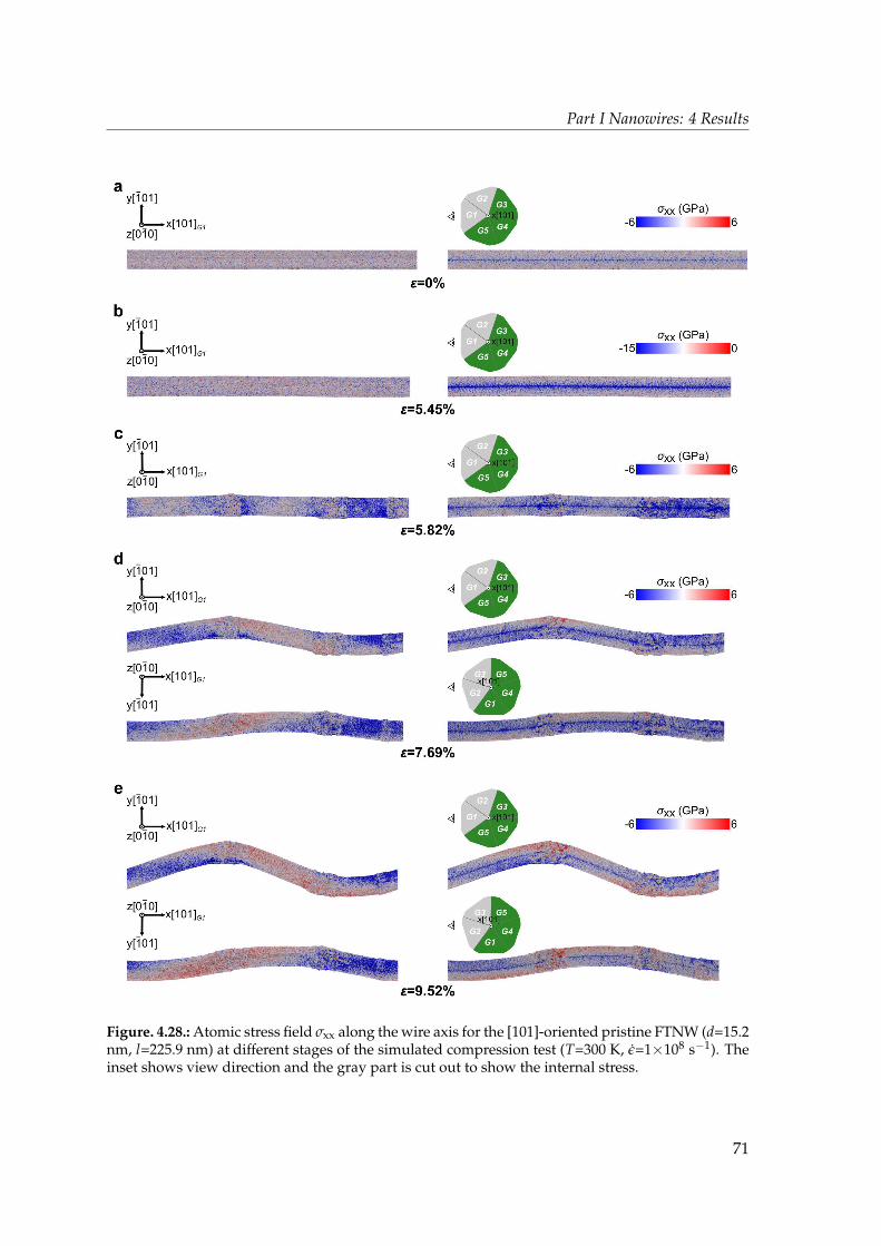
Part I Nanowires: 4 Results
a
b
Figure. 4.28.: Atomic stress field σxx along the wire axis for the [101]-oriented pristine FTNW (d=15.2nm, l=225.9 nm) at different stages of the simulated compression test (T=300 K, ε=1×10⁸ s−1). Theinset shows view direction and the gray part is cut out to show the internal stress.
71
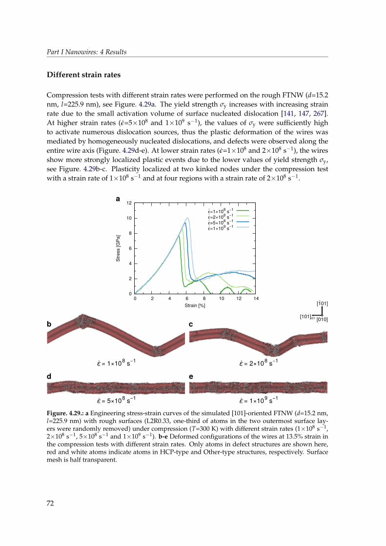
Part I Nanowires: 4 Results
Different strain rates
Compression tests with different strain rates were performed on the rough FTNW (d=15.2nm, l=225.9 nm), see Figure. 4.29a. The yield strength σy increases with increasing strainrate due to the small activation volume of surface nucleated dislocation [141, 147, 267].At higher strain rates (ε=5×10⁸ and 1×10⁹ s−1), the values of σy were sufficiently highto activate numerous dislocation sources, thus the plastic deformation of the wires wasmediated by homogeneously nucleated dislocations, and defects were observed along theentire wire axis (Figure. 4.29d-e). At lower strain rates (ε=1×10⁸ and 2×10⁸ s−1), the wiresshow more strongly localized plastic events due to the lower values of yield strength σy,see Figure. 4.29b-c. Plasticity localized at two kinked nodes under the compression testwith a strain rate of 1×10⁸ s−1 and at four regions with a strain rate of 2×10⁸ s−1.
ε.= 1×10
8s
−1ε.= 2×10
8s
−1
ε.= 5×10
8s
−1ε.= 1×10
9s
−1
b c
d e
[101]-
[010][101]G1
a
0
2
4
6
8
10
12
0 2 4 6 8 10 12 14
Str
ess [
GP
a]
Strain [%]
ε
.
=1×10⁸
s−1
ε
.
=2×10⁸
s−1
ε
.
=5×10⁸
s−1
ε
.
=1×10⁹
s−1
Figure. 4.29.: a Engineering stress-strain curves of the simulated [101]-oriented FTNW (d=15.2 nm,l=225.9 nm) with rough surfaces (L2R0.33, one-third of atoms in the two outermost surface lay-ers were randomly removed) under compression (T=300 K) with different strain rates (1×10⁸ s−1,2×10⁸ s−1, 5×10⁸ s−1 and 1×10⁹ s−1). b-e Deformed configurations of the wires at 13.5% strain inthe compression tests with different strain rates. Only atoms in defect structures are shown here,red and white atoms indicate atoms in HCP-type and Other-type structures, respectively. Surfacemesh is half transparent.
72
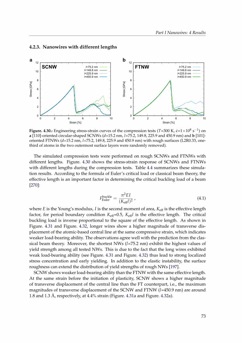
Part I Nanowires: 4 Results
4.2.3. Nanowires with different lengths
a
0
2
4
6
8
10
12
0 2 4 6 8 10
Str
ess [G
Pa]
Strain [%]
l=75.2 nm
l=149.8 nm
l=225.9 nm
l=450.9 nm
0
2
4
6
8
10
12
0 2 4 6 8 10
Str
ess [G
Pa]
Strain [%]
l=75.2 nm
l=149.8 nm
l=225.9 nm
l=450.9 nm
b
SCNW FTNW
Figure. 4.30.: Engineering stress-strain curves of the compression tests (T=300 K, ε=1×10⁸ s−1) ona [110]-oriented circular-shaped SCNWs (d=15.2 nm, l=75.2, 149.8, 225.9 and 450.9 nm) and b [101]-oriented FTNWs (d=15.2 nm, l=75.2, 149.8, 225.9 and 450.9 nm) with rough surfaces (L2R0.33, one-third of atoms in the two outermost surface layers were randomly removed).
The simulated compression tests were performed on rough SCNWs and FTNWs withdifferent lengths. Figure. 4.30 shows the stress-strain response of SCNWs and FTNWswith different lengths during the compression tests. Table 4.4 summarizes these simula-tion results. According to the formula of Euler’s critical load or classical beam theory, theeffective length is an important factor in determining the critical buckling load of a beam[270]:
FbuckleEuler =
π2EI(Keffl)2 , (4.1)
where E is the Young’s modulus, I is the second moment of area, Keff is the effective lengthfactor, for period boundary condition Keff=0.5, Keffl is the effective length. The criticalbuckling load is inverse proportional to the square of the effective length. As shown inFigure. 4.31 and Figure. 4.32, longer wires show a higher magnitude of transverse dis-placement of the atomic-based central line at the same compressive strain, which indicatesweaker load-bearing ability. The observations agree well with the prediction from the clas-sical beam theory. Moreover, the shortest NWs (l=75.2 nm) exhibit the highest values ofyield strength among all tested NWs. This is due to the fact that the long wires exhibitedweak load-bearing ability (see Figure. 4.31 and Figure. 4.32) thus lead to strong localizedstress concentration and early yielding. In addition to the elastic instability, the surfaceroughness can extend the distribution of yield strengths of rough NWs [197].
SCNW shows weaker load-bearing ability than the FTNW with the same effective length.At the same strain before the initiation of plasticity, SCNW shows a higher magnitudeof transverse displacement of the central line than the FT counterpart, i.e., the maximummagnitudes of transverse displacement of the SCNW and FTNW (l=450.9 nm) are around1.8 and 1.3 A, respectively, at 4.4% strain (Figure. 4.31a and Figure. 4.32a).
73
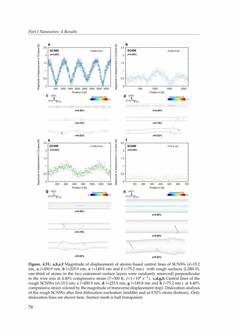
Part I Nanowires: 4 Results
SCNW SCNW
ε=4.78%
ε=9.52%
ε=4.40%
ε=4.40%
0 1.3Displacement (Å)
ε=4.40%
0 2.0Displacement (Å)
ε=4.40%
ε=4.78%
0.2 2.1Displacement (Å)
0 0.6Displacement (Å)
ε=4.78%
ε=9.52%
ε=4.40%
ε=4.88%
ε=9.52%
ε=4.40%
SCNW
ε=4.40%
SCNW ε=4.40%
a b
c d
e f
g h
l=450.9 nm l=225.9 nm
l=149.8 nm l=75.2 nm
0
0.5
1
1.5
2
2.5
100 200 300 400 500 600 700Ma
gn
itud
e o
f d
isp
lace
me
nt
in Y
Z p
lan
e [
Å]
Position X [Å]
0
0.5
1
1.5
2
2.5
500 1000 1500 2000Ma
gn
itud
e o
f d
isp
lace
me
nt
in Y
Z p
lan
e [
Å]
Position X [Å]
0
0.5
1
1.5
2
2.5
500 1000 1500 2000 2500 3000 3500 4000Ma
gn
itud
e o
f d
isp
lace
me
nt
in Y
Z p
lan
e [
Å]
Position X [Å]
ε=9.52%
y[001]
x[110]z[110]-
-
0
0.5
1
1.5
2
2.5
200 400 600 800 1000 1200 1400Ma
gn
itud
e o
f d
isp
lace
me
nt
in Y
Z p
lan
e [
Å]
Position X [Å]
y[001]
x[110]z[110]-
-y[001]
x[110]z[110]-
-
y[001]
x[110]z[110]-
-
Figure. 4.31.: a,b,e,f Magnitude of displacement of atomic-based central lines of SCNWs (d=15.2nm, a l=450.9 nm, b l=225.9 nm, e l=149.8 nm and f l=75.2 nm.) with rough surfaces (L2R0.33,one-third of atoms in the two outermost surface layers were randomly removed) perpendicularto the wire axis at 4.40% compressive strain (T=300 K, ε=1×10⁸ s−1). c,d,g,h Central lines of therough SCNWs (d=15.2 nm, c l=450.9 nm, d l=225.9 nm, g l=149.8 nm and h l=75.2 nm.) at 4.40%compressive strain colored by the magnitude of transverse displacement (top). Dislocation analysisof the rough SCNWs after first dislocation nucleation (middle) and at 9.52% strain (bottom). Onlydislocation lines are shown here. Surface mesh is half transparent.
74
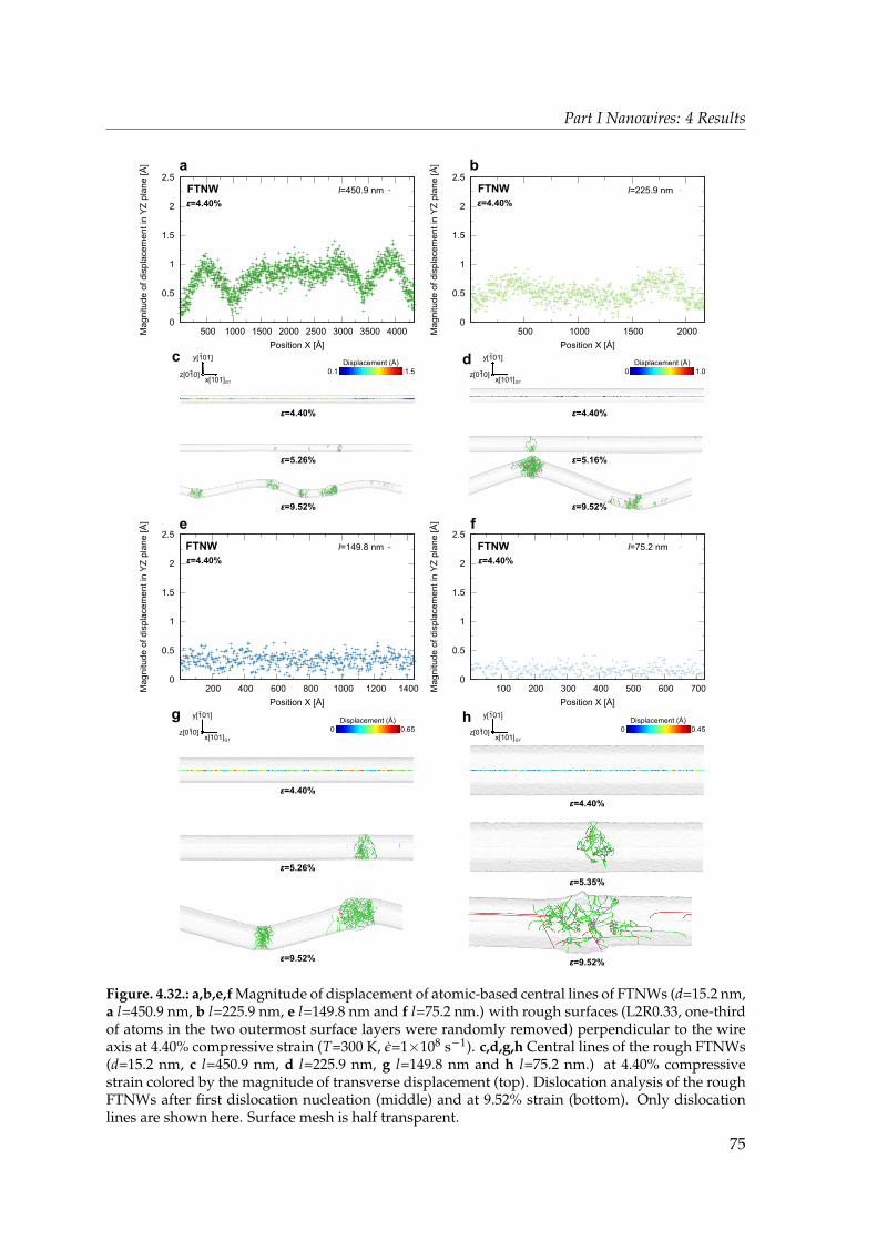
Part I Nanowires: 4 Results
FTNW FTNW
ε=5.26%
ε=9.52%
ε=4.40%
ε=4.40%
0 1.0Displacement (Å)
ε=4.40%
0.1 1.5Displacement (Å)
ε=4.40%
ε=5.16%
ε=9.52%
0 0.65Displacement (Å)
0 0.45Displacement (Å)
ε=5.26%
ε=9.52%
ε=4.40%
ε=5.35%
ε=9.52%
ε=4.40%
FTNW
ε=4.40%
FTNW ε=4.40%
a b
c d
e f
g h
y[101]-
z[010]x[101]G1
-
0
0.5
1
1.5
2
2.5
500 1000 1500 2000Magnitu
de o
f dis
pla
cem
ent in
YZ
pla
ne [Å
]
Position X [Å]
0
0.5
1
1.5
2
2.5
500 1000 1500 2000 2500 3000 3500 4000Magnitu
de o
f dis
pla
cem
ent in
YZ
pla
ne [Å
]
Position X [Å]
0
0.5
1
1.5
2
2.5
100 200 300 400 500 600 700Magnitu
de o
f dis
pla
cem
ent in
YZ
pla
ne [Å
]
Position X [Å]
0
0.5
1
1.5
2
2.5
200 400 600 800 1000 1200 1400Magnitu
de o
f dis
pla
cem
ent in
YZ
pla
ne [Å
]
Position X [Å]
l=450.9 nm l=225.9 nm
l=149.8 nm l=75.2 nm
y[101]-
z[010]x[101]G1
-
y[101]-
z[010]x[101]G1
-
y[101]-
z[010]x[101]G1
-
Figure. 4.32.: a,b,e,f Magnitude of displacement of atomic-based central lines of FTNWs (d=15.2 nm,a l=450.9 nm, b l=225.9 nm, e l=149.8 nm and f l=75.2 nm.) with rough surfaces (L2R0.33, one-thirdof atoms in the two outermost surface layers were randomly removed) perpendicular to the wireaxis at 4.40% compressive strain (T=300 K, ε=1×10⁸ s−1). c,d,g,h Central lines of the rough FTNWs(d=15.2 nm, c l=450.9 nm, d l=225.9 nm, g l=149.8 nm and h l=75.2 nm.) at 4.40% compressivestrain colored by the magnitude of transverse displacement (top). Dislocation analysis of the roughFTNWs after first dislocation nucleation (middle) and at 9.52% strain (bottom). Only dislocationlines are shown here. Surface mesh is half transparent.
75
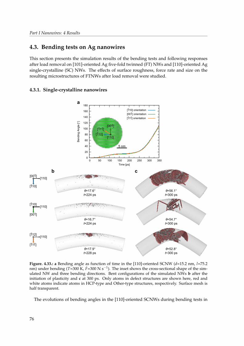
Part I Nanowires: 4 Results
4.3. Bending tests on Ag nanowires
This section presents the simulation results of the bending tests and following responsesafter load removal on [101]-oriented Ag five-fold twinned (FT) NWs and [110]-oriented Agsingle-crystalline (SC) NWs. The effects of surface roughness, force rate and size on theresulting microstructures of FTNWs after load removal were studied.
4.3.1. Single-crystalline nanowires
a
b
5 nm
[110]-
[110]
[001]-
[111- -
[110] orientation
0
20
40
60
80
100
120
140
160
180
0 50 100 150 200 250 300 350
Bendin
g A
ngle
[]
Time [ps]
[001] orientation
[111] orientation
[110][001]
[110]-
-
[110]
[001]
[110]-
-
[110][112]
[111]-
-
-
θ=52.8°
t=300 ps
θ=54.7°
t=300 ps
θ=56.1°
t=300 ps
c
θ=17.9°
t=228 ps
θ=16.7°
t=224 ps
θ=17.6°
t=224 ps
Figure. 4.33.: a Bending angle as function of time in the [110]-oriented SCNW (d=15.2 nm, l=75.2nm) under bending (T=300 K, F=300 N s−1). The inset shows the cross-sectional shape of the sim-ulated NW and three bending directions. Bent configurations of the simulated NWs b after theinitiation of plasticity and c at 300 ps. Only atoms in defect structures are shown here, red andwhite atoms indicate atoms in HCP-type and Other-type structures, respectively. Surface mesh ishalf transparent.
The evolutions of bending angles in the [110]-oriented SCNWs during bending tests in
76
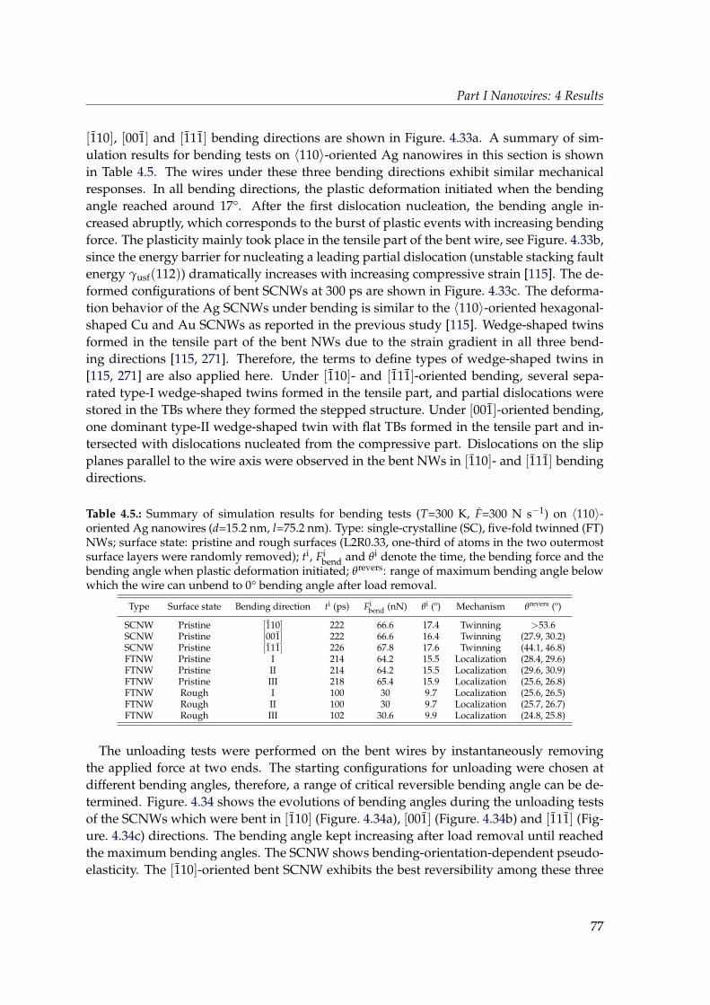
Part I Nanowires: 4 Results
[110], [001] and [111] bending directions are shown in Figure. 4.33a. A summary of sim-ulation results for bending tests on 〈110〉-oriented Ag nanowires in this section is shownin Table 4.5. The wires under these three bending directions exhibit similar mechanicalresponses. In all bending directions, the plastic deformation initiated when the bendingangle reached around 17°. After the first dislocation nucleation, the bending angle in-creased abruptly, which corresponds to the burst of plastic events with increasing bendingforce. The plasticity mainly took place in the tensile part of the bent wire, see Figure. 4.33b,since the energy barrier for nucleating a leading partial dislocation (unstable stacking faultenergy γusf(112)) dramatically increases with increasing compressive strain [115]. The de-formed configurations of bent SCNWs at 300 ps are shown in Figure. 4.33c. The deforma-tion behavior of the Ag SCNWs under bending is similar to the 〈110〉-oriented hexagonal-shaped Cu and Au SCNWs as reported in the previous study [115]. Wedge-shaped twinsformed in the tensile part of the bent NWs due to the strain gradient in all three bend-ing directions [115, 271]. Therefore, the terms to define types of wedge-shaped twins in[115, 271] are also applied here. Under [110]- and [111]-oriented bending, several sepa-rated type-I wedge-shaped twins formed in the tensile part, and partial dislocations werestored in the TBs where they formed the stepped structure. Under [001]-oriented bending,one dominant type-II wedge-shaped twin with flat TBs formed in the tensile part and in-tersected with dislocations nucleated from the compressive part. Dislocations on the slipplanes parallel to the wire axis were observed in the bent NWs in [110]- and [111] bendingdirections.
Table 4.5.: Summary of simulation results for bending tests (T=300 K, F=300 N s−1) on 〈110〉-oriented Ag nanowires (d=15.2 nm, l=75.2 nm). Type: single-crystalline (SC), five-fold twinned (FT)NWs; surface state: pristine and rough surfaces (L2R0.33, one-third of atoms in the two outermostsurface layers were randomly removed); ti, Fi
bend and θi denote the time, the bending force and thebending angle when plastic deformation initiated; θrevers: range of maximum bending angle belowwhich the wire can unbend to 0° bending angle after load removal.
Type Surface state Bending direction ti (ps) Fibend (nN) θi (º) Mechanism θrevers (º)
SCNW Pristine [110] 222 66.6 17.4 Twinning >53.6SCNW Pristine [001] 222 66.6 16.4 Twinning (27.9, 30.2)SCNW Pristine [111] 226 67.8 17.6 Twinning (44.1, 46.8)FTNW Pristine I 214 64.2 15.5 Localization (28.4, 29.6)FTNW Pristine II 214 64.2 15.5 Localization (29.6, 30.9)FTNW Pristine III 218 65.4 15.9 Localization (25.6, 26.8)FTNW Rough I 100 30 9.7 Localization (25.6, 26.5)FTNW Rough II 100 30 9.7 Localization (25.7, 26.7)FTNW Rough III 102 30.6 9.9 Localization (24.8, 25.8)
The unloading tests were performed on the bent wires by instantaneously removingthe applied force at two ends. The starting configurations for unloading were chosen atdifferent bending angles, therefore, a range of critical reversible bending angle can be de-termined. Figure. 4.34 shows the evolutions of bending angles during the unloading testsof the SCNWs which were bent in [110] (Figure. 4.34a), [001] (Figure. 4.34b) and [111] (Fig-ure. 4.34c) directions. The bending angle kept increasing after load removal until reachedthe maximum bending angles. The SCNW shows bending-orientation-dependent pseudo-elasticity. The [110]-oriented bent SCNW exhibits the best reversibility among these three
77
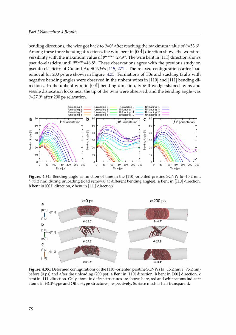
Part I Nanowires: 4 Results
bending directions, the wire got back to θ=0° after reaching the maximum value of θ=53.6°.Among these three bending directions, the wire bent in [001] direction shows the worst re-versibility with the maximum value of θrevers=27.9°. The wire bent in [111] direction showspseudo-elasticity until θrevers=46.8°. These observations agree with the previous study onpseudo-elasticity of Cu and Au SCNWs [115, 271]. The relaxed configurations after loadremoval for 200 ps are shown in Figure. 4.35. Formations of TBs and stacking faults withnegative bending angles were observed in the unbent wires in [110] and [111] bending di-rections. In the unbent wire in [001] bending direction, type-II wedge-shaped twins andsessile dislocation locks near the tip of the twin were observed, and the bending angle wasθ=27.9° after 200 ps relaxation.
0
10
20
30
40
50
60
0 50 100 150 200 250 300
Bendin
g A
ngle
[°]
Time [ps]
0
10
20
30
40
50
60
0 50 100 150 200 250 300
Bendin
g A
ngle
[°]
Time [ps]
0
10
20
30
40
50
60
0 50 100 150 200 250 300
Bendin
g A
ngle
[°]
Time [ps]
Unloading 1Unloading 2Unloading 3Unloading 4
Unloading 5Unloading 6Unloading 7Unloading 8
Unloading 9Unloading 10Unloading 11Unloading 12
Unloading 13Unloading 14Unloading 15Unloading 16
[110] orientation-
[001] orientation-
[111] orientation--a b c
Figure. 4.34.: Bending angle as function of time in the [110]-oriented pristine SCNW (d=15.2 nm,l=75.2 nm) during unloading (load removal at different bending angles). a Bent in [110] direction,b bent in [001] direction, c bent in [111] direction.
t=0 ps
[110][001]
[110]-
-
[110]
[001]
[110]-
-
[110][112]
[111]-
-
-
t=200 psa
b
c
θ=28.0°
θ=27.2°
θ=26.1°
θ=-4.7°
θ=27.9°
θ=-3.4°
Figure. 4.35.: Deformed configurations of the [110]-oriented pristine SCNWs (d=15.2 nm, l=75.2 nm)before (0 ps) and after the unloading (200 ps). a Bent in [110] direction, b bent in [001] direction, cbent in [111] direction. Only atoms in defect structures are shown here, red and white atoms indicateatoms in HCP-type and Other-type structures, respectively. Surface mesh is half transparent.
78
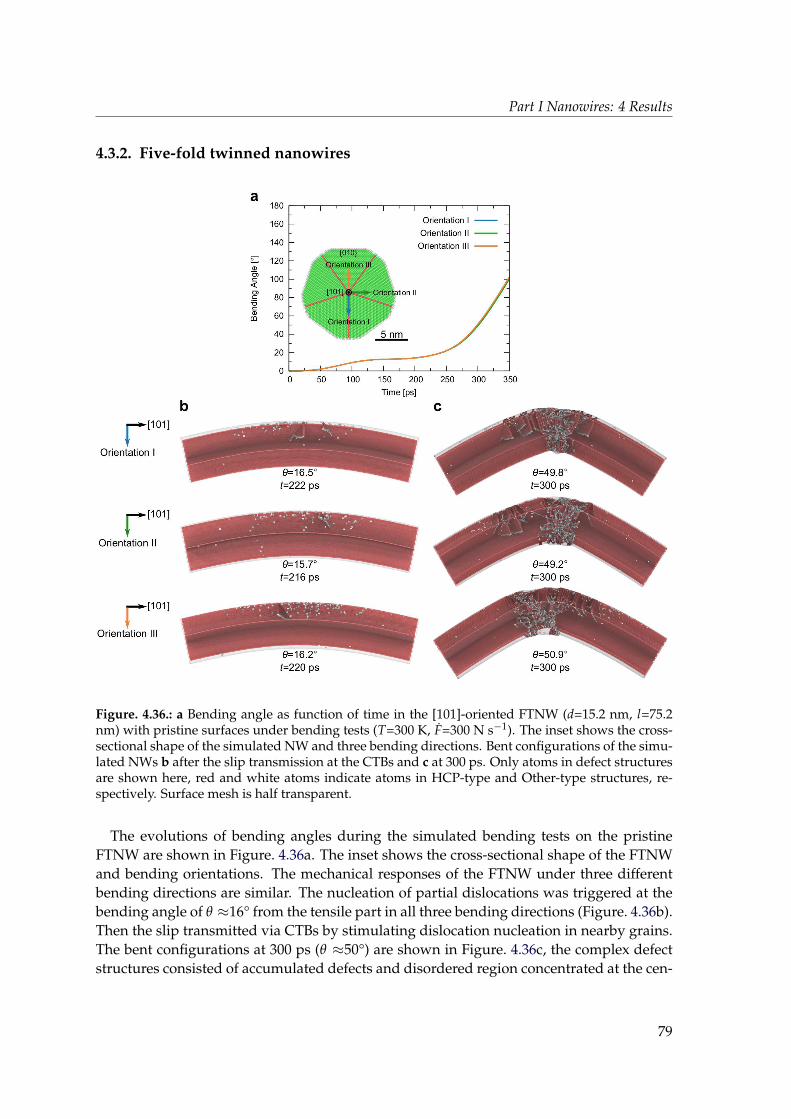
Part I Nanowires: 4 Results
4.3.2. Five-fold twinned nanowires
a
b
5 nm
[101]
010
Orientation I
0
20
40
60
80
100
120
140
160
180
0 50 100 150 200 250 300 350
Be
nd
ing
An
gle
[]
Time [ps]
Orientation I
Orientation II
Orientation III
Figure. 4.36.: a Bending angle as function of time in the [101]-oriented FTNW (d=15.2 nm, l=75.2nm) with pristine surfaces under bending tests (T=300 K, F=300 N s−1). The inset shows the cross-sectional shape of the simulated NW and three bending directions. Bent configurations of the simu-lated NWs b after the slip transmission at the CTBs and c at 300 ps. Only atoms in defect structuresare shown here, red and white atoms indicate atoms in HCP-type and Other-type structures, re-spectively. Surface mesh is half transparent.
The evolutions of bending angles during the simulated bending tests on the pristineFTNW are shown in Figure. 4.36a. The inset shows the cross-sectional shape of the FTNWand bending orientations. The mechanical responses of the FTNW under three differentbending directions are similar. The nucleation of partial dislocations was triggered at thebending angle of θ ≈16° from the tensile part in all three bending directions (Figure. 4.36b).Then the slip transmitted via CTBs by stimulating dislocation nucleation in nearby grains.The bent configurations at 300 ps (θ ≈50°) are shown in Figure. 4.36c, the complex defectstructures consisted of accumulated defects and disordered region concentrated at the cen-
79
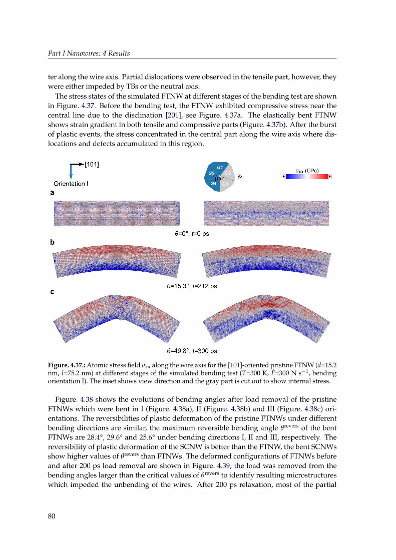
Part I Nanowires: 4 Results
ter along the wire axis. Partial dislocations were observed in the tensile part, however, theywere either impeded by TBs or the neutral axis.
The stress states of the simulated FTNW at different stages of the bending test are shownin Figure. 4.37. Before the bending test, the FTNW exhibited compressive stress near thecentral line due to the disclination [201], see Figure. 4.37a. The elastically bent FTNWshows strain gradient in both tensile and compressive parts (Figure. 4.37b). After the burstof plastic events, the stress concentrated in the central part along the wire axis where dis-locations and defects accumulated in this region.
σxx (GPa)
6-6
[101]
Orientation I b
Figure. 4.37.: Atomic stress field σxx along the wire axis for the [101]-oriented pristine FTNW (d=15.2nm, l=75.2 nm) at different stages of the simulated bending test (T=300 K, F=300 N s−1, bendingorientation I). The inset shows view direction and the gray part is cut out to show internal stress.
Figure. 4.38 shows the evolutions of bending angles after load removal of the pristineFTNWs which were bent in I (Figure. 4.38a), II (Figure. 4.38b) and III (Figure. 4.38c) ori-entations. The reversibilities of plastic deformation of the pristine FTNWs under differentbending directions are similar, the maximum reversible bending angle θrevers of the bentFTNWs are 28.4°, 29.6° and 25.6° under bending directions I, II and III, respectively. Thereversibility of plastic deformation of the SCNW is better than the FTNW, the bent SCNWsshow higher values of θrevers than FTNWs. The deformed configurations of FTNWs beforeand after 200 ps load removal are shown in Figure. 4.39, the load was removed from thebending angles larger than the critical values of θrevers to identify resulting microstructureswhich impeded the unbending of the wires. After 200 ps relaxation, most of the partial
80
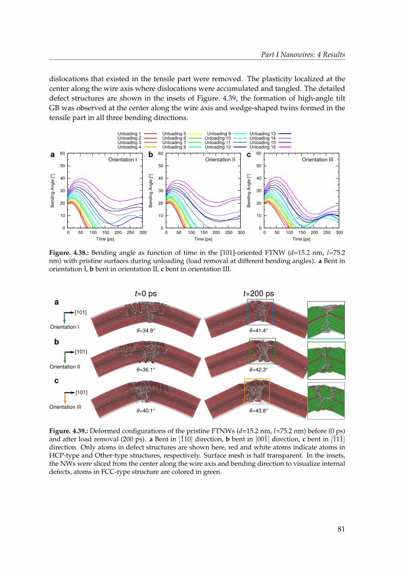
Part I Nanowires: 4 Results
dislocations that existed in the tensile part were removed. The plasticity localized at thecenter along the wire axis where dislocations were accumulated and tangled. The detaileddefect structures are shown in the insets of Figure. 4.39, the formation of high-angle tiltGB was observed at the center along the wire axis and wedge-shaped twins formed in thetensile part in all three bending directions.
Unloading 1Unloading 2Unloading 3Unloading 4
Unloading 5Unloading 6Unloading 7Unloading 8
Unloading 9Unloading 10Unloading 11Unloading 12
Unloading 13Unloading 14Unloading 15Unloading 16
Orientation I Orientation II Orientation IIIa b c
0
10
20
30
40
50
60
0 50 100 150 200 250 300
Bendin
g A
ngle
[°]
Time [ps]
0
10
20
30
40
50
60
0 50 100 150 200 250 300
Bendin
g A
ngle
[°]
Time [ps]
0
10
20
30
40
50
60
0 50 100 150 200 250 300
Bendin
g A
ngle
[°]
Time [ps]
Figure. 4.38.: Bending angle as function of time in the [101]-oriented FTNW (d=15.2 nm, l=75.2nm) with pristine surfaces during unloading (load removal at different bending angles). a Bent inorientation I, b bent in orientation II, c bent in orientation III.
t=0 ps t=200 psa
b
c
[101]
Orientation I
[101]
Orientation II
Orientation III
[101]
θ=34.9°
θ=36.1°
θ=40.1° θ=43.8°
θ=42.3°
θ=41.4°
Figure. 4.39.: Deformed configurations of the pristine FTNWs (d=15.2 nm, l=75.2 nm) before (0 ps)and after load removal (200 ps). a Bent in [110] direction, b bent in [001] direction, c bent in [111]direction. Only atoms in defect structures are shown here, red and white atoms indicate atoms inHCP-type and Other-type structures, respectively. Surface mesh is half transparent. In the insets,the NWs were sliced from the center along the wire axis and bending direction to visualize internaldefects, atoms in FCC-type structure are colored in green.
81
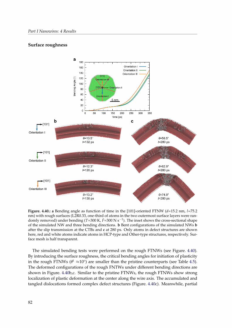
Part I Nanowires: 4 Results
Surface roughness
a
b
5 nm
[101]
010
Orientation I
Figure. 4.40.: a Bending angle as function of time in the [101]-oriented FTNW (d=15.2 nm, l=75.2nm) with rough surfaces (L2R0.33, one-third of atoms in the two outermost surface layers were ran-domly removed) under bending (T=300 K, F=300 N s−1). The inset shows the cross-sectional shapeof the simulated NW and three bending directions. b Bent configurations of the simulated NWs bafter the slip transmission at the CTBs and c at 280 ps. Only atoms in defect structures are shownhere, red and white atoms indicate atoms in HCP-type and Other-type structures, respectively. Sur-face mesh is half transparent.
The simulated bending tests were performed on the rough FTNWs (see Figure. 4.40).By introducing the surface roughness, the critical bending angles for initiation of plasticityin the rough FTNWs (θi ≈10°) are smaller than the pristine counterparts (see Table 4.5).The deformed configurations of the rough FNTWs under different bending directions areshown in Figure. 4.40b,c. Similar to the pristine FTNWs, the rough FTNWs show stronglocalization of plastic deformation at the center along the wire axis. The accumulated andtangled dislocations formed complex defect structures (Figure. 4.40c). Meanwhile, partial
82
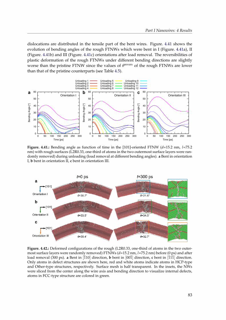
Part I Nanowires: 4 Results
dislocations are distributed in the tensile part of the bent wires. Figure. 4.41 shows theevolution of bending angles of the rough FTNWs which were bent in I (Figure. 4.41a), II(Figure. 4.41b) and III (Figure. 4.41c) orientations after load removal. The reversibilities ofplastic deformation of the rough FTNWs under different bending directions are slightlyworse than the pristine FTNW since the values of θrevers of the rough FTNWs are lowerthan that of the pristine counterparts (see Table 4.5).
Unloading 1Unloading 2Unloading 3Unloading 4
Unloading 5Unloading 6Unloading 7Unloading 8
Unloading 9Unloading 10Unloading 11Unloading 12
Orientation I Orientation II Orientation IIIa b c
0
10
20
30
40
50
60
0 50 100 150 200 250 300
Bendin
g A
ngle
[°]
Time [ps]
0
10
20
30
40
50
60
0 50 100 150 200 250 300
Bendin
g A
ngle
[°]
Time [ps]
0
10
20
30
40
50
60
0 50 100 150 200 250 300B
endin
g A
ngle
[°]
Time [ps]
Figure. 4.41.: Bending angle as function of time in the [101]-oriented FTNW (d=15.2 nm, l=75.2nm) with rough surfaces (L2R0.33, one-third of atoms in the two outermost surface layers were ran-domly removed) during unloading (load removal at different bending angles). a Bent in orientationI, b bent in orientation II, c bent in orientation III.
Figure. 4.42.: Deformed configurations of the rough (L2R0.33, one-third of atoms in the two outer-most surface layers were randomly removed) FTNWs (d=15.2 nm, l=75.2 nm) before (0 ps) and afterload removal (300 ps). a Bent in [110] direction, b bent in [001] direction, c bent in [111] direction.Only atoms in defect structures are shown here, red and white atoms indicate atoms in HCP-typeand Other-type structures, respectively. Surface mesh is half transparent. In the insets, the NWswere sliced from the center along the wire axis and bending direction to visualize internal defects,atoms in FCC-type structure are colored in green.
83
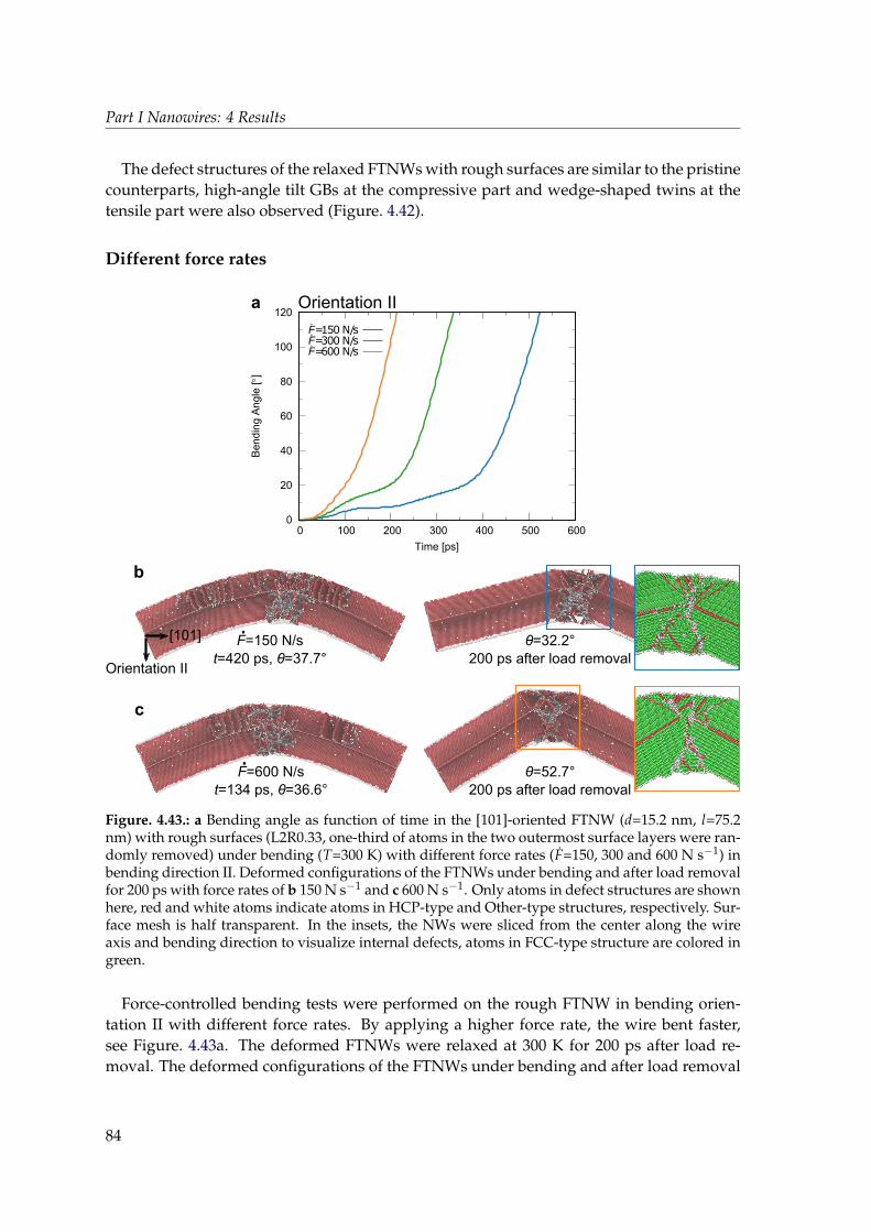
Part I Nanowires: 4 Results
The defect structures of the relaxed FTNWs with rough surfaces are similar to the pristinecounterparts, high-angle tilt GBs at the compressive part and wedge-shaped twins at thetensile part were also observed (Figure. 4.42).
Different force rates
F.=150 N/sF.=300 N/sF.=600 N/s
Orientation II
[101]
Orientation II
b
a
F=150 N/s
t=420 ps, θ=37.7°
.
0
20
40
60
80
100
120
0 100 200 300 400 500 600
Be
nd
ing
An
gle
[]
Time [ps]
F=600 N/s
t=134 ps, θ=36.6°
.
c
θ=32.2°
200 ps after load removal
θ=52.7°
200 ps after load removal
Figure. 4.43.: a Bending angle as function of time in the [101]-oriented FTNW (d=15.2 nm, l=75.2nm) with rough surfaces (L2R0.33, one-third of atoms in the two outermost surface layers were ran-domly removed) under bending (T=300 K) with different force rates (F=150, 300 and 600 N s−1) inbending direction II. Deformed configurations of the FTNWs under bending and after load removalfor 200 ps with force rates of b 150 N s−1 and c 600 N s−1. Only atoms in defect structures are shownhere, red and white atoms indicate atoms in HCP-type and Other-type structures, respectively. Sur-face mesh is half transparent. In the insets, the NWs were sliced from the center along the wireaxis and bending direction to visualize internal defects, atoms in FCC-type structure are colored ingreen.
Force-controlled bending tests were performed on the rough FTNW in bending orien-tation II with different force rates. By applying a higher force rate, the wire bent faster,see Figure. 4.43a. The deformed FTNWs were relaxed at 300 K for 200 ps after load re-moval. The deformed configurations of the FTNWs under bending and after load removal
84
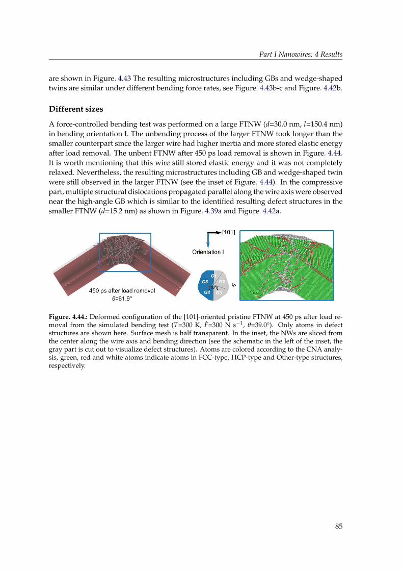
Part I Nanowires: 4 Results
are shown in Figure. 4.43 The resulting microstructures including GBs and wedge-shapedtwins are similar under different bending force rates, see Figure. 4.43b-c and Figure. 4.42b.
Different sizes
A force-controlled bending test was performed on a large FTNW (d=30.0 nm, l=150.4 nm)in bending orientation I. The unbending process of the larger FTNW took longer than thesmaller counterpart since the larger wire had higher inertia and more stored elastic energyafter load removal. The unbent FTNW after 450 ps load removal is shown in Figure. 4.44.It is worth mentioning that this wire still stored elastic energy and it was not completelyrelaxed. Nevertheless, the resulting microstructures including GB and wedge-shaped twinwere still observed in the larger FTNW (see the inset of Figure. 4.44). In the compressivepart, multiple structural dislocations propagated parallel along the wire axis were observednear the high-angle GB which is similar to the identified resulting defect structures in thesmaller FTNW (d=15.2 nm) as shown in Figure. 4.39a and Figure. 4.42a.
b
Figure. 4.44.: Deformed configuration of the [101]-oriented pristine FTNW at 450 ps after load re-moval from the simulated bending test (T=300 K, F=300 N s−1, θ=39.0°). Only atoms in defectstructures are shown here. Surface mesh is half transparent. In the inset, the NWs are sliced fromthe center along the wire axis and bending direction (see the schematic in the left of the inset, thegray part is cut out to visualize defect structures). Atoms are colored according to the CNA analy-sis, green, red and white atoms indicate atoms in FCC-type, HCP-type and Other-type structures,respectively.
85
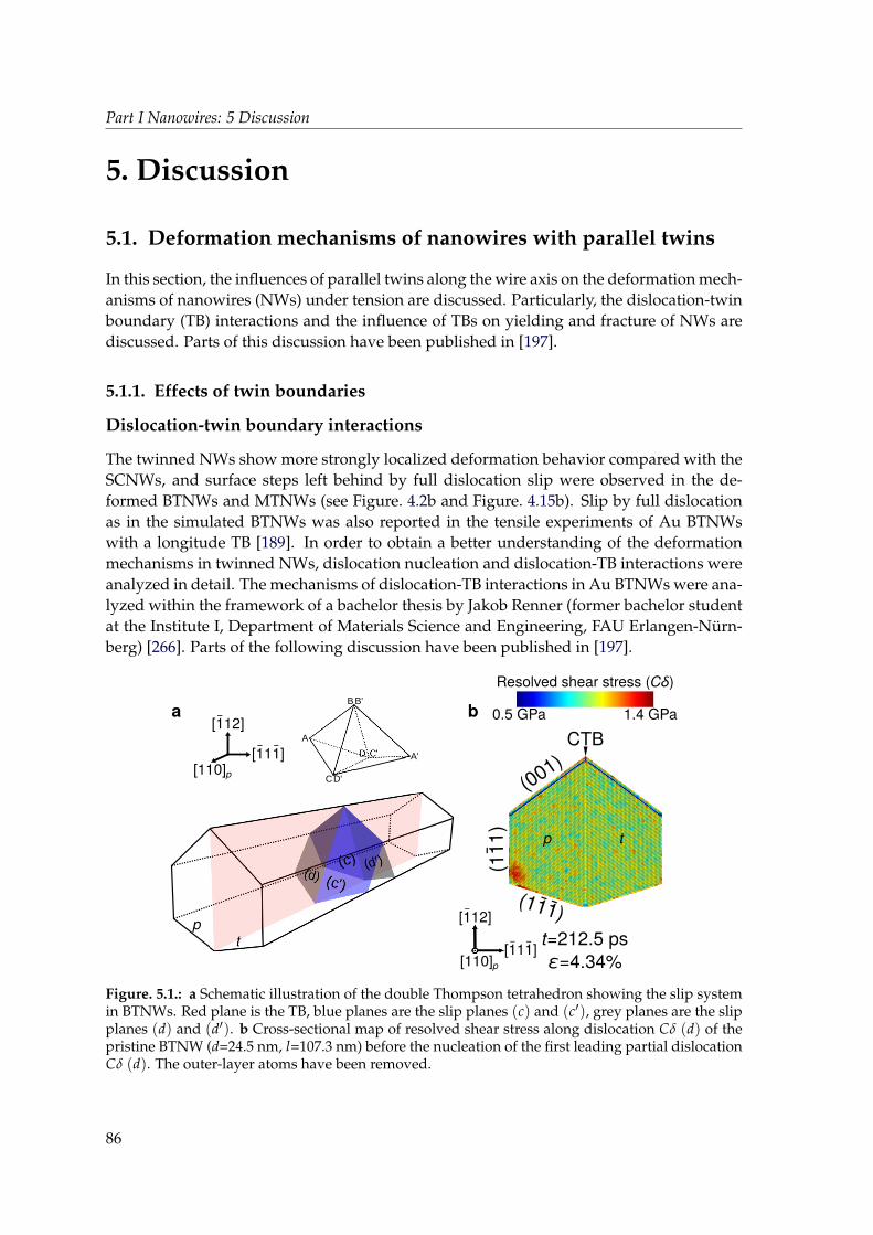
Part I Nanowires: 5 Discussion
5. Discussion
5.1. Deformation mechanisms of nanowires with parallel twins
In this section, the influences of parallel twins along the wire axis on the deformation mech-anisms of nanowires (NWs) under tension are discussed. Particularly, the dislocation-twinboundary (TB) interactions and the influence of TBs on yielding and fracture of NWs arediscussed. Parts of this discussion have been published in [197].
5.1.1. Effects of twin boundaries
Dislocation-twin boundary interactions
The twinned NWs show more strongly localized deformation behavior compared with theSCNWs, and surface steps left behind by full dislocation slip were observed in the de-formed BTNWs and MTNWs (see Figure. 4.2b and Figure. 4.15b). Slip by full dislocationas in the simulated BTNWs was also reported in the tensile experiments of Au BTNWswith a longitude TB [189]. In order to obtain a better understanding of the deformationmechanisms in twinned NWs, dislocation nucleation and dislocation-TB interactions wereanalyzed in detail. The mechanisms of dislocation-TB interactions in Au BTNWs were ana-lyzed within the framework of a bachelor thesis by Jakob Renner (former bachelor studentat the Institute I, Department of Materials Science and Engineering, FAU Erlangen-Nurn-berg) [266]. Parts of the following discussion have been published in [197].
A'
A
BB'
CD'
[111]- -
[112]-
[110]p
p
[110]p[111]- -
[112]-
0.5 GPa 1.4 GPa
Resolved shear stress (Cδ)
CTB
t=212.5 ps
ε=4.34%
(111
) -
(001)
(111)
--
p t
a b
Figure. 5.1.: a Schematic illustration of the double Thompson tetrahedron showing the slip systemin BTNWs. Red plane is the TB, blue planes are the slip planes (c) and (c′), grey planes are the slipplanes (d) and (d′). b Cross-sectional map of resolved shear stress along dislocation Cδ (d) of thepristine BTNW (d=24.5 nm, l=107.3 nm) before the nucleation of the first leading partial dislocationCδ (d). The outer-layer atoms have been removed.
86
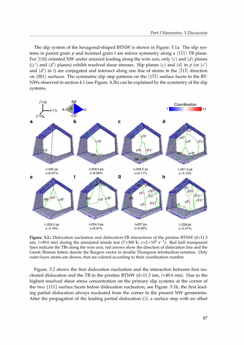
Part I Nanowires: 5 Discussion
The slip system of the hexagonal-shaped BTNW is shown in Figure. 5.1a. The slip sys-tems in parent grain p and twinned grain t are mirror symmetry along a (111) TB plane.For [110]-oriented NW under uniaxial loading along the wire axis, only (c) and (d) planes((c′) and (d′) planes) exhibit resolved shear stresses. Slip planes (c) and (d) in p (or (c′)and (d′) in t) are conjugated and intersect along one line of atoms in the [111] directionon (001) surfaces. The symmetric slip step patterns on the (111) surface facets in the BT-NWs observed in section 4.1 (see Figure. 4.2b) can be explained by the symmetry of the slipsystems.
t=245 ps
ε=5.01%
t=248.5 ps
ε=5.09%
t=249.5 ps
ε=5.11%
t=251.5 ps
ε=5.15%
t=253.5 ps
ε=5.19%
t=254.5 ps
ε=5.21%
t=257 ps
ε=5.26%
t=259 ps
ε=5.31%
a b c d
e f g h
C
C
γ' D'γ'
C
γ' D'γ'
B γ''
γD γD
C
γ' D'γ'
B γ''
B γ''γD B γ''γD
' ''
B
γD
γ'
D'γ'
''
'
Bγ ''
'
Bγ
''
''
D'γ'
γD
Figure. 5.2.: Dislocation nucleation and dislocation-TB interactions of the pristine BTNW (d=11.3nm, l=49.6 nm) during the simulated tensile test (T=300 K, ε=2×10⁸ s−1). Red half transparentlines indicate the TBs along the wire axis, red arrows show the direction of dislocation line and theGreek/Roman letters denote the Burgers vector in double Thompson tetrahedron notation. Onlyouter-layer atoms are shown, that are colored according to their coordination number.
Figure. 5.2 shows the first dislocation nucleation and the interaction between first nu-cleated dislocation and the TB in the pristine BTNW (d=11.3 nm, l=49.6 nm). Due to thehighest resolved shear stress concentration on the primary slip systems at the corner ofthe two 111 surface facets before dislocation nucleation, see Figure. 5.1b, the first lead-ing partial dislocation always nucleated from the corner in the present NW geometries.After the propagation of the leading partial dislocation Cδ, a surface step with an offset
87
Part I Nanowires: 5 Discussion
of one partial Burgers vector was left behind on each surface facet (Figure. 5.2a,b), whichcan serve as a nucleation site for subsequent dislocations. After depositing on the TB, theleading partial dislocation interacted with the TB by forming a stair-rod dislocation γ′δ atthe triple junction where the TB bounded by two 111 surface facets (see Figure. 5.2b). Si-multaneously, a new leading partial dislocation D′γ′ was stimulated in t on the symmetricslip plane from the triple junction [197, 266]. This reaction can be represented as follows:
Cδ→ D′γ′ + γ′δ . (5.1)
After the above interaction, the stair-rod dislocation γ′δ dissociated into two trailingpartial dislocations δB in p and γ′B′ in t starting at the intersection of TB and free surfaces,Figure. 5.2c:
γ′δ + δB→ γ′B′ , (5.2)
which then swept through their respective grains [197, 266]. Eventually, both the leadingand trailing partial dislocations escaped at the free surfaces (Figure. 5.2d-h).
The surface step on the (001) surface facet left by the first leading partial dislocation Cδ
served as a nucleation site for another leading partial dislocation γD on the conjugated slipplane (c) (Figure. 5.2c). The partial dislocation γD was stimulated from the step and theninteracted with the TB following the similar mechanisms as described in Equations (5.1)and (5.2), see Figure. 5.2e-h.
These events repeatedly happened on the same and nearby atomic planes during the de-formation processes and led to a strongly localized deformation behavior in the BTNW. Themechanisms observed here, namely, the transmission of leading partial dislocation and theunzipping of stair-rod dislocation by nucleation of two trailing partial dislocations at theintersection of TB and NW free surfaces [197], provide an explanation for the observationof full dislocation slip in experiments on Au BTNW [189].
Similar mechanisms were also observed in the MTNW. Figure. 5.3 shows the dislocationnucleation and dislocation-TB interactions of the pristine MTNW (d=24.5 nm, l=107.3 nm)under tension. The first leading partial dislocation Cδ nucleated from the corner of the two111 surface facets in p1 and then interacted with the CTB1 following the similar mech-anism as introduced in Equation (5.1). A stair-rod dislocation γ′δ on the TB and anotherleading partial dislocation D′γ′ in t1 were stimulated at the intersection of TB and NWfree surfaces. Then, the stair-rod dislocation γ′δ dissociated into two trailing partial dislo-cations δB in p1 and γ′B′ in t1 following the above mechanism as described in Equation(5.2). The full dislocation DB(c′) in t1 then interacted with the CTB2 following a combinedmechanism as introduced in Equations (5.1) and (5.2):
D′γ′ + γ′B′ → Cδ + δB . (5.3)
The full dislocations DB(c′) in t1 and CB(d) in p2 intersected at the CTB2 by a stair-rod dislocation δγ′. The full dislocations interacted with other CTBs following the samereaction as introduced in Equation (5.3) and swept through the entire wire. These plasticevents repeatedly happened in the same region and led to a strongly localized deformationbehavior in the MTNW. Comparing to BTNW, the slip system of MTNW is narrower along
88
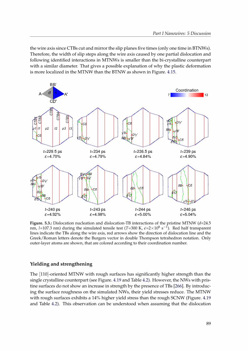
Part I Nanowires: 5 Discussion
the wire axis since CTBs cut and mirror the slip planes five times (only one time in BTNWs).Therefore, the width of slip steps along the wire axis caused by one partial dislocation andfollowing identified interactions in MTNWs is smaller than the bi-crystalline counterpartwith a similar diameter. That gives a possible explanation of why the plastic deformationis more localized in the MTNW than the BTNW as shown in Figure. 4.15.
BB'
A'
CD'
A'
Figure. 5.3.: Dislocation nucleation and dislocation-TB interactions of the pristine MTNW (d=24.5nm, l=107.3 nm) during the simulated tensile test (T=300 K, ε=2×10⁸ s−1). Red half transparentlines indicate the TBs along the wire axis, red arrows show the direction of dislocation line and theGreek/Roman letters denote the Burgers vector in double Thompson tetrahedron notation. Onlyouter-layer atoms are shown, that are colored according to their coordination number.
Yielding and strengthening
The [110]-oriented MTNW with rough surfaces has significantly higher strength than thesingle crystalline counterpart (see Figure. 4.19 and Table 4.2). However, the NWs with pris-tine surfaces do not show an increase in strength by the presence of TBs [266]. By introduc-ing the surface roughness on the simulated NWs, their yield stresses reduce. The MTNWwith rough surfaces exhibits a 14% higher yield stress than the rough SCNW (Figure. 4.19and Table 4.2). This observation can be understood when assuming that the dislocation
89
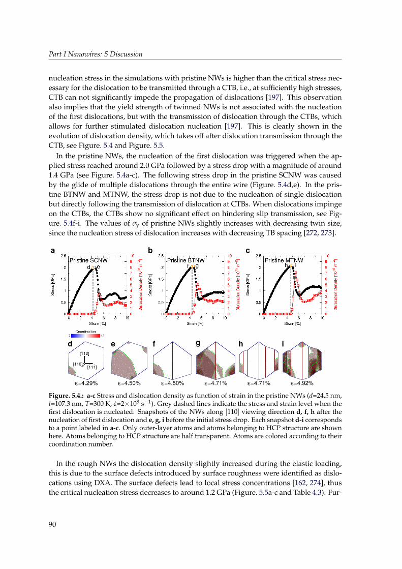
Part I Nanowires: 5 Discussion
nucleation stress in the simulations with pristine NWs is higher than the critical stress nec-essary for the dislocation to be transmitted through a CTB, i.e., at sufficiently high stresses,CTB can not significantly impede the propagation of dislocations [197]. This observationalso implies that the yield strength of twinned NWs is not associated with the nucleationof the first dislocations, but with the transmission of dislocation through the CTBs, whichallows for further stimulated dislocation nucleation [197]. This is clearly shown in theevolution of dislocation density, which takes off after dislocation transmission through theCTB, see Figure. 5.4 and Figure. 5.5.
In the pristine NWs, the nucleation of the first dislocation was triggered when the ap-plied stress reached around 2.0 GPa followed by a stress drop with a magnitude of around1.4 GPa (see Figure. 5.4a-c). The following stress drop in the pristine SCNW was causedby the glide of multiple dislocations through the entire wire (Figure. 5.4d,e). In the pris-tine BTNW and MTNW, the stress drop is not due to the nucleation of single dislocationbut directly following the transmission of dislocation at CTBs. When dislocations impingeon the CTBs, the CTBs show no significant effect on hindering slip transmission, see Fig-ure. 5.4f-i. The values of σy of pristine NWs slightly increases with decreasing twin size,since the nucleation stress of dislocation increases with decreasing TB spacing [272, 273].
a b c
ε=4.29% ε=4.50% ε=4.50% ε=4.71% ε=4.71% ε=4.92%
[110]p[111]
-
[112]-
d e f g h i
Figure. 5.4.: a-c Stress and dislocation density as function of strain in the pristine NWs (d=24.5 nm,l=107.3 nm, T=300 K, ε=2×10⁸ s−1). Grey dashed lines indicate the stress and strain level when thefirst dislocation is nucleated. Snapshots of the NWs along [110] viewing direction d, f, h after thenucleation of first dislocation and e, g, i before the initial stress drop. Each snapshot d-i correspondsto a point labeled in a-c. Only outer-layer atoms and atoms belonging to HCP structure are shownhere. Atoms belonging to HCP structure are half transparent. Atoms are colored according to theircoordination number.
In the rough NWs the dislocation density slightly increased during the elastic loading,this is due to the surface defects introduced by surface roughness were identified as dislo-cations using DXA. The surface defects lead to local stress concentrations [162, 274], thusthe critical nucleation stress decreases to around 1.2 GPa (Figure. 5.5a-c and Table 4.3). Fur-
90
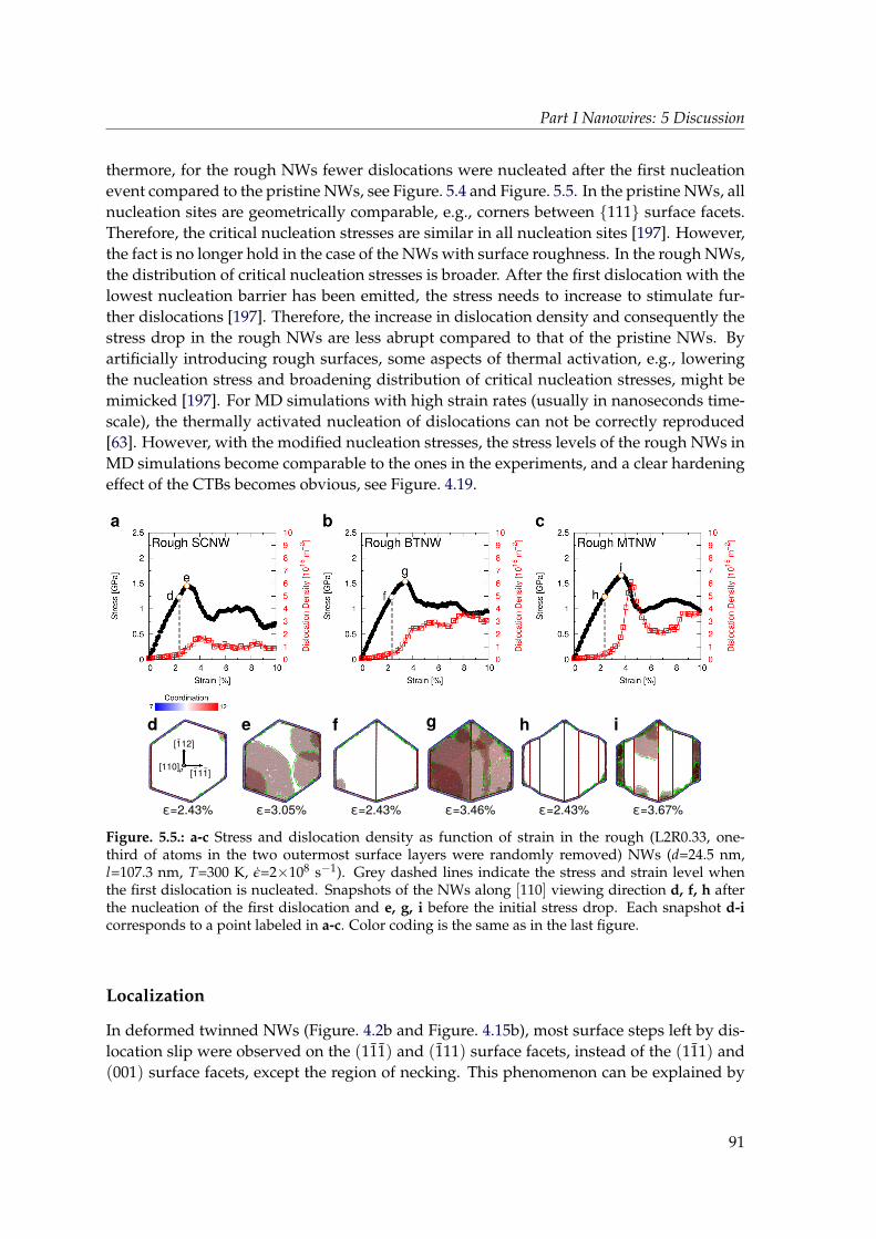
Part I Nanowires: 5 Discussion
thermore, for the rough NWs fewer dislocations were nucleated after the first nucleationevent compared to the pristine NWs, see Figure. 5.4 and Figure. 5.5. In the pristine NWs, allnucleation sites are geometrically comparable, e.g., corners between 111 surface facets.Therefore, the critical nucleation stresses are similar in all nucleation sites [197]. However,the fact is no longer hold in the case of the NWs with surface roughness. In the rough NWs,the distribution of critical nucleation stresses is broader. After the first dislocation with thelowest nucleation barrier has been emitted, the stress needs to increase to stimulate fur-ther dislocations [197]. Therefore, the increase in dislocation density and consequently thestress drop in the rough NWs are less abrupt compared to that of the pristine NWs. Byartificially introducing rough surfaces, some aspects of thermal activation, e.g., loweringthe nucleation stress and broadening distribution of critical nucleation stresses, might bemimicked [197]. For MD simulations with high strain rates (usually in nanoseconds time-scale), the thermally activated nucleation of dislocations can not be correctly reproduced[63]. However, with the modified nucleation stresses, the stress levels of the rough NWs inMD simulations become comparable to the ones in the experiments, and a clear hardeningeffect of the CTBs becomes obvious, see Figure. 4.19.
d e f g h
ε=2.43% ε=3.05% ε=2.43% ε=3.46% ε=2.43% ε=3.67%
[110]p[111]
-
[112]-
i
a b c
Rough SCNW Rough BTNW
Figure. 5.5.: a-c Stress and dislocation density as function of strain in the rough (L2R0.33, one-third of atoms in the two outermost surface layers were randomly removed) NWs (d=24.5 nm,l=107.3 nm, T=300 K, ε=2×10⁸ s−1). Grey dashed lines indicate the stress and strain level whenthe first dislocation is nucleated. Snapshots of the NWs along [110] viewing direction d, f, h afterthe nucleation of the first dislocation and e, g, i before the initial stress drop. Each snapshot d-icorresponds to a point labeled in a-c. Color coding is the same as in the last figure.
Localization
In deformed twinned NWs (Figure. 4.2b and Figure. 4.15b), most surface steps left by dis-location slip were observed on the (111) and (111) surface facets, instead of the (111) and(001) surface facets, except the region of necking. This phenomenon can be explained by
91
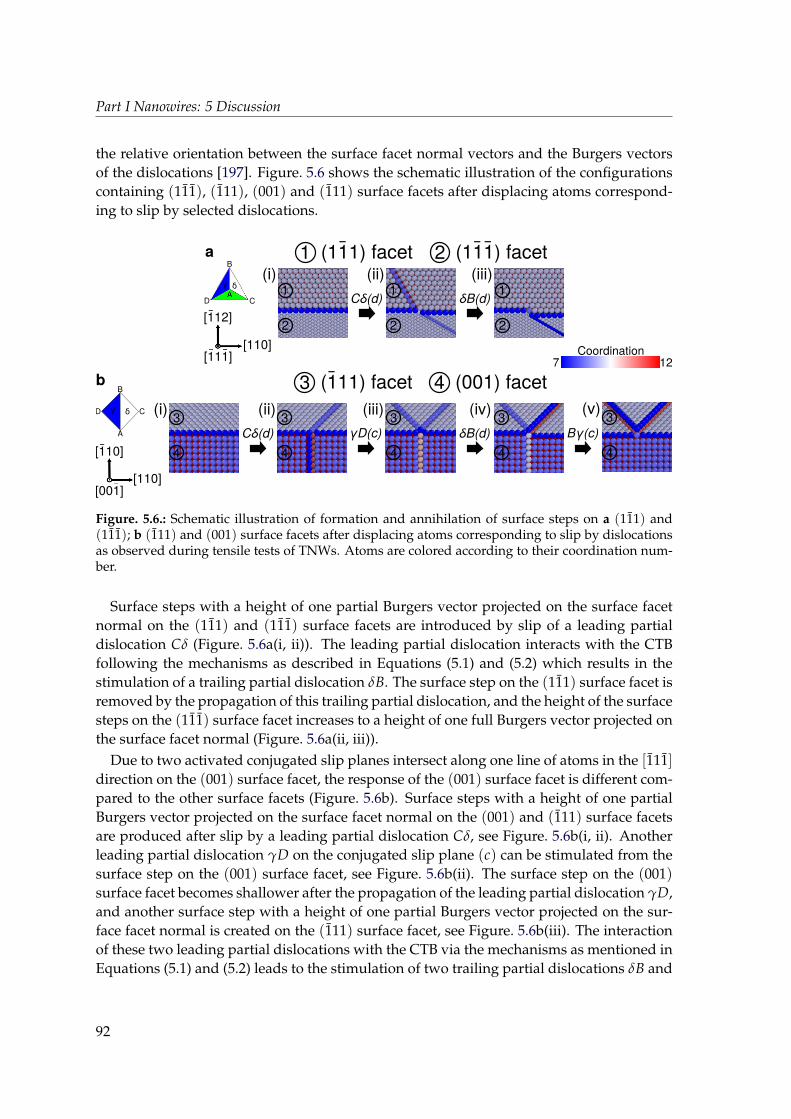
Part I Nanowires: 5 Discussion
the relative orientation between the surface facet normal vectors and the Burgers vectorsof the dislocations [197]. Figure. 5.6 shows the schematic illustration of the configurationscontaining (111), (111), (001) and (111) surface facets after displacing atoms correspond-ing to slip by selected dislocations.
Coordination127
1
2
D
B
C
A
δγ
D
B
C
δγ
Cδ(d) δB(d)
Cδ(d) γD(c) δB(d) Bγ(c)
a
(i) (ii) (iii)
b
(i) (ii) (iii) (iv) (v)
[110]
[110]-
[001]
[110][111]-
[112]-
1 (111) facet-
(111) facet--
2
(001) facet(111) facet-
3 4
1
2
1
2
3
4
3
4
3
4
3
4
3
4
Figure. 5.6.: Schematic illustration of formation and annihilation of surface steps on a (111) and(111); b (111) and (001) surface facets after displacing atoms corresponding to slip by dislocationsas observed during tensile tests of TNWs. Atoms are colored according to their coordination num-ber.
Surface steps with a height of one partial Burgers vector projected on the surface facetnormal on the (111) and (111) surface facets are introduced by slip of a leading partialdislocation Cδ (Figure. 5.6a(i, ii)). The leading partial dislocation interacts with the CTBfollowing the mechanisms as described in Equations (5.1) and (5.2) which results in thestimulation of a trailing partial dislocation δB. The surface step on the (111) surface facet isremoved by the propagation of this trailing partial dislocation, and the height of the surfacesteps on the (111) surface facet increases to a height of one full Burgers vector projected onthe surface facet normal (Figure. 5.6a(ii, iii)).
Due to two activated conjugated slip planes intersect along one line of atoms in the [111]direction on the (001) surface facet, the response of the (001) surface facet is different com-pared to the other surface facets (Figure. 5.6b). Surface steps with a height of one partialBurgers vector projected on the surface facet normal on the (001) and (111) surface facetsare produced after slip by a leading partial dislocation Cδ, see Figure. 5.6b(i, ii). Anotherleading partial dislocation γD on the conjugated slip plane (c) can be stimulated from thesurface step on the (001) surface facet, see Figure. 5.6b(ii). The surface step on the (001)surface facet becomes shallower after the propagation of the leading partial dislocation γD,and another surface step with a height of one partial Burgers vector projected on the sur-face facet normal is created on the (111) surface facet, see Figure. 5.6b(iii). The interactionof these two leading partial dislocations with the CTB via the mechanisms as mentioned inEquations (5.1) and (5.2) leads to the stimulation of two trailing partial dislocations δB and
92
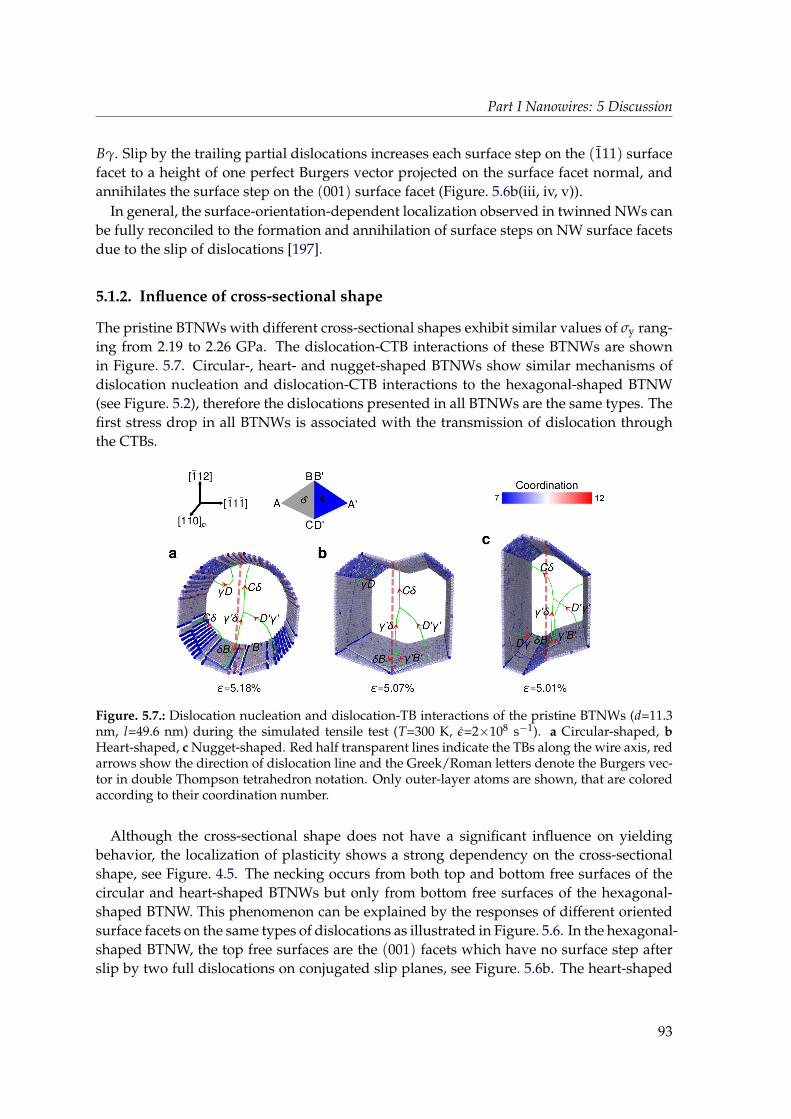
Part I Nanowires: 5 Discussion
Bγ. Slip by the trailing partial dislocations increases each surface step on the (111) surfacefacet to a height of one perfect Burgers vector projected on the surface facet normal, andannihilates the surface step on the (001) surface facet (Figure. 5.6b(iii, iv, v)).
In general, the surface-orientation-dependent localization observed in twinned NWs canbe fully reconciled to the formation and annihilation of surface steps on NW surface facetsdue to the slip of dislocations [197].
5.1.2. Influence of cross-sectional shape
The pristine BTNWs with different cross-sectional shapes exhibit similar values of σy rang-ing from 2.19 to 2.26 GPa. The dislocation-CTB interactions of these BTNWs are shownin Figure. 5.7. Circular-, heart- and nugget-shaped BTNWs show similar mechanisms ofdislocation nucleation and dislocation-CTB interactions to the hexagonal-shaped BTNW(see Figure. 5.2), therefore the dislocations presented in all BTNWs are the same types. Thefirst stress drop in all BTNWs is associated with the transmission of dislocation throughthe CTBs.
Dγγ'B'
D'γ'
Cδ
D'γ'
γ'B'
Cδ
γD Cδ
D'γ'
γ'B'
γD
ε=5.18%
Figure. 5.7.: Dislocation nucleation and dislocation-TB interactions of the pristine BTNWs (d=11.3nm, l=49.6 nm) during the simulated tensile test (T=300 K, ε=2×10⁸ s−1). a Circular-shaped, bHeart-shaped, c Nugget-shaped. Red half transparent lines indicate the TBs along the wire axis, redarrows show the direction of dislocation line and the Greek/Roman letters denote the Burgers vec-tor in double Thompson tetrahedron notation. Only outer-layer atoms are shown, that are coloredaccording to their coordination number.
Although the cross-sectional shape does not have a significant influence on yieldingbehavior, the localization of plasticity shows a strong dependency on the cross-sectionalshape, see Figure. 4.5. The necking occurs from both top and bottom free surfaces of thecircular and heart-shaped BTNWs but only from bottom free surfaces of the hexagonal-shaped BTNW. This phenomenon can be explained by the responses of different orientedsurface facets on the same types of dislocations as illustrated in Figure. 5.6. In the hexagonal-shaped BTNW, the top free surfaces are the (001) facets which have no surface step afterslip by two full dislocations on conjugated slip planes, see Figure. 5.6b. The heart-shaped
93
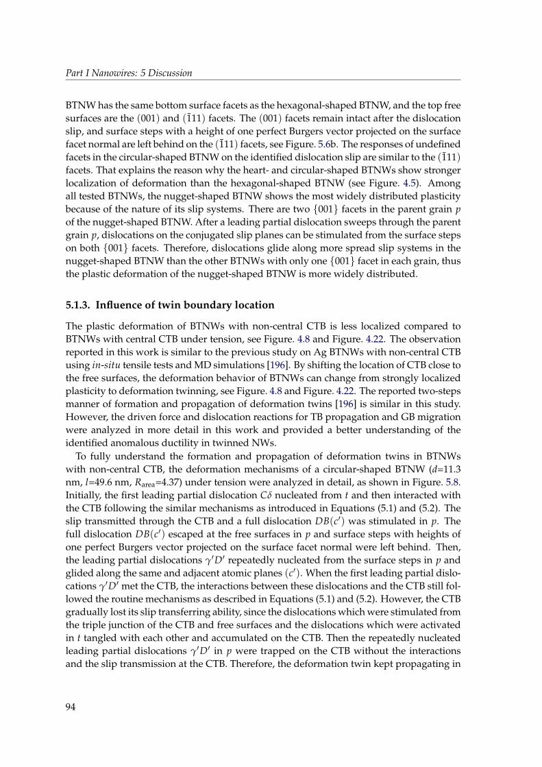
Part I Nanowires: 5 Discussion
BTNW has the same bottom surface facets as the hexagonal-shaped BTNW, and the top freesurfaces are the (001) and (111) facets. The (001) facets remain intact after the dislocationslip, and surface steps with a height of one perfect Burgers vector projected on the surfacefacet normal are left behind on the (111) facets, see Figure. 5.6b. The responses of undefinedfacets in the circular-shaped BTNW on the identified dislocation slip are similar to the (111)facets. That explains the reason why the heart- and circular-shaped BTNWs show strongerlocalization of deformation than the hexagonal-shaped BTNW (see Figure. 4.5). Amongall tested BTNWs, the nugget-shaped BTNW shows the most widely distributed plasticitybecause of the nature of its slip systems. There are two 001 facets in the parent grain pof the nugget-shaped BTNW. After a leading partial dislocation sweeps through the parentgrain p, dislocations on the conjugated slip planes can be stimulated from the surface stepson both 001 facets. Therefore, dislocations glide along more spread slip systems in thenugget-shaped BTNW than the other BTNWs with only one 001 facet in each grain, thusthe plastic deformation of the nugget-shaped BTNW is more widely distributed.
5.1.3. Influence of twin boundary location
The plastic deformation of BTNWs with non-central CTB is less localized compared toBTNWs with central CTB under tension, see Figure. 4.8 and Figure. 4.22. The observationreported in this work is similar to the previous study on Ag BTNWs with non-central CTBusing in-situ tensile tests and MD simulations [196]. By shifting the location of CTB close tothe free surfaces, the deformation behavior of BTNWs can change from strongly localizedplasticity to deformation twinning, see Figure. 4.8 and Figure. 4.22. The reported two-stepsmanner of formation and propagation of deformation twins [196] is similar in this study.However, the driven force and dislocation reactions for TB propagation and GB migrationwere analyzed in more detail in this work and provided a better understanding of theidentified anomalous ductility in twinned NWs.
To fully understand the formation and propagation of deformation twins in BTNWswith non-central CTB, the deformation mechanisms of a circular-shaped BTNW (d=11.3nm, l=49.6 nm, Rarea=4.37) under tension were analyzed in detail, as shown in Figure. 5.8.Initially, the first leading partial dislocation Cδ nucleated from t and then interacted withthe CTB following the similar mechanisms as introduced in Equations (5.1) and (5.2). Theslip transmitted through the CTB and a full dislocation DB(c′) was stimulated in p. Thefull dislocation DB(c′) escaped at the free surfaces in p and surface steps with heights ofone perfect Burgers vector projected on the surface facet normal were left behind. Then,the leading partial dislocations γ′D′ repeatedly nucleated from the surface steps in p andglided along the same and adjacent atomic planes (c′). When the first leading partial dislo-cations γ′D′ met the CTB, the interactions between these dislocations and the CTB still fol-lowed the routine mechanisms as described in Equations (5.1) and (5.2). However, the CTBgradually lost its slip transferring ability, since the dislocations which were stimulated fromthe triple junction of the CTB and free surfaces and the dislocations which were activatedin t tangled with each other and accumulated on the CTB. Then the repeatedly nucleatedleading partial dislocations γ′D′ in p were trapped on the CTB without the interactionsand the slip transmission at the CTB. Therefore, the deformation twin kept propagating in
94
Part I Nanowires: 5 Discussion
p as reported in the [110]-oriented SCNWs under tension (Figure. 4.1b).
[110]p
[111]- -
B'B
A' δ' γ
C'D
A
[112]-
t=210 ps
ε=4.29%
[110]p
[111]- -
B'B
A' δ' γ
C'D
A
[112]-
t=224 ps
ε=4.58%
t=233.5 ps
ε=4.78%
t=242.5 ps
ε=4.97%
t=257 ps
ε=5.72%
t=286.5 ps
ε=5.90%
t=295.5 ps
ε=6.09%
t=298.5 ps
ε=6.15%
Twin
γ'D'γ'D'
γ'D'
γ'D' γ'D'
γ'D'
γ'D'γ'D'
t=350 ps
ε=7.25%
t=400 ps
ε=8.33%
t=450 ps
ε=9.42%
GB
GB
GBTB2
TB2
TB
1
TB2
TB2
TB
1
γ'D'
α'D
'
γ'α'
p t
[101]-
[101]-
γ'D'
γ'D'
a
b
p t
γ'α'Cα
γ'D'
c d
Figure. 5.8.: Deformation mechanisms of circular-shaped BTNW with non-central TB (d=11.3 nm,l=49.6 nm, Rarea=4.37) during the simulated tensile test (T=300 K, ε=2×10⁸ s−1). a Growth of de-formation twin in the parent grain p. Only outer-layer atoms and atoms that make up the TB anddefects are shown. Atoms are half transparent and colored according to their coordination number.b Propagation of a deformation twin from p to the twin grain t. NW is sliced from the center alongthe (101) plane. Atoms are colored according to the CNA analysis, green, red and white atomsindicate atoms in FCC-type, HCP-type and Other-type structures, respectively.
After the accumulation of certain numbers of dislocations, the CTB lost its coherencyand transformed into a GB, see Figure. 5.8b, similar mechanisms were reported in previousstudies on nano-twinned metals [275–278]. During the remaining deformation process, theleading partial dislocations γ′D′ repeatedly nucleated in p, which led to the growth ofthe deformation twin in p. Then, each trapped dislocation γ′D′ dissociated into a partialdislocation α′D′ and a stair-rod dislocation γ′α′ on the TB1, as shown in Figure. 5.8c:
γ′D′ → α′D′ + γ′α′ . (5.4)
95
Part I Nanowires: 5 Discussion
The partial dislocation α′D′ moved along the TB1 and de-twinned the smaller grain t. Thestair-rod dislocation γ′α′ dissociated into a partial dislocation Cα in t and another partialdislocation γ′D′ at the junction of TBs and GB, see Figure. 5.8d:
γ′α′ → Cα + γ′D′ . (5.5)
The partial dislocation Cα moved along the TB1 to continuously de-twin t and the de-twinned matrix transformed into a part of the deformation twin by partial dislocation γ′D′.The formation of the deformation twin induced bending moment in p and the magnitudeof the internal bending stress increased with increasing twin length [61, 62]. The continu-ous activation of the leading partial dislocations γ′D′ in p was stimulated by the internalbending stress. Meanwhile, the internal bending stress impelled the migration of the GB,thus the deformation twin transmitted into t during the deformation process. This phe-nomenon was also observed in the larger BTNW (d=32.3 nm, Rarea=4.37), see Figure. A.1in Appendix, which could be relevant to the ratio of the second moments of area betweencross-sections of t and p.
De-twinning via secondary twins and stacking faults has been reported in the FCC nano-twinned metals with relatively low stacking fault energy [275–279]. After the de-twinningprocesses in nano-twinned metals, the secondary twins were highly faulted and the pri-mary TB usually transformed into a GB or an amorphous area with lots of pinned disloca-tions. Here, the deformation twins can penetrate into the thinner grain without disorderinterface and area inside of the secondary twins. The differences can be reasoned as fol-lows. Twinned NWs have free surfaces where dislocations can escape and then releaselocal strain energy, therefore dislocations are less likely to tangle with each other comparedwith nano-twinned metals.
5.1.4. Comparison with experiments
The tensile experiments on Au MTNWs were performed by Jungho Shin (University ofCalifornia Santa Barbara, Materials Department). Parts of the following results and discus-sion have been published in [197].
Deformation twinning was observed in simulated [110]-oriented SCNWs under tension,which agrees well with previous experimental and simulation observations [21, 61–63, 107–109, 114]. The different resolved shear stresses on leading and trailing partial dislocationscan explain the occurrence of deformation twinning [62, 114]. In [110]-oriented NWs un-der tension, since the Schmid factors for the leading and trailing partial dislocations on theprimary slip systems are 0.471 and 0.236, respectively, the resolved shear stress of the lead-ing partial dislocation is two times higher than the trailing partial dislocation. Therefore,the leading partial dislocations on adjacent slip planes keep nucleating in a self-stimulatedmanner and leads to the growth of deformation twins in the [110]-oriented SCNWs [61, 62].
The simulated MTNW was constructed based on the size of each twin segment deter-mined in the experimental sample, see Figure. 2.13a. Similar to the correlative in-situ ten-sile tests, the elastic response of the simulated MTNWs is similar to the SCNWs and theyield strength of the rough MTNW is higher than the single crystalline counterpart. After
96
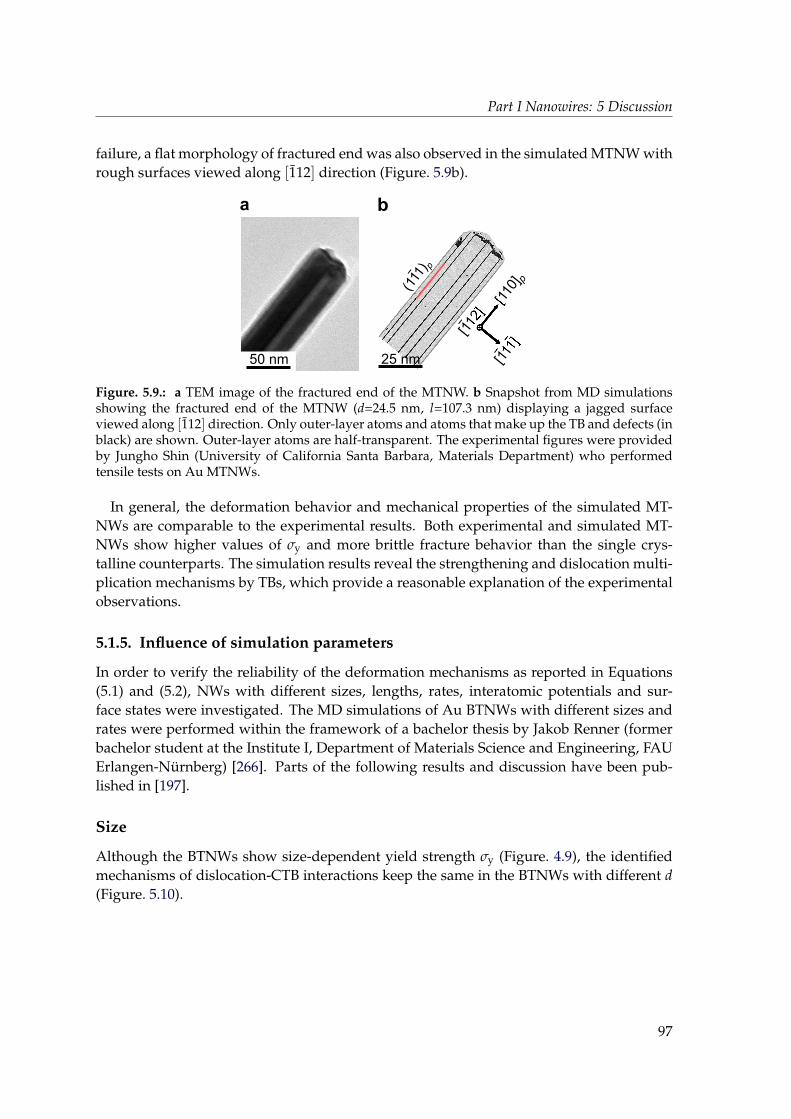
Part I Nanowires: 5 Discussion
failure, a flat morphology of fractured end was also observed in the simulated MTNW withrough surfaces viewed along [112] direction (Figure. 5.9b).
b
(111
) p-
25 nm [11-
[112-
[110
] p
50 nm
a
Figure. 5.9.: a TEM image of the fractured end of the MTNW. b Snapshot from MD simulationsshowing the fractured end of the MTNW (d=24.5 nm, l=107.3 nm) displaying a jagged surfaceviewed along [112] direction. Only outer-layer atoms and atoms that make up the TB and defects (inblack) are shown. Outer-layer atoms are half-transparent. The experimental figures were providedby Jungho Shin (University of California Santa Barbara, Materials Department) who performedtensile tests on Au MTNWs.
In general, the deformation behavior and mechanical properties of the simulated MT-NWs are comparable to the experimental results. Both experimental and simulated MT-NWs show higher values of σy and more brittle fracture behavior than the single crys-talline counterparts. The simulation results reveal the strengthening and dislocation multi-plication mechanisms by TBs, which provide a reasonable explanation of the experimentalobservations.
5.1.5. Influence of simulation parameters
In order to verify the reliability of the deformation mechanisms as reported in Equations(5.1) and (5.2), NWs with different sizes, lengths, rates, interatomic potentials and sur-face states were investigated. The MD simulations of Au BTNWs with different sizes andrates were performed within the framework of a bachelor thesis by Jakob Renner (formerbachelor student at the Institute I, Department of Materials Science and Engineering, FAUErlangen-Nurnberg) [266]. Parts of the following results and discussion have been pub-lished in [197].
Size
Although the BTNWs show size-dependent yield strength σy (Figure. 4.9), the identifiedmechanisms of dislocation-CTB interactions keep the same in the BTNWs with different d(Figure. 5.10).
97
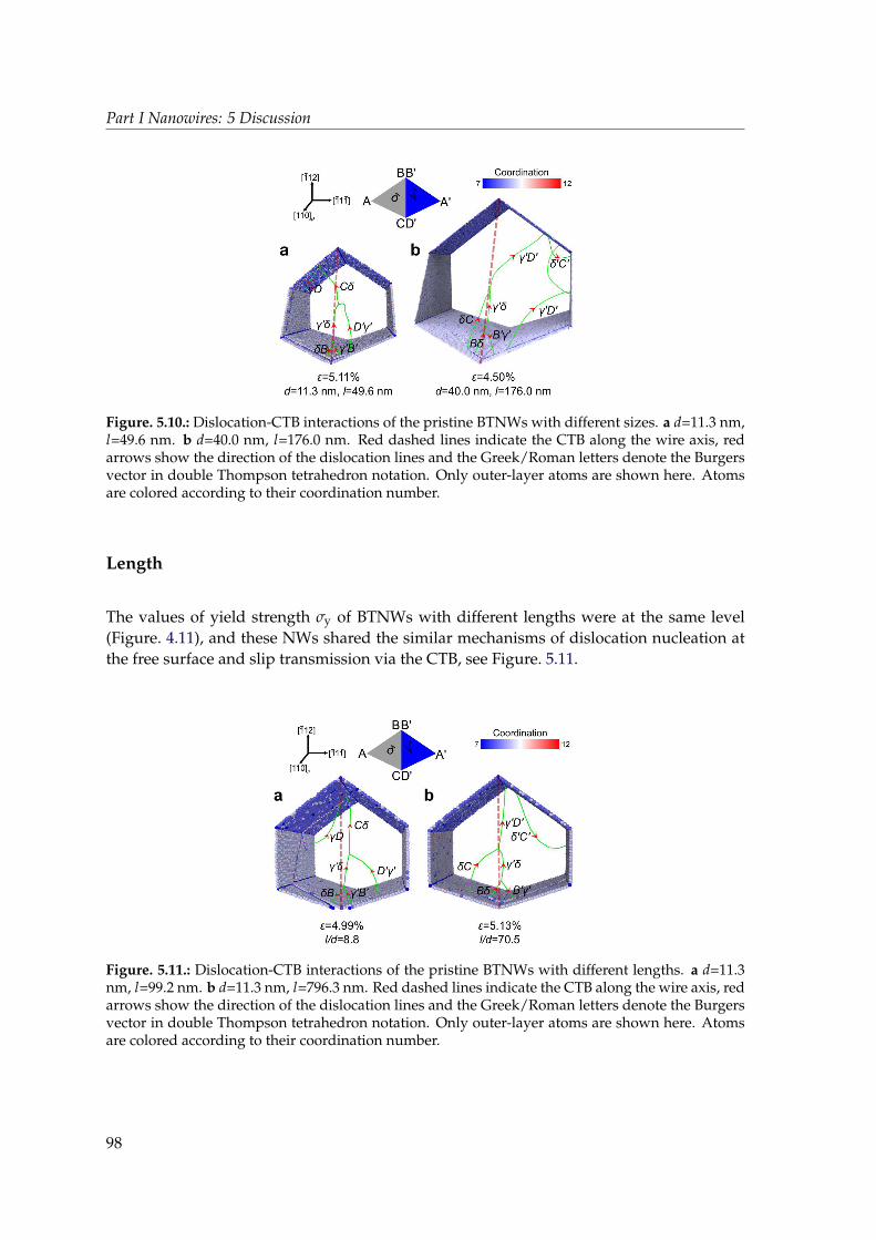
Part I Nanowires: 5 Discussion
D''
B 'B'
D
Figure. 5.10.: Dislocation-CTB interactions of the pristine BTNWs with different sizes. a d=11.3 nm,l=49.6 nm. b d=40.0 nm, l=176.0 nm. Red dashed lines indicate the CTB along the wire axis, redarrows show the direction of the dislocation lines and the Greek/Roman letters denote the Burgersvector in double Thompson tetrahedron notation. Only outer-layer atoms are shown here. Atomsare colored according to their coordination number.
Length
The values of yield strength σy of BTNWs with different lengths were at the same level(Figure. 4.11), and these NWs shared the similar mechanisms of dislocation nucleation atthe free surface and slip transmission via the CTB, see Figure. 5.11.
ε=4.99%
l/d=8.8
Cδ
D'γ'
δB γ'B'
ε=5.13%
l/d=70.5
γ'D'
γ'δ
B'γ'
δC
δ'C'
Bδ
Figure. 5.11.: Dislocation-CTB interactions of the pristine BTNWs with different lengths. a d=11.3nm, l=99.2 nm. b d=11.3 nm, l=796.3 nm. Red dashed lines indicate the CTB along the wire axis, redarrows show the direction of the dislocation lines and the Greek/Roman letters denote the Burgersvector in double Thompson tetrahedron notation. Only outer-layer atoms are shown here. Atomsare colored according to their coordination number.
98
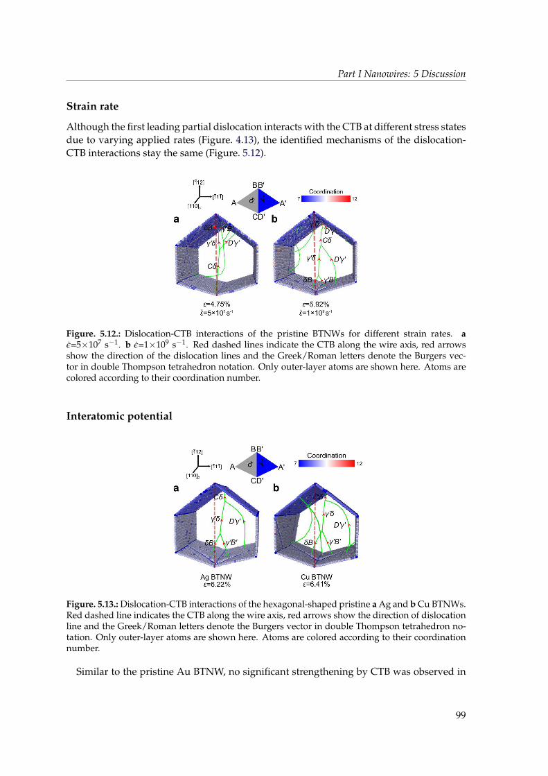
Part I Nanowires: 5 Discussion
Strain rate
Although the first leading partial dislocation interacts with the CTB at different stress statesdue to varying applied rates (Figure. 4.13), the identified mechanisms of the dislocation-CTB interactions stay the same (Figure. 5.12).
D''
B 'B'
C
'B'
D''
D''
ε=4.75%
ε=5×10⁷ s
-1
Figure. 5.12.: Dislocation-CTB interactions of the pristine BTNWs for different strain rates. aε=5×10⁷ s−1. b ε=1×10⁹ s−1. Red dashed lines indicate the CTB along the wire axis, red arrowsshow the direction of the dislocation lines and the Greek/Roman letters denote the Burgers vec-tor in double Thompson tetrahedron notation. Only outer-layer atoms are shown here. Atoms arecolored according to their coordination number.
Interatomic potential
Ag BTNW =6.22%
Cu BTNW =6.41%
C
γ'
B γ
Dγ
Figure. 5.13.: Dislocation-CTB interactions of the hexagonal-shaped pristine a Ag and b Cu BTNWs.Red dashed line indicates the CTB along the wire axis, red arrows show the direction of dislocationline and the Greek/Roman letters denote the Burgers vector in double Thompson tetrahedron no-tation. Only outer-layer atoms are shown here. Atoms are colored according to their coordinationnumber.
Similar to the pristine Au BTNW, no significant strengthening by CTB was observed in
99
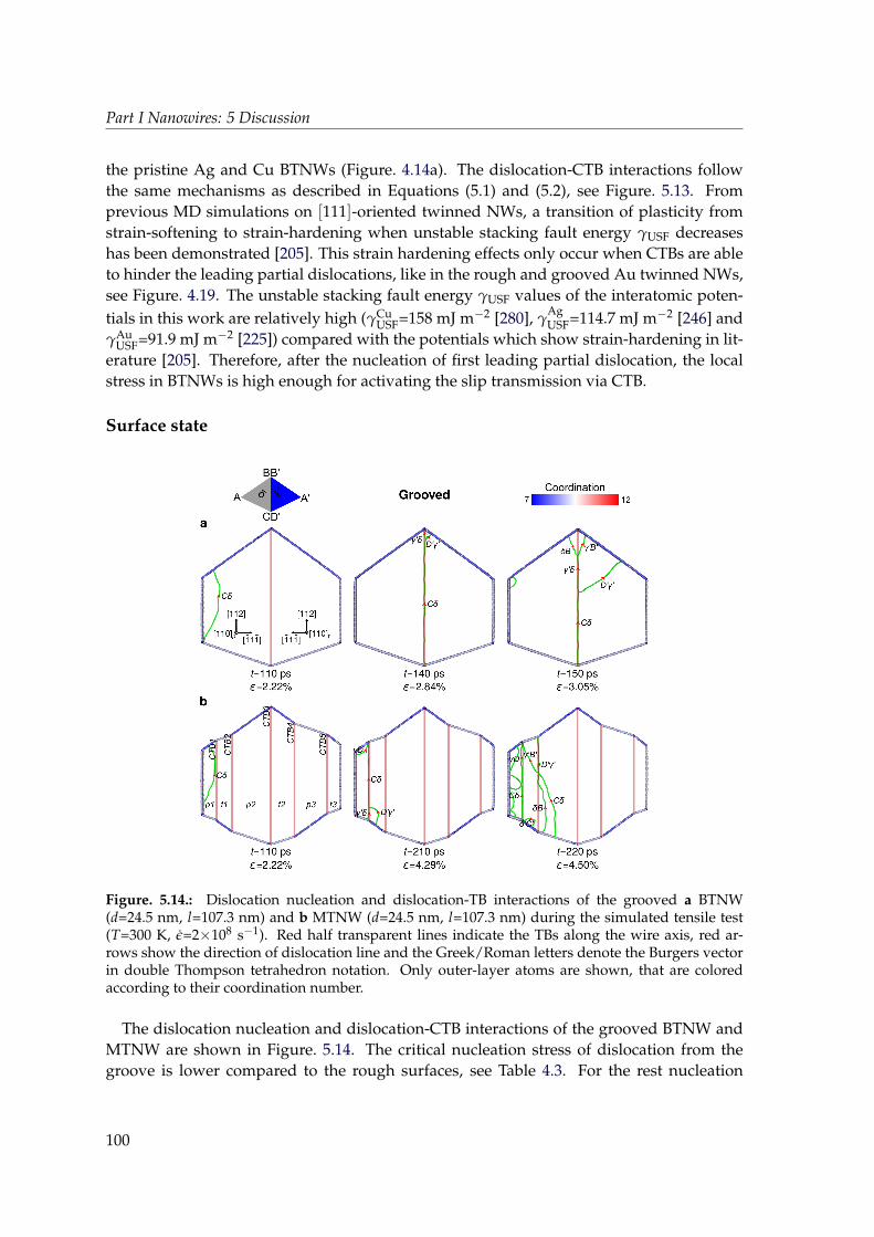
Part I Nanowires: 5 Discussion
the pristine Ag and Cu BTNWs (Figure. 4.14a). The dislocation-CTB interactions followthe same mechanisms as described in Equations (5.1) and (5.2), see Figure. 5.13. Fromprevious MD simulations on [111]-oriented twinned NWs, a transition of plasticity fromstrain-softening to strain-hardening when unstable stacking fault energy γUSF decreaseshas been demonstrated [205]. This strain hardening effects only occur when CTBs are ableto hinder the leading partial dislocations, like in the rough and grooved Au twinned NWs,see Figure. 4.19. The unstable stacking fault energy γUSF values of the interatomic poten-tials in this work are relatively high (γCu
USF=158 mJ m−2 [280], γAgUSF=114.7 mJ m−2 [246] and
γAuUSF=91.9 mJ m−2 [225]) compared with the potentials which show strain-hardening in lit-
erature [205]. Therefore, after the nucleation of first leading partial dislocation, the localstress in BTNWs is high enough for activating the slip transmission via CTB.
Surface state
Figure. 5.14.: Dislocation nucleation and dislocation-TB interactions of the grooved a BTNW(d=24.5 nm, l=107.3 nm) and b MTNW (d=24.5 nm, l=107.3 nm) during the simulated tensile test(T=300 K, ε=2×10⁸ s−1). Red half transparent lines indicate the TBs along the wire axis, red ar-rows show the direction of dislocation line and the Greek/Roman letters denote the Burgers vectorin double Thompson tetrahedron notation. Only outer-layer atoms are shown, that are coloredaccording to their coordination number.
The dislocation nucleation and dislocation-CTB interactions of the grooved BTNW andMTNW are shown in Figure. 5.14. The critical nucleation stress of dislocation from thegroove is lower compared to the rough surfaces, see Table 4.3. For the rest nucleation
100
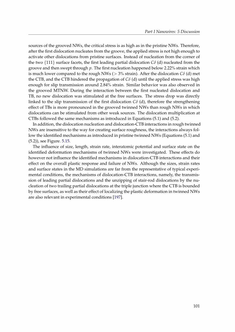
Part I Nanowires: 5 Discussion
sources of the grooved NWs, the critical stress is as high as in the pristine NWs. Therefore,after the first dislocation nucleates from the groove, the applied stress is not high enough toactivate other dislocations from pristine surfaces. Instead of nucleation from the corner ofthe two 111 surface facets, the first leading partial dislocation Cδ (d) nucleated from thegroove and then swept through p. The first nucleation happened below 2.22% strain whichis much lower compared to the rough NWs (> 3% strain). After the dislocation Cδ (d) metthe CTB, and the CTB hindered the propagation of Cδ (d) until the applied stress was highenough for slip transmission around 2.84% strain. Similar behavior was also observed inthe grooved MTNW. During the interaction between the first nucleated dislocation andTB, no new dislocation was stimulated at the free surfaces. The stress drop was directlylinked to the slip transmission of the first dislocation Cδ (d), therefore the strengtheningeffect of TBs is more pronounced in the grooved twinned NWs than rough NWs in whichdislocations can be stimulated from other weak sources. The dislocation multiplication atCTBs followed the same mechanisms as introduced in Equations (5.1) and (5.2).
In addition, the dislocation nucleation and dislocation-CTB interactions in rough twinnedNWs are insensitive to the way for creating surface roughness, the interactions always fol-low the identified mechanisms as introduced in pristine twinned NWs (Equations (5.1) and(5.2)), see Figure. 5.15.
The influence of size, length, strain rate, interatomic potential and surface state on theidentified deformation mechanisms of twinned NWs were investigated. These effects dohowever not influence the identified mechanisms in dislocation-CTB interactions and theireffect on the overall plastic response and failure of NWs. Although the sizes, strain ratesand surface states in the MD simulations are far from the representative of typical experi-mental conditions, the mechanisms of dislocation-CTB interactions, namely, the transmis-sion of leading partial dislocations and the unzipping of stair-rod dislocations by the nu-cleation of two trailing partial dislocations at the triple junction where the CTB is boundedby free surfaces, as well as their effect of localizing the plastic deformation in twinned NWsare also relevant in experimental conditions [197].
101
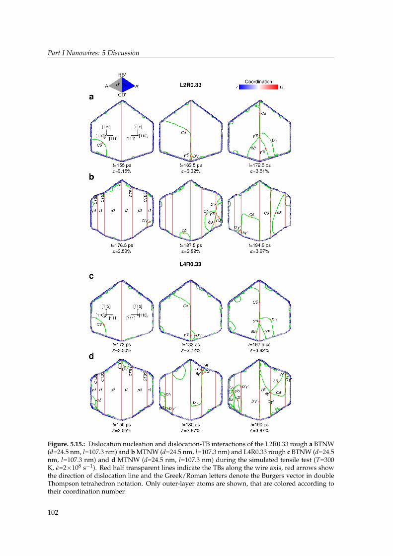
Part I Nanowires: 5 Discussion
Figure. 5.15.: Dislocation nucleation and dislocation-TB interactions of the L2R0.33 rough a BTNW(d=24.5 nm, l=107.3 nm) and b MTNW (d=24.5 nm, l=107.3 nm) and L4R0.33 rough c BTNW (d=24.5nm, l=107.3 nm) and d MTNW (d=24.5 nm, l=107.3 nm) during the simulated tensile test (T=300K, ε=2×10⁸ s−1). Red half transparent lines indicate the TBs along the wire axis, red arrows showthe direction of dislocation line and the Greek/Roman letters denote the Burgers vector in doubleThompson tetrahedron notation. Only outer-layer atoms are shown, that are colored according totheir coordination number.
102
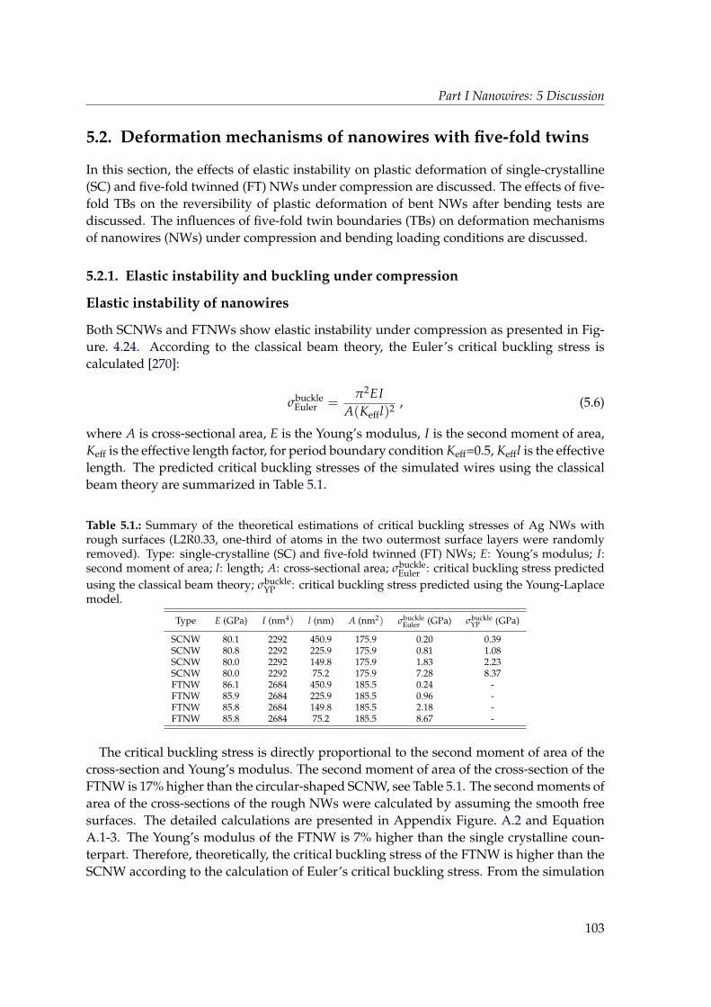
Part I Nanowires: 5 Discussion
5.2. Deformation mechanisms of nanowires with five-fold twins
In this section, the effects of elastic instability on plastic deformation of single-crystalline(SC) and five-fold twinned (FT) NWs under compression are discussed. The effects of five-fold TBs on the reversibility of plastic deformation of bent NWs after bending tests arediscussed. The influences of five-fold twin boundaries (TBs) on deformation mechanismsof nanowires (NWs) under compression and bending loading conditions are discussed.
5.2.1. Elastic instability and buckling under compression
Elastic instability of nanowires
Both SCNWs and FTNWs show elastic instability under compression as presented in Fig-ure. 4.24. According to the classical beam theory, the Euler’s critical buckling stress iscalculated [270]:
σbuckleEuler =
π2EIA(Keffl)2 , (5.6)
where A is cross-sectional area, E is the Young’s modulus, I is the second moment of area,Keff is the effective length factor, for period boundary condition Keff=0.5, Keffl is the effectivelength. The predicted critical buckling stresses of the simulated wires using the classicalbeam theory are summarized in Table 5.1.
Table 5.1.: Summary of the theoretical estimations of critical buckling stresses of Ag NWs withrough surfaces (L2R0.33, one-third of atoms in the two outermost surface layers were randomlyremoved). Type: single-crystalline (SC) and five-fold twinned (FT) NWs; E: Young’s modulus; I:second moment of area; l: length; A: cross-sectional area; σbuckle
Euler : critical buckling stress predictedusing the classical beam theory; σbuckle
YP : critical buckling stress predicted using the Young-Laplacemodel.
Type E (GPa) I (nm4) l (nm) A (nm2) σbuckleEuler (GPa) σbuckle
YP (GPa)
SCNW 80.1 2292 450.9 175.9 0.20 0.39SCNW 80.8 2292 225.9 175.9 0.81 1.08SCNW 80.0 2292 149.8 175.9 1.83 2.23SCNW 80.0 2292 75.2 175.9 7.28 8.37FTNW 86.1 2684 450.9 185.5 0.24 -FTNW 85.9 2684 225.9 185.5 0.96 -FTNW 85.8 2684 149.8 185.5 2.18 -FTNW 85.8 2684 75.2 185.5 8.67 -
The critical buckling stress is directly proportional to the second moment of area of thecross-section and Young’s modulus. The second moment of area of the cross-section of theFTNW is 17% higher than the circular-shaped SCNW, see Table 5.1. The second moments ofarea of the cross-sections of the rough NWs were calculated by assuming the smooth freesurfaces. The detailed calculations are presented in Appendix Figure. A.2 and EquationA.1-3. The Young’s modulus of the FTNW is 7% higher than the single crystalline coun-terpart. Therefore, theoretically, the critical buckling stress of the FTNW is higher than theSCNW according to the calculation of Euler’s critical buckling stress. From the simulation
103
Part I Nanowires: 5 Discussion
results, the SCNW exhibits weaker load-bearing ability compared to the FTNW with sim-ilar length, see Figure. 4.31a and Figure. 4.32a, which agree with the prediction using theclassical beam theory.
a bSCNW FTNW
0
0.2
0.4
0.6
0.8
1
1.2
1.4
0 1 2 3 4 5 6M
agn
itude
of
dis
pla
cem
en
t in
YZ
pla
ne
[Å
]
Stress [GPa]
l=75.2 nml=149.8 nml=225.9 nml=450.9 nm
0
0.2
0.4
0.6
0.8
1
1.2
1.4
0 1 2 3 4 5 6
Ma
gn
itud
e o
f d
isp
lace
me
nt
in Y
Z p
lan
e [
Å]
Stress [GPa]
l=75.2 nml=149.8 nml=225.9 nml=450.9 nm
Figure. 5.16.: Average magnitude of transverse displacement of atomic-based central lines in YZplane as function of applied stress: a SCNWs (d=15.2 nm, l=450.9, 225.9, 149.8, 75.2 nm), b FTNWs(d=15.2 nm, l=450.9, 225.9, 149.8, 75.2 nm) with rough surfaces (L2R0.33, one-third of atoms in thetwo outermost surface layers were randomly removed).
The critical buckling stresses of the wires can be measured by characterizing the averagemagnitude of transverse displacement of the atomic-based central line (Figure. 5.16). Atthe beginning of the elastic deformation, the central lines of all wires fluctuated around0.2 A transverse displacement, see Figure. 5.16. The critical buckling stress is ill definedin these MD simulations due to the thermal fluctuation at 300 K. However, the observedtrends, such as the longer wire shows earlier elastic buckling and the SCNWs show earlierelastic buckling than FTNWs, keep consistent with the theoretical prediction.
More sophisticated buckling models [281–283] were developed by integrating the classi-cal beam theory with the linear surface elasticity theory [284]. The surface stress which wasdemonstrated to play a significant role in the mechanical behavior of nano-objects [42, 45]is taken into account in these models. Based on the Young-Laplace model [281, 282], thecritical load of axial buckling of a circular-shaped nanowire can be solved as:
FbuckleYL =
π2(EI)∗
(Keffl)2 + H, (5.7)
where (EI)∗ is the effective flexural rigidity, for circular-shaped wire (EI)∗ = 164 πEd4 +
18 πEsd3, Es represents surface stiffness, d is the diameter and E is the Young’s modulus.H is a constant determined by the residual surface stress τ0 and cross-sectional shape,for circular-shaped wire H = 2τ0d. Quasi-static compression tests were performed on acircular-shaped [110]-oriented SCNW (d=15.2 nm, l=14.3 nm), Es and τ0 were calculatedaccording to the method reported in literature [285]:
τ(ε) = γ +∂γ
∂ε, (5.8)
104
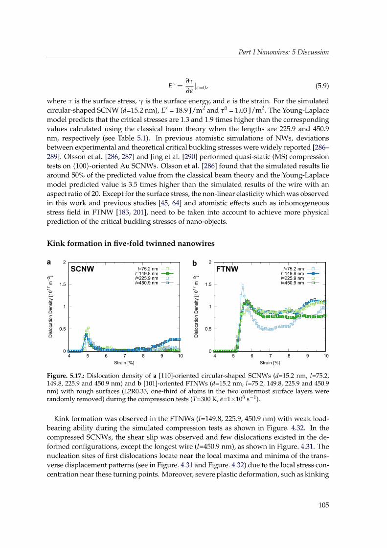
Part I Nanowires: 5 Discussion
Es =∂τ
∂ε|ε=0, (5.9)
where τ is the surface stress, γ is the surface energy, and ε is the strain. For the simulatedcircular-shaped SCNW (d=15.2 nm), Es = 18.9 J/m2 and τ0 = 1.03 J/m2. The Young-Laplacemodel predicts that the critical stresses are 1.3 and 1.9 times higher than the correspondingvalues calculated using the classical beam theory when the lengths are 225.9 and 450.9nm, respectively (see Table 5.1). In previous atomistic simulations of NWs, deviationsbetween experimental and theoretical critical buckling stresses were widely reported [286–289]. Olsson et al. [286, 287] and Jing et al. [290] performed quasi-static (MS) compressiontests on 〈100〉-oriented Au SCNWs. Olsson et al. [286] found that the simulated results liearound 50% of the predicted value from the classical beam theory and the Young-Laplacemodel predicted value is 3.5 times higher than the simulated results of the wire with anaspect ratio of 20. Except for the surface stress, the non-linear elasticity which was observedin this work and previous studies [45, 64] and atomistic effects such as inhomogeneousstress field in FTNW [183, 201], need to be taken into account to achieve more physicalprediction of the critical buckling stresses of nano-objects.
Kink formation in five-fold twinned nanowires
a bSCNW FTNW
0
0.5
1
1.5
2
4 5 6 7 8 9 10
Dis
location D
ensity [10
17
m
2]
Strain [%]
l=75.2 nml=149.8 nml=225.9 nml=450.9 nm
0
0.5
1
1.5
2
4 5 6 7 8 9 10
Dis
location D
ensity [10
17
m
2]
Strain [%]
l=75.2 nml=149.8 nml=225.9 nml=450.9 nm
Figure. 5.17.: Dislocation density of a [110]-oriented circular-shaped SCNWs (d=15.2 nm, l=75.2,149.8, 225.9 and 450.9 nm) and b [101]-oriented FTNWs (d=15.2 nm, l=75.2, 149.8, 225.9 and 450.9nm) with rough surfaces (L2R0.33, one-third of atoms in the two outermost surface layers wererandomly removed) during the compression tests (T=300 K, ε=1×10⁸ s−1).
Kink formation was observed in the FTNWs (l=149.8, 225.9, 450.9 nm) with weak load-bearing ability during the simulated compression tests as shown in Figure. 4.32. In thecompressed SCNWs, the shear slip was observed and few dislocations existed in the de-formed configurations, except the longest wire (l=450.9 nm), as shown in Figure. 4.31. Thenucleation sites of first dislocations locate near the local maxima and minima of the trans-verse displacement patterns (see in Figure. 4.31 and Figure. 4.32) due to the local stress con-centration near these turning points. Moreover, severe plastic deformation, such as kinking
105
Part I Nanowires: 5 Discussion
in FTNWs and shear slip steps in SCNWs, localized at these initial nucleation sites. There-fore, the perturbation which is introduced by the elastic instability has significant effectson consequential initiation and localization of plasticity in NWs.
The localization of plastic deformation in FTNW is different from SCNW. In the SCNWs,the compressive strain was carried by shear slip along the primary slip planes (c) and(d), see Figure. 4.26. As shown in Figure. 5.17a, the dislocation density of the compressedSCNWs remained at a relatively low level after yielding. The dislocation starvation mech-anism [7, 37] was identified in the SCNWs, namely dislocations can easily escape from thefree surfaces without tangling and accumulation. The longest tested SCNWs (l=450.9 nm)exhibited an increase of dislocation density after around 8.5% strain. As shown in Fig-ure. 4.31c, dislocation accumulation and shear slip steps were both observed in the longestSCNW (l=450.9 nm) at 9.52% strain.
The FTNWs show higher dislocation density during the deformation processes than thesingle-crystalline counterparts (see Figure. 5.17b). In contrast to the SCNWs, dislocationsnucleated from the free surfaces interact and tangle with each other by forming disloca-tion interlocks in the FTNWs. The storage of dislocations in the FTNWs is due to thepre-existing TBs and five-fold symmetry of crystallographic arrangement. TBs can hinderdislocation movement and multiply dislocations by dislocation-TB interactions [179, 197]thus twinned NWs show higher dislocation density than the single-crystalline counter-parts, which was also observed in Au twinned NWs Figure. 5.5. In addition to the effect ofTBs, five-fold symmetry of crystallographic arrangement in FTNWs leads to an enclosedcap-like slip system [192], see Appendix Figure. A.3. Dislocations propagate along the con-fined and intersected slip planes tend to interact and tangle with each other. Dislocations,as the main carrier of plastic deformation, are hard to disentangle and escape from thefree surfaces, therefore after dislocations accumulate and saturate in the localized regions,the compressive strain is mainly mediated by bending (see the evolution of stress field ofFTNW during compression test in Figure. 4.28).
The kink formation of Ag FTNW under compression was reported in previous MD sim-ulations [291]. Peng et al. [291] correlated the compression-induced bending of FTNWswith the concentration of plastic deformation. However, this previous study [291] ignoredthe importance of elastic instability, especially the effects of elastic buckling on consequen-tial dislocation nucleation, deformation localization and kink formation, which is demon-strated in this work.
5.2.2. Reversibility of plastic deformation under bending
After load removal, the bent SCNWs and FTNWs show pseudo-elasticity (see Section 4.3)which was also reported in previous studies on FCC [115, 271] and BCC [292] SCNWs.The driving force for the reversible deformation process of bent NWs after load removal isstored elastic energy. The geometrically necessary defects, such as geometrically necessarydislocations (GNDs) and twins (GNTs), and other glissile dislocations can be erased uponunbending. The formation of sessile dislocation locks due to dislocation accumulationand tangle has significant effects on the reversible processes upon unbending. The sessiledefects can not easily escape from the free surfaces after load removal therefore impede
106
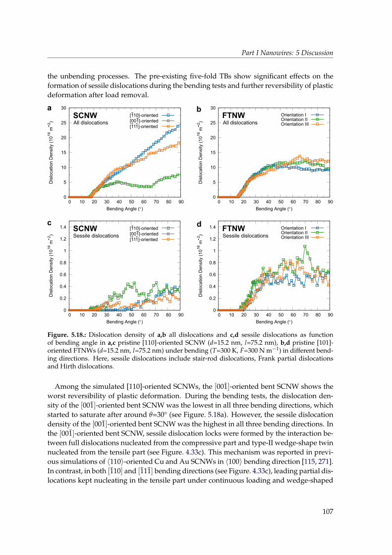
Part I Nanowires: 5 Discussion
the unbending processes. The pre-existing five-fold TBs show significant effects on theformation of sessile dislocations during the bending tests and further reversibility of plasticdeformation after load removal.
a b
dc
FTNW
FTNWSCNW
SCNW
0
5
10
15
20
25
30
0 10 20 30 40 50 60 70 80 90
Dis
loca
tio
n D
en
sity (
10
16
m
2)
Bending Angle ()
Orientation IIOrientation III
Orientation I
0
5
10
15
20
25
30
0 10 20 30 40 50 60 70 80 90D
islo
ca
tio
n D
en
sity (
10
16
m
2)
Bending Angle ()
[110]-oriented
[001]-oriented
[111]-oriented
[110]-oriented
[001]-oriented
[111]-oriented
0
0.2
0.4
0.6
0.8
1
1.2
1.4
0 10 20 30 40 50 60 70 80 90
Dis
location D
ensity (
10
16
m
2)
Bending Angle ()
Orientation IIOrientation III
Orientation I
0
0.2
0.4
0.6
0.8
1
1.2
1.4
0 10 20 30 40 50 60 70 80 90
Dis
location D
ensity (
10
16
m
2)
Bending Angle ()
All dislocations All dislocations
Sessile dislocationsSessile dislocations
Figure. 5.18.: Dislocation density of a,b all dislocations and c,d sessile dislocations as functionof bending angle in a,c pristine [110]-oriented SCNW (d=15.2 nm, l=75.2 nm), b,d pristine [101]-oriented FTNWs (d=15.2 nm, l=75.2 nm) under bending (T=300 K, F=300 N m−1) in different bend-ing directions. Here, sessile dislocations include stair-rod dislocations, Frank partial dislocationsand Hirth dislocations.
Among the simulated [110]-oriented SCNWs, the [001]-oriented bent SCNW shows theworst reversibility of plastic deformation. During the bending tests, the dislocation den-sity of the [001]-oriented bent SCNW was the lowest in all three bending directions, whichstarted to saturate after around θ=30° (see Figure. 5.18a). However, the sessile dislocationdensity of the [001]-oriented bent SCNW was the highest in all three bending directions. Inthe [001]-oriented bent SCNW, sessile dislocation locks were formed by the interaction be-tween full dislocations nucleated from the compressive part and type-II wedge-shape twinnucleated from the tensile part (see Figure. 4.33c). This mechanism was reported in previ-ous simulations of 〈110〉-oriented Cu and Au SCNWs in 〈100〉 bending direction [115, 271].In contrast, in both [110] and [111] bending directions (see Figure. 4.33c), leading partial dis-locations kept nucleating in the tensile part under continuous loading and wedge-shaped
107
Part I Nanowires: 5 Discussion
GNTs formed since they are the energetically most favorable arrangements to accommo-date the strain gradient [115, 292]. In contrast to the dislocation starvation during the simu-lated compression tests of SCNWs (see Figure. 5.17), these geometrically necessary defectswere not able to penetrate through the bent wire because of the high compressive stress onthe other side of the neutral axis. So these glissile dislocations and defects were immobi-lized by the bending stress state and could not escape from the free surfaces, therefore thedislocation density kept increasing during the simulated bending tests in these two bend-ing directions, see Figure. 5.18a. Moreover, limited sessile dislocation locks were formedin these two bending directions, especially before θ=50° (see Figure. 5.18c), therefore, thedetwinning of wedge-shaped GNTs could take place continuously without significant im-pediments from dislocation intersections before the critical θrevers after load removal.
The bent FTNWs show worse reversibility of plastic deformation than the single crys-talline counterparts. The evolution of dislocation densities of the FTNWs is similar in allthree bending orientations and the values are lower than the [110] and [111]-oriented bentSCNWs (see Figure. 5.18b). In addition to the neutral axis, the TBs and compressive stressfield due to the disclination impeded the propagation of dislocations nucleated from thetensile part (see Figure. 4.36b,c). The plasticity in FTNWs is more localized in the centerpart along the wire axis compared to the twin-free counterparts. As shown in Figure. 5.18d,the sessile dislocation densities of the FTNWs started to increase after around θ=20° in allthree bending directions and the values are higher than the SCNWs. After load removal,the glissile dislocations, such as leading partial dislocations nucleated from the tensile partand were immobilized by the TBs and stress field, escaped from the free surfaces (see Fig-ure. 4.39). Grain boundary (GB) which was formed by the accumulation of dislocationsat the interlocked dislocation networks was observed in the compressive part of the bentFTNWs in all bending directions (see Figure. 4.39). The formation of GB impeded the un-bending processes thus worsen the reversibility of plastic deformation in FTNWs.
5.2.3. Resulting microstructures in buckled and bent nanowires
Formation of high-angle grain boundary
In contrast to shear slip in the compressed SCNWs (Figure. 4.26 and Figure. 4.31) andwedge-shaped twinning in the bent SCNWs (Figure. 4.33), strongly localized plastic defor-mation which was mediated by formation of kinks was observed in buckled (Figure. 4.27and Figure. 4.32) and bent (Figure. 4.36) FTNWs. High-angle grain boundaries (GBs) local-ized at the compressive part in the kinked regions.
The accumulation of dislocations at the interlocked dislocation networks leads to theformation of GB in buckled NWs. Under compressive loading the plastic deformation of〈110〉-oriented NW is mainly carried by full dislocations [21, 62, 115]. The first full dislo-cations AB(d) (Aδ(d)+ δB(d)) and AC(d) (Aδ(d)+ δC(d)) nucleated from the free surfaces(see Figure. 5.19a). Dislocations on slip planes (b) and (c) with zero Schmid factor werealso stimulated, which either nucleated at the free surfaces (see Figure. 5.19b, d) or cross-slipped (see Figure. 5.19c, f) from the full dislocations on slip planes (d) (Aδ(d) + δC(d)→Aβ(b) + βC(b)) and (a) (Dα(a) + αB(a)→Dγ(c) + γB(c)). The presence of these struc-
108
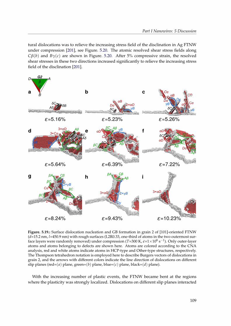
Part I Nanowires: 5 Discussion
tural dislocations was to relieve the increasing stress field of the disclination in Ag FTNWunder compression [201], see Figure. 5.20. The atomic resolved shear stress fields alongCβ(b) and Bγ(c) are shown in Figure. 5.20. After 5% compressive strain, the resolvedshear stresses in these two directions increased significantly to relieve the increasing stressfield of the disclination [201].
δC
AδδB
BδC
B
D
αDαD Cα
Dα
αB C
Cα
Dα
αB
γBδC
2×αD
βC
Aβ
Aβ
Aβ
βC
αD
αD
Cα
Cα
αD
AC
Dα
αC
AδδC
βC
αD
Cα
αD
Cα
αD
AββC
AβAδ
δCδC
Aδ
γB
Aβ
γB Dγ
3×αD
3×Cα
βC
Aβ
βC
AββC
3×Aδ3×δC
3×αD
βA Cβ
2×γB3×αD
Dγ
Aβ
2×αD
βA
βC
βC
AββC
Cα2×γB
Cβ
DααC
Dγ
ε=5.64% ε=6.39% ε=7.22%
ε=8.24% ε=9.43% ε=10.23%
ADG2
β
C
B
ε=5.16% ε=5.26%ε=5.23%
a b c
d e f
g h i
Figure. 5.19.: Surface dislocation nucleation and GB formation in grain 2 of [101]-oriented FTNW(d=15.2 nm, l=450.9 nm) with rough surfaces (L2R0.33, one-third of atoms in the two outermost sur-face layers were randomly removed) under compression (T=300 K, ε=1×10⁸ s−1). Only outer-layeratoms and atoms belonging to defects are shown here. Atoms are colored according to the CNAanalysis, red and white atoms indicate atoms in HCP-type and Other-type structures, respectively.The Thompson tetrahedron notation is employed here to describe Burgers vectors of dislocations ingrain 2, and the arrows with different colors indicate the line direction of dislocations on differentslip planes (red=(a) plane, green=(b) plane, blue=(c) plane, black=(d) plane).
With the increasing number of plastic events, the FTNW became bent at the regionswhere the plasticity was strongly localized. Dislocations on different slip planes interacted
109
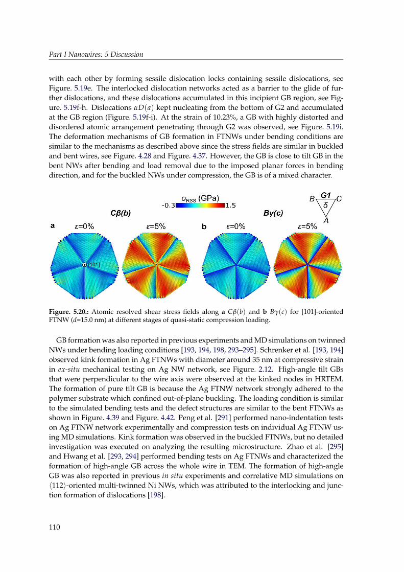
Part I Nanowires: 5 Discussion
with each other by forming sessile dislocation locks containing sessile dislocations, seeFigure. 5.19e. The interlocked dislocation networks acted as a barrier to the glide of fur-ther dislocations, and these dislocations accumulated in this incipient GB region, see Fig-ure. 5.19f-h. Dislocations αD(a) kept nucleating from the bottom of G2 and accumulatedat the GB region (Figure. 5.19f-i). At the strain of 10.23%, a GB with highly distorted anddisordered atomic arrangement penetrating through G2 was observed, see Figure. 5.19i.The deformation mechanisms of GB formation in FTNWs under bending conditions aresimilar to the mechanisms as described above since the stress fields are similar in buckledand bent wires, see Figure. 4.28 and Figure. 4.37. However, the GB is close to tilt GB in thebent NWs after bending and load removal due to the imposed planar forces in bendingdirection, and for the buckled NWs under compression, the GB is of a mixed character.
σRSS (GPa)-0.3 1.5
ε=0% ε=5%
C(b) B(c)
ε=0% ε=5%a b
Figure. 5.20.: Atomic resolved shear stress fields along a Cβ(b) and b Bγ(c) for [101]-orientedFTNW (d=15.0 nm) at different stages of quasi-static compression loading.
GB formation was also reported in previous experiments and MD simulations on twinnedNWs under bending loading conditions [193, 194, 198, 293–295]. Schrenker et al. [193, 194]observed kink formation in Ag FTNWs with diameter around 35 nm at compressive strainin ex-situ mechanical testing on Ag NW network, see Figure. 2.12. High-angle tilt GBsthat were perpendicular to the wire axis were observed at the kinked nodes in HRTEM.The formation of pure tilt GB is because the Ag FTNW network strongly adhered to thepolymer substrate which confined out-of-plane buckling. The loading condition is similarto the simulated bending tests and the defect structures are similar to the bent FTNWs asshown in Figure. 4.39 and Figure. 4.42. Peng et al. [291] performed nano-indentation testson Ag FTNW network experimentally and compression tests on individual Ag FTNW us-ing MD simulations. Kink formation was observed in the buckled FTNWs, but no detailedinvestigation was executed on analyzing the resulting microstructure. Zhao et al. [295]and Hwang et al. [293, 294] performed bending tests on Ag FTNWs and characterized theformation of high-angle GB across the whole wire in TEM. The formation of high-angleGB was also reported in previous in situ experiments and correlative MD simulations on〈112〉-oriented multi-twinned Ni NWs, which was attributed to the interlocking and junc-tion formation of dislocations [198].
110
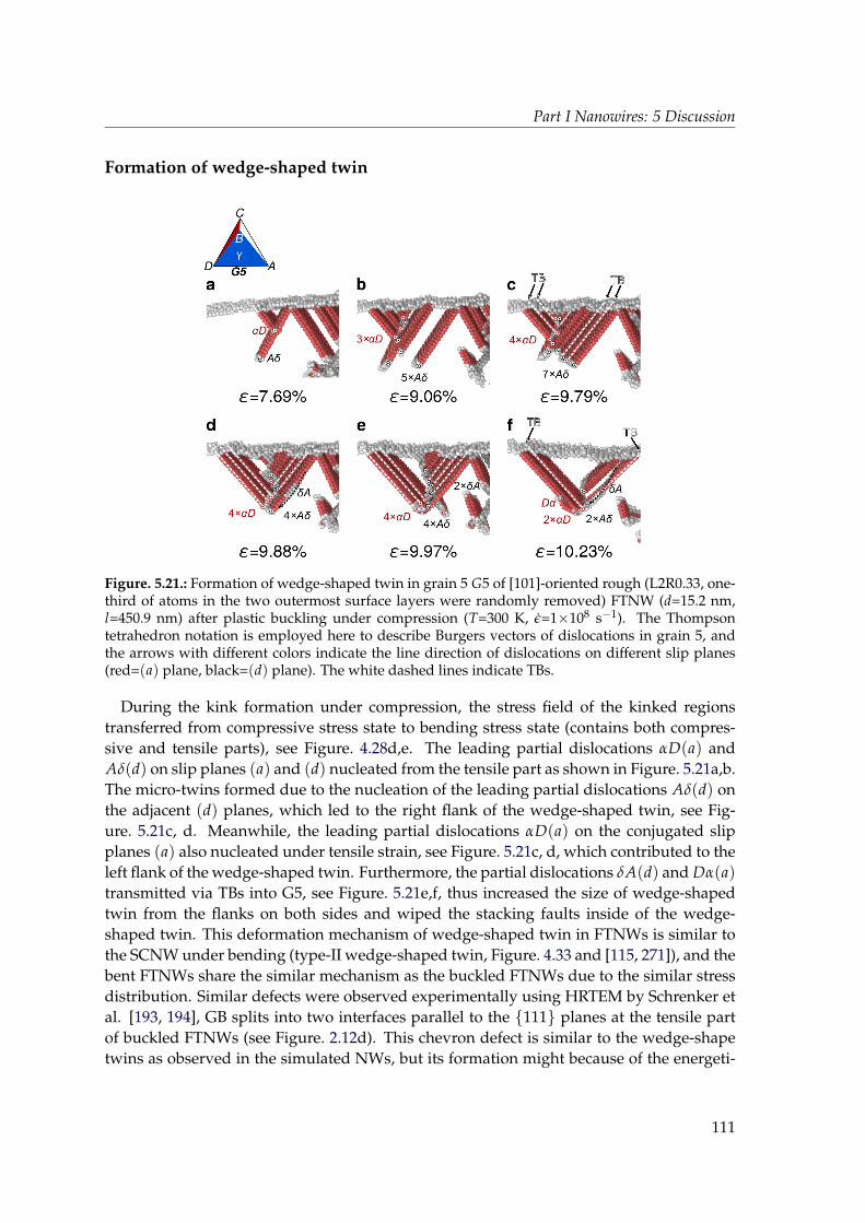
Part I Nanowires: 5 Discussion
Formation of wedge-shaped twin
αD
Aδ
3×αD
5×Aδ
Figure. 5.21.: Formation of wedge-shaped twin in grain 5 G5 of [101]-oriented rough (L2R0.33, one-third of atoms in the two outermost surface layers were randomly removed) FTNW (d=15.2 nm,l=450.9 nm) after plastic buckling under compression (T=300 K, ε=1×10⁸ s−1). The Thompsontetrahedron notation is employed here to describe Burgers vectors of dislocations in grain 5, andthe arrows with different colors indicate the line direction of dislocations on different slip planes(red=(a) plane, black=(d) plane). The white dashed lines indicate TBs.
During the kink formation under compression, the stress field of the kinked regionstransferred from compressive stress state to bending stress state (contains both compres-sive and tensile parts), see Figure. 4.28d,e. The leading partial dislocations αD(a) andAδ(d) on slip planes (a) and (d) nucleated from the tensile part as shown in Figure. 5.21a,b.The micro-twins formed due to the nucleation of the leading partial dislocations Aδ(d) onthe adjacent (d) planes, which led to the right flank of the wedge-shaped twin, see Fig-ure. 5.21c, d. Meanwhile, the leading partial dislocations αD(a) on the conjugated slipplanes (a) also nucleated under tensile strain, see Figure. 5.21c, d, which contributed to theleft flank of the wedge-shaped twin. Furthermore, the partial dislocations δA(d) and Dα(a)transmitted via TBs into G5, see Figure. 5.21e,f, thus increased the size of wedge-shapedtwin from the flanks on both sides and wiped the stacking faults inside of the wedge-shaped twin. This deformation mechanism of wedge-shaped twin in FTNWs is similar tothe SCNW under bending (type-II wedge-shaped twin, Figure. 4.33 and [115, 271]), and thebent FTNWs share the similar mechanism as the buckled FTNWs due to the similar stressdistribution. Similar defects were observed experimentally using HRTEM by Schrenker etal. [193, 194], GB splits into two interfaces parallel to the 111 planes at the tensile partof buckled FTNWs (see Figure. 2.12d). This chevron defect is similar to the wedge-shapetwins as observed in the simulated NWs, but its formation might because of the energeti-
111

Part I Nanowires: 5 Discussion
cally favorable surface reconstruction of the GB [296].
112
Part I Nanowires: 6 Conclusions
6. Conclusions
In this part, deformation behavior and mechanisms of 〈110〉-oriented nanowires (NWs)with parallel and five-fold twins along the wire axis under tension, compression and bend-ing were studied. The effects of twin boundaries (TBs) on strength, localization of plasticdeformation and resulting microstructures of NWs were studied in detail. The main out-comes of these works are listed below.
• The presence of pre-existing longitudinal TBs can strengthen the NWs under ten-sion when the stress for dislocation nucleation is lower than the stress necessaryfor dislocation transmission through the TBs. By introducing the surface roughness,some specific aspects of thermal activation, namely lowering the nucleation stressand broadening the distribution of critical stresses, are mimicked in MD simulations.The twinned NWs with surface roughness show comparable levels of yield stressesand strengthening effects to the experiments.
• The longitudinal TBs lead to strongly localized plastic deformation of twinned NWsunder tension in contrast to the deformation twinning mediated plasticity in SCNWs.The mechanisms of dislocation-TB interactions, namely, the transmission of leadingpartial dislocation and the unzipping of stair-rod dislocation by nucleation of twotrailing partial dislocations at the intersection of TB and NW free surfaces, provide anexplanation for the observation of full dislocation slip in experiments on Au twinnedNWs.
• The surface facet orientation of twinned NWs has a significant influence on frac-ture behavior under tension. The relative orientation between the surface facet nor-mal vectors and the Burgers vectors of the activated dislocations explains the cross-sectional shape-dependent localization of plastic deformation. The location of TBin bi-crystalline twinned (BT) NWs influences the deformation behavior. In the BT-NWs with non-central TB, deformation twin in larger grain penetrates through thepre-existing longitudinal TB and dominates the plasticity.
• Under compression, SCNWs and five-fold twinned (FT) NWs exhibit elastic instabil-ity which has significant effects on consequential initiation and localization of plas-tic deformation. The elastic buckling is measured by the displacement of the wirecentral line perpendicular to the wire axis. The local maxima and minima of themagnitude of the transverse displacement correlate well with the preferable sites forsurface dislocation nucleation and further deformation localization. FTNWs showstronger load-bearing ability compared to SCNWs in compression. Longer wiresexhibit weaker load-bearing ability in compression. These observed trends quali-tatively agree with the prediction of the classical beam theory.
• FTNWs show kink formation and bending mediated plasticity under compression, incontrast to the shear slip mediated plasticity in SCNWs. SCNWs experience dislocation-
113
Part I Nanowires: 6 Conclusions
starved plastic deformation, namely the surface nucleated dislocations can easily es-cape at free surfaces and create shear slip steps. Dislocations in FTNWs are morelikely to accumulate and tangle with each other because of the enclosed cap-like slipsystems due to five-fold symmetry of crystallographic arrangement, resulting in theformation of grain boundary (GB). Similar deformation modes and resulting defectsare also observed in experiments of FTNWs.
• FTNWs in force-controlled bending tests show similar stress states and resulting mi-crostructures to the buckled FTNWs under compression. The pre-existing five-foldtwins have a significant influence on the reversibility of plastic deformation of bentNW after load removal. SCNWs show better reversibility of plastic deformation thanFTNWs under bending since the formation of high-angle tilt GB in FTNWs impedesthe unbending processes in contrast to the formation of reversible geometrically nec-essary defects in SCNWs.
114
Part I Nanowires: 7 Outlook
7. Outlook
Surface dislocation nucleation controlled plasticity dominates the deformation behavior ofdislocation free nano-objects. Heterogeneous nucleation criteria at free surfaces are stillnot fully understood. In future study, the influence of surface morphology needs to beconsidered when developing numerical models to capture the nucleation events at freesurfaces. The energy barrier to creating ledges on different surface facets by dislocationslip and the capability of interatomic potentials for capturing these features need to bequantitatively evaluated. In addition, the influences of surface roughness and roundedcorners which widely exist in real-life nano-objects on stress concentration and followingnucleation events need to be also taken into account.
Routine molecular dynamics simulations on nano-objects mainly focus on pure metals.However, the influence of chemical complexity, i.e., segregation of alloying elements atfree surfaces, on surface stress and correlative elastic response and nucleation criteria andfurther dislocation propagation is still unknown.
In experiments, complex stress states, such as bending, torsion or mixed both, in pre-deformed nano-objects are inevitable due to the misalignment during the mounting of thesamples on mechanical testing stages. The superimposed effect of pre-existing strain fieldand applied strain on the mechanical response of nano-objects is still unknown. Nano-objects under complex loading conditions need to be investigated using atomistic simula-tions to gain insight into the deformation behavior under complex stress states in confineddimensions.
115
Part II.
Nanoporous gold
Part II Nanoporous gold: 8 Results
This part presents the deformation behavior of nanoporous gold under compression. Bycomparing the simulation results on experimentally-informed samples and geometrically-constructed samples with close solid fraction and mean ligament size, the influence oftopology and surface morphology on mechanical properties and deformation mechanismsof nanoporous gold were investigated. The size effects on the elastic response, yield strength,flow stress and deformation mechanisms of nanoporous gold were investigated by per-forming compression tests on the samples with identical network structure but differentligament sizes.
Compression tests were performed on the experimentally-informed sample (ligamentsize L=30 nm) which was reconstructed using electron tomography technique and com-pared with the geometrically-constructed sample which was constructed from gyroid struc-tures. The geometrical information, e.g., surface curvature, local thickness and networkconnectivity, of nanoporous network structures was characterized. The topology-dependentmechanical responses include yielding, flow stress and densification behavior, were stud-ied by analyzing the evolution of defect structures in realistic and gyroid nanoporous struc-tures during compression. The surface-morphology-dependent deformation mechanismswere explained by identifying the differences in atomic stress distribution in these twonanoporous gold structures. The size-dependent mechanical properties and deformationmechanisms were investigated by performing compression tests on the real-size (ligamentsize L=30 nm) and scaled-down (ligament size L=10, 7.5, 5 nm) samples. The size effect onyielding was correlated to surface-induced stress and explained early yielding in small-sizeligaments. The size effect on flow stress behavior was correlated to the evolution of dis-location density during compression. The size-dependent deformation mechanisms wereexplained by combining dislocation density and dislocation types (full or partial disloca-tions). By comparing with the correlative in-situ compression test on the nanoporous goldsample (ligament size L=30 nm), the formations of experimentally observed resulting mi-crostructures were explained by analyzing the mechanisms of dislocation nucleation andinteractions in atomistic simulations.
In the following, the results for geometrical characterization and compression tests onnanoporous gold are described in chapter 8. The size and geometry dependencies on defor-mation behavior and mechanisms of nanoporous gold and comparison with the correlativein-situ experiments are discussed in chapter 9.
117
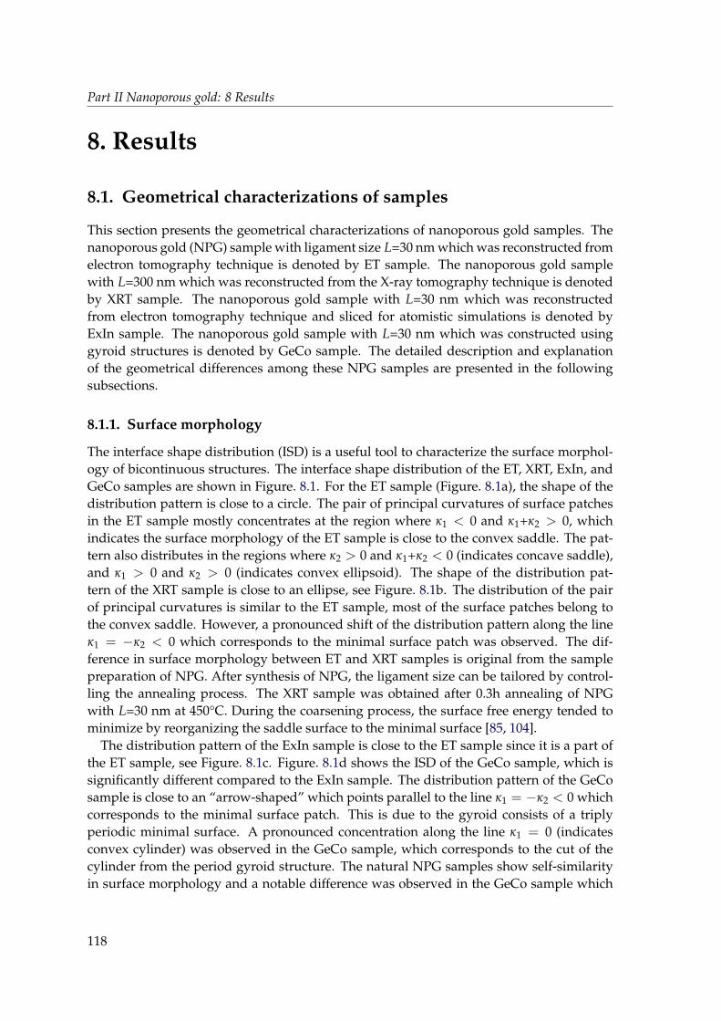
Part II Nanoporous gold: 8 Results
8. Results
8.1. Geometrical characterizations of samples
This section presents the geometrical characterizations of nanoporous gold samples. Thenanoporous gold (NPG) sample with ligament size L=30 nm which was reconstructed fromelectron tomography technique is denoted by ET sample. The nanoporous gold samplewith L=300 nm which was reconstructed from the X-ray tomography technique is denotedby XRT sample. The nanoporous gold sample with L=30 nm which was reconstructedfrom electron tomography technique and sliced for atomistic simulations is denoted byExIn sample. The nanoporous gold sample with L=30 nm which was constructed usinggyroid structures is denoted by GeCo sample. The detailed description and explanationof the geometrical differences among these NPG samples are presented in the followingsubsections.
8.1.1. Surface morphology
The interface shape distribution (ISD) is a useful tool to characterize the surface morphol-ogy of bicontinuous structures. The interface shape distribution of the ET, XRT, ExIn, andGeCo samples are shown in Figure. 8.1. For the ET sample (Figure. 8.1a), the shape of thedistribution pattern is close to a circle. The pair of principal curvatures of surface patchesin the ET sample mostly concentrates at the region where κ1 < 0 and κ1+κ2 > 0, whichindicates the surface morphology of the ET sample is close to the convex saddle. The pat-tern also distributes in the regions where κ2 > 0 and κ1+κ2 < 0 (indicates concave saddle),and κ1 > 0 and κ2 > 0 (indicates convex ellipsoid). The shape of the distribution pat-tern of the XRT sample is close to an ellipse, see Figure. 8.1b. The distribution of the pairof principal curvatures is similar to the ET sample, most of the surface patches belong tothe convex saddle. However, a pronounced shift of the distribution pattern along the lineκ1 = −κ2 < 0 which corresponds to the minimal surface patch was observed. The dif-ference in surface morphology between ET and XRT samples is original from the samplepreparation of NPG. After synthesis of NPG, the ligament size can be tailored by control-ling the annealing process. The XRT sample was obtained after 0.3h annealing of NPGwith L=30 nm at 450°C. During the coarsening process, the surface free energy tended tominimize by reorganizing the saddle surface to the minimal surface [85, 104].
The distribution pattern of the ExIn sample is close to the ET sample since it is a part ofthe ET sample, see Figure. 8.1c. Figure. 8.1d shows the ISD of the GeCo sample, which issignificantly different compared to the ExIn sample. The distribution pattern of the GeCosample is close to an “arrow-shaped” which points parallel to the line κ1 = −κ2 < 0 whichcorresponds to the minimal surface patch. This is due to the gyroid consists of a triplyperiodic minimal surface. A pronounced concentration along the line κ1 = 0 (indicatesconvex cylinder) was observed in the GeCo sample, which corresponds to the cut of thecylinder from the period gyroid structure. The natural NPG samples show self-similarityin surface morphology and a notable difference was observed in the GeCo sample which
118
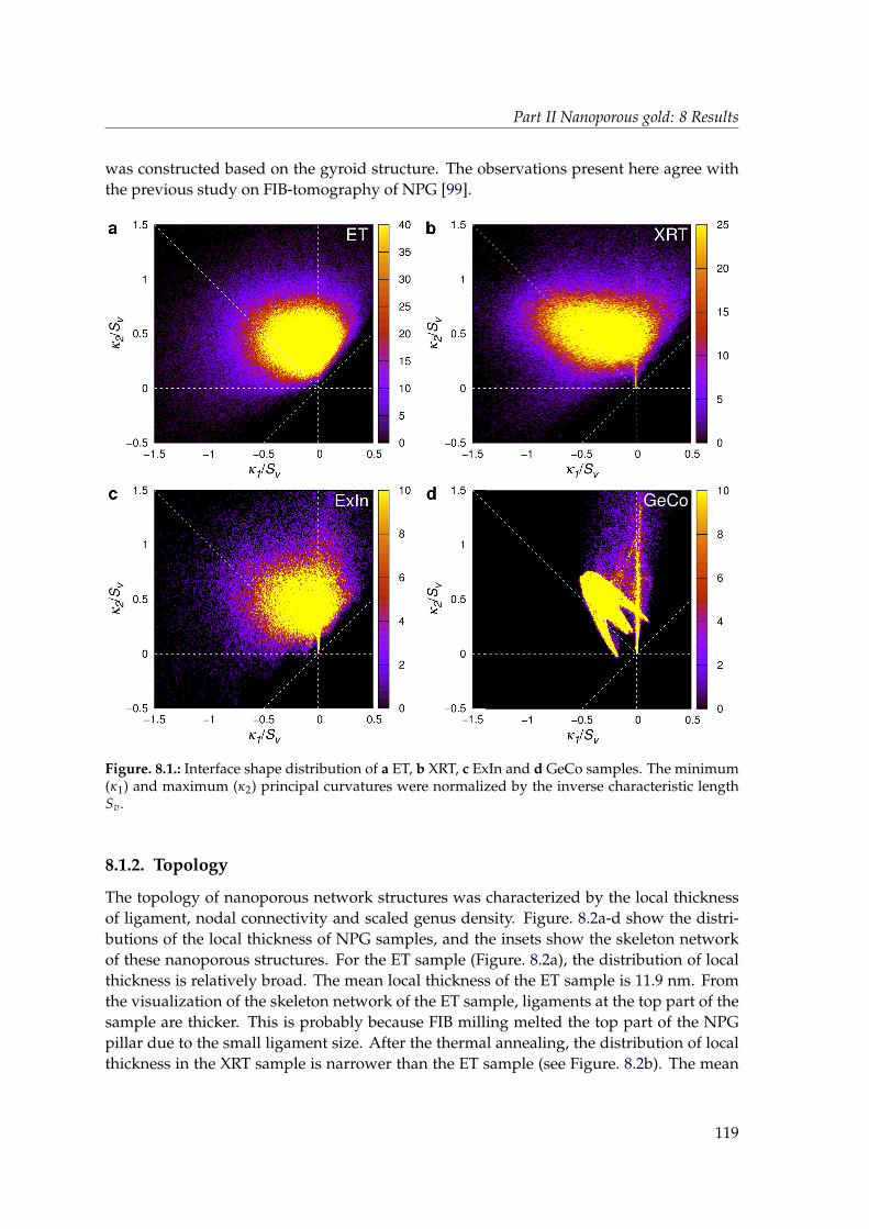
Part II Nanoporous gold: 8 Results
was constructed based on the gyroid structure. The observations present here agree withthe previous study on FIB-tomography of NPG [99].
GeCo
Figure. 8.1.: Interface shape distribution of a ET, b XRT, c ExIn and d GeCo samples. The minimum(κ1) and maximum (κ2) principal curvatures were normalized by the inverse characteristic lengthSv.
8.1.2. Topology
The topology of nanoporous network structures was characterized by the local thicknessof ligament, nodal connectivity and scaled genus density. Figure. 8.2a-d show the distri-butions of the local thickness of NPG samples, and the insets show the skeleton networkof these nanoporous structures. For the ET sample (Figure. 8.2a), the distribution of localthickness is relatively broad. The mean local thickness of the ET sample is 11.9 nm. Fromthe visualization of the skeleton network of the ET sample, ligaments at the top part of thesample are thicker. This is probably because FIB milling melted the top part of the NPGpillar due to the small ligament size. After the thermal annealing, the distribution of localthickness in the XRT sample is narrower than the ET sample (see Figure. 8.2b). The mean
119
Part II Nanoporous gold: 8 Results
local thickness of the XRT sample is 126.8 nm. The ligaments near the bottom surface ofthe sample are thicker since the NPG pillar sits on a solid Au substrate. The effects of FIBmilling is not as notable as in the smaller NPG pillar. The distribution of local thickness ofthe ExIn sample is shown in Figure. 8.2c, it is narrower than the ET sample. The mean localthickness of the ExIn is 10.4 nm. In contrast to the natural NPG samples, the GeCo sampleshows a normal distribution of local thickness, see the inset of Figure. 8.2d. Except for thethin ligaments at the outermost pillar due to the cutting, the distribution of local thicknessis ranging from 10 to 15 nm. The mean local thickness of the GeCo sample is 12.4 nm.
Figure. 8.2e-f show the nodal connectivity of ExIn and GeCo samples. In the ExIn sample,13.9%, 64.9% and 21.2% nodes connect with 1, 3 and >3 ligaments, respectively. In theGeCo sample, 6.1% and 93.9% nodes connect with 1 and 3 ligaments, respectively. Forgyroid structures, the typical nodal connectivity is 3. By cutting the period structure intoa pillar, a few nodes with only one connected ligament were generated. For natural NPG,most nodes connect with 3 ligaments. Due to the heterogeneity of the natural networkstructures, the ExIn sample has more nodes with 1 and >3 nodal connectivity than theGeCo sample.
To quantitatively characterize the global network connectivity of NPG structures, scaledgenus density was applied on the ET and XRT samples, and the results were comparedwith the previous study using FIB tomography [99] and phase-field-based [99] and MD-based artificial [133] NPG structures, see Figure. 8.3. After the coarsening process, the XRTsample shows a higher relative density than the ET sample. Meanwhile, the scaled genusdensity increases with increasing relative density. The relation between scaled genus den-sity and relative density seems to be linear according to the previous MD-based method[133]. This trend also observed in the experimental data which includes NPG sampleswere reconstructed using FIB tomography in literature [99] and using non-destructive to-mography techniques in this work. The artificially constructed NPG shows notable devia-tions compared to the natural reconstructed NPG. In general, the MD-based samples showhigher scaled genus density than the natural NPG with similar relative density, and thephase-field-based sample shows a lower value than the natural ones.
120
Part II Nanoporous gold: 8 Results
0
0.1
0.2
0.3
0.4
0.5
0 5 10 15 20 25
Pe
rce
nta
ge
Local thickness (nm)
0
0.1
0.2
0.3
0.4
0.5
0 50 100 150 200 250
Pe
rce
nta
ge
Local thickness (nm)
0
0.1
0.2
0.3
0.4
0.5
0 5 10 15 20 25
Pe
rce
nta
ge
Local thickness (nm)
a b
c dGeCo
0
0.1
0.2
0.3
0.4
0.5
0 5 10 15 20 25
Pe
rce
nta
ge
Local thickness (nm)
ExIn
Local thickness (nm)0 20
ET XRT
Local thickness (nm)0 20
Local thickness (nm)0 200
Local thickness (nm)0 20
[137]
[72110]
[310]
e f
ExIn GeCo
Figure. 8.2.: Distribution of local thickness in a ET, b XRT, c ExIn and d GeCo samples. The binsize of the histogram is 1 nm for ET, ExIn and GeCo samples and is 10 nm for XRT sample. Theinsets show the skeleton network of nanoporous structures. The color and thickness of the tubesare related to the local thickness of the ligaments. Skeletonization of e ExIn and f GeCo samples.The color of the nodes is related to the number of ligaments connected to that node. Blue, greenand red nodes indicate 1, 3 and more than 3 ligaments connected to that node, respectively. Surfacemesh is half-transparent.
121
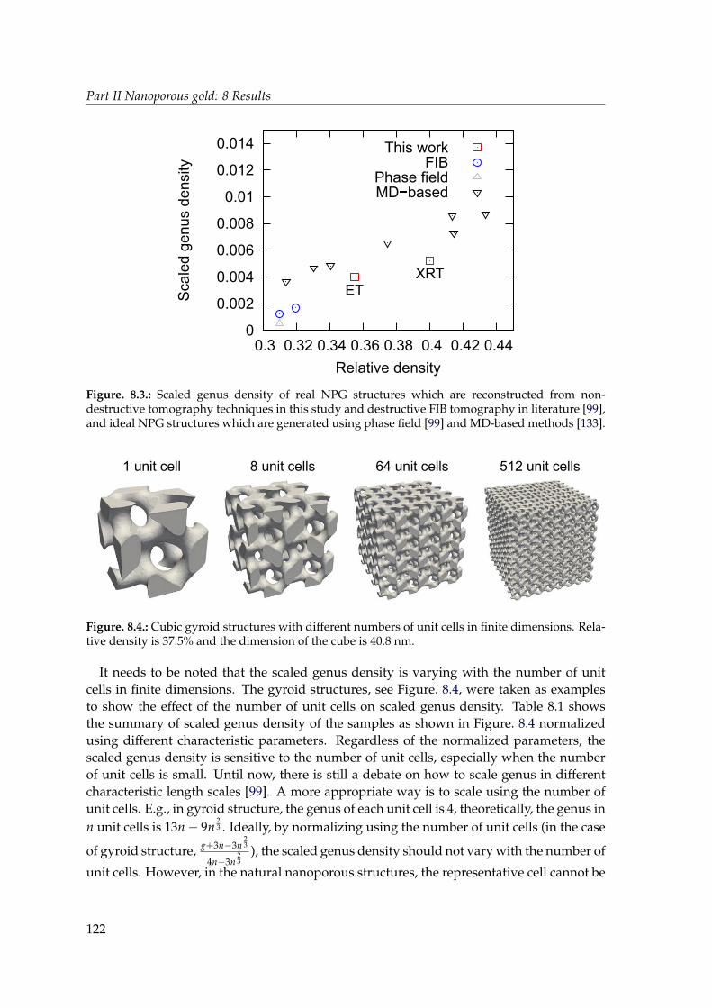
Part II Nanoporous gold: 8 Results
0
0.002
0.004
0.006
0.008
0.01
0.012
0.014
0.3 0.32 0.34 0.36 0.38 0.4 0.42 0.44
Scale
d g
enus d
ensity
Relative density
This workFIB
Phase fieldMDbased
ETXRT
Figure. 8.3.: Scaled genus density of real NPG structures which are reconstructed from non-destructive tomography techniques in this study and destructive FIB tomography in literature [99],and ideal NPG structures which are generated using phase field [99] and MD-based methods [133].
1 unit cell 8 unit cells 64 unit cells 512 unit cells
Figure. 8.4.: Cubic gyroid structures with different numbers of unit cells in finite dimensions. Rela-tive density is 37.5% and the dimension of the cube is 40.8 nm.
It needs to be noted that the scaled genus density is varying with the number of unitcells in finite dimensions. The gyroid structures, see Figure. 8.4, were taken as examplesto show the effect of the number of unit cells on scaled genus density. Table 8.1 showsthe summary of scaled genus density of the samples as shown in Figure. 8.4 normalizedusing different characteristic parameters. Regardless of the normalized parameters, thescaled genus density is sensitive to the number of unit cells, especially when the numberof unit cells is small. Until now, there is still a debate on how to scale genus in differentcharacteristic length scales [99]. A more appropriate way is to scale using the number ofunit cells. E.g., in gyroid structure, the genus of each unit cell is 4, theoretically, the genus inn unit cells is 13n− 9n
23 . Ideally, by normalizing using the number of unit cells (in the case
of gyroid structure, g+3n−3n23
4n−3n23
), the scaled genus density should not vary with the number of
unit cells. However, in the natural nanoporous structures, the representative cell cannot be
122
Part II Nanoporous gold: 8 Results
easily identified. Therefore, further study is necessary to characterize global connectivityin a more general way.
Table 8.1.: Summary of scaled genus density of gyroid structures with different numbers of unitcells in finite dimensions (40.8× 40.8× 40.8 nm3) normalized using different characteristic param-eters. n: number of unit cells; g: genus; L: mean ligament size; Sv: surface area per solid volume;Sv f : surface area per foam volume.
n g L Sv Sv f g×V−1 × S−3v [105, 133] g×V−1 × S−3
v f [99] g×V−1 × L3[297] g+3n−3n23
4n−3n23
1 4 10 0.042 0.015 0.00079 0.01670 0.05890 48 68 5 0.072 0.026 0.00269 0.06038 0.12515 4
64 688 2.5 0.137 0.046 0.00397 0.10414 0.15828 4512 6080 1.25 0.277 0.089 0.00419 0.12910 0.17484 4
8.2. Compression tests on nanoporous gold
This section presents compression tests on NPG samples. In subsection 8.2.1, the deforma-tion behavior of the ExIn sample (L=30 nm) under compression was investigated. In sub-section 8.2.2, the deformation behavior of the GeCo sample (L=30 nm) under compressionwas studied. In subsection 8.2.3, compression tests were performed on the scaled-downExIn and GeCo samples (L=10, 7.5 and 5 nm). The deformation behavior of the scaled-down NPG samples was compared with the real-size samples (L=30 nm).
8.2.1. Deformation behavior of experimentally-informed samples
The atomic configurations of undeformed and deformed (at 26.5% strain) ExIn sample andthe correlative engineering stress-strain response are shown in Figure. 8.5. The mechanicalresponse of the ExIn sample is similar to metallic cellular solids in macroscopic scale [97]and the deformation process can be divided into three stages. The first stage is elasticityand followed by a plateau of plastic flow. After 20% strain, a pronounced hardening be-havior due to the densification occurred, and the neighboring ligaments were contacted at26.5% strain as shown in Figure. 8.5b. At the beginning of the deformation process, thestress did not increase immediately, since the bumpy surfaces at the top and bottom ofthe sample were first deformed by virtual indenters. These bumpy surfaces formed nearthe atomic sharp cutting edges after relaxation, which are inevitable in the preparation ofsimulation samples. During the elastic deformation, the stress-strain response is not per-fectly linear, since the forces were detected by the virtual indenters and ligaments may losecontact with the indenters due to their mechanical instability during the compression. Theyield strength σy of the ExIn sample is 73 MPa. After global yielding, a stress drop wasobserved before the plateau of plastic deformation. Between 7.5% and 20% strain, the flowstress fluctuated around 65 MPa, and then steadily increased after densification.
123
Part II Nanoporous gold: 8 Results
0
50
100
150
200
0 0.05 0.1 0.15 0.2 0.25
Engin
eering s
tress [M
Pa]
Strain
ExIn
b ε=0%
ε=26.5%
[137]
[72110][310]
a
Figure. 8.5.: a Engineering stress-strain curve of the compression test (T=300 K, ε=1×10⁸ s−1) onthe ExIn NPG (L=30 nm). b Configurations of the simulated ExIn NPG (L=30 nm) before and after(at 26.5% strain) compression.
8.2.2. Deformation behavior of geometrically-constructed samples
ba
0
50
100
150
200
0 0.05 0.1 0.15 0.2 0.25
En
gin
ee
rin
g s
tre
ss [
MP
a]
Strain
GeCo
ε=26.5%
ε=0%
[137]
[72110][310]
Figure. 8.6.: a Engineering stress-strain curve of the compression test (T=300 K, ε=1×10⁸ s−1) on theGeCo NPG (L=30 nm). b Configurations of the simulated GeCo NPG (L=30 nm) before and after(at 26.5% strain) compression.
The compression test was performed on the GeCo sample using MD simulations. Thestress-strain response of the GeCo sample is shown in Figure. 8.6a. A stress fluctuationoccurred during the elastic deformation since ligaments at the top and bottom surfaces lostcontact with the virtual indenters. The GeCo sample yielded at 153 MPa, which is morethan 2 times higher than the ExIn sample. After the global yielding, the stress dropped to100 MPa and then fluctuated around 115 MPa. No strain hardening effect was observeduntil the end of the compression test at 26.5% strain. The undeformed and deformed atomicconfigurations are shown in Figure. 8.6b. No densification was observed in the deformedGeCo NPG sample at 26.5% strain.
124
Part II Nanoporous gold: 8 Results
8.2.3. Deformation behavior of scaled-down samples
0
50
100
150
200
250
300
350
400
0 0.05 0.1 0.15 0.2 0.25
σzz
[MP
a]
Strain
L=5nm
b
0
100
200
300
400
500
600
700
800
0 0.05 0.1 0.15 0.2 0.25
σzz
(MP
a)
Strain
L=5nmL=7.5nmL=10nmL=30nm
L=7.5nmL=10nmL=30nm
a ExIn GeCo
Figure. 8.7.: True stress as function of strain of a ExIn and b GeCo samples with different ligamentsizes under compression (T=300 K, ε=1×10⁸ s−1).
To study the size effects on mechanical properties of NPG samples, compression testswere performed on the scaled-down (L=10, 7.5 and 5 nm) ExIn and GeCo samples usingMD simulations. The scaled-down samples were homogeneously scaled down by differ-ent factors without changing geometry, thus the complex influence of network structureson mechanical responses can be mostly excluded. Figure. 8.7 shows the evolution of truestress along the loading axis (z-axis) during the simulated compression of the ExIn andGeCo samples. In the scaled-down samples, no significant stress drop was observed af-ter the global yielding. In both ExIn and GeCo samples, size effects on Young’s modulus,yield stress and flow stress were identified. In both NPG samples, Young’s modulus de-creases with decreasing ligament size, “smaller is more compliant” trend was observed.For yield strength, “smaller is weaker” trend was identified, the value of σy decreases withthe decrease of ligament size. Flow stresses of the real-size NPG samples (L=30 nm) weresignificantly lower than the scaled-down samples. The quantitative evaluation of thesesize effects and corresponding mechanisms are introduced in chapter 9.
125
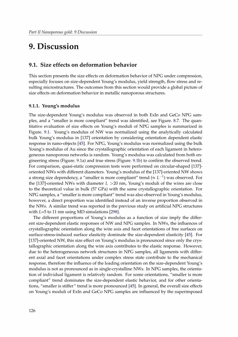
Part II Nanoporous gold: 9 Discussion
9. Discussion
9.1. Size effects on deformation behavior
This section presents the size effects on deformation behavior of NPG under compression,especially focuses on size-dependent Young’s modulus, yield strength, flow stress and re-sulting microstructures. The outcomes from this section would provide a global picture ofsize effects on deformation behavior in metallic nanoporous structures.
9.1.1. Young’s modulus
The size-dependent Young’s modulus was observed in both ExIn and GeCo NPG sam-ples, and a “smaller is more compliant” trend was identified, see Figure. 8.7. The quan-titative evaluation of size effects on Young’s moduli of NPG samples is summarized inFigure. 9.1. Young’s modulus of NW was normalized using the analytically calculatedbulk Young’s modulus in [137] orientation by considering orientation dependent elasticresponse in nano-objects [45]. For NPG, Young’s modulus was normalized using the bulkYoung’s modulus of Au since the crystallographic orientation of each ligament in hetero-geneous nanoporous networks is random. Young’s modulus was calculated from both en-gineering stress (Figure. 9.1a) and true stress (Figure. 9.1b) to confirm the observed trend.For comparison, quasi-static compression tests were performed on circular-shaped [137]-oriented NWs with different diameters. Young’s modulus of the [137]-oriented NW showsa strong size dependency, a “smaller is more compliant” trend (∝ L−1) was observed. Forthe [137]-oriented NWs with diameter L >20 nm, Young’s moduli of the wires are closeto the theoretical value in bulk (57 GPa) with the same crystallographic orientation. ForNPG samples, a “smaller is more compliant” trend was also observed in Young’s modulus,however, a direct proportion was identified instead of an inverse proportion observed inthe NWs. A similar trend was reported in the previous study on artificial NPG structureswith L=5 to 11 nm using MD simulations [298].
The different proportions of Young’s modulus as a function of size imply the differ-ent size-dependent elastic responses of NW and NPG samples. In NWs, the influences ofcrystallographic orientation along the wire axis and facet orientations of free surfaces onsurface-stress-induced surface elasticity dominate the size-dependent elasticity [45]. For[137]-oriented NW, this size effect on Young’s modulus is pronounced since only the crys-tallographic orientation along the wire axis contributes to the elastic response. However,due to the heterogeneous network structures in NPG samples, all ligaments with differ-ent axial and facet orientations under complex stress state contribute to the mechanicalresponse, therefore the influence of the loading orientation on the size-dependent Young’smodulus is not as pronounced as in single-crystalline NWs. In NPG samples, the orienta-tion of individual ligament is relatively random. For some orientations, “smaller is morecompliant” trend dominates the size-dependent elastic behavior, and for other orienta-tions, “smaller is stiffer” trend is more pronounced [45]. In general, the overall size effectson Young’s moduli of ExIn and GeCo NPG samples are influenced by the superimposed
126
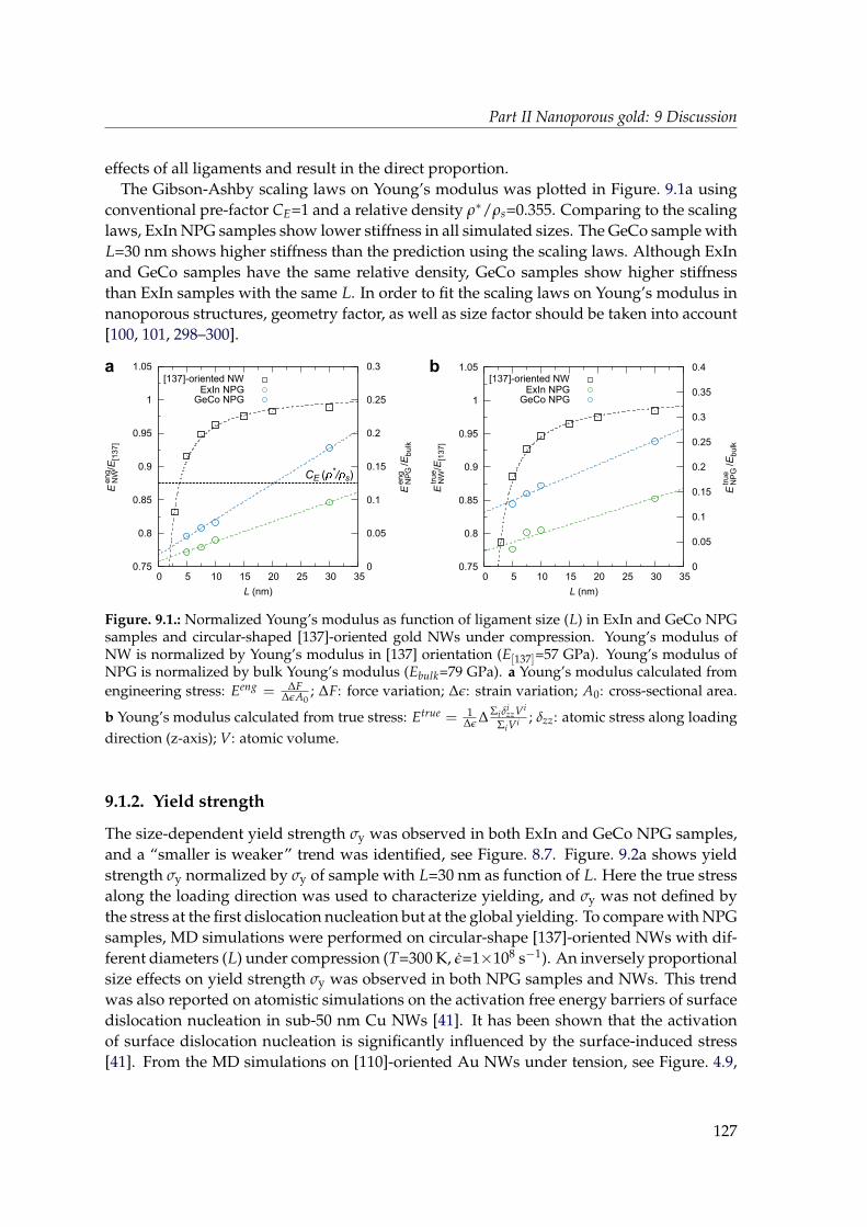
Part II Nanoporous gold: 9 Discussion
effects of all ligaments and result in the direct proportion.The Gibson-Ashby scaling laws on Young’s modulus was plotted in Figure. 9.1a using
conventional pre-factor CE=1 and a relative density ρ∗/ρs=0.355. Comparing to the scalinglaws, ExIn NPG samples show lower stiffness in all simulated sizes. The GeCo sample withL=30 nm shows higher stiffness than the prediction using the scaling laws. Although ExInand GeCo samples have the same relative density, GeCo samples show higher stiffnessthan ExIn samples with the same L. In order to fit the scaling laws on Young’s modulus innanoporous structures, geometry factor, as well as size factor should be taken into account[100, 101, 298–300].
ExIn NPGGeCo NPG
[137]-oriented NW
0.75
0.8
0.85
0.9
0.95
1
1.05
0 5 10 15 20 25 30 350
0.05
0.1
0.15
0.2
0.25
0.3
0.35
0.4
EN
Wtr
ue/E
[137]
EN
PG
true
/Ebulk
L (nm)
a b
ExIn NPGGeCo NPG
[137]-oriented NW
0.75
0.8
0.85
0.9
0.95
1
1.05
0 5 10 15 20 25 30 350
0.05
0.1
0.15
0.2
0.25
0.3
EN
Weng/E
[137]
EN
PG
eng
/Ebulk
L (nm)
CE (*/s)
Figure. 9.1.: Normalized Young’s modulus as function of ligament size (L) in ExIn and GeCo NPGsamples and circular-shaped [137]-oriented gold NWs under compression. Young’s modulus ofNW is normalized by Young’s modulus in [137] orientation (E[137]=57 GPa). Young’s modulus ofNPG is normalized by bulk Young’s modulus (Ebulk=79 GPa). a Young’s modulus calculated fromengineering stress: Eeng = ∆F
∆εA0; ∆F: force variation; ∆ε: strain variation; A0: cross-sectional area.
b Young’s modulus calculated from true stress: Etrue = 1∆ε ∆ Σiδ
izzVi
ΣiVi ; δzz: atomic stress along loadingdirection (z-axis); V: atomic volume.
9.1.2. Yield strength
The size-dependent yield strength σy was observed in both ExIn and GeCo NPG samples,and a “smaller is weaker” trend was identified, see Figure. 8.7. Figure. 9.2a shows yieldstrength σy normalized by σy of sample with L=30 nm as function of L. Here the true stressalong the loading direction was used to characterize yielding, and σy was not defined bythe stress at the first dislocation nucleation but at the global yielding. To compare with NPGsamples, MD simulations were performed on circular-shape [137]-oriented NWs with dif-ferent diameters (L) under compression (T=300 K, ε=1×10⁸ s−1). An inversely proportionalsize effects on yield strength σy was observed in both NPG samples and NWs. This trendwas also reported on atomistic simulations on the activation free energy barriers of surfacedislocation nucleation in sub-50 nm Cu NWs [41]. It has been shown that the activationof surface dislocation nucleation is significantly influenced by the surface-induced stress[41]. From the MD simulations on [110]-oriented Au NWs under tension, see Figure. 4.9,
127
Part II Nanoporous gold: 9 Discussion
a “smaller is stronger” trend was observed. In contrast, an opposite trend was observedin the [137]-oriented Au NWs under compression. Whether it is “smaller is stronger” or“smaller is weaker” depends on the combined effects of surface-induced stress and appliedstress. Ultimately, the local resolved shear stress determines the activation of dislocation atfree surfaces.
0.6
0.8
1
1.2
1.4
0 5 10 15 20 25 30 35 40
σy/σ
y 3
0n
m
L [nm]
ExInGeCo
[137]oriented NWf(x)=A L
1+B
0
0.005
0.01
0.015
0.02
0.025
0.03
0.035
0.04
4 2 0 2 4
Pro
babili
ty d
ensity
Resolved shear stress Aβ (GPa)
L=10 nmL=30 nm
L=5 nm
0
0.005
0.01
0.015
0.02
0.025
0.03
0 2 4 6 8 10 12 14
Pro
ba
bili
ty d
en
sity
von Mises stress (GPa)
L=10 nmL=30 nm
L=5 nm
B
A
D
C (b)
τ Aβ (
GP
a)
0.5
-0.5
L=5 nm L=7.5 nm
L=10 nm L=30 nm
[137]
[72110]
[310]
ε=0%
a b
c d
Figure. 9.2.: a Normalized true yield strength (normalized by true yield strength of samples withL=30 nm) as function of ligament size in ExIn and GeCo NPG samples and [137]-oriented gold NWsunder compression (T=300 K, ε=1×10⁸ s−1). b Atomic stress (resolved along Aβ direction on slipplane (b)) states in a representative junction of GeCo samples with different ligament sizes (L=5,7.5, 10 and 30 nm) before compression. Probability densities (bin size=0.1 GPa) of c resolved shearstress τAβ and d von Mises stress σvon Mises in GeCo samples with different ligament sizes (L=5, 10and 30 nm) before compression.
In contrast to different proportions of Young’s modulus as a function of size in NPGand NW samples, the similar inverse proportion of size-dependent yield strength σy wasidentified in both samples. The yield strength σy of NPG is much lower than NW withsimilar characteristic length since local strain gradient and varying ligament sizes in het-erogeneous network structures lead to early yielding. Although the nucleation events inNPG are heterogeneously distributed, nanoporous structures have identical slip systemsas NWs with the same crystallographic orientation under homogeneous uniaxial loading.Therefore, the criterion for surface dislocation nucleation in NPG and NW samples with the
128
Part II Nanoporous gold: 9 Discussion
same characteristic length is similar. The resolved shear stress along Aβ direction on slipplane (b) in relaxed GeCo samples with different sizes is shown in Figure. 9.2b. Aβ direc-tion has one of the highest Schmid factors among all activated slip directions, see Table A.1in the Appendix. Therefore, Aβ(b) prefers to be first activated in further compressive load-ing. The stress state before mechanical loading reflects the effect of surface-induced stresson the dislocation activation. The stress level is significantly higher in smaller samplessince the effect of surface-induced stress is more pronounced in the samples with a highersurface-to-volume ratio. Figure. 9.2c-d show the quantitative characterization of size effecton surface-induce stress, the distributions of resolved shear stress Aβ(b) and von Misesstress are higher in the large stress range (|τAβ|> 2 GPa and σvon Mises > 6 GPa) for smallerNPG samples. The surface-induced stress assists the surface dislocation nucleation by re-ducing the applied stress needed to overcome the activation barrier, therefore a “small isweaker” trend was observed in [137]-oriented nano-objects under uniaxial compression.
9.1.3. Flow stress
The flow stress of the real-size (L=30 nm) NPG samples is lower than the scaled-down(L=10, 7.5 and 5 nm) counterparts (see Figure. 8.7). To understand the size-dependentflow stress behavior in NPG, the evolution of dislocation density (ρdislocation) during thesimulated compression test was calculated (Figure. 9.3a,b). In all simulated samples, com-pression led to a continuous accumulation of dislocations. The value of ρdislocation is higherin the smaller sample as shown in Figure. 9.3a,b, however, the number of dislocations inindividual ligament is much lower in smaller one. The value of ρdislocation and averagednumber of dislocations per ligament Ndislocation
ligament at 15%, 20% and 25% strain in ExIn NPGsamples with different characteristic lengths are summarized in Table 9.1. As an example,at 20% strain, Ndislocation
ligament values of ExIn samples with ligament sizes of 5, 10 and 30 nmare 2, 4 and 20, respectively (see Table 9.1). Although ρdislocation is higher in smaller NPGat the same strain state, the absolute number of dislocations in one ligament is lower inthe smaller one. This implies that if one surface nucleated dislocation glides through aligament it will interact with more dislocations in the larger ligament.
In order to quantitatively evaluate flow stress behavior in NPG with different charac-teristic lengths, ρdislocation is normalized by multiplying mean ligament size L. Consid-ering a ligament with a characteristic length L and a number of geometrically-necessarydislocations (GNDs) is NGND, see Figure. 9.4, then ρdislocation in this ligament is NGND
L2 . Tomaintain the same strain gradient in a ligament with 2L, the number of GNDs is 2NGND
and ρdislocation= NGND2L2 . In both cases as shown in Figure. 9.4, the normalized dislocation
density is NGNDL . As shown in Figure. 9.3c,d, the normalized dislocation density of the real-
size sample is significantly higher than the other scaled-down samples in both ExIn andGeCo NPG samples, which indicates that extra dislocations stored in the real-size sam-ples. The deviation of normalized dislocation density implies the distinct plastic deforma-tion mechanisms in real-size samples. Dislocations in the real-size samples (L=30 nm) aremore likely to interact with each other by forming sessile dislocation locks compared to thescaled-down samples. As evidence (see subsection 9.1.4), stacking fault tetrahedra (SFTs)and small-angle grain boundaries (SAGBs) resulting from dislocation interaction and in-
129
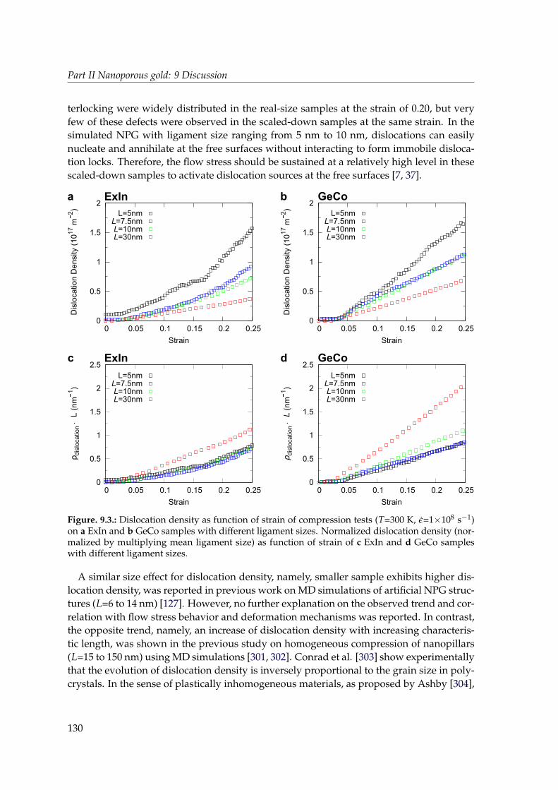
Part II Nanoporous gold: 9 Discussion
terlocking were widely distributed in the real-size samples at the strain of 0.20, but veryfew of these defects were observed in the scaled-down samples at the same strain. In thesimulated NPG with ligament size ranging from 5 nm to 10 nm, dislocations can easilynucleate and annihilate at the free surfaces without interacting to form immobile disloca-tion locks. Therefore, the flow stress should be sustained at a relatively high level in thesescaled-down samples to activate dislocation sources at the free surfaces [7, 37].
0
0.5
1
1.5
2
0 0.05 0.1 0.15 0.2 0.25
Dis
location D
ensity (
10
17
m
2)
Strain
b
0
0.5
1
1.5
2
0 0.05 0.1 0.15 0.2 0.25
Dis
locatio
n D
ensity (
10
17
m
2)
Strain
a
L=7.5nmL=10nmL=30nm
L=5nmL=7.5nmL=10nmL=30nm
L=5nm
ExIn GeCo
0
0.5
1
1.5
2
2.5
0 0.05 0.1 0.15 0.2 0.25
ρd
islo
ca
tio
nL
(nm
1)
Strain
0
0.5
1
1.5
2
2.5
0 0.05 0.1 0.15 0.2 0.25
ρd
islo
ca
tio
n
L(n
m
1)
Strain
L=7.5nmL=10nmL=30nm
L=5nmL=7.5nmL=10nmL=30nm
L=5nm
dc ExIn GeCo
Figure. 9.3.: Dislocation density as function of strain of compression tests (T=300 K, ε=1×10⁸ s−1)on a ExIn and b GeCo samples with different ligament sizes. Normalized dislocation density (nor-malized by multiplying mean ligament size) as function of strain of c ExIn and d GeCo sampleswith different ligament sizes.
A similar size effect for dislocation density, namely, smaller sample exhibits higher dis-location density, was reported in previous work on MD simulations of artificial NPG struc-tures (L=6 to 14 nm) [127]. However, no further explanation on the observed trend and cor-relation with flow stress behavior and deformation mechanisms was reported. In contrast,the opposite trend, namely, an increase of dislocation density with increasing characteris-tic length, was shown in the previous study on homogeneous compression of nanopillars(L=15 to 150 nm) using MD simulations [301, 302]. Conrad et al. [303] show experimentallythat the evolution of dislocation density is inversely proportional to the grain size in poly-crystals. In the sense of plastically inhomogeneous materials, as proposed by Ashby [304],
130
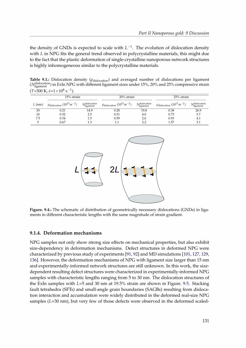
Part II Nanoporous gold: 9 Discussion
the density of GNDs is expected to scale with L−1. The evolution of dislocation densitywith L in NPG fits the general trend observed in polycrystalline materials, this might dueto the fact that the plastic deformation of single-crystalline nanoporous network structuresis highly inhomogeneous similar to the polycrystalline materials.
Table 9.1.: Dislocation density (ρdislocation) and averaged number of dislocations per ligament(Ndislocation
ligament ) in ExIn NPG with different ligament sizes under 15%, 20% and 25% compressive strain
(T=300 K, ε=1×10⁸ s−1).15% strain 20% strain 25% strain
L (nm) ρdislocation (1017m−2) Ndislocationligament ρdislocation (1017m−2) Ndislocation
ligament ρdislocation (1017m−2) Ndislocationligament
30 0.21 14.9 0.28 19.8 0.38 26.910 0.32 2.5 0.51 4.0 0.73 5.77.5 0.34 1.5 0.59 2.6 0.93 4.15 0.67 1.3 1.1 2.2 1.57 3.1
L 2L
Figure. 9.4.: The schematic of distribution of geometrically necessary dislocations (GNDs) in liga-ments in different characteristic lengths with the same magnitude of strain gradient.
9.1.4. Deformation mechanisms
NPG samples not only show strong size effects on mechanical properties, but also exhibitsize-dependency in deformation mechanisms. Defect structures in deformed NPG werecharacterized by previous study of experiments [91, 92] and MD simulations [101, 127, 129,136]. However, the deformation mechanisms of NPG with ligament size larger than 15 nmand experimentally-informed network structures are still unknown. In this work, the size-dependent resulting defect structures were characterized in experimentally-informed NPGsamples with characteristic lengths ranging from 5 to 30 nm. The dislocation structures ofthe ExIn samples with L=5 and 30 nm at 19.5% strain are shown in Figure. 9.5. Stackingfault tetrahedra (SFTs) and small-angle grain boundaries (SAGBs) resulting from disloca-tion interaction and accumulation were widely distributed in the deformed real-size NPGsamples (L=30 nm), but very few of those defects were observed in the deformed scaled-
131
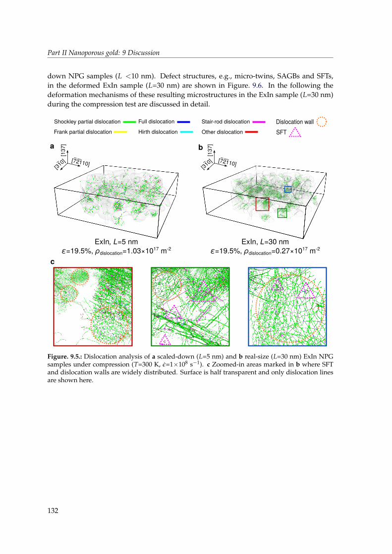
Part II Nanoporous gold: 9 Discussion
down NPG samples (L <10 nm). Defect structures, e.g., micro-twins, SAGBs and SFTs,in the deformed ExIn sample (L=30 nm) are shown in Figure. 9.6. In the following thedeformation mechanisms of these resulting microstructures in the ExIn sample (L=30 nm)during the compression test are discussed in detail.
ExIn, L=30 nm
ε=19.5%, ρdislocation=0.27×10¹⁷ m-2
[13
7]
[72110][3
10]
[13
7]
[72110][3
10]
ExIn, L=5 nm
ε=19.5%, ρdislocation=1.03×10¹⁷ m-2
a b
c
Full dislocation Stair-rod dislocation
Hirth dislocation
Shockley partial dislocation
Frank partial dislocation
Dislocation wall
SFTOther dislocation
Figure. 9.5.: Dislocation analysis of a scaled-down (L=5 nm) and b real-size (L=30 nm) ExIn NPGsamples under compression (T=300 K, ε=1×10⁸ s−1). c Zoomed-in areas marked in b where SFTand dislocation walls are widely distributed. Surface is half transparent and only dislocation linesare shown here.
132
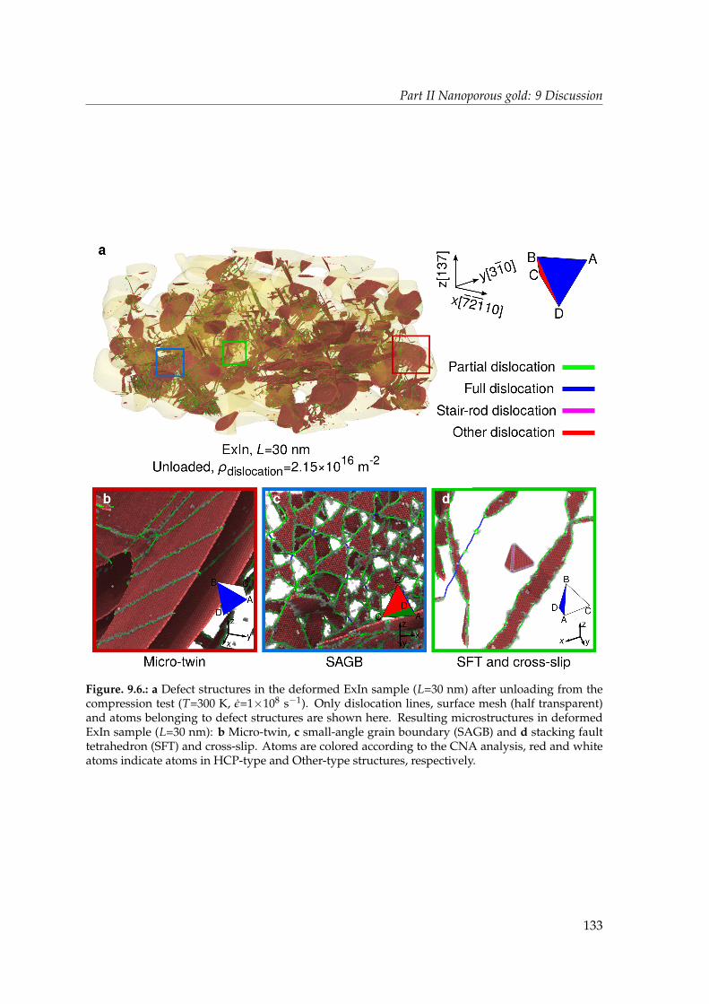
Part II Nanoporous gold: 9 Discussion
Figure. 9.6.: a Defect structures in the deformed ExIn sample (L=30 nm) after unloading from thecompression test (T=300 K, ε=1×10⁸ s−1). Only dislocation lines, surface mesh (half transparent)and atoms belonging to defect structures are shown here. Resulting microstructures in deformedExIn sample (L=30 nm): b Micro-twin, c small-angle grain boundary (SAGB) and d stacking faulttetrahedron (SFT) and cross-slip. Atoms are colored according to the CNA analysis, red and whiteatoms indicate atoms in HCP-type and Other-type structures, respectively.
133
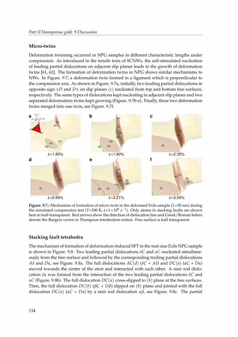
Part II Nanoporous gold: 9 Discussion
Micro-twins
Deformation twinning occurred in NPG samples in different characteristic lengths undercompression. As introduced in the tensile tests of SCNWs, the self-stimulated nucleationof leading partial dislocations on adjacent slip planes leads to the growth of deformationtwins [61, 62]. The formation of deformation twins in NPG shows similar mechanisms toNWs. In Figure. 9.7, a deformation twin formed in a ligament which is perpendicular tothe compression axis. As shown in Figure. 9.7a, initially, two leading partial dislocations inopposite sign γD and Dγ on slip planes (c) nucleated from top and bottom free surfaces,respectively. The same types of dislocations kept nucleating in adjacent slip planes and twoseparated deformation twins kept growing (Figure. 9.7b-e). Finally, these two deformationtwins merged into one twin, see Figure. 9.7f.
ε=1.80%
γD
Dγ
Aβ
(b)
(c)
Aβ (b)
Aβ
Dγ
γD
γD
(c)
(b)
Dγ
(c)
Dγ
(b)
(c)
Dγ
(c)
γD
γD
(b)βD
βA
(b)
(b)βA
(b)
(c)(c)
ε=1.90% ε=2.35%
ε=2.69% ε=3.21% ε=3.54%
d e f
cba[1 3 7]
[3 1 0] [7 21 10]
B
C
D
Figure. 9.7.: Mechanism of formation of micro-twin in the deformed ExIn sample (L=30 nm) duringthe simulated compression test (T=300 K, ε=1×10⁸ s−1). Only atoms in stacking faults are shownhere in half-transparent. Red arrows show the direction of dislocation line and Greek/Roman lettersdenote the Burgers vector in Thompson tetrahedron notion. Free surface is half transparent.
Stacking fault tetrahedra
The mechanism of formation of deformation-induced SFT in the real-size ExIn NPG sampleis shown in Figure. 9.8. Two leading partial dislocations δC and αC nucleated simultane-ously from the free surface and followed by the corresponding trailing partial dislocationsAδ and Dα, see Figure. 9.8a. The full dislocations AC(d) (δC + Aδ) and DC(a) (αC + Dα)moved towards the center of the strut and interacted with each other. A stair rod dislo-cation δα was formed from the interaction of the two leading partial dislocations δC andαC (Figure. 9.8b). The full dislocation DC(a) cross-slipped to (b) plane at the free surfaces.Then, the full dislocation DC(b) (βC + Dβ) slipped on (b) plane and jointed with the fulldislocation DC(a) (αC + Dα) by a stair rod dislocation αβ, see Figure. 9.8c. The partial
134
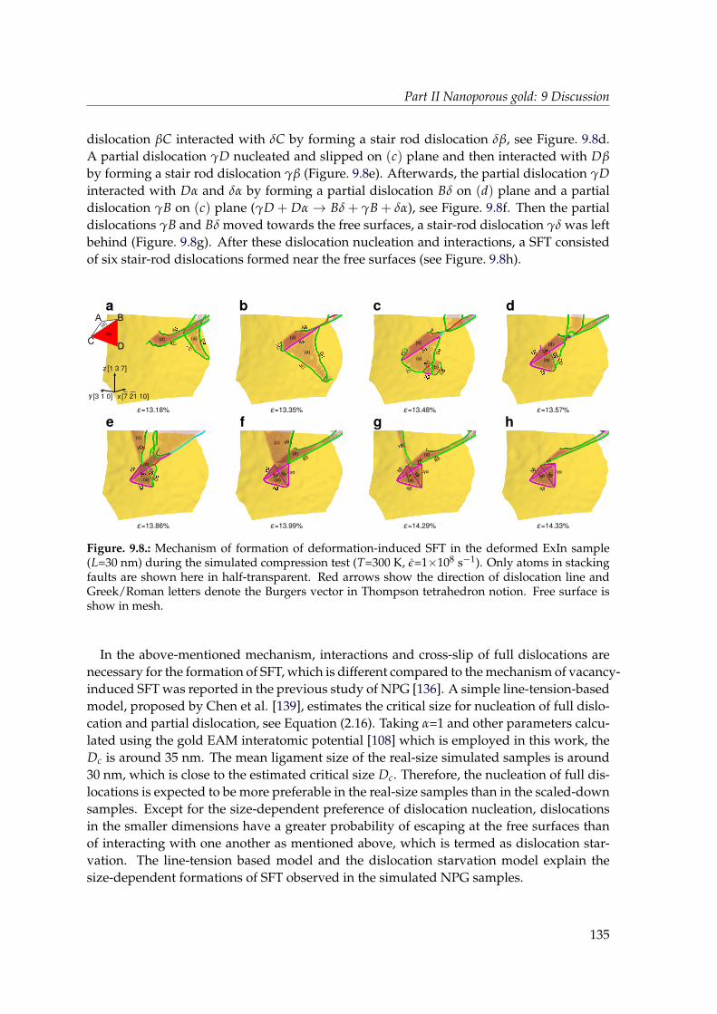
Part II Nanoporous gold: 9 Discussion
dislocation βC interacted with δC by forming a stair rod dislocation δβ, see Figure. 9.8d.A partial dislocation γD nucleated and slipped on (c) plane and then interacted with Dβ
by forming a stair rod dislocation γβ (Figure. 9.8e). Afterwards, the partial dislocation γDinteracted with Dα and δα by forming a partial dislocation Bδ on (d) plane and a partialdislocation γB on (c) plane (γD + Dα→ Bδ + γB + δα), see Figure. 9.8f. Then the partialdislocations γB and Bδ moved towards the free surfaces, a stair-rod dislocation γδ was leftbehind (Figure. 9.8g). After these dislocation nucleation and interactions, a SFT consistedof six stair-rod dislocations formed near the free surfaces (see Figure. 9.8h).
A B
DC
ε=13.18%
C
A
(d) (a)
C
D
(d)
(a)
C
D
C
A
(d)
(a)
(b)
D
A
C
C
D
C
(d)
D
(a)
D
D
D
(d)
(a)
(c)
γD
δα
(d)
(a)
γβ γα
γB
Bδ
(c)
δβ
αβ
δα(a)
γβ
γα
(d)
Bδ
γB
γδ
δβ
αβ
δα
γβ
γα
γδ
ε=13.35% ε=13.48% ε=13.57%
ε=13.86% ε=13.99% ε=14.29% ε=14.33%
(d)
(a)
[1 3 7]z
[3 1 0]y [7 21 10]x
a b c d
e f g h
Figure. 9.8.: Mechanism of formation of deformation-induced SFT in the deformed ExIn sample(L=30 nm) during the simulated compression test (T=300 K, ε=1×10⁸ s−1). Only atoms in stackingfaults are shown here in half-transparent. Red arrows show the direction of dislocation line andGreek/Roman letters denote the Burgers vector in Thompson tetrahedron notion. Free surface isshow in mesh.
In the above-mentioned mechanism, interactions and cross-slip of full dislocations arenecessary for the formation of SFT, which is different compared to the mechanism of vacancy-induced SFT was reported in the previous study of NPG [136]. A simple line-tension-basedmodel, proposed by Chen et al. [139], estimates the critical size for nucleation of full dislo-cation and partial dislocation, see Equation (2.16). Taking α=1 and other parameters calcu-lated using the gold EAM interatomic potential [108] which is employed in this work, theDc is around 35 nm. The mean ligament size of the real-size simulated samples is around30 nm, which is close to the estimated critical size Dc. Therefore, the nucleation of full dis-locations is expected to be more preferable in the real-size samples than in the scaled-downsamples. Except for the size-dependent preference of dislocation nucleation, dislocationsin the smaller dimensions have a greater probability of escaping at the free surfaces thanof interacting with one another as mentioned above, which is termed as dislocation star-vation. The line-tension based model and the dislocation starvation model explain thesize-dependent formations of SFT observed in the simulated NPG samples.
135
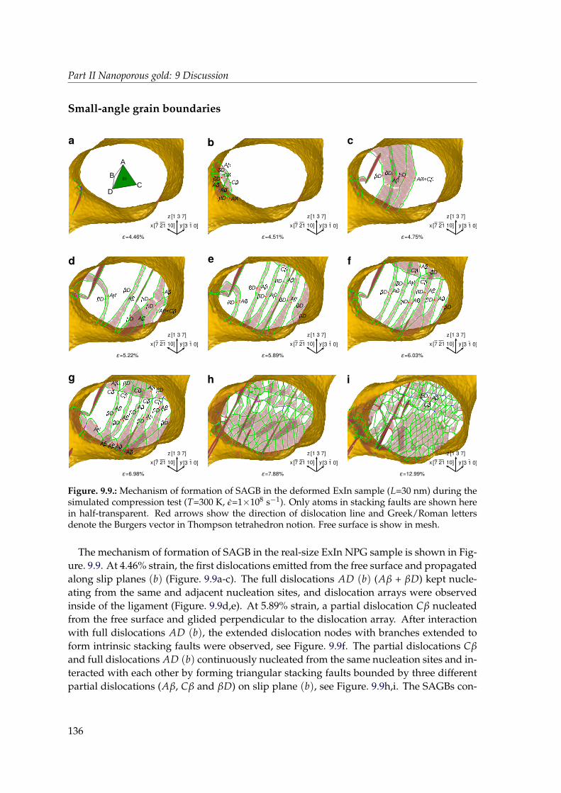
Part II Nanoporous gold: 9 Discussion
Small-angle grain boundaries
[1 3 7]z
[3 1 0]y[7 21 10]x
A
B
DC
(b)
a
[1 3 7]z
[3 1 0]y[7 21 10]x
[1 3 7]z
[3 1 0]y[7 21 10]x
[1 3 7]z
[3 1 0]y[7 21 10]x
[1 3 7]z
[3 1 0]y[7 21 10]x
[1 3 7]z
[3 1 0]y[7 21 10]x
[1 3 7]z
[3 1 0]y[7 21 10]x
[1 3 7]z
[3 1 0]y[7 21 10]x
[1 3 7]z
[3 1 0]y[7 21 10]x
ε=4.46% ε=4.51% ε=4.75%
ε=5.22% ε=5.89% ε=6.03%
b c
d e f
g h i
ε=6.98% ε=7.88% ε=12.99%
A
D
DC
A
A
AD
C DD
A
DA+C
AD
D
A
AD
A
D
D
A+C
AD
D A
D A
D A
D A
D
D
C
D A
D A
D A
D A
D A
CA
D
C
D
D
A
D
A
D
A
DA
DA
D
AAA
A
A
CC
A D
C DA
C CC
AD
Figure. 9.9.: Mechanism of formation of SAGB in the deformed ExIn sample (L=30 nm) during thesimulated compression test (T=300 K, ε=1×10⁸ s−1). Only atoms in stacking faults are shown herein half-transparent. Red arrows show the direction of dislocation line and Greek/Roman lettersdenote the Burgers vector in Thompson tetrahedron notion. Free surface is show in mesh.
The mechanism of formation of SAGB in the real-size ExIn NPG sample is shown in Fig-ure. 9.9. At 4.46% strain, the first dislocations emitted from the free surface and propagatedalong slip planes (b) (Figure. 9.9a-c). The full dislocations AD (b) (Aβ + βD) kept nucle-ating from the same and adjacent nucleation sites, and dislocation arrays were observedinside of the ligament (Figure. 9.9d,e). At 5.89% strain, a partial dislocation Cβ nucleatedfrom the free surface and glided perpendicular to the dislocation array. After interactionwith full dislocations AD (b), the extended dislocation nodes with branches extended toform intrinsic stacking faults were observed, see Figure. 9.9f. The partial dislocations Cβ
and full dislocations AD (b) continuously nucleated from the same nucleation sites and in-teracted with each other by forming triangular stacking faults bounded by three differentpartial dislocations (Aβ, Cβ and βD) on slip plane (b), see Figure. 9.9h,i. The SAGBs con-
136
Part II Nanoporous gold: 9 Discussion
sisted of these triangular stacking fault patterns which are widely existed in the real-sizeExIn and GeCo NPG samples, but not in the scaled-down samples.
The formation of SAGB is due to the interaction between the array of full dislocationsand partial dislocations. Similar to the mechanism of deformation-induced SFT, the size-dependent dislocation nucleation and interaction explain the size-dependent formations ofSAGB observed in the simulated NPG samples. In addition, the Schmid factor of partialdislocation Cβ is zero under uniaxial loading along [137] direction. However, due to theheterogeneous network structure, the stress state in the individual ligament is complex,might mixed with bending and torsion. Therefore, partial dislocation Cβ which is lessfavorable according to Schmid’s law can be stimulated during the compression tests ofNPG.
137
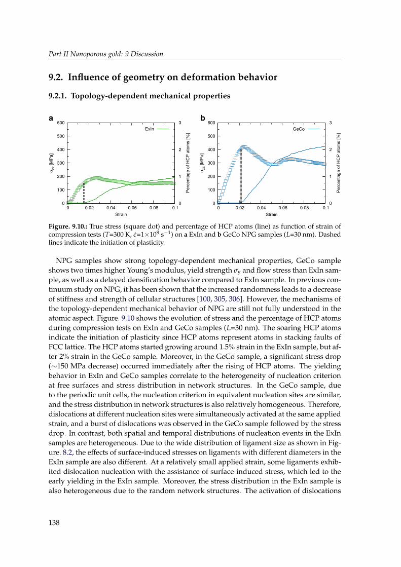
Part II Nanoporous gold: 9 Discussion
9.2. Influence of geometry on deformation behavior
9.2.1. Topology-dependent mechanical properties
0
100
200
300
400
500
600
0 0.02 0.04 0.06 0.08 0.10
1
2
3
σzz
[MP
a]
Perc
enta
ge o
f H
CP
ato
ms [%
]
Strain
ExIn
a b
Figure. 9.10.: True stress (square dot) and percentage of HCP atoms (line) as function of strain ofcompression tests (T=300 K, ε=1×10⁸ s−1) on a ExIn and b GeCo NPG samples (L=30 nm). Dashedlines indicate the initiation of plasticity.
NPG samples show strong topology-dependent mechanical properties, GeCo sampleshows two times higher Young’s modulus, yield strength σy and flow stress than ExIn sam-ple, as well as a delayed densification behavior compared to ExIn sample. In previous con-tinuum study on NPG, it has been shown that the increased randomness leads to a decreaseof stiffness and strength of cellular structures [100, 305, 306]. However, the mechanisms ofthe topology-dependent mechanical behavior of NPG are still not fully understood in theatomic aspect. Figure. 9.10 shows the evolution of stress and the percentage of HCP atomsduring compression tests on ExIn and GeCo samples (L=30 nm). The soaring HCP atomsindicate the initiation of plasticity since HCP atoms represent atoms in stacking faults ofFCC lattice. The HCP atoms started growing around 1.5% strain in the ExIn sample, but af-ter 2% strain in the GeCo sample. Moreover, in the GeCo sample, a significant stress drop(∼150 MPa decrease) occurred immediately after the rising of HCP atoms. The yieldingbehavior in ExIn and GeCo samples correlate to the heterogeneity of nucleation criterionat free surfaces and stress distribution in network structures. In the GeCo sample, dueto the periodic unit cells, the nucleation criterion in equivalent nucleation sites are similar,and the stress distribution in network structures is also relatively homogeneous. Therefore,dislocations at different nucleation sites were simultaneously activated at the same appliedstrain, and a burst of dislocations was observed in the GeCo sample followed by the stressdrop. In contrast, both spatial and temporal distributions of nucleation events in the ExInsamples are heterogeneous. Due to the wide distribution of ligament size as shown in Fig-ure. 8.2, the effects of surface-induced stresses on ligaments with different diameters in theExIn sample are also different. At a relatively small applied strain, some ligaments exhib-ited dislocation nucleation with the assistance of surface-induced stress, which led to theearly yielding in the ExIn sample. Moreover, the stress distribution in the ExIn sample isalso heterogeneous due to the random network structures. The activation of dislocations
138
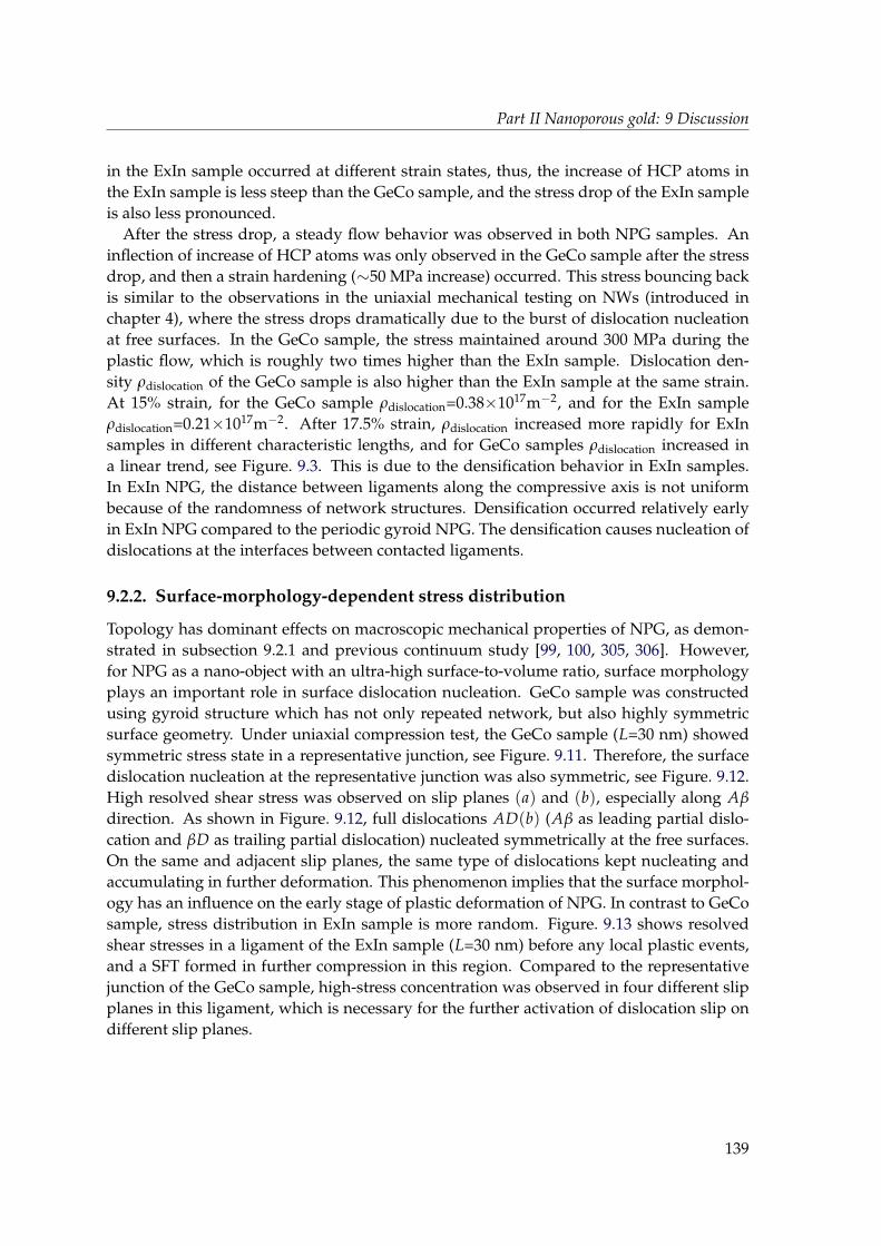
Part II Nanoporous gold: 9 Discussion
in the ExIn sample occurred at different strain states, thus, the increase of HCP atoms inthe ExIn sample is less steep than the GeCo sample, and the stress drop of the ExIn sampleis also less pronounced.
After the stress drop, a steady flow behavior was observed in both NPG samples. Aninflection of increase of HCP atoms was only observed in the GeCo sample after the stressdrop, and then a strain hardening (∼50 MPa increase) occurred. This stress bouncing backis similar to the observations in the uniaxial mechanical testing on NWs (introduced inchapter 4), where the stress drops dramatically due to the burst of dislocation nucleationat free surfaces. In the GeCo sample, the stress maintained around 300 MPa during theplastic flow, which is roughly two times higher than the ExIn sample. Dislocation den-sity ρdislocation of the GeCo sample is also higher than the ExIn sample at the same strain.At 15% strain, for the GeCo sample ρdislocation=0.38×10¹⁷m−2, and for the ExIn sampleρdislocation=0.21×10¹⁷m−2. After 17.5% strain, ρdislocation increased more rapidly for ExInsamples in different characteristic lengths, and for GeCo samples ρdislocation increased ina linear trend, see Figure. 9.3. This is due to the densification behavior in ExIn samples.In ExIn NPG, the distance between ligaments along the compressive axis is not uniformbecause of the randomness of network structures. Densification occurred relatively earlyin ExIn NPG compared to the periodic gyroid NPG. The densification causes nucleation ofdislocations at the interfaces between contacted ligaments.
9.2.2. Surface-morphology-dependent stress distribution
Topology has dominant effects on macroscopic mechanical properties of NPG, as demon-strated in subsection 9.2.1 and previous continuum study [99, 100, 305, 306]. However,for NPG as a nano-object with an ultra-high surface-to-volume ratio, surface morphologyplays an important role in surface dislocation nucleation. GeCo sample was constructedusing gyroid structure which has not only repeated network, but also highly symmetricsurface geometry. Under uniaxial compression test, the GeCo sample (L=30 nm) showedsymmetric stress state in a representative junction, see Figure. 9.11. Therefore, the surfacedislocation nucleation at the representative junction was also symmetric, see Figure. 9.12.High resolved shear stress was observed on slip planes (a) and (b), especially along Aβ
direction. As shown in Figure. 9.12, full dislocations AD(b) (Aβ as leading partial dislo-cation and βD as trailing partial dislocation) nucleated symmetrically at the free surfaces.On the same and adjacent slip planes, the same type of dislocations kept nucleating andaccumulating in further deformation. This phenomenon implies that the surface morphol-ogy has an influence on the early stage of plastic deformation of NPG. In contrast to GeCosample, stress distribution in ExIn sample is more random. Figure. 9.13 shows resolvedshear stresses in a ligament of the ExIn sample (L=30 nm) before any local plastic events,and a SFT formed in further compression in this region. Compared to the representativejunction of the GeCo sample, high-stress concentration was observed in four different slipplanes in this ligament, which is necessary for the further activation of dislocation slip ondifferent slip planes.
139
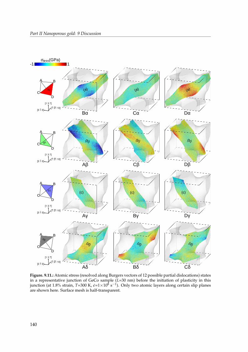
Part II Nanoporous gold: 9 Discussion
σR(GPa)1-1
Bα Cα Dα
Aβ Cβ Dβ
Aγ Bγ Dγ
Aδ Bδ Cδ
(b) (b) (b)
(a) (a) (a)
(c) (c) (c)
(d)(d)
(d)
A B
C
D
(a)
A B
C
D
A B
C
D
A B
C
D
(b)
(c)
(d)
[1 3 7]
[3 1 0][7 21 10]
[1 3 7]
[3 1 0][7 21 10]
[1 3 7]
[3 1 0][7 21 10]
[1 3 7]
[3 1 0][7 21 10]
Figure. 9.11.: Atomic stress (resolved along Burgers vectors of 12 possible partial dislocations) statesin a representative junction of GeCo sample (L=30 nm) before the initiation of plasticity in thisjunction (at 1.8% strain, T=300 K, ε=1×10⁸ s−1). Only two atomic layers along certain slip planesare shown here. Surface mesh is half-transparent.
140
Part II Nanoporous gold: 9 Discussion
BA
D
C
A
A
AD
A
D
AD
A
D
A
D
A
D
(b)
(b)
ε=1.94% ε=2.03% ε=2.42% ε=2.90%
a b c d
[1 3 7] [3 1 0]
[7 21 10]
Figure. 9.12.: Surface dislocation nucleation in a representative junction of GeCo sample (L=30 nm)during the simulated compression test (T=300 K, ε=1×10⁸ s−1).
141
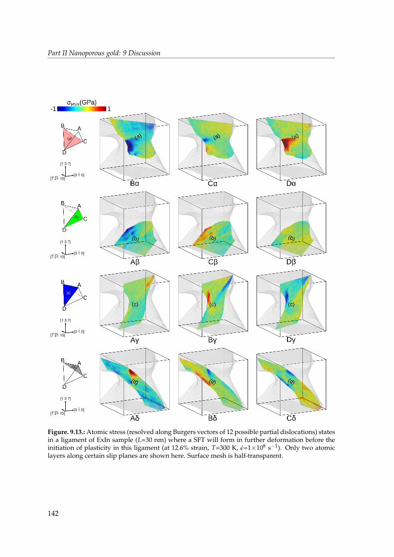
Part II Nanoporous gold: 9 Discussion
[1 3 7]
[3 1 0][7 21 10]
[1 3 7]
[3 1 0][7 21 10]
[1 3 7]
[3 1 0][7 21 10]
[1 3 7]
[3 1 0][7 21 10]
Figure. 9.13.: Atomic stress (resolved along Burgers vectors of 12 possible partial dislocations) statesin a ligament of ExIn sample (L=30 nm) where a SFT will form in further deformation before theinitiation of plasticity in this ligament (at 12.6% strain, T=300 K, ε=1×10⁸ s−1). Only two atomiclayers along certain slip planes are shown here. Surface mesh is half-transparent.
142
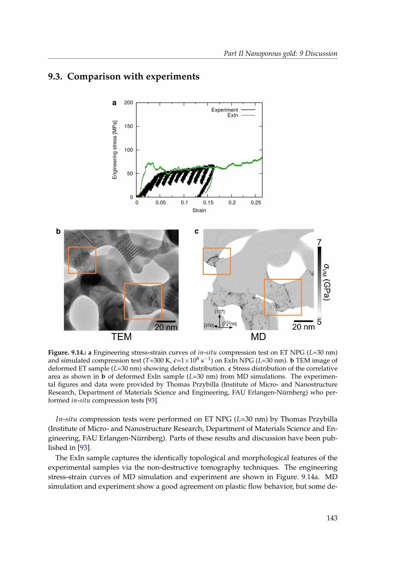
Part II Nanoporous gold: 9 Discussion
9.3. Comparison with experiments
0
50
100
150
200
0 0.05 0.1 0.15 0.2 0.25
En
gin
ee
rin
g s
tre
ss [
MP
a]
Strain
ExperimentExIn
a
b c
Figure. 9.14.: a Engineering stress-strain curves of in-situ compression test on ET NPG (L=30 nm)and simulated compression test (T=300 K, ε=1×10⁸ s−1) on ExIn NPG (L=30 nm). b TEM image ofdeformed ET sample (L=30 nm) showing defect distribution. c Stress distribution of the correlativearea as shown in b of deformed ExIn sample (L=30 nm) from MD simulations. The experimen-tal figures and data were provided by Thomas Przybilla (Institute of Micro- and NanostructureResearch, Department of Materials Science and Engineering, FAU Erlangen-Nurnberg) who per-formed in-situ compression tests [93].
In-situ compression tests were performed on ET NPG (L=30 nm) by Thomas Przybilla(Institute of Micro- and Nanostructure Research, Department of Materials Science and En-gineering, FAU Erlangen-Nurnberg). Parts of these results and discussion have been pub-lished in [93].
The ExIn sample captures the identically topological and morphological features of theexperimental samples via the non-destructive tomography techniques. The engineeringstress-strain curves of MD simulation and experiment are shown in Figure. 9.14a. MDsimulation and experiment show a good agreement on plastic flow behavior, but some de-
143
Part II Nanoporous gold: 9 Discussion
viations on elastic response and yield stress. These deviations of mechanical propertiesmay come from the limitations of MD simulations and imprecise measurements of experi-ments. MD simulations were performed on the pristine NPG, although with the assistanceof cutting-edge electron tomography technique ExIn sample has relatively realistic geom-etry, the internal defects which pre-existed in the experimental sample are not captured inthe simulated sample. These defects may lead to early yielding which lower the value ofσy of the experimental sample. Another limitation of MD simulations is timescales. Asmentioned in chapter 5, thermal activation of dislocation can not be mimicked in MD sim-ulations due to the limited timescales, thus the activation barrier can only be overcomeby applied stress. Therefore, yield strength σy predicted using MD simulations is gener-ally higher than the experimental value. From the experimental aspect, the calculation ofYoung’s modulus is not ideal, since the NPG pillar sat on a porous substrate which is notcompletely rigid at the beginning of the compression. Furthermore, MD simulation onlysimulated a part of the ET NPG pillar, which may not reflect the mechanical response of theentire pillar. In general, the comparison between experiments and MD simulations shouldonly be qualitative but not quantitative.
A qualitative study on topology-dependent deformation behavior of NPG can be achievedby comparing defect and stress/strain distribution in an identical area from the experi-ments and simulations. As shown in the TEM image of the deformed ET sample (see Fig-ure. 9.14b), defects are mainly localized near the junctions of the network structures. Thelocal von Mises stress concentration of the deformed ExIn sample (L=30 nm) from MD sim-ulations (see Figure. 9.14c) correlates well with the defect distribution of the identical areaas observed from TEM. Figure. 2.11 shows the characteristic crystal defects observed in thedeformed ET sample using TEM, which were also observed from MD simulations. Theidentical stress and defect distribution and resulting microstructures in simulations andexperiments indicate that the experimentally-informed real-size MD simulations can cap-ture not only the mechanical response in network structures, but also size- and geometry-dependent deformation mechanisms.
144
Part II Nanoporous gold: 10 Conclusions
10. Conclusions
In this part, deformation behavior and mechanisms of nanoporous gold (NPG) sampleswhich were reconstructed from non-destructive tomography techniques and constructedusing gyroid structures under compression were studied. The effects of size and geom-etry on mechanical properties, i.e., Young’s modulus, yield strength and flow stress, anddislocation-based deformation mechanisms were studied in detail. The main outcomes ofthese works are listed below.
• NPG shows strong size-dependent mechanical properties. For the elastic regime,the influence of non-linear elasticity on the size-dependency of Young’s modulus inloading orientation is mediated by the ligaments with different axial and facet orien-tations. For the yielding behavior, the effect of surface-induced stress is pronouncedin sub-ten-nanometer ligaments, which can assist surface dislocation nucleation, andthis effect is limited in NPG with a characteristic length of 30 nm. In NPG with liga-ment size of 30 nm, dislocation interaction and multiplication dominates the plasticflow.
• NPG show size-dependent resulting microstructures after compression, e.g., small-angle grain boundaries and stacking fault tetrahedron only widely existed in thedeformed real-size NPG with average ligament size of 30 nm. The size-dependentnucleation and interaction of full dislocations explain the formations of these defectsin the real-size NPG.
• Geometry-dependent mechanical properties and deformation mechanisms of NPGwere investigated at the atomic scale. The gyroid NPG is stiffer and stronger thanthe natural NPG with a similar porosity and average ligament size. Early yieldingwas observed in the natural NPG due to the heterogeneity of stress and ligament sizedistributions. In contrast, the yielding behavior in the gyroid NPG is more homoge-neous. Surface morphology has an effect on the initial stage of plastic deformation.Symmetric surface morphology in the gyroid NPG leads to symmetric stress fieldthus symmetric surface dislocation nucleation in certain slip systems. In contrast,random surface morphology in the natural NPG leads to the activation of dislocationslip in different slip systems.
• Atomistic simulations on the experimentally-informed real-size NPG show a quali-tative agreement with in-situ experiments, especially in plastic flow behavior and re-sulting microstructures. The limitations and shortcomings in both experiments andsimulations need to be taken into account when correlating experimental and mod-eling results.
From the cross-scale experimentally-informed simulations and 3D experimental charac-terization methods, we gain a better understanding of the influence of 3D microstructure
145
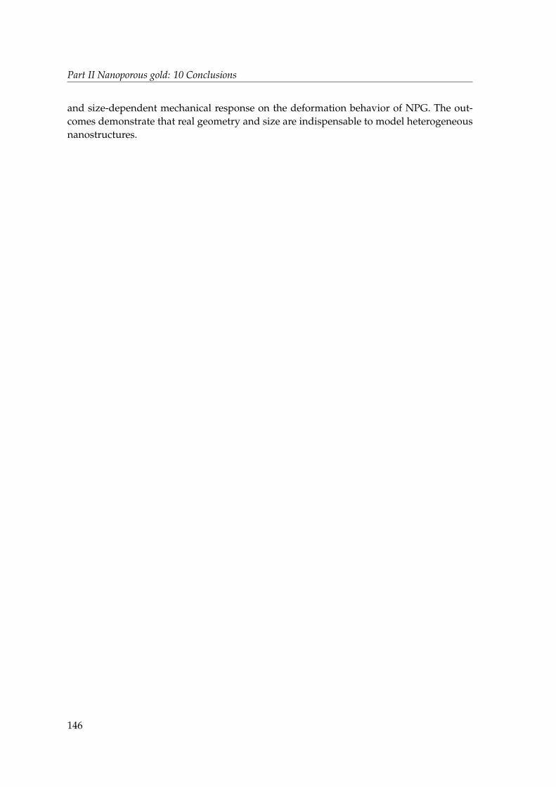
Part II Nanoporous gold: 10 Conclusions
and size-dependent mechanical response on the deformation behavior of NPG. The out-comes demonstrate that real geometry and size are indispensable to model heterogeneousnanostructures.
146
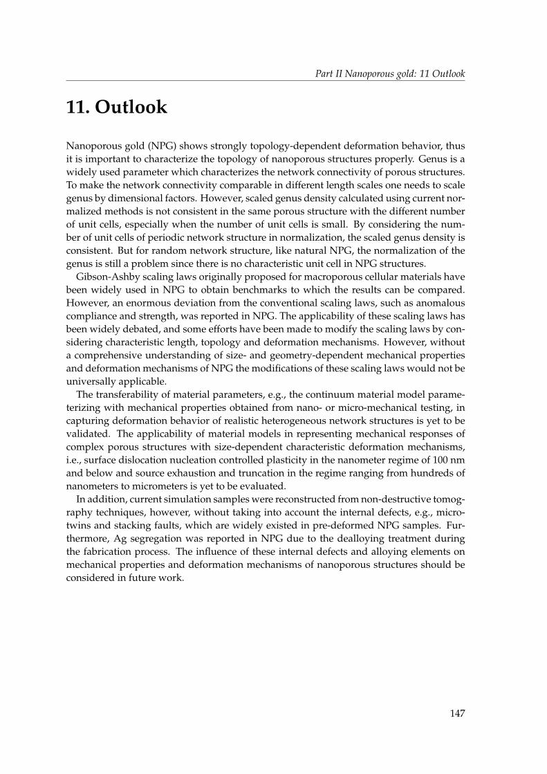
Part II Nanoporous gold: 11 Outlook
11. Outlook
Nanoporous gold (NPG) shows strongly topology-dependent deformation behavior, thusit is important to characterize the topology of nanoporous structures properly. Genus is awidely used parameter which characterizes the network connectivity of porous structures.To make the network connectivity comparable in different length scales one needs to scalegenus by dimensional factors. However, scaled genus density calculated using current nor-malized methods is not consistent in the same porous structure with the different numberof unit cells, especially when the number of unit cells is small. By considering the num-ber of unit cells of periodic network structure in normalization, the scaled genus density isconsistent. But for random network structure, like natural NPG, the normalization of thegenus is still a problem since there is no characteristic unit cell in NPG structures.
Gibson-Ashby scaling laws originally proposed for macroporous cellular materials havebeen widely used in NPG to obtain benchmarks to which the results can be compared.However, an enormous deviation from the conventional scaling laws, such as anomalouscompliance and strength, was reported in NPG. The applicability of these scaling laws hasbeen widely debated, and some efforts have been made to modify the scaling laws by con-sidering characteristic length, topology and deformation mechanisms. However, withouta comprehensive understanding of size- and geometry-dependent mechanical propertiesand deformation mechanisms of NPG the modifications of these scaling laws would not beuniversally applicable.
The transferability of material parameters, e.g., the continuum material model parame-terizing with mechanical properties obtained from nano- or micro-mechanical testing, incapturing deformation behavior of realistic heterogeneous network structures is yet to bevalidated. The applicability of material models in representing mechanical responses ofcomplex porous structures with size-dependent characteristic deformation mechanisms,i.e., surface dislocation nucleation controlled plasticity in the nanometer regime of 100 nmand below and source exhaustion and truncation in the regime ranging from hundreds ofnanometers to micrometers is yet to be evaluated.
In addition, current simulation samples were reconstructed from non-destructive tomog-raphy techniques, however, without taking into account the internal defects, e.g., micro-twins and stacking faults, which are widely existed in pre-deformed NPG samples. Fur-thermore, Ag segregation was reported in NPG due to the dealloying treatment duringthe fabrication process. The influence of these internal defects and alloying elements onmechanical properties and deformation mechanisms of nanoporous structures should beconsidered in future work.
147

Appendix
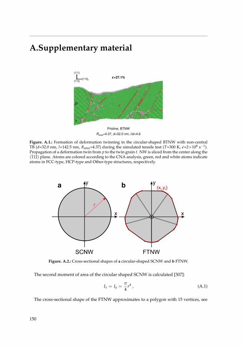
A.Supplementary material
Pristine, BTNW
Rarea=4.37, d=32.0 nm, l/d=4.6
ε=27.1%
p
t
[110]p[112]-
[111]- -
Figure. A.1.: Formation of deformation twinning in the circular-shaped BTNW with non-centralTB (d=32.0 nm, l=142.5 nm, Rarea=4.37) during the simulated tensile test (T=300 K, ε=2×10⁸ s−1).Propagation of a deformation twin from p to the twin grain t. NW is sliced from the center along the(112) plane. Atoms are colored according to the CNA analysis, green, red and white atoms indicateatoms in FCC-type, HCP-type and Other-type structures, respectively.
Figure. A.2.: Cross-sectional shapes of a circular-shaped SCNW and b FTNW.
The second moment of area of the circular shaped SCNW is calculated [307]:
Ix = Iy =π
4r4 , (A.1)
The cross-sectional shape of the FTNW approximates to a polygon with 15 vertices, see
150
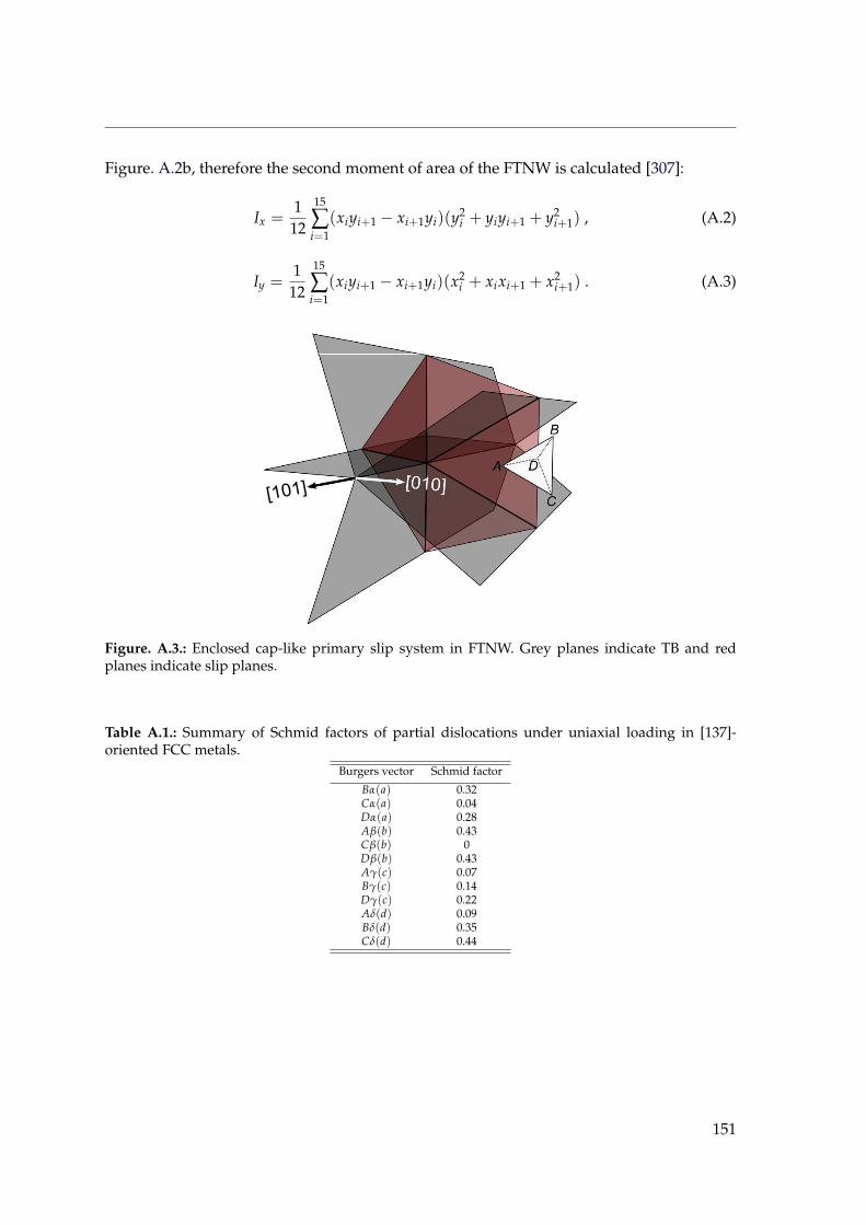
Figure. A.2b, therefore the second moment of area of the FTNW is calculated [307]:
Ix =1
12
15
∑i=1
(xiyi+1 − xi+1yi)(y2i + yiyi+1 + y2
i+1) , (A.2)
Iy =1
12
15
∑i=1
(xiyi+1 − xi+1yi)(x2i + xixi+1 + x2
i+1) . (A.3)
[101]
Figure. A.3.: Enclosed cap-like primary slip system in FTNW. Grey planes indicate TB and redplanes indicate slip planes.
Table A.1.: Summary of Schmid factors of partial dislocations under uniaxial loading in [137]-oriented FCC metals.
Burgers vector Schmid factor
Bα(a) 0.32Cα(a) 0.04Dα(a) 0.28Aβ(b) 0.43Cβ(b) 0Dβ(b) 0.43Aγ(c) 0.07Bγ(c) 0.14Dγ(c) 0.22Aδ(d) 0.09Bδ(d) 0.35Cδ(d) 0.44
151
References
[1] R. P. Feynman, There’s plenty of room at the bottom, California Institute of Technol-ogy, Engineering and Science magazine. (page 1).
[2] G. Binnig, H. Rohrer, C. Gerber, E. Weibel, Surface studies by scanning tunnelingmicroscopy, Physical Review Letters 49 (1) (1982) 57. (page 1).
[3] P. K. Jain, I. H. El-Sayed, M. A. El-Sayed, Au nanoparticles target cancer, Nano Today2 (1) (2007) 18–29. (page 1).
[4] M. Law, L. E. Greene, J. C. Johnson, R. Saykally, P. Yang, Nanowire dye-sensitizedsolar cells, Nature Materials 4 (6) (2005) 455. (page 1).
[5] O. Kraft, P. A. Gruber, R. Monig, D. Weygand, Plasticity in confined dimensions,Annual Review of Materials Research 40 (2010) 293–317. (pages 1 and 12).
[6] T. Zhu, J. Li, Ultra-strength materials, Progress in Materials Science 55 (7) (2010) 710–757.
[7] J. R. Greer, J. T. M. De Hosson, Plasticity in small-sized metallic systems: Intrinsicversus extrinsic size effect, Progress in Materials Science 56 (6) (2011) 654–724. (pages1, 1, 12, 13, 106, and 130).
[8] G. Richter, K. Hillerich, D. S. Gianola, R. Monig, O. Kraft, C. A. Volkert, Ultrahighstrength single crystalline nanowhiskers grown by physical vapor deposition, NanoLetters 9 (8) (2009) 3048–3052. (pages 1, 14, 15, 15, 16, 21, 41, and 41).
[9] H. Gleiter, Nanocrystalline materials, in: Advanced Structural and Functional Mate-rials, Springer, 1991, pp. 1–37. (page 1).
[10] N. Mameka, K. Wang, J. Markmann, E. T. Lilleodden, J. Weissmuller, Nanoporousgold-testing macro-scale samples to probe small-scale mechanical behavior, Materi-als Research Letters 4 (1) (2016) 27–36. (pages 1, 17, 17, 17, 18, 18, 19, and 19).
[11] X. Wu, Y. Zhu, Heterogeneous materials: a new class of materials with unprece-dented mechanical properties, Materials Research Letters 5 (8) (2017) 527–532. (page2).
[12] E. Ma, T. Zhu, Towards strength–ductility synergy through the design of heteroge-neous nanostructures in metals, Materials Today 20 (6) (2017) 323–331. (page 1).
[13] J. P. Hirth, J. Lothe, Theory of dislocations (1983). (pages 4, 6, 7, 10, 10, 10, and 37).
[14] D. Hull, D. J. Bacon, Introduction to dislocations, Butterworth-Heinemann, 2001.(pages 4, 6, 7, 7, 8, 9, 10, and 10).
[15] R. Heidenreich, W. Shockley, Report of a conference on the strength of solids, Lon-don: Physical Society (1948) 57. (page 5).
152
[16] F. Frank, Lxxxiii. crystal dislocations-elementary concepts and definitions, The Lon-don, Edinburgh, and Dublin Philosophical Magazine and Journal of Science 42 (331)(1951) 809–819. (page 6).
[17] W. Cai, V. V. Bulatov, J. Chang, J. Li, S. Yip, Dislocation core effects on mobility, Dis-locations in solids 12 (2004) 1–80. (page 6).
[18] N. Thompson, Dislocation nodes in face-centred cubic lattices, Proceedings of thePhysical Society. Section B 66 (6) (1953) 481. (pages 6, 9, and 45).
[19] V. Schmid, W. Boas, Kristallplastizitat, verlag julius springer (1935). (page 8).
[20] E. Tadmor, S. Hai, A peierls criterion for the onset of deformation twinning at a cracktip, Journal of the Mechanics and Physics of Solids 51 (5) (2003) 765–793. (pages 11,21, 21, and 37).
[21] C. R. Weinberger, W. Cai, Plasticity of metal nanowires, Journal of Materials Chem-istry 22 (8) (2012) 3277–3292. (pages 11, 12, 15, 20, 20, 21, 21, 21, 55, 55, 96, and 108).
[22] V. Vıtek, Intrinsic stacking faults in body-centred cubic crystals, Philosophical Mag-azine 18 (154) (1968) 773–786. (pages 11 and 38).
[23] J. R. Rice, Dislocation nucleation from a crack tip: an analysis based on the Peierlsconcept, Journal of the Mechanics and Physics of Solids 40 (2) (1992) 239–271. (pages11 and 38).
[24] J. Frenkel, Zur theorie der elastizitatsgrenze und der festigkeit kristallinischer korper,Zeitschrift fur Physik 37 (7-8) (1926) 572–609. (page 12).
[25] E. Hall, The deformation and ageing of mild steel: Iii discussion of results, Proceed-ings of the Physical Society. Section B 64 (9) (1951) 747. (page 12).
[26] N. Petch, The cleavage strength of polycrystals, Journal of the Iron and Steel Institute174 (1953) 25–28. (page 12).
[27] M. D. Uchic, D. M. Dimiduk, J. N. Florando, W. D. Nix, Sample dimensions influencestrength and crystal plasticity, Science 305 (5686) (2004) 986–989. (pages 13 and 15).
[28] J. R. Greer, W. D. Nix, Size dependence of mechanical properties of gold at the sub-micron scale, Applied Physics A 80 (8) (2005) 1625–1629. (page 13).
[29] C. A. Volkert, E. T. Lilleodden, Size effects in the deformation of sub-micron Aucolumns, Philosophical Magazine 86 (33-35) (2006) 5567–5579.
[30] D. Kiener, C. Motz, T. Schoberl, M. Jenko, G. Dehm, Determination of mechanicalproperties of copper at the micron scale, Advanced Engineering Materials 8 (11)(2006) 1119–1125.
153
[31] D. Norfleet, D. Dimiduk, S. Polasik, M. Uchic, M. Mills, Dislocation structuresand their relationship to strength in deformed nickel microcrystals, Acta Materialia56 (13) (2008) 2988–3001. (page 13).
[32] M. D. Uchic, P. A. Shade, D. M. Dimiduk, Plasticity of micrometer-scale single crys-tals in compression, Annual Review of Materials Research 39 (2009) 361–386. (page13).
[33] R. Dou, B. Derby, A universal scaling law for the strength of metal micropillars andnanowires, Scripta Materialia 61 (5) (2009) 524–527. (pages 13, 13, and 14).
[34] T. A. Parthasarathy, S. I. Rao, D. M. Dimiduk, M. D. Uchic, D. R. Trinkle, Contributionto size effect of yield strength from the stochastics of dislocation source lengths infinite samples, Scripta Materialia 56 (4) (2007) 313–316. (page 13 and 13).
[35] S. I. Rao, D. Dimiduk, M. Tang, M. Uchic, T. Parthasarathy, C. Woodward, Estimat-ing the strength of single-ended dislocation sources in micron-sized single crystals,Philosophical Magazine 87 (30) (2007) 4777–4794. (page 13).
[36] S. I. Rao, D. Dimiduk, T. A. Parthasarathy, M. Uchic, M. Tang, C. Woodward, Ather-mal mechanisms of size-dependent crystal flow gleaned from three-dimensional dis-crete dislocation simulations, Acta Materialia 56 (13) (2008) 3245–3259. (page 13and 13).
[37] J. R. Greer, W. D. Nix, Nanoscale gold pillars strengthened through dislocation star-vation, Physical Review B 73 (24) (2006) 245410. (pages 14, 106, and 130).
[38] C. Herring, J. Galt, Elastic and plastic properties of very small metal specimens, Phys-ical Review 85 (6) (1952) 1060. (page 14).
[39] S. S. Brenner, Tensile strength of whiskers, Journal of Applied Physics 27 (12) (1956)1484–1491. (page 14).
[40] S. Brenner, Plastic deformation of copper and silver whiskers, Journal of AppliedPhysics 28 (9) (1957) 1023–1026. (page 14).
[41] Q.-J. Li, B. Xu, S. Hara, J. Li, E. Ma, Sample-size-dependent surface dislocation nu-cleation in nanoscale crystals, Acta Materialia 145 (2018) 19–29. (pages 14, 15, 15, 15,24, 26, 127, and 127).
[42] Q.-J. Li, E. Ma, When ’smaller is stronger’ no longer holds, Materials Research Letters6 (5) (2018) 283–292. (pages 14, 15, 15, 15, and 104).
[43] A. Chokshi, A. Rosen, J. Karch, H. Gleiter, On the validity of the Hall-Petch rela-tionship in nanocrystalline materials, Scripta Metallurgica 23 (10) (1989) 1679–1683.(page 14).
[44] G. Nieman, J. Weertman, R. Siegel, Micro-hardness of nanocrystalline palladium andcopper produced by inert-gas condensation, Scripta Metallurgica 23 (12) (1989) 2013–2018. (page 14).
154
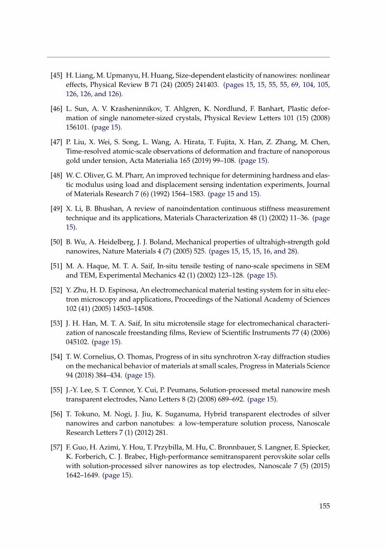
[45] H. Liang, M. Upmanyu, H. Huang, Size-dependent elasticity of nanowires: nonlineareffects, Physical Review B 71 (24) (2005) 241403. (pages 15, 15, 55, 55, 69, 104, 105,126, 126, and 126).
[46] L. Sun, A. V. Krasheninnikov, T. Ahlgren, K. Nordlund, F. Banhart, Plastic defor-mation of single nanometer-sized crystals, Physical Review Letters 101 (15) (2008)156101. (page 15).
[47] P. Liu, X. Wei, S. Song, L. Wang, A. Hirata, T. Fujita, X. Han, Z. Zhang, M. Chen,Time-resolved atomic-scale observations of deformation and fracture of nanoporousgold under tension, Acta Materialia 165 (2019) 99–108. (page 15).
[48] W. C. Oliver, G. M. Pharr, An improved technique for determining hardness and elas-tic modulus using load and displacement sensing indentation experiments, Journalof Materials Research 7 (6) (1992) 1564–1583. (page 15 and 15).
[49] X. Li, B. Bhushan, A review of nanoindentation continuous stiffness measurementtechnique and its applications, Materials Characterization 48 (1) (2002) 11–36. (page15).
[50] B. Wu, A. Heidelberg, J. J. Boland, Mechanical properties of ultrahigh-strength goldnanowires, Nature Materials 4 (7) (2005) 525. (pages 15, 15, 15, 16, and 28).
[51] M. A. Haque, M. T. A. Saif, In-situ tensile testing of nano-scale specimens in SEMand TEM, Experimental Mechanics 42 (1) (2002) 123–128. (page 15).
[52] Y. Zhu, H. D. Espinosa, An electromechanical material testing system for in situ elec-tron microscopy and applications, Proceedings of the National Academy of Sciences102 (41) (2005) 14503–14508.
[53] J. H. Han, M. T. A. Saif, In situ microtensile stage for electromechanical characteri-zation of nanoscale freestanding films, Review of Scientific Instruments 77 (4) (2006)045102. (page 15).
[54] T. W. Cornelius, O. Thomas, Progress of in situ synchrotron X-ray diffraction studieson the mechanical behavior of materials at small scales, Progress in Materials Science94 (2018) 384–434. (page 15).
[55] J.-Y. Lee, S. T. Connor, Y. Cui, P. Peumans, Solution-processed metal nanowire meshtransparent electrodes, Nano Letters 8 (2) (2008) 689–692. (page 15).
[56] T. Tokuno, M. Nogi, J. Jiu, K. Suganuma, Hybrid transparent electrodes of silvernanowires and carbon nanotubes: a low-temperature solution process, NanoscaleResearch Letters 7 (1) (2012) 281.
[57] F. Guo, H. Azimi, Y. Hou, T. Przybilla, M. Hu, C. Bronnbauer, S. Langner, E. Spiecker,K. Forberich, C. J. Brabec, High-performance semitransparent perovskite solar cellswith solution-processed silver nanowires as top electrodes, Nanoscale 7 (5) (2015)1642–1649. (page 15).
155
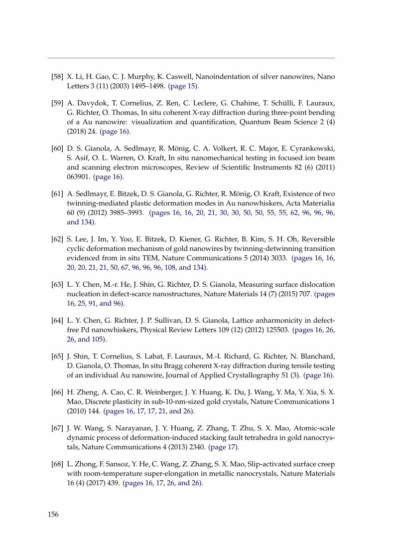
[58] X. Li, H. Gao, C. J. Murphy, K. Caswell, Nanoindentation of silver nanowires, NanoLetters 3 (11) (2003) 1495–1498. (page 15).
[59] A. Davydok, T. Cornelius, Z. Ren, C. Leclere, G. Chahine, T. Schulli, F. Lauraux,G. Richter, O. Thomas, In situ coherent X-ray diffraction during three-point bendingof a Au nanowire: visualization and quantification, Quantum Beam Science 2 (4)(2018) 24. (page 16).
[60] D. S. Gianola, A. Sedlmayr, R. Monig, C. A. Volkert, R. C. Major, E. Cyrankowski,S. Asif, O. L. Warren, O. Kraft, In situ nanomechanical testing in focused ion beamand scanning electron microscopes, Review of Scientific Instruments 82 (6) (2011)063901. (page 16).
[61] A. Sedlmayr, E. Bitzek, D. S. Gianola, G. Richter, R. Monig, O. Kraft, Existence of twotwinning-mediated plastic deformation modes in Au nanowhiskers, Acta Materialia60 (9) (2012) 3985–3993. (pages 16, 16, 20, 21, 30, 30, 50, 50, 55, 55, 62, 96, 96, 96,and 134).
[62] S. Lee, J. Im, Y. Yoo, E. Bitzek, D. Kiener, G. Richter, B. Kim, S. H. Oh, Reversiblecyclic deformation mechanism of gold nanowires by twinning-detwinning transitionevidenced from in situ TEM, Nature Communications 5 (2014) 3033. (pages 16, 16,20, 20, 21, 21, 50, 67, 96, 96, 96, 108, and 134).
[63] L. Y. Chen, M.-r. He, J. Shin, G. Richter, D. S. Gianola, Measuring surface dislocationnucleation in defect-scarce nanostructures, Nature Materials 14 (7) (2015) 707. (pages16, 25, 91, and 96).
[64] L. Y. Chen, G. Richter, J. P. Sullivan, D. S. Gianola, Lattice anharmonicity in defect-free Pd nanowhiskers, Physical Review Letters 109 (12) (2012) 125503. (pages 16, 26,26, and 105).
[65] J. Shin, T. Cornelius, S. Labat, F. Lauraux, M.-I. Richard, G. Richter, N. Blanchard,D. Gianola, O. Thomas, In situ Bragg coherent X-ray diffraction during tensile testingof an individual Au nanowire, Journal of Applied Crystallography 51 (3). (page 16).
[66] H. Zheng, A. Cao, C. R. Weinberger, J. Y. Huang, K. Du, J. Wang, Y. Ma, Y. Xia, S. X.Mao, Discrete plasticity in sub-10-nm-sized gold crystals, Nature Communications 1(2010) 144. (pages 16, 17, 17, 21, and 26).
[67] J. W. Wang, S. Narayanan, J. Y. Huang, Z. Zhang, T. Zhu, S. X. Mao, Atomic-scaledynamic process of deformation-induced stacking fault tetrahedra in gold nanocrys-tals, Nature Communications 4 (2013) 2340. (page 17).
[68] L. Zhong, F. Sansoz, Y. He, C. Wang, Z. Zhang, S. X. Mao, Slip-activated surface creepwith room-temperature super-elongation in metallic nanocrystals, Nature Materials16 (4) (2017) 439. (pages 16, 17, 26, and 26).
156
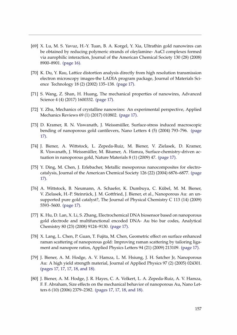
[69] X. Lu, M. S. Yavuz, H.-Y. Tuan, B. A. Korgel, Y. Xia, Ultrathin gold nanowires canbe obtained by reducing polymeric strands of oleylamine- AuCl complexes formedvia aurophilic interaction, Journal of the American Chemical Society 130 (28) (2008)8900–8901. (page 16).
[70] K. Du, Y. Rau, Lattice distortion analysis directly from high resolution transmissionelectron microscopy images-the LADIA program package, Journal of Materials Sci-ence Technology 18 (2) (2002) 135–138. (page 17).
[71] S. Wang, Z. Shan, H. Huang, The mechanical properties of nanowires, AdvancedScience 4 (4) (2017) 1600332. (page 17).
[72] Y. Zhu, Mechanics of crystalline nanowires: An experimental perspective, AppliedMechanics Reviews 69 (1) (2017) 010802. (page 17).
[73] D. Kramer, R. N. Viswanath, J. Weissmuller, Surface-stress induced macroscopicbending of nanoporous gold cantilevers, Nano Letters 4 (5) (2004) 793–796. (page17).
[74] J. Biener, A. Wittstock, L. Zepeda-Ruiz, M. Biener, V. Zielasek, D. Kramer,R. Viswanath, J. Weissmuller, M. Baumer, A. Hamza, Surface-chemistry-driven ac-tuation in nanoporous gold, Nature Materials 8 (1) (2009) 47. (page 17).
[75] Y. Ding, M. Chen, J. Erlebacher, Metallic mesoporous nanocomposites for electro-catalysis, Journal of the American Chemical Society 126 (22) (2004) 6876–6877. (page17).
[76] A. Wittstock, B. Neumann, A. Schaefer, K. Dumbuya, C. Kubel, M. M. Biener,V. Zielasek, H.-P. Steinruck, J. M. Gottfried, J. Biener, et al., Nanoporous Au: an un-supported pure gold catalyst?, The Journal of Physical Chemistry C 113 (14) (2009)5593–5600. (page 17).
[77] K. Hu, D. Lan, X. Li, S. Zhang, Electrochemical DNA biosensor based on nanoporousgold electrode and multifunctional encoded DNA- Au bio bar codes, AnalyticalChemistry 80 (23) (2008) 9124–9130. (page 17).
[78] X. Lang, L. Chen, P. Guan, T. Fujita, M. Chen, Geometric effect on surface enhancedraman scattering of nanoporous gold: Improving raman scattering by tailoring liga-ment and nanopore ratios, Applied Physics Letters 94 (21) (2009) 213109. (page 17).
[79] J. Biener, A. M. Hodge, A. V. Hamza, L. M. Hsiung, J. H. Satcher Jr, NanoporousAu: A high yield strength material, Journal of Applied Physics 97 (2) (2005) 024301.(pages 17, 17, 17, 18, and 18).
[80] J. Biener, A. M. Hodge, J. R. Hayes, C. A. Volkert, L. A. Zepeda-Ruiz, A. V. Hamza,F. F. Abraham, Size effects on the mechanical behavior of nanoporous Au, Nano Let-ters 6 (10) (2006) 2379–2382. (pages 17, 17, 18, and 18).
157
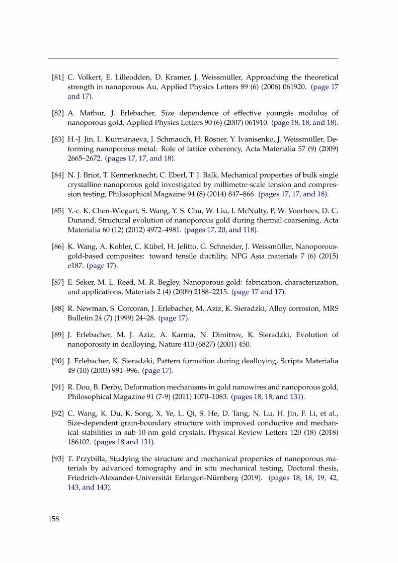
[81] C. Volkert, E. Lilleodden, D. Kramer, J. Weissmuller, Approaching the theoreticalstrength in nanoporous Au, Applied Physics Letters 89 (6) (2006) 061920. (page 17and 17).
[82] A. Mathur, J. Erlebacher, Size dependence of effective youngas modulus ofnanoporous gold, Applied Physics Letters 90 (6) (2007) 061910. (page 18, 18, and 18).
[83] H.-J. Jin, L. Kurmanaeva, J. Schmauch, H. Rosner, Y. Ivanisenko, J. Weissmuller, De-forming nanoporous metal: Role of lattice coherency, Acta Materialia 57 (9) (2009)2665–2672. (pages 17, 17, and 18).
[84] N. J. Briot, T. Kennerknecht, C. Eberl, T. J. Balk, Mechanical properties of bulk singlecrystalline nanoporous gold investigated by millimetre-scale tension and compres-sion testing, Philosophical Magazine 94 (8) (2014) 847–866. (pages 17, 17, and 18).
[85] Y.-c. K. Chen-Wiegart, S. Wang, Y. S. Chu, W. Liu, I. McNulty, P. W. Voorhees, D. C.Dunand, Structural evolution of nanoporous gold during thermal coarsening, ActaMaterialia 60 (12) (2012) 4972–4981. (pages 17, 20, and 118).
[86] K. Wang, A. Kobler, C. Kubel, H. Jelitto, G. Schneider, J. Weissmuller, Nanoporous-gold-based composites: toward tensile ductility, NPG Asia materials 7 (6) (2015)e187. (page 17).
[87] E. Seker, M. L. Reed, M. R. Begley, Nanoporous gold: fabrication, characterization,and applications, Materials 2 (4) (2009) 2188–2215. (page 17 and 17).
[88] R. Newman, S. Corcoran, J. Erlebacher, M. Aziz, K. Sieradzki, Alloy corrosion, MRSBulletin 24 (7) (1999) 24–28. (page 17).
[89] J. Erlebacher, M. J. Aziz, A. Karma, N. Dimitrov, K. Sieradzki, Evolution ofnanoporosity in dealloying, Nature 410 (6827) (2001) 450.
[90] J. Erlebacher, K. Sieradzki, Pattern formation during dealloying, Scripta Materialia49 (10) (2003) 991–996. (page 17).
[91] R. Dou, B. Derby, Deformation mechanisms in gold nanowires and nanoporous gold,Philosophical Magazine 91 (7-9) (2011) 1070–1083. (pages 18, 18, and 131).
[92] C. Wang, K. Du, K. Song, X. Ye, L. Qi, S. He, D. Tang, N. Lu, H. Jin, F. Li, et al.,Size-dependent grain-boundary structure with improved conductive and mechan-ical stabilities in sub-10-nm gold crystals, Physical Review Letters 120 (18) (2018)186102. (pages 18 and 131).
[93] T. Przybilla, Studying the structure and mechanical properties of nanoporous ma-terials by advanced tomography and in situ mechanical testing, Doctoral thesis,Friedrich-Alexander-Universitat Erlangen-Nurnberg (2019). (pages 18, 18, 19, 42,143, and 143).
158
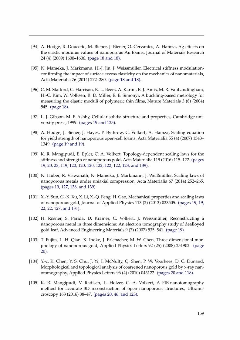
[94] A. Hodge, R. Doucette, M. Biener, J. Biener, O. Cervantes, A. Hamza, Ag effects onthe elastic modulus values of nanoporous Au foams, Journal of Materials Research24 (4) (2009) 1600–1606. (page 18 and 18).
[95] N. Mameka, J. Markmann, H.-J. Jin, J. Weissmuller, Electrical stiffness modulation-confirming the impact of surface excess elasticity on the mechanics of nanomaterials,Acta Materialia 76 (2014) 272–280. (page 18 and 18).
[96] C. M. Stafford, C. Harrison, K. L. Beers, A. Karim, E. J. Amis, M. R. VanLandingham,H.-C. Kim, W. Volksen, R. D. Miller, E. E. Simonyi, A buckling-based metrology formeasuring the elastic moduli of polymeric thin films, Nature Materials 3 (8) (2004)545. (page 18).
[97] L. J. Gibson, M. F. Ashby, Cellular solids: structure and properties, Cambridge uni-versity press, 1999. (pages 19 and 123).
[98] A. Hodge, J. Biener, J. Hayes, P. Bythrow, C. Volkert, A. Hamza, Scaling equationfor yield strength of nanoporous open-cell foams, Acta Materialia 55 (4) (2007) 1343–1349. (page 19 and 19).
[99] K. R. Mangipudi, E. Epler, C. A. Volkert, Topology-dependent scaling laws for thestiffness and strength of nanoporous gold, Acta Materialia 119 (2016) 115–122. (pages19, 20, 23, 119, 120, 120, 120, 122, 122, 122, 123, and 139).
[100] N. Huber, R. Viswanath, N. Mameka, J. Markmann, J. Weißmuller, Scaling laws ofnanoporous metals under uniaxial compression, Acta Materialia 67 (2014) 252–265.(pages 19, 127, 138, and 139).
[101] X.-Y. Sun, G.-K. Xu, X. Li, X.-Q. Feng, H. Gao, Mechanical properties and scaling lawsof nanoporous gold, Journal of Applied Physics 113 (2) (2013) 023505. (pages 19, 19,22, 22, 127, and 131).
[102] H. Rosner, S. Parida, D. Kramer, C. Volkert, J. Weissmuller, Reconstructing ananoporous metal in three dimensions: An electron tomography study of dealloyedgold leaf, Advanced Engineering Materials 9 (7) (2007) 535–541. (page 19).
[103] T. Fujita, L.-H. Qian, K. Inoke, J. Erlebacher, M.-W. Chen, Three-dimensional mor-phology of nanoporous gold, Applied Physics Letters 92 (25) (2008) 251902. (page20).
[104] Y.-c. K. Chen, Y. S. Chu, J. Yi, I. McNulty, Q. Shen, P. W. Voorhees, D. C. Dunand,Morphological and topological analysis of coarsened nanoporous gold by x-ray nan-otomography, Applied Physics Letters 96 (4) (2010) 043122. (pages 20 and 118).
[105] K. R. Mangipudi, V. Radisch, L. Holzer, C. A. Volkert, A FIB-nanotomographymethod for accurate 3D reconstruction of open nanoporous structures, Ultrami-croscopy 163 (2016) 38–47. (pages 20, 46, and 123).
159
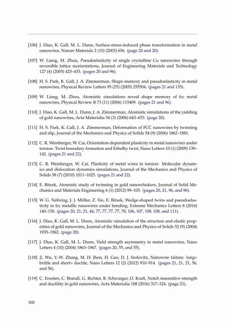
[106] J. Diao, K. Gall, M. L. Dunn, Surface-stress-induced phase transformation in metalnanowires, Nature Materials 2 (10) (2003) 656. (page 20 and 20).
[107] W. Liang, M. Zhou, Pseudoelasticity of single crystalline Cu nanowires throughreversible lattice reorientations, Journal of Engineering Materials and Technology127 (4) (2005) 423–433. (pages 20 and 96).
[108] H. S. Park, K. Gall, J. A. Zimmerman, Shape memory and pseudoelasticity in metalnanowires, Physical Review Letters 95 (25) (2005) 255504. (pages 21 and 135).
[109] W. Liang, M. Zhou, Atomistic simulations reveal shape memory of fcc metalnanowires, Physical Review B 73 (11) (2006) 115409. (pages 21 and 96).
[110] J. Diao, K. Gall, M. L. Dunn, J. A. Zimmerman, Atomistic simulations of the yieldingof gold nanowires, Acta Materialia 54 (3) (2006) 643–653. (page 20).
[111] H. S. Park, K. Gall, J. A. Zimmerman, Deformation of FCC nanowires by twinningand slip, Journal of the Mechanics and Physics of Solids 54 (9) (2006) 1862–1881.
[112] C. R. Weinberger, W. Cai, Orientation-dependent plasticity in metal nanowires undertorsion: Twist boundary formation and Eshelby twist, Nano Letters 10 (1) (2009) 139–142. (pages 21 and 22).
[113] C. R. Weinberger, W. Cai, Plasticity of metal wires in torsion: Molecular dynam-ics and dislocation dynamics simulations, Journal of the Mechanics and Physics ofSolids 58 (7) (2010) 1011–1025. (pages 21 and 22).
[114] E. Bitzek, Atomistic study of twinning in gold nanowhiskers, Journal of Solid Me-chanics and Materials Engineering 6 (1) (2012) 99–105. (pages 20, 21, 96, and 96).
[115] W. G. Nohring, J. J. Moller, Z. Xie, E. Bitzek, Wedge-shaped twins and pseudoelas-ticity in fcc metallic nanowires under bending, Extreme Mechanics Letters 8 (2016)140–150. (pages 20, 21, 21, 44, 77, 77, 77, 77, 78, 106, 107, 108, 108, and 111).
[116] J. Diao, K. Gall, M. L. Dunn, Atomistic simulation of the structure and elastic prop-erties of gold nanowires, Journal of the Mechanics and Physics of Solids 52 (9) (2004)1935–1962. (page 20).
[117] J. Diao, K. Gall, M. L. Dunn, Yield strength asymmetry in metal nanowires, NanoLetters 4 (10) (2004) 1863–1867. (pages 20, 55, and 55).
[118] Z. Wu, Y.-W. Zhang, M. H. Jhon, H. Gao, D. J. Srolovitz, Nanowire failure: long=brittle and short= ductile, Nano Letters 12 (2) (2012) 910–914. (pages 21, 21, 21, 56,and 56).
[119] C. Ensslen, C. Brandl, G. Richter, R. Schwaiger, O. Kraft, Notch insensitive strengthand ductility in gold nanowires, Acta Materialia 108 (2016) 317–324. (page 21).
160
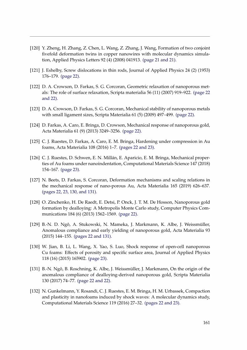
[120] Y. Zheng, H. Zhang, Z. Chen, L. Wang, Z. Zhang, J. Wang, Formation of two conjointfivefold deformation twins in copper nanowires with molecular dynamics simula-tion, Applied Physics Letters 92 (4) (2008) 041913. (page 21 and 21).
[121] J. Eshelby, Screw dislocations in thin rods, Journal of Applied Physics 24 (2) (1953)176–179. (page 22).
[122] D. A. Crowson, D. Farkas, S. G. Corcoran, Geometric relaxation of nanoporous met-als: The role of surface relaxation, Scripta materialia 56 (11) (2007) 919–922. (page 22and 22).
[123] D. A. Crowson, D. Farkas, S. G. Corcoran, Mechanical stability of nanoporous metalswith small ligament sizes, Scripta Materialia 61 (5) (2009) 497–499. (page 22).
[124] D. Farkas, A. Caro, E. Bringa, D. Crowson, Mechanical response of nanoporous gold,Acta Materialia 61 (9) (2013) 3249–3256. (page 22).
[125] C. J. Ruestes, D. Farkas, A. Caro, E. M. Bringa, Hardening under compression in Aufoams, Acta Materialia 108 (2016) 1–7. (pages 22 and 23).
[126] C. J. Ruestes, D. Schwen, E. N. Millan, E. Aparicio, E. M. Bringa, Mechanical proper-ties of Au foams under nanoindentation, Computational Materials Science 147 (2018)154–167. (page 23).
[127] N. Beets, D. Farkas, S. Corcoran, Deformation mechanisms and scaling relations inthe mechanical response of nano-porous Au, Acta Materialia 165 (2019) 626–637.(pages 22, 23, 130, and 131).
[128] O. Zinchenko, H. De Raedt, E. Detsi, P. Onck, J. T. M. De Hosson, Nanoporous goldformation by dealloying: A Metropolis Monte Carlo study, Computer Physics Com-munications 184 (6) (2013) 1562–1569. (page 22).
[129] B.-N. D. Ngo, A. Stukowski, N. Mameka, J. Markmann, K. Albe, J. Weissmuller,Anomalous compliance and early yielding of nanoporous gold, Acta Materialia 93(2015) 144–155. (pages 22 and 131).
[130] W. Jian, B. Li, L. Wang, X. Yao, S. Luo, Shock response of open-cell nanoporousCu foams: Effects of porosity and specific surface area, Journal of Applied Physics118 (16) (2015) 165902. (page 23).
[131] B.-N. Ngo, B. Roschning, K. Albe, J. Weissmuller, J. Markmann, On the origin of theanomalous compliance of dealloying-derived nanoporous gold, Scripta Materialia130 (2017) 74–77. (page 22 and 22).
[132] N. Gunkelmann, Y. Rosandi, C. J. Ruestes, E. M. Bringa, H. M. Urbassek, Compactionand plasticity in nanofoams induced by shock waves: A molecular dynamics study,Computational Materials Science 119 (2016) 27–32. (pages 22 and 23).
161
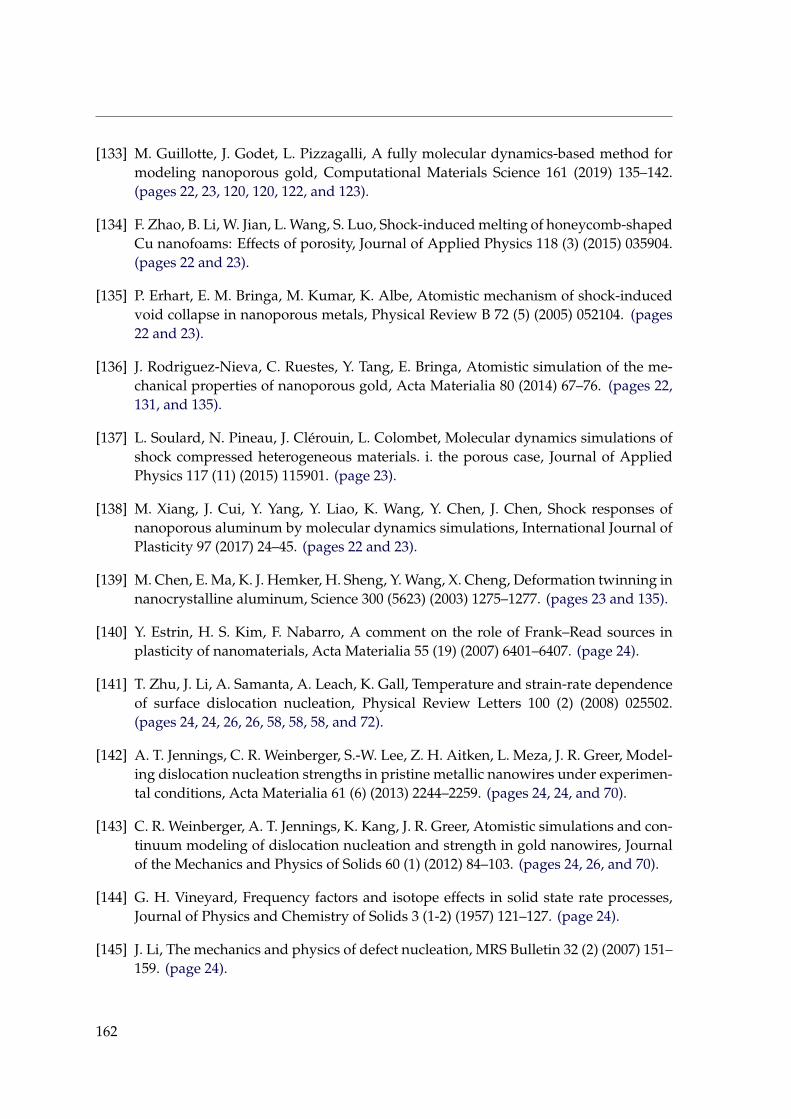
[133] M. Guillotte, J. Godet, L. Pizzagalli, A fully molecular dynamics-based method formodeling nanoporous gold, Computational Materials Science 161 (2019) 135–142.(pages 22, 23, 120, 120, 122, and 123).
[134] F. Zhao, B. Li, W. Jian, L. Wang, S. Luo, Shock-induced melting of honeycomb-shapedCu nanofoams: Effects of porosity, Journal of Applied Physics 118 (3) (2015) 035904.(pages 22 and 23).
[135] P. Erhart, E. M. Bringa, M. Kumar, K. Albe, Atomistic mechanism of shock-inducedvoid collapse in nanoporous metals, Physical Review B 72 (5) (2005) 052104. (pages22 and 23).
[136] J. Rodriguez-Nieva, C. Ruestes, Y. Tang, E. Bringa, Atomistic simulation of the me-chanical properties of nanoporous gold, Acta Materialia 80 (2014) 67–76. (pages 22,131, and 135).
[137] L. Soulard, N. Pineau, J. Clerouin, L. Colombet, Molecular dynamics simulations ofshock compressed heterogeneous materials. i. the porous case, Journal of AppliedPhysics 117 (11) (2015) 115901. (page 23).
[138] M. Xiang, J. Cui, Y. Yang, Y. Liao, K. Wang, Y. Chen, J. Chen, Shock responses ofnanoporous aluminum by molecular dynamics simulations, International Journal ofPlasticity 97 (2017) 24–45. (pages 22 and 23).
[139] M. Chen, E. Ma, K. J. Hemker, H. Sheng, Y. Wang, X. Cheng, Deformation twinning innanocrystalline aluminum, Science 300 (5623) (2003) 1275–1277. (pages 23 and 135).
[140] Y. Estrin, H. S. Kim, F. Nabarro, A comment on the role of Frank–Read sources inplasticity of nanomaterials, Acta Materialia 55 (19) (2007) 6401–6407. (page 24).
[141] T. Zhu, J. Li, A. Samanta, A. Leach, K. Gall, Temperature and strain-rate dependenceof surface dislocation nucleation, Physical Review Letters 100 (2) (2008) 025502.(pages 24, 24, 26, 26, 58, 58, 58, and 72).
[142] A. T. Jennings, C. R. Weinberger, S.-W. Lee, Z. H. Aitken, L. Meza, J. R. Greer, Model-ing dislocation nucleation strengths in pristine metallic nanowires under experimen-tal conditions, Acta Materialia 61 (6) (2013) 2244–2259. (pages 24, 24, and 70).
[143] C. R. Weinberger, A. T. Jennings, K. Kang, J. R. Greer, Atomistic simulations and con-tinuum modeling of dislocation nucleation and strength in gold nanowires, Journalof the Mechanics and Physics of Solids 60 (1) (2012) 84–103. (pages 24, 26, and 70).
[144] G. H. Vineyard, Frequency factors and isotope effects in solid state rate processes,Journal of Physics and Chemistry of Solids 3 (1-2) (1957) 121–127. (page 24).
[145] J. Li, The mechanics and physics of defect nucleation, MRS Bulletin 32 (2) (2007) 151–159. (page 24).
162
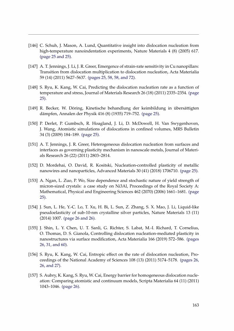
[146] C. Schuh, J. Mason, A. Lund, Quantitative insight into dislocation nucleation fromhigh-temperature nanoindentation experiments, Nature Materials 4 (8) (2005) 617.(page 25 and 25).
[147] A. T. Jennings, J. Li, J. R. Greer, Emergence of strain-rate sensitivity in Cu nanopillars:Transition from dislocation multiplication to dislocation nucleation, Acta Materialia59 (14) (2011) 5627–5637. (pages 25, 58, 58, and 72).
[148] S. Ryu, K. Kang, W. Cai, Predicting the dislocation nucleation rate as a function oftemperature and stress, Journal of Materials Research 26 (18) (2011) 2335–2354. (page25).
[149] R. Becker, W. Doring, Kinetische behandlung der keimbildung in ubersattigtendampfen, Annalen der Physik 416 (8) (1935) 719–752. (page 25).
[150] P. Derlet, P. Gumbsch, R. Hoagland, J. Li, D. McDowell, H. Van Swygenhoven,J. Wang, Atomistic simulations of dislocations in confined volumes, MRS Bulletin34 (3) (2009) 184–189. (page 25).
[151] A. T. Jennings, J. R. Greer, Heterogeneous dislocation nucleation from surfaces andinterfaces as governing plasticity mechanism in nanoscale metals, Journal of Materi-als Research 26 (22) (2011) 2803–2814.
[152] D. Mordehai, O. David, R. Kositski, Nucleation-controlled plasticity of metallicnanowires and nanoparticles, Advanced Materials 30 (41) (2018) 1706710. (page 25).
[153] A. Ngan, L. Zuo, P. Wo, Size dependence and stochastic nature of yield strength ofmicron-sized crystals: a case study on Ni3Al, Proceedings of the Royal Society A:Mathematical, Physical and Engineering Sciences 462 (2070) (2006) 1661–1681. (page25).
[154] J. Sun, L. He, Y.-C. Lo, T. Xu, H. Bi, L. Sun, Z. Zhang, S. X. Mao, J. Li, Liquid-likepseudoelasticity of sub-10-nm crystalline silver particles, Nature Materials 13 (11)(2014) 1007. (page 26 and 26).
[155] J. Shin, L. Y. Chen, U. T. Sanli, G. Richter, S. Labat, M.-I. Richard, T. Cornelius,O. Thomas, D. S. Gianola, Controlling dislocation nucleation-mediated plasticity innanostructures via surface modification, Acta Materialia 166 (2019) 572–586. (pages26, 31, and 60).
[156] S. Ryu, K. Kang, W. Cai, Entropic effect on the rate of dislocation nucleation, Pro-ceedings of the National Academy of Sciences 108 (13) (2011) 5174–5178. (pages 26,26, and 27).
[157] S. Aubry, K. Kang, S. Ryu, W. Cai, Energy barrier for homogeneous dislocation nucle-ation: Comparing atomistic and continuum models, Scripta Materialia 64 (11) (2011)1043–1046. (page 26).
163
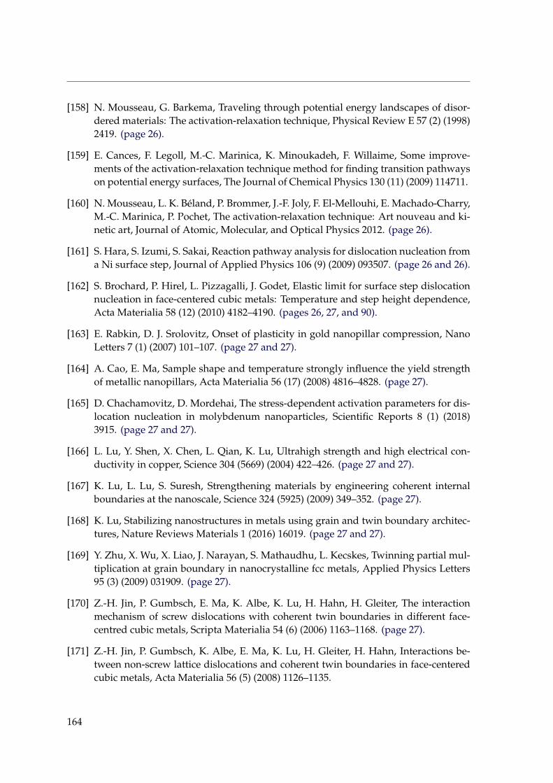
[158] N. Mousseau, G. Barkema, Traveling through potential energy landscapes of disor-dered materials: The activation-relaxation technique, Physical Review E 57 (2) (1998)2419. (page 26).
[159] E. Cances, F. Legoll, M.-C. Marinica, K. Minoukadeh, F. Willaime, Some improve-ments of the activation-relaxation technique method for finding transition pathwayson potential energy surfaces, The Journal of Chemical Physics 130 (11) (2009) 114711.
[160] N. Mousseau, L. K. Beland, P. Brommer, J.-F. Joly, F. El-Mellouhi, E. Machado-Charry,M.-C. Marinica, P. Pochet, The activation-relaxation technique: Art nouveau and ki-netic art, Journal of Atomic, Molecular, and Optical Physics 2012. (page 26).
[161] S. Hara, S. Izumi, S. Sakai, Reaction pathway analysis for dislocation nucleation froma Ni surface step, Journal of Applied Physics 106 (9) (2009) 093507. (page 26 and 26).
[162] S. Brochard, P. Hirel, L. Pizzagalli, J. Godet, Elastic limit for surface step dislocationnucleation in face-centered cubic metals: Temperature and step height dependence,Acta Materialia 58 (12) (2010) 4182–4190. (pages 26, 27, and 90).
[163] E. Rabkin, D. J. Srolovitz, Onset of plasticity in gold nanopillar compression, NanoLetters 7 (1) (2007) 101–107. (page 27 and 27).
[164] A. Cao, E. Ma, Sample shape and temperature strongly influence the yield strengthof metallic nanopillars, Acta Materialia 56 (17) (2008) 4816–4828. (page 27).
[165] D. Chachamovitz, D. Mordehai, The stress-dependent activation parameters for dis-location nucleation in molybdenum nanoparticles, Scientific Reports 8 (1) (2018)3915. (page 27 and 27).
[166] L. Lu, Y. Shen, X. Chen, L. Qian, K. Lu, Ultrahigh strength and high electrical con-ductivity in copper, Science 304 (5669) (2004) 422–426. (page 27 and 27).
[167] K. Lu, L. Lu, S. Suresh, Strengthening materials by engineering coherent internalboundaries at the nanoscale, Science 324 (5925) (2009) 349–352. (page 27).
[168] K. Lu, Stabilizing nanostructures in metals using grain and twin boundary architec-tures, Nature Reviews Materials 1 (2016) 16019. (page 27 and 27).
[169] Y. Zhu, X. Wu, X. Liao, J. Narayan, S. Mathaudhu, L. Kecskes, Twinning partial mul-tiplication at grain boundary in nanocrystalline fcc metals, Applied Physics Letters95 (3) (2009) 031909. (page 27).
[170] Z.-H. Jin, P. Gumbsch, E. Ma, K. Albe, K. Lu, H. Hahn, H. Gleiter, The interactionmechanism of screw dislocations with coherent twin boundaries in different face-centred cubic metals, Scripta Materialia 54 (6) (2006) 1163–1168. (page 27).
[171] Z.-H. Jin, P. Gumbsch, K. Albe, E. Ma, K. Lu, H. Gleiter, H. Hahn, Interactions be-tween non-screw lattice dislocations and coherent twin boundaries in face-centeredcubic metals, Acta Materialia 56 (5) (2008) 1126–1135.
164
[172] Y. Zhu, J. Narayan, J. Hirth, S. Mahajan, X. Wu, X. Liao, Formation of single and mul-tiple deformation twins in nanocrystalline fcc metals, Acta Materialia 57 (13) (2009)3763–3770.
[173] Y. Zhu, X. Wu, X. Liao, J. Narayan, L. Kecskes, S. Mathaudhu, Dislocation–twin in-teractions in nanocrystalline fcc metals, Acta Materialia 59 (2) (2011) 812–821. (page27).
[174] P. J. Imrich, C. Kirchlechner, C. Motz, G. Dehm, Differences in deformation behaviorof bicrystalline Cu micropillars containing a twin boundary or a large-angle grainboundary, Acta Materialia 73 (2014) 240–250. (pages 27 and 51).
[175] P. J. Imrich, C. Kirchlechner, D. Kiener, G. Dehm, Internal and external stresses: Insitu TEM compression of Cu bicrystals containing a twin boundary, Scripta Materi-alia 100 (2015) 94–97. (page 51).
[176] G. Dehm, B. Jaya, R. Raghavan, C. Kirchlechner, Overview on micro-and nanome-chanical testing: New insights in interface plasticity and fracture at small lengthscales, Acta Materialia 142 (2018) 248–282. (page 27).
[177] J. P. Liebig, S. Krauß, M. Goken, B. Merle, Influence of stacking fault energy and dis-location character on slip transfer at coherent twin boundaries studied by micropillarcompression, Acta Materialia 154 (2018) 261–272. (page 28).
[178] N. V. Malyar, B. Grabowski, G. Dehm, C. Kirchlechner, Dislocation slip transmissionthrough a coherent σ3 111 copper twin boundary: Strain rate sensitivity, activationvolume and strength distribution function, Acta Materialia 161 (2018) 412–419. (page28 and 28).
[179] Y. Zhu, X. Liao, X. Wu, Deformation twinning in nanocrystalline materials, Progressin Materials Science 57 (1) (2012) 1–62. (pages 28 and 106).
[180] B. Wu, A. Heidelberg, J. J. Boland, J. E. Sader, Microstructure-Hardened SilverNanowires, Nano Letters (2006) 1–5. (page 28, 28, and 28).
[181] M. Lucas, A. M. Leach, M. T. McDowell, S. E. Hunyadi, K. Gall, C. J. Murphy,E. Riedo, Plastic deformation of pentagonal silver nanowires: Comparison betweenAFM nanoindentation and atomistic simulations, Physical Review B 77 (24) (2008)2–5. (page 28 and 28).
[182] F. Niekiel, E. Bitzek, E. Spiecker, Combining atomistic simulation and X-ray diffrac-tion for the characterization of nanostructures : A case study on fivefold twinned,ACS Nano 8 (2014) 1629–1638. (page 41).
[183] Q. Qin, S. Yin, G. Cheng, X. Li, T. H. Chang, G. Richter, Y. Zhu, H. Gao, Recoverableplasticity in penta-twinned metallic nanowires governed by dislocation nucleationand retraction, Nature Communications 6 (2015) 5983. (pages 28, 28, 32, 32, 32, 41,70, and 105).
165
[184] M. Tian, J. Wang, J. Kurtz, T. E. Mallouk, M. Chan, Electrochemical growth of single-crystal metal nanowires via a two-dimensional nucleation and growth mechanism,Nano Letters 3 (7) (2003) 919–923. (page 29).
[185] J. Wang, M. Tian, T. E. Mallouk, M. H. Chan, Microtwinning in template-synthesizedsingle-crystal metal nanowires, The Journal of Physical Chemistry B 108 (3) (2004)841–845.
[186] S. Zhong, T. Koch, M. Wang, T. Scherer, S. Walheim, H. Hahn, T. Schimmel, Nanoscaletwinned copper nanowire formation by direct electrodeposition, Small 5 (20) (2009)2265–2270.
[187] M. Bernardi, S. N. Raja, S. K. Lim, Nanotwinned gold nanowires obtained by chemi-cal synthesis, Nanotechnology 21 (28) (2010) 285607.
[188] D. Jang, X. Li, H. Gao, J. R. Greer, Deformation mechanisms in nanotwinned metalnanopillars, Nature Nanotechnology 7 (9) (2012) 594–601. (pages 29, 29, 29, 29, 32,32, 33, and 33).
[189] B. Roos, B. Kapelle, G. Richter, C. A. Volkert, Surface dislocation nucleation con-trolled deformation of Au nanowires, Applied Physics Letters 105 (20) (2014) 201908.(pages 30, 30, 30, 30, 53, 86, and 88).
[190] A. Kobler, T. Beuth, T. Kloffel, R. Prang, M. Moosmann, T. Scherer, S. Walheim,H. Hahn, C. Kubel, B. Meyer, et al., Nanotwinned silver nanowires: structure andmechanical properties, Acta Materialia 92 (2015) 299–308. (pages 28 and 31).
[191] Y. Zhu, Q. Qin, F. Xu, F. Fan, Y. Ding, T. Zhang, B. J. Wiley, Z. L. Wang, Size effectson elasticity, yielding, and fracture of silver nanowires: In situ experiments, PhysicalReview B 85 (4) (2012) 1–7. (page 28 and 28).
[192] T. Filleter, S. Ryu, K. Kang, J. Yin, R. A. Bernal, K. Sohn, S. Li, J. Huang, W. Cai,H. D. Espinosa, Nucleation-controlled distributed plasticity in penta-twinned silvernanowires, Small 8 (19) (2012) 2986–2993. (pages 28, 28, 32, 32, 32, and 106).
[193] N. J. Schrenker, Z. Xie, P. Schweizer, M. Moninger, F. Werner, N. Karpstein, M. Mack-ovic, G. D. Spyropoulos, M. Gobelt, S. Christiansen, et al., Microscopic deformationmodes and impact of network anisotropy on the mechanical and electrical perfor-mance of five-fold twinned silver nanowire electrodes, ACS Nano. (pages 28, 28, 29,110, 110, and 111).
[194] N. Schrenker, In situ microscopy study on the mechanical integrity of flexible sil-ver nanowire electrodes, Doctoral thesis, Friedrich-Alexander-Universitat Erlangen-Nurnberg (2020). (pages 28, 28, 29, 110, 110, and 111).
[195] J. Wang, F. Sansoz, J. Huang, Y. Liu, S. Sun, Z. Zhang, S. X. Mao, Near-ideal theoret-ical strength in gold nanowires containing angstrom scale twins, Nature Communi-cations 4 (2013) 1742. (pages 29, 29, 29, 32, 32, and 33).
166
[196] G. Cheng, S. Yin, T.-H. Chang, G. Richter, H. Gao, Y. Zhu, Anomalous tensile detwin-ning in twinned nanowires, Physical Review Letters 119 (25) (2017) 256101. (pages30, 30, 33, 94, and 94).
[197] Z. Xie, J. Shin, J. Renner, A. Prakash, D. S. Gianola, E. Bitzek, Origins of strength-ening and failure in twinned au nanowires: Insights from in- situ experiments andatomistic simulations, Acta Materialia 187 (2020) 166–175. (pages 30, 30, 41, 49, 62,73, 86, 86, 88, 88, 88, 90, 90, 91, 91, 91, 92, 93, 96, 97, 101, and 106).
[198] L. Wang, D. Kong, Y. Zhang, L. Xiao, Y. Lu, Z. Chen, Z. Zhang, J. Zou, T. Zhu,X. Han, Mechanically driven grain boundary formation in nickel nanowires, ACSNano 11 (12) (2017) 12500–12508. (pages 31, 110, and 110).
[199] A. Cao, Y. Wei, Atomistic simulations of the mechanical behavior of fivefold twinnednanowires, Physical Review B 74 (21) (2006) 1–7. (pages 32, 32, 32, and 70).
[200] A. M. Leach, M. McDowell, K. Gall, Deformation of top-down and bottom-up silvernanowires, Advanced Functional Materials 17 (1) (2007) 43–53. (pages 32, 70, and 70).
[201] F. Niekiel, E. Spiecker, E. Bitzek, Influence of anisotropic elasticity on the mechanicalproperties of fivefold twinned nanowires, Journal of the Mechanics and Physics ofSolids 84 (2015) 358–379. (pages 32, 32, 69, 70, 70, 70, 70, 80, 105, 109, and 109).
[202] J. Wang, H. Huang, Novel deformation mechanism of twinned nanowires, AppliedPhysics Letters 88 (20) (2006) 203112. (pages 32 and 33).
[203] A. Cao, Y. Wei, S. X. Mao, Deformation mechanisms of face-centered-cubic metalnanowires with twin boundaries, Applied Physics Letters 90 (15) (2007) 151909.(page 33 and 33).
[204] K. A. Afanasyev, F. Sansoz, Strengthening in gold nanopillars with nanoscale twins,Nano Letters 7 (7) (2007) 2056–2062. (pages 32 and 33).
[205] C. Deng, F. Sansoz, Fundamental differences in the plasticity of periodically twinnednanowires in Au, Ag, Al, Cu, Pb and Ni, Acta Materialia 57 (20) (2009) 6090–6101.(pages 33, 100, and 100).
[206] A. Kunz, S. Pathak, J. R. Greer, Size effects in Al nanopillars: Single crystalline vs.bicrystalline, Acta Materialia 59 (11) (2011) 4416–4424. (page 33).
[207] Z. X. Wu, Y. W. Zhang, M. H. Jhon, J. R. Greer, D. J. Srolovitz, Nanostructure andsurface effects on yield in Cu nanowires, Acta Materialia 61 (6) (2013) 1831–1842.
[208] G. J. Tucker, Z. H. Aitken, J. R. Greer, C. R. Weinberger, The mechanical behaviorand deformation of bicrystalline nanowires, Modelling and Simulation in MaterialsScience and Engineering 21 (1) (2013) 15004. (page 33).
[209] B. Xing, S. Yan, W. Jiang, Q. H. Qin, Deformation mechanism of kink-step distortedcoherent twin boundaries in copper nanowire, AIMS Materials Science 4 (1) (2017)102–117. (page 33).
167
[210] E. B. Tadmor, R. E. Miller, Modeling materials: continuum, atomistic and multiscaletechniques, Cambridge University Press, 2011. (page 36).
[211] D. Frenkel, B. Smit, Understanding molecular simulation: from algorithms to appli-cations, Vol. 1, Elsevier, 2001.
[212] M. P. Allen, D. J. Tildesley, Computer simulation of liquids, Oxford university press,2017. (page 36).
[213] J. Stadler, R. Mikulla, H.-R. Trebin, IMD: a software package for molecular dynam-ics studies on parallel computers, International Journal of Modern Physics C 8 (05)(1997) 1131–1140. (page 36).
[214] E. Bitzek, F. Gahler, J. Hahn, C. Kohler, G. Krdzalic, J. Roth, C. Rudhart, G. Schaaf,J. Stadler, H.-R. Trebin, Recent developments in IMD: Interactions for covalent andmetallic systems, in: High Performance Computing in Science and Engineering 2000,Springer, 2001, pp. 37–47. (page 36).
[215] S. Plimpton, Fast parallel algorithms for short-range molecular dynamics, Journal ofComputational Physics 117 (1) (1995) 1–19. (page 36).
[216] S. Nose, A unified formulation of the constant temperature molecular dynamicsmethods, The Journal of Chemical Physics 81 (1) (1984) 511–519. (page 36).
[217] W. G. Hoover, Canonical dynamics: equilibrium phase-space distributions, PhysicalReview A 31 (3) (1985) 1695. (page 36).
[218] E. Bitzek, P. Koskinen, F. Gahler, M. Moseler, P. Gumbsch, Structural relaxation madesimple, Physical Review Letters 97 (17) (2006) 170201. (page 36).
[219] J. Guenole, W. G. Nohring, A. Vaid, F. Houlle, Z. Xie, A. Prakash, E. Bitzek, Assess-ment and optimization of the fast inertial relaxation engine (fire) for energy mini-mization in atomistic simulations and its implementation in lammps, ComputationalMaterials Science 175 (2020) 109584. (page 36 and 36).
[220] M. S. Daw, M. I. Baskes, Semiempirical, quantum mechanical calculation of hydrogenembrittlement in metals, Physical Review Letters 50 (17) (1983) 1285. (page 36).
[221] M. S. Daw, M. I. Baskes, Embedded-atom method: Derivation and application toimpurities, surfaces, and other defects in metals, Physical Review B 29 (12) (1984)6443. (page 36).
[222] Y. Mishin, D. Farkas, M. Mehl, D. Papaconstantopoulos, Interatomic potentials formonoatomic metals from experimental data and ab initio calculations, Physical Re-view B 59 (5) (1999) 3393. (page 37).
[223] Y. Mishin, Interatomic potentials for metals, in: Handbook of Materials Modeling,Springer, 2005, pp. 459–478. (page 37).
168

[224] J. H. Rose, J. R. Smith, F. Guinea, J. Ferrante, Universal features of the equation ofstate of metals, Physical Review B 29 (6) (1984) 2963. (page 37).
[225] H. S. Park, J. A. Zimmerman, Modeling inelasticity and failure in gold nanowires,Physical Review B 72 (5) (2005) 054106. (pages 37, 37, and 100).
[226] V. Fiorentini, M. Methfessel, M. Scheffler, Reconstruction mechanism of fcc transitionmetal (001) surfaces, Physical Review Letters 71 (7) (1993) 1051. (page 37).
[227] L. Vitos, A. Ruban, H. L. Skriver, J. Kollar, The surface energy of metals, SurfaceScience 411 (1-2) (1998) 186–202. (page 37).
[228] N. Takeuchi, C. Chan, K. Ho, Reconstruction of the (100) surfaces of Au and Ag,Physical Review B 43 (18) (1991) 14363. (page 37).
[229] M. Jenkins, Measurement of the stacking-fault energy of gold using the weak-beamtechnique of electron microscopy, Philosophical Magazine 26 (3) (1972) 747–751.(page 37).
[230] X.-Z. Wu, R. Wang, S.-F. Wang, Q.-Y. Wei, Ab initio calculations of generalized-stacking-fault energy surfaces and surface energies for FCC metals, Applied SurfaceScience 256 (21) (2010) 6345–6349. (page 37).
[231] J. Torres, E. Tosatti, A. Dal Corso, F. Ercolessi, J. Kohanoff, F. Di Tolla, J. Soler, Thepuzzling stability of monatomic gold wires, Surface Science 426 (3) (1999) L441–L446.(page 37).
[232] A. Every, A. McCurdy, Second and higher order elastic constants, Landolt-BornsteinNumerical Data and Functional Relationships in Science and Technology New SeriesGroup III: Crystal and Solid State Physics 29 (1992) 743. (page 37).
[233] R. Eibler, H. Erschbaumer, C. Temnitschka, R. Podloucky, A. J. Freeman, Ab-initiocalculation of the electronic structure and energetics of the unreconstructed Au (001)surface, Surface Science 280 (3) (1993) 398–414. (page 37).
[234] Y. Umeno, C. Elsasser, B. Meyer, P. Gumbsch, M. Nothacker, J. Weißmuller, F. Ev-ers, Ab initio study of surface stress response to charging, EPL (Europhysics Letters)78 (1) (2007) 13001. (page 37).
[235] N. Rosengaard, H. L. Skriver, Calculated stacking-fault energies of elemental metals,Physical Review B 47 (19) (1993) 12865. (page 37).
[236] N. Bernstein, E. Tadmor, Tight-binding calculations of stacking energies andtwinnability in fcc metals, Physical Review B 69 (9) (2004) 094116. (page 37).
[237] C. Kittel, P. McEuen, P. McEuen, Introduction to solid state physics, Vol. 8, WileyNew York, 1996. (page 37).
[238] C. Smith, Metal reference book, Betterworths, London (1976) 186. (page 37).
169
[239] G. Simons, H. Wang, Single crystal elastic constants and calculated aggregate prop-erties, J. Grand. Res. Center.-1965.-34 (1) (1977) 269. (page 37).
[240] B. Medasani, Y. H. Park, I. Vasiliev, Theoretical study of the surface energy, stress, andlattice contraction of silver nanoparticles, Physical Review B 75 (23) (2007) 235436.(page 37).
[241] M. Methfessel, D. Hennig, M. Scheffler, Trends of the surface relaxations, surfaceenergies, and work functions of the 4d transition metals, Physical Review B 46 (8)(1992) 4816. (page 37).
[242] M. Weinert, R. Watson, J. Davenport, G. Fernando, Adsorbed layer and multilayermaterials: The energetics and bonding of Pd and Ag on Nb (001) and Nb (110), Phys-ical Review B 39 (17) (1989) 12585. (page 37).
[243] J. Hartford, B. Von Sydow, G. Wahnstrom, B. Lundqvist, Peierls barriers and stressesfor edge dislocations in Pd and Al calculated from first principles, Physical ReviewB 58 (5) (1998) 2487. (page 37).
[244] S. Crampin, K. Hampel, D. Vvedensky, J. MacLaren, The calculation of stacking faultenergies in close-packed metals, Journal of Materials Research 5 (10) (1990) 2107–2119. (page 37).
[245] N. Kioussis, M. Herbranson, E. Collins, M. Eberhart, Topology of electronic chargedensity and energetics of planar faults in fcc metals, Physical Review Letters 88 (12)(2002) 125501. (page 37).
[246] P. Williams, Y. Mishin, J. Hamilton, An embedded-atom potential for the Cu–Ag sys-tem, Modelling and Simulation in Materials Science and Engineering 14 (5) (2006)817. (pages 37 and 100).
[247] K. E. Korte, S. E. Skrabalak, Y. Xia, Rapid synthesis of silver nanowires through aCuCl-or CuCl2-mediated polyol process, Journal of Materials Chemistry 18 (4) (2008)437–441. (page 41 and 41).
[248] A. M. Rodrıguez, G. Bozzolo, J. Ferrante, Multilayer relaxation and surface energiesof fcc and bcc metals using equivalent crystal theory, Surface Science 289 (1-2) (1993)100–126. (page 41).
[249] G. Richter, personal communication. (pages 41 and 53).
[250] V. V. Radmilovic, M. Gobelt, C. Ophus, S. Christiansen, E. Spiecker, V. R. Rad-milovic, Low temperature solid-state wetting and formation of nanowelds in silvernanowires, Nanotechnology 28 (38) (2017) 385701. (page 41).
[251] P. Gilbert, Iterative methods for the three-dimensional reconstruction of an objectfrom projections, Journal of Theoretical Biology 36 (1) (1972) 105–117. (page 42).
170
[252] A. Prakash, M. Hummel, S. Schmauder, E. Bitzek, Nanosculpt: A methodology forgenerating complex realistic configurations for atomistic simulations, MethodsX 3(2016) 219–230. (page 42).
[253] K. Michielsen, J. Kole, Photonic band gaps in materials with triply periodic surfacesand related tubular structures, Physical Review B 68 (11) (2003) 115107. (page 42).
[254] A. Stukowski, Visualization and analysis of atomistic simulation data with OVITO–the open visualization tool, Modelling and Simulation in Materials Science and En-gineering 18 (1) (2009) 015012. (page 44).
[255] J. D. Honeycutt, H. C. Andersen, Molecular dynamics study of melting and freezingof small Lennard-Jones clusters, The Journal of Chemical Physics 91 (19) (1987) 4950–4963. (page 44).
[256] D. Faken, H. Jonsson, Systematic analysis of local atomic structure combined with3D computer graphics, Computational Materials Science 2 (2) (1994) 279–286. (page44).
[257] A. Stukowski, K. Albe, Extracting dislocations and non-dislocation crystal defectsfrom atomistic simulation data, Modelling and Simulation in Materials Science andEngineering 18 (8) (2010) 085001. (pages 44, 45, and 45).
[258] A. Stukowski, V. V. Bulatov, A. Arsenlis, Automated identification and indexing ofdislocations in crystal interfaces, Modelling and Simulation in Materials Science andEngineering 20 (8) (2012) 085007. (pages 44 and 45).
[259] A. Jacobson, D. Panozzo, et al., libigl: A simple C++ geometry processing library,https://libigl.github.io/ (2018). (page 44).
[260] A. Stukowski, Structure identification methods for atomistic simulations of crys-talline materials, Modelling and Simulation in Materials Science and Engineering20 (4) (2012) 045021. (page 45).
[261] R.-s. Liu, K.-j. Dong, Z.-a. Tian, H.-r. Liu, P. Peng, A.-b. Yu, Formation and magicnumber characteristics of clusters formed during solidification processes, Journal ofPhysics: Condensed Matter 19 (19) (2007) 196103. (page 45).
[262] J. J. Moller, E. Bitzek, BDA: A novel method for identifying defects in body-centeredcubic crystals, MethodsX 3 (2016) 279–288. (page 45).
[263] W. Brostow, J.-P. Dussault, B. L. Fox, Construction of Voronoi polyhedra, Journal ofComputational Physics 29 (1) (1978) 81–92. (page 45).
[264] M. Zhou, A new look at the atomic level virial stress: on continuum-molecular sys-tem equivalence, Proceedings of the Royal Society of London. Series A: Mathemati-cal, Physical and Engineering Sciences 459 (2037) (2003) 2347–2392. (page 45).
171
[265] H. D. Espinosa, B. Prorok, B. Peng, Plasticity size effects in free-standing submi-cron polycrystalline fcc films subjected to pure tension, Journal of the Mechanicsand Physics of Solids 52 (3) (2004) 667–689. (page 49).
[266] J. Renner, Surface nucleation controlled plasticity of twinned gold nanowires,Bachelor thesis, Lehrstuhl Allgemeine Werkstoffeigenschaften, Friedrich-Alexander-Universitat Erlangen-Nurnberg (2015). (pages 55, 58, 86, 88, 88, 89, and 97).
[267] R. Ramachandramoorthy, W. Gao, R. Bernal, H. Espinosa, High strain rate tensiletesting of silver nanowires: rate-dependent brittle-to-ductile transition, Nano Letters16 (1) (2016) 255–263. (pages 58, 58, and 72).
[268] S. Zhang, Mechanical behaviors of single crystalline and fivefold twinned agnanowires under compression, Computational Materials Science 98 (2015) 320–327.(page 70 and 70).
[269] M. Sun, R. Cao, F. Xiao, C. Deng, Surface and interface controlled yielding and plas-ticity in fivefold twinned ag nanowires, Computational Materials Science 79 (2013)289–295. (page 70 and 70).
[270] S. P. Timoshenko, J. M. Gere, Theory of elastic stability, Courier Corporation, 2009.(pages 73 and 103).
[271] W. Nohring, Atomistic simulations of single crystal nanostructures subjectedto bending loads, Bachelor thesis, Lehrstuhl Allgemeine Werkstoffeigenschaften,Friedrich-Alexander-Universitat Erlangen-Nurnberg (2010). (pages 77, 77, 78, 106,107, and 111).
[272] Z. Chen, Z. Jin, H. Gao, Repulsive force between screw dislocation and coherent twinboundary in aluminum and copper, Physical Review B 75 (21) (2007) 212104. (page90).
[273] C. Deng, F. Sansoz, Size-dependent yield stress in twinned gold nanowires mediatedby site-specific surface dislocation emission, Applied Physics Letters 95 (9) (2009)091914. (page 90).
[274] S. Brochard, P. Beauchamp, J. Grilhe, Stress concentration near a surface step andshear localization, Physical Review B 61 (13) (2000) 8707. (page 90).
[275] K. Wang, N. Tao, G. Liu, J. Lu, K. Lu, Plastic strain-induced grain refinement atthe nanometer scale in copper, Acta Materialia 54 (19) (2006) 5281–5291. (pages 95and 96).
[276] S. Ni, Y. Wang, X. Liao, R. Figueiredo, H. Li, S. Ringer, T. Langdon, Y. Zhu, The effectof dislocation density on the interactions between dislocations and twin boundariesin nanocrystalline materials, Acta Materialia 60 (6) (2012) 3181–3189.
172
[277] Y. Cao, Y. Wang, Z. Chen, X. Liao, M. Kawasaki, S. Ringer, T. Langdon, Y. Zhu, De-twinning via secondary twinning in face-centered cubic alloys, Materials Science andEngineering: A 578 (2013) 110–114.
[278] Y. Cao, Y. Wang, X. An, X. Liao, M. Kawasaki, S. Ringer, T. Langdon, Y. Zhu, Grainboundary formation by remnant dislocations from the de-twinning of thin nano-twins, Scripta Materialia 100 (2015) 98–101. (page 95).
[279] Y. Cao, L. Zhang, Y. Zhang, Twinning interactions induced amorphisation in ultrafinesilicon grains, Materials Science and Engineering: A 658 (2016) 321–325. (page 96).
[280] Y. Mishin, M. Mehl, D. Papaconstantopoulos, A. Voter, J. Kress, Structural stabilityand lattice defects in copper: Ab initio, tight-binding, and embedded-atom calcula-tions, Physical Review B 63 (22) (2001) 224106. (page 100).
[281] J. He, C. M. Lilley, Surface effect on the elastic behavior of static bending nanowires,Nano Letters 8 (7) (2008) 1798–1802. (page 104 and 104).
[282] G.-F. Wang, X.-Q. Feng, Surface effects on buckling of nanowires under uniaxial com-pression, Applied Physics Letters 94 (14) (2009) 141913. (page 104).
[283] F. Song, G. Huang, H. Park, X. Liu, A continuum model for the mechanical behav-ior of nanowires including surface and surface-induced initial stresses, InternationalJournal of Solids and Structures 48 (14-15) (2011) 2154–2163. (page 104).
[284] M. E. Gurtin, A. I. Murdoch, A continuum theory of elastic material surfaces, Archivefor Rational Mechanics and Analysis 57 (4) (1975) 291–323. (page 104).
[285] V. B. Shenoy, Atomistic calculations of elastic properties of metallic fcc crystal sur-faces, Physical Review B 71 (9) (2005) 094104. (page 104).
[286] P. A. Olsson, H. S. Park, Atomistic study of the buckling of gold nanowires, ActaMaterialia 59 (10) (2011) 3883–3894. (page 105, 105, and 105).
[287] P. A. Olsson, H. S. Park, On the importance of surface elastic contributions to theflexural rigidity of nanowires, Journal of the Mechanics and Physics of Solids 60 (12)(2012) 2064–2083. (page 105).
[288] Z. Wang, X. Zu, L. Yang, F. Gao, W. J. Weber, Buckling of gan nanotubes under uni-axial compression, Solid State Communications 146 (7-8) (2008) 293–297.
[289] J. Wachter, G. Gutierrez, A. Zuniga, R. Palma, Buckling of cu–zr-based metallicglasses nanowires: molecular dynamics study of surface effects, Journal of MaterialsScience 49 (23) (2014) 8051–8056. (page 105).
[290] W. Jiang, R. Batra, Molecular statics simulations of buckling and yielding of goldnanowires deformed in axial compression, Acta Materialia 57 (16) (2009) 4921–4932.(page 105).
173
[291] P. Peng, H. Sun, A. P. Gerlich, W. Guo, Y. Zhu, L. Liu, G. Zou, C. V. Singh, N. Zhou,Near-ideal compressive strength of nanoporous silver composed of nanowires, ActaMaterialia 173 (2019) 163–173. (pages 106, 106, 106, and 110).
[292] Y. Yang, S. Li, X. Ding, J. Sun, E. K. Salje, Interface driven pseudo-elasticity in α-Fe nanowires, Advanced Functional Materials 26 (5) (2016) 760–767. (pages 106and 108).
[293] B. Hwang, T. Kim, S. M. Han, Compression and tension bending fatigue behaviorof ag nanowire network, Extreme Mechanics Letters 8 (2016) 266–272. (page 110and 110).
[294] B. Hwang, J. G. Seol, C.-H. An, S. H. Kim, Bending fatigue behavior of silvernanowire networks with different densities, Thin Solid Films 625 (2017) 1–5. (page110).
[295] H. Zhao, A. S. Eggeman, C. P. Race, B. Derby, Geometrical constraints on the bendingdeformation of penta-twinned silver nanowires, Acta Materialia 185 (2020) 110–118.(page 110 and 110).
[296] T. Radetic, F. Lancon, U. Dahmen, Chevron defect at the intersection of grain bound-aries with free surfaces in au, Physical Review Letters 89 (8) (2002) 085502. (page112).
[297] K. Hu, M. Ziehmer, K. Wang, E. T. Lilleodden, Nanoporous gold: 3D structural anal-yses of representative volumes and their implications on scaling relations of mechan-ical behaviour, Philosophical Magazine 96 (32-34) (2016) 3322–3335. (page 123).
[298] S. Mathesan, D. Mordehai, Size-dependent elastic modulus of nanoporous aunanopillars, Acta Materialia 185 (2020) 441–452. (pages 126 and 127).
[299] L.-Z. Liu, X.-L. Ye, H.-J. Jin, Interpreting anomalous low-strength and low-stiffness ofnanoporous gold: Quantification of network connectivity, Acta Materialia 118 (2016)77–87.
[300] R. Liu, A. Antoniou, A relationship between the geometrical structure of ananoporous metal foam and its modulus, Acta Materialia 61 (7) (2013) 2390–2402.(page 127).
[301] M. Yaghoobi, G. Z. Voyiadjis, Size effects in fcc crystals during the high rate com-pression test, Acta Materialia 121 (2016) 190–201. (page 130).
[302] G. Z. Voyiadjis, M. Yaghoobi, Size and strain rate effects in metallic samples of con-fined volumes: Dislocation length distribution, Scripta Materialia 130 (2017) 182–186.(page 130).
[303] H. Conrad, S. Feuerstein, L. Rice, Effects of grain size on the dislocation density andflow stress of niobium, Materials Science and Engineering 2 (3) (1967) 157–168. (page130).
174
[304] M. Ashby, The deformation of plastically non-homogeneous materials, The Philo-sophical Magazine: A Journal of Theoretical Experimental and Applied Physics21 (170) (1970) 399–424. (page 130).
[305] C. Chen, T. Lu, N. Fleck, Effect of imperfections on the yielding of two-dimensionalfoams, Journal of the Mechanics and Physics of Solids 47 (11) (1999) 2235–2272.(pages 138 and 139).
[306] H. Zhu, J. Hobdell, A. Windle, Effects of cell irregularity on the elastic properties of2D Voronoi honeycombs, Journal of the Mechanics and Physics of Solids 49 (4) (2001)857–870. (pages 138 and 139).
[307] F. P. Beer, E. R. Johnston Jr, D. F. Mazurek, P. J. Cornwell, E. R. Eisenberg, S. Sanghi,Vector mechanics for engineers, Vol. 1, Tata McGraw-Hill Education, 1977. (pages150 and 151).
175
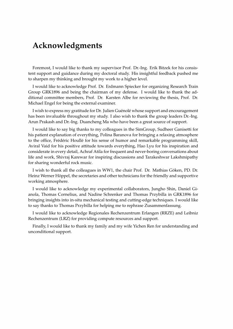
Acknowledgments
Foremost, I would like to thank my supervisor Prof. Dr.-Ing. Erik Bitzek for his consis-tent support and guidance during my doctoral study. His insightful feedback pushed meto sharpen my thinking and brought my work to a higher level.
I would like to acknowledge Prof. Dr. Erdmann Spiecker for organizing Research TrainGroup GRK1896 and being the chairman of my defense. I would like to thank the ad-ditional committee members, Prof. Dr. Karsten Albe for reviewing the thesis, Prof. Dr.Michael Engel for being the external examiner.
I wish to express my gratitude for Dr. Julien Guenole whose support and encouragementhas been invaluable throughout my study. I also wish to thank the group leaders Dr.-Ing.Arun Prakash and Dr.-Ing. Duancheng Ma who have been a great source of support.
I would like to say big thanks to my colleagues in the SimGroup, Sudheer Ganisetti forhis patient explanation of everything, Polina Baranova for bringing a relaxing atmosphereto the office, Frederic Houlle for his sense of humor and remarkable programming skill,Aviral Vaid for his positive attitude towards everything, Hao Lyu for his inspiration andconsiderate in every detail, Achraf Atila for frequent and never-boring conversations aboutlife and work, Shivraj Karewar for inspiring discussions and Tarakeshwar Lakshmipathyfor sharing wonderful rock music.
I wish to thank all the colleagues in WW1, the chair Prof. Dr. Mathias Goken, PD. Dr.Heinz Werner Hoppel, the secretaries and other technicians for the friendly and supportiveworking atmosphere.
I would like to acknowledge my experimental collaborators, Jungho Shin, Daniel Gi-anola, Thomas Cornelius, and Nadine Schrenker and Thomas Przybilla in GRK1896 forbringing insights into in-situ mechanical testing and cutting-edge techniques. I would liketo say thanks to Thomas Przybilla for helping me to rephrase Zusammenfassung.
I would like to acknowledge Regionales Rechenzentrum Erlangen (RRZE) and LeibnizRechenzentrum (LRZ) for providing compute resources and support.
Finally, I would like to thank my family and my wife Yichen Ren for understanding andunconditional support.


