Embed Size (px)
Citation preview
AVANCE
Service Manual
BRUKER
Version
002
The information in this manual may be altered without notice.
BRUKER accepts no responsibility for actions taken as a resultof use of this manual. BRUKER accepts no liability for any mis-takes contained in the manual, leading to coincidental damage,whether during installation or operation of the instrument. Un-authorised reproduction of manual contents, without writtenpermission from the publishers, or translation into another lan-guage, either in full or in part, is forbidden.
This manual was written by
Eamon Butler
© August 9, 2000: Bruker Analytik GmbH
Rheinstetten, Germany
P/N: Z31245DWG-Nr: 915002
Contents
Contents ............................................................... 3
1 Introduction ............................................................ 7
2 RF Paths ................................................................. 92.1 Introduction ......................................................................... 92.2 RF paths in a DMX .............................................................. 92.3 Pulse Names ..................................................................... 122.4 Changes in the nomenclature: ........................................... 132.5 RF Paths in the DRX ......................................................... 132.6 RF Paths in the DPX ......................................................... 14
3 AQX32 Board Layout ............................................ 173.1 Acquisition Bus .................................................................. 17
Board Order ...................................................................17Jumpers ........................................................................18
3.2 VME BUS .......................................................................... 18Jumpers ........................................................................18
3.3 CCU .................................................................................. 21
4 TCU: Timing Control Unit ..................................... 254.1 Principal Functions ............................................................ 254.2 Physical Connections ........................................................ 254.3 TCU Power Supply ............................................................ 264.4 Front Panel SMB Connectors ............................................ 264.5 Outputs ............................................................................. 274.6 Duration Generator ............................................................ 284.7 TCU control via explicit pulse programming. ...................... 294.8 Software Diagnostic Test ................................................... 294.9 Miscellaneous ................................................................... 29
5 FCU: Frequency Control Unit ............................... 375.1 Principal Functions ............................................................ 375.2 Front panel SMB. Connectors ............................................ 375.3 FCU Adapter ..................................................................... 38
Connector F1: ................................................................395.4 FCU Power Supplies ......................................................... 415.5 Jumper Positions. .............................................................. 425.6 FCUCHAN ......................................................................... 435.7 SRAM Memory .................................................................. 445.8 Duration Generator ............................................................ 455.9 MOD and MULT DACS ...................................................... 46
Version 002 BRUKER 3
Contents
5.10 DDS Connections .............................................................. 485.11 DDS Specifications ........................................................... 495.12 Connector F2 .................................................................... 495.13 PTS Bit settings ................................................................ 515.14 Software Diagnostic Test ................................................... 52
6 PTS 620 ..................................................................536.1 DDS Connections .............................................................. 536.2 Outputs ............................................................................. 536.3 Inputs ............................................................................... 546.4 Synth1 Pinouts .................................................................. 546.5 Overview ........................................................................... 546.6 Units ................................................................................. 556.7 Trouble shooting ............................................................... 576.8 Adding extra channels ....................................................... 58
7 LOT Board..............................................................617.1 Functions .......................................................................... 617.2 Signals .............................................................................. 62
8 ASU: Amplitude Setting Unit .................................698.1 Functions .......................................................................... 698.2 Signals .............................................................................. 718.3 MOD and MULT gating ...................................................... 768.4 AT20 and AT40 Blanking ................................................... 77
9 Router/Combiner ...................................................799.1 Introduction ....................................................................... 799.2 RSEL Parameters ............................................................. 799.3 Output Blanking ................................................................ 819.4 TGPENAB ......................................................................... 829.5 Cascading routers ............................................................. 82
10 BRUKER Linear Amplifiers....................................8710.1 New features ..................................................................... 8710.2 Terminology ...................................................................... 8710.3 Brief Summary of standard Amplifier Types ....................... 8710.4 RF Output Power: Comparison with previous transmitters .. 8910.5 Amplifier Blanking ............................................................. 9010.6 Configuration for DMX spectrometers (1 Router) ............... 9010.7 Configuration for DMX spectrometers (2 Routers) .............. 9110.8 Configuration for DRX spectrometers (1 Router) ................ 9310.9 Configuration for DRX spectrometers (2 Routers) .............. 9310.10 Standard configuration for DPX spectrometers .................. 9410.11 BLA Controller board II ...................................................... 9510.12 Front Panel Display DMX, DRX Amplifiers ......................... 9510.13 Front Panel Display for DPX amplifier ............................... 9810.14 BLARH100 Block Diagram ................................................ 9810.15 BLARH 100 Output Switches ........................................... 100
4 BRUKER Version 002
Contents
10.16 BLAXH 50 Block Diagram ................................................ 10110.17 BLAXH 50 Output Switches ............................................. 10210.18 R S 4 8 5 I n t e r f a c e B o a r d .................................. 104
General Description .....................................................104Jumper Settings ...........................................................106RS485 Pinouts .............................................................107RS485 signals .............................................................108
10.19 Amplifier Specifications ................................................... 108
11 HPPR .................................................................... 11311.1 HPPR Signals .................................................................. 11311.2 Polarity of gating signals .................................................. 11511.3 X-BB Modules ................................................................. 11511.4 QNP switching ................................................................. 11611.5 Preamplifier Selection ...................................................... 11611.6 HPPRGN ......................................................................... 11711.7 HPPR Module Coding ...................................................... 118
Modules from ECL C onwards ...................................... 11911.8 Checking the module identification via the software ......... 119
12 RX22 Receiver......................................................12312.1 Controller module ............................................................ 12512.2 Downloading Firmware .................................................... 12612.3 Reset .............................................................................. 12612.4 Jumper Settings, Polarity of RGP(EP) .............................. 12712.5 Power Supply .................................................................. 12812.6 Image Rejection Mixer ..................................................... 12812.7 Testing the overall gain of the Receiver ........................... 129
13 HRD 16 Controller Board .....................................13113.1 Functions ........................................................................ 131
14 RCU: Receiver Control Unit.................................13514.1 Functions ........................................................................ 13514.2 Front Panel Connections ................................................. 13614.3 Checking the DWELL CLOCK .......................................... 13714.4 Acquisition Bus ................................................................ 13814.5 VME Bus ......................................................................... 13814.6 Transfer of data to CCU ................................................... 13914.7 Diagnostic test ................................................................ 139
15 12C Bus in the AQR..............................................14115.1 BBIS ............................................................................... 14115.2 I2C Bus ........................................................................... 14115.3 I2C Bus 1 ........................................................................ 14115.4 II2C Bus 2 ....................................................................... 14215.5 DSX Configuration: .......................................................... 143
16 ACB ......................................................................147
Version 002 BRUKER 5
Contents
16.1 SBS Bus ......................................................................... 14716.2 RS232 Connection .......................................................... 14716.3 I2C Bus ........................................................................... 14816.4 Link to BSMS .................................................................. 14916.5 Reset .............................................................................. 149
17 LAB: Level Adapter Board ..................................15117.1 LOWER CONNECTOR LAB1 .......................................... 15117.2 UPPER CONNECTOR LAB2 ........................................... 15217.3 DPX Spectrometers ......................................................... 152
18 Software...............................................................15318.1 EDSCON: Edit spectrometer constants: ........................... 15318.2 EDSP display .................................................................. 154
A Conversion Tables ............................................. 159
B Linear Amplifier Specifications ......................... 161
C Wiring Diagrams ................................................ 173
D List of Abbreviations ......................................... 189
Figures ............................................................... 193
Tables ................................................................ 197
6 BRUKER Version 002
Introduction 1
This manual is intended to serve as a single reference guide to AVANCE spec-trometers. It has been written primarily for service engineers, though some infor-mation may also prove useful to applications and sales personnel.
It is hoped that after reading this manual service engineers will be able to effec-tively troubleshoot an AVANCE type spectrometer. Little effort has been made toexplain the internal workings of the various boards and units. With the use of SMDtechnology these boards are not intended to be repaired in the field . Instead themanual concentrates on describing the board functions and specifications as wellas the relevant input and outputs.
Copies of this manual entitled "AVANCE Service Manual" are available from SAG( P/N Z31245, DWG-No. 915002)
If you have any corrections or comments with regard to improving this manualplease contact:
Bruker Analytik GmbH
Silberstreifen Phone:(49) 721 5161-198
76287 Rheinstetten Fax: (49) 721 5161-297
Version 002 BRUKER 7 (201)

Introduction
8 (201) BRUKER Version 002
RF Paths 2
Introduction 2.1
Tracing the rf paths is very often the first step in troubleshooting an instrument.Therefore before discussing the individual components of AVANCE spectrometersin detail, it may prove useful to give a brief introductory overview of the rf pathsand corresponding blanking/gating signals. For simplicity a relatively simple ex-ample of a two channel experiment will be used. All of the signals discussed in thefollowing sections are accessible and easy to measure.
RF paths in a DMX 2.2
Regardless of NUCLEUS or final frequency every rf channel begins with a 1Vpp3-4 MHz cw signal from the appropriate FCU (DDS out). Bit settings from the FCU(Connector F2) are then used to produce a PTS output frequency of SF01/02 +440 MHz. This cw signal is then transmitted to the SE451.
In the SE451:
1. The end frequency (SF01, SF02) is produced by mixing the rf input frequencywith 440MHz.
2. For the first time the rf signal is pulsed with the gating signals TGPCH1 andTGPCH2.
The pulsed rf signal is sent to the ASU which adjusts the amplitude according tothe attenuation set by software. FCU produced voltages called MOD and MULTare used to implement the fine amplitude adjustment. Fixed 20 and 40 dB attenu-ators may also be switched in using the FCU produced AT20 and AT40 signals.The max. output of the ASU is 1 Vpp corresponding to a software power level of pl= -6 dB.
Within the ASU the rf signal is blanked twice using the TGPCH and BPCH signalsfrom the TCU.
Version 002 BRUKER 9 (201)
RF Paths
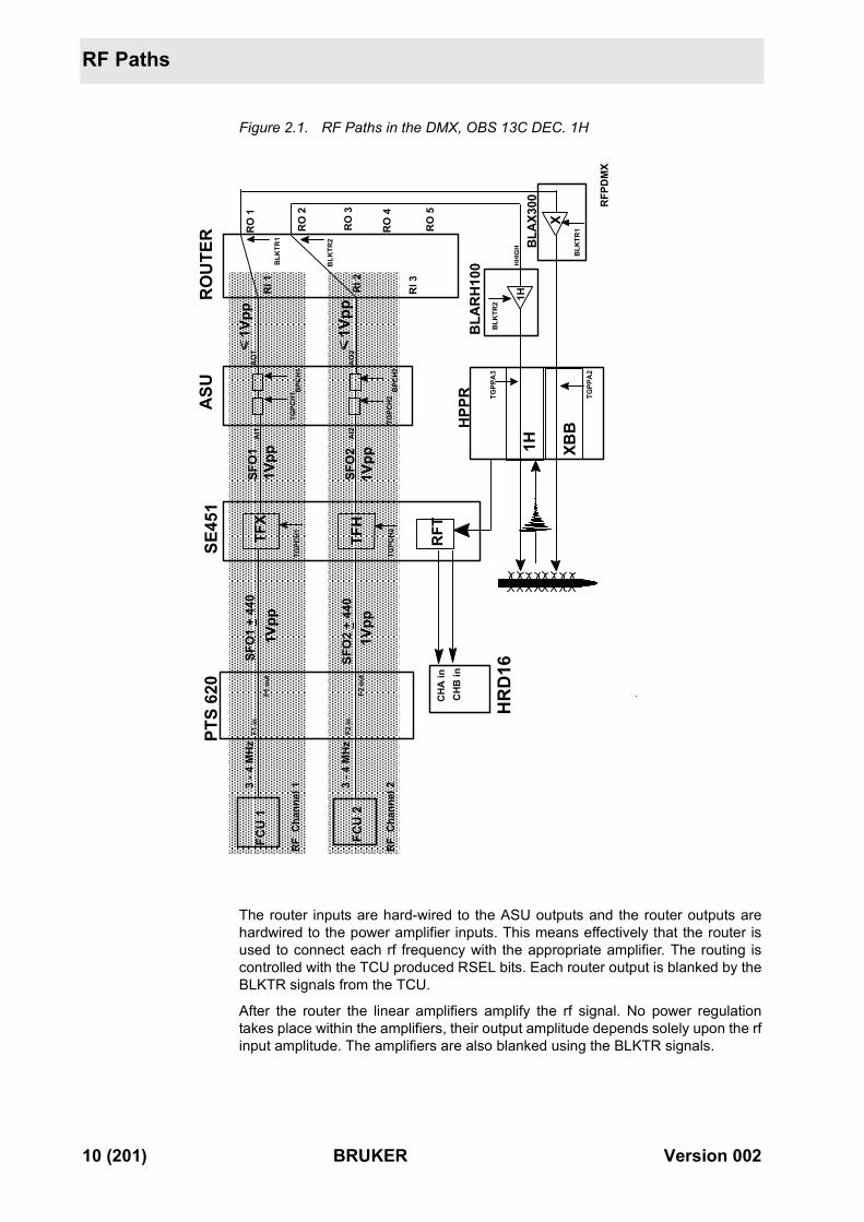
Figure 2.1. RF Paths in the DMX, OBS 13C DEC. 1H
The router inputs are hard-wired to the ASU outputs and the router outputs arehardwired to the power amplifier inputs. This means effectively that the router isused to connect each rf frequency with the appropriate amplifier. The routing iscontrolled with the TCU produced RSEL bits. Each router output is blanked by theBLKTR signals from the TCU.
After the router the linear amplifiers amplify the rf signal. No power regulationtakes place within the amplifiers, their output amplitude depends solely upon the rfinput amplitude. The amplifiers are also blanked using the BLKTR signals.
PTS
620
F2 in
F2 o
ut
F1 in
F1 o
ut
ASU
RO
UTE
R
RI 2
RI 1
RI 3
RO
4
RO
5
RO
3
RO
2
RO
13
- 4 M
Hz
3 - 4
MHz
TFX
TFH
RFT
SE45
1
RFP
DM
X
BPC
H1
1Vpp
1Vpp
1Vpp
TGPC
H1
BLA
X300
HR
D16
CH
A in
CH
B in
HPP
R
TGPC
H2
TGPC
H1 B
PCH
2TG
PCH
2
1H
X
1Vpp
BLK
TR2
BLK
TR1
SFO
2
1Vpp
1Vpp
BLA
RH
100
TGPP
A3
XBB
1H
TGPP
A2
HH
IGH
AI1 AI2
AO
2
AO
1
FCU
2
FCU
1
SFO
2 +
440
SFO
1 +
440
SFO
1
RF
Cha
nnel
1
BLK
TR1
BLK
TR2
RF
Cha
nnel
2
10 (201) BRUKER Version 002
RF paths in a DMX
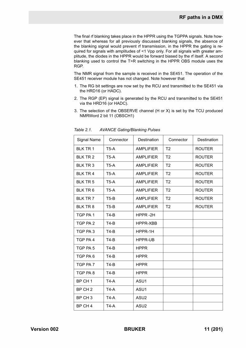
The final rf blanking takes place in the HPPR using the TGPPA signals. Note how-ever that whereas for all previously discussed blanking signals, the absence ofthe blanking signal would prevent rf transmission, in the HPPR the gating is re-quired for signals with amplitudes of <1 Vpp only. For all signals with greater am-plitude, the diodes in the HPPR would be forward biased by the rf itself. A secondblanking used to control the T>R switching in the HPPR OBS module uses theRGP.
The NMR signal from the sample is received in the SE451. The operation of theSE451 receiver module has not changed. Note however that
1. The RG bit settings are now set by the RCU and transmitted to the SE451 viathe HRD16 (or HADC).
2. The RGP (EP) signal is generated by the RCU and transmitted to the SE451via the HRD16 (or HADC).
3. The selection of the OBSERVE channel (H or X) is set by the TCU producedNMRWord 2 bit 11 (OBSCH1)
Table 2.1. AVANCE Gating/Blanking Pulses
Signal Name Connector Destination Connector Destination
BLK TR 1 T5-A AMPLIFIER T2 ROUTER
BLK TR 2 T5-A AMPLIFIER T2 ROUTER
BLK TR 3 T5-A AMPLIFIER T2 ROUTER
BLK TR 4 T5-A AMPLIFIER T2 ROUTER
BLK TR 5 T5-A AMPLIFIER T2 ROUTER
BLK TR 6 T5-A AMPLIFIER T2 ROUTER
BLK TR 7 T5-B AMPLIFIER T2 ROUTER
BLK TR 8 T5-B AMPLIFIER T2 ROUTER
TGP PA 1 T4-B HPPR -2H
TGP PA 2 T4-B HPPR-XBB
TGP PA 3 T4-B HPPR-1H
TGP PA 4 T4-B HPPR-UB
TGP PA 5 T4-B HPPR
TGP PA 6 T4-B HPPR
TGP PA 7 T4-B HPPR
TGP PA 8 T4-B HPPR
BP CH 1 T4-A ASU1
BP CH 2 T4-A ASU1
BP CH 3 T4-A ASU2
BP CH 4 T4-A ASU2
Version 002 BRUKER 11 (201)
RF Paths
Pulse Names 2.3
All blanking/gating pulses used in AVANCE spectrometers are active low and pro-duced by the TCU. One of the features of the new ADVANCE range is that rf sig-nals are blanked more frequently than in previous spectrometers which shouldimprove the on/off ratio and give cleaner pulses with shorter rise and fall times. Alist of signals and corresponding abbreviations is contained in the Appendix. Oneof the initial problems is becoming familiar with the new terminology and the fol-lowing points will hopefully help clarify the situation.
What is the difference between a blanking pulse and a gatingpulse?Effectively none. When the signal goes low (active) rf power transmission is possi-ble. Gating signals are tied exactly to the rf pulse transmission. If a 7 µs rf signal isto be transmitted, than the gating pulse will go low for 7 µs at exactly the momentof transmission. This applies to the TGPCH signals used in ASU's and the SE451.
Blanking pulses are distinguished from gating pulses in that the timing is not nec-essarily tied exactly to rf power transmission. Instead the blanking pulse may goactive slightly prior to rf transmission and remain active for a short period aftertransmission. The optimal pre and post blanking timing will depend on the physi-cal properties of the various switches but are typically 1-3 µs and may be set us-ing the „edscon“ table (see "EDSCON: Edit spectrometer constants:" on page153)
BP CH 5 T4-A ASU3
BP CH 6 T4-A ASU3
BP CH 7 T4-A ASU4
BP CH 8 T4-A ASU4
TGP CH 1 T4-A ASU1 T4-B SE451
TGP CH 2 T4-A ASU1 T4-B SE451
TGP CH 3 T4-A ASU2 T4-B SE451
TGP CH 4 T4-A ASU2 T4-B SE451
TGP CH 5 T4-A ASU3
TGP CH 6 T4-A ASU3
TGP CH 7 T4-A ASU4
TGP CH 8 T4-A ASU4
BLKGRADX T5-B Backpanel
BLKGRADY T5-B Backpanel
BLKGRADZ T5-B Backpanel
Table 2.1. AVANCE Gating/Blanking Pulses
Signal Name Connector Destination Connector Destination
12 (201) BRUKER Version 002
Changes in the nomenclature:
In this respect the pulses BPCH (ASU) and BLKTR (Router and amplifiers) aretermed blanking pulses.
One inconsistency to this naming is the TGPPA signals used in the HPPR. Thetiming of these pulses may be altered with the „edscon“ table and they should re-ally be called blanking pulses as opposed to gating pulses.
Which pulse is assigned to which channelA specific rf channel“ number“ starts at the FCU and ends at the Router input.This rf channel connects FCU1 through the PTS and SE451/LOT to ASU Input1/Output1 to Router Input1. The corresponding pulses are TGPCH1 (SE451, ASU)and BPCH1 (ASU).
Similarly rf channel2 starts at FCU2 and ends at Router Input2 with correspondingpulses TGPCH2 and BPCH2.
Which BLKTR signal is used in the Router is determined solely by which Routeroutput is used. Thus an rf signal at RO1 is blanked BLKTR1, an rf signal at RO3 isblanked by BLKTR3 etc.
Since a particular rf channel number can be routed to several different Router out-puts, the BLKTR hardwired to the Router output can not be assigned the numberof the rf channel.
Since each Router output is hardwired to a particular amplifier the nomenclaturefor Router blanking and amplifier blanking is identical. Thus an amplifier whose in-put is taken from RO2 will be blanked by BLKTR2.
The various HPPR gating pulses are effectively hardwired to the TCU via the Pe-riph. Cascode and the pulses are assigned as follows:
The 2H module is gated by TGPPA1
The X-BB module is gated by TGPPA2
The 1H module is gated by TGPPA3
The USER-BOX module is gated by TGPPA4
Table 2.1. is a summary of the various gating/blanking pulses.
Changes in the nomenclature: 2.4
To try to make pulse terminology more meaningful (in English!) the following pulsenames are no longer standard
1. SPF (Sender Pulse) and SPFND pulses. These have been replaced by TG-PCH and BPCH respectively.
2. EP (Empfänger Pulse) is now called the RGP (Receiver Gating Pulse)
3. SPENAB is now called TGENAB
RF Paths in the DRX 2.5
The first major difference to the DMX is that the end frequency SF01, SF02 is pro-duced directly at the PTS output. There is no subsequent mixing with 440 MHz inan SE451 type device.
Version 002 BRUKER 13 (201)
RF Paths
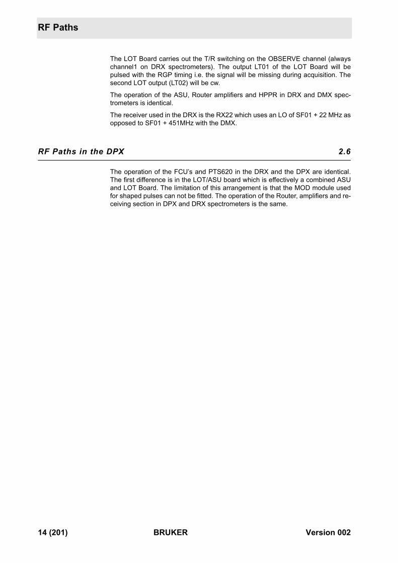
The LOT Board carries out the T/R switching on the OBSERVE channel (alwayschannel1 on DRX spectrometers). The output LT01 of the LOT Board will bepulsed with the RGP timing i.e. the signal will be missing during acquisition. Thesecond LOT output (LT02) will be cw.
The operation of the ASU, Router amplifiers and HPPR in DRX and DMX spec-trometers is identical.
The receiver used in the DRX is the RX22 which uses an LO of SF01 + 22 MHz asopposed to SF01 + 451MHz with the DMX.
RF Paths in the DPX 2.6
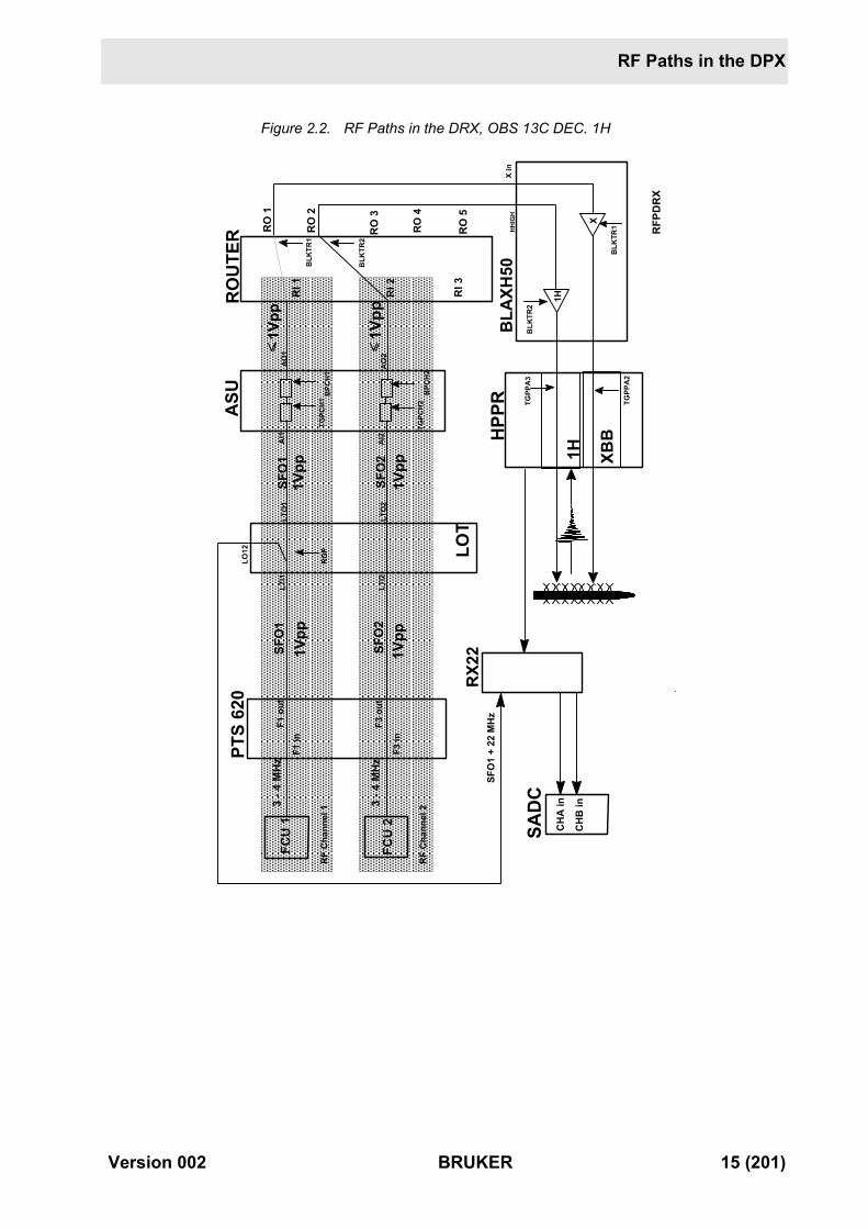
The operation of the FCU’s and PTS620 in the DRX and the DPX are identical.The first difference is in the LOT/ASU board which is effectively a combined ASUand LOT Board. The limitation of this arrangement is that the MOD module usedfor shaped pulses can not be fitted. The operation of the Router, amplifiers and re-ceiving section in DPX and DRX spectrometers is the same.
14 (201) BRUKER Version 002
RF Paths in the DPX
Figure 2.2. RF Paths in the DRX, OBS 13C DEC. 1H
FCU
2
FCU
1
SF
O1
PTS
620
F3 in
F3 o
ut
F1 in
F1 o
ut
ASU
RO
UTE
R
RI 1
RI 2 RI 3
RO
2
RO
3
RO 4
RO
5
3 - 4
MH
z
3 - 4
MH
z
LOT
RFP
DR
X
BPC
H1
BLK
TR2
1Vpp
1Vpp
1Vpp
SAD
CC
HA
in
CH
B in
TGPC
H1
BPC
H2
TGPC
H2
1H
X
1Vpp
BLK
TR2
BLK
TR1
SFO
1 +
22 M
Hz
SFO
1
SFO
2
1Vpp
1Vpp
TGPP
A3
XBB
1H
TGPP
A2
HH
IGH
RX2
2
RG
P
BLA
XH50
SFO
2
X in
HPP
R
AI2AI1
AO1
AO2
LTO
1
LTO
2
LTI1
LTI2
LO12
RO
1
BLK
TR1
RF
Cha
nnel
1
RF
Cha
nnel
2
Version 002 BRUKER 15 (201)
RF Paths
Figure 2.3. RF Paths in the DPX, OBS 13C DEC. 1H
FCU
2
FCU1
SFO
1
PTS
620
F3 in
F3 o
ut
F1 in
F1 o
ut
RO
UTE
R
RI 1
RI 2 RI 3
RO
4
RO
3
RO
2
RO
1
3 - 4
MH
z
3 - 4
MH
z
LOT/
ASU
RFP
DPX
BPC
H1
BLK
TR2
1Vpp
1Vpp
1Vpp
SAD
CC
HA
in
CHB
in
TGPC
H1
BLK
TR1
BPC
H2
TGPC
H2
1H
X
1Vpp
BLK
TR2
BLK
TR1
SFO
1 +
22 M
Hz
TGPP
A3
XBB
1H
TGPP
A2
H in
RX2
2
RG
P
BLA
XH20
SFO
2
X in
HPP
R
AO
1
AO
2LT
I2
LTI1
RO
5
LO12
Rf C
hann
el 1
Rf C
hann
el 2
16 (201) BRUKER Version 002
AQX32 Board Layout 3
Acquisition Bus 3.1
This is a real time Bus with interrupt capability. The Bus is designed to intercon-nect the TCU with the RCU and FCU's (and GCU where installed ).The TCU is theone and only master of the Acquisition Bus. In this way the TCU can have uninter-rupted control of the Acquisition timing.
The Bus has two sections. One is 16 bit, uni-directional real-time and used to con-trol the FCU's and RCU. The second is 8 bit, bi-directional non real-time and atpresent used exclusively to control the GCU.
Under certain circumstances (i.e. errors) the RCU or GCU can generate interruptsto the TCU.
The Acquisition Bus connection is made by plugging a Bus backplane onto theX32 backplane. The Bus backplane comes in two versions 8 slot (standard) or 5slot. The standard 8 slot Bus allows for one TCU (3 slots), one RCU, and 4 FCU's(or 3 FCU's and one GCU).
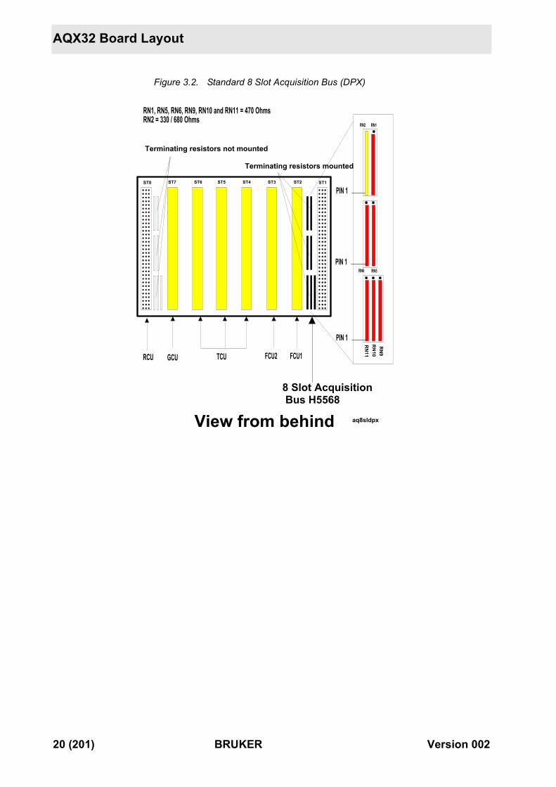
An 8 slot Bus can be easily combined with a 5 slot to give a 13 slot AcquisitionBus. Ribbon cable (P/N HZ2969) is used to connect the two Buses. When makingthis modification, the position of the terminating resistors must be changed (seeFigure 3.3.)
The extended 13 slot Bus allows for one TCU ( 3 slots), one RCU, one GCU and8 FCU's.
Board Order 3.1.1
Strictly speaking there is no set board order. However optimum performance isachieved with the TCU and a set of terminating resistors positioned at oppositeends of the Bus. This minimises unwanted reflections at the end of the Bus. TheRCU, GCU and FCU's can then be placed in any order in between.
With this in mind a standard layout has been decided upon for all 20 slot X32computers delivered with DRX and DMX spectrometers (see Figure 3.1.).TheTCU is placed at the extreme left end (front view) of the Acquisition Bus, the RCU(and terminating resistors) at the extreme right and FCU's and GCU and emptyslots in between.
As a result of thermal problems a slightly different layout has been used in the 9slot X32 as used in DPX spectrometers. The cooling fans are located to the left ofthe rack. To optimise the cooling of the FCU's and the TCU the board order in Figure 3.2. is now standard.
Version 002 BRUKER 17 (201)
AQX32 Board Layout
Jumpers 3.1.2
There are no jumpers on the Acquisition Bus. Just remember to set the terminat-ing resistor networks correctly.
VME BUS 3.2
This standard bi-directional 32 bit Bus comes in two versions, 9 slot (DPX) and 20slot (DMX, DRX). It is used for communication between all boards in the AQX32rack including the CCU. On this Bus only the RCU and CCU can be master ( theRCU has priority over the CCU regarding Bus requests.)
The only requirement is that the CCU be placed at the extreme left (front view) ofthe Bus. This is to ensure that it receives all request messages.
Jumpers 3.2.1
To ensure that the DMA is not interrupted any vacant slots must have correspond-ing jumpers inserted at the backplane. If an extra new board is inserted the jump-ers must be removed from the backplane.
NOTE: The TCU consists of 2 boards but occupies 3 slots. The middle slotshould have the jumpers inserted.
18 (201) BRUKER Version 002
VME BUS
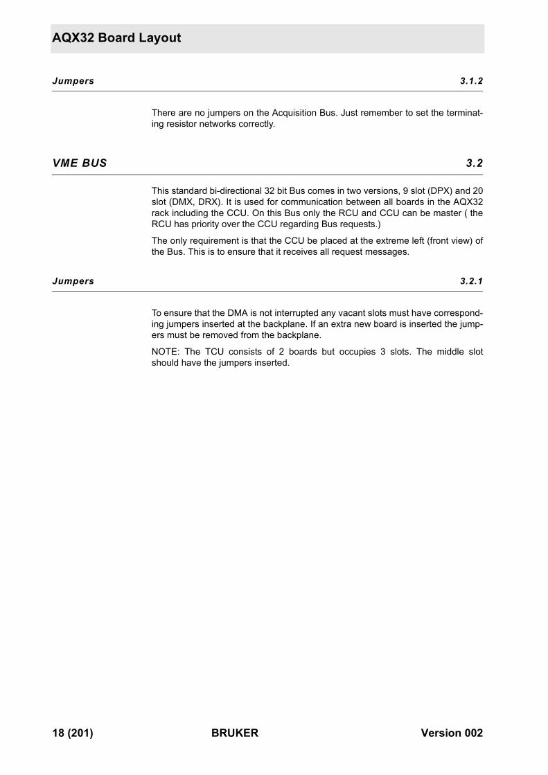
Figure 3.1. Standard 8 Slot Acquisition Bus (DMX, DRX)
AQ B
US 8
CO
NNE
CTO
R
L-SE
ITE
ST1ST2ST3ST4ST5ST6ST7ST8
Terminating resistors not mounted
Terminating resistors mounted
RN
12R
N13
RN
14
RN7RN8
RN3 RN4
aq8slotView from behind
PIN 1
PIN 1
PIN 1
8 Slot Acquisition Bus H5568
RN3, RN7, RN8, RN12, RN13 and RN14 = 470 OhmsRN4 = 330 / 680 Ohms
RCU TCUFCU1FCU2FCU3FCU4
Version 002 BRUKER 19 (201)
AQX32 Board Layout
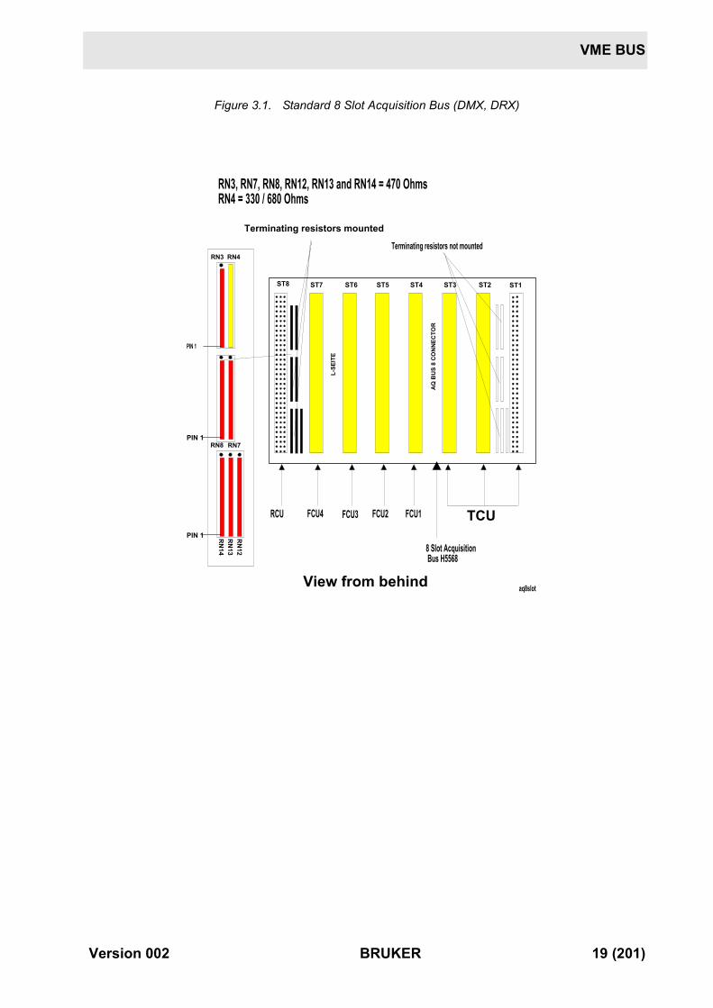
Figure 3.2. Standard 8 Slot Acquisition Bus (DPX)
aq8sldpx
ST1ST2ST3ST4ST5ST6ST7
Terminating resistors not mounted
Terminating resistors mounted
View from behind
TCU FCU1FCU2
8 Slot Acquisition Bus H5568
RCU
RN1, RN5, RN6, RN9, RN10 and RN11 = 470 OhmsRN2 = 330 / 680 Ohms
RN
9R
N10
RN
11
RN5RN6
RN2 RN1
PIN 1
PIN 1
PIN 1
ST8
GCU
20 (201) BRUKER Version 002
CCU
Figure 3.3. Extended 13 Slot Acquisition Bus (DMX, DRX)
CCU 3.3
The latest spectrometers will be delivered with the new CCU, CommunicationControl Unit (P/N H2570).
This effectively replaces the CPU4 , the CPU3 Fast Ext. Memory and SIB withone board. A separate panel (RS232/485 EXT. Board P/N H5731) which runs
Term
inat
ing
resi
stor
sno
t mou
nted
Term
inat
ing
resi
stor
s m
ount
ed
View
from
beh
ind
5 Sl
ot A
cqui
sitio
n B
us P
/N H
5577
AQ BUS 8 CONNECTOR
L-SEITE
ST1
ST2
ST3
ST4
ST5
ST6
ST7
ST8
Term
inat
ing
resi
stor
s no
t mou
nted
Term
inat
ing
resi
stor
s no
t mou
nted
TCU
Rib
bon
Cab
le P
/N H
Z 29
69
8 Sl
ot A
cqui
sitio
n B
us H
5568
aq13
slot
RCU
FCU
1FC
U2
FCU
3FC
U4
FCU
5FC
U6
FCU
7FC
U8
GC
U
RN5RN3
RN14RN
16R
N9
PIN
1
PIN
1
PIN
1
RN11RN15
RN
14,R
N5,
RN
3,R
N15
,RN
11,R
N9
= 47
0 O
hms
RN
16 =
330
/ 68
0 O
hms
Version 002 BRUKER 21 (201)
AQX32 Board Layout
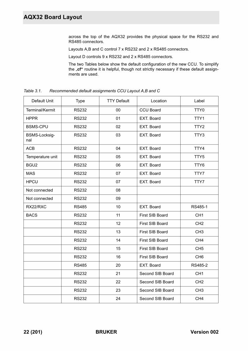
across the top of the AQX32 provides the physical space for the RS232 andRS485 connectors.
Layouts A,B and C control 7 x RS232 and 2 x RS485 connectors.
Layout D controls 9 x RS232 and 2 x RS485 connectors.
The two Tables below show the default configuration of the new CCU. To simplifythe „cf“ routine it is helpful, though not strictly necessary if these default assign-ments are used.
Table 3.1. Recommended default assignments CCU Layout A,B and C
Default Unit Type TTY Default Location Label
Terminal/Kermit RS232 00 CCU Board TTY0
HPPR RS232 01 EXT. Board TTY1
BSMS-CPU RS232 02 EXT. Board TTY2
BSMS-Locksig-nal
RS232 03 EXT. Board TTY3
ACB RS232 04 EXT. Board TTY4
Temperature unit RS232 05 EXT. Board TTY5
BGU2 RS232 06 EXT. Board TTY6
MAS RS232 07 EXT. Board TTY7
HPCU RS232 07 EXT. Board TTY7
Not connected RS232 08
Not connected RS232 09
RX22/RXC RS485 10 EXT. Board RS485-1
BACS RS232 11 First SIB Board CH1
RS232 12 First SIB Board CH2
RS232 13 First SIB Board CH3
RS232 14 First SIB Board CH4
RS232 15 First SIB Board CH5
RS232 16 First SIB Board CH6
RS485 20 EXT. Board RS485-2
RS232 21 Second SIB Board CH1
RS232 22 Second SIB Board CH2
RS232 23 Second SIB Board CH3
RS232 24 Second SIB Board CH4
22 (201) BRUKER Version 002
CCU
RS232 25 Second SIB Board CH5
RS232 26 Second SIB Board CH6
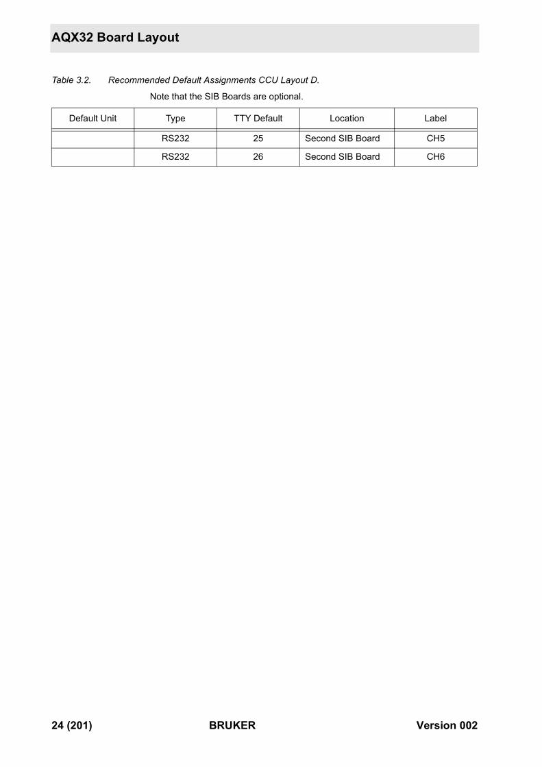
Table 3.2. Recommended Default Assignments CCU Layout D.
Note that the SIB Boards are optional.
Default Unit Type TTY Default Location Label
Terminal/Kermit RS232 00 CCU TTY00
HPPR RS232 01 EXT. Board TTY01
BSMS-CPU RS232 02 EXT. Board TTY02
BSMS-Locksig-nal
RS232 03 EXT. Board TTY03
ACB RS232 04 EXT. Board TTY04
Temperature unit RS232 05 EXT. Board TTY05
BGU2 RS232 06 EXT. Board TTY06
MAS RS232 07 EXT. Board TTY07
HPCU RS232 07 EXT. Board TTY07
BACS RS232 08 EXT. Board TTY08
Free use RS232 09 EXT. Board TTY09
RX22/RXC RS485 10 EXT. Board RS485-10
RS232 11 First SIB Board CH1
RS232 12 First SIB Board CH2
RS232 13 First SIB Board CH3
RS232 14 First SIB Board CH4
RS232 15 First SIB Board CH5
RS232 16 First SIB Board CH6
RS485 20 EXT. Board RS485-20
RS232 21 Second SIB Board CH1
RS232 22 Second SIB Board CH2
RS232 23 Second SIB Board CH3
RS232 24 Second SIB Board CH4
Table 3.1. Recommended default assignments CCU Layout A,B and C
Default Unit Type TTY Default Location Label
Version 002 BRUKER 23 (201)
AQX32 Board Layout
RS232 25 Second SIB Board CH5
RS232 26 Second SIB Board CH6
Table 3.2. Recommended Default Assignments CCU Layout D.
Note that the SIB Boards are optional.
Default Unit Type TTY Default Location Label
24 (201) BRUKER Version 002
TCU: Timing Control Unit 4
The TCU consists of two boards and occupies 3 slots in the AQX32 Rack. TheTCU delivered with the first batch of Avance instruments was officially known asTCU0 (TCU0 Main Board P/N H2558 and TCU Ext. Board P/N H2562). In Decem-ber 94 a new TCU_4K Main Board P/N H5811 was introduced. The main differ-ences between TCU0 and TCU_4K are
a) additional on board memory of 64kB instead of 8kB
b) the new TCU_4K hardware will support the BBIS system
c) the new TCU_4K requires XWIN-NMR software.
Pin assignments have not changed.
The TCU is connected to the FCU's, RCU and GCU where installed, via the Ac-quisition Bus. The TCU is the one and only master of this Bus.
Principal Functions 4.1
1. To synchronise and control the timing of the RCU, FCU's and GCU where in-stalled.
2. To generate gating and blanking pulses used in the ASU, Router, Amplifiersand HPPR.
3. To control the Router switching via the RSEL bit settings.
4. To generate various switching signals used in Amplifiers, SE451, QNP Pneu-matic Unit etc.
A complete list of the TCU outputs is given at the end of this Chapter. A singleTCU is designed to provide all the required signals for a spectrometer with up to 8rf channels.
All outputs of the TCU are TTL active low .The outputs are designed to go high af-ter a hardware reset of the CCU. Up to and including Layout C of the TCU MainBoard the required pull up resistors are however missing from the outputs of con-nector T4. As a result, after a reset, these outputs may be low when measuredwith the Burndy disconnected. This will be changed with future TCU layouts.
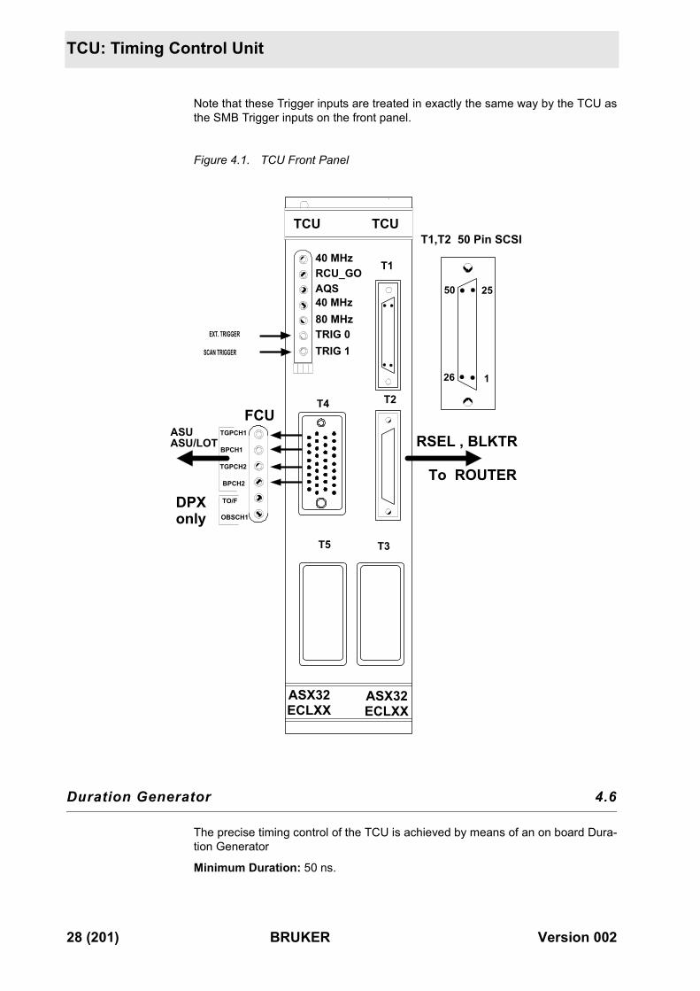
Physical Connections 4.2
1. SCSI connector T2 is connected directly to the Router and transmits the RSELbit settings as well as BLKTR1 - 10.
Version 002 BRUKER 25 (201)
TCU: Timing Control Unit
2. TGPCH and BPCH signals are wired to the FCU F1 Adapter from where theyare connected to the ASU.
3. Connectors T3, T4 and T5 carry various signals to amplifiers, SE451 etc. viathe cable harness.
4. Connector T1 is used only for signals required for high power applications.
Note1: The signals TO/F and OBSCH1 are wired to the FCU in DPX spectrome-ters only. This is because they are required by the combined LOT/ASU Board. InDRX spectrometers the separate LOT Board receives these signals via the cableharness.
Note2: The four signals TGPCH1, BPCH1, TGPCH2, BPCH2 are the requiredgating/blanking signals for a single two channel ASU. For each subsequent chan-nel the corresponding pair of gating/blanking connections must be added. Kitswith correctly labeled cables are available for each extra channel that might beadded. When ordering it is important to specify which channel (e.g. 3 or 4 etc)which is to be added.
Note 3: The Burndy connectors T3,T4 and T5 are fitted exclusively with coaxpins. This means that it is not possible to use the traditional Burndy Break-outBox. Signals can however be easily checked at the other end of the coax cable.
The Burndy connectors are wired to the TCU via Ribbon connectors A and B i.eDC Pins on the TCU. The tables at the end of this Chapter give not only the CoaxPin assignments but also the corresponding DC Pin assignments of Ribbon con-nectors A and B..
The use of SCSI connectors as opposed to the traditional Burndy connectors hasthe following advantages.
a) Less space required
b) The use of twisted pairs reduces unwanted magnetic pickup because theenclosed area is small and the signals induced in successive twists tend tocancel.
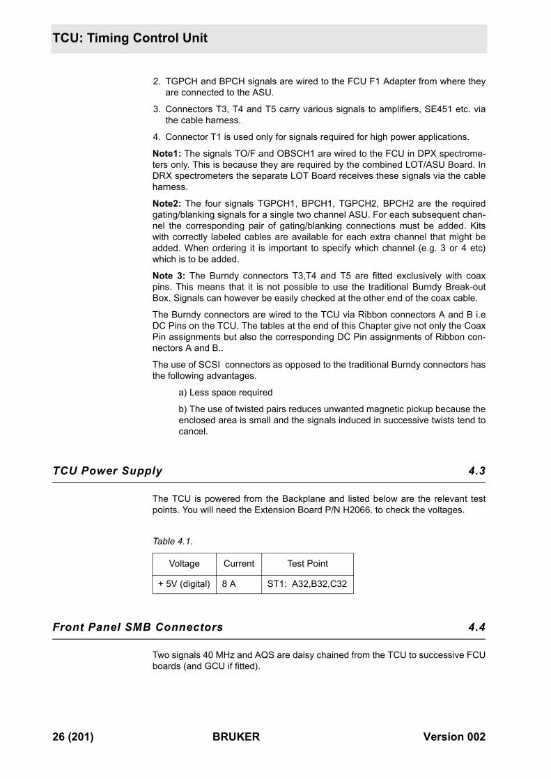
TCU Power Supply 4.3
The TCU is powered from the Backplane and listed below are the relevant testpoints. You will need the Extension Board P/N H2066. to check the voltages.
Front Panel SMB Connectors 4.4
Two signals 40 MHz and AQS are daisy chained from the TCU to successive FCUboards (and GCU if fitted).
Table 4.1.
Voltage Current Test Point
+ 5V (digital) 8 A ST1: A32,B32,C32
26 (201) BRUKER Version 002
Outputs
40 MHz: This output signal is TTL (3Vpp at 50 Ω ) and operates on a 50% duty cycle. Twooutputs are provided. One is used to clock the FCU's ( and GCU if fitted), the oth-er to clock the RCU.
RCUGO: This pulse is used to start the RCU and as such must accompany every scan. Thetiming is so that it goes high for 50 ns, approximately 200 ns before the RGP (EP)pulse.
AQS: Various instructions are sent from the TCU to the FCU's and GCU via the Acquisi-tion Bus. This TTL strobe pulse is used to synchronise the timing of the Bus.Thestrobe pulses go low for a minimum of 25 ns. The Data transfer itself is triggeredby the rising edge.
80 MHz.: This input signal comes directly from the PTS620 and is the clocking frequency forthe TCU. Note that the voltage level is 0 dBm ( 0.65Vpp at 50Ω ). This signal isused to generate the 40MHz signals described above.
TRIG0: This input is available should it be necessary to trigger the TCU with an externalinput.
TRIG 1: This input is for the signal "scantrigger" which originates in the BSMS.This signalcould be used to synchronise the TCU timing with sample spinning
Outputs 4.5
Total number of individual outputs: 147
Connector T1: 28 outputs: 2 inputs ( TRIG 2, TRIG3 )
Connector T2: 38 outputs
Connector T3: 32 outputs, 2 inputs ( TRIG 2, TRIG3 ) All Coax.
Connector T4: 34 outputs (All Coax).
Connector T5: 34 outputs (All Coax).
The inputs TRIG 2 and TRIG3 are not used at present. They could be usedshould it be necessary to trigger the TCU with an external input. Only one set ofinputs can be used either T1 or T3. Which are used is set with Jumpers W3 andW4 on the TCU Extension Board. The default factory settings are:
W3: Pin 2-Pin 3 => TRIG3 input is T3 Pin NN and T1 input not connected.
W4: Pin 1-Pin2 => TRIG2 input is T1 Pin 25 and T3 input not connected.
Version 002 BRUKER 27 (201)
TCU: Timing Control Unit
Note that these Trigger inputs are treated in exactly the same way by the TCU asthe SMB Trigger inputs on the front panel.
Figure 4.1. TCU Front Panel
Duration Generator 4.6
The precise timing control of the TCU is achieved by means of an on board Dura-tion Generator
Minimum Duration: 50 ns.
40 MHzRCU_GOAQS
80 MHzTRIG 0
T1
TCU
ASX32ECLXX
TCU
40 MHz
SCAN TRIGGER
EXT. TRIGGER
ASX32ECLXX
T1,T2 50 Pin SCSI
T4 T2
T3T5
FCURSEL , BLKTR
ASUASU/LOT
To ROUTER
TRIG 1
2550
1
DPXonly
26
TGPCH1
TGPCH2
BPCH1
BPCH2
TO/F
OBSCH1
28 (201) BRUKER Version 002
TCU control via explicit pulse programming.
This effectively means that bits can be set high or low for a minimum of 50 ns.
Timing Resolution: 12.5 ns.
This resolution is set by the 80 MHz clocking frequency. Bits can thus be set highor low for durations of 50, 62.5, 75 ,87.5 ns etc.
Pulse Rise Times: 5 ns
Pulse Fall times: 4 ns.
TCU control via explicit pulse programming. 4.7
The TCU outputs are normally set automatically from either the "edsp", "edasp" or"eda" tables or from the pulse program itself.
For test purposes however it is sometimes useful to explicitly program the variousoutputs using the following pulse program command:
d11 setnmr2^3 = set NMRWord 2 bit 3 high (inactive).
d11 setnmr2|3 = set NMRWord 2 bit 3 low (active).
d11 is the switching time and can be set as low as 50 ns ( the minimum duration.)
Once a bit is set high or low it will remain in this state until a further instruction toalter it's state is received. This syntax applies to all NMR words 0 - 8
A different syntax which is identical to that previously used in conventional RCPpulses can also be used, but only for NMR word 0 .
e.g. to activate (set low) BLKTR3 (see table 4.2.) for the duration p1 use:
p1:c2
e.g. to transmit a pulse p1 on channel 1 and simultaneously activate (set low)BLKTR4 for the duration p1 use:
p1:f1:c3
Note that unlike the "setnmr" command the bit will go inactive ( high ) as soon asp1 has elapsed.
Software Diagnostic Test 4.8
A useful test program is entitled "tcutest" which is normally in the directory:
/u/systest/tcu ( logged in on ’spect’)
Miscellaneous 4.9
The most important TCU outputs will be discussed in various Chapters throughoutthis manual ,but for completion several signals which will not be dealt with at laterstages are explained below
Version 002 BRUKER 29 (201)
TCU: Timing Control Unit
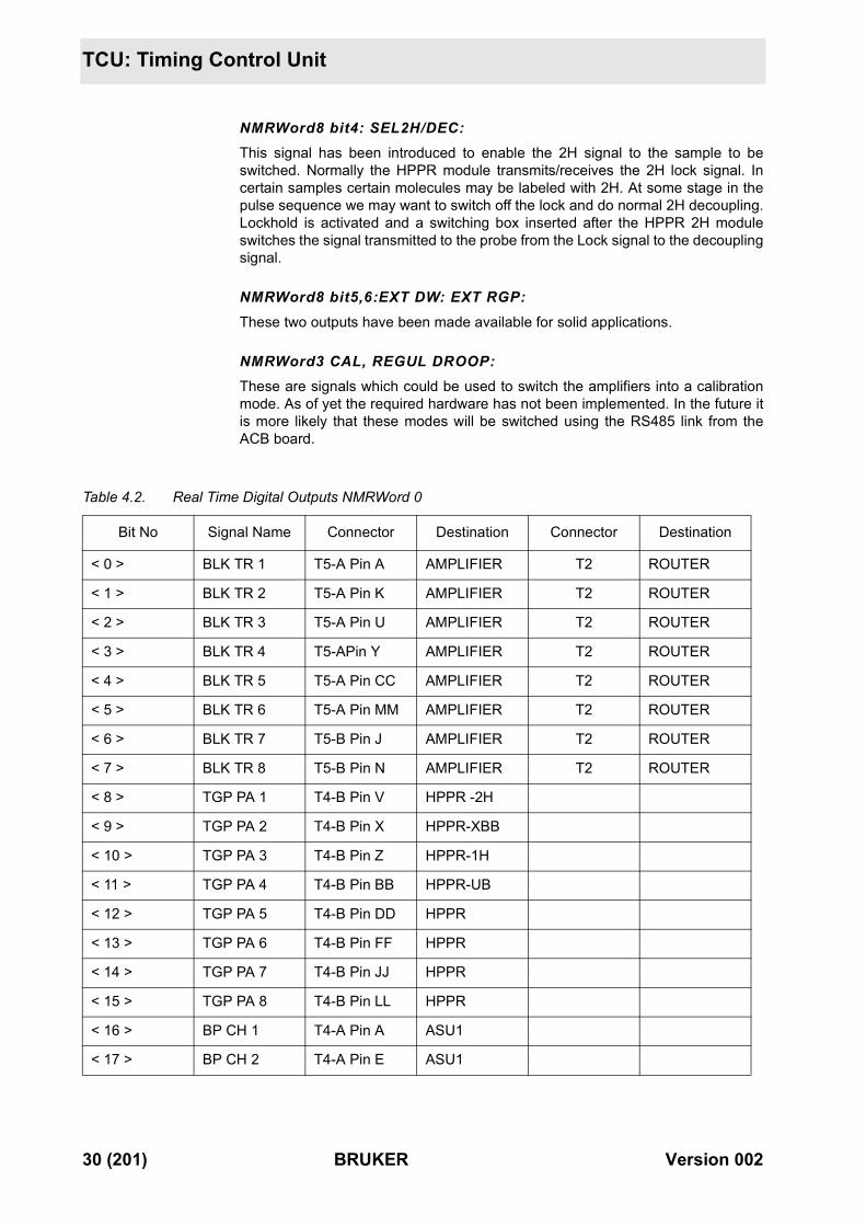
NMRWord8 bit4: SEL2H/DEC: This signal has been introduced to enable the 2H signal to the sample to beswitched. Normally the HPPR module transmits/receives the 2H lock signal. Incertain samples certain molecules may be labeled with 2H. At some stage in thepulse sequence we may want to switch off the lock and do normal 2H decoupling.Lockhold is activated and a switching box inserted after the HPPR 2H moduleswitches the signal transmitted to the probe from the Lock signal to the decouplingsignal.
NMRWord8 bit5,6:EXT DW: EXT RGP: These two outputs have been made available for solid applications.
NMRWord3 CAL, REGUL DROOP: These are signals which could be used to switch the amplifiers into a calibrationmode. As of yet the required hardware has not been implemented. In the future itis more likely that these modes will be switched using the RS485 link from theACB board.
Table 4.2. Real Time Digital Outputs NMRWord 0
Bit No Signal Name Connector Destination Connector Destination
< 0 > BLK TR 1 T5-A Pin A AMPLIFIER T2 ROUTER
< 1 > BLK TR 2 T5-A Pin K AMPLIFIER T2 ROUTER
< 2 > BLK TR 3 T5-A Pin U AMPLIFIER T2 ROUTER
< 3 > BLK TR 4 T5-APin Y AMPLIFIER T2 ROUTER
< 4 > BLK TR 5 T5-A Pin CC AMPLIFIER T2 ROUTER
< 5 > BLK TR 6 T5-A Pin MM AMPLIFIER T2 ROUTER
< 6 > BLK TR 7 T5-B Pin J AMPLIFIER T2 ROUTER
< 7 > BLK TR 8 T5-B Pin N AMPLIFIER T2 ROUTER
< 8 > TGP PA 1 T4-B Pin V HPPR -2H
< 9 > TGP PA 2 T4-B Pin X HPPR-XBB
< 10 > TGP PA 3 T4-B Pin Z HPPR-1H
< 11 > TGP PA 4 T4-B Pin BB HPPR-UB
< 12 > TGP PA 5 T4-B Pin DD HPPR
< 13 > TGP PA 6 T4-B Pin FF HPPR
< 14 > TGP PA 7 T4-B Pin JJ HPPR
< 15 > TGP PA 8 T4-B Pin LL HPPR
< 16 > BP CH 1 T4-A Pin A ASU1
< 17 > BP CH 2 T4-A Pin E ASU1
30 (201) BRUKER Version 002
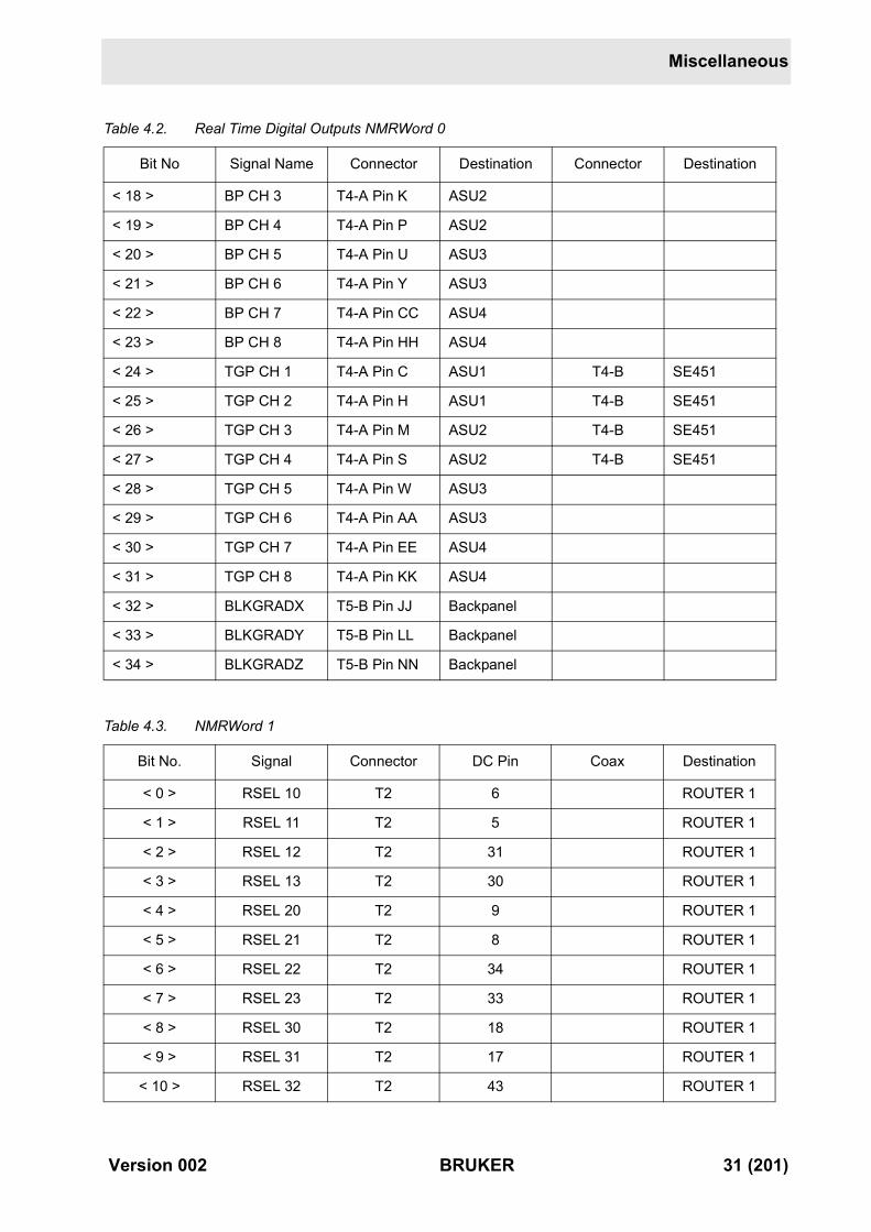
Miscellaneous
< 18 > BP CH 3 T4-A Pin K ASU2
< 19 > BP CH 4 T4-A Pin P ASU2
< 20 > BP CH 5 T4-A Pin U ASU3
< 21 > BP CH 6 T4-A Pin Y ASU3
< 22 > BP CH 7 T4-A Pin CC ASU4
< 23 > BP CH 8 T4-A Pin HH ASU4
< 24 > TGP CH 1 T4-A Pin C ASU1 T4-B SE451
< 25 > TGP CH 2 T4-A Pin H ASU1 T4-B SE451
< 26 > TGP CH 3 T4-A Pin M ASU2 T4-B SE451
< 27 > TGP CH 4 T4-A Pin S ASU2 T4-B SE451
< 28 > TGP CH 5 T4-A Pin W ASU3
< 29 > TGP CH 6 T4-A Pin AA ASU3
< 30 > TGP CH 7 T4-A Pin EE ASU4
< 31 > TGP CH 8 T4-A Pin KK ASU4
< 32 > BLKGRADX T5-B Pin JJ Backpanel
< 33 > BLKGRADY T5-B Pin LL Backpanel
< 34 > BLKGRADZ T5-B Pin NN Backpanel
Table 4.3. NMRWord 1
Bit No. Signal Connector DC Pin Coax Destination
< 0 > RSEL 10 T2 6 ROUTER 1
< 1 > RSEL 11 T2 5 ROUTER 1
< 2 > RSEL 12 T2 31 ROUTER 1
< 3 > RSEL 13 T2 30 ROUTER 1
< 4 > RSEL 20 T2 9 ROUTER 1
< 5 > RSEL 21 T2 8 ROUTER 1
< 6 > RSEL 22 T2 34 ROUTER 1
< 7 > RSEL 23 T2 33 ROUTER 1
< 8 > RSEL 30 T2 18 ROUTER 1
< 9 > RSEL 31 T2 17 ROUTER 1
< 10 > RSEL 32 T2 43 ROUTER 1
Table 4.2. Real Time Digital Outputs NMRWord 0
Bit No Signal Name Connector Destination Connector Destination
Version 002 BRUKER 31 (201)
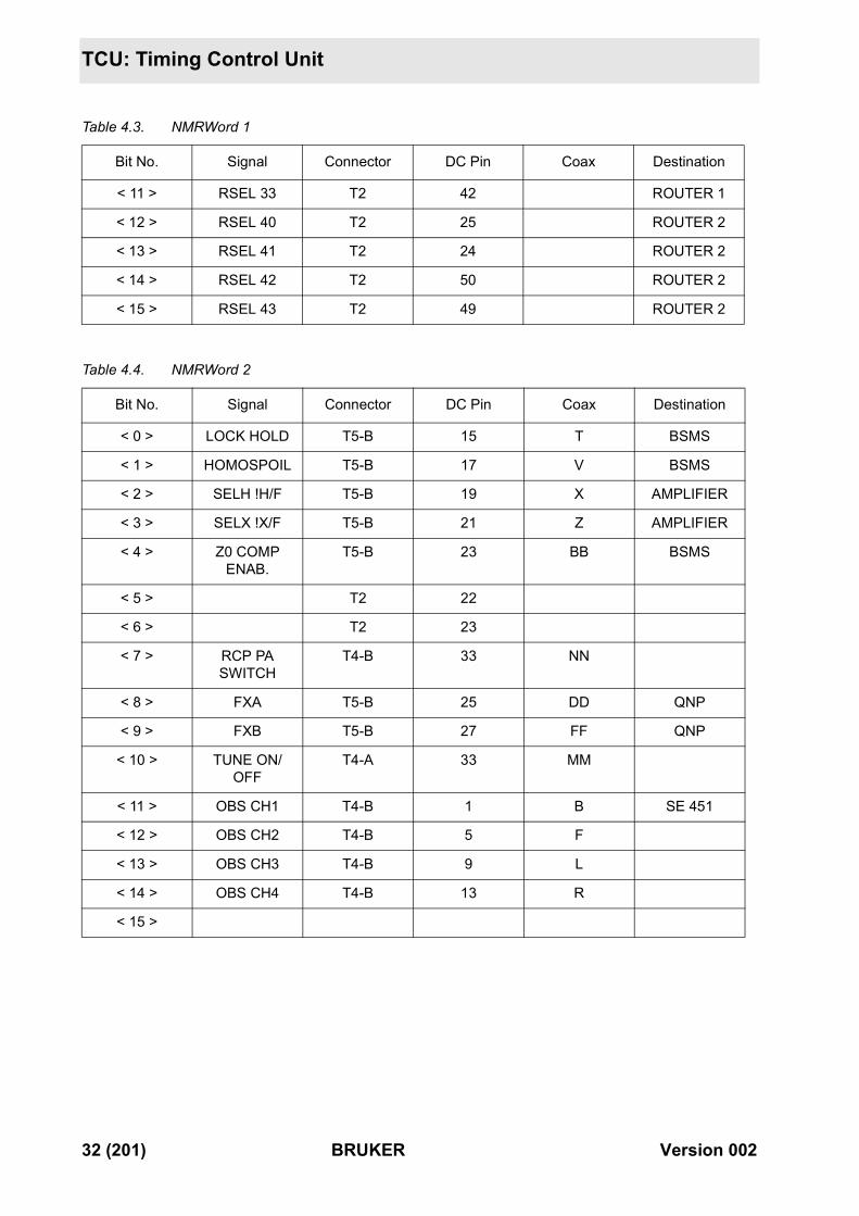
TCU: Timing Control Unit
< 11 > RSEL 33 T2 42 ROUTER 1
< 12 > RSEL 40 T2 25 ROUTER 2
< 13 > RSEL 41 T2 24 ROUTER 2
< 14 > RSEL 42 T2 50 ROUTER 2
< 15 > RSEL 43 T2 49 ROUTER 2
Table 4.4. NMRWord 2
Bit No. Signal Connector DC Pin Coax Destination
< 0 > LOCK HOLD T5-B 15 T BSMS
< 1 > HOMOSPOIL T5-B 17 V BSMS
< 2 > SELH !H/F T5-B 19 X AMPLIFIER
< 3 > SELX !X/F T5-B 21 Z AMPLIFIER
< 4 > Z0 COMP ENAB.
T5-B 23 BB BSMS
< 5 > T2 22
< 6 > T2 23
< 7 > RCP PA SWITCH
T4-B 33 NN
< 8 > FXA T5-B 25 DD QNP
< 9 > FXB T5-B 27 FF QNP
< 10 > TUNE ON/OFF
T4-A 33 MM
< 11 > OBS CH1 T4-B 1 B SE 451
< 12 > OBS CH2 T4-B 5 F
< 13 > OBS CH3 T4-B 9 L
< 14 > OBS CH4 T4-B 13 R
< 15 >
Table 4.3. NMRWord 1
Bit No. Signal Connector DC Pin Coax Destination
32 (201) BRUKER Version 002
Miscellaneous
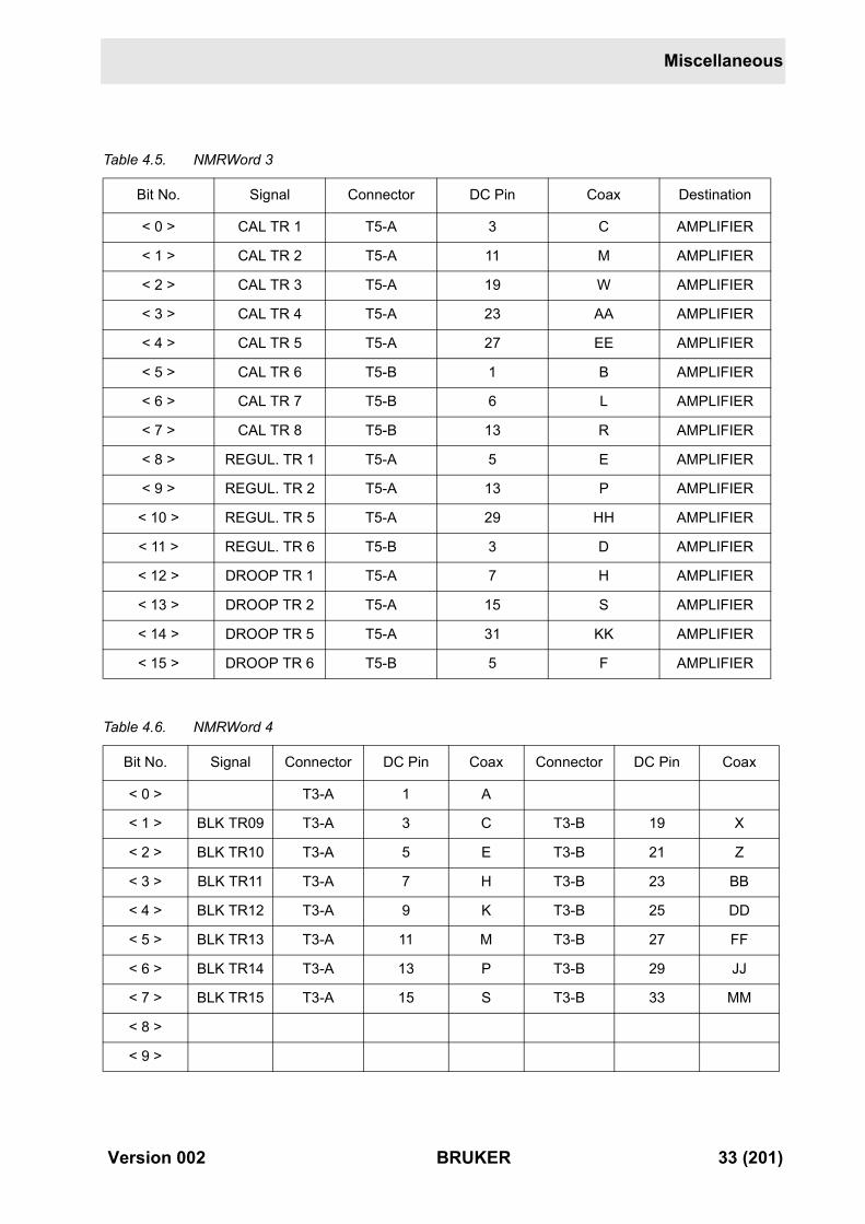
Table 4.5. NMRWord 3
Bit No. Signal Connector DC Pin Coax Destination
< 0 > CAL TR 1 T5-A 3 C AMPLIFIER
< 1 > CAL TR 2 T5-A 11 M AMPLIFIER
< 2 > CAL TR 3 T5-A 19 W AMPLIFIER
< 3 > CAL TR 4 T5-A 23 AA AMPLIFIER
< 4 > CAL TR 5 T5-A 27 EE AMPLIFIER
< 5 > CAL TR 6 T5-B 1 B AMPLIFIER
< 6 > CAL TR 7 T5-B 6 L AMPLIFIER
< 7 > CAL TR 8 T5-B 13 R AMPLIFIER
< 8 > REGUL. TR 1 T5-A 5 E AMPLIFIER
< 9 > REGUL. TR 2 T5-A 13 P AMPLIFIER
< 10 > REGUL. TR 5 T5-A 29 HH AMPLIFIER
< 11 > REGUL. TR 6 T5-B 3 D AMPLIFIER
< 12 > DROOP TR 1 T5-A 7 H AMPLIFIER
< 13 > DROOP TR 2 T5-A 15 S AMPLIFIER
< 14 > DROOP TR 5 T5-A 31 KK AMPLIFIER
< 15 > DROOP TR 6 T5-B 5 F AMPLIFIER
Table 4.6. NMRWord 4
Bit No. Signal Connector DC Pin Coax Connector DC Pin Coax
< 0 > T3-A 1 A
< 1 > BLK TR09 T3-A 3 C T3-B 19 X
< 2 > BLK TR10 T3-A 5 E T3-B 21 Z
< 3 > BLK TR11 T3-A 7 H T3-B 23 BB
< 4 > BLK TR12 T3-A 9 K T3-B 25 DD
< 5 > BLK TR13 T3-A 11 M T3-B 27 FF
< 6 > BLK TR14 T3-A 13 P T3-B 29 JJ
< 7 > BLK TR15 T3-A 15 S T3-B 33 MM
< 8 >
< 9 >
Version 002 BRUKER 33 (201)
TCU: Timing Control Unit
< 10 >
< 11 >
< 12 >
< 13 >
< 14 >
< 15 >
Table 4.7. NMRWord 5
Bit No. Signal Connector DC Pin Coax Destination
< 0 > GAIN 0 TR1 T1 2 HI POWER
< 1 > GAIN 1 TR1 T1 27 HI POWER
< 2 > C/AB TR1 T1 3 HI POWER
< 3 > GAIN 0 TR2 T1 5 HI POWER
< 4 > GAIN 1 TR2 T1 30 HI POWER
< 5 > C/AB TR2 T1 6 HI POWER
< 6 > C/AB TR5 T1 8 HI POWER
< 7 > RELAY H T1 10 HI POWER
< 8 > RELAY X T1 35 HI POWER
< 9 > RELAY Y T1 12 HI POWER
< 10 > RACK ON/OFF T1 37 HI POWER
< 11 > RCP T1 13 HI POWER
< 12 > RELAY Z T1 14 HI POWER
< 13 > RCP T1 15 HI POWER
< 14 > RCP T1 16 HI POWER
< 15 > RCP T1 17 HI POWER
Table 4.8. NMRWord 6
Bit No. Signal Connector DC Pin Coax Destination
< 0 > STRAFI STP1 DIR T1 18 HI POWER
< 1 > STRAFI LB SEL T1 43 HI POWER
Table 4.6. NMRWord 4
Bit No. Signal Connector DC Pin Coax Connector DC Pin Coax
34 (201) BRUKER Version 002
Miscellaneous
< 2 > STRAFI DCM STRT T1 19 HI POWER
< 3 > STRAFI STP1 CLK T1 20 HI POWER
< 4 > STRAFI STP2 CLK T1 21 HI POWER
< 5 > STRAFIRES STP1 T1 22 HI POWER
< 6 > STRAFI DCM RES T1 23 HI POWER
< 7 > STRAFI GO POS T1 24 HI POWER
< 8 >
< 9 >
< 10 >
< 11 >
< 12 >
< 13 >
< 14 >
< 15 >
Table 4.9. NMRWord 7
Bit No. Signal Connector DC Pin Coax Destination
< 0 > RSEL 50 T2 2 ROUTER 2
< 1 > RSEL 51 T2 1 ROUTER 2
< 2 > RSEL 52 T2 27 ROUTER 2
< 3 > RSEL 53 T2 26 ROUTER 2
< 4 > RSEL 60 T2 4 ROUTER 2
< 5 > RSEL 61 T2 3 ROUTER 2
< 6 > RSEL 63 T2 29 ROUTER 2
< 7 > RSEL 63 T2 28 ROUTER 2
< 8 > RSEL 71 T3-A 17 U ROUTER 3
< 9 > RSEL 71 T3-A 19 W ROUTER 3
< 10 > RSEL 72 T3-A 21 Y ROUTER 3
< 11 > RSEL 73 T3-A 23 AA ROUTER 3
< 12 > RSEL 80 T3-A 25 CC ROUTER 3
< 13 > RSEL 81 T3-A 27 EE ROUTER 3
Table 4.8. NMRWord 6
Bit No. Signal Connector DC Pin Coax Destination
Version 002 BRUKER 35 (201)
TCU: Timing Control Unit
< 14 > RSEL 82 T3-A 29 HH ROUTER 3
< 15 > RSEL 83 T3-A 31 KK ROUTER 3
Table 4.10. NMRWord 8
Bit No. Signal Connector DC Pin Coax Destination
< 0 > RSEL 90 T3-B 1 B ROUTER 3
< 1 > RSEL 91 T3-B 3 D ROUTER 3
< 2 > RSEL 92 T3-B 5 F ROUTER 3
< 3 > RSEL 93 T3-B 7 J ROUTER 3
< 4 > SEL2H/DEC T3-B 9 L
< 5 > EXT DW T3-B 11 N
< 6 > EXT RGP T3-B 13 R
< 7 > T3-B 15 T
< 8 > T3-B 17 V
< 9 >
< 10 >
< 11 >
< 12 >
< 13 >
Table 4.9. NMRWord 7
Bit No. Signal Connector DC Pin Coax Destination
36 (201) BRUKER Version 002
FCU: Frequency Control Unit 5
Principal Functions 5.1
1. To generate the DDS input for the PTS. (Frequency and phase).
2. To control the frequency setting of the PTS output.
3. To generate MOD, MULT, AT20 and AT40 signals used for power regulation inthe ASU Boards.
4. To control the phase of the 4 Phase Modulator using ph1 and ph2 signals (Sol-ids measurements)
In many respects the FCU takes the place of the MCI board (see table 5.4.)
Front panel SMB. Connectors 5.2
Two signals, 40 MHz and AQS are daisy chained between successive FCUboards.
40 MHz. In/Out: This clocking signal originates from the 80 MHz of the TCU. It is TTL (2.5 - 3Vppat 50 Ω) and operates on a 50% duty cycle.
AQS In / Out: This is a TTL strobe pulse which is used to validate data transfer over the real-time Acquisition Bus. The strobe pulses go low for a minimum of 25 ns. The Datatransfer itself is triggered by the rising edge.
DDS out: 3 - 4 MHz. 0.8 - 1Vpp at 50 Ω.This signal goes directly to the PTS. Note that theDDS unit has a range of 0 - 10 MHz but only 3 - 4 MHz is used.
MOD MULT (Non Differential): These two outputs have been made available for transmitters with internal ampli-tude setting (i.e without external ASU). This would enable the FCU to drive trans-mitters such as the Ecoupler, BSV-10, BLT-4 etc..
The voltages delivered at the MOD and MULT outputs will depend on the load andhow the spectrometer is configured.
Version 002 BRUKER 37 (201)
FCU: Frequency Control Unit
The non differential outputs will always be present, even when the differential out-puts are used (as is normally the case). As such they are a useful test point forchecking whether the MOD and MULT voltages are responding to the software.The values of MOD and MULT delivered at the non differential outputs for a spec-trometer configured as a AVANCE will be different from those above in table 5.1.
Note: The non-differential OP AMPs have a settling time of 180 ns. These outputshave a longer settling time than the differential outputs, which is 90 ns.
PH1, PH2:These two bits can be used to control the 0×, 90×,180× and 270× fast phaseswitching in a 4 Channel Modulator.
RUN LED:This LED will light whenever the FCU loops through a list
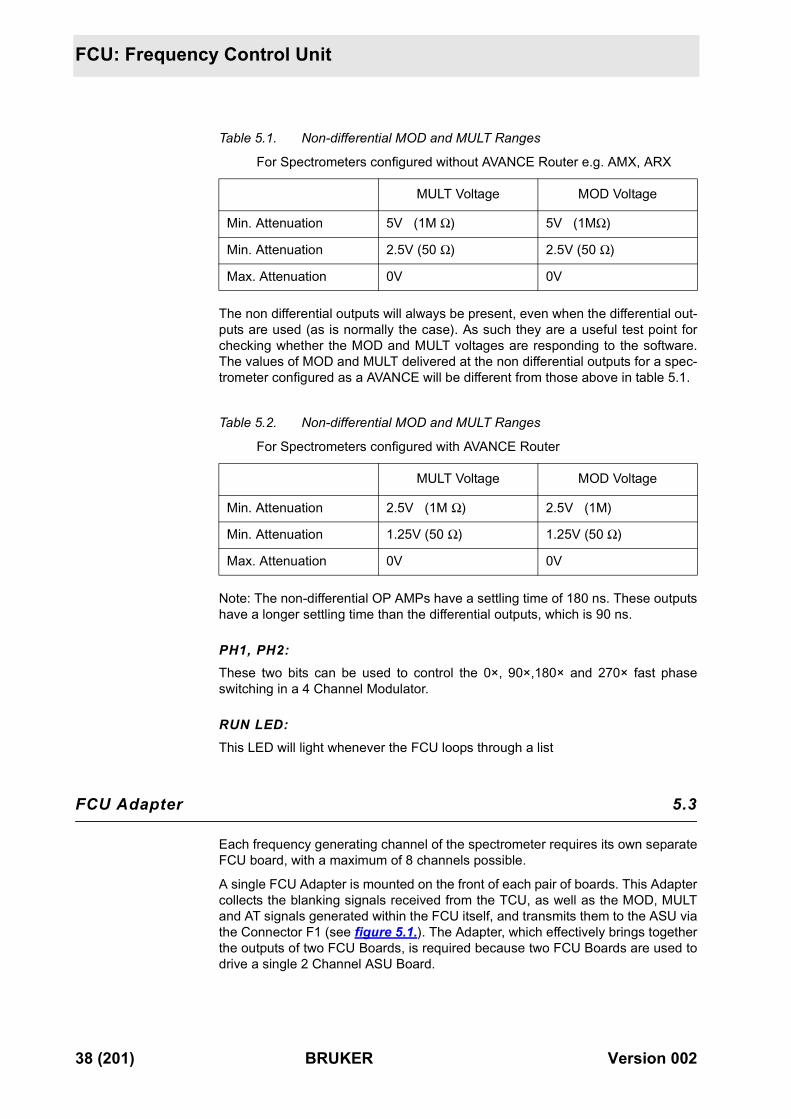
FCU Adapter 5.3
Each frequency generating channel of the spectrometer requires its own separateFCU board, with a maximum of 8 channels possible.
A single FCU Adapter is mounted on the front of each pair of boards. This Adaptercollects the blanking signals received from the TCU, as well as the MOD, MULTand AT signals generated within the FCU itself, and transmits them to the ASU viathe Connector F1 (see figure 5.1.). The Adapter, which effectively brings togetherthe outputs of two FCU Boards, is required because two FCU Boards are used todrive a single 2 Channel ASU Board.
Table 5.1. Non-differential MOD and MULT Ranges
For Spectrometers configured without AVANCE Router e.g. AMX, ARX
MULT Voltage MOD Voltage
Min. Attenuation 5V (1M Ω) 5V (1MΩ)
Min. Attenuation 2.5V (50 Ω) 2.5V (50 Ω)
Max. Attenuation 0V 0V
Table 5.2. Non-differential MOD and MULT Ranges
For Spectrometers configured with AVANCE Router
MULT Voltage MOD Voltage
Min. Attenuation 2.5V (1M Ω) 2.5V (1M)
Min. Attenuation 1.25V (50 Ω) 1.25V (50 Ω)
Max. Attenuation 0V 0V
38 (201) BRUKER Version 002
FCU Adapter
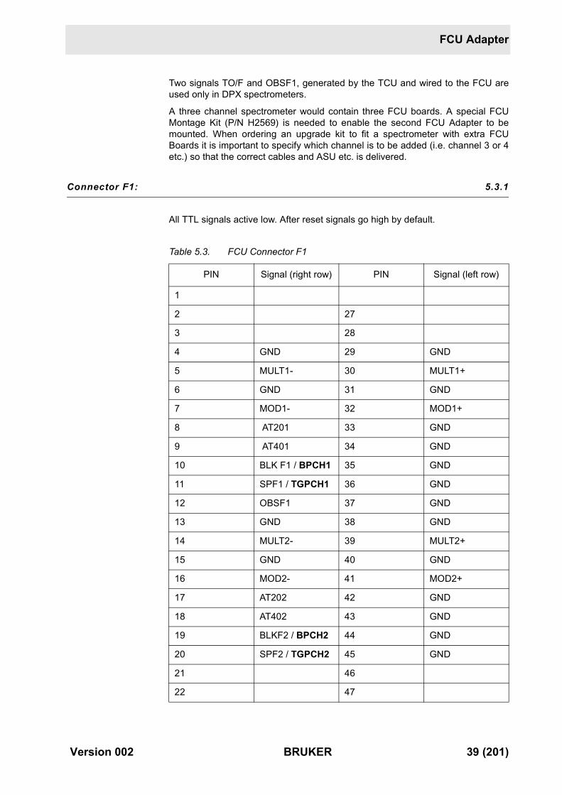
Two signals TO/F and OBSF1, generated by the TCU and wired to the FCU areused only in DPX spectrometers.
A three channel spectrometer would contain three FCU boards. A special FCUMontage Kit (P/N H2569) is needed to enable the second FCU Adapter to bemounted. When ordering an upgrade kit to fit a spectrometer with extra FCUBoards it is important to specify which channel is to be added (i.e. channel 3 or 4etc.) so that the correct cables and ASU etc. is delivered.
Connector F1: 5.3.1
All TTL signals active low. After reset signals go high by default.
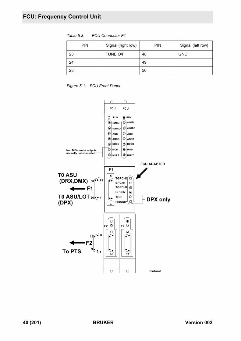
Table 5.3. FCU Connector F1
PIN Signal (right row) PIN Signal (left row)
1
2 27
3 28
4 GND 29 GND
5 MULT1- 30 MULT1+
6 GND 31 GND
7 MOD1- 32 MOD1+
8 AT201 33 GND
9 AT401 34 GND
10 BLK F1 / BPCH1 35 GND
11 SPF1 / TGPCH1 36 GND
12 OBSF1 37 GND
13 GND 38 GND
14 MULT2- 39 MULT2+
15 GND 40 GND
16 MOD2- 41 MOD2+
17 AT202 42 GND
18 AT402 43 GND
19 BLKF2 / BPCH2 44 GND
20 SPF2 / TGPCH2 45 GND
21 46
22 47
Version 002 BRUKER 39 (201)
FCU: Frequency Control Unit
Figure 5.1. FCU Front Panel
23 TUNE O/F 48 GND
24 49
25 50
Table 5.3. FCU Connector F1
PIN Signal (right row) PIN Signal (left row)
FCU
40MAI
40MAO
AQSI
AQSO
DDSO
MOD
MULT
RUN
FCU
40MAI
40MAO
AQSI
AQSO
DDSO
MOD
MULT
RUN
fcufront
FCU ADAPTER
Non Differerntial outputsnormally not connected
126
2550
F1
T0 ASU (DRX,DMX)
T0 ASU/LOT (DPX)
To PTSF2
F2 F2
1
8
9
15
DPX only
TGPCH1BPCH1TGPCH2BPCH2TO/FOBSCH1
F1
40 (201) BRUKER Version 002
FCU Power Supplies
FCU Power Supplies 5.4
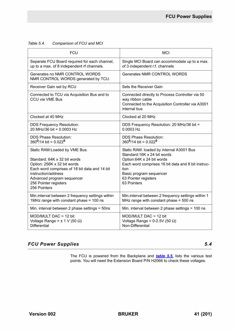
The FCU is powered from the Backplane and table 5.5. lists the various testpoints. You will need the Extension Board P/N H2066 to check these voltages.
Table 5.4. Comparison of FCU and MCI
FCU MCI
Separate FCU Board required for each channel, up to a max. of 8 independent rf channels.
Single MCI Board can accommodate up to a max. of 3 independent r.f. channels
Generates no NMR CONTROL WORDSNMR CONTROL WORDS generated by TCU.
Generates NMR CONTROL WORDS
Receiver Gain set by RCU Sets the Receiver Gain
Connected to TCU via Acquisition Bus and to CCU via VME Bus
Connected directly to Process Controller via 50 way ribbon cableConnected to the Acquisition Controller via A3001 internal bus
Clocked at 40 MHz Clocked at 20 MHz
DDS Frequency Resolution:20 MHz/36 bit = 0.0003 Hz
DDS Frequency Resolution: 20 MHz/36 bit = 0.0003 Hz
DDS Phase Resolution:3600/14 bit = 0.0220
DDS Phase Resolution: 3600/14 bit = 0.0220
Static RAM:Loaded by VME Bus.
Standard: 64K x 32 bit wordsOption: 256K x 32 bit wordsEach word comprises of 18 bit data and 14 bit instruction/addressAdvanced program sequencer256 Pointer registers256 Pointers
Static RAM: loaded by internal A3001 BusStandard:16K x 24 bit wordsOption:64K x 24 bit wordsEach word comprises 16 bit data and 8 bit instruc-tionBasic program sequencer63 Pointer registers63 Pointers
Min.interval between 2 frequency settings within 1MHz range with constant phase = 100 ns
Min.interval between 2 frequency settings within 1 MHz range with constant phase = 500 ns
Min. interval between 2 phase settings = 50ns Min. interval between 2 phase settings = 100 ns
MOD/MULT DAC = 12 bitVoltage Range = ± 1 V (50 Ω)Differential
MOD/MULT DAC = 12 bitVoltage Range = 0-2.5V (50 Ω)Non-Differential
Version 002 BRUKER 41 (201)
FCU: Frequency Control Unit
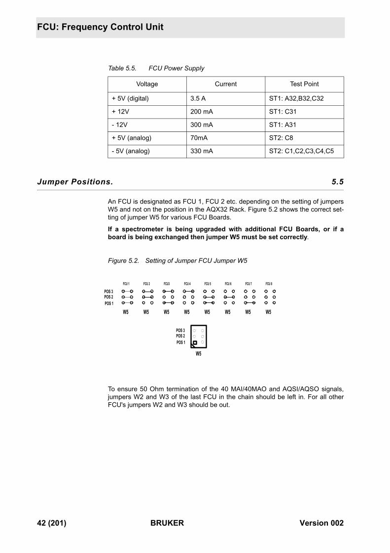
Jumper Positions. 5.5
An FCU is designated as FCU 1, FCU 2 etc. depending on the setting of jumpersW5 and not on the position in the AQX32 Rack. Figure 5.2 shows the correct set-ting of jumper W5 for various FCU Boards.
If a spectrometer is being upgraded with additional FCU Boards, or if aboard is being exchanged then jumper W5 must be set correctly.
Figure 5.2. Setting of Jumper FCU Jumper W5
To ensure 50 Ohm termination of the 40 MAI/40MAO and AQSI/AQSO signals,jumpers W2 and W3 of the last FCU in the chain should be left in. For all otherFCU's jumpers W2 and W3 should be out.
Table 5.5. FCU Power Supply
Voltage Current Test Point
+ 5V (digital) 3.5 A ST1: A32,B32,C32
+ 12V 200 mA ST1: C31
- 12V 300 mA ST1: A31
+ 5V (analog) 70mA ST2: C8
- 5V (analog) 330 mA ST2: C1,C2,C3,C4,C5
W5 W5 W5 W5 W5
FCU 5
W5 W5 W5
FCU 2 FCU3 FCU 4 FCU 6 FCU 7 FCU 8
POS 1POS 2POS 3
FCU 1
POS 1POS 2POS 3
W5
42 (201) BRUKER Version 002
FCUCHAN
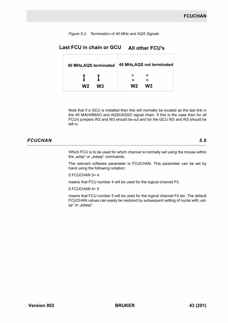
Figure 5.3. Termination of 40 MHz and AQS Signals
Note that if a GCU is installed then this will normally be located as the last link inthe 40 MAI/40MAO and AQSI/AQSO signal chain. If this is the case then for allFCU's jumpers W2 and W3 should be out and for the GCU W2 and W3 should beleft in.
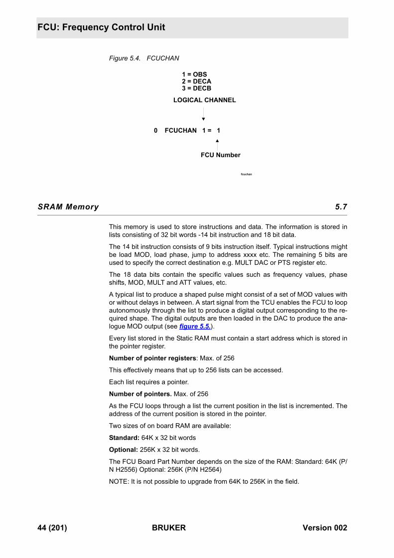
FCUCHAN 5.6
Which FCU is to be used for which channel is normally set using the mouse withinthe „edsp“ or „edasp“ commands.
The relevant software parameter is FCUCHAN. This parameter can be set byhand using the following notation:
0 FCUCHAN 3= 4
means that FCU number 4 will be used for the logical channel F3.
0 FCUCHAN 4= 5
means that FCU number 5 will be used for the logical channel F4 etc. The defaultFCUCHAN values can easily be restored by subsequent setting of nuclei with „ed-sp“ or „edasp“.
W2 W3
40 MHz,AQS terminated
W2 W3
40 MHz,AQS not terminated
Last FCU in chain or GCU All other FCU's
Version 002 BRUKER 43 (201)
FCU: Frequency Control Unit
Figure 5.4. FCUCHAN
SRAM Memory 5.7
This memory is used to store instructions and data. The information is stored inlists consisting of 32 bit words -14 bit instruction and 18 bit data.
The 14 bit instruction consists of 9 bits instruction itself. Typical instructions mightbe load MOD, load phase, jump to address xxxx etc. The remaining 5 bits areused to specify the correct destination e.g. MULT DAC or PTS register etc.
The 18 data bits contain the specific values such as frequency values, phaseshifts, MOD, MULT and ATT values, etc.
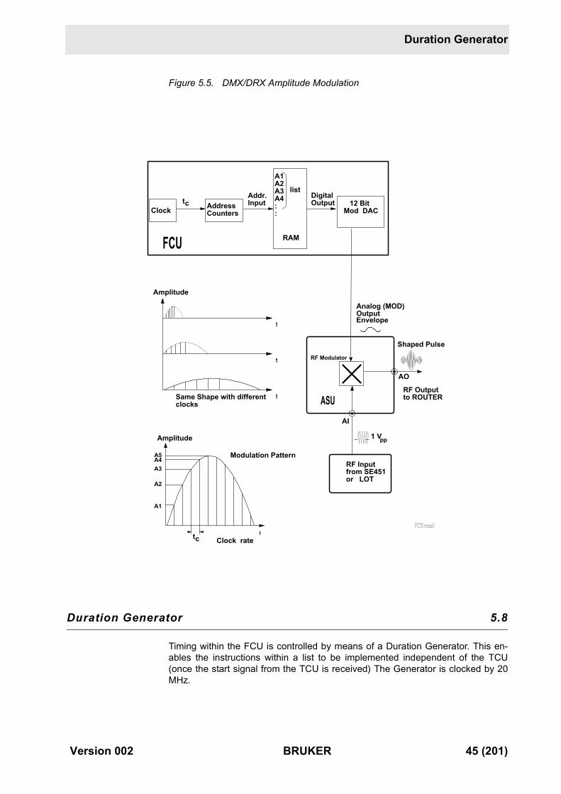
A typical list to produce a shaped pulse might consist of a set of MOD values withor without delays in between. A start signal from the TCU enables the FCU to loopautonomously through the list to produce a digital output corresponding to the re-quired shape. The digital outputs are then loaded in the DAC to produce the ana-logue MOD output (see figure 5.5.).
Every list stored in the Static RAM must contain a start address which is stored inthe pointer register.
Number of pointer registers: Max. of 256
This effectively means that up to 256 lists can be accessed.
Each list requires a pointer.
Number of pointers. Max. of 256
As the FCU loops through a list the current position in the list is incremented. Theaddress of the current position is stored in the pointer.
Two sizes of on board RAM are available:
Standard: 64K x 32 bit words
Optional: 256K x 32 bit words.
The FCU Board Part Number depends on the size of the RAM: Standard: 64K (P/N H2556) Optional: 256K (P/N H2564)
NOTE: It is not possible to upgrade from 64K to 256K in the field.
0 FCUCHAN 1 = 1
LOGICAL CHANNEL
FCU Number
1 = OBS2 = DECA3 = DECB
fcuchan
44 (201) BRUKER Version 002
Duration Generator
Figure 5.5. DMX/DRX Amplitude Modulation
Duration Generator 5.8
Timing within the FCU is controlled by means of a Duration Generator. This en-ables the instructions within a list to be implemented independent of the TCU(once the start signal from the TCU is received) The Generator is clocked by 20MHz.
Clock AddressCounters
RAM
12 Bit Mod DAC
A1A2A3A4::
listAddr.Input
DigitalOutput
FCU
Analog (MOD)OutputEnvelope
RF Modulator
RF Inputfrom SE451or LOT
RF Outputto ROUTER
Shaped Pulse
ASU
1 V
AI
AO
tc
pp
t
A1
A2
A3A4A5
Clock rate
Amplitude
Modulation Pattern
tc
Amplitude
t
t
tSame Shape with different clocks
Version 002 BRUKER 45 (201)
FCU: Frequency Control Unit
The minimum duration possible is 50 ns resulting in a minimum time of 50 ns be-tween any two instructions. The FCU has a timing resolution of 25 ns so that dura-tions can have lengths of 50,75,100,125 ns etc.
Table 5.6 contains a list of processes which are carried out by the FCU and the re-quired time to carry out these processes.
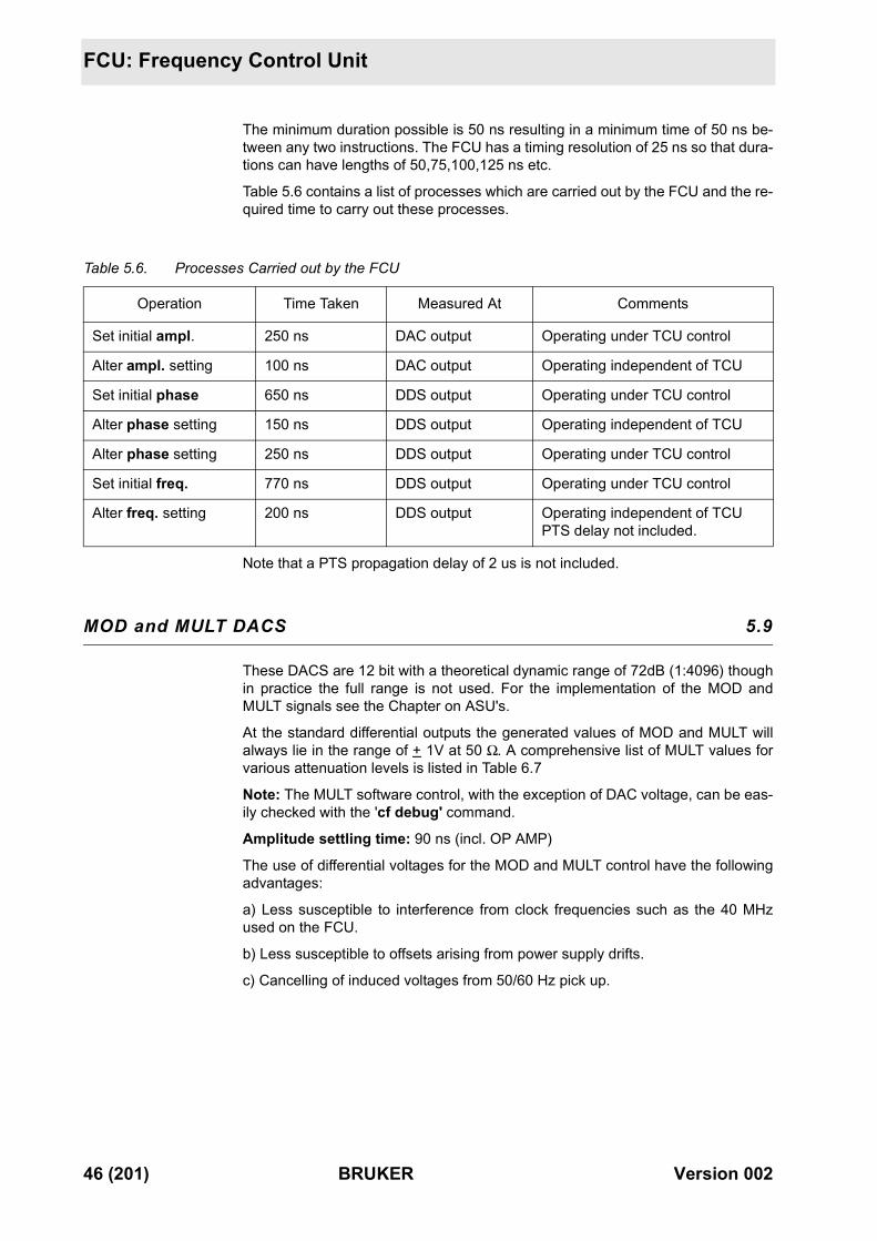
Note that a PTS propagation delay of 2 us is not included.
MOD and MULT DACS 5.9
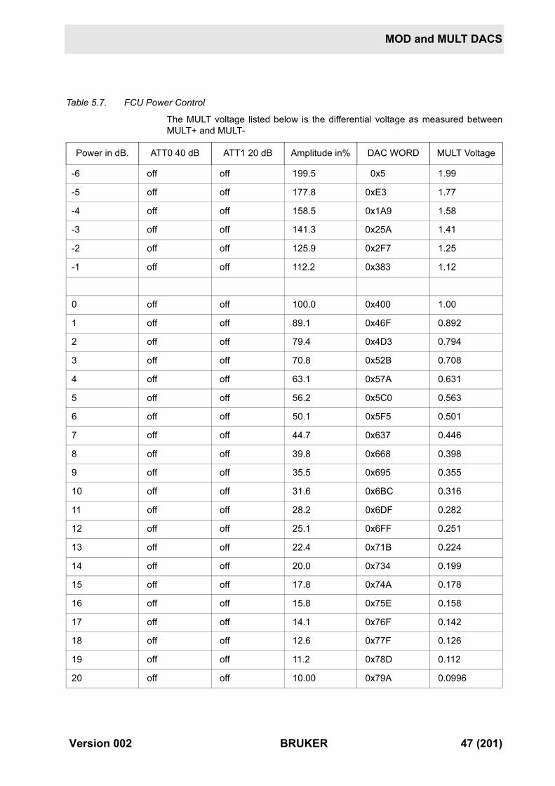
These DACS are 12 bit with a theoretical dynamic range of 72dB (1:4096) thoughin practice the full range is not used. For the implementation of the MOD andMULT signals see the Chapter on ASU's.
At the standard differential outputs the generated values of MOD and MULT willalways lie in the range of + 1V at 50 Ω. A comprehensive list of MULT values forvarious attenuation levels is listed in Table 6.7
Note: The MULT software control, with the exception of DAC voltage, can be eas-ily checked with the 'cf debug' command.
Amplitude settling time: 90 ns (incl. OP AMP)
The use of differential voltages for the MOD and MULT control have the followingadvantages:
a) Less susceptible to interference from clock frequencies such as the 40 MHzused on the FCU.
b) Less susceptible to offsets arising from power supply drifts.
c) Cancelling of induced voltages from 50/60 Hz pick up.
Table 5.6. Processes Carried out by the FCU
Operation Time Taken Measured At Comments
Set initial ampl. 250 ns DAC output Operating under TCU control
Alter ampl. setting 100 ns DAC output Operating independent of TCU
Set initial phase 650 ns DDS output Operating under TCU control
Alter phase setting 150 ns DDS output Operating independent of TCU
Alter phase setting 250 ns DDS output Operating under TCU control
Set initial freq. 770 ns DDS output Operating under TCU control
Alter freq. setting 200 ns DDS output Operating independent of TCUPTS delay not included.
46 (201) BRUKER Version 002
MOD and MULT DACS
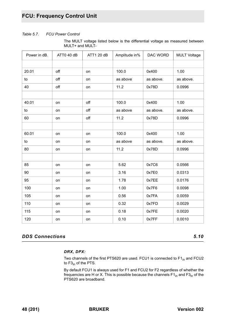
Table 5.7. FCU Power Control
The MULT voltage listed below is the differential voltage as measured betweenMULT+ and MULT-
Power in dB. ATT0 40 dB ATT1 20 dB Amplitude in% DAC WORD MULT Voltage
-6 off off 199.5 0x5 1.99
-5 off off 177.8 0xE3 1.77
-4 off off 158.5 0x1A9 1.58
-3 off off 141.3 0x25A 1.41
-2 off off 125.9 0x2F7 1.25
-1 off off 112.2 0x383 1.12
0 off off 100.0 0x400 1.00
1 off off 89.1 0x46F 0.892
2 off off 79.4 0x4D3 0.794
3 off off 70.8 0x52B 0.708
4 off off 63.1 0x57A 0.631
5 off off 56.2 0x5C0 0.563
6 off off 50.1 0x5F5 0.501
7 off off 44.7 0x637 0.446
8 off off 39.8 0x668 0.398
9 off off 35.5 0x695 0.355
10 off off 31.6 0x6BC 0.316
11 off off 28.2 0x6DF 0.282
12 off off 25.1 0x6FF 0.251
13 off off 22.4 0x71B 0.224
14 off off 20.0 0x734 0.199
15 off off 17.8 0x74A 0.178
16 off off 15.8 0x75E 0.158
17 off off 14.1 0x76F 0.142
18 off off 12.6 0x77F 0.126
19 off off 11.2 0x78D 0.112
20 off off 10.00 0x79A 0.0996
Version 002 BRUKER 47 (201)
FCU: Frequency Control Unit
DDS Connections 5.10
DRX, DPX: Two channels of the first PTS620 are used. FCU1 is connected to F1in and FCU2to F3in of the PTS.
By default FCU1 is always used for F1 and FCU2 for F2 regardless of whether thefrequencies are H or X. This is possible because the channels F1in and F3in of thePTS620 are broadband.
20.01 off on 100.0 0x400 1.00
to off on as above as above. as above.
40 off on 11.2 0x78D 0.0996
40.01 on off 100.0 0x400 1.00
to on off as above as above. as above.
60 on off 11.2 0x78D 0.0996
60.01 on on 100.0 0x400 1.00
to on on as above as above. as above.
80 on on 11.2 0x78D 0.0996
85 on on 5.62 0x7C6 0.0566
90 on on 3.16 0x7E0 0.0313
95 on on 1.78 0x7EE 0.0176
100 on on 1.00 0x7F6 0.0098
105 on on 0.56 0x7FA 0.0059
110 on on 0.32 0x7FD 0.0029
115 on on 0.18 0x7FE 0.0020
120 on on 0.10 0x7FF 0.0010
Table 5.7. FCU Power Control
The MULT voltage listed below is the differential voltage as measured betweenMULT+ and MULT-
Power in dB. ATT0 40 dB ATT1 20 dB Amplitude in% DAC WORD MULT Voltage
48 (201) BRUKER Version 002
DDS Specifications
DMX: Three channels of the first PTS620 are used. FCU1 is connected to F1in, FCU2 toF2in, and FCU3 to F3in of the PTS.
The F2in channel of the PTS contains a triple mixer to generate magnet specific1H frequencies suitable for further mixing in the SE451. The only input require-ment for this channel is the 3-4 MHz DDS signal. This enables a third channel tobe used within the PTS620. The first 1H frequency is by default generated byFCU2 regardless of whether it is F1 or F2. By default FCU1 is used for F1, onlywhen it is an X frequency
DDS Specifications 5.11
The DDS units used by the FCU are identical to those used in the MCI.
Frequency Range: 0 - 10 MHz.
Used Range: 3 - 4 MHz
Frequency Stability: This is set by the stability of the PTS 10 MHz crystal oscilla-tor which is specified to 3 x10⁻⁹/day.
Frequency Resolution: The DDS unit is clocked by 20 MHz and the frequencysetting is stored in a 36 bit register
20 MHz/236 = 0.0003 Hz.
Phase Resolution: A 14 bit register is used to store phase values.
360°/214 = 0.022°
Phase Settling Time: 50 ns.
Connector F2 5.12
All signals active low except PTS doubling command.
After reset all signals go high by default.The pin assignments of connector F2 is detailed in the table below.
These signals are used to set the final output of the PTS 620. Unlike the MCIthese signals can be measured at the FCU output without the requirement that thePTS620 is connected. A simple way to check if the PTS control is operating inDRX/DPX instruments is to run a series of short acquisitions. The F1 of the PTSwill then switch rapidly from the SFO1 to SFO1 +22 MHz. This will cause some ofbits transmitted through connector F2 to switch rapidly. The switching should besynchronized with the acquisition so that the EP_HPPR is a handy triggering sig-nal. To observe the PTS control in DMX instruments a frequency list can belooped through or alternatively the bit settings can be viewed during the wobbleroutine
Version 002 BRUKER 49 (201)
FCU: Frequency Control Unit
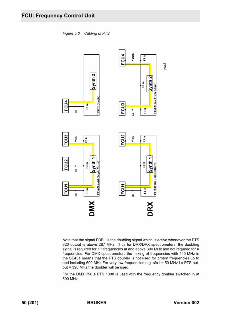
Figure 5.6. Cabling of PTS
Note that the signal FDBL is the doubling signal which is active whenever the PTS620 output is above 287 MHz. Thus for DRX/DPX spectrometers, the doublingsignal is required for 1H frequencies at and above 300 MHz and not required for Xfrequencies. For DMX spectrometers the mixing of frequencies with 440 MHz inthe SE451 means that the PTS doubler is not used for proton frequencies up toand including 600 MHz.For very low frequencies e.g. sfo1 = 50 MHz i.e PTS out-put = 390 MHz the doubler will be used.
For the DMX 750 a PTS 1000 is used with the frequency doubler switched in at500 MHz.
FCU
1FC
U2
FCU
3FC
U4
DDS
DDS
DDS
DDS
F1 in
F2 in
F3 in
F1 in
Synt
h 1
PTS6
20 (w
ith T
ripl
e M
ixer
)PT
S620
(Sin
gle)
DM
X
ptscabl
FCU
1FC
U2
DDS
DDS
F1 in
F2 in
F3 in
Synt
h 1
PTS6
20 (n
o T
ripl
e M
ixer
)D
RX
FCU
3FC
U4
DDS
DDS
F1 in
F2 in
F3 in
Synt
h 2
PTS6
20 (n
o T
ripl
e M
ixer
)
Synt
h 2
50 (201) BRUKER Version 002
PTS Bit settings
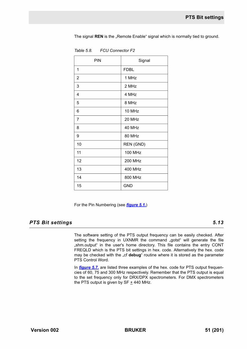
The signal REN is the „Remote Enable“ signal which is normally tied to ground.
For the Pin Numbering (see figure 5.1.)
PTS Bit settings 5.13
The software setting of the PTS output frequency can be easily checked. Aftersetting the frequency in UXNMR the command „gotst“ will generate the file„shm.output“ in the user's home directory. This file contains the entry CONTFREQLD which is the PTS bit settings in hex. code. Alternatively the hex. codemay be checked with the „cf debug“ routine where it is stored as the parameterPTS Control Word.
In figure 5.7. are listed three examples of the hex. code for PTS output frequen-cies of 60, 75 and 300 MHz respectively. Remember that the PTS output is equalto the set frequency only for DRX/DPX spectrometers. For DMX spectrometersthe PTS output is given by SF + 440 MHz.
Table 5.8. FCU Connector F2
PIN Signal
1 FDBL
2 1 MHz
3 2 MHz
4 4 MHz
5 8 MHz
6 10 MHz
7 20 MHz
8 40 MHz
9 80 MHz
10 REN (GND)
11 100 MHz
12 200 MHz
13 400 MHz
14 800 MHz
15 GND
Version 002 BRUKER 51 (201)
FCU: Frequency Control Unit
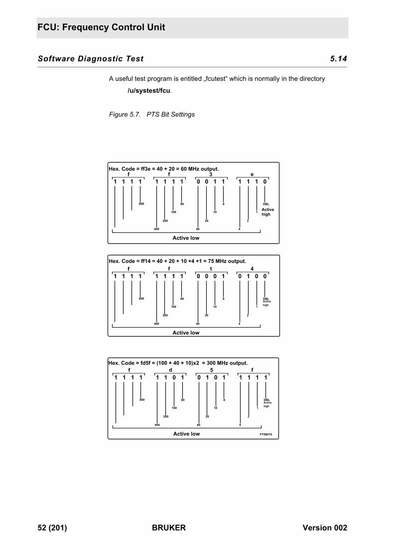
Software Diagnostic Test 5.14
A useful test program is entitled „fcutest“ which is normally in the directory
/u/systest/fcu.
Figure 5.7. PTS Bit Settings
1 1 1 1
800
1 1 1 1
80
100
200
400
0 0 1 1
8
10
20
40
1 1 1 0
DBL
1
2
4
f f 3 e
Active high
Active low
Hex. Code = ff3e = 40 + 20 = 60 MHz output.
1 1 1 1
800
1 1 1 1
80
100
200
400
0 0 0 1
8
10
20
40
0 1 0 0
DBL
1
2
4
f f 1 4
Active high
Active low
Hex. Code = ff14 = 40 + 20 + 10 +4 +1 = 75 MHz output.
1 1 1 1
800
1 1 0 1
80
100
200
400
0 1 0 1
8
10
20
40
1 1 1 1
DBL
1
2
4
f d 5 f
Active high
Active low
Hex. Code = fd5f = (100 + 40 + 10)x2 = 300 MHz output.
PTSBITS
52 (201) BRUKER Version 002
PTS 620 6
Type: PTS D 620 Q0020 (P/N O0573)
DDS Connections 6.1
DRX/DPX: Two channels of the first PTS620 are used. FCU1 is connected to F1in and FCU2to F3in of the PTS.
By default FCU1 is always used for OBSF1 and FCU2 for DECNUC regardless ofwhether the frequencies are H or X. This is possible because the channels F1 andF3 of the PTS620 are broadband.
DMX: Three channels of the first PTS620 are used. FCU1 is connected to F1in , FCU2 toF2in and FCU3 to F3in of the PTS.
The F2 channel of the PTS contains a triple mixer to generate magnet specific 1Hfrequencies suitable for further mixing in the SE451. The only input requirementfor this channel is the 3-4 MHz. DDS signal. This enables a third channel to beused within the PTS620. The first 1H frequency is by default generated byFCU2 regardless of whether it is OBS or DEC. By default FCU1 is used forOBSF1, only when it is an X frequency.
Outputs 6.2
Range: 1-620 MHz F1 and F3
1H frequency + 0.5MHz F2
Output amplitude: + 4 dBm ( 1Vpp at 50Ω ).
Frequency Control: Remote by TTL level. F1 and F3
Switching time: 20µs 100 MHz digit:
5 µs 10/ 1 MHz digit:
Transmit\Receive switching time; <5µs DRX/DPX
<2µs DMX
Aux. outputs: 5 x 10 MHz + 4 dBm
1 x 22 MHz + 4 dBm
1 x 80 MHz 0 dBm (0.65 Vpp at 50Ω )
Version 002 BRUKER 53 (201)
PTS 620
Inputs 6.3
DDSCH1,2,3: 3-4 MHz 1Vpp at 50Ω
Freq. Resolution: 0.0003 Hz
Phase Resolution: 0.022°
Synth1 Pinouts 6.4
Overview 6.5
The PTS620 produces the required RF frequency on two identical broadbandchannels F1 and F3. Each channel produces frequencies in the range of 1 MHz -310 MHz, but with the aid of a frequency doubler at the final output, this range isextended to 1 MHz - 620 MHz.
In the DRX or DPX there is no subsequent mixing of frequencies in a SE451 typeTFX or TFH unit. The PTS620 generates the final RF frequencies SFO1 andSFO2
In the DMX there is subsequent mixing of frequencies in the SE451. For the OBSand DECNUC frequencies the PTS output is given by SF + 440MHz. The third rffrequency DECNUCB is generated directly.
Table 6.1. SYNTH1 Pin Assignment
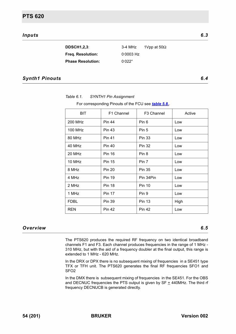
For corresponding Pinouts of the FCU see table 5.8..
BIT F1 Channel F3 Channel Active
200 MHz Pin 44 Pin 6 Low
100 MHz Pin 43 Pin 5 Low
80 MHz Pin 41 Pin 33 Low
40 MHz Pin 40 Pin 32 Low
20 MHz Pin 16 Pin 8 Low
10 MHz Pin 15 Pin 7 Low
8 MHz Pin 20 Pin 35 Low
4 MHz Pin 19 Pin 34Pin Low
2 MHz Pin 18 Pin 10 Low
1 MHz Pin 17 Pin 9 Low
FDBL Pin 39 Pin 13 High
REN Pin 42 Pin 42 Low
54 (201) BRUKER Version 002
Units
The fine resolution of the RF output is achieved by mixing frequencies generatedinternally in the PTS with signals (DDSCH1, DDSCH2) generated by Direct DigitalSynthesis in the FCU. In this way a frequency resolution of 0.0003 Hz and phaseresolution of 0.022° is achieved. The switching time between frequencies howeveris limited to that of the PTS.
Abbreviations:SGA, SGB: Standard Generators A and B
DMA: Digit Module A
IA: Input amplifier.
OA: Output amplifier
IM: Intermediate Mixer
SO: Switched Oscillator
Units 6.6
For the following section please refer to figure 6.2..
Crystal Oscillator: Produces a 10 MHz signal to a very high degree of accuracy (stability 3 x 10⁻⁹/day). This signal acts as a reference standard for all frequencies generated withinthe PTS.
SGA, SGB: uses the 10 MHz reference to generate the following frequencies 112, 113, 14, 16,18, 20 and 22 MHz. Of particular importance is the 18 MHz signal. The SGA mod-ule also produces signals of frequency (nx10) MHz where n is any integer from 1to 16.
Mixer: In this module the 3-4 MHz is mixed with 18 MHz to give frequencies in the 14-15MHz range. The DMA unit requires inputs of 14-15 MHz. It is in the mixer that thefine resolution of the RF output is entered.
DMA: This unit adds the required number of 1 MHz steps to the frequency. It also adds acarrier frequency so that the DMA output frequency always lies in the 140-150MHz range.
IM, SO, IA, OA: These modules combine to perform the following functions.
1. Addition of the selected 10 MHz steps
2. Output amplification and level control
3. Doubling of frequencies above 310 MHz and filtering of harmonics.
Version 002 BRUKER 55 (201)
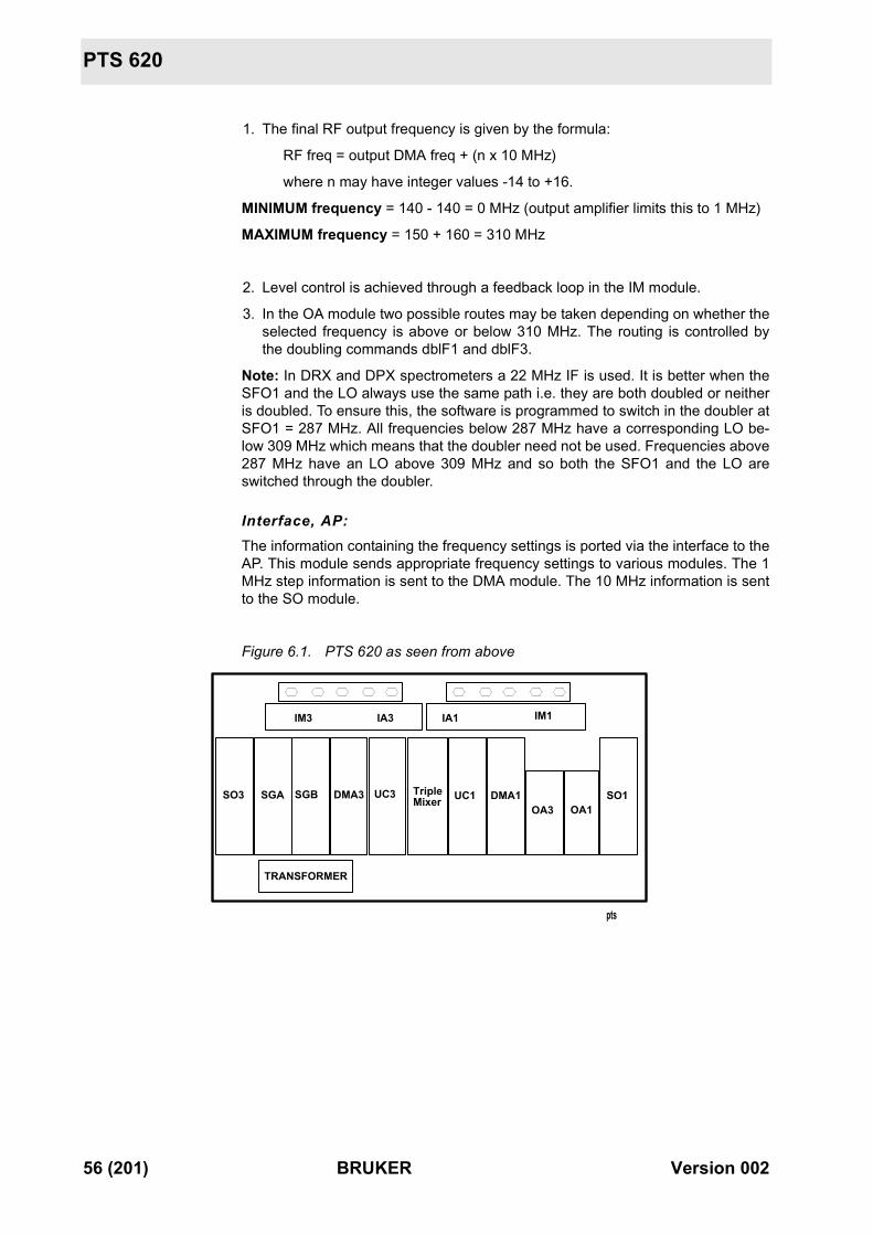
PTS 620
1. The final RF output frequency is given by the formula:
RF freq = output DMA freq + (n x 10 MHz)
where n may have integer values -14 to +16.
MINIMUM frequency = 140 - 140 = 0 MHz (output amplifier limits this to 1 MHz)
MAXIMUM frequency = 150 + 160 = 310 MHz
2. Level control is achieved through a feedback loop in the IM module.
3. In the OA module two possible routes may be taken depending on whether theselected frequency is above or below 310 MHz. The routing is controlled bythe doubling commands dblF1 and dblF3.
Note: In DRX and DPX spectrometers a 22 MHz IF is used. It is better when theSFO1 and the LO always use the same path i.e. they are both doubled or neitheris doubled. To ensure this, the software is programmed to switch in the doubler atSFO1 = 287 MHz. All frequencies below 287 MHz have a corresponding LO be-low 309 MHz which means that the doubler need not be used. Frequencies above287 MHz have an LO above 309 MHz and so both the SFO1 and the LO areswitched through the doubler.
Interface, AP: The information containing the frequency settings is ported via the interface to theAP. This module sends appropriate frequency settings to various modules. The 1MHz step information is sent to the DMA module. The 10 MHz information is sentto the SO module.
Figure 6.1. PTS 620 as seen from above
IM3 IA3 IA1 IM1
TRANSFORMER
pts
OA3 OA1SO1DMA1UC1UC3DMA3SGBSGASO3 Triple
Mixer
56 (201) BRUKER Version 002
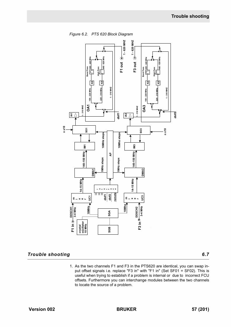
Trouble shooting
Figure 6.2. PTS 620 Block Diagram
Trouble shooting 6.7
1. As the two channels F1 and F3 in the PTS620 are identical, you can swap in-put offset signals i.e. replace "F3 in" with "F1 in" (Set SF01 = SF02). This isuseful when trying to establish if a problem is internal or due to incorrect FCUoffsets. Furthermore you can interchange modules between the two channelsto locate the source of a problem.
i n t e r f a c e
m i x e r rem
ote
dblf1
dblf2
SGB
SGA
18M
Hz
m i x e r
crys
tal
osci
llato
r10
MH
z
AP
14-1
5 M
Hz
18M
hz
14-1
5 M
Hz
140-
150
MH
z
140-
150
MH
zF3
out
DM
A1
IM1
DM
A3
IM3
UC
1
UC
3
dblf1
1MH
z st
eps
1MH
z st
eps
10M
hz s
teps
DD
SCH
1F1
in
10M
Hz
step
sn x1
0
n x1
0
3-4
MH
z
3-4
MH
zF3
in
IA3
SO3
OA
3
1 - 3
10 M
HZ
1 - 3
10 M
HZ
1 - 6
20 M
HZ
IA1
SO1
F1 o
ut
1 - 3
10 M
HZ
1 - 3
10 M
HZ
1 - 6
20 M
HZ
dblf2
225
- 310
MH
z
300
- 440
MHz
440
- 620
MH
z
Ban
d Pa
ss
Hig
h Pa
ss
150
- 220
MH
z
OA
1
225
- 310
MH
z
300
- 440
MHz
440
- 620
MH
z
Ban
d Pa
ss
Hig
h Pa
ss
X215
0 - 2
20 M
Hz
X2 X2 X2
DD
SCH
2
Version 002 BRUKER 57 (201)
PTS 620
2. Checking the frequency of DDSCH1 / DDSCH2
Note that the description below is valid if doubler is not used.
SF01/SF02 = XXX.abcdefg
=> DDSCH1/DDSCH2 = 4.0000000 - 0.abcdefg MHz
eg. observe X nucleus
SF01 = 75.2345678 MHz => DDSCH1 = 3.7654322 MHz
SF01= 150.5124736 MHz => DDSCH1 = 3.4875264 MHz
eg. observe 1H nucleus
SF01 = 300.0000000 MHz => DDSCH2 = 4.0000000 MHz
SF01 = 500.1300000 MHz => DDSCH2 = 3.8700000 MHz
3. Two potentiometers are available with which the output voltages may be ad-justed.
"F3 out" may be adjusted by means of the potentiometer located immedi-ately to the right of the synth1 socket. To adjust the amplitude of "F1 out" itis necessary to open the PTS and adjust the potentiometer located underthe OA1 module.
4. Checking the frequency setting:
As mentioned in the Chapter on FCU's it is much simpler to measure the bit set-tings at the FCU output connector F2 rather than at the Synth1 input.
Adding extra channels 6.8
DMX: The first PTS620 will provide three frequencies as long as at least one frequencyis proton. The addition of a fourth channel will require a second PTS.
DRX: The first PTS 620 will provide a max. of two channels. The addition of a thirdchannel will require a second PTS 620.
DPX: The DPX may be configured with a max of two channels.
When a single extra channel is to be added then a single channel PTS is avail-able. This PTS is fitted
a) without the internal time base (10 MHz)
b) without 22 MHz and 80 MHz outputs.
c) with 5 x 10 MHz outputs.
When two additional channels are to be added then a standard dual channel PTS620 will be supplied.
The additional PTS units are referenced to an external 10 MHz source takenfrom the first PTS 620 and in this way the two synthesisers are synchronised.
58 (201) BRUKER Version 002
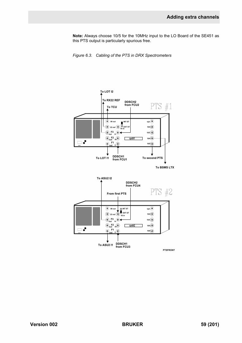
Adding extra channels
Note: Always choose 10/5 for the 10MHz input to the LO Board of the SE451 asthis PTS output is particularly spurious free.
Figure 6.3. Cabling of the PTS in DRX Spectrometers
80 out
22 out
out in
F1
F2
F3
10/1
10/2
10/3
10/4synth1
To LOT I1
out
out
in
in
DDSCH1from FCU1
To RX22 REF
10 in
10/5
To LOT I2
DDSCH2from FCU2
To TCU
To BSMS LTX
To second PTS
80 out
22 out
out in
F1
F2
F3
10/1
10/2
10/3
10/4synth2
To ASU2 I1
out
out
in
in
DDSCH1from FCU3
10 in
10/5
To ASU2 I2DDSCH2from FCU4
INT ST
EXT ST
INT ST
EXT ST
From first PTS
PTSFRONT
Version 002 BRUKER 59 (201)
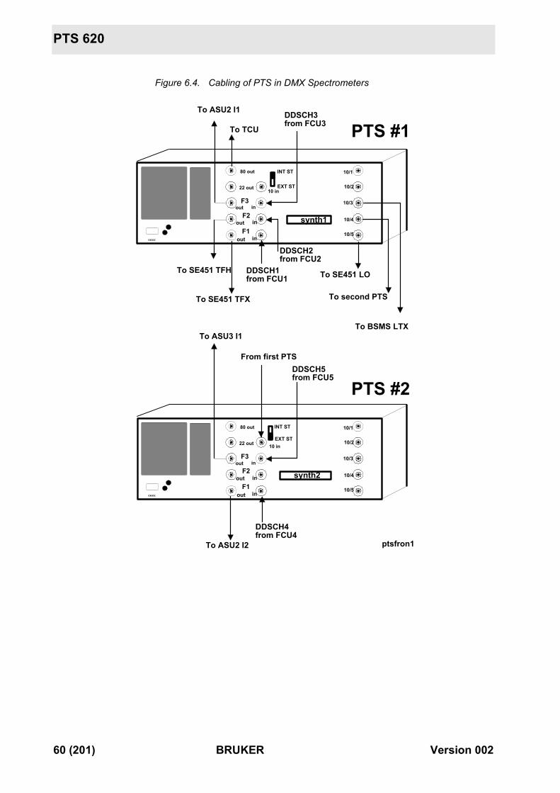
PTS 620
Figure 6.4. Cabling of PTS in DMX Spectrometers
80 out
22 out
out in
F1
F2
F3
10/1
10/2
10/3
10/4synth1
To SE451 TFH
out
out
in
in
DDSCH1from FCU1
10 in
10/5
DDSCH3from FCU3
To TCU
To BSMS LTX
To second PTS
80 out
22 out
out in
F1
F2
F3
10/1
10/2
10/3
10/4synth2
To ASU2 I2
out
out
in
in
DDSCH4from FCU4
10 in
10/5
To ASU3 I1
DDSCH5from FCU5
INT ST
EXT ST
INT ST
EXT ST
From first PTS
ptsfron1
To ASU2 I1
DDSCH2from FCU2
To SE451 TFX
To SE451 LO
PTS #1
PTS #2
60 (201) BRUKER Version 002
LOT Board 7
The LOT Board (Local Oscillator and Tune Board P/N W1301855 ) is system fre-quency independent and used exclusively in DRX spectrometers. The LOT Boardis a switching device using FET (GaAs) NE630D components with a switchingspeed of 20 ns.
A variation of this board, the LOT/ASU ( W1301854 ) is used in DPX spectrome-ters. The DPX Board combines the T/R switching, the wobble routine and theMULT, ATT functions in one board ( The MOD function however is not provideddue to space limitations). For the purposes of this manual the LOT Board and theASU Boards will be described separately.
Functions 7.1
1. To implement the T/R switching on the observe channel.
2. To provide a "tune out" and "LO" signal for the wobble routine.
1. T/R switching:
During the transmit mode (see figure 7.2.) up to two rf inputs (LTI1, LTI2), areconnected directly to two corresponding outputs (LTO1, LTO2). In this mode theLOT Board simply lets the rf signals through.
In the receive mode the frequency of the rf signal of the observe channel isswitched to the LO frequency and redirected to the receiver via the output LO12.The timing of the T/R switching is controlled by means of the RGP (EP) pulse. TheLO frequency always has the value SFO1 + 22 MHz. The 22 MHz is added to theSFO1 frequency within the PTS 620. This effectively introduces a switching de-lay(<5ms). Since DE = 4.5ms by default, the T/R switching has an effect (if any)on the first digitised point only. Note that should the first point be critical then thedefault DE can be extended.
2. Wobble Routine:
The RF path used by the wobble routine is illustrated in figure 7.4.. Note that theLOT hardware is such that Channel 2 is always used to provide the "FTUNE" out-put.
Version 002 BRUKER 61 (201)
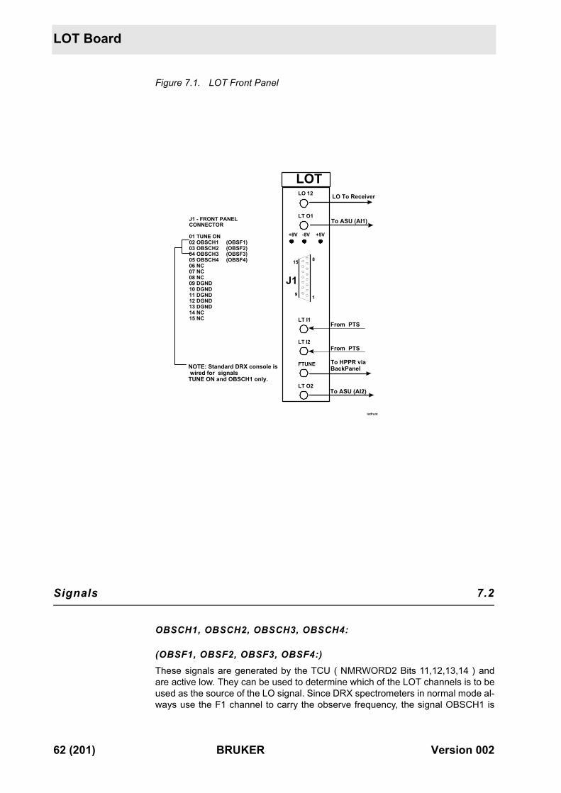
LOT Board
Figure 7.1. LOT Front Panel
Signals 7.2
OBSCH1, OBSCH2, OBSCH3, OBSCH4:
(OBSF1, OBSF2, OBSF3, OBSF4:)These signals are generated by the TCU ( NMRWORD2 Bits 11,12,13,14 ) andare active low. They can be used to determine which of the LOT channels is to beused as the source of the LO signal. Since DRX spectrometers in normal mode al-ways use the F1 channel to carry the observe frequency, the signal OBSCH1 is
LO 12
LT O1
LT I1
LT I2
FTUNE
LT O2
LOT
+8V -8V +5V
J1 - FRONT PANEL CONNECTOR
01 TUNE ON02 OBSCH1 (OBSF1) 03 OBSCH2 (OBSF2)04 OBSCH3 (OBSF3)05 OBSCH4 (OBSF4)06 NC07 NC08 NC09 DGND10 DGND11 DGND12 DGND13 DGND14 NC15 NC
LO To Receiver
To ASU (AI1)
From PTS
From PTS
To ASU (AI2)
To HPPR viaBackPanel
1
8
9
15
J1
lotfront
NOTE: Standard DRX console is wired for signals TUNE ON and OBSCH1 only.
62 (201) BRUKER Version 002
Signals
the signal that needs to be correctly set. This signal will automatically be set lowonce an observe nucleus has been selected in the "edasp" or "edsp" menus andthe corresponding interface initialised. The signal will reset high after the "stop"command has been entered or when a hardware reset of the CCU is carried out.(For TCU Boards up to and including Layout C, the pull-up resistors are notmounted on the TCU T4 outputs and so the signal should be checked on the LOTBoard itself and not at the TCU output.)
The signal OBSCH2 (OBSF2) allows for the possibility of using the second rf input(LT I2) as the source of the LO signal .This option is normally not used .
The signals OBSCH3 (OBSF3) and OBSCH4 (OBSF4) are not used at present .They allow for the possibility of using the LOT Board to carry up to 4 rf frequen-cies. This option may be implemented in the future for example to switch the ob-serve nucleus during an experiment.
NOTE1: For the standard LOT Board only signals OBSCH1 and TUNE ON are actuallyconnected in the console wiring.
NOTE2: In DMX spectrometers the signal OBSCH1 is used to select either the H or Xchannel as the observe channel in the SE451. In the new 19 inch SE451 ( 3 chan-nel capability) signals OBSCH1, OBSCH2 and OBSCH3 will be used to select theobserve channel.
RGP (EP):This signal, as measured on the board itself, is low for the duration of the acquisi-tion ( receiver open ) and high at all other times. The RGP (EP) signal, originatesin the RCU and is transmitted to the SADC via the 50 pin cable. From here it isconnected to the LOT Board via the back panel.
PAL LOT 1 ( EP610 ):In DRX spectrometers the chief functions of this Pal are to produce the F1>LOand BLKLO signals.
F1>LO :This signal is used to implement the T/R switching on the F1 channel . It is pro-duced by combining the RGP (EP) and OBSCH1 signals. The signal is high dur-ing transmission but goes low for the duration of the acquisition.
Table 7.1. Truth Table to Select LO Sources
OBSCH1 OBSCH2 LO Sources
0 0 CH1
1 0 CH2
0 1 CH1
1 1 None
Version 002 BRUKER 63 (201)
LOT Board
BLKLO:This signal is used to blank the LO12 output to the receiver . The signal is activehigh for the duration of the acquisition.
TUNE ON (OFF):This signal is produced by the TCU ( NMRWORD2 Bit10 ). It is active low and setwhenever the "wobb" command is entered.
TGPENAB (SPENAB):This signal is not actually used on the LOT Board but can be measured on theboard at the backpanel connection. The signal is low during rf transmission. Aftera power down from the BSMS keyboard the signal goes high.
Power Supply:The LOT Board is powered from the back panel via connector J1. The same pow-er supply board (W4P31377) is used for both the LOT and the ASU Boards.
64 (201) BRUKER Version 002
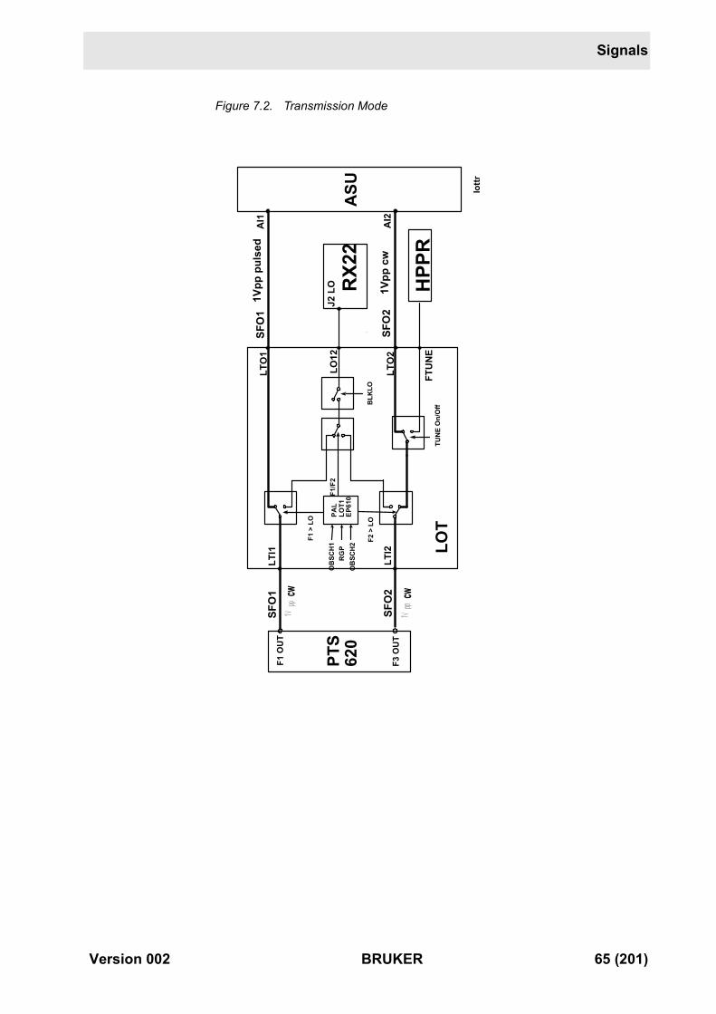
Signals
Figure 7.2. Transmission Mode
PTS
620
ASU
RX2
2
AI2
AI1
SFO
1F1
OU
TLT
I1
cwF1
> L
O
SFO
2LT
I2
F2 >
LO
TUN
E O
n/O
ff
RG
PO
BSC
H2
PAL
LOT1
EP61
0
HPP
RF3
OU
T
J2 L
O
LOT
F1/F
2
cwSF
O2
SFO
1
OB
SCH
1
lottr
1Vpp
pul
sed
1Vpp
cw
LTO
1
LO12
LTO
2
FTU
NE
BLK
LO
Version 002 BRUKER 65 (201)
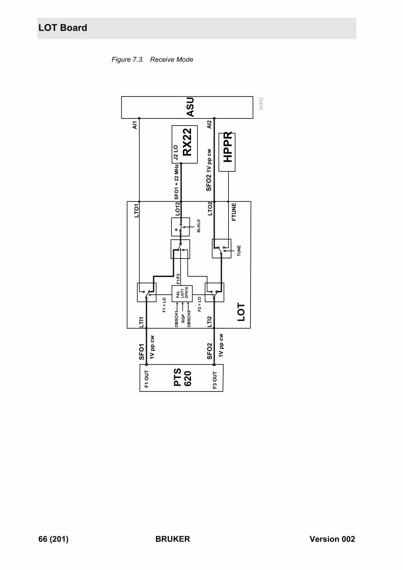
LOT Board
Figure 7.3. Receive Mode
PTS
620
ASU
RX2
2 AI2
AI1
SFO
1F1
OU
TLT
I1
F1 >
LO
SFO
2LT
I2
F2 >
LO
TUN
E
RG
PO
BSC
H2
PAL
LOT1
EP61
0
HPP
RF3
OU
T
J2 L
O
LOT
F1/F
2
SFO
2
SFO
1 +
22 M
Hz
OB
SCH
1
1V p
p cw
1V p
p cw
1V p
p cw
BLK
LO
LTO
1
LO12
LTO
2
FTU
NE
66 (201) BRUKER Version 002
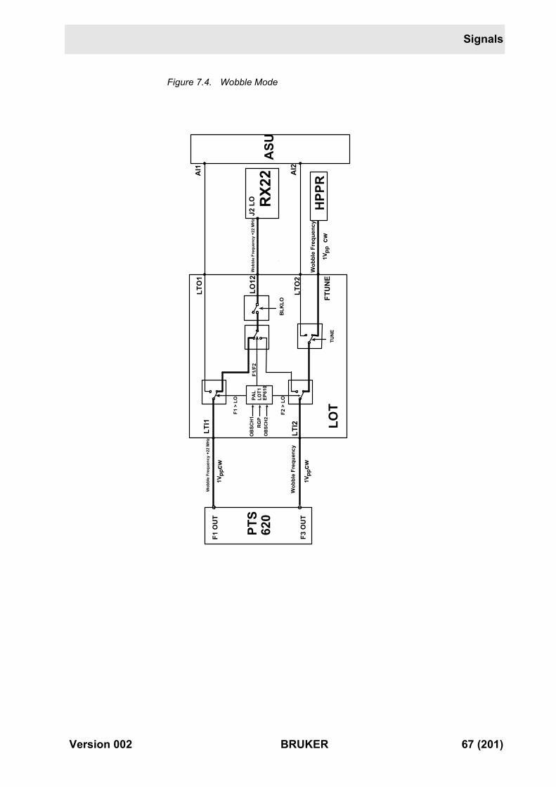
Signals
Figure 7.4. Wobble Mode
PTS
620
ASU
RX2
2 AI2
AI1
Wob
ble
Freq
uenc
y +2
2 M
Hz
F1 O
UT
LTI1
1Vpp
cw
F1 >
LO
LTI2
F2 >
LO
TUN
E
RGP
OB
SCH
1
OB
SCH
2
PAL
LOT1
EP61
0
HPP
RF3
OU
T
J2 L
O
LOT
F1/F
2W
obbl
e Fr
eque
ncy
+22
MH
z
Wob
ble
Freq
uenc
y
Wob
ble
Freq
uenc
y 1V
ppcw
1Vpp
cw
BLKL
O
LTO
1
LO12
LTO
2
FTU
NE
Version 002 BRUKER 67 (201)

LOT Board
68 (201) BRUKER Version 002
ASU: Amplitude Setting Unit 8
Functions 8.1
1. To set the amplitude of up to two rf signals using the MOD, MULT, AT20 andAT40 signals.
2. To blank the rf signal using the TGPCH and BPCH signals
The ASU performs functions which in AMX and ARX spectrometers were carriedout internally within the transmitters themselves. The AVANCE amplifiers nowserve as pure amplifiers, they carry out no power regulation or setting. The finaloutput of the BLAX300, BLAXH40 etc. will be a linear function of the rf input inten-sity.
The ASU board is system frequency independent up to 600 MHz and compatiblewith all of the new range of linear amplifiers BLARH100, BLAX300, BLAXH50 etc.(The 750 MHz DMX uses the same ASU board with selected components to ex-tend the bandwidth to 750 MHz.). There is no distinction between ASU boards forDRX and DMX spectrometers. The DPX spectrometer however uses a dual pur-pose ASU/LOT board without the MOD section. For this reason shaped pulsesare not possible with DPX spectrometers.
Standard ASU boards are capable of independently setting the amplitude of two rfchannels. The input rf signals (AI1, AI2) have a maximum intensity of 1VPP (4dBmat 50W). These inputs come from either the SE451 (DMX) or LOT board (DRX).
Where more than 2 rf channels are used*, then a second ASU board must be fit-ted.Three channel spectrometers are fitted with a single channel ASU (P/NW1301853). Four channel spectrometers simply use a second standard 2 chan-nel ASU (P/N W1301852) The third and fourth rf input signals are taken directlyfrom the respective PTS outputs.
*Note that the DPX spectrometer has a maximum of 2 channels.
The ASU receives the MOD, MULT, AT20, AT40 and various blanking signals fromthe FCU via the 50 pin SCSCI Type front panel connector (table 8.1.).Note thatthe connection to the FCU is one to one.
Version 002 BRUKER 69 (201)
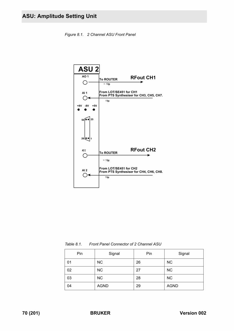
ASU: Amplitude Setting Unit
Figure 8.1. 2 Channel ASU Front Panel
Table 8.1. Front Panel Connector of 2 Channel ASU
Pin Signal Pin Signal
01 NC 26 NC
02 NC 27 NC
03 NC 28 NC
04 AGND 29 AGND
AO 1
AI 1
AO 2
AI 2
ASU 2
+8V -8V +5V
To ROUTER
From LOT/SE451 for CH1From PTS Synthesiser for CH3, CH5, CH7.
1
25
26
50
To ROUTER
1 Vpp
1 Vpp
1 Vpp
RFout CH1
RFout CH2
From LOT/SE451 for CH2From PTS Synthesiser for CH4, CH6, CH8.
1 Vpp
70 (201) BRUKER Version 002
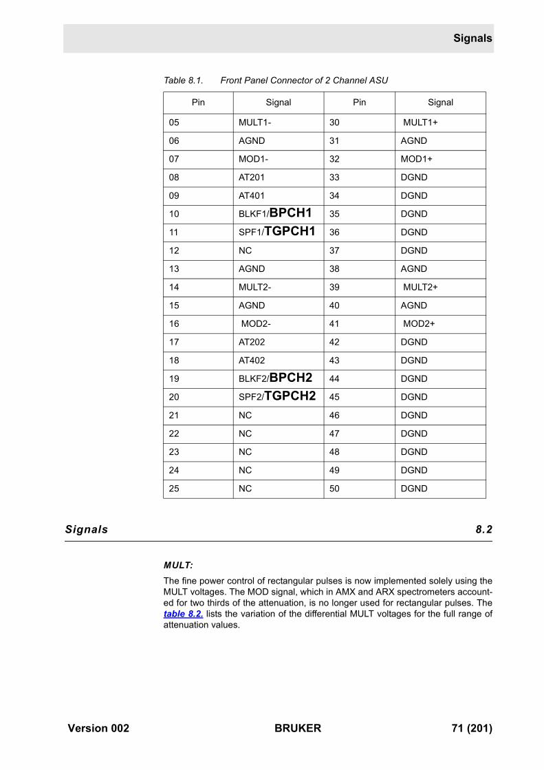
Signals
Signals 8.2
MULT:The fine power control of rectangular pulses is now implemented solely using theMULT voltages. The MOD signal, which in AMX and ARX spectrometers account-ed for two thirds of the attenuation, is no longer used for rectangular pulses. Thetable 8.2. lists the variation of the differential MULT voltages for the full range ofattenuation values.
05 MULT1- 30 MULT1+
06 AGND 31 AGND
07 MOD1- 32 MOD1+
08 AT201 33 DGND
09 AT401 34 DGND
10 BLKF1/BPCH1 35 DGND
11 SPF1/TGPCH1 36 DGND
12 NC 37 DGND
13 AGND 38 AGND
14 MULT2- 39 MULT2+
15 AGND 40 AGND
16 MOD2- 41 MOD2+
17 AT202 42 DGND
18 AT402 43 DGND
19 BLKF2/BPCH2 44 DGND
20 SPF2/TGPCH2 45 DGND
21 NC 46 DGND
22 NC 47 DGND
23 NC 48 DGND
24 NC 49 DGND
25 NC 50 DGND
Table 8.1. Front Panel Connector of 2 Channel ASU
Pin Signal Pin Signal
Version 002 BRUKER 71 (201)
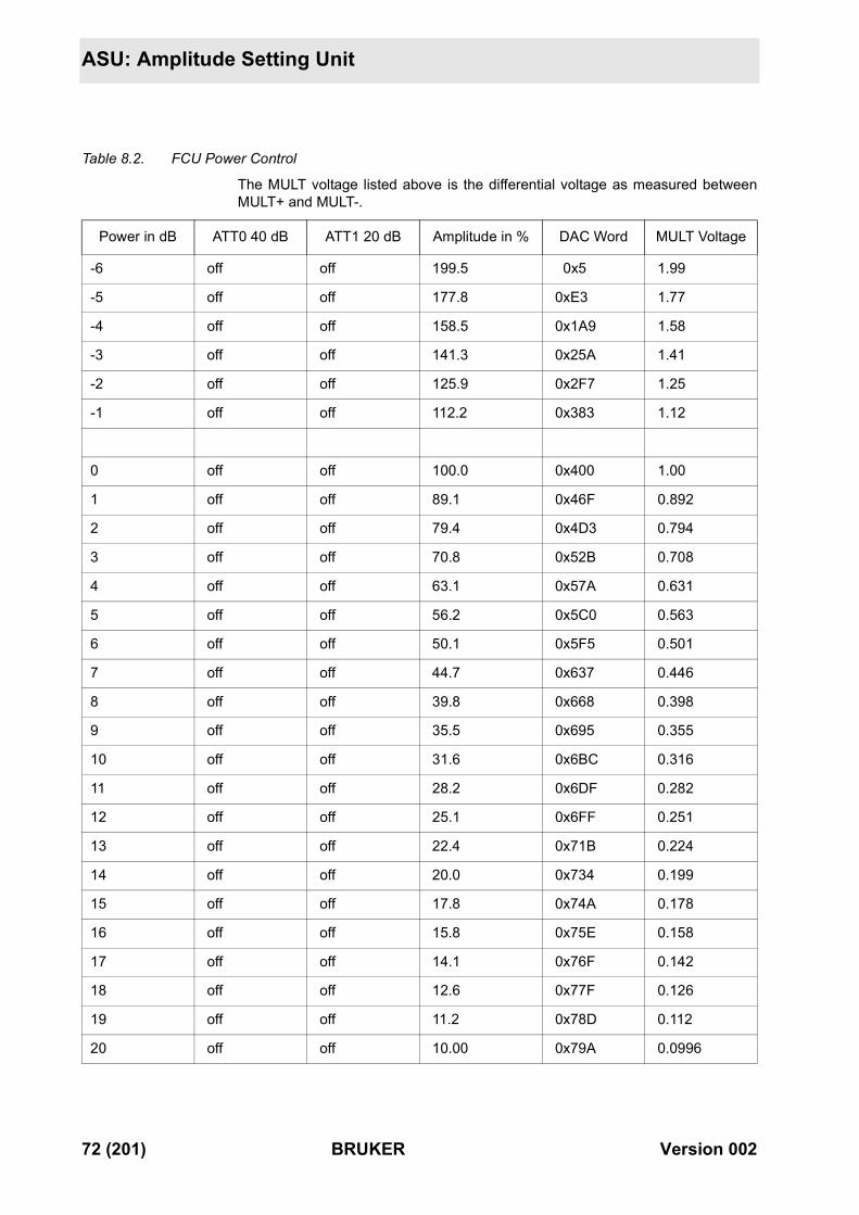
ASU: Amplitude Setting Unit
Table 8.2. FCU Power Control
The MULT voltage listed above is the differential voltage as measured betweenMULT+ and MULT-.
Power in dB ATT0 40 dB ATT1 20 dB Amplitude in % DAC Word MULT Voltage
-6 off off 199.5 0x5 1.99
-5 off off 177.8 0xE3 1.77
-4 off off 158.5 0x1A9 1.58
-3 off off 141.3 0x25A 1.41
-2 off off 125.9 0x2F7 1.25
-1 off off 112.2 0x383 1.12
0 off off 100.0 0x400 1.00
1 off off 89.1 0x46F 0.892
2 off off 79.4 0x4D3 0.794
3 off off 70.8 0x52B 0.708
4 off off 63.1 0x57A 0.631
5 off off 56.2 0x5C0 0.563
6 off off 50.1 0x5F5 0.501
7 off off 44.7 0x637 0.446
8 off off 39.8 0x668 0.398
9 off off 35.5 0x695 0.355
10 off off 31.6 0x6BC 0.316
11 off off 28.2 0x6DF 0.282
12 off off 25.1 0x6FF 0.251
13 off off 22.4 0x71B 0.224
14 off off 20.0 0x734 0.199
15 off off 17.8 0x74A 0.178
16 off off 15.8 0x75E 0.158
17 off off 14.1 0x76F 0.142
18 off off 12.6 0x77F 0.126
19 off off 11.2 0x78D 0.112
20 off off 10.00 0x79A 0.0996
72 (201) BRUKER Version 002
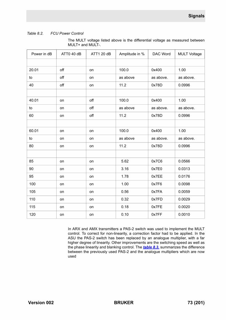
Signals
In ARX and AMX transmitters a PAS-2 switch was used to implement the MULTcontrol. To correct for non-linearity, a correction factor had to be applied. In theASU the PAS-2 switch has been replaced by an analogue multiplier, with a farhigher degree of linearity. Other improvements are the switching speed as well asthe phase linearity and blanking control. The table 8.3. summarizes the differencebetween the previously used PAS-2 and the analogue multipliers which are nowused
20.01 off on 100.0 0x400 1.00
to off on as above as above. as above.
40 off on 11.2 0x78D 0.0996
40.01 on off 100.0 0x400 1.00
to on off as above as above. as above.
60 on off 11.2 0x78D 0.0996
60.01 on on 100.0 0x400 1.00
to on on as above as above. as above.
80 on on 11.2 0x78D 0.0996
85 on on 5.62 0x7C6 0.0566
90 on on 3.16 0x7E0 0.0313
95 on on 1.78 0x7EE 0.0176
100 on on 1.00 0x7F6 0.0098
105 on on 0.56 0x7FA 0.0059
110 on on 0.32 0x7FD 0.0029
115 on on 0.18 0x7FE 0.0020
120 on on 0.10 0x7FF 0.0010
Table 8.2. FCU Power Control
The MULT voltage listed above is the differential voltage as measured betweenMULT+ and MULT-.
Power in dB ATT0 40 dB ATT1 20 dB Amplitude in % DAC Word MULT Voltage
Version 002 BRUKER 73 (201)
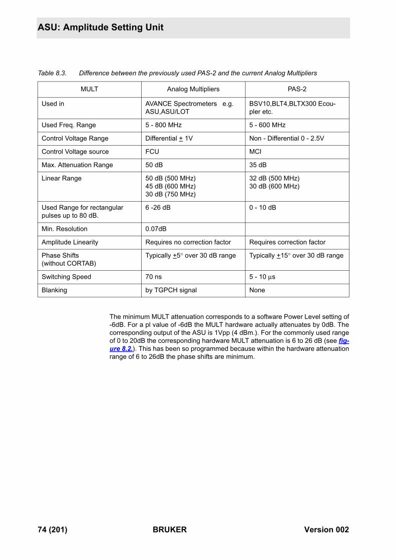
ASU: Amplitude Setting Unit
The minimum MULT attenuation corresponds to a software Power Level setting of-6dB. For a pl value of -6dB the MULT hardware actually attenuates by 0dB. Thecorresponding output of the ASU is 1Vpp (4 dBm.). For the commonly used rangeof 0 to 20dB the corresponding hardware MULT attenuation is 6 to 26 dB (see fig-ure 8.2.). This has been so programmed because within the hardware attenuationrange of 6 to 26dB the phase shifts are minimum.
Table 8.3. Difference between the previously used PAS-2 and the current Analog Multipliers
MULT Analog Multipliers PAS-2
Used in AVANCE Spectrometers e.g. ASU,ASU/LOT
BSV10,BLT4,BLTX300 Ecou-pler etc.
Used Freq. Range 5 - 800 MHz 5 - 600 MHz
Control Voltage Range Differential + 1V Non - Differential 0 - 2.5V
Control Voltage source FCU MCI
Max. Attenuation Range 50 dB 35 dB
Linear Range 50 dB (500 MHz)45 dB (600 MHz)30 dB (750 MHz)
32 dB (500 MHz)30 dB (600 MHz)
Used Range for rectangular pulses up to 80 dB.
6 -26 dB 0 - 10 dB
Min. Resolution 0.07dB
Amplitude Linearity Requires no correction factor Requires correction factor
Phase Shifts(without CORTAB)
Typically +5° over 30 dB range Typically +15° over 30 dB range
Switching Speed 70 ns 5 - 10 µs
Blanking by TGPCH signal None
74 (201) BRUKER Version 002
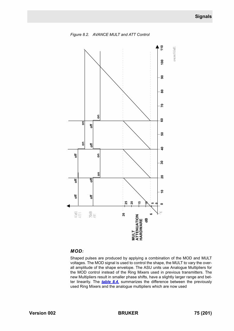
Signals
Figure 8.2. AVANCE MULT and ATT Control
MOD:Shaped pulses are produced by applying a combination of the MOD and MULTvoltages. The MOD signal is used to control the shape, the MULT to vary the over-all amplitude of the shape envelope. The ASU units use Analogue Multipliers forthe MOD control instead of the Ring Mixers used in previous transmitters. Thenew Multipliers result in smaller phase shifts, have a slightly larger range and bet-ter linearity. The table 8.4. summarizes the difference between the previouslyused Ring Mixers and the analogue multipliers which are now used
MU
LTA
TTEN
UA
TIO
NH
AR
DW
AR
E
515 102025
off
off
off
off
off
off
off
onon
onon
on
020
3040
5060
7080
9010
011
010
626
0
dB
Version 002 BRUKER 75 (201)
ASU: Amplitude Setting Unit
Two analogue multipliers set in series allow a modulation of up to 60 dB within asingle shape. The MULT signal is used to vary the overall amplitude of the shapedpulse and is normally maintained within the range of 0 to 30 dB. In conjunctionwith the 20 and 40 dB fixed attenuators, this gives a range in attenuation of over90 dB.
Larger MULT attenuation (between 30 and 50 dB) is possible but slightly largerphase shifts may arise at frequencies beyond 500 MHz.
MOD and MULT gating 8.3
Nomenclature: SPF1 = TGPCH1 SPF2 = TGPCH2 (Transmitting Gating Pulses)
TGPENAB(SPENAB) is normally permanently low, unless a power down reset isactivated from the BSMS keyboard. The TGPCH signals from the TCU are simplycombined with the TGPENAB through an „or“ gate to produce the SPFMULT andSPFMOD signals. The SPFMULT and SPFMOD signals (active low) are thenused to gate the MOD and MULT sections. Thus the gating signals will go low (ac-tive) only when either TGPCH1 or TGPCH2 is low. This allows precise gating con-trol of the MOD and MULT units which improves the on/off ratio. This gating wasnot implemented with the internal MOD and MULT units of previous transmitters.Note that the timing of TGPCH signals may not be altered using the „edscon „ta-ble.
Table 8.4. Difference between the previously used Ring Mixers and the current Analog Multipliers
MOD Analog Multipliers Ring Mixers
Used in e.g. ASU,ASU/LOT
BSV10,BLT4,BLTX300 Ecou-pler etc.
Freq. Range 5 - 800 MHz 5 - 800 MHz
Control Voltage Range Differential + 1V Non - Differential 0 - 2.5V
Control Voltage source FCU MCI
Max. Attenuation Range 2 x 30 dB 2 x 25 dB
Used Range for shapedpulses
2 x 30 dB 2 x 25 dB
Min. Resolution 0.14dB
Amplitude Linearity Requires no correction factor Requires no correction factor
Phase Shifts for 600 MHz over 50 dB.(without CORTAB)
<+ 10° > +20°
Switching Speed 70 ns 70 ns
Blanking by TGPCH signal None
76 (201) BRUKER Version 002
AT20 and AT40 Blanking
AT20 and AT40 Blanking 8.4
Nomenclature: BLKF1 = BPCH1 BLKF2 = BPCH2
The signals AT20FM1, AT40FM1, AT20FM2 and AT40FM2 are used to blank theattenuators and are active high (attenuator switched on).
The logic of the PAL ASU02 is such that the 20 and 40 dB attenuators are auto-matically active whenever rf signals are not being transmitted. Outside of pulsetransmission BPCH is high and therefore the 20 and 40 dB attenuators are by de-fault active. This new feature ensures minimum noise outside of the transmittedpulses. Whether the 20 or 40 dB attenuation is applied during the pulse transmis-sion itself depends on the signals AT20 and AT40. If these signals are low thenthe attenuators will be switched off.
The timing of BPCH signals may be altered using the „edscon „table. The corre-sponding edscon parameters are BLKTR[1-8].
Version 002 BRUKER 77 (201)
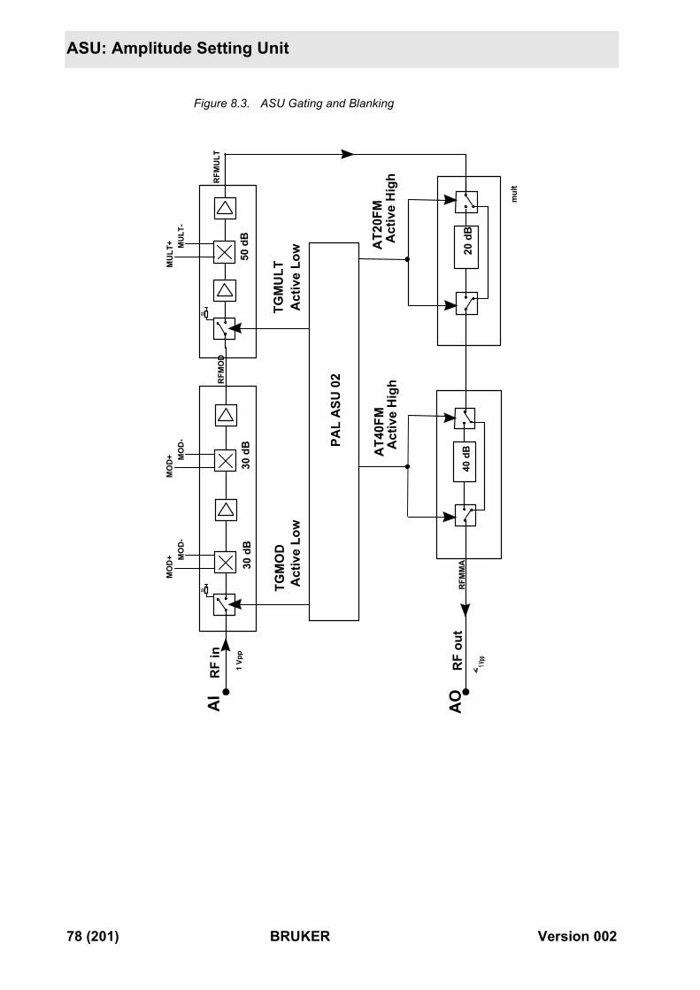
ASU: Amplitude Setting Unit
Figure 8.3. ASU Gating and Blanking
30 d
B
TGM
OD
TGM
ULT
30 d
B
MO
D+ M
OD
-M
OD
+ MO
D-
50 d
B
MU
LT+ MU
LT-
AT2
0FM
AT4
0FM
PAL
ASU
02
Act
ive
Low
Act
ive
Low
Act
ive
Hig
hA
ctiv
e H
igh
RF
in
RF
out
mul
t
AI
RFM
OD
RFM
ULT
RFM
MA
AO
1 Vpp
50 50
20 d
B
1 Vp
p
40 d
B
78 (201) BRUKER Version 002
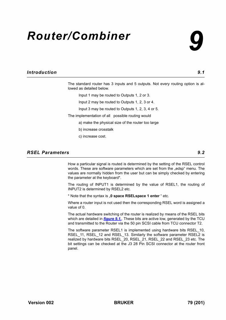
Router/Combiner 9
Introduction 9.1
The standard router has 3 inputs and 5 outputs. Not every routing option is al-lowed as detailed below.
Input 1 may be routed to Outputs 1, 2 or 3.
Input 2 may be routed to Outputs 1, 2, 3 or 4.
Input 3 may be routed to Outputs 1, 2, 3, 4 or 5.
The implementation of all possible routing would
a) make the physical size of the router too large
b) increase crosstalk
c) increase cost.
RSEL Parameters 9.2
How a particular signal is routed is determined by the setting of the RSEL controlwords. These are software parameters which are set from the „edsp“ menu. Thevalues are normally hidden from the user but can be simply checked by enteringthe parameter at the keyboard*.
The routing of INPUT1 is determined by the value of RSEL1, the routing ofINPUT2 is determined by RSEL2 etc.
* Note that the syntax is „0 space RSELspace 1 enter “ etc.
Where a router input is not used then the corresponding RSEL word is assigned avalue of 0.
The actual hardware switching of the router is realized by means of the RSEL bitswhich are detailed in figure 9.1.. These bits are active low, generated by the TCUand transmitted to the Router via the 50 pin SCSI cable from TCU connector T2.
The software parameter RSEL1 is implemented using hardware bits RSEL_10,RSEL_11, RSEL_12 and RSEL_13. Similarly the software parameter RSEL2 isrealized by hardware bits RSEL_20, RSEL_21, RSEL_22 and RSEL_23 etc. Thebit settings can be checked at the J3 28 Pin SCSI connector at the router frontpanel.
Version 002 BRUKER 79 (201)
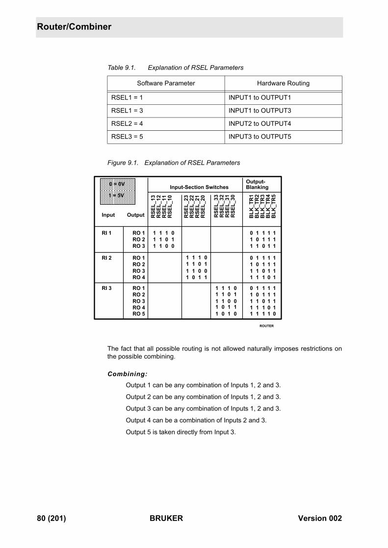
Router/Combiner
Figure 9.1. Explanation of RSEL Parameters
The fact that all possible routing is not allowed naturally imposes restrictions onthe possible combining.
Combining:Output 1 can be any combination of Inputs 1, 2 and 3.
Output 2 can be any combination of Inputs 1, 2 and 3.
Output 3 can be any combination of Inputs 1, 2 and 3.
Output 4 can be a combination of Inputs 2 and 3.
Output 5 is taken directly from Input 3.
Table 9.1. Explanation of RSEL Parameters
Software Parameter Hardware Routing
RSEL1 = 1 INPUT1 to OUTPUT1
RSEL1 = 3 INPUT1 to OUTPUT3
RSEL2 = 4 INPUT2 to OUTPUT4
RSEL3 = 5 INPUT3 to OUTPUT5
Input-Section SwitchesOutput-Blanking
Input Output RSE
L_13
RSE
L_12
RSE
L_11
RSE
L_10
RSE
L_23
RSE
L_22
RSE
L_21
RSE
L_20
RSE
L_33
RSE
L_32
RSE
L_31
RSE
L_30
BLK
_TR
1B
LK_T
R2
BLK
_TR
3B
LK_T
R4
BLK
_TR
5
RI 1 RO 1RO 2RO 3
1 1 1 01 1 0 11 1 0 0 1 1 0 11
1 0 1 110 1 1 11
RI 2 RO 1RO 2RO 3 1 1 0 0 1 1 0 11
1 0 1 110 1 1 11
RO 4 1 0 1 1 1 1 1 10
1 1 0 11 1 1 0
RI 3 RO 1RO 2RO 3 1 1 0 0 1 1 0 11
1 0 1 110 1 1 11
RO 4 1 1 1 10RO 5 1 1 1 01
1 0 1 11 0 1 0
1 1 0 11 1 1 0
ROUTER
0 = 0V
1 = 5V
80 (201) BRUKER Version 002
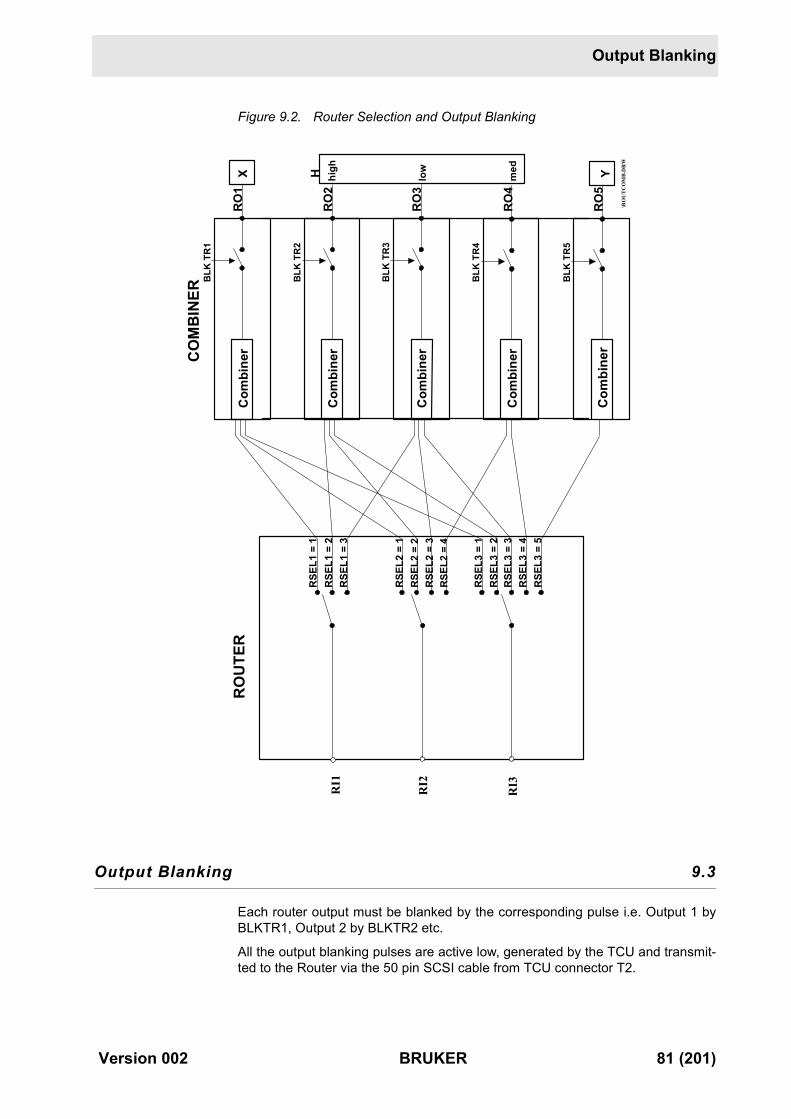
Output Blanking
Figure 9.2. Router Selection and Output Blanking
Output Blanking 9.3
Each router output must be blanked by the corresponding pulse i.e. Output 1 byBLKTR1, Output 2 by BLKTR2 etc.
All the output blanking pulses are active low, generated by the TCU and transmit-ted to the Router via the 50 pin SCSI cable from TCU connector T2.
RSE
L1 =
1R
SEL1
= 2
RSE
L1 =
3
RSE
L2 =
1R
SEL2
= 2
RSE
L2 =
3R
SEL2
= 4
RSE
L3 =
1R
SEL3
= 2
RSE
L3 =
3R
SEL3
= 4
RSE
L3 =
5
RI1
RI2
RI3
Com
bine
r
Com
bine
r
Com
bine
r
Com
bine
r
BLK
TR
1
Com
bine
r
BLK
TR
2
BLK
TR3
BLK
TR
4
BLK
TR
5
RO
UTE
RR
O1
RO
2
RO
3
RO
4
RO
5
H YX high
low
med
CO
MB
INER
\RO
UT
CO
MB
.DR
W
Version 002 BRUKER 81 (201)
Router/Combiner
The banking pulses can be checked at the J3 28 Pin SCSI connector at the routerfront panel.
The precise timing of the output blanking pulses can be altered with the „edscon“parameters BLKTR[1 - 15].
TGPENAB 9.4
The router is designed to be completely disabled if the TGPENAB signal shouldgo high. This will happen if the TRANS P-DOWN key of the BSMS keyboard ispressed. The signal is transmitted via the ACB to the ASU's, the LOT and routeralong the AQR backplane. To check this signal you will need the AQR EXT. Board(P/N Z012746). The signal can be measured between Pins 9a and 9b and forpower transmission must be low.
Cascading routers 9.5
For the present a standard cascade arrangement for two routers has been decid-ed upon. This standard arrangement is necessary if the „edsp“ display is to cor-rectly control the hardware. Note that if the software detects more than 3 FCU’sthen it will assume that a second router is fitted. (The AQR can accommodate upto 3 routers which can, from the hardware viewpoint, be cascaded in differentways but this will not be automatically supported by the software.)
The figure 9.3. shows an example where two routers are cascaded. The soft-ware treats the two routers effectively as a single router. Input 3 of Router 1can not be controlled directly by a separate RSEL software word. Insteadthe software automatically routes Input 3 of Router1 correctly, depending onthe requirements for Output 1 of Router2.
Table 9.2. Hardware and Software Control of a Second Router
Input Software Word Corresponding Hardware Bit
RI1 Router 2 RSEL 3 RSEL_ 40, RSEL_41, RSEL_42,RSEL_43,
RI2 Router 2 RSEL 4 RSEL_ 50, RSEL_51, RSEL_52,RSEL_53,
RI3 Router 2 RSEL 5 RSEL_60, RSEL_61, RSEL_62,RSEL_63,
Output Software Output Corresponding Hardware Blanking pulse
RO1 Router 2 BLKTR6
RO2 Router 2 6 BLKTR7
RO3 Router 2 7 BLKTR8
RO4 Router 2 8 BLKTR9
RO5 Router 2 9 BLKTR10
82 (201) BRUKER Version 002
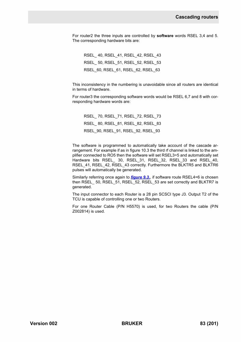
Cascading routers
For router2 the three inputs are controlled by software words RSEL 3,4 and 5.The corresponding hardware bits are:
RSEL_ 40, RSEL_41, RSEL_42, RSEL_43
RSEL_ 50, RSEL_51, RSEL_52, RSEL_53
RSEL_60, RSEL_61, RSEL_62, RSEL_63
This inconsistency in the numbering is unavoidable since all routers are identicalin terms of hardware.
For router3 the corresponding software words would be RSEL 6,7 and 8 with cor-responding hardware words are:
RSEL_ 70, RSEL_71, RSEL_72, RSEL_73
RSEL_ 80, RSEL_81, RSEL_82, RSEL_83
RSEL_90, RSEL_91, RSEL_92, RSEL_93
The software is programmed to automatically take account of the cascade ar-rangement. For example if as in figure 10.3 the third rf channel is linked to the am-plifier connected to RO5 then the software will set RSEL3=5 and automatically setHardware bits RSEL_ 30, RSEL_31, RSEL_32, RSEL_33 and RSEL_40,RSEL_41, RSEL_42, RSEL_43 correctly. Furthermore the BLKTR5 and BLKTR6pulses will automatically be generated.
Similarly referring once again to figure 9.3., if software route RSEL4=6 is chosenthen RSEL_ 50, RSEL_51, RSEL_52, RSEL_53 are set correctly and BLKTR7 isgenerated.
The input connector to each Router is a 28 pin SCSCI type J3. Output T2 of theTCU is capable of controlling one or two Routers.
For one Router Cable (P/N H5570) is used, for two Routers the cable (P/NZ002814) is used.
Version 002 BRUKER 83 (201)
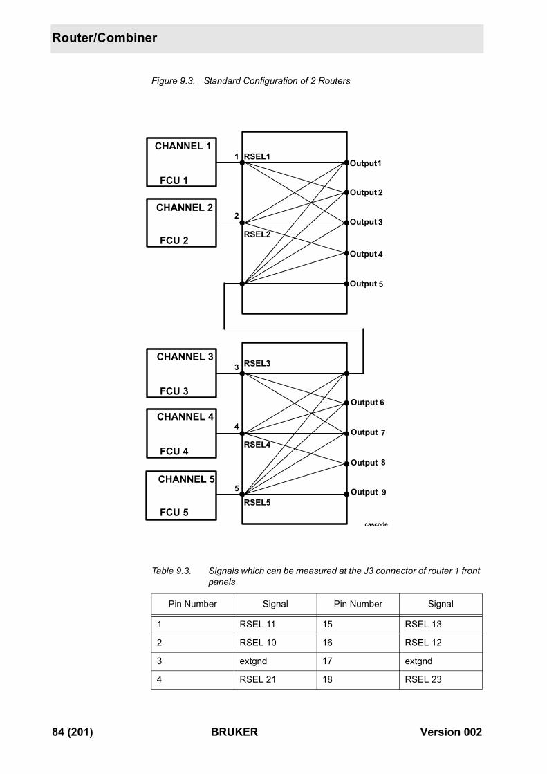
Router/Combiner
Figure 9.3. Standard Configuration of 2 Routers
Table 9.3. Signals which can be measured at the J3 connector of router 1 front panels
Pin Number Signal Pin Number Signal
1 RSEL 11 15 RSEL 13
2 RSEL 10 16 RSEL 12
3 extgnd 17 extgnd
4 RSEL 21 18 RSEL 23
CHANNEL 1
FCU 1
CHANNEL 2
FCU 2
1
2
CHANNEL 3
FCU 3
CHANNEL 4
FCU 4
CHANNEL 5
FCU 5
3
4
5
7
8
9
cascode
6
RSEL2
RSEL1
RSEL3
RSEL4
RSEL5
Output
Output
Output
Output
Output
1
2
3
4
5
Output
Output
Output
Output
84 (201) BRUKER Version 002
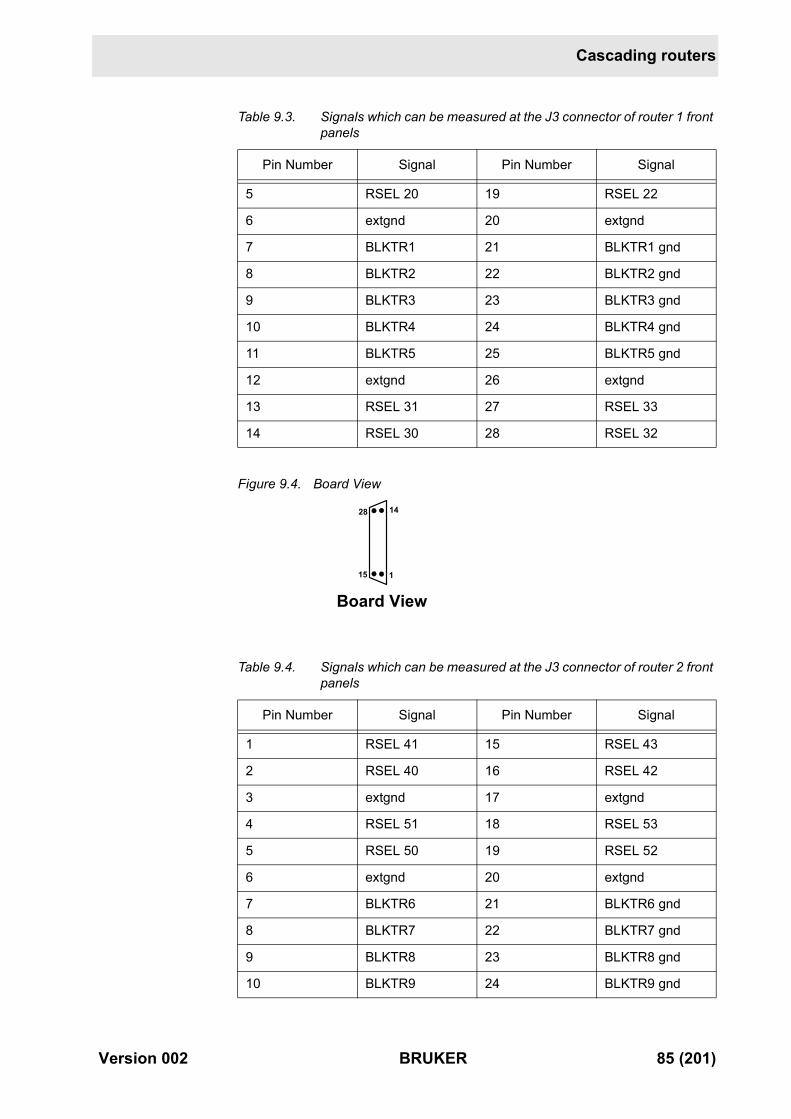
Cascading routers
Figure 9.4. Board View
5 RSEL 20 19 RSEL 22
6 extgnd 20 extgnd
7 BLKTR1 21 BLKTR1 gnd
8 BLKTR2 22 BLKTR2 gnd
9 BLKTR3 23 BLKTR3 gnd
10 BLKTR4 24 BLKTR4 gnd
11 BLKTR5 25 BLKTR5 gnd
12 extgnd 26 extgnd
13 RSEL 31 27 RSEL 33
14 RSEL 30 28 RSEL 32
Table 9.4. Signals which can be measured at the J3 connector of router 2 front panels
Pin Number Signal Pin Number Signal
1 RSEL 41 15 RSEL 43
2 RSEL 40 16 RSEL 42
3 extgnd 17 extgnd
4 RSEL 51 18 RSEL 53
5 RSEL 50 19 RSEL 52
6 extgnd 20 extgnd
7 BLKTR6 21 BLKTR6 gnd
8 BLKTR7 22 BLKTR7 gnd
9 BLKTR8 23 BLKTR8 gnd
10 BLKTR9 24 BLKTR9 gnd
Table 9.3. Signals which can be measured at the J3 connector of router 1 front panels
Pin Number Signal Pin Number Signal
1
14
15
28
Board View
Version 002 BRUKER 85 (201)
Router/Combiner
Figure 9.5. Standard Configuration of 2 Routers
11 BLKTR10 25 BLKTR10 gnd
12 extgnd 26 extgnd
13 RSEL 61 27 RSEL 63
14 RSEL60 28 RSEL 62
Table 9.4. Signals which can be measured at the J3 connector of router 2 front panels
Pin Number Signal Pin Number Signal
CHANNEL 1
FCU 1
CHANNEL 2
FCU 2
CHANNEL 3
FCU 3
CHANNEL 4
FCU 4
CHANNEL 5
FCU 5
6
7
8
1
2
5
4
3
2
1
5
cascade1
9
RSEL3= 5
BLAX300
4
3
RSEL4= 6
86 (201) BRUKER Version 002
BRUKER Linear Amplifiers 10
New features 10.1
Among the new features of the latest range of power amplifiers are:
1. The output amplitude is a linear function of the amplitude of the rf input. Unlikeprevious transmitters no power setting takes place within the amplifier itself. Assuch they are referred to as amplifiers and not transmitters.
2. New safety features (OVERDRIVE, PULSE WIDTH, DUTY CYCLE) which willtemporarily disable the amplifier whenever output power is above a specifiedlimit. Each amplifier has on board information stored in the RS485 InterfaceBoard regarding amplifier type, max. Duty Cycle, max. Pulse Width etc. Theseparameters can be changed by software if necessary.
3. The amplifiers are controlled by the ACB (Amplifier Control Board) via anRS485 type link (SBS Bus). Individual Amplifiers can be addressed. Hardware address codes are set via a HEX. switch located on the amplifier front panel.Read and write access to the BLA Control board II is possible via the ACBBoard.
4. Improved LED front panel display with diagnostic information regarding PulseWidth, Duty Cycle, Temperature etc.
5. Precise software timing control of the amplifier blanking pulses (BLKTR1..15)via the „edscon“ table.
Terminology 10.2
BLARH 100 = BRUKER Linear Array Amplifier for 1H with 100W High Powerchannel.
The „array“ refers to the fact that the unit contains more than 1 amplifier connect-ed to the same output channel.
BLAX 300: BRUKER Linear Amplifier for X frequencies with single channel 300Wamplifier.
Brief Summary of standard Amplifier Types 10.3
1. BLARH 100:
This is a standard DMX amplifier with three 1H/19F rf channels.
Input HHigh - 100 W output for rf input of 4 dBm.
Version 002 BRUKER 87 (201)
BRUKER Linear Amplifiers
Input HLow - Output power 50 dB lower than high power channel. Thiswould correspond to an output of 1mW for rf input of 4 dBm.
Input HMed - 10 W output for rf input of 4 dBm.
A variation of this transmitter is the BLARH50 with a HHigh channel max.output of 50W instead of 100W. At the moment this amplifier is fitted to 750MHz spectrometers, but a 100W version will be introduced if required.
2. BLAX 300:
This is the standard DMX X frequency amplifier with a single channel X fre-quency amplifier.
Input Xin - 300W output for rf input of 4 dBm.
3. BLAXH 50:
This is the standard DRX amplifier with three rf channels, two for 1H/19F,one for X frequencies.
Input HHigh: - 50W output power for rf input of 4 dBm.
Input HLow - Output power 50 dB lower than high power channel.
Input Xin - 100W output power for rf input of 4 dBm.
4. BLAXH 20:
This is the standard DPX amplifier with two rf channels, one for 1H/19F, onefor X frequencies.
Input H - 20W output power for rf input of 4 dBm.
Input X - 100W output power for rf input of 4 dBm.
A comprehensive list of available amplifiers with Part Numbers is given onthe next page. Data sheets in the Appendix give precise specifications ofthe above amplifiers.
88 (201) BRUKER Version 002
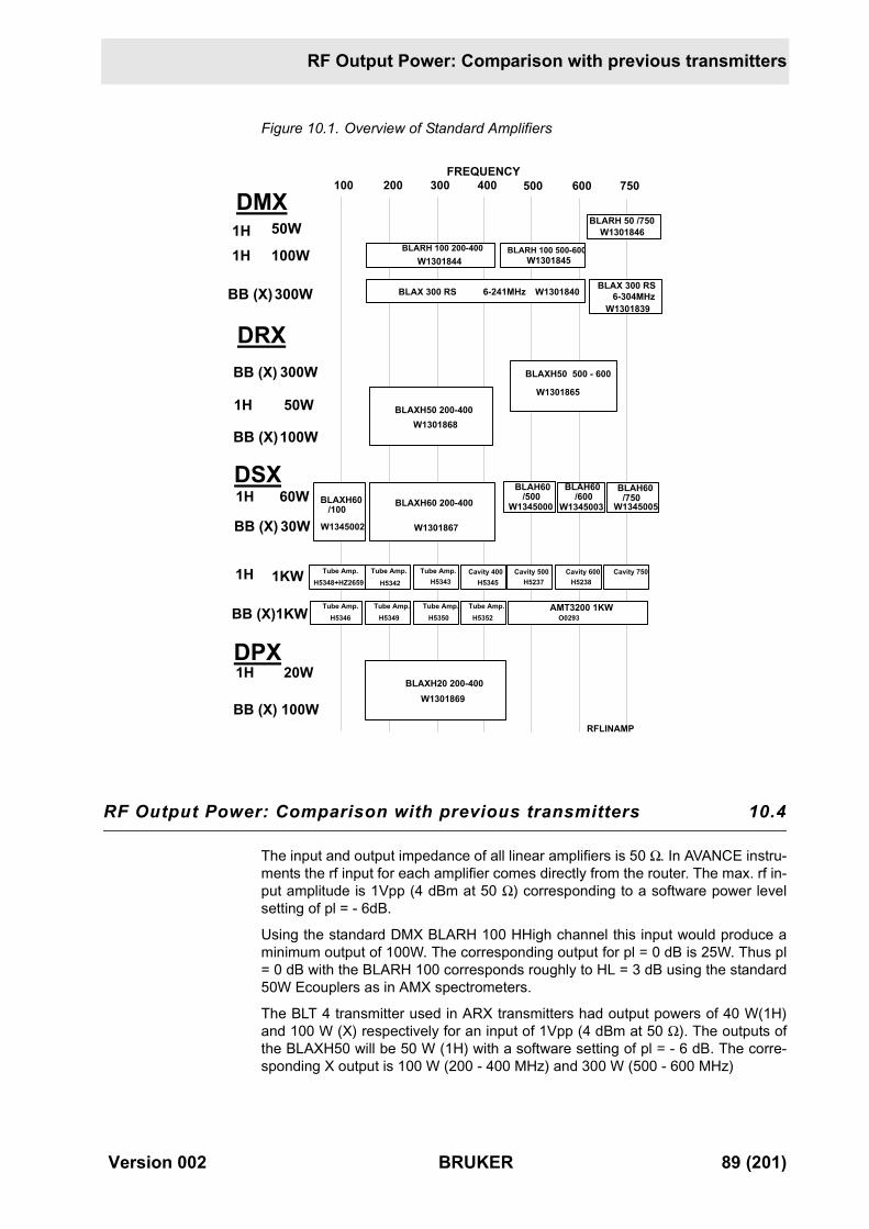
RF Output Power: Comparison with previous transmitters
Figure 10.1. Overview of Standard Amplifiers
RF Output Power: Comparison with previous transmitters 10.4
The input and output impedance of all linear amplifiers is 50 Ω. In AVANCE instru-ments the rf input for each amplifier comes directly from the router. The max. rf in-put amplitude is 1Vpp (4 dBm at 50 Ω) corresponding to a software power levelsetting of pl = - 6dB.
Using the standard DMX BLARH 100 HHigh channel this input would produce aminimum output of 100W. The corresponding output for pl = 0 dB is 25W. Thus pl= 0 dB with the BLARH 100 corresponds roughly to HL = 3 dB using the standard50W Ecouplers as in AMX spectrometers.
The BLT 4 transmitter used in ARX transmitters had output powers of 40 W(1H)and 100 W (X) respectively for an input of 1Vpp (4 dBm at 50 Ω). The outputs ofthe BLAXH50 will be 50 W (1H) with a software setting of pl = - 6 dB. The corre-sponding X output is 100 W (200 - 400 MHz) and 300 W (500 - 600 MHz)
100 200 300 400 500 600 750
BLARH 100 200-400 BLARH 100 500-600
6-241MHz BLAX 300 RS
BLAXH50 200-400
BLAXH60 200-400BLAXH60 /100
BLAH60 /500
BLAH60 /600
BLAH60 /750
Tube Amp. Cavity 400
AMT3200 1KW
BLAXH20 200-400
DMX
DRX
DSX
DPX
1H
BB (X)
100W
300W
1H
BB (X)
50W
100W
1H 60W
BB (X) 30W
1H 1KW
BB (X)1KW
1H
BB (X)
20W
100W RFLINAMP
FREQUENCY
W1301844 W1301845
W1301846
W1301839
W1301840
W1301868
W1345000
W1301867
H5348+HZ2659 H5342 H5345 H5237 H5238
O0293H5352H5350H5349H5346
W1301869
H5343
W1345003 W1345005
W1345002
BB (X) 300W
BLAX 300 RS
BLARH 50 /750
6-304MHz
Tube Amp. Tube Amp. Cavity 500 Cavity 600 Cavity 750
Tube Amp. Tube Amp. Tube Amp. Tube Amp.
50W1H
BLAXH50 500 - 600
W1301865
Version 002 BRUKER 89 (201)
BRUKER Linear Amplifiers
Amplifier Blanking 10.5
The blanking pulses (BLKTR 1... 15) are active low TTL level and produced by theTCU. They are easily measured at the BNC connections on the amplifier frontpanel. Which blanking pulse is required for which amplifier will depend solelyupon which router output provides the rf amplifier input. This is because the sameblanking pulses are used to blank the router output as the amplifier. Thus an am-plifier channel connected to router output RO1 will be blanked by BLKTR1. Anamplifier channel connected to router output RO3 will be blanked by BLKTR3 etc.The timing of the BLKTR[1... 15] pulses can be adjusted with the „edscon“ table.
Configuration for DMX spectrometers (1 Router) 10.6
Table 10.1 lists the connections between the router outputs and a possible ar-rangement of amplifiers in a DMX spectrometer. In order for the „edsp“ display tofunction properly certain requirements are necessary. Firstly that the Hex Addresswhich is set on the front panel of each amplifier must correspond to the router out-put to which the first amplifier input is connected. (For the BLAXH50 this is Xin, forthe BLARH100 this is HHigh)
Secondly auxiliary amplifier inputs must be connected in the correct order.
For example when the software detects that a BLARH100 has Hex. address of 2then it will assume:
a) that output 2 of the router is connected to HHigh.
b) that outputs 3 and 4 of the router are connected to HLow and HMed re-spectively.
Table 10.1. Standard Connections between the Router Outputs and the Amplifiers
Amplifier Hex. Address AMP Input Router BLKTR PULSE
BLAX 300: 1 Xin connected to Router1 RO1 BLKTR1
BLARH 100 2 HHigh connected to Router1 RO2 BLKTR2
HLow connected to Router1 RO3 BLKTR3
HMed connected to Router1 RO4 BLKTR4
BLAX 300(Y) 5 Xin connected to Router1 RO5 BLKTR5
90 (201) BRUKER Version 002
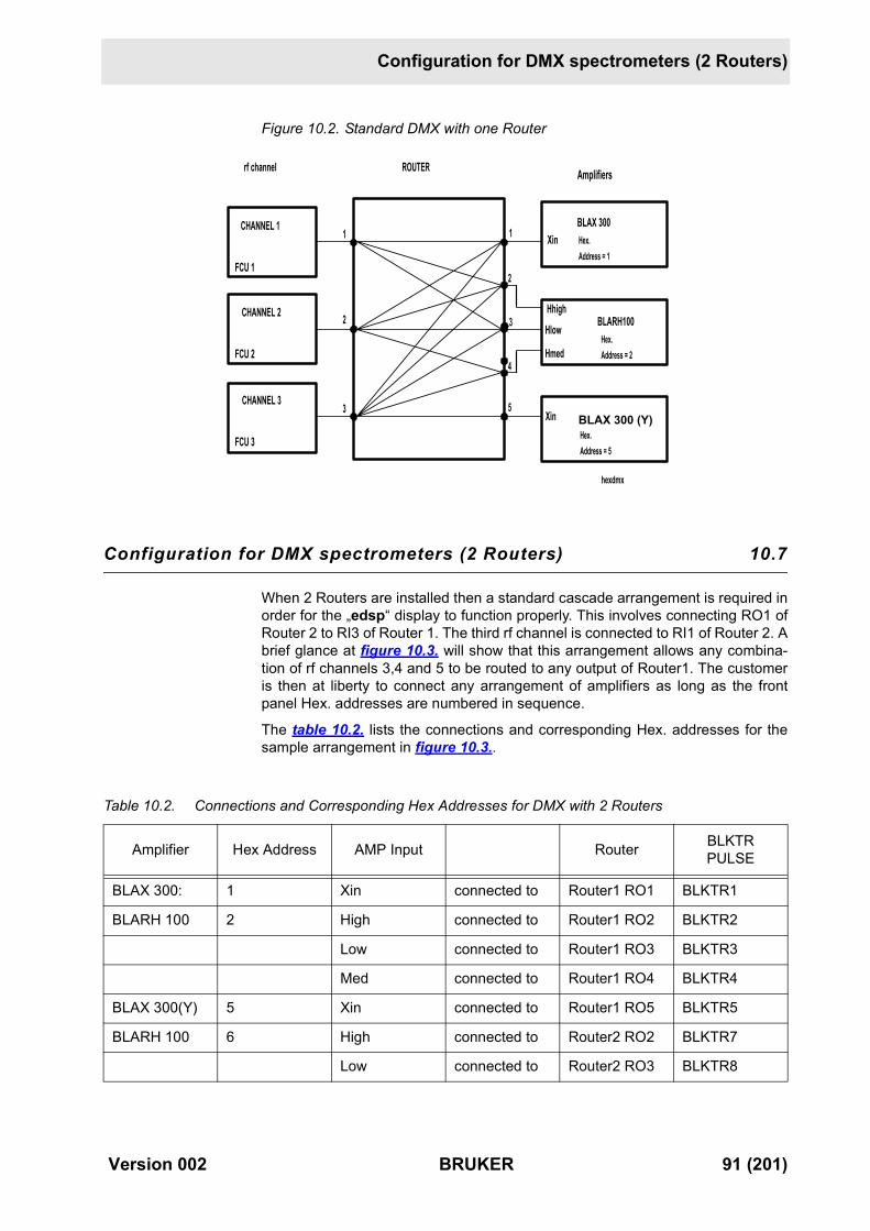
Configuration for DMX spectrometers (2 Routers)
Figure 10.2. Standard DMX with one Router
Configuration for DMX spectrometers (2 Routers) 10.7
When 2 Routers are installed then a standard cascade arrangement is required inorder for the „edsp“ display to function properly. This involves connecting RO1 ofRouter 2 to RI3 of Router 1. The third rf channel is connected to RI1 of Router 2. Abrief glance at figure 10.3. will show that this arrangement allows any combina-tion of rf channels 3,4 and 5 to be routed to any output of Router1. The customeris then at liberty to connect any arrangement of amplifiers as long as the frontpanel Hex. addresses are numbered in sequence.
The table 10.2. lists the connections and corresponding Hex. addresses for thesample arrangement in figure 10.3..
Table 10.2. Connections and Corresponding Hex Addresses for DMX with 2 Routers
Amplifier Hex Address AMP Input Router BLKTR PULSE
BLAX 300: 1 Xin connected to Router1 RO1 BLKTR1
BLARH 100 2 High connected to Router1 RO2 BLKTR2
Low connected to Router1 RO3 BLKTR3
Med connected to Router1 RO4 BLKTR4
BLAX 300(Y) 5 Xin connected to Router1 RO5 BLKTR5
BLARH 100 6 High connected to Router2 RO2 BLKTR7
Low connected to Router2 RO3 BLKTR8
CHANNEL 1
FCU 1
CHANNEL 2
FCU 2
CHANNEL 3
FCU 3
1
2
3
1
2
3
4
5
ROUTER Amplifiers
BLAX 300
BLARH100
hexdmx
BLAX 300 (Y)
Hex.Address = 1
Hex.Address = 2
Hex.Address = 5
Xin
HhighHlow
Hmed
Xin
rf channel
Version 002 BRUKER 91 (201)
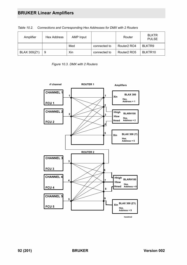
BRUKER Linear Amplifiers
Figure 10.3. DMX with 2 Routers
Med connected to Router2 RO4 BLKTR9
BLAX 300(Z1) 9 Xin connected to Router2 RO5 BLKTR10
Table 10.2. Connections and Corresponding Hex Addresses for DMX with 2 Routers
Amplifier Hex Address AMP Input Router BLKTR PULSE
CHANNEL 1
FCU 1
CHANNEL 2
FCU 2
1
2
1
2
3
4
5
CHANNEL 3
FCU 3
CHANNEL 4
FCU 4
CHANNEL 5
FCU 5
3
4 7
Y
hexdmx2
ROUTER 1 Amplifiers
BLAX 300Hex.Address = 1
BLAX 300 (Y)Hex.Address = 5
BLAX 300 (Z1)
Hex.Address = 9
Hex.Address =7
ROUTER 2
Xin
Xin
Xin
rf channel
5
H/FBLARH100Hhigh
HlowHmed
Hex.Address = 6
H/FBLARH100
Hex.Address = 2
HhighHlowHmed
6
8
9
92 (201) BRUKER Version 002
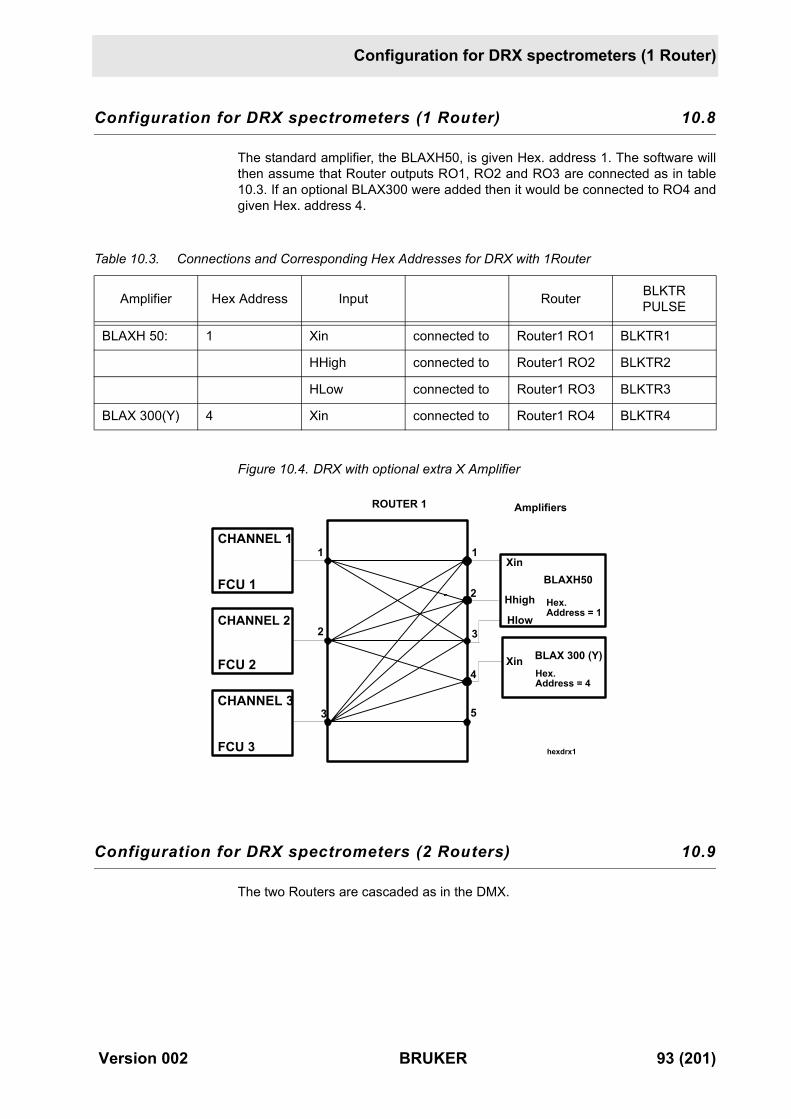
Configuration for DRX spectrometers (1 Router)
Configuration for DRX spectrometers (1 Router) 10.8
The standard amplifier, the BLAXH50, is given Hex. address 1. The software willthen assume that Router outputs RO1, RO2 and RO3 are connected as in table10.3. If an optional BLAX300 were added then it would be connected to RO4 andgiven Hex. address 4.
Figure 10.4. DRX with optional extra X Amplifier
Configuration for DRX spectrometers (2 Routers) 10.9
The two Routers are cascaded as in the DMX.
Table 10.3. Connections and Corresponding Hex Addresses for DRX with 1Router
Amplifier Hex Address Input Router BLKTR PULSE
BLAXH 50: 1 Xin connected to Router1 RO1 BLKTR1
HHigh connected to Router1 RO2 BLKTR2
HLow connected to Router1 RO3 BLKTR3
BLAX 300(Y) 4 Xin connected to Router1 RO4 BLKTR4
CHANNEL 1
FCU 1
CHANNEL 2
FCU 2
1
2
1
2
3
4
5CHANNEL 3
FCU 3
Y
ROUTER 1 Amplifiers
Hex.Address = 1
BLAX 300 (Y)Hex.Address = 4
BLAXH50
3
hexdrx1
Hhigh
Hlow
Xin
Xin
Version 002 BRUKER 93 (201)
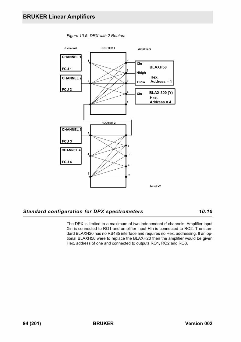
BRUKER Linear Amplifiers
Figure 10.5. DRX with 2 Routers
Standard configuration for DPX spectrometers 10.10
The DPX is limited to a maximum of two independent rf channels. Amplifier inputXin is connected to RO1 and amplifier input Hin is connected to RO2. The stan-dard BLAXH20 has no RS485 interface and requires no Hex. addressing. If an op-tional BLAXH50 were to replace the BLAXH20 then the amplifier would be givenHex. address of one and connected to outputs RO1, RO2 and RO3.
CHANNEL 1
FCU 1
CHANNEL 2
FCU 2
1
2
1
5
CHANNEL 3
FCU 3
CHANNEL 4
FCU 4
5
Y
ROUTER 1 Amplifiers
BLAX 300 (Y)Hex.Address = 4
ROUTER 2
Hex.Address = 1
BLAXH502
3
4
hexdrx2
Hhigh
Hlow
Xin
Xin
rf channel
4
3
7
8
9
6
94 (201) BRUKER Version 002
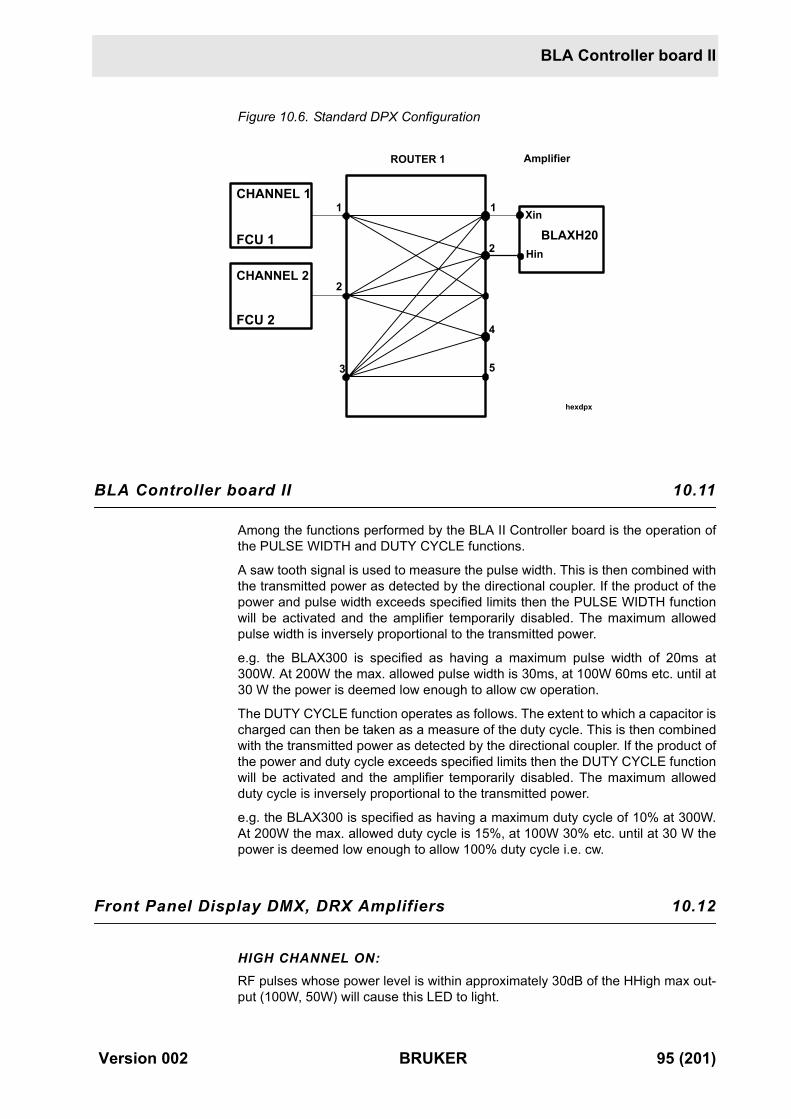
BLA Controller board II
Figure 10.6. Standard DPX Configuration
BLA Controller board II 10.11
Among the functions performed by the BLA II Controller board is the operation ofthe PULSE WIDTH and DUTY CYCLE functions.
A saw tooth signal is used to measure the pulse width. This is then combined withthe transmitted power as detected by the directional coupler. If the product of thepower and pulse width exceeds specified limits then the PULSE WIDTH functionwill be activated and the amplifier temporarily disabled. The maximum allowedpulse width is inversely proportional to the transmitted power.
e.g. the BLAX300 is specified as having a maximum pulse width of 20ms at300W. At 200W the max. allowed pulse width is 30ms, at 100W 60ms etc. until at30 W the power is deemed low enough to allow cw operation.
The DUTY CYCLE function operates as follows. The extent to which a capacitor ischarged can then be taken as a measure of the duty cycle. This is then combinedwith the transmitted power as detected by the directional coupler. If the product ofthe power and duty cycle exceeds specified limits then the DUTY CYCLE functionwill be activated and the amplifier temporarily disabled. The maximum allowedduty cycle is inversely proportional to the transmitted power.
e.g. the BLAX300 is specified as having a maximum duty cycle of 10% at 300W.At 200W the max. allowed duty cycle is 15%, at 100W 30% etc. until at 30 W thepower is deemed low enough to allow 100% duty cycle i.e. cw.
Front Panel Display DMX, DRX Amplifiers 10.12
HIGH CHANNEL ON:RF pulses whose power level is within approximately 30dB of the HHigh max out-put (100W, 50W) will cause this LED to light.
CHANNEL 1
FCU 1
CHANNEL 2
FCU 2
1
2
1
2
4
5
ROUTER 1 Amplifier
BLAXH20
3
hexdpx
Xin
Hin
Version 002 BRUKER 95 (201)
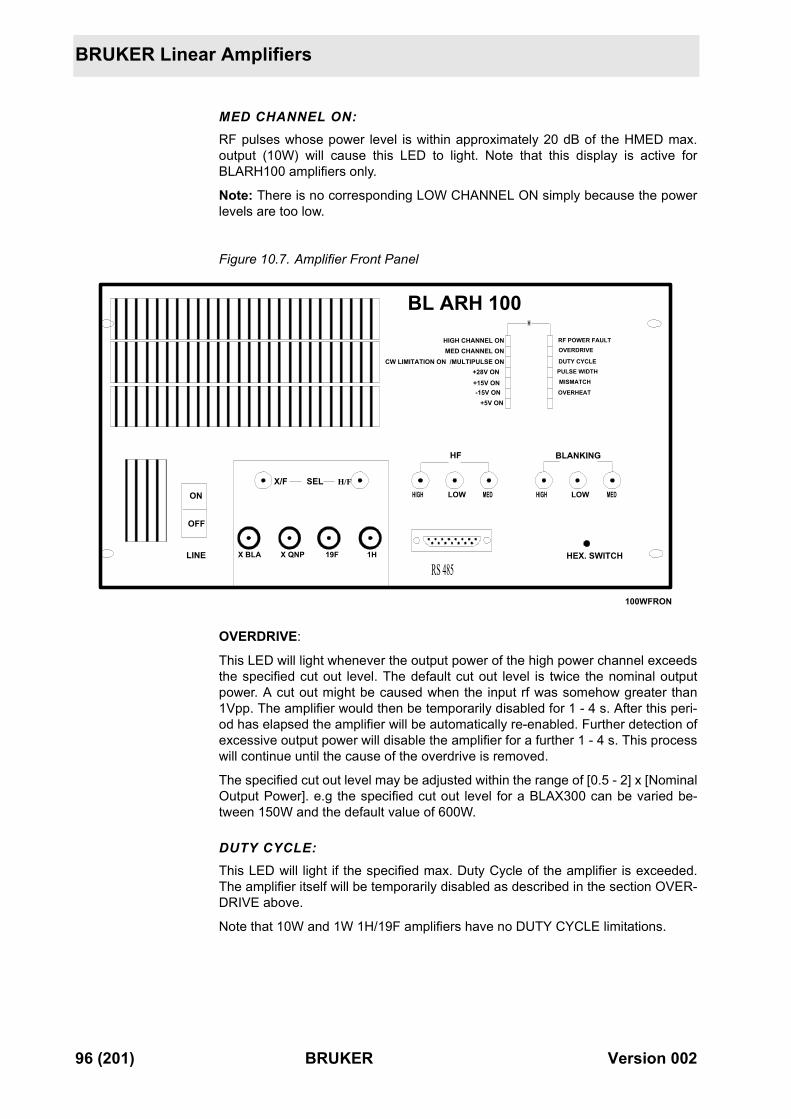
BRUKER Linear Amplifiers
MED CHANNEL ON:RF pulses whose power level is within approximately 20 dB of the HMED max.output (10W) will cause this LED to light. Note that this display is active forBLARH100 amplifiers only.
Note: There is no corresponding LOW CHANNEL ON simply because the powerlevels are too low.
Figure 10.7. Amplifier Front Panel
OVERDRIVE:
This LED will light whenever the output power of the high power channel exceedsthe specified cut out level. The default cut out level is twice the nominal outputpower. A cut out might be caused when the input rf was somehow greater than1Vpp. The amplifier would then be temporarily disabled for 1 - 4 s. After this peri-od has elapsed the amplifier will be automatically re-enabled. Further detection ofexcessive output power will disable the amplifier for a further 1 - 4 s. This processwill continue until the cause of the overdrive is removed.
The specified cut out level may be adjusted within the range of [0.5 - 2] x [NominalOutput Power]. e.g the specified cut out level for a BLAX300 can be varied be-tween 150W and the default value of 600W.
DUTY CYCLE:This LED will light if the specified max. Duty Cycle of the amplifier is exceeded.The amplifier itself will be temporarily disabled as described in the section OVER-DRIVE above.
Note that 10W and 1W 1H/19F amplifiers have no DUTY CYCLE limitations.
H
BL ARH 100
HIGH LOW MED HIGH LOW MED
BLANKINGHF
RS 485
SELX/F H/F
X BLA X QNP 19F
ON
OFF
LINE 1H
100WFRON
HEX. SWITCH
HIGH CHANNEL ON
CW LIMITATION ON /MULTIPULSE ON+28V ON+15V ON-15V ON
+5V ON
MED CHANNEL ONRF POWER FAULT
DUTY CYCLE
OVERDRIVE
PULSE WIDTHMISMATCH
OVERHEAT
96 (201) BRUKER Version 002
Front Panel Display DMX, DRX Amplifiers
PULSE WIDTH:This LED will light if the max. specified pulse width of the particular amplifier is ex-ceeded. The amplifier itself will be temporarily disabled as described in the sec-tion OVERDRIVE above.
Note that the 10W and 1W 1H/19F amplifiers have no PULSE WIDTH limitation.
MISMATCH:This LED will light whenever the reflected power is above a specified level. Thislevel corresponds at maximum power to a VSWR of 6 which corresponds to 50%reflection of forward power. The MISMATCH function is active for the high poweroutput only.
CW LIMITATION ON:In normal operation the CW LIMITATION ON LED is not lit.
With an RS485 command the normal operating status can be altered to switch offthe internal DUTY CYCLE and PULSE WIDTH limitations. In this mode the CWLIMITATION ON LED will light. The OVERDRIVE function will still however be ac-tive. If the average output power is above the specified limits then the amplifier willautomatically switch off for 1 - 4 s.
This CW LIMITATION feature is due to be replaced by the MULTIPULSE ON fea-ture (see below)
MULTIPULSE ON:This function is not implemented in the earliest amplifiers and is intended to re-place the CW LIMITATION ON function. In normal operation the MULTIPULSEON led is not lit.
With an RS485 command the normal operating status can be altered to switch offthe DUTY CYCLE limitation (the PULSE WIDTH function is still active!). In thismode the MULTIPULSE ON LED will light.
This was designed for experiments such as CRAMPS where the Duty Cycle maytypically be 50% even though this represents no risk to the probe. The OVER-DRIVE function will still however be active. If the average output power is abovethe specified limits then the amplifier will automatically be disabled for 1 - 4s.
Note that the software setting of the MULTIPULSE ON function is not yet imple-mented.
OVERHEAT:A temperature sensor located within the amplifier monitors the temperature.Should the temperature rise above specified limits (non-adjustable) then the am-plifier will automatically be disabled. The amplifier will remain disabled until thetemperature has dropped sufficiently whereupon it will be automatically re-en-abled.
RF POWER FAULT:This is a general diagnostic LED which lights whenever any other LEDs in thesame display column light.
Version 002 BRUKER 97 (201)
BRUKER Linear Amplifiers
Front Panel Display for DPX amplifier 10.13
In order to reduce costs and due to it’s reduced power capabilities this amplifierhas not the same protection features or front panel display as with other amplifi-ers. The LED on the front panel will light to signify power transmission (up to 25dBof max. output).
Note that the only protection feature is an OVERHEAT function which effectivelyswitches the amplifier off should the output power cause the amplifier to warm suf-ficiently. The amplifier will remain disabled until the temperature has dropped. Thecorresponding power at which the temperature cut out is activated will depend onfactors such as room temperature and console ventilation. However the customershould be advised not to operate at full power with a Duty Cycle above 10%. Fur-thermore the customer should ensure that cw operation at too high a power doesnot damage the probe. As a general rule cw operation should not exceed 2 - 3 W.This would correspond to a power level setting of pl = 10 dB (X channel) and pl =3dB(1H channel)
BLARH100 Block Diagram 10.14
The unit has 3 separate rf inputs see figure 10.9.. For inputs of equal amplitudethe HHigh channel will have an output 20 dB higher than the HLOW when mea-sured before the directional coupler. In the directional coupler the HLOW channelis further attenuated by 30 dB. Thus the HLOW channel final output power will be50 dB of the HHigh output for rf inputs of equal amplitude. The use of this amplifierarrangement has the advantage of expanding the overall dynamic range from amax. of 110 dB available from a single amplifier to 160 dB available from the com-bination (see figure 11.8). The HLOW channel is designed for applications that re-quire long pulses with corresponding very low power.
The HMED channel option should prove particularly useful for 1H/19F decouplingexperiments. The figure 10.10. and the figure 10.11. show the rf paths forOBS1H/Dec 19F and vice versa. Note that there is no need for switching withinthe BLARH 100 for this type of experiment as long as the decoupling power is lessthan 10W.
The XBLA input is designed to be taken from the BLAX 300 output. With the aid ofthe internal switching different rf inputs can be easily switched to the same output.This is particularly useful if a QNP HPPR module is connected to the QNP amplifi-er output because 19F or X frequencies can be transmitted without any need forrecabling.
98 (201) BRUKER Version 002
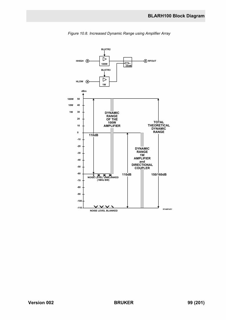
BLARH100 Block Diagram
Figure 10.8. Increased Dynamic Range using Amplifier Array
100WHHIGH RFOUT
1W
BLKTR2
BLKTR3
50
40
30
20
10
0
-10
-20
-30
-40
-50
-60
-70
-80
-90
-100
-110
100W
1W
10W
dBm
RFAMPARY
NOISE LEVEL UNBLANKED(1MHz BW)
NOISE LEVEL BLANKED
DYNAMICRANGEOF THE100W
AMPLIFIER
DYNAMICRANGE
1WAMPLIFIER
andDIRECTIONAL
COUPLER
TOTALTHEORETICAL
DYNAMICRANGE
110dB
110dB 150/160dB
HLOW
-30dB
Version 002 BRUKER 99 (201)
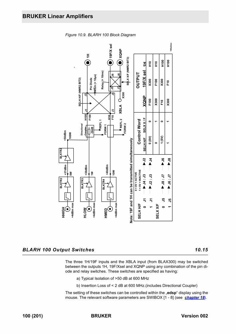
BRUKER Linear Amplifiers
Figure 10.9. BLARH 100 Block Diagram
BLARH 100 Output Switches 10.15
The three 1H/19F inputs and the XBLA input (from BLAX300) may be switchedbetween the outputs 1H, 19F/Xsel and XQNP using any combination of the pin di-ode and relay switches. These switches are specified as having:
a) Typical Isolation of >50 dB at 600 MHz
b) Insertion Loss of < 2 dB at 600 MHz.(includes Directional Coupler)
The setting of these switches can be controlled within the „edsp“ display using themouse. The relevant software parameters are SWIBOX [1 - 8] (see chapter 18).
BLK
TR4
BLK
TR3
BLK
TR2
5W 1W 10W
+40d
Bm
+30d
Bm
+37d
Bm
BLK
TR2
100W
+50d
Bm -30d
B
J3J1J2
FOR
W 2
REF
L 2
FOR
W 1
REF
L 1
HHI
GH
HLO
W
HM
ED
+4dB
m m
ax
+4dB
m m
ax
+4dB
m m
ax
19F/
X se
l
1HH
100
H10
SELH
H/F
(NM
R2
BIT
2)
J4F1
0
F100
J7XQ
NP
XBLA
X300
J8
J5J6
SELX
X/F
(NM
R2
BIT
3)
SELH
H/F 0
J1J4
: J3
J2
1J1
J2 :
J3J4
SELX
X/F 0
J5J8
: J7
J6
1J5
J6 :
J7J8
SELH
H/F
0 SE
LX X
/ F
XQN
P1H
0F1
00H
10
01
X300
F100
H10
10
F10
H10
01
1X3
00F1
0H
100
X300
X300
100w
bloc
(0V)
(5V)
Not
e: 1
9F a
nd 1
H c
an b
e tr
ansm
itted
sim
ulta
neou
sly
Pin
Dio
deSw
itch
(< 1
0µs)
Rel
ay (<
10m
s)
Dire
ctio
nal
Cou
pler
0 =
0V =
AC
TIVE
1 =
5V =
INA
CTI
VE
19F/
X se
lC
ontr
ol W
ord
OU
TPU
T
100 (201) BRUKER Version 002
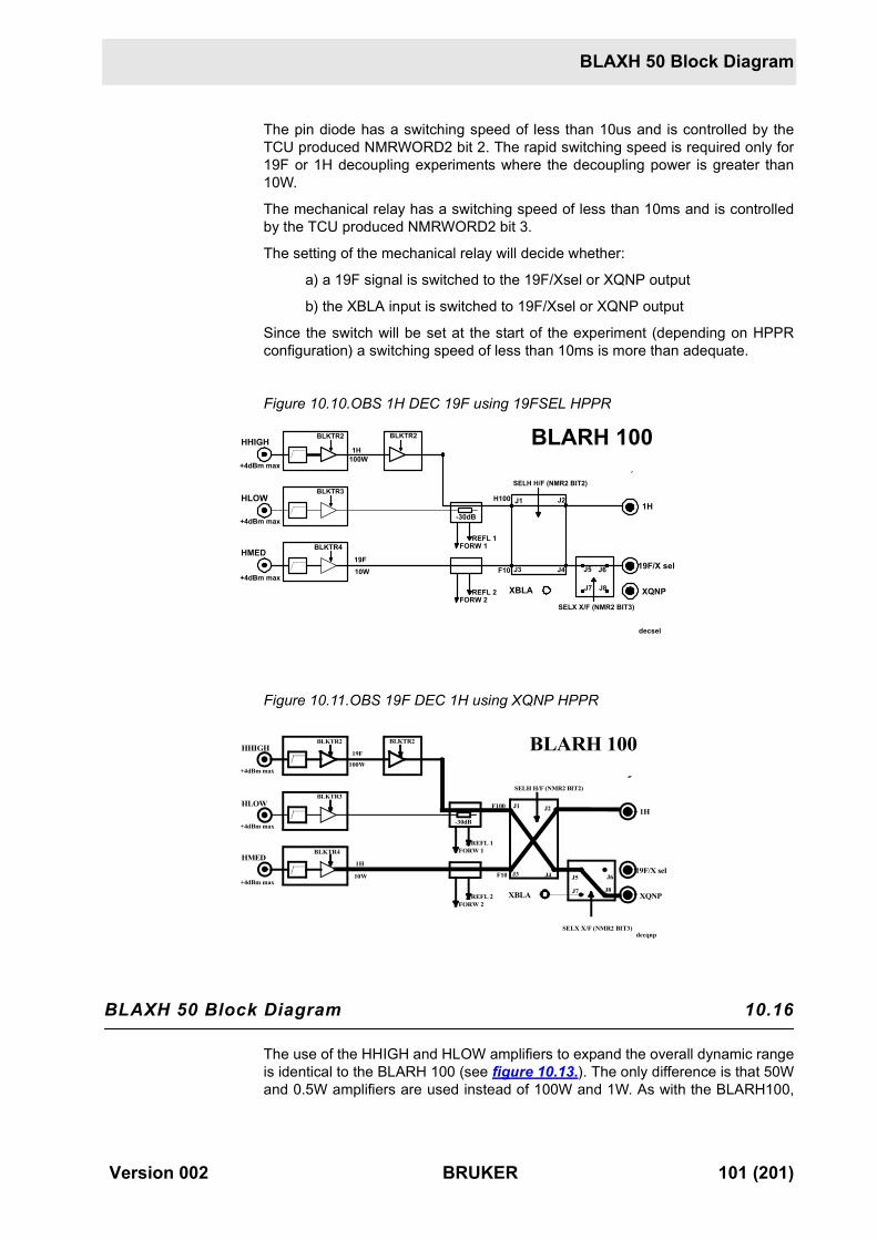
BLAXH 50 Block Diagram
The pin diode has a switching speed of less than 10us and is controlled by theTCU produced NMRWORD2 bit 2. The rapid switching speed is required only for19F or 1H decoupling experiments where the decoupling power is greater than10W.
The mechanical relay has a switching speed of less than 10ms and is controlledby the TCU produced NMRWORD2 bit 3.
The setting of the mechanical relay will decide whether:
a) a 19F signal is switched to the 19F/Xsel or XQNP output
b) the XBLA input is switched to 19F/Xsel or XQNP output
Since the switch will be set at the start of the experiment (depending on HPPRconfiguration) a switching speed of less than 10ms is more than adequate.
Figure 10.10.OBS 1H DEC 19F using 19FSEL HPPR
Figure 10.11.OBS 19F DEC 1H using XQNP HPPR
BLAXH 50 Block Diagram 10.16
The use of the HHIGH and HLOW amplifiers to expand the overall dynamic rangeis identical to the BLARH 100 (see figure 10.13.). The only difference is that 50Wand 0.5W amplifiers are used instead of 100W and 1W. As with the BLARH100,
BLKTR4
BLKTR3
BLKTR2
10W
BLKTR2
-30dB
J3
J1 J2
FORW 2REFL 2
FORW 1REFL 1
HHIGH
HLOW
HMED
+4dBm max
+4dBm max
+4dBm max
19F/X sel
1HH100
SELH H/F (NMR2 BIT2)
J4F10
J7 XQNPXBLA J8
J5 J6
SELX X/F (NMR2 BIT3)
BLARH 100100W1H
19F
decsel
BLKTR4
BLKTR3
BLKTR2
10W
BLKTR2
-30dB
J3
J1 J2
FORW 2REFL 2
FORW 1REFL 1
HHIGH
HLOW
HMED
+4dBm max
+4dBm max
+4dBm max
19F/X sel
1HF100
SELH H/F (NMR2 BIT2)
J4F10
J7XQNPXBLA
J8
J5 J6
SELX X/F (NMR2 BIT3)
BLARH 100100W
1H
19F
decqnp
Version 002 BRUKER 101 (201)
BRUKER Linear Amplifiers
the output of the HLOW channel will always be 50dB of the HHIGH output for thesame rf input amplitude. The X in input of the BLAXH50 comes directly from therouter whereas in the BLARH100 it can be taken from the output of the BLAX300.
BLAXH 50 Output Switches 10.17
The two 1H/19F inputs (HHIGH and HLOW) and the X in input may be switchedbetween the outputs 1H, 19F/Xsel and XQNP using any combination of the pin di-ode and relay switches.
These switches are specified as having:
a) Typical Isolation of >50 dB at 600 MHz
b) Insertion Loss of < 2 dB at 600 MHz.(includes Directional Coupler)
The setting of these switches can be controlled within the „edsp“ display. The rel-evant software parameters are SWIBOX [1 - 8] (see chapter 18).
The pin diode has a switching speed of less than 10us and is controlled by theTCU produced NMRWord2 bit 2. The rapid switching speed will be required for19F/1H decoupling experiments where the rf signal is switched between the 1Hand either of the other two outputs. The corresponding software commands are„foh“ (switch to 1H) and „fox“ (switch to either 19F/Xsel or XQNP). Note that withthe BLAXH 50 it is not possible to transmit 19F and 1H simultaneously.
The mechanical relay has a switching speed of less than 10 ms and is controlledby the TCU produced NMRWord 2 bit 3.
The setting of this mechanical relay will decide whether:
a) a 19F signal is switched to 19F/Xsel or XQNP output
b) the Xin input is switched to 19F/Xsel or XQNP output
Since the switch will be set at the start of the experiment (depending on HPPRconfiguration) a switching speed of 10 ms is more than adequate.
102 (201) BRUKER Version 002
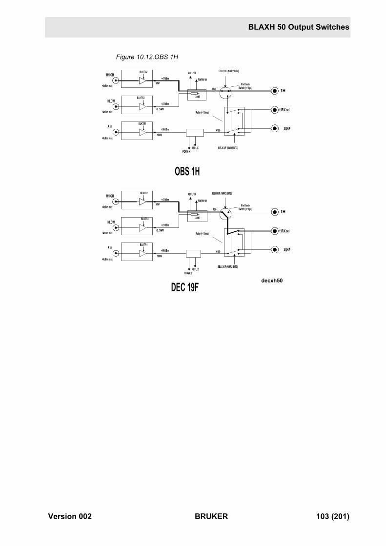
BLAXH 50 Output Switches
Figure 10.12.OBS 1H
BLKTR1
BLKTR3
BLKTR2
50W
0.5W
100W+50dBm
+27dBm
+47dBm
-30dB
FORW XREFL X
HHIGH
HLOW
X in
+4dBm max
+4dBm max
+4dBm max
19F/X sel
1H
XQNP
SELX X/F (NMR2 BIT3)
X100
REFL 1H
FORW 1H
H50
SELH H/F (NMR2 BIT2)
Relay (< 10ms)
Pin DiodeSwitch (< 10µs)
BLKTR1
BLKTR3
BLKTR2
50W
0.5W
100W+50dBm
+27dBm
+47dBm
-30dB
FORW XREFL X
HHIGH
HLOW
X in
+4dBm max
+4dBm max
+4dBm max
19F/X sel
1H
XQNP
SELX X/F (NMR2 BIT3)
X100
REFL 1H
FORW 1H
F50
SELH H/F (NMR2 BIT2)
Relay (< 10ms)
Pin DiodeSwitch (< 10µs)
OBS 1H
DEC 19Fdecxh50
Version 002 BRUKER 103 (201)
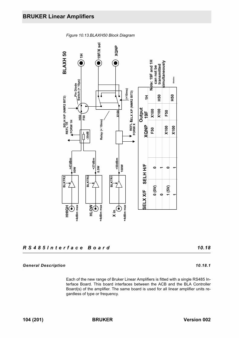
BRUKER Linear Amplifiers
Figure 10.13.BLAXH50 Block Diagram
R S 4 8 5 I n t e r f a c e B o a r d 10.18
General Description 10.18.1
Each of the new range of Bruker Linear Amplifiers is fitted with a single RS485 In-terface Board. This board interfaces between the ACB and the BLA ControllerBoard(s) of the amplifier. The same board is used for all linear amplifier units re-gardless of type or frequency.
BLK
TR1
BLK
TR3
BLK
TR2
50W
0.5W 100W+5
0dB
m
+27d
Bm
+47d
Bm
-30d
B FOR
W X
REF
L X
HH
IGH
HLO
W
X in
+4dB
m m
ax
+4dB
m m
ax
+4dB
m m
ax
19F/
X se
l
1H XQN
P
SELX
X/F
(NM
R2
BIT
3)
BLA
XH 5
0
SELH
H/F
0
SELX
X/F
XQN
PO
utpu
t19
F1H
0
01
H50
10
11
X100
H50
F50
X100
X100
X100
F50
X100
REF
L 1H
FOR
W 1
H H50
F50
SELH
H/F
(NM
R2
BIT
2) (<10
ms)
50w
bloc
Not
e: 1
9F a
nd 1
H
can
not b
e tr
ansm
itted
sim
ulta
neou
sly
(0V)
(5V)
Rel
ay (<
10m
s)
Pin
Dio
deSw
itch
(< 1
0µs)
104 (201) BRUKER Version 002
R S 4 8 5 I n t e r f a c e B o a r d
Note however that for BLAXH50 amplifiers the board is fitted with an additionalpiggyback board to cater for the second BLA Controller Board.
Functions:1. To digitize the Forward, Reflected and Blanking signals received from the BLA
Controller Board and transmit them to the ACB. From here they are either dis-played on the Boss Keyboard or the graphics monitor.
2. To provide read/write access to amplifier parameters such as Pulse Width Lim-itation, Max. Duty Cycle, FORW and REFL power.
3. To enable new application software to be downloaded.
4. Storage of data regarding number of amplifiers and amplifier type.
The RS485 link operates at a fixed baud rate of 62500. The RS485 data transmis-sion uses the SBS standard of 8 bits data with 1 start bit and 1 stop bit.
The principal elements of the RS485 board are:
U22:Among other subunits this microprocessor contains eight 8 bit sample and holdunits. Four are used to digitize the Forward and Reflected signals (2 channels),the other four are reserved for internal diagnostic tests.
U10:This EPROM contains the boot software. Note that new boot software cannot bedownloaded over the RS485 link. In the unlikely event of new boot software beingrequired then the EPROM itself must be exchanged.
U2:This FLASH EPROM contains the application software used by the board. Newapplication software can be downloaded over the RS485 link.
U9:This contains 32K of RAM.
U4:This chip has 4 x 8 bit DACs used to set the Duty Cycle, max. Pulse Width andOVERDRIVE cut out level.
U14, U15:These monoflops are used to extend the duration of the BLKTR pulses to a fixedduration 70 ms regardless of the pulse length. This is so that the power displaymay be more easily observed.
U27, U28:These monoflops perform the same function to the Forward and Reflected sig-nals.
Version 002 BRUKER 105 (201)
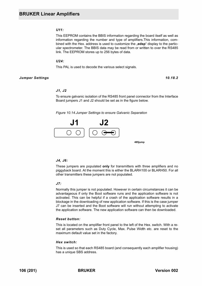
BRUKER Linear Amplifiers
U11:This EEPROM contains the BBIS information regarding the board itself as well asinformation regarding the number and type of amplifiers.This information, com-bined with the Hex. address is used to customize the „edsp“ display to the partic-ular spectrometer. The BBIS data may be read from or written to over the RS485link. The EEPROM stores up to 256 bytes of data.
U24: This PAL is used to decode the various select signals.
Jumper Settings 10.18.2
J1, J2To ensure galvanic isolation of the RS485 front panel connector from the InterfaceBoard jumpers J1 and J2 should be set as in the figure below.
Figure 10.14.Jumper Settings to ensure Galvanic Separation
J4, J6:These jumpers are populated only for transmitters with three amplifiers and nopiggyback board. At the moment this is either the BLARH100 or BLARH50. For allother transmitters these jumpers are not populated.
J7:Normally this jumper is not populated. However in certain circumstances it can beadvantageous if only the Boot software runs and the application software is notactivated. This can be helpful if a crash of the application software results in ablockage in the downloading of new application software. If this is the case jumperJ7 can be inserted and the Boot software will run without attempting to activatethe application software. The new application software can then be downloaded.
Reset button: This is located on the amplifier front panel to the left of the Hex. switch. With a re-set all parameters such as Duty Cycle, Max. Pulse Width etc. are reset to themaximum default value set in the factory.
Hex switch:This is used so that each RS485 board (and consequently each amplifier housing)has a unique SBS address.
J1 J2
485jump
106 (201) BRUKER Version 002
R S 4 8 5 I n t e r f a c e B o a r d
NOTE: To avoid a blockage of the SBS Bus the RS485 cable should first be dis-connected before switching an amplifier off. Switch on the amplifier before recon-necting the RS485 cable.
RS485 Pinouts 10.18.3
15 Pin SUB miniature connectors are used. The ACB is female, all slaves (ampli-fiers) are male.
Figure 10.15.RS485 Pinouts
Table 10.4. RS485 Pinouts
Pin Function Type at Master Type at Slave
1 Shield PASSIVE PASSIVE
2 RxD+ INPUT OUTPUT
3 /WUP OUTPUT INPUT
4 TXD+ OUTPUT INPUT
5 — — —
6 GND POWER POWER
7 GND POWER POWER
8 GND POWER POWER
9 RXD- INPUT OUTPUT
10 — — —
11 TXD- OUTPUT INPUT
12 — — —
13 VRS POWER POWER
14 VRS POWER POWER
15 VRS POWER POWER
1 8
9 15 485pin
Version 002 BRUKER 107 (201)
BRUKER Linear Amplifiers
RS485 signals 10.18.4
TXD+, TXD-:TXD+ and TXD- form a twisted pair. The RS485 link uses differential transmissionlines. These transmission lines can be driven only by the master (ACB). Becausethe slaves (amplifiers) cannot drive these lines (they can only receive) a bus con-flict is avoided
RXD+, RXD-:RXD+ and RXD- form a twisted pair. The receive lines are also differential. Theslaves use these lines to transmit data. The master cannot drive these lines, it canonly receive. A bus conflict caused by more than one slave attempting to transmitis prevented by software.
Note: Slave to slave data transmission is not allowed!
WUP:This is a Bruker specific RS485 compatible signal. To avoid interference the soft-ware can switch off some slaves during acquisition (sleep mode). To restart theslaves outside of acquisition the WUP signal is used to carry out a hardware reseton the slaves. The WUP is active low and driven by the master only.
VRS:Power supply of 12 V. This is provided by the ACB
Termination:The RS485 bus must be terminated correctly. A special connector is provided (P/N H5167)
Amplifier Specifications 10.19
A comprehensive list of specifications is now available for all Bruker linear amplifi-ers. This section describes how these specifications are defined. Example fig-ures quoted here refer to the specifications of the BLAX 300 RS which arecontained at the end of this chapter.
FREQUENCY RANGE:A measure of the frequency range over which the amplifier is designed to beused. RF signals at frequencies outside this range may have significantly reducedgain.
GAIN FLATNESSThe amplifier gain will be somewhat dependent on the absolute frequency. TheGAIN FLATNESS is quoted for the specified frequency range. e.g. for the BLAX300 RS the gain is specified not to vary by more than 1.5 dB for any frequencywithin the 6 - 241 MHz range.
108 (201) BRUKER Version 002
Amplifier Specifications
LINEAR GAIN:This is measured well within the linear region of the amplifier, typically at 10 dBbelow max. output. The linear gain will differ from the gain at the specified max.output. For the BLAX 300 RS an input of 1Vpp (4 dBm) will produce an output of300 W(55 dBm) i.e gain = 51 dB.
A brief glance at figure 11.17 should show however that the gain within the linearregion will be greater (in the case of the BLAX300 54 dB).
Figure 10.16.Linear Gain for BLAX300 (not to scale)
CW OUTPUT POWER:The BLA Control Board II limits the maximum allowed output power in CW modeto the specified value.
LINEAR OUTPUT POWER:At high output powers the linearity of the amplifier will suffer. The amplifier is de-fined as linear up to the power level where the actual output deviates from the per-fectly linear output by 1 dB. This level is referred to as the 1 dB compression point(see figure 10.17.)
Input
OutputLINEAR GAIN = 54 dB
GAIN at max output = 51 dB
gain
Version 002 BRUKER 109 (201)
BRUKER Linear Amplifiers
Figure 10.17.Linear Output Power (not to scale)
AMPLIFIER BIASING:All Bruker linear amplifiers are class AB.
BLANKING DELAY:The blanking within the amplifier is implemented using MOSFET's. These transis-tors have a certain response time and should ideally be activated prior to the arriv-al of the rf signal. The blanking delay is the time which should be allowed toensure that the MOSFET's are correctly biased to allow rf transmission.
RF RISE TIMEThe time taken for an rf pulse to rise from 10% to 90% of its final voltage.
RF FALL TIME:The time taken for an rf pulse to fall from 90% to 10% of its final voltage.
D C RINGINGThis is a consequence of the sharp rise and fall of the blanking pulses (BLKTR1 -15) applied within the amplifier. The ringing will occur at the start and end of theblanking pulse and may last several µseconds. The ringing is independent of therf power.
INPUT NOISE FIGURE:If the amplifier were perfect then noise and signal would both be amplified by thesame factor i.e. the Gain „G“. In reality the amplifier will add it’s own noise to theoutput and the output noise will be greater than Nt x G where „Nt“ is the thermalnoise at the input. The output noise can be represented by Nt x(G + F) where G isthe Gain and F the Noise Figure in dB.
OUTPUT NOISE POWER(UNBLANKED)The thermal noise at 300 K has a power level of - 174 dBm measured over abandwidth of 1Hz. Add to this the 7 dB Noise Figure along with the 54 dB LINEARGAIN to yield an output noise power of - 113 dBm/Hz.
Perfectly Linear ResponseActual Response
Input
Output
Linear Output Power
linear
110 (201) BRUKER Version 002
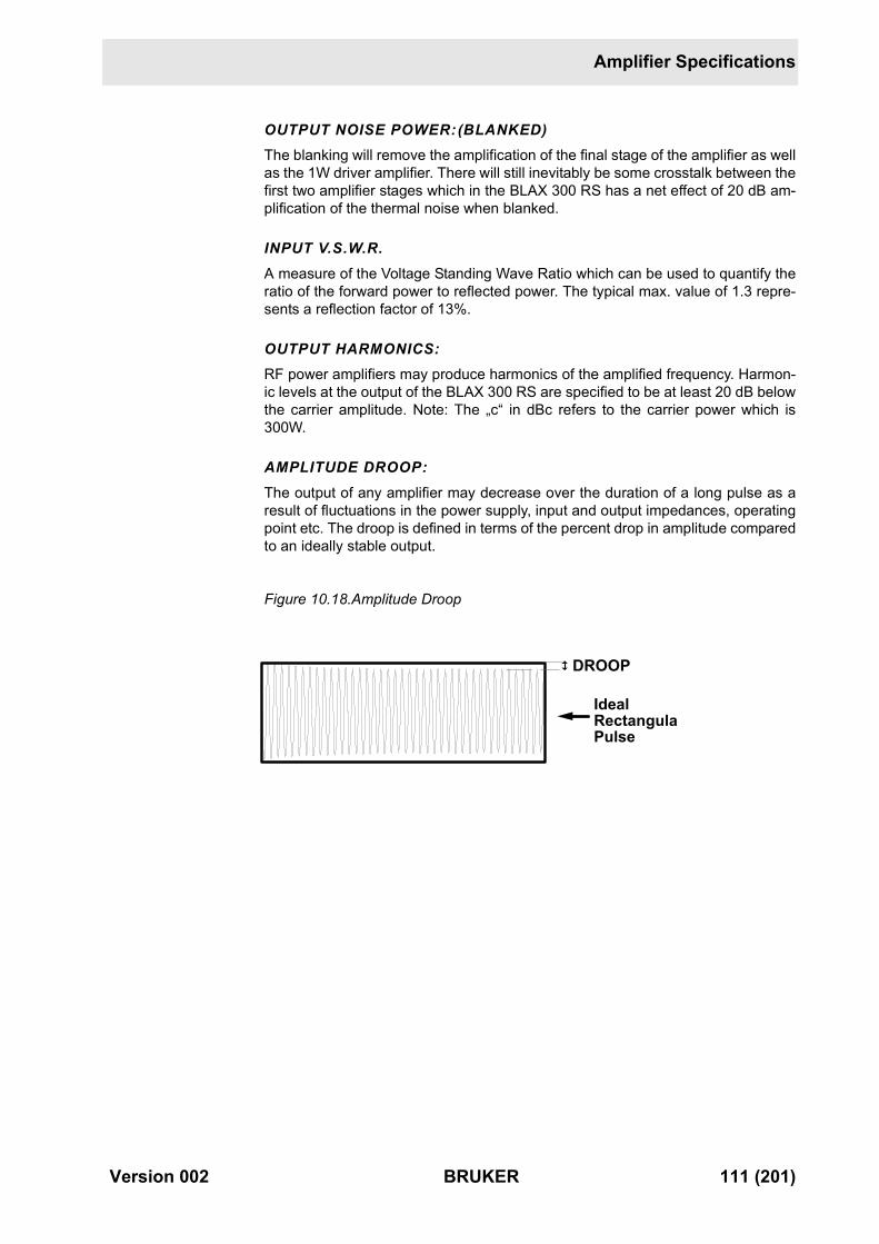
Amplifier Specifications
OUTPUT NOISE POWER:(BLANKED)The blanking will remove the amplification of the final stage of the amplifier as wellas the 1W driver amplifier. There will still inevitably be some crosstalk between thefirst two amplifier stages which in the BLAX 300 RS has a net effect of 20 dB am-plification of the thermal noise when blanked.
INPUT V.S.W.R.A measure of the Voltage Standing Wave Ratio which can be used to quantify theratio of the forward power to reflected power. The typical max. value of 1.3 repre-sents a reflection factor of 13%.
OUTPUT HARMONICS:RF power amplifiers may produce harmonics of the amplified frequency. Harmon-ic levels at the output of the BLAX 300 RS are specified to be at least 20 dB belowthe carrier amplitude. Note: The „c“ in dBc refers to the carrier power which is300W.
AMPLITUDE DROOP:The output of any amplifier may decrease over the duration of a long pulse as aresult of fluctuations in the power supply, input and output impedances, operatingpoint etc. The droop is defined in terms of the percent drop in amplitude comparedto an ideally stable output.
Figure 10.18.Amplitude Droop
Ideal RectangulaPulse
DROOP
Version 002 BRUKER 111 (201)
BRUKER Linear Amplifiers
112 (201) BRUKER Version 002
HPPR 11
HPPR Signals 11.1
The following table displays a list of signals which may be conveniently measuredat the Cover Display module of the HPPR.
Table 11.1. HPPR Signals
Periphery Socket Signal HPPR Cover Display
A +19V J0A/J0C
B DGND J0B
C +19V J0A/J0C
D RCP J0D
E TGPPA2 J0E
F SPF0 J0f
G RGP(EP) J0G
H DGND J0H
J TGPPA3 J0J
K not used
L -19V J0L
M DGND J0M
N +9V J0N
P n.c.
R TGPPA1 J0R
S n.c.
T n.c.
U +14V J0U
V GND J0V
Version 002 BRUKER 113 (201)
HPPR
TGPPA1, TGPPA2, TGPPA3:These Transmission gating pulses are assigned as follows:
TGPPA1 2H Module
TGPPA2 X BB Module
TGPPA3 1H Module
These pulses are produced by the TCU and may or may not be inverted in theLAB (up to Console wiring ECL04) depending on the HPPR Cover Module config-uration (see section 11.2). As of Console wiring ECL5 the signals are wired di-rectly to the HPPR Periph and the HPPR cover module must be configured foractive low gating.
The module selected as the OBS module is gated by the RGP signal. The TGPPApulses are used to gate any preamps selected to transmit decoupling pulses byacting on the polarization of the diodes in the Transmit/Receive section. Note thatthe TGPPA signals are very often not required. An rf pulse with intensity >1Vpp islikely to bias the diodes even in the absence of a gating pulse.
The pre blanking delay of the TGPPA signals may be adjusted in the „edscon“ ta-ble using the BLKPA[1 -3] parameters.
SPFO:This is the gating pulse for the lock preamplifier. This signal is pulsed at the fre-quency of 6.6 KHz regardless of whether a 2H or 19F lock is being used.
RGP (EP):Normal receiver gating pulse. This signal goes high for the duration of the acquisi-tion. This pulse is used to control the diodes in the preamp module selected as theOBS module. The OBS module is gated separately by the RGP pulse to ensurethat the T/R switching in the HPPR Hot Switch is synchronized with the acquisi-tion. This pulse is connected to the HPPR Periph. from:
the output labelled EP_HPPR of the RX22 (DRX,DPX)
the output labelled EP_HPPR of the RXC (DSX)
the output labelled EPc of the HRD16 Controller II (DMX)
RCP:This signal is not used at present. This signal could be used for fast switching be-tween selected preamps during a pulse program where the RS232C control wouldbe too slow. This would allow the selected OBS module to be switched during anacquisition. This feature may be implemented in the future.
114 (201) BRUKER Version 002
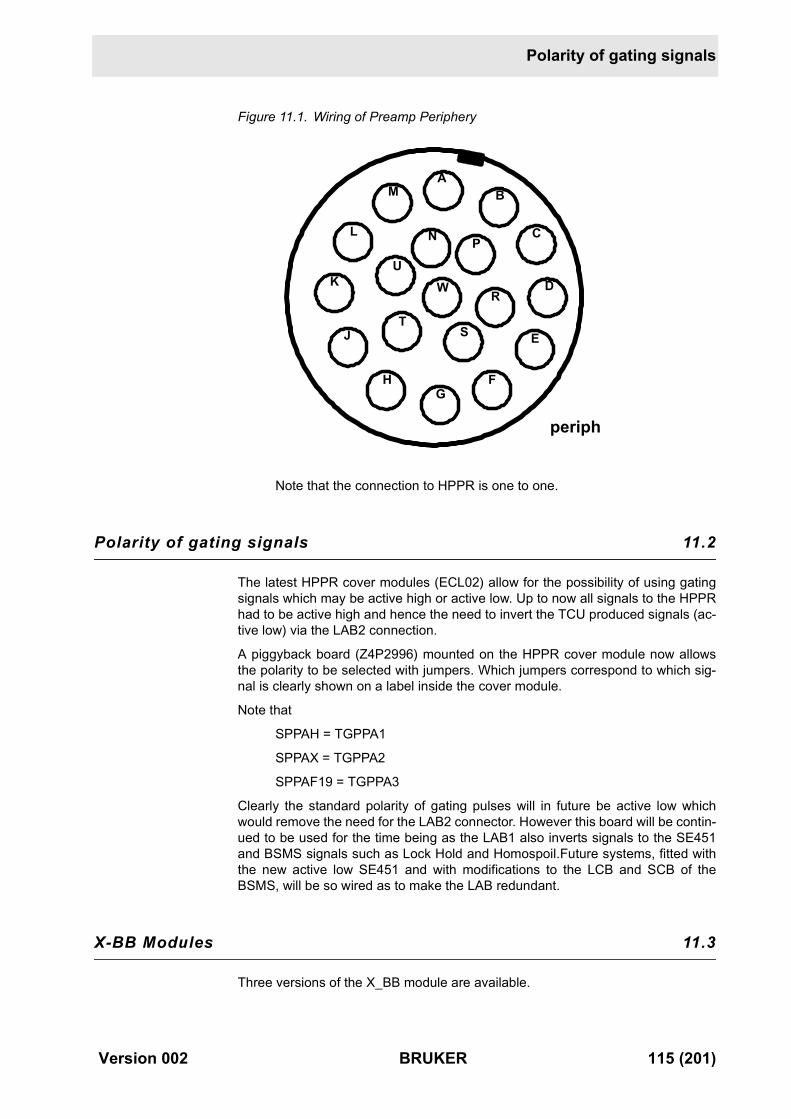
Polarity of gating signals
Figure 11.1. Wiring of Preamp Periphery
Note that the connection to HPPR is one to one.
Polarity of gating signals 11.2
The latest HPPR cover modules (ECL02) allow for the possibility of using gatingsignals which may be active high or active low. Up to now all signals to the HPPRhad to be active high and hence the need to invert the TCU produced signals (ac-tive low) via the LAB2 connection.
A piggyback board (Z4P2996) mounted on the HPPR cover module now allowsthe polarity to be selected with jumpers. Which jumpers correspond to which sig-nal is clearly shown on a label inside the cover module.
Note that
SPPAH = TGPPA1
SPPAX = TGPPA2
SPPAF19 = TGPPA3
Clearly the standard polarity of gating pulses will in future be active low whichwould remove the need for the LAB2 connector. However this board will be contin-ued to be used for the time being as the LAB1 also inverts signals to the SE451and BSMS signals such as Lock Hold and Homospoil.Future systems, fitted withthe new active low SE451 and with modifications to the LCB and SCB of theBSMS, will be so wired as to make the LAB redundant.
X-BB Modules 11.3
Three versions of the X_BB module are available.
AB
C
D
E
FG
H
J
K
L
M
N
R
ST
UP
W
periph
Version 002 BRUKER 115 (201)
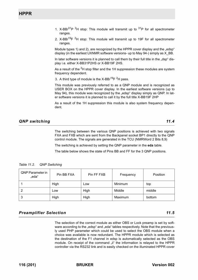
HPPR
1. X-BB/31P 2H stop: This module will transmit up to 31P for all spectrometerranges.
2. X-BB/19F 2H stop: This module will transmit up to 19F for all spectrometerranges.
Module types 1) and 2), are recognized by the HPPR cover display and the „edsp“display (in the earliest UXNMR software versions- up to May 94-) simply as X_BB.
In later software versions it is planned to call them by their full title in the „dsp“ dis-play i.e. either X-BB31P2HS or X-BB19F 2HS.
As a result of the 2H stop filter and the 1H suppression these modules are systemfrequency dependent.
3. A third type of module is the X-BB/19F 2H pass.
This module was previously referred to as a QNP module and is recognized asUSER BOX on the HPPR cover display. In the earliest software versions (up toMay 94), this module was recognized by the „edsp“ display simply as QNP. In lat-er software versions it is planned to call it by the full title X-BB19F 2HP
As a result of the 1H suppression this module is also system frequency depen-dent.
QNP switching 11.4
The switching between the various QNP positions is achieved with two signalsFXA and FXB which are sent from the Backpanel socket BP1 directly to the QNPcontrol module. The signals are generated in the TCU (NMRWord 2 Bits 8,9)
The switching is achieved by setting the QNP parameter in the eda table.
The table below shows the state of Pins BB and FF for the 3 QNP positions.
Preamplifier Selection 11.5
The selection of the correct module as either OBS or Lock preamp is set by soft-ware according to the „edsp“ and „eda“ tables respectively. Note that the previous-ly used PHP parameter which could be used to select the OBS module when achoice was available is now redundant. The HPPR module which is selected asthe destination of the F1 channel in edsp is automatically selected as the OBSmodule. On receipt of the command „ii“ the information is relayed to the HPPRcontroller via the RS232 link and is easily checked on the illuminated HPPR cover
Table 11.2. QNP Switching
QNP Parameter in „eda“ Pin BB FXA Pin FF FXB Frequency Position
1 High Low Minimum top
2 Low High Middle middle
3 High High Maximum bottom
116 (201) BRUKER Version 002
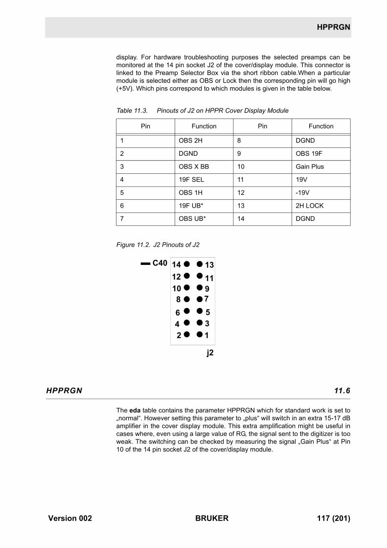
HPPRGN
display. For hardware troubleshooting purposes the selected preamps can bemonitored at the 14 pin socket J2 of the cover/display module. This connector islinked to the Preamp Selector Box via the short ribbon cable.When a particularmodule is selected either as OBS or Lock then the corresponding pin will go high(+5V). Which pins correspond to which modules is given in the table below.
Figure 11.2. J2 Pinouts of J2
HPPRGN 11.6
The eda table contains the parameter HPPRGN which for standard work is set to„normal“. However setting this parameter to „plus“ will switch in an extra 15-17 dBamplifier in the cover display module. This extra amplification might be useful incases where, even using a large value of RG, the signal sent to the digitizer is tooweak. The switching can be checked by measuring the signal „Gain Plus“ at Pin10 of the 14 pin socket J2 of the cover/display module.
Table 11.3. Pinouts of J2 on HPPR Cover Display Module
Pin Function Pin Function
1 OBS 2H 8 DGND
2 DGND 9 OBS 19F
3 OBS X BB 10 Gain Plus
4 19F SEL 11 19V
5 OBS 1H 12 -19V
6 19F UB* 13 2H LOCK
7 OBS UB* 14 DGND
135791113
2468
101214
j2
C40
Version 002 BRUKER 117 (201)
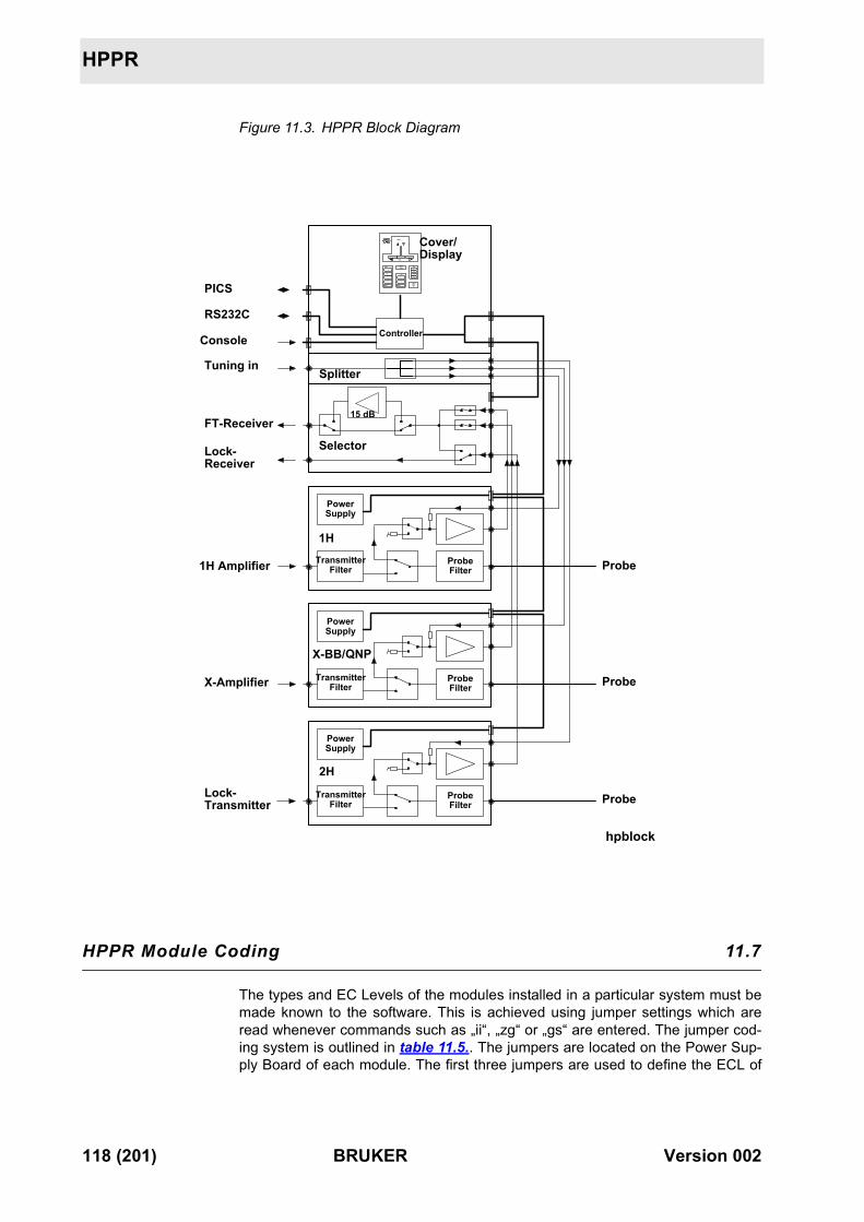
HPPR
Figure 11.3. HPPR Block Diagram
HPPR Module Coding 11.7
The types and EC Levels of the modules installed in a particular system must bemade known to the software. This is achieved using jumper settings which areread whenever commands such as „ii“, „zg“ or „gs“ are entered. The jumper cod-ing system is outlined in table 11.5.. The jumpers are located on the Power Sup-ply Board of each module. The first three jumpers are used to define the ECL of
PowerSupply
TransmitterFilter
ProbeFilter
PowerSupply
TransmitterFilter
ProbeFilter
PowerSupply
TransmitterFilter
ProbeFilter
Matching
Tuning
Observe
X-BB
USER BOX
ChannelSelector
Lock
USER BOX
COMPUTER
READY
ERROR
DISPLAYTEST
StatusPICS1 H
2 H
19 F
2 H
19 F
Controller
Cover/Display
Splitter
Selector
1H
X-BB/
2HLock-Transmitter
1H Amplifier
Lock-Receiver
FT-Receiver
Tuning in
Console
RS232C
PICS
Probe
X-Amplifier Probe
Probe
15 dB
QNP
hpblock
118 (201) BRUKER Version 002
Checking the module identification via the software
the module. This is an internal ECL determined by jumpers and may not cor-respond with the ECL written at the rear of the module.
Two systems of identification are used depending on the ECL
1) Modules with ECL A or ECL B
2) Modules from ECL C onwards.
From ECL C onwards the system was altered to enable a greater number of mod-ule types to be defined. Note that AVANCE systems is likely only be delivered withECL level C and onwards and this system only will be explained.
Modules from ECL C onwards 11.7.1
Only one set of jumpers, JM1 to JM8 on the Power Supply Board, are used.
Note that the frequency of the Module is no longer included in the coding as wasthe case with ECLA and ECLB.
The first three jumpers are used to define the ECL of the module. The other fivejumpers are used to determine the type of module.
Checking the module identification via the software 11.8
Information on how the software has decoded the jumpers can be obtained as fol-lows:
1. Configure the spectrometer with the command „cf debug“
2. A normal configuration will then proceed.
3. After the configuration is complete enter the command „ii“.
4. After a short delay this will produce a window entitled „ii“ command standardoutput listing. This display contains information about which modules havebeen identified by the software.
The type of Module, the ECL and a hexadecimal code will be given.
The ECL will have numbers 1,2 etc., where 1 corresponds to ECL A in table 1.
The hex code is the binary equivalent of the jumpers settings in table 12.5 withoutthe first three bits, used for ECL determination.
Example of „cf debug“ entryModule 2 = 1H Module ecl 3 code 0x18.
ECL 3 is ECL C of table 11.5.
Jumper settings for 1H in table 11.5. are 00011XXX binary = 24 decimal = 18 hex.
Each time the command „ii“ is entered the debug window will be displayed. If youno longer need this information then reconfigure the spectrometer with the normal„cf“ command.
Version 002 BRUKER 119 (201)
HPPR
QNP module coding:This module is not included in table 11.5. because it has one and only one jumperconfiguration (shown below) regardless of ECL.
Table 11.4. Jumper Settings for all QNP Modules
JM8 JM7 JM6 JM5 JM4 JM3 JM2 JM1 JUMPER
0 0 0 0 0 0 1 0 X-BB_19F_2HP(Former QNP)
Table 11.5. Jumper Coding of HPPR Modules
JM8 JM7 JM6 JM5 JM4 JM3 JM2 JM1 JUMPER
1 0 0 0 0 0 0 0 0 No Preamp available
2 X X X X X 0 0 1 Module ECL A (1)
3 X X X X X 0 1 0 Module ECL B (2)
4 X X X X X 0 1 1 Module ECL C (3)
5 X X X X X 1 0 0 Module ECL D (4)
6 X X X X X 1 1 1 Module ECL E (5)
7 X X X X X 1 0 0 Module ECL F (6)
8 X X X X X 1 1 1 Module ECL G (7)
9 X X 0 0 1 X X X 3H Module
10 0 0 0 1 0 X X X 3H Module HP
11 0 0 0 1 1 X X X 1H Module
12 0 0 1 0 0 X X X 1H Module HP
13 0 0 1 0 1 X X X 19F-Sel. Module
14 0 0 1 1 0 X X X 19F-Sel.ModuleHP
15 0 0 1 1 1 X X X 19F/1H/3H/ Mod-ule HP
16 0 1 0 0 0 X X X X-BB_19F_2HS Module
17 0 1 0 0 1 X X X X-BB_19F Module HP
18 0 1 0 1 0 X X X X-BB_31P_2HS Module
19 0 1 0 1 1 X X X X-BB_31P Module HP
120 (201) BRUKER Version 002
Checking the module identification via the software
20 0 1 1 0 0 X X X 2H Module
21 0 1 1 0 1 X X X 2H Module HP
22 0 1 1 1 0 X X X Reserve
23 0 1 1 1 1 X X X Reserve
24 1 0 0 0 0 X X X Reserve
25 1 0 0 0 1 X X X Reserve
26 1 0 0 1 0 X X X Reserve
27 1 0 0 1 1 X X X Reserve
28 1 0 1 0 0 X X X Reserve
29 1 0 1 0 1 X X X Reserve
30 1 0 1 1 0 X X X Reserve
31 1 0 1 1 1 X X X Reserve
32 1 1 0 0 0 X X X Reserve
33 1 1 0 0 1 X X X Reserve
34 1 1 0 1 0 X X X Reserve
35 1 1 0 1 1 X X X Reserve
36 1 1 1 0 0 X X X Reserve
37 1 1 1 0 1 X X X Reserve
38 1 1 1 1 0 X X X Reserve
Table 11.5. Jumper Coding of HPPR Modules
JM8 JM7 JM6 JM5 JM4 JM3 JM2 JM1 JUMPER
Version 002 BRUKER 121 (201)

HPPR
122 (201) BRUKER Version 002
RX22 Receiver 12
This chapter will highlight the differences between the ARX Receiver and the newDRX Receiver the RX22.
The RX22 Receiver is used in DRX and DPX instruments and is in principle verysimilar to the ARX Receiver in terms of the rf sections. Only minor modificationshave been made to the RF and IF sections. This has resulted principally in a larg-er bandwidth in comparison to the ARX receiver.
A significant modification to the AF section is the introduction of a heater and reg-ulation circuit used to monitor and maintain the temperature of the Quad moduleat a steady of 55°C from ECL03 onwards. (Up to and including ECL02 the Quadmodule temperature was maintained at 65°C). This should further reduce anysmall phase and gain drift that might be caused by temperature fluctuations. Fur-ther improvements are the introduction of improved metal shielding in the Quadmodule.
The RX22 is a cassette-module plugged into the AQR.
Version 002 BRUKER 123 (201)
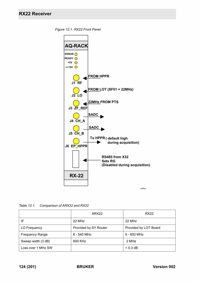
RX22 Receiver
Figure 12.1. RX22 Front Panel
Table 12.1. Comparison of ARX22 and RX22
ARX22 RX22
IF 22 MHz 22 MHz
LO Frequency Provided by SY Router Provided by LOT Board
Frequency Range 6 - 540 MHz 6 - 600 MHz
Sweep width (3 dB) 600 KHz 2 MHz
Loss over 1 MHz SW < 0.3 dB
AQ-RACK
RX-22
ERRORREADY
+5V
+/-15V
J1 RF
J2 LO
J3 ZF_REF
J4 CH_A
J5 CH_B
J6 EP_HPPR
FROM HPPR
FROM LOT (SF01 + 22MHz)
22MHz FROM PTS
SADC
SADC
( default high during acquisition)
rx22fron
RS485 from X32Sets RG(Disabled during acquisition)
To HPPR
124 (201) BRUKER Version 002
Controller module
Apart from performance by far the greatest differences between the ARX22 andthe RX22 is in the controller module which makes software control of hardwarefeatures possible via the RS485 link.
Controller module 12.1
The controller module of the ARX22 receiver was used principally to handle theRG settings, EP pulse and power supplies. The RX22 controller has a muchgreater capability including interfacing with both an RS485 link and an I2C Bus(The I2C Bus is not actually used by the RX22). A Flash EPROM allows the fol-lowing information to be stored:
1) Gain settings for the various rf sections
2) Phase and Gain settings for the Quad module
3) Calibration data for the various amplifiers in the RF, IF, and AF sections
4) BBIS type information
5) Firmware used by the microcontroller
1. Gain settings:
The UXNMR RG value is transmitted to the receiver via the RS485 link. The datais interpreted by the controller and the appropriate control signals are then trans-mitted to the RF and IF amplifiers. The table 12.4. displays which combination of
Gain Range 93 dB 93 dB
Min. Gain Step 3 dB 1 dB
Gain Set by MCI via BURNDY con-nector
Set by RS485 Link
Temperature stability Quad module subject to drift Quad module regulated to 55°C
Quad peak adjustment Hardware pot. trimming Software adjustment via RS485 link
I2 C Interface None Yes
RS485 Interface None Yes
EP Pulse Generated by process controller Transmitted to receiver via Burndy
Generated by RCU. Transmit-ted to receiver via SADC and Backplane
EP_HPPR Direct from Process Controller Low during Acquisition
Via RX22 Active High/Low set by Jumpers (ECL01)
Power supply Supplied via front panel BURNDY
Supplied from back panel
Table 12.1. Comparison of ARX22 and RX22
ARX22 RX22
Version 002 BRUKER 125 (201)
RX22 Receiver
gain settings is used for the various sections for the complete range of UXNMRRG values. Note that this table uses RG steps of 3 dB. As of ECL00 it is possibleto alter the RG in 1 dB steps.
When an UXNMR RG value which does not correspond exactly to a hardware val-ue is entered, then the nearest value is taken.
Note that whereas before with the ARX receiver it was possible to measure theRG bit settings at the Burndy connector this is no longer possible because the RGbit settings are now transmitted over the RS485 link. However it is now extremelyeasy to test the RG bit settings using the RX22 tool.
2. Phase and Gain settings for the Quad module
It is now possible to make the Quad Image adjustments by software. Using theRX22 tool program the Gain (resolution +3.2% of current Gain) or Phase (resolu-tion + 5°) may be adjusted. When the adjustments are made they should bestored using the „Save Configuration“ routine. This will ensures that the correctvalues are automatically reloaded after a power up.
3. Calibration data:
The calibration of the various amplifiers is carried out in the factory individually foreach board. The increased accuracy resulting from the calibration has made itpossible for the 1 dB steps of the PAS to be implemented. Although this data maybe altered with the aid of the RX22 tool this is not recommended. False calibrationdata will result in the RX22 operating improperly.
4. BBIS data:
The FLASH EPROM also contains BBIS data such as production data, softwareversion, EC level etc. This data is transmitted via the RS485 link.
5. Firmware:
The RX22 tool program can be used to download new firmware.
Downloading Firmware 12.2
When installing UXNMR use the command „rx22_copy“. This will ensure that thenewest firmware contained in the currently installed UXNMR is copied to the ap-propriate files. If this is not done then firmware which is not up to date may bedownloaded.
To download the firmware use Menu Point 3 of the „RX22“ tool.
File to be downloaded /u/conf/instr/rx22tool/tool/rx22.hex
Future RX22 tool versions will have an auto-download feature so that the file pathname need not be explicitly entered.
Reset 12.3
The RX22 Controller is normally active only when the RGP signal is high (inactive,receiver closed). In this state RG values may be changed etc. When the EP signalgoes low (active, receiver open) the controller is effectively switched off. No fur-ther communication is possible over the RS485 link.* The 12MHz mProcessorclocking frequency is also switched off. This ensures that no disturbances can oc-
126 (201) BRUKER Version 002
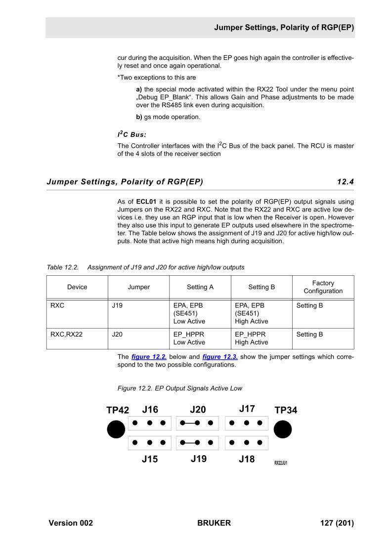
Jumper Settings, Polarity of RGP(EP)
cur during the acquisition. When the EP goes high again the controller is effective-ly reset and once again operational.
*Two exceptions to this are
a) the special mode activated within the RX22 Tool under the menu point„Debug EP_Blank“. This allows Gain and Phase adjustments to be madeover the RS485 link even during acquisition.
b) gs mode operation.
I2C Bus: The Controller interfaces with the I2C Bus of the back panel. The RCU is masterof the 4 slots of the receiver section
Jumper Settings, Polarity of RGP(EP) 12.4
As of ECL01 it is possible to set the polarity of RGP(EP) output signals usingJumpers on the RX22 and RXC. Note that the RX22 and RXC are active low de-vices i.e. they use an RGP input that is low when the Receiver is open. Howeverthey also use this input to generate EP outputs used elsewhere in the spectrome-ter. The Table below shows the assignment of J19 and J20 for active high/low out-puts. Note that active high means high during acquisition.
The figure 12.2. below and figure 12.3. show the jumper settings which corre-spond to the two possible configurations.
Figure 12.2. EP Output Signals Active Low
Table 12.2. Assignment of J19 and J20 for active high/low outputs
Device Jumper Setting A Setting B Factory Configuration
RXC J19 EPA, EPB (SE451)Low Active
EPA, EPB (SE451)High Active
Setting B
RXC,RX22 J20 EP_HPPRLow Active
EP_HPPRHigh Active
Setting B
J16 J20 J17
J18J19J15
TP42 TP34
RX22JU1
Version 002 BRUKER 127 (201)
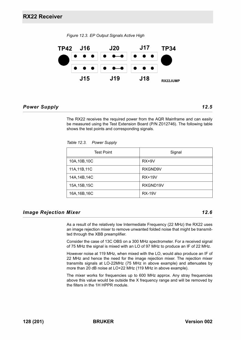
RX22 Receiver
Figure 12.3. EP Output Signals Active High
Power Supply 12.5
The RX22 receives the required power from the AQR Mainframe and can easilybe measured using the Test Extension Board (P/N Z012746). The following tableshows the test points and corresponding signals.
Image Rejection Mixer 12.6
As a result of the relatively low Intermediate Frequency (22 MHz) the RX22 usesan image rejection mixer to remove unwanted folded noise that might be transmit-ted through the XBB preamplifier.
Consider the case of 13C OBS on a 300 MHz spectrometer. For a received signalof 75 MHz the signal is mixed with an LO of 97 MHz to produce an IF of 22 MHz.
However noise at 119 MHz, when mixed with the LO, would also produce an IF of22 MHz and hence the need for the image rejection mixer. The rejection mixertransmits signals at LO-22MHz (75 MHz in above example) and attenuates bymore than 20 dB noise at LO+22 MHz (119 MHz in above example).
The mixer works for frequencies up to 600 MHz approx. Any stray frequenciesabove this value would be outside the X frequency range and will be removed bythe filters in the 1H HPPR module.
Table 12.3. Power Supply
Test Point Signal
10A,10B,10C RX+9V
11A,11B,11C RXGND9V
14A,14B,14C RX+19V
15A,15B,15C RXGND19V
16A,16B,16C RX-19V
J16 J20 J17
J18J19J15
TP42 TP34
RX22JUMP
128 (201) BRUKER Version 002
Testing the overall gain of the Receiver
Testing the overall gain of the Receiver 12.7
Column 2 of table 12.4. lists the approximate overall real gain of the RX22 Re-ceiver for a range of RG values. To check these values carry out the following pro-cedure.
1. Measure the voltage of the 80 MHz output of the PTS620 (~1Vpp at 50 Ω)
2. Set SFO1 = 80.0001 MHz. AQ = 60 seconds
3. Set RG = 1
4. Connect the 80 MHz output via a variable attenuator to the receiver input. Setthe attenuator to 80 dB.
5. Enter „zg“ and observe the voltage at the receiver output CHA or CHB. Adjustthe variable attenuator until the voltage at the receiver output is equal to thatmeasured at the 80 MHz output of the PTS. The attenuation required can betaken as a measure of the gain of the receiver.
You can repeat using various values of RG, but be sure to increase the attenua-tion accordingly.
Table 12.4. 3dB GAIN Table
RG Value Real Gain dB (approx)
Relative Gain (dB) RF Amplifier 1st IF
Amplifier PAS 2nd IF Amplifier
1 12 1 -12dB +8dB -9dB -4dB
1.4 15 4 -12dB +8dB -6dB -4dB
2 18 7 -12dB +8dB -3dB -4dB
2.8 21 10 -12dB +8dB 0dB -4dB
4 24 13 0dB +8dB -9dB -4dB
5.7 27.1 17 0dB +8dB -6dB -4dB
8 30.1 19 0dB +8dB -3dB -4dB
11.3 33.1 22 0dB +8dB 0dB -4dB
16 36.1 25 +12dB +8dB -9dB -4dB
22.6 39.1 28 +12dB +8dB -6dB -4dB
32 42.1 31 +12dB +8dB -3dB -4dB
45.3 45.1 34 +12dB +8dB 0dB -4dB
64 48.1 37 +12dB +8dB -9dB +8dB
90.5 51.1 40 +12dB +8dB -6dB +8dB
Version 002 BRUKER 129 (201)
RX22 Receiver
128 54.1 43 +12dB +8dB -3dB +8dB
181 57.2 46 +12dB +8dB 0dB +8dB
256 60.2 49 +24dB +8dB -9dB +8dB
362 63.2 52 +24dB +8dB -6dB +8dB
512 66.2 55 +24dB +8dB -3dB +8dB
724.1 69.2 58 +24dB +8dB -0dB +8dB
1K 72.2 61 +24dB +20dB -9dB +8dB
1.4K 75.2 64 +24dB +20dB -6dB +8dB
2K 78.2 67 +24dB +20dB -3dB +8dB
2.8K 81.2 70 +24dB +20dB 0dB +8dB
4K 84.2 73 +24dB +20dB -9dB +20dB
5.7K 87.3 76 +24dB +20dB -6dB +20dB
8K 90.3 79 +24dB +20dB -3dB +20dB
11.3K 93.3 82 +24dB +20dB 0dB +20dB
16K 96.3 85 +24dB +20dB -9dB +32dB
22.6K 99.3 88 +24dB +20dB -6dB +32dB
32K 102.3 91 +24dB +20dB -3dB +32dB
45.3K 105.3 94 +24dB +20dB 0dB +32dB
Table 12.4. 3dB GAIN Table
RG Value Real Gain dB (approx)
Relative Gain (dB) RF Amplifier 1st IF
Amplifier PAS 2nd IF Amplifier
130 (201) BRUKER Version 002
HRD 16 Controller Board 13
The HRD 16 digitizers as used in AVANCE spectrometers have a modified Con-troller Board II (P/N Z02478)
Functions 13.1
1. To provide RGPa, RGPb and RGPc outputs.
These three outputs (labelled EPa, EPb, EPc on the board itself) are identi-cal and generated from a single RGP pulse transmitted from the RCU viathe 50 way digitizer cable.
In a DMX, 2 of these outputs are used in the SE451 (RFT and LO), the thirdis used to blank the OBS module of the HPPR. As such the three outputsare active high (i.e. high during acquisition).
In a DRX, fitted with HRD 16 as option, only the RGPa output is required.This output is connected to the LAB1 where it is inverted (to active low dur-ing acquisition) and transmitted to the RX22 via the AQR backplane. Fromthis signal the EP_ HPPR output (active high during acquisition) is alsogenerated (see figure 13.2.).
2. To provide an ADC ON output
This signal is generated by the RCU and transmitted to the HRD 16 via the50 way cable. The signal as well as controlling the ADC of the HRD16 itself,is required to control the ADC LED of the BSMS keyboard. A modification(EC no. 1865, see APPENDIX) may be required with earlier LAB's in orderto observe this LED on the BSMS keyboard. The ADC ON signal is simplywired through the LAB to the AQR backplane. It is not inverted on the LAB.From here it is transmitted to the BSMS via the ACB.
Future AVANCE spectrometers will be fitted with the HADC (instead of theHRD16) which will have direct access to the AQR backplane and the LABwill not be required (The spectrometer must also be fitted with an RXC andthe new 19 inch SE451).
3. Transmission of bits DRG 0 - 7 to SE451 via the canon mini sub 9.
These signals are actually generated by the RCU and simply transmitted tothe HRD16 via the 50 way digitizer cable. The Bit settings can easily bechecked either at the HRD16 output or at the RFT Burndy of the SE451(ta-ble 13.1.).
Note that bits DRG 0 - 5 are used to set the receiver gain in the SE 451 from 1 to32K. DRG 7 is used to switch the High Pass / Low Pass filters in the RFT. Bit 6 isnot used. For DRX spectrometers the sub mini 9 connector is not required. Thereceiver gain is set via the RS485 link to the RX22.
Version 002 BRUKER 131 (201)
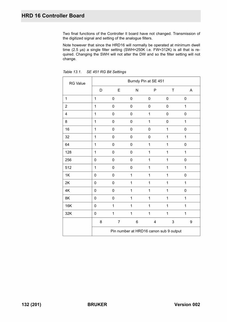
HRD 16 Controller Board
Two final functions of the Controller II board have not changed. Transmission ofthe digitized signal and setting of the analogue filters.
Note however that since the HRD16 will normally be operated at minimum dwelltime (2.5 µs) a single filter setting (SWH=250K i.e. FW=312K) is all that is re-quired. Changing the SWH will not alter the DW and so the filter setting will notchange.
Table 13.1. SE 451 RG Bit Settings
RG Value Burndy Pin at SE 451
D E N P T A
1 1 0 0 0 0 0
2 1 0 0 0 0 1
4 1 0 0 1 0 0
8 1 0 0 1 0 1
16 1 0 0 0 1 0
32 1 0 0 0 1 1
64 1 0 0 1 1 0
128 1 0 0 1 1 1
256 0 0 0 1 1 0
512 1 0 0 1 1 1
1K 0 0 1 1 1 0
2K 0 0 1 1 1 1
4K 0 0 1 1 1 0
8K 0 0 1 1 1 1
16K 0 1 1 1 1 1
32K 0 1 1 1 1 1
8 7 6 4 3 9
Pin number at HRD16 canon sub 9 output
132 (201) BRUKER Version 002
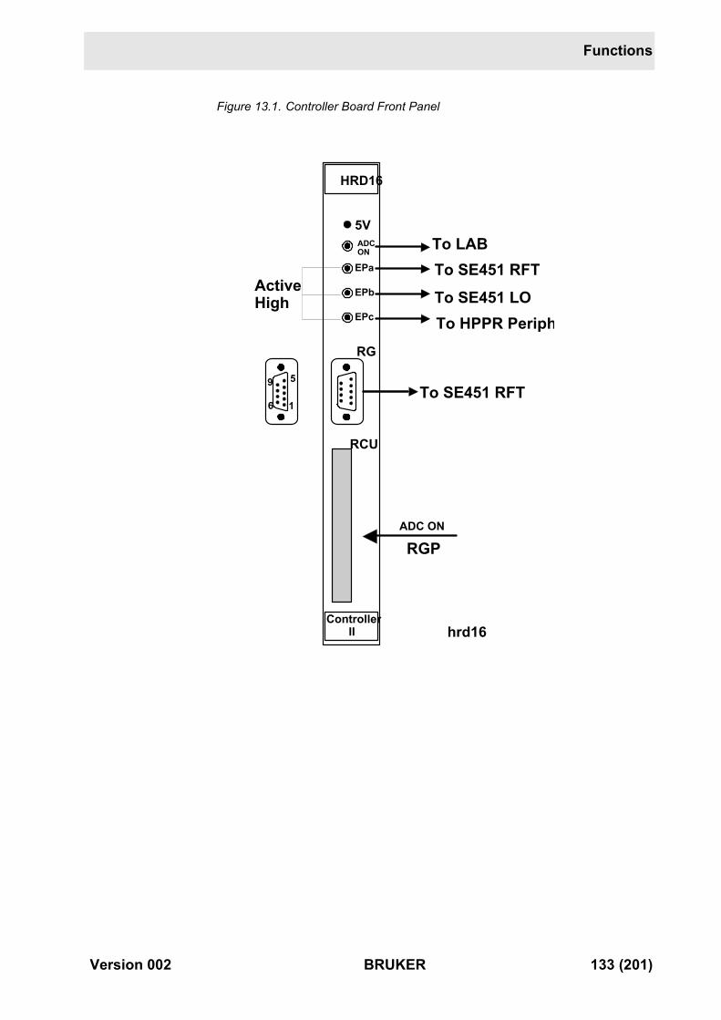
Functions
Figure 13.1. Controller Board Front Panel
Controller II
HRD16
ADCON
EPa
EPb
EPc
5V
RG
RCU
hrd16
ActiveHigh
To SE451 RFT1
59
6
To SE451 RFTTo SE451 LOTo HPPR Periph
To LAB
ADC ON
RGP
Version 002 BRUKER 133 (201)
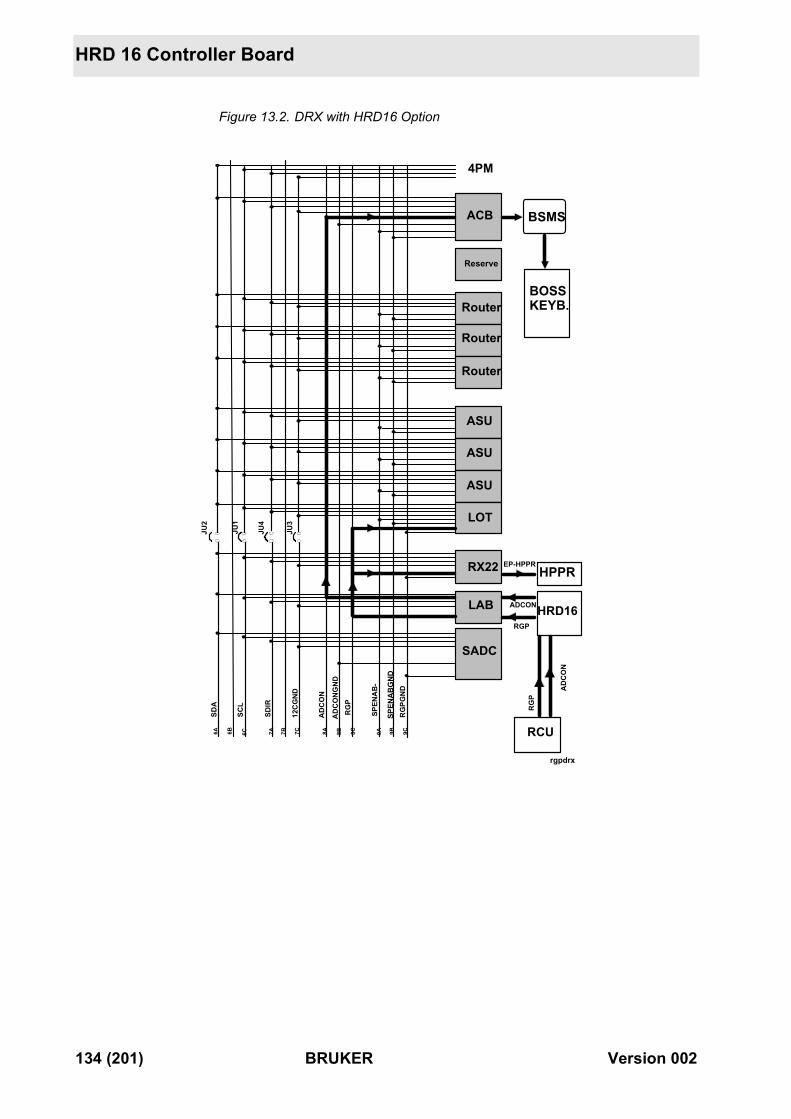
HRD 16 Controller Board
Figure 13.2. DRX with HRD16 Option
4PM
ACB
Reserve
Router
Router
Router
ASU
ASU
ASU
LOT
RX22
LAB
6A 6B 6C 7A 7B 7C 8A 8B 8C 9A 9B 9C
SDA
SCL
SDIR
12C
GN
D
AD
CO
N
RG
PA
DC
ON
GN
D
SPEN
AB
-
SPEN
ABG
NDR
GPG
ND
JU2
JU1
JU4
JU3
rgpdrx
RCU
HPPR
BSMS
RGP
AD
CO
N
HRD16
SADC
BOSSKEYB.
RG
P
ADCON
EP-HPPR
134 (201) BRUKER Version 002
RCU: Receiver Control Unit 14
Functions 14.1
1. Upon receipt of the RCUGO signal from the TCU, the RCU takes completecontrol of the acquisition. The RCU will then operate autonomously until theend of the current scan. To perform a second scan however the RCU must waitfor a second RCUGO signal from the TCU
Note that the RCUGO signal is synchronized with the 40MHz in signal, bothof which are received from the TCU. It is important that both these signalsare derived from the same source.
2. As part of the acquisition control the RCU generates the DWELL CLOCK aswell as the RGP and ADCON signals. It also handles the receiver phase.
3. The RCU is responsible for processing the acquired signal i.e. digital filteringand decimation as well as accumulation and the DMA transfer of processeddata to the CCU.
4. The RCU is master of all digitizers (SADC, HADC, FADC and HRD16) and alldigitizer functions. T. This includes the filter settings (SADC, HADC, FLTP/4Mand HRD16FT) and Quad. Mode (qsim, qf). For the SADC, HADC and HRD16the information is sent directly over the 50 way digitizer cable. For the FLTP/4M the information is sent through the SADC or HADC and then to the FLTP/4M via the I2C BUS of the AQR.
5. For homo-decoupling the timing of the decoupling pulses is set by the RCU.The RCU generates two signals SPHD and RGP (EPHDON EPHDOFF SPH-DON SPHDOFF). These signals are then combined in a PAL (TCU0AE40) onthe TCU to synchronize the receiver gating with the decoupling pulses.
6. Setting of the SE451 receiver gain in DMX and DSX spectrometers. In DMXspectrometers the RG bit settings are first ported through the HRD16 Control-ler II Board and then connected to the SE451 via the 9 way cable. In DSXspectrometers the RG bit settings are transmitted to the RXC from the CCUover the RS485 link and then connected to the SE451 via the RXC front panelconnection.
Future machines will no longer be fitted with the HRD16 and the RG will al-ways be set with the RXC.
Version 002 BRUKER 135 (201)
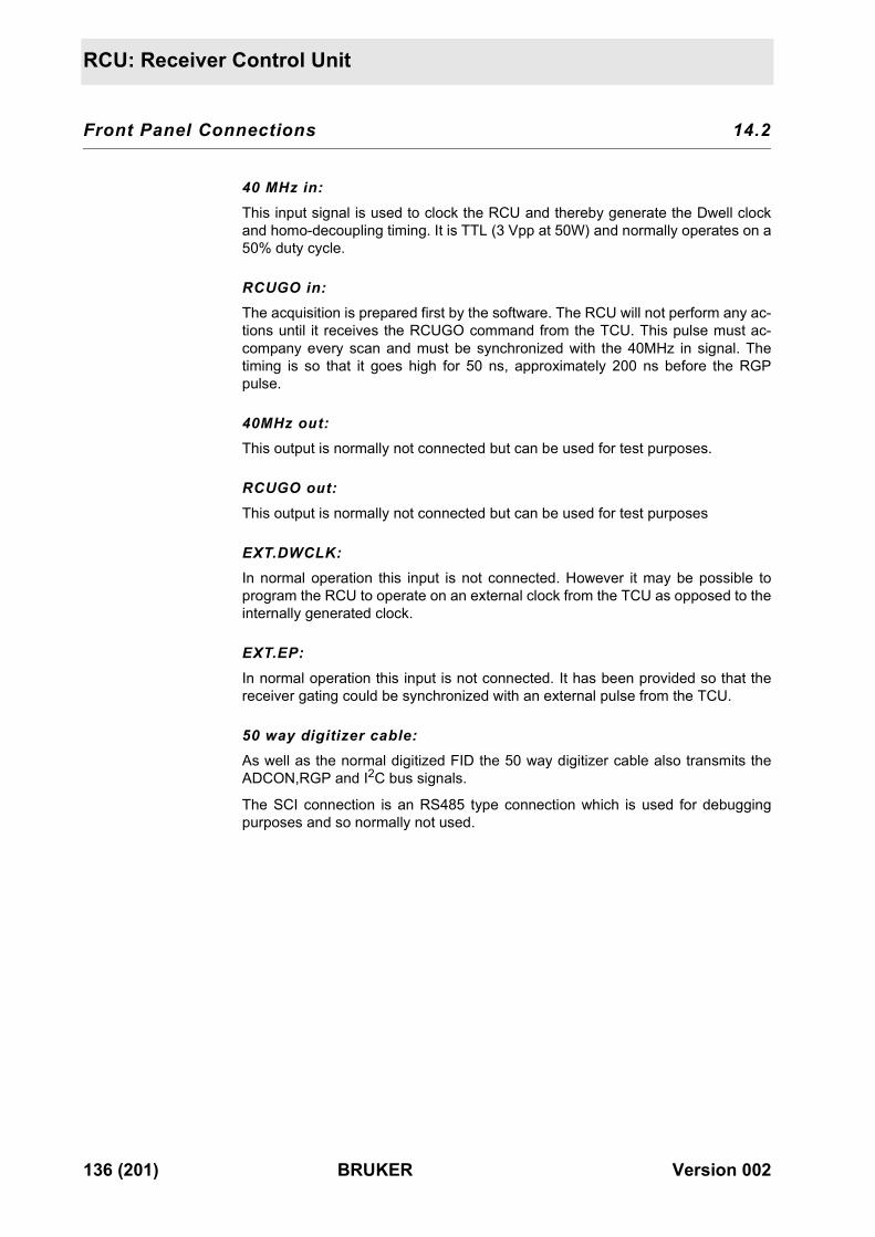
RCU: Receiver Control Unit
Front Panel Connections 14.2
40 MHz in:This input signal is used to clock the RCU and thereby generate the Dwell clockand homo-decoupling timing. It is TTL (3 Vpp at 50W) and normally operates on a50% duty cycle.
RCUGO in:The acquisition is prepared first by the software. The RCU will not perform any ac-tions until it receives the RCUGO command from the TCU. This pulse must ac-company every scan and must be synchronized with the 40MHz in signal. Thetiming is so that it goes high for 50 ns, approximately 200 ns before the RGPpulse.
40MHz out:This output is normally not connected but can be used for test purposes.
RCUGO out:This output is normally not connected but can be used for test purposes
EXT.DWCLK:In normal operation this input is not connected. However it may be possible toprogram the RCU to operate on an external clock from the TCU as opposed to theinternally generated clock.
EXT.EP:In normal operation this input is not connected. It has been provided so that thereceiver gating could be synchronized with an external pulse from the TCU.
50 way digitizer cable: As well as the normal digitized FID the 50 way digitizer cable also transmits theADCON,RGP and I2C bus signals.
The SCI connection is an RS485 type connection which is used for debuggingpurposes and so normally not used.
136 (201) BRUKER Version 002
Checking the DWELL CLOCK
Figure 14.1. RCU Front Panel
Checking the DWELL CLOCK 14.3
For this the Test Extension Board (P/N H2066) is required. The DWELL CLOCKsignal may be measured at J2 C30 of either the RCU or the TCU.
If the Test Extension Board is not available then the DWELL CLOCK can be mea-sured at C30 of the Acquisition Bus along the back of the AQX32.
The following table illustrates the Min. dwell time and corresponding max. dwellclock for various digitizers.
RCUFRONT
40MHzin
RCUGOin40MHzoutRCUGOoutExt.DWCLKExt.EP
FAILHOLD
DMAADCON
ADC
SCI
AQX
RCU
Normally not connected
FROM TCU
ADCONRGP
FILTER SETTINGfor SADC, FLTP/4M
RG SETTINGfor SE451
Digitised FID
Normally not connected
Version 002 BRUKER 137 (201)
RCU: Receiver Control Unit
Note that for the FADC the oversampling is redundant at rates above the normalmode.
Note also that the actual dwell clock is determined not by the parameter DW(„eda“) but rather DWOV.
Acquisition Bus 14.4
The RCU is connected to the TCU via the Acquisition bus. The TCU is the oneand only master of this bus. Typical instructions sent from the TCU to the RCUover this bus are:
a) RCU Ze = zero memory
b) RCU SYNC = synchronize the RCU clock (40 MHz) with the TCU clock(80 MHz)
c) RCU_PH 0 = set receiver phase
d) RCU EOA = end of Acquisition
e) WR#0 = write to disc
The above commands can be checked using the file „shm.out“ which is automati-cally created in the users home directory with the command „gotst“.
Note that the Acquisition Bus is not used to transmit the RCUGO signal and 40MHz clocking frequency. Instead they are sent directly to the RCU over the frontpanel as it was felt that this would lead to cleaner signal transmission.
VME Bus 14.5
The RCU is connected to the standard VME bus which runs along the AQX32backplane. The CCU and RCU are the only possible masters of this bus, with theRCU having priority. Typical uses of this bus are:
a) Transfer of processed digitized data from the RCU to the CCU (DMA).
b) Transfer of information regarding the Filter Widths, Receiver Gains asset by UXNMR.
c) Upgrading of acquisition parameters e.g. number of scans, etc.
Table 14.1. Minimum dwell time and corresponding maximum dwell clock
Digitizer Minimum Dwell Time (Quad Mode) Dwell Clock Maximum SW
(Quad Mode)
SADC 3.3us 300 KHz 150 KHz
HRD16 2.5 us 400 KHz 200KHz
FADC 0.05 us (High speed) 20 MHz 10MHz
FADC 2.5 us (Normal mode) 400 KHz 200KHz
138 (201) BRUKER Version 002
Transfer of data to CCU
Transfer of data to CCU 14.6
The RCU operates an automatic overflow and diskwrite. The accumulated digi-tized FIDs are stored in a 32 bit x1 M DRAM. The number of scans that can bestored will depend on the digital resolution that is used (see figure 14.2.). Notethat the RCU can be fitted with optional extra DRAM expanding the memory to 32bit x2 M DRAM
At higher sample rates, when using the FADC, a 32 bit x 64K SRAM which is fast-er than the DRAM is used for accumulation.The use of the SRAM is automaticallyhandled by the software
Diagnostic test 14.7
The RCU may be checked using
/u/systest/rcu/rcutest (logged in on spect)
Useful commands are
„h“ = help and prints a list of commands
„res“ = performs a software reset of the RCU
„auto“ = starts an automatic self test
The directory /u/systest/rcu also contains the file „docu“ which describes the „rcut-est“ commands in detail.
Version 002 BRUKER 139 (201)
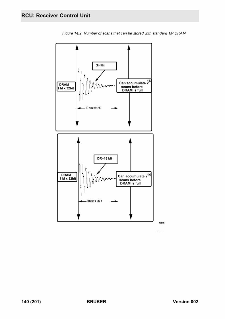
RCU: Receiver Control Unit
Figure 14.2. Number of scans that can be stored with standard 1M DRAM
DRAM 1 M x 32bit
TD max = 512 K
DR=16 bit
Can accumulate 2 16scans before DRAM is full
TD max = 512 K
DR=18 bit
Can accumulate 2 14scans before DRAM is full
RCUDRAM
DRAM 1 M x 32bit
rcudram
140 (201) BRUKER Version 002
12C Bus in the AQR 15
BBIS 15.1
This term stands for Bruker Board Information System and is a component of theon-board local intelligence which is now a feature of all AQR boards. In the futureit will be expanded to include the AQX32 boards. The system is designed to storeinformation about a particular board on the board itself in an EEPROM. The typeof information stored is Date of manufacture, Part and Serial number, EngineeringLevel etc. This information is burnt onto the EEPROM at manufacture. At the mo-ment it is only possible to access this information using a P.C. and special soft-ware. However it is envisaged that in the future engineers will be able to accessthis information via a service tool. When the system is fully implemented it shouldbe possible to login remotely to a customer’s spectrometer and have access to in-formation such as the Engineering Level of all boards. The transfer of informationwithin the AQR boards is achieved using the I2C Bus.
I2C Bus 15.2
This is a bi-directional, real time 8 bit serial bus. The bus is non differential anduses TTL levels. Two independent I2C buses run along the AQR backplane (seefigure 16.1). Although both buses use the same protocol they perform differentfunctions and shall be described separately.
Note: In order to separate the two I2C buses of the backplane jumpers JU1, JU2,JU3 and JU4 must not be populated.
I2C Bus 1 15.3
This bus interconnects a maximum of eight slots of the AQR Backplane and isused exclusively to support the BBIS. The ACB is the one and only master of thisbus. This essentially fixes the position of the ACB in the AQR. The eighth slaveshave hardware addresses 0 - 7. The address of a particular slot is fixed in that it ishardwired at the backplane. Vacant slots do not interrupt the bus. An ASU can beplaced in any of the slots corresponding to Address 4, 5 or 6. Similarly a routercan occupy Address 1, 2 or 3.
The lines of the I2C bus are as follows:
SDA:This is the serial data transfer line. Data may only be sent in 8 bit words. For ad-dressing purposes the 8 bits are subdivided as follows:
Version 002 BRUKER 141 (201)
12C Bus in the AQR
Three bits determine which board is to be addressed. This limits the bus to a max-imum of eight boards. Four bits determine which chip of the board is addressed.For I2C Bus 1 this address must always correspond to the EEPROM which storesthe BBIS data. The last bit determines whether the bus is operating in read orwrite mode.
SCL:The I2C bus can operate at various clocking frequencies as set by the master. TheACB Board uses a clocking frequency of 100 KHz which is the maximum for I2Cbus operation.
SDIR:The SDIR Signal determines whether the master ACB is sending data (SDIR low)or receiving data (SDIR high).
The 8 bit data words mean that each BBIS EEPROM contains a maximum of 256storage registers, each containing up to 8 bits of data.
II2C Bus 2 15.4
A second I2C bus interconnects the remaining three slots. For DRX Spectrome-ters the slots are occupied by the RX22*, LAB and SADC. For DMX Spectrome-ters only the LAB slot is occupied. For DSX Spectrometers the three slots areoccupied by the RXC, FLT/4P and SADC (see figure 16.2).
The master of this I2C bus is the RCU. Access to the bus is gained via the SADCusing the 50 way digitizer cable. The I2C bus can be used to:
a) Support the BBIS as with I2C Bus 1.
b) Set the filters in the SADC (DRX).
c) Set the filters in the FLTP/4M (DSX).
d) Turn the quadrature detection off (qf in eda).
The software hex. addresses for these boards starting at far left (SADC) are 4E,4C and 4A.
* Note that while the RX22 has access to the second I2C it does not use it.
142 (201) BRUKER Version 002
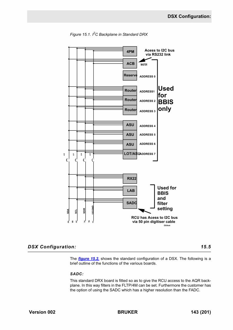
DSX Configuration:
Figure 15.1. I2C Backplane in Standard DRX
DSX Configuration: 15.5
The figure 15.2. shows the standard configuration of a DSX. The following is abrief outline of the functions of the various boards.
SADC:This standard DRX board is fitted so as to give the RCU access to the AQR back-plane. In this way filters in the FLTP/4M can be set. Furthermore the customer hasthe option of using the SADC which has a higher resolution than the FADC.
4PM
ACB
Reserve
Router
Router
Router
ASU
ASU
ASU
RX22
LAB
SADC
6A 6B 6C 7A 7B 7C
SDA
SCL
SDIR
12CG
ND
JU2
JU1
JU4
JU3
i2cbus
ADDRESS 0
ADDRESS1
ADDRESS 2
ADDRESS 3
ADDRESS 4
ADDRESS 5
ADDRESS 6
ADDRESS 7
MASTER
Acess to I2C bus via RS232 link
UsedforBBISonly
RCU has Acess to I2C bus via 50 pin digitiser cable
Used forBBIS andfiltersetting
LOT/ASU
Version 002 BRUKER 143 (201)
12C Bus in the AQR
FLTP/4M:This is the filter board so named because of the max. Bandwidth of 4MHz. The fil-ters are set by the RCU via the I2C bus. This board also provides the power sup-ply for the FADC
RXC:This is effectively an RX22 minus the RF section. The DSX is fitted with an FADCinstead of the HRD16. The RXC board in a DSX fulfills the functions of the HRD16Controller II Board in a DMX. This board receives the RGP(EP) from the RCU viathe SADC and AQR backplane. This gating pulse is then used to produce threeoutputs RGPa, RGPb and RGPc. These three outputs (labelled EPA_SE451,EPB_SE451 and EP_HPPR on the board itself) are identical.
A second function is to set the RG bits for the SE451. The information is transmit-ted via the RS485 link from the CCU
A future function of the RXC will be BBIS identification of the new SE451. This willbe done via a direct I2C link from the RXC front panel to the SE451.
144 (201) BRUKER Version 002
DSX Configuration:
Figure 15.2. I2C Backplane in Standard DSX (with new 19“ SE451)
4PM
ACB
Reserve
Router
Router
Router
ASU
ASU
ASU
RXC
FLTP/4M
SADC
6A 6B 6C 7A 7B 7C
SDA
SCL
SDIR
12CG
ND
JU2
JU1
JU4
JU3
i2cbus1
ADDRESS 0
ADDRESS1
ADDRESS 2
ADDRESS 3
ADDRESS 4
ADDRESS 5
ADDRESS 6
ADDRESS 7
MASTER
Acess to I2C bus via RS232 link
UsedforBBISonly
RCU has Acess to I2C bus via 50 pin digitiser cable
Used forBBISandfiltersetting
ASU
Version 002 BRUKER 145 (201)

12C Bus in the AQR
146 (201) BRUKER Version 002
ACB 16
The ACB acts in may ways as an interface between various spectrometer unitsand shall be discussed in terms of the various communication links with theseunits (see figure 16.1.).
SBS Bus 16.1
The ACB can control up to a maximum of 16 linear amplifiers via the SBS (SerialBruker Spectrospin) Bus. This is an RS485 type bus of which the ACB is the oneand only master. The ACB uses the bus to determine the type and number of in-stalled amplifiers. Each amplifier housing is given a unique address via a Hex.switch on the amplifier front panel. From the Hex. address the router outputs towhich the amplifier is connected is made known to the software. This informationis then used to customize the „edsp“ display for each individual spectrometer.
Amplifier parameters such a Max. Duty Cycle, Max Pulse Width etc. may also beaccessed via the SBS Bus.
This bus also carries the „FORW“, „REFL“ and „BLKTR“ signals from the Amplifi-ers to the ACB. From here these signals are displayed either on the graphic mon-itor or on the BOSS keyboard.
Note: For correct operation the SBS Bus cable (P/N H5624) must be fitted withthe terminating plug (P/N H5167).
RS232 Connection 16.2
This connection is used:
1. During initial ACB start-up/reset and to transmit amplifier status and parame-ters to the CCU.
2. To transmit the data for the screen display of forward and reflected power etc.The data is transmitted to the CCU and then displayed on the graphics moni-tor. Only those amplifiers which are required for the power display are scannedby the ACB.
3. Read/Write BBIS data via a software tool. This tool is still in development but itwill soon be possible to access all BBIS data of the 8 AQR boards connectedto the ACB via the I2C bus.
Version 002 BRUKER 147 (201)
ACB
Figure 16.1. ACB Interfaces
I2C Bus 16.3
The ACB is master of the I2C Bus which interconnects 8 slots in the AQR. The ad-dressing of various boards is determined solely by the position of the slot in theAQR. The position of the ACB in the AQR is fixed to the second slot from the end.The position of other boards is more flexible i.e. a Router can occupy any Routerslot, an ASU any ASU slot etc. The I2C Bus is used to transfer BBIS data.
DISPLAY DATA OUT
BBIS DATA I C BUS2
+5V Vcc
+5V PWR
+5V X
+5V VPI
RS232-X32
RESET
SBS-MASTER
RS 232CCU
SBS Bus
acb
40 bit data streamBSMSCPU
ADDR =7 ADDR = 6 ADDR = 5 ADDR = 4 ADDR = 3 ADDR =2 ADDR =1 ADDR = 0
ASU1 RESERVEROUT1ASU2 ASU3 ASU4
AMPL.
AMPL.
AMPL.
AMPL.
AQR Backplane
ACBROUT2 ROUT3
1
8
9
15
1
8
9
15
148 (201) BRUKER Version 002
Link to BSMS
Link to BSMS 16.4
This is a 40 Bit unidirectional data stream used to operate the power display onthe Boss keyboard (one bit for each LED). The information is received from theamplifiers via the SBS Bus. The power display has a refresh rate of between 300and 600 Hz. depending on the number of amplifiers that are scanned.
This connection also carries the ADC ON (from AQR Backpanel) and OBS (fromComputer) signals to the Boss Keyboard.
Then final function of this link is the „Chan Select“ and „TRANS P-DOWN“ func-tions.
The „TRANS P-DOWN“ button on the BOSS keyboard will cause the ACB to setthe SPENAB signal high when pressed. This will disable all ASU’s, Routers andAmplifiers.
The „Chan Select“ button on the Boss Keyboard simply causes the ACB to togglethrough the various channels with regard to the power display.
Note: If the cable to the BSMS CPU is not attached all signal transmission is auto-matically disabled.
Reset 16.5
This will:
a) reactivate the SPENAB signal.
b) re-enable any disabled amplifiers.
A hardware reset is carried out by pressing the reset button on the front panel.
A software reset is carried out during the „cf“ routine or by clicking on „ACB-Re-set“ in the „acbdisp“ menu.
Version 002 BRUKER 149 (201)

ACB
150 (201) BRUKER Version 002
LAB: Level Adapter Board 17
This board is used to invert signals from active low (AVANCE standard) to activehigh. This is required for units such as the SE451 and HPPR which were devel-oped prior to the introduction of the AVANCE series.
Note: Newly developed SE451 units and HPPR cover modules will make the LABredundant. In the case of the SE451 the logic will be altered to active low. Thenewest HPPR cover modules have a piggyback board with which the HPPR canbe configured to accept active low gating pulses. Modifications to the BSMS willalso enable the LockHold and Homospoil outputs to be inverted by software.
The LAB has two connectors LAB1 and LAB2.
LOWER CONNECTOR LAB1 17.1
The functions of the main LAB board which takes it's inputs from Connector LAB1will depend on whether the instrument is a DMX or DRX. Jumper settings can beused to determine
a) whether a signal is inverted or not
b) whether a signal is connected to the AQR backplane or not.
STANDARD DMXThe board is used to invert signals used in the SE451. Listed below are the rele-vant signals and required jumper settings.
To invert TGPCH1 (SPFX to SE451) J6 in
To invert TGPCH2 (SPFH to SE451) J5 in
To invert OBSCH1 (SELOBS X/H) J2 in
STANDARD DRXFor a DRX fitted with a RX22 receiver the Connector LAB1 is not used. This is be-cause the RX22 logic is active low. Note however that one jumper position is rele-vant. Jumper J9 should not be inserted. This is to ensure that the RGP pulsewhich is transmitted along the AQR backplane is not connected to the LAB.
DRX with HRD16:The RGPa pulse is normally transmitted from the RCU to the SADC via the 50way digitizer cable. From here it is connected to the RX22 via the AQR backplane.When the SADC is not fitted then the HRD16 must provide the RX22 with RGPa.A cable connects RGPa out (SMB connector of the HRD16) to pin P of Connector
Version 002 BRUKER 151 (201)
LAB: Level Adapter Board
LAB 1 (see figure 13.2.). From here it is inverted and transmitted to the back-plane. The required jumper settings are listed below:
To invert RGPa (EPa) J7 in
To connect RGPa (EPa) to backplane J9 in
BSMS Signals:Two further signals may be inverted if required using Connector LAB 1:
UPPER CONNECTOR LAB2 17.2
The piggyback board handles signals received from Connector LAB2 and is nor-mally used to invert signals for the HPPR. Three inputs (TGPPA1, TGPPA2, andTGPPA3) are taken from the TCU and the inverted outputs are connected to thePREAMP PERIPH Connector.
The piggyback board is designed to invert any connected inputs. There are nojumper settings to determine whether a signal is inverted or not. The board isused identically in DMX, DRX, and DSX spectrometers.
DPX Spectrometers 17.3
For these spectrometers the LAB is not required because
a) The RX22 logic is active low. This makes Connector LAB1 redundant.
b) They are fitted with the newer HPPR cover modules as standard. Thismakes Connector LAB2 redundant.
Note that for some of the earliest DPX spectrometers it may be necessary to mod-ify the BSMS for Lockhold inversion.
Table 17.1. BSMS Signals
Signal Input Output Comments
Homospoil L M J4 in to invert
Lock Hold R U J3 in to invert
152 (201) BRUKER Version 002
Software 18
EDSCON: Edit spectrometer constants: 18.1
It is now possible to edit the delays before rf pulses using the table called up withthe UXNMR command „edscon“. Note that the edscon table does not allow one tomake all adjustments that are supported by the hardware. Instead a simplifiedversion has been developed in the interest of user friendliness. The engineershould however be aware that the pre and post blanking delay may be set individ-ually for every individually produced TCU output. In the edscon table the user canset the pre blanking delays only. To set the post blanking delays, with the softwareas it is presently configured, would require explicit pulse programming. A furthersimplifying feature is that the same timing is used for Router, amplifiers andASU’s. However with explicit pulse programming these could also be set individu-ally. If deemed necessary the edscon table could be expanded to support all hard-ware timing features.
The constants set in the „edscon“ table are stored in the file /u/conf/instr/<name>/scon
The constants are set for the spectrometer and will automatically be implementedfor each new acquisition. Individual values may not be stored in different datasets. Figure 19.1 shows the relationship between the „edscon“ parameters andthe corresponding blanking pulses for an rf pulse of length p1 on channel 1. Allvalues are in ms.
Default values for all preblanking is 3ms. The BLKTR,TGPCH,TGPPA and BPCHpulses have already been explained in various chapters. Note that while the tabledisplays BLKTR0-15 only BLKTR1-15 are relevant as regards amplifier and routerblanking. Furthermore as regard the ASU only BLKTR1-8 are actually used. ThePHASPR parameter is the phase preset time which can be set individually foreach FCU.
The software is so programmed that 4.5ms after the „go = 2“ statement in thepulse program the first point will be digitised. This value can be changed but onlyin the source program. However at what particular point within this 4.5ms the Re-ceiver is opened may be set by the user with the parameter De1. This has the de-fault value of 2ms. A second parameter De2 which determines how soon after theRCU_Go pulse the transmitter phase is reset may be adjusted with the parameterDe1 (default value 1ms).
Version 002 BRUKER 153 (201)
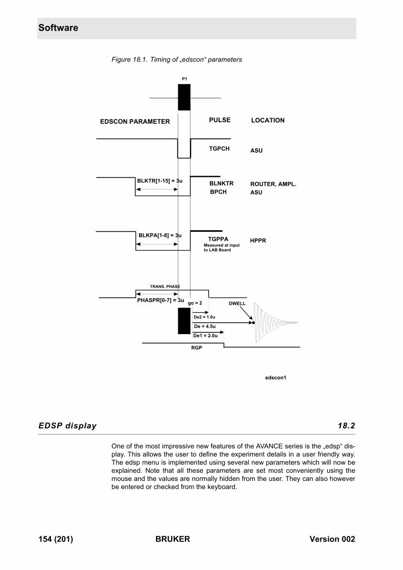
Software
Figure 18.1. Timing of „edscon“ parameters
EDSP display 18.2
One of the most impressive new features of the AVANCE series is the „edsp“ dis-play. This allows the user to define the experiment details in a user friendly way.The edsp menu is implemented using several new parameters which will now beexplained. Note that all these parameters are set most conveniently using themouse and the values are normally hidden from the user. They can also howeverbe entered or checked from the keyboard.
P1
TGPCH
TGPPA
BPCH
EDSCON PARAMETER PULSE LOCATION
ASU
HPPR
ASUBLNKTRBLKTR[1-15] = 3u ROUTER, AMPL.
BLKPA[1-8] = 3uMeasured at input to LAB Board
edscon1
De = 4.5u
De2 = 1.0u
De1 = 2.0u
TRANS. PHASE
RGP
DWELL
PHASPR[0-7] = 3u go = 2
154 (201) BRUKER Version 002
EDSP display
FCUCHAN:This parameter determines which physical FCU is assigned to which softwarechannel. This parameter can be set by hand using the following notation:
0 FCUCHAN 3= 4*
Which means that FCU number 4 will be used for the logical channel F3.
0 FCUCHAN 4= 5
Which means that FCU number 5 will be used for the logical channel F4 etc.
* Note that the keyboard syntax is „0 space FCUCHAN space 3 enter “ etc. Thissyntax applies to all edsp parameters.
The default FCUCHAN values can easily be restored by clicking on „DEFAULT“with the mouse.
RSEL:How a particular signal is routed is determined by the setting of the RSEL controlwords. Since each FCU is effectively hardwired (via the PTS) to a specific Routerinput and each Router output is hardwired to a specific amplifier, the edsp displaysimply displays the FCU connections to the amplifier.
The routing of FCU1 is determined by the value of RSEL1, the routing of FCU2 isdetermined by RSEL2 etc. The destination amplifier determines the value as-signed to RSEL1, RSEL2 etc.
For example:
0 RSEL1 = 3 means that FCU1 is routed to amplifier 3
0 RSEL2 = 5 means that FCU2 is routed to amplifier 5
Each amplifier is numbered from 1 to 16 as in figure 18.2..
Where a router input is not used then the corresponding RSEL word is assigned avalue of 0.
SWIBOX:The output of the various individual amplifiers may be switched to different N-typeoutputs labelled 1H, 19F and X QNP on the amplifier housing front panel (seechapter 11).
The parameter SWIBOX is used to control the internal switching within the ampli-fier housing. The amplifier outputs can be switched to different N-type outputs de-pending upon the value assigned to the SWIBOX parameter.
For example: 0 SWIBOX 1 = 3 means switch amplifier output 1 to N-type output 3
The numbering of the various inputs and outputs of the DMX and DRX standardamplifiers can be seen in figure 18.2. and figure 18.3.
Where an amplifier output is not used then the corresponding SWIBOX word isassigned a value of 0.
Note that in order for the edsp display to work properly the output of the firstBLAX300 in a DMX should be hardwired to the Xin of the BLARH100.
PRECHAN:This parameter is used to determine the connections from the amplifier output tothe HPPR module. Note however that this parameter has no physical influence It
Version 002 BRUKER 155 (201)
Software
is up to the operator to ensure that the cabling is correct. The parameter is re-quired so that the contents of the edsp display may be stored and called up at alater date. The PRECHAN parameter is however used to determine the OBSmodule. The module chosen as the destination of the F1 (NUC1) channel will beselected as the OBS module.
Up to 5 HPPR modules may be displayed in edsp and they are numbered 0 to 4as in figure 18.2.
For example: 0 prechan 1 = 3 means that amplifier output 1 is connected to HPPRmodule 3.
Note that when an amplifier output is not used then the corresponding PRECHANparameter defaults to a value of 5.
156 (201) BRUKER Version 002
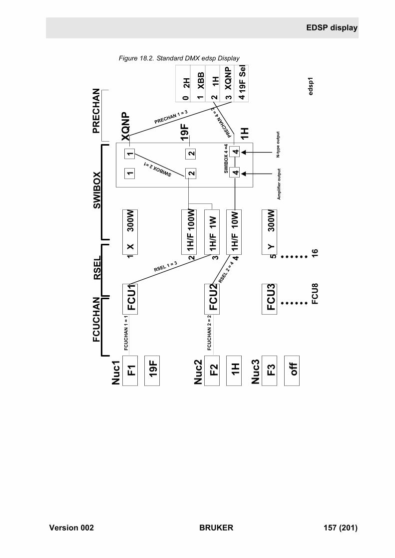
EDSP display
Figure 18.2. Standard DMX edsp Display
F1 19F
F2 1H F3 off
Nuc
1FC
U1
FCU
2
FCU
3
X 1H/F
1H/F
Y
300W
100W
1W 300W
XQN
P
19F
1H1H
/F10
W
FCU
CH
AN
SWIB
OX
PREC
HA
NR
SEL
2H XBB
1H
5
0 1 2
RSEL 1 = 3
41
421
SWIBOX 2 =1
2
PRECHAN 1 = 3
41 2 3
FCU
CH
AN
1 =
1
3 419
F Se
lXQ
NP
Nuc
2
Nuc
3
FCU
CH
AN 2
= 2
RSEL
2 =
4PR
ECHA
N 4 =
2
edsp
116
FCU
8
SWIB
OX
4 =4
Am
plifi
er o
utpu
tN
-type
out
put
Version 002 BRUKER 157 (201)
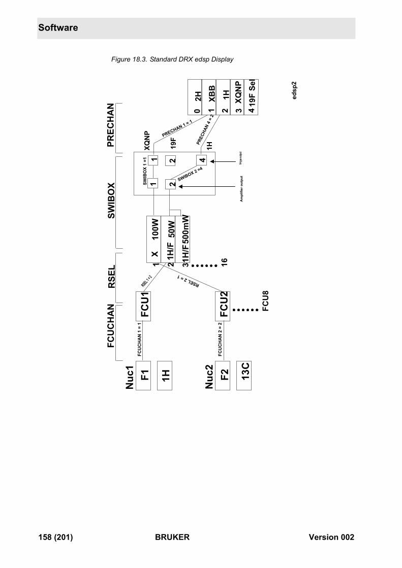
Software
Figure 18.3. Standard DRX edsp Display
F1 1H F2 13C
Nuc
1FC
U1
FCU
2
X 1H/F
100W
50W
XQN
P
19F
1H
1H/F
500m
W
FCU
CH
AN
SWIB
OX
PREC
HA
NR
SEL
2H XBB
1H
0 1 2
RSEL 1 = 2
1
41SW
IBO
X 1
=1
2
PRECHAN 1 = 1
1 2 3
FCU
CH
AN
1 =
1
3 419
F Se
lXQ
NP
Nuc
2FC
UC
HA
N 2
= 2
RSEL 2 = 1
PREC
HAN
4 =
2
edsp
2
16
FCU
8
SWIBOX 2 =42
Am
plifi
er o
utpu
tN-t
ype ou
tput
158 (201) BRUKER Version 002

Conversion Tables A
Version 002 BRUKER 159 (201)
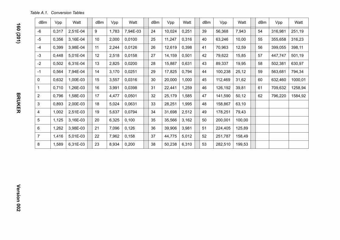
Table A.1. Conversion Tables
Watt dBm Vpp Watt
160dBm Vpp Watt dBm Vpp Watt dBm Vpp Watt dBm Vpp
7,943 54 316,981 251,19
10,00 55 355,658 316,23
12,59 56 399,055 398,11
15,85 57 447,747 501,19
19,95 58 502,381 630,97
25,12 59 563,681 794,34
31,62 60 632,460 1000,01
39,81 61 709,632 1258,94
50,12 62 796,220 1584,92
63,10
79,43
100,00
125,89
158,49
199,53
(201)B
RU
KER
Version 002
-6 0,317 2,51E-04 9 1,783 7,94E-03 24 10,024 0,251 39 56,368
-5 0,356 3,16E-04 10 2,000 0,0100 25 11,247 0,316 40 63,246
-4 0,399 3,98E-04 11 2,244 0,0126 26 12,619 0,398 41 70,963
-3 0,448 5,01E-04 12 2,518 0,0158 27 14,159 0,501 42 79,622
-2 0,502 6,31E-04 13 2,825 0,0200 28 15,887 0,631 43 89,337
-1 0,564 7,94E-04 14 3,170 0,0251 29 17,825 0,794 44 100,238
0 0,632 1,00E-03 15 3,557 0,0316 30 20,000 1,000 45 112,469
1 0,710 1,26E-03 16 3,991 0,0398 31 22,441 1,259 46 126,192
2 0,796 1,58E-03 17 4,477 0,0501 32 25,179 1,585 47 141,590
3 0,893 2,00E-03 18 5,024 0,0631 33 28,251 1,995 48 158,867
4 1,002 2,51E-03 19 5,637 0,0794 34 31,698 2,512 49 178,251
5 1,125 3,16E-03 20 6,325 0,100 35 35,566 3,162 50 200,001
6 1,262 3,98E-03 21 7,096 0,126 36 39,906 3,981 51 224,405
7 1,416 5,01E-03 22 7,962 0,158 37 44,775 5,012 52 251,787
8 1,589 6,31E-03 23 8,934 0,200 38 50,238 6,310 53 282,510
Linear Amplifier Specifications B
Version 002 BRUKER 161 (201)
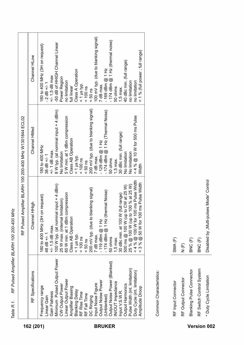
Tabl
e R
.1.
RF
Puls
ed A
mpl
ifier
BLA
RH
100
200
-400
MH
z
RF
Puls
ed A
mpl
ifier
BLA
RH
100
200
-400
MH
z W
1301
844
ECL0
2
RF
Spec
ifica
tions
Cha
nnel
HH
igh
Cha
nnel
HM
edC
hann
el H
Low
Freq
uenc
y ra
nge
Line
ar G
ain
Gai
n Fl
atne
ssM
inim
um P
ulse
d O
utpu
t Pow
erC
W O
utpu
t Pow
erLi
near
Out
put P
ower
Ampl
ifier
Bia
sing
Blan
king
Del
ayR
F R
ise
Tim
eR
F Fa
ll Ti
me
DC
Rin
ging
Inpu
t Noi
se F
igur
eO
utpu
t Noi
se P
ower
(U
nbla
nked
)O
utpu
t Noi
se P
ower
(Bla
nked
)IN
/OU
T Im
peda
nce
Inpu
t V.S
.W.R
.O
utpu
t Har
mon
ics
Puls
e W
idth
(int
. lim
itatio
n)D
uty
Cyc
le (i
nt. l
imita
tion)
Ampl
itude
Dro
op
180
to 4
00 M
Hz
(3H
on
requ
est)
48 d
B +/
- 1+/
- 1,5
dB
max
.10
0 W
typ.
(at n
omin
al in
put +
4 d
Bm)
25 W
max
. (in
tern
al li
mita
tion)
60 W
min
. at 1
dBm
com
pres
sion
Cla
ss A
B O
pera
tion
< 1
µs ty
p.<
100
ns<
50 n
s20
0 m
V ty
p. (d
ue to
bla
nkin
g si
gnal
)7
dB m
ax.
- 119
dBm
@ 1
Hz
- 174
dBm
@ 1
Hz
(ther
mal
Noi
se)
50 o
hms
1,5
max
.30
dBc
min
. at 1
00 W
(ful
l ran
ge)
500
ms
@ 1
00 W
(up
to C
W a
t 25
W)
25 %
@ 1
00 W
(up
to 1
00 %
at 2
5 W
)<
4 %
@ 1
00 W
for 1
00 m
s Pu
lse
Wid
th<
3 %
@ 5
0 W
for 1
00 m
s Pu
lse
Wid
th
180
to 4
00 M
Hz
38 d
B +/
- 1+/
- 1 d
B m
ax.
8 W
typ.
(at n
omin
al in
put +
4 d
Bm)
No
limita
tion
5 W
min
. at 1
dBm
com
pres
sion
Cla
ss A
B O
pera
tion
< 1
µs ty
p.<
100
ns<
50 n
s20
0 m
V ty
p. (d
ue to
bla
nkin
g si
gnal
)7
dB m
ax.
- 129
dBm
@ 1
Hz
- 174
dBm
@ 1
Hz
(The
rmal
Noi
se)
50 o
hms
1,5
max
.30
dBc
min
. (fu
ll ra
nge)
N
o lim
itatio
nN
o lim
itatio
n<
4 %
@ 1
0 W
for 5
00 m
s Pu
lse
Wid
th
180
to 4
00 M
Hz
(3H
on
requ
est)
- 2 d
B +/
- 1+/
- 1,5
dB
max
-50
dB o
f HH
IGH
Cha
nnel
Lin
ear
Pow
er R
egio
nno
lim
itatio
nfu
ll lin
ear
Cla
ss A
Ope
ratio
n<
1 µs
typ.
< 10
0 ns
< 50
ns
100
mV
typ.
(due
to b
lank
ing
sign
al)
7 dB
max
.- 1
69 d
Bm @
1 H
z - 1
74 d
Bm @
1 H
z (th
erm
al n
oise
)50
ohm
s1,
5 m
ax.
40 d
Bc m
in. (
full
rang
e)no
lim
itatio
nno
lim
itatio
n<
1 %
(ful
l pow
er ;
full
rang
e)
Com
mon
Cha
ract
eris
tics:
RF
Inpu
t Con
nect
orSM
A (F
)
RF
Out
put C
onne
ctor
N (F
)
Blan
king
Pul
se C
onne
ctor
BNC
(F)
RF
Switc
h C
ontro
l Sys
tem
BNC
(F)
* Dut
y C
ycle
Lim
itatio
nD
isab
led
by „M
ulti-
puls
es M
ode“
Con
trol
162 (201) BRUKER Version 002
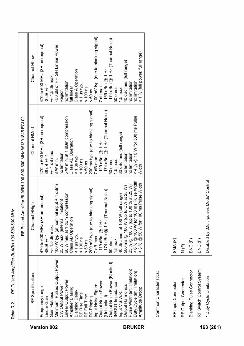
Tabl
e R
.2.
RF
Puls
ed A
mpl
ifier
BLA
RH
100
500
-600
MH
z
RF
Puls
ed A
mpl
ifier
BLA
RH
100
500
-600
MH
z W
1301
845
ECL0
2
RF
Spec
ifica
tions
Cha
nnel
HH
igh
Cha
nnel
HM
edC
hann
el H
Low
Freq
uenc
y ra
nge
Line
ar G
ain
Gai
n Fl
atne
ssM
inim
um P
ulse
d O
utpu
t Pow
erC
W O
utpu
t Pow
erLi
near
Out
put P
ower
Ampl
ifier
Bia
sing
Blan
king
Del
ayR
F R
ise
Tim
eR
F Fa
ll Ti
me
DC
Rin
ging
Inpu
t Noi
se F
igur
eO
utpu
t Noi
se P
ower
(U
nbla
nked
)O
utpu
t Noi
se P
ower
(Bla
nked
)IN
/OU
T Im
peda
nce
Inpu
t V.S
.W.R
.O
utpu
t Har
mon
ics
Puls
e W
idth
(int
. lim
itatio
n)D
uty
Cyc
le (i
nt. l
imita
tion)
Ampl
itude
Dro
op
470
to 6
00 M
Hz
(3H
on
requ
est)
48dB
+/-
1+/
- 1,5
dB
max
.10
0 W
typ.
(at n
omin
al in
put +
4 d
Bm)
25 W
max
. (in
tern
al li
mita
tion)
60 W
min
. at 1
dBm
com
pres
sion
Cla
ss A
B O
pera
tion
< 1
µs ty
p.<
100
ns<
50 n
s20
0 m
V ty
p. (d
ue to
bla
nkin
g si
gnal
)7
dB m
ax.
- 119
dBm
@ 1
Hz
- 174
dBm
@ 1
Hz
(The
rmal
Noi
se)
50 o
hms
1,5
max
.40
dBc
min
. at 1
00 W
(ful
l ran
ge)
500
ms
@ 1
00 W
(up
to C
W a
t 25
W)
25 %
@ 1
00 W
(up
to 1
00 %
at 2
5 W
)<
6 %
@ 1
00 W
for 1
00 m
s Pu
lse
Wid
th<
3 %
@ 5
0 W
for 1
00 m
s Pu
lse
Wid
th
470
to 6
00 M
Hz
(3H
on
requ
est)
38 d
B +/
- 1+/
- 1 d
B m
ax8
W m
in.
no li
mita
tion
5 W
min
. at 1
dBm
com
pres
sion
Cla
ss A
B O
pera
tion
< 1
µs ty
p.<
100
ns<
50 n
s20
0 m
v ty
p. (d
ue to
bla
nkin
g si
gnal
)7
dB m
ax.
- 129
dBm
@ 1
Hz
- 174
dBm
@ 1
Hz
(The
rmal
Noi
se)
50 o
hms
1,5
max
.30
dBc
min
. (fu
ll ra
nge)
no li
mita
tion
no li
mita
tion
< 4
% @
10
W fo
r 500
ms
Puls
e W
idth
470
to 6
00 M
Hz
(3H
on
requ
est)
-2 d
B +/
- 1+/
- 1,5
dB
max
.- 5
0 dB
of H
HIG
H L
inea
r Pow
er
Reg
ion
no li
mita
tion
full
linea
rC
lass
A O
pera
tion
< 1
µs ty
p.<
100
ns<
50 n
s10
0 m
V ty
p. (d
ue to
bla
nkin
g si
gnal
)7
db m
ax.
- 169
dBm
@ 1
Hz
- 174
dBm
@ 1
Hz
(The
rmal
Noi
se)
50 o
hms
1,5
max
.40
dBc
min
. (fu
ll ra
nge)
no li
mita
tion
no li
mita
tion
< 1
% (f
ull p
ower
, ful
l ran
ge)
Com
mon
Cha
ract
eris
tics:
RF
Inpu
t Con
nect
orSM
A (F
)
RF
Out
put C
onne
ctor
N (F
)
Blan
king
Pul
se C
onne
ctor
BNC
(F)
RF
Switc
h C
ontro
l Sys
tem
BNC
(F)
* Dut
y C
ycle
Lim
itatio
nD
isab
led
by „M
ulti-
puls
es M
ode“
Con
trol
Version 002 BRUKER 163 (201)
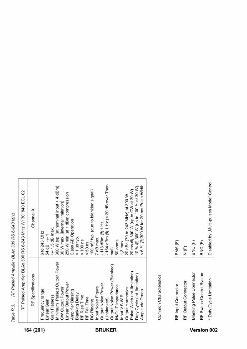
Tabl
e R
.3.
RF
Puls
ed A
mpl
ifier
BLA
x 30
0 R
S 6-
243
MH
z
RF
Puls
ed A
mpl
ifier
BLA
x 30
0 R
S 6-
243
MH
z W
1301
840
ECL
02
RF
Spec
ifica
tions
Cha
nnel
X
Freq
uenc
y ra
nge
Line
ar G
ain
Gai
n Fl
atne
ssM
inim
um P
ulse
d O
utpu
t Pow
erC
W O
utpu
t Pow
erLi
near
Out
put P
ower
Ampl
ifier
Bia
sing
Blan
king
Del
ayR
F R
ise
Tim
eR
F Fa
ll Ti
me
DC
Rin
ging
Inpu
t Noi
se F
igur
eO
utpu
t Noi
se P
ower
(U
nbla
nked
)O
utpu
t Noi
se P
ower
(Bla
nked
)IN
/OU
T Im
peda
nce
Inpu
t V.S
.W.R
.O
utpu
t Har
mon
ics
Puls
e W
idth
(int
. lim
itatio
n)D
uty
Cyc
le (i
nt. l
imita
tion)
Ampl
itude
Dro
op
6 to
243
MH
z54
dB
+/-
1+/
- 1,5
dB
max
.30
0 W
typ.
(at n
omin
al in
put +
4 d
Bm)
30 W
max
. (in
tern
al li
mita
tion)
250
W m
in. a
t 1 d
Bm c
ompr
essi
onC
lass
AB
Ope
ratio
n<
1 µs
typ.
< 10
0 ns
< 50
ns
100
mV
typ.
(due
to b
lank
ing
sign
al)
7 dB
max
.- 1
13 d
Bm @
1 H
z- 1
54 d
Bm @
1 H
z (<
20
dB o
ver T
her-
mal
)50
ohm
s1,
3 m
ax.
20 d
Bc (7
0 to
243
MH
z) a
t 300
W
20 m
s @
300
W (u
p to
CW
at 3
0 W
)10
% @
300
W (u
p to
100
% a
t 30
W)
< 6
% @
300
W fo
r 20
ms
Puls
e W
idth
Com
mon
Cha
ract
eris
tics:
RF
Inpu
t Con
nect
orSM
A (F
)
RF
Out
put C
onne
ctor
N (F
)
Blan
king
Pul
se C
onne
ctor
BNC
(F)
RF
Switc
h C
ontro
l Sys
tem
BNC
(F)
* Dut
y C
ycle
Lim
itatio
nD
isab
led
by „M
ulti-
puls
es M
ode“
Con
trol
164 (201) BRUKER Version 002
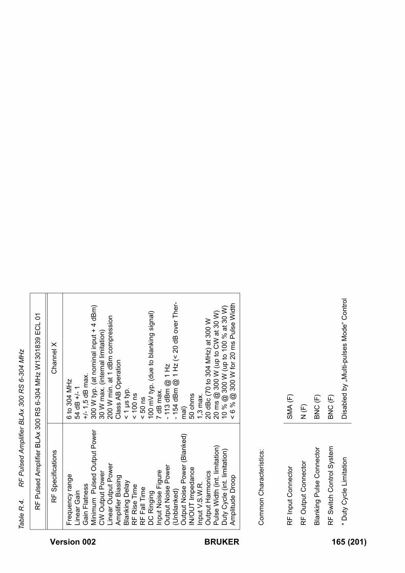
Tabl
e R
.4.
RF
Puls
ed A
mpl
ifier
BLA
x 30
0 R
S 6-
304
MH
z
RF
Puls
ed A
mpl
ifier
BLA
x 30
0 R
S 6-
304
MH
z W
1301
839
ECL
01
RF
Spec
ifica
tions
Cha
nnel
X
Freq
uenc
y ra
nge
Line
ar G
ain
Gai
n Fl
atne
ssM
inim
um P
ulse
d O
utpu
t Pow
erC
W O
utpu
t Pow
erLi
near
Out
put P
ower
Ampl
ifier
Bia
sing
Blan
king
Del
ayR
F R
ise
Tim
eR
F Fa
ll Ti
me
DC
Rin
ging
Inpu
t Noi
se F
igur
eO
utpu
t Noi
se P
ower
(U
nbla
nked
)O
utpu
t Noi
se P
ower
(Bla
nked
)IN
/OU
T Im
peda
nce
Inpu
t V.S
.W.R
.O
utpu
t Har
mon
ics
Puls
e W
idth
(int
. lim
itatio
n)D
uty
Cyc
le (i
nt. l
imita
tion)
Ampl
itude
Dro
op
6 to
304
MH
z54
dB
+/- 1
+/- 1
,5 d
B m
ax.
300
W ty
p. (a
t nom
inal
inpu
t + 4
dBm
)30
W m
ax. (
inte
rnal
lim
itatio
n)20
0 W
min
. at 1
dBm
com
pres
sion
Cla
ss A
B O
pera
tion
< 1
µs ty
p.<
100
ns<
50 n
s10
0 m
V ty
p. (d
ue to
bla
nkin
g si
gnal
)7
dB m
ax.
- 113
dBm
@ 1
Hz
- 154
dBm
@ 1
Hz
(< 2
0 dB
ove
r The
r-m
al)
50 o
hms
1,3
max
.20
dBc
(70
to 3
04 M
Hz)
at 3
00 W
20
ms
@ 3
00 W
(up
to C
W a
t 30
W)
10 %
@ 3
00 W
(up
to 1
00 %
at 3
0 W
)<
6 %
@ 3
00 W
for 2
0 m
s Pu
lse
Wid
th
Com
mon
Cha
ract
eris
tics:
RF
Inpu
t Con
nect
orSM
A (F
)
RF
Out
put C
onne
ctor
N (F
)
Blan
king
Pul
se C
onne
ctor
BNC
(F)
RF
Switc
h C
ontro
l Sys
tem
BNC
(F)
* Dut
y C
ycle
Lim
itatio
nD
isab
led
by „M
ulti-
puls
es M
ode“
Con
trol
Version 002 BRUKER 165 (201)
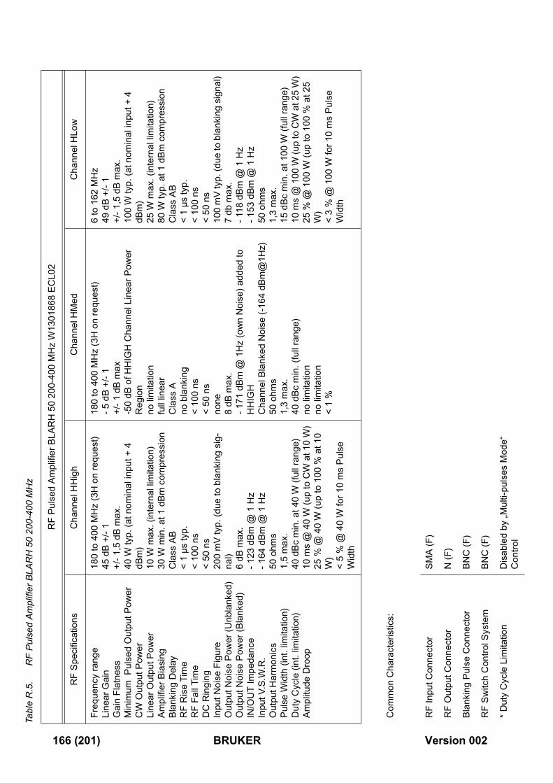
Tabl
e R
.5.
RF
Puls
ed A
mpl
ifier
BLA
RH
50
200-
400
MH
z
RF
Puls
ed A
mpl
ifier
BLA
RH
50
200-
400
MH
z W
1301
868
ECL0
2
RF
Spec
ifica
tions
Cha
nnel
HH
igh
Cha
nnel
HM
edC
hann
el H
Low
Freq
uenc
y ra
nge
Line
ar G
ain
Gai
n Fl
atne
ssM
inim
um P
ulse
d O
utpu
t Pow
erC
W O
utpu
t Pow
erLi
near
Out
put P
ower
Ampl
ifier
Bia
sing
Blan
king
Del
ayR
F R
ise
Tim
eR
F Fa
ll Ti
me
DC
Rin
ging
Inpu
t Noi
se F
igur
eO
utpu
t Noi
se P
ower
(Unb
lank
ed)
Out
put N
oise
Pow
er (B
lank
ed)
IN/O
UT
Impe
danc
eIn
put V
.S.W
.R.
Out
put H
arm
onic
sPu
lse
Wid
th (i
nt. l
imita
tion)
Dut
y C
ycle
(int
. lim
itatio
n)Am
plitu
de D
roop
180
to 4
00 M
Hz
(3H
on
requ
est)
45 d
B +/
- 1+/
- 1,5
dB
max
.40
W ty
p. (a
t nom
inal
inpu
t + 4
dB
m)
10 W
max
. (in
tern
al li
mita
tion)
30 W
min
. at 1
dBm
com
pres
sion
Cla
ss A
B <
1 µs
typ.
< 10
0 ns
< 50
ns
200
mV
typ.
(due
to b
lank
ing
sig-
nal)
6 dB
max
.- 1
23 d
Bm @
1 H
z- 1
64 d
Bm @
1 H
z50
ohm
s1,
5 m
ax.
40 d
Bc m
in. a
t 40
W (f
ull r
ange
)10
ms
@ 4
0 W
(up
to C
W a
t 10
W)
25 %
@ 4
0 W
(up
to 1
00 %
at 1
0 W
)<
5 %
@ 4
0 W
for 1
0 m
s Pu
lse
Wid
th
180
to 4
00 M
Hz
(3H
on
requ
est)
- 5 d
B +/
- 1+/
- 1 d
B m
ax-5
0 dB
of H
HIG
H C
hann
el L
inea
r Pow
er
Reg
ion
no li
mita
tion
full
linea
rC
lass
Ano
bla
nkin
g<
100
ns<
50 n
sno
ne8
dB m
ax.
- 171
dBm
@ 1
Hz
(ow
n N
oise
) add
ed to
H
HIG
HC
hann
el B
lank
ed N
oise
(-16
4 dB
m@
1Hz)
50 o
hms
1,3
max
.40
dBc
min
. (fu
ll ra
nge)
no li
mita
tion
no li
mita
tion
< 1
%
6 to
162
MH
z49
dB
+/- 1
+/- 1
,5 d
B m
ax.
100
W ty
p. (a
t nom
inal
inpu
t + 4
dB
m)
25 W
max
. (in
tern
al li
mita
tion)
80 W
typ.
at 1
dBm
com
pres
sion
Cla
ss A
B <
1 µs
typ.
< 10
0 ns
< 50
ns
100
mV
typ.
(due
to b
lank
ing
sign
al)
7 db
max
.- 1
18 d
Bm @
1 H
z- 1
53 d
Bm @
1 H
z50
ohm
s1,
3 m
ax.
15 d
Bc m
in. a
t 100
W (f
ull r
ange
)10
ms
@ 1
00 W
(up
to C
W a
t 25
W)
25 %
@ 1
00 W
(up
to 1
00 %
at 2
5 W
)<
3 %
@ 1
00 W
for 1
0 m
s Pu
lse
Wid
th
Com
mon
Cha
ract
eris
tics:
RF
Inpu
t Con
nect
orSM
A (F
)
RF
Out
put C
onne
ctor
N (F
)
Blan
king
Pul
se C
onne
ctor
BNC
(F)
RF
Switc
h C
ontro
l Sys
tem
BNC
(F)
* Dut
y C
ycle
Lim
itatio
nD
isab
led
by „M
ulti-
puls
es M
ode“
C
ontro
l
166 (201) BRUKER Version 002
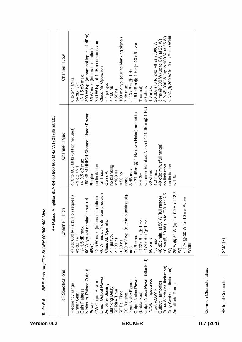
Tabl
e R
.6.
RF
Puls
ed A
mpl
ifier
BLA
RH
50
500-
600
MH
z
RF
Puls
ed A
mpl
ifier
BLA
RH
50
500-
600
MH
z W
1301
865
ECL0
2
RF
Spec
ifica
tions
Cha
nnel
HH
igh
Cha
nnel
HM
edC
hann
el H
Low
Freq
uenc
y ra
nge
Line
ar G
ain
Gai
n Fl
atne
ssM
inim
um P
ulse
d O
utpu
t Po
wer
CW
Out
put P
ower
Line
ar O
utpu
t Pow
erAm
plifi
er B
iasi
ngBl
anki
ng D
elay
RF
Ris
e Ti
me
RF
Fall
Tim
eD
C R
ingi
ngIn
put N
oise
Fig
ure
Out
put N
oise
Pow
er
(Unb
lank
ed)
Out
put N
oise
Pow
er (B
lank
ed)
IN/O
UT
Impe
danc
eIn
put V
.S.W
.R.
Out
put H
arm
onic
sPu
lse
Wid
th (i
nt. l
imita
tion)
Dut
y C
ycle
(int
. lim
itatio
n)Am
plitu
de D
roop
470
to 6
00 M
Hz
(3H
on
requ
est)
45 d
B +/
- 1+/
- 1,5
dB
max
.50
W ty
p. (a
t nom
inal
inpu
t + 4
dB
m)
12,5
W m
ax. (
inte
rnal
lim
itatio
n)40
W m
in. a
t 1 d
Bm c
ompr
essi
onC
lass
AB
Ope
ratio
n<
1 µs
typ.
< 10
0 ns
< 50
ns
200
mV
typ.
(due
to b
lank
ing
sig-
nal)
7 dB
max
.- 1
22 d
Bm @
1 H
z- 1
74 d
Bm @
1 H
z50
ohm
s1,
5 m
ax.
40 d
Bc m
in. a
t 50
W (f
ull r
ange
)10
ms
@ 5
0 W
(up
to C
W a
t 12,
5 W
)25
% @
50
W (u
p to
100
% a
t 12,
5 W
)<
5 %
@ 5
0 W
for 1
0 m
s Pu
lse
Wid
th
470
to 6
00 M
Hz
(3H
on
requ
est)
- 5 d
B +/
- 1+/
- 0,5
dB
max
-50
dB o
f HH
IGH
Cha
nnel
Lin
ear P
ower
R
egio
nno
lim
itatio
nfu
ll lin
ear
Cla
ss A
no b
lank
ing
< 10
0 ns
< 50
ns
none
8 dB
max
.- 1
71 d
Bm @
1 H
z (o
wn
Noi
se) a
dded
to
HH
IGH
Cha
nnel
Bla
nked
Noi
se (-
174
dBm
@ 1
Hz)
50 o
hms
1,3
max
.40
dBc
min
. (fu
ll ra
nge)
no li
mita
tion
no li
mita
tion
< 1
%
6 to
241
MH
z54
dB
+/- 1
+/- 1
,5 d
B m
ax.
300
W ty
p. (a
t nom
inal
inpu
t + 4
dBm
)25
W m
ax. (
inte
rnal
lim
itatio
n)25
0 W
typ.
at 1
dBm
com
pres
sion
Cla
ss A
B O
pera
tion
< 1
µs ty
p.<
100
ns<
50 n
s10
0 m
V ty
p. (d
ue to
bla
nkin
g si
gnal
)7
db m
ax.
- 113
dBm
@ 1
Hz
- 154
dBm
@ 1
Hz
(< 2
0 dB
ove
r Th
erm
al)
50 o
hms
1,3
max
.20
dBc
(70
to 2
42 M
Hz)
at 3
00 W
3 m
s @
300
W (u
p to
CW
at 2
5 W
)8
% @
300
W (u
p to
100
% a
t 25
W)
< 3
% @
300
W fo
r 3 m
s Pu
lse
Wid
th
Com
mon
Cha
ract
eris
tics:
RF
Inpu
t Con
nect
orSM
A (F
)
Version 002 BRUKER 167 (201)
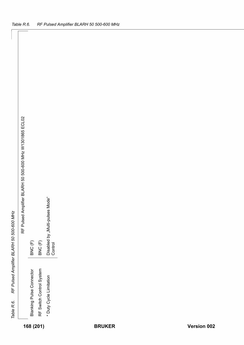
Table R.6. RF Pulsed Amplifier BLARH 50 500-600 MHz
Blan
king
Pul
se C
onne
ctor
BNC
(F)
RF
Switc
h C
ontro
l Sys
tem
BNC
(F)
* Dut
y C
ycle
Lim
itatio
nD
isab
led
by „M
ulti-
puls
es M
ode“
C
ontro
l
Tabl
e R
.6.
RF
Puls
ed A
mpl
ifier
BLA
RH
50
500-
600
MH
z
RF
Puls
ed A
mpl
ifier
BLA
RH
50
500-
600
MH
z W
1301
865
ECL0
2
168 (201) BRUKER Version 002
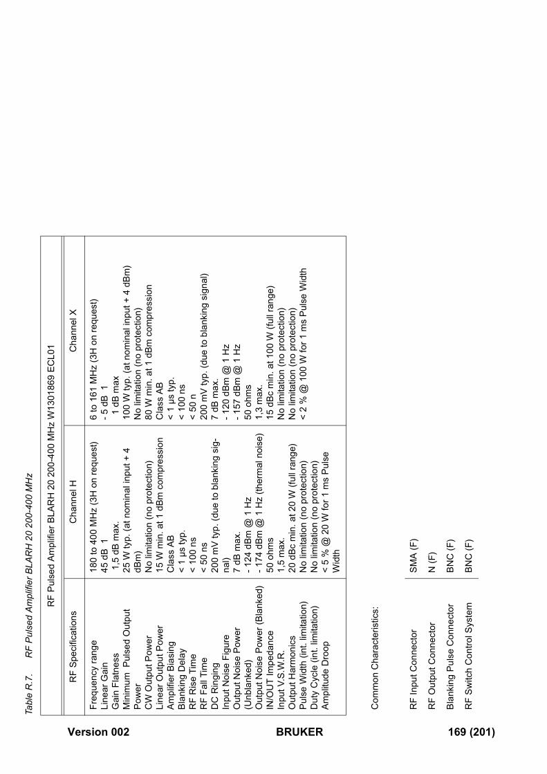
Tabl
e R
.7.
RF
Puls
ed A
mpl
ifier
BLA
RH
20
200-
400
MH
z
RF
Puls
ed A
mpl
ifier
BLA
RH
20
200-
400
MH
z W
1301
869
ECL0
1
RF
Spec
ifica
tions
Cha
nnel
HC
hann
el X
Freq
uenc
y ra
nge
Line
ar G
ain
Gai
n Fl
atne
ssM
inim
um P
ulse
d O
utpu
t Po
wer
CW
Out
put P
ower
Line
ar O
utpu
t Pow
erAm
plifi
er B
iasi
ngBl
anki
ng D
elay
RF
Ris
e Ti
me
RF
Fall
Tim
eD
C R
ingi
ngIn
put N
oise
Fig
ure
Out
put N
oise
Pow
er
(Unb
lank
ed)
Out
put N
oise
Pow
er (B
lank
ed)
IN/O
UT
Impe
danc
eIn
put V
.S.W
.R.
Out
put H
arm
onic
sPu
lse
Wid
th (i
nt. l
imita
tion)
Dut
y C
ycle
(int
. lim
itatio
n)Am
plitu
de D
roop
180
to 4
00 M
Hz
(3H
on
requ
est)
45 d
B 1
1,5
dB
max
.25
W ty
p. (a
t nom
inal
inpu
t + 4
dB
m)
No
limita
tion
(no
prot
ectio
n)15
W m
in. a
t 1 d
Bm c
ompr
essi
onC
lass
AB
< 1
µs ty
p.<
100
ns<
50 n
s20
0 m
V ty
p. (d
ue to
bla
nkin
g si
g-na
l)7
dB m
ax.
- 124
dBm
@ 1
Hz
- 174
dBm
@ 1
Hz
(ther
mal
noi
se)
50 o
hms
1,5
max
.20
dBc
min
. at 2
0 W
(ful
l ran
ge)
No
limita
tion
(no
prot
ectio
n)N
o lim
itatio
n (n
o pr
otec
tion)
< 5
% @
20
W fo
r 1 m
s Pu
lse
Wid
th
6 to
161
MH
z (3
H o
n re
ques
t)- 5
dB
1 1
dB
max
100
W ty
p. (a
t nom
inal
inpu
t + 4
dBm
)N
o lim
itatio
n (n
o pr
otec
tion)
80 W
min
. at 1
dBm
com
pres
sion
Cla
ss A
B<
1 µs
typ.
< 10
0 ns
< 50
n20
0 m
V ty
p. (d
ue to
bla
nkin
g si
gnal
)7
dB m
ax.
- 120
dBm
@ 1
Hz
- 157
dBm
@ 1
Hz
50 o
hms
1,3
max
.15
dBc
min
. at 1
00 W
(ful
l ran
ge)
No
limita
tion
(no
prot
ectio
n)N
o lim
itatio
n (n
o pr
otec
tion)
< 2
% @
100
W fo
r 1 m
s Pu
lse
Wid
th
Com
mon
Cha
ract
eris
tics:
RF
Inpu
t Con
nect
orSM
A (F
)
RF
Out
put C
onne
ctor
N (F
)
Blan
king
Pul
se C
onne
ctor
BNC
(F)
RF
Switc
h C
ontro
l Sys
tem
BNC
(F)
Version 002 BRUKER 169 (201)
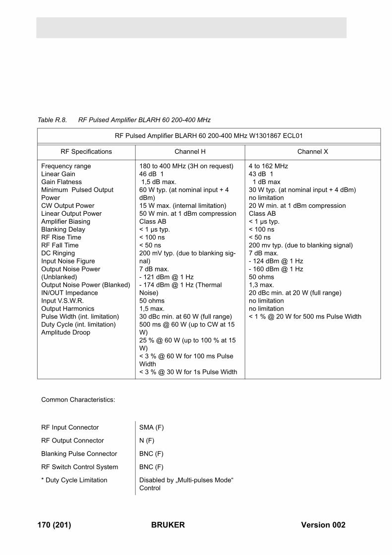
)
dth
Table R.8. RF Pulsed Amplifier BLARH 60 200-400 MHz
RF Pulsed Amplifier BLARH 60 200-400 MHz W1301867 ECL01
RF Specifications Channel H Channel X
Frequency rangeLinear GainGain FlatnessMinimum Pulsed Output PowerCW Output PowerLinear Output PowerAmplifier BiasingBlanking DelayRF Rise TimeRF Fall TimeDC RingingInput Noise FigureOutput Noise Power (Unblanked)Output Noise Power (Blanked)IN/OUT ImpedanceInput V.S.W.R.Output HarmonicsPulse Width (int. limitation)Duty Cycle (int. limitation)Amplitude Droop
180 to 400 MHz (3H on request)46 dB 1 1,5 dB max.60 W typ. (at nominal input + 4 dBm)15 W max. (internal limitation)50 W min. at 1 dBm compressionClass AB < 1 µs typ.< 100 ns< 50 ns200 mV typ. (due to blanking sig-nal)7 dB max.- 121 dBm @ 1 Hz- 174 dBm @ 1 Hz (Thermal Noise)50 ohms1,5 max.30 dBc min. at 60 W (full range)500 ms @ 60 W (up to CW at 15 W)25 % @ 60 W (up to 100 % at 15 W)< 3 % @ 60 W for 100 ms Pulse Width< 3 % @ 30 W for 1s Pulse Width
4 to 162 MHz 43 dB 1 1 dB max30 W typ. (at nominal input + 4 dBmno limitation20 W min. at 1 dBm compressionClass AB < 1 µs typ.< 100 ns< 50 ns200 mv typ. (due to blanking signal)7 dB max.- 124 dBm @ 1 Hz - 160 dBm @ 1 Hz 50 ohms1,3 max.20 dBc min. at 20 W (full range)no limitationno limitation< 1 % @ 20 W for 500 ms Pulse Wi
Common Characteristics:
RF Input Connector SMA (F)
RF Output Connector N (F)
Blanking Pulse Connector BNC (F)
RF Switch Control System BNC (F)
* Duty Cycle Limitation Disabled by „Multi-pulses Mode“ Control
170 (201) BRUKER Version 002

Version 002 BRUKER 171 (201)

172 (201) BRUKER Version 002

Wiring Diagrams C
Version 002 BRUKER 173 (201)
GotoFigure R.4. DPX DC Wiring Diagram Page 1
AG
ND
HPP
R
-19V
HPP
R
DG
ND
HPP
R
+9V
X
+9V
HPP
R
GN
D X
A
GN
D
+19V
RX
-1
9V R
X
24,1
223
,11
21,9
8 22,1
020 16
,4,1
8,6
17,5
15,3 (F
XB
)
B,H
L M U N V
CC HH BB
FF CC
19,7
+9V
RX
1FD
BL
+FD
BL
-B
1A
12
1 M
Hz
+1
MH
z -
B2
A2
32
MH
z +
2 M
Hz
-B
3A
34
4 M
Hz
+4
MH
z -
B4
A4
58
MH
z +
8 M
Hz
-B
5A
56
10 M
Hz
+10
MH
z -
B6
A6
720
MH
z +
20 M
Hz
-B
7A
78
40 M
Hz
+40
MH
z -
B8
A8
980
MH
z +
80 M
Hz
-B
9A
911
100
MH
z +
100
MH
z -
B10
A10
1220
0 M
Hz
+20
0 M
Hz
-B
11A
1113
400
MH
z +
400
MH
z -
B12
A12
1480
0 M
Hz
+80
0 M
Hz
-B
13A
13,1
5G
ND
HZ0
4043
NM
R2
<8>
NM
R2
<9>
(FX
A
174 (201)
Part-No. for Drawing only
POS
DD
FF
10
1 2
3 4 5 6 7 8 9 10 11 12 13 14 15 16 17B
18
R
19
U
20
K
21
E
D
22
R
C
23
24W
25
26IR
27
28INEC
29
GL
30
31D
32
33IA
34
G
35
36R
37
ASh
38
Mee
39
t
40
41 42 43 44 45 46V
47
e
48
r
49
si
50
o
DPX
: 05 of1 3FDU
Drawn MDPXDC1
01.07.93
odificationFDU
15.07.94
E
25.
SH
10.94
K
E
ST
SH
24.
F
02.95
DU
20.
22.
09.95
03.94
.
RCU
TCU T2
AQ
X
TCU T4
TCU T5
FCU1 F2
FCU2 F2
SADC
RX22
ASU/LOT +19V
HPP
AQ
R
ROUTER R2
ACB (Option) 5,13
PSB
PREAMP
PERIPHHPPR A,C
SYNTH1PTS 310/620
BACKPANELBURNDY 1 K
n 002
GotoFigure R.5. DPX DC Wiring Diagram Page 2
FDB
L -
21
MH
z +
1 M
Hz
-3
2 M
Hz
+2
MH
z -
44
MH
z +
4 M
Hz
-5
8 M
Hz
+8
MH
z -
610
MH
z +
10 M
Hz
-7
20 M
Hz
+20
MH
z -
840
MH
z +
40 M
Hz
-9
80 M
Hz
+80
MH
z -
1110
0 M
Hz
+10
0 M
Hz
-12
200
MH
z +
200
MH
z -
1340
0 M
Hz
+40
0 M
Hz
-14
800
MH
z +
800
MH
z -
10,1
5G
ND
6749
2
6 028
A1
B2
A2
B3
A3
B4
A4
B5
A5
B6
A6
B7
A7
B8
A8
B9
A9
B10
A10
B11
A11
B12
A12
B13
A13
HZ0
4043
Version
Part-No. for Drawing only
POS
H43
HZ4
51 52
53
0
54
02
55
56 57 58 59 60 61 62 63 64 65 66 67 68 69 70 71D
72
C
73
74W
75
76B
IR
77
R
78
U
INEC
79
K
GL
80
E
81
R
D
82
83IA
84
G
85
86R
87
ASh
88
Mee
89
t
90
91 92 93 94 95 96 97 98 99 1001
DPX
: 05 of2 3FDU
Drawn MDPXDC2
12.04.94
odificationFDU
15.07.94
E
25.
SH
10.94
K
E
ST
SH
24.
F
02.95
DU
20.02.0
9.9527.94
.
RCU
TCU T2
AQ
X
TCU T4
TCU T5
FCU1 F2
1
FCU2 F2
SADC
RX22
ASU/LOTAQ
R
ROUTER
ACB (OPtion)
FDB
PSBPREAMP
L +
PERIPHHPPR
SYNTH1PTS 310/620
B1
BACKPANELBURNDY 1
75 (201)
GotoFigure R.6. DPX DC Wiring Diagram Page 3
GIOKeybd. Parallel I/O Monitor 19“KeyboardMouseLaser Printer
TTY00TTY01-05/10TTY06-09/20TTY01-05/10TTY06-09/2
TTY02TTY03TTY04TTY05TTY06
TTY07TTY08TTY09RS485-TTY10 RS485-TTY20RX22
CPULCBBSMS Keybd. HPPRBVT 3300
MAS
BGU2
B-ACS
Options
ETH
TTY01
AQ
R
BSM
S
41 (M
ouse
)
HZ0
3318
HZ0
4112
Plo
tter o
r Ter
min
al
H26
06 +
651
34 +
O00
594
6749
232
(KEY
BD
.) +
O00
304
(Ada
pter
)
6749
2Z0
4161
(KER
MIT
)
Z274
222
885
+ 65
562
Z123
21 +
655
62H
Z040
54
HZ0
4054
HZ0
4054
HZ0
4055
HZ0
4050
HZ0
4052
BA
RC
OD
E PR
INTE
R
2288
7H
Z044
60 +
H51
67 (T
erm
inat
or)
6613
8 SC
SI D
RIV
EH
2606
+ 6
5134
+ O
0059
4H
Z044
59 +
H51
67 (T
erm
inat
or) (
if B
LAX
H 5
0 )
HZ0
4459
( if
BLA
RH
100&
BLA
X30
0 )
HZ0
4459
+ H
5167
(Ter
min
ator
tor)
xten
sion
Uni
tC
CU
ACB (Option)
Opt
ions
BLAXH 50 (H,X)BLARH 100 (H)
BLAX 300 (X)
EthernetNetwork
OP
SGI
0AQ
X AQ
X R
S232
/485
E
176 (201)
Part-No. for Drawing only
POS.
CSI Extern
Graphic Con.Mouse PortRS232RS42210-Base TAUI
6613
7O
007
O00
1 H
NM
R S
TATI
ON
DE
SK T
101
102
S
103
104
105
106
107
108
109
110
111
112
113
114
115
116
117
B
118
R
119
U
120
K
121
E
D
122
R
C
123
124
W
125
126
IR
127
128
INEC
129
GL
130
131
D
132
133
IA
134
G
135
136
R
137
ASh
138
Mee
139
t
140
141
142
143
144
145
146
V
147
e
148
r
149
si
150
o
DPX
: 05 of3 3DPXDC2
Drawn M
02.03.94ESH
odification
15.07.94FDU
28.
E
09.94
SH
25.
1S
0.94E
H
24.
F
02.95
DU
20.
K
09.95
ST
n 002
GotoFigure R.7. DPX HF Wiring Diagram Page 1
NM
R2<
1> !H
OM
OSP
OIL
SMB
Hom
ospo
il Pu
lse
SMA
2H
LO
J3
SMA
J3
SMA
80M
Hz
RF
Sign
al F
T
N
NM
R2<
4> Z
0 C
OM
P EN
AB
LE
TR1
BN
CTR
2 B
NC
BLK
GD
Y (N
MR
0<33
>)
BLK
TR3
(H lo
w) (
NM
R0<
1>)
BLK
GD
Z (N
MR
0<34
>)
BLK
TR2
(H h
igh)
(NM
R0<
1>)
HZ0
3805
5 F1
SM
A
HZ0
3804
HZ3
395
SMA
CH
A
SMA
CH
B
4 F1
SM
A
8 F3
SM
A
SMA
LTI
1
9 F3
SM
A
2H R
ECB
NC
N T
ype
FH
Z339
5
NM
R2<
3> S
EL !X
/F
80M
Hz
NM
R2<
2> S
EL !H
/F
NM
R2<
7> R
CP
PASW
ITC
HD
Z122
56
TRA
NSM
FH
BLK
TR1
(X) (
NM
R0<
0>)
BLK
GD
X (N
MR
0<32
>)
ASC
H1
SMB
fem
ale
GPC
H1
SMB
!TG
PCH
1 (S
P_F1
in)SM
A C
HA
SM
A C
HB
H
Z038
04
HZ0
3805
HZ3
395
DD
SCH
1D
DSC
H2
SYN
CH
1SY
NC
H2
SMB
SMB
SMA
LTI
2
2<11
>!O
BSC
H1
T!O
/F2<
10>
2H T
R
TGPF
O (S
PFO
)
SMA
J2SM
A J4
SMA
J7
SMA
RF
BN
CB
NC
BN
C
TRA
NSM
FX
TRA
NSM
F19
N N
N N N
R E J
TR3
BN
C
H B
NC
M B
NC
C B
NC
ASC
H2
LOR
X IN
SM
AH
HIG
H S
MA
H L
OW
(IF
BLA
XH
50) S
MA
RI1
IR
I2I
HZ0
3804
HZ0
3804
HZ0
3806
HZ0
3806
HZ0
3806
RO
1I/T
R1
RO
2I/T
R2
RO
3I/T
R3
RO
1IR
O2I
RO
3I
AO
1IA
O2I
FTU
NE
LO1
LOH
Z038
04FT
UN
EB
NC
TU
NIN
G IN
Z122
56
22 M
Hz
G
10 /
410
MH
z
NN
SMA
HZ0
3805
SMA
J2
SMB
BPC
H1
(BLN
K_F
1)SM
B !T
GPC
H2
(SP_
F2 in
)SM
B B
PCH
2 (B
LNK
_F2)
SCA
N T
RIG
GER
PCH
1G
PCH
2C
H2
TRIG
0
IF R
EFIF
REF
EP
Z0 S
MB
!TG
PPA
1 (!
SPPA
H)
!TG
PPA
2 (!
SPPA
X)
!TG
PPA
3 (!
SPPA
Y)
Z122
56Z1
2257
HZ0
3805
AQ
R
Version
Part-No. for Drawing only
POS
V
NN
80M
Hz
SMB
X
C A H E
!T
NM
RB M
MN
MR
Z
V X Z
B !T BP
TRIG
0 SM
B
TRIG
1 SM
B
BB A NN
K U JJ LL
N E
XT
DW
R E
XT
EP
1 2
3
0
4
02
5
6 7 8 9 10 11 12 13 14 15 16 17 18 19 20 21H
22
F
23
24W
25
26B
IR
27
R
28
U
INEC
29
K
GL
30
E
31
R
D
32
33IA
34
G
35
36R
37
ASh
38
Mee
39
t
40
41 42 43 44 45 46 47 48SMB
49 50SMB
1
DPX
: 05 of1 1DPXHF1
Drawn M27.07.94
FDU
odification15.07.94
FDU
28.
E
09.94
SH
25
E
.
10.94SH
24.
F
02.95
DU
21.
K
09.95
ST
AQ
X
.
RCU
TCU T3
TCU T4
T
TCU T5
FCU1
FCU2
SADC
RX22
NM
A
R2<0> !L
O
SU/L
OT
CK
HO
L
ROUTER D
ACB
PSB
LAB2
SLCB
SCB
BS
LCBMS
SM
LTX A L
. Hol
d
LRX
SYNTH
PTS 510 / 620BLAXH 20BLAXH 50
P
PERIPHRE
AM
HPP
R
HOUSINGPB
aPa
BURNDY 1ck nel
77 (201)
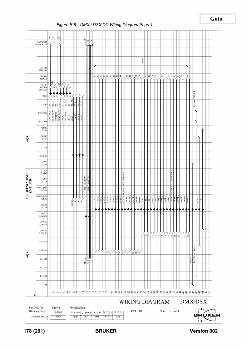
GotoFigure R.8. DMX / DSX DC Wiring Diagram Page 1
AG
ND
HPP
R
-19V
HPP
R
DG
ND
HPP
R
+9V
X
+9V
HPP
R
GN
D X
A
GN
D
+19V
RX
-1
9V R
X
NM
R2<
8> (F
XA
)
NM
R2<
9> (F
XB
)
24,1
223
,11
21,9
8 22,1
020 16
,4,1
8,6
17,5
15,3
B,H
L M U N V
CC
HH
BB
FF CC
19,7
+9V
RX
FDB
L1
MH
z2
MH
z4
MH
z8
MH
z10
MH
z20
MH
z40
MH
z80
MH
zR
EN F
1 (G
ND
) REM
OTE
EN
AB
LE10
0 M
Hz
200
MH
z
400
MH
z80
0 M
Hz
GN
D F
1FD
BL
1 M
Hz
2 M
Hz
4 M
Hz
8 M
Hz
10 M
Hz
20 M
Hz
40 M
Hz
80 M
Hz
REN
F3
(GN
D) R
EMO
TE E
NA
BLE
100
MH
z20
0 M
Hz
400
MH
z80
0 M
Hz
GN
D F
3
1 2 3 4 5 6 7 8 9 10 11 12 13 14 15
1 2 3 4 5 6 7 8 9 10 11 12 13 14 15
42 5 6 30 31 5034 35 7 8 32 3349 45 50 13 9 1016 40 41 42 43 4419 20 1539 17 18
H55
64
if 2
rout
er Z
0028
140
with
1 R
oute
r
6749
167
491
HH
,MM J YK
AQ
X
FREQ
UE
NC
YSE
451
3C
178 (201)
Part-No. for Drawing only
POS
DD FF
H43
6
H55
7
1 2
3 4 5 6 7 8 9 10 11 12 13 14 15 16 17B
18
R
19
U
20
K
21
E
22
R
23
24W
25
26IR
27
28INEC
29
GL
30
31D
32
33IA
34
G
35
36R
37
ASh
38
Mee
39
t
40
41 42 43 44 45 46V
47
e
48
r
49
si
50
o
DMX/D
: 03 of1 3DMX/DSXDC1
Drawn M
FDU
12.04.94
odification
E21
FDU
05.08.94
SH.09.94E24
.SH10.94
F
28.
KDU
03.95 08
ST
.09.95
UN
ITH
.
RCU
TCU T2
TCU T4
TCU T5
FCU1 F2
FCU2 F2
FCU3 F2(Option)
FCU4 F2(Option)
FCU5 F2(Option)
FADCBC 133
SE 451SCH Control
4 PhaseMod. Control
RXCControl
SMA’sBNC’s
SADCHADC
FILP/4M
RXC
AQ
ASU2CH1&2
R
ASU2CH3&4
ROUTER1 +19V
HPP
ROUTER2 R25
ACB ,13
PSB
PREAMP
PERIPHHPPR A,C
SYNTH1PTS 620
SYNTH2PTS 620
BACKPANELBURNDY 1
KK
SX
n 002
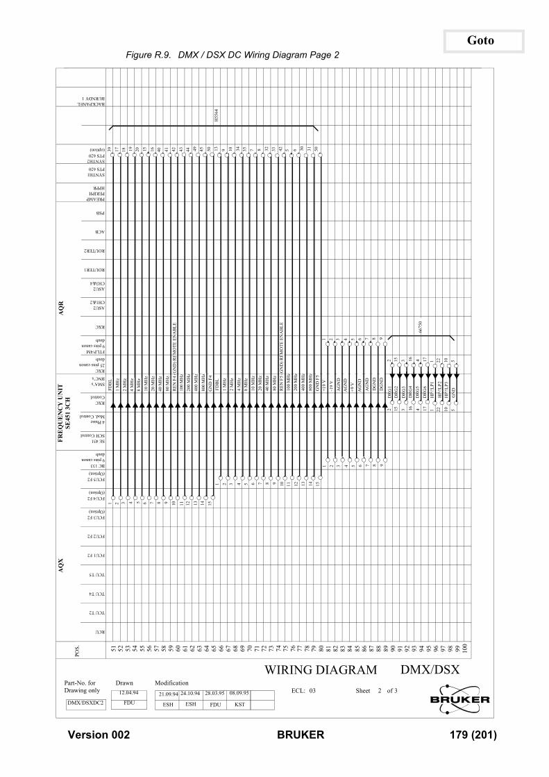
GotoFigure R.9. DMX / DSX DC Wiring Diagram Page 2
1 M
Hz
2 M
Hz
4 M
Hz
8 M
Hz
10 M
Hz
20 M
Hz
40 M
Hz
80 M
Hz
REN
F4
(GN
D) R
EMO
TE E
NA
BLE
100
MH
z20
0 M
Hz
400
MH
z80
0 M
Hz
GN
D F
4FD
BL
1 M
Hz
2 M
Hz
4 M
Hz
8 M
Hz
10 M
Hz
20 M
Hz
40 M
Hz
80 M
Hz
REN
F5
(GN
D) R
EMO
TE E
NA
BLE
100
MH
z20
0 M
Hz
400
MH
z80
0 M
Hz
GN
D F
5
2 3 4 5 6 7 8 9 10 11 12 13 14 15
42 5 6 30 31 5034 35 7 8 32 3349 45 50 13 9 1016 40 41 42 43 4419 20 1517 18
H55
641 2 3 4 5 6 7 8 9 10 11 12 13 14 15
1 2 3 4 5 6 7 8 9
2 15 3 16 4 17 1 22 10 5
2 15 3 16 4 17 1 22 10 5
1 2 3 4 5 6 7 8 9
6675
0
+19
V-1
9 V
AG
ND
AG
ND
+9 V
AG
ND
DG
ND
DR
G1
DR
G2
DR
G3
DR
G4
DR
G5
DR
G6DG
ND
HP/
!LP1
HP/
!LP2
HP/
!LP3
GN
DAG
ND
AQ
X
FREQ
UE
NC
YSE
451
3C
Version
Part-No. for Drawing only
POS
51 5253
0
54
02
55
56 57 58 59 60 61 62 63 64 65 66 67 68 69 70 71 72 73 74W
75
76B
IR
77
R
78
U
INEC
79
K
GL
80
E
81
R
D
82
83IA
84
G
85
86R
87
ASh
88
Mee
89
t
90
91 92 93 94 95 96 97 98 99 1001
DMX/D
: 03 of2 3DMX/DSXDC2
Drawn M
FDU
12.04.94
odification
21.09.94
E
24.
ESH
FSH10.94 28
.DU
03.95 08
KST
.09.95
UN
ITH
.
RCU
TCU T2
TCU T4
TCU T5
FCU1 F2
FCU2 F2
FCU3 F2(Option)
1
FCU4 F2(Option)
FCU5 F2(Option)
BC 133
9 pins canondaubSE 451SCH Control
4 PhaseMod. Control
RXCControl
FDB
SMA’sBNC’s
RXC
L
25 pins canondaub
FTLP/4M
9 pins canondaubRXC
AQ
ASU2CH1&2
R
ASU2CH3&4
ROUTER1
ROUTER2
ACB
PSB
PREAMP
PERIPHHPPRSYNTH1PTS 620
SYNTH2
PTS 620(option) 39BACKPANEL
BURNDY 1 SX79 (201)
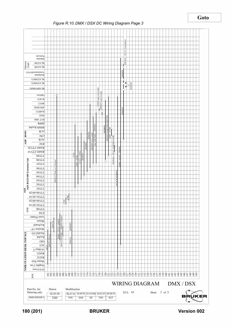
GotoFigure R.10. DMX / DSX DC Wiring Diagram Page 3
GIOKeybd. Parallel I/O Monitor 19“KeyboardMouseLaser Printer
TTY00TTY01-05/10TTY06-09/20TTY01-05/10TTY06-09/2
TTY02TTY03TTY04TTY05TTY06
TTY07TTY08TTY09RS485-TTY10 RS485-TTY20RXCACBCPULCBBSMS Keybd. HPPRBVT 3000
MAS
B-HPCU
4PH.MOD
BGU2
B-ACS
Options
BLARH100(H)
BLAX300(X)
BLAX300(Y)
BackplaneTerminator(H5167)
BLAX300
BLAX300
EthernetNetwork
Opt
ions
Am
pl.
ETH
TTY01
AQ
R
BSM
S
41 (M
ouse
)
HZ0
3318
HZ0
4112
Plo
tter o
r Ter
min
al
H26
06 +
651
34 +
O00
594
6749
232
(KEY
BD
.) +
O00
304
(Ada
pter
)
6749
2Z0
4161
(KER
MIT
)
7274
222
885
+ 65
562
Z123
21 +
655
62H
Z040
54
HZ0
4054
HZ0
4054
HZ0
4055
(if n
o so
lid) H
Z040
50H
Z040
52 B
AR
CO
DE
PRIN
TER
2288
7 +
6758
9
HZ0
4460
+ H
5167
(TER
MIN
ATO
R)
6613
8 SC
SI D
RIV
EH
2606
+ 6
5134
+ O
0059
4H
Z044
59H
Z044
59 +
H51
67 (T
erm
inat
or)
xten
sion
Uni
t
(use
with
Sol
id)
HZ0
4053
H54
88 (o
nly
with
solid
)H
Z040
55 (o
nly
if so
lid)
HZ0
4459
HZ0
4458
TO
P SG
I
0AQ
X AQ
X R
S232
/485
E
180 (201)
Part-No. for
POS.
CSI Extern
Graphic ConMouse PortRS232RS42210-Base TAUI
6613
7O
007
O00
1 H
101
102
S
103
104
105
106
107
108
109
110
111
112
113
114
115
116
117
B
118
R
119
U
120
K
121
E
122
R
123
124
W
125
126
IR
127
128
INEC
129
GL
130
131
D
132
133
IA
134
G
135
136
R
137
ASh
138
Mee
139
t
140
141
142
143
144
145
146
V
147
e
148
r
149
si
150
o
DMX /
: 03 of3 3DMX/DSXDC3
Drawn M
02.03.94ESH
odification
06.07.94FDU
28.
E
09.94
SH
24.
1 0.94ESH
28
F
.03.95
DU
08
K
.09.95
ST
.
NM
R S
TA
TIO
N D
ESK
CCU
DSX
Drawing onlyn 002
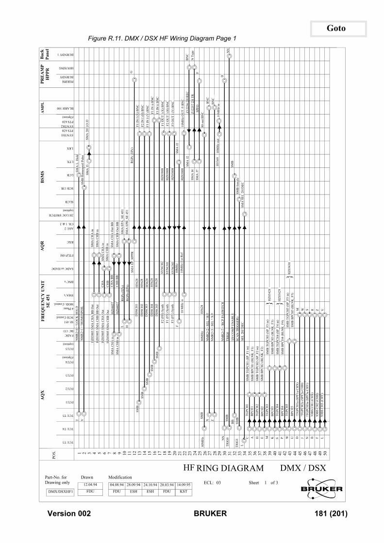
GotoFigure R.11. DMX / DSX HF Wiring Diagram Page 1
Z122
56 2
H R
EC
NM
R2<
1> !H
OM
OSP
OIL
SMB
Hom
ospo
il Pu
lse
SMA
2H
LO
J3SM
A J3
SMA
CH
A in
HZ0
3805
SM
A C
HA
BB
Out
SMA
CH
B in
SMB
SMB
SYN
CH
2H
Z038
08F2
(FH
) Syn
th
10 M
Hz
inF
SPFO
F
NM
R2<
2> S
EL !
H/F
BN
C
10M
Hz
in
BN
C
TRIG
0!Z
0 C
OM
P EN
AB
LESC
AN
TR
IGG
ER)
SEL
2H/!D
ECSM
B T
GPC
H1
(SP_
F1 in
)
FT
CH
A B
B C
HB
BB
HZ0
3805
SM
A C
HB
BB
Out
SMA
CH
A in
HZ0
3805
SM
A C
HA
Out
SMA
CH
B in
CH
A
CH
B
HZ0
3805
SM
A C
HB
Out
RG
Pa (E
Pa)
SMA
EPA
_SE
451
HZ0
4057
HZ0
4057
SMA
CH
A in
SMA
CH
B in
SMA
CH
A O
ut B
BSM
A C
HB
Out
BB
RG
Pb (E
Pb)
LSM
A E
PB_S
E 45
1H
SMA
EP_
HPP
RG
RG
Pc (E
Pc)
F1 IN
I (X
) BN
CF2
IN I
(H) B
NC
F3 IN
I (Y
) BN
C
H56
28H
5628
H56
28H
5628
H56
28SM
BSM
B
DD
SCH
1
DD
SCH
2D
DSC
H3
DD
SCH
4D
DSC
H5
F1 IN
ii B
NC
F3 IN
ii B
NC
HZ0
3808
HZ0
3808
HZ0
3808
F1 O
UT
I (X
) BN
CF2
OU
T I (
H) B
NC
F3 O
UT
I (Y
) BN
CSM
A J2
10M
Hz
OU
T /5
BN
C
SYN
CH
1
SYN
CH
3
F1 (F
X) S
ynth
F3 (F
Y) S
ynth
10M
Hz
10M
Hz
Ext R
ef
SMA
J2
BN
C
Z122
57 2
H T
RN
Typ
eSM
A J4
SMA
J7
80 o
ut B
NC
NM
R2<
3> S
EL !
X/F
80M
Hz
H56
28
10M
Hz
out
H53
69D
NN
SMB
SMB
fem
ale
NM
R2<
7> !R
CP
PASW
ITC
H
SMA
SEL
2H
/DEC
(SPF
1a C
HX
)
CH
X)
SMB
BPC
H1
(BLN
K_F
1)
M W S R Z V
(SPF
2a C
HH
)SP
F3a
CH
Y)
CH
H)
CH
Y)
SMB
TG
PCH
2 (S
P_F2
in)
SMB
BPC
H2
(BLN
K_F
2)
SMB
BPC
H3
(BLN
K_F
3)
SMB
BPC
H4
(BLN
K_F
4)
SMB
TG
PCH
3 (S
P_F3
in)
SMB
TG
PCH
4 (S
P_F4
in)
SMB
BPC
H5
(BLN
K_F
5)SM
B T
GPC
H5
(SP_
F5 in
)
HZ0
3428
HZ0
3429
HZ0
3430
AQ
X
REQ
UE
NC
Y U
NI
SE 4
51
Version
Part-No. for Drawing only
POS
V
SMB
X Z
BB
IG0NN
TGPC
H1
Hz
SMB
SMB
SMB
G1
BPC
H1
TGPC
H2
BPC
H2
TGPC
H3
BPC
H3
TGPC
H4
BPC
H4
TGPC
H5
BPC
H5
!TG
PCH
1a
!OB
S C
H1
(
C A H E M K S P W U D J N B F L
!TG
PCH
2a
!TG
PCH
3a (
!OB
S C
H2
(!O
BS
CH
3 (
1 2
3
0
4
02
5
6 7 8 9 10 11 12 13 14 15 16 17 18 19 20 21 22 23 24WH
2580
M
F
26
B
IR
27
R
28
U
INEC
29
K
GL
30TR
E
31
R
D
32TR
I
33L
IA
34
G
35
36R
37
ASh
38
Mee
39
t
40
41 42 43 44 45 46 47 48 49 501
DMX /
: 03 of1 3DMX/DSXHF1
Drawn M12.04.94
FDU
odification04.08.94
FDU
28.
E
09.94
SH
24
E
.
10.94SH
28.
F
03.94
DU
14.
K
09.95
ST
AQ
R
.
TCU T3
TCU T4
T
TCU T5
FCU1
FCU2
FCU3
FCU4 (Option)
FCU5(option)
NM
FADCBC 133
R2<
0> !L
O
SE 451SCH ControlCK
HO
L
4 Phase MOD. Control.
D
SMA’s
BNC’s
SADC or HADC
FTLP/4M
RXC
ASU 2CH. 1 & 2
2H LOC SWITCH(option)
SLCB
SCB 13R
BSM
LCBS SMA
L.
LTX Hold
AM
SYNTH2PTS 620(Option)
PTS 620
PL BLARH 100
SYNTH1
LRX
P
PERIPHBURNDY
RE
AM
HPP
R
HOUSINGPB
aPa
BURNDY 1ck nel
DSX
81 (201)
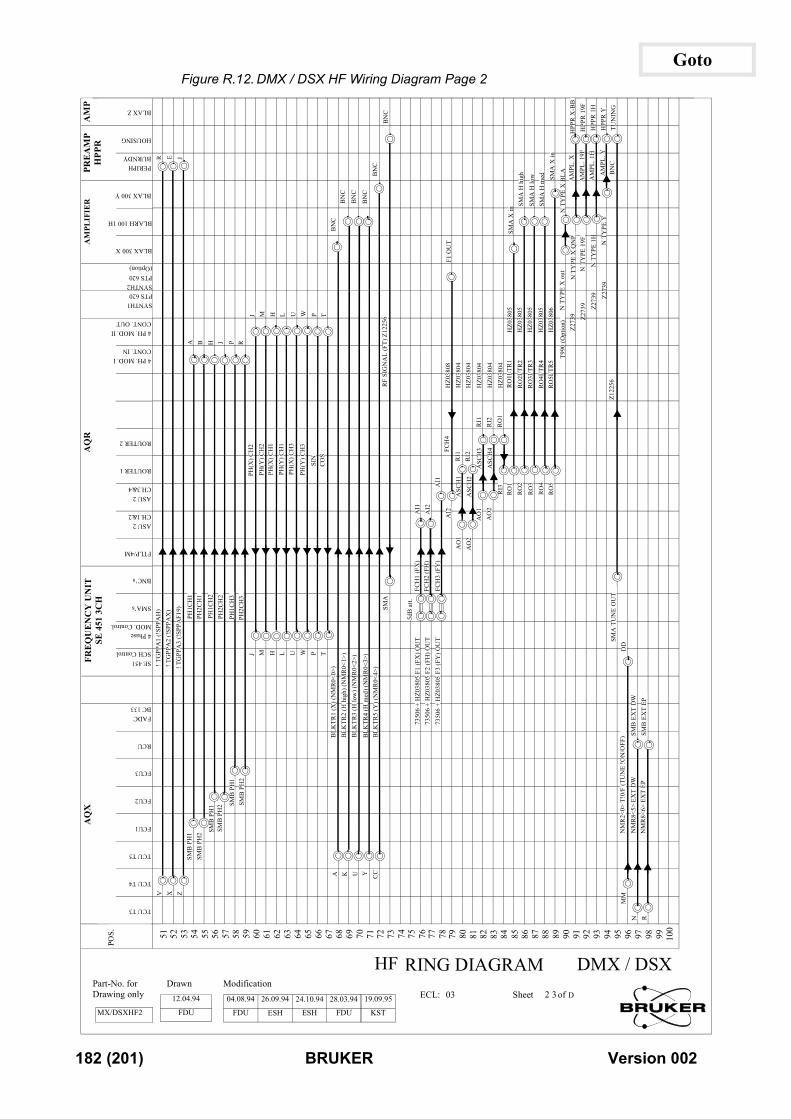
GotoFigure R.12. DMX / DSX HF Wiring Diagram Page 2
F1 O
UT
FCH
1 (F
X)
FT
PH1C
H1
PH(X
) CH
2
A
BLK
TR1
(X) (
NM
R0<
0>)
BN
C
7350
6 +
HZ0
3805
F1
(FX
) OU
T
HZ0
3808
FCH
4
SMA
DD
SMB
EX
T D
WR
8<5>
EX
T D
W
E J
BN
C
BN
CB
NC
BN
C
BN
C
B H J P R
J M H L U W P T
J M H L U W P T
PH2C
H1
PH1C
H2
PH2C
H2
PH1C
H3
PH2C
H3
! TG
PPA
2 (!
SPPA
X)
! TG
PPA
3 (!
SPPA
F19)
PH(Y
) CH
2PH
(X) C
H1
PH(Y
) CH
1PH
(X) C
H3
PH(Y
) CH
3
SIN
CO
S
B P
H1 SM
B P
H1
B P
H2 SM
B P
H2
BLK
TR2
(H h
igh)
(NM
R0<
1>)
BLK
TR3
(H lo
w) (
NM
R0<
2>)
BLK
TR4
(H m
ed) (
NM
R0<
3>)
BLK
TR5
(Y) (
NM
R0<
4>)
RF
SIG
NA
L (F
T) Z
1225
6
7350
6 +
HZ0
3805
F2
(FH
) OU
T73
506
+ H
Z038
05 F
3 (F
Y) O
UT
FCH
2 (F
H)
FCH
3 (F
Y)
AI1
AI2
AI1
5dB
att.
AI2
AO
1A
O2
AO
1A
O2
HZ0
3804
HZ0
3804
HZ0
3804
HZ0
3804
HZ0
3804
RI1
RI2
RI1
RI2
RO
1R
O1
RO
2R
O3
RO
4R
O5
RI3
ASC
H2
ASC
H1
ASC
H3
ASC
H4
HZ0
3805
HZ0
3805
HZ0
3806
HZ0
3805
HZ0
3805
RO
1I/T
R1
RO
2I/T
R2
RO
3I/T
R3
RO
4I/T
R4
RO
5I/T
R5
SMA
X in
SMA
H h
igh
SMA
H lo
wSM
A H
med
SMA
TU
NE
OU
T
SMB
EX
T EP
R8<
6> E
XT
EP
R2<
0> T
!0/F
(TU
NE
!ON
/OFF
)
Z122
56
SMA
X in
BN
C
HPP
R X
-BB
HPP
R 1
9FH
PPR
1H
HPP
R Y
TUN
ING
AM
PL. X
AM
PL. 1
9FA
MPL
. 1H
AM
PL. Y
N T
YPE
X B
LAN
TY
PE X
out N T
YPE
X Q
NP
N T
YPE
19F
N T
YPE
1H
N T
YPE
Y
T990
(Opt
ion)
Z273
9 Z273
9 Z273
9 Z273
9
AQ
X
REQ
UE
NC
Y U
NI
SE 4
51 3
CH
182 (201)
Part-No. for
POS
X
NM
ZSM
B P
H1 SM
SMB
PH
2 SM
A K U Y CC
NM
NM
MM
51 52
53 54 55 56 57 58 59 60 61 62 63 64 65 66 67B
68
R
69
U
70
K
71
E
72
R
73
H
74
W
75
F
76
IR
77
78INEC
79
GL
80
81D
82
83IA
84
G
85
86R
87
ASh
88
Mee
89
t
90
91 92 93 94 95 96NV
97R
e
98
r
99
si
100
o
DMX /
: 03 of2 3 DMX/DSXHF2
Drawn M12.04.94
FDU
odification04.08.94
FDU
26.
E
09.94
SH
24
E
.
10.94SH
28.
F
03.94
DU
19.
K
09.95
ST
AQ
R
.
TCU T3
V
TCU T4
TCU T5
FCU1
FCU2
FCU3
RCU
FADCBC 133
!
SE 451SCH Control
TGPP
A1
4 Phase MOD. Control.
(!SP
PAH
)
SMA’s
BNC’s
FTLP/4M
ASU 2CH.1&2
ASU 2CH.3&4
ROUTER 1
ROUTER 2
4 PH. MOD. ICONT. IN
4 PH. MOD. IICONT. OUT
SYNTH1PTS 620SYNTH2
PTS 620(Option)AM
PL
BLAX 300 X
IFIE
R
BLARH 100 1H
BLAX 300 Y
P
PERIPHBURNDY
RE
AM
HPP
R
R
HOUSINGPA
M
BLAX ZPDSX
Drawing onlyn 002
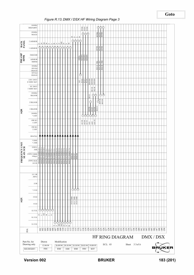
GotoFigure R.13. DMX / DSX HF Wiring Diagram Page 3
(Option)
FT
10M
Hz
H M
AI1
III
10/3
RFT
R6
ASC
H6
BLK
GD
Y (N
MR
0<33
>)B
LKG
DZ
(NM
R0<
34>)
BLK
TR6
(NM
R0<
5>)
B F L
BLK
TR7
(NM
R0<
6>)
BLK
TR8
(NM
R0<
7>)
BLK
TR9
(NM
R4<
1>)
R V DD
BLK
TR10
(NM
R4<
2>)
BLK
TR11
(NM
R4<
3>)
BLK
TR12
(NM
R4<
4>)
JJ S W
BLK
TR13
(NM
R4<
5>)
BLK
TR14
(NM
R4<
6>)
BLK
TR15
(NM
R4<
7>)
U6
SMB
Z
B F
DD
SCH
6
L
U7
SMB
U8
SMB
R
DD
SCH
7D
DSC
H8
FCH
6FC
H7
FCH
8A
I2 II
IA
I1 IV
AO
1
AO
2A
O1
IV
HZ0
4091
HZ0
4091
HZ0
4091
FCU
6FC
U7
FCU
8
ASC
H7
ASC
H8
RO
2 II
IR
O1
III
RO
2 II
RI3
IIR
I1 II
IR
I2 II
I
HZ0
3804
HZ0
3804
HZ0
3804
RFT
R7
RFT
R8
H57
00H
5700
H57
00
RO
1 II
/ TR
6R
O1
III /
TR
7R
O2
III /
TR
8
AQ
X
REQ
UE
NC
Y U
NI
SE 4
51 3
CH
Version
Part-No. for
POS
L NN
M J N
FC FC FC
101
102
103
0
104
02
105
106
X
107Z
108
BB
109
DD
110
FF
111JJ
112
M
113
114
115
116
117
118
119
120
121
122
123
124
WH
125
F
126
B
IR
127
R
128
U
INEC
129
K
GL
130
E
131
R
D
132
133
IA
134
G
135
136
R
137
ASh
138
Mee
139
t
140
141
142
143
144
145
146
147
148
149
150
1
DMX /
: 03 of3 3 DMX/DSXHF3
Drawn M12.04.94
FDU
odification26.09.94
ESH
20.
E
10.94
SH
24
E
.
10.94SH
28.
F
03.94
DU
19.
K
09.95
ST
AQ
R
.
TCU T3
TCU T4
JJ
TCU T5
FCU1
FCU2
FCU’s
RCU
FADCBC 133
B
SE 451SCH Control
LKG
DX
4 Phase MOD. Control.(NM
R0<
3
RXCControl
2>)
BNC’sSMA’s
FTLP/4M
ASU 2CH.1&2
ASU 2CH.3&4
ASU’s(Option)
ROUTER 1
ROUTER 2
ROUTER(Option)
4 PH. MOD. ICONT. IN
4 PH. MOD. IICONT. OUT
SYNTH1PTS 620SYNTH2
PTS 620(Option)P
PERIPHBURNDY
RE
AM
HPP
R
HOUSINGP
BURNDY 1
C
BA
CK
PAN
EL
BURNDY 2SYNTH.(Option)
AMPLIFIER
DSX
Drawing only83 (201)
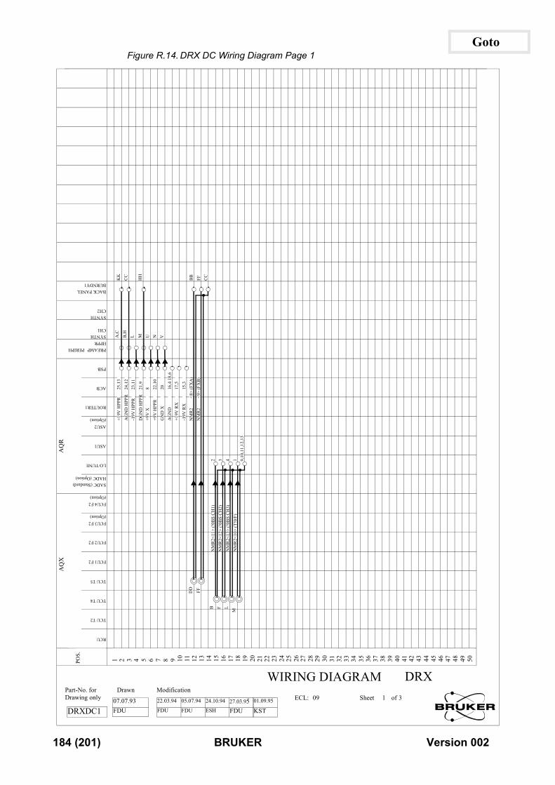
GotoFigure R.14. DRX DC Wiring Diagram Page 1
2 3 4 1 9,10
,11,
12,1
3
NM
R2<
11>
(!0B
S C
H1)
NM
R2<
12>
(!0B
S C
H2)
NM
R2<
13>
(!0B
S C
H3)
NM
R2<
10>
(T!0
/F)
+19V
HPP
RA
GN
D H
PPR
-1
9V H
PPR
D
GN
D H
PPR
+9
V X
+9
V H
PPR
G
ND
X
AG
ND
+1
9V R
X
-19V
RX
N
MR
2 <8
>N
MR
2 <9
>
25,1
324
,12
23,1
121
,98 22
,10
20 16,4
18,
617
,515
,3(F
XA
)(F
XB
)
A,C
B,H
L M U N V
KK
CC
HH
BB
FF CC
AQ
X
AQR
184 (201)
Part-No. for Drawing only
POS
B F LM
DD FF
1 2
3 4 5 6 7 8 9 10 11 12 13 14 15 16 17B
18
R
19
U
20
K
21
E
22
R
23
24W
25
26IR
27
28INEC
29
GL
30
31D
32
33IA
34
G
35
36R
37
ASh
38
Mee
39
t
40
41 42 43 44 45 46V
47
e
48
r
49
si
50
o
DRX
: 09 of1 3DRXDC10F
Drawn M
7.07.93DU
odification22.03.94
FDU
05.0
FDU
7.94 24.1
ESH
0.94 27.0
FD
3.95U01.0
KS
9.95T
.
RCU
TCU T2
TCU T4
TCU T5
FCU1 F2
FCU2 F2
FCU3 F2(Option)
FCU4 F2(Option)
SADC (Standard)HADC (Option)
LO/TUNE
ASU1
ASU2(Option)
ROUTER1
ACB
PSB
PREAMP PERIPHHPPRSYNTH
CH1SYNTH
CH2BACK PANELBURNDY1
n 002
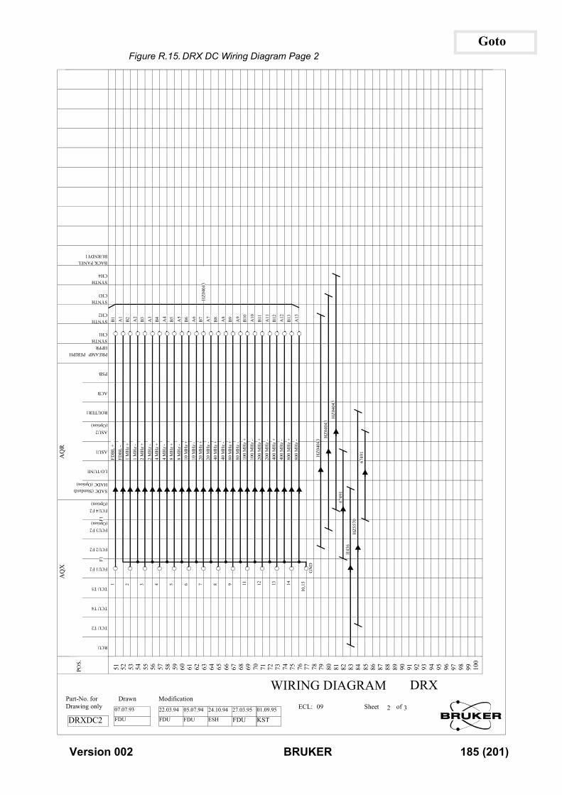
GotoFigure R.15. DRX DC Wiring Diagram Page 2
FDB
L -
A1
21
MH
z +
1 M
Hz
-B
2A
23
2 M
Hz
+2
MH
z -
B3
A3
44
MH
z +
4 M
Hz
-B
4A
45
8 M
Hz
+8
MH
z -
B5
A5
610
MH
z +
10 M
Hz
-B
6A
67
20 M
Hz
+20
MH
z -
B7
A7
840
MH
z +
40 M
Hz
-B
8A
89
80 M
Hz
+80
MH
z -
B9
A9
1110
0 M
Hz
+10
0 M
Hz
-B
10A
1012
200
MH
z +
200
MH
z -
B11
A11
1340
0 M
Hz
+40
0 M
Hz
-B
12A
1214
800
MH
z +
800
MH
z -
B13
A13
15G
ND
HZ0
4043
HZ0
4043
HZ0
4043
6749
1H
436
HZ5
570
6749
1
HZ0
4043
AQ
X
AQR
Version
Part-No. for Drawing only
POS
10,
51 52
53
0
54
02
55
56 57 58 59 60 61 62 63 64 65 66 67 68 69 70 71 72 73 74W
75
76B
IR
77
R
78
U
INEC
79
K
GL
80
E
81
R
D
82
83IA
84
G
85
86R
87
ASh
88
Mee
89
t
90
91 92 93 94 95 96 97 98 99 1001
DRX
: 09 of2 3DRXDC20
F
Drawn M7.07.93
DU
odification22.03.94
FDU
05.0
FDU
7.94 24.1
ESH
0.94 27.0
FD
3.95U01.0
KS
9.95T
.
RCU
TCU T2
TCU T4
TCU T5 1
FCU1 F2
F1
FCU2 F2
FCU3 F2(Option) F1
FCU4 F2(Option)
SADC (Standard)HADC (Option)
LO/TUNE
FDB
ASU1 L +
ASU2(Option)
ROUTER1
ACB
PSB
PREAMP PERIPHHPPRSYNTH
CH1SYNTH B1
CH2
SYNTH
CH3SYNTH
CH4BACK PANEL
BURNDY185 (201)
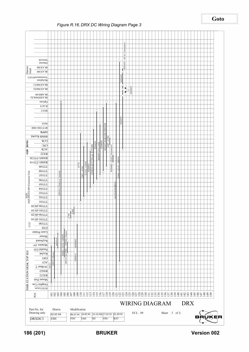
GotoFigure R.16. DRX DC Wiring Diagram Page 3
GIOKeybd. Parallel I/O Monitor 19“KeyboardMouseLaser Printer
TTY00TTY01-05/10TTY06-09/20TTY01-05/10TTY06-09/2
TTY02TTY03TTY04TTY05TTY06
TTY07TTY08TTY09RS485-TTY10 RS485-TTY20RX22ACBCPULCBBSMS Keybd. HPPRBVT3300-3000
MAS
BGU2
B-ACS
Options
BLAXH50(H,X)BLARH100
BLAX300(X)
BLAX300(Y)
BackplaneTerminator(H5167)
BLAX300
BLAX300
EthernetNetwork
Opt
ions
Am
pl.
ETH
TTY01
AQ
R
BSM
S
(Mou
se)
HZ0
3318
HZ0
4112
Plo
tter o
r Ter
min
al
H26
06 +
651
34 +
O00
594
6749
232
(KEY
BD
.) +
O00
304
(Ada
pter
)
6749
2Z0
4161
(KER
MIT
)Z2
742
2288
5 +
6556
2Z1
2321
+ 6
5562
HZ0
4054
HZ0
4054
(BV
T330
0 op
t. B
VT3
000)
HZ0
4054
HZ0
4055
(if n
o so
lid)
HZ0
4050
HZ0
4052
BA
RC
OD
E PR
INTE
R22
887
+675
89H
Z044
60 +
H51
67 (T
erm
inot
or)
6613
8 SC
SI D
RIV
EH
2606
+ 6
5134
+ O
0059
4H
Z044
59H
Z044
58H
Z044
59 +
H51
67 (T
erm
inat
or)
tens
ion
Uni
tC
CU
HZ0
4459
OP
SGI
0
AQ
XA
QX
RS2
32/4
85 E
x
186 (201)
Part-No. for Drawing only
POS.
CSI ExternGraphic Con.
Mouse PortRS232RS42210-Base TAUI
NM
R S
TATI
ON
DES
K T
6613
7O
0074
1
O00
1 H
101
102
S
103
104
105
106
107
108
109
110
111
112
113
114
115
116
117
B
118
R
119
U
120
K
121
E
122
R
123
124
W
125
126
IR
127
128
INEC
129
GL
130
131
D
132
133
IA
134
G
135
136
R
137
ASh
138
Mee
139
t
140
141
142
143
144
145
146
V
147
e
148
r
149
si
150
o
DRX
: 09 of3 3DRXDC30E
Drawn M
2.03.94SH
odification
06.07.94FDU
28.0
ESH
9.94 24.1
SH
0.94E 27.0
FDU
3.95 01.0
KST
9.95
n 002
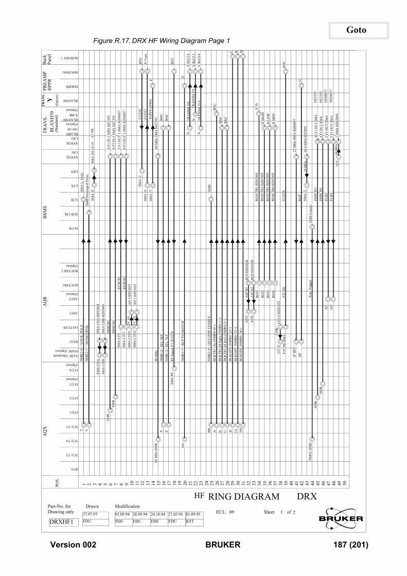
GotoFigure R.17. DRX HF Wiring Diagram Page 1
10 M
Hz
LOR
TRA
NSM
FH
FC H
1
FC H
2
NM
R2<
1> !H
OM
OSP
OIL
SMB
Hom
ospo
il Pu
lse
SMA
2H
LO
J3
SMA
J3
SMA
CH
A H
Z038
04SM
A C
HA
SMA
CH
B H
Z038
04SM
A C
HB
SMB
DD
SCH
14
F1 IN
1 S
MA
HZ3
395
SMB
DD
SCH
28
F3 IN
1 S
MA
HZ3
395
SMA
LTI
1SY
NC
H1
5 F1
OU
T 1
SMA
HZ0
4057
SMA
LTI
2SY
NC
H2
9 F3
OU
T 1
SMA
HZ0
4057
SMA
LTI
01SM
A L
TI02
AI1
I H
Z034
25A
I2 I
HZ0
3425
Z122
56B
NC
Z122
57N
Typ
eSM
A J2
SMA
J4
FSM
A J
7TG
PF0
(SPF
0)
80 M
Hz
80 M
Hz
SMA
HZ3
395
NM
R<2
> SE
L !H
/FB
NC
NM
R<2
> SE
L !X
/FB
NC
SMA
RF
RF
Sign
al F
T Z1
2256
BN
C
NM
R2<
7> R
CP
PASW
ITC
HD
N
RG
214
NTR
AN
SM F
XN
RG
214
N TRA
NSM
F19
N R
G21
4N
NM
R2<
4> !Z
0 C
OM
P EN
AB
LESM
BB
LKTR
1 (X
) (N
MR
0<0>
)B
NC
BLK
TR2
(H h
igh)
(NM
R0<
1>)
BN
CB
LKTR
3 (H
low
) (N
MR
0<2>
)B
NC
BLK
GD
X (N
MR
0<32
>)C
BLK
GD
Y (N
MR
0<33
>)H
BLK
GD
Z (N
MR
0<34
>)M
RI1
I HZ0
3804
A01
IA
SCH
1
RI2
I HZ0
3804
A
02I
ASC
H2
X IN
RO
1IR
O1I
/TR
1 H
Z038
05
H H
IGH
RO
2IR
O2I
/TR
2 H
Z038
05
H L
OW
RO
3IR
O3I
/TR
3 H
Z038
05
H M
EDR
O4I
RO
4I/T
R4
HZ0
3805
LO1/
2 H
Z034
25LO
J2
BN
CFT
UN
E SM
AZ1
2256
22 M
Hz
SMA
HZ0
4057
IF R
EFG
EPR
GP
10/4
SM
A H
Z380
5SM
A J2
10 M
Hz
SMB
Fem
ale
Scan
Trig
ger
44 F
1 IN
2 S
MA
SMB
DD
SCH
3
8 F3
IN 2
SM
ASM
BD
DSC
H4
5 F1
OU
T SM
AA
I1FC
H3
5 F1
OU
T SM
AA
I2FC
H4
1 SM
A H
Z038
0410
/5
FTU
NE
HZ3
395
HZ3
395
HZ0
4057
HZ0
4057
Z174
0
AQ
Version
Part-No. for Drawing only
POS
V
80 M
Hz
SMB
X Z
NN
BB A K U JJ LL NN
TRIG
1 SM
B
1 2
3
0
4
02
5
6 7 8 9 10 11 12 13 14 15 16 17 18 19 20 21 22 23 24WH
25
F
26
B
IR
27
R
28
U
INEC
29
K
GL
30
E
31
R
D
32
33IA
34
G
35
36R
37
ASh
38
Mee
39
t
40
41 42 43 44 45 46 47 48 49 501
DRX
: 09 of1 2DRXHF12
F
Drawn M7.07.93
DU
odification05.08.94
FDU
26.0
FDU
9.94 24.1
ESH
0.94 27.0
FDU
3.94 01.0
KST
9.95
AQ
X
R.
RCU
TCU T2
TCU T4
T
TCU T5
FCU1
FCU2
FCU3 (Option)
FCU4 (Option)
NM
SADC (Standard)HADC (Option)
R2<
0> !L
O
RX22 CKHO
L
LO/TUNE D
ASU1
ASU2(Option)
ROUTER1
ROUTER 2(Option)
SLCB
BS
SCB 13RMS
LCB
SMA
LTX L. Hol
d
LRX
SYNTHCH1
SYNTHCH2BLARHTR B (S
100 1H(Option)BLAX300
AN
S.LA
XH
5ta
ndar
d)
X-BB(Option)
0(O
p
TR
A Y
BLAX300tion)PR HP
NS.
PERIPHEAM
PPR
HOUSING
Bac
Pan
BURNDY 1k el87 (201)
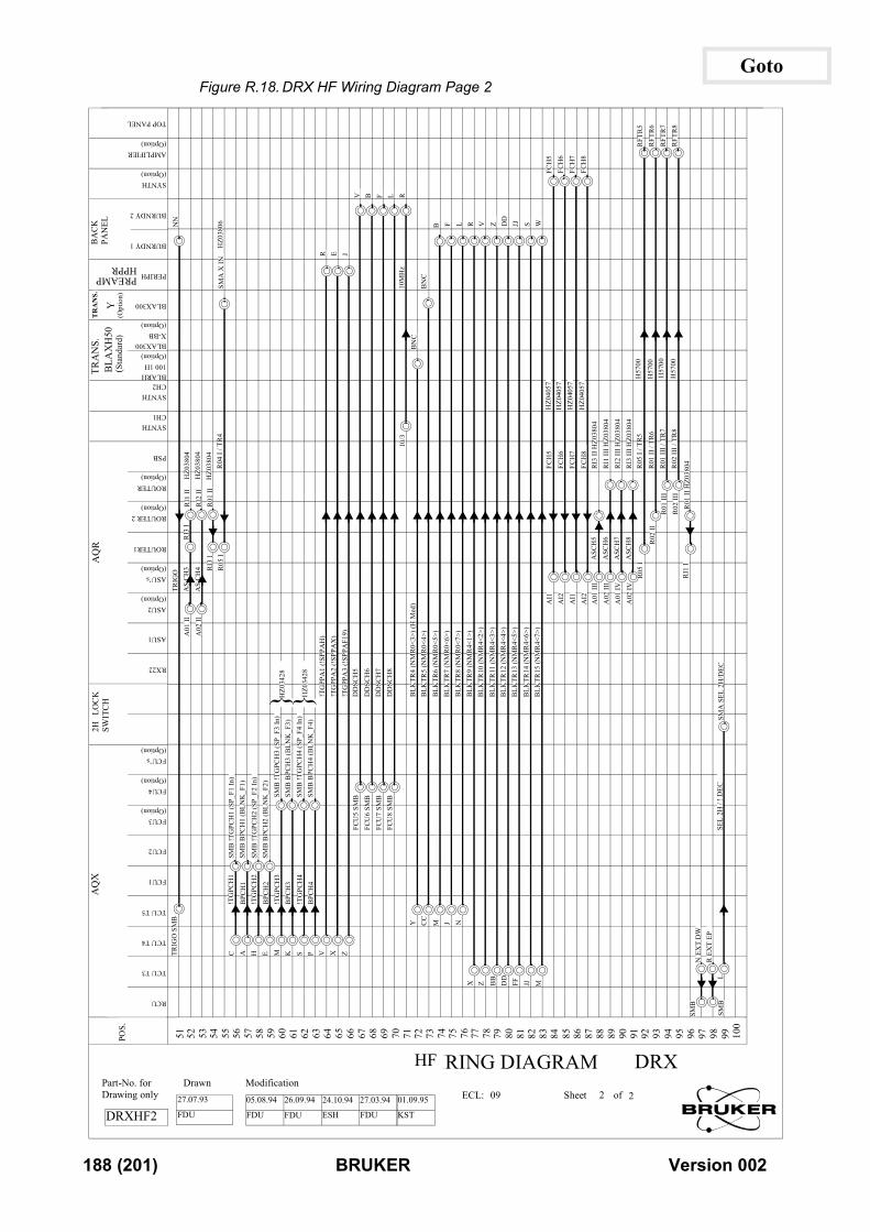
GotoFigure R.18. DRX HF Wiring Diagram Page 2
R01
II H
Z038
04
AS
CH
3
SMB
!TG
PCH
1 (S
P_F1
In)
SMB
BPC
H1
(BLN
K_F
1)
!TG
PPA
1 (!
SPPA
H)
R
FCU
5 SM
BD
DSC
H5
V
FCH
5A
I1FC
H5
FCH
6A
I2FC
H6
FCH
7A
I1FC
H7
FCH
8A
I2FC
H8
RI3
IR
I1 II
A01
IIA
S C
H4
RI2
IIA
02 II
R01
IIR
I3 I
R05
I
SMB
!TG
PCH
2 (S
P_F2
In)
SMB
BPC
H2
(BLN
K_F
2)SM
B !T
GPC
H3
(SP_
F3 In
)
!TG
PCH
1
BPC
H1
!TG
PCH
2B
PCH
2
SMB
BPC
H3
(BLN
K_F
3)!T
GPC
H3
BPC
H3
SMB
!TG
PCH
4 (S
P_F4
In)
SMB
BPC
H4
(BLN
K_F
4)!T
GPC
H4
BPC
H4
HZ03
428
HZ0
3428
!TG
PPA
2 (!
SPPA
X)
E!T
GPP
A3
(!SP
PAF1
9)J
FCU
6 SM
BD
DSC
H6
BFC
U7
SMB
DD
SCH
7F
FCU
8 SM
BD
DSC
H8
L
SMA
X IN
R10
/310
MH
zB
LKTR
4 (N
MR
0<3>
) (H
Med
)B
NC
BLK
TR5
(NM
R0<
4>)
BN
CB
LKTR
6 (N
MR
0<5>
) B
BLK
TR7
(NM
R0<
6>)
FB
LKTR
8 (N
MR
0<7>
) L
BLK
TR9
(NM
R4<
1>)
RB
LKTR
10 (N
MR
4<2>
) V
BLK
TR11
(NM
R4<
3>)
ZB
LKTR
12 (N
MR
4<4>
) D
DB
LKTR
13 (N
MR
4<5>
) JJ
BLK
TR14
(NM
R4<
6>)
SB
LKTR
15 (N
MR
4<7>
) W
ASC
H5
A01
III
RI3
II H
Z038
04A
SCH
6A
02 II
IR
I1 II
I HZ0
3804
ASC
H7
A01
IVR
I2 II
I HZ0
3804
ASC
H8
A02
IVR
I3 II
I HZ0
3804
RFT
R5
R05
IR
FTR
6R
02 II
RFT
R7
R01
III
RFT
R8
R02
III
R05
I / T
R5
R01
II /
TR6
R01
III /
TR
7 R
02 II
I / T
R8
RI1
I
SMA
SEL
2H
/DEC
SEL
2H /
! DEC
R04
I / T
R4
HZ0
3804
HZ0
3804
HZ0
3804
HZ0
3806
HZ0
4057
HZ0
4057
HZ0
4057
HZ0
4057
H57
00
H57
00H
5700
H57
00
AQ
X
LOC
KIT
CH
188 (201)
Part-No. for Drawing only
POS
M
C A VH E M K S P X Z
Y CC J N
X Z BB
DD
FF JJ M
N E
XT
DW
R E
XT
EPL
51 52
53 54 55 56 57 58 59 60 61 62 63 64 65 66 67B
68
R
69
U
70
K
71
E
72
R
73
74WH
75
F
76
IR
77
78INEC
79
GL
80
81D
82
83IA
84
G
85
86R
87
ASh
88
Mee
89
t
90
91 92 93 94 95 96SMB
V
97
e
98
r
SMB
99
si
100
o
DRX
: 09 of2 2DRXHF22
F
Drawn M7.07.93
DU
odification05.08.94
FDU
26.0
FDU
9.94 24.1
ESH
0.94 27.0
FDU
3.94 01.0
KST
9.95
AQ
R
.
RCU
TCU T3
TRIG
TCU T4 O S
MB
TCU T5
FCU1
FCU2
FCU3 (Option)
FCU4 (Option)
FCU’s (Option)
2 S
H WRX22
ASU1
ASU2(Option)
TRI
ASU’s(Option)
GO
ROUTER1
ROUTER 2(Option)
ROUTER(Option)
PSB
SYNTHCH1
SYNTHCH2BLARHTR B (S
100 1H(Option)BLAX300
AN
S.LA
XH
tand
ard)
X-BB(Option)
50(O
ptY
TR
A
BLAX300ion)PREAMP
NS.
PERIPHHPPR
BURNDY 1
NN
BA
CK
PAN
EL
BURNDY 2
SYNTH (Option)
AMPLIFIER(Option)
TOP PANEL
n 002
List of Abbreviations D
Table R.9. List of Abbreviations
ACB Amplifier Control Board (in AQRACK)
ACU Acquisition Control Unit (TCU + nFCU + RCU + GCU)
AI1 ASU Input Connector 1
AO1 ASU Output Connector 1
AQRACK Acquisition Rack (19“ x 7U)
AQS Acquisition Synchronization (from TCU to FCUs)
AQSI Acquisition Synchronization Input (FCU)
AQSO Acquisition Synchronization Output (FCU)
AQX32 Acquisition Computer (19“ x 7 U)
ASCH1 RF-Output Signal from ASU Channel 1
ASU Amplitude Setting Unit
AT201 20 dB Attenuator Input 1 on ASU
AT401 40 dB Attenuator Input 1 on ASU
AT20CH1 Control of 20 dB Attenuator for Channel 1
AT40CH1 Control of 40 dB Attenuator for Channel 1
BGU Bruker Gradient Analog Control Unit
BLAH Bruker Linear Amplifier for H Range
BLARH Bruker Linear Amplifer Array for H Range
BLAX Bruker Linear Amplifier for X Range
BLAXH Bruker Linear Amplifier for X & H Range
BLKTR1 Blanking Transmitter 1
BLTX Bruker Linear Transmitter for X Range
BP1 Blanking Pulse Input 1 on ASU
BPCH1 Blanking Pulse Channel 1 (former SPFND)
Version 002 BRUKER 189 (201)
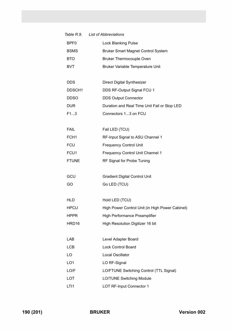
BPF0 Lock Blanking Pulse
BSMS Bruker Smart Magnet Control System
BTO Bruker Thermocouple Oven
BVT Bruker Variable Temperature Unit
DDS Direct Digital Synthesizer
DDSCH1 DDS RF-Output Signal FCU 1
DDSO DDS Output Connector
DUR Duration and Real Time Unit Fail or Stop LED
F1...3 Connectors 1...3 on FCU
FAIL Fail LED (TCU)
FCH1 RF-Input Signal to ASU Channel 1
FCU Frequency Control Unit
FCU1 Frequency Control Unit Channel 1
FTUNE RF Signal for Probe Tuning
GCU Gradient Digital Control Unit
GO Go LED (TCU)
HLD Hold LED (TCU)
HPCU High Power Control Unit (in High Power Cabinet)
HPPR High Performance Preamplifier
HRD16 High Resolution Digitizer 16 bit
LAB Level Adapter Board
LCB Lock Control Board
LO Local Oscillator
LO1 LO RF-Signal
LO/F LO/FTUNE Switching Control (TTL Signal)
LOT LO/TUNE Switching Module
LTI1 LOT RF-Input Connector 1
Table R.9. List of Abbreviations
190 (201) BRUKER Version 002
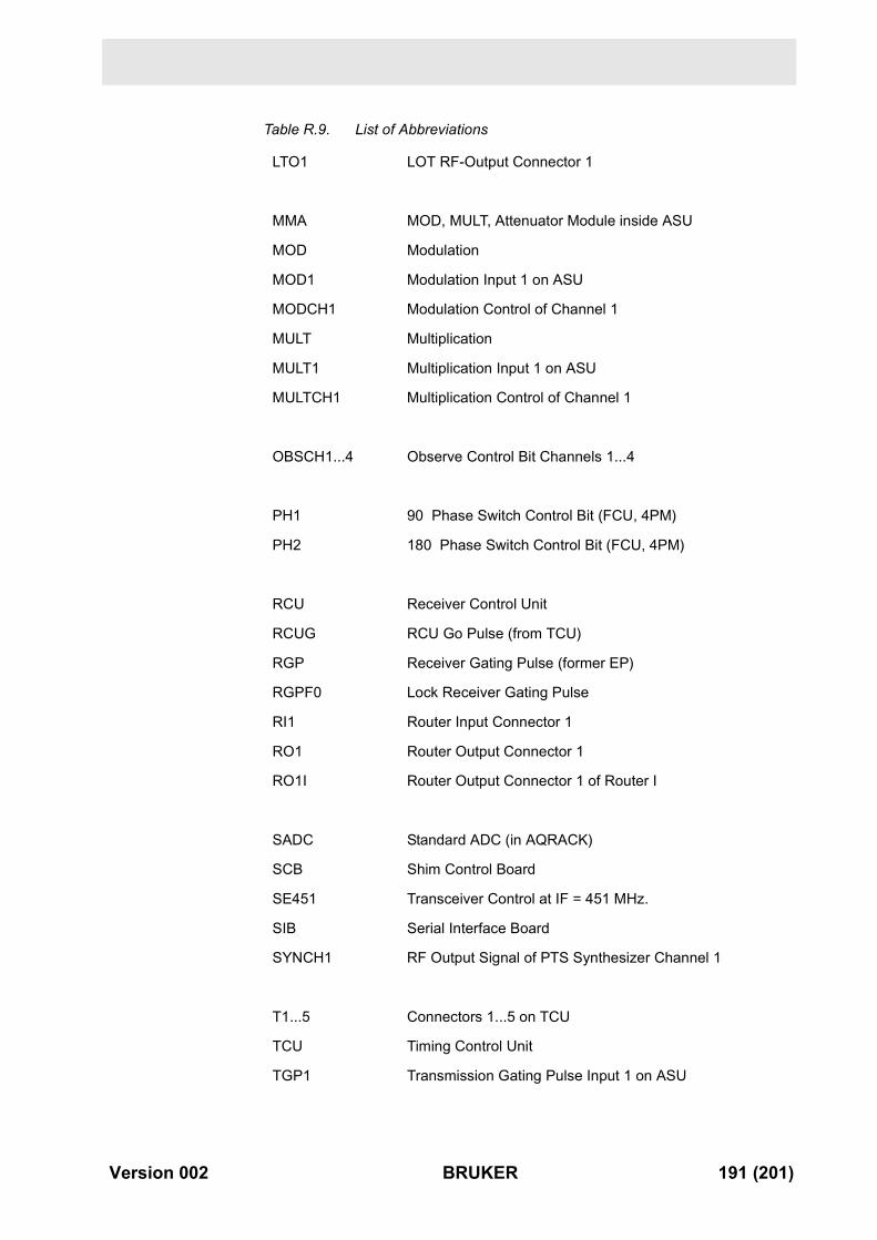
LTO1 LOT RF-Output Connector 1
MMA MOD, MULT, Attenuator Module inside ASU
MOD Modulation
MOD1 Modulation Input 1 on ASU
MODCH1 Modulation Control of Channel 1
MULT Multiplication
MULT1 Multiplication Input 1 on ASU
MULTCH1 Multiplication Control of Channel 1
OBSCH1...4 Observe Control Bit Channels 1...4
PH1 90 Phase Switch Control Bit (FCU, 4PM)
PH2 180 Phase Switch Control Bit (FCU, 4PM)
RCU Receiver Control Unit
RCUG RCU Go Pulse (from TCU)
RGP Receiver Gating Pulse (former EP)
RGPF0 Lock Receiver Gating Pulse
RI1 Router Input Connector 1
RO1 Router Output Connector 1
RO1I Router Output Connector 1 of Router I
SADC Standard ADC (in AQRACK)
SCB Shim Control Board
SE451 Transceiver Control at IF = 451 MHz.
SIB Serial Interface Board
SYNCH1 RF Output Signal of PTS Synthesizer Channel 1
T1...5 Connectors 1...5 on TCU
TCU Timing Control Unit
TGP1 Transmission Gating Pulse Input 1 on ASU
Table R.9. List of Abbreviations
Version 002 BRUKER 191 (201)
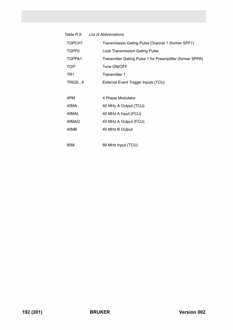
TGPCH1 Transmission Gating Pulse Channel 1 (former SPF1)
TGPF0 Lock Transmission Gating Pulse
TGPPA1 Transmitter Gating Pulse 1 for Preamplifier (former SPPA)
TO/F Tune ON/OFF
TR1 Transmitter 1
TRIG0...4 External Event Trigger Inputs (TCU)
4PM 4 Phase Modulator
40MA 40 MHz A Output (TCU)
40MAI 40 MHz A Input (FCU)
40MAO 40 MHz A Output (FCU)
40MB 40 MHz B Output
80M 80 MHz Input (TCU)
Table R.9. List of Abbreviations
192 (201) BRUKER Version 002
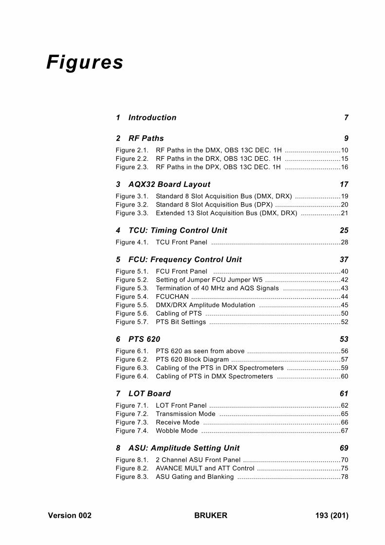
Figures
1 Introduction 7
2 RF Paths 9Figure 2.1. RF Paths in the DMX, OBS 13C DEC. 1H ............................10Figure 2.2. RF Paths in the DRX, OBS 13C DEC. 1H ............................15Figure 2.3. RF Paths in the DPX, OBS 13C DEC. 1H ............................16
3 AQX32 Board Layout 17Figure 3.1. Standard 8 Slot Acquisition Bus (DMX, DRX) .......................19Figure 3.2. Standard 8 Slot Acquisition Bus (DPX) .................................20Figure 3.3. Extended 13 Slot Acquisition Bus (DMX, DRX) ....................21
4 TCU: Timing Control Unit 25Figure 4.1. TCU Front Panel .................................................................28
5 FCU: Frequency Control Unit 37Figure 5.1. FCU Front Panel ................................................................40Figure 5.2. Setting of Jumper FCU Jumper W5 ......................................42Figure 5.3. Termination of 40 MHz and AQS Signals .............................43Figure 5.4. FCUCHAN ...........................................................................44Figure 5.5. DMX/DRX Amplitude Modulation .........................................45Figure 5.6. Cabling of PTS ....................................................................50Figure 5.7. PTS Bit Settings ..................................................................52
6 PTS 620 53Figure 6.1. PTS 620 as seen from above ...............................................56Figure 6.2. PTS 620 Block Diagram .......................................................57Figure 6.3. Cabling of the PTS in DRX Spectrometers ...........................59Figure 6.4. Cabling of PTS in DMX Spectrometers ................................60
7 LOT Board 61Figure 7.1. LOT Front Panel ..................................................................62Figure 7.2. Transmission Mode .............................................................65Figure 7.3. Receive Mode .....................................................................66Figure 7.4. Wobble Mode ......................................................................67
8 ASU: Amplitude Setting Unit 69Figure 8.1. 2 Channel ASU Front Panel .................................................70Figure 8.2. AVANCE MULT and ATT Control ..........................................75Figure 8.3. ASU Gating and Blanking ....................................................78
Version 002 BRUKER 193 (201)
Figures
9 Router/Combiner 79Figure 9.1. Explanation of RSEL Parameters ........................................ 80Figure 9.2. Router Selection and Output Blanking ................................. 81Figure 9.3. Standard Configuration of 2 Routers .................................... 84Figure 9.4. Board View ......................................................................... 85Figure 9.5. Standard Configuration of 2 Routers .................................... 86
10 BRUKER Linear Amplifiers 87Figure 10.1. Overview of Standard Amplifiers .......................................... 89Figure 10.2. Standard DMX with one Router ........................................... 91Figure 10.3. DMX with 2 Routers ............................................................ 92Figure 10.4. DRX with optional extra X Amplifier ..................................... 93Figure 10.5. DRX with 2 Routers ............................................................ 94Figure 10.6. Standard DPX Configuration ............................................... 95Figure 10.7. Amplifier Front Panel .......................................................... 96Figure 10.8. Increased Dynamic Range using Amplifier Array ................. 99Figure 10.9. BLARH 100 Block Diagram ............................................... 100Figure 10.10.OBS 1H DEC 19F using 19FSEL HPPR ............................ 101Figure 10.11.OBS 19F DEC 1H using XQNP HPPR ............................... 101Figure 10.12.OBS 1H ............................................................................ 103Figure 10.13.BLAXH50 Block Diagram .................................................. 104Figure 10.14.Jumper Settings to ensure Galvanic Separation ................ 106Figure 10.15.RS485 Pinouts .................................................................. 107Figure 10.16.Linear Gain for BLAX300 (not to scale) ............................. 109Figure 10.17.Linear Output Power (not to scale) .................................... 110Figure 10.18.Amplitude Droop ................................................................111
11 HPPR 113Figure 11.1. Wiring of Preamp Periphery .............................................. 115Figure 11.2. J2 Pinouts of J2 ................................................................ 117Figure 11.3. HPPR Block Diagram ........................................................ 118
12 RX22 Receiver 123Figure 12.1. RX22 Front Panel ............................................................. 124Figure 12.2. EP Output Signals Active Low ........................................... 127Figure 12.3. EP Output Signals Active High .......................................... 128
13 HRD 16 Controller Board 131Figure 13.1. Controller Board Front Panel ............................................. 133Figure 13.2. DRX with HRD16 Option ................................................... 134
14 RCU: Receiver Control Unit 135Figure 14.1. RCU Front Panel ............................................................... 137Figure 14.2. Number of scans that can be stored with standard 1M DRAM ..
140
15 12C Bus in the AQR 141Figure 15.1. I2C Backplane in Standard DRX ......................................... 143
194 (201) BRUKER Version 002
Figures
Figure 15.2. I2C Backplane in Standard DSX (with new 19“ SE451) .......145
16 ACB 147Figure 16.1. ACB Interfaces ..................................................................148
17 LAB: Level Adapter Board 151
18 Software 153Figure 18.1. Timing of „edscon“ parameters ..........................................154Figure 18.2. Standard DMX edsp Display ..............................................157Figure 18.3. Standard DRX edsp Display ..............................................158
A Conversion Tables 159
B Linear Amplifier Specifications 161
C Wiring Diagrams 173Figure R.4. DPX DC Wiring Diagram Page 1 ........................................174Figure R.5. DPX DC Wiring Diagram Page 2 ........................................175Figure R.6. DPX DC Wiring Diagram Page 3 ........................................176Figure R.7. DPX HF Wiring Diagram Page 1 ........................................177Figure R.8. DMX / DSX DC Wiring Diagram Page 1 .............................178Figure R.9. DMX / DSX DC Wiring Diagram Page 2 .............................179Figure R.10. DMX / DSX DC Wiring Diagram Page 3 .............................180Figure R.11. DMX / DSX HF Wiring Diagram Page 1 ..............................181Figure R.12. DMX / DSX HF Wiring Diagram Page 2 ..............................182Figure R.13. DMX / DSX HF Wiring Diagram Page 3 ..............................183Figure R.14. DRX DC Wiring Diagram Page 1 ........................................184Figure R.15. DRX DC Wiring Diagram Page 2 ........................................185Figure R.16. DRX DC Wiring Diagram Page 3 ........................................186Figure R.17. DRX HF Wiring Diagram Page 1 ........................................187Figure R.18. DRX HF Wiring Diagram Page 2 ........................................188
D List of Abbreviations 189
Version 002 BRUKER 195 (201)

Figures
196 (201) BRUKER Version 002
Tables
1 Introduction 7
2 RF Paths 9Table 2.1. AVANCE Gating/Blanking Pulses ................................... 11
3 AQX32 Board Layout 17Table 3.1. Recommended default assignments CCU Layout A,B and C
22Table 3.2. Recommended Default Assignments CCU Layout D. ...... 23
4 TCU: Timing Control Unit 25Table 4.1. 26Table 4.2. Real Time Digital Outputs NMRWord 0 ........................... 30Table 4.3. NMRWord 1 ................................................................... 31Table 4.4. NMRWord 2 ................................................................... 32Table 4.5. NMRWord 3 ................................................................... 33Table 4.6. NMRWord 4 ................................................................... 33Table 4.7. NMRWord 5 ................................................................... 34Table 4.8. NMRWord 6 ................................................................... 34Table 4.9. NMRWord 7 ................................................................... 35Table 4.10. NMRWord 8 ................................................................... 36
5 FCU: Frequency Control Unit 37Table 5.1. Non-differential MOD and MULT Ranges ........................ 38Table 5.2. Non-differential MOD and MULT Ranges ........................ 38Table 5.3. FCU Connector F1 ......................................................... 39Table 5.4. Comparison of FCU and MCI ......................................... 41Table 5.5. FCU Power Supply ........................................................ 42Table 5.6. Processes Carried out by the FCU ................................. 46Table 5.7. FCU Power Control ........................................................ 47Table 5.8. FCU Connector F2 ......................................................... 51
6 PTS 620 53Table 6.1. SYNTH1 Pin Assignment ............................................... 54
7 LOT Board 61Table 7.1. Truth Table to Select LO Sources ................................... 63
8 ASU: Amplitude Setting Unit 69Table 8.1. Front Panel Connector of 2 Channel ASU ...................... 70Table 8.2. FCU Power Control ........................................................ 72
Version 002 BRUKER 197 (201)
Tables
Table 8.3. Difference between the previously used PAS-2 and the cur-rent Analog Multipliers 74
Table 8.4. Difference between the previously used Ring Mixers and the current Analog Multipliers 76
9 Router/Combiner 79Table 9.1. Explanation of RSEL Parameters ................................... 80Table 9.2. Hardware and Software Control of a Second Router ...... 82Table 9.3. Signals which can be measured at the J3 connector of router
1 front panels 84Table 9.4. Signals which can be measured at the J3 connector of router
2 front panels 85
10 BRUKER Linear Amplifiers 87Table 10.1. Standard Connections between the Router Outputs and the
Amplifiers 90Table 10.2. Connections and Corresponding Hex Addresses for DMX
with 2 Routers 91Table 10.3. Connections and Corresponding Hex Addresses for DRX
with 1Router 93Table 10.4. RS485 Pinouts ............................................................ 107
11 HPPR 113Table 11.1. HPPR Signals ............................................................. 113Table 11.2. QNP Switching ............................................................ 116Table 11.3. Pinouts of J2 on HPPR Cover Display Module ............. 117Table 11.4. Jumper Settings for all QNP Modules .......................... 120Table 11.5. Jumper Coding of HPPR Modules ................................ 120
12 RX22 Receiver 123Table 12.1. Comparison of ARX22 and RX22 ................................. 124Table 12.2. Assignment of J19 and J20 for active high/low outputs 127Table 12.3. Power Supply .............................................................. 128Table 12.4. 3dB GAIN Table .......................................................... 129
13 HRD 16 Controller Board 131Table 13.1. SE 451 RG Bit Settings ............................................... 132
14 RCU: Receiver Control Unit 135Table 14.1. Minimum dwell time and corresponding maximum dwell clock
138
15 12C Bus in the AQR 141
16 ACB 147
17 LAB: Level Adapter Board 151
198 (201) BRUKER Version 002
Tables
Table 17.1. BSMS Signals .............................................................. 152
18 Software 153
A Conversion Tables 159Table A.1. Conversion Tables ........................................................160
B Linear Amplifier Specifications 161Table R.1. RF Pulsed Amplifier BLARH 100 200-400 MHz ............ 162Table R.2. RF Pulsed Amplifier BLARH 100 500-600 MHz ............ 163Table R.3. RF Pulsed Amplifier BLAx 300 RS 6-243 MHz .............. 164Table R.4. RF Pulsed Amplifier BLAx 300 RS 6-304 MHz .............. 165Table R.5. RF Pulsed Amplifier BLARH 50 200-400 MHz .............. 166Table R.6. RF Pulsed Amplifier BLARH 50 500-600 MHz .............. 167Table R.7. RF Pulsed Amplifier BLARH 20 200-400 MHz .............. 169Table R.8. RF Pulsed Amplifier BLARH 60 200-400 MHz .............. 170
C Wiring Diagrams 173
D List of Abbreviations 189Table R.9. List of Abbreviations .................................................... 189
Version 002 BRUKER 199 (201)

Tables
200 (201) BRUKER Version 002

Version 002 BRUKER 201 (201)
Lastpage


