Embed Size (px)
Citation preview

BEES Magazine February 2018
K S R Institute for Engineering and Technology Department of Electrical and Electronics Engineering


BEES Magazine Together We Make Difference
February 2018
Contents
S. No Topic & Author(s) Page No
1 Eye Tracking Technology Soma Sundaram R, Soundarakumar C
1
2 Machine Learning Srinivasan R, Yogeshwaran S
4
3 MEMS (Microelectromechanical Systems) Dhivagar N, Dhivagar S
7
4 Industry 4.0 Boopalan R, Kavin Kumar M
10
5 Android Versions Iniya Dharini R, Kamali Soundarya B 13
6 TFT & OELD – Advancement in Display Technology Yokeshwaran B, Surya S 16
7 Innovations in Solar PV Technology Jayaram N, Thirumoorthi G
19
8 Healthcare Technology using IOT Vivek.V, Mugesh.M 21
Editorial Board
Student Incharges Faculty Incharge
Soma Sundaram R IV Year Dr. T. Srihari
Stephen Immanuvel J III Year Professor / EEE


Magazine – BEES, Department of Electrical and Electronics Engineering, KSRIET February 2018
1
Eye Tracking Technology
Soma Sundaram R Soundarakumar C IV year EEE IV year EEE
Introduction
Imagine scrolling an online news article by
merely staring at the bottom of the webpage. How
about reorganizing your desktop files by dragging
them around with your gaze?
For years we’ve been using mice and
keyboard (and later touch screens) as the main tools
to control and send commands to our computers
and devices.
But 2016 proved that things are headed for a
change. With great leaps in artificial intelligence
and machine learning, we saw a new array of highly
efficient assistants and devices that can be
controlled with voice commands.
The start of 2017 gave a hint at what the
next breakthrough might be. If you’re following
tech publications, eye tracking has made the rounds
quite a bit lately. The Facebook-owned Oculus
acquired eye tracking startup Eye Tribe; Acer
announced a new monitor that tracks eye
movement at CES 2017; and again, at CES, Tobii
announced a new line of eye tracking initiatives for
the coming year.
Here are the key points if you’re wondering what is
eye tracking technology and what it can do.
What is Eye Tracking?
Eye tracking is about understating the state and
activity of the eye. This includes tracking your
point of gaze, the duration of your stare at any given
point, when you blink and how your pupils react to
different visual stimuli. But it’s also about where
you’re not looking, what you’re ignoring, what gets
you distracted and so forth.
The information gathered by eye tracking
technology can be used to facilitate a number of
tasks that were previously cumbersome, and also
opens up possibilities that were inconceivable
before.
While the concept might sound simple, the
technology behind it is quite complex and has been
made possible thanks to advances in sensors
technology as well as image analysis and
recognition.
Eye Tracking Devices
Head-mounted eye tracking gear
Based on task requirements, eye tracking
gear are usually head mounted or remote. Head
mounted or mobile units, such as eye tracking
glasses, are more suitable for settings where you’re
moving around such as task performance in real life
or virtual environments. Remote devices, now
reduced to the size of very small panels, offer a less

Magazine – BEES, Department of Electrical and Electronics Engineering, KSRIET February 2018
2
intrusive experience and are convenient for when
you’re sitting behind your computer and gazing at
the monitor.
Most common eye tracking devices usually
involve two main components: an infrared or near-
infrared light source and a camera. The light is
directed toward the eye, and the camera picks up
the reflections to calculate rotation of the eyes and
direction of the gaze. Eye tracking devices also pick
up other activity such as blink frequency and
changes in eye pupil diameter.
The collected data is then fed to algorithms
and software, which discover details in the user’s
eyes and reflection patterns, and interpret the image
stream to calculate the user’s eyes and gaze point
on a device screen.
Remote eye tracking
Use Cases of Eye Tracking Technology
We use our eyes constantly for different tasks
including reading magazines, gazing at posters and
ads, playing games and whatnot. Virtually anything
that involves a visual component can become the
subject of eye tracking and the data collected by eye
tracking devices can be leveraged to glean insights
and understand human behavior.
Here are some of the more popular use cases.
Eye Tracking in Gaming
One of the most obvious uses of eye
tracking is improving gaming experience. There are
a wide range of areas where eye tracking can make
it easier for users to interact with the user interface
of games, as they can replace mouse navigation and
scrolling.
They can also be used to analyze the eye
interaction with the interface. This can help players
improve their gaming by giving them insights on
what details they’re ignoring.
In rendering, the technology can be used to
prioritize rendering for the gaze area and make
more efficient use of computer resources.
The technology can also be used to improve
the gaming environment, such as having the game
characters react when the user is staring directly at
them. Imagine an RPG where characters in a tavern
will get mad if you look at their purse or an FPS
where you can tip off AI allies about enemies
sneaking up on them by looking in their direction.
Games will become a whole lot easier to play
(though I’m not sure if it’s a good thing).
Eye tracking in advertising and market research
Knowing where customers and users
look—and where they don’t—can be invaluable for
both online, TV and print advertising. Eye trackers
on monitors and kiosks can glean insights into how
many users see key messages and component of
ads, while mobile gear can be used to weigh
customer reaction to print material, posters and
product packages.

Magazine – BEES, Department of Electrical and Electronics Engineering, KSRIET February 2018
3
Eye tracking devices can also help store
owners research customer behavior and navigation
patterns in order to better understand how
customers look at products on shelves, which
sections of the store get more attention from
customers, and how they can make better use of
their store space.
Eye Tracking in UI and Environment Testing
Eye tracking can give a huge leg up to A/B
testing, the method used to measure efficiency of
variations to user interface.
Software and web developers can use eye
tracking to better understand what’s good and not
so good about the user interfaces of their
applications and websites. Eye tracking will let you
know what areas of the screen are getting more
attention and focus, and how you can reorient and
restructure user interfaces to improve user
engagement.
Software and game developers can better
understand which features of their applications are
going unnoticed. VR environments can be tested to
see how much attention is directed to each of the
areas.
Eye Tracking and Accessibility
Eye tracking will make it possible for users with
physical difficulties in performing mouse
navigation. Eye tracking can help users with
disabilities move the cursor as efficiently as
anyone.
Eye Tracking and Driving Safety
Distracted driving and drowsiness are two of the
prominent causes of road incidents. Eye tracking
technology can help track the driver’s attention and
state of awareness and issue warnings.
Combined with other innovative technologies such
as smart sensors and image analysis software, eye
tracking can help direct drivers’ attention to where
it most matters and prevent incidents from
happening.
This is just the beginning. There are a lot of
other fields where eye tracking can be useful,
including medicine, education, simulation and
neuroscience, and probably many more areas that
we will soon find out as the technology further
matures and goes mainstream.
Will there be a dark side to it? Time will
tell. For the moment, we know that companies will
be able to collect much more information about us,
and that usually does come with some privacy
tradeoffs. But it’s still too early to tell whether this
is a bad thing or not.

Magazine – BEES, Department of Electrical and Electronics Engineering, KSRIET February 2018
4
Machine Learning
SRINIVASAN R YOGESHWARAN S III year EEE III year EEE
Introduction
Machine learning is a core sub-area of
artificial intelligence; it enables computers to
get into a mode of self-learning without being
explicitly programmed. When exposed to new
data, these computer programs are enabled to
learn, grow, change, and develop by
themselves.
While the concept of machine learning
has been around for a long time, the ability to
apply complex mathematical calculations to big
data automatically—iteratively and quickly—
has been gaining momentum over the last
several years. So, put simply, the iterative
aspect of machine learning is the ability to
adapt to new data independently. This is
possible as programs learn from previous
computations and use “pattern recognition” to
produce reliable results.
With the constant evolution of the field,
there has been a subsequent rise in the uses,
demands, and importance of machine learning.
Big data has become quite a buzzword in the
last few years; that’s in part due to increased
sophistication of machine learning, which helps
analyze those big chunks of big data. Machine
learning has also changed the way data
extraction, and interpretation is done by
involving automatic sets of generic methods
that have replaced traditional statistical
techniques.
Uses of Machine Learning
Earlier in this article, we mentioned some
applications of machine learning. To
understand the concept of machine learning
better, let’s consider some more examples: web
search results, real-time ads on web pages and
mobile devices, email spam filtering, network
intrusion detection, and pattern and image
recognition. All these are by-products of
applying machine learning to analyze huge
volumes of data.
Traditionally, data analysis was always being
characterized by trial and error, an approach
that becomes impossible when data sets are
large and heterogeneous. Machine learning
comes as the solution to all this chaos by
proposing clever alternatives to analyzing huge

Magazine – BEES, Department of Electrical and Electronics Engineering, KSRIET February 2018
5
volumes of data. By developing fast and
efficient algorithms and data-driven models for
real-time processing of data, machine learning
is able to produce accurate results and analysis.
Terms and Types
Whether you realize it or not, machine learning
is one of the most important technology
trends—it underlies so many things we use
today without even thinking about them.
Speech recognition, Amazon and Netflix
recommendations, fraud detection, and
financial trading are just a few examples of
machine learning commonly in use in today’s
data-driven world.
Data Mining, Machine Learning, and Deep
Learning
Put simply, machine learning and data mining
use the same algorithms and techniques as data
mining, except the kinds of predictions vary.
While data mining discovers previously
unknown patterns and knowledge, machine
learning reproduces known patterns and
knowledge—and further automatically applies
that information to data, decision-making, and
actions.
Deep learning, on the other hand, uses
advanced computing power and special types of
neural networks and applies them to large
amounts of data to learn, understand, and
identify complicated patterns. Automatic
language translation and medical diagnoses are
examples of deep learning.
Popular Machine Learning Methods
How exactly do machines learn? Two popular
methods of machine learning are supervised
learning and unsupervised learning. It is
estimated that about 70 percent of machine
learning is supervised learning, while
unsupervised learning ranges from 10 – 20
percent.
Supervised Learning
This kind of learning is possible when inputs
and the outputs are clearly identified, and
algorithms are trained using labeled examples.
To understand this better, let’s consider the
following example: an equipment could have
data points labeled F (failed) or R (runs).
The learning algorithm using supervised
learning would receive a set of inputs along
with the corresponding correct output to find
errors. Based on these inputs, it would further
modify the model accordingly. This is a form
of pattern recognition, as supervised learning
happens through methods like classification,
regression, prediction, and gradient boosting.
Supervised learning uses patterns to predict the
values of the label on additional unlabeled data.

Magazine – BEES, Department of Electrical and Electronics Engineering, KSRIET February 2018
6
Supervised learning is more commonly used in
applications where historical data predict future
events, such as fraudulent credit card
transactions.
Unsupervised Learning
Unlike supervised learning, unsupervised
learning is used with data sets without
historical data. An unsupervised learning
algorithm explores surpassed data to find the
structure. This kind of learning works best for
transactional data; for instance, it helps in
identifying customer segments and clusters
with certain attributes—this is often used in
content personalization.
Popular techniques where unsupervised
learning is used also include self-organizing
maps, nearest neighbor mappig, singular value
decomposition, and k-means clustering.
Basically, online recommendations,
identification of data outliers, and segment text
topics are all examples of unsupervised
learning.
Machine Learning Algorithms and Processes
If you’re studying machine learning, you
should familiarize yourself with these common
machine learning algorithms and processes:
neural networks, decision trees, random forests,
associations and sequence discovery, gradient
boosting and bagging, support vector machines,
self-organizing maps, k-means clustering,
Bayesian networks, Gaussian mixture models,
and more.
Other tools and processes that pair up with the
best algorithms to aid in deriving the most
value from big data include:
Comprehensive data quality and
management
GUIs for building models and process flows
Interactive data exploration and
visualization of model results
Comparisons of different machine learning
models to quickly identify the best one
Automated ensemble model evaluation to
identify the best performers
Easy model deployment so you can get
repeatable, reliable results quickly
Integrated end-to-end platform for the
automation of the data-to-decision process
Magazine – BEES, Department of Electrical and Electronics Engineering, KSRIET February 2018
7
MEMS (Microelectromechanical Systems)
DHIVAGAR N DHIVAGAR S III year EEE III year EEE
Introduction
MEMS refers to technology that allows
mechanical structures to be miniaturized and
thoroughly integrated with electrical circuitry,
resulting in a single physical device that is actually
more like a system, where “system” indicates that
mechanical components and electrical components
are working together to implement the desired
functionality. Thus, it’s a micro (i.e., very small)
electrical and mechanical system.
Mechanical to Electrical to (Micro)mechanical
Mechanical components and systems are generally
considered to be less technologically advanced
than comparable solutions based primarily on
electrical phenomena, but this doesn’t mean that
the mechanical approach is universally inferior.
The mechanical relay, for example, is far older
than transistor-based devices that provide similar
functionality, but mechanical relays are still
widely used.
Nevertheless, typical mechanical devices will
always have the disadvantage of being hopelessly
bulky in comparison to the electronic components
found in integrated circuits. The space constraints
of a given application may cause electrical
components to be favored or required, even when
a mechanical implementation would have resulted
in a simpler or higher-performance design.
MEMS technology represents a conceptually
straightforward solution to this dilemma: if we
modify the mechanical devices such that they are
not only very small but also fully compatible with
integrated-circuit manufacturing processes, we
can, to a certain extent, have the “best of both
worlds.”
What Makes a MEMS?
In the previous section, I stated that MEMS
technology is a conceptually straightforward
solution. As you might expect, coming up with the
idea of a microscopic mechanical device is much
easier than actually building it.
We use the verb “to machine” to describe the work
of turning a piece of metal into a mechanical
component such as a gear or a pulley. In the
MEMS world, the equivalent term is “to
micromachine.” The tiny mechanical structures in
a MEMS device are fabricated by physically
modifying silicon (or another substrate material)
using specialized techniques about which I know
almost nothing. These silicon mechanical
structures are then combined with silicon
integrated circuits, and the resulting
electromechanical system is enclosed in packaging
and sold as a single device.
As explained in a paper on MEMS published by
Loughborough University in England, MEMS
devices make use of micromachined structures,
sensors, and actuators. Sensors allow a MEMS to
detect thermal, mechanical, magnetic,
electromagnetic, or chemical changes that can be

Magazine – BEES, Department of Electrical and Electronics Engineering, KSRIET February 2018
8
converted by electronic circuitry into usable data,
and actuators create physical changes rather than
simply measure them.
Examples of MEMS Devices
Let’s look at an example of the functionality and
internal structure of a MEMS device.
Micromachined cantilever switch beams.
This graphic conveys the physical structure
of micromachined cantilever switch beams. There
are four switch beams and each one has five
contacts (the use of multiple contacts is a
technique for reducing on-state resistance). The
switch beams are actuated by an applied voltage.
Here we see the MEMS switch (on the right) and
the associated driver circuitry (on the left),
interconnected and housed in a QFN package. The
driver circuitry allows a typical digital device,
such as a microcontroller, to effectively control the
switch because it does everything necessary to
generate a ramped, high-voltage actuation signal
that promotes effective and reliable switch
operation.
MEMS Applications: When Are MEMS Devices
Used?
MEMS technology can be incorporated into a wide
variety of electronic components. The companies
that make these components would presumably
claim that a MEMS implementation is superior to
whatever was used before the MEMS version
became available. It would be difficult to verify
enough of these claims to justify a generalized
statement along the lines of “MEMS devices offer
significantly better performance than non-MEMS
devices.” However, my general impression is
that in many situations MEMS is indeed a
significant step forward and, if performance or
ease of implementation is a priority in your design,
I would look at MEMS devices first.
In the context of electrical engineering, MEMS
technology has been incorporated into four
product categories:
Audio
Sensors
Switches
Oscillators
There might be some less-common products that
don’t fit into one of these categories; if you’re
aware of something that I overlooked, feel free to
let us know in the comments.

Magazine – BEES, Department of Electrical and Electronics Engineering, KSRIET February 2018
9
Audio
In the audio domain, we have MEMS microphones
and MEMS speakers. The basic characteristics of
a MEMS mic are conveyed by the following
diagram.
Sensors
Sensors are the dominant application of MEMS
techniques; there are MEMS gyroscopes,
inclinometers, accelerometers, flow sensors, gas
sensors, pressure sensors, and magnetic-field
sensors.
Switches
Electrically controlled switches are, in my opinion,
a particularly interesting application of MEMS
technology. The ADGM1004 is easy to control,
works with signal frequencies from 0 Hz to over
10 GHz, has less than 1 nA of leakage current in
the off state, and provides an actuation lifetime of
at least one billion cycles.
Combining a micromachined resonator with
excitation circuitry and sustaining circuitry results
in a MEMS oscillator. If you'd like to investigate
an actual MEMS component, you can check out a
news article from 2017 in which I discussed the
SiT2024B MEMS oscillator from SiTime.
Oscillators
MEMS oscillators, might be an excellent
choice in demanding applications; in the
abovementioned article on the SiT2024B, I point
out that based on SiTime’s information, a MEMS
oscillator can seriously outperform quartz-based
oscillators.
Conclusion
Many electronic devices incorporate
MEMS technology, and it’s likely that you’ll come
across a MEMS component sooner or later—if not
every time you design a board. This article has
provided a good overview of what MEMS is and
how it is used in electronic design.

Magazine – BEES, Department of Electrical and Electronics Engineering, KSRIET February 2018
10
Industry 4.0
BOOPALAN R KAVIN KUMAR M IV year EEE IV year EEE
Introduction The term “Industrie 4.0” was conceived in
Germany in 2015 as part of a campaign to
encourage technology development and advanced
manufacturing initiatives to transform
manufacturing and production. Industry 4.0, in
essence, represents the next industrial revolution
and, for OTTO Motors, it represents the next
generation of robotics in advanced manufacturing -
those that are interconnected and collaborative.
The 4th industrial revolution is the action of the
physical world becoming a type of information
system through sensors and actuators embedded in
physical objects and linked through networks.
According to a 2015 Gartner Study, about
25 billion objects will be interconnected by 2020.
Today there are 3.8 billion such objects. It’s
difficult to imagine the potential of having 6 times
the amount of devices interconnected over the next
few years, but this is exactly what we’re going to
see.
This new revolution and the centralization of
operational data will fuse process data and physical
systems into one. But this won’t happen overnight.
As technology evolves, we’ll see further cross-
functionalization of engineering teams; we’re
already seeing this movement in universities today
with the introduction of new engineering streams
such as Mechatronics Engineering. There is a
universal understanding that in the very near future,
it is no longer going to be enough to be an expert in
one individual field such as “mechanical engineer”.
Rather, the factory workers will need to understand
full systems in order to implement true process
change. Even if we do achieve the vision of the
future - the vision of the smart factory - the human
workforce will need multiple skills to take on
complex manufacturing roles to include
implementation, support, and training of these
highly advanced, cyber-physical systems.
A Step into the Future
In the factory of the future, machines will instantly
recognize material that is brought to them and
adjust themselves accordingly to provide accurate

Magazine – BEES, Department of Electrical and Electronics Engineering, KSRIET February 2018
11
and efficient service. Then the system’s onboard
intelligence will autonomously record deviations
from the standard process so it can make the
determination of when the part is done. Lastly, it
will call for the transport of the good to be taken to
the next step in the process. Transportation will - as
you may have guessed - be completely self-driven.
Process and device will become inseparable. This
is the direction we’re heading in and it is all
powered by the capabilities of Industry 4.0. Learn
more about Industry 4.0 and how self-driving
vehicle technology will drive change on the factory
floor.
5 Key Industry 4.0 Technologies
New Industry 4.0 technologies, spanning mobile
computing to cloud computing, have undergone
vast development in the last decade and are now
ready to be used as commercially available,
interconnected systems within manufacturing – this
is Industry 4.0. It holds the key to accessing real-
time results and data that will catapult the industry
into new levels of lean achievements.
The concept of Industry 4.0 however, is not a
simple one. It envelops many technologies and is
used in a variety of different contexts. There are
five pieces that define Industry 4.0 at its core. Each
piece is similar in nature but, when integrated
together, create capability that has never before
been possible. In an effort to understand Industry
4.0, the following five terms are explained as they
contribute to the next industrial revolution:
1. Big Data
As per Forbes, Big Data is a collection of
data from traditional and digital sources inside and
outside your company that represents a source for
ongoing discovery and analysis. Today data is
collected everywhere, from systems and sensors to
mobile devices. The challenge is that the industry
is still in the process of developing methods to best
interpret data. It’s the evolution of Industry 4.0 that
will change the way organizations and solutions
within those organizations work together; teams
will be able to make better, smarter decisions.
2. Smart Factory
The concept of Smart Factory is the
seamless connection of individual production steps,
from planning stages to actuators in the field. In the
near future, machinery and equipment will be able
to improve processes through self-optimization;
systems will autonomously adapt to the traffic
profile and network environment.

Magazine – BEES, Department of Electrical and Electronics Engineering, KSRIET February 2018
12
Leading by example is the Siemens Electronic
Works facility in Amberg, Germany. Smart
machines coordinate production and global
distribution or a built-to-order process involving
roughly 1.6 billion components. When the Smart
Factory is achieved, it will represent a pivotal shift
for Industry 4.0, as the revolution will begin to roll
out across multiple verticals.
Various markets spanning healthcare to consumer
goods will adapt Industry 4.0 technologies initially
modelled in the Smart Factory.
3. Cyber Physical Systems
Cyber physical systems are integrations of
computation, networking and physical processes.
Computers and networks monitor and control
physical processes with feedback loops; the
physical system reacts, the system uses software to
interpret action and tracks results. The notion
centers on computers and software being embedded
in devices where the first use is not computation;
rather it is a loop of action and machine learning.
4. Internet of Things (IoT)
The internet of things is a simple term for a
grandiose concept. IoT is the connection of all
devices to the internet and each other. As
Wired said, “it’s built on cloud computing and
networks of data-gather sensors; it’s mobile,
virtual, and instantaneous connection.” This
interconnection will enable “smart factories” to
take shape as equipment will use data to
manufacture, move, report and learn at astounding
rates, efficiently.
5. Interoperability
Interoperability is in essence what happens when
we bring the above elements together. It is
the connection of cyber-physical systems, humans
and smart factories communicating with each other
through the IoT. In doing so, manufacturing
partners can effectively share information, error-
free. Consider that no single company can dictate
all its partners use the same software or standards
for how the information is
represented. Interoperability enables error-free
transmission and translation.
From 3D prints to self-driving vehicles, Industry
4.0 technologies are propelling the manufacturing
industry with new means of efficiency, accuracy
and reliability. The level of intelligence offered
today is only the beginning for what is to come.

Magazine – BEES, Department of Electrical and Electronics Engineering, KSRIET February 2018
13
Android Versions
INIYA DHARINI R KAMALI SOUNDARYA B II year EEE II year EEE
Introduction Thanks to its version code names based on
delicious desserts, a trip to android history is refreshing. What’s more, with every release of its new version, Google puts up a giant statue of the delicacy associated with the code name on its campus.What better way to celebrate the arrival of those luring Android versions, equally tempting as the desserts they stand for.
Every Android version after 1.5 has been evolved with definite code names that have been chosen in an alphabetical manner. And no official explanation has ever been given for this peculiar naming convention, although it has garnered much media attention. However, Google did not attach any high-calorie code name to its initial versions 1.0 and 1.1 of the Android Operating System. 1. Cupcake
Although not the very first version from
Google after buying the company Android, Version 1.5 is considered as the first prominent version that highlighted the true power of its platform. With this version, in fact, Google kicked off the trend of naming its versions after yummy desserts. The many novel features associated with the Cupcake version include third-party keyboard and direct upload to YouTube.
2. Donut
Released in 2009, Android Version 1.6 has
been code named as “Donut,” after the tasty ring-shaped delicacy. Its specialties like enhanced user experience, text-to speech support, improved video aspects and refined search integration helped Google to get itself rooted firmly in the highly competitive Smartphone market. Larger screen-size support and turn-by-turn navigation facilities were the other sweet coatings on the donut version. 3. Eclair
Named after those oblong baked pastries
with chocolate filling, Android 2.0 was released in October 2009. The bug fix version named as 2.0.1 soon followed a couple of months later in December 2009. Then in January 2010, out came Android 2.1 with added animation features.
Magazine – BEES, Department of Electrical and Electronics Engineering, KSRIET February 2018
14
However, the three versions are often considered as a single release. Google map navigation is its highlighted feature. Other celebrated features of Version Éclair include flash and digital zoom options for camera, live wallpapers, multi-touch support mechanism and of course, Bluetooth 2.1 support. 4. Froyo
The next one in the queue, Android 2.2 is
about sheer speed and nothing else. Short for Frozen Yoghurt, Google got this version’s speed technically enhanced. Yet another unique characteristic feature was its uniquely redesigned home screen. It ensured better functionality for the device, with the entire process streamlined. 5. Gingerbread
Named after the popular ginger-flavored
cookies, Android version 2.3 looked new and fresh in various ways. A few of its unique features included several cameras, SIP internet calling, download manager, a few sensors like a barometer, gravimeter etc. 6. Honeycomb
Google introduced Android 3.0 in February 2011 and called it, Honeycomb. Made for tablets, versions 3.1 and 3.2 followed in rapid succession. Gingerbread was, in fact, Android’s very first tablet-only update. 7. Ice Cream Sandwich
Version 4.0 was the outcome of Google’s
plan to get the tablet-only platform of Honeycomb synthesized with a mobile platform. Dubbed as Ice-cream Sandwich, enhanced functionality was not the only big change that it brought in. In terms of design too, there were drastic changes. Introduction of default font was another highlight of Ice-cream Sandwich. From this version onwards, Google effectively brought all its services under the umbrella, ‘Google Play’. 8. Jelly Bean
Although primarily meant to enhance
functionality and improve user interface, “Google Now” was indeed the most innovative aspect of Version 4.1. Nicknamed as Jelly Bean, here was something that could correctly guess what you are up to search, before you actually go looking for it. Apart from the predictive feature, highly interactive notifications too made Jelly Bean stand out from the rest. Version 4.1 was also noted for its unique in- built speech-to-text engine, popularly referred

Magazine – BEES, Department of Electrical and Electronics Engineering, KSRIET February 2018
15
to as ‘voice typing’. The outcome has been an overall performance enhancement that assured an absolutely buttery smooth user interface. 9. KitKat
Google officially unveiled Android version
4.4, which it named as Kitkat, in 2013. Nestle offered full support and even kicked off a special ad campaign on its release.
However, the code name that Google had initially associated with Android 4.4 was “Key Lime Pie”. The name was later changed to Kitkat as they thought key lime pie was not a very popular dessert.
Google wanted a dessert name that is known by all, and hence partnered with Nestle for the code name Kitkat. Version 4.4 debuted on Nexus 5, and can effectively run on quite many devices compared to earlier Android versions.
‘Google Now’ feature, introduced initially in Jelly Bean was taken even ahead with the introduction of Kitkat. Earlier, you had to touch the gadget to open up the smart artificial intelligence (AI) assistant. Now with Jelly Bean, all you got to do to initiate the search is to utter the required phrase to the gadget.
Another advantage of Version 4.4 was that now the operating system could run even on devices with lower RAM. 512 MB RAM was the recommended minimum. The introduction of Emoji on Google’s keyboards was yet another unique aspect of Kitkat.
10. Lollipop With Version 5.0, popularly referred to as
Lollipop, Android could simply spread across a wide range of devices from smart phones to televisions and even to smart watches.
Lollipop came out with a brand new
runtime. Battery saving feature ensures excellent battery life on these various devices. It saves your phone from damage even while its battery is running low. 11. Marshmallow
Android 6.0, named Marshmallow, has been released under the code name Android M. It has ushered in a fistful of welcome changes that are sure to make a major impact. Doze mode that cuts down the power consumption drastically when the device is idle, opt-in app permission, fully supported USB C, inbuilt fingerprint sensor support system is but a few of them. It even allows the user to get a MicroSD card formatted and use it as internal storage, enjoying the same security level. Of course, all those versions that have been rolled out by Google till now have been sweet. Still sweeter ones are yet to come and steal the show. Android N, the next in line is already underway with its developer preview already released.

Magazine – BEES, Department of Electrical and Electronics Engineering, KSRIET February 2018
16
TFT & OELD – Advancement in Display Technology
YOKESHWARAN B SURYA S IV year EEE IV year EEE
TFT Technology:
Thin Film Transistor (TFT full form) monitors are
now popular in Computers, TV, Laptops, Mobile
phones etc. It gives enhanced quality of images like
contrast and address-ability. Unlike the LCD
monitors, TFT monitors can be viewed from any
angle without image distortion. TFT display is a
form of Liquid Crystal Display with thin film
transistors for controlling the image formation.
Before going into the details of TFT technology, let
us see how the LCD works.
The LCD contains Liquid crystals which is a state
between liquid and solid. That is the matter can
change its form from liquid to solid and viceversa.
The liquid crystal flows like a liquid and it can
orient to form the solid crystal. In the LCD
displays, the liquid crystals used have the property
of light modulation. The LCD screen do not emit
light directly but it has a number of pixels filled
with liquid crystals that pass light. These are
arranged in front of a Back light which is the source
of light. The pixels are distributed in columns and
rows and the pixel behaves like a capacitor. Similar
to a capacitor, the pixel has a liquid crystal
sandwiched between two conductive layers. The
images from The LCD may be Monochrome or
colored. Each pixel is connected with a switching
transistor.
When compared to the ordinary LCD, TFT
monitors give very sharp and crisp text with
increased response time. The TFT display has
transistors made up of thin films of Amorphous
silicon deposited on a glass using the PECVD
technology. Inside each pixel, the transistor
occupies only a small portion and the remaining
space allows the passage of light. Moreover, each
transistor can works off at the expense of very little
charge so that the image redrawing is very fast and
the screen refreshes many times in a second. In a
standard TFT Monitor around 1.3 million pixels

Magazine – BEES, Department of Electrical and Electronics Engineering, KSRIET February 2018
17
with 1.3 million thin film transistors are present.
These transistors are highly sensitive to voltage
fluctuations and mechanical stress and will be
damaged easily leading to the formation of Dots of
colors . These dots without the image are called as
Dead pixels. In the Dead pixels, the transistors are
damaged and cannot work properly.
The Monitors using TFT are known as TFT-LCD
monitors. The display of TFT monitor has two
Glass substrates enclosing a layer of liquid crystal.
The Front glass substrate has a color filter. The
Back glass filter contains the thin transistors
arranged in columns and rows. Behind the Back
glass substrate, there is Back light unit that gives
light. When the TFT display is charged, the
molecules in the liquid crystal layer bend and allow
the passage of light. This creates a pixel. The color
filter present in the Front glass substrate gives the
required color to each pixel.
There are two ITO electrodes in the display to apply
voltage. The LCD is placed between these
electrodes. When a varying voltage is applied
through the electrodes, the liquid crystal molecules
align in different patterns. This alignment produces
both light and dark areas in the image. This kind of
image is called as Grey scale image. In color TFT
monitor, the color filter substrate present in the
front glass substrate gives color to the pixels. The
color or grey pixel formation depends on the
voltage applied by the Data driver circuit.
The Thin film transistors play an important role in
pixel formation. These are arranged in the Back
glass substrate. The pixel formation depends on the
On/Off of these switching transistors. The
switching controls the movement of electrons into
the ITO electrode region. When the millions of
Pixels are formed and alighted according to the
switching of the transistors, millions of liquid
crystal angles are created. These LC angles
generates the image in the screen.
Organic Electro Luminescent Display
Organic Electro Luminescent Display (OELD) is
the recently evolved solid state semiconductor LED
having a thickness of 100-500 nanometers. It is also
called as Organic LED or OLED. It finds many
applications including the displays in mobile
phones, digital camera etc. The advantage of OELD
is that it is much thinner than the LCD and
consumes less power. OLED is composed of
aggregates of Amorphous and Crystalline
molecules which are arranged in an irregular
pattern. The structure has many thin layers of
organic material. When current passes through
these thin layers, light will be emitted through the
process of Electrophosphorescence. The display
can emit colors like Red, Green, Blue, White etc.
Magazine – BEES, Department of Electrical and Electronics Engineering, KSRIET February 2018
18
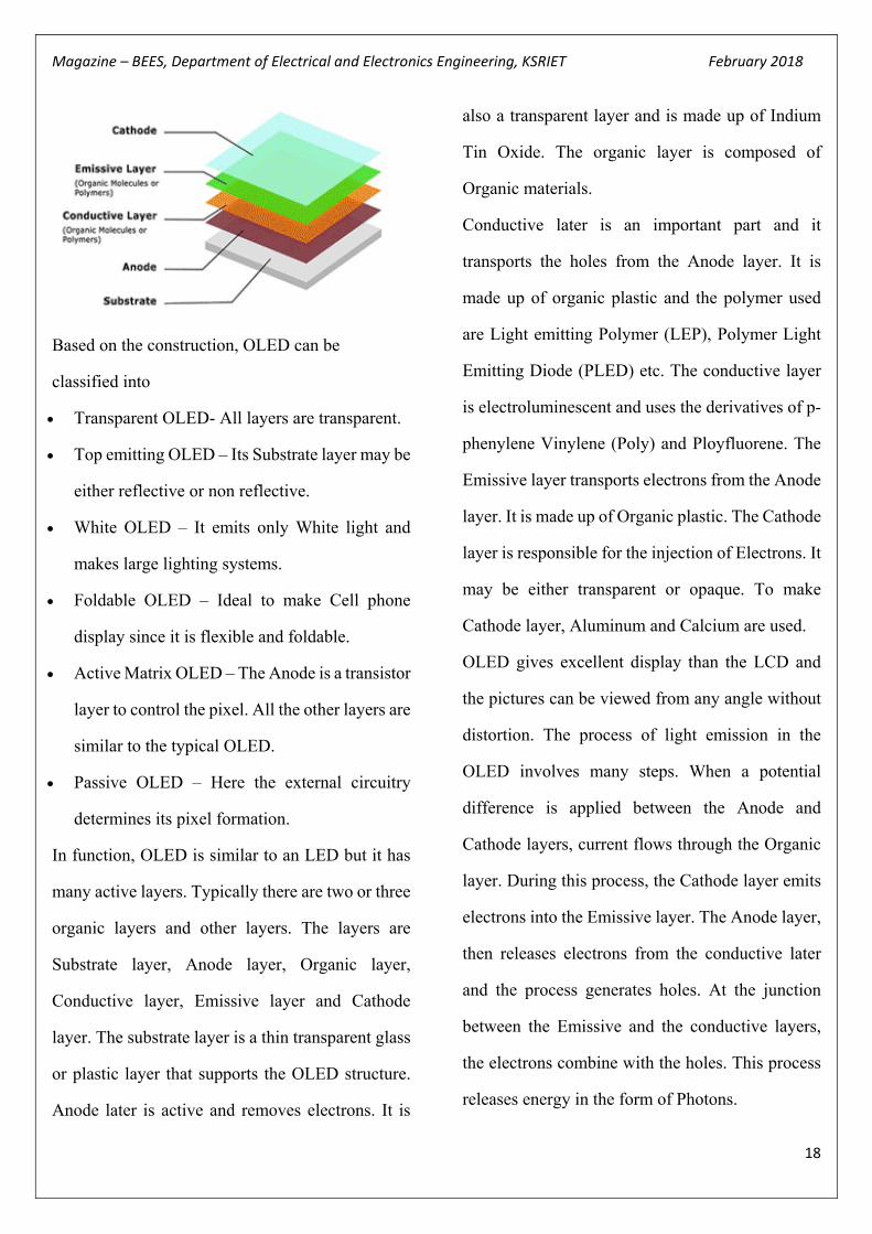
Based on the construction, OLED can be
classified into
Transparent OLED- All layers are transparent.
Top emitting OLED – Its Substrate layer may be
either reflective or non reflective.
White OLED – It emits only White light and
makes large lighting systems.
Foldable OLED – Ideal to make Cell phone
display since it is flexible and foldable.
Active Matrix OLED – The Anode is a transistor
layer to control the pixel. All the other layers are
similar to the typical OLED.
Passive OLED – Here the external circuitry
determines its pixel formation.
In function, OLED is similar to an LED but it has
many active layers. Typically there are two or three
organic layers and other layers. The layers are
Substrate layer, Anode layer, Organic layer,
Conductive layer, Emissive layer and Cathode
layer. The substrate layer is a thin transparent glass
or plastic layer that supports the OLED structure.
Anode later is active and removes electrons. It is
also a transparent layer and is made up of Indium
Tin Oxide. The organic layer is composed of
Organic materials.
Conductive later is an important part and it
transports the holes from the Anode layer. It is
made up of organic plastic and the polymer used
are Light emitting Polymer (LEP), Polymer Light
Emitting Diode (PLED) etc. The conductive layer
is electroluminescent and uses the derivatives of p-
phenylene Vinylene (Poly) and Ployfluorene. The
Emissive layer transports electrons from the Anode
layer. It is made up of Organic plastic. The Cathode
layer is responsible for the injection of Electrons. It
may be either transparent or opaque. To make
Cathode layer, Aluminum and Calcium are used.
OLED gives excellent display than the LCD and
the pictures can be viewed from any angle without
distortion. The process of light emission in the
OLED involves many steps. When a potential
difference is applied between the Anode and
Cathode layers, current flows through the Organic
layer. During this process, the Cathode layer emits
electrons into the Emissive layer. The Anode layer,
then releases electrons from the conductive later
and the process generates holes. At the junction
between the Emissive and the conductive layers,
the electrons combine with the holes. This process
releases energy in the form of Photons.

Magazine – BEES, Department of Electrical and Electronics Engineering, KSRIET February 2018
19
Innovations in Solar PV Technology
JAYARAM N THIRUMOORTHI G IV year EEE IV year EEE
Introduction When we think of solar panels, chances are
we think of roofs or giant arrays of glimmering
panels in the desert. However, advances in
photovoltaic (PV) technologies over the last decade
have made possible many more smaller-scale
applications for everyday living, on a more
personal level. Improvements in design and
configuration, energy storage, efficiency, and
battery size have created opportunities for solar
energy in a variety of situations, some of which you
have probably not considered—including off-grid
scenarios that can help you survive emergency
situations. Below are nine examples of innovative,
low-cost ways solar energy is being used to
enhance our daily lives.
Streetlights
More cities across the world are powering
streetlights with solar energy. The sun charges the
batteries during the day, which then powers light-
emitting diodes (LEDs) at night to illuminate the
streets. San Diego is incorporating smart sensors
into streetlights that can even direct drivers to open
parking spaces and help first responders during
emergency situations. Combining internet-linked
sensors with solar powered streetlights saves both
time and money.
Vaccine Refrigerators
In developing countries, 24-hour electricity
isn’t guaranteed, and in many cases, there is no
electrical grid. “Private companies have been
manufacturing solar-powered vaccine refrigerators
so healthcare workers in remote areas can
administer critical medication to those who need
it,” states Charlie Gay, director of the Solar Energy
Technologies Office for the Office of Energy
Efficiency and Renewable Energy (EERE). “This
technology solution has been saving lives for more
than four decades.”
Ovens
Solar ovens—also called solar cookers—
reflects the sun’s energy to cook food. Solar
cookers can be parabolic or square structures lined
with a reflective material that directs the rays into
the box, where it heats the food evenly.
Parabolic solar cooker.
The lid on top is typically made out of glass to
better focus the sun’s rays. They are ideal for off-
grid living and often used in developing countries,
which reduces air pollution that results from
burning fuel.

Magazine – BEES, Department of Electrical and Electronics Engineering, KSRIET February 2018
20
Cell-Phone Charger
USB cell phone chargers can charge a
phone to almost full after only a few hours exposure
to UV sunlight. These portable solar panels are
about the size of a tablet and can also charge GPS
trackers, tablets, or even laptops. They can be
hooked on backpacks to collect solar energy as you
walk, making them ideal for outdoor excursions.
Paint
Instead of constructing typical solar cells of
silicon, “polymers dissolved in a solvent create a
‘paint’ or coating that can be applied to any surface
– from homes to offices to cars,” writes technology
writer Stephanie Hicks on Hub Pages. “It’s
inexpensive and versatile. Unlike bulky
photovoltaic solar panels, solar paint uses thin-film
nanoparticles instead of silicon as solar conductors.
When applied to the sides of structures that face the
sun, the thin solar cells invisibly generate clean,
green power.”
Tents
Solar-powered tents are essentially larger versions
of solar-powered backpacks.
Orange solar tents.
The tents have imbedded photovoltaic cells that
store solar energy by day, which is then used to
illuminate the tent at night and charge or power
devices and small appliances, including heaters.
The U.S. Army has a version that can generate up
to 2 kilowatts of power a day.
Bike Locks
The Ellipse Skylock is the world’s first
solar-powered bike lock. It powered by a built-in
solar panel that provides enough power for a week
after just one hour of charging. The Skylock
connects wirelessly to the rider’s phone to provide
keyless entry, theft detection, bike sharing, and
crash alerts. It also sends an alert if the bike is
disturbed, using its long-range Bluetooth.
Backpacks
Thin-film solar panels attached to the
outside of backpacks provide up to about four watts
of power—enough to charge phones, cameras, and
other devices while simply walking. These exterior
solar cells can also be attached to briefcases and
handbags. These backpacks are ideal for students,
hikers, and campers, who will always have a
charged device during their travels, or when they
reach their destination.
Solar Fabric
Solar fabric is an application of solar
technology with a wide range of applications. Solar
cells are woven into textile fibers and generate
convenient solar electricity. “One version, created
by FTL Solar, can literally be pitched like a tent to
provide both shelter and electricity,” writes Hicks.
“Consider the endless possibilities: military, rescue
operations, disaster relief, recreational options,
medical units, and even temporary housing. Any
place you need flexible convenient solar power,
solar fabric is your answer.”

Magazine – BEES, Department of Electrical and Electronics Engineering, KSRIET February 2018
21
Healthcare Technology using IOT
VIVEK.V MUGESH.M II year EEE II year EEE
Introduction
The next wave in the era of computing will
be outside the realm of the traditional desktop. In
the Internet of Things (IoT) paradigm, many of the
objects that surround us will be on the network in
one form or another. Radio Frequency
IDentification (RFID) and sensor network
technologies will rise to meet this new challenge, in
which information and communication systems are
invisibly embedded in the environment around us.
This results in the generation of enormous amounts
of data which have to be stored, processed and
presented in a seamless, efficient, and easily
interpretable form. This model will consist of
services that are commodities and delivered in a
manner similar to traditional commodities. Cloud
computing can provide the virtual infrastructure for
such utility computing which integrates monitoring
devices, storage devices, analytics tools,
visualization platforms and client delivery. The
cost based model that Cloud computing offers will
enable end-to-end service provisioning for
businesses and users to access applications on
demand from anywhere.
Activity trackers during cancer treatment:
The Memorial Sloan Kettering Cancer
Center (MSK) and cloud research firm Medidata
are testing the use of activity trackers to gather
lifestyle data.
Patients will wear an activity tracker for up
to a week prior to treatment and then continuously
for several months over the course of multiple
treatments.
The trackers will assist in logging activity
level and fatigue, with appetite also being logged
directly, and all data saved to Medidata’s Patient
Cloud ePRO app on their personal smart phones.
Using a variety of data gathered day-to-day through
wearables or apps is a fairly obvious way that
diagnosis and treatment can be improved for many
conditions.
This is particularly the case for a disease
such as cancer, for which the reaction to therapy
plays an important and determinant part in
prescribing the right treatment.

Magazine – BEES, Department of Electrical and Electronics Engineering, KSRIET February 2018
22
Pharma is following, though, and developing its
own connected systems to help diabetes sufferers.
In 2016, Roche acquired distribution rights to an
implantable long-term continuous glucose
monitoring (CGM) system which uses a 90 day
sensor below the patient’s skin.
The sensor communicates with a smart transmitter
which then sends blood glucose levels to a sister
mobile app on the patient’s phone.
Medical Information Distribution
This is a most prominent innovation of IoT
applications in healthcare, the distribution of
accurate and current information to patients
remains one of the most challenging concerns of
medical care. IoT devices not only improve health
in the daily lives of individuals but also facilities
and professional practice.
IoT systems take healthcare out of facilities like
hospitals and allow intrusive care into the office,
home or social space. They empower and enable
individuals to cater to their own health, and allow
healthcare providers to deliver better care to
patients.
Conclusion
Hence, today we learned IoT applications in the
healthcare field. We covered the different
healthcare applications of IoT and how IoT is
beneficial for healthcare. In next tutorial, we will
study IoT application in agriculture. Till, will you
satisfy with the “IoT applications in healthcare”,
tell us in the feedback section.

Program Outcomes (POs)
PO1 Engineering Knowledge: Apply the knowledge of mathematics, science, and engineering fundamentals to solve the complex electrical engineering problems.
PO2 Problem Analysis: Identify, formulate, review research literature, and analyze complex Electrical and Electronics Engineering problems enabling attainment of conclusions using first principles of mathematics, natural sciences, and engineering sciences.
PO3 Design/Development of Solutions: Design solutions, components or process for complex Electrical Engineering problems to meet the specified needs considering public health, safety and environmental considerations.
PO4 Conduct Investigations of complex problems: Exercise research knowledge and technical methodology for design, analysis and interpretation of data to converge to a suitable solution.
PO5 Modern Tool Usage: Use modern engineering tools, softwares and equipments to predict, analyze and model engineering problems.
PO6 The Engineer & Society: Apply reasoning skills to assess societal, health, safety, legal and cultural issues relevant to the professional engineering practice and take consequent responsibilities in the society
PO7 Environment and Sustainability: Realize the impact of the professional engineering solutions and demonstrate the knowledge for sustainable development in environmental context
PO8 Ethics: Apply and realize the professional ethics and responsibilities in Electrical engineering practice.
PO9 Individual and Team Work: Exhibit Individuality, Leadership and Team spirit in multidisciplinary settings.
PO10 Communication: Communicate, comprehend, write reports, design documentation and presentation effectively on complex engineering activities
PO11 Project Management & Finance: Demonstrate the Electrical engineering and management principles adhering to financial strategies to manage projects as a member or leader in a team
PO12 Life Long Learning: Inculcate independent and life-long learning in the broadest context of technological change.
Program Specific Outcomes (PSOs)
PSO 1: Electrical drives and control: Graduates will Analyze, design and provide Engineering solutions in the field of Power Electronics and Drives
PSO 2: Embedded system: Graduates will Simulate, experiment and solve complex problems in Embedded System.

KSR INSTITUTE FOR ENGINEERING AND TECHNOLOGY
VISION
To become a globally recognized Institution in Engineering Education, Research and Entrepreneurship.
MISSION
Accomplish quality education through improved teaching learning process. Enrich technical skills with state of the art laboratories and facilities. Enhance research and entrepreneurship activities to meet the industrial and societal needs.
Department of EEE
VISION
To produce world class Electrical and Electronics Technocrats and Entrepreneurs with social responsibilities.
MISSION
Impart quality education in the field of Electrical and Electronics Engineering through state of the art learning ambience.
Enrich interdisciplinary skills and promote research through continuous learning.
Enhance professional ethics, entrepreneurship skills and social responsibilities to serve the nation.
BEES Magazine February 2018


