Embed Size (px)
Citation preview
NOVEL CONCEPTS IN HIGH-FREQUENCY RESONANT POWER PROCESSING
by
Richard W. Farrington
Dissertation submitted to the Faculty of the
Virginia Polytechnic Institute and State University
in partial fulfillment of the requirements for the degree of
Doctor of Philosophy
in
Electrical Engineering
APPROVED:
C. fo REQ OA Gove nntiC.
Fred C. Lee, Co-Chairman Milan M. Jovanovic Co-Chairman
Bo H. Cho Gary S. Brown
J John F. Rossi
June 10. 1992
Blacksburg, Virginia
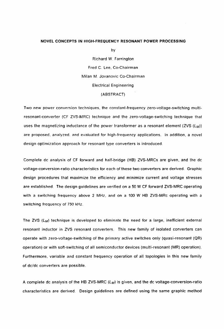
NOVEL CONCEPTS IN HIGH-FREQUENCY RESONANT POWER PROCESSING
by
Richard W. Farrington
Fred C. Lee, Co-Chairman
Milan M. Jovanovic Co-Chairman
Electrical Engineering
(ABSTRACT)
Two new power conversion techniques, the constant-frequency zero-voltage-switching multi-
resonant-converter (CF ZVS-MRC) technique and the zero-voltage-switching technique that
uses the magnetizing inductance of the power transformer as a resonant element (ZVS (Lyy))
are proposed, analyzed. and evaluated for high-frequency applications. In addition, a novel
design optimization approach for resonant type converters is introduced.
Complete de analysis of CF forward and half-bridge (HB) ZVS-MRCs are given, and the dc
voltage-conversion-ratio characteristics for each of these two converters are derived. Graphic
design procedures that maximize the efficiency and minimize current and voltage stresses
are established. The design guidelines are verified on a 50 W CF forward ZVS-MRC operating
with a switching frequency above 2 MHz, and on a 100 W HB ZVS-MRc operating with a
switching frequency of 750 kHz.
The ZVS (Ly) technique is developed to eliminate the need for a large, inefficient external
resonant inductor in ZVS resonant converters. This new family of isolated converters can
operate with zero-voltage-switching of the primary active switches only (quasi-resonant (QR)
operation) or with soft-switching of all semiconductor devices (multi-resonant (MR) operation).
Furthermore, variable and constant frequency operation of all topologies in this new family
of dc/dc converters are possible.
A complete de analysis of the HB ZVS-MRC (Ly) is given, and the dc voltage-conversion-ratio
characteristics are derived. Design guidelines are defined using the same graphic method

employed in the design of CF ZVS-MRCs. Constant frequency implementation of the HB
ZVS-MRC (Lay) using controllable saturable inductors is also proposed.
Finally, a novel approach to evaluate and design resonant converters based on the minimi-
zation of reactive power is developed.

To my grandmother, Marta Calleros de Azmitia, and
the memory of my grandfather, Enrique Azmitia Toriello.

Acknowledgements
| would like to express my sincere appreciation to both, Professor Fred C. Lee and Dr. Milan
M. Jovanovic . for their patience, guidance. and support during my doctoral studies. Much of
this work would not have been possible without their encouragement and belief in me.
{ also wish to thank Professors Bo H. Cho, Gary S. Brown, and John F. Rossi for their con-
tributions as members of my doctoral committee and suggestions through out the course of
this work.
| would also like to give a special thanks to the faculty, staff, and students at the Virginia Power
Electronics Center (VPEC) for their support and friendships. | would specially like to recognize
Dr. Wojciech Tabisz, Dr. Pawel Gradzki, Juan Sabate, Viatko Vlatkovic, C.S. Leu, Wei Tang,
Erik Yang, and Chih-Yi Lin.
| would like to thank my parents, William and Maria Elena, for providing, through their own
life. a source of inspiration. The support and faith of my family has been a source of strength.
Finally, | would like to thank Paru Desai for her friendship, support, and understanding.
This work was supported by the Virginia Center for Innovative Technology.
Acknowledgements

Table of Contents
1. INTRODUCTION 2.0... ee ee ee eee ete eee eens
1.1 Objectives of the Research .... 0... 0000 ee
1.2 Methods of Approach ........0.0...00 ee ee
1.3 Major Results 2.2... 0.00000
1.4 Outline of Dissertation ......00.00000 0000. nen
2. CONSTANT FREQUENCY ZVS-MRCS 26d ee ee eet ees
2.1 Introduction ©... eee eee
2.2 Principle of Operation of the Buck ZVS-MRC
2.3 CF Zero-Voltage Multi-Resonant Switch .........0...0 000000000 eee
2.4 Operation of CF Buck ZVS-MRC ...................
2.5 Basic Constant-Frequency Multi-Resonant Topologies .....................405.
2.6 Experimental CF Buck ZVS-MRC ©. d dd ee
2.7 Summary .............0.2 200005.
3. ANALYSIS OF CF FORWARD AND HALF-BRIDGE ZVS-MRCs ............0+ 0c eeee
3.14 Introduction ....000000 000000 eee ee eee ae
3.2 CF Forward ZVS-MRC ww. ee
Table of Contents
17
20
25
33
39
40
42
vi

3.2.1DC Analysis 22.0.0... 20.0000. ee ee 42
3.2.1.1 Mode lof Operation .......0 (4 Lee 44
3.2.1.2 Mode Il of Operation ...... ... 49
3.2.2 DC Voltage-Conversion-Ratio .....0...000 000.00. ce ee 54
3.3 CF HB ZVS-MRC wd eee 57
3.3.14DC Analysis ....... 000020002 eee 57
3.3.1.1 Mode lof Operation ..........0 0 (ok 59
3.3.1.3 Mode Il of Operation .......... ee 63
3.3.2 DC Voltage-Conversion-Ratio ee ... 63
3.4 Design Guidelines 22.0... ee 71
3.4.1 Design Trade-offs for CF Forward ZVS-MRC ...........0.....00.0.0.....00.. 73
3.4.2 Design Procedure for CF Forward ZVS-MRC_..... ... 86
3.4.3 Design Trade-offs for CF HB ZVS-MRC ...... 2... ee 88
3.4.4 Design Procedure for CF HB ZVS-MRC ..... dd ee 99
3.5.1 Experimental Results for CF Forward ZVS-MRC ................. 00000005 101
3.5.1.1 Power Stage 2.0... 0. ee 101
3.5.1.2 Control/Timing Requirements for the CF Switch .............. 0° ..... 105
3.5.2 Experimental Results for CF HB ZVS-MRC ......... be ee ae 107
3.5.2.1 Power Stage .. 0... eee 107
3.5.2.1 Control/Timing Requirements for the CF Switches .................... 112
3.6 Summary .......0 00.00. eee .. 116
4. NEW FAMILY OF ZVS ISOLATED CONVERTERS USING THE MAGNETIZING
INDUCTANCE ... 1... ccc ce ee te ee eee ee tee ee eee eee teens 118
4.1 Introduction 2.0.00... 0. eee 118
4.2 Concept and Development ........................ .. 122
4.2.1 Zero-Voltage-Switching Principle in HB ZVS-QRC ... ees 122
4.2.2 Zero-Voltage-Switching using the Magnetizing Inductance ................. 127
Table of Contents vii
423 Implementation .........00.00 0000000... ee
4.2.4 Soft-Switching Rectifier Circuit ©. eee
45 Summary ..................004
5. DC ANALYSIS AND IMPLEMENTATION OF THE HB ZVS-MRC (Ly)
5.1 Introduction ......0.00 000000 ee een
5.2 Operation of the HB ZVS-MRC (Ly)
5.2.1DC Analysis .........02 2020000000 00 ee
5.2.1.1 Mode | of Operation
5.2.1.2 Mode Il of Operation ..........0................
5.2.1.3 Mode Illof Operation ©... eee eee.
5.2.1.4 Light Load Operation
5.3 DC Voltage-Conversion-Ratio .............0. 0.0.0.2 0000004
5.4 Design Guidelines ......... 0.0.0.0 00 0 ee
5.4.1 Design Trade-off Study ............00. 0.0.0.0 .00 000508
5.4.2 Design Procedure for the HB ZVS-MRC (Ly) ..........
5.5 Experimental Results for Variable Frequency Operation .......
5.6 Constant Frequency Implementation .....................
5.7 Summary .. 00... ee
6. ANALYSIS OF REACTIVE POWER IN RESONANT CONVERTER .............0008-
6.1. Introduction ......0.00..0 0.000.000 00000 0 eee
6.2. Analysis of Real and Reactive Power ....................
6.3. Discussion .........0.0 00000002 0c eee
6.4. Design Optimazation Based on Mininization of Reactive Power
65.Summary ... oe ee
7. CONCLUSION 261. ee eee eee eee tee eee eee tert eee
Table of Contents
145
145
146
148
154
158
159
159
174
178
178
190
192
199
204
205
205
210
214
227
233
234
viii

REFERENCES ............. 0. cece eee eee
Appendix A. Analysis CF Forward ZVS-MRC ...
A.1DC Analysis ...........00......0.....
A.2.1.1 Mode lof Operation .... — .......
A.2.1.2 Mode ll of Operation .........
A.2 DC Voltage-Conversion-Ratio ..........
A.3 DC Analysis of the Topological Stages .....
A.4 Calculating the DC Voltage-Conversion-Ratio
Appendix B. Analysis CF HB ZVS-MRC.........
B.1DC Analysis .....................0....
B.1.1 Mode! of Operation .....
B.1.2 Mode ll of Operation ...............
B.2 DC Voltage-Conversion-Ratio ..........
B.3 DC Analysis of the Topological Stages .....
B.4 Calculating the DC Voltage-Conversion-Ratio
Appendix C. Analysis of HB ZVS-MRC (Ly) ....
C.1DC Analysis ..........0.....000..0.0...
C.1.1 Mode | of Operation .....
C.1.2 Mode Il of Operation ...............
C.1.3 Mode Illof Operation .... — .......
C.3.2 Light Load Operation .......
C.2 DC Voltage-Conversion-Ratio ............
C.3 DC Analysis of Topological Stages
C.3.1 Heavy Load Operation ..............
C.1.4 Light Load Operation ..........
Table of Contents
Cr
269
270
315
317
317
319
328
335
338
381
385
385
392
404
A415
437
441
442
442
528

Table of Contents
List of Illustrations
Figure
Figure
Figure
Figure
Figure
Figure
Figure
Figure
Figure
Figure
Figure
Figure
Figure
Figure
Figure
Figure
Figure
Figure
Figure
2.1. Buck zero-voltage-switched (ZVS) multi-resonant-converter (MRC). .......
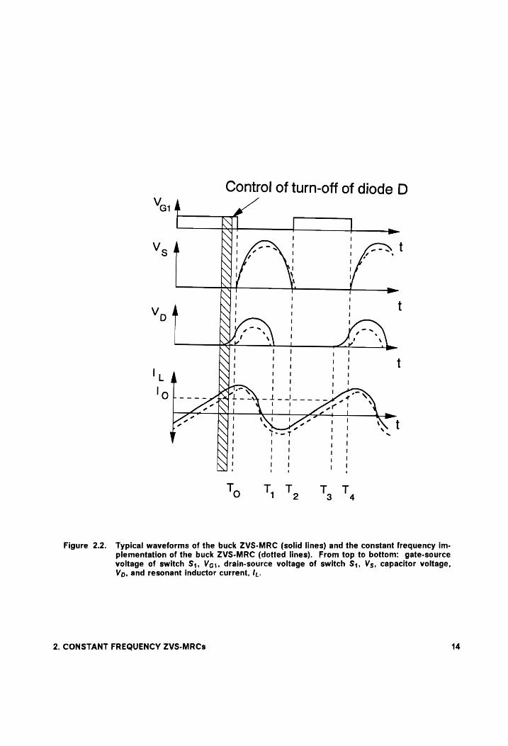
2.2. Typical waveforms of the buck ZVS-MRC (solid lines) and the constant fre- quency implementation of the buck ZVS-MRC (dotted lines). .............
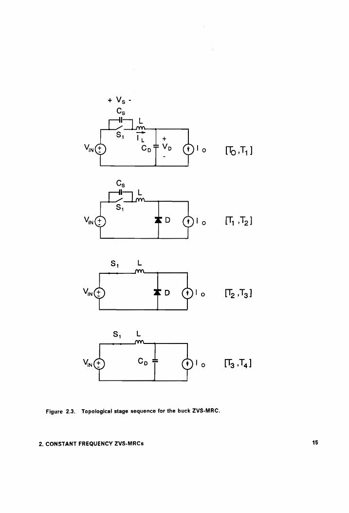
2.3. Topological stage sequence for the buck ZVS-MRC. ...................
2.4. Resonant switches: ©0000... 0.0.0.0. 0.0 ee ee
2.5. Constant Frequency (CF) buck zero-voltage-switched (ZVS) multi-resonant-
converter (MRC). 00. ees
2.6. Topological stage sequence of the CF buck ZVS-MRC. .................
2.7. Typical waveforms of the CF buck ZVS-MRC, .................- 20000.
2.8. Basic CF ZVS-MRC topologies: (a) sepic, (b) boost, (c) cuk, (d) buck-boost, (e) buck, and (f) zeta. 2... ee eee
2.9. Basic single-ended isolated CF ZVS-MRC topologies: (a) forward, (b) flyback, (c) zeta, (d) sepic, and (e) cuk. 2. es
2.10. Different implementations of the CF forward ZVS-MRC: ................
2.11. Different implementations of the CF HB ZVS-MRC. .......
2.12. Experimental CF buck ZVS-MRC. .. 0... 1
2.13. Conceptual diagram of gate drive for CF buck ZVS-MRC. ..............
2.14. Oscillograms of experimental CF buck ZVS-MRC for different loads: ......
3.1. (a) Forward ZVS-MRC (b) CF forward ZVS-MRC. ...................05.4
3.2. Equivalent model of the CF forward ZVS-MRC. .....
3.3. Topological stages of the CF forward ZVS-MRC ..................-..-..
3.4. Ideal waveforms of the CF forward ZVS-MRC operating in Mode I.A, .......
3.5. Ideal waveforms of the CF forward ZVS-MRC operating in Mode l1.B, .......
List of INustrations
14
32
34
36
37
43
45
46
47
50
xi

Figure
Figure
Figure
Figure
Figure
Figure
Figure
Figure
Figure
Figure
Figure
Figure
Figure
Figure
Figure
Figure
Figure
Figure
Figure
Figure
Figure
Figure
Figure
Figure
3.6.
3.7.
3.8.
3.9.
3.10.
3.11.
3.12.
3.13.
3.14.
3.15,
3.16
3.17.
3.18.
3.19
3.20
3.21
3.22
3.23
3.24
3.25.
3.26.
3.27.
3.28.
3.29.
Ideal waveforms of the CF forward ZVS-MRC operating in Mode Il.A, ...... 51
Ideal waveforms of the CF forward ZVS-MRC operating in Mode ll.B, ...... 52
DC voltage conversion ratio curves of the CF forward ZVS-MRC indicating the region in which the different modes of operation occur; ................ 55
DC voltage conversion ratio curves of the CF forward ZVS-MRC for different values of Cy and fsffo; 60 ee eee 56
(a) Half-bridge ZVS-MRC (b) CF half-bridge ZVS-MRC. ................ 58
Topological stages of the CF HB ZVS-MRC ....... 2... ee eee 60
Ideal waveforms of the CF HB ZVS-MRC operating in Mode l.A, ... ... 61
Ideal waveforms of the CF HB ZVS-MRC operating in Mode l.C, ... ... 64
Ideal waveforms of the CF HB ZVS-MRC operating in Mode Il.A, ......... 65
Ideal waveforms of the CF HB ZVS-MRC operating in Mode ll.C, ......... 66
DC voltage conversion ratio curve of the CF HB ZVS-MRC showing the regions where the different modes of operation occur; ............. 0.0.00 0005 69
DC voltage conversion ratio curves of the CF HB ZVS-MRC for different values
of Cn and feon|fo: Ce 70
DC voltage conversion ratio curve of the CF forward ZVS-MRC for Cy = 3 and
5, and fs/fo = 0.65 and0.7; 20.1. eee 74
Design examples #1 and #2 for the CF forward ZVS-MRC; Cy =3 and fs/fo
= O65 222 ee 76
Design examples #3 and #4 for the CF forward ZVS-MRC; Cy =3 and fs/fo —~ O65 ©... 78
Design example #5 for the CF forward ZVS-MRC; Cy =5 and fs/fo = 0.65 . 80
Design example #6 for the CF forward ZVS-MRC; Cy =3 and fs/fpo = 0.7 .. 81
Design example #7 for the CF forward ZVS-MRC; Cy =5 and fs/fo = 0.55 . 82
DC voltage conversion ratio curve of the CF forward ZVS-MRC for Cyn = 10 and 5, and fs/fo = O03 and 0.25; 00. ee 89
Design examples #1 and #2 for the CF HB ZVS-MRC; Cy =5 and fs/fo = 0.25 91
Design examples #3 and #4 for the CF HB ZVS-MRC; Cy =5 and fs/fo = 0.25 92
Design example #5 for the CF HB ZVS-MRC; Cy =10 and fs/fpo = 0.25 .... 94
Design example #6 for the CF HB ZVS-MRC; Cy =5 and fs/fpo = 0.3 ...... 95
Design example #7 for the CF HB ZVS-MRC; Cy =10 and fs/fpo = 03 ..... 96
List of MIlustrations xii
Figure 3.30. Measured efficiency of the CF forward ZVS-MRC as a function of the load
Figure
Figure
Figure
Figure
Figure
Figure
Figure
Figure
Figure
Figure
Figure
Figure
Figure
Figure
Figure
Figure
Figure
Figure
Figure
Figure
Figure
Figure
current for different line conditions. ..............0.. 0... ... 00200504 102
3.31. Waveforms of the CF forward ZVS-MRC for different load conditions: .... 103
3.32. Measured efficiency of the forward ZVS-MRC and CF forward ZVS-MRC for different load currents and an input voltage of 48V. .................. 104
3.33. Experimental CF HB ZVS-MRCs ..........00....00 0000000000 0000. 106
3.34. Measured efficiency of the CF HB ZVS-MRC shown in Fig. 3.33(a) as a func- tion of the load current for different line conditions. .................. 108
3.35. Measured efficiency of the CF HB ZVS-MRC shown in Fig. 3.33(b) as a func-
tion of the load current for different line conditions. .................. 109
3.36. Waveforms of the CF HB ZVS-MRC, with the CF switch in the secondary side for different load conditions: ......... 00000000000 ee 110
3.37. Block diagram of the control scheme for the CF HB ZVS-MRC of Fig. 33.3(b). 113
3.38. Block diagram of the control scheme for the CF HB ZVS-MRC of Fig. 33.3(a). 114
41. The HB ZVS-QRC. ©... eee 120
4.2. Topological stages of HB ZVS-QRC: .... 1... ee 121
4.3. The HB ZVS-QRC (Ly) converter ©... 0... ees 123
4.4. Topological stages of the HB ZVS-QRC (Ly): .......--........-........ 124
4.5. Ideal waveforms of the HB ZVS-QRC (Ly), ... 02. ee 125
4.6. DC voltage-conversion-ratio characteristics of the HB ZVS-QRC (Ly) as a function of the normalized conversion frequency. .................... 131
4.7. Basic isolated ZVS-QRC (Ly) topologies: (a) forward; (b) flyback; (c) zeta; (d)
cuk; (e) sepic. 2. eee 132
48. Ideal waveforms of the forward ZVS-QRC (Ly), ..... .. 133
4.9. Topological stages of the forward ZVS-QRC (Ly). ........0.00..2..22... 134
4.10. Ideal waveforms of the flyback ZVS-QRC (Ly), ..... Lae .. 136
4.11. Topological stages of the flyback ZVS-QRC (Ly). .................... 137
4.12. Magnetic switch: series combination of a saturable inductor and a rectifier diode, 20 ee ee 139
4.13. Implementation of the ZVS-QRC (Ly) using saturable inductors: (a) forward, (b) half-bridge, (c) zeta, and (d) cuk. 2.0.0... ee 140
4.14. The soft-switched magnetic switch. ........... 20.00.0000 eee eee 142
Figure 4.15. Soft switching implementation of the rectifier circuit in ZVS (Lyy) converters: 143
List of Illustrations xiii
Figure 5.1. The HB ZVS-MRC (Ly). 0.00.00 ccc cette teeters 147
Figure
Figure
Figure
Figure
Figure
Figure
Figure
Figure
Figure
Figure
Figure
Figure
Figure
Figure
Figure
Figure
Figure
Figure
Figure
Figure
Figure
Figure
Figure
Figure
Figure
5.2. (a) Representation of the saturable inductor for dc analysis; (b) Current through the linear and saturable inductor ......................0004 150
5.3a. Topological stage of the HB ZVS-MRC (Ly): .............. 0.0. .0005. 151
5.3b. Topological stage of the HB ZVS-MRC (Ly): ........20000000.00.0.. 152
5.3c. Topological stage of the HB ZVS-MRC (Ly): .. 2... 2 ee 2. 153
5.4a. Ideal waveforms of the HB ZVS-MRC (Lys) operating in Mode I.A, ....... 155
5.4b. Ideal waveforms of the HB ZVS-MRC (Ly) operating in Mode |.A; switching
transition [To — To], 26 eee 156
5.5. Ideal waveforms of the HB ZVS-MRC (Ly) operating in Mode /.B, ........ 160
5.6. Ideal waveforms of the HB ZVS-MRC (Ly) operating in Mode I.C, ........ 161
5.7. Ideal waveforms of the HB ZVS-MRC (Ly) operating in Mode ILA, ........ 162
5.8. Ideal waveforms of the HB ZVS-MRC (Ly) operating in Mode II.B, ... .. 163
5.9. Ideal waveforms of the HB ZVS-MRC (Ly) operating in Mode IILC, ........ 164
5.10. Ideal waveforms of the HB ZVS-MRC (Ly) operating in Mode IIA. ...... 165
5.11. Ideal waveforms of the HB ZVS-MRC (Ly) operating in Mode IIl.B, ...... 166
5.12. Ideal waveforms of the HB ZVS-MRC (Ly) operating in Mode IIl.C, ...... 167
5.13. Ideal waveforms of the HB ZVS-MRC (Ly) operating in Mode Ill.D, ...... 168
5.14. Ideal waveforms of the HB ZVS-MRC (Ly) operating in Mode IIl.E, ...... 169
5.15. Ideal waveforms of the HB ZVS-MRC (Ly) operating in Mode Ill. F, ...... 170
5.16. Topological Stage BP. ........0 2.0... 0202 ee 172
5.17. DC voltage-conversion-ratio characteristics as a function of the normalized switching frequency 2.020. . eee 176
5.18. DC voltage-conversion-ratio characteristics showing the regions where the different modes of operation occur: .......0.0.00 20.0.0. 000 0 ee eee 177
5.19. Design example #1 for the HB ZVS-MRC Ly; Cn = 5,Ln = 6, ......... 181
5.20. Design example #2 for the HB ZVS-MRC Ly; Cy = 5,Ln = 3, .... .. 182
5.21. Design example #3 for the HB ZVS-MRC Ly; Cy = 10,Ly = 6, .... .. 183
5.22. Design example #4 for the HB ZVS-MRC Ly; Cyn = 10, Ly = 3, ......... 184
5.23. Design examples #5 and #6 for the HB ZVS-MRC Ly: Cn = 5,Ly = 6, ... 189
List of IMustrations xiv
Figure 5.24. Flux swing experienced by the saturable inductors in the variable frequency HB ZVS-MRC (Ly). 6 eee 194
Figure 5.25. HB ZVS-MRC (Ly) efficiency as a function of load current for different input VoltageS 26 ee een 195
Figure 5.26. Oscillograms of the experimental variable frequency HB ZVS-MRC (Ly): . 196
Figure 5.27. HB ZVS-MRC efficiency as a function of load current for different input volt- AGES. eee eee 197
Figure 5.28. (a) HB ZVS-MRC (Ly) power stage; (b) HB ZVS-MRC power stage. ...... 198
Figure 5.29. Power stage power transformer from left to right: HB ZVS-MRC and HB ZVS-MRC (Ly). 0. eee 199
Figure 5.30. Implementation of a controllable saturable inductor using a El ferrite core. 201
Figure 5.31. Oscillograms of the experimental constant frequency HB ZVS converter: . 202
Figure 6.1. Power flow in PWM dc/dc converters. .......... 0.00002 cee ee 207
Figure 6.2. Power flow in resonant-type dc/dc converters. ...................0.. 208
Figure 6.3a. Circuit diagrams and primary transformer voltage and current waveforms for different resonant converters: ... 0.0.2.0... 00000. es 215
Figure 6.3b. Circuit diagrams and primary transformer voltage and current waveforms for different resonant converters continue: ............... 0.000000 0 ue 216
Figure 6.4. HB ZCS-QRC: (a) dc voltage conversion ratio, (b) transformer power transfer effectiveness, (c) normalized primary rms current. ................... 217
Figure 6.5. HB ZVS-MRC Ly: (a) dc voltage conversion ratio, (b) transformer power transfer effectiveness, (c) normalized primary rms current. ............. 218
Figure 6.6. HB ZVS-MRC dc voltage conversion ratio, transformer power transfer effec- tiveness. and normalized primary rms current characteristics .......... 219
Figure 6.7. CF HB ZVS-MRC: (a) dc voltage conversion ratio, (b) transformer power transfer effectiveness, (c) normalized primary rms current. ............. 220
Figure 6.8a. FB SPRC dc voltage conversion ratio, transformer power transfer effective- ness, and normalized primary rms current .....................-04. 221
Figure 6.8b. FB SPRC dc voltage conversion ratio, transformer power transfer effective- ness, and normalized primary rms current ...............2. 0000000. 222
Figure 6.8c. FB SPRC dc voltage conversion ratio, transformer power transfer effective- ness, and normalized primary rms current ................ 0.000005. 223
Figure 6.9. Design optimization of HB ZVS-MRC based on minimum reactive power: (a) Designs #2, #3, and #4 and (b) Design #9. .................. 000000. 229
Figure A.1. The CF forward ZVS-MRC. ... 0. eee 253
List of Hlustrations xv
Figure
Figure
Figure
Figure
Figure
Figure
Figure
Figure
Figure
Figure
Figure
Figure
Figure
Figure
Figure
Figure
Figure
Figure
Figure
Figure
Figure
A.2. Equivalent model of the CF forward ZVS-MRC. ..................... 255
A.3. Topological stages of the CF forward ZVS-MRC ...... 1... eee. 256
A.4. Ideal waveforms of the CF forward ZVS-MRC operating in Mode I.A, .... 258
A.5. Ideal waveforms of the CF forward ZVS-MRC operating in Mode |.B, .... 260
A.6. Ideal waveforms of the CF forward ZVS-MRC operating in Mode Il.A, .... 263
A.7. |deal waveforms of the CF forward ZVS-MRC operating in Mode II.B, .... 266
A.8a. DC voltage conversion ratio and Vs'""/Vixy curves of the CF forward ZVS-MRC for Cy = 2 and fs/fp = 0.80. ...... 2... 0. ee 271
A.8b. Normalized primary rms current and VP-P IVin characteristics of the CF forward ZVS-MRC Cy = 2 and fs/fo = 0.80. ..........00...00.. 00... 272
A.8c. VB@Vin and Iy/(/o/N) characteristics of the CF forward ZVS-MRC Cy = 2 and fs/ffo = 0.80. 2.0. eee 273
A.9a. DC voltage conversion ratio and VeeXTViN curves of the CF forward ZVS-MRC for Cy = 3 and fs/fpo = O65. .... 2... ee 274
A.9b. Normalized primary rms current and VP ~ °/Viw characteristics of the CF forward ZVS-MRC Cyn = 3 and fs/fo = 0.65. ......00.0.. 0.00.0 02005. 275
A.9c. VB@S/Vin and Iy/(io/N) characteristics of the CF forward ZVS-MRC Cy = 3 and fs/fp = 065. 2... eee 276
A.10a. DC voltage conversion ratio and Ve °”/Vin curves of the CF forward ZVS-MRC for Cy = 3 and fs/fpo = 0.70. .. 0... ee 277
A.10b. Normalized primary rms current and VP ~?/Viw characteristics of the CF forward ZVS-MRC Cy = 3 and fs/fo = 0.70. .......0.200 0.0.0.0... 020.4. 278
A.10c. VB88/Vin and Inm/(lo/N) characteristics of the CF forward ZVS-MRC Cy =
3 and fs/fo = 0.70. 22... ee 279
A.11a. DC voltage conversion ratio and V¢'""/Viy curves of the CF forward ZVS-MRC for Cyn = Sand fs/fp = 0.55. 1.0.0.0... 2 ee ee 280
A.11b. Normalized primary rms current and VP ~ ?/Vin characteristics of the CF forward ZVS-MRC Cyn = 5 and fs/fo = 0.55. ..... 0... 0... eee 281
A.l1c. VB@X/Vin and Im/(lo/N) characteristics of the CF forward ZVS-MRC Cy = Sand fs/fo = 0.58. 00. eee 282
A.12a. DC voltage conversion ratio and Vs°"/Viy curves of the CF forward ZVS-MRC for Cy = 5 and fs/fo = 0.60. ............. 20.00. eee 283
A.12b. Normalized primary rms current and VP-P iVin characteristics of the CF forward ZVS-MRC Cn = 5 and fs/fo = 0.60. .......... 0.0.0... .2 2000 284
A.12c. VB@/Vin and In/(io/N) characteristics of the CF forward ZVS-MRC Cy = 5 and fs/fo = 060. 22... eee 285
List of Illustrations xvi
Figure
Figure
Figure
Figure
Figure
Figure
Figure
Figure
Figure
Figure
Figure
Figure
Figure
Figure
Figure
Figure
Figure
Figure
Figure
Figure
Figure
Figure
Figure
A.13a. DC voltage conversion ratio and Vein curves of the CF forward
ZVS-MRC for Cyn = 5 and fs/fp = 065. ........ 0.0.0.0... eee 286
A.13b. Normalized primary rms current and VP ~ ?/Viw characteristics of the CF forward ZVS-MRC Cn = 5 and fs/fpo = 065. .......0....0...00..0.0004. 287
A.13c. VB6X/Vin and In/(lo/N) characteristics of the CF forward ZVS-MRC Cy = Sand fs/fo = 065. 90... 0000 ee 288
A.14a. DC voltage conversion ratio and VS "1ViN curves of the CF forward
ZVS-MRC for Cy = 7 and fs/fo = 0.55. .......2.0..0.000...0.0..000-000.0, 289
A.14b. Normalized primary rms current and VP ~ ?/Vjy characteristics of the CF forward ZVS-MRC Cn = 7 and fs/fo = 0.55. ......2000002-202000000.. 290
A.14c. VB@7Vin and In/Vo/N) characteristics of the CF forward ZVS-MRC Cy = 7 and Fslfo = 055 eee 291
A.15a. DC voltage conversion ratio and VS "Vin curves of the CF forward
ZVS-MRC for Cyn = 7 and fs/fo = 060. .........0 00000000000. 292
A.15b. Normalized primary rms current and VP ~ ?/Viny characteristics of the CF forward ZVS-MRC Cn = 7 and fs/fo = 0.60. .........00....2. 0... ..04.. 293
A.15c. VR@8/Vin and Iy/(lo/N) characteristics of the CF forward ZVS-MRC Cy = 7 and fsffo = 060. 2.00. eee 294
A.16. Topological Stage A of ideal CF forward ZVS-MRC. ................. 295
A.17. Topological Stage B of ideal CF forward ZVS-MRC. ... .. 299
A.18. Topological Stage C of ideal CF forward ZVS-MRC. ................. 302
A.19. Topological Stage D of ideal CF forward ZVS-MRC. ................. 304
A.20. Topological Stage E of ideal CF forward ZVS-MRC. ................. 309
A.21. Topological Stage F of ideal CF forward ZVS-MRC. ................. 313
B.1. The CF HB ZVS-MRC. .....................0204.. .. 318
B.2. Topological stages of the CF HB ZVS-MRC .....................0.. 320
B.3. Ideal waveforms of the CF HB ZVS-MRC operating in Mode I.A, ........ 321
B.4. Ideal waveforms of the CF HB ZVS-MRC operating in Mode 1.C, ........ 326
B.5. Ideal waveforms of the CF HB ZVS-MRC operating in Mode II.A, ... .. 329
B.6. Ideal waveforms of the CF HB ZVS-MRC operating in Mode II.C, ........ 333
B.7a. DC voltage conversion ratio curve of the CF HB ZVS-MRC for Cy = 2 and
Foon/fo = 0.85. 2 eee eee 339
B.7b. Normalized primary rms current and vp7P characteristics of the CF HB ZVS-MRC for Cy = 2 and fcon/fo = 0.35. ..... 0.0.0. ee 340
List of INustrations xvii
Figure
Figure
Figure
Figure
Figure
Figure
Figure
Figure
Figure
Figure
Figure
Figure
Figure
Figure
Figure
Figure
Figure
Figure
Figure
Figure
Figure
B.8a. DC voltage conversion ratio curve of the CF HB ZVS-MRC for Cy = 5 and Foonlfo = 0.25. 22 ee 341
B.8b. Normalized primary rms current and V; ” characteristics of the CF HB ZVS-MRC for Cy = 5 and feon/fo = 0.25. 0... ee ee 342
B.9a. DC voltage conversion ratio curve of the CF HB ZVS-MRC for Cy = 5 and foonlfo = 0.30. 20 eee 343
B.9b. Normalized primary rms current and vp—P characteristics of the CF HB ZVS-MRC for Cy = 5 and fcon/fo = 0.30. ......0.0 000.000.000.000, 344
B.10a. DC voltage conversion ratio curve of the CF HB ZVS-MRC for Cy = 10 and Foonlfo = 0.20. 202. eee 345
B.10b. Normalized primary rms current and vP~” characteristics of the CF HB ZVS-MRC for Cy = 10 and fcon/fo = 0.20. 2.2... . ee 346
B.11a. DC voltage conversion ratio curve of the CF HB ZVS-MRC for Cy = 10 and Iconffo = 0.25. 20 ees 347
B.11b. Normalized primary rms current and vi ~? characteristics of the CF HB ZVS-MRC for Cy = 10 and fcon/fo = 0.25. 2... 348
B.12a. DC voltage conversion ratio curve of the CF HB ZVS-MRC for Cy = 10 and Ioonlfo = 0.30. 20. eee 349
B.12b. Normalized primary rms current and ve ~? characteristics of the CF HB ZVS-MRC for Cy = 10 and fcon/fo = 0.30. ..... 0.0.0.0... ee ee 350
B.13a. DC voltage conversion ratio curve of the CF HB ZVS-MRC for Cy = 20 and Foonlfo = 0.25. 20 ee eee ee 351
B.13b. Normalized primary rms current and vP ~? characteristics of the CF HB ZVS-MRC for Cyn = 20 and fcon/fo = 0.25. 2.0.2 es 352
B.14a. DC voltage conversion ratio curve of the CF HB ZVS-MRC for Cy = 20 and Ioonlfo = 0.80. 0. ee eee 353
B.14b. Normalized primary rms current and vp—P characteristics of the CF HB ZVS-MRC for Cyn = 20 and fcon/fo = 0.30. .......... 00.00.2202 eee 354
B.15. Topological Stage A of ideal CF HB ZVS-MRC. .................... 355
B.16. Topological Stage B of ideal CF HB ZVS-MRC. .................... 361
B.17. Topological Stage C of ideal CF HB ZVS-MRC. .................... 365
B.18. Topological Stage D of ideal CF HB ZVS-MRC. ... .. 368
B.19. Topological Stage AF of ideal CF HB ZVS-MRC. ................... 372
B.20. Topological Stage BF of ideal CF HB ZVS-MRC. ................... 375
B.21. Topological Stage CF of ideal CF HB ZVS-MRC. ................... 380
List of Illustrations xviii
Figure
Figure
Figure
Figure
Figure
Figure
Figure
Figure
Figure
Figure
Figure
Figure
Figure
Figure
Figure
Figure
Figure
Figure
Figure
Figure
Figure
Figure
Figure
Figure
Figure
B.22. Circuit representation of the primary of the HB during: .............. 382
C.1. Soft switched half-bridge (HB ZVS-MRC (Ly)). «2... ee ee 386
C.2. (a) Representation of the saturable inductor for dc analysis; (b) Current through the linear and saturable inductor with SL .................0.. 388
C.3a. Topological stage of the HB ZVS-MRC (Ly): ............2....0...0.. 389
C.3b. Topological stage of the HB ZVS-MRC (Ly): .................---.. 390
C.3c. Topological stage of the HB ZVS-MRC (Ly): ........0..00.0. 0000000. 391
C.4a. Ideal waveforms of the HB ZVS-MRC (Ly) operating in Mode l.A, ...... 393
C.4b. Ideal waveforms of the HB ZVS-MRC (Ly) operating in Mode I.A; switching
transitionn [To — To], 2.20. ee 394
C.5. Ideal waveforms of the HB ZVS-MRC (Ly) operating in Mode I.B, ....... 397
C.6. Ideal waveforms of the HB ZVS-MRC (Ly) operating in Mode I.C, ....... 401
C.7. Ideal waveforms of the HB ZVS-MRC (Ly) operating in Mode Il.A, ...... 405
C.8. Ideal waveforms of the HB ZVS-MRC (Ly) operating in Mode |I.B,_ . .. 409
C.9. Ideal waveforms of the HB ZVS-MRC (Ly) operating in Mode ll.C, ...... 412
C.10. Ideal waveforms of the HB ZVS-MRC (Ly) operating in Mode Ill.A, ..... 416
C.11. Ideal waveforms of the HB ZVS-MRC (Ly) operating in Mode Ill.B, ..... 420
C.12. Ideal waveforms of the HB ZVS-MRC (Ly) operating in Mode IIIl.C, ..... 423
C.13. Ideal waveforms of the HB ZVS-MRC (Ly) operating in Mode IIl.D, ..... 427
C.14. Ideal waveforms of the HB ZVS-MRC (Ly) operating in Mode IIE, ..... 431
C.15. Ideal waveforms of the HB ZVS-MRC (Ly) operating in Mode Ill. F, ..... 434
C.16. Topological Stage BP. ....... 2... eee 439
C.17a. DC voltage-conversion-ratio characteristics as a function of the normal- ized switching frequency for Cy=5 andLy=1. ....................-. 443
C.17b. Normalized primary rms current and maximum rectifier voltage charac- teristics for Cy=5 andlLy=1 ... 2. ee 444
C.18a. DC voltage-conversion-ratio characteristics as a function of the normal- ized switching frequency for Cy=10 andLyj=1. .............-.2000-- 445
C.18b. Normalized primary rms current and maximum rectifier voltage charac- teristics for Cy=10 and Ly=1 «0. ee 446
C.19a. DC voltage-conversion-ratio characteristics as a function of the normal- ized switching frequency for Cy=5 andLy=3. ................000040. 447
List of Illustrations xix
Figure
Figure
Figure
Figure
Figure
Figure
Figure
Figure
Figure
Figure
Figure
Figure
Figure
Figure
Figure
Figure
Figure
Figure
Figure
Figure
Figure
Figure
C.19b. Normalized primary rms current and maximum rectifier voltage charac- teristics for Cyn=5 andly=3 ©... ee
C.20a. DC voltage-conversion-ratio characteristics as a function of the normal- ized switching frequency for Cy=10 andlLy=3. ...................0..
C.20b. Normalized primary rms current and maximum rectifier voltage charac- teristics for Cy=10 andlyj=3 ...........0..0.0.00...000000 0. eee eee
C.21a. DC voltage-conversion-ratio characteristics as a function of the normal- ized switching frequency for Cy=5 and Ly=6. ......................
C.21b. Normalized primary rms current and maximum rectifier voltage charac- teristics for Cyn=5 andln=6 1... ee
C.22a. DC voltage-conversion-ratio characteristics as a function of the normal- ized switching frequency for Cy=10 andlLy=6. ..................0...
C.22b. Normalized primary rms current and maximum rectifier voltage charac- teristics for Cy=10 andLy=6 .........0..0. 00000000000 eee ee
C.23. Topological Stage A of ideal HB ZVS-MRC (Ly).
C.24. Topological Stage B of ideal HB ZVS-MRC (Ly)
C.25. Topological Stage C of ideal HB ZVS-MRC (Ly). ...................
C.26. Topological Stage D of ideal HB ZVS-MRC (Ly). ..............-00.0.
C.27. Topological Stage E of ideal HB ZVS-MRC (Ly). ...................-
C.28. Topological Stage EP of ideal HB ZVS-MRC (Ly).
C.29. Topological Stage F of ideal HB ZVS-MRC (Ly). .................-.
C.30. Topological Stage G of ideal HB ZVS-MRC (Ly). ...................
C.31. Topological Stage H of ideal HB ZVS-MRC (Ly). ...................
C.32. Topological Stage HP of ideal HB ZVS-MRC (Ly). ............-2.-..
C.33. Topological Stage | of ideal HB ZVS-MRC (Ly). ......
C.34. Topological Stage IP of ideal HB ZVS-MRC (Ly). ...............020--
C.35. Topological Stage J of idea} HB ZVS-MRC (Ly).
C.36. Topological Stage JP of ideal HB ZVS-MRC (Ly). ...........-...0..
C.37. Topological Stage BP of ideal HB ZVS-MRC (Ly). .............-....
List of Illustrations
455
463
471
476
480
485
489
494
499
503
507
512
517
523
529
xx

List of Tables
Table 2.1. Efficiency of experimental CF buck ZVS-MRC for different load currents ..... 35
Table 3.1. Modes of operation of the CF forward ZVS-MRC ............0.......0... 53
Table 3.2. Modes of operation of the CF HB ZVS-MRC. ......................0055 67
Table 3.3. Summary of design examples #1, #2. #3, and #4 for the CF forward ZVS-MRC 79
Table 3.4. Summary of design examples #5, #6, and #7 for the CF forward ZVS-MRC_.. 84
Table 3.5. Summary of design examples #1, #2. #3, and #4 for the CF HB ZVS-MRC. ... 93
Table 3.6. Summary of design examples #5, #6. and #7 for the CF HB ZVS-MRC. ...... 98
Table 5.1. Modes of operation of the HB ZVS-MRC (Ly). ........2.020.0.0.0...2.000005. 171
Table 5.2. Summary of design examples #1, #2, #3, and #4 of the HB ZVS-MRC (Ly). . 187
Table 5.3. Summary of design examples #5 and #6 of the HB ZVS-MRC (Ly). ....... 188
Table 6.1. Switch utilization factors for analyzed bridge converters. .......... .. 226
Table A.1. Modes of operation of the CF forward ZVS-MRC. ......... Le .. 268
Table B.1. Modes of operation of the CF HB ZVS-MRC. ....................2... 336
Table C.1. Modes of operation of the HB ZVS-MRC (Ly). .............2.2020085 440
List of Tables xxi
1. INTRODUCTION
The advancement of Very Large Scale Integration (VLSI) technology continues to reduce the
size and increase the speed of information processing systems. At the same time, power
demands of the VLSI systems continue to increase due to higher densities of data processing
systems. However, the size reduction of power supplies has not kept the same pace. This
trend has prompted the research and development of efficient electric power conditioners
having high power densities and fast transient response operating with conversion frequen-
cies in the megahertz range.
Generally, when the conversion frequency of conventional Pulse-Width-Modulated (PWM)
supplies nears 1 MHz, the switching loss becomes excessive due to the presence of a high
current and a high voltage during turn-on and turn-off phase of the power switch. Circuit
parasitics, such as transformer leakage inductance, semiconductor junction capacitances, and
rectifier reverse recovery are among the major factors that hinder the operation of "hard
switched” PWM converters at higher switching frequencies.
1. INTRODUCTION 1
Recent developments in high-frequency power conversion have shown an increased utiliza-
tion of parasitic components. Several innovative techniques have been proposed to operate
the active switch with zero-voltage turn-on or zero-current turn-off in order to minimize
switching losses, stresses, and noises. Generally, these techniques can be classified in two
groups: resonant techniques and pulse-width-modulated (PWM) techniques with zero-
voltage-switching (ZVS) or zero-current-switching (ZCS) [A1-A27], [B1-B36]. The ZVS concept
has also been extended to include both active and passive switches [C1-C20], [D1-D15]. The
resulting multi-resonant converters (MRCs) and class-E converters with resonant rectifiers
utilize the transformer leakage inductance and transistor and rectifier junction capacitances
to form a multi-component resonant network to obtain ZVS of all semiconductor components.
Two major disadvantages of resonant type converters are variable frequency operation and
increased current and/or voltage stresses of all semiconductor components. Normally, ZVS
converters require constant off-time variable frequency control, while ZCS converters require
constant on-time variable frequency control. For converters operating with a wide input volt-
age and load range, the frequency range is also broad. As result, an optimum design of the
magnetic components (inductors and transformers) and EMI and output filters is difficult to
achieve. In addition, the bandwidth of a closed-loop control is compromised since it is de-
termined by the minimum switching frequency. It would be desirable to operate the convert-
ers at a constant frequency to derive a greater benefit from high-frequency operation.
Several constant-frequency (CF) resonant converters operating under zero-voltage or zero-
current switching have been proposed [E1-E31]. A class-E converter operating at approxi-
mately 1.5 MHz was described in [E2]. The class-E approach was later modified to attain even
higher switching frequencies [C6,C7]. Buck and flyback CF PWM converters which use zero-
voltage-resonant transition are described in [E13], while a ZVS full-bridge (FB) PWM converter
1. INTRODUCTION 2
using phase shift control is discussed in [E7,E13]. The clamp-mode series-resonant converter
is introduced in [E8], and the buck zero-current-switched quasi-resonant converters
(ZCS-QRCs) operating at constant frequency are discussed in [E9]. The constant frequency
implementation of resonant converters simplifies the design of the magnetic components and
reduces the switching interference spectrum to a single frequency.
An additional disadvantage of the ZVS quasi-resonant (QR) and multi-resonant (MR) family
of converters is that they require a relatively large resonant inductor to achieve ZVS over a
wide load range. The resonant inductor is subjected to high resonant currents and voltages
which have detrimental effects on the overall efficiency and size of ZVS-QRCs and ZVS-MRCs.
In isolated ZVS-QRC and ZVS-MRC topologies, the resonant inductor is connected in series
with the primary winding of the power transformer [B19-B39],[D1-D15]. However, the
magnetizing inductance cannot be used as a resonant element in these topologies. For ex-
ample, in the half-bridge ZVS-QRC, the primary windings of the transformer is shorted during
the resonant stage due to the simultaneous conduction of output rectifiers. This makes it im-
possible to use the magnetizing inductance as a resonant element to achieve ZVS [D8]. To
use the magnetizing inductance as the resonant inductor, it is necessary to open the sec-
ondary side of the transformer during the resonant interval instead of shorting it. With the
secondary of the transformer open, the magnetizing inductance appears in series with the
capacitance of the primary switches, thus forming the necessary resonant circuit needed for
ZVS [F1-F3].
Recent developments have shown several converters operating with ZVS by utilizing the
magnetizing inductance to discharge the switch capacitances [E18,F1-F7]. A ZVS forward
converter utilizing the magnetizing inductance of the power transformer as a resonant ele-
1. INTRODUCTION 3

ment is described in [E18,F3,F7]. Similar utilization of the magnetizing inductance as a reso-
nant component for the full-bridge (FB) and half-bridge (HB) topologies is described in [F3-F5]].
This work introduces two new families of ZVS converters: the CF ZVS-MR family and the
family of isolated ZVS converters which uses the magnetizing inductance of the power trans-
former as a resonant element. A systematic approach to generating these two new families
is discussed in detail. Furthermore, the operation of the forward and HB topologies are ana-
lyzed by neglecting all major losses in the converters. Design procedures for these two
topologies are determined from the idealized analysis. The advantages and disadvantages
of these new families of converters are discussed relative to other soft switching resonant
techniques.
The family of ZVS-MRC operating at constant frequency is generated by replacing the passive
switch in the multi-resonant switch with an active switch [E1,E5,E6,E20,E24). Several exper-
imental CF ZVS-MRC circuits have been reported so far [E1,E5,E6,E20]. The CF buck converter
is described in [E1,E5], the HB converter in [E5,E20], and the Cuk converter in [E6]. An intro-
ductory, generalized analysis of CF ZVS-MRCs is presented in [B35]. The analysis was de-
veloped primarily for nonisolated topologies, but it can be applied to isolated topologies if the
magnetizing current of the transformer is neglected. However, the analysis is not directly
applicable to the CF forward ZVS-MRC since the magnetizing current plays an important role
in its operation [D3,D7,D12]. Also, the analysis cannot be directly applied to off-line (bridge-
type and push-pull) ZVS-MRCs due to the inherent clamping of the resonant-voltage waveform
of the primary switches [D6,D8-D10]. In this work the complete analysis of the CF forward and
HB ZVS-MRCs is presented.
1. INTRODUCTION 4
The family of ZVS converters which utilizes the magnetizing inductance of the power trans-
former is generated by operating isolated PWM converters with constant off-time variable
on-time control (variable switching frequency) and allowing for the resonance between the
magnetizing inductance and the capacitance in parallel with the power switch(es). In order
to insure the resonance of the magnetizing inductance during the complete resonant transi-
tion, a mechanism that opens the secondary windings of the power transformer during this
interval is needed. The magnetizing inductance then becomes a resonant element, forming
a resonant network with the capacitances across each of the power switches. Depending on
the mechanism used to open the secondary winding of the power transformer during the
resonant interval, this family of converters can also operate with constant switching frequency.
This concept is further extended to obtain soft turn-off of the output rectifiers,resulting in op-
eration similar to that of ZVS-MRCs. Like the ZVS-MRCs, all of the major circuit parasitics
are absorbed by the resonant network.
1.1 Objectives of the Research
The need for high-frequency, high-density, low cost, reliable, and expendable modular power
supplies compatible with logic cards has motivated the following studies:
a) Development of CF ZVS-MRCs:
e Comprehensive analysis of the CF forward and HB ZVS-MR topologies.
1. INTRODUCTION 5

Definition of a systematic and complete design procedure for the CF ZVS-MRCs.
Assessment of merits and limitations of CF ZVS-MRCs high-frequency operation.
b) Development of isolated ZVS (Ly) converters:
Development of a new family of ZVS converters which uses the magnetizing inductance
of the power transformer as a resonant element.
Comprehensive analysis of the ZVS forward and HB topologies.
Definition of a systematic and complete design procedure for the HB ZVS converter that
uses the magnetizing inductance as a resonant element.
Assessment of merits and limitations of ZVS converters that use the magnetizing
inductance as a resonant element suitable for high-frequency power conversion.
c) Assessment of various resonant power processing techniques:
Development of an analysis of circulating power to asses the efficiency of different power
processing techniques.
Comparison of the new families of ZVS converters with existing ZVS and ZCS resonant
converters.
Definition of design guidelines to minimize the circulating power flowing through resonant
converters (maximize power stage efficiency).
1. INTRODUCTION 6
1.2 Methods of Approach
By neglecting the higher order effects, the operation of isolated ZVS converters can be mod-
eled as a sequence of equivalent circuits, each corresponding to a specific switching interval
during a switching cycle. State equations and the boundary condition of each stage can be
determined and matched to describe the steady-state behavior and to derive the dc voltage-
conversion-ratio characteristics.
From the dc characteristics, given a switching frequency or switching frequency range of op-
eration, design procedures for ZVS converters which assume minimum stress on the semi-
conductor switches and maximum efficiency of the power stage are proposed. Also, design
techniques for isolated driver stages are described for both families of converters. A mag-
amp type control is proposed for constant frequency implementation of ZVS-MRCs (Ly).
Using an energy transfer analysis, ZVS topologies are evaluated. The region of their most
suitable application is determined taking into account the maximum conversion frequency,
input voltage range, load range, circulating energy, relative efficiency, and expected power
density.
1. INTRODUCTION 7

1.3 Major Results
For the two high-frequency techniques considered in this work, the major results can be
summarized as follows:
CF ZVS-MRCs:
(1)
(2)
(3)
(4)
(5)
(6)
The family of ZVS-MRCs operating at a constant switching frequency was proposed.
Simple rules for generating CF ZVS-MRCs from corresponding PWM converters were
defined.
A comprehensive dc analysis of the forward and HB CF ZVS-MRCs was performed.
DC voltage-conversion-ratio characteristics were calculated.
Design procedures for the CF forward and HB ZVS-MR topologies, which used the com-
puted dc characteristics, were defined.
The designs were verified experimentally by building a 50 W CF forward ZVS-MRC op-
erating at a switching frequency above 1 MHz and a 100 W CF HB ZVS-MRC switching at
approximately 700 KHz.
ZVS (Lm) converters:
(1) A new family of ZVS converters that uses the magnetizing inductance as a resonant
component was proposed (ZVS (Ly). The converters can operate with variable or constant
switching frequency.
1. INTRODUCTION 8
(2) Rules for generating this new family of converters from their PWM counterparts were
defined.
(3) The ZVS (Ly) technique was expanded to allow for soft switching operation of the rectifier
circuit (ZVS-MRC (Ly)).
(4) Adc analysis of the HB ZVS-MRC (Ly) was performed.
(5) DC voltage-conversion-ratio characteristics for the HB ZVS-MRC (Ly) were calculated.
(6) A design procedure for the HB topology that maximizes power stage efficiency was given.
The procedure was verified experimentally by the construction of a 100 W converter op-
erating with a minimum switching frequency of 250 kHz.
(8) Constant frequency operation of the HB ZVS-MRC (Ly) was verified experimentally.
Assessment of resonant techniques:
(1) A reactive power analysis to asses different power processing techniques was developed.
(2) Characteristics measuring the reactive power processed by different resonant techniques
were determined for the bridge-type topologies.
(3) A number of resonant converters were optimized based on reactive power minimization.
1.4 Outline of Dissertation
This dissertation is divided into three major parts. The first part of the dissertation, Chapters
2 and 3 discuss CF ZVS-MRCs. The principle of operation of CF ZVS-MRCs is presented in
1. INTRODUCTION 9

Chapter 2 and a complete dc analysis of the forward and HB topologies are discussed in
Chapter 3.
Chapters 4 and 5 introduce the new family of converters that use the magnetizing inductance
of the transformer as a resonant element. Chapter 4 discusses the principle of operation of
this new family of converters. A detail dc analysis of the HB topology ZVS-MRC (Ly) is pre-
sented in Chapter 5.
In Chapter 6, the analysis of reactive power in a number of resonant converter fs presented.
The analysis is used to define design procedures that maximize the efficiency of the convert-
ers.
Finally, conclusions and suggestions for future work are given in Chapter 7.
1. INTRODUCTION 10
2. CONSTANT FREQUENCY ZVS-MRCs
2.1 Introduction
This chapter presents the basic principle of operation of the constant frequency (CF) zero-
voltage-switched (ZVS) multi-resonant (MR) family of converters. The operation of the con-
ventional buck ZVS-MRC is presented to show how ZVS-MRCs can be operated under
constant frequency. Like the conventional ZVS-MRCs, the CF ZVS-MRCs operate with zero
voltage switching of all semiconductor devices, power switches and rectifier diodes
[E1,E5,E6,20).
The new family of CF ZVS-MRCs is generated using a systematic approach based on the CF
zero-voltage multi-resonant switch concept. The CF ZVS-MRC implementation of the six basic
topologies (buck, boost, buck-boost, zeta, sepic. and cuk) are discussed in this chapter. In
2. CONSTANT FREQUENCY ZVS-MRCs 11
addition, implementation of the basic isolated topologies is also shown and topological vari-
ations for the forward and the HB converters are discussed in detail.
2.2 Principle of Operation of the Buck ZVS-MRC
The conventional buck ZVS-MRC is shown in Fig. 2.14. The resonant components in this con-
verter are the capacitances across the active switch, Cs, the capacitance in parallel with the
secondary windings of the power transformer, Cp, and the resonant inductor, L. To simplify
the discussion of the operation of the buck ZVS-MRC and how its operation results in variable
frequency control, it will be assumed that the load and output filter can be replaced by a
constant current source and that the semiconductor devices are ideal (switching and con-
duction losses are neglected). The operation of the buck ZVS-MRC can be characterized by
the sequence of the topological stages the converter follows during one switching cycle. The
different topological stages result from the possible on/off state of the two semiconductor
switches (switch S, and rectifier diode D ). The waveforms corresponding to the operation
of this converter are shown by the solid lines of Fig. 2.2. In addition, the topological sequence
the buck ZVS-MRC goes through one switching cycle is shown in Fig. 2.3.
Following the topological sequence shown in Fig. 2.3, prior to time To, switch S; is on and the
resonant inductor current increases in a resonant fashion since capacitance Cp resonates
with L. At time To, switch S41 is turned off and the voltage across this switch increases in a
resonant manner due to the interaction of capacitances Cs and Cp with the resonant inductor.
2. CONSTANT FREQUENCY ZVS-MRCs 12
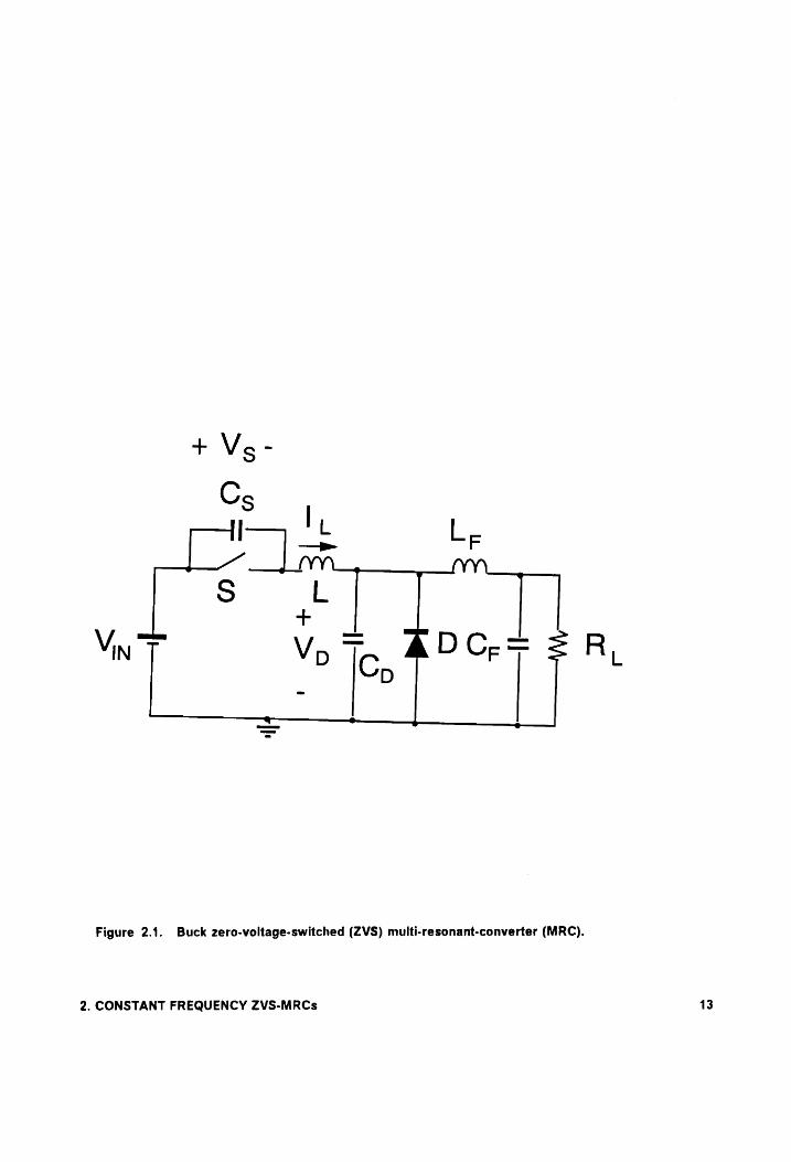
Figure 2.1. Buck zero-voltage-switched (ZVS) multi-resonant-converter (MRC).
2. CONSTANT FREQUENCY ZVS-MRCs 13
Control of turn-off of diode D
Vor
“ N
N N
‘of N | Ni ! ! Neo \ Ces
Ni | I NQ oot i
NP ht ol aN ~ oe Za
ZEN. Po ger
PON NO Neo Ny ty ty NY! 1 _ T 1,7, 1, 7,
Typical waveforms of the buck ZVS-MRC (solid lines) and the constant frequency im- plementation of the buck ZVS-MRC (dotted lines). From top to bottom: gate-source voltage of switch S,, Vc;, drain-source voltage of switch $,, Vs, capacitor voltage, Vp, and resonant inductor current, /,.
Figure 2.2.
2. CONSTANT FREQUENCY ZVS-MRCs 14
Cs ct L
S, Vn)
Ss, oL
Figure 2.3. Topological stage sequence for the buck ZVS-MRC.
2. CONSTANT FREQUENCY ZVS-MRCs
[lo 514 J
[Ty 512]
[Tp iT ]
[Tg 14]
15
At time 7,1, the voltage across the rectifier diode becomes forward biased. During the time
interval 7, — To, the resonant inductor resonates with capacitance Cs in a manner that forces
the voltage across this capacitance to return to zero at time Tz. Since the resonant inductor
current is less than zero at time To, the antiparallel diode of switch S, will conduct. Zero
voltage turn-on of switch S, is possible during the interval between time T2 and the time the
resonant inductor current becomes positive (conduction interval of the antiparallel diode of
switch S1). From time To — 73, switch S,; and diode D conduct, and the resonant inductor
current increases linearly. At time 73, the value of the resonant inductor current increases to
the value of the load current turning the freewheeling diode off. As the resonant inductor
current continues to increase above the value of the load current, the difference between the
resonant inductor and load currents charges capacitor Cp, giving rise to the fourth topological
stage. In this last topological stage, T3 — 74, switch S, is conducting and the resonant
inductor resonates with capacitance Cp. This stage ends when switch S; is turned off initiating
a new switching cycle. From the operation of this converter it can be concluded that power
is transferred during the first and last topological stages and the second and third stages
correspond to the freewheeling stages. The turn-off time of the freewheeling diode is deter-
mined from the converter operation. Therefore, there is no way of controlling the duration of
the power transferring stages (time duration determined by the natural operation of the con-
verter), and variable frequency control is needed to regulate the output terminal of this con-
verter and all other ZVS-MRCs.
From the basic operation of the buck ZVS-MRC, it can be inferred that constant frequency
operation of this converter is possible if the time at which the last stage begins can be con-
trolled; i.e., controlling the duration of the power transferring stages. In the conventional buck
ZVS-MRC the last stage begins when the resonant inductor current increases to the value of
2. CONSTANT FREQUENCY ZVS-MRCs 16
the load current and diode D is commutated off naturally. It is possible to control the time at
which the freewheeling stage ends by replacing diode D by a second active switch, So, re-
sulting in operation of the converter as depicted by the dotted lines of Fig. 2.2. When the
resonant inductor current increases to the value of the load current, switch So does not turn
off and the difference between the resonant inductor and load currents is returned to the
source. By adding switch So across the input of the output filter, the duration time during
which power is transferred to the load can be easily controlled using CF operation. The idea
of controlling ZVS-MRCs under constant switching frequency can be generalized for all
topologies by introducing the concept of the CF MR switch.
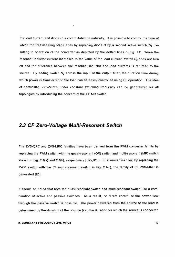
2.3 CF Zero-Voltage Multi-Resonant Switch
The ZVS-QRC and ZVS-MRC families have been derived from the PWM converter family by
replacing the PWM switch with the quasi-resonant (QR) switch and multi-resonant (MR) switch
shown in Fig. 2.4(a) and 2.4(b), respectively [B25,B26]. In a similar manner, by replacing the
PWM switch with the CF multi-resonant switch in Fig. 2.4(c), the family of CF ZVS-MRC is
generated [E5].
It should be noted that both the quasi-resonant switch and multi-resonant switch use a com-
bination of active and passive switches. As a result, no direct control of the power flow
through the passive switch is possible. The power delivered from the source to the load is
determined by the duration of the on-time (i.e., the duration for which the source is connected
2. CONSTANT FREQUENCY ZVS-MRCs 17
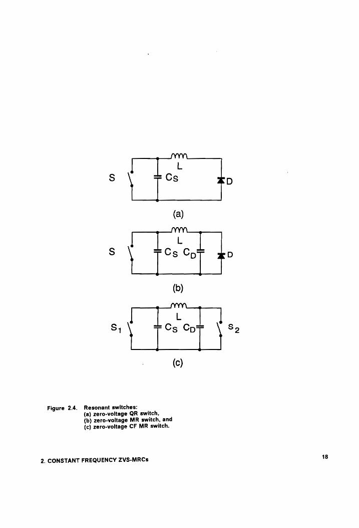
Figure 2.4. Resonant switches: (a) zero-voltage QR switch,
(b) zero-voltage MR switch, and
(c) zero-voltage CF MR switch.
2. CONSTANT FREQUENCY ZVS-MRCs 18
to the output). To control the output power flow in ZVS-QRCs, it is necessary to vary the
switching frequency by varying the on-time while the off-time is maintained constant (constant
off-time control).
The single active switch, S, in ZVS-QRCs and ZVS-MRCs controls the power flow from the
source to the load, but there is no way of returning any excess energy back to the source.
The loss of control of the power flow from the load to the source is related to the loss of
freedom that results from operating with ZVS. By operating with soft switching, the time at
which the rectifier diode (passive switch) turns on/off is determined by the zero-voltage con-
dition which depends on the operation of the converter and cannot be arbitrarily set. In order
to regain the lost degree of freedom, the passive switch can be replaced by a second active
switch as shown in Fig. 2.4(c). The second active switch is used to control the flow of energy
from the load to the source. Constant-frequency operation is now possible, since any excess
energy that is transferred to the rectifier circuit can be returned to the load by simply modu-
lating the pulse width of the on-time of the second active switch. Switch S, is operated with
CF and constant duty cycle, where the off time is determined by the ZVS condition.
The CF buck ZVS-MRC is obtained by replacing the PWM switch in the buck PWM converter
with the CF MR switch as shown in Fig. 2.5. In other words, simply replace the freewheeling
diode by an active switch as suggested in the first section of this chapter. The detailed anal-
ysis of the operation of the CF buck ZVS-MRC shows how a second active switch can be used
to control ZVS-MRCs at a constant switching frequency. It is important to notice that in ZVS
converters the active switches are generally replaced by MOSFET switches. MOSFETs are
selected as the active device because a voltage unidirectional switch is needed for ZVS. To
switch under zero voltage conditions, the antiparallel diode of switch S; and So naturally
conducts prior to turn-on, clamping the switch voltage to zero. Therefore, when the switch
2. CONSTANT FREQUENCY ZVS-MRCs 19

finally turns on, the voltage supported by the switch is zero, resulting in lossless turn-on.
Throughout this work it will be understood that when referring to a switch that operates with
ZVS, the physical switch will have an antiparallel diode, either an inherent antiparallel diode
such as MOSFET devices, or an externally added antiparallel diode.
2.4 Operation of CF Buck ZVS-MRC
For ease of explanation, it is assumed that the inductance of the output filter is large and in
Steady-state the output filter can be approximated by a constant current source with a value
equal to the load current, and that all semiconductor devices are ideal. The different
topological stages of the CF buck ZVS-MRC are shown in Fig. 2.6 and the typical waveforms
of the operation of this converter are shown in Fig. 2.7. The operation of the CF buck ZVS-MRC
can be summarized in the following manner:
Stage A [To, 7], Fig. 2.6(a)
Previous to time To, switch S; and S» are on and the inductor current increases linearly while
the load current freewheels through switch Sz. Stage A begins when switch S, is turned off
and the current that was flowing through the switch is diverted into the resonant capacitor
Cs. Switch S2 remains off and the voltage across switch S; increases in a resonant manner
as capacitances Cp and Cs resonate with inductance L. This stage ends when the voltage
2. CONSTANT FREQUENCY ZVS-MRCs 20
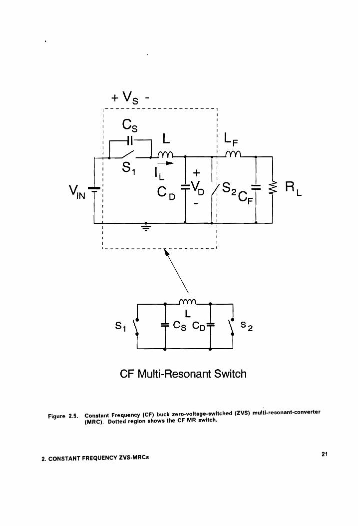
a detest ds
, peer} CF Multi-Resonant Switch
Constant Frequency (CF) buck zero-voltage-switched (ZVS) multi-resonant-converter Figure 2.5.
(MRC). Dotted region shows the CF MR switch.
2. CONSTANT FREQUENCY ZVS-MRCs 21
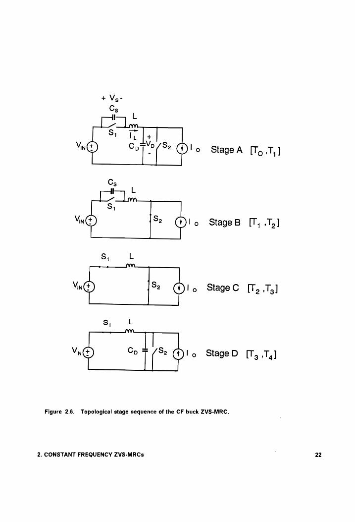
Cs | L
=V Vin ope lo StageA [1.7]
Cs
S, MS {Se or StageB [T, 7]
fyYvV\__.
Vy | Sz o StageC [T,,T,]
Ss, oL
“@ Cy {{" Oo Stage D [T5 Tg]
Figure 2.6. Topological stage sequence of the CF buck ZVS-MRC.
2. CONSTANT FREQUENCY ZVS-MRCs
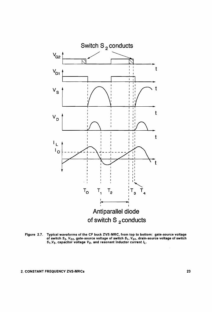
Switch S , conducts
Ver } '
L | mi ly!
Ve ! : a t 1 4!
I J i
| . at t
PL nA | 1 4!
! Dy tn +t l, 1 ; a
lo 6 i!
NZ V"t
~
To qT, qT, T 4
l
——————
Antiparallel diode
of switch S ,conducts
Figure 2.7. Typical waveforms of the CF buck ZVS-MRC, from top to bottom: gate-source voltage of switch S2, Veo, gate-source voltage of switch S;, Vg,, drain-source voltage of switch $1,Vs, capacitor voltage Vp, and resonant inductor current /,.
2. CONSTANT FREQUENCY ZVS-MRCs 23
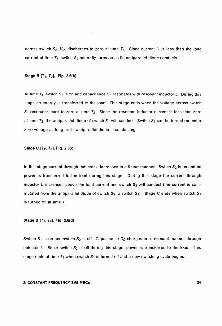
across switch So, Vp, discharges to zero at time 7;. Since current /,; is less than the load
current at tire 7,, switch S» naturally turns on as its antiparallel diode conducts.
Stage B [7;, To], Fig. 2.6(b)
At time 71, switch So is on and capacitance Cs resonates with resonant inductor L. During this
stage no energy is transferred to the load. This stage ends when the voltage across switch
S; resonates back to zero at time 72. Since the resonant inductor current is less than zero
at time To, the antiparallel diode of switch S; will conduct. Switch S; can be turned on under
zero voltage as long as its antiparallel diode is conducting.
Stage C [T2, Ts], Fig. 2.6(c)
In this stage current through inductor L increases in a linear manner. Switch So is on and no
power is transferred to the load during this stage. During this stage the current through
inductor L increases above the load current and switch So will conduct (the current is com-
mutated from the antiparallel diode of switch So to switch So). Stage C ends when switch So
is turned off at time 73
Stage B [T3, T4], Fig. 2.6(d)
Switch S, is on and switch So is off. Capacitance Cp charges in a resonant manner through
inductor L. Since switch So is off during this stage, power is transferred to the load. This
stage ends at time 74 when switch S, is turned off and a new switching cycle begins.
2. CONSTANT FREQUENCY ZVS-MRCs 24
Since power is transferred to the load only during the off-time of switch So, the output voltage
of this converter can easily be regulated by controlling the on-time of this switch without
having to vary the switching frequency. This second active switch is referred to as the
constant-frequency (CF) switch. Using this technique, soft switching of all semiconductor de-
vices is achieved at a constant switching frequency.
Due to the multiple resonance present in CF MRCs, normal operation of these converters re-
sults in more than one mode of operation where each mode corresponds to a different
topological stage sequence. The complete dc analysis of the CF buck ZVS-MRC is presented
in [E1] (operation of the CF buck ZVS-MRC results in four different modes).
2.5 Basic Constant-Frequency Multi-Resonant Topologies
The family of CF ZVS-MRCs is obtained by replacing the PWM switch in corresponding PWM
converters with the CF MR switch discussed in Section 2.2. Alternatively, the CF ZVS-MR
family of converters can also be generated from conventional PWM converters using the fol-
lowing rules:
(1) replace the rectifier diode with an active switch
{antiparallel diode is needed for operation with ZVS),
(2) place capacitance Cs in parallel with switch Sj,
(3) place capacitance Cp in parallel with switch So, and
2. CONSTANT FREQUENCY ZVS-MRCs 25
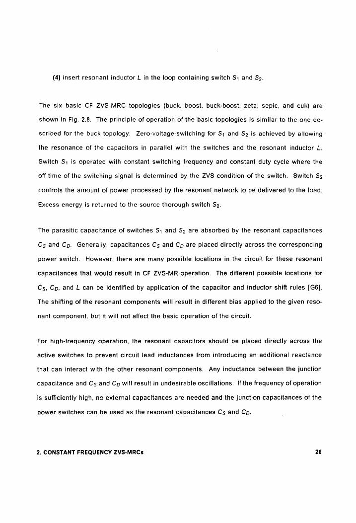
(4) insert resonant inductor L in the loop containing switch S; and So.
The six basic CF ZVS-MRC topologies (buck, boost, buck-boost, zeta, sepic, and cuk) are
shown in Fig. 2.8. The principle of operation of the basic topologies is similar to the one de-
scribed for the buck topology. Zero-voltage-switching for S; and So is achieved by allowing
the resonance of the capacitors in parallel with the switches and the resonant inductor L.
Switch S, is operated with constant switching frequency and constant duty cycle where the
off time of the switching signal is determined by the ZVS condition of the switch. Switch So
controls the amount of power processed by the resonant network to be delivered to the load.
Excess energy is returned to the source thorough switch So.
The parasitic capacitance of switches S; and S»2 are absorbed by the resonant capacitances
Cs and Cp. Generally, capacitances Cs and Cp are placed directly across the corresponding
power switch. However, there are many possible locations in the circuit for these resonant
capacitances that would result in CF ZVS-MR operation. The different possible locations for
Cs, Cp, and L can be identified by application of the capacitor and inductor shift rules [G6].
The shifting of the resonant components will result in different bias applied to the given reso-
nant component. but it will not affect the basic operation of the circuit.
For high-frequency operation, the resonant capacitors should be placed directly across the
active switches to prevent circuit lead inductances from introducing an additional reactance
that can interact with the other resonant components. Any inductance between the junction
capacitance and Cs and Cp will result in undesirable oscillations. If the frequency of operation
is sufficiently high, no external capacitances are needed and the junction capacitances of the
power switches can be used as the resonant capacitances Cs and Cp.
2. CONSTANT FREQUENCY ZVS-MRCs 26
my Aye Co 7 sm ;
(c)
C IF L L,
4 nm" nn
1
Vin T Cot (eer sR,
(e)
Vw Ly Oe RR,
(d)
Cs
Am fim —i nm 1
Vin"7 Lv C1 erry sR,
=
(f)
Figure 2.8. Basic CF ZVS-MRC topologies: (a) sepic, (b) boost, (c) cuk, (d) buck- boost, (e) buck,
and (f) zeta. So Is the constant frequency switch.
2. CONSTANT FREQUENCY ZVS-MRCs 27
Le
C Lin Cp L Se
C | | | vey ©? ‘| \, oF 3! oer :
[oye ee (d)
Lin Ca Lb Cre Le
“Ly ie at i P )
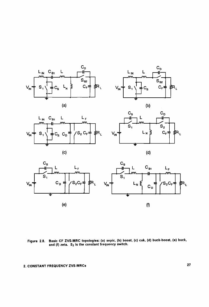
Figure 2.9. Basic single- ended isolated CF ZVS-MRC topologies: (a) forward, (b) flyback, (c) zeta, (d) sepic, and (e) cuk. S2 is the constant frequency switch.
rc
wy
Be)
2. CONSTANT FREQUENCY ZVS-MRCs 28
In most power conversion applications, a power transformer is used in dc/dc converter circuits
to provide electrical isolation and/or the desired conversion ratio. Generally, the leakage
inductance of the power transformer, especially in off-line applications, can disrupt the normal
operation of dc/dc converters. CF MR converters absorb the effect of the leakage inductance
of the transformer without disrupting the operation of the converter. The six basic isolated
topologies are shown in Fig. 2.9. The resonant capacitance Cp is shown in the secondary
circuit, directly in parallel with switch So. Placing capacitance Cp on the secondary allows the
leakage inductance of the transformer to form part of the resonant inductor L.
Capacitance Cp can also be placed across the primary windings of the power transformer.
The advantage of placing the resonant capacitance Cp on the primary side is that the high
frequency current associated with this capacitance will not circulate through the power
transformer, thereby reducing transformer winding losses. The effect of the leakage
inductance can not be accounted for in the operation of the converter if capacitance Cp is
placed across the primary winding of the transformer. At high switching frequencies, this ar-
rangement will result in unwanted ringing between the leakage inductance and the junction
Capacitance of switch So and the forward diode D, in the forward topology. This ringing in-
creases conduction losses in the rectifier circuit and could possibly result in an unstable op-
eration similar to that of ZVS-QRCs [B17,D1,D8,D12].
Operation of CF ZVS-MRCs results in conduction of the antiparallel diode of the CF switch for
an extended period of time. If a MOSFET switch is used for the CF switch, the poor charac-
teristics of the inherent antiparallel diode in all MOSFET switches will result in high conduction
losses. Conduction losses due to the conduction of the anitparallel diode of the CF switch can
be reduced by placing an external low forward voltage drop diode (Schottky diode) in parallel
with the MOSFET switch. A second alternative is to advance the turn-on time of the CF switch
2. CONSTANT FREQUENCY ZVS-MRCs 29

and operate the MOSFET switch as a synchronous rectifier [D412]. That is, force the current
to flow through the MOSFET rather than the antiparallel diode. Synchronous rectifiers are
MOSFET devices with improved third quadrant characteristics. These devices are manufac-
tured to operate as controlled rectifiers and their third quadrant voltage vs. current charac-
teristics are much better than their first quadrant characteristics. The idea of synchronous
rectification can be used successfully in CF ZVS-MRCs to reduce conduction losses of the CF
switch by using a device that has good first and third quadrant voltage vs. current character-
istics (low Rps(ON)). Using synchronous rectification in CF ZVS-MRCs does not result in ad-
ditional control. This will become more clear as the control requirements for the CF forward
and HB ZVS-MRCs are discussed in the next chapter.
The operation of nonisolated CF ZVS-MRCs can be directly extended to the single-ended,
isolated topologies, as long as the magnetizing current of the transformer is neglected.
Therefore, the analysis is not directly applicable to the CF forward ZVS-MRC since the
magnetizing current plays an important role in its operation [D7]. Also, the analysis cannot
be directly applied to off-line (bridge-type, push-pull) ZVS-MRCs due to the inherent clamping
of the resonant voltage waveform of the primary switches [B22,D8].
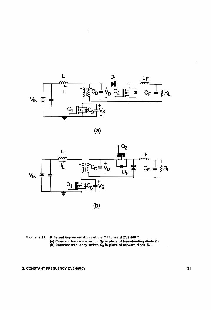
Figure 2.10 shows different implementations of the CF forward ZVS-MRC. CF operation of this
converter is possible by regaining control of the turn-off time of the freewheeling diode. Direct
control of the turn-off time of this device is achieved by replacing it by an active switch as
shown in Fig. 2.10(a). Control of the turn-off time of the freewheeling diode is also possible
by controlling the turn-on time of the forward diode D;. Control of the turn off time of the for-
ward diode is achieved by replacing this diode with an active switch as shown in Fig. 2.10(b).
2. CONSTANT FREQUENCY ZVS-MRCs 30
I t “FEO Ye Qe oe OF T Re VIN = = ; -
| Q; | 3c, Vg
Figure 2.10. Different implementations of the CF forward ZVS-MRC: (a) Constant frequency switch Q2 in place of freewheeling diode Dr; (b) Constant frequency switch Q2 in place of forward diode D;.
2. CONSTANT FREQUENCY ZVS-MRCs 31
Cp
| clare [glx IN ax
Vin + “i E. 79, CF i At
Pi PRIM * 1s IN 3 , cy
“lpr C
(c)
Figure 2.11. Different implementations of the CF HB ZVS-MRC. (a) Two active switches (constant frequency switches) replacing the rectifier diodes; (b) One active switch placed across the input of the output filter; (c) A bidirectional switch across the primary windings of the transformer.
2. CONSTANT FREQUENCY ZVS-MRCs 32

The first implementation of this converter, shown in Fig. 2.10(a), is preferred because no iso-
lated driver is needed for switch S» (CF switch).
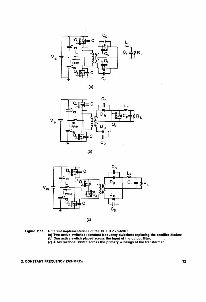
Figure 2.11 shows different implementations of the CF HB ZVS-MRC. Like the conventional
HB ZVS-MRC. the load current freewheels through the shorted secondary windings of the
power transformer during the freewheeling stage of the CF HB ZVS-MRC [D6,D8,E20]. Since
the secondary windings of the transformer are shorted during this stage, the CF HB ZVS-MRC
can be implemented by adding only one extra switch (across the output filter) as shown in Fig.
2.11(b) and still operate with ZVS. Furthermore, CF switch Q3 can be shifted to the primary
side of the power transformer as shown in Fig. 2.11(c). This implementation requires a true
bidirectional switch. By placing the CF switch on the primary side, the conduction losses in
this switch and the power transformer are reduced considerably. A complete dc analysis of
the CF forward and the HB ZVS-MRC will be presented in Chapter 3.
A detailed analysis of the CF cuk ZVS-MRC has been presented in [E6].
2.6 Experimental CF Buck ZVS-MRC
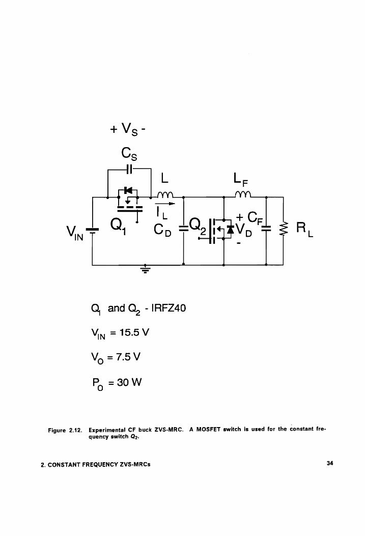
To demonstrate the high-frequency operation of CF multi-resonant converter, a CF buck
ZVS-MRC was implemented. The circuit diagram of the experimental converter is shown in
Fig. 2.12. The converter uses a simple control scheme to regulate the output voltage. The
2. CONSTANT FREQUENCY ZVS-MRCs 33
+ Ve -
Cg —_—||——_
L L- fp em rr —=- Ih
Vino Q, Cy 72 |tq&Vo == R,
Q, and Q, -IRFZ40
Viy = 15.5 V
Vo =7.5V
P, =30W
Figure 2.12. Experimental CF buck ZVS-MRC. A MOSFET switch is used for the constant fre-
quency switch Qo.
2. CONSTANT FREQUENCY ZVS-MRCs 34
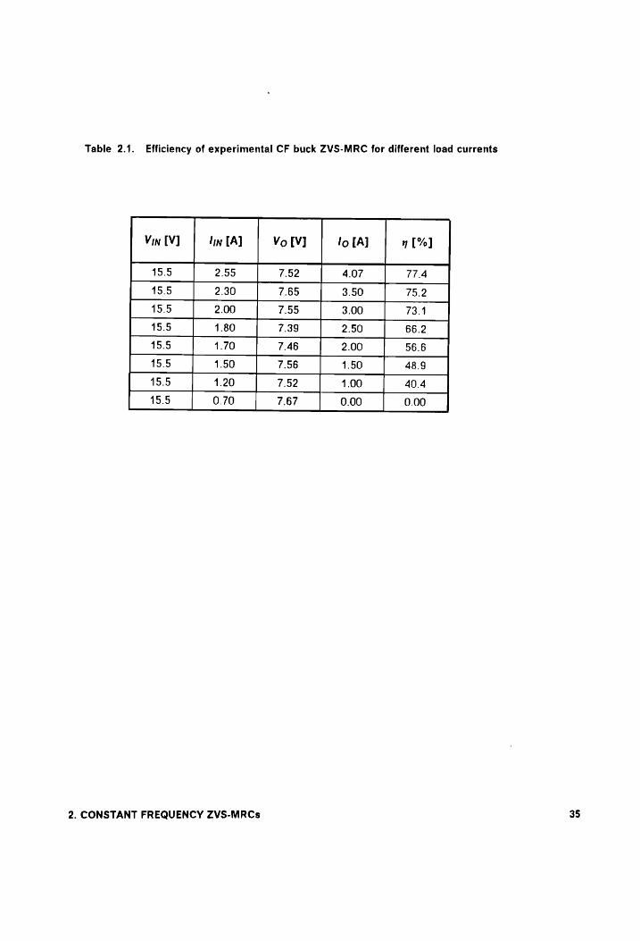
Table 2.1. Efficiency of experimental CF buck ZVS-MRC for different load currents
VinIV) | twIAl | VotV] | fofAl | 1f%]
15.5 2.55 7.52 4.07 77.4
15.5 2.30 7.65 3.50 75.2
15.5 2.00 7.55 3.00 73.1
15.5 1.80 7.39 2.50 66.2
15.5 1.70 7.46 2.00 56.6
15.5 1.50 7.56 1.50 48.9
15.5 1.20 7.52 1.00 40.4
15.5 0.70 7.67 0.00 0.00
2. CONSTANT FREQUENCY ZVS-MRCs
Q1 drive
=}
Flip-Flop
MONOSTABLE #1 0 Q Td control Q CK RD
CL
OSCILLATOR MONOSTABLE #2
Toff control Q Ton control
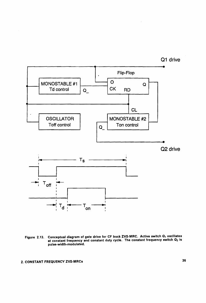
——
Q2 drive
~ Ts > | !
i ! on I
Figure 2.13. Conceptual diagram of gate drive for CF buck ZVS-MRC. Active switch Q;, oscillates
at constant frequency and constant duty cycle. The constant frequency switch Qo is
pulse-width-modulated.
2. CONSTANT FREQUENCY ZVS-MRCs 36
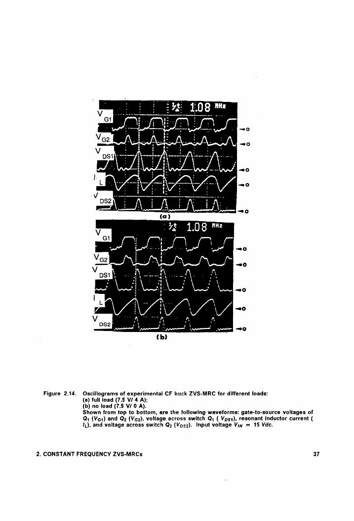
. aan
YF 1.08 Ate
Figure 2.14. Oscillograms of experimental CF buck ZVS-MRC for different loads:
(a) full load (7.5 V/ 4 A); (b) no load (7.5 V/ 0 A). Shown from top to bottom, are the following waveforms: gate-to-source voltages of Q; (Vegi) and Q2 (Vg2), voltage across switch Q; ( Vps1), resonant inductor current ( 11), and voltage across switch Qo (Vps2). Input voltage Vin = 15 Vde.
2. CONSTANT FREQUENCY ZVS-MRCs 37
driving signal of the CF switch can be generated from the driving signal of the primary switch
Q, as shown in Fig. 2.13. The converter is controlled by varying the duration of Ton of the
driving signal for Qo.
The converter was designed to deliver 30 W at an input voltage of 15 V and output voltage of
7.5 V. The converter was operated at a switching frequency of 1.08 MHz. The following com-
ponents were used for the power stage:
S1, So - IRFZ40;
Cs - 15 nF NPO chip ceramic;
Cp - 50 nF NPO chip ceramic;
L - 500 nH;
Lr - 1 wH; and
Cr - 22 pH.
Figure 2.14 shows the ocsillograms of the experimental buck converter for full load and light
load operation. The waveforms are very clean with essentially no parasitic oscillations. The
converter regulates the output voltage from full load (4 A) to no load (0 A) at a constant
switching frequency. The measured power stage efficiency for different load conditions is
given in the last column of Table 2.1. MOSFET voltage stress does not vary considerably as
the load is varied from full load to no load.
2. CONSTANT FREQUENCY ZVS-MRCs 38

2./ Summary
A new family of CF ZVS-MRCs has been presented. The CF ZVS-MR family of converters can
be generated by replacing the PWM switch by the CF MR switch in the typical PWM convert-
ers. The CF ZVS-MRCs are suitable for high-frequency operation due to their ability to absorb
all of the major parasitic components into the resonant network. All semiconductor devices
operate under ZVS conditions at a constant switching frequency resulting in a substantial re-
duction of switching losses.
2. CONSTANT FREQUENCY ZVS-MRCs 39

3. ANALYSIS OF CF FORWARD AND
HALF-BRIDGE ZVS-MRCs
3.1 Introduction
The PWM forward and half-bridge (HB) converters are two of the most popular topologies used
in applications that require isolation. The forward topology is most effective in the 50 W - 200
W range. The single-ended, single switch forward converter is a very cost effective topology
due to its low part count. The forward converter is one of the most attractive topologies of the
new family of CF ZVS-MRCs. Its operation, analysis, and characteristics are similar to those
of the conventional forward ZVS-MRC. However, the effect of the magnetizing inductance of
the power transformer, which makes the operation of the CF forward ZVS-MRC quite different
from that of the CF buck ZVS-MRC, cannot be ignored.
3. ANALYSIS OF CF FORWARD AND HALF-BRIDGE ZVS-MRCs 40
The voltage stress of the active switch in single-ended ZVS converters is generally several
times the input voltage [B33,D1-D15]. On the other hand, the bridge-type topologies clamp the
voltage across the primary active switches to the value of the input voltage. Therefore, in
similar applications, single-ended topologies require the use of switches with higher break-
down voltage. These devices have higher on-resistance relative to the devices used in HB
and push-pull topologies. As a result, the HB converter will operate with lower turn-on loss.
Consequently, the ZVS HB converter is very attractive for off-line applications where the
switching loss is of importance. Also, due to the two quadrant operation of the HB topology,
the transformer of this converter operates with reduced flux density when compared with the
one used for the forward or flyback converters having similar cross-sectional core areas.
Flux reset in the power transformer is not a concern in CF forward and HB ZVS-MRCs. In the
forward topology, transformer core reset is provided by the resonant capacitance Cp that ap-
pears across the secondary winding of the transformer [D7,D12]. In the HB topology, trans-
former core reset results from the two-quadrant operation.
Finally, due to the higher conversion frequency, the HB converter requires a smaller output
filter. For the same peak-to-peak output voltage ripple, the filter corner frequency of the HB
topology is twice that of the forward and flyback topologies.
This chapter presents complete dc analysis of the CF forward and HB ZVS-MRCs. It also dis-
cusses design trade-offs and outlines design procedure for both the forward and HB
topologies. Finally, experimental results for a 50 W CF forward ZVS-MRC and a 100 W, off-line,
CF HB ZVS-MRC are presented.
3. ANALYSIS OF CF FORWARD AND HALF-BRIDGE ZVS-MRCs 41

3.2 CF Forward ZVS-MRC
Figure 3.1 shows the conventional forward and the CF forward ZVS-MRCs. The constant fre-
quency implementation of the forward ZVS-MRC is derived by simply replacing the free-
wheeling diode in the forward ZVS-MRC by transistor Q. as shown in Fig. 3.1(b). Capacitance
Cs is the resonant capacitance across transistor Q, and it includes the output capacitance of
this switch. Capacitance Cp is the resonant capacitance across the secondary windings of the
power transformer, and it incorporates the parasitic capacitance of both, rectifier D; and CF
switch Qo. L is the resonant inductor and it absorbs the leakage inductance of the power
transformer.
3.2.1 DC Analysis
To simplify the analysis it is assumed that:
a) the output filter inductance is sufficiently large and can be approximated by a current
source with a value equal to the output current, /o;
b) the voltage drop across the conducting semiconductor switches (MOSFETs and diodes)
is negligible;
c) the switching times of the semiconductor switches are zero; and
3. ANALYSIS OF CF FORWARD AND HALF-BRIDGE ZVS-MRCs 42
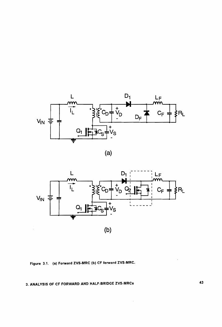
VIN T = J |+
CUE Csr Vs
(a)
L Dy; tL —_I¥YV\ | _iSVYY\
i bfoott, 5 fit! ce 4 aR Vin = = ~___ !
Figure 3.1. (a) Forward ZVS-MRC (b) CF forward ZVS-MRC.
3. ANALYSIS OF CF FORWARD AND HALF-BRIDGE ZVS-MRCs 43

d) the magnetizing inductance of the power transformer is large and can be represented by
an equivalent current source, /y, whose magnitude depends on the operating condition
but is constant over one switching cycle.
To further simplify the analysis, the load current, Jo, and the resonant capacitance, Cp, are
reflected to the primary side of the transformer. In addition, diode D,; and transistor Q» are
replaced by a single-pole double-throw switch. The equivalent model of the simplified con-
verter is shown in Fig. 3.2.
During one switching cycle, the converter goes through a sequence of five of the six possible
topological stages shown in Fig. 3.3. The CF forward ZVS-MRC can operate in four different
modes, each representing a different sequence of topological stages. Modes Il.A and II.B
occur for heavy load currents, whereas Modes I|.A and I|.B occur for light output currents.
3.2.1.1 Mode I of Operation
The sequence of the topological stages in Mode |.A is A-B-C-A-E. Figure 3.4 shows the key
waveforms of the CF forward ZVS-MRC in this mode of operation.
Stage A [To, 71], Fig. 3.3(a)
During this stage transistor Q, and diode D, are conducting and transistor Q, is off. Voltage
Vp across Cp is positive and capacitance Cp and inductor L resonate until the voltage across
3. ANALYSIS OF CF FORWARD AND HALF-BRIDGE ZVS-MRCs 44
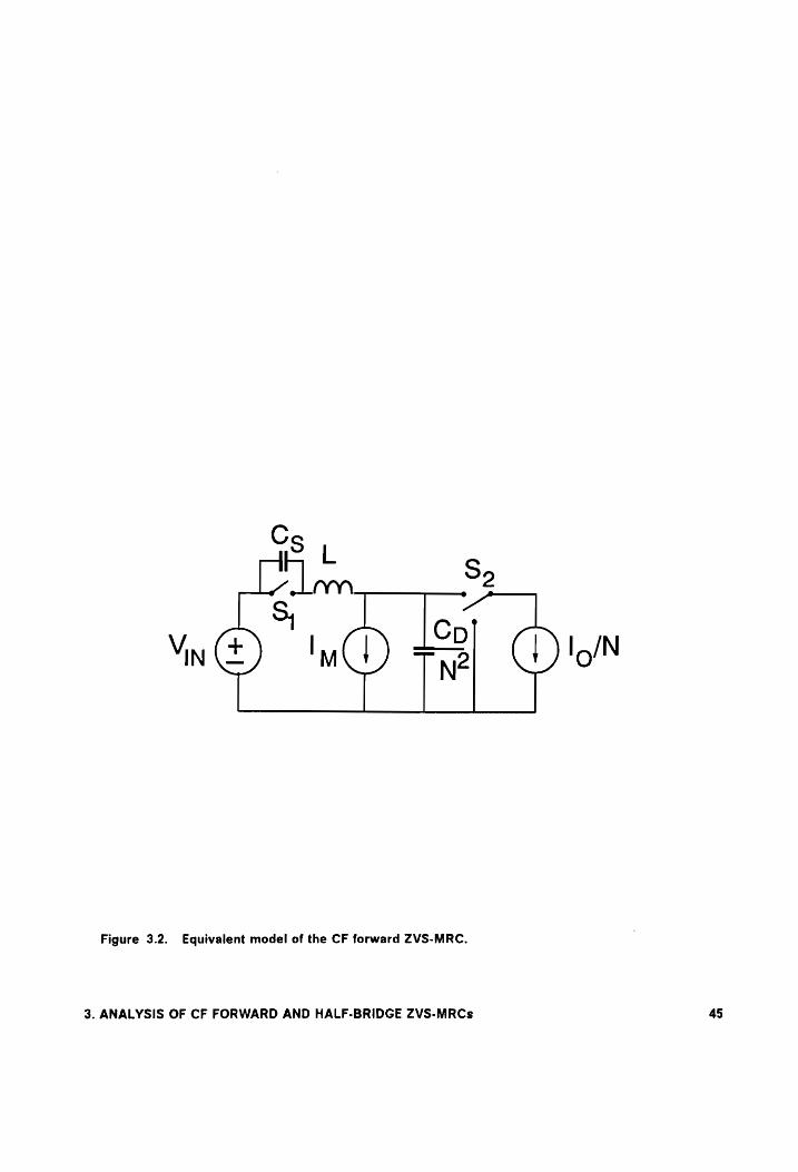
L ‘nen __82 ~ [eo
M | NZ /N
Figure 3.2. Equivalent model of the CF forward ZVS-MRC.
3. ANALYSIS OF CF FORWARD AND HALF-BRIDGE ZVS-MRCs 45
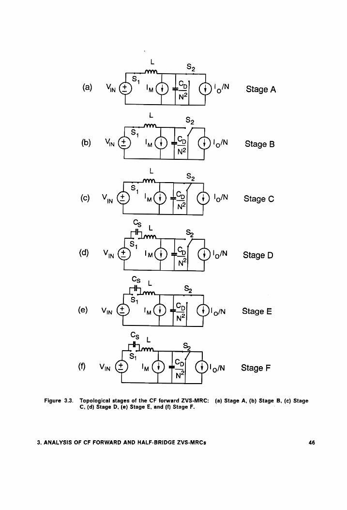
S2 SVYY\..
S;
(a) Vy © IM Jc, ID/N Stage A N
L 3 SYVYY\. S2
(b) Vin @ IV 1°. IQ/N Stage B
N
L
——Nmn_ Se2
“th Ic (c) Va M 2 oN Stage C
(d) Stage D
(e) Stage E
(f) Stage F Topological stages of the CF forward ZVS-MRC: (a) Stage A, (b) Stage B, (c) Stage Figure 3.3. C, (d) Stage D, (e) Stage E, and (f) Stage F.
3. ANALYSIS OF CF FORWARD AND HALF-BRIDGE ZVS-MRCs
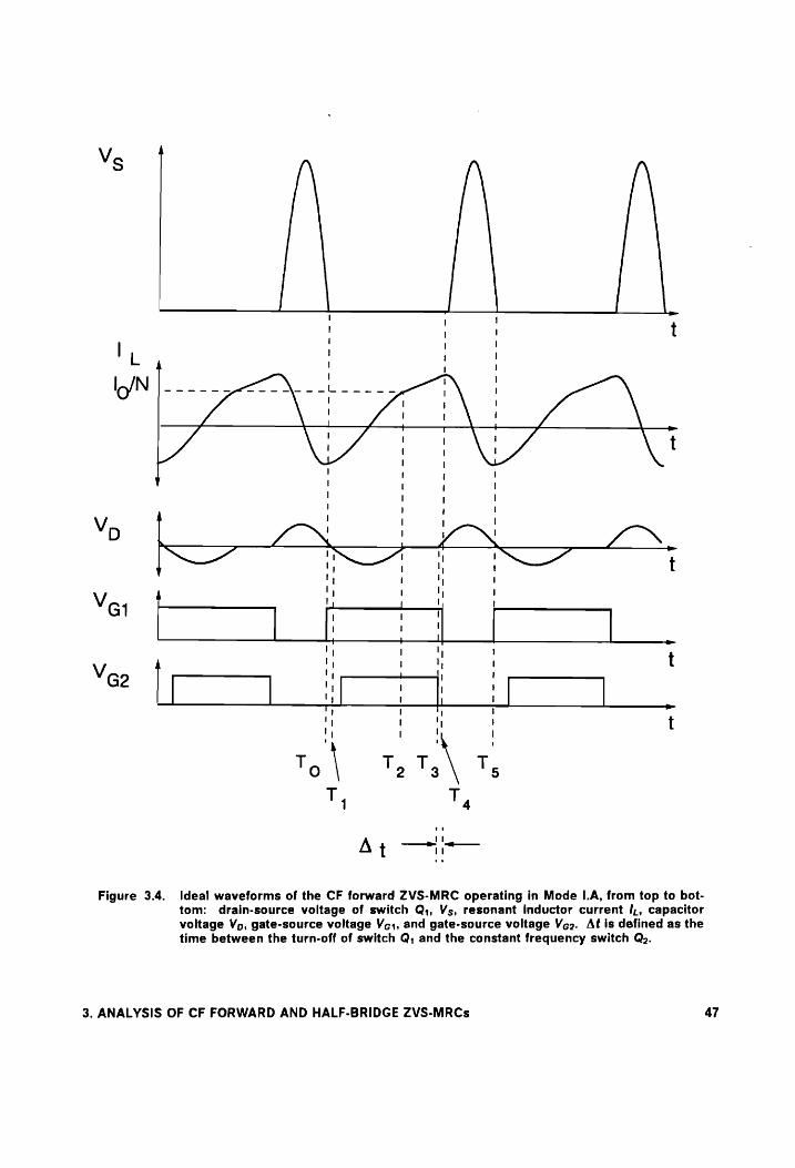
aw
Y
Figure 3.4. Ideal waveforms of the CF forward ZVS-MRC operating in Mode I.A, from top to bot- tom: drain-source voltage of switch Q,, Vs, resonant inductor current /,, capacitor voltage Vp, gate-source voltage Vg1, and gate-source voltage Veo. At is defined as the time between the turn-off of switch Q, and the constant frequency switch Qo.
3. ANALYSIS OF CF FORWARD AND HALF-BRIDGE ZVS-MRCs 47

Qs reaches Zero at time 7, and its antiparallel diode starts conducting. At the same time diode
D, turns off.
Stage B [7;, T2], Fig.3.3(b)
Since the antiparallel diode of Q. is conducting. capacitance Cp continues to resonate with L.
This stage ends at time T, when voltage Vp increases to zero and diode D; turns on. To
achieve lossless turn-on, Q2 should be turned on during this stage.
Stage C [T2, 73], Fig. 3.3(c)
In this stage D, and Q, conduct. As a result. voltage Vp is clamped to zero and the voltage
across resonant inductor L is Viv. The resonant inductor current increases linearly until Q> is
turned off at time 73.
Stage A [T3, T,], Fig. 3.3(a)
Diode D, remains on and capacitance Cp and inductance L start to resonate. Voltage Vp in-
creases in a resonant manner. This stage ends at time T,, when Q, is turned off.
Stage E [T4, Ts], Fig. 3.3(e)
Diode D; remains on, so capacitances Cp and Cs and inductance L resonate. This stage ends
at time 7s, when voltage Vs returns to zero through a resonant oscillation. Transistor Q, should
be subsequently turned on to achieve lossless turn-on. The next cycle is then initiated.
3. ANALYSIS OF CF FORWARD AND HALF-BRIDGE ZVS-MRCs 48
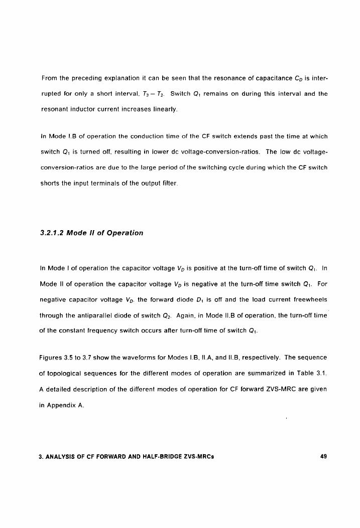
From the preceding explanation it can be seen that the resonance of capacitance Cp is inter-
rupted for only a short interval, 73 — To. Switch Q,; remains on during this interval and the
resonant inductor current increases linearly.
In Mode |.B of operation the conduction time of the CF switch extends past the time at which
switch Q, is turned off, resulting in lower dc voltage-conversion-ratios. The low dc voltage-
conversion-ratios are due to the large period of the switching cycle during which the CF switch
shorts the input terminals of the output filter.
3.2.1.2 Mode Ii of Operation
In Mode | of operation the capacitor voltage Vp is positive at the turn-off time of switch Q,. In
Mode II of operation the capacitor voltage Vp is negative at the turn-off time switch Q,. For
negative capacitor voltage Vp. the forward diode D, is off and the load current freewheels
through the antiparallel diode of switch Q,. Again, in Mode II.B of operation, the turn-off time
of the constant frequency switch occurs after turn-off time of switch Q,.
Figures 3.5 to 3.7 show the waveforms for Modes I.B, II.A, and II.B, respectively. The sequence
of topological sequences for the different modes of operation are summarized in Table 3.1.
A detailed description of the different modes of operation for CF forward ZVS-MRC are given
in Appendix A.
3. ANALYSIS OF CF FORWARD AND HALF-BRIDGE ZVS-MRCs 49
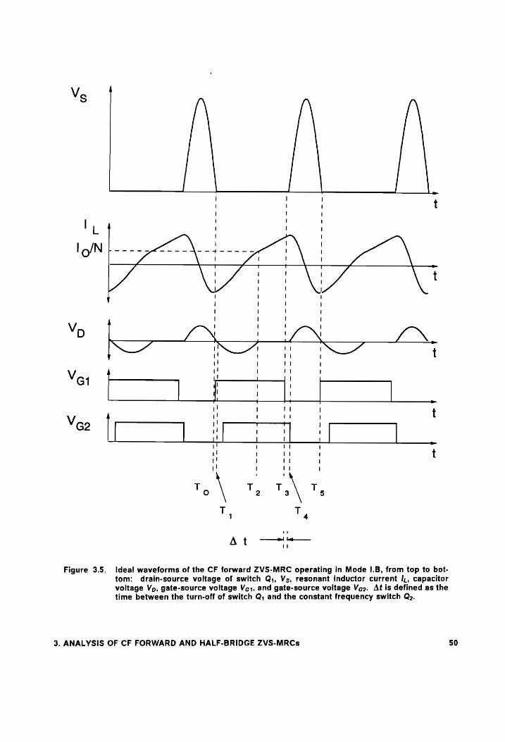
< on
ww 1
aw
\ D
=
a
Me) LN
4 r : :
Vor _—— 4 1
| 7 I + 1! ! iy I t
Vea f 4 !
ot t HEE
To5 \ T, r\ T.
T T
Figure 3.5. Ideal waveforms of the CF forward ZVS-MRC operating in Mode |.B, from top to bot- tom: drain-source voltage of switch Q;, Vs, resonant inductor current /,, capacitor voltage Vp, gate-source voltage V¢;, and gate-source voltage Vez. At is defined as the time between the turn-off of switch Q, and the constant frequency switch Qo.
3. ANALYSIS OF CF FORWARD AND HALF-BRIDGE ZVS-MRCs
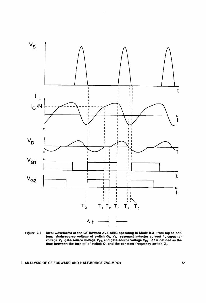
+
V :
Nn I ! IN ‘t
Ver | pi i
rT t Veo |
ria c yy my
To T, 1, T, T, T,
At — \
Figure 3.6. Ideal waveforms of the CF forward ZVS-MRC operating in Mode II.A, from top to bot- tom: drain-source voltage of switch Q;, Vs, resonant inductor current /,, capacitor voltage Vp, gate-source voltage Vcg;, and gate-source voltage Veo. At is defined as the time between the turn-off of switch Q; and the constant frequency switch Qo.
3. ANALYSIS OF CF FORWARD AND HALF-BRIDGE ZVS-MRCs
|
i
| | I
Veo : ; ! I
| ! \ Ht | — i i ! i Vi ; t ' ' eh J
T 0 T 1 T 2 T 5
q 3 q 4
‘4
At —=— I,
Figure 3.7. Ideal waveforms of the CF forward ZVS-MRC operating in Mode II.B, from top to bot- tom: drain-source voltage of switch Q,, Vs, resonant inductor current /,, capacitor voltage Vp, gate-source voltage Vg1, and gate-source voltage Vez. At is defined as the time between the turn-off of switch Q,; and the constant frequency switch Q2.
3. ANALYSIS OF CF FORWARD AND HALF-BRIDGE ZVS-MRCs 52
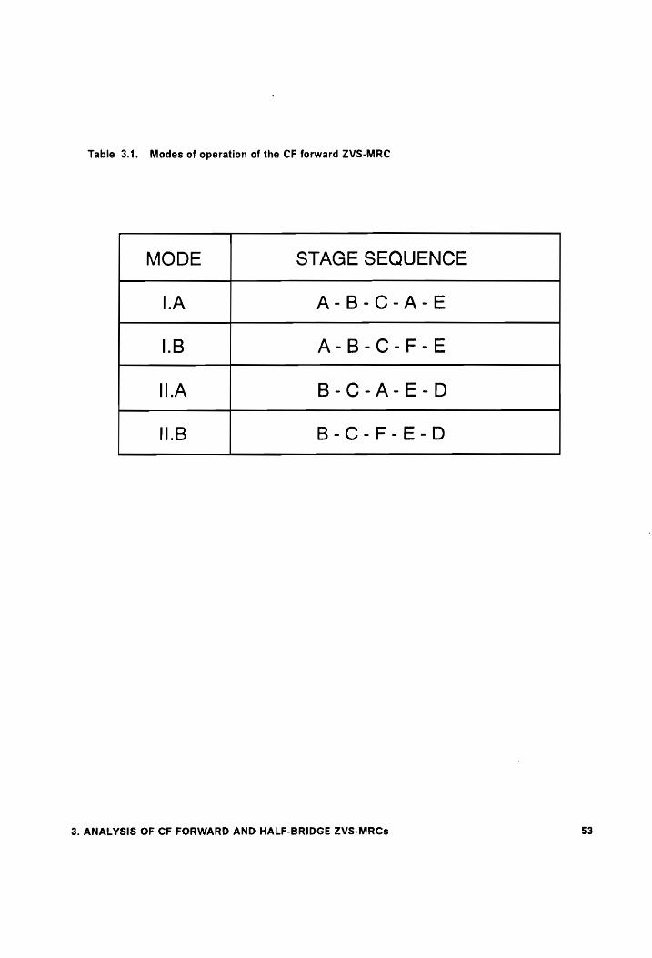
Table 3.1. Modes of operation of the CF forward ZVS-MRC
MODE STAGE SEQUENCE
LA A-B-C-A-E
.B A-B-C-F-E
ILA B-C-A-E-D
.B B-C-F-E-D
3. ANALYSIS OF CF FORWARD AND HALF-BRIDGE ZVS-MRCs 53
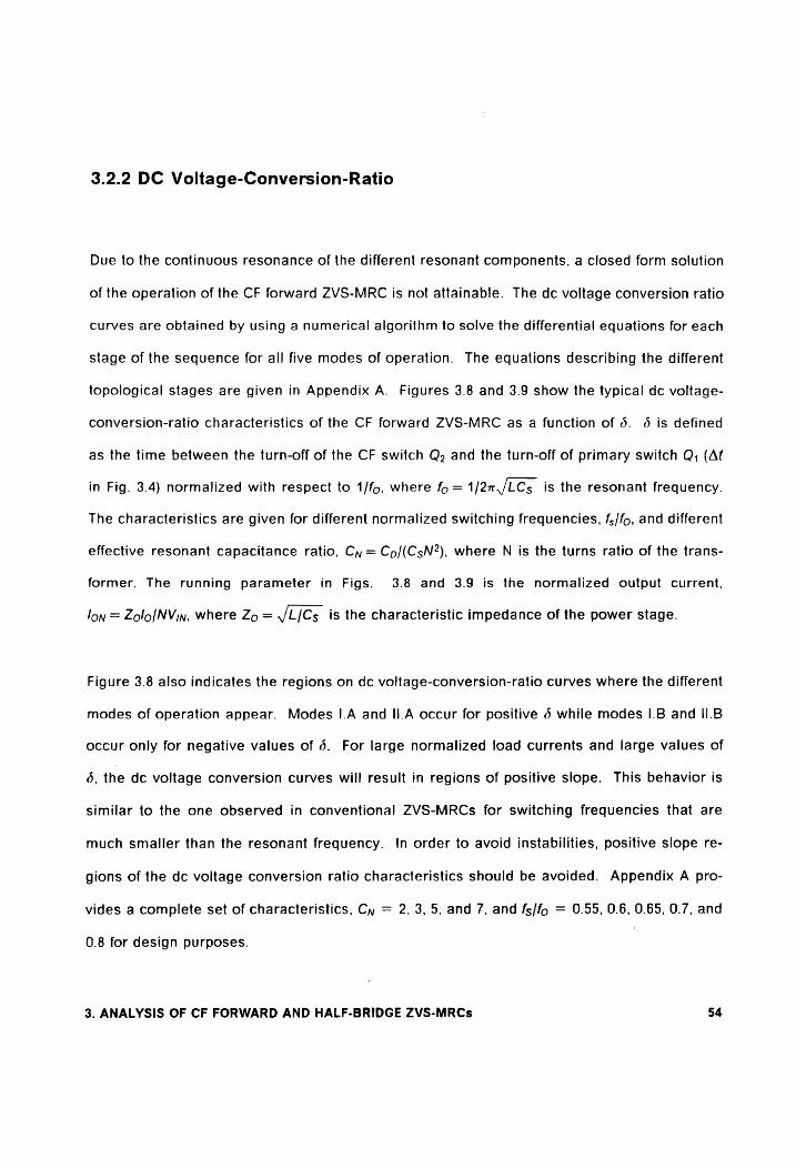
3.2.2 DC Voltage-Conversion-Ratio
Due to the continuous resonance of the different resonant components, a closed form solution
of the operation of the CF forward ZVS-MRC is not attainable. The dc voltage conversion ratio
curves are obtained by using a numerical algorithm to solve the differential equations for each
stage of the sequence for all five modes of operation. The equations describing the different
topological stages are given in Appendix A. Figures 3.8 and 3.9 show the typical dc voltage-
conversion-ratio characteristics of the CF forward ZVS-MRC as a function of 6. 6 is defined
as the time between the turn-off of the CF switch Q, and the turn-off of primary switch Q, (At
in Fig. 3.4) normalized with respect to 1/fo, where fo = 1/22 J/LCs is the resonant frequency.
The characteristics are given for different normalized switching frequencies, f,/fo, and different
effective resonant capacitance ratio, Cy = Cp/(CsN?), where N is the turns ratio of the trans-
former. The running parameter in Figs. 3.8 and 3.9 is the normalized output current,
lon = Zolo/NVin, where Zo =./L/Cs is the characteristic impedance of the power stage.
Figure 3.8 also indicates the regions on dc voltage-conversion-ratio curves where the different
modes of operation appear. Modes |.A and Il.A occur for positive 6 while modes |.B and II.B
occur only for negative values of 6. For large normalized load currents and large values of
é, the dc voltage conversion curves will result in regions of positive slope. This behavior is
similar to the one observed in conventional ZVS-MRCs for switching frequencies that are
much smaller than the resonant frequency. In order to avoid instabilities, positive slope re-
gions of the dc voltage conversion ratio characteristics should be avoided. Appendix A pro-
vides a complete set of characteristics, Cy = 2, 3, 5, and 7, and fs/fo = 0.55, 0.6, 0.65, 0.7, and
0.8 for design purposes.
3. ANALYSIS OF CF FORWARD AND HALF-BRIDGE ZVS-MRCs 54
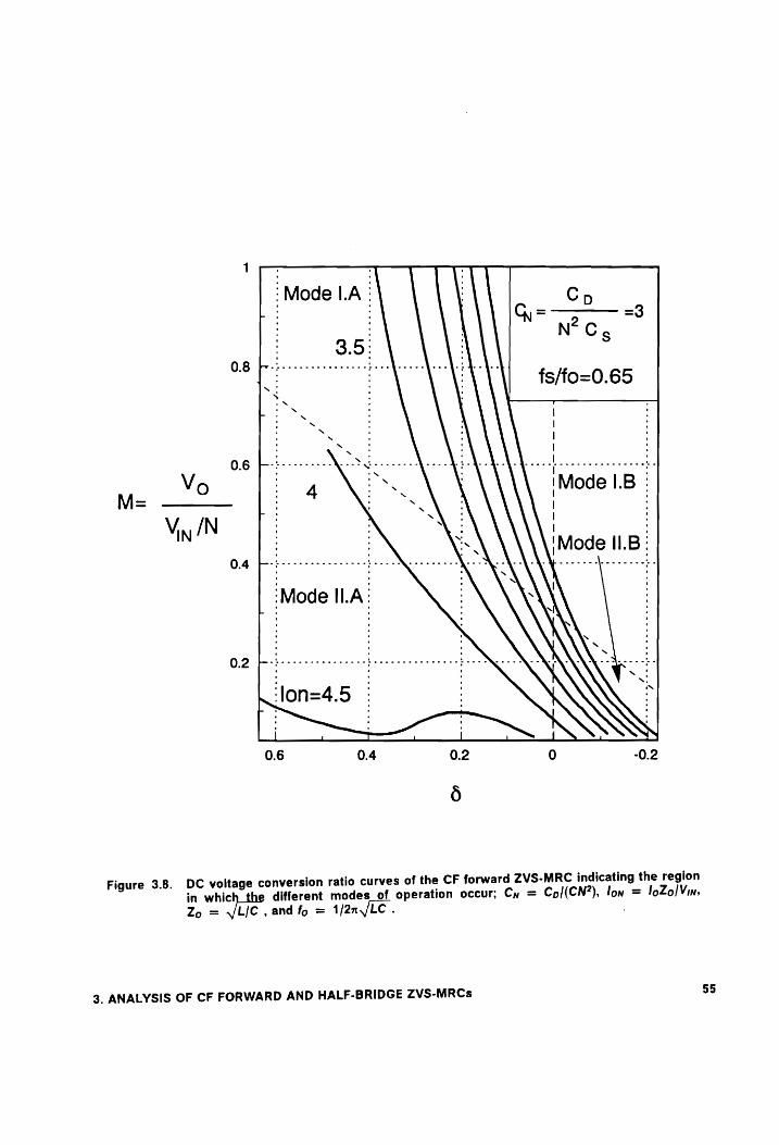
Mode LA | Cp L : Q=— > 58
NC, 0.8 bloc. PA. AA!
{ : : 2 fs/fo=0.65 —r
a en oA AV . Mode I.B :
Mode 11.B
Figure 3.8. DC voltage conversion ratio curves of the CF forward ZVS-MRC indicating the region
in whic different modes of operation occur; Cy = Col(CN?), lon = loZo/Vin,
Zo = VL/C , and fo = 1/2n,/LC .
3. ANALYSIS OF CF FORWARD AND HALF-BRIDGE ZVS-MRCs
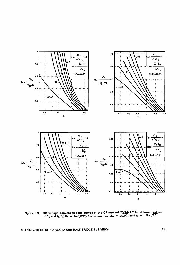
0.5
0.4
V M= O43
Vn /N
02
0.1
0.35
0.3
Vv 0.25
Oo Mz
Vin/N 2
0.15
0.1 0.05 Figure 3.9. DC voltage conversion ratio curves of the CF forward Z
of Cy and fs/fo; Cu = Co/(CN?), lon = loZolVin, Zo
3. ANALYSIS OF CF FORWARD AND HALF-BRIDGE ZVS-MRCs
0:5
Pee ee ee Me ee Re eh BR ee eee
@eere eee - -R--&- A- A- -
bee mee ee et em we eee
CS ve 25
N°C,
Zolo
NV
lon=
fs/fo=0.65
Se ee
eye er eee eee ee
-MRC for different values
= /L/C , and fo = 1/2nx,/LC .
56

3.3 CF HB ZVS-MRC
The circuit diagram of the conventional and CF HB ZVS-MRCs are shown in Fig. 3.10. The CF
HB ZVS-MRC is obtained by replacing the output rectifiers in the HB ZVS-MRC with transistors
Q3 and Q,4 as shown in Fig. 3.10(b). Resonant capacitors C; and Cy represent the output
capacitance of the primary transistors, Q; and Q.. Resonant inductor L can either be a sepa-
rate inductor or the leakage inductance of the transformer. Since the junction capacitance of
the CF switches is not sufficiently large to obtain the desired resonance, capacitors C3 and
C4 are usually externally-added capacitors.
3.3.1 DC Analysis
To simplify the analysis, in addition to the assumptions made for the forward converter, it is
assumed that Q; and Q». and switches Q3 and Q, are identical so that C;=Cy=Cs and
C3=C,=Cp. Since the magnetizing current is not important for the operation of the HB con-
verter, it is ignored.
It was found that during one switching cycle the converter enters a sequence of five
topological stages out of the seven possible shown in Fig. 3.11. It was also found that the CF
HB ZVS-MRC can operate in six modes. Mode |.A occurs at high load currents and high dc
voltage conversion ratios whereas modes II.A, II.B, and II.C occur at lighter load currents and
3. ANALYSIS OF CF FORWARD AND HALF-BRIDGE ZVS-MRCs 57
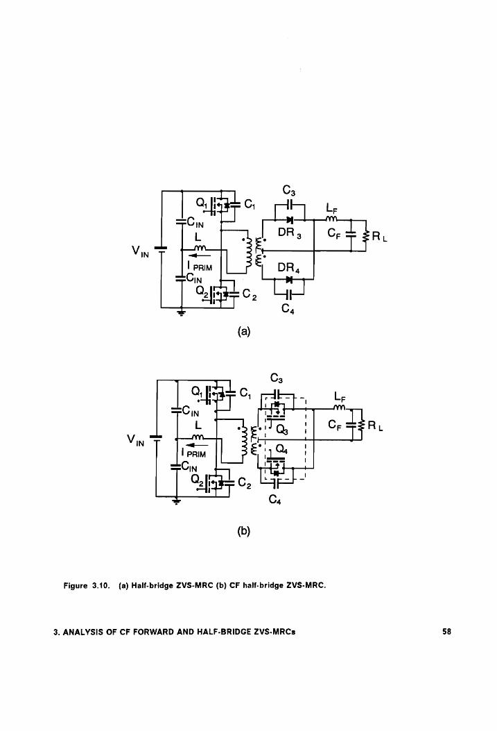
(a)
Cs Ofte C t— _ L he ‘fF b= F
Cin LI Ee ) Tl L : E I Q, || Cr TF Ri
Vin ~ IN T = EQ, 3
Cn | 34 ! O “
HI
2 2
T
(b)
Figure 3.10. (a) Half-bridge ZVS-MRC (b) CF half-bridge ZVS-MRC.
3. ANALYSIS OF CF FORWARD AND HALF-BRIDGE ZVS-MRCs 58

high dc voltage-conversion-ratios. Modes |.B and |.C occur for low dc voltage conversion ra-
tios.
3.3.1.1 Mode | of Operation
Figure 3.12 shows the key waveforms of the CF HB ZVS-MRC during Mode |.A of operation.
The sequence of the topological stages in this mode is A-B-C-CF-D.
Stage A [To, T,]. Fig. 3.11(a)
At time To, Q, is turned off. Since the antiparallel diode of Q3 is reverse-biased, capacitances
C,, Co, and C4 resonate with inductance L. During this stage capacitance C, is being charged
in a resonant manner and Cp» is being discharged. The stage terminates at time 7; when
voltage across capacitor Co becomes zero (at the same time voltage across C, is Vj). Sub-
sequently, switch Q. and the constant frequency switch Q3 should be turned on to achieve soft
switching.
Stage B [T;, To], Fig. 3.11(b)
In this stage C, continues to resonate with L. Due to a negative voltage across L, the primary
current decreases and C, continues to discharge. The stage terminates at time T. when the
capacitor voltage across C, becomes zero and the antiparallel diode of Q, turns on.
3. ANALYSIS OF CF FORWARD AND HALF-BRIDGE ZVS-MRCs 59
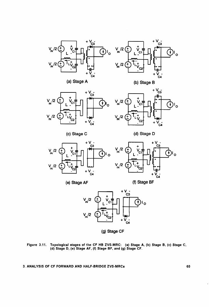
(g) Stage CF
Figure 3.11. Topological stages of the CF HB ZVS-MRC:
(a) Stage A, (b) Stage B, (c) Stage C,
(d) Stage D, (e) Stage AF, (f) Stage BF, and (g) Stage CF.
3. ANALYSIS OF CF FORWARD AND HALF-BRIDGE ZVS-MRCs 60
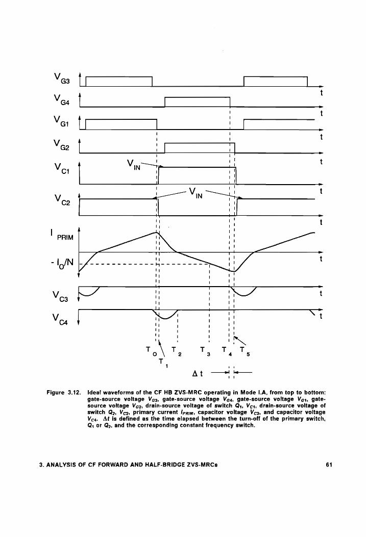
Yes [fT | | | Via | .
1 t Vey tT | ! | .
Vee | 7 : : Vor | Vive '
At —=—
Figure 3.12. Ideal waveforms of the CF HB ZVS-MRC operating in Mode I.A, from top to bottom: gate-source voltage Vc3, gate-source voltage Ves, gate-source voltage Vg, gate- source voltage Vg2, drain-source voltage of switch Q;, Ve;, drain-source voltage of switch Q2, Veo, primary current Ipgim, capacitor voltage Vc3, and capacitor voltage Vcq. At is defined as the time elapsed between the turn-off of the primary switch, Q, or Qo, and the corresponding constant frequency switch.
3. ANALYSIS OF CF FORWARD AND HALF-BRIDGE ZVS-MRCs 61

Stage C [To2, 73], Fig. 3.11(c)
In this stage the antiparallel diodes of Q3 and Q, conduct so that the secondary windings of the
transformer are shorted. As a result, the primary voltage across the transformer is zero and
a negative voltage is applied to L. The primary current decreases with a constant rate. This
stage terminates at time T3; when the primary current becomes — /9/N and the antiparallel di-
ode of Q3 ceases to conduct.
Stage CF [T3, 74], Fig. 3.11(g)
During this stage transistor Q3 conducts. The primary voltage of the transformer is zero and
the current through the resonant inductor continues to decrease at a constant rate. This stage
terminates when switch Q3 is turned off at time Tq.
Stage D [Ts, Ts], Fig. 3.11 (d)
At timeT,4, C3 starts resonating with inductance L. This stage ends when transistor Q, is turned
off and a new conversion cycle is initiated.
In Mode I|.A of operation the time at which capacitance C3 resonates with inductance L is de-
layed until switch Q. is turned off (as long as switch Q3 is on the voltage across C3 is shorted).
In Mode I|.B and I.C the conduction time of switches Q3 and Q, (the CF switches) is extended
past the time during which the switching transition of switches Q, and Q, occurs. Therefore,
3. ANALYSIS OF CF FORWARD AND HALF-BRIDGE ZVS-MRCs 62

the voltage across the input of the output filter remains shorted for a longer period of the
switching cycle resulting in low dc voltage-conversion-ratios.
3.3.1.3 Mode Il of Operation
In this mode of operation the current through the resonant inductor is between Io/N < , <
—Io/N at the time the secondary side resonant capacitor discharges resulting in the absence
of the natural freewheeling stage (Stage C). Mode !I is characterized by increased circulating
currents in the rectifier circuit and the secondary windings of the transformer.
In Modes II.B and II.C, the CF switches are allowed to conduct a longer period of time and they
are not turned off until after the primary switches (switches Q, or Q2) have been turned off.
Figures 3.13 to 3.15 show the typical converter waveforms for the CF HB ZVS-MRC operating
in Modes I.C, Il.A, and II.C, respectively. Table 3.2 summarizes the five-stage sequences of
the modes of operation for the CF HB ZVS-MRC. A detailed description of the six modes of
operation of the CF HB ZVS-MRC are given in Appendix B.
3.3.2 DC Voltage-Conversion-Ratio
For reasons similar to the ones discussed for the forward topology, the dc voltage conversion
ratio curves for the HB topology are obtained by using a numerical algorithm to solve the
differential equations for each stage of the sequence representing the eight modes of opera-
3. ANALYSIS OF CF FORWARD AND HALF-BRIDGE ZVS-MRCs 63
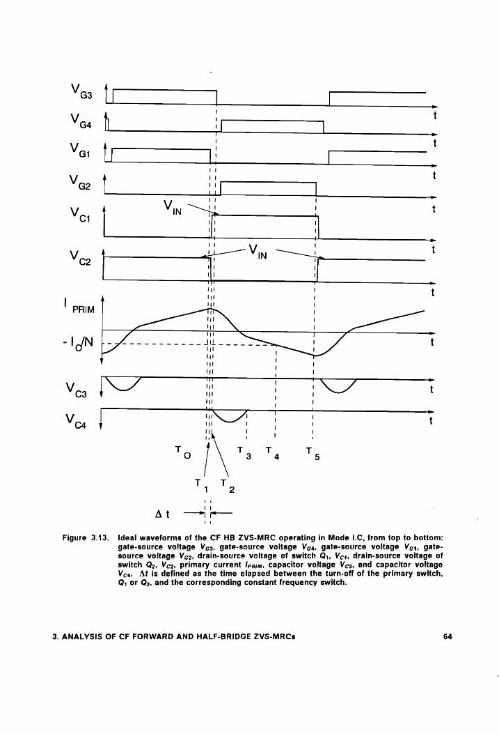
G3 tT _| 7
t
Yoo LL i . V t
G1 tT _ |
Vv 7 t a2 | 7 :
V r t Yor | NT :
Veo } ai Vy —1
1 4 rt ! PRIM 1 I oo
- IN Cfo nnnnnnnee th t
' "
~»
or td w+
¥
Vt At — -.—
4
Figure 3.13. Ideal waveforms of the CF HB ZVS-MRC operating in Mode I.C, from top to bottom: gate-source voltage Ves, gate-source voltage Vc4, gate-source voltage Vg, gate- source voltage Vc2, drain-source voltage of switch Q,, Vc, drain-source voltage of switch Qo, Vc2, primary current Ipajy, capacitor voltage Vc3, and capacitor voltage Vcq. At is defined as the time elapsed between the turn-off of the primary switch, Q, or Qo, and the corresponding constant frequency switch.
3. ANALYSIS OF CF FORWARD AND HALF-BRIDGE ZVS-MRCs 64
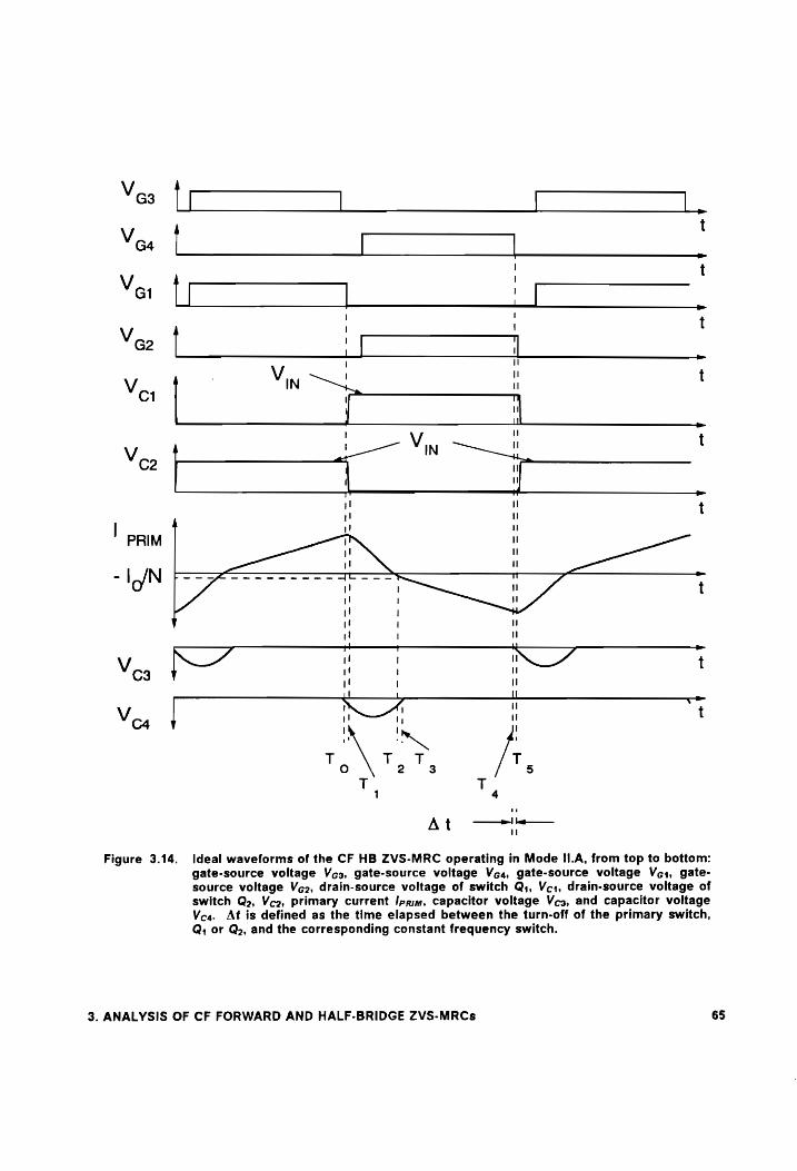
-e
¥
Vea [ L
Ver [I] ] 7 j
Vee | 1
of : |
< <
z
we
-
a Zz
< 9
—~
¥
At —-— Figure 3.14. Ideal waveforms of the CF HB ZVS-MRC operating in Mode II.A, from top to bottom:
gate-source voltage Vc3, gate-source voltage Vgs«, gate-source voltage Vg:, gate- source voltage V2, drain-source voltage of switch Q,, Vci, drain-source voltage of switch Q>2, Veo, primary current Ipaim, Capacitor voltage Ves, and capacitor voltage Ves. At is defined as the time elapsed between the turn-off of the primary switch, Q, or Q>, and the corresponding constant frequency switch.
3. ANALYSIS OF CF FORWARD AND HALF-BRIDGE ZVS-MRCs
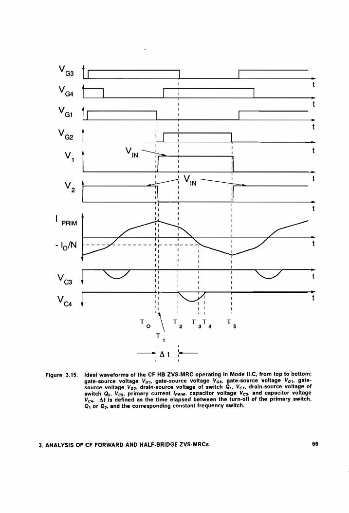
T 2
—At *—
Figure 3.15. Ideal waveforms of the CF HB ZVS-MRC operating in Mode II.C, from top to bottom: gate-source voltage Vc3, gate-source voltage Ves, gate-source voltage Vc,, gate- source voltage Veo, drain-source voltage of switch Q,, Vci, drain-source voltage of switch Q2, Veo, primary current Ipgm, capacitor voltage Vcs, and capacitor voltage Vcq. At is defined as the time elapsed between the turn-off of the primary switch, Q, or Qo, and the corresponding constant frequency switch.
3. ANALYSIS OF CF FORWARD AND HALF-BRIDGE ZVS-MRCs 66
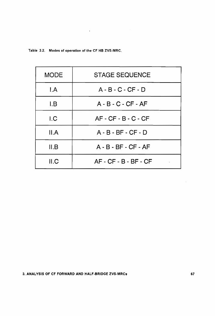
Table 3.2. Modes of operation of the CF HB ZVS-MRC.
MODE STAGE SEQUENCE
LA A-B-C-CF-D
1B A-B-C-CF-AF
LC AF -CF-B-C-CF
ILA A-B-BF-CF-D
I.B A-B-BF-CF-AF
ILC AF -CF-B-BF-CF
3. ANALYSIS OF CF FORWARD AND HALF-BRIDGE ZVS-MRCs 67

tion. The equations for the topological stages describing the operation of the HB topology are
given in Appendix B. Figures 3.16 and 3.17 show the typical dc voltage-conversion-ratio
characteristics of the CF HB ZVS-MRC as a function of 6. 6 is defined as the time between the
turn-off of the CF switch Q3 or Q,, and the turn-off of the primary switch Q,; or Qos, respectively,
(At in Fig. 3.11) normalized with respect to 1/fo, where the resonant frequency is
fo= 1/2n/LC . The characteristics are given for different normalized conversion frequencies,
feon[f, and for different values of Cy = 2Cp/(CN?), where fcon = 2fs is the conversion frequency,
fs is the switching frequency, and N is the turns ratio of the transformer. The running param-
eter in Figs. 3.146 and 3.17 is the normalized output current, lon = 2Zolo/NVin where
Zo=~VL/2C is the characteristic impedance.
Figure 3.16 also shows the regions in the dc voltage-conversion-ratio characteristics where
the different modes of operation for the CF HB ZVS-MRC occur. Mode | occurs for heavy load
operation and Mode II occurs for lighter load conditions. Modes |.A and I|.A occur for positive
values of 6 and modes |.B, I.C, II.B, and II.C occur for negative values of 6.
A complete set of design characteristics, Cy = 2.5, 10, and 20; and fcon/fo = 0.2, 0.25, 0.3, and
0.35, are given in Appendix B.
3. ANALYSIS OF CF FORWARD AND HALF-BRIDGE ZVS-MRCs 68
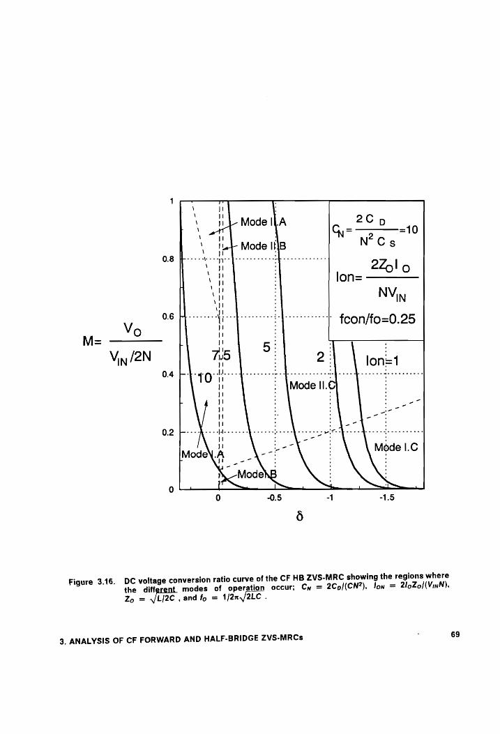
2C p Q=—z7 7210
N° Cs
2Zo1 6
NV
- fcon/fo=0.25
lon=
Figure 3.16. DC voltage conversion ratio curve of the CF HB ZVS-MRC showing the regions where
the diff modes of operation occur; C
Zo = V/L/2C , and fo = 1/2n,/2LC .
3. ANALYSIS OF CF FORWARD AND HALF-BRIDGE ZVS-MRCs
wo = 2CpI(CN?), lon = 2loZol(VinN),
69
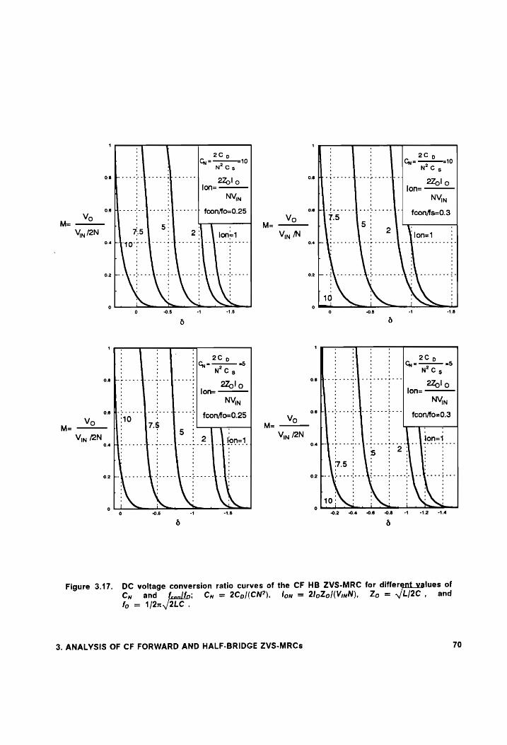
1 1
_2f5 0 205
: ’ N’?Cs5 : : Cus N?C .
osk--- ale ef ee eee these ceed nm pCi agg poet ede :
: : 220 08 ‘ coeeeesey : : lon= 2 : : lon= 220! o
NVin it : NVin r fcon/fo=0.25 fcon/fs=0.3
lon=1 lon=1
1.6 3
6
1
2Cp 2Cp : G= 2 25 = 2 x5
; N°C5 N°C gs 06 F------4e-- nee dee eee : 3 | Bolo 22ol 0
-| lon= lon=
: : : NVin NViy Vo oe H- ‘0 ---]--- woos : "| feon/fo=0.25 fcon/fo=0.3
Figure 3.17. DC voltage conversion ratio curves of the CF HB ZVS-MRC for diferent values of
Cn and f, fo; Cn = 2Cp/(CN?), lon = 2loZo!(VinN), Zo = Lj2c ’ and
fo = 1]2x./2LC .
3. ANALYSIS OF CF FORWARD AND HALF-BRIDGE ZVS-MRCs 70

3.4 Design Guidelines
In order to determine design guidelines for CF ZVS-MRCs, it is necessary to determine the
maximum peak-to-peak currents and voltages for both the active switches and the rectifier
diodes. Since CF ZVS-MRCs can be designed for different values of f,/fo (leonlfo for the HB
topology) and Cy which results in different device stresses, design trade-offs need to be con-
sidered. No analytical expressions for the current and voltage stresses on the different con-
verter components exist for any topology of this new family of converters. Therefore, current
and voltage stresses are determined from the numerical solution of the operation of the con-
verters.
To evaluate the effect of the different design parameters on the performance of CF ZVS-MRCs,
different design examples for both the forward and HB topologies are considered. A stress
analysis of the different design examples provides design trade-offs and guidelines. The de-
signs of the CF forward and HB ZVS-MRC are based on the numerically calculated dc
voltage-conversion-ratio characteristics and require the following design specifications:
input voltage range, VjR™ — Vin":
¢ output voltage, Vo:
e = load range, /8'" — 13": and
e switching frequency, fy.
The first step in designing the converter is to determine the transformer turns ratio N, Cy, and
fslfo (fcon|/fo for the HB topology) using a set of dc characteristics plotted for different Cy and
f,!fo (fcon/fo). In order to design an efficient converter, both conduction and magnetic core
3. ANALYSIS OF CF FORWARD AND HALF-BRIDGE ZVS-MRCs 71
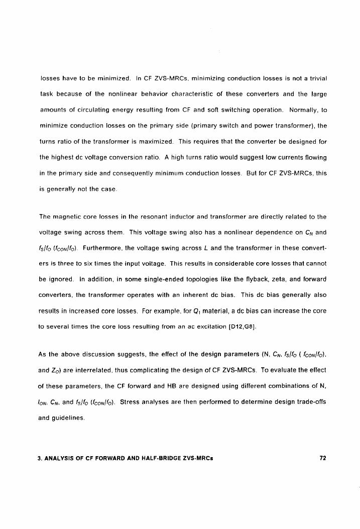
losses have to be minimized. In CF ZVS-MRCs, minimizing conduction losses is not a trivial
task because of the nonlinear behavior characteristic of these converters and the large
amounts of circulating energy resulting from CF and soft switching operation. Normally, to
minimize conduction losses on the primary side (primary switch and power transformer), the
turns ratio of the transformer is maximized. This requires that the converter be designed for
the highest dc voltage conversion ratio. A high turns ratio would suggest low currents flowing
in the primary side and consequently minimum conduction losses. But for CF ZVS-MRCs, this
is generally not the case.
The magnetic core losses in the resonant inductor and transformer are directly related to the
voltage swing across them. This voltage swing also has a nonlinear dependence on Cy and
fslfo (fcon/fo). Furthermore, the voltage swing across L and the transformer in these convert-
ers is three to six times the input voltage. This results in considerable core losses that cannot
be ignored. In addition, in some single-ended topologies like the flyback, zeta, and forward
converters, the transformer operates with an inherent dc bias. This dc bias generally also
results in increased core losses. For example, for Q; material, a dc bias can increase the core
to several times the core loss resulting from an ac excitation [D12,G8].
As the above discussion suggests, the effect of the design parameters (N, Cy, fs/fo ( fcon/fo),
and Zo.) are interrelated. thus complicating the design of CF ZVS-MRCs. To evaluate the effect
of these parameters, the CF forward and HB are designed using different combinations of N,
lon, Cn, and fs/fo (fcon/fo). Stress analyses are then performed to determine design trade-offs
and guidelines.
3. ANALYSIS OF CF FORWARD AND HALF-BRIDGE ZVS-MRCs 72

3.4.1 Design Trade-offs for CF Forward ZVS-MRC
Design trade-offs of the forward topology are based on the following design specifications:
¢ input voltage range, Vn — VIN" = 45-55 V:
e §€6©output voltage, Vo = SV;
e load range, /g"" — 18% = 2- 10 A; and
e switching frequency, f, = 2 MHz.
These design specifications represent design parameters for a VLSI application. Figure 3.18
shows the dc voltage-conversion-ratio characteristics of the CF forward ZVS-MRC for Cy = 5
and 3, and f,/fo = 0.65 and 0.7. From the de voltage conversion ratio characteristics it can
be seen that for Cy = 5 and fs/fo = 0.7 a transformer turns ratio less than or equal to one
which will translate into high conduction losses. Due to high conduction losses it is obvious
that such a characteristic should be avoided when designing a CF ZVS-MRC. From the dc
characteristics it can also be seen that a fourth design parameter needs to be determined, i.e.,
the maximum normalized load current, [38* = (/5"Zo)/Vi'". To investigate the effect of N,
Cw, fs/fo, and /64* on the converter performance, seven different design examples are consid-
ered:
Design #1: N = 5, OK" = 4, Cn = 3, and fe/fo = 0.65,
Design # 2: N = 8, ISK" = 3, Cy = 3, and fs/fo = 0.65,
Design # 3: N = 3, 10K" = 4, Cn = 3, and fe/fo = 0.65,
Design # 4: N = 5, IGK% = 3, Cyn = 3, and fef/fo = 0.65,
Design #5: N = 2, I5K% = 3, Cn = 5, and fe/fo = 0.65,
3. ANALYSIS OF CF FORWARD AND HALF-BRIDGE ZVS-MRCs 73
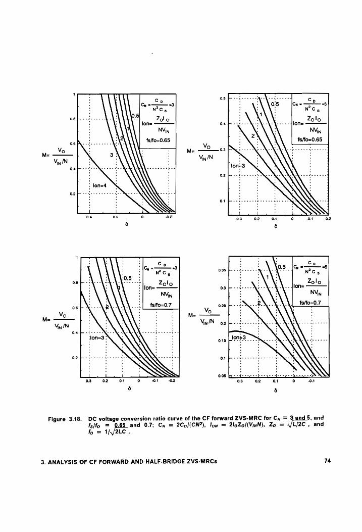
1 Cp O85 Preraccs err 7c 4 core
= 23 0:5 Cn = : 25
' ' 5 0.8 F---4------ -\- 2 Zol : : Z |
lon= 2 0.4 F---2---\--\--\-Y-- -- flon= o’°
NVin ; NVin
fs/fo=0.65 fs/fo=0.65
. ae
a ee
. Sena
Sino
f
0.2
0.35
0.3
0.15
0.1 0.05 Figure 3.18. DC voltage conversion ratio curve of the CF forward ZVS-MRC for Cy = 5, and
fslfo = 0.65 and 0.7; Cy = 2Cp/(CN?), lon = 2loZol(VwN), Zo = VL/2C , and fo = 1/,/2LC .
3. ANALYSIS OF CF FORWARD AND HALF-BRIDGE ZVS-MRCs 74

Design #6: N = 2, ISK* 3, Cy = 3, and fs/fo = 0.7, and
Design # 7: N 2, 1ON™ = 4, Cy = 3, and fe/fo = 0.65.
Figures 3.19 and 3.20 show the operating ranges and stresses for the first four designs which
study the effect of selecting different transformer turns ratios and /3K* (Zo is determined from
lon) values on the current and voltage stresses while Cy and fs/fo are kept constant. Since the
procedure is identical in each case, only Design #1 is described in detail.
Figure 3.19 shows the dc voltage conversion ratio characteristic for Cy = 3 and fe/fo = 0.65.
For a given Cy and fs/fo, the minimum conduction time of the CF switch occurs at full load
(i34") and low line (Mmax) (point A in Fig. 3.19). whereas the maximum conduction time of this
switch occurs at light load = (/P = IBXVRUS(VvReIB™)) and high line
(Mmin = MmaxVin"/Vine”) (point C in Fig. 3.19). Points B (high-line and full-load) and D (low-line
and light-load) are the two remaining points needed to completely define the operating region
on the dc _ voltage-conversion-ratio curves. Point B is determined by M™" and
lon = (OR"Vin')/Vine*. Similarly, point D is determined by M™* and loy = lowlo"|lo°”. By
selecting Mmax and /3K”", the operating point at full load and low line is defined. For the first
design, the maximum value of the normalized load current was, by arbitrary choice, selected
as 4.0. As a result, the operating range extends over the shaded area shown in Fig. 3.19.
Every point on the dc voltage-conversion-ratio curves (M, fs/fo. and Ion) has a one-to-one cor-
respondence with the points in the current/voltage characteristics. Therefore, any operating
region defined in the dc voltage-conversion-ratio curves can be transposed into any of the
other characteristics from which the current and voltage stresses associated with a given re-
gion of operation can be determined.
3. ANALYSIS OF CF FORWARD AND HALF-BRIDGE ZVS-MRCs 75
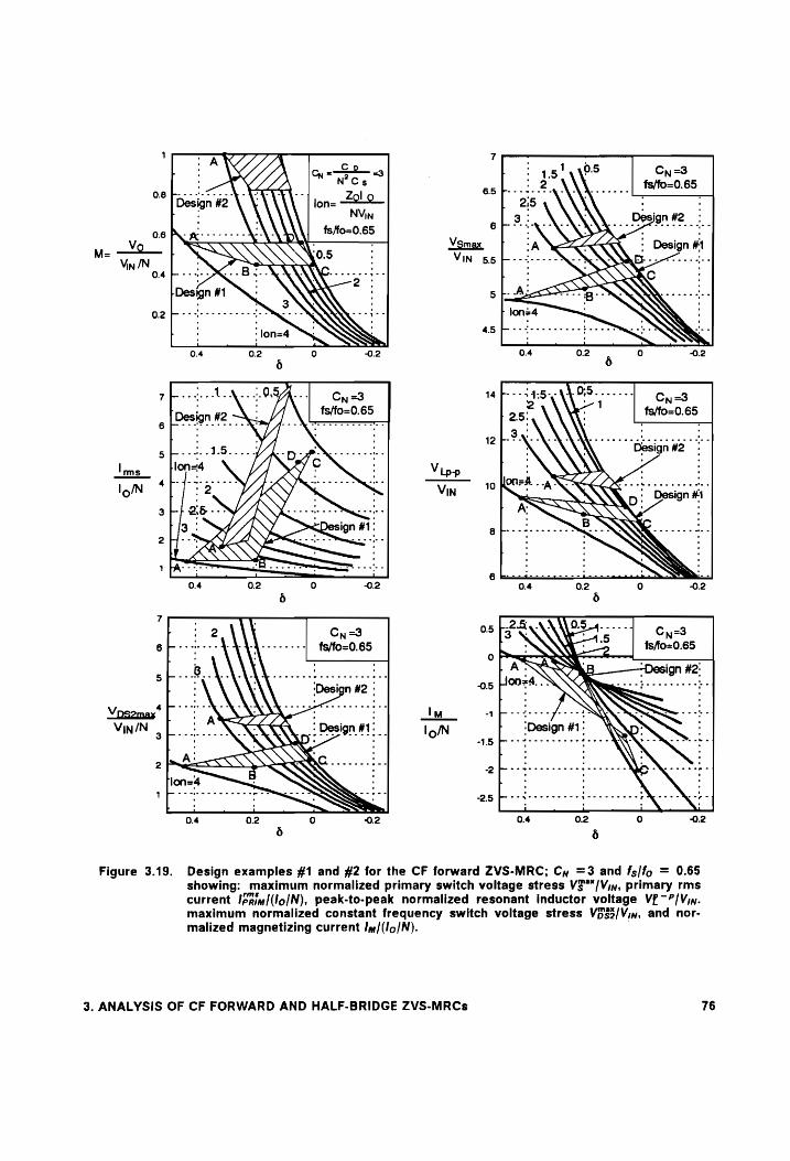
Figure 3.19.
Co N=?
- Zz lone -£2-2— NVin
fs/fo=0.65
0.5 .
5 0.2
Cy =3 14 F --54-5--A4
fs/fo=0.65
12
Vip VIN 10
arn 8
——_i- 6
0.5 3 ~ = 2 Css
: fsfio=0.65
°
.
0.5 PEE - NAc ccs t
ln 1 ! weeks
1.5 fore TAWA Mu” .
2.5 -
0.4 0.2 0 0.2
6
Design examples #1 and #2 for the CF forward ZVS-MRC; Cy =3 and fs/fo = 0.65 showing: maximum normalized primary switch voltage stress V$"/Vin, primary rms current Ipaim/(lo/N), peak-to-peak normalized resonant inductor voltage VP~?/Vww. maximum normalized constant frequency switch voltage stress V533/Vin, and nor- malized magnetizing current Iq/(lo/N).
3. ANALYSIS OF CF FORWARD AND HALF-BRIDGE ZVS-MRCs 76

Figures 3.19 - 3.23 show normalized characteristics of the maximum transistor Q, voltage,
Vs“, peak-to-peak resonant inductor voltage. VP”, transistor Qs voltage, Voss, resonant
inductor rms current, /paiy, and the magnetizing current, ly. The voltage characteristics are
normalized with respect to the input voltage V;,. The current characteristics are normalized
with respect to the ratio of /o/N.
Since the characteristics are normalized, it is difficult to predict the region in which the mini-
mum voltage and current stresses will occur for a given design. The voltage and current
stresses can be determined from the shown characteristics by denormalizing the voltages and
currents at each corner of the operating region. The resulting currents and voltages for the
first four designs are summarized in Table 3.3. The following design trade-offs are inferred:
1) Comparison of designs #1 and #4 suggests that increasing /89% and holding all other
parameters constant (designing for higher Zo) decreases all voltage and current
stresses.
2) Comparison of designs #1 and #3 and designs #2 and #4 suggests that moving down
in a line of constant /oy results in decreased voltage stresses but increased current
stresses.
3) Finally. comparison of designs #1 and #2 suggests that designing for a higher M,,a, and
a lower lon does not result in lower conduction losses.
For a given Cy and fs/fo, the converter should be designed So that full load and low line op-
eration occurs for the minimum conduction time of the CF switch, i.e., design for maximum
3. ANALYSIS OF CF FORWARD AND HALF-BRIDGE ZVS-MRCs 77
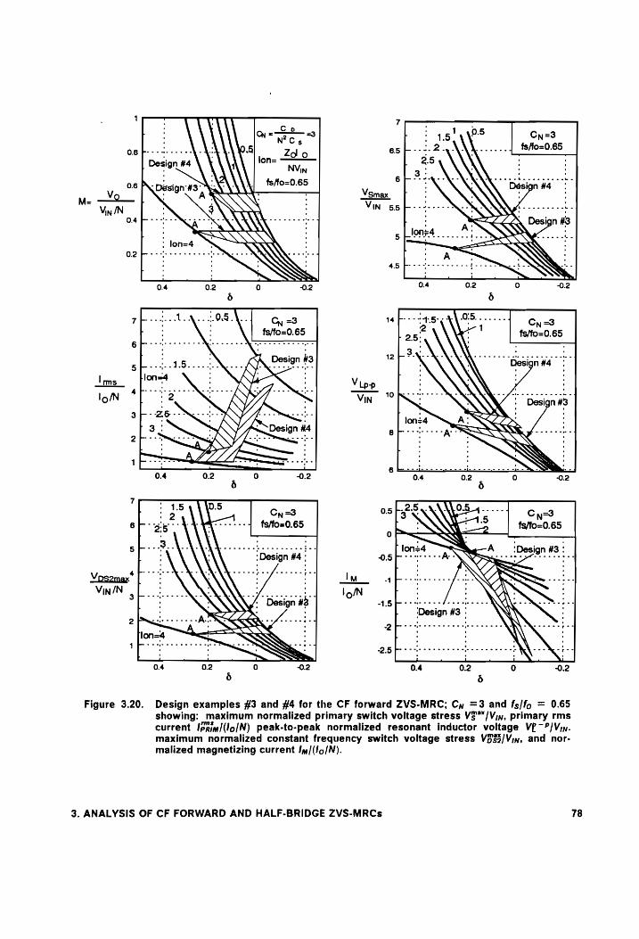
1 - a 7 5
Qu N?Cs =3
08 poste ee eee Zoo 65> ----
| Design #4 lon= 7 | 3
: - 6 06 A pasign-#3 fs/fo=0.65 V
__Vo 1% Vsmax,
Figure 3.20. Design examples #3 and #4 for the CF forward ZVS-MRC; Cy =3 and fs/fo = 0.65 showing: maximum normalized primary switch voltage stress V$"/Vin, primary rms current Ipaim/(lo/N) peak-to-peak normalized resonant inductor voltage VP ~?/Viw. maximum normalized constant frequency switch voltage stress V§33/Vin, and nor- malized magnetizing current I/(lo/N).
3. ANALYSIS OF CF FORWARD AND HALF-BRIDGE ZVS-MRCs 78
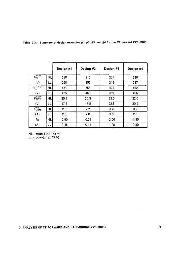
Table 3.3. Summary of design examples #1, #2, #3, and #4 for the CF forward ZVS-MRC
Design #1 Desing #2 Design #3 Design #4
Ve THL 280 313 267 289
(V) LL 220 257 215 237
vp? HL 481 555 429 462
(V) LL 425 466 369 406
Vos. |HL 20.9 20.5 23.0 22.0 (V) LL 17.6 17.5 22.5 20.2
IpRim =| HL 2.6 2.2 3.4 3.2
(A) LL 2.5 2.0 3.3 2.8
Inv HL -0.60 -0.33 -2.00 -1.30
(A) LL -0.16 0.441 | -1.00 -0.80
HL - High-Line (55 V) LL - Low-Line (45 V)
3. ANALYSIS OF CF FORWARD AND HALF-BRIDGE ZVS-MRCs 79
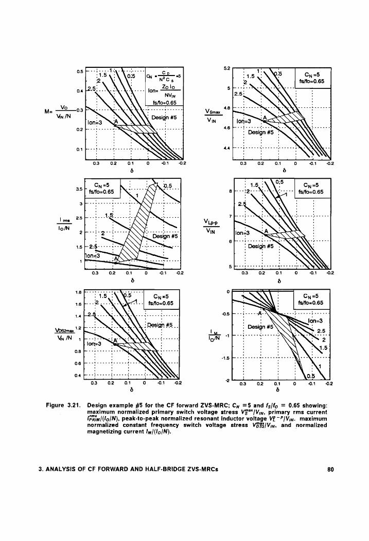
5.2
O5 be cteee Tye Qe eee e ee 1. ; V5 q:\ los ly ees | 34.588 S Cy =5
, 2 ‘ : N°C 5 2 \ fs/fo=0.65
; | bee NONE NENE.-- 0.4 Le.9 * lon= Zo lo 5 :
NVin 2.5;
V : : ’ fs/fo=0.65 : : : : : ° : : . ee eeee 4B Poot t cree NON \ccc: brrttee
M= Mn /N 0.3 P QR . Vsmax N : - Design #5 ve ; ‘A
loners \ \ \ q VIN lon=3 , ; O2 b---i--ee- _ Leedeeeeee 4.6 b---i----- ote NE NEAAAAG
: : , ‘ : Design #5 :
Pot WX PoP 01 frente deere SQ -- a beciereedeeeeecbeceeed
0.3 o2 Of 0 01 02 03 02 01 0 0102 6
| mse
lo/N
1.8 bec ee he ee ee eee Qe twee we
L 1.5 \ 5 Cy=5 16-2 .--\AYA*..- fs/fo=0.65
1.4 - “A\Q\K rt
tate NSS : Design #5 _. Vos2max ‘ : :
Vu /N Oy beer e Kee decrees | lorr=3
0.8 ee ee ee eee
0.6 len a ow hie doen enae see J
; ; 04 Fi a
03 Oo2 01 o 01 02 Figure 3.21. Design example #5 for the CF forward ZVS-MRC; Cy =5 and fs/fo = 0.65 showing:
maximum normalized primary switch voltage stress V$*"/Vi,, primary rms current Iprimi(lo/N), peak-to-peak normalized resonant inductor voltage VP-?/Vjy. maximum normalized constant frequency switch voltage stress V533/Viw, and normalized magnetizing current Im/(/o/N).
3. ANALYSIS OF CF FORWARD AND HALF-BRIDGE ZVS-MRCs 80
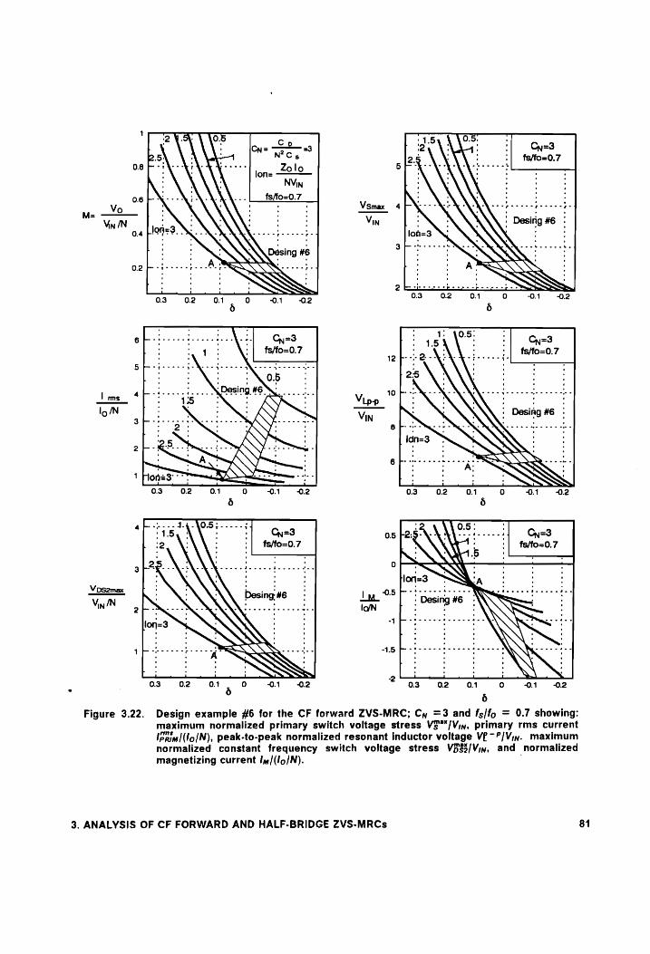
Vin/N
Figure 3.22.
1.5
whee mee he eee er bw ew
eRe creme be weer basen ns
eee tee
0.1 0.2
Design example #6 for the CF forward ZVS-MRC; Cy =3 and fs/fo = 0.7 showing: maximum normalized primary switch voltage stress V$*"/Viw, primary rms current Iprim[(lo/N), peak-to-peak normalized resonant inductor voltage VP~?/Viw. maximum normalized constant frequency switch voltage stress V583/Viw, and normalized magnetizing current Im/(lo/N).
3. ANALYSIS OF CF FORWARD AND HALF-BRIDGE ZVS-MRCs 81
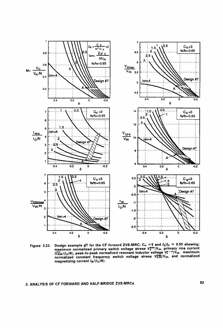
0.8 F----------4- 4!
0.2
Cc Qe 33
nN? a Zdo
lon=
NVin fs/fo=0.65
0.4 0.2 0 0.2
Cy =3
Figure 3.23.
Design example #7 for the CF forward ZVS-MRC; Cy =5 and fs/fo = 0.55 showing:
maximum normalized primary switch voltage stress V$*"/Vjy, primary rms current
Ifnim|(lo/N), peak-to-peak normalized resonant inductor voltage VP -?/Viy. maximum
normalized constant frequency switch voltage stress Vp'$2/Viw, and normalized
magnetizing current Im/(lo/N).
3. ANALYSIS OF CF FORWARD AND HALF-BRIDGE ZVS-MRCs 82
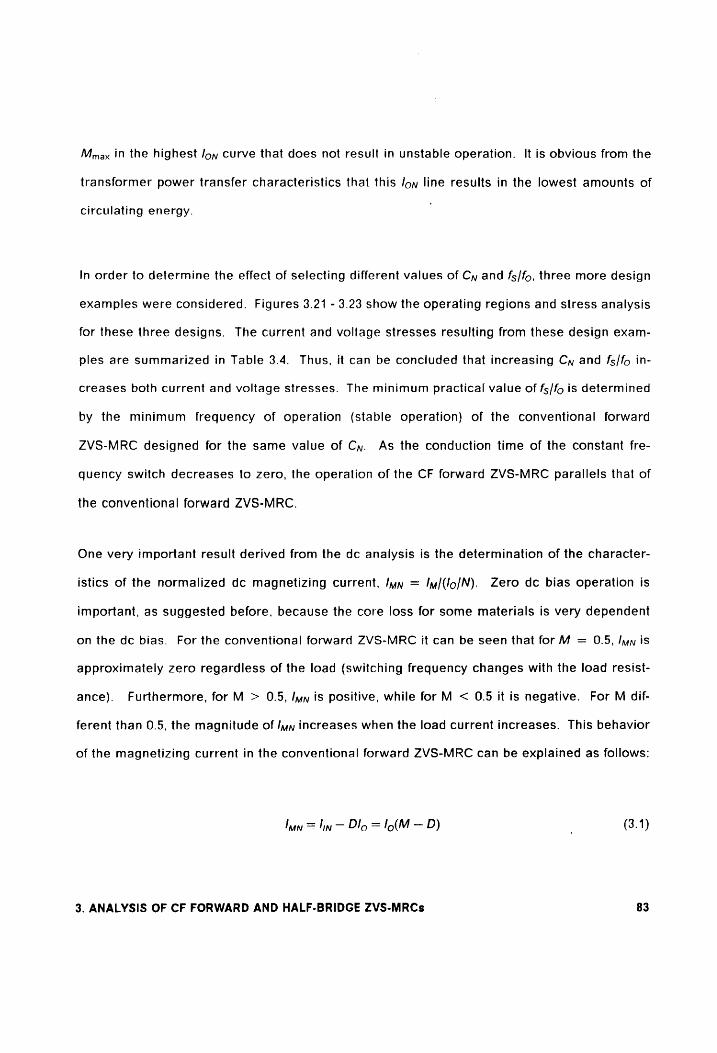
Mmax in the highest /oy curve that does not result in unstable operation. It is obvious from the
transformer power transfer characteristics that this /oy line results in the lowest amounts of
circulating energy.
In order to determine the effect of selecting different values of Cy and fs/fo, three more design
examples were considered. Figures 3.21 - 3.23 show the operating regions and stress analysis
for these three designs. The current and voltage stresses resulting from these design exam-
ples are summarized in Table 3.4. Thus, it can be concluded that increasing Cy and fs/fo in-
creases both current and voltage stresses. The minimum practical value of fs/fo is determined
by the minimum frequency of operation (stable operation) of the conventional forward
ZVS-MRC designed for the same value of Cy. As the conduction time of the constant fre-
quency switch decreases to zero, the operation of the CF forward ZVS-MRC parallels that of
the conventional forward ZVS-MRC.
One very important result derived from the dc analysis is the determination of the character-
istics of the normalized dc magnetizing current, Imy = Im/(lo/N). Zero dc bias operation is
important, as suggested before, because the core loss for some materials is very dependent
on the dc bias. For the conventional forward ZVS-MRC it can be seen that for M = 0.5, Imp is
approximately zero regardless of the load (switching frequency changes with the load resist-
ance). Furthermore, for M > 0.5, Iwy is positive, while for M < 0.5 it is negative. For M dif-
ferent than 0.5, the magnitude of Jj, increases when the load current increases. This behavior
of the magnetizing current in the conventional forward ZVS-MRC can be explained as follows:
In = bin — Dlg = I—o(M — D) (3.1)
3. ANALYSIS OF CF FORWARD AND HALF-BRIDGE ZVS-MRCs 83
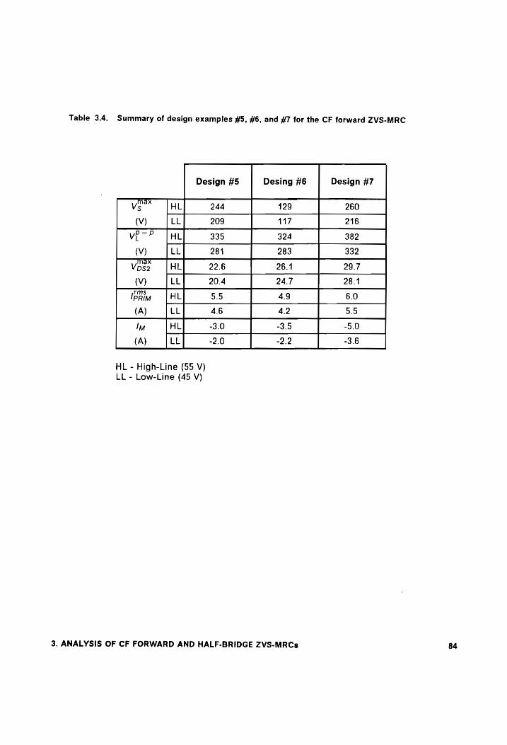
Table 3.4. Summary of design examples #5, #6, and #7 for the CF forward ZVS-MRC
Design #5 Desing #6 Design #7
Ves LHL 244 429 260
(V) LL 209 417 216
VP-P TAL 335 324 382
(V) LL 281 283 332
Vos. {HL 22.6 26.1 29.7 (V) LL 20.4 24.7 28.4
Ippim =| HL 55 49 6.0
(A) LL 46 4.2 5.5
Iu HL -3.0 -3.5 -5.0
(A) LL -2.0 -2.2 -3.6
HL - High-Line (55 V) LL - Low-Line (45 V)
3. ANALYSIS OF CF FORWARD AND HALF-BRIDGE ZVS-MRCs 84

where /o is the dc output current and D is defined as the conduction time of the forward diode
relative to the switching period. It can be seen that the magnetizing current becomes zero
when M = D. This condition holds for M = 0.5. since D is approximately 0.5 for the conven-
tional forward ZVS-MRC. However, D is not necessarily equal to 0.5 for the CF forward
ZVS-MRC since the control of the conduction time of the rectifier devices is what allows for
CF operation. In the CF forward ZVS-MRC In ~ 0 occurs only for light conduction times of the
CF switch. Consequently, the region where I, is zero is limited to maximum values of 6 and
dc voltage-conversion-ratios between 0.65 and 0.45. This suggests that for partial to light load
operation, the magnetizing current in the CF forward ZVS-MRC will be strongly biased nega-
tively.
Finally, one last trade-off that should be considered in all single-ended topologies is that of the
voltage stress across switch Q;. From the different design examples it can be observed that
for these design specifications it is very difficult to design a CF forward ZVS-MRC with a pri-
mary switch voltage stress, Vs", lower than 200 V. If this stress is limited below 200 V a de-
vice rated for 200 V can be used, otherwise, a 400 V device is needed. Generally a 200 V
device has a much lower Rosiom, approximately half of that of a 400 V device. Therefore, using
a 200 V device could considerably reduce the conduction losses. As the design examples
suggest, reducing the voltage stresses usually increases conduction losses. This means that
for single ended topologies, like the forward converter, the designer has to decide if lowering
the primary voltage stress so that a lower Rpsiom device can be used will decrease the overall
conduction losses. No general rule can be given in this case. since the answer is very case
dependent due to the discrete nature of the device ratings.
3. ANALYSIS OF CF FORWARD AND HALF-BRIDGE ZVS-MRCs 85

3.4.2 Design Procedure for CF Forward ZVS-MRC
A design procedure can be established for the CF forward ZVS-MRC based on the trade-offs
described in the previous section. Four rules should be followed while designing the CF for-
ward ZVS-MRC:
1) A dc voltage-conversion-ratio characteristic curve that allows for the converter to be
designed for Jy = 0 under full load conditions should be selected.
2) The power stage characteristic impedance Zo should be maximized; i.e., the low-line
full-load operating condition should be designed to fall in the maximum Joy curve that
does not result in unstable operation.
3) The value of Cy and fs/fo should be selected to be as low as possible to minimize con-
duction losses due to circulating energy.
4) The turns ratio of the transformer should be selected so that nominal line and full-load
operating condition result in J, = 0 (reduces core losses resulting from the dc bias at
nominal-line and full-load operating condition).
Once Cy, f,/fo, Mmax, and 134% have been selected, the turns ratio of the transformer is calcu-
lated from:
3. ANALYSIS OF CF FORWARD AND HALF-BRIDGE ZVS-MRCs 86

Vin. Mou, = N= t= 9) (3.2)
Vo
where Viv.” is the nominal input voltage. From the definition for Cy, fo, and I38*, it follows that:
Aypmaxymin
=—— ma (3.3) 2tfolo
pmax
Cs= — min (3.4) OnfoNimeXy™m
and
The voltage ratings of the semiconductor devices can be easily determined from the complete
set of given characteristics. For simplicity, the peak current through the primary switch can
be estimated using the following expression:
ymax
pk IN
loi< 2Lfy (3.6)
where the maximum current through the CF switch is:
IPO<NIP 4 (3.7)
3. ANALYSIS OF CF FORWARD AND HALF-BRIDGE ZVS-MRCs 87

Finally, the input and output filters are designed following rules similar to those for PWM
converters.
3.4.3 Design Trade-offs for CF HB ZVS-MRC
There are two main differences between the design of push-pull topologies like the HB con-
verter and the design of the CF forward ZVS-MRC. First, the transformer in push-pull
topologies operates with no dc bias. Second, the voltage stress across the primary switches
is clamped to the value of the input voltage. Not having to consider these two issues simplifies
the design of the HB converter and all other push-pull topologies.
Design trade-offs of the HB topology are based on the following design specifications:
input voltage range, ViR®* — Vin" = 270-330 V;
© output voltage, Vo = 5V;
¢ load range, /3'" — 19% = 0-20 A; and
e switching frequency, f, = 750 kHz.
Figure 3.24 shows the dc characteristics of the CF HB ZVS-MRC for Cy = 10 and 5, and
feonlfo = 0.3 and 0.25. To investigate the effect of N, Cy, feon/fo, and /3%” on the converter per-
formance, eight different design examples are considered:
Design # 1: N = 13, IGN" = 10, Cy = 5, and hon/fo = 0.25,
Design # 2: N = 27, G4" = 10, Cy = 5, and hon/fo = 0.25,
3. ANALYSIS OF CF FORWARD AND HALF-BRIDGE ZVS-MRCs 88
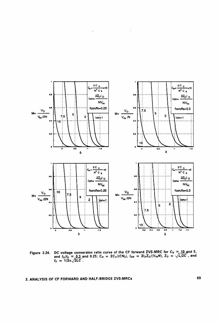
os
os
Vin /2N 0. o2
Figure 3.24. DC voltage conversion ratio curve of the CF forward ZVS-MRC for Cy = nd 5,
and fs/fo = 0.3 and 0.25; Cy = 2Cp/(CN2), lon = 2loZo/(VinN), Zo =" Lj2c ’ and
fo = 1/2x,/2LC .
3. ANALYSIS OF CF FORWARD AND HALF-BRIDGE ZVS-MRCs

Design # 3: N = 5, 19K" = 10, Cy = 5, and foonffo = 0.25,
= 13, G8" = 7.5, Cy = 5, and hon/fo = 0.25, z | Design # 4:
Design # 5: N = 13, IS = 10, Cy = 10, and fron/fo = 0.25,
Design # 6: N = 13, IOK* = 7.5, Cy = 5, and feon/fo = 0.3, and
{| Design # 7: N = 13, OK = 7.5, Cy 10, and hon/fo = 0.3.
Figures 3.25 - 3.29 show normalized characteristics of the peak-to-peak resonant inductor
voltage, V; ?/Viy, peak-to-peak primary transformer voltage, Veaik/Vin, and the primary rms
current. fer/(lo/N). The voltage characteristics are normalized with respect to the input
voltage, Viv. The current characteristics are normalized with respect to the load current re-
flected into the primary side, Io/N.
Figures 3.25 - 3.27 show the operating ranges and stresses for the first four designs. Again,
the first four designs study the effect of selecting different transformer turns ratios N and /gy”
on the current and voltage stresses while Cy and hon/fo remain constant. Table 3.5 summa-
rizes the voltage and current stresses resulting from designs #1 - #4. From the results shown
in these tables, the following design trade-offs are observed:
1) Comparison of designs #1 and #4 suggests that increasing /84" with all other parame-
ters held constant decreases all voltage and current stresses.
2) Comparison of designs #1, #2, and #3 suggests that moving down in a line of constant
lon results in decreased voltage stresses but increased current stresses.
3. ANALYSIS OF CF FORWARD AND HALF-BRIDGE ZVS-MRCs 90
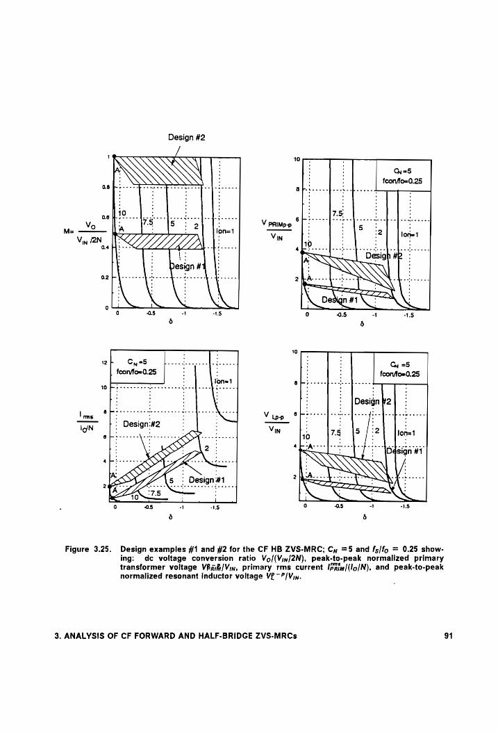
Design #2
08 ---.--- poscecse esc e were shes beve sees 8 eve. se fee wee bee. . ‘ . . ' ‘ ‘
6 bam
V PRIMp-p
ViN
Gy =5 fcon/foz0.25
Figure 3.25. Design examples #1 and #2 for the CF HB ZVS-MRC; Cy =5 and fs/fo = 0.25 show-
ing: dc voltage conversion ratio Vo/(Vin/2N), peak-to-peak normalized primary transformer voltage V8ah/Vin, primary rms current Ipain/(lo/N), and peak-to-peak normalized resonant inductor voltage Vf ~?/Vjw.
3. ANALYSIS OF CF FORWARD AND HALF-BRIDGE ZVS-MRCs 91
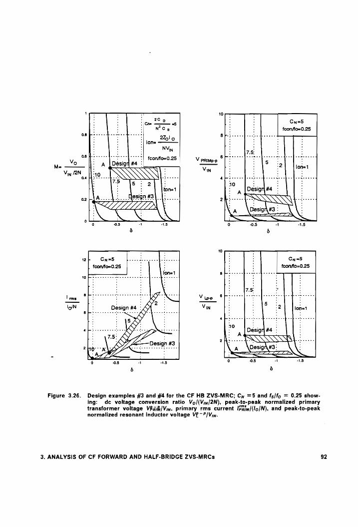
1 10 —— 2c : :
Crs — a5 : ‘ Cn=s : . NC s ‘ ‘ feon/fo=0.25
sep pete Tn az : : . : : | lon=
; NVin
06 theres: toes vers fcon/fo=0.25 Vo ;
Ma ;
Viy /2N |]: a. :
02
10
Cu=5
feon/fo=0.25
@ few -- of ee eee bee ee
7.5: , lms Vipp Shroff pepo
, : : 5 ; lo Vin 2 lon=1
ebieee fe weheetep bee 10 : Design #4 Do, esig
2 Bee w ee hee .
A \Desigh\#3:
- { t
Go 0.5 -t
é é
Figure 3.26. Design examples #3 and #4 for the CF HB ZVS-MRC; Cy =5 and fs/fo = 0.25 show- ing: dc voltage conversion ratio Vo/(Viny/2N), peak-to-peak normalized primary transformer voltage VBah/Viw, primary rms current Ipaim/(lo/N), and peak-to-peak normalized resonant inductor voltage VP ~?/Viw.
3. ANALYSIS OF CF FORWARD AND HALF-BRIDGE ZVS-MRCs 92
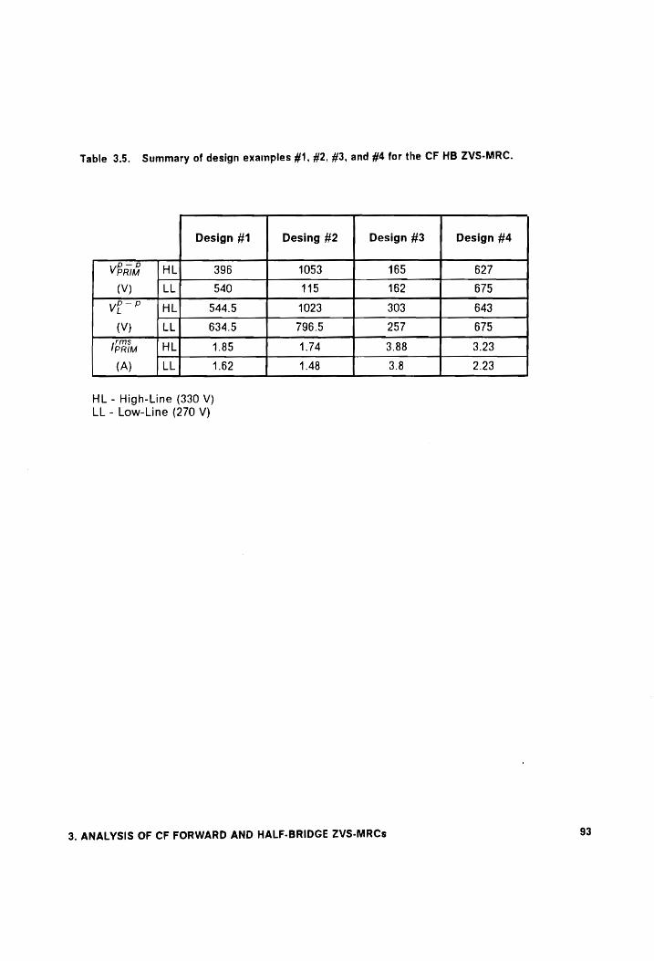
Table 3.5. Summary of design examples #1, #2, #3, and #4 for the CF HB ZVS-MRC.
Design #1 Desing #2 Design #3 Design #4
Very =| HL 396 1053 165 627
(V) LL 540 115 162 675
ve? THL 544.5 1023 303 643
(V) LL 634.5 796.5 257 675
Ipaim =| HL 1.85 1.74 3.88 3.23
(A) LL 1.62 1.48 3.8 2.23
HL - High-Line (330 V) LL - Low-Line (270 V)
3. ANALYSIS OF CF FORWARD AND HALF-BRIDGE ZVS-MRCs 93
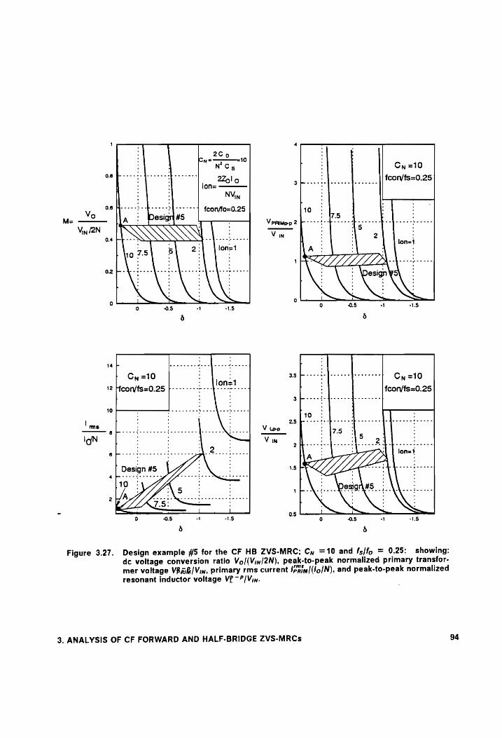
1 4
2c Caz — =10
,; N°Cs : Cy =10
O8 Po pene apess eres 2Zo!lo6 4 : fcon/fs=0.25 . . lon= cree epot rere ge sccecrs
; NVin
Vo 0.6 fy----- reopecss “3 ep otrtee fcon/fo=0.25 M= A esig #5 | Verumep 2
Vin /2N V
0.4 EE-- ~SASAAAAAY.-]---- Beeeee IN 10 7.5 5 2 lon=1
: : : : '
02 FKP ede petee
0 i 0 0 0.5 A 1.5
é é
14 - '
Cn =10 3.5 aa cprr rcs per essces Cn =10
12 THfcon/fs=0.25 : fcon/fs=0.25
10
l ins 8 hep e+e ese eee eee ee we cee ewe Zo eae ee eis ene wnee
IQN
a bevel beey Design #5
abe eeedeeeeees weeeedee NQuedeeeee
2 Se eee ee ee
~ 0 5 1 Ls
5 6
Figure 3.27. Design example #5 for the CF HB ZVS-MRC; Cy =10 and fs/fo = 0.25: showing:
dc voltage conversion ratio Vo/(Vin/2N), peak-to-peak normalized primary transfor-
mer voltage VBah/Vin, primary rms current Iepim/(lo/N), and peak-to-peak normalized resonant inductor voltage VP~°/Viw.
3. ANALYSIS OF CF FORWARD AND HALF-BRIDGE ZVS-MRCs 94
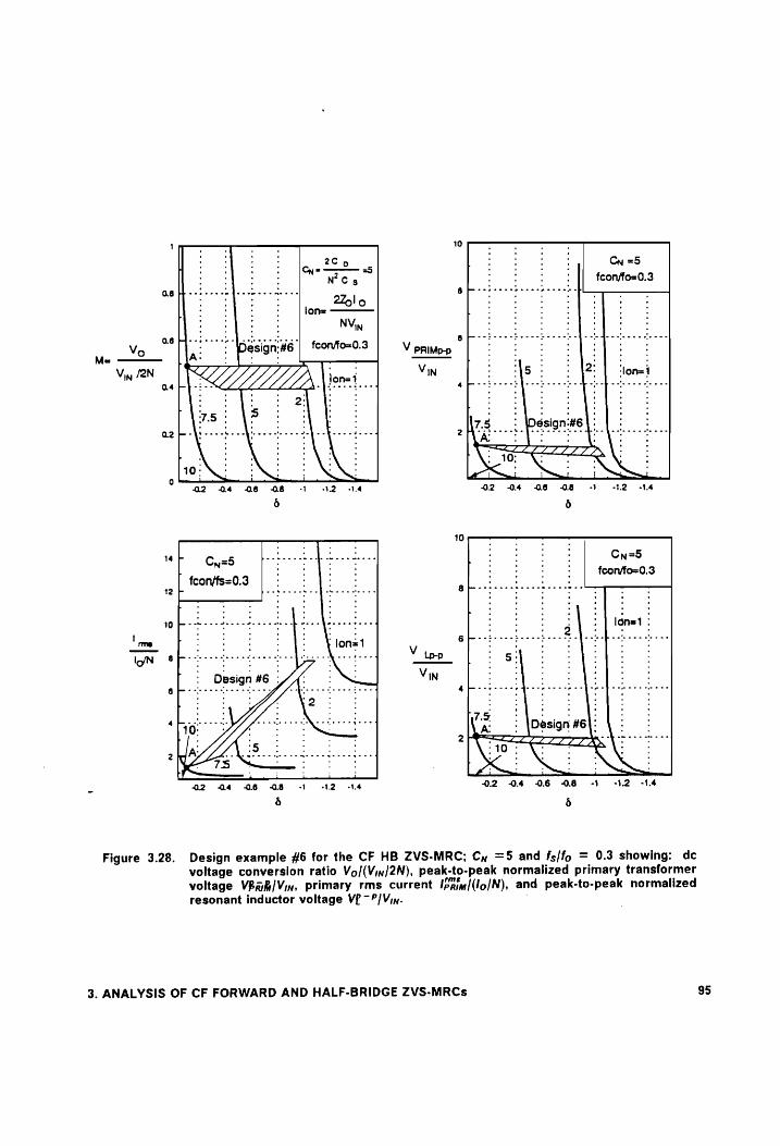
2C 5 Poh Cy =5 = 25 r . ‘ . .
. ‘ ‘ ' oN NC 5 : : : : fcon/fo=0.3 ae tbeete eek feecbee ee. B cei eecebeeceneeeele
. ‘ , . 2Zolo : : : :
lon=
Ds NVin 06 Web eeeckefece eee ceeee Bendre bere eee c eee ede ee dee: leeaee —
TT7 Vin 5 2: lon=1 a eeciecect dee ee oo eee
78. 1 ésign:#6 2 A! . o
: 10; | l i
02 04 086 O08 +1
6
10
Cnyz5
feor/fo=0.3
ar eee eee see ewe weer aces
ldn=1
OPP pb efeededeeB |. a tp Ge heey Ve fo sh La
Design #6 ; oN VIN 6 wee enee . wea . wee fu chia e er ervecnanseaed 4p etre ee Gowe ° eee te cede o
7.5 Door A: {a CDA Ne A: Design #6:
2 = .
a WAL ZL idee cece dee edeeeedee ed W0N:
_ a2 04 06 O81 2 NA 02 04 06 08 -1 -12 -1.4
é 6
Figure 3.28. Design example #6 for the CF HB ZVS-MRC; Cy =5 and fs/fo = 0.3 showing: dc
voltage conversion ratio Vo/(Vin/2N), peak-to-peak normalized primary transformer
voltage VBak/Vin, primary rms current Iepim/(lo/N), and peak-to-peak normalized resonant inductor voltage VP ~?/Viw.
3. ANALYSIS OF CF FORWARD AND HALF-BRIDGE ZVS-MRCs 95
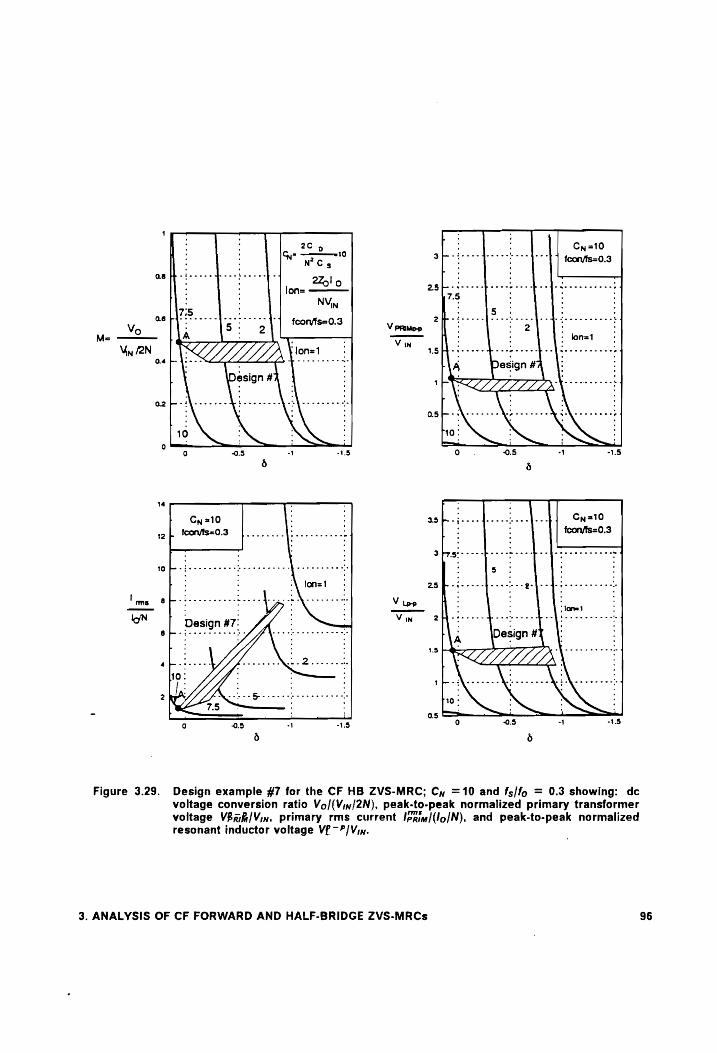
Design #7 ’
i
Design example #7 for the CF HB ZVS-MRC; Cy =10 and fs/fo = 0.3 showing: dc voltage conversion ratio Vo/(Vin/2N), peak-to-peak normalized primary transformer voltage V8ah/Vin, primary rms current Ippim/(lo/N), and peak-to-peak normalized resonant inductor voltage VP ~?/Viy.
Figure 3.29.
3. ANALYSIS OF CF FORWARD AND HALF-BRIDGE ZVS-MRCs 96

The effect of the design parameters /3¥*% and N on the value of the current and voltages is
similar to the one displayed by the CF forward ZVS-MRC. The difference lies in that the dc
voltage conversion ratio characteristics for the HB topology are much steeper than those of
the forward topology. Although the dc voltage conversion ratio characteristics of the HB
topology are very steep, the normalized primary rms current characteristics remain relatively
flat for high values of loy. This means that as the converter design is changed and higher
values of M are selected, the value of the primary rms current will decrease but at a much
slower rate than the increase in M. As can be seen from the results of designs #1 and #2, the
value of the maximum primary rms current at full load decreases from 1.84 in Design #1 to
174 in Design #2. However, the value of the turns ratio increases from 13 in Design #1 to 27
in Design #2. This means that the winding resistance resulting from Design #2 is more than
twice the one for Design #1. Therefore, Design #1 will more likely result in decreased overall
conduction losses.
The effect of selecting different Cy and fron/fo is studied in designs #5, #6, and #7 and is shown
in Figs. 3.27 - 3.29. The results from these designs are summarized in Table 3.6. As can be
seen from Table 3.6, the effect of Cy and fio,/fo in the design of the HB is similar to the one
observed for the forward converter, i.e., increasing Cy and fcon/fo increases the voltage and
current stresses.
Since the maximum voltage of the primary switches in the CF half-bridge ZVS-MRC is limited
to the maximum input voltage (Vjn**), the voltage stress of the switches is independent of the
load current.
3. ANALYSIS OF CF FORWARD AND HALF-BRIDGE ZVS-MRCs 97
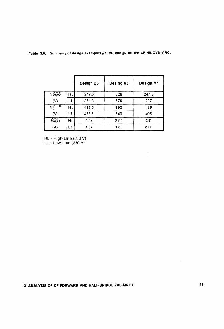
Table 3.6. Summary of design examples #5, #6, and #7 for the CF HB ZVS-MRC.
Design #5 Desing #6 Design #7
Vern =| HL 247.5 726 247.5
(V) LL 371.3 576 297
ve~P VAL 412.5 990 429
(V) LL 438.8 540 405
IpRim =| HL 2.24 2.92 3.0
(A) LL 1.84 1.88 2.03
HL - High-Line (330 V) LL - Low-Line (270 V)
3. ANALYSIS OF CF FORWARD AND HALF-BRIDGE ZVS-MRCs

3.4.4 Design Procedure for CF HB ZVS-MRC
From the design trade-off study, the following rules should be used in designing a CF HB
ZVS-MRC:
1) The value of Cy and fon/fo should be selected to be as low as possible to minimize
conduction losses due to circulating energy.
2) The characteristic impedance of the power stage Zo should be maximized; i.e., select
the full-load low-line operating condition to fall in the maximum /on curve that does not
result in unstable operation.
3) The converter should be designed for M ~ 0.5 in order to minimize conduction losses
in the primary circuit.
Once Cy, fron{fo, Mmax, and /@§" have been selected, the turns ratio of the transformer and
resonant component values are calculated from:
min vom N= IN max (3.8)
Vo
Cy= ; N?CyC (3.9)
and
3. ANALYSIS OF CF FORWARD AND HALF-BRIDGE ZVS-MRCs 99

2
cs | wicvin” L=— ae (3.10)
lo
Switches Q, and Q, with small on-resistance are necessary to keep the conduction losses low,
whereas smaller output capacitances of the switches are desirable to reduce the primary peak
(and rms) currents. Thus. the value of Cs is the value of the output capacitance of either Q;
or Qo.
The peak current through the primary switches can be estimated using the following ex-
pression:
max
Vin Priw< vr (3.11)
$s
The peak current through the CF switches is:
pk pk
Ioe<Nlprim (3.12)
and the maximum voltage stress on the CF switches is:
max max Vin Vat = (3.13)
3.5 Experimental Results
Using the design guidelines suggested in the previous section, a 50 W CF forward ZVS-MRC
and two 100 W CF HB ZVS-MRCs were built.
3. ANALYSIS OF CF FORWARD AND HALF-BRIDGE ZVS-MRCs 100

3.5.1 Experimental Results for CF Forward ZVS-MRC
3.5.1.1 Power Stage
A 50 W, CF forward ZVS-MRC with a 5 V output was designed for an input voltage range from
45 V to 55 V. The converter operates from full load (10 A) to no load (0 A) at a switching fre-
quency of 1.9 MHz. The components of the power stage are the following:
Q, - IRF740 (international Rectifier):
Q,_ - IRFZ44 (international Rectifier):
TR - core: custom made E core (material Q));
primary: 6 turns of 150/44 Litz wire;
secondary: 2 turns 5 mils copper foil;
primary leakage inductance: 390 nH;
Lo - inductance: 2 jH;
core: Micrometals iron powder core T44-6:
winding: 22 turns of 150/44 Litz wire;
D,; - Semetex SXS300W45M;
Cs - 270 pF + 2 x 480 pF mica;
Cp -7x6.8 nF, NPO chip ceramic;
Le - inductance: 1 pH;
core: TDK RM5Z52B (material H7c,4);
winding: 4 turns magnet wire AWG# 16;
gap: 5 mm; and
3. ANALYSIS OF CF FORWARD AND HALF-BRIDGE ZVS-MRCs 101
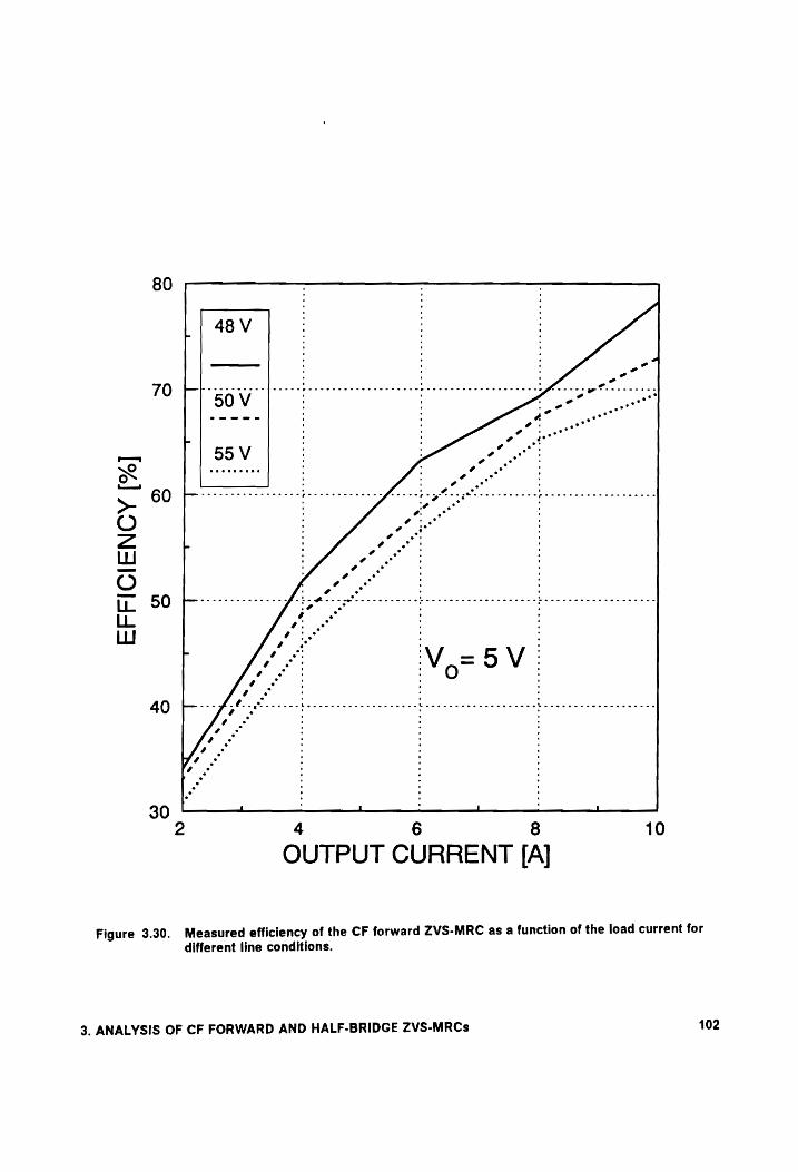
80
70
© oO
EFFICIENCY
[%]
40
39 t-— _ a : | 4 6 8 OUTPUT CURRENT [A]
Figure 3.30. Measured efficiency of the CF forward ZVS-MRC as a function of the load current for
different line conditions.
3. ANALYSIS OF CF FORWARD AND HALF-BRIDGE ZVS-MRCs 102
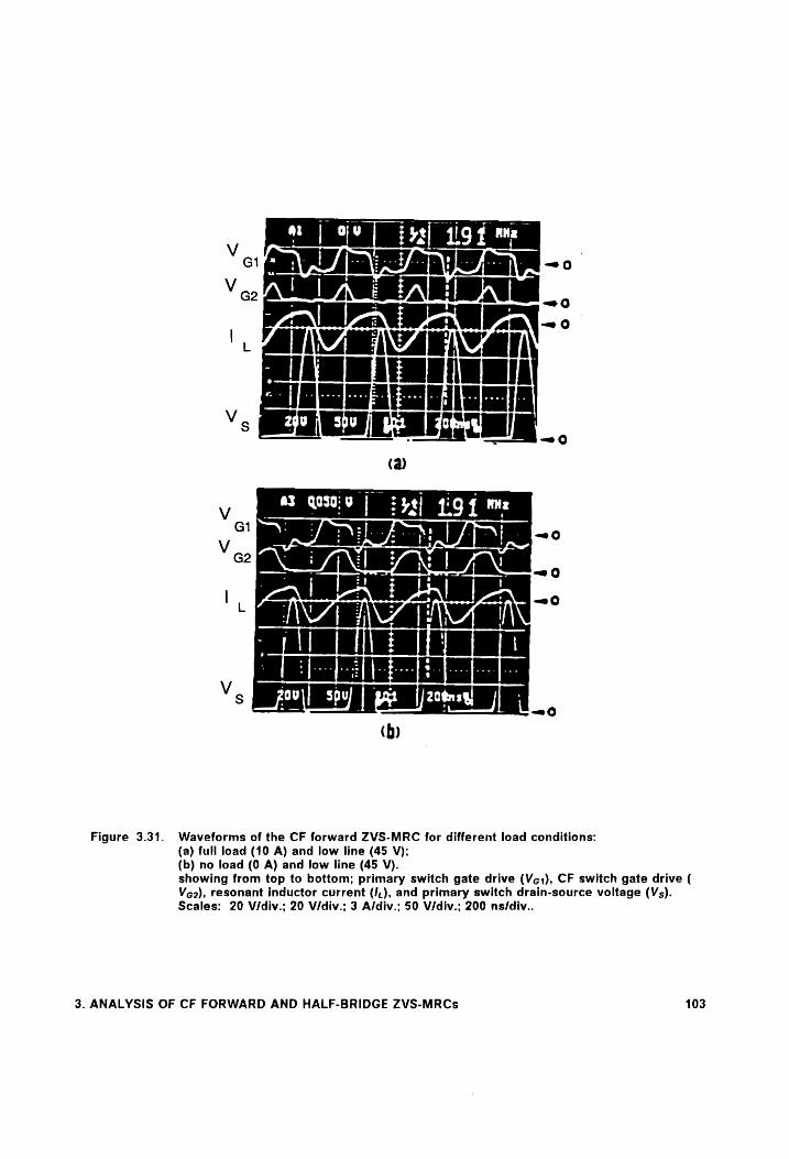
Vor mya),
h AY mIVAiN AE SS aSalone
*s DESC SEC (a)
Figure 3.31. Waveforms of the CF forward ZVS-MRC for different load conditions: (a) full load (10 A) and low line (45 V):; (b) no load (0 A) and low line (45 V). showing from top to bottom; primary switch gate drive (Vg.), CF switch gate drive ( Veo), resonant inductor current (/,), and primary switch drain-source voltage (Vs). Scales: 20 Vidiv.; 20 Vidiv.; 3 A/div.; 50 Vidiv.; 200 ns/div..
3. ANALYSIS OF CF FORWARD AND HALF-BRIDGE ZVS-MRCs 103
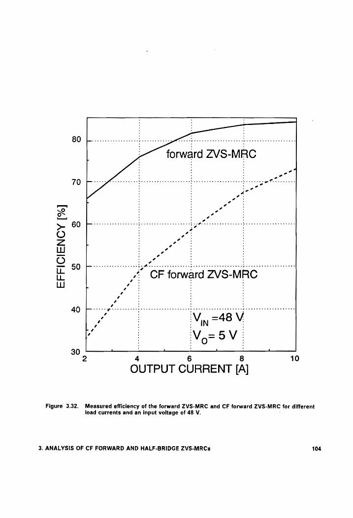
BO Lene cececcc cece bec c cet ee bee ee cree teteceesbeceeetseeneteeenees
3 forward ZVS- MRC
70 pro bette teeeeees seerettieteeteaees rarer
BO Freres petite neers renee O wo Z | io Lu ae © °?
LL 50 pee Ree ne eee eee p iene t et eee neens
Ic CF forward ZVS- MRC UI L “
a a ne a : Viy =48 V.
Lf , Vo= 5V
30 - 2 10 4 6 8
OUTPUT CURRENT [A]
Figure 3.32. Measured efficiency of the forward ZVS-MRC and CF forward ZVS- MRC for different load currents and an input voltage of 48 V.
3. ANALYSIS OF CF FORWARD AND HALF-BRIDGE ZVS-MRCs 104
Cr - 4x3 yF NPO chip ceramic.
Figure 3.30 shows the measured efficiency of the power stage as a function of the load current
for different input voltages. A maximum efficiency of 78.3% was obtained for the power stage
at full load and low line. The maximum efficiency occurs for the minimum conduction period
of the CF switch. Figure 3.31 shows the oscillograms of key waveforms at low line for full load
and no load operation. Figure 3.32 compares the efficiency of a variable frequency forward
ZVS-MRC built for the same specifications and using the same components and that of the
CF forward ZVS-MRC for different load currents and an input voltage of 48 V. Figure 3.32
shows that the increased circulating energy resulting from constant frequency operation of
ZVS-MRC heavily penalizes the performance of CF ZVS-MRCs.
3.5.1.2 Control/Timing Requirements for the CF Switch
The gate-source signal for the primary switch Q, of the CF forward ZVS-MRC oscillates at a
constant switching frequency and a constant duty cycle. The off-time of this switch is deter-
mined from the resonance of the primary switch voltage. No feedback control is needed for
the primary switch Q,. The turn-on time of the constant frequency switch Q2 cannot be syn-
chronized with the turn-on time of the primary switch, if soft switching of Qo is desired, be-
cause in Mode | of operation the voltage across capacitor voltage Vp is positive (forward diode
D,; is conducting) at the time the primary switch turns on. Soft switching of Q2 can be main-
tained for all operating conditions by introducing a delay between the turn-on time of this
switch relative to the turn-on time of Q,;. Once the capacitor voltage Vp becomes negative, the
antiparallel diode of switch Q2 will conduct and soft switching of this switch can be achieved.
3. ANALYSIS OF CF FORWARD AND HALF-BRIDGE ZVS-MRCs 105
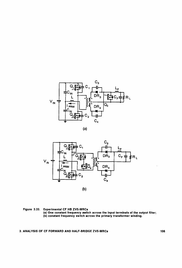
OMe C, Lp
IN 4 Ly C R Vat rT L
<—
| prim
IN rn
| eft C, LU C,
(a)
Le nn
© ‘ HH
DD 2
(b)
Figure 3.33. Experimental CF HB ZVS-MRCs (a) One constant frequency switch across the input terminals of the output filter; (b) constant frequency switch across the primary transformer winding.
3. ANALYSIS OF CF FORWARD AND HALF-BRIDGE ZVS-MRCs 106
In general, the delay between the two switches is very short and can be easily adjusted once
the hardware is completed. A similar control scheme as the one shown for the CF buck
ZVS-MRC (Fig. 2.13) can be used for the CF forward ZVS-MRC. Positive feedback control is
needed to control the conduction time of the constant frequency switch since an increase in
the conduction time of this switch results in a decrease of the output voltage.
3.5.2 Experimental Results for CF HB ZVS-MRC
3.5.2.1 Power Stage
The CF HB ZVS-MRCs shown in Fig. 3.33(a) and Fig. 3.33(b) were designed for an input voltage
range from 270 V to 330 V. The converters operate with a switching frequency of 700 kHz and
are capable of regulating the 5 V output from no load to full load (20 A). The experimental
power stage components of the circuit implementation shown in Fig. 3.33(a) are:
Q,,Q. - IRF740 (international Rectifiers);
Q3 - IRFZ44 (international Rectifiers);
C,,C. ~=- output capacitance of IRF740;
TR - core: TDK LP 32/13 (material H7c4);
primary: 16 turns of 150/44 Litz wire:
secondary: 1 turn of 5 strand of 150/44 Litz wire;
primary leakage inductance: 16 nH;
L - leakage inductance of power transformer;
3. ANALYSIS OF CF FORWARD AND HALF-BRIDGE ZVS-MRCs 107
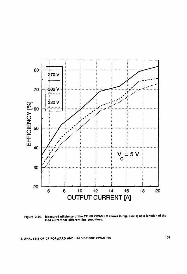
80
o
Oo
EFFICIENCY
[%]
h
Oo 30 |- Cet
6 8 10 12 14 16 18 20
OUTPUT CURRENT [A]
20
Figure 3.34. Measured efficiency of the CF HB ZVS-MRC shown in Fig. 3.33(a) as a function of the
load current for different line conditions.
3. ANALYSIS OF CF FORWARD AND HALF-BRIDGE ZVS-MRCs 108
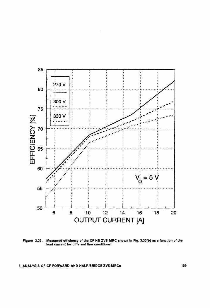
85
80
N
on
|
©
EFFICIENCY
[%]
ao) oO 55 ee
6 8 10 12 14 16 18 20
OUTPUT CURRENT [A]
Figure 3.35. Measured efficiency of the CF HB ZVS-MRC shown in Fig. 3.33(b) as a function of the load current for different line conditions.
3. ANALYSIS OF CF FORWARD AND HALF-BRIDGE ZVS-MRCs 109
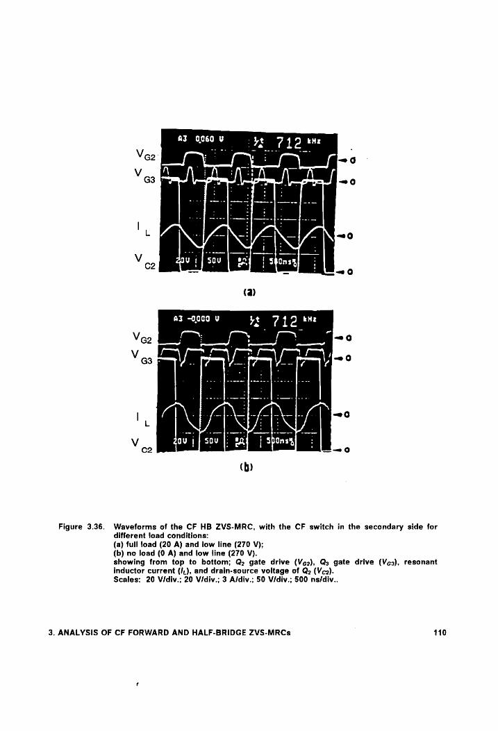
Figure 3.36. Waveforms of the CF HB ZVS-MRC, with the CF switch in the secondary side for
different load conditions: (a) full load (20 A) and low line (270 V); (b) no load (0 A) and low line (270 V). showing from top to bottom; Q2 gate drive (Vg2), Qs gate drive (Ves), resonant inductor current (/,), and drain-source voltage of Q2 (Vc2). Scales: 20 V/div.; 20 Vidiv.; 3 A/div.; 50 Vidiv.; 500 ns/div..
3. ANALYSIS OF CF FORWARD AND HALF-BRIDGE ZVS-MRCs 110
Dr3Drq - BOCNQO45 (International Rectifier):
C3,C,y - 4x 6.8 nF NPO chip ceramic;
Le - inductance: 1 pH;
core: TDK RM6Z12 (material H7c¢aq):
winding: 4 turns magnet wire AGW# ‘16;
gap: 5 mm.: and
Cr - 5 x 3.3 F NPO ceramic chip.
For the experimental power stage shown in Fig. 3.33(b), the following components are used:
Q, — Q, - IRF740 (International Rectifier);
C,.C, - output capacitance of IRF740;
TR - core: TDK LP 22/13 (material H7cq);
primary: 10 turns of 150/44 Litz wire;
secondary: 1 turn of 5 strand of 150/44 Litz wire;
primary leakage inductance: 400 nH:
L - inductance: 16 nH;
core: TDK LP 22/13 (material H7cq:
winding: 20 turns of 150/44 Litz wire:
gap: 7mm;
Dr3Drq - BOCNQO45 (International Rectifier):
C3,C, - 4x 6.8 nF NPO chip ceramic:
Le - inductance: 1 nH;
core: TDK RM6Z12 (material H7¢a).
winding: 4 turns magnet wire AGW# 16:
3. ANALYSIS OF CF FORWARD AND HALF-BRIDGE ZVS-MRCs 111
gap: 5 mm.,; and
Cr - 5x 3.3 wF NPO ceramic chip.
Figure 3.34 shows the measured efficiency of the experimental power stage of Fig. 3.33(a) as
a function of the output current, whereas Fig. 3.35 shows the measured efficiency of the ex-
perimental power stage of Fig. 3.33(b) as a function of the output current. The maximum effi-
ciency for both designs occurs at low line and full load. Placing the CF switch in the primary
side reduces the conduction losses associated with the CF switch, and results in higher effi-
ciencies over the whole load and input voltage range. A significant decrease in efficiency at
light loads results from increased conduction losses and the loss of zero-voltage turn-on of the
CF switch. Figure 3.36 shows oscillograms for the CF HB ZVS-MRC shown in Fig. 3.33(a) op-
erating at low line and full load, and low line and no load.
3.5.2.1 Control/Timing Requirements for the CF Switches
The gate drive signal for the CF switches for the CF HB with two active switches in the rectifier
circuit (Fig. 3.40(b)) can be synchronized with the gate drive signal of the primary switches.
That is, the turn-on time of the constant frequency switches coincides with that of the corre-
sponding primary switch. This is possible because in the HB topology the switching frequency
is half of the filter frequency and all switches will only conduct for half a cycle. For example,
when the primary current (resonant inductor current) is positive at the start of a switching
cycle (time To in Fig. 3.12), the antiparallel diode of switch Q3 conducts and the load is being
supplied from the primary. At time T>. (Fig. 3.12), the load current freewheels, through the
shorted secondary transformer windings, i.e., the antiparallel diode of switches Q3 and Q,
3. ANALYSIS OF CF FORWARD AND HALF-BRIDGE ZVS-MRCs 112
MONOSTABLE #1
D Flip-Flop
Td control Q D Q Q3 CK Q
OSCILLATOR
Toff control
D Flip-Flop
D Q Q1
CK Q_ Qo
mt—Ty
ee
— '
Figure 3.37. Block diagram of the control scheme for the CF HB ZVS-MRC of Fig. 33.3(b).
3. ANALYSIS OF CF FORWARD AND HALF-BRIDGE ZVS-MRCs 113
MONOSTABLE #1 MONOSTABLE #2 Td control Q Tm control
D Flip-Flop
OSCILLATOR
Toff control CK Q
Q3
Q1
Q2
Figure 3.38. Block diagram of the control scheme for the CF HB ZVS-MRC of Fig. 33.3(a).
3. ANALYSIS OF CF FORWARD AND HALF-BRIDGE ZVS-MRCs 114

conduct. At time 73 (Fig. 3.12) the primary current has decreased to — /o/N and CF switch Q3
will start conducting. From this discussion, it can be seen that switch Q3 can be turned on at
To without changing the operation of the converler because it’s antiparallel diode will conduct
during the time interval 73 — To. Switch Q3 turns-on under zero voltage (ZVS). Thus, the
turn-on time of switch Q3 is synchronized with the turn-on time of switch Q, and the turn-on
time of switch Q, is synchronized with the turn-on time of switch Qo.
As for all CF ZVS-MRCs, the primary switches require no feedback control. Positive feedback
control is needed for the consonant frequency switches. This means that as the conduction
time of switch Q3 and Q, increases, the output voltage will decrease as the line and load re-
main constant.
The same control scheme can be used for the constant frequency implementation of the HB
topology using a bidirectional switch in parallel with the primary windings of the power
transformer (Fig. 3.33(b)). A true bidirectional switch can be implemented using two
MOSFETS as shown in Fig. 3.33(b). Each MOSFET used in the bidirectional switch switches
at the same speed as the principal switches (switches Q,; and Q2). Thus, the turn-on time of
switch Q3 is synchronized with the the turn-on lime of switch Q,, and Q, is synchronized with
Q,. The practical implementation of this control scheme is shown in Fig.3.37.
The control scheme of the constant frequency switch for the implementation of the CF HB
converter using one active switch in the secondary circuit (Fig. 3.33(a)) is not as simple as the
one described above. The turn-on time of switch Q3 has to be adjusted so that it occurs during
the freewheeling stage. During the freewheeling stage, the voltage across the input terminals
of the output filter is zero and Q3 can be turned on under zero voltage. The duration and the
time of the freewheeling stage, relative to the switching transition of the primary switches
3. ANALYSIS OF CF FORWARD AND HALF-BRIDGE ZVS-MRCs 115
(beginning of the switching cycle), varies as a function of load and line conditions. Therefore,
if the turn-on time of the constant frequency switch Q3 is adjusted for soft switching under
heavy load conditions, it is very likely that zero voltage turn-on will be lost at light load con-
ditions. Switch Q3 switches at twice the switching frequency and its turn-on time does not
coincide with the turn-on of either of the primary switches. Therefore, a delay has to be in-
troduced between the turn-on time of switch Q3 and the turn-on of switches Q,; and Qo. The
control for the implementation of the CF HB ZVS-MRC using one CF switch at the input of the
output fileter is shown in Fig.3.38.
3.6 Summary
A complete dc analysis and design of the CF forward and HB MR converters is presented.
Design trade-offs are presented for both of these topologies. Design guidelines for the CF
forward and HB ZVS-MRCs based on the design trade-off studies are listed. The design of the
forward topology is different from the other converters in this new family of converters be-
cause the magnetizing current plays an important role in the operation of the converter. The
design of the HB topology also differs from the other converters in this family of ZVS-MRCs,
since the primary switches are clamped to the input voltage, interrupting the resonance of the
primary switch capacitance and the resonant inductor. An alternative design method based
on the analysis of reactive energy flowing through the converter will be discussed in Chapter
6. This alternative method minimizes the transformer size while maximizing the efficiency of
the converter. Performance of an experimental 50 W forward converter and two 100 W, off-
3. ANALYSIS OF CF FORWARD AND HALF-BRIDGE ZVS-MRCs 116

line, HB converters are also shown. A significant improvement of the performance of the CF
ZVS-MRC is expected from the development of MOSFETs with very low on-resistance (syn-
chronous rectifiers).
3. ANALYSIS OF CF FORWARD AND HALF-BRIDGE ZVS-MRCs 117
4. NEW FAMILY OF ZVS ISOLATED CONVERTERS
USING THE MAGNETIZING INDUCTANCE
4.1 Introduction
Circuit parasitics, such as transformer leakage inductance, semiconductor junction
capacitances, and rectifier reverse recovery are among the major factors hindering operation
of “hard switched” PWM converters at high switching frequencies. Recent developments in
high-frequency power conversion have shown an increased utilization of parasitic compo-
nents. Several innovative techniques have been proposed to operate the active switch with
zero-voltage turn-on in order to minimize switching losses, stresses, and noises. Generally,
these techniques can be classified in two groups: resonant techniques and pulse-width-
modulated (PWM) techniques with zero-voltage switching (ZVS) [B1-B36] and [C1-C20]. The
ZVS concept has also been extended to include both active and passive switches [D1-D15].
4. NEW FAMILY OF ZVS ISOLATED CONVERTERS USING THE MAGNETIZING INDUCTANCE 118
In order to obtain ZVS of all semiconductor components, the resulting multi-resonant con-
verters (MRCs) [D1] and class-E converters with resonant rectifiers [C2] utilize the transformer
leakage inductance and transistor and rectifier junction capacitances to form a multi-
component resonant network. The constant frequency implementation of the ZVS-MR family
of converters was discussed in the first three chapters.
A major disadvantage of the resonant type converters is they require a relatively large reso-
nant inductor to achieve ZVS over a wide load range, in particular the zero-voltage-switched
(ZVS) quasi-resonant (QR) and multi-resonant (MR) family of converters, for both variable and
constant frequency operation. The resonant inductor is subjected to high resonant currents
and voltages, which have a detrimental effect on the overall efficiency and size of ZVS-QRCs,
ZVS-MRCs, and CF ZVS-MRCs.
In isolated ZVS-QRC and ZVS-MRC topologies, the resonant inductor is connected in series
with the primary winding of the power transformer as shown in Fig. 4.1 for the half-bridge (HB)
ZVS-QRC [B22]. However, the magnetizing inductance cannot be used as a resonant element
because the primary of the transformer is shorted during the resonant stage, due to the si-
multaneous conduction of output rectifiers DR; and DR2 as shown in Fig. 4.2(b) [B22]. Figure
4.2 shows the topological stage sequence found in one half-cycle of normal operation of the
HB ZCS-QRC. To use the magnetizing inductance as the resonant inductor, it is necessary to
open the secondary side of the transformer during the resonant interval instead of shorting it.
With the secondary of the transformer open, the magnetizing inductance appears in series
with the capacitances of the primary switches, thus forming a resonant circuit.
In this chapter, a method of generating a new family of isolated ZVS converters, which utilize
the magnetizing inductance as a resonant element and eliminates the need for an external
4. NEW FAMILY OF ZVS ISOLATED CONVERTERS USING THE MAGNETIZING INDUCTANCE 119
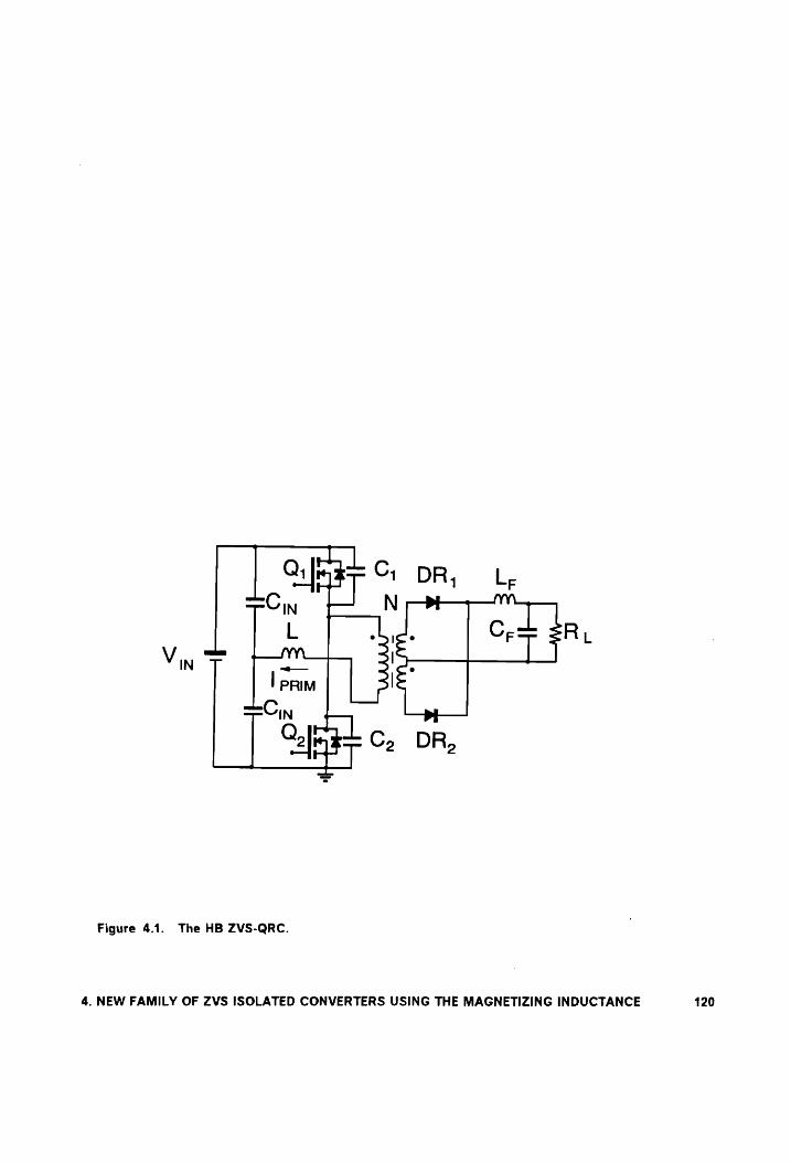
Figure 4.1. The HB ZVS-QRC.
4. NEW FAMILY OF ZVS ISOLATED CONVERTERS USING THE MAGNETIZING INDUCTANCE 120
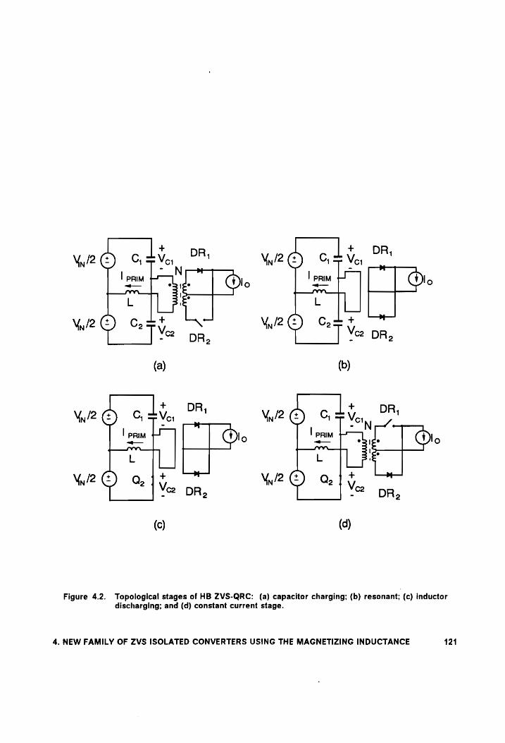
Figure 4.2. Topological stages of HB ZVS-QRC: (a) capacitor charging; (b) resonant: (c) inductor discharging; and (d) constant current stage.
4. NEW FAMILY OF ZVS ISOLATED CONVERTERS USING THE MAGNETIZING INDUCTANCE 121
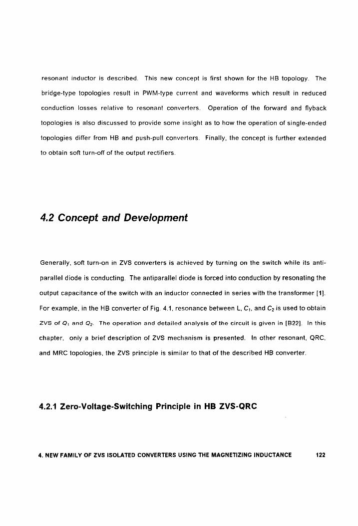
resonant inductor is described. This new concept is first shown for the HB topology. The
bridge-type topologies result in PWM-type current and waveforms which result in reduced
conduction losses relative to resonant converters. Operation of the forward and flyback
topologies is also discussed to provide some insight as to how the operation of single-ended
topologies differ from HB and push-pull converters. Finally, the concept is further extended
to obtain soft turn-off of the output rectifiers.
4,2 Concept and Development
Generally, soft turn-on in ZVS converters is achieved by turning on the switch while its anti-
parallel diode is conducting. The antiparallel diode is forced into conduction by resonating the
output capacitance of the switch with an inductor connected in series with the transformer [1].
For example, in the HB converter of Fig. 4.1, resonance between L, C;, and C2 is used to obtain
ZVS of Q; and Q2. The operation and detailed analysis of the circuit is given in [B22]. In this
chapter, only a brief description of ZVS mechanism is presented. In other resonant, QRC,
and MRC topologies, the ZVS principle is similar to that of the described HB converter.
4.2.1 Zero-Voltage-Switching Principle in HB ZVS-QRC
4. NEW FAMILY OF ZVS ISOLATED CONVERTERS USING THE MAGNETIZING INDUCTANCE 122
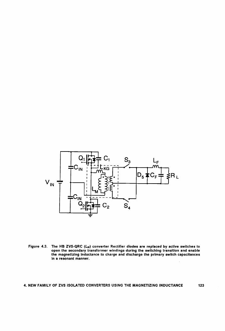
Qs hie Cy S, L,
Cw i -Eke .! D, #C; Re
Vin T ! Pa I
2 LE IN ~qoo---- —— — = apo, S
Figure 4.3. The HB ZVS-QRC (Ly) converter Rectifier diodes are replaced by active switches to open the secondary transformer windings during the switching transition and enable the magnetizing inductance to charge and discharge the primary switch capacitances in a resonant manner.
4. NEW FAMILY OF ZVS ISOLATED CONVERTERS USING THE MAGNETIZING INDUCTANCE 123
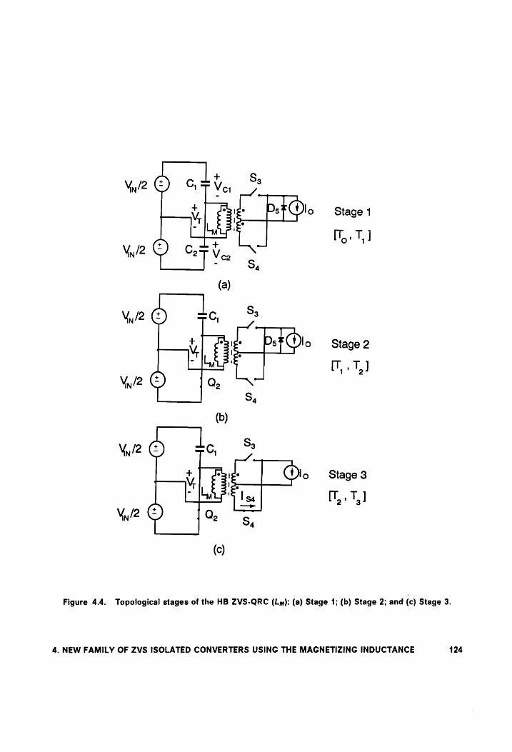
Yy/2
\/2 =C, ‘
Thy Vy/2 Q,
\/2
Vy/2
Wo
Stage 1
T,.T,]
Stage 2
+7,
Stage 3
[T, , T;
Figure 4.4. Topological stages of the HB ZVS-QRC (Ly): (a) Stage 1; (b) Stage 2; and (c) Stage 3.
4. NEW FAMILY OF ZVS ISOLATED CONVERTERS USING THE MAGNETIZING INDUCTANCE 124
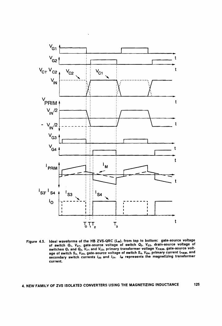
Figure 4.5. Ideal waveforms of the HB ZVS-QRC (Ly), from top to bottom: gate-source voltage
of switch Q;, Vos, gate-source voltage of switch Q2, Vez, drain-source voltage of
switches Q, and Q2, Vc, and Vco, primary transformer voltage Verm, gate-source volt-
age of switch Ss, Ves, gate-source voltage of switch S4, Vea, primary current Ipam, and
secondary switch currents Isg and Isa. Im represents the magnetizing transformer
current.
4. NEW FAMILY OF ZVS ISOLATED CONVERTERS USING THE MAGNETIZING INDUCTANCE 125

Prior to the turn off of switch Q,; in the HB converter of Fig. 4.1, constant output current /o is
flowing through the upper secondary. At the same time, primary current /o/N flows through
switch Q,, the primary winding, and inductor L. Due to the conduction of Q,, the voltage across
C, is zero, and the full supply voltage Vj, appears across Co. When Q, is turned-off, primary
current /o/N is diverted from Q, to C; and Co. The equivalent circuit of the converter imme-
diately after the switch is turned off is shown in Fig. 4.2(a). Since the primary current during
this stage remains constant (/o/N), there is no voltage drop across inductor L, and voltages
across C, and C2 change linearly. Voltage Vc, increases from zero to Vjy, while voltage Veco
decreases from Viv to zero at the same rate. When voltages across C; and Co reach Vjn/2, i.e.,
Ve1 = Voo = Vin/2, the primary voltage across the transformer becomes zero. Further change
of voltages Vc; and Vc. tend to make the primary voltage of the transformer negative, which
forces rectifier DR. to turn on. When DR» starts conducting, the secondary windings of the
transformer are shorted since DR; still conducts. As a result, the primary voltage across the
transformer is zero as shown in Fig. 4.2(b). Inductance L and capacitances C,; and Cp, (effec-
tively connected in parallel) form a resonant circuit and the voltages across C; and Cz continue
to change (C,; to charge and C, to discharge) in a resonant fashion. When voltage Vc2 reaches
zero, antiparallel diode D. starts conducting, clamping the voltage across Q, to zero. If Qo is
turned on while D. is conducting, ZVS of Q. is achieved.
As can be seen, during the resonant stage, which creates the conditions for ZVS, the trans-
former is shorted by simultaneous conduction of the output rectifiers. As a result, the
magnetizing inductance of the transformer, which is in series with L, is taken out of the circuit.
To use the magnetizing inductance as a resonant element and eliminate the need for an ex-
ternal resonant inductor, it is necessary to modify the circuit in Fig. 4.1 so that the magnetizing
inductance is not shorted during the resonant stage.
4. NEW FAMILY OF ZVS ISOLATED CONVERTERS USING THE MAGNETIZING INDUCTANCE 126

4.2.2 Zero-Voltage-Switching using the Magnetizing Inductance
Figure 4.3 shows the conceptual implementation of a HB ZVS which utilizes the magnetizing
inductance as a resonant element (HB ZVS-QRC (Ly)). In order to prevent the voltage across
the magnetizing inductance of the power transformer from being shorted during the switching
transition. the rectifiers are replaced by switches S3 and S,. In addition, to ensure a current
path when both secondary switches are turned-off, a freewheeling diode Ds is connected
across the input of the output filter. The added switches, S3 and Sy, delay the energy transfer
from the primary circuit to the secondary circuit until the magnetizing inductance discharges
the output capacitance of the switch to be turned on and forces its antiparallel diode into
conduction. During a switching cycle this converter enters a sequence of three topological
stages. Figure 4.4 shows the topological stages and Fig. 4.5 the ideal waveforms of the con-
verter. The waveforms are obtained assuming that the forward voltage drop of all semicon-
ductor devices, the leakage inductance of the power transformer, and the parasitic
capacitance of the rectifier diodes are negligible. Also, the output filter and the load are re-
placed by an ideal current source by assuming that the inductance of the output filter is large
enough so that the filter inductor current is constant during a switching period.
Prior to the turn off of transistor Q, in the circuit of Fig. 4.3, secondary-side switch S3 is on, and
switch S, is off. As result, the entire constant load current flows through the upper secondary,
as in the case of the converter in Fig. 4.1. At t= To, switches Q, and S3 are turned off, and the
magnetizing current is diverted from Q, into C, and Co. At the same time, the load current is
commutated to the freewheeling diode. Figure 4.4(a) shows the equivalent circuit of the con-
verter immediately after Q; and S3 are turned off. This topological stage is referred to as
Stage 1. With the output current freewheeling, the primary current consists only of the
4. NEW FAMILY OF ZVS ISOLATED CONVERTERS USING THE MAGNETIZING INDUCTANCE 127
magnetizing current. This magnetizing current charges C, and discharges C2 at the same
rate. It should be noted that charging of C; and discharging of Cz occurs in a resonant fashion,
since Ly, C;, and Cy form a resonant circuit. However, Ly is normally very large, and a rela-
tively constant magnetizing current during the duration of Stage 1 produces linear voltage
changes across C; and Cy. Stage 1 ends at f=7;, when the voltage across switch Q, de-
creases to zero, and the antiparallel diode of Q2 starts conducting. To achieve ZVS, the gate
drive to switch Q, should be applied while its antiparallel diode is conducting. During Stage
2, shown in Fig. 4.4(b), switch S3 and Ss remain off, and no power is transferred to the load.
The primary current is the magnetizing current of the power transformer and the load current
continues to freewheel through diode Ds. This stage ends at t= T) , when switch S, is turned
on, and the converter enters Stage 3. During Stage 3, Fig. 4.4(c), the load current is com-
mutated from the freewheeling diode to the lower secondary. As a result, during this stage
power is transferred to the load. The primary current is the sum of the magnetizing current
of the transformer and the load current reflected to the primary. This stage ends at t= 73
when switches Qs and S, are turned off, marking the beginning of a new conversion cycle.
Since power is delivered to the load only during Stage 3, the output voltage can be regulated
at a constant switching frequency by varying the duration of this stage; controlling the time
of Stage 2. Note that the duration of Stage 1 can not be controlled, since approximately con-
stant blocking time 7; — To is needed to create conditions for ZVS of the primary switches.
This time interval is dependent upon the magnetizing current, magnetizing inductance, and
the junction capacitance of switches Q,; and Q,. The maximum output voltage is obtained
when the duration of Stage 2 is zero, i.e., when T, = 7;. If the duration of Stage 2 is fixed, i.e.,
T2 — T; = constant, the output voltage can be regulated by varying the switching frequency.
4. NEW FAMILY OF ZVS ISOLATED CONVERTERS USING THE MAGNETIZING INDUCTANCE 128
To simplify the variable-frequency control, the duration of Stage 2 can be made zero
(T2 = T) in practice.
With variable-frequency control, Q; and Q» operate with variable on-time control, while
switches S3 and S4 are delayed by a constant time interval (7; — To). Figure 4.6 shows the dc
voltage-conversion-ratio characteristics as a function of the normalized conversion frequency
(f,{2fo) where wo = 2rfo = 1/./2CLm , C = C; = C2 is the resonant capacitance across the
primary switches, and Ly is the magnetizing inductance of the transformer. Under constant
frequency control. switch Q,; and Q» operate with constant frequency and constant duty cycle,
while switches S3 and S, are leading-edge PWM. The dc voltage-conversion-ratio character-
istics for constant-frequency control can be approximated by M = D~(T>2 — T;)/(T3 — 71), as-
suming the duration of Stage 1. T; — To, is small. The dc voltage-conversion-ratio for both
variable frequency and constant frequency operation are load independent.
This concept can be extended to other isolated topologies as shown in Fig. 4.7. For single
ended topologies, the resonance of the output capacitance of the primary switch and the
magnetizing inductance of the power transformer take place for half of a resonant cycle.
Figure 4.8 shows the ideal waveforms for the forward topology of Fig. 4.7(a). The stage se-
quence for normal operation of the forward converter is shown in Fig. 4.9. In this topology,
when power transfer is interrupted by a forced turn-off of switch Q,, the output capacitance
of the switch starts resonating with the magnetizing inductance of the transformer, Stage 1
[To. T;]. As a result, the voltage Vc, in Fig. 4.8 first increases, goes through a maximum, and
finally reaches zero att=T7,. At t=T,, the antiparallel diode of Q, starts conducting the pri-
mary current and Vc; remains at zero. ZVS is achieved by turning on Q, when the antiparallel
diode is conducting. The additional active switch S». replacing the forward diode is necessary
4. NEW FAMILY OF ZVS ISOLATED CONVERTERS USING THE MAGNETIZING INDUCTANCE 129

to insure that the turn-on of the forward diode D, (Fig. 2.9{a)) will not prevent the zero voltage
turn-on of switch S;.
In Stage 2 [7;, 72]. the voltage across the magnetizing inductance is equal to the input voltage
resulting in a magnetizing current that increases at a constant rate. The load current contin-
ues to freewheel. Stage 3 [7>, 73] begins when switch So is turned on, thus turning off the
freewheeling diode; power is transferred to the load from the source. This last stage ends
when switch S, is turned off at time T3 initiating a new switching cycle.
It should be noted that the flyback and sepic topologies do not need an extra active switch to
resonate the magnetizing inductance of the power transformer during the resonant interval,
since the magnetizing inductance is free to resonate during the off-interval of the power
switch. In addition, the resonance of the resonant capacitor voltage across the power switch
is clamped by the output voltage. The ideal waveforms for the flyback topology are shown in
Fig. 4.10. The topological stage sequence for this converter is shown in Fig. 4.11.
The operation of the flyback converter is the following: in Stage 1 [To, 7;], switch S; conducts
and the magnetizing current increases at a constant rate. At time 7,, switch S; is turned off,
Stage 2, and the magnetizing current charges capacitance C, in parallel with S;. Capacitance
C, will continue to charge until the voltage across this capacitance is equal to Vo/N + Vin,
where N is the turns ratio of the transformer. At the same time, the magnetizing inductance
gets clamped to — Vo/N. In Stage 3 [T», T3], the magnetizing current decreases at a constant
rate since the magnetizing inductance remains clamped to — Vo/N. This stage ends when the
magnetizing current decreases to zero and diode D, turns off. In Stage 4 [73, T4], the
magnetizing inductance resonates with capacitance C,. If Vo/N is greater than the input volt-
4. NEW FAMILY OF ZVS ISOLATED CONVERTERS USING THE MAGNETIZING INDUCTANCE 130
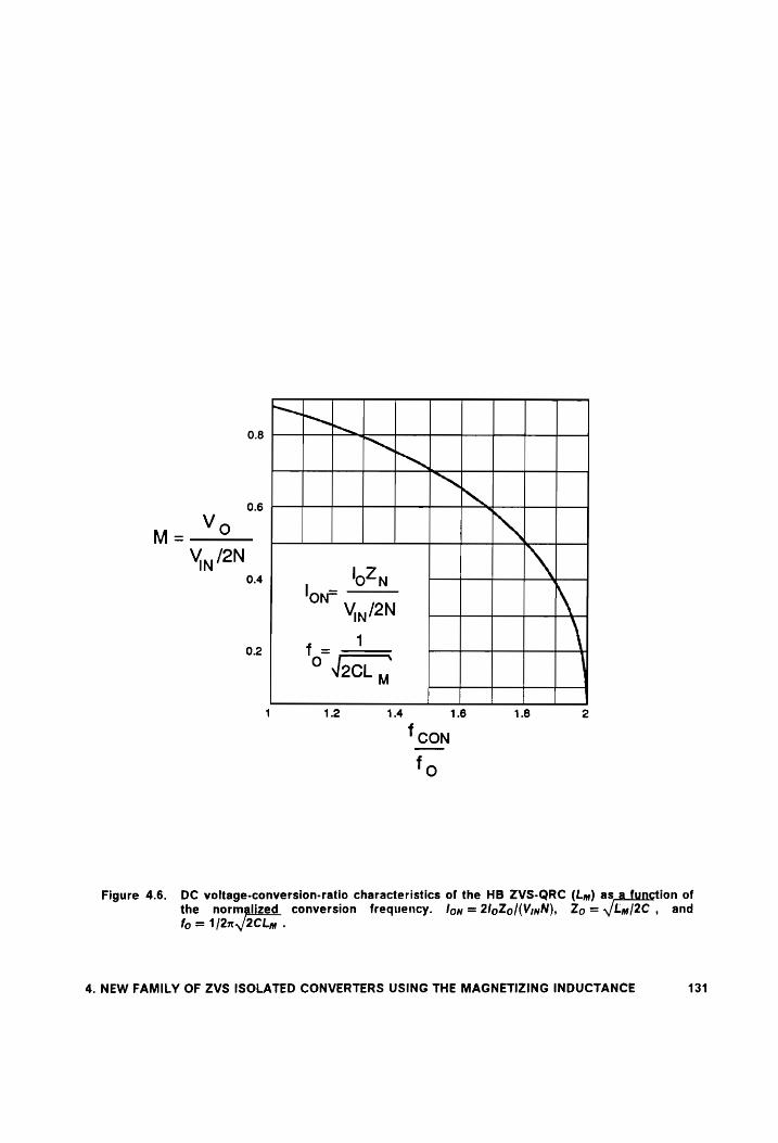
0.8 ——
V,,/2N IZ 0.4 lon= O“N \
Vin /2N
0.2 f = 1 \
Figure 4.6. DC voltage-conversion-ratio characteristics of the HB ZVS-QRC (Ly) as ion of the normalized conversion frequency. lon = 2IloZo/(VinN), Zo=-~/Lm/2C , and fo = 1/2n,/2CLay .
4. NEW FAMILY OF ZVS ISOLATED CONVERTERS USING THE MAGNETIZING INDUCTANCE 131
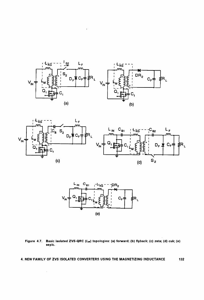
Figure 4.7. Basic isolated ZVS-QRC (Lw) topologies: (a) forward; (b) flyback; (c) zeta; (d) cuk; (e)
sepic.
4. NEW FAMILY OF ZVS ISOLATED CONVERTERS USING THE MAGNETIZING INDUCTANCE 132
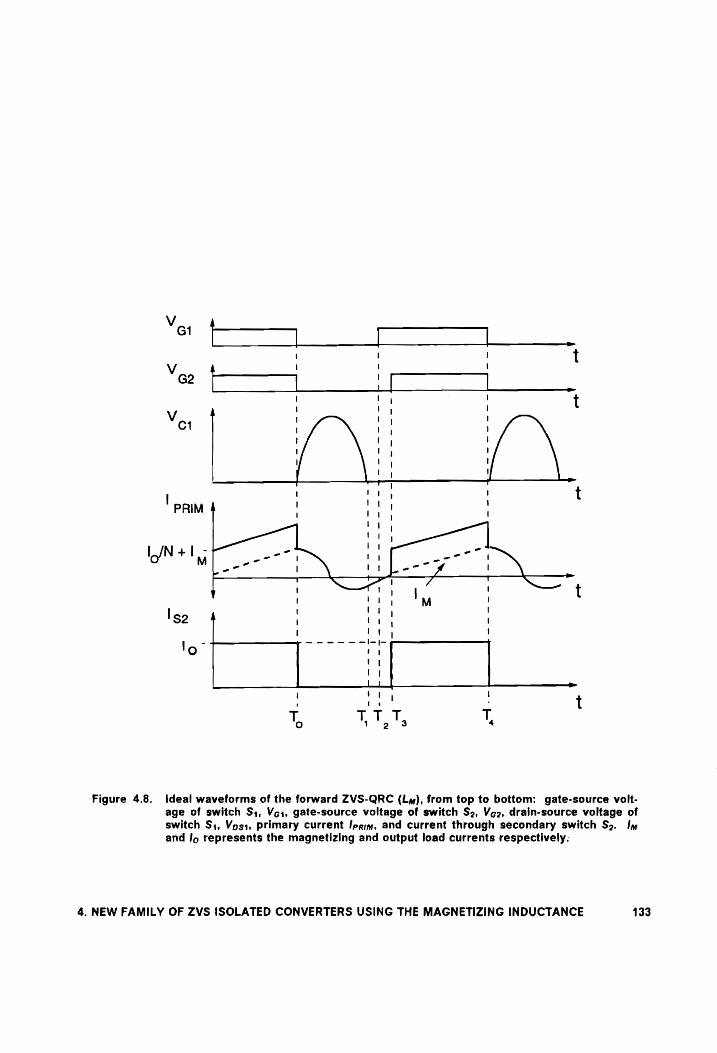
Vor ———_ |
\ | t | i i
“ea ET ‘TT - y ! !
C1 ' I
! |
I t
| a
| 4 ny t PRIM a
Pt 1
- It IN +1 Z !
{ Ot 7 7 ‘—¢ | yay M l
Iso ii! | ! il 1
lo TO YOO | |
i ) 4 =»
ry t
™ 41,7, T
Figure 4.8. Ideal waveforms of the forward ZVS-QRC (Ly), from top to bottom: gate-source volt- age of switch S,, Ves, gate-source voltage of switch S2, Vez, drain-source voltage of switch S4, Vos, primary current Ipaim, and current through secondary switch S2. /Iy and Io represents the magnetizing and output load currents respectively.
4. NEW FAMILY OF ZVS ISOLATED CONVERTERS USING THE MAGNETIZING INDUCTANCE 133
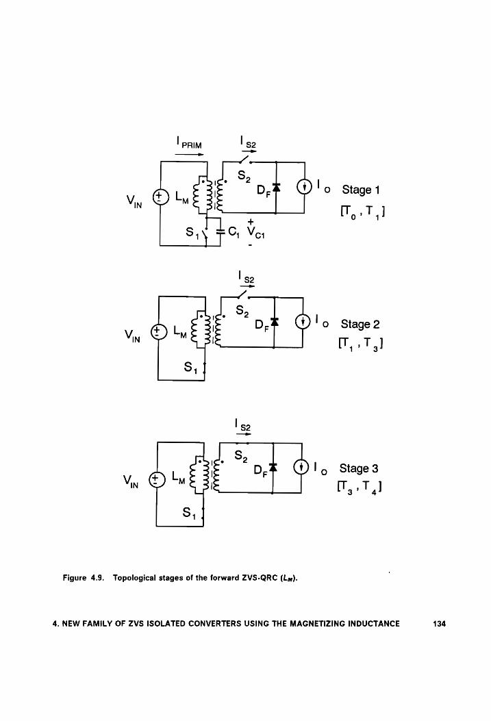
| | D Oo Stage 1 Vin © La : F
TT, ]
Je . Se
D; M!o Stage 2
4 [T,,1,]
82
, Sp V D-, |, Stage 3
IN (T,.7,]
Figure 4.9. Topological stages of the forward ZVS-QRC (Ly).
4. NEW FAMILY OF ZVS ISOLATED CONVERTERS USING THE MAGNETIZING INDUCTANCE 134
age, then capacitance C, will naturally discharge to zero before switch S; is turned on. Al-
though not given here, this can be easily shown by writing the differential equation describing
Stage 4. If output voltages where Vo/N < Viv are desired, diode D2. needs to be replaced by
an active switch. By replacing diode D>» with an active switch, the current through this second
switch can be forced to conduct in the reverse direction, storing additional energy in the
magnetizing inductance that can be used to switch Q, under zero-voltage conditions. The
flyback as shown in Fig. 4.9 operates with a variable switching frequency.
lf constant frequency operation is desirable for the flyback converter, diode Dz needs to be
replaced by a second active switch. By adding the second active switch, the conduction time
of the rectifier switch (previously diode D2) can be controlled. Another characteristic of the
flyback and sepic topologies that should be mentioned is that because the magnetizing
inductance is used as a resonant element, no resetting scheme is needed. This is the case
for all single-ended topologies of this new family of converters.
4.2.3 Implementation
The switch that opens the secondary winding(s) of the power transformer during the resonant
interval can be implemented in different ways. Figure 4.12 shows the implementation with a
series combination of a saturable reactor and a rectifier diode [F2]. The saturable reactor
provides the necessary blocking time to ensure that the resonant interval has ended before
allowing the rectifier diode to conduct. Figure 4.13 (b) shows the HB topology implemented
by replacing the secondary switches with the switch described in Fig. 4.11. Other isolated
4. NEW FAMILY OF ZVS ISOLATED CONVERTERS USING THE MAGNETIZING INDUCTANCE 135
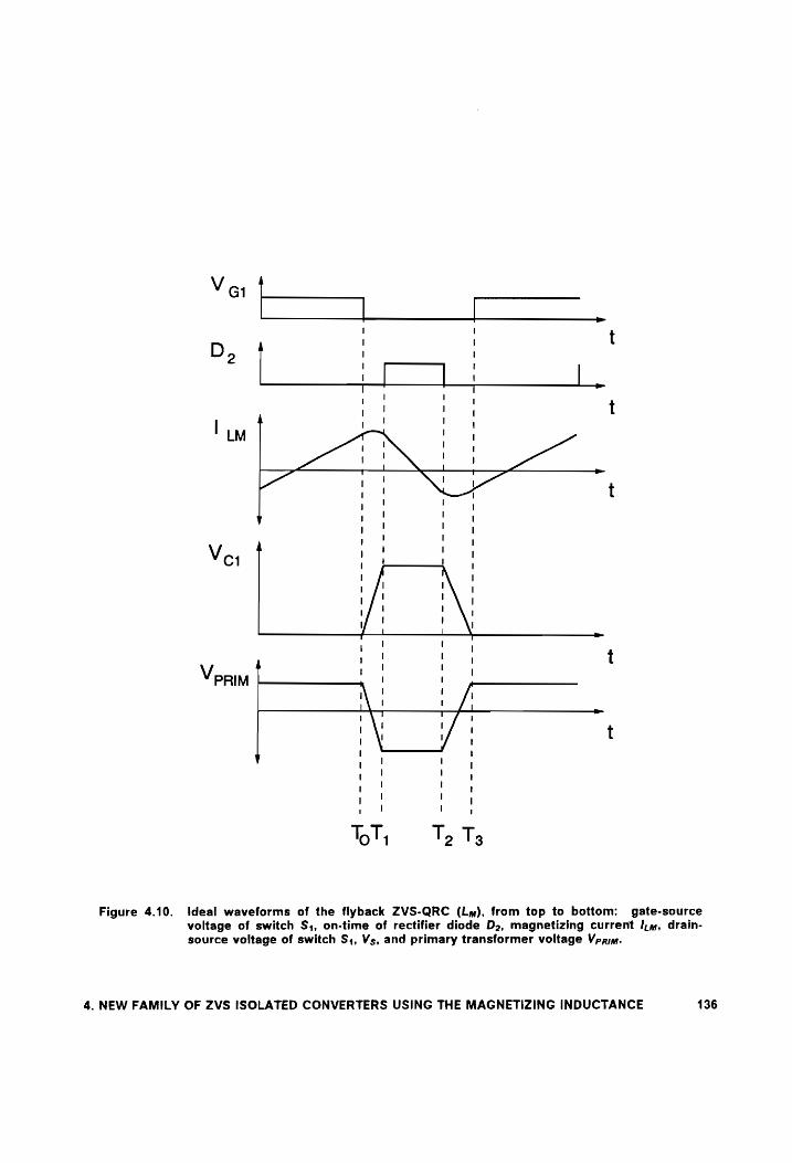
| |
7 ! t Pe | ! !
—_1_4 | P| t
oH] CaN | —
~ Mi NUR
Yop EG
-~--4
< 7 D =
ait: ~<—<_- — ee eee
lee
ot
a + nN 4 oo
Figure 4.10. Ideal waveforms of the flyback ZVS-QRC (Ly), from top to bottom: gate-source voltage of switch S,, on-time of rectifier diode D2, magnetizing current I,m, drain-
source voltage of switch $1, Vs, and primary transformer voltage Vprim.
4. NEW FAMILY OF ZVS ISOLATED CONVERTERS USING THE MAGNETIZING INDUCTANCE 136
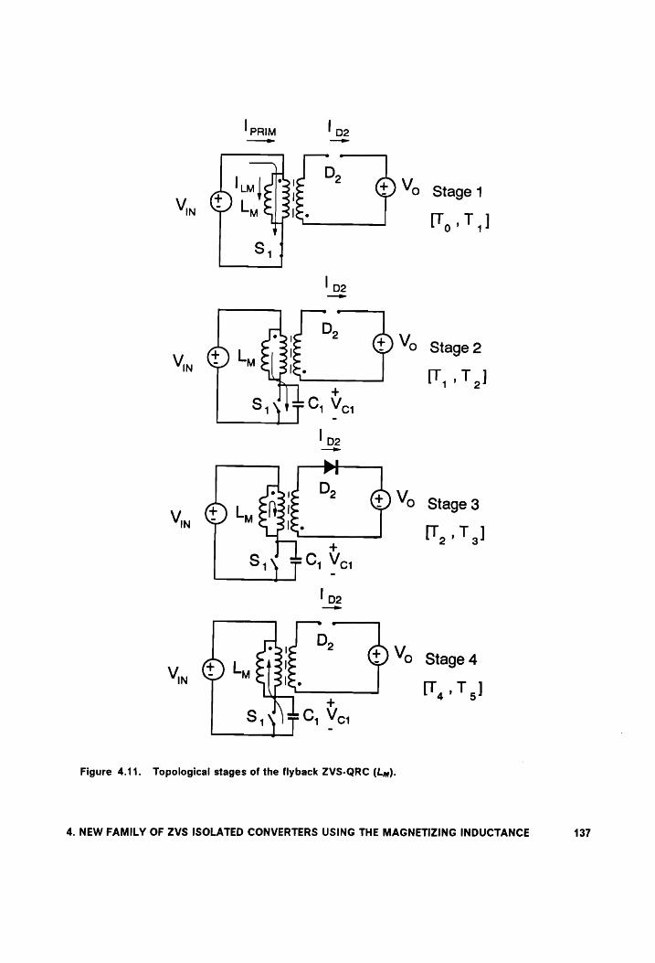
Stage 1
[T, ' T 1!
Stage 2
7.)
Stage 3
T,,7.]
Stage 4
T,.7.] Figure 4.11. Topological stages of the flyback ZVS-QRC (Ly).
4. NEW FAMILY OF ZVS ISOLATED CONVERTERS USING THE MAGNETIZING INDUCTANCE 137
topologies can be easily generated following the same procedure. It should be noted that the
circuit in Fig. 4.13 requires variable frequency control because the saturable inductor blocking
time is fixed.
Constant frequency operation of ZVS-QRC (Ly) requires an additional active switch in the
rectifier circuit. The active switch in the primary side of the power stage is operated with
constant switching frequency and constant duty cycle (off time is determined by ZVS condition)
and the output voltage is regulated by PWM of the active switch in the secondary side.
Therefore, constant frequency operation results in secondary side control. Secondary side
control can easily be used in multiple output applications where all outputs have to be tightly
regulated; i.e., the second active switch in the rectifier circuit is used as a postregulator.
Furthermore, since ZVS of the primary switch(es) only depends on the interaction of the output
capacitance of this switch(es) and the magnetizing inductance of the transformer, a common
front end can be designed independently from the postregulated rectifier circuits. The front
end can be designed for a maximum power rating exceeding that of the total output power,
allowing for system expansion in the future.
4.2.4 Soft-Switching Rectifier Circuit
The output rectifiers of the converters shown in Figs. 4.7 and 4.13 turn off with an abrupt re-
verse voltage, resulting in parasitic ringings of the junction capacitance of the rectifier and the
secondary side transformer leakage and lead inductances. To avoid the parasitic ringings, it
is necessary to resonate the rectifier voltage in a controlled fashion as, for example, it is done
4. NEW FAMILY OF ZVS ISOLATED CONVERTERS USING THE MAGNETIZING INDUCTANCE 138
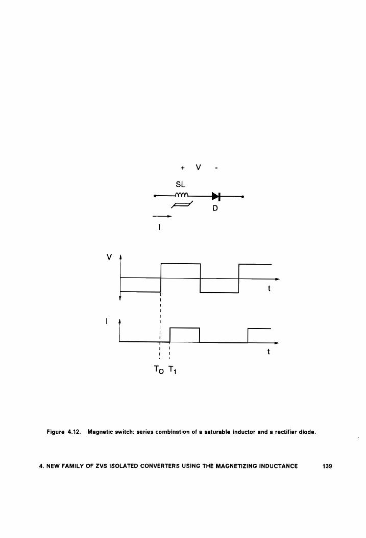
SL
-——_"".—___}>}] __-
JT D
|
V4
t
v
|
| \ {
! a
Do t
To Ty
Figure 4.12. Magnetic switch: series combination of a saturable inductor and a rectifier diode.
4. NEW FAMILY OF ZVS ISOLATED CONVERTERS USING THE MAGNETIZING INDUCTANCE 139
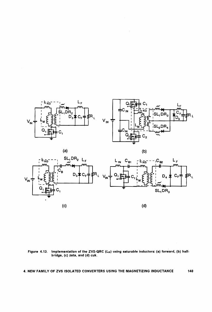
(c) (d)
Figure 4.13. Implementation of the ZVS-QRC (Lm) using saturable inductors: (a) forward, (b) half- bridge, (c) zeta, and (d) cuk.
4. NEW FAMILY OF ZVS ISOLATED CONVERTERS USING THE MAGNETIZING INDUCTANCE 140
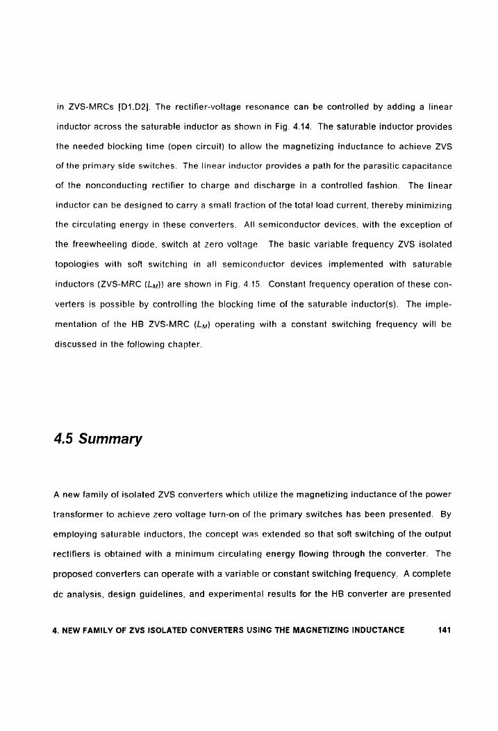
in ZVS-MRCs [D1,D2]. The rectifier-voltage resonance can be controlled by adding a linear
inductor across the saturable inductor as shown in Fig. 4.14. The saturable inductor provides
the needed blocking time (open circuit) to allow the magnetizing inductance to achieve ZVS
of the primary side switches. The linear inductor provides a path for the parasitic capacitance
of the nonconducting rectifier to charge and discharge in a controlled fashion. The linear
inductor can be designed to carry a small fraction of the total load current, thereby minimizing
the circulating energy in these converters. All semiconductor devices, with the exception of
the freewheeling diode, switch at zero voltage. The basic variable frequency ZVS isolated
topologies with soft switching in all semiconductor devices implemented with saturable
inductors (ZVS-MRC (Ly)) are shown in Fig. 4.15. Constant frequency operation of these con-
verters is possible by controlling the blocking time of the saturable inductor(s). The imple-
mentation of the HB ZVS-MRC (Ly) operating with a constant switching frequency will be
discussed in the following chapter.
4.5 Summary
A new family of isolated ZVS converters which utilize the magnetizing inductance of the power
transformer to achieve zero voltage turn-on of the primary switches has been presented. By
employing saturable inductors, the concept was extended so that soft switching of the output
rectifiers is obtained with a minimum circulating energy flowing through the converter. The
proposed converters can operate with a variable or constant switching frequency. A complete
dc analysis, design guidelines. and experimental results for the HB converter are presented
4. NEW FAMILY OF ZVS ISOLATED CONVERTERS USING THE MAGNETIZING INDUCTANCE 141
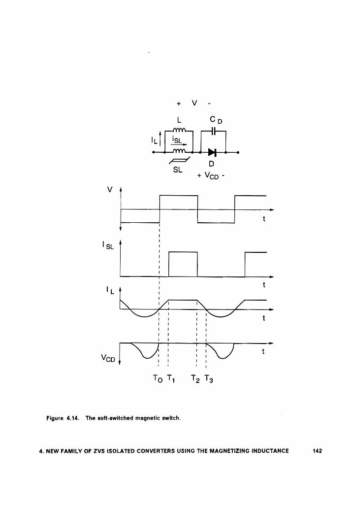
L Cop —_||—
| a
/——_ D
SL + Vop -
V a4
t
’
lop 4
7
=
Figure 4.14. The soft-switched magnetic switch.
4. NEW FAMILY OF ZVS ISOLATED CONVERTERS USING THE MAGNETIZING INDUCTANCE 142
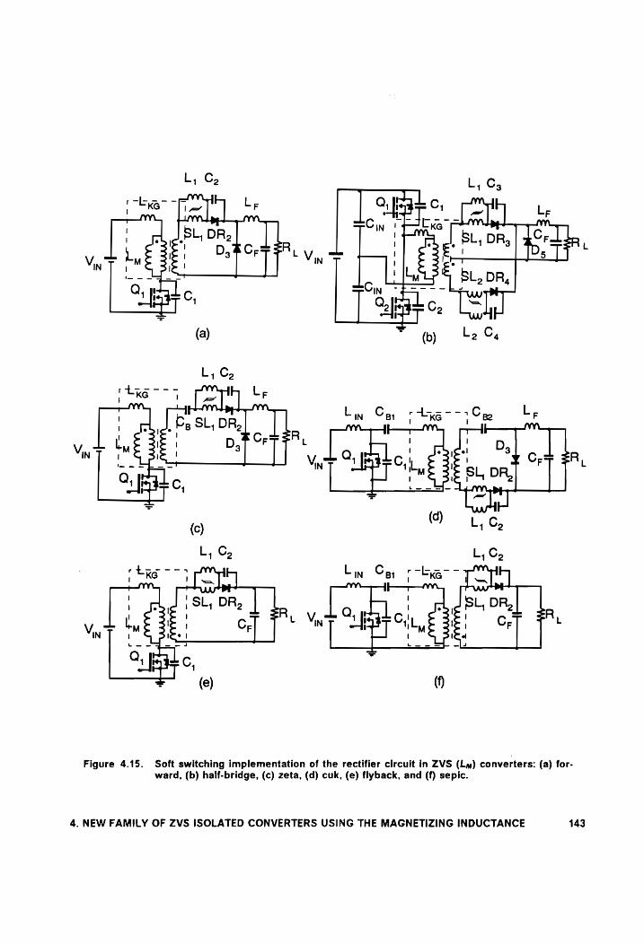
Figure 4.15. Soft switching implementation of the rectifier circuit in ZVS (Lm) converters: (a) for-
ward, (b) half-bridge, (c) zeta, (d) cuk, (e) flyback, and (f) sepic.
4. NEW FAMILY OF ZVS ISOLATED CONVERTERS USING THE MAGNETIZING INDUCTANCE 143

in the next chapter. In the following chapter, a detailed analysis of the operation of the HB
topology (Fig. 4.14(b)) is presented.
4. NEW FAMILY OF ZVS ISOLATED CONVERTERS USING THE MAGNETIZING INDUCTANCE 144
5. DC ANALYSIS AND IMPLEMENTATION
OF THE HB ZVS-MRC (Ly)
5.1 Introduction
A new family of converters that uses the magnetizing inductance as a resonant element was
introduced in the previous chapter. By using the magnetizing inductance as a resonant
component the need for using an external resonant inductor to achieve ZVS is eliminated.
The bridge-type topologies of this new family of ZVS converters exhibit a very desirable
property. These converters clamp the resonant voltage across the primary switches, resulting
in a very short resonant interval. Since the resonant interval in these converters is only a
small fraction of the total switching cycle, the current and voltage waveforms are squarewave
shaped like those of PWM converters. PWM-type waveforms are very desirable since they
result in low conduction losses and minimize circulating energy.
5. DC ANALYSIS AND IMPLEMENTATION OF THE HB ZVS-MRC (Lm) 145

Chapter 4 discussed how the parallel combination of a linear and saturable inductor is used
to obtain soft switching of the rectifier circuit for this new family of converters. Using saturable
inductors to implement the soft switching rectifier circuit helps keep the circulating energy
flowing through the converter at a minimum. This means that for the HB topology, the current
and voltage waveforms are mostly squarewave shaped and there is not much energy circu-
lating through the converter. In this chapter, the dc analysis of the HB ZVS-MRC (Ly) is
studied in detail. First, only variable frequency operation is considered in the analysis. Like
most resonant topologies, this converter is found to operate in more than one mode. The dc
voltage conversion ratio and stress analysis characteristics obtained from the dc analysis are
used in design trade-off studies. The trade-off study is used to define design guidelines for the
HB ZVS-MRC (Ly).
The last section of this chapter studies the implementation of the HB ZVS-MRC (Ly) using
controllable saturable inductors. By controlling the blocking time of the saturable inductors,
the soft-switched HB can operate at a constant switching frequency. Finally, experimental
results for a 100 W HB ZVS-MRC (Ly) operating with variable and constant switching frequency
are presented.
5.2 Operation of the HB ZVS-MRC (Ly)
The ZVS-MRC Ly is shown in Fig. 5.1. The primary switches Q, and Q» of this converter are
turned on under zero voltage and the rectifier diodes DR3 and DR, are turned on under soft
5. DC ANALYSIS AND IMPLEMENTATION OF THE HB ZVS-MRC (Lym) 146
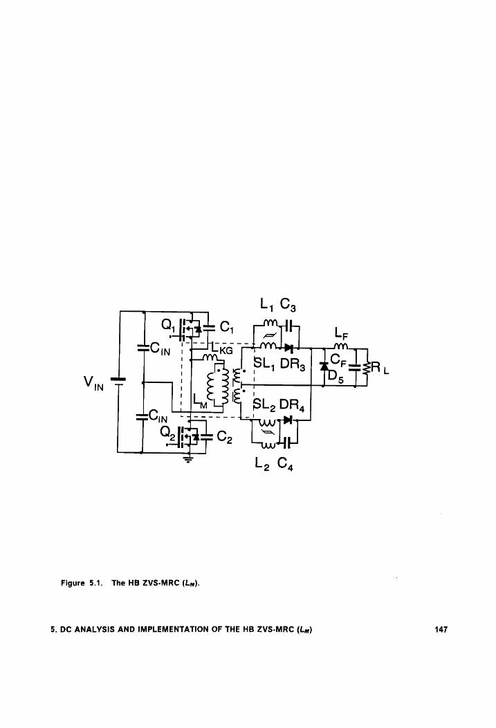
+ | SL, DR, Croker
e_ J s | "
Figure 5.1. The HB ZVS-MRC (Ly).
5. DC ANALYSIS AND IMPLEMENTATION OF THE HB ZVS-MRC (Lym) 147
switching conditions. ZVS of the primary switches is achieved by allowing capacitances C,
and C, to resonate with the magnetizing inductance during the switching transition. This
switching transition is very short due to the voltage clamping of the primary switches that is
characteristic of all bridge-type topologies. Soft switching of the rectifier diodes is achieved
by allowing capacitance C3 and C, to charge and discharge in a controlled fashion through the
linear inductor in parallel with the saturable inductor and in series with the rectifier diodes.
The linear inductors carry only a small fraction of the total current when the rectifier diodes
are forward biased. Most of the load current flows through the saturable inductors. Like a
typical HB converter, when rectifier DR3 is forward biased, rectifier DR, is reversed biased and
vice versa. As can be seen from the previous discussion, capacitances C;, Co, C3, and C4 are
resonant capacitances, and L;, Lo, and Ly are the resonant inductors of the converter.
5.2.1 DC Analysis
To simplify the analysis of the HB ZVS-MRC (Ly). it is assumed that:
a) the output filter inductance is sufficiently targe so that it can be approximated by a current
source with a value equal to the output current, /o;
b) the voltage drops across the conducting semiconductor switches (MOSFETs and diodes)
are negligible:
c) the switching times of the semiconductor switches are zero;
d) transformer leakage inductance is negligible;
e) C=C,;=Co; Cp=Cy=Cs, andL =L,=Ly:
5. DC ANALYSIS AND IMPLEMENTATION OF THE HB ZVS-MRC (Ly) 148

f) the saturable inductors, SL; and SL», are identical:
g) the slope of the saturable inductance SL, and SL, is defined by the ratio L/SL (ratio of the
linear inductance to saturable inductance); and
h) the current through the linear inductor L at the time the corresponding saturable inductor
saturates is Isa4r as shown in Fig. 5.2(b).
The representation of the saturable inductor is shown in Fig. 5.2(a). The inductors block all
current when not saturated. Once saturated. it behaves like an inductor with very low
inductance.
During a switching cycle, the converter enters a sequence of seven or eight topological stages
during heavy load and light load operation, respectively. Each sequence of topological stages
represents a different mode of operation. Figure 5.3 shows the different possible topological
stages.
The operation of the HB ZVS-MRC (Ly) is classified into four major modes of operation. The
first three modes occur for heavy load conditions, while the fourth mode is found at light load
operation. Since light-load operation is not important for the design of the converter, it will
not be discussed in detail.
5. DC ANALYSIS AND IMPLEMENTATION OF THE HB ZVS-MRC (Ly) 149
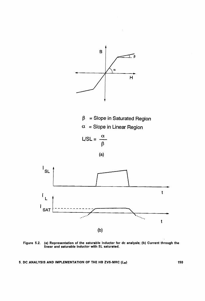
4 y
8 = Slope in Saturated Region
Qa = Slope in Linear Region
USL = B
(a)
l SL
t nm
bot SAT r* eo? “ N., -
. t
(b)
Figure 5.2. (a) Representation of the saturable inductor for dc analysis; (b) Current through the linear and saturable inductor with SL saturated.
5. DC ANALYSIS AND IMPLEMENTATION OF THE HB ZVS-MRC (Ly) 150
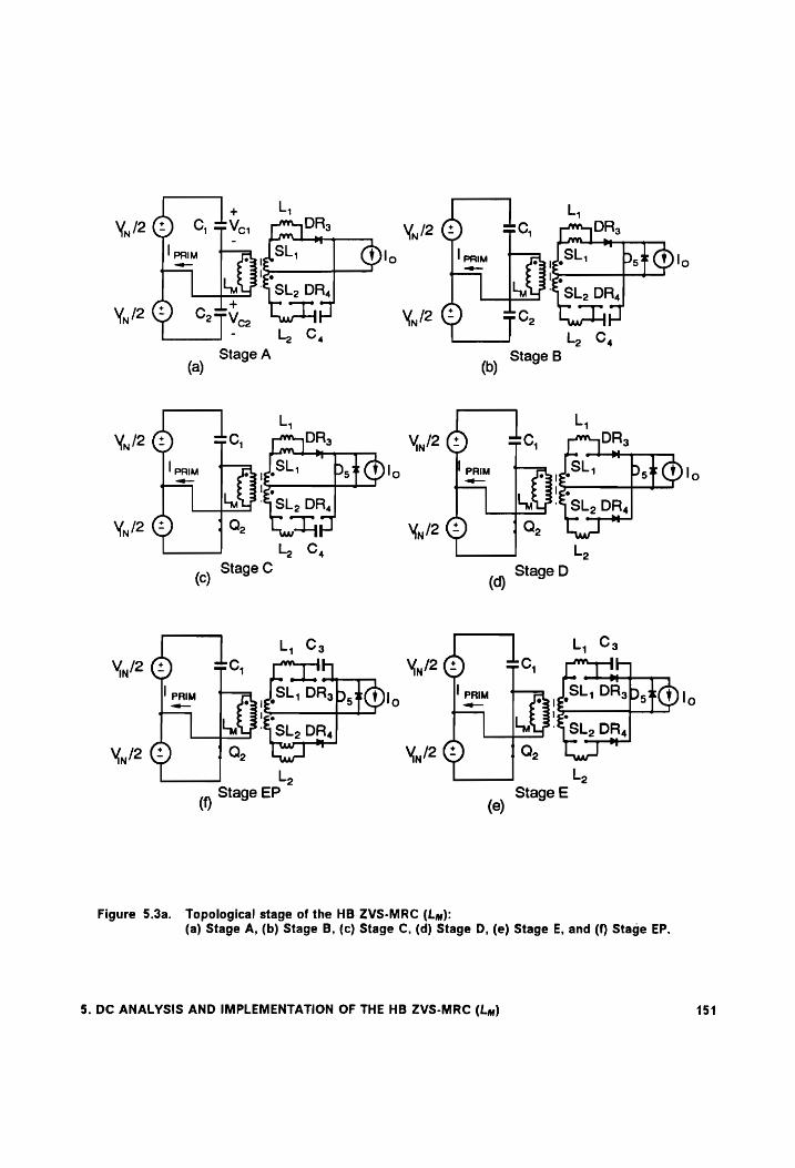
-C, DR;
; SL, D5 3
igs a SL, DR,
1 Q;
(c)
™
=C, IFA, gS DRs
| i
Ty lL, ¢,
Stage C
L, Cs
SL. DR, Q,
(f)
Figure 5.3a.
2
Stage EP L
Topological stage of the HB ZVS-MRC (Ly):
SL, DR,
=C, DR
Sli - I J
Q,
Lo
(a) Stage A, (b) Stage B, (c) Stage C, (d) Stage D, (e) Stage E, and (f) Stage EP.
5. DC ANALYSIS AND IMPLEMENTATION OF THE HB ZVS-MRC (Ly) 151
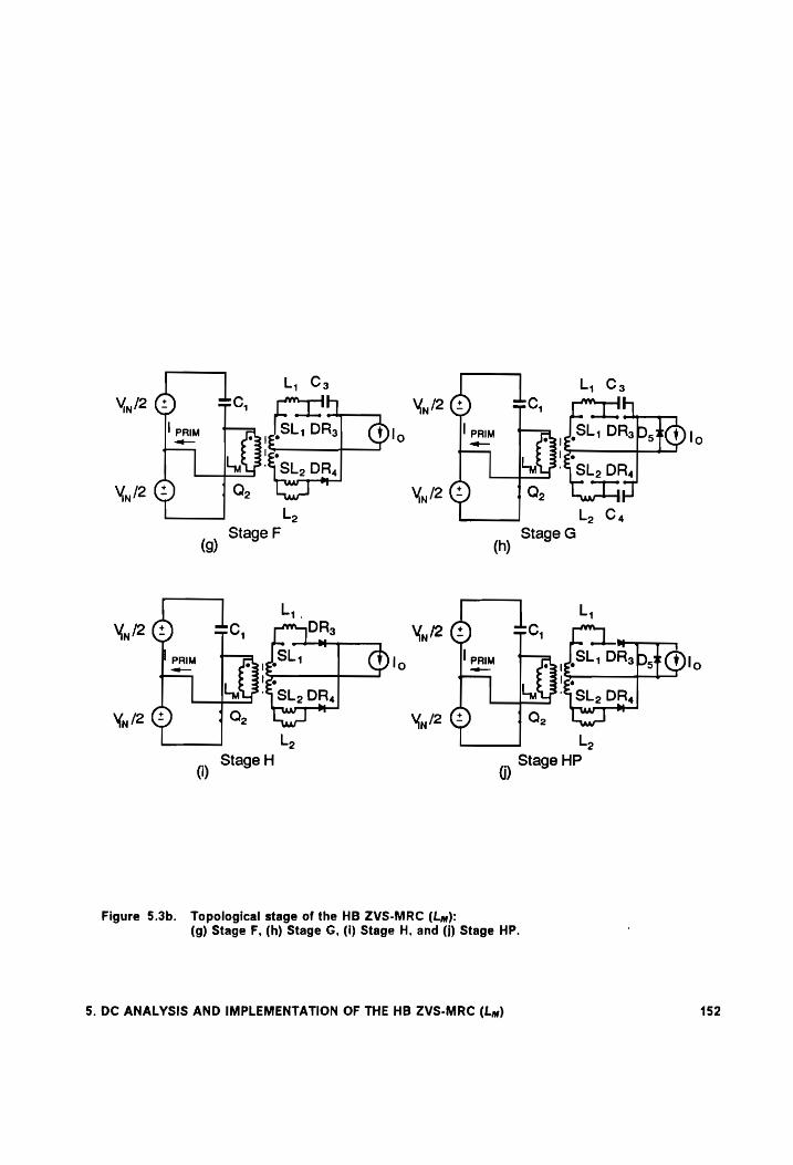
Ly Cz a
|SL; D
JE SL». D +
L, C4
Rs D4 y lo
Stage a Stage G
(h)
| Le L,
gst: DRsb, Mo
3 ‘SL DR, " aT
.. Stage Hp?
Figure 5.3b. Topological stage of the HB ZVS-MRC (Ly): (g) Stage F, (h) Stage G, (i) Stage H, and (j) Stage HP.
5. DC ANALYSIS AND IMPLEMENTATION OF THE HB ZVS-MRC (Ly) 152
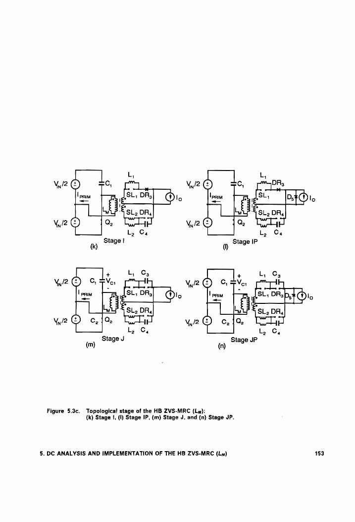
L, eC, " DR
uy ,SL, Ds# 1) Io
Ige
Li? -® SL, DR,
4H
Ls Stage IP
‘ L, ©,
apni Of x L, fH
Stage JP
Figure 5.3c. Topological stage of the HB ZVS-MRC (Lym): (k) Stage [, (I) Stage IP, (m) Stage J, and (n) Stage JP.
5. DC ANALYSIS AND IMPLEMENTATION OF THE HB ZVS-MRC (Lm) 153
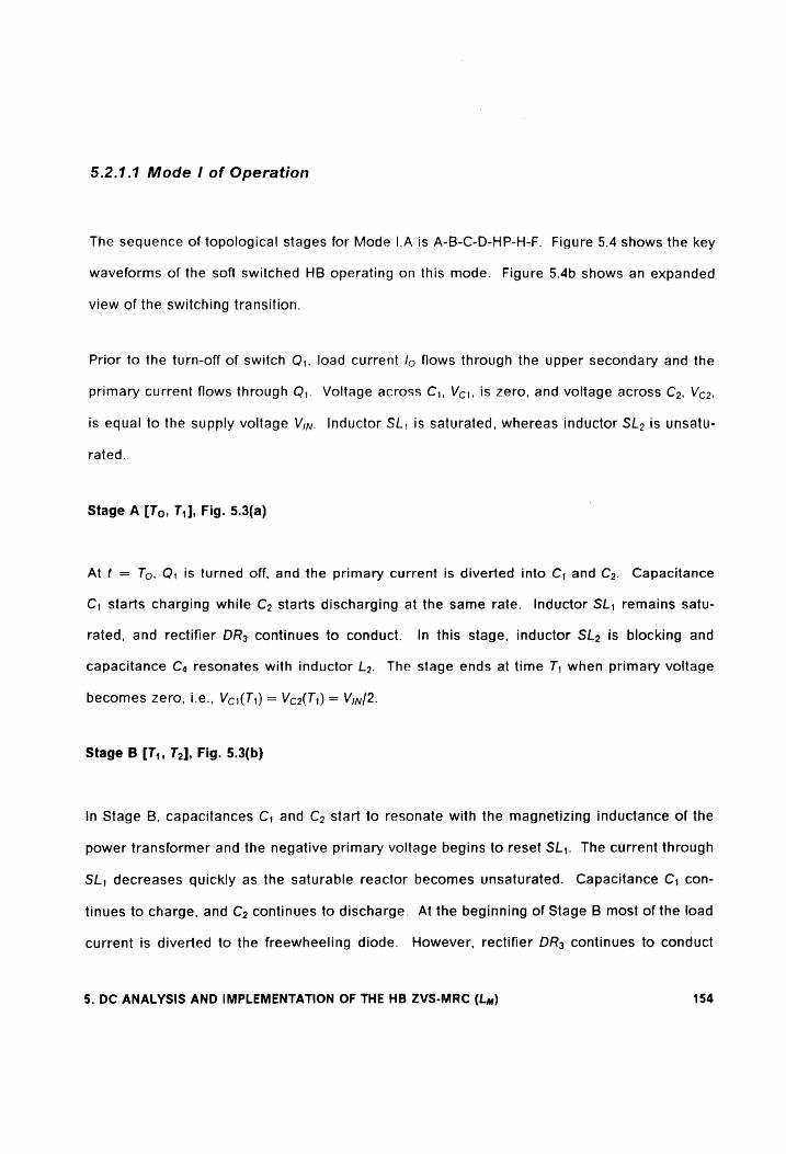
5.2.1.1 Mode | of Operation
The sequence of topological stages for Mode I.A is A-B-C-D-HP-H-F. Figure 5.4 shows the key
waveforms of the soft switched HB operating on this mode. Figure 5.4b shows an expanded
view of the switching transition.
Prior to the turn-off of switch Q,, load current /o flows through the upper secondary and the
primary current flows through Q,. Voltage across C,, Vc;, is zero, and voltage across Co, Veo,
is equal to the supply voltage Viv. Inductor SL, is saturated, whereas inductor SL» is unsatu-
rated.
Stage A [To, 7], Fig. 5.3(a)
At t = To, Q; is turned off, and the primary current is diverted into C; and Cz. Capacitance
C, starts charging while C. starts discharging at the same rate. Inductor SL; remains satu-
rated, and rectifier DR; continues to conduct. In this stage, inductor SL» is blocking and
Capacitance C, resonates with inductor L». The stage ends at time 7; when primary voltage
becomes zero, i.e., Vei(T1) = Veo(T1) = Vin/2.
Stage B [T7;, T2], Fig. 5.3(b)
In Stage B, capacitances C; and Cp» start to resonate with the magnetizing inductance of the
power transformer and the negative primary voltage begins to reset SL;. The current through
SL, decreases quickly as the saturable reactor becomes unsaturated. Capacitance C, con-
tinues to charge, and C2 continues to discharge. At the beginning of Stage B most of the load
current is diverted to the freewheeling diode. However, rectifier DR3 continues to conduct
5. DC ANALYSIS AND IMPLEMENTATION OF THE HB ZVS-MRC (Lym) 154
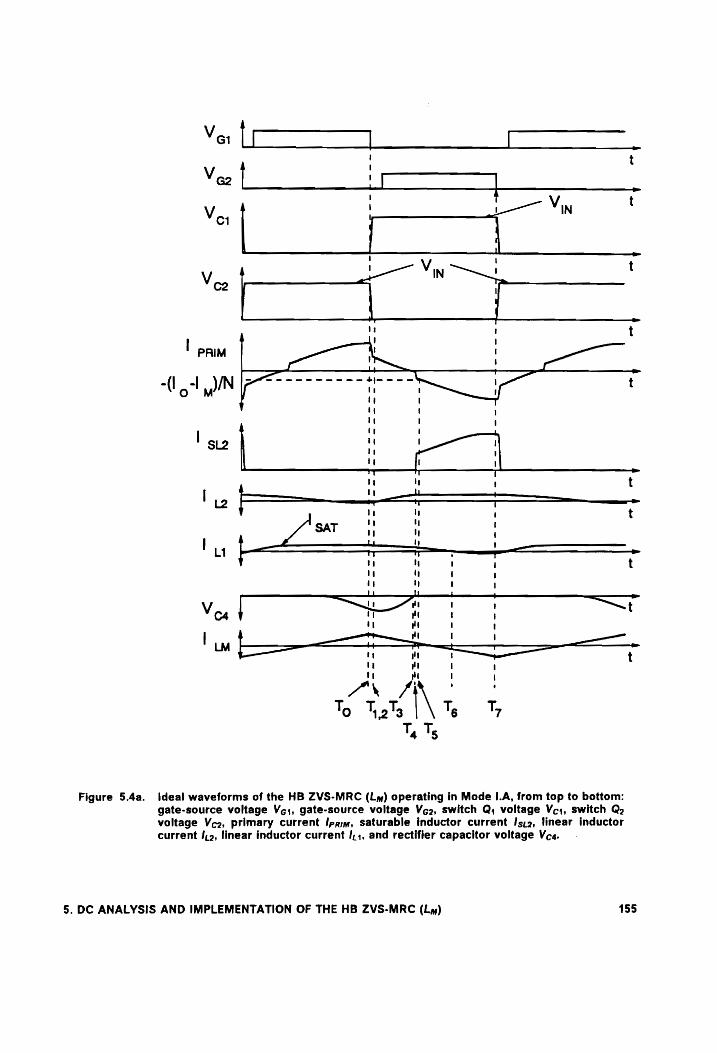
"1 1 t | ! ! PRIM t i ——
i . . . SS ee +---- 1 ,
Hot WN "oo ! 4 i I
i t { | it i
SL2 nt ! MH '
Tt { i _
ow t | 4 Ny li + a
2y oo 1 t t t
L1 —— 1 — —_ ty i ‘ I t 4 iT ‘ 1
u yt !
Vou J et st ' t ‘
{ $ La Hu | —— =
yo i" " eT t i an Ad; To Tots |\ 1 Ty
', Ts
Figure 5.4a. Ideal waveforms of the HB ZVS-MRC (Ly) operating in Mode |.A, from top to bottom: gate-source voltage Vg1, gate-source voltage Vc2, switch Q, voltage Vci, switch Q2 voltage Vco, primary current Ipam, saturable inductor current /Is:2, linear inductor current /,2, linear inductor current /,,, and rectifier capacitor voltage Veg.
5. DC ANALYSIS AND IMPLEMENTATION OF THE HB ZVS-MRC (Ly) 155
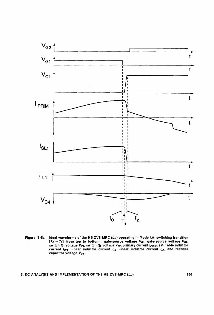
t {
Vai - -
Ver | ! C1 tA
ft t \
TT — _ t
| 4 1 \t
PRIM 1
; 1 1
1 t t J
; 1
v {
ro
| ~ SL1 ii!
14"
on 1, ! a
Mt t mo
ly Pr 7 i
t
~4---4-
<
Q
L
o! \
4A a/
Figure 5.4b. Ideal waveforms of the HB ZVS-MRC (Lj) operating in Mode |.A; switching transition [To ~ T2], from top to bottom: gate-source voltage Vg;, gate-source voltage Veo, switch Q, voltage Vc;, switch Q2 voltage Veo, primary current Ipaiy, saturable inductor current {szo, linear inductor current [,o, linear inductor current /{,,, and rectifier capacitor voltage Vca.
5. DC ANALYSIS AND IMPLEMENTATION OF THE HB ZVS-MRC (Lm) 156

since a small, positive, current (5-10 % of the load current) flows through inductor L,. The
current through L,; decreases to zero due to the negative voltage across the upper secondary.
At the same time, inductor L2 and capacitor C4 continue to resonate. This stage ends at time
To when the voltage across capacitor C, becomes zero, and the antiparallel diode of Q, starts
conducting. Switch Q. should be turned on while its antiparallel diode is conducting to
achieve ZVS.
Stage C [To, T3], Fig. 5.3(c)
During Stage C, inductor L; continues to discharge, inductor Ly and capacitor C, continue to
resonate, and saturable inductor SL; continues to reset. During this stage, the current through
SL, decreases to zero. Since the the negative voltage across the upper secondary is constant
(— Vin/N), current through L, decreases linearly. Also, the freewheeling diode continues to
conduct. This stage ends at time 73; when the voltage across capacitor C4, completely dis-
charges and rectifier DR, turns on.
Stage D [T3, 74], Fig. 5.3(d)
In Stage D, both saturable inductors are blocking. Current through L; continues to decrease
and current through inductor L. increases linearly. The freewheeling diode continues to carry
most of the load current. This stage ends at time 7, when inductor SL» saturates.
Stage HP [T4, Ts], Fig. 5.3(d)
In Stage HP, the current through the saturable inductor SL2 increases rapidly since this
inductor is saturated. The freewheeling diode continues to conduct until the current through
5. DC ANALYSIS AND IMPLEMENTATION OF THE HB ZVS-MRC (Ly) 157

SL. is large enough to supply the load. The current through L; continues to increase and the
current through L, to decrease in a linear manner. Stage HP ends when the sum of the current
through L;, Lo, and SL» equals the load current there by turning the freewheeling diode off.
Stage H [Ts, Te], Fig. 5.3(d)
In this stage, the load current is supplied by saturable inductor SL2. The current through L,
continues to linearly decrease and the current through L2 and SL» to increase also in a linear
manner. This stage ends at time 7, when the current through L; decreases to zero and diode
DR; turns off.
Stage F [T¢., T7], Fig. 5.3(f)
In Stage F, inductor SL, continues to block and capacitor C3 begins resonating with inductor
L,;. Inductor SL, remains saturated and most of the load current flows through SL». This stage
ends when switch Q, is turned off, initiating a new conversion cycle.
5.2.1.2 Mode Ii of Operation
In Mode Il of operation the current through the linear inductor L, decreases to zero, turning
off rectifier diode DR, before capacitor C, completely discharges to zero. The change in po-
larity of the current through L, initiates the resonance between this inductance and rectifier
capacitance C3. In this mode, rectifier capacitances C3 and C, will both resonate with the lin-
5. DC ANALYSIS AND IMPLEMENTATION OF THE HB ZVS-MRC (Ly) 158
ear inductors at the same time. Mode Il results in higher dc voltage-conversion-ratios relative
to Mode I.
5.2.1.3 Mode Ill of Operation
In Mode III of operation, SL, saturates before capacitor C, discharges completely (Mode | of
operation) or the current through linear inductor L; reverses its polarity (Mode II of operation).
This mode maximizes the time duration of the power transferring stages, resulting in higher
dc voltage-conversion ratios relative to the two previous modes of operation.
Figures 5.4 to 5.15 show the typical waveforms of the HB ZVS-MRC (Ly) for the different modes
of operation. Table 5.1 summarizes the topological sequences for the different modes of op-
eration. The topological stages P where _ is a letter from E to J, represent the converter
during the time in which saturable inductor SL» is saturated, but its current has not increased
to the necessary value so as to turn off the freewheeling diode. These stages represent the
switching transition of the magnetic switch.
5.2.1.4 Light Load Operation
For heavy to medium load operation, the saturable reactors SL; and SL2 supply most of the
load current, while the linear inductors, Ly; and Lo, carry 10 to 20% of the total Joad current.
Heavy load currents result in increased delay between the time the saturable reactor begins
5. DC ANALYSIS AND IMPLEMENTATION OF THE HB ZVS-MRC (Ly) 159
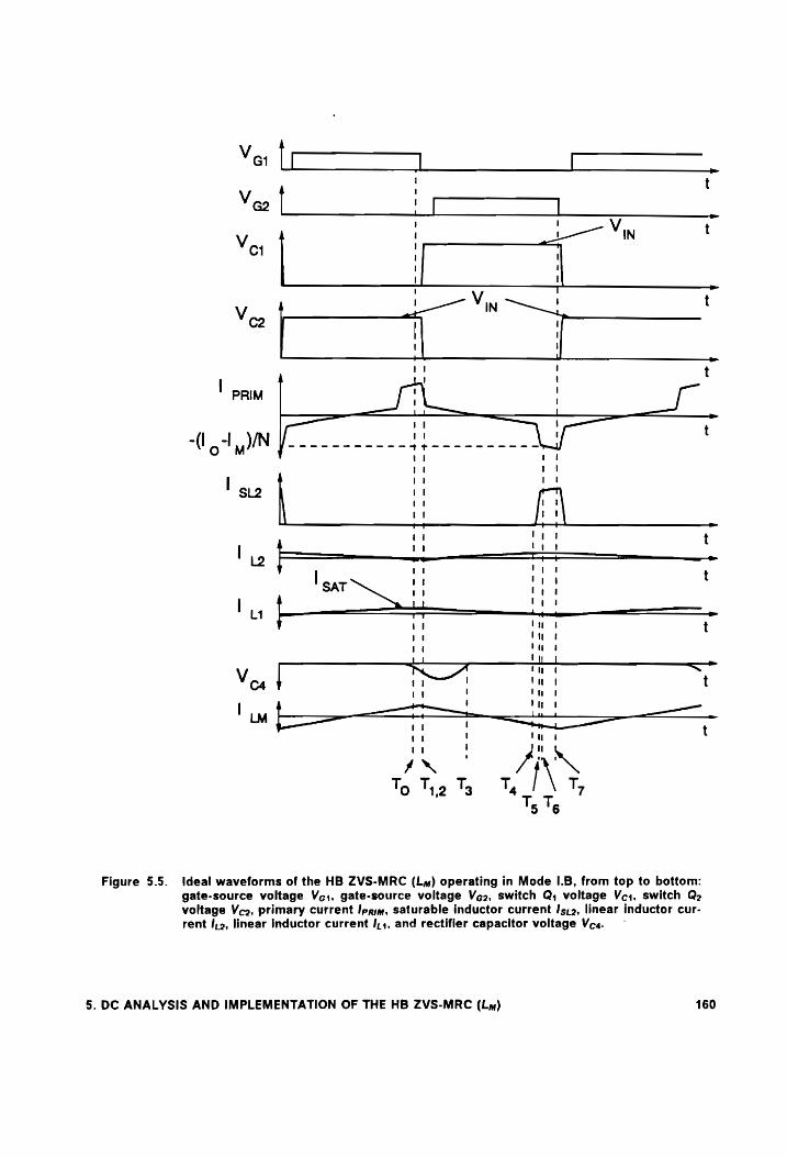
Veo | | : Vv 1 Vin t
C1 ;
| . Voo 4 Nm SS t
ri mt Vt
SL2 rt vt tot
7 f ‘| 7
4 m1 oy t Lo r — mt ——- —
SAT mt 14
, 4 wet te ot m1 i t
rt Vino
Le i ‘not —_ Vout ng |
| 4 tt tw a LM ++ Lay _ ~~ . | rm ;
wi | "
A ANN To Tyo Ty OT, Ty
Figure 5.5. Ideal waveforms of the HB ZVS-MRC (Ly) operating in Mode |.B, from top to bottom: gate-source voltage Vc:, gate-source voltage Ve2, switch Q, voltage Vci, switch Q2 voltage Vco, primary current /pam, saturable inductor current /s,2, linear inductor cur- rent I,o, linear inductor current /,,, and rectifier capacitor voltage Vc«.
5. DC ANALYSIS AND IMPLEMENTATION OF THE HB ZVS-MRC (Ly) 160

Ye. [J [_ t
Vee ! | | .
V ! 2 Vin ' C1 |
V -— Vin st t
am pron
Io _—_ Lo C 2 | oat Wy ge
| 1 i! I
| AT NN uo! { } ' nese —
Li TI 7 — t
1! | i
1 ‘ ' 1! | Lo _
V | Se" ot ~t CA i my
| 4 1 ! i ' ene LM L = _ o-
— 7 " t
i "
T T,. T. T T. O 12 3 * TT, 7
Figure 5.6. Ideal waveforms of the HB ZVS-MRC (Lm) operating in Mode I.C, from top to bottom: gate-source voltage Vc, gate-source voltage Veo, switch Q, voltage Vc, switch Q2 voltage Vco, primary current lpam, saturable inductor current /s:2, linear inductor cur- rent J,2, linear inductor current I,1, and rectifier capacitor voltage V4.
5. DC ANALYSIS AND IMPLEMENTATION OF THE HB ZVS-MRC (Lm) 161
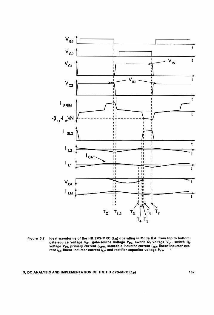
Ve: | (J Cc. t
Veo | | : Voy ! i —— Vin a { UU a
V t Vos IN |
= oO i z S ( { i ( i i} ' i 1 i ! f
ou
4—-—-b
t ' ( { t t ( (
~|
—_——
me
ie
ee oe
I suo f \ i
OE FT t >
tt tt t t 4 it Vt
l 5 eee ee . —————— -
I {
SATS vt "1 ;
lt =u — ‘ i}
i it LJ tty j —— Vox | i ee a ! t
Figure 5.7. Ideal waveforms of the HB ZVS-MRC (Lm) operating in Mode II.A, from top to bottom: gate-source voltage Vg:, gate-source voltage Vg2, switch Q, voltage Vc;, switch Q2 voltage Vc2, primary current Ipam, saturable inductor current /s;2, linear inductor cur- rent Ico, linear inductor current /J,;, and rectifier capacitor voltage Vc.
5. DC ANALYSIS AND IMPLEMENTATION OF THE HB ZVS-MRC (Ly) 162

; t
Veo | rs :
V | ! a Nn ° | iL
Veo = Vin —— t
Bt r | oa fh : of : | t (I ct y/N i ------ qa--==-- A
| suo 7 ,
' tt
a : Lt r a4 | it i t \ \
SAT 1 | | ™, 7 ii!
L141 —" —_ a —
v it boat, t it rout,
: Vin > ors -
Vos} 7 ty t tt! J ty
iy
~J
Figure 5.8. Ideal waveforms of the HB ZVS-MRC (Ly) operating in Mode II.B, from top to bottom: gate-source voltage Vc, gate-source voltage Vg, switch Q, voltage Vci, switch Q, voltage Vco, primary current Ipam, saturable inductor current /s.2, linear inductor cur- rent J,o, linear Inductor current /,;, and rectifier capacitor voltage Vcq.
5. DC ANALYSIS AND IMPLEMENTATION OF THE HB ZVS-MRC (Lym) 163

Veo | | Voy ! a Vin t
V Vin ! t
1 " i el t ba ity !
| Wy (
Lj Wy L —_ ii Ce
A
Veg | | t
Figure 5.9. Ideal waveforms of the HB ZVS-MRC (Lm) operating in Mode II.C, from top to bottom: gate-source voltage Vc, gate-source voltage Vez, switch Q, voltage Vc1, switch Q2 voltage Vco, primary current Ipgm, saturable inductor current /s:2, linear inductor cur-
rent /,, linear inductor current /,,, and rectifier capacitor voltage Vea.
5. DC ANALYSIS AND IMPLEMENTATION OF THE HB ZVS-MRC (Lym) 164
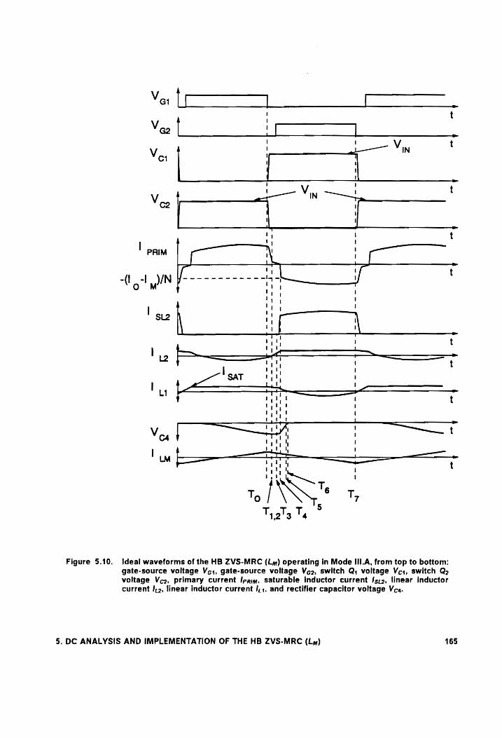
1 t
Veo | 2 ! iV Voy : a
vt 1 —— Vig C2 '
7 ! t
os
a = ~~,
z. 1
\
( I 1 { { ( 1 ( 1 j 4 |
~~. Il
{
1 \ ' I
i
SL2
rn 4 t
bo kw _~ — - l2 { iets \ nn te
| yy '
all ray ' it ng — t (0 t
ryt
hy i! te < ¥
Figure 5.10. Ideal waveforms of the HB ZVS-MRC (Ly) operating in Mode III.A, from top to bottom: gate-source voltage Vg, gate-source voltage Vee, switch Q, voltage Vci, switch Q> voltage Vc2, primary current [paiy, saturable inductor current /s;2, linear inductor current /,2, linear inductor current I, ;, and rectifier capacitor voltage Vex.
5. DC ANALYSIS AND IMPLEMENTATION OF THE HB ZVS-MRC (Lm) 165
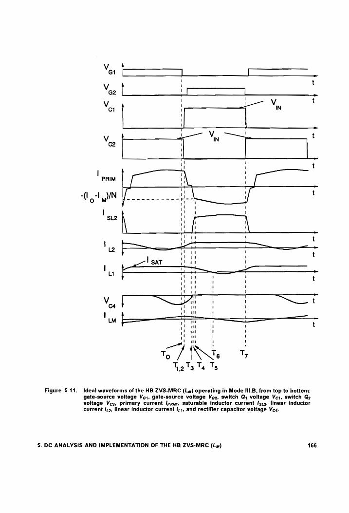
' t {
G2 | if __| - \ ' t
Vor ! IN
; t a,
! !
Vf — Vin a t C2 I
. i! t
1
!
SL2 1! ! \ _
1! M1 ' t
ls t—__ om — —_ . ' oud 1 t
| yeoad '
L1 { Th er t
i! vt ! ' i! vt t ! tow 1 t a ; 7
i } tt C4 yh ate i '
1 1 |
Figure 5.11. Ideal waveforms of the HB ZVS-MRC (Ly) operating in Mode III.B, from top to bottom: gate-source voltage Vg, gate-source voltage Veo, switch Q, voltage Vc;, switch Q, voltage Veo, primary current Ipaim, saturable inductor current /s;2, linear inductor current /,2, linear inductor current /,,, and rectifier capacitor voltage Vcq.
5. DC ANALYSIS AND IMPLEMENTATION OF THE HB ZVS-MRC (Lm) 166
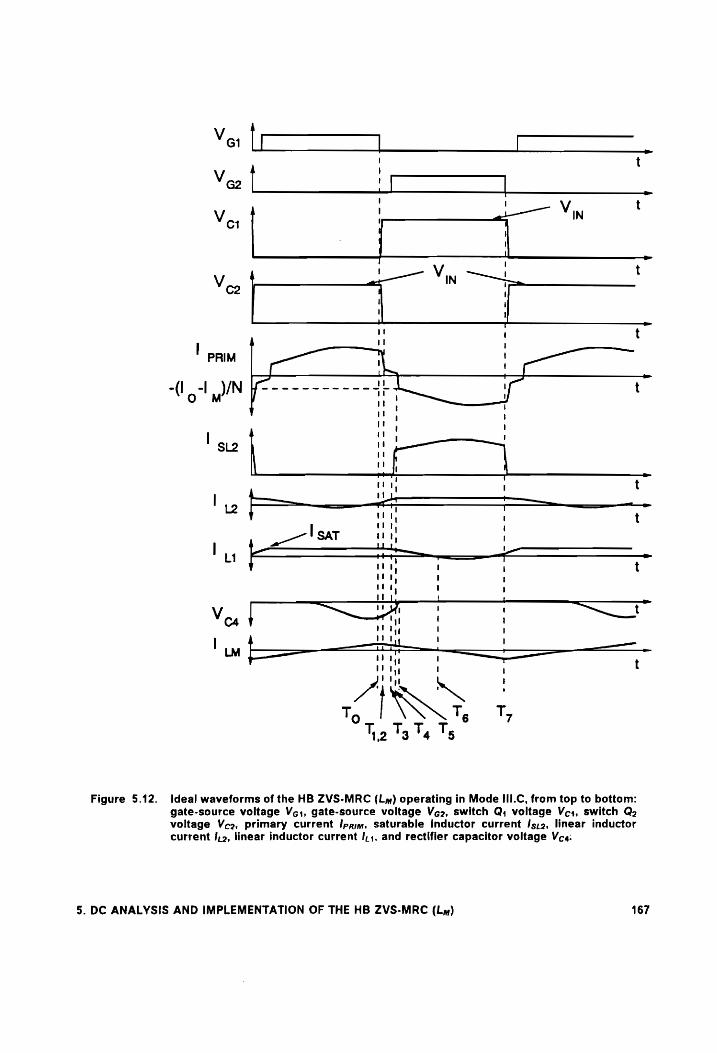
Figure 5.12.
' t '
Veo | ‘( .
Vor a— Yun ' j \
— t
M t
-Aw-4----J..~
pt = ty I t
ee . | L2 = aan > —_—
nt : t [pee Ty : —_ I
L1 } hay an ' j =
Why 1 \ t a, I !
i! _ . 7m ' t
{ 1
Ideal waveforms of the HB ZVS-MRC (Lm) operating in Mode III.C, from top to bottom: gate-source voltage Vg:, gate-source voltage Ve2, switch Q, voltage Vc, switch Q2 voltage Vc2, primary current Ipaim, saturable inductor current /s;2, linear inductor current /,o, linear inductor current /,,, and rectifier capacitor voltage Vea:
5. DC ANALYSIS AND IMPLEMENTATION OF THE HB ZVS-MRC (Lm) 167
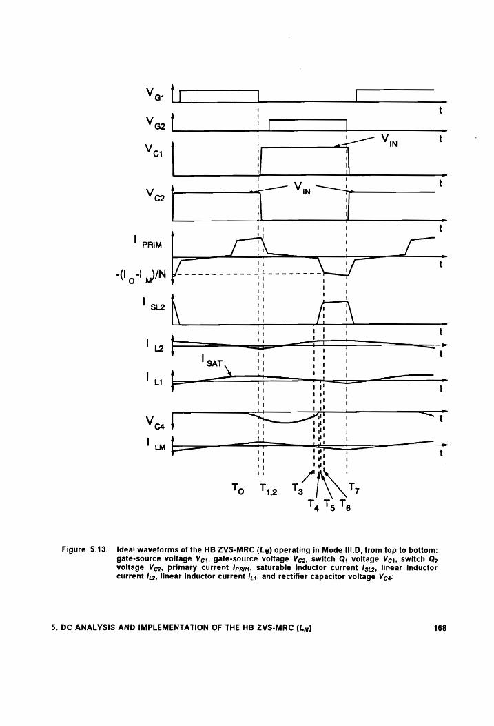
1 Veo | 1 ;
; a dV in t Vor |
l {
t 1
i ~
| t
{ I
' t
' 1! ' t 4 ' rt, _
Ma | iy et t SAT ! ro ;
ON lst a : ii | Hh oa :
ae tT Vou} r | LM i: i aes ell t
by yl \ ty Aik ! fe .
To Tyo Ty ING T, T5 1,
Figure 5.13. Ideal waveforms of the HB ZVS-MRC (Lm) operating in Mode III.D, from top to bottom: gate-source voltage Vcg;, gate-source voltage Veo, switch Q, voltage Vc;, switch Q2 voltage Veo, primary current /pgm~, saturable inductor current /s:o, linear inductor current /,2, linear inductor current /,,, and rectifier capacitor voltage Vca:
5. DC ANALYSIS AND IMPLEMENTATION OF THE HB ZVS-MRC (Ly) 168
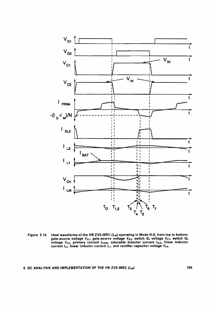
Ve. | cc.
ot Voy | i oo Vin t
Veo —— Vin <= t
Co az t
| PRIM | fT Ne ! of /
(| -l )N [f----------- J------ aaa
OQ M Vt ! 1
7 ' ; | ti j I
Sl2 i! ' i! 1 I
, 7 i t
t
sar ' Mo ly ‘ eel Lt rt ' eee
—— TT a id ny
r_! iy | -_
— Vest er t i! Wa I
| 4 _ we eg MM 1! a t
I 1! 1
i! we
Figure 5.14. Ideal waveforms of the HB ZVS-MRC (Lm) operating in Mode III.E, from top to bottom: gate-source voltage Vg, gate-source voltage Ve2, switch Q, voltage Vc, switch Q2 voltage Vc2, primary current Ipaim. saturable inductor current /s:2, linear inductor current J,o, linear inductor current /,,. and rectifier capacitor voltage Vca.
5. DC ANALYSIS AND IMPLEMENTATION OF THE HB ZVS-MRC (Lm) 169
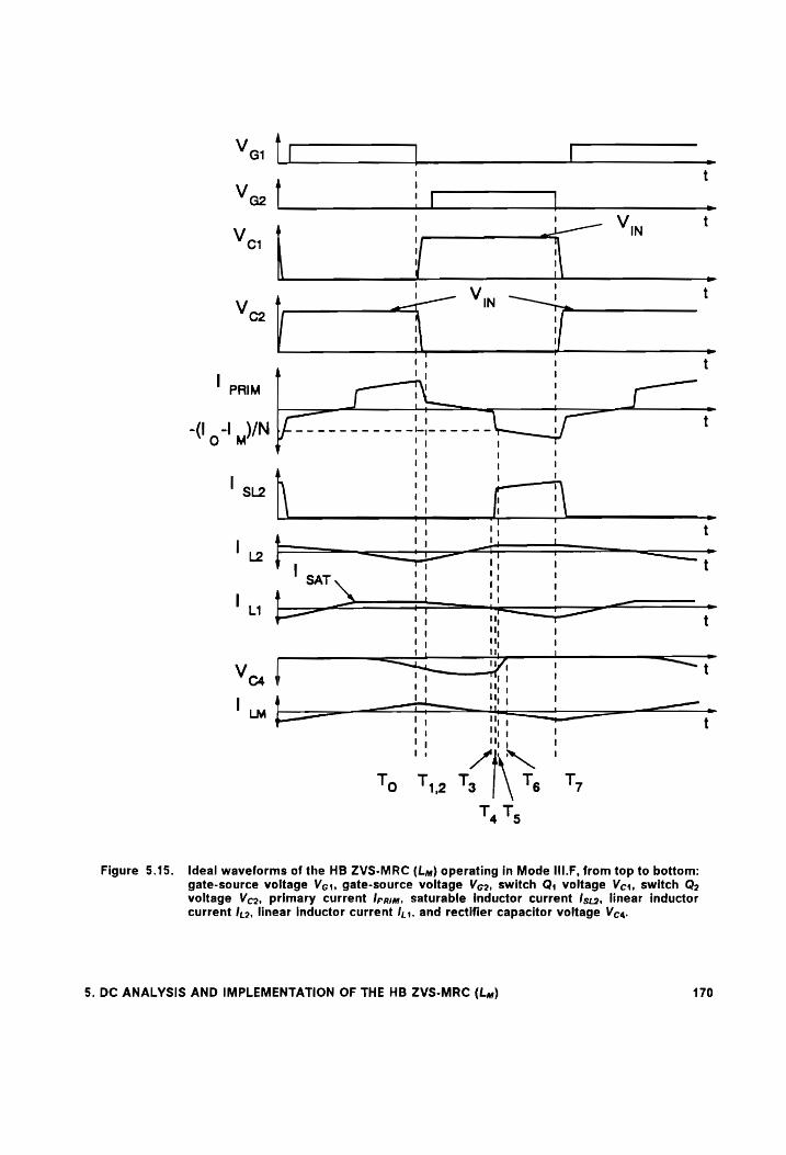
Ver Pe ' t
Veo | ‘co . Vor | r + Vin t
a
1 \
ae | t a
L2 | ee i |
sat \! i!
Pot __ L1 ~— I .————— t
i! it ty, U1, |
Vy aaa Vou | een tie : t
a 7 —— t t 4
! AN
To Tie Ts 1 Ty
TT.
Figure 5.15. [deal waveforms of the HB ZVS-MRC (Ly) operating in Mode III.F, from top to bottom: gate-source voltage Vc:, gate-source voltage Veo, switch Q, voltage Vc., switch Q> voltage Veco, primary current Ipam, saturable inductor current /s;2, linear inductor current [,o, linear inductor current /,,, and rectifier capacitor voltage Vcq.
5. DC ANALYSIS AND IMPLEMENTATION OF THE HB ZVS-MRC (Lm) 170
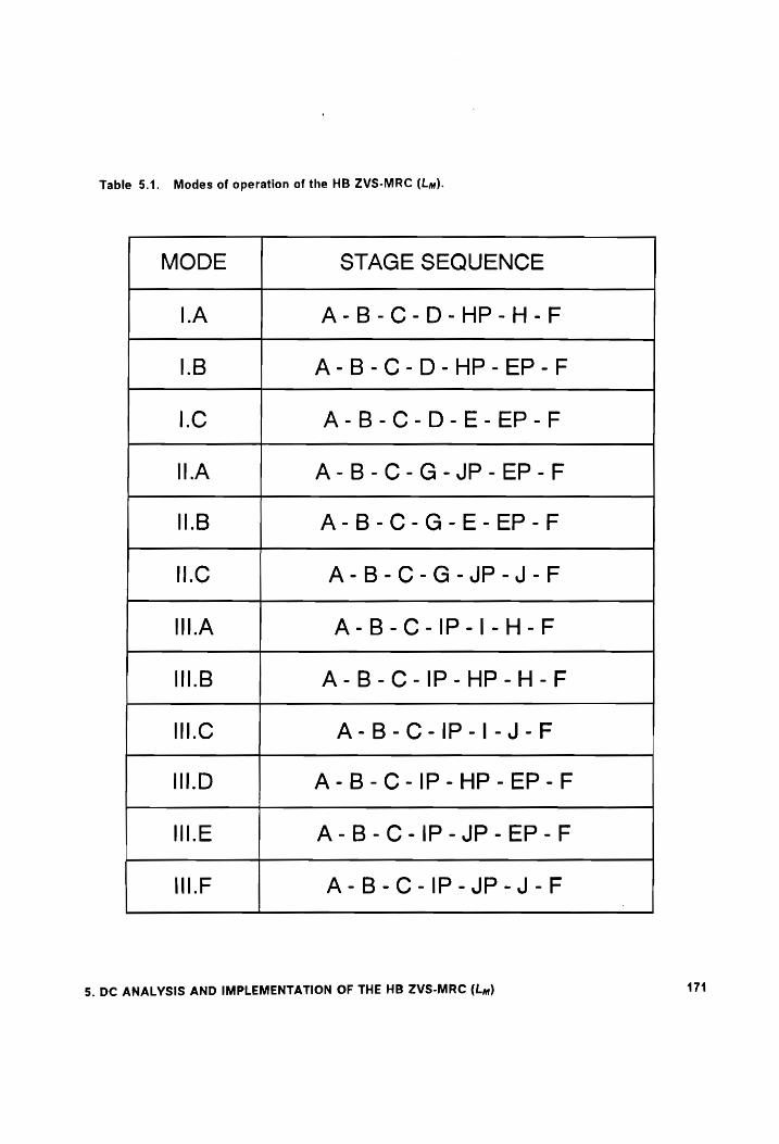
Table 5.1. Modes of operation of the HB ZVS-MRC (Lm).
MODE STAGE SEQUENCE
LA A-B-C-D-HP-H-F
.B A-B-C-D-HP-EP-F
LC A-B-C-D-E-EP-F
ILA A-B-C-G-JP-EP-F
IB A-B-C-G-E-EP-F
Ike A-B-C-G-JP-J-F
ILA A-B-C-IP-|-H-F
I1.B A-B-C-IP-HP-H-F
II.C A-B-C-IP-|-J-F
11.D A-B-C-IP-HP-EP-F
HIE A-B-C-IP-JP-EP-F
IN.F A-B-C-IP-JP-J-F
5. DC ANALYSIS AND IMPLEMENTATION OF THE HB ZVS-MRC (Lm) 171
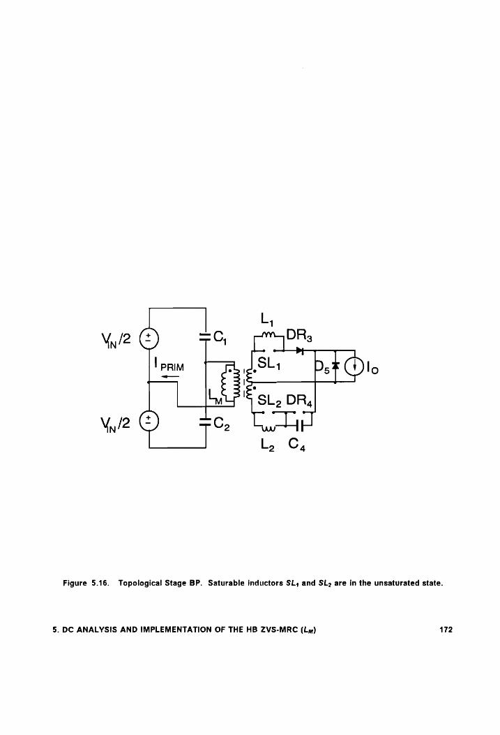
\in/2 ©) +O, DRs
ow a JSts ” BF Ole
wie @)
5 3 H LJ
Figure 5.16. Topological Stage BP. Saturable inductors SL, and SL2 are in the unsaturated state.
5. DC ANALYSIS AND IMPLEMENTATION OF THE HB ZVS-MRC (Ly) 172

to unsaturate and the time it blocks all current (saturable inductors were modeled to have a
finite inductance when saturated and infinite inductance when unsaturated). The corre-
sponding saturable inductor, saturable inductor SL, for the half cycle described by the
topological sequences in the preceding discussion, will not start resetting until the voltage
across the transformer windings changes polarity. The transformer voltage will changes from
positive to negative at the start of topological Stage B. Topological stages A and B model the
switching transition of the primary switches and correspond to a small fraction of the total
switching period. Therefore, for heavy loads, the delay time necessary for the saturable cores
to come out of saturation is longer than the duration of the switching transition (time duration
of topological stages A and B) as is modeled in the topological sequences describing modes
|, Il, and Ill. At lighter loads, the time it takes the saturable inductor to come out of saturation
decreases and the current through this inductor will decrease to zero before the switching
transition is over. Therefore, to model light load operation, an added topological stage is
needed to represent the latter duration of Stage B when saturable inductor SL, is no longer
saturated. This stage is shown in Fig. 5.16 as topological Stage BP. During light load opera-
tion, the switching transition is represented by the topological sequence of Stage A, Stage B,
and Stage BP.
For even lighter load operation most of the load will no longer be supplied by the saturable
inductors. In the extreme case. no load operation, the saturable inductors will never saturate
and all of the load current will be supplied by the linear inductors L; and Lo. Light load to no
load operation was not modelled since they are not necessary for the design of the converter.
A detail analysis of this converter is given in Appendix C. The primary switches in this con-
verter turn on under zero voltage due to the resonance of the primary-switch capacitance and
the magnetizing inductance. Similarly, the rectifiers turn on softly (zero-voltage turn-on) due
5. DC ANALYSIS AND IMPLEMENTATION OF THE HB ZVS-MRC (Ly) 173
to the controlled resonance of the rectifier capacitance and the linear inductors on the sec-
ondary side of the transformer. Since in normal operation the saturable inductors are not
forced to sweep the complete B-H loop, the converter can operate at a relatively high fre-
quency. A constant off-time, variable frequency control is required to regulate the output
voltage. However, if controlled saturable inductors are used instead, constant frequency op-
eration of the primary switches is possible by using post regulation. constant frequency op-
eration will be discussed in the sections that follow.
As can be seen from Figs. 5.4 to 5.15, currents and voltages in the primary circuit are quasi-
squarewave. The amplitude of the voltage waveform is clamped to V,y as in the corresponding
PWM converter. The amplitude of the primary current waveform shows a light resonance and
is slightly higher than in PWM converters. These PWM-like waveshapes are very desirable
since they result in lower conduction losses and stresses.
Single-ended topologies will do not have these desirable characteristics since the voltage
across the primary switch will resonante to several times the input voltage. However, due to
the precense of the saturable inductor, the current stressess will be much reduced compared
to those in ZVS-MRCs.
5.3 DC Voltage-Conversion-Ratio
The dc voltage-conversion-ratio curves are obtained by solving the differential equations for
each stage of the sequence representing the different modes of operation. The solution of the
5. DC ANALYSIS AND IMPLEMENTATION OF THE HB ZVS-MRC (Lm) 174
differential equations for the different stages used to represent the operation of this converter
are given in Appendix C. A set of dc voltage-conversion-ratio characteristics are shown in
Figs. 5.17 and 5.18. The characteristics are plotted as a function of normalized conversion
frequency, fron = fs/2fo, for different normalized output currents, loy = Zylo/NVin. The charac-
teristics are plotted for different values of the design parameters: Cy = 2Cp/(N7C), the ratio
of the capacitance across the rectifiers reflected to the primary (4Cp/N2) and the resonant
Capacitance across the primary switches (2C); Ly = 4Ly/(N?L), the ratio of the magnetizing
inductance Ly and the resonant inductors across the rectifiers reflected to the primary
(N?L/4): Isun = Isar/(lof/N), the normalized current of the linear inductor during the interval the
saturable inductor is saturated; and L/SL, the ratio between the secondary linear inductance
and the inductance of the saturable reactor when saturated. The resonant frequency is de-
fined aS wo = 2nfo = 1/,/2CLy and the characteristic impedance as Zy=JLy/2C . Vw is the
input voltage and N is the turns ratio of the transformer.
The selected value of L/SL only changes the spacing between the different curves of constant
lon in the de voltage-conversion-ratio curves. As the value of L/SL increases the distance
between the curves decreases. The decreased frequency dependence resulting from line and
load variations for 0.2 < M < 0.7 is due to the presence of the saturable inductors.
Figure 5.18 also shows the regions of the dc voltage conversion curves corresponding to dif-
ferent modes of operation. In Mode Ill, the saturable inductor SL». saturates before capacitor
C, completely discharges to zero, maximizing the duration of the power transferring stages.
Mode Ill of operation results in the highest power stage dc gain. In Mode Il, linear inductor
L, decreases to zero before either SL» saturates or C, completely discharges resulting in the
simultaneous resonance of capacitances C, and C3. Mode II of operation results in lower dc
gains than those found in Mode Ill of operation. In Mode | of operation, rectifier capacitance
5. DC ANALYSIS AND IMPLEMENTATION OF THE HB ZVS-MRC (Lm) 175
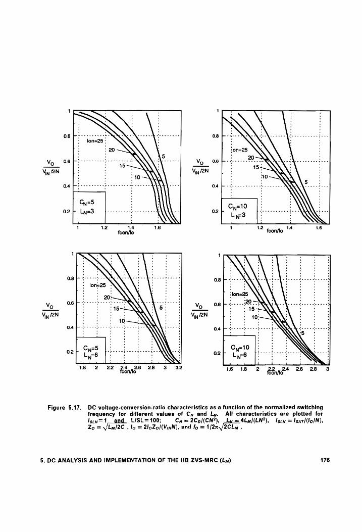
1
OB birreeeee- P QAACAE A: feeeeeeee lon=25 : . :
: 20 ; 5
V 0.6 L a 9 15
Vin /2N : iN ; +10
0.4 Fecrrctceee weeee terse eee ee ANY
L Cy=5 3 !
O02; Ly=3 t-------e- beeeeee eed
1 1.2 1.4 1.6 1 1.2 1.4 1.6 feon/fo feon/fo
1 : :
og fe MAX Lee » lone25 :
; ft 20: O06 Fouct ccc bocee R . portteeced
Vo 154 5: Vo Vin /2N : : : Viy /2N IN IN : 10
0.4 Fas - sence te---t--NARAL Ee
02r Ne Terr c psc rss ass
N™ 4 . . . . '
18 2 22 24 26 28 3 32 16 18 6~CDCtSC AC fonts 2 fant e162
Figure 5.17. DC voltage-conversion-ratio characteristics as a function of the normalized switching frequency for different values of Cy and Ly. All characteristics are plotted for Istw= 1 L/SL= 100; Cy = 2Co/(CN?), = 4Ly/(LN?), Istw = Isar/(lo/N), Zo =/bm/2C , lo = 2loZo/(VinN), and fo = 1/22,/2CLy .
5. DC ANALYSIS AND IMPLEMENTATION OF THE HB ZVS-MRC (Lm) 176
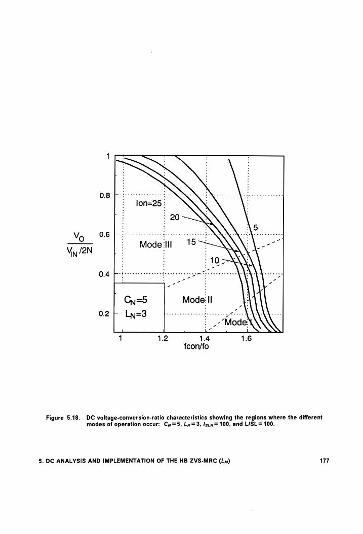
0.8 felsic EY. \ eed. esses : fon=25:
r : 20
Vv O.6 Priced i. _O_ 3 3 15—~ Vy /2N Model :
0.4 Bo ns, : center yen Th leeeeeeee ‘ :
0.256 Ly=3 occeeseeeeed vtec eee heeees AVA 1 1.2 1.4
fcon/fo
Figure 5.18. DC voltage-conversion-ratio characteristics showing the regions where the different modes of operation occur: Cy=5, Ly=3, Ispy=100, and L/SL= 100.
5. DC ANALYSIS AND IMPLEMENTATION OF THE HB ZVS-MRC (Lm) 177

C, completely discharges to zero turning rectifier diode DR, on before saturable inductor SL»
saturates or the current through linear inductor L; changes polarity. For light to no load op-
eration, all or a high percentage of the load current flows thorough the linear inductors. This
mode of operation is not shown since it is not necessary for design purposes.
A complete set of design characteristics, Cy = 5 and 10 and, Ly = 1, 3, and 6 are given in
Appendix C.
9.4 Design Guidelines
5.4.1 Design Trade-off Study
To determine design guidelines for the HB ZVS-MRC (Ly), it is necessary to determine how
rms currents and peak-to-peak voltages for the magnetic components and the rectifier diodes
vary as a function of the design parameters. Since this converter can be designed for different
Cy, Ly, Isiw. L/SL, Zo, and transformer turns ratio N, a design trade-off study needs to be con-
sidered. No analytical expression for the current and voltage stresses on the different com-
ponents exist for the HB ZVS-MRC (Ly). Therefore, current and voltage stresses are
determined from the numerical solution of the operation of the converter used to determine
the dc voltage-conversion curves.
5. DC ANALYSIS AND IMPLEMENTATION OF THE HB ZVS-MRC (Ly) 178

To evaluate the effect of the different design parameters on the performance of this converter,
different design examples are considered. Comparing current and voltage stresses for the
different design examples provides design guidelines. The design of the HB ZVS-MRC (Ly)
is based on the dc voltage-conversion-ratio characteristics curves and the following design
specifications:
¢ input voltage range, Vin” - Viv":
© output voltage, Vo:
max — join. d e §=load range, Io o ;,an
® minimum switching frequency, fe"".
The first step in designing the converter is to determine the transformer turns ratio N, Cy, Ly,
and Zo using a set of dc voltage-conversion-ratio curves.
For a design that maximizes efficiency, peak resonant currents and the circulating energy
flowing through the converter must be minimized. Circulating energy is directly dependent
on the values of Cy and Lw. In addition, Cy and Ly determine the frequency range of the con-
verter for the given input voltage, output voltage, and load current specifications. /s,, deter-
mines the blocking time of the saturable inductors. A smaller /s,yj corresponds to a shorter
blocking time. For variable-frequency control, it is desirable to minimize the blocking time by
making it slightly greater than the duration of the switching transition. By allowing the
saturable inductors to saturate as fast a possible, i.e., minimum /s:y, the duration of the stages
during which power is transferred to the load is maximized for a given Cy, Ly, and Zo; i.e.,
minimizes the loss in duty cycle as seen by the rectifier circuit. Similarly, maximizing the ratio
L/SL decreases the load dependence by decreasing the time it takes the saturable inductors
to come out of saturation (as for a ideal operation).
5. DC ANALYSIS AND IMPLEMENTATION OF THE HB ZVS-MRC (Ly) 179

The effect of the design parameters (N, Cy, Ly. Zo, Isty, and L/SL) are interrelated, thus com-
plicating the design of the HB ZVS-MRC (Ly). From the above discussion, the effects of Is:y
and L/SL are well understood. /s;, should be minimized and L/SL should be maximized for
a given inductor design. This minimizes conduction losses in the primary side (higher trans-
former turns ratio) and the frequency range (lower load dependence). The effects due to the
remaining design parameters on the design of the HB ZVS-MRC (Ly) are not obvious. To
evaluate the effect of the transformer turns ratio N, Cy, Ly, and Zo, the soft switched HB is
designed using different combinations of these parameters and a current and voltage stress
analysis is performed to determine design trade-offs and guidelines.
Design trade-offs of this converter are based on the following design specifications:
¢ input voltage range, Viv" - Viv" = 40 - 60 V:
® output voltage, Vo = 5V;
max e load range, Io™ - 15"" = 5-20 A; and
¢ minimum switching frequency, fe'". = 250 kHz.
Figures 5.18 - 5.21 show the dc characteristics of the HB ZVS-MRC ( Ly) for Cy = 5 and 10,
and Ly = 3 and 6. All characteristics are plotted for L/SL = 100 and /Is,y =/sar/(lo/N) = 1.
Ispy = 1 corresponds to a maximum current through the linear inductors of 10 - 15 % of the
total load current if the converter is designed for an Ion >15. Six different design examples
are considered in the design trade-off study:
Design #1: N = 3, fon~ = 25, Cy = 5, and Ly = 6;
5. DC ANALYSIS AND IMPLEMENTATION OF THE HB ZVS-MRC (Lm) 180
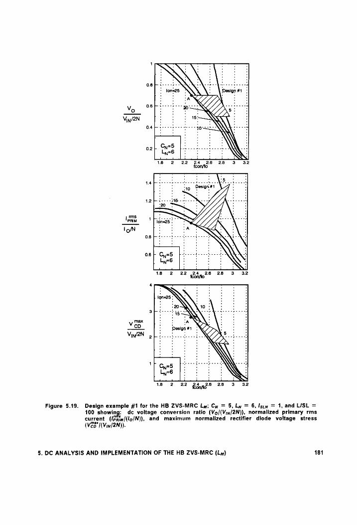
og bi----b NRA Ee Lee eed
VMn2@N fo 04 b feeb eedee es jgueet: NO Ed
| ms PRIM
Figure 5.19. Design example #1 for the HB ZVS-MRC Ly; Cy = 5, bw = 6, Istew = 1, and L/SL =
100 showing: dc voltage conversion ratio (Vo/(Vin/2N)), normalized primary rms current (lerm/(lo/N)), and maximum normalized rectifier diode voltage stress
(Veo"/(Vin/2N)).
5. DC ANALYSIS AND IMPLEMENTATION OF THE HB ZVS-MRC (Lay) 181
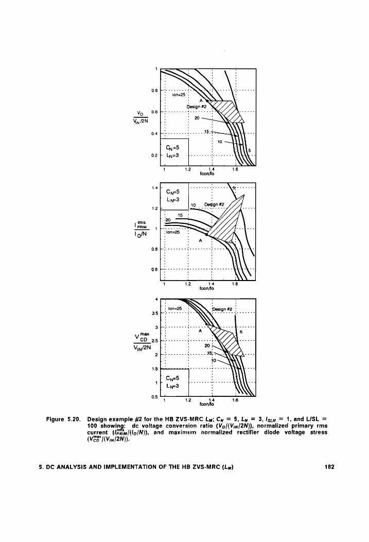
1
0.8 L.* eee erence 2. - re eer eeakoa ee
lon=25 ‘ ‘ '
: A
: Design #2
Vo O68 Pcttcrtttt ttt OLX : 99 :
Vy /2N 0.4 bee ce cee eedee ee IBS
‘40
G5 5 02 F LyHS fee re eee tere ee ee
1.4
1.2
| ms
PRIM
lo/N
0.8
0.6
4 .
‘fon=25 Design #2 : 3.5 Frise RANA Eee freee
L ;
3 -- "sre ree oD -~- NS oC ge se
y max : : . 5
CD o5}-:.------- dese seeee OLA, ee
Vin/2N ft: ; 20 | ee Sere ee ABS
: : {0 1.5 b= yocttttts ratte
Cy=5 1 be we ww rw eee
Lag3
os bs i i 1 1.2 1.4 16
fcon/fo
Figure 5.20. Design example #2 for the HB ZVS-MRC Ly; Cy = 5, Ly = 3, Istw = 1, and L/SL = 100 showing: dc voltage conversion ratio (Vo/(Vin/2N)), normalized primary rms current (lpaim/(lo/N)), and maximum normalized rectifier diode voltage stress
(Voo"/(Vin/2N)).
5. DC ANALYSIS AND IMPLEMENTATION OF THE HB ZVS-MRC (Lm) 182
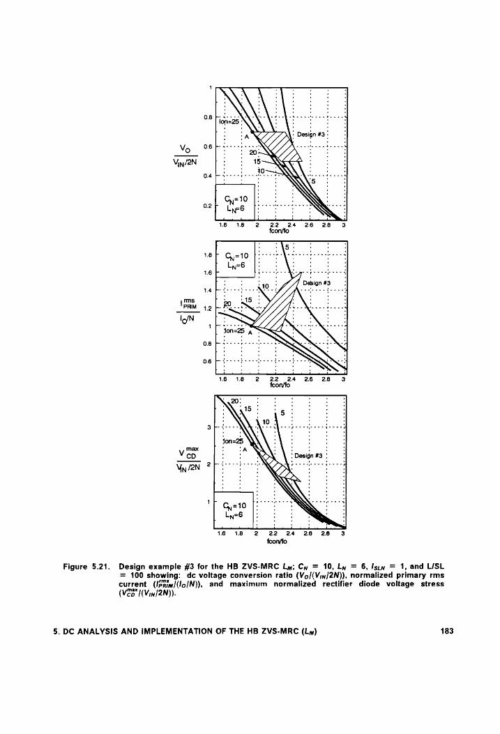
. tae wee . 0.8 whe ew ete wae
’
02 f Pott SQ
167 Terr tet tt Resp + rere sy
‘ : : : Design #3 ‘
14 Fiserbo Nee vileseede seed 1 D\e PRIM 19 b- FO... NX fe Nee.
lofN
08 bie. be TRACK XG
0.6 f-ie-ecie eee ede ARAL
16 18 #2 22 24 26 28 3 fcon/fo
4 420: : : :
: .15 : ‘ :
; 5: : 10 :
3 Routt: coe abe rte rte yocced
jon=! : max Y tA
Veo ae. ‘ Design #3 °
Uylen 2p cb NN bg
Figure 5.21. Design example #3 for the HB ZVS-MRC Ly; Cy = 10, Ly = 6, Isen = 1, and L/SL = 100 showing: dc voltage conversion ratio (Vo/(Vin/2N)), normalized primary rms current (Iprim/(lo/N)), and maximum normalized rectifier diode voltage stress (Veo"/(Vin/2N)).
5. DC ANALYSIS AND IMPLEMENTATION OF THE HB ZVS-MRC (Ly) 183
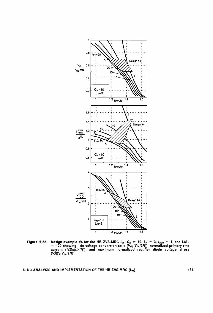
Figure 5.22.
0.8 F-
0.4
0.2
Vv CD : : : : V N /2N ‘ Design #4
2
Design example #4 for the HB ZVS-MRC Ly; Cy = 10, Ly = 3, Istw = 1, and L/SL = 100 showing: dc voltage conversion ratio (Vo/(Vin4/2N)), normalized primary rms current (lspm/(lo/N)}, and maximum normalized rectifier diode voltage stress
(Veo"/(Vin/2N)).
5. DC ANALYSIS AND IMPLEMENTATION OF THE HB ZVS-MRC (Ly) 184

II Design #2: N = 3, Ign = 25, Cy = 5, and Ly = 3;
6; tl II Design #3: N = 3, Ion” = 25, Cy = 10, and Ly
Design #4: N = 3, lon* = 25, Cy = 10, and Ly = 3:
Design #5: N = 4, In" = 25, Cy = 5, and Ly = 6; and
Design #6: N = 3, Ion. = 20, Cy = 5, and Ly = 6.
Figures 5.19 - 5.22 show the operating regions and device stresses for the first four designs
which study the effect of selecting different values of Cy and Ly while the remaining design
parameters are kept constant. Defining the region of operation follows similar guidelines as
the ones shown for the CF ZVS-MRCs. This characteristics show the dc voltage-conversion-
ratio curves, the normalized rms primary current. and the maximum voltage stress across the
rectifier diodes normalized with respect to the input voltage. Voltage stress characteristics
are not needed for the remaining components since the HB operation results in clamping of
the primary switch voltage stresses to the value of the input voltage. Furthermore, since the
magnetizing inductance of the the transformer is the resonant inductor, the primary transfor-
mer voltage consists of a square waveform with a maximum of Vjy/2 and a minimum of
— Vin/2. Figure 5.19 shows the operating region corresponding for Design #1. As for most
variable frequency ZVS topologies, the minimum switching frequency is determined by the
full-load and low-line conditions (point A in Fig. 5.19). Full-load and high-line operation is
shown as point B in Fig. 5.19 and points C and D represent high-line and light-load and low-
line and light-load conditions, respectively.
Since the characteristics are normalized, it is difficult to predict the regions that would result
in minimum primary rms current (minimum conduction losses) and the regions of minimum
rectifier diode voltage stress, Vep*. To understand the effect of Cy and Ly, Table 5.2 summa-
5. DC ANALYSIS AND IMPLEMENTATION OF THE HB ZVS-MRC (Ly) 185

rizes the calculated rms primary currents and maximum rectifier diode voltage stress for
high-line and low-line, and full-load operation for the first four designs. From the results in
Table 5.2, the following design trade-off is inferred: comparing Design #1 with Designs #2 and
#3 suggests that increasing the ratio Ly or Cy increases the value of the rms primary current
but decreases the maximum voltage stress seen by the rectifier diodes.
In order to study the effect of selecting different transformer turns ratios N (selecting Mmax)
and different power stage characteristic impedances Zo (selecting /oy), two more design ex-
amples were considered. Figure 5.23 shows the operating region and stress analysis corre-
sponding to these two designs. The resulting currents and voltages stresses of these designs
are summarized in Table 5.3 and suggest the following conclusions:
1) Designing for a higher transformer turns ratio (selecting a higher Mma) decreases the
primary rms current without increasing the maximum rectifier voltage stress consider-
ably (2 V maximum difference).
2) Designing for a lower power stage characteristic impedance Zo results in increased
primary rms current and increased maximum rectifier voltage stress.
5. DC ANALYSIS AND IMPLEMENTATION OF THE HB ZVS-MRC (Ly) 186
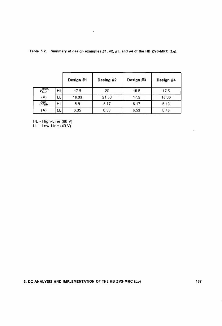
Table 5.2. Summary of design examples #1, #2, #3, and #4 of the HB ZVS-MRC (Ly).
Design #1 Desing #2 Design #3 Design #4
Veep. [HL 17.5 20 16.5 17.5 (V) LL 18.33 21.33 17.2 18.66
IpRim | HL 5.9 5.77 6.17 6.13
(A) LL 6.35 6.33 6.53 6.46
HL - High-Line (60 V) LL - Low-Line (40 V)
5. DC ANALYSIS AND IMPLEMENTATION OF THE HB ZVS-MRC (Lm) 187

Table 5.3. Summary of design examples #5 and #6 of the HB ZVS-MRC (Ly).
Design #5 Desing #6
Ven. |HL 18.7 18.5
(V) LL 20 18.66
IpRim =| HL 4.87 6.133 (A) LL 5.4 6.533
HL - High-Line (60 V) LL - Low-Line (40 V)
5. DC ANALYSIS AND IMPLEMENTATION OF THE HB ZVS-MRC (Lm) 188
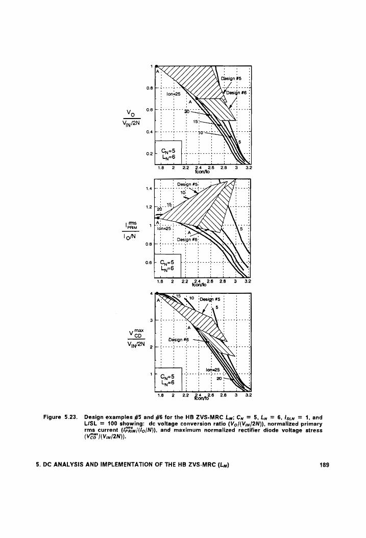
A: ot r Design ¥5
0.8 b-i----5-: dfrvtene ed * jonees5 * Design #6 .
|: DOTA tS 06 fb Sa--sb eggs N eon
Vo bo rf : ‘ 15°:
Vin/2N PO Dt O.4 Peyer rere estes qguecn AN ene
nl : . 5
=5 ‘ : ob On Lille ° Ly=6 |: :
1.8 2 22 24 26 28 3 3.2
fconito
: ‘ Design #5. : : 1.4 Posse ctr ese hNQgtie breech Pf 10 ;
1.2 bap:
pms yg [ALL RZAAANRANT.. ee PRIM lon=25 « Ns . \5
loN : : Design #6: O.B Fofecc cheer ete ie
O6F CyHS farcrcterccnee ee oa Ly=6 fs of i
18 2 22 24 26 28 3 32 fcon/fo
4
BRL tee KS SSS DM
max
Vico Vinf2N 5
.
ale
18 #2 22 Fonute® 28 3 32
Figure 5.23. Design examples #5 and #6 for the HB ZVS-MRC Ly; Cy = 5, Ly = 6, Istn = 1, and L/SL = 100 showing: dc voltage conversion ratio (Vo/(Vin/2N)), normalized primary rms current (/paim/(lo/N)), and maximum normalized rectifier diode voltage stress
(VEo"/(Vin/2N)).
5. DC ANALYSIS AND IMPLEMENTATION OF THE HB ZVS-MRC (Ly) 189

5.4.2 Design Procedure for the HB ZVS-MRC (Ly)
From the design trade-off study, the following rules should be used in designing the HB
ZVS-MRC (Ly) if conduction losses need to be minimized:
1) The value of the capacitance ratio Cy and inductor ratio Ly should be minimized.
2) The characteristic impedance of the converter should be maximized (design so that
full-load and low-line condition falls in the maximum /oy curve).
3) The turns ratio of the transformer should be maximized (design for the maximum Mmax
possible).
Once Cy, Ly, Mmax. and Gy have been selected, the turns ratio is calculated from the following
expressions:
min
Vin 2M N= IN max (5.1)
The values of C; and Cy represent the output capacitances of the switches. Once the switches
are selected based on their current and voltage ratings and on-resistance as is done in cor-
responding PWM converters, the value for C = C; = C2 is known. To minimize the ripple of the
primary current, i.e., minimize the stresses and losses in the switches and primary winding,
it is desirable to maximize Ly. Ly determines the resonant frequency along with capacitance
5. DC ANALYSIS AND IMPLEMENTATION OF THE HB ZVS-MRC (Lm) 190
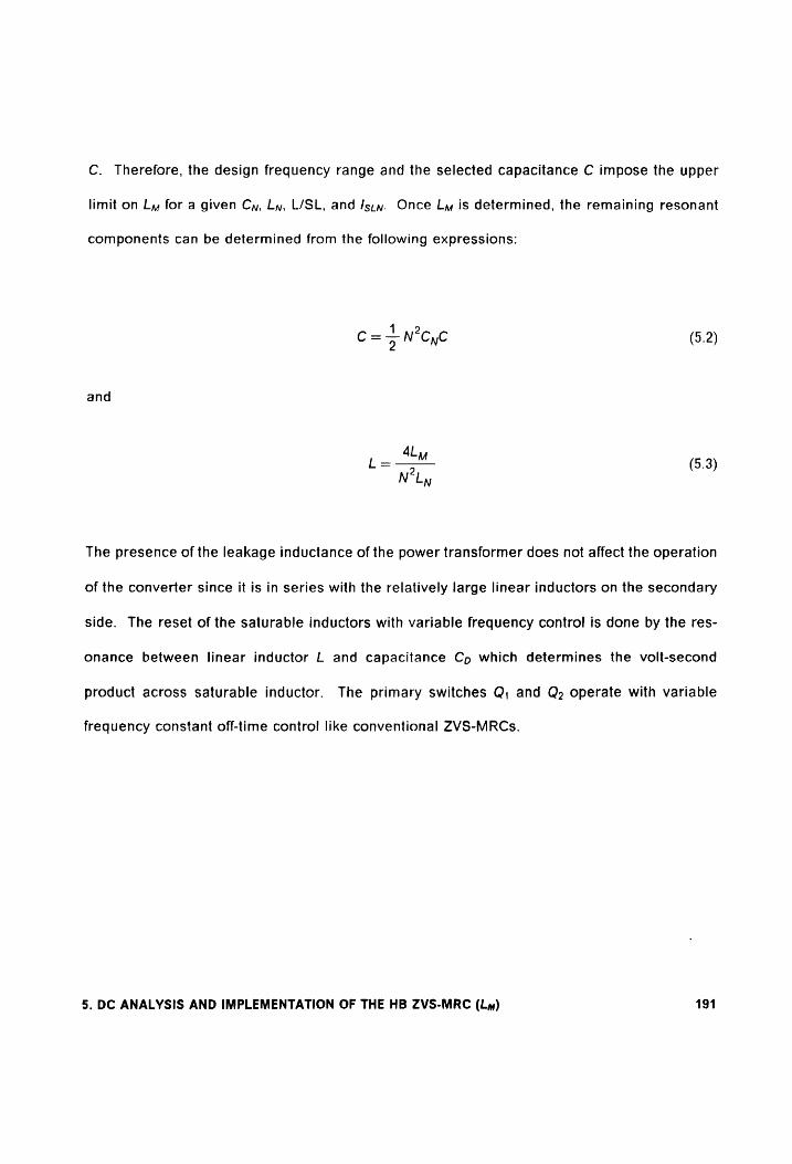
C. Therefore, the design frequency range and the selected capacitance C impose the upper
limit on Ly for a given Cy, Ly, L/SL, and Iszy. Once Ly is determined, the remaining resonant
components can be determined from the following expressions:
C= + N?CqyC (5.2)
and
AL L= a (5.3)
N°Ly
The presence of the leakage inductance of the power transformer does not affect the operation
of the converter since it is in series with the relatively large linear inductors on the secondary
side. The reset of the saturable inductors with variable frequency control is done by the res-
onance between linear inductor L and capacitance Cp which determines the volt-second
product across saturable inductor. The primary switches Q, and Q» operate with variable
frequency constant off-time control like conventional ZVS-MRCs.
5. DC ANALYSIS AND IMPLEMENTATION OF THE HB ZVS-MRC (Lm) 191
5.9 Experimental Results for Variable Frequency Operation
A 100 W HB ZVS converter was designed for an input voltage range of 40 V to 60 V, an output
voltage of 5 V, and a load-current range of O A to 20 A. The experimental power stage com-
ponents are:
Q;, Qo -IRF540 (International Rectifiers):
C,,Co -output capacitance of IRF540,
559 pF [8]:
TR -core: TDK EPC-19-Z (material H7¢,4):
primary: 5 X 3 turns of 150/42 Litz
wire;
secondary: 2 turn of 5 mil. copper
foil;
primary leakage inductance: 60 nH:
magnetizing inductance: 25 pH;
DR3zDR, -60CNQ045 (international Rectifier);
C3, C4 -2 x 0.5 nF ceramic cap.;
Lr -inductance: 1 nH;
core: TDK RM6Z12 (material H7c,4);
winding: 4 turns magnet wire
AGW3# 16;
gap: 5 mm.,;
Cr -5 x 3.3 uF NPO ceramic chip cap.;
5. DC ANALYSIS AND IMPLEMENTATION OF THE HB ZVS-MRC (Lm) 192

where TR stand for the power transformer. The combination of linear and saturable inductors
(L;/SL, and L2/SL») is implemented on a single core by winding four turns of Litz wire 150/44
on an amorphous Toshiba core (MB10 X 7 X 4.5). The reset of the saturable inductor is de-
termined by the operation of the converter and depends on the value of the resonant compo-
nents and load and line conditions. As long as the residual flux of the core is comparable to
Bsar (material with high squareness factor), the flux swing in the core will be limited to the top
portion of the first and second quadrant of the B-H loop as shown in Fig. 5.24
Figure 5.25 shows the measured efficiency of the converter as a function of the load current
for different input voltages. The converter has a maximum efficiency of 86.3 % at low line and
full load. The efficiency decreases to 83.1 % at high line and full load. The switching fre-
quency range is between 250 kHz to 1 MHz. Figure 5.26 shows typical oscillograms of key
waveforms of the HB converter for full load (20 A) and no load (0 A) operation. The measured
efficiency of a conventional HB ZVS-MRC designed for the same specifications is shown in Fig.
5.27. The HB ZVS-MRC has a maximum efficiency of 85 % at low line and full load operation
and the efficiency of the converter decreases to 80.2 % at high line and full load operation.
The experimental HB ZVS-MRC operated with a minimum switching frequency of 250 kHz and
a maximum switching frequency of 1.6 MHz. Comparing the efficiencies shown in Figures 5.26
and 5.27 suggests that the performance of the HB ZVS-MRC (Ly) is less sensitive to variations
in line and load conditions. The decreased sensitivity is due to decreased circulating energy
flowing between the primary and secondary circuits. Figure 5.28 shows a photograph of the
HB ZVS-MRC (Ly) and HB ZVS-MRC power stages. The reduced circulating energy in the HB
ZVS-MRC (Ly) results in a size reduction of the power transformer. The TDK EPC-27-Z core
(H7c4 material) is used for the transformer in the HB ZVS-MRC shown in Fig. 5.28(b). A com-
5. DC ANALYSIS AND IMPLEMENTATION OF THE HB ZVS-MRC (Lym) 193
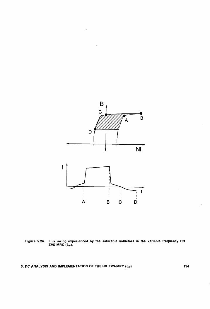
> wo
Q.
O.--
Figure 5.24. Flux swing experienced by the saturable inductors in the variable frequency HB ZVS-MRC (Ly).
5. DC ANALYSIS AND IMPLEMENTATION OF THE HB ZVS-MRC (Lym) 194
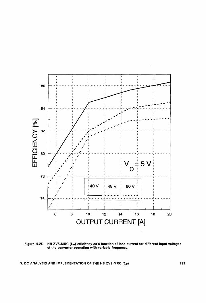
86
84
©
Nm
EFFICIENCY
[9%]
78
76 Poste pretececes otitis pessttts ribrtrttetpere eortetc ress
je
6 8 10 12 14 16 18 20
OUTPUT CURRENT [A]
Figure 5.25. HB ZVS-MRC (Ly) efficiency as a function of load current for different input voltages of the converter operating with variable frequency.
5. DC ANALYSIS AND IMPLEMENTATION OF THE HB ZVS-MRC (Lm) 195
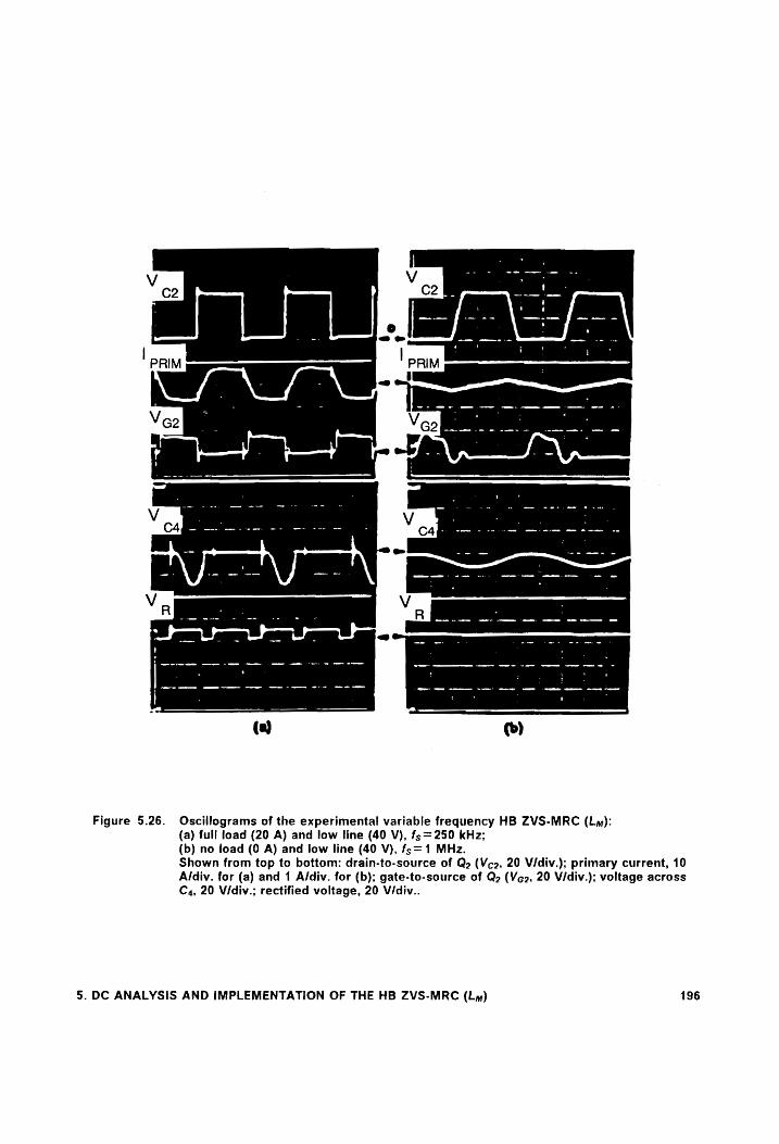
Figure 5.26. Oscillograms of the experimental variable frequency HB ZVS-MRC (Ly):
(a) full load (20 A) and low line (40 V), fs=250 kHz; (b) no load (0 A) and low line (40 V), fs=1 MHz. Shown from top to bottom: drain-to-source of Q2 (Vco, 20 Vidiv.); primary current, 10 Aldiv. for (a) and 1 A/div. for (b); gate-to-source of Q2 (Vg, 20 Vidiv.); voltage across C4, 20 Vidiv.; rectified voltage, 20 V/div..
5. DC ANALYSIS AND IMPLEMENTATION OF THE HB ZVS-MRC (Ly) 196
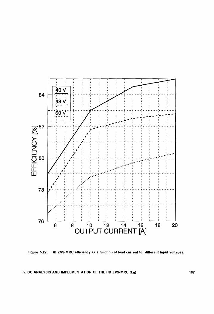
84
©
PO
EFFICIENCY
[%]
oO ~J
©
76
Figure 5.27. HB ZVS-MRC efficiency as a function of load current for different input voltages.
wm ane : : : : : :
60 V PoP eed ebesecvs : : : : : awe eeen: :
» . e . ‘ * - . . .
: : : ’ “- : : ‘
eer: pam eee ee pe fs Nese Peete eee. ee ee beceedeceeteeees Leese
. ww” . . . . .
: 2s. ‘ : : : : 1a : : : : : : 14 ; ‘ :
+ if e + ‘ ‘ * e '
po ee eel Peete eee Gee ee eee eteeeee tretee bree etceec dees beeee gece cde eee Beene : of : : : : ‘ : :
: at : : : : : : : : oo: : : : : : : : . a ’ . . . . ’ ‘ este?
pam fee bbe eee terete etee beeeee wrtcee breee boven cscs bores Lawetare--- berse . Oo. ‘ ‘ . . . . woe, .
a ee ; : 4 : : : : : ‘* : : : e Aa ‘ ’ ° e oo 4 ‘ 4
: oat : : : werent : : : totter Gece eeee beeerdeeeee mergegett Neste Brcccbescrdececs a bere
y? : : : ” : : : : c . . : A : :
c: : as : : : oo: : yet : : :
pf -- 4 aecee Yweee eld etc tte wee etn wees a Yeeocce Be we abo wwe tm eene Bec cehawe ecto owen Beer we
y : of : : : : tyes :
De! | ooh eee eee bocce deen e tec cca b ence Downe et ececbeces Goce a eteece a
* e '
! iL i | i | oT L | i
6 8 10 12 OUTPUT CUR
14 RENT
5. DC ANALYSIS AND IMPLEMENTATION OF THE HB ZVS-MRC (Ly)
16 [Al
18 20
197
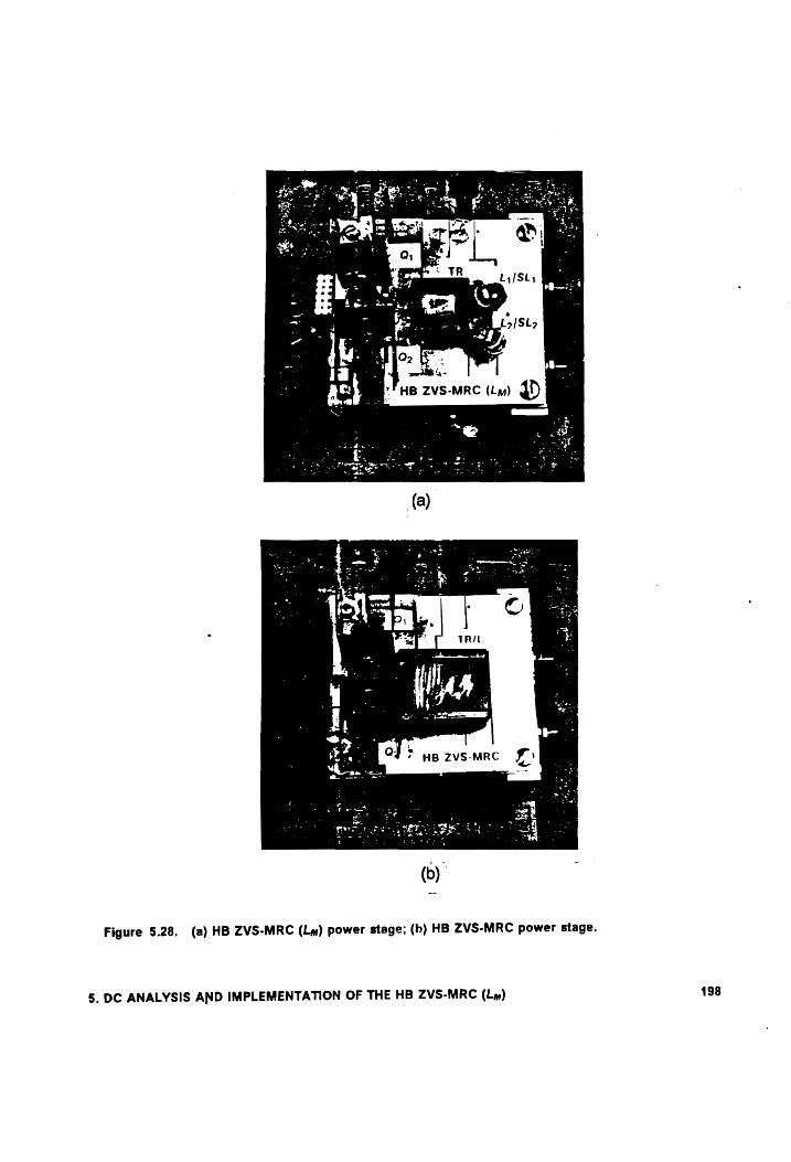
Figure 5.28. (a) HB ZVS-MRC (Lm) power stage; (b) HB ZVS-MRC power stage.
5. DC ANALYSIS AND IMPLEMENTATION OF THE HB ZVS-MRC (Lm) 198
parison of the difference in the transformer size resulting from these two power processing
techniques is shown in Fig. 5.29.
53.6 Constant Frequency Implementation
As discussed previously, the proposed family converters can operate at a constant switching
frequency if controllable saturable inductors are used. Figure 5.30 shows the implementation
of the controllable saturable inductor using an E core [G5,G6]. For ferrite core materials, the
blocking time, given a set of windings, is controlled by biasing the core further or closer to
saturation with a de control current. The current through the control winding sets up a dc bias
in the core. Depending on the value of the dc bias, the blocking time of the saturable inductor
varies. Increasing the control current increases the dc bias on leg /3 (leg that saturates) of the
controlled saturable inductor as shown in Fig. 5.30. As the dc bias in leg /3 increases, the
blocking time of the saturable inductor decreases, resulting in increased output voltage. Sim-
ilarly, if the value of the control current deceases, the blocking time of the saturable inductor
increases, resulting in a lower output voltage. The maximum blocking time occurs for a zero
control current corresponding to no dc bias.
The maximum blocking time of the saturable inductor occurs at high line and no load condi-
tions. The minimum blocking time corresponds to operation at low line and full load. This
means that the saturable inductor has to be designed so that it is able to block the secondary
5. DC ANALYSIS AND IMPLEMENTATION OF THE HB ZVS-MRC (Ly) 199
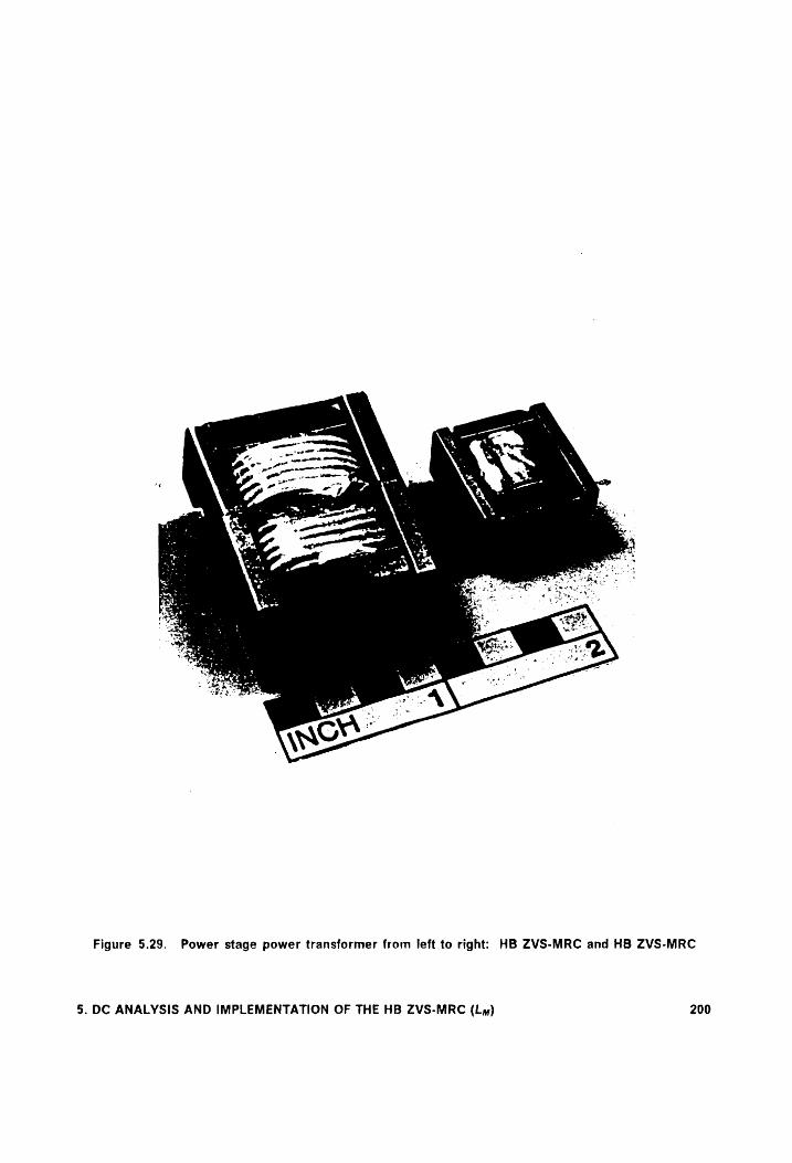
Figure 5.29. Power stage power transformer from left to right: HB ZVS-MRC and HB ZVS-MRC
5. DC ANALYSIS AND IMPLEMENTATION OF THE HB ZVS-MRC (Ly) 200
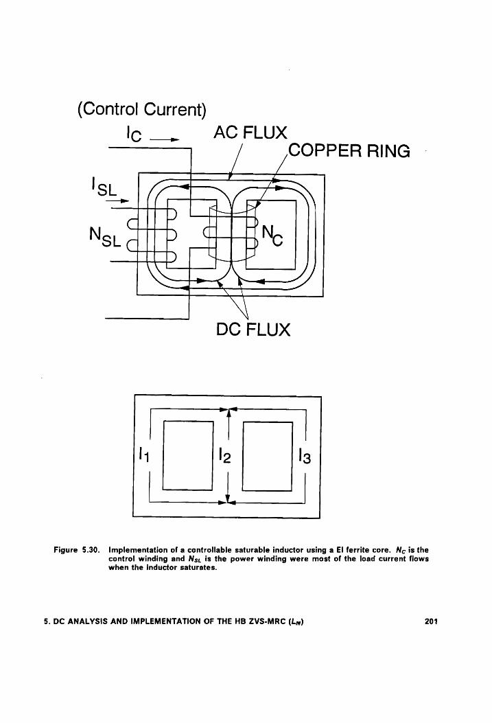
(Control Current)
lc _,. ACFLUX COPPER RING
Is.
No Noi
DC FLUX
Figure 5.30. Implementation of a controllable saturable inductor using a El ferrite core. Nc is the control winding and Ns, is the power winding were most of the load current flows when the inductor saturates.
5. DC ANALYSIS AND IMPLEMENTATION OF THE HB ZVS-MRC (Ly) 201
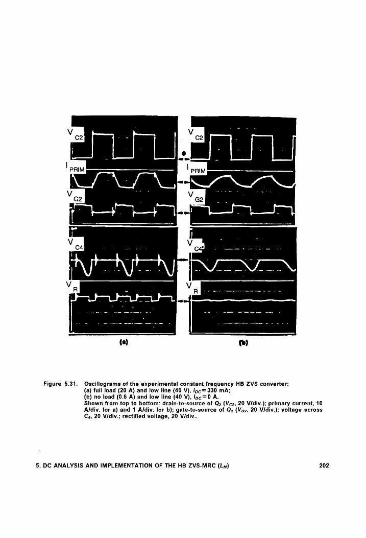
Figure 5.31. Oscillograms of the experimental constant frequency HB ZVS converter:
(a) full foad (20 A) and low line (40 V), [pc=330 mA; (b) no load (0.6 A) and low line (40 V), lnc=0 A. Shown from top to bottom: drain-to-source of Q2 (Vc2, 20 Vidiv.); primary current, 10 Aldiv. for a) and 1 Afdiv. for b); gate-to-source of Q2 (Veo, 20 Vidiv.); voltage across C4, 20 Vidiv.; rectified voltage, 20 V/div..
5. DC ANALYSIS AND IMPLEMENTATION OF THE HB ZVS-MRC (Ly) 202
transformer voltage for half a switching cycle at zero dc bias. The value of the linear inductor
and the no load _ condition determine the size of the saturable inductor
(Vin](2Nfeon)=NetAcBsa70.95), where Ac is the corssectional area of the core and a factor of 0.95
is used to insure the no load condition applies. Furthermore, in order to maximize the trans-
former turns ratio, the saturable inductor has to be designed so that the duration of the free-
wheeling stages at low line and full load are minimized, i.e., proper selection of the maximum
dc bias.
With this secondary-side mag-amp control, the converter is well suited for multiple output
applications.
Figure 5.31 shows typical oscillograms for the key waveforms of the soft switching HB oper-
ating at a constant switching frequency of 250 kHz. An EPC-13-Z core from TDK, material
H7ce4 is used as the controllable saturable inductor. The principal winding consists of six turns
of Litz wire 150/42, and the control winding consists of 50 turns of magnet wire AWG #34. In
addition, 8.9 nF external capacitance was added across the rectifiers. The converter regulates
the output for line ranges from 45 V to 55 V and for load ranges from full load to 0.6 A at low
line, and from full load to 6 A at high line.
9./ Summary
A new family of isolated ZVS converters which utilizes the magnetizing inductance of the
power transformer to achieve zero voltage turn-on of the primary switches has been pre-
5. DC ANALYSIS AND IMPLEMENTATION OF THE HB ZVS-MRC (Ly) 203

sented. By employing saturable inductors, the concept is extended so that soft switching of
the output rectifiers is obtained with a minimum circulating energy flowing through the con-
verter. The proposed converters can operate with a variable or constant switching frequency.
A complete dc analysis, design guidelines, and experimental results for the half-bridge con-
verter were presented.
5. DC ANALYSIS AND IMPLEMENTATION OF THE HB ZVS-MRC (Ly) 204
6. ANALYSIS OF REACTIVE POWER IN
RESONANT CONVERTER
6.7. Introduction
Generally, higher conversion frequencies bring size reduction of power transformer and filter
components and increase the overall power density. In particular, the size of the transformer
is determined by the maximum volt-second product applied to the primary winding and the
currents flowing through the primary and secondary windings. The maximum volt-second
product determines the maximum flux density and dictates the selection of the primary turns
and cross-sectional area of the core. At the same time, the currents in the primary and sec-
ondary windings, along with their respective number of turns, determine the window area of
the core. By increasing the conversion frequency, the volt-second product decreases, making
it possible to reduce the number of primary turns and/or to select a core with a smaller
6. ANALYSIS OF REACTIVE POWER IN RESONANT CONVERTER 205

cross-sectional area. The minimum number of primary turns is practically limited by the re-
quired turns ratio for a one-turn secondary. Beyond this, any decrease of volt-second product
due to a higher conversion frequency can be achieved by a reduction in the cross-sectional
area of the core. However, this trend occurs only in a limited frequency range because the
core and copper (winding) losses also increase as the frequency increases, thus reducing the
efficiency of the transformer. As a result, operaling a transformer above a certain frequency
no longer results in a size reduction, but on the contrary, requires a larger core to handle the
increased core and copper losses. This frequency strongly depends on the magnetic material.
Depending on the application, the frequency range of 200 kHz to 1 MHz seems to be optimal
for most high-frequency magnetic materials used today.
Generally, the transformer current and voltage in isolated PWM converters are square-wave
and without a noticeable phase-shift, as represented in Fig. 6.1. As a result, only real power
is processed through the power transformer, and virtually no circulating energy (reactive
power) is generated during the power processing. However, as switching frequencies in-
crease into the megahertz range, PWM converters suffer from excessive switching losses.
To reduce switching losses and make high-frequency operation possible, a number of reso-
nant and soft-switching converters have been proposed [A1-A31], [B1-B36], [C1-C20], [D1-D15],
[E1-E31], [F1-F7], including the converters in the first five chapters of this work. These con-
verters utilize controlled resonances of reactive parasitics and/or externally added resonant
components to achieve zero-current or zero-voltage switching of the power switches and/or
rectifiers. Generally, due to continuous resonances, resonant converters have sinusoidal-type
currents and/or voltages. In addition, in the majority of resonant converters, the primary
current and voltage of the transformer exhibit a significant phase shift that results in a sub-
stantial reactive (circulating) power flow as shown in Fig. 6.2. Although the resonant con-
6. ANALYSIS OF REACTIVE POWER IN RESONANT CONVERTER 206
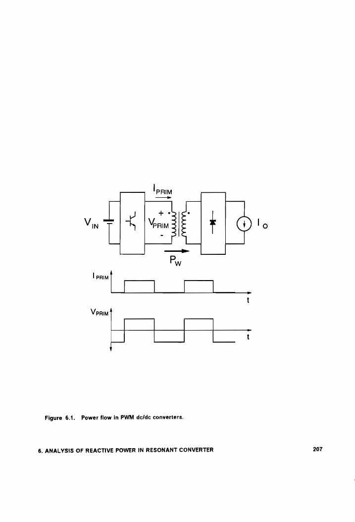
lpRiM
V tL Vee SIE
| PRIM |
VpRiM |
+ y
Figure 6.1. Power flow in PWM dc/dc converters.
6. ANALYSIS OF REACTIVE POWER IN RESONANT CONVERTER
~y
207
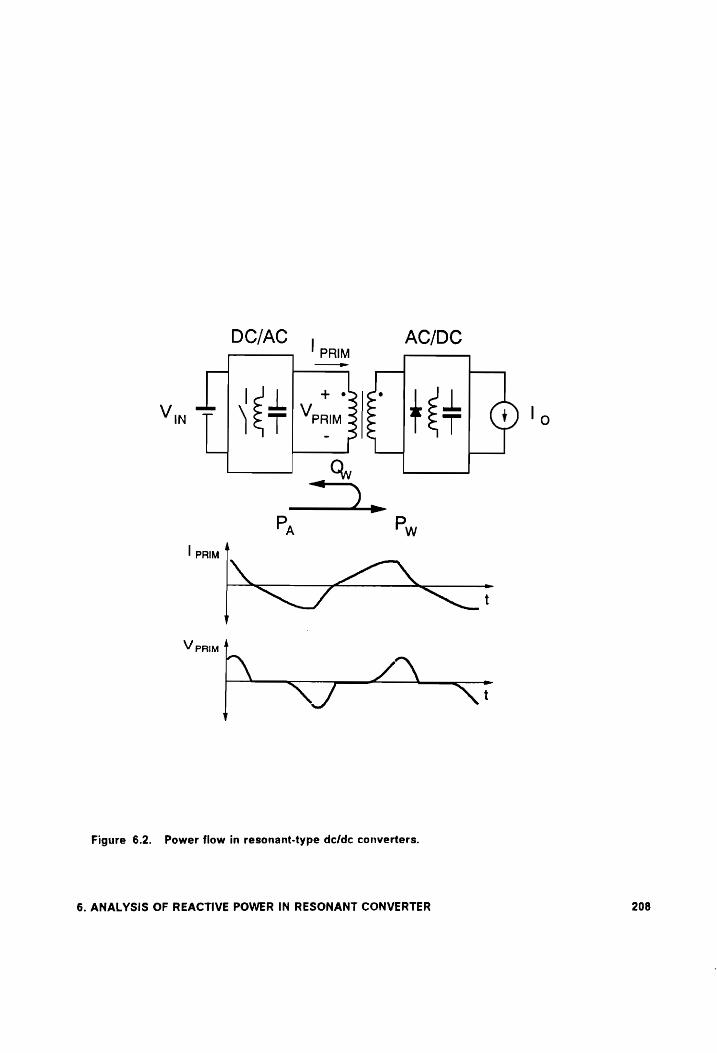
AC/DC
“Ed Q,
—), P, Py
Zz \
vm PT vert A .
[ NZ Ni
Figure 6.2. Power flow in resonant-type dc/dc converters.
6. ANALYSIS OF REACTIVE POWER IN RESONANT CONVERTER 208

verters with in-phase primary current and voltage do not circulate power, they still suffer from
increased current and voltage stresses compared to their PWM counterparts. In soft-switching
converters, resonances occur only during short switching transitions so that their currents and
voltages are closer to square-type waveforms of PWM converters.
To achieve soft-switching for a wide range of operating line and load conditions, resonant-type
converters usually need to be designed with a large amount of circulating energy (reactive
power) [D1-D15]. As a result, the amount of power processed by the transformer in a
resonant-type converter is usually significantly greater than that of a similar PWM converter
with the same rated output power. Therefore. the size of the power transformer in high-
frequency resonant-type converters is not necessarily smaller than the size of the power
transformer of the corresponding PWM converter operating at a lower switching frequency.
In addition, to process the increased amount of power, resonant converters require switches
with higher voltage and/or current ratings. This has a detrimental effect on the overall effi-
ciency of the power stage due to increased conduction losses, especially when a power FET
is used.
in this chapter, a new methodology is presented to measure the effectiveness of power con-
version. It is based on the analysis of the reactive power processed by the power transformer
as an indicator of the amount of circulating energy in the resonant network. In addition, the
current stresses of the power switches are derived for a number of resonant converter
topologies. The results of the analysis are used to define design guidelines which minimize
circulating energy. The analyzed converter topologies include: the half-bridge zero-current-
switching quasi- resonant-converter (HB ZCS-QRC) [D4], the half-bridge zero-voltage-switched
multi-resonant-converter (HB ZVS-MRC) [D6], the constant frequency half-bridge zero-
voltage-switched multi-resonant-converter (CF HB ZVS-MRC), the HB ZVS that uses the
6. ANALYSIS OF REACTIVE POWER IN RESONANT CONVERTER 209
magnetizing inductance as a resonant element (HB ZVS-MRC (Ly), and the full-bridge
series-parallel-resonant-converter (FB SPRC) [A25-A31]. Although only bridge-type topologies
are presented, the analysis and conclusions can be easily extended to any other topology.
6.2, Analysis of Real and Reactive Power
Due to the presence of reactive components, the power processed by the power transformer
of a resonant converter consists of real (Pw) and reactive (Qw) power. To calculate Pw and
Qwy, it is necessary to determine the primary voltage and primary current waveforms. For the
five converters considered in this paper, the primary voltage and current waveforms are de-
termined analytically using the approach described in [A25-A31], [B14], [D4-D7], [E20], and
[F3]. In this approach, the operation of a converter during a single conversion cycle is divided
into several topological stages corresponding to different states of the switching devices
(MOSFETs and rectifiers). Equivalent circuits for each topological stage are solved analyt-
ically, assuming that the capacitor voltages and inductor currents are continuous at the
boundaries of two consecutive topological stages. However, due to the nonlinear nature of
these converters and the larger number of modes of operations (sequences of topological
stages) usually encountered in resonant-type converters, a numerical algorithm is necessary
to obtain the desired waveforms. Recently, this approach has been successfully used to ob-
tain the dc characteristics of a number of quasi- and multi-resonant converters [A31], [B14],
[D6], [E20], and [F3]. In this work, the described approach is extended to calculate the real,
6. ANALYSIS OF REACTIVE POWER IN RESONANT CONVERTER 210
reaclive, and apparent power flowing through the power transformer and current stresses of
the switches of the discussed converters.
Since the currents and voltages of the analyzed converters are not true sinusoids, the con-
tributions of higher voltage and current harmonics to Pw and Qw have to be taken into ac-
count. By applying a Fourier decomposition to the primary voltage and current waveforms,
the accurate calculation of real, reactive, and apparent power, Pa, processed by the transfor-
mer can be obtained. The Fourier representation of the primary transformer voltage and
current is given by:
n
Verim(f) = > Vern sin(nwof) (6.1) 1
and
n
IpRim()) = > Iprimn sIN(NMol + Pp) (6.2) 0
where Vprimn and Iprimn represent the n” harmonic of the primary transformer voltage and
current, respectively, and ¢p is the phase shift between the primary transformer voltage and
current waveforms. From the Fourier representation of these signals, the real power, reactive
power, and apparent power can be obtained from the following expressions:
n
Vprimn !pRimn Py = d, COS $n) (6.3)
6. ANALYSIS OF REACTIVE POWER IN RESONANT CONVERTER 211
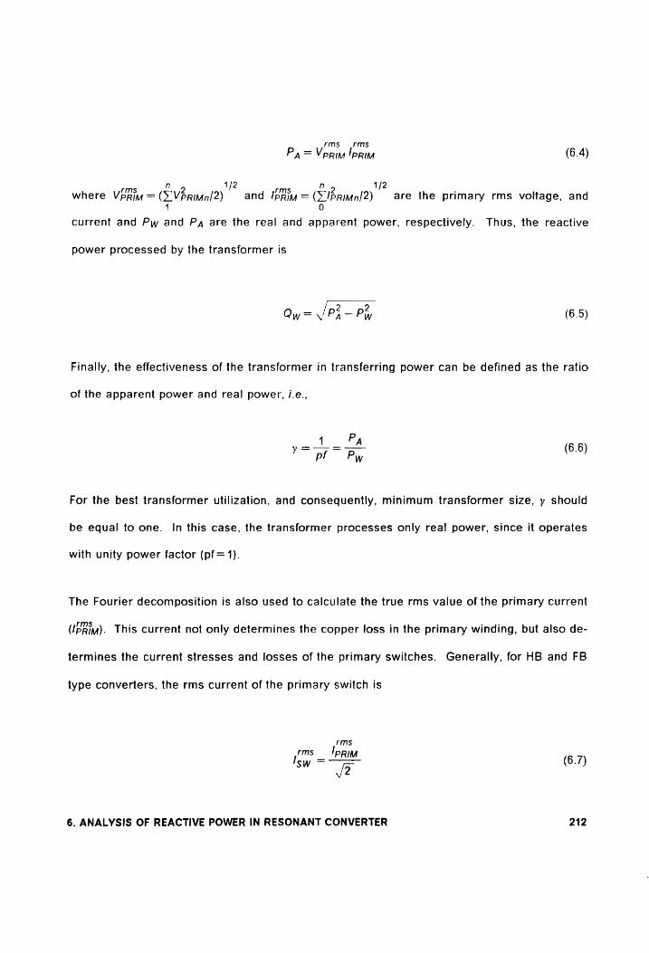
rims rms
Pa= Vprim |pRiv (6.4)
rms n 2 1/2 rms n 2 1/2 : where Vprim = (3-VpRimn/2) and /priv = (3_/PRimn!/2) are the primary rms voltage, and
1 0
current and Pw and Pa, are the real and apparent power, respectively. Thus, the reactive
power processed by the transformer is
Qw = /p2 — p?, (6.5)
Finally, the effectiveness of the transformer in transferring power can be defined as the ratio
of the apparent power and real power, /.e.,
4 Py y= = 5 (6.6)
For the best transformer utilization, and consequently, minimum transformer size, y should
be equal to one. In this case, the transformer processes only real power, since it operates
with unity power factor (pf = 1).
The Fourier decomposition is also used to calculate the true rms value of the primary current
(IPaim). This current not only determines the copper loss in the primary winding, but also de-
termines the current stresses and losses of the primary switches. Generally, for HB and FB
type converters, the rms current of the primary switch is
rms
rms Iprim 6.7) sw = /2
6. ANALYSIS OF REACTIVE POWER IN RESONANT CONVERTER 212

The relationship between peak switch current EW and IpRim depends on the shape of the pri-
mary current waveform. However, the upper boundary of ee is
PK rms( max)
Isw < /2 Ippin (6.8)
where the equal sign is used for distortion-free sinusoidal waveforms. For converters with
quasi-sinusoidal waveforms, such as those of Fig. 6.3(a), 6.3(c), 6.3(d), and 6.3(e), the peak
switch current is close to the limit given in Eq. (6.8). On the other hand, for converters with
predominantly square-wave shape of the primary current, such as in the converter of Fig.
6.3(b), the peak switch current is closer to the rms primary current, ie., (Ew IPB.
Figures 6.4 through 6.8 show the dc conversion ratio M, the power transfer effectiveness of the
transformer y, and the normalized primary rms current (IPRIMN) characteristics for the five
converters (Fig. 6.3). It should be noted that the SPRC characteristics in Fig. 6.8 were obtained
by taking into account the primary switch capacitance [A31]. The characteristics are all plot-
ted as a function of feon/fo (x-axis) for different normalized load currents /oy with the exception
of the characteristics of the SPRC, which are given for different values of the normalized load
resistance Q. For every operating point on the dc characteristics (M, feon/fo. lon), the ratio
of the apparent power to the real power processed by the transformer can be determined by
reading the » value for the corresponding fceon/fo. The normalized rms primary current can
be determined in a similar manner. For example, the de operating point defined in a gain
characteristic can be mapped into the } and /priy characteristics, as shown in Fig. 6.4. Con-
versely, any point in the y or IPRIM characteristics can be mapped into the two remaining
characteristics. The relationship between the real and reactive power as a function of y is
6. ANALYSIS OF REACTIVE POWER IN RESONANT CONVERTER 213

Qw = Pytan( cos~"(1/y)) (6.9)
6.3. Discussion
As can be seen from Figs. 6.4 - 6.8, the HB ZCS-QRC and the HB ZVS-MRC (Ly) have relatively
small y = Pa/Pw (close to unity). As a result. these two converters circulate very small
amounts of power between the primary and the secondary circuits. The HB ZCS-QRC has the
best overall power-transfer effectiveness among the analyzed converters. As seen from Fig.
6.4, its worst-case power transfer effectiveness, which occurs at full load, is y = 1.18, and it
is independent of frequency. In this converter, power is transferred from the primary to the
secondary only during the on-time period of a switching cycle. Most of the power processed
by the transformer is delivered to the load because the primary current and primary trans-
former voltage are in phase (Fig. 6.3(a)). The presence of small amounts of reactive power
(y#1) results mainly from harmonic distortion of the primary voltage waveform. Due to the
resonance of the switch current that is used to create conditions for lossless turn-off, the rms
primary current in the HB ZCS-QRC is higher than that in the PWM HB circuit, as shown in
Fig. 6.4(c). Thus, the conduction losses in the transformer and the semiconductor switches
are increased compared to the HB PWM converter.
Besides the HB ZCS-QRC, the HB ZVS-MRC (Ly) does not suffer from excessive circulating
power during heavy load operation. As can be seen from Fig. 6.5, for conversion frequencies
6. ANALYSIS OF REACTIVE POWER IN RESONANT CONVERTER 214
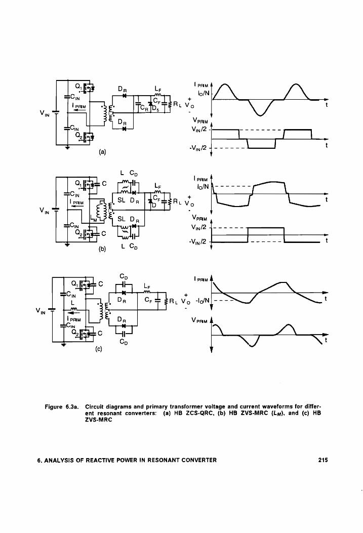
ot a a on Cin | r T C. . + io
I PRIM ° ° TC 4 LV oO t
Vin a t I R 5 T -
° S Dr VPRM | IN Vin /2 -|———g— Toys ney
+ Vy/24------ Ly t a) 1 (
L Cy
OfraeC poh on: aan 1s ~ Le lb/NA------- e “4 ws
vs LU SL Da | aCF , \ | \ t yo E * [pp TT" vo
IN T Ly SL Da VPRM
IN Vin/2 t ------ Qagto LS " .
Vin/2 t Vy 2 nt - - - ¥ (b) L Cy
Q C Co lpr
L . | Dr Cpt FRL Vo oN == t
V mks F TL -
IN <_— £°
lprM Da Verm IN
fie C L \ S/N ~
Cp | NS t (c)
Figure 6.3a. Circuit diagrams and primary transformer voltage and current waveforms for differ- ent resonant converters:
ZVS-MRC
6. ANALYSIS OF REACTIVE POWER IN RESONANT CONVERTER
(a) HB ZCS-QRC, (b) HB ZVS-MRC (Ly), and (c) HB
215
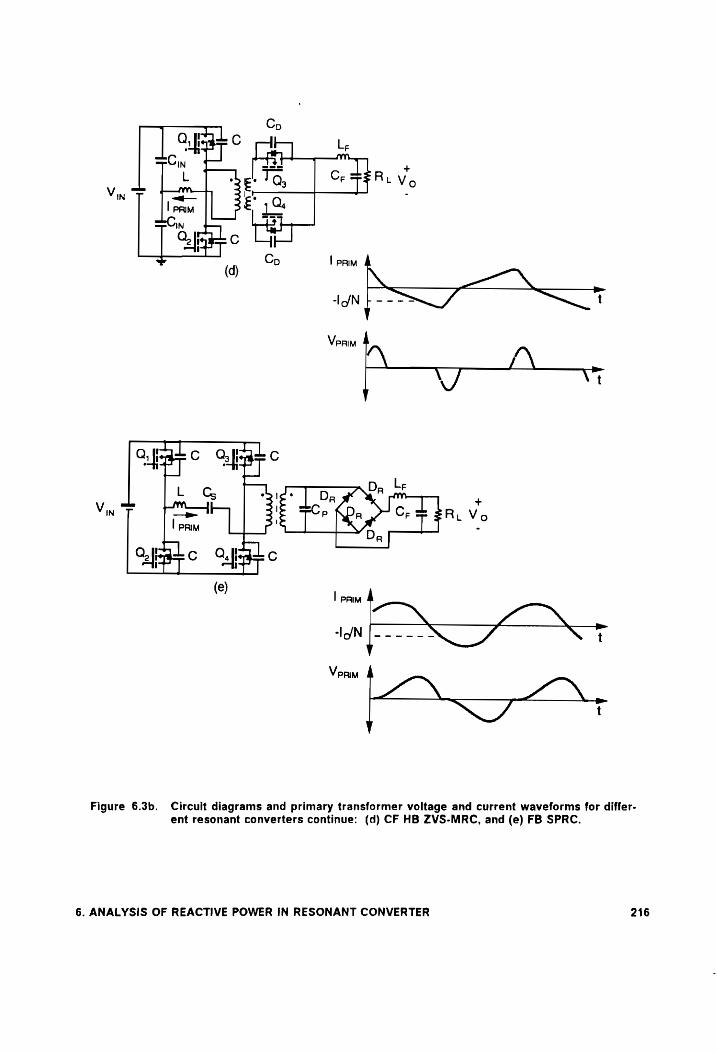
} Le
Vin + : 4 3 DR x Cc Ln V. pan ; P TF L 9
De
CpeTS Cpa |
Figure 6.3b. Circuit diagrams and primary transformer voltage and current waveforms for differ- ent resonant converters continue: (d) CF HB ZVS-MRC, and (e) FB SPRC.
6. ANALYSIS OF REACTIVE POWER IN RESONANT CONVERTER 216
1
0.8
Vo ; M= 0.6 ---f- fe: fe--3-
Vn/2N : : (a)
0.4 f-
0.2
1.18 f+ += ae lon=1
1.16 Fee c ccc cts wee qeee errr et ase teee
‘ Vo: :
¥ : (b) ta pooeeeeeeeteefeebeeee tienes
0,05 : ¥ fos | —_—_e.K :
eee ee 1
Bo (c)
; Jon=1
0 0.2 0.4 06 PY} 1 fcon/fo
Figure 6.4. HB ZCS-QRC: (a) dc voltage conversion ratio, (b) transformer power transfer effec- tivenes normalized primary rms current. characteristics. lon = 2loZo/ViwN, Zo = V/L/2Ce , and fo = 1/,/2CaL ; L is the leakage inductance of transformer.
6. ANALYSIS OF REACTIVE POWER IN RESONANT CONVERTER 217
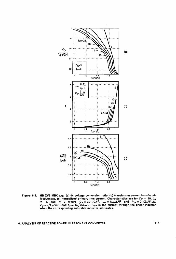
Figure 6.5.
6. ANALYSIS OF REACTIVE POWER IN RESONANT CONVERTER
0.68 Prot r eet Se RQ
lon=25:
‘ 20 beers we ee eee ew > - - AS Vo 0.6 15 (a)
Vin/2N |: "10 04 fees bested
Foes
02F- Ly=3 ee
(b)
1 1.2 1.4 1.6 fcon/fo
| ms PRIM io (c)
1 1.2 1.4 1.6
fcon/fo
HB ZVS-MRC Ly: (a) dc voltage conversion ratio, (b) transformer power transfer ef- fectiveness, (c) normalized primary rms current. Characteristics are for Cy = 10, Ly = 3, = 2 where Cy= 2Cp/CN2, lyn= 4Lmy/LN2 and lon = 2loZolVinN,
Zo = V/Lu/2c , and fo = 1/,/2CLy . Iscn is the current through the linear inductor when the corresponding saturable inductor satrurates.
218
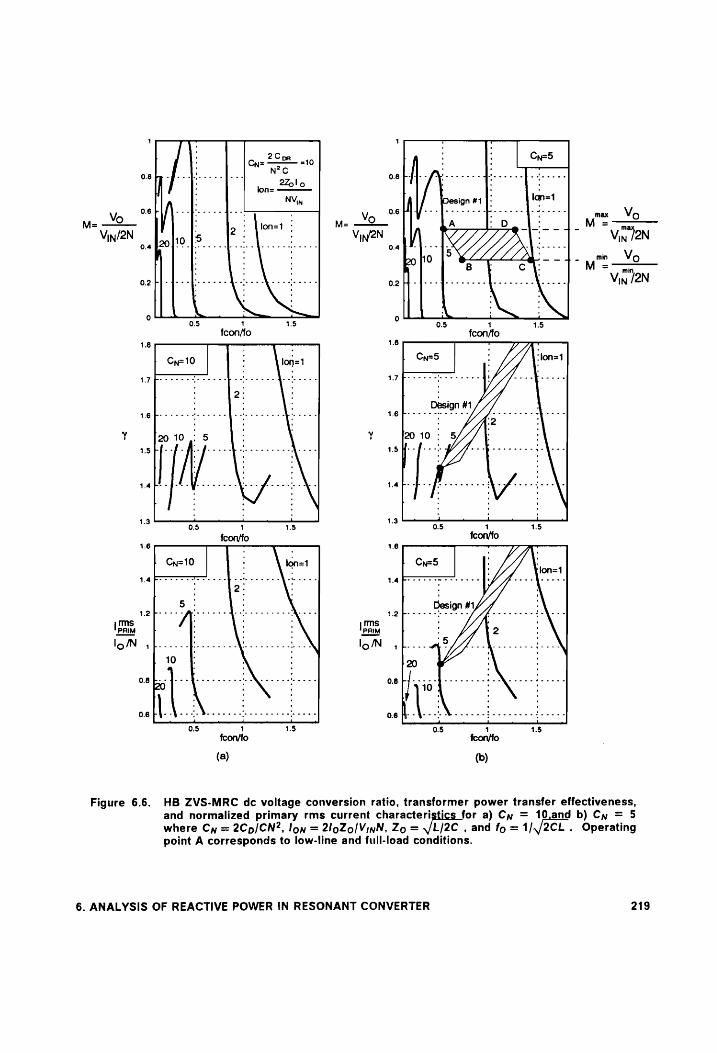
0.5 1 1.5
fcon/fo
| ms PRIM
lo /N
05 1 7s fcon/fo
(b)
Figure 6.6. HB ZVS-MRC dc voltage conversion ratio, transformer power transfer erectiveness, and normalized primary rms current characteristics for a) Cy = 10,and b) Cy = where Cy = 2Cp/CN2, lon = 2IgZo/VinN, Zo = J/L/2C , and fo = 1/,/2CL . boctating point A corresponds to low-line and full-load conditions.
6. ANALYSIS OF REACTIVE POWER IN RESONANT CONVERTER 219
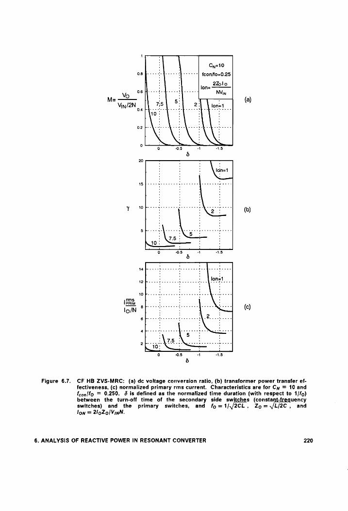
1
Cy=10
0.8 feon/fo=0.25
2Zolo lon= -————
Vo 0.6 N
= : (a) Vin/2N | loner
oat Ae A
0 1.5
¥ (b)
| Pram loIN ° (c)
Figure 6.7. CF HB ZVS-MRC: (a) dc voltage conversion ratio, (b) transformer power transfer ef- fectiveness, (c) normalized primary rms current. Characteristics are for Cy = 10 and feonlfo = 0.250. 6 is defined as the normalized time duration (with respect to 1/fo) between the turn-off time of the secondary side switches (constant- uency switches) and the primary switches, and fo=1/,/2CL, Zo= “1L2¢ , and
lon = 2190Z0/VinN.
6. ANALYSIS OF REACTIVE POWER IN RESONANT CONVERTER 220
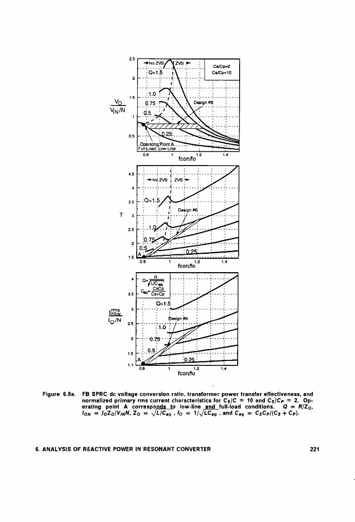
2.5
Looe. tee A ee ee lee Cs/Cp=2
: Cs/Cp=10
2 y :
VB Fete eee ee np ee ee: woeee wees wore Vo : Design #6
Vin/N 1
05 --- ~"
| Operating Point A... == Full-Load, Low-Line
0.8 1.2
fcon/fo
Design #6 s ies ote we *ewece we pecbaeae ae
. . a
1.2 1.4 0.8 1 .
fcon/fo
Figure 6.8a. FB SPRC dc voltage conversion ratio, transformer power transfer effectiveness, and normalized primary rms current characteristics for Cs/C = 10 and Cs/Cp = 2. Op- erating point A Fa eee low-line and full-load conditions. Q = R/Zo,
lon = loZolVinN, Zo = VLICeq . fo = 1]\/LCeg , and Ceg = CsCp/(Cs + Cp).
6. ANALYSIS OF REACTIVE POWER IN RESONANT CONVERTER 221
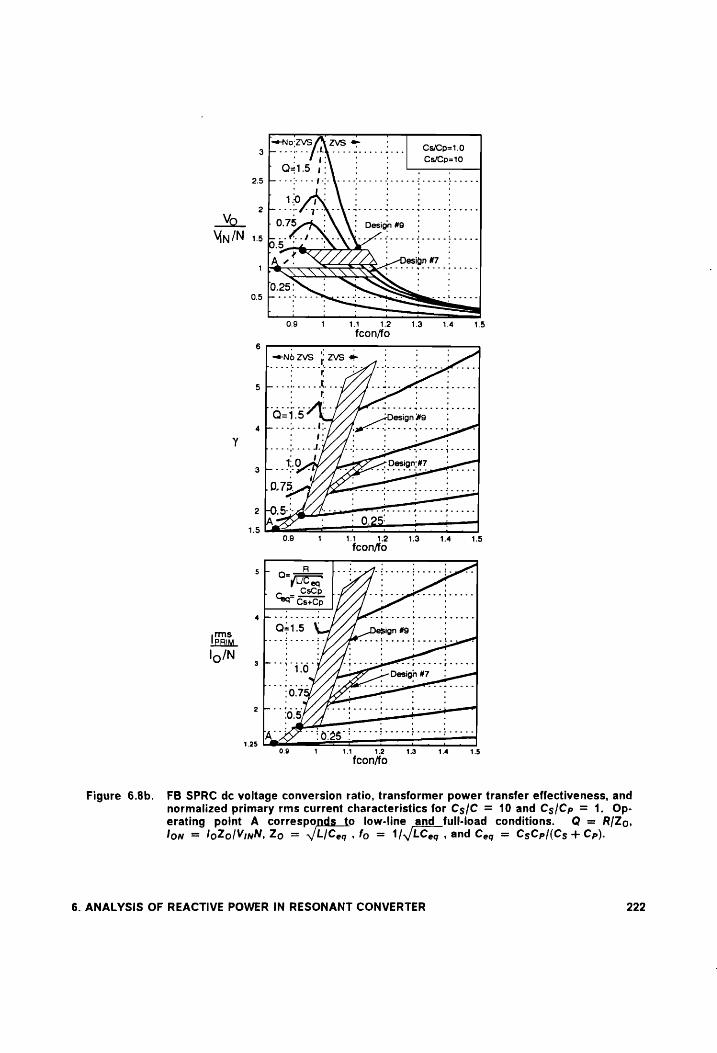
jans
lo/N
1.3 1.4 1.5 0.9 1 1.1 1.2
fcon/fo
Figure 6.8b. FB SPRC dc voltage conversion ratio, transformer power transfer effectiveness, and normalized primary rms current characteristics for Cs/C = 10 and Cs/Cp = 1. Op- erating point A oe eee low-line and full-load conditions. Q = R/Zo,
lon = loZolVinN, Zo = VL/Ceq. fo = 1]/LCeqg , and Ceg = CsCp/(Cs + Cp).
6. ANALYSIS OF REACTIVE POWER IN RESONANT CONVERTER 222
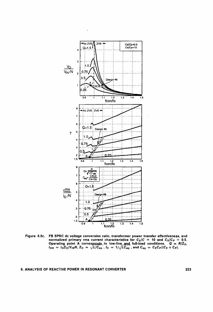
“NoZVS/JZVS Cs(Cp=0.5 | O=1.5 FI : Cs/Cp=10
3
_Vo_ MN/N 4 L057. A\ ooo ioe.
1
0.9 1 4 12 1.3 1.4 1.5
fcon/fo
Q bce cece eee cece lec eeedeeees “No ZVS'ZvVS-~
Thar te ee Ge eee ee eens
6 pont \ a rte esr wre rer Nt tte ee
r Q=1.5: Design #8:
y epee Dy : a Do r 4.0A!
ab ~-- se ff. -e- ad Ree eee
0.75: : Bp iT Yo eee eee feeeee tee
(0.3 2 ip eo h ).
1.5 : : ———— i 0.8 1 1.1 1.2 1.3 1.4 1.5
fcon/fo
rms PRIM
lb /N
1.3 1.4 1.5 11 1.2 fcon/fo
Figure 6.8c. FB SPRC dc voltage conversion ratio, transformer power transfer effectiveness, and normalized primary rms current characteristics for Cs5/C = 10 and Cs/Cp = 0.5. Operating point A sre ees t low-line_and_ full-load conditions. Q = R/Zo, Jon = loZo/VinN, Zo = VLiCeq . fo = 1] bCeg , and Ceg = CsCp/(Cs + Cp).
6. ANALYSIS OF REACTIVE POWER IN RESONANT CONVERTER 223
below 1.5 of the resonant frequency, y is independent of load. ,In addition, for dc voltage-
conversion-ratios close to one and for feon/fo < 1.3, »y < 1.2. Therefore, a properly designed
A converter, which at heavy loads operates with fcon/fo 1.3, does not circulate a significant
amount of power. The good power transfer effectiveness is due to a very short resonant in-
terval in comparison to the switching period, and the absence of any resonance between re-
active elements on different sides of the transformer. That is, the energy stored in the
magnetizing inductance at the beginning of every switching transition is used to operate the
active switches under ZVS, while the linear inductors located on the secondary side are used
for charging and discharging the capacitance in parallel with the rectifier diodes in a con-
trolled fashion. In addition, this converter has square-type primary current and switch current
waveforms, as shown in the previous chapter, so that their rms values are only slightly higher
than those in the PWM HB circuit, Fig. 6.5(c). As a result, the soft-switching of the semicon-
ductor components is achieved without significantly increasing their conduction losses. The
added components on the secondary side (SL, L, and Cp) have a minimal effect on the effi-
ciency and the size of the converter, since the saturable reactor SL and linear inductor L can
be integrated on a single surface-mount type ferrite core [F3].
The HB ZVS-MRC (Fig. 6.6), the CF HB ZVS-MRC (Fig. 6.7), and the FB SPRC (Fig. 6.8) circulate
relatively large amounts of power. For these converters, the circulating power is a strong
function of the load (lon ) and line (M) conditions, as well as of the values of the reactive
components. For example, in the multi-resonant converter (Fig. 6.3(c)), a higher ratio of
rectifier capacitance Cp to the switch capacitance C, i.e., Cy = 2Cp/(N2C), results in increased
circulating power when dc operating points with the same /on and M are compared. This ef-
fect is more noticeable at lighter loads (i.e., /on = 2, 1, ...), aS can be seen by comparing y in
Figs. 6.6(a) and 6.6(b). Similarly, a higher ratio of the series to parallel capacitances Cs/Cp
6. ANALYSIS OF REACTIVE POWER IN RESONANT CONVERTER 224
in the SPRC results in smaller circulating power as can be seen by comparing y in Figs. 8(a),
8(b), and 8(c). For these two converters, dc operating conditions with minimum circulating
energy (minimum y) occur for heavy loads (/on = 5, 10, ..., in Fig. 6.6, and Q=0.25, 0.5, ... in
Fig. 6.8). Even when a dc operating point with minimum circulating energy is selected, the
apparent power processed in the transformer of the HB ZVS-MRC and SPRC is approximately
1.4 times the real (output) power. This corresponds to circulating power comparable to the
output power, since for Pw = Qw, y = Pa/Pw = J1 + (QwiPw) = J2. Therefore, the
power transformer for the best possible design in the ZVS-MRC and SPRC handles roughly
twice the power of the transformer in the corresponding PWM circuit. In addition, the con-
verters with increased circulating power (i.e., ZVS-MRCs, CF ZVS-MRCs, and the SPRC) also
suffer from increased primary rms currents. The rms primary current shows the same trend
with respect to load and line conditions as does y. As a result, to accommodate larger power
and rms currents, the size of the transformer in these converters has to be larger than the size
of the transformer in the corresponding PWM converter operating at a similar frequency. In
addition, these converters require primary switches with higher current ratings to handle the
increased rms currents. Table 6.1 shows typical utilization factors of the primary switches for
all of the analyzed converters operating with minimum circulating energy. The utilization
factor is defined as the ratio of the output power divided by the number of switches to the
product of the peak voltage and current seen by these switches.
The largest amount of circulating power and its strongest dependence on load and line con-
ditions are found in the CF HB ZVS-MRC, Fig. 6.7(c). In applications with wide input-voltage
and/or load range, this converter exhibits very poor efficiency at medium and light loads. As
a result, its potential applications are limited to those with narrow input-voltage and load
variations, such as the ones encountered in the systems with power-factor corrector.
6. ANALYSIS OF REACTIVE POWER IN RESONANT CONVERTER 225
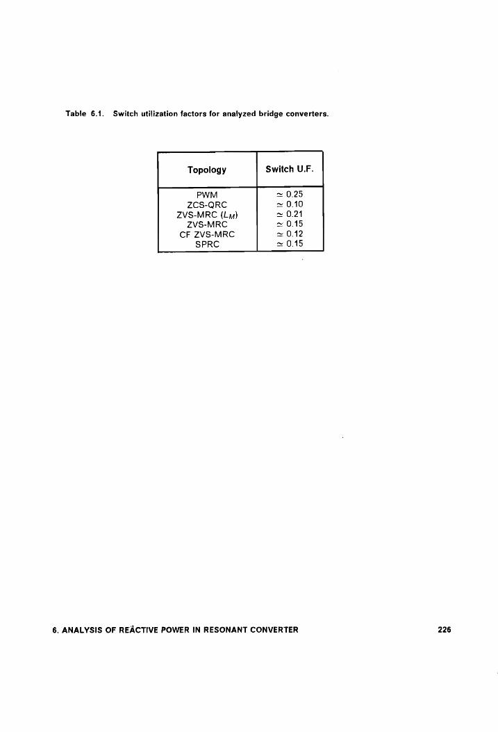
Table 6.1. Switch utilization factors for analyzed bridge converters.
Topology Switch U.F.
PWM ~ 0.25 ZCS-QRC ~ 0.10
ZVS-MRC (Ly) ~ 0.21 ZVS-MRC ~ 0.15
CF ZVS-MRC ~ 0.12
SPRC ~ 0.15
6. ANALYSIS OF REACTIVE POWER IN RESONANT CONVERTER 226

6.4. Design Optimazation Based on Mininization of
Reactive Power
Since the HB ZCS-QRC and the HB ZVS-MRC (Ly) do not circulate significant amounts of
power, their design optimization procedures are relatively simple and are based on criteria
other than the minimization of the reactive power as described in detail in [B14] for the HB
ZCS-QRC and in Chapter 5 for the HB ZVS-MRC (Ly). On the other hand, for the HB ZVS-MRC,
CF HB ZVS-MRC, and the SPRC, design optimization guidelines that maximize their overall
efficiencies can be defined based on the minimization of the reactive power. As discussed in
the previous section, the rms primary current (as well as the secondary currents) exhibits the
same trend as the reactive power, i.e., regions of operation with smaller reactive power also
have smaller rms primary currents. Consequently, the minimization of the reactive power
also results in the minimization of the conduction losses and therefore maximizes the overall
efficiency. Due to the limited number of applications in which the CF ZVS-MRC can be used,
design examples for this converter are not considered in this paper.
In this section, several design examples for the HB ZVS-MRC and SPRC, which use the char-
acteristics presented in Figs. 6.6, 6.8, and 6.9 to identify the regions of operation with minimum
circulating energy are presented. The boundaries of the region of operation are determined
from the line and load specifications. For example, point A in Fig. 6.6(b) represents low-line
6. ANALYSIS OF REACTIVE POWER IN RESONANT CONVERTER 227

(VIN), full-load (/3%) operating point, while point B corresponds to the high-line (Vin2’), full-
load (/6°”) operating point. Similarly, points C and D in Fig. 6.6(b) correspond to the high-line
min (Vine*), light-load (/3'") and low-line (VIX"), light-load (/3'") operating points, respectively. Low
line operating points A and D lie on the M™* = Vo/(Vjn'"/2N) line, while high-line (Vin2”) op-
max erating points B and C lie on the Mmin = Vo/(Vin’ /2N) line. These four points completely
define the operating region for the given design specifications.
For example, the HB ZVS-MRC can be designed to operate in the region shown in Fig. 6.6(a).
From the y characteristics (Fig. 6.6(b)), it can be seen that Design #1 does not minimize the
circulating power. The amount of circulating power can be minimized by selecting the oper-
ating regions, as shown in Fig. 6.9(a). Regions of minimum circulating energy are selected
by specifying the low-line full-load operating points (point A) at minimum y on the selected
lon curves. Design #2 and Design #3 circulate the same amounts of power under full-load and
low-line conditions (y ~ 1.4) which is less than in Design #1 (y ~ 1.45). However, Design #3
requires a transformer with a substantially lower turns ratio than Design #2 because the re-
gion of operation corresponding to Design #3 (Fig. 6.9(a)) lies in the region of the dc charac-
teristics with lower gain (M@™4* = 0.45) than in the case of Design #2 (M™@* = 0.87). The turns
ratio of the transformer in Design #3 is approximately one-half of that in Design #2 (0.45/0.87
~ 0.5). Therefore, Design #2 has lower conduction losses on the primary side and maximum
overall efficiency under heavy load conditions. In addition, Design #2 will operate with a
narrower switching frequency range. It should be noted that by selecting the full-load, low-line
operating point on a curve with /on < 2 (point A in Design #4 in Fig. 6.9(a)), the turns ratio of
the transformer can be slightly increased in comparison with Design #2. However, the circu-
lating power in this design would be larger since y increases dramatically at lower values of
Ion.
6. ANALYSIS OF REACTIVE POWER IN RESONANT CONVERTER 228
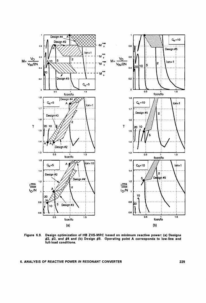
Design #4 AT Re
~ Vin/2N
| ms PRIM
lo/N 1
0.8
0.6
1 tcon/fo
Figure 6.9. Design optimization of HB ZVS-MRC based on minimum reactive power: (a) Designs #2, #3, and #4 and (b) Design #9. Operating point A corresponds to low-line and full-load conditions.
6. ANALYSIS OF REACTIVE POWER IN RESONANT CONVERTER 229

A higher transformer turns ratio for the same /Gn* can be obtained by selecting a character-
istic with higher Cy, for example Design #5 in Fig. 6.9(b). This design clearly results in higher
reactive power compared to Design #2. To compare conduction losses (IPRiM) of Design #5
relative to Design #2, it is necessary to determine the relative turns ratio of the transformers
since the rms primary current is given in the normalized form. The turns ratio of the trans-
former in Design #5 has a larger number of turns because the low-line, full-load operating
point (point A in Fig. 6.9(a)) is selected at a higher dc gain (Mus ~ 1) compared to Design #2
(Mus ~ 0.8). In fact, the number of turns of the transformer (Nys5) in Design #5 is
Nys = Mys*/Myo © = 1.25Nyo. Therefore, the maximum rms primary current for Design #5
(operating point A) is Iprimys = 1.2/6°*/1.25Nyo = 0.96/06 */Nyo ~ IpRimy2, i.e., approximately
equal to the rms primary current for Design #2. Since Design #2 circulates less power, it is
more efficient than Design #5.
From the y characteristics of the SPRC shown in Fig. 6.6 for different ratios of series to parallel
capacitances Cs/Cp, it can be seen that the circulating power is a strong function of Cs/Cp for
high values of Q, ie, Q > 0.75. The circulating power decreases as the ratio of these
capacitances increases. For example, for Q=1 and in the vicinity of the resonant frequency
(feonlfo ~ 0.9 - 1.0), y is approximately 4 for Cs/Cp = 0.5 (Fig. 6.8(a)), approximately 3 for
Cs/Cp = 1 (Fig. 6.8(b)), and 2.5 for Cs/Cp = 2 (Fig. 6.8(c)). However, for lower values of Q (i.e.,
Q < 0.75), the amount of circulating power is almost independent of Cs/Cp. For Q = 0.25, for
example, y is in the range of 1.5 to 1.75, regardless of the Cs/Cp ratio.
The rms primary current shows a similar trend as the circulating power with respect to the
Cs/Cp ratio. Generally, higher values of Cs/Cp result in smaller rms primary currents. This
trend continues for lower Q values. For example, normalized rms primary currents for Q =
0.25 and around the resonant frequency are approximately 1.75, 1.3, and 1.1 for Cs/Cp = 0.5,
6. ANALYSIS OF REACTIVE POWER IN RESONANT CONVERTER 230

1, and 2 respectively. To minimize the circulating power in the SPRC, it is necessary that the
low-line, full-load operating point (point A on the dc characteristics in Fig. 6.8) be placed at the
maximum gain (M = Vo/(Vin/N)) on the lowest Q curve. The operating regions in Figs. 6.8(a),
6.8(b), and 6.8(c), labeled Designs #6, #7, and #8, indicate the regions with the minimum cir-
culating energy.
From Figs. 6.8(a), 6.8(b), and 6.8(c), it can be seen that Designs #6 and #7 have smaller cir-
culating energy (7 ~ 1.5 for operating point A) compared to Design #8 (y ~ 1.75). Due to the
higher dc gain, Designs #7 and #8 have a higher transformer turns ratio (M™4*~1 for operating
point A) compared to Design #6 (W™9* ~ 0.8). The turns ratio of the transformer in Design #6
is approximately 20% smaller than the turns ratio for Designs #7 and #8, ie,
Nye = 0.8Ny7 43. As a result, the rms primary current for Design #6 is larger than the rms
primary current for Design #7. Namely, from Fig. 6.6(a), IpRimye = 1.110°"/Nug =
1.110 °*/0.8Ny7 48 ~ 1.45/6°"/Ny7. Since for Design #8 (Fig. 6.8(c)), /pRiuve = 1-5, the rms pri-
mary currents for Designs #6 and #8 are almost the same. Since Design #7 circulates the
least amount of power and has the smallest rms primary current, it is expected to yield the
best efficiency.
It should be noted that if operating point A is selected at a higher Q, as for example Q = 0.5
for Design #9 in Fig. 6.9(b), the circulating energy is increased compared to Design #7 which
lies in the Q = 0.25 curve. At the same time, the rms primary currents are approximately
equal, even though a higher transformer turns ratio for Design #9 can be used since the dc
gain is higher (Mmax~1.25) than in Design #7 (Mmax~1). From Fig. 6.8(b)
IPRiMHG = 1.610°*/Nyo = 1.6/6°%/1.25Ny7 = 1.28/6°*/Nu7, while IpRimy7 ~ 1.2510" /Ny7. There-
fore, Design #9 is less efficient than Design #7. However, Design #9 does operate with a
narrower frequency range. Therefore, higher Qs (Q > 0.25; i.e., not minimum y) should be
6. ANALYSIS OF REACTIVE POWER IN RESONANT CONVERTER 231

considered only when there is a frequency range constraint. This result agrees with the de-
sign guidelines for the SPRC provided in [A18]. The characteristics in Fig. 6.8 can also be
used to evaluate this trade-off if the switching-frequency range is a design variable.
As can be seen from the above design examples, even when the HB ZVS-MRC and SPRC are
designed for minimum y, the reactive power circulating through the converters is comparable
with the power delivered to the load. As a result, the transformer in these converters usually
has to be designed to process more than twice the output power. Therefore, the expected
transformer size reduction from high-frequency operation of resonant converters in most
cases cannot be realized. This is especially true if the converters need to operate with a wide
input-voltage range.
Generally, the poor power-transfer characteristics of resonant converters are associated with
a large phase-shift between the primary voltage and current of the transformer . Good
sinusoidal waveforms with minimum distortion are not necessary to achieve efficient power
transfer through the transformer (y~1). For example, ZCS-QRCs have good transformer
power-transfer characteristics since these signals are in phase, even though their primary
transformer voltage and current are not sinusoids.
The power transfer characteristics of the transformer in ZVS resonant converters can be im-
proved considerably (y~1) by placing the secondary-side resonant capacitances on the pri-
mary side. This dramatically reduces the amount of reactive power that needs to be handled
by the transformer, but results in the loss of soft switching on the rectifiers. However, the
primary-side resonance does not reduce the reactive power circulating on the primary circuit
that has to be handled by the primary switches and resonant components. It also precludes
6. ANALYSIS OF REACTIVE POWER IN RESONANT CONVERTER 232

the absorption of the transformer leakage inductance into the resonant network, causing
parasitic ringings and losses on the secondary side.
6.5. Summary
The analysis of reactive (circulating) power and rms currents in a number of resonant con-
verters is presented. The results of the analysis show that the HB ZCS-QRC and the soft-
switched HB ZVS-MRC (Ly) circulate relatively small amounts of power. However, the
circulating power in HB ZVS-MRC, CF HB ZVS-MRC, and SPRC is found to be considerably
larger. The analysis is used to generate sets of characteristics for each converter that can
be used in their design optimization based on the minimization of the circulating power. In
addition, several design examples are presented for HB ZVS-MRC and SPRC. The described
analysis and procedure can be easily extended to any other resonant or soft-switched
topology.
6. ANALYSIS OF REACTIVE POWER IN RESONANT CONVERTER 233
7. CONCLUSION
This dissertation introduced two new zero-voltage-switched power conversion technologies;
the constant-frequency (CF) zero-voltage-switched (ZVS) multi-resonant (MR) technology and
the zero-voltage-switched technology that utilizes the magnetizing inductance of the power
transformer as a resonant element (ZVS (Ly)). The CF ZVS-MR family of converters is an ex-
tension of ZVS-MRCs modified so that constant frequency operation is possible. Multi-
resonant operation at constant switching frequency was achieved by replacing the rectifier
diode(s) by an active switch.
The second ZVS technique makes use of the magnetizing inductance of the power transformer
as a resonant component. The operation of these converters is modified so that during the
switching transition the magnetizing inductance is free to resonate. By adding a second active
switch in the rectifier circuit, the time during which the secondary winding(s) is connected to
the load can be controlled. Therefore, during the switching transition the magnetizing
7. CONCLUSION 234

inductance is disconnected from the load and allowed to resonate with the resonant
capacitances so that soft switching operation of the primary switch(es) is. achieved.
Any PWM topology can be transformed into its CF multi-resonant counterpart by replacing the
active/passive semiconductor devices with the CF multi-resonant switch network. To operate
CF ZVS-MRCs in the low megahertz switching frequencies, external resonant components
have to be added since the intrinsic parasitic reactances of the power stage are not sufficient.
The dc analysis of the forward and HB topologies has been described in detail. A numerical
algorithm was used to solve the transcendental equations describing the operation of these
two topologies. Based on the dc analysis, a design trade-off study was performed, resulting
in a set of design guidelines for each of these two topologies. It was found that to optimize
the efficiency of CF ZVS-MRCs, the ratio of resonant capacitances, Cy, and the frequency of
operation should be minimized. On the other hand, the value of the characteristic impedance
has to be maximized to minimize conduction losses. The value of the turns ratio of the
transformer is selected so that the transformer core losses due to the inherent dc bias, char-
acteristic of single-ended topologies, is minimized. Finally, because of the added active
switch in the secondary side, CF ZVS-MRCs have secondary side control, resulting in simple
control schemes.
Unlike the PWM forward, the CF forward ZVS-MRC does not require an additional transformer
resetting circuit. Transformer reset was achieved from the interaction of the magnetizing
inductance and the secondary side resonant capacitor, Cp. Like most single-ended ZVS
topologies, the primary transistor voltage will resonate to a maximum value of several times
the input voltage, resulting in a design trade off between the maximum voitage rating and
device Rps(on) when selecting the device for this switch.
7. CONCLUSION 235
The design of the CF HB ZVS-MRC follow guidelines similar to the one given for the CF for-
ward ZVS-MRC but because of the clamping of the primary switch voltage and the zero dc
biased operation of the transformer, the design of the HB topology is more straightforward.
The concept of using the magnetizing inductance of the transformer as a resonant component
was first considered as it relates to zero voltage turn-on of the primary power switches. The
switches used to insure that the magnetizing inductance was free to resonate during the
switching transition can be implemented using either semiconductor or magnetic switches.
IGBTs and SCRs can be used as the secondary side switches. Similarly, the series combi-
nation of a diode and a saturable inductor can also be used. Variable or constant frequency
operation of these converters is possible. For constant frequency operation, the secondary
side switches result in secondary side control.
Soft turn-on of the rectifier diodes was obtained by adding the parallel combination of a
saturable and linear inductor in series with the rectifier diodes (ZVS-MRC (Lyy)). The linear
inductor was used to charge and discharge the junction capacitance of the rectifiers in a
controlled fashion. The saturable inductor carried most of the load current and clamped the
resonance of the linear inductors to minimize the circulating energy needed for soft switching.
The parallel combination of saturable and linear inductor can be implemented in practice with
a single amorphous core.
The bridge-type topologies of this family of converters operate with quasi-square type currents
and voltages much like the ones of their PWM counterparts, resulting in low conduction
losses. A dc analysis was presented for the HB ZVS-MRC (Ly). The dc analysis was per-
formed using a nonlinear algorithm that solved the transcendental equations describing the
operation of this converter. Based on the dc analysis, a design trade-off study was performed
7. CONCLUSION 236
resulting in a set of design guidelines for the soft-switched HB converter. It is found that to
optimize the efficiency, the ratio of resonant components, Cy and Ly, need to be minimized
to minimize the circulating energy flowing through the converter. The value of the current at
the time the saturable reactor saturates, /s,7 {the saturation current for the integrated version
of linear/saturable inductor) and the ratio between the slope of the linear and saturable
inductances, L/SL, should be minimized to reduce the frequency range. This also contributes
to minimize the circulating energy flowing through the converter.
Constant frequency implementation of the HB ZVS-MRC (Ly) was implemented by replacing
the saturable inductors with controllable saturable inductors. The blocking time of the
saturable reactor was controlled by changing the dc bias on the core. A controllable saturable
inductor fabricated from an El ferrite core was used. The control winding was placed on the
center leg while the saturable inductor winding was placed on one of the outside legs. The
ac flux resulting from the saturable inductor winding, which could disturb the control, was
isolated to the outside path of the core by adding a single turn copper ring in the center leg.
This copper ring prevented any ac flux from entering the center leg. The dc bias established
by the control winding allowed one of the outside legs to easily saturate.
In the final chapter a comprehensive analysis of the reactive power (circulating power) in se-
veral resonant converters was presented. The ratio of reactive power to real power trans-
ferred through the power transformer was used to asses the effectiveness of the different
power conversion techniques. Ideally, power processing techniques should result in zero re-
active power, i.e., transferr only real power. The studied converter topologies include: HB
zero-current-switched (ZCS) quasi-resonant-converter (QRC), HB zero-voltage-switched (ZVS)
multi-resonant-converter (MRC), the HB zero-voltage-switched (ZVS) multi-resonant-converter
(MRC) (Ly), and the HB series-parallel-resonant-converter (SPRC). From the studied
7. CONCLUSION 237
topologies, the HB ZCS-QRC and the HB ZVS-MRC (Ly) generated the least amount of reac-
tive power. On the other hand, CF ZVS-MRCs generated a large amount of reactive power.
In most cases, the reactive power transferred in these converters was greater than the real
power transferred, resulting in an increased size of the power transformer. Since the reactive
power processed by CF ZVS-MRCs does not decrease considerably as the output load de-
creases, the performance of these converters is very sensitive to the changes in load, i.e., the
efficiency decreases rapidly as the output load decreases. For similar reasons, the perform-
ance of this family of converters is also very sensitive to line variations. The study suggests
that CF ZVS-MRCs are not suitable for applications that require a large input voltage range
or high performance at fractional loads.
High-frequency power conversion provides numerous research opportunities, resulting in new
and better power conversion techniques. The following research areas are of considerable
interest for future work.
e Phase shift control of ZVS-MRCs. Due to large circulating energy, the CF ZVS-MR family
of converters discussed in this dissertation has limited applications. A second alternative
to achieving constant frequency operation of ZVS-MRCs is phase shift control. Phase shift
control has been successfully implemented for PWM and resonant topologies. Phase shift
control of a class-E dc-dc converter was presented in [C14], but for practical reasons, a
one transformer topology would be more desirable.
e = Evaluation of the merits of single-ended topologies of the new family of converters using
the magnetizing inductance. Many low power applications (below 100 W) require single-
ended topologies because of their low part count. The implementation of single-ended
7. CONCLUSION 238

topologies was shown, but the complete analysis of these converters was not presented.
The forward and flyback topologies may be found to have merits in high-frequency appli-
cations.
e Integration of magnetic structures in the soft switched HB. The implementation of the soft
switched HB results in three different magnetic structures. These magnetic structures
are small, but it would be very desirable to integrate the saturable inductors and trans-
former into a single core.
e = Soft-switching techniques with PWM type control and waveforms. Square-type currents
and voltages result in low conduction losses. Furthermore, constant frequency control
simplifies the design of the filter and magnetic components. Topologies that achieve
soft-switching while still maintaining square-type currents and voltages and operate at a
constant switching frequency would be very desirable.
7. CONCLUSION 239
REFERENCES
A. RESONANT CONVERTERS
[A1]
[A2]
[A3]
[A4]
[A5]
[A6]
[A7]
[A8]
F.C. Schwarz, “A method of resonant current pulse modulation for power converters,”
IEEE Trans. Industrial Electronics Control and Instrumentation, pp. 209-221, 1970.
F.C. Schwarz, “An improved method of resonant current pulse modulation for power converters,” /EEE Power Electronics Specialists Conference Proc., pp. 194-204, 1975.
F.C. Schwarz, J.B. Klaassens, “A 95% efficient 1 kW dc converter with an internal fre- quency of 50 kHz,” /EEE Power Electronics Specialists Conference Proc., pp. 125-134, 1977.
K.A. Check, “Designing improved high-frequency dc-dc converters with a new resonant thyristor technique,” Powercon 6, pp. F.3.1-F.3.7, 1979.
D.A. Amin, “Applying sinewave power switching technique to the design of high- frequency off-line converters,” Powercon 7, pp. A.1.1-A.1.7, 1980.
W. Ebbinge, “Designing very high efficiency converters with a new high frequency res-
onant GTO technique,” Powercon 8, pp. A.1.1-A.1.7, 1981.
R. Myers, R. Peck, “200 kHz power FET technology in new modular power supplies,” Hewlett-Packard J., pp. 3-10, Aug. 1981.
V. Vorperian, S. Cuk, “A complete dc analysis of the series resonant converter,” /EEE Power Electronics Specialists Conference Proc., pp. 85-100, 1982.
REFERENCES 240
[A9]
[A10]
[A11]
[A12]
[A13]
[A14]
[A15]
[A16]
[A17]
[A18]
[A19]
[A20]
[A21]
[A22]
[A23]
[A24]
V. Vorperian, S. Cuk, “Small signal analysis of resonant converters,” /JEEE Power Elec- tronics Specialists Conference Proc., pp. 269-282, 1983.
R. King, T. Stuart, “Inherent overload protection for the series resonant converter,” /EEE Trans. Aerospace and Electronics Systems, pp. 820-830, 1983.
R.L. Steigerwald, “High frequency resonant transistor dc-dc converters,” JEEE Trans. Industrial Electronics, pp 181-191, 1984.
R. Oruganti, F.C. Lee, “Resonant power processors: Part | - State plane analysis,” /EEE Trans. Industry Applications, Vol. \A-21, no. 6, pp. 1453-1460, 1985.
R. Oruganti. F.C. Lee, “Resonant power processors: Part Il - Methods of control,” /EEE Trans. Industry Applications, Vol. |A-21, no. 6, pp. 1461-1471, 1985.
|.J. Pitel, “"Phase-modulated, resonant power conversion technique for high-frequency
link inverters,” IEEE [AS Annual Meeting Proceedings, pp. 1163-1172, 1985.
R. W. Lutz, P. C. Todd, ”A 100 watt, off-line, 250 kKHz resonant power supply,” High Fre-
quency Power Conversion Conference Record, pp. 1-14, 1986.
S. Young, “High frequency resonant converter using power MOSFETs,” High Frequency Power Conversion Conference Record, pp. 21-35, 1986.
D.M. Divan, "Design considerations for very high frequency dc/dc converters,” /EEE Trans. Power Electronics, pp. 45-54, 1987.
R.L. Steigerwald, “A comparison of half-bridge resonant converter topologies,” /EEE Applied Power Electronics Conference Proc., pp. 135-144, 1987.
Also: JEEE Trans. Power Electronics, Vol. 3, no. 2, pp. 135-144, 1988.
B. Carsten, "A hybrid series-parallel resonant converter for high frequencies and power
levels,” High Frequency Power Conversion Conference Record, pp. 41-47, 1987.
D.V. Jones, “A new resonant converter topology,” High Frequency Power Conversion
Conference Record, pp. 48-53. 1987.
F. Tsai, P. Materu, F.C. Lee, ”“Constant-frequency, clamp-mode resonant converter,”
IEEE Power Electronics Specialists Conference Proc., pp. 557-566, 1987.
F. Tsai, F.C. Lee, “State-plane analysis of clamped mode parallel resonant converter,”
IEEE International Telecommunications Energy Conference Proceedings, pp. 220-227,
1987.
L. Casey, M. Schlecht, “A high frequency, low volume, point-of-load power supply for
distributed power systems,” /EEE Power Electronics Specialists Conference Proc., pp.
438-450, 1987.
A.K.S. Bhat, S.B. Dewan, “Analysis and design of a high-frequency resonant converter
using LCC-type commutation,” /EEE Trans. Power Electronics, Vol. PE-2, no. 4, pp.
291-301, 1987.
REFERENCES 241
[A25] A.K.S. Bhat, S.B. Dewan, “Analysis and design of high frequency resonant converter
[A26]
[A26]
[A27]
[A28]
[A29]
[A30]
[A311]
using LCC-type commutation,” JEEE Trans. Power Electronics, Vol. 2, no. 4, pp. 291-301, 1987.
F.M. Magalhaes, F.T. Dickens, G.R. Westerman, N.G. Ziesse, ”“Zero-voltage-switched resonant half-bridge high-voltage dc-dc converter,” High Frequency Power Conversion Record, pp. 332-343, 1988.
|. Bataresh, R. Liu, C.Q. Lee, and A.K. Upahdyay, “Theoretical and experimental studies of the LCC-type parallel resonant converter,” JEEE Trans. Power Electronics, vol. 4, no. 1, pp. 136-150, Jan. 1989.
A.K.S. Bhat, “Analysis and design of LCL-type series resonant converter,” IEEE Inter- national Telecommunications Energy Conference Proc, paper 10.1, pp. 172-178, 1990.
T. Ninomiya, T. Hgashi, M. Nakahara, K. Fujimoto, K. Harada, ’Full-wave voltage-mode resonant converter with multiple outputs.” /EEE Power Electronics Specialists Confer- ence Proc., pp. 543-551,1991.
H.P. Ludeke, N. Frohleke, and H. Grotstollen, “Analysis of a series-parallel-loaded
resonant-converter with tertiary side resonance for high output power and low output voltage,” European Power Electronics Conference Proc., pp. 4-139 - 4-144, 1991.
O.P. Mandhana, and R.G. Hoft, "Steady state frequency domain analysis of parallel- series resonant converter,” /EEE Applied Power Electronics Conference Proc., pp. 229-233, 1992.
J.A. Sabate, R. Farrington, M.M. Jovanovic, and F.C. Lee, “Effect of switch capacitance
On zero-voltage-switching of resonant converter,” JEEE Power Electronics Specialists Conference Proc., (to be published), 1992.
B. ZERO-CURRENT-SWITCHED AND ZERO-VOLTAGE-SWITCHED QUASI-RESONANT CONVERTERS
[B1]
[B2]
[B3]
[B4]
[B5]
[B6]
E. Buchanan, E.J. Miller, "Resonant switching power conversion technique,” /EEE Power
Electronics Specialists Conference Proc., pp. 188-193, 1975.
E.J. Miller, “Resonant switching power conversion,” IEEE Power Electronics Specialists Conference Proc., pp. 206-211, 1976.
E.J. Miller, "Resonant switching converter,” U.S. Patent, 4,138,715, 1979.
P. Vinciarelli, “Forward converter switching at zero current,” U. S. Pat. 4,415,959, 1983.
K. Liu, F. C. Lee, “Resonant switches - A unified approach to improve performance of switching converters,” /EEE International Telecommunications Energy Conference Pro- ceedings, pp. 334-341, 1984.
K. Liu, R. Oruganti, F. C. Lee, “Resonant switches - Topologies and characteristics,”
JEEE Power Electronics Specialists Conference Proc., pp. 106-116, 1985. also: /EEE Trans. Power Electronics, Vol. PE-2, no. 1, pp. 62-74, 1987.
REFERENCES 242

[B7]
[B8)
[B9]
[B10]
[B11]
[B12]
[B13]
[B14]
[B15]
[B16]
[B17]
[B18]
[B19]
M.M. Jovanovic, K.H. Liu, R. Oruganti, F.C. Lee, “State-plane analysis of quasi-resonant
converters,” /EEE International Telecommunications Energy Conference Proceedings, pp. 235-242, 1985. also: JEEE Trans. Power Electronics, Vol. PE-2, no. 1, pp. 36-44, 1987.
K. H. Liu, F. C. Lee, “Secondary-side resonance for high-frequency power conversion,” IEEE Applied Power Electronics Specialists Conference Proc., pp. 83-89, 1986.
T. Zeng, D.Y. Chen, F.C. Lee, ’Variations of quasi-resonant dc-dc converter topologies,” IEEE Power Electronics Specialists Conference Proc., pp. 381-392, 1986.
L. Roufberg, “Effects of parasitic elements on quasi-resonant buck converters,” VPEC Power Electronics Seminar Proceedings, Virginia Polytechnic Institute and State Uni- versity, Blacksburg, Virginia, pp. 10-22, 1986.
R. Tymerski, “Finite filter inductance effects on quasi-resonant converter perform- ances,” VPEC Power Electronics Seminar Proceedings, Virginia Polytechnic Institute and State University, Blacksburg, Virginia, pp. 24-36, 1986.
D. C. Hopkins, M. M. Jovanovic, F. C. Lee, F. W. Stephenson, “Two-megahertz off-line hybridized quasi-resonant converter,” JEEE Applied Power Electronics Conference Proc., pp. 105-114, 1987. also: IEEE Trans. Power Electronics, Vol. 4, no. 1, pp. 147-154, 1989.
A. Heyman, “Low-profile high-frequency off-line quasi-resonant converter,” IEEE Applied Power Electronics Conference Proc., pp.157-165, 1987.
M. M. Jovanovic, D. C. Hopkins, F. C. Lee, “Design aspects for high-frequency off-line quasi-resonant converters,” High Frequency Power Conversion Conference Pro- ceedings, Vol. PE-2, no. 2, pp. 83-97, 1987. also: IEEE Trans. Power Electronics, pp.136-146,1989.
L. Roufberg, “DC analysis of quasi-resonant buck and forward converters including ef- fects of parasitic elements,” M.S. Thesis, Virginia Polytechnic Institute and State Uni- versity, Blacksburg, Virginia, 1987.
R. Rangan, D.Y. Chen, J. Yang, J. Lee, “Application of IGT/COMFET to zero-current-
switched resonant converters,” [EEE Power Electronics Specialists Conference Proc., pp. 55-60, 1987.
M.M. Jovanovic, F. C. Lee, “Stability analysis of push-pull and bridge-type zero- current-switched quasi-resonant converters,” JEEE Power Electronics Specialists Con- ference Proc., pp. 134-145, 1988. also: [EEE Trans. Power Electronics, Vol. 4, no. 4, pp. 459-469, 1989.
M. M. Jovanovic, F. C. Lee, D. Y. Chen, “A full-wave off-line zero-current-switched quasi-resonant converter,” High Frequency Power Conversion Conference Record, pp. 150-160, 1988. also: IEEE Trans. Power Electronics, Vol. 4, no. 2, pp. 215-224, 1989.
K. H. Liu, F. C. Lee, "Zero-voltage switching technique in dc/dc converters,” /EEE Power Electronics Specialists Conference Proc., Vol. 5, no. 3, pp. 58-70, 1986. also: Trans. Power Electronics, pp. 293-304, 1990.
REFERENCES 243
[B20]
[B21]
[B22]
[B23]
[B24]
[B25]
[B26]
[B27]
[B28]
[B29]
[B30]
[B31]
[B32]
[B33]
M. Kazimerczuk, K. Puczko, “Control circuit for class e and zero-voltage-switched FM resonant dc/dc converters,” High Frequency Power Conversion Conference Pro- ceedings, pp. 98-115, 1987.
W. A. Tabisz, P. Gradzki, F.C. Lee, “Zero-voltage-switched quasi-resonant buck and
flyback converters - Experimental results at 10 MHz,” /EEE Power Electronics Specialists Conference Proc., pp. 404-413, 1987.
M.M. Jovanovic, W.A. Tabisz, F.C. Lee, “Zero-voltage-switching technique in high-
frequency off-line converters,” [EEE Applied Power Electronics Conference Proc., pp. 130-138, 1988.
R. Oruganti, “"Quasi-resonant converters, Part | - Generalized dc analysis,” VPEC Power Electronics Seminar Proceedings, Virginia Polytechnic Institute and State University,
Blacksburg, Virginia, pp. 74-90, 1986.
R. Oruganti, “Quasi-resonant converters, Part Il - Topological variations,” VPEC Power
Electronics Seminar Proceedings, Virginia Polytechnic Institute and State University,
Blacksburg. Virginia, pp. 92-102, 1986.
V. Vorperian, R. Tymerski, K. H. Liu, F. C. Lee, “Generalized resonant switches, Part 1:
Topologies,” VPEC Power Electronics Seminar Proceedings, Virginia Polytechnic Insti-
tute and State University, Blacksburg, Virginia, pp. 116-122, 1986.
V. Vorperian, R. Tymerski, K. H. Liu, F. C. Lee, “Generalized Resonant switches, Part 2: Analysis and circuit models,” VPEC Power Electronics Seminar Proceedings, Virginia Polytechnic Institute and State University, Blacksburg, Virginia, pp. 124-131, 1986.
K.H. Liu, “High-frequency quasi-resonant converter techniques,” Ph.D. Dissertation, Virginia Polytechnic Institute and State University, Blacksburg, Virginia, 1987.
M. Schlecht, L. Casey, “Comparison of the square-wave and quasi-resonant
topologies,” IEEE Applied Power Electronics Conference Proc., pp. 124-134, 1987.
V. Vorperian, “Equivalent circuit models for resonant and PWM switches,” /EEE Inter- national Symposium on Circuits and Systems Proceedings, pp. 1080-1087, 1987.
T. Meynard, Y. Cheron, H. Foch, “Generalization of the resonant switch concept: struc-
tures and performances,” High Frequency Power Conversion Conference Record, pp.
54-70, 1987.
S. Freeland, R.D. Middlebrook, "A unified analysis of converters with resonant
switches,” IEEE Power Electronics Specialists Conference Proc., pp. 20-30, 1987.
K.D. Ngo, “Generalization of resonant switches and quasi-resonant dc-dc converters,”
IEEE Power Electronics Specialists Conference Proc., pp. 395-403, 1987.
A. Lotfi, "Comparison of stresses of quasi-resonant and PWM converters,” VPEC Power
Electronics Seminar Proceedings, Virginia Polytechnic Institute and State University,
Blacksburg, Virginia, pp. 129-139, 1987.
REFERENCES 244
[B34]
[B35]
[B36]
J. Nishizawa, T. Tmamushi, T. Koga, S. Sugawara, H. Hayashi, H. Sekimoto, “Quasi- resonant dc/dc converter using a single SI thyristor,” /JEEE International Telecommuni- cations Energy Conference Proc., pp. 68-75, 1988.
D. Maksimovic, S. Cuk, “A general approach to synthesis and analysis of quasi-
resonant converters,” /EEE Power Electronics Specialists Conference Proc., pp. 713-727, 1989.
|. Barbi, D.C. Martins, R.N. dePrado, "Effects of nonlinear resonant inductor on the be- havior of zero-voltage switched quasi-resonant converters,” IEEE Power Electronics Specialists Conference Proc., pp. 552-561, 1990.
C. HIGH-FREQUENCY POWER CONVERTERS
[C1]
[C2]
[C3]
[C4]
[C5]
[C6]
[C7]
[C8]
[C9]
[C10]
R. J. Guttmann, “Application of RF circuit design principles to distributed power con- verters,” /EEE Trans. Industrial Electronics Control and Instrumentation, pp. 156-164, 1980.
R. Redl, B. Molnar, “Design of a 1.5 MHz regulated dc/dc converter”, Power Conversion International Conference Proc., pp. 74-87, 1983.
R. Redl, B. Molnar, N. O. Sokal, “Small-signal dynamic analysis of regulated class e dc/dc converters,” /EEE Power Electronics Specialists Conference Proc., Vol. PE-1, no. 2, pp. 62-71, 1984. also: /EEE Trans. Power Electronics, pp. 121-128, 1986.
G. Lutteke, H. C. Raets, “High-voltage high-frequency class e converter suitable for miniaturization,” [EEE Power Electronics Specialists Conference Proc., pp. 54-61, 1984.
G. Lutteke, H. C. Raets, "220 V mains 500 kHz class e converter using a BIMOS,” JEEE Power Electronics Specialists Conference Record, pp. 127-135, 1985.
C. Mullet, "Design of high-frequency saturable reactor output regulators,” Notes of the
tutorial held at High Frequency Power Conversion Conference, Virginia Beach, Virginia,
May 28-30, 1986.
K. Lohn, “On the overall efficiency of the class e power converter,” /EEE Power Elec-
tronics Specialists Conference Record, pp. 351-358, 1986.
W. A. Tabisz, "Comparison between class e and zero-voltage-switched quasi-resonant dc/de converters,” VPEC Power Electronics Seminar Proceedings, Virginia Polytechnic Institute and State University, Blacksburg. Virginia, pp. 54-60, 1986.
V. Vorperian, “Quasi-square-wave converters: Topologies and analysis,” /EEE Trans.
Power Electronics, Vol. 3, no. 2, pp. 183-191, 1988.
L.D. Salazar, P.D. Ziogas, “A single-ended SMR converter topology with optimized switching characteristics,” JEEE Trans. Power Electronics, Vol. 4, no. 1, pp. 53-63, 1989.
REFERENCES 245
[C11]
[C12]
[C13]
[C14]
[C15]
[C16]
[C17]
[C18]
[C19]
[C20]
M.K. Kazimierczuk, X.T. Bui, “Class e dc/dc converters with an inductive impedance inverter,” /EEE Trans. Power Electronics. Vol. 4, no. 1, pp. 124-135, 1989.
R. Redel, N. Sokal, “A new class-e dc/dc converter family with reduced part count: derivations, topologies, and design considerations,” High Frequency Power Conversion Conference Proc., pp. 395-415, 1989.
S. Hamada, T. Kanazawa, “A new conceptual PWM dc-dc converter with zero-voltage switching incorporating non-controlled saturable reactors,” /EEE Power Electronics Specialists Conference Proc., pp. 881-888. 1989.
C.Q. Hu, X.Z. Zhang, S.P. Huang, “Class-e combined-converter by phase-shift control,” IEEE Power Electronics Specialists Conference Proc., pp. 221-228, 1989.
C.Q. Lee, R. Liu, S. Sooksatra, “Novel class-e converters,” /EEE Power Electronics
Specialists Conference Proc., pp. 213-220. 1989.
C.Q. Lee, R. Liu, S. Sooksatra, “Nonresonant and resonant coupled zero voltage switching converters,” JEEE Trans. Power Electronic, Vol. 5, no. 4, pp. 404-412, 1990.
K. Harada, H. Sakamoto, “Switched snubber for high frequency switching,” /EEE Power Electronics Specialists Conference Proc., pp. 181-188, 1990.
K. Harada, H. Sakamoto, “On the saturable inductor commutation for zero-voltage- switching,” /EEE Power Electronics Specialists Conference Proc., pp. 189-196, 1990.
J.A. Ferreira, A. Van Ross, J.D. Van Wyk, ”A generic soft switching converter topology with a parallel nonlinear network for high power application,” /EEE Power Electronics Specialists Conference Proc., pp. 298-304, 1990.
K. Harada, H. Sakamoto, “High power and high switching frequency dc-to-dc converter
using saturable inductor commutation and switched snubber,” /EEE Power Electronics Specialists Conference Proc., pp. 148-154, 1991.
D. ZERO-VOLTAGE-SWITCHED MULTI-RESONANT-CONVERTERS
[D1]
[D2]
[D3]
[D4]
W. Tabisz, F.C. Lee, “Application of a novel, multi-resonant switch in high-frequency dc/dc converters,” VPEC Power Electronics Seminar Proceedings, Virginia Polytechnic Institute and State University, Blacksburg, Virginia, pp. 65-71, 1987.
W.A. Tabisz, F.C. Lee “Zero-voltage-switching multi-resonant technique - A novel ap- proach to improved performance of high-frequency quasi-resonant converters,” IEEE Power Electronics Specialists Conference Proc., pp. 9-17, 1988. 1988.
W. Tabisz, F.C. Lee, “A novel, zero-voltage-switched multi-resonant forward converter,” High Frequency Power Conversion Record, pp. 309-318, 1988.
F.C. Lee, W.A. Tabisz, M.M. Jovanovic, “Recent developments in high-frequency quasi- resonant and multi-resonant technologies,” Third European Conference on Power Elec- tronics and Applications Proc., pp. 401-410, 1989.
REFERENCES 246

[D5]
[D6]
[D7]
[D8]
[D9]
[D10]
[D11]
[D12]
[D13]
[D14]
[D15]
W.A. Tabisz, F. C. Lee, “DC analysis and design of zero-voltage-switched multi-resonant converter,” /EEE Power Electronics Specialists Conference Proc., pp. 243-251, 1989.
M.M Jovanovic, F.C. Lee, "Mode analysis of half-bridge zero-voltage-switched multi- resonant converter,” JEEE Power Electronics Specialists Conference Proc., Vol. 5, no.
2,pp. 252-262, 1989. also: Trans. Power Electronics, pp. 160-171, 1990.
W. Tang, W.A. Tabisz, A. Lofti, F.C. Lee, V. Vorperian, “DC analysis and design of for- ward zero-voltage-switched multi-resonant converter,” IEEE Power Electronics Special- ists Conference Proc., pp. 333-340, 1990.
M.M. Jovanovic, High Frequency, Off-Line Power Conversion using Quasi-Resonant and Multi-Resonant Techniques, Ph.D. Dissertation, Virginia Polytechnic and State Univer-
sity Blacksburg, Va., 1988.
M.M. Jovanovic, R. Farrington, F.C. Lee, “Comparison of half-bridge off-line, ZCS-QRC and ZVS-MRC,” JEEE Transaction on Aerospace and Electronic Systems, Vol. 26, no. 2, pp. 326-336, 1990.
R. Farrington, M. Hayes, M. Jovanovic, F.C. Lee, F.W. Stephenson, “High density power
hybrid design of a half-bridge multi-resonant converter,” High Frequency Power Con- version Record, pp. 26-33, 1990.
M.M. Jovanovic, C.S. Leu, F.C. Lee, ”Zero-voltage-switched multi-resonant converter. for high-power, pulse-load applications,” /EEE Trans. Industrial Electronics, Vol. 37, no. 6,
pp. 554-555, 1990.
W.A. Tabisz, High Frequency Multi-Resonant Power Conversion Techniques, Ph.D. Dis-
sertation, Virginia Polytechnic and State University Blacksburg, Va., 1990.
D. Schroder, F. Franck, “A contribution to the design specification of single cell multi-
resonant converters,” JEEE Power Electronics Specialists Conference Proc., pp. 552-559, 1991.
W.A. Tabisz, F.C. Lee, D.Y. Chen, “A MOSFET resonant synchronous rectifier for high-
frequency dc/dc converters,” /JEEE Power Electronics Specialists Conference Proc., pp.
769-779, 1991.
W.A. Tabisz, F.C. Lee, “Design of high-density on-board single- and multiple-output
multi-resonant converters,” High Frequency Power Conversion Record, pp. 45-57, 1990.
E. CONSTANT-FREQUENCY ZERO-CURRENT-SWITCHED AND ZERO-VOLTAGE-SWITCHED CONVERTERS
[E1] D. Maksimovic, S. Cuk, “Constant-frequency control of quasi-resonant converters,” High
Frequency Power Conversion Conference Record, pp. 9-17, 1988.
REFERENCES 247

[E2)
[E3]
[E4]
[E5]
[E6]
[E7]
[E8]
[E9]
[E10]
[E11]
[E12]
[E13]
[E14]
[E15]
R. Redl, B. Molnar, N. O. Sokal, “Class e resonant regulated dc/dc power converters: analysis Of operation and experimental results at 1.5 MHz,” /EEE Power Electronics Specialists Conference Vol. PE-1, no. 2, Proc., pp. 50-60, 1983.
also: /EEE Trans. Power Electronics, pp. 111-120, 1986.
W. W.C. Bowman, J.F. Balicki, F.T. Dickens. R.M. Honeycutt, W.A. Nitz, W. Strauss, W.B. Suiter, N.G. Ziesse, “A resonant dc-to-dc converter operating at 22 MHz,” /EEE Applied Power Electronics Conference Proc., pp. 3-11, 1988.
F.M. Magalhaes, F.T. Dickens, G.R. Westerman, N.G. Ziesse, ”“Zero-voltage-switched resonant half-bridge high-voltage converter,” High-Frequency Power Conversion Con- ference Record, pp. 332-334, 1988.
M.M. Jovanovic, R. Farrington, F.C. Lee “Constant-frequency multi-resonant convert- ers,” Virginia Power Electronics Center (VPEC) Power Electronic Seminar Proceedings,
Virginia Polytechnic Institute and State University, Blacksburg, Virginia, pp. 56-65, 1989.
D. Maksimovic, Z. Zhang, S. Cuk, “A high power density VHSIC power supply,” /EEE Applied Power Electronics Conference Proc., pp. 119-127, 1990.
R.A. Fisher, K.D.T. Ngo, M.H. Kuo, “A 500 kHz, 250 W dc-dc converter with multiple outputs controlled by phase-shifted PWM and magnetic amplifiers,” High-Frequency Power Conversion Conference Record, pp. 100-110, 1988.
J.A. Sabate, F.C. Lee, “Off-line applications of the fixed frequency clamped mode series- resonant converter,” IEEE Applied Power Electronics Conference Proc., pp. 213-220, 1989.
|. Barbi, J.C. Bolacell, D.C. Martins, F.B. Libano, “Buck quasi-resonant converter oper- ating at constant frequency: Analysis, design and experimentation,” /EEE Power Elec- tronics Specialists Conference Proc., pp. 873-880, 1989.
!. Barbi, J.B. Vieira, J.C. Bolacell "A forward pulse-width modulated quasi-resonant converter: Analysis, design and experimental results,” /EEE Power Electronics Special- ists Conference Proc., pp. 21-26, 1990. 1986.
R. K. Harada, W.J. Gu, K. Murata, “Controlled resonant converters with switching fre- quency fixed,” /EEE Power Electronics Specialists Conference Proc., pp. 424-430, 1987.
S.G. Trabert, R.W. Erickson, “Steady state analysis of the duty cycle controlled series resonant converter,” /EEE Power Electronics Specialists Conference Proc., pp. 545-556, 1987.
O.D. Patterson, D.M. Divan, ”“Pseudo-resonant full bridge dc/dc converter,” JEEE Power Electronics Specialists Conference Proc., pp. 424-430, 1987.
K. Harada, W. Gu, “Steady state analysis of class e resonant dc-dc converter regulated under fixed switching frequency,” JEEE Power Electronics Specialists Conference Proc., pp. 3-8, 1987.
C.P. Henze, H.C. Martin, D.W. Parsley “Zero-voltage switching in high frequency power converters using pulse width modulation,” EEE Applied Power Electronics Conference Proc., pp. 33-40, 1988.
REFERENCES 248
[E16]
[E17]
[E18]
[E19]
[E20]
[E21]
[E22]
[E23]
[E24]
[E25]
[E26]
[E27]
[E28]
[E29]
|. Barbi, J.B. Vieira Jr., H.L. Hey, “A pulse-width modulated zero-voltage-zero-current
switched half-bridge quasi-resonant converter,” /EEE Industrial Electronics Conference Proc., pp. 42-47, 1988.
|. Barbi, M.A. Oliveira, J.B. Vieira Jr., “A half-bridge pulse-width modulated zero- current-switched quasi-resonant converter,” /JEEE Industrial Electronics Conference Proc., pp. 54-59, 1988.
R. Hiramatu, |. Norigoe, H. Hiki, S. Takeishi, H. Yoshioka, K. Arakawa, S. Kameyama,
"ZVS PWM converter utilizing parital resonance,” /EEE International Telecommuni- cations Energy Conference, paper 20.9, pp. 1-6, 1989.
P. Imbertson, N. Mohan, “New PWM converter circuits combining zero switching loss
with low conduction loss,” /EEE International Telecommunications Energy Conference,
paper 10.2 pp. 179-185, 1990.
R. Farrington, M.M. Jovanovic. F.C. Lee, “Constant-frequency zero-voltage-switched multi-resonant converters: Analysis, design, and experimental results,” /EEE Power
Electronics Specialists Conference Proc., pp. 33-40, 1990.
|. Barbi, A.J. Perin, D.C. Martins, “A new family of pulse-width modulated zero-voltage
switching dc-to-dc converters: Topologies, analysis and experimentation,” /EEE Indus-
trial Applications Society Conference Record, pp. 1256-1261, 1990.
L.C Freitas, |. Barbi, “Modeling of dc-dc pulse-width modulated quasi-resonant con-
verters,” International Power Electronics Conference Record, pp. 183-190, 1990.
P. Imbertson, N. Mohan, “Square-wave resonant power converter,” International Power
Electronics Conference Record, pp. 354-361, 1990.
G.K. Schoneman, ”A novel zero-voltage switched multiresonant converter,” JEEE Power
Electronics Specialists Conference Proc., pp. 195-201, 1991.
S. Sooksatra, Q.C. Lee, “PWM controlled SRC with inductive output filter at constant
switching frequency,” JEEE Power Electronics Specialists Conference Proc., pp. 258-265, 1991.
J. Vieira, |. Barbi, "Constant frequency PWM capacitor voltage clamped series resonant
power supply,” [EEE Applied Power Electronics Conference Proc., pp. 52-57, 1991.
E. Morap, P. Ziogas, G. Joos, “High frequency high power dc-dc full bridge converter
with zero-current zero-voltage commutation,” JEEE Applied Power Electronics Confer-
ence Proc., pp. 71-80, 1991.
|. Barbi, H. Hey, ’A half-bridge zero-voltage switching pulse-width modulated dc-dc
converter,” [EEE Applied Power Electronics Conference Proc., pp. 140-145, 1991.
J. Sabate, V. Viatkovic, R. Ridley, F.C. Lee, “High-voltage, high power, ZVS, full-bridge
PWM converter employing an active snubber,” /EEE Applied Power Electronics Confer-
ence Proc., pp. 158-163, 1991.
REFERENCES 249
[E30] L. Freitas, E. Coelho, H. Hey, “A lossless commutation pulse-width-modulated converter by using a resonant disconnecting circuit,” /JEEE Applied Power Electronics Conference Proc., pp. 573-579, 1991.
[E31] C. Lee, S. Sooksatra, R. Liu, “Constant frequency controlled full-bridge, LCC-type par- allel resonant converter,” IEEE Applied Power Electronics Conference Proc., pp. 587-593, 1991.
F. ZVS USING THE MAGNETIZING INDUCTANCE OF THE POWER TRANSFORMER
[F1] K. Watanabe, S. Takeishi, |. Norigoe, R. Hiramatsu, “Self running converter utilizing partial resonance,” JEEE International Telecommunications Energy Conference Proc., pp. 186-193, 1988.
[F2] S. Hamada, T. Kanazawa, Y. Ogino, M. Nakaoka, ”A new constant frequency phase- shifted PWM zero-voltage switching dc-dc converter incorporating non-controllable saturable reactors,” IEEE Trans. Magnetics, Vol. 25, no. 5, pp. 3991-3993, 1989.
[F3] R. Farrington, M.M. Jovanovic, F.C. Lee, “A new family of isolated zero-voltage- switched converters,” /EEE Power Electronics Specialists Conference Proc., pp. 209-215, 1991.
[F4] M. Shoyama, K. Harada, ”"Zero-voltage-switched push-pull dc-dc converter,” /EEE Power Electronics Specialists Conference Proc., pp. 223-229, 1991.
[F5] TT. Ninomiya, N. Matsumoto, M. Nakahara, K. Harada, “Static and dynamic analysis of zero-voltage-switched half-bridge converter with PWM control,” /EEE Power Electronics Specialists Conference Proc., pp. 230-237, 1991.
[F6] S. Hamada, N. Nakaoka, “Analysis and design of a saturable reactor assisted soft-
switching full-bridge dc-dc converter,” JEEE Power Electronics Specialists Conference Proc., pp. 155-162, 1991.
[F7] 1.D. Jitaru “Constant frequency, forward converter with resonant transition,” High Fre-
quency Power Conversion Record, pp. 282-292, 1991.
G. GENERAL
[G1] J.K. Watson, Application of Magnetism, Gainesville, FL: 1985.
[G2] L.W. Johnson, R.D. Riess. Numerical Analysis, Publisher: Addison-Wesley Inc., 1982.
[G3] D.T. Mook, A.H. Nayfeh, Nonlinear Oscillations, New York, NY: John Wiley & Sons Inc., 1979.
[G4] A. Snelling, Soft Ferrites, London, UK: Iliffe Books, Ltd., 1969.
REFERENCES 250

[G5] A.S. Kislovski, “Linear variable inductor in power processing,” /EEE Applied Power Electronics Conf. Proc., pp. 87-90, 1987.
[G6] M. Knights, “Controlled transformer,” /EEE Applied Power Electronics Conf. Proc., pp.
556-564, 1991.
[G7] L.O. Chua, Introduction to Nonlinear Network Theory, New York, NY: McGraw-Hill, 1969.
REFERENCES 251
Appendix A. Analysis CF Forward ZVS-MRC
Figure A.1 shows the circuit diagram for CF forward ZVS-MRCs. Capacitance Cs is the res-
onant capacitance across transistor Q, and it includes the output capacitance of this switch.
Capacitance Cp is the resonant capacitance across the secondary windings of the power
transformer, and it incorporates the parasitic capacitance of both rectifier D; and CF switch
Qo. L is the resonant inductor and it absorbs the leakage inductance of the power transformer.
Appendix A. Analysis CF Forward ZVS-MRC 252
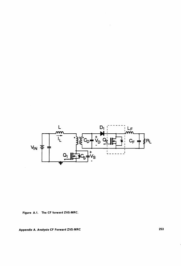
ee — we KM =
-
Ws
_SVYV\_
S if ot
Tt Q)
¢ {t y 2
Figure A.1. The CF forward ZVS-MRC.
Appendix A. Analysis CF Forward ZVS-MRC 253
A.1 DC Analysis
To simplify the analysis it is assumed that:
a) the output filter inductance is sufficiently large and can be approximated by a current
source with a value equal to the output current, /o;
b) the voltage drop across the conducting semiconductor switches (MOSFETs and diodes)
is negligible;
c) the switching times of the semiconductor switches are zero; and
d) the magnetizing inductance of the power transformer is large and can be represented by
an equivalent current source, /4y, whose magnitude depends on the operating condition
but is constant over one switching cycle.
To further simplify the analysis, the load current, /o, and the resonant capacitance, Cp, are
reflected to the primary side of the transformer. In addition, diode D, and transistor Qo are
replaced by a single-pole double-throw switch. The equivalent model of the simplified con-
verter is shown in Fig. A.2.
During one switching cycle, the converter goes through a sequence of five of the six possible
topological stages shown in Fig. A.3. The CF forward ZVS-MRC can operate in four different
modes, each representing a different sequence of topological stages. Modes II.A and II.B
occur for heavy load currents, whereas Modes I|.A and |.B occur for light output currents.
Appendix A. Analysis CF Forward ZVS-MRC 254
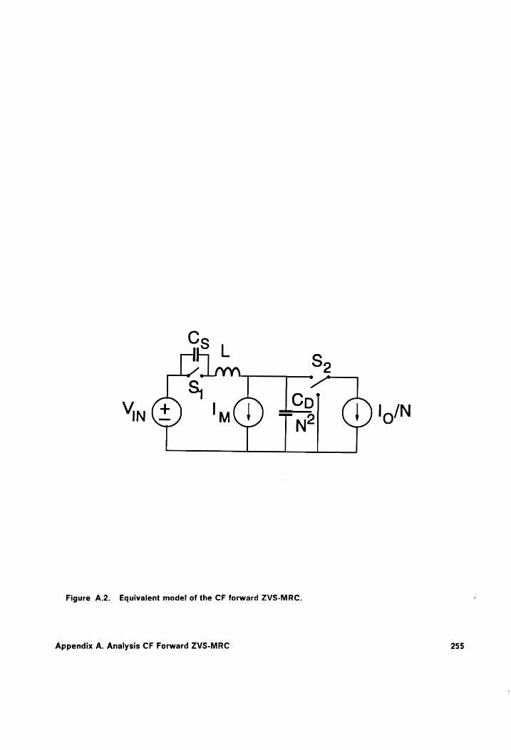
Figure A.2. Equivalent model of the CF forward ZVS-MRC.
Appendix A. Analysis CF Forward ZVS-MRC 255
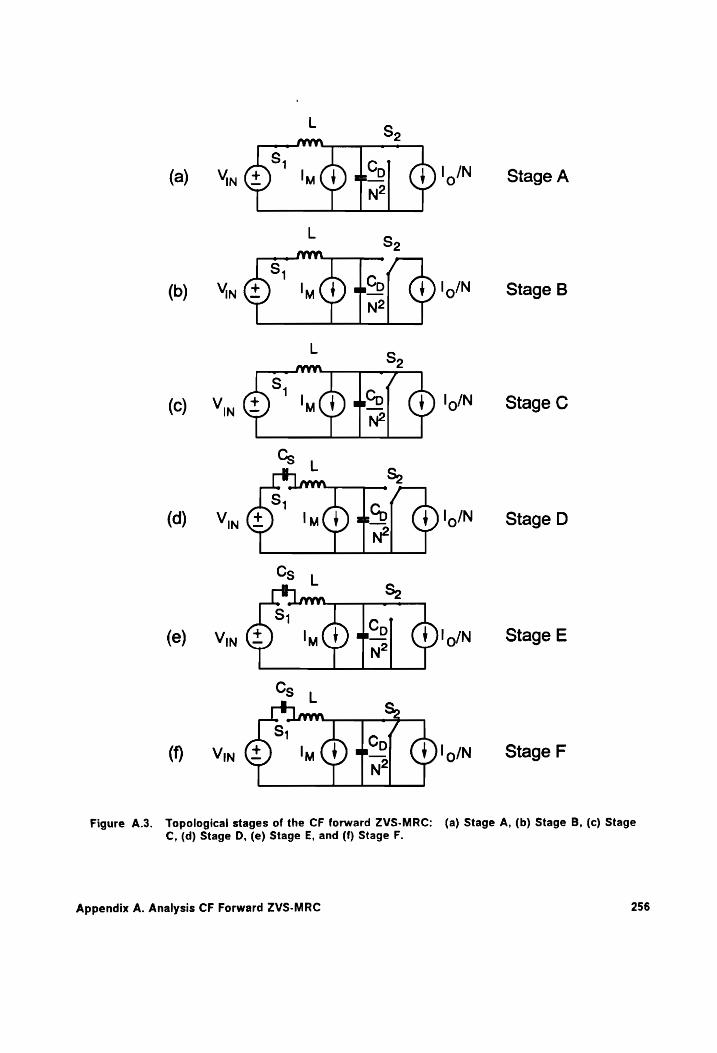
(a)
(b)
(c)
(d)
(f)
Figure A.3. Topological stages of the CF forward ZVS-MRC:
nm S2
S; C Vin IM mi IO/N
N2
L S
_rrm 2 S; Cp
N2
Ig/N
Vin Im(}) #20 Io/N N2
Cs L s
S4 V | BCD |_,/N IN M Ne O
Cy L
S1 Vv | Co lo/N IN M we o/
C, (d) Stage D, (e) Stage E, and (f) Stage F.
Appendix A. Analysis CF Forward ZVS-MRC
Stage A
Stage B
Stage C
Stage D
Stage E
Stage F
(a) Stage A, (b) Stage B, (c) Stage
256
A.2.1.1 Mode | of Operation
Mode I.A
The sequence of the topological stages in Mode |.A is A-B-C-A-E. Figure A.4 shows the key
waveforms of the CF forward ZVS-MRC in this mode of operation.
Stage A [To, 71], Fig. A.3(a)
During this stage transistor Q, and diode D, are conducting and transistor Qo is off. Voltage
Vp across Cp is positive and capacitance Cp and inductor L resonate until the voltage across
Qo reaches zero at time 7; and its antiparallel diode starts conducting. At the same time di-
ode D, turns off.
Stage B [7;, To], Fig.A.3(b)
Since the antiparallel diode of Qo is conducting, capacitance Cp continues to resonate with
L. This stage ends at time To when voltage Vp increases to zero and diode D, turns on. To
achieve lossless turn-on, Qo should be turned on during this stage.
Stage C [To2, T3], Fig. A.3(c)
Appendix A. Analysis CF Forward ZVS-MRC 257
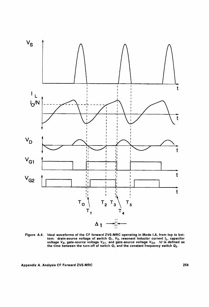
ar
¥
(
ww ¥
aww 1
wwe
—|
O
— _s
=
—|
N —|
@ —|
oO
Figure A.4. Ideal waveforms of the CF forward ZVS-MRC operating in Mode I|.A, from top to bot- tom: drain-source voltage of switch Q;, Vs, resonant inductor current /,, capacitor voltage Vp, gate-source voltage Vc;, and gate-source voltage Vg2. At is defined as the time between the turn-off of switch Q; and the constant frequency switch Qo.
Appendix A. Analysis CF Forward ZVS-MRC 258

In this stage D; and Qo conduct. As a result, voltage Vp is clamped to zero and the voltage
across resonant inductor L is Vjy. The resonant inductor current increases linearly until Qo
is turned off at time T3.
Stage A [T3, Ta], Fig. A.3(a)
Diode D, remains on and capacitance Cp and inductance L start to resonate. Voltage Vp in-
creases in a resonant manner. This stage ends at time T4, when Q, is turned off.
Stage E [T4, Ts], Fig. A.3(e)
Diode D; remains on, so capacitances Cp and Cs and inductance L resonate. This stage ends
at time 75, when voltage Vs returns to zero through a resonant oscillation. Transistor Q,
should be subsequently turned on to achieve lossless turn-on. The next cycle is then initiated.
From the preceeding explanation, it can be seen that the resonance of capacitance Cp is in-
terrupted for only a short interval, 73 — To. Switch Q; remains on during this interval and the
resonant inductor current increases linearly.
Mode I.B
The sequence of the topological stages in Mode |.B is A-B-C-F-E. Figure A.5 shows the key
waveforms of the CF forward ZVS-MRC in this mode of operation.
Stage A [To, 11], Fig. A.3(a)
Appendix A. Analysis CF Forward ZVS-MRC 253
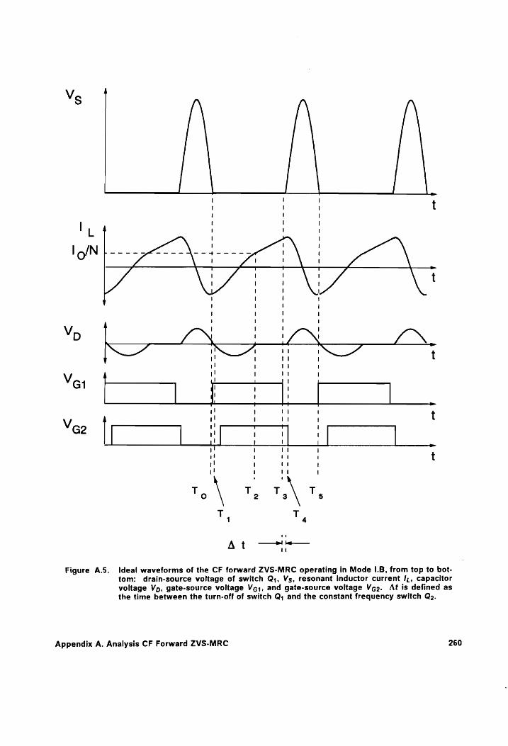
< on
eee
eee
wee
ee
vw
7
<
G)
NO
Figure A.5. Ideal waveforms of the CF forward ZVS-MRC operating in Mode I.B, from top to bot- tom: drain-source voltage of switch Q,;, Vs, resonant inductor current /,, capacitor voltage Vp, gate-source voltage Vc;, and gate-source voltage Vg2. At is defined as the time between the turn-off of switch Q; and the constant frequency switch Qo.
Appendix A. Analysis CF Forward ZVS-MRC 260

During this stage transistor Q, and diode D,; are conducting and transistor Qo is off. Voltage
Vp across Cp is positive, and capacitance Cp and inductor L resonate until the voltage across
Qo reaches zero at time 7, and the antiparallel diode of Qo starts conducting. At the same
time, diode D, turns off.
Stage B [7, T2], Fig. A.3(b)
Since the antiparallel diode of Qo is conducting. capacitance Cp continues to resonate with
L. This stage ends at time Tz when voltage Vp increases to zero, turning on diode D;. To
achieve lossless turn-on, Qz2 should be turned on during this stage.
Stage C [To2, T3], Fig. A.3(c)
In this stage D, and Q2 conduct. As a result, voltage Vp is clamped at zero and the voltage
across resonant inductor L is Vin. This stage ends at time T3 when switch Q, is turned off.
Stage F [Ts, Ta], Fig. A.3(f)
Diode D; remains on, switch Q, is off, and capacitance Cs and inductance L start to resonate.
Voltage Vs increases and the resonant inductor current increases in a resonant manner until
switch Qo is turned off at time T4.
Stage E [T4, Ts], Fig. A.3(e)
Appendix A. Analysis CF Forward ZVS-MRC 261

Diode D, is on, so capacitances Cs and Cp and inductance L resonate. This stage ends at
time Ts when voltage Vs returns to zero through a resonant oscillation. Transistor Q; should
be subsequently turned on to achieve lossless turn-on. The next cycle is then initiated.
This mode of operation is very similar to Mode I.A, the difference being that in Mode |.B the
resonance of capacitance Cp is interrupted for a longer time, resulting in switch Qg being
turned off after switch Q, is turned off.
A.2.1.2 Mode Il of Operation
In Mode | of operation capacitor voltage Vp is positive at the turn-off time of switch Q,. In
Mode II of operation capacitor voltage Vp is negative at the turn-off time of switch Q,. As long
as Capacitor voltage Vp is negative, the forward diode Dy, is off and the load current freewheels
through the antiparallel diode of switch Qo.
Mode Il.A
The sequence of the topological stages in Mode II.A is B-C-A-E-D. Figure A.6 shows the key
waveforms of the CF forward ZVS-MRC in this mode of operation.
Stage B [To, 71], Fig. A.3(b)
Appendix A. Analysis CF Forward ZVS-MRC 262
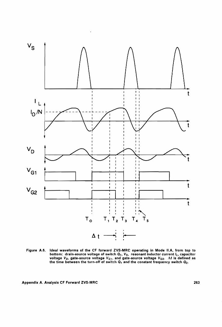
i t
- ‘
> —
eae eae
ele
)
’ 1
! I
' 4 I
' | Lo ! Ver — ! bb 4 |
t vo | 4 t
j I | 1 14
Veo JO
! Py t PEE EIN
To T,17, 7, T, Ts
— At -—
Figure A.6. Ideal waveforms of the CF forward ZVS-MRC operating in Mode II.A, from top to bottom: drain-source voltage of switch Q;, Vs, resonant inductor current !/,, capacitor voltage Vp, gate-source voltage Vc;, and gate-source voltage Vg. At is defined as the time between the turn-off of switch Q, and the constant frequency switch Qo.
Appendix A. Analysis CF Forward ZVS-MRC 263

Since the antiparallel diode of Q2 is conducting, capacitance Cp resonates with L. This stage
ends at time 7, when voltage Vp increases to zero, turning on diode D,;. To eliminate the
turn-on loss, Qz should be turned on during this stage.
Stage C [7}, To], Fig. A.3(c)
In this stage D, and Qo conduct. As a result. voltage Vp is clamped at zero and the voltage
across resonant inductor L is Viy. The resonant inductor current increases linearly until Qo
is turned off at time To.
Stage A [T2, T3], Fig. A.3(a)
Diode D; remains on and capacitance Cp and inductance L start to resonate. Voltage Vp in
creases in a resonant manner. This stage ends at time 73, when Q, is turned off.
Stage E [T3, T4], Fig. A.3(d)
Diode D; remains on and capacitances Cs and Cp resonate with inductance L. This stage
ends at time 74, when voltage Vp decreases to zero through a resonant oscillation and forward
diode D, turns off.
Stage D [Ts, Ts], Fig. A.3(e)
During this stage the antiparallel diode of switch Qz conducts and diode D, is off. Voltage
Vp across Cp is negative and capacitance Cs and Cp resonate with inductor L until the voltage
Appendix A. Analysis CF Forward ZVS-MRC 264

across Q, reaches zero at time Ts and the antiparallel diode of Q, starts conducting. Q,
should be subsequently turned on to achieve lossless turn-on. The next cycle is then initiated.
Mode II.B
The sequence of the topological stages in Mode II.B is B-C-F-D-E. Figure A.7 shows the key
waveforms of the CF forward ZVS-MRC in this mode of operation.
Stage B [To, 7], Fig. A.3(b)
Since the antiparallel diode of Qz is conducting. capacitance Cp resonates with L. This stage
ends at time 7, when voltage Vp increases to zero, turning on diode D,. To achieve lossless
turn-on, Q2 should be turned on during this stage.
Stage C [71, To], Fig. A.3(c)
In this stage Dy, and Qo conduct. As a result. voltage Vp is clamped to zero and the voltage
across resonant inductor L is Vijy. The resonant inductor current increases linearly until Q,
is turned off at time To.
Stage F [To2, T3], Fig. A.3(f)
Diode D, and switch Q2 remain on and voltage Vp remains clamped to zero. Voltage Vs in
creases in a resonant manner. This stage ends at time 74, when Qo is turned off.
Appendix A. Analysis CF Forward ZVS-MRC 265
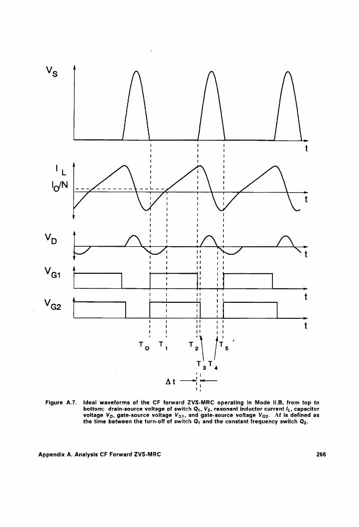
vw ¥
Figure A.7. Ideal waveforms of the CF forward ZVS-MRC operating in Mode II.B, from top to bottom: drain-source voltage of switch Q;, Vs, resonant inductor current /,, capacitor voltage Vp, gate-source voltage Vcg;, and gate-source voltage Vg2. At is defined as the time between the turn-off of switch Q; and the constant frequency switch Qo.
Appendix A. Analysis CF Forward ZVS-MRC 266
Stage E [T3, Ta], Fig. A.3(e)
Diode D, remains on and capacitances Cs and Cp and inductance L resonate. Capacitor
voltage Vp increases in a resonant manner. This stage ends at time 75 when voltage Vp res-
onates back to zero turning diode D;, off and forcing the antiparallel diode of switch Qo on.
Transistor Qo should be subsequently turned on to achieve soft switching.
Stage D [T4, Ts], Fig. A.3(d)
During this stage voltage Vp across Cp is negative and the antiparallel diode of switch Qo
conducts. Capacitances Cp and Cs resonate with the resonant inductor L. This stage ends
at time time 75 when the voltage across switch Q; resonates back to zero. Switch Q, should
be turned on soon after to achieve lossless turn-on, initiating a new switching cycle.
The difference between Mode II.A and Mode II.B is similar to the one described between
modes |.A and I.B; in Mode II.B switch Qo is turned off after switch Q, is already off.
The sequence of the four modes of operation are summarized in Table A.1.
Appendix A. Analysis CF Forward ZVS-MRC 267
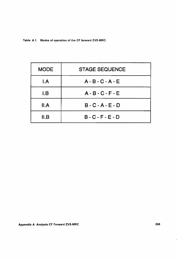
Table A.1. Modes of operation of the CF forward ZVS-MRC.
MODE STAGE SEQUENCE
ILA A-B-C-A-E
I.B A-B-C-F-E
ILA B-C-A-E-D
.B B-C-F-E-D
Appendix A. Analysis CF Forward ZVS-MRC 268
A.2 DC Voltage-Conversion-Ratio
Figures A.8a - A.15a show the typical dc voltage-conversion-ratio characteristics of the CF
forward ZVS-MRC as a function of 6. 6 is defined as the time between the turn-off of the CF
switch Qa and the turn-off of primary switch Q,; (Af in Fig. A.4) normalized with respect to
1/fo, where fo = 1/2n/LCs is the resonant frequency. The characteristics are given for dif-
ferent normalized switching frequencies f,/fo and different effective resonant capacitance ratio
Cn = Cpj](CsN2), where N is the turns ratio of the transformer. The running parameter in Figs.
A.8a - A.15c is the normalized output current Jon = Zolo/NVin, where Zo=VJLI/Cs is the
characteristic impedance of the power stage.
A complete set of design characteristics is given for Cy = 2, 3, 5, and 7, and fs/fo = 0.55, 0.6,
0.65, and 0.8 (Figs. A.8a - A.15c). Characteristics for all possible combinations are not given
since not all possible combinations result in practical design curves. For example, low
capacitance ratios (Cy = 2) and low switching frequencies (fs/fo < 0.8) will result in large
conduction times of the CF switch (high conduction losses) for all values of /oy. Therefore, this
characteristics will not provide an efficient design. Similarly, high capacitance ratios (Cy =
7) and high switching frequencies (fs/fo > 0.6) result in dc voltage conversion ratio charac-
teristics with M < 0.3. Again, this characteristics will not result in a practical design.
Appendix A. Analysis CF Forward ZVS-MRC 269

A.3 DC Analysis of the Topological Stages
The following section contains the mathematical derivations pertaining to the different
topological stages resulting from the forward ZVS-MRC operating at a constant switching fre-
quency. Analytical expressions for the initial conditions, circuit equations, their solutions, and
durations of the topological stages for the ideal CF forward ZVS-MRC are presented.
STAGE A [Tao, Tat] (Fig. A.16)
Initial Conditions:
Vs(T ao) = 0
A Vp(Tao) = Vo
A (Tao) ="
Equations:
di, (f) at + v/(o) = Vin
. dvp(t) i _ Coat = lo + Iw
Appendix A. Analysis CF Forward ZVS-MRC
(A.1.a)
(A.1.b)
(A.1.c)
(A.2.a)
(A.2.b)
270
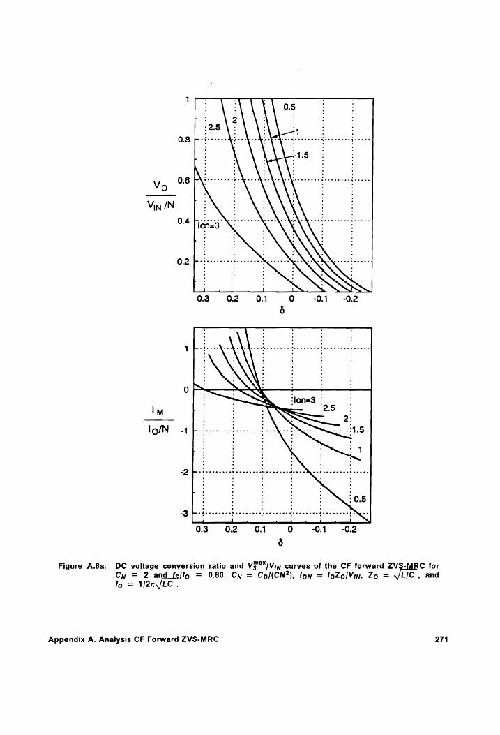
0.8
Vo 0.6
Vin /N 0.4
0.2
1 fe he nw ae As be ce ete eee ne eee wea bee wccnne Baweee
0 , , ‘lon=3 : ‘
ry } 7 ; Poo Ud VRE 2:
lo/N eT fp rieeee ee eebe eee te QL TL 1.5-
: 4
22 Pobeereeetber tethered teers beoees
: 0.5 -3 be obec ececes ‘ ee ceca ces ccc ccc clone ecces Baewcncee 4
i _| l i i Jt
0.3 0.2 0.1 0 -0.1 -0.2
$
Figure A.8a. DC voltage conversion ratio and Vs'*"/Vjy curves of the CF forward ZVS-MRC for Cy = 2 and_fs/fo = 0.80. Cy = Co/(CN2), lon = loZo/Vin, Zo = VL/C , and fo = Aj2nJLe .
Appendix A. Analysis CF Forward ZVS-MRC 271
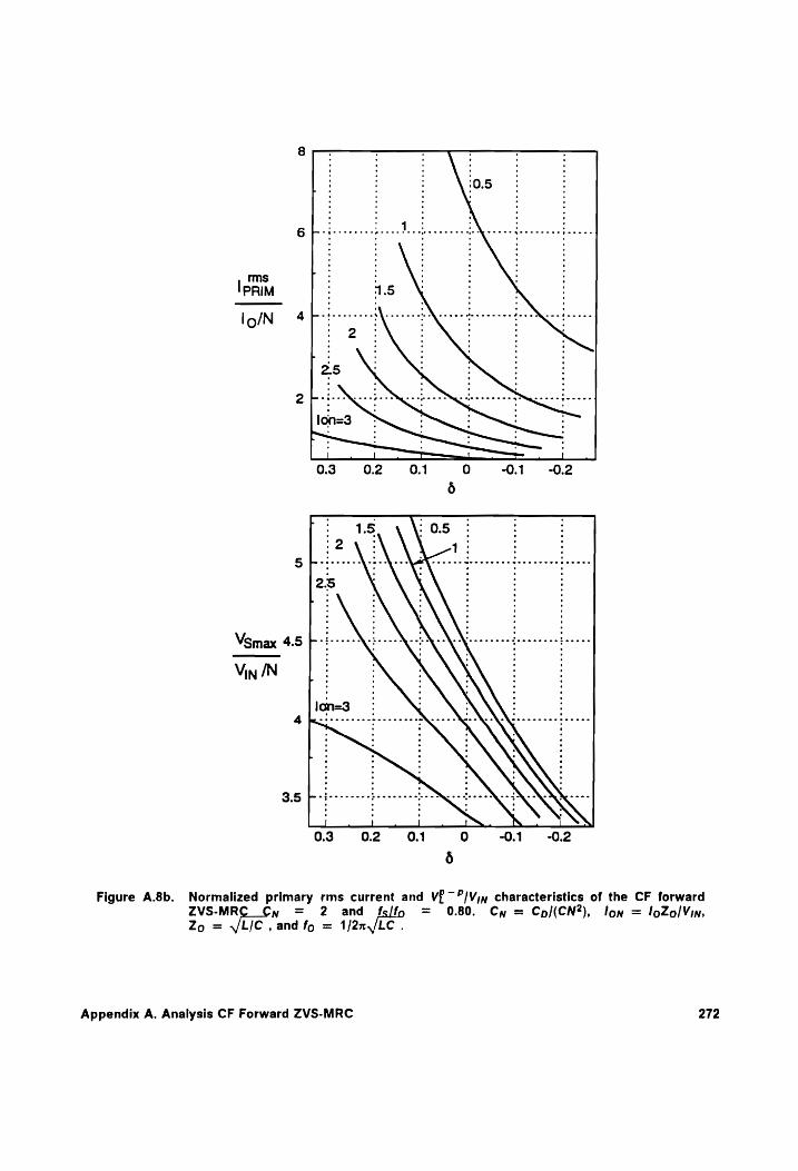
l ms
PRIM
lo/N
Vsmax 4.5
Vin IN
Figure A.8b. Normalized primary rms current and VP~?/Vjwy characteristics of the CF forward
ZVS-MRC_Cy = 2 and fs/fp = 0.80. Cy = Cp/(CN2), low = loZo/Vin, Zo = VL/C , and fo = 1/2x/LC .
Appendix A. Analysis CF Forward ZVS-MRC 272
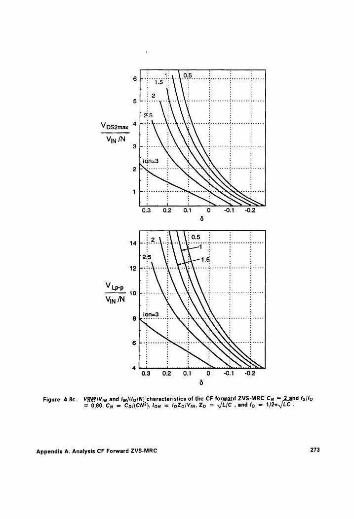
Figure A.8c. VB5¥xX/Vin and Iy/(lo/N) characteristics of the CF fo d ZVS-MRC Cy = 2.and fs/fo
= 0.80. Cy = Co/(CN?), lon = loZo/Vin, Zo = ‘Lie ,and fo = 1/2z/LC .
Appendix A. Analysis CF Forward ZVS-MRC 273
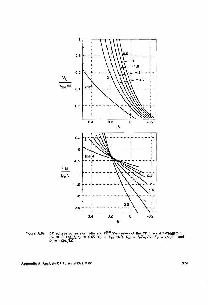
05 PENNA prtecereesecedeas
°F SY lons ,
O57 eeeee pe ween cwcecce ; “AN Ng Ct te see cee ewe nestene
IM ——— 1 bem cee emer cere cee ccc cme eo eh es em oo me
lo/N | 2.5
-1.5 i fem cree eee ye Bee ee Meee ence 2:
PF 1:5 wD sce edecseceeeeeeeecheseeeeeee Qader Qieeeeeees bee
Po 25 ee OS) \:
ij = | l
0.4 0.2 0 -0.2
Figure A.9a. DC voltage conversion ratio and Vs'*/Vin curves of the CF forward ZVS-MRC for Cn = 3 and fs/fo = 0.65. Cy = Co/(CN2), lon = loZolViw, Zo = VL/C , and fo = 1/2n/LC .
Appendix A. Analysis CF Forward ZVS-MRC 274
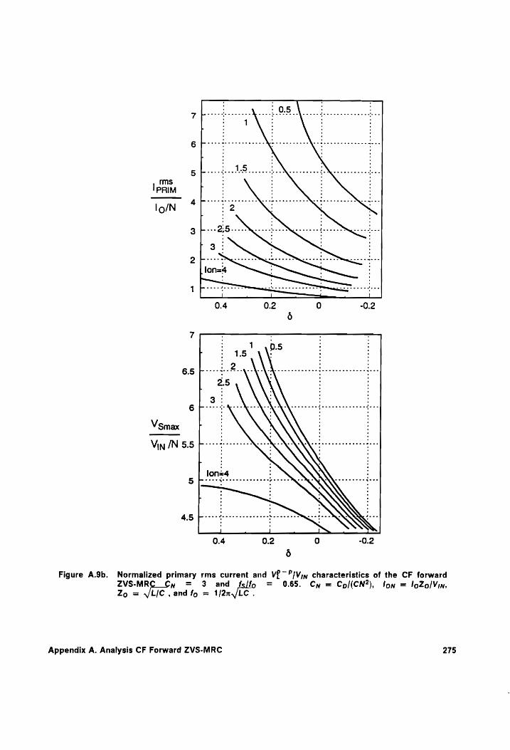
ms
PRIM
lo/N
6.5
Vmax
Vin /N 5.5
Figure A.9b. Normalized primary rms current and VP~?/Viy characteristics of the CF forward ZVS-MR n = 3 and fe/f = 0.65. Cy = Cp/(CN2), lon = loZo/Vin,
Zo = VL/C , and fo = 1/2x,/LC .
Appendix A. Analysis CF Forward ZVS-MRC 275
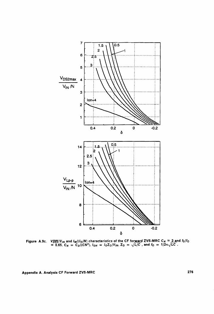
Figure A.9c. VB@¥/Vin and Iy/(lo/N) characteristics of the CF fo ZVS-MRC Cy = 3.and fs/fo
= 0.65.Cy = Cp/(CN?2), lon = loZolVin, Zo = Lic ,and fo = 1/2x./LC .
Appendix A. Analysis CF Forward ZVS-MRC 276
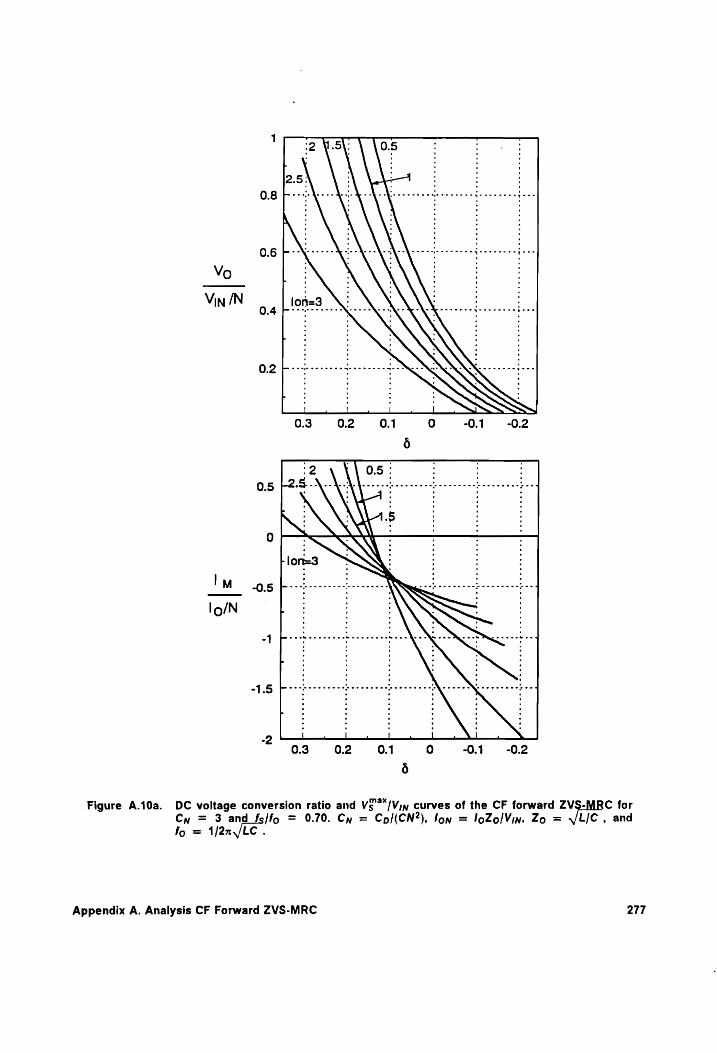
Figure A.10a. DC voltage conversion ratio and Vs'"*/V)w curves of the CF forward ZVS-MRC for
Cy = 3 and_fs/fo = 0.70. Cy = Co/(CN2), lon = loZolVin, Zo = VL/C , and fo = 1/2n/LC .
Appendix A. Analysis CF Forward ZVS-MRC 277
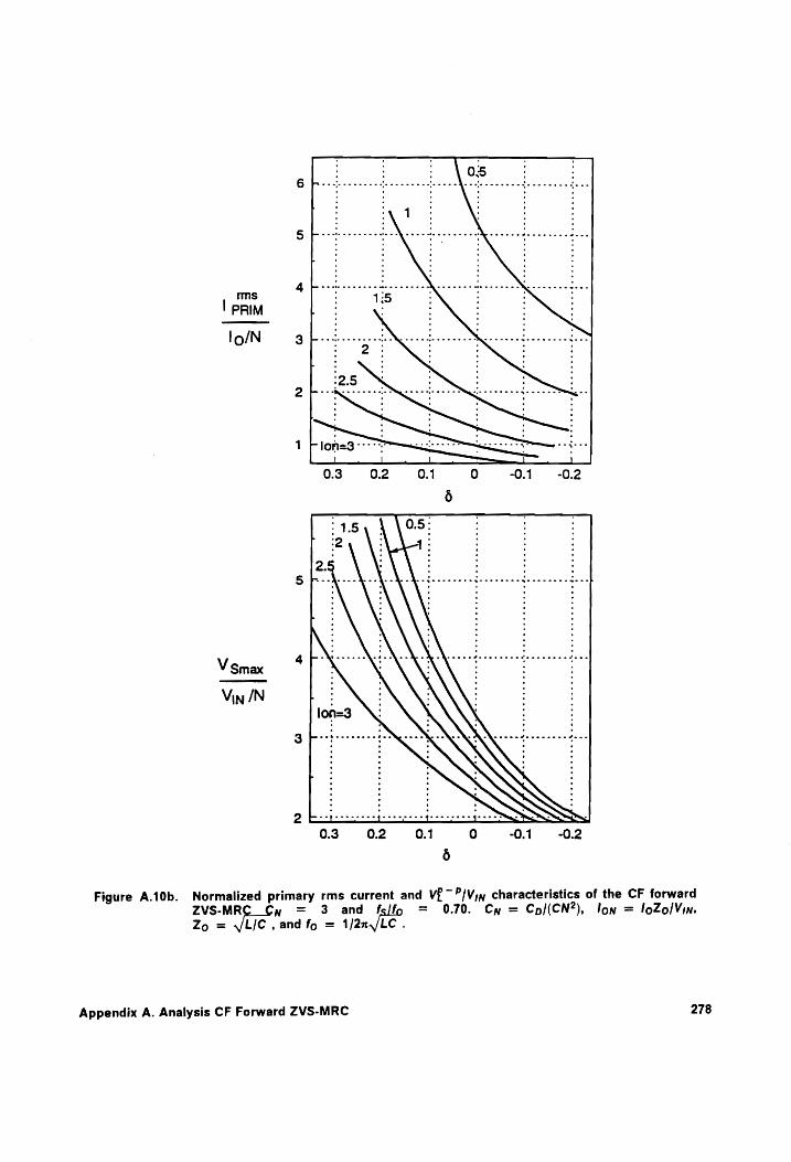
ms
| PRIM
lo/N
V smax
Vin /N
Figure A.10b. Normalized primary rms current and VP -°/Vy characteristics of the CF forward
ZVS-MR n = 3 and felfpo = 0.70. Cy = Co/(CN?), lon = loZolVin, Zo = Lic , and fo = 1/2x ic.
Appendix A. Analysis CF Forward ZVS-MRC 278
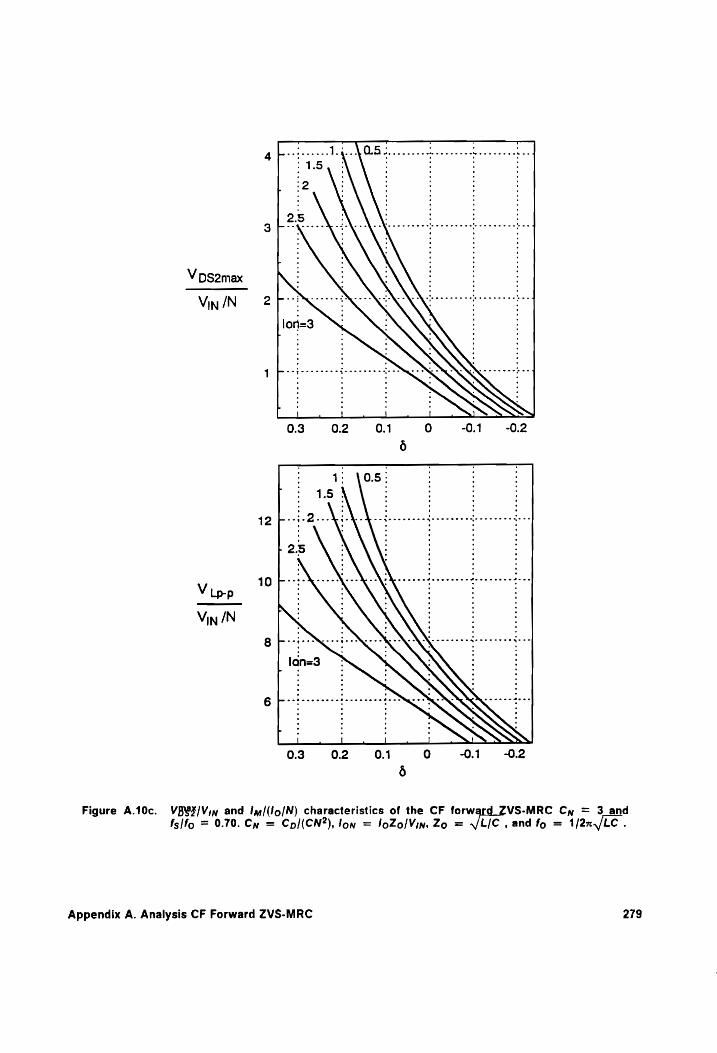
V ps2max
Vin /N
Figure A.10c. VBPX/Viny and Iy/(lo/N) characteristics of the CF forw VS-MRC Cy = 3_and
fslfo = 0.70. Cn = Cp/(CN?2), lon = loZolVin, Zo = Lic , and fo = 1/2x,/LC .
Appendix A. Analysis CF Forward ZVS-MRC 279
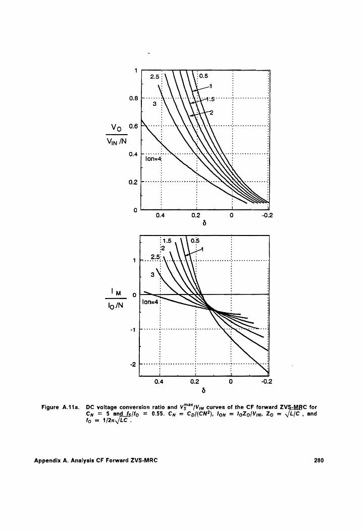
Figure A.11a. DC voltage conversion ratio and Vs'°"/Viy curves of the CF forward ZVS-MRC for
Cn = 5 and_fs/fo = 0.55. Cy = Co/(CN?), lon = IoZo/Vin, Zo = VL/C , and fo = 1/2nJLC -
Appendix A. Analysis CF Forward ZVS-MRC 280
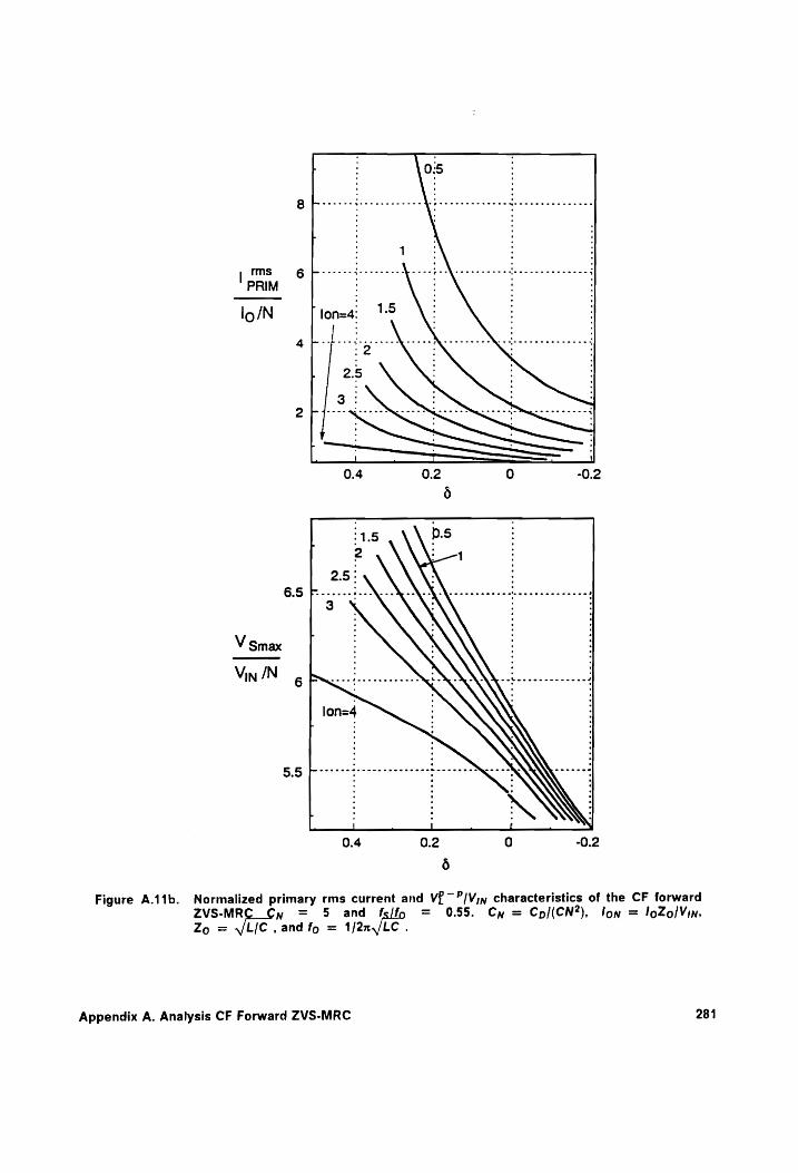
| ms
PRIM
lo/N
V smax
Figure A.11b. Normalized primary rms current and VP~?/Vw characteristics of the CF forward
ZVS-MR nN = 5 and Ke = 0.555. Cy = Cp/(CN?), lon = loZolVin,
Zo = VL/C , and fo = 1/2x/LC .
Appendix A. Analysis CF Forward ZVS-MRC 281
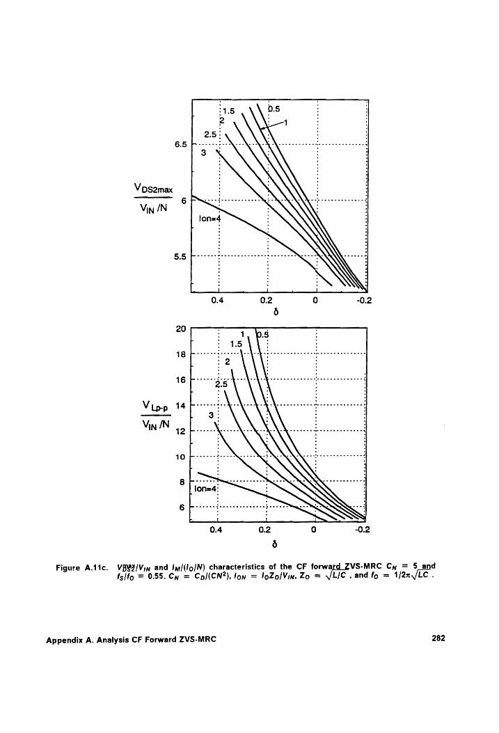
V ps2max
Figure A.1ic. VBex/Viy and Iq/(lo/N) characteristics of the CF forw VS-MRC Cy = 5_and
fs/fo = 0.55. Cy = Co/(CN2), lon = loZolVin, Zo = VLIC , and fo = 1/2x./LC .
Appendix A. Analysis CF Forward ZVS-MRC 282
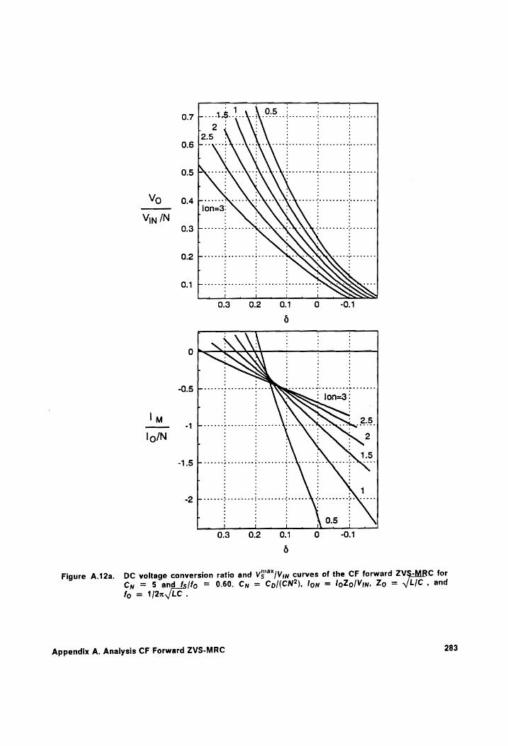
Im
lo/N
)
Figure A.12a. DC voltage conversion ratio and Vs'”"/Viw curves of the CF forward ZVS-MRC for
Cy = 5 and fs/fo = 0.60. Cy = Cyo/(CN2), lon = loZo/Vin. Zo = VLIC , and
fo = 1/2x,/LC .
Appendix A. Analysis CF Forward ZVS-MRC 283
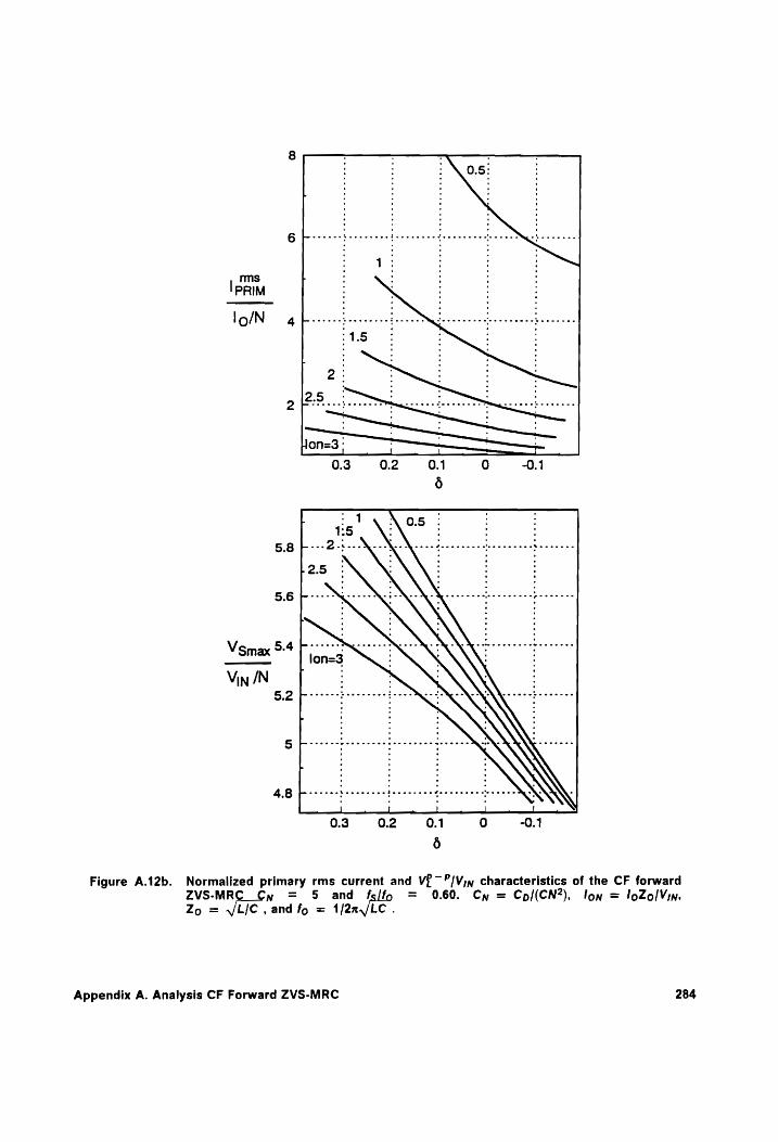
ms
PRIM
lo/N
0.3 0.2 0.1 0 -0.1
5.8
5.6
Vin /N 5.2
4.8
Figure A.12b. Normalized primary rms current and V{~ °/V;y characteristics of the CF forward ZVS-MR n = 5 and feff, = 060. Cy = Cp/(CN?2), lon = loZolVin,
Zo = VLIC , and fo = 1/2x,/LC .
Appendix A. Analysis CF Forward ZVS-MRC 284
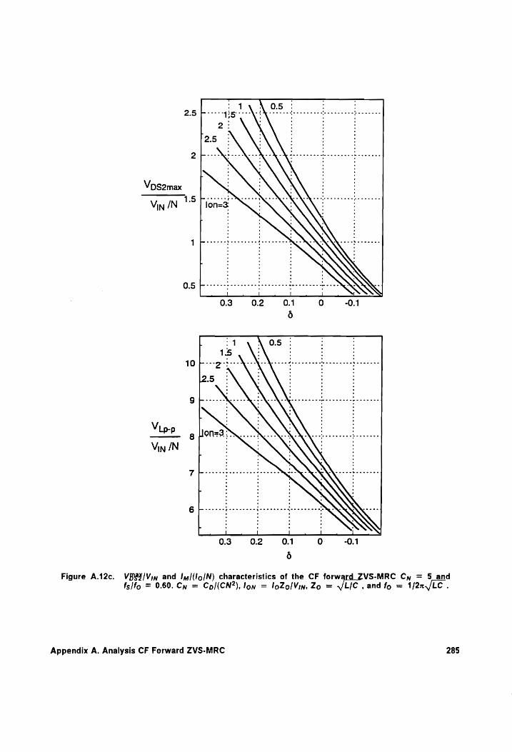
2.5
Vps2max
Vin IN 1?
0.5
Vin /N
Figure A.12c. VB@X/Viy and Im/(lo/N) characteristics of the CF forw VS-MRC Cy = 5_and
fs}fo = 0.60. Cy = Co/(CN2), lon = loZolVin, Zo = VLIC , and fo = 1/22x./LC .
Appendix A. Analysis CF Forward ZVS-MRC 285
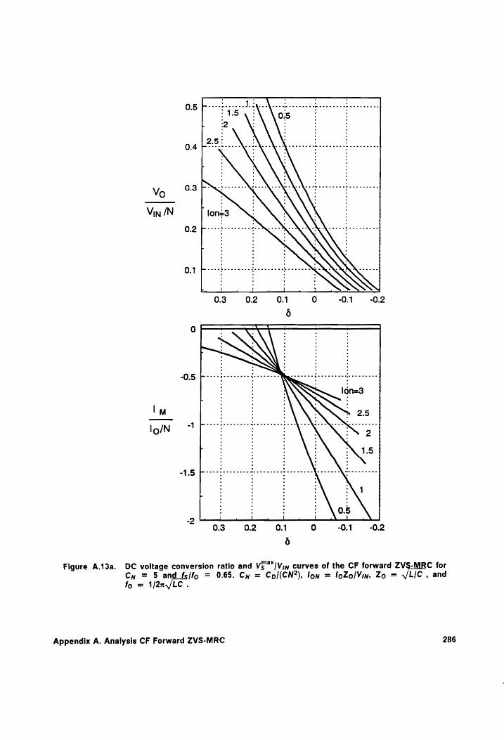
0 J —
-0.5 pe ccs gcc cccces moc c ces Rie ccc eee feereeeeed coer escces
lon=3
lm 2.5 lo/N MLD rere t cece cece nec e cece eee eee ieee Nee eee 3 .-
F 1.5
01.5 Perec te reece rece cet cece et eee ce reece cee eens ee eee
“\1
0.5 2 | ,_ | _. 1 | _ \ ‘
03 O2 #40. 0 0.1 -0.2
6
Figure A.13a. DC voltage conversion ratio and Vs /V;y curves of the CF forward ZVS-MRC for Cy = 5 and _fs/fo = 0.65. Cy = Cp/(CN2), lon = loZolVin. Zo = VLIC, and
fo = A/2n,/LC .
Appendix A. Analysis CF Forward ZVS-MRC 286
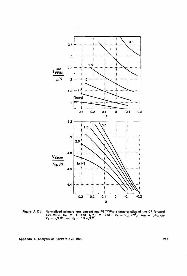
rms
| PRIM
lo/N
V Smax
Vin /N
Figure A.13b. Normalized primary rms current and Vf ~°/V;, characteristics of the CF forward
ZVS-MRC_Cy = 5 and felfo = 0.65. Cy = Cy/(CN2), low = loZolVw, Zo = s/LIC , and fo = 1/2n/LC .
Appendix A. Analysis CF Forward ZVS-MRC 287
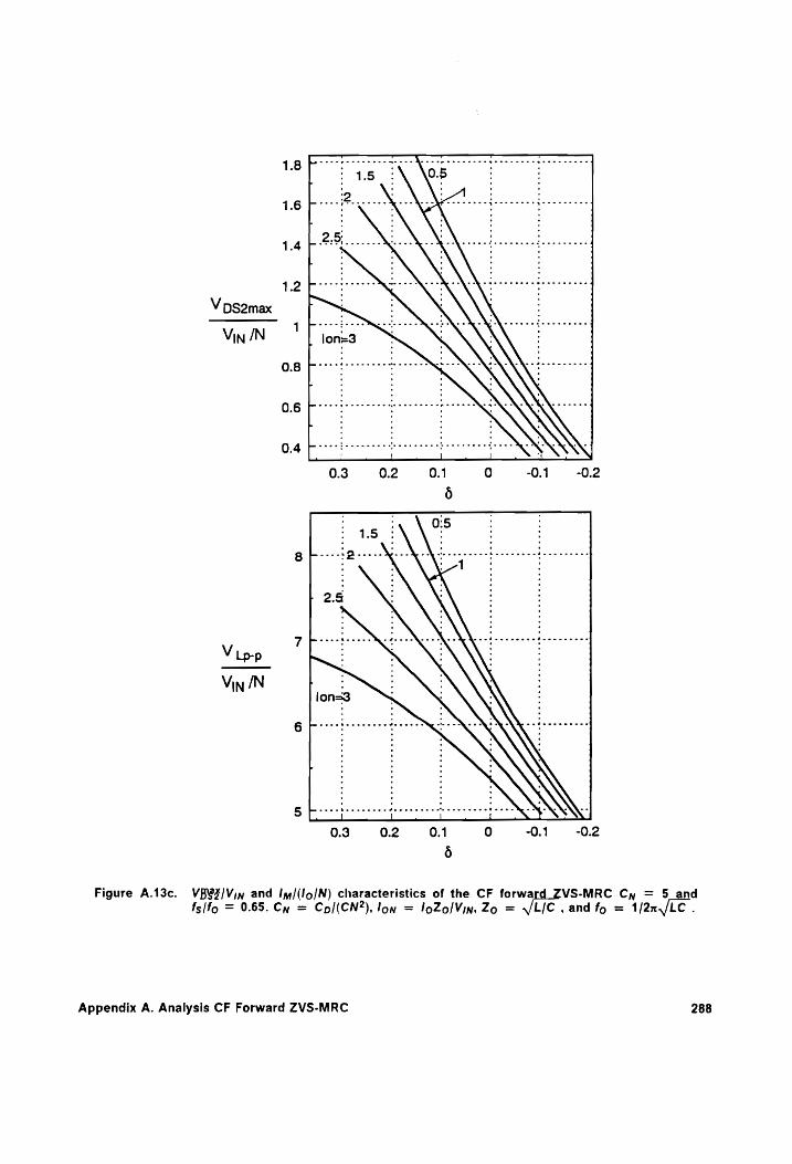
V ps2max
Vin /N
Vip-p Vin IN
Figure A.13c. VB@X/Vin and Iy/([o/N) characteristics of the CF forward_ZVS-MRC Cy = 5_and
fs/fo = 0.65. Cy = Cp/(CN2), lon = loZolVin, Zo = JLIC , and fo = 1/2n/LC .
Appendix A. Analysis CF Forward ZVS-MRC 288
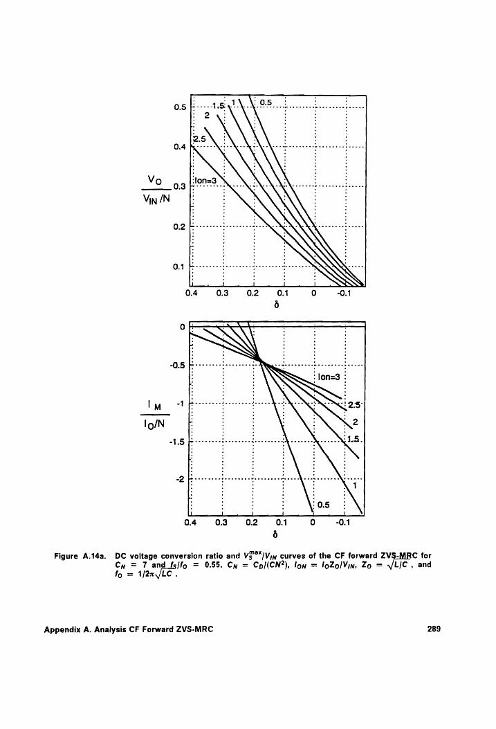
deere ener a, ai al an al a
0.4 0.3 0.2 0.1 0 -0.1
6
0 ‘ ao \ jj
5 Pere dee Accent : : : lon=
[ M -1 + wrrteees Presecses Doses apes yee NT: ‘235
lo/N r 2
“1.5 beeeeeee Seeeeeene Seeeeaeweddboeseees Meee? 1.5
lp [besseesssdecscnseeteceseees NL. 1
E (05: ft | __ | __ |
0.4 0.3 0.2 0.1 0 -0.1
6
Figure A.14a. DC voltage conversion ratio and Vs"”/Vjy curves of the CF forward ZVS-MRC for Cy = 7 and_fs/fo = 0.55. Cy = Cp/(CN2), lon = loZo/lVin, Zo = Lic , and
fo = 1/2x/LC .
Appendix A. Analysis CF Forward ZVS-MRC 289
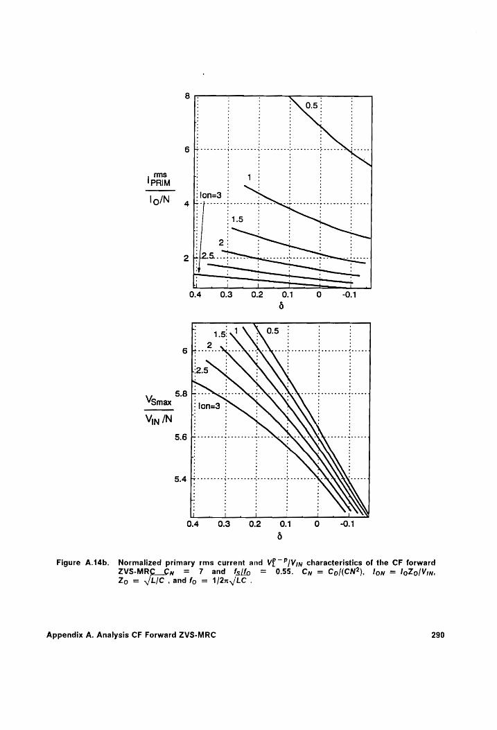
ms
|PRIM
lo/N
5.8 Vmax
Vin /N
5.6 |
5.45 Figure A.14b. Normalized primary rms current and VP~°/V;, characteristics of the CF forward
ZVS-MR n = 7 and fs[fpo = 0.55. Cy = Cp/(CN2), lon = loZolVin,
Zo = VJLIC and fo = 1/2n,/LC .
Appendix A. Analysis CF Forward ZVS-MRC 290
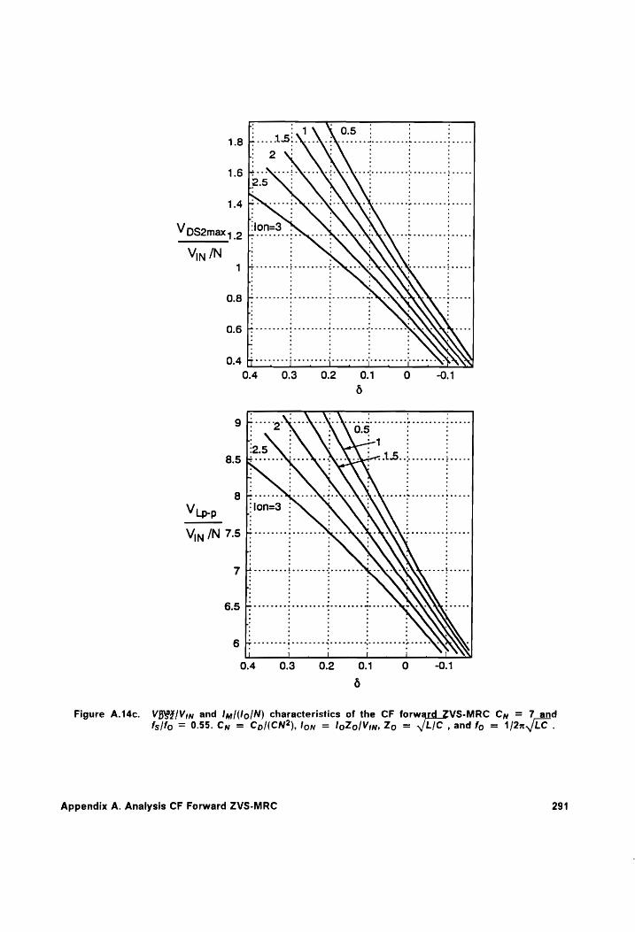
138f
1.6
1.45
Vps2max 2
Vin /N
0.8 §
0.6 F
Vipp Vin /N 7.5 F
L:
Figure A.14c. VB@F/Viy and Iy/(/o/N) characteristics of the CF forw VS-MRC Cy = 7_and fslfo = 0.55. Cy = Cp/(CN2), lon = loZo/Vin, Zo = V/LIC , and fo = 1/2x,/LC .
Appendix A. Analysis CF Forward ZVS-MRC 291
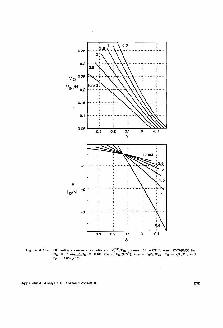
0.35
0.3
V 0 0.25
Vin /N 02
0.15
0.1 0.05
-1 bee se cees : ew eworeee werteeeeeedl ees a oe oclseeeee
: : . : 2
Figure A.15a. DC voltage conversion ratio and Vs'""/V;y curves of the CF forward ZVS-MRC for
Cy = 7 and_fs/fo = 0.60. Cy = Cp/(CN2), lon = loZo/Vin, Zo = VLIC , and fo = 1/2n./LC .
Appendix A. Analysis CF Forward ZVS-MRC 292
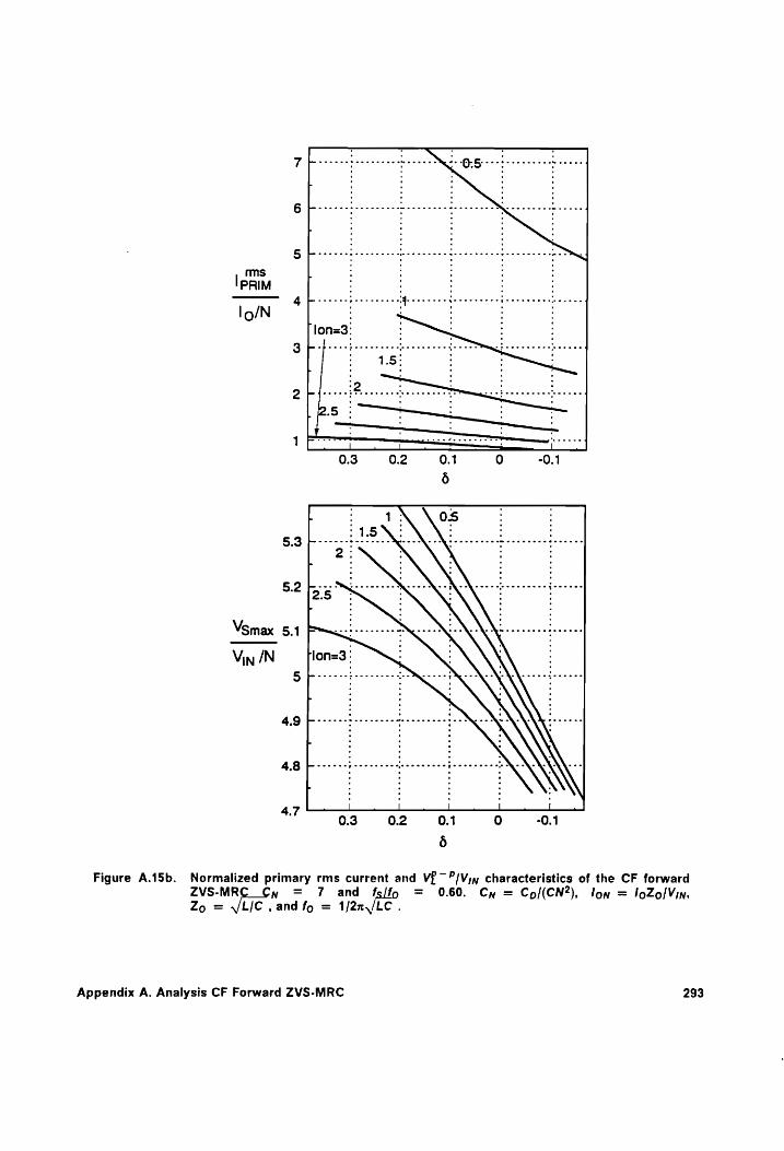
ms
lPRIM
lo/N
Vsmax 5.1
Vin /N
Figure A.15b. Normalized primary rms current and VP ?/V;y characteristics of the CF forward
ZVS-MR nN = 7 and fs/fp = 0.60. Cy = Co/(CN2), low = loZo/lVn, Zo = Lic , and fo = 1/2n Lc.
Appendix A. Analysis CF Forward ZVS-MRC 293
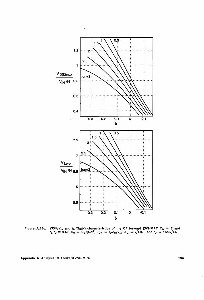
1.2
V ps2max
VIN IN 0.8
0.6
0.4
7.5
Vip-p
Vin /N 6.5
5.5 Figure A.15c. VB@X/Vin and In/(lo/N) characteristics of the CF forwa VS-MRC Cy = 7_and
fs {fo = 0.60. Cy = Cp/(CN?), lon = loZolVin, Zo = Lic , and fo = 1/2n,/LC .
Appendix A. Analysis CF Forward ZVS-MRC 294
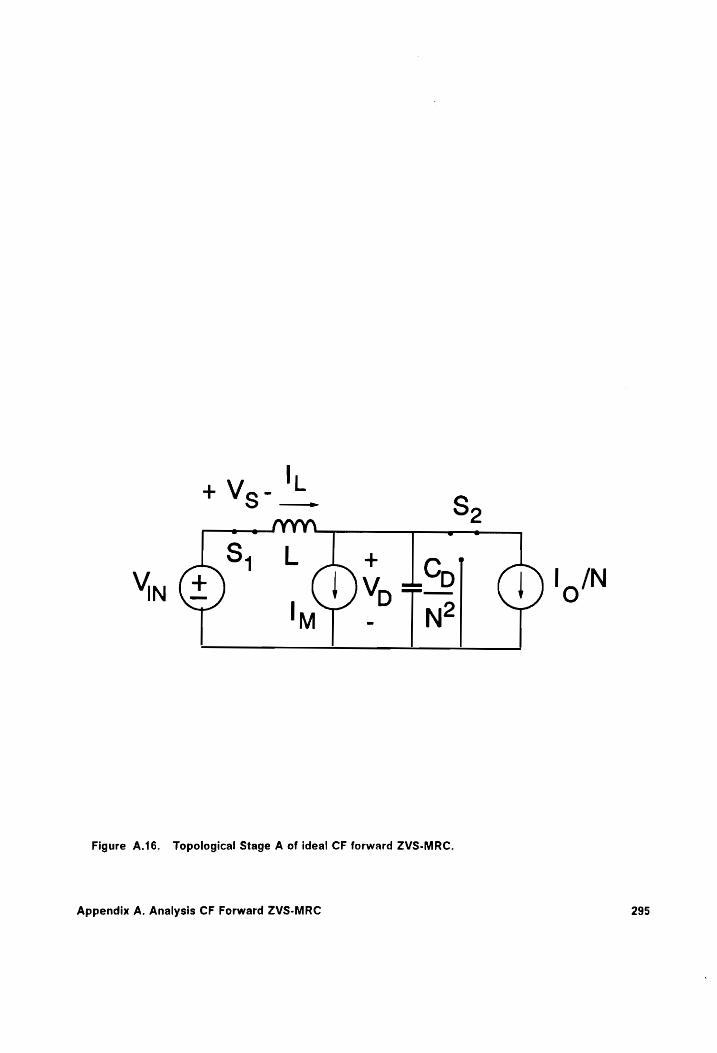
Figure A.16. Topological Stage A of ideal CF forward ZVS-MRC.
Appendix A. Analysis CF Forward ZVS-MRC 295

From Eqs. (A.1.a) - (A.2.b). it follows that:
d’vp(t) Nn? Nn? a) + LCp v(t) = LCp Vin (A.3.a)
where the following parameters are defined as:
1 Oo =->——= (A.3.b)
V/LCs
C Cy=— (A.3.c)
CoN
= {4 Zo= Ce (A.3.d)
Zp= [5 (A.3.e) Cp/N
and
CN? a3
It should be noted that Cp/(N)? represents the capacitance of the CF switch and the free-
wheeling diode reflected into the primary. Therefore, Cy is the ratio between the total re-
flected secondary side capacitance and the primary switch capacitance Cs.
Appendix A. Analysis CF Forward ZVS-MRC 296

Solution:
A Vp = 4, COS moKt + by Sin woKt + Vin (A.4.a)
A Cp Cp i, = Damok —z COS moKt — agnoK —>z sin wmoKt+lot ly (A.4.b)
N N
where
A aa = Vp —_ Vin (A.5.a)
A ba=Zp(l, — lo — ly) (A.5.b)
Initial conditions in and vA are determined from Stages C (Eq. (A.17)) and E (Eqs. (A.29a) and
{(A.29.b)) which preceede Stage A.
Voltages are normalized with respect to Vj. currents with respect to /o/N, and time with re-
spect to 1/fo (fo = wo/2n); Eqs. (A.4.a) and (A.4.b) then respectively become:
AN AN AN Vp = (Vp _ 1) cos anKty + K[I, _ In _ 1Vlon sin 27Kty, + 1 (A.6.a)
AN AN AN [YD -1] . i =14+lyn~t+ Ue — In — 1) cos 2nKkty — Klon sin 2nKty (A.6.b)
Appendix A. Analysis CF Forward ZVS-MRC 297

Stage Duration T, = Tai — Tao
The stage duration T, is determined from the following condition if the next stage is Stage B:
Vp(T,) = 9 (A.7)
but if the next stage is Stage E, then stage duration T, is determined from the turn-off of the
primary switch capacitance. In both cases, it is necessary to solve a transcendental equation
to determine the stage duration.
STAGE B [Tgo, Ts1] (Fig. A.17)
Initial Conditions:
Vs(Tg0) = 0 (A.8.a)
B
i(Tpo) =I (A.8.c)
Equations:
Appendix A. Analysis CF Forward ZVS-MRC 298
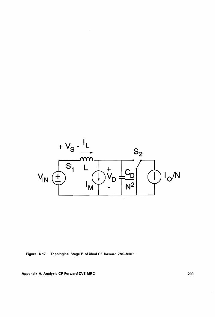
Figure A.17. Topological Stage B of ideal CF forward ZVS-MRC.
Appendix A. Analysis CF Forward ZVS-MRC 299

di, (t) rT + Vp(t) = Vin
dvp(t) I(t) — Cp —— = Io
From Eqs. (A.9.a) and (A.9.b), it follows that:
2 d°vp(t) =n? N?
dt? + LCp vp(t) _ LCp Vin
Solution:
B . Vp = 4g COS WOK + bg SIN WOKE + Vin,
B Cp Co i, = bgwoK —Z Cos woKt — aginoKk —> sin moKt + ly
N N
where
B ag = Vp — Vin
B bg =Zp(l, — I)
or in the normalized form:
Appendix A. Analysis CF Forward ZVS-MRC
(A.9.a)
(A.9.b)
(A.10.a)
(A.11.a)
(A.11.b)
(A.12.a)
(A.12.b)
300

BN BN BN Vp = (Vp _ 1) cos anKty + KU. _ lunJion sin anKty +14
[Vp —1] Klon sin 2nKty
BN BN A = In + Ch, — lyn] cos 2nKty —
Stage Duration Tg = Tg1 — Tgo
The stage duration 7g is determined from the following condition:
Vp(T pg) = 0
STAGE C [Tco, Tc1] (Fig. A.18)
Initial Conditions:
Vs(Tco) = 0
Vo(Tco) = 9
C i(Teo) = hr
Equations:
Appendix A. Analysis CF Forward ZVS-MRC
(A.13.a)
(A.13.b)
(A.14)
(A.15.a)
(A.15.b)
(A.15.c)
301
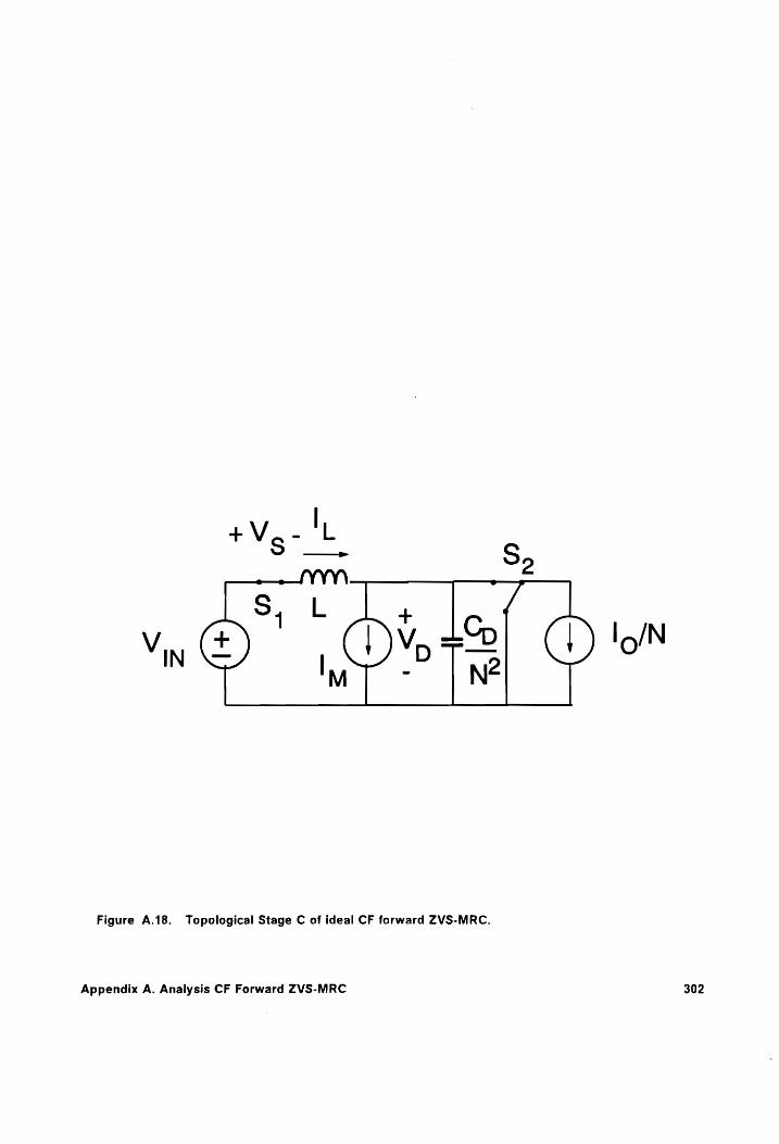
Figure A.18. Topological Stage C of ideal CF forward ZVS-MRC.
Appendix A. Analysis CF Forward ZVS-MRC 302

L—— =Vin (A. 16)
Solution:
i, =I, he (4.17)
or in the normalized form:
ip =I, \ + Qnty (A.18)
Stage Duration Tc = Tc1 — Tco
The stage duration Tc is determined from the turn-off of the CF switch Qo.
STAGE D [Tpo, Tp1] (Fig. A.19)
Initial Conditions:
D Vs(Tp0) = Vs (A.19.a)
Appendix A. Analysis CF Forward ZVS-MRC 303
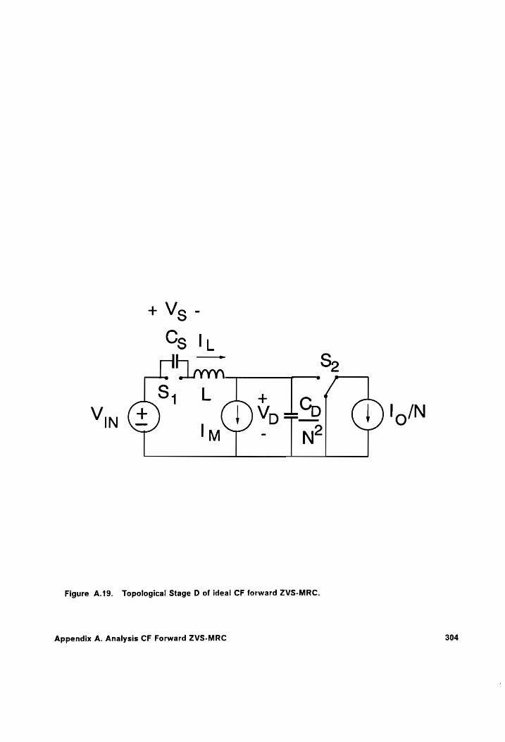
Figure A.19. Topological Stage D of ideal CF forward ZVS-MRC.
Appendix A. Analysis CF Forward ZVS-MRC 304

D
Vd(Tpo) = Vp
D ipo) ="
Equations:
di, (t) C at
. dvp(t) i(t) -Cp dt =lIo+ly
dv{t I(t) =lep(t) = Cp s
From Eqs. (A.20.a) - (A.20.c), it follows that:
d’vo(t) 2 dv.(f) lo+ty 2 2V0 Wo
at? dt CIN?
where
14+ Cy
27° Cy
Solution:
Appendix A. Analysis CF Forward ZVS-MRC
(A.19.b)
(A.19.c)
(A.20.a)
(A.20.b)
(A.20.c)
(A.21.a)
(A.21.b)
305
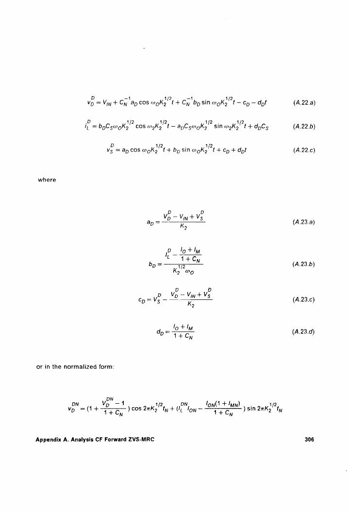
D 1 1/2 —1 . 1/2 Vp = Vin + Cy ap cos moKo t+ Cy bp SIN wok» f— Cp _- dpt
.D 1/2 4/2 4/2, 1/2 A = bpCsmoKs! cos nok! t _— apCsingKs! sin inky! t + ApnCs
D 1/2 ; 1/2 Vs =A COS M_oKy t+ bpsinwoKy t+e€p+dpt
where
D D Vp — Vin + Vs
4p = Ky
D_lIot!y
tC 14+Cy
Ky DO
D D D Vp ~YwtVs
lot+dy
D™ 14Cy
or in the normalized form:
DN DN Vp —1 /
Vp “(+ 4 E 7 lon(1 + Iw) °t 1+ Cy N
1/2 DN 4 ) cos 2nKy ty + (I, lon — ) sin 2nK,
Appendix A. Analysis CF Forward ZVS-MRC
(A.22.a)
(A.22.b)
(A.22.c)
(A.23.a)
(A.23.b)
(A.23.c)
(A.23.d)
306

Cu, DN lon) + Iyndenty
+s5 6-14 13 t, (A.24.a)
i; DN 14+/ 1 IMN- [V D ~ 1] ‘ 1/2 = [I _— 7 + 14+ Cy |co S2n Ks! “ty +2 sin 2nKo ty
ON'*2
lon(1 + In) — 44+Cy (A.24.b)
DN OM on — lon(1 + In) DN Vp —1 4/2 LON 1+ Cy . 1/2
Vs = K, £08 2K» ty — 1) + C il sin 2nKy ty
NOS2
1+ Cy
Stage Duration Tp = Tp1 — Tpo
The stage duration Tp is determined from the following condition if the stage following is Stage
B:
v.(Tp) = 0 (A.25.a)
and by
Appendix A. Analysis CF Forward ZVS-MRC 307

if the following stage is Stage E.
Initial Conditions:
Equations:
STAGE E [Teo, Te1] (Fig. A.20)
E Vs(TE9) = Vs4
Vp(TF0) = Vp
(Tro) =h
di, (f)
, dvp(f) i(f) ~~ Cp at = UY,
. . dvs(f)
From Eqs. (A.27.a) - (A.27.c), it follows that
Appendix A. Analysis CF Forward ZVS-MRC
(A.26.a)
(A.26.b)
(A.26.c)
(A.27.a)
(A.27.b)
(A.27.c)
308
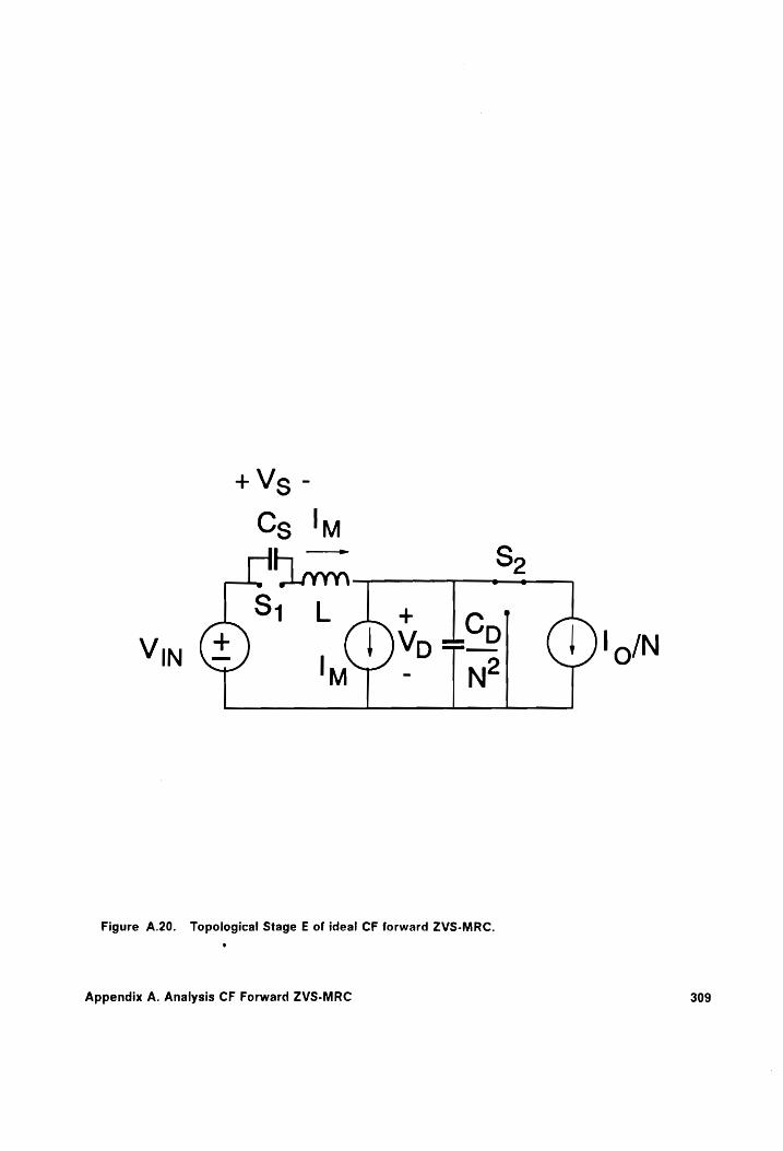
Figure A.20. Topological Stage E of ideal CF forward ZVS-MRC.
Appendix A. Analysis CF Forward ZVS-MRC 309

Solution:
where
d*vs(t) 2 vet) ly 2 3 + KywWo dt = 2 Wo
at Cp/N
E —1 1/2 1, 4/2 Vp = Vin + Cy ar cos oka! {+ Cy be sin ok, t— Ce _— drt
JE 1/2 1/2 1/2. 1/2 At = beCsino Ks! cos inky! t —_ apCgwoKs! Sin inky! t + a-Cs
E 4/2 . 2 Vo = af COS anoK,! t+ be sin wok,! {+ Cpe + drt
or in the normalized form:
Appendix A. Analysis CF Forward ZVS-MRC
(A.28)
(A.29.a)
(A.29.b)
(A.29.c)
(A.30.a)
(A.30.b)
(A.30.c)
(A.30.d)
310

EN EN Vp - EN /
vp =(1 + Pre )o0s OnKy' ty + (I) Ty Gp lon sin 2nKy!“ty
C ven 1) lon 2at NY D ON'MNETEN 1+ Cy +- 1+ Cy (A.31.a)
EN EN EN / 1/2 Vp -1) «| 1 ih = - MN ] cos 2nK' ty + Ho in OnKy ty
1 + Cy . ON a
IMN + 1+ Cy (A.31.b)
EN ! Ur MN EN (Vp —1) 4/2 ont T+ Cy! . 1/2 Vo =——>— (cos 2dnK, ty—1) + sin2nxK, t S K 2 'N 1/2 2 'N
2 CyKo
lonlunetty
Stage Duration Te = Te; — Teo
The stage duration 7¢ is determined from the following condition if the stage following is Stage
A:
Vo(Tp) =O (A.32.a)
Appendix A. Analysis CF Forward ZVS-MRC 311

and by
Vo(Tr) =9
if the following stage is Stage D.
STAGE F [Tro, Tr1] (Fig. A.21)
Initial Conditions:
F
Vs(Tro) = Vs
Vo(Tro) = 9
F
(Tro) =A
Equations:
di, (f) «at + Vo(f) = Viy
dve(t) i,(t) = igs(t) = Cs ai
From Eqs. (A.34.a) and (A.34.b), it follows that:
Appendix A. Analysis CF Forward ZVS-MRC
(A.32.b)
(A.33.a)
(A.33.b)
(A.33.c)
(A.34.a)
(A.34.b)
312
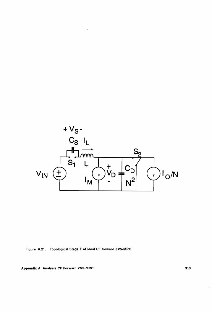
Figure A.21. Topological Stage F of ideal CF forward ZVS-MRC.
Appendix A. Analysis CF Forward ZVS-MRC 313

Solution:
where
or in the normalized form:
d°vs(t) 2 2 5 + MoVs(t) => MOVIN
at
F
Vs = ar COs Wot + bp sin wot + Vin
F —1 —1 I = brZo cos Mol _ arZo sin Mot
F
ap = Vs — Vin
F
br = 1,Zo
FN FN . Vo =1-—cos2dnty +), loy sin 2nty
FN FN sin Qnty, i, =, cos 2nty + _
ON
Stage Duration T- = Tr; — Tro
Appendix A. Analysis CF Forward ZVS-MRC
(A.35)
(A.36.a)
(A.36.b)
(A.37.a)
(A.37.b)
(A.38.a)
(A.38.b)
314
The stage duration Tr is determined by the turn-off time of the CF switch Qo.
A.4 Calculating the DC Voltage-Conversion-Ratio
To find the dc voltage-conversion-ratio of the CF forward ZVS-MRC, the secondary transformer
voltage has to be integrated during the intervals for which the forward diode D, conducts rel-
ative to the switching period. For the CF forward ZVS-MRC, only topological Stages A and D
transfer power to the load. Therefore, by finding the average secondary transformer voltage
during the duration of these stages, the output voltage can be calculated in the following
manner:
mM ot, . mt, >
Vo=fol) i vpdt + >I, vpdt] (A.39) 0 0°
where n1 and no are the number of times Stage A and Stage D occur during one switching
cycle, respectively. The dc voltage-conversion-ratio can be calculated simply by normalizing
Eq. (A.39) with respect to the source voltage Vjj/N:
Appendix A. Analysis CF Forward ZVS-MRC 315
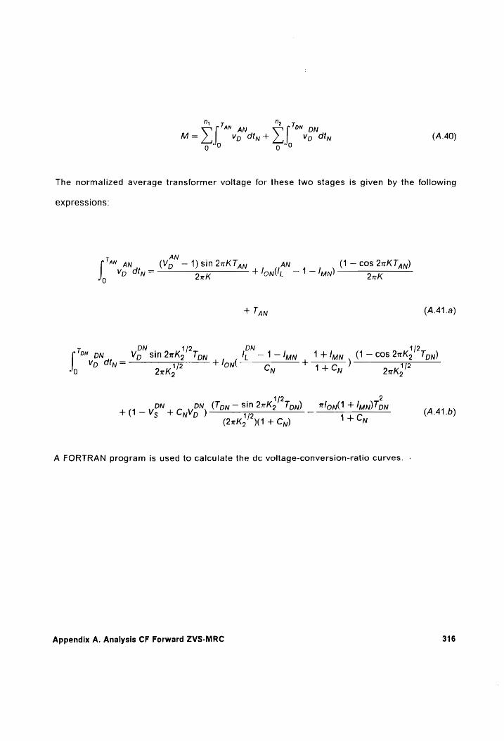
TAN 4 re Tow DN
u=>f vp Satu + Do Vp dty (A.40) 0 0
The normalized average transformer voltage for these two stages is given by the following
expressions:
AN TAN AN (Vp —1)8in 2nKT gy AN (1 — cos 2nKT,y)
| YD n= 2nK + lon, —1—'Iun)-———aae
+ TAN (A.41.a)
DN 1f2 DN 1/2 [vee Vp. sin 2nKo' Ty blog ett At hu (= 608 OnKy' Tp) D N SS ee"—_maKX«—_—_—_—_—_—_QVQVQUQGl
0 OnKy ON Cy 1+ Cy OnK,y!”
. 1/2 2 DN. (T, sin 2nrK, T, tlon(1 + Inyn)T, +1 — Ve 4 cy ybN (Ton — ” ™Ka Ton) _ ont a DN (A.41.b)
(2nKy')(4 + Cy) N
A FORTRAN program is used to calculate the dc voltage-conversion-ratio curves.
Appendix A. Analysis CF Forward ZVS-MRC 316

Appendix B. Analysis CF HB ZVS-MRC
The circuit diagram of the CF HB ZVS-MRCs is shown in Fig. B.1. The CF HB ZVS-MRC is
obtained by replacing the output rectifiers in the HB ZVS-MRC with transistors Q3 and Q4.
Resonant capacitors C; and Co represent the output capacitance of the primary transistors,
Q, and Qa. Resonant inductor L can either be a separate inductor or the leakage inductance
of the transformer. Since the junction capacitance of the CF switches is not sufficiently large
to obtain the desired resonance, capacitors C3 and C, are usually externally-added capacitors.
B.1 DC Analysis
To simplify the analysis, in addition to the assumptions made for the forward converter, it is
assumed that Q; and Q2 and switches Q3 and Q, are identical, so that C;=Co=Cs and
Appendix B. Analysis CF HB ZVS-MRC 317
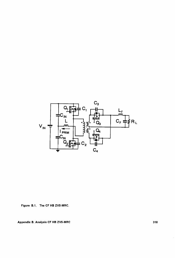
Figure B.1. The CF HB ZVS-MRC.
Appendix B. Analysis CF HB ZVS-MRC 318
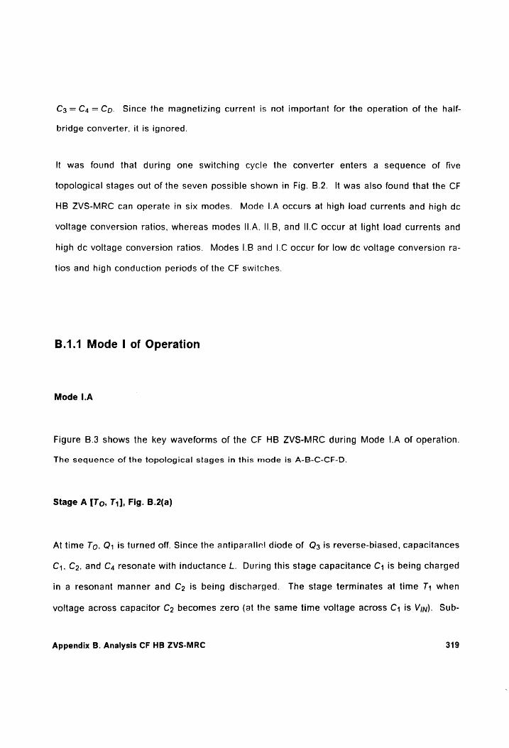
C3=C4=Cp. Since the magnetizing current is not important for the operation of the half-
bridge converter, it is ignored.
It was found that during one switching cycle the converter enters a sequence of five
topological stages out of the seven possible shown in Fig. B.2. It was also found that the CF
HB ZVS-MRC can operate in six modes. Mode |.A occurs at high load currents and high de
voltage conversion ratios, whereas modes II.A. II.B, and II.C occur at light load currents and
high dc voltage conversion ratios. Modes |.B and |.C occur for low dc voltage conversion ra-
tios and high conduction periods of the CF switches.
B.1.1 Mode I of Operation
Mode I.A
Figure B.3 shows the key waveforms of the CF HB ZVS-MRC during Mode |.A of operation.
The sequence of the topological stages in this mode is A-B-C-CF-D.
Stage A [To, 71], Fig. B.2(a)
At time To, Q, is turned off. Since the antiparallel diode of Q3 is reverse-biased, capacitances
C,, Co, and C4 resonate with inductance L. During this stage capacitance C, is being charged
in a resonant manner and Co is being discharged. The stage terminates at time 7; when
voltage across capacitor Co becomes zero (at the same time voltage across C, is Vjn). Sub-
Appendix B. Analysis CF HB ZVS-MRC 319
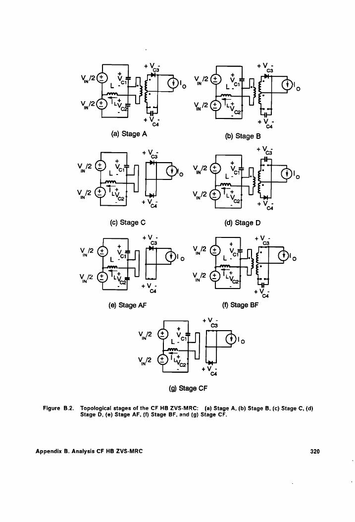
Wi? ae | O',
w2@ hy | OA. - K-
+V - C4
(b) Stage B
+V- C4
(d) Stage D
>t +V-
C4
(g) Stage CF
Figure B.2. Topological stages of the CF HB ZVS-MRC: (a) Stage A, (b) Stage B, (c) Stage C, (d) Stage D, (e) Stage AF, (f) Stage BF, and (g) Stage CF.
Appendix B. Analysis CF HB ZVS-MRC 320
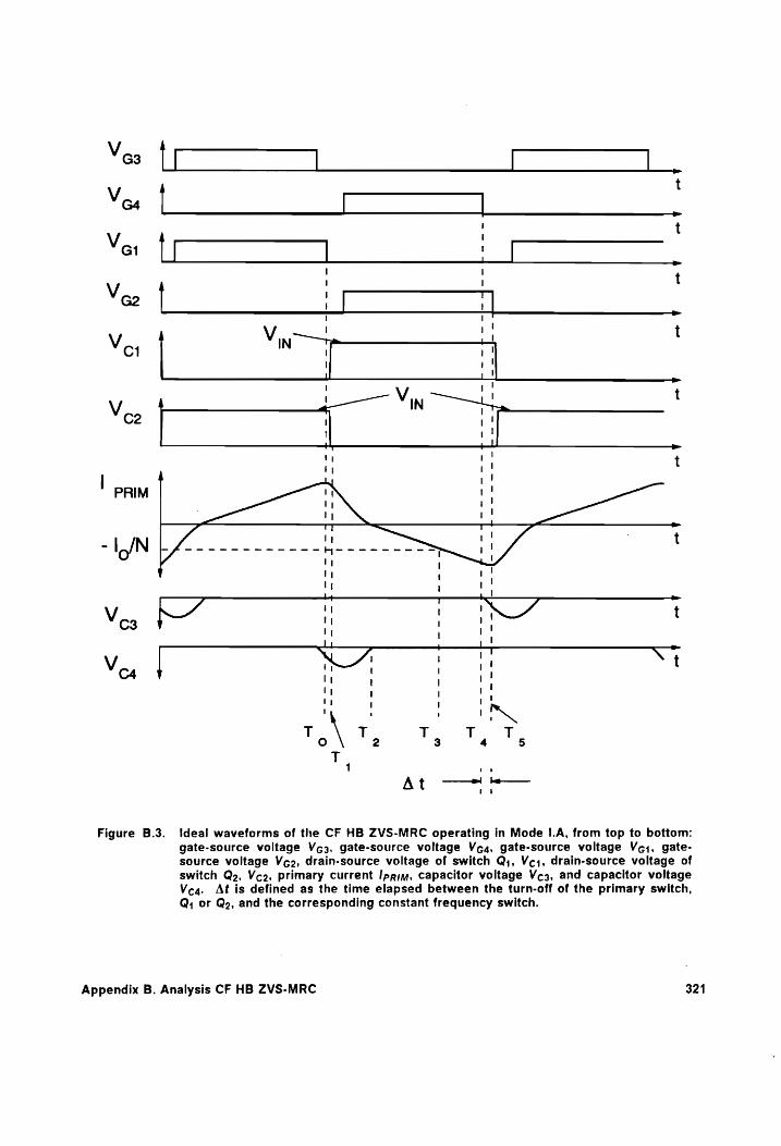
< cs {[ | [ |
Vex { | ) ; ; t
Ver {TL | al . : t
Veo | ]
Voy vin .
<
z —
¥
Q nN
Pe =
}
we ¥
$
7 w- V
wee eee fee
ee
LLL
| 4 ot
|
+
Oo 4_7-
+ LN
4 o
+ a a
At —o—
Figure B.3. !deal waveforms of the CF HB ZVS-MRC operating in Mode 1.A, from top to bottom: gate-source voltage Vg3, gate-source voltage Vcg4, gate-source voltage Vc¢;, gate- source voltage Vg, drain-source voltage of switch Q;, Vc;, drain-source voltage of switch Qo, Vco, primary current Ippjy, capacitor voltage Vc3, and capacitor voltage Vcq. At is defined as the time elapsed between the turn-off of the primary switch, Q; or Qo, and the corresponding constant frequency switch.
Appendix B. Analysis CF HB ZVS-MRC 321
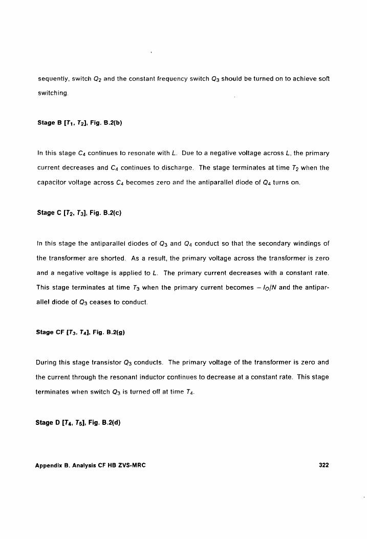
sequently, switch Qo and the constant frequency switch Q3 should be turned on to achieve soft
switching.
Stage B [T1, T2], Fig. B.2(b)
In this stage C4 continues to resonate with L. Due to a negative voltage across L, the primary
current decreases and C4 continues to discharge. The stage terminates at time T> when the
capacitor voltage across C4 becomes zero and the antiparallel diode of Q, turns on.
Stage C [To, T3], Fig. B.2(c)
In this stage the antiparallel diodes of Q3 and Q4 conduct so that the secondary windings of
the transformer are shorted. As a result, the primary voltage across the transformer is zero
and a negative voltage is applied to L. The primary current decreases with a constant rate.
This stage terminates at time 73 when the primary current becomes — /o/N and the antipar-
allel diode of Q3 ceases to conduct.
Stage CF [T3, Ta], Fig. B.2(g)
During this stage transistor Q3 conducts. The primary voltage of the transformer is zero and
the current through the resonant inductor continues to decrease at a constant rate. This stage
terminates when switch Q3 is turned off at time T4.
Stage D [Ta, Ts], Fig. B.2(d)
Appendix B. Analysis CF HB ZVS-MRC 322

At timeT4, C3 starts resonating with inductance L. This stage ends when transistor Qo is
turned off and a new conversion cycle is initiated.
In Mode |.A of operation the time at which capacitance C3 resonates with inductance L is de-
layed until switch Q3 is turned off (as long as switch Q3 is on the voltage across C3 is shorted).
Mode I.B
The sequence of topological stages in this mode of operation is A-B-C-CF-AF.
Stage A [To, 11], Fig. B.2(a)
At time To, Q4 is turned off. The antiparallel diode of Q3 is reverse-biased and capacitances
C,, Co, and C4 resonate with inductance L. During this stage capacitance C, is being charged
in a resonant manner and Co is being discharged. The stage terminates at time 7,, when
voltage across capacitor Cp becomes zero (at the same time voltage across C, is Vjy). Sub-
sequently, Q2 and Q3 should be switched on to achieve lossless turn-on.
Stage B [T1, T2], Fig. B.2(b)
In this stage C4 continues to resonate with L. Due to a negative voltage across L, the primary
current decreases and C4, continues to discharge. The stage terminates at time To, when the
capacitor voltage across C4 becomes zero and the antiparallel diode of Q4 turns on.
Stage C [To, T3], Fig. B.2(c)
Appendix B. Analysis CF HB ZVS-MRC 323

In this stage the antiparallel diodes of Q3 and Q, conduct so that the secondary windings of
the transformer are shorted. As a result, the primary voltage across the transformer is zero
and a negative voltage is applied to L. The primary current decreases with a constant rate.
The stage terminates at time T3 when the primary current becomes — /o/N and the antiparallel
diode of Q3 ceases to conduct.
Stage CF [T3, T4], Fig. B.2(g)
During this stage transistor Q3 conducts. The primary voltage of the transformer is zero and
the current through the resonant inductor continues to decrease at a constant rate. This stage
terminates when switch Q, is turned off at time T4.
Stage AF [Ta, Ts], Fig. B.2(e)
In this stage switch Q3 is on and the antiparallel diode of switch Q4 is conducting resulting in
a zero primary transformer voltage. Capacitances C; and Co resonate with inductance L.
Capacitance C, is being charged in a resonant manner and capacitance Co is being dis-
charged at the same rate. This stage ends at time time Ts when switch Qg3 is turned off.
In Mode |.B of operation switch Q3 is turned off a short interval after switch Q2 is turned off
and before switch Q, is turned on under zero voltage.
Mode I.C
Appendix B. Analysis CF HB ZVS-MRC 324
Figure B.4 shows the key waveforms of the CF HB ZVS-MRC during Mode I.C of operation.
The sequence of the topological stages in this mode is AF-CF-B-C-CF.
Stage AF [To, 71], Fig. B.2(e)
At time To, switch Q, is turned off. Switch Q4 and the antiparallel diode of switch Q3 remains
on clamping the primary transformer voltage to zero, and capacitance C; and Co resonate with
L. Capacitance C, is charged in a resonant manner and capacitance Cy discharges at the
same rate during this stage. This stage ends when the voltage across capacitance Co de-
creases to zero through a resonant oscillation. At the same time the voltage across
capacitance C, reaches the supply voltage and remains clamped to this value. Subsequently,
switch Qa should be turned under soft switching conditions.
Stage CF [T1, T2], Fig. B.2(g)
During this stage switches Qo, Q4 and the antiparallel diode of switch Q3 are on and the load
current freewheels through the shorted secondary winding of the transformer. The voltage
across the resonant inductor is negative and the current through this inductor decreases at
a constant rate. This stage ends at time time Tz when switch Q, is turned off.
Stage B [To, T3], Fig. B.2(b)
In this stage switch Qo and the antiparallel diode of switch Q3 conduct. Due to the negative
voltage across inductance L, the primary current decreases and capacitance Cz, is first
Appendix B. Analysis CF HB ZVS-MRC 325
Ves {| | ;
Vea f i | '
Ver I | |
Veo | Hl | : | Vin 7 !
Veo | Vn — a
| PRIM f ! |
$
C
o> V
Figure B.4. Ideal waveforms of the CF HB ZVS-MRC operating in Mode I.C, from top to bottom:
gate-source voltage Vg3, gate-source voltage Vcq, gate-source voltage Vg;, gate-
source voltage Vg2, drain-source voltage of switch Q;, Vc1, drain-source voltage of
switch Qo, Vco, primary current Ippiy, capacitor voltage Vc3, and capacitor voltage
Vea. At is defined as the time elapsed between the turn-off of the primary switch,
Q; or Qo, and the corresponding constant frequency switch.
Appendix B. Analysis CF HB ZVS-MRC 326
charged and subsequently discharged in a resonant manner. This stage ends when the
capacitor voltage across C4 becomes zero and the antiparallel diode of switch Q4 turns on.
Stage C [T3, T4], Fig. B.2(c)
In this stage the antiparallel diodes of Q3 and Q,4 conduct so that the secondary windings of
the transformer are shorted. As a result, the primary voltage across the transformer is zero
and a negative voltage is applied toL. The primary current decreases at a constant rate. The
stage terminates at time 74, when the primary current becomes —/o/N and the antiparallel
diode of Q3 ceases to conduct.
Stage CF [T4, Ts], Fig. B.2(g)
During this stage transistor Q3 and the antiprallel diode of switch Q4 conduct. The primary
voltage of the transformer is zero and the current through the resonant inductor continues to
decrease at a constant rate. This stage ends when transistor Qo is turned off and a new
conversion cycle is initiated at time Ts.
In Mode I.C switch Q3 remains on for a longer time than in the two previous modes and is
turned off after the switching transition of the primary switches. The resonance of the sec-
ondary side capacitances is interrupted for most of the switching cycle, resulting in low output
voltages.
Appendix B. Analysis CF HB ZVS-MRC 327
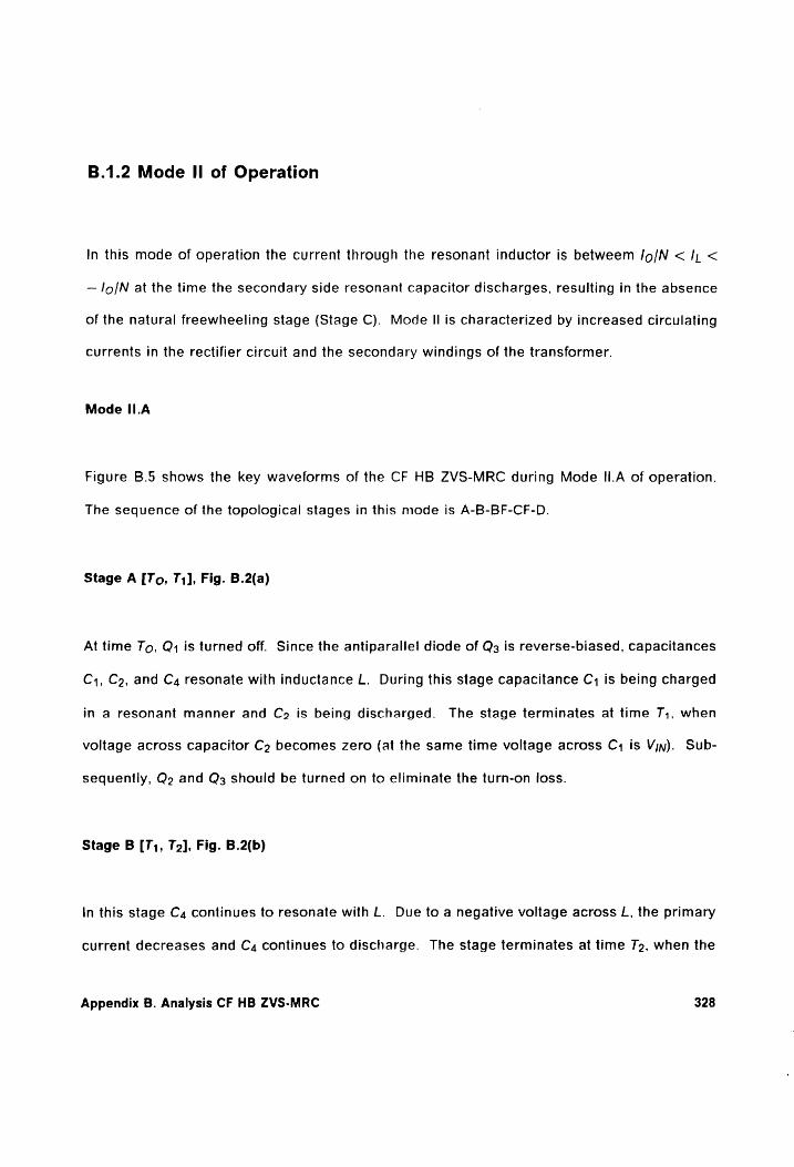
B.1.2 Mode II of Operation
In this mode of operation the current through the resonant inductor is betweem /o/N < I, <
—Io/N at the time the secondary side resonant capacitor discharges, resulting in the absence
of the natural freewheeling stage (Stage C). Mode II is characterized by increased circulating
currents in the rectifier circuit and the secondary windings of the transformer.
Mode II.A
Figure B.5 shows the key waveforms of the CF HB ZVS-MRC during Mode II.A of operation.
The sequence of the topological stages in this mode is A-B-BF-CF-D.
Stage A [To, 71], Fig. B.2(a)
At time To, Q, is turned off. Since the antiparallel diode of Q3 is reverse-biased, capacitances
C1, Co, and C4 resonate with inductance L. During this stage capacitance C, is being charged
in a resonant manner and Co is being discharged. The stage terminates at time 7,, when
voltage across capacitor C2 becomes zero (at the same time voltage across C; is Vjy). Sub-
sequently, Qo and Q3 should be turned on to eliminate the turn-on loss.
Stage B [71, T2], Fig. B.2(b)
In this stage C4 continues to resonate with L. Due to a negative voltage across L, the primary
current decreases and C, continues to discharge. The stage terminates at time To, when the
Appendix B. Analysis CF HB ZVS-MRC 328
Vos [ | | L t
Vea | | [ . 1 t
Yer LP | I . i t
Veo | i: | . Vor | Vin t
< <
=z
a
¥
a
7
< 8
-- 4
_,
~~ V
At —r_
Figure B.5. ideal waveforms of the CF HB ZVS-MRC operating in Mode II.A, from top to bottom: gate-source voltage Vcg3, gate-source voltage Vgq4, gate-source voltage Vg, gate- source voltage Veo, drain-source voltage of switch Q;, Vc;, drain-source voltage of switch Qo, Vco, primary current Ipaiy, capacitor voltage Vc3, and capacitor voltage Vca. At is defined as the time elapsed between the turn-off of the primary switch, Q; or Qo, and the corresponding constant frequency switch.
Appendix B. Analysis CF HB ZVS-MRC 329
current through the resonant inductor decreases to —/on/N, the antiparallel diode of switch
Q3 ceases to conduct, and switch Q3 conducts.
Stage BF [To, 73], Fig. B.2(f)
In this stage switch Qo and Q3 are on and capacitance C4, continues to resonate with
inductance L. This stage ends at time T3 when the voltage across capacitance C, decreases
to zero through a resonant oscillation and the antiparallel diode of switch Q,4 starts to conduct.
Stage CF [T3, T4], Fig. B.2(g)
In stage CF transistor Q3 and the anitparallel diode of Q4 conduct. The primary voltage of the
transformer is zero (secondary windings of the transformer are shorted) and the current
through the resonant inductor continues to decrease at a constant rate. This stage terminates
when switch Q3 is turned off at time Ta.
Stage D [T4, Ts], Fig. B.2(d)
At time T4, C3 starts to resonate with inductance L. This stage ends when transistor Qo is
turned off and a new conversion cycle is initiated.
Mode I1.B
Appendix B. Analysis CF HB ZVS-MRC 330
In modes II.B and II.C, the CF switches are allowed to conduct a longer period of time and they
are not turned off until after the primary switches (switches Q, or Qo) have been turned off.
The sequence of the topological stages in Mode II.B is A-B-BF-CF-AF.
Stage A [To, T%], Fig. B.2(a)
At time To, Q4 is turned off. Since the antiparallel! diode of Q3 is reverse-biased, capacitances
C,, Co, and C4 resonate with inductance L. During this stage capacitance C, is being charged
in a resonant manner and Co is being discharged. The stage terminates at time T, when
voltage across capacitor Cp becomes zero (at the same time voltage across C, is Vin). Sub-
sequently, Qo and Q3 should be switched on to achieve lossless turn-on.
Stage B [T1, T2], Fig. B.2(b)
In this stage C4 continues to resonate with L. Due to a negative voltage across L, the primary
current decreases and C, continues to discharge. The stage terminates at time To, when the
current through the resonant inductor decreases to —/on/N and switch Q3 conducts as its
antiparallel diode turn off.
Stage BF [To, T3], Fig. B.2(f)
In this stage switch Q2 and Q3 are on and capacitance C4 continues to resonate with
inductance L. This stage ends at time T3 when the voltage across capacitance C4 decreases
to zero through a resonant oscillation and the antiparallel diode of switch Q, starts to conduct.
Appendix B. Analysis CF HB ZVS-MRC 331

Stage CF [T3, Ta], Fig. B.2(g)
During this stage transistor Q3 and the anitparallel diode of Q4 conduct. The primary voltage
of the transformer is zero (secondary windings of the transformer are shorted) and the current
through the resonant inductor continues to decrease at a constant rate. This stage terminates
when switch Qo is turned off at time 74.
Stage AF [T4, Ts], Fig. B.2(e)
At time 74, capacitances C; and Co start to resonate with inductance L. During Stage AF Q3
remains on and the antiparallel diode of switch Q4 continues to conduct (transformer sec-
ondary winding remain shorted). Capacitance C;, charges in a resonant manner and
Capacitance Co discharges at the same rate. Stage AF ends when switch Q3 is turned off.
Mode II.C
In Mode II.B switch Q3 is turned off after switch Q2 is turned off and before switch Q, is turned
on under zero voltage. In Mode II.C, however. switch Q3 is turned off after the switching
transition for switches Q; and Q2 has occurred. The sequence of the topological stages in
Mode II.C is AF-CF-B-BF-CF. Figure B.6 shows the key waveforms of the CF HB ZVS-MRC op-
erating in Mode II.C.
Stage AF [To, 71], Fig. B.2(e)
At time To, Q; is turned off. The antiparallel diode of Q3 is forward-biased and the antiparallel
diode of switch Q4 conducts. During this stage capacitances C;, and Co resonate with
Appendix B. Analysis CF HB ZVS-MRC 332
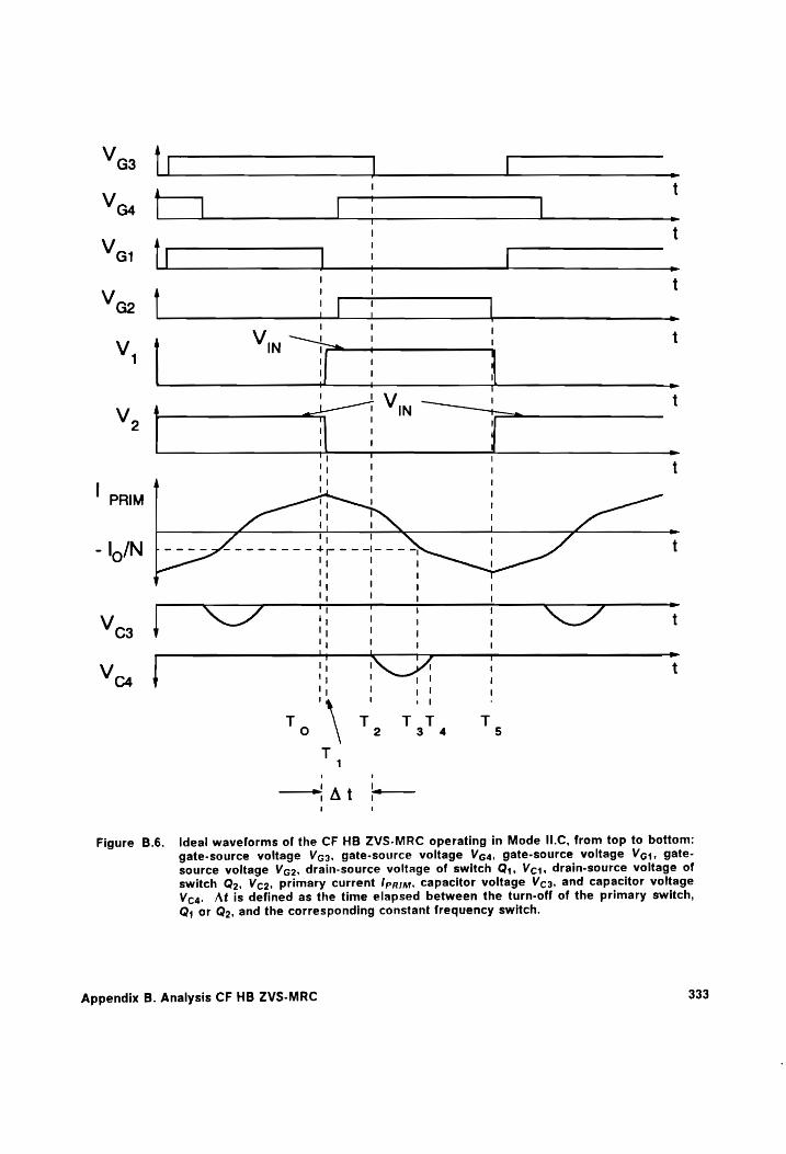
=!
—"At +—
Figure B.6. Ideal waveforms of the CF HB ZVS-MRC operating in Mode II.C, from top to bottom:
gate-source voltage Vg3, gate-source voltage Vcg4, gate-source voltage Vg, gate-
source voltage Vg2, drain-source voltage of switch Q;, Vc, drain-source voltage of
switch Qo, Vc2, primary current Ipaim, capacitor voltage Vc3, and capacitor voltage
Vcq. At is defined as the time elapsed between the turn-off of the primary switch,
Q; or Q2, and the corresponding constant frequency switch.
Appendix B. Analysis CF HB ZVS-MRC 333

inductance L. The secondary windings of power transformer are shorted and capacitance C,
is charged in a resonant manner and Co is discharged at the same rate. The stage terminates
at f= 7, when voltage across capacitor Cp becomes zero (at the same time voltage across
C, is Vin). Subsequently, Qo and Q3, should be turned on to eliminate the switching loss.
Stage CF [T}, T2], Fig. B.2(g)
During this stage Q4 remains on and the antiparallel diode of switch Q3 continues to conduct.
The secondary windings of the transformer remain shorted and the current through the reso-
nant inductor decreases at a constant rate. This stage ends when switch Q, is turned off.
Stage B [To, T3], Fig. B.2(b)
In this stage C4 starts to resonate with L. Due to a negative voltage across L, the primary
current decreases and C4 charges in a resonant manner. The stage terminates at time To,
when the current through the resonant inductor decreases to —/on/N. Also, the antiparallel
diode of switch Q3 ceases to conduct and switch Q3 begins to conducts.
Stage BF [T3, T4], Fig. B.2(f)
In this stage switch Qo and Qs are on and capacitance C4 continues to resonate with
inductance L. This stage ends at time 74 when the voltage across capacitance C4 decreases
to zero through a resonant oscillation and the antiparallel diode of switch Q,4 starts to conduct.
, Stage CF [Ta, Ts], Fig. B.2(g)
Appendix B. Analysis CF HB ZVS-MRC 334
In Stage CF transistor Q3 and the anitparallel diode of Q4 conduct. The primary voltage of the
transformer is zero (secondary windings of the transformer are shorted) and the current
through the resonant inductor continues to decrease at a constant rate. This stage terminates
when switch Qo is turned off at time Ts.
Table B.1 summarizes the five-stage sequences of all the modes of operation modeled for the
CF HB ZVS-MRC.
B.2 DC Voltage-Conversion-Ratio
Figures B.7a - B.14a shows the typical dc voltage-conversion-ratio characteristics of the CF
HB ZVS-MRC as a function of 6. 6 is defined as the time between the turn-off of the CF switch
Q3 or Q4. and the turn-off of the primary switch Q1 or Qo, respectively (At in Fig. 3.11) nor-
malized with respect to 1/fo, where the resonant frequency is fo = 1/27,./LC . The character-
istics are given for different normalized conversion frequencies, fegn/fo, and for different values
of Cy = 2Cp)(CN2), where feon = 2fs is the conversion frequency, fs is the switching frequency,
and N is the turns ratio of the transformer. Figures B.7a - B.14b are plotted for different values
of the normalized output current. Jon = 2Zolo/NVin where Zo = Jtj2c is the characteristic
impedance.
Appendix B. Analysis CF HB ZVS-MRC 335
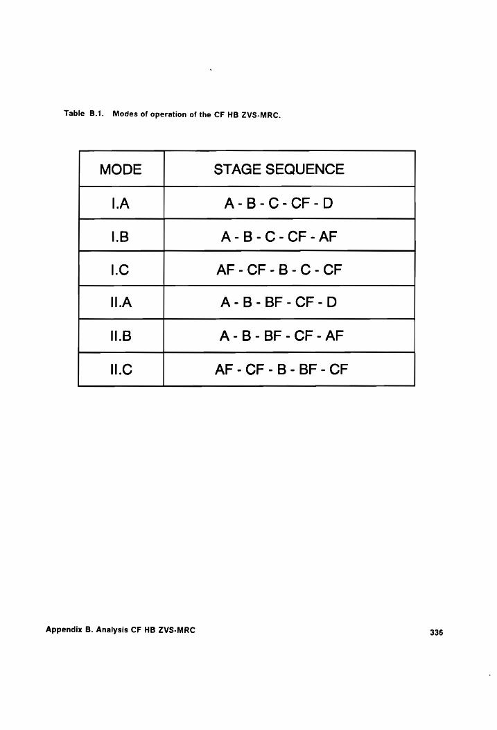
Table B.1. Modes of operation of the CF HB ZVS-MRC.
MODE STAGE SEQUENCE
ILA A-B-C-CF-D
.B A-B-C-CF-AF
I.C AF -CF-B-C-CF
L.A A-B-BF-CF-D
.B A-B-BF-CF-AF
ILC AF - CF -B-BF-CF
Appendix B. Analysis CF HB ZVS-MRC 336

A complete set of design characteristics is given for Cy = 2, 5, 10, and 20, and fcon/fo = 0.2,
0.25, 0.3, and 0.35 (Figs. B.7a - B.14b). Characteristics for all possible combinations are not
given since not all possible combinations result in practical design curves. For example, low
capacitance ratios (Cy = 2) and low switching frequencies (fcon/fo < 0.35) will result in op-
eration where the CF switches conduct for an extended period of time regardless of the load
current, resulting in high conduction losses. Similarly high capacitance ratio (Cy = 20) and
very low switching frequencies ( fcon/fo < 0.2) will also result in design where the CF switches
conduct for an extended period of time. Again this will result in an inefficient design.
Appendix B. Analysis CF HB ZVS-MRC 337

B.3 DC Analysis of the Topological Stages
Analytical expressions for the initial conditions, circuit equations, their solutions, and dura-
tions of the topological stages reffer to the ideal CF HB ZVS-MRC.
STAGE A [Tao, Ta1] (Fig. B.15)
Initial Conditions:
A VorilT a0) == Vo4 (B.1.a)
A Voo(T ao) = Veo (B.1 .b)
. A
ippim( ao) = prim (B.1.c)
Appendix B. Analysis CF HB ZVS-MRC 338
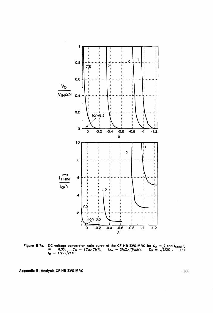
11: 0.8 Ho-ierrrrrtr force reed eee pieced.
7:5 5:
08 Hern efufenenteretfen ne Vo ; :
Vin/2N 0.4
0.2
0 02 -0.4
6
10 , 4
2
B be ejeeeeeee bee eccceheacccenueccecs
rms | PRIM 6F se secrs reste seen seer eset c coms resee
lo/N }
re we Pew emo web en Pewee mca en set ececce te bavscs Porevece s
Jon=8:5
‘ , 1 | Le | OQ 0.2 -0.4 -0.6 -0.8 -1 -1.2
i)
Figure B.7a. DC voltage conversion ratio curve of the CF HB ZVS-MRC for Cy = d fcon/fo = 0.35. Cn = 2Cp/(CN2), Jon = 2!loZol(VinN), Zo = VL/2C , and fo = 1/2n,/2LC .
Appendix B. Analysis CF HB ZVS-MRC 339
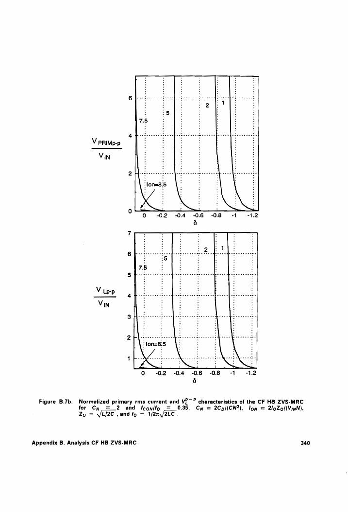
wee eee eee bee see
3 Se en Leese
/ Es 75:
4 bewleceeeechesecbekeee V PRIMp-p
VIN
V ip-p
Vin
Figure B.7b. Normalized primary rms current and Vi? characteristics of the CF HB ZVS-MRC for Cy _= 2 and foonl/fo =__ 0.35.
Zo = VL/2C , and fo = 1/2n,/2LC .
Appendix B. Analysis CF HB ZVS-MRC
Cy = 2Cp/(CN?), lon = 2loZol(ViwN),
340
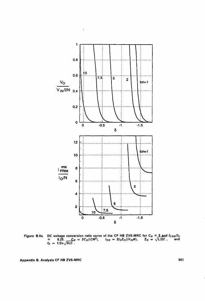
0.8
0.6
Vo
Vin/2N 0.4
0.2
o
12
10
ms
| PRIM
lo/N
Figure B.8a. DC voltage conversion ratio curve of the CF HB ZVS-MRC for Cy = d feonlfo
= 0.25. Cy = 2Cp/(CN?), lon = 2loZo/l(VinN), Zo = VL/2C , and fo= 1/2n,/2Lc .
Appendix B. Analysis CF HB ZVS-MRC 341
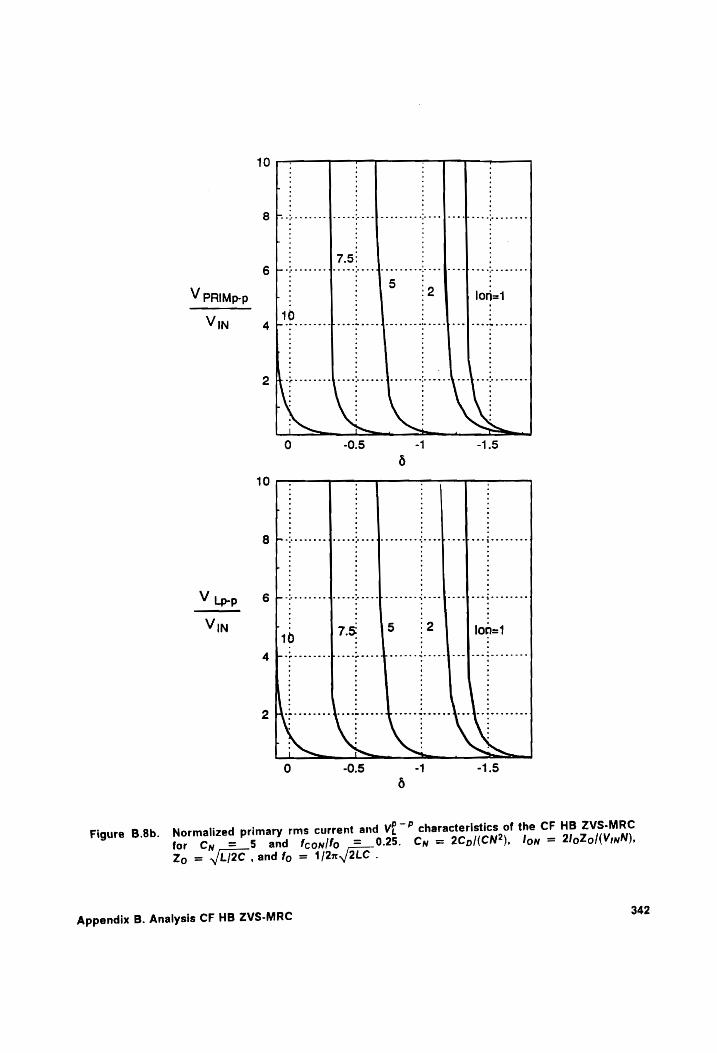
10
8 i... eee |e ee eb ee ee ee eee eee Sn
6 mm enrnvr eee eeea meer atevnanetoeodse nares eereerwrae L eee ewrme ann eae
5
V PRIMp-p 2 lon=1
Vn 4g HO bb pp.
Figure B.8b. Normalized primary rms current and ve? characteristics of the CF HB ZVS-MRC
for Cy = 5 and fconlfo = 0.25. Cy = 2Cp/(CN?), lon = 210Zo0/(VinN),
Zo = VL/2C , and fo = 1/2x,/2LC .
Appendix B. Analysis CF HB ZVS-MRC 342
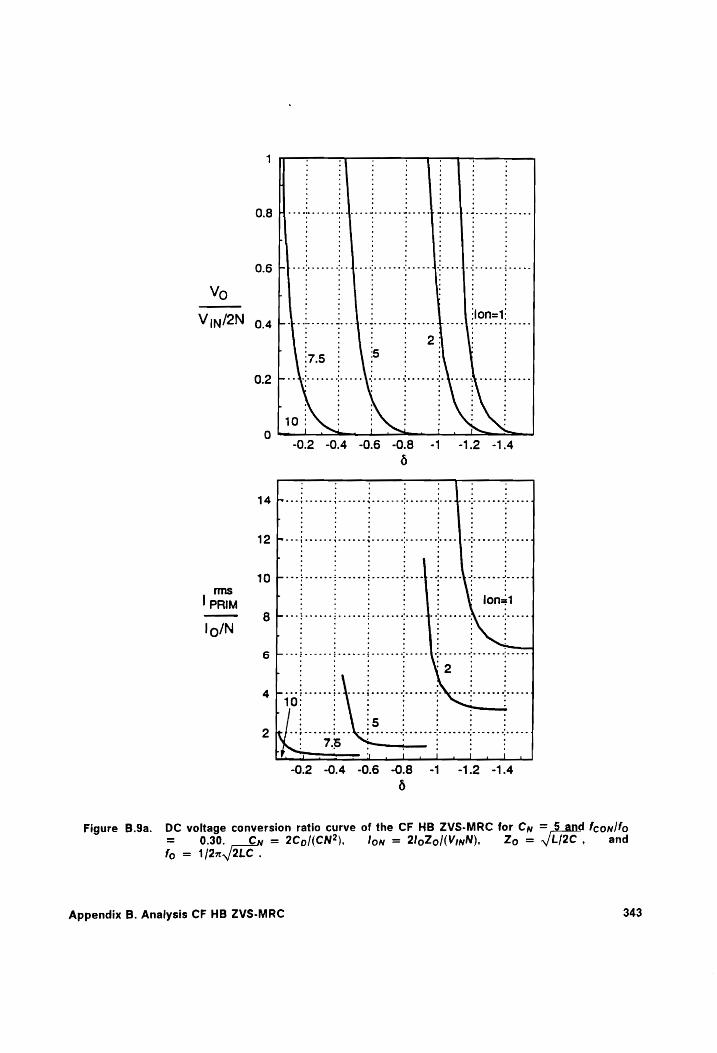
| Prim
lo/N 1 A] il el 1 —i
0.2 -04 -06 -08 -1 -1.2 -1.4
6
Figure B.9a. DC voltage conversion ratio curve of the CF HB ZVS-MRC for Cy = d fcon/fo = 0.30. Cy = 2Cp/(CN2), lon = 2ZloZol(VinN), Zo = Lj2c ’ and
fo = 1/2x,/2LC .
Appendix B. Analysis CF HB ZVS-MRC 343
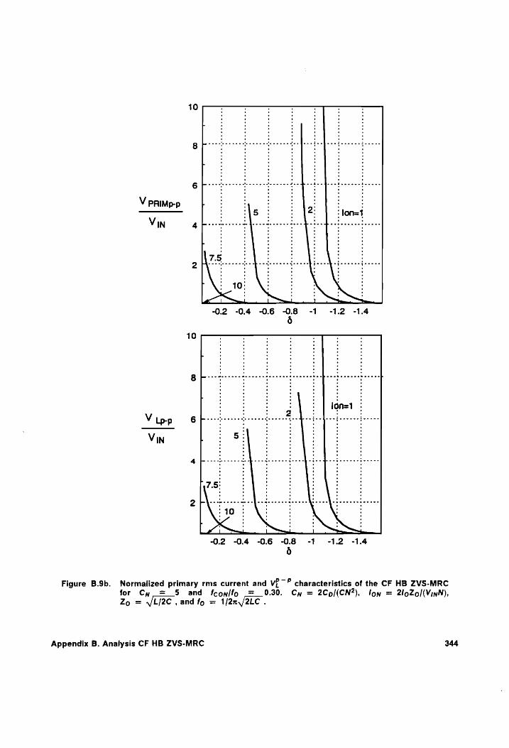
10
ee eee cece wee eh ee ee nee cenccecce trmand
0.2 -0.4 -0.6 * “1 --1.2 -1.4
10
8 Peres eravee Monee ne toeoeevnvetnenssceesbeoPsevebsesseeesestenenne
Vipp 6 bedside Bde
VIN : 8
4 bedded be EL be
7.5:
2k cote wc ccc ccc ced wwe w wes cece ee hewn ecb sewn sec cccces
: 10
O02 -04 -06 -08 -1 -12 -1.4 6
Figure B.9b. Normalized primary rms current and VP characteristics of the CF HB ZVS-MRC for Cn = 5 and feonlfo = 0.30. Cyn = 2Cp/(CN ), lon = 2loZo/(VinN),
Zo = VL/2C , and fo = 1/2x,/2LC .
Appendix B. Analysis CF HB ZVS-MRC 344
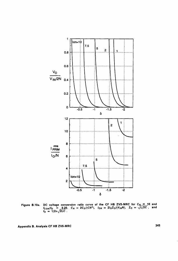
1 : lon=10
7.5 5
0.8 Leek epee yo PP
q
0.6 b---- efor Wood be Vo :
Vin/2N
ms
l PRIM
Io/N
Figure B.10a. DC voltage conversion ratio curve of the CF HB ZVS-MRC for Cy _=_10 and
feonl/fo = 0.20. Cy = 2Cp/(CN2), lon = 210Zol(VinN), Zo = L/2c , and
fo = 1/2n,/2L¢ .
Appendix B. Analysis CF HB ZVS-MRC 345
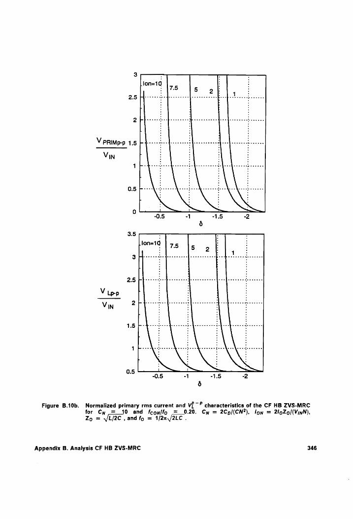
; 2 | ; 2.5 ' Lecce bef fe. pepe.
V PRIMp-p 1.5
VIN 0.5
3.5
VIN 2
1.5
0.5
Figure B.10b. Normalized primary rms current and vP —? characteristics of the CF HB ZVS-MRC for Cy = 10 and fcon/fo = 0.20. Cy = 2Cp/(CN2), lon = 2loZo/(VinN), Zo = VL/2C , and fo = 1/22,/2LC .
Appendix B. Analysis CF HB ZVS-MRC 346
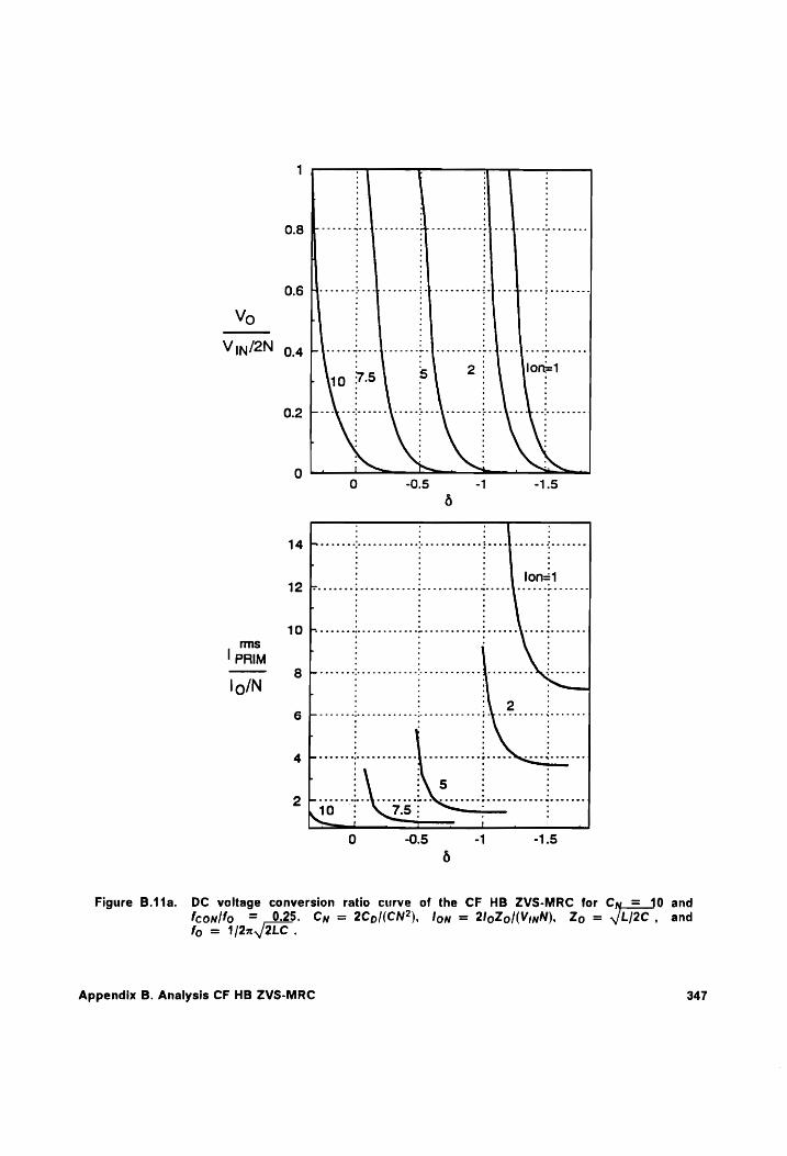
rms
| PRIM
lo/N
Figure B.11a. DC voltage conversion ratio curve of the CF HB ZVS-MRC for Cx_=_10 and foonlfo = 0.25. Cn = 2Cp/(CN2), lon = 2loZol(VinN), Zo = Lj2c , and
fo = 1/2n,/2Lc .
Appendix B. Analysis CF HB ZVS-MRC 347
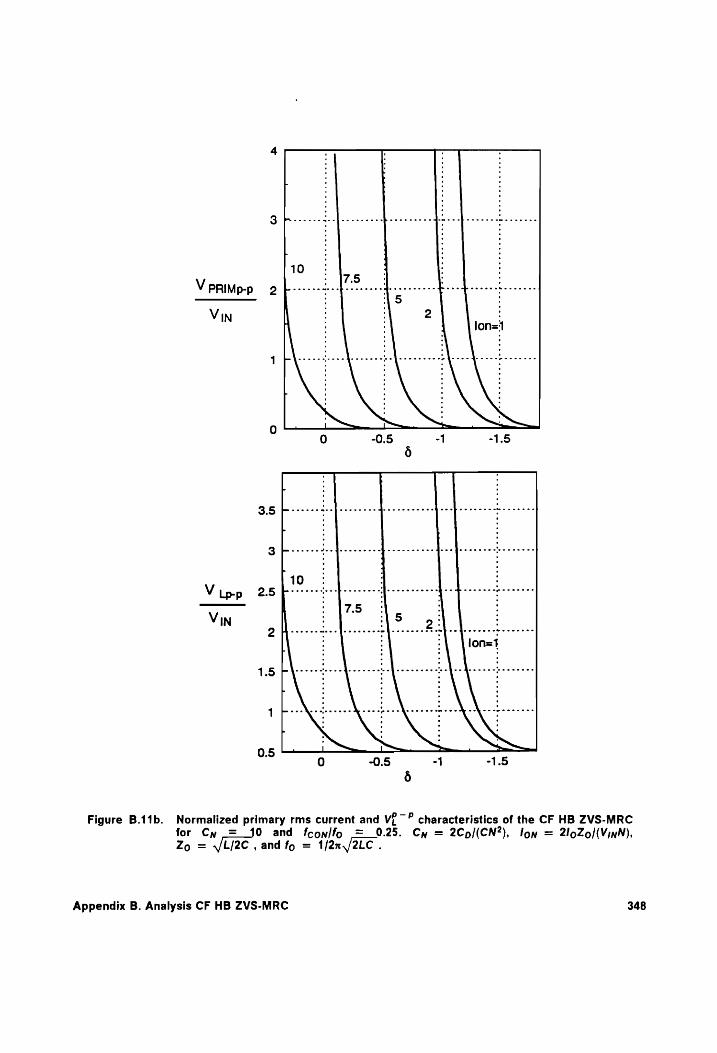
bm eee een ee emo ae
Figure B.11b. Normalized primary rms current and Vi” characteristics of the CF HB ZVS-MRC
for Cn = 0 and foonlfo = 0.25. Cn = 2Cp/(CN?), lon = 2l0Zol(VinN),
Zo = VL/2C , and fo = 1/2n,/2Lc .
Appendix B. Analysis CF HB ZVS-MRC 348
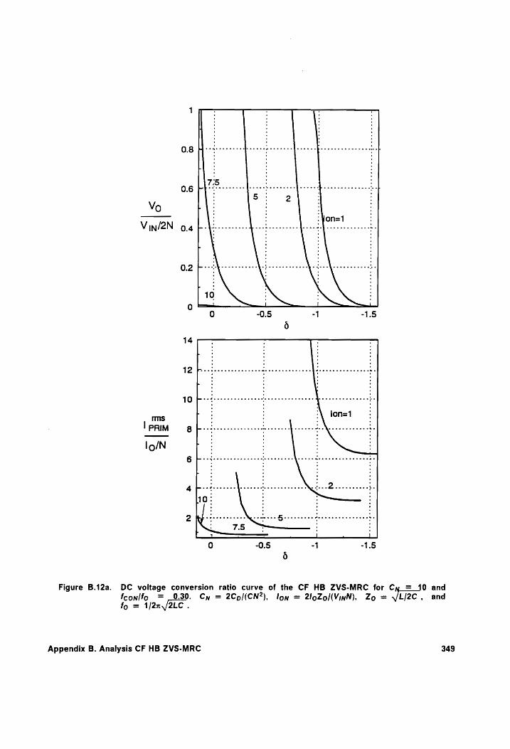
0.8
0.6
Vo
Vin/2N 94
0.2
0
14
12
10
ms
IPRIM
lo/N
6
4
2
Figure B.12a. DC voltage conversion ratio curve of the CF HB ZVS-MRC for Cy_=_40 and feonlfo = 0.30. Cy = 2Cp/(CN2), lon = 2l0Zo/(VinN), Zo = Lj2c , and
fo = 1/2n./2LC .
Appendix B. Analysis CF HB ZVS-MRC 349
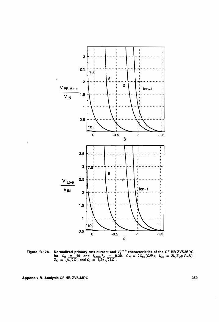
Figure B.12b. Normalized primary rms current and VP” ° characteristics of the CF HB ZVS-MRC
for Cn = 0 and foonlfo =_ 0.30. Cn = 2Cp/(CN2), lon = 2loZo/(VinN),
Zo = VL/2C , and fo = 1/2x,/2LC .
Appendix B. Analysis CF HB ZVS-MRC 350
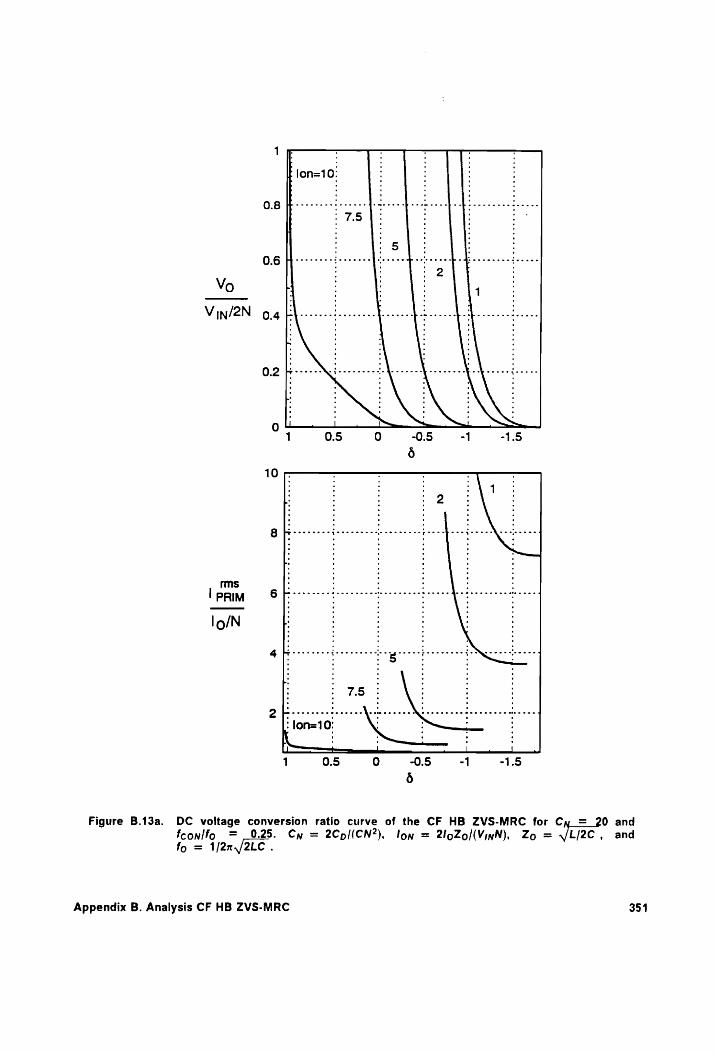
0.8
0.6 fF
Vo
Vin/2N 0.4
0.2 5
0
10 F
8 fF
rms :
IpRiM §F-
lo/N
ak
Figure B.13a. DC voltage conversion ratio curve of the CF HB ZVS-MRC for Cx = 20 and foonlfo = 0.25. Cw = 2Cp/(CN?), low = 2loZol(VinN), Zo = V/L/2C , and fo = 1/2n,/2Lc .
Appendix B. Analysis CF HB ZVS-MRC 351
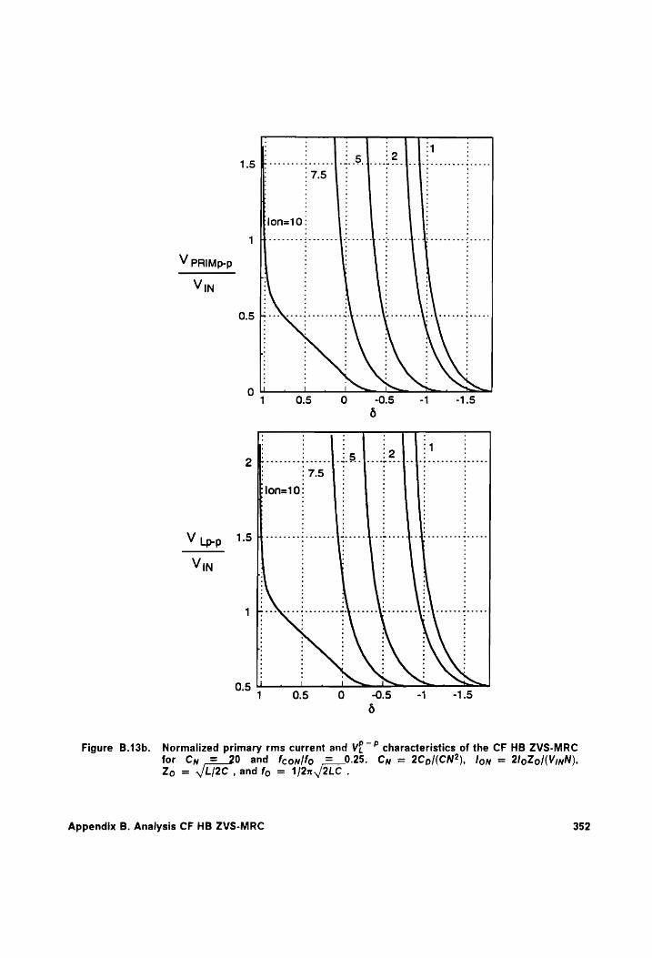
rlon=10:
were ere esc c ences Fae e eee Ae comer ee V Lop 1.5 5
0.5
Figure B.13b. Normalized primary rms current and V2 ~ ” characteristics of the CF HB ZVS-MRC for Cy = 20 and fcon/fo = 0.25. Cy = 2Cp/(CN?), lon = 2loZo/(VinN), Zo = L/2c , and fo = 1/2x,/2LC .
Appendix B. Analysis CF HB ZVS-MRC 352
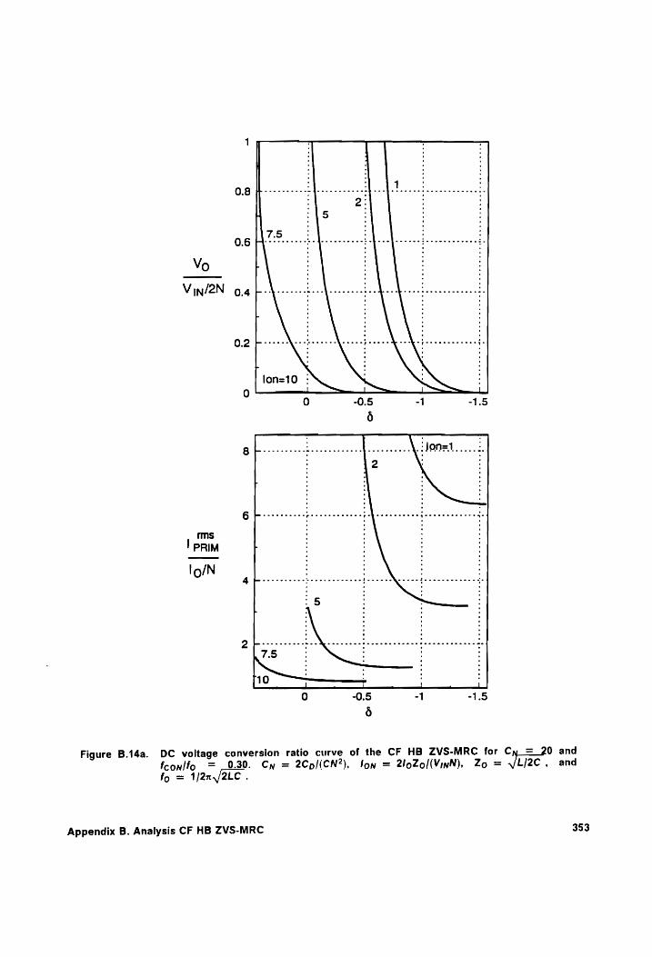
0.8
0.6
Vo
Vin/2N 0.4
0.2
ms
| PRIM
Io/N
Figure B.14a. DC voltage conversion ratio curve of the CF HB ZVS-MRC for Cy_= 20 and
foonlfo = _0.30. Cy = 2Cpn/(CN2), lon = 2loZol(VinN), Zo = Lj2c , and
fo = 1/2x,f2Lc .
Appendix B. Analysis CF HB ZVS-MRC 353
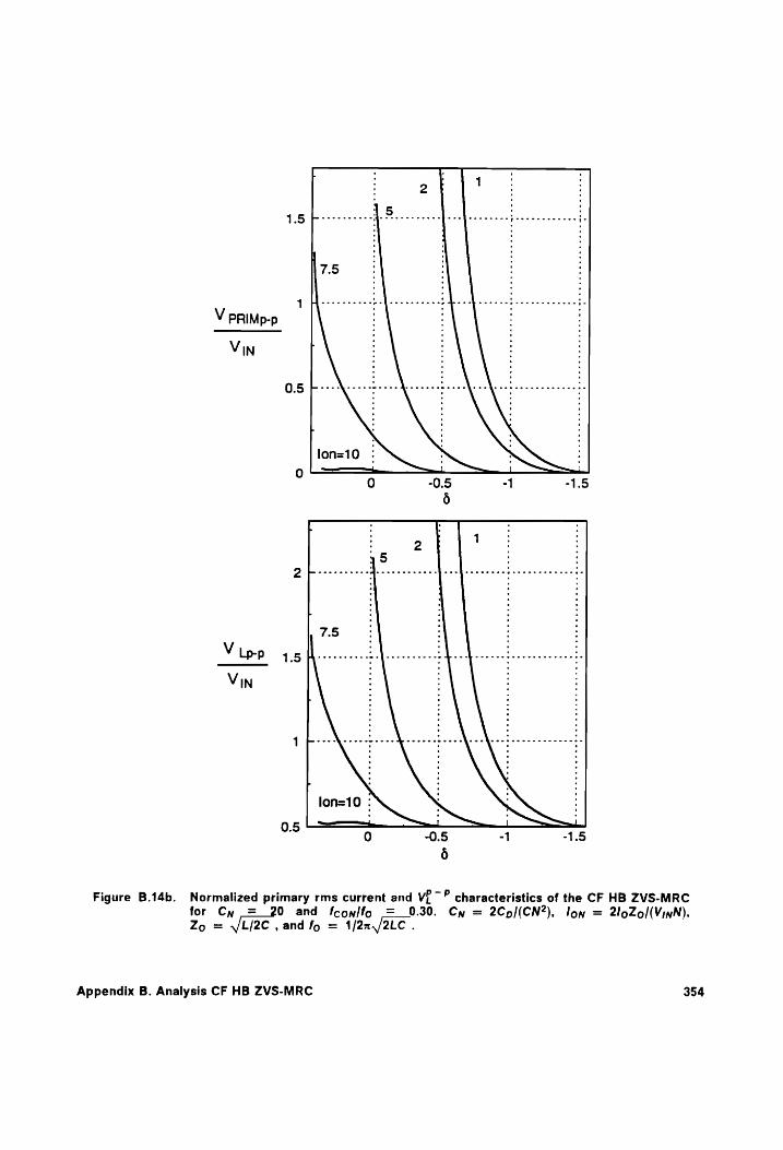
1.5
05 bo Needed A. Leones
lon=10
i ' 5
2 Lm crew cnncae . wee eww cee cbc ence ewe w eng eeeerccncennge
7.5 V Lipp 1.5 Hee e eee epee ce ence pee be ee eect ee cee eee eee ete
VIN
1 be ce hn ow meee Bcc c emcee ce ebhe ce he cet ce wesc ccccccae
Figure B.14b. Normalized primary rms current and VE ° characteristics of the CF HB ZVS-MRC for Cyn = 0 and feonlfo =_ 0.30. Cn = 2Cp/(CN2), lon = 2loZol(VinN),
Zo = VL/2C , and fo = 1/22,/2LC .
Appendix B. Analysis CF HB ZVS-MRC 354
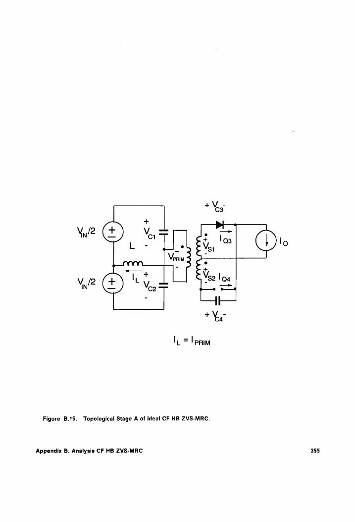
Figure B.15. Topological Stage A of ideal CF HB ZVS-MRC.
Appendix B. Analysis CF HB ZVS-MRC 355
A Verim() ao) = Verim
A laa(T ao) = !Q3
A iga(Tao) = !e4
Vaa(T ao) = 9
A VealT ao) = Vea
Equations:
diprpim( Vin
Veil) + Vppm(t) + b — a =
AVe4() WVceo(t) Vc, (t) ipria(t) = Cy —G,— — Co Gg = 2
iprina(t) = + Ligalt) — iga(O)]
igalt) + igalt) = lo
Vsi(Q) + Vso(t) = — Vea(t)
Weaa(t) iga(t) = C4 aT
Vv t Vs4(t) = Volt) = “era
Appendix B. Analysis CF HB ZVS-MRC
(B.1.d)
(B.1.e)
(B.1.f)
(B.1.9)
(B.1.h)
(B.2.a)
(B.2.b)
(B.2.c)
(B.2.d)
(B.2.e)
(B.2./)
(B.2.g)
356
From Eas. (B.1.a) - (B.2.g), it follows that:
3 Vel) | 22 Wel) _ Nilo
+ Wo = (B.3.a) ae? dt 8LCC,
where
oo=—= (B.3.b) 0 Le ~
K=_ /1 +1 (B.3.c) Cy “
2Cp Cy=—5 (B.3.a)
N2C
It should be noted that Cp/(N/2)? represents the reflected capacitance of the CF switches re-
flected into the primary. This capacitance is seen in series with switch capacitances C1 and
Co. which are effectively connected in parallel. Therefore, Cy can be regarded as a ratio of
the reflected CF switch capacitance into the primary and total primary switch capacitance,
C1+Co = 2.
Solution:
Appendix B. Analysis CF HB ZVS-MRC 357
NI Oy
A Vo, = b,( COS woKt — 1) + a, SIN WOKE +
4Cpk?
A ~byK a,K NioC
Zo Zo 2CpK*
Nio
4CpK?
A Vin VpRIM = —5 + Ba — (1 — Kg COS enoKt — (1 — K*)ag sin ogKt — t
where
a,=—2- [Ih ___lo_y AK © PRIM N(1 + Cy)
1 A Vin A
by= ee [Vprim — 3 + Ver)
(B.4.a)
(B.4.b)
(B.4.c)
(B.5.a)
(B.5.b)
Initial conditions IBrim and VeRIM are determined from the stage preceding Stage A. For
Modes |.A and II.A. it is Stage D (Eqs. (B.26.a) and (B.26.b) with negative signs at f= 7p). For
Modes I|.B and II.B, it is Stage AF (Eqs. (B.34.a) and (B.34.b) with a negative sign at time
f = Tar).
Normalizing voltages with respect to Vjjy/2, current with respect to /o/N, and time with respect
to 1/fo, Eqs. (B.4.a) - (B.4.c) become:
Appendix B. Analysis CF HB ZVS-MRC 358

AN lon _,AN 4 . ttlon Vo} = Dan cos 2nKty — 1) + 9K Urrm ~ 4G, Isin 2nKty + K2C ty (B.6.a)
N
IPRIM =— ] sin 2nKty + [lprin _ 44Cy ] cos 27Kty + > (B.6.b)
ON N K°Cy
AN 1 2 | 2, lon _,AN 1 ,
tlon
—— 'n (B.6.c) K°Cy
where
2Zolo lon = NV (B.7.a)
4 AN AN Dan = ey (Veriu — 9.5 + Vey) (B.7.b)
Stage Duration T,4 = Tai — Tao
Stage duration T, is determined from:
Vor(T a) = Vin (B.8.a)
Appendix B. Analysis CF HB ZVS-MRC 359

To solve for Ta, it is necessary to solve a transcendental equation to get the stage duration.
STAGE B [Tgo, Tai] (Fig. B.16)
Initial Conditions:
Vor(TBo) = Vin (B.9.a)
Vea(T go) = 0 (B.9.b)
iprim( Bo) = prim (B.9.c)
Vprim(7 Bo) = VpRIM (B.9.d)
iaa(TBo) = Ig3 (B.9.e)
iga(Tgo) = laa (B.9./)
Va3(7Bo0) = 9 (B.9.9)
Vaa(7B0) = Vo4 (B.9.h)
Equations:
Verim(t) +L a =— <i (B.10.a)
Appendix B. Analysis CF HB ZVS-MRC 360
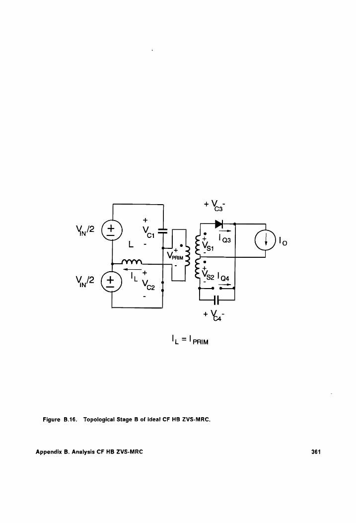
Figure B.16. Topological Stage B of ideal CF HB ZVS-MRC.
Appendix B. Analysis CF HB ZVS-MRC 361

iprim(t) = + Liga(t) — ieg(t)]
igalt) + iga(t) = Io
Vsi(0) + Vso(t) = — Vaal)
AV, (0) . Q4
iga(f) = Cp ” at
Vprim(t) Vsi(Q) = Vsal(f) = —p—
From Eqs. (B.10.a) - (B.10.f), it follows that:
2 9 2 oO Verim(f) + weCe Venn (t) = — N'Vin _ _ Vine@o
ote O~N YPRIMM, 8LCp 2Cvy
Solution:
2, Vin t ——— B —1/2 . —1
VpRIM = 4B cos moCn tf — bp sin woCn 2
1/2
B I C 4 49 lppim = + + 2 (bp cos moCy 2, _ 4B sin moCn / t)
where Zo = /L/2C_ is the characteristic impedance and
Appendix B. Analysis CF HB ZVS-MRC
(B.10.b)
(B.10.c)
(B.10.d)
(B.10.e)
(B.10.f)
(B.11)
(B.11.a)
(B.11.b)
362

B Vin ap = Vpriv + 7
25 O B
bg = —a75 Uprim — 7 Cy
or in the normalized form:
BN —1/2 —1/2 VpRIM = QBN cos anCy / ty + ben sin anCy / thy _ ¥
4/2 BN 2C _ _
ipRIM = 4 + lon (ban cos OnCy ty _— 4BN sin OnCy ty)
where
BN 4 apn = Vorim + 9
lon BN
ben = —a75 (prim — 1) 2c),
Stage Duration Tg = Tai — Tgo:
B Vprim(Ta) = 9,
Appendix B. Analysis CF HB ZVS-MRC
(B.12.a)
(B.12.b)
(B.13.a)
(B.13.b)
(B.14.a)
(B.14.b)
(B.15.a)
363

or
B iprim(Tg) = — IoIN.
STAGE C [Tco, Tc1] (Fig. B.17)
Initial Conditions:
Vor(Tco) = Vin
VealTco) = 0
C lpr co) = !pRim
Vprim(' co) = 9
C ia3(Tco) = !93
C iea(Tco) =!
Va3(Tco) = 0
VealTco) = 9
Equations:
Appendix B. Analysis CF HB ZVS-MRC
(B.15.b)
(B.16.a)
(B.16.b)
(B.16.c)
(B.16.d)
(B.16.e)
(B.16.f)
(B.16.g)
(B.16.h)
364
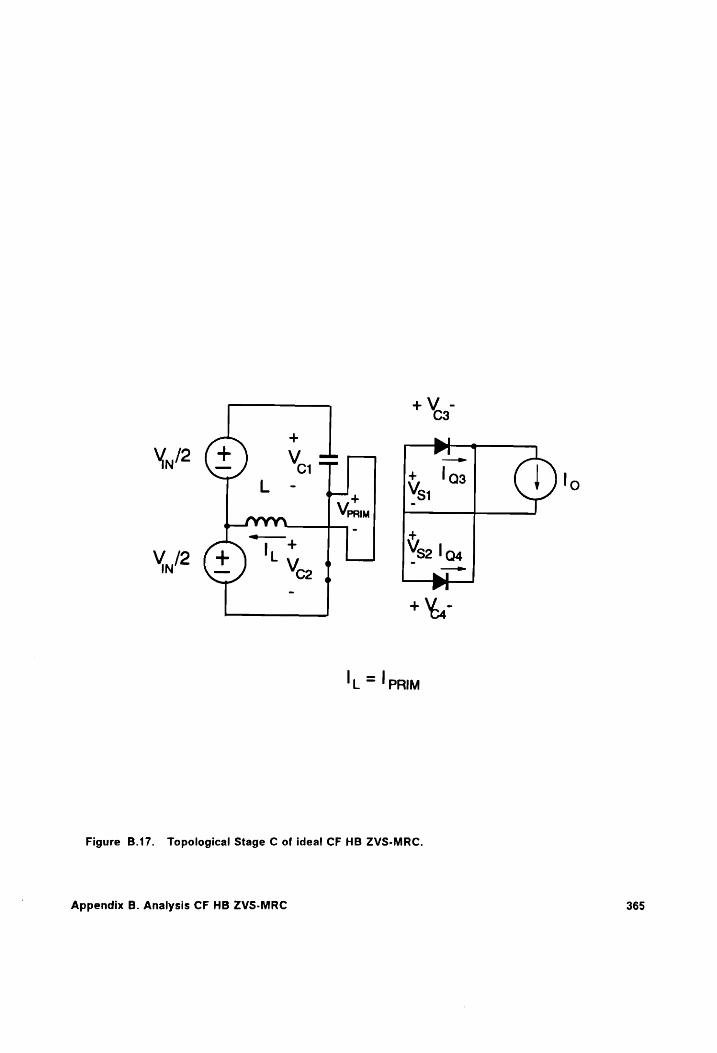
Figure B.17. Topological Stage C of ideal CF HB ZVS-MRC.
Appendix B. Analysis CF HB ZVS-MRC 365

diprim(t) | Vin dt 9 ~ 9
Solution:
Cc Cc VIN iprim = Iprim — ym
or in the normalized form:
CN CN 9 _| 2m, IPRIM = 'PRIM — lon N
Stage Duration Tc = Tci — Tco:
c O ippim(c) = — 4
and, from Eq. (B.18), it follows that:
Lc lo To= Vy Uprim + ]
Appendix B. Analysis CF HB ZVS-MRC
(B.17)
(B.18)
(B.19)
(B.20)
(B.21)
366

or in the normalized form from Eq. (B.19), it follows that:
lon CN Ton = on (prim + 1)
STAGE D [Tpo, Tp1] (Fig. B.18)
Initial Conditions:
Voi(Tpo) = Vin
Ve2(Tpo) = 0
D lppim( po) = lpr
D
Vorim( po) = Verim
D iga(Tpo0) = !e3
D igalT po) = !ea
D Va3(Tpo) = Va3
Vaa(T po) = 0
Equations:
Appendix B. Analysis CF HB ZVS-MRC
(B.22)
(B.23.a)
(B.23.b)
(B.23.c)
(B.23.d)
(B.23.e)
(B.23.f)
(B.23.g)
(B.23.h)
367
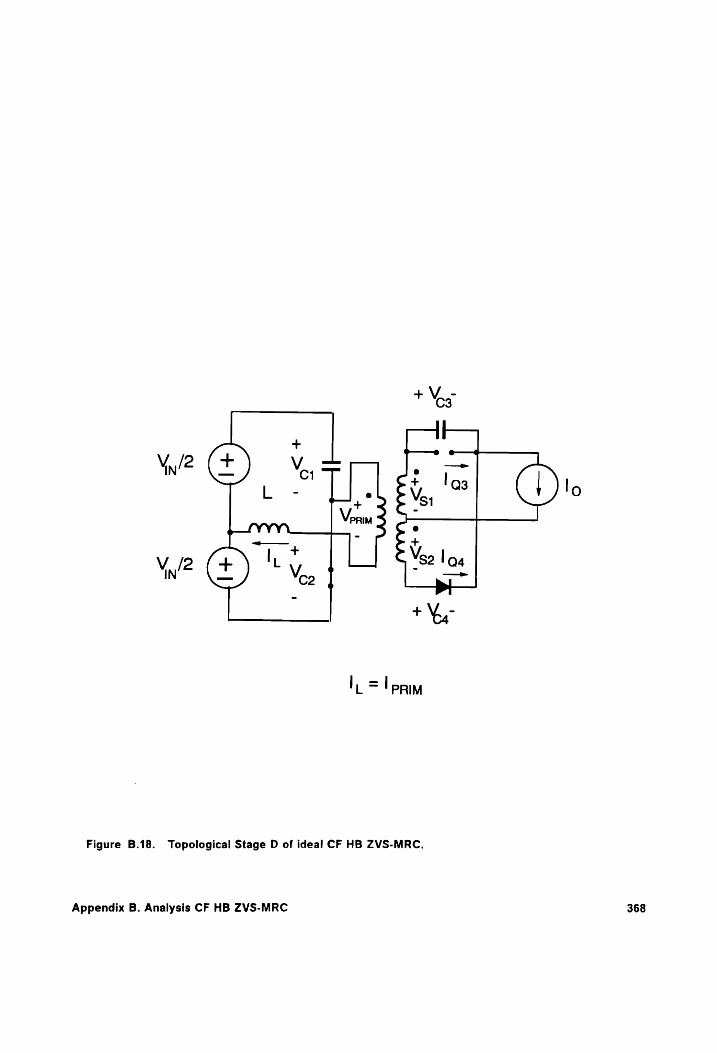
Figure B.18. Topological Stage D of ideal CF HB ZVS-MRC.
Appendix B. Analysis CF HB ZVS-MRC 368
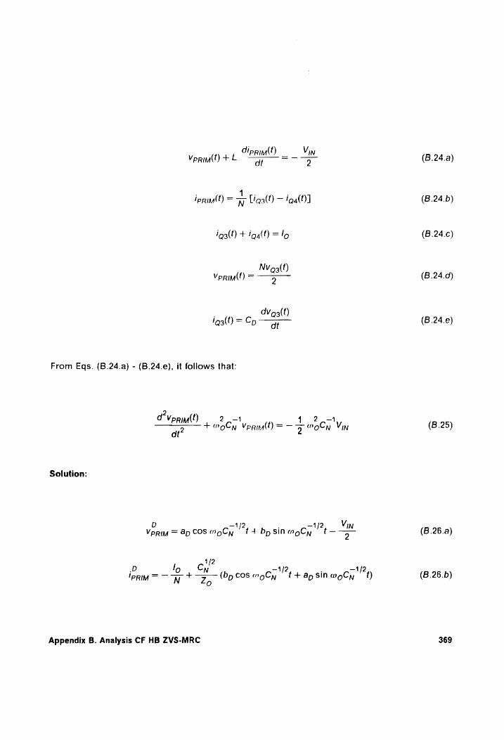
diprim(t) Vin Vprim(t) + L —~ = —
ipriv(t) = i Liga(t) ~ iga(t)]
iaa(f) + iga(t) = lo
NVaalf) Vprim(f) = —a—
Vaal) ia3(9 = Cp . dt
From Eqs. (B.24.a) - (B.24.e), it follows that:
2 'Vprim(t) 20-1 4 2.—4
ot? + MoCn Vpri(t) = 2 MmoCn Vin
Solution:
D —1/2 . ~1/2 V
VpRIM = Ap COS ingly i t4 bpsinagCy / t— >
1/2
ip c —1f2 , —1/2 ‘PRIM = — + + z (bp COS MoCy t+apsinwoCy i t)
Appendix B. Analysis CF HB ZVS-MRC
(B.24.a)
(B.24.b)
(B.24.c)
(B.24.d)
(B.24.e)
(B.25)
(B.26.a)
(B.26.b)
369

where
D Vin
Ap = Verim +
Zo__,D lo bp = —77z Uprm + ay I NC)
or in the normalized form:
DN —1/2 . —1/2 VPRIM = 4pn cos ancy fy 4. bon sin 2nCy / thy _ 3
4/2 .DN 2Cy -1/2 . ~1/2 iprpim = — 1+ lon (bon COS 2nCy ty — Apy SiN 2nCy, ty)
where
DN 4 apn = Verim + 9
lon __,DN bon = 77m prim + 1) 2C,)
Stage Duration Tp = Tp1 —Tpo
Appendix B. Analysis CF HB ZVS-MRC
(B.27.a)
(B.27.b)
(B.28.a)
(B.28.b)
(B.29.a)
(B.29.b)
370

Time duration for this stage is determined by the turn-off of the primary switches. For the half
cycle being analyzed, Tg is determined by the turn-off of switch Qo.
STAGE AF [Taro, Tari] (Fig. B.19)
Initial Conditions:
Vor(Taro) = 9 (B.30.a)
VealT aro) = Vin (B.30.b)
ippim(T aro) = lpRIM (B.30.c)
Verim(T aro) = 0 (B.30.d)
iaa(Taro) = I93 (B.30.e)
iaa(T aro) = loa (B.30.f)
Va3(Taro) = 9 (B.30.g)
Vaa(Taro) = 0 (B.30.h)
Equations:
Appendix B. Analysis CF HB ZVS-MRC 371
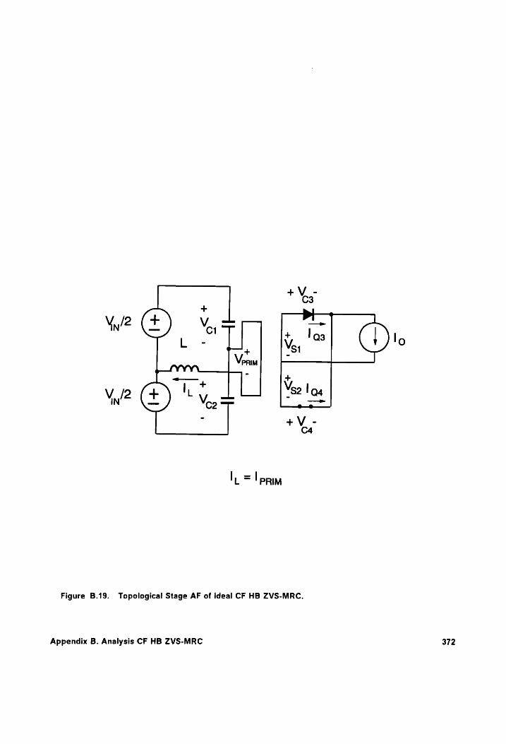
+ -
V3 an — -
+ | Q3
_— Vs} lo + . Verim
- +
Veo lag
+V - C4
I = | PRIM
Figure B.19. Topological Stage AF of ideal CF HB ZVS-MRC.
Appendix B. Analysis CF HB ZVS-MRC 372

di t V Vos(t) +L prim(t) _ iN at
. WN, (t) iprim(?) = C, dt ~ Cy at dt
iprim(t) = < Liga(t) — ie4(t)]
laa(t) + igalt) =lo
Vsi(t) = Vso(f) = 0
From Eqs. (B.30.a) - (B.31.e), it follows that:
2 2 d Ver(6) bw Wex(t) woVin wt 2
Solution:
ven = + [agar COS mot + Dar SIN wot + Vin]
iri = Zo [Dar COS mot — agg SIN of]
where
Appendix B. Analysis CF HB ZVS-MRC
Wealt) _ pe Wer)
(B.31.a)
(B.31.b)
(B.31.c)
(B.31.d)
(B.31.e)
(B.32)
(B.33.a)
(B.33.b)
373

AF Agr = 2(Ve, — 0.5)
AF
Dar = 2lprinZo
or in the normalized form:
AFN Vo4 =F + AaFn COs 2nty + Darn sin ant]
_AFN AFN arn, IPRIM = lpRim cos anty _ Thy sin arty
ON
where
AFN Aarn = 2(Veq1 — 9.5)
AFN bacn = 'primlon
Stage Duration Tar = Tari — Taro
(B.34.a)
(B.34.b)
(B.35.a)
(B.35.b)
(B.36.a)
(B.36.b)
For all modes containing stage AF, the duration of this stage is determined by the turn-off of
the CF switch. For the half cycle being analyzed it corresponds to the turn-off of CF switch
Q3.
STAGE BF [Tero, Teri] (Fig. B.20)
Appendix B. Analysis CF HB ZVS-MRC 374
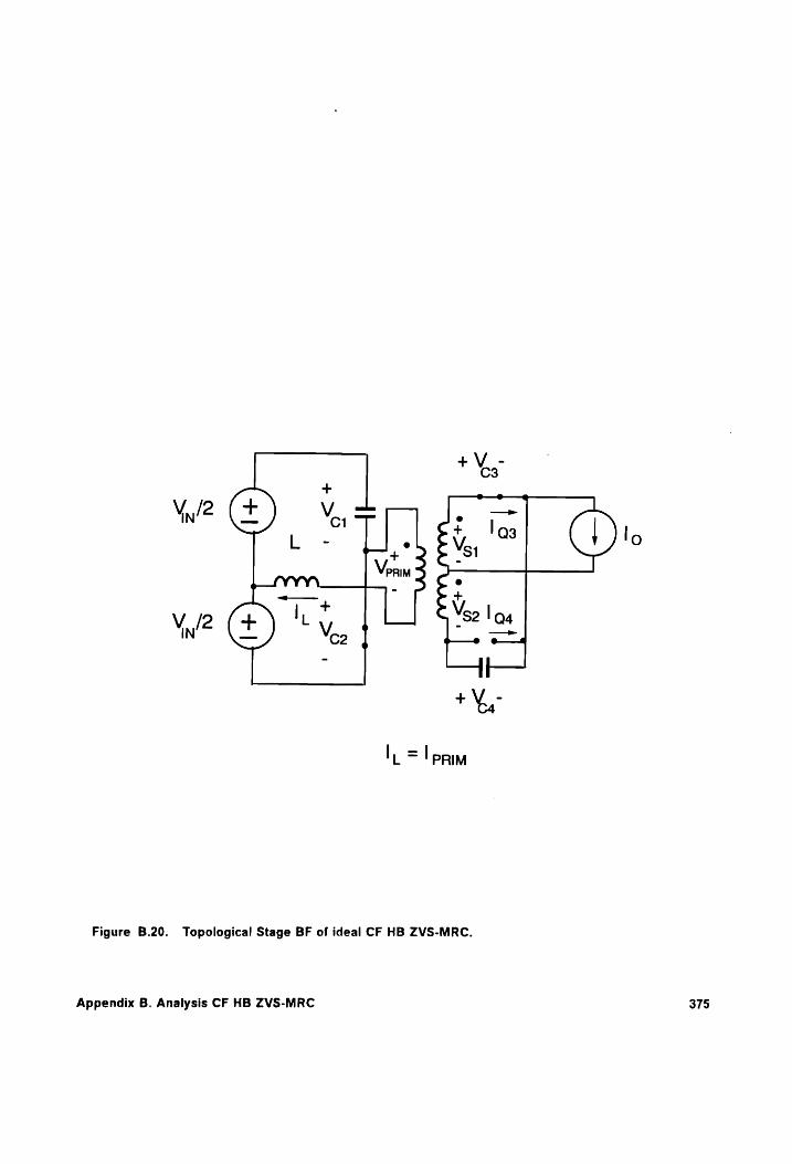
Figure B.20. Topological Stage BF of ideal CF HB ZVS-MRC.
Appendix B. Analysis CF HB ZVS-MRC 375

Initial Conditions:
Vor(T gro) = Vin (5.37.a)
Veo(TBF0) = 9 (B.37.b)
. lo,
BF Veprim( Bro) = Verim (B.37.d)
BF iaa(T Bro) = !a3 (B.37.e)
BF laa(TBFO) = laa (B.37.f)
Va3(7Bro) = 9 (B.37.g)
BF Vaa(Taro) = Vaa (B.37.h)
Equations:
dippin(t) Vin Vor (O + L dt = 2 (B.38.a)
. 1... . IpriM(D) = Fy Lias() — faalO)] (B.38.b)
Appendix B. Analysis CF HB ZVS-MRC 376
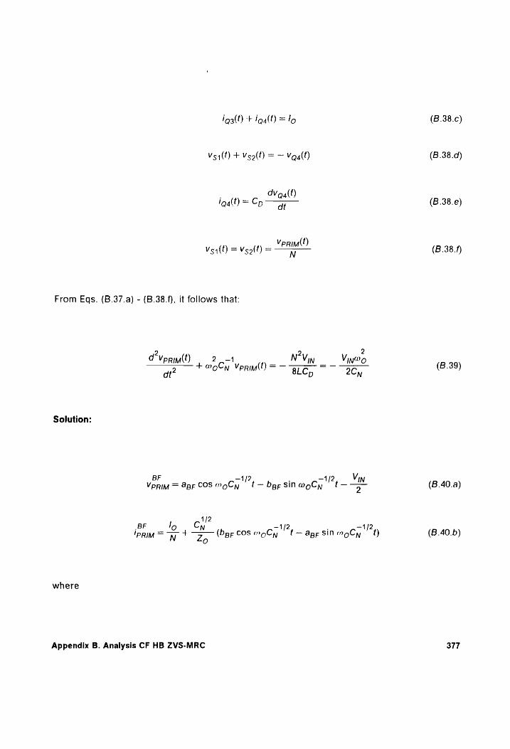
Vsi(t) + Vso(f) = — Vaglf)
AVo4(t) igg(t) = Cp ——
Vprim(o) Vsi(f) = Vsolf) = Sy
From Eqs. (B.37.a) - (B.38.f), it follows that:
2 9 2
d Vprim(f) 4 woe coy ()=- N Vin _ Vin®o
dt2 ON *PRIM ~~ 8LCp ~~ 2Cy
Solution:
BF —1/2 —1/2 V VPRIM = apr COS MoCn t— bor sin woCy / t— >
1/2
BF / C 4/2 . 499
IPRIM = W + zs (bpr cos moCly | t— apr sin mon / t)
O
where
Appendix B. Analysis CF HB ZVS-MRC
(B.38.c)
(B.38.d)
(B.38.e)
(B.38.f)
(B.39)
(B.40.a)
(B.40.b)
377

BF Vin apr = Vprim + 3
Zo. 2lo bpp =—aypz L-]
Cy
or in the normalized form:
BFN —1 12 . —1/2 N- >
1/2 .BFN —1/2 . —1/2 IpRiImM = 1+ lon (bern cos 2nCy / ty _ 4BFN sin 2nCy tn)
where
BFN 4 Aprn = Verin + >
lon been = 45
c,/?
Stage Duration Tar = Tar — Tero:
BF Verim(T pr) = 9
Appendix B. Analysis CF HB ZVS-MRC
(B.41.a)
(B.41.b)
(B.42.a)
(B.42.b)
(B.43.a)
(B.43.b)
(B.44)
378

STAGE CF [Tcro, Tcr1] (Fig. B.21)
Initial Conditions:
Voi(Tcro) = Vin
Vool(T cro) = 0
CF lppim( cro) = prim
Vprim( cro) = 0
CF ig3(Tcro) =!Q3
CF igalTcro) = !@4
Va3(T cro) = 9
Vaal(Toro) = 9
Equations:
Cipri(!) | Vin _ at 2
Solution:
Appendix B. Analysis CF HB ZVS-MRC
(B.45.a)
(B.45.b)
(B.45.c)
(B.45.d)
(B.45.e)
(B.45./)
(B.45.g)
(B.45.h)
(B.46)
379
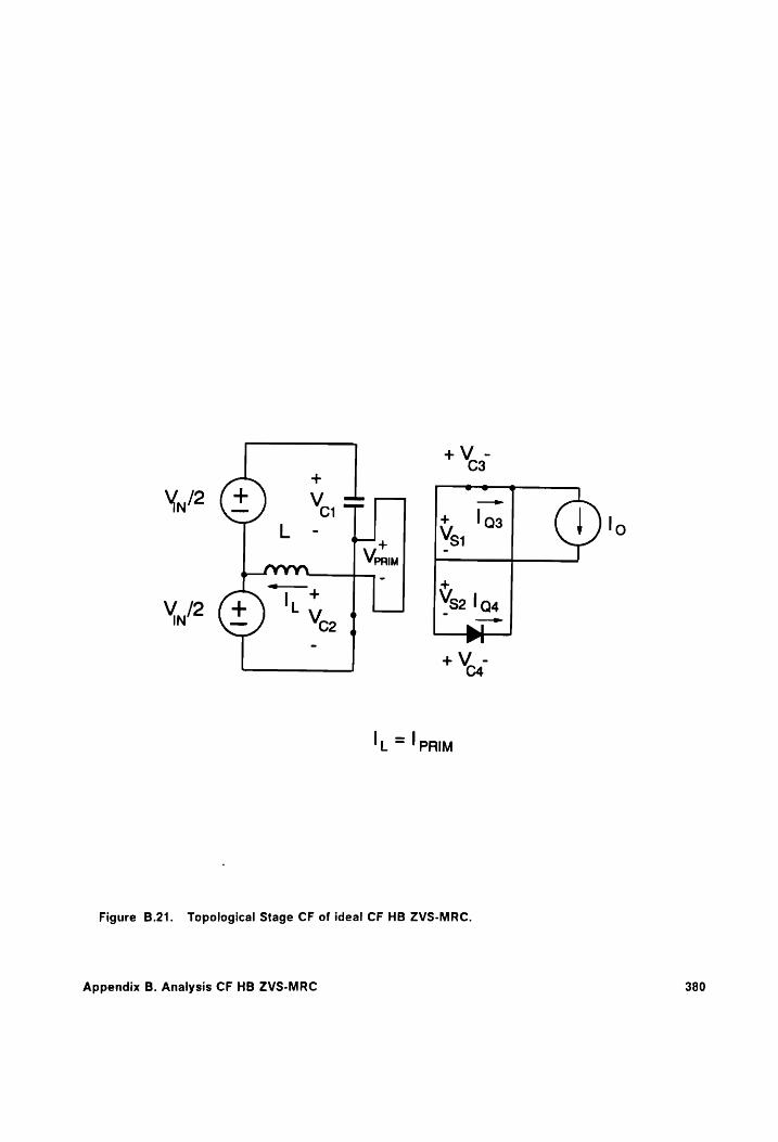
Figure B.21. Topological Stage CF of ideal CF HB ZVS-MRC.
Appendix B. Analysis CF HB ZVS-MRC 380
CFO CF Vin ‘prim = 'pRim ~ >, & (B.47)
or in the normalized form:
CFN CFN 2-7” prim = lprin ~ Ton tn (B.48)
Stage Duration Tcr = Tc1 — Teco
The duration of this stage is determined by the turn-off of the CF switch when the converter
operates in either Mode |.A or Mode Il.A. The CF switch can be either switch Q3 or Q,4 de-
pending on whether this topological stage occurs before or after Stage C. If Stage CF occurs
before Stage C, Tcr will be determined by the turn-off of switch Q4; and if Stage CF occurs after
Stage C, Tcr is determined by the turn-off of switch Q3. For Modes |.B, I.C, II.B, and II.C the
time duration Tcr is determined by the turn-off of the primary switches Q, and Qo (operation
for negative 96).
B.4 Calculating the DC Voltage-Conversion-Ratio
Appendix B. Analysis CF HB ZVS-MRC 381
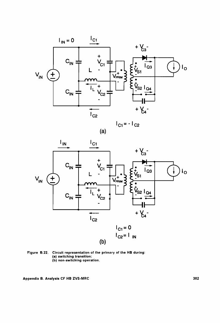
loo= | IN
(b) Figure B.22. Circuit representation of the primary of the HB during:
(a) switching transition: (b) non-switching operation.
Appendix B. Analysis CF HB ZVS-MRC 382
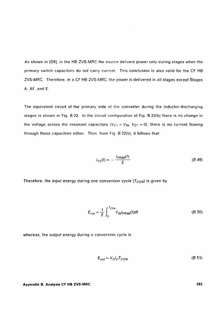
As shown in [D8], in the HB ZVS-MRC the source delivers power only during stages when the
primary switch capacitors do not carry current. This conclusion is also valid for the CF HB
ZVS-MRC. Therefore. in a CF HB ZVS-MRC, the power is delivered in all stages except Stages
A, AF, and E.
The equivalent circuit of the primary side of the converter during the inductor-discharging
stages is shown in Fig. B.22. In the circuit configuration of Fig. B.22(b) there is no change in
the voltage across the resonant capacitors (Vc1 = Vin, Vc; = 90); there is no current flowing
through these capacitors either. Thus. from Fig. B.22(b), it follows that:
] t igg(t) = — “PRM (B.49)
Therefore, the input energy during one conversion cycle (Tcon) is given by
rm]
=
Toon
Enp = | Viniprim(Hat (B.50)
whereas, the output energy during a conversion cycle is
Eout = Vololcon (B.51)
Appendix B. Analysis CF HB ZVS-MRC 383
Expression for the dc voltage-conversion-ratio is obtained by first substituting the expressions
for the primary currents in Stage B (Eq. B.11.b), Stage C (Eq. B.18), Stage D (Eq. B.26.b), Stage
BF (Eq. B.43.b), and Stage CF (Eq. B.48), into equation B.53 and integrating it. The rsulting
expression is then equated to equation B.54. In the normalized form, the following relation is
then obtained:
Vo ——9 gt Tt Tary + 2T ey + 2Taen + Toray +7 Viyl(2N) conL an + Tarn BN BEN + Torin + Toren
.CN Ton CFIN DN | Torin CF2N. .BFN. Tcron + (iprin + 1) + (ippim + lpr) —)7 + (iprRim + fprim) 9
Cy ttlon
. 1/2 —1/2 + Lopy sin 2nCy © (Ten + Teen) — Agn(1— cos 2mCy (Tan + Teew))]
Cy tlon
+ (bpy Sin 2nCy Ty — apy(1 — cos 2aCy *Tpy))] (B.52)
To calculate the dc voltage-conversion-ratio, it is necessary to find the duration of the different
topological stages. Since it requires solving transcendental equations, the voltage-
conversion-ratio can only be computed using a numerical procedure. A FORTRAN program
was used to calculate the dc voltage-conversion-ratio.
Appendix B. Analysis CF HB ZVS-MRC 384

Appendix C. Analysis of HB ZVS-MRC (Ly)
The circuit diagram of the HB ZVS-MRC (Ly) is shown in Fig. C.1. Capacitances Cy, Co, C3,
and C4 are resonant capacitances, and L:;, Lo. and Ly are the resonant inductors of the con-
verter. Since the juncticn capacitance of the rectifier diodes is not sufficiently large to obtain
the desired resonance, capacitors C3 and Cy, are usually externally added capacitors.
C.1 DC Analysis
To simplify the analysis of the HB ZVS-MRC (Ly). it is assumed that:
a) the output filter inductance is sufficiently large so that it can be approximated by a current
source with a value equal to the output current, /o;
Appendix C. Analysis of HB ZVS-MRC (Ly) 385
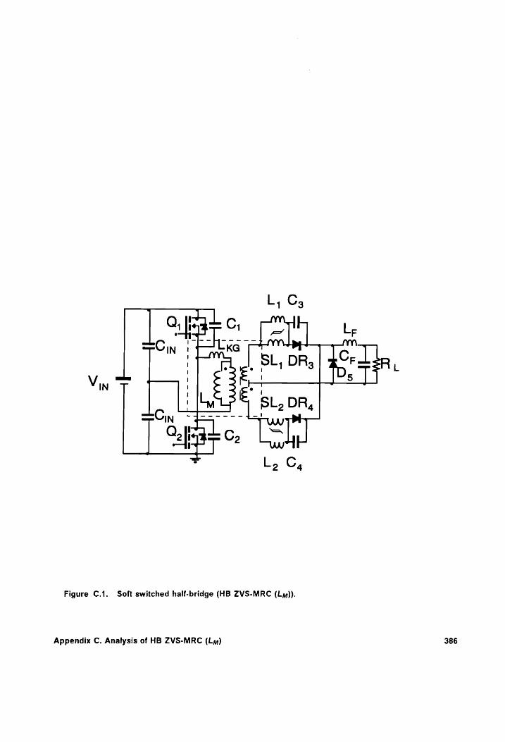
Figure C.1. Soft switched half-bridge (HB ZVS-MRC (Ly).
Appendix C. Analysis of HB ZVS-MRC (Ly) 386

b) the voltage drops across the conducting semiconductor switches (MOSFETs and diodes)
are negligible;
c) the switching times of the semiconductor switches are zero;
d) transformer leakage inductance is negligible:
e) C=C1=Co: Cpo=C3=C4; and lL =Ly =Lo:
f) the saturable inductors, SL; and SLo, are identical:
g) the slope of the saturable inductance SL; and SLo is defined by the ratio L/SL (ratio of the
linear inductance to saturable inductance): and
h) the current through the linear inductor L at the time the corresponding saturable inductor
saturates is /s4r as shown in Fig. C.2(b).
The representation of the saturable inductor is shown in Fig. C.2(a). The reactors block all
current when not saturated. Once saturated, it behaves like an inductor with very low
inductance.
During a switching cycle, the converter enters a sequence of seven or eight topological stages
during heavy load and light load operation, respectively. Again, each sequence of topological
stages represents a different mode of operation. Figure C.3 shows the different possible
topological stages.
The operation of the soft switched HB converter can be classified into four major modes of
operation. The first three modes occur for heavy load operation, while the fourth mode is
characteristic of light load operation. Light load operation is not considered essential to the
design of the converter and will not be discussed in detail.
Appendix C. Analysis of HB ZVS-MRC (Ly) 387
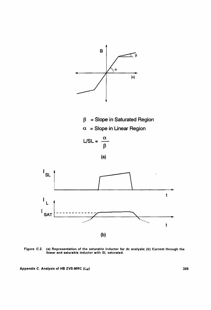
B = Slope in Saturated Region
a = Slope in Linear Region
WSL= 2 B
(a)
ot
—
Mh
| SAT [7777 TTT AN _. ae “N., i . ,
(b)
Figure C.2. (a) Representation of the saturable inductor for dc analysis; (b) Current through the linear and saturable inductor with SL saturated.
Appendix C. Analysis of HB ZVS-MRC (La) 388
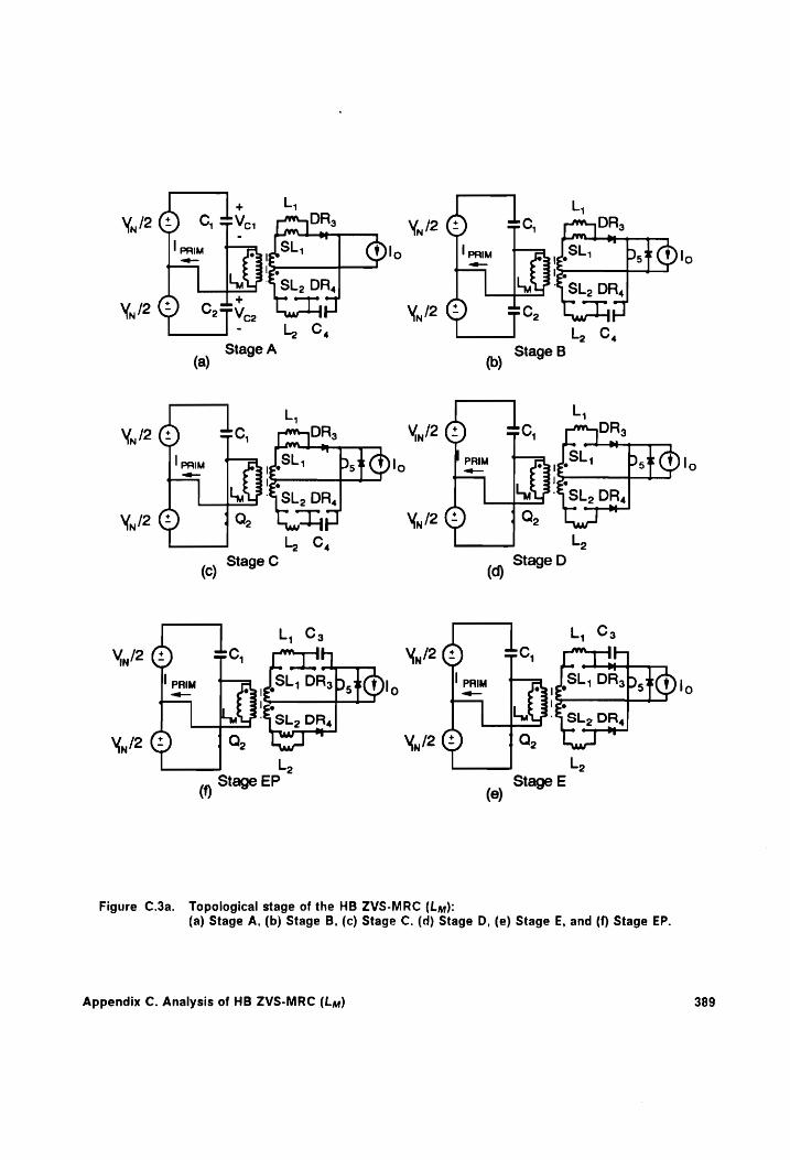
ae (c)
pee
SL, ori
win Stage C
L, Cs
a
|SL,D
I
Dee
rol
x< tp
—('+
) F =
Q
rey} +3
>
QO
oe
Oo.
Figure C.3a. Topological stage of the HB ZVS-MRC (Ly): (a) Stage A, (b) Stage B, (c) Stage C. (d) Stage D, (e) Stage E, and (f) Stage EP.
Appendix C. Analysis of HB ZVS-MRC (Ly)
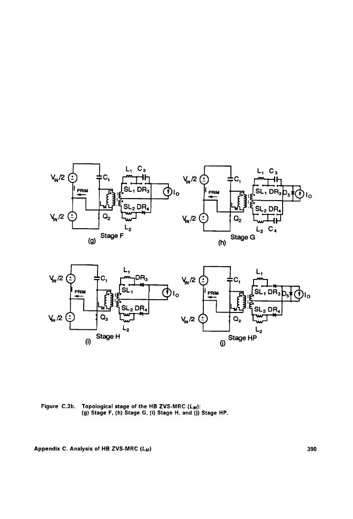
L, Cz
A (su, DR; 5% ’ lo
lee
4i?-5 s_. DR, a, i
L, Cy,
Stage G
Figure C.3b. Topological stage of the HB ZVS-MRC (Ly): (g) Stage F, (h) Stage G, (i) Stage H, and (j) Stage HP.
Appendix C. Analysis of HB ZVS-MRC (Ly) 390
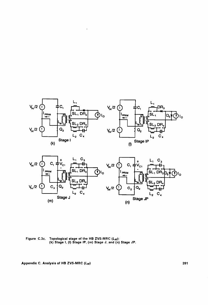
Figure C.3c. Topological stage of the HB ZVS-MRC (Ly):
(k) Stage I, (I) Stage IP, (m) Stage J, and (n) Stage JP.
Appendix C. Analysis of HB ZVS-MRC (La) 391

C.1.1 Mode | of Operation
Mode I.A
The sequence of topological stages for Mode |.A is A-B-C-D-HP-H-F. Figure C.4 shows the key
waveforms of the soft switched HB operating on this mode.
Prior to the turn-off of switch Q,, load current /o flows through the upper secondary and the
primary current flows through Q;. Voltage across Cy, ,Vci, is zero, and voltage across Co,
Vco2, is equal to the supply voltage Vin. Inductor SL, is saturated, whereas inductor Slo is
unsaturated.
Stage A [To, 71], Fig. C.3(a)
At t = To, Q, is turned off, and the primary current is diverted into C; and Co. Capacitance
C, starts charging while, C2 starts discharging at the same rate. Inductor SL; remains satu-
rated. and rectifier DR3 continues to conduct. In this stage, inductor SLo is blocking and
capacitance Cy, resonates with inductor Ly. The stage ends at time 7; when primary voltage
becomes zero, i.e.. Ve4(T4) = Voo(T1) = Vin/2.
Stage B [T}, Tz], Fig. C.3(b)
In Stage B, capacitances C; and Co start to resonate with the magnetizing inductance of the
power transformer and the negative primary voltage begins to reset SL;. The current through
SL, decreases quickly as the saturable reactor becomes unsaturated. Capacitance C, con-
Appendix C. Analysis of HB ZVS-MRC (Ly) 392
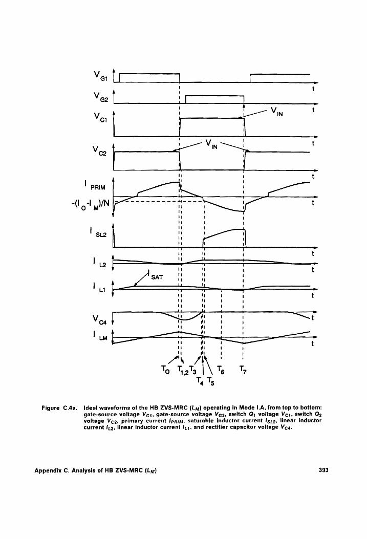
4 Voo ji
t
I hu
—
t
SL2 i
'y ' ! _
i 1 a t [ 4 ‘| at '
L2 ' ‘4 " t
sat tt ! | U4 4 ty yy ' ——— eo.
t i Hi ; 4 t "4 4 1 i
ot Vos | — ™t
it tl | t
LM tt at { ' t
iF] et ' t
" 1
Ah To Tals Tg T, T, Ts
Figure C.4a. Ideal waveforms of the HB ZVS-MRC (La) operating in Mode |.A, from top to bottom: gate-source voltage Vg;, gate-source voltage Vcg2, switch Q,; voltage Vc1, switch Q2 voltage Vc2, primary current Ipryiy, saturable Inductor current /s;,2, linear inductor current I, 9, linear inductor current /,;. and rectifier capacitor voltage Vc4.
Appendix C. Analysis of HB ZVS-MRC (La,) 393
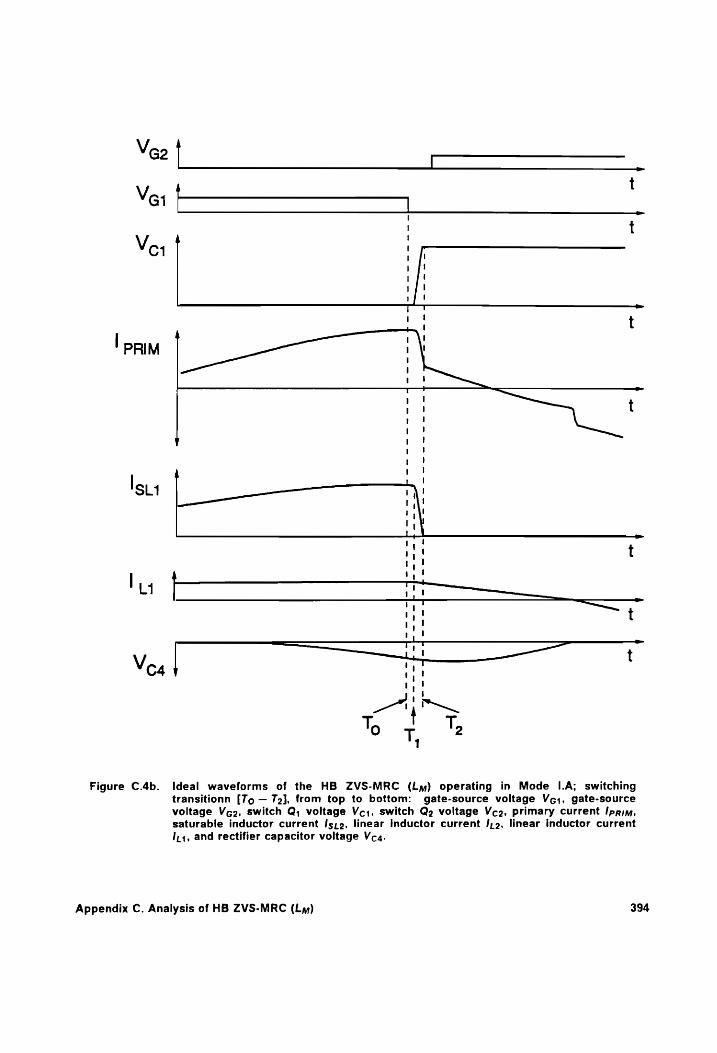
Figure C.4b. Ideal waveforms of the HB ZVS-MRC (Ly) operating in Mode I.A; switching
transitionn [To — 72], from top to bottom: gate-source voltage Vc;, gate-source voltage Veo, switch Q; voltage Vc;, switch Q2 voltage Vco, primary current Ipriy, saturable inductor current Is,2, linear Inductor current /I,2, linear inductor current I,4, and rectifier capacitor voltage Vc4.
Appendix C. Analysis of HB ZVS-MRC (Ly) 394
tinues to charge, and Co continues to discharge. At the beginning of Stage B most of the load
current is diverted to the freewheeling diode. However, rectifier DR3 continues to conduct
since a small, positive current (5-10 % of the load current) flows through inductor L;. The
current through L, decreases to zero due to the negative voltage across the upper secondary.
At the same time, inductor L» and capacitor C4 continue to resonate. This stage ends at time
Tz when the voltage across capacitor Cp becomes zero, and the antiparallel diode of Qo starts
conducting. Switch Q» should be turned on while its antiparallel diode is conducting to
achieve ZVS.
Stage C [T2, T3], Fig. C.3(c)
During Stage C, inductor L; continues to discharge. inductor Lo and capacitor C4 continue to
resonate, and saturable inductor SL; continues to reset. During this stage, the current through
SL; decreases to zero. Since the the negative voltage across the upper secondary is con-
stant (— Vin/N), current through L; decreases linearly. Also, the freewheeling diode continues
to conduct. This stage ends at time 73 when the voltage across capacitor C4 resonates to zero
and rectifier DR4 turns on.
Stage D [T3, T4], Fig. C.3(d)
In Stage D, both saturable inductors are blocking. Current through L; continues to decrease
and current through inductor Lo increases linearly. The freewheeling diode continues to carry
most of the load current. This stage ends at time T4 when inductor SL> saturates.
Stage HP [Ta4, Ts], Fig. C.3(d)
Appendix C. Analysis of HB ZVS-MRC (La) 395
In Stage HP, the current through the saturable inductor SLo increases rapidly since this
inductor is saturated. The freewheeling diode continues to conduct until the current through
SL2 is large enough to supply the load. The current through L; continues to increase and the
current through Lo to decrease in a linear manner. Stage HP ends when the sum of the cur-
rent through L1, Lo, and SL2 equals the load current there by turning the freewheeling diode
Off.
Stage H [Ts, Te], Fig. C.3(d)
In this stage, the load current is supplied by saturable inductor SL>o. The current through L,
continues to linearly decrease and the current through Ly and SLo increases also in a linear
manner. This stage ends at time 7g when the current through L; decreases to zero and diode
DR3 turns off.
Stage F [Tg, 77], Fig. C.3(f)
In Stage F, inductor SL; continues to block, and capacitor C3 begins resonating with inductor
L,. inductor SL» remains saturated and most of the load current flows through SL». This
stage ends when switch Qo is turned off. initiating a new conversion cycle.
Mode I.B
The sequence of topological stages for Mode |.B is A-B-C-D-HP-EP-F. Figure C.5 shows the
key waveforms of the soft switched HB operating on this mode.
Appendix C. Analysis of HB ZVS-MRC (Lm) 396
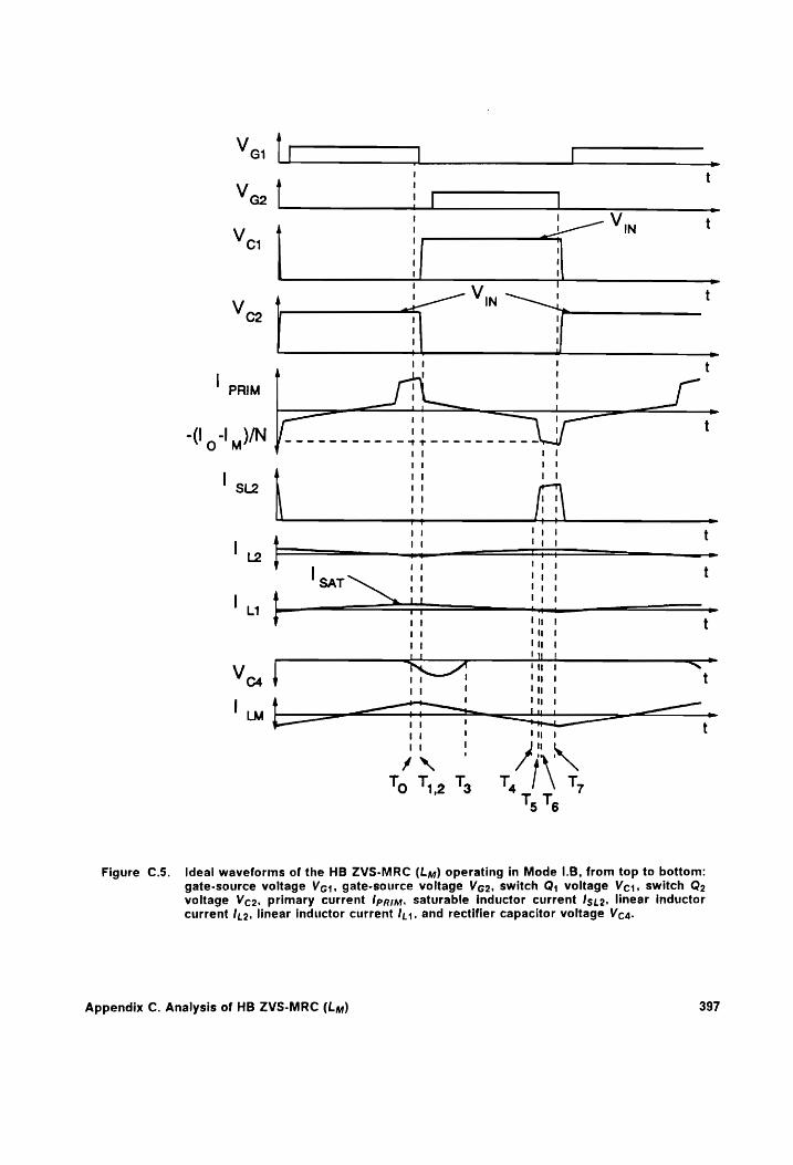
OM (1 14
ti 1 | td 'ot
SL2 v1 ri Il |
tt |
it td | 4; tt 14 t
\
~IId
E
~
( _/
V > os | 7 lim ——<—_ bu ——-
tt t Ta tt | "
a T. /} | T T. QO 1,2 3 4 7
Ts 1,
Figure C.5. Ideal waveforms of the HB ZVS-MRC (Ly) operating in Mode 1.B, from top to bottom: gate-source voltage Vg;, gate-source voltage Veo, switch Q, voltage Vc1, switch Qo voltage Veo, primary current Ipesjyy, saturable inductor current Jsz2, linear inductor current /,2, linear inductor current /,;, and rectifier capacitor voltage Vcq.
Appendix C. Analysis of HB ZVS-MRC (Ly) 397

Prior to the turn-off of switch Q,, load current /o flows through the upper secondary and the
primary current flows through Q,. Voltage across C; ,Vci, is zero, and voltage across Co,
Veco, is equal to the supply voltage Vj. Inductor SL; is saturated, whereas inductor SLo is
unsaturated.
Stage A [To, 71], Fig. C.3(a)
At t = To, Q, is turned off, and the primary current is diverted into C,; and Co. Capacitance
C, starts charging and Co starts discharging at the same rate. Inductor SL, remains saturated,
and rectifier DR3 continues to conduct. In this stage, inductor SL2 continues to block and
capacitance C4 resonates with inductor Lo. The stage ends at time 7; when primary voltage
becomes zero, t.e., Vo1(71) = Vco(T1) = Vin/2.
Stage B [71, T2], Fig. C.3(b)
In Stage B, capacitances C, and Co start to resonate with the magnetizing inductance of the
power transformer since the negative primary voltage resets SL; The current through SL,
decreases quickly as the saturable reactor becomes unsaturated. Capacitance C, continues
to charge, and C2 continues to discharge. At the beginning of Stage B, most of the load cur-
rent is diverted to the freewheeling diode. The current through L, decreases to zero due to
the negative voltage across the upper secondary. At the same time, inductor Lo and capacitor
C4 continue to resonate. This stage ends at time Tz when the voltage across capacitor Co
becomes zero, and the antiparallel diode of Qo starts conducting. Switch Q2 should be turned
on while its antiparallel diode is conducting to achieve lossless switching.
Stage C [To, T3], Fig. C.3(c)
Appendix C. Analysis of HB ZVS-MRC (Ly) 398

During Stage C, inductor L; continues to discharge, inductor Ly and capacitor C4 continue to
resonate, and saturable inductor SL, continues to reset. During this stage, the current through
SL, decreases to zero. Since the the negative voltage across the upper secondary is con-
stant (— Vin/N), current through L, decreases linearly. Also, the freewheeling diode continues
to conduct. This stage ends at time 73 when the voltage across capacitor C4 completely dis-
charges and rectifier DR, turns on.
Stage D [T3, Ta], Fig. C.3(d)
In Stage D, both saturable inductors are unsaturated and the current through L; continues to
linearly decrease and at the same time the current through inductor Lo increases linearly.
The freewheeling diode continues to carry most of the load current. This stage ends at time
Tg when inductor SLo saturates.
Stage HP [T4, Ts], Fig. C.3(j)
In Stage HP, the current through the saturable inductor SLo increases rapidly since SLo is
saturated, but this current is still not large enough to supply the load, therfore, the free-
wheeling diode continues to conduct. The current through L; continues to increase and the
current through Lo decreases linearly. This stage ends at time Ts when the current L, de-
creases to zero and diode DRz3 turns off.
Stage EP [Ts, Te], Fig. C.3(f)
Appendix C. Analysis of HB ZVS-MRC (Ly) 399

In stage EP, inductor SL, continues to reset and capacitor C3 is charged in a resonant manner
through inductor L;. Inductor SLo remains saturated and the freewheeling diode continues to
conduct. Stage EP ends when the sum of the current through Ly, Lo, and SLo increase to the
value of the load current, thereby turning the freewheeling diode off.
Stage F [Tg, T7], Fig. C.3(g)
In Stage F, inductor SL; remains unsaturated and capacitor C3 continues to resonate with
inductor L;. Inductor SLo remains saturated, and most of the load current flows through SLo.
This stage ends when switch Qo is turned off. initiating a new conversion cycle.
Mode 1.C
The sequence of topological stages for Mode I.C is A-B-C-D-E-EP-F. Figure C.6 shows the key
waveforms of the soft switched HB operating on this mode.
Prior to the turn-off of switch Q;, load current /o flows through the upper secondary and the
primary current flows through Q,. Voltage across Cy ,Vce4, is zero, and voltage across Co,
Vc2. is equal to the supply voltage Vjy. Inductor SL, is saturated, whereas inductor SLo is
unsaturated.
Stage A [To, 74], Fig. C.3(a)
At t = To, Q, is turned off, and the primary current is diverted into C, and Co. Capacitance
C, starts charging while Co starts discharging at the same rate. Inductor SL; remains satu-
rated, and rectifier DR3 continues to conduct. In this stage, inductor SL2 blocks all current and
Appendix C. Analysis of HB ZVS-MRC (La) 400
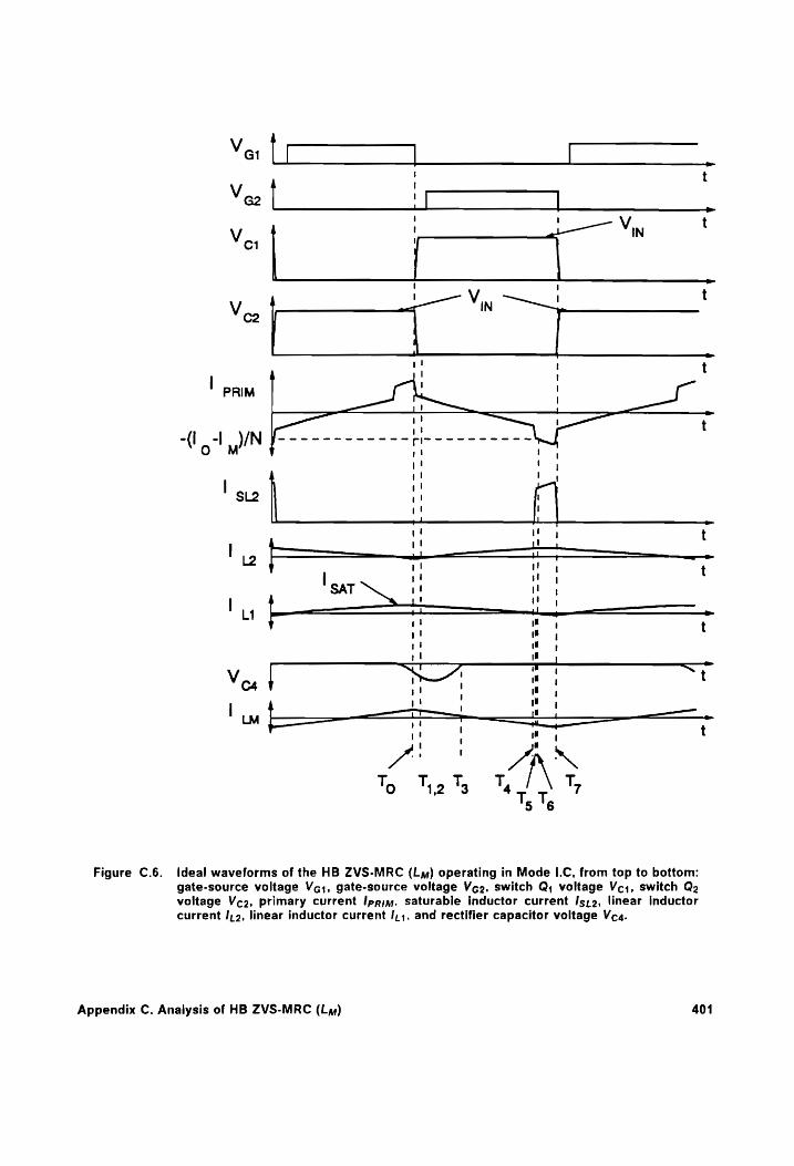
t Veo i! | _.
V j a Vin ‘
|
uw i t
-(|_-l )/N f------------ bj --- = (ly iN ri ry
1! { }
i/ I ' \
ii I
ey : Wy t 1 ! I
! |
Vt No Lt - — = :
! oy
1! | 1 | Se __
T t Vou \ a ~t
Vl |
| >
oo!
Figure C.6. Ideal waveforms of the HB ZVS-MRC (Ly) operating in Mode I.C, from top to bottom: gate-source voltage Vg;, gate-source voltage Vege, switch Q; voltage Vc, switch Q2 voltage Vc2, primary current Ippiy,, saturable inductor current Iszo, linear inductor current /,9, linear inductor current /,,. and rectifier capacitor voltage Vc.
Appendix C. Analysis of HB ZVS-MRC (Lx) 401
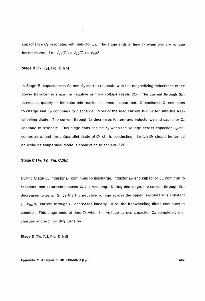
Capacitance Cy, resonates with inductor Lo. The stage ends at time 7; when primary voltage
becomes zero, i.e., Ve1(™) = Voo(™) = Vin/2.
Stage B [T4, T2], Fig. C.3(b)
In Stage B, capacitances C, and Co start to resonate with the magnetizing inductance of the
power transformer since the negative primary voltage resets SL,. The current through SL,
decreases quickly as the saturable reactor becomes unsaturated. Capacitance C, continues
to charge and Co continues to discharge. Most of the load current is diverted into the free-
wheeling diode. The current through L; decreases to zero and inductor Ly and capacitor C4
continue to resonate. This stage ends at time To when the voltage across capacitor Co be-
comes zero, and the antiparallel diode of Qo starts conducting. Switch Qz should be turned
on while its antiparallel diode is conducting to achieve ZVS.
Stage C [To, T3], Fig. C.3(c)
During Stage C, inductor L; continues to discharge, inductor Ly and capacitor C4 continue to
resonate, and saturable inductor SL, is resetting. During this stage, the current through SL,
decreases to zero. Since the the negative voltage across the upper secondary is constant
(— Vin/N), current through L; decreases linearly. Also, the freewheeling diode continues to
conduct. This stage ends at time 73 when the voltage across capacitor C4 completely dis-
charges and rectifier DR, turns on.
Stage D [T3, Ta], Fig. C.3(d)
Appendix C. Analysis of HB ZVS-MRC (Lay) 402
In Stage D, both saturable inductors are unsaturated, and current through L; continues to
linearly decrease. At the same time the current through inductor Lo increases linearly. The
freewheeling diode continues to carry most of the load current. This stage ends at time T4
when the current through L, decreases to zero turning diode DRg off.
Stage E [T4, Ts], Fig. C.3(e)
In Stage E, inductor SL, continues to reset and capacitor C3 resonates with inductor L3.
Inductor SLo is saturated and the current through Slo and Lo increases linearly. This stage
ends at time Tg when the current through Lo increases to /s,r and SL» saturates.
Stage EP [Ts, Te], Fig. C.3(f)
In stage EP, inductor SL, continues to reset and capacitor C3 begins to resonate with inductor
L,. Inductor SLo remains saturated and the freewheeling diode continues to conduct. Stage
EP ends when the sum of the current through L;. Lo, and SL» increases to the value of the load
current at which point the freewheeling diode is turned off.
Stage F [Te, T7], Fig. C.3(g)
In Stage F, inductor SL, is unsaturated and capacitor C3 resonates with inductor Ly. Inductor
SL». remains saturated, and most of the load current flows through SL. This stage ends when
switch Qo is turned off, initiating a new conversion cycle.
Appendix C. Analysis of HB ZVS-MRC (Ly) 403
C.1.2 Mode Il of Operation
In Mode II of operation the current through the linear inductor L, decreases to zero, turning
off rectifier diode DR3 before capacitor C4 completely discharges to zero. The change in po-
larity of the current through L, initiates the resonance between this inductance and rectifier
capacitance C3. In this mode. rectifier capacitances C3 and Cy, will both resonate with the
linear inductors at the same time. Mode I! results in higher dc-voltage-conversion-ratios
compared to Mode I.
Mode II.A
The sequence of topological stages for Mode II.A is A-B-C-G-JP-EP-F. Figure C.7 shows the
key waveforms of this converter operating on this mode.
Prior to the turn-off of switch Q,, load current /o flows through the upper secondary and the
primary current flows through Q,;. Voltage across C, , Vc. is zero, and voltage across Co,
Vc2, is equal to the supply voltage Vijy. Inductor SL; is saturated, whereas inductor SLo is
unsaturated.
Stage A [To, 71], Fig. C.3(a)
At t = To, Q, is turned off, and the primary current is diverted into C; and Co. Capacitance
C, starts charging and C2 starts discharging at the same rate. Inductor SL; remains saturated,
and rectifier DR3 continues to conduct. In this stage, inductor SLo is continues to reset and
Appendix C. Analysis of HB ZVS-MRC (Las) 404
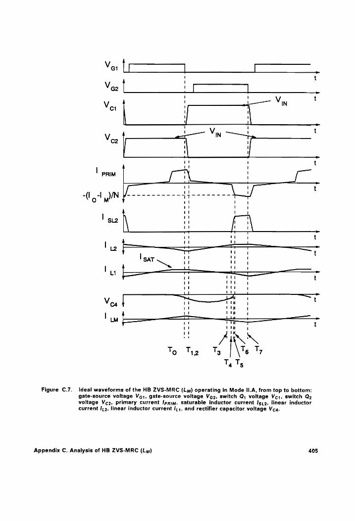
|
Veo | oe .
| | ; Ve 3 Vin ! t
I {
, ; | | -
— om mba
oe
4
mI ! 1
i I t
tl t !
ae - f \ rt t 1 _
1 tg t
ISAT Hf a
t
bee ee
— te
it
i
t
I
—
1
l
|
Figure C.7. Ideal waveforms of the HB ZVS-MRC (La) operating in Mode II.A, from top to bottom: gate-source voltage Vc¢;, gate-source voltage Vgo, switch Q; voltage Vc1, switch Q2 voltage Veco, primary current Ipaiy, saturable inductor current Is;2, linear inductor current /I,2, linear inductor current /,,, and rectifier capacitor voltage Vca.
Appendix C. Analysis of HB ZVS-MRC (Ly) 405
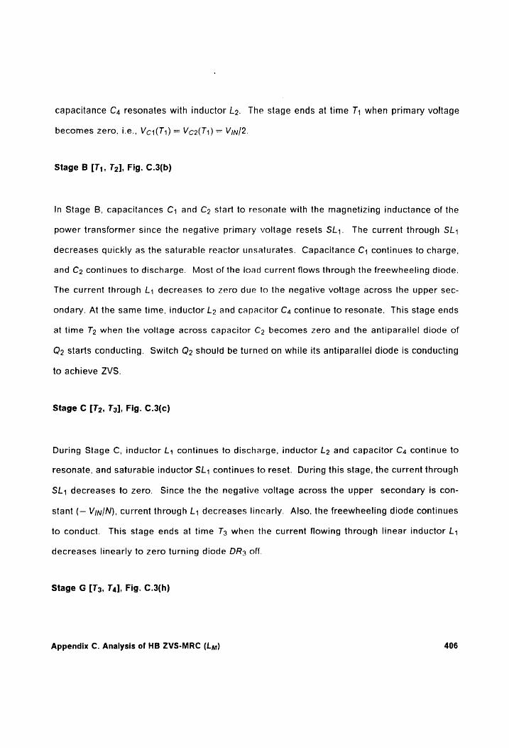
Capacitance Cy, resonates with inductor Lz. The stage ends at time 7, when primary voltage
becomes zero, i.e., Ve1(M4) = Vc2(™) = Vin/2.
Stage B [T1, T2], Fig. C.3(b)
In Stage B, capacitances C, and Co start to resonate with the magnetizing inductance of the
power transformer since the negative primary voltage resets SL; The current through SL;
decreases quickly as the saturable reactor unsaturates. Capacitance C, continues to charge,
and C2 continues to discharge. Most of the load current flows through the freewheeling diode.
The current through L, decreases to zero due to the negative voltage across the upper sec-
ondary. At the same time, inductor Lo and capacitor C4 continue to resonate. This stage ends
at time Tz when the voltage across capacitor Co becomes zero and the antiparallel diode of
Qo starts conducting. Switch Q2 should be turned on while its antiparallel diode is conducting
to achieve ZVS.
Stage C [T2, T3], Fig. C.3(c)
During Stage C, inductor L, continues to discharge, inductor Lo and capacitor C4 continue to
resonate, and saturable inductor SL, continues to reset. During this stage, the current through
SL, decreases to zero. Since the the negative voltage across the upper secondary is con-
stant (— Vin/N), current through L; decreases linearly. Also. the freewheeling diode continues
to conduct. This stage ends at time 73 when the current flowing through linear inductor L,
decreases linearly to zero turning diode DR3 off.
Stage G [T3, T4], Fig. C.3(h)
Appendix C. Analysis of HB ZVS-MRC (L4,) 406
In Stage G, inductor Lo resonates with capacitance C4 and inductor LL, resonates with
capacitance C3. The freewheeling diode continues to conduct during the duration of this
stage. Stage G ends at time 74 when the current through linear inductor Lo increases to the
value of /sar and saturable inductor SLo saturates.
Stage JP [74, Ts], Fig. C.3(n)
In this stage, inductor L; continues to resonate with the capacitance in parallel with rectifier
diode DR3, C3, and saturable inductor SL» and linear inductor Lo resonate with rectifier
Capacitance C4. The current through Slo and Lo increase but now in a resonant manner. The
freewheeling diode continues to conduct for the duration of this stage. Stage JP ends at time
Ts when capacitor C4 discharges to zero,turning diode DR, on.
Stage EP [Ts, Te], Fig. C.3(f)
In this stage, the freewheeling diode continues to conduct and inductor current /,, continues
to decrease in a resonant manner as Capacitance C3 is charged in a controlled fashion. The
current through Lz and SL2 increases in a linear manner, but the current through the saturable
reactor increases at a much faster rate. Stage |! ends when the sum of the currents through
L,, Lo, and SL» increases to the value of the load current, turning the freewheeling diode off.
Stage F [T¢, T7], Fig. C.3(g)
In Stage F, capacitor C3 continues resonating with inductor L;. Inductor SLo remains satu-
rated, and most of the load current flows through this inductor. The current through linear
Appendix C. Analysis of HB ZVS-MRC (Ly) 407

inductor Lo does not vary considerably (/19 ~/s,ar) as long as SLo remains saturated. This
stage ends when switch Qo is turned off, and a new conversion cycle is initiated.
Mode I1.B
The sequence of topological stages for Mode I!.B is A-B-C-G-E-EP-F. Figure C.8 shows the key
waveforms of the soft switched HB operating on this mode.
Prior to the turn-off of switch Q1, load current /o flows through the upper secondary and the
primary current flows through Q;. Voltage across Cy ,Vc1, is zero, and voltage across Co,
Veco, is equal to the supply voltage Vin. Inductor SL, is saturated, whereas inductor SLo is
unsaturated.
Stage A [To, 1], Fig. C.3(a)
At t = To, Q, is turned off, and the primary current is diverted into C,; and Co. Capacitance
C, starts charging, while Co starts discharging at the same rate. Inductor SL; remains satu-
rated, and rectifier DR3 continues to conduct. In this stage, inductor SLo is unsaturated and
capacitance C4 resonates with inductor Ly. The stage ends at time 7; when primary voltage
becomes zero, i.e., Vc4(T1) = Veo(TM) = Vin/2.
Stage B [T1, T2], Fig. C.3(b)
In Stage B, capacitances C, and Co start to resonate with the magnetizing inductance of the
power transformer since the negative primary voltage resets SL;. The current through SL,
decreases quickly as the saturable reactor becomes unsaturated. Capacitance C, continues
Appendix C. Analysis of HB ZVS-MRC (Ly) 408
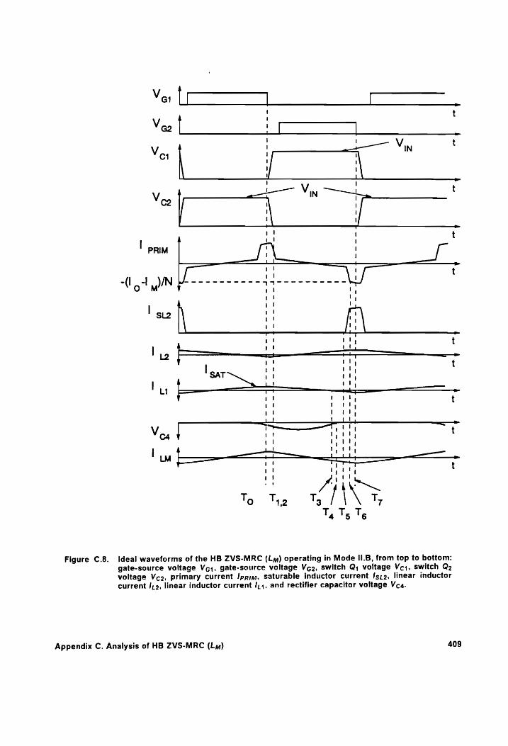
ee [—? ! t
Vea _
!
< n3
oa
-L.=--
)
<
z
-
j
: 3
j
' \ '
ty t | 4 t rity
l2 4 ; 13 ity - —;
i ' SAT ry i!
l t wae iit Li pea tf — a= _
Y 1 road, t 1 tol,
il 1outy Ll 1 ev, pa (nd
| t —™
Vos t ! rit t ! rt,
ity
Figure C.8. Ideal waveforms of the HB ZVS-MRC (Ly) operating in Mode II.B, from top to bottom:
gate-source voltage Vg, gate-source voltage Vg2, switch Q; voltage Vc1, switch Q2 voltage Vce2, primary current Ipayy, saturable Inductor current fs.2, linear inductor current /,>, linear inductor current /,;, and rectifier capacitor voltage Vcq.
Appendix C. Analysis of HB ZVS-MRC (La) 409
to charge, and Cy continues to discharge. Most of the load current is diverted into the free-
wheeling diode. The current through L; decreases to zero, at the same time, inductor Lo and
capacitor C4, continue to resonate. This stage ends at time Tz when the voltage across
capacitor C2 becomes zero and the antiparallel diode of Qo starts conducting. Switch Qo
should be turned on while its antiparallel diode is conducting to achieve ZVS.
Stage C [T2, T3], Fig. C.3(c)
During Stage C, inductor L; continues to discharge, inductor L» and capacitor C4 continue to
resonate, and saturable inductor SL, is resetting. During this stage, the current through SL,
decreases to zero and this inductor will remain unsaturated for the remaining of the switching
cycle. Since the the negative voltage across the upper secondary is constant (— Vix/N), cur-
rent through L; decreases linearly. Also, the freewheeling diode continues to conduct. This
stage ends at time T3 when the current through L; changes from positive to negative and
rectifier diode DR3 ceases to conduct.
Stage G [T73, T4], Fig. C.3(h)
In Stage G, both saturable inductors are unsaturated and current through Lo increases and
current through L, decreases in a resonant manner. Capacitance C3 charges in a controlled
manner through linear inductor L,; and capacitance C4 discharges through Lo. The free-
wheeling diode continues to carry most of the load current. This stage ends at time T, when
the voltage across rectifier capacitance C4 resonates back to zero, turning rectifier DR4 on.
Stage E [T4, Ts], Fig. C.3(e)
Appendix C. Analysis of HB ZVS-MRC (La) 410
In Stage E, inductor SL, continues to reset and capacitor C3 resonates with inductor L;.
Inducfor SL2 is unsaturated and the current through Lo increases linearly. This stage ends
at time Tg when the the current through Lo increases to the value of Isay and saturable
inductor SLo saturates.
Stage EP [Ts, Te], Fig. C.3(f)
In stage EP, inductor SL, continues to reset and capacitor C3 resonates with inductor Lj.
Inductor SLo is saturated and the freewheeling diode continues to conduct. The current
through Slo and L» increase in a linear manner. Stage EP ends when the sum of the current
through L,, Lo, and SL2 increases to the value of the load current, turning the freewheeling
diode Off.
Stage F [Tg, T7], Fig. C.3(g)
In Stage F, inductor SL; continues to reset and capacitor C3 resonates with inductor Ly.
Inductor SL>o remains saturated, and most of the load current flows through Slo. This stage
ends when switch Qo is turned off, initiating a new conversion cycle.
Mode II.C
The sequence of topological stages for Mode II.C is A-B-C-G-JP-J-F. Figure C.9 shows the key
waveforms of this converter operating on this mode.
Prior to the turn-off of switch Q;, load current /o flows through the upper secondary and the
primary current flows through Q;. Voltage across C; , Vc, is zero, and voltage across Co,
Appendix C. Analysis of HB ZVS-MRC (La) 411
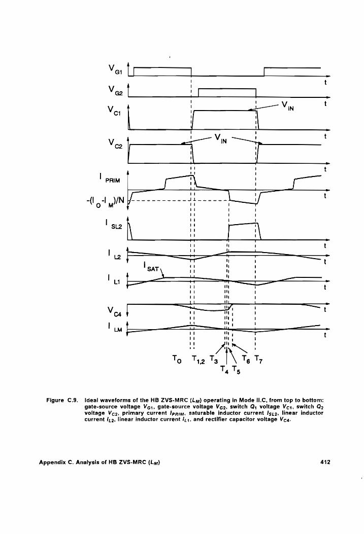
|
v pu = R
_———_>
ee
ee
~}----4.--
} }
Figure C.9. Ideal waveforms of the HB ZVS-MRC (Ly) operating in Mode II.C, from top to bottom: gate-source voltage Vcg,, gate-source voltage Vcgo, switch Q, voltage Vc, switch Q» voltage Vco, primary current Ipaia, saturable inductor current Iszo, linear inductor current /,2, linear inductor current /,;, and rectifier capacitor voltage Vcq.
Appendix C. Analysis of HB ZVS-MRC (Ly) 412
Vc2, is equal to the supply voltage Vin. Inductor SL, is saturated, whereas inductor SLo is
unsaturated.
Stage A [To, 71], Fig. C.3(a)
Att = To, Q; is turned off, and the primary current is diverted into C; and Co. Capacitance
C, starts charging, while Co starts discharging at the same rate. Inductor SL; remains satu-
rated, and rectifier DRa continues to conduct. In this stage, inductor SLo is unsaturated and
Capacitance C4 resonates with inductor Lo. The stage ends at time 7, when primary voltage
becomes zero, i.e., Ve1(T1) = Voo(T1) = Vin/2.
Stage B [7;, T2], Fig. C.3(b)
In Stage B, capacitances C, and Co start to resonate with the magnetizing inductance of the
power transformer since the negative primary voltage resets SL,. The current through SL,
decreases quickly as the saturable reactor becomes unsaturated. Capacitance C, continues
to charge, and C2 continues to discharge. Most of the load current flows through the free-
wheeling diode and the current through lL; decreases to zero due to the negative voltage
across the upper secondary. At the same time. inductor Ly and capacitor C4 continue to res-
Onate. This stage ends at time 72 when the voltage across capacitor Co becomes zero and
the antiparallel diode of Qz starts conducting. Switch Q2 should be turned on while its anti-
parallel diode is conducting to operate with ZVS.
Stage C [To, T3], Fig. C.3(c)
Appendix C. Analysis of HB ZVS-MRC (Ly) 413
During Stage C, inductor L; continues to discharge, inductor Lo and capacitor C4 continue to
form a resonant network, and saturable inductor SL, continues to reset. During this stage, the
current through SL; decreases to zero and this saturable reactor will block all current for the
remaining of the switching cycie. Since the the negative voltage across the upper secondary
is constant (— Vin/N), current through L;, decreases linearly. Also, the freewheeling diode
continues to conduct. This stage ends at time T3 when the current flowing through linear
inductor L; decreases to zero, turning diode DR3 off.
Stage G [T3, T4], Fig. C.3(h)
In Stage G, inductor Lo resonates with capacitance C4 and inductor L; resonates with
Capacitance C3. The freewheeling diode continues to conduct during the duration of this
stage. Stage G ends at time 74 when the current through linear inductor Lo increases to the
value of /sgy and saturable inductor SLo saturates.
Stage JP [T4, Ts], Fig. C.3(n)
In this stage, inductor L; continues to resonate with the capacitance in parallel with rectifier
diode DR3, C3, and saturable inductor SL> and linear inductor Lo resonate with rectifier
capacitance C4. The current through SLo2 and Lo increases in a resonant manner, and the
freewheeling diode continues to conduct for the duration of this stage. Stage JP ends at time
Ts when the sum of the current through SLo. Lo. and L4 increases to the value of the load
current turning the freewheeling diode off.
Stage J [Ts, Ts], Fig. C.3(m)
Appendix C. Analysis of HB ZVS-MRC (Ly) 414
In this stage, the freewheeling diode is off and inductor current /;4 decreases in a resonant
manner as capacitance C3 is charged in a controlled fashion. Saturable inductor SL» is satu-
rated and supplies most of the load current. Rectifier capacitance C4 continues to discharge
in a resonant manner as it interacts with SLo. Lo. L1, and C3. The load current is mostly sup-
plied by the lower rectifier circuit. Stage J ends when rectifier capacitance C4 discharges to
zero and rectifier diode DR, turns on.
Stage F [Tg, T7], Fig. C.3(g)
In Stage F, capacitor C3 continues resonating with inductor Ly. Inductor SLo remains saturated
and most of the load current flows through SL. The current through linear inductor Lo does
not vary considerably (/12 ~/sar) as long as SLo remains saturated. This stage ends when
switch Qo is turned off, and a new conversion cycle is initiated.
C.1.3 Mode Ill of Operation
In Mode III of operation SL» saturates before capacitor C4 discharges completely (Mode | of
operation) or the current through linear inductor L1 reverses its polarity (Mode II of operation).
This mode maximizes the time duration of the power transferring stages, resulting in higher
dc voltage-conversion ratios compared to the two previous modes of operation.
Mode III.A
Appendix C. Analysis of HB ZVS-MRC (Laz) 415
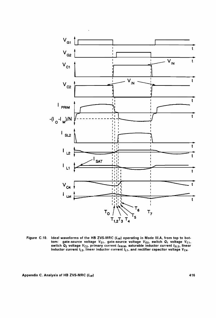
Ve: [7] [_— t Vee —_ G2 | ~
V t Voy | ! + IN
| ; ! t | BRIM cm ! —
7 ! t “lo?! win f- TT TTT 1 ,
se | io 7 ; t
_——— Ve La . er. ee i ot
7! sat iti! ly t rt -
ft ity! I IN To . Ty Tals T,
Figure C.10. Ideal waveforms of the HB ZVS-MRC (Ly) operating in Mode III.A, from top to bot- tom: gate-source voltage Vg;, gate-source voltage Vgo, switch Q; voltage Vey, switch Q2 voltage Vco, primary current Ipajy, saturable inductor current /s;9, linear inductor current Io, linear inductor current /,;, and rectifier capacitor voltage Vcq.
Appendix C. Analysis of HB ZVS-MRC (Ly) 416

The sequence of topological stages for Mode Ill.A is A-B-C-IP-I-H-F. Figure C.10 shows the key
waveforms of the HB ZVS-MRC (Li) operating on this mode.
Prior to the turn-off of switch Q,, load current /o flows through the upper secondary and the
primary current flows through Q;. Voltage across C,; ,Vci, is zero, and volfage across Co,
Vco, is equal to the supply voltage Vjy. Inductor SL; is saturated, whereas inductor SL» is
unsaturated.
Stage A [To, T4], Fig. C.3(a)
At tf = To, Q, is turned off, and the primary current is diverted into C; and Co. Capacitance
C, starts charging, while Co starts discharging at the same rate. Inductor SL, remains satu-
rated, and rectifier DR3 continues to conduct. In this stage, inductor SL» is unsaturated and
capacitance C4 resonates with inductor Lo. The stage ends at time 7; when primary voltage
becomes zero.
Stage B [T7}, To], Fig. C.3(b)
In Stage B, capacitances C, and Co start to resonate with the magnetizing inductance of the
power transformer since the negative primary voltage resets SL;. The current through SL,
decreases quickly as the saturable reactor unsaturates. Capacitance C, continues to charge,
and Co continues to discharge. At the beginning of Stage B most of the load current is di-
verted to the freewheeling diode. The current through L; decreases to zero and inductor Lo
and capacitor C4 continue to resonate. This stage ends at time 72 when the voltage across
capacitor Cp becomes zero, and the antiparallel diode of Qo starts conducting. Switch Qo
Appendix C. Analysis of HB ZVS-MRC (Ly) 417

should be turned on soon after while its antiparallel diode is conducting to achieve lossless
switching.
Stage C [To, T3], Fig. C.3(c)
During Stage C, inductor L; continues to discharge, inductor Lo and capacitor C4 continue to
resonate, and saturable inductor SL, continues to reset. During this stage, the current through
SL; decreases to zero. Since the the negative voltage across the upper secondary is con-
stant (— Vin/N), current through L, decreases linearly. Also, the freewheeling diode continues
to conduct. This stage ends at time 73 when saturable inductor SLo saturates.
Stage IP [T3, T4], Fig. C.3(I)
In Stage IP, inductor Lo and saturable inductor SLo resonate with capacitance C4. Inductor
L, continues to decrease linearly and the freewheeling diode conducts. Stage IP ends at time
T4 when the sum of the current flowing through L;. Lo, and SLo increases to the value of the
load current and the freewheeling diode ceases to conduct.
Stage | [T4, Ts], Fig. C.3(k)
In this stage, inductors L;, Lo, and SLo resonate with capacitance C4. SLo supplies most of the
load current and the freewheeling diode is off. At time 75 the voltage across capacitor C4
completely discharges and rectifier DR, is turned on.
Stage H [Ts, Te], Fig. C.3(i)
Appendix C. Analysis of HB ZVS-MRC (La,) 418

In this stage, the load current is supplied by the lower rectifier circuit. The current through L,
continues to decrease and the current through Lz and SLo increases in a linear manner. This
stage ends at time Tg when the current through L; decreases to zero and diode DR3 turns off.
Stage F [T¢, T7], Fig. C.3(g)
In Stage F, inductor SL; continues to reset and capacitor C3 begins resonating with inductor
L,. Inductor SLy remains saturated, and most of the load current flows through SLo. This
stage ends when switch Qo2 is turned off. beginning a new conversion cycle.
Mode III.B
The sequence of topological stages for Mode III.B is A-B-C-IP-HP-H-F. Figure C.11 shows the
key waveforms of this converter operating on this mode.
Prior to the turn-off of switch Q,, load current /o flows through the upper secondary and the
primary current flows through Q,. Voltage across C, , Vc1, is zero, and voltage across Co,
Vc2, is equal to the supply voltage Vjy. Inductor SL, is saturated, whereas inductor SLo is
unsaturated.
Stage A [To, 11], Fig. C.3(a)
At t = To, Q; is turned off. and the primary current is diverted into C,; and Co. Capacitance
C, starts charging, while Co starts discharging at the same rate. Inductor SL; remains satu-
rated, and rectifier DR3 continues to conduct. In this stage, inductor SL is unsaturated and
Appendix C. Analysis of HB ZVS-MRC (Ly) 419
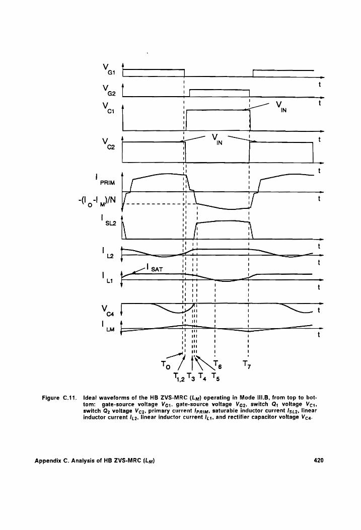
Gt | J t
!
t
Veo | 7 . ' ! t
ci ; mat
' q _
Vio 4 a Vin 1 t
i t | RIM | : ! rT
“(I 1 QIN /- oe A at t
SL2
' yPotd t t
| sat ae I {- oo — _
’ ou f t t
mE bg jt tt ' ' oe
7 \! it ' '
My fee
{
Figure C.11. Ideal waveforms of the HB ZVS-MRC (Ly) operating in Mode III.B, from top to bot- tom: gate-source voltage Vg;, gate-source voltage Vcg2, switch Q, voltage Vc, switch Q2 voltage Vco, primary current Ipriy, saturable inductor current /sz2, linear inductor current /,o, linear inductor current /,4, and rectifier capacitor voltage Vcq.
Appendix C. Analysis of HB ZVS-MRC (Ly) 420

capacitance C4 resonates with inductor Lo. The stage ends at time 7, when primary voltage
becomes zero, i.e., Ve1(71) = Vcoo(™) = Vin/2.
Stage B [74, Ta], Fig. C.3(b)
In Stage B, capacitances C, and Co start to resonate with the magnetizing inductance of the
power transformer since the negative primary voltage resets SL;. The current through SL,
decreases quickly as the saturable reactor becomes unsaturated. Capacitance C,; continues
to charge, and Co continues to discharge. Most of the load current flows through the free-
wheeling diode. The current through L; decreases to zero due to a negative voltage across
the upper secondary. At the same time, inductor Lo and capacitor C4 continue to resonate.
This stage ends at time Tz when the voltage across capacitor Cp becomes zero and the anti-
parallel diode of Qo starts conducting. Switch Qo should be turned on while its antiparallel
diode is conducting to achieve ZVS.
Stage C [T2, T3], Fig. C.3(c)
During Stage C, inductor L; continues to discharge, inductor Lo and capacitor C4 continue to
resonate. and saturable inductor SL; continues to reset. During this stage, the current through
SL, decreases to zero. Since the the negative voltage across the upper secondary is con-
stant (— Vijn/N), current through L; decreases linearly. Also, the freewheeling diode continues
to conduct. This stage ends at time 73 when saturable inductor SL2 saturates.
Stage IP [T3, T4], Fig. C.3(I)
Appendix C. Analysis of HB ZVS-MRC (La) 421
In Stage IP, inductor L» and saturable inductor SL2 resonate with capacitance C4. Inductor
L, continue to decrease linearly and the freewheeling diode conducts. Stage IP ends at time
Tg when capacitor C4 has completely discharged and diode DR, turns on.
Stage HP [T4, Ts], Fig. C.3(j)
In this stage, inductor current i,4(f) continues to decrease and the current through Lo and
SLo increases linearly. Stage HP ends when the sum of the current flowing through Ly, Lo,
and SL» increases to the value of the load current.
Stage H [Ts, Te], Fig. C.3(i)
In this stage, the load current is supplied by the lower rectifier circuit. The current through
L, continues to decrease and the current through Lo and SL»> increases in a linear manner.
This stage ends at time 7g when the current through L4 decreases to zero and diode DR3 turns
off.
Stage F [Ts, T7], Fig. C.3(g)
In Stage F, inductor SL; remains unsaturated and capacitor C3 begins resonating with inductor
L4. Inductor SL> remains saturated and most of the load current flows through SLo. This stage
ends when switch Qo is turned off, and a new conversion cycle is initiated.
Mode I11.C
Appendix C. Analysis of HB ZVS-MRC (La) 422
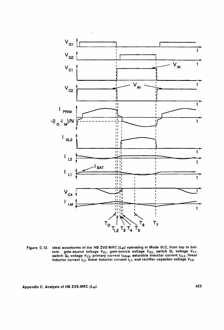
; t
Veo | se : Vo, t ! ot VN t
y i
| , - Veo | eV Oe t
i t
ey 4 T ra | 1 \
L1 ’ + FF — —— Sie
Het, ! ' t a, t 1
it ! Vt 1 a Vent
t t 1
Figure C.12. Ideal waveforms of the HB ZVS-MRC (Ly) operating in Mode III.C, from top to bot- tom: gate-source voltage Vg;, gate-source voltage VcG2, switch Q; voltage Vc1, switch Q2 voltage Vco, primary current Ipaiy, saturable inductor current Isc, linear inductor current /,2. linear inductor current /,4, and rectifier capacitor voltage Vcq.
Appendix C. Analysis of HB ZVS-MRC (Ly) 423

The sequence of topological stages for Mode III.C is A-B-C-IP-I-J-F. Figure C.12 shows the key
waveforms of this converter operating on this mode.
Prior to the turn-off of switch Q,, load current /o flows through the upper secondary and the
primary current flows through Q,;. Voltage across C, , Vc}, is zero, and voltage across Co,
Veco, is equal to the supply voltage Viy. Inductor SL, is saturated, whereas inductor SLo is
unsaturated.
Stage A [To, T1], Fig. C.3(a)
At t = To, Q, is turned off, and the primary current is diverted into C, and Co. Capacitance
C, starts charging, while Co starts discharging at the same rate. Inductor SL, remains satu-
rated, and rectifier DR3 continues to conduct. In this stage, inductor SL» is unsaturated and
capacitance C4 resonates with inductor Lo. The stage ends at time 7; when primary voltage
becomes zero, i.e., Vc1(71) = Vcoo(T1) = Vin/2.
Stage B [T}, T2], Fig. C.3(b)
In Stage B, capacitances C; and Co start to resonate with the magnetizing inductance of the
power transformer since the negative primary voltage resets SL). The current through SL,
decreases quickly as the saturable reactor becomes unsaturated. Capacitance C, continues
to charge, and Co continues to discharge. Most of the load current flows through the free-
wheeling diode. The current through L, decreases to zero due to a negative voltage across
the upper secondary. At the same time, inductor Ly and capacitor C4 continue to resonate.
This stage ends at time Tz when the voltage across capacitor Co becomes zero and the anti-
Appendix C. Analysis of HB ZVS-MRC (Ly) 424
parallel diode of Qz starts conducting. Swilch Q2 should be turned on while its antiparallel
diode is conducting to achieve ZVS.
Stage C [To2, T3], Fig. C.3(c)
During Stage C, inductor L, continues to discharge, inductor Lo and capacitor C4 continue to
resonate, and saturable inductor SL; continues to reset. During this stage, the current through
SL, decreases to zero and since the the negative voltage across the upper secondary is
constant (— Vin/N). current through L; decreases linearly. Also, the freewheeling diode con-
tinues to conduct. This stage ends at lime 73 when the current through Lo increases to the
value of /sa7 and saturable inductor SL» saturates.
Stage IP [T3, Ta], Fig. C.3(1)
In Stage IP, inductor Lo and Slo resonates with capacitance C4. Inductor L, continues to de-
crease linearly and the freewheeling diode continues to conduct. Stage IP ends at time 7,4
when the sum of the current flowing through L,. Lo. and SLo increases to the value of the load
current.
Stage | [T4, Ts], Fig. C.3(k)
In this stage, inductor current i,4(f) continues to linearly decrease and the current through Lo
and SL» increases in a resonant manner. The freewheeling diode is off and the load current
is supplied by the lower rectifier circuit. This stage ends at time T5 when the current through
L, decreases to zero turning diode DRa off.
Appendix C. Analysis of HB ZVS-MRC (Ly) 425

Stage J [T5, Te], Fig. C.3(m)
In this stage, the load current is supplied by the lower rectifier circuit. The current through
L, decreases and the current through Lo and SLo2 increases in a resonant manner (interaction
with C3 and C4). This stage ends at time 7g when the voltage across C4 resonates back to zero
turning diode DR, on.
Stage F [T6, T7], Fig. C.3(g)
In Stage F, inductor SL, is unsaturated and capacitor C3 begins resonating with inductor Lj.
Inductor SLo remains saturated, and most of the load current flows through this inductor. This
stage ends when switch Qa» is turned off, and a new conversion cycle is initiated.
Mode III.D
The sequence of topological stages for Mode III.D is A-B-C-IP-HP-EP-F. Figure C.13 shows the
key waveforms of this converter operating on this mode.
Prior to the turn-off of switch Q;. load current /o flows through the upper secondary and the
primary current flows through Q,. Voltage across C; ,Vc;, is zero, and voltage across Co,
Vco, is equal to the supply voltage Viy. Inductor SL, is saturated, whereas inductor SLo is
unsaturated.
Stage A [To, 71], Fig. C.3(a)
Appendix C. Analysis of HB ZVS-MRC (Ly) 426
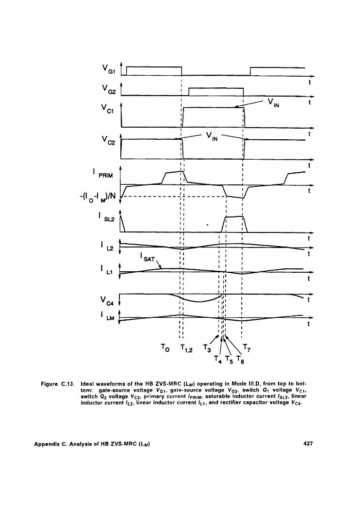
| |
t
Veo | | C7 . v4 a «DVN t
C1 ;
| !
! |
o & 3
-
hb
Zi4q
lrir
crzc
d t
lio ———— I ; — rr 4 SAT Vy ' '
| ‘ \ i! tt eg . I oe Oe am 7 ——— -
‘| rn | Ly ral k ~ _ eo ee
Vea ee 1] ryt 1
|
Figure C.13. Ideal waveforms of the HB ZVS-MRC (Ly) operating in Mode III.D, from top to bot- tom: gate-source voltage Vcg;, gate-source voltage Vg, switch Q, voltage Vey, switch Q2 voltage Veco, primary current Ippjjy, saturable inductor current Js; 2, linear inductor current /,2, linear inductor current /,4, and rectifier capacitor voltage Vcq.
Appendix C. Analysis of HB ZVS-MRC (La) 427

At t = To, Q; is turned off, and the primary current is diverted into C; and Co. Capacitance
C, starts charging, while Cy starts discharging at the same rate. Inductor SL, remains satu-
rated, and rectifier DR3 continues to conduct. In this stage, inductor SLo is unsaturated and
capacitance C4 resonates with inductor Lo. The stage ends at time 7, when primary voltage
becomes zero, i.e., Vc4(T1) = Voo(T1) = Vin/2.
Stage B [7;, T2], Fig. C.3(b)
In Stage B, capacitances C, and Co start to resonate with the magnetizing inductance of the
power transformer since the negative primary voltage resets SL;. The current through SL,
decreases quickly as the saturable reactor becomes unsaturated. Capacitance C, continues
to charge, and Co continues to discharge. Most of the load current flows through the free-
wheeling diode. The current through L; decreases to zero due to the negative voltage across
the upper secondary. At the same time, inductor Lz and capacitor C4 continue to resonate.
This stage ends at time 72 when the voltage across capacitor Cp becomes zero and the anti-
parallel diode of Qo starts conducting. Switch Qs should be turned on while its antiparallel
diode is conducting to achieve ZVS.
Stage C [To, T3], Fig. C.3(c)
During Stage C, inductor L; continues {to discharge, inductor Lo and capacitor C4 continue to
resonate, and saturable inductor SL, continues to reset. During this stage, the current through
SL, decreases to zero. Since the the negative voltage across the upper secondary is con-
stant (— Vin/N), current through L, decreases linearly. Also, the freewheeling diode continues
to conduct. This stage ends at time 73 when saturable inductor SL saturates.
Appendix C. Analysis of HB ZVS-MRC (Ly) 428

Stage IP [T3, Ta], Fig. C.3(1)
In Stage IP, inductor Lo and saturable inductor SL2 resonate with capacitance C4. Inductor
L, continues to decrease linearly and the freewheeling diode continues to conducts. Stage IP
ends at time T4 when capacitor C4, completely discharged and diode DR, turns on.
Stage HP [T74, Ts], Fig. C.3(j)
In this stage, inductor current /,4(f) continues to decrease and the current through Lo and
SL2 increases linearly. Stage HP ends when the current through linear inductor L, decreases
to zero, turning rectifier diode DR3 off and starting the resonance of the rectifier capacitance
C3 and inductor L3.
Stage EP [Ts, Te], Fig. C.3(f)
In this stage, the freewheeling diode continues to conduct and inductor L, resonates with
capacitance C3. Saturable inductor SLo is saturated. The current through SLo2 and the linear
inductor Lo increases in a linear manner, but the current through the saturable reactor in-
creases at a much faster rate. This stage ends when the sum of the currents flowing through
both linear inductors and saturable inductor SL». increases to the value of the load current
turning the freewheeling diode off.
Stage F [Tg, T7], Fig. C.3(g)
In Stage F, capacitor C3 continues resonating with inductor Ly. Inductor SLo remains satu-
rated, and most of the load current flows through Slo. The current through linear inductor Lo
Appendix C. Analysis of HB ZVS-MRC (Ly) 429

does not vary considerably (/1o ~/sar) as long as SLo remains saturated. This stage ends
when switch Q2 is turned off. and a new conversion cycle is initiated.
Mode III.E
The sequence of topological stages for Mode III.E is A-B-C-IP-JP-EP-F. Figure C.14 shows the
key waveforms of this converter operating on this mode.
Prior to the turn-off of switch Q,, load current /o flows through the upper secondary and the
primary current flows through Q,;. Voltage across C; ,Vc1, is zero, and voltage across Co,
Veo, is equal to the supply voltage Vjy. Inductor SL, is saturated, whereas inductor SL> is
unsaturated.
Stage A [To, 74], Fig. C.3(a)
At t = To, Q, is turned off, and the primary current is diverted into C; and Co. Capacitance
C, starts charging and Co starts discharging at the same rate. Inductor SL, remains saturated,
and rectifier DR3 continues to conduct. In this stage, inductor SLo is resetting and capacitance
C4 resonates with inductor Ly. The stage ends at time 7; when primary voltage becomes zero,
l.e.. Vor(T1) = Veo(T1) = Vin/2.
Stage B [T1, T2], Fig. C.3(b)
In Stage B, capacitances C; and Co start to resonate with the magnetizing inductance of the
power transformer since the negative primary voltage resets SL;. The current through SL,
decreases quickly as the saturable reactor becomes unsaturated. Capacitance C, continues
Appendix C. Analysis of HB ZVS-MRC (La) 430
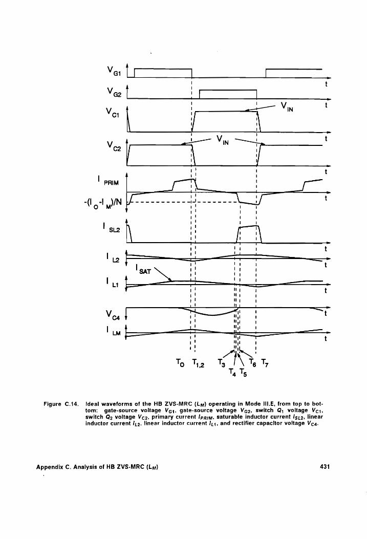
Figure C.14. Ideal waveforms of the HB ZVS-MRC (Ly) operating in Mode III.E, from top to bot-
tom: gate-source voltage Vg1. gate-source voltage Vg, switch Q; voltage Vc;, switch Q2 voltage Vco, primary current Ipa;y, saturable inductor current /s5;2, linear inductor current /,9, linear inductor current /,4, and rectifier capacitor voltage Vc«.
Appendix C. Analysis of HB ZVS-MRC (Ly) 431
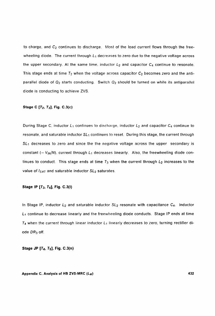
to charge, and C2 continues to discharge. Most of the load current flows through the free-
wheeling diode. The current through L, decreases to zero due to the negative voltage across
the upper secondary. At the same time, inductor Lo and capacitor C4 continue to resonate.
This stage ends at time To when the voltage across capacitor Cp becomes zero and the anti-
parallel diode of Q2 starts conducting. Switch Qz should be turned on while its antiparallel
diode is conducting to achieve ZVS.
Stage C [T2, T3], Fig. C.3(c)
During Stage C, inductor L, continues to discharge, inductor Lz and capacitor C4 continue to
resonate, and saturable inductor SL; continues to reset. During this stage, the current through
SL; decreases to zero and since the the negative voltage across the upper secondary is
constant (— Vjy/N), current through L; decreases linearly. Also, the freewheeling diode con-
tinues to conduct. This stage ends at time 73 when the current through Lo increases to the
value of /sar and saturable inductor SL2 saturates.
Stage IP [T3, T4], Fig. C.3(1)
In Stage IP, inductor Lo and saturable inductor SLo resonate with capacitance Cy. Inductor
L, continue to decrease linearly and the freewheeling diode conducts. Stage IP ends at time
T4 when the current through linear inductor L; linearly decreases to zero, turning rectifier di-
ode DR3 off.
Stage JP [T4, Ts], Fig. C.3(n)
Appendix C. Analysis of HB ZVS-MRC (La) 432

In this stage, inductor L; starts resonating with the capacitance in parallel with rectifier diode
DR3, C3. Saturable inductor SLo and linear inductor Ly» continue to resonate with rectifier
capacitance C,. The current through SLo and Lo increases in a resonant manner. The free-
wheeling diode continues to conduct for the duration of this stage. Stage JP ends at time 75
when voltage across capacitor C4 resonates back to zero, turning rectifier diode DR, on.
Stage EP [Ts, Tg], Fig. C.3(f)
In this stage, the freewheeling diode continues to conduct and inductor L; resonates with
Capacitance C3. Saturable inductor SL2 is saturated and the current through SLo and the lin-
ear inductor Lo increases in a linear manner, but the current through the saturable reactor
increases at a much faster rate. This stage ends when the sum of the currents flowing through
both linear inductors and saturable inductor SL2 increases to the value of the load current
turning the freewheeling diode off.
Stage F [Tg, T7], Fig. C.3(g)
In Stage F, capacitor C3 continues resonating with inductor L;. Inductor SL2 remains satu-
rated, and most of the load current flows through SL»o. This stage ends when switch Qo is
turned off, and a new conversion cycle is initiated.
Mode IIl.F
The sequence of topological stages for Mode III.F is A-B-C-IP-JP-J-F. Figure C.15 shows the
key waveforms of this converter operating on this mode.
Appendix C. Analysis of HB ZVS-MRC (Ly) 433
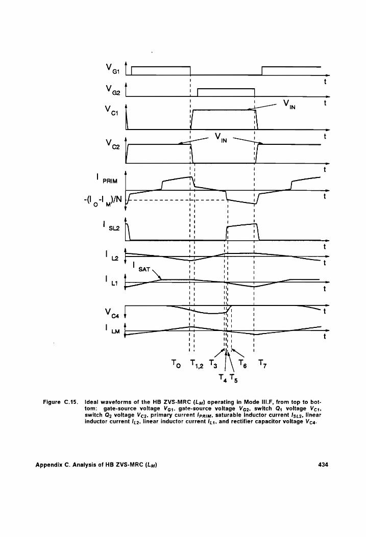
Ve [co Po
Veo | |__| : Ye | a Vin t
Veo _'— Vn — t
t
| | 1 SAT ' '
1} I ——
| = F nt,
Von t oo Lut oo a
Figure C.15. Ideal waveforms of the HB ZVS-MRC (Ly) operating in Mode Ill.F, from top to bot- tom: gate-source voltage Vg. gate-source voltage Vg2, switch Q; voltage Vc, switch Q2 voltage Vc2, primary current Ipa;y, saturable inductor current Isro, linear inductor current !,2, linear inductor current J,4, and rectifier capacitor voltage Vcq.
Appendix C. Analysis of HB ZVS-MRC (La) 434

Prior to the turn-off of switch Q,, load current /o flows through the upper secondary and the
primary current flows through Q;. Voltage across C, ,Vc4, is zero, and voltage across Co,
Veo, is equal to the supply voltage Viy. Inductor SL, is saturated, whereas inductor SL> is
unsaturated.
Stage A [To, 71], Fig. C.3(a)
At t = To, Q;, is turned off, and the primary current is diverted into C, and Co. Capacitance
C, starts charging and Co starts discharging at the same rate. Inductor SL, remains saturated,
and rectifier DR3 continues to conduct. In this stage, inductor SLo is unsaturated and
capacitance C4 resonates with inductor Ly. The stage ends at time 7, when primary voltage
becomes zero, i.e., Vco4(T1) = Voo(™4) = Vin/2.
Stage B [T1, T2], Fig. C.3(b)
In Stage B, capacitances C, and C2 start to resonate with the magnetizing inductance of the
power transformer since the negative primary voltage resets SL;. The current through SL,
decreases quickly as the saturable reactor becomes unsaturated. Capacitance C, continues
to charge, and C2 continues to discharge. Most of the load current flows through the free-
wheeling diode. The current through L, decreases to zero due to the negative voltage across
the upper secondary. At the same time, inductor Lo and capacitor C4 continue to resonate.
This stage ends at time 72 when the voltage across capacitor Cp becomes zero and the anti-
parallel diode of Q2 starts conducting. Switch Qo should be turned on while its antiparallel
diode is conducting to achieve ZVS.
Stage C [T2, T3], Fig. C.3(c)
Appendix C. Analysis of HB ZVS-MRC (Ly) 435

During Stage C, inductor L;, continues to discharge, inductor Lo and capacitor C4 continue to
resonate, and saturable inductor SL, continues to reset. During this stage, the current through
SL; decreases to zero. Since the the negative voltage across the upper secondary is con-
stant (— Vin/N), current through L; decreases linearly. Also, the freewheeling diode continues
to conduct. This stage ends at time 73 when saturable inductor SLo saturates.
Stage IP [T3, Ta], Fig. C.3(I)
In Stage IP, inductor Lo and saturable inductor SLo resonate with capacitance C4. Inductor
L, continues to decrease linearly and the freewheeling diode conducts. Stage |P ends at time
T4 when the current through linear inductor L, linearly decreases to zero, turning rectifier di-
ode DR3 Off.
Stage JP [T4, Ts], Fig. C.3(n)
In this stage, inductor L, starts resonating with the capacitance in parallel with rectifier diode
DR3, C3. Saturable inductor SL2 and linear inductor Lz continue to resonate with rectifier
capacitance C4. The current through SL» and Lo increases in a resonant manner. The free-
wheeling diode continues to conduct for the duration of this stage. Stage JP ends at time 75
when the sum of the current through SLo. Lo. and L; increases to the value of the load current,
turning the freewheeling diode off.
Stage J [Ts, Te], Fig. C.3(m)
Appendix C. Analysis of HB ZVS-MRC (L») 436

In this stage, the freewheeling diode is off and inductor current /,, decreases in a resonant
manner as Capacitance C3 is charged in a controlled fashion. Saturable inductor SL» is satu-
rated and supplies most of the load current. Rectifier capacitance C4 continues to discharge
in a resonant manner as it interacts with SLo, Lo, L1, and C3. Stage J ends when rectifier
capacitance C, discharges to zero and rectifier diode DR, turns on.
Stage F [Ts, T7], Fig. C.3(g)
in Stage F, capacitor C3 continues resonating with inductor L;. Inductor SLo remains satu-
rated, and most of the load current flows through SL. The current through linear inductor Lo
does not vary considerably (/p2 ~/sar) since SLo is saturated. This stage ends when switch
Q2 is turned off, and a new conversion cycle is initiated.
C.3.2 Light Load Operation
For heavy to medium load operation the saturable reactors SL1 and SL2 supply most of the
load current, while the linear inductors, L1 and Lo, carry 20 to 10% of the total load current.
Heavy load currents result in increased delay between the time the saturable reactor begins
to unsaturate and the time it blocks all current (saturable inductors were modeled to have a
finite inductance when saturated and infinite inductance when unsaturated). The corre-
sponding saturable inductor, saturable inductor SL, for the half cycle described by the
topological sequences in the preceding discussion, will not start resetting until the voltage
across the transformer windings changes polarity. The transformer voltage will changes from
Appendix C. Analysis of HB ZVS-MRC (Ly) 437
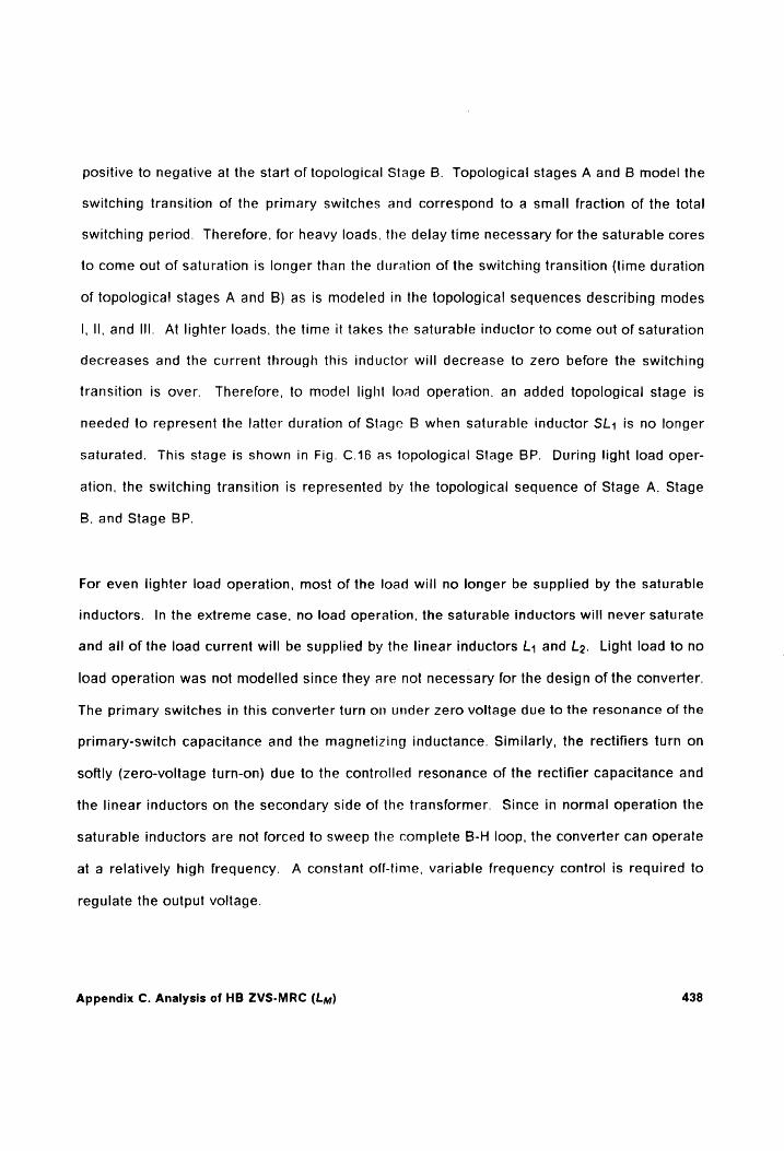
positive to negative at the start of topological Stage B. Topological stages A and B model the
switching transition of the primary switches and correspond to a small fraction of the total
switching period. Therefore, for heavy loads. the delay time necessary for the saturable cores
to come out of saturation is longer than the duration of the switching transition (time duration
of topological stages A and B) as is modeled in the topological sequences describing modes
I, Il, and Ill. At lighter loads, the time it takes the saturable inductor to come out of saturation
decreases and the current through this inductor will decrease to zero before the switching
transition is over. Therefore, to model light load operation. an added topological stage is
needed to represent the latter duration of Stage B when saturable inductor SL, is no longer
saturated. This stage is shown in Fig. C.16 as topological Stage BP. During light load oper-
ation, the switching transition is represented by the topological sequence of Stage A. Stage
B. and Stage BP.
For even lighter load operation, most of the load will no longer be supplied by the saturable
inductors. In the extreme case, no load operation, the saturable inductors will never saturate
and all of the load current will be supplied by the linear inductors L, and Lo. Light load to no
load operation was not modelled since they are not necessary for the design of the converter.
The primary switches in this converter turn on under zero voltage due to the resonance of the
primary-switch capacitance and the magnetizing inductance. Similarly, the rectifiers turn on
softly (zero-voltage turn-on) due to the controlled resonance of the rectifier capacitance and
the linear inductors on the secondary side of the transformer. Since in normal operation the
saturable inductors are not forced to sweep the complete B-H loop, the converter can operate
at a relatively high frequency. A constant off-time, variable frequency control is required to
regulate the output voltage.
Appendix C. Analysis of HB ZVS-MRC (Lay) 438
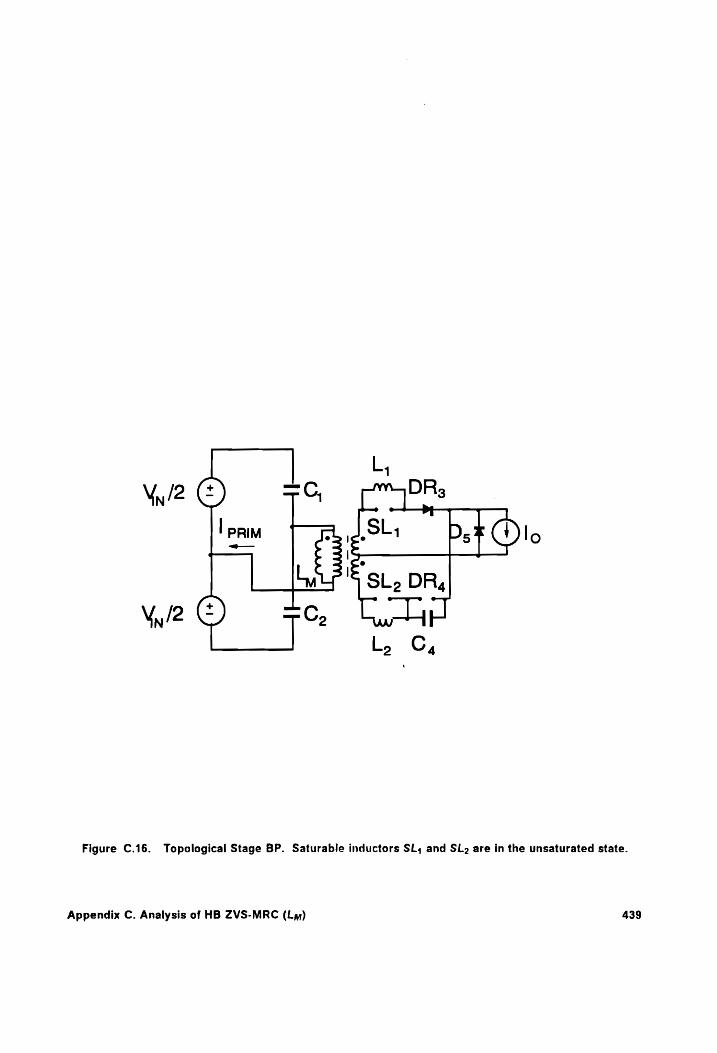
Ly
\Wy/2 @) TC; DAs
Ae Pef Dl | +
La?! ach
Y2@) =C, L. nde
Figure C.16. Topological Stage BP. Saturable inductors SL, and SL2 are in the unsaturated state.
Appendix C. Analysis of HB ZVS-MRC (Ly) 439
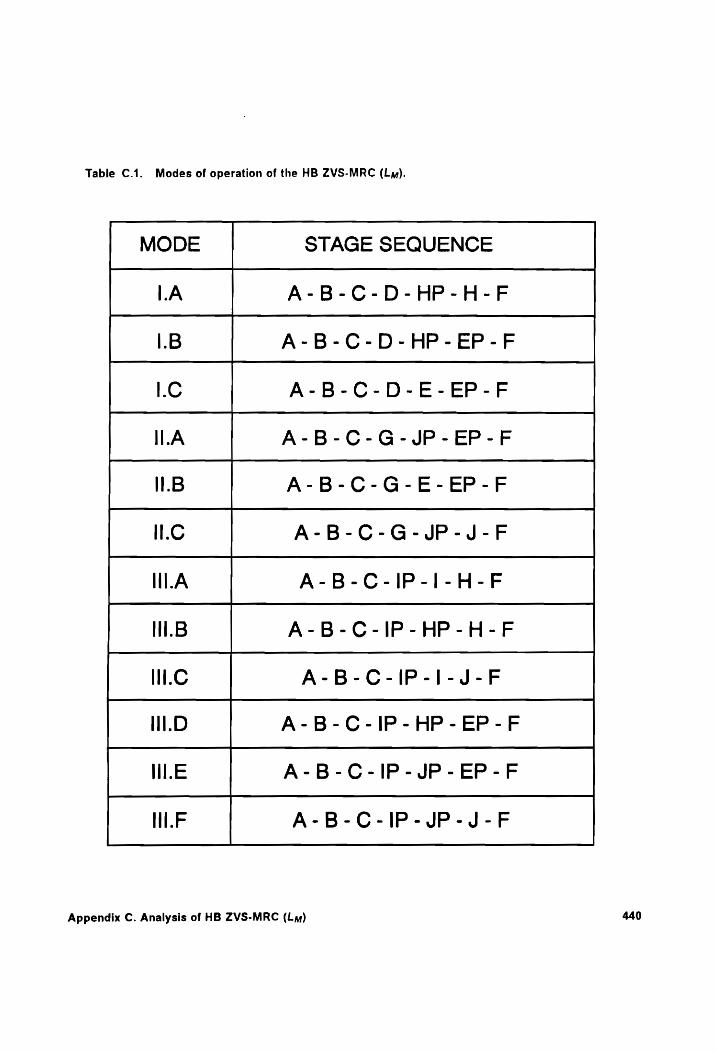
Table C.1. Modes of operation of the HB ZVS-MRC (Ly).
MODE STAGE SEQUENCE
LA A-B-C-D-HP-H-F
I.B A-B-C-D-HP-EP-F
.C A-B-C-D-E-EP-F
ILA A-B-C-G-JP-EP-F
11.B A-B-C-G-E-EP-F
ILC A-B-C-G-JP-J-F
ILA A-B-C-IP-1-H-F
11.B A-B-C-IP-HP-H-F
ike: A-B-C-IP-1-J-F
II.D A-B-C-IP-HP-EP-F
LE A-B-C-IP-JP-EP-F
INF A-B-C-IP-JP-J-F
Appendix C. Analysis of HB ZVS-MRC (Ly) 440

C.2 DC Voltage-Conversion-Ratio
A set of dc voltage-conversion-ratio characteristics is shown in Figs. C.17a - C.22a. The
characteristics are plotted as a function of normalized conversion frequency, fcoon = fs/2fo for
different normalized output currents, lon = ZNlo/NVin. The characteristics are plotted for dif-
ferent values of the design parameters: Cy = 2Cp/(N2C), the ratio of the capacitance across
the rectifiers reflected to the primary (4Cp/N2) and the resonant capacitance across the pri-
mary switches (2C); Ly = 4Ly/(N2L), the ratio of the magnetizing inductance Ly and the reso-
nant inductors across the rectifiers reflected to the primary (N2L/4): Isin =/sar/(/o/N), the
normalized current of the linear inductor during the interval the saturable inductor is satu-
rated; and L/SL, the ratio between the secondary linear inductance and the inductance of the
saturable reactor when saturated. The resonant frequency is defined § as
wo = 2nfo = 1/,/2CLy and the characteristic impedance as Zy= /tu[2C . Vin is the input
voltage and N is the turns ratio of the transformer.
A complete set of design characteristics are given for Cy = 5 and 10, and Ly = 1, 3, and 6
(Figs. C.17a - C.22b). All characteristics are plotted for Isar/lo = 1 and for the ratio L/ SL
= 100.
Appendix C. Analysis of HB ZVS-MRC (La) 441

C.3 DC Analysis of Topological Stages
Analytical expressions for the initial conditions, circuit equations, their solutions, and dura-
tions of the topological stages refers to the ideal HB ZVS-MRC (Ly) shown in Fig. C.1:
C.3.1 Heavy Load Operation
STAGE A [Tao, Tat] (Fig. C.23)
Initial Conditions:
Vori(Tao) = 0 (C.1.a)
Vool(Tao) = Vin (C.1.b)
Appendix C. Analysis of HB ZVS-MRC (Ly) 442
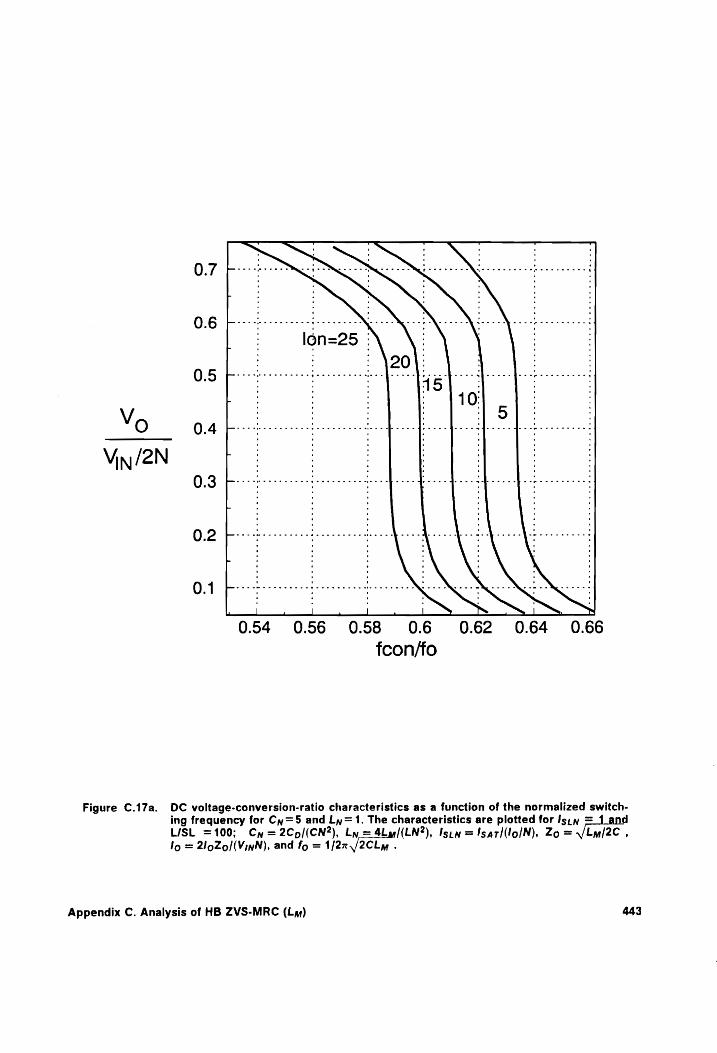
Vin/2N Po: ; ;
08 foie nena afenafendfanf taco 0.2 + wee eee cece ee cece ee ee bee eee eee Bee ee pe Pee eee
o a + + a . a . O11 feeders NR NN
oe 0.54 0.56 0.5 0.6
fcon/fo
0.62 0.64 0.66
Figure C.17a. DC voltage-conversion-ratio characteristics as a function of the normalized switch- ing frequency for Cy=5 and Ly=1. The characteristics are plotted for Isiy = d
LISL =100; Cy = 2Cp/(CN?), Ly = 4byy/(LN2), Isiew =!sari(lo/N), Zo = VLm/2c , lo = 2loZo/(VinN), and fo = 1/227,/2CLy .
Appendix C. Analysis of HB ZVS-MRC (Ly) 443
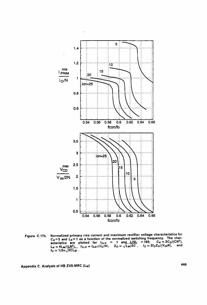
Figure C.17b.
Appendix C. Analysis of HB ZVS-MRC (La)
Fe eS 0.54 0.56 0.58 O06 0.62 0.64 0.66
fcon/fo
eee Pa rete ee Hew een red
wee ee Qe eee ete eee eee,
max
Vep
Vin/2N sisson oo fob es fe coon |
0.54 0.56 0.58 06 0.62 0.64 0.66
fcon/fo
Normalized primary rms current and maximum rectifier voltage characteristics for
Cy=5 and Ly=1 as a function of the normalized switching frequency. The char-
acteristics are plotted for Isjy = 1 an =100; Cy = 2Cp/(CN?),
Ly = 4Ly/(LN2)._ Isuen=!sari(lo/N). Zo=Vbml2C, 10 =2loZo/(ViwN), and fo = 1/22n,/2CLy .
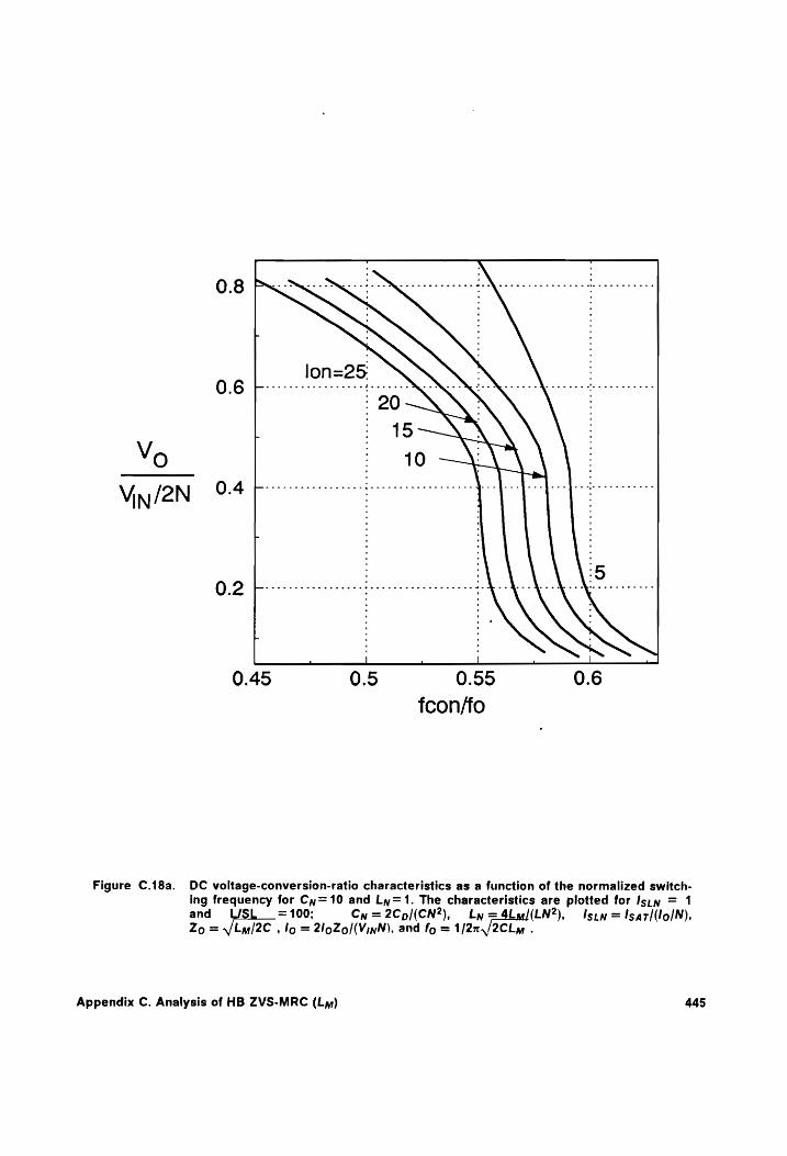
0.8
0.6 b----e cree ! Leese
Vin /2N 0:4 Preece aan a
0.2 pocceete etic teeters eeeeee reset MANN.
0.45 Figure C.18a. DC voltage-conversion-ratio characteristics as a function of the normalized switch-
ing frequency for Cy=10 and Ly=1. The characteristics are plotted for Ispy = 1 and = 100: Cy =2Cp/(CN?), Ly =4ba/(LN?), Istn =Isar/(lo/N), Zo = Ly /2c ’ lo = 2loZol(VinN). and fo = 1/2zx,, 2CLay ,
Appendix C. Analysis of HB ZVS-MRC (Ly) 445
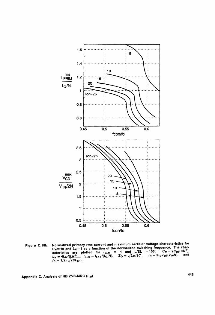
Figure C.18b.
Appendix C. Analysis of HB ZVS-MRC (Lm)
ms
| PRIM
lo/N
3.5 F--- RIAA ence eee eee dee eee eed
lon=25 3 bee ec ww we we ete ots elon cree ce cece cen mercer cee ’
95 bescseeeeeeees oe NA ccc decceeee max :
Veo 20 2 be snes e cere ncee 7 15 wwe eo Nes
Vin/2N S49 eV
18 bee oe StL | 1 bes meee w cmc ewe cwe sew cmc w ence oye hen Bes hee Ree Bye wee c cee
0.5 wee eee eee ‘ ence caccece - eeeneee
0.45 0.5 0.55 0.6
fcon/fo
Normalized primary rms current and maximum rectifier voltage characteristics for
Cy=10 and Ly=1 as a function of the normalized switching frequency. The char-
acteristics are plotted for Isin = 1 a Pr = 100; Cn = 2Co/(CN?),
Ly = 4Ly/(LN2). Isun=Isari(lolN), Zo=Vbml2C, fo = 2loZo/(VinN), and fo = 1/2n,/2CLy .
446
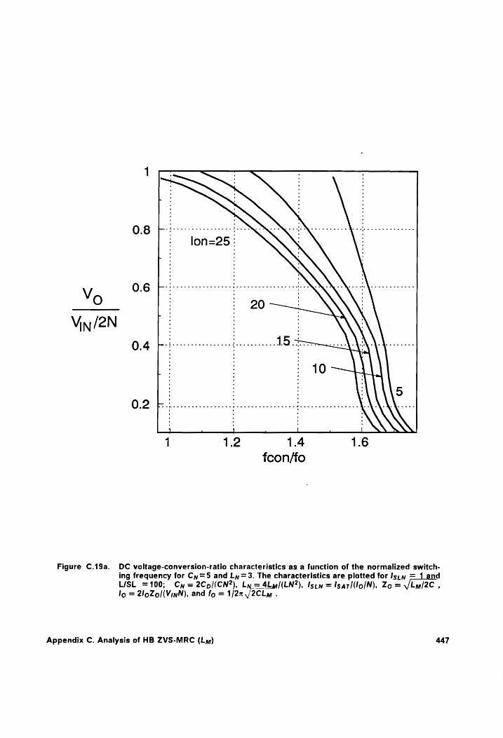
0.8 poi NRK Noe) brsereeeeee
0.6 po be AA \ esses Yo : : :
Vin/2N : 2 :
0.4. bee 15
0.2 E bocce teeeeeeeeeebeeeeeeteeeet eee deteeeeeeeee eee AA.
i 12. 4.4 fcon/fo
Figure C.19a. DC voltage-conversion-ratio characteristics as a function of the normalized switch- ing frequency for Cy=5 and Ly=3. The characteristics are plotted for Isiy = d L/SL =100; Cy = 2Cp/(CN2), Ly = 4bay/(LN2), Isen =Isari(lo/N), Zo = VJLm/2c , lo = 2loZo/(VinN), and fo = 1/2n./2CLy .
Appendix C. Analysis of HB ZVS-MRC (Lay) 447
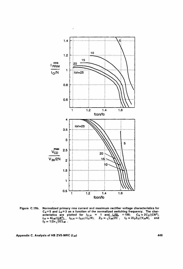
ms
| PRIM
Io/N
max
Veo
Vin/2N
Figure C.19b. Normalized primary rms current and maximum rectifier voltage characteristics for
Cy=5 and Ly=3 as a function of the normalized switching frequency. The char- acteristics are plotted for Is;sy = 1 ang =100; Cy = 2Cp/(CN?), Ly = 4b y/(LN2). Istn=Isari(lo/N), Zo=VJVbLm/2C, Io =2loZo/(ViwN), and fo = 1/2n/2CLy .
Appendix C. Analysis of HB ZVS-MRC (Lm) 448
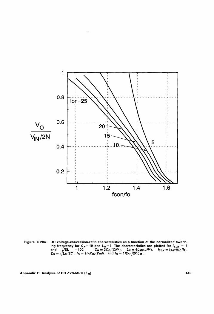
Vin/2N
Figure C.20a.
0.8 be NX XE AE) eeeteceeteeeneeee be
0.6 bie MA ec beer
0.4 bedi LO
. ’ . ‘ . . . . . , ’ ‘ . 4 ry ’
’ . . . 0.2 biocide QQ ° . ’ . ’
’ . . . ’ . '
’ __.! \ |
1 1.2
fcon/fo
DC voltage-conversion-ratio characteristics as a function of the normalized switch- ing frequency for Cy=10 and Ly=3. The characteristics are plotted for Is;y = 1
and SL = 100; Cy = 2Cp/(CN?), Ly =4bm/(LN?), Isin =!sar/(lo/N), Zo = /Lm/2C . Io = 2loZol(VinN), and fo = 1/2n/2CLyy «
Appendix C. Analysis of HB ZVS-MRC (La) 449
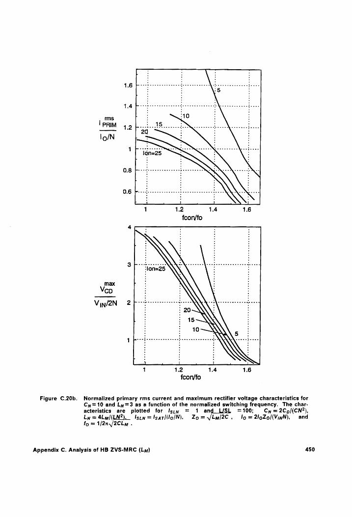
Figure C.20b.
ms
| PRIM
lo/N
max
Vep
Vin/2N
1 1 ___!
1 1.2 1.4 1.6 fcorv/fo
Normalized primary rms current and maximum rectifier voltage characteristics for Cy=10 and Ly=3 as a function of the normalized switching frequency. The char- acteristics are plotted for Is.n = 1 ae =100; Cy =2Cp/(CN2), Ly = 4Ly/(LN2 Isen=Isari(lo/N), Zoz=Vbul2C , Io =2loZol(VinN), and fo = 1/2x,/2CLy .
Appendix C. Analysis of HB ZVS-MRC (Ly) 450
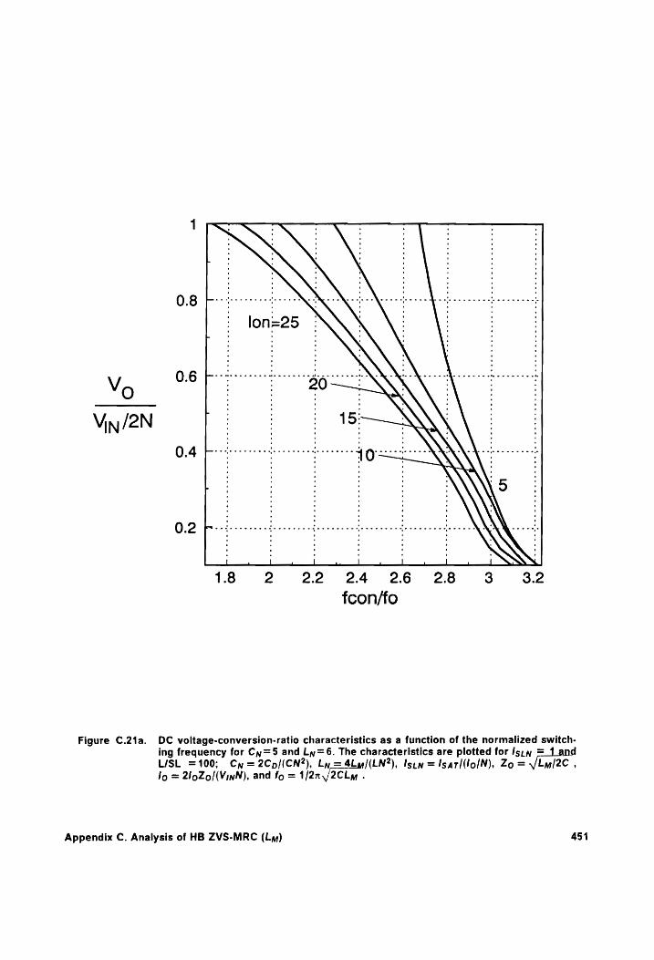
0.8 Pe Nf:
0.6 fo enn egg NNN ee Yo BAA
044 fo rn onto gee
ie et, | 22 24 26 28 3 43.2
fcon/fo
mot,
co
Figure C.21a. DC voltage-conversion-ratio characteristics as a function of the normalized switch- ing frequency for Cy=5 and Ly=6. The characteristics are plotted for Is;y = d
L/SL =100; Cy = 2Cp/(CN?), Ly = 4by/(LN?), Isen =Isari(lo/N), Zo = VLM/2c , Io = 2loZo/(VinN), and fo = 1/2n,/2Cly .
Appendix C. Analysis of HB ZVS-MRC (Ly) 451
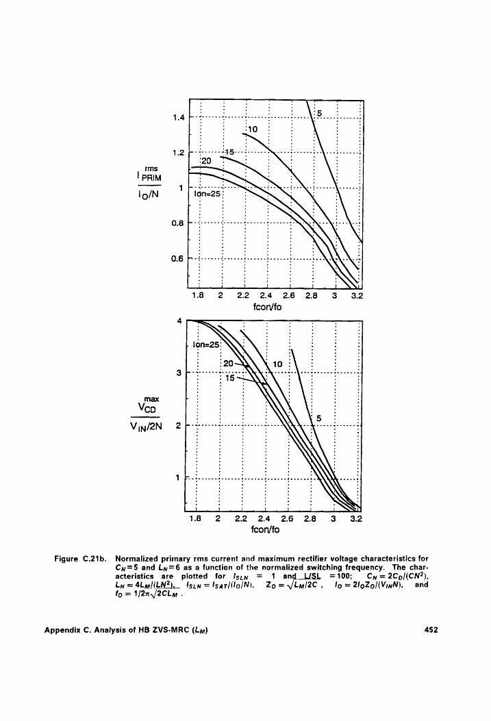
1 bene pee beeeefeeenfeeel Seoesesee
1.2
ms
! PRIM
loIN | | toneas?
8 pion nrbcnnterel
0.6 po eeeeeed weeeee wees : eeeeee eeeeee - ;
| 18 2 22 24 26 28 3 32
fcon/fo
max
Veo
Vin/2N
Pa GUS 1.8 2 22 2.4 26 2.8 3 3.2
fcon/fo
Figure C.21b. Normalized primary rms current and maximum rectifier voltage characteristics for Cy=5 and Ly=6 as a function of the normalized switching frequency. The char- acteristics are plotted for Is:y = 1 an =100; Cy =2Co/(CN?), Ly = 4Ly/(LN2 Isun=Isari(lo/N). Zo=VSLml2C . 1o=2loZol(VinN), and
fo = 1/2n,/2CLy .
Appendix C. Analysis of HB ZVS-MRC (Lym) 452
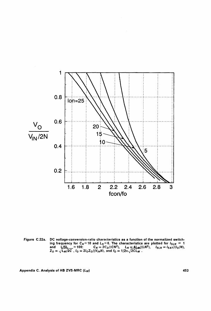
0.8 Fie se NNN br rd
0.6 boo Qf es Vo NNO EE VON OT TB SAS ‘wien et 0
O04 Pov crehneceee SRR hecerteccrie
02 bn Ne 16 18 2 22 24 26 28 3
fcon/fo
Figure C.22a. DC voltage-conversion-ratio characteristics as a function of the normalized switch- ing frequency for Cy=10 and Ly=6. The characteristics are plotted for Iszgn = 1 and USL = 100: Cy =2Cp/(CN?), Ly =4baui(LN?), Ison = Isari(lo/N), Zo = /Lm/2c ’ lo = 2loZol(VinN). and fo = 1/2zx 2CLm .
Appendix C. Analysis of HB ZVS-MRC (Ly) 453
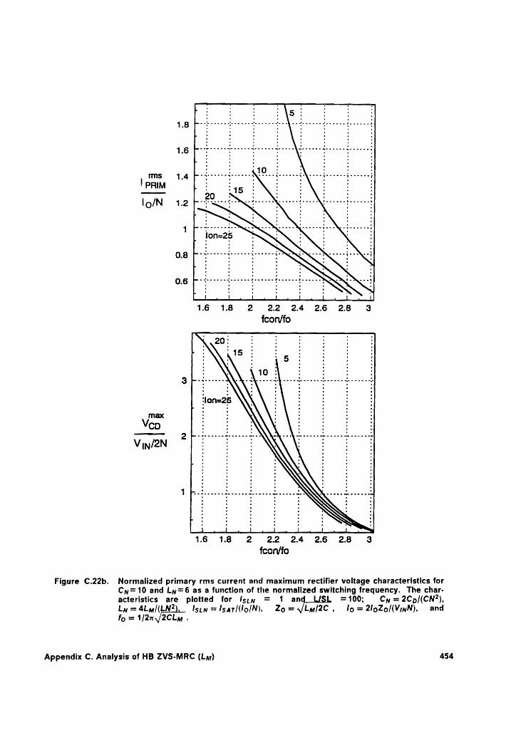
Figure C.22b.
ms
| PRIM
lo/N
a
16 18 2 22 24 26 28 3 fceon/fo
max
Veo
Vin/2N
piel ethan al al |
1618 2 22 24 26 28 3 fcon/fo
Normalized primary rms current and maximum rectifier voltage characteristics for Cy=10 and Ly=6 as a function of the normalized switching frequency. The char- acteristics are plotted for fscy = 1 ang =100; Cy =2Cp/(CN?), Ly = 4Ly/{LN2), sen =Isari(lolIN) Zo=VbLwl2C, Ilo =2loZo/(VinN), and fo = 1/2n,/2CLy .
Appendix C. Analysis of HB ZVS-MRC (Ly) 454
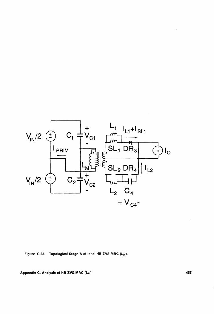
Figure C.23. Topological Stage A of ideal HB ZVS-MRC (Ly).
Appendix C. Analysis of HB ZVS-MRC (Las) 455

A iprim( ao) = lpr
A itm ao) = !im
Vea(T ao) = 9
A VoalT ao) = Vea
. A ins(Tao) = Ia
A inolT ao) = Ihe
A isns(Tao) =! 514
ispo(T ao) = 0
Equations:
Vor(t) + Veo(t) = Vin
WV¢,(f) Weoo(t) Cc dt =C dt + fray(t) + ippyy(t)
ippm(t) = a Lipa (t) + fsr a(t) — ipo(f)]
, di, 4(t) dis: s(t) Virlt) = Vsi1() = —F— = SL —
Appendix C. Analysis of HB ZVS-MRC (La)
(C.1.c)
(C.1.d)
(C.1.e)
(C.1.f)
(C.1.g)
(C.1.h)
(C.1.i)
(C.1/)
(C.2.a)
(C.2.b)
(C.2.c)
(C.2.d)
456
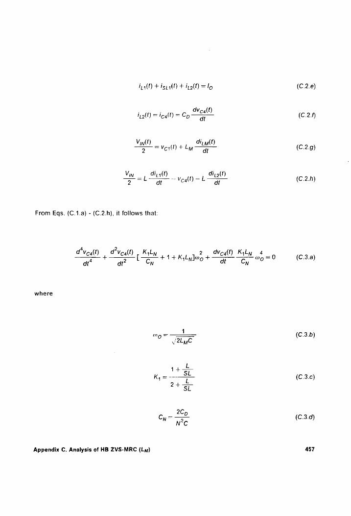
Mal + fsi((O + frat) = lo
Ac, (t) ira(O) = Ica(t) = Cp a
Vin yy gp, em 9 = Vel M dt
Vin diy 4(t) di, a(t) L —Ve,4(t) — L ot
2 at
From Eqs. (C.1.a) - (C.2.h), it follows that:
Aveg(f) Kily 4 dt Cy?
4 2 d Veal) 1 A Vcalt) [ Kyly 2
+14 K,Lyloo + dt* dt® Cy
where
Appendix C. Analysis of HB ZVS-MRC (La)
(C.2.e)
(C.2./)
(C.2.g)
(C.2.h)
(C.3.a)
(C.3.b)
(C.3.c)
(C.3.d)
457
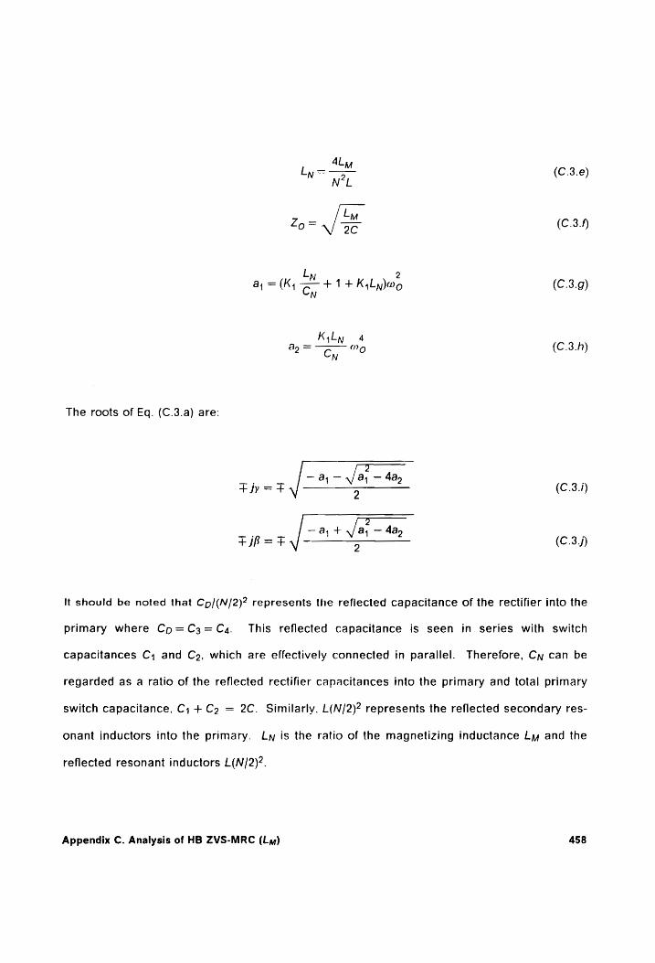
Ly = (C.3.e) N NPL
Li Zo=./se (C.3./
Ly 2 a = (K, Cy + 1 + K,Ly)wo (C.3.g)
K,L 4 ap = — wy (C.3.h)
The roots of Eq. (C.3.a) are:
fm ay Vf ay — 4a Typed St (C.3.i)
_. _ —a,+./a, — 4a
+ jp =F a? (C.3,f)
It should be noted that Cp/(N/2)? represents the reflected capacitance of the rectifier into the
primary where Cp=C3=Cy. This reflected capacitance is seen in series with switch
capacitances C, and Co, which are effectively connected in parallel. Therefore, Cy can be
regarded as a ratio of the reflected rectifier capacitances into the primary and total primary
switch capacitance, C; + Co = 2C. Similarly. L(N/2)2 represents the reflected secondary res-
onant inductors into the primary. Ly is the ratio of the magnetizing inductance Ly and the
reflected resonant inductors L(N/2)?.
Appendix C. Analysis of HB ZVS-MRC (Lm) 458

Solution:
A Voq = a, COS yf + by Sin yt +c, cos Bt+d, sin pt (C.4.a)
A iio = Crlbay cos yt — ayy Sin yt + dB cos Bt—cyf sin Bt] (C.4.b)
A
— aay? sin y + df? cos ft — caf sin Bt] — + [lo — Biro(t)] (C40)
A V Vor = > + + [a,N cos yf + b,N sin yt +c,N cos Bt + d,N sin Bt
— K>K,N[agy” cos yt + bay’ sin yt + c4f* cos Bt + d,f* sin BtT] (C.4.d)
A Cp . A iy = 7 [bay( cos yt — 1) — agy sin yt + dgB( cos Bt—1)—c,f sin Bt] +1,, (C.4.e)
1+— SL
A A OA Ista =lo — hia — Ate (C.4f)
where
A lo A 2,NC A 2 lum + ap Fal — Koy om — he ay
d,= += (C.5.a) NCBKofy° — BJ
A
lho — Cofhd, baa ee (C.5.b)
Appendix C. Analysis of HB ZVS-MRC (Lm) 459

Vin
A A 9
CA= 5D (C.5.c)
NKo( fi" — y”)
A
a, = Vea — Ca (C.5.d)
Cy Ky = . (C.5.e)
Lyng
Initial conditions iA, Iho, Vas. WM. and Vay are determined from the stage preceding Stage A.
Normalizing voltages with respect to Vix/2, current with respect to /o/N, and time with respect
to 1/fo, Eqs. (C.4.a) - (C.4.d) become:
AN Vo4q = Ayan COS yaty + Dy SiN yyty + Can COS Bryty + Gy SiN Baty (C.6.a)
.AN Cn . . ho = “Alon. [Danys cos yntn _ aANnys sin ney + danbs cos Buty - Canbs sin Buty] (C.6.b)
AN . Voy = 14 [ayn COS ypyty + Dan SIN y_ty + Can COS Paty + dan SiN Baty
Cn 2 2, 2 2. Ly Ki[aanys COS yuty + Ban's SIN yyly + CanBs COS Buty + Aanhs Sin Bytyl] (C.6.c)
AN 2 2. 2 2. tim = [BDanys COS yt — anys SIN yyty + Cans COS Buty — CanBs SIN Buty
Cy 3 3) C«; 3 _ Le K, [bans cos Yen _— AaAnys sin yntn + danhs cos Buty (C.6.d)
N
3 AN — Canhs Sin Buty lon — 1+ 2lro
Appendix C. Analysis of HB ZVS-MRC (Ly) 460
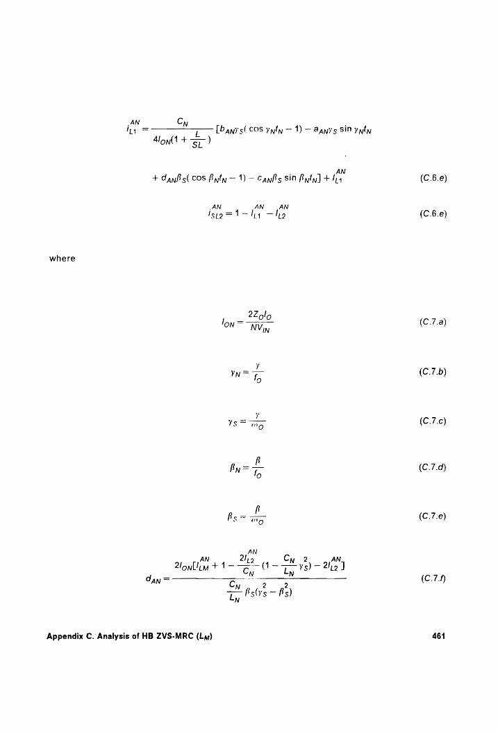
where
AN Cy , iL, = ——— 5 [anys 608 yvfy — 1) — aanys SIM uty
; AN + danBs( COS Byty — 1) — Cans sin Buty] + I,
AN AN AN ispp=1—tiy Ihe
2Zolo ON NV wy
Y
Nee
y
YS MO
B Bp _—
N fo
R Bs = MO
AN AN 2hio Cy 2 AN
2lon[lim + 1- Ee (1-7 ys) — 2h J N N
dan = Cy > 2
Tr Bstvs — Bs) N
Appendix C. Analysis of HB ZVS-MRC (La)
(C.6.e)
(C.6.e)
(C.7.a)
(C.7.b)
(C.7.c)
(C.7.d)
(C.7.e)
(C.7.f)
461
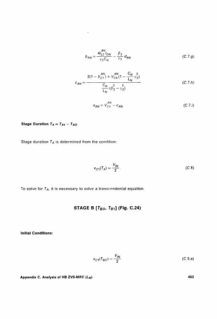
Cy 2 AN AN 2(1 — Ver) + Veg (1 - T ¥s)
N Can =
Stage Duration Tg = Ta1 — Tao
Cn 2 2
7, V's — ys)
N A aan = Voa — Can
Stage duration T, is determined from the condition:
To solve for 7T,, it is necessary to solve a transcendental equation.
STAGE B [Tgo, Ta1] (Fig. C.24)
Initial Conditions:
Appendix C. Analysis of HB ZVS-MRC (Ly)
Vo1(T,) = =
Voi(Tgo0) =
2
20
(C.7.g)
(C.7.h)
(C.7.i)
(C.8)
(C.9.a)
462
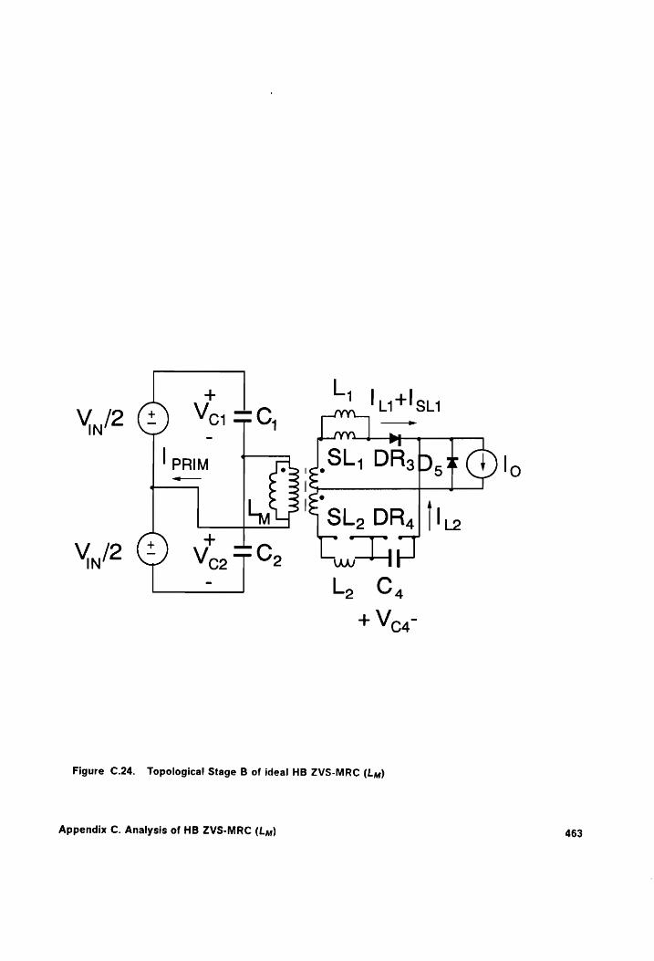
+
V2 @) Vor =e, |= | PRIM fd ,SL1 DR: Dt Do
-—— |
Ly tt {Sts DRal fle Vin/2 ©) Veo Co 4
Figure C.24. Topological Stage B of ideal HB ZVS-MRC (Ly)
Appendix C. Analysis of HB ZVS-MRC (Ly) 463

Vin
VoalTpo) = 5
B ipriu( Bo) = lprim
B Aim Bo) = lim
Ve3lTg0) = 0
B Vo4l(Tg0) = Vea
B fos(TBo) = lu
B iro(Tg0) = Ihe
B ista(T Bo) = Isn4
isto(Tgo) = 0
Equations:
aVer(t) Well . dt & apt MeO + lpi (O)
Ippim(D) = N Lina( + fses(t) — fro(t)]
Appendix C. Analysis of HB ZVS-MRC (La)
(C.9.b)
(C.9.c)
(C.9.d)
(C.9.e)
(C.9.
(C.9.g)
(C.9.h)
(C.9.i)
(C.9,j)
(C.10.a)
(C.10.b)
(C.10.c)
464

ON, = Vv, 4(t) = Vs14(8) =L dt = SL dt
WVe4(t) ipo(t) = igg(t) = Cp at
Vin diza(t)
Vin(t Ci, s(t AO veal) + by SMO
From Eqs. (C.9.a) - (C.10.h), it follows that:
4 2 2 DVealt) Od Veg(t) _ Ly 2 Wes(t) — by Ly | 4
4 + ot [et Kaleo + ot Cc 3~ 4c, eo =
at
where
Ly L Matt 4 osr
Ly 2
a,= (S. 4. K3)0
Ly Ly 4
Appendix C. Analysis of HB ZVS-MRC (La)
(C.10.d)
(C.10.e)
(C.10.f)
(C.10.g)
(C.10.h)
(C.11.a)
(C.11.b)
(C.11.c)
(C.11.d)
465

The roots of Eq. (C.11.a) are:
+jy =F 9 (C.11.e)
— a, + Vay — 4a, F jp =F 5 (C.11./
Solution:
B Vc4 = 4g COS yt + be siny! + Cg cos Pt + dg sin ft (C.12.a)
B ito = Cplbgy cos yt — apy sinyt + dpB cos Pt — cpf sin ft] (C.12.b)
B b a d c iim = ~ [ - cos yt — = sin yt + —- cos Bt ——~ sin Bt + K,[agy sin yt
M B B
— bpy cos yt + Cpf sin ft — dpf cos ft]] + eg (C.12.c)
B V Vo, = > + N[ag cos yt + bp sin yt + cp cos t+ dg sin Bt — K,[agy” cos yt
+ bpy” sin yt + cgf? cos ft + dg? sin Bt] (C.12.d)
B b a d Cc ae _ — cos yt — 3 sin yt + --2- cos pt— —3 sin Bt + Ko[apy sin yt
L,Y , p B
— bpy cos yf + Caf sin ff — dpf cos Pt]] + fe (C.12.e)
Appendix C. Analysis of HB ZVS-MRC (Ly) 466

5B _ 1, s 2B oe . c isu = Sp La cos vt — y sin yt + R — 7 sin Bt + Ko[apy sin yt cos Pt —
— Dpy cos yt + CoP sin ft — dp cos ft]] + gp
where
B B
Bo fiy Isty 2, 2CN . 1 liu + a + ~ halt — Kaye + ar J
ICNPK(y* — B?)
B 2
K(p° — y”)
B
ap = Vca — CB
1,58 | % fg =I pl te — Ko(ybg — Bdp)]
B NL .B €g =hu- Ta (lia — fg]
8 1,58 . OB 98 =!sin ep la + 7” Kealrbe — Bog)
Appendix C. Analysis of HB ZVS-MRC (Ly)
(C.12./)
(C.13.a)
(C.13.b)
(C.13.c)
(C.13.d)
(C.13.e)
(C.13./)
(C.13.g)
467

or in the normalized form:
BN Vea = 4gn cos yayty + Den sin yaytn + Can cos Buty + dan sin Butn (C.14.a)
.BN Cy ; ; 122 = a [bars COS yay — agyy's SIM yyfy + Gpnhs COS Byly — CanBs SIN Buty] (C.14.b)
BN . Vor = 1+ [apy COS ypyty + Day SIN yyty + Cay COS Buty + an Sin Baty
Cy 2 2, 2 2,
~ Ty [agnys COS yyty + Denys SiN aly + Canhs COS Buty + Agyhs sin Byty]] (C.14.c)
BN iim = [Opnys COS yuty — agnys SIN y_ty + Apnhs COS Buty — CanBs sin Buty
Cn 3 3 3 3, —_— Ly [Denys cos ynty _ aBNYs + CanPs cos Bytn _ Canbs sin Bytnlillon (C.14.d)
BN BN .BN — ty —Isp4 + tro
ity = Fie [ neu COS yaly — eu SIN yyly + au cos faty — ee SIN Baty
+ ¢ [agny’s SIN yyty — Denys COS yaty + Canbs SIN Buty (C.14.e)
— dgnhs COs Pyty)) + fan
ier = at [ wen COS yyty — “au Sin yayty + ae cos Baty — cee Sin Baty
Appendix C. Analysis of HB ZVS-MRC (Lm) 468

Cw . . + Ly [agnyys sin Yvty _ Dani's cos yvty + Canbs sin Bruty (C.14./
— Agnhs cos fiytyl)] + Gan
where
YN = To (C.15.a)
y
Ys = 6 (C.15.b)
p Bu= 7 (C.15.c)
0
_+ C.15 Bs = 9 ( 15.d)
BN BN BN BN 4 Cy 2 lonllim + lia +4'su1 — Ie (G- [41 - Ts] + 1)]
N N
day = C.15.e BN Cy > OD ( )
TL Bslys — Bs] N
BN Aliolon = Bs
Dan = sly _ ys. pn (C.15.A)
BN BN Cy 2 Ver — 1+ Veq [1 ~ Ty 78d
BN Cy 9 5 (C g)
Te. (Ps — ys) N
Appendix C. Analysis of HB ZVS-MRC (Ly) 469

BN aBN = Vea _ Can (C.15.h)
L(t Cn 2) Nii — > Ys 2 BN BN Ly dgnln Cy 2 Bs Cy 2 ;
fon =a — Ihe za rT, [1-7 Bs — (55) (1-7 ys) ] (C.15./) Cnys s N N
Cy 2 Cy 2
(1 —--~— ys) (1-——— Bs) BN Lly Ly Ln ;
Gan =!su1 ~ ast Pen —y5 + 9a Ge J (C.15,/)
BN BN Can =!im — 4enlli1 — fen] (C.15.k)
Stage Duration Tg = Tg1 — Tgo
Stage duration Tg is determined from the condition:
YVor(Tg) = Vin (C.16.a)
or
isp4(Tp) = 0. (C.16.b)
STAGE C [Tco, Tc1] (Fig. C.25)
Initial Conditions:
Appendix C. Analysis of HB ZVS-MRC (Ly) 470
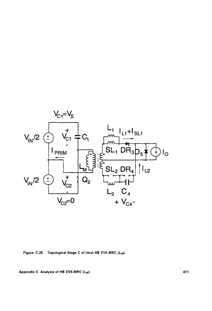
Figure C.25. Topological Stage C of ideal HB ZVS-MRC (Ly).
Appendix C. Analysis of HB ZVS-MRC (Ly) 471

Vori(Tco) = Vin
VoolTco) = 90
C lppim( co) = !prim
C inm(co) = !tm
Vea(Too) = 9
Cc VealTco) = Vea
Cc in(Too) =!
c ino(Tco) = Ihe
C ists(Teo) = Is14
isto(Tco) =O
Equations:
Vin Vprim() = —
Verim(t) diz (t) N — at
Appendix C. Analysis of HB ZVS-MRC (La)
(C.17.a)
(C.17.b)
(C.17.c)
(C.17.d)
(C.17.e)
(C.17.f)
(C179)
(C.17.h)
(C.17.i)
(C.17,/)
(C.18.a)
(C.18.b)
472

Vin di, 2(t) ON —_— Ve,(f) -+- L dt
. . AVe,4(0) fpolt) = teal) = Cp a
Vin di, (8) al at
From Eqs. (C.17.a) - (C.18.e), it follows that:
9 2 d Vea(t) 2 Vin@p
Os veatwe = By
where
Mp =
VlCp
Solution:
Cc Vin Vo4 = Ac COS apt + be sin mpl + ON
Cc ; lip = Comp[be COS pf — ac SiN wf]
Appendix C. Analysis of HB ZVS-MRC (Ly)
(C.18.c)
(C.18.d)
(C.18.¢)
(C.19.a)
(C.19.b)
(C.20.a)
(C.20.b)
473
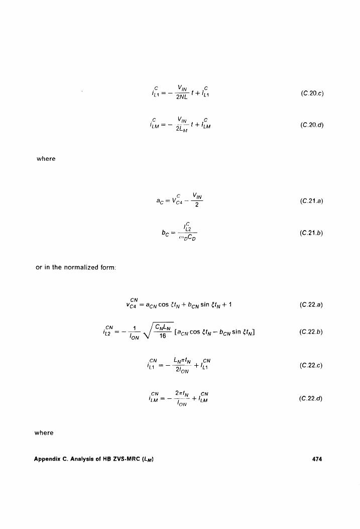
=o tt ttl
itu = — a thu
where
dc = Vou — =
be= Iho opCp
or in the normalized form:
CN Vo4a = Acn COS fty “++ Don sin oty 4+ 4
Cyly ‘Le lon 16
[acy COS fy — Don SIN Cty]
CN Lyrty 4 joN
ay = op it
[CN arty CN iu = 7.., LM
ON
where
Appendix C. Analysis of HB ZVS-MRC (Lm)
(C.20.c)
(C.20.d)
(C.21.a)
(C.21.b)
(C.22.a)
(C.22.b)
(C.22.c)
(C.22.d)
474

CN
@cn= Vea —1 (C.23.a)
CN Don = Ite Ion, / 3 (C.23.b)
NN
Ly ¢ =2n Cy (C.23.c)
Stage Duration Tc = Tc; — Tco
Stage duration Tc is determined from the conditions:
ip4(To) = 0 (C.24.a)
or
io(Tc) = Is art- (C.24.b)
Isay is the current of the linear inductor at the time the saturable inductor saturates.
STAGE D [Tpo, To1] (Fig. C.26)
Initial Conditions:
Appendix C. Analysis of HB ZVS-MRC (Ly) 475
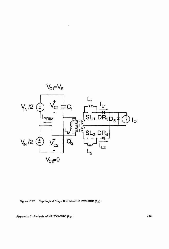
VorEVs
Ly Vy /2 ©) Vor =C, py Li
lpr a ,SL1 DR3sp 4 lo
a DR, + + 4
Vn [2 _ Voo ‘
Voz 0
Figure C.26. Topological Stage D of ideal HB ZVS-MRC (Ly).
Appendix C. Analysis of HB ZVS-MRC (Ly) 476

Voi po) = Vin
Voal(Tpo) = 0
D prim po) = prim
D itm( po) = !im
VoalTpo) = 0
VcalTpo) = 9
D lus(Tpo) = Ih
D hto(T po) = Ie
ists(Tpo) = 0
ista(Tpo) = 9
Equations:
IN a
Vin, ital) aN at
Appendix C. Analysis of HB ZVS-MRC (Ly)
(C.25.a)
(C.25.b)
(C.25.c)
(C.25.d)
(C.25.e)
(C.25./)
(C.25.g)
(C.25.h)
(C.25.i)
(C.25,/)
(C.26.a)
(C.26.b)
477

Vin I di, >(t)
2N at
Mn _, Auld) 2 M dt
Solution:
D Vin D a= opp f+ los
D Vin D
a= Sap ft le
D Vin D iM=— J t+ lin
or in the normalized form:
DN Lyrty DN a = oy
DN Lyant DN iio = + Iho
_DN arty DN iM = 7 lon + liv
Appendix C. Analysis of HB ZVS-MRC (Ly)
(C.26.c)
(C.26.d)
(C.27.a)
(C.27.b)
(C.27.c)
(C.28.a)
(C.28.b)
(C.28.c)
478
Stage Duration Tp = Tp; — Tpo
Stage duration Tc is determined from the conditions:
| 1°,2NL inn4(Tp) =0, Tp= Vin (C.29.a)
or
(leap — lo)2NL ito(Tp) =!sar) Tp = > Van . (C.29.b)
STAGE E [Teo, Tes] (Fig. C.27)
Initial Conditions:
Voi(TEo) = Vin . (C.30.a)
Vea(Teo) = 0 (C.30.b)
E ippiM(T co) = lpr (C.30.c)
E itm(Teo) = Im (C.30.d)
Appendix C. Analysis of HB ZVS-MRC (La) 479
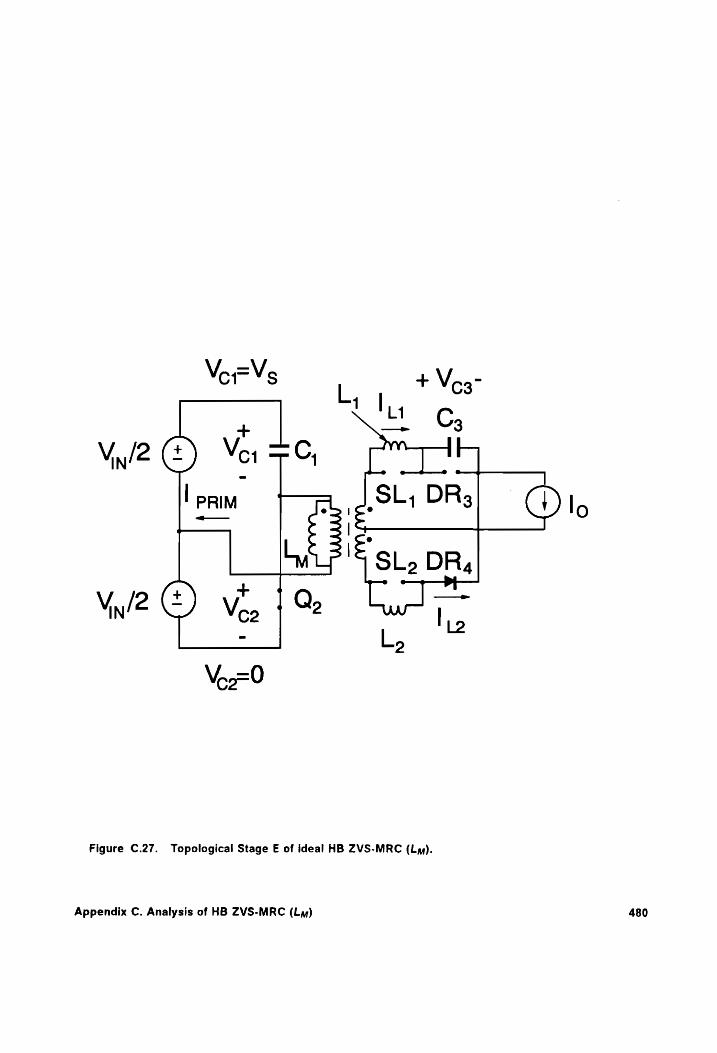
Figure C.27. Topological Stage E of ideal HB ZVS-MRC (Ly).
Appendix C. Analysis of HB ZVS-MRC (Ly) 480
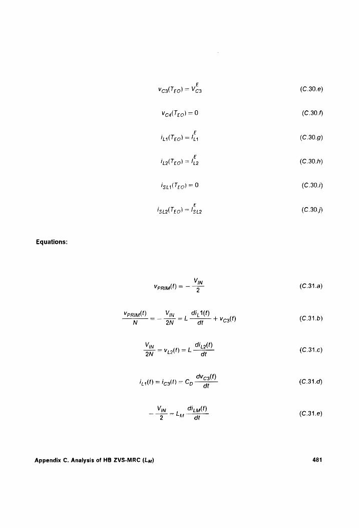
E VoalTE0) = Ves
VealTeo) = 9
E iig(Te0) = Ie
E iro(Teo) = Ie
isps(TEG) = 0
. E
IspalTeo) = Is12
Equations:
Vin Verim(f) = — 7
Vprim(t) Vin —, AID) N77 ON TO att Meal?)
Vin di, o(t) ON = Mal) = ba
. AN 3(t) ina) = fog) = CoG
Vin, Fill) 2 ™ at
Appendix C. Analysis of HB ZVS-MRC (Ly)
(C.30.e)
(C.30.f)
(C.30.g)
(C.30.h)
(C.30.i)
(C.30,)
(C.31.a)
(C.31.b)
(C.31.c)
(C.31.d)
(C.31.e)
481

From Eqs. (C.30.a) - (C.31.e), it follows that:
9 2
dt? c3l ya D— ON
Solution:
E Vin Voz = af COS wf + be SiN opt + =
oN
E . M4 = Comp[br cos pt _ ar sin opt]
EE Vin E
E Vin E
where
—E Vin
or in the normalized form:
Appendix C. Analysis of HB ZVS-MRC (Ly)
(C.32)
(C.33.a)
(C.33.b)
(C.33.c)
(C.33.d)
(C.33.a)
(C.33.b)
482
EN Vo3 = acy COS Cty + Den Sin Cty + 1
EN 1 Cyly ; iy => 15 [ary COS Sty — Dey sin Cty]
ON
EN Lyrty EN 12 =a + Iho
EN Qnty EN Th + liy
lon
where
EN aren = Vo3 — 1
ens 46 ben =a lon TyCn
Stage Duration Te = Te1 — Teo
Stage duration T¢ is determined from the conditions:
ipa(Te) + ipolTe) = lo
or
Appendix C. Analysis of HB ZVS-MRC (L~4,)
(C.34.a)
(C.34.b)
(C.34.c)
(C.34.d)
(C.35.a)
(C.35.b)
(C.36.a)
483
lro(Te) = Isar-
STAGE EP [Tepo, Tep1] (Fig. C.28)
Initial Conditions:
Vor(Tepo) = Vin
Voo(Tepo) = 90
EP lppim( Epo) = prim
EP inm(Tepo) = !/im
EP VoalTepo) = Veg
VoalTepo) = 0
EP ina(Tepo) =!
EP ipolTero) = Iie
isnal(Tepo) =9
EP isto(Tepo) = '!s12
Appendix C. Analysis of HB ZVS-MRC (La)
(C.36.b)
(C.37.a)
(C.37.b)
(C.37.c)
(C.37.d)
(C.37.e)
(C.37.f
(C.37.g)
(C.37.h)
(C.37.i)
(C.37,/)
484
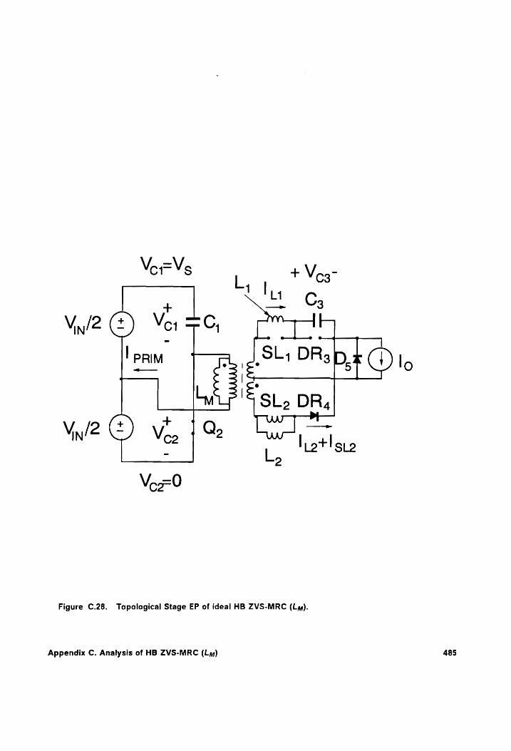
Figure C.28. Topological Stage EP of ideal HB ZVS-MRC (Ly).
Appendix C. Analysis of HB ZVS-MRC (La) 485
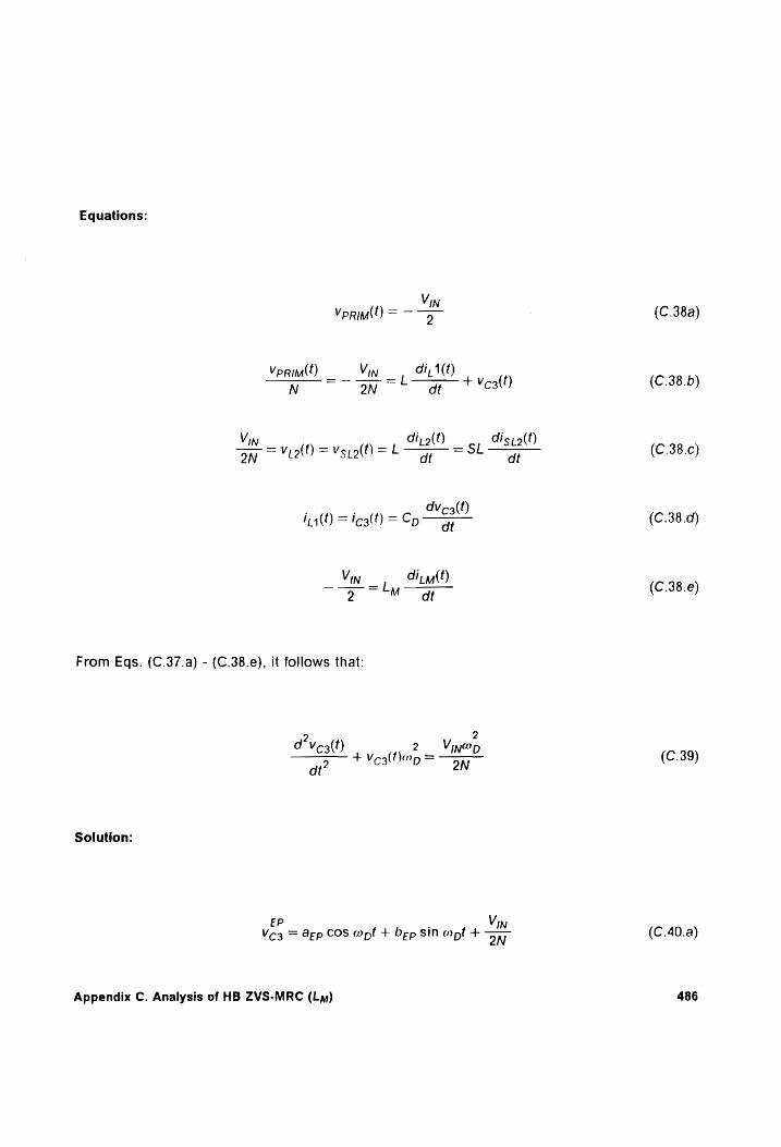
Equations:
VIN VpriM(t) = —
Verim(t) Vin i ACE) NON * at Vest!)
Vin di, a(t) Aisi o(f) on Mal = veil) = bp = SE ae
. . AWV3(f) ia(t) = icglt) = Cp a
Vn, Aiud 2 ™M at
From Eqs. (C.37.a) - (C.38.e), it follows that:
2 2
PV C3) thane = VINOD a CBRUOD = ony dt2 2N
Solution:
Vin EP . Vc3 = agp COS wpf + Dep Sin apt +
Appendix C. Analysis of HB ZVS-MRC (Ly)
2N
(C.38a)
(C.38.b)
(C.38.c)
(C.38.d)
(C.38.e)
(C.39)
(C.40.a)
486

.EP . ii4 = Compl bep COS not — agp SIN wf]
EP Vin EP 'SL2= Oysp ft 'st2
EP Vin EP iM =~ 3 t+liy
where
EP VIN agp = Ve3 —
EP bee = EP ompCp
or in the normalized form:
EPN . Vc3 = @rpn cos Ety 4- bepy sin éty + 1
EPN 1 Crly
11 16 ON Larry COS Sty — Depa Sin Sty]
EPN Lyurty EPN "ho Don + tho
Appendix C. Analysis of HB ZVS-MRC (Ly)
(C.40.b)
(C.40.c)
(C.40.d)
(C.40.e)
(C.41.a)
(C.41.b)
(C.42.a)
(C.42.b)
(C.42.c)
487
EPN SL Lytty — EPN Istpo2 = L2 L lon
EPN dnty EPN 7 an ] LM
ON
where
EPN aepn= Veg — 1
EPN [46 b =/,, | —— EPN L1 "ON LyCy
Stage Duration Tep = Tep1 — Tepo
Stage duration Te is determined from the condition:
ispolTep) + fro(Tep) + fia(Tep) = Io
STAGE F [Tro, Tes] (Fig. C.29)
Initial Conditions:
Voril(Tro) = Vin
Appendix C. Analysis of HB ZVS-MRC (Ly)
(C.42.)
(C.42.e)
(C.43.a)
(C.43.b)
(C.44)
(C.45.a)
488
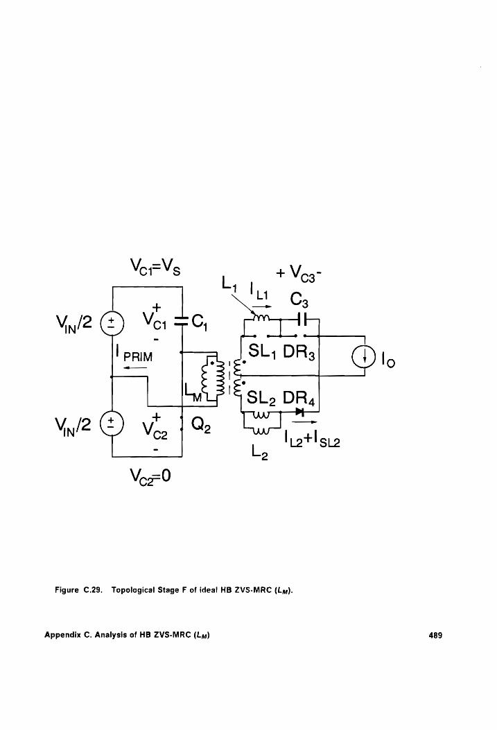
V
\Wwi2 @ Figure C.29. Topological Stage F of ideal HB ZVS-MRC (Ly).
Appendix C. Analysis of HB ZVS-MRC (Ly) 489

Voo(T ro) = 0
F ippimm( £0) = !prim
F limU ro) = Iim
F
Vo3(T ro) = Ves
VealTro) = 0
F aT ro) = Ih
F frolT ro) = Io
isns(Tro) =O
F ispo(Tro) ='sr2
Equations:
Vin Vprim(!) = —
2VpRim(f) Vin di, 1(f) di, a(t) PRI = Nt A + vea(t)- 2
Vin di, a(t) dis; a(t) on = Vial!) = Vsvalt) = 6 —G— = SL —
Appendix C. Analysis of HB ZVS-MRC (Ly)
(C.45.b)
(C.45.c)
(C.45.d)
(C.45.e)
(C.45.f)
(C.45.g)
(C.45.h)
(C.45.i)
(C.45./)
(C.46.a)
(C.46.b)
(C.4B.c)
430

. AV ¢3(6) i4(t) = iceg() = Cp a
Vin L di, y(t) 2 Mat
From Eqs. (C.45.a) - (C.46.e), it follows that:
2 Vin@pK
2N
2 d'Vea(t) 2
5 + Veal tink, = at
Solution:
F 1/2 1/2 Vin Vc3 = ar cos K, Wpt + br sin K, wpt + ON
F
iy = Cpmp Kt E bp cos Kt Pept — ag sin Kt Penpt]
F
ho = —_____1____ (ar sin ony l?t — b-( cos cop Ky |? —1))+ cp Leopk}!2(2 += Opn ( SL )
F F F Ista =lo~ tir — Ihe
F Vin F im =~ E+ I
where
Appendix C. Analysis of HB ZVS-MRC (La)
(C.46.d)
(C.46.e)
(C.47)
(C.48.a)
(C.48.b)
(C.48.c)
(C.48.d)
(C.48.e)
491

ap = Ve3— >
F —1/2 5. [uk
Fr MDCp
Cr=lo
or in the normalized form:
FN Vog = agy Cos EK1!?ty + Dey sin EKy!?ty + 1
EN [Cyl yK ay =~ = —~ [ary cos EKq/7ty — bey sin Ky? ety]
ON
FN 1 Cryly
1g =
7 — [arn sin EKA?t ON sf 16(2 +--+ =
1/2 — bey( cos Ky! ty — 1) + Cry
FN FN EN isng =1—bhy — Iho
FN 2mty FN iM = — ~~ + lim
ON
where
Appendix C. Analysis of HB ZVS-MRC (Ly)
(C.49.a)
(C.49.b)
(C.49.c)
(C.50.a)
(C.50.b)
(C.50.c)
(C.50.d)
(C.42.e)
492

FN arn = Vo3 — 1 (C.51.a)
FN 16
FN Cry = Iho (C.51.c)
Stage Duration Tr = Tr1 — Tro
Stage duration Tr is determined by the turn-off of switch Qo initiating a new conversion cycle.
STAGE G [Teo, Tos] (Fig. C.30)
Initial Conditions:
Vo1(TGo) = Vin (C.52.a)
VealT eo) = 9 (C.52.b)
iprm(T Go) = IPR (C.52.c)
itm( Go) = liu (C.52.d)
Appendix C. Analysis of HB ZVS-MRC (Ly) 493
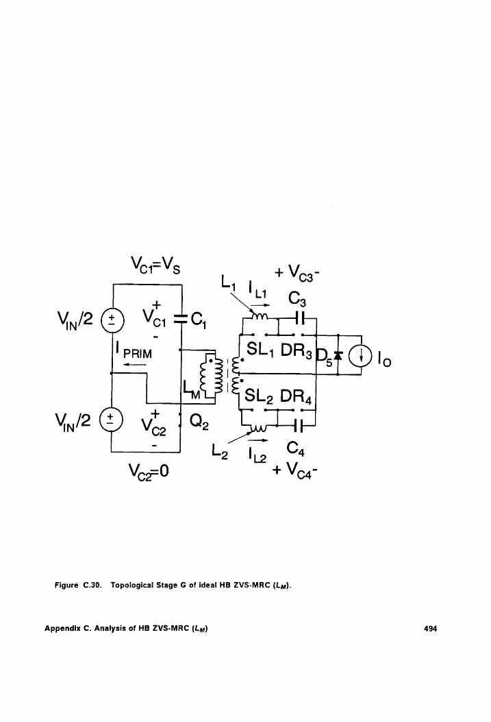
Figure C.30. Topological Stage G of ideal HB ZVS-MRC (Lay).
Appendix C. Analysis of HB ZVS-MRC (La) 494
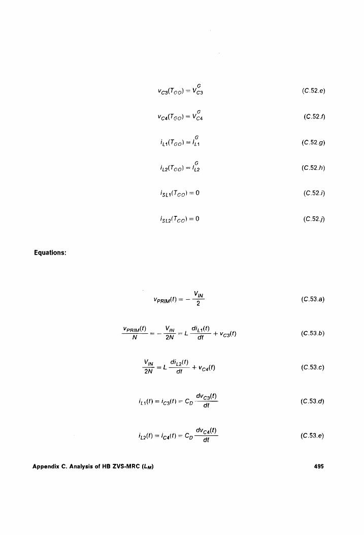
G
Vo3(Tco) = Ves
G
VealTGo) = Vca
i G
ins(Teo) = I
j GC hio(Teo) = Ie
Equations:
Verim(}) = — “is
tenuna( __ vin _ 1 Hus) vest)
oT ~f mu + Vealt)
ip y(t) = igg(t) = Cp Mall
Wea (t)
ital!) = ical) = Cp —S
Appendix C. Analysis of HB ZVS-MRC (Las)
(C.52.e)
(C.52./)
(C.52.g)
(C.52.h)
(C.52.i)
(C.52./)
(C.53.a)
(C.53.b)
(C.53.c)
(C.53.d)
(C.53.e)
495
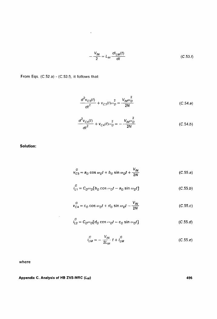
Vin —, Gilt) 2 at
From Eqs. (C.52.a) - (C.53.f), it follows that:
9 2
d veal!) +v (Nene Vin®p a C3 D-~ oy dt? 2N
d?v-4(t) Viens CA 2 IN®@D ye + VealOarp = ON
Solution:
G Vin Vo4 = ag cos wpt + be sin wpt + “ON
.G . M4 = Comp[be cos mot _ ag sIn wpt]
G Vin Vo4 = Cg COS «pt + dg SIN wpt — ON
.G . ing = Compldg Cos orpt — cg sin pf]
G Vin G jy =z——a tei LM LM 2Lyy
where
Appendix C. Analysis of HB ZVS-MRC (Ly)
(C.53.f)
(C.54.a)
(C.54.b)
(C.55.a)
(C.55.b)
(C.55.c)
(C.55.d)
(C.55.e)
496
jo
b.= L1
Comply
cin Co= Vea F 9
G
Iho
Wg ~ mpCp
or in the normalized form:
GN . Voz = Agn COS Cty + ben Sin Sty + 1
.GN 1 / Cnln fg = — 7 4 / = [Aen COS Sty — Den sin Sty] lon 16
GN Vc4 = Con cos Ety + don sin Ety _— ¥
GN ‘ Cyln . Iho = — 7 16 [Con cos fty — don sin ft] ON
GN arty GN
where
Appendix C. Analysis of HB ZVS-MRC (Ly)
(C.56.a)
(C.56.b)
(C.56.c)
(C.56.d)
(C.57.a)
(C.57.b)
(C.57.c)
(C.57.d)
(C.57.e)
497

GN agen = Vo3 — 1
GN 16 Pon =I Jon, | Tree
G Con = Vea + 1
GN 16 den =Ia lon, | TyCy
Stage Duration Tg = Te1 —Tco
Stage duration Tg is determined from the conditions:
ina(T@) + it2(Te) = Io
fto(T@) = Isat
or
VoalTe) = Q.
STAGE H [Tyo, TH1) (Fig. C.31)
Appendix C. Analysis of HB ZVS-MRC (Ly)
(C.58.a)
(C.58.b)
(C.58.c)
(C.58.d)
(C.59.a)
(C.59.b)
(C.59.c)
498
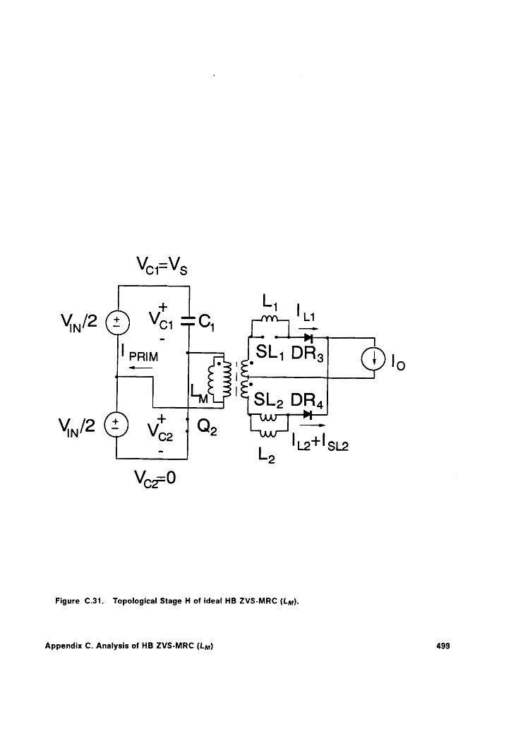
Ly +
Vin /2 (+) Vo1 TO, i
IPAM SL; DR3 a —_ ts ’ lo
ic DR, + 1Q
Min/2 & Vi, | Q , Iotleis
Figure C.31. Topological Stage H of ideal HB ZVS-MRC (Ly).
Appendix C. Analysis of HB ZVS-MRC (Ly) 499

Initial Conditions:
Vo1(THo) = Vin
Voo(THo) = 9
H ippim( Ho) = !prim
H itm vo) = !im
Vo3(THo) = 9
VoalT Ho) = 9
H ing(THo) = I
H iroTHo) = Ie
iseaTHo) =9
H fsro(THo) = '!sr2
Equations:
Vin Verim(f) = — 9
Appendix C. Analysis of HB ZVS-MRC (Ly)
(C.60.a)
(C.60.b)
(C.60.c)
(C.60.d)
(C.60.e)
(C.60.f)
(C.60.g)
(C.60.h)
(C.60.i)
(C.60,/)
(C.61.a)
500
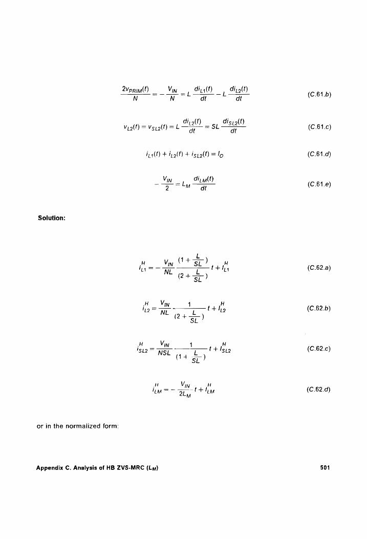
2Vprim(f) Vin, Merl) Meal N - N at at
di, a(t) dis,o(t) Vio(t) = Vgialt) = L —a— = SL
ipa(t) + frolf) + isro() = lo
Vin —, Fim 2 MoM sdt
Solution:
L H Vin (1+ SL ) H ia =~ y
SL
H VY H itp = NS 1+ — t+ hp M+
SL
H Vin 1 H 'st2 = Wsp “a =y t+ Isro
SL
in =— vin t yn LM ~— 2Lay LM
or in the normalized form:
Appendix C. Analysis of HB ZVS-MRC (Ly)
(C.61.b)
(C.61.c)
(C.61.d)
(C.61.e)
(C.62.a)
(C.62.b)
(C.62.c)
(C.62.d)
501
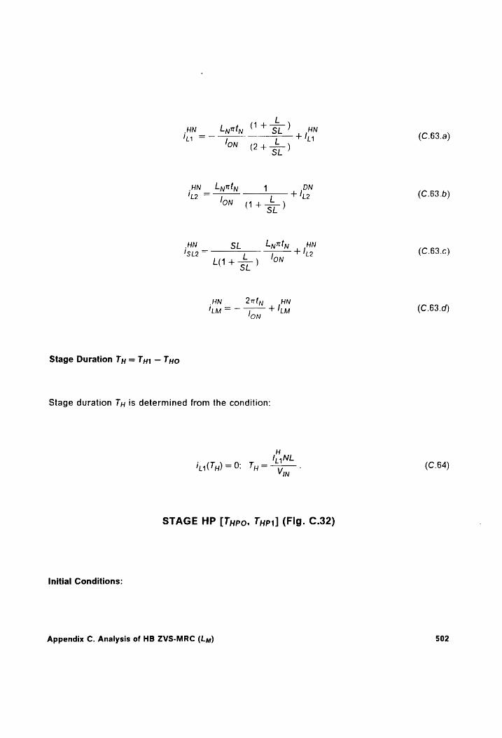
14 = lon L + Ih (C.63.a)
(2+ SL
HN Lyrt DN ig = th (C.63.b) ON +
HN SL Lytty | HN 'o19 = L ta + hig (C.63.c)
L(i+—-) (ON SL
HN arty HN lim =~ j + liv (C.63.0)
ON
Stage Duration Ty = TH1 — Tyo
Stage duration Ty is determined from the condition:
WNL ina(Ty) = 90 Ty = (C.64)
STAGE HP [Tupo, Tupi] (Fig. C.32)
Initial Conditions:
Appendix C. Analysis of HB ZVS-MRC (Lay) 502
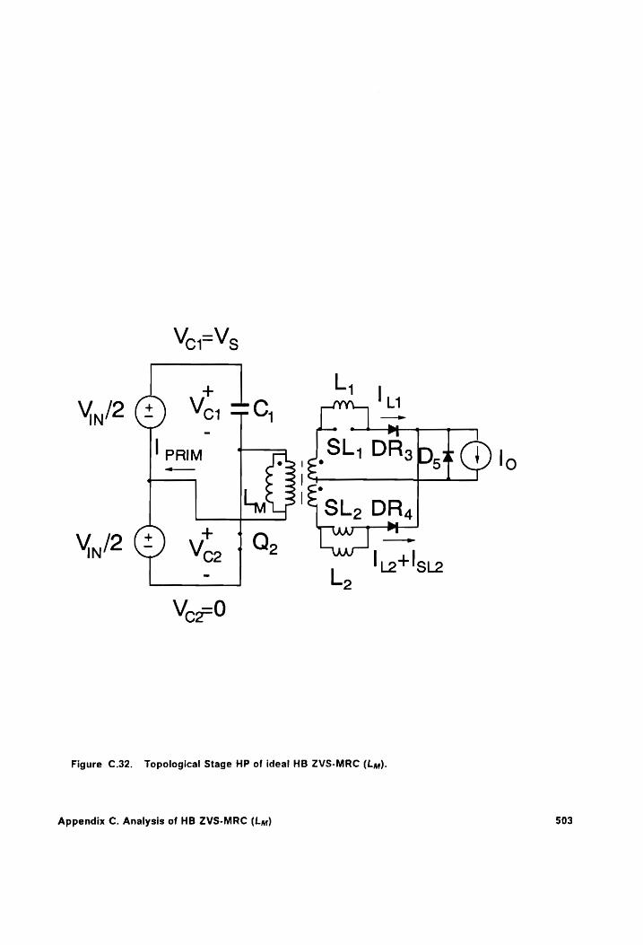
Figure C.32. Topological Stage HP of ideal HB ZVS-MRC (Ly).
Appendix C. Analysis of HB ZVS-MRC (Ly) 503
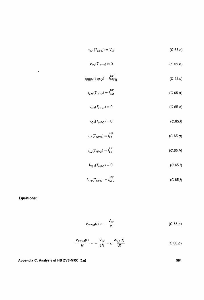
Equations:
Vor(Typo) = Vin
Voo(THpo) = 0
HP iprim( Heo) = prim
HP lpm yeo) =!im
Vo3(THpo) = 0
Voea(Typo) = 0
HP iiaTypo) = lh
HP hro(Typo) = Iie
ista(Tupo) = 9
HP istol(Typo) = 'sr2
Vin VpriM(f) = — >
VpriM(t) = Vin _, Gita l(t)
N 2N at
Appendix C. Analysis of HB ZVS-MRC (La)
(C.65.a)
(C.65.b)
(C.65.c)
(C.65.d)
(C.65.e)
(C.65.f)
(C.65.9)
(C.65.h)
(C.65.i)
(C.65,j)
(C.66.a)
(C.66.b)
504
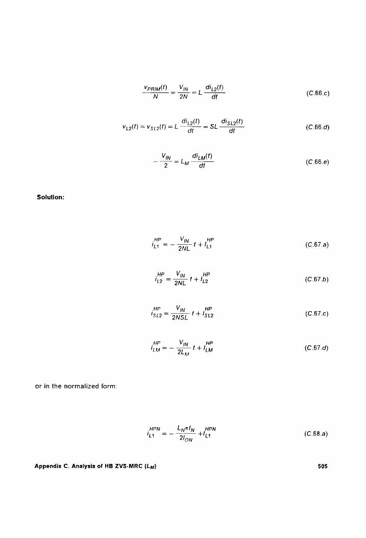
VpriM( Vin _, Gizolt) N ~ 2N at
Aralt) _ 5, Asiall) Violt) =Vsp() =L a= ot
Vin Sem)
— Q Mat
Solution:
HP Vin HP
HPO OV HP ie = np ft fe
HP Vin HP 'SL2 = ONSL f+ /s19
JHP Vin t jue iy =—- = LM 2Lny LM
or in the normalized form:
HPN Lyrty HPN My =~ pp Hl 2lon
Appendix C. Analysis of HB ZVS-MRC (Ly)
(C.66.c)
(C.66.d)
(C.66.e)
(C.67.a)
(C.67.b)
(C.87.c)
(C.67.d)
(C.68.a)
505

HPN Lyutty HPN ‘2 Dov * L2
HPN SL Lytty | HPN iggg9 =—- SL2 L Qloy SL2
HPN anty HPN iM = + ILM
Stage Duration Typ = THpi1 — Typo
Stage duration Typ is determined from the conditions:
in4(7yp) =9; Tp = Vin
or
iro(THp) + fuse) + isto Hp) = lo-
STAGE I [Tio, 711] (Fig. C.33)
Initial Conditions:
Appendix C. Analysis of HB ZVS-MRC (La)
HP Ir, 2NL
(C.68.b)
(C.68.c)
(C.68.d)
(C.69.a)
(C.69.b)
506
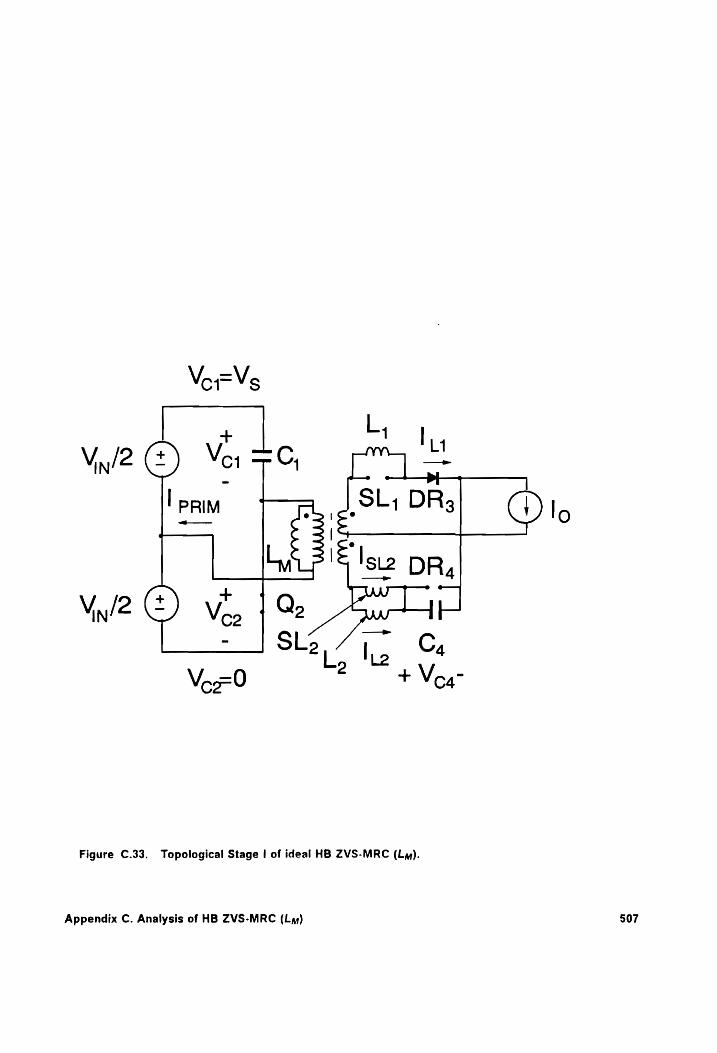
Figure C.33. Topological Stage | of ideal HB ZVS-MRC (Ly).
Appendix C. Analysis of HB ZVS-MRC (Ly) 507

Equations:
Vor(Tio) = Vin
Veo(Tio) = 9
I Ippo) = !prim
i limo) = lim
Voe3(Tio) = 0
I VoalTi9) = Veg
| liaMio) = Ie
I ina(Tio) = Ihe
isp4(Tjo) = 0
i ispa(Tio) = !sro
Vin Vprim(t) = —
Vin. diz g(t) di, 9(t) Nb ae 7 Meal) by
iea(t) + ipa 4 fspa() = lo
Appendix C. Analysis of HB ZVS-MRC (Ly)
(C.70.a)
(C.70.b)
(C.70.c)
(C.70.d)
(C.70.e)
(C.70./)
(C.70.g)
(C.70.h)
(C.70.i)
(C.70,j)
(C.71.a)
(C.71.b)
(C.71.c)
508

av-4(t
ipo(t) + Isro(t) = icalt) = cp
Vin i di; y(E) 2 MoM sat
From Eqs. (C.70.a) - (C.71.e), it follows that:
2 2 d‘v (t) 2 V Kya
SS + Vea Kp = at
Solution:
i Vo4 = a) COS np K4!7t + b, sin wpK4!*t + 7
1/2 I Cyompk
ist2 = SF [608 np 7t — a Sin np ky] + 1+ SL
! I inp = Cpp Ky? [b, cos mp Ky !?t — a) sin op K4/7t] — M510
! Vin ! iuM=z Tt OLy t+ liu
where
Appendix C. Analysis of HB ZVS-MRC (La)
(C.71.d)
(C.71.e)
(C.72)
(C.73.a)
(C.73.b)
(C.73.c)
(C.73.d)
509

1 Vin a) = Vea — "N_
{ /
lo + !sp9
opCpK, /2
=
ss SL I i
Cy= ly - 7 (lio + Isp) 414+ SL
or in the normalized form:
IN . Vo4 = ajy COS EKA? ty + bin sin EKA? ty +2
L
IN “SL LyC ; isfo= = . | K, [bij cos Kyl ety, — ay sin Kh! et] + cy
(1 + 7 Von
IN 4 LyCy 1/2 Ape IN 12-16 M1 Lin cos Kt! &ty — ayy sin Ky éty] — sy
IN arty IN iim = — + diy
ON
where
IN ain = Vea — 2
Appendix C. Analysis of HB ZVS-MRC (Ly)
(C.74.a)
(C.74.b)
(C.74.c)
(C.75.a)
(C.75.b)
(C.75.c)
(C.75.d)
(C.76.a)
510
by = (Ny + lasloy. /—8 (C.76.b) IN L2 SL2 ON LyCnKy iM.
L IN “SL” IN IN
Cw = Isn2 — “F(a t Is) (C.76.c)
+ SL
Stage Duration 7; = Tj — Tio
Stage duration T; is determined from the conditions:
i(TV=O (C.77.a)
or
Vo4(T)) = 0. (C.77.b)
STAGE IP [Tipo, Tipi] (Fig. C.34)
Initial Conditions:
Yor(Tipo) = Vin (C.78.a)
VeolTipo) = 0 (C.78.b)
Appendix C. Analysis of HB ZVS-MRC (Ly) 511
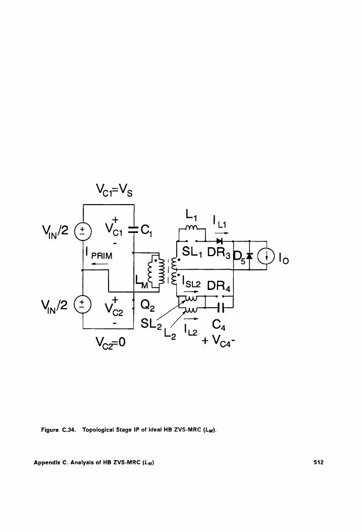
Figure C.34. Topological Stage IP of ideal HB ZVS-MRC (Ly).
Appendix C. Analysis of HB ZVS-MRC (La) 512

IP lprimU ipo) = !prim
IP inm(U iro) =!
Vo3(T ipo) = 9
Ip VoealT ipo) = Vea
IP ina ipo) = Ie
IP fro ipo) = Ie
ists ipo) = 0
IP isco(Tipo) = 'st2
Equations:
Vin Verim(f) = — 5
Vin diz o(t) ON Eat teal
Vin, Aha) 2N at
Walt)
Appendix C. Analysis of HB ZVS-MRC (Ly)
(C.78.c)
(C.78.d)
(C.78.e)
(C.78.f
(C.78.9)
(C.78.h)
(C.78.i)
(C.78 j)
(C.79.a)
(C.79.b)
(C.79.c)
(C.79.d)
513
Vin di, y(t)
From Eqs. (C.78.a) - (C.79.e), it follows that:
2 2 d?Vea(t) upgttyen?, = Minka 9 + Veal Kap = aa
dt® 2N
ook Kaa itt op
Solution:
IP . Vin Vc4 = ap cos wpKat + bip SIN wpKagt + “ON
IP 4 , Iso = = CompK, [Dip cos mpK,gt _ aip sin wpK yt] + Cip
IP . IP ito = CrmpK 4[ Dip cos arpkK at _— ap sin wMpK,t) _ Isto
Ip Vin ip liu =— Qhy t+ lim
where
rp Vin dip = Vea — Dap
Appendix C. Analysis of HB ZVS-MRC (La)
(C.79.e)
(C.80.a)
(C.80.b)
(C.81.a)
(C.81.b)
(C.81.c)
(C.81.d)
(C.82.a)
514
IP IP la +519 p= mC oK, (C.82.b)
aE IP SL IPP
Cp = Ig ~~ (ha + Ist) (C.82.c) ‘tor
or in the normalized form:
IPN ; Vo4 = apy COS CK aty + Dipy Sin CKgty + 1 (C.83.a)
[bipy COS KyEty — Apa SIN KyEty) + Cypyy (C.83.b)
PN
lio [bipy COS Kg ty — ajpy Sin Kygéty] — Ispo (C.83.c)
JPN Qnty IPN iMo=T ton + lin (C.83.d)
ON
where
IPN
(fen 1 PN, _ Le SL2"ON- 16
bipn = Ky LyCy (C.84.b)
Appendix C. Analysis of HB ZVS-MRC (Ly) 515
L IPN “SL. IPN IPN
Cipn = !s12 ~~~ — (Ita. + Is) 4
SL
Stage Duration T)p = T)p; — Tipo
Stage duration 7;p is determined from the conditions:
ip4(Tip) =0
Voa(T ip) = 0
or
ing(Tip) + fro(Tip) + Ista(Tip) = lo
STAGE J [TJo, T1] (Fig. C.35)
Initial Conditions:
Vergo) = Vin
Veol(T yo) = 0
Appendix C. Analysis of HB ZVS-MRC (La)
(C.84.c)
(C.85.a)
(C.85.b)
(C.85.c)
(C.86.a)
(C.86.b)
516
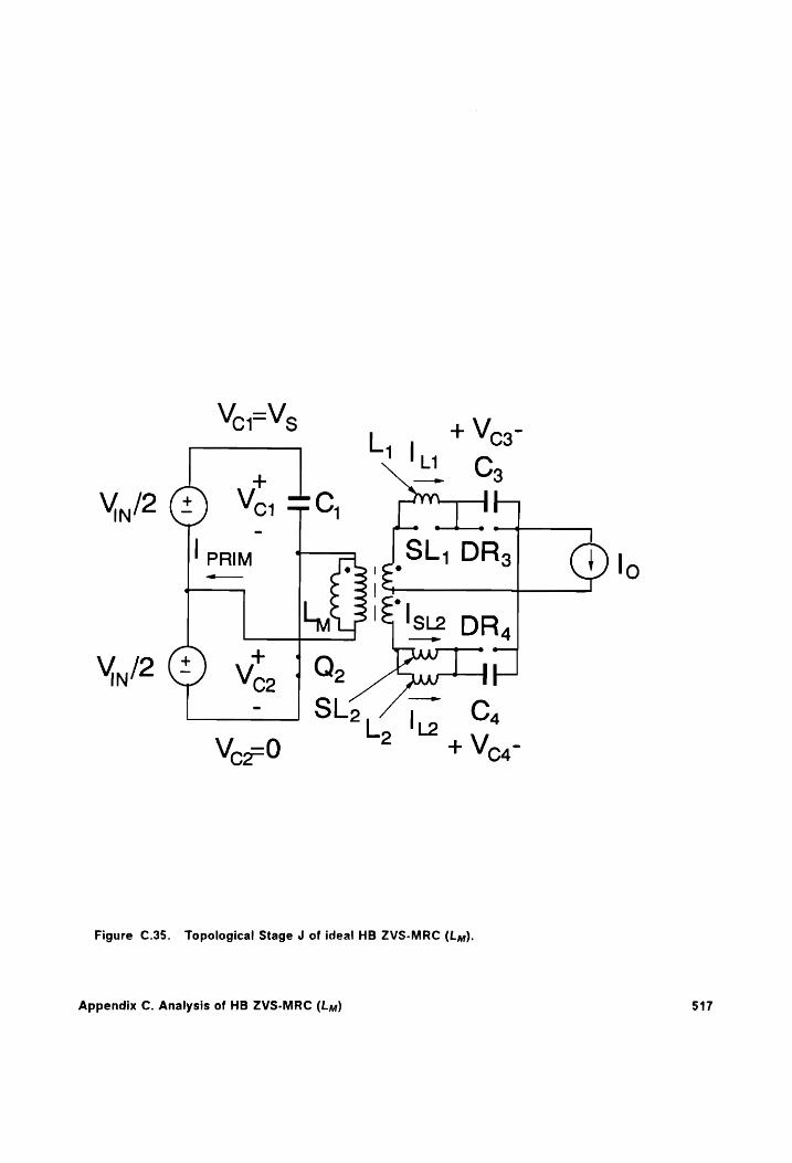
Figure C.35. Topological Stage J of ideal HB ZVS-MRC (Ly).
Appendix C. Analysis of HB ZVS-MRC (Ly) 517

J iprim( vo) = '!prim
J lnm(yo) = lim
J Vo3(Ty0) = Ve3
J VealTyo) = Vea
J ing(Tg0) =I
J lro(Ty0) = Nie
ist4(Ty0) = 9
J ispa(Ty0) = !sro
Equations:
Vin Vprim(l) = — ——
2VpRim(t) Vin di, (f) diz a(t) NN att Meal) = Veal) Ep
iat) + ipo(Disio(O) = Io
, , We, (t) iro(t) + fsrolf) = ical) = Cp cat
Appendix C. Analysis of HB ZVS-MRC (La)
(C.86.c)
(C.86.d)
(C.86.e)
(C.86.f)
(C.86.g)
(C.86.h)
(C.86.i)
(C.86./)
(C.87.a)
(C.87.b)
(C.87.c)
(C.87.d)
518

. . AWe3(t) Il) = leglt) = Cp —G—
Yin Aum) 2 “at
From Eqs. (C.86.a) - (C.87.f), it follows that:
L d‘v (t) 2(1 +)
LCp(2+ 3)
L 241+) we |e
Solution:
J Vo4 = a) COS wyl + Dy SIN wyl + Cyt + d;
iLg=——7 [bye y( cos of — 1) — aen, sin agt] + Iho
(1+—)
J Vin Vo3 = — ay COS ng — by COS nyt + Cyt + dy — 4
J . ing = Cplayeny sin nyt — bys CoS wyt + Cy]
Appendix C. Analysis of HB ZVS-MRC (Ly)
(C.87.e)
(C.87.f
(C.88.a)
(C.88.b)
(C.89.a)
(C.89.b)
(C.89.c)
(C.89.d)
519

J J J
isto =!o — ba — thy
J Vin J liM = Qk f+ liu
where
J J V Vig t Veg + —
N d,= 9
J ay = Vea — Ay
Jovog c= la the t+/svo vo 2Cp
J J
tia ttsrg — ¢y J mylp - Oy
or in the normalized form:
J ad J M4 + lio + Isio 8rty
JN Vo4q = Ayy COS Sty + Day Sin Sty + C
N
JN CyKs . JN iLg = 7 — [dyn 608 Sty — 1) — ayy SIN Sty] + Iho
Appendix C. Analysis of HB ZVS-MRC (Ly)
(C.89.e)
(C.89./)
(C.90.a)
(C.90.b)
(C.90.c)
(C.90.d)
(C.91.a)
(C.91.b)
520
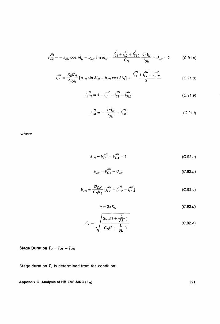
J J J JN Ih +hotlsio 8rty
Cn lon
JN JN JN UN KzC lig thy +l hh = in [ayy sin Oty _ Don cos Oty] + Ss
JN JN JN JN isp9 =1-—thy ~~ the — Isto
JN arty JN iM = + lim
ON
where
JN JN diy = Vo3 + Vea + 4
UN ayn = Vea — Ay
2lon _JN JN JN JN ~ Go Cie +42 —hiy]
nK5
6 = 27Ks
OL (1 + =?
L Cyl2 + =)
Stage Duration Ty = Ty, — Tyo
Stage duration Ty is determined from the condition:
Appendix C. Analysis of HB ZVS-MRC (Ly)
(C.91.c)
(C.91.d)
(C.91.e)
(C.91.1
(C.92.a)
(C.92.b)
(C.92.c)
(C.92.d)
(C.92.e)
521

Voa(Ty) = 0 (C.93)
STAGE JP [Tupo, Typ1] (Fig. C.36)
Initial Conditions:
VerTuro) = Vin (C.94.a)
Vea(Typo) = 0 (C.94.b)
ippimM(ypo) = lpr (C.94.c)
itmUypo) = hin (C.94.d)
Vea(Typo) = Ves (C.94.e)
VealTupo) = Vou (C.94.f)
ii4(Tyro) = he (C.94.g)
ita(Typo) = li (C.94.h)
isia(Typo) = 0 (C.94.i)
Appendix C. Analysis of HB ZVS-MRC (Ly) 522
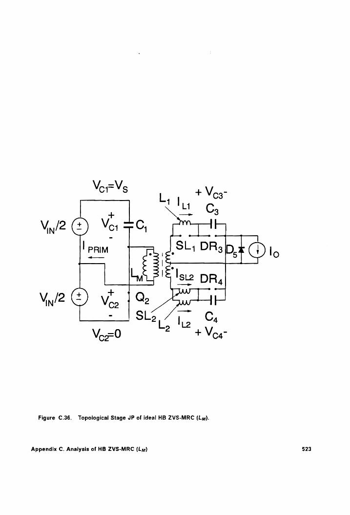
Figure C.36. Topological Stage JP of ideal HB ZVS-MRC (Ly).
Appendix C. Analysis of HB ZVS-MRC (Ly) 523
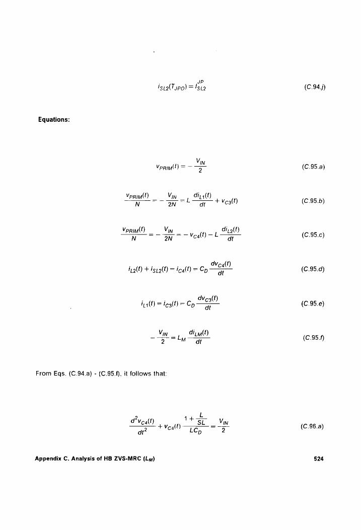
. JP
ispolTypo) =!sr2
Equations:
Vin Vprim(t) = — ——
VpRim(l) Vin, Gir (t) NON Dap t Ves
Vprim(f) Vin di; o(t) Ny oN = 7 Veal) — LE
Wall) inalt) + isralt) = ical) = Cp —F
. , dVc3(F) ii(O = fealt) = Cp a
Vin _, Fim 2 ™_ dt
From Eqs. (C.94.a) - (C.95.f), it follows that:
L 2 tl D' Vea (t) tor Vin 2 + Veal) TE = at D
Appendix C. Analysis of HB ZVS-MRC (Ly)
(C.94,j)
(C.95.a)
(C.95.b)
(C.95.c)
(C.95.d)
(C.95.e)
(C.95.f)
(C.96.a)
524
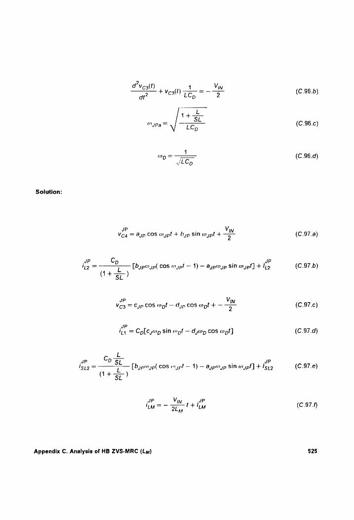
OD = __—___-
J/LCp
Solution:
JP . Vin Voa = ayp cos wypt + byp sin wypt + “2
JP Cp JP ho = ——_. [by pw yp( cos a ypt _ 1) _ aypMyp sin wypt] + lio
(14+ SL )
JP Vin Vo3 = Cyp COS wot — Ajp COS wpt + — 72
MP . ing = CrolCymp sin opt — djwp COS wf]
L JP Cp SL . UP Isto = —— p [bypeyp( cos om ypt _— 1) _ aypMyp sin wr ypt] + Isp
44+4— ( SL
JP Vin ' yP i —— LM 2h LM
Appendix C. Analysis of HB ZVS-MRC (La)
(C.96.b)
(C.96.c)
(C.96.d)
(C.97.a)
(C.97.b)
(C.97.c)
(C.97.d)
(C.97.e)
(C.97.f)
525

where
JP ayp = Vea — 1
JP JP — tte +I ste
JP ~—
Cpom yp
JP Cy = Vo3 + 4
yp
Li d,= J Comp
or in the normalized form:
JPN . Voq = yy COS vty + Diy Sin vty + 1
OL pePN jJPN JN JPN ho = a [bypy cos tly — aypn sin vin] + tio ~ 2
ON \/ 8A +P) 1+
JPN . Voz = — ayy COS thy, — Dyn SIN vey — 1
JPN 1 Cyly . iy =- Tow 15 [Cypy COS vty — Aypy Sin vey]
Cyl y(t +) JPN 4 NON SL . JPN Isto = lon 8 [bury cos vty — Aypn sin vty | — fro
JPN arty JPN iim =~ ~ +m
ON
Appendix C. Analysis of HB ZVS-MRC (Las)
(C.98.a)
(C.98.b)
(C.98.c)
(C.98.d)
(C.99a)
(C.99.b)
(C.99.c)
(C.99.d)
(C.99.e)
(C.99.f)
526
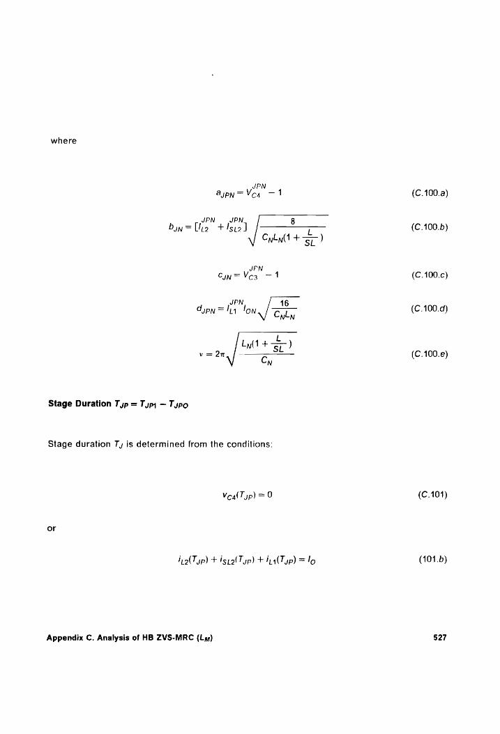
where
JPN QyPN => Ve4 _ 1 (C.100.a)
JPN JPN B byw=[he +!sto] ——— (C.100.b)
Cult + =)
JPN Cin=Vo3 — 1 (C.100.c)
JPN / 46
NEN
(C.100.e)
Stage Duration Typ = Typ; — Typo
Stage duration 7, is determined from the conditions:
Ve4lT yp) = 0 (C.101)
or
irolTyp) + ispalT yp) + in4(Typ) = lo (101.b)
Appendix C. Analysis of HB ZVS-MRC (Ly) 527
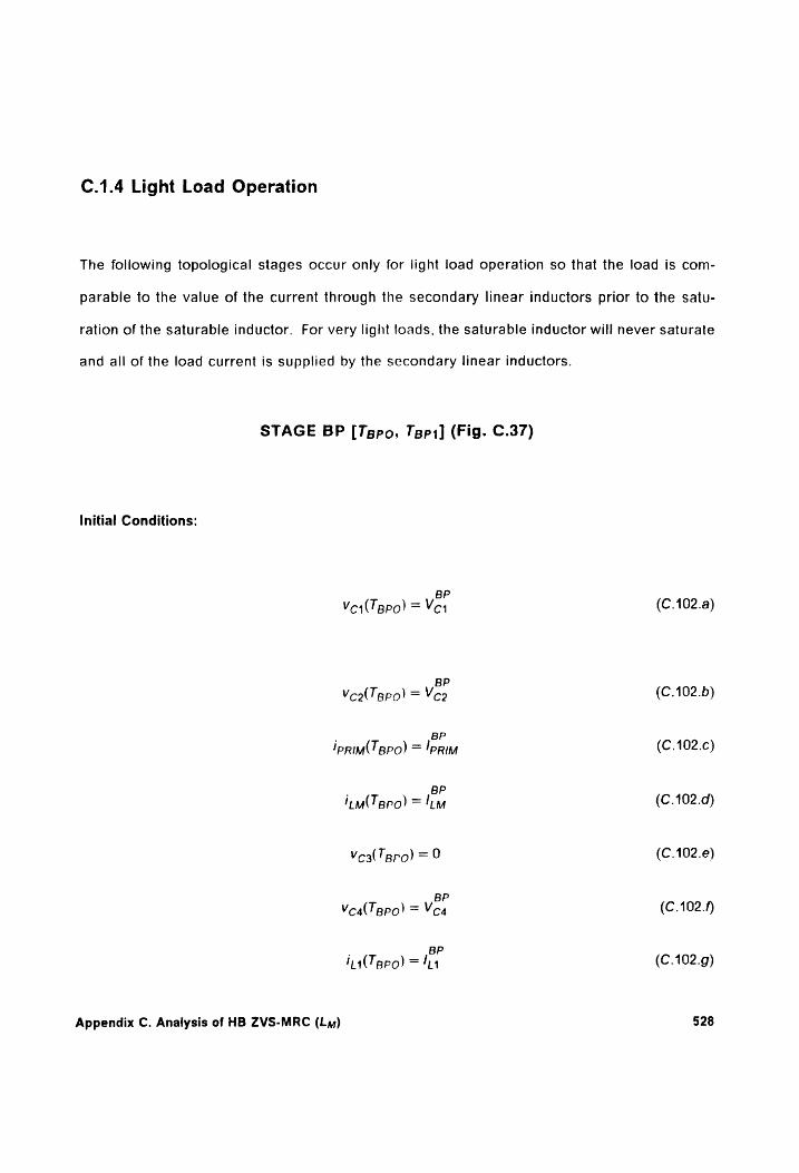
C.1.4 Light Load Operation
The following topological stages occur only for light load operation so that the load is com-
parable to the value of the current through the secondary linear inductors prior to the satu-
ration of the saturable inductor. For very light loads, the saturable inductor will never saturate
and all of the load current is supplied by the secondary linear inductors.
STAGE BP [Tgpo, 7sp1] (Fig. C.37)
Initial Conditions:
BP Vor(Tgpo) = Ver
BP Vco(T po) = Veo
BP ippim( Bpo) = |prim
BP itm Beo) = !Lw
Vo3(Tgro) = 90
BP VoalT Bpo) = Veg
BP ina(T apo) = Ih
Appendix C. Analysis of HB ZVS-MRC (La)
(C.102.a)
(C.102.b)
(C.102.c)
(C.102.d)
(C.102.e)
(C.102.f)
(C.102.g)
528
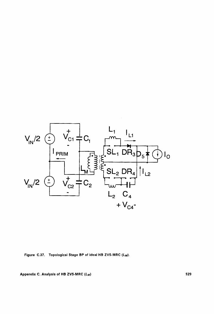
Figure C.37. Topological Stage BP of ideal HB ZVS-MRC (Ly).
Appendix C. Analysis of HB ZVS-MRC (La) 529
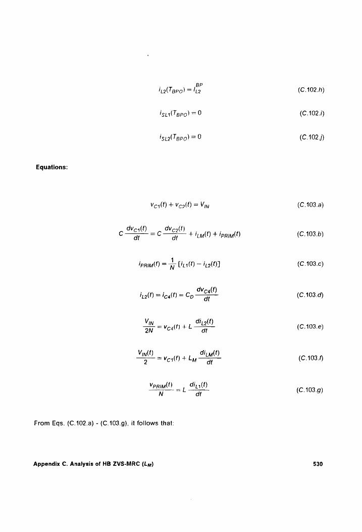
BP ipo(Teapo) = Io
isis(Tgpo) = 9
isto(Tgpo) = 0
Equations:
Voa(t) + Veolt) = Vin
We, (f) Woolf) . dt ott fum(f) + lpr)
iprim(t) = 7 Lin4() — fo(t)]
; ; We, (6) ipo(t) = icalt) = Cp oat
di, (Ct) ot
Vin
Vin(f) di, y(t) 9 = VeilD + Ly dt
VpriM(!) | ual N 7 at
From Eqs. (C.102.a) - (C.103.g), it follows that:
Appendix C. Analysis of HB ZVS-MRC (Ly)
(C.102.h)
(C.102.i)
(C.102./)
(C.103.a)
(C.103.b)
(C.103.c)
(C.103.d)
(C.103.e)
(C.103.f)
(C.103.g)
530

4 2 2 A Vest) — AVealt) » Ly 2. Wealt) . Ln Ly | 4
+ [ ~— + Kglerg + [ =— K5 —-—=— Joo = 0
dt* dt® Cy at Cn 4Cy
where
Ly Kg= 1+
The roots of Eq. (C.96.a) are:
+1
= | +I
7 THT fay _ 4a,
2
yO
jes + /a, — 4a,
2
+ Nome
=> I +
Solution:
BP Vc4 = Agp COS yt + Dap sin yt + Cap cos ft + dpp sin Pt
BP itg = Cp[bgpy cos yt — agpy sin yf + dppf cos Pt — Cgpf sin Bt]
Appendix C. Analysis of HB ZVS-MRC (Ly)
(C.104.a)
(C.104.b)
(C.104.c)
(C.104.d)
(C.104.e)
(C.104.f)
(C.105.a)
(C.105.b)
531

‘BP b agp qd c ium = 7, [ye €08 yt — Fe sin yt + 2 cos pt——P sin pit
+ Ko[agpy sin yt _ bppy cos yt + Copf sin pt _— dapf cos pty] + Cgp
Bp OV Vor = > + N[agp Cos yt + Dap sin yt + Cgp cos ft + dpp sin Bt
~ K[agpy” cos yt + bgpy” sin yt + Cap’ cos Bt + dgpf sin BET]
BP a ds i = LIE cos) ZF sin ‘t+ = cos pt — 2? sin pr
y B
+ Ko[appy sin yt — bepy cos yt + Capp sin Bt — dppf cos Pt}) + fap
BP b a d c j 1p BP cos yt — BP sin yt + FP cos pt — 2 sin pe
Y y p Bp
+ Ko[agpy sin yt — bgapy cos yt + C_apf sin Bt — dppf cos Bt]] + Gpp
where
BP
BP iy 2CN | 1 li + yy > lip [(1 — Koy") Cp +77 J
Cgp = 2
2CNPK,(y° — )
Appendix C. Analysis of HB ZVS-MRC (Ly)
(C.105.c)
(C.105.d)
(C.105.e)
(C.105.f)
(C.108.a)
(C.108.b)
532
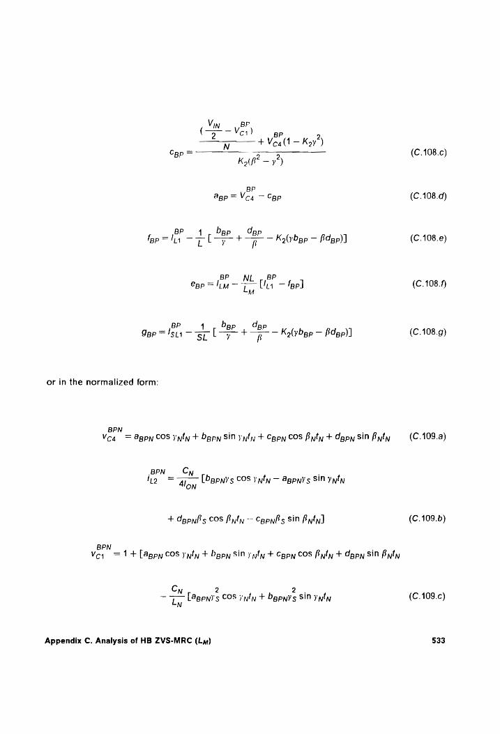
(a7 Yer BP 2 N + Vo4(1 — Koy")
Cap = Ss (C.108.c) K(f" — y")
BP app = Veg — Cpp (C.108.d)
BP 4, Dep | Opp pp = lis ~~ Kal Ppp — Bape) I (C. 108.e)
BP NL _.BP Cap = lim 7 Ui — fee] (C.108.f) M
Bp 4_, bpp | Isp Sep =!su1 ~ gp Ly~ +p — KalvPep — Bape) (C.108.g)
or in the normalized form:
BPN . . Vo4 = Agpy COS yney + bepn sin yon + Cppn COS Buty + Cppn sin Buty (C.109.a)
BPN Cy iio => — [pens ©OS yyty — agpny's SIN yyty
Alon
+ dgpyf's COS Byty - CapnBs Sin Byty] (C.109.b)
BPN i Vor = 1+ [agpy COS yyty + Depp SiN yyty + Cappy COS Buty + Agen Sin Buty
Cy 2 2.
Ty [agpny's COS inly + Dgpwys SiN yyty (C.109.c)
Appendix C. Analysis of HB ZVS-MRC (Ly) 533

2 2.
+ Capafs COS Buty + Agenbs Sin Bytyd]
BPN itm = [Dgpnys COS yuty — Agpny’s SIN yay + Ogpnfs COS Buty — Cypyfs SIN Byty
— a [bapw’s COS yuty — AapNYs + dgpyfs cos Buty (C.109.d)
~ Capwhs Sin ButylWow~ fir + ica
jBPN _ Z [ Pee COS ypyty — UPR SIN yayty + Sr cos Baty — Oe sin Buty
+ Te Lagpny's SiN y_ty — Dppnys COS yuty (C.109.e)
+ Cypyfs SiN Byty — Igpnfis COS Bytyl] + fgpn
BPN LLy bepn ———_
@aBPpN Agpn Caen i = —— COS yay, — ——— sin yp ft —— cos Baty — ——— sin Bayt SL1 AlonSL Ys YN'N yn + Buty Ys Buty
Ys Bs
N + Ly [appnys sin yntn _ Dopnys cos ynty (C.1093.f/)
+ CepnBs SiN Byty — Agpnfhs COS Butyl] + Iepn
where
YN =F (C.110.a)
Appendix C. Analysis of HB ZVS-MRC (Ly) 534
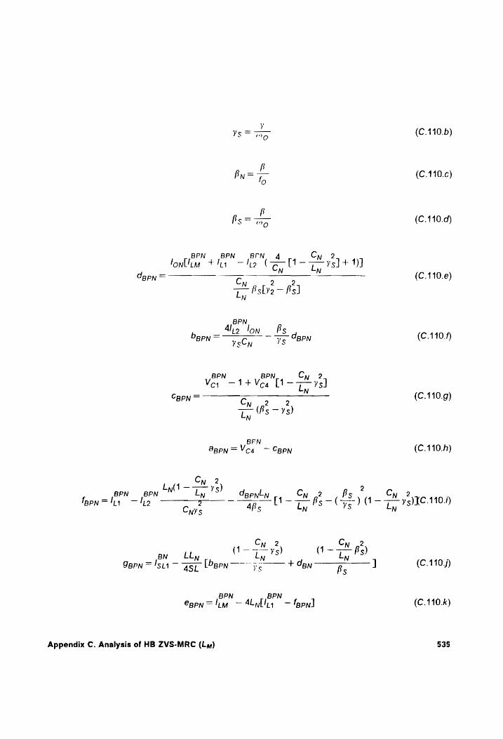
p By= fo
B Bo= M9
BPN BPN BFN 4 Cy 2 lonllim +4ia tte (E- [1 - 7 ys}+1)]
N N Oppn = C
Bslys — Bs] N
BPN 4lio lon — Bs ysCn Ys
bepy = BPN
BPN BPN Cy 2 Vox —14+ Vea [t— 7 ys] Cc =
™ EN (g2 -y ) Ly S Ss
BPN Aappn=Vcq — Cepn
on 2
init — ys) BPN BPN Agpnln Cn Bs fppn='ir —!1o 2 ~ ag [1-7 fs ~(4> Sy
NYS
BN Ely
N Gepn = 'si1 — Gey LOppn——~ ir
BPN BPN Cppn=lim — 4Lali4 — fepn]
Appendix C. Analysis of HB ZVS-MRC (Ly)
(C.110.b)
(C.110.c)
(C.110.d)
(C.110.e)
(C.110.f)
(C.110.g)
(C.110.h)
—— * ys)XC. 110.i)
(C.110,/)
(C.110.k)
535
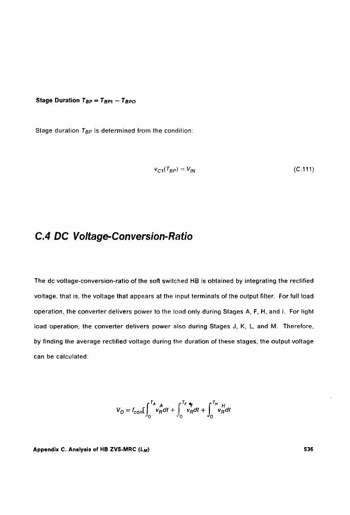
Stage Duration Tgp = Tgp; — Tgpo
Stage duration Tgp is determined from the condition:
Vo1(7 Bp) = Vin (C.111)
C.4 DC Voltage-Conversion-Ratio
The dc voltage-conversion-ratio of the soft switched HB is obtained by integrating the rectified
voltage, that is, the voltage that appears at the input terminals of the output filter. For full load
operation, the converter delivers power to the load only during Stages A, F, H, and |. For light
load operation, the converter delivers power also during Stages J, K, L, and M. Therefore,
by finding the average rectified voltage during the duration of these stages, the output voltage
can be calculated:
Tay Tr Ty oy Vpoft + [ vpdt + | vpat
“0 Vo= conl | 0
0
Appendix C. Analysis of HB ZVS-MRC (Ly) 536

Ty " j J +| vpat + | Vpdt] (C.112)
0 '0
where vk is the rectified time domain voltage that appears at the input of the output filter
during Stage i. The dc voltage-conversion-ratio can be calculated by normalizing Eq. (C.112)
with respect to Vin/2N:
Vo M [ Tan A Nt Tm EN [ ‘M0 } iN it
VR N R N R N Vin/2N /0 9 ‘0
Tw ON NN JN [ VR ath, + | VR dty] (C.4 13)
The normalized average rectified voltage for these stages is given by the following ex-
pressions:
TAN AN b a d 1 AN AN |. AN [ Va Uy= ZUG, (608 rnTan — 1) — Ga SIN Tan + Bu (cos ByTan — 1)
“AN sin ByT SNK Caaurs SiN yyTay — Tay ~ 1 ——— sin By AN + Jo7 sL4any's SIN NT an — Danys( COS ynT an — 1) By Net
2lon BN AN 1) + CanBs SiN ByTan — Ganfs( COS ByTan — 1)]1 - Thy Vig — I (C.114.a)
Appendix C. Analysis of HB ZVS-MRC (Ly) 537
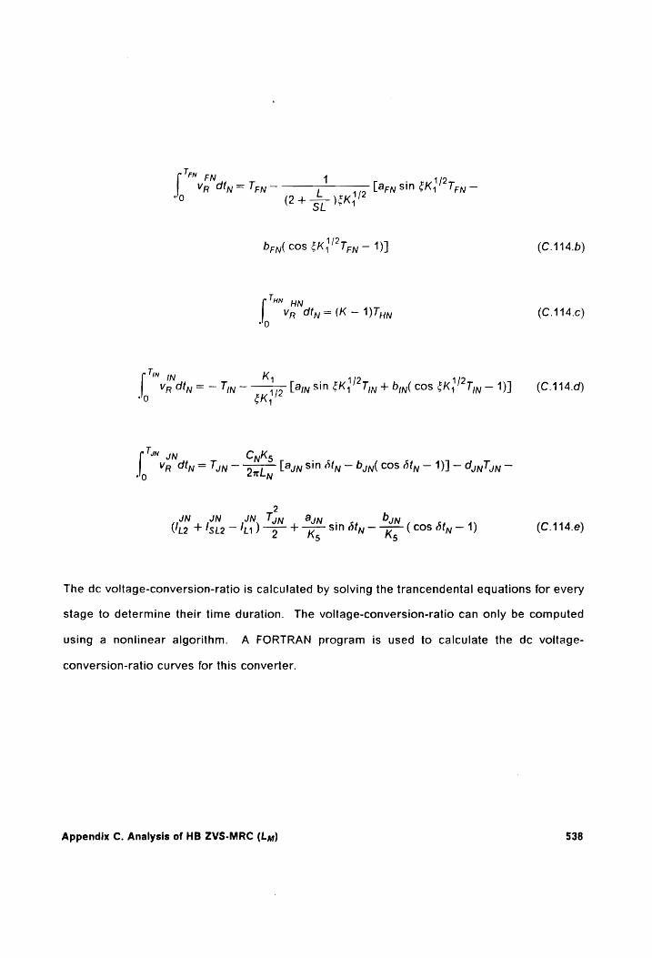
TEN EN
| [apy sin EKq? Tey — 0
Vp dty = Tey - ——-- —_— (2 + eK}?
ben( cos EKq!° Tey — 1)]
Th HN
[ Va ty =(K — 1)THn “0
Tw K VR ath, =— Tin _ —1_ [ayy sin EKA? Ty, + bin( cos EKA? Ty _ 1)]
Ty JN Ks .
VR dty = TUN _ Only [ayn sin bty _— Dyn cos Oty _— 1)] _ yn Tun _
2 JN JN JN OT, a b
(ia +! 19 —Ih4) a + — sin dty — ™ (cos dty — 1)
(C.114.b)
(C.114.c)
(C.114.d)
(C.114.e)
The dc voltage-conversion-ratio is calculated by solving the trancendental equations for every
stage to determine their time duration. The voltage-conversion-ratio can only be computed
using a nonlinear algorithm. A FORTRAN program is used to calculate the dc voltage-
conversion-ratio curves for this converter.
Appendix C. Analysis of HB ZVS-MRC (Ly) 538
Vita
The author was born in Guatemala City, Guatemala. He received his B.S. degree from North
Carolina State University in both Electrical and Mechanical Engineering in 1986. He received
his M.S. degree in Electrical Engineering also from North Carolina State University in 1988.
Since starting his doctoral studies at Virginia Polytechnic Institute and State University he has
worked on various research projects in the area of power electronics. His research interests
include modeling, testing, and design of high-frequency dc-to-dc converters.
The author is a member of the Phi Kappa Phi honor society and the IEEE Power Electronics
Society.
Vita 539


