Embed Size (px)
Citation preview

Our reference: SNB 16940 P-authorquery-v9
AUTHOR QUERY FORM
Journal: SNB Please e-mail or fax your responses and any corrections to:
E-mail: [email protected]
Article Number: 16940 Fax: +353 6170 9272
Dear Author,
Please check your proof carefully and mark all corrections at the appropriate place in the proof (e.g., by using on-screenannotation in the PDF file) or compile them in a separate list. Note: if you opt to annotate the file with software other thanAdobe Reader then please also highlight the appropriate place in the PDF file. To ensure fast publication of your paper pleasereturn your corrections within 48 hours.
For correction or revision of any artwork, please consult http://www.elsevier.com/artworkinstructions.
Any queries or remarks that have arisen during the processing of your manuscript are listed below and highlighted by flags inthe proof. Click on the ‘Q’ link to go to the location in the proof.
Location in Query / Remark: click on the Q link to goarticle Please insert your reply or correction at the corresponding line in the proof
Q1 Please confirm that given names and surnames have been identified correctly.Q2 Please ensure that the corresponding authors’ information are complete and accurate.Q3 One or more sponsor names and the sponsor country identifier may have been edited to a standard format
that enables better searching and identification of your article. Please check and correct if necessary.Q4 Please provide the grant numbers for “Royal Society of Edinburgh”, “Carnegie Trust Funding”, “Scottish
Sensor System Centre (SSSC)”, “EPSRC”, “European Commission” and “Ministerio de Economıa yCompetitividad del Gobierno de Espana” if any.
Q5 Please check the abbreviated journal titles in Refs. [1,45].Q6 Please provide complete bibliographic details in Ref. [24].Q7 Please provide the volume number for the bibliography in Refs. [28,29,43].Q8 Please provide the abbreviated journal titles for Refs. [30–32].Q9 Please define figure parts for Fig. 12 if necessary.Q10 Please specify the significance of footnote “*” cited in the table, as a corresponding footnote text has
not been provided.
Please check this box or indicate your approval ifyou have no corrections to make to the PDF file
Thank you for your assistance.

Please cite this article in press as: J. Zhou, et al., Characterisation of aluminium nitride films and surface acoustic wave devices formicrofluidic applications, Sens. Actuators B: Chem. (2014), http://dx.doi.org/10.1016/j.snb.2014.05.066
ARTICLE IN PRESSG ModelSNB 16940 1–9
Sensors and Actuators B xxx (2014) xxx–xxx
Contents lists available at ScienceDirect
Sensors and Actuators B: Chemical
journa l homepage: www.e lsev ier .com/ locate /snb
Characterisation of aluminium nitride films and surface acoustic wavedevices for microfluidic applications
1
2
J. Zhoua,b,c, M. DeMiguel-Ramosd, L. Garcia-Gancedoe, E. Iborrad, J. Olivaresd, H. Jina,∗,Q1
J.K. Luoa, A.S. Elhadyb, S.R. Donga, D.M. Wanga, Y.Q. Fub,∗3
4
a Department of Information Science and Electronic Engineering, Zhejiang University, Hangzhou 310027, China5b Thin Film Centre, Scottish Universities Physics Alliance (SUPA), University of the West of Scotland, Paisley PA1 2BE, UK6c School of Engineering, The University of Edinburgh, Edinburgh EH9 3JF, UK7d GMME-CEMDATIC, ETSIT, Universidad Politécnica de Madrid, Madrid 28040, Spain8e Electrical Engineering Division, Department of Engineering, University of Cambridge, Cambridge CB3 0FA, UK9
10
a r t i c l e i n f o11
12
Article history:13
Received 7 March 201414
Received in revised form 22 April 201415
Accepted 14 May 201416
Available online xxx17
18
Keywords:19
AlN film20
Surface acoustic wave21
Microfluidic22
Microstructure23
Thickness24
a b s t r a c t
Aluminium nitride (AlN) films with different thicknesses (from 2.3 to 4.7 �m) were deposited ontohigh resistivity silicon substrates using magnetron sputtering. Crystalline and bonding structures of thedeposited AlN films were characterised. The AlN films showed a highly c-axis texture. AlN film based sur-face acoustic wave (SAW) devices were fabricated and characterised. The SAW devices showed Rayleighwave transmission band with a large side-lobe suppression of ∼15 dB. With the increase in film thickness,both the central band frequency and electromechanical coupling coefficient were increased, and valuesof temperature coefficient of frequency was increased linearly from −21.3 to −27.4 ppm/K. Microfluidicmanipulations including streaming, pumping and jetting have been realised using AlN SAW devices. Theapplied RF power boundary between streaming and pumping and that between the pumping and jettingdecreased with the increase of film thickness. The measured streaming and pumping velocities as wellas device surface temperatures increased with the film thickness.
© 2014 Elsevier B.V. All rights reserved.
25
1. Introduction26
Surface acoustic wave (SAW) resonators have been a major27
building block of electronic devices with wide applications for fil-28
ters, frequency duplexers, RF-tags (RFIDs), etc. in electronics and29
communications [1]. Recently, SAW devices have found tremen-30
dous applications in biochemical sensing, drug development, life31
science and medical research [2–5], and precise microfluidic con-32
trol with various functions such as acoustic streaming, mixing,33
pumping, jetting and nebulisation have been realised [6–12].34
Microfluidic devices based on the SAW devices provide an efficient,35
reliable and controllable method to deliver microfluidic functions36
as well as manipulate, trap, sort and pattern cells and nano-particles37
[13–17].38
∗ Corresponding authors at: University of the West of Scotland, Thin Film Centre,B229, Richardson Building, University of the West of Scotland, Paisley PA1 2BE, UK.Tel.: +44 0141 848 3563.Q2
E-mail addresses: [email protected] (H. Jin), [email protected],[email protected] (Y.Q. Fu).
SAW devices are normally fabricated on either bulk piezoelectric 39
substrates such as quartz, LiNbO3 or LiTaO3, or on piezoelectric thin 40
films such as zinc oxide (ZnO) or aluminium nitride (AlN), which 41
can be deposited on conventional substrates such as glass or sil- 42
icon [18–20]. Thin film SAW devices present several advantages 43
over the bulk counterparts in terms of device design flexibility, 44
production cost, and the most important aspect, the possibility of 45
integration in complex MEMS systems or CMOS electronics [11]. In 46
the past decade, many studies on microfluidic applications using 47
ZnO based SAW devices have been reported [21,22]. However, ZnO 48
films present potential issues for biomedical and microfluidic appli- 49
cations (unstable in liquid solutions [23]), making them less ideal 50
materials for microfluidic applications than other thin film piezo- 51
electric materials such as AlN. ZnO is also prone to form oxygen 52
vacancies, which act as donor-like impurities, thus making the 53
material conductive and destroying its piezoelectric activity [24]. 54
Conversely, AlN films have better chemical and thermal stability 55
than ZnO films [25,26]. Although generally the coupling coefficient, 56
k2, values of the ZnO/Si SAW devices are slightly higher than those 57
of the AlN/Si SAW devices [21,27], AlN films have a reasonable 58
good piezoelectric activity to obtain SAW actuators with a good 59
enough k2. The SAW propagation velocity is considerably larger in 60
http://dx.doi.org/10.1016/j.snb.2014.05.0660925-4005/© 2014 Elsevier B.V. All rights reserved.

Please cite this article in press as: J. Zhou, et al., Characterisation of aluminium nitride films and surface acoustic wave devices formicrofluidic applications, Sens. Actuators B: Chem. (2014), http://dx.doi.org/10.1016/j.snb.2014.05.066
ARTICLE IN PRESSG ModelSNB 16940 1–9
2 J. Zhou et al. / Sensors and Actuators B xxx (2014) xxx–xxx
the AlN devices than those in the ZnO ones, and the propagation61
losses are lower due to their much larger elastic constants [28]. For62
fabricating SAW devices, it is critical to deposit AlN films with c-63
axis orientation, low stress, less transition layer between substrate64
and AlN films and good adhesion to substrates, as well as a piezo-65
electric response as good as those from the theoretical analysis of66
the single crystal of the AlN [29–32]. Currently, AlN film acoustic67
wave devices have been demonstrated to be promising for high fre-68
quency sensing applications, especially for film bulk acoustic wave69
devices with a high sensitivity [28,33]. However, there are few stud-70
ies available on the optimisation and characterisation of the effects71
of film microstructure and thickness (up to a few microns) in order72
to improve microfluidic performance of the AlN SAW based devices.73
In this study, AlN films with various thicknesses were deposited74
onto Si substrate, and their crystalline structure, film stress, SAW75
response, and sensing/microfluidic performance of the AlN SAW76
devices as a function of the film thickness were characterised.77
2. Experimental78
AlN films with thicknesses (h) ranging from 2.3 to 4.7 �m were79
deposited onto 4-inch in diameter (1 0 0)-oriented high resisti-80
vity Si substrates using a pulsed-DC reactive magnetron sputtering81
process in an ultra-high vacuum system. The diameter of the82
high-purity (99.999%) Al metallic target was 150 mm. Before AlN83
deposition, the substrates were heated to 400 ◦C with a base84
pressure of 1 × 10⁻⁸ Torr. The surface of the substrate was then85
plasma-cleaned by means of a short bombardment (60 s) with Ar+86
ions from a bias RF glow discharge. The AlN films were then sput-87
tered onto Si substrate using a gas mixture of Ar:N2 (4:6), a total88
pressure of 1.9 mTorr, a pulsed-DC target power of 1.2 kW and a89
platen temperature of 400 ◦C. AlN films develop a non-constant in-90
plane stress as they grew. The initial film stress is large compressive,91
but becomes less compressive and even tensile as the film thick-92
ness increases [34]. To reduce the stress gradient in a thick AlN93
film and improve its adherence to the substrate, an RF bias power94
of 80 W, which leads to a DC polarisation of −60 V, was applied to95
the substrates during the first 30 min of the deposition. In the sec-96
ond 30-min deposition, the RF bias applied to the substrate was97
increased to 90 W (−65 V DC bias) to compensate the film stress.98
After 1 h deposition, the RF bias was increased to 100 W (−70 V DC99
bias). The average deposition rate was estimated to be ∼60 nm/min.100
Crystalline structure of the AlN films was analyzed using X-ray101
diffraction (XRD, D5000, Siemens) with Cu-k� radiation. This radi-102
ation is composed by two terms k�1 with wavelength of 1.5406 A103
and k�2 with 1.5444 A. The intensity of k�1 is double of k�2. The104
XRD diffraction results obtained from the films were fitted with105
Voigt functions (i.e., mixed Lorentzian and Gaussian functions) for106
each k� term [35]. The overall in-plane residual stress was evalu-107
ated by measuring the radius of curvature of the sample before and108
after the deposition of the AlN film using a Veeco Dektak-150 pro-109
filometer. The residual stress was then calculated using the Stoney’s110
equation [36]. Cross-sectional morphology of the films was ana-111
lysed using a scanning electron microscope (SEM, Hitachi S-4800).112
Raman spectra of the AlN films were recorded at room temperature113
using a Raman microscope (Thermo Scientific DXR) with an exci-114
tation laser wavelength � = 532 nm and a resolution of 1 cm−1. The115
microscale (1 × 1 �m2) surface roughness of the films was charac-116
terised using an atomic force microscope (AFM, Agilent 5100), in117
contact mode using a Si3N4 cantilever. Macroscale surface rough-118
ness of the films were characterised using a surface profilometer119
(Dektak3 ST) with a scan distance of 2 mm, scan velocity of 0.5 �m/s120
and a loading force of 30 mg.121
SAW delay lines were fabricated on the AlN layer by pattern-122
ing Cr/Au inter-digitised transducers (IDTs) using a conventional123
photolithography process. The IDTs have a spatial periodicity of 124
64 �m (a line-width of 16 �m and a space of 16 �m), 30 pairs of fin- 125
gers, and an aperture of 4.9 mm. The distance between the centres 126
of both transducers was 10 mm and this is where the microfluidic 127
experiments were done. The transmission properties of the devices 128
were assessed by measuring the scattering parameters using an RF 129
vector network analyser (Agilent Technologies, E5061B). The tem- 130
perature dependence of the transmission properties of the SAW 131
devices with different thicknesses was measured in an environ- 132
mental controlled chamber (WKL 34, WEISS TECHNIC), capable of 133
controlling the temperature with an accuracy of 0.1 ◦C. 134
For microfluidic tests, the AlN SAW devices were surface- 135
coated with a ∼200 nm thick layer of CYTOPTM (Asahi Glass 136
Co. Ltd.) in order to enhance their surface hydrophobicity. The 137
SAW devices were connected to a signal generator (Agilent Tech- 138
nologies, N9310A), which was amplified by a broadband power 139
amplifier (Amplifier Research, 75A250). The system was care- 140
fully impedance-matched to avoid internal reflection of the RF 141
signals. The microfluidic behaviour of de-ionised water droplets 142
were recorded using a high speed video camera (Vision Research, 143
phantom V7.3) working at a frame rate of 4000 frames/s. Internal 144
streaming velocities were estimated from the particle move- 145
ment inside the droplet from the high speed video. Droplet 146
pumping/jetting speeds were also estimated based on the recorded 147
movies. The devices were mounted onto a bulk aluminium alloy 148
test-holder during testing in order to minimise the possible heat- 149
ing effect. The device surface temperature after applying the RF 150
power was measured using an infrared video camera (Therma- 151
CAMTM SC640) with and without water droplets on the device 152
surface. 153
3. Results and discussions 154
3.1. Film characterisation 155
Fig. 1 shows XRD patterns of the AlN films with thicknesses of 156
2.3, 3.4 and 4.7 �m, respectively. The dominant (0 0 0 2) peak of the 157
wurtzite AlN structure was verified for all the AlN films, indicating 158
a preferential growth orientation along c-axis, which is indepen- 159
dent of the film thickness. The peaks appearing around ∼32.5◦ are 160
the vestiges of the diffraction of the partially filtered k� radiation. 161
Only the XRD pattern of the thinner film (2.3 �m thick) show other 162
small peaks, which are not due to the AlN film. Probably they are 163
Fig. 1. XRD patterns of AlN films with different thicknesses. (Intensity axis is inlogarithmic scale and the patterns have been shifted vertically for comparison.)

Please cite this article in press as: J. Zhou, et al., Characterisation of aluminium nitride films and surface acoustic wave devices formicrofluidic applications, Sens. Actuators B: Chem. (2014), http://dx.doi.org/10.1016/j.snb.2014.05.066
ARTICLE IN PRESSG ModelSNB 16940 1–9
J. Zhou et al. / Sensors and Actuators B xxx (2014) xxx–xxx 3
Fig. 2. (0 0 0 2) Diffraction peak of the 4.7 �m thick AlN film fitted with three pairsof Voigt functions (corresponding each to k�1 and k�2 reflections of each stepdeposited layer).
Table 1Curve fitting results of (0 0 0 2) XRD peak of the films of different thicknesses. Onlyk�1 data are presented. .Q10
2.3 �m 3.2 �m 4.7 �m
2�-1 35.9020 35.8336 35.8340Int. 1 23,310 29,400 49,000FWHM-1 0.3136 0.1900 0.23652�-2 36.0130 36.0270 35.9847Int. 2 5860 181,000 245,200FWHM-2 0.1027 0.1444 0.10952�-3 * * 36.0760Int. 3 * * 130,000FWHM-3 * * 0.1209
reflections of radiation from impurities in the X-ray tube on silicon,164
which cannot be observed in the thicker AlN films. This ensures that165
all the AlN films have pure (0 0 0 2) orientation, and therefore, are166
good candidates for having a good piezoelectric response [37].167
In Fig. 2, a detailed XRD pattern of the 4.7 �m film is presented168
together with the decomposition in pairs of k�1 and k�2 of three169
families of planes corresponding to three families of microcrystals.170
In Table 1, the result of the fittings for the three types of AlN films171
studied in this work are listed. The origin of these different grain172
populations lies on the changes in the substrate bias polarisation173
during the film deposition. This can be also seen in Fig. 3(a), which174
represents SEM cross-section image of the 4.7 �m thick AlN films.175
All the AlN films have columnar microcrystalline grains perpen-176
dicular to the substrate with a clear evolution in its morphology177
in the direction of growth. With increase of the film thickness, the178
columnar structures are more neatly arranged and compact, indi- 179
cating forming a better crystalline structure, which is consistent 180
with the XRD results. 181
Various values of the diffraction angles of these grain popula- 182
tions are due to different strain values. The bottom-most layer near 183
the substrate has a compressive stress indicated by the (0 0 0 2) 184
peak shifting to lower angles. The upper layers have more ten- 185
sile stress components compensating the former one. The resulting 186
stress of the final layer is under 200 MPa in all the cases, and the 187
film stress increases with film thickness. The AlN (0 0 0 2) peak 188
becomes stronger and shaper, with a lower value of full width at half 189
maximum (FWHM), with gradually increasing film thickness. This 190
indicates that the grain size of the AlN films becomes larger as the 191
thickness of the film increases. Because this grain size is larger than 192
100 nm, the estimation using the Debye–Scherrer formula [38] can- 193
not be done although the FWHM of the k�1 term of the diffracted 194
X-ray radiation can be used as a measurement of the crystal quality. 195
This parameter becomes larger when the grain size is smaller but 196
also when the stress gradient in the c-axis direction increases. 197
Typical microscale surface roughness of the 4.7 �m thick AlN 198
films obtained from AFM analysis is shown in Fig. 3(b). With the 199
increase in AlN film thickness, grain sizes of the films increase 200
slightly and the values of the Roughness Measurement of the Sur- 201
face (RMS) are 5.96 and 7.01 nm for the AlN films with thicknesses 202
of 2.3 and 4.7 �m, respectively. The average macroscale surface 203
roughness values (Ra) obtained from the surface profilometer are 204
31.6, 33.4 and 36.7 nm for the AlN films with thicknesses of 2.3, 205
3.4 and 4.7 �m, respectively. In brief, the surface roughness does 206
not appear change dramatically, thus will not have any significant 207
effect on the microfluidic performance. 208
Fig. 4 shows the Raman spectra of the AlN films. The sharp peak 209
around 522 cm−1 and the broad peak at about 979 cm−1 corre- 210
spond to the single-phonon vibration mode and two TO-phonon 211
overtones scattering of the silicon substrate, respectively [39]. The 212
peaks around 250 cm−1 and 302 cm−1 are assigned to E2(low) 213
vibration modes [40,41]. The E2(high) mode (∼655.5 cm−1) and 214
A1(LO) mode of the wurtzite AlN film (∼890 cm−1) were detected, 215
which are sensitive to the strain inside the AlN film [41,42]. The 216
E2(high) mode peak of all films seems to be left-shifted compared 217
to the 655.5 cm−1 of standard unstrained AlN [41], confirming the 218
existence of compressive stresses in the AlN film on Si substrate. 219
However, a careful analysis of the second derivative of the Raman 220
spectra around 655 cm−1 shows that the peak is actually composed 221
by two or three bands which are associated to the two or three 222
AlN layers. Unfortunately, an accurate fitting of these bands has 223
not been possible because the low signal to noise ratio of the mea- 224
surements and, thus, quantitative information about the stress of 225
these layers cannot be obtained from the Raman analysis. The no- 226
appearance of the E1(LO) and the A1(TO) modes, around 912 cm−1227
Fig. 3. Characterisation of the 4.7 �m thick AlN films: (a) SEM image of cross-section morphology, (b) AFM image of surface morphology.

Please cite this article in press as: J. Zhou, et al., Characterisation of aluminium nitride films and surface acoustic wave devices formicrofluidic applications, Sens. Actuators B: Chem. (2014), http://dx.doi.org/10.1016/j.snb.2014.05.066
ARTICLE IN PRESSG ModelSNB 16940 1–9
4 J. Zhou et al. / Sensors and Actuators B xxx (2014) xxx–xxx
Fig. 4. Raman spectra of the AlN films with different thicknesses: (a) 2.3 �m, (b)3.4 �m and (c) 4.7 �m (the different spectra are presented on top of each other forclarity).
Fig. 5. Transmission (S21) signals of the AlN SAW devices with different thicknesses.
and 620 cm−1, respectively, indicates that the films are purely c-axis228
oriented. All these results are coherent with the XRD data discussed229
above.230
3.2. SAW device characterisation231
Fig. 5 shows typical transmission signals (S21) of the devices with232
different AlN film thicknesses. The devices exhibit clear transmis-233
sion bands, which are centred at 79.8, 80.1, and 80.3 MHz for the234
samples with AlN film thicknesses of 2.3, 3.4 and 4.7 �m, respec-235
tively. All the bands have an out-of-band rejection of ∼13 to ∼15 dB,236
and are assigned to the Rayleigh mode waves. The phase velocity237
(vp) of the SAW devices were determined by vp = �·f0 (in which � is238
wavelength of the SAW device, 64 �m, and f0 is the measured cen-239
tral band frequency). The corresponding velocities of the Rayleigh240
peaks were found to be 5107.2, 5126.4 and 5139.2 m/s, respectively,241
for the AlN film thicknesses of 2.3, 3.4 and 4.7 �m, indicating that242
the velocity increases as the ratio of the thickness to wavelength243
(h/�) increases. For a layered structure, the phase velocity of the244
SAW device is influenced by the properties of both the piezoelec-245
tric layer and substrate. As the wavelength is much longer than246
the thickness of the AlN layer, acoustic waves will penetrate much247
deeper into the substrate. The phase velocity for the Rayleigh wave248
in an ideal (0 0 0 2) AlN layer is ∼5607 m/s [43], which is higher249
than that of Si (4680 m/s) [44]. As the thickness of the AlN thin film250
increases, a higher proportion of the acoustic waves travel in the251
piezoelectric AlN film, leading to a higher acoustic velocity.252
The electromechanical coupling coefficient of the Rayleigh 253
modes was calculated using the following formula based on the 254
corresponding Smith-Charts [45]: 255
k2 = �
4N
(G
B
)f =f0
(1) 256
where N is the number of finger pairs; G and B are the radia- 257
tion conductance and susceptance at the band central frequency, 258
respectively. The average values of k2 for the Rayleigh modes of 259
the AlN SAW devices were found to be 0.1%, 0.19% and 0.24%, for 260
the AlN thickness of 2.3, 3.4 and 4.7 �m, respectively. It is notable 261
that the value of k2 increases with the increase of thickness of AlN 262
films. This is mainly due to the dispersion of k2 with the ratio h/�, 263
which, like the frequency, occurs in layered SAW structures. How- 264
ever, it is not discarded the possibility of an improvement of the 265
AlN properties as the thickness increases. 266
It is well known that SAW devices are extremely useful in the 267
development of various types of sensors owing to their high sen- 268
sitivity and wireless capability [4]. One of the major drawbacks of 269
these devices for sensing applications is their sensibility to tem- 270
perature variations. In order to evaluate this influence, the central 271
band frequencies of the Rayleigh waves of AlN based SAW devices 272
with different film thicknesses have been obtained as a function of 273
temperature, and the results are shown in Fig. 6(a). The frequencies 274
measured for all the devices decrease linearly with increase of tem- 275
perature. The central band frequency at a temperature T (in Celsius 276
degrees) (fT) can be expressed as: 277
fT = f0 × (1 + ˛ × T) (2) 278
where ˛ is the temperature coefficient of the centre frequency (TCF) 279
defined as �f/(f0�T), and f0 is the frequency at 20 ◦C. The obtained 280
values of ˛ are −21.3 ppm/◦C, −23.7 ppm/◦C, and −27.4 ppm/◦C for 281
the devices with AlN thicknesses of 2.3, 3.4 and 4.7 �m, respectively 282
(with f0 of 79.8, 80.1, and 80.3 MHz). The results are comparable to 283
those in the literature [46]. The magnitude of the TCF increases 284
linearly with film thickness as shown in Fig. 6(b), because the TCF 285
values of the AlN films are larger than that of Si, thus the more 286
proportion of the wave travels in the AlN film when its thickness is 287
larger. 288
3.3. Microfluidic performance 289
When a liquid droplet is located on the propagation path of a 290
surface acoustic wave, the SAW interacts with the liquid and the 291
acoustic energy couples into the liquid, inducing a typical butterfly 292
acoustic streaming pattern [47]. These patterns can be observed if 293
starch nano-particles are dispersed into the liquid. When a droplet 294
containing starch nano-particles was positioned off the central line 295
of the wave path, the induced flow circulation into the droplet 296
due to asymmetric acoustic streaming rapidly establishes vortex 297
patterns. Fig. 7 shows the acoustic streaming and particle concen- 298
tration phenomena of the droplets with a volume of 3 �L positioned 299
at the edge and in the centre of the acoustic path between the IDTs. 300
The concentration flow patterns of the starch particles inside the 301
liquid are actuated by the shear streaming forces, which induce 302
particle migration due to the gradient in the azimuthal streaming 303
velocity in the droplet [48]. When an applied RF power is about 304
2.1 W (at the Rayleigh central band frequency), the streaming tra- 305
jectory of the 3 �L droplets shows a typical butterfly pattern with a 306
double vortex when the droplet is located in the centre of the acous- 307
tic path of the SAW devices. As the film thickness increases from 308
2.3 to 4.7 �m, the streaming velocity increases from 1.8 to 3.1 cm/s 309
at the same RF power of 2.1 W. Whereas, particle concentration is 310
observed at the same time when the droplet is positioned at the 311
edge of the wave path, and the durations for the particle concen- 312
tration decreases from 7 to 5 s when the droplet were actuated by 313

Please cite this article in press as: J. Zhou, et al., Characterisation of aluminium nitride films and surface acoustic wave devices formicrofluidic applications, Sens. Actuators B: Chem. (2014), http://dx.doi.org/10.1016/j.snb.2014.05.066
ARTICLE IN PRESSG ModelSNB 16940 1–9
J. Zhou et al. / Sensors and Actuators B xxx (2014) xxx–xxx 5
Fig. 6. (a) Central band frequency as a function of temperature for the AlN based devices of different thicknesses: 4.7 �m, 3.4 �m and 2.3 �m; (b) the TCF as a function ofAlN thickness showing the linear relationship.
Fig. 7. Droplets of 3 �L show acoustic streaming induced by the AlN SAW devices. A double vortex streaming pattern is produced in the centre of the wave path while asingle vortex is formed in droplet in the edge of the wave path, for different AlN thicknesses: (a) 2.3 �m, (b) 3.4 �m and (c) 4.7 �m, with RF power of 2.1 W.
the SAW devices with film thickness increasing from 2.3 to 4.7 �m.314
These phenomena are attributed to the increased wave amplitude315
with the increasing AlN film thickness, which is closely related to316
the increase in value of k2. Additionally, the flow speed increases317
and the dispersed particles concentration time (vortex formation)318
decreases with the applied RF powers.319
For the same water droplet size, there are power boundaries320
for various microfluidic phenomena, including internal flow-321
ing/mixing, pumping and ejection. Fig. 8 shows the estimated322
power boundaries of the microfluidic phenomena for the films with323
different thicknesses. Internal streaming occurs at a low RF power324
of a few mW. Higher power will result in efficient droplet pumping325
and jetting. As shown in Fig. 8, when the thickness of AlN films326
increases from 2.3 to 3.4 �m, and then to 4.7 �m, the power bound-327
ary between steaming and pumping decreases from 35 to 27.5 W,328
and then to 14 W. With the highest power applied (∼70 W), there329
was no jetting observed for the AlN SAW device with the film thick-330
ness of 2.3 �m. As shown in Fig. 8, the power boundary between331
pumping and jetting decreases to 62 W, and then to 35 W, with the332
film thicknesses increased from 3.4 to 4.7 �m.333
With an RF input power of 62 W, for the SAW devices made334
with AlN film thicknesses of 2.3 and 3.4 �m, the droplet can be only335
observed to move on the device surface as shown in Fig. 9(a) and (b).336
The droplets are strongly deformed following the Rayleigh angle337
direction, and then pushed forward through sliding and rolling. As338
the thickness of AlN film increases from 2.3 to 3.4 �m, the pumping339
velocity increases from 11.2 to 16 mm/s at an RF power of 62 W. 340
Whereas for the AlN film thickness of 4.7 �m, significant jetting 341
of the droplet in a much shorter duration is observed as shown in 342
Fig. 9(c) under the same RF input power. At 0.3 ms after the applica- 343
tion of the RF power to the IDT, the droplet was ejected from surface 344
into a coherent cylindrical liquid jetting beam, with a tilted angle 345
Fig. 8. The estimated boundaries of the microfluidic phenomena for the AlN filmswith different thicknesses: (a) 4.7 �m, (b) 3.4 �m and (c) 2.3 �m with the fixeddroplet size of 3 �L.

Please cite this article in press as: J. Zhou, et al., Characterisation of aluminium nitride films and surface acoustic wave devices formicrofluidic applications, Sens. Actuators B: Chem. (2014), http://dx.doi.org/10.1016/j.snb.2014.05.066
ARTICLE IN PRESSG ModelSNB 16940 1–9
6 J. Zhou et al. / Sensors and Actuators B xxx (2014) xxx–xxx
Fig. 9. The pumping and jetting images of the droplets of 3 �L during the different time under the RF input power of 62 W, with different AlN thicknesses: (a) 2.3 �m, (b)3.4 �m and (c) 4.7 �m.
Fig. 10. Surface temperatures on the SAW devices for the different AlN thicknesses: (a) 2.3 �m, (b) 3.4 �m and (c) 4.7 �m with the RF power of 68 W, at the time of 1.2 s, (d)influence of PF input power and AlN thickness on the surface temperatures on the SAW devices.
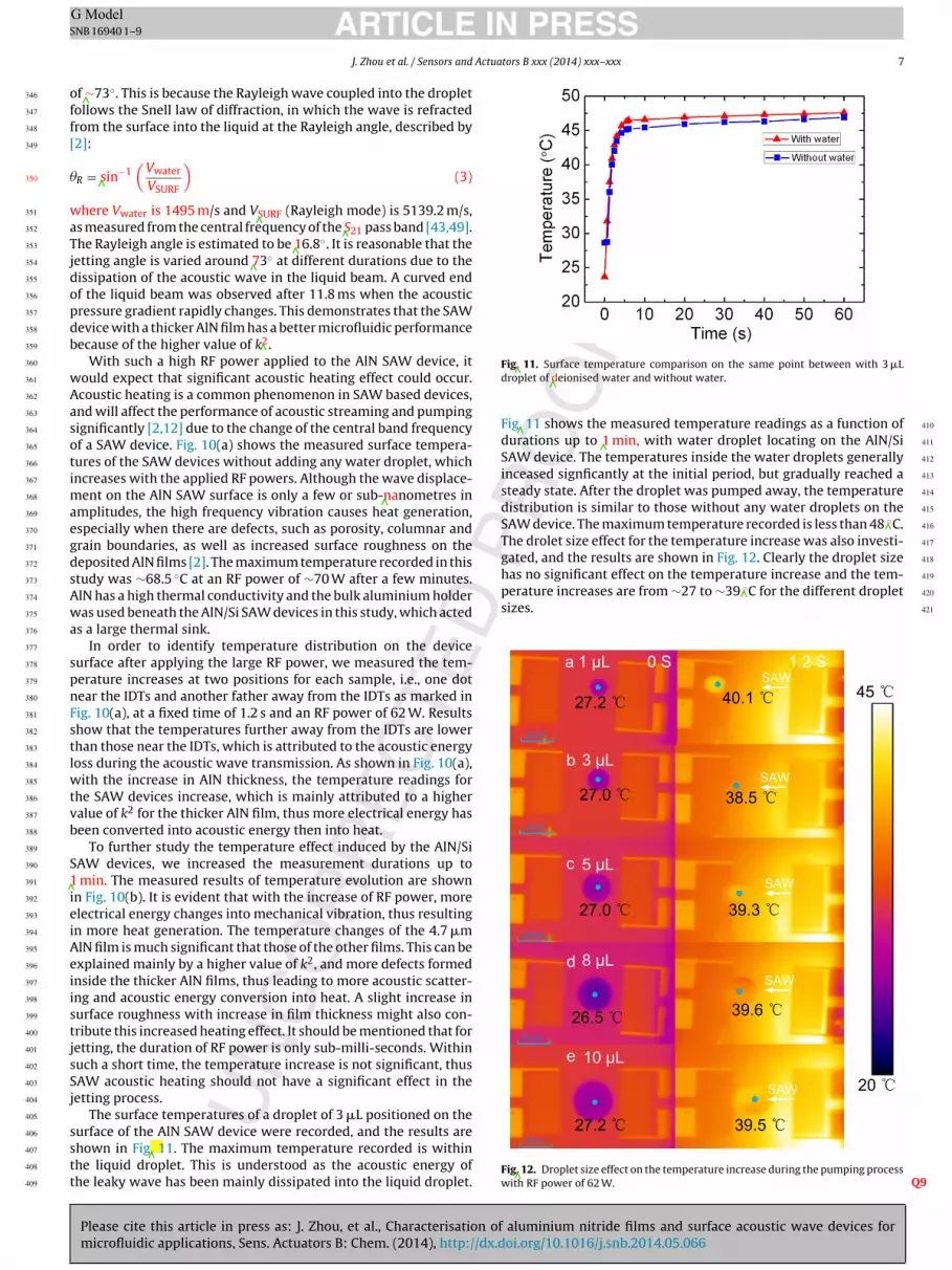
Please cite this article in press as: J. Zhou, et al., Characterisation of aluminium nitride films and surface acoustic wave devices formicrofluidic applications, Sens. Actuators B: Chem. (2014), http://dx.doi.org/10.1016/j.snb.2014.05.066
ARTICLE IN PRESSG ModelSNB 16940 1–9
J. Zhou et al. / Sensors and Actuators B xxx (2014) xxx–xxx 7
of ∼73◦. This is because the Rayleigh wave coupled into the droplet346
follows the Snell law of diffraction, in which the wave is refracted347
from the surface into the liquid at the Rayleigh angle, described by348
[2]:349
�R = sin−1(
Vwater
VSURF
)(3)350
where Vwater is 1495 m/s and VSURF (Rayleigh mode) is 5139.2 m/s,351
as measured from the central frequency of the S21 pass band [43,49].352
The Rayleigh angle is estimated to be 16.8◦. It is reasonable that the353
jetting angle is varied around 73◦ at different durations due to the354
dissipation of the acoustic wave in the liquid beam. A curved end355
of the liquid beam was observed after 11.8 ms when the acoustic356
pressure gradient rapidly changes. This demonstrates that the SAW357
device with a thicker AlN film has a better microfluidic performance358
because of the higher value of k2.359
With such a high RF power applied to the AlN SAW device, it360
would expect that significant acoustic heating effect could occur.361
Acoustic heating is a common phenomenon in SAW based devices,362
and will affect the performance of acoustic streaming and pumping363
significantly [2,12] due to the change of the central band frequency364
of a SAW device. Fig. 10(a) shows the measured surface tempera-365
tures of the SAW devices without adding any water droplet, which366
increases with the applied RF powers. Although the wave displace-367
ment on the AlN SAW surface is only a few or sub-nanometres in368
amplitudes, the high frequency vibration causes heat generation,369
especially when there are defects, such as porosity, columnar and370
grain boundaries, as well as increased surface roughness on the371
deposited AlN films [2]. The maximum temperature recorded in this372
study was ∼68.5 ◦C at an RF power of ∼70 W after a few minutes.373
AlN has a high thermal conductivity and the bulk aluminium holder374
was used beneath the AlN/Si SAW devices in this study, which acted375
as a large thermal sink.376
In order to identify temperature distribution on the device377
surface after applying the large RF power, we measured the tem-378
perature increases at two positions for each sample, i.e., one dot379
near the IDTs and another father away from the IDTs as marked in380
Fig. 10(a), at a fixed time of 1.2 s and an RF power of 62 W. Results381
show that the temperatures further away from the IDTs are lower382
than those near the IDTs, which is attributed to the acoustic energy383
loss during the acoustic wave transmission. As shown in Fig. 10(a),384
with the increase in AlN thickness, the temperature readings for385
the SAW devices increase, which is mainly attributed to a higher386
value of k2 for the thicker AlN film, thus more electrical energy has387
been converted into acoustic energy then into heat.388
To further study the temperature effect induced by the AlN/Si389
SAW devices, we increased the measurement durations up to390
1 min. The measured results of temperature evolution are shown391
in Fig. 10(b). It is evident that with the increase of RF power, more392
electrical energy changes into mechanical vibration, thus resulting393
in more heat generation. The temperature changes of the 4.7 �m394
AlN film is much significant that those of the other films. This can be395
explained mainly by a higher value of k2, and more defects formed396
inside the thicker AlN films, thus leading to more acoustic scatter-397
ing and acoustic energy conversion into heat. A slight increase in398
surface roughness with increase in film thickness might also con-399
tribute this increased heating effect. It should be mentioned that for400
jetting, the duration of RF power is only sub-milli-seconds. Within401
such a short time, the temperature increase is not significant, thus402
SAW acoustic heating should not have a significant effect in the403
jetting process.404
The surface temperatures of a droplet of 3 �L positioned on the405
surface of the AlN SAW device were recorded, and the results are406
shown in Fig. 11. The maximum temperature recorded is within407
the liquid droplet. This is understood as the acoustic energy of408
the leaky wave has been mainly dissipated into the liquid droplet.409
Fig. 11. Surface temperature comparison on the same point between with 3 �Ldroplet of deionised water and without water.
Fig. 11 shows the measured temperature readings as a function of 410
durations up to 1 min, with water droplet locating on the AlN/Si 411
SAW device. The temperatures inside the water droplets generally 412
inceased signficantly at the initial period, but gradually reached a 413
steady state. After the droplet was pumped away, the temperature 414
distribution is similar to those without any water droplets on the 415
SAW device. The maximum temperature recorded is less than 48 ◦C. 416
The drolet size effect for the temperature increase was also investi- 417
gated, and the results are shown in Fig. 12. Clearly the droplet size 418
has no significant effect on the temperature increase and the tem- 419
perature increases are from ∼27 to ∼39 ◦C for the different droplet 420
sizes. 421
Fig. 12. Droplet size effect on the temperature increase during the pumping processwith RF power of 62 W. Q9

Please cite this article in press as: J. Zhou, et al., Characterisation of aluminium nitride films and surface acoustic wave devices formicrofluidic applications, Sens. Actuators B: Chem. (2014), http://dx.doi.org/10.1016/j.snb.2014.05.066
ARTICLE IN PRESSG ModelSNB 16940 1–9
8 J. Zhou et al. / Sensors and Actuators B xxx (2014) xxx–xxx
4. Conclusions422
AlN films with different thicknesses were deposited on the sil-423
icon substrate using magnetron sputtering. XRD, SEM and Raman424
show that all the films show a highly c-axis texture and columnar425
structure perpendicular to the substrate. With the increase of AlN426
film, the crystal quality of the films increases. All the AlN based427
SAW devices present good SAW responses with a large side-lobe428
suppression of ∼13 to 15 dB. As the thickness increases, both the429
SAW velocity and electro-mechanical coupling coefficient increase.430
With the increase of AlN thickness, the TCF increases linearly from431
−21.3 to −27.4 ppm/K. Micro-fluidic manipulation has been suc-432
cessfully demonstrated for all the devices. The streaming velocity433
increases from 1.8 cm/s to 3.1 cm/s when the RF power of 2.1 W434
applied to the IDT transducers of different film thicknesses. Jet-435
ting was observed in the 4.7 �m film device with an RF power of436
62 W, whereas only pumping was observed for the thinner AlN SAW437
device, which demonstrates that a thicker AlN film leads to a better438
fluidic performance. The heating effect is more significant for the439
thicker AlN film, attributed to the increase in the electromechani-440
cal coupling coefficient, film defects and surface roughness. The use441
of AlN thin films instead of ZnO has several advantages: (1) AlN is442
chemical inert; (2) AlN has better mechanical properties (hardness443
and modulus), which are beneficial for SAW propagation; (3) the444
propagating velocity for both AlN SAW and Lamb waves are higher445
allowing to design devices with higher dimensionality (finger elec-446
trode width) for the same working frequency; (4) AlN SAW has a447
smaller value of TCFs. A slightly lower coupling coefficient of AlN448
respect ZnO, which implies the use of higher power levels for the449
same effects, is the only disadvantage although it is not critical.450
Acknowledgements451
This work was supported by Royal Society of Edinburgh,Q3452
Carnegie Trust Funding, the Royal Society-Research, Grant453
(RG090609), and Scottish Sensor System Centre (SSSC), EPSRCQ4454
(Engineering and Physical Sciences Research Council, UK) Engi-455
neering Instrument Pool for providing the high speed video system456
(Vision Research, phantom V7.3) and the Infrared camera (Therma-457
CAMTM SC640), National Natural Science Foundation of China (No.458
61171038, 61204124 and 61274037), Zhejiang Province Natural459
Science Fund Key Project (No. J20110271), Fundamental Research460
Funds for the Central Universities (No. 2014QNA5002), and Zhe-461
jiang Provincial Natural Science Foundation of China (Z11101168).462
The authors acknowledge the Cyrus Tang Centre for Sensor Materi-463
als and Applications. Part of this work was funded by the European464
Commission through the 7th Framework Programme by the Rap-465
taDiag project (http://www.raptadiag.eu/), the COST action IC1208466
and by the Ministerio de Economía y Competitividad del Gobierno467
de Espana through project MAT2010-18933.468
References469
[1] A. Pohl, A review of wireless SAW sensors, IEEE Trans. Ultrason. Ferroelectr.470
Freq. Control 47 (2000) 317–332.Q5471
[2] Y.Q. Fu, J.K. Luo, X.Y. Du, A. Flewitt, Y. Li, G.H. Markx, A.J. Waltond, W.I.472
Milne, Recent developments on ZnO films for acoustic wave based bio-sensing473
and microfluidic applications: a review, Sens. Actuators, B: Chem. 143 (2010)474
606–619.475
[3] R. Fachberger, A. Erlacher, Applications of wireless SAW sensing in the steel476
industry, Procedia Eng. 5 (2010) 224–227.477
[4] C. Lim, W. Wang, S. Yang, K. Lee, Development of SAW-based multi-gas sen-478
sor for simultaneous detection of CO2 and NO2, Sens. Actuators, B: Chem. 154479
(2011) 9–16.480
[5] K. Länge, B.E. Rapp, M. Rapp, Surface acoustic wave biosensors: a review, Anal.481
Bioanal. Chem. 391 (2008) 1509–1519.482
[6] L.Y. Yeo, J.R. Friend, Surface acoustic wave microfluidics, Annu. Rev. Fluid Mech.483
46 (2013) 56006.484
[7] L.Y. Yeo, J.R. Friend, Ultrafast microfluidics using surface acoustic waves, Biomi- 485
crofluidics 3 (2009) 012002. 486
[8] A. Wixforth, Acoustically driven programmable microfluidics for biological and 487
chemical applications, J. Assoc. Lab. Autom. 11 (2006) 399–405. 488
[9] J. Friend, L.Y. Yeo, Microscale acoustofluidics: microfluidics driven via acoustics 489
and ultrasonics, Rev. Mod. Phys. 83 (2011) p647. 490
[10] P.S. Dittrich, A. Manz, Lab-on-a-chip: microfluidics in drug discovery, Nat. Rev. 491
Drug Discovery 5 (2006) 210–218. 492
[11] Y.F. Li, Y.Q. Fu, S. Brodie, M. Alghane, A. Walton, Enhanced micro-droplet 493
splitting, concentration, sensing and ejection by integrating ElectroWetting- 494
On-Dielectrics and Surface Acoustic Wave technologies, Solid-State Sensors, 495
Actuators and Microsystems Conference (TRANSDUCERS), 2011 16th Interna- 496
tional (2011) 2936–2939. 497
[12] X.Y. Du, Y.Q. Fu, J.K. Luo, A. Flewitt, W. Milne, Microfluidic pumps employing 498
surface acoustic waves generated in ZnO thin films, J. Appl. Phys. 105 (2009) 499
024508–24517. 500
[13] T. Franke, S. Braunmüller, L. Schmid, A. Wixforth, D. Weitz, Surface acoustic 501
wave actuated cell sorting (SAWACS), Lab Chip 10 (2010) 789–794. 502
[14] X. Ding, S.-C.S. Lin, M.I. Lapsley, S. Li, X. Guo, C.Y. Chan, et al., Standing sur- 503
face acoustic wave (SSAW) based multichannel cell sorting, Lab Chip 12 (2012) 504
4228–4231. 505
[15] Z. Wang, J. Zhe, Recent advances in particle and droplet manipulation for 506
lab-on-a-chip devices based on surface acoustic waves, Lab Chip 11 (2011) 507
1280–1285. 508
[16] Z. Guttenberg, H. Müller, H. Habermüller, A. Geisbauer, J. Pipper, J. Felbel, et al., 509
Planar chip device for PCR and hybridization with surface acoustic wave pump, 510
Lab Chip 5 (2005) 308–317. 511
[17] Y.Q. Fu, Y. Li, C. Zhao, F. Placido, A. Walton, Surface acoustic wave nebulization 512
on nanocrystalline ZnO film, Appl. Phys. Lett. 101 (2012) 194101–194103. 513
[18] X.Y. Du, M. Swanwick, Y.Q. Fu, J.K. Luo, A. Flewitt, D. Lee, et al., Surface acoustic 514
wave induced streaming and pumping in 128 Y-cut LiNbO3 for microfluidic 515
applications, J. Micromech. Microeng. 19 (2009) 035016. 516
[19] J. Reboud, Y. Bourquin, R. Wilson, G.S. Pall, M. Jiwaji, A.R. Pitt, A. Grahamb, 517
A.P. Watersb, J.M. Cooper, Shaping acoustic fields as a toolset for microfluidic 518
manipulations in diagnostic technologies, Proc. Nat. Acad. Sci. U.S.A. 109 (2012) 519
15162–15167. 520
[20] J. Zhou, X.L. He, W.B. Wang, Q. Zhu, W.P. Xuan, H. Jin, S.R. Dong, D.M. Wang, J.K. 521
Luo, Transparent surface acoustic wave devices on ZnO/glass using Al-doped 522
ZnO as the electrode, IEEE Electron Device Lett. 10 (2013) 1319–1321. 523
[21] H.F. Pang, Y.Q. Fu, L. Garcia-Gancedo, S. Porro, J.K. Luo, F. Placido, J.I.B. Wilson, 524
A.J. Flewitt, W.I. Milne, X.T. Zu, Enhancement of microfluidic efficiency with 525
nanocrystalline diamond interlayer in the ZnO-based surface acoustic wave 526
device, Microfluid. Nanofluid. 15 (2013) 377–386. 527
[22] X.Y. Du, Y.Q. Fu, S. Tan, J.K. Luo, A.J. Flewitt, W.I. Milne, D.S. Lee, N.M. Park, J. Park, 528
Y.J. Choi, S.H. Kim, S. Maeng, ZnO film thickness effect on surface acoustic wave 529
modes and acoustic streaming, Appl. Phys. Lett. 93 (2008) 094105–194105. 530
[23] I. Kim, D. Ku, J. Ko, D. Kim, K. Lee, J-h Jeong, T.S. Lee, B. Cheong, Y.J. Baik, W.M. 531
Kim, Improvement of the thermal and chemical stability of Al doped ZnO films, 532
J. Electroceram. 17 (2006) 241–245. 533
[24] V. Lughi, Aluminum nitride thin films for MEMS resonators: growth and char- 534
acterization (2006). Q6535
[25] H. Cheng, Y. Sun, J. Zhang, Y. Zhang, S. Yuan, P. Hing, AlN films deposited under 536
various nitrogen concentrations by RF reactive sputtering, J. Cryst. Growth 254 537
(2003) 46–54. 538
[26] M.-A. Duboisa, P. Muraltb, Properties of aluminum nitride thin films for piezo- 539
electric transducers and microwave filter applications, Appl. Phys. Lett. 74 540
(1999) 3032–3034. 541
[27] G. Bu, D. Ciplys, M. Shur, L. Schowalter, S. Schujman, R. Gaska, Electromechanical 542
coupling coefficient for surface acoustic waves in single-crystal bulk aluminum 543
nitride, Appl. Phys. Lett. 84 (2004) 4611–4613. 544
[28] Y.Q. Fu, J.S. Cherng, J.K. Luo, M.P.Y. Desmulliez, Y. Li, A.J. Walton, F. Placido, Alu- 545
minium nitride thin film acoustic wave device for microfluidic and biosensing 546
applications, Acoust. Waves (2010) 466. Q7547
[29] C. Caliendo, G. Saggio, P. Verardi, E. Verona, Piezoelectric AlN film for SAW 548
devices applications, Proc. IEEE Ultrason. Symp. (1993) 249–252. 549
[30] B.H. Hwang, C.S. Chen, H.Y. Lu, T.C. Hsu, Growth mechanism of reactively sput- 550
tered aluminum nitride thin films (2002) 380–388. Q8551
[31] A. Bourret, A. Barski, J.L. Rouvière, G. Renaud, A. Barbier, Growth of aluminum 552
nitride on (1 1 1) silicon: microstructure and interface structure (1998) 2003. 553
[32] G. Radtke, M. Couillard, G.A. Botton, D. Zhu, C.J. Humphreys, Scanning trans- 554
mission electron microscopy investigation of the Si(1 1 1)/AlN interface grown 555
by metalorganic vapor phase epitaxy (2010) 251901. 556
[33] M. Benetti, D. Cannata, A. D’Amico, F. Di Pietrantonio, A. Macagnano, E. Verona, 557
SAW sensors on AlN/Diamond/Si structures, in: Sensors, 2004 Proceedings of 558
IEEE, IEEE, 2004, pp. 753–756. 559
[34] P. Pobedinskas, J.-C. Bolsée, W. Dexters, B. Ruttens, V. Mortet, J. D’Haen, et al., 560
Thickness dependent residual stress in sputtered AlN thin films, Thin Solid 561
Films 522 (2012) 180–185. 562
[35] Th.H. De Keijser, J.I. Langford, E.J. Mittemeijer, A. Vogels, Use of the Voigt func- 563
tion in a single-line method for the analysis of X-ray diffraction line broadening, 564
J. Appl. Crystallogr. 15 (1982) 308–314. 565
[36] G.G. Stoney, The tension of metallic films deposited by electrolysis, Proc. R. Soc. 566
London, Ser. A: Containing Pap. Math. Phys. Charact. 82 (1909) 172–175. 567
[37] E. Iborra, M. Clement, L. Vergara, A. Sanz-Hervas, J. Olivares, J. Sangrador, 568
Dependence of the IR reflectance LO absorption bands on the crystalline texture 569
of AlN films, Appl. Phys. Lett. 88 (2006) 231901–231903. 570

Please cite this article in press as: J. Zhou, et al., Characterisation of aluminium nitride films and surface acoustic wave devices formicrofluidic applications, Sens. Actuators B: Chem. (2014), http://dx.doi.org/10.1016/j.snb.2014.05.066
ARTICLE IN PRESSG ModelSNB 16940 1–9
J. Zhou et al. / Sensors and Actuators B xxx (2014) xxx–xxx 9
[38] J. Zhou, X.L. He, H. Jin, W.B. Wang, B. Feng, S.R. Dong, D.M. Wang, J.K. Luo, Crys-571
talline structure effect on the performance of flexible ZnO/polyimide surface572
acoustic wave devices, J. Appl. Phys. 114 (2013) 044502.573
[39] P.A. Temple, C. Hathaway, Multiphonon Raman spectrum of silicon, Phys. Rev.574
B: Condens. Matter 7 (1973) 3685.575
[40] H. Trodahl, F. Martin, P. Muralt, N. Setter, Raman spectroscopy of sputtered AlN576
films: E2 (high) biaxial strain dependence, Appl. Phys. Lett. 89 (2006) 061905.577
[41] Y. Deng, Y. Kong, Y. Zheng, C. Zhou, D. Xi, P.P. Chen, G. Shulin, S. Bo, Z. Rong, H.578
Ping, Jiang Ruolian, S. Yi, Study on strain and piezoelectric polarization of AlN579
thin films grown on Si, J. Vac. Sci. Technol., A 23 (2005) 628–630.580
[42] L.E. McNeil, M. Grimsditch, R.H. French, Vibrational spectroscopy of aluminum581
nitride, J. Am. Ceram. Soc. 76 (1993) 1132–1136.582
[43] K. Tsubouchi, K. Sugai, N. Mikoshiba, AlN material constants evaluation and583
SAW properties on AlN/Al2O3 and AlN/Si, IEEE Ultrason. Symp. (1981) 375–380.584
[44] A.A. Mohanan, M.S. Islam, S.H.M. Ali, R. Parthiban, N. Ramakrishnan, Investiga-585
tion into mass loading sensitivity of Sezawa wave mode-based surface acoustic586
wave sensors, Sensors 13 (2013) 2164–2175.587
[45] W.R. Smith, H.M. Gerard, J.H. Collins, T.M. Reeder, H.J. Shaw, Analysis of inter-588
digital surface wave transducers by use of an equivalent circuit model, IEEE589
Trans. Microwave Theory Tech. 17 (1969) 856–864.590
[46] G. Chung, H. Hong, Effect of a 3C-SiC buffer layer on the SAW properties of AlN591
films grown on Si substrates, J. Korean Phys. Soc. 55 (2009) 1446–1450.592
[47] H. Jin, J. Zhou, X.L. He, W.B. Wang, H.W. Guo, S.R. Dong, D.M. Wang, J.K. Luo,593
Flexible surface acoustic wave resonators built on disposable plastic film for594
electronics and lab-on-a-chip applications, Sci. Rep. 3 (2013) 2140.595
[48] R. Wilson, J. Reboud, Y. Bourquin, S.L. Neale, Y. Zhang, J.M. Cooper, Phononic596
crystal structures for acoustically driven microfluidic manipulations, Lab Chip597
11 (2011) 323–328.598
[49] Y.Q. Fu, L. Garcia-Gancedo, H.F. Pang, S. Porro, Y. Gu, J.K. Luo, et al., Microflu-599
idics based on ZnO/nanocrystalline diamond surface acoustic wave devices,600
Biomicrofluidics 6 (2012) 024105.601
Biographies602
Jian Zhou received his B.S. from Hunan University, China, in 2010. He then pursued603
his Ph.D. in Information Science and Electronic Engineering, Zhejiang University.604
From Oct. 2013 to April 2014, he did research work as an academic visitor in Uni-605
versity of West of Scotland/University of Edinburgh. His research interests include606
flexible MEMS devices, sensors and microfluidics.607
Mario DeMiguel-Ramos received his M.Sci. in Telecommunications Engineering608
from the Universidad Politécnica de Madrid, Spain, in 2012. He also holds a Master609
in Liberal Arts from the Universidad Francisco de Vitoria achieved in 2012. He joined610
the Group of Microsystems and Electronic Materials (GMME-CEMDATIC) in 2011,611
where he currently works towards his Ph.D. He worked in the Centre for Advanced612
Photonics and Electronics (CAPE) in the University of Cambridge in 2013 as a visitor613
researcher, developing ZnO thin films with a tilted c-axis for in-liquid sensing. His614
current research interests focus on thin film deposition and design and fabrication615
of AlN bulk acoustic wave (BAW) resonators for biosensing applications.616
Luis García-Gancedo received a M.Sc. in Physics from the University of Oviedo,617
(Spain) in 2003 and a Ph.D. in Electrical Engineering from the University of Brighton618
(UK) in 2007. He then worked as a Research Fellow at the University of Birming-619
ham (UK) in a multidisciplinary project fabricating ultrasonic transducers and arrays620
for ultrahigh resolution real time biomedical imaging. He joined the University of621
Cambridge (UK) in Jan. 2009, where he is at present a Research Associate at the Elec-622
trical Engineering Division, working on the development of low-cost biosensors for623
diagnostic applications. Since October 2010 Luis has been a Lecturer in Engineering624
at Newnham College, University of Cambridge.625
Enrique Iborra received M.Sc. degree in Physics from the Universidad Complutense626
de Madrid, Madrid, Spain, in 1982. He received the Ph.D. degree (with distinction)627
in Physics from the same university in 1986. In 1987, he joined the Department of628
Electronic Technology at the Universidad Politécnica de Madrid (UPM), Spain, as629
associate professor. Now, he is full professor in the same department. Since 1995 he
has been the head of the Group of Microsystems and Electronic Materials (GMME) in 630
the research centre on Advanced Materials and Devices for the Information and Com- 631
munication Technologies (CEMDATIC) at the UPM. He has been working in thin film 632
electronic materials and sensor devices since 1982. His current research interests 633
are the applications of piezoelectric AlN thin films to electroacoustic sensors. 634
Jimena Olivares received the BSc degree and the M.Sc. degree in physics from 635
the Universidad Autonoma de Madrid, Spain, in 1995 and 1997, respectively. She 636
received the Ph.D. degree in physics from the Universidad Politécnica de Madrid, 637
Spain, in 2001 for a research work on polycrystalline SiGe thin films. She spent 2 638
years in a Spanish company, where she worked in the field of technology transfer 639
and in the management of European research projects. In 2003, she joined the Group 640
of Microsystems and Electronic Materials of the Department of Electronic Technol- 641
ogy of the Universidad Politecnica de Madrid. Now, she is associate professor in 642
the same department. Her current research interests are piezoelectric-based MEMS 643
applications and biological sensors. 644
Hao Jin received his B.S. and Ph.D. degrees in electronic science and technology 645
from Zhejiang University, PR China, in 2001 and 2006, respectively. After gradua- 646
tion, he worked as an RF engineer at Semiconductor Manufacturing International 647
Corporation, PR China. From 2007, he was a post-doctoral fellowship and then 648
worked as a faculty in the Department of Information Science & Electronic Engi- 649
neering at Zhejiang University, China. He became an associate professor in MEMS 650
in 2012. His research interests include vacuum science and technology, magnetron 651
sputtering processes, micro/nano piezoelectric devices, RF MEMS, and flexible elec- 652
tronics. Dr. Jin is the Associate Editor of the Chinese Journal of Vacuum Science and 653
Technology. 654
Jack Luo received his Ph.D. from the University of Hokkaido, Japan in 1989. He 655
worked in Cardiff University as a research fellow, in Newport Wafer Fab. Ltd., Philips 656
Semiconductor Co. and Cavendish Kinetics Ltd. as an engineer, senior engineer and 657
manager, and then in Cambridge University as a senior researcher from 2004. From 658
January 2007, he became a Professor in MEMS at the Centre for Material Research 659
and Innovation (CMRI), University of Bolton. His current research interests focus on 660
flexible electronics, microsystems, sensors and lab-on-a-chip for biotechnology and 661
healthcare applications, and third generation thin film solar cells using novel low 662
cost materials. 663
Ahmed Elhady received B.Sc. in Physics from the American University in Cairo, Egypt 664
in 2005, and M.Sc. in Sensor Design from the University of West of Scotland in Paisley, 665
UK in 2012. He is currently a PhD student at the Thin Film Center, the University of 666
West of Scotland, UK. His Research interests includes sensors and instrumentation, 667
microfluidics, and surface acoustic wave devices. 668
Shurong Dong received his B.S. and M.D. degrees in Materials Science and Engi- 669
neering, from Zhejiang University, PR China, in 1994 and 1998, respectively. After 670
graduation, he worked as a faculty at Zhejiang University, PR China. In 2003, he 671
received the Ph.D. degree in electronic science and technology from Zhejiang Uni- 672
versity, and then became an associate professor of microelectronics in 2004. In 2013, 673
he became a professor of MEMS and ESD. Currently, His research interests include 674
vacuum science and technology, micro/nano piezoelectric devices, RF MEMS, ESD, 675
RF IC, and flexible electronics. 676
Demiao Wang received his bachelor degree from Zhejiang University, Department 677
of radio and vacuum, China, in 1970. Since then he became a lecture of Zhejiang 678
University. In 1998, he became a professor of Zhejiang University. Now his research 679
topics are MEMS devices, film based devices and functional film material. 680
Richard Yongqing Fu is a Reader in Thin Film Centre and Physics Department in 681
University of West of Scotland, UK, and was a lecturer in Micro and Bio-Engineering 682
in Heriot-Watt University, UK before 2011. He obtained his Ph.D. degree from 683
Nanyang Technological University, Singapore, and then worked as a Research Fellow 684
in Singapore-Massachusetts Institute of Technology Alliance, and a Research Asso- 685
ciate in University of Cambridge. His recent work is focused on shape memory and 686
piezoelectric thin films for microactuators, microsensors and microfluidic devices, 687
as well as nanocomposites, and thin films and coatings. He published over 230 SCI 688
journal papers, two books, and 15 book chapters. 689


