Embed Size (px)
Citation preview
CAD for VLSI Design - II
Lecture 6
V. Kamakoti and Shankar Balachandran
Overview of this Lecture
• CMOS Transistor Theory– Delay Issues (Cont’d)
• Types and effects of Capacitances on delay
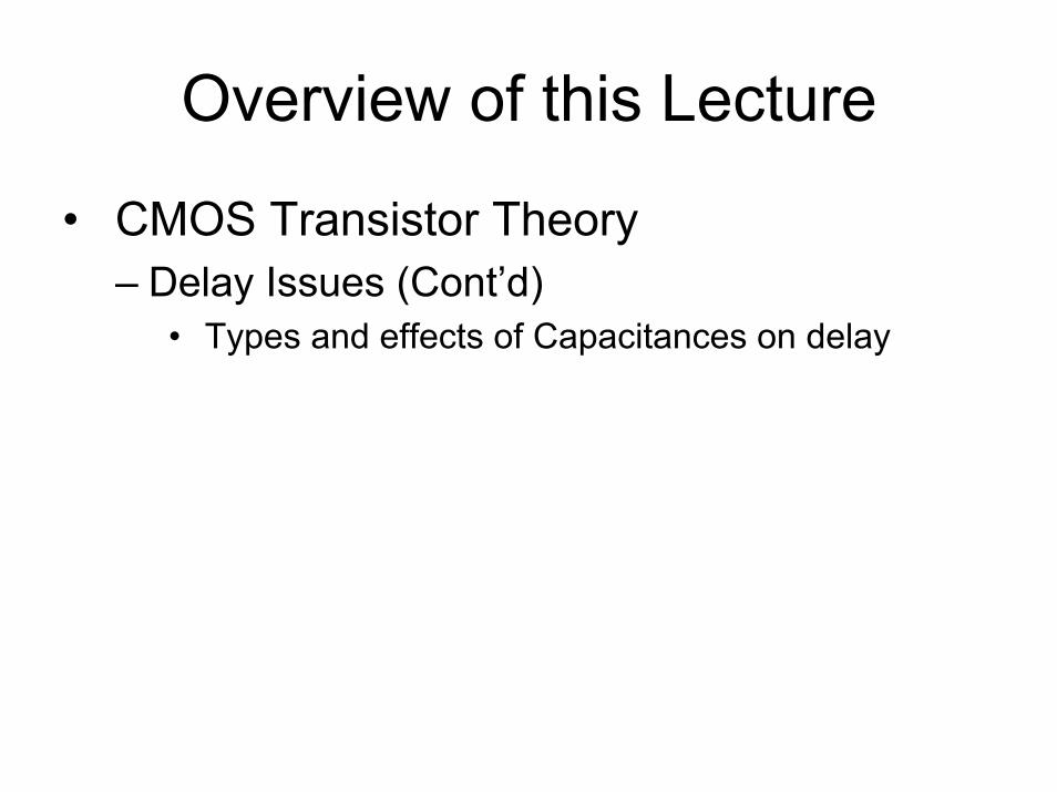
Parasitic Capacitance• Switching speeds of MOS systems strongly depend on
the parasitic capacitances associated with MOSFETs and interconnections
• Total Cload on the output of a CMOS gate is the sum of:– Gate capacitance (Cg)– Junction capacitance due to the source and drain
regions and their surroundings (Csb and Cdb)– Interconnect (or routing) capacitance (Cw)
• Gate oxide capacitance per unit area,ε ε
= 0 oxox
ox
Ct
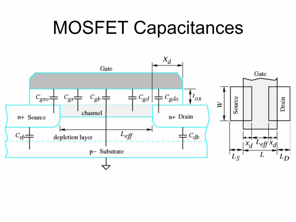
MOSFET Capacitances
xd xd
xd
Gate Capacitance
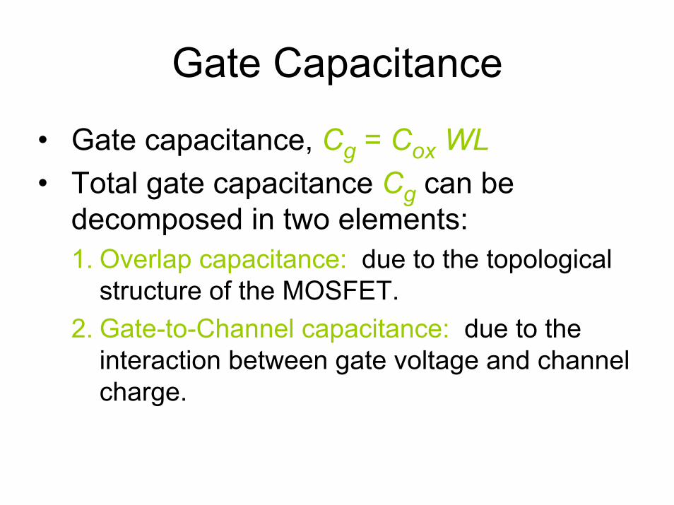
• Gate capacitance, Cg = Cox WL• Total gate capacitance Cg can be
decomposed in two elements:1. Overlap capacitance: due to the topological
structure of the MOSFET.2. Gate-to-Channel capacitance: due to the
interaction between gate voltage and channel charge.
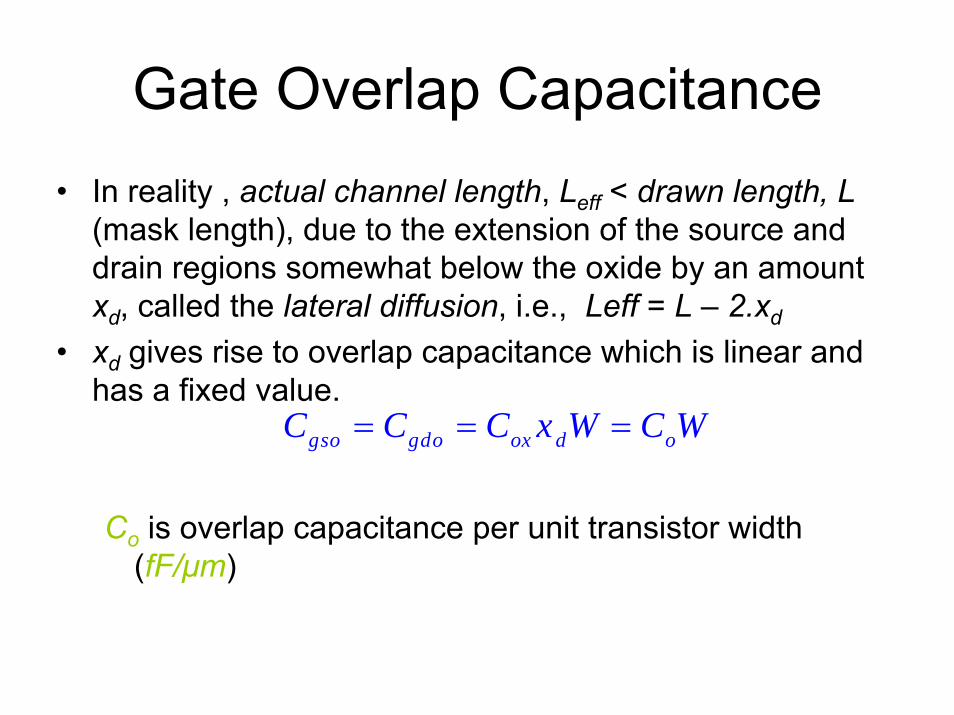
Gate Overlap Capacitance• In reality , actual channel length, Leff < drawn length, L
(mask length), due to the extension of the source and drain regions somewhat below the oxide by an amount xd, called the lateral diffusion, i.e., Leff = L – 2.xd
• xd gives rise to overlap capacitance which is linear and has a fixed value.
Co is overlap capacitance per unit transistor width (fF/μm)
= = =gso gdo ox d oC C C x W C W
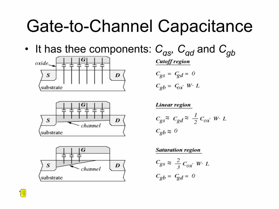
Gate-to-Channel Capacitance• It has thee components: Cgs, Cgd and Cgb
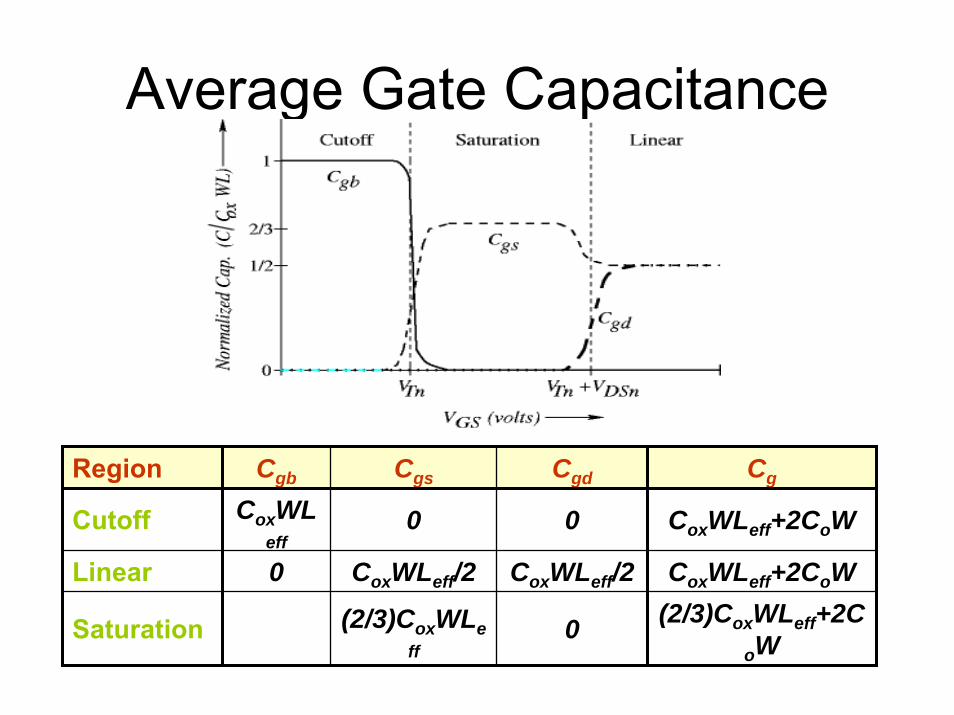
Average Gate Capacitance
Region Cgb Cgs Cgd Cg
Cutoff CoxWLeff
0 0
CoxWLeff/2
0
CoxWLeff+2CoW
Linear 0 CoxWLeff/2 CoxWLeff+2CoW
Saturation (2/3)CoxWLeff
(2/3)CoxWLeff+2CoW
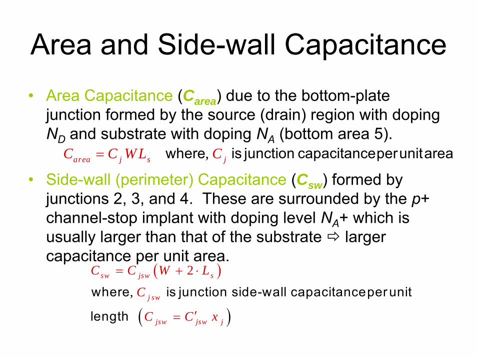
Area and Side-wall Capacitance• Area Capacitance (Carea) due to the bottom-plate
junction formed by the source (drain) region with doping ND and substrate with doping NA (bottom area 5).
• Side-wall (perimeter) Capacitance (Csw) formed by junctions 2, 3, and 4. These are surrounded by the p+ channel-stop implant with doping level NA+ which is usually larger than that of the substrate larger capacitance per unit area.
= ,area j s jC C WL Cwhere is junction capacitanceperunitarea
( )
( )where is junction side-wall capacitanceperunit
length
= + ⋅
′=
2
,sw jsw s
j sw
jsw jsw j
C C W L
C
C C x
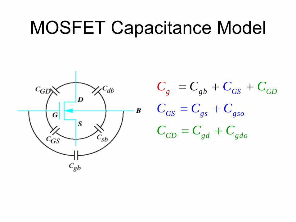
MOSFET Capacitance Model
=
= +
=
+
+
+
GS
GS gs gso
GD
GD g
g
gdo
bg
d
C C
C
C C
C C
C C C
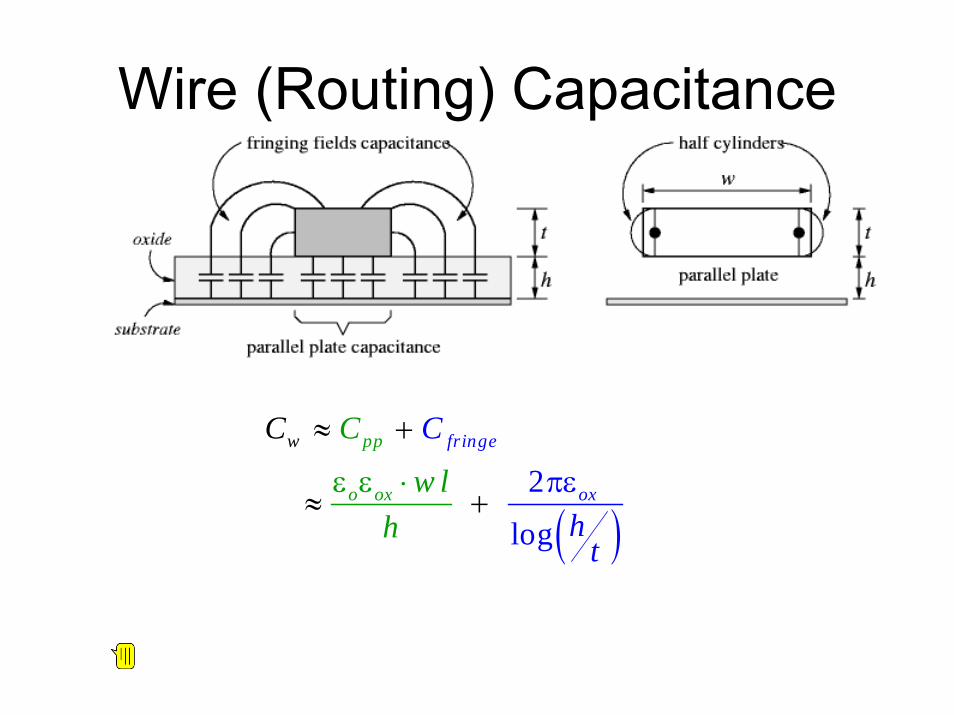
Wire (Routing) Capacitance
( )ε ε πε
≈ +
≈ +⋅ 2
log
pp
o o
fri
x
nge
o
w
x
C
wl
h
CC
ht
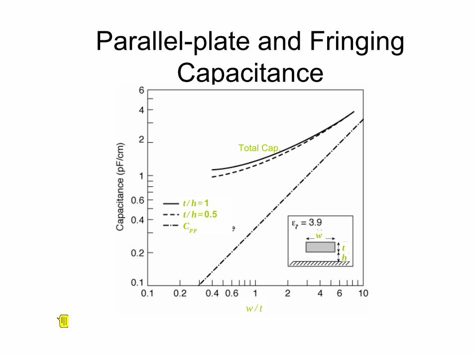
Parallel-plate and Fringing Capacitance
Total Cap.
w/t
wth
t/h=1t/h=0.5Cpp
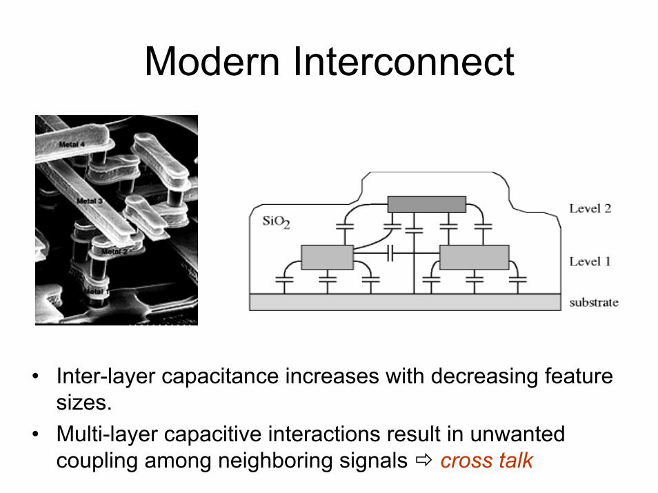
Modern Interconnect
• Inter-layer capacitance increases with decreasing feature sizes.
• Multi-layer capacitive interactions result in unwanted coupling among neighboring signals cross talk
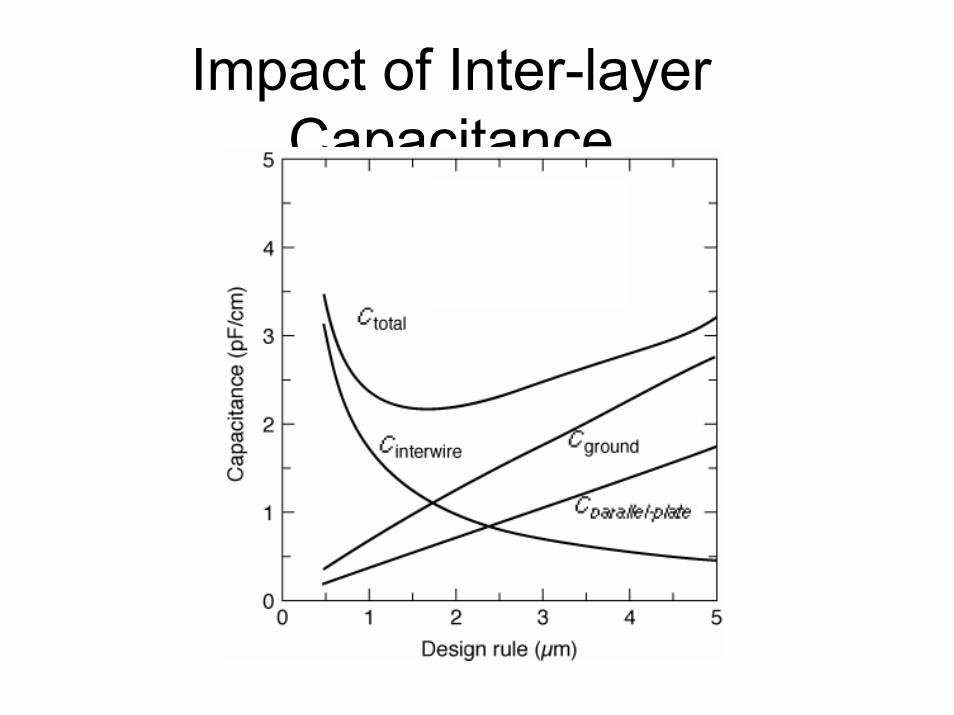
Impact of Inter-layer Capacitance
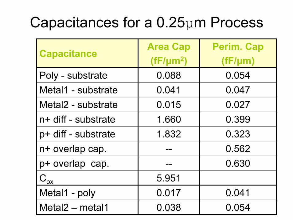
Capacitances for a 0.25μm Process
CapacitanceArea Cap(fF/μm2)
Perim. Cap(fF/μm)
Poly - substrate 0.0880.0410.015
n+ diff - substrate 1.660 0.399
n+ overlap cap. -- 0.562p+ overlap cap. -- 0.630Cox 5.951Metal1 - poly 0.017 0.041
1.832
0.038
0.054Metal1 - substrate 0.047Metal2 - substrate 0.027
p+ diff - substrate 0.323
Metal2 – metal1 0.054
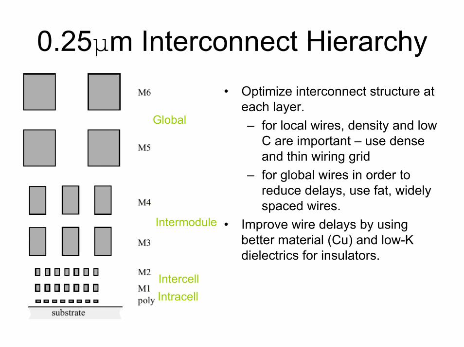
0.25μm Interconnect Hierarchy• Optimize interconnect structure at
each layer.– for local wires, density and low
C are important – use dense and thin wiring grid
– for global wires in order to reduce delays, use fat, widely spaced wires.
• Improve wire delays by using better material (Cu) and low-K dielectrics for insulators.
IntracellIntercell
Intermodule
Global
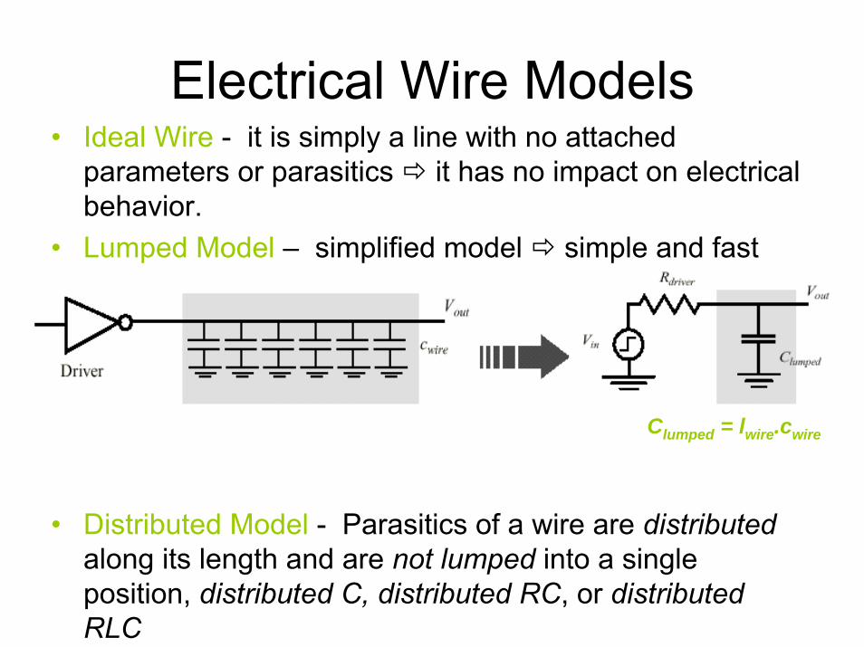
Electrical Wire Models• Ideal Wire - it is simply a line with no attached
parameters or parasitics it has no impact on electrical behavior.
• Lumped Model – simplified model simple and fast computation, e.g., lumped C, lumped RC or lumped RLC
• Distributed Model - Parasitics of a wire are distributedalong its length and are not lumped into a single position, distributed C, distributed RC, or distributed RLC
Clumped = lwire.cwire
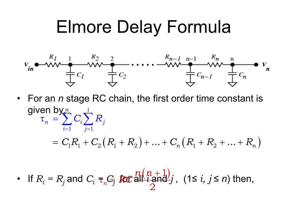
Elmore Delay Formula
• For an n stage RC chain, the first order time constant is given by,
• If Ri = Rj and Ci = Cj for all i and j , (1≤ i, j ≤ n) then,
( ) ( )
n i
n i ji j
n nC R C R R C R
C R
R R= =
τ
= + + + + + + +
= ∑ ∑
1 1 2 1 2 1 2
1 1
... ...
( )+τ =
12n
n nRC
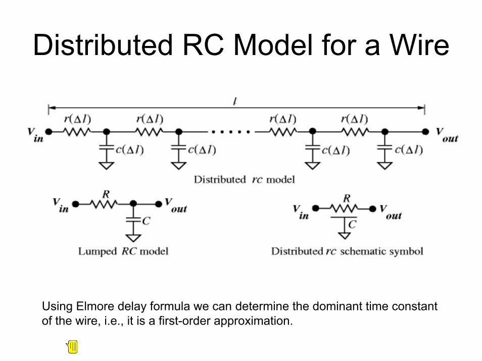
Distributed RC Model for a Wire
Using Elmore delay formula we can determine the dominant time constantof the wire, i.e., it is a first-order approximation.
Questions and Answers
Thank You