Embed Size (px)
Citation preview
CO-UNIT VI- Basic Processing Unit (HARDWIRED CONTROL AND MICROPROGRAMMED CONTROL)
1
Text/Reference Books
2. Computer Organization and Architecture: Designing for
Performance, William Stallings , Prentice-Hall India,Publ.
3.Computer Architecture A Quantitative Approach ,John L Hennessy and David Patterson , Morgan Kaufman Publ.
4.Structured Computer Organization ,Andrew S. Tanenbaum , Prentice-Hall India Publ.
5. Computer Organization and Design, P. Paul Choudhury ,Prentice-Hall India,Publ.
Websites:
2
The following sources are used for preparing these slides
1. Computer Organization , Carl Hamacher, Zvonko Vranesic, Safwat Zaky
McGraw Hill Publ.
CO-UNIT-V-Memory System
CONTENTS
Fundamental Concepts on Control Unit
Machine Cycles
Function of the Control Unit
Register Transfers
Performing Arithmetic Operation
Fetching a word from memory
Storing a word in memory
Execution of Complete Instruction
Branch Instructions
Multiple Bus Organization
Hardwired Control
Micro programmed Control
Micro Instructions
Microprogram Sequencing
Wide Branch Addressing
Microinstruction with next address field
Prefetching Micro Instructions
Emulation
3 CO-Unit VI-Basic Processor Unit
CO-UNIT VI
BASIC PROCESSING UNIT
Dt.8.3.18
Updated on 13.3.18
4
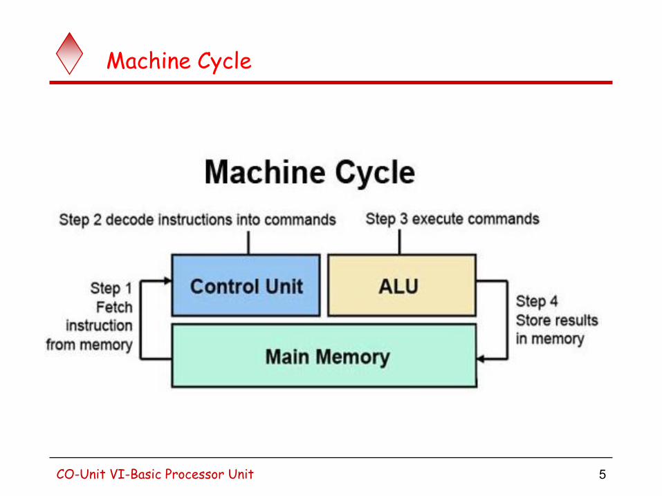
Machine Cycle
5 CO-Unit VI-Basic Processor Unit
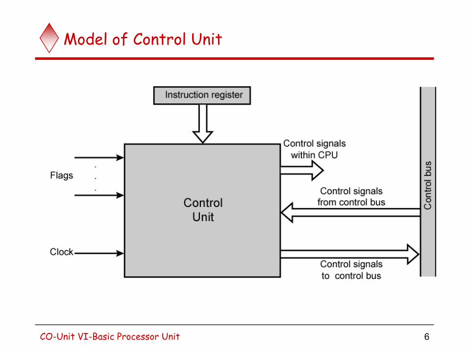
Model of Control Unit
6 CO-Unit VI-Basic Processor Unit
Functions of Control Unit using Control Signals
Sequencing
CU causes the CPU to step through a series of micro-operations in proper sequence based on the program being executed.
E.g. In order to carry out a task such as ADD, the control unit must generate a set of control signals in a predefined sequence governed by the HW structure of the processing section.
Execution
CU causes each micro-operation to be performed
Control Signals
External: inputs indicating the state of the system
Internal: logic required to perform the sequencing and execution functions
7 CO-Unit VI-Basic Processor Unit
Fundamental Concepts contd..
Inputs to control unit are:
Master clock
Status info from processing section
Command signals from external agent
Outputs produced by control unit
Signals that drive the processing section and responses to an external envent (operation complete or abort) due to exceptions (overflow and underflow)
Control unit undertakes the following responsibilities
Instruction interpretation:
Read instr. , Recognize, Get operands and Route to appropriate functional units, necessary control signals issued
Instruction sequencing:
Control unit determines the address of next instruction to be executed and loads to PC
Processor fetches one instruction at a time and perform the operation specified.
Instructions are fetched from successive memory locations until a branch or a jump instruction is encountered
8 CO-Unit VI-Basic Processor Unit
Connection between CPU and Memory
CO-Unit VI-Basic Processor Unit 9
10
Fetch/execute cycle
Step I: Fetch the contents of the memory location pointed to by
Program Counter (PC).
PC points to the memory location which has the instruction to be executed.
Load the contents of the memory location into Instruction Register (IR).
Step II:
Increment the contents of the PC by 4 (assuming the memory is byte addressable and the word length is 32 bits).
Step III:
Carry out the operation specified by the instructions in the IR.
Steps I and II constitute the fetch phase, and are repeated as many times as necessary to fetch the complete instruction.
Step III constitutes the execution phase.
CO-Unit VI-Basic Processor Unit
11
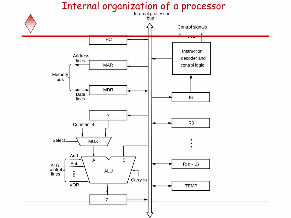
Internal organization of a processor
Recall that a processor has several registers/building blocks: Memory address register (MAR)
Memory data register (MDR)
Program Counter (PC)
Instruction Register (IR)
General purpose registers R0 - R(n-1)
Arithmetic and logic unit (ALU)
Control unit.
How are these units organized and how do they communicate with each other?
CO-Unit VI-Basic Processor Unit
12
Organization
PC
CPU bus
IR
Decoder
control
R0
R1
R2
Rn-1
Register file
MAR
MDR
memory bus
Y
Z
ALU
CO-Unit VI-Basic Processor Unit
13
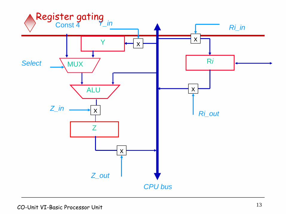
Register gating
Ri
CPU bus
Y
Z
ALU
x
x
x
x
MUX
x
Const 4 Ri_in
Ri_out
Y_in
Select
Z_in
Z_out
CO-Unit VI-Basic Processor Unit
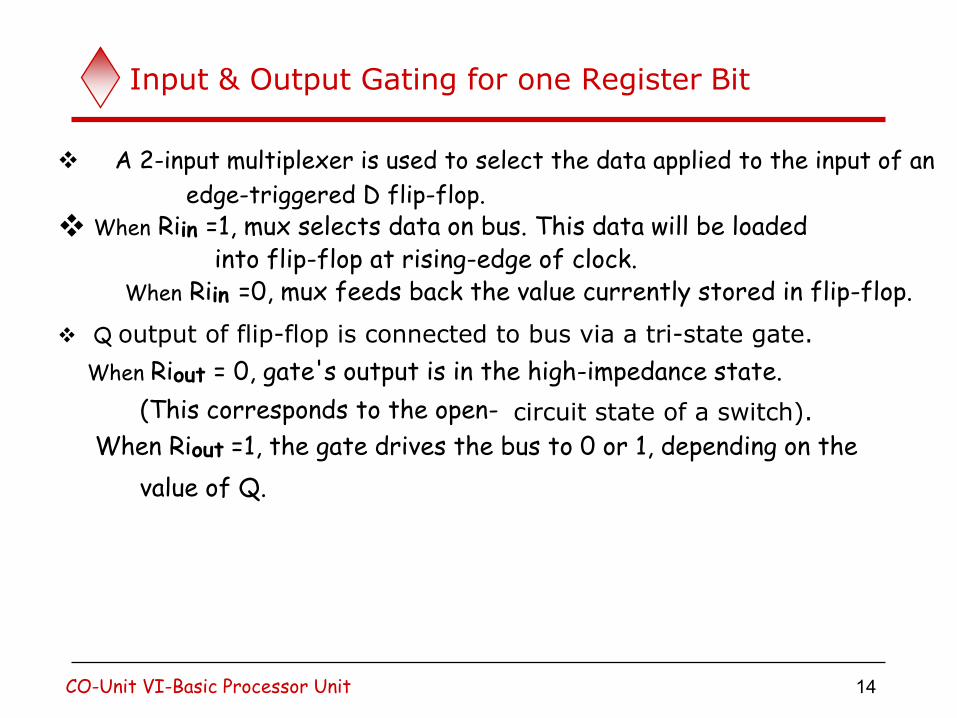
Input & Output Gating for one Register Bit
A 2-input multiplexer is used to select the data applied to the input of an
edge-triggered D flip-flop.
When Riin =1, mux selects data on bus. This data will be loaded into flip-flop at rising-edge of clock. When Riin =0, mux feeds back the value currently stored in flip-flop.
Q output of flip-flop is connected to bus via a tri-state gate.
When Riout = 0, gate's output is in the high-impedance state. (This corresponds to the open- circuit state of a switch). When Riout =1, the gate drives the bus to 0 or 1, depending on the value of Q.
CO-Unit VI-Basic Processor Unit 14
15
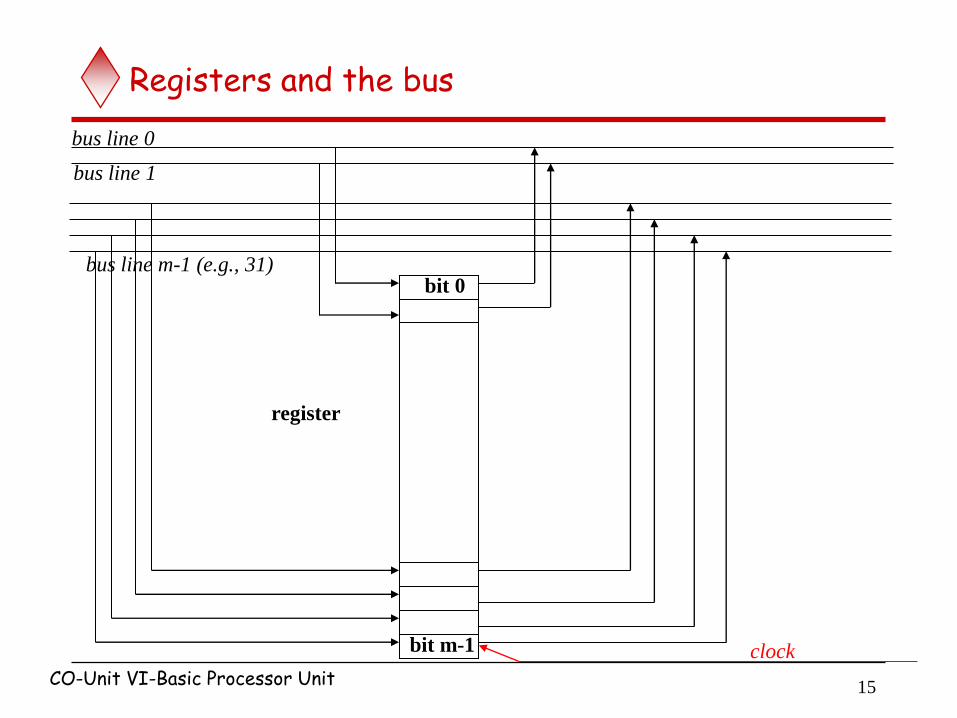
Registers and the bus
bus line 0
bus line 1
bus line m-1 (e.g., 31) bit 0
bit m-1
register
clock
CO-Unit VI-Basic Processor Unit
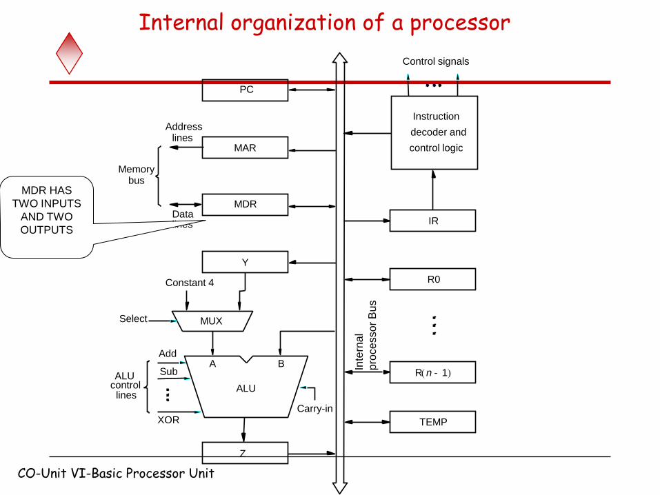
Internal organization of a processor
lines Data
Address lines
bus Memory
Carry-in
ALU
PC
MAR
MDR
Y
Z
Add
XOR
Sub
IR
TEMP
R0
control ALU
lines
Control signals
R n 1 - ( )
Instruction
decoder and
Inte
rna
l
pro
ce
sso
r B
us
control logic
A B
MUX Select
Constant 4
MDR HAS
TWO INPUTS
AND TWO
OUTPUTS
CO-Unit VI-Basic Processor Unit
17
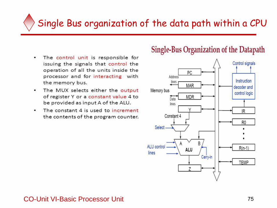
Single bus organization
Single bus organization: ALU, control unit and all the registers are connected via a
single common bus (Called Internal Bus)
Bus is internal to the processor and should not be confused with the external bus that connects the processor to the memory and I/O devices.
Data lines of the external memory bus are connected to the internal processor bus via MDR. Register MDR has two inputs and two outputs.
Data may be loaded to (from) MDR from (to) internal processor bus or external memory bus.
Address lines of the external memory bus are connected to the internal processor bus via MAR. MAR receives input from the internal processor bus.
MAR provides output to external memory bus.
CO-Unit VI-Basic Processor Unit
18
Single bus organization (contd..)
Instruction decoder and control logic block, or control unit issues signals to control the operation of all units inside the processor and for interacting with the memory bus. Control signals depend on the instruction loaded in the
Instruction Register (IR)
Outputs from the control logic block are connected to: Control lines of the memory bus.
ALU, to determine which operation is to be performed.
Select input of the multiplexer MUX to select between Register Y and constant 4.
Control lines of the registers, to select the registers.
CO-Unit VI-Basic Processor Unit
19
Single bus organization (contd..)
Registers Y, Z, and TEMP: Used by the processor for temporary storage during execution
of some instructions.
Note that Registers R0 to R(n-1) are used to store data generated by one instruction for later use by another instruction.
Data is stored in R0 through R(n-1) after the execution of an instruction.
Multiplexer MUX selects either the output of register Y or a constant 4, depending upon the control input Select.
Constant 4 is used to increment the value of the PC. B input of ALU is obtained directly from processor-bus. As instruction execution progresses, data are transferred from one register to another, often passing through ALU to perform arithmetic or logic operation.
CO-Unit VI-Basic Processor Unit
20
Registers and the bus (contd..)
A bus may be viewed as a collection of parallel wires.
Buses have no memory: They are just a collection of wires.
When data is on the bus, all registers can “see” that data at their inputs.
A register may place its contents onto the bus.
CO-Unit VI-Basic Processor Unit
21
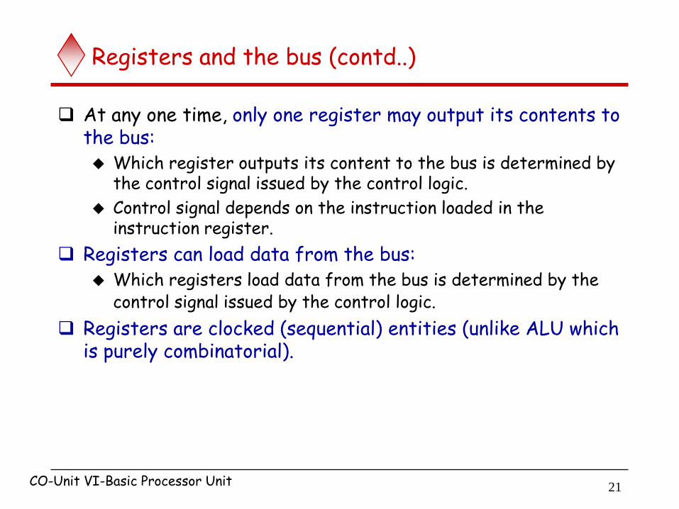
Registers and the bus (contd..)
At any one time, only one register may output its contents to the bus: Which register outputs its content to the bus is determined by
the control signal issued by the control logic.
Control signal depends on the instruction loaded in the instruction register.
Registers can load data from the bus: Which registers load data from the bus is determined by the
control signal issued by the control logic.
Registers are clocked (sequential) entities (unlike ALU which is purely combinatorial).
CO-Unit VI-Basic Processor Unit
22
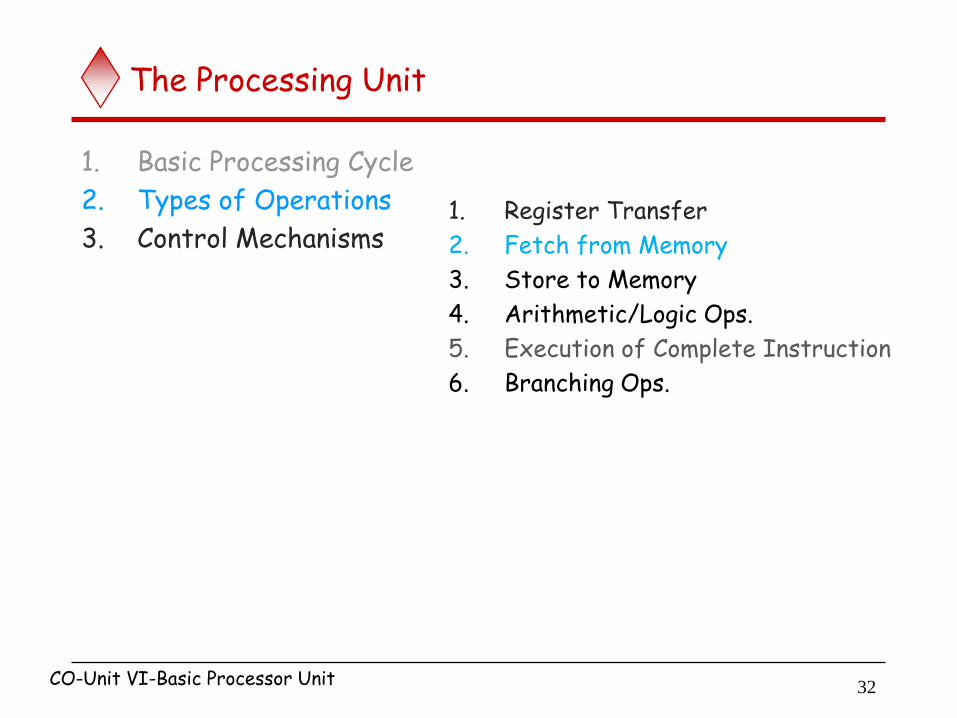
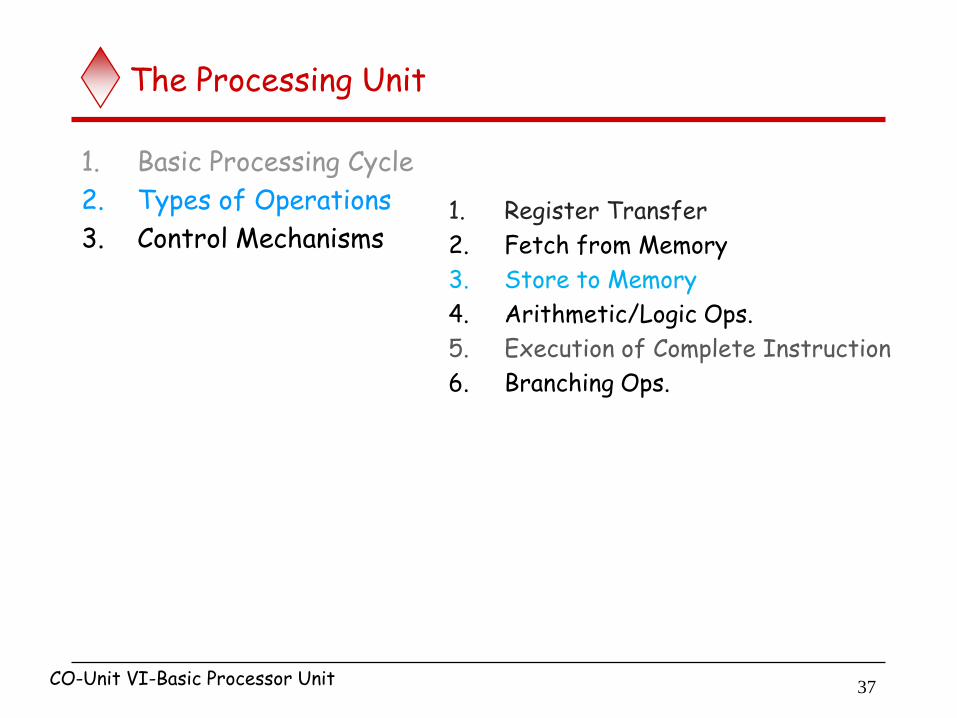
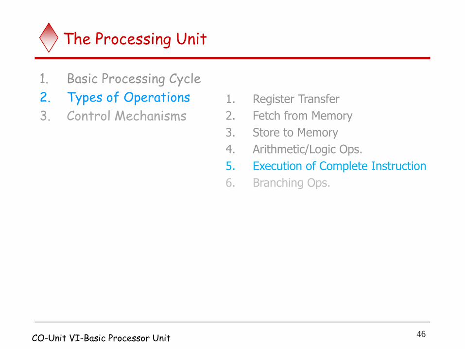
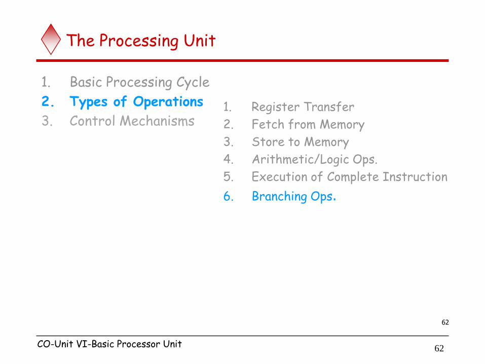
The Processing Unit
1. Basic Processing Cycle
2. Types of Operations
3. Control Mechanisms 1. Register Transfer
2. Fetch from Memory
3. Store to Memory
4. Arithmetic/Logic Ops.
5. Execution of Complete Instruction
6. Branching Ops.
CO-Unit VI-Basic Processor Unit
23
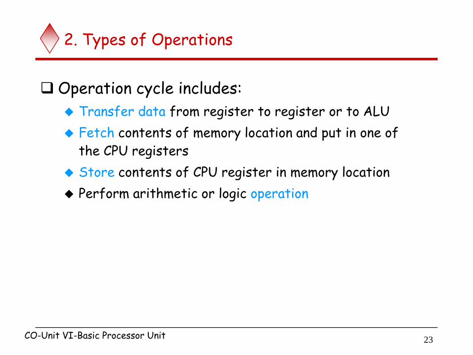
2. Types of Operations
Operation cycle includes:
Transfer data from register to register or to ALU
Fetch contents of memory location and put in one of
the CPU registers
Store contents of CPU register in memory location
Perform arithmetic or logic operation
CO-Unit VI-Basic Processor Unit
24
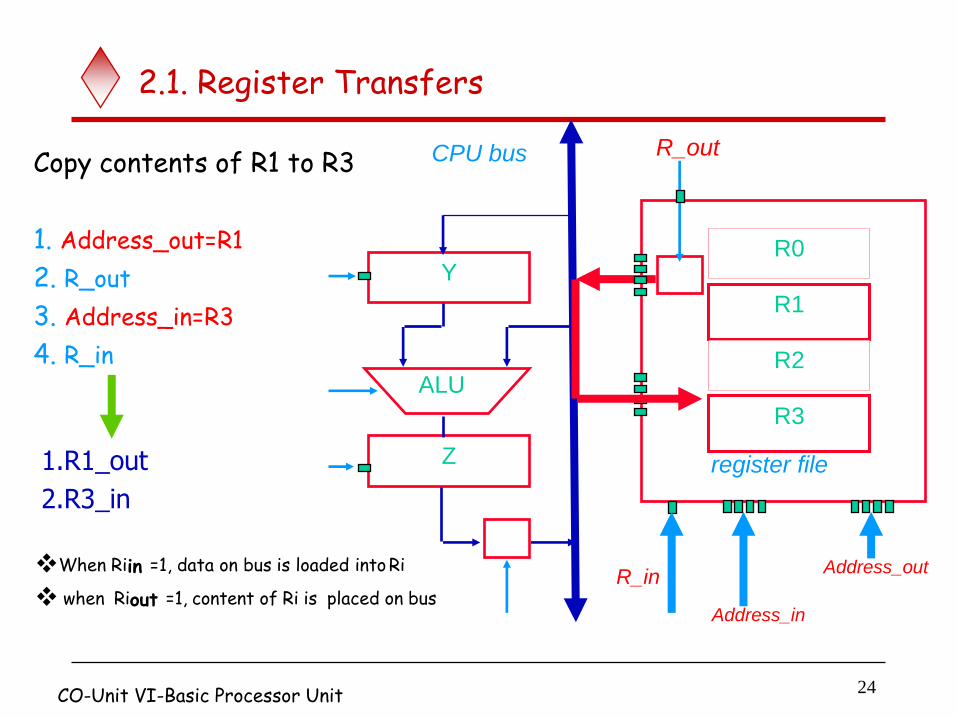
2.1. Register Transfers
R0
R1
R2
R3
Y
Z register file
ALU
Address_in
R_in
R_out CPU bus
Address_out
Copy contents of R1 to R3
1. Address_out=R1
2. R_out
3. Address_in=R3
4. R_in
1.R1_out
2.R3_in
When Riin =1, data on bus is loaded into Ri
when Riout =1, content of Ri is placed on bus
CO-Unit VI-Basic Processor Unit
25
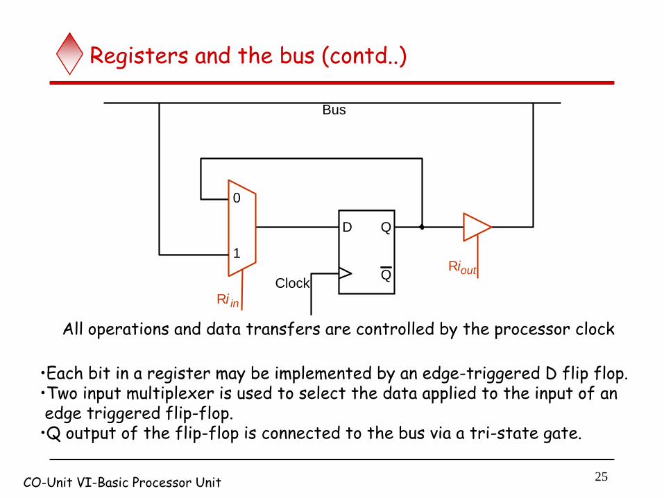
Registers and the bus (contd..)
D Q
Q Clock
1
0
R i out
Bus
R i in
•Each bit in a register may be implemented by an edge-triggered D flip flop. •Two input multiplexer is used to select the data applied to the input of an edge triggered flip-flop. •Q output of the flip-flop is connected to the bus via a tri-state gate.
All operations and data transfers are controlled by the processor clock
CO-Unit VI-Basic Processor Unit
26
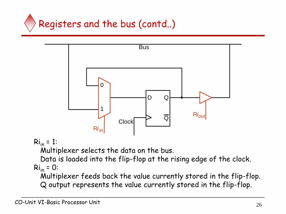
Registers and the bus (contd..)
D Q
Q Clock
1
0
R i out
Bus
R i in
Riin = 1: Multiplexer selects the data on the bus. Data is loaded into the flip-flop at the rising edge of the clock. Riin = 0: Multiplexer feeds back the value currently stored in the flip-flop. Q output represents the value currently stored in the flip-flop.
CO-Unit VI-Basic Processor Unit
27
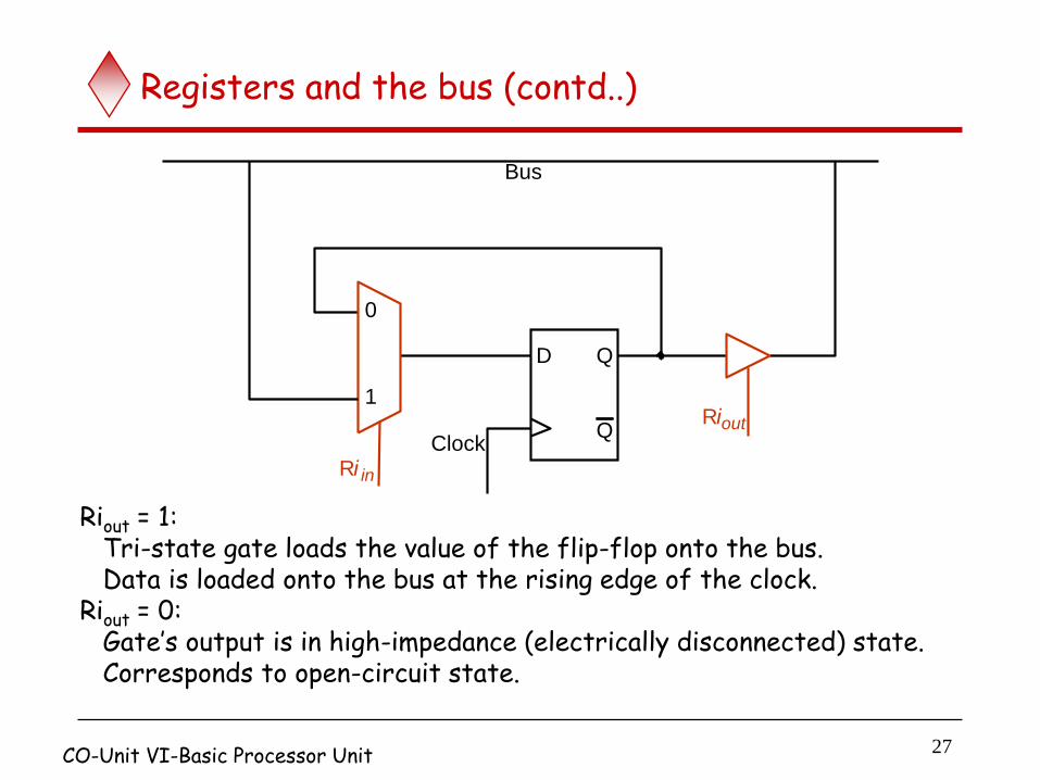
Registers and the bus (contd..)
D Q
Q Clock
1
0
R i out
Bus
R i in
Riout = 1: Tri-state gate loads the value of the flip-flop onto the bus. Data is loaded onto the bus at the rising edge of the clock. Riout = 0: Gate’s output is in high-impedance (electrically disconnected) state. Corresponds to open-circuit state.
CO-Unit VI-Basic Processor Unit
28
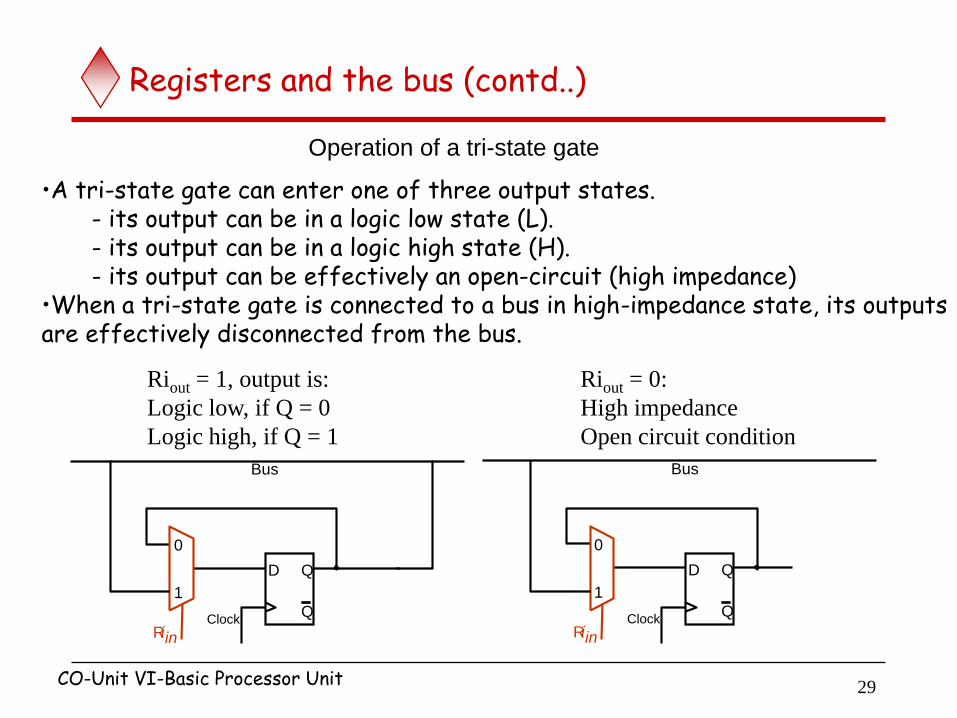
Registers and the bus (contd..)
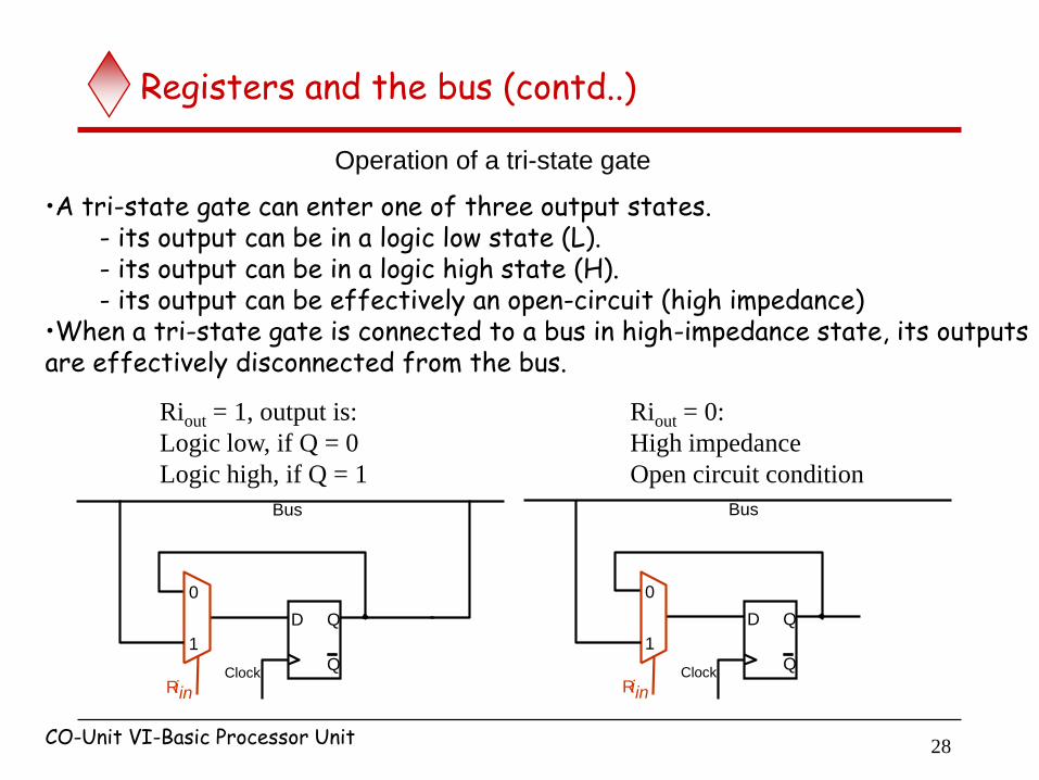
Operation of a tri-state gate
•A tri-state gate can enter one of three output states. - its output can be in a logic low state (L). - its output can be in a logic high state (H). - its output can be effectively an open-circuit (high impedance) •When a tri-state gate is connected to a bus in high-impedance state, its outputs are effectively disconnected from the bus.
D Q
Q Clock
1
0
Bus
R i in
D Q
Q Clock
1
0
Bus
R i in
Riout = 1, output is:
Logic low, if Q = 0
Logic high, if Q = 1
Riout = 0:
High impedance
Open circuit condition
CO-Unit VI-Basic Processor Unit
29
Registers and the bus (contd..)
Operation of a tri-state gate
•A tri-state gate can enter one of three output states. - its output can be in a logic low state (L). - its output can be in a logic high state (H). - its output can be effectively an open-circuit (high impedance) •When a tri-state gate is connected to a bus in high-impedance state, its outputs are effectively disconnected from the bus.
D Q
Q Clock
1
0
Bus
R i in
D Q
Q Clock
1
0
Bus
R i in
Riout = 1, output is:
Logic low, if Q = 0
Logic high, if Q = 1
Riout = 0:
High impedance
Open circuit condition
CO-Unit VI-Basic Processor Unit
30
Registers and the bus (contd..)
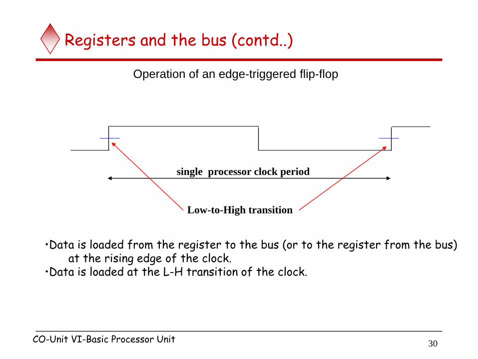
Operation of an edge-triggered flip-flop
single processor clock period
Low-to-High transition
•Data is loaded from the register to the bus (or to the register from the bus) at the rising edge of the clock. •Data is loaded at the L-H transition of the clock.
CO-Unit VI-Basic Processor Unit
31
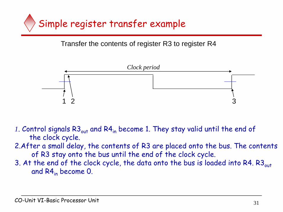
Simple register transfer example
Transfer the contents of register R3 to register R4
1. Control signals R3out and R4in become 1. They stay valid until the end of the clock cycle. 2.After a small delay, the contents of R3 are placed onto the bus. The contents of R3 stay onto the bus until the end of the clock cycle. 3. At the end of the clock cycle, the data onto the bus is loaded into R4. R3out and R4in become 0.
1 2 3
Clock period
CO-Unit VI-Basic Processor Unit
32
The Processing Unit
1. Basic Processing Cycle
2. Types of Operations
3. Control Mechanisms 1. Register Transfer
2. Fetch from Memory
3. Store to Memory
4. Arithmetic/Logic Ops.
5. Execution of Complete Instruction
6. Branching Ops.
CO-Unit VI-Basic Processor Unit
33
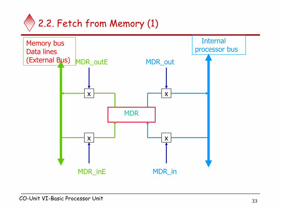
2.2. Fetch from Memory (1)
MDR
x
Internal processor bus
Memory bus Data lines (External Bus)
x
x
x
MDR_out
MDR_in
MDR_outE
MDR_inE
CO-Unit VI-Basic Processor Unit
34
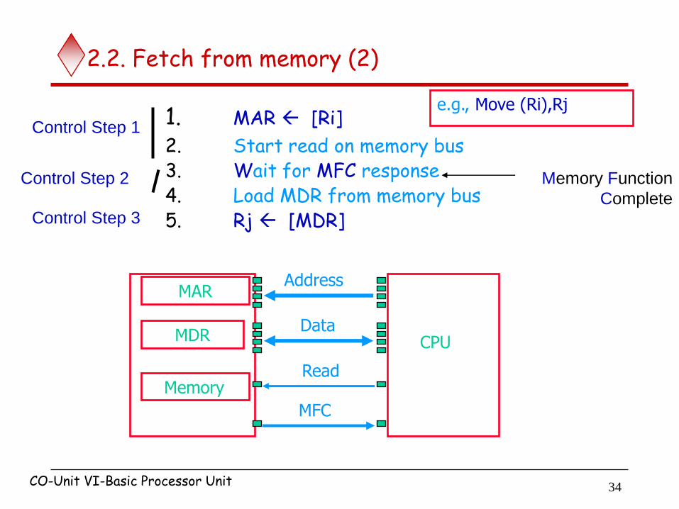
MAR
MDR
2.2. Fetch from memory (2)
1. MAR [Ri]
2. Start read on memory bus 3. Wait for MFC response 4. Load MDR from memory bus 5. Rj [MDR]
MFC
Memory
CPU
Read
Address
Data
e.g., Move (Ri),Rj
Memory Function
Complete
Control Step 1
Control Step 2
Control Step 3
CO-Unit VI-Basic Processor Unit
Memory
35
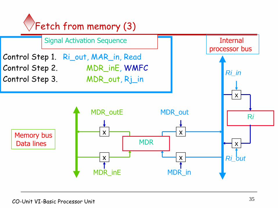
Fetch from memory (3)
Control Step 1. Ri_out, MAR_in, Read
Control Step 2. MDR_inE, WMFC
Control Step 3. MDR_out, Rj_in
Signal Activation Sequence
Ri
x
x
Ri_in
Ri_out
x
x
x
x
MDR_out
MDR_in
MDR_outE
MDR_inE
MDR
Internal processor bus
Memory bus Data lines
CO-Unit VI-Basic Processor Unit
36
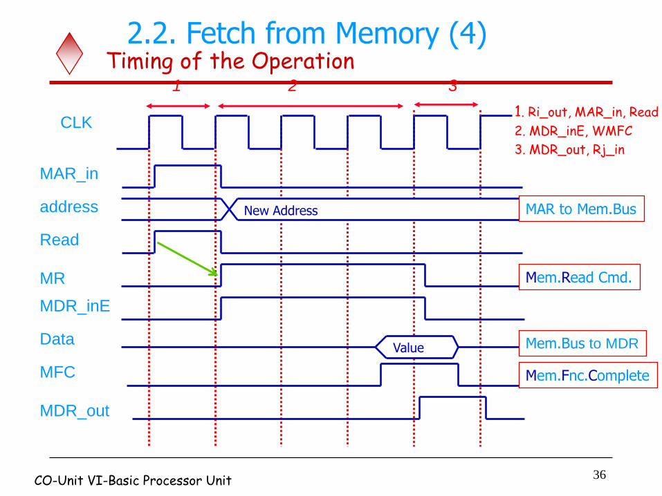
2.2. Fetch from Memory (4)
Value
New Address
Timing of the Operation
CLK
MAR_in
MR
1 2 3
address
Read
MDR_inE
Data
MFC
MDR_out
1. Ri_out, MAR_in, Read
2. MDR_inE, WMFC
3. MDR_out, Rj_in
Mem.Fnc.Complete
Mem.Read Cmd.
Mem.Bus to MDR
MAR to Mem.Bus
CO-Unit VI-Basic Processor Unit
37
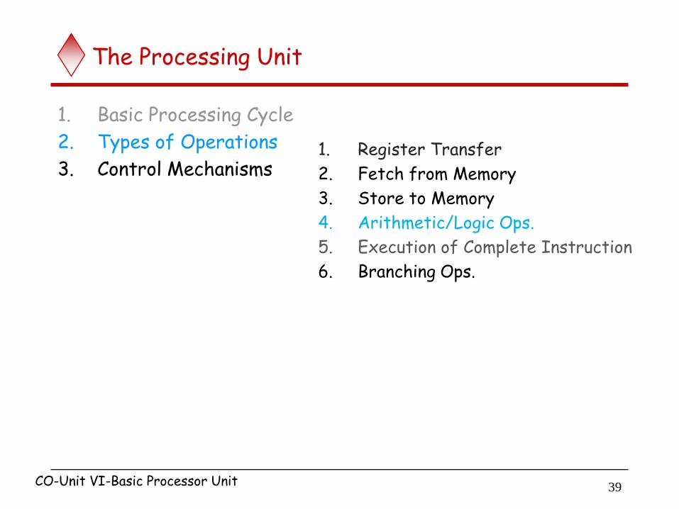
The Processing Unit
1. Basic Processing Cycle
2. Types of Operations
3. Control Mechanisms 1. Register Transfer
2. Fetch from Memory
3. Store to Memory
4. Arithmetic/Logic Ops.
5. Execution of Complete Instruction
6. Branching Ops.
CO-Unit VI-Basic Processor Unit
38
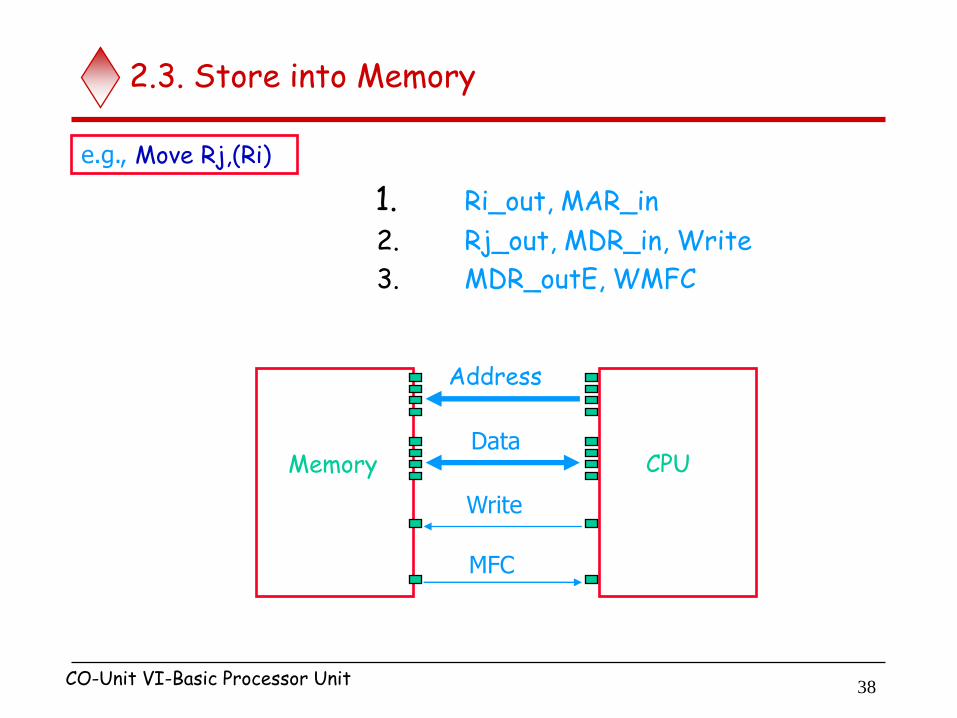
2.3. Store into Memory
1. Ri_out, MAR_in
2. Rj_out, MDR_in, Write
3. MDR_outE, WMFC
Memory CPU
Write
Address
Data
MFC
e.g., Move Rj,(Ri)
CO-Unit VI-Basic Processor Unit
39
The Processing Unit
1. Basic Processing Cycle
2. Types of Operations
3. Control Mechanisms 1. Register Transfer
2. Fetch from Memory
3. Store to Memory
4. Arithmetic/Logic Ops.
5. Execution of Complete Instruction
6. Branching Ops.
CO-Unit VI-Basic Processor Unit
40
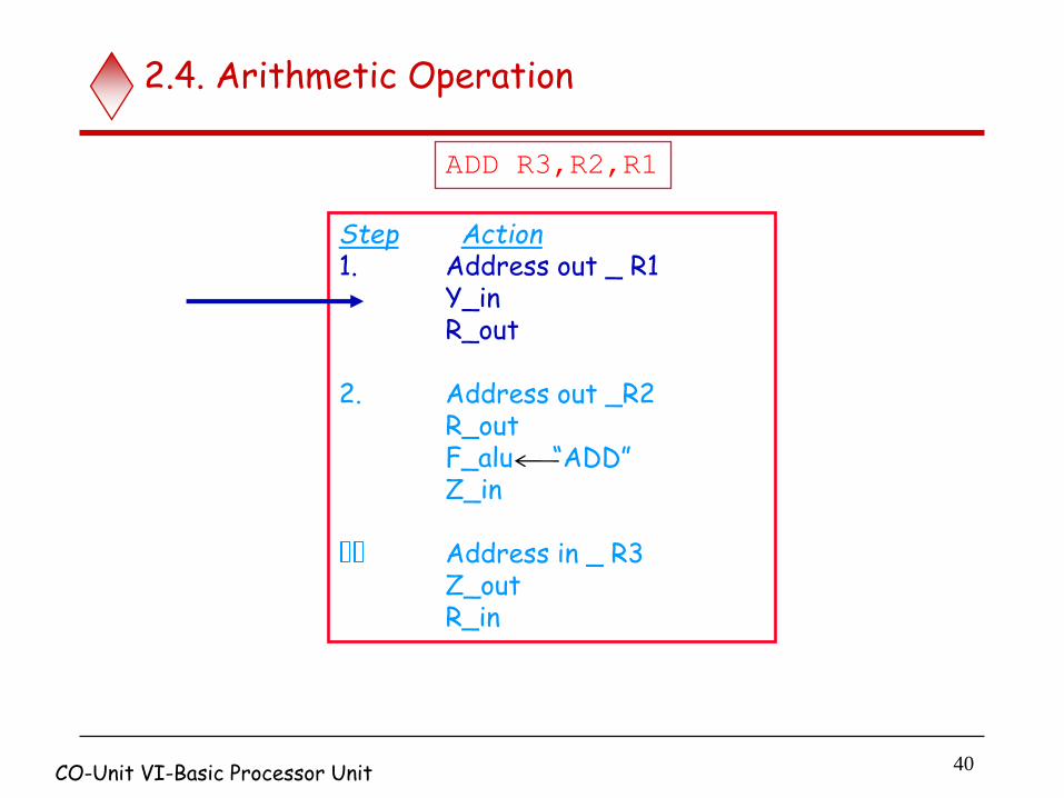
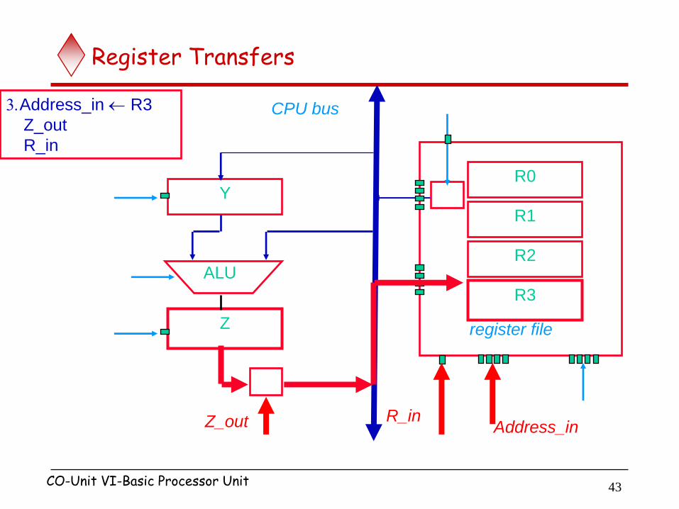
2.4. Arithmetic Operation
Step Action 1. Address out _ R1 Y_in R_out 2. Address out _R2 R_out F_alu “ADD” Z_in
Address in _ R3 Z_out R_in
ADD R3,R2,R1
CO-Unit VI-Basic Processor Unit
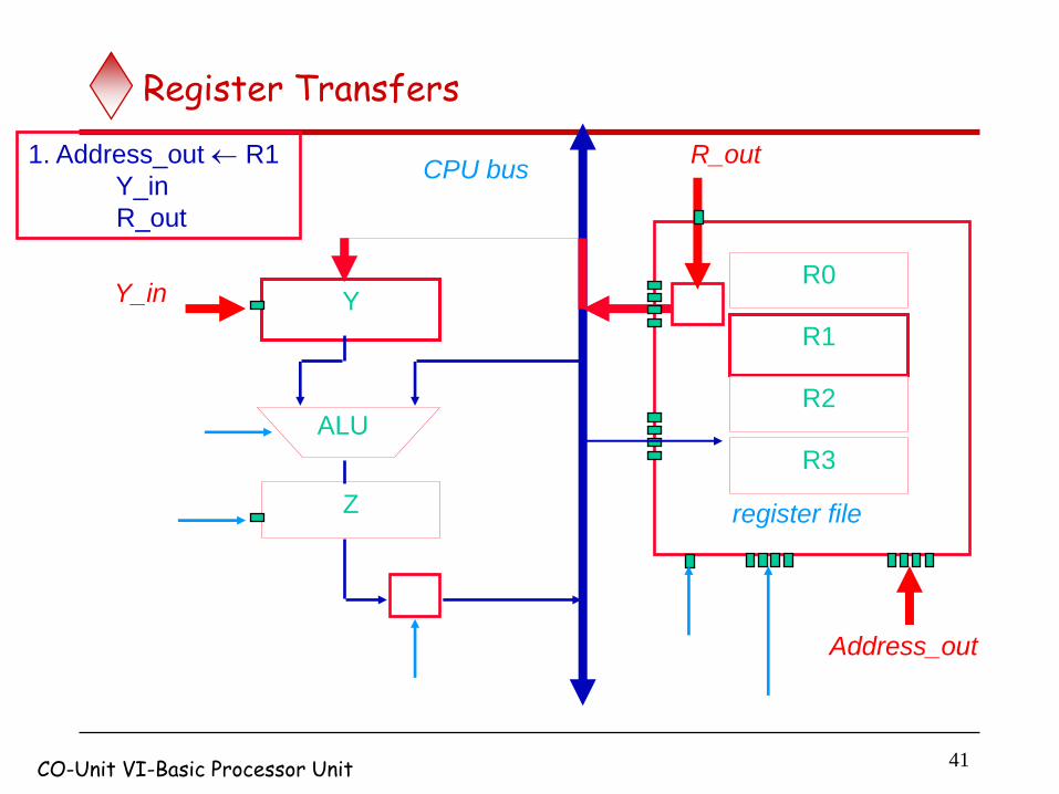
41
Register Transfers
R0
R1
R2
R3
Y
Z register file
ALU
Y_in
R_out CPU bus
Address_out
1. Address_out R1
Y_in
R_out
CO-Unit VI-Basic Processor Unit
42
Register Transfers
R0
R1
R2
R3
Y
ALU
Z register file
Y_in
Z_in
R_out CPU bus
Address_out
F_alu
2. Address_out R2
R_out
F_alu “ADD”
Z_in
CO-Unit VI-Basic Processor Unit
43
Register Transfers
R0
R1
R2
R3
Y
Z register file
ALU
Z_out Address_in R_in
CPU bus Address_in R3
Z_out
R_in
CO-Unit VI-Basic Processor Unit
44
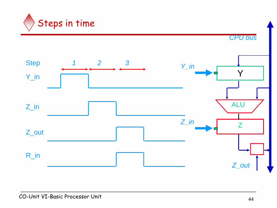
Steps in time
Y_in
Z_in
Z_out
R_in
1 2 3 Step
Y
Z
ALU
Z_out
CPU bus
Z_in
Y_in
CO-Unit VI-Basic Processor Unit
46
The Processing Unit
1. Basic Processing Cycle
2. Types of Operations
3. Control Mechanisms 1. Register Transfer
2. Fetch from Memory
3. Store to Memory
4. Arithmetic/Logic Ops.
5. Execution of Complete Instruction
6. Branching Ops.
CO-Unit VI-Basic Processor Unit
47
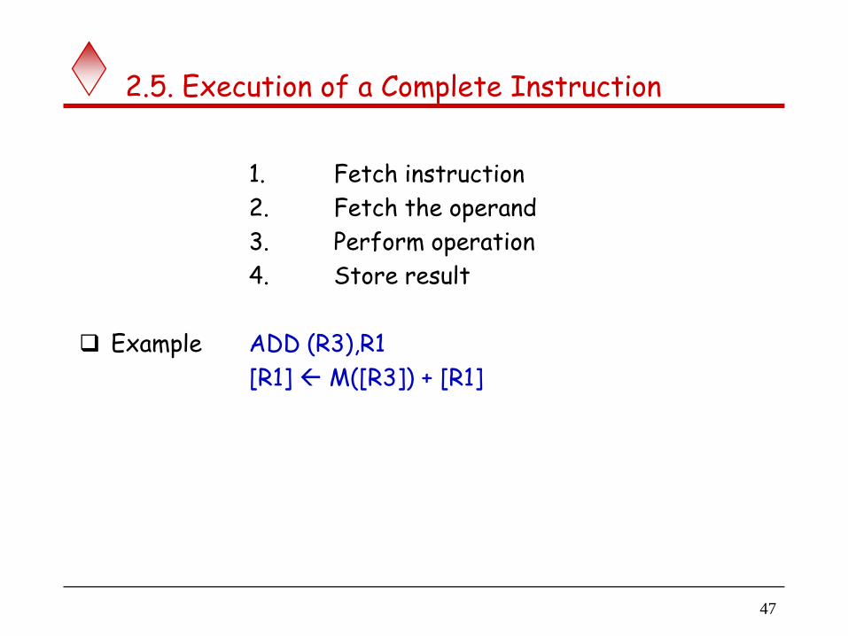
2.5. Execution of a Complete Instruction
1. Fetch instruction
2. Fetch the operand
3. Perform operation
4. Store result
Example ADD (R3),R1
[R1] M([R3]) + [R1]
48
Execution fetch (1)
Step Action
1 PC_out, MAR_in, Read
Set carry-in ALU
F_alu = “ADD”
Z_in
Z_out, PC_in
Wait for MFC
3 MDR_out, IR_in [PC] [PC ]+1
[IR] M([PC ])
Step 1-3:
Instruction fetch and
PC update
Note: for architectures having PC:=PC+4 a different scheme must be used
CO-Unit VI-Basic Processor Unit
[R1] M([R3]) + [R1]
49
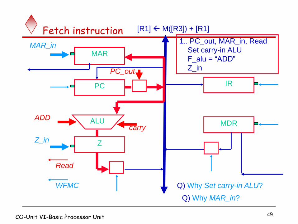
Fetch instruction
PC
Z
ALU
Z_in
ADD
MAR
PC_out
carry
MAR_in
Read
WFMC
MDR
IR
1.. PC_out, MAR_in, Read
Set carry-in ALU
F_alu = “ADD”
Z_in
Q) Why Set carry-in ALU?
Q) Why MAR_in?
CO-Unit VI-Basic Processor Unit
[R1] M([R3]) + [R1]
50
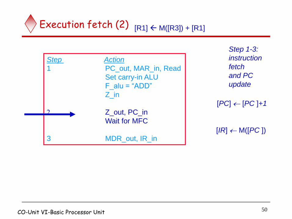
Execution fetch (2)
Step Action
1 PC_out, MAR_in, Read
Set carry-in ALU
F_alu = “ADD”
Z_in
Z_out, PC_in
Wait for MFC
3 MDR_out, IR_in
Step 1-3:
instruction
fetch
and PC
update
[PC] [PC ]+1
[IR] M([PC ])
CO-Unit VI-Basic Processor Unit
[R1] M([R3]) + [R1]
51
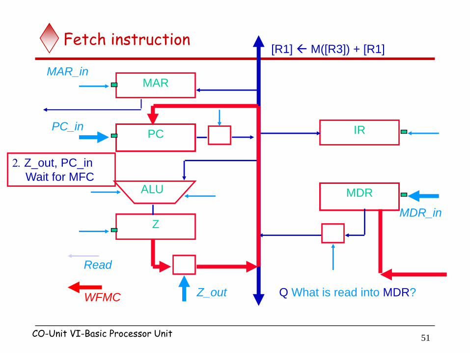
Fetch instruction
PC
Z
ALU
PC_in
Z_out
MAR MAR_in
Read
WFMC
MDR
IR
MDR_in
Z_out, PC_in
Wait for MFC
Q What is read into MDR?
CO-Unit VI-Basic Processor Unit
[R1] M([R3]) + [R1]
52
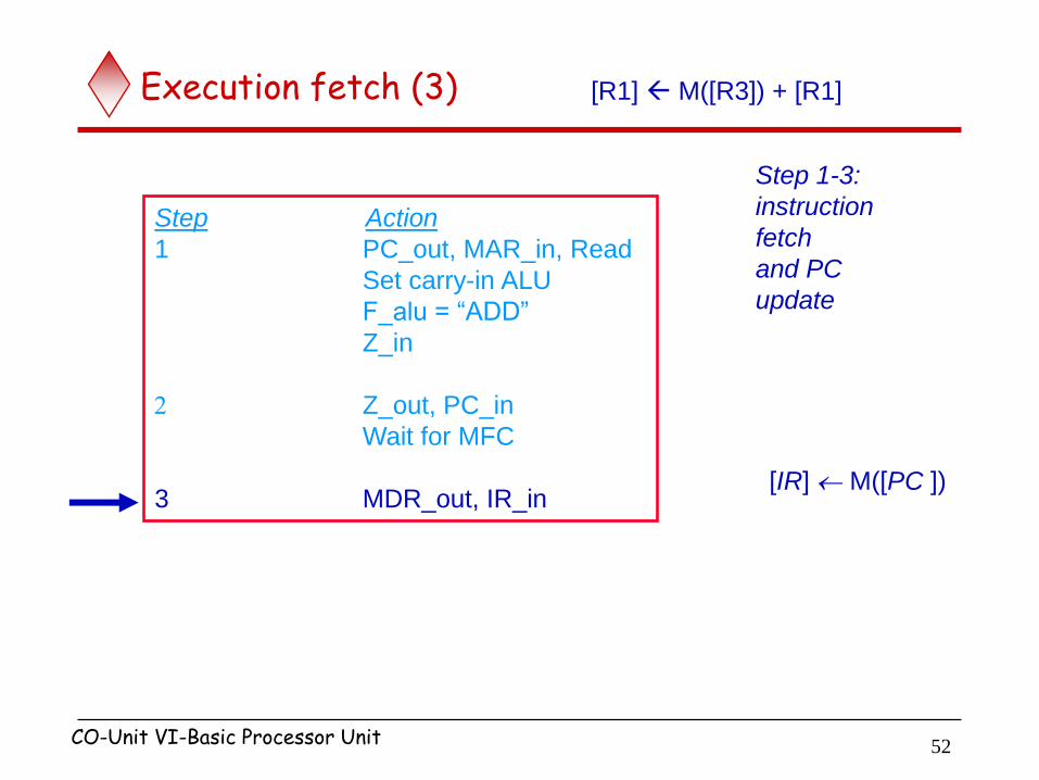
Execution fetch (3)
Step Action
1 PC_out, MAR_in, Read
Set carry-in ALU
F_alu = “ADD”
Z_in
Z_out, PC_in
Wait for MFC
3 MDR_out, IR_in [IR] M([PC ])
Step 1-3:
instruction
fetch
and PC
update
CO-Unit VI-Basic Processor Unit
[R1] M([R3]) + [R1]
53
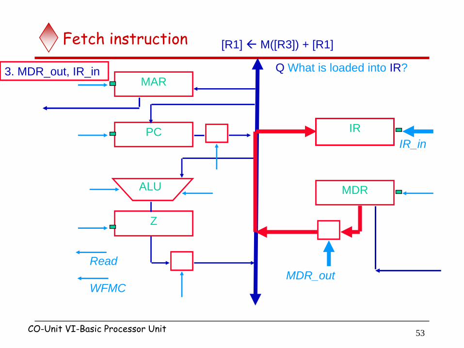
Fetch instruction
PC
Z
ALU
MAR
Read
WFMC
MDR
IR_in
MDR_out
IR
3. MDR_out, IR_in Q What is loaded into IR?
CO-Unit VI-Basic Processor Unit
[R1] M([R3]) + [R1]
54
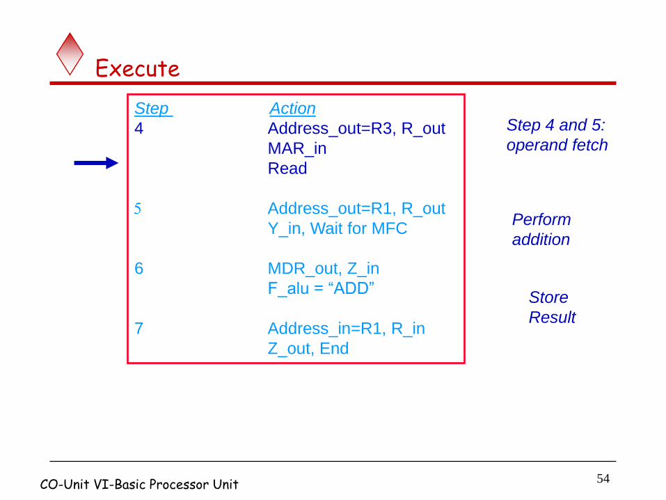
Execute
Step Action
4 Address_out=R3, R_out
MAR_in
Read
Address_out=R1, R_out
Y_in, Wait for MFC
6 MDR_out, Z_in
F_alu = “ADD”
7 Address_in=R1, R_in
Z_out, End
Step 4 and 5:
operand fetch
Perform
addition
Store
Result
CO-Unit VI-Basic Processor Unit
55
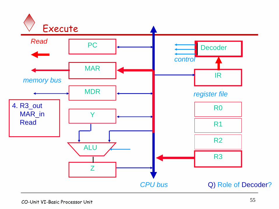
Execute
PC
CPU bus
IR
Decoder
control
R0
R1
R2
R3
register file
MAR
MDR
memory bus
Y
Z
ALU
Read
4. R3_out
MAR_in
Read
Q) Role of Decoder?
CO-Unit VI-Basic Processor Unit
56
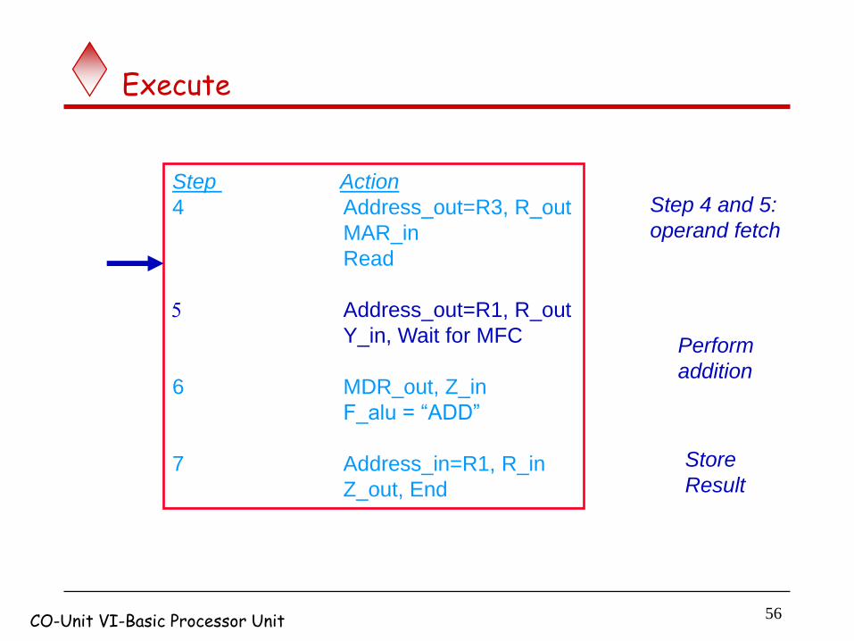
Execute
Step Action
4 Address_out=R3, R_out
MAR_in
Read
Address_out=R1, R_out
Y_in, Wait for MFC
6 MDR_out, Z_in
F_alu = “ADD”
7 Address_in=R1, R_in
Z_out, End
Step 4 and 5:
operand fetch
Perform
addition
Store
Result
CO-Unit VI-Basic Processor Unit
57
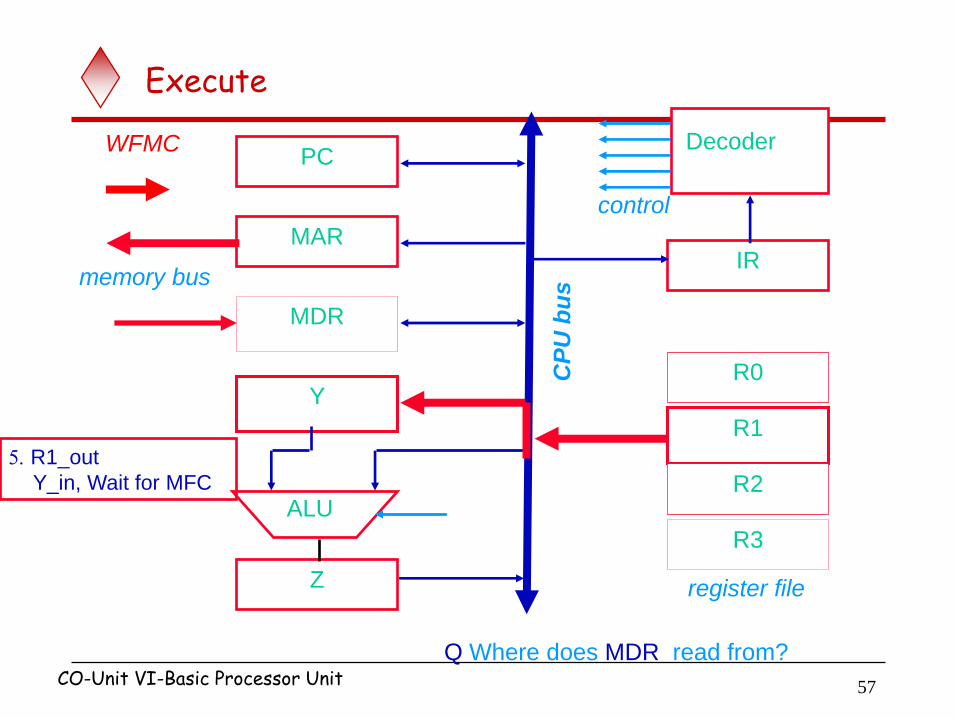
Execute
PC
CP
U b
us IR
Decoder
control
R0
R1
R2
R3
register file
MAR
MDR
memory bus
Y
Z
ALU
WFMC
R1_out
Y_in, Wait for MFC
Q Where does MDR read from? CO-Unit VI-Basic Processor Unit
58
Execute
Step Action
4 Address_out=R3, R_out
MAR_in
Read
Address_out=R1, R_out
Y_in, Wait for MFC
6 MDR_out, Z_in
F_alu = “ADD”
7 Address_in=R1, R_in
Z_out, End
Step 4 and 5:
operand fetch
Perform
addition
Store Result
CO-Unit VI-Basic Processor Unit
59
Execute
PC
CPU bus
IR
Decoder
control
R0
R1
R2
R3
register file
MAR
MDR
memory bus
Y
Z
ALU
6. MDR_out, Z_in
F_alu = “ADD”
Q) Who sets F_alu to ADD?
Q Why Z_in?
CO-Unit VI-Basic Processor Unit
[R1] M([R3]) + [R1]
60
Execute
Step Action
4 Address_out=R3, R_out
MAR_in
Read
Address_out=R1, R_out
Y_in, Wait for MFC
6 MDR_out, Z_in
F_alu = “ADD”
7 Address_in=R1, R_in
Z_out, End
Step 4 and 5:
operand fetch
Perform
addition
Store
Result
CO-Unit VI-Basic Processor Unit
[R1] M([R3]) + [R1]
61
Execute
PC
CPU bus
IR
Decoder
control
R0
R1
R2
R3
register file
MAR
MDR
memory bus
Y
Z
ALU
7. R1_in
Z_out, End
Q) Role of End?
CO-Unit VI-Basic Processor Unit
62
62
The Processing Unit
1. Basic Processing Cycle
2. Types of Operations
3. Control Mechanisms 1. Register Transfer
2. Fetch from Memory
3. Store to Memory
4. Arithmetic/Logic Ops.
5. Execution of Complete Instruction
6. Branching Ops.
CO-Unit VI-Basic Processor Unit
63
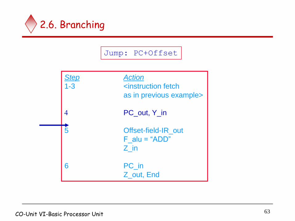
2.6. Branching
Step Action
1-3 <instruction fetch
as in previous example>
PC_out, Y_in
5 Offset-field-IR_out
F_alu = “ADD”
Z_in
6 PC_in
Z_out, End
Jump: PC+Offset
CO-Unit VI-Basic Processor Unit
64
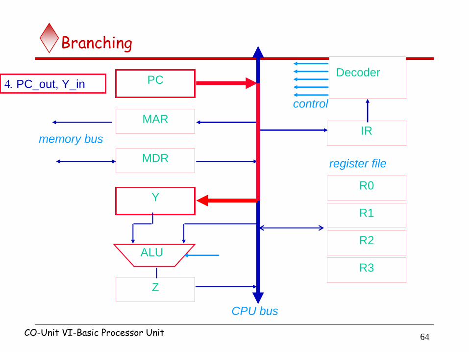
Branching
PC
CPU bus
IR
Decoder
control
R0
R1
R2
R3
register file
MAR
MDR
memory bus
Y
Z
ALU
PC_out, Y_in
CO-Unit VI-Basic Processor Unit
65
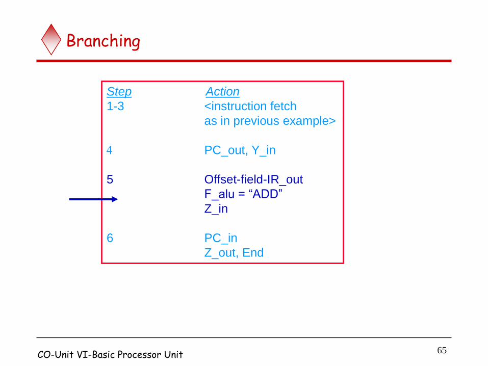
Branching
Step Action
1-3 <instruction fetch
as in previous example>
PC_out, Y_in
5 Offset-field-IR_out
F_alu = “ADD”
Z_in
6 PC_in
Z_out, End
CO-Unit VI-Basic Processor Unit
66
Branching
PC
CPU bus
IR
Decoder
control
R0
R1
R2
R3
register file
MAR
MDR
memory bus
Y
Z
ALU
5. Offset-field-IR_out
F_alu = “ADD”
Z_in
CO-Unit VI-Basic Processor Unit
67
Branching
Step Action
1-3 <instruction fetch
as in previous example>
PC_out, Y_in
5 Offset-field-IR_out
F_alu = “ADD”
Z_in
6 PC_in
Z_out, End
CO-Unit VI-Basic Processor Unit
68
Branching
PC
CPU bus
IR
Decoder
control
R0
R1
R2
R3
register file
MAR
MDR
memory bus
Y
Z
ALU
6. PC_in
Z_out, End
CO-Unit VI-Basic Processor Unit
69
Conditional branching
Step Action
1-3 <instruction fetch
as in previous example>
PC_out, Y_in
If N=0 then End
5 Offset-field-IR_out
F_alu = “ADD”
Z_in
6 PC_in
Z_out, End
JN : PC+Offset
If not Negative
CO-Unit VI-Basic Processor Unit
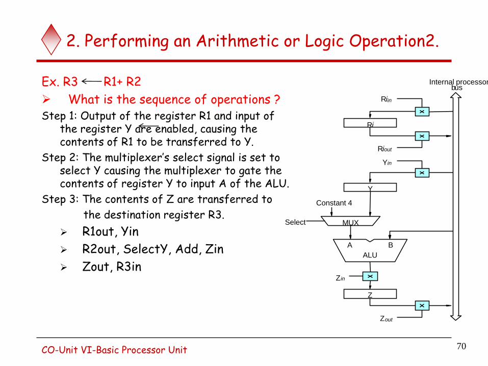
2. Performing an Arithmetic or Logic Operation2.
Ex. R3 R1+ R2
What is the sequence of operations ? Step 1: Output of the register R1 and input of
the register Y are enabled, causing the contents of R1 to be transferred to Y.
Step 2: The multiplexer’s select signal is set to select Y causing the multiplexer to gate the contents of register Y to input A of the ALU.
Step 3: The contents of Z are transferred to
the destination register R3.
R1out, Yin
R2out, SelectY, Add, Zin
Zout, R3in
70 CO-Unit VI-Basic Processor Unit
B A
Z
ALU
Y in
Y
Z in
Z out
R i in
R i
R i out
b us Internal processor
Constant 4
MUX Select
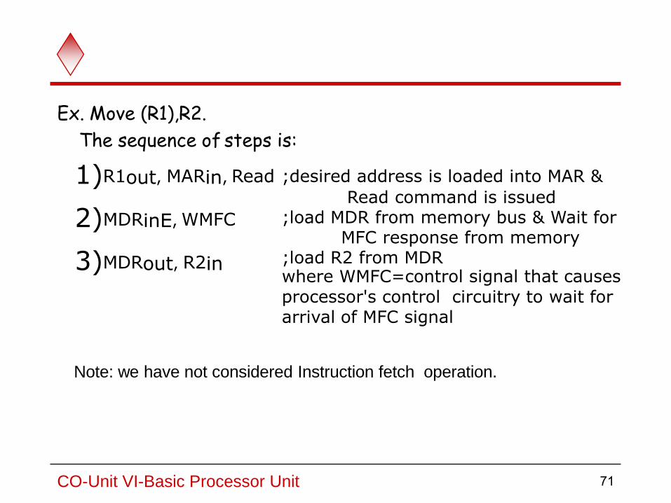
Ex. Move (R1),R2.
The sequence of steps is:
CO-Unit VI-Basic Processor Unit 71
1)R1out, MARin, Read
2)MDRinE, WMFC
3)MDRout, R2in
;desired address is loaded into MAR &
Read command is issued ;load MDR from memory bus & Wait for MFC response from memory ;load R2 from MDR where WMFC=control signal that causes processor's control circuitry to wait for arrival of MFC signal
Note: we have not considered Instruction fetch operation.
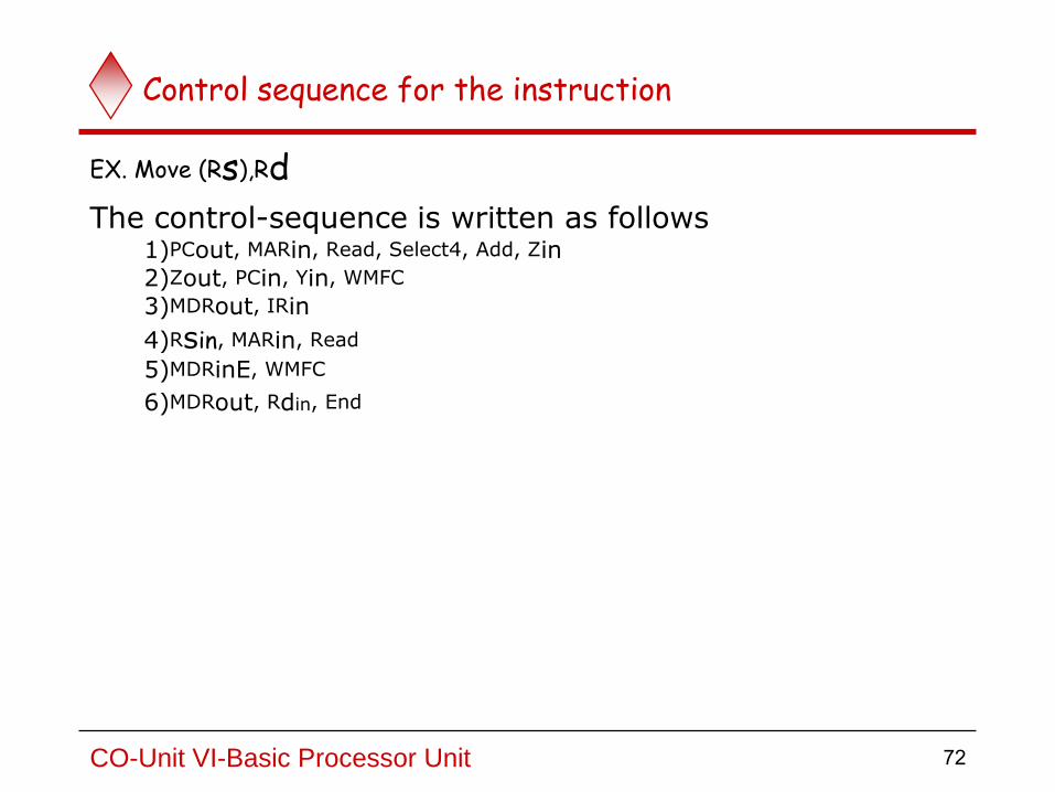
Control sequence for the instruction
EX. Move (Rs),Rd The control-sequence is written as follows
1)PCout, MARin, Read, Select4, Add, Zin 2)Zout, PCin, Yin, WMFC
3)MDRout, IRin
4)Rsin, MARin, Read
5)MDRinE, WMFC
6)MDRout, Rdin, End
CO-Unit VI-Basic Processor Unit 72
Execution of a complete instruction Consider the instruction Add (R3),R1
Which adds he contents of a memory- Location pointed by R3 to register R1. Executing this instruction requires the following actions:
1)Fetch the instruction. 2)Fetch the first operand.
3)Perform the addition. 4)Load the result into R1.
CO-Unit VI-Basic Processor Unit 73
Instruction Execution
Instruction execution proceeds as follows: R1← R1 + [R3] Step1:The instruction-fetch operation is initiated by loading contents of PC into MAR & sending a Read request to memory. The Select signal is set to Select4, which causes the Mux to select constant 4. This value is added to operand at input B (PC‟s content), and the result is stored in Z
Step2: Updated value in Z is moved to PC. Step3: Fetched instruction is moved into MDR and then to IR. Step4: Contents of R3 are loaded into MAR & a memory read signal is issued. Step5: Contents of R1 are transferred to Y to Prepare for addition. Step6: When Read operation is completed, memory-operand is available in MDR, and the addition is performed. Step7: Sum is stored in Z, then transferred to R1. The End signal causes a new instruction fetch cycle to begin by returning to step1.
CO-Unit VI-Basic Processor Unit 74
Single Bus organization of the data path within a CPU
CO-Unit VI-Basic Processor Unit 75
Internal organization of a processor
lines Data
Address lines
bus Memory
Carry-in
ALU
PC
MAR
MDR
Y
Z
Add
XOR
Sub
bus
IR
TEMP
R0
control ALU
lines
Control signals
R n 1 - ( )
Instruction
decoder and
Internal processor
control logic
A B
MUX Select
Constant 4
Execution of a Complete Instruction Step Action
1 PCout , MAR in , Read,Select4,Add, Zin
2 Zout , PCin , Yin , WMF C
3 MDRout , IR in
4 R3out , MAR in , Read
5 R1out , Yin , WMF C
6 MDRout , SelectY,Add, Zin
7 Zout , R1in , End
Figure 7.6. Control sequencefor executionof the instruction Add (R3),R1.
Add (R3), R1 R1← R1 + [R3])
Execution of a Complete Instruction
Step Action
1 PCout , MAR in , Read,Select4,Add, Zin
2 Zout , PCin , Yin , WMF C
3 MDRout , IR in
4 R3out , MAR in , Read
5 R1out , Yin , WMF C
6 MDRout , SelectY,Add, Zin
7 Zout , R1in , End
Figure 7.6. Control sequencefor executionof the instruction Add (R3),R1.
linesData
Addresslines
busMemory
Carry -in
ALU
PC
MAR
MDR
Y
Z
Add
XOR
Sub
bus
IR
TEMP
R0
controlALU
lines
Control signals
R n 1-( )
Instruction
decoder and
Internal processor
control logic
A B
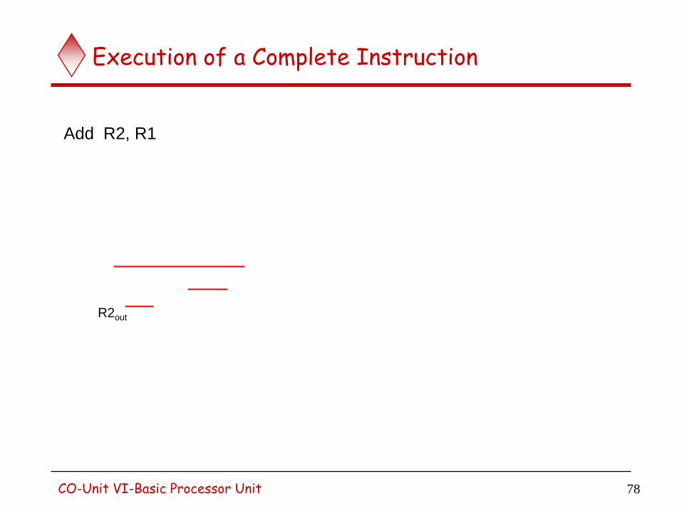
Figure 7.1. Single-bus organization of the datapath inside a processor.
MUXSelect
Constant 4
Add R2, R1
R2out
78 CO-Unit VI-Basic Processor Unit
Execution of Branch Instructions
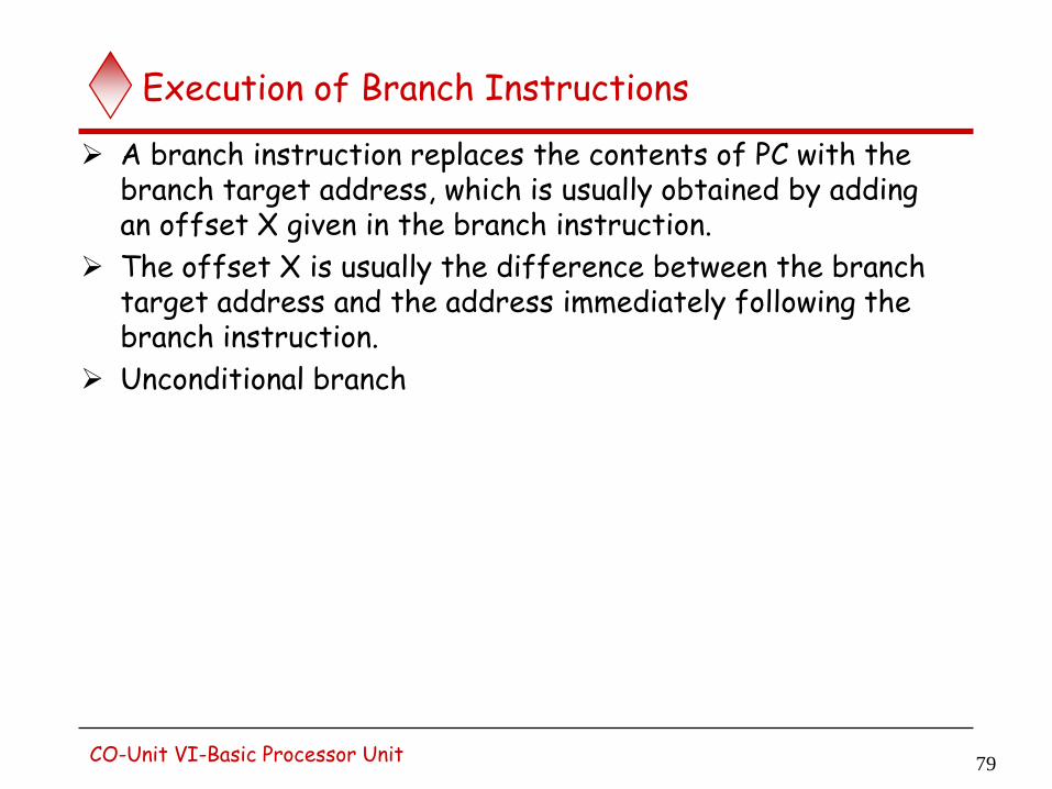
A branch instruction replaces the contents of PC with the branch target address, which is usually obtained by adding an offset X given in the branch instruction.
The offset X is usually the difference between the branch target address and the address immediately following the branch instruction.
Unconditional branch
79 CO-Unit VI-Basic Processor Unit
Execution of Branch Instructions
The processing starts, as usual, the fetch phase ends in step3. In step 4, the offset-value is extracted from IR by instruction-decoding circuit.
Since the updated value of PC is already available in register Y, the offset X is gated onto the bus, and an addition operation is performed.
In step 5, the result, which is the branch-address, is loaded into the PC. The offset X used in a branch instruction is usually the difference between the branch target-address and the address immediately following the branch instruction. (For example, if the branch instruction is at location 1000 and branch target-address is 1200, then the value of X must be 196, since the PC will be containing the address 1004 after fetching the instruction at location 1000).
In case of conditional branch, we need to check the status of the condition-codes before loading a new value into the PC. e.g. Offset-field-of-IRout, Add, Zin, If N=0 then END If N=0, processor returns to step 1 immediately after step 4. If N=1, step 5 is performed to load a new value into PC
CO-Unit VI-Basic Processor Unit 80
Execution of Branch Instructions
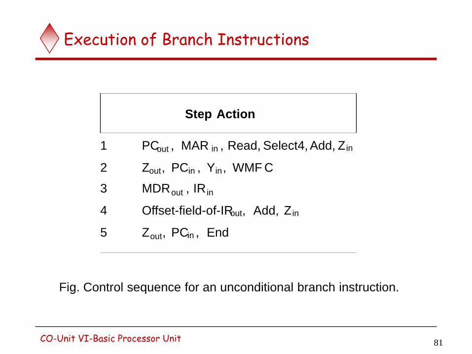
Step Action
1 PC out , MAR in , Read, Select4, Add, Z in
2 Z out , PC in , Y in , WMF C
3 MDR out , IR in
4 Offset-field-of-IR out , Add, Z in
5 Z out , PC in , End
Fig. Control sequence for an unconditional branch instruction.
81 CO-Unit VI-Basic Processor Unit
Multiple-Bus Organization
• Allow the contents of two
different registers to be
accessed simultaneously and
have their contents placed on
buses A and B.
• Allow the data on bus C to
be loaded into a third register
during the same clock cycle.
• Incrementer unit.
• ALU simply passes one of
its two input operands
unmodified to bus C
control signal: R=A or R=B
General purpose registers are combined into a single block called registers. 3 ports,2 output ports –access two different registers and have their
contents on buses A and B Third port allows data on bus c during same clock cycle. Bus A & B are used to transfer the source operands to A & B inputs of the
ALU. ALU operation is performed. The result is transferred to the destination over the bus C.
ALU may simply pass one of its 2 input operands unmodified to bus C.
The ALU control signals for such an operation R=A or R=B.
Incrementer unit is used to increment the PC by 4.
Using the incrementer eliminates the need to add the constant value 4 to the PC using the main ALU.
The source for the constant 4 at the ALU input multiplexer can be used to increment other address such as loadmultiple & storemultiple
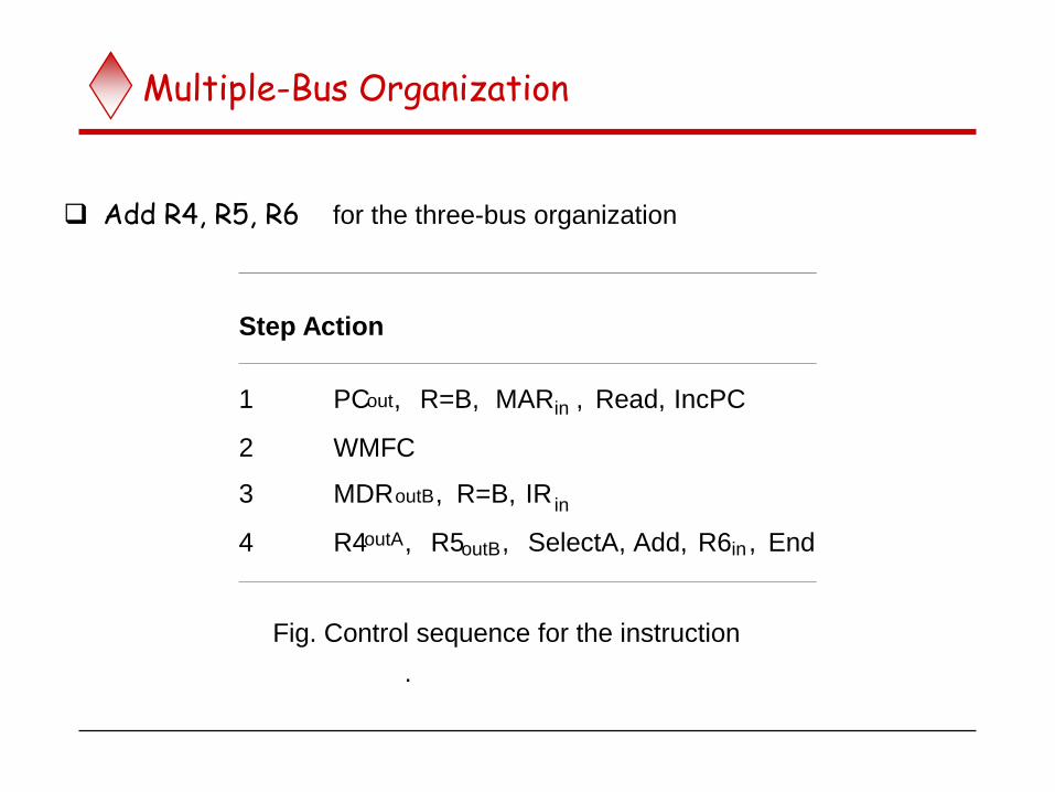
Multiple-Bus Organization
Add R4, R5, R6 for the three-bus organization
Step Action
1 PC out , R=B, MAR in , Read, IncPC
2 WMF C
3 MDR outB , R=B, IR in
4 R4 outA , R5 outB , SelectA, Add, R6 in , End
Fig. Control sequence for the instruction
.
Instruction execution proceeds as follows in Multiple-Bus Organization
Step 1:The contents of PC are passed
through the ALU using R=B control signal & loaded into MAR to start a memory read operation
At the same time PC is incrementer by 4
Step 2:The processor waits for MFC
Step 3: Loads the data ,received into MDR ,then transfers them to IR.
Step 4: The execution phase of the instruction requires only one control step to complete.
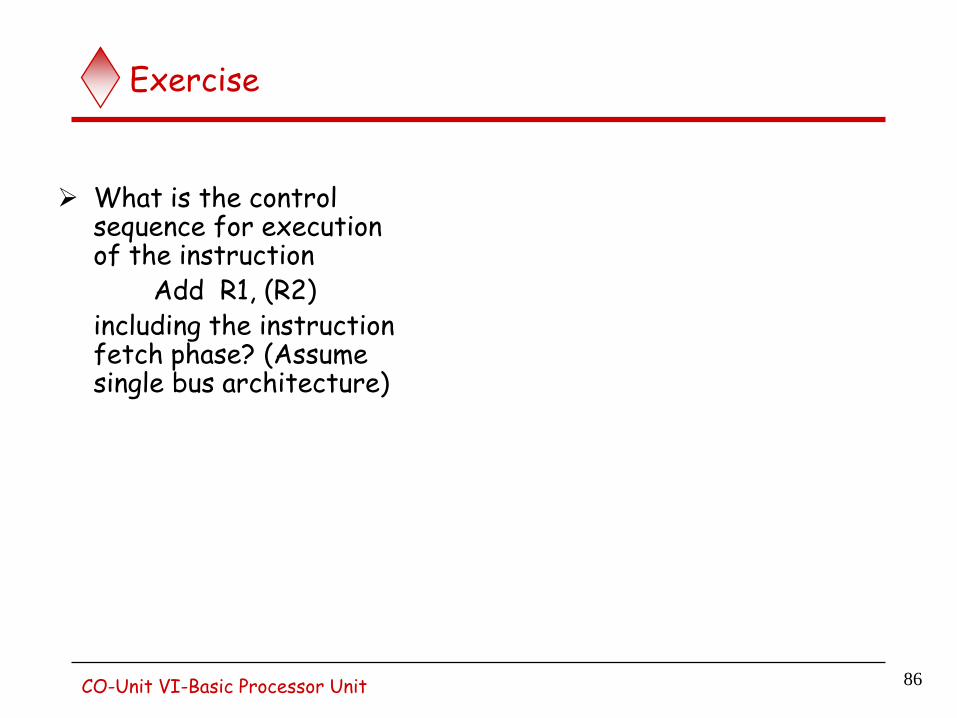
Exercise
What is the control sequence for execution of the instruction
Add R1, (R2) including the instruction
fetch phase? (Assume single bus architecture)
linesData
Addresslines
busMemory
Carry -in
ALU
PC
MAR
MDR
Y
Z
Add
XOR
Sub
bus
IR
TEMP
R0
controlALU
lines
Control signals
R n 1-( )
Instruction
decoder and
Internal processor
control logic
A B
Figure 7.1. Single-bus organization of the datapath inside a processor.
MUXSelect
Constant 4
86 CO-Unit VI-Basic Processor Unit
87
87
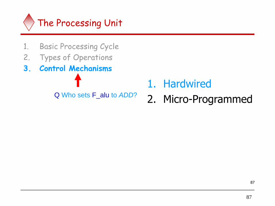
The Processing Unit
1. Basic Processing Cycle
2. Types of Operations
3. Control Mechanisms
1. Hardwired
2. Micro-Programmed Q Who sets F_alu to ADD?
Hardwired Control
88
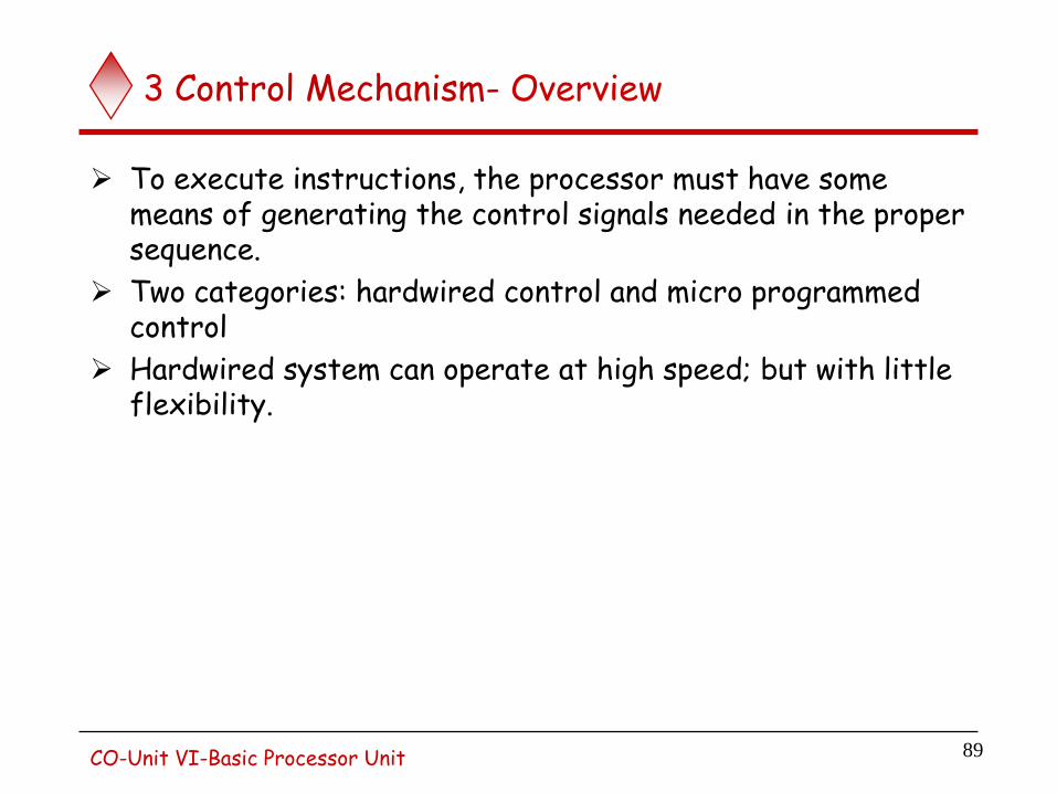
3 Control Mechanism- Overview
To execute instructions, the processor must have some means of generating the control signals needed in the proper sequence.
Two categories: hardwired control and micro programmed control
Hardwired system can operate at high speed; but with little flexibility.
89 CO-Unit VI-Basic Processor Unit
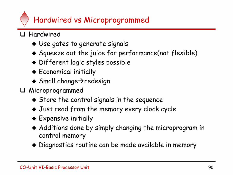
Hardwired vs Microprogrammed
Hardwired
Use gates to generate signals
Squeeze out the juice for performance(not flexible)
Different logic styles possible
Economical initially
Small changeredesign
Microprogrammed
Store the control signals in the sequence
Just read from the memory every clock cycle
Expensive initially
Additions done by simply changing the microprogram in control memory
Diagnostics routine can be made available in memory
90 CO-Unit VI-Basic Processor Unit
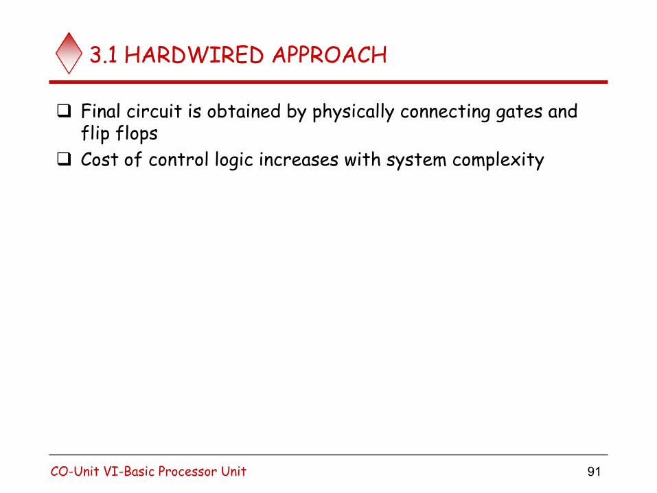
3.1 HARDWIRED APPROACH
Final circuit is obtained by physically connecting gates and flip flops
Cost of control logic increases with system complexity
91 CO-Unit VI-Basic Processor Unit
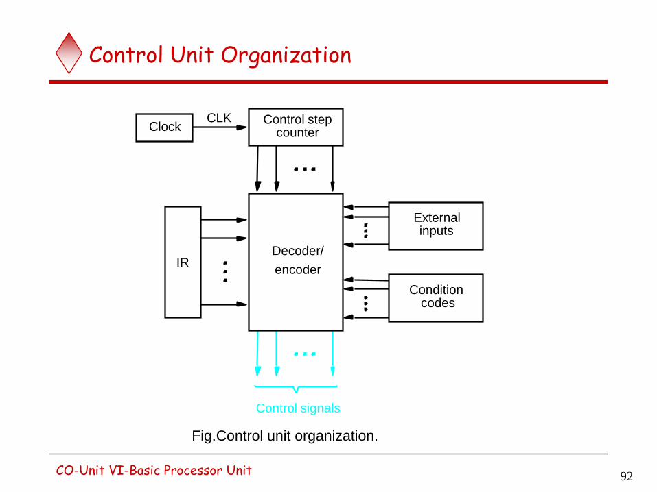
Control Unit Organization
Fig.Control unit organization.
CLK Clock
Control step
IR encoder
Decoder/
Control signals
codes
counter
inputs
Condition
External
92 CO-Unit VI-Basic Processor Unit
93
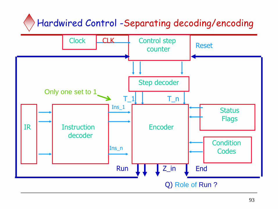
Hardwired Control -Separating decoding/encoding
Status Flags
Condition Codes
End
Reset
Run
Control step counter
Clock
Step decoder
T_1 T_n Ins_1
Encoder
Instruction decoder
IR
Ins_n
Only one set to 1
Z_in
CLK
Q) Role of Run ?
Decoder/encoder block is a combinational-circuit that generates required control-outputs depending on state of all its inputs. Step-decoder provides a separate signal line for each step in the control sequence. Similarly, output of instruction-decoder consists of a separate line for each machine instruction. For any instruction loaded in IR, one of the output-lines INS1
through INSm is set to 1, And all other lines are set to The input signals to encoder-block are combined to generate the individual control- signals Yin, PCout, Add, End and so on.
CO-Unit VI-Basic Processor Unit 94
95
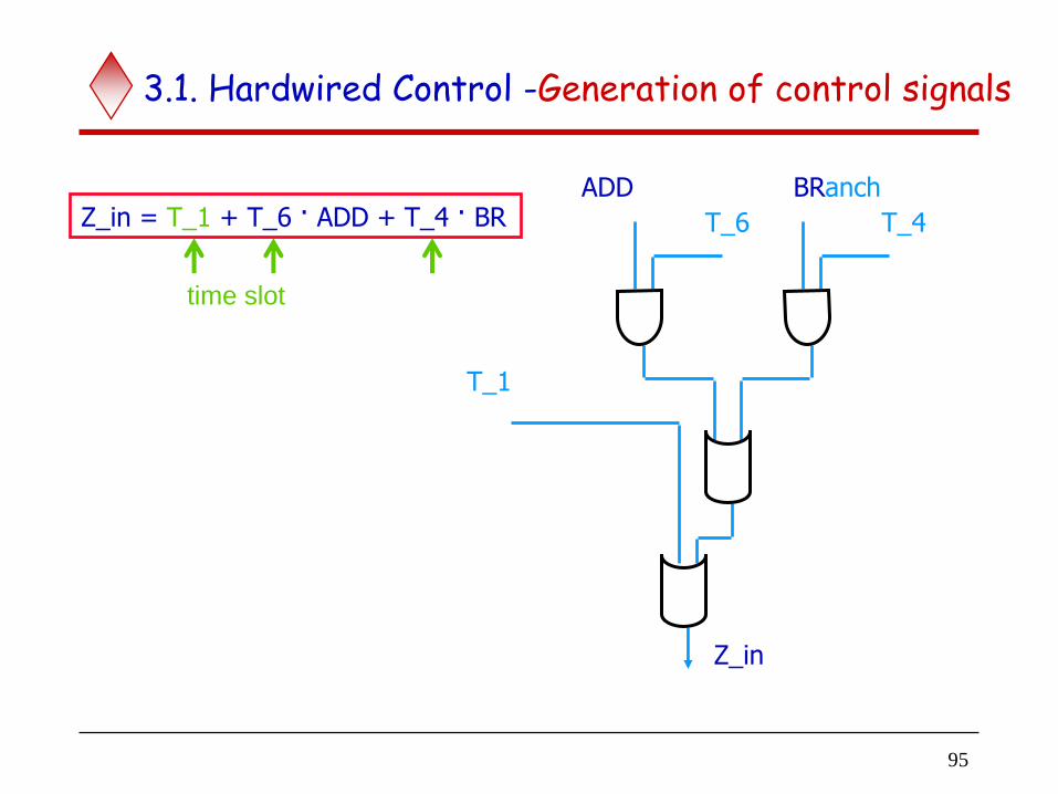
3.1. Hardwired Control -Generation of control signals
ADD
T_6 T_4
BRanch
T_1
Z_in
Z_in = T_1 + T_6 . ADD + T_4 . BR
time slot
This signal is asserted during time-slot T1 for all instructions,
during T6 for an Add instruction
during T4 for unconditional branch instruction
The control H/W shown can be viewed as a state m/c that changes from one state to
another in every clock cycle, depending on the content of IR,the conditional codes and the external inputs
When RUN=1, counter is incremented by 1 at the end of every clock cycle. When RUN=0, counter stops counting. Sequence of operations carried out by this machine is determined by wiring of logic elements, hence the name “hardwired”.
CO-Unit VI-Basic Processor Unit 96
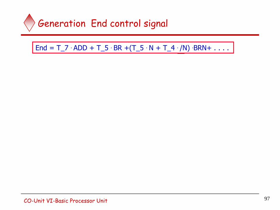
Generation End control signal
Figure 7.13.Generation of the End control signal.
T7
Add BranchBranch<0
T5
End
NN
T4T5
97 CO-Unit VI-Basic Processor Unit
End = T_7 . ADD + T_5 . BR +(T_5 . N + T_4 . /N) .BRN+ . . . .
99
3.1. Hardwired Control-Performance
Performance is dependent on:
Power of instructions
Cycle time
Number of cycles per instruction
Performance improvement by:
Multiple datapaths
Instruction prefetching and pipelining
Caches
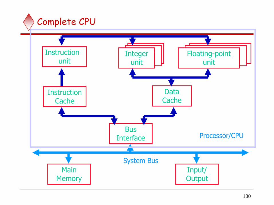
100
Complete CPU
Instruction unit
Floating-point unit
Integer unit
Data Cache
Instruction Cache
Bus Interface
Main Memory
Input/ Output
Processor/CPU
System Bus
Integer unit
Integer unit
Floating-point unit
Floating-point unit
A Complete Processor
This has separate processing-units to deal with integer data and
floating-point data. A data-cache is inserted between these processing-units & main-memory.
Instruction-unit fetches instructions → from an instruction-cache or → from main-memory when desired instructions are not already in cache Processor is connected to system-bus & hence to the rest of the computer by means of a bus interface
Using separate caches for instructions & data is common practice in many processors today. A processor may include several units of each type to increase the potential for concurrent operations
CO-Unit VI-Basic Processor Unit 101
102
Micro programmed Control
103
3.2. Micro-programmed control
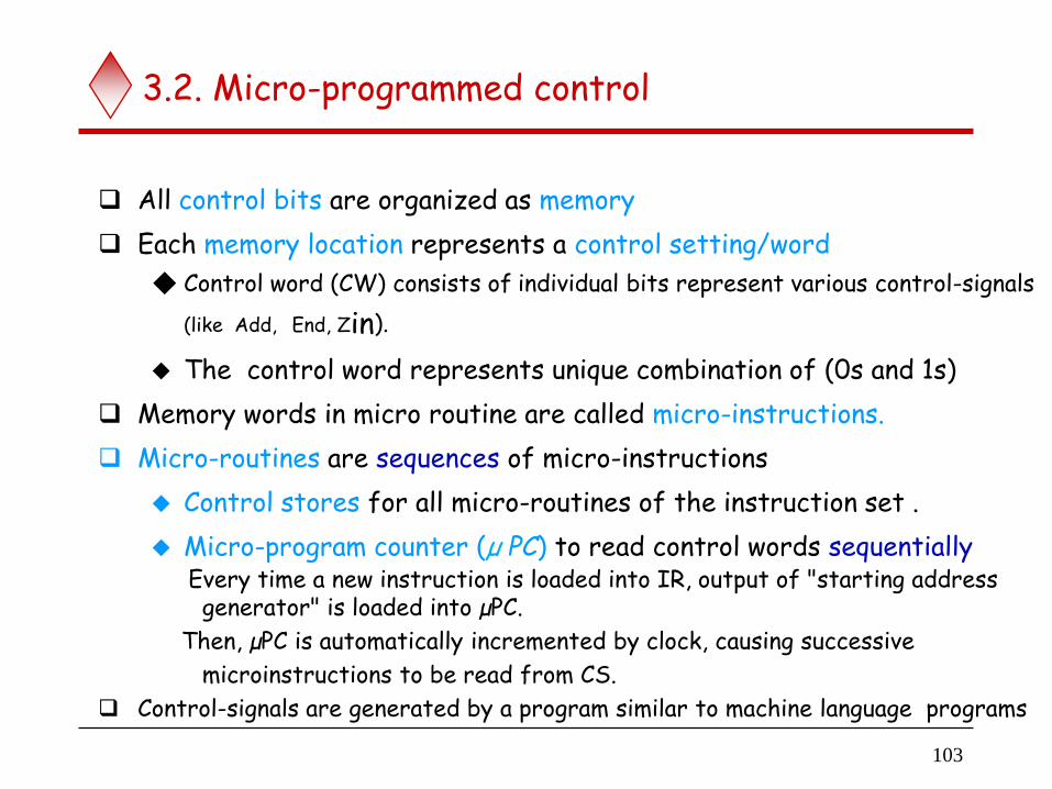
All control bits are organized as memory
Each memory location represents a control setting/word
Control word (CW) consists of individual bits represent various control-signals
(like Add, End, Zin).
The control word represents unique combination of (0s and 1s)
Memory words in micro routine are called micro-instructions.
Micro-routines are sequences of micro-instructions
Control stores for all micro-routines of the instruction set .
Micro-program counter (µ PC) to read control words sequentially Every time a new instruction is loaded into IR, output of "starting address generator" is loaded into µPC.
Then, µPC is automatically incremented by clock, causing successive
microinstructions to be read from CS.
Control-signals are generated by a program similar to machine language programs
104
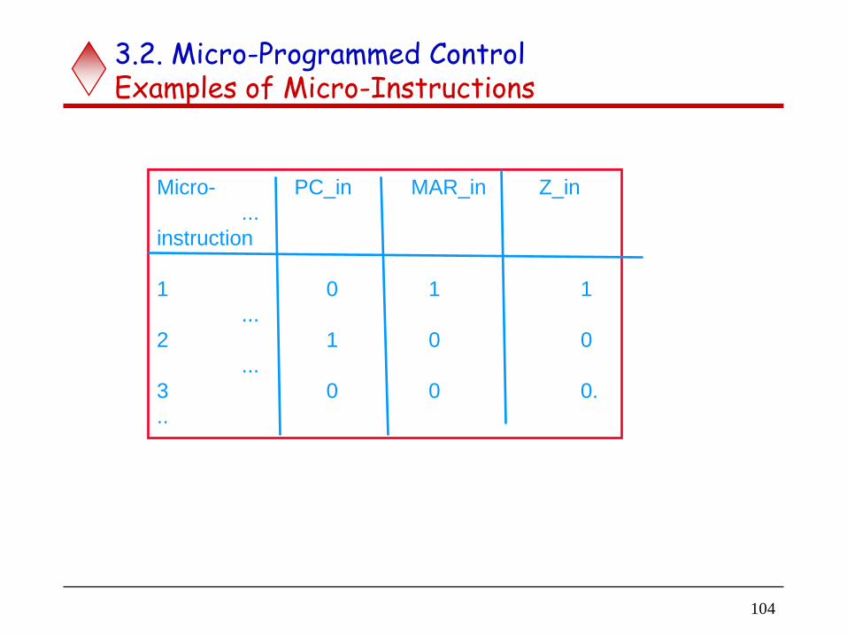
3.2. Micro-Programmed Control Examples of Micro-Instructions
Micro- PC_in MAR_in Z_in
...
instruction
1 0 1 1
...
2 1 0 0
...
3 0 0 0.
..
Microprogrammed Control
Control signals are generated by a program similar to machine language programs.
Control Word (CW); microroutine; microinstruction
PC i
n
PC o
ut
MA
Rin
Rea
d
MD
R out
IRin
Yin
Sel
ect
Add Z in
Zou
t
R1 ou
t
R1 i
n
R3 o
ut
WM
FC
End
0
1
0
0
0
0
0
0
0
0
0
0
0
1
1
0
0
0
0
0
0
1
0
0
1
0
0
0
1
0
0
1
0
0
0
0
0
1
0
0
1
0
0
0
1
0
0
0
0
0
1
0
0
1
0
0
1
0
0
0
0
0
0
1
0
0
0
0
1
0
1
0
0
0
0
1
0
0
1
0
0
0
0
1
0
0
0
0
1
0
0
0
0
0
0
0
0
1
0
0
0
1
0
0
0
0
1
0
0
1
0
0
Micro -instruction
1
2
3
4
5
6
7
Figure 7.15 An example of microinstructions for Figure 7.6.
105 CO-Unit VI-Basic Processor Unit
106
PC
in
PC
ou
t
MA
Rin
Re
ad
MD
Ro
ut
IRin
Yin
Se
lect
Add
Zin
Zo
ut
R1 o
ut
R1 i
n
R3 o
ut
WM
FC
End
0
1
0
0
0
0
0
0
0
0
0
0
0
1
1
0
0
0
0
0
0
1
0
0
1
0
0
0
1
0
0
1
0
0
0
0
0
1
0
0
1
0
0
0
1
0
0
0
0
0
1
0
0
1
0
0
1
0
0
0
0
0
0
1
0
0
0
0
1
0
1
0
0
0
0
1
0
0
1
0
0
0
0
1
0
0
0
0
1
0
0
0
0
0
0
0
0
1
0
0
0
1
0
0
0
0
1
0
0
1
0
0
Micro -instruction
1
2
3
4
5
6
7
Figure 7.15 An example of microinstructions for Figure 7.6.
Step Action
1 PCout , MAR in , Read,Select4,Add, Zin
2 Zout , PCin , Yin , WMF C
3 MDRout , IR in
4 R3out , MAR in , Read
5 R1out , Yin , WMF C
6 MDRout , SelectY,Add, Zin
7 Zout , R1in , End
Figure 7.6. Control sequencefor executionof the instruction Add (R3),R1.
CO-Unit VI-Basic Processor Unit
Microinstructions for Add (R3),R1
Microroutine for the instruction Branch<0
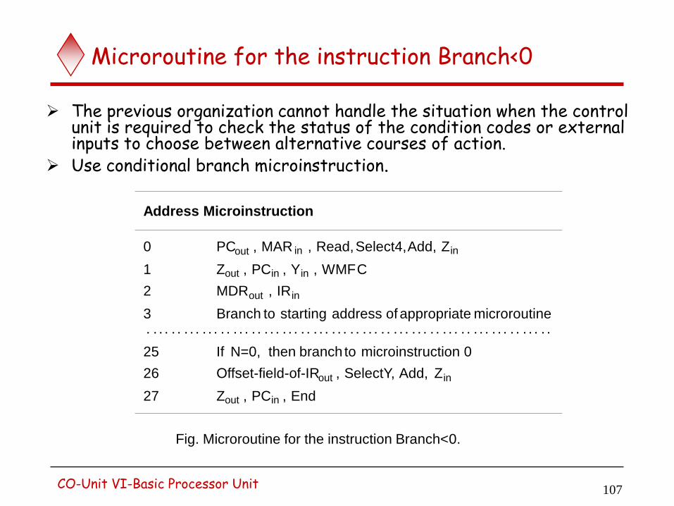
The previous organization cannot handle the situation when the control unit is required to check the status of the condition codes or external inputs to choose between alternative courses of action.
Use conditional branch microinstruction.
Address Microinstruction
0 PC out , MAR in , Read, Select4, Add, Z in
1 Z out , PC in , Y in , WMF C
2 MDR out , IR in
3 Branch to starting address of appropriate microroutine . . . . . . . . . . . . . . . . . . . . . . . . . . . . . . . . . . . . . . . . . . . . . . . . . . . . . . . . . . . . . . . . . .
25 If N=0, then branch to microinstruction 0
26 Offset-field-of-IR out , SelectY, Add, Z in
27 Z out , PC in , End
Fig. Microroutine for the instruction Branch<0.
107 CO-Unit VI-Basic Processor Unit
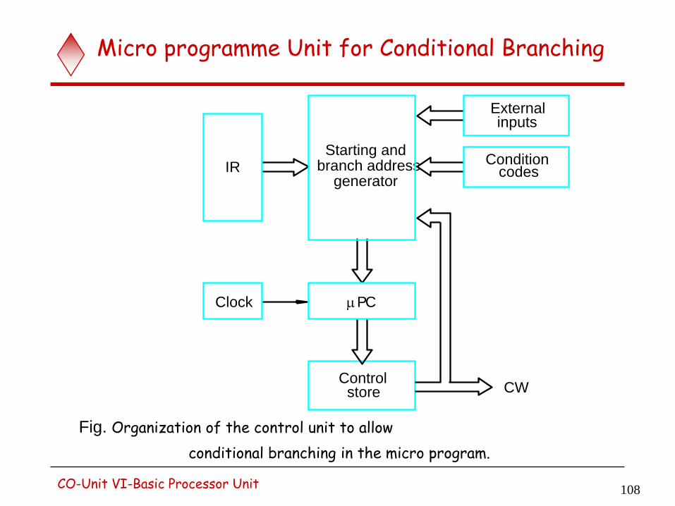
Micro programme Unit for Conditional Branching
Fig. Organization of the control unit to allow
conditional branching in the micro program.
Control store
Clock
generator
Starting and branch address Condition
codes
inputs External
CW
IR
m P C
108 CO-Unit VI-Basic Processor Unit
Conditional Branching
In case of conditional branching, microinstructions specify which of the external inputs, condition-codes should be checked as a condition for branching to take place.
The starting and branch address generator block loads a new address into µPC when a microinstruction instructs it to do so .
To allow implementation of a conditional branch, inputs to this block consist of → external inputs and condition-codes → contents of IR µPC is incremented every time a new microinstruction is fetched from microprogram memory except in following situations
i) When a new instruction is loaded into IR, µPC is loaded with starting-address of microroutine for that instruction.
ii) When a Branch microinstruction is encountered and branch condition is satisfied, µPC is loaded with branch-address.
iii) When an End microinstruction is encountered, µPC is loaded with address of first CW in microroutine for instruction fetch cycle.
CO-Unit VI-Basic Processor Unit 109
Microinstructions
A straightforward way to structure microinstructions is to assign one bit position to each control signal.
However, this is very inefficient. The length can be reduced: most signals are not needed
simultaneously, and many signals are mutually exclusive. All mutually exclusive signals are placed in the same group in binary
coding.
110 CO-Unit VI-Basic Processor Unit
1) Assigning individual bits to each control-signal results in long microinstructions because the number of required signals is usually large.
2) Available bit-space is poorly used because
only a few bits are set to 1 in any given microinstruction. Solution: Signals can be grouped because
- Most signals are not needed simultaneously. - Many signals are mutually exclusive.
Grouping control-signals into fields requires a little more hardware because decoding-circuits must be used to decode bit patterns of each field into individual control signals. Advantage: This method results in a smaller control-store (only 20 bits are needed to store the patterns for the 42 signals).
CO-Unit VI-Basic Processor Unit 111
3) Having a separate microroutine for each machine instruction results in
a large total number of microinstructions and a large control-store.
4) Execution time is longer because it takes more time to carry out the
required branches.
Some Drawbacks of microprogrammed control
112
Microprogrammed control (contd..)
Microinstruction format
•Simple approach is to allocate one bit for each control signal - Results in long microinstructions, since the number of control signals is usually very large. - Few bits are set to 1 in any microinstruction, resulting in a poor use of bit space. •Reduce the length of the microinstruction by taking advantage of the fact that most signals are not needed simultaneously, and many signals are mutually exclusive. For example: - Only one ALU function is active at a time. - Source for a data transfer must be unique. - Read and Write memory signals cannot be active simultaneously.
•Group mutually exclusive signals in the same group.
•At most one microperation can be specified per group.
•Use binary coding scheme to represent signals within a group.
113
Microprogrammed control (contd..)
Microinstruction format
Examples:
•If ALU has 16 operations, then 4 bits can be sufficient. •Group register output signals into the same group, since only one of these signals will be active at any given time (Why?) If the CPU has 4 general purpose registers, then PCout, MDRout, Zout, Offsetout, R0out, R1out, R2out, R3out and Tempout can be placed in a single group, and 4 bits will be needed to represent these.
114
3.2. Micro-Programmed Control Structure micro-instructions
Most simple organization: 1 bit per control signal
However,
Many bits needed (e.g., 80-120 bits)
For many signals, only one is needed per cycle; hence they can be grouped
Coding is possible: e.g., an address instead of a single control bit per register
Alternative approach to reduce the length of the microinstruction:
• Enumerate the patterns of the required signals in all microinstructions.
• Assign each meaningful combination of active control signals a unique code.
• Code represents the microinstruction .
• Grouping control signals into fields requires a little more hardware:
Decoding circuits are needed to decode patterns to individual control signals.
Cost of the additional hardware is offset by reduced number of bits
in each microinstruction:
Reduces the size of the control store.
Full encoding can reduce the length of the microinstruction even further,
but this reduction comes at the expense of increasing the complexity of
the decoder circuits.
115
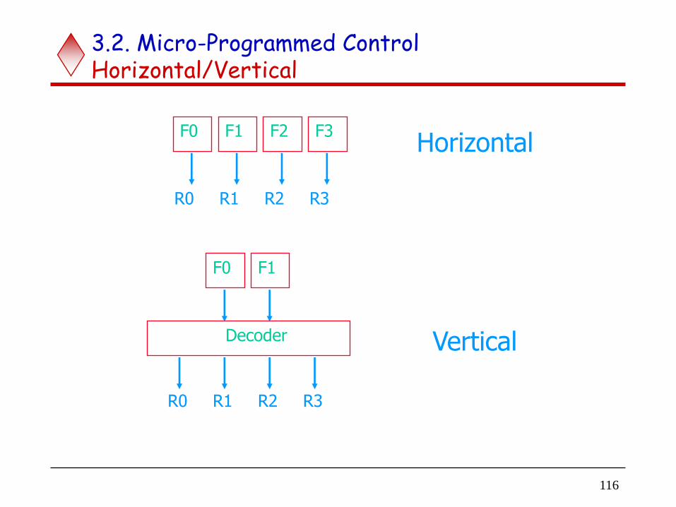
3.2. Micro-Programmed Control Forms of organization
Little coding: horizontal organization
Large words
Little decoding logic
Fast
Much coding: vertical organization
Small control store
Much decoding logic
Slower
Mixed organization
116
3.2. Micro-Programmed Control Horizontal/Vertical
F0 F1 F2 F3
R0 R1 R2 R3
Horizontal
F0 F1
Decoder
R0 R1 R2 R3
Vertical
117
3.2. Micro-Programmed Control Sequencing
Thus far only branch after fetch
No sharing of micro-code between micro-routines
Micro-subroutines lead to more efficient control store
118
3.2. Micro-Programmed Control Multi-way branching
Number of two-way branches
disadvantage: slows down
More than one branch address in micro-instruction
disadvantage: more bits required
bit-ORing if specified branch address
119
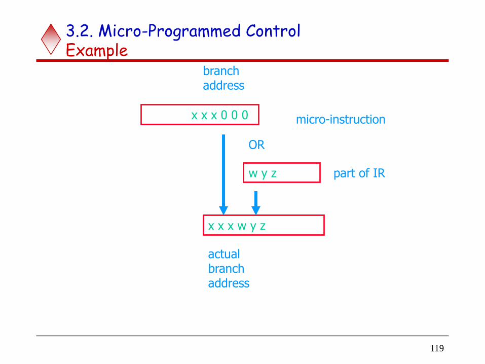
3.2. Micro-Programmed Control Example
x x x 0 0 0
w y z
x x x w y z
micro-instruction
part of IR
branch address
OR
actual branch address
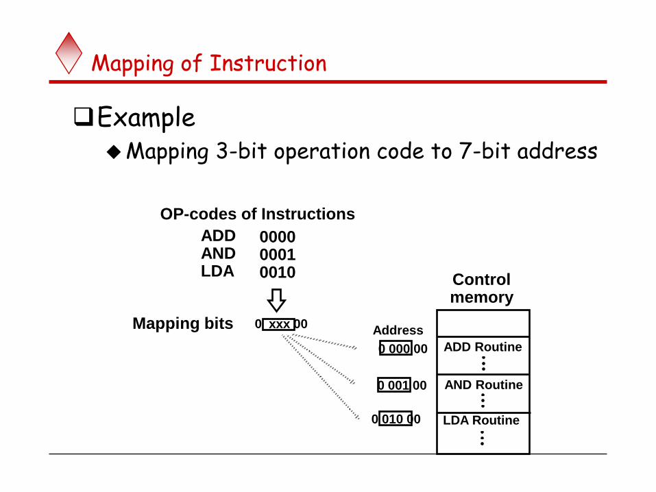
Mapping of Instruction
Example Mapping 3-bit operation code to 7-bit address
OP-codes of Instructions
ADD AND LDA
0000 0001 0010
Address
0 000 00
0 001 00
0 010 00
Mapping bits 0 xxx 00
ADD Routine
AND Routine
LDA Routine
Control memory
121
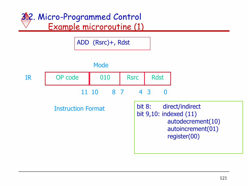
3.2. Micro-Programmed Control Example microroutine (1)
ADD (Rsrc)+, Rdst
Instruction Format
OP code 010 Rsrc Rdst
Mode
0 3 4 7 8 10 11
IR
bit 8: direct/indirect bit 9,10: indexed (11) autodecrement(10) autoincrement(01) register(00)
122
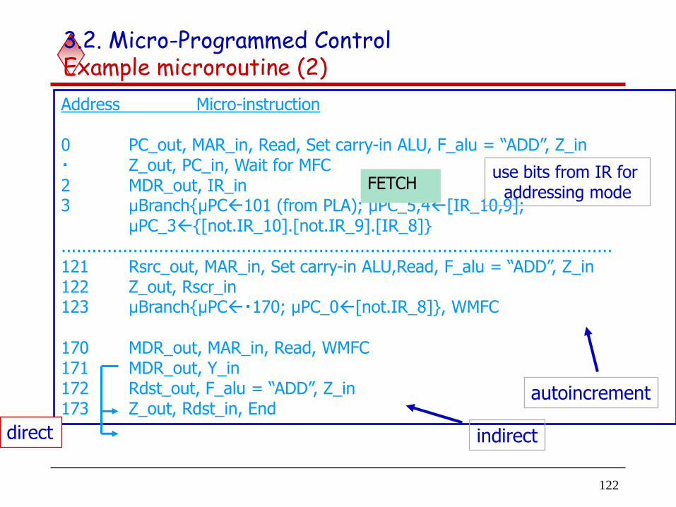
3.2. Micro-Programmed Control Example microroutine (2)
Address Micro-instruction 0 PC_out, MAR_in, Read, Set carry-in ALU, F_alu = “ADD”, Z_in Z_out, PC_in, Wait for MFC
2 MDR_out, IR_in 3 μBranch{μPC101 (from PLA); μPC_5,4[IR_10,9]; μPC_3{[not.IR_10].[not.IR_9].[IR_8]}
........................................................................................................... 121 Rsrc_out, MAR_in, Set carry-in ALU,Read, F_alu = “ADD”, Z_in 122 Z_out, Rscr_in 123 μBranch{μPC 170; μPC_0[not.IR_8]}, WMFC
170 MDR_out, MAR_in, Read, WMFC 171 MDR_out, Y_in 172 Rdst_out, F_alu = “ADD”, Z_in 173 Z_out, Rdst_in, End
FETCH
autoincrement
indirect direct
use bits from IR for addressing mode
123
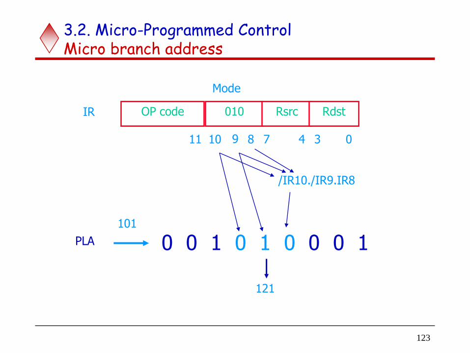
3.2. Micro-Programmed Control Micro branch address
OP code 010 Rsrc Rdst
Mode
0 3 4 7 8 10 11
IR
0 0 1 0 1 0 0 0 1
/IR10./IR9.IR8
PLA
121
101
9
124
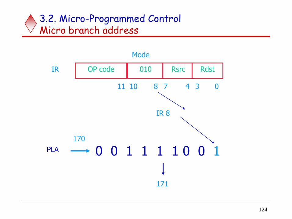
3.2. Micro-Programmed Control Micro branch address
OP code 010 Rsrc Rdst
Mode
0 3 4 7 8 10 11
IR
0 0 1 1 1 1 0 0 1
IR 8
PLA
171
170
125
Microprogram sequencing-
Simple microprogram sequencing:
•Load the starting address into mPC when a new instruction is loaded
into IR.
•Introduce some branching capability within the microprogram through
special branch microinstructions, which specify the branch address.
Disadvantages of the simple approach:
•Large total number of microinstructions and large control store.
•Most machines have several addressing modes, and many combinations of
instructions and addressing modes.
•Separate microroutine for each of these combinations produces a lot of
•duplication of common parts.
•Share as much common code as possible.
•Sharing common code requires many branch instructions to transfer
control among various parts.
•Execution time is longer because it takes more time to carry out the
required branches.
126
Microprogrammed control (contd..)
Microprogram sequencing
Consider the following instruction which adds the source operand to
the contents of register Rdst, and places the results in register Rdst.
ADD src, Rdst
Assume that the source operand can be specified in the following
addressing modes:
- Register.
- Autoincrement
- Autodecrement
- Indexed.
- Indirect forms of the above methods.
127
Start of instruction fetch.
Microroutines for all the instructions
ADD Rsrc, Rdst
128
Microprogrammed control (contd..)
Start of instruction fetch.
Microroutines for all the instructions
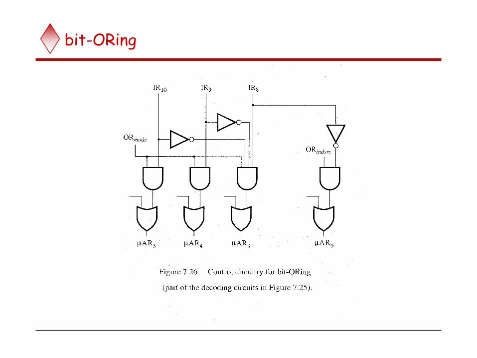
Microinstruction at address 170 is performed in the register indirect mode. Microinstruction at address 171 is performed in the register direct mode. Microinstruction 170 is bypassed if register direct mode is used. One way to bypass microinstruction 170 is to have the previous microinstruction specify address 170, and then use an OR gate to change the LSB of the address to 1. This technique is called bit-ORing.
ADD Rsrc, Rdst
Branch Address Modification Using Bit-ORing
CO-Unit VI-Basic Processor Unit 129
The micro program in Figure 20 shows that branches are not always made to a single branch address. This is a direct consequence of combining simple micro routines by sharing common parts. Consider the point labeled ∞ in the figure. At this point, it is necessary to choose between actions required by direct and indirect addressing modes. If the indirect mode is specified in the instruction, then the microinstruction in location 170 is performed to fetch the operand from the memory. If the direct mode is specified, this fetch must be bypassed by branching immediately to location 171. The most efficient way to bypass microinstruction 170 is to have the preceding branch microinstructions specify the address 170 and then use an OR gate to change the least significant it of this address to 1 if the direct addressing mode is involved. This is known as the bit-ORing technique for modifying branch addresses.
Alternative Approaches to the bit-ORing
CO-Unit VI-Basic Processor Unit 130
An alternative to the bit-ORing approach is to use two conditional branch
microinstructions allocations 123,143, and 166.
Another possibility is to include two next address fields within a branch
microinstruction, one for the direct and one for the indirect address modes.
Both of these alternatives are inferior to the bit-Oring technique.
131
Microprogrammed control (contd..)
Microinstructions with the next-address field.
•Several branch microinstructions are required to enable sharing of common code. •The branch microinstructions do not perform any useful operation related to data. •They are required to determine the address of the next microinstruction. •They slow down the execution of the instruction.
•Ideally we need to assign consecutive addresses to all microinstructions that are generally executed one after the other. •Recall that the next microinstruction is determined by incrementing the microprogram counter. •But due to the goal of sharing as much common code as possible, this is not always possible. •This leads to a significant increase in the branch instructions.
132
Microprogrammed control (contd..)
Microinstructions with the next-address field.
•Powerful alternative is to include an address field as a part of every
microinstruction.
•The address field indicates the location of the next microinstruction to
be fetched.
•In effect, every microinstruction becomes a branch microinstruction in
addition to its other function.
Disadvantages:
•Additional bits are required to specify the address field in every instruction.
•Approximately one-sixth of the control store is devoted to specifying
the address.
Advantages:
•Separate branch instructions are virtually eliminated.
•Flexible scheme, very few restrictions in assigning addresses to
microinstructions.
133
3.2. Micro-Programmed Control Next-address field (1)
Micro-instruction contains address next micro-instruction
Larger store needed
Branch micro-instructions no longer needed
134
Next-address field (2)
IR Status flags
Condition codes
Decoding circuits
micro-AR
Control store
Next address
Microinstruction decoder
micro-IR
Next-address field
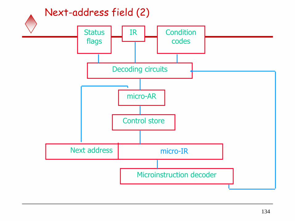
The microprogram discussed earlier requires several branch microinstructions, which perform no useful operation in the datapath.
A powerful alternative approach is to include an address field as a part of every microinstruction to indicate the location of the next microinstruction to be fetched.
Pros: separate branch microinstructions are virtually eliminated; few limitations in assigning addresses to microinstructions.
Cons: additional bits for the address field (around 1/6)
CO-Unit VI-Basic Processor Unit 135
136
3.2. Micro-Programmed Control Example
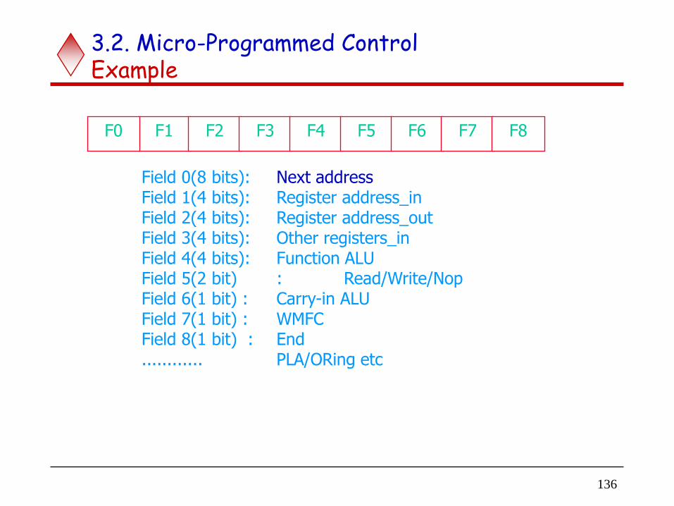
Field 0(8 bits): Next address Field 1(4 bits): Register address_in Field 2(4 bits): Register address_out Field 3(4 bits): Other registers_in Field 4(4 bits): Function ALU Field 5(2 bit) : Read/Write/Nop Field 6(1 bit) : Carry-in ALU Field 7(1 bit) : WMFC Field 8(1 bit) : End ............ PLA/ORing etc
F1 F2 F3 F4 F5 F6 F7 F8 F0
137
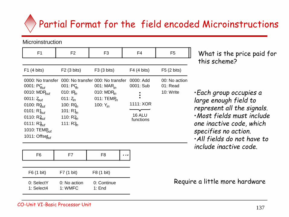
Partial Format for the field encoded Microinstructions
F2 (3 bits)
000: No transfer
001: PC in
010: IR in
011: Z in
100: R0 in
101: R1 in
110: R2 in
111: R3 in
F1 F2 F3 F4 F5
F1 (4 bits) F3 (3 bits) F4 (4 bits) F5 (2 bits)
0000: No transfer
0001: PC out
0010: MDR out
0011: Z out
0100: R0 out
0101: R1 out
0110: R2 out
0111: R3 out
1010: TEMP out
1011: Offset out
000: No transfer
001: MAR in
010: MDR in
011: TEMP in
100: Y in
0000: Add
0001: Sub
1111: XOR
16 ALU functions
00: No action
01: Read
10: Write
Microinstruction
F6 F7 F8
F6 (1 bit) F7 (1 bit) F8 (1 bit)
0: SelectY
1: Select4
0: No action
1: WMFC
0: Continue
1: End
•Each group occupies a large enough field to represent all the signals. •Most fields must include one inactive code, which specifies no action. •All fields do not have to include inactive code.
CO-Unit VI-Basic Processor Unit
What is the price paid for this scheme?
Require a little more hardware
138
3.2. Micro-Programmed Control Organization
Micro-program is often placed in ROM on CPU chip
Some machines had writable control store, i.e. user could
change instruction set
Further Discussions
Prefetching
Emulation
139 CO-Unit VI-Basic Processor Unit
140
Prefetching
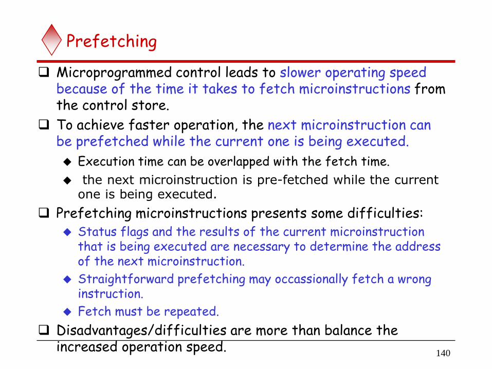
Microprogrammed control leads to slower operating speed because of the time it takes to fetch microinstructions from the control store.
To achieve faster operation, the next microinstruction can be prefetched while the current one is being executed.
Execution time can be overlapped with the fetch time.
the next microinstruction is pre-fetched while the current one is being executed.
Prefetching microinstructions presents some difficulties: Status flags and the results of the current microinstruction
that is being executed are necessary to determine the address of the next microinstruction.
Straightforward prefetching may occassionally fetch a wrong instruction.
Fetch must be repeated.
Disadvantages/difficulties are more than balance the increased operation speed.
141
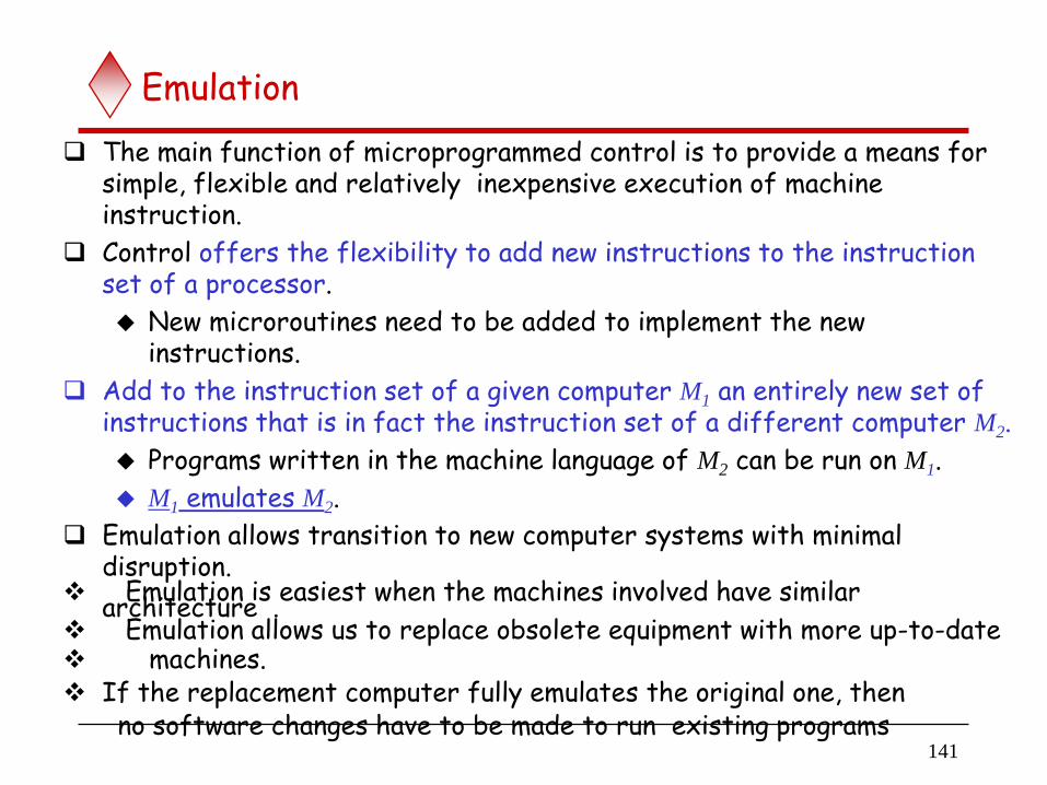
Emulation
The main function of microprogrammed control is to provide a means for simple, flexible and relatively inexpensive execution of machine instruction.
Control offers the flexibility to add new instructions to the instruction set of a processor.
New microroutines need to be added to implement the new instructions.
Add to the instruction set of a given computer M1 an entirely new set of instructions that is in fact the instruction set of a different computer M2.
Programs written in the machine language of M2 can be run on M1.
M1 emulates M2.
Emulation allows transition to new computer systems with minimal disruption.
Emulation is easiest when the machines involved have similar architecture .
Emulation allows us to replace obsolete equipment with more up-to-date machines. If the replacement computer fully emulates the original one, then no software changes have to be made to run existing programs
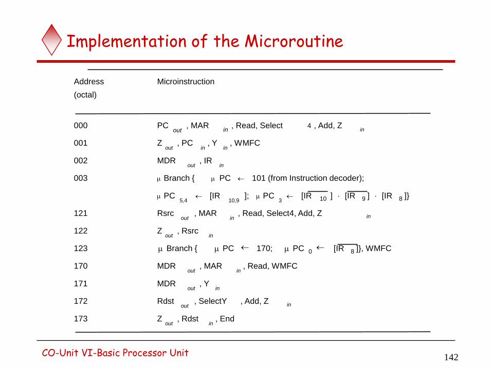
Implementation of the Microroutine
142
Address Microinstruction
(octal)
000 PC out
, MAR in
, Read, Select 4 , Add, Z in
001 Z out
, PC in
, Y in
, WMFC
002 MDR out
, IR in
003 m Branch { m PC 101 (from Instruction decoder);
m PC 5,4
[IR 10,9
]; m PC 3
121 Rsrc out
, MAR in
, Read, Select4, Add, Z in
122 Z out
, Rsrc in
123
170 MDR out
, MAR in
, Read, WMFC
171 MDR out
, Y in
172 Rdst out
, SelectY , Add, Z in
173 Z out
, Rdst in
, End
[IR 10 ] [IR 9 ] [IR 8 ]}
m Branch { m PC 170; m PC 0 [IR 8 ]}, WMFC
CO-Unit VI-Basic Processor Unit
Implementation of the Microroutine
(See Figure 7.23 for encoded signals.)
Figure 7.24. Implementation of the microroutine of Figure 7.21 using a
1
0
1
11110
0111110
001
001
1
21 0
00
0
00
0
0
0
0
0
0
0
0
0
0
0 0
0
0
00
0 0
0101
110
37
7
00000000
0 1111
110
0
0
0
17
07
F9
0
0
0
0
0
0
F10
0
0
0
0
0
0
00
0
0
0
0
0
0
F8F7F6F5F4
000 0 0 0 0 0
0
0
0
0
0
1
0
0
0
0
0
0
0
0
0
0
0
0 1
1
0
0
0 0
1
0
0
0
10000
0000
1100000
10
0
0
0
0
0
0
1
0 0
0
0
0
0
0
00 01
000
000
001
110
100
10
F2
1
110 0 0 0 0 0
1
1
221
0
11110
111 00
1
1
2
0
21
0
00
address
Octal
111 00000
1 0000000
10000000
F0 F1
0
0 0 10 0
010
010
0 11
001
110
100
0
0
0
1
1
0
1
F3
next-microinstruction address field.
011000 0 0 0 0 00 00 00000 0 0 0 0 030 0 00 0 0
143 CO-Unit VI-Basic Processor Unit

decoder
Microinstruction
Control store
Next address F1 F2
Other control signals
F10F9F8
Decoder
Decoder
circuitsDecoding
Condition
External
codes
inputs
Rsrc RdstIR
Rdstout
Rdstin
Rsrcout
Rsrcin
mAR
InstDecout
ORmode
ORindsrc
R15in R15out R0in R0out
Figure 7.25. Some details of the control-signal-generating circuitry.
bit-ORing

Feel happy to smile Always wear a Smile Not because life is full of reasons to smile But because your smile is a reason for many others to smile.

All the best
Do well in the examinations
Wish you all success
God bless you.
THANK YOU