Embed Size (px)
Citation preview

1
Computing with Non-equilibrium RatchetsMehdi Kabir*, Dincer Unluer*, Lijun Li, Avik W. Ghosh, and Mircea R. Stan
Abstract—Electronic ratchets transduce local spatial asymme-tries into directed currents in the absence of a global drainbias, by rectifying temporal signals that reside far from thermalequilibrium. We show that the absence of a drain bias can providedistinct energy advantages for computation, specifically, reducingstatic dissipation in a logic circuit. Since the ratchet functions as agate voltage-controlled current source, it also potentially reducesthe dynamic dissipation associated with charging/dischargingcapacitors. In addition, the unique charging mechanism elim-inates timing related constraints on logic inputs, in principleallowing for adiabatic charging. We calculate the ratchet currentsin classical and quantum limits, and show how a sequence ofratchets can be cascaded to realize universal Boolean logic.
Index Terms—Electric potential, Laplace equations, powerdissipation, current-voltage characteristics, spatiotemporal phe-nomena, logic gates
I. INTRODUCTION
The exponential growth in computational processing hasbeen driven by the scaling of CMOS technology to smaller andsmaller scales. The largest impediment to sustained scalingis the large thermal budget arising from power dissipationin logic circuits [1], [2]. Biological systems perform switch-ing operations quite efficiently, albeit at lower speeds andtargeting very specific applications as opposed to universallogic. Nonetheless, the principles that many biological systemsutilize are quite instructive - notable among them being theuse of analog encoding of signals, and the employment ofstrongly non-equilibrium power sources. Brownian motors usenon-equilibrium noise to create directed motion [3]–[5] tofuel the motion of motor proteins [6] and drive ion flow inartificial nanopores [7]. The purpose of this paper is to explorethe distinct energy advantages of extending ratchet principlesto solid-state electronics, specifically the shuttling of chargeswithout a global drain bias under non-equilibrium conditions[8]–[10].
We find two distinct advantages of an electronic ratchetrelated to its device level energetics. First, the absence of adrain bias needed to create global directionality reduces thestatic dissipation during device operation. In purely current-controlled logic (e.g. a Binary Decision Diagram or BDD), thisis a distinct advantage. In a conventional CMOS incarnationhowever, charging an output capacitor converts this currentsource into an effective drain voltage. At this stage, the secondadvantage of a ratchet comes in - a voltage-controlled currentsource dissipates less energy when charging the capacitor, andis amenable to adiabatic charging. Conventional schemes for
All authors are with the Charles L. Brown Dept. of Electrical and ComputerEngineering, University of Virginia, Charlottesville, VA 22904. This materialis based on work supported by the Nanoelectronics Research Initiative(INDEX Center), ViNC, UVA-NanoSTAR, and UVA-FEST awards. *Theseauthors contributed equally to this work.
Fig. 1. Prototypical geometry of a ratchet consisting of an interdigitated topgate, which creates the asymmetric time varying potential, and a back gate,which determines the initial number of carriers in the channel by shiftingthe Fermi level. The current driven by the top gate is used to build upvoltage, which can be used to back gate the next cascaded ratchet in thelogic architecture.
adiabatic charging require precise timing information for sig-nal synchronization; since we wait till each capacitor chargesup adequately, such a timing requirement is not demanded ofour proposed ratchet.
Figure 1 shows a possible implementation of a ratchet basedswitch. We have a dual gated device with a top and a backgate capacitor. The top gate, consisting of interdigitated metalplates, creates a spatially asymmetric potential - obtained bysolving Laplace’s equation (Fig. 2). An AC signal applied tothese plates creates a clock that raises and lowers the potentialbarriers periodically. The ratchet mechanism (described in thenext section) creates a net non-zero DC current averaged overspace and time, and this current progressively builds up acharge on the back gate capacitor. The back gate capacitorrepresents the input gate to the next ratchet in series (notshown), moving its Fermi energy and turning it on so thatthe second ratchet can now start shuttling charges. A suitablelayout of a ratchet array can then realize a NAND, a NOR orother generic Boolean logic gates.
II. RATCHET PHYSICS: A TOY MODEL
We consider only a specific subset of all possible ratchettypes - ‘flashing ratchets’. Fig. 3 shows the basic operationof a flashing ratchet and how the particles will accumulatearound a single potential minimum. However in a real devicethe particles will be distributed equally to every minima. Aperiodic potential with built-in local asymmetry is createdby a sequence of interdigitated electrodes (Fig. 2). When thebarriers are fully raised, the carriers injected into the channellocalize around the potential minima (Fig. 3B). When theapplied AC clock lowers the barriers (Fig. 3C), the carriers
arX
iv:1
303.
4258
v1 [
cond
-mat
.mes
-hal
l] 1
8 M
ar 2
013

2
Fig. 2. Simulation of the potential profile for a ratchet with 135nm barrierlength using the Laplace tool box in Matlab (PDEtool). The positive electrodesare 25nm in width whereas the grounded electrodes are 10nm in width toincrease the asymmetry. The a/b separation factor between the electrodes is3. The lower figure is showing the Laplace potential through the center of theSi channel.
spread out in both left and right directions, driven by thermaldiffusion in the classical limit and by wave packet evolution inthe quantum limit, driven by the difference in phase velocitiesof the individual Fourier components. When the potentialis turned back on again, the carriers drift down to theirnearest valleys (Fig. 3D). Owing to the local asymmetry of thepotential profile, there will be more carriers that have crossedthe top of the barriers into each valley compared to the barriersitting further, because the diffusion occurs when the barriersare down. In other words, there is a progressive space-timeaveraged movement of charges unidirectionally even in theabsence of a source-drain bias, driven simply by the non-equilibrium signal supplied by the clock.
The action of a ratchet can thus be described as a clock-driven current, that can be used to build an open-circuit voltageVOC across a capacitor in a logic circuit. As the voltage buildson the capacitor, it creates a back-flow until the reverse biascurrent cancels the ratchet current upon complete charging ofthe capacitive load. A large open circuit voltage allows theratchet to drive the next stage, but this efficiency needs to becounter weighed against the corresponding energy dissipatedand the charging delay associated with building the voltage.
A. Approximate quasi-analytical result
Using the diffusion equation [11], near the valley at x0, thepotential profile can be approximated as
U(x) ≈ U(x0) +(x− x0)2
2U ′′(x0) (1)
where dash represents a 1-D spatial derivative. The corre-sponding equilibrium initial carrier distribution becomes
N(x) ∝ exp[−U(x)/kT ]
= n0 exp
[− (x− x0)2
2σ20
](2)
where σ0 =√kT/U ′′(x0) is the standard deviation of Gaus-
sian distribution and U(x0) is set to be zero for convenience.
Fig. 3. Computing mechanism for a bistate quantum ratchet simulated with135nm barrier length, 1.67GHz AC clock, and ∼ 20kT barrier height usingquantum flow and relaxation. (A): Interdigitated electrodes between twoconductor planes creating the desired asymmetric local potential profile in thechannel. (B): Initial carrier distribution (shaded area) when potential (dashedline) is “on”. (C): Distributed carriers when potential is “off”.(D): electrondistribution when potential is again turned back on at the heated state. Thered line n− stands for the carriers overcoming the barrier peak on the left(back-flow), while n+ stands for those on the right (forward-flow). Sincen+ is bigger than n−, a net flow to the right results. (E) Shows the relaxedstage at the end of each cycle, where we reset the electron distribution (n/n0)to the initial equilibrium solution.
After one computing cycle (Fig. 3), the net carrier densitydifference between two neighboring potential wells is
∆N = n0Slbarr
[erfc
(b√
2σ20 + 4Dtoff
)
− erfc
(a√
2σ20 + 4Dtoff
)](3)
where erfc is the complementary error function, and n0 =Ncexp(−Ef−Ec
kT ) is the initial carrier density in the semi-conducting channel, Nc is the effective density of states, Efis the fermi-level, Ec is the conduction band level, D is thediffusion constant, S is the channel cross-sectional area, lbarris the length of the potential barrier, ton is the duration ofthe “on” part of the clock when the barrier is raised, toff isthe “off” time period when the barrier is lowered, a and bare the asymmetric physical lengths defined in Fig. 3D. Thisexpression also assumes that the drift time is smaller than ton,i.e. the barrier is raised long enough for the charges to driftinto the valley, whereupon phonons rapidly relax their energy.Finally, the net space- and time-averaged current under zeroreverse bias becomes
I0 =q∆N
ton + toff(4)
It is clear that the current arises because of the asymmetry(a > b), driven by the clock frequency related to ton,off .

3
Fig. 4. (A) shows a spatio-temporal ratchet potential, with a prominent spatial asymmetry with 4 barriers. (B) shows the contour-plot of this ratchet potentialprogressively turned on between 0.02 ns and 0.08 ns and then turned off after 0.8 ns. (C) shows a colormap of the current density over this time (blue isnegative, red is positive, and green is zero). As seen from the figure, the drift segment of the current during the potential up-cycle is actually two-phased,showing a quick initial drift down the steeper slope (thin, localized dark blue to cyan), followed by a slower drift of a larger number of particles (hence a netpositive current) down the smaller slope shown in spreading red to yellow. The current density plots shown in (D) are the snapshots at time instances markedby the horizontal dashed lines in (C). During down cycle, the back and forward propagating currents (blue and red, near t = 0.157 ns) are comparable as thediffusion process is symmetric in space whereas when potential is turning up, near t = 0.032 ns back-flow dominates and at t = 0.067 ns the forward-flow ismore prominent. Thus the net current flow proceeds with a two-phased drift, supplanted gradually by a symmetric diffusion.
B. Simulating a quantum ratchet
The quantum flow of electrons in the ratchet involvessolving the time-dependent one-electron Schrodinger equation
i~∂ψ
∂t−Hψ = 0 (5)
where H is the time-dependent Hamiltonian matrix describingthe channel. The Hamiltonian is described using the 1-D finitedifference tight-binding formula
Hn,m = [Un + 2t0]δn,m − t0δn,m+1 − t0δn,m−1 (6)
where t0 ≡ ~2/2m∗a2 depends on the grid size a and theeffective mass m∗. To get ballistic non-equilibrium flow in adrain-driven device, we normally add in self-energy matricesfor injection and removal, coupled with bias-separated contactFermi-Dirac distributions [12]. For the ratchet however, flowis generated simply by the time-dependence in H . To visualizethis short-circuit current, we will simply incorporate periodicboundary conditions for the shuttling of charges. The initialstate of the particles is obtained from the eigenvectors αand eigenvalues Eα of the matrix [H] at the time instantt = 0, while the subsequent evolution of the wavefunctionsis obtained using the Crank-Nicholson approximation for itsefficiency and simplicity in computing :
ψt+∆t = [1− iH∆t
2~]−1[1 +
iH∆t
2~]ψt (7)
In addition to a local asymmetry and an energy source, theratchet needs dissipation to generate a ‘reset’ at the end ofeach cycle. A purely ballistic quantum evolution, describedabove, does not have an inbuilt mechanism for relaxing thecharges. As a result, our simulations show that the process ofcontinuously pumping energy into the ratchet from an AC field
causes the carriers to heat up and eventually fly off the barriers.We thus need a way to remove the excess energy at theend of each AC cycle. Coupling the electrons with substratephonons would remove that energy. Rather than modeling thiscomplex behavior, we capture this relaxation using a ‘one-shot’ procedure, where at the end of each clock cycle, we resetthe electron distribution to the initial equilibrium solution. Theenergy difference between the equilibrium eigenvalue and thatreached at the end of the AC cycle is the dissipation that wecan then keep track of.
The time-dependent potential Un ≡ U(xn) samples theasymmetric barrier shape, which we choose as U(x) = x2(1−x7). Periodic boundary conditions are invoked by settingH1,N = HN,1 = −t0, while open boundary conditions requireself-energy matrices with Σ1(1, 1) = Σ2(N,N) = −t0eika.While periodic boundary conditions suffice to see the shuttlingof charges, and in addition provide analytical simplicity for aclosed circuit, there is a danger of tails of the wavefunctionescaping a drain and re-injected from the source towardsa valley and self-interfering, an issue that open boundaryconditions do not run into. This becomes a bigger issue ifwe let the charges build up at the end for an open circuit,whereupon the periodic boundary conditions cannot even bejustified. Consequently, we will use open boundary conditionsfor the latter half of the paper (see section III-E).
C. Simulating a classical ratchet
Classically we keep track of the charges rather than wave-functions, and evolve them by the Newtonian drift-diffusionequation
∂N
∂t= −∂(µξN)
∂x+D
∂2N
∂x2(8)

4
Fig. 5. (A) above shows how the asymmetric ratchet potential changes withtime and space. (B) shows how the particles are evenly distributed (localized)in bins when the potential is raised and how they move to the right withthe oscillating top gate (the blue area in between localized bins shows thepathway of particles moving right). (C-E) show the total, drift, and diffusioncurrent densities. One can see that drift current opposes the diffusion currentat all the times, but their magnitudes are different thus resulting in a net flowto the right. As discussed in the previous sections, the second phase of thetwo-part drift current shown in yellow moves the particles to right, then thediffusion current spreads the particles evenly right and left.
where N = N(x, t) is the carrier distribution, ξ = ξ(x, t)is the electric field, µ is the carrier mobility, and D is thediffusion constant. The triangular potential affects the carriersthrough the electric field given by the equation:
ξ = −dUdx
(9)
where U is the spatially-varying potential profile across theratchet. The current can be calculated from N as
J = qvN + qD∂N
∂x(10)
where v = µξ and q is the electric charge. Fig. 4A and Bshows how the potential is varied with space and time. Part Cdemonstrates how the total current density is generated by themovement of electrons and has a net positive current flow tothe right. The Gaussian distributed particles initially localizein the second well (L ≈ 6µm) and start to diffuse both sidesat t = 0.003 ns equally. As the potential starts to turn onbetween 0.02 ns and 0.08 ns, a small amount of particles (dueto asymmetry of potential) quickly drift down the steeper slope(thin dark blue to cyan) followed by a slower, positive driftmovement of a larger group of particles (red/orange to yellow)resulting in a net positive forward-flow. At t = 0.157 ns, thepotential is lowered down and the diffusion starts, helping thetwo-phase drift current. As shown in the current figures ofFig. 5E, the net flow of particles is caused mostly by the driftcurrent (Fig. 5C), not by the diffusive current which is almostsymmetrical in both directions (Fig. 5D).
The boundary condition at the contacts is set to describecarrier recombination in the relaxation time approximation
dN
dt
∣∣∣∣end
= −Nendτ
(11)
where τ is the time it takes for the electrons to transfer fromthe semiconductor to the capacitor. In these simulations, weuse copper as the capacitive material for the back gate of thenext ratchet (See Table I) [13]. This boundary condition occursbecause of the interface between the ratchet channel and
TABLE ISIMULATION PARAMETERS FOR DRIFT-DIFFUSION
REFER TO TABLE II FOR CIRCUIT PARAMETERS
Barrier Length (L) 3 µm
Asymmetry (a - b) 2.25 µ− 0.75 µm
Channel Thickness (t) 20 nm
Channel Width (W ) 6 µm
Oxide Thickness (tox) 5 nm
Top Gate AC Clock 0.39V @ 6 GHzDiffusion Constant (D) 3.62× 10⁻³ m2s−1
Si Eff. Den. of States (Nc) 3.23× 1025 m−3
η = (Ec−Ef
kT) 3
Max. Ratchet Barrier Height (in kT/q) 15Capacitor Escape Rate (for Cu) (τ ) 1.786× 10⁻¹⁴ s
contact, and it usually limits the amount of charge which canflow in and out of the capacitor. However, in our simulations,the charge extraction rate for copper was fast enough to allowall charge carriers to (dis)charge the capacitor. Therefore, thecontact interface did not limit the current flow between thecapacitor and the ratchet.
In order to capture the charging process of the load ca-pacitor, the number of charges accumulating on the capacitorwas calculated as Q = JendS∆t, where Jend represents thecurrent density crossing the boundary at the end of each timestep, S is the channel cross sectional area, and ∆t is thesimulation time step. Using this we can calculate the voltageincrease as V = Q/C, where C is the load capacitance.We then superimpose a backward voltage varying linearlyfrom 0 to V across the ratchet (ideally, by solving Poisson’sequation, but simplified in our treatment here), and add it tothe sawtooth potential to give a tilted asymmetric potential.We then recalculate the electric field and reiterate eqn. 8 untilthe capacitor is charged under open bias and the net space-time-averaged current vanishes (shown in Fig. 6). Note thatthere is still dynamic current flow and associated dissipation.
D. Calculating the Open Circuit Voltage
Charging of the load capacitor increases the voltage on oneside of the ratchet, resulting in a tilted potential growing withtime across the device. The resulting reverse current partiallycancels out the directional current from the ratchet. Eventually,the capacitor reaches a critical voltage, called the open circuitvoltage (VOC) when the reverse current equals the currentgenerated by the ratchet, averaged over space and time. Itis therefore important to extract the open circuit voltage tounderstand the drivability of the ratchet device for logic.
Let us assume that the time dependent current through theratchet in one operation cycle can be given by I(t). Therefore,the current generated by the ratchet after one clock cycle is
I0 =1
ton
∫ ton+toff
toff
I(t)dt
=Q
ton(12)
where Q is the total charge placed on the load capacitor.The voltage generated on the load capacitor after one cycle

5
Fig. 6. (A)Drift-diffusion simulation of the electronic ratchet showing the charging of a load capacitor. After 11 clock cycles the particles are distributedequally among all the barriers and there is a net forward-flow of current to the right. The two-phase drift current is less prominent as the VOC is built-up,but still exists as seen in the (B-E) (Darker red colors start changing to orange/yellow colors as the VOC increases). As the particles reach the right side (L= 6µm), they get ejected by the system and charge a localized back gate capacitor to a VOC of ≈ 145mV .
is V0 = Q/C. This, in turn, creates a reverse current ofIrev,0 = V0/R, where R is the resistance of the ratchetchannel (in general, a nonlinear resistance which must becalculated self-consistently). If we assume that the space-timeaveraged current pumped by the ratchet remains constant, thetotal current generated by the ratchet during the next cyclegiven by
I1 =Q
ton− Irev,0 (13)
This way, the voltage on the capacitor after N cycles is
VN =1
CIN ton + VN−1
=1
C
[Q
ton− VN−1
R
]ton + VN−1
=Q
C+ (1− ton
RC)VN−1
=Q
C
1− (1− tonRC
)N
tonRC
(14)
Therefore, the open circuit voltage can be defined as
VOC ≡ limN→∞
VN =Q
tonR
=lbarrqn0µS
· 1
ton
∫ ton+toff
toff
I(t)dt (15)
It is important to note that the output voltage is only indirectlydependent on the input voltage. The input voltage from theback gate increases the number of carriers in the channel, andthus the magnitude of VOC . However, since the top gate isalways oscillating, it does not influence the input that tries todetermine the output. The input is decoupled from the charging
process of the output which means that the ratchet back gate isadiabatically charged without placing any timing constraintson the input.
If we now apply Eqn. (15) to (4), we get the following VOCfor the Gaussian distribution
VOC =l2barr
2µ(ton + toff )
[erfc
(b√
2σ0 + 4Dtoff
)
− erfc
(a√
2σ0 + 4Dtoff
)](16)
For the simulations, we use the parameters listed in TableI. The parameters are conventional material properties ofsilicon for the channel and silicon dioxide for the oxide [11].Furthermore, we derive device parameters such as back gatecapacitance from the dimensions and structures shown in Fig.1.
In figure 6, we show the charging of the load capacitor.According to the drift-diffusion simulations, the open circuitvoltage saturates to ≈ 145mV , which is in a relatively goodagreement with the analytic value of ≈ 125mV derived byusing the parameters from Table I in eqn. (16). From 3D figureshowing different time cycles in Fig. 6A, we can see that asthe forward-flow of electrons decreases with time and VOCbuilds up. In the Fig. 6B at t ≈ 0.05ns and x ≈ 5µm, there isnet positive current shown in yellow, but as the VOC built, thispositive current gets lets prominent and disappears as shownin Fig. 6E. The space-time averaged net-current becomes zero.
III. LOGIC WITH RATCHETS
A. Static power in CMOS vs. Ratchet
Static power dissipation in CMOS circuits is caused by adirect current from the power source (Vdd) to ground (See Fig.
6
Fig. 7. Conventional vs. Adiabatic Charging (A) CMOS circuits areconventionally charged using a DC voltage source. (B) By using a lowfrequency AC voltage source, the capacitor can be charged while dissipatingless energy [15].
7A). In an ideal CMOS circuit, there is no static dissipationbecause its complementary nature ensures that for each turnedon PMOS, there exists a turned off NMOS blocking a directpath to ground, or vice versa. However, in real circuits, MOS-FETs are not completely turned off and there exist leakagecurrents which traverse from Vdd to ground–creating staticpower dissipation. In modern CMOS circuits, leakage poweris a significant problem which usually accounts for a largeportion of all power dissipation [14].
The electronic ratchet, on the other hand, can avoid thisissue altogether. Rather than using a DC power source togenerate a current, the ratchet uses a time varying asymmetricpotential to create a net current. Therefore, the ratchet candrive current without a source to drain bias. Since there areno DC power sources, the ratchet can, in principle, be used todesign circuits with no static dissipation.
B. Dynamic power in CMOS vs. Ratchet
In CMOS logic circuits, dynamic power dissipation resultsfrom the charging and discharging of load capacitors. Takethe inverter in Fig. 7A for example. When the inverter hasan input of ’0’, the load capacitor is charged to Q = CVdd.Therefore, the energy dissipated is given by:
Ediss = Esource − Ecap
=
∫ Q
0
Vdd dQ−∫ Q
0
V dQ
= CV 2dd − C
∫ Vdd
0
V dV
=1
2CV 2
dd (17)
This energy is dissipated in the form of heat due to theeffective resistance of system. The dissipated power is given bythe equation P = 1
2CV2ddf , where f is the operating frequency
TABLE IIPARAMETERS FOR CIRCUIT SIMULATIONS
REFER TO TABLE I FOR DEVICE DIMENSIONS
Freq. of Top Gate (ω) 6× 10⁹ s−1
Top Gate Capacitance (C1) 9.07× 10⁻¹³ F
Back Gate Capacitance (C2) 4.24× 10⁻¹³ F
Inductance (L) 7.76× 10⁻¹⁰ H
Channel Resistance (R) 1.39× 10³ Ω
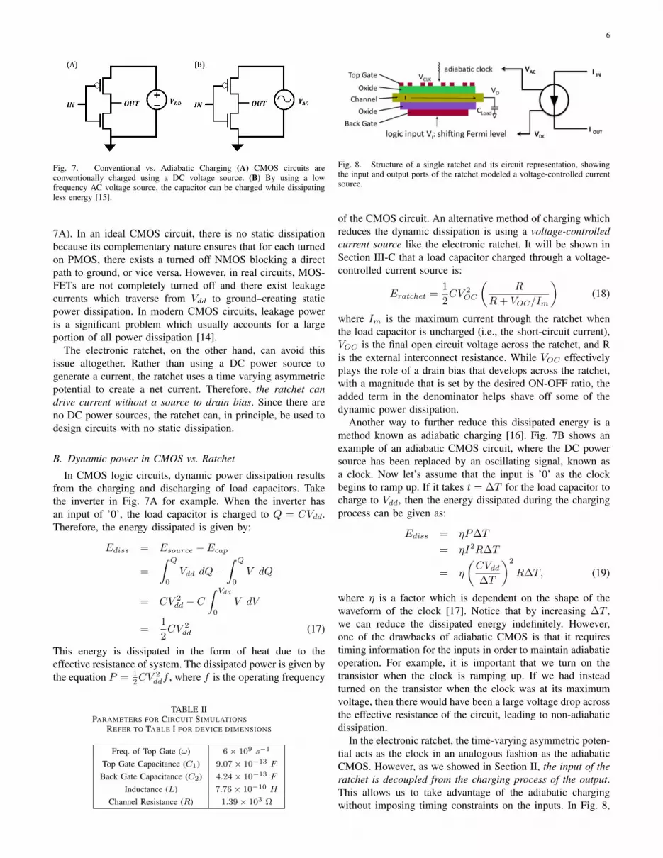
Fig. 8. Structure of a single ratchet and its circuit representation, showingthe input and output ports of the ratchet modeled a voltage-controlled currentsource.
of the CMOS circuit. An alternative method of charging whichreduces the dynamic dissipation is using a voltage-controlledcurrent source like the electronic ratchet. It will be shown inSection III-C that a load capacitor charged through a voltage-controlled current source is:
Eratchet =1
2CV 2
OC
(R
R+ VOC/Im
)(18)
where Im is the maximum current through the ratchet whenthe load capacitor is uncharged (i.e., the short-circuit current),VOC is the final open circuit voltage across the ratchet, and Ris the external interconnect resistance. While VOC effectivelyplays the role of a drain bias that develops across the ratchet,with a magnitude that is set by the desired ON-OFF ratio, theadded term in the denominator helps shave off some of thedynamic power dissipation.
Another way to further reduce this dissipated energy is amethod known as adiabatic charging [16]. Fig. 7B shows anexample of an adiabatic CMOS circuit, where the DC powersource has been replaced by an oscillating signal, known asa clock. Now let’s assume that the input is ’0’ as the clockbegins to ramp up. If it takes t = ∆T for the load capacitor tocharge to Vdd, then the energy dissipated during the chargingprocess can be given as:
Ediss = ηP∆T
= ηI2R∆T
= η
(CVdd∆T
)2
R∆T, (19)
where η is a factor which is dependent on the shape of thewaveform of the clock [17]. Notice that by increasing ∆T ,we can reduce the dissipated energy indefinitely. However,one of the drawbacks of adiabatic CMOS is that it requirestiming information for the inputs in order to maintain adiabaticoperation. For example, it is important that we turn on thetransistor when the clock is ramping up. If we had insteadturned on the transistor when the clock was at its maximumvoltage, then there would have been a large voltage drop acrossthe effective resistance of the circuit, leading to non-adiabaticdissipation.
In the electronic ratchet, the time-varying asymmetric poten-tial acts as the clock in an analogous fashion as the adiabaticCMOS. However, as we showed in Section II, the input of theratchet is decoupled from the charging process of the output.This allows us to take advantage of the adiabatic chargingwithout imposing timing constraints on the inputs. In Fig. 8,

7
Fig. 9. An equivalent circuit of the charging behavior of the ratchet. Theratchet acts as a voltage-controlled current source, where current is a functionof the voltage on the capacitor. The current is at a maximum, Im, initiallywhen the capacitor is uncharged. As the voltage builds up, the reverse currentdecreases the net current, until the capacitor reaches the open circuit voltage,VOC when there is a zero net current.
a circuit symbol of electronic ratchet is presented showing theinput and output ports.
C. Capacitive Charging using a Current Source
Consider a simple circuit model in which an electronicratchet charges a capacitor, as shown in Fig. 9. The I-Vcharacteristic of the electronic ratchet is also shown. We canwrite the Kirchoff’s equations as follows to describe thiscircuit
I =V − VcR
(20)
I = − ImVOC
V + Im (21)
I = CdVcdt
(22)
where I is the current, V is the voltage of the node betweenthe electronic ratchet and the resistor and Vc is the voltage onthe capacitor.
From the equations (21-22), the voltage on the capacitor,Vc, and current, I can be solved as
Vc = VOC(1− e−t/R′C)
I =VOCR′
e−t/R′C (23)
in which R′ = R+ VOC/ImTherefore, the energy charged into the capacitor is
Ecap =
∫ VOC
0
CVcdVc =1
2CV 2
OC (24)
and the dissipated energy on the resistor is
ER =
∫ ∞0
I2Rdt
=
∫ ∞0
(VOCR′
)2e−2t/R′CRdt
=CV 2
OC
2
R
R′
=CV 2
OC
2
R
R+ VOC
Im
(25)
From this equation, we make the following observations.In a ratchet, the load capacitor is charged to VOC ratherthan Vdd. Therefore, the ratchet energetics are comparableto CMOS circuits with extremely low drain-source voltages.
Fig. 10. Circuit model for the ratchet. An adiabatic clock is modeled usingan inductor L and the top gate capacitor C1. A (virtual) diode is used tocapture the unidirectional current (ratchet) which drives charging of the loadcapacitor C2.
Furthermore, the ratchet introduces an extra resistance term,VOC/Im which decreases the energy dissipation further. Forour simulations (see Section 3), the channel resistance was1.39 kΩ compared to the extra resistance term of 2.70 kΩ.Therefore, the unique charging method of the ratchet makes itintrinsically less dissipative than conventional CMOS logic.
D. Adiabatic Charging
We will now develop a more accurate circuit model for theratchet (Fig. 10) to describe its energetics during adiabaticcharging. An LC circuit is used to represent the oscillatingclock for the top gate. This clock charges up the top gatecapacitor, which represents the charging or discharging of theasymmetric ratchet potential. Because the circuit is operatingat the natural frequency, we are able to adiabatically transportelectrons in the channel, thus reducing the energy dissipationof the circuit.
The asymmetry of the ratchet potential provides direction-ality to the electrons and gives a net positive current. Thisasymmetry is captured by a (virtual) Schottky diode, whichallows current to flow easily in one direction while acting asa rectifier in the opposite direction. The diode parameters areselected by calibrating with the drift-diffusion simulation. Thebarrier height is selected as 15kT/q as in the simulations andthe I0 is selected as 1x10⁻¹⁵A to match the results. The diodealso acts as the voltage-controlled current source described inFig. 9. This current is used to charge the load capacitor, whichacts as the back gate capacitor of the next ratchet in a cascadedlogic architecture (Fig. 12).
The charging process can be seen in the following analysis.We treat the diode as a short-circuited element when there isa positive current running through it, and as an open-circuitwhen the current is negative . During the time when the diodeis short circuited, we have the following Kirchoff’s equations
Ldi1dt− Q1
C1= 0 (26)
Q1
C1−Ri2 −
Q2
C2= 0 (27)
where i1 and i2 are the currents in the two separate loopcircuits. For eqn. (26), we assume that the charge on the topgate capacitor, C1, is exclusively determined by the currentgenerated by the inductor. This is a valid assumption if the topgate capacitance is much larger than the back gate capacitance(see Table II), thus acting as an ‘energy tank’ [18].

8
Fig. 11. Energy dissipated as a function of ωL for a fixed input energy onthe inductor. The energy dissipated is calculated by taking the integral of thedissipated power I2R at t = ∞. The energy goes to zero in the adiabaticlimit.
We first solve eqn. (26), and apply the boundary conditiondQ1/dt|t=0 = −I0
d2Q1
dt2− Q1
LC1= 0
Q1(t) = − I0ωL
sinωLt (28)
where ωL = 1/√LC1. Next, we substitute (28) into (27) to
get:dQ2
dt+
Q2
RC2= − I0
ωLRC1sinωLt (29)
Let ω1 = 1/RC1 and ω2 = 1/RC2. Therefore, equation (29)has the solution (with boundary condition Q2(0) = 0) :
Q2(t) = − I0ω1
ω2L + ω2
2
exp(−ω2t)
− I0ω1
ωL(ω2L + ω2
2)(ω2 sinωLt− ωL cosωLt) (30)
Therefore, the back gate charging current is
I(t) =I0ω1ω2
ω2L + ω2
2
exp(−ω2t)
− I0ω1
(ω2L + ω2
2)(ωL sinωLt+ ω2 cosωLt) (31)
Equation (31) is only valid during times when I(t) ≥ 0. Thiscondition requires that:
cosωLt
(ωLω2
)sinωLt ≤ exp (−ω2t) (32)
Fig. 12. Logic circuits are built by cascading ratchet gates together. Thefirst ratchet builds up an open circuit voltage which is then used to charge ordischarge the back gate of the next ratchet.
Fig. 13. Ratchet inverter computing mechanism. (A - Case 1) Vin is low andmoves Fermi level down shown in (B), p-ratchet will have a higher currentthan n-ratchet so the output will charge the next capacitor Cbg until thecapacitor voltage reaches −VOC (low). Vin is high the output will dischargenext capacitor Cbg from VOC (high) to zero (A - Case 2).
Equation 32 suggests that there are periods when the back gatecapacitor stops charging. During these periods, the charge ismaintained on the back gate capacitor, as we will see later inour numerical simulations.
Let us now look at the adiabatic limit for the energydissipation, by taking ωL → 0. However, we must make surethat the initial energy on the inductor is unaffected by thislimit. Since ωL = 1/
√LC1, L increases quadratically as we
decrease ωL. Now, the initial energy on the inductor is givenby Eind = 1
2LI20 ∝ (I0/ωL)
2. Therefore, we must decreaseωL in such a way that I0/ωL remains constant. It is easy tosee that the second and third terms in equation (31) go to zeroas ωL → 0. The first term also goes to zero if we re-write theequation as:
limωL→0
I(t) =I0ω1ω2
ωL(ω2L + ω2
2)ωL exp(−ω2t) = 0 (33)
With I → 0, the dissipated energy through the resistor,Ediss = I2R also goes to zero. This implies that the totalenergy dissipated can be reduced by arbitrarily lowering theclock frequency, as predicted by the adiabatic limit (Fig. 11).
E. Ratchet-Based Gates
The open circuit voltage generated across a ratchet can beused to move the Fermi energy across another ratchet, i.e., to

9
Fig. 14. (A) Ratchet NAND gate and (B) NOR gate with the extra balancecapacitors. Balance capacitors helps the models to have stable transientcurrent, thus eliminating the metastability during the transitions.
electrostatically ‘dope’ it (Fig. 12). Electronic ratchets can bedoped to either n-type or p-type, as shown in the Fig. 13B, bycharging the back gate capacitor. CMOS-like combinations ofan n-ratchet and a p-ratchet can further create universal ratchetbased logic gates like INV, NAND, and NOR. In theory,electronic ratchets are capable of realizing any Boolean logicoperation based on these three gates. For example, a ratchetinverter can be realized with an n-type and p-type ratchet, asshown in Fig. 13A. As seen in the figure, the magnitudes ofIA and IB (currents from the p-type and n-type ratchets) canbe manipulated through the back gate, which adjusts the Fermilevel in the channel (Fig. 13B). Furthermore, the output VOCis used to drive the back gate of the next ratchet in the circuit(shown as VOC in Fig. 13C). The sign of the current differencebetween IA and IB determines the charging or dischargingof the next ratchet’s back gate capacitor. When the input ishigh, the Fermi-level of the n-type devices gets shifted intothe conduction band, allowing a large number of electrons toconduct and generate a high magnitude current (IB). In thep-type ratchet, high input bias shifts the EF away from theconduction band, thus lowering the current (IA). When IB islarger than IA, the output of the inverter will start to dischargethe next logic element’s back gate capacitor.
In an analogous process, ratchet-based NAND gates andNOR gates can be created with two p-type and two n-typeratchets, with an extra balance capacitor between ratchets inpull-down network of NAND or pull-up network of NOR,to balance the current (as shown in the Fig. 14). The balancecapacitor helps the model to have a stable transient current, sothat gates do not have meta-stable states between transitions.
In order to further capture the cascading behavior of theratchet in our circuit model, we have modified the Schottkydiode in our circuit to be a three terminal device, i.e., a voltagecontrolled rectifier. The third terminal is dependent on the opencircuit voltage built across the previous ratchet. This voltageadjusts the turn-on voltage for the device, thus mimicking theon and off states of a ratchet based on the back gate voltage.In Fig. 12, we show how the voltage across the second ratchetdiode is created by the open circuit voltage from the firstratchet.
We simulated the circuit in Fig. 10 using Virtuoso Spectre.
Fig. 15. Circuit simulation using the circuit diagram in Fig. 10 resultsshowing: The voltage being stored on the back gate capacitor compared withthe drift-diffusion simulations. For the values of the circuit elements, we usedthe parameters listed on Table II and for the Schottky parameters, we usedbarrier height of 15kT and I0 of 1E-15A. Both of the results converge closeto ≈ 145mV and ≈ 160mV , slightly over shooting the expected result of≈ 125mV . The difference between the curves is our circuit model does notcapture the back-flow of the electrons as open-circuit builds-up, so it slightlyover shoots the actual voltage built-up.
For the values of the circuit elements, we used the parameterslisted on Table II. In order to adjust the clock frequency, wechanged the inductance and also the initial current so that theenergy stored on the inductor remains constant through allclocking frequencies. We show the charging of the back gatecapacitor to the open circuit voltage in Fig. 15. As predictedfrom eqn. (32), the clock charges the back gate only duringthe times when the the current is positive (potential is up) anddischarges when the current is negative (potential is down).We observe a qualitatively matching VOC built-up betweenthe circuit simulations and the drift-diffusion simulations,although the circuit model can not capture the back-flow ofparticles when the potential is down. The VOC estimated isslightly higher than the calculated value given the simplicityof circuit model and the ideal diode missing the back-flowshown in Fig. 6A.
Fig. 11 shows the energy dissipated in the resistor as afunction of the top gate oscillation frequency. We can seethat the energy continues to decrease as we scale down theoscillation frequency as predicted by our adiabatic limit. Forhigh frequencies (ωL ω2), we begin to recover eqn. (25) ofthe conventional charging mechanism.
IV. LIMITATIONS AND CHALLENGES
We saw how electronic ratchets can be used to perform logicoperations in principle at low energy costs, and how energydissipation can be further reduced by the adiabatic chargingprocess in the absence of timing constraints. However, thereare a few critical effects that can still limit the overallperformance of the proposed ratchet. Innovative material anddevice engineering maybe able to circumvent these limitations.
In Section IV, we demonstrated that the energy dissipatedby the ratchet can be arbitrarily reduced by turning downthe clocking frequency; however there is a lower limit to thefrequency in order to have the ratchet operational. It is worthremembering that the ratchet is ultimately a non-equilibriumdevice. If we allow the electrons to continuously diffuse bylowering the asymmetric saw-tooth potential too long, we will

10
reach a near homogeneous distribution for which the driftcurrent component upon raising the barriers will be muchsmaller. This can be seen in eqn. 10: as we increase toff ,both error function terms become small, and their differencedecreases. Since electrons move at high speeds through asmall-channel high-mobility material, this requires a minimumfrequency fast enough before the electron distribution becomeshomogenized. In other words, we have to maintain a balancebetween the mobility of the channel material and the clockingfrequency in order to get optimal performance from the ratchet.
As we scale ratchets towards nano-scale dimensions, weinvariably reduce the distance between barriers. The clockingfrequencies must be increased significantly to maintain theratchet operational at small dimensions. For a nanometer-sized device, our calculations and simulations predict that thefrequencies must be in the Terahertz range in order to generateenough current to drive the next gate. This can be bypassedby slowing down the electrons using a multi-phased clock. Aperistaltic ratchet uses multiple clocks with different spatialand temporal phases to achieve directionality. Initially, theelectrons are localized by the top gate clock and when thebarrier is lowered, they start to diffuse through the channel. Atthis point, a second clock raises another set of barriers, slightlyoffset spatially, that begin to localize the electrons once again.Because of the spatial offset and temporal phases, the electronshave a net directionality at lower clock frequencies.
Aside from the issue of compatibility between intrinsic andimposed frequencies, there is also a design issue that ratchetsneed to overcome. While the creation of a clock-driven currentsource in the absence of a drain bias seems like a distinct netpositive, by transducing that current into a capacitive voltage(influenced by a design that is ultimately CMOS-centric), weeventually tend to neutralize that advantage. As the ratchetsystem pumps electrons into the load capacitor, it builds up anopen circuit voltage over time. This built-up voltage, however,acts as an effective drain bias which reintroduces the staticdissipation into the logic circuit. Therefore, an alternativemethod of implementing logic circuits should be devised tomitigate this issue. It might be possible to create a current-based logic system which would eschew the static dissipation,at least for several intermediate logic stages. For now, wepresent this simple method as a demonstration of ratchet logicdesign, but ref. [19] shows that power efficient computationwith limited number of electrons can be achieved in a ratchet-like geometry through the use of purely current driven BinaryDecision Design (BDD) Circuits.
V. CONCLUSIONS
Biological systems are rife with examples where ratchet-like mechanisms are purported to shuttle elements (typicallymotor proteins) in the absence of global potentials, poweredby non-equilibrium signals such as the hydrolysis of ATPover a finite noise frequency range [20]. The purpose of thispaper was four-fold: (a) to extend this concept to a solid-state device, using a clock and a series of potentials createdby interdigitated electrodes; (b) to show how such a ratchetdevice can be cascaded to create universal Boolean logic; (c)
to explain the possible energy-saving advantages raising fromthe reduced dynamic and static dissipation; and (d) finally, tooutline limitations exposed by the simulations of our studieddevice geometries, namely, the importance of switching infuture to current-driven (as opposed to voltage-driven) logic,and the need to achieve a temporal matching or resonancebetween driving and driven frequencies.
VI. ACKNOWLEDGEMENTS
This material is based on work supported by the Nano-electronics Research Initiative (INDEX Center), ViNC andNanoSTAR. We would also like to acknowledge Suman Dattaand Arun Thathachary for useful discussions.
REFERENCES
[1] V. Zhirnov, I. Cavin, R.K., J. Hutchby, and G. Bourianoff, “Limits tobinary logic switch scaling - a gedanken model,” Proceedings of theIEEE, vol. 91, pp. 1934–1939, nov 2003.
[2] “The international technology roadmap for semiconductors report 2010update overview,” 2010.
[3] R. Feynman, R. Leighton, and M. Sands, The Feynman Lectures onPhysics, vol. 1. Boston: Addison-Wesley, second ed., 1963.
[4] M. O. Magnasco, “Forced thermal ratchets,” Phys. Rev. Lett., vol. 71,pp. 1477–1481, Sep 1993.
[5] R. D. Astumian, “Thermodynamics and kinetics of a brownian motor,”Science, vol. 276, no. 5314, pp. 917–922, 1997.
[6] S. Rice, A. W. Lin, D. Safer, C. L. Hart, N. Naber, B. O. Carragher,S. M. Cain, E. Pechatnikova, E. M. Wilson-Kubalek, M. Whittaker,E. Pate, R. Cooke, E. W. Taylor, R. A. Milligan, and R. D. Vale,“A structural change in the kinesin motor protein that drives motility,”Nature, vol. 402, no. 6763, pp. 778–784, 1999.
[7] C. Dekker, “Solid-state nanopores,” Nat Nano, vol. 2, no. 4, pp. 209–215, 2007.
[8] P. Jung, J. G. Kissner, and P. Hanggi, “Regular and chaotic transport inasymmetric periodic potentials: Inertia ratchets,” Phys. Rev. Lett., vol. 76,pp. 3436–3439, Apr 1996.
[9] M. Borromeo and F. Marchesoni, “Asymmetric confinement in a noisybistable device,” Europhysics Letters, vol. 68, no. 6, p. 783, 2004.
[10] D. Reguera, G. Schmid, P. S. Burada, J. M. Rubi, P. Reimann, andP. Hanggi, “Entropic transport: Kinetics, scaling, and control mecha-nisms,” Phys. Rev. Lett., vol. 96, p. 130603, Apr 2006.
[11] R. Pierret, Semiconductor Device Fundamentals. Pearson Education,1996.
[12] S. Datta, Electronic Transport in Mesoscopic Systems. CambridgeStudies in Semiconductor Physics and Microelectronic Engineering,Cambridge University Press, 1997.
[13] R. Knorren and K. H. Bennemann, “Dynamics of excited electrons incopper and ferromagnetic transition metals: Theory and experiment,”Phys. Rev. B., vol. 61, pp. 9427–9440, Apr 2000.
[14] K.-S. Yeo and K. Roy, Low Voltage, Low Power VLSI Subsystems. NewYork, NY, USA: McGraw-Hill, Inc., 1 ed., 2005.
[15] M. Kabir, D. Unluer, L. Li, A. Ghosh, and M. Stan, “Electronic ratchet:A non-equilibrium, low power switch,” in Nanotechnology (IEEE-NANO), 2011 11th IEEE Conference on, pp. 482 –486, aug. 2011.
[16] J. Denker, “A review of adiabatic computing,” in Low Power Electronics,1994. Digest of Technical Papers., IEEE Symposium, pp. 94–97, oct1994.
[17] N. Anuar, Y. Takahashi, and T. Sekine, “Two phase clocked adiabaticstatic cmos logic,” in System-on-Chip, 2009. SOC 2009. InternationalSymposium on, pp. 083–086, oct. 2009.
[18] J. Blanchard, The History of Electrical Resonance. Bell telephonelaboratories Incorporated, 1941.
[19] V. Saripalli, V. Narayanan, and S. Datta, “Ultra low energy binarydecision diagram circuits using few electron transistors,” in Nano-Net, vol. 20 of Lecture Notes of the Institute for Computer Sciences,Social Informatics and Telecommunications Engineering, pp. 200–209,Springer Berlin Heidelberg, 2009. 10.1007/978-3-642-04850-0-27.
[20] G. Oster and H. Wang, “Atp synthase: two motors, two fuels,” Structure,vol. 7, no. 4, pp. R67 – R72, 1999.


