Embed Size (px)
Citation preview

Journal of the Association of Arab Universities for Basic and Applied Sciences (2014) 15, 15–20
University of Bahrain
Journal of the Association of Arab Universities for
Basic and Applied Scienceswww.elsevier.com/locate/jaaubas
www.sciencedirect.com
ORIGINAL ARTICLE
Conductivity and thermoelectric properties
of nanostructure tin oxide thin films
* Corresponding author. Tel.: +963 955158906.
E-mail address: [email protected] (F.H. Jneed).
Peer review under responsibility of University of Bahrain.
Production and hosting by Elsevier
1815-3852 ª 2013 Production and hosting by Elsevier B.V. on behalf of University of Bahrain.
http://dx.doi.org/10.1016/j.jaubas.2012.09.005
M.A. Batal, Ghassan Nashed, Fares Haj Jneed *
Department of Physics College of Science, University of Aleppo, Syria
Received 3 May 2012; revised 3 August 2012; accepted 17 September 2012
Available online 6 June 2013
KEYWORDS
Thin films;
SnO2;
Seebeck effect;
Thermoelectric
Abstract Tin oxide thin films doped with iron or copper were deposited on glass and porous alu-
mina substrates, using the co-deposition dip coating sol–gel technique. Alumina substrate was pre-
pared by the anodizing technique. Samples were sintered for 2 h at temperature 600 �C. The XRD
spectrum of deposited samples shows a polycrystalline structure with a clear characteristic peak of
SnO2 cassiterite phase. From (I–V) characteristics measured at different temperatures for samples
prepared on glass substrates, the density of states at the Fermi level was calculated. Thermoelectric
effect was measured with a change of temperature for prepared samples under low pressure 1 mbar.
Seebeck coefficient, the carrier concentration, the charge carrier mobility and the figure merit were
determined for prepared samples under low pressure 1 mbar. Seebeck coefficient was improved
when films were deposited on porous Alumina substrates.ª 2013 Production and hosting by Elsevier B.V. on behalf of University of Bahrain.
1. Introduction
Thermoelectric phenomenon was first discovered by Thomas J.Seebeck in 1822, when he developed a voltage by joining two
pieces of different materials together and placing a tempera-ture difference to the couple. He also found that the voltagedifference observed was proportional to the temperature gradi-ent (S= V/DT). This effect was named after him and the coef-
ficient S (also known as a) is known as Seebeck coefficient.This coefficient is very low for metals (only a few mV/K) and
much larger for semiconductors (typically a few 100 mV/K).The aptitude of a material for thermoelectric applicationsis determined by using a dimensionless figure of merit(Pichanusakorn et al., 2010):
ZT ¼ S2rj
T
in which S, r, T and j are, respectively, Seebeck coefficient,electrical conductivity, operating temperature and total ther-
mal conductivity. Thermoelectric energy conversion, whichdirectly transforms the heat into electricity, has drawn muchattention in recent years and found applications in a variety
of areas such as renewable and clean energy, thermoelectricpower generation, small scale cooling systems for electronicdevices, microrefrigerator devices, and micro-thermo-chemistry
on a chip for microelectronic components (Fahrettin,2009).The thermoelectric materials are usually bulk, thinfilm and low-dimensional structures such as Skutterudite

16 M.A. Batal et al.
type (CoAs3-type) alloys. Since thin films are expected to
have lower thermal conductivity than the bulk materials,due to strong phonon scattering at their interfaces, thermo-electric films likely open up the possibility for improvement
of thermoelectric efficiency (Frank, 2007). Although somethermoelectric materials, such as Bi2S3 and Bi2Te3 films,have found particular applications, their efficiencies at thebest (ZT � 1) are not enough for wider utilization in com-
mercial applications (Banerjee et al., 2004). Thus, develop-ment of materials with high thermoelectric efficiencies isone of the main current research interests. Tin oxide
(SnO2) thin film is well known as a wide band gap n-typesemiconductor (Eg = 3.6–3.8 eV) with high simultaneouselectrical conductivity and optical transparency in visible re-
gion of the spectrum (Bulusua et al., 2008). So far, thereare only a few reports on thermoelectric properties ofSnO2 thin films. In this paper, we report the preparationof p-type SnO2 doped with Fe or Cu thin films with a large
thermoelectric efficiency to improve the thermoelectric effectof SnO2 doped with Fe or Cu thin films (Bagherim et al.,2009). The thermoelectrical, electrical and structural
properties of these films are studied using Seebeck effectmeasurements.
Figure 1 XRD pattern of prepared films deposited on glass s
2. Experimental
The SnO2:Fe or SnO2:Cu thin films have been prepared onglass and porous alumina substrates prepared by the anodiz-
ing technique, using the co-deposition dip coating sol–geltechnique, the films were doped with iron or copper at con-centration %5. SnCl4.5H2O and FeCl3:6H2O or CuCl2.2H2O
were purchased from MERCK company and are used asstarting materials. Typically, SnCl4.5H2O and FeCl3:6H2Oor CuCl2.2H2O are mixed together in Ethanol. The obtainedsolution is continuously stirred at 80 �C for 4 h and aged
2 days.Glass and porous alumina substrates were dipped in the
sol–gel and then drawn from it at the speed of 7 cm/min. Then
dried at 80 �C, and sintered at 600 �C for 2 h.
3. Structural characterization of films
XRD patterns of SnO2 doped with Fe or Cu films deposited onglass substrates were recorded by Philips system using Cu Ka(k = 0.154056 nm) radiation with 2h in the range of 20–70� as
shown in Fig. 1.
ubstrates (a) SnO2 doped with Fe (b) SnO2 doped with Cu.
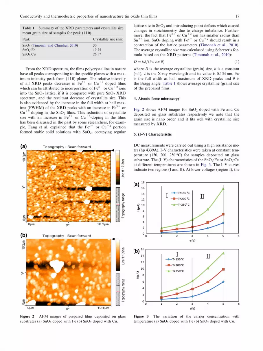
Table 1 Summary of the XRD parameters and crystallite size
mean grain size of samples for peak (110).
Peak Crystallite size (nm)
SnO2 (Timonah and Chunhui, 2010) 30
SnO2:Fe 19.75
SnO2:Cu 26.57
Conductivity and thermoelectric properties of nanostructure tin oxide thin films 17
From the XRD spectrum, the films polycrystalline in naturehave all peaks corresponding to the specific planes with a max-
imum intensity peak from (110) planes. The relative intensityof all XRD peaks decreases in Fe3+ or Cu+2 doped filmswhich can be attributed to incorporation of Fe3+ or Cu+2 ions
into the SnO2 lattice, if it is compared with pure SnO2 XRDspectrum, and the resultant decrease of crystallite size. Thisis also evidenced by the increase in the full width at half max-
ima (FWHM) of the XRD peaks with an increase in Fe3+ orCu+2 doping in the SnO2 films. This reduction of crystallitesize with an increase in Fe3+ or Cu+2-doping in the filmshas been discussed in the past by some researchers, for exam-
ple, Fang et al. explained that the Fe3+ or Cu+2 portionformed stable solid solutions with SnO2, occupying regular
Figure 2 AFM images of prepared films deposited on glass
substrates (a) SnO2 doped with Fe (b) SnO2 doped with Cu.
lattice site in SnO2 and introducing point defects which causedchanges in stoichiometry due to charge imbalance. Further-more, the fact that Fe3+ or Cu+2 ion has smaller radius than
Sn+4 ion, SnO2 doping with Fe3+ or Cu+2 should result in acontraction of the lattice parameters (Timonah et al., 2010).The average crystalline size was calculated using Scherrer’s for-
mula based on the XRD patterns (Timonah et al., 2010):
D ¼ kk=ðdw cos hÞ ð1Þ
where D is the average crystalline (grain) size, k is a constant(�1), k is the X-ray wavelength and its value is 0.154 nm, dwis the full width at half maximum of XRD peaks and h isthe Bragg angle. Table 1 shows average crystalline (grain) sizeof the prepared films.
4. Atomic force microscopy
Fig. 2 shows AFM images for SnO2 doped with Fe and Cu
deposited on glass substrates respectively we note that thegrain size is nano order and it fits well with crystalline sizemeasured by XRD.
5. (I–V) Characteristic
DC measurements were carried out using a high resistance me-ter (hp 4339A). I–V characteristics were taken at constant tem-
perature (150, 200, 250 �C) for samples deposited on glasssubstrate. The (I–V) characteristics of the SnO2:Fe or SnO2:Cuat different temperatures are shown in Fig. 3. The I–V curves
indicate two regions (I and II). At lower voltages (region I), the
Figure 3 The variation of the carrier concentration with
temperature (a) SnO2 doped with Fe (b) SnO2 doped with Cu.

Table 2 Density of states at the Fermi level of samples.
N(EF) (eV�1m�3) T = 150 �C T = 200 �C T= 250 �C
SnO2:Fe 1.77944E + 19 1.33571E + 20 1.25162E + 21
SnO2:Cu 2.65025E + 19 3.47235E + 19 8.73979E + 19
Table 3 Activation energy for all samples at region I and II.
Ea (eV) Region (1) Region (2)
SnO2:Fe 0.2827 0.1727
SnO2:Cu 0.3286 0.1795
18 M.A. Batal et al.
conduction is ohmic, i.e., the current changes linearly with
voltage, but, at higher voltages (region II), the conduction isnonohmic.
The slope of the second region II increases with increasing
temperature. This confirms the presence of space charge lim-ited conductivity, i.e., high-electric conductivity region is gov-erned by the injected space charge. The density of states at the
Fermi level can be determined using the following relation(Fahrettin, 2009):
NðEFÞ ¼2ere0DV
ed2DEF
ð2Þ
Since:
Figure 4 (a) The variation of the potential with Temperature differe
DEF ¼ kTLnI2V1
I1V2
ð3Þ
where DEF is the shift of the quasi-Fermi level, DV is thechange of applied voltage, e is the electronic charge, er isthe dielectric constant of the material (9.65 of SnO2), d is
the film thickness and k is the Boltzmann constant.Table 2 shows the density of states at the Fermi levelof samples.
The electrical conductivity is dependent on temperature ofthe SnO2 doped with Fe or Cu films. It can be analyzed bythe following relation (Fahrettin, 2009):
r ¼ r0 exp � Ea
kT
� �ð4Þ
where Ea is the activation energy, T is the temperature, k is theBoltzmann constant and r0 is the pre-exponential factor. The
electrical conductivity of the film increases with the increaseof temperature.
Activation energy values for regions (I) and (II) were deter-
mined from the slope Lnr ¼ f 1T
� �as shown in Table 3.
Table 3 shows activation energy at lower voltages (region I)is larger than at higher voltages (region II).
6. Thermoelectric properties
The chamber in which the sample was tested was initially
pumped using a rotary pump to a rough vacuum of 1 mbar.
nce, (b) the variation of the Seebeck coefficient with temperature.

Conductivity and thermoelectric properties of nanostructure tin oxide thin films 19
The difference in temperature at the two ends of the samplewas measured by placing two thermocouples at the ends ofthe sample. In order to create a temperature gradient along
with the sample, only one end of the sample was heated leadingto the creation of a hot junction and a cold junction. One ofthe thermocouples measures the temperature at the hot junc-
tion of the sample, whereas the other thermocouple measuresthe temperature at the cold junction.
A graph of the measured thermoelectric against tempera-
ture difference was plotted, Fig. 4a, and the slope of the curvethus obtained gives the Seebeck coefficient of the film Fig. 4b.The Seebeck coefficient of the deposited films was found to bepositive confirming to the p-type behavior of tin oxide doped
with iron or copper.The Seebeck coefficient, S dependence on the temperature
are shown in Fig. 4. In the extrinsic conductivity region, the in-
crease in thermoelectric power with temperature is due to theincreasing number of thermally excited carriers. The Seebeckcoefficient of the film increases with increasing temperature
and indicates two linear regions. The p-type electrical conduc-tivity of the SnO2 doped with iron or copper film originatesfrom ionized defects (Batzill et al., 2005). The sign positive
of Seebeck coefficient increases with increasing temperaturedue to the high mobility of minority carriers. In the oxide semi-conductors with low mobility, the charge carriers are localizedat vacant sites and the conductivity takes place via a hopping
process. Therefore, the carrier concentration for the SnO2
doped Fe or Cu films is described as follows:
n ¼ N exp �Se
k
� �ð5Þ
Figure 5 (a) The variation of the carrier concentration with
temperature, (b) variation of charge carrier mobility with
temperature.
where e is the electron charge, k is the Boltzmann constant, S is
the Seebeck coefficient and N is the density of states.The carrier concentration for the SnO2 film was determined
as a function of temperature using Eq. (5) and is shown in
Fig. 5a. The n values of the film increase with increasing tem-perature. The charge carrier mobility is described as follows(Hammad et al., 2011):
l ¼ 1
enqð6Þ
Fig. 5b shows the charge carrier mobility dependence on tem-perature for the SnO2 doped with Fe or Cu film, the mobility
increases with an increase of temperature. The increase inmobility with temperature suggests that the hopping conduc-tivity is dominant in the SnO2 doped with Fe or Cu film.
7. Seebeck effect improvement of tin oxide films
An ideal thermoelectric material should possess large Seebeck
coefficients, high electrical conductivity and low thermalconductivity. High electrical conductivity is necessary in orderto minimize Joule heating, while a low thermal conductivity
helps to retain heat at the junctions and maintain a largetemperature gradient. In metals, the ratio of the thermal con-ductivity to electrical conductivity is a constant (Wiedemann–
Franz-Lorenz law) and it is not possible to reduce one whileincreasing the other. In semiconductors the ratio of the ther-mal conductivity to electrical conductivity is greater than inmetals owing to their poorer electrical conductivity. This ratio
can be decreased (i.e., the electrical conductivity can be
Figure 6 (a) The variation of the potential with temperature
difference, (b) the variation of the Seebeck coefficient with
temperature.

20 M.A. Batal et al.
increased) if the thermoelectric material is alloyed with an iso-morphous element or compound (Shi et al., 2004).
Fig. 6a,b shows the measured thermoelectric potential as a
function of temperature difference was plotted and the Seebeckcoefficient as a function of temperature for the SnO2:Fe orSnO2:Cu films deposited on porous alumina substrate. The
Seebeck coefficient of the deposited films was found to be po-sitive confirming to the p-type behavior of tin oxide dopedwith iron or copper. Seebeck coefficient for SnO2:Fe is larger
than Seebeck coefficient for SnO2:Cu films deposited on glassand alumina substrates. Seebeck coefficient for films depositedon glass substrate is smaller than Seebeck coefficient for filmsdeposited on alumina substrate and this can be understood due
to deference thermal and electrical conductivity of substrates.
8. Conclusions
In this paper, we have studied the preparation and character-ization of the SnO2:Fe or SnO2:Cu thin films with high ther-moelectric efficiency. These films have been deposited by
using the co-deposition dip coating sol–gel technique. TheXRD spectrum of deposited samples shows a polycrystallinestructure with a clear characteristic peak of SnO2 cassiterite
phase.The thermoelectrical measurements have shown p-type con-
ductivity in thin films with Fe or Cu. Also, the Seebeck coeffi-
cient for SnO2:Fe or SnO2:Cu films deposited on porousalumina substrates prepared by the anodizing technique is lar-ger than Seebeck coefficient for SnO2:Fe or SnO2:Cu filmsdeposited on glass substrates.
References
Bagherim, M., Shahtahmasebi, N., Alinejad, A., Youssefi, M.,
Shokooh-Saremi, M., 2009. Fe-doped SnO2 transparent semi-
conducting thin films deposited by spray pyrolysis technique:
thermoelectric and p-type conductivity properties. Solid State
Sciences 11, 233–239, Tehran.
Banerjee, N., Maity, R., Kundoo, S., Chattopadhyay, K.K., 2004.
Poole–Frenkel effect in nan crystalline SnO2: F thin films prepared
by a sol–gel dip-coating technique. Indian Physics 201, 983–989,
New Delhi.
Batzill, M., Diebold, U., 2005. The surface and materials science of tin
oxide. Progress in Surface Science 79, 47–154, New York.
Bulusua, A., Walkerb, D.G., 2008. Review of electronic transport
models for thermoelectric materials. Superlattices and Microstruc-
tures 44, 1–36, New York.
Fahrettin, Y., 2009. Electrical conductivity, Seebeck coefficient and
optical properties of SnO2 film deposited on ITO by dip coating.
Journal of Alloys and Compounds 74, 55–59. Ankara.
Frank, R., MOOS, R., 2007. Direct thermoelectric gas sensors: design
aspects and first gas sensors. Sensors and Actuators 123, 413–419,
Berlin.
Hammad, T.M., Hejazy, N.K., 2011. Structural, electrical and optical
properties of ATO thin films fabricated by dip coating method.
International Nano Letters 1, 123–128, Jerusalem.
Pichanusakorn, P., Bandaru, P., 2010. Nanostructured thermoelec-
trics. Materials Science and Engineering 67, 19–63, New York.
Shi, L., Hao, Q., Yu, C., 2004. Thermal conductivities of individual tin
dioxide nanobelts. Applied Physics Letters 84, 2638–2641, Tokyo.
Timonah, N.S., Chunhui, Y.L.S., 2010. Structural, optical and
electrical properties of Fe-doped SnO2 fabricated by sol–gel dip
coating technique. Materials Science in Semiconductor Processing
13, 113–125, Pekin.


