Embed Size (px)
Citation preview

www.elsevier.com/locate/tsf
Thin Solid Films 493
Constitution and microstructure of magnetron sputtered nanocomposite
coatings in the system Ti–Al–N–C
M. Stueber a,*, P.B. Barna b, M.C. Simmonds c, U. Albers a, H. Leiste a, C. Ziebert a,
H. Holleck a, A. Kovacs b, P. Hovsepian c, I. Gee c
a Forschungszentrum Karlsruhe, Institute of Materials Research I, Hermann-von-Helmholtz-Platz 1, 76344 Eggenstein-Leopoldshafen, Germanyb Research Institute for Technical Physics and Materials Science, Hungarian Academy of Sciences, Konkoly Thege St. 29-33, H-1121 Budapest, Hungary
c Sheffield Hallam University, Materials Research Institute, City Campus, Howard Street, S1 1WB Sheffield, United Kingdom
Received 18 August 2004; received in revised form 30 June 2005; accepted 25 July 2005
Available online 26 August 2005
Abstract
An ambitious objective in the development of self-lubricating wear-resistant coatings is to make use of lubricious phases such as graphite,
amorphous carbon or MoS2 incorporated into coatings. A series of (Ti,Al)(N,C) coatings with different carbon contents (0–28 at.%) have
been deposited by reactive magnetron sputtering of TiAl in a mixture of Ar, N2 and CH4 gases. The microstructure and constitution of these
coatings have been investigated using electron microprobe analysis, atomic force microscopy, X-Ray photoelectron spectroscopy, cross
sectional transmission electron microscopy, Raman spectroscopy, X-ray diffraction and pole figure analyses. Starting from a pure TiAlN
coating significant changes in the microstructure of the coatings were observed dependent on the carbon concentration. Under optimum
conditions nanocomposite coatings with a structure of a coexisting metastable hard, nanocrystalline fcc TiAlNC phase and an amorphous
carbon phase (a-C) have been deposited. The localization of an amorphous carbon phase has been shown by high-resolution transmission
electron microscopy.
D 2005 Elsevier B.V. All rights reserved.
Keywords: Nanocomposite; Sputtering; Transmission electron microscopy; X-Ray photoelectron spectroscopy
1. Introduction
High-speed manufacturing processes and tribologically
stressed components in many applications have a demand
for innovative materials and surfaces providing complex
multifunctional property profiles covering wear resistance,
oxidation and corrosion resistance and low friction. Nano-
structured and nanocomposite materials and thin films are
promising concepts for the engineering design and realisa-
tion of such property profiles [1–7]. In the field of surface
science and technology the combination of a nanocrystal-
line, hard and wear resistant phase and a lubricious phase
such as amorphous carbon (a-C) or MoS2, coexisting in a
single-layer coating has been reported many times in the
literature [8–17]. The application of crystalline binary hard
0040-6090/$ - see front matter D 2005 Elsevier B.V. All rights reserved.
doi:10.1016/j.tsf.2005.07.290
* Corresponding author. Tel.: +49 7247 82 3889; fax: +49 7247 82 4567.
E-mail address: [email protected] (M. Stueber).
phases, either thermodynamically stable or metastable such
as WC1�x [17–22], TiC1�x [11,23–28], TaC1�x [29], or
TiB2�x [30] in nanocomposites together with a-C are mostly
state-of-the-art and some coatings have been commercially
available for many years. Nanocomposite coatings combin-
ing ternary nanocrystalline metastable hard phases and a-C
have not yet been reported in detail.
The material system Ti–Al–N–C is a good candidate for
examining the synthesis of such coatings as it offers well-
known metastable hard phases such as TiAlN and TiAlNC
which are the basis for the presently most frequently used
coatings in the tool industry. With (Ti,Al)N coatings for
example, a higher oxidation resistance up to 750 -C, anincreased hardness and a better cutting performance
compared to pure TiN films was reported first by Munz
and Knotek et al. [31,32]. The development and optimisa-
tion of (Ti,Al)N based thin films since then is described in
the excellent review article of PalDey and Deevi [33].
(2005) 104 – 112
M. Stueber et al. / Thin Solid Films 493 (2005) 104–112 105
Detailed information on the constitution, microstructure and
thermodynamic stability of phases in the Ti–Al–N system
as well as the properties and performance of Ti–Al–N thin
films prepared by various physical vapour deposition (PVD)
methods such as magnetron sputtering, ion beam assisted
deposition, arc evaporation, arc ion plating or chemical
vapour deposition (CVD) methods such as plasma enhanced
CVD are given in the literature [34–46].
Zhang et al. prepared (Ti,Cr)CN nanocrystalline films by
magnetron sputtering [47]. Shieh and Hon [48] reported on
chemical vapour deposited nanocomposite coatings of
(Ti,Al)(C,N), while Lackner et al. investigated the chemical,
microstructural and tribological properties of (Ti,Al)(C,N)
coatings deposited by pulsed laser deposition [49].
In the present work, a series of (Ti,Al)(N,C) coatings
with different carbon contents (0–28 at.%) have been
deposited by reactive magnetron sputtering of TiAl in a
mixture of Ar, N2 and CH4 gases. Starting from a pure
(Ti,Al)N coating significant changes in the microstructure of
the coatings were observed dependent on the carbon
concentration. Under optimum conditions nanocomposite
coatings with a structure of a coexisting metastable hard,
nanocrystalline fcc TiAlNC phase and an a-C phase have
been deposited. This paper presents and discusses the
preparation, growth, constitution and microstructure of
these coatings.
2. Experimental details
2.1. Deposition method
(Ti,Al)(N,C) single layer coatings of various micro-
structure and constitution have been prepared by reactive
magnetron sputtering of a TiAl target in a mixture of Ar, N2
and CH4 gases. The equipment used was a Hauzer HTC 625
machine. The target applied was made of a commercially
available TiAl alloy composed of 50 mol% Ti and 50 mol%
Al. The target size was 400�125 mm. All deposition
experiments have been carried out at a target power of 6 kW.
Commercially available hard metal tool inserts have been
used as substrates for all samples apart from those for the
pole figure measurements, where thermally oxidized Si
single crystals have been used to avoid substrate interfe-
rence effects. Prior to deposition the substrate materials have
been ultrasonically cleaned in acetone and isopropanol for
15 min and have been plasma-etched by a dc glowing
discharge in argon for 90 min. The SiO2 surface layer of the
Si single crystals has been completely etched away during
the plasma etching. During deposition the substrate temper-
ature was kept constant at 400 -C for all films and a constant
bias voltage of �80 V dc was applied to the substrates. The
argon gas flow was kept constant at 200 sccm while the
nitrogen gas flow was kept constant at 32 sccm, giving a
total pressure of 0.34 Pa. The CH4 gas flow was varied
systematically between 0 and 30 sccm.
2.2. Characterisation of microstructure, constitution and
properties
The elemental composition of the (Ti,Al)(N,C) coatings
was characterised by electron microprobe analysis (EMPA)
using a Cameca microbeam system.
The microstructure of the coatings was investigated by
cross sectional transmission electron microscopy (XTEM,
Philips CM20 and JEOL 3010 UHR) as well as by selected
area electron diffraction (SAED). Cross sectional specimens
were prepared in a Technoorg Linda IV/H/L ion beam
thinning apparatus. Ion beam thinning was completed with
low angle and low energy ion beam (<200 eV) according to
the method reported by Barna and Barna and Pecz [50,51].
The diffraction patterns were evaluated with the Process
Diffraction software tool developed by Labar [52,53].
X-ray photoelectron spectroscopy (XPS) analysis was
performed on a Kratos Axis 165 XPS spectrometer using
monochromatic Al Ka (1486.6 eV) radiation in a vacuum of
around 5�10�9 mbar. Survey scans were performed at a
pass energy of 80 eV, high resolution scans of 20 eV; in this
configuration the FWHM peak width of the Ag 3d 5/2 peak
is around 0.6 eV. The energy analyser was calibrated using
the Ag 3d and Auger lines prior to use and the Ag 3d peak
was monitored during the XPS measurements to control
energy shifts due to electrostatic charging [54].
Raman spectroscopy was performed using a Renishaw
Raman System 2000 spectrometer. The holographic notch
filters allowed a lower spectral limit of ¨150 cm�1. The
excitation wavelength used was 632.8 nm (25 mW power)
from a HeNe laser. A maximum throughput of 4–5 mW was
possible at the sample in a 1–2 Am spot through at standard
50� microscope objective. The penetration depth into these
PVD coatings is low, approximately 100–200 nm, the main
controlling factors are: reflectivity of the surface, density,
colouration, and topography.
Glancing angle X-ray diffraction (GAXRD) was per-
formed on a Phillips PW1710 X-ray diffractometer. Typi-
cally, an incidence angle of 5 degrees was used with Cu Ka
radiation (k=0.15418 nm). X-ray pole figures were
obtained on a Phillips X’Pert X-ray diffractometer again
using Cu Ka radiation.
Mechanical properties and the performance of the coa-
tings on tool steel substrates have been characterised by
measuring the microhardness applying the Vickers method
(0.5 N load) and the critical load of failure in the scratch test
(CSEM Revetest). The coating thickness was determined by
surface profilometry.
3. Results and discussion
The chemical composition and the constitution of the
deposited (Ti,Al)(N,C) films are given in Table 1. The argon
contamination of the coatings is not specified in this table as
it is below 0.1 at.% for all films, as measured by EMPA. The

Table 1
Chemical composition and constitution of (Ti,Al)(N,C) coatings deposited
by reactive dc magnetron sputtering from a TiAl alloy target under variation
of the methane gas flow
Sample
no.
Coating type and
microstructure
Elemental composition (at.%)
Ti Al N C O
1 nc fcc TiAlN 26.7 26.5 45.0 0.7 1.0
2 nc fcc TiAlNC 21.7 26.5 45.3 5.5 0.9
3 nc fcc TiAlNC+a-C 20.6 24.1 46.4 8.1 0.8
4 nc fcc TiAlNC+a-C 21.2 23.0 45.5 9.5 0.7
5 nc fcc TiAlNC+a-C 20.4 22.6 42.7 13.5 0.7
6 nc fcc TiAlNC+a-C 19.5 21.8 41.4 16.3 1.1
7 nc fcc TiAlNC+a-C 17.0 19.0 34.9 28.0 0.9
All other deposition parameters were kept constant.
36 37 38 39 40
(Rel
ativ
e in
tens
ity (
arb.
uni
ts)
Diffraction angle, 2θ (degrees)
0 at.% C
5.5 at.% C8.1 at.% C
9.5 at.% C
28.0 at.% C
Fig. 1. GAXRD diffractograms of reactively sputtered (Ti,Al)(N,C) films
showing the shift of the (111) peaks of TiAlN like structure with increasing
carbon content. The dashed lines are an aid to the eye to show the shift in
peak position.
8.1 at.% C
nten
sity
(ar
b. u
nits
)
M. Stueber et al. / Thin Solid Films 493 (2005) 104–112106
Ti / (Ti+Al) and the non-metal /metal ratio are given in
Table 2. It is clear that the Ti / (Ti+Al) ratio is nearly 0.5 and
remains constant for all coatings independent on the non-
metal /metal ratio. In the case of the nearly carbon-free
(Ti,Al)N coatings the non-metal /metal ratio is 0.85 while
with increasing carbon concentration the overall non-metal /
metal (N+C) / (Ti+Al) ratio increases significantly. This
behaviour is clearly related to the increasing carbon
concentration caused by the increasing methane gas flow.
The N/ (Ti+Al) ratio is between 0.85 and 1.04.
Glancing angle X-ray diffractograms are shown in Figs.
1 and 2. GAXRD differs from conventional Bragg–
Brentano XRD in that in the Bragg–Brentano geometry
the diffraction vector is normal to the surface. For a glancing
angle incidence of 5-, as used in this study, the diffraction
vector is approximately 13- and 15- off the surface normal
for the (111) and (200) orientations, respectively. GAXRD
was used in preference to Bragg–Brentano XRD in this
study to avoid strong substrate interference effects. Figs. 1
and 2 and analysis of diffractograms taken over a large
range of diffraction angles indicates the presence of the
cubic B1-NaCl structure only in all coatings. From Fig. 1 it
can be seen that the (111) peak position moves to a lower
diffraction angle indicating an expansion in the d-spacing
with increasing carbon content. The change in the d-spacing
with increasing carbon content is shown in Fig. 3a. For pure
(Ti,Al)N coatings the lattice spacing corresponding to the
(111) reflection was calculated to be d111=0.2402 nm which
shows reasonable agreement with values for TiAlN in the
literature [55]. With increasing carbon content up to around
Table 2
Ti / (Ti+Al) and non-metal /metal atomic concentration ratios of magnetron-
sputtered (Ti,Al)(N,C) coatings
Sample no. Ti / (Ti+Al) N/ (Ti+Al) C/ (Ti+Al) (N+C) / (Ti+Al)
1 0.50 0.85 0.01 0.86
2 0.45 0.94 0.11 1.05
3 0.46 1.04 0.18 1.22
4 0.48 1.03 0.22 1.25
5 0.47 0.99 0.32 1.31
6 0.47 1.00 0.39 1.40
7 0.47 0.97 0.78 1.75
9.5 at.% C the lattice spacing increases approximately
linearly to 0.2434 nm. Above 9.5% the d-spacing is nearly
constant and only increases slightly. The film with the
highest carbon concentration of 28 at.% has a value of
d111=0.2437 nm. A similar relationship between d-spacing
and the (200) reflection was also observed (Fig. 3b). The
lattice parameters of fcc-TiC and fcc-TiN are 0.4328 and
0.4238 nm, respectively. The expansion of the lattice that is
observed here may be due to the direct substitution of
carbon into the nitrogen lattice positions, because of the
larger atomic radius of carbon in comparison to nitrogen.
42 43 44 45
5.5 at.% C
9.5 at.% C
Diffraction angle, 2θ (degrees)
Rel
ativ
e i
0 at.% C
28.0 at.% C
Fig. 2. GAXRD diffractograms of reactively sputtered (Ti,Al)(N,C) films
showing the shift of the (200) peaks of the TiAlN like structure with
increasing carbon content. The dashed lines are an aid to the eye to show
the shift in peak position.

0 5 10 15 20 25 30
2.40
2.41
2.42
2.43
2.44
d-sp
acin
g (A
ngst
rom
)
Carbon content (at.%)
0 5 10 15 20 25 30
2.08
2.09
2.10
2.11
d-sp
acin
g (A
ngst
rom
)
Carbon content (at.%)
(b)
(a)
Fig. 3. Graph showing the variation in the d-spacing of (a) the (111) planes
and (b) the (200) plane versus the carbon content of the films. The error
bars represent the error estimate on the determination of the d-spacing.
(111) peak (200) peak
5.5
at.%
C
8.1
at.%
C16
.3 a
t.%
C28
.0 a
t.%
C
Fig. 4. X-Ray Diffraction pole figures of the (111) and (200) peaks for the
(Ti,Al)(N,C) coating with 5.5, 8.1, 16.3, and 28.0 at.�% carbon.
M. Stueber et al. / Thin Solid Films 493 (2005) 104–112 107
The threshold at around 9.5 at.% suggest that this
substitution occurs readily at low carbon contents but
saturates at values above this value. Where the excess
carbon is situated above this threshold is not indicated from
the XRD.
Fig. 1 shows a peak broadening of the (111) reflection
with increasing C content. This indicates a decreasing grain
size with increasing carbon content. Further insight into the
growth of these films is shown in the X-ray pole figures of
films prepared on Si substrates (Fig. 4). The pole figures
indicate that the films of C content up to 13.5 at.% C have
well pronounced two-axis texture [56] with (111) texture
axis off to the substrate normal. The (200) orientation pole
figures of this range of C content show three well defined
peaks with a tilt angle of approximately 55 - with respect to
the (111) peak maximum. These peaks are related to the
(100) planes of the (111) oriented crystals and clearly prove
the crystals are aligned with respect to the surface. This
alignment can be related to the orientation effect of the ion-
sputtered Si single crystal substrates. In a recent study
Kovacs et al. have shown that the (Ti,Al)(N,C) coatings
with 5.5 at.% grow epitaxially on hard metal substrate [57].
However the substrate interference effects did not allow to
record pole figures on these samples grown on hard metal.
The pole figures of the coatings with 16.3 and 28 at.% C
indicate the decreasing texturing with increasing C content.
No (200) texture could be detected in any of the coatings
investigated. Evidence for the existence of the two-axis
texture can also be seen in the AFM image of a coating with
5.5 at.% C (Fig. 5). This figure is representative for the
whole surface of this sample and clearly illustrates the three-
fold symmetry of (100) planes.
In TEM characterisation the strong correlation between
the carbon content, grain size and morphology can be seen
in more detail (Figs. 6–8). All coatings show a columnar
morphology of structure zone T according to the structure
zone models of Thornton and of Barna and Adamik [58,59].
The columnar morphology of carbon-free (Ti,Al)N thin
coatings agrees well to similar findings documented in the
literature [37,60]. The columns are single crystals and are
separated by tight grain boundaries. Doping the (Ti,Al)N
coating with C very pronounced grain boundaries show up

Fig. 7. Cross sectional TEM images of a (Ti,Al)(N,C) coating with a C
content of 13.5 at.%: a) bright field image with corresponding SAED
pattern, b) dark field image taken by (200) reflection of fcc TiAlNC phase,
c) HRTEM image: the arrows indicate the amorphous carbon cluster
inclusions at the grain boundaries.
Fig. 5. AFM image of a (Ti,Al)(N,C) coating with a C content of 5.5 at.%.
M. Stueber et al. / Thin Solid Films 493 (2005) 104–112108
on the XTEM images at lower C concentrations <9.5 at.%
(Fig. 6). The columns are single crystals and the surface
topography corresponds to the topography of the points of
individual columns. In the range of 5.5 to 13.5 at.% C the
diameter of columns is decreasing with increasing carbon
concentration (for example, the average column diameter
was 440 nm in the case of 5.5 at.% C and 300 nm,
respectively in the case of 8.1 at.% C). The columns are
separated by pronounced grain boundaries containing an
amorphous phase. In the range of C concentration of 9.5–
16.3 at.% the columnar structure transforms into a dense
fibre-like structure (Fig. 7a). Dark field images (Fig. 7b)
indicate that the fibres are mostly single crystals and no
pronounced grain boundaries can be identified at this
resolution. However, in the high-resolution TEM image
(Fig. 7c) amorphous carbon cluster inclusions of 1–2 nm
size at grain boundaries can be seen. The average column
diameter is further reduced to a minimum value of 52 nm for
coatings with 13.5 at.% C and then increases with increasing
carbon concentration. The structure of coatings with high C
concentration (C>20 at.%) is homogenous with nano-
crystalline structure in the near substrate region and trans-
Fig. 6. XTEM images of a (Ti,Al)(N,C) coating with a C content of 5.5
at.%: a) bright field image, b) dark field image, c) selected area diffraction
pattern.
forms into a columnar structure with increasing film
thickness. The columns have large diameter (about 200–
250 nm for films with 28 at.% C) and well defined column
boundaries (Fig. 8). The phase contrast images clearly show
that columns are composed of frond-like lamellae (Fig. 8b).
According to the high-resolution TEM images (Fig. 8c) the
frond-like lamellae are separated by an amorphous phase.
Fig. 8. Cross sectional TEM images of a (Ti,Al)(N,C) coating with a C
content of 28.0 at.%: a) bright field image with corresponding SAED
pattern, b) phase contrast image, c) HRTEM image: the arrows indicate the
amorphous phase between the frond-like lamellae.
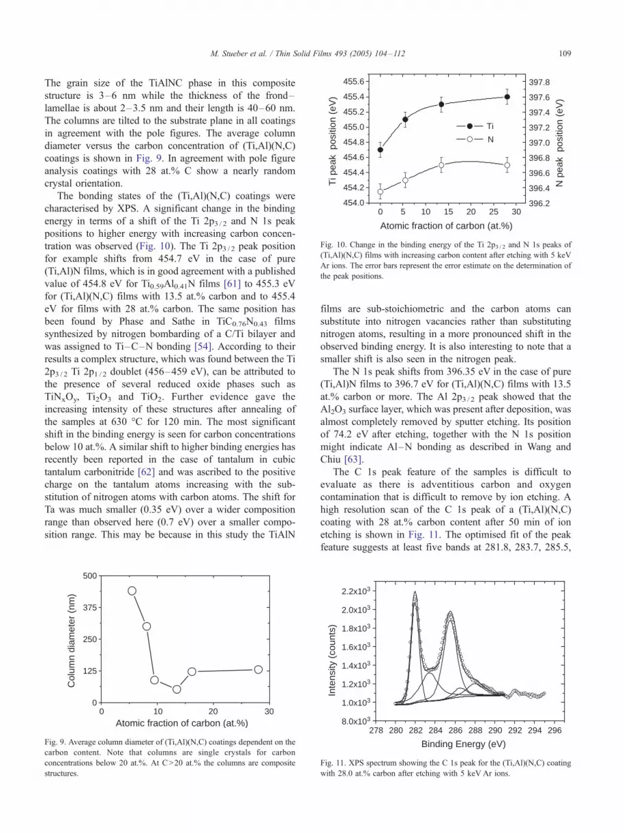
0 5 10 15 20 25 30454.0
454.2
454.4
454.6
454.8
455.0
455.2
455.4
455.6
396.2
396.4
396.6
396.8
397.0
397.2
397.4
397.6
397.8
Ti
N p
eak
pos
ition
(eV
)
Ti p
eak
pos
ition
(eV
)
Atomic fraction of carbon (at.%)
N
Fig. 10. Change in the binding energy of the Ti 2p3 / 2 and N 1s peaks of
(Ti,Al)(N,C) films with increasing carbon content after etching with 5 keV
Ar ions. The error bars represent the error estimate on the determination of
the peak positions.
M. Stueber et al. / Thin Solid Films 493 (2005) 104–112 109
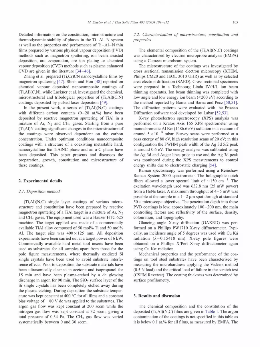
The grain size of the TiAlNC phase in this composite
structure is 3–6 nm while the thickness of the frond–
lamellae is about 2–3.5 nm and their length is 40–60 nm.
The columns are tilted to the substrate plane in all coatings
in agreement with the pole figures. The average column
diameter versus the carbon concentration of (Ti,Al)(N,C)
coatings is shown in Fig. 9. In agreement with pole figure
analysis coatings with 28 at.% C show a nearly random
crystal orientation.
The bonding states of the (Ti,Al)(N,C) coatings were
characterised by XPS. A significant change in the binding
energy in terms of a shift of the Ti 2p3 / 2 and N 1s peak
positions to higher energy with increasing carbon concen-
tration was observed (Fig. 10). The Ti 2p3 / 2 peak position
for example shifts from 454.7 eV in the case of pure
(Ti,Al)N films, which is in good agreement with a published
value of 454.8 eV for Ti0.59Al0.41N films [61] to 455.3 eV
for (Ti,Al)(N,C) films with 13.5 at.% carbon and to 455.4
eV for films with 28 at.% carbon. The same position has
been found by Phase and Sathe in TiC0.76N0.43 films
synthesized by nitrogen bombarding of a C/Ti bilayer and
was assigned to Ti–C–N bonding [54]. According to their
results a complex structure, which was found between the Ti
2p3 / 2 Ti 2p1 / 2 doublet (456–459 eV), can be attributed to
the presence of several reduced oxide phases such as
TiNxOy, Ti2O3 and TiO2. Further evidence gave the
increasing intensity of these structures after annealing of
the samples at 630 -C for 120 min. The most significant
shift in the binding energy is seen for carbon concentrations
below 10 at.%. A similar shift to higher binding energies has
recently been reported in the case of tantalum in cubic
tantalum carbonitride [62] and was ascribed to the positive
charge on the tantalum atoms increasing with the sub-
stitution of nitrogen atoms with carbon atoms. The shift for
Ta was much smaller (0.35 eV) over a wider composition
range than observed here (0.7 eV) over a smaller compo-
sition range. This may be because in this study the TiAlN
0 10 20 300
125
250
375
500
Col
umn
diam
eter
(nm
)
Atomic fraction of carbon (at.%)
Fig. 9. Average column diameter of (Ti,Al)(N,C) coatings dependent on the
carbon content. Note that columns are single crystals for carbon
concentrations below 20 at.%. At C>20 at.% the columns are composite
structures.
films are sub-stoichiometric and the carbon atoms can
substitute into nitrogen vacancies rather than substituting
nitrogen atoms, resulting in a more pronounced shift in the
observed binding energy. It is also interesting to note that a
smaller shift is also seen in the nitrogen peak.
The N 1s peak shifts from 396.35 eV in the case of pure
(Ti,Al)N films to 396.7 eV for (Ti,Al)(N,C) films with 13.5
at.% carbon or more. The Al 2p3 / 2 peak showed that the
Al2O3 surface layer, which was present after deposition, was
almost completely removed by sputter etching. Its position
of 74.2 eV after etching, together with the N 1s position
might indicate Al–N bonding as described in Wang and
Chiu [63].
The C 1s peak feature of the samples is difficult to
evaluate as there is adventitious carbon and oxygen
contamination that is difficult to remove by ion etching. A
high resolution scan of the C 1s peak of a (Ti,Al)(N,C)
coating with 28 at.% carbon content after 50 min of ion
etching is shown in Fig. 11. The optimised fit of the peak
feature suggests at least five bands at 281.8, 283.7, 285.5,
278 280 282 284 286 288 290 292 294 2968.0x103
1.0x10³
1.2x10³
1.4x10³
1.6x10³
1.8x10³
2.0x10³
2.2x10³
Inte
nsity
(co
unts
)
Binding Energy (eV)
Fig. 11. XPS spectrum showing the C 1s peak for the (Ti,Al)(N,C) coating
with 28.0 at.% carbon after etching with 5 keV Ar ions.

0 5 10 15 20 25 300.0
5.0x10⁴
1.0x10⁵
1.5x10⁵
2.0x10⁵
2.5x10⁵
3.0x10⁵
3.5x10⁵
4.0x10⁵
Inte
nsity
(co
unts
)
Atomic fraction of Carbon (%)
Fig. 13. Integrated peak intensity of the D–G band versus the carbon
content of the films.
M. Stueber et al. / Thin Solid Films 493 (2005) 104–112110
286.5 and 287.9 eV. The signal at 281.8 eV can be attributed
to Ti–C bonding, whereas the signals at 285.5 and 286.5 eV
are typical for C–OH bonding and aliphatic/h-carbons andother adventitious hydrocarbons as sputter etching residues,
respectively [64]. The nature of the other broader bands at
283.7 and 287.9 eV is not absolutely clear but might be
attributable to interfacial carbon at the grain boundaries [64]
and CO species due to recontamination during the XPS
analysis, respectively. Moreover XPS indicates that a two-
phase microstructure dominates in the coatings with high
carbon content.
Additional information on the coating constitution can be
obtained from Raman spectroscopy which is a sensitive
measure for various forms of carbon. The Raman spectra of
the (Ti,Al)(N,C) films are given in Fig. 12. The onset of a
broad band between 1350 and 1600 cm�1 characteristic for
carbon–carbon bonding of a highly disordered amorphous
carbon phase of mixed sp2 and sp3 bonding is visible at
films with higher carbon concentrations. The integrated
peak intensity shows that the D–G bands are seen at carbon
contents of 8.1 at.% and higher and that both bands increase
strongly with increasing carbon content (Fig. 13). This
confirms the existence of a free a-C phase in the
(Ti,Al)(N,C) films at higher C concentrations as indicated
by XTEM and XPS characterisation.
Thickness, critical load of failure in the scratch test and
the Vickers microhardness of the (Ti,Al)(N,C) coatings are
summarised in Table 3.
From the chemical composition of the carbon-free
metastable nanocrystalline fcc TiAlN films a N-deficit is
obvious from the (Ti+Al) /N ratio. Thus the microstructure
evolution of these coatings dependent on the carbon content
might be explained by a five-step growth model: 1) The
growth starts from a sub-stoichiometric (Ti,Al)N1�x phase
with a significant N-deficit. 2) By adding carbon to the
coating these lattice places are filled and a single-phase
nanocrystalline fcc TiAlNC structure is built. 3) Once the N-
vacancies are filled, carbon atoms can substitute regular N
0 1000 2000 3000 4000
28.0 at. % C
13.5 at. % C
5.5 at.% C
Inte
nsity
(ar
b. u
nits
)
Raman Shift (cm-1)
8.1 at.% C
9.5 at.% C
16.3 at. % C
Fig. 12. Raman spectra showing the onset of the D–G band (the dotted
box) characteristic for amorphous carbon with increasing carbon content in
the (Ti,Al)(N,C) coatings.
positions. 4) Exceeding the solubility range of carbon within
the TiAlN lattice, which seems to occur above 8 at.% of
carbon, the carbon starts to build nanoclusters or agglome-
rates at grain boundaries of the (Ti,Al)(N,C) lattice. 5) When
increasing the C content further, the size of carbon clusters
increases and larger domains of amorphous carbon phase or
even an amorphous carbon matrix can be formed on the
growth surface of TiAlNC crystals. The growth of TiAlNC
crystals is interrupted by these C domains decreasing the
grain size of TiAlNC further. This process leads to the
formation of a frond-like structure characterizing the films of
28 at.% C. Thus if the maximum solubility for carbon in the
nanoscale fcc lattice is achieved, the growth of phase-
separated nanocomposite coatings starts. This phase separa-
tion seems to take place during the structure formation and to
follow the thermodynamic rules and kinetics of PVD phase
transitions. The occurrence of coexisting nanocrystalline/
amorphous phases in ternary and quaternary systems was
predicted by Holleck already in 1986 on the basis of
theoretical considerations on the thermodynamics and
kinetics of PVD processes [65] and again by Veprek on the
basis of his extensive experimental and theoretical work on
the Ti–Si–N system [66]. Furthermore our results are in
excellent agreement with a recently published paper by
Lackner et al., who identified very similar growth mecha-
Table 3
Thickness, critical load of failure in the scratch test and Vickers
microhardness of magnetron-sputtered (Ti,Al)(N,C) coatings
Sample
no.
(Ti,Al)(N,C)
coating, carbon
content (at.%)
Thickness
(Am)
Critical load
of failure (N)
Microhardness
(HV0.05)
1 0 4.7 15 1852
2 5.5 5.8 120 1401
3 8.1 4.2 25 1528
4 9.5 3.5 45 1622
5 13.5 4.7 45 1635
6 16.3 5.4 35 1554
7 28.0 5.1 30 1141

M. Stueber et al. / Thin Solid Films 493 (2005) 104–112 111
nisms and microstructures for (Ti,Al)(C,N) coatings depo-
sited by pulsed laser deposition [49].
4. Conclusions
It has been shown that it is possible to create by PVD
methods a nanocomposite coating coexisting of two
metastable phases, one of them being nanocrystalline and
the other being amorphous. The microstructural arrange-
ment of both these phases, i.e., in the form of isolated a-C
clusters within a nanocrystalline matrix or as a continuous
amorphous network or matrix percolated with the nano-
crystalline phase, clearly depends on the process parameters
selected for deposition and can be explained by the
proposed five-step growth model. From this point of view
and as well from the literature it can be concluded that these
different microstructures will result in completely different
property profiles of such coatings. The properties of
nanocomposite coatings are determined by phase boundaries
and by the materials selected to build them. The ability to
synthesise metastable nanocrystalline phases within a nano-
composite coating and the combination of various types of
nanocomposite layers within a nanocomposite multilayer
thin film will offer to the material scientist a powerful tool
for an engineering design of the coatings properties and
performance. For example, the idea of superlattice coatings
built of nanocomposite layers of similar microstructure
seems very promising for future applications.
Taking into account the similarities and differences
between the reported type of nanocomposite coatings and
the literature it must be concluded that the modelling and
simulation of nanocomposite growth processes should focus
on the fundamentals of materials science and thermody-
namics. Exciting properties such as super-toughness and
super-hardness are desired for many applications but are
always only a result of the design of the constitution and
microstructure of a coating. To achieve success in future
engineering of multifunctional PVD coating properties for
specific applications, a deep knowledge and understanding
of phase relations in the phase diagrams, of the thermody-
namics and kinetics of the deposition process and of the
corresponding PVD phase diagrams is desired.
Acknowledgements
The authors would like to appreciate the funding of this
work by the European Commission within Framework
Programme 5 under the Growth Programme, Grant G5RD-
CT2001-00578. Parts of the TEM characterisation is grate-
fully acknowledged also by the Hungarian National Research
Foundation, contract no. OTKAT033075 and T043437. The
technical assistance of D. Zahoor and S. Creasey as well as
discussions with Dr. B. Lewis, Dr. S. Ulrich and Dr. J.
Rodenburg are also gratefully acknowledged.
References
[1] H. Holleck, H. Schulz, Thin Solid Films 153 (1987) 11.
[2] H. Holleck, M. Lahres, Mater. Sci. Eng., A Struct. Mater.: Prop.
Microstruct. Process. 140 (1991) 609.
[3] H. Gleiter, Adv. Mater. 4 (1992) 474.
[4] S. Veprek, S. Reiprich, Thin Solid Films 268 (1995) 64.
[5] O. Knotek, E. Lugscheider, F. Loffler, B. Bosserhoff, S. Schmitz,
Mater. Sci. Eng., A Struct. Mater.: Prop. Microstruct. Process. 209
(1996) 394.
[6] J. Musil, Surf. Coat. Technol. 125 (2000) 322.
[7] R. Hauert, J. Patscheider, Adv. Eng. Mater. 2 (2000) 247.
[8] C.P. Klages, R. Memming, Mat. Sci. Forum 52–53 (1989) 609.
[9] H. Dimigen, C.P. Klages, Surf. Coat. Technol. 49 (1991) 543.
[10] K. Bewilogua, H. Dimigen, Surf. Coat. Technol. 61 (1993) 144.
[11] A.A. Voevodin, S.V. Prasad, J.S. Zabinski, J. Appl. Phys. 82 (1997)
855.
[12] A.A. Voevodin, J.S. Zabinski, Thin Solid Films 370 (2000) 223.
[13] D. Nilsson, F. Svahn, U. Wiklund, S. Hogmark, Wear 254 (2003)
1084.
[14] R. Gilmore, M.A. Baker, P.N. Gibson, W. Gissler, M. Stoiber, P.
Losbichler, C. Mitterer, Surf. Coat. Technol. 108–109 (1998) 345.
[15] A. Savan, E. Pfluger, R. Goller, W. Gissler, Surf. Coat. Technol. 126
(2000) 159.
[16] Y.W. Bae, W.Y. Lee, C.S. Yust, P.J. Blau, T.M. Besmann, J. Am.
Ceram. Soc. 79 (1996) 819.
[17] W. Precht, A. Czyzniewski, Surf. Coat. Technol. 174–175 (2003)
979.
[18] A.A. Voevodin, J.P. O‘Neill, S.V. Prasad, J.S. Zabinski, J. Vac. Sci.
Technol., A, Vac. Surf. Films 17 (1999) 986.
[19] O.R. Monteiro, M.-P. Delplancke-Ogletree, I.G.G. Brown, Thin Solid
Films 342 (1999) 100.
[20] A.A. Voevodin, J.P. O‘Neill, J.S. Zabinski, Thin Solid Films 342
(1999) 194.
[21] O. Wanstrand, M. Larsson, P. Hedenqvist, Surf. Coat. Technol. 111
(1999) 247.
[22] S.J. Park, K.-R. Lee, D.-H. Ko, K.Y. Eun, Diamond Relat. Mater. 11
(2002) 747.
[23] M. Wang, K. Schmidt, K. Reichelt, H. Dimigen, H. Hubsch, Surf.
Coat. Technol. 47 (1991) 691.
[24] W.J. Meng, R.C. Tittsworth, L.E. Rehn, Thin Solid Films 377–378
(2000) 222.
[25] U. Wiklund, M. Nordin, O. Wanstrand, M. Larsson, Surf. Coat.
Technol. 124 (2000) 154.
[26] T. Zehnder, J. Patscheider, Surf. Coat. Technol. 133–134 (2000) 138.
[27] B. Feng, D.M. Cao, W.J. Meng, L.E. Rehn, P.M. Baldo, G.L. Doll,
Thin Solid Films 398–399 (2001) 210.
[28] M. Stuber, H. Leiste, S. Ulrich, H. Holleck, D. Schild, Surf. Coat.
Technol. 150 (2002) 218.
[29] C. Benndorf, M. Grischke, H. Koeberle, R. Memming, A. Brauer, F.
Thieme, Surf. Coat. Technol. 36 (1988) 171.
[30] R. Gilmore, M.A. Baker, P.N. Gibson, W. Gissler, Surf. Coat. Technol.
105 (1998) 45.
[31] W.-D. Munz, J. Vac. Sci. Technol., A, Vac. Surf. Films 4 (1986) 2717.
[32] O. Knotek, M. Bohmer, T. Leyendecker, J. Vac. Sci. Technol., A, Vac.
Surf. Films 4 (1986) 2695.
[33] S. PalDeey, S.C. Deevi, Mater. Sci. Eng., A Struct. Mater.: Prop.
Microstruct. Process. 342 (2003) 58.
[34] J.C. Schuster, J. Bauer, J. Solid State Chem. 53 (1984) 260.
[35] L. Hultman, Vacuum 57 (2000) 1.
[36] D. McIntyre, J.E. Greene, G. Hakansson, J.-E. Sundgren, W.-D. Munz,
J. Appl. Phys. 67 (1990) 1542.
[37] L. Hultman, G. Hakansson, U. Wahlstrom, J.-E. Sundgren, I. Petrov, F.
Adibi, J.E. Greene, Thin Solid Films 205 (1991) 153.
[38] J. Musil, H. Hruby, Thin Solid Films 365 (2000) 104.
[39] P.W. Shum, Z.F. Zhou, K.Y.X. Li, Y.G. Shen, Mater. Sci. Eng., B,
Solid-State Mater. Adv. Technol. 100 (2003) 204.

M. Stueber et al. / Thin Solid Films 493 (2005) 104–112112
[40] Y. Setsuhara, T. Suzuki, Y. Makino, S. Miyake, T. Sakata, H. Mori,
Surf. Coat. Technol. 97 (1997) 254.
[41] A. Horling, L. Hultman, M. Oden, J. Sjolen, L. Karlsson, J. Vac. Sci.
Technol., A, Vac. Surf. Films 20 (2002) 1815.
[42] A. Kimura, H. Hasegawa, K. Yamada, T. Suzuki, Surf. Coat. Technol.
120–121 (1999) 438.
[43] K. Sato, N. Ichimiya, A. Kondo, Y. Tanaka, Surf. Coat. Technol. 163–
164 (2003) 135.
[44] K.H. Kim, S.H. Lee, Thin Solid Films 283 (1996) 165.
[45] C. Jarms, H.-R. Stock, P. Mayr, Surf. Coat. Technol. 108–109 (1998)
206.
[46] O. Kyrylov, R. Cremer, D. Neuschutz, R. Prange, Surf. Coat. Technol.
151–152 (2002) 359.
[47] S. Zhang, Y. Fu, H. Du, X.T. Zeng, Y.C. Liu, Surf. Coat. Technol. 162
(2002) 42.
[48] J. Shieh, M.H. Hon, J. Vac. Sci. Technol., A, Vac. Surf. Films 20
(2002) 87.
[49] J.M. Lackner, W. Waldhauser, R. Ebner, R.J. Bakker, T. Schoberl, B.
Major, Thin Solid Films 468 (2004) 125.
[50] A. Barna, Mater. Res. Soc. Symp. Proc. 254 (1991) 3.
[51] A. Barna, B. Pecz, M. Menyhard, Ultramicroscopy 70 (1998)
161.
[52] J.L. Labar, in: L. Frank, F. Ciampor (Eds.), Proceedings of the
12th European Congress on Electron Microscopy, Brno, Czech
Republic, Instrumentation and Methodology, vol. 3, 2000 (July
10–14), pp. I379.
[53] J.L. Labar, Microsc. Anal. 75 (2002) 9.
[54] D.M. Phase, V. Sathe, J. Phys. D: Appl. Phys. 37 (2004) 1696.
[55] M. Zhou, Y. Makino, M. Nose, K. Nogi, Thin Solid Films 339 (1999)
203.
[56] E. Bauer, in: M.H. Francombe, H. Sato (Eds.), Single-Crystal Films,
Proceedings of an International Conference Held at Philco Scientific
Laboratory, Blue Bell, Pennsylvania, U.S.A., May 1963, Pergamon
Press, Oxford, 1964, p. 58.
[57] A. Kovacs, B. Veisz, P.B. Barna, G. Radnoczi, M. Stuber, in: G. Van
Tendeloo (Ed.), Proceedings of the 13th European Microscopy
Congress, Antwerp, Belgium, August 22–27, Materials Science, vol.
2, 2004, pp. II39.
[58] J.A. Thornton, J. Vac. Sci. Technol., A, Vac. Surf. Films 4 (1986)
3059.
[59] P.B. Barna, M. Adamik, Thin Solid Films 317 (1998) 27.
[60] G. Hakanson, J.-E. Sundgren, D. McIntyre, J. Greene, W.D. Munz,
Thin Solid Films 153 (1987) 55.
[61] P.W. Shum, K.Y. Li, Z.F. Zhou, Y.G. Shen, Surf. Coat. Technol. 185
(2004) 245.
[62] O.Yu. Khyzhun, V.A. Kolyagin, J. Alloys Compd. 363 (2004) 32.
[63] D.-Y. Wang, M.-C. Chiu, Surf. Coat. Technol. 156 (2002) 201.
[64] V. Schier, H.-J. Michel, J. Halbritter, Fresenius’ J. Anal. Chem. 346
(1993) 227.
[65] H. Holleck, J. Vac. Sci. Technol., A, Vac. Surf. Films 4 (1986) 2661.
[66] S. Veprek, Thin Solid Films 317 (1998) 449.


