Embed Size (px)
Citation preview
Continuous Hydrothermal Flow
Synthesis of Optimised Transparent
Conducting Oxide Nanoparticles and
Thin Films
Dougal P. Howard
A thesis submitted to
University College London
in partial fulfilment of the requirements for the degree of
Doctor of Philosophy
Supervised by Professor Jawwad A. Darr
September 2017
Department of Chemistry
20 Gordon Street
London WC1H 0AJ
United Kingdom

Declaration
I, Dougal P. Howard, confirm that the work presented in this thesis is my own.
Where information has been derived from other sources, I confirm that this has
been indicated in the work.
Dougal P. Howard
Abstract
This thesis focuses on the synthesis of a variety of different transparent conducting
oxide (TCO) nanomaterials using a continuous hydrothermal flow synthesis pro-
cess, wherein aqueous solutions of chemical precursors were mixed with heated,
pressurised water to facilitate nanoparticle formation.
In Chapter 3, a screening investigation was carried out by doping zinc oxide with
a number of different elements in order to highlight the most promising systems
with regards to electronic conductivity. Of the twenty-four materials tested, zinc
oxides doped with aluminium (AZO), gallium (GZO), and silicon (SiZO), Chapters
4 and 5, respectively, were selected for compositional optimisation and further test-
ing. Aluminium and gallium doping and co-doping (AGZO) optimisation resulted
in materials of similar conductivity to indium tin oxide (ITO), the industry standard
TCO material.
Upon completion of compositional optimisation, ITO and AGZO were synthesised
with a citrate coating added in-process (Chapter 6). This aided in the dispersion of
the nanoparticles for deposition into thin films by inkjet printing and spin coating;
the latter was also carried out with un-coated GZO, AGZO, and SiZO. Preliminary
inkjet printed films demonstrated very high conductivity (ITO) or very high trans-
parency (AGZO), but never both in the same film, indicating the promise of the
deposition method while requiring further investigation to be carried out. The spin
coated films of all four materials were highly transparent and conductive, competi-
tive with the best performing materials so far reported in literature. The AGZO spin
coated films in particular, were the most conductive ever reported, superior even to
those deposited by the sputtering methods currently used in industry.
List of Publications
Publications related to this work
• DP Howard, P Marchand, T Gordon, JA Darr. Sustainable Transparent
Conducting Oxide Nanomaterials; Aluminium- and Gallium-Co-Doped Zinc
Oxide (AGZO). Journal of Nanoscience and Nanotechnology, 16(9):10166-
10171, 2016
• DP Howard, P Marchand, ID Johnson, CJ Carmalt, IP Parkin, JA Darr. Con-
ducting Al and Ga-doped zinc oxides; rapid optimisation and scale-up. Jour-
nal of Materials Chemistry A, 4(33):12774-12780, 2016
• DP Howard, P Marchand, L McCafferty, CJ Carmalt, IP Parkin, JA Darr.
High-Throughput Continuous Hydrothermal Synthesis of Transparent Con-
ducting Aluminum and Gallium Co-doped Zinc Oxides. ACS Combinatorial
Science, 29:239-245, 2017
• DP Howard, P Marchand, CJ Carmalt, IP Parkin, JA Darr. Si-doped Zinc
Oxide Transparent Conducting Oxides; Nanoparticle Optimisation, Scale-up
and Thin Film Deposition. Journal of Materials Chemistry C, 5(34):8796-
8801, 2017
Abstract 4
Other publications
• M Lubke, DP Howard, CF Armer, AJ Gardecka, A Lowe, MV Reddy, Z
Liu, JA Darr. High energy lithium ion battery electrode materials; enhanced
charge storage via both alloying and insertion processes. Electrochimica
Acta, 231:247-254, 2017
• M Lubke, D Ning, CF Armer, DP Howard, DJL Brett, Z Liu, JA Darr. Evalu-
ating the Potential Benefits of Metal Ion Doping in SnO2 Negative Electrodes
for Lithium Ion Batteries. Electrochimica Acta, 242:400-407, 2017
• GP Evans, MJ Powell, ID Johnson, DP Howard, D Bauer, JA Darr, IP Parkin.
Room temperature vanadium dioxide-carbon nanotube gas sensors made via
continuous hydrothermal flow synthesis. Sensors and Actuators B, in-press
(accepted manuscript), 2017

Acknowledgements
Particular thanks are owed to Professor Darr for his guidance for the duration of my
research. I have learnt so much under his supervision and benefited immensely from
it. Thanks also to my secondary supervisor, Professor Furio Cora, and Professors
Carmalt and Parkin for the invaluable feedback they have given me over the years,
and to the EPSRC for funding my studentship.
To the various members of the CMTG group: to Pete, Liam, Marco, and Paul for
being exactly the post-docs I needed at the time, for the immense support they gave
both to me and to the rest of the group, and for all I learned from them. To Eva,
Jess, Kalyani, Neel, and Clement for welcoming me into the group and making my
Masters project a lot of fun. To Adrian for the Korean fried chicken and karaoke, to
Dustin for always being up for another round, to Ian for the crispy doggos, Meggi
for the crispy bacon, and to both for being such excellent company in the office over
so many years. To the newbies, Carlos, Charles, Chris, and Tom, for coming along
for the ride even as the end was in sight.
To the Scanlads, Alex, Ben, and Chris, the Sladies, Mia and Rachel, and David
and Felicity, for warming my office, tolerating, abusing and amusing me in equal
measure, to share my office with all of them over the years has been an absolute
pleasure. To Martin and Oli, and the rest of my gym brethren, Richard, Phil, Zac,
Jerzy, and Tom, for making sure my days started the right way, and for pushing me
further than I could have gone alone.
Acknowledgements 6
To the Jazz folk, Max, Ryan and Sally, Cat, Claire, Sarah, and Mike, for making
Tuesdays the highlight of my week. To Mingkang for the years of friendship and
support, and for the shell he had me leave behind, and to Mo, Tim, Jimmy, Vicky
and Lucy, for the great times we had in undergrad. To Rose and Natalia, for giving
me a home when I moved to London. To Anthony, and Simon, and Nick, Becca,
Julia, Wini, and the rest of the Oxford crew, who formed me.
To Pub Lyf, those several-times-weekly wonders of human beings, for making my
Masters year the best of my life. To Olivia, and Mark, for brightening every single
day. To Oliver, Charlotte, Harriet, Leigh, Natalie, Apple and Camellia, for the
incredible life they made for me, and the genuine good they all did me, and still do.
And to my parents, Tim and Holly, whose support of my various endeavours has
been both ceaseless and profound, and to my often lovely sisters, who grow less
and less irritating as time goes on. And to all those dearest of friends who have
come and gone, and those who have come and stayed, who have been a source of
happiness and (for the most part) sanity, you have my sincere gratitude. To you, and
to all those others too numerous to count, who made my life better for being a part
of it, I dedicate this.

Acknowledgements 7
I am grateful for my family, and for my friends,for those who shaped me, moulded me, those whose impact I can say
was to help form me into the man I find myself today.
I am thankful for all those who have come into my life,however briefly, who flitted in and out, or who chose
to stay awhile, especially those who roseto the challenge of putting up with me, who made me stronger,who encouraged me to be the best me that I could be,
who pushed and pulled and dragged me onthrough all of life’s ups and downs, never alone.
For all who joined me at my table,for accepting me, for choosing to stay awhile
and offering some sort of refuge, some stablesafe haven from the isolation and speed and guile
of the city we are lucky enough to call our home.
Not everyone comes into our lives forever, mostdrift in and out, passing through and neverreally knowing who or what or why you are the way you are;
Only a very few enter in such a way that evenif tomorrow they were to part, leaving
they’d be leaving on you a work of art,a mark of the impact they’ve had along their way,
one that will, for better or worse, always stay.
Such people live with you forever despitehowever many thousands of miles and hours of flight
are separating and coming in between a bondthat will remain until the very end, perhaps beyond.
I am grateful to all those who have surrounded me,for being my friends, and for being my family.
For always greeting me with wine and a smile,and for letting me be the one to stay awhile.
- D
Contents
Declaration 1
Abstract 2
List of Publications 3
Acknowledgements 5
List of Figures 13
List of Tables 23
List of Abbreviations 28
1 Literature Review and General Introduction 30
1.1 Transparent Conducting Oxides . . . . . . . . . . . . . . . . . . . 30
1.1.1 Properties of TCO materials . . . . . . . . . . . . . . . . . 30
1.1.2 Applications of TCOs . . . . . . . . . . . . . . . . . . . . 35
1.1.2.1 Example application: organic light-emitting diode 37
1.1.3 The indium issue . . . . . . . . . . . . . . . . . . . . . . . 38
1.2 Promising Replacement Materials . . . . . . . . . . . . . . . . . . 41
1.2.1 Tin dioxide . . . . . . . . . . . . . . . . . . . . . . . . . . 41
1.2.2 Zinc oxide . . . . . . . . . . . . . . . . . . . . . . . . . . 44
1.3 Deposition Techniques . . . . . . . . . . . . . . . . . . . . . . . . 45
1.3.1 Physical vapour deposition methods . . . . . . . . . . . . . 46
1.3.2 Chemical vapour deposition methods . . . . . . . . . . . . 48
Contents 9
1.3.3 Ink/dispersion-based methods . . . . . . . . . . . . . . . . 49
1.3.4 Deposition method comparison and summary . . . . . . . . 50
1.4 Synthesis of Nanoparticles . . . . . . . . . . . . . . . . . . . . . . 51
1.4.1 Batch synthesis methods versus continuous methods . . . . 51
1.4.2 Continuous hydrothermal flow synthesis . . . . . . . . . . . 52
1.4.3 CHFS as a combinatorial tool . . . . . . . . . . . . . . . . 55
1.5 Hypotheses . . . . . . . . . . . . . . . . . . . . . . . . . . . . . . 56
2 Experimental Methods 57
2.1 Introduction . . . . . . . . . . . . . . . . . . . . . . . . . . . . . . 57
2.2 Synthesis and Cleaning of TCO Nanoparticles via CHFS . . . . . . 57
2.2.1 3-pump setup . . . . . . . . . . . . . . . . . . . . . . . . . 58
2.2.2 4-pump setup . . . . . . . . . . . . . . . . . . . . . . . . . 60
2.2.3 High-Throughput setup . . . . . . . . . . . . . . . . . . . . 61
2.2.4 Confined Jet Mixer (CJM) design . . . . . . . . . . . . . . 62
2.2.5 Cleaning and processing of the as-made slurries . . . . . . . 63
2.2.6 Precursor materials . . . . . . . . . . . . . . . . . . . . . . 63
2.3 Physical Characterisation of Powders . . . . . . . . . . . . . . . . . 65
2.3.1 Powder X-ray diffraction (pXRD) and particle size estima-
tion using Scherrer analysis . . . . . . . . . . . . . . . . . 65
2.3.2 X-ray photoelectron spectroscopy (XPS) . . . . . . . . . . 66
2.3.3 Transmission electron microscopy and energy dispersive X-
ray spectroscopy (TEM/EDS) . . . . . . . . . . . . . . . . 66
2.3.4 Inductively couples plasma atomic emission spectroscopy
(ICP-AES) . . . . . . . . . . . . . . . . . . . . . . . . . . 66
2.3.5 Brunauer-Emmett-Teller (BET) analysis . . . . . . . . . . . 67
2.3.6 Thermogravimetric analysis (TGA) . . . . . . . . . . . . . 67
2.4 Sample Preparation for Further Analysis . . . . . . . . . . . . . . . 67
2.4.1 Pellet preparation . . . . . . . . . . . . . . . . . . . . . . . 67
2.4.2 Ink formulation . . . . . . . . . . . . . . . . . . . . . . . . 68
2.4.2.1 Spin-coating inks . . . . . . . . . . . . . . . . . 68
Contents 10
2.4.2.2 Inkjet printing inks . . . . . . . . . . . . . . . . 68
2.4.3 Ink/Dispersion Analysis Techniques . . . . . . . . . . . . . 69
2.4.3.1 Dynamic light scattering (DLS) and Zeta poten-
tial measurements . . . . . . . . . . . . . . . . . 69
2.4.3.2 Viscosity measurements . . . . . . . . . . . . . . 70
2.4.4 Thin film deposition . . . . . . . . . . . . . . . . . . . . . 70
2.4.4.1 Spin-coating method . . . . . . . . . . . . . . . . 70
2.4.4.2 Inkjet printing method . . . . . . . . . . . . . . . 70
2.4.4.3 Heat treatment of thin films . . . . . . . . . . . . 71
2.5 Electrical and Optical Characterisation . . . . . . . . . . . . . . . . 71
2.5.1 Hall effect measurements . . . . . . . . . . . . . . . . . . . 71
2.5.2 UV/Vis/near-IR measurements . . . . . . . . . . . . . . . . 72
2.5.3 Film thickness measurements . . . . . . . . . . . . . . . . 72
2.5.3.1 Ellipsometry . . . . . . . . . . . . . . . . . . . . 73
2.5.3.2 Scanning electron microscopy (SEM) . . . . . . . 73
3 Determination of Suitable Dopants for Transparent Conducting ZnO 74
3.1 Aims . . . . . . . . . . . . . . . . . . . . . . . . . . . . . . . . . . 74
3.2 Introduction . . . . . . . . . . . . . . . . . . . . . . . . . . . . . . 74
3.3 Experimental Design and Observations . . . . . . . . . . . . . . . . 75
3.4 Dopant Screening Results for Doped Zinc Oxides . . . . . . . . . . 76
3.4.1 Electrical characterisation for doped zinc oxides . . . . . . 76
3.4.2 Physical characterisation of doped zinc oxides . . . . . . . 78
3.5 Conclusions; Promising ZnO:dopant Systems for Further Investiga-
tion . . . . . . . . . . . . . . . . . . . . . . . . . . . . . . . . . . 86
Appendix for Chapter 3 . . . . . . . . . . . . . . . . . . . . . . . . 88
4 Al and Ga Doped and Co-Doped Zinc Oxide for Transparent Conduct-
ing Oxides 109
4.1 Aims . . . . . . . . . . . . . . . . . . . . . . . . . . . . . . . . . . 109
4.2 Introduction . . . . . . . . . . . . . . . . . . . . . . . . . . . . . . 109
Contents 11
4.3 AZO and GZO . . . . . . . . . . . . . . . . . . . . . . . . . . . . 112
4.3.1 Experimental design and observations . . . . . . . . . . . . 112
4.3.2 Characterisation . . . . . . . . . . . . . . . . . . . . . . . 113
4.3.2.1 Physical analysis; XRD, TEM, and BET . . . . . 113
4.3.2.2 Compositional analysis; ICP, EDS, XPS . . . . . 115
4.3.3 Electrical testing of discs . . . . . . . . . . . . . . . . . . . 120
4.3.3.1 Aluminium doped zinc oxide (AZO) . . . . . . . 120
4.3.3.2 Gallium doped zinc oxide (GZO) . . . . . . . . . 125
4.3.4 Conclusions: AZO . . . . . . . . . . . . . . . . . . . . . . 125
4.3.5 Conclusions: GZO . . . . . . . . . . . . . . . . . . . . . . 126
4.4 AGZO: Aluminium and Gallium co-doped Zinc Oxide . . . . . . . 126
4.4.1 Experimental design and observations . . . . . . . . . . . . 126
4.4.2 Physical characterisation; XRD, TEM, ICP and BET . . . . 127
4.4.3 Electrical characterisation . . . . . . . . . . . . . . . . . . 130
4.4.4 Conclusions . . . . . . . . . . . . . . . . . . . . . . . . . . 130
4.5 Overall Conclusions for AZO, GZO, and AGZO . . . . . . . . . . . 133
5 Si Doped and Co-Doped Zinc Oxide for Transparent Conducting Ox-
ides 134
5.1 Aims . . . . . . . . . . . . . . . . . . . . . . . . . . . . . . . . . . 134
5.2 Introduction . . . . . . . . . . . . . . . . . . . . . . . . . . . . . . 134
5.3 SiZO: Laboratory and Pilot Scale Synthesis . . . . . . . . . . . . . 137
5.3.1 Experimental design . . . . . . . . . . . . . . . . . . . . . 137
5.3.2 Physical characterisation of SiZO samples . . . . . . . . . . 139
5.3.3 Electrical characterisation . . . . . . . . . . . . . . . . . . 141
5.3.4 Conclusions . . . . . . . . . . . . . . . . . . . . . . . . . . 143
5.4 SiZO: Co-Doping Investigation . . . . . . . . . . . . . . . . . . . . 143
5.4.1 Experimental design . . . . . . . . . . . . . . . . . . . . . 143
5.4.2 Characterisation . . . . . . . . . . . . . . . . . . . . . . . 144
5.5 Conclusions . . . . . . . . . . . . . . . . . . . . . . . . . . . . . . 148
Contents 12
6 Transparent Conducting Oxide Nanoparticle Ink Formulation and De-
position 149
6.1 Aims . . . . . . . . . . . . . . . . . . . . . . . . . . . . . . . . . . 149
6.2 Introduction . . . . . . . . . . . . . . . . . . . . . . . . . . . . . . 149
6.2.1 Synthesis and properties of ITO as a TCO . . . . . . . . . . 150
6.2.2 Synthesis and properties of ZnO as a TCO . . . . . . . . . . 151
6.2.3 Surface functionalisation of nanoparticles using citrate . . . 156
6.2.4 Zeta potential measurements . . . . . . . . . . . . . . . . . 158
6.3 Citrate-Coated Indium Tin Oxide . . . . . . . . . . . . . . . . . . . 159
6.3.1 Experimental design . . . . . . . . . . . . . . . . . . . . . 159
6.3.2 Citrate-loading onto ITO investigation . . . . . . . . . . . . 160
6.3.3 Further characterisation of optimal cit:ITO . . . . . . . . . 160
6.4 Citrate-coated AGZO . . . . . . . . . . . . . . . . . . . . . . . . . 164
6.4.1 Experimental design . . . . . . . . . . . . . . . . . . . . . 164
6.4.2 Citrate-loading onto AGZO investigation . . . . . . . . . . 165
6.4.3 Further characterisation of optimal cit:AGZO . . . . . . . . 168
6.5 Inkjet Printing of cit:ITO and cit:AGZO . . . . . . . . . . . . . . . 168
6.5.1 Further characterisation and ink formulation of cit:ITO and
cit:AGZO . . . . . . . . . . . . . . . . . . . . . . . . . . . 168
6.5.2 Inkjet printing results from cit:ITO and cit:AGZO inks . . . 175
6.5.3 Inkjet printing summary and conclusions . . . . . . . . . . 180
6.6 Spin Coating of CHFS Nanomaterials . . . . . . . . . . . . . . . . 182
6.6.1 Experimental design and observations . . . . . . . . . . . . 182
6.6.2 Spin coated films; SEM and optical measurements . . . . . 182
6.6.3 Spin coated films; electrical measurements . . . . . . . . . 188
6.6.4 Spin-coating summary . . . . . . . . . . . . . . . . . . . . 190
6.7 Overall Conclusions . . . . . . . . . . . . . . . . . . . . . . . . . . 190
7 Conclusions and Outlook 192
Bibliography 196
List of Figures
1.1 Simplified band structures for different types of materials. Valence
(filled) bands are shown in blue, conduction (empty) are shown in
red, and EF is the Fermi Energy Level. . . . . . . . . . . . . . . . . 31
1.2 Band gap information for five different materials: In2O3, SnO2,
ZnO, Cu2O, and Si. VBM is the valence band maximum, CBM
is the conduction band minimum, and their values are relative to the
vacuum level, which is set to 0 eV. . . . . . . . . . . . . . . . . . . 33
1.3 Comparison of band gap sizes for In2O3 (and ITO), SnO2, ZnO, and
TiO2. . . . . . . . . . . . . . . . . . . . . . . . . . . . . . . . . . 33
1.4 Example schematic for an organic light emitting diode. . . . . . . . 37
1.5 Comparison of the prices (in US$ per metric tonne) of In, Sn, and
Zn, between 1950 and 2015, using a linear scale. . . . . . . . . . . 39
1.6 Comparison of the prices (in US$ per metric tonne) of In, Sn, and
Zn, between 1950 and 2015, using a logarithmic (base 10) scale. . . 39
1.7 World indium production in tonnes broken down by the principal
countries producing it, between the years of 1997 and 2016. . . . . 40
1.8 Schematic of a simplified magnetron sputtering process. . . . . . . 47
1.9 Schematic of a simplified pulsed laser deposition process. Adapted
from [1] . . . . . . . . . . . . . . . . . . . . . . . . . . . . . . . . 47
1.10 Schematic of a simplified aerosol assisted chemical vapour deposi-
tion process. . . . . . . . . . . . . . . . . . . . . . . . . . . . . . . 48
List of Figures 14
1.11 Simple phase diagram for water to depict the matter-phase be-
haviour under different temperatures and pressures. Used with per-
mission from [2]. . . . . . . . . . . . . . . . . . . . . . . . . . . . 53
2.1 a) The pilot-scale CHFS reactor, and b) the laboratory-scale reac-
tor. The labels correspond to i) pressure gauges, ii) deionised water
reservoir, iii) the precursor feed vessels, iv) the control module, v)
the mixer and chiller setup, vi) the high-throughput setup Gilson
pumps, vii) the Milton Roy diaphragm pumps, and viii) the back-
pressure regulator (BPR) and outlet. . . . . . . . . . . . . . . . . . 58
2.2 Schematic for the 3-pump CHFS setup; P1, P2, and P3 are the di-
aphragm pumps, T stands for the temperature, and P stands for the
pressure. . . . . . . . . . . . . . . . . . . . . . . . . . . . . . . . . 59
2.3 Schematic for the 4-pump CHFS setup; P1-4 are the diaphragm
pumps, T stands for the temperature, and P stands for the pressure. . 60
2.4 Schematic for the high-throughput CHFS setup. P1 and P3 are di-
aphragm pumps, P2a and P2b are Gilson pumps, T stands for the
temperature, and P stands for the pressure. . . . . . . . . . . . . . . 61
2.5 Schematic showing the design for the Confined Jet Mixer (CJM)
(adapted from [3]). . . . . . . . . . . . . . . . . . . . . . . . . . . 62
2.6 a) the Hall Probe mount upon which the sample is loaded, held in
place by use of blu-tak, b) a series of heat treated 16 mm pressed
discs of varying compositions, with the central disc sporting gold-
sputtered electrical contact points, and c) a 10 x 10 mm (approx.)
cut shard of a heat treated spin-coated thin film of aluminium and
gallium co-coped zinc oxide, with four spots of silver paint added
to act as electrical contact points, typical of the size of sample used
for Hall Effect measurements on thin films in this work. . . . . . . . 72
List of Figures 15
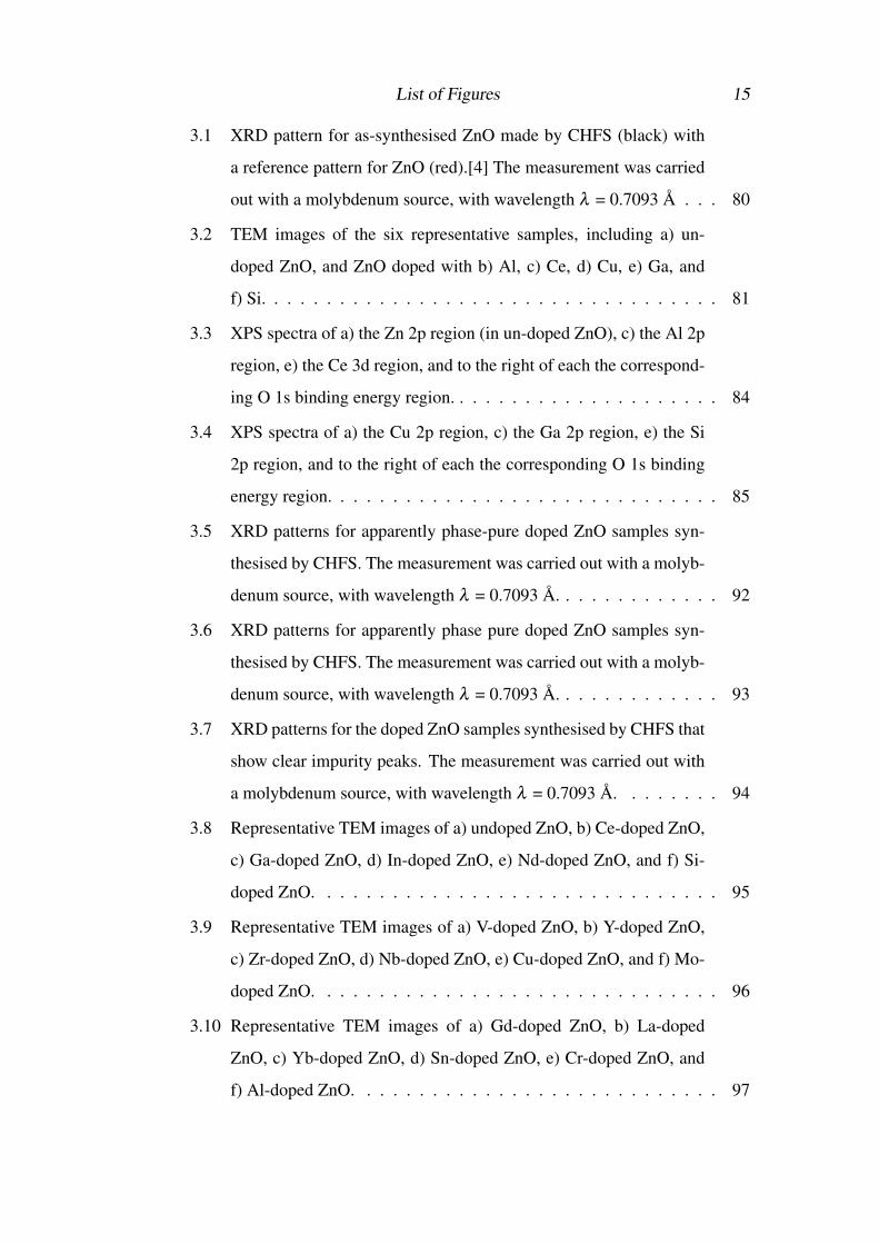
3.1 XRD pattern for as-synthesised ZnO made by CHFS (black) with
a reference pattern for ZnO (red).[4] The measurement was carried
out with a molybdenum source, with wavelength λ = 0.7093 A . . . 80
3.2 TEM images of the six representative samples, including a) un-
doped ZnO, and ZnO doped with b) Al, c) Ce, d) Cu, e) Ga, and
f) Si. . . . . . . . . . . . . . . . . . . . . . . . . . . . . . . . . . . 81
3.3 XPS spectra of a) the Zn 2p region (in un-doped ZnO), c) the Al 2p
region, e) the Ce 3d region, and to the right of each the correspond-
ing O 1s binding energy region. . . . . . . . . . . . . . . . . . . . . 84
3.4 XPS spectra of a) the Cu 2p region, c) the Ga 2p region, e) the Si
2p region, and to the right of each the corresponding O 1s binding
energy region. . . . . . . . . . . . . . . . . . . . . . . . . . . . . . 85
3.5 XRD patterns for apparently phase-pure doped ZnO samples syn-
thesised by CHFS. The measurement was carried out with a molyb-
denum source, with wavelength λ = 0.7093 A. . . . . . . . . . . . . 92
3.6 XRD patterns for apparently phase pure doped ZnO samples syn-
thesised by CHFS. The measurement was carried out with a molyb-
denum source, with wavelength λ = 0.7093 A. . . . . . . . . . . . . 93
3.7 XRD patterns for the doped ZnO samples synthesised by CHFS that
show clear impurity peaks. The measurement was carried out with
a molybdenum source, with wavelength λ = 0.7093 A. . . . . . . . 94
3.8 Representative TEM images of a) undoped ZnO, b) Ce-doped ZnO,
c) Ga-doped ZnO, d) In-doped ZnO, e) Nd-doped ZnO, and f) Si-
doped ZnO. . . . . . . . . . . . . . . . . . . . . . . . . . . . . . . 95
3.9 Representative TEM images of a) V-doped ZnO, b) Y-doped ZnO,
c) Zr-doped ZnO, d) Nb-doped ZnO, e) Cu-doped ZnO, and f) Mo-
doped ZnO. . . . . . . . . . . . . . . . . . . . . . . . . . . . . . . 96
3.10 Representative TEM images of a) Gd-doped ZnO, b) La-doped
ZnO, c) Yb-doped ZnO, d) Sn-doped ZnO, e) Cr-doped ZnO, and
f) Al-doped ZnO. . . . . . . . . . . . . . . . . . . . . . . . . . . . 97
List of Figures 16
3.11 Representative TEM images of a) Mn-doped ZnO, b) Pr-doped
ZnO, c) Sm-doped ZnO, d) Fe-doped ZnO, e) Mg-doped ZnO, and
f) Ti-doped ZnO. . . . . . . . . . . . . . . . . . . . . . . . . . . . 98
3.12 XPS spectra of the Zn 2p region for the doped ZnO samples, ar-
ranged in increasing binding energies from bottom to top. As per
convention, the energy scale increases from right to left. . . . . . . . 99
3.13 XPS spectra of a) the Zn 2p region (in un-doped ZnO), c) the Ce 3d
region, e) the Cr 2p region, and to the right of each the correspond-
ing O 1s binding energy region. . . . . . . . . . . . . . . . . . . . . 100
3.14 XPS spectra of a) the La 3d region, c) the Nb 3d 3d region, e) the Y
3d region, and to the right of each the corresponding O 1s binding
energy region. . . . . . . . . . . . . . . . . . . . . . . . . . . . . . 101
3.15 XPS spectra of a) the Gd 4d region, c) the Mn 2p region, e) the Sm
3d region, and to the right of each the corresponding O 1s binding
energy region. . . . . . . . . . . . . . . . . . . . . . . . . . . . . . 102
3.16 XPS spectra of a) the Sn 3d region, c) the Ti 2p region, e) the Zr
3d region, and to the right of each the corresponding O 1s binding
energy region. . . . . . . . . . . . . . . . . . . . . . . . . . . . . . 103
3.17 XPS spectra of a) the Cu 2p region, c) the V 2p region, e) the Fe
2p region, and to the right of each the corresponding O 1s binding
energy region. . . . . . . . . . . . . . . . . . . . . . . . . . . . . . 104
3.18 XPS spectra of a) the Pr 3d region, c) the Nd 3d region, e) the In
3d region, and to the right of each the corresponding O 1s binding
energy region. . . . . . . . . . . . . . . . . . . . . . . . . . . . . . 105
3.19 XPS spectra of a) the Al 2p region, c) the Ga 2p region, e) the Si
2p region, and to the right of each the corresponding O 1s binding
energy region. . . . . . . . . . . . . . . . . . . . . . . . . . . . . . 106
List of Figures 17
4.1 XRD patterns for samples of AZO and GZO. a) shows a full pattern
typical of the zinc oxides, in this case 1.0 at% AZO. b) shows a
standard ZnO pattern.[4] c1) and d1) show peaks in the range 13.5
to 17.5 2θ pilot scale AZO and GZO, c2 - c4) and d2 - d4) show
these same peaks for 5, 3, and 1 at% nominal dopant level for each
AZO and GZO, respectively, synthesised on the laboratory scale.[5] 116
4.2 TEM images of 2.5 at% AZO (a and b), and 5.0 at% AZO (c and d)
made on the laboratory scale CHFS.[5] . . . . . . . . . . . . . . . . 117
4.3 TEM images of 2.5 at% GZO (a and b), and 5.0 at% GZO (c and d)
made on the laboratory scale CHFS.[5] . . . . . . . . . . . . . . . . 117
4.4 a) and b) full XRD patterns for AZO (2.5 at% Al) and GZO (3.5
at% Ga) synthesised on the pilot scale, accompanied by c) the stan-
dard reference pattern,[4] and a representative TEM image of each
sample in d) and e) for AZO and GZO, respectively.[5] . . . . . . . 118
4.5 XPS spectra for the Zn 2p and Al 2p binding energy regions; a), b),
and c) show the Zn 2p binding energy regions for the 2.5 at% AZO
(lab scale), the 5.0 at% AZO (lab scale), and 2.5 at% AZO (pilot
scale), respectively, and to the right of each is the corresponding Al
2p region, in d), e), and f), respectively.[5] . . . . . . . . . . . . . . 121
4.6 XPS spectra for the Zn 2p and Ga 2p binding energy regions; ; a), b),
and c) show the Zn 2p binding energy regions for the 2.5 at% GZO
(lab scale), the 5.0 at% GZO (lab scale), and 3.5 at% GZO (pilot
scale), respectively, and to the right of each is the corresponding Ga
2p region, in d), e), and f), respectively.[5] . . . . . . . . . . . . . . 122
4.7 Resistivity trend in laboratory scale CHFS-made AZO as tested by
Hall Effect measurements on pressed, heat treated discs. Error bars
represent the standard deviation in the values.[5] . . . . . . . . . . . 124
4.8 Resistivity trend in laboratory scale CHFS-made GZO as tested by
Hall Effect measurements on pressed, heat treated discs. Error bars
represent the standard deviation in the values.[5] . . . . . . . . . . . 124
List of Figures 18
4.9 XRD data for the six representative AGZO samples, including
a) (3,1)AGZO, b) (1,3)AGZO, c), (2,1)AGZO, d) (1,2)AGZO,
e) (1.5,0.5)AGZO, f) (0.5,1.5)AGZO, and g) a ZnO reference
pattern.[4, 6] . . . . . . . . . . . . . . . . . . . . . . . . . . . . . . 128
4.10 TEM images for the six representative AGZO samples, including a)
(0.5,1.5)AGZO, b) (1.5,0.5)AGZO, c) (1,2)AGZO, d) (2,1)AGZO,
e) (1,3)AGZO, and f) (3,1)AGZO.[6] . . . . . . . . . . . . . . . . . 129
4.11 Colour point map of the conductivity of the AGZO compositional
space explored. Black encircled data points are from AZO and
GZO. Green represents high conductivity, and red represents low
conductivity. The bottom right apex represents 100 at% Zn, the top
apex represents 5 at% Al and 95 at% Zn, and the bottom left apex
represents 5 at% Ga and 95 at%.[5, 6] . . . . . . . . . . . . . . . . 132
4.12 Resistivity data ternary contour plot, including several AZO and
GZO samples. Data points are marked with a black spot, and
the contour is generated using Origin Pro’s probability algorithm,
wherein red represents the lowest resistivity, and blue the highest.
The bottom right apex represents 100 at% Zn, the top apex repre-
sents 5 at% Al and 95 at% Zn, and the bottom left apex represents
5 at% Ga and 95 at% Zn. . . . . . . . . . . . . . . . . . . . . . . . 132
5.1 XRD patterns of silicon-doped zinc oxide, including samples with
2.5 at% Si (blue), 1.0 at% Si (green), 0.25 at% Si (red for lab-scale
and gold for pilot-scale), and a standard ZnO pattern (black).[4, 7] . 138
5.2 TEM images of various SiZO samples as follows: a) and c) show
0.25 at% Si made on the laboratory and pilot scales, respectively, b)
shows 2.5 at% Si, and d) shows 1.0 at% Si.[7] . . . . . . . . . . . . 139
5.3 XPS spectra for a) and b) the Zn 2p binding energies for the 1.0
and 2.5 at% SiZO samples, respectively, and c) and d) the Si 2p
binding energies for the 1.0 and 2.5 at% SiZO samples, respectively,
as synthesised using the laboratory scale CHFS.[7] . . . . . . . . . 140
List of Figures 19
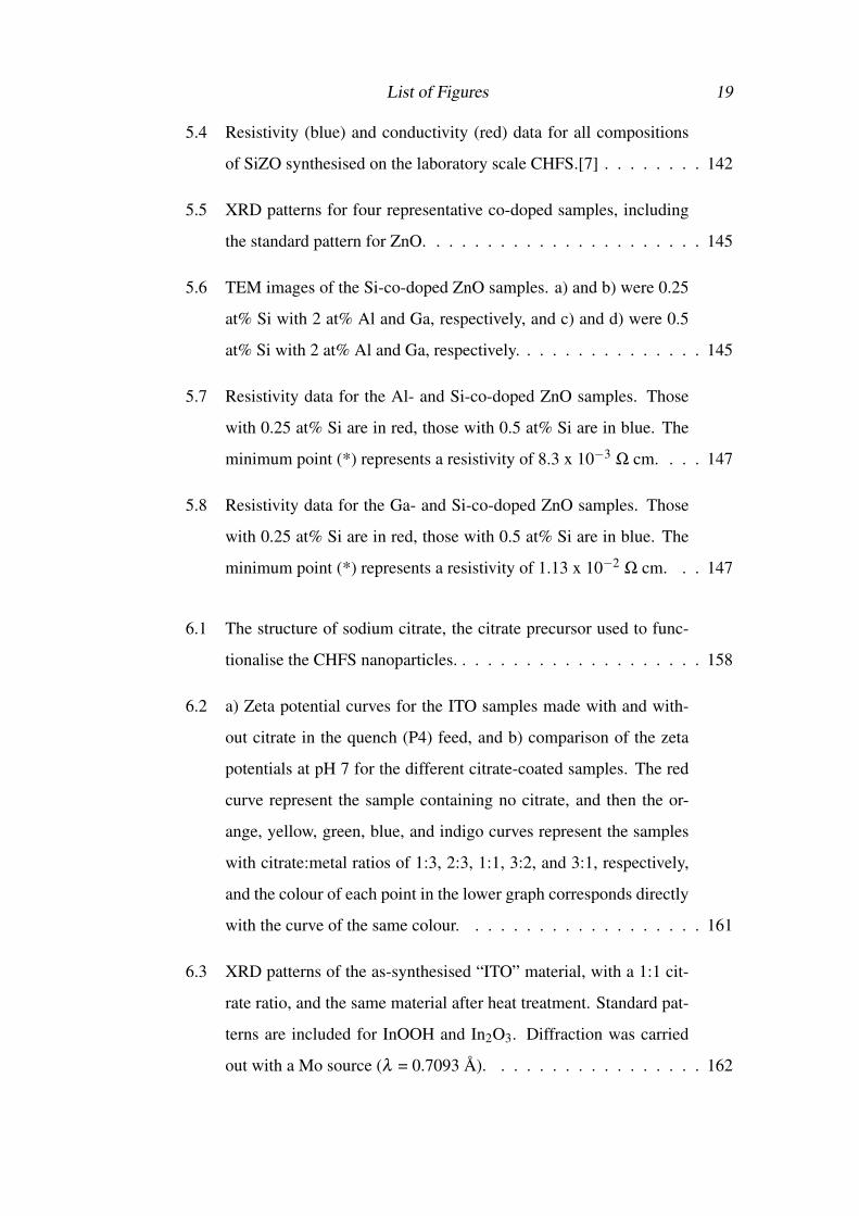
5.4 Resistivity (blue) and conductivity (red) data for all compositions
of SiZO synthesised on the laboratory scale CHFS.[7] . . . . . . . . 142
5.5 XRD patterns for four representative co-doped samples, including
the standard pattern for ZnO. . . . . . . . . . . . . . . . . . . . . . 145
5.6 TEM images of the Si-co-doped ZnO samples. a) and b) were 0.25
at% Si with 2 at% Al and Ga, respectively, and c) and d) were 0.5
at% Si with 2 at% Al and Ga, respectively. . . . . . . . . . . . . . . 145
5.7 Resistivity data for the Al- and Si-co-doped ZnO samples. Those
with 0.25 at% Si are in red, those with 0.5 at% Si are in blue. The
minimum point (*) represents a resistivity of 8.3 x 10⁻³ Ω cm. . . . 147
5.8 Resistivity data for the Ga- and Si-co-doped ZnO samples. Those
with 0.25 at% Si are in red, those with 0.5 at% Si are in blue. The
minimum point (*) represents a resistivity of 1.13 x 10⁻² Ω cm. . . 147
6.1 The structure of sodium citrate, the citrate precursor used to func-
tionalise the CHFS nanoparticles. . . . . . . . . . . . . . . . . . . . 158
6.2 a) Zeta potential curves for the ITO samples made with and with-
out citrate in the quench (P4) feed, and b) comparison of the zeta
potentials at pH 7 for the different citrate-coated samples. The red
curve represent the sample containing no citrate, and then the or-
ange, yellow, green, blue, and indigo curves represent the samples
with citrate:metal ratios of 1:3, 2:3, 1:1, 3:2, and 3:1, respectively,
and the colour of each point in the lower graph corresponds directly
with the curve of the same colour. . . . . . . . . . . . . . . . . . . 161
6.3 XRD patterns of the as-synthesised “ITO” material, with a 1:1 cit-
rate ratio, and the same material after heat treatment. Standard pat-
terns are included for InOOH and In2O3. Diffraction was carried
out with a Mo source (λ = 0.7093 A). . . . . . . . . . . . . . . . . 162
List of Figures 20
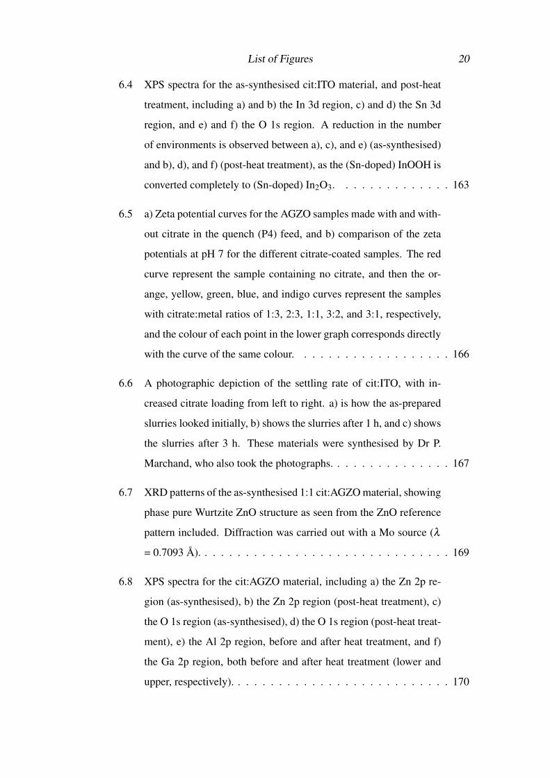
6.4 XPS spectra for the as-synthesised cit:ITO material, and post-heat
treatment, including a) and b) the In 3d region, c) and d) the Sn 3d
region, and e) and f) the O 1s region. A reduction in the number
of environments is observed between a), c), and e) (as-synthesised)
and b), d), and f) (post-heat treatment), as the (Sn-doped) InOOH is
converted completely to (Sn-doped) In2O3. . . . . . . . . . . . . . 163
6.5 a) Zeta potential curves for the AGZO samples made with and with-
out citrate in the quench (P4) feed, and b) comparison of the zeta
potentials at pH 7 for the different citrate-coated samples. The red
curve represent the sample containing no citrate, and then the or-
ange, yellow, green, blue, and indigo curves represent the samples
with citrate:metal ratios of 1:3, 2:3, 1:1, 3:2, and 3:1, respectively,
and the colour of each point in the lower graph corresponds directly
with the curve of the same colour. . . . . . . . . . . . . . . . . . . 166
6.6 A photographic depiction of the settling rate of cit:ITO, with in-
creased citrate loading from left to right. a) is how the as-prepared
slurries looked initially, b) shows the slurries after 1 h, and c) shows
the slurries after 3 h. These materials were synthesised by Dr P.
Marchand, who also took the photographs. . . . . . . . . . . . . . . 167
6.7 XRD patterns of the as-synthesised 1:1 cit:AGZO material, showing
phase pure Wurtzite ZnO structure as seen from the ZnO reference
pattern included. Diffraction was carried out with a Mo source (λ
= 0.7093 A). . . . . . . . . . . . . . . . . . . . . . . . . . . . . . . 169
6.8 XPS spectra for the cit:AGZO material, including a) the Zn 2p re-
gion (as-synthesised), b) the Zn 2p region (post-heat treatment), c)
the O 1s region (as-synthesised), d) the O 1s region (post-heat treat-
ment), e) the Al 2p region, before and after heat treatment, and f)
the Ga 2p region, both before and after heat treatment (lower and
upper, respectively). . . . . . . . . . . . . . . . . . . . . . . . . . . 170
List of Figures 21
6.9 TEM images of a) and b) the as-prepared cit:ITO, and c) and d) the
as-prepared cit:AGZO. Both materials were made by CHFS accord-
ing to the procedure outlined in Section 2.2.2 . . . . . . . . . . . . 171
6.10 Thermogravimetric analysis (TGA) and differential scanning
calorimetry (DSC) of the citrate-coated ITO material as a dense
wet paste after cleaning of the as-synthesised material. The change
in mass is a black solid line, displayed as a percentage loss, while
the heat flow from DSC is shown as a blue dashed line. . . . . . . . 172
6.11 Thermogravimetric analysis (TGA) and differential scanning
calorimetry (DSC) of the citrate-coated AGZO material as a dense
wet paste after cleaning of the as-synthesised material.The change
in mass is a black solid line, displayed as a percentage loss, while
the heat flow from DSC is shown as a blue dashed line. . . . . . . . 173
6.12 An example depiction of the effect of shear rate on the dynamic
viscosity, of ink vehicle U10197. . . . . . . . . . . . . . . . . . . . 174
6.13 The dynamic viscosities of the ink vehicle (U10197), a series of
mass loadings of cit:ITO (up to 40 solid wt%), and including the
viscosities of the 25 wt% inks of each cit:ITO and cit:AGZO, which
were 7.25 cP and 9.81 cP, respectively. . . . . . . . . . . . . . . . . 175
6.14 Inkjet printed thin films printed from 1:1 cit:ITO inks. a) shows
the films as-printed, b) shows the films after heat treatment in 5 %
H2/N2, c) shows the films after heat treatment in air, and d) shows
the films after heat treatment in Ar. All heat treatments were carried
out at 550 C for 5 h onto microscope slides. . . . . . . . . . . . . . 176
6.15 Inkjet printed thin films printed from 1:1 cit:AGZO. a) shows an
untreated, as-printed film, and b) shows a typical heat treated film.
Heat treatments were carried out under 5 % H2/N2 at 550 C for 5
h. The substrate was NSG Pilkington float glass. . . . . . . . . . . . 178
List of Figures 22
6.16 SEM images of the surface of a 1:1 cit:ITO inkjet printed film (a
and b) and a cit:AGZO inkjet printed film, both heat treated under
5 % H2/N2. . . . . . . . . . . . . . . . . . . . . . . . . . . . . . . 179
6.17 Side-on SEM images of inkjet printed films 1:1 cit:AGZO films, to
determine thickness. Images were taken by Dr P. Marchand. . . . . 179
6.18 UV/Vis/NIR spectra of pre- (red) and post-heat treatment (blue)
1:1 cit:AGZO inkjet printed films, including transmittance, T (solid
lines) and reflectance, R (dashed lines) spectra. . . . . . . . . . . . 180
6.19 SEM images of spin-coated 1:1 cit:ITO films, including surface im-
ages (a and b) and side-on (c, d, and e) to gauge thickness. . . . . . 184
6.20 SEM images of spin-coated GZO (a and b), AGZO (c and d), and
SiZO (e and f) films. . . . . . . . . . . . . . . . . . . . . . . . . . 185
6.21 UV/Vis/NIR spectra of pre- (red) and post-heat treatment (blue) 1:1
cit:ITO spin coated films, including transmittance, T (solid lines)
and reflectance, R (dashed lines) spectra. . . . . . . . . . . . . . . . 186
6.22 UV/Vis/NIR spectra of pre- (red) and post-heat treatment (blue)
GZO spin coated films, including transmittance, T (solid lines) and
reflectance, R (dashed lines) spectra. . . . . . . . . . . . . . . . . . 186
6.23 UV/Vis/NIR spectra of pre- (red) and post-heat treatment (blue)
AGZO spin coated films, including transmittance, T (solid lines)
and reflectance, R (dashed lines) spectra. . . . . . . . . . . . . . . . 187
6.24 UV/Vis/NIR spectra of pre- (red) and post-heat treatment (blue)
SiZO spin coated films, including transmittance, T (solid lines) and
reflectance, R (dashed lines) spectra. . . . . . . . . . . . . . . . . . 187
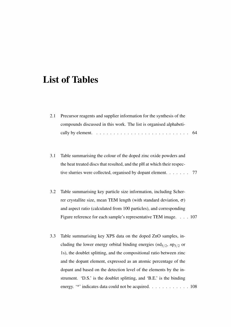
List of Tables
2.1 Precursor reagents and supplier information for the synthesis of the
compounds discussed in this work. The list is organised alphabeti-
cally by element. . . . . . . . . . . . . . . . . . . . . . . . . . . . 64
3.1 Table summarising the colour of the doped zinc oxide powders and
the heat treated discs that resulted, and the pH at which their respec-
tive slurries were collected, organised by dopant element. . . . . . . 77
3.2 Table summarising key particle size information, including Scher-
rer crystallite size, mean TEM length (with standard deviation, σ )
and aspect ratio (calculated from 100 particles), and corresponding
Figure reference for each sample’s representative TEM image. . . . 107
3.3 Table summarising key XPS data on the doped ZnO samples, in-
cluding the lower energy orbital binding energies (nd5/2, np3/2 or
1s), the doublet splitting, and the compositional ratio between zinc
and the dopant element, expressed as an atomic percentage of the
dopant and based on the detection level of the elements by the in-
strument. ‘D.S.’ is the doublet splitting, and ‘B.E.’ is the binding
energy. ‘*’ indicates data could not be acquired. . . . . . . . . . . . 108
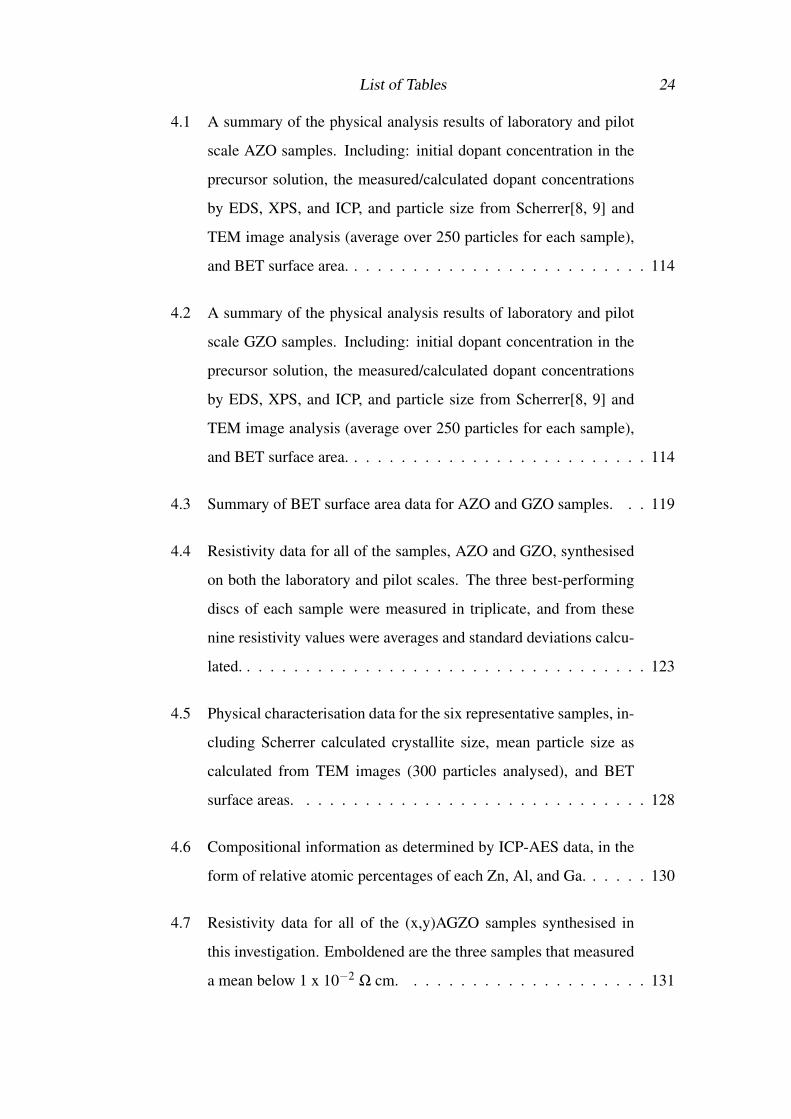
List of Tables 24
4.1 A summary of the physical analysis results of laboratory and pilot
scale AZO samples. Including: initial dopant concentration in the
precursor solution, the measured/calculated dopant concentrations
by EDS, XPS, and ICP, and particle size from Scherrer[8, 9] and
TEM image analysis (average over 250 particles for each sample),
and BET surface area. . . . . . . . . . . . . . . . . . . . . . . . . . 114
4.2 A summary of the physical analysis results of laboratory and pilot
scale GZO samples. Including: initial dopant concentration in the
precursor solution, the measured/calculated dopant concentrations
by EDS, XPS, and ICP, and particle size from Scherrer[8, 9] and
TEM image analysis (average over 250 particles for each sample),
and BET surface area. . . . . . . . . . . . . . . . . . . . . . . . . . 114
4.3 Summary of BET surface area data for AZO and GZO samples. . . 119
4.4 Resistivity data for all of the samples, AZO and GZO, synthesised
on both the laboratory and pilot scales. The three best-performing
discs of each sample were measured in triplicate, and from these
nine resistivity values were averages and standard deviations calcu-
lated. . . . . . . . . . . . . . . . . . . . . . . . . . . . . . . . . . . 123
4.5 Physical characterisation data for the six representative samples, in-
cluding Scherrer calculated crystallite size, mean particle size as
calculated from TEM images (300 particles analysed), and BET
surface areas. . . . . . . . . . . . . . . . . . . . . . . . . . . . . . 128
4.6 Compositional information as determined by ICP-AES data, in the
form of relative atomic percentages of each Zn, Al, and Ga. . . . . . 130
4.7 Resistivity data for all of the (x,y)AGZO samples synthesised in
this investigation. Emboldened are the three samples that measured
a mean below 1 x 10⁻² Ω cm. . . . . . . . . . . . . . . . . . . . . 131
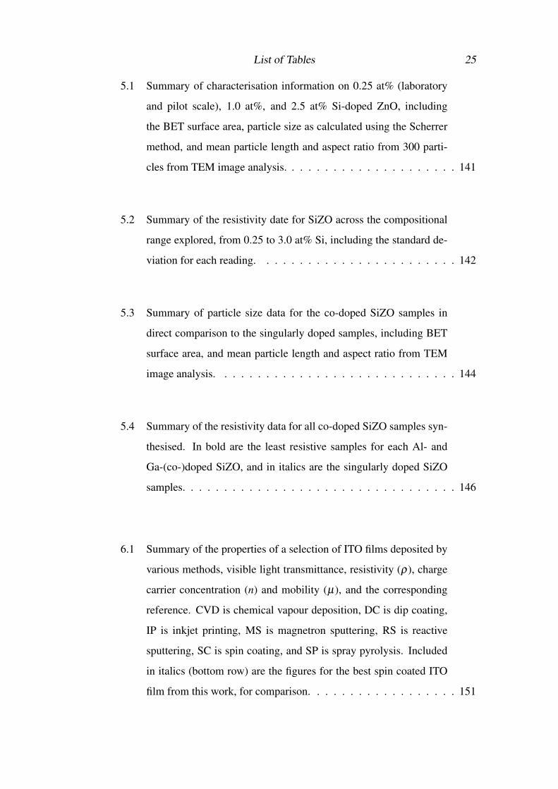
List of Tables 25
5.1 Summary of characterisation information on 0.25 at% (laboratory
and pilot scale), 1.0 at%, and 2.5 at% Si-doped ZnO, including
the BET surface area, particle size as calculated using the Scherrer
method, and mean particle length and aspect ratio from 300 parti-
cles from TEM image analysis. . . . . . . . . . . . . . . . . . . . . 141
5.2 Summary of the resistivity date for SiZO across the compositional
range explored, from 0.25 to 3.0 at% Si, including the standard de-
viation for each reading. . . . . . . . . . . . . . . . . . . . . . . . 142
5.3 Summary of particle size data for the co-doped SiZO samples in
direct comparison to the singularly doped samples, including BET
surface area, and mean particle length and aspect ratio from TEM
image analysis. . . . . . . . . . . . . . . . . . . . . . . . . . . . . 144
5.4 Summary of the resistivity data for all co-doped SiZO samples syn-
thesised. In bold are the least resistive samples for each Al- and
Ga-(co-)doped SiZO, and in italics are the singularly doped SiZO
samples. . . . . . . . . . . . . . . . . . . . . . . . . . . . . . . . . 146
6.1 Summary of the properties of a selection of ITO films deposited by
various methods, visible light transmittance, resistivity (ρ), charge
carrier concentration (n) and mobility (µ), and the corresponding
reference. CVD is chemical vapour deposition, DC is dip coating,
IP is inkjet printing, MS is magnetron sputtering, RS is reactive
sputtering, SC is spin coating, and SP is spray pyrolysis. Included
in italics (bottom row) are the figures for the best spin coated ITO
film from this work, for comparison. . . . . . . . . . . . . . . . . . 151
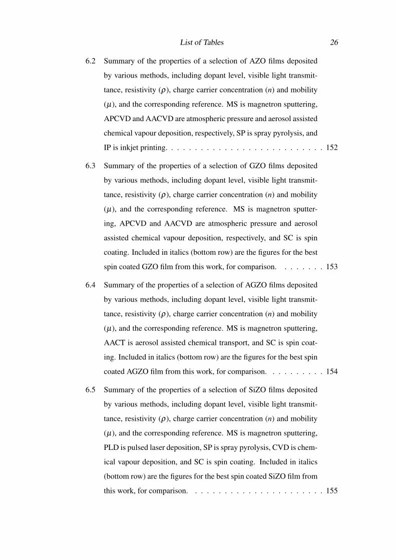
List of Tables 26
6.2 Summary of the properties of a selection of AZO films deposited
by various methods, including dopant level, visible light transmit-
tance, resistivity (ρ), charge carrier concentration (n) and mobility
(µ), and the corresponding reference. MS is magnetron sputtering,
APCVD and AACVD are atmospheric pressure and aerosol assisted
chemical vapour deposition, respectively, SP is spray pyrolysis, and
IP is inkjet printing. . . . . . . . . . . . . . . . . . . . . . . . . . . 152
6.3 Summary of the properties of a selection of GZO films deposited
by various methods, including dopant level, visible light transmit-
tance, resistivity (ρ), charge carrier concentration (n) and mobility
(µ), and the corresponding reference. MS is magnetron sputter-
ing, APCVD and AACVD are atmospheric pressure and aerosol
assisted chemical vapour deposition, respectively, and SC is spin
coating. Included in italics (bottom row) are the figures for the best
spin coated GZO film from this work, for comparison. . . . . . . . 153
6.4 Summary of the properties of a selection of AGZO films deposited
by various methods, including dopant level, visible light transmit-
tance, resistivity (ρ), charge carrier concentration (n) and mobility
(µ), and the corresponding reference. MS is magnetron sputtering,
AACT is aerosol assisted chemical transport, and SC is spin coat-
ing. Included in italics (bottom row) are the figures for the best spin
coated AGZO film from this work, for comparison. . . . . . . . . . 154
6.5 Summary of the properties of a selection of SiZO films deposited
by various methods, including dopant level, visible light transmit-
tance, resistivity (ρ), charge carrier concentration (n) and mobility
(µ), and the corresponding reference. MS is magnetron sputtering,
PLD is pulsed laser deposition, SP is spray pyrolysis, CVD is chem-
ical vapour deposition, and SC is spin coating. Included in italics
(bottom row) are the figures for the best spin coated SiZO film from
this work, for comparison. . . . . . . . . . . . . . . . . . . . . . . 155

List of Tables 27
6.6 Summary of the optical and electrical characterisation data for the
four spin coated materials; cit:ITO, GZO, AGZO, and SiZO. Data
includes transmittance, thickness from ellipsometry, charge carrier
concentration (n) and mobility (µ), and resistivity (ρ). . . . . . . . 189
List of Abbreviations
AACVD aerosol-assisted chemical vapour deposition
AGZO aluminium and gallium co-doped zinc oxide
APCVD atmospheric pressure chemical vapour deposition
ATO antimony doped tin dioxide
AZO aluminium doped zinc oxide
at% atomic percent
BET Brunauer-Emmett-Teller
BPR back pressure regulator
CHFS continuous hydrothermal flow synthesis
CJM confined jet mixer
CVD chemical vapour deposition
DI deionized
DLS dynamic light scattering
EDS energy dispersive x-ray spectroscopy
EF Fermi level
EPSRC Engineering and Physical Sciences Research Council
eV electron volt
FTO fluorine-doped tin dioxide
GZO gallium-doped zinc oxide
HOMO highest occupied molecular orbital
ICP-AES inductively coupled plasma atomic emission spectroscopy
IR infrared
ITO indium tin oxide
List of Tables 29
LED light emitting diode
OLED organic light emitting diode
PLD pulsed laser deposition
PMA poly(methacrylic acid)
PVD physical vapour deposition
SEM scanning electron microscopy
SiZO silicon doped zinc oxide
TCO transparent conducting oxide
TEM transmission electron microscopy
US$ United States dollar
UV ultraviolet
vis visible
XPS x-ray photoelectron spectroscopy
XRD x-ray diffraction
Chapter 1
Literature Review and General
Introduction
In this chapter, an overview of transparent conducting oxides (TCOs) is given, in-
cluding discussions of their optoelectronic properties and how they arise, the appli-
cations of TCOs, and the methods by which they are synthesised and deposited as
thin films.
1.1 Transparent Conducting OxidesTransparent conducting oxides (TCOs) are a class of materials that demonstrate the
often incompatible properties of high optical transparency and conductivity; this
section will outline in detail their properties and key applications, as well as the
materials that are predominantly used in them.
1.1.1 Properties of TCO materials
TCOs are present in devices in the form of thin films. This reduces the space they
take up in devices, and aids in the optical transparency that is fundamental to many
of their uses. The required optical transparency is typically > 80 % across the
visible range (400 - 700 nm), and to achieve this a wide, direct optical band gap
semiconductor is needed with band gap of 3.1 eV, corresponding to the transmis-
sion of visible light.[10] In addition to the gap between the valence band maximum
and the conduction band minimum, it is also important that the first allowed transi-
tion from the conduction band minimum is also at least 3.1 eV, else already-excited
1.1. Transparent Conducting Oxides 31
electrons would be able to absorb visible light for further excitation, negating the
purpose of the material. Furthermore, such a material requires resistivity values of
the order of 10−4 Ω cm, and it is the unlikely combination of these two properties,
high conductivity and transmittance of visible light, that is so rare and that makes
transparent conducting materials so highly sought-after.[11] In determining suitable
candidates for these applications, a certain robustness is also required, as chemical
or thermal instability would in time contribute to shortened lifespans of the devices
in which they are used.
In order to ensure an optically transmissive, intrinsically semiconducting metal ox-
ide is sufficiently conductive, it can be extrinsically doped with an aliovalent ele-
ment. Lower valency in this element results in p-type semiconductivity, wherein the
conduction mechanism relies on mobile positive ‘holes’ in the valence band; higher
valency of the element results in n-type semiconductivity, in which the conduction
mechanism relies on additional, free-moving electrons in the conduction band.
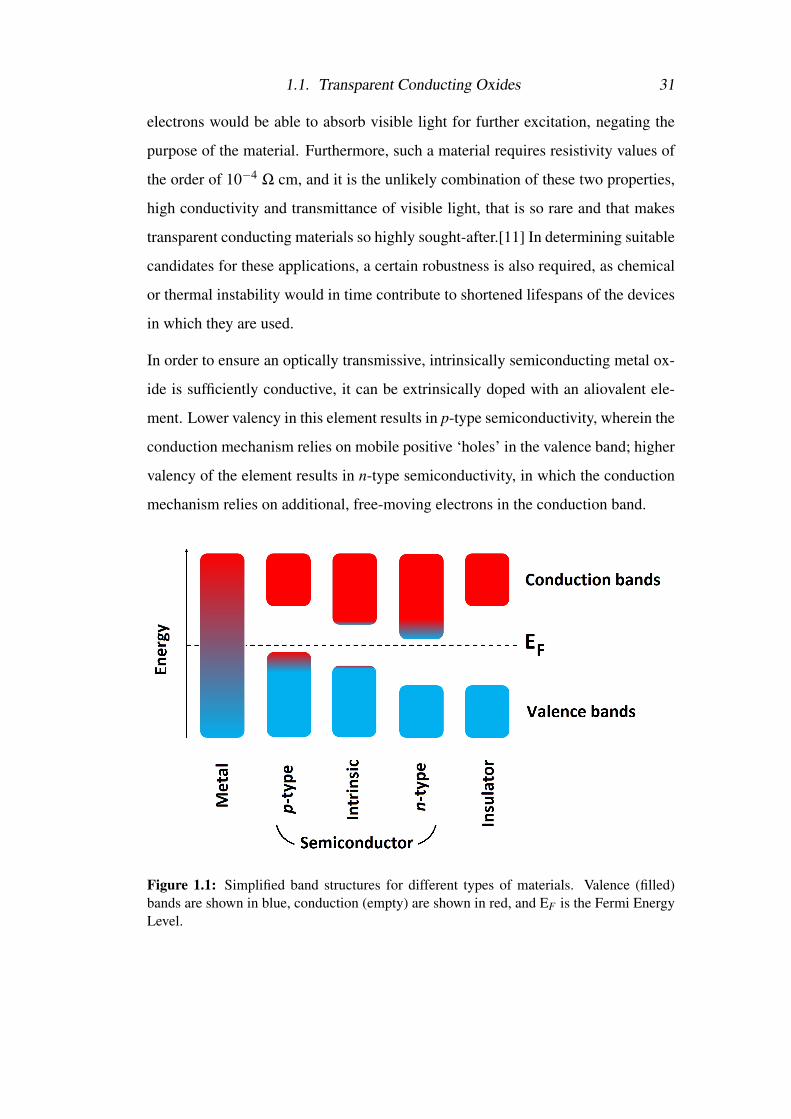
Figure 1.1: Simplified band structures for different types of materials. Valence (filled)bands are shown in blue, conduction (empty) are shown in red, and EF is the Fermi EnergyLevel.
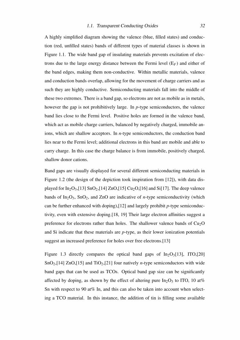
1.1. Transparent Conducting Oxides 32
A highly simplified diagram showing the valence (blue, filled states) and conduc-
tion (red, unfilled states) bands of different types of material classes is shown in
Figure 1.1. The wide band gap of insulating materials prevents excitation of elec-
trons due to the large energy distance between the Fermi level (EF ) and either of
the band edges, making them non-conductive. Within metallic materials, valence
and conduction bands overlap, allowing for the movement of charge carriers and as
such they are highly conductive. Semiconducting materials fall into the middle of
these two extremes. There is a band gap, so electrons are not as mobile as in metals,
however the gap is not prohibitively large. In p-type semiconductors, the valence
band lies close to the Fermi level. Positive holes are formed in the valence band,
which act as mobile charge carriers, balanced by negatively charged, immobile an-
ions, which are shallow acceptors. In n-type semiconductors, the conduction band
lies near to the Fermi level; additional electrons in this band are mobile and able to
carry charge. In this case the charge balance is from immobile, positively charged,
shallow donor cations.
Band gaps are visually displayed for several different semiconducting materials in
Figure 1.2 (the design of the depiction took inspiration from [12]), with data dis-
played for In2O3,[13] SnO2,[14] ZnO,[15] Cu2O,[16] and Si[17]. The deep valence
bands of In2O3, SnO2, and ZnO are indicative of n-type semiconductivity (which
can be further enhanced with doping),[12] and largely prohibit p-type semiconduc-
tivity, even with extensive doping.[18, 19] Their large electron affinities suggest a
preference for electrons rather than holes. The shallower valence bands of Cu2O
and Si indicate that these materials are p-type, as their lower ionization potentials
suggest an increased preference for holes over free electrons.[13]
Figure 1.3 directly compares the optical band gaps of In2O3[13], ITO,[20]
SnO2,[14] ZnO,[15] and TiO2,[21] four natively n-type semiconductors with wide
band gaps that can be used as TCOs. Optical band gap size can be significantly
affected by doping, as shown by the effect of altering pure In2O3 to ITO, 10 at%
Sn with respect to 90 at% In, and this can also be taken into account when select-
ing a TCO material. In this instance, the addition of tin is filling some available
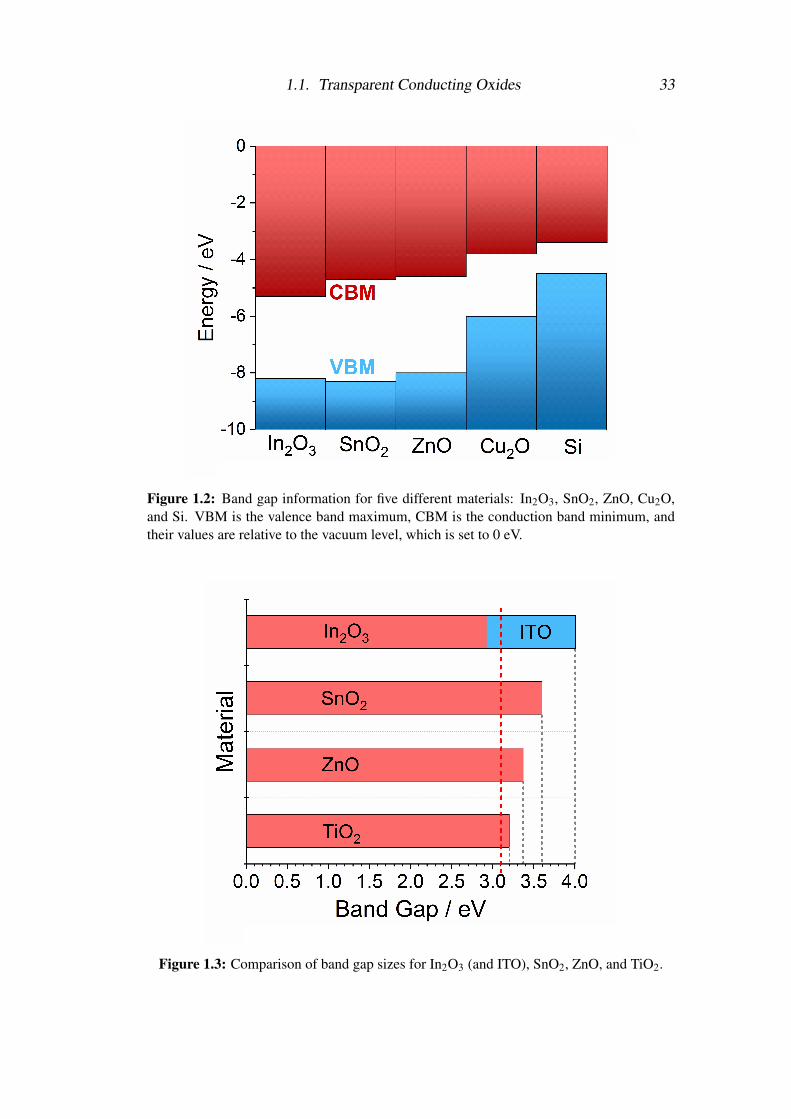
1.1. Transparent Conducting Oxides 33
Figure 1.2: Band gap information for five different materials: In2O3, SnO2, ZnO, Cu2O,and Si. VBM is the valence band maximum, CBM is the conduction band minimum, andtheir values are relative to the vacuum level, which is set to 0 eV.
Figure 1.3: Comparison of band gap sizes for In2O3 (and ITO), SnO2, ZnO, and TiO2.
1.1. Transparent Conducting Oxides 34
states in the conduction band, rendering them unavailable for promoted electrons
in the valence band, thus the band gap is effectively being increased due to this
unavailability of some lower energy conduction band states. This effect is called a
Moss-Burnstein shift, which does not affect the fundamental band gap (the energy
difference between the VBM and CBM), but does effect the optical band gap, the
effective observed band gap of the material. All of these materials can, typically
when appropriately doped, demonstrate the high transparency and conductivity
required of TCOs. ITO especially is the most conductive of all industrially rele-
vant TCOs,[22] with high physical and chemical stability, which resulted from the
1960’s onwards in ITO being the TCO of choice in the vast majority of applications
over alternative materials.[23]
The conduction mechanism in ITO is based on both the tetravalent tin on the indium
sites, Sn•In, which theoretically contributes to the carrier concentration according
to 3.0 x 10²⁰ x CSn cm−3, where CSn is the atomic percentage of Sn relative to In,
and the presence of oxygen vacancies in the lattice.[24, 25] For pure indium oxide,
the oxygen vacancy prevalence is fundamental to the conductivity of the material,
contributing as shown in Equation 1.1, using Kroger-Vink notation:
OxO→ V••O +2e
′+
12
O2(g) (1.1)
In this notation the subscript denotes the lattice position upon which the element
is situated where relevant, and the superscript denotes charge, such that the ‘ x ’
represents neutral charge, the ‘ • ’ represents one positive charge for each present,
and the ‘ ′ ’ represents one negative charge for each present, while V is a vacancy,
and i would represent an interstitial site. In this way the oxygen vacancy is a doubly
ionised donor, which can donate up to two electrons per defect. Additionally, the
presence of these oxygen vacancies facilitates the mobility of O2− through the lat-
tice, contributing to the ionic conductivity of the material, though this is negligible
compared to the electronic conductivity.[26]
In an ideal system, the conductivity, σ , carrier concentration, n, and charge carrier
1.1. Transparent Conducting Oxides 35
mobility, µ , are related by Equation 1.2, where e is electronic charge.
σ = nµe (1.2)
Thus, as alluded to above, high carrier concentrations and mobilities lead to higher
conductivities. However, µ is proportional to the time between resistive scattering
events.[27] In this context, scattering refers to the mechanism by which the non-
random directional movement of charge carriers is inhibited, and it follows that the
fewer scattering processes present in a material, the higher the possible mobility of
the charge carriers.[28] This is visually apparent from the band structures elucidated
by computational calculations, in that the curvature of the bands (i.e. the dispersion)
is indicative of the mobility of the electron charge carriers such that relatively flat
bands across k-vectors show low mobility.[29] It is unfortunate then, that higher
charge carrier concentrations increase the propensity for scattering effects, and thus
have a negative impact on the mobility of the carriers. Thus the optimisation of the
resistivity of the materials is, for the most part, a balancing act between increasing
the charge carrier concentration and the mobility, increasing the former as much as
possible without inhibiting the latter.[24] For ITO, typical charge carrier concentra-
tions of ca. 1021 cm−3 are observed, with mobilities of > 30 cm2 V−1 s−1 typically
observed in literature reports.[25, 30, 31]
1.1.2 Applications of TCOs
TCOs were first of interest in coating glass for anti-fogging/icing aircraft wind-
screens and other components that would be negatively affected by the cold tem-
peratures of flight altitude.[32–34] Modern applications of TCOs are prolific, and
spread across various electronics industries, principally including organic light-
emitting diodes (OLEDs) to enhance optical power output,[35] touchscreens,[23]
solar cells (to enable current collection with short carrier diffusion lengths),[36, 37]
flat-panel displays,[38] and smart windows,[39] wherein optical properties can be
modulated by charge insertion or extraction through a transparent conducting con-
tact. These various technologies have proliferated themselves utterly through mod-

1.1. Transparent Conducting Oxides 36
ern society; their prevalence and growing indispensability have led to a transparent
conductor market the highest-charging analysts estimate to be worth between $5-10
billion within the next 10 years, of which ITO has comprised 90% as recently as
2013, and is expected to continue to be the most commonly used transparent con-
ducting material for at least the next several years.[40–43]
As an example of a typical TCO application, the following section outlines the
schematic of an OLED, and describes how a TCO is incorporated into the device
and its purpose.
1.1. Transparent Conducting Oxides 37
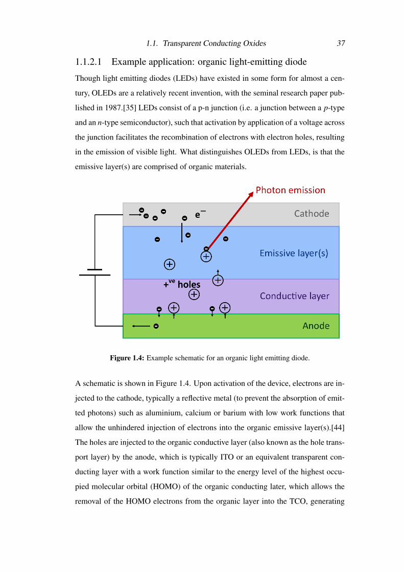
1.1.2.1 Example application: organic light-emitting diode
Though light emitting diodes (LEDs) have existed in some form for almost a cen-
tury, OLEDs are a relatively recent invention, with the seminal research paper pub-
lished in 1987.[35] LEDs consist of a p-n junction (i.e. a junction between a p-type
and an n-type semiconductor), such that activation by application of a voltage across
the junction facilitates the recombination of electrons with electron holes, resulting
in the emission of visible light. What distinguishes OLEDs from LEDs, is that the
emissive layer(s) are comprised of organic materials.
Figure 1.4: Example schematic for an organic light emitting diode.
A schematic is shown in Figure 1.4. Upon activation of the device, electrons are in-
jected to the cathode, typically a reflective metal (to prevent the absorption of emit-
ted photons) such as aluminium, calcium or barium with low work functions that
allow the unhindered injection of electrons into the organic emissive layer(s).[44]
The holes are injected to the organic conductive layer (also known as the hole trans-
port layer) by the anode, which is typically ITO or an equivalent transparent con-
ducting layer with a work function similar to the energy level of the highest occu-
pied molecular orbital (HOMO) of the organic conducting later, which allows the
removal of the HOMO electrons from the organic layer into the TCO, generating
1.1. Transparent Conducting Oxides 38
mobile holes in the organic layer.[45] These holes can move towards the emissive
layer, whereupon they recombine with electrons (from the cathode), emitting vis-
ible light photons. Depending on the nature of the organic materials in use in the
device, the anode can quite easily be the most expensive component due to the cost
of the ITO. As such, replacement of ITO with a cheaper, more sustainable material
could dramatically reduce the overall cost of fabricating such devices.
1.1.3 The indium issue
In any application that does not require mechanical flexibility, ITO is the best mate-
rial for use as a transparent conducting thin film in terms of its properties; it is highly
conductive and transmissive, as well as being physically and chemically stable.[22]
It is not, however, a sustainable material, in terms of pricing volatility and long-
term availability it is unlikely that indium supply will continue to meet demand.
ITO films started to gain traction in industry in the 1960’s with the emergence or
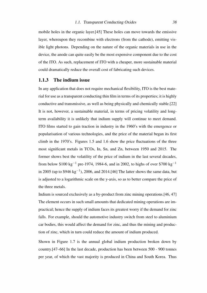
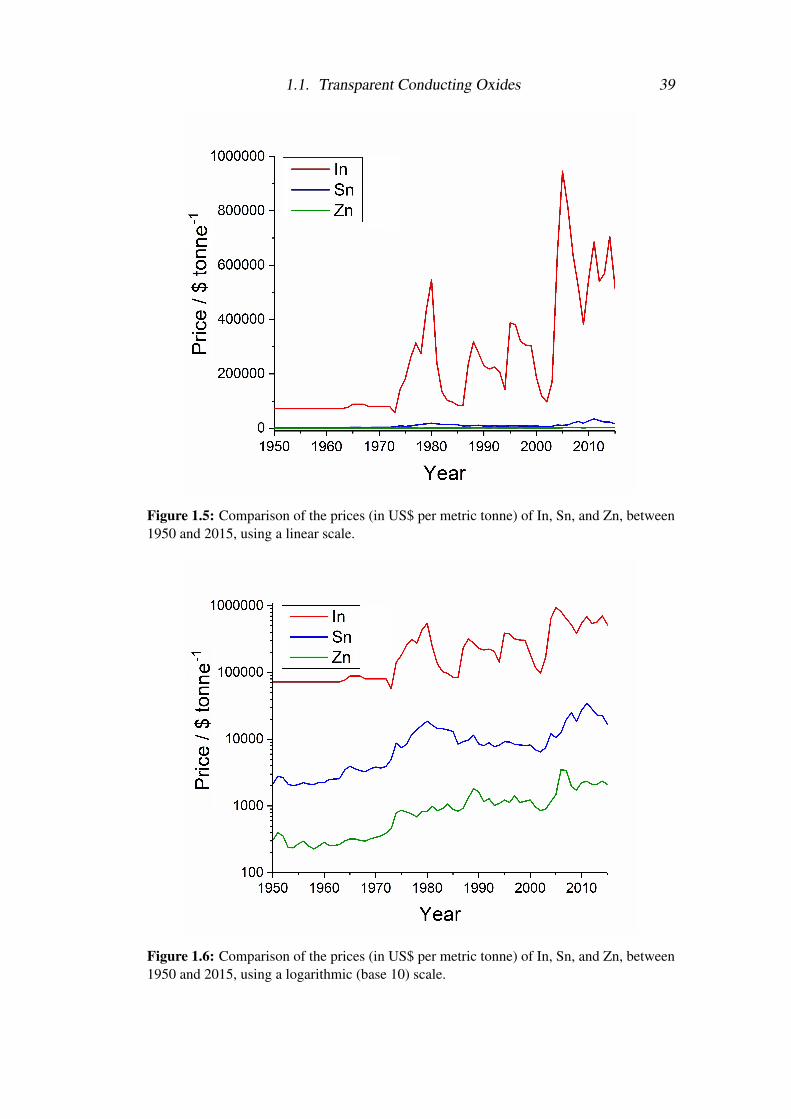
popularisation of various technologies, and the price of the material began its first
climb in the 1970’s. Figures 1.5 and 1.6 show the price fluctuations of the three
most significant metals in TCOs, In, Sn, and Zn, between 1950 and 2015. The
former shows best the volatility of the price of indium in the last several decades,
from below $100 kg−1 pre-1974, 1984-6, and in 2002, to highs of over $700 kg−1
in 2005 (up to $946 kg−1), 2006, and 2014.[46] The latter shows the same data, but
is adjusted to a logarithmic scale on the y-axis, so as to better compare the price of
the three metals.
Indium is sourced exclusively as a by-product from zinc mining operations.[46, 47]
The element occurs in such small amounts that dedicated mining operations are im-
practical; hence the supply of indium faces its greatest worry if the demand for zinc
falls. For example, should the automotive industry switch from steel to aluminium
car bodies, this would affect the demand for zinc, and thus the mining and produc-
tion of zinc, which in turn could reduce the amount of indium produced.
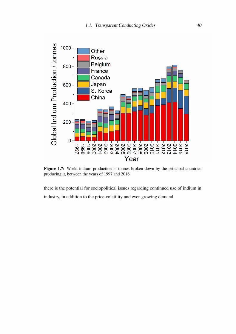
Shown in Figure 1.7 is the annual global indium production broken down by
country.[47–66] In the last decade, production has been between 500 - 900 tonnes
per year, of which the vast majority is produced in China and South Korea. Thus
1.1. Transparent Conducting Oxides 39
Figure 1.5: Comparison of the prices (in US$ per metric tonne) of In, Sn, and Zn, between1950 and 2015, using a linear scale.
Figure 1.6: Comparison of the prices (in US$ per metric tonne) of In, Sn, and Zn, between1950 and 2015, using a logarithmic (base 10) scale.
1.1. Transparent Conducting Oxides 40
Figure 1.7: World indium production in tonnes broken down by the principal countriesproducing it, between the years of 1997 and 2016.
there is the potential for sociopolitical issues regarding continued use of indium in
industry, in addition to the price volatility and ever-growing demand.
1.2. Promising Replacement Materials 41
Though not included graphically, the price of indium in 2016 was drastically re-
duced to as low as $228 kg−1.[47] This is thought to have been due to the collapse
of the Fanya Metal Exchange Co. Ltd. in 2015, resulting in an oversupply of in-
dium and depressed demand for the the metal.[67, 68] Global production was also
affected by a fire in November 2015 that damaged the indium production plant at
the Auby zinc smelter in France,[69, 70] entirely diminishing France’s output.[47]
It is beyond the scope of this Thesis to postulate as to the possible future demand
and supply of indium beyond those analytical reports and forecasts already referred
to,[40–43] but the aforementioned economic factors have led to the growing need
to find cheaper and more sustainable alternatives for indium in technology wher-
ever possible; as such there is both a scientific and industrial imperative to conduct
research along the lines of that discussed herein. Most pertinent to this work is thus
the requirement to find alternative TCO materials to ITO.
1.2 Promising Replacement MaterialsIn pursuit of phasing indium out of the TCO industry, there are a number of different
potential replacement materials. The two ‘host’ materials most studied are ZnO
and SnO2. These are both conductive in their own rights, but are improved by
introduction of aliovalent dopants. This section discusses the properties of these
materials, and the precedent for their use as TCOs.
1.2.1 Tin dioxide
As shown in Figure 1.5, tin tends to be much cheaper than indium, and films based
on SnO2 can be deposited by the same processes as ITO. Thus there is no need to
replace the deposition machinery when attempting to replace the material. SnO2,
like In2O3, is a natively n-type semiconductor, and this native conductivity is again
based primarily on the formation of oxygen vacancies,[71] as shown in Equation 1.1
on page 34. The structure is tetragonal rutile, and the band gap is ca. 3.6 eV.[72] It
has been postulated for some time that the oxygen vacancies take the form of shal-
low donor levels near the conduction band.[73] Interstitial tin, Sni can also read-
ily form, another source of conductivity, and neither of these are compensated by
1.2. Promising Replacement Materials 42
the formation of VSn or Oi as might be expected, as these are formed deep in the
valence band, leading to a high charge carrier concentration even in the undoped
material.[12, 72] Additionally, if the annealing of the material is under reducing
conditions, the hydrogen present, though it is possible it could draw out some lat-
tice oxygen, will tend to add hydrogen to the structure, either as Hi, the interstitial,
or on the oxygen site, as HO. In either case, this forms an additional shallow donor
level, which can contribute to the conductivity of the material.[12, 73]
Thin films of SnO2 have been made by a variety of methods, with resistivities as
low as 1.1 x 10⁻³ Ω cm for CVD,[74] 1.5 x 10⁻³ Ω cm for films made by mag-
netron sputtering,[75] and as low as 7.5 x 10⁻⁴ Ω cm for electron beam evapora-
tion methods,[76] the latter with optical transmittance up to 90 %. Difficulty in
effective sintering/annealing has generally prevented SnO2 from obtaining the lev-
els of resistivity reported for indium or zinc-based materials, the scattering effects
from defects and grain boundaries proving deleterious for the electronic proper-
ties in many cases, particularly noticeable with increasing film thickness, which
inherently causes a greater concentration of these defects to be present in the thin
film.[77–79] One potential way around the issues of using polycrystalline material
could be to use the amorphous analogue, however despite recent advances and de-
vice implementation of amorphous TCO films, these do not tend to exhibit nearly
the electronic capabilities of the crystalline materials.[80–83]
In addition to the oxygen vacancies, aliovalent dopants can be introduced to the
lattice, most commonly Sb5+ onto the Sn4+ site, or F− on the O2− site, i.e. Sb•Sn
or F•O, respectively, both of which contribute towards the n-type semiconductiv-
ity of the material. Sb-doped SnO2, also known as ATO, and F-doped SnO2, also
known as FTO, are the most commonly researched SnO2-based materials for TCO
applications.[71] ATO is analogous to ITO, in that the metal ion is being replaced
by a dopant with an oxidation state one higher. Though in some cases, the optical
properties are below the standards set for TCOs,[84] films towards the lower end
in the order of 10−3 Ω cm have been made by sputtering,[78, 85–87], sol gel/spin
coating,[84, 88] pulsed laser deposition,[89] and spray pyrolysis.[90, 91] Generally,
1.2. Promising Replacement Materials 43
the reduced conductivity is attributed to low mobilities, caused by the abovemen-
tioned effects, often only around 10 cm2 V−1 s−1,[84, 90] compared to > 30 cm2
V−1 s−1 for ITO.
FTO is actively used in industrial processes as an ITO replacement material, ac-
counting for the second largest share of the TCO market behind ITO itself, in part
due to the reduced cost, but also due to the chemical and thermal stability of its
electrical properties, though the material is not as conductive as ITO, nor as well
suited for patterning or etching.[92] As with ATO, the best films in terms of elec-
trical properties have been deposited by spray pyrolysis,[79, 93–96] as low as 2 x
10−4 Ω cm for the resistivity.[94, 96] Sol-gel dip coating methods have obtained
resistivities in the order of 10−4 Ω cm too,[97] as have CVD processes,[98, 99]
though with film growth rates of only a few nm min−1. Up-scaling of similar CVD
processes to 100 nm min−1 have been carried out, but at a cost of resistivity by some
two orders of magnitude.[100]
Though these are the most common SnO2-based TCO materials, many other
dopants have been tested. Tantalum[101, 102] and tungsten[103] doping have
achieved resistivities of 2 x 10⁻³ Ω cm when deposited on glass, though by deposi-
tion onto a heated Al2O3 substrate, the former has been reported to have resistivities
as low as 3.5 x 10⁻⁴ Ω cm.[104] Praseodymium[105] and neodymium[106] have
also been tested, with resistivities of 3.7 x 10⁻³ Ω cm and 6.2 x 10⁻³ Ω cm reported,
respectively, though the former in conjunction with fluorine doping, which would
be expected to further enhance the conductivity.
Introduction of Al, Ga, or In onto the Sn site in the lattice would be superficially
expected, by the converse logic to Sb replacing Sn, to result in p-type semicon-
ductivity. And indeed, there are reports that claim precisely that, for In,[107]
Ga,[108, 109] and Al.[110] The p-type nature of the conductivity is expressed, by
Hall Effect measurements, as producing a positive Hall coefficient, whereas for n-
type materials the Hall coefficient is negative. And that is what the aforementioned
studies report, specifically a cross-over point at which drastically reduced, p-type
1.2. Promising Replacement Materials 44
semiconductivity is observed (several orders of magnitude increase in resistivity).
Though not categorically known to be impossible, the general consensus from re-
cent studies is that p-type SnO2 is highly unlikely.[12] This is from the computa-
tional standpoint of calculating the formation energies of a number of defects, and
deducing the likelihood of each being present, and what effect their presence has. It
is, from more advanced hybrid density functional theory, concluded that no shallow
acceptor levels that are uncompensated will be formed from any likely candidate de-
fects in SnO2, which would be necessary for p-type semiconductivity to occur,[12]
though there do exist less recent computational studies that have concluded that
p-type SnO2 is plausible.[111]
1.2.2 Zinc oxide
Zinc oxide exists predominantly in hexagonal Wurtzite structure, with a band gap
ca. 3.4 eV.[19, 112] The mechanism for conductivity differs from that of In2O3
or SnO2 however, in that for ZnO, the VO defects act as much deeper donor levels
than might be conventionally thought.[113] Instead, it tends to be hydrogen impu-
rities that result in the observed n-type conductivity in undoped ZnO. Hydrogen
in ZnO is highly atypical; it has been postulated that generally speaking hydro-
gen acts as an amphoteric impurity in a semiconductor, i.e. it is present as H+ in
a p-type semiconductor, and as H− in an n-type semiconductor, counteracting the
inherent conductivity of the material; the prevailing belief for a time was that in
ZnO, hydrogen is always present as H+, the only form in which it was supposedly
thermodynamically stable, and indeed this is the case below the conduction band
minimum.[114–116] However a DFT study in 2011 showed that H− could also be
present as a shallow acceptor, with the (+/-) transition for Hi at 0.34 eV above the
CBM.[117] Both Hi and HO have similar formation energies, and while in the lattice
the hydrogen will tend to be strongly bound to the lattice oxygen, effectively form-
ing O-H bonds while acting as shallow donors to contribute to the conductivity of
the ZnO.[19] Generally speaking, ZnO-based TCO materials can not be patterned
as easily due to chemical instability, particularly of Al-doped ZnO, but this sensi-
tivity to both acidic and basic conditions means that wet etching is possible, unlike
1.3. Deposition Techniques 45
ITO, wherein dry etching is necessary.[118]
Again, the introduction of aliovalent dopants has been shown to be highly effective
with regards to increasing the conductivity of ZnO, most commonly Al (AZO) and
Ga (GZO), but many more have been investigated. ZnO-based materials tend to
be slightly less conductive than ITO, and slightly more transparent.[37, 118] It was
concerns with the thermal stability of undoped ZnO that led Minami et al. to sputter
films of AZO in the early 1980’s,[119] achieving resistivities as low as 2 x 10⁻⁴
Ω cm. Other methods have garnered similarly low resistivities, while still main-
taining high optical transparency, including CVD,[120, 121] PLD,[122] and spray
pyrolysis.[123] GZO has seen equivalent resistivities (generally slightly higher, but
balanced by higher chemical stability than AZO) from magnetron sputtering,[124–
126] PLD,[127] and CVD,[128, 129] and the co-doped material, AGZO, has from
sputtering achieved similarly conductive thin films.[130–133] The other doped
systems explored include zinc oxide doped with silicon,[134–136], indium,[137]
tin,[138] niobium,[139] lanthanum,[140] and neodymium,[141] among numerous
others. Many of these have quite competitive resistivity and optical properties,
however the most promising remain AZO, GZO, and AGZO.[13, 37, 39, 142] The
considerable reduction in cost for zinc versus indium, and to a lesser extent versus
tin, mean that more expensive dopant elements can be considered, as the low level
of these still results in the specific cost of the material being relatively low.
For a fuller description of the different doped zinc oxide systems investigated, see
Section 3.2 on page 74. For detailed discussions into AZO, GZO, and AGZO, see
Section 4.2 on page 109 and Section 6.2.2 on page 151.
1.3 Deposition Techniques
This section will outline the predominant methods of depositing thin films of TCOs,
including physical and chemical vapour techniques, and spin coating and inkjet
printing.
1.3. Deposition Techniques 46
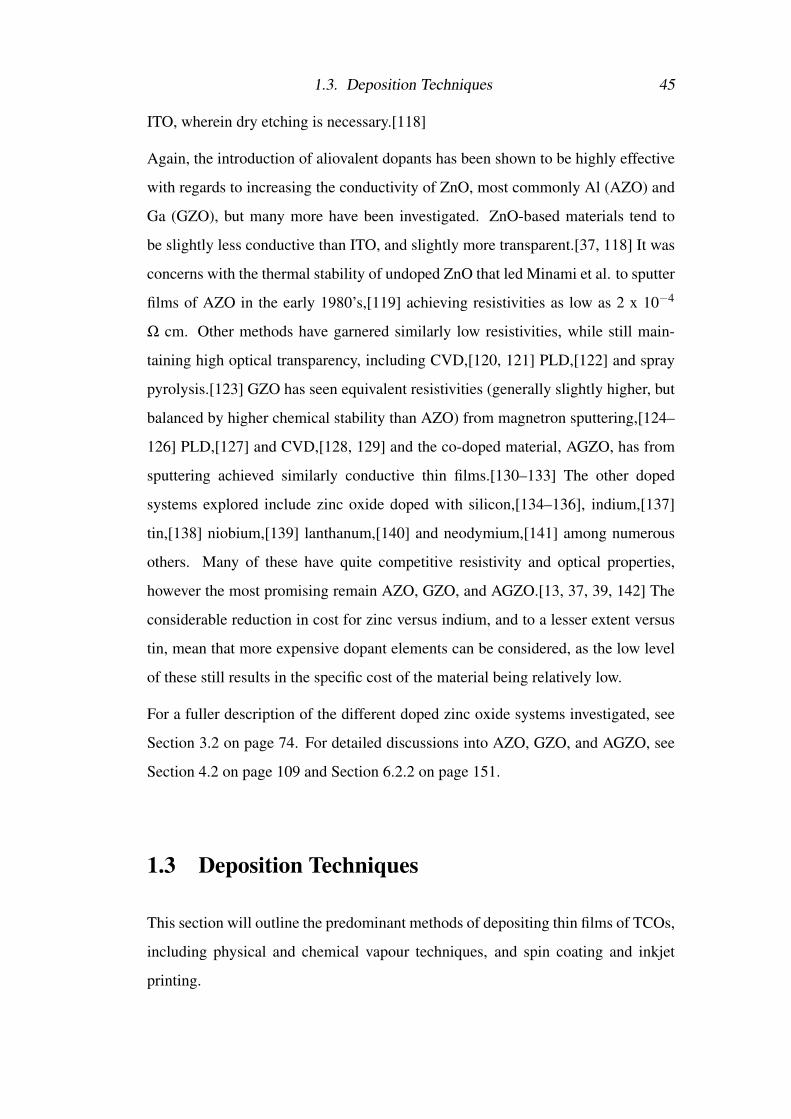
1.3.1 Physical vapour deposition methods
Physical vapour deposition (PVD) techniques are the pre-eminent thin film deposi-
tion methods employed in the majority of TCO applications. Most commonly used
is magnetron sputtering. A highly simplified schematic for such a process is shown
in Figure 1.8. Ions (in this case of the in-flowing Ar gas) bombard the target, for
example a dense ITO ceramic, and the formed plasma is ejected towards the sub-
strate, guided by electrical and magnetic fields, resulting in a thin film of the target
material forming on the substrate. Though the magnetic field helps to direct the
formed plasma and moderate thin film growth, inevitably a large proportion of the
target will end up on the walls of the chamber.
When one casts their eye over scientific reports of TCO thin films in search of the
most conductive films, inevitably magnetron sputtering will dominate the list, par-
ticularly with regards to ZnO-based films. For example, the work of Ray et al.[30]
and Shigesato et al.,[31, 143] resulting in thin films of ITO deposited by magnetron
sputtering all with resistivities < 2 x 10⁻⁴ Ω cm. Examples are prevalent too
of thin films of zinc oxide doped with aluminium (AZO),[119, 144–146] gallium
(GZO),[124, 125] aluminium and gallium together (co-doped, AGZO),[130–133]
and silicon (SiZO),[134, 135, 147] all of which had resistivities in the order of 10−4
Ω cm. Magnetron sputtering can be scaled, the technology for deposition is rela-
tively mature, and the resulting films are conductive and transparent.
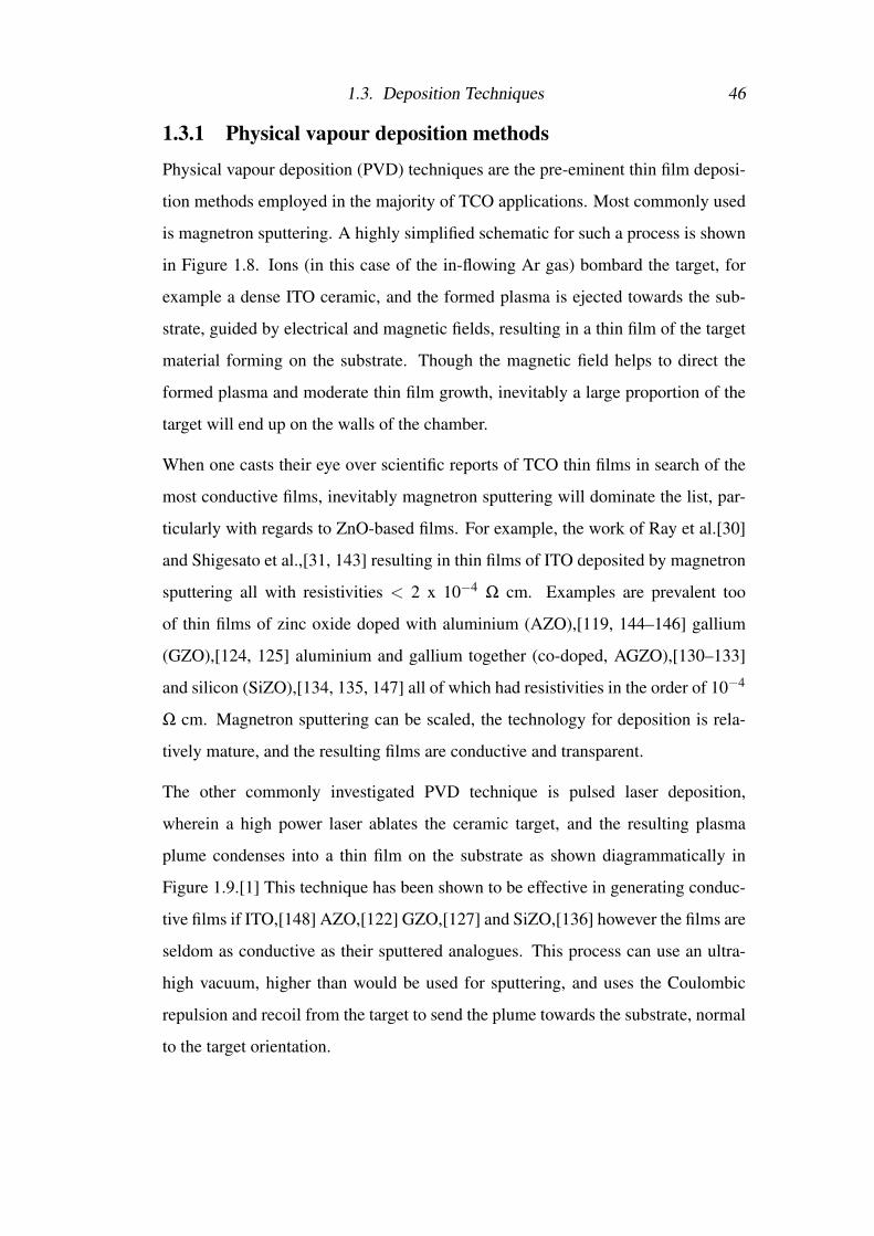
The other commonly investigated PVD technique is pulsed laser deposition,
wherein a high power laser ablates the ceramic target, and the resulting plasma
plume condenses into a thin film on the substrate as shown diagrammatically in
Figure 1.9.[1] This technique has been shown to be effective in generating conduc-
tive films if ITO,[148] AZO,[122] GZO,[127] and SiZO,[136] however the films are
seldom as conductive as their sputtered analogues. This process can use an ultra-
high vacuum, higher than would be used for sputtering, and uses the Coulombic
repulsion and recoil from the target to send the plume towards the substrate, normal
to the target orientation.
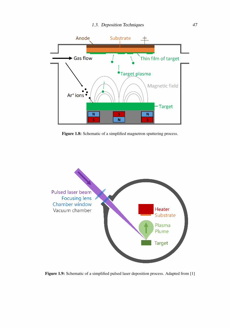
1.3. Deposition Techniques 47
Figure 1.8: Schematic of a simplified magnetron sputtering process.
Figure 1.9: Schematic of a simplified pulsed laser deposition process. Adapted from [1]
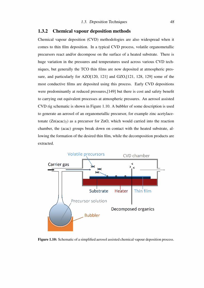
1.3. Deposition Techniques 48
1.3.2 Chemical vapour deposition methods
Chemical vapour deposition (CVD) methodologies are also widespread when it
comes to thin film deposition. In a typical CVD process, volatile organometallic
precursors react and/or decompose on the surface of a heated substrate. There is
huge variation in the pressures and temperatures used across various CVD tech-
niques, but generally the TCO thin films are now deposited at atmospheric pres-
sure, and particularly for AZO[120, 121] and GZO,[121, 128, 129] some of the
most conductive films are deposited using this process. Early CVD depositions
were predominantly at reduced pressures,[149] but there is cost and safety benefit
to carrying out equivalent processes at atmospheric pressures. An aerosol assisted
CVD rig schematic is shown in Figure 1.10. A bubbler of some description is used
to generate an aerosol of an organometallic precursor, for example zinc acetylace-
tonate (Zn(acac)2) as a precursor for ZnO, which would carried into the reaction
chamber, the (acac) groups break down on contact with the heated substrate, al-
lowing the formation of the desired thin film, while the decomposition products are
extracted.
Figure 1.10: Schematic of a simplified aerosol assisted chemical vapour deposition process.
1.3. Deposition Techniques 49
In some ways very similar to CVD, is spray pyrolysis, wherein a typically aque-
ous precursor solution is sprayed onto a heated substrate, and the product film is
formed by hydrolysis reactions. In this case, the distinction between spray pyrol-
ysis and CVD lies in whether or not the solution vapourises before impacting the
substrate.[150]
1.3.3 Ink/dispersion-based methods
Inks and dispersions can be made in several ways. With regards to TCOs, the most
common method would be via a sol-gel process. The metal precursor(s) are dis-
solved in a solvent or solvent mixture, heated and stirred, typically with a complex-
ing agent (added after initial nucleation) which facilitates, over time, the formation
of a colloidal suspension of the product. ‘Ageing’ of the solution can take sev-
eral days before spin coating is carried out. This is typically in a static regime, in
that drops are placed on the substrate, which then undergoes rapid spinning, ver-
sus dynamic spin coating in which the substrate is already spinning, and the mate-
rial is dropped onto it.[151–154] TCO thin films have been made by spin coating
sol-gel synthesised materials achieving resistivities as low as 6.3 x 10⁻⁴ Ω cm for
ITO,[154] and 3.9 x 10⁻³ Ω cm for AZO.
The alternative is to suspend already-synthesised nanoparticles in a dispersion
medium, typically by sonic agitation, and carry out the spin coating before the
particles have a chance to settle out, but generally speaking this results in infe-
rior electrical properties.[20, 154]
Inkjet printing is far less reported. In this process, a dispersion of ceramic nanopar-
ticles is used to print thin films by deposition of numerous droplets, placed very
precisely, which depending on the wettability of the substrate, and properties of the
droplets, can coalesce into a continuous layer, which can in turn be carefully dried
of the dispersion medium to leave a consistent film. Heat treatment to anneal this
film is necessary to generate the electrical contact and network through the particles.
The films tend to be highly transparent, but also highly resistive. As with the re-
dispersion of nanoparticles for spin coating, the resulting film is not as conductive
1.3. Deposition Techniques 50
as the materials are capable of, whether due to imperfect or ineffectual annealing,
dispersion quality or indeed quality of the film itself. Inkjet printed films of ITO
have achieved resistivities as low as 3 x 10⁻² Ω cm (some 100 times higher than
required of TCOs) with transparency as high as 87 %.[155] In this study in partic-
ular is demonstrated an additional capability of inkjet printing, in that in addition
to this film, another was deposited that also had an Ag grid put down, which en-
hanced the conductivity of the film by approximately two orders of magnitude. The
transparency fell to 82%, still within the acceptable range, and due to the precision
and small droplet sizes, this required very little expensive silver to achieve. A sim-
ilarly conductive (sans silver grid) AZO film was deposited by inkjet printing with
a transparency of 93 % by Vernieuwe et al.,[156] but the resistivity of 2.5 x 10⁻² Ω
cm is too high for the high transparency to make up for.
1.3.4 Deposition method comparison and summary
Given that the material cost, especially with regards to ITO, is a significant issue in
the generation of thin films, using a deposition method that is as efficient as possible
is optimal, as waste of material is an additional cost to the process.
Most of the deposition techniques described above do not deposit even a majority
of the starting material onto the substrate. This particularly concerns magnetron
sputtering, the most commonly used industrial process, wherein as little as 30 % of
the target ends up in the film, while the rest coats the walls of the chamber. Much of
this can be recovered and is not necessarily permanently lost, but the situation is not
ideal. PLD suffers similarly, though to a lesser extent, and CVD too. And it is not
only the vapour techniques; spin coating results in much of the dispersion coating
the walls rather than the substrate.
Of all the methods, only inkjet printing transfers all of the material into the film. In
terms of vehicle-to-substrate transport, it is by far the most efficient, however the
electrical properties of the films fall short of the requirements for TCOs. Resistiv-
ities in the order of 10−2 Ω cm are the best reported thus far, whereas all of the
other methods are capable of generating films in the order of 10−4 Ω cm. If inkjet
1.4. Synthesis of Nanoparticles 51
printing is to become an industrially viable technique, address of this shortcoming
is absolutely essential.
1.4 Synthesis of NanoparticlesThis section aims to outline the specific process by which all of the nanomaterials
discussed in this thesis were synthesised, including first a comparison to analogous
batch syntheses, then a more detailed discussion as to the nucleation and growth of
nanoparticles in a continuous hydrothermal flow synthesis (CHFS) process. Find
presently a discussion as to the scientific basis and applications of CHFS; detailed
discussion as to how this pertains to the specific TCO materials appears in the in-
troduction sections of each Chapter, where relevant.
1.4.1 Batch synthesis methods versus continuous methods
The distinction between batch and continuous synthesis methods can be distilled as
follows: a batch synthesis is a closed process, in that a reaction occurs between a set
of reagents under a certain set of conditions, after which the product is separated out
and collected, the conditions returned to atmospheric norm. By contrast, a continu-
ous process is not a closed system; it involves the ongoing addition of reagents and
removal of products in flow, and subject to the longevity of the machinery involved,
and the availability of reagents, a continuous process can be continued indefinitely.
For many syntheses, precise control of temperature and pH, among other properties,
is of great importance. Slight variations can, for example in sol-gel processes, lead
to significant batch-to-batch variations, a significant issue for an industrial process,
in which consistency of particle properties is critical.[157, 158] This and other pro-
cesses, such as co-precipitation methods, can be very involved, with multiple slow
steps required before the end product can be collected.[159] Specifically concerning
metal oxides, batch industrial processes, such as the French Process for generating
zinc oxide, may involve the use of extreme temperatures (ca. 1000 C), and as such
are very energy-intensive.[160]
Industrial processes for nanoparticle synthesis should ideally satisfy a number of
1.4. Synthesis of Nanoparticles 52
requirements. These include, but are not limited to, the necessity for production of
controlled, homogeneous materials with consistent properties for their desired ap-
plications, the in-line monitoring of said consistency, lack of needless complexity
in the process (single-step processes are ideal), efficiency in energy and resource
use, both at research and industrial scale of production, flexibility in reaction pa-
rameters to fine-tune particle properties, and perhaps above all should be the safety
of the process. This includes the risk to workers from process machinery (and by
extension the facility to safely disable said process machinery), as well as from po-
tentially harmful reagents and solvents, and pertinent to this research in particular,
from nanoparticles themselves. The long-term health risks are not fully known, but
that dry nanoparticles can be inhaled is not in question, merely the potential detri-
ment to the respiratory health of those involved.[159, 161, 162]
In address of these, continuous hydrothermal processes stand tall. Temperature,
pressure, pH, concentration, flow rates, and mixing regimes among other parameters
are easily controllable, and system/flow properties and dynamics can be calculated
precisely should one have a chemical engineer to hand. Monitoring of the process
while synthesis is carried out is also possible, and from the point of view of the pro-
cess scientist carrying out the synthesis, safety precautions and reaction design can
allay the majority of concerns. Water is typically the only solvent, and the product
is collected as a wet slurry of nanoparticles in water, such that the nanoparticles
produced are not in a form that can be inhaled at all.[159] The process is, however,
typically carried out at high temperatures and pressures, though at lower tempera-
tures than many industrial batch processes,[159, 160] and though safety precautions
can minimise the risk to personnel, no such process can ever be entirely risk-free.
1.4.2 Continuous hydrothermal flow synthesis
Continuous hydrothermal flow synthesis (CHFS) processes, especially those em-
ployed herein, principally take advantage of the change in water properties across
the supercritical/liquid phase boundary. This is depicted in Figure 1.11, wherein
the phase behaviour of water at different temperatures and pressures is depicted.[2]
Three points of interest in the graph are denoted by the dashed lines. From left
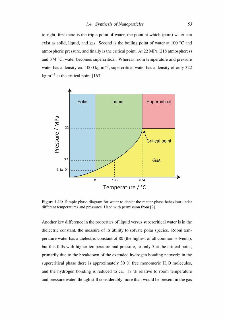
1.4. Synthesis of Nanoparticles 53
to right, first there is the triple point of water, the point at which (pure) water can
exist as solid, liquid, and gas. Second is the boiling point of water at 100 C and
atmospheric pressure, and finally is the critical point. At 22 MPa (218 atmospheres)
and 374 C, water becomes supercritical. Whereas room temperature and pressure
water has a density ca. 1000 kg m−3, supercritical water has a density of only 322
kg m−3 at the critical point.[163]
Figure 1.11: Simple phase diagram for water to depict the matter-phase behaviour underdifferent temperatures and pressures. Used with permission from [2].
Another key difference in the properties of liquid versus supercritical water is in the
dielectric constant, the measure of its ability to solvate polar species. Room tem-
perature water has a dielectric constant of 80 (the highest of all common solvents),
but this falls with higher temperature and pressure, to only 5 at the critical point,
primarily due to the breakdown of the extended hydrogen bonding network; in the
supercritical phase there is approximately 30 % free monomeric H2O molecules,
and the hydrogen bonding is reduced to ca. 17 % relative to room temperature
and pressure water, though still considerably more than would be present in the gas
1.4. Synthesis of Nanoparticles 54
phase. Indeed, supercritical water exists in liquid-like hydrogen bonded clusters
dispersed within a gas-like phase, interfaces between other phases no longer exist
so there is no surface tension to speak of.[164–166] These changes between liq-
uid and supercritical states do not occur instantaneously upon reaching the critical
temperature and pressure, there are significant changes in near-critical (sub-critical)
water relative to the liquid phase too, and advantage can be taken of these in a CHFS
process.[159, 163]
The precursors for a CHFS reaction are typically aqueous metal salts, for example
zinc nitrate as a precursor for zinc oxide. This has a very high solubility in water,
93g per 100 mL of room temperature water,[167] because it is highly polar. This
also means that it is not soluble in non-polar solvents, as supercritical water can be
classified. Hence if a room temperature solution of zinc nitrate (even very dilute)
meets and mixes thoroughly with a stream of supercritical water, it will be in a su-
percritical, or near-critical state. The solution becomes supersaturated with the zinc
nitrate, which will crash out of solution and react with the superheated water around
it according to the two-part reaction scheme depicted in Equations 1.3 and 1.4 for a
metal nitrate reagent, where the metal is represented by ‘M’. In this case, the nitric
acid produced will make the product stream acidic; modifiers such as potassium hy-
droxide can be added to aid in the nucleation of the metal oxides, and to neutralise
or make alkaline the product stream.
M(NO3)x (aq) + xH2O→M(OH)x (s) + xHNO3 (1.3)
M(OH)x (s)→MO x2 (s) +
x2
H2O (1.4)
This applies to many metal oxides, though conversion of the hydroxide to the ox-
ide requires that there be sufficient energy, so in some instances, such as in the
case of the CHFS synthesis of In2O3, the oxide is only formed at mixing tem-
peratures of 400 C or more; lower temperatures result in the partially converted
InO(OH).[28, 168, 169] However, with materials such as CeO2 and ZrO2,[170, 171]
1.4. Synthesis of Nanoparticles 55
NiO,[172] ZnO,[173, 174] and TiO2,[175] among others, the oxide can be formed
at milder temperatures. The applications of CHFS are limited only by what ma-
terials can be synthesised. Gas sensing,[176, 177] photocatalysis,[174, 178, 179]
lithium ion batteries,[180–183] capacitors[184] and thermochromics[185, 186] are
only a small selection of the applications to which CHFS can be lent; for a full and
more detailed delve into the field I refer the reader to the review by Darr et al.[159]
With regards to TCO materials, ITO has been made in hydrothermal flow
before,[169, 187] but in only one report was subsequently deposited as a thin film,
yielding resistivities around 1 x 10⁻² Ω cm.[168] Other prospective TCO materi-
als have been synthesised by CHFS, including some doped zinc oxides,[174] and
niobium-doped titania,[181] however these were not tested for their TCO-related
properties, but for photocatalysis and energy storage, respectively.
1.4.3 CHFS as a combinatorial tool
CHFS lends itself very effectively to high throughput, combinatorial screening
of different materials, in that by altering the precursor solutions, a large number
of samples can be synthesised in a relatively short period of time, for example
the high-throughput synthesis of a 66-sample phase diagram of CexZryYzO2−δ
in < 1 day.[170] This is something for which there is no simple analogue for
batch synthesis processes, beyond the acquisition and use of 66 autoclaves.
Other prevalent combinatorial synthesis methods (non-CHFS) have been in use
for up to two decades,[188] including magnetron sputtering,[188–192], pulsed
laser deposition,[193–195] molecular beam epitaxy,[196] flame pyrolysis,[197]
sol-gel,[198], solid state,[199, 200] and chemical vapour deposition.[201]
These have encompassed a variety of technological application research areas,
such as superconductors,[188, 193] TCOs,[189–192, 194, 197, 198, 201, 202]
photocatalysis,[196, 198] and themoelectrics.[195, 199, 200] These techniques are
for the most part geared towards the synthesis of combinatorial libraries in the
form of thin films; with the exception of solid state[200] and spray pyrolysis[197]
1.5. Hypotheses 56
methods, there has been a lack of combinatorial methodology for the production of
nanopowders. Given the few examples that so far exist, it is clear that for materials
discovery and compositional optimisation, CHFS can be a powerful combinatorial
research tool that has yet to be properly applied to the field of TCOs.
1.5 HypothesesIn this chapter, the fundamentals to the understanding of this thesis were presented.
The properties and applications of transparent conducting oxides were discussed, as
well as the issues in the field, namely those presented by continued use of indium-
based materials, and the consequent requirement not only for more sustainable re-
placement materials, but also the development, and more prevalent use of increas-
ingly sustainable synthetic and deposition methodologies.
Thus, the hypothesis question of this thesis is as follows:
Can continuous hydrothermal flow synthesis be used to synthesise materials that
demonstrate, when deposited as thin films, the optical and electronic properties that
are required of transparent conducting oxides in their various applications.
This can be broken down into the following investigative steps:
i. To screen numerous materials synthesised by continuous hydrothermal flow syn-
thesis, in order to determine the systems that demonstrate the most promising elec-
tronic properties.
ii. To optimise these most promising systems in terms of the dopant level for maxi-
mal conductivity.
iii. To surface-functionalise these optimised materials within the synthetic process,
and deposit them as thin films by such methods as spin-coating or inkjet printing,
furthermore optimising the processing and heat treatment of the films to obtain as
optically transparent, electrically conductive, materials as possible.
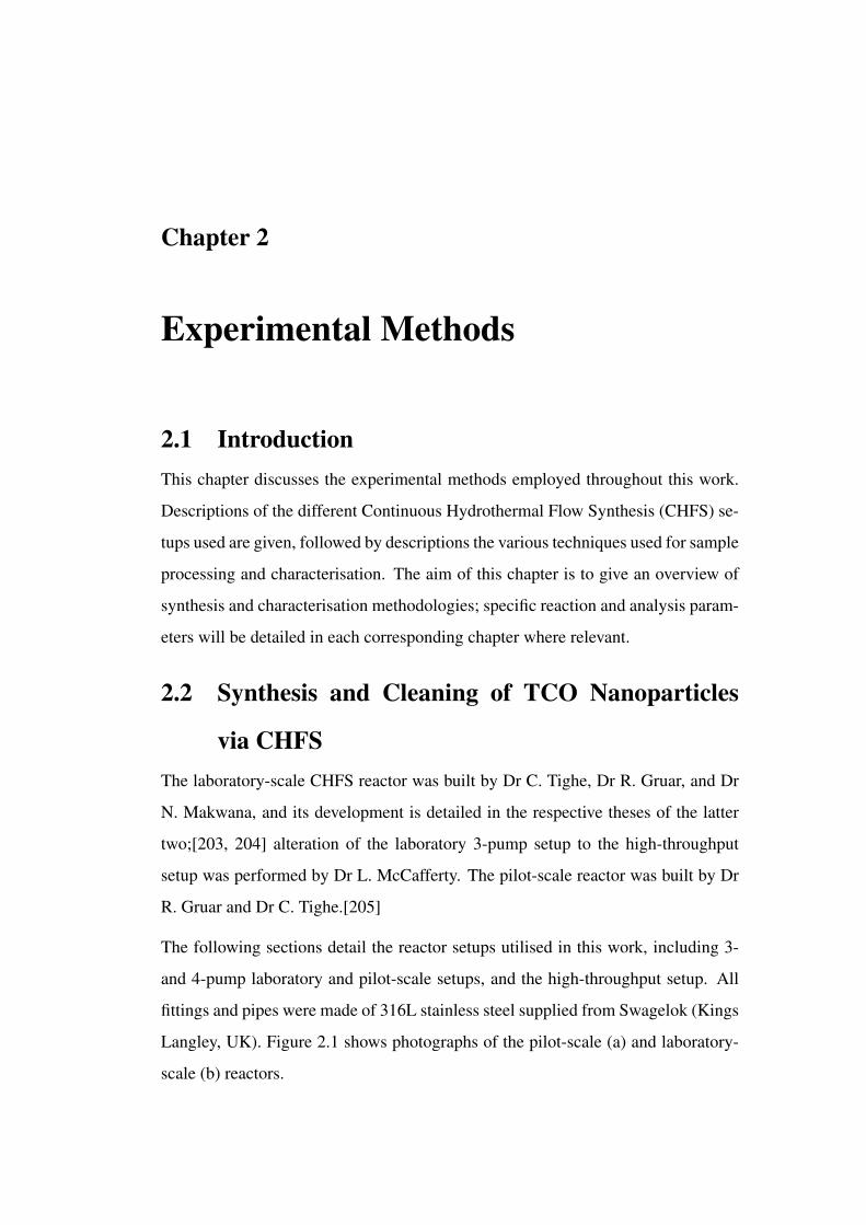
Chapter 2
Experimental Methods
2.1 IntroductionThis chapter discusses the experimental methods employed throughout this work.
Descriptions of the different Continuous Hydrothermal Flow Synthesis (CHFS) se-
tups used are given, followed by descriptions the various techniques used for sample
processing and characterisation. The aim of this chapter is to give an overview of
synthesis and characterisation methodologies; specific reaction and analysis param-
eters will be detailed in each corresponding chapter where relevant.
2.2 Synthesis and Cleaning of TCO Nanoparticles
via CHFSThe laboratory-scale CHFS reactor was built by Dr C. Tighe, Dr R. Gruar, and Dr
N. Makwana, and its development is detailed in the respective theses of the latter
two;[203, 204] alteration of the laboratory 3-pump setup to the high-throughput
setup was performed by Dr L. McCafferty. The pilot-scale reactor was built by Dr
R. Gruar and Dr C. Tighe.[205]
The following sections detail the reactor setups utilised in this work, including 3-
and 4-pump laboratory and pilot-scale setups, and the high-throughput setup. All
fittings and pipes were made of 316L stainless steel supplied from Swagelok (Kings
Langley, UK). Figure 2.1 shows photographs of the pilot-scale (a) and laboratory-
scale (b) reactors.
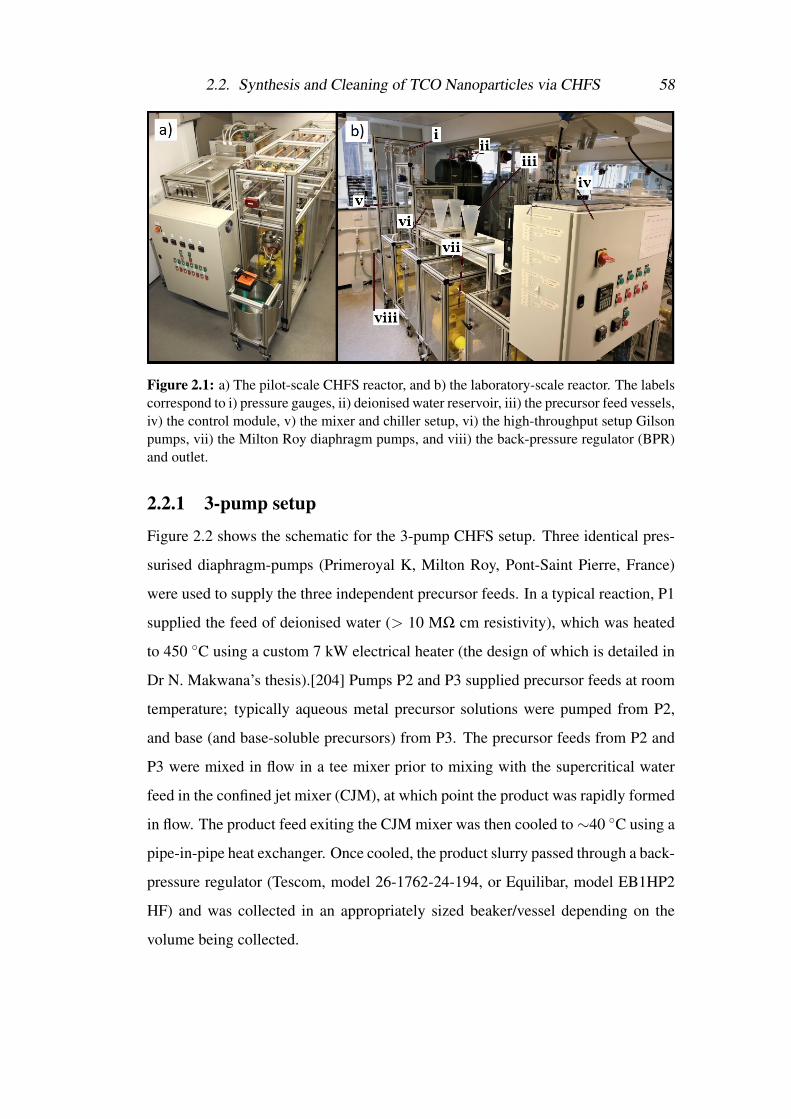
2.2. Synthesis and Cleaning of TCO Nanoparticles via CHFS 58
Figure 2.1: a) The pilot-scale CHFS reactor, and b) the laboratory-scale reactor. The labelscorrespond to i) pressure gauges, ii) deionised water reservoir, iii) the precursor feed vessels,iv) the control module, v) the mixer and chiller setup, vi) the high-throughput setup Gilsonpumps, vii) the Milton Roy diaphragm pumps, and viii) the back-pressure regulator (BPR)and outlet.
2.2.1 3-pump setup
Figure 2.2 shows the schematic for the 3-pump CHFS setup. Three identical pres-
surised diaphragm-pumps (Primeroyal K, Milton Roy, Pont-Saint Pierre, France)
were used to supply the three independent precursor feeds. In a typical reaction, P1
supplied the feed of deionised water (> 10 MΩ cm resistivity), which was heated
to 450 C using a custom 7 kW electrical heater (the design of which is detailed in
Dr N. Makwana’s thesis).[204] Pumps P2 and P3 supplied precursor feeds at room
temperature; typically aqueous metal precursor solutions were pumped from P2,
and base (and base-soluble precursors) from P3. The precursor feeds from P2 and
P3 were mixed in flow in a tee mixer prior to mixing with the supercritical water
feed in the confined jet mixer (CJM), at which point the product was rapidly formed
in flow. The product feed exiting the CJM mixer was then cooled to∼40 C using a
pipe-in-pipe heat exchanger. Once cooled, the product slurry passed through a back-
pressure regulator (Tescom, model 26-1762-24-194, or Equilibar, model EB1HP2
HF) and was collected in an appropriately sized beaker/vessel depending on the
volume being collected.
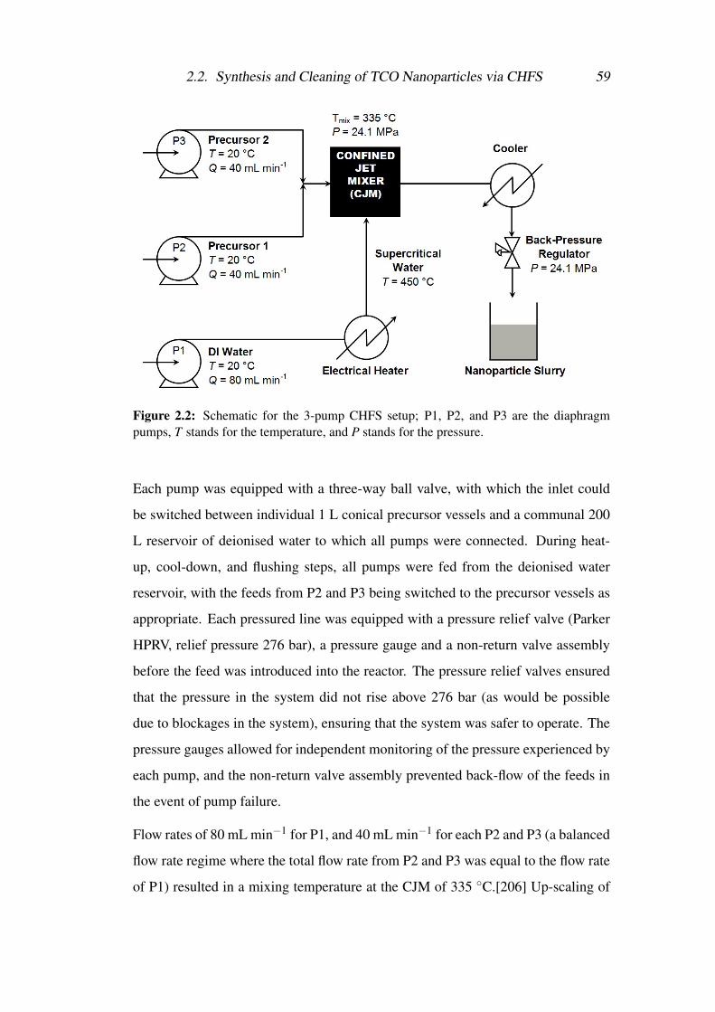
2.2. Synthesis and Cleaning of TCO Nanoparticles via CHFS 59
Figure 2.2: Schematic for the 3-pump CHFS setup; P1, P2, and P3 are the diaphragmpumps, T stands for the temperature, and P stands for the pressure.
Each pump was equipped with a three-way ball valve, with which the inlet could
be switched between individual 1 L conical precursor vessels and a communal 200
L reservoir of deionised water to which all pumps were connected. During heat-
up, cool-down, and flushing steps, all pumps were fed from the deionised water
reservoir, with the feeds from P2 and P3 being switched to the precursor vessels as
appropriate. Each pressured line was equipped with a pressure relief valve (Parker
HPRV, relief pressure 276 bar), a pressure gauge and a non-return valve assembly
before the feed was introduced into the reactor. The pressure relief valves ensured
that the pressure in the system did not rise above 276 bar (as would be possible
due to blockages in the system), ensuring that the system was safer to operate. The
pressure gauges allowed for independent monitoring of the pressure experienced by
each pump, and the non-return valve assembly prevented back-flow of the feeds in
the event of pump failure.
Flow rates of 80 mL min−1 for P1, and 40 mL min−1 for each P2 and P3 (a balanced
flow rate regime where the total flow rate from P2 and P3 was equal to the flow rate
of P1) resulted in a mixing temperature at the CJM of 335 C.[206] Up-scaling of
2.2. Synthesis and Cleaning of TCO Nanoparticles via CHFS 60
the process to flow rates of 400 mL min−1, 200 mL min−1 and 200 mL min−1 for
pumps P1, P2 and P3, respectively, was carried out using the pilot-scale CHFS, and
five-fold volumetric increase in scale, though also with a mixing temperature of 335C.
2.2.2 4-pump setup
Figure 2.3: Schematic for the 4-pump CHFS setup; P1-4 are the diaphragm pumps, Tstands for the temperature, and P stands for the pressure.
Figure 2.3 shows a schematic for the 4-pump setup for a CHFS reactor. Practically,
the setup is identical to the 3-pump analogue, with the addition of a second CJM
after the first, wherein the product stream comprised of the mixed feeds from P1,
P2, and P3, met the room temperature quench feed from P4. This P4 feed contained
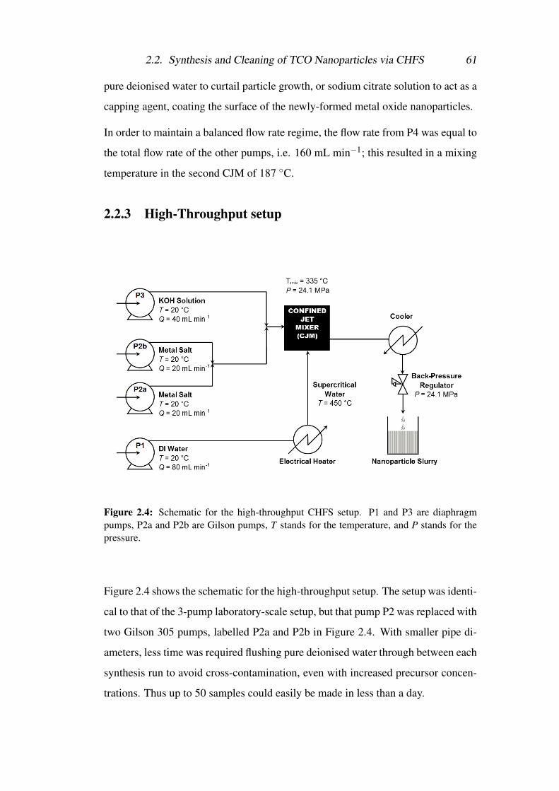
2.2. Synthesis and Cleaning of TCO Nanoparticles via CHFS 61
pure deionised water to curtail particle growth, or sodium citrate solution to act as a
capping agent, coating the surface of the newly-formed metal oxide nanoparticles.
In order to maintain a balanced flow rate regime, the flow rate from P4 was equal to
the total flow rate of the other pumps, i.e. 160 mL min−1; this resulted in a mixing
temperature in the second CJM of 187 C.
2.2.3 High-Throughput setup
Figure 2.4: Schematic for the high-throughput CHFS setup. P1 and P3 are diaphragmpumps, P2a and P2b are Gilson pumps, T stands for the temperature, and P stands for thepressure.
Figure 2.4 shows the schematic for the high-throughput setup. The setup was identi-
cal to that of the 3-pump laboratory-scale setup, but that pump P2 was replaced with
two Gilson 305 pumps, labelled P2a and P2b in Figure 2.4. With smaller pipe di-
ameters, less time was required flushing pure deionised water through between each
synthesis run to avoid cross-contamination, even with increased precursor concen-
trations. Thus up to 50 samples could easily be made in less than a day.

2.2. Synthesis and Cleaning of TCO Nanoparticles via CHFS 62
2.2.4 Confined Jet Mixer (CJM) design
The design of the CJM is shown in Figure 2.5. The co-current mixer was designed
by Darr et al.,[3] in which the two flows (supercritical water and the reagent mix-
ture) were fed co-currently. The pipe-in-pipe setup saw the supercritical water flow
through the inner pipe, while the precursor solutions were introduced orthogonal to
the water feed. Nanoparticle formation occurred at the point the two feeds mixed,
and the reaction products were carried upwards away from the mixing point.
Figure 2.5: Schematic showing the design for the Confined Jet Mixer (CJM) (adapted from[3]).
2.2. Synthesis and Cleaning of TCO Nanoparticles via CHFS 63
2.2.5 Cleaning and processing of the as-made slurries
As-prepared samples were collected as particle-laden slurries from the CHFS reac-
tor. Solids were retrieved by centrifugation using a Sigma 4K15 centrifuge at 4500
rpm. If the sample settled readily, centrifugation was carried out using 50 mL Fal-
con tubes and centrifugation was conducted in the range 5 - 30 minutes depending
on how readily the samples settled out. If the sample did not settle, then 500 mL
centrifuge buckets were used instead. Un-coated particles were cleaned by wash-
ing centrifuged dense pastes with deionised water, agitated, and centrifuged again;
this process was repeated until the supernatant measured a conductivity < 50 µS as
measured using a Hanna Instruments H198311 conductivity meter. Coated particles
(which tended to settle less readily) were treated in like manner, but washings were
carried out with 20 wt% acetone and 80 wt% deionised water, and each centrifuga-
tion step typically took 1 - 3 hours.
After cleaning, samples were in the form of a dense paste, approximately 50-60
wt% solid. Coated samples from which inks were to be made were stored in this
form, however the majority of samples were then dried using a Virtis Genesis 35 XL
Freeze Drier. This was achieved by first freezing the sample chamber (containing
the dense wet pastes) and the condenser unit (which trapped the water) to -40 C,
then implementing a vacuum. Holding the vacuum such that the pressure was < 13
Pa, the temperature of the sample chamber was slowly raised from -40 C to 25 C
over a period of 24 h. This resulted in free-flowing powders, which were further
ground by pestle and mortar, and total yields then measured and calculated.
2.2.6 Precursor materials
All water used in syntheses and subsequent cleaning steps was 10 MΩ deionized
water purified using a Millipore Elix Essential water purification system, and the
base was potassium hydroxide solution (KOH, Fisher Scientific, Leicestershire,
UK). Precursor reagents for each of the desired elements were used as-purchased
from the suppliers as detailed in Table 2.1.
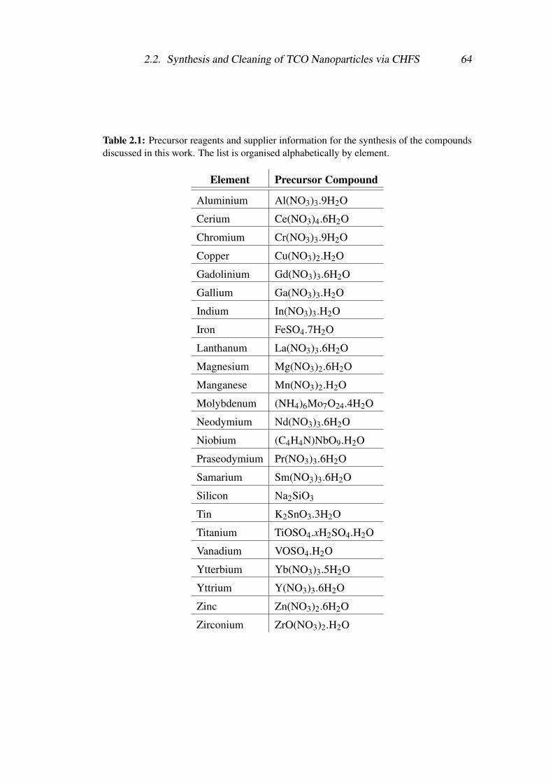
2.2. Synthesis and Cleaning of TCO Nanoparticles via CHFS 64
Table 2.1: Precursor reagents and supplier information for the synthesis of the compoundsdiscussed in this work. The list is organised alphabetically by element.
Element Precursor Compound
Aluminium Al(NO3)3.9H2O
Cerium Ce(NO3)4.6H2O
Chromium Cr(NO3)3.9H2O
Copper Cu(NO3)2.H2O
Gadolinium Gd(NO3)3.6H2O
Gallium Ga(NO3)3.H2O
Indium In(NO3)3.H2O
Iron FeSO4.7H2O
Lanthanum La(NO3)3.6H2O
Magnesium Mg(NO3)2.6H2O
Manganese Mn(NO3)2.H2O
Molybdenum (NH4)6Mo7O24.4H2O
Neodymium Nd(NO3)3.6H2O
Niobium (C4H4N)NbO9.H2O
Praseodymium Pr(NO3)3.6H2O
Samarium Sm(NO3)3.6H2O
Silicon Na2SiO3
Tin K2SnO3.3H2O
Titanium TiOSO4.xH2SO4.H2O
Vanadium VOSO4.H2O
Ytterbium Yb(NO3)3.5H2O
Yttrium Y(NO3)3.6H2O
Zinc Zn(NO3)2.6H2O
Zirconium ZrO(NO3)2.H2O
2.3. Physical Characterisation of Powders 65
2.3 Physical Characterisation of Powders
The following sections detail the methodologies employed in the characterisation
of the powders. These include X-ray diffraction, X-ray photoelectron spectroscopy,
transmission electron microscopy, energy dispersive X-ray spectroscopy, Brunauer-
Emmett-Teller analysis, thermogravimetric analysis, and atomic emission spec-
troscopy.
2.3.1 Powder X-ray diffraction (pXRD) and particle size estima-
tion using Scherrer analysis
XRD data were collected using a STOE Stadi P diffractometer in transmission ge-
ometry, employing a molybdenum source (Mo-Kα1 radiation, λ = 0.7093 ), with a
typical data collection range of 2θ = 5 - 35 . Approximately 0.01 g of sample was
mounted between two transparent acetate sheets for analysis.
The 2θ scan range, acquisition time, and step size were dependent on the samples
and are detailed in each chapter separately. The phase composition of the samples
was determined by comparison to reference patterns available in the Inorganic Crys-
tal Structure Database (ICSD).
Scherrer analysis[8, 9] was carried out on the (100), (002), and (102) peaks, as
for Wurtzite ZnO-based samples, these are the three most intense and best defined
peaks, positioned at relatively low scattering angles. The method was used for
crystallite size estimation, not to be taken as accurate values on their own, rather
indicative of trends in particle size used in conjunction with BET surface area anal-
ysis and TEM particle size analysis. Equation 2.1 shows the calculation used for
the Scherrer method, where τ is the lower bound of the estimated crystallite size, K
is the dimensionless shape factor taken to be 0.9, λ is the wavelength of the X-ray
source used, β is the line broadening at half the maximum intensity for the peak in
question, and θ is the Bragg angle.
τ =Kλ
βcosθ(2.1)
2.3. Physical Characterisation of Powders 66
2.3.2 X-ray photoelectron spectroscopy (XPS)
X-ray photoelectron spectroscopy was carried out using a Thermo Scientific K-
alpha photoelectron spectrometer using monochromatic Al-Kα radiation. Survey
scans were collected in the binding energy range 0-1100 eV at a pass energy of
200 eV. Higher resolution scans were recorded for the principle peaks as detailed in
the respective chapters concerning them. Peak positions were calibrated using the
adventitious carbon 1s peak at 284.7 eV using CasaXPS software, from which XY
data was extracted. Samples were prepared by affixing small cuts of double-sided
carbon tape to the sample holder, with the powder samples on the up-turned side of
the tape.
2.3.3 Transmission electron microscopy and energy dispersive
X-ray spectroscopy (TEM/EDS)
Transmission electron microscopy (TEM) was performed using a Jeol 200 kV trans-
mission electron microscope in imaging mode. Samples were dispersed in methanol
and drop coated onto 300 mesh carbon-coated copper TEM grids (purchased from
Agar Scientific). Image analysis and particle size measurements were carried out
using Gatan Digital Microscopy Suite software. Energy Dispersive X-ray Spec-
troscopy (EDS) analysis was carried out using an Oxford Instruments X-MaxN 80-
T Silicon Drift Detector (SDD) fitted to the transmission electron microscope and
processed using Aztec software.
2.3.4 Inductively couples plasma atomic emission spectroscopy
(ICP-AES)
Compositional analysis was carried out on selected samples using inductively cou-
pled plasma atomic emission spectroscopy (ICP-AES). Dilute solutions of the sam-
ples were prepared by dissolution in 1% aqueous nitric acid, and analysis was car-
ried out using a Varian 720 ICP-AES in axial configuration equipped with an au-
tosampler. Prior to sample analysis, calibrations were carried out using standards
at concentrations of 2.5, 5.0, 7.5, and 10.0 ppm for zinc, and 0.25, 0.5, 0.75, and
1.0 ppm for each Al, Ga, and Si. The measurements and subsequent conversion
2.4. Sample Preparation for Further Analysis 67
calculations were carried out by I. Johnson and Dr P. Marchand.
2.3.5 Brunauer-Emmett-Teller (BET) analysis
Brunauer-Emmett-Teller (BET) measurements were carried out on dry powders to
ascertain the surface area of the different samples. 0.1 - 0.2 g of powders were
weighed out and degassed by heating to 150 C under a flow of nitrogen gas for >
12 h in glass BET tubes. The samples were re-weighed to ascertain the degassed
sample mass, and the tubes affixed to the Micromeritics TriStar II PLUS surface
area and porosity analyser, which was used to measure adsorption isotherms and
thus calculate the BET surface area.
2.3.6 Thermogravimetric analysis (TGA)
Thermogravimetric analysis (TGA) was performed on a Netzsh STA 449C instru-
ment. TGA was carried out in static air with the samples in aluminium pans at
atmospheric pressure. The rate of heating was 10 C min−1, from room tempera-
ture up to a maximum temperature of 600 C.
2.4 Sample Preparation for Further AnalysisCompositional optimisation was determined by pressing dry powders into discs and
performing electrical measurements on them. Optimised compositions were then
used to generate thin films, by spin coating and inkjet printing. Methods of prepara-
tion of pellets (powders only) and inks (powders and dense wet pastes) are described
in the following sections.
2.4.1 Pellet preparation
Approximately 0.5 g of dry powder sample was pressed into a 16 mm diameter, ca. 1
mm thick compact disc using a bench-top hydraulic press (Specac, Orpington, UK),
under a force of 50 kN for 5 to 30 minutes, depending on the sample in question.
Discs were made in triplicate for each sample. Once pressed, the discs were heat
treated in a tube furnace (70 mm internal work tube diameter, Elite Thermal Systems
Ltd.) for 3 hours at 500 C under a 5% hydrogen in nitrogen atmosphere, with an
approximate flow rate of 5 cm3 min−1. Examples of the discs are shown in Figure
2.4. Sample Preparation for Further Analysis 68
2.6.
2.4.2 Ink formulation
Dispersions/inks of the nanoparticles, were required for multiple deposition tech-
niques, including but not limited to spin coating and inkjet printing. These dispers-
ing methodologies are discussed in the following sections.
2.4.2.1 Spin-coating inks
Inks for spin-coating were prepared from dry powders with no surface coatings, or
from citrate-coated indium tin oxide dense wet paste. To 1.0 g of dry powder (or
equivalent in paste form) was added 4.0 g of dispersing medium (typically 20 wt%
ethylene glycol in deionized water). These were mixed by hand using a spatula to
ensure that the powder was wetted, then underwent sonic agitation using a sonicat-
ing bath (VWR Ultrasonic Cleaner, USC100T) for 30 min. This began the process
of breaking up the agglomerates, and cleaned the sample off the spatula, giving a
crude dispersion. This was further treated by use of a Branson Digital Sonifier 250
sonicating tip operating at 20% amplitude with a 0.3 s on/off pulse length. The
tip was submerged in the dispersion, which was itself held in an ice bath to ensure
excessive heating of the dispersion did not occur. Each 2 min sonicating tip treat-
ment (1 min on, 1 min off) was followed by 2 min resting in the ice bath before the
next treatment was carried out. Insufficient cooling time resulted in the suspension
overheating; this coagulated the formulation, characterised by an irreversible and
sudden increase in viscosity. Eight such treatments were carried out, before further
sonic agitation of the dispersion in the sonicating bath for 30 min. The dispersions
were allowed to rest for up to 1 h before spin coating was carried out.
2.4.2.2 Inkjet printing inks
25 - 30 g inks for inkjet printing were prepared from wet pastes of surface-modified
nanoparticles that had been coated with citrate during the synthetic process. A
small amount (ca. 0.1 g) of the paste was baked at 300 C in air using a Carbolite
CWF-1300 muffle furnace to ascertain the metal oxide loading (typically 55-60
wt%). An appropriate calculated amount of paste was weighed out, and to it added
2.4. Sample Preparation for Further Analysis 69
Sun Chemical ink vehicle U10197 as the dispersing medium, such that the solid
loading was 25 wt%, and the minimum mass of the ink was 25 g. This was agitated
using sonication in the abovementioned sonicating bath for 15 minutes before the
sonicating tip was used in the manner described above to carry out between 10
and 15 treatments, until the dispersion could in its entirety pass through a 3.1 µm
syringe filter (Thermo Scientific).
2.4.3 Ink/Dispersion Analysis Techniques
Dispersion analysis was carried out in the form of dynamic light scattering (DLS)
(hydrodynamic diameter and surface zeta potential measurements) and viscometry
measurements. Methodologies for these are discussed in the following sections.
2.4.3.1 Dynamic light scattering (DLS) and Zeta potential measure-
ments
DLS and zeta potential measurements were carried out using a Nano Zetasizer
ZEN3600 (Malvern Instruments Ltd). Samples were prepared by suspending 10
mg of powder (or equivalent for ink samples) in 100 mL of 5 mM NaCl solution in
deionized water.
Particle size distributions were measured at an angle of 173 using backscatter
geometry. Each size distribution obtained was taken as an average of ten measure-
ments, each lasting 10 seconds. These measurements were carried out in disposable,
chemically resistant PMMA cuvettes (Malvern).
Zeta potential measurements were carried out in like configuration, but using dis-
posable folded capillary cells with in-built electrodes (Malvern). The samples as
prepared above were adjusted to pH 7, and measurements carried out step-wise ei-
ther decreasing or increasing the pH to within the stability of the sample in question;
0.1 M and 0.01 M solutions of each HNO3 and KOH prepared using 5 mM NaCl
solution were used to adjust the pH. Each data point was an average of at least ten
agreeing measurements (up to 100, depending on the cumulatively calculated stan-
dard deviation) after voltage equilibration, and three data points were taken for each
pH value for each sample. The mean zeta potentials were then plotted against pH
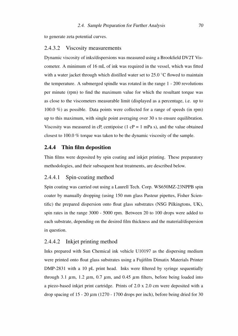
2.4. Sample Preparation for Further Analysis 70
to generate zeta potential curves.
2.4.3.2 Viscosity measurements
Dynamic viscosity of inks/dispersions was measured using a Brookfield DV2T Vis-
cometer. A minimum of 16 mL of ink was required in the vessel, which was fitted
with a water jacket through which distilled water set to 25.0 C flowed to maintain
the temperature. A submerged spindle was rotated in the range 1 - 200 revolutions
per minute (rpm) to find the maximum value for which the resultant torque was
as close to the viscometers measurable limit (displayed as a percentage, i.e. up to
100.0 %) as possible. Data points were collected for a range of speeds (in rpm)
up to this maximum, with single point averaging over 30 s to ensure equilibration.
Viscosity was measured in cP, centipoise (1 cP = 1 mPa s), and the value obtained
closest to 100.0 % torque was taken to be the dynamic viscosity of the sample.
2.4.4 Thin film deposition
Thin films were deposited by spin coating and inkjet printing. These preparatory
methodologies, and their subsequent heat treatments, are described below.
2.4.4.1 Spin-coating method
Spin coating was carried out using a Laurell Tech. Corp. WS650MZ-23NPPB spin
coater by manually dropping (using 150 mm glass Pasteur pipettes, Fisher Scien-
tific) the prepared dispersion onto float glass substrates (NSG Pilkingtons, UK),
spin rates in the range 3000 - 5000 rpm. Between 20 to 100 drops were added to
each substrate, depending on the desired film thickness and the material/dispersion
in question.
2.4.4.2 Inkjet printing method
Inks prepared with Sun Chemical ink vehicle U10197 as the dispersing medium
were printed onto float glass substrates using a Fujifilm Dimatix Materials Printer
DMP-2831 with a 10 pL print head. Inks were filtered by syringe sequentially
through 3.1 µm, 1.2 µm, 0.7 µm, and 0.45 µm filters, before being loaded into
a piezo-based inkjet print cartridge. Prints of 2.0 x 2.0 cm were deposited with a
drop spacing of 15 - 20 µm (1270 - 1700 drops per inch), before being dried for 30
2.5. Electrical and Optical Characterisation 71
min in air at 95 C to remove the dispersing medium. Proprietary additives were in
some cases added to the inks before printing to improve dispersion quality, surface
tension, viscosity, or wetting properties of the inks, facilitating a higher quality
film. Deposition and proprietary formulation altering was carried out by, or under
instruction of Dr M. Pickrell of Sun Chemical Ltd.
2.4.4.3 Heat treatment of thin films
All thin films, deposited by spin coating or inkjet printing methodologies, were
heat treated in a tube furnace (100 mm internal diameter work tube, Elite Thermal
Systems) at 550 C for 5 h under a flow of N2 or Ar (ITO films), or 5% H2/N2
(ZnO-based films), with a ramp rate of 5.0 C min−1.
2.5 Electrical and Optical CharacterisationMethods for the electrical (Hall Effect) and optical (UV/Vis/NIR) characterisation
are described below, as well as the methods used to determine film thickness (opti-
cal, and side-on SEM), needed to calculate the resistivity of the films.
2.5.1 Hall effect measurements
Heat treated pellets were prepared for Hall measurements by gold-sputtering four
electrical contact points onto the surface as shown in Figure 2.6. For heat treated
thin films, the electrical contacts were instead added using silver paint (Sigma).
Hall effect measurements were carried out using the Van der Pauw method to de-
termine the bulk resistivity of the materials. The samples (thin film or disc), once
mounted onto the sample holder as shown in Figure 2.6, were subjected to an input
current of 1 mA and a calibrated magnetic field of 0.58 T using the Van der Pauw
probe, as part of an Ecopia HMS-3000 Hall Measurement System; the transverse
voltage was then measured. The measurement was repeated by reversing the direc-
tion of the magnetic field and the current. Resistivity measurements were made in
triplicate for each sample and the mean value and standard deviations were calcu-
lated. Between each measurement, the sample was removed and re-mounted to give
a fairer representation of the average electrical properties.
2.5. Electrical and Optical Characterisation 72
Figure 2.6: a) the Hall Probe mount upon which the sample is loaded, held in place by useof blu-tak, b) a series of heat treated 16 mm pressed discs of varying compositions, with thecentral disc sporting gold-sputtered electrical contact points, and c) a 10 x 10 mm (approx.)cut shard of a heat treated spin-coated thin film of aluminium and gallium co-coped zincoxide, with four spots of silver paint added to act as electrical contact points, typical of thesize of sample used for Hall Effect measurements on thin films in this work.
2.5.2 UV/Vis/near-IR measurements
Spectra were obtained using a PerkinElmer Lambda 951 UV/Vis/NIR spectropho-
tometer with an integrating sphere setup and an air background. Samples were
measured in the form of thin films prepared by either spin coating or inkjet print-
ing; transmittance, and reflectance measurements were taken in the range 300 -
2500 nm. Average transmission in the visible range was calculated by averaging
the transmittance values in the range 400 - 700 nm.
2.5.3 Film thickness measurements
Film thickness was determined predominantly by optical methods, corroborated by
side-on scanning electron microscopy (SEM). These methodologies are discussed
in the following sections.
2.5. Electrical and Optical Characterisation 73
2.5.3.1 Ellipsometry
Measurements were carried out using a Filmetrics F20 Thin Film Analyser. Thick-
nesses were measured at multiple points (typically 8 - 12) on each thin film sample
and a mean film thickness calculated. This value was used in the subsequent Hall
Effect measurements for the film.
2.5.3.2 Scanning electron microscopy (SEM)
Field emission scanning electron microscopy (FE-SEM) measurements were ob-
tained using a JEOL JSM-6700F microscope with a 5 keV accelerating voltage.
Zinc oxide-based samples were gold coated using a sputter coater fitted with a gold
target prior to imaging. Images were taken of the surface of the films and in some
cases side-on to determine film thickness. Side-on SEM images of inkjet printed
ZnO-based films were acquired by Dr P. Marchand.
Chapter 3
Determination of Suitable Dopants
for Transparent Conducting ZnO
3.1 AimsThe aim of this chapter is to investigate the identification by synthesis and character-
isation of various CHFS-synthesised doped zinc oxides by screening the conductiv-
ity of the materials. The electrical testing is carried out by Hall Effect measurements
on pressed, heat-treated discs. Physical characterisation is discussed with respect
to pXRD (including Scherrer analysis), TEM, and XPS. The benchmark material,
ITO, synthesised and tested by the same methods, obtained optimal resistivities of
the order of 10−3 Ω cm.
3.2 IntroductionFor the reasons discussed extensively in Chapter 1, doped zinc oxides are highly
desirable as replacement materials for indium tin oxide in applications requiring
transparent conducting oxides. The ZnO dopant in question can be immensely
variable, though typically the most prevalent in industry and academic research
are aluminium[119, 120, 145] and gallium.[128, 129, 207] Many others are well
known to benefit the electrical properties of zinc oxide, including post-transition
metal elements such as indium,[137] tin,[138] and silicon,[208, 209] transition
metals such as iron,[210] manganese,[211, 212] molybdenum,[213] niobium,[139]
titanium,[214, 215] vanadium,[216] yttrium,[217] and zirconium,[218] and lan-
3.3. Experimental Design and Observations 75
thanides such as lanthanum,[140] neodymium,[141] and ytterbium.[219] Other
transition metals such as chromium and copper are known, but full characterisa-
tion is limited with respect to the desirable optoelectronic properties pertinent to
TCOs. Magnesium is also known in literature, typically as a co-dopant.[220]
Thin films of these materials were generated by a variety of different techniques, in-
cluding sputtering, atomic layer deposition, and sol gel dip-coating, but never have
the majority been made by a continuous hydrothermal flow synthesis, thus all would
be considered as part of the screening process. A good number of other elements
have been considered for use as TCOs when doped into ZnO that have been ex-
cluded for various reasons. Generally speaking the issue is potential harm to the en-
vironment, or harmfulness in their handling, or indeed their only water-soluble pre-
cursors being inherently damaging to the CHFS process machinery. These include
cobalt and nickel,[221] boron,[222] and germanium,[223] among others. Con-
versely, there were water-soluble precursors to hand for elements such as cerium,
gadolinium, prasaeodymium, and samarium, for which there is no literature prece-
dent for doped ZnO TCOs, but based on the chemistry of similar elements (the
aforementioned lanthanides for which there is literature precedent), it was judged
to be worth the effort to include them in the study.
3.3 Experimental Design and Observations
A three-pump, single mixer laboratory-scale CHFS set-up was used (see Experi-
mental chapter, section 2.2.1). With a total metal concentration, [Zn + dopant], of
0.2 M (supplied by pump P2), and pump flow rates of 80, 40, and 40 mL min−1 for
pumps P1, P2, and P3, respectively, approximately 5 g of product was expected in
a collection volume of 1.2 L. Base (KOH) concentration was maintained at twice
the metal concentration, 0.4 M, in the feed supplied by pump P3. For a full list
of the precursors used, see Table 2.1 in Chapter 2; note that silicon and tin precur-
sors (sodium metasilicate and potassium stannate, respectively) were introduced via
pump P3, as they were base soluble, all other dopants were introduced with the zinc
precursor via pump P2.
3.4. Dopant Screening Results for Doped Zinc Oxides 76
Doping of the respective investigated elements into ZnO had the effect of turning
some of the powders from white (as observed for undoped ZnO) to various other
colours, as listed in Table 3.1, along with the colours of the corresponding discs
made from those powders. All products were collected in the pH range 6-8, with
yields of 70 % (± 5 %). Most powders were light in colour, white or off-white, with
notable exceptions being those samples doped with Mn, Cu, and Fe, which turned
various shades of brown. Pressing of the powders into discs and heat treating in
a reducing atmosphere caused many colour changes, for the most part to green or
blue (if the colour changed from white at all). ZnO:Cu turned an intense purple,
ZnO:Nd turned pink, and ZnO:Fe turned green.
Powder X-ray diffraction (pXRD), transmission electron microscopy (TEM), and
X-ray photoelectron spectroscopy (XPS) were used to characterise the powder sam-
ples, and Hall Effect measurements were used to determine the electrical properties
of the samples as pressed, heat treated discs.
3.4 Dopant Screening Results for Doped Zinc OxidesThis Section describes the electrical and physical analysis results obtained for the
various doped powders. First, the Hall Effect resistivity measurements; at this point
the testing methodology for screening was new and lacking in refinement, thus elec-
trical results are reported as being within certain ranges (as an order of magnitude).
Disc fabrication and heat treatment steps resulted in a relatively low ‘survival rate’,
in that two in three discs would break in one of the steps, failing to be tested. Once
electrical results were collected from at least five separate discs for each sample,
the relative potential of the doped zinc oxides was reasoned for future investigation.
Following the electrical results are the characterisation data, including XRD, XPS,
and TEM, for all of the materials.
3.4.1 Electrical characterisation for doped zinc oxides
For every material, at least five discs were made that were structurally robust after
pressing and heat treating. Electrical contacts were made by sputtering gold con-
tacts, such that the distance between each of the four contact points was typically
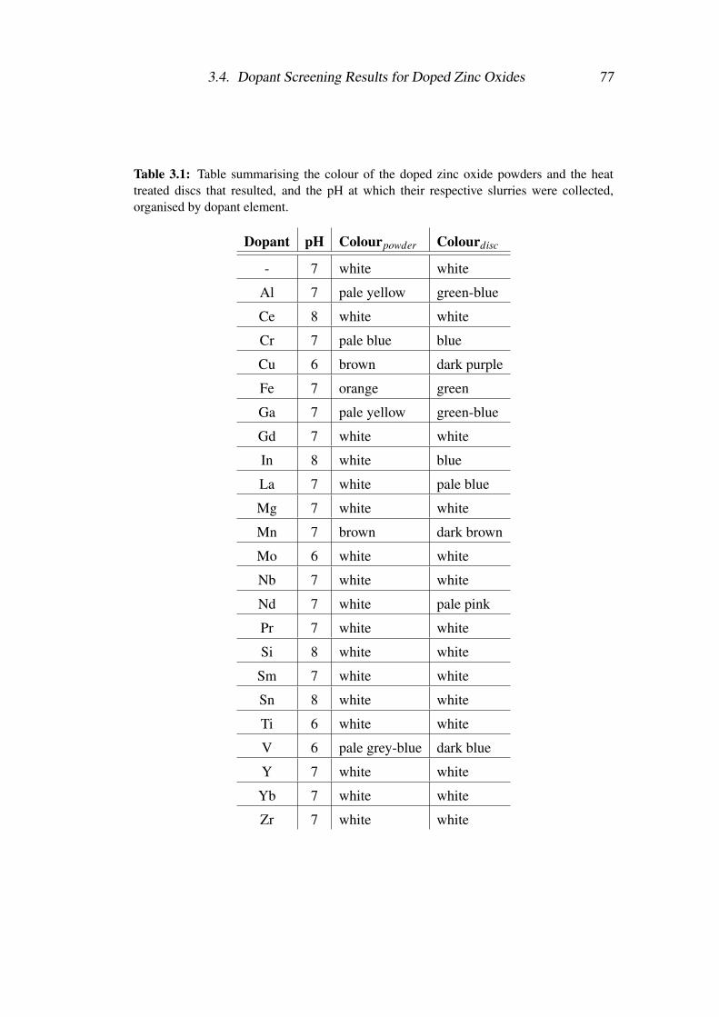
3.4. Dopant Screening Results for Doped Zinc Oxides 77
Table 3.1: Table summarising the colour of the doped zinc oxide powders and the heattreated discs that resulted, and the pH at which their respective slurries were collected,organised by dopant element.
Dopant pH Colourpowder Colourdisc
- 7 white white
Al 7 pale yellow green-blue
Ce 8 white white
Cr 7 pale blue blue
Cu 6 brown dark purple
Fe 7 orange green
Ga 7 pale yellow green-blue
Gd 7 white white
In 8 white blue
La 7 white pale blue
Mg 7 white white
Mn 7 brown dark brown
Mo 6 white white
Nb 7 white white
Nd 7 white pale pink
Pr 7 white white
Si 8 white white
Sm 7 white white
Sn 8 white white
Ti 6 white white
V 6 pale grey-blue dark blue
Y 7 white white
Yb 7 white white
Zr 7 white white
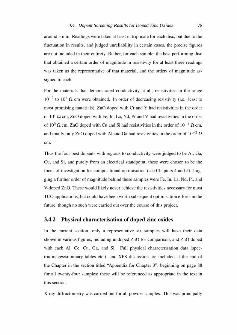
3.4. Dopant Screening Results for Doped Zinc Oxides 78
around 5 mm. Readings were taken at least in triplicate for each disc, but due to the
fluctuation in results, and judged unreliability in certain cases, the precise figures
are not included in their entirety. Rather, for each sample, the best performing disc
that obtained a certain order of magnitude in resistivity for at least three readings
was taken as the representative of that material, and the orders of magnitude as-
signed to each.
For the materials that demonstrated conductivity at all, resistivities in the range
10−2 to 101 Ω cm were obtained. In order of decreasing resistivity (i.e. least to
most promising materials), ZnO doped with Cr and Y had resistivities in the order
of 101 Ω cm, ZnO doped with Fe, In, La, Nd, Pr and V had resistivities in the order
of 100 Ω cm, ZnO doped with Cu and Si had resistivities in the order of 10−1 Ω cm,
and finally only ZnO doped with Al and Ga had resistivities in the order of 10−2 Ω
cm.
Thus the four best dopants with regards to conductivity were judged to be Al, Ga,
Cu, and Si, and purely from an electrical standpoint, these were chosen to be the
focus of investigation for compositional optimisation (see Chapters 4 and 5). Lag-
ging a further order of magnitude behind these samples were Fe, In, La, Nd, Pr, and
V-doped ZnO. These would likely never achieve the resistivities necessary for most
TCO applications, but could have been worth subsequent optimisation efforts in the
future, though no such were carried out over the course of this project.
3.4.2 Physical characterisation of doped zinc oxides
In the current section, only a representative six samples will have their data
shown in various figures, including undoped ZnO for comparison, and ZnO doped
with each Al, Ce, Cu, Ga, and Si. Full physical characterisation data (spec-
tra/images/summary tables etc.) and XPS discussion are included at the end of
the Chapter in the section titled “Appendix for Chapter 3”, beginning on page 88
for all twenty-four samples; these will be referenced as appropriate in the text in
this section.
X-ray diffractometry was carried out for all powder samples. This was principally
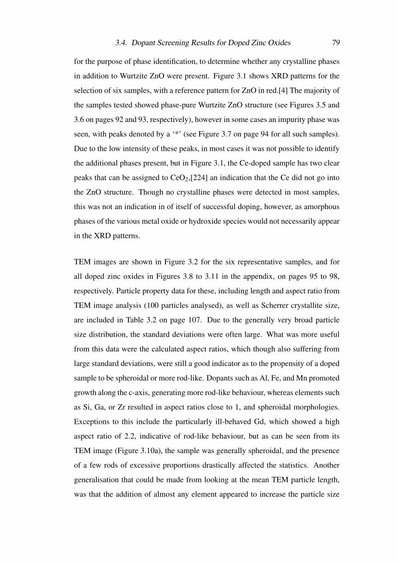
3.4. Dopant Screening Results for Doped Zinc Oxides 79
for the purpose of phase identification, to determine whether any crystalline phases
in addition to Wurtzite ZnO were present. Figure 3.1 shows XRD patterns for the
selection of six samples, with a reference pattern for ZnO in red.[4] The majority of
the samples tested showed phase-pure Wurtzite ZnO structure (see Figures 3.5 and
3.6 on pages 92 and 93, respectively), however in some cases an impurity phase was
seen, with peaks denoted by a ‘*’ (see Figure 3.7 on page 94 for all such samples).
Due to the low intensity of these peaks, in most cases it was not possible to identify
the additional phases present, but in Figure 3.1, the Ce-doped sample has two clear
peaks that can be assigned to CeO2,[224] an indication that the Ce did not go into
the ZnO structure. Though no crystalline phases were detected in most samples,
this was not an indication in of itself of successful doping, however, as amorphous
phases of the various metal oxide or hydroxide species would not necessarily appear
in the XRD patterns.
TEM images are shown in Figure 3.2 for the six representative samples, and for
all doped zinc oxides in Figures 3.8 to 3.11 in the appendix, on pages 95 to 98,
respectively. Particle property data for these, including length and aspect ratio from
TEM image analysis (100 particles analysed), as well as Scherrer crystallite size,
are included in Table 3.2 on page 107. Due to the generally very broad particle
size distribution, the standard deviations were often large. What was more useful
from this data were the calculated aspect ratios, which though also suffering from
large standard deviations, were still a good indicator as to the propensity of a doped
sample to be spheroidal or more rod-like. Dopants such as Al, Fe, and Mn promoted
growth along the c-axis, generating more rod-like behaviour, whereas elements such
as Si, Ga, or Zr resulted in aspect ratios close to 1, and spheroidal morphologies.
Exceptions to this include the particularly ill-behaved Gd, which showed a high
aspect ratio of 2.2, indicative of rod-like behaviour, but as can be seen from its
TEM image (Figure 3.10a), the sample was generally spheroidal, and the presence
of a few rods of excessive proportions drastically affected the statistics. Another
generalisation that could be made from looking at the mean TEM particle length,
was that the addition of almost any element appeared to increase the particle size
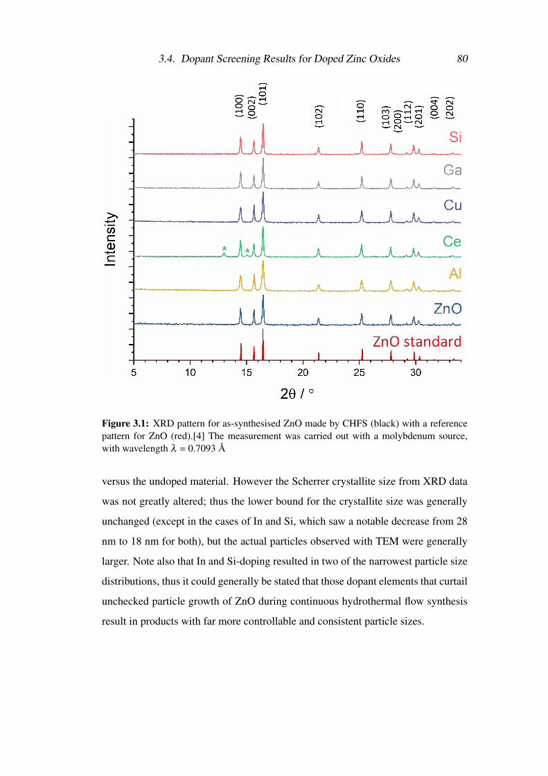
3.4. Dopant Screening Results for Doped Zinc Oxides 80
Figure 3.1: XRD pattern for as-synthesised ZnO made by CHFS (black) with a referencepattern for ZnO (red).[4] The measurement was carried out with a molybdenum source,with wavelength λ = 0.7093 A
versus the undoped material. However the Scherrer crystallite size from XRD data
was not greatly altered; thus the lower bound for the crystallite size was generally
unchanged (except in the cases of In and Si, which saw a notable decrease from 28
nm to 18 nm for both), but the actual particles observed with TEM were generally
larger. Note also that In and Si-doping resulted in two of the narrowest particle size
distributions, thus it could generally be stated that those dopant elements that curtail
unchecked particle growth of ZnO during continuous hydrothermal flow synthesis
result in products with far more controllable and consistent particle sizes.
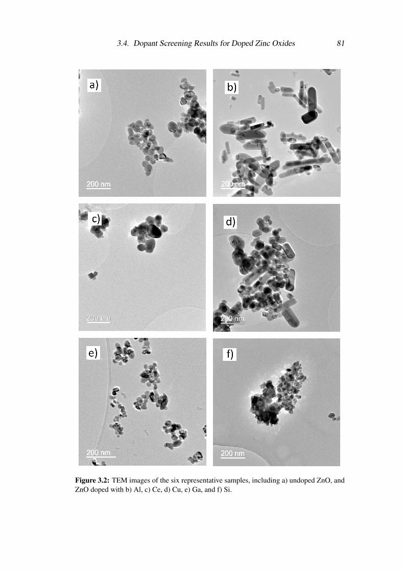
3.4. Dopant Screening Results for Doped Zinc Oxides 81
Figure 3.2: TEM images of the six representative samples, including a) undoped ZnO, andZnO doped with b) Al, c) Ce, d) Cu, e) Ga, and f) Si.
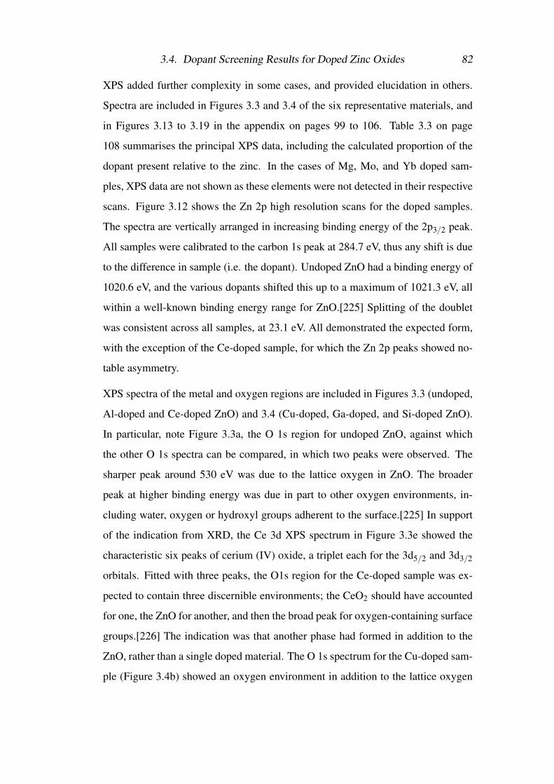
3.4. Dopant Screening Results for Doped Zinc Oxides 82
XPS added further complexity in some cases, and provided elucidation in others.
Spectra are included in Figures 3.3 and 3.4 of the six representative materials, and
in Figures 3.13 to 3.19 in the appendix on pages 99 to 106. Table 3.3 on page
108 summarises the principal XPS data, including the calculated proportion of the
dopant present relative to the zinc. In the cases of Mg, Mo, and Yb doped sam-
ples, XPS data are not shown as these elements were not detected in their respective
scans. Figure 3.12 shows the Zn 2p high resolution scans for the doped samples.
The spectra are vertically arranged in increasing binding energy of the 2p3/2 peak.
All samples were calibrated to the carbon 1s peak at 284.7 eV, thus any shift is due
to the difference in sample (i.e. the dopant). Undoped ZnO had a binding energy of
1020.6 eV, and the various dopants shifted this up to a maximum of 1021.3 eV, all
within a well-known binding energy range for ZnO.[225] Splitting of the doublet
was consistent across all samples, at 23.1 eV. All demonstrated the expected form,
with the exception of the Ce-doped sample, for which the Zn 2p peaks showed no-
table asymmetry.
XPS spectra of the metal and oxygen regions are included in Figures 3.3 (undoped,
Al-doped and Ce-doped ZnO) and 3.4 (Cu-doped, Ga-doped, and Si-doped ZnO).
In particular, note Figure 3.3a, the O 1s region for undoped ZnO, against which
the other O 1s spectra can be compared, in which two peaks were observed. The
sharper peak around 530 eV was due to the lattice oxygen in ZnO. The broader
peak at higher binding energy was due in part to other oxygen environments, in-
cluding water, oxygen or hydroxyl groups adherent to the surface.[225] In support
of the indication from XRD, the Ce 3d XPS spectrum in Figure 3.3e showed the
characteristic six peaks of cerium (IV) oxide, a triplet each for the 3d5/2 and 3d3/2
orbitals. Fitted with three peaks, the O1s region for the Ce-doped sample was ex-
pected to contain three discernible environments; the CeO2 should have accounted
for one, the ZnO for another, and then the broad peak for oxygen-containing surface
groups.[226] The indication was that another phase had formed in addition to the
ZnO, rather than a single doped material. The O 1s spectrum for the Cu-doped sam-
ple (Figure 3.4b) showed an oxygen environment in addition to the lattice oxygen
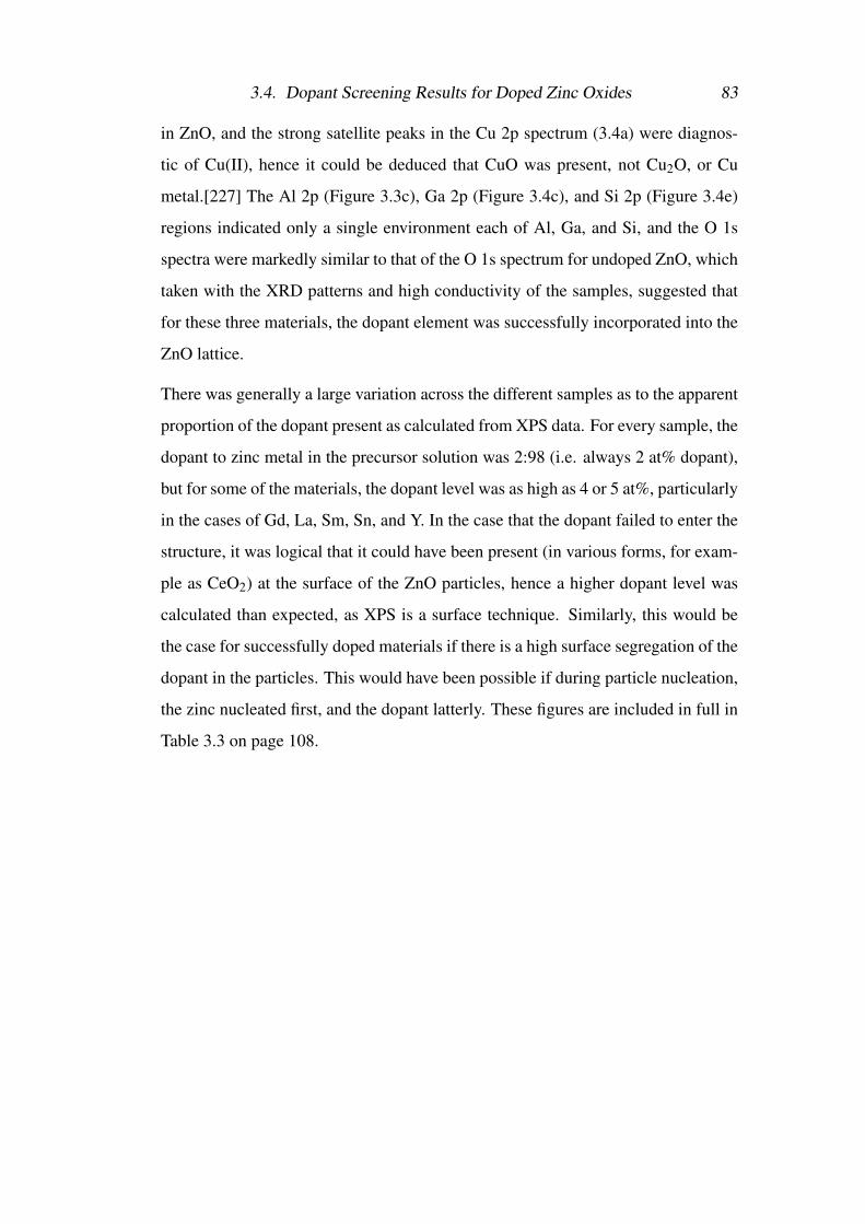
3.4. Dopant Screening Results for Doped Zinc Oxides 83
in ZnO, and the strong satellite peaks in the Cu 2p spectrum (3.4a) were diagnos-
tic of Cu(II), hence it could be deduced that CuO was present, not Cu2O, or Cu
metal.[227] The Al 2p (Figure 3.3c), Ga 2p (Figure 3.4c), and Si 2p (Figure 3.4e)
regions indicated only a single environment each of Al, Ga, and Si, and the O 1s
spectra were markedly similar to that of the O 1s spectrum for undoped ZnO, which
taken with the XRD patterns and high conductivity of the samples, suggested that
for these three materials, the dopant element was successfully incorporated into the
ZnO lattice.
There was generally a large variation across the different samples as to the apparent
proportion of the dopant present as calculated from XPS data. For every sample, the
dopant to zinc metal in the precursor solution was 2:98 (i.e. always 2 at% dopant),
but for some of the materials, the dopant level was as high as 4 or 5 at%, particularly
in the cases of Gd, La, Sm, Sn, and Y. In the case that the dopant failed to enter the
structure, it was logical that it could have been present (in various forms, for exam-
ple as CeO2) at the surface of the ZnO particles, hence a higher dopant level was
calculated than expected, as XPS is a surface technique. Similarly, this would be
the case for successfully doped materials if there is a high surface segregation of the
dopant in the particles. This would have been possible if during particle nucleation,
the zinc nucleated first, and the dopant latterly. These figures are included in full in
Table 3.3 on page 108.
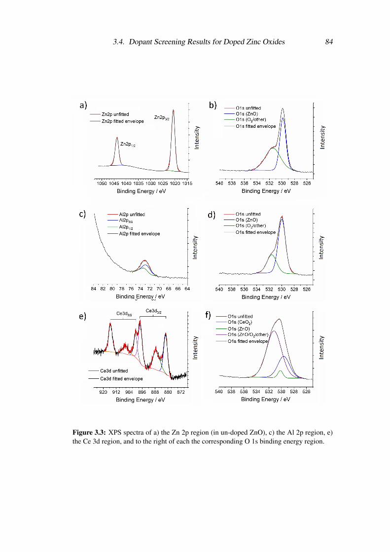
3.4. Dopant Screening Results for Doped Zinc Oxides 84
Figure 3.3: XPS spectra of a) the Zn 2p region (in un-doped ZnO), c) the Al 2p region, e)the Ce 3d region, and to the right of each the corresponding O 1s binding energy region.
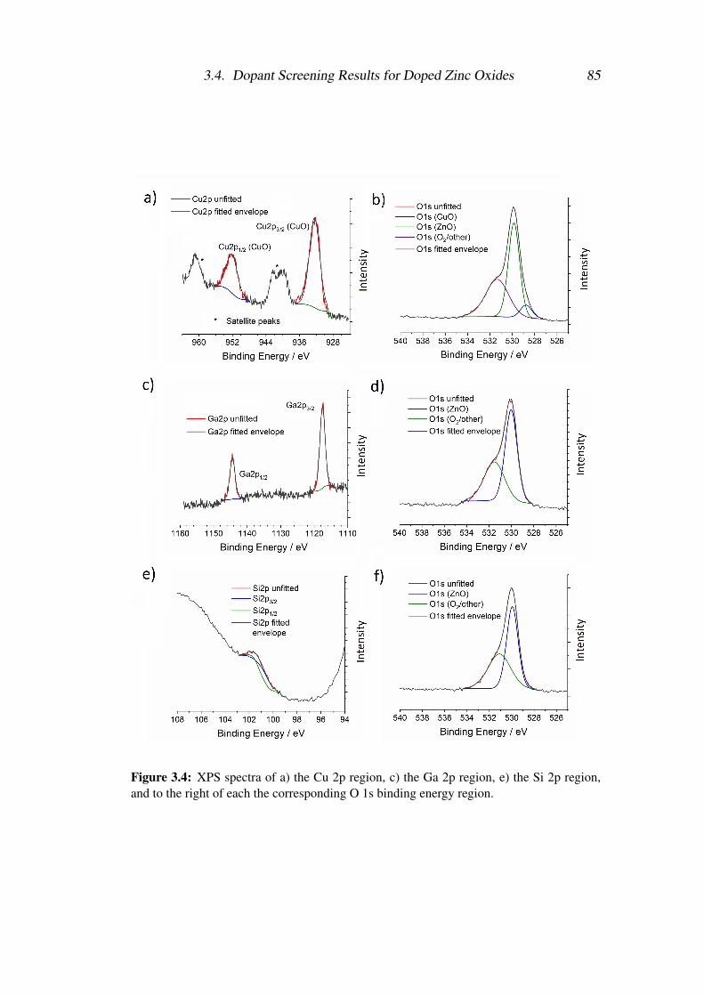
3.4. Dopant Screening Results for Doped Zinc Oxides 85
Figure 3.4: XPS spectra of a) the Cu 2p region, c) the Ga 2p region, e) the Si 2p region,and to the right of each the corresponding O 1s binding energy region.
3.5. Conclusions; Promising ZnO:dopant Systems for Further Investigation 86
3.5 Conclusions; Promising ZnO:dopant Systems for
Further InvestigationZnO was synthesised via CHFS with an assortment of 24 different dopants, includ-
ing the undoped material, synthesised under the same conditions (including dopant
proportion) for direct comparison. As indicated by XPS and XRD, some elements,
such as Al and Ga, were doped successfully into the structure. Others, such as Cu
and V, appeared to be partially doped into the ZnO structure, and for some (Ce in
particular) there was no evidence of incorporation into the ZnO lattice at all. Mor-
phologies were spheroidal or rod-like for all systems tested, generally with broad,
inconsistent particle size distributions (determined by TEM image analysis). The
majority demonstrated phase-pure Wurtzite structure by XRD; crystalline impurity
peaks were only detected for 5 out of 24 samples.
Generally speaking, inclusion of dopant elements increased the mean particle size
versus undoped ZnO and broadened the particle size distribution, but the crystal-
lite size remained approximately consistent across most doped systems, with the
notable exceptions of Si- and In-doped ZnO, for which both a drastic decrease in
Scherrer crystallite size (from 28 down to 18 nm for both materials), and a signifi-
cant narrowing of the particle size distribution was observed.
Approximately half of the dopants tested demonstrated some level of conductivity
when the powders were tested as pressed, heat treated discs, but of these the only
dopants that were judged to be sufficiently conductive for further testing and opti-
misation were Al, Ga, Si, and Cu. These yielded resistivities of the order of 10−2 or
10−1 Ω cm; the benchmark material, ITO, synthesised and tested by the same meth-
ods obtained resistivities in the order 10−3 Ω cm, thus any (unoptimised) materials
with resistivities more than two orders of magnitude higher were judged to be inap-
propriate for further investigation. However, due to the intensely dark colour of the
Cu-doped sample, as prepared and then more so post-heat treatment, its promise as
a TCO material was judged to be insufficient for further investigation.

3.5. Conclusions; Promising ZnO:dopant Systems for Further Investigation 87
Thus the three materials that would be focussed on as ITO-replacement TCO mate-
rials were Al-doped ZnO (see Chapter 4), Ga-doped ZnO (see also Chapter 4), and
Si-doped ZnO (see Chapter 5). For these, a selection of compositions would need
to be synthesised and tested for their electronic properties in order to determine the
optimal level of dopant in the doped ZnO system relative to the proportion of zinc.
Once this had been established, the optimal samples could be scaled up to semi-
industrial scales of synthesis and coated in flow, facilitating the dispersion of the
nanoparticles in various media to then be deposited into thin films by spin coating
or inkjet printing methods.
3.5. Conclusions; Promising ZnO:dopant Systems for Further Investigation 88
Appendix for Chapter 3This appendix section includes the full characterisation for the dopant screening ex-
periments, including XRD, XPS, TEM, and tables summarising the physical char-
acterisation data. XRD patterns are shown in Figures 3.5 to 3.7, representative TEM
images are shown in Figures 3.8 to 3.11, and XPS spectra are shown in Figures 3.12
to 3.19.
Figure 3.12 shows the Zn 2p high resolution scans for the doped samples. The
spectra are vertically arranged in increasing binding energy of the 2p3/2 peak. All
samples were calibrated to the carbon 1s peak at 284.7 eV, thus any shift is due to
the difference in sample (i.e. the dopant). Undoped ZnO had a binding energy of
1020.6 eV, and the various dopants shifted this up to a maximum of 1021.3 eV, all
within a well-known binding energy range for ZnO.[225] Splitting of the doublet
was consistent across all samples, at 23.1 eV. All demonstrated the expected form,
with the exception of the Ce-doped sample, for which the Zn 2p peaks showed no-
table asymmetry.
XPS spectra of the metal and oxygen regions are included in Figure 3.13 for un-
doped, Ce-doped, and Cr doped ZnO and in Figure 3.14 for La-doped, Nb-doped,
and Y-doped ZnO. In particular, note Figure 3.13a, the O 1s region for undoped
ZnO, against which the other O 1s spectra can be compared, in which two peaks
were observed. The sharper peak around 530 eV was due to the lattice oxygen in
ZnO. The broader peak at higher binding energy was due in part to other oxy-
gen environments, including water, oxygen or hydroxyl groups adherent to the
surface.[225] In support of the indication from XRD, the Ce 3d XPS spectrum in
Figure 3.13c showed the characteristic six peaks of cerium (IV) oxide, a triplet each
for the 3d5/2 and 3d3/2 orbitals. Fitted with three peaks, the O1s region for the Ce-
doped sample was expected to contain three discernible environments; the CeO2
should have accounted for one, the ZnO for another, and then the broad peak for
oxygen-containing surface groups.[226] The Cr 2p region in Figure 3.13e showed
only a single environment for the chromium, the 2p1/2 peak overlapping with a
Zn Auger peak. Though the conductivity of the sample was indicative of success-
3.5. Conclusions; Promising ZnO:dopant Systems for Further Investigation 89
ful doping, it was shown to be incomplete by the appearance of an addition peak
in the oxygen spectrum at lower binding energy than the ZnO peak, correspond-
ing to chromium oxide, although the oxidation state of the chromium could not be
deduced from the data here, neither in the oxide form nor within the zinc oxide
structure.[228]
The La 3d5/2 binding energy region shown in Figure 3.14a showed peaks char-
acteristic of La(OH)3, supported by the O 1s region, which showed two metal
(hydr)oxide peaks; one each could be attributed to La(OH)3 and the other to
ZnO.[225, 229, 230] The Nb 3d region shown in Figure 3.14c showed a single
niobium oxide environment, the lack of conductivity and over-large peak in the O
1s region indicated the formation of Nb2O5.[231] Finally in Figure 3.14 was the
yttrium 3d region in Figure 3.14e, in which there were two doublets present, one
each for Y2O3 (lower binding energy) and Y(OH)3 (higher binding energy). This,
coupled with the presence of conductivity in the sample and the single extra peak in
the O 1s region (Figure 3.14f) could have indicated that some of the yttrium went
into the ZnO structure, while the remainder appeared to form the hydroxide.[232]
Figure 3.15 shows the Gd 4d (a), Mn 2p (c), and Sm 3d (e) regions. Gadolin-
ium showed a single environment (Figure 3.15a), complicated by the presence not
only of a satellite peak but also the strongly overlapping Zn 3s peak; the most in-
tense peak present. The O 1s spectrum indicated the possibility of the formation of
gadolinium oxide (Gd2O3) as a separate phase.[232] In the case of manganese (Fig-
ures 3.15c and 3.15d), the spectra were highly diagnostic; a clear peak was seen in
the O1s spectrum (Figure 3.15d) at lower binding energy than the one correspond-
ing to ZnO, indicating a separate manganese oxide phase. The single environment
seen in the Mn 2p spectrum coupled with a lack of satellite peaks (as would have
been seen for MnO) and also lacking the distinctive feature in the Mn 2p3/2 peak
that would have been indicative of MnO2, suggested that Mn2O3 was the species
present as the separate phase.[233] The samarium spectra pointed to one environ-
ment, but the O 1s spectrum could not be deconvoluted beyond saying that there are
likely multiple metal oxide and/or hydroxide species present. This, with the lack of
3.5. Conclusions; Promising ZnO:dopant Systems for Further Investigation 90
conductivity in the sample, most likely indicated that Sm had not gone into the ZnO
structure.
Figure 3.16 shows the Sn 3d (a), Ti 2p (c), and Zr 3d (e) regions. In each case,
only a single environment was suggested by the spectra, and the lack of impurity
peaks in the XRD patterns could for these materials have suggested that the dopants
went into the ZnO structure. However this did not result in conductivity for any
of the three;[234–236] formation of additional defects in the structure (e.g. those
leading to recombination centres, rendering electrons conductively impotent) could
have been to blame.
Figure 3.17 shows the Cu 2p d (a), V 2p (c), and Fe 2p (e) regions. All three
resulted in varying degrees of conductivity, and none demonstrated impurities by
XRD, which could in itself been used as evidential of successful doping. However,
in each there were some points of interest in the XPS spectra. An extra peak in
the metal oxide region of the O 1s spectrum (3.17b) of copper indicated another
oxygen environment in addition to ZnO, and the strong satellite peaks in the Cu
2p spectrum (3.17a) were diagnostic of Cu(II), hence it could be deduced that CuO
was present, not Cu2O, or Cu metal.[227] There were characteristic peaks in the
V 2p spectrum (3.17c) of two oxidation states, (II) and (IV), with the intensity of
the latter greatly outweighing that of the former. There was no extra peak in the
O1s spectrum (3.17d), but it was likely that partial doping had taken place.[237]
Finally, the iron spectrum showed a single environment (Figure 3.17e), with one
strong satellite peak. An additional peak appeared in the O 1s spectrum, imply-
ing the formation of an iron oxide species, but the oxidation state(s) could not be
unequivocally elucidated from this data. The 2p3/2 peak appeared at 710.0 eV, for
which there is precedent for Fe(II) and Fe(III) oxides, however generally speaking
it is more likely to be due to FeO from the binding energy position.[226]
Figure 3.18 shows the Pr 3d (a), Nd 3d (c), and In 3d (e) XPS regions. In each case,
the O 1s spectra were very similar; one metal oxide peak was seen, along with the
broader peak. One environment each for Pr (3.18a) and In (3.18e), coupled with
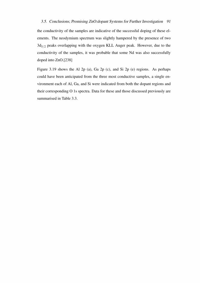
3.5. Conclusions; Promising ZnO:dopant Systems for Further Investigation 91
the conductivity of the samples are indicative of the successful doping of these el-
ements. The neodymium spectrum was slightly hampered by the presence of two
3d5/2 peaks overlapping with the oxygen KLL Auger peak. However, due to the
conductivity of the samples, it was probable that some Nd was also successfully
doped into ZnO.[238]
Figure 3.19 shows the Al 2p (a), Ga 2p (c), and Si 2p (e) regions. As perhaps
could have been anticipated from the three most conductive samples, a single en-
vironment each of Al, Ga, and Si were indicated from both the dopant regions and
their corresponding O 1s spectra. Data for these and those discussed previously are
summarised in Table 3.3.
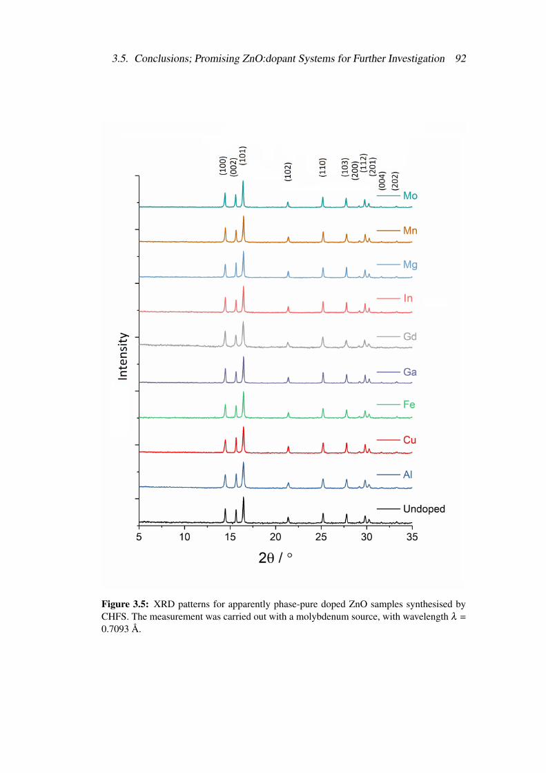
3.5. Conclusions; Promising ZnO:dopant Systems for Further Investigation 92
Figure 3.5: XRD patterns for apparently phase-pure doped ZnO samples synthesised byCHFS. The measurement was carried out with a molybdenum source, with wavelength λ =0.7093 A.
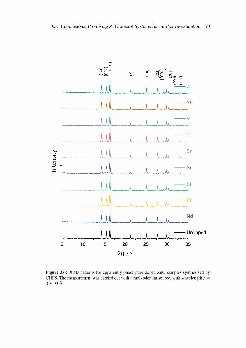
3.5. Conclusions; Promising ZnO:dopant Systems for Further Investigation 93
Figure 3.6: XRD patterns for apparently phase pure doped ZnO samples synthesised byCHFS. The measurement was carried out with a molybdenum source, with wavelength λ =0.7093 A.
3.5. Conclusions; Promising ZnO:dopant Systems for Further Investigation 94
Figure 3.7: XRD patterns for the doped ZnO samples synthesised by CHFS that showclear impurity peaks. The measurement was carried out with a molybdenum source, withwavelength λ = 0.7093 A.
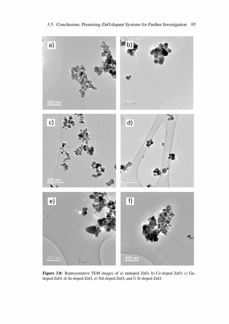
3.5. Conclusions; Promising ZnO:dopant Systems for Further Investigation 95
Figure 3.8: Representative TEM images of a) undoped ZnO, b) Ce-doped ZnO, c) Ga-doped ZnO, d) In-doped ZnO, e) Nd-doped ZnO, and f) Si-doped ZnO.
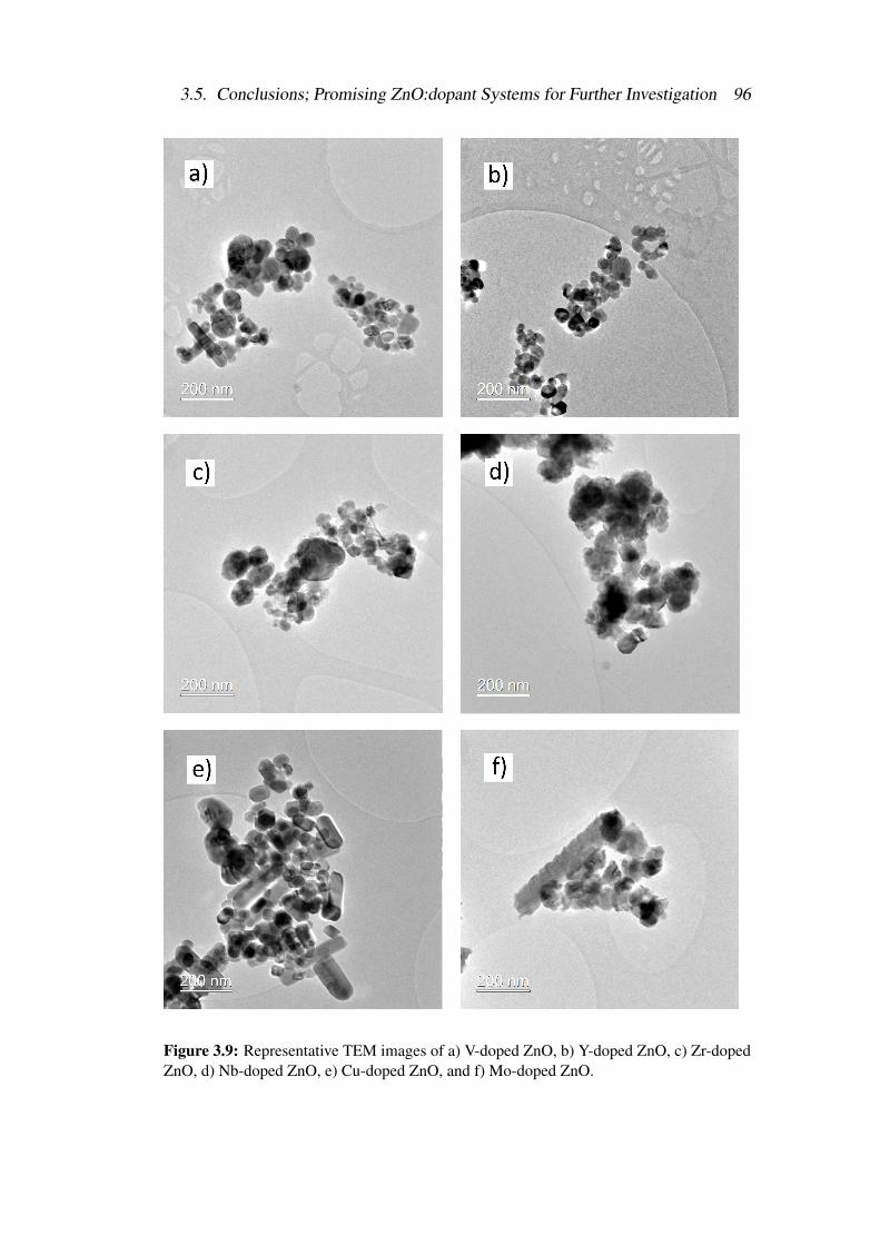
3.5. Conclusions; Promising ZnO:dopant Systems for Further Investigation 96
Figure 3.9: Representative TEM images of a) V-doped ZnO, b) Y-doped ZnO, c) Zr-dopedZnO, d) Nb-doped ZnO, e) Cu-doped ZnO, and f) Mo-doped ZnO.
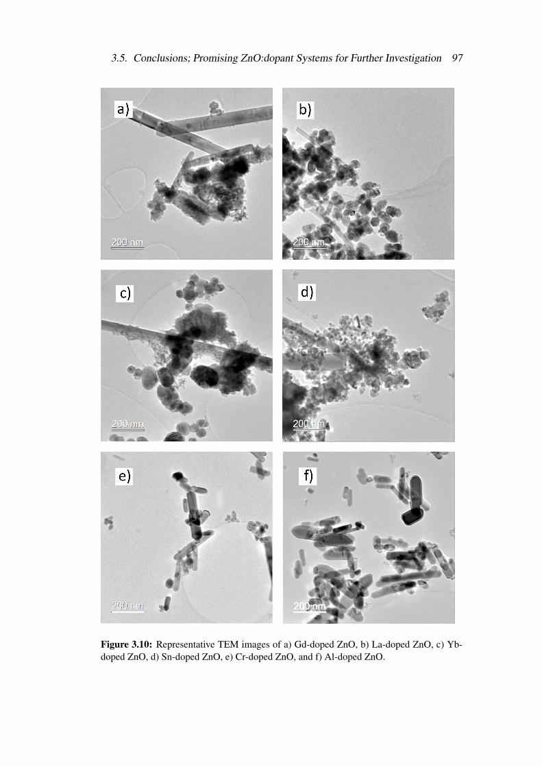
3.5. Conclusions; Promising ZnO:dopant Systems for Further Investigation 97
Figure 3.10: Representative TEM images of a) Gd-doped ZnO, b) La-doped ZnO, c) Yb-doped ZnO, d) Sn-doped ZnO, e) Cr-doped ZnO, and f) Al-doped ZnO.
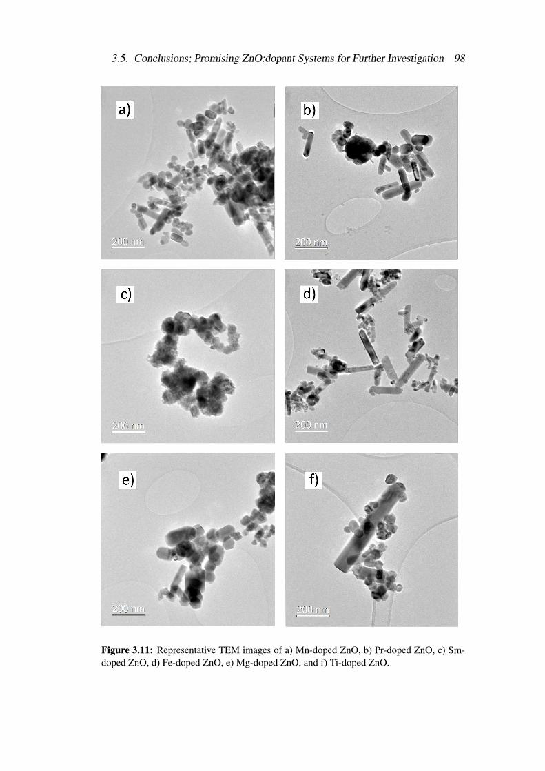
3.5. Conclusions; Promising ZnO:dopant Systems for Further Investigation 98
Figure 3.11: Representative TEM images of a) Mn-doped ZnO, b) Pr-doped ZnO, c) Sm-doped ZnO, d) Fe-doped ZnO, e) Mg-doped ZnO, and f) Ti-doped ZnO.
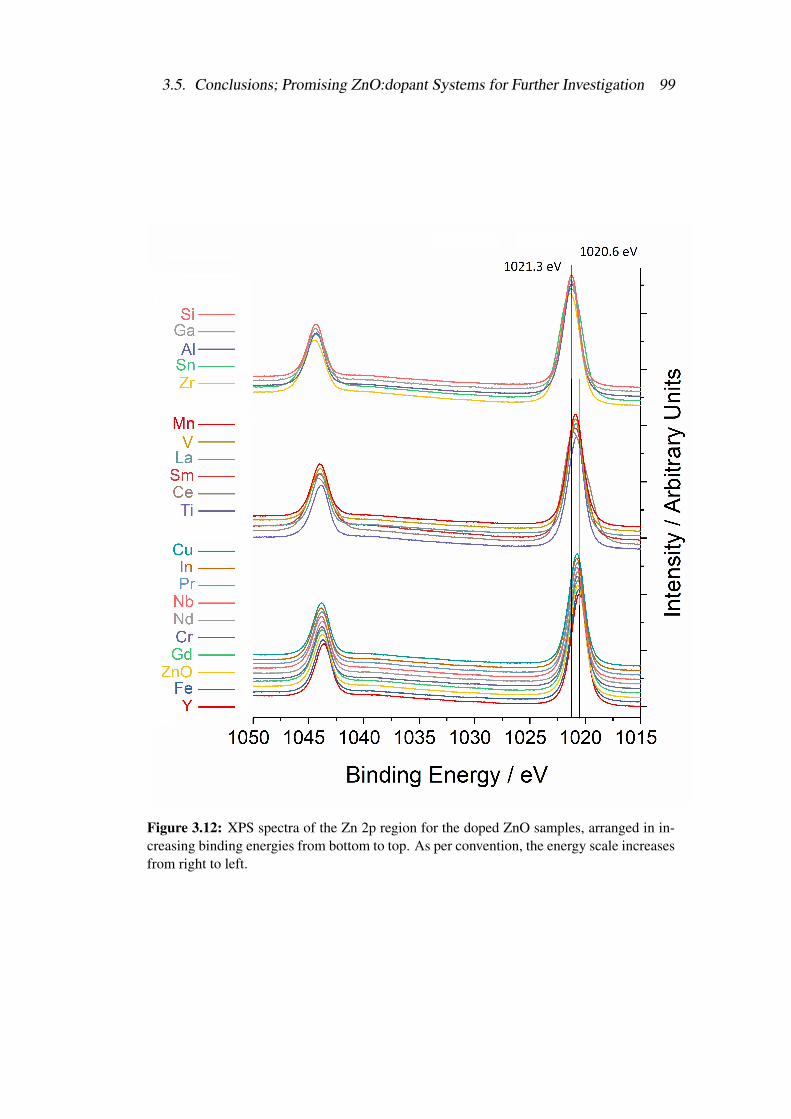
3.5. Conclusions; Promising ZnO:dopant Systems for Further Investigation 99
Figure 3.12: XPS spectra of the Zn 2p region for the doped ZnO samples, arranged in in-creasing binding energies from bottom to top. As per convention, the energy scale increasesfrom right to left.
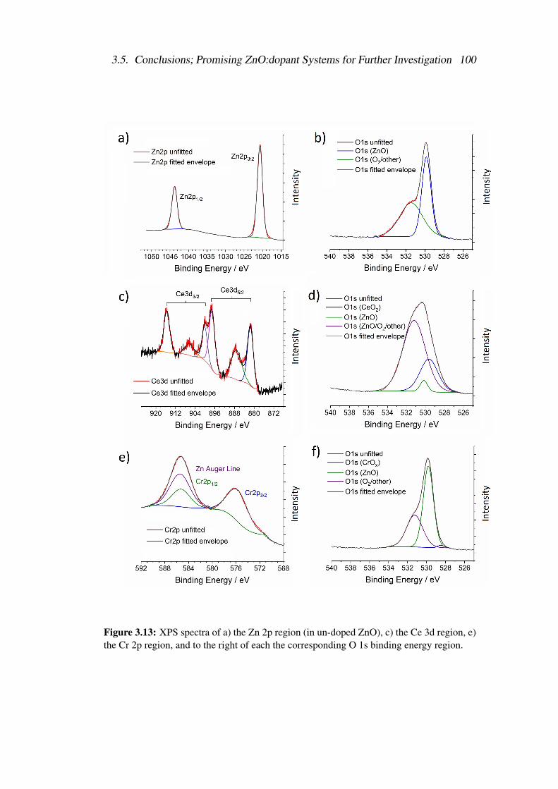
3.5. Conclusions; Promising ZnO:dopant Systems for Further Investigation 100
Figure 3.13: XPS spectra of a) the Zn 2p region (in un-doped ZnO), c) the Ce 3d region, e)the Cr 2p region, and to the right of each the corresponding O 1s binding energy region.
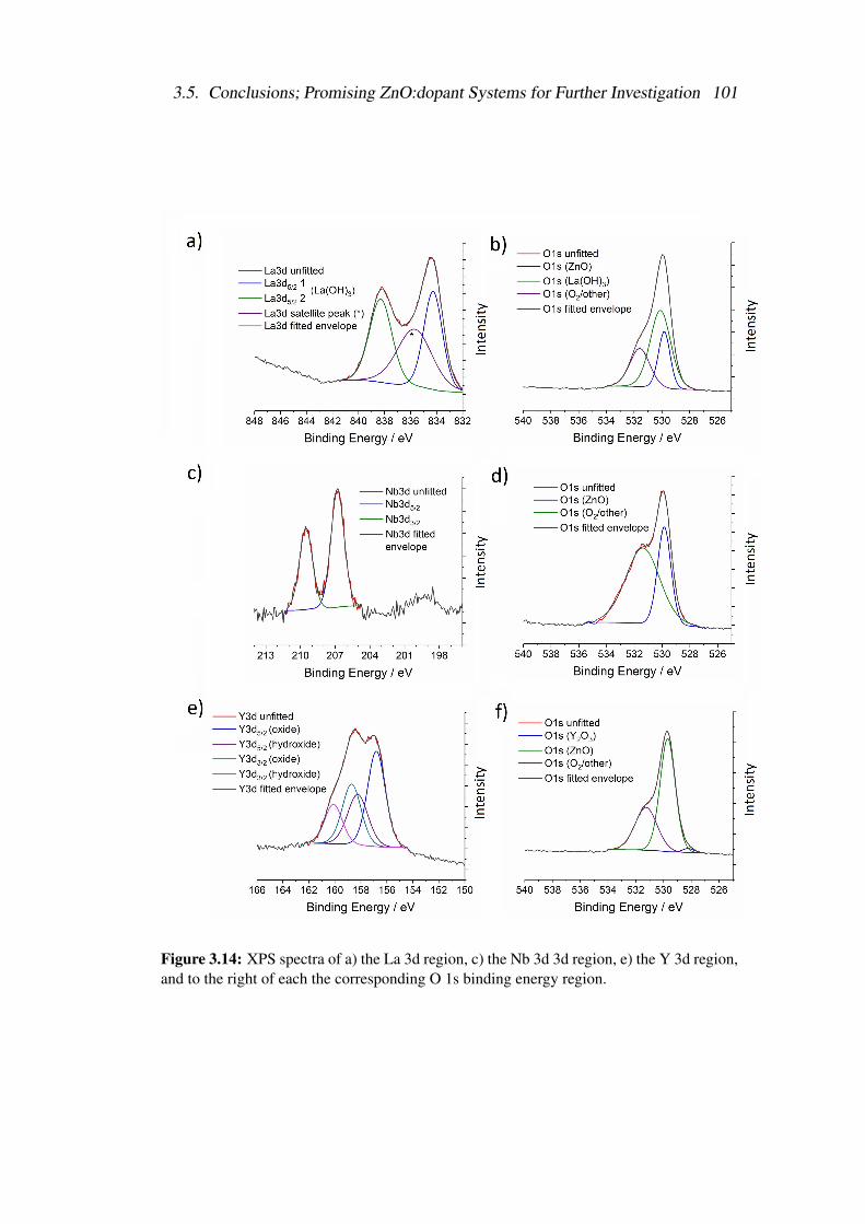
3.5. Conclusions; Promising ZnO:dopant Systems for Further Investigation 101
Figure 3.14: XPS spectra of a) the La 3d region, c) the Nb 3d 3d region, e) the Y 3d region,and to the right of each the corresponding O 1s binding energy region.
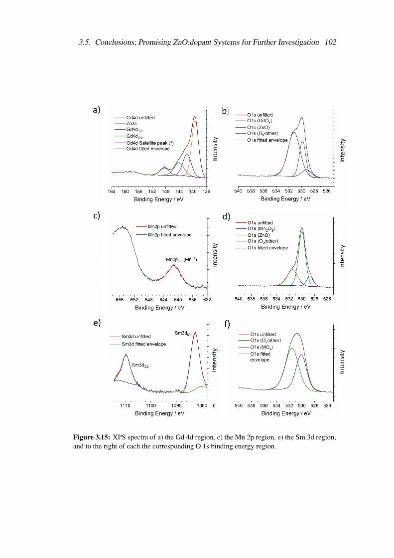
3.5. Conclusions; Promising ZnO:dopant Systems for Further Investigation 102
Figure 3.15: XPS spectra of a) the Gd 4d region, c) the Mn 2p region, e) the Sm 3d region,and to the right of each the corresponding O 1s binding energy region.
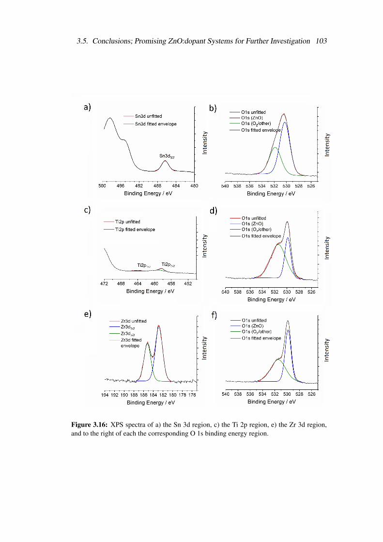
3.5. Conclusions; Promising ZnO:dopant Systems for Further Investigation 103
Figure 3.16: XPS spectra of a) the Sn 3d region, c) the Ti 2p region, e) the Zr 3d region,and to the right of each the corresponding O 1s binding energy region.
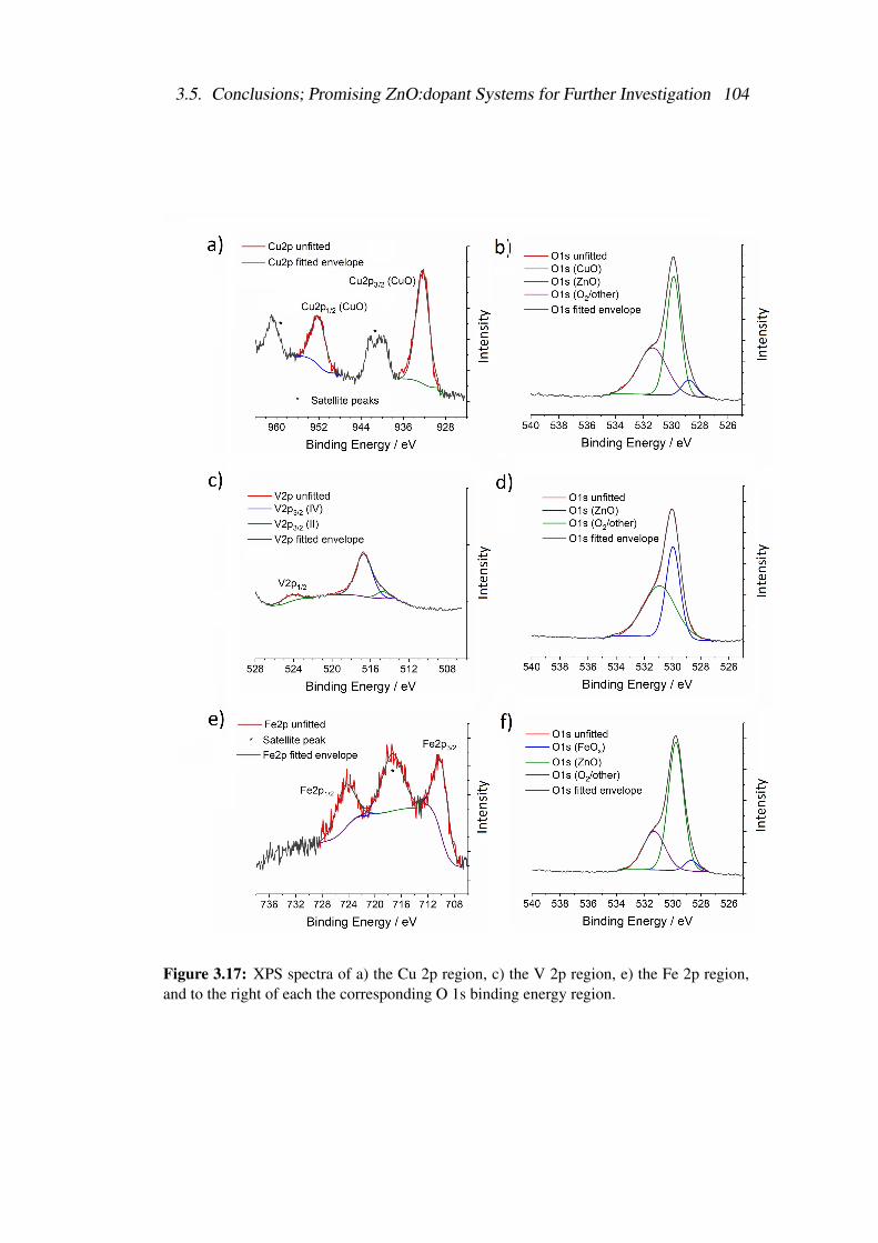
3.5. Conclusions; Promising ZnO:dopant Systems for Further Investigation 104
Figure 3.17: XPS spectra of a) the Cu 2p region, c) the V 2p region, e) the Fe 2p region,and to the right of each the corresponding O 1s binding energy region.
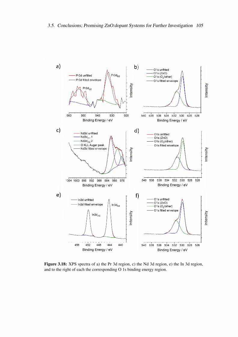
3.5. Conclusions; Promising ZnO:dopant Systems for Further Investigation 105
Figure 3.18: XPS spectra of a) the Pr 3d region, c) the Nd 3d region, e) the In 3d region,and to the right of each the corresponding O 1s binding energy region.
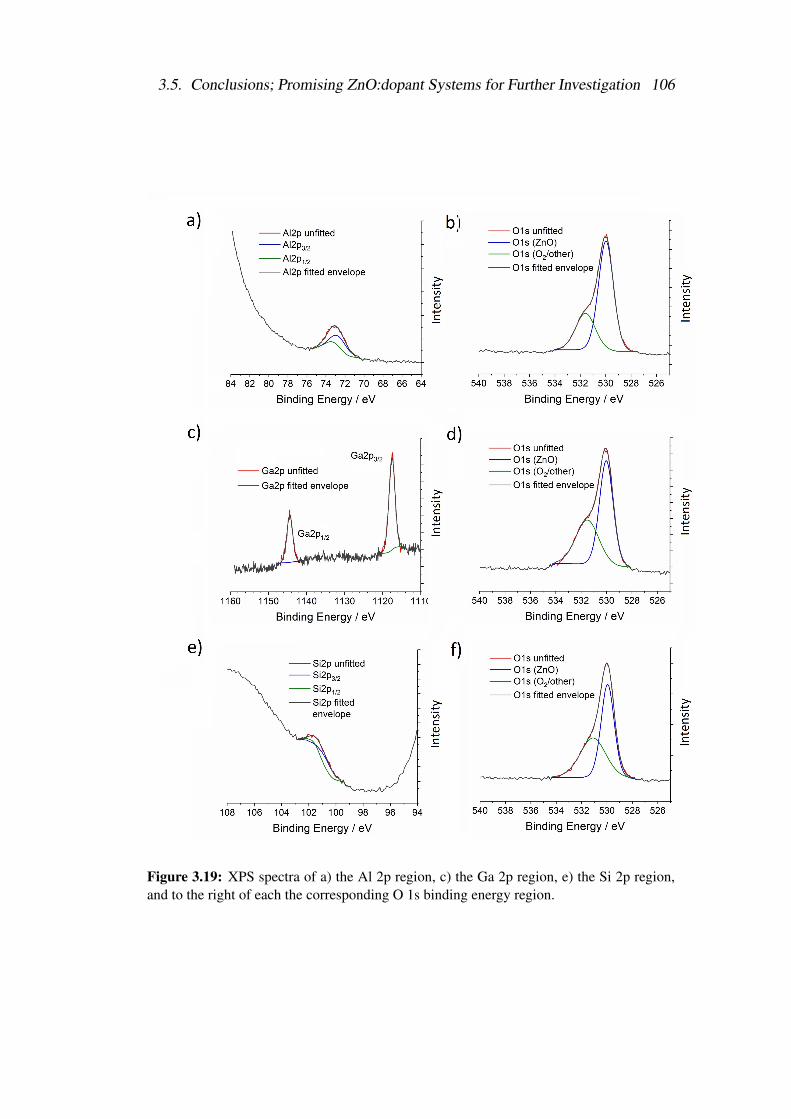
3.5. Conclusions; Promising ZnO:dopant Systems for Further Investigation 106
Figure 3.19: XPS spectra of a) the Al 2p region, c) the Ga 2p region, e) the Si 2p region,and to the right of each the corresponding O 1s binding energy region.
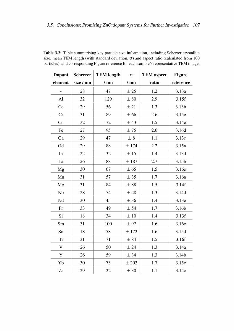
3.5. Conclusions; Promising ZnO:dopant Systems for Further Investigation 107
Table 3.2: Table summarising key particle size information, including Scherrer crystallitesize, mean TEM length (with standard deviation, σ ) and aspect ratio (calculated from 100particles), and corresponding Figure reference for each sample’s representative TEM image.
Dopantelement
Scherrersize / nm
TEM length/ nm
σ
/ nmTEM aspect
ratioFigure
reference
- 28 47 ± 25 1.2 3.13a
Al 32 129 ± 80 2.9 3.15f
Ce 29 56 ± 21 1.3 3.13b
Cr 31 89 ± 66 2.6 3.15e
Cu 32 72 ± 43 1.5 3.14e
Fe 27 95 ± 75 2.6 3.16d
Ga 29 47 ± 8 1.1 3.13c
Gd 29 88 ± 174 2.2 3.15a
In 22 32 ± 15 1.4 3.13d
La 26 88 ± 187 2.7 3.15b
Mg 30 67 ± 65 1.5 3.16e
Mn 31 57 ± 35 1.7 3.16a
Mo 31 84 ± 88 1.5 3.14f
Nb 28 74 ± 28 1.3 3.14d
Nd 30 45 ± 36 1.4 3.13e
Pr 33 49 ± 54 1.7 3.16b
Si 18 34 ± 10 1.4 3.13f
Sm 31 100 ± 97 1.6 3.16c
Sn 18 58 ± 172 1.6 3.15d
Ti 31 71 ± 84 1.5 3.16f
V 26 50 ± 24 1.3 3.14a
Y 26 59 ± 34 1.3 3.14b
Yb 30 73 ± 202 1.7 3.15c
Zr 29 22 ± 30 1.1 3.14c
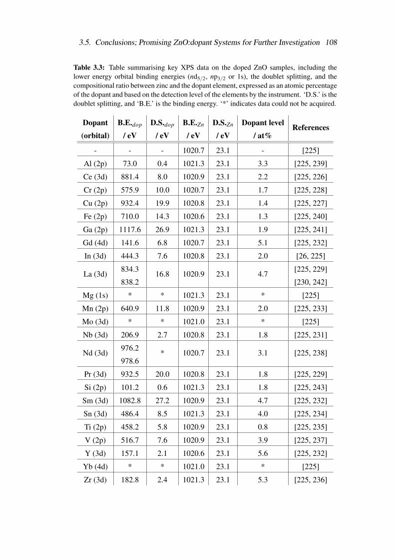
3.5. Conclusions; Promising ZnO:dopant Systems for Further Investigation 108
Table 3.3: Table summarising key XPS data on the doped ZnO samples, including thelower energy orbital binding energies (nd5/2, np3/2 or 1s), the doublet splitting, and thecompositional ratio between zinc and the dopant element, expressed as an atomic percentageof the dopant and based on the detection level of the elements by the instrument. ‘D.S.’ is thedoublet splitting, and ‘B.E.’ is the binding energy. ‘*’ indicates data could not be acquired.
Dopant(orbital)
B.E.dop
/ eVD.S.dop
/ eVB.E.Zn
/ eVD.S.Zn
/ eVDopant level
/ at%References
- - - 1020.7 23.1 - [225]
Al (2p) 73.0 0.4 1021.3 23.1 3.3 [225, 239]
Ce (3d) 881.4 8.0 1020.9 23.1 2.2 [225, 226]
Cr (2p) 575.9 10.0 1020.7 23.1 1.7 [225, 228]
Cu (2p) 932.4 19.9 1020.8 23.1 1.4 [225, 227]
Fe (2p) 710.0 14.3 1020.6 23.1 1.3 [225, 240]
Ga (2p) 1117.6 26.9 1021.3 23.1 1.9 [225, 241]
Gd (4d) 141.6 6.8 1020.7 23.1 5.1 [225, 232]
In (3d) 444.3 7.6 1020.8 23.1 2.0 [26, 225]
La (3d)834.3
838.216.8 1020.9 23.1 4.7
[225, 229]
[230, 242]
Mg (1s) * * 1021.3 23.1 * [225]
Mn (2p) 640.9 11.8 1020.9 23.1 2.0 [225, 233]
Mo (3d) * * 1021.0 23.1 * [225]
Nb (3d) 206.9 2.7 1020.8 23.1 1.8 [225, 231]
Nd (3d)976.2
978.6* 1020.7 23.1 3.1 [225, 238]
Pr (3d) 932.5 20.0 1020.8 23.1 1.8 [225, 229]
Si (2p) 101.2 0.6 1021.3 23.1 1.8 [225, 243]
Sm (3d) 1082.8 27.2 1020.9 23.1 4.7 [225, 232]
Sn (3d) 486.4 8.5 1021.3 23.1 4.0 [225, 234]
Ti (2p) 458.2 5.8 1020.9 23.1 0.8 [225, 235]
V (2p) 516.7 7.6 1020.9 23.1 3.9 [225, 237]
Y (3d) 157.1 2.1 1020.6 23.1 5.6 [225, 232]
Yb (4d) * * 1021.0 23.1 * [225]
Zr (3d) 182.8 2.4 1021.3 23.1 5.3 [225, 236]
Chapter 4
Al and Ga Doped and Co-Doped Zinc
Oxide for Transparent Conducting
Oxides
4.1 Aims
Having identified aluminium and gallium doping in zinc oxide (AZO and GZO, re-
spectively) as the most promising doped systems with respect to conductivity, the
aim of this chapter is to outline the investigation into the compositional optimisa-
tion of AZO and GZO for TCOs as synthesised by continuous hydrothermal flow
synthesis (CHFS), on both the laboratory and pilot scales. The effect of co-doping
zinc oxide with both aluminium and gallium (usually known as AGZO) was also
investigated. In addition to the electrical testing, characterisation including XRD,
BET, TEM, XPS, EDS, and ICP-AES is also discussed, to gauge the effect that the
different dopant ratios have on the properties of the material.
4.2 Introduction
All three of these materials, AZO, GZO, and AGZO have the same flavour of defect
chemistry that gives rise to their improved conductivity over the undoped material.
The Al3+ or Ga3+ will tend to be situated on the Zn2+ site, i.e. as Al•Zn or as
Ga•Zn. In both cases, the dopant acts as a shallow donor; the extra valence electron
4.2. Introduction 110
is loosely bound, and thus is mobile and able to carry charge.[22, 244] These point
defects cause a degree of lattice strain; Zn2+ has an ionic radius of 0.60 A, Al3+
and Ga3+ have ionic radii of 0.39 A and 0.47 A, respectively,[245] and this can lead
to mobility issues for the charge carriers at higher dopant levels, counter-balancing
the increasing concentration of carriers. The point at which this occurs is difficult
to state with certainty, as formation of balancing intrinsic defects can occur, which
could trap some of these extra electrons, or inhibition by ionised impurities or scat-
tering effects. As such, not every dopant ion will necessarily contribute its extra
electron to the carrier concentration in the material.[11, 244, 246, 247]
Issues with thermal stability of non-stoichiometric (the only way to make it highly
conductive) undoped zinc oxide led to Minami et al. experimenting with deposition
of AZO for application as a TCO for the first time in 1984.[119] with a little un-
der 2 at% Al, a magnetron-sputtered film demonstrated a marked improvement in
thermal stability, and a resistivity of only 1.9 x 10⁻⁴ Ω cm, and remains among the
most conductive AZO films in literature to this day. A great number of other groups
have made films of the order of 10−4 Ω cm, however, by various deposition meth-
ods including magnetron sputtering,[144–146, 248–253] atmospheric pressure[120]
and aerosol assisted[121] chemical vapour deposition (APCVD and AACVD, re-
spectively), and pulsed laser deposition (PLD).[122, 254] Other techniques such as
spray pyrolysis[123], atomic later deposition (ALD),[255] and inkjet printing[156]
and spraying[256] have been explored, but are orders of magnitude higher in terms
of resistivity. A summary of the best performing AZO films from literature is in-
cluded in Table 6.2 in Chapter 6.
GZO was first made by magnetron sputtering in 1990 by Choi et al,[257] though
the films displayed resistivities of only ca. 2 x 10⁻³ Ω cm. This was soon improved
upon, to the point where films of GZO with resistivities of the order 10−4 Ω cm
have since been made by sputtering,[124–126, 207, 248, 258, 259] APCVD,[128]
CVD,[129], AACVD,[121] and PLD.[127] A tabulated summary for a selection of
these materials is included in Table 6.3 in Chapter 6.
4.2. Introduction 111
Similarly, several AGZO films have been made by sputtering, with resistivities of
ca. 10−4;[130–133, 248, 253, 260–263] a summary of AGZO film data from litera-
ture is included in Table 6.4 in Chapter 6. Section 6.2 of Chapter 6 also expounds
upon the additional optoelectronic properties of the materials; this Chapter focuses
on comparison of different material compositions primarily by use of their resistiv-
ity values.
Though thin films are typically formed by sputtering, the material in the target needs
first to be synthesised, in which case the ZnO would most likely have been synthe-
sised for these studies by one of three methods:[112, 160, 264, 265]
• The French (or Indirect) process, wherein metallic zinc is melted in a crucible
and vapourised (at ca. 1000 C), at which point the Zn vapour reacts with
oxygen in the air to form ZnO.
• The American (or Direct) process, wherein impure minerals, ores, or compos-
ites of zinc undergo carbothermal reduction by heating with a carbon source
such as anthracite to produce the zinc vapour, at a similarly high temperature
to the French process. Due to the reduced purity of the starting material, the
American process also typically results in a lower purity ZnO product.
• Wet chemical process, wherein zinc precursor solutions are used to precipi-
tate the carbonate or hydroxide, which is converted to the oxide by calcining
(typically around 800 C).
Al2O3, or alumina, is primarily sourced from the mineral Bauxite, which is typically
purified by use of the Bayer Process, adding NaOH to the Bauxite to obtain sodium
aluminate, from which pure aluminium hydroxide can be precipitated by seeding.
This can then be converted to alumina by calcining at 1100 C.[266] Gallium oxide
(most stably β -Ga2O3) can be easily generated from most gallium precursors by
simply heating in air or a water environment to several hundred degrees, forming
either the oxide or hydroxide phase, which can then be calcined above 600 C to
form highly pure gallium oxide.[267]
4.3. AZO and GZO 112
In order to generate a sputtering target, or multiple sputtering targets depending on
the specific methodology employed, these materials would need to undergo a fur-
ther annealing step as above, generally >1000 C.
Benefits of Continuous Hydrothermal Flow Synthesis (CHFS) over such processes
are fully discussed in Section 1.4 of Chapter 1, but in brief, CHFS is able to di-
rectly deliver ZnO or doped ZnO by a purely hydrothermal (i.e. water as the only
solvent) process at drastically lower temperatures than those processes mentioned
above, most of which require at least one calcination step at or above 1000 C. Be-
fore the studies outlined in this chapter, no such had been carried out investigating
aluminium and gallium doping or co-doping into zinc oxide by CHFS.
4.3 AZO and GZOThis section outlines the investigation into AZO and GZO; the compositional opti-
misation and scale-up, by means of physical and electrical characterisation.
4.3.1 Experimental design and observations
Initially a three-pump, single mixer laboratory-scale CHFS set-up was used (see
Experimental chapter, section 2.2.1). With a total metal concentration, [Zn + Al] or
[Zn + Ga], of 0.3 M (supplied by pump P2), and pump flow rates of 80, 40, and 40
mL min−1 for pumps P1, P2, and P3, respectively. 8 g of product was expected in a
collection volume of 1.2 L, and base (KOH) concentration was maintained at twice
the metal concentration, 0.6 M, in the feed supplied by pump P3.
Al and Ga dopant concentrations in the range 0.5 to 6.0 at% (with 0.5 at% incre-
ments) were synthesised, such that there were twelve products of each AZO and
GZO. With the optimal AZO sample identified as 2.5 at% Al, synthesis of 1.0, 2.0,
2.5, and 3.5 at% Al-doped ZnO was carried out on the pilot scale, wherein the flow
rates used were 400, 200, and 200 mL min−1 for pumps P1, P2, and P3, respectively
(in effect a five-fold volumetric scale-up process). As the optimal GZO sample was
at 3.5 at% Ga, 2.0, 3.0, 3.5, and 4.5 at% Ga samples were synthesised on the pilot
scale.
4.3. AZO and GZO 113
Doping of both Al and Ga into ZnO had the effect of turning the powders from
white to pale yellow, with the intensity of the colour increasing with dopant level.
Ga-doping resulted in more intense colouring than analogous Al doping levels.
All samples were collected at pH 7-8, and required three rounds of washing and
centrifugation (as detailed in 2.2.5) before freeze-drying. Yields of the collected,
dried powder samples were consistently at 80% (±5%). Experimental observa-
tions were the same on both the laboratory and pilot scale processes. Upon pressing
these yellow powders into discs, the colour significantly intensified, and they turned
yellow-green, with more intense green colouring as dopant levels increased. In turn,
heat treatment of these green discs resulted in a further colour change to blue, and
again the intensity of the colour was dependent on the dopant level.
Powder X-ray diffraction (pXRD), transmission electron microscopy (TEM), en-
ergy dispersive X-ray spectroscopy (EDS), X-ray photoelectron spectroscopy
(XPS), Brunauer-Emmett-Teller (BET) measurements, and inductively coupled
plasma atomic emission spectroscopy (ICP-AES) were used to characterise the
powder samples, and Hall Effect measurements were used to determine the electri-
cal properties of the samples as pressed, heat treated discs.
4.3.2 Characterisation
Tables 4.1 and 4.2 show summaries of the characterisation of the 2.5 at% and 5.0
at% samples of each laboratory-scale synthesised AZO and GZO, and the conduc-
tively optimal samples of each synthesised on the pilot scale (2.5 at% and 3.5 at%
for AZO and GZO, respectively), including surface area, particle size, and elemen-
tal compositional analysis.
4.3.2.1 Physical analysis; XRD, TEM, and BET
XRD patterns and excerpts are shown in Figures 4.1 and 4.4; all samples across the
compositional space and synthesised on both the laboratory and pilot scales demon-
strated phase pure Wurtzite ZnO structure by XRD. Increasing the dopant level
for both materials resulted in smaller crystallite size as calculated by the Scherrer
method, and up-scaling of the synthesis to the pilot CHFS resulted in a miore sig-
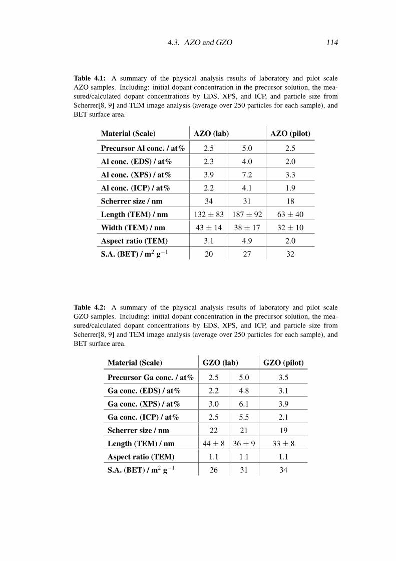
4.3. AZO and GZO 114
Table 4.1: A summary of the physical analysis results of laboratory and pilot scaleAZO samples. Including: initial dopant concentration in the precursor solution, the mea-sured/calculated dopant concentrations by EDS, XPS, and ICP, and particle size fromScherrer[8, 9] and TEM image analysis (average over 250 particles for each sample), andBET surface area.
Material (Scale) AZO (lab) AZO (pilot)
Precursor Al conc. / at% 2.5 5.0 2.5
Al conc. (EDS) / at% 2.3 4.0 2.0
Al conc. (XPS) / at% 3.9 7.2 3.3
Al conc. (ICP) / at% 2.2 4.1 1.9
Scherrer size / nm 34 31 18
Length (TEM) / nm 132 ± 83 187 ± 92 63 ± 40
Width (TEM) / nm 43 ± 14 38 ± 17 32 ± 10
Aspect ratio (TEM) 3.1 4.9 2.0
S.A. (BET) / m2 g−1 20 27 32
Table 4.2: A summary of the physical analysis results of laboratory and pilot scaleGZO samples. Including: initial dopant concentration in the precursor solution, the mea-sured/calculated dopant concentrations by EDS, XPS, and ICP, and particle size fromScherrer[8, 9] and TEM image analysis (average over 250 particles for each sample), andBET surface area.
Material (Scale) GZO (lab) GZO (pilot)
Precursor Ga conc. / at% 2.5 5.0 3.5
Ga conc. (EDS) / at% 2.2 4.8 3.1
Ga conc. (XPS) / at% 3.0 6.1 3.9
Ga conc. (ICP) / at% 2.5 5.5 2.1
Scherrer size / nm 22 21 19
Length (TEM) / nm 44 ± 8 36 ± 9 33 ± 8
Aspect ratio (TEM) 1.1 1.1 1.1
S.A. (BET) / m2 g−1 26 31 34
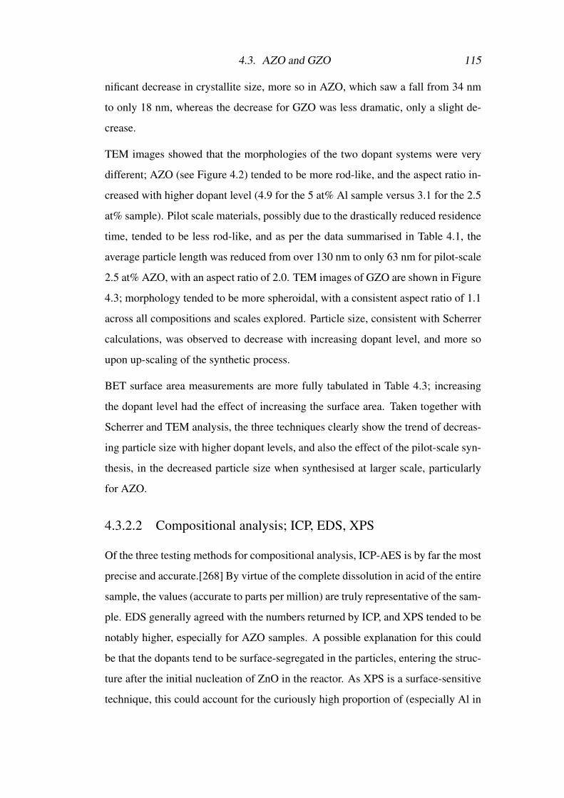
4.3. AZO and GZO 115
nificant decrease in crystallite size, more so in AZO, which saw a fall from 34 nm
to only 18 nm, whereas the decrease for GZO was less dramatic, only a slight de-
crease.
TEM images showed that the morphologies of the two dopant systems were very
different; AZO (see Figure 4.2) tended to be more rod-like, and the aspect ratio in-
creased with higher dopant level (4.9 for the 5 at% Al sample versus 3.1 for the 2.5
at% sample). Pilot scale materials, possibly due to the drastically reduced residence
time, tended to be less rod-like, and as per the data summarised in Table 4.1, the
average particle length was reduced from over 130 nm to only 63 nm for pilot-scale
2.5 at% AZO, with an aspect ratio of 2.0. TEM images of GZO are shown in Figure
4.3; morphology tended to be more spheroidal, with a consistent aspect ratio of 1.1
across all compositions and scales explored. Particle size, consistent with Scherrer
calculations, was observed to decrease with increasing dopant level, and more so
upon up-scaling of the synthetic process.
BET surface area measurements are more fully tabulated in Table 4.3; increasing
the dopant level had the effect of increasing the surface area. Taken together with
Scherrer and TEM analysis, the three techniques clearly show the trend of decreas-
ing particle size with higher dopant levels, and also the effect of the pilot-scale syn-
thesis, in the decreased particle size when synthesised at larger scale, particularly
for AZO.
4.3.2.2 Compositional analysis; ICP, EDS, XPS
Of the three testing methods for compositional analysis, ICP-AES is by far the most
precise and accurate.[268] By virtue of the complete dissolution in acid of the entire
sample, the values (accurate to parts per million) are truly representative of the sam-
ple. EDS generally agreed with the numbers returned by ICP, and XPS tended to be
notably higher, especially for AZO samples. A possible explanation for this could
be that the dopants tend to be surface-segregated in the particles, entering the struc-
ture after the initial nucleation of ZnO in the reactor. As XPS is a surface-sensitive
technique, this could account for the curiously high proportion of (especially Al in
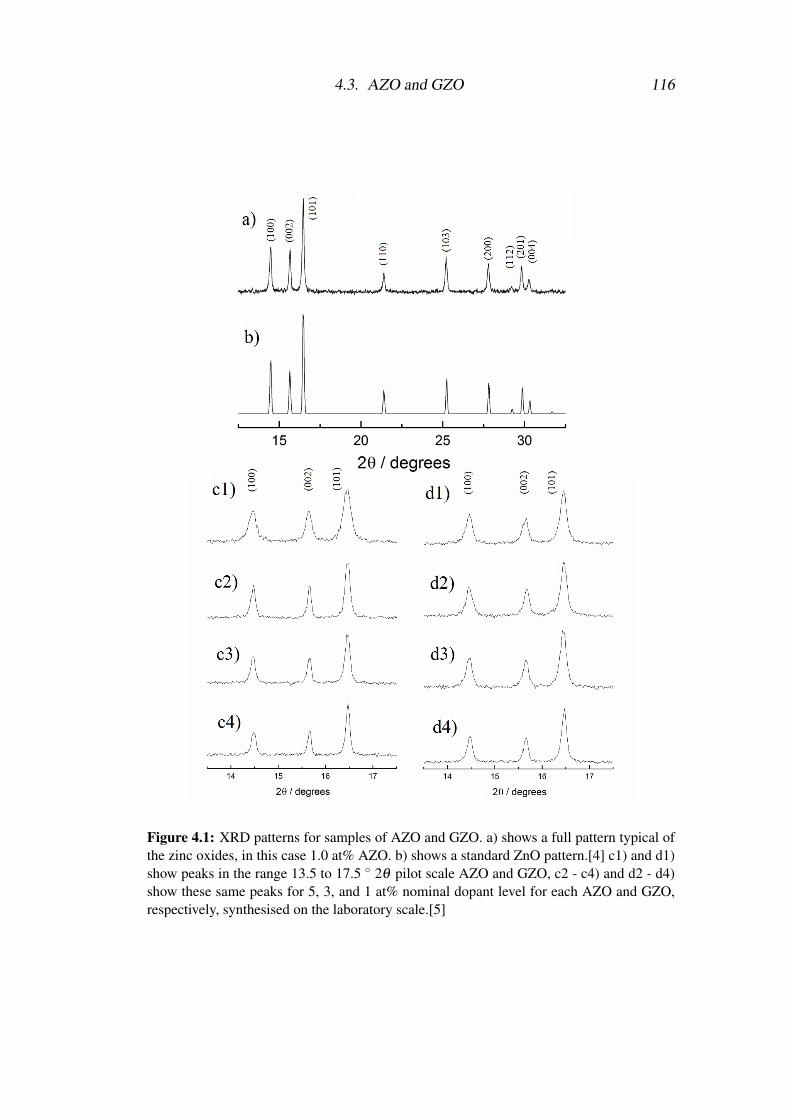
4.3. AZO and GZO 116
Figure 4.1: XRD patterns for samples of AZO and GZO. a) shows a full pattern typical ofthe zinc oxides, in this case 1.0 at% AZO. b) shows a standard ZnO pattern.[4] c1) and d1)show peaks in the range 13.5 to 17.5 2θ pilot scale AZO and GZO, c2 - c4) and d2 - d4)show these same peaks for 5, 3, and 1 at% nominal dopant level for each AZO and GZO,respectively, synthesised on the laboratory scale.[5]
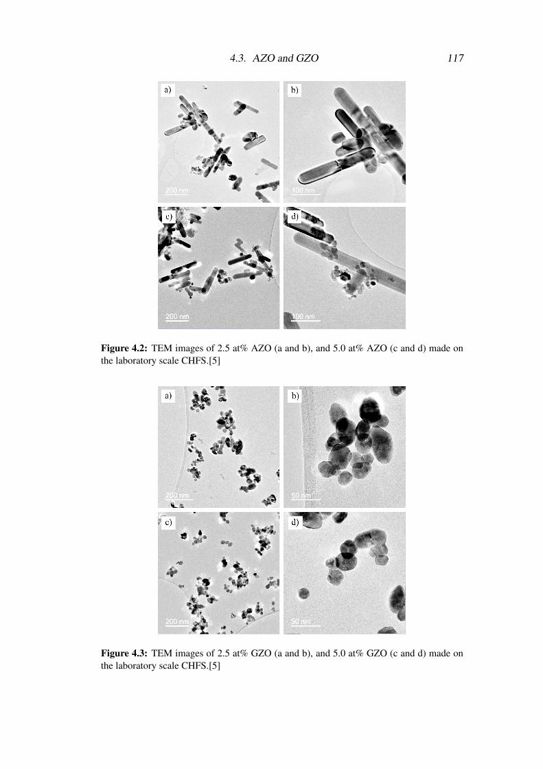
4.3. AZO and GZO 117
Figure 4.2: TEM images of 2.5 at% AZO (a and b), and 5.0 at% AZO (c and d) made onthe laboratory scale CHFS.[5]
Figure 4.3: TEM images of 2.5 at% GZO (a and b), and 5.0 at% GZO (c and d) made onthe laboratory scale CHFS.[5]
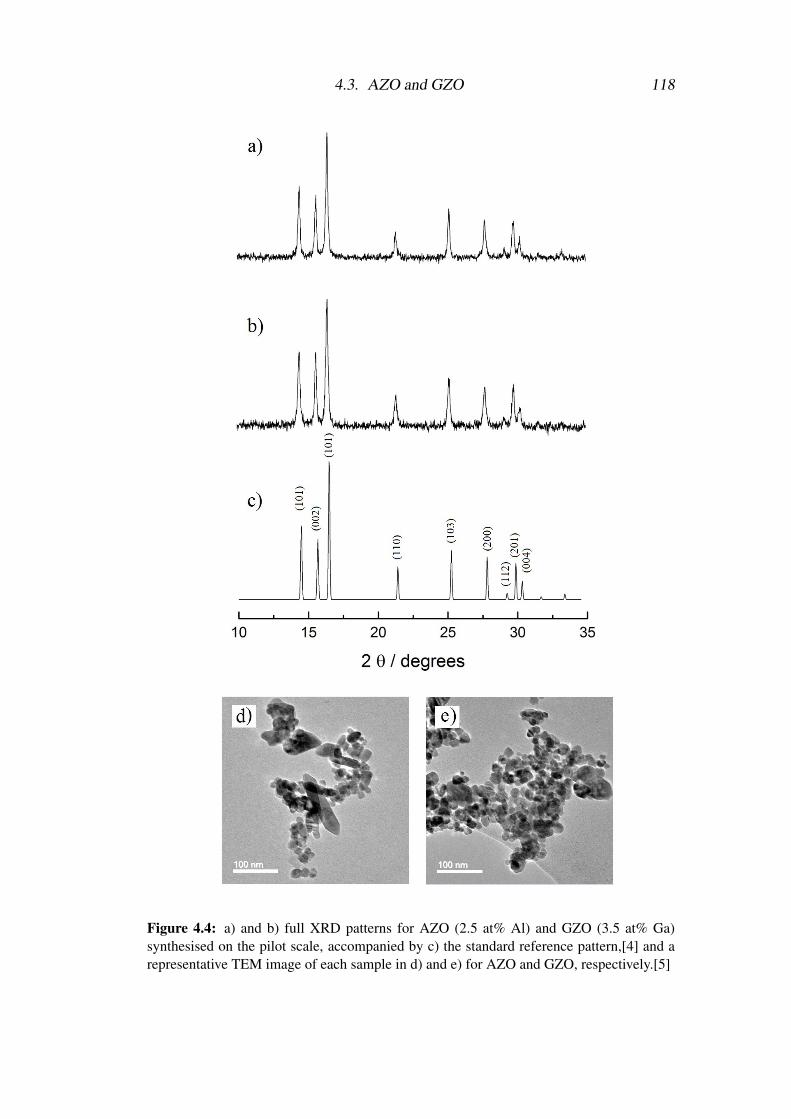
4.3. AZO and GZO 118
Figure 4.4: a) and b) full XRD patterns for AZO (2.5 at% Al) and GZO (3.5 at% Ga)synthesised on the pilot scale, accompanied by c) the standard reference pattern,[4] and arepresentative TEM image of each sample in d) and e) for AZO and GZO, respectively.[5]
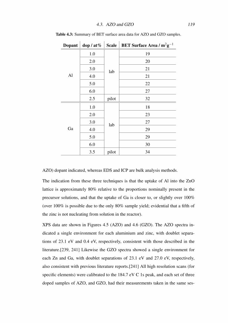
4.3. AZO and GZO 119
Table 4.3: Summary of BET surface area data for AZO and GZO samples.
Dopant dop / at% Scale BET Surface Area / m2g−1
Al
1.0
lab
19
2.0 20
3.0 21
4.0 21
5.0 22
6.0 27
2.5 pilot 32
Ga
1.0
lab
18
2.0 23
3.0 27
4.0 29
5.0 29
6.0 30
3.5 pilot 34
AZO) dopant indicated, whereas EDS and ICP are bulk analysis methods.
The indication from these three techniques is that the uptake of Al into the ZnO
lattice is approximately 80% relative to the proportions nominally present in the
precursor solutions, and that the uptake of Ga is closer to, or slightly over 100%
(over 100% is possible due to the only 80% sample yield; evidential that a fifth of
the zinc is not nucleating from solution in the reactor).
XPS data are shown in Figures 4.5 (AZO) and 4.6 (GZO). The AZO spectra in-
dicated a single environment for each aluminium and zinc, with doublet separa-
tions of 23.1 eV and 0.4 eV, respectively, consistent with those described in the
literature.[239, 241] Likewise the GZO spectra showed a single environment for
each Zn and Ga, with doublet separations of 23.1 eV and 27.0 eV, respectively,
also consistent with previous literature reports.[241] All high resolution scans (for
specific elements) were calibrated to the 184.7 eV C 1s peak, and each set of three
doped samples of AZO, and GZO, had their measurements taken in the same ses-
4.3. AZO and GZO 120
sion, therefore it can be concluded the small shifts in binding energies were due
to the differences between the doped samples themselves, not any outside effects.
Consistent for both AZO and GZO are the shift in binding energy of the Zn 2p
peaks, such that the laboratory and pilot scale 2.5 at% dopant synthesised materials
showed a Zn 2p binding energy that was 0.3 eV lower than then analogous peak for
the 5.0 at% dopant materials. Similarly, a 0.2 eV and 0.3 eV (increase) shift was
seen when increasing the laboratory-scale dopant level from 2.5 to 5.0 at% for Al
and Ga, respectively. It should be noted that the dopant uptake was less efficient for
the pilot scale materials (with respect to the nominal dopant concentrations in the
precursor solutions) than for the laboratory scale. This is likely due in part to the
reduced residence time in the pilot scale process that could have had an effect on
the dopant uptake efficiencies.
4.3.3 Electrical testing of discs
This section outlines the electrical testing of all of the laboratory and pilot-scale
synthesised products to determine the optimal composition for lowest resistivity.
Table 4.7 gives a summary of all resistivities for the various AZO and GZO samples,
and the following subsections will show the trends graphically for each system.
4.3.3.1 Aluminium doped zinc oxide (AZO)
Figure 4.7 shows the resistivity trend with increasing Al-content in AZO. After an
initial decline (with increasing Al) to a low resistivity of 7.0 x 10⁻³ Ω cm, the resis-
tivity then rose again. The most conductive sample was thus the sample synthesised
with 2.5 at% in the precursor solution. This trend appeared to hold on the pilot
scale too, however the optimal resistivity at ca. 2.0 to 2.5 at% Al is almost an order
of magnitude higher. That the trend held (i.e. a decrease to a minimum resistivity
followed by a subsequent increase), implied that there is a factor at play beyond
uptake efficiency (as indicated by compositional analysis); leaving a combination
of the morphology, particle size, and packing of the particles as possible causes for
the inferior pellets.
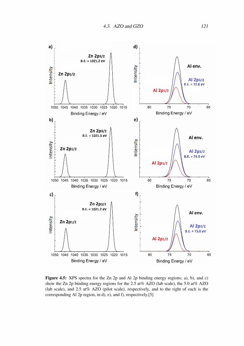
4.3. AZO and GZO 121
Figure 4.5: XPS spectra for the Zn 2p and Al 2p binding energy regions; a), b), and c)show the Zn 2p binding energy regions for the 2.5 at% AZO (lab scale), the 5.0 at% AZO(lab scale), and 2.5 at% AZO (pilot scale), respectively, and to the right of each is thecorresponding Al 2p region, in d), e), and f), respectively.[5]
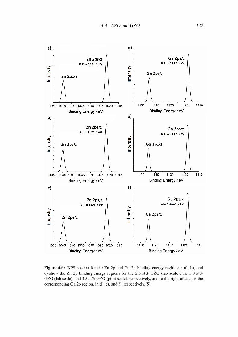
4.3. AZO and GZO 122
Figure 4.6: XPS spectra for the Zn 2p and Ga 2p binding energy regions; ; a), b), andc) show the Zn 2p binding energy regions for the 2.5 at% GZO (lab scale), the 5.0 at%GZO (lab scale), and 3.5 at% GZO (pilot scale), respectively, and to the right of each is thecorresponding Ga 2p region, in d), e), and f), respectively.[5]
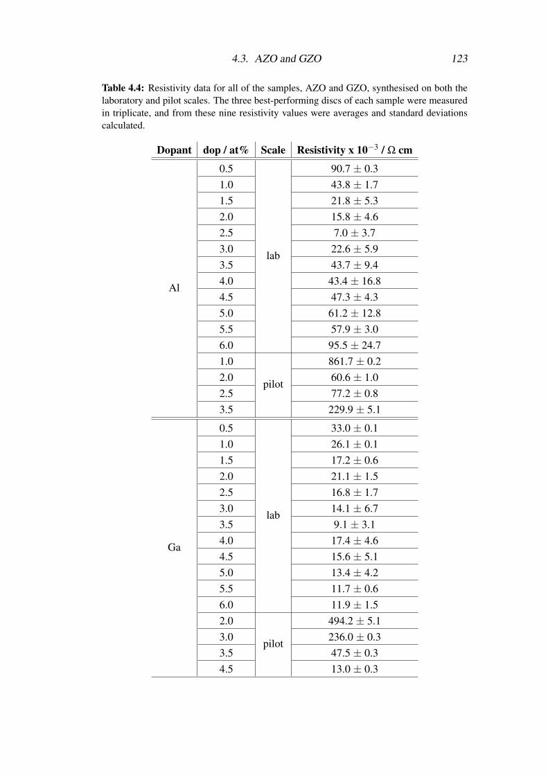
4.3. AZO and GZO 123
Table 4.4: Resistivity data for all of the samples, AZO and GZO, synthesised on both thelaboratory and pilot scales. The three best-performing discs of each sample were measuredin triplicate, and from these nine resistivity values were averages and standard deviationscalculated.
Dopant dop / at% Scale Resistivity x 10−3 / Ω cm
Al
0.5
lab
90.7 ± 0.31.0 43.8 ± 1.71.5 21.8 ± 5.32.0 15.8 ± 4.62.5 7.0 ± 3.73.0 22.6 ± 5.93.5 43.7 ± 9.44.0 43.4 ± 16.84.5 47.3 ± 4.35.0 61.2 ± 12.85.5 57.9 ± 3.06.0 95.5 ± 24.71.0
pilot
861.7 ± 0.22.0 60.6 ± 1.02.5 77.2 ± 0.83.5 229.9 ± 5.1
Ga
0.5
lab
33.0 ± 0.11.0 26.1 ± 0.11.5 17.2 ± 0.62.0 21.1 ± 1.52.5 16.8 ± 1.73.0 14.1 ± 6.73.5 9.1 ± 3.14.0 17.4 ± 4.64.5 15.6 ± 5.15.0 13.4 ± 4.25.5 11.7 ± 0.66.0 11.9 ± 1.52.0
pilot
494.2 ± 5.13.0 236.0 ± 0.33.5 47.5 ± 0.34.5 13.0 ± 0.3
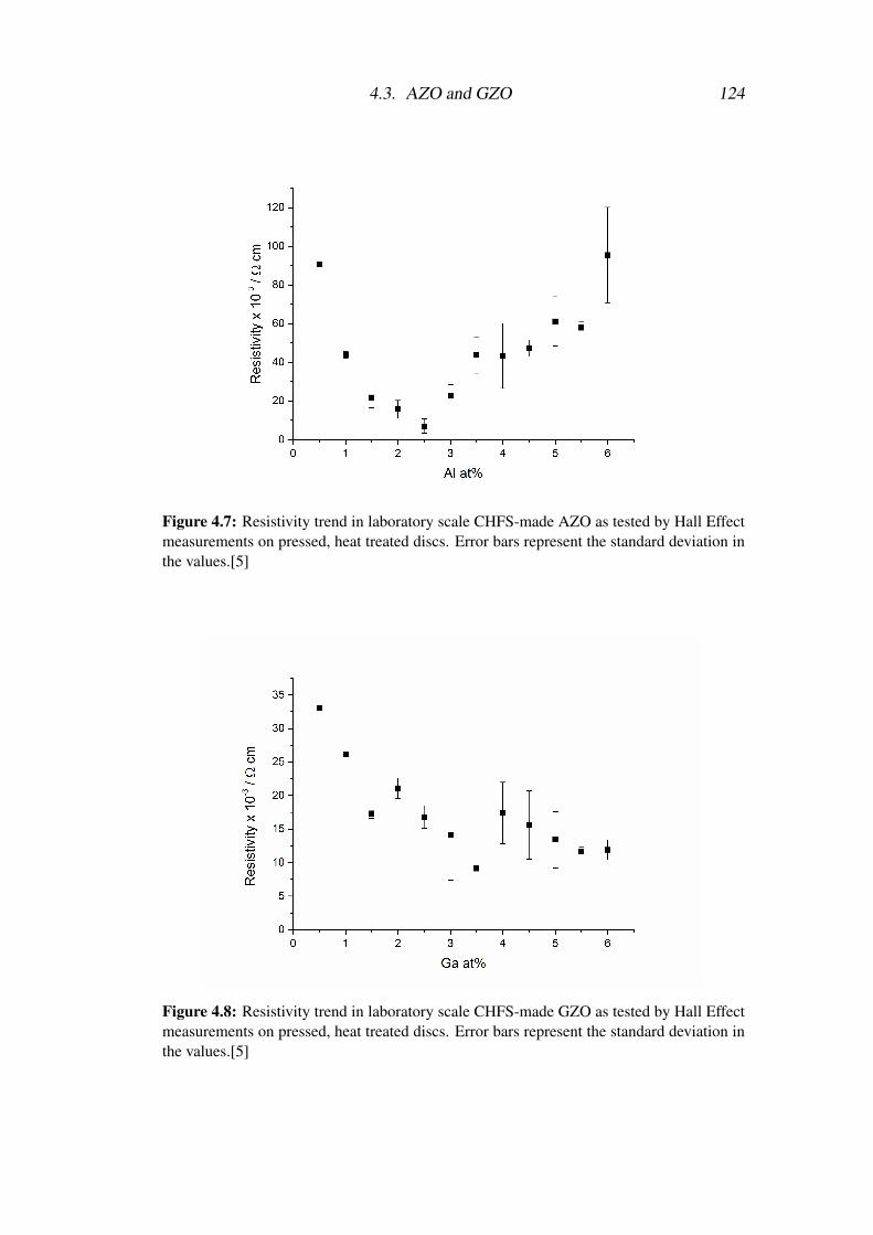
4.3. AZO and GZO 124
Figure 4.7: Resistivity trend in laboratory scale CHFS-made AZO as tested by Hall Effectmeasurements on pressed, heat treated discs. Error bars represent the standard deviation inthe values.[5]
Figure 4.8: Resistivity trend in laboratory scale CHFS-made GZO as tested by Hall Effectmeasurements on pressed, heat treated discs. Error bars represent the standard deviation inthe values.[5]
4.3. AZO and GZO 125
4.3.3.2 Gallium doped zinc oxide (GZO)
Figure 4.8 shows the resistivity trend with increasing Ga content in GZO. As with
AZO, increasing dopant level causes the resistivity to decrease to a minimum of 9.1
x 10−3 Ω cm (at 3.5 at% Ga), however unlike with the AZO trend, the subsequent
increase in resistivity was not observed. Within error, the resistivity remained ap-
proximately constant from 3.5 at% Ga upwards, implying that though additional Ga
was not contributing to higher conductivity, neither was it particularly conductivity-
inhibiting at the dopant levels being investigated. This was further observed on the
pilot scale, wherein increasing the dopant level reduced the conductivity, until by
4.5 at% the resistivity of the pilot-scale powder was 1.3 x 10⁻² Ω cm, comparable
to the laboratory scale material.
4.3.4 Conclusions: AZO
Doping of Al into ZnO was successful; up to 6.0 at%, only a single phase was iden-
tified by XRD, and only a single environment was observed for each Zn 2p and Al
2p orbital binding energies. Increasing the dopant level promoted growth along the
c-axis, resulting in increasingly rod-like morphology.
The optimal composition as determined by pressing the powder samples into discs
and heat treating, pointed to the 2.5 at% AZO sample as being consistently the most
conductive. Higher resistivity was observed with both higher and lower dopant lev-
els, above the optimal 7.0 x 10⁻³ Ω cm. This value was close to that of 6.0 x 10⁻³ Ω
cm obtained by ITO as synthesised using the same CHFS process,[168] demonstrat-
ing the promise of AZO as an ITO replacement material for TCOs. Up-scaling of
the synthesis to 330 g h−1 resulted in a deterioration of the electrical properties by
almost a factor of 10. Rod-like behaviour decreased, as did particle size and dopant
uptake, however as the trend observed on the laboratory scale appeared largely to
be consistent on the pilot scale (though with fewer data points), the explicit cause of
this remains unknown. The most likely reasons could include differences in particle
size, packing and agglomeration, altering the resistance of the pellets when pressed.
4.4. AGZO: Aluminium and Gallium co-doped Zinc Oxide 126
4.3.5 Conclusions: GZO
Doping of Ga into ZnO was successful; up to 6.0 at% Ga, only a single phase was
identified by XRD, and only a single environment was observed for each Zn 2p
and Ga 2p orbital binding energies from XPS data. Increasing the dopant level did
not alter the morphology, but did decrease particle size. The optimal composition
as determined by pressing the powder samples into discs and heat treating, pointed
to the 3.5 at% GZO sample as being consistently the most conductive. Higher
resistivities were observed with both higher and lower dopant levels, above the op-
timal 9.1 x 10⁻³ Ω cm. This was also close to the 6.0 x 10⁻³ Ω cm obtained by
ITO as synthesised using the same process and the 7.0 x 10⁻³ Ω cm seen in AZO,
demonstrating the promise of GZO as an ITO replacement TCO material as made
by CHFS. Up-scaling of the synthesis to 330 g h−1 resulted in a minor deterioration
of the electrical properties, and a shift in the trend to the optimal nominal dopant
level (in the precursor solutions) increasing from 3.5 at% to 4.5 at%.
4.4 AGZO: Aluminium and Gallium co-doped Zinc
Oxide
4.4.1 Experimental design and observations
The high-throughput set-up was used as described in Section 2.2.3. Twenty compo-
sitions were investigated, between 1.0 and 5.0 at% total dopant level, with dopant
increments of 0.5 at%. The following naming convention is in use in this section:
each sample has been designated (x,y)AGZO, such that x and y are the nominal
dopant concentrations in the precursor solutions of Al and Ga, respectively. Thus
the sample (1,2)AGZO is the sample made with 1 at% Al, 2 at% Ga, and 97 at% Zn
in the precursor solution.
In keeping with the high-throughput nature of the experiment, higher concentration
precursor solutions were used than in the previous AZO and GZO experiments;
metal concentration, [metal], was 0.5 M, and [KOH] was 1.0 M. 100 mL of each
precursor solution was used, such that the 400 mL collected was set to contain
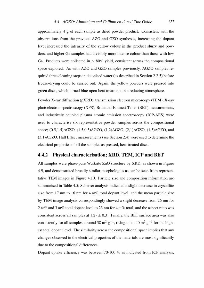
4.4. AGZO: Aluminium and Gallium co-doped Zinc Oxide 127
approximately 4 g of each sample as dried powder product. Consistent with the
observations from the previous AZO and GZO syntheses, increasing the dopant
level increased the intensity of the yellow colour in the product slurry and pow-
ders, and higher Ga samples had a visibly more intense colour than those with low
Ga. Products were collected in > 80% yield, consistent across the compositional
space explored. As with AZO and GZO samples previously, AGZO samples re-
quired three cleaning steps in deionised water (as described in Section 2.2.5) before
freeze-drying could be carried out. Again, the yellow powders were pressed into
green discs, which turned blue upon heat treatment in a reducing atmosphere.
Powder X-ray diffraction (pXRD), transmission electron microscopy (TEM), X-ray
photoelectron spectroscopy (XPS), Brunauer-Emmett-Teller (BET) measurements,
and inductively coupled plasma atomic emission spectroscopy (ICP-AES) were
used to characterise six representative powder samples across the compositional
space; (0.5,1.5)AGZO, (1.5,0.5)AGZO, (1,2)AGZO, (2,1)AGZO, (1,3)AGZO, and
(3,1)AGZO. Hall Effect measurements (see Section 2.4) were used to determine the
electrical properties of all the samples as pressed, heat treated discs.
4.4.2 Physical characterisation; XRD, TEM, ICP and BET
All samples were phase-pure Wurtzite ZnO structure by XRD, as shown in Figure
4.9, and demonstrated broadly similar morphologies as can be seen from represen-
tative TEM images in Figure 4.10. Particle size and composition information are
summarised in Table 4.5; Scherrer analysis indicated a slight decrease in crystallite
size from 17 nm to 16 nm for 4 at% total dopant level, and the mean particle size
by TEM image analysis correspondingly showed a slight decrease from 26 nm for
2 at% and 3 at% total dopant level to 23 nm for 4 at% total, and the aspect ratio was
consistent across all samples at 1.2 (± 0.3). Finally, the BET surface area was also
consistently for all samples, around 38 m2 g−1, rising up to 40 m2 g−1 for the high-
est total dopant level. The similarity across the compositional space implies that any
changes observed in the electrical properties of the materials are most significantly
due to the compositional differences.
Dopant uptake efficiency was between 70-100 % as indicated from ICP analysis,
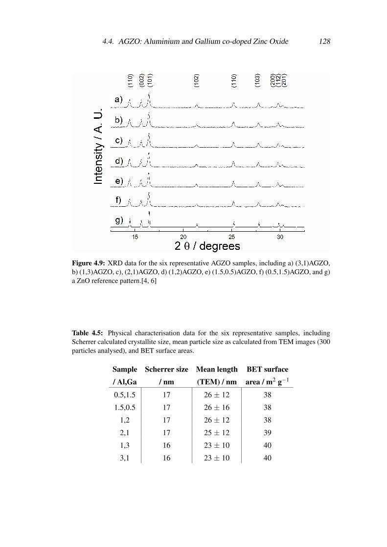
4.4. AGZO: Aluminium and Gallium co-doped Zinc Oxide 128
Figure 4.9: XRD data for the six representative AGZO samples, including a) (3,1)AGZO,b) (1,3)AGZO, c), (2,1)AGZO, d) (1,2)AGZO, e) (1.5,0.5)AGZO, f) (0.5,1.5)AGZO, and g)a ZnO reference pattern.[4, 6]
Table 4.5: Physical characterisation data for the six representative samples, includingScherrer calculated crystallite size, mean particle size as calculated from TEM images (300particles analysed), and BET surface areas.
Sample/ Al,Ga
Scherrer size/ nm
Mean length(TEM) / nm
BET surfacearea / m2 g−1
0.5,1.5 17 26 ± 12 38
1.5,0.5 17 26 ± 16 38
1,2 17 26 ± 12 38
2,1 17 25 ± 12 39
1,3 16 23 ± 10 40
3,1 16 23 ± 10 40
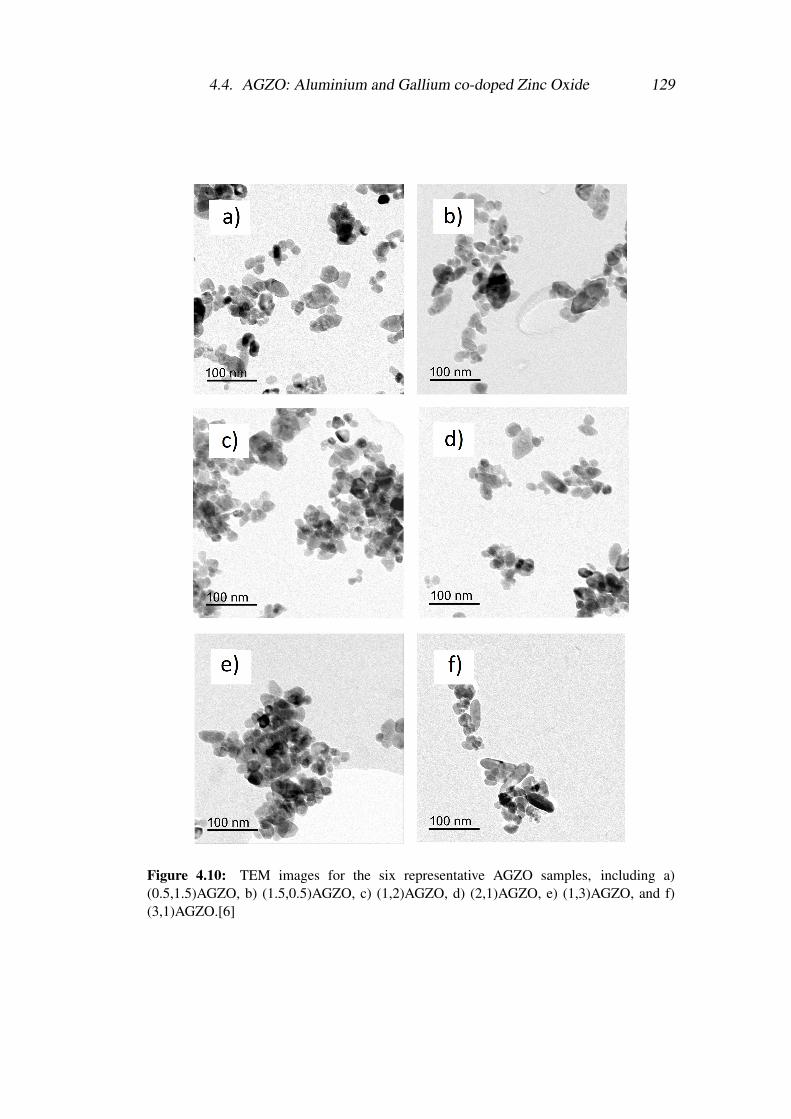
4.4. AGZO: Aluminium and Gallium co-doped Zinc Oxide 129
Figure 4.10: TEM images for the six representative AGZO samples, including a)(0.5,1.5)AGZO, b) (1.5,0.5)AGZO, c) (1,2)AGZO, d) (2,1)AGZO, e) (1,3)AGZO, and f)(3,1)AGZO.[6]
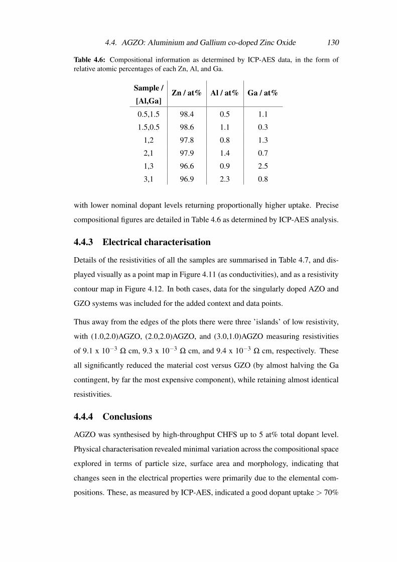
4.4. AGZO: Aluminium and Gallium co-doped Zinc Oxide 130
Table 4.6: Compositional information as determined by ICP-AES data, in the form ofrelative atomic percentages of each Zn, Al, and Ga.
Sample /[Al,Ga]
Zn / at% Al / at% Ga / at%
0.5,1.5 98.4 0.5 1.1
1.5,0.5 98.6 1.1 0.3
1,2 97.8 0.8 1.3
2,1 97.9 1.4 0.7
1,3 96.6 0.9 2.5
3,1 96.9 2.3 0.8
with lower nominal dopant levels returning proportionally higher uptake. Precise
compositional figures are detailed in Table 4.6 as determined by ICP-AES analysis.
4.4.3 Electrical characterisation
Details of the resistivities of all the samples are summarised in Table 4.7, and dis-
played visually as a point map in Figure 4.11 (as conductivities), and as a resistivity
contour map in Figure 4.12. In both cases, data for the singularly doped AZO and
GZO systems was included for the added context and data points.
Thus away from the edges of the plots there were three ’islands’ of low resistivity,
with (1.0,2.0)AGZO, (2.0,2.0)AGZO, and (3.0,1.0)AGZO measuring resistivities
of 9.1 x 10⁻³ Ω cm, 9.3 x 10⁻³ Ω cm, and 9.4 x 10⁻³ Ω cm, respectively. These
all significantly reduced the material cost versus GZO (by almost halving the Ga
contingent, by far the most expensive component), while retaining almost identical
resistivities.
4.4.4 Conclusions
AGZO was synthesised by high-throughput CHFS up to 5 at% total dopant level.
Physical characterisation revealed minimal variation across the compositional space
explored in terms of particle size, surface area and morphology, indicating that
changes seen in the electrical properties were primarily due to the elemental com-
positions. These, as measured by ICP-AES, indicated a good dopant uptake > 70%
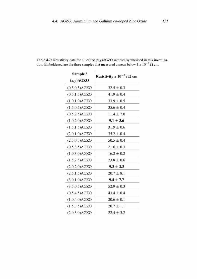
4.4. AGZO: Aluminium and Gallium co-doped Zinc Oxide 131
Table 4.7: Resistivity data for all of the (x,y)AGZO samples synthesised in this investiga-tion. Emboldened are the three samples that measured a mean below 1 x 10⁻² Ω cm.
Sample /(x,y)AGZO
Resistivity x 10−3 / Ω cm
(0.5,0.5)AGZO 32.5 ± 0.3
(0.5,1.5)AGZO 41.9 ± 0.4
(1.0,1.0)AGZO 33.9 ± 0.5
(1.5,0.5)AGZO 35.6 ± 0.4
(0.5,2.5)AGZO 11.4 ± 7.0
(1.0,2.0)AGZO 9.1 ± 3.6
(1.5,1.5)AGZO 31.9 ± 0.6
(2.0,1.0)AGZO 35.2 ± 0.4
(2.5,0.5)AGZO 50.5 ± 0.4
(0.5,3.5)AGZO 21.6 ± 0.3
(1.0,3.0)AGZO 16.2 ± 0.2
(1.5,2.5)AGZO 23.8 ± 0.6
(2.0,2.0)AGZO 9.3 ± 2.3
(2.5,1.5)AGZO 20.7 ± 8.1
(3.0,1.0)AGZO 9.4 ± 7.7
(3.5,0.5)AGZO 52.9 ± 0.3
(0.5,4.5)AGZO 43.4 ± 0.4
(1.0,4.0)AGZO 20.6 ± 0.1
(1.5,3.5)AGZO 20.7 ± 1.1
(2.0,3.0)AGZO 22.4 ± 3.2
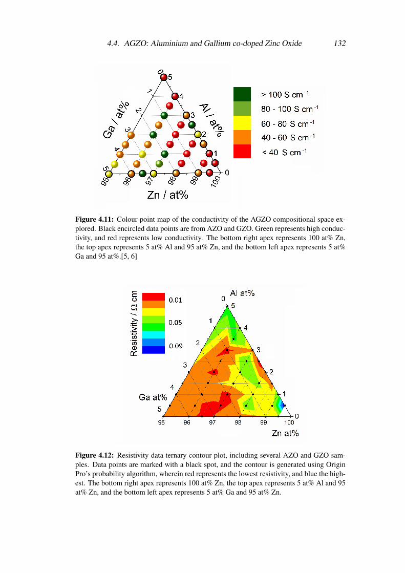
4.4. AGZO: Aluminium and Gallium co-doped Zinc Oxide 132
Figure 4.11: Colour point map of the conductivity of the AGZO compositional space ex-plored. Black encircled data points are from AZO and GZO. Green represents high conduc-tivity, and red represents low conductivity. The bottom right apex represents 100 at% Zn,the top apex represents 5 at% Al and 95 at% Zn, and the bottom left apex represents 5 at%Ga and 95 at%.[5, 6]
Figure 4.12: Resistivity data ternary contour plot, including several AZO and GZO sam-ples. Data points are marked with a black spot, and the contour is generated using OriginPro’s probability algorithm, wherein red represents the lowest resistivity, and blue the high-est. The bottom right apex represents 100 at% Zn, the top apex represents 5 at% Al and 95at% Zn, and the bottom left apex represents 5 at% Ga and 95 at% Zn.
4.5. Overall Conclusions for AZO, GZO, and AGZO 133
relative to the nominal precursor solution concentrations, and Hall Effect measure-
ments determined three samples that obtained low resistivities < 1 x 10⁻² Ω cm;
(1.0,2.0)AGZO, (2.0,2.0)AGZO, and (3.0,1.0)AGZO measured resistivities of 9.1 x
10−3 Ω cm, 9.3 x 10⁻³ Ω cm, and 9.4 x 10⁻³ Ω cm, respectively, comparable to the
singularly doped GZO (9.1 x 10⁻³ Ω cm at 3.5 at% doping level), but not quite as
conductive as the best AZO sample (7.0 x 10⁻³ Ω cm).
4.5 Overall Conclusions for AZO, GZO, and AGZOAZO, GZO, and AGZO were synthesised by CHFS with varying dopant levels in
order to determine the optimal composition in terms of electrical conductivity. This
was tested by pressing each sample into a pellet and heat treating in a reducing
atmosphere, and reproducibility ensured by the pressing of multiple pellets, with
multiple readings taken for each pellet before calculating the average and standard
deviations. The optimal compositions of each laboratory-scale synthesised (produc-
tion rate of 60 g h−1) material were as follows: AZO with 2.5 at% Al yielded an
average resitivity of 7.0 x 10⁻³ Ω cm, while GZO with 3.5 at% Ga, and AGZO with
1 at% Al and 2 at% Ga both yielded an average resistivity of 9.1 x 10⁻³ Ω cm.
Physical analysis by XRD, BET, and TEM indicated a decrease in particle size with
increasing nominal dopant levels in the precursor solutions. Furthermore, colour
change and the onset of conductivity in the doped samples relative to un-doped ZnO
initially implied that successful doping into the ZnO structure was taking place.
These, when taking also into account the single phase observed by XRD, the single
environments for the Zn 2p, Al 2p, and Ga 2p XPS peaks, and the compositional
analysis by both XPS and ICP, were strongly evidential that these materials, though
not in themselves novel, had been synthesised for the first time by CHFS.
For comparison of the electrical properties, the optimal composition of ITO (made
with 10 at% Sn) synthesised and tested by the same methods, had a resistivity of
6.0 x 10⁻³ Ω cm.[168] Thus each of the optimal compositions of each AZO, GZO,
and AGZO had resistivities very close to that of ITO, indicating their promise as
conducting oxide materials when synthesised by CHFS.
Chapter 5
Si Doped and Co-Doped Zinc Oxide
for Transparent Conducting Oxides
5.1 AimsAfter AZO and GZO, the next most promising system with respect to conductivity
was silicon-doped zinc oxide (SZO, or SiZO). The aim of this chapter is thus to
investigate the compositional optimisation of SiZO as synthesised by continuous
hydrothermal flow synthesis (CHFS), as well as subsequent up-scaling to the pilot-
scale CHFS. The effect of co-doping SiZO with either aluminium or gallium is
also investigated. In addition to the electrical testing, characterisation including
XRD, BET, TEM, XPS, and ICP-AES is also discussed, to gauge the effect that the
different dopant ratios have on the properties of the materials.
5.2 IntroductionSilicon is a tetravalent ion, i.e. Si4+, thus when it is present as Si••Zn, as a substitu-
tional defect on a zinc site, it will donate two electrons rather than the single electron
donated by trivalent dopant cations such as Al or Ga. Additionally, Si4+ is consid-
erably smaller than Zn2+; their ionic radii are 0.26 A and 0.60 A, respectively.[245]
This has a number of effects; the high charge concentration means that silicon in
SiZO will draw oxygen anions to it more effectively than trivalent cation dopants
would, and indeed more strongly than the Zn2+ in the lattice. Each acts as a point
defect, and perturbs the Zn ions closest to it in the Zn plane, generating localised
5.2. Introduction 135
planar defects.[269] This, coupled with the two electrons (charge carriers) con-
tributed by each SiZn mean that as dopant level increases, the conductivity will be
significantly hampered by scattering effects in the lattice, inhibiting carrier mobil-
ity, thus the optimally conductive composition of SiZO should have a lower dopant
level than seen for AZO, GZO or AGZO.[270] Additionally, upon over-saturation
of Si into ZnO, one would expect to see the appearance of additional phases due to
the strain on the lattice that the Si ions cause.[269, 270]
Silicon itself is a highly desirable element for incorporation in a ZnO-based TCO
film due to a number of factors; comparatively little is needed relative to the equiv-
alent trivalent-doped systems, silicon is highly earth abundant and accessible (sec-
ond most abundant element in the Earth’s crust after oxygen),[271] and has neither
the chemical stability issues of AZO, nor the high costs associated with gallium in
GZO.[272, 273]
The first calculations on SiZO were carried out by Korner and Elsasser in
2011,[270] to which the conclusion was that substitution of Si onto the Zn sites
in the lattice was by far the preferential doping mechanism. Though interstitial sil-
icon was not addressed in that study, in subsequent work by Wu et al.[274] it was
shown that Si in either the octahedral or tetrahedral interstitial site has too high a
formation energy, at least double that of the substitutional SiZn, thus the substitu-
tional defect is formed upon Si-doping into ZnO.
Few studies exist in literature in which SiZO thin films are generated and fully
characterised in the context of application as TCOs, i.e. with optical and electri-
cal characterisation in tow. That said, from the studies that have been carried out,
competitive resistivities, carrier concentrations, charge carrier mobilities, and trans-
mittance properties have been achieved. SiZO thin films have been made by several
techniques, including CVD,[275] spray pyrolysis,[276, 277] pulsed laser deposition
(PLD),[136, 208, 278] and magnetron sputtering.[134, 147, 279] Of these, sputtered
films were the most transmissive, at 90%[134] and 94.5%[147], but PLD and spray
pyrolysis techniques also garnered films with > 80% transmittance across the vis-
5.2. Introduction 136
ible range. The seminal work by Minami et al.[135] was also the first to reach the
order of 10−4 Ω cm, but many published sputtering and PLD studies managed to
match this feat.[134, 136, 147, 208, 278, 279] For a detailed summary of a selec-
tion of SiZO thin films deposited by various methods in literature, see Table 6.5 in
Chapter 6.
Though thin films are typically formed by sputtering, the material in the target needs
first to be synthesised, in which case the ZnO would most likely have been synthe-
sised by one of three methods:[112, 160, 264, 265]
• The French (or Indirect) process, wherein metallic zinc is melted in a crucible
and vapourised (around 1000 C), at which point the Zn vapour reacts with
oxygen in the air to form ZnO.
• The American (or Direct) process, wherein impure minerals, ores, or compos-
ites of zinc undergo carbothermal reduction by heating with a carbon source
such as anthracite to produce the zinc vapour, at a similarly high temperature
to the French process.
• Wet chemical processes, wherein zinc precursor solutions are used to precip-
itate the carbonate or hydroxide, which is converted to the oxide by calcining
(typically ca. 800 C).
In order to generate a sputtering target, these materials would need to undergo a
further annealing step as above, likely also >1000 C.
The silicon source could take the form of a single crystal wafer (typical for
PLD)[208], or could be used in the form of SiO2, which could be made top down (it
exists in nature as quartz) or bottom-up in the laboratory by a vast number of meth-
ods, for example by acidification of solutions of sodium silicate to form a silica gel,
then washing, drying, and dehydrating of the gel to form microporous silica; by this
method annual global production of silica has exceeded 1 billion kg.[280, 281] In
order to generate a sputtering target, these materials would need to undergo a fur-
ther annealing step as above, likely also >1000 C.
5.3. SiZO: Laboratory and Pilot Scale Synthesis 137
Benefits of Continuous Hydrothermal Flow Synthesis (CHFS) over more conven-
tional synthesis processes are fully discussed in Section 1.4 of Chapter 1. In brief,
CHFS should be able to directly deliver ZnO or doped ZnO by a purely hydrother-
mal (i.e. water as the only solvent) process at much lower temperatures than those
processes mentioned above. Before the studies outlined in this chapter, no such had
been carried out investigating silicon doping or co-doping into zinc oxide by CHFS.
5.3 SiZO: Laboratory and Pilot Scale SynthesisThis section outlines the investigation into SiZO synthesised on the laboratory (60
g h−1) and pilot (300 g h−1) scales, i.e. the compositional optimisation by means of
physical and electrical characterisation.
5.3.1 Experimental design
Initially, a 3-pump, single mixer laboratory-scale CHFS set-up was used (see Ex-
perimental chapter, section 2.2.1). With a total [Zn + Si] concentration of 0.3 M
(Zn supplied by pump P2, Si supplied by the base feed in pump P3), and pump flow
rates of 80, 40, and 40 mL min−1 for pumps P1, P2, and P3, respectively, 8 g of
product was expected in a collection volume of 1.2 L. Base (KOH) concentration
was maintained at twice the [Zn + Si] concentration, 0.6 M, in the feed supplied by
pump P3.
Optimal Si dopant level was anticipated to be lower than that of Al or Ga due to
the scattering affects alluded to in section 5.2; as such, concentrations of 0.25, 0.5,
1.0, 1.5, 2.0, 2.5, and 3.0 at% Si were investigated. Increasing the Si level had no
visible effect on the powders, which remained white for all samples, and the yield
remained fairly constant at ca. 79% (± 3%). As seen for AZO, GZO, and AGZO,
and as detailed in Section 2.2.5, all samples required three rounds of washing and
centrifugation before the supernatant measured negligible conductivity. Powders
were still white upon freeze-drying, and remained so after pressing into discs and
the subsequent heat treatment.
The optimal composition of 0.25 at% Si was scaled up to the pilot scale CHFS pro-
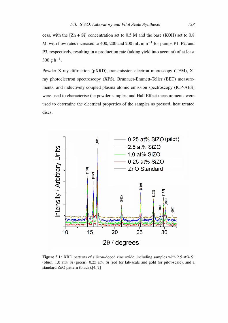
5.3. SiZO: Laboratory and Pilot Scale Synthesis 138
cess, with the [Zn + Si] concentration set to 0.5 M and the base (KOH) set to 0.8
M, with flow rates increased to 400, 200 and 200 mL min−1 for pumps P1, P2, and
P3, respectively, resulting in a production rate (taking yield into account) of at least
300 g h−1.
Powder X-ray diffraction (pXRD), transmission electron microscopy (TEM), X-
ray photoelectron spectroscopy (XPS), Brunauer-Emmett-Teller (BET) measure-
ments, and inductively coupled plasma atomic emission spectroscopy (ICP-AES)
were used to characterise the powder samples, and Hall Effect measurements were
used to determine the electrical properties of the samples as pressed, heat treated
discs.
Figure 5.1: XRD patterns of silicon-doped zinc oxide, including samples with 2.5 at% Si(blue), 1.0 at% Si (green), 0.25 at% Si (red for lab-scale and gold for pilot-scale), and astandard ZnO pattern (black).[4, 7]
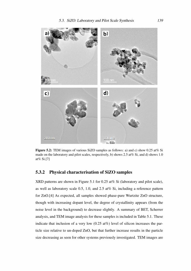
5.3. SiZO: Laboratory and Pilot Scale Synthesis 139
Figure 5.2: TEM images of various SiZO samples as follows: a) and c) show 0.25 at% Simade on the laboratory and pilot scales, respectively, b) shows 2.5 at% Si, and d) shows 1.0at% Si.[7]
5.3.2 Physical characterisation of SiZO samples
XRD patterns are shown in Figure 5.1 for 0.25 at% Si (laboratory and pilot scale),
as well as laboratory scale 0.5, 1.0, and 2.5 at% Si, including a reference pattern
for ZnO.[4] As expected, all samples showed phase-pure Wurtzite ZnO structure,
though with increasing dopant level, the degree of crystallinity appears (from the
noise level in the background) to decrease slightly. A summary of BET, Scherrer
analysis, and TEM image analysis for these samples is included in Table 5.1. These
indicate that inclusion of a very low (0.25 at%) level of silicon increases the par-
ticle size relative to un-doped ZnO, but that further increase results in the particle
size decreasing as seen for other systems previously investigated. TEM images are
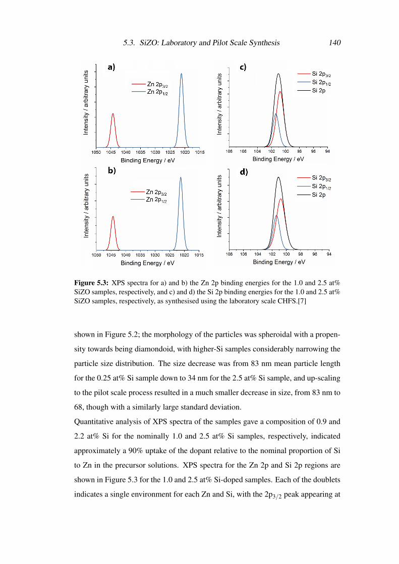
5.3. SiZO: Laboratory and Pilot Scale Synthesis 140
Figure 5.3: XPS spectra for a) and b) the Zn 2p binding energies for the 1.0 and 2.5 at%SiZO samples, respectively, and c) and d) the Si 2p binding energies for the 1.0 and 2.5 at%SiZO samples, respectively, as synthesised using the laboratory scale CHFS.[7]
shown in Figure 5.2; the morphology of the particles was spheroidal with a propen-
sity towards being diamondoid, with higher-Si samples considerably narrowing the
particle size distribution. The size decrease was from 83 nm mean particle length
for the 0.25 at% Si sample down to 34 nm for the 2.5 at% Si sample, and up-scaling
to the pilot scale process resulted in a much smaller decrease in size, from 83 nm to
68, though with a similarly large standard deviation.
Quantitative analysis of XPS spectra of the samples gave a composition of 0.9 and
2.2 at% Si for the nominally 1.0 and 2.5 at% Si samples, respectively, indicated
approximately a 90% uptake of the dopant relative to the nominal proportion of Si
to Zn in the precursor solutions. XPS spectra for the Zn 2p and Si 2p regions are
shown in Figure 5.3 for the 1.0 and 2.5 at% Si-doped samples. Each of the doublets
indicates a single environment for each Zn and Si, with the 2p3/2 peak appearing at
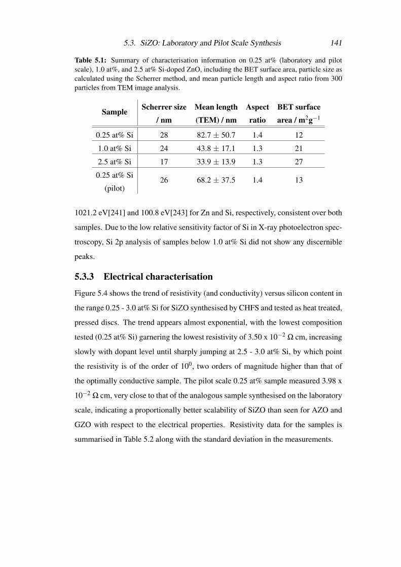
5.3. SiZO: Laboratory and Pilot Scale Synthesis 141
Table 5.1: Summary of characterisation information on 0.25 at% (laboratory and pilotscale), 1.0 at%, and 2.5 at% Si-doped ZnO, including the BET surface area, particle size ascalculated using the Scherrer method, and mean particle length and aspect ratio from 300particles from TEM image analysis.
Sample Scherrer size/ nm
Mean length(TEM) / nm
Aspectratio
BET surfacearea / m2g−1
0.25 at% Si 28 82.7 ± 50.7 1.4 12
1.0 at% Si 24 43.8 ± 17.1 1.3 21
2.5 at% Si 17 33.9 ± 13.9 1.3 27
0.25 at% Si
(pilot)26 68.2 ± 37.5 1.4 13
1021.2 eV[241] and 100.8 eV[243] for Zn and Si, respectively, consistent over both
samples. Due to the low relative sensitivity factor of Si in X-ray photoelectron spec-
troscopy, Si 2p analysis of samples below 1.0 at% Si did not show any discernible
peaks.
5.3.3 Electrical characterisation
Figure 5.4 shows the trend of resistivity (and conductivity) versus silicon content in
the range 0.25 - 3.0 at% Si for SiZO synthesised by CHFS and tested as heat treated,
pressed discs. The trend appears almost exponential, with the lowest composition
tested (0.25 at% Si) garnering the lowest resistivity of 3.50 x 10⁻² Ω cm, increasing
slowly with dopant level until sharply jumping at 2.5 - 3.0 at% Si, by which point
the resistivity is of the order of 100, two orders of magnitude higher than that of
the optimally conductive sample. The pilot scale 0.25 at% sample measured 3.98 x
10−2 Ω cm, very close to that of the analogous sample synthesised on the laboratory
scale, indicating a proportionally better scalability of SiZO than seen for AZO and
GZO with respect to the electrical properties. Resistivity data for the samples is
summarised in Table 5.2 along with the standard deviation in the measurements.
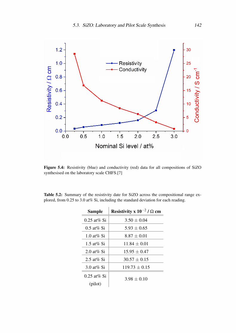
5.3. SiZO: Laboratory and Pilot Scale Synthesis 142
Figure 5.4: Resistivity (blue) and conductivity (red) data for all compositions of SiZOsynthesised on the laboratory scale CHFS.[7]
Table 5.2: Summary of the resistivity date for SiZO across the compositional range ex-plored, from 0.25 to 3.0 at% Si, including the standard deviation for each reading.
Sample Resistivity x 10−2 / Ω cm
0.25 at% Si 3.50 ± 0.04
0.5 at% Si 5.93 ± 0.65
1.0 at% Si 8.87 ± 0.01
1.5 at% Si 11.84 ± 0.01
2.0 at% Si 15.95 ± 0.47
2.5 at% Si 30.57 ± 0.15
3.0 at% Si 119.73 ± 0.15
0.25 at% Si
(pilot)3.98 ± 0.10
5.4. SiZO: Co-Doping Investigation 143
5.3.4 Conclusions
SiZO was synthesised by CHFS in the dopant range 0.25 to 3.0 at% Si. These
powders were tested for their resistivity by pressing into discs and subsequent heat
treatment, and from Hall Effect measurements the optimally conductive sample was
found to be the sample made with 0.25 at% Si, with a resistivity of 3.50 x 10⁻² Ω
cm. This was then synthesised again on the pilot scale process (> 300 g h−1), and
was found to retain the electrical properties well; this sample measured a resistivity
of 3.98 x 10⁻² Ω cm. Increase of the dopant level led to a decrease in particle size
and an increase in resistivity, and it was also seen that pilot scale synthesis resulted
in a slight decrease in particle size and increase in resistivity. There is no indication
as to whether the dopant level is directly and solely responsible for the increase in
resistivity, or whether particle size is also a significant factor, particularly at low
dopant levels where the small change in Si results in a dramatic change in particle
size. It is possible that the large particle size resulting from 0.25 at% Si benefits the
resistivity by means of reducing the grain boundary effects in the compacts.
5.4 SiZO: Co-Doping InvestigationThough SiZO was among the best materials screened in the experiments discussed
in Chapter 3, the optimally conductive sample (ρ = 3.5 x 10⁻² Ω cm) was still
considerably more resistive than the optimal samples of AZO (ρ = 7.0 x 10⁻³ Ω
cm), GZO (ρ = 9.1 x 10⁻³ Ω cm), or AGZO (ρ = 9.1 x 10⁻³ Ω cm), by around 4 - 5
times. Thus further experiments were planned to enhance the conductivity of SiZO
by co-doping with Al or Ga, SiAZO and SiGZO, respectively.
5.4.1 Experimental design
Synthesis was exactly as carried out previously on the laboratory scale CHFS pro-
cess for purely Si-doped ZnO. Si was once more introduced into the process with
the base feed via pump P3, and Al, Ga, and Zn in various ratios were introduced
via pump P2. The samples made were as follows (and as summarised in Table
5.3): 0.25 at% Si with 1.0, 1.5, 2.0, and 3.0 at% of either Al or Ga, and 0.5 at%
Si with 1.0, 2.0, and 3.0 at% of either Al or Ga; the remaining at% of each sample
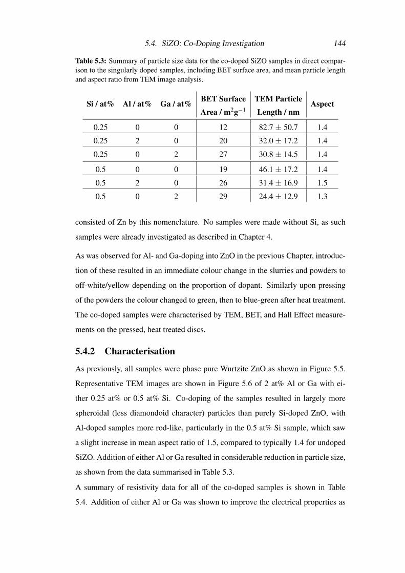
5.4. SiZO: Co-Doping Investigation 144
Table 5.3: Summary of particle size data for the co-doped SiZO samples in direct compar-ison to the singularly doped samples, including BET surface area, and mean particle lengthand aspect ratio from TEM image analysis.
Si / at% Al / at% Ga / at% BET SurfaceArea / m2g−1
TEM ParticleLength / nm
Aspect
0.25 0 0 12 82.7 ± 50.7 1.4
0.25 2 0 20 32.0 ± 17.2 1.4
0.25 0 2 27 30.8 ± 14.5 1.4
0.5 0 0 19 46.1 ± 17.2 1.4
0.5 2 0 26 31.4 ± 16.9 1.5
0.5 0 2 29 24.4 ± 12.9 1.3
consisted of Zn by this nomenclature. No samples were made without Si, as such
samples were already investigated as described in Chapter 4.
As was observed for Al- and Ga-doping into ZnO in the previous Chapter, introduc-
tion of these resulted in an immediate colour change in the slurries and powders to
off-white/yellow depending on the proportion of dopant. Similarly upon pressing
of the powders the colour changed to green, then to blue-green after heat treatment.
The co-doped samples were characterised by TEM, BET, and Hall Effect measure-
ments on the pressed, heat treated discs.
5.4.2 Characterisation
As previously, all samples were phase pure Wurtzite ZnO as shown in Figure 5.5.
Representative TEM images are shown in Figure 5.6 of 2 at% Al or Ga with ei-
ther 0.25 at% or 0.5 at% Si. Co-doping of the samples resulted in largely more
spheroidal (less diamondoid character) particles than purely Si-doped ZnO, with
Al-doped samples more rod-like, particularly in the 0.5 at% Si sample, which saw
a slight increase in mean aspect ratio of 1.5, compared to typically 1.4 for undoped
SiZO. Addition of either Al or Ga resulted in considerable reduction in particle size,
as shown from the data summarised in Table 5.3.
A summary of resistivity data for all of the co-doped samples is shown in Table
5.4. Addition of either Al or Ga was shown to improve the electrical properties as
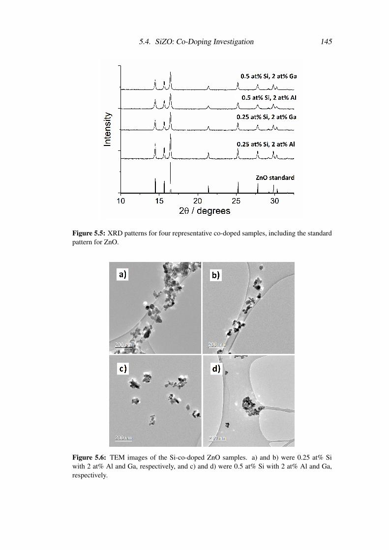
5.4. SiZO: Co-Doping Investigation 145
Figure 5.5: XRD patterns for four representative co-doped samples, including the standardpattern for ZnO.
Figure 5.6: TEM images of the Si-co-doped ZnO samples. a) and b) were 0.25 at% Siwith 2 at% Al and Ga, respectively, and c) and d) were 0.5 at% Si with 2 at% Al and Ga,respectively.
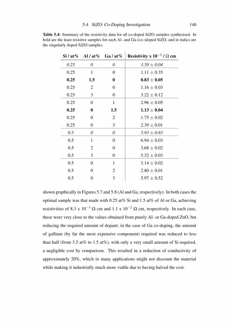
5.4. SiZO: Co-Doping Investigation 146
Table 5.4: Summary of the resistivity data for all co-doped SiZO samples synthesised. Inbold are the least resistive samples for each Al- and Ga-(co-)doped SiZO, and in italics arethe singularly doped SiZO samples.
Si / at% Al / at% Ga / at% Resistivity x 10−2 / Ω cm
0.25 0 0 3.50 ± 0.04
0.25 1 0 1.11 ± 0.35
0.25 1.5 0 0.83 ± 0.050.25 2 0 1.16 ± 0.03
0.25 3 0 3.22 ± 0.12
0.25 0 1 2.96 ± 0.05
0.25 0 1.5 1.13 ± 0.040.25 0 2 1.75 ± 0.02
0.25 0 3 2.39 ± 0.01
0.5 0 0 5.93 ± 0.65
0.5 1 0 6.94 ± 0.03
0.5 2 0 3.68 ± 0.02
0.5 3 0 5.32 ± 0.03
0.5 0 1 3.14 ± 0.02
0.5 0 2 2.80 ± 0.01
0.5 0 3 5.97 ± 0.52
shown graphically in Figures 5.7 and 5.8 (Al and Ga, respectively). In both cases the
optimal sample was that made with 0.25 at% Si and 1.5 at% of Al or Ga, achieving
resistivities of 8.3 x 10⁻³ Ω cm and 1.1 x 10⁻² Ω cm, respectively. In each case,
these were very close to the values obtained from purely Al- or Ga-doped ZnO, but
reducing the required amount of dopant; in the case of Ga co-doping, the amount
of gallium (by far the most expensive component) required was reduced to less
than half (from 3.5 at% to 1.5 at%), with only a very small amount of Si required,
a negligible cost by comparison. This resulted in a reduction of conductivity of
approximately 20%, which in many applications might not discount the material
while making it industrially much more viable due to having halved the cost.
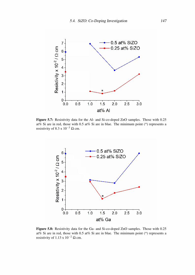
5.4. SiZO: Co-Doping Investigation 147
Figure 5.7: Resistivity data for the Al- and Si-co-doped ZnO samples. Those with 0.25at% Si are in red, those with 0.5 at% Si are in blue. The minimum point (*) represents aresistivity of 8.3 x 10⁻³ Ω cm.
Figure 5.8: Resistivity data for the Ga- and Si-co-doped ZnO samples. Those with 0.25at% Si are in red, those with 0.5 at% Si are in blue. The minimum point (*) represents aresistivity of 1.13 x 10⁻² Ω cm.
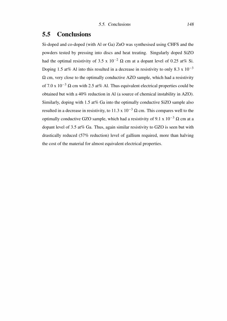
5.5. Conclusions 148
5.5 ConclusionsSi-doped and co-doped (with Al or Ga) ZnO was synthesised using CHFS and the
powders tested by pressing into discs and heat treating. Singularly doped SiZO
had the optimal resistivity of 3.5 x 10⁻² Ω cm at a dopant level of 0.25 at% Si.
Doping 1.5 at% Al into this resulted in a decrease in resistivity to only 8.3 x 10⁻³
Ω cm, very close to the optimally conductive AZO sample, which had a resistivity
of 7.0 x 10⁻³ Ω cm with 2.5 at% Al. Thus equivalent electrical properties could be
obtained but with a 40% reduction in Al (a source of chemical instability in AZO).
Similarly, doping with 1.5 at% Ga into the optimally conductive SiZO sample also
resulted in a decrease in resistivity, to 11.3 x 10⁻³ Ω cm. This compares well to the
optimally conductive GZO sample, which had a resistivity of 9.1 x 10⁻³ Ω cm at a
dopant level of 3.5 at% Ga. Thus, again similar resistivity to GZO is seen but with
drastically reduced (57% reduction) level of gallium required, more than halving
the cost of the material for almost equivalent electrical properties.
Chapter 6
Transparent Conducting Oxide
Nanoparticle Ink Formulation and
Deposition
6.1 Aims
The principal aim of this chapter is to investigate the deposition of Continuous
Hydrothermal Flow Synthesis (CHFS)-made transparent conducting oxide (TCO)
nanoparticles onto glass substrates in the form of thin films. This first involves
the investigation into the citrate-coating of the nanoparticles, ink formulation, and
finally the inkjet printing and spin coating of the optimised materials in order to
gauge the effect of depositing the nanoparticles on the optoelectronic properties of
the material.
6.2 Introduction
Deposition by inkjet printing would first involve the in-process surface modifica-
tion of the nanoparticles by inclusion of sodium citrate in the reactor quench feed,
coating the particles with citrate. Thus the loading optimisation of citrate is first
investigated onto ITO and AGZO (which will henceforth be referred to as cit:ITO
and cit:AGZO, respectively, when coated with citrate), followed by deposition by
inkjet printing and characterisation of the thin films by optical and electronic means.
6.2. Introduction 150
Additional deposition by spin coating is also investigated, followed by in-depth op-
toelectronic characterisation of the thin films, made from cit:ITO, GZO, AGZO,
and SiZO. This section outlines the relevant studies so far reported in literature of
the deposition of thin films of ITO and ZnO doped with Al, Ga, Al/Ga, and Si, for
direct comparison with the films deposited as part of this work, as well as outlin-
ing the theory behind surface functionalisation and zeta potential measurements of
nanoparticles.
6.2.1 Synthesis and properties of ITO as a TCO
Studies into the deposition of ITO by various methods have generated thin
films with resistivities of the order of 10−4 Ω cm, including magnetron
sputtering,[30, 31, 143, 282] spray deposition[25] and pyrolysis,[283, 284]
CVD,[149] dip coating,[285] and spin coating.[154] These films tended to have
very high charge carrier concentrations (> 1021 cm−3) and reasonable mobilities
(> 30 cm2 V−1 s−1), as summarised in Table 6.1, from the last five decades. Almost
untested is inkjet printing, the results of which have thus far disappointed in terms
of the resistivities, which have been considerably higher than more conventional
deposition techniques.[155, 286] That said, optically the inkjet printed films tend to
be superior, and inclusion of co-printed Ag grids can decrease the resistivity < 2 x
10−4 Ω cm, at a slight cost to the optical light transmittance (82 % vs. 87 %).[155]
ITO has been made in hydrothermal flow before,[169, 187] and a dopant optimisa-
tion investigation was recently carried out,[168] which reported the most conductive
CHFS-made ITO nanomaterials, 6.0 x 10⁻³ Ω cm as a pressed, heat treated pellet,
and spin-coated films of this un-coated material had resistivities ca. 1 x 10⁻² Ω
cm. However, ITO has not been surface-functionalised in-process and subsequently
printed. Lu et al. functionalised ITO nanoparticles with hexanoic acid for disper-
sion in hexane, however the only electrical testing by pressing a thin film indicated
resistivity ca. 8 Ω cm, but no printing or other deposition method took place.[169]
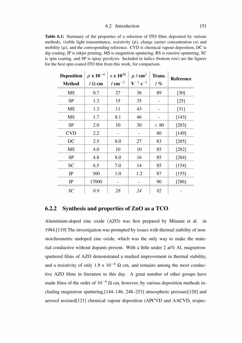
6.2. Introduction 151
Table 6.1: Summary of the properties of a selection of ITO films deposited by variousmethods, visible light transmittance, resistivity (ρ), charge carrier concentration (n) andmobility (µ), and the corresponding reference. CVD is chemical vapour deposition, DC isdip coating, IP is inkjet printing, MS is magnetron sputtering, RS is reactive sputtering, SCis spin coating, and SP is spray pyrolysis. Included in italics (bottom row) are the figuresfor the best spin coated ITO film from this work, for comparison.
DepositionMethod
ρ x 10−4
/ Ω cmn x 1020
/ cm−3
µ / cm2
V−1 s−1
Trans./ %
Reference
MS 0.7 27 36 89 [30]
SP 1.3 15 35 - [25]
MS 1.3 11 43 - [31]
MS 1.7 8.1 46 - [143]
SP 2.0 10 30 < 80 [283]
CVD 2.2 - - 80 [149]
DC 2.5 8.0 27 83 [285]
MS 4.0 10 10 85 [282]
SP 4.8 8.0 16 85 [284]
SC 6.5 7.0 14 85 [154]
IP 300 1.0 1.2 87 [155]
IP 17000 - - 90 [286]
SC 0.9 28 24 82 -
6.2.2 Synthesis and properties of ZnO as a TCO
Aluminium-doped zinc oxide (AZO) was first prepared by Minami et al. in
1984.[119] The investigation was prompted by issues with thermal stability of non-
stoichiometric undoped zinc oxide, which was the only way to make the mate-
rial conductive without dopants present. With a little under 2 at% Al, magnetron-
sputtered films of AZO demonstrated a marked improvement in thermal stability,
and a resistivity of only 1.9 x 10⁻⁴ Ω cm, and remains among the most conduc-
tive AZO films in literature to this day. A great number of other groups have
made films of the order of 10−4 Ω cm, however, by various deposition methods in-
cluding magnetron sputtering,[144–146, 248–253] atmospheric pressure[120] and
aerosol assisted[121] chemical vapour deposition (APCVD and AACVD, respec-
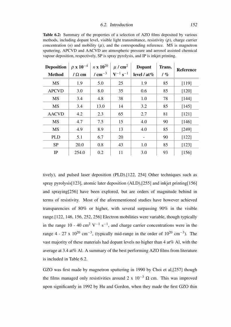
6.2. Introduction 152
Table 6.2: Summary of the properties of a selection of AZO films deposited by variousmethods, including dopant level, visible light transmittance, resistivity (ρ), charge carrierconcentration (n) and mobility (µ), and the corresponding reference. MS is magnetronsputtering, APCVD and AACVD are atmospheric pressure and aerosol assisted chemicalvapour deposition, respectively, SP is spray pyrolysis, and IP is inkjet printing.
DepositionMethod
ρ x 10−4
/ Ω cmn x 1020
/ cm−3
µ / cm2
V−1 s−1
Dopantlevel / at%
Trans./ %
Reference
MS 1.9 5.0 25 1.9 85 [119]
APCVD 3.0 8.0 35 0.6 85 [120]
MS 3.4 4.8 38 1.0 78 [144]
MS 3.4 13.0 14 3.2 85 [145]
AACVD 4.2 2.3 65 2.7 81 [121]
MS 4.7 7.5 15 4.0 90 [146]
MS 4.9 8.9 13 4.0 85 [249]
PLD 5.1 6.7 20 - 90 [122]
SP 20.0 0.8 43 1.0 85 [123]
IP 254.0 0.2 11 3.0 93 [156]
tively), and pulsed laser deposition (PLD).[122, 254] Other techniques such as
spray pyrolysis[123], atomic later deposition (ALD),[255] and inkjet printing[156]
and spraying[256] have been explored, but are orders of magnitude behind in
terms of resistivity. Most of the aforementioned studies have however achieved
transparencies of 80% or higher, with several surpassing 90% in the visible
range.[122, 146, 156, 252, 256] Electron mobilities were variable, though typically
in the range 10 - 40 cm2 V−1 s−1, and charge carrier concentrations were in the
range 4 - 27 x 1020 cm−3, (typically mid-range in the order of 1020 cm−3). The
vast majority of these materials had dopant levels no higher than 4 at% Al, with the
average at 3.4 at% Al. A summary of the best performing AZO films from literature
is included in Table 6.2.
GZO was first made by magnetron sputtering in 1990 by Choi et al,[257] though
the films managed only resistivities around 2 x 10⁻³ Ω cm. This was improved
upon significantly in 1992 by Hu and Gordon, when they made the first GZO thin
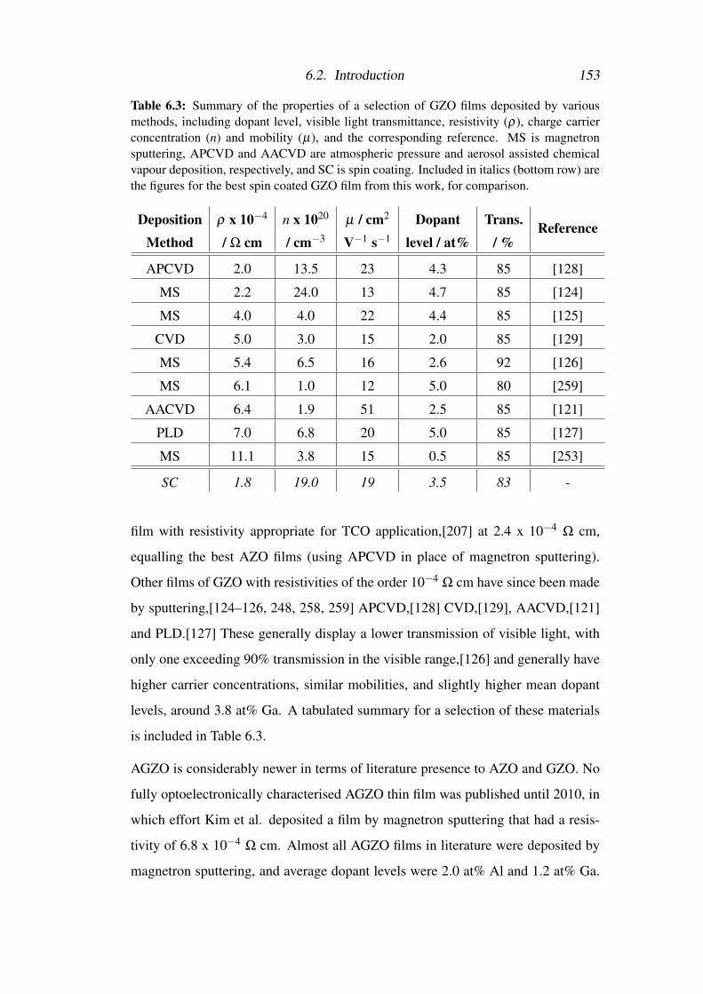
6.2. Introduction 153
Table 6.3: Summary of the properties of a selection of GZO films deposited by variousmethods, including dopant level, visible light transmittance, resistivity (ρ), charge carrierconcentration (n) and mobility (µ), and the corresponding reference. MS is magnetronsputtering, APCVD and AACVD are atmospheric pressure and aerosol assisted chemicalvapour deposition, respectively, and SC is spin coating. Included in italics (bottom row) arethe figures for the best spin coated GZO film from this work, for comparison.
DepositionMethod
ρ x 10−4
/ Ω cmn x 1020
/ cm−3
µ / cm2
V−1 s−1
Dopantlevel / at%
Trans./ %
Reference
APCVD 2.0 13.5 23 4.3 85 [128]
MS 2.2 24.0 13 4.7 85 [124]
MS 4.0 4.0 22 4.4 85 [125]
CVD 5.0 3.0 15 2.0 85 [129]
MS 5.4 6.5 16 2.6 92 [126]
MS 6.1 1.0 12 5.0 80 [259]
AACVD 6.4 1.9 51 2.5 85 [121]
PLD 7.0 6.8 20 5.0 85 [127]
MS 11.1 3.8 15 0.5 85 [253]
SC 1.8 19.0 19 3.5 83 -
film with resistivity appropriate for TCO application,[207] at 2.4 x 10⁻⁴ Ω cm,
equalling the best AZO films (using APCVD in place of magnetron sputtering).
Other films of GZO with resistivities of the order 10−4 Ω cm have since been made
by sputtering,[124–126, 248, 258, 259] APCVD,[128] CVD,[129], AACVD,[121]
and PLD.[127] These generally display a lower transmission of visible light, with
only one exceeding 90% transmission in the visible range,[126] and generally have
higher carrier concentrations, similar mobilities, and slightly higher mean dopant
levels, around 3.8 at% Ga. A tabulated summary for a selection of these materials
is included in Table 6.3.
AGZO is considerably newer in terms of literature presence to AZO and GZO. No
fully optoelectronically characterised AGZO thin film was published until 2010, in
which effort Kim et al. deposited a film by magnetron sputtering that had a resis-
tivity of 6.8 x 10⁻⁴ Ω cm. Almost all AGZO films in literature were deposited by
magnetron sputtering, and average dopant levels were 2.0 at% Al and 1.2 at% Ga.
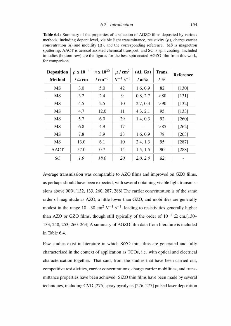
6.2. Introduction 154
Table 6.4: Summary of the properties of a selection of AGZO films deposited by variousmethods, including dopant level, visible light transmittance, resistivity (ρ), charge carrierconcentration (n) and mobility (µ), and the corresponding reference. MS is magnetronsputtering, AACT is aerosol assisted chemical transport, and SC is spin coating. Includedin italics (bottom row) are the figures for the best spin coated AGZO film from this work,for comparison.
DepositionMethod
ρ x 10−4
/ Ω cmn x 1020
/ cm−3
µ / cm2
V−1 s−1
(Al, Ga)/ at%
Trans./ %
Reference
MS 3.0 5.0 42 1.6, 0.9 82 [130]
MS 3.2 2.4 9 0.8, 2.7 <80 [131]
MS 4.5 2.5 10 2.7, 0.3 >90 [132]
MS 4.7 12.0 11 4.3, 2.1 95 [133]
MS 5.7 6.0 29 1.4, 0.3 92 [260]
MS 6.8 4.9 17 - >85 [262]
MS 7.8 3.9 23 1.6, 0.9 78 [263]
MS 13.0 6.1 10 2.4, 1.3 95 [287]
AACT 57.0 0.7 14 1.5, 1.5 90 [288]
SC 1.9 18.0 20 2.0, 2.0 82 -
Average transmission was comparable to AZO films and improved on GZO films,
as perhaps should have been expected, with several obtaining visible light transmis-
sions above 90%.[132, 133, 260, 287, 288] The carrier concentration is of the same
order of magnitude as AZO, a little lower than GZO, and mobilities are generally
modest in the range 10 - 30 cm2 V−1 s−1, leading to resistivities generally higher
than AZO or GZO films, though still typically of the order of 10−4 Ω cm.[130–
133, 248, 253, 260–263] A summary of AGZO film data from literature is included
in Table 6.4.
Few studies exist in literature in which SiZO thin films are generated and fully
characterised in the context of application as TCOs, i.e. with optical and electrical
characterisation together. That said, from the studies that have been carried out,
competitive resistivities, carrier concentrations, charge carrier mobilities, and trans-
mittance properties have been achieved. SiZO thin films have been made by several
techniques, including CVD,[275] spray pyrolysis,[276, 277] pulsed laser deposition
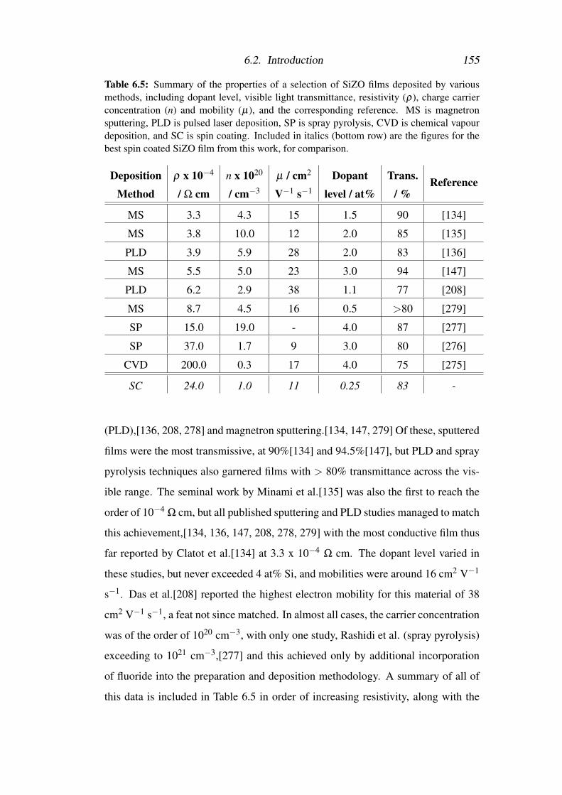
6.2. Introduction 155
Table 6.5: Summary of the properties of a selection of SiZO films deposited by variousmethods, including dopant level, visible light transmittance, resistivity (ρ), charge carrierconcentration (n) and mobility (µ), and the corresponding reference. MS is magnetronsputtering, PLD is pulsed laser deposition, SP is spray pyrolysis, CVD is chemical vapourdeposition, and SC is spin coating. Included in italics (bottom row) are the figures for thebest spin coated SiZO film from this work, for comparison.
DepositionMethod
ρ x 10−4
/ Ω cmn x 1020
/ cm−3
µ / cm2
V−1 s−1
Dopantlevel / at%
Trans./ %
Reference
MS 3.3 4.3 15 1.5 90 [134]
MS 3.8 10.0 12 2.0 85 [135]
PLD 3.9 5.9 28 2.0 83 [136]
MS 5.5 5.0 23 3.0 94 [147]
PLD 6.2 2.9 38 1.1 77 [208]
MS 8.7 4.5 16 0.5 >80 [279]
SP 15.0 19.0 - 4.0 87 [277]
SP 37.0 1.7 9 3.0 80 [276]
CVD 200.0 0.3 17 4.0 75 [275]
SC 24.0 1.0 11 0.25 83 -
(PLD),[136, 208, 278] and magnetron sputtering.[134, 147, 279] Of these, sputtered
films were the most transmissive, at 90%[134] and 94.5%[147], but PLD and spray
pyrolysis techniques also garnered films with > 80% transmittance across the vis-
ible range. The seminal work by Minami et al.[135] was also the first to reach the
order of 10−4 Ω cm, but all published sputtering and PLD studies managed to match
this achievement,[134, 136, 147, 208, 278, 279] with the most conductive film thus
far reported by Clatot et al.[134] at 3.3 x 10⁻⁴ Ω cm. The dopant level varied in
these studies, but never exceeded 4 at% Si, and mobilities were around 16 cm2 V−1
s−1. Das et al.[208] reported the highest electron mobility for this material of 38
cm2 V−1 s−1, a feat not since matched. In almost all cases, the carrier concentration
was of the order of 1020 cm−3, with only one study, Rashidi et al. (spray pyrolysis)
exceeding to 1021 cm−3,[277] and this achieved only by additional incorporation
of fluoride into the preparation and deposition methodology. A summary of all of
this data is included in Table 6.5 in order of increasing resistivity, along with the
6.2. Introduction 156
corresponding references for further reading.
All of these materials, AZO, GZO, AGZO, and SiZO, have demonstrated electrical
and optical properties rivalling (or at least nearing) those of ITO, not only from mag-
netron sputtering but from several other deposition techniques, to the extent that any
of them could be considered as viable replacement materials and worthy of study.
This is especially true with regards to using CHFS, as there are very few studies into
inkjet printing that show any promise at all (whether with ZnO-based materials, or
indeed with ITO itself); typically the films demonstrate excellent optical properties,
but with low conductivity.[155, 156, 256, 286] Surface functionalisation of these
materials for aid in formulation of inks would be a significant step towards replac-
ing the ubiquitous sputtering techniques currently in use, but there was first the need
to elucidate the optimal composition of the materials as made by CHFS, as they had
not before been synthesised by such a method before this research. Results of the
compositional optimisation are discussed in Chapters 4 (AZO, GZO, and AGZO)
and 5 (SiZO), while surface functionalisation and deposition results are discussed
further on in this chapter.
6.2.3 Surface functionalisation of nanoparticles using citrate
Efforts toward surface-functionalisation using various different capping agents
have been used in coating ceria,[289, 290] various iron oxides,[291–293]
silicon,[293] titanium,[294, 295] hafnium,[296] and zirconium dioxides,[297] and
gold nanoparticles,[298, 299] among others. The majority of these synthesis meth-
ods involve batch processes, but some are continuous, analogous to the method-
ologies employed in this research. This offers a benefit as coating particles can
be introduced at lower temperatures after the initial nucleation of the primary
product particles, without risk of organic capping agents thermally decompos-
ing at the elevated temperatures required to synthesise many of the materials in
question.[291, 300]
Citrate-coated nanoparticles are desirable in a number of applications, particu-
larly biomedical applications due to citrate’s inherent biocompatibility, for example
6.2. Introduction 157
functionalised magnetite nanoparticle synthesis for use in magnetic hyperther-
mia treatments.[291, 292] This has been demonstrated in hydrothermal flow,[300]
however the synthesis of surface-functionalised citrate-coated nanoparticles for ap-
plication as TCOs has yet to be investigated in literature, though there are a very few
articles on other surface modifiers used to disperse TCO nanoparticles including
ITO[169] and ZnO.[301]
Citrate was selected as the surface modifier in this instance because of the nature
of the desired ink ‘product’; the hypothetical ink was to be water-based, as was
the synthesis method. As such, the modifier had to be water soluble in reagent
form, and hydrophilic when coated onto nanoparticles. Citrate is naturally oc-
curring, inexpensive and has been shown to be effective in this pursuit for other
systems.[291, 294, 299, 300] Grafting density of the citrate molecules on the sur-
face of the functionalised nanoparticles can be calculated using Equation 6.1.
σ = M(4
3πr3)d(mCAmNP
)
MCA/4πr2 (6.1)
In this equation, σ is the grafting density in molecules per square nanometer (CA
nm−2), M is Avogadro’s Constant, and mCA/mNP is the ratio of solid mass ac-
counted for by the citrate (versus citrate and metal oxide nanoparticles), which is
determined from TGA analysis. MCA is the molecular weight of the capping agent
(192.12 g mol−1), d is the density of the metal oxide (assumed to be 7.14 g cm−3
for ITO and 5.61 g cm−3 for AGZO), and r is the mean radial length across the
three axes for each nanoparticle; thus 4πr3 represents an estimation of the volume
of each nanoparticle, which is more accurate the closer the particle is to a perfect
sphere. As grafting density is only to be calculated to 1 d.p., the approximation was
judged to be acceptable.
For the most part, citrate was used in the form of citric acid in previous reports,
however due to the pH sensitivity of ZnO-based materials (particularly at low
pH), sodium citrate was used in this study. Its structure is as shown in Figure
6.1. Each of the three (COO)− groups can be the point of adherence to the sur-
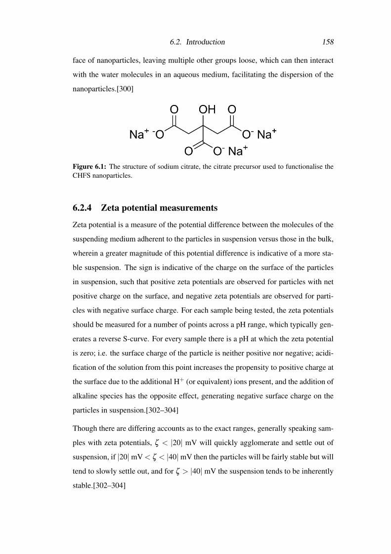
6.2. Introduction 158
face of nanoparticles, leaving multiple other groups loose, which can then interact
with the water molecules in an aqueous medium, facilitating the dispersion of the
nanoparticles.[300]
Figure 6.1: The structure of sodium citrate, the citrate precursor used to functionalise theCHFS nanoparticles.
6.2.4 Zeta potential measurements
Zeta potential is a measure of the potential difference between the molecules of the
suspending medium adherent to the particles in suspension versus those in the bulk,
wherein a greater magnitude of this potential difference is indicative of a more sta-
ble suspension. The sign is indicative of the charge on the surface of the particles
in suspension, such that positive zeta potentials are observed for particles with net
positive charge on the surface, and negative zeta potentials are observed for parti-
cles with negative surface charge. For each sample being tested, the zeta potentials
should be measured for a number of points across a pH range, which typically gen-
erates a reverse S-curve. For every sample there is a pH at which the zeta potential
is zero; i.e. the surface charge of the particle is neither positive nor negative; acidi-
fication of the solution from this point increases the propensity to positive charge at
the surface due to the additional H+ (or equivalent) ions present, and the addition of
alkaline species has the opposite effect, generating negative surface charge on the
particles in suspension.[302–304]
Though there are differing accounts as to the exact ranges, generally speaking sam-
ples with zeta potentials, ζ < |20| mV will quickly agglomerate and settle out of
suspension, if |20|mV < ζ < |40|mV then the particles will be fairly stable but will
tend to slowly settle out, and for ζ > |40| mV the suspension tends to be inherently
stable.[302–304]
6.3. Citrate-Coated Indium Tin Oxide 159
6.3 Citrate-Coated Indium Tin Oxide
This section investigates the coating of ITO with citrate as part of the CHFS pro-
cess, starting with the optimisation of citrate-loading and continuing with the char-
acterisation of the optimal material. Ink formulation and deposition are detailed in
following sections.
6.3.1 Experimental design
Dr P. Marchand et al. previously investigated the compositional optimisation of
ITO as synthesised by CHFS, finding that 10 at% Sn relative to 90 at% In gave
the lowest resistivity when pressed into a disc and heat treated, with ρ = 6.0 x
10−3 Ω cm. Formic acid was used in order to facilitate the formation of oxygen
vacancies in the ITO structure.[168, 169] This was included in the indium precursor
feed supplied by pump P2. Pump P3 contained the tin precursor and base (KOH),
and pump P1 provided the flow of supercritical water as in all previous syntheses.
Pump P4 contained aqueous sodium citrate solution at various concentrations, the
capping/surface-coating agent. Pumps P1, P2, P3, and P4 had flow rates of 80, 40,
40, and 160 mL min−1, respectively; the mixing temperature in the first mixer was
335 C, and the mixing temperature in the second mixer was 187 C, low enough
that the citrate ions would not begin to decompose. The indium concentration was
0.09 M, the tin concentration 0.01 M, the formic acid concentration 0.5 M, and the
KOH concentration 0.75 M. Citrate:metal ratios of 0, 0.33, 0.67, 1.0, 1.5, and 3.0
were used, the highest citrate concentration a two times excess of citrate versus the
metal concentration. Inclusion of citrate had an immediate and drastic effect on the
propensity of the slurries to settle out; washing with water and acetone was required
for all samples as per the outline in Section 2.2.5, with centrifugation steps up to 3
h per wash. Significant losses of sample during the cleaning steps resulted in final
yields of ca. 50 %, though this could have been mitigated by additional time on
the centrifuge or improved recovery. The samples were collected at a pH of 8, all a
similar colour, very pale blue, indicative of the formation of oxygen vacancies.[168]
6.3. Citrate-Coated Indium Tin Oxide 160
6.3.2 Citrate-loading onto ITO investigation
This section outlines the use of zeta potential measurements to gauge the optimal
amount of citrate in the ITO synthesis, with regards to the stability of the coated ma-
terial in aqueous dispersions. The primary method of sample analysis was dynamic
light scattering, by which method (see also Section 2.4.3) zeta potential curves were
extracted for each material. These are shown in Figure 6.2a, whereas Figure 6.2b
shows the comparisons of the different zeta potentials at pH 7 for each sample, the
goal being the greatest magnitude of zeta potential, signifying the most stable par-
ticles in neutral solution.
As can be seen from the figure, the zeta potential drops sharply on addition of any
citrate to the particles, reaching a minimum at a citrate:metal ratio of 1:1. Excess of
citrate causes the zeta potential at pH 7 to rise above -30 mV, reducing the effective-
ness of the citrate present in preventing agglomeration of the suspended particles.
This value of -39.7 mV is indicative of good stability in aqueous media, and it was
this material that saw its synthesis scaled up for further characterisation.
6.3.3 Further characterisation of optimal cit:ITO
This section discusses additional characterisation of the 1:1 cit:ITO material, includ-
ing pre- and post-heat treatment XRD and XPS. As can be seen from XRD in Figure
6.3, the as-synthesised cit:ITO is in fact for the most part InOOH, although some
In2O3 peaks can also be seen when compared to the reference pattern.[305, 306]
The InOOH phase disappeared entirely upon heat treatment of the as-made material
(5 h at 550 C under an Ar atmosphere), leaving phase pure ITO, consistent with
previous investigations in the UCL group.[168] This is further supported by XPS
as shown in Figure 6.4. The as-prepared material (Figure 6.4a, c, and e) shows
clearly two chemical environments for the metals (both In, show in 6.4a, and Sn, in
6.4c). These can be attributed to the oxyhydroxide and oxide phases for the larger
and smaller peaks, respectively. Upon heat treating, only a single environment for
each metal was observed, consistent with observations from XRD. The 3d5/2 peaks
of 444.9 eV and 486.8 eV for In and Sn, respectively, are consistent with expected
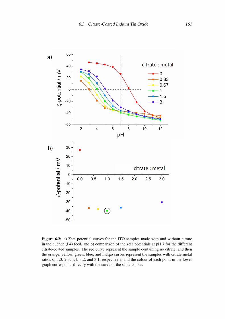
6.3. Citrate-Coated Indium Tin Oxide 161
Figure 6.2: a) Zeta potential curves for the ITO samples made with and without citratein the quench (P4) feed, and b) comparison of the zeta potentials at pH 7 for the differentcitrate-coated samples. The red curve represent the sample containing no citrate, and thenthe orange, yellow, green, blue, and indigo curves represent the samples with citrate:metalratios of 1:3, 2:3, 1:1, 3:2, and 3:1, respectively, and the colour of each point in the lowergraph corresponds directly with the curve of the same colour.
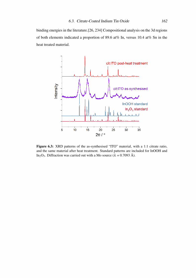
6.3. Citrate-Coated Indium Tin Oxide 162
binding energies in the literature.[26, 234] Compositional analysis on the 3d regions
of both elements indicated a proportion of 89.6 at% In, versus 10.4 at% Sn in the
heat treated material.
Figure 6.3: XRD patterns of the as-synthesised “ITO” material, with a 1:1 citrate ratio,and the same material after heat treatment. Standard patterns are included for InOOH andIn2O3. Diffraction was carried out with a Mo source (λ = 0.7093 A).
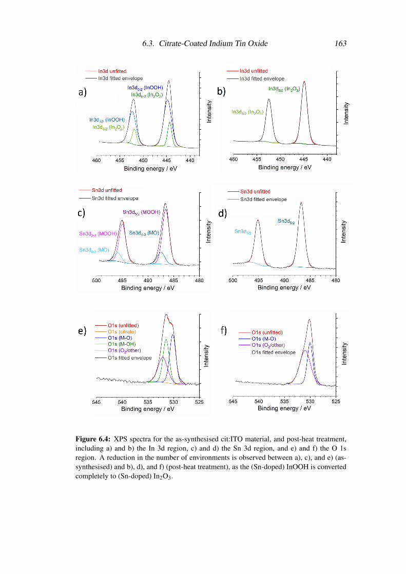
6.3. Citrate-Coated Indium Tin Oxide 163
Figure 6.4: XPS spectra for the as-synthesised cit:ITO material, and post-heat treatment,including a) and b) the In 3d region, c) and d) the Sn 3d region, and e) and f) the O 1sregion. A reduction in the number of environments is observed between a), c), and e) (as-synthesised) and b), d), and f) (post-heat treatment), as the (Sn-doped) InOOH is convertedcompletely to (Sn-doped) In2O3.
6.4. Citrate-coated AGZO 164
6.4 Citrate-coated AGZO
This section investigates the coating of ZnO doped with 2 at% Al and 2 at% Ga
(with respect to 96 at% Zn, hereafter referred to simply as “AGZO” in this Chapter)
with citrate as part of the CHFS process, starting with the optimisation of citrate-
loading and continuing with the characterisation of the optimal material. Ink for-
mulation and deposition is detailed in following sections.
6.4.1 Experimental design
The investigation into the compositional optimisation of Al and Ga co-doped ZnO
as synthesised by CHFS took place in 2016,[6, 307] and is detailed in Chapter 4.
Over the course of the investigation, three compositions were found to have resis-
tivities below 1 x 10⁻² Ω cm.[6] These were ZnO doped with (Al at%, Ga at%) of
(1.0, 2.0), (2.0, 2.0), and (3.0, 1.0). Of these, the greatest precision of the repeat
measurements was with 2 at% each of Al and Ga, the second lowest resistivity sam-
ple in the study (ρ = 9.3 x 10⁻³ Ω cm), and as such it was judged to be the best
candidate material for the citrate-optimisation study, being cheaper than GZO, and
more stable than AZO.
A 4-pump setup was used as described in Section 2.2.2. Pump P1 provided the
stream of supercritical water, P2 provided the metal precursors ([Zn + Al + Ga] =
0.3 M), P3 provided the base feed ([KOH] = 0.6 M), and P4 contained various con-
centrations of aqueous sodium citrate solution. Pumps P1, P2, P3, and P4 had flow
rates of 80, 40, 40, and 160 mL min−1, respectively; the mixing temperature in the
first mixer was 335 C, and the mixing temperature in the second mixer was 187 C.
As with the cit:ITO experiments, citrate:metal ratios of 0, 0.33, 0.67, 1.0, 1.5, and
3.0 were used, the highest citrate concentration a two times excess of citrate versus
the metal concentration. Similarly to the observations in the cit:ITO experiments,
inclusion of citrate had an immediate and drastic effect on the propensity of the slur-
ries to settle out; washing with water and acetone was required for all samples as
per the outline in Section 2.2.5, with centrifugation steps up to 1 h per wash; all of
the cit:AGZO samples settled more readily than the analogous cit:ITO samples had
6.4. Citrate-coated AGZO 165
previously. Yields were higher however, perhaps due in part to the ease of settling
of the material, and all samples were obtained in ca. 70% yield by mass.
6.4.2 Citrate-loading onto AGZO investigation
This section outlines the use of zeta potential measurements to gauge the optimal
amount of citrate in the ITO synthesis, with regards to the stability of the coated ma-
terial in aqueous dispersions. The primary method of sample analysis was dynamic
light scattering, by which method (see also Section 2.4.3) zeta potential curves were
extracted for each material. These are shown in Figure 6.5a, whereas Figure 6.5b
shows the comparisons of the different zeta potentials at pH 7 for each sample, the
goal being the greatest magnitude of zeta potential, signifying the most stable par-
ticles in neutral solution.
As can be seen from the figure, the zeta potential drops sharply on addition of any
citrate to the nanoparticle surfaces, reaching a minimum at a citrate:metal ratio of
1:1; however further increase in citrate concentration, differing from the effect ob-
served with cit:ITO, resulted in no change in the zeta potential at pH 7. Thus the
1:1 sample was judged to be the best sample (as it used the minimum amount of
citrate for the same result). Its zeta potential at pH 7 was -27.9 mV, indicative of
moderate stability, considerably worse than the -39.7 mV obtained for the analo-
gous cit:ITO sample. It should also be noted that the values were less predictable
for cit:AGZO; the curves exhibited less of the characteristic s-shape expected, and
less of a trend between samples could be identified. This could be due in part to the
inherent chemical instability of ZnO-based materials in lower pH environments; de-
rived count rate of the cit:AGZO samples dropped significantly by pH 3 (indicating
that the material had most likely started to dissolve), whereas the same effect was
not observed for cit:ITO until pH 2. Additionally, reduced efficiency and proclivity
of the citrate to bind to the surface could have had an effect.
A visual depiction of the effect of coating ITO with citrate is shown in Figure 6.6,
wherein as time passed (up to 3 h), the sample with no citrate settled completely,
and samples with increasing citrate loading settled out noticeably slower.
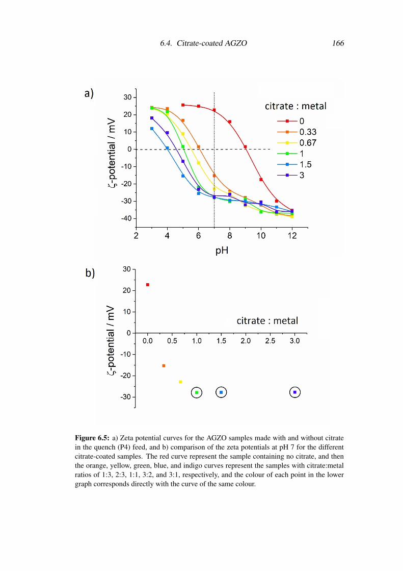
6.4. Citrate-coated AGZO 166
Figure 6.5: a) Zeta potential curves for the AGZO samples made with and without citratein the quench (P4) feed, and b) comparison of the zeta potentials at pH 7 for the differentcitrate-coated samples. The red curve represent the sample containing no citrate, and thenthe orange, yellow, green, blue, and indigo curves represent the samples with citrate:metalratios of 1:3, 2:3, 1:1, 3:2, and 3:1, respectively, and the colour of each point in the lowergraph corresponds directly with the curve of the same colour.
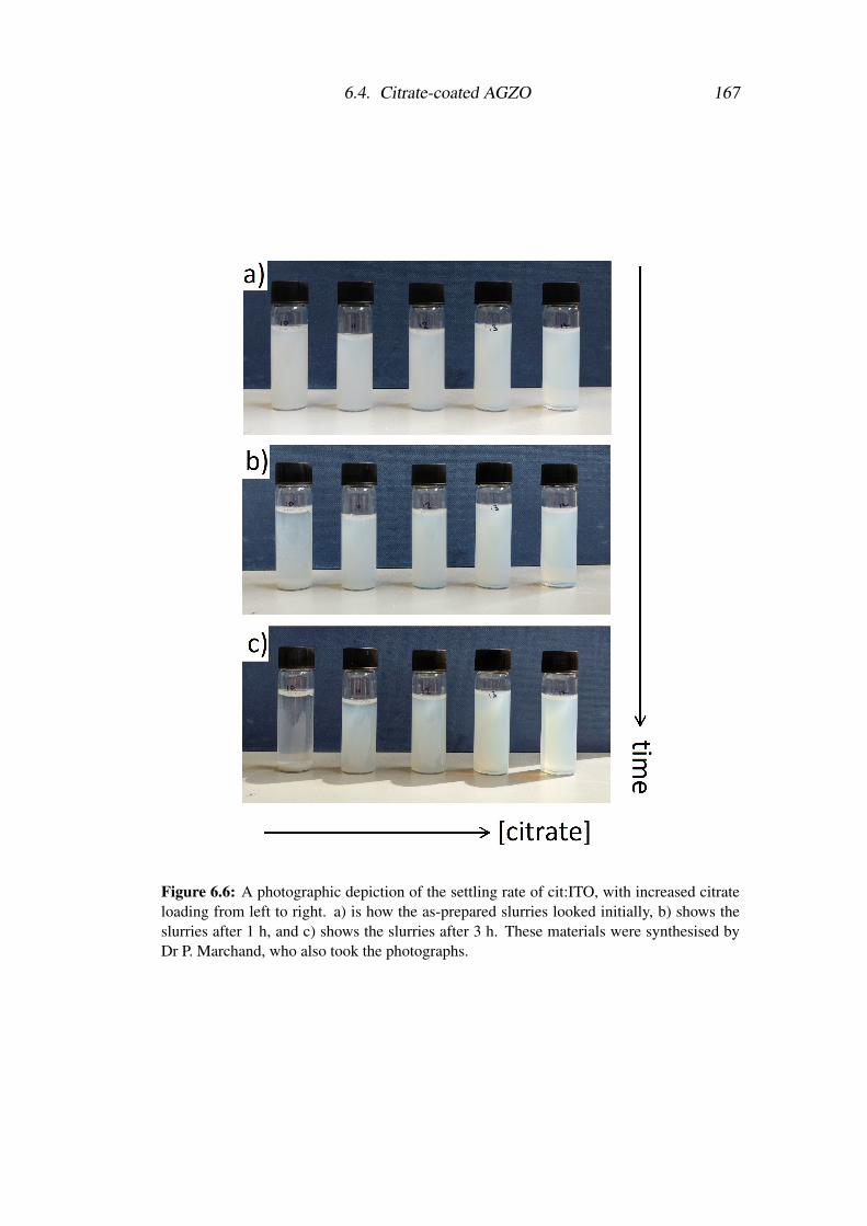
6.4. Citrate-coated AGZO 167
Figure 6.6: A photographic depiction of the settling rate of cit:ITO, with increased citrateloading from left to right. a) is how the as-prepared slurries looked initially, b) shows theslurries after 1 h, and c) shows the slurries after 3 h. These materials were synthesised byDr P. Marchand, who also took the photographs.
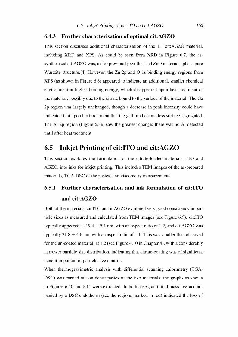
6.5. Inkjet Printing of cit:ITO and cit:AGZO 168
6.4.3 Further characterisation of optimal cit:AGZO
This section discusses additional characterisation of the 1:1 cit:AGZO material,
including XRD and XPS. As could be seen from XRD in Figure 6.7, the as-
synthesised cit:AGZO was, as for previously synthesised ZnO materials, phase pure
Wurtzite structure.[4] However, the Zn 2p and O 1s binding energy regions from
XPS (as shown in Figure 6.8) appeared to indicate an additional, smaller chemical
environment at higher binding energy, which disappeared upon heat treatment of
the material, possibly due to the citrate bound to the surface of the material. The Ga
2p region was largely unchanged, though a decrease in peak intensity could have
indicated that upon heat treatment that the gallium became less surface-segregated.
The Al 2p region (Figure 6.8e) saw the greatest change; there was no Al detected
until after heat treatment.
6.5 Inkjet Printing of cit:ITO and cit:AGZOThis section explores the formulation of the citrate-loaded materials, ITO and
AGZO, into inks for inkjet printing. This includes TEM images of the as-prepared
materials, TGA-DSC of the pastes, and viscometry measurements.
6.5.1 Further characterisation and ink formulation of cit:ITO
and cit:AGZO
Both of the materials, cit:ITO and it:AGZO exhibited very good consistency in par-
ticle sizes as measured and calculated from TEM images (see Figure 6.9). cit:ITO
typically appeared as 19.4 ± 5.1 nm, with an aspect ratio of 1.2, and cit:AGZO was
typically 21.8± 4.6 nm, with an aspect ratio of 1.1. This was smaller than observed
for the un-coated material, at 1.2 (see Figure 4.10 in Chapter 4), with a considerably
narrower particle size distribution, indicating that citrate-coating was of significant
benefit in pursuit of particle size control.
When thermogravimetric analysis with differential scanning calorimetry (TGA-
DSC) was carried out on dense pastes of the two materials, the graphs as shown
in Figures 6.10 and 6.11 were extracted. In both cases, an initial mass loss accom-
panied by a DSC endotherm (see the regions marked in red) indicated the loss of
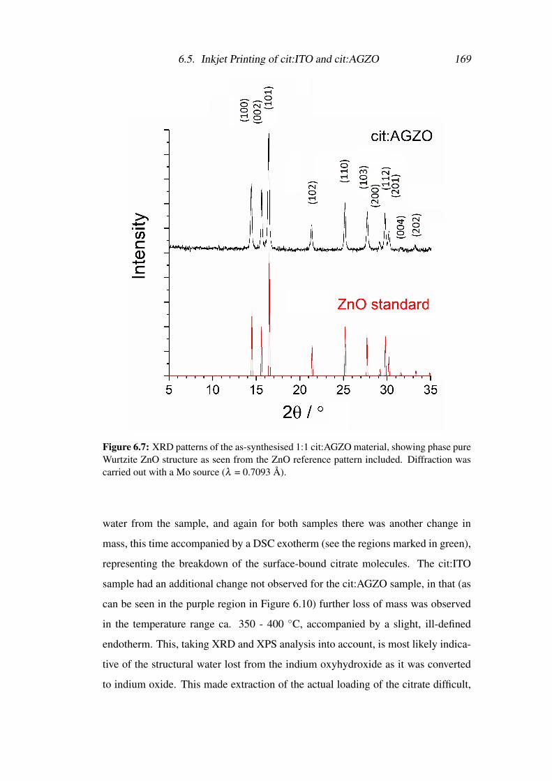
6.5. Inkjet Printing of cit:ITO and cit:AGZO 169
Figure 6.7: XRD patterns of the as-synthesised 1:1 cit:AGZO material, showing phase pureWurtzite ZnO structure as seen from the ZnO reference pattern included. Diffraction wascarried out with a Mo source (λ = 0.7093 A).
water from the sample, and again for both samples there was another change in
mass, this time accompanied by a DSC exotherm (see the regions marked in green),
representing the breakdown of the surface-bound citrate molecules. The cit:ITO
sample had an additional change not observed for the cit:AGZO sample, in that (as
can be seen in the purple region in Figure 6.10) further loss of mass was observed
in the temperature range ca. 350 - 400 C, accompanied by a slight, ill-defined
endotherm. This, taking XRD and XPS analysis into account, is most likely indica-
tive of the structural water lost from the indium oxyhydroxide as it was converted
to indium oxide. This made extraction of the actual loading of the citrate difficult,
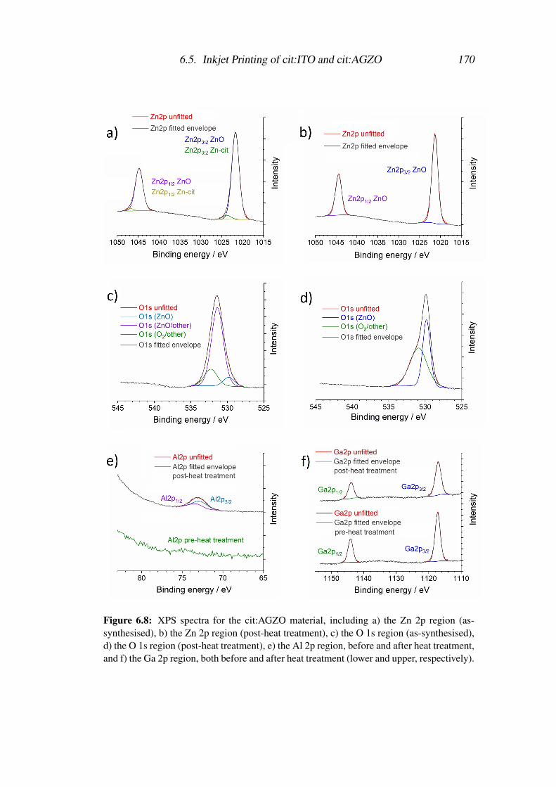
6.5. Inkjet Printing of cit:ITO and cit:AGZO 170
Figure 6.8: XPS spectra for the cit:AGZO material, including a) the Zn 2p region (as-synthesised), b) the Zn 2p region (post-heat treatment), c) the O 1s region (as-synthesised),d) the O 1s region (post-heat treatment), e) the Al 2p region, before and after heat treatment,and f) the Ga 2p region, both before and after heat treatment (lower and upper, respectively).
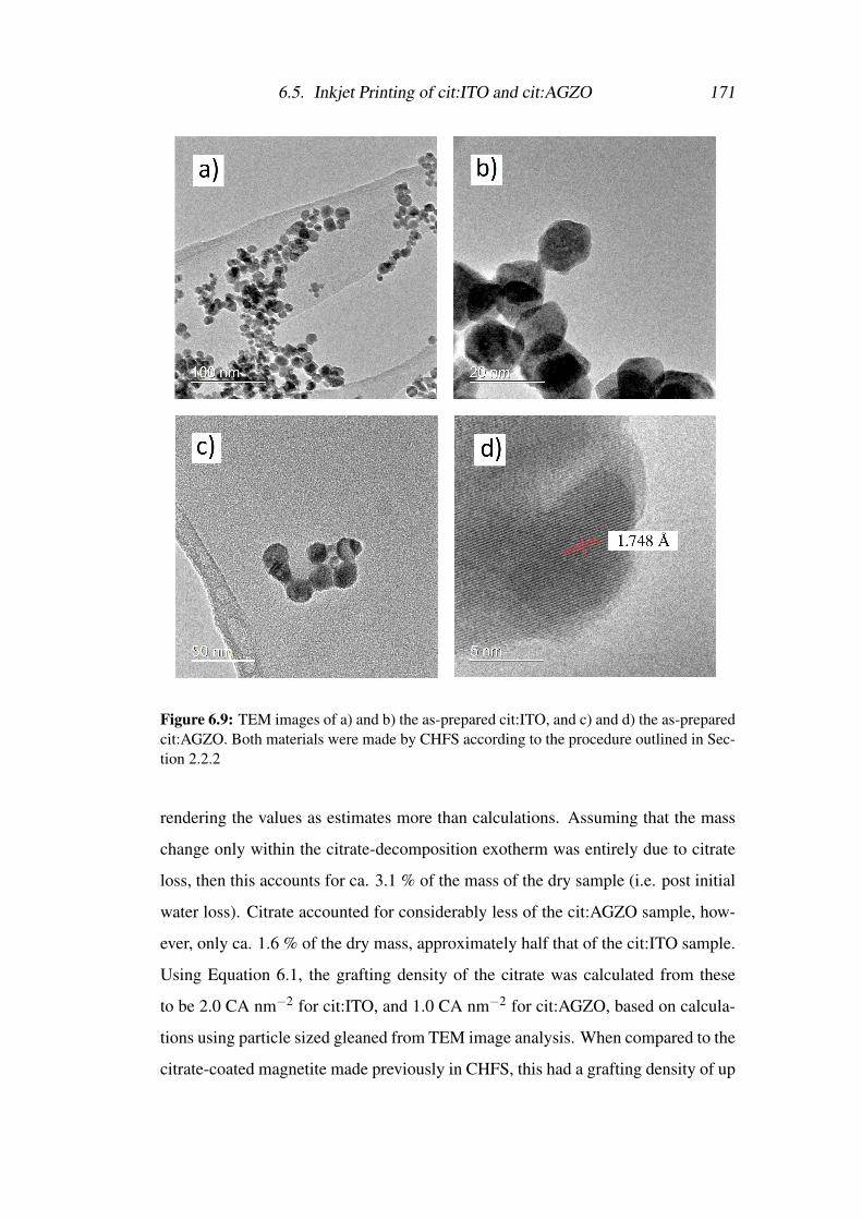
6.5. Inkjet Printing of cit:ITO and cit:AGZO 171
Figure 6.9: TEM images of a) and b) the as-prepared cit:ITO, and c) and d) the as-preparedcit:AGZO. Both materials were made by CHFS according to the procedure outlined in Sec-tion 2.2.2
rendering the values as estimates more than calculations. Assuming that the mass
change only within the citrate-decomposition exotherm was entirely due to citrate
loss, then this accounts for ca. 3.1 % of the mass of the dry sample (i.e. post initial
water loss). Citrate accounted for considerably less of the cit:AGZO sample, how-
ever, only ca. 1.6 % of the dry mass, approximately half that of the cit:ITO sample.
Using Equation 6.1, the grafting density of the citrate was calculated from these
to be 2.0 CA nm−2 for cit:ITO, and 1.0 CA nm−2 for cit:AGZO, based on calcula-
tions using particle sized gleaned from TEM image analysis. When compared to the
citrate-coated magnetite made previously in CHFS, this had a grafting density of up
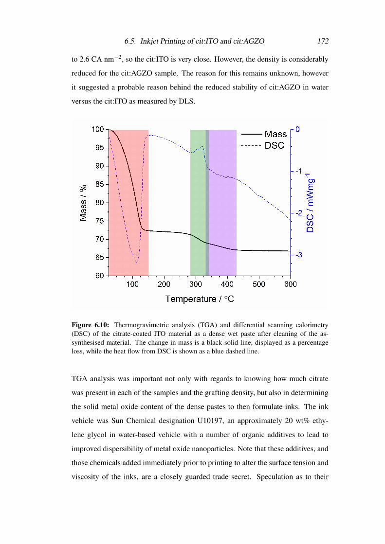
6.5. Inkjet Printing of cit:ITO and cit:AGZO 172
to 2.6 CA nm−2, so the cit:ITO is very close. However, the density is considerably
reduced for the cit:AGZO sample. The reason for this remains unknown, however
it suggested a probable reason behind the reduced stability of cit:AGZO in water
versus the cit:ITO as measured by DLS.
Figure 6.10: Thermogravimetric analysis (TGA) and differential scanning calorimetry(DSC) of the citrate-coated ITO material as a dense wet paste after cleaning of the as-synthesised material. The change in mass is a black solid line, displayed as a percentageloss, while the heat flow from DSC is shown as a blue dashed line.
TGA analysis was important not only with regards to knowing how much citrate
was present in each of the samples and the grafting density, but also in determining
the solid metal oxide content of the dense pastes to then formulate inks. The ink
vehicle was Sun Chemical designation U10197, an approximately 20 wt% ethy-
lene glycol in water-based vehicle with a number of organic additives to lead to
improved dispersibility of metal oxide nanoparticles. Note that these additives, and
those chemicals added immediately prior to printing to alter the surface tension and
viscosity of the inks, are a closely guarded trade secret. Speculation as to their
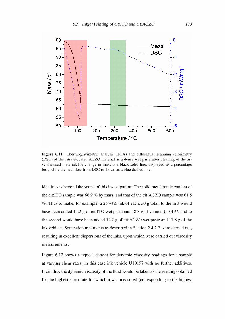
6.5. Inkjet Printing of cit:ITO and cit:AGZO 173
Figure 6.11: Thermogravimetric analysis (TGA) and differential scanning calorimetry(DSC) of the citrate-coated AGZO material as a dense wet paste after cleaning of the as-synthesised material.The change in mass is a black solid line, displayed as a percentageloss, while the heat flow from DSC is shown as a blue dashed line.
identities is beyond the scope of this investigation. The solid metal oxide content of
the cit:ITO sample was 66.9 % by mass, and that of the cit:AGZO sample was 61.5
%. Thus to make, for example, a 25 wt% ink of each, 30 g total, to the first would
have been added 11.2 g of cit:ITO wet paste and 18.8 g of vehicle U10197, and to
the second would have been added 12.2 g of cit:AGZO wet paste and 17.8 g of the
ink vehicle. Sonication treatments as described in Section 2.4.2.2 were carried out,
resulting in excellent dispersions of the inks, upon which were carried out viscosity
measurements.
Figure 6.12 shows a typical dataset for dynamic viscosity readings for a sample
at varying shear rates, in this case ink vehicle U10197 with no further additives.
From this, the dynamic viscosity of the fluid would be taken as the reading obtained
for the highest shear rate for which it was measured (corresponding to the highest
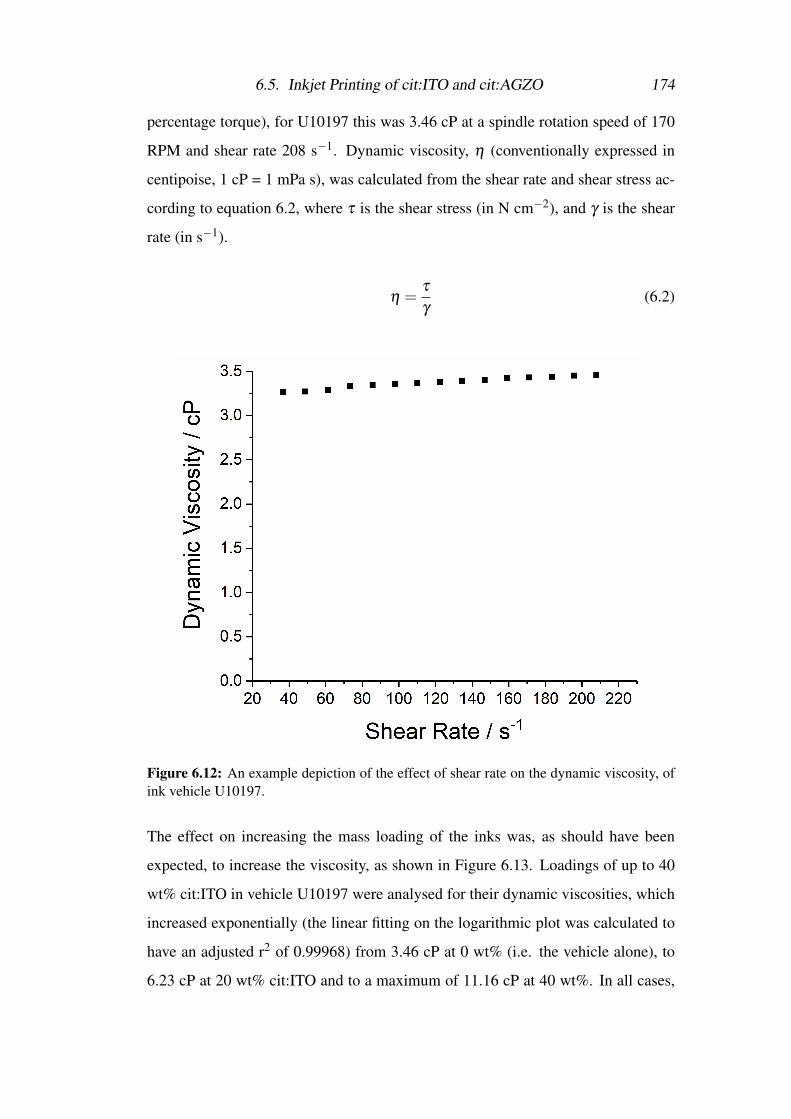
6.5. Inkjet Printing of cit:ITO and cit:AGZO 174
percentage torque), for U10197 this was 3.46 cP at a spindle rotation speed of 170
RPM and shear rate 208 s−1. Dynamic viscosity, η (conventionally expressed in
centipoise, 1 cP = 1 mPa s), was calculated from the shear rate and shear stress ac-
cording to equation 6.2, where τ is the shear stress (in N cm−2), and γ is the shear
rate (in s−1).
η =τ
γ(6.2)
Figure 6.12: An example depiction of the effect of shear rate on the dynamic viscosity, ofink vehicle U10197.
The effect on increasing the mass loading of the inks was, as should have been
expected, to increase the viscosity, as shown in Figure 6.13. Loadings of up to 40
wt% cit:ITO in vehicle U10197 were analysed for their dynamic viscosities, which
increased exponentially (the linear fitting on the logarithmic plot was calculated to
have an adjusted r2 of 0.99968) from 3.46 cP at 0 wt% (i.e. the vehicle alone), to
6.23 cP at 20 wt% cit:ITO and to a maximum of 11.16 cP at 40 wt%. In all cases,
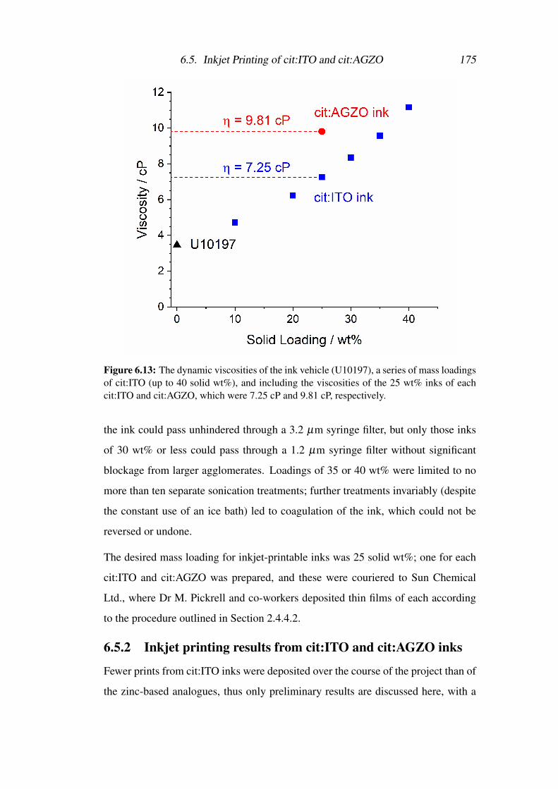
6.5. Inkjet Printing of cit:ITO and cit:AGZO 175
Figure 6.13: The dynamic viscosities of the ink vehicle (U10197), a series of mass loadingsof cit:ITO (up to 40 solid wt%), and including the viscosities of the 25 wt% inks of eachcit:ITO and cit:AGZO, which were 7.25 cP and 9.81 cP, respectively.
the ink could pass unhindered through a 3.2 µm syringe filter, but only those inks
of 30 wt% or less could pass through a 1.2 µm syringe filter without significant
blockage from larger agglomerates. Loadings of 35 or 40 wt% were limited to no
more than ten separate sonication treatments; further treatments invariably (despite
the constant use of an ice bath) led to coagulation of the ink, which could not be
reversed or undone.
The desired mass loading for inkjet-printable inks was 25 solid wt%; one for each
cit:ITO and cit:AGZO was prepared, and these were couriered to Sun Chemical
Ltd., where Dr M. Pickrell and co-workers deposited thin films of each according
to the procedure outlined in Section 2.4.4.2.
6.5.2 Inkjet printing results from cit:ITO and cit:AGZO inks
Fewer prints from cit:ITO inks were deposited over the course of the project than of
the zinc-based analogues, thus only preliminary results are discussed here, with a
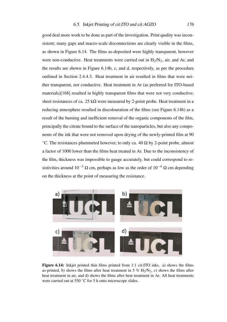
6.5. Inkjet Printing of cit:ITO and cit:AGZO 176
good deal more work to be done as part of the investigation. Print quality was incon-
sistent; many gaps and macro-scale disconnections are clearly visible in the films,
as shown in Figure 6.14. The films as-deposited were highly transparent, however
were non-conductive. Heat treatments were carried out in H2/N2, air, and Ar, and
the results are shown in Figure 6.14b, c, and d, respectively, as per the procedure
outlined in Section 2.4.4.3. Heat treatment in air resulted in films that were nei-
ther transparent, nor conductive. Heat treatment in Ar (as preferred for ITO-based
materials)[168] resulted in highly transparent films that were not very conductive;
sheet resistances of ca. 25 kΩ were measured by 2-point probe. Heat treatment in a
reducing atmosphere resulted in discolouration of the films (see Figure 6.14b) as a
result of the burning and inefficient removal of the organic components of the film,
principally the citrate bound to the surface of the nanoparticles, but also any compo-
nents of the ink that were not removed upon drying of the newly-printed film at 90C. The resistances plummeted however, to only ca. 40 Ω by 2-point probe, almost
a factor of 1000 lower than the films heat treated in Ar. Due to the inconsistency of
the film, thickness was impossible to gauge accurately, but could correspond to re-
sistivities around 10−3 Ω cm, perhaps as low as the order of 10−4 Ω cm depending
on the thickness at the point of measuring the resistance.
Figure 6.14: Inkjet printed thin films printed from 1:1 cit:ITO inks. a) shows the filmsas-printed, b) shows the films after heat treatment in 5 % H2/N2, c) shows the films afterheat treatment in air, and d) shows the films after heat treatment in Ar. All heat treatmentswere carried out at 550 C for 5 h onto microscope slides.
6.5. Inkjet Printing of cit:ITO and cit:AGZO 177
Even if the resistivity of the films were to be towards the upper end of the window
suggested above, these would still be the most conductive TCO thin films yet de-
posited by inkjet printing. Further depositions are necessary, and re-formulation of
the inks so as to better wet the surface of the glass substrate; this could result in
improved, more consistent coverage. An area of relatively even coverage is shown
in Figure 6.16 (a and b) of the film shown in Figure 6.14b. In this region, the sur-
face is relatively smooth and featureless, the majority of features can only be seen
at X50,000 magnification, but particulates are not easily distinguishable. Return-
ing to the characterisation of the ITO nanoparticles, the relatively un-crystalline
(Sn-doped) InOOH appeared to have been annealed especially effectively, forming
crystalline ITO with few micro-defects and imperfections in the film, resulting in
high conductivity.
Figure 6.15 shows 2 typical inkjet printed films made from cit:AGZO. The as-
printed film is non-conductive and has an optical transparency of 80 %. Upon heat
treating in a reducing atmosphere (5 % H2/N2), the film does not change very much
by eye; the transmittance rises to 84 % however, and the film becomes conductive.
The lowest resistivities measured for inkjet printed AGZO films are of the order of
10−1 Ω cm, considerably higher even than the pressed discs of the material. Deposi-
tion of the inks, whether due in part to one or more component of the ink interacting
with the ZnO-based nanoparticles, or to the parameters with which the depositions
were carried out, did not result in the same conductivity as was seen even in unopti-
mised inkjet printed ITO. Figure 16 (c and d) shows SEM images of the cit:AGZO
film post-heat treatment. More distinct particles were clearly visible than in the
ITO analogue, and the surface appeared rougher with cracks and particles. Most
notably, many long rodlike needles were visible, up to microns in length, which
were not seen at all in TEM images of the nanoparticles after synthesis. Sinter-
ing growth appeared to have been preferentially oriented, along the c-axis, possibly
accounting in part for a less effective annealing step, and thus a less (electrically)
well-connected film and higher resistivity.
Side-on SEM imaging was carried out by Dr P. Marchand on several ZnO-based
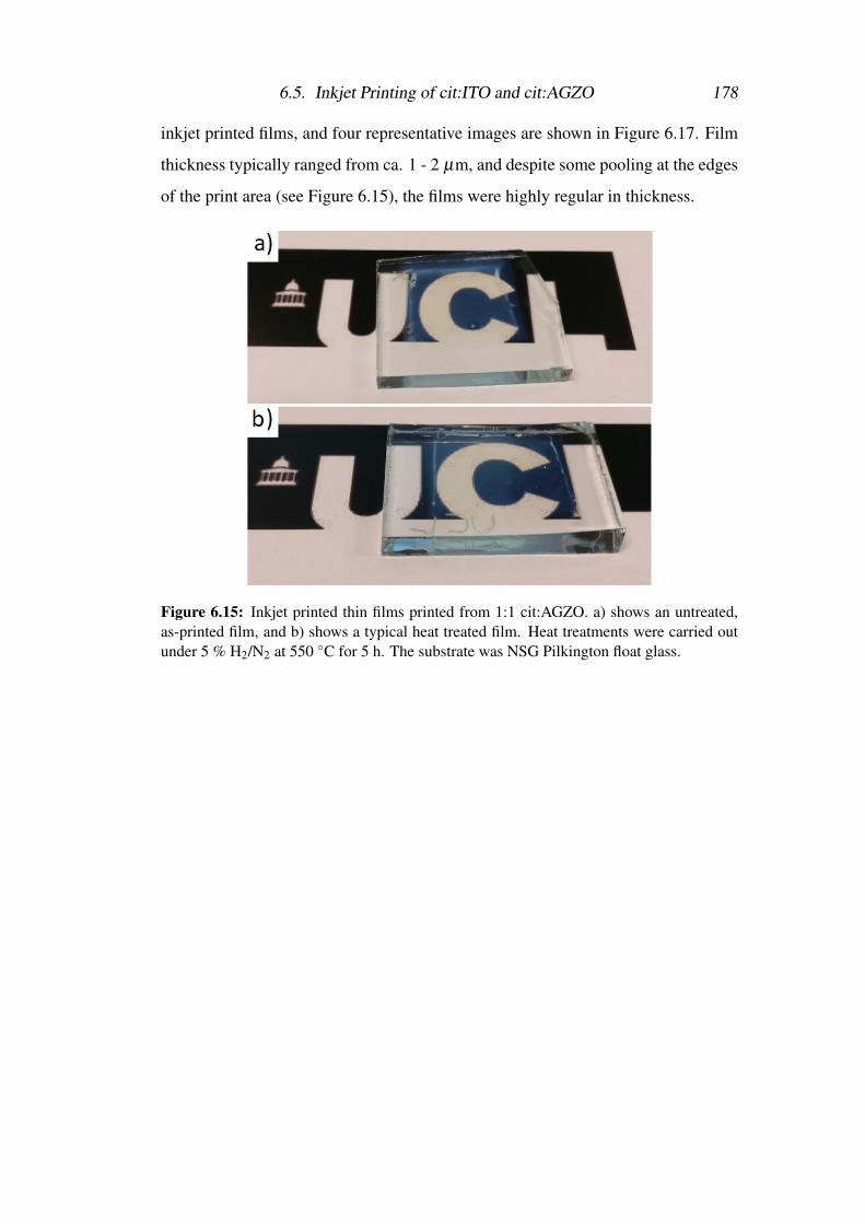
6.5. Inkjet Printing of cit:ITO and cit:AGZO 178
inkjet printed films, and four representative images are shown in Figure 6.17. Film
thickness typically ranged from ca. 1 - 2 µm, and despite some pooling at the edges
of the print area (see Figure 6.15), the films were highly regular in thickness.
Figure 6.15: Inkjet printed thin films printed from 1:1 cit:AGZO. a) shows an untreated,as-printed film, and b) shows a typical heat treated film. Heat treatments were carried outunder 5 % H2/N2 at 550 C for 5 h. The substrate was NSG Pilkington float glass.
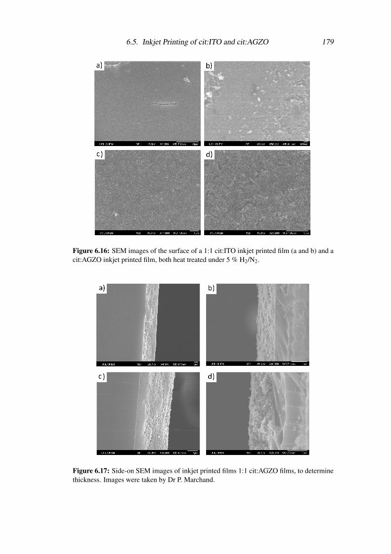
6.5. Inkjet Printing of cit:ITO and cit:AGZO 179
Figure 6.16: SEM images of the surface of a 1:1 cit:ITO inkjet printed film (a and b) and acit:AGZO inkjet printed film, both heat treated under 5 % H2/N2.
Figure 6.17: Side-on SEM images of inkjet printed films 1:1 cit:AGZO films, to determinethickness. Images were taken by Dr P. Marchand.
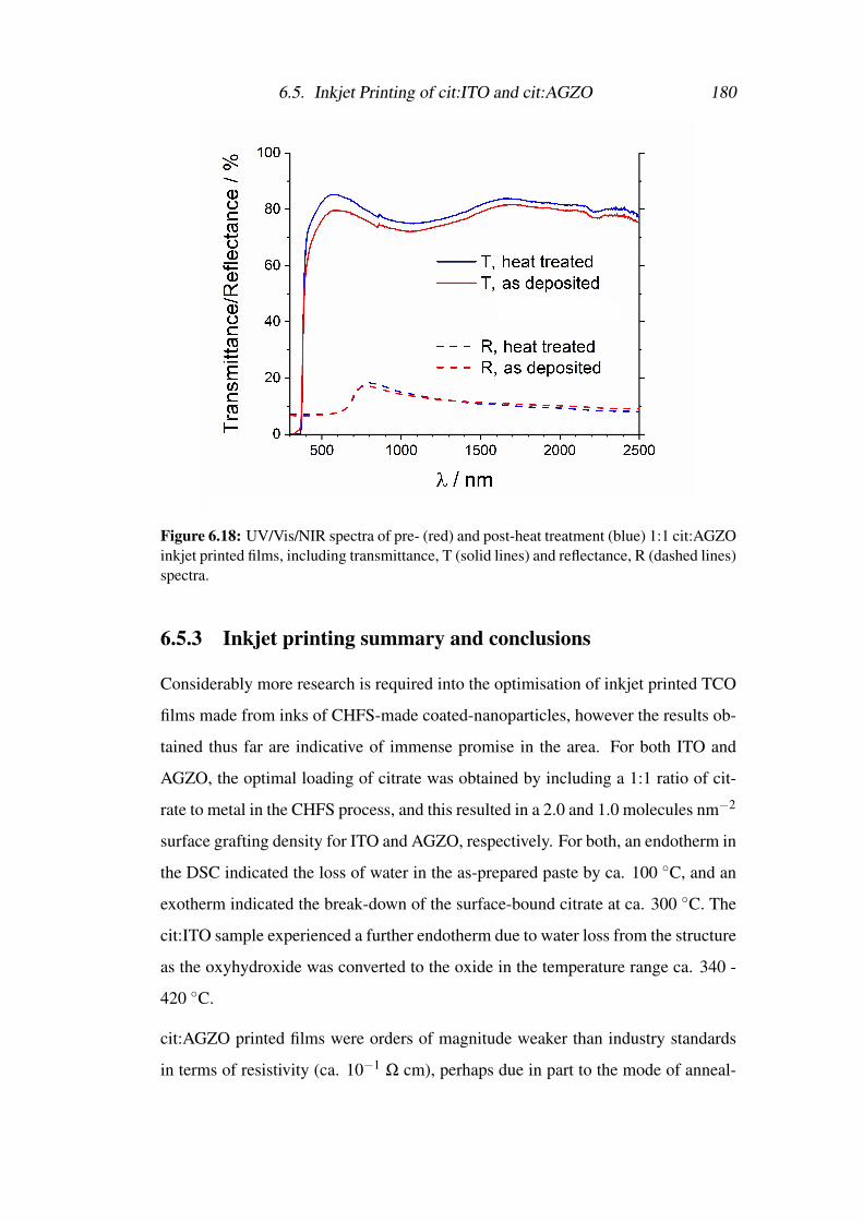
6.5. Inkjet Printing of cit:ITO and cit:AGZO 180
Figure 6.18: UV/Vis/NIR spectra of pre- (red) and post-heat treatment (blue) 1:1 cit:AGZOinkjet printed films, including transmittance, T (solid lines) and reflectance, R (dashed lines)spectra.
6.5.3 Inkjet printing summary and conclusions
Considerably more research is required into the optimisation of inkjet printed TCO
films made from inks of CHFS-made coated-nanoparticles, however the results ob-
tained thus far are indicative of immense promise in the area. For both ITO and
AGZO, the optimal loading of citrate was obtained by including a 1:1 ratio of cit-
rate to metal in the CHFS process, and this resulted in a 2.0 and 1.0 molecules nm−2
surface grafting density for ITO and AGZO, respectively. For both, an endotherm in
the DSC indicated the loss of water in the as-prepared paste by ca. 100 C, and an
exotherm indicated the break-down of the surface-bound citrate at ca. 300 C. The
cit:ITO sample experienced a further endotherm due to water loss from the structure
as the oxyhydroxide was converted to the oxide in the temperature range ca. 340 -
420 C.
cit:AGZO printed films were orders of magnitude weaker than industry standards
in terms of resistivity (ca. 10−1 Ω cm), perhaps due in part to the mode of anneal-
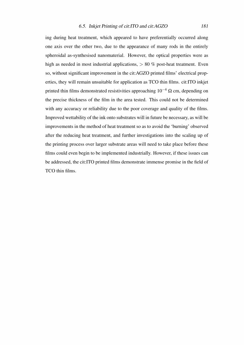
6.5. Inkjet Printing of cit:ITO and cit:AGZO 181
ing during heat treatment, which appeared to have preferentially occurred along
one axis over the other two, due to the appearance of many rods in the entirely
spheroidal as-synthesised nanomaterial. However, the optical properties were as
high as needed in most industrial applications, > 80 % post-heat treatment. Even
so, without significant improvement in the cit:AGZO printed films’ electrical prop-
erties, they will remain unsuitable for application as TCO thin films. cit:ITO inkjet
printed thin films demonstrated resistivities approaching 10−4 Ω cm, depending on
the precise thickness of the film in the area tested. This could not be determined
with any accuracy or reliability due to the poor coverage and quality of the films.
Improved wettability of the ink onto substrates will in future be necessary, as will be
improvements in the method of heat treatment so as to avoid the ‘burning’ observed
after the reducing heat treatment, and further investigations into the scaling up of
the printing process over larger substrate areas will need to take place before these
films could even begin to be implemented industrially. However, if these issues can
be addressed, the cit:ITO printed films demonstrate immense promise in the field of
TCO thin films.
6.6. Spin Coating of CHFS Nanomaterials 182
6.6 Spin Coating of CHFS NanomaterialsThis section investigates the deposition of thin films of CHFS-made nanomaterials
by spin coating, including cit:ITO, GZO, AGZO, and SiZO. A considerable amount
of work was carried out by N. Kuye in the testing of different dispersing media,
and by Dr P. Marchand before her. Some credit is due to both of them in the work
subsequently described.
6.6.1 Experimental design and observations
The thin films herein characterised were deposited from dispersions made from
20 wt% cit:ITO, GZO, AGZO, and SiZO in Sun Chemical ink vehicle U10197,
dispersed and deposited as described in Section 2.2. Heat treatment of all films was
carried out for 5 h at 550 C, ITO under argon, and ZnO-based materials under 5 %
H2/N2.
6.6.2 Spin coated films; SEM and optical measurements
Figures 6.19 and 6.20 show SEM images of the spin coated cit:ITO and ZnO-based
materials, respectively. Figure 6.19 also includes three representative side-on SEM
images, which were used to confirm film thickness as calculated from ellipsometry.
As can be seen from the cit:ITO film, it is very similar aesthetically to the inkjet
printed film as shown in Figure 6.16. Where it differs significantly is in the thick-
ness. Ellipsometry indicated a thickness of just 90 nm, and this was confirmed from
side-on SEM; some regions were slightly thicker, approaching ca. 1 µm, and some
were thinner, of the order of a few 10’s of nm, however the mean thickness was ap-
proximately 100 nm (Figure 6.19c), thus the optical thickness measurements were
taken to be accurate for the resistivity measurements and calculations.
The SiZO film was relatively featureless, a smooth film with some small particulate
lumps and extrusions as shown from Figure 6.20f. Curiously, the GZO and AGZO
films were for the most part smoother still, with much more minor extrusions, but
particles were visible of similar size to those of the SiZO. Morphologically, the
difference was drastic between the spin-coated AGZO film, and the inkjet printed
cit:AGZO film, which should both have annealed similarly, however in the AGZO
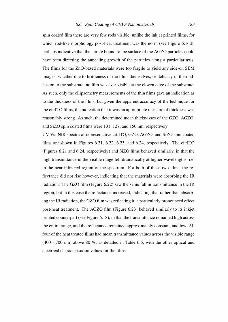
6.6. Spin Coating of CHFS Nanomaterials 183
spin coated film there are very few rods visible, unlike the inkjet printed films, for
which rod-like morphology post-heat treatment was the norm (see Figure 6.16d),
perhaps indicative that the citrate bound to the surface of the AGZO particles could
have been directing the annealing growth of the particles along a particular axis.
The films for the ZnO-based materials were too fragile to yield any side-on SEM
images; whether due to brittleness of the films themselves, or delicacy in their ad-
hesion to the substrate, no film was ever visible at the cloven edge of the substrate.
As such, only the ellipsometry measurements of the thin films gave an indication as
to the thickness of the films, but given the apparent accuracy of the technique for
the cit:ITO films, the indication that it was an appropriate measure of thickness was
reasonably strong. As such, the determined mean thicknesses of the GZO, AGZO,
and SiZO spin coated films were 131, 127, and 150 nm, respectively.
UV-Vis-NIR spectra of representative cit:ITO, GZO, AGZO, and SiZO spin coated
films are shown in Figures 6.21, 6.22, 6.23, and 6.24, respectively. The cit:ITO
(Figures 6.21 and 6.24, respectively) and SiZO films behaved similarly, in that the
high transmittance in the visible range fell dramatically at higher wavelengths, i.e.
in the near infra-red region of the spectrum. For both of these two films, the re-
flectance did not rise however, indicating that the materials were absorbing the IR
radiation. The GZO film (Figure 6.22) saw the same fall in transmittance in the IR
region, but in this case the reflectance increased, indicating that rather than absorb-
ing the IR radiation, the GZO film was reflecting it, a particularly pronounced effect
post-heat treatment. The AGZO film (Figure 6.23) behaved similarly to its inkjet
printed counterpart (see Figure 6.18), in that the transmittance remained high across
the entire range, and the reflectance remained approximately constant, and low. All
four of the heat treated films had mean transmittance values across the visible range
(400 - 700 nm) above 80 %, as detailed in Table 6.6, with the other optical and
electrical characterisation values for the films.
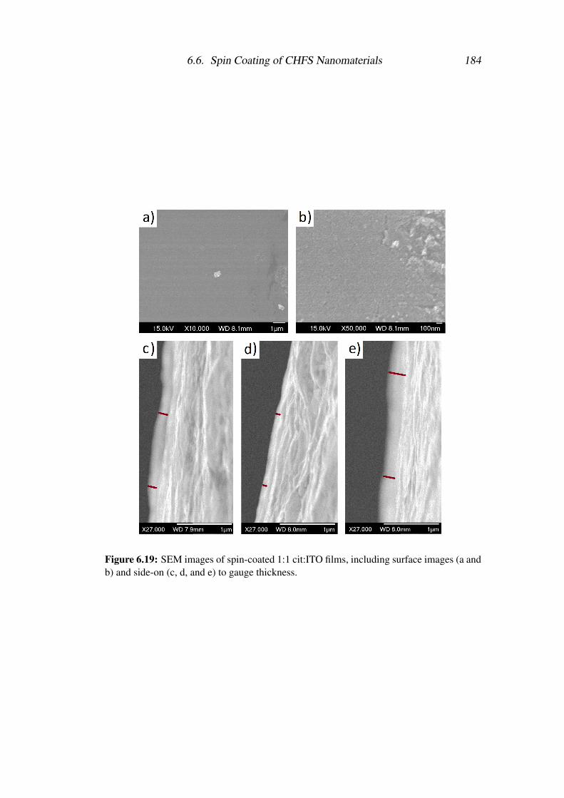
6.6. Spin Coating of CHFS Nanomaterials 184
Figure 6.19: SEM images of spin-coated 1:1 cit:ITO films, including surface images (a andb) and side-on (c, d, and e) to gauge thickness.
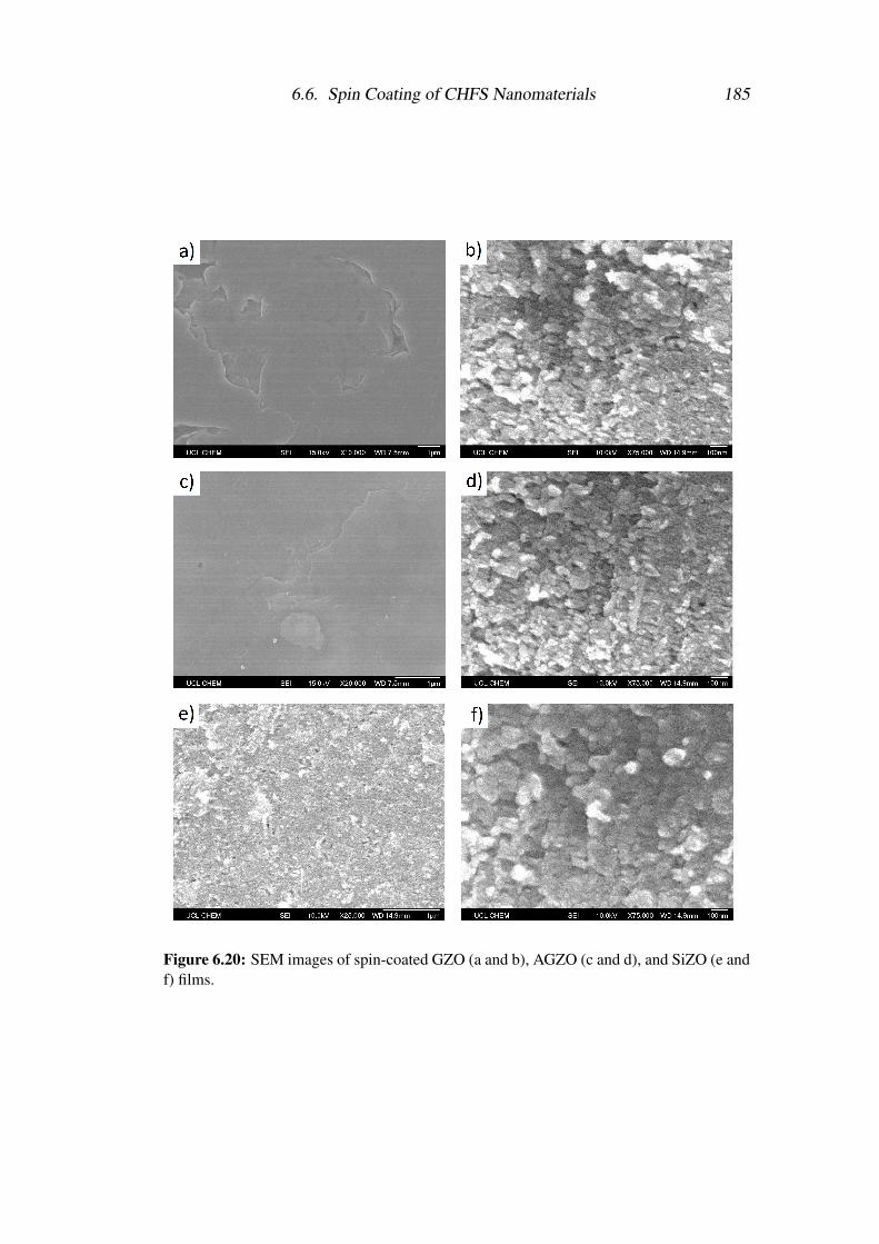
6.6. Spin Coating of CHFS Nanomaterials 185
Figure 6.20: SEM images of spin-coated GZO (a and b), AGZO (c and d), and SiZO (e andf) films.
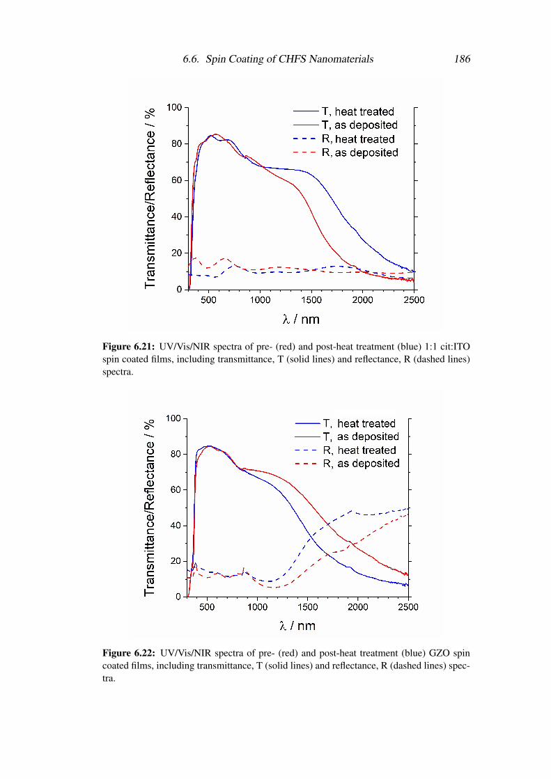
6.6. Spin Coating of CHFS Nanomaterials 186
Figure 6.21: UV/Vis/NIR spectra of pre- (red) and post-heat treatment (blue) 1:1 cit:ITOspin coated films, including transmittance, T (solid lines) and reflectance, R (dashed lines)spectra.
Figure 6.22: UV/Vis/NIR spectra of pre- (red) and post-heat treatment (blue) GZO spincoated films, including transmittance, T (solid lines) and reflectance, R (dashed lines) spec-tra.
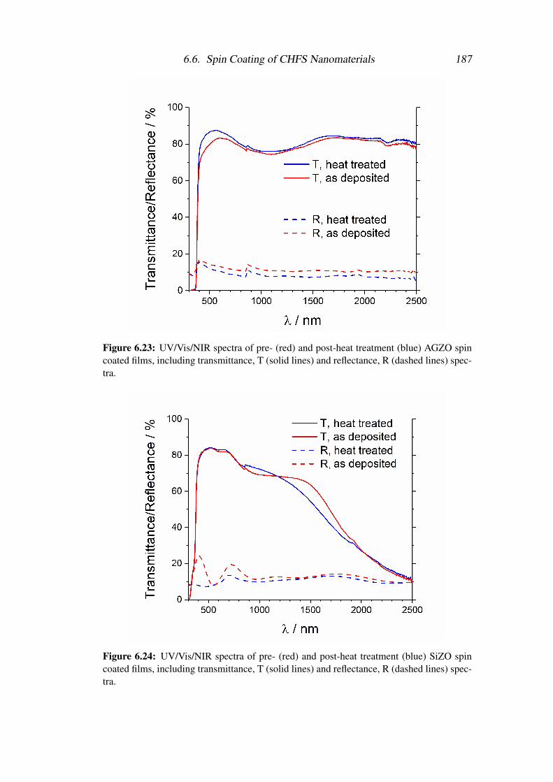
6.6. Spin Coating of CHFS Nanomaterials 187
Figure 6.23: UV/Vis/NIR spectra of pre- (red) and post-heat treatment (blue) AGZO spincoated films, including transmittance, T (solid lines) and reflectance, R (dashed lines) spec-tra.
Figure 6.24: UV/Vis/NIR spectra of pre- (red) and post-heat treatment (blue) SiZO spincoated films, including transmittance, T (solid lines) and reflectance, R (dashed lines) spec-tra.
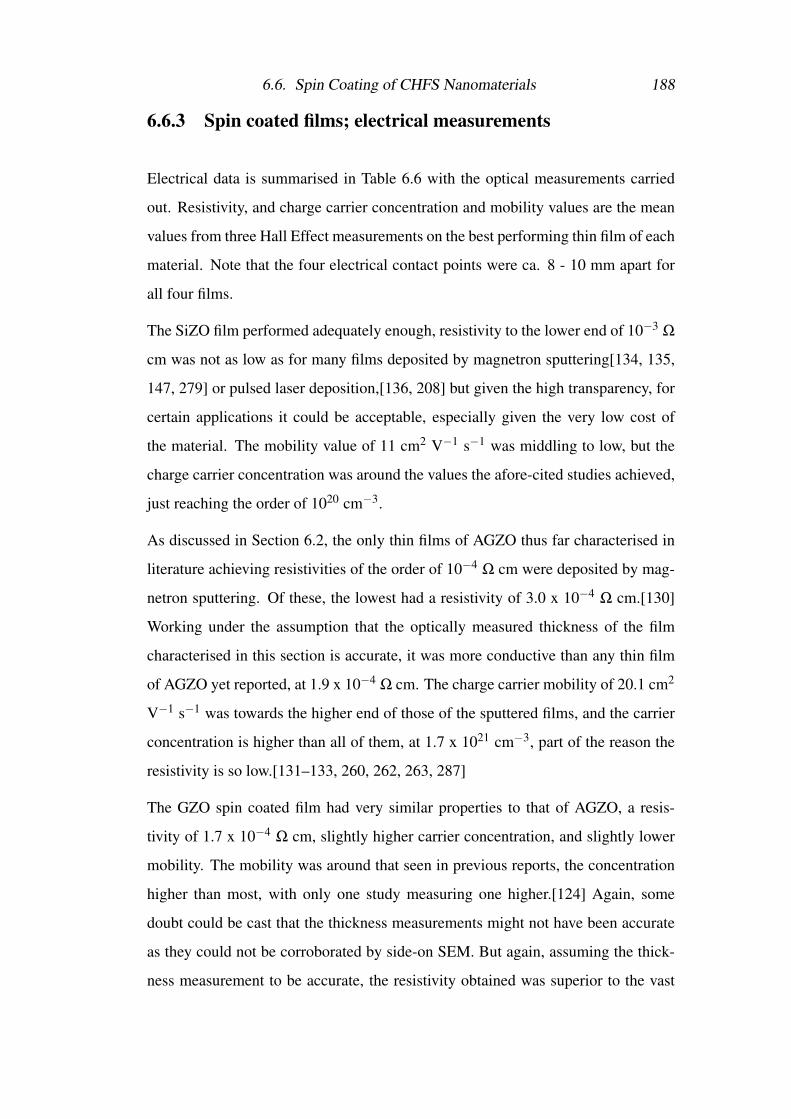
6.6. Spin Coating of CHFS Nanomaterials 188
6.6.3 Spin coated films; electrical measurements
Electrical data is summarised in Table 6.6 with the optical measurements carried
out. Resistivity, and charge carrier concentration and mobility values are the mean
values from three Hall Effect measurements on the best performing thin film of each
material. Note that the four electrical contact points were ca. 8 - 10 mm apart for
all four films.
The SiZO film performed adequately enough, resistivity to the lower end of 10−3 Ω
cm was not as low as for many films deposited by magnetron sputtering[134, 135,
147, 279] or pulsed laser deposition,[136, 208] but given the high transparency, for
certain applications it could be acceptable, especially given the very low cost of
the material. The mobility value of 11 cm2 V−1 s−1 was middling to low, but the
charge carrier concentration was around the values the afore-cited studies achieved,
just reaching the order of 1020 cm−3.
As discussed in Section 6.2, the only thin films of AGZO thus far characterised in
literature achieving resistivities of the order of 10−4 Ω cm were deposited by mag-
netron sputtering. Of these, the lowest had a resistivity of 3.0 x 10⁻⁴ Ω cm.[130]
Working under the assumption that the optically measured thickness of the film
characterised in this section is accurate, it was more conductive than any thin film
of AGZO yet reported, at 1.9 x 10⁻⁴ Ω cm. The charge carrier mobility of 20.1 cm2
V−1 s−1 was towards the higher end of those of the sputtered films, and the carrier
concentration is higher than all of them, at 1.7 x 1021 cm−3, part of the reason the
resistivity is so low.[131–133, 260, 262, 263, 287]
The GZO spin coated film had very similar properties to that of AGZO, a resis-
tivity of 1.7 x 10⁻⁴ Ω cm, slightly higher carrier concentration, and slightly lower
mobility. The mobility was around that seen in previous reports, the concentration
higher than most, with only one study measuring one higher.[124] Again, some
doubt could be cast that the thickness measurements might not have been accurate
as they could not be corroborated by side-on SEM. But again, assuming the thick-
ness measurement to be accurate, the resistivity obtained was superior to the vast
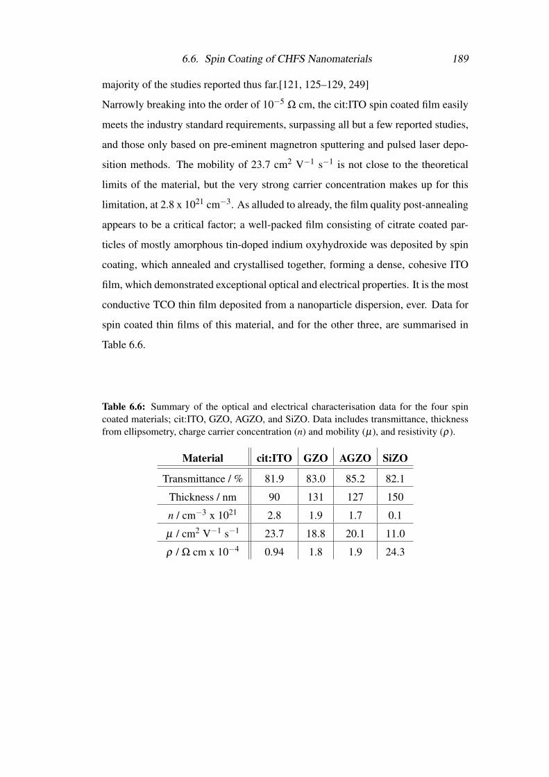
6.6. Spin Coating of CHFS Nanomaterials 189
majority of the studies reported thus far.[121, 125–129, 249]
Narrowly breaking into the order of 10−5 Ω cm, the cit:ITO spin coated film easily
meets the industry standard requirements, surpassing all but a few reported studies,
and those only based on pre-eminent magnetron sputtering and pulsed laser depo-
sition methods. The mobility of 23.7 cm2 V−1 s−1 is not close to the theoretical
limits of the material, but the very strong carrier concentration makes up for this
limitation, at 2.8 x 1021 cm−3. As alluded to already, the film quality post-annealing
appears to be a critical factor; a well-packed film consisting of citrate coated par-
ticles of mostly amorphous tin-doped indium oxyhydroxide was deposited by spin
coating, which annealed and crystallised together, forming a dense, cohesive ITO
film, which demonstrated exceptional optical and electrical properties. It is the most
conductive TCO thin film deposited from a nanoparticle dispersion, ever. Data for
spin coated thin films of this material, and for the other three, are summarised in
Table 6.6.
Table 6.6: Summary of the optical and electrical characterisation data for the four spincoated materials; cit:ITO, GZO, AGZO, and SiZO. Data includes transmittance, thicknessfrom ellipsometry, charge carrier concentration (n) and mobility (µ), and resistivity (ρ).
Material cit:ITO GZO AGZO SiZO
Transmittance / % 81.9 83.0 85.2 82.1
Thickness / nm 90 131 127 150
n / cm−3 x 10²¹ 2.8 1.9 1.7 0.1
µ / cm2 V−1 s−1 23.7 18.8 20.1 11.0
ρ / Ω cm x 10−4 0.94 1.8 1.9 24.3
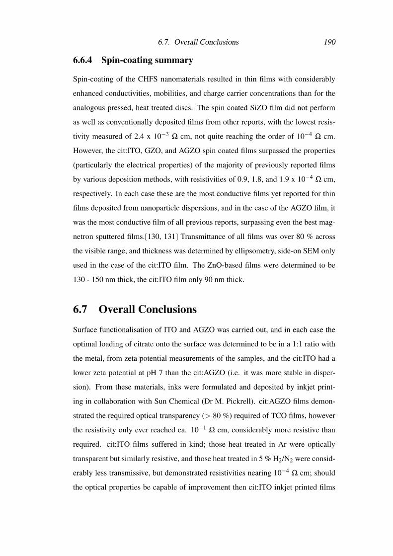
6.7. Overall Conclusions 190
6.6.4 Spin-coating summary
Spin-coating of the CHFS nanomaterials resulted in thin films with considerably
enhanced conductivities, mobilities, and charge carrier concentrations than for the
analogous pressed, heat treated discs. The spin coated SiZO film did not perform
as well as conventionally deposited films from other reports, with the lowest resis-
tivity measured of 2.4 x 10⁻³ Ω cm, not quite reaching the order of 10−4 Ω cm.
However, the cit:ITO, GZO, and AGZO spin coated films surpassed the properties
(particularly the electrical properties) of the majority of previously reported films
by various deposition methods, with resistivities of 0.9, 1.8, and 1.9 x 10⁻⁴ Ω cm,
respectively. In each case these are the most conductive films yet reported for thin
films deposited from nanoparticle dispersions, and in the case of the AGZO film, it
was the most conductive film of all previous reports, surpassing even the best mag-
netron sputtered films.[130, 131] Transmittance of all films was over 80 % across
the visible range, and thickness was determined by ellipsometry, side-on SEM only
used in the case of the cit:ITO film. The ZnO-based films were determined to be
130 - 150 nm thick, the cit:ITO film only 90 nm thick.
6.7 Overall Conclusions
Surface functionalisation of ITO and AGZO was carried out, and in each case the
optimal loading of citrate onto the surface was determined to be in a 1:1 ratio with
the metal, from zeta potential measurements of the samples, and the cit:ITO had a
lower zeta potential at pH 7 than the cit:AGZO (i.e. it was more stable in disper-
sion). From these materials, inks were formulated and deposited by inkjet print-
ing in collaboration with Sun Chemical (Dr M. Pickrell). cit:AGZO films demon-
strated the required optical transparency (> 80 %) required of TCO films, however
the resistivity only ever reached ca. 10−1 Ω cm, considerably more resistive than
required. cit:ITO films suffered in kind; those heat treated in Ar were optically
transparent but similarly resistive, and those heat treated in 5 % H2/N2 were consid-
erably less transmissive, but demonstrated resistivities nearing 10−4 Ω cm; should
the optical properties be capable of improvement then cit:ITO inkjet printed films
6.7. Overall Conclusions 191
could become industrially viable alternatives to magnetron sputtered films, as al-
most ubiquitously used in TCO depositions today.
Spin coating of cit:ITO, GZO, AGZO, and SiZO resulted in thin films with highly
competitive electrical and optical properties, with resistivities of 9.4 x 10⁻⁵ Ω cm,
1.8 10−4 Ω cm, 1.9 10−4 Ω cm, and 2.4 10−3 Ω cm, respectively. These values were
(comparatively between the materials) in keeping with previous reports testing the
materials as pressed, heat treated discs, for which ITO had the lowest resistivity,
GZO and AGZO similar but higher, and SiZO five times higher resistivity again.[5–
7, 168] These represent, for each of the four materials, the most conductive thin
films yet reported for depositions of dispersed nanoparticles by a considerable mar-
gin.
Though the spin coating results were very promising indeed, the process is still rel-
atively wasteful; it was one of the aims of the thesis to deposit thin films of the
materials by inkjet printing (a zero-waste deposition process) with sufficient opto-
electronic properties that the films could be applied as transparent conducting films
in industry. This was not achieved; electronically, or optically, every film thus far
has failed to reach the benchmarks set. cit:ITO inkjet printed films show the most
promise, as they at least appear to have reached the electronic properties required
of TCOs, however more work is required in the optimisation of the deposition and
heat treatment steps to give more consistent, and indeed transparent, films.
Chapter 7
Conclusions and Outlook
This project had three investigative steps generated by the central hypothesis. First,
was to use continuous hydrothermal flow synthesis (CHFS) to identify ZnO-based
replacement materials for indium tin oxide (ITO) in transparent conducting oxide
(TCO) applications. Then, to optimise the most promising materials in terms of the
electronic properties. And finally, to surface-functionalise selected CHFS nanoma-
terials to facilitate the formulation of stable dispersions and inks, which could then
be deposited by such methods as inkjet printing and spin coating.
In pursuit of the first, Chapter 3 discussed the dopant screening experiments, in-
cluding the synthesis and characterisation of a number of different doped zinc ox-
ides. These were screened as pressed, heat treated discs by performing Hall Effect
measurements to determine the bulk resistivity of the materials. As ITO had pre-
viously been synthesised, tested and optimised by the same methods, it was used
as the benchmark, achieving resistivities as low as 6 x 10⁻³ Ω cm. Of all doped
zinc oxides synthesised and tested, only four unoptimised materials obtained resis-
tivities within two orders of magnitude of this. This was judged to be acceptable
variance from ITO’s electrical properties, as this was a single, arbitrarily chosen
composition (2 at% dopant with respect to 98 at% Zn) of each material, and had
not yet been optimised. These materials were ZnO doped with Al, Cu, Ga, and Si.
Of these, Cu-doping resulted in a material that was dark in colour, black post-heat
treatment, marking it inappropriate for use as a TCO, and so the three materials
that were highlighted for further investigation as potential ITO replacements were
193
Al-doped ZnO (AZO), Ga-doped ZnO (GZO), and Si-doped ZnO (SiZO).
Chapter 4 discussed the compositional optimisation of AZO and GZO, finding that
the lowest resistivities occurred at dopant levels of 2.5 at% Al and 3.5 at% Ga, re-
spectively, with resistivities of 7.0 x 10⁻³ Ω cm and 9.1 x 10⁻³ Ω cm for AZO and
GZO, respectively, both very close to the optimally resistive ITO sample. Further
investigation was carried out in the co-doping of these materials (Al- and Ga-co-
doped ZnO, AGZO), in an attempt to balance the chemical instability of AZO, and
the high costs associated with the use of Ga in GZO. This compositional screening,
also included in Chapter 4, indicated that three compositions of AGZO gave similar
resistivities to singularly doped GZO, with compositions described as (Al at%,Ga
at%)AGZO of (1.0,2.0)AGZO, (2.0,2.0)AGZO, and (3.0,1.0)AGZO obtaining re-
sistivities of 9.1 x 10⁻³ Ω cm, 9.3 x 10⁻³ Ω cm, and 9.4 x 10⁻³ Ω cm, respectively.
Of these, the narrowest distribution of measurements (i.e. the most reliable) was of
the sample synthesised with 2 at% of each Al and Ga. As such, this material was
selected for surface functionalisation experiments as discussed in Chapter 6.
Chapter 5 first conducted the compositional optimisation of SiZO, finding that the
most conductive sample made was that with 0.25 at% Si, a considerably lower
dopant level than for AZO, GZO, or AGZO. This had a resistivity some four times
higher than GZO and AGZO, however, with ρ = 3.5 x 10⁻² Ω cm. Introduction of
Al and Ga as co-dopants improved the electrical properties; in each case the most
conductive sample had 0.25 at% Si and 1.5 at% of either Al, or Ga. These materi-
als, SiAZO and SiGZO, obtained resistivities of 8.3 x 10⁻³ Ω cm and 11.3 x 10⁻³
Ω cm, respectively, very close to the singularly doped AZO and GZO materials.
Future work to functionalise these and deposit as thin films would be a logical con-
tinuation of the project.
Chapter 6 discussed the pursuit of the final project goal, the functionalisation and
deposition of CHFS nanomaterials into thin films. Functionalisation was imple-
mented by inclusion of sodium citrate in the CHFS process, introduced at a second
mixing point. This quenched particle growth and introduced citrate to the surface
194
of the particles. The two systems for which this was investigated were ITO and
AGZO, and for both of these the optimal loading was achieved by a 1:1 ratio of
citrate to metal in the CHFS process. From these, cit:ITO and cit:AGZO, were for-
mulated large ink batches, which were deposited by inkjet printing in collaboration
with Dr M. Pickrell of Sun Chemical. These films showed promise either optically,
or electrically, but never both at the same time in the same film. cit:ITO printed
films neared the conductivity requirements of a TCO thin film when heat treated in
a reducing atmosphere, perhaps within an order of magnitude (though precise de-
termination of resistivity was not possible due to inconsistent film coverage). This
would represent the most conductive injet printed TCO film reported by orders of
magnitude, but further depositions and testing are absolutely necessary in the future,
as well as improvements to the heat treatment regime so as not to hamper the opti-
cal properties of the films. cit:AGZO films were optically and aesthetically superior,
however suffered from high resistivities. Formulation optimisation, and improved
sintering should be the focus of future research to match the electrical properties
required of TCO thin films.
Chapter 6 went on to cover the spin coating of optimised cit:ITO, GZO, AGZO,
and SiZO. Each of these films, though the deposition technique was more wasteful
than inkjet printing would have been, obtained competitive resistivities, particularly
the former three, which showed resistivities of 9.4 x 10⁻⁵ Ω cm, 1.8 10−4 Ω cm,
and 1.9 10−4 Ω cm, for cit:ITO, GZO, and AGZO, respectively. These are among
the most conductive thin films ever reported for any of those materials, particularly
significant when noting that this is when compared principally to the sputtering
techniques typically used in industrial TCO thin film depositions. When compared
to other thin films made from nanoparticle dispersions, these (including the SiZO
film, with ρ = 2.4 x 10⁻³ Ω cm) are the most conductive films yet reported by a
considerable margin, where comparisons exist at all.
The cit:ITO film was robust, and optimally measured thickness could be corrobo-
rated by side-on SEM, however the mechanical strength of the ZnO-based films was
lacking. Dropping the film to the floor resulted in significant cracks, and cleaving
195
the substrate destroyed the film to the point that side-on SEM images could not be
retrieved for any of the films. It is possible that spin coating of citrate-coated ZnO
analogues could aid in the formation of denser, more robust films, and this could be
investigated further. Also, as alluded to above, there are other ’optimal materials’
for which depositions were not carried out as part of this investigation, including
the SiAZO and SiGZO films, and the other optimally conductive AGZO samples.
These offer similar solutions to the issues of singularly doped AZO and GZO, by
reducing cost and hopefully increasing the chemical stability. Furthermore, this
project was limited only to ZnO as the host material. There is precedent for SnO2
and TiO2-based materials too; a dopant screen could be carried out for each, fol-
lowed similarly by compositional optimisation of the most promising materials and
finally surface-functionalisation and deposition as thin films.
In conclusion, the goals that were set out in the beginning of the project have broadly
been accomplished, though incompletely. There is scope for further research into
different dopants (for example, those highlighted in Chapter 3 that were judged
insufficiently conductive), different material families altogether, such as SnO2, and
the work as detailed in Chapter 6 would benefit from many more depositions, partic-
ularly of the cit:ITO ink by inkjet printing, if the deposition technique is ever to be
taken seriously as an industrially viable alternative to magnetron sputtering. Investi-
gations into spin coating of CHFS nanomaterials have demonstrated unequivocally
that the materials are capable of exemplary, in some cases unparalleled, optical and
electronic properties as thin films. As such they are worth future consideration and
experimentation, in order to fully realise their potential, and perhaps through them
the potential of the inkjet printing on the whole, in pursuit of a more sustainable,
cheaper, and less wasteful technique to generate TCO thin films.
Bibliography
[1] T. Sanders. https://en.wikipedia.org/wiki/File:Diagram of pulsed laser deposition.png
(accessed 31.08.17), 2016.
[2] Clement J. U. Denis. Nucleation and growth of industrial nanomaterials in
a continuous hydrothermal reactor. PhD thesis, 2016.
[3] J. A. Darr, C. J. Tighe, and R. I. Gruar. Co-current mixer, apparatus, reactor
and method for precipitating nanoparticles. U.S. Patent 9,192,901, 2015.
[4] Heinz Schulz and K. H. Thiemann. Structure parameters and polarity of the
wurtzite type compounds Sic-2H and ZnO. Solid State Communications,
32(9):783–785, 1979.
[5] D. P. Howard, P. Marchand, I. D. Johnson, C. J. Carmalt, I. P. Parkin, and
J. A. Darr. Conducting Al and Ga-doped zinc oxides; rapid optimisation and
scale-up. J. Mater. Chem. A, 4(33):12774–12780, 2016.
[6] Dougal P. Howard, Peter Marchand, Liam McCafferty, Claire J. Carmalt,
Ivan P. Parkin, and Jawwad A. Darr. High-Throughput Continuous Hy-
drothermal Synthesis of Transparent Conducting Aluminum and Gallium Co-
doped Zinc Oxides. ACS Combinatorial Science, 19:239–245, 2017.
[7] Dougal P. Howard, P. Marchand, Ivan P. Parkin, Claire J. Carmalt, and
Jawwad A. Darr. Si-doped Zinc Oxide Transparent Conducting Oxides;
Nanoparticle Optimisation, Scale-up and Thin Film Deposition. Journal of
Materials Chemistry C, 5(34):8796–8801, 2017.
BIBLIOGRAPHY 197
[8] P. Scherrer. Bestimmung der Große und der inneren Struktur von Kol-
loidteilchen mittels Rontgenstrahlen. Nachrichten von der Gesellschaft der
Wissenschaften zu Gottingen, Mathematisch-Physikalische Klasse, 1918:98–
100, 1918.
[9] A. L. Patterson. The scherrer formula for X-ray particle size determination.
Physical Review, 56(10):978–982, 1939.
[10] Klaus Ellmer. Past achievements and future challenges in the development
of optically transparent electrodes. Nature Photonics, 6(12):809–817, nov
2012.
[11] K Ellmer. Resistivity of polycrystalline zinc oxide films: current status and
physical limit. Journal of Physics D: Applied Physics, 34(21):3097–3108,
2001.
[12] David O. Scanlon and Graeme W. Watson. On the possibility of p-type SnO2.
Journal of Materials Chemistry, 39(39):25236–25245, 2012.
[13] P. D C King, T. D. Veal, F. Fuchs, Ch Y. Wang, D. J. Payne, A. Bourlange,
H. Zhang, G. R. Bell, V. Cimalla, O. Ambacher, R. G. Egdell, F. Bechstedt,
and C. F. McConville. Band gap, electronic structure, and surface electron
accumulation of cubic and rhombohedral In2 O3. Physical Review B - Con-
densed Matter and Materials Physics, 79(20):1–10, 2009.
[14] K Reimann and M Steube. Experimental determination of the electronic band
structure of SnO2. Solid State Communications, 105:649–652, 1998.
[15] A. Mang, K. Reimann, and St Rubenacke. Band gaps, crystal-field splitting,
spin-orbit coupling, and exciton binding energies in ZnO under hydrostatic
pressure. Solid State Communications, 94(4):251–254, 1995.
[16] B. Kramm, A. Laufer, D. Reppin, A. Kronenberger, P. Hering, A. Polity,
and B. K. Meyer. The band alignment of Cu 2O/ZnO and Cu 2O/GaN het-
erostructures. Applied Physics Letters, 100(9):094102, 2012.
BIBLIOGRAPHY 198
[17] W. Martienssen and H. Warlimont. Springer Handbook of Condensed Matter
and Materials Data. 2005.
[18] H.a. Al-Jawhari. A review of recent advances in transparent p-type Cu$ 2$O-
based thin film transistors. Materials Science in Semiconductor Processing,
40:241–252, 2015.
[19] Anderson Janotti, Eric Snow, and Chris G. Van de Walle. A pathway to p-type
wide-band-gap semiconductors. Applied Physics Letters, 95(17):172109,
2009.
[20] Dilawar Ali, M Z Butt, Iqra Muneer, Farooq Bashir, and Murtaza Saleem.
Correlation between structural and optoelectronic properties of tin doped in-
dium oxide thin films. Optik - International Journal for Light and Electron
Optics, 128:235–246, 2017.
[21] D Reyes-Coronado, G Rodrıguez-Gattorno, M E Espinosa-Pesqueira, C Cab,
R de Coss, and G Oskam. Phase-pure TiO(2) nanoparticles: anatase, brookite
and rutile. Nanotechnology, 19(14):145605, 2008.
[22] Roy G Gordon. C riteria for Choosing Transparent Conductors. MRS Bul-
letin, (August):52–57, 2000.
[23] Brian G Lewis and David C Paine. Applications and Processing of Transpar-
ent. MRS Bulletin, 25(August):22–27, 2000.
[24] R B H Tahar, T Ban, Y Ohya, and Y Takahashi. Tin doped indium oxide thin
films: Electrical properties. Journal of Applied Physics, 83(5):2631–2645,
1998.
[25] G Frank and H Kostlin. Electrical Properties and Defect Model of Tin-Doped
Indium Oxide Layers. Applied Physics A, 27:197–206, 1982.
[26] John C C Fan and John B Goodenough. Xray photoemission spec-
troscopy studies of Sndoped indiumoxide films. Journal of Applied Physics,
48(8):3524–3531, 1977.
BIBLIOGRAPHY 199
[27] P. P. Edwards, A. Porch, M. O. Jones, D. V. Morgan, and R. M. Perks. Basic
materials physics of transparent conducting oxides. Dalton Transactions,
(19):2995, 2004.
[28] D. Feng and G. Jin. Transport Properties. In Introduction to Condensed
Matter Physics: Volume 1, pages 199–231. World Scientific, 2005.
[29] David O. Scanlon and Graeme W. Watson. Undoped n -Type Cu 2 O: Fact or
Fiction? The Journal of Physical Chemistry Letters, 1(17):2582–2585, sep
2010.
[30] Swati Ray, Ratnabali Banerjee, N. Basu, A. K. Batabyal, and A. K. Barua.
Properties of tin doped indium oxide thin films prepared by magnetron sput-
tering. Journal of Applied Physics, 54(6):3497–3501, 1983.
[31] Yuzo Shigesato, Satoru Takaki, and Takeshi Haranoh. Electrical and struc-
tural properties of low resistivity tin-doped indium oxide films. Journal of
Applied Physics, 71(7):3356–3364, 1992.
[32] H A Mcmaster. Conductive coating for glass and method of application,
1947.
[33] M S Tarnopol. Indium oxide coating on a silicious base, 1954.
[34] J. F. Wager, D. A. Keszler, and R. E. Presley. Applications. In Transparent
Electronics, chapter 3, pages 39–56. Springer, Boston, MA, 2008.
[35] C. W. Tang and S. A. Vanslyke. Organic electroluminescent diodes. Applied
Physics Letters, 51(12):913–915, 1987.
[36] C. G. Granqvist. Solar energy materials - Overview and some examples.
Applied Physics A Solids and Surfaces, 52(2):83–93, 1991.
[37] P D C King and T D Veal. Conductivity in transparent oxide semiconduc-
tors. Journal of physics. Condensed matter : an Institute of Physics journal,
23(33):334214, aug 2011.
BIBLIOGRAPHY 200
[38] Tadatsugu Minami and Toshihiro Miyata. Present status and future prospects
for development of non- or reduced-indium transparent conducting oxide thin
films. Thin Solid Films, 517(4):1474–1477, 2008.
[39] Claes G. Granqvist. Electrochromics for smart windows: Oxide-based thin
films and devices. Thin Solid Films, 564:1–38, aug 2014.
[40] NanoMarkets. Transparent Conductor Markets 2014-2021. Technical report,
2014.
[41] Allied Market Research. Transparent Conductive Films Market by Tech-
nology (ITO on PET, ITO on Glass, Non ITO oxides, Silver Nanowires,
Graphene, Carbon Nanotube, Metal Mesh, Micro fine Wire, PEDOT) and
Application (Smart Phones, Tablets and tablet PCs, Notebooks, All-in-one
PCs,. Technical report, 2014.
[42] Research and Markets. Transparent Conductive Films (TCF) 2017-2027:
Forecasts, Markets, Technologies. Technical report, 2017.
[43] Touch Display Research Inc. ITO-Replacement Report, January 2016. Tech-
nical report, 2016.
[44] R. H. Friend, R. W. Gymer, A. B. Holmes, J. H. Burroughes, R. N. Marks,
C. Taliani, D. D. C. Bradley, D. A. Dos Santos, J. L. Bredas, M. Logdlund,
and W. R. Salaneck. Electroluminescence in conjugated polymers. Nature,
397(6715):121–128, 1999.
[45] L Ke, P Chen, R.S. Kumar, and A.P. Burden. Indium-tin-oxide-free organic
light-emitting device. IEEE Transactions on Electron Devices, 53(6):1483–
1486, 2006.
[46] T. D. Kelly and G. R. Matos. Historical statistics for mineral and material
commodities in the United States (2016 version): U.S. Geological Survey
Data Series 140 (date accessed: 06/06/2017), 2016.
BIBLIOGRAPHY 201
[47] Amy C. Tolcin. U.S. Geological Survey, Mineral Commodity Summaries,
January 2017. Technical report, 2017.
[48] Robert D. Brown Jr. U.S. Geological Survey, Mineral Commodity Sum-
maries, January 1998. Technical report, 1998.
[49] Robert D. Brown Jr. U.S. Geological Survey, Mineral Commodity Sum-
maries, January 1999. Technical report, 1999.
[50] Robert D. Brown Jr. U.S. Geological Survey, Mineral Commodity Sum-
maries, January 2000. Technical report, 2000.
[51] Robert D. Brown Jr. U.S. Geological Survey, Mineral Commodity Sum-
maries, January 2001. Technical report, 2001.
[52] Robert D. Brown Jr. U.S. Geological Survey, Mineral Commodity Sum-
maries, January 2002. Technical report, 2002.
[53] John D. Jorgenson. U.S. Geological Survey, Mineral Commodity Sum-
maries, January 2003. Technical report, 2003.
[54] John D. Jorgenson. U.S. Geological Survey, Mineral Commodity Sum-
maries, January 2004. Technical report, 2004.
[55] Michael W. George. U.S. Geological Survey, Mineral Commodity Sum-
maries, January 2005. Technical report, 2005.
[56] James F. Carlin Jr. U.S. Geological Survey, Mineral Commodity Summaries,
January 2006. Technical report, 2006.
[57] James F. Carlin Jr. U.S. Geological Survey, Mineral Commodity Summaries,
January 2007. Technical report, 2007.
[58] Amy C. Tolcin. U.S. Geological Survey, Mineral Commodity Summaries,
January 2008. Technical report, 2008.
[59] Amy C. Tolcin. U.S. Geological Survey, Mineral Commodity Summaries,
January 2009. Technical report, 2009.
BIBLIOGRAPHY 202
[60] Amy C. Tolcin. U.S. Geological Survey, Mineral Commodity Summaries,
January 2010. Technical report, 2010.
[61] Amy C. Tolcin. U.S. Geological Survey, Mineral Commodity Summaries,
January 2011. Technical report, 2011.
[62] Amy C. Tolcin. U.S. Geological Survey, Mineral Commodity Summaries,
January 2012. Technical report, 2012.
[63] Amy C. Tolcin. U.S. Geological Survey, Mineral Commodity Summaries,
January 2013. Technical report, 2013.
[64] Amy C. Tolcin. U.S. Geological Survey, Mineral Commodity Summaries,
February 2014. Technical report, 2014.
[65] Amy C. Tolcin. U.S. Geological Survey, Mineral Commodity Summaries,
January 2015. Technical report, 2015.
[66] Amy C. Tolcin. U.S. Geological Survey, Mineral Commodity Summaries,
January 2016. Technical report, 2016.
[67] Peter Koven. Collapsing Fanya Metal Exchange in China raises concerns
about minor metals, 2015.
[68] Lucy Hornby. Head of Fanya metals scheme arrested in China, 2016.
[69] Nyrstar. ”Results Release Nyrstar H1 2016 EN”. Technical report, 2016.
[70] James Heyward. Fire breaks out at Nyrstar’s Auby indium plant, 2015.
[71] Thomas O Mason, Steven P Harvey, Kenneth R Poeppelmeier, Klaus Ellmer,
Robert Kykyneshi, Jin Zeng, David P Cann, Mamoru Mizuhashi, Hideo
Hosono, Claes G Granqvist, Yuzo Shigesato, Hiromichi Ohta, Timothy J
Coutts, David L Young, Timothy a Gessert, Art Sleight, David S Ginley,
John D Perkins, David C Paine, Burag Yaglioglu, Joseph Berry, J Robertson,
B Falabretti, Nanostructured Tcos Zno, and Dana C Olson. Handbook of
Transparent Conductors. 2011.
BIBLIOGRAPHY 203
[72] Cetin Klc and Alex Zunger. Origins of coexistence of conductivity and trans-
parency in SnO2. Physical Review Letters, 88(9):955011–955014, 2002.
[73] S. Samson and C. G. Fonstad. Defect structure and electronic donor levels in
stannic oxide crystals. Journal of Applied Physics, 44(10):4618–4621, 1973.
[74] Masahiko Kojima, Hisao Kato, Atsuo Imai, and Akira Yoshida. Electronic
conduction of tin oxide thin films prepared by chemical vapor deposition.
Journal of Applied Physics, 64(4):1902–1905, 1988.
[75] I. H. Kim, J. H. Ko, D. Kim, K. S. Lee, T. S. Lee, J. h. Jeong, B. Cheong,
Y. J. Baik, and W. M. Kim. Scattering mechanism of transparent conduct-
ing tin oxide films prepared by magnetron sputtering. Thin Solid Films,
515(4):2475–2480, 2006.
[76] Ratnabali Banerjee and Debajyoti Das. Properties of tin oxide films prepared
by reactive electron beam evaporation. Thin Solid Films, 149(3):291–301,
1987.
[77] Takamitsu Isono, Takeshi Fukuda, Koji Nakagawa, Reo Usui, Ryohei Satoh,
Eiji Morinaga, and Yu Mihara. High Conductivity SnO2 Thin Films for Flat
Panel Displays. SID Digest, 37(1):1874–1877, 2006.
[78] Hong-Lei Ma, Xiao-Tao Hao, Jin Ma, Ying-Ge Yang, Jie Huang, De-Heng
Zhang, and Xian-Gang Xu. Thickness dependence of properties of SnO 2 :
Sb films deposited on flexible substrates. Applied Surface Science, 191:313–
318, 2002.
[79] E. Shanthi, A. Banerjee, V. Dutta, and K. L. Chopra. Electrical and optical
properties of tin oxide films doped with F and (Sb+F). Journal of Applied
Physics, 53(3):1615–1621, 1982.
[80] Hideo Hosono, Naoto Kikuchi, Naoyuki Ueda, and Hiroshi Kawazoe. Work-
ing hypothesis to explore novel wide band gap electrically conducting
BIBLIOGRAPHY 204
amorphous oxides and examples. Journal of Non-Crystalline Solids, 198-
200:165–169, 1996.
[81] Kenji Nomura, Hiromichi Ohta, Akihiro Takagi, Toshio Kamiya, Masahiro
Hirano, and Hideo Hosono. Room-temperature fabrication of transparent
flexible thin-film transistors using amorphous oxide semiconductors. Nature,
432(7016):488–492, 2004.
[82] G.S. Collins, T. Kachnowski, N. Benczer-Koller, and M. Pasternak. Ap-
plication of the Mossbauer effect to the characterization of an amorphous
tin-oxide system. Physical Review B, 19(3):1369, 1979.
[83] Madambi K. Jayaraj, Kachirayil J. Saji, Kenji Nomura, Toshio Kamiya, and
Hideo Hosono. Optical and electrical properties of amorphous zinc tin ox-
ide thin films examined for thin film transistor application. Journal of Vac-
uum Science & Technology B: Microelectronics and Nanometer Structures,
26(2):495, 2008.
[84] Ha-Rim An, ChangYeoul Kim, Sung-Tag Oh, and Hyo-Jin Ahn. Effect of
sol-layers on Sb-doped SnO2 thin films as solution-based transparent con-
ductive oxides. Ceramics International, 40(1):385–391, jan 2014.
[85] J. Montero, J. Herrero, and C. Guillen. Preparation of reactively sputtered
Sb-doped SnO2 thin films: Structural, electrical and optical properties. Solar
Energy Materials and Solar Cells, 94(3):612–616, mar 2010.
[86] J. Montero, C. Guillen, C. G. Granqvist, J. Herrero, and G. a. Niklasson.
Lithium intercalation in sputter deposited antimony-doped tin oxide thin
films: Evidence from electrochemical and optical measurements. Journal
of Applied Physics, 115(15):153702, apr 2014.
[87] Hong Lei Ma, Xiao Tao Hao, Jin Ma, Ying Ge Yang, Jie Huang, De Heng
Zhang, and Xian Gang Xu. Thickness dependence of properties of SnO2:Sb
films deposited on flexible substrates. Applied Surface Science, 191(1-
4):313–318, 2002.
BIBLIOGRAPHY 205
[88] T. R. Giraldi, M. T. Escote, M. I B Bernardi, V. Bouquet, E. R. Leite,
E. Longo, and J. A. Varela. Effect of thickness on the electrical and optical
properties of Sb doped SnO2 (ATO) thin films. Journal of Electroceramics,
13(1-3):159–165, 2004.
[89] Shihui Yu, Linghong Ding, Chuang Xue, Li Chen, and W.F. Zhang. Transpar-
ent conducting Sb-doped SnO2 thin films grown by pulsed laser deposition.
Journal of Non-Crystalline Solids, 358(23):3137–3140, dec 2012.
[90] Seung-Yup Lee and Byung-Ok Park. Structural, electrical and optical char-
acteristics of SnO2:Sb thin films by ultrasonic spray pyrolysis. Thin Solid
Films, 510(1-2):154–158, 2006.
[91] H. S. Randhawa, M. D. Matthews, and R. F. Bunshah. SnO2 films prepared
by activated reactive evaporation. Thin Solid Films, 83(2):267–271, 1981.
[92] Huiyong Liu, V. Avrutin, N. Izyumskaya, U Ozgr, and H. Morkoc. Transpar-
ent conducting oxides for electrode applications in light emitting and absorb-
ing devices. Superlattices and Microstructures, 48(5):458–484, nov 2010.
[93] B R Marathe, M G Takwale, and V G Bhide. Structural Properties of SnO2:F
Films Deposited by Spray Pyrolysis Technique. Thin Films, 164:261–264,
1988.
[94] M Thirumoorthi and J Thomas Joseph Prakash. Effect of F doping on phys-
ical properties of (211) oriented SnO2 thin films prepared by jet nebulizer
spray pyrolysis technique. Superlattices and Microstructures, 89:378–389,
2016.
[95] Boubaker Benhaoua, Soumaia Abbas, Achour Rahal, Atmane Benhaoua, and
M.S. Aida. Effect of film thickness on the structural, optical and electrical
properties of SnO2: F thin films prepared by spray ultrasonic for solar cells
applications. Superlattices and Microstructures, 83:78–88, 2015.
BIBLIOGRAPHY 206
[96] Mejda Ajili, Michel Castagne, and Najoua Kamoun. Optik Spray solution
flow rate effect on growth , optoelectronic characteristics and photolumines-
cence of SnO 2 : F thin films for photovoltaic application. Optik - Interna-
tional Journal for Light and Electron Optics, 126(7-8):708–714, 2015.
[97] Quang-Phu Tran, Jau-Shiung Fang, and Tsung-Shune Chin. Properties of
fluorine-doped SnO2 thin films by a green solgel method. Materials Science
in Semiconductor Processing, 40:664–669, 2015.
[98] Nuruzzaman Noor, Clair K. T. Chew, Davinder S. Bhachu, Matthew R.
Waugh, Claire J. Carmalt, and Ivan P. Parkin. Influencing FTO thin film
growth with thin seeding layers: a route to microstructural modification. J.
Mater. Chem. C, 3(36):9359–9368, 2015.
[99] Tadashi Ishida, Osamu Tabata, Jung Il Park, Sung Ho Shin, Hiroyuki Mag-
ara, Shigeharu Tamura, Shoichi Mochizuki, and Toshiyuki Mihara. Highly
conductive transparent F-doped tin oxide films were prepared by photo-CVD
and thermal-CVD. Thin Solid Films, 281-282(1-2):228–231, 1996.
[100] Michael J. Powell, Dominic B. Potter, Rachel L. Wilson, Jawwad A. Darr,
Ivan P. Parkin, and Claire J. Carmalt. Scaling aerosol assisted chemical
vapour deposition: Exploring the relationship between growth rate and film
properties. Materials & Design, 129(May):116–124, 2017.
[101] Shoichiro Nakao, Yasushi Hirose, Tomoteru Fukumura, and Tetsuya
Hasegawa. Carrier generation mechanism and effect of tantalum-doping in
transparent conductive amorphous SnO2 thin films Carrier generation mech-
anism and effect of tantalum-doping in transparent conductive amorphous
SnO 2 thin fi lms. Japanese Journal of Applied Physics, 53(05FX04):1–5,
2014.
[102] Mirko Weidner, Joachim Brotz, and Andreas Klein. Sputter-deposited poly-
crystalline tantalum-doped SnO2 layers. Thin Solid Films, 555:173–178,
2014.
BIBLIOGRAPHY 207
[103] Shihui Yu, Lingxia Li, Zheng Sun, Haoran Zheng, Helei Dong, Dan Xu, and
Weifeng Zhang. Characteristics of Transparent Conducting W-Doped SnO
<sub>2</sub> Thin Films Prepared by Using the Magnetron Sputtering
Method. Journal of the American Ceramic Society, 98(4):1121–1127, 2015.
[104] Shoichiro Nakao, Naoomi Yamada, Taro Hitosugi, Yasushi Hirose, Toshihiro
Shimada, and Tetsuya Hasegawa. Fabrication of highly conductive Ta-doped
SnO2 polycrystalline films on glass using seed-layer technique by pulse laser
deposition. Thin Solid Films, 518(11):3093–3096, mar 2010.
[105] Shaohang Wu, Yantao Li, Jinsong Luo, Jie Lin, Yi Fan, Zhihong Gan, and
Xingyuan Liu. Pr and F co-doped SnO transparent conductive films with high
work function deposited by ion-assisted electron beam evaporation. Optics
express, 22(4):4731–7, feb 2014.
[106] G. Turgut, E. Sonmez, and S. Duman. Evaluation of an Nd doping effect
on characteristic properties of tin oxide. Materials Science in Semiconductor
Processing, 30:233–241, 2015.
[107] Zhenguo Ji, Zhenjie He, Yongliang Song, Kun Liu, and ZhiZhen Ye. Fabri-
cation and characterization of indium-doped p-type SnO2 thin films. Journal
of Crystal Growth, 259(3):282–285, 2003.
[108] Chien-Yie Tsay and Shan-Chien Liang. Fabrication of p-type conductivity
in SnO2 thin films through Ga doping. Journal of Alloys and Compounds,
622:644–650, 2015.
[109] M S Anwar, Faheem Ahmed, Si Nae Heo, Keun Young Park, and Bon Heun
Koo. Indication of room temperature ferromagnetism in highly transparent
and conductive Ga-doped SnO2 thin films. Thin Solid Films, 547:137–140,
2013.
[110] C.E. Benouis, M. Benhaliliba, Z. Mouffak, a. Avila-Garcia, a. Tiburcio-
Silver, M. Ortega Lopez, R. Romano Trujillo, and Y.S. Ocak. The low re-
BIBLIOGRAPHY 208
sistive and transparent Al-doped SnO2 films: p-type conductivity, nanostruc-
tures and photoluminescence. Journal of Alloys and Compounds, 603:213–
223, 2014.
[111] Abhishek Kumar Singh, Anderson Janotti, Matthias Scheffler, and Chris G.
Van De Walle. Sources of electrical conductivity in SnO2. Physical Review
Letters, 101(5):1–4, 2008.
[112] Claus F. Klingshirn. ZnO: Material, physics and applications.
ChemPhysChem, 8(6):782–803, 2007.
[113] Anderson Janotti and Chris G. Van De Walle. New insights into the role of
native point defects in ZnO. Journal of Crystal Growth, 287:58–65, 2006.
[114] M. D. McCluskey and S. J. Jokela. Sources of n-type conductivity in ZnO.
Physica B: Condensed Matter, 401-402:355–357, 2007.
[115] Sukit Limpijumnong, Luke Gordon, Maosheng Miao, Anderson Janotti, and
Chris G. Van De Walle. Alternative sources of p-type conduction in acceptor-
doped ZnO. Applied Physics Letters, 97(7):072112, 2010.
[116] Anderson Janotti and Chris G. Van De Walle. Oxygen vacancies in ZnO.
Applied Physics Letters, 87(12):1–3, 2005.
[117] Mao Hua Du and Koushik Biswas. Anionic and hidden hydrogen in ZnO.
Physical Review Letters, 106(11):1–4, 2011.
[118] David S. Ginley and Clark Bright. Transparent Conducting Oxides. MRS
Bulletin, 25(08):15–18, 2000.
[119] Tadatsugu Minami, Toshihiro Miyata, Tadatsugu Minami, Hirotoshi Sato,
Kouichi Tomura, Masaru Ohnishi, and Michio Yoshizawa. Highly Conduc-
tive and Transparent Aluminum Doped Zinc Oxide Thin Films Prepared by
RF Magnetron Sputtering. Japanese Journal of Applied Physics, 23:280–
282, 1984.
BIBLIOGRAPHY 209
[120] Jianhua Hu and Roy G Gordon. Textured aluminum-doped zinc oxide
thin films from atmospheric pressure chemical-vapor deposition Textured
aluminum-doped deposition zinc oxide thin fil s from atmospheric pressure.
Journal of Applied Physics, 71:880–890, 1992.
[121] S. Kuprenaite, T. Murauskas, A. Abrutis, V. Kubilius, Z. Saltyte, and
V. Plausinaitiene. Properties of In-, Ga-, and Al-doped ZnO films grown by
aerosol-assisted MOCVD: Influence of deposition temperature, doping level
and annealing. Surface and Coatings Technology, 271:156–164, dec 2015.
[122] Tudor Coman, Daniel Timpu, Valentin Nica, Catalin Vitelaru, Ali-
cia Petronela Rambu, George Stoian, Mihaela Olaru, and Cristian Ursu.
Sequential PLD in oxygen/argon gas mixture of Al-doped ZnO thin films
with improved electrical and optical properties. Applied Surface Science,
418:456–462, 2017.
[123] A. F. Aktarazzuman, G. I. Sharma, and L. K. Malhotra. ELECTRICAL,
OPTICAL AND ANNEALING CHARACTERISTICS OF ZnO:AI FILMS
PREPARED BY SPRAY PYROLYSIS. Thin Solid Films, 198:67–74, 1991.
[124] Gui-Gen Wang, Jie Zeng, Jie-Cai Han, and Li-Yi Wang. Highly transparent
and conductive Ga-doped ZnO films with good thermal stability prepared by
dual-target reactive sputtering. Materials Letters, 137:307–310, dec 2014.
[125] P.K Song, M Watanabe, M Kon, A Mitsui, and Y Shigesato. Electrical and
optical properties of gallium-doped zinc oxide films deposited by dc mag-
netron sputtering. Thin Solid Films, 411(1):82–86, 2002.
[126] a.S. Pugalenthi, R. Balasundaraprabhu, V. Gunasekaran, N. Muthuku-
marasamy, S. Prasanna, and S. Jayakumar. Effect of thickness on the struc-
tural, optical and electrical properties of RF magnetron sputtered GZO thin
films. Materials Science in Semiconductor Processing, 29:176–182, jan
2015.
BIBLIOGRAPHY 210
[127] G.a. Hirata, J. McKittrick, T Cheeks, J.M. Siqueiros, J.a. Diaz, O Contr-
eras, and O.a. Lopez. Synthesis and optelectronic characterization of gallium
doped zinc oxide transparent electrodes. Thin Solid Films, 288(1-2):29–31,
1996.
[128] Ha-Rim An, Hyo-Jin Ahn, and Jeong-Woo Park. High-quality, conduc-
tive, and transparent Ga-doped ZnO films grown by atmospheric-pressure
chemical-vapor deposition. Ceramics International, 41(2):2253–2259, mar
2015.
[129] B. M. Ataev, A. M. Bagamadova, A. M. Djabrailov, V. V. Mamedov, and
R A Rabadanov. Highly conductive and transparent Ga-doped epitaxial ZnO
films on sapphire by CVD. Thin Solid Films, 260(1):19–20, 1995.
[130] Ke Zhu, Ye Yang, and Weijie Song. Effects of substrate temperature on the
structural, morphological, electrical and optical properties of Al and Ga co-
doped ZnO thin films grown by DC magnetron sputtering. Materials Letters,
145:279–282, 2015.
[131] Xiaoyan Du, Jin Li, and Xiaofang Bi. The role of Ga partial substitution for
Al in the enhanced conductivity of transparent AZO thin fi lm. Journal of
Alloys and Compounds, 698:128–132, 2017.
[132] Jia Liu, Weijia Zhang, Dengyuan Song, Qiang Ma, Lei Zhang, Hui Zhang,
and Leng Zhang. Investigation of aluminum gallium co-doped zinc oxide
targets for sputtering thin film and photovoltaic application. Journal of Alloys
and Compounds, 575:174–182, 2013.
[133] Shang-Chou Chang. Post-annealed gallium and aluminum co-doped zinc
oxide films applied in organic photovoltaic devices. Nanoscale Research
Letters, 9(1):562, 2014.
[134] J. Clatot, M. Nistor, and a. Rougier. Influence of Si concentration on electri-
cal and optical properties of room temperature ZnO:Si thin films. Thin Solid
Films, 531:197–202, mar 2013.
BIBLIOGRAPHY 211
[135] Tadatsugu Minami, Hirotoshi Sato, Hidehito Nanto, and Shinzo Takata.
Highty Conductive and Transparent Silicon Doped Zinc Oxide Thin Films
Prepared by RF Magnetron Sputtering. Japanese Journal of Applied Physics,
25(Part 2, No. 9):L776–L779, 1986.
[136] Vladimir L. Kuznetsov, Alex T. Vai, Malek Al-Mamouri, J. Stuart Abell,
Michael Pepper, and Peter P. Edwards. Electronic transport in highly con-
ducting Si-doped ZnO thin films prepared by pulsed laser deposition. Applied
Physics Letters, 107(23), 2015.
[137] Anil Singh, Sujeet Chaudhary, and Dinesh K. Pandya. On the temperature
dependence of mobility in hydrogenated indium-doped ZnO thin films. Acta
Materialia, 77:125–132, sep 2014.
[138] F. Z. Bedia, A. Bedia, M. Aillerie, N. Maloufi, and B. Benyoucef. Structural,
Optical and Electrical Properties of Sn-doped Zinc Oxide Transparent Films
Interesting for Organic Solar Cells (OSCs). Energy Procedia, 74:539–546,
2015.
[139] Muying Wu, Shihui Yu, Lin He, Geng Zhang, Dongxiong Ling, and Weifeng
Zhang. Influence of oxygen pressure on the structural, electrical and optical
properties of Nb-doped ZnO thin films prepared by pulsed laser deposition.
Applied Surface Science, 292:219–224, feb 2014.
[140] H.-Y. He, J.-F. Huang, J. Fei, and J. Lu. La-doping content effect on the opti-
cal and electrical properties of La-doped ZnO thin films. Journal of Materials
Science: Materials in Electronics, 26:1205–1211, 2014.
[141] A. Douayar, P. Prieto, G. Schmerber, K. Nouneh, R. Diaz, I. Chaki, S. Colis,
A. El Fakir, N. Hassanain, A. Belayachi, Z. Sekkat, A. Slaoui, A. Dinia, and
M. Abd-Lefdil. Investigation of the structural, optical and electrical proper-
ties of Nd-doped ZnO thin films deposited by spray pyrolysis. Eur. Phys. J.
Appl. Phys., 61(1):10304, 2013.
BIBLIOGRAPHY 212
[142] Andreas Stadler. Transparent Conducting OxidesAn Up-To-Date Overview.
Materials, 5(12):661–683, apr 2012.
[143] Yuzo Shigesato and David C. Paine. A microstructural study of low resistiv-
ity tin-doped indium oxide prepared by d.c. magnetron sputtering. Thin Solid
Films, 238(1):44–50, 1994.
[144] P.J.M. Isherwood, N. Neves, J.W. Bowers, P. Newbatt, and J.M. Walls.
High quality aluminium doped zinc oxide target synthesis from nanopartic-
ulate powder and characterisation of sputtered thin films. Thin Solid Films,
566:108–114, sep 2014.
[145] Tadatsugu Minami, Hidehito Nanto, and Shinzo Takata. Optical Properties of
Aluminum Doped Zinc Oxide Thin Films Prepared by RF Magnetron Sput-
tering. Japanese Journal of Applied Physics, 24(8):605–607, 1985.
[146] Kun Ho, Kimki Cheol, and Dae Young Ma. Structural , electrical and op-
tical properties of aluminum doped zinc oxide films prepared by radio fre-
quency magnetron sputtering Structural , electrical and optical properties of
aluminum doped zinc oxide films prepared by radio frequency magnetron
sput. Journal of Applied Physics, 81:7764–7772, 1997.
[147] Qin Hua, Wang Ligang, Liu Ruijin, and Yuan Wenfeng. Influence of tar-
get substrate distance on the properties of transparent conductive Si doped
ZnO thin films. Optik - International Journal for Light and Electron Optics,
125(15):3902–3907, aug 2014.
[148] H. Kim, J. S. Horwitz, G. P. Kushto, Z. H. Kafafi, and D. B. Chrisey. Indium
tin oxide thin films grown on flexible plastic substrates by pulsed-laser depo-
sition for organic light-emitting diodes. Applied Physics Letters, 79(3):284–
286, 2001.
[149] J Kane and H P Schweizer. Chemical vapor deposition of transparent elec-
trically conducting layers of indium oxide dopet with tin. Thin Solid Films,
29:155–163, 1975.
BIBLIOGRAPHY 213
[150] K. L. Chopra, S. Major, and D. K. Pandya. Transparent conductors-A status
review. Thin Solid Films, 102(1):1–46, 1983.
[151] M Vishwas, K Narasimha Rao, K V Arjuna Gowda, and R P S Chakradhar.
Influence of Sn doping on structural, optical and electrical properties of ZnO
thin films prepared by cost effective sol-gel process. Spectrochimica acta.
Part A, Molecular and biomolecular spectroscopy, 95:423–6, sep 2012.
[152] Xu Liu, Kaimeng Pan, Weibo Li, Dan Hu, Shuyang Liu, and Yude Wang.
Optical and gas sensing properties of Al-doped ZnO transparent conducting
films prepared by solgel method under different heat treatments. Ceramics
International, 40(7):9931–9939, aug 2014.
[153] R. Jothi Ramalingam, T. Radika, and Hamad A. Al-Lohedan. Prepara-
tion and surface characterization of nanodisk/nanoflower-structured gallium-
doped zinc oxide as a catalyst for sensor applications. Chinese Journal of
Catalysis, 37(8):1235–1241, 2016.
[154] N. Al-Dahoudi and M. A. Aegerter. Comparative study of transparent con-
ductive In2O3:Sn (ITO) coatings made using a sol and a nanoparticle sus-
pension. Thin Solid Films, 502(1-2):193–197, 2006.
[155] Myun Sung Hwang, Bong Yong Jeong, Jooho Moon, Sang Ki Chun, and
Jihoon Kim. Inkjet-printing of indium tin oxide (ITO) films for transparent
conducting electrodes. Materials Science and Engineering B: Solid-State
Materials for Advanced Technology, 176(14):1128–1131, 2011.
[156] Kenny Vernieuwe, Dieter Cuypers, Christine E A Kirschhock, Kristof
Houthoofd, Henk Vrielinck, Johan Lauwaert, Jonathan De Roo, Isabel Van
Driessche, and Klaartje De Buysser. Thermal processing of aqueous AZO
inks towards functional TCO thin fi lms. Journal of Alloys and Compounds,
690:360–368, 2017.
[157] A. E. Danks, S. R. Hall, and Z. Schnepp. The evolution of solgel’ chemistry
as a technique for materials synthesis. Mater. Horiz., 3(2):91–112, 2016.
BIBLIOGRAPHY 214
[158] A. Feinle, M. S. Elsaesser, and N. Husing. Solgel synthesis of monolithic
materials with hierarchical porosity. Chem. Soc. Rev., 45(12):3377–3399,
2016.
[159] J. A. Darr, J. Zhang, N. M. Makwana, and X. Weng. Continuous Hydrother-
mal Synthesis of Inorganic Nanoparticles; Applications and Future Direc-
tions. Chem Rev, in press:1–141, 2017.
[160] Agnieszka Kolodziejczak-Radzimska and Teofil Jesionowski. Zinc oxide-
from synthesis to application: A review. Materials, 7(4):2833–2881, 2014.
[161] Eleonore Frohlich and Sharareh Salar-Behzadi. Toxicological assessment of
inhaled nanoparticles: Role of in vivo, ex vivo, in vitro, and in Silico Studies.
International Journal of Molecular Sciences, 15(3):4795–4822, 2014.
[162] Shahnaz Bakand, Amanda Hayes, and Finance Dechsakulthorn. Nanoparti-
cles: a review of particle toxicology following inhalation exposure. Inhala-
tion Toxicology, 24(2):125–135, 2012.
[163] D. P. Fernandez, Y. Mulev, A. R H Goodwin, and J. M H Levelt Sengers. A
Database for the Static Dielectric Constant of Water and Steam. Journal of
Physical and Chemical Reference Data, 24(1):33–70, 1995.
[164] Hitoshi Ohtaki. Effects of temperature and pressure on hydrogen bonds in
water and in formamide. Journal of Molecular Liquids, 103-104(SPEC.):3–
13, 2003.
[165] G. Galli and D. Pan. A closer look at supercritical water. Proceedings of the
National Academy of Sciences, 110(16):6250–6251, 2013.
[166] Ph Wernet, D. Testemale, J. L. Hazemann, R. Argoud, P. Glatzel, L. G.M.
Pettersson, A. Nilsson, and U. Bergmann. Spectroscopic characterization of
microscopic hydrogen-bonding disparities in supercritical water. Journal of
Chemical Physics, 123(15), 2005.
BIBLIOGRAPHY 215
[167] Kirk-Othmer. Encyclopedia of Chemical Terminology 4th Ed. John Wiley
and Sons, New York, NY, 1995.
[168] Peter Marchand, Neel M Makwana, Christopher J Tighe, I Gruar, Ivan P
Parkin, Claire J Carmalt, and Jawwad a Darr. High-Throughput Synthe-
sis , Screening and Scale- Up of Optimised Conducting Indium Tin Oxides
. High-Throughput Synthesis , Screening and Scale-Up of Optimised Con-
ducting Indium Tin Oxides . The combination of low electrical resistivity
and high optical t. ACS Combinatorial Science, 18:130–137, 2016.
[169] Jinfeng Lu, Kimitaka Minami, Seiichi Takami, Masatoshi Shibata, Yasunobu
Kaneko, and Tadafumi Adschiri. Supercritical Hydrothermal Synthesis and
In situ Organic Modification of Indium Tin Oxide Nanoparticles Using
Continuous- Flow Reaction System. ACS Applied Materials & Interfaces,
4:351–354, 2012.
[170] Xiaole Weng, Jeremy K Cockcroft, Geoffrey Hyett, Martin Vickers, Paul
Boldrin, Chiu C Tang, Stephen P Thompson, Julia E Parker, Jonathan C
Knowles, Ihtesham Rehman, Ivan Parkin, Julian R G Evans, and Jawwad a
Darr. High-throughput continuous hydrothermal synthesis of an entire
nanoceramic phase diagram. Journal of combinatorial chemistry, 11(5):829–
834, 2009.
[171] Raul Quesada-Cabrera, Xiaole Weng, Geoff Hyett, Robin J H Clark, Xue Z
Wang, and Jawwad a Darr. High-throughput continuous hydrothermal syn-
thesis of nanomaterials (part II): unveiling the as-prepared CexZryYzO2-δ
phase diagram. ACS combinatorial science, 15(9):458–63, sep 2013.
[172] J. F. K. Cooper, a. Ionescu, R. M. Langford, K. R. a. Ziebeck, C. H. W.
Barnes, R. Gruar, C. Tighe, J. a. Darr, N. T. K. Thanh, and B. Ouladdiaf.
Core/shell magnetism in NiO nanoparticles. Journal of Applied Physics,
114(8):083906, 2013.
[173] Liang Shi, Anu Naik, Josephine B M Goodall, Christopher James Tighe,
BIBLIOGRAPHY 216
Robert Ian Gruar, Russell Binions, Ivan Paul Parkin, and Jawwad a Darr.
Highly Sensitive ZnO Nanorods and Nanoprism based NO2-Gas Sensors ;
Size and Shape Control using a Continuous Hydrothermal Pilot Plant Highly
Sensitive ZnO Nanorods and Nanoprism based NO 2 -Gas Sensors ; Size and
Shape Control using a Continuous Hydrothe. Langmuir, 29(2):10603–10609,
2013.
[174] Josephine B. M. Goodall, Derek Illsley, Robert Lines, Neel M. Makwana,
and Jawwad a. Darr. StructurePropertyComposition Relationships in Doped
Zinc Oxides: Enhanced Photocatalytic Activity with Rare Earth Dopants.
ACS Combinatorial Science, 17:100–112, 2015.
[175] Zhice Zhang, Sonal Brown, Josephine B.M. Goodall, Xiaole Weng, Kathryn
Thompson, Kenan Gong, Suela Kellici, Robin J.H. Clark, Julian R.G. Evans,
and Jawwad a. Darr. Direct continuous hydrothermal synthesis of high sur-
face area nanosized titania. Journal of Alloys and Compounds, 476(1-2):451–
456, may 2009.
[176] Sofia Elouali, Leanne G Bloor, Russell Binions, Ivan P Parkin, Claire J Car-
malt, and Jawwad a Darr. Gas sensing with nano-indium oxides (In2O3)
prepared via continuous hydrothermal flow synthesis. Langmuir : the ACS
journal of surfaces and colloids, 28(3):1879–85, jan 2012.
[177] Gwyn P. Evans, Michael J. Powell, Ian D. Johnson, Dougal P. Howard,
Dustin Bauer, Jawwad A. Darr, and Ivan P. Parkin. Room temperature vana-
dium dioxidecarbon nanotube gas sensors made via continuous hydrothermal
flow synthesis. Sensors and Actuators B: Chemical, 2017.
[178] Kathryn Thompson, Josephine Goodall, Suela Kellici, John a. Mattinson,
Terry a. Egerton, Ihtesham Rehman, and Jawwad a. Darr. Screening tests
for the evaluation of nanoparticle titania photocatalysts. Journal of Chemical
Technology & Biotechnology, 84(11):1717–1725, nov 2009.
[179] Josephine B. M. Goodall, Suela Kellici, Derek Illsley, Robert Lines,
BIBLIOGRAPHY 217
Jonathan C. Knowles, and Jawwad a. Darr. Optical and photocatalytic
behaviours of nanoparticles in the TiZnO binary system. RSC Advances,
4(60):31799, jun 2014.
[180] Ian D. Johnson, Mechthild Lubke, On Ying Wu, Neel M. Makwana, Glen J.
Smales, Husn U. Islam, Rashmi Y. Dedigama, Robert I. Gruar, Christo-
pher J. Tighe, David O. Scanlon, Furio Cora, Dan J L Brett, Paul R. Shear-
ing, and Jawwad A. Darr. Pilot-scale continuous synthesis of a vanadium-
doped LiFePO4/C nanocomposite high-rate cathodes for lithium-ion batter-
ies. Journal of Power Sources, 302:410–418, 2016.
[181] Mechthild Lubke, Juhun Shin, Peter Marchand, Dan Brett, Paul Shearing,
Zhaolin Liu, and Jawwad A Darr. Highly pseudocapacitive Nb-doped TiO 2
high power anodes for lithium-ion batteries. Journal of Materials Chemistry
A, 3(45):22908–22914, 2015.
[182] Mechthild Lubke, Dougal Howard, Ceilidh F. Armer, Aleksandra J.
Gardecka, Adrian Lowe, M.V. Reddy, Zhaolin Liu, and Jawwad A. Darr.
High energy lithium ion battery electrode materials; enhanced charge storage
via both alloying and insertion processes. Electrochimica Acta, 231:247–254,
2017.
[183] Mechthild Lubke, Ding Ning, Ceilidh F. Armer, Dougal Howard, Dan J.L.
Brett, Zhaolin Liu, and Jawwad A. Darr. Evaluating the Potential Benefits of
Metal Ion Doping in SnO 2 Negative Electrodes for Lithium Ion Batteries.
Electrochimica Acta, 242:400–407, 2017.
[184] Dustin Bauer, Alexander J Roberts, Noriyoshi Matsumi, and Jawwad A Darr.
Nano-sized Mo- and Nb-doped TiO 2 as anode materials for high energy and
high power hybrid Li-ion capacitors. Nanotechnology, 28(19):195403, 2017.
[185] Michael John Powell, P Marchand, C J Denis, J C Bear, J A Darr, and I P
Parkin. Direct and continuous synthesis of VO 2 nanoparticles. Nanoscale,
7(44):18686–18693, 2015.
BIBLIOGRAPHY 218
[186] Raul Quesada-Cabrera, Michael J Powell, Peter Marchand, Clement J Denis,
Francesco Di Maggio, Jawwad A Darr, and Ivan P Parkin. Scalable Produc-
tion of Thermochromic Nb-Doped VO2 Nanomaterials Using Continuous
Hydrothermal Flow Synthesis. Journal of Nanoscience and Nanotechnol-
ogy, 16(9):10104–10111, 2016.
[187] Zhen Fang, Hassane Assaaoudi, Roderick I L Guthrie, Janusz A. Kozinski,
and Ian S. Butler. Continuous synthesis of tin and indium oxide nanoparticles
in sub- and supercritical water. Journal of the American Ceramic Society,
90(8):2367–2371, 2007.
[188] X.-D. Xiang, Xiaodong Sun, Gabriel Briceno, Yulin Lou, Kai-An Wang,
Hauyee Chang, William G. Wallace-Freedman, Sung-Wei Chen, and Pe-
ter G. Schultz. A Combinatorial Approach to Materials Discovery. Science,
268:1738–1740, 1995.
[189] J D Perkins, J A del Cueto, J L Alleman, C Warmsingh, B M Keyes, L M
Gedvilas, P A Parilla, B To, D W Readey, and D S Ginley. Combinatorial
studies of Zn-Al-O and Zn-Sn-O transparent conducting oxide thin films.
Thin Solid Films, 411:152, 2002.
[190] J D Perkins, J L Alleman, and National Renewable. Discovery and Op-
timization of In-Zn-Sn-O BasedTransparent Conductors By Combinatorial
and Pulsed Laser Deposition Approaches. Conference Record of the 29th
IEEE Photovoltaic Specialists Conference, pages 1126–1129, 2002.
[191] Matthew P. Taylor, Dennis W. Readey, Charles W. Teplin, Maikel F A M Van
Hest, Jeff L. Alleman, Matthew S. Dabney, Lynn M. Gedvilas, Brian M.
Keyes, Bobby To, Philip A. Parilla, John D. Perkins, and David S. Gin-
ley. Combinatorial Growth and Analysis of the Transparent Conducting Ox-
ide ZnO/In (IZO). Macromolecular Rapid Communications, 25(1):344–347,
2004.
BIBLIOGRAPHY 219
[192] Samuel S. Mao and Paul E. Burrows. Combinatorial screening of thin film
materials: An overview. Journal of Materiomics, 1(2):85–91, 2015.
[193] M. Murakami, Y. Matsumoto, M. Nagano, T. Hasegawa, M. Kawasaki, and
H. Koinuma. Combinatorial fabrication and characterization of ferromag-
netic Ti-Co-O system. Applied Surface Science, 223(1-3):245–248, 2004.
[194] J. D. Perkins, M. P. Taylor, M. F A M Van Hest, C. W. Teplin, J. L. Alleman,
M. S. Dabney, L. M. Gedvilas, B. M. Keyes, B. To, D. W. Readey, A. E.
Delahoy, S. Guo, and D. S. Ginley. Combinatorial optimization of Transpar-
ent conducting oxides (TCOS) for PV. Conference Record of the 31st IEEE
Photovoltaic Specialists Conference, pages 145–147, 2005.
[195] M. Watanabe, T. Kita, T. Fukumura, A. Ohtomo, K. Ueno, and M. Kawasaki.
Combinatorial synthesis and high throughput evaluation of thermoelectric
power factor in Mg-Si-Ge ternary compounds. Applied Surface Science,
254(3):777–780, 2007.
[196] Akira Nakayama, Eiji Suzuki, and Takashi Ohmori. Development of high
throughput evaluation for photocatalyst thin-film. Applied Surface Science,
189:260–264, 2002.
[197] Min Kim, Samson Lai, and Richard M. Laine. Combinatorial Nanopowder
Synthesis Along the ZnO-Al 2 O 3 Tie Line Using Liquid-Feed Flame Spray
Pyrolysis. Journal of the American Ceramic Society, 94(10):3308–3318, oct
2011.
[198] S. J. Henderson, J. a. Armstrong, a. L. Hector, and M. T. Weller. High-
throughput methods to optically functional oxide and oxide?nitride materials.
Journal of Materials Chemistry, 15(15):1528, 2005.
[199] R. Funahashi, S. Urata, and M. Kitawaki. Exploration of n-type oxides by
high throughput screening. International Conference on Thermoelectrics,
ICT, Proceedings, 2002-Janua:219–222, 2002.
BIBLIOGRAPHY 220
[200] Wei Wang and Jinhui Wang. Development of MnZn ferrites by combinato-
rial synthesis and high throughput screening method. Journal of Alloys and
Compounds, 463(1-2):112–118, 2008.
[201] Nicholas P. Chadwick, Emily N. K. Glover, Sanjayan Sathasivam, Su-
laiman N. Basahel, Shaeel a. Althabaiti, Abdulrahman O. Alyoubi, Ivan P.
Parkin, and Claire J. Carmalt. Photo-activity and low resistivity in N/Nb
Co-doped TiO 2 thin films by combinatorial AACVD. J. Mater. Chem. A,
4:407–415, 2016.
[202] J.D. Perkins, C.W. Teplin, M.F.a.M van Hest, J.L. Alleman, X. Li, M.S. Dab-
ney, B.M. Keyes, L.M. Gedvilas, D.S. Ginley, Y. Lin, and Y. Lu. Optical
analysis of thin film combinatorial libraries. Applied Surface Science, 223(1-
3):124–132, 2004.
[203] Robert I. J. Gruar. Synthesis and characterisation of nanomaterials produced
using laboratory and pilot scale continuous hydrothermal flow reactors. PhD
thesis, 2013.
[204] Neel M. Makwana. Photoactive and UV Attenuating Nanomaterial and Het-
erojunction Devices. PhD thesis, 2016.
[205] Robert I Gruar, Christopher J Tighe, and Jawwad A Darr. Scaling-up a Con fi
ned Jet Reactor for the Continuous Hydrothermal Manufacture of Nanoma-
terials. Industrial & Engineering Chemistry Research, 52:5270–5281, 2013.
[206] W. Wagner and A. Pruß. The IAPWS Formulation 1995 for the Thermo-
dynamic Properties of Ordinary Water Substance for General and Scientific
Use. Journal of Physical and Chemical Reference Data, 31(2):387–535,
1999.
[207] Jianhua Hu and Roy G Gordon. Atmospheric pressure chemical vapor de-
position of gallium doped zinc oxide thin films from diethyl zinc, water, and
triethyl gallium. Journal of Applied Physics, 72:5381–5392, 1992.
BIBLIOGRAPHY 221
[208] a K Das, P Misra, and L M Kukreja. Effect of Si doping on electrical and
optical properties of ZnO thin films grown by sequential pulsed laser deposi-
tion. Journal of Physics D: Applied Physics, 42(16):165405, aug 2009.
[209] Dan Hu, Xu Liu, Shaojuan Deng, Yongjun Liu, Zhipeng Feng, Bingqian
Han, Yan Wang, and Yude Wang. Structural and optical properties of Mn-
doped ZnO nanocrystalline thin films with the different dopant concentra-
tions. Physica E: Low-dimensional Systems and Nanostructures, 61:14–22,
jul 2014.
[210] Mohammad F. Al-Kuhaili, Sardar M.A. Durrani, Ayman S. El-Said, and
R. Heller. Influence of iron doping on the structural, chemical, and opto-
electronic properties of sputtered zinc oxide thin films. Journal of Materials
Research, 31:3230–3239, 2016.
[211] H. T. Cao, Z. L. Pei, J. Gong, C. Sun, R. F. Huang, and L. S. Wen. Preparation
and characterization of Al and Mn doped ZnO (ZnO: (Al, Mn)) transparent
conducting oxide films. Journal of Solid State Chemistry, 177(4-5):1480–
1487, 2004.
[212] Huafu Zhang, Hanfa Liu, Chengxin Lei, Changkun Yuan, and Aiping Zhou.
Tungsten-doped ZnO transparent conducting films deposited by direct cur-
rent magnetron sputtering. Vacuum, 85(2):184–186, 2010.
[213] I. Soumahoro, S. Colis, G. Schmerber, C. Leuvrey, S. Barre, C. Ulhaq-
Bouillet, D. Muller, M. Abd-lefdil, N. Hassanain, J. Petersen, a. Berrada,
a. Slaoui, and a. Dinia. Structural, optical, spectroscopic and electrical prop-
erties of Mo-doped ZnO thin films grown by radio frequency magnetron sput-
tering. Thin Solid Films, 566:61–69, sep 2014.
[214] Do-Joong Lee, Ki-Ju Kim, Soo-Hyun Kim, Jang-Yeon Kwon, Jimmy Xu,
and Ki-Bum Kim. Atomic layer deposition of Ti-doped ZnO films with en-
hanced electron mobility. Journal of Materials Chemistry C, 1(31):4761,
2013.
BIBLIOGRAPHY 222
[215] Kristin Bergum, Per-Anders Hansen, Helmer Fjellvag, and Ola Nilsen. Struc-
tural, electrical and optical characterization of Ti-doped ZnO films grown by
atomic layer deposition. Journal of Alloys and Compounds, 616:618–624,
dec 2014.
[216] Shuhei Okuda, Takuya Matsuo, Hiroshi Chiba, Tatsuya Mori, and Kat-
suyoshi Washio. Conductive and transparent V-doped ZnO thin films grown
by radio frequency magnetron sputtering. Thin Solid Films, 557:197–202,
apr 2014.
[217] Xiaofei Han, Kunhee Han, and Meng Tao. Low Resistivity Yttrium-Doped
Zinc Oxide by Electrochemical Deposition. Journal of The Electrochemical
Society, 157(6):H593, 2010.
[218] Maoshui Lv, Xianwu Xiu, Zhiyong Pang, Ying Dai, and Shenghao Han.
Transparent conducting zirconium-doped zinc oxide films prepared by rf
magnetron sputtering. Applied Surface Science, 252(5):2006–2011, 2005.
[219] Chih Hsien Cheng, Wei Lun Hsu, Chun Jung Lin, Yi Hao Pai, and Gong Ru
Lin. Performance of highly transparent and stable zinc oxide co-doped thin-
film by aluminum and ytterbium. IEEE/OSA Journal of Display Technology,
10(10):786–792, 2014.
[220] Wei-Sheng Liu, Wei-Ku Chen, Shen-Yu Wu, and Kuang-Po Hsueh. Im-
proved Crystal Quality of Transparent Conductive Ga-doped ZnO Films by
Magnesium Doping Through Radio-Frequency Magnetron Sputtering Prepa-
ration. Journal of the American Ceramic Society, 97(2):473–480, feb 2014.
[221] G. Vijayaprasath, R. Murugan, G. Ravi, T. Mahalingam, and Y. Hayakawa.
Characterization of dilute magnetic semiconducting transition metal doped
ZnO thin films by solgel spin coating method. Applied Surface Science,
313:870–876, sep 2014.
[222] H. Zhu, Y. Feng, L. Zhang, B. Lai, T. He, D. Liu, Y. Wang, J. Yin, Y. Ma,
Y. Huang, H. Jia, and Y. Mai. Investigation of the stability of boron-doped
BIBLIOGRAPHY 223
zinc oxide films grown by low-pressure chemical vapor deposition. Physica
Status Solidi (a), 209(7):1259–1265, jul 2012.
[223] Makoto Arita, Mayu Yamaguchi, and Masataka Masuda. Electrical and Op-
tical Properties of Germanium-Doped Zinc Oxide Thin Films. Materials
Transactions, 45(11):3180–3183, 2004.
[224] Chunman Ho, Jimmy C Yu, Tszyan Kwong, Angelo C Mak, and Sukyin
Lai. Morphology-Controllable Synthesis of Mesoporous CeO 2 Nano- and
Microstructures. Chemistry of Materials, 17:4514–4522, 2005.
[225] B.R. Strohmeier and D.M. Hercules. Characterization of the Interaction Zinc
Ions and y-Alumina. Journal of Catalysis, 86:266–279, 1984.
[226] E Paparazzo, G M Ingo, and N Zacchetti. Xray induced reduction effects
at CeO2 surfaces: An xray photoelectron spectroscopy study. Journal of
Vacuum Science & Technology A: Vacuum, Surfaces, and Films, 9(3):1416–
1420, 1991.
[227] G. Moretti, G. Fierro, M. Lo Jacono, and P. Porta. Characterization of
CuOZnO catalysts by Xray photoelectron spectroscopy: Precursors, calcined
and reduced samples. Surface and Interface Analysis, 14(6-7):325–336,
1989.
[228] B. Wichterlova, L. Krajcikova, Z. Tvaruzkova, and S. Beran. Chromium
Ions in Zeolites. Journal of the Chemical Society, Faraday Transactions I,
80(I):2639–2645, 1984.
[229] D D Sarma and R Rao. Xpes Studies of Oxides of Second-and Third-Row
Transition Metals Including Rare Earths*. Journal of Electron Spectroscopy
and Related Phenomena, 20:25–45, 1980.
[230] A M De Asha and R M Nix. Interaction of Carbon Dioxide with Oxidised
L a / C u ( l l l ). Journal of the Chemical Society, Faraday Transactions,
91(20):3611–3617, 1995.
BIBLIOGRAPHY 224
[231] V. I. Nefedov, Y. V. Salyn, A. A. Chertkov, and L. N. Padurets. The x-ray
electronic study of the distribution of electron density in transition element
hydrides. Zhurnal Neorganicheskoi Khimii, 19(6):1443–1445, 1974.
[232] Y Uwamino, T Ishizuka, and H Yamatera. X-ray photoelectron compounds
spectroscopy of rare-earth. Journal of Electron Spectroscopy and Related
Phenomena, 34:67–78, 1984.
[233] V. Di Castro and G. Polzonetti. XPS study of MnO oxidation. Journal of
Electron Spectroscopy and Related Phenomena, 48(1):117–123, 1989.
[234] R. O. Ansell, T. Dickinson, A. F. Povey, and P. M A Sherwood. Quantitative
use of the angular variation technique in studies of tin by X-ray photoelectron
spectroscopy. Journal of Electron Spectroscopy and Related Phenomena,
11(3):301–313, 1977.
[235] A P Dementjev, O P Ivanova, L A Vasilyev, A V Naumkin, D M Nemirovsky,
and D Y Shalaev. Altered layer as sensitive initial chemical state indicator*.
Journal of Vacuum Science & Technology A: Vacuum, Surfaces, and Films,
12(2):423–427, 1994.
[236] S Sinha, S Badrinarayanant, and A P B Sinha. INTERACTION OF
OXYGEN WITH Zr76Fe24 METGLASS: AN X-RAY PHOTOELECTRON
SPECTROSCOPY STUDY. Journal of the Less-Common Metals, 125:85–
95, 1986.
[237] Thomas Lindblad, Bernd Rebenstorf, and Zhi-guang Yan. Characterization
of vanadia supported on amorphous A1PO4 and its properties for oxidative
dehydrogenation of propane. Applied Catalysis A: General, 112:187–208,
1994.
[238] C. J. Powell. Recommended Auger parameters for 42 elemental solids. Jour-
nal of Electron Spectroscopy and Related Phenomena, 185(1-2):1–3, 2012.
BIBLIOGRAPHY 225
[239] I. Olefjord, H. J. Mathieu, and P. Marcus. Intercomparison of surface analysis
of thin aluminium oxide films. Surface and Interface Analysis, 15(11):681–
692, 1990.
[240] E. Paparazzo. XPS and Auger Spectroscopy Studies on Mixures of the Oxide
SiO2, Al2O3, Fe2O3, and Cr2O3. Journal of Electron Spectroscopy and
Related Phenomena, 36:269–279, 1985.
[241] Gunnar Schon. Auger and direct electron spectra in X-ray photoelectron
studies of zinc, zinc oxide, gallium and gallium oxide. Journal of Electron
Spectroscopy and Related Phenomena, 2(1):75–86, 1973.
[242] C. D. Wagner. Handbook of x-ray photoelectron spectroscopy : a reference
book of standard data for use in x-ray photoelectron spectroscopy. Eden
Prairie, Minn. : Physical Electronics Division, Perkin-Elmer Corp., 1979.
[243] W. A. M. Aarnink, A. Weishaupt, and A. van Silfhout. Angle-resolved X-ray
photoelectron spectroscopy (ARXPS) and a modified Levenberg-Marquardt
fit procedure: a new combination for modeling thin layers. Applied Surface
Science, 45:37–48, 1990.
[244] Anderson Janotti and Chris G Van de Walle. Fundamentals of zinc oxide as
a semiconductor. Reports on Progress in Physics, 72(12):126501, dec 2009.
[245] R. D. Shannon. Revised effective ionic radii and systematic studies of in-
teratomic distances in halides and chalcogenides. Acta Crystallographica
Section A, 32(5):751–767, 1976.
[246] A Janotti, J B Varley, J L Lyons, and C G Van De Walle. Controlling the
Conductivity in Oxide Semiconductors. In Junqiao Wu, Jinbo Cao, Wei-
Qiang Han, Anderson Janotti, and Ho-Cheol Kim, editors, Functional Metal
Oxide Nanostructures, Springer Series in Materials Science, chapter 2, pages
23–35. Springer New York, New York, NY, 2012.
BIBLIOGRAPHY 226
[247] C. Klingshirn. ZnO: From basics towards applications. Physica Status Solidi
(B), 244(9):3027–3073, sep 2007.
[248] Y. C. Lin, T. Y. Chen, L. C. Wang, and S. Y. Lien. Comparison of AZO,
GZO, and AGZO Thin Films TCOs Applied for a-Si Solar Cells. Journal of
The Electrochemical Society, 159(6):H599, 2012.
[249] Qingjun Jiang, Jianguo Lu, and Zhizhen Ye. Plasma-induced surface textures
of ZnO:Al transparent conductive films. Vacuum, 111:42–47, jan 2015.
[250] Chaoying Liu, Zhiwei Xu, Yanfang Zhang, Jing Fu, Shuguang Zang, and
Yan Zuo. Effect of annealing temperature on properties of ZnO:Al thin films
prepared by pulsed DC reactive magnetron sputtering. Materials Letters,
139:279–283, jan 2015.
[251] Jin Hua Gu, Lu Long, Zhou Lu, and Zhi You Zhong. Optical, electrical
and structural properties of aluminum-doped nano-zinc oxide thin films de-
posited by magnetron sputtering. Journal of Materials Science: Materials in
Electronics, 26(2):734–741, nov 2015.
[252] E. G-Berasategui, C. Zubizarreta, R. Bayon, J. Barriga, R. Barros, R. Mar-
tins, and E. Fortunato. Study of the optical, electrical and corrosion resistance
properties of AZO layers deposited by DC pulsed magnetron sputtering. Sur-
face and Coatings Technology, 271:141–147, 2014.
[253] Jia Liu, Weijia Zhang, Dengyuan Song, Qiang Ma, Lei Zhang, Hui Zhang,
Xiaobo Ma, and Haiyang Song. Comparative study of the sintering process
and thin film sputtering of AZO, GZO and AGZO ceramics targets. Ceramics
International, 40(8):12905–12915, sep 2014.
[254] Qinghu You, Hua Cai, Kun Gao, Zhigao Hu, Shuang Guo, Peipei Liang,
Jian Sun, Ning Xu, and Jiada Wu. Highly transparent and conductive Al-
doped ZnO films synthesized by pulsed laser co-ablation of Zn and Al targets
assisted by oxygen plasma. Journal of Alloys and Compounds, 626:415–420,
mar 2015.
BIBLIOGRAPHY 227
[255] Yang Geng, Li Guo, Sai-Sheng Xu, Qing-Qing Sun, Shi-Jin Ding, Hong-
Liang Lu, and David Wei Zhang. Influence of Al Doping on the Properties
of ZnO Thin Films Grown by Atomic Layer Deposition. The Journal of
Physical Chemistry C, 115(25):12317–12321, 2011.
[256] S Vunnam, K Ankireddy, J Kellar, and W Cross. Highly transparent and
conductive Al-doped ZnO nanoparticulate thin films using direct write pro-
cessing. Nanotechnology, 25(19):195301, 2014.
[257] Byung Ho Choi and Ho Bin Im. Electrical Properties of Gallium-Doped
Zinc Oxide Films Prepared. Journal of the American Ceramic Society,
73(5):1347–1350, 1990.
[258] Eunkyoung Nam, Young-Hun Kang, Donggeun Jung, and Young Sung Kim.
Anode material properties of Ga-doped ZnO thin films by pulsed DC mag-
netron sputtering method for organic light emitting diodes. Thin Solid Films,
518(22):6245–6248, sep 2010.
[259] Junjun Jia, Aya Yoshimura, Yukihiro Kagoya, Nobuto Oka, and Yuzo Shige-
sato. Transparent conductive Al and Ga doped ZnO films deposited using
off-axis sputtering. Thin Solid Films, 559:69–77, may 2014.
[260] Ji Hun Park, Sang Ho Shin, Hyung Seok Yoon, Yongbae Jeon, Seunghun Lee,
Yoongyu Lee, and Sangwon Yoon. Gallium codoping for high visible and
near-infrared transmission in Al-doped ZnO thin films for industrial-scale
applications. Journal of Vacuum Science & Technology A: Vacuum, Surfaces,
and Films, 33(2):021508, mar 2015.
[261] J.-H. Kang, D.W. Kim, J.H. Kim, Y.S. Lim, M.-H. Lee, W.-S. Seo, H.J. Choi,
K.H. Seo, and M.G. Park. Improved thermal stability of ZnO transparent
conducting films with a ZnO overlayer. Thin Solid Films, 519(20):6840–
6843, aug 2011.
[262] Tae Hoon Kim, Young-Gu Ju, Lee Soon Park, Sang Hern Lee, Jong Hyeob
Baek, and Young Moon Yu. Enhanced Optical Output Power of Tunnel
BIBLIOGRAPHY 228
Junction GaN-Based Light Emitting Diodes with Transparent Conducting
Al and Ga-Codoped ZnO Thin Films. Japanese Journal of Applied Physics,
49(9):091002, sep 2010.
[263] Y. H. Son, S. H. Choi, J. J. Park, M. H. Jung, Y. Hyr, and I. S. Kim. Fabrica-
tion and Study of Transparent Conductive Films ZnO(Al) and ZnO(AlGa)
by DC Magnetron Sputtering. Journal of the Korean Vacuum Society,
22(3):119–125, 2013.
[264] Frank C. Porter. Zinc Handbook: Properties, Processing, and Use in Design
(Mechanical Engineering Series). CRC Press, 1st edition, 1991.
[265] Amir Moezzi, Andrew M. McDonagh, and Michael B. Cortie. Zinc ox-
ide particles: Synthesis, properties and applications. Chemical Engineering
Journal, 185-186:1–22, 2012.
[266] Fathi Habashi. A Hundred Years of the Bayer Process for Alumina Produc-
tion, pages 85–93. Springer International Publishing, Cham, 2016.
[267] Normal N. Greenwood. The Chemistry of Gallium. Advances in Inorganic
Chemistry and Radiochemistry, 5:91–134, 1963.
[268] G. A. Jenner, H. P. Longerich, S. E. Jackson, and B. J. Fryer. ICP-MS -
A powerful tool for high-precision trace-element analysis in Earth sciences:
Evidence from analysis of selected U.S.G.S. reference samples. Chemical
Geology, 83(1-2):133–148, 1990.
[269] Gaurav Bajpai, Tulika Srivastava, Mohd Nasir, Saurabh Tiwari, Shubhra Ba-
jpai, E G Rini, Sajal Biring, and Somaditya Sen. Scripta Materialia A com-
prehensive theoretical and experimental study on structural and mechanical
properties of Si doped ZnO. Scripta Materialia, 135:1–4, 2017.
[270] Wolfgang Korner and Christian Elsasser. Density functional theory study for
polycrystalline ZnO doped with Si or Nb. Physical Review B, 83(205306):1–
6, 2011.
BIBLIOGRAPHY 229
[271] Frederick K. Lutgens, Edward J. Tarbuck, and Dennis G. Tasa. Essentials of
Geology (12th Edition). Pearson, 12 edition, 2014.
[272] Mukesh Kumar, a.K. Sigdel, T. Gennett, J.J. Berry, J.D. Perkins, D.S. Ginley,
and C.E. Packard. Optimizing amorphous indium zinc oxide film growth for
low residual stress and high electrical conductivity. Applied Surface Science,
283:65–73, 2013.
[273] Z C Chang and S C Liang. The Microstructure of Aging ZnO , AZO , and
GZO Films. International Journal of Chemical, Molecular, Nuclear, Materi-
als and Metallurgical Engineering, 8(5):451–453, 2014.
[274] Hsuan-Chung Wu, Yen-Chun Peng, and Tsu-Ping Shen. Electronic and Op-
tical Properties of Substitutional and Interstitial Si-Doped ZnO. Materials,
5(12):2088–2100, 2012.
[275] Dominic B Potter, Michael J Powell, Jawwad A Darr, Ivan P Parkin, and
Claire J Carmalt. RSC Advances Transparent conducting oxide thin fi lms of
Si- doped ZnO prepared by aerosol assisted CVD. RSC Advances, 7:10806–
10814, 2017.
[276] Nazanin Rashidi, Vladimir L. Kuznetsov, Jonathan R. Dilworth, Michael
Pepper, Peter J. Dobson, and Peter P. Edwards. Highly conducting and opti-
cally transparent Si-doped ZnO thin films prepared by spray pyrolysis. Jour-
nal of Materials Chemistry C, 1(42):6960, 2013.
[277] Nazanin Rashidi, Alex T. Vai, Vladimir L. Kuznetsov, Jonathan R. Dilworth,
and Peter P. Edwards. Origins of conductivity improvement in fluoride-
enhanced silicon doping of ZnO films. Chem. Commun., 51(45):9280–9283,
2015.
[278] Vladimir L Kuznetsov, Alex T Vai, Malek Al-mamouri, J Stuart Abell,
Michael Pepper, and Peter P Edwards. Electronic transport in highly con-
ducting Si-doped ZnO thin films prepared by pulsed laser deposition Elec-
BIBLIOGRAPHY 230
tronic transport in highly conducting Si-doped ZnO thin films prepared by
pulsed laser deposition. Applied Physics Letters, 107(232103):1–5, 2015.
[279] R. E. Treharne, L. J. Phillips, K. Durose, a. Weerakkody, I. Z. Mitrovic, and
S. Hall. Non-parabolicity and band gap re-normalisation in Si doped ZnO.
Journal of Applied Physics, 115(6):063505, feb 2014.
[280] Normal N. Greenwood and Alan Earnshaw. Chemistry of the Elements.
Butterworth-Heinemann, 1st edition, 1984.
[281] O. W. Florke, H. A. Graetsch, F. Brunk, L. Benda, S. Paschen, H. E. Bergna,
W. O. Roberts, W. A. Welsh, C. Libanati, M. Ettlinger, D. Kerner, M. Maier,
W. Meon, R. Schmoll, H. Gies, and D. Schiffmann. Silica. In Ullmann’s
Encyclopedia of Industrial Chemistry, pages 422–507. Wiley-VCH Verlag
GmbH & Co. KGaA, Weinheim, 2008.
[282] M. Buchanan, J. B. Webb, and D. F. Williams. Preparation of conducting and
transparent thin films of tin-doped indium oxide by magnetron sputtering.
Applied Physics Letters, 37(2):213–215, 1980.
[283] Mamoru Mizuhashi. Electrical Properties of Vacuum-Deposited Indium Ox-
ide and Indium Tin Oxide Films. Thin Solid Films, 70(1):91–100, 1980.
[284] J. C. Manifacier, L. Szepessy, J. F. Bresse, and M. Perotin. In203 : (Sn) and
SnO2: (F) Films - Application to Solar Energy Conversion Part II - Electrical
and Optical Properties. Materials Research Bulletin, 14:163–175, 1979.
[285] R. Ota, S. Seki, M. Ogawa, T. Nishide, A. Shida, M. Ide, and Y. Sawada.
Fabrication of indium-tin-oxide films by dip coating process using ethanol
solution of chlorides and surfactants. Thin Solid Films, 411(1):42–45, 2002.
[286] Sung-Jei Hong, Yong-Hoon Kim, and Jeong-In Han. Development of Ul-
trafine Idium Tin Oxide (ITO) Nanoparticle for Ink-Jet Printing by Low-
Temperature Synthetic Methods. IEEE Trans. Nanotechnol, 7(2):172–176,
2008.
BIBLIOGRAPHY 231
[287] Ki-Won Seo, Hyun-Su Shin, Ju-Hyun Lee, Kwon-Bum Chung, and Han-
Ki Kim. The effects of thickness on the electrical, optical, structural and
morphological properties of Al and Ga co-doped ZnO films grown by linear
facing target sputtering. Vacuum, 101:250–256, mar 2014.
[288] Dona S.Y. Jayathilake, T. A. Nirmal Peiris, Jagdeep Singh Sagu, Dominic B.
Potter, K.G. Upul Wijayantha, Claire J. Carmalt, and Darren John Southee.
Microwave Assisted Synthesis and Processing of Al, Ga and Al,Ga Co-
doped ZnO for the Pursuit of Optimal Conductivity for Transparent Con-
ducting Film Fabrication. ACS Sustainable Chemistry & Engineering, page
acssuschemeng.7b00263, 2017.
[289] Rahul P. Bagwe, Lisa R. Hilliard, and Weihong Tan. Surface modification
of silica nanoparticles to reduce aggregation and nonspecific binding. Lang-
muir, 22(9):4357–4362, 2006.
[290] Minori Taguchi, Naomi Yamamoto, Daisuke Hojo, Seiichi Takami, Tadafumi
Adschiri, Toshitaka Funazukuri, and Takashi Naka. Synthesis of monocar-
boxylic acid-modified CeO2 nanoparticles using supercritical water. RSC
Adv., 4:49605–49613, 2014.
[291] Nguyen T.K. Thanh and Luke A.W. Green. Functionalisation of nanoparti-
cles for biomedical applications. Nano Today, 5(3):213–230, 2010.
[292] Wei Wu, Quanguo He, and Changzhong Jiang. Magnetic iron oxide nanopar-
ticles: Synthesis and surface functionalization strategies. Nanoscale Re-
search Letters, 3(11):397–415, 2008.
[293] A. B. Bourlinos, R. Herrera, N. Chalkias, D. D. Jiang, Q. Zhang, L. A.
Archer, and E. P. Giannelis. Surface-Functionalized Nanoparticles with
Liquid-Like Behavior. Advanced Materials, 17(2):234–237, 2005.
[294] Imali A Mudunkotuwa and Vicki H Grassian. Citric Acid Adsorption on
TiO 2 Nanoparticles in Aqueous Suspensions at Acidic and Circumneutral
BIBLIOGRAPHY 232
pH : Surface Coverage , Surface Speciation , and Its Impact on Nanopar-
ticle - Nanoparticle Interactions. Jounal of American Chemical Society,
(132):14986–14994, 2010.
[295] Toshihiko Arita, Ken-ichi Moriya, Kimitaka Minami, Takashi Naka, and
Tadafumi Adschiri. Supercritical Hydrothermal Synthesis of Carboxylic
Acid-surface-functionalized TiO2 Nanocrystals: pH Sensitive Dispersion
and Hybridization with Organic Compounds. Chemistry Letters, 39(9):961–
963, 2010.
[296] Ameneh Sahraneshin, Shunsuke Asahina, Takanari Togashi, Varu Singh,
Seiichi Takami, Daisuke Hojo, Toshihiko Arita, Kimitaka Minami, and
Tadafumi Adschiri. Surfactant-Assisted Hydrothermal Synthesis of Water-
Dispersible Hafnium Oxide Nanoparticles in Highly Alkaline Media. Crystal
Growth & Design, 12:5219–5226, 2012.
[297] Minori Taguchi, Seiichi Takami, Tadafumi Adschiri, Takayuki Nakane,
Koichi Sato, and Takashi Naka. Synthesis of surface-modified monoclinic
ZrO2 nanoparticles using supercritical water. CrystEngComm, 14(6):2132,
2012.
[298] Shuwen Zeng, Ken-Tye Yong, Indrajit Roy, Xuan-Quyen Dinh, Xia Yu, and
Feng Luan. A Review on Functionalized Gold Nanoparticles for Biosensing
Applications. Plasmonics, 6:491–506, 2011.
[299] Junfeng Liu, Samuel Legros, Guibin Ma, Jonathan G C Veinot, Frank von der
Kammer, and Thilo Hofmann. Influence of surface functionalization and par-
ticle size on the aggregation kinetics of engineered nanoparticles. Chemo-
sphere, 87(8):918–924, 2012.
[300] Robert I. Gruar, Christopher J. Tighe, Paul Southern, Quentin A. Pankhurst,
and Jawwad A. Darr. A Direct and Continuous Supercritical Water Process
for the Synthesis of Surface-Functionalized Nanoparticles. Industrial & En-
gineering Chemistry Research, 54(30):7436–7451, 2015.
BIBLIOGRAPHY 233
[301] Victor Khrenov, Markus Klapper, Mathias Koch, and Klaus M??llen. Surface
functionalized ZnO particles designed for the use in transparent nanocom-
posites. Macromolecular Chemistry and Physics, 206(1):95–101, 2005.
[302] Sourav Bhattacharjee. DLS and zeta potential - What they are and what they
are not? Journal of Controlled Release, 235:337–351, 2016.
[303] Malvern Instruments Ltd. Zeta potential: An Introduction in 30 minutes.
Zetasizer Nano Serles Technical Note. MRK654-01, 2:1–6, 2011.
[304] Malvern Instruments Ltd. Zeta Potential Theory. In Zetasizer Nano Series
User Manual, pages 1–12.
[305] A. N. Christensen, R. Gronbaek, and S. E. Rasmussen. The Crystal Structure
of InOOH. Acta Chemica Scandinavica, 18:1261–1266, 1964.
[306] M. Marezio. Refinement of the crystal structure of In2O3 at two wavelengths.
Acta Crystallographica, 20(6):723–728, 1966.
[307] Dougal P Howard, Peter Marchand, Tharan Gordon, and Jawwad A Darr.
Sustainable Transparent Conducting Oxide Nanomaterials; Aluminium- and
Gallium-Co-Doped Zinc Oxide (AGZO). Journal of Nanoscience and Nan-
otechnology, 16(9):10166–10171, 2016.


