Embed Size (px)
Citation preview

Dan Schwartz 2018.11.08
Application Engineer, Keysight EEsof EDA
2
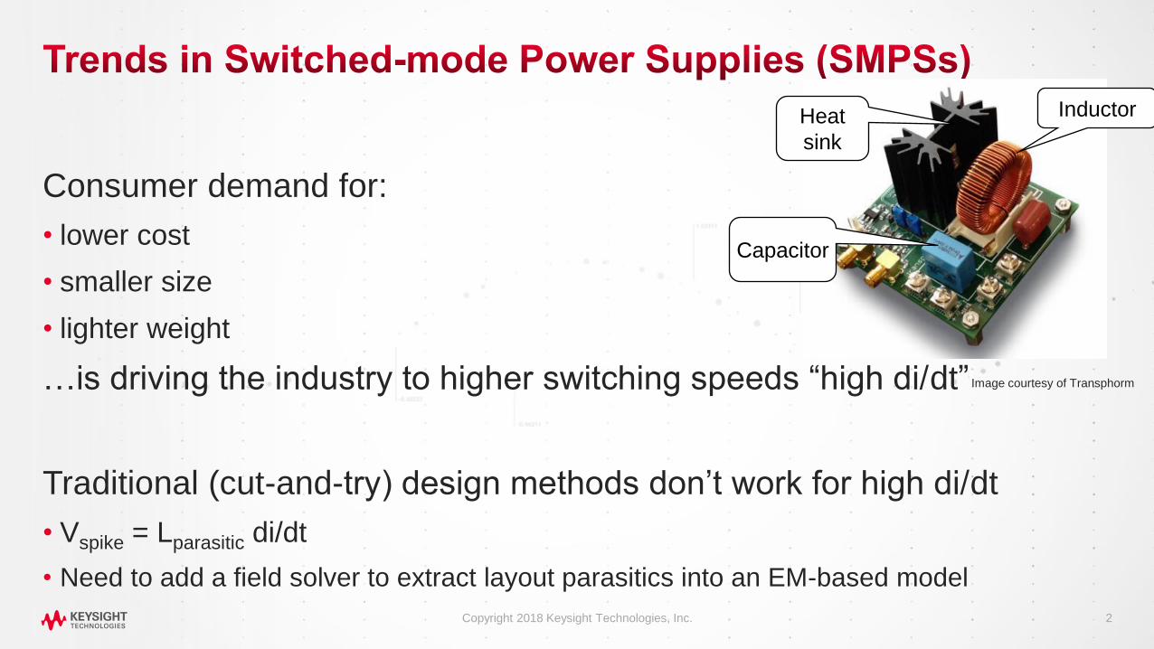
Consumer demand for:
• lower cost
• smaller size
• lighter weight
…is driving the industry to higher switching speeds “high di/dt”
Traditional (cut-and-try) design methods don’t work for high di/dt
• Vspike = Lparasitic di/dt
• Need to add a field solver to extract layout parasitics into an EM-based model
Copyright 2018 Keysight Technologies, Inc.
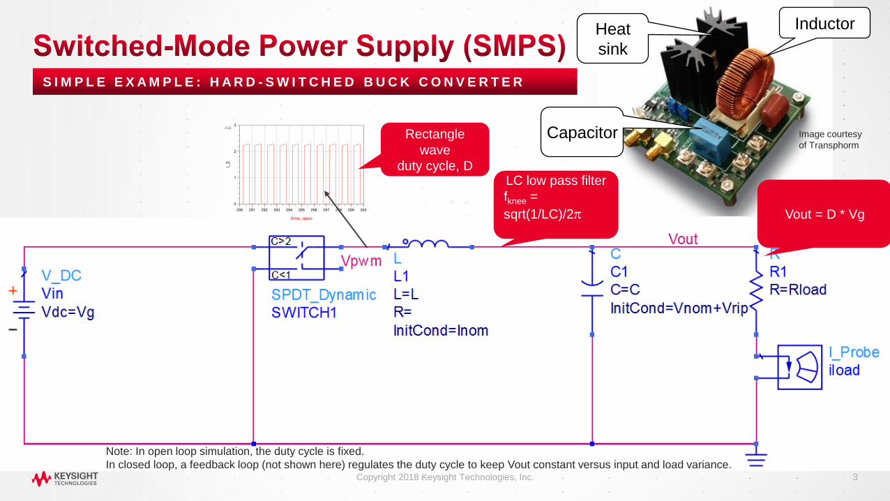
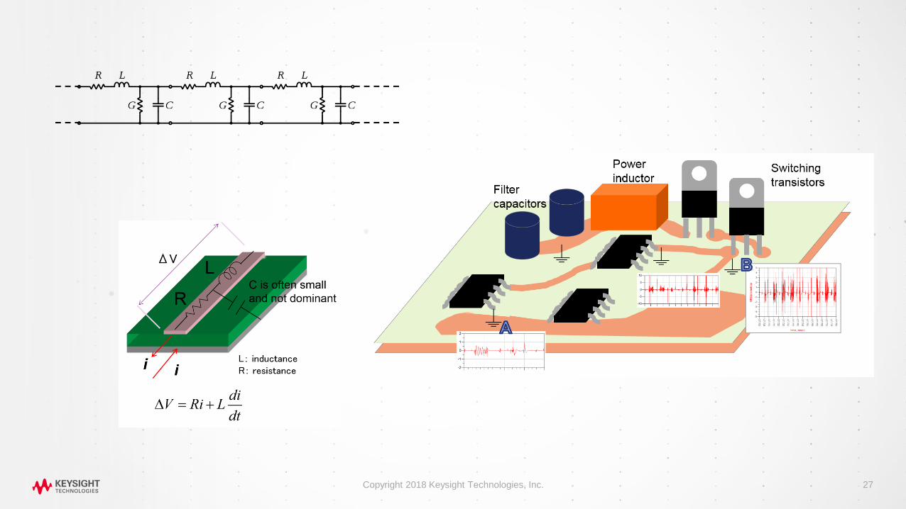
Heat
sink
Inductor
Capacitor
Image courtesy of Transphorm
3
S I M P L E E X A M P L E : H A R D - S W I T C H E D B U C K C O N V E R T E R
Copyright 2018 Keysight Technologies, Inc.
Heat
sink
Inductor
Capacitor Rectangle
wave
duty cycle, D LC low pass filter
fknee =
sqrt(1/LC)/2p
Vout = D * Vg
Note: In open loop simulation, the duty cycle is fixed.
In closed loop, a feedback loop (not shown here) regulates the duty cycle to keep Vout constant versus input and load variance.
Image courtesy
of Transphorm
4
U N L E S S T H E E D G E S P E E D I S I N C R E A S E D A S W E L L
Copyright 2018 Keysight Technologies, Inc.
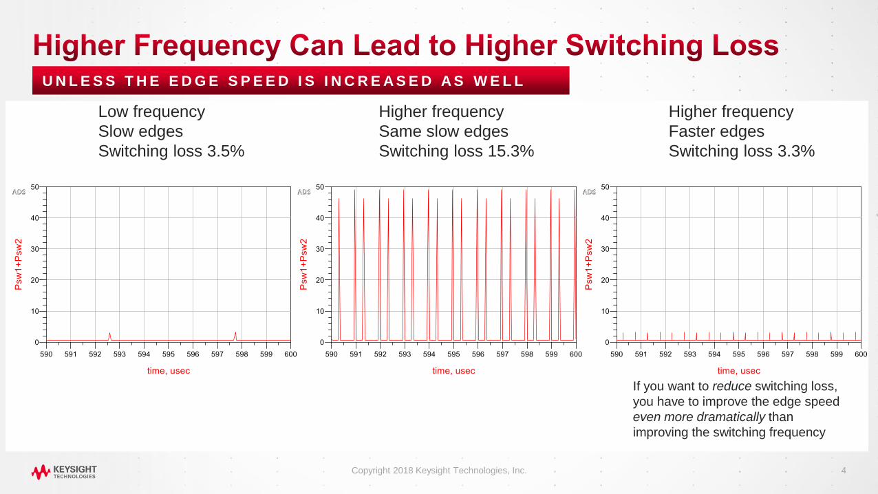
Low frequency
Slow edges
Switching loss 3.5%
Higher frequency
Same slow edges
Switching loss 15.3%
Higher frequency
Faster edges
Switching loss 3.3%
If you want to reduce switching loss,
you have to improve the edge speed
even more dramatically than
improving the switching frequency
5
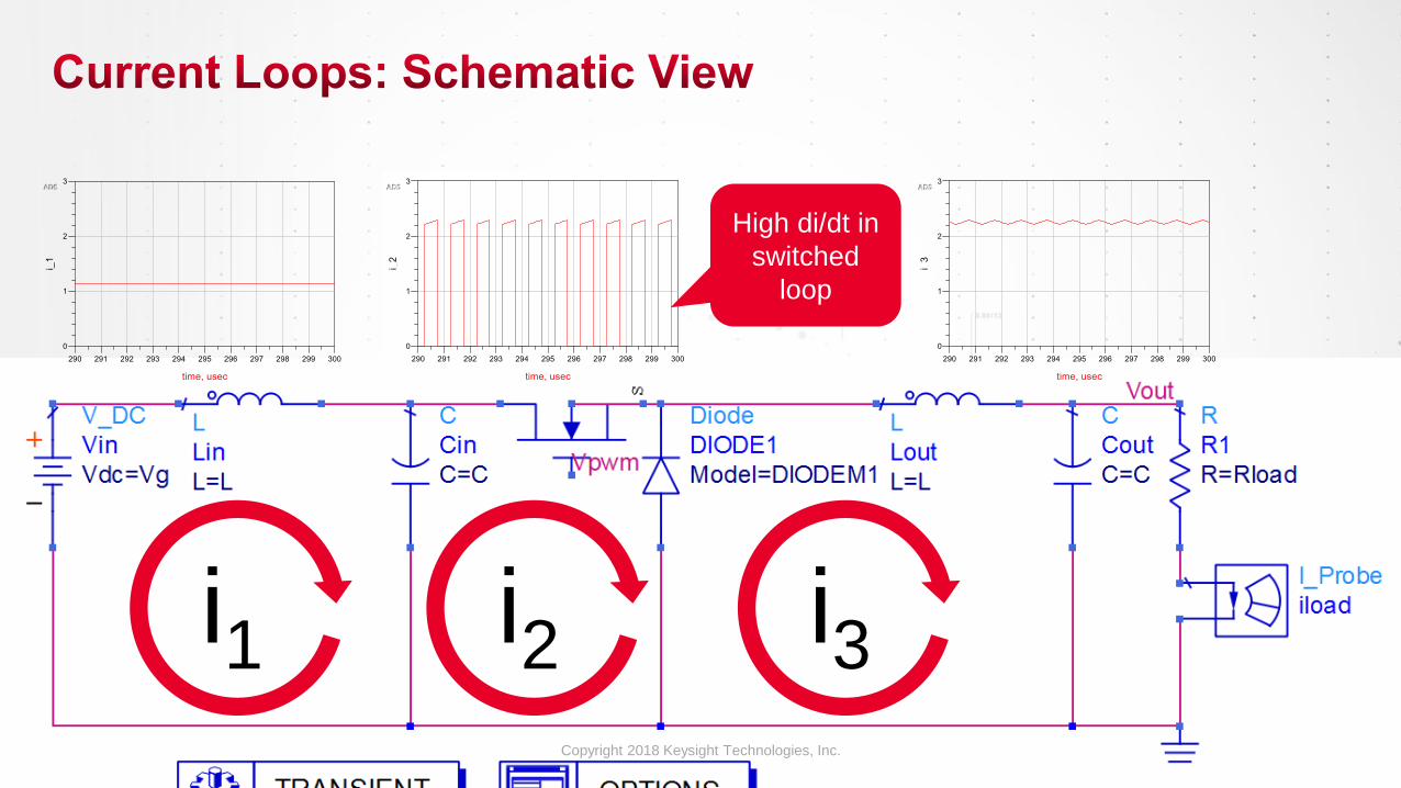
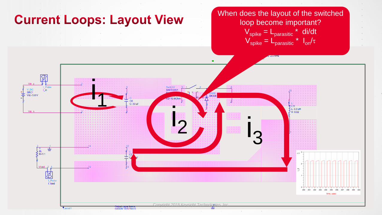
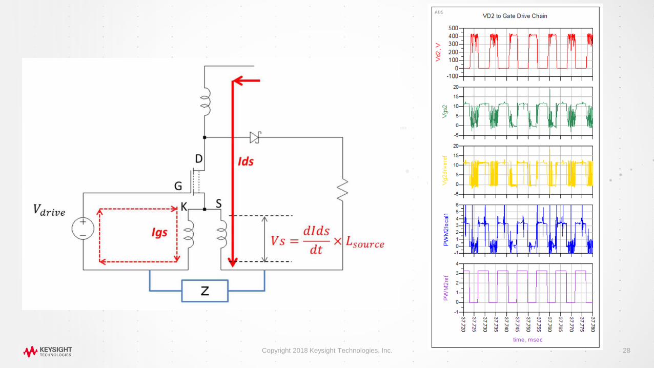
i2 i1 i3
High di/dt in
switched
loop
Copyright 2018 Keysight Technologies, Inc.
6
i1 i2 i3
When does the layout of the switched
loop become important?
Vspike = Lparasitic * di/dt
Vspike = Lparasitic * Ion/t
Copyright 2018 Keysight Technologies, Inc.
7 Copyright 2018 Keysight Technologies, Inc.
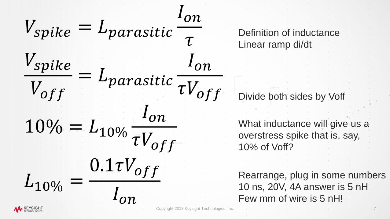
𝑉𝑠𝑝𝑖𝑘𝑒 = 𝐿𝑝𝑎𝑟𝑎𝑠𝑖𝑡𝑖𝑐𝐼𝑜𝑛𝜏
𝑉𝑠𝑝𝑖𝑘𝑒
𝑉𝑜𝑓𝑓= 𝐿𝑝𝑎𝑟𝑎𝑠𝑖𝑡𝑖𝑐
𝐼𝑜𝑛𝜏𝑉𝑜𝑓𝑓
10% = 𝐿10%𝐼𝑜𝑛𝜏𝑉𝑜𝑓𝑓
𝐿10% =0.1𝜏𝑉𝑜𝑓𝑓
𝐼𝑜𝑛
Divide both sides by Voff
Definition of inductance
Linear ramp di/dt
What inductance will give us a
overstress spike that is, say,
10% of Voff?
Rearrange, plug in some numbers
10 ns, 20V, 4A answer is 5 nH
Few mm of wire is 5 nH!
8
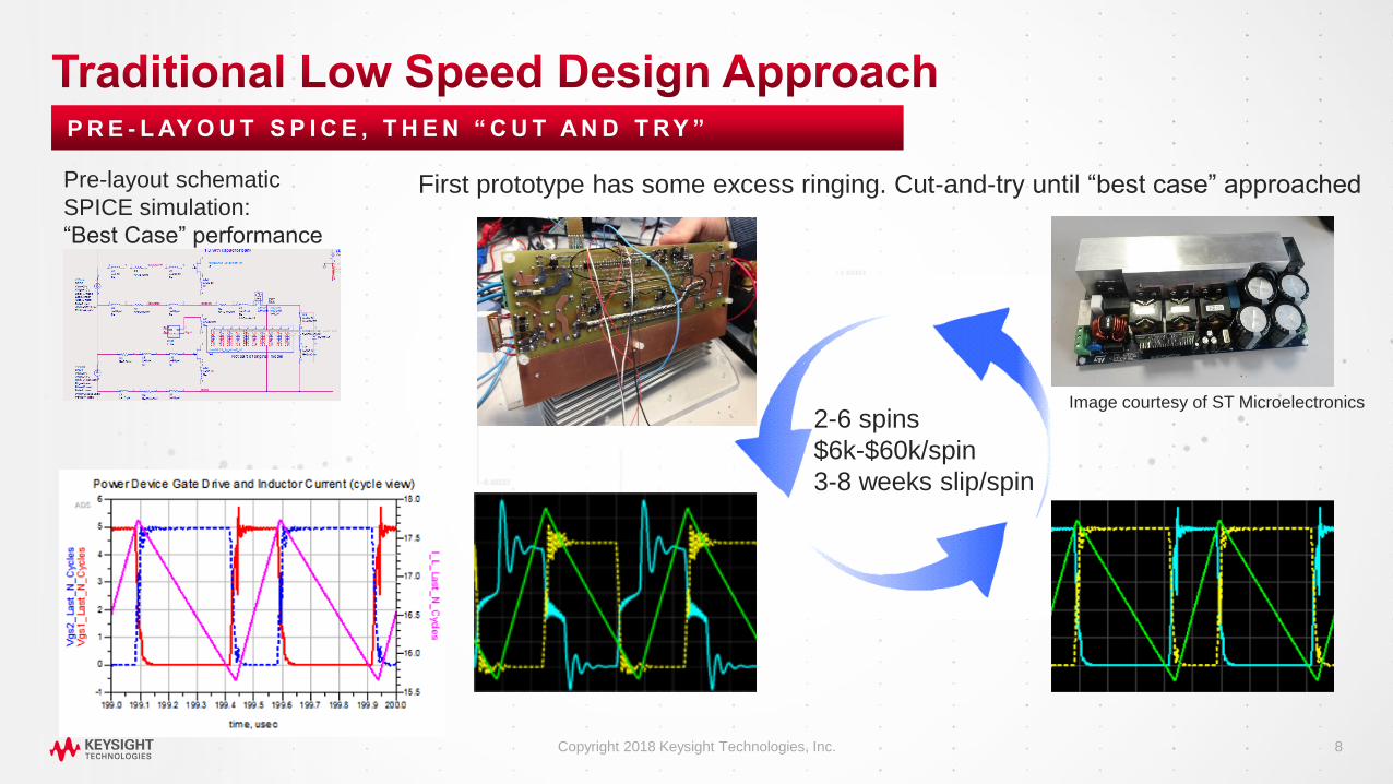
P R E - L AY O U T S P I C E , T H E N “ C U T A N D T R Y ”
Copyright 2018 Keysight Technologies, Inc.
Pre-layout schematic
SPICE simulation:
“Best Case” performance
First prototype has some excess ringing. Cut-and-try until “best case” approached
2-6 spins
$6k-$60k/spin
3-8 weeks slip/spin
Image courtesy of ST Microelectronics

9
P R E - L AY O U T S P I C E , T H E N “ C U T A N D T R Y ”
Copyright 2018 Keysight Technologies, Inc.
Pre-layout schematic
SPICE simulation:
“Best Case” performance
First prototype has destructive failure.
What next?
10 Copyright 2018 Keysight Technologies, Inc.
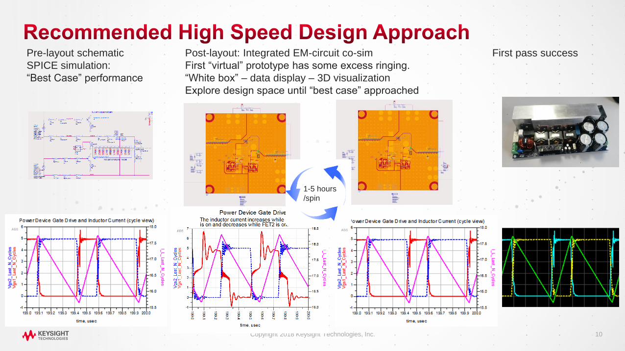
Pre-layout schematic
SPICE simulation:
“Best Case” performance
Post-layout: Integrated EM-circuit co-sim
First “virtual” prototype has some excess ringing.
“White box” – data display – 3D visualization
Explore design space until “best case” approached
First pass success
1-5 hours
/spin

11
N E W P R O B L E M S R E Q U I R E D I F F E R E N T T O O L S
Copyright 2018 Keysight Technologies, Inc.
12
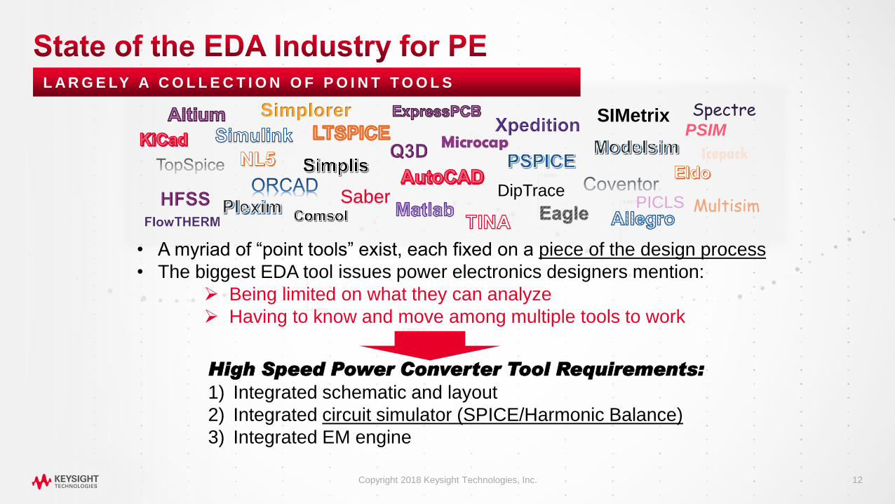
L A R G E LY A C O L L E C T I O N O F P O I N T T O O L S
Saber
Simplorer SIMetrix
• A myriad of “point tools” exist, each fixed on a piece of the design process
• The biggest EDA tool issues power electronics designers mention:
Being limited on what they can analyze
Having to know and move among multiple tools to work
PSIM
Multisim
Microcap
DipTrace
Icepack
PICLS
Spectre
High Speed Power Converter Tool Requirements:
1) Integrated schematic and layout
2) Integrated circuit simulator (SPICE/Harmonic Balance)
3) Integrated EM engine
Copyright 2018 Keysight Technologies, Inc.
13
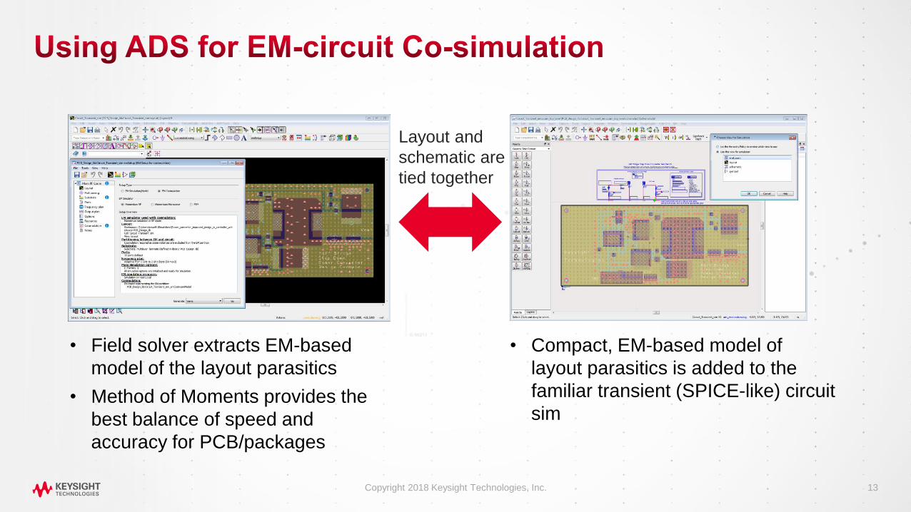
• Field solver extracts EM-based
model of the layout parasitics
• Method of Moments provides the
best balance of speed and
accuracy for PCB/packages
• Compact, EM-based model of
layout parasitics is added to the
familiar transient (SPICE-like) circuit
sim
Layout and
schematic are
tied together
Copyright 2018 Keysight Technologies, Inc.
14
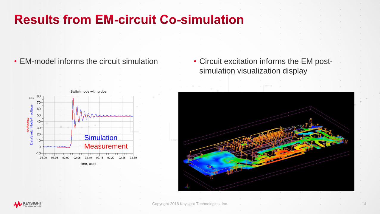
• Circuit excitation informs the EM post-
simulation visualization display
• EM-model informs the circuit simulation
Copyright 2018 Keysight Technologies, Inc.
Simulation
Measurement
15
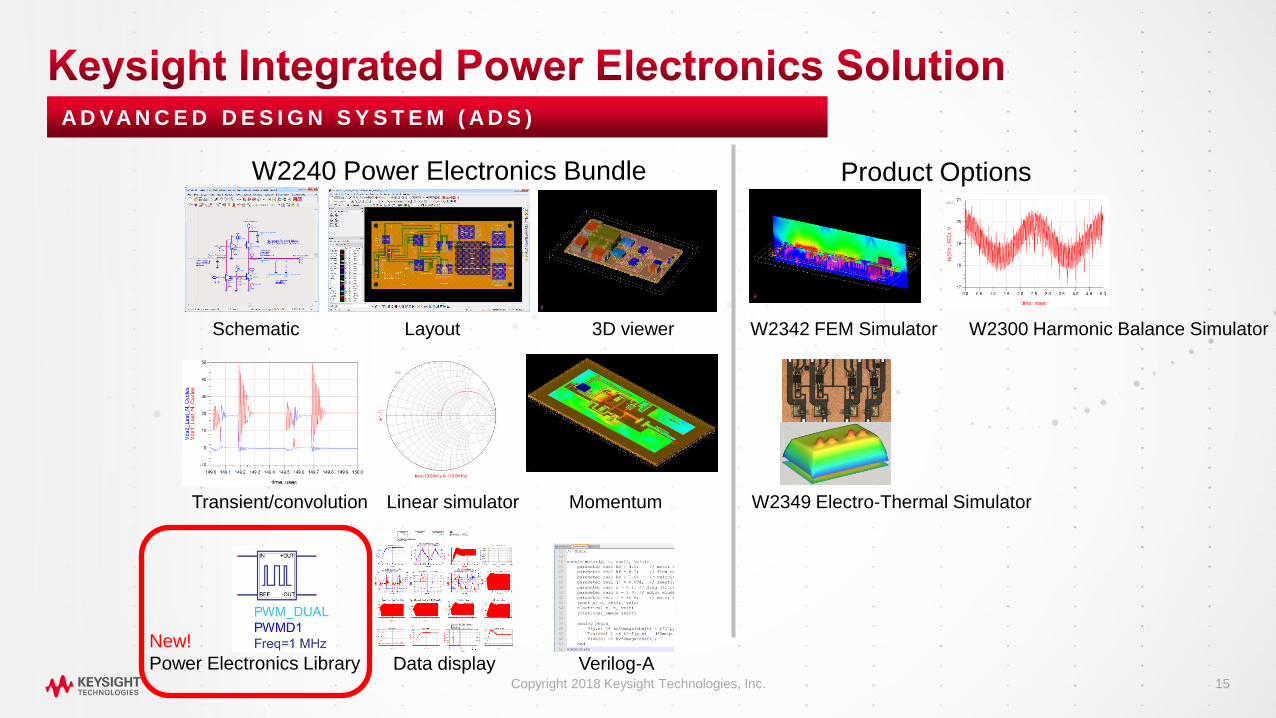
A D VA N C E D D E S I G N S Y S T E M ( A D S )
Copyright 2018 Keysight Technologies, Inc.
Schematic Layout 3D viewer
Data display
Transient/convolution Linear simulator Momentum
W2240 Power Electronics Bundle Product Options
W2342 FEM Simulator
W2349 Electro-Thermal Simulator
W2300 Harmonic Balance Simulator
New!
Power Electronics Library Verilog-A
16
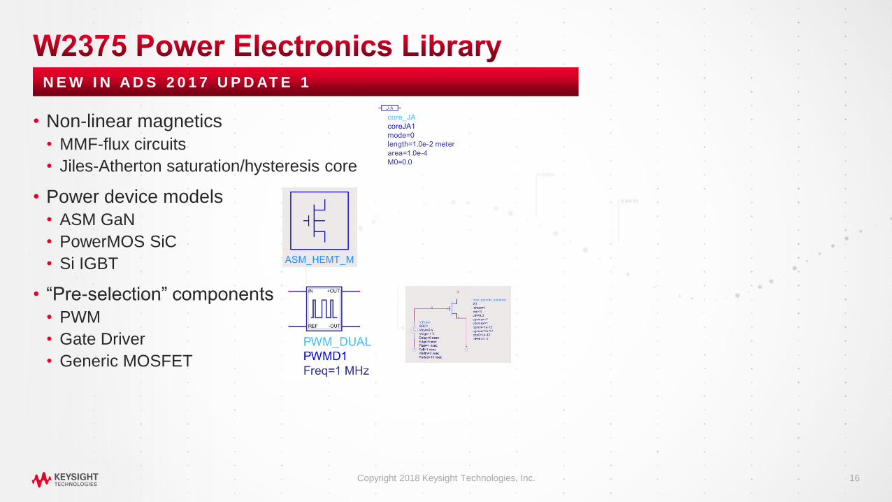
• Non-linear magnetics
• MMF-flux circuits
• Jiles-Atherton saturation/hysteresis core
• Power device models
• ASM GaN
• PowerMOS SiC
• Si IGBT
• “Pre-selection” components
• PWM
• Gate Driver
• Generic MOSFET
N E W I N A D S 2 0 1 7 U P D AT E 1
Copyright 2018 Keysight Technologies, Inc.
17
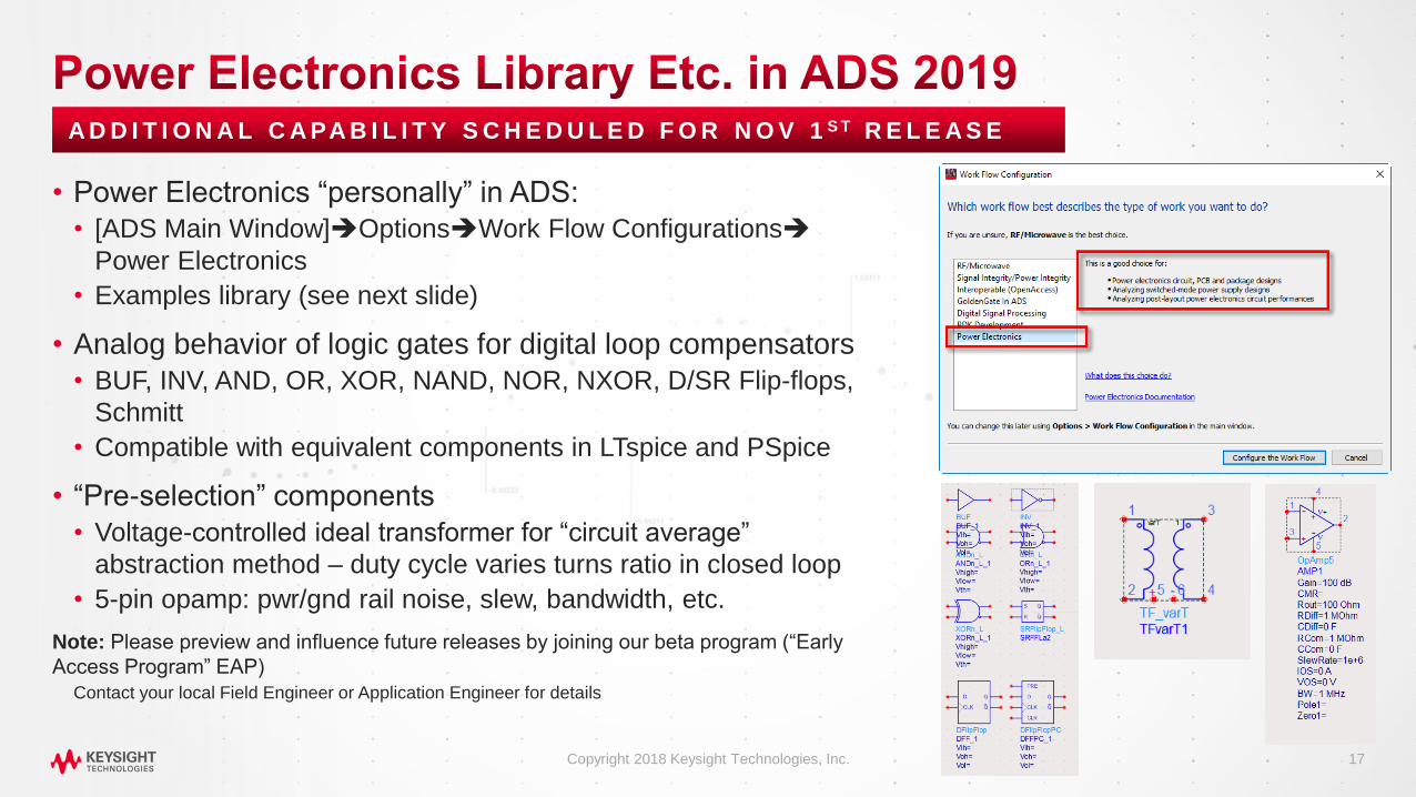
• Power Electronics “personally” in ADS:
• [ADS Main Window]OptionsWork Flow Configurations
Power Electronics
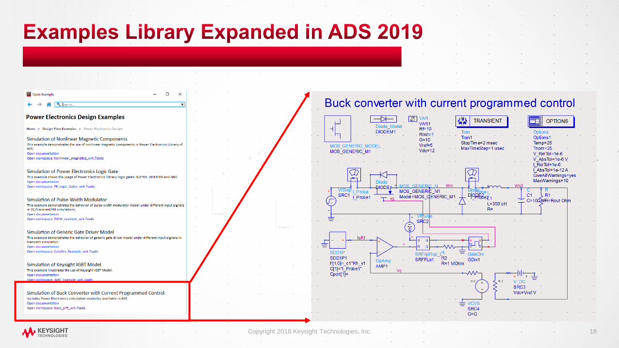
• Examples library (see next slide)
• Analog behavior of logic gates for digital loop compensators
• BUF, INV, AND, OR, XOR, NAND, NOR, NXOR, D/SR Flip-flops,
Schmitt
• Compatible with equivalent components in LTspice and PSpice
• “Pre-selection” components
• Voltage-controlled ideal transformer for “circuit average”
abstraction method – duty cycle varies turns ratio in closed loop
• 5-pin opamp: pwr/gnd rail noise, slew, bandwidth, etc.
Note: Please preview and influence future releases by joining our beta program (“Early
Access Program” EAP)
Contact your local Field Engineer or Application Engineer for details
A D D I T I O N A L C A PA B I L I T Y S C H E D U L E D F O R N O V 1 S T R E L E A S E
Copyright 2018 Keysight Technologies, Inc.
18
Copyright 2018 Keysight Technologies, Inc.
19 Copyright 2018 Keysight Technologies, Inc.
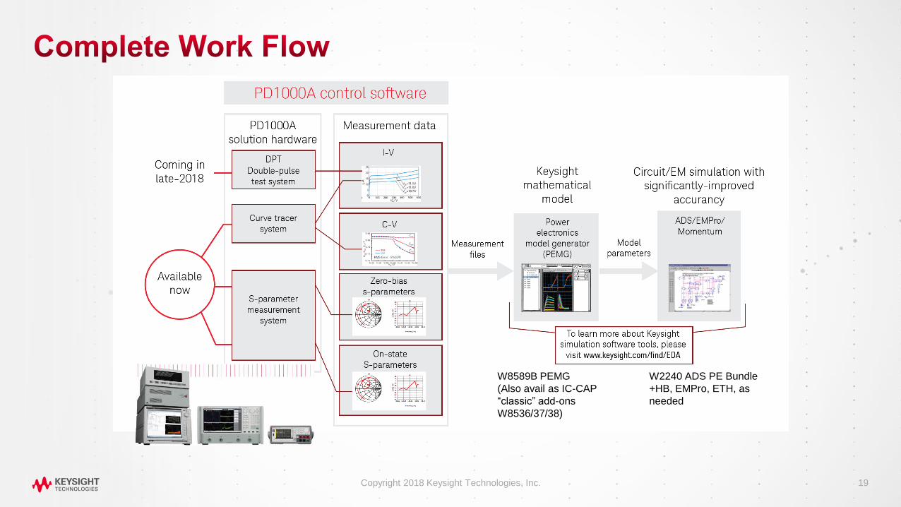
W8589B PEMG
(Also avail as IC-CAP
“classic” add-ons
W8536/37/38)
W2240 ADS PE Bundle
+HB, EMPro, ETH, as
needed
20
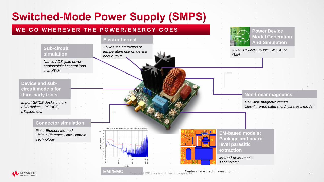
W E G O W H E R E V E R T H E P O W E R / E N E R G Y G O E S
Copyright 2018 Keysight Technologies, Inc.
Native ADS gate driver,
analog/digital control loop
incl. PWM
Sub-circuit
simulation
Finite Element Method
Finite-Difference Time-Domain
Technology
Connector simulation
Method-of-Moments
Technology
EM-based models:
Package and board
level parasitic
extraction
Center image credit: Transphorm
MMF-flux magnetic circuits
Jiles-Atherton saturation/hysteresis model
Non-linear magnetics
Import SPICE decks in non-
ADS dialects: PSPICE,
LTspice, etc.
Device and sub-
circuit models for
third-party tools
Solves for interaction of
temperature rise on device
heat output
Electrothermal
Power Device
Model Generation
And Simulation
IGBT, PowerMOS incl. SiC, ASM
GaN
EMI/EMC
21
Multi-lingual model import • Dialects of SPICE
• Verilog-AMS
• VHDL-AMS
Post-layout EM extraction • PEPro (application-specific EM)
• Momentum (general purpose EM)
• EMI/EMC analysis
Multi-discipline, multi-nature support for motor control etc. • Electrical: voltage/current
• Magnetic: MMF/flux
• Kinematic: position/velocity/force or velocity/force
• Rotational: angle/angular v./torque
• Thermal: temperature/power
• Logic: discrete or analog behavioral
Keysight Confidential Center image credit: Transphorm
Power device model generation • IC-CAP: Full featured for device modelers
• PEMG: Simplified flow for circuit designers,
models from a PDF datasheet
Closed-loop analysis • Bode plot
• Impedance analysis
• Stability in the presence of noise
PathWave • Connect device measurement,
device modeling, circuit design,
simulation, prototype
characterization test, and
manufacturing pass/fail test

22
W I D E - B A N D G A P P O W E R D E V I C E S E N A B L E H I G H D I / D T
Copyright 2018 Keysight Technologies, Inc.

23
R E F E R E N C E D E S I G N : P O W E R M O S + PA C K A G E + P C B
Red: simulated results
Blue: measured results
FDMS86181
PowerTrench® MOSFET
ADS package model
On Semiconductor Test Board
Customers often do
not believe they can
obtain predictive
results. They Can!
On Semiconductor
Copyright 2018 Keysight Technologies, Inc.
Image courtesy of ON Semiconductor
24
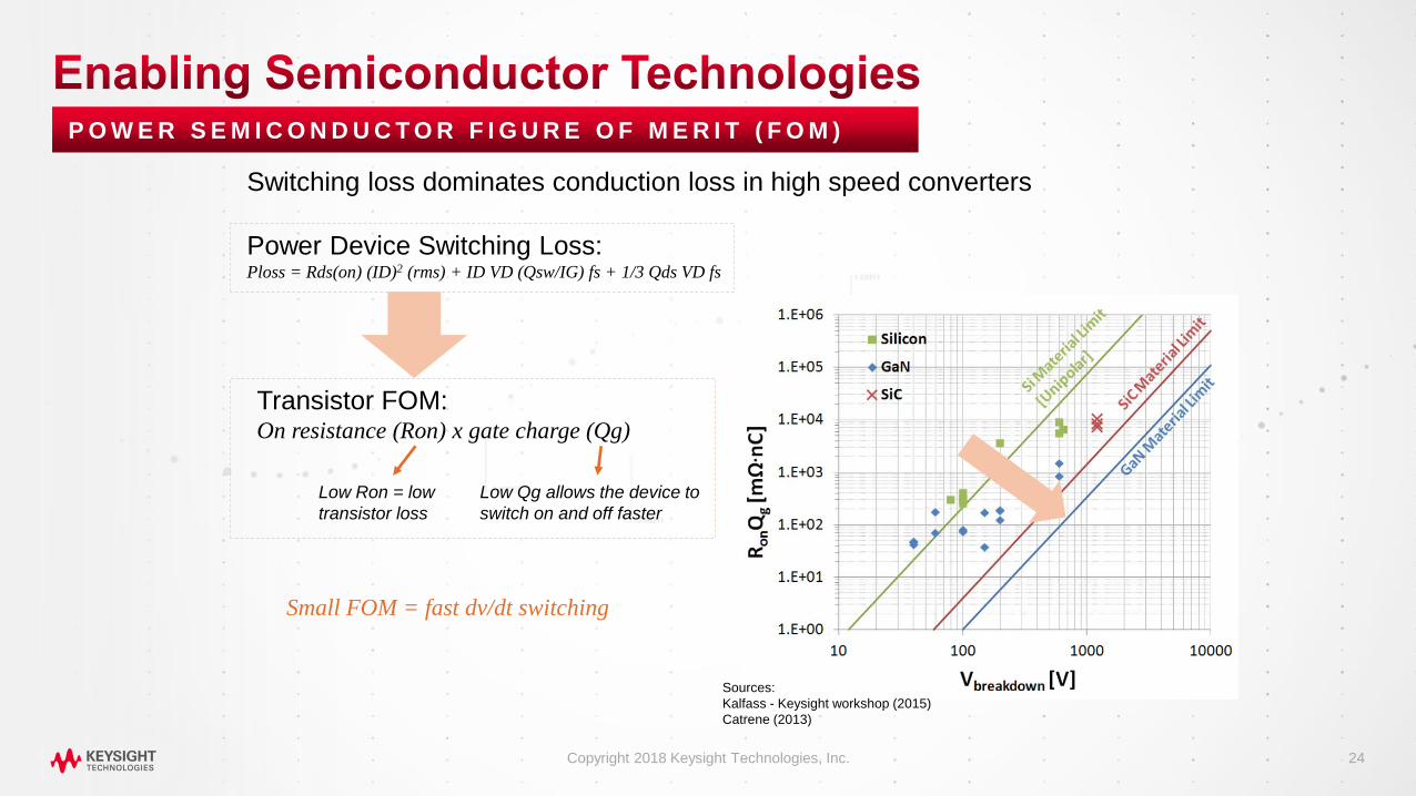
P O W E R S E M I C O N D U C T O R F I G U R E O F M E R I T ( F O M )
Copyright 2018 Keysight Technologies, Inc.
Transistor FOM: On resistance (Ron) x gate charge (Qg)
Small FOM = fast dv/dt switching
Sources:
Kalfass - Keysight workshop (2015)
Catrene (2013)
Switching loss dominates conduction loss in high speed converters
Power Device Switching Loss: Ploss = Rds(on) (ID)2 (rms) + ID VD (Qsw/IG) fs + 1/3 Qds VD fs
Low Ron = low
transistor loss
Low Qg allows the device to
switch on and off faster
25
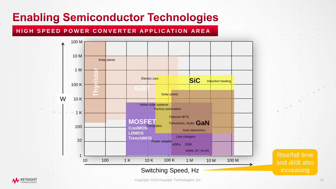
H I G H S P E E D P O W E R C O N V E R T E R A P P L I C AT I O N A R E A
Copyright 2018 Keysight Technologies, Inc.
10 100 M 10 M 1 M 100 K 10 K 1 K 100
10
100 M
10 M
1 M
100 K
10 K
1 K
100
1
Th
yri
sto
r IGBT
MOSFET CoolMOS
LDMOS
TrenchMOS
SiC
GaN
W
Switching Speed, Hz
Power adapter HDDs DDR
Auto electronics
Mobile, BT, WLAN
Home solar systems
Electric cars
Solar plants
Computers Televisions, Audio
Telecom /BTS
Factory automation
Induction heating
Solar plants
Line chargers
Rise/fall time
and di/dt also
increasing

26
IEEE Power Electronics Magazine, June 2017 pp.46-55
Copyright 2018 Keysight Technologies, Inc.
27 Copyright 2018 Keysight Technologies, Inc.
28 Copyright 2018 Keysight Technologies, Inc.
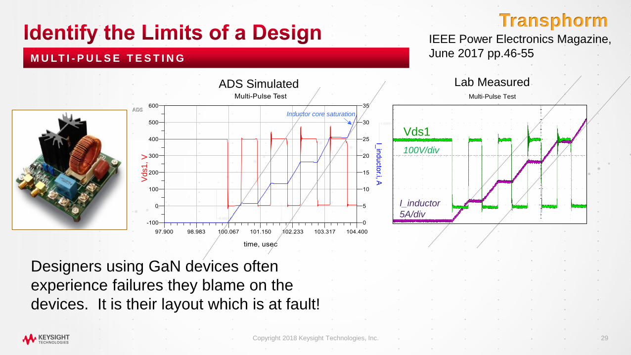
29
M U LT I - P U L S E T E S T I N G
Designers using GaN devices often
experience failures they blame on the
devices. It is their layout which is at fault!
Transphorm
Copyright 2018 Keysight Technologies, Inc.
ADS Simulated
Inductor core saturation
IEEE Power Electronics Magazine,
June 2017 pp.46-55
Lab Measured Multi-Pulse Test
Vds1 V
ds1
, V
100V/div
I_inductor
5A/div
30
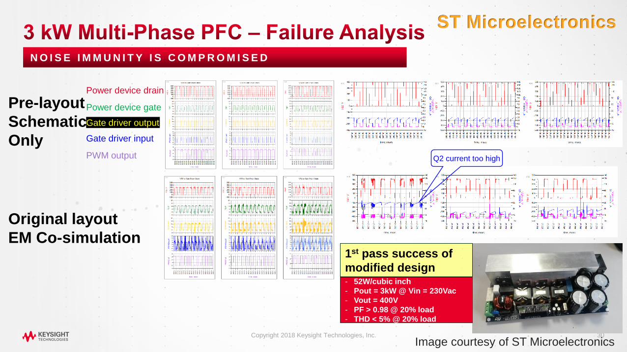
N O I S E I M M U N I T Y I S C O M P R O M I S E D
1st pass success of
modified design - 52W/cubic inch
- Pout = 3kW @ Vin = 230Vac
- Vout = 400V
- PF > 0.98 @ 20% load
- THD < 5% @ 20% load
Pre-layout
Schematic
Only
Original layout
EM Co-simulation
ST Microelectronics
Copyright 2018 Keysight Technologies, Inc.
PWM output
Gate driver input
Gate driver output
Power device gate
Power device drain
Q2 current too high
Image courtesy of ST Microelectronics
31
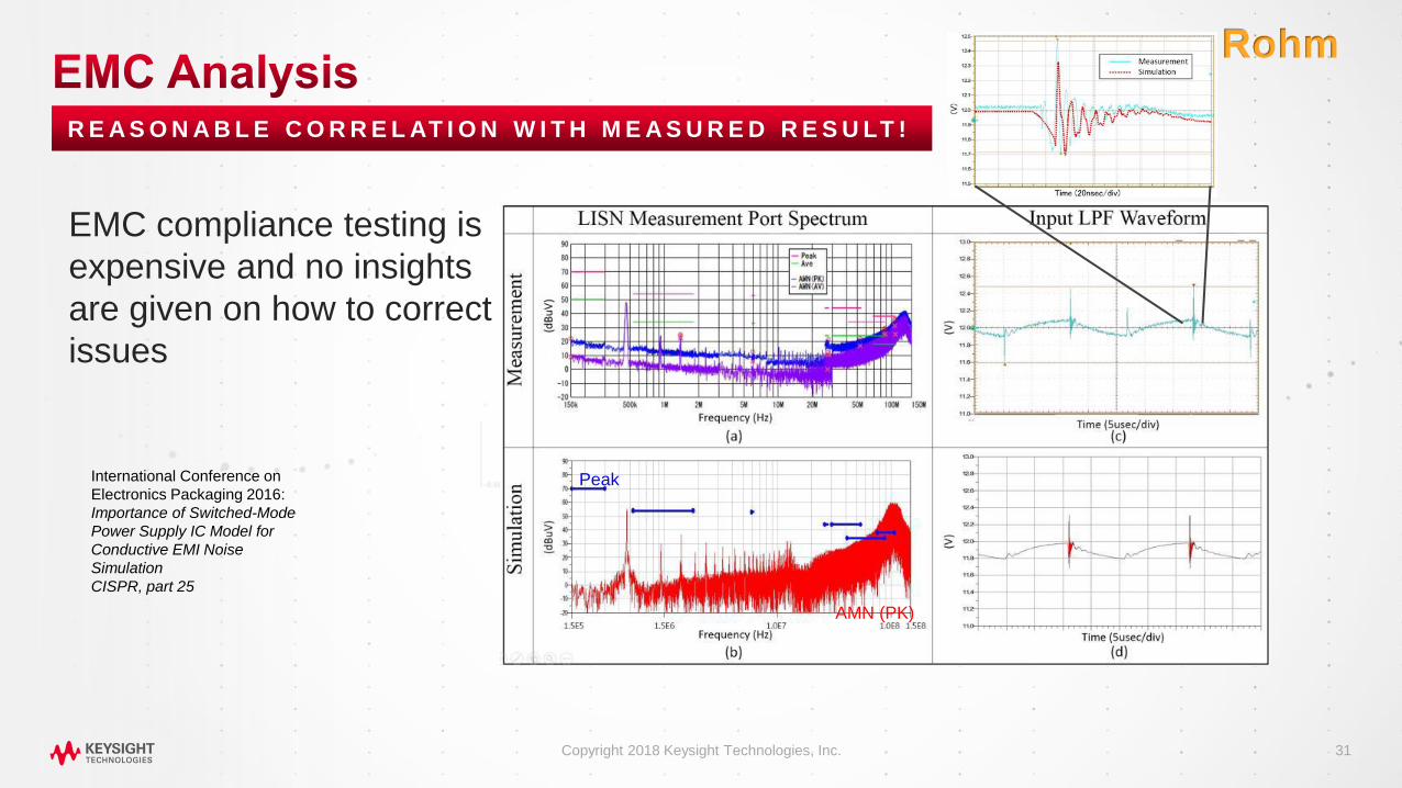
R E A S O N A B L E C O R R E L AT I O N W I T H M E A S U R E D R E S U LT !
EMC compliance testing is
expensive and no insights
are given on how to correct
issues
Rohm
Copyright 2018 Keysight Technologies, Inc.
International Conference on
Electronics Packaging 2016:
Importance of Switched-Mode
Power Supply IC Model for
Conductive EMI Noise
Simulation
CISPR, part 25
Peak
AMN (PK)
32
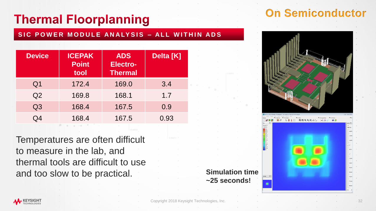
S I C P O W E R M O D U L E A N A LY S I S – A L L W I T H I N A D S
Device ICEPAK
Point
tool
ADS
Electro-
Thermal
Delta [K]
Q1 172.4 169.0 3.4
Q2 169.8 168.1 1.7
Q3 168.4 167.5 0.9
Q4 168.4 167.5 0.93
Simulation time
~25 seconds!
Temperatures are often difficult
to measure in the lab, and
thermal tools are difficult to use
and too slow to be practical.
On Semiconductor
Copyright 2018 Keysight Technologies, Inc.
33
• Increasing power density trends are pushing up switching speed
• High switching speed introduces a whole new class of challenges
• Parasitic effects destroy performance and are costly
• EM Co-simulation provides the best predictive analysis you can get
• An integrated workflow provides more capability and streamlines the workflow
• Quick Start Guide for ADS in Power Electronics https://literature.cdn.keysight.com/litweb/pdf/5992-2514EN.pdf
Copyright 2018 Keysight Technologies, Inc.


