Embed Size (px)
Citation preview

IEEE TRANSACTIONS ON CIRCUITS AND SYSTEMS—I: REGULAR PAPERS, VOL. 51, NO. 2, FEBRUARY 2004 329
Design of Voltage-Mode and Current-ModeComputational Circuits UsingFloating-Gate MOS Transistors
S. Vlassis and S. Siskos, Member, IEEE
Abstract—In this paper, we present voltage-mode and cur-rent-mode computational circuits using floating-gate MOS(FGMOS) transistors, operating in saturation region. The circuitsare designed using two FGMOS basic-cells, each one formed bythree floating-gate transistors with common source. The first basiccell is connected in voltage mode, while the second one is connectedin current-mode configuration in order to implement voltage andcurrent-mode circuits, respectively. Using the basic FGMOS cells,voltage and current squarers, four-quadrant multipliers and acurrent square rooter are designed. Mismatches and distortionanalysis for the proposed circuits have been elaborated. The mostimportant advantages are, rail-to-rail dynamic input range, lowdistortion and ability for either differential or single-ended inputsignals. Simulation results demonstrate the feasibility and theaccuracy of the circuits.
Index Terms—Current-mode squarer/multiplier, current squareroot, floating-gate MOSFETs, voltage-mode squarer/multiplier.
I. INTRODUCTION
ANALOG computational circuits are very useful buildingblocks finding many applications in analog signal pro-
cessing, fuzzy systems, neural networks etc. The circuits’ sim-plicity, area efficiency, and operation speed are their most im-portant characteristics. There are many publications on com-putational circuits such as squarers, multipliers, square rooters,vector calculation, and defuzzification circuits in voltage mode[1]–[11] and in current mode [12]–[17]. These kind of circuitscan manipulate single-ended and/or balanced inputs with thelargest possible dynamic input range featuring small nonlin-earity error and low distortion.
The floating-gate MOS (FGMOS) structures have foundmany applications in op-amp compensation [18], digital-to-analog (D/A) and analog-to–digital (A/D) converters [19],electronic programming [20], neural networks [21], and oper-ation transconductance amplifiers (OTA) [22]. In the last fewyears, there is an increased number of publications on the useof FGMOS structures in the implementation of analog compu-tational circuits. Until now, the FGMOS was mainly used inthe implementation of voltage-mode circuits such as voltagesquarers, multipliers, and attenuators [23]–[28]. The FGMOS
Manuscript received November 15, 2000; revised July 3, 2003. This paperwas recommended by Associate Editor R. Gharpurey.
S. Vlassis is with Theta Microelectronics, Athens 15133, Greece (e-mail:[email protected]).
S. Siskos is with the Electronics Laboratory, Department of Physics,Aristotle University of Thessaloniki, Thessaloniki 54124, Greece (e-mail:[email protected]).
Digital Object Identifier 10.1109/TCSI.2003.822401
transistor is also a very good candidate for single-ended circuitdesign due to its voltage additive characteristics. The draincurrent of a FGMOS is proportional to the square of theweighted sum of its input signals [23]–[28].
In this paper, we propose basic computational circuits involtage mode such as a squarer and a four-quadrant multiplierand extend the use of the FGMOS transistors in the constructionof current-mode computational circuits. A precision currentsquare-rooting circuit, a current squarer and a four-quadrantcurrent multiplier are also proposed.
The advantages of these circuits are rail-to-rail input range,single-ended input signals presenting low distortion in the caseof the voltage-mode ones, and no body-effect which leads to ahighly accurate output current for the current-mode ones.
The paper is organized as follows. The structure and the op-eration of the FGMOS transistor are described in Section II.In Section III, a basic FGMOS cell is proposed which is real-ized by three FGMOS transistors with common source. In Sec-tion IV, a voltage squarer and a four-quadrant voltage multiplierare proposed. In the same section, the component mismatchesand the second-order effects of the voltage squarer, are analyzed.In Section V, a current square-rooting circuit, a current squarerand a four-quadrant current multiplier are proposed. Finally, inSection VI simulation results are given verifying the theoreticalanalysis and demonstrating the feasibility and the effectivenessof the proposed circuits.
II. FGMOS TRANSISTOR
The basic structure of an -channel FGMOS transistorwith -input voltages , is shown in Fig. 1(a).The floating gate is formed by the first polysilicon layer overthe channel while the -input gates are formed by the secondpolysilicon layer and they are located over the floating gate. Thefloating gate is capacitively coupled to the -input gates. Thesymbolic representation of such devices is shown in Fig. 1(b).
The drain current of a FGMOS transistor with -input gatesin the saturation region, neglecting the second-order effects isgiven by the following equation [23]–[28]:
(1)
where is the transconductance parameterof the transistor, the electron mobility, the floating-gateoxide capacitance, the transistor aspect ratio,
1057-7122/04$20.00 © 2004 IEEE

330 IEEE TRANSACTIONS ON CIRCUITS AND SYSTEMS—I: REGULAR PAPERS, VOL. 51, NO. 2, FEBRUARY 2004
(a)
(b)
Fig. 1. (a) Structure of an n-input FGMOS transistor. (b) Symbolicrepresentation.
are the capacitive coupling ratios, is the source voltage, andis the threshold voltage of the transistor. The input capacitive
coupling ratios are defined as
(2)
where is the input capacitances between the floating gate andeach of the th input (see Fig. 1), is the total capacitanceassociated with the floating gate, which in the saturation regionis given by
(3)
where is the oxide capacitance in the saturation re-gion and is the overlap capacitance between floating gateand source. It is assumed that the overlap capacitance betweenfloating gate and drain and the parasitic capacitance be-tween floating gate and bulk are very small compared tothe . The other capacitive coupling ratios associated with theoverlap capacitances are given by
and . It should be notedthat the capacitances , , and are proportional to thechannel width of a MOS transistor. The capacitances ,
are given by , whereis the floating-gate oxide capacitance per unit area,
is the gate-to-source overlap capacitance per unit channel width.Equation (1) shows that the FGMOS transistor drain current insaturation is proportional to the square of the weighted sum ofthe input signals, where the weight of each input signal is de-termined by the capacitive coupling ratio of the correspondinginput.
III. BASIC FGMOS CELL
The proposed computational building blocks are constructedusing the basic FGMOS cell, which is shown in Fig. 2. The basicFGMOS cell has two configurations, voltage-mode configura-
(a)
(b)
Fig. 2. (a) Basic FGMOS voltage-mode cell, V-M cell. (b) Current-mode cell,C-M cell.
tion (V-M cell), Fig. 2(a), and current-mode configuration (C-Mcell), Fig. 2(b). Both are constructed by three FGMOS transis-tors Mx, My, and Mz, operating in saturation, in a common-source configuration. Mx and My have one input gate and Mzhas two input gates. In the V-M cell, and are the twosingle-ended input voltages and , , and are the threeoutput currents, while in the C-M cell and are the twoinput currents and is the output current.
By setting the aspect ratio of the Mz twice that of Mx and My,and the floating-gate oxide capaci-
tance of Mz is twice that of Mx and My,and and also, the floating gate-to-source overlapcapacitance of the Mz is twice that of Mx and My,
and . The input capacitances of thethree transistors are equal to . Therefore, the capacitive cou-pling ratios and of the Mx, My, respectively, and the twoequal capacitive coupling ratios of Mz are given by
(4)
(5)
The capacitive coupling ratios and associated with theoverlap capacitances have the same values for transistors Mx,My, and Mz are and
. Thus, the currents , , and the voltages ,both of V-M and C-M cells satisfy the following:
(6)
(7)
(8)
Next, we shall describe the way that the basic cells can be used toconstruct a number of computational building blocks in voltageand in current-mode.

VLASSIS AND SISKOS: DESIGN OF VOLTAGE-MODE AND CURRENT-MODE COMPUTATIONAL CIRCUITS 331
Fig. 3. Proposed squarer.
IV. VOLTAGE-MODE CIRCUITS USING THE V-M CELL
A. Voltage Squarer and Four-Quadrant Multiplier
One shortcome of many computational circuits such assquarers and multipliers is that they require balanced inputsignals. The input signal range and the total harmonic distortion(THD) will suffer if no balanced input signals are used. Also,normal operation of these circuits requires additional circuitry,such as input stages, to transform a single-ended input signalto its balanced counterpart. These input stages decrease theaccuracy and the frequency performance of the overall circuit.
In this section, we shall describe the principle of operationof a voltage squarer that overcomes the above disadvantages.The proposed voltage squarer implemented using the V-M cell[23], is shown in Fig. 3. The bias current source , which isadded, can be excluded and the common-source voltage can beconnected to the negative supply voltage. However, this schemerequires a more complicated common-mode feedback circuit atthe output stage. and are the single-ended input voltagesand the equal load resistor. After routine calculations andusing (6)–(8), the output voltage can be expressed as
(9)
From (9), the output voltage is proportional to the square ofthe difference of the two single-ended or balanced input signals
and . These two inputs are directly applied to the squarerwithout additional circuitry. Clearly, the gain of the squarer isdetermined by the transistor transconductance parameter andthe square of the coupling ratio .
An alternative realization of the squarer is shown in Fig. 4(a),while the symbol of the squarer is shown in Fig. 4(b). As shownin Fig. 4, one more input gate (namely bias gate) is added ineach of the FGMOS Mx, My, and Mz with the coupling ratiosdenoted as , , and , respectively. The input capac-itances of the bias gate are for Mx and My and for Mz(see Fig. 4). The voltage is applied to the bias gate. The new
(a)
(b)
Fig. 4. Alternative realization of the (a) squarer and (b) symbol.
capacitive coupling ratios , , and of the input gate ofeach transistor are
(10)
(11)
while the capacitive coupling ratios of the bias gate , for, , , of each transistor
(12)
(13)
Cancellation of the common terms associated with the , ,and is achieved due to the common-source connection ofthe three FGMOS transistors. The output voltage of the alterna-tive realization of the squarer is given again by (9). As shownnext, with appropriate adjustment of the bias voltage , the
window of each FGMOS can be effectively shifted withinthe supply rails in order to achieve rail-to-rail input range andminimum nonlinearity.
A four-quadrant multiplier can be easily implemented usingthe proposed squarer of Fig. 4, as it is shown in Fig. 5. Threesquarers are used, where the input voltages of the first squarerare and 0, the input voltages of the second are andand the input voltages of the third squarer are 0 and . Thismultiplier implementation is based on the identity

332 IEEE TRANSACTIONS ON CIRCUITS AND SYSTEMS—I: REGULAR PAPERS, VOL. 51, NO. 2, FEBRUARY 2004
Fig. 5. Four-quadrant multiplier using the proposed squarer of Fig. 4.
. After routine calculations the output voltageof the multiplier is given by
(14)
which is the four-quadrant multiplication of the two single-ended or differential input signals and . An alternativemultiplier implementation is based on the identity
but it requires an additional circuit to obtain thevoltage summation .
B. Input Range of the Squarer
The input voltage range of the squarer is determined by sev-eral factors. The first factor is related to the cut-off condition forthe FGMOS transistor. In order to find an expression for max-imum input range the common-source voltage needs to beexpressed in terms of input signals. The last can be obtained byequating the current source with the sum of the drain cur-rents of the Mx, My, and Mz. Substituting the expression forthe drain currents , , , as described from (6)–(8), into theequation and solving for the common-sourcevoltage we take the following expression:
(15)
In (15), and are single-ended input signals.The FGMOS transistor is always ON when
. Thus, based on this inequality and substitutingthe expression for the voltage as described in (15), themaximum voltage range is determined by the inequality
(16)
In Fig. 6, the set of lines denoted by (i) and (ii) are the plotof (16) for two values of the bias current source and ,respectively . According to (16), an increase of the
results in a higher input voltage range. As long as the inputvoltages are located within the area enclosed by the lines theFGMOS would not be in cutoff. Therefore, appropriate choiceof may extend the linear input range rail-to-rail.
Fig. 6. Input range of the squarer.
A second factor that limits the maximum input range is thecondition in which the transistor MB2, which acts as currentsource, enters the linear region. This factor is dominant at thethird quadrant when the two single-ended input voltages havelarge negative values. A way to avoid this problem is to increasethe input attenuation at the cost of the input noise performance.Another way, that it can be applied to the proposed circuit, is theusage of an additional input gate biased at . Using the addi-tional bias gate the input range increase, since MB2 is always insaturation, without using an increased input attenuation. In thiscircuit, a tradeoff was made between input attenuation and inputrange in order to achieve the minimum possible input attenua-tion for rail-to-rail input range.
For the operation of MB2 in saturation, when both inputstake the minimum values which are equal to the negative powersupply , the inequality
or must be fulfilled. Basedon the above inequality and using (15) for the common-sourcevoltage and also , thedependence of the bias voltage from the other circuit pa-rameters is determined by the inequality
(17)
where is the transconductance parameter of the transistorMB1. From (17), for small values of the compared to ,the bias voltage must take large values in order to maintain
into saturation.A third factor, which determines the maximum input range, is
related with the linear operation of the FGMOS. We assume thatthe currents , , and flow through the two load resistors .When the bias current is increased, the voltage drop across loadresistance is also increased, causing the FGMOS to operatein the linear region. This applies especially in the first quadrantwhen both inputs have their maximum value. For proper opera-tion in the saturation e.g., for the transistor Mx when both inputstake their maximum value which is equal to the positive supplyvoltage, , the inequality
must be fulfilled. Based on this inequality and also

VLASSIS AND SISKOS: DESIGN OF VOLTAGE-MODE AND CURRENT-MODE COMPUTATIONAL CIRCUITS 333
using (15) for the common-source voltage and the expres-sion for the drain voltage of thetransistor Mx, the dependence of the load resistance from theother circuit parameters is determined by the inequality
(18)
Equation (18) indicates that a decrease of the power supplyvoltage results in a decrease of in orderto ensure that the transistors operate into the saturation region.Equations(16)–(18) show that it is possible to obtain a rail-to-railinput range by a careful choice of the design parameters suchas capacitive coupling ratios, aspect ratio of the transistors, biascurrent , bias voltage , and the load resistance.
The main features of the proposed squarer are the circuit’ssimplicity, the single-ended and/or balanced input signals pro-cessing without additional circuitry, large input signal rangeequal to 100% of the supply voltage and small nonlinearity error,less than 0.5%.
C. Component Mismatches and Second-Order Effects of theVoltage Squarer
The operation of the voltage squarer has been analyzedneglecting the deviations from the ideal square law due tocomponent mismatches as well as mobility degradation,channel-length modulation and the effect of the floatinggate-to-drain overlap capacitance. These nonidealities repre-sent the basic source of errors of the squarer. The resultingdistortion will be calculated by applying a sinusoidal signal toone input, , while keeping the other inputconstant. Both calculations and simulations are valid for lowfrequencies. The technology parameters, the aspect ratios ofthe MOS components and the capacitive coupling ratios arepresented in Section VI with additional simulation results.
1) Component Mismatches: The ideal voltage output of thesquarer, which is given by (9), can be rewritten as
(19)
where the constants and are functions of the input, and are given by ,
, while is independent of .In order to calculate the effect of the component mismatcheson the voltage squarer accuracy, we assume that the value ofa component of a transistor Mq, such as its transconductanceparameter or the threshold voltage , is given by
(20)
where is the nominal value of the component of transistorMq, is the variation from the nominal value . Therefore,substituting (20), into (6)–(8), the voltage output of the squareris a function of the input voltages and the component mismatchand can be expressed as
(21)
where is the output offset,is the gain error and
is the error depending on the inputvoltage . According to the above considerations, the worstcase distortion in decibels of the squarer, under full-scaleinput conditions, can be defined by
(22)
The worst case distortion occurred under full-scale input con-ditions, where one input was held at the positive or neg-ative power supply and the other is a sinusoidal signal
.a) Input capacitive coupling ratio mismatches: Mis-
match in the coupling ratio between FGMOS transistors hasa significant effect on the performance of the voltage squarer.In order to keep the analysis simple, we assume that there isno mismatch between the bias input gate of each FGMOS.Let us suppose that the input-gate mismatch between FGMOStransistors is
for (23)
and
(24)
where is the mean value of the capacitive coupling ratio. Thecapacitive-coupling-ratio mismatches produce a voltage offsetwhich has the following expression:
(25)where . By substituting (23) and (24)into (9), and using (15), the coefficients and havethe following expressions:
(26)
(27)
(28)
(29)
where the input is kept constant at 1.5 V (equal to )and the other input is . Fig. 7 shows thecalculated and simulated results for the worst case distortion

334 IEEE TRANSACTIONS ON CIRCUITS AND SYSTEMS—I: REGULAR PAPERS, VOL. 51, NO. 2, FEBRUARY 2004
Fig. 7. Worst case distortions of the voltage squarer versus threshold voltagemismatches �V , input coupling ratio mismatches �w , bias-gate couplingratio mismatches�w , transconductance mismatches�K and load resistancemismatches �R.
versus the percentage mismatch of the input couplingratio, . The worst case , under full-scaleinput conditions, are less than 45 dB, for
and mismatch of the input coupling ratios.b) Transconductance parameter mismatch: We assume
that the transconductances mismatch between the FGMOStransistors are
for (30)
and
(31)
where is the mean value of the transconductance parame-ters. The transconductance parameters mismatches produce adc output offset, which is given by the following:
(32)
By substituting (30) and (31) into (9) and using (15), the coef-ficients and have the following expressions:
(33)
(34)
(35)
The FGMOS transistors must be placed in the closest pos-sible proximity in order to obtain matching of transistors. Fig. 7shows the theoretical and simulated results for the worst casedistortion of the voltage squarer versus the percentagemismatch of the transconductance parameters, . As-suming worst case conditions, and
, the theoretical and simulated results show thatthe worst distortion , under full-scale input conditions,is less than 64 dB.
c) Threshold voltage mismatch: We assume that thethreshold voltage mismatch between the FGMOS transis-tors are
for (36)
where is the mean value of the threshold voltage. Thethreshold voltage mismatches produce a dc output offset, whichis given by the following:
(37)
By substituting (36) into (9) and using (15), the coefficientsand have the following expressions:
(38)
(39)
(40)
Fig. 7 shows the calculated and simulated results for the worstcase distortion of the voltage squarer versus the per-centage mismatch of the threshold voltage . As-suming worst case conditions, and
, the calculated and simulated results show thatis less than 42 dB.
d) Bias-gate capacitive coupling ratio mismatch: Themismatch in can be expressed as
for (41)
where is the mean value of the bias-gate capacitive couplingratio. It is assumed that the remaining coupling ratios betweentransistors associated with the signal input gate are matched.The bias-gate capacitive coupling ratio mismatches produce adc output offset, which is given by the following:
(42)

VLASSIS AND SISKOS: DESIGN OF VOLTAGE-MODE AND CURRENT-MODE COMPUTATIONAL CIRCUITS 335
By substituting (41) into (9) and using (15), the coefficientsand have the following expressions:
(43)
(44)
(45)
Fig. 7 shows the calculated and simulated results for the worstcase distortion versus the percentage mismatchof the bias-gate capacitive coupling ratio, . As-suming worst case conditions, and
, the calculated and simulated results show thatthe , under full-scale input conditions, is less than
47.5 dB.e) Load resistance mismatch: The mismatch in the load
resistance can be expressed as
for (46)
where is the mean value of the load resistor. The load re-sistor’s mismatches produce a dc output offset, which is givenby the following:
(47)
By substituting (46) into (9) and using (15), the coefficientsand have the following expressions:
(48)
(49)
(50)
(51)
(52)
Fig. 7 shows the calculated and simulated results for the worstcase distortion versus the percentage mismatch of thebias-gate capacitive coupling ratio, . Assuming worstcase conditions, , the calculated andsimulated results show that the worst , under full-scale input conditions, is less than 79 dB.
From the above theoretical analysis and simulation results,we should ensure adjacent placement and placement in closeproximity of the matched floating-gate transistors, input-gateand bias-gate capacitance and load resistors in order to reducedevice mismatches when the layout is designed.
2) Second-Order Effects:a) Mobility degradation: Another factor which reduces
the accuracy of the voltage squarer is the mobility degradation.The carrier mobility model used to estimate the effect of mo-
bility degradation under high electric-field conditions gives forthe mobility, the following:
(53)
where is the mobility-degradation coefficient and is thezero-field mobility of electrons. Including (53) into drain cur-rent drain expression of each transistor the dc output offset isgiven by
(54)
The coefficients and have the following expressions:
(55)
(56)
(57)
(58)
(59)
Fig. 8 shows the calculated and simulated results for the worstdistortion caused by mobility degradation versus
, where the input is kept constant at 1.5 V and forV . The calculated and simulated results for the
worst distortion , under full-scale input conditions, is about42 dB.
b) Channel-Length Modulation: To evaluate the distortioncaused by channel-length modulation, the factor hasto be included in the drain current expression of all transistors.Thus, the output voltage is given by
(60)Fig. 8 shows the calculated and simulated results for the worstdistortion caused by channel-length modulation versus ,where the input is kept constant at 1.5 V and the modula-tion factor is V . The worst , under full-scaleinput conditions, is about 58 dB.
c) Effect of flooding-gate-to-drain overlap capaci-tance : To evaluate the distortion caused by theflooding-gate-to-drain overlap capacitance the additional term
has to be included in the drain current expression of allthe transistor, where and is the drain voltageof each transistor. By neglecting the higher order terms, thecoefficients and have the following expressions:
(61)
(62)

336 IEEE TRANSACTIONS ON CIRCUITS AND SYSTEMS—I: REGULAR PAPERS, VOL. 51, NO. 2, FEBRUARY 2004
Fig. 8. Worst case distortions of the voltage squarer caused by mobilityreduction D , channel-length modulation D , and flooding-gate-to-drainoverlap capacitance D versus input signal V = V while V = �1:5 V.
(63)
(64)
In Fig. 8, the calculated and simulated results for the worstcase distortion caused by the flooding-gate-to-drainoverlap capacitance are shown, where the input is keptconstant at 1.5 V and . The worst case ,under full-scale input conditions, is about 67 dB.
The above results for the second-order effects show that themaximum distortion caused by the mobility degradation is equalto 45 dB. This is due to the fact that the factor
is different for each transistor under full-scale condition,V, causing a relatively large variation of the
transconductance parameter between transistors Mx, My, andMz.
V. CURRENT-MODE CIRCUITS USING THE C-M CELL
The fundamental current-mode approach [29] to realize asquare-root function is based on MOS translinear principle.The major drawback of this kind of circuits is the body effectwhich decreases rapidly the accuracy. In this section a newapproach to realize precision current-mode circuits, such assquare-rooting circuit, squarer and multiplier, based on thecurrent-mode cell (C-M cell), is proposed.
A. Square Rooting Circuit
The circuit is shown in Fig. 9. The NMOS floating-gate tran-sistors Mx, My, and Mz do not exhibit body effect, in spite ofusing n-well technology, since their sources are connected to thesubstrate. Eliminating the voltages and from (6)–(8), thedrain current of the Mz is given by
(65)
So
(66)
Fig. 9. Square-rooting circuit based on the C-M cell.
(a)
(b)
Fig. 10. (a) Core cell and its symbols for current-source configuration Core+and (b) for current-sink configuration Core-.
Thus, the output current of the square rooting circuit can beexpressed as
(67)
which is proportional to the square root of the product of the twoinput currents. In other words, the output current is equal tothe geometric mean of the two input currents and . Theinput currents are limited to take always positive value whiletheirs lowest limit is set from the transition of the transistorsMx and My from saturation to subthreshold region.
B. Current-Mode Squarer and Multiplier
The current squarer is constructed by two core circuits whichare shown in Fig. 10(a). The symbols of the core circuits in cur-rent source configuration (Core+) and in current sink configu-ration (Core-), are shown in Fig. 10(b). The input current of theCore circuits is , the output current is now the current whilethe current is its bias current. The transistors Mm1-Mm3,Mxconstruct the bias circuit. The bias current is redirected to theinput node (namely in) through current mirror Mm2-Mm3. Thecurrent is mirrored to the node in, through current mirrorMm4,Mm5 gain . For the Core+ circuit, the outputcurrent is mirrored to the output node out+ through mirrorMm5,Mm6 while for the Core- circuit the output current ismirrored to the output node out- due to mirror My,My2.

VLASSIS AND SISKOS: DESIGN OF VOLTAGE-MODE AND CURRENT-MODE COMPUTATIONAL CIRCUITS 337
(a)
(b)
Fig. 11. (a) Current squarer. (b) Current four-quadrant multiplier.
Applying Kirchhoff’s current law at the input node in andusing (66), we obtain
(68)
Solving (68) for the output current , we obtain
(69)
A current-mode squarer can be easily realized using two Core+circuits, as in Fig. 11(a). Using (69), the output current ofthe squarer circuit can be expressed as
(70)After some calculation, the current is equal to
(71)
which is obviously proportional to the square of the input cur-rent . The current input range is limited to be within
. It should be noted that only one bias is used to bias all theCore circuits.
Moreover, a four-quadrant current-mode multiplier canbe realized using three Core circuits in the configuration ofFig. 11(b). After some calculations, the output current ofthe multiplier circuit is given by
(72)
The current input range of the multiplier is limited to be within. It should be noted that the accuracy of
the above current-mode square rooter, squarer and multiplieris independent of the body effect. Therefore, using the pro-posed technique for the construction of current-mode circuits,higher accuracy is achieved compared to the current-mode cir-cuits based on the translinear principle.
C. Component Mismatches
In this section, we consider the contribution of the compo-nent mismatches on the distortion of the current square-rootingcircuit. The ideal output current of the square-rooting circuit,which is given by (67), can be rewritten as
(73)
where the gain factor is equal to . Substituting(20), into (65)–(67), the output current of the square root be-comes a function of both input currents and simultaneously ofthe component mismatches. Therefore, the output current willhave the following expression:
(74)
where is the output offset,is the gain factor including the component mis-
matches, while is theerror, depending on the input current . It should be noted herethat the resulting distortion will be calculated assuming the cur-rent constant. Both calculation and simulations are valid forlow frequencies. The worst distortion in decibels of the squarerooting, relatively to the component mismatch , is defined as
(75)
a) Capacitive coupling ratio mismatches: The capacitivecoupling ratio mismatches produces a voltage offset which hasthe following expression:
(76)
By substituting (23) and (24) into (65)–(67), the coefficientsand have the following expressions:
(77)
(78)
The calculated and simulated results for the worst case leadsto a distortion less than to 41.5 dB, for
, mismatches of the input couplingratios and A, A.
b) Transconductance parameter mismatch: The transcon-ductance parameters mismatches produce a dc output offsetwhich is given by
(79)

338 IEEE TRANSACTIONS ON CIRCUITS AND SYSTEMS—I: REGULAR PAPERS, VOL. 51, NO. 2, FEBRUARY 2004
The coefficients and have the following expressions:
(80)
(81)
The calculated and simulated results for the worst case givea distortion for the square-rooting circuit less than
56 dB, for andmismatches.
f) Threshold voltage mismatch: The threshold voltagemismatch produce a dc output offset current, which is given by
(82)
The coefficients and have the following expressions:
(83)
(84)
Therefore, the threshold voltage mismatch produce only anoffset current which is equal to 0.95 A, for
and mismatches.
VI. SIMULATION RESULTS
The proposed voltage and current-mode circuits were sim-ulated using SPICE and 2 m double-poly, double-metal MI-ETEC CMOS process parameters. The threshold voltage andthe transconductance parameters of the NMOS and PMOS tran-sistors for this technology are V, Vand A/V , A/V , respectively, whilethe gate-oxide capacitance per unit area was 0.825 fF m . Thepower supply for the voltage mode circuits was 1.5 V whilefor the current-mode 2.5 V. In order to increase the accuracy ofthe proposed circuits low-voltage and high-swing current mir-rors have been used.
According to the inequalities (16)–(18) for rail-to-rail inputrange of the voltage squarer the bias voltage was chosen to be1.5 V. The load resistance was set to 25 K and the bias cur-rent source of the squarer was equal to 60 A. The aspect ra-tios of the transistors wereand . In order to achieve minimum nonlin-earity for rail-to rail input range the capacitance coupling ratios
and must have values and . Therefore,the capacitances and take the values pF and
pF, respectively. Single-ended input signals wereused with zero common-mode signal for all measurements. Thesquarer is able to operate properly with large input range dueto attenuation effects of the coupling capacitors. Fig. 12 showsthe dc transfer characteristics of the voltage squarer versus theinput voltage . The voltage varied rail-to-rail from 1.5to 1.5 V while the input taking values from 1.5 to 1.5 Vwith 0.5 V steps.
The worst case condition, associated with the input signals,is when the distortion of the output signal reaches its maximumvalue. For the proposed circuit, the worst case condition is whenthe one input signal is equal to the negative rail voltage Vy
Fig. 12. DC transfer characteristics of the voltage squarer versus V with Vas parameter.
Fig. 13. Transient response of the voltage squarer, when the input voltages V ,V are two sinusoidal signals with amplitude 1.5 and 1 V, and 1 MHz, 500 kHzfrequency and V is the output voltage.
Vss and the other varies rail to rail. This is because (i) whenthe Vy Vss, the gate of transistor My [see Fig. 4(a)] becomessmall enough and the quadratic I-V characteristic for its draincurrent is only an approximation and (ii) the common-sourcevoltage is decreasing causing the transistor MB2 (see againFig. 4(a)) to operate near to the triode region. Then, the worstcase distortion is about 45 dB where the was a 500-Hzramp swinging from 1.5 to 1.5 V and the input was a dcvoltage equal to 1.5 V. Similar results were obtained inter-changing the role of and . Fig. 13 shows a typical outputwaveform of the squarer where two single-ended sinusoidalsignals are applied. The voltage was 3 , 1 MHz whilethe voltage was 2 , 500 kHz.
For the voltage multiplier a 100 A bias current source wasused, while the load resistance was 15 K . Fig. 14 shows thedc transfer characteristics of the multiplier versus with asparameter. The voltage varied rail-to-rail while the voltage
was taking the values 1.5, 0.5,0,0.5,1.5 V. The worst casedistortion for the , under full-scale input conditions, was lessthan 40 dB. The worst case distortion was calculated applying1.5 Vdc at the input while the gain of a differential amplifier

VLASSIS AND SISKOS: DESIGN OF VOLTAGE-MODE AND CURRENT-MODE COMPUTATIONAL CIRCUITS 339
Fig. 14. DC transfer characteristic of the four-quadrant voltage multiplierversus Vx, with Vy as parameter.
Fig. 15. DC transfer characteristics of the current square-rooting circuit versusI with current I as parameter.
was adjusted to give . The input signal consistsof a 500 Hz ramp swinging between 1.5 and 1.5 V (rail-to-rail). Interchanging the role of and similar results wereobtained due to symmetrical structure of the multiplier.
Comparing with the circuits performances (in terms of dis-tortion and nonlinearity) of the [1], [2], [8], [9], where voltagemode squarers and multipliers have been implemented, the pro-posed circuits present better performances, while the circuit per-formances of the [10] are similar with these ones of the proposedcircuits but it presents smaller input voltage range. It should benoted that all the circuits of the [1], [2], [8], [9] and [10] use con-ventional MOSFET’s to implement voltage squarers and multi-pliers. In the case of FGMOS implementations the performancesof the multipliers presented in [22] and [27] are worse than thesones of the proposed circuits (distortion 1.2% and 1.4% for [22]and [27] respectively, while in our case is less than 1%). In [24]the distortion is 0.5% as well as in [28] where a multiplier inBiCMOS technology is presented.
For the current square-rooting circuit, the aspect ratios ofthe FGMOS transistors were and
. In order to obtain a large current input
Fig. 16. DC transfer characteristics of the current squarer.
Fig. 17. Transient response of the current squarer when the input current I isa sinusoidal signal with amplitude 40 �A and 1-MHz frequency and I is theoutput current.
range and minimum nonlinearity, the capacitance couplingratio can be set as so the capacitance must havethe value pF. Fig. 15 shows dc transfer characteristicsof the current square-root circuit, where the input currentvaries between 0–40 A and the other input current takesthe values 4, 16 and 32 A. The output current varied from 0to 40 A. For the worst case, where A, the distortiondue to second-order effects was less than 0.5% for currentbetween 5 –40 A.
The proposed circuit presents considerably better perfor-mances compared to the performances of the circuit of [30],which is working in the subthreshold region and similarperformances with these ones of the circuit of [12], which usemore transistors than the proposed implementation which isvery compact.
For the current squarer and multiplier the bias current wasset to 140 A. The dc transfer characteristics of the currentsquarer are shown in Fig. 16. The input current varied be-tween and 60 A. The output current varied from 0 to 50
A with distortion due to second-order effects, being less than0.2%. The transient response of the current squarer is plottedin Fig. 17. The input current was 80 A , 1 MHz whilethe output current had frequency 2 MHz which is double thefrequency of the current . Fig. 18 shows the dc transfer char-acteristics of the four-quadrant current multiplier. It plots the

340 IEEE TRANSACTIONS ON CIRCUITS AND SYSTEMS—I: REGULAR PAPERS, VOL. 51, NO. 2, FEBRUARY 2004
Fig. 18. DC transfer characteristics of the current multiplier versus inputcurrent I with the current I as parameters.
output current against the input current varying fromto 25 A while the input current takes the values 25,
15, 5, 0, 5, 15, and A. The worst case linearity errorof the multiplier was less than 0.4% for A.Comparing with the performances of the circuits of the [16] wehave obtained better performance in terms of linearity error andcompactness while using the same core circuit we have designedboth current squarer and multiplier.
Finally, simulation results about the distortion due to compo-nent mismatches and second-order effects for a scaled process(AMS 0.6 m) are presented. The distortion of the voltagesquarer due to mismatches, were found to be: threshold voltagemismatch 40 dB, transconductance parameter mismatch
62 dB, input capacitive coupling ratio mismatch 51 dB,bias-gate capacitive coupling ratio mismatch 40.5 dB andload resistance mismatch 67 dB. The distortion of thevoltage squarer due to second-order effects were found to be:mobility degradation 51.5 dB, channel-length modulation
46 dB, effect of flooding-gate-to-drain overlap capacitance55 dB. About the distortion of the current square rooter due
to mismatches we take threshold voltage mismatch 1.2 Aoffset, transconductance parameter mismatch 56 dB, inputcapacitive coupling ratio mismatch 56 dB. Concluding, theprocess of MIETEC 2 um presents smaller harmonic distortionthan that of AMS 0.6 um. On the other hand, the circuits thatuse the process of AMS 0.6 um present larger bandwidth thanthat of MIETEC 2 um, since the parasitic capacitances inAMS 0.6 um are smaller in comparison with MIETEC 2 um.Generally, the process that can be used in a design, must be theoptimum in order to achieve the specifications about distortion,bandwidth etc.
VII. CONCLUSION
In this paper, novel voltage and current-mode computationcircuits based on FGMOS transistors are proposed. All thecircuits are based on a floating-gate cell formed by three
floating-gate transistors in common-source configurationoperating in saturation region. This cell has a voltage-modeand a current-mode configuration in order to implementvoltage and current-mode circuits. A voltage squarer and afour-quadrant voltage multiplier are proposed. These circuitscan operate for rail-to-rail inputs and present relatively smallnonlinearity and distortion. Also a very simple current-modesquare-rooting circuit is proposed. Finally, a current squarerand a four-quadrant current multiplier are proposed. Thecomponent mismatches and the second-order effects have beenanalyzed. Simulation results demonstrate the functionality ofthese circuits. The proposed circuits are useful building blocksfinding many applications in voltage and current-mode analogsignal processing, fuzzy systems, and neural networks.
REFERENCES
[1] S. Liu and Y. Hwang, “CMOS squarer and four-quadrant multiplier,”IEEE Trans. Circuits Syst. I, vol. 42, pp. 119–122, Apr. 1995.
[2] S.-I. Liu and D.-J. Wei, “Analogue squarer and multiplier based on MOSsquare-law characteristic,” Electron. Lett., vol. 32, no. 6, pp. 541–542,1996.
[3] D. C. Soo and R. G. Meyer, “A four-quadrant NMOS analog multiplier,”IEEE J. Solid-State Circuits, vol. SC-17, pp. 1174–1178, Dec. 1982.
[4] S. C. Qin and R. L. Geiger, “A �5 V CMOS analog multiplier,” IEEEJ. Solid-State Circuits, vol. SC-22, pp. 1143–1146, Dec. 1987.
[5] J. S. Pena-Finol and J. A. Connely, “A MOS four-quadrant analog mul-tiplier using the quarter-square technique,” IEEE J. Solid-State Circuits,vol. SC-22, pp. 1064–1073, Dec. 1987.
[6] K. Bult and H. Wallinga, “A CMOS four-quadrant analog multiplier,”IEEE J. Solid-State Circuits, vol. SC-21, pp. 430–435, June 1986.
[7] S.-I. Liu and C.-C. Chang, “A CMOS square-law vector summation cir-cuit,” IEEE Trans. Circuits Syst. II, vol. 43, pp. 520–524, July 1996.
[8] G. Giustolini, G. Palmisano, and G. Palumbo, “1.5 V power supplyCMOS voltage squarer,” Electron. Lett., vol. 33, no. 13, pp. 1134–1135,1997.
[9] S. I. Liu, J. L. Lee, and C. C. Chang, “Low voltage BiCMOS four-quad-rant multiplier and squarer,” Analog Integr. Circuits Signal Proc., vol.20, pp. 25–29, 1999.
[10] A. Hyogo, Y. Fukutomi, and K. Sekine, “Low voltage four-quadrantanalog multiplier using square root circuit based on CMOS pair,” inProc. IEEE Int. Symp. Circuits Systems, ISCAS’99, Orlando, FL, May1999, pp. II-274–II-277.
[11] S. R. Zarabadi, M. Ismail, and C.-C. Hung, “High performance analogVLSI computational circuits,” IEEE J. Solid-State Circuits, vol. 33, pp.430–435, Apr. 1998.
[12] V. Riewruja, K. Anuntahirunrat, and W. Surakampontrorn, “A class ABCMOS square-rooting circuit,” Int. J. Electron., vol. 85, no. 1, pp. 55–60,1998.
[13] M. H. Eskiyerli, A. J. Payne, and C. Toumazou, “State space synthesisof integrators based on the MOSFET square law,” Electron. Lett., vol.32, no. 6, pp. 505–506, 1996.
[14] R. J. Wiegerink, Analysis and Synthesis of MOS Translinear Circuits.Boston, MA: Kluwer, 1993.
[15] H. Wasaki, Y. Horio, and S. Nakamura, “Current multiplier/divider cir-cuit,” Electron. Lett., vol. 27, no. 6, pp. 504–506, 1991.
[16] O. Oliaei and P. Loumeau, “Four-quadrant class AB CMOS current mul-tiplier,” Electron. Lett., vol. 32, no. 25, pp. 504–506, 1996.
[17] B.-D. Liu, C.-Y. Huang, and H.-Y. Wu, “Modular current-mode defuzzi-fication circuit for fuzzy logic controlers,” Electron. Lett., vol. 30, no.16, pp. 1287–1288, 1994.
[18] M. Lanzoni, G. Tondi, P. Galbiati, and B. Ricco, “Automatic andcontinuous offset compensation of MOS operational amplifiers usingfloating-gate transistors,” IEEE J. Solid-State Circuits, vol. 33, pp.287–290, Feb. 1998.
[19] Y. Liming, S. H. K. Embadi, and E. Sanchez-Sinencio, “A floating-gateMOSFET D/A converter,” in Proc. IEEE Int. Symp. Circuits Syst., HongKong, 1997, pp. 409–412.
[20] Y. Berg and T. S. Lande, “Programmable floating-gate MOS logicfor low-power operation,” in Proc. IEEE Int. Symp. Circuits Syst.,ISCAS’97, Hong Kong, 1997, pp. 1792–1795.
VLASSIS AND SISKOS: DESIGN OF VOLTAGE-MODE AND CURRENT-MODE COMPUTATIONAL CIRCUITS 341
[21] B. W. Lee, B. J. Sheu, and H. Yang, “Analog floating-gate synapses forgeneral-purpose VLSI neural computation,” IEEE Trans. Circuits Syst.,vol. 38, pp. 654–658, June 1991.
[22] J. Ramirez-Angulo, S. C. Choi, and G. Gonzalez-Altamirano, “Low-voltage circuits building blocks using multiple-input floating-gatetransistors,” IEEE Trans. Circuits Syst. I, vol. 42, pp. 971–974, Nov.1995.
[23] S. Vlassis and S. Siskos, “Analogue squarer and multiplier based onfloating-gate MOS transistors,” Electron. Lett., vol. 34, no. 9, pp.825–826, 1998.
[24] H. R. Mehrvarz and C. Y. Kwok, “A novel multi-input floating-gateMOS four-quadrant analog multiplier,” IEEE J. Solid-State Circuits, vol.31, pp. 1123–1131, Aug. 1996.
[25] J. F. Schoeman and T.-H. Joubert, “four-quadrant analogue CMOS mul-tiplier using capacitively coupled dual-gate transistors,” Electron. Lett.,vol. 32, no. 3, pp. 209–210, 1996.
[26] S. Vlassis, T.Th. Yiamalis, and S. Siskos, “Analogue computational cir-cuits based in floating-gate transistors,” in Proc. IEEE Int. Conf. Electr.Circuits Syst. ICECS’99, vol. I, Greece, 1999, pp. 129–133.
[27] J. J. Chen, S. I. Liu, and Y. S. Hwang, “Low-voltage single supply fourquandrant multiplier using floating-gate MOSFETs,” in Proc. IEEE Int.Symp. Circuits Systems, ISCAS’97, Hong Kong, 1997, pp. 237–240.
[28] J. Ramirez-Angulo, “�0.75 V BiCMOS four-quadrant analog multiplierwith rail-to-rail input signal-swing,” in Proc. IEEE Int. Symp. CircuitsSystems, ISCAS’96, Atlanta, GA, May 1996.
[29] C. Toumazou, F. J. Lidgey, and D. G. Haigh, Analog IC Design: TheCurrent-Mode Approach. London, U.K.: Peregrinus, 1990.
[30] M. van der Gevel and J. C. Kuenen, “px circuit based on a novel, back-
gate-using multiplier,” Electronic Lett., vol. 30, no. 3, 1994.
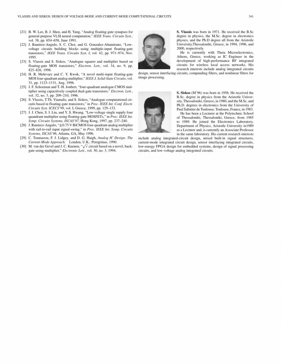
S. Vlassis was born in 1971. He received the B.Scdegree in physics, the M.Sc. degree in electronicsphysics, and the Ph.D degree all from the AristotleUniversity,Thessaloniki, Greece, in 1994, 1996, and2000, respectively.
He is currently with Theta Microelectronics,Athens, Greece, working as IC Engineer in thedevelopment of high-performance RF integratedcircuits for wireless local access networks. Hisresearch interests include analog integrated circuits
design, sensor interfacing circuits, companding filters, and nonlinear filters forimage processing.
S. Siskos (M’96) was born in 1956. He received theB.Sc. degree in physics from the Aristotle Univer-sity, Thessaloniki, Greece, in 1980, and the M.Sc. andPh.D. degrees in electronics from the University ofPaul Sabatier de Toulouse, Toulouse, France, in 1983.
He has been a Lecturer at the Polytechnic Schoolof Thessaloniki, Thessaloniki, Greece, from 1985to 1989. He joined the Electronics Laboratory,Department of Physics, Aristotle University in1989as a Lecturer and, is currently an Associate Professorin the same laboratory. His current research interests
include analog integrated-circuit design, mixed built-in signal structures,current-mode integrated circuit design, sensor interfacing integrated circuits,low-energy FPGA design for embedded systems, design of signal processingcircuits, and low-voltage analog integrated circuits.


