Embed Size (px)
Citation preview

This page intentionally left blank

Designing Digital Computer Systemswith Verilog
This unique book serves both as an introduction to computer architecture and asa guide to using a hardware description language (HDL) to design, model andsimulate real digital systems. The book starts with an introduction to Verilog: theHDL chosen for the book since it is widely used in industry and straightforward tolearn. Next, the instruction set architecture (ISA) for the simple VeSPA (Very SmallProcessor Architecture) processor is defined; this processor has been simulated andthoroughly tested at the University of Minnesota by the authors. The VeSPA ISAis used throughout the remainder of the book to demonstrate how behavioral andstructural models can be developed and intermingled in Verilog. Although Verilogis used throughout, the lessons learned will be equally applicable to other HDLs.Written for senior and graduate students, this book is also an ideal introduction toVerilog for practicing engineers. A companion website is available with the Verilogsource code for all of the examples in the text, Verilog source code for the VeSPAprocessor, and additional software to assist in using the VeSPA simulations. Seewww.cambridge.org/052182866X for details.
David Lilja is a professor of electrical and computer engineering, and a fellow of theMinnesota Supercomputing Institute, at the University of Minnesota in Minneapolis.He also serves as a member of the graduate faculties in computer science andscientific computation, and was the founding director of graduate studies for computerengineering. He has served on the program committees of numerous conferences andas associate editor for IEEE Transactions on Computers. David is a senior memberof the IEEE and a member of the ACM.
Sachin Sapatnekar is the Robert and Marjorie Henle Professor in the Departmentof Electrical and Computer Engineering at the University of Minnesota, and serves onthe graduate faculty in computer science and engineering. He has served as associateeditor for several IEEE journals, and has been a distinguished visitor for the IEEEComputer Society, and a distinguished lecturer for the IEEE Circuits and SystemsSociety. He is a recipient of the NSF Career Award and the SRC Technical ExcellenceAward. He is a fellow of the IEEE and a member of the ACM.


Designing Digital Computer Systemswith Verilog
David J. Lilja and Sachin S. SapatnekarDepartment of Electrical and Computer EngineeringUniversity of MinnesotaMinneapolis

CAMBRIDGE UNIVERSITY PRESS
Cambridge, New York, Melbourne, Madrid, Cape Town, Singapore, São Paulo
Cambridge University PressThe Edinburgh Building, Cambridge CB2 8RU, UK
First published in print format
ISBN-13 978-0-521-82866-6
ISBN-13 978-0-511-26409-2
© D. Lilja and S. Sapatnekar 2005
2004
Information on this title: www.cambridge.org/9780521828666
This publication is in copyright. Subject to statutory exception and to the provision ofrelevant collective licensing agreements, no reproduction of any part may take placewithout the written permission of Cambridge University Press.
ISBN-10 0-511-26409-7
ISBN-10 0-521-82866-X
Cambridge University Press has no responsibility for the persistence or accuracy of urlsfor external or third-party internet websites referred to in this publication, and does notguarantee that any content on such websites is, or will remain, accurate or appropriate.
Published in the United States of America by Cambridge University Press, New York
www.cambridge.org
hardback
eBook (EBL)
eBook (EBL)
hardback

Contents
Preface vii
1 Controlling complexity 1
1.1 Hierarchical design flow 11.2 Designing hardware with software 41.3 Summary 6
2 A Verilogical place to start 7
2.1 My Veri first description 72.2 A more formal introduction to the basics 92.3 Behavioral and structural models 162.4 Functions and tasks 282.5 Summary 30
Further reading 31
3 Defining the instruction set architecture 32
3.1 Instruction set design 323.2 Defining the VeSPA instruction set 353.3 Specifying the VeSPA ISA 483.4 Summary 56
Further reading 56
4 Algorithmic behavioral modeling 58
4.1 Module definition 594.2 Instruction and storage element definitions 594.3 Fetch-execute loop 644.4 Fetch task 684.5 Execute task 714.6 Condition code tasks 774.7 Tracing instruction execution 794.8 Summary 81
5 Building an assembler for VeSPA 82
5.1 Why assembly language? 825.2 The assembly process 83
v

vi Contents
5.3 VASM – the VeSPA assembler 885.4 Linking and loading 925.5 Summary 92
6 Pipelining 94
6.1 Instruction partitioning for pipelining 946.2 Pipeline performance 966.3 Dependences and hazards 976.4 Dealing with pipeline hazards 1036.5 Summary 104
Further reading 104
7 Implementation of the pipelined processor 105
7.1 Pipelining VeSPA 1057.2 The hazard detection unit 1067.3 Overview of the pipeline structure 1087.4 A detailed description of the pipeline stages 1097.5 Timing considerations 1157.6 Summary 117
Further reading 117
8 Verification 118
8.1 Component-level test benches 1188.2 System-level self-testing 1278.3 Formal verification 1308.4 Summary 131
Further reading 131
A The VeSPA instruction set architecture (ISA) 132
A.1 Notational conventions 132A.2 Storage elements 133A.3 The instruction specifications 133
B The VASM assembler 147
B.1 Notational conventions 147B.2 Assembler directives 148B.3 Example program 149B.4 Modifying the assembler 149
Further reading 152
Index 153

Preface
To the engineer, all matter in the universe can be placed into one of two categories: (1) things thatneed to be fixed, and (2) things that will need to be fixed after you’ve had a few minutes to playwith them.
Quoted by Scott Adams in The Dilbert Principle.
Hardware description languages (HDLs) are used extensively in industry to designdigital systems ranging from microprocessors to components within consumer appli-ances, such as cellular telephones. These languages allow engineers to quickly andprecisely specify and document their designs in a high-level language that has strongsimilarities to conventional programming languages, such as Java, C, and C++.Automatic tools exist to simulate the design using this high-level description and,ultimately, to translate the design from the hardware description language into anactual silicon chip.There are two primary hardware description languages in use by industry today,
Verilog and VHDL. Both languages solve the same basic problem, but in slightlydifferent ways. There are strong adherents to both languages and arguments aboutwhich is better often seem to have the feel of a religious war. The Institute ofElectrical and Electronic Engineers (IEEE) made Verilog an international standard in1995 and it continues to be refined and enhanced.Numerous books have been written to describe both languages. These books range
from the IEEE standards document, to tutorial texts that introduce the languageto novices, to texts for advanced users that describe the many subtle aspects ofthe languages. However, these books tend to treat the languages as just anotherprogramming language to be learned. They tend to miss the forest for the treessince they fail to view the broader goals of design as they focus on the details ofdescribing specific circuits rather than considering the larger picture that encompassesarchitectural choices and their impact on circuit design, and vice versa.The philosophy behind this book is to view the language as only a tool in the
overall design process used to produce the final product, which is the piece of siliconthat is a part of a larger system. This book will teach the reader how to designa complex digital system using the Verilog HDL as the vehicle for modeling andsimulating the design. We have chosen to focus on Verilog due to its economic
vii

viii Preface
importance and due to its popularity and widespread use among the designers ofprocessors and other digital systems within the computing industry. Our philosophyis to teach the components of the language that are necessary for the design of ourexample processor simultaneously with the teaching of the overall design process.
Organization
This book begins with a brief introduction to the hierarchical design process that isused throughout the book to control the complexity involved in designing a large-scale digital system. Chapter 2 then introduces the Verilog language using severalrelatively small examples. The instruction set architecture (ISA) for the simple VeSPAprocessor is defined in Chapter 3 along with a running commentary explaining thereasoning behind the various trade-offs that must be made during the design of anysystem. This ISA is used throughout the remainder of the book to demonstrate how abehavioral model of the processor can be developed (Chapter 4) and then refined intoa detailed pipelined implementation (Chapter 7). Along the way, we describe howan assembler is constructed to translate assembly language programs into machinelanguage (Chapter 5) and the general concepts involved in pipelining a processordesign (Chapter 6). The book concludes with a discussion of several techniques thatare used to verify the correctness of the final design (Chapter 8). Appendix A providesa concise summary of the VeSPA instruction set, while Appendix B presents thedetails of the VeSPA assembler.At the end of some chapters, we provide suggestions for further reading for
those who are interested in pursuing a particular topic in more detail. There is alsoa companion web site for this book (www.cambridge.org/052182866X) with theVerilog source code for all of the examples used in the book, plus some additionaltools that can be used with the VeSPA processor models, such as the assembler.
Suggestions for using this text
This book was written primarily with the following three uses in mind:
1. As a supplemental text for an undergraduate course in computer architecture.Popular existing computer architecture textbooks tend to base their discussionsaround simple processors designed specifically for the needs of the given textbook.What these books often fail to do, however, is to tie the overall design processinto the hardware description language methodology that engineers actually usein industry. This book provides a useful supplement to a computer architecturecourse to show how a hardware description language is actually used to design

Preface ix
a processor from start to finish. For example, a course instructor could assignstudents the task of modifying the VeSPA processor presented in this book as aseries of homework assignments throughout the term.
2. As the primary text for a computer design laboratory course. This book wouldbe useful as the text for a computer design laboratory course. This type of coursemay be offered independently, or as a formal component of a computer architecturecourse, as suggested above.
3. As a self-teaching guide for graduate engineers. The book has a very tutorialflavor. This approach makes it useful for practicing engineers who want a self-study text to update their skills in the area of digital systems design. It would alsobe appropriate for someone who knows VHDL, for instance, but needs to learnVerilog.
Acknowledgements
The development of any book requires the efforts of more than just the authors. Andthis book is no exception.We would particularly like to acknowledge the contributions of Saurabh Dighe
to the design of the pipelined implementation of VeSPA presented in Chapter 7.Saurabh also provided substantial help in generating the figures used in this chapter.We also would like to thank Jerry Sobelman for his careful reading of an early
draft of the book, and his courage in using this draft while teaching a course oncomputer organization and design. He pointed out numerous errors and confusingexplanations, which we hope we have corrected satisfactorily.The numerous students who muddled through our very early attempts at teaching
our computer organization course using some rather raw versions of the VeSPAdesign and this text deserve both our apologies and sincere thanks. Their suggestionsand feedback helped us improve both the processor design and our writing.Finally, we thank the anonymous reviewers of our original proposal to develop
this book for their insightful comments and specific suggestions for focusing someof the explanations and discussion.While all of these people made substantial contributions to the outcome of this
book, any errors that remain are our responsibility.

1 Controlling complexity
Technical skill is mastery of complexity while creativity is mastery of simplicity.E. Christopher Zeeman, Catastrophe Theory, 1977
The goal of this text is to teach you how to design a processor from scratch. In astep-by-step process, we will teach you how to specify, design, and test a processoras an example of a complex digital system. We will use the commercially importantVerilog hardware description language (HDL) as the basis for this design process.In particular, we will develop the VeSPA (Very Small Processor Architecture)
processor as a vehicle for demonstrating the overall design process. We show howthe instruction set for this processor is defined, how to build an assembler for theprocessor, how to develop a behavioral simulator in Verilog to test the instructionset and the assembler, and how to develop a complete Verilog structural model of apipelined implementation of the processor. We also describe the synthesis process forautomatically translating this structural model into a real piece of silicon hardware.We end by demonstrating several techniques that can be used to verify the correctnessof the processor design.
1.1 Hierarchical design flow
The development of any type of digital computing system is fundamentally a problemof controlling complexity. The designer of a large-scale digital system, such as aprocessor, begins with a high-level idea of what tasks the system is to perform.To realize this system in some physical technology, such as a collection of VLSI(Very Large-Scale Integrated circuit) silicon chips, the designer must determine howmillions of individual transistors should be interconnected to perform the desiredoperations. The need to translate from a high-level conceptual view of the system toa specification of the complex interconnections among a virtual sea of transistors isreferred to as the designer’s abstraction gap, as suggested in Figure 1.1.To bridge this gap between system concept and physical realization, we can use the
hierarchical design flow process shown in Figure 1.2. The instruction set architecture
1

2 Controlling complexity
Sea of transistors on VLSI chips
Digitalsystem
Abstraction gap
for i = 1,na[i] = b[i] * c[i] x[i] = a[i]/y[i] ... ...
Figure 1.1. The need to translate from the high-level conceptual view of a digital system, such asa processor capable of executing the program shown above, to its physical realization in VLSIchips leads to the designer’s abstraction gap.
Digitalsystem
C/C++
Sea of transistors on VLSI chips
Expanded C/C++
1. Architectural
2. Functional
4. Structural
5. Physical
Hierarchical design levels
3. Register-transfer (RTL)Hardware description language
Gates, netlist
Figure 1.2. The hierarchical design flow used to bridge the abstraction gap between the high-levelview of a digital system and its physical realization in VLSI chips.
(ISA) specification at the highest level in this design hierarchy provides an abstractdescription of what functions the system is capable of performing. In the case of thedesign of a processor, this level specifies the instructions available to the assemblylanguage programmer and the programmer-visible architectural storage elements,such as the general-purpose registers, the program counter, and the processor statusregister. This level of the hierarchy is typically described using a written assemblylanguage programmer’s manual.

Hierarchical design flow 3
The behavioral level of the design hierarchy is a logical refinement of the ISAspecification. This level provides precise functional information about how thesystem’s state is affected by each of the operations specified in the ISA. The beha-vioral Verilog model developed in this step can actually execute machine languageprograms written for the processor. However, it typically contains no timing inform-ation showing how long each instruction takes to execute, nor does it specify how theoperations are implemented. It is used to verify that the ISA is defined correctly, andto provide a simulator on which programmers, such as compiler writers and operatingsystem programmers, can begin developing and testing their code.This behavioral level in the design hierarchy is sometimes referred to as the
register-transfer level (RTL) since it describes transformations that occur to thecontents of registers as they are moved among the storage elements defined bythe ISA. However, it does not typically specify how the transformation itself isimplemented. For instance, the subtraction of the contents of register rs2 from thecontents of register rs1 with the results stored in register rdst may be specified atthis level in Verilog as R[‘rdst] = R[‘rs1] − R[‘rs2]. This RTL or behavioraldescription shows what happens in a subtraction operation, but it does not specifyhow it happened or how much time was required.The next level in the design hierarchy is the structural level. This level begins to
answer the questions of how a function is actually implemented. It also begins todefine the number of cycles required to execute each operation, the number of busesthat interconnect registers and functional units, the size of internal memory buffers,and so forth. This level represents a mapping of the behavioral model into a morespecific implementation. For example, this level defines how the subtractor actuallyperforms a subtraction operation.Finally, the physical design level specifies the detailed chip-level floor-planning,
layout, and transistor-level timing. It defines a mapping of the structural level descrip-tion on to a specific technology, such as a CMOS application-specific integrated circuit(ASIC). This final stage in the design hierarchy often can be produced automaticallyfrom the structural Verilog description using an appropriate logic synthesis design auto-mation tool. The designer may choose to translate certain portions of the design fromthe behavioral or structural level to the next level by hand, however, to optimize specificdesign criteria, such as power consumption, chip area, or signal delays, for instance.Since each level in this design hierarchy is an incremental refinement of the
previous level, this hierarchical design flow provides a technique for managing thecomplexity of designing a large digital system. The hardware description languageis a means for precisely capturing the details at the behavioral and structural levelsof the design hierarchy. These behavioral and structural models can be compiled andsimulated to verify the correctness of the design at each level. The structural modelthen provides the input for a synthesis tool that will make the final transformation ofthe hardware description language model into a piece of silicon.

4 Controlling complexity
1.2 Designing hardware with software
Using the above design flow, it can often seem that designing a processor is verymuch like writing a piece of software. Indeed, both the behavioral and structuralmodels of a processor are written in the hardware description language and can bechanged, compiled, and executed (actually, simulated) in a manner very similar towriting, compiling, and executing a program written in a high-level programminglanguage, such as C, C++, Java, or Fortran, for instance. However, it is importantto distinguish the fundamental differences in this hardware design process from theprocess of writing software to run on a processor.Figure 1.3 shows how a hardware designer begins with the ISA, develops a
functional and behavioral model, refines these models into a structural model, and,finally, synthesizes that model into the actual processor. This processor consists ofhardware storage elements for the ISA-defined registers, logic circuits that implementthe ISA-specified instructions, and the memory system. In the final step, it is a real,tangible piece of hardware. To change the processor, for instance, to add a newinstruction, every step in this chain of events must be repeated. The result is anew silicon chip with the additional logic circuits necessary to implement this newinstruction. While it may be quite simple to make the changes necessary to implementthis new instruction in the ISA specification manual and the Verilog models, it canbe a slow and expensive process to actually fabricate the new chip.The analogous process for compiling and executing a program written in a
high-level language is compared to this hardware design process in Figure 1.4.A programmer begins with a logical description of the task to be accomplished bythe program. This description is refined into an algorithm that describes the steps
Physical implemenation(Full custom/ASIC/FPGA implementation)
Structural description(Translation to a gate-level description)
Functional description(ISA verification)
Processor specification (ISA, High-level specifications)
Behavioral description(High-level tradeoffs for timing/power)
Figure 1.3. The process of refining the behavioral and structural models in a hardware descriptionlanguage to produce a new processor.

Designing hardware with software 5
Software compilation Hardware compilation
Processor specification(ISA, High-level specifications)
Functional description(ISA verification)
Behavioral description(High-level tradeoffs for timing/power)
Structural description(Translation to a gate-level description)
Physical implemenation(Full custom/ASIC/FPGA Implementation)
Algorithm to high-level language
Code optimization
Compilation to assembly language
Assembly to machine language
Logical description
Figure 1.4. The process of compiling and executing a program to run on an existing processorhas strong similarities to the process of designing a digital system using a hardware descriptionlanguage. However, the final results of the two processes are quite different.
necessary to complete the desired task. This algorithm then is written in a textualformat in the syntax of some high-level language, such as C/C++. A compiler readsthis text file and transforms the program into another text file containing an equi-valent program in the target processor’s assembly language. Finally, this text file isread by an assembler and converted into a string of bits that can be linked with otherprecompiled library functions and loaded into the processor’s memory. At this point,the processor can execute the program stored in its memory.Changing anything in the program requires each of these steps to be repeated
beginning with the text file that contains the modified high-level program. However,in contrast to the need to produce a new silicon chip, the recompiled program cansimply be loaded into the processor’s memory where it is ready to be re-executed.While the steps required to produce the processor chip are analogous to those requiredto compile and execute a program, the last step in each process produces completelydifferent results. The software compilation process produces a string of bits thatare stored in the processor’s memory. The hardware development process, however,ultimately produces a new artifact in the form of a new piece of silicon.

6 Controlling complexity
1.3 Summary
While shrinking process technologies have permitted the possibility of building largeintegrated circuits, they have also forced designers to battle with the task of managingthis complexity under pressing time-to-market constraints on the design cycle. As anatural result, there has been an increased amount of automation throughout the entiredesign process. One manifestation of this change has been an evolution from buildingcircuits at the gate or transistor level to developing an ability to specify circuits ata reasonably high level, from where a circuit implementation can be obtained in apush-button manner. Interestingly, a similar evolution was seen in software: in theearly years, software was written at the assembler level, but as programs becamemore complex, there was a move towards writing programs in a high-level languagethat could be translated by a compiler into machine code.HDLs have played an important role in this process, as they represent a medium
for designers to specify a circuit at a level that is comparable to a high-level language.Once a design is specified in such a standardized format, there are a number ofcomputer-aided design (CAD) tools that will compile this code to translate thespecification into a hardware implementation. In today’s world, Verilog and VHDLare the two most widely used HDLs. Since the subject of which of these is the betterlanguage can prompt fierce partisan reactions among the believers of either sect, wewill prudently avoid that debate.1 In this book, we use the Verilog HDL as a vehiclefor processor design, and our rationale for this choice is threefold. Firstly, we feel thatVerilog, being more C-like, is easier for the novice to learn, and is less encumberedwith syntactic niceties than VHDL. Secondly, it is arguably the most widely usedHDL in industry today. Thirdly, and we believe, most convincingly, learning Verilogprovides an easy path to learning any other HDL, and the major goal of this book isto profess the ideas behind processor design using HDLs, rather than to evangelizeany specific HDL.
1 A third prong to the debate may be added in the near future with the advent of newer hardwaredescription languages based on C, although these are in the early stages of use at this time.

2 A Verilogical place to start
Let’s start at the very beginning.A very good place to start.When you read, you begin with A-B-C,when you sing, you begin with Do-Re-Mi.
from Rogers and Hammerstein’s The Sound of Music
In this chapter, we will present an elementary introduction to Verilog, with theprimary aim of permitting the reader to learn enough of the language to carry out acompetent design. Due to the scope of this text, we do not attempt to present completecoverage of the language; for example, we will not cover switch-level modelingconcepts that are typically at the transistor-level, since the design of our processordoes not require that level of design detail. For these and other details, the interestedreader may refer to sources such as those shown in the Further reading section atthe end of this chapter.
2.1 My Veri first description
In teaching an English-speaker a new tongue such as Spanish or Japanese or Marathi,two extreme approaches may be attempted. A more structured approach would leadthe student through a rigorous path that first teaches the alphabet, followed by words,sentences and grammar; an alternative ‘immersive’ or ‘communicative’ approachplaces the student in an environment where the language is extensively spoken, in thehope that this may motivate learning in a more natural environment. In practice, ofcourse, an intermediate approach is often the most effective, and we will use a similarphilosophy in presenting a first exposition to the admittedly nonhuman language thatis Verilog.In this section, we will present a simple Verilog description of a very simple
module. The module that we present is a full adder that inputs three bits, the addend
7

8 A Verilogical place to start
bits, a and b, and the input carry bit, cin. The full adder outputs two bits, the sum bit,s, and the output carry bit, cout, and these are related by the elementary equations
s = a⊕b⊕ cin
cout = a ·b+a · cin+b · cinA Verilog description is shown in Figure 2.1, and is fairly self-explanatory. Thedescription is encapsulated within a module that is parameterized by its ports,or connections to the external world. The body of the module first declares theseparameters as inputs or outputs, followed by a description that defines the functionalityof the module in terms of its logic equations; note that the symbols ˆ , & and � referto the XOR, AND and OR logical operators, respectively.
module full_adder(a,b,cin,s,cout);
input a,b,cin; // declaration of the list of inputsoutput s, cout; // declaration of the list of outputs
assign s = a ˆ b ˆ cin;assign cout = (a & b) | (a & cin) | (b & cin);
endmodule
Figure 2.1. Verilog module for a full adder.
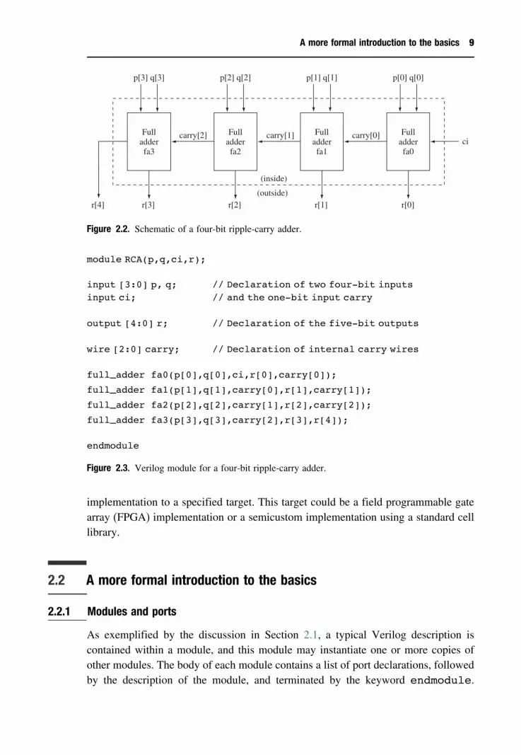
This module may be used as a building block for the hierarchical description of amore complex module, such as the four-bit ripple carry adder of Figure 2.2 whoseVerilog description is shown in Figure 2.3. As before, the module description beginswith a listing and then a declaration of all inputs and outputs. An interesting featureis in the definition of several vectors. For instance, the inputs p and q are definedas four-bit vectors, with bit 3 being the most significant bit; alternatively, if ‘[3:0]’were to be substituted by ‘[0:3]’, then bit 0 would be the most significant bit. Thenext declaration of a wire corresponds, in this example, to an internal connectionwithin the module. Finally, the description of the adder instantiates four copies offull_adder defined in Figure 2.1. Note that the order of the port connectionscorresponds exactly to the order used in the definition of full_adder1.Through the examples shown above, it is easy to see that the specification of the
adder is very similar to writing a program in a high-level programming language.A Verilog compiler has the capability of translating this description to a hardware
1 Verilog does indeed permit an out-of-order specification of the list of ports, but we prefer toavoid its use in this book.
A more formal introduction to the basics 9
p[3]
ci
r[0]r[1]r[2]r[3]r[4]
carry[2] carry[1] carry[0]Fulladderfa3
Fulladderfa2
Fulladderfa1
Fulladderfa0
(inside)
(outside)
q[3] p[2] q[2] p[1] q[1] p[0] q[0]
Figure 2.2. Schematic of a four-bit ripple-carry adder.
module RCA(p,q,ci,r);
input [3:0] p, q; // Declaration of two four-bit inputsinput ci; // and the one-bit input carry
output [4:0] r; // Declaration of the five-bit outputs
wire [2:0] carry; // Declaration of internal carry wires
full_adder fa0(p[0],q[0],ci,r[0],carry[0]);
full_adder fa1(p[1],q[1],carry[0],r[1],carry[1]);
full_adder fa2(p[2],q[2],carry[1],r[2],carry[2]);
full_adder fa3(p[3],q[3],carry[2],r[3],r[4]);
endmodule
Figure 2.3. Verilog module for a four-bit ripple-carry adder.
implementation to a specified target. This target could be a field programmable gatearray (FPGA) implementation or a semicustom implementation using a standard celllibrary.
2.2 A more formal introduction to the basics
2.2.1 Modules and ports
As exemplified by the discussion in Section 2.1, a typical Verilog description iscontained within a module, and this module may instantiate one or more copies ofother modules. The body of each module contains a list of port declarations, followedby the description of the module, and terminated by the keyword endmodule.
10 A Verilogical place to start
The ports of the module may be of type input, output, or inout, where the lastcorresponds to a bidirectional connection.
2.2.2 Nets and registers
Apart from the port declarations, it is also possible to make declarations that areentirely internal to the module. These declarations may correspond to:
Net variables correspond to structural connections between two or more elementswithin the module. These are most often declared within a model using thekeyword wire. Alternative specifications of nets also exist to define, forexample, tristable nets (e.g., triand, trior), nets that can implement wiredAND or wired OR logic functions (e.g., wand, wor), and power/ground nets(supply1 and supply0). The default value of a wire data type is the tristatevalue z.
Register variables correspond to elements with memory that can store their valueuntil they are next updated. The most commonly used register data type isdenoted by the keyword reg, and its default value is the unknown value x.The differences between a register declaration and a hardware implementationof a register are subtle and include the fact that the former may or may not beclocked and may be changed asynchronously. In many cases, though, there is aone-to-one relationship between the two: the burden of ensuring this is placedon the designer, who can force synchronicity by updating the register variablein the Verilog description only on the onset of a clock.
Unless specified in terms of an array, both the wire and reg keywords represent asingle bit. Particularly in the case of stored variables, more compact representationsare often convenient. To facilitate this, Verilog permits register variables of typeinteger and real to store integer and real variables, respectively. For example,in specifying the value of a counter, an integer variable may be more convenientto use, and may make the description more readable than the use of an arrayof bits.Another stored variable that is provided for convenience is the integer time
data type, which is most commonly used in conjunction with the system function$time that provides the current time point of the simulation as an integer. A corres-ponding data type realtime can be used to store time in the form of a realnumber.Verilog imposes stringent requirements on the mapping from the internals of
a module to its ports, and these are summarized below. Since a port defines theconnection to a module to the external world, it may be viewed from the inside of amodule as well as from the outside. For the example of the full adder module that was

A more formal introduction to the basics 11
used in a ripple-carry adder, the definition of the ports within module full_addercorrespond to the view of that module from the inside. In module RCA, the datatypes of the ports in each of the four instantiations of full_adder correspond toits view from the outside. This is illustrated by the symbols ‘inside’ and ‘outside’ inFigure 2.2.The following rules govern the mapping of ports of a module to nets or registers:
• From the inside, an input must be a net data type, but not a register data type.The connection external to the module may be either a register or a net.
• An output port may be either a net or a register variable from the inside, butmust be a net variable on the outside.
• An inout port must be a net both from the inside and the outside.
The rationale for this convention could be understood by observing that the designerdoes not inadvertently specify a latency of more than one, i.e., two storage elementsare not inadvertently connected in series. In cases where such a connection is desired,the notation permits such a connection through an explicit and conscious action ofconnecting a net to a register.Note that the Verilog 2001 standard has a new feature that permits a statement of
the form:
output reg a;
while in earlier versions of Verilog, this would have to be written as
output a;reg a;
2.2.3 Vectors and arrays
It is often convenient to conceptualize groups of nets or registers in terms of an array,for example, in case of a bus or a hardware register. For this purpose, Verilog permitsthe definition of a vector for net and reg data types. For example, an eight-bitaddress bus may be specified using the declaration
wire [7:0] address;
where bit 7 corresponds to the most significant bit (MSB) and bit 0 to the leastsignificant bit (LSB).Examples of the use of this declaration were seen in Figure 2.3. It is interesting to
note that it is possible to access an individual element of the vector, for example, byreferring to address[2].

12 A Verilogical place to start
For the reg, integer and time data types, Verilog also permits the definitionof an array. For example, the declaration
reg io_port[3:0];
corresponds to an array of four one-bit reg variables. Similarly, one may also declarean array of vectors such as
reg [7:0] cache[511:0];
which declares an array of 512 reg variables, each of which is an eight-bit widevector2.
A few common applications of vectors and arrays are:
• Memory, in the form of RAMs, ROMs or register files, may be modeled usingarrays of vectors, as in the case of the cache declaration above.
• Strings of characters can be stored in reg vectors; the caveat here is that eachcharacter requires eight bits, so that a string of n bits requires the declaration of areg vector of dimension 8×n.
2.2.4 Constants
The keyword parameter in Verilog announces the declaration of a constantand assigns a value to it. Parameter values may be declared by providing theirvalues with the description. For example, within a module my_module, one maydefine
parameter number_of_bits = 32;
The defparam statement in the upper level module permits the declared valuesof the parameter within a module to be overridden. For example, the value of theparameter number_of_bits in the module my_module may be overridden inthe upper level module that instantiates it as follows
defparam x.number_of_bits = 16;defparam y.number_of_bits = 64;
my_module x();my_module y();
2 It is important to observe that the above is a unidimensional array of eight-bit reg variables, andthat Verilog does not permit multidimensional variable declarations.

A more formal introduction to the basics 13
The my_module x(); and my_module y(); statements will, respectively,instantiate the module my_module and override the value of the internallydeclared parameter, number_of_bits, from its default value of 32 to 16 and 64,respectively.Alternatively, parameter instances can also be overridden during module
instantiation. Consider a case where a module internally defines the followingparameters
module xyz;:parameter p1 = 1;parameter p2 = 2;parameter p3 = 3;parameter p4 = 4;:endmodule
When xyz is instantiated, the parameters may be overridden as follows
xyz #(5,6,7,8) xyz1;
This statement overrides the values of p1 through p4 with the numbers 5, 6, 7 and8, respectively. Note that the order of parameters in the instantiation correspondsdirectly to the order in which they are defined in the module. If all of the parametersare not specified, then the parameters are overridden in order of appearance. Forexample, in
xyz #(11,12) xyz1;
the value of p1 is set to 11, of p2 to 12, and those of p3 and p4 remain at theirdefault values of 3 and 4, respectively.
2.2.5 Number representation
Verilog permits numbers to be represented using a binary, octal, hex or decimalrepresentation. Apart from the normally permissible values (0 and 1 for binary,0 through 7 for octal, 0 through F for hex, and 0 through 9 for decimal), each digitmay take on the values x (unknown) or z (high impedance).A number may be represented in a sized or unsized form, depending on whether
the number of bits is specified or not. A sized number is represented in the form
size ’ base_format number
where size corresponds to the number of bits, base_format takes on one of thepossible values of b (binary), o (octal), h (hex) or d (decimal), and number is the

14 A Verilogical place to start
actual value of the number. It is important to note that regardless of the base that isused, the size refers to the number of binary bits in the representation. Examplesof numbers in a sized format include
8’b11111111, 8’o377, 8’h FF and 8’d255
Note that, coincidentally, all of the above numbers represent the same value indifferent bases. It is worth reiterating that x and z are also permissible values foreach digit in any base.In contrast, unsized numbers are written without a size specification, which defaults
to a value that varies with the simulator.
2.2.6 Operators
The statements within a Verilog description can be expressed in terms of a set ofoperations. Many of these may use the wide range of built-in operators that Verilogprovides for the most commonly used operations; these operators are typically usedto alter a set of operands on the right-hand side of an expression to generate a resultthat is assigned to the left-hand side.The built-in operators in Verilog can be classified into several categories described
below. Many of these operators are similar to those used in many other programminglanguages.
Arithmetic operators: These include the following that operate on two operands
Operator Add Subtract Multiply Divide Modulus
Symbol + – ∗ / %
In addition, as in most other languages, + and − may act as unary operatorson a single operand; for example −8 would negate the value of the number 8.
Logical, bitwise and reduction operators: These perform a set of basic Booleanor bitwise-Boolean operations, and are listed below. The Boolean operatorsperform logical operations on one-bit Boolean operands, yielding a Booleanresult. In contrast, the bitwise-Boolean operators operate on binary words ofmultiple bits and perform bit-by-bit Boolean operations on the correspondingbits of each word. Reduction operators use the same operator symbols as bitwise-Boolean operators, but differ from them in that they operate on one operandinstead of two, and yield a one-bit result. For example, the reduction AND ofan eight-bit vector myvec, denoted as & myvec, is given by the logical ANDof the eight bits of myvec.

A more formal introduction to the basics 15
Operator Boolean Bitwise-Boolean
and or not and or not xor xnor
Symbol && �� ! & � ˜ ˆ ˜ ˆ
Relational operators: Relational operators are used to verify the truth or falsehood
of an expression, and return a Boolean value of 1 or 0, respectively, depending
on the result. If no conclusion can be arrived at (for example, when there are x
or z bits in the operands), then a value of x is returned.
A special case of this is the case equality operator, which returns either a 0
or a 1 in each case. If the operands contain x or z bits in the same positions,
the result is a 1; otherwise it is a 0. As an example, if two variables A and B
each hold the value xz1, then the ‘==’ operator will return x, while the ‘===’
operator will return 1.
greater less greater than less thanOperator than than or equal to or equal to
Symbol > < >= <=
Operator equal not equal equal (case) not equal (case)
Symbol == ! = === ! ===
Other miscellaneous operators: The shift operations perform a left (<<) or a
right (>>) shift by a specified number of bits. To shift a reg variable A by
four bits to the left, one simply writes the statement
A << 4;
These shifts correspond to logical shifts that shift zeros into the vacated bit
positions.
Another useful operator performs concatenation of multiple operands and is
a handy tool in hardware specification. A Verilog statement that concatenates
variables X and Y and writes the result into Z is
Z = {X,Y};
It is worth pointing out that constant operands are also permitted for
concatenation.

16 A Verilogical place to start
A special case of concatenation is the replication operator, which repeatedlyconcatenates the same number a specified number of times. To replicate thevariable A twice and write it into B, one would simply write
B = { 2 {A} };
Finally, as in the C language, the conditional operator evaluates the truth of anexpression and then performs either one operation or another, as follows:
condition ?: true_consequence : false_consequence;
These conditional statements may be nested, so that true_consequencemay, for example, contain another conditional statement.
2.3 Behavioral and structural models
One of the advantages that many hardware description languages afford is in therepresentation of hardware at various levels of abstraction. In this section, we willconsider the design of a simple finite state machine (FSM), and represent it at twolevels of abstraction in Verilog:
Behavioral: At this level, the design is coarsely described at a high level ofabstraction that resembles a high-level language, and the details of the preciseimplementation are hidden. An example of a behavioral description would bea program that describes the behavior of an FSM in terms of its state transitiondiagram.
Structural: This is considered to be a lower level of implementation, at whichthe design is finalized up to the gate or block level. For the FSM example,this could correspond to a selection of gates that implement the logic equationsthat relate the next state bits and outputs to the present state bits and inputs.Alternatively, the structural level could use blocks of greater complexity thana gate, such as an ALU, which could then be defined in a separate module.
Each level of abstraction is important during the design process. Design is anintrinsically hierarchical process in which the task of building a system is subdividedinto multiple tasks of building subsystems that interact through a set of signals, andit is important to verify the correctness of the subsystems through the design process.Early in the process, the behavioral models for each block can be ‘pasted’ togetherthrough their interacting signals to ensure correctness. As we go further into theprocess, a more detailed model can be inserted to replace a more abstract modelsuch as the behavioral model for one or more blocks in a system-level simulation.Moreover, each such detailed model for a block can be compared with its more

Behavioral and structural models 17
abstract model for correctness, and this process lends itself towards a structured anddisciplined design philosophy.At higher levels of abstraction, the designer has a greater flexibility to change the
system in a relatively painless manner. However, performance measurement at thislevel is relatively inaccurate since many of the system details are as yet undetermined.While this is resolved at the structural level, the design effort involved in making asignificant change at this level is considerable.A final point is that a typical design description may contain a combination of
behavioral and structural descriptions.
2.3.1 An example of a finite state machine
We now present a specific example of a digital circuit that is described by Verilogat various levels of abstraction. We begin with an FSM description, and our examplemodels the life of a typical medieval knight. As the knight sets off on a quest, hemay first make preparations that involve polishing his armor, sharpening his sword,taking his horse to the vet for a checkup, etc. He would then seek a dragon to slay,and do battle until either the dragon or his courage were exhausted.This may be modeled by a system whose inputs are
• the adventure signal, which indicates that the knight is seized with the spirit ofadventure,
• the sword_sharpened signal, which is asserted when all preparations for thequest are complete,
• the courage signal, which measures whether the knight’s valor is up to the taskat hand, and
• the dragon signal, which indicates a live dragon nearby.
A state diagram that models this system is shown in Figure 2.4. We begin in stateS0, where the knight remains until the adventure signal is asserted. At this point,a transition is made to state S1, where he prepares for his adventure. The signalsword_sharpened is set to true when these preparations are complete, and he setsoff on his quest, to state S2. Even the bravest of knights could have an off day, and ifhis courage deserts him at this point (as signaled by the input courage), he returnsto state S0. If, however, his courage remains strong, he remains in state S2 until alive dragon shows up. On the assertion of the signal dragon, a transition is made tostate S3, where a battle with the dragon is fought in a single clock cycle. At the endof the clock cycle, if the dragon is vanquished, the signal dragon is asserted, anda transition is made to the final state S4, where the quest_over signal is assertedto show that the quest has been fulfilled. If, however, the dragon is still alive afterthe battle, the knight retreats to state S2, where he tests his courage reserves. If the

18 A Verilogical place to start
1
sword_sharpened
courage AND dragon
adventure
courage
dragon dragonsword_sharpened
adventure
S0/quest_over
S1/quest_over
S2/quest_over
courage AND dragon
S3/quest_over
S4/quest_over
Figure 2.4. State machine for an FSM that models the life of a medieval knight.
dragon then flees, the signal dragon is asserted, and the knight remains in S2 untilthe next dragon appears, or until his courage fails him; otherwise, if the dragon staysto fight and the knight has ample reserves of courage, he returns to S3 for anotherbattle with the dragon.We will now write a Verilog description for this FSM, using various levels of
abstraction.
2.3.2 Behavioral modeling
In this section, we will present a general guide to behavioral modeling using Verilog.The example of the medieval knight will be used to motivate an initial set ofconstructs, after which a broader set of constructs will be defined.The Verilog behavioral model for the FSM is shown in Figure 2.5, in which the
lines of code have been numbered for ease of explanation. The first observation thatwe make is that the description is essentially a translation of the state diagram inFigure 2.4 to Verilog code.Studying the code segment that describes this FSM, we observe that the first set
of ‘define statements in lines 2–6 are used to set some parameters that are utilizedwithin the program, similar to the #define statement in C. The parameters definedin these statements may be used within the rest of the description by prefixingthe parameter by the ‘ symbol, as has been done on line 42, for example. Lines8–17 provide the module definition, listing the inputs and outputs to the FSM, after

Behavioral and structural models 19
1. // Definition of states2. ‘define S0 3’b0003. ‘define S1 3’b0014. ‘define S2 3’b0105. ‘define S3 3’b0116. ‘define S4 3’b1007.8. module knight_life(adventure, courage, sword_sharpened,9. dragon, clock, quest_over);10.11. input adventure; // Declaration of inputs that12. input courage; // report on various13. input sword_sharpened; // aspects of a medieval14. input dragon; // knight’s life15. input clock;16. output quest_over; // (Set to 1 on completing quest)17. reg quest_over;18.19. reg [2:0] present_state; // Declaration of20. reg [2:0] next_state; // internal state variables21.22. initial23. begin24. present_state = ‘S0;25. next_state = ‘S0;26. quest_over = 1’b0;27. end28.29. always @(present_state)30. begin31. casex (present_state)32. 3’b0xx: quest_over = 1’b0; // S0 through S333. 3’b100: quest_over = 1’b1; // S434. default: begin quest_over = 1’b0;
$display(‘‘Illegal state’’); end35. endcase36. end37.38. always @(present_state or adventure or courage39. or sword_sharpened or dragon)40. begin41. case(present_state)42. ‘S0: if (adventure)43. next_state = ‘S1;44. else45. next_state = ‘S0;
Figure 2.5. Behavioral description of an FSM modeling the life of a medieval knight.

20 A Verilogical place to start
46. ‘S1: if (sword_sharpened)47. next_state = ‘S2;48. else49. next_state = ‘S1;50. ‘S2: if (courage)51. if (dragon)52. next_state = ‘S3;53. else54. next_state = ‘S2;55. else56. next_state = ‘S0;57. ‘S3: if (dragon)58. next_state = ‘S2;59. else60. next_state = ‘S4;61. ‘S4: next_state = ‘S4;62. default: $display(‘‘Illegal state’’);63. endcase64. end65.66. always @(posedge clock) // Updates the state at67. present_state = next_state; // positive clock edge68.69. endmodule
Figure 2.5. (Continued)
which internal state variables are described in lines 19– 20. Note that the outputquest_over is also declared as a register to ensure that it holds its value.The initial statement on lines 22–27 is a construct that we have not encountered
as yet in our discussion. It is used to initialize the values of various internal and outputvariables at the beginning of the system simulation. A module may contain multipleinitial statements, each of which is executed concurrently at time 0 of the simulation3.Line 29 introduces the always statement, which is performed repeatedly during
the simulation. In this case, the always statement is qualified by the timing statement@present_state, implying that the statement is entered whenever the value ofthe variable present_state is modified during the simulation.Lines 31–34 serve to set up the Moore outputs associated with the states ‘S0,
‘S1, ‘S2, ‘S3, and ‘S4 using the casex statement. The case, casex and casezconstructs are all very similar statements that are followed by an expression (wewill shortly point out the differences between them). Depending on the value taken
3 Be warned that not all simulators support the initial statement, and it is generally considered anonsynthesizable construct, and may have to be set up during verification.

Behavioral and structural models 21
by that expression, one of the following alternatives is executed. For example, thevalue of present_state is tested on line 31 to determine which of the succeedingstatements is to be executed. Line 32 corresponds to any state that has a zero inthe first bit position, namely states ‘S0 through ‘S3, where quest_over is set to0. When present_state corresponds to state ‘S4, the statement on line 33 isexecuted to set quest_over to 1. The default statement corresponds to the casewhere none of the other alternatives is chosen, a situation that is not expected in ourcase. Nevertheless, it is considered good practice to insert, for example, a simpleerror statement for the default case, using the $display system call. Note that theoutput quest_over was listed as a reg variable on line 17; this is required since itis used to hold a value within a case statement. However, synthesizers will typicallynot assign a memory element to this reg variable, as long as it is assigned a valuefor all possible combinations of the case statement.The difference between the various flavors of the case statements is simple: case
requires all bit positions in the case alternatives to be precisely specified as either0 or 1; casez permits bits in the case alternatives to take on the value z, and treatsthem as ‘don’t cares’ in the comparison; casex permits x or z values and treatsboth as ‘don’t cares’.Lines 38–64 use constructs that have been previously defined, and perform the
function of setting the value of next_state whenever either an input or thepresent_state is altered, which triggers an entry into the always statement.The case statement considers the value of the inputs and encodes the transitionsdefined in the state diagram in Figure 2.4. We commend to the reader’s attentionthe if-else construct, used for the first time on lines 42–45, which is ratherself-explanatory.Finally, lines 66–67 update the value of the state on the onset of the clock. The
statement always @(posedge clock) indicates that this update is performed atthe positive edge of the signal clock, thereby implying that positive edge-triggeredflip-flops are used to construct the state machine. If negative edge-triggered flip-flops were to be used instead, the keyword posedge would have been replaced bynegedge.
2.3.3 Other constructs for behavioral modeling
We now introduce several other constructs that are useful in behavioral modeling.
Timing controlsIn the physical implementation of digital systems, various hardware components havenonzero delays. Verilog provides for statements that can model these delays at various

22 A Verilogical place to start
levels of abstraction. The simplest delay assignment corresponds to an assignmentstatement, and is exemplified by the following statement:
# 10 a = b;
This assignment statement indicates that the program waits for 10 time units, afterwhich a takes on the value of b, and for this reason, this type of delay is oftenreferred to as a blocking delay. A different way of specifying the delay, which canend in different results, is the statement:
a = # 10 b;
The difference between this and the previous assignment statement lies in the fact thatduring simulation, it takes the value of b at the very time (in terms of the simulationclock) when the statement is encountered. It then sets a to take on that value 10 timeunits hence. This is unlike the earlier statement that samples the value of b only10 units later. In other words, unlike the previous statement, which postponed theexecution of the entire statement by 10 time units, this statement only postpones theassignment by 10 time units, and is equivalent to the statements:
c = b;# 10 a = c;
where c is a temporary variable. Clearly, if b changes during these 10 time units,the result of the two assignments will be different.Timing controls in a Verilog description may also be inserted by the use of the @
keyword, as in lines 29, 38 and 66 of Figure 2.5. These correspond to the use of asignal edge for control. If, instead, level-sensitive control is desired, one may use thewait statement, which is of the type:
wait (signal_name)begin(list of assignments)
end
Blocking and nonblocking assignmentsAn assignment statement is one that is used to update the value of a variable, andtypically consists of a variable on the left-hand side and an equation on the right-handside. We have encountered such statements frequently so far: as an example, considerline 24 in Figure 2.5. This assignment, which uses the = operator, is referred toas a blocking assignment. Blocking assignments that appear sequentially after eachother within an initial or always block are executed sequentially during thesimulation. For the code shown below, the first three statements are executed at time0, the fourth at time 10, and the fifth at time 30, as shown in the comments.

Behavioral and structural models 23
initialbegina = b; // Executes at time 0 of the simulationc = 1’b0; // Executes at time 0 of the simulation,
// but after a = bd = 1’b0; // Executes at time 0 of the simulation,
// but after c = 1’b0#10 c = 1’b1; // Executes at time 10 of the simulationd = #20 c; // Executes at time 30 of the simulation
end
A subtle point here is that although the first three statements are executed attime zero, the order in which they are executed is strictly sequential. In otherwords, a = b; is first executed, after which c = 1’b0; is carried out, and thenthe assignment d = 1’b0; is completed, but as far as the simulation is concerned,all of these are said to execute at time 0. The importance of understanding theorder in which the statements are executed is in realizing that a sequence ofblocking assignments a = b; c = a; may not yield the same result as c = a;
a = b;.In contrast, the nonblocking assignment uses the <= symbol4, and corresponds to
a set of concurrent assignment statements, each of which can be considered to beginexecuting in parallel when the block of code is encountered during the simulation.The primary utility of nonblocking statements in Verilog is in modeling concurrenttransfers in digital systems.
initialbegina = b; // Executes at time 0 of the simulationc = 1’b0; // Executes at time 0 of the simulationd = 1’b0; // Executes at time 0 of the simulation#10 c <= 1’b1; // Executes at time 10 of the simulationd <= #20 c; // Executes at time 20 of the simulation
end
If we consider the block of code shown above, it is superficially very similar to theprevious example with blocking statements, with the difference that some of the =
symbols have been replaced by a <= symbol. However, the result is entirely differentfrom the case where blocking assignments are used. The first three assignments are
4 Interestingly, this is also used to denote ‘less than or equal to’, and the meaning of the symbol isusually quite obvious from the context it is used in.

24 A Verilogical place to start
executed at time 0, the fourth at time 10, and the fifth assignment is now executedat time 20.When a mixture of blocking and nonblocking assignments is used, the
blocking assignments are first executed, followed by the nonblocking assignments.Consequently, in this example, d will take on the binary value 0 from time 0 to 20,and then switch to the waveform of c, delayed by 20 time units. Therefore, since cis at 0 until time 10, and then switches to 1, it follows that d will be at logic 0 fromtime 0 to 30, after which it changes to logic 1.
LoopsLike most programming languages, Verilog permits the use of loops for repetitiveactions, with four types of constructs: forever, repeat, for, and while. Theselooping statements can only appear inside an initial or always block.
Forever loops are performed repeatedly throughout the simulation, once they areencountered. Perhaps the most common application is in generating a clocksignal for simulation. An example that generates a clock signal of period 10units is given by the code segment below:
initialbeginclock = 1’b0;forever
#5 clock = ˜clock;end
Repeat loops execute a loop a fixed number of times. An example of a codesegment that uses a repeat loop to initialize a register file is shown below:
parameter nbits = 16;integer i;
initialbegini = 1;repeat (nbits)begin
regfile[i] = 0;i = i+1;
endend
For a good illustration of the use of a repeat loop, the reader is referred to page135 of the IEEE 1364-2001 Verilog Standard, where a compact description ofa multiplier implementation is provided.

Behavioral and structural models 25
For loops are very similar to those in C, and an illustration on the very sameinitialization example is shown below:
parameter nbits = 16;integer i;
initialbeginfor (i = 1; i <= nbits; i = i+1)beginregfile[i] = 0;
endend
While loops are executed as long as the condition associated with the loop is trueat the entry point of the loop. The use of this loop for the the same initializationstep is shown below:
parameter nbits = 16;integer i;
initialbegini = 1;while (i <= nbits)begin
regfile[i] = 0;i = i+1;
endend
2.3.4 Structural description
The behavioral level is a high level of abstraction that permits a description of thestate diagram in Figure 2.4 in a manner similar to a high-level programming language.Taking the design one step closer to implementation involves the translation of thestate diagram into a set of logic equations that relate the next state and the outputsto the present state and the inputs.As in the behavioral description, we work with an encoding of the states, and
as before, we will choose a simple scheme for encoding here, where the ith stateSi is assigned using the binary number that corresponds to the integer i. However,the reader is reminded that the choice of state encoding can impact the circuitperformance in several ways: firstly, depending on the binary assignments providedto the states, the amount of logic to be implemented can be different, particularly ina situation such as this where the ‘don’t care’ space is large. Secondly, the average

26 A Verilogical place to start
number of switching transitions, which translate directly to the power dissipation ofthe circuit, depends on the state assignment. A simple technique that is often usedis to attempt to assign neighboring (in the Hamming distance sense) state codes tostates that are connected by a transition edge, so that the number of switching statebits in each transition is minimized. Of course, this may not always be possible, andthe task of the hardware synthesizer is to explore the design space for an optimalimplementation.For the state assignment that we have chosen, we can obtain, using routine tech-
niques, a logic level implementation of the circuit in the form of the followingBoolean equations
NS2 = PS2+PS1PS0dragon′ (2.1)
NS1 = PS′1PS0sword_sharpened+PS1PS
′0courage+PS1PS0dragon (2.2)
NS0 = PS′2PS
′1PS
′0adventure+PS′
1PS0sword_sharpened′
+PS1PS′0couragedragon (2.3)
quest_over= PS2 (2.4)
where NS2NS1NS0 and PS2PS1PS0 correspond to the encodings for the next andpresent state, respectively.The Verilog code describing this machine at a next lower level (sometimes referred
to as the dataflow level) is shown in Figure 2.6. Unsurprisingly, lines 1 to 19,which deal with declarations and initializations, are substantially similar to lines 8through 27 in Figure 2.5. One difference is that as we get closer to the hardwareimplementation, next_state is declared as a wire that updates a register holdingpresent_state. In the succeeding lines 21 to 36, we encounter an assignmentstatement called a ‘continuous assignment’, denoted by the keyword assign5. Thisstatement ensures that the value of the left-hand side is stored unless it is overwrittenby the execution of another assign statement, or overruled by a deassignstatement of the type deassign variable_name;. The assign statement canonly be used for reg variables, and differs from the continuous assignment introducedin Section 2.3.2 in that the value for a register can be deassigned.
A useful attribute of the assign statement lies in its ability to model level-sensitive behavior. For example, it can be seen that if the inputs to this FSMchange asynchronously with the clock, the present_state inputs will also changeasynchronously.At the next lower level of hardware description, the circuit describing the FSM can
be mapped on to a specific set of gates. While the Boolean Eqs (2.1–2.4) describethe circuit at the logic level, they do not explicitly map the circuit on to gates.
5 This was also encountered previously in the example in Figure 2.1.

Behavioral and structural models 27
1. module knight_life(adventure, courage,2. sword_sharpened, dragon, clock, quest_over);3.4. input adventure; // Declaration of inputs that5. input courage; // report on various6. input sword_sharpened; // aspects of a medieval7. input dragon; // knight’s life8. input clock;9. output quest_over; // (Set to 1 on completing quest)10. reg quest_over;11.12. reg [2:0] present_state; // Declaration of13. wire [2:0] next_state; // internal state variables14.15. initial16. begin17. present_state = 3’b000;18. quest_over = 1’b0;19. end20.21. assign next_state[2] = present_state[2] || // equation (2.1)22. (present_state[1] && present_state[0] && ˜dragon);23. assign next_state[1] = // equation (2.2)24. (˜present_state[1] &&25. present_state[0] && sword_sharpened) ||26. (present_state[1] &&27. ˜present_state[0] && courage) ||28. (present_state[1] &&29. present_state[0] && dragon);30. assign next_state[0] = // equation (2.3)31. (˜present_state[2] && ˜present_state[1] &&32. ˜present_state[0] && adventure) ||33. (˜present_state[1] &&34. present_state[0] && ˜sword_sharpened) ||35. (present_state[1] &&36. ˜present_state[0] && courage && dragon);37.38. always @(posedge clock)39. begin40. present_state = next_state;41. quest_over = present_state[2]; // equation (2.4)42. end43. endmodule
Figure 2.6. Dataflow description of the knight’s FSM.

28 A Verilogical place to start
For example, these expressions may be implemented in terms of a two-level sumof products, or as a multilevel logic circuit, and the choice made here can affectcircuit performance parameters such as delay, area and power. While the descriptionshown here is a gate-level structural description, it is also possible to show structuraldescriptions that use larger blocks such as MUXs or ALUs, which are separatelydefined in other Verilog modules.A structural description of the FSM is described by the Verilog code in Figure 2.7.
As before, the declarations and initializations remain essentially unchanged from thebehavioral and dataflow code. The structural code utilizes a set of predefined gatetypes in Verilog. Each gate type is followed by an optional instance name (not usedhere) succeeded in parentheses by the output and the list of all inputs as follows:
out, in1, in2, in3, ...
(Of course, if the number of inputs is less than three, the list terminates with thelast input.) The set of gate types includes the and, nand, or, nor, xor, xnor,not and buf (buffer) gates. Additionally, tristate buffers bufif0 and bufif1 aredefined with the ordered parameter list
out,in,ctrl
For a bufif0 buffer, the value of in is transferred to out when ctrl is 0; abufif1 is similar, except that the transfer occurs when ctrl is 1. The bufferedinverters, notif0 and notif1 are similarly defined.Lines 50 through 53 use instances of a module DFF that is defined separately in
Figure 2.8.Although the notion is not used here, it is possible to assign delays to the predefined
gate types. If only one parameter is defined, it is used for all transitions: for example,
nor #(10) nor1(a1,a2,a3,a4)
is a three-input NOR gate with a delay of 10 units for all transitions. If two parametersare defined, they correspond to the rise and fall delay, respectively. For example,
nor #(3,4) nor2(a5,a6,a7)
is a two-input NOR gate with a rise delay of 3 units and a fall delay of 4 units.
2.4 Functions and tasks
In order to keep the Verilog code modular, functions and tasks are often invokedin writing a hardware description, and these play the same role as subprograms ofvarious types in high-level languages. A function can have numerous inputs that are

Functions and tasks 29
1. module knight_life(adventure, courage,2. sword_sharpened, dragon, clock, quest_over);3.4. input adventure; // Declaration of inputs that5. input courage; // report on various6. input sword_sharpened; // aspects of a medieval7. input dragon; // knight’s life8. input clock;9. output quest_over; // (Set to 1 on completing quest)10. reg quest_over;11. wire questover;12.13. reg [2:0] present_state; // Declaration of14. wire [2:0] next_state; // internal variables15.16. wire n1, n2, n3, n4, n5, n6, n7, n8, n9, n10, n11;17. wire ps0_bar, ps1_bar, ps2_bar;18. wire sword_sharpened_bar, dragon_bar;19.20. initial21. begin22. present_state = 3’b000;23. end24.25. not (ps2_bar, present_state[2]);26. not (ps1_bar, present_state[1]);27. not (ps0_bar, present_state[0]);28. not (sword_sharpened_bar, sword_sharpened);29. not (dragon_bar, dragon);30. // equation (2.1)31. and (n1, present_state[1], present_state[0], dragon_bar);32. or (next_state[2], present_state[2], n1);33. // equation (2.2)34. and (n2, ps1_bar, present_state[0], sword_sharpened);35. and (n3, ps0_bar, courage);36. and (n4, present_state[0], dragon);37. or (n5, n3, n4);38. and (n6, present_state[1], n8);39. or (next_state[1], n2, n6);40. // equation (2.3)41. and (n7, ps2_bar, ps0_bar, adventure);42. and (n8, present_state[0], sword_sharpened_bar);43. or (n9, n7, n8);44. and (n10, ps1_bar, n9);45. and (n11, present_state[1], ps0_bar, courage, dragon);
Figure 2.7. (Continued)
30 A Verilogical place to start
46. or (next_state[0], n10, n11);47. // equation (2.4)48. buf(questover, present_state[2]);49.50. DFF dff0(next_state[0], present_state[0], clock);51. DFF dff1(next_state[1], present_state[1], clock);52. DFF dff2(next_state[2], present_state[2], clock);53. DFF dff3(questover, quest_over, clock);54.55. endmodule
Figure 2.7. Structural description of the knight’s FSM.
module DFF(Q,D,clock);
input D, clock; // declaration of the list of inputsoutput Q; // declaration of the list of outputsreg Q;
always @(posedge clock)begin
Q = D;end
endmodule
Figure 2.8. Verilog module representing a D flip-flop.
passed in as arguments to the function, but only one output that is returned as thevalue of the function. In contrast, a task may have a number of input, output or inoutparameters that are returned through the arguments of the task. Other significantdifferences between functions and tasks lie in the fact that unlike tasks, functionsalways execute in zero simulation time and cannot contain delays. Moreover, whiletasks can call other nested tasks or functions, this is not permissible for functions. Wewill provide examples of functions and tasks as we proceed further into this book.
2.5 Summary
This chapter has presented a quick, and not too dirty (we hope), introduction toVerilog, and could be considered an aid to help the reader get his or her feet wet. Wereiterate that it is not intended to be a comprehensive introduction to the language,and we have primarily introduced the subset of constructs that will be most usefulin following this book. As a consequence of this, there are several issues that have
Further reading 31
not been discussed, such as programming language interface, user-defined primitivesand switch-level models. We will introduce subsets of these in the remainder of thebook on an as-needed basis. In addition, we commend to the reader several goodtexts that deal more wholly with the Verilog hardware description language, such asthose shown below.
Further reading
M. G. Arnold, Verilog Digital Computer Design: Algorithms into Hardware. Upper Saddle River,NJ: Prentice Hall, 1999.
J. Bhasker, A Verilog HDL Primer, 2nd edn. Allentown, PA: Star Galaxy Publishing, 1999.M. D. Ciletti, Modeling, Synthesis and Rapid Prototyping with the Verilog HDL. Upper Saddle
River, NJ: Prentice Hall, 1999.IEEE Standard Verilog Hardware Description Language. IEEE Std 1364-2001, sponsored by the
Design Automation Standards Committee, IEEE Computer Society, 2001.P. R. Moorby and D. E. Thomas, The Verilog Hardware Description Language, 5th edn. Boston,
MA: Kluwer Academic Publishers, 2002.S. Palnitkar, Verilog HDL: A Guide to Digital Design and Synthesis. Mountain View, CA: SunSoft
Press, 1996.D. R. Smith and P. D. Franzon, Verilog Styles for Synthesis of Digital Systems. Upper Saddle River,
NJ: Prentice Hall, 2000.
3 Defining the instruction set architecture
It’s like building a bridge. Once the main lines of the structure are right, then the details miraculouslyfit. The problem is the overall design.
Freeman Dyson in Freeman Dyson: Mathematician, Physicist, and Writer,
Interview with Donald J. Albers, The College Mathematics Journal, 25, No. 1, January 1994.
Now that we have been introduced to the fundamentals of Verilog, we make a slightchange in course to return to the top level of the design flow shown previouslyin Figure 1.2. In particular, we now discuss the process by which we define theinstruction set of a new processor.The instruction set architecture (ISA) of a processor defines all of the instructions
available in the processor plus the storage elements that are accessible to the assemblylanguage programmer. The contents of these storage elements, plus a few more thatmay not be directly accessible to the programmer, comprise the processor’s state.In this chapter, we show how the ISA of a complete processor, which we call
the Very Small Processor Architecture, or VeSPA for short, is defined, refined, andultimately specified. This processor is quite simple, with only slightly more than adozen instructions. However, it is a complete processor capable of executing programswritten in a high-level language compiled with an appropriate compiler. We usethis processor throughout the remainder of this text as a vehicle for demonstratingthe entire processor design process when using the Verilog hardware descriptionlanguage.
3.1 Instruction set design
The design of an instruction set for a new processor is more of an art than a science.The instruction set must be logically complete so that it is capable of executing anyarbitrary sequence of operations that may be required by a program written in ahigh-level language. In fact, it has been shown that an instruction set with only oneor two carefully chosen instructions can be logically complete. However, executingprograms on such a processor is likely to be rather inefficient since even relativelysimple operations could require complex sequences of the one or two instructions
32

Instruction set design 33
available in the instruction set. Furthermore, it may be difficult to implement whatare likely to be rather complicated instructions in the hardware.In developing a new instruction set, then, we want to ensure that we have enough
different types of instructions available to allow the compiler to produce code thatwill efficiently execute the most common operations. We do not want to define toomany instructions, though, since each instruction will be translated into some setof logic gates and registers that will ultimately be implemented in silicon. And thissilicon will cost real money.Our choice of specific instructions to include in the instruction set will involve
numerous compromises and trade-offs. Our overall goal, however, should be toproduce a processor that satisfies the following general criteria:
• It should be easy to write a compiler that can generate efficient code for theprocessor. Writing and verifying software to run on a processor is a very largecomponent of the cost of any computer system. Consequently, to improve theproductivity of the programmers, most programs are written in a high-levellanguage. As a result, it is important that our instruction set is a good target for acompiler generating code for it.
• The processor should produce a level of performance sufficient for the givenapplication. For a general-purpose processor, we may be interested in producingthe highest level of performance possible. However, for an embedded system, suchas the controller for a digital camera, or for some other low-cost application, wetypically would want only the minimum level of performance necessary to meetthe demands of the application.
• We must be able to produce sufficient quantities of the processor within ourpredefined cost constraints. Designing a processor with only the minimum levelof performance needed by the application typically helps to minimize the cost.However, there are other design decisions we can make, such as the number andcomplexity of the individual instructions we choose to include, that also will havea direct impact on the cost of the processor.
• Finally, it should be relatively simple to build and verify. We could define complexinstructions that satisfy the needs of the compiler, for instance. However, it may bevery difficult to actually build a processor that implemented these instructions. Moreimportantly, it may be hard to build a processor that includes these instructions andstill satisfies the cost and performance constraints. It also could be very difficult toverify that the implementation is correct.
The choices made about the instruction set will significantly impact our ability tosatisfy the above criteria. Experience has shown that, in general, instruction sets thatare highly regular and include a relatively small number of instructions tend to havethe best chance of allowing us to satisfy these criteria.

34 Defining the instruction set architecture
With these goals in mind, we can divide the various types of instructions we arelikely to need in our processor into the following general categories:
• Arithmetic operations: The basic arithmetic operations are fundamental to theoperation of any processor. Binary arithmetic operations take as inputs two operandvalues and produce a single output value. Addition, subtraction, multiplication,and division are all binary operations. Unary arithmetic operations, on the otherhand, take a single input operand and produce a single result. Arithmetic negation,which is the same as subtracting a value from zero, is a unary operation commonlyimplemented in processors. Other unary operations include functions such as sine,cosine, and logarithms, for example.
• Logical operations: The logical operations manipulate the individual bits withinvalues that are represented as binary numbers. The binary logical operations, thatis, those that require two input operands, include AND, OR, and exclusive OR(XOR). The logical bit-by-bit complement operator, NOT, is an example of a unarylogical operation.
• Control operations: Programmers assume that, unless directed otherwise, theinstructions in a program will be executed in the order in which they appear inthe source code. That is, they are executed in a straightforward sequential order.However, the real power of a computer system comes from its ability to comparevalues and make a decision based on this comparison. The decision typicallyreduces to a binary decision of either: 1) executing the next instruction in sequenceif the comparison turns out FALSE; or 2) branching to a specified instructionsomewhere else in the program if the comparison turns out to be TRUE. This typeof operation is called a conditional branch. Other control operations include anunconditional branch in which the binary decision always evaluates to TRUE, andthe similar jump operation in which the sequence of execution always transfers tothe indicated target instruction.
• Data transfer operations: The data transfer operations are used to move valuesfrom one storage location to another without changing the value in the sourcestorage location. Common data transfer operations are used to move values betweenregisters or to read values from, or write values to, the memory. Note that thesedata transfer operations actually copy a value from one storage location to anotherinstead of physically moving the value.
Each of these types of instructions must specify the operation itself, the operandson which it is to operate, and the next instruction to be executed. Since the mostcommon next instruction to be executed immediately follows the currently executinginstruction, it would be wasteful to have every instruction specify the next instructionin the sequence. Instead, we introduce the program counter (PC). The PC is a registerthat contains the address of the next instruction to be executed. It is automatically

Defining the VeSPA instruction set 35
incremented by one instruction location as each instruction is executed. It therebyimplicitly specifies the next instruction to be executed. With a PC, only branch andjump instructions need to explicitly specify the next instruction.
3.2 Defining the VeSPA instruction set
The first step in defining the instruction set for a new processor is to select the set ofinstructions from each of the above categories that will produce a logically completeset. Additionally, we want the instructions in this set to be simple to implement, andwe typically want the smallest number of instructions necessary to efficiently executethe application programs. In the following sections, we describe the instructions wehave chosen for the VeSPA instruction set as we discuss some important designdecisions and trade-offs.
3.2.1 Arithmetic instructions
Determining which of all possible arithmetic instructions to include in the instructionset is typically the first step in which we are directly confronted with some importanttrade-offs. Not only do we need to determine which specific operations we wouldlike to include, but we also need to determine how to specify the operands.
Specifying operandsAs mentioned above, each of these instructions must specify the operation itself,the operands on which it is to operate, and the next instruction to be executed. Wewill assume that there is a PC to implicitly determine the next instruction to beexecuted. In specifying the operands, we can similarly specify them either explicitlyor implicitly. If we specify each operand explicitly, each binary operation would needthree fields, two fields to specify the input operands and one field for the destinationoperand. We can reduce the number of operand fields needed in each instruction,however, by implicitly specifying some of them. The number of operands we specifyexplicitly leads to the following options.
• Three-address machine: A three-address machine explicitly specifies both inputoperands and the destination for the output value in each arithmetic instruction. Forexample, the assembly language format for an add operation in this type of machinecould be something like add r1,r2,r3 to specify that the sum of registers r2and r3 should be placed in register r1. (It is common in assembly languagesto have the destination register as the left-most register in the instruction. Thesesemantics are meant to suggest those of a high-level language in which the left-handside is the destination of an operation, such as r1 = r2 + r3.)

36 Defining the instruction set architecture
• Two-address machine: In a two-address machine, only the two source operandsare specified explicitly. The destination operand is implicitly assumed to be thesame as one of the source operands. For instance, add r2,r3 would place thesum of r2 and r3 into r2. This approach reduces the number of bits required inthe instruction to specify operands. However, this reduction comes at the expenseof less flexibility in specifying operands in the assembly language.
• One-address machine: A one-address machine specifies only a single sourceoperand. The other source operand and the destination are implicitly assumed tobe a special register, typically called the accumulator. The assembly languagecode add r2, for instance, would add the value in r2 to a special register calledac. The sum then is stored in ac. The one-address machine often is called anaccumulator-based machine.
• Zero-address machine: The simplest form of an arithmetic instruction specifiesonly the operation to be performed while implicitly assuming the locations of bothinput operands and the result destination. This is precisely what happens in a stack-based, or zero-address machine. In this type of machine, the two input operands areassumed to be the top two elements of a special storage structure called the stack.An add instruction causes these two elements to be popped off the stack and addedtogether with the result being pushed back on to the top of the stack. A stack is avery powerful data structure that is used frequently in various aspects of processordesign. However, a stack-based machine is somewhat limited in the way it canaccess the necessary operands. As a result, stack-based machines are not particularlycommon. A notable exception, however, is the Java Virtual Machine (JVM) thatis used to execute programs compiled from the Java programming language.
A three-address machine obviously will require more bits in each instruction toexplicitly specify its operands compared to any of the other choices. However, athree-address machine may require fewer instructions to execute a series of operationsfrom a high-level language than the other types of machines. In addition, arithmeticoperations are most naturally expressed when explicitly specifying two operands andthe destination. This feature tends to make the compiler writer’s job easier than whenwriting a compiler for one of the choices that implicitly specifies one or more of theoperands. Taking these various trade-offs into account, we have chosen to use thethree-address format for the arithmetic operations in VeSPA.
Choosing specific instructionsWe next need to determine the specific instructions to include in the instructionset. First, an ADD instruction is essential since add operations are performed veryfrequently in most programs. These ADDs are used not only for explicit arithmeticcalculations, but they also are used extensively in most programming languages foraddress computations.

Defining the VeSPA instruction set 37
When using two’s-complement arithmetic, a subtract instruction is not actuallynecessary since subtraction can be performed by adding the negation of the secondoperand to the first. That is, the operation a = b − c is the same as the operationa = b + (−c). However, negating the second operand requires at least one moreinstruction in addition to the add operation. Also, when comparing two values, it isconvenient to have an explicit subtract operation in the instruction set. As a result,we have decided to include the SUB operation in VeSPA’s instruction set.For simplicity of implementation, we have decided not to include any additional
arithmetic operations. Multiplications can be performed in VeSPA through repeatedadditions. While this approach is substantially slower than building a multiplierdirectly in hardware, it does simplify the design of the processor dramatically. Simil-arly, divisions would have to be performed using repeated subtraction, or some otherdivision algorithm implemented as a sequence of the basic instructions available.To summarize, we have defined VeSPA as a three-address machine with both an
addition and a subtraction instruction.
Arithmetic overflowOne subtlety that arises in the arithmetic operations of a computer system is that,with a fixed number of bits available, there is a maximum absolute value that canbe computed and stored. Trying to store a value larger than what will fit within theavailable number of bits will cause an overflow.In a system that uses two’s-complement arithmetic with n bits, one of these bits
will be dedicated to the sign bit. This then leaves the remaining n−1 bits to store theactual value. Thus, the largest values that can be stored are ±2n−1−1. Actually, thevalue−2n−1 is a legal value on many systems. However, for simplicity of explanation,we ignore this value in this discussion. See the references at the end of the chapter formore information about the trade-offs involved in representing negative values andtwo’s-complement arithmetic. If the absolute value of a result produced by one ofthe arithmetic instructions is larger than 2n−1−1, an error has occurred which mustsomehow be reported to higher level system software. The system may choose toignore this overflow information. However, the processor designer still must ensurethat overflows are detected.To determine how to detect when an overflow has occurred, we can examine all
possible combinations of signs of the two input operands and the result. In particular,if we add two values together that have opposite signs, it is impossible for the resultto produce an overflow. If the two input values are both of the same sign, though,either positive or negative, it is possible for the result to overflow. What happens isthat the sum will produce a carry-out from the most-significant bit of the absolutevalue of the result into its sign bit. Thus, when an overflow occurs, the sign bit of theresult will be the opposite of the sign bits of the two input operands. All eight possiblecombinations are summarized in Table 3.1 showing which combinations indicate that

38 Defining the instruction set architecture
Table 3.1. Determining the conditions underwhich two’s-complement overflow can occurwhen computing X + Y.
Input X Input Y X + Y Overflow?
≥ 0 ≥ 0 ≥ 0 no≥ 0 ≥ 0 < 0 yes≥ 0 < 0 ≥ 0 no≥ 0 < 0 < 0 no< 0 ≥ 0 ≥ 0 no< 0 ≥ 0 < 0 no< 0 < 0 ≥ 0 yes< 0 < 0 < 0 no
an overflow has occurred. A specific implementation for the corresponding overflowdetection hardware based on this table is shown in Section 3.2.3.Note that for subtraction, an overflow occurs when a borrow from the sign bit is
necessary. Subtracting a negative value from a positive value must produce a positiveresult. Similarly, subtracting a positive value from a negative value must produce anegative result. If either of these conditions is violated, a borrow from the sign bitmust have been performed indicating that a subtraction overflow has occurred. Theserequirements lead to the combinations shown in Table 3.2.
Arithmetic carry outThe above discussion concerned overflow of signed numbers computed using two’s-complement arithmetic. The key consideration was a carry into the sign bit of theresult during addition, or a borrow from the sign bit during subtraction. An analogoustype of overflow can occur when computing with unsigned values. With n bits,
Table 3.2. Determining the conditions underwhich two’s-complement overflow can occurwhen computing X - Y.
Input X Input Y X − Y Overflow?
≥ 0 ≥ 0 ≥ 0 no≥ 0 ≥ 0 < 0 no≥ 0 < 0 ≥ 0 no≥ 0 < 0 < 0 yes< 0 ≥ 0 ≥ 0 yes< 0 ≥ 0 < 0 no< 0 < 0 ≥ 0 no< 0 < 0 < 0 no

Defining the VeSPA instruction set 39
we can represent the unsigned values 0 to 2n − 1. Trying to compute a result thatproduces an unsigned value larger than 2n − 1 needs to be detected. This type ofoverflow is indicated simply by a carry out from the most significant bit. It often isuseful to save this carry out bit in a special register to facilitate extended-precisionarithmetic using special software routines. Saving this bit is addressed further inSection 3.2.3.
3.2.2 Logical operation instructions
The logical operation instructions, such as the Boolean AND, OR, exclusive-OR(XOR), and NOT, operate on the individual bits within a binary value. That is,there are no carries into or out of adjacent bits with these types of operations. Forexample, the logical AND of the binary values 1101 0011 and 0011 1011 producesthe result 0001 0011. The Boolean NOT operation is a unary operation that simplycomplements each individual bit from the single input operand. The NOT of 11010011 produces 0010 1100, for instance. The NOT operation can be composed withthe AND or the OR operations to produce the NAND and NOR operations.In choosing which logical operations to include in a processor’s instruction set, it is
important to ensure that the selected set is logically complete. Logical completenessmeans that any of the basic logical operations can be computed using one or more ofthe operations available in the processor’s instruction set. For example, DeMorgan’sTheorem can be applied to compute the OR operation using only AND and NOToperations. Similarly, appropriate combinations of AND, OR, and NOT operationscan be used to compute the XOR of any two values.It can be shown that NAND by itself is logically complete, as is NOR by itself.
However, computing an XOR using only NAND operations (or NOR operations)would require a relatively long sequence of instructions. We need to choose thelogical operation instructions for our processor to balance the need for efficiency withthe desire to minimize the number of instructions that we must implement. Giventhe frequent need for computing the various logical operations in many applicationprograms, and the relative simplicity of implementing the basic operations, we decideto include the OR, AND, NOT, and XOR operations within VeSPA’s instructionset. This combination allows us to compute the NAND and NOR operations using asequence of only two instructions.
3.2.3 Control instructions
The control instructions alter the normal sequential execution of instructions thatoccurs with the steady incrementing of the PC. As mentioned previously, there aretwo basic types of control instructions: 1) the conditional branch, which alters the PCdepending on the outcome of a test; and 2) an unconditional branch, or jump, that

40 Defining the instruction set architecture
always alters the PC. The conditional branch must specify the operands to be tested,plus the condition for which the operands are being tested. In addition, both types ofbranches must specify the target address to which they will transfer control.The target address is typically specified either as an absolute address to which
the program should branch, or as an offset from the current value of the PC. Thesecond form of specifying the target address is known as PC-relative addressing.The PC-relative approach allows every instruction to branch forwards or back-wards the same amount from the branch instruction’s location in memory. It alsoallows a program to be relocated in memory without having to recalculate all of thetarget addresses. However, it does require an adder to calculate the target address,PC + offset. The absolute addressing approach has the advantage of not requiringthis address computation, plus the ability to jump directly to the desired address.In VeSPA, we decide to implement the conditional branch instructions using
PC-relative addressing to specify the branch target. The unconditional branch, whichwe will call a jump instruction, will use the absolute addressing mode for specifyingthe branch target. This approach of defining two types of control instructions iscommonly used in the design of processors as it provides a good balance betweenthe two methods of specifying the target address.In addition to the desire to jump to an arbitrary address, high-level language
features such as procedure calls and functions require the processor to implementsome mechanism for jumping back to the instruction that follows the initial jump.To provide the basic operations necessary for this type of subroutine call and return,we include a variant of the jump instruction that saves the address of the instructionimmediately following the jump into a designated register. We call this varianta jump-and-link instruction. The return operation is performed by jumping to theaddress stored in the designated link register.The need to specify a condition to be tested, plus the operands to be used in the
test, leads us to another trade-off in designing our instruction set. One approach is toincorporate both pieces of information (i.e., the condition and the operands) into thebranch instruction itself. This leads to a set of compare-and-branch instructions. Thisapproach has the advantage of specifying all of the information necessary to completethe branch in a single instruction. However, it is a relatively complex instruction inthat it performs two essentially independent operations, the compare and the test of thecondition, in one instruction. This complexity can lead to implementation difficultieswhich can end up impacting the processor’s critical path delays and, thereby, theoverall clock cycle time.An alternative is to separate the compare from the test. With this approach, we
end up with two different types of instructions. The compare instruction requires twoinput operands. Its output is one or more bits whose values are determined by theresult of the comparison. The separate conditional branch instruction then tests theresult of the compare instruction to decide whether or not to branch. Of course, some

Defining the VeSPA instruction set 41
storage elements are needed to save the outcome of the compare until it is neededby the branch instruction. The outcome of the compare operation typically is storedin the processor’s condition code bits. These bits are part of the processor’s state.They are set by the compare instruction, and possibly by other instructions1. Theyare subsequently tested by the conditional branch instructions.
Due to the relative complexity of implementing a compare-and-branch instruction,we have chosen in VeSPA to use separate compare and branch instructions. Thecondition codes necessary to implement the various conditional tests are describednext.
Condition codesThere are four condition code bits that are commonly set as a result of an operationor an explicit compare instruction. These specific conditions are chosen since a richvariety of conditional branches can be computed using these condition code bits.These bits are:
• Carry bit – C: The C bit is set to 1 to indicate that a carry out has occurred fromthe most significant bit of an unsigned operation. It is set to 0 if no carry occurs.
• Zero bit – Z: The Z bit is set to 1 if all of the bits in the result are 0. If at leasta single bit is a 1, the Z bit is set to 0. Thus, this condition bit indicates that thearithmetic value of the result was zero.
• Negative bit – N: This bit is set to 1 when the result is negative. A 0 value indicatesthat the result was positive or zero.
• Overflow bit – V: The overflow bit is set to 1 if the result produces a two’s-complement arithmetic overflow, as discussed in Section 3.2.1. The V bit is setto 0 when no overflow has occurred.
The logic required to calculate each of these bits is relatively straightforward. Thecarry bit (C) is simply the carry-out of the most significant bit of the ALU. Also,notice that, when using the two’s-complement representation of values, a result isnegative if the sign bit is 1. The N bit, then, is simply a copy of the most-significantbit of the result, which is the sign bit.A logical OR of all of the bits in the result would produce a 1 if one or more of
the bits in the result were 1. This is the complement of the definition of the zero bit
1 Setting the condition codes is considered a side effect of instructions other than the compareinstruction. This type of side effect can cause difficulties when trying to pipeline a processor.Consequently, it generally is a good idea to minimize the number of instructions that set thecondition codes.

42 Defining the instruction set architecture
(Z). Thus, the Z bit can be calculated simply by forming the logical NOR of everybit in the result. Using Verilog’s logical bit operators, we have
Z =˜(| result[WIDTH-1:0])
where result is the output of an ALU with WIDTH bits. The vertical bar (�) is anoperator that forms the bit-wise logical OR of every bit in result. The tilde (˜)forms the logical complement (the NOT operator).As we saw previously in Section 3.2.1, the conditions necessary for an overflow are
slightly more complicated than those for determining the C, Z, and N bits. However,Table 3.1 really is a truth table showing when the overflow bit, V, is true. From thistable we see that V should be 1 whenever the sign of the result is the opposite of thesigns of the two input operands. These sign bits are simply the most significant bitsof each of the three values. Continuing the example above using Verilog’s logical bitoperators, we have
V = (result[WIDTH-1] & ˜op1[WIDTH-1] &˜op2[WIDTH-1])| (˜result[WIDTH-1] & op1[WIDTH-1] & op2[WIDTH-1])
The first term of this equation says that V is 1 if the result is a negative numberbut both operands are positive numbers. This is logically ORed with the second termwhich says that V is 1 if the result is a positive number but both operands are negativenumbers. Thus, this equation says in Boolean logic exactly that an overflow occurswhenever the sign of the result is the opposite of the signs of the two input operands.The above equation assumed that the operation being performed was an addition.
Comparing Tables 3.1 and 3.2, we can see that determining whether an overflow hasoccurred for a subtraction operation is the same as for an addition operation, if wereverse the sign bit for the second operand before testing it in the above overflowequation. This observation leads to the following generalized equation for computingthe V bit:
V = (result[WIDTH-1] & ˜op1[WIDTH-1] & ˜(subtˆop2[WIDTH-1]))| (˜result[WIDTH-1] & op1[WIDTH-1] & (subtˆop2[WIDTH-1]))
In this equation, it is assumed that subt is an input to the logic that computes thecondition codes. This input is set to 0 when the ALU operation being performed isan addition, and is set to 1 if the operation is a subtraction. The caret (ˆ) in Verilogis the bit-wise exclusive-OR operation. Using this operator forces the sign bit of thesecond operand to be inverted when subt is 1.
Setting the condition codesThe compare instruction, CMP, is likely to be one of the most commonly usedinstructions to set the condition codes in VeSPA. This instruction is identical to theSUB instruction, except that it does not save the results of the subtraction. The only

Defining the VeSPA instruction set 43
results it saves are the condition code bits. There are times when it is useful to actuallysave the results of the subtraction operation performed as part of a comparison,however, in addition to setting the condition codes bits. For instance, in a loop, it iscommon to subtract the loop stride value from the loop count variable and branchback to the top of the loop if the resulting value is not zero. By allowing the SUBinstruction to set the condition code bits, we eliminate the need to perform an explicitcompare operation to test the loop counter for zero. A similar argument can be madefor allowing the ADD instruction to set the condition code bits. Thus, we decide todefine the CMP, ADD, and SUB instructions in VeSPA as all setting the conditioncode bits.In some processors, other instructions, such as the logical operations, also can set
the condition code bits. This can be useful for testing the state of a particular bit orfield of bits in a register. To minimize the number of instructions that have the side-effect of setting the condition codes bits, however, only the ADD, SUB, and CMPinstructions set the condition code bits in VeSPA. As we shall see in Section 7.2,this decision will facilitate building a pipelined version of this processor by reducingthe number of hazards between instructions.
Conditional branchingThe whole point of defining the condition code bits is so that the processor can testthem and make decisions based on their values. This is precisely the function of theconditional branch instructions. A typical use of these instructions would be first tocompare two values using the CMP instruction. This comparison would do nothingmore than set the condition code bits. One of the conditional branch operations thenwould read the appropriate condition code bits as inputs and branch or not, dependingon whether the specific condition being tested evaluated to true or not.Given that we have defined four condition code bits, it is logical to have four
different conditional branches that check the value of each bit individually. Thus,we define the branch-on-carry-set (BCS), branch-on-overflow-set (BVS), branch-on-equal (BEQ), and branch-on-minus (BMI) instructions to branch if the correspondingcondition code bit is set. Note that the BEQ is testing if the Z bit is set and that theBMI is testing if the N bit is set. Furthermore, the additional logic needed to test thecomplementary condition for each condition code bit is trivial, consisting of nothingmore than a single inverter. This then leads to the branch-on-carry-clear (BCC),branch-on-overflow-clear (BVC), branch-on-not-equal (BNE), and branch-on-plus(BPL) conditional branch instructions.While these branch conditions are quite useful, the power of the condition codes
becomes apparent when we look at testing more complex relationships than simplywhether a condition bit is set or reset. When comparing two signed values usingthe CMP instruction, the second operand is subtracted from the first operand. Thiscomparison will produce a negative value if the first operand is less than the second

44 Defining the instruction set architecture
operand. It would appear, then, that a branch-on-less-than (BLT) test should branchif the N bit is set after a subtraction using either the SUB or CMP instructions.However, if an overflow occurs as a result of the subtraction, the sign bit will beinverted from what it should have been if the first operand was actually less than thesecond operand2. In this case, the complement of the N flag should be tested. Thus,the condition to be tested for BLT is (N & ˜V) � (˜N & V). For the complementarycondition, that is, branch-on-greater-then-or-equal-to (BGE), the test is simply thelogical complement of this test, ˜((N & ˜V) � (˜N & V)). After simplification, thistest becomes (˜N & ˜V) � (N & V).We can extend the BLT test to branch-on-less-than-or-equal-to (BLE) by noting
that the Z bit will be set if the two operands are equal. The test for BLE thenbecomes Z � ((N & ˜V) � (˜N & V)). The test for branch-on-greater-than (BGT) isthe complement of this test which, after simplification, becomes ˜Z & ((˜N & ˜V)� (N & V)).All of the branch conditions available in VeSPA, along with the corresponding
tests of the condition codes, are summarized in Table 3.3. For completeness, wehave included a branch-always (BRA) instruction and its complement, branch-never(BNV), in the instruction set.
Table 3.3. The conditional branch instructions available in VeSPA, and the conditions they test.
Conditional branch Assembly Condition code bits tested
Branch always BRA 1Branch never BNV 0Branch on carry clear BCC ˜CBranch on carry set BCS CBranch on overflow clear BVC ˜VBranch on overflow set BVS VBranch on equal BEQ ZBranch on not equal BNE ˜ ZBranch on greater than or equal BGE ( ˜N & ˜V) | (N & V)Branch on less than BLT (N & ˜V) | ( ˜ N & V)Branch on greater than BGT ˜ Z & (( ˜ N & ˜V)| (N & V))Branch on less than or equal BLE Z | ((N & ˜V) | ( ˜ N & V))Branch on plus BPL ˜NBranch on minus BMI N
2 Notice that we allow overflows to occur in this situation so that we can compare two values thatcan both be represented within the number of bits available in the processor, even though theirdifference cannot be.

Defining the VeSPA instruction set 45
3.2.4 Data transfer instructions
In Section 3.2.1 we made the decision that VeSPA would be a three-address machine.That is, for the arithmetic and logical operations, VeSPA explicitly specifies in theinstruction where both source operands are located, and the address of the destinationwhere the result value is to be stored. What exactly do we mean by an ‘address’,though?
Load-store and memory-to-memory architecturesIn the most general sense, an address is a number that tells the processor where tolocate some storage element. From the processor’s point-of-view, we typically havetwo basic types of addresses, a register address and a memory address. Registersare storage elements that are physically located near the processor in a registerfile. Consequently, they can be accessed very quickly, typically within a singleclock cycle. The proximity of the register file to the processor and their high speedmakes registers very expensive to implement, however. As a result, most processorshave a relatively small number of registers available, typically on the order of16 to 128.A register address identifies a specific register within the register file. With a
relatively small number of unique registers, only a few bits are needed for the registeraddress. For instance, only six bits are needed to uniquely identify 26 = 64 uniqueregisters.The main memory is a substantially less expensive array of storage elements (on
a per bit basis) that also can be directly accessed by the processor. Due to thelarge number of memory locations, though, they must be located far away from theprocessor. This distance, combined with the type of technology that makes memoriesinexpensive, also makes them relatively slow to access. Furthermore, the memoryaddress, which is a number that points to one particular word in memory, requiressubstantially more bits than the number of bits needed to address a register. Using32 to 64 bits in a single address to specify one of 232 or 264 unique memory locationsis common in today’s processors, for instance.In spite of the differences between registers and memory, they both can be used
to store operands and results. The addresses used to specify the operands and thedestination in the three-address VeSPA processor could be either memory addressesor register addresses. A memory-to-memory processor architecture explicitly specifiesa memory address for each of the operands and the destination within the instruction.A register-based architecture, on the other hand, specifies the operands and destin-ation using only register addresses. In this type of architecture, explicit loadand store instructions are needed to move values between the registers and thememory. As a result, this type of architecture is commonly referred to as a load-storearchitecture.

46 Defining the instruction set architecture
There are numerous arguments about why one type of architecture is preferred overthe other. It also is possible to mix the two approaches so that some of the operands arespecified using register addresses while some are specified using memory addresses.Indeed, processors using a variety of approaches are produced today. However,one of the very nice features of a pure load-store architecture is that all of theinstructions, except the load and store instructions themselves, need only a smallnumber of register bits to specify the addresses of the operands and the destination.This characteristic allows all of the non-load/store instructions to fit into a commoninstruction format. This common format tends to simplify the design of the processor.In addition, explicitly identifying those instructions that access memory allows load-store architectures to perform certain types of optimizations that can hide the relativelylong delay to access memory. Given these reasons, combined with the popularity ofload-store architectures within the processor design community, we decide to makeVeSPA a load-store architecture.
The VeSPA load-store instructionsWe have defined three different load instructions and two different store instructionsfor VeSPA. The differences in these instructions are in the addressing modes theyuse to specify a particular location in memory. The load-immediate instruction (LDI)uses an immediate addressing mode in which the actual value to be loaded hasbeen previously stored by the assembler within the instruction itself. Thus, the LDIinstruction does not actually initiate a new memory access. Since the LDI instructionhas already been fetched from memory, the LDI simply copies the value from theappropriate field in the instruction word and stores it in the designated destinationregister. This instruction is commonly used to initialize variables with constant values,for instance.The load-direct (LD) instruction performs a basic read of a memory location and
stores the value read into the designated destination register. This instruction uses adirect addressing mode in which the address of the desired location in memory isencoded directly into the instruction.With the load-indexed (LDX) instruction, in contrast, a register address is encoded
into the instruction as an operand, in addition to the address of the destination register.The contents of this source operand register are assumed to have been previouslyinitialized with the address of the desired location in memory by other instructionsexecuted by the program. This register is called an index register and the addressingmode is called indexed addressing.We further extend this indexed addressing mode by allowing an offset value to
be added to the contents of the index register. The offset value is stored as animmediate value within the instruction. The sum of the offset and the address in theindex register then is the actual address in memory to be read. This offset-plus-indexaddressing mode is quite useful to compilers when generating the code needed to

Defining the VeSPA instruction set 47
access parameters and local variables allocated on a run-time stack for procedure andfunction calls in high-level languages such as C.We also define store instructions that correspond to the LD and LDX instructions.
The store-direct (ST) instruction uses a direct addressing mode to specify the addressof the location in memory to which the value in a specified source register shouldbe written. Similarly, the store-indexed (STX) instruction specifies the destinationaddress using the same offset-plus-index addressing mode as the LDX instruction.In addition to moving values between registers and memory, it is convenient to
be able to move values just between registers. Consequently, we define a specialmove (MOV) instruction that copies the contents of one register into another register.We do not actually implement this instruction in hardware, however. Instead, theassembler automatically converts this instruction into an ADD instruction where thesecond operand is the value 0. Adding zero to the contents of a register and storingthe result is equivalent to copying the contents of the source operand register into thedestination register.The MOV instruction is an example of a pseudo-instruction. That is, it exists
only in the assembler, although it can be used by an assembly language programmeras if it were actually implemented in the hardware. Notice that this instruction hasthe side-effect of setting the condition code bits since it is converted into an ADDinstruction.
3.2.5 Miscellaneous instructions
Perhaps somewhat surprisingly, it is often useful to have an instruction that does nowork. For example, if we wish to insert a fixed delay into a program, we could putthis instruction into a loop and execute it as many times as necessary to obtain thedesired delay. It also may useful to have this type of instruction in some pipelinedimplementations of the processor, as discussed in Section 6.3.2.We could implement this type of no-operation, or no-op, instruction using some
appropriate combination of existing instructions. For example, moving a register toitself with the MOV instruction is effectively a no-op. However, we must be carefulabout any side effects caused by the instruction. In the case of the MOV, for instance,the condition codes would be affected. The cleanest approach is to define a specialinstruction, which we will call NOP, that does no work and has no operands, outputs,or side effects.Finally, it is useful to have an instruction to indicate that the processor should
terminate its processing. In VeSPA we define the halt instruction (HLT) to stop theprocessor from fetching and executing any more instructions. Note, though, that inmost systems there will be an operating system that runs continuously. Consequently,in many situations the HLT instruction is unnecessary. However, we will find theHLT instruction to be useful in terminating a Verilog simulation.

48 Defining the instruction set architecture
3.3 Specifying the VeSPA ISA
In the previous section, we determined the set of instructions we want to include inour processor. Before we can begin to build simulation models for this processor,however, we need to very carefully specify exactly what each instruction does andthe ways in which they affect the storage elements that comprise the processor’sstate. This instruction set architecture (ISA) specification precisely defines for theassembly language programmer and the compiler writer what each instruction does,what registers it changes, what inputs it expects, and so forth.You can think of this ISA specification as a detailed contract between the processor
architect and the programmers. It also provides a contract between the architect andthe logic designers who ultimately will implement this ISA in actual hardware. Aslong as both the programmers and the logic designers satisfy the conditions specifiedin this ISA ‘contract’, the architect is guaranteeing that their programs will run asexpected on any processor that is designed to this ISA specification.At this stage we do not want to specify how each instruction accomplishes its
operations, though. We want to leave the details of the implementation to lowerlevels of the design hierarchy. This approach allows us to define a single ISA that canhave many different underlying implementations. These different implementationsmay be designed to satisfy different cost and performance constraints, for instance.However, by maintaining the same ISA across several different implementations, wemaintain the ability to run the same binary object file produced by the assembler (ordirectly by the compiler) on the different implementations. The performance of eachimplementation may be different, but, by making sure each implementation adheresto the ISA specification, we are assured that the programs will run correctly.
3.3.1 The instruction format
We are now at the point where we have to make some firm decisions about certainfeatures of the processor, such as the number of registers and the basic word size. Aswe make these decisions, we will continue to be confronted with trade-offs and wewill close off certain options. Nevertheless, we must decide on specific values forthese features to allow us to specify the instruction format. This format determineshow each of the bits in an instruction will be interpreted by the processor when it isfetched from memory and executed.We begin by somewhat arbitrarily deciding that this will be a 32-bit machine. That
is, each register will be capable of holding a 32-bit value. This decision also impliesthat the ALU and data paths likely should be 32-bits wide as well. For consistency,we decide that memory addresses will be 32-bits, and that the memory should bebyte-addressable. That is, each 32-bit memory address points to a unique eight-bit

Specifying the VeSPA ISA 49
location in the memory. Finally, we again arbitrarily decide that VeSPA will have32 registers in its register file. We could have chosen more or fewer, but 32 seemslike a reasonable balance between a sufficiently large number of registers and thenumber of bits required to address these registers.Given that we have defined the memory to be byte-addressable, it would seem
reasonable to define the instruction format such that each instruction fits in somewhole number multiple of eight bits. Experience has shown that the implementationtends to be simpler if all of the instructions in a processor have the same number ofbits. That is, it is convenient for all of the instructions to have a fixed length. Thisfixed length will simplify the fetching and decoding of each instruction. Since wehave a 32-bit basic architecture, it seems reasonable that we should make all of theinstructions fit into four bytes to make a 32-bit instruction word.To define the instruction format, we must determine how the 32 bits for each
instruction are partitioned into appropriate fields (groups) of bits. These fields are usedto represent the operation to be performed, the source operand register numbers, thedestination register number, the target address of a conditional branch, the conditionto be tested, and so on. As much as possible, these fields should be aligned amongthe different instruction types. That is, if we decide that bits 22–26 should be thefield to identify the first operand for the ADD instruction, we want to make surethat these same bits are used for the first operand field in all of the instructions.This type of alignment will significantly simplify the hardware required to decodethe fields compared to a processor in which the fields are defined differently for eachinstruction.Looking over the instructions that we have defined for VeSPA in the previous
section, we find 14 arithmetic, logical, and miscellaneous operations (including CMP),two different types of jump instructions, and 14 different conditional branches. Itwould appear, then, that we need five opcode bits to uniquely specify each operationavailable in the instruction set since five bits provides 25 = 32 unique bit patterns.However, it we think a little more deeply about branch instructions, for instance,we notice that they all perform exactly the same operation. The only differenceamong them is the condition that they test. So, instead of having separate opcodesfor each of the conditional branches, we decide to devote a single opcode, whichwe call Bxx, to the conditional branches. We will use another field within thisconditional branch instruction to distinguish among the different conditions beingtested.Similarly, the JMP and JMPL instructions perform almost identical operations.
The only difference is that JMPL also stores the return address value in the specifiedlink register. Consequently, we will dedicate one opcode for the JMP and JMPLinstructions with an additional bit used to specify whether the return address shouldbe saved or not.

50 Defining the instruction set architecture
After these consolidations, we find that we have only 16 unique instructions. Thesecan be distinguished using a four-bit opcode field. However, to give us room togrow in the future by adding new instructions, we decide to allocate five bits tothe opcode field, as shown in Figure 3.1. These opcode bits are absolutely fixed forevery instruction in VeSPA. The processor needs to decode only these five bits todetermine the instruction it is executing. We arbitrarily assign opcode values to theinstructions as shown in Table 3.4. In the next section, we define the remainder ofthe instruction format for the individual instructions as we describe their detailedoperation.
31 · · · 27 26 · · · 0CCCCC xxx xxxx xxxx xxxx xxxx xxxx xxxx
opcode bits operand specifiers, etc.
Figure 3.1. The basic instruction format of the VeSPA processor showing the location of theopcode field.
Table 3.4. The operations and corresponding opcodes defined for the VeSPA processor.
Opcode
Mnemonic Decimal Binary Operation
NOP 0 00000 No operation.ADD∗ 1 00001 Addition.SUB∗ 2 00010 Subtraction.OR 3 00011 Bit-wise logical OR.AND 4 00100 Bit-wise logical AND.NOT 5 00101 Bit-wise logical complement.XOR 6 00110 Bit-wise logical exclusive OR.CMP∗ 7 00111 Arithmetic comparison.Bxx† 8 01000 Conditional branch (xx = specific condition).JMP 9 01001 Jump indirectly through a register + offset.JMPL 9 01001 Jump and link indirectly through a register + offset.LD 10 01010 Load direct from memory.LDI 11 01011 Load an immediate value.LDX 12 01100 Load indirect through index register + offset.ST 13 01101 Store direct to memory.STX 14 01110 Store indirect through index register + offset.HLT 31 11111 Halt execution.
Assembler pseudo-instructions.
MOV∗ Move (actually copy) one register to another.
∗ These instructions set the condition code bits.† This instruction reads the condition code bits.

Specifying the VeSPA ISA 51
3.3.2 Instruction specifications
Now that we have determined the basic instruction format, the number of registers,the number of address bits, and so on, we can precisely define the operation of eachinstruction. A complete assembly language programmer’s guide to these instructiondefinitions is given in Appendix A. In the following, we describe the reasoningbehind the choices made in this ISA.
Arithmetic and logical instructionsEach of the arithmetic and logical instructions, including ADD, AND, XOR, OR,and SUB, must specify two source operand registers and a destination register inaddition to the opcode. Since we have 32 registers, five bits will be needed to specifyeach operand and the destination for a total of 15 bits. Including the five opcodebits, 20 bits will be needed to completely specify these instructions, which easily fitswithin the 32 bits available.However, this encoding leaves 12 bits unused in each of these instructions. It seems
unfortunate to waste all of these undefined bits. In fact, we can take advantage ofthese available bits by slightly altering the definition of one of the source operands.Instead of requiring both operands to always be in registers, we can allow one ofthe operands to be specified using an immediate addressing mode. In this mode, theactual value of the operand, instead of its address, can be encoded into the extra bitsavailable in these instructions. Note that we will need one of these bits to indicatethe addressing mode for this operand, that is, whether the corresponding instructionbits should be interpreted as a register number or as an immediate value.This extension to allow two different addressing modes for one of the source
operands leads to the instruction encoding shown in Figure 3.2. We have chosenthe bits immediately following the opcode, bits 26–22, to represent the destinationregister number, rdst. The next five bits, 21–17, specify the register containing oneof the operands, rs1. The next bit, however, bit 16, is used as a mode bit to indicatewhich addressing mode is being used for the second operand. If this bit is a 0, thenbits 15 to 11 should be interpreted as the address of a register that contains the secondoperand, rs2. However, if this bit is a 1, then bits 15 to 0 should be interpreted asthe actual value to be used for the second operand.
31 · · · 27 26 · · · 22 21 · · · 17 16 15 · · · 11 10 · · · 0opcode rdst rs1 0 rs2 00 0000 0000
31 · · · 27 26 · · · 22 21 · · · 17 16 15 · · · 0opcode rdst rs1 1 immed16
Figure 3.2. The instruction format for the arithmetic and logical operations.
52 Defining the instruction set architecture
Note that there is a slight wrinkle in interpreting this immediate field. Only 16 bitsare available to store this value. However, our processor operates on 32-bit quantities.Somehow this 16-bit field must be extended to a 32-bit quantity. Yet again, we havea choice to make. One choice is to treat this 16-bit field as an unsigned integer. In thiscase, we simply insert zeros into the most-significant 16 bits to make it a 32-bit value.The other choice is to treat it as a signed integer. In this case, we must sign-extendthe value to convert it from a 16-bit value to a 32-bit value. Sign extension is donesimply be filling the most significant bits with copies of the sign bit, which is bit 15in this case. Either choice would be ‘correct’. In the case of VeSPA, we decide totreat this immediate operand as a signed integer, and so specify that this immediatefield will be sign-extended before the operation takes place. This immediate fieldthus can contain a value in the range ±215−1.The requirements for specifying the CMP instruction are almost identical to these
instructions. The only difference is that CMP does not need to specify a destinationregister. Thus, we use the same instruction format for CMP, except that the destinationregister field will be ignored by the processor. It is conventional (and good engineeringpractice) to specify that these unused bits should be all zero.Similarly, the requirements of the NOT instruction are almost the same as the
other instructions in this category. The difference in this case, however, is that NOTneeds to specify only a single source operand. Thus, the format for this instruction isspecified to be the same as the other instructions in this category, except that the rs2field should be ignored by the processor when the instruction is executed. We also donot allow the immediate addressing option with this instruction since the NOT of anyconstant value could be calculated by the compiler or assembler. An LDI instructionthen would be the best choice to use to load this constant value instead of using aNOT instruction.
Control instructionsIn addition to the standard opcode field, the conditional branch instruction needs tospecify the condition to be checked and the address to which the program shouldbranch if the condition is true. If the condition evaluates to false, the programcontinues executing with the instruction immediately following the branch.Specifying the branch condition in the instruction format is quite straightforward.
Table 3.3 listed the 14 conditions that we can test with the conditional branchinstruction. We encode which condition is being tested in the cond field in bits26 to 23 shown in Figure 3.3. The specific encodings assigned to each condition testare shown in Appendix A.When specifying the branch target address, we are again confronted with several
options and trade-offs. As stated previously, we very much want to maintain afixed-size instruction format. Thus, as shown in Figure 3.3, we have bits 22 to 0

Specifying the VeSPA ISA 53
31 · · · 27 26 · · · 23 22 · · · 001000 cond immed23
Figure 3.3. The instruction format for the conditional branch instruction.
available to encode the branch target address. Furthermore, for performance consider-ations, we would like the branch target address to be fully encoded in this 23-bit field.Since branches are quite common, we do not want to have to load the target addressinto one of the registers before each branch instruction, for instance. Unfortunately,we cannot fully encode a complete 32-bit memory address into the 23-bit fieldavailable in the instruction. The trade-off we decide to make is to encode only 23bits of the 32-bit branch target address into the conditional branch instruction.Having made this decision, our next choice is how to interpret this 23-bit value.
One option is to interpret it as an absolute memory address. This implicitly requiresus to fill in the nine missing high-order bits with 0. The problem with this optionis that branches can only branch to instructions within the address range 0 through�223 − 1�. That is, with this approach, it is impossible to specify a branch targetaddress larger than 223. This is a very severe restriction on the processor, and onethat actually is unnecessary.An alternative approach, and the one we choose for VeSPA, is to interpret this
23-bit immediate field as an offset value from the current PC value. That is, thebranch target address is determined by adding the sign-extended value stored in thisimmediate field to the current value of the PC. This allows the conditional branchinstructions to branch forwards or backwards to any address within±222−1 addressesof the branch instruction itself.Actually, there is one small peculiarity that we must take into account with this
addressing mode. While the branch instruction is being executed, the PC has alreadybeen incremented to point to the next instruction following the branch. Since eachinstruction is four bytes, and the addresses in VeSPA point to a byte in memory,the value of the PC is actually four larger than the address of the branch instructionitself. Thus, the value stored in this immediate field should be
(the address of the branch instruction)− (the address of the branch target)−4�
While this PC-relative addressing approach does not allow us to access theentire memory space with a single conditional branch, it does provide an attractivecompromise among all of our conflicting requirements.In contrast to the conditional branch instructions, which are constrained to
branching within a limited range forwards or backwards from the instruction’saddress, we would like the jump instructions to be able to directly jump to any loca-tion in the address space. This requirement means that 32 bits are needed to specify

54 Defining the instruction set architecture
the jump target address. Since five bits of the instruction are dedicated to the opcode,the only way to specify a complete 32-bit target address while keeping the instructionsize fixed at 32 bits is by storing the target address in a register. Thus, the JMP andJMPL instructions specify the jump target address by encoding a register address intothe instruction. This register must have been initialized with the desired jump targetaddress by instructions executed before the jump instruction.The JMP instruction needs to specify only a single operand – the address to which
it is to jump. So, its encoding requires only the address of the register that contains thetarget address. The JMPL also needs to specify this jump address plus a destinationregister in which to store the return address. We also need a bit to indicate whetherthis is a JMP or a JMPL operation. These various requirements lead to the instructionencoding shown in Figure 3.4 for the two flavors of the jump instruction.As always, bits 31 to 27 are reserved for the opcode. The rs1 field in bits 21 to
17 specifies the register containing the jump target address. If bit 16, which we callthe link bit, is 1, bits 26 to 22 are interpreted as the rdst field, which is the registernumber in which to store the return address, that is, the value currently in the PC. Ifthis link bit is a 0, this field is ignored and no return address is saved.At this point, we could ignore bits 15 to 0 and say that the jump instruction has
been completely defined. However, we extend the functionality of this instruction bydefining these extra bits to be a signed immediate field. This immediate value is sign-extended and added to the address stored in register rs1 to form the actual jump targetaddress. Typically this immediate field would be set to zero so that the jump will bedirectly to the address in rs1. However, this type of jump-with-offset operation canbe useful when implementing jump tables in software, for instance. We have decidedto include this feature in the jump instruction since it costs very little to add it.
Data transfer instructionsThe load-immediate (LDI) instruction must specify the opcode, the immediatevalue to be stored, and the destination register into which the value is to be stored.Since five bits are needed for the opcode and another five bits are needed tospecify the destination register, 22 bits remain for the immediate value, as shown inFigure 3.5. Interpreting this value as a signed two’s-complement integer allows theLDI instruction to load values in the range ±221−1.
JMP 31 · · · 27 26 · · · 22 21 · · · 17 16 15 · · · 001001 00000 rs1 0 immed16
JMPL 31 · · · 27 26 · · · 22 21 · · · 17 16 15 · · · 001001 rdst rs1 1 immed16
Figure 3.4. The instruction format for the two jump instructions.
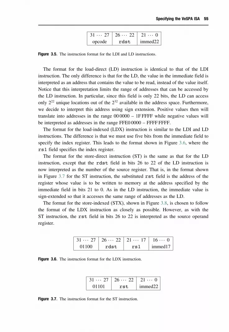
Specifying the VeSPA ISA 55
31 · · · 27 26 · · · 22 21 · · · 0opcode rdst immed22
Figure 3.5. The instruction format for the LDI and LD instructions.
The format for the load-direct (LD) instruction is identical to that of the LDIinstruction. The only difference is that for the LD, the value in the immediate field isinterpreted as an address that contains the value to be read, instead of the value itself.Notice that this interpretation limits the range of addresses that can be accessed bythe LD instruction. In particular, since this field is only 22 bits, the LD can accessonly 222 unique locations out of the 232 available in the address space. Furthermore,we decide to interpret this address using sign extension. Positive values then willtranslate into addresses in the range 00 0000 – 1F FFFF while negative values willbe interpreted as addresses in the range FFE0 0000 – FFFF FFFF.The format for the load-indexed (LDX) instruction is similar to the LDI and LD
instructions. The difference is that we must use five bits from the immediate field tospecify the index register. This leads to the format shown in Figure 3.6, where thers1 field specifies the index register.The format for the store-direct instruction (ST) is the same as that for the LD
instruction, except that the rdst field in bits 26 to 22 of the LD instruction isnow interpreted as the number of the source register. That is, in the format shownin Figure 3.7 for the ST instruction, the substituted rst field is the address of theregister whose value is to be written to memory at the address specified by theimmediate field in bits 21 to 0. As in the LD instruction, the immediate value issign-extended so that it accesses the same range of addresses as the LD.The format for the store-indexed (STX), shown in Figure 3.8, is chosen to follow
the format of the LDX instruction as closely as possible. However, as with theST instruction, the rst field in bits 26 to 22 is interpreted as the source operandregister.
31 · · · 27 26 · · · 22 21 · · · 17 16 · · · 001100 rdst rs1 immed17
Figure 3.6. The instruction format for the LDX instruction.
31 · · · 27 26 · · · 22 21 · · · 001101 rst immed22
Figure 3.7. The instruction format for the ST instruction.

56 Defining the instruction set architecture
31 · · · 27 26 · · · 22 21 · · · 17 16 · · · 001110 rst rs1 immed17
Figure 3.8. The instruction format for the STX instruction.
Recall that the MOV instruction is a pseudo-instruction that gets converted intoan ADD by the assembler. Therefore, the encoding of the MOV instruction will bethe same as the ADD.
Miscellaneous instructionsBoth the HLT and NOP instructions require no operands to be specified. Theinstruction encodings for these two instructions require only the opcode field.The remaining bits can be any value since they will be ignored by the processor.However, it is conventional to set all unused bits to zero.
3.4 Summary
The instruction set architecture (ISA) of a processor precisely defines the interfacebetween the hardware designers and the software developers. In this chapter, wedemonstrated with the example VeSPA processor the steps a computer architectwould use to develop the ISA for a new processor. We discussed several of theimportant design trade-offs that face the architect, such as the various approachesto specifying an instruction’s operands and how to go about choosing specificinstructions to include in the ISA. We also showed how condition codes can becalculated and used to create a rich variety of conditional branch instructions. Finally,we defined the instruction format for each instruction in VeSPA and preciselyspecified how each instruction operates.The next step is to build a behavioral simulation model to experiment with
this new processor specification. This model will allow us to validate that ourspecification is complete and that our trade-offs were appropriate. If it turns out wemade some poor trade-offs, or we need to more precisely specify certain operations,we can always return and change the ISA specification, at least until we release thespecification to the programmers.
Further reading
The following texts discuss in greater depth the trade-offs involved in designinga processor’s instruction set. They also describe several other instruction setarchitectures that have been implemented in different processors.

Summary 57
V. C. Hamacher, Z. G. Vranesic, and S. G. Zaky, Computer Organization. 4th edn. McGraw-Hill,1996. See Chapters 2 and 8 in particular.
V. P. Heuring and H. F. Jordan, Computer Systems Design and Architecture. Addison-Wesley,1997. See Chapter 2 and 3 in particular.
D. A. Patterson and J. L. Hennessy, Computer Organization and Design: The Hardware/SoftwareInterface. Morgan Kaufmann Publishers, 1998. See Chapter 3 in particular.
B. Wilkinson, Computer Architecture: Design and Performance. Prentice Hall, 1996. SeeChapter 2 in particular.

4 Algorithmic behavioral modeling
The sciences do not try to explain, they hardly even try to interpret, they mainly make models. By amodel is meant a mathematical construct which, with the addition of certain verbal interpretations,describes observed phenomena. The justification of such a mathematical construct is solely andprecisely that it is expected to work.
John Von Neumann
In the previous chapter, we defined the instruction set architecture for the VeSPAprocessor. This ISA definition includes all of the storage elements that comprise theprocessor’s state and are accessible to the assembly language programmer. It alsoincludes a description of each instruction and how it affects these state elements. Ournext step is to develop a simulation model of this ISA to verify that our instructiondefinitions are complete, that we have included the right mix of instructions, that thestate elements we defined are appropriate, and so forth. Our completed simulationmodel will be capable of executing programs written in the processor’s machinelanguage. (In the next chapter, we describe an assembler for generating machinelanguage programs.)Our goal in this chapter is to develop an algorithmic behavioral model of the
VeSPA processor. This type of model describes what each instruction does whileignoring the implementation details needed to actually construct the logic that ulti-mately will produce this behavior. For example, at this stage, we do not care whetherthe ALU uses a ripple-carry adder or a carry-lookahead adder. We are concernedonly that the ADD instruction causes the sum of two values stored in the registerfile to be written to the correct destination register. One important consideration isthat this behavioral model ignores all timing information. The specific timing of theindividual operations is left to the lower level models.We describe the processor in an algorithmic fashion using the C language-like
syntax and features of Verilog. This behavioral model does not make use of the fullpower and complete features of the Verilog language, though. Instead, we describeonly those features and language constructs that are needed to write this behavioralmodel. The appropriate features are introduced as they are needed. If we have definedthe ISA completely, we should find that developing this behavioral model reduces toalmost a direct translation of the ISA definition in Appendix A into the correspondingVerilog equivalent.
58
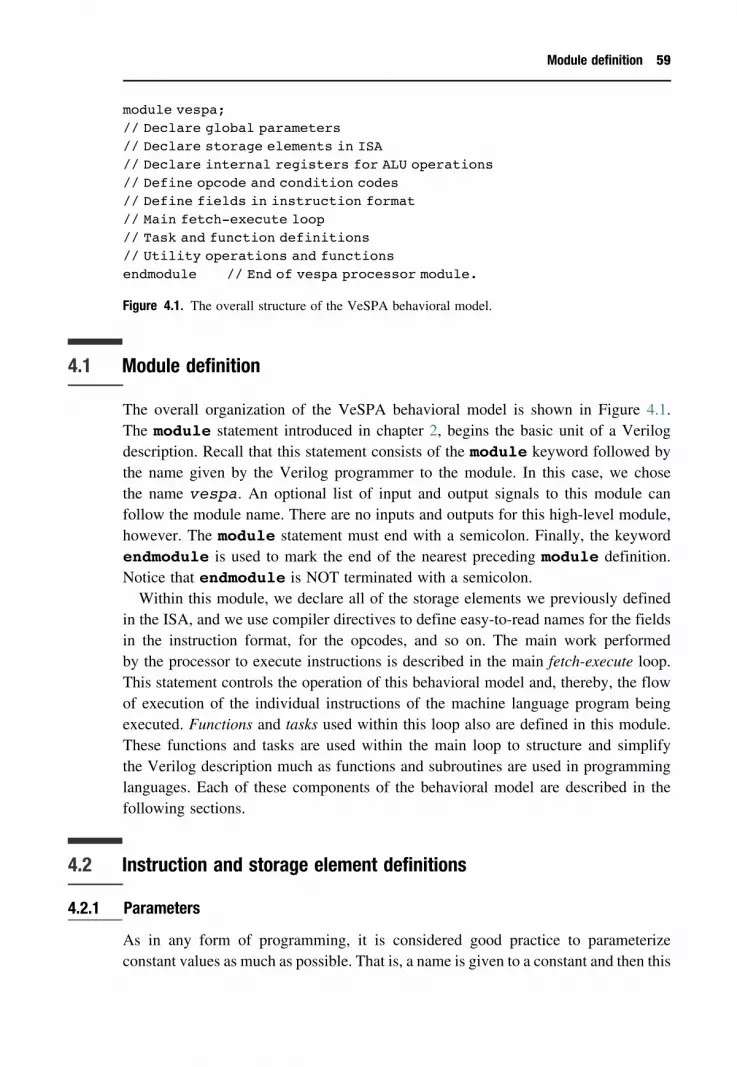
Module definition 59
module vespa;// Declare global parameters// Declare storage elements in ISA// Declare internal registers for ALU operations// Define opcode and condition codes// Define fields in instruction format// Main fetch-execute loop// Task and function definitions// Utility operations and functionsendmodule // End of vespa processor module.
Figure 4.1. The overall structure of the VeSPA behavioral model.
4.1 Module definition
The overall organization of the VeSPA behavioral model is shown in Figure 4.1.The module statement introduced in chapter 2, begins the basic unit of a Verilogdescription. Recall that this statement consists of the module keyword followed bythe name given by the Verilog programmer to the module. In this case, we chosethe name vespa. An optional list of input and output signals to this module canfollow the module name. There are no inputs and outputs for this high-level module,however. The module statement must end with a semicolon. Finally, the keywordendmodule is used to mark the end of the nearest preceding module definition.Notice that endmodule is NOT terminated with a semicolon.Within this module, we declare all of the storage elements we previously defined
in the ISA, and we use compiler directives to define easy-to-read names for the fieldsin the instruction format, for the opcodes, and so on. The main work performedby the processor to execute instructions is described in the main fetch-execute loop.This statement controls the operation of this behavioral model and, thereby, the flowof execution of the individual instructions of the machine language program beingexecuted. Functions and tasks used within this loop also are defined in this module.These functions and tasks are used within the main loop to structure and simplifythe Verilog description much as functions and subroutines are used in programminglanguages. Each of these components of the behavioral model are described in thefollowing sections.
4.2 Instruction and storage element definitions
4.2.1 Parameters
As in any form of programming, it is considered good practice to parameterizeconstant values as much as possible. That is, a name is given to a constant and then this

60 Algorithmic behavioral modeling
name is used throughout the program instead of the value itself. This technique allowsthe value of the constant to be changed in only one location and then have the modifiedvalue automatically propagated to every location where it is used in the program. InVerilog, the parameter statement is used to assign a value to a symbolic name.We define three parameters in the VeSPA behavioral model:
parameter WIDTH = 32; // Datapath width.parameter NUMREGS = 32; // Number of registers in the ISA.parameter MEMSIZE = (1 << 13); // Size of the memory actually
// simulated. Address range is// 0 to (2ˆ13 - 1).
The parameter keyword begins the statement followed by one or more definitionsof the form name = constant expression. Multiple definitions within one parameterstatementmustbe separatedwithcommas.Thestatement is terminatedwitha semicolon.In the first parameter statement, we define the width of the registers and corres-
ponding data paths to be 32 bits. The second statement defines the number of registersto be 32, as we previously defined in the ISA. We could easily change the data widthof the processor to 16 bits, for instance, by changing this single statement. Similarly,we could increase the number of registers in the processor by changing the secondstatement. Note, however, that changing the number of registers also would requireus to redefine the instruction format to accommodate the additional bits required toaddress the increased number of registers. Thus, this change would have ramificationsfar beyond this single statement.The third parameter statement is slightly more complex than the other two. In this
statement, we are defining how much of the processor’s memory we really want tosimulate. Recall that, in the ISA definition, we said that the memory consists of 232
bytes where each consecutive address points to a single byte. However, it would beimpractical to simulate such a large memory system. Instead, we use this parameterstatement to determine what subset of this memory we should simulate. The Verilogexpression (1 << 13) is evaluated at compile-time to produce a constant value toassign to the parameter name MEMSIZE. The operator << shifts the bit pattern on theleft-hand side by the number of bit positions specified on the right-hand side. Thestatement thus shifts the value 1 left 13 times, which is equivalent to computing 213.Consequently, this parameter statement causes the value 8192 to be substituted forthe name MEMSIZE wherever it appears in the remainder of this Verilog program.
4.2.2 Register declarations
After defining these parameters, we declare all of the storage elements that are definedin the ISA.

Instruction and storage element definitions 61
reg[7:0] MEM[0:MEMSIZE-1]; // Byte-wide main memory.reg[WIDTH-1:0] R[0:NUMREGS-1]; // General-purpose registers.reg[WIDTH-1:0] PC; // Program counter.reg[WIDTH-1:0] IR; // Instruction register.reg C; // Condition code bit.reg V; // Condition code bit.reg Z; // Condition code bit.reg N; // Condition code bit.reg RUN; // Execute while RUN=1
The basic Verilog storage element is a single-bit register called a reg. It canbe extended into a vector of bits to produce a multibit register that can be refer-enced using a single name. The statement reg[WIDTH-1:0] PC;, for instance,declares a register WIDTH bits wide. The most-significant bit can be referenced asPC[WIDTH-1] with the least-significant bit referenced as PC[0]. The expressionPC[4:2] extracts a field consisting of bits 4, 3, and 2 from the register PC. TheVerilog compiler interprets a value in a reg vector as an unsigned integer.A register definition can be extended to a two-dimensional array of registers by
subscripting the name assigned to the register. For instance, the statement
reg[7:0] MEM[0:MEMSIZE-1];
from above declares an array of registers called MEM, each of which is eight bits wide.This statement is used to declare the memory in the simulated VeSPA processorthat is included within this behavioral model. A single register within this array isreferenced using MEM[96], for example. It is not possible to reference a singlebit from this array of registers, however. To pull out a single bit or field of bits,MEM[96] would have to be assigned to another register, such as IR.The remainder of the registers included in this list of declarations are those we
defined as part of VeSPA’s ISA, except for the registers IR and RUN. The IR registeris the instruction register. This register is not directly accessible to the assemblylanguage programmer and so was not defined in the ISA. However, every processorneeds an IR to hold the most recent word read from memory that is the currentinstruction being executed. Signals from the IR will be used to select which operationis performed, which registers will be used as the input operands, and so on. The RUNregister, in contrast, is declared simply as a convenience for the behavioral model. Itis used as a flag register and is reset by the HLT instruction to signal the end of thesimulation.We also define the following registers:
reg[WIDTH-1:0] op1; // Source operand 1.reg[WIDTH-1:0] op2; // Source operand 2.reg[WIDTH :0] result; // Result value.

62 Algorithmic behavioral modeling
These are not ‘architected’ registers, however. Similar to the RUN register, theyare defined specifically for the behavioral model to assist in calculating the conditioncodes. Note, for instance, that the result register is one bit wider than the processorWIDTH defined previously. This extra bit stores the carry-out value generated by thearithmetic operations. It is subsequently used to set the C bit of the condition codebits. However, it is not defined in the ISA. Consequently, it may or may not existin a final implementation. In any case, the assembly language programmer cannotcount on its existence since the hardware implementer may choose to throw it outcompletely in the final implementation.
4.2.3 Instruction field and opcode definitions
To make the Verilog code readable by a human, we define an easy- to-read identifierfor each opcode in the ISA. We use the ‘define statement for this purpose, asshown in the following Verilog statements.
‘define NOP ’d0‘define ADD ’d1‘define SUB ’d2‘define OR ’d3‘define AND ’d4‘define NOT ’d5‘define XOR ’d6‘define CMP ’d7‘define BXX ’d8‘define JMP ’d9‘define LD ’d10‘define LDI ’d11‘define LDX ’d12‘define ST ’d13‘define STX ’d14‘define HLT ’d31
In the above statements, the ‘define is being used in a manner similar to theparameter statement. However, the parameter statement is used to assign aconstant value to a symbolic name. Since the value in the parameter statementis computed at compile-time, it can contain arbitrarily complex expressions. The‘define, in contrast, performs a strict textual substitution1. For instance, after theabove ‘define statements are encountered, the compiler will insert the text ’d31wherever it encounters the text ‘HLT.
1 This textual substitution is essentially the same as the operation of the #define command inthe C programming language.

Instruction and storage element definitions 63
The backquote character (‘) is used in Verilog to identify compiler directives.A compiler directive is a command to the compiler to perform some operation that willremain in effect throughout the compilation, or until the directive is specifically turnedoff. The ‘undef directive removes a previous definition. For example, ‘undef HLTwill disassociate the text ’d31 from the text HLT.The forward quote (’) in the above definitions is used to indicate the numeric base
in which a constant is to be interpreted. The bases available in Verilog are:
• ’d – decimal• ’h – hexadecimal• ’b – binary• ’o – octal
The base identifier is not case sensitive so that ’d or ’D can be used for decimal, ’hor ’H can be used for hexadecimal, ’b or ’B can be used for binary, and ’o or ’O canbe used for octal.A size specification can optionally precede the base identifier to indicate the number
of bits that should be used to represent the constant value. For example,
• 4’hC is a four-bit constant with the value 12.• 8’b0110 is an eight-bit constant with the value 6. If the value given is smallerthan the size, the most significant bits are padded with zeroes.
• 2’b0110 is a two-bit constant with the value 2. When the specified size is toosmall for the given value, the most significant bits are simply truncated. Also notethat spaces can appear between the size and base specifiers and between the baseand the constant value.
In addition to relating easy-to-read names to the opcode values, it is useful toidentify each of the conditional branch instructions with its corresponding binarypattern using the ‘define, as follows:
‘define BRA ’b0000‘define BNV ’b1000‘define BCC ’b0001‘define BCS ’b1001‘define BVC ’b0010‘define BVS ’b1010‘define BEQ ’b0011‘define BNE ’b1011‘define BGE ’b0100‘define BLT ’b1100‘define BGT ’b0101‘define BLE ’b1101

64 Algorithmic behavioral modeling
‘define BPL ’b0110‘define BMI ’b1110
Finally, we give a symbolic name to each of the fields we defined in the instructionformat.
‘define OPCODE IR[31:27] // opcode field‘define rdst IR[26:22] // destination register‘define rs1 IR[21:17] // source register 1‘define IMM_OP IR[16] // IR[16]==1 when source 2 is immediate
// operand‘define rs2 IR[15:11] // source register 2‘define rst IR[26:22] // source register for store op‘define immed23 IR[22:0] // 23-bit literal field‘define immed22 IR[21:0] // 22-bit literal field‘define immed17 IR[16:0] // 17-bit literal field‘define immed16 IR[15:0] // 16-bit literal field‘define COND IR[26:23] // Branch conditions.
Thesedefinitionsmake itmucheasier to read thecode thatdescribeswhateach instruc-tion does. Note that we can give different names to the same or overlapping fields fromthe IR. For instance, rst and rdst both refer to bits [26:22] of the IR. The reasonfor defining two different names for the same instruction bits is to make these namescorrespond to the fields we previously defined in the ISA for the different instructions.
4.3 Fetch-execute loop
The execution of machine instructions by a processor can be reduced to two basicsteps. First, the next instruction to be executed is fetched from memory and stored inthe IR. Next, the instruction is decoded and the indicated operation is performed. Thisprocess, which is called the fetch-execute cycle, then repeats for the next instruction.Recall that the PC (program counter) determines which instruction is executed next.Thus, the PC needs to be incremented at some point during this fetch-execute cycleto point to the next instruction in memory that will be executed.The Verilog code needed to implement this type of fetch-execute cycle for VeSPA
is shown below.
initial begin
$readmemh(“v.out”,MEM); // Read v.out file into MEM.
RUN = 1; // RUN gets reset by the HLT instruction.PC = 0; // Start executing from address 0.num_instrs = 0;

Fetch-execute loop 65
while (RUN == 1)beginnum_instrs = num_instrs + 1; // Number of instructions executed.fetch; // Fetch the next instruction.execute; // Execute it.print_trace; // Print a trace of execution,
// if enabled.end
$display(“\nTotal number of instructions executed: %d\n\n”,num_instrs);
$finish; // Terminate the simulation and exit.
end
The initial statement in a Verilog model is executed exactly once at simu-lation time 0. The statements between the begin and the end keywords will beexecuted in the order shown, as in any procedural programming language, such as C.The initial statement is useful for initializing constants at the start of a Verilogsimulation, for instance. A module may have any number of initial statements.All of them will appear to execute once concurrently at the beginning of the simu-lation. Thus, the order of these statements is not important. In this behavioral modelof VeSPA, however, the entire simulation will occur within this single initialstatement bracketed by the begin and the end statements.The first step performed in the simulation is to read the contents of a file called
v.out using the $readmemh statement. The values read from this text file arestored into the previously defined array of registers we called MEM. It is assumed herethat someone has written a program in the VeSPA binary machine language and hasstored this program in text format in the file v.out. Typically, an assembler wouldbe used to produce this file. We are using this $readmemh statement to simulatethe operation of an operating system’s loader function storing a program into theprocessor’s memory prior to executing it.The system task $readmemh reads a text file and stores it in the indicated memory
beginning at the smallest memory index. The contents of the text file are assumedto be hexadecimal values. Alternatively, the $readmemb system task is available toread files that are in are assumed to be binary values. The contents of a file consistingof VeSPA machine language statements, for example, could look like this:
50 00 00 1858 40 00 0008 43 00 0138 02 00 0046 ff ff f4f8 00 00 0000 00 00 0a

66 Algorithmic behavioral modeling
Each line contains the four bytes that comprise one VeSPA instruction. Each ofthese values must be separated by by one or more spaces or tabs, or by a new line.The above file contains 28 eight-bit values expressed in hexadecimal. Notice that wecannot write all four bytes as a single hex value, such as 5000000f. The problemwith this format is that MEM was defined as a byte-wide memory. Thus, the valuesread by $readmemh must be single bytes.It also is possible to specify a range of addresses in the $readmemh (or
$readmemb) system task calls. For instance,
$readmemh(“v.out”,MEM, 32, 64)
would store the first 32 values read from v.out into MEM beginning at address 32and continuing sequentially through address 64. Finally, addresses may be specifiedexplicitly within the text file using the @ sign. Thus, a text file that contained
@0020 50 00 00 38@0024 58 40 00 00@0028 08 43 00 01@002c 38 02 00 00@0030 46 ff ff f4@0034 f8 00 00 00@0038 00 00 00 0a
would store the hex value 50 at MEM[20], the value 00 at MEM[21], the value 00at MEM[22], and so on. The addresses given in the file (i.e., the value followingthe @) are interpreted as hexadecimal values and do not have to appear in sequentialorder.The next statement following the $readmemh statement simply sets the register
RUN to 1 to indicate that the processor can begin executing. The RUN flag will bereset when the HLT instruction is executed. We also need to tell the processor theaddress in memory from which it is to begin executing. This is done by assigning 0to the PC register. A consequence of this assignment is that anyone writing assemblylanguage programs for this processor must ensure that the first instruction they wantexecuted is located at address 0 in VeSPA’s address space. We could change thisrequirement by assigning a different value to the PC at this point in the simulation.Many processors, for instance, assign all ones to the PC when the processor is reset.(The instruction at this address should be a jump to the start of the program.) Thechoice of starting addresses is arbitrary. However, whatever choice is made must becommunicated to the assembly language programmers.The statement num_instrs = 0; initializes an integer variable. This variable
must have been previously declared using the statement
integer num_instrs;
Fetch-execute loop 67
Integer variables can be freely used in behavioral models to store signed integervalues. Integer variables are typically a minimum of 32 bits, although some Verilogcompilers may use more bits to represent the value. Bit vectors cannot be extractedfrom integers. Instead, the integer must be assigned to a variable that was declaredas a reg. Type conversion between regs and integers is automatic when usingan assignment statement. In this behavioral model of VeSPA, we use this integervariable to count the total number of instructions that are executed in the simulation.After all of this initialization, we finally encounter the actual fetch-execute loop.
The while statement will execute the immediately following statement as long asthe condition within the parentheses is true. If the condition is already false at the startof the loop, the loop statement is not executed. Only a single statement can followthe while. If multiple statements are to be executed within the loop, they must beenclosed within the begin and end statements. In our simulation, the while loopwill execute until the RUN flag is reset.Within this fetch-execute loop, the first operation simply increments the count of
the number of instructions executed. The next three statements, fetch;, execute;,and print_trace;, are calls to user-defined tasks. These tasks are like procedurecalls in a high-level programming language. As we shall see later, tasks can haveboth input and output parameters. One of the most common uses of tasks is to allowthe same piece of code to be called from multiple locations, possibly with differentparameter values. Our goal in using tasks within this fetch-execute loop, though, issimply to make the code easier to read. We will define the operations performed ineach of these tasks in the following sections.The simulation of the processor ends with the system-defined $display and
$finish tasks. The names of all system-defined tasks in Verilog begin with a $. The$display statement is Verilog’s primary system-defined task for printing results.The syntax for this task is as follows:
$display(“format specification”, arguments);
As can be seen in the above fetch-execute loop, the format specificationfor the $display task is very similar to that used in the C programming language.The following formats can be specified in Verilog:
%b − binary value%c − single ASCII character%d − decimal value%h − hexadecimal value%m − a hierarchical name%o − octal value%s − string of ASCII characters%t − Verilog-defined global time value%v − signal strength value of a net

68 Algorithmic behavioral modeling
The format specifier following the percent character (%) is not case-sensitive. Asin C, the following escape sequences can be used to print special characters.
\n − newline\t − tab%% − the % character\“ − the “ character\\ − the \character
The $display task always prints to the standard output and ends by printinga newline character. The $write task is the same as the $display task exceptthat it does not automatically print a newline. Furthermore, if no format specifier isgiven for a particular argument, both the $display and $write tasks print thevalue as if it were a decimal value. Similarly, the $displayb, $displayh, and$displayo tasks assume unspecified values to be binary, hexadecimal, and octal,respectively. These tasks have corresponding $writeb, $writeh, and $writeotasks.The $finish task terminates the simulation and causes the simulator to exit.
A similar $stop task also terminates the simulation. However, this task causes thesimulator to enter an interactive mode instead of returning control to the operatingsystem.
4.4 Fetch task
We define the fetch task to read the value in memory currently being pointed to bythe PC and then store that value in the IR. This is the next instruction to be executedby the VeSPA processor being simulated.A task definition in Verilog begins with the task keyword. This is followed by
the name of the task and terminated with a semicolon. The task’s parameters aredeclared next. If the task does not have any parameters, nothing needs to be declared.A single statement that comprises the body of the task follows. The task is terminatedwith the endtask keyword. If more than one statement is needed within the task,they must be enclosed within a begin-end pair. A task must be defined within anenclosing module declaration.The fetch task for VeSPA is defined as follows:
task fetch;beginIR = read_mem(PC);PC = PC + 4; // PC points to the next instruction to be executed
endendtask

Fetch task 69
The read_mem statement in this task is an example of a Verilog function.A function is similar to a task except that it is required to have at least one inputand it returns exactly one value. Furthermore, a function is not allowed to call othertasks, and it cannot contain any delays. In this fetch task, the read_mem functionis used to return the four-byte value in memory pointed to by the address that is itssingle argument. We encapsulate the actual operation of the memory in this functionsince the memory will be accessed by several instructions in the simulated instructionset. Furthermore, this encapsulation allows us to change the memory interface bychanging only this single function. As long as the function continues to return afour-byte value and takes the 32- bit address as an input, no other changes should beneeded in the code.This instruction fetch task also is a good place to increment the PC by one
instruction. Recall that each memory address was defined in the ISA to point toa single byte. However, each instruction is four bytes. Thus, incrementing by oneinstruction is equivalent to incrementing the PC by 4, as is done in this task.
4.4.1 Memory interface
At first glance, it would seem that the memory interface should be nothing more thana simple assignment statement. For instance, it would seem that the assignment
IR = MEM[PC];
should move the value in MEM at the address pointed to by the PC register into the IR.However, in defining the memory interface, we suddenly find that we are confrontedwith a choice that impacts the ISA.The problem is that MEM is defined as an array of eight-bit wide registers while the
IR is a 32-bit wide register. Somehow we must compose the eight-bit values in MEMinto an appropriate 32-bit value to store into IR. And this is precisely what impactsthe ISA definition.We have two possible options. A given byte address x could store the least-
significant byte of the 32-bit word, with address x+1 storing the next significant byte,x+2 storing the next byte, and x+3 storing the most-significant byte. Alternatively,this order could be reversed so that address x stores the most-significant byte upthrough the least-significant byte in address x+3.
The choice between these two options determines the endian-ness of our processor.A big-endian machine has the most significant byte (i.e., the ‘big end’ of the 32-bitvalue) stored at the lowest memory address. A little-endian machine, on the otherhard, stores the least-significant byte (i.e., the ‘little end’) at the lowest memoryaddress. Which option to choose is mostly irrelevant, except when transferring databetween machines with different endian-ness, and when manipulating individual bitswithin a word. Since compilers and assemblers generate machine instructions, which

70 Algorithmic behavioral modeling
requires manipulating the bits within the words, they must know the endian-ness ofthe machine. Thus, we must specify the endian-ness as part of the ISA definition.Processors using both byte orderings exist. The Intel x86 family of processors uses
a little-endian ordering, while the Sun SPARC, PowerPC, and 68000 families all usea big-endian ordering. We arbitrarily choose a big-endian ordering for VeSPA. Thischoice leads to the following definition for the read_mem function.
function [WIDTH-1:0] read_mem;input [WIDTH-1:0] addr; // the address from which to read
read_mem = {MEM[addr],MEM[addr+1],MEM[addr+2],MEM[addr+3]};
endfunction // read_mem
The function keyword identifies the start of the function definition. The expres-sion between the square brackets, [WIDTH-1:0], specifies the size of the valuethat will be returned by the function. If no size is specified, it defaults to a singlebit returned value. This declaration is followed by the function name. One or moreinput statements are used to declare the size of the inputs to the function, alongwith the names by which they are referenced within the function. The order of theseinput declarations corresponds to the order of the parameters when the function iscalled. A value is returned from a function by assigning the value to be returned tothe function name.The four bytes read from the MEM array in the read_mem function are composed
into a single 32-bit value using the curly brackets ({,}). These brackets are theconcatenation operator. In addition to concatenating groups of bits to compose largervalues, concatenation can be used with replication in the format
{number of repetitions {expression, expression, ...}}
For example,
{4{3’b101}}
would produce the value 101101101101.Notice that the order in which the individual values read from the MEM array are
concatenated in the above function makes VeSPA a big-endian machine. If we hadthought about it earlier, we would have defined the endian-ness of the machine as partof the ISA definition. However, this turns out to be one of those details that is easyto overlook. One of the advantages of developing this type of behavioral simulationmodel is that we are forced to precisely specify all of these types of details that willinfluence the ISA specification.

Execute task 71
4.5 Execute task
The execute task is where the real work of the processor is performed. As withthe fetch task, this task takes no inputs and produces no outputs. The executionof the VeSPA instructions is simulated by the changes they make to the processor’sstate, including the architectural registers, the condition code bits, and the memory.As shown below, the body of the execute task consists of a single case
statement.
task execute;begin
case (‘OPCODE)
‘ADD: beginif (‘IMM_OP == 0)
op2 = R[‘rs2];else
op2 = sext16(‘immed16);op1 = R[‘rs1];result = op1 + op2;R[‘rdst] = result[WIDTH-1:0];setcc(op1, op2, result, 0);
end
‘AND: beginif (‘IMM_OP == 0)
op2 = R[‘rs2];else
op2 = sext16(‘immed16);op1 = R[‘rs1];result = op1 & op2;R[‘rdst] = result[WIDTH-1:0];
end
‘XOR: beginif (‘IMM_OP == 0)
op2 = R[‘rs2];else
op2 = sext16(‘immed16);op1 = R[‘rs1];result = op1 ˆ op2;R[‘rdst] = result[WIDTH-1:0];
end

72 Algorithmic behavioral modeling
‘BXX: beginif (checkcc(Z,C,N,V) == 1)
PC = PC + sext23(‘immed23);end
‘CMP: beginif (‘IMM_OP == 0)
op2 = R[‘rs2];else
op2 = sext16(‘immed16);op1 = R[‘rs1];result = op1 - op2;setcc(op1, op2, result, 1);
end
‘HLT: beginRUN = 0;
end
‘JMP: beginif (‘IMM_OP == 1) // If jump-and-link operation, the old PC
R[‘rdst] = PC; // value must be saved before it is lost.PC = R[‘rs1] + sext16(‘immed16);
end
‘LD: beginR[‘rdst] = read_mem (sext22 (‘immed22));
end
‘LDI: beginR[‘rdst] = sext22(‘immed22);
end
‘LDX: beginR[‘rdst] = read_mem(R[‘rs1] + sext17(‘immed17));
end
‘NOP: beginend
‘NOT: beginop1 = R[‘rs1];result = ˜op1;R[‘rdst] = result[WIDTH-1:0];
end
‘OR: beginif (‘IMM_OP == 0)
op2 = R[‘rs2];else
op2 = sext16(‘immed16);op1 = R[‘rs1];

Execute task 73
result = op1 | op2;R[‘rdst] = result[WIDTH-1:0];
end
‘ST: beginwrite_mem(sext22(‘immed22),R[‘rst]);
end
‘STX: beginwrite_mem(R[‘rs1] + sext17(‘immed17),R[‘rst]);
end
‘SUB: beginif (‘IMM_OP == 0)
op2 = R[‘rs2];else
op2 = sext16(‘immed16);op1 = R[‘rs1];result = op1 - op2;R[‘rdst] = result[WIDTH-1:0];setcc(op1, op2, result, 1);
end
default: begin$display(‘‘Error: undefined opcode: %d’’,‘OPCODE) ;
end
endcase // OPCODE caseend
endtask
The basic format of a case statement is
case(case-expression)expression-1 : statement-1expression-2 : statement-2expression-3 : statement-3...default: default-statement
endcase
The case statement, which is similar to the switch statement in C, providesa branching capability in Verilog in which one of several possible destinationscan be selected. When the case statement is executed, the case-expressionis first evaluated. This value then is compared to each of expression-1,

74 Algorithmic behavioral modeling
expression-2, and so on. The statement following the colon (:) in the firstexpression that matches the value computed in the case-expression is thenexecuted. If none of the expressions match, the default-statement is executed.The default statement is actually optional. However, it is good programmingpractice to always include a default option.In our simulation of VeSPA, the case expression is simply the value ‘OPCODE,
which we previously defined as the field of bits in the IR that contain the opcode.The value of these bits from the IR is compared with each of the previously definedopcodes. The statements associated with the matching opcode, which are bracketedin a begin-end block, then are executed. The default condition catches thesituation in which the processor tries to execute an undefined opcode.The statements associated with each opcode determine the operations that will be
performed on the state of the VeSPA processor when that opcode is executed. Theseoperations are an almost literal translation of the operations we defined as part of theISA in Chapter 3. (Also see Appendix A for a concise summary of each instruction’soperation.)The operation of the arithmetic and logical instructions all follow the same basic
pattern. First, the immediate operand bit, ‘IMM_OP, is checked to determine if thesecond operand is in one of the registers. This check is performed with an ifstatement. The conditions allowed in an if statement are the same as those in the Clanguage:
== − equal to<= − less than or equal to>= − greater than or equal to< − less than> − greater than!= − not equal to
If the condition evaluates to true, which is indicated by a nonzero value, the state-ment immediately following the if is executed. Otherwise, the statement followingthe else is executed. Nesting of if-else statements is allowed. Each else state-ment is always associated with the closest if that does not have a correspondingelse.The condition being evaluated in the VeSPA simulation is ‘IMM_OP == 0. If this
condition is true, that is, if this bit is equal to 0, the second operand for this instructionis taken from the register pointed to by ‘rs2, which is one of the previously definedbit fields in the IR. If this condition evaluates to false, however, the operand has beenspecified as an immediate value and is taken from the appropriate 16-bit immediatefield of the IR.The function sext16 is used to sign-extend this 16-bit value into an appropriate
WIDTH-bit value as follows (recall that WIDTH was previously defined to be 32 bitsfor this processor):

Execute task 75
function [WIDTH-1:0] sext16; // 16-bit inputinput [15:0] d_in; // the bit field to be sign extended
sext16[WIDTH-1:0] = { {(WIDTH-16){d_in[15]}} ,d_in};
endfunction // sext16
This function uses the replication operator to duplicate the most-significant bit ofthis 16-bit value, which is its sign bit, 16 (i.e., WIDTH-16) times. The concatenationoperator then is used to prepend the sign-extension field to the 16-bit input valueto produce the full 32-bit value desired. This final 32-bit value is assigned to thefunction name to return the value to the calling location. We define the functionssext17, sext22, and sext23 to sign-extend input values of other sizes in asimilar way.After the two operands have been loaded into the op1 and op2 registers, the desired
arithmetic or logical operation is performed and the result is stored in the resultregister. Recall that the result register was declared to be one bit wider than theWIDTH parameter to allow the storage of the carry-out bit of an ALU operation.Consequently, when the contents of this register are written to the appropriate registerin the register file, identified with the ‘rdst field, only the lower bits are used. Thisassignment of the larger width value to the smaller width register is performed withthe statement R[‘rdst] = result[WIDTH-1:0];. Notice that the bit selectionoperator is used to extract the lower 32-bits from the result register. Finally, thesetcc function is used to set the condition code bits for those instructions that weredefined in the ISA as affecting the condition codes. The operation of the setccfunction is detailed in Section 4.6.Notice that the operations for the CMP instruction are exactly the same as those for
the SUB instruction. The only difference is that the CMP instruction never stores itsresult. Its only impact on the processor’s state is to change the value of the conditioncode bits (the PC also gets automatically updated when this instruction is executed,of course).The operation of the branch instruction, BXX, in this behavioral model is quite
simple. First, the checkcc function, which is described in detail in Section 4.6, iscalled to check the outcome of the specific condition being tested. If the returnedvalue is a 1, indicating that the condition was true, the PC is loaded with the currentvalue of the PC plus the sign-extended branch offset stored in the immediate field inthe IR. This change to the PC register causes the program to fetch the next instructionto be executed from the branch target address. If the condition evaluates to false,however, no changes are made to the PC. The result is that the next instructionexecuted is the instruction immediately following the branch.The JMP instruction operates in a similar fashion, except that no condition is
checked. Instead, the PC always is updated with the sum of the address stored in the

76 Algorithmic behavioral modeling
jump target register indicated with the ‘rs1 field, and the sign-extended offset valuestored in the immediate field in the IR. The if statement in this instruction is used todetermine whether the old PC value needs to be saved in the link register specified bythe ‘rdst field. Recall that this old PC value is pointing to the instruction followingthe JMP as the JMP is being executed.In the LDI instruction, the value stored in the destination register specified by
the ‘rdst field is obtained by sign-extending the immediate value stored in theIR. The operation of the LD instruction appears to be quite similar, except thatthe sign-extended value is used as the memory address in the read_mem function.Notice that this is the same read_mem function described in Section 4.4.1 whenwe discussed the fetch function. The LDX instruction also accesses the memoryusing the read_mem function. For this instruction, however, the memory addressis computed as the sum of the value stored in the operand register specified by the‘rs1 field and the sign-extended immediate value in the IR.The operations of the two store instructions, ST and STX, parallel the operations
of the LD and LDX instructions. These instructions use the following write_memtask to access the memory, however.
task write_mem;input [WIDTH-1:0] addr; // Address to which to write.input [WIDTH-1:0] data; // The data to write.
begin
{MEM[addr],MEM[addr+1],MEM[addr+2],MEM[addr+3]} = data;
end
endtask // write_mem
We use a task to write to memory instead of a function since we do not need toreturn any values. Instead, this task takes the address and the value to be written tomemory as its input parameters. The assignment statement simulates the write of the32-bit data value to four consecutive bytes in the MEM array in big-endian order.The only operation performed by the HLT instruction in this behavioral model is to
reset the RUN flag to 0. This action causes the condition being tested in the whilestatement in the fetch-execute loop to fail when the execute task returns. This changein the RUN flag prevents any more instructions from being fetched and executed.The NOP instruction makes no changes to the processor’s state, other than allowing
the PC to be updated to point to the next instruction to be executed.Finally, the default condition in this execute task prints out a message if
the VeSPA processor attempts to execute an undefined opcode. We could cause thesimulation to terminate at this point by inserting a $stop or $finish statement in

Condition code tasks 77
the default case. However, we instead decide to let the simulation continue withthe execution of the next instruction.
4.6 Condition code tasks
The VeSPA behavioral model uses one task and one function to interface with thecondition code bits. The setcc task is called by those instructions that set thecondition code bits. As seen in the following task definition, this task takes asinputs the two input operands and the corresponding result produced by the ALU.Additionally, it takes a single bit input, subt, to indicate that the operation performedwas a subtraction.
task setcc;input [WIDTH-1:0] op1; // Operand 1.input [WIDTH-1:0] op2; // Operand 2.input [WIDTH :0] result; // The calculated result value.input subt; // Set if the operation was a subtraction.
// In this case, the sign bit of op2// must be inverted to correctly// calculate the V bit.
beginC = result[WIDTH]; // The carry out of the result.Z = (̃|result[WIDTH-1:0]); // Result is zero if all bits are 0.N = result[WIDTH-1]; // Result is negative if the most
// significant bit is 1.V = ( result[WIDTH-1] & ˜op1[WIDTH-1] & ˜(subt ˆ op2[WIDTH-1]))
| (˜result[WIDTH-1] & op1[WIDTH-1] & (subt ˆ op2[WIDTH-1]));end
endtask
The four condition code bits are set in this task according to the logic equationspreviously developed in Section 3.2.3 when defining the ISA. Thus, the C bit is thecarry-out bit of the ALU, which has been stored in the most-significant bit of the33-bit result register; the Z bit is the NOR of all of the bits in the result, excludingthe carry-out bit; N is a copy of the sign bit of the result; and V is a function of thesign bits of the two input operands and the result. Note that the sign bit of the secondoperand is inverted using the exclusive-OR operator (ˆ) if the operation performedwas a subtraction.While the setcc task sets the condition code bits, the checkcc function is used
to test these bits based on the condition specified in a conditional branch instruction. AVerilog function is used for this checking since we need to return a value. The inputsto the checkcc function are the four condition code bits and the ‘COND field of theIR. In the following function definition, we specify the four input bits explicitly. The

78 Algorithmic behavioral modeling
‘COND has been defined globally, however, so there is no need to declare it as an input.In fact, the condition code bits also are globally accessible and so do not need to bedeclared as explicit inputs. However, the condition code bits are part of what is calledthe architected state. This terminology means that these bits are explicitly defined inthe processor’s ISA and will change as a consequence of the execution of instructions.The ‘COND field, on the other hand, is a pseudonym for some of the IR bits. The formof the declaration used for checkcc emphasizes the fact that the primary inputs tothis function are the architected state bits. The ‘COND field determines what functionof these input bits needs to be computed to evaluate the condition.
function checkcc;input Z; // The condition code bits.input C;input N;input V;
begincase (‘COND)
‘BRA: begincheckcc = 1;
end
‘BNV: begincheckcc = 0;
end
‘BCC: begincheckcc = ˜C;
end
‘BCS: begincheckcc = C;
end
‘BVC: begincheckcc = ˜V;
end
‘BVS: begincheckcc = V;
end
‘BEQ: begincheckcc = Z;
end

Tracing instruction execution 79
‘BNE: begincheckcc = ˜Z;
end
‘BGE: begincheckcc = (˜N & ˜V) | (N & V);
end
‘BLT: begincheckcc = (N & ˜V) | (˜N & V);
end
‘BGT: begincheckcc = ˜Z & ((˜N & ˜V) | (N & V));
end
‘BLE: begincheckcc = Z | ((N & ˜V) | (˜N & V));
end
‘BPL: begincheckcc = ˜N;
end
‘BMI: begincheckcc = N;
end
endcase // COND caseend
endfunction // checkcc
The appropriate condition to test is selected using a case statement based on the‘COND field of the IR. In all cases, the function should return a 1 if the selected condi-tion is true and a 0 if the condition is false. The logic equations needed to determinethese outcomes are exactly those we developed in Table 3.3 in Section 3.2.3.
4.7 Tracing instruction execution
When debugging machine language programs written for the VeSPA processor, andwhen debugging the behavioral model itself, it is useful to have some facility to tracethe execution of the program, and to monitor the contents of important registers, as itruns on the processor. We define the following print_trace function to performthis type of tracing.

80 Algorithmic behavioral modeling
task print_trace;integer i;integer j;integer k;
begin
‘ifdef TRACE_PCbegin$display(‘‘Instruction #:%d\tPC=%h\tOPCODE=%d’’, num_instrs,PC,
‘OPCODE);end
‘endif // TRACE_PC
‘ifdef TRACE_CCbegin$display(‘‘Condition codes: C=%b V=%b Z=%d N=%b’’, C,V,Z,N);
end‘endif // TRACE_CC
‘ifdef TRACE_REGSbegink = 0;for (i = 0; i < NUMREGS; i = i + 4)
begin$write(‘‘R[%d]: ’’,k);for (j = 0; j <= 3; j = j + 1)
begin$write(‘‘ %h’’,R[k]);k = k + 1;
end$write(‘‘\n’’);end
$write(‘‘\n’’);end
‘endif // TRACE_REGS
endendtask
Recall from Section 4.3 that this print_trace task is called in the fetch-executeloop after each instruction is executed. By this point, you should understand enoughabout Verilog to be able to almost completely understand how this task operates.One new Verilog statement in this task is the ‘ifdef-‘endif construct. This
construct is used for conditional compilation. Specifically, if the name followingthe ‘ifdef has been defined, the statements between the begin-end pair will beexecuted. If it has not been defined, the statements will be ignored. Thus, to turn on

Summary 81
tracing of the PC as a VeSPA program is executed, we need the following statementnear the top of the program:
‘define TRACE_PC 1
Similar definitions will turn the tracing on for TRACE_REGS and TRACE_CC.There is an ‘else statement that can be used with the ‘ifdef as shown in the
following example:
‘ifdef USE_64BITparameter WIDTH = 64;‘elseparameter WIDTH = 32;‘endif
The other new construct used in this task is the for loop. The syntax of the forloop is identical to that in the C language. That is,
for (start-value ; end-value ; increment)
4.8 Summary
Thealgorithmicbehavioralmodelof theVeSPAprocessor asanalmost literal translationfrom the ISA definition. This behavioral model can be used to execute programswrittenin VeSPA’s machine language. In the next chapter, we describe the assembler used totranslate programs written in VeSPA’s assembly language into the machine languageformat that can be executed by this behavioral model simulation. Subsequent chapterswill refine this behavioral model into a structural model that completely describes howa pipelined implementation of the processor can be constructed.

5 Building an assembler for VeSPA
In order to translate a sentence from English into French two things are necessary. First, wemust understand thoroughly the English sentence. Second, we must be familiar with the forms ofexpression peculiar to the French language.
George Polya, How to Solve It, Princeton University Press, 1945.
5.1 Why assembly language?
The instructions that are actually executed by a processor are stored in memory as asequence of binary numbers. When these numbers are fetched by the processor, theyare executed by interpreting this machine language according to the steps specified inthe instruction set architecture (ISA). It is possible to write programs directly in thebinary 1s and 0s of a processor’s machine language. However, it would be extremelytedious and error-prone since humans think in terms of symbols and higher-levellanguages. Consequently, we assign symbolic names to each of the instructions inthe ISA, and to each of the registers and other memory elements that are accessibleto a programmer. We then define a syntax which precisely describes how the varioussymbols can be composed into a complete program. These symbolic names and syntaxdefine a complete programming language which is called an assembly language.An assembler is a program that accepts as input a text file consisting of a sequence
of alphanumeric characters that comprise a program written in a processor’s assemblylanguage. The output of the assembler is a machine language representation of theassembly language program that can be directly executed by the processor. Theoriginal textual format of the program is called the source code. The executablemachine language is called the object code.Most programmers will write their programs using a high-level language, such
as C, Java, or Fortran. So why do we need to develop an assembler for a newprocessor? Perhaps the most important reason is that an assembly language is agood target language for the output of a compiler. That is, a compiler can translatethe source code of a program written in a high-level language into the source codeof the assembly language of the processor on which the program is to execute.
82

The assembly process 83
This processor’s assembly language is called the target language of the compiler. Theassembler then is used to translate this target assembly code into the final executableobject code.Of course, it is possible for the compiler to generate the machine language object
code directly from the high-level language source code. However, it would have toduplicate most of the functions of the assembler anyway. Consequently, it may beeasier for the compiler to translate from a high-level language into the assemblylanguage of the target processor.Another reason for programming in assembly language is that there may not yet
be a compiler available for the processor. For example, when a new processor isbeing designed, a new compiler for this processor would have to be written at thesame time. The processor designers often need to write some programs to test outthe ISA specification on a simulator, for instance, before the compiler is available(see Chapter 8 for more information on writing these types of simple test programs).Thus, the processor designers are likely to make extensive use of the assembler.Assembly language also is frequently used to write the software for
performance-critical sections of an application program. Compilers generally arevery good at producing consistently fast code for an entire program. However, aprogrammer who understands the intimate details of an application often can do abetter job than a compiler of writing assembly code for important sections of theprogram. This is because the assembly code gives the programmer very fine controlof the execution of the instructions. Furthermore, by understanding the specific needsof the application program, the programmer may be able to optimize the program inways that would not be apparent to a compiler. As a result, it is not unusual to writean entire application in a high-level language. The performance-critical sections ofthe program then may be rewritten directly in assembly language. These assemblylanguages sections are linked to the portions written in the high-level language toproduce the final, complete executable object file.Finally, it may be necessary to program a portion of an application program
directly in assembly code to access special features of a processor that cannot beexpressed in a high-level language. For instance, a processor could be designed withspecial-purpose signal-processing or multimedia processing instructions. It may bedifficult to find a compiler that can generate the assembly code needed to accessthese special-purpose instructions.
5.2 The assembly process
The conversion of an assembly language program into an equivalent machinelanguage program can be performed with almost a one-to-one translation of thesymbols representing the machine instructions into the corresponding machine code

84 Building an assembler for VeSPA
bit patterns. The translation process is slightly more complex than this directconversion, however, since we wish to simplify the programmer’s task by allowingsymbolic names for variables and symbolic labels for the target addresses of branchinstructions. For example, we want to allow the programmer to write a statement likeld r0,aaa to specify that the value at address aaa is to be loaded into registerr0. However, we do not want to force the programmer to explicitly determine whatthe actual memory address of aaa is. Instead, the assembler should be able to figureout the address of this variable and automatically insert it into the appropriate fieldin the ld instruction.Similarly, we want the ability to write a statement such as bne exit to specify
the target of a branch using the symbolic name exit instead of the actual address.Again, the assembler will automatically determine the offset value that needs to beinserted into the appropriate field in the bne instruction.
5.2.1 Assembly language format
To prevent the assembler’s translation job from becoming impossibly complex,assembly language programmers must conform to a specific syntax. This syntaxspecifies the order of the various components of an instruction that must be specified,the specific mnemonic names used for the operations, and so forth. Most assemblersrequire the statements in the source program to be written in the following format:
Label Operation Operands Comment
The individual fields in each statement must be separated by appropriate white-space(i.e., blank space, tabs, and new-lines) to allow the assembler to distinguish eachindividual field. Appropriate use of white-space also can be used to enhance thereadability of the program.The Label field is optional. It is used to associate a symbolic name with the
address at which this statement will ultimately get loaded into the processor’s memory.The required Operation field is used to specify the actual operation that willbe performed when the instruction is executed using the mnemonic name defined inthe ISA. For example, this field may contain the mnemonic add or and to indicatethe corresponding operation.The symbolic names for an appropriate number of operands for the given operation
are specified in the next field. Register operands are typically specified using a namesuch as r17 to indicate register number 17, for instance. Where appropriate for thegiven operation, labels also may be given in this field to symbolically specify anaddress in memory. An appropriate constant value may be given here for operationsthat will accept a literal value. The immediate addressing mode used to specify literalvalues is typically indicated by preceding the desired value with the # character.

The assembly process 85
Finally, the optional Comment field begins with a specific character, or sequenceof characters, such as a semicolon. This field can contain any alphanumeric charactersand is ignored by the assembler. It is used by the programmer to insert short commentsthat make the program more understandable to a human reader.
5.2.2 Two-pass assembler
The example VeSPA assembly language program in Figure 5.1 executes theinstructions in a loop the number of times specified in the variable count. Noticethat each of the statements in this program shows the basic structure described in theprevious section. That is, it contains a field for an optional symbolic label followedby the operation mnemonic, the symbolic operands, and, finally, a comment. Wewill translate this example program by hand into the VeSPA machine language todemonstrate how the assembly process works.We assume that this program has been stored in a file that can be read by the
assembler one line at a time. Comments in this particular assembly language areidentified with the semicolon character (;). Thus, the assembler will ignore the firstfive lines in this file.As it is translating a program from assembly language into machine language, the
assembler maintains a variable called the location counter, which we denote LC. Thevalue of the location counter is the address in the target processor’s memory space intowhich the next instruction assembled should be placed. LC will be incremented byan appropriate amount after each instruction is assembled so that the instructions will
;; A test program that simply loops ’count’ number of times.; r0 = the value read from the variable ’count’; r1 = the current iteration number;
.org 0 ; start the program at address 0ld r0,count ; load the value of count into r0ldi r1,#0 ; initialize r1 to 0
back: add r1,r1,#1 ; add one to the value in r1cmp r1,r0 ; compare iteration number (r1) to count (r0)ble back ; loop if r1 <= r0hlt ; otherwise, stop execution
;; Define the storage locations;count:
.word 0xA ; number of times to loop (in hex)
Figure 5.1. An example of an assembly language program written for the VeSPA processor.

86 Building an assembler for VeSPA
be placed in consecutive locations in memory. The statement .org 0 is a commandto the assembler telling it the address at which the instructions should be assembled.Thus, this statement forces the assembler to set LC = 0.The next line read by the assembler is
ld r0,count ; load the value of count into r0
The assembler parses this line into four tokens, specifically, the symbolic opcodeld, the two operands r0 and count, and the comma character (,). The semicolonand everything that follows it on the same line are ignored. The assembler now couldtry and generate the machine language code for this instruction. In particular, wedefined the format for the ld instruction to be as shown in Figure 5.2. The opcodecan be obtained by looking it up in a table. The five-bit value for the rdst field isknown to be 00000 since one of the operands is the token r0, which specifies register0. Filling in a value for the immed22 field is slightly more difficult, however. Thisfield should contain the address for the symbolic name count. Unfortunately, theassembler does not yet know the address to which this symbolic name will resolvesince it has not yet seen this symbolic name defined. The address that should beassociated with this name is not actually defined until near the end of the programin the statement that begins with count:. As a result, it cannot yet fill in this fieldin the instruction.This problem of not knowing the addresses of symbolic names until after they
have been encountered in the program is called the forward referencing problem.To resolve this problem of using a name in a program before it is defined, mostassemblers adopt a two-pass approach. First, the entire program is read line-by-lineby the assembler during which a symbol table is constructed. Each entry in the symboltable contains the alphanumeric name of a symbol and, once it is known, the memoryaddress to which this name corresponds.After the symbol table has been constructed, the assembler makes a second pass
through the source code. Whenever it encounters a symbolic name during this pass,it can look up the corresponding address in the symbol table. This address thenis used to generate the appropriate value to be inserted into the machine languagecode.The assembler finds the definition of each symbol as follows. As it reads each
line, it increments LC by the number of memory locations that will be needed tostore the instruction specified in the line. Simultaneously, the assembler is looking
31 · · · 27 26 · · · 22 21 · · · 001010 rdst immed22
Figure 5.2. The instruction format for the LD instruction.

The assembly process 87
for labels. A label is the definition of a symbolic name. In this assembly language,labels are a sequence of alphanumeric characters (i.e., a symbolic name) terminatedwith a colon (:). When it encounters a label, it makes an entry for the symbolic namein the symbol table. The address that corresponds to the symbol is the current valueof LC. This value is stored in the symbol table along with the symbol itself.
In VeSPA, each instruction has a fixed length of four bytes. Thus, the addressesat which each instruction in the example program in Figure 5.1 will be assembledare those shown in Figure 5.3. On its first pass through this program, the assemblerwill find two symbols defined, the labels back: and count:. It will assign thevalue 8 to the symbol back and the value 24 to the symbol count. It then willbegin the second pass through the source code with the symbol table shown inFigure 5.4.During the second pass, the assembler has enough information to fill in the values
for each field of every instruction. The final field in the ld instruction shown inFigure 5.2 can now be determined by looking up the value associated with countin the symbol table. This value is found to be 24. The complete machine languagecode for this instruction then is
01010 00000 0000000000000000011000.
This value will be stored at address 0. When it is ultimately executed by theVeSPA processor, it will be interpreted as a load instruction that reads the contentsof memory address 24 and puts the value into register r0.
.org 0 ; start the program at address 00 ld r0,count ; load the value of count into r04 ldi r1,#0 ; initialize r1 to 08 back: add r1,r1,#1 ; add one to the value in r112 cmp r1,r0 ; compare iteration number (r1) to count (r0)16 ble back ; loop if r1 <= r020 hlt ; otherwise, stop execution24 count:
.word 0xA ; number of times to loop (in hex)
Figure 5.3. The addresses at which the instructions will be stored after the program in Figure 5.1is assembled.
Symbolic name Corresponding value
back 8count 24
Figure 5.4. The contents of the assembler’s symbol table at the start of the second pass throughthe program shown in Figure 5.1.

88 Building an assembler for VeSPA
@0000 50 00 00 18@0004 58 40 00 00@0008 08 43 00 01@000c 38 02 00 00@0010 46 ff ff f4@0014 f8 00 00 00@0018 00 00 00 0a
Figure 5.5. The complete object file (in hex format) for the program in Figure 5.1 after it hasbeen assembled. Note that the address of each instruction is shown in each line using the Verilogcommand @. This object code thus is ready to be read by an appropriate Verilog $readmemh()statement (see Section 4.3).
The remaining statements in the program are assembled into the final machinelanguage in the same way. The final object code containing the machine languagefor this example program is shown in hex format in Figure 5.5.
5.3 VASM – the VeSPA assembler
The assembler we have developed for VeSPA is called VASM, for VeSPA ASeMbler.It is a simple two-pass assembler that accepts text files as input and producesan object file that can be read by the Verilog simulators of VeSPA developedin this book. Note that the machine code in this object file is actually stored asa series of ASCII characters representing the hexadecimal values of the machinelanguage instructions. This format allows the object file to be viewed and modifiedwith any text editor. It also is the format expected by the Verilog $readmemh()command.The next section describes the VeSPA assembly language syntax, along with some
useful assembler commands. (A programmer’s summary of the syntax is given inAppendix B.) This is followed by a brief description of how each of the assemblerpasses accomplishes its tasks.
5.3.1 VASM syntax and assembler commands
Programs written in the VeSPA assembly language must conform to the standardstructure described in Section 5.2.1, that is, an optional label followed by the operationand operands with an optional comment. White space (blanks, tabs, and new-lines)can be inserted freely anywhere in the input text to enhance the readability of theprogram. Note, however, that comments extend to only the end of a line – each newline is interpreted as a new assembly language statement. The number of operandsthat need to be specified is determined by the particular operation and addressingmode used.

VASM – the VeSPA assembler 89
Comments must be preceded by either a semicolon (;) or two adjacent slashcharacters (//). Any characters on a line that follow either of these symbols are ignoredby the assembler. These two types of comment delimiters have identical meaningsand can be used interchangeably. Immediate operands (i.e., literal values) are denotedusing the pound character (#), such as #45. All values are assumed to be decimalunless they are preceded by the character sequence 0x to indicate a hexadecimalvalue. For example, 12 would be interpreted as the decimal value 12 while 0x12would be interpreted as a hexadecimal value with the decimal equivalent of 18.Register operands are indicated by appending a number between 0 and 31 to theletter r or R, such as r23 or R13. The mnemonic names used for the operations arethose listed in the ISA definition shown in Appendix A.Symbolic names, also called identifiers, must begin with one upper- or lower-case
letter. This letter may be followed by zero or more letters, digits, or the underscorecharacter (_). Labels may not be the same as one of the mnemonics chosen for theoperations, nor can they be the same as a register operand. For example, Exit_Here,b96, and a_0 are all valid identifiers, while add and r5 are not.Label definitions are indicated by appending the colon character (:) to the end of
an identifier, as in Exit_Here:. As mentioned previously, the value assigned toa symbolic name is the value of the location counter, LC, at the time the name isdefined (using the colon). Note that a symbolic name can be defined only once ina program since each name can have only one value associated with it. It can bereferenced multiple times, of course, but it can be defined only once.In addition to the special meanings assigned to these characters, VASM has
defined several special assembler directives. Ignoring lines that consist of only acomment, nearly every statement in an assembly language program gets convertedinto a corresponding machine language instruction. The exception to this rule isan assembler directive. Instead of causing the assembler to produce a machineinstruction, a directive is a command to the assembler itself that will somehow alterthe assembly process. The .org statement discussed previously is one example ofan assembler directive. Recall that it forces the location counter to be set to the givenvalue.Three additional VASM directives are used to allocate space in the processor’s
memory for variables that will be accessed by the executing VeSPA program. Thesedirectives are: .byte, which reserves a single byte in memory and assigns it aninitial value; .word, which reserves and initializes a word (four bytes) of memory;and .alloc, which reserves any number of words, but does not initialize them.All three of these directives force the location counter, LC, to be incremented by anappropriate value. In the case of .byte, the LC is incremented by 1, while .wordcauses it to be incremented by four bytes. Since .alloc allocates multiple words, theLC is incremented by four times the specificed number of words. Finally, the .equdirective assigns a specific value to a symbolic name. This directive is frequently

90 Building an assembler for VeSPA
used to parameterize values in assembly language programs. See Appendix A for theprecise syntax used by these directives.
5.3.2 Pass 1 – lexical analysis and parsing
VASM is a reasonably straightforward two-pass assembler. However, it reads theactual input file only once. During the first pass, each line of the input file is read andconverted into an internal representation that is stored in the assembler’s memory. Thesecond pass then reads this internally-stored representation of the program instead ofreading the actual input file again.The first pass performs two types of operations as it reads the source code lines
of the assembly language program – a lexical analysis combined with a syntacticalanalysis. The lexical analysis examines the sequence of characters one character ata time as the file is read in. It then groups these characters into meaningful chunks,called tokens. For example, the lexical analysis will group the sequence of charactersadd into a token for the add operation. Similarly, when the letter r or R is followedby a one- or two-digit number, the lexical analyzer will group these characters intoa token for a register operand, such as r7.These tokens then are passed to the parser, which performs the syntactical analysis
of the program. This analysis checks to ensure that the tokens occur in the properorder, for instance, that an add token is followed by the required number of operands.The parser is responsible for generating the symbol table, inserting appropriatesymbols and values into the table, and for maintaining the proper value of the locationcounter (LC). It also identifies label definitions, converts tokens representing numericvalues into their actual binary values (which are stored in the symbol table), performsthe operations specified by the assembler directives, and does a very limited amountof error checking.The output of this first pass is the symbol table containing the values that correspond
to all of the symbolic names used in the program. In addition, an internal data structureis constructed that contains the parsed representation of each input statement.While it is certainly possible to write a program from scratch to perform this lexical
analysis and parsing, a variety of tools have been written to simplify the process.In the case of VASM, we used the lex and yacc tools. These are very powerfultools frequently used by compiler developers to convert a program from a textualformat into a representation that can be parsed and manipulated before generatingthe corresponding assembly or object code. It is beyond scope of this text to teachyou all of the details about lex and yacc. The ideas are not particularly difficult tounderstand, although the terminology can get somewhat technical. Instead, we presenta detailed example in Appendix B.4 showing how a new instruction can be added toVASM. This example should be sufficient to allow you to modify the assembler tosuit your own needs.

VASM – the VeSPA assembler 91
5.3.3 Pass 2 – machine code generation
The second pass of the assembler scans through the internal representations ofeach assembly language program statement. As the statements are scanned, they areconverted into the appropriate machine code. The values for all symbolic names canbe obtained from the symbol table during this pass as the machine code is generated,as can the actual binary values of all numeric constants used as immediate values.This pass uses many bit manipulation operations to insert the appropriate values intoeach of the opcode and operand fields.There is one small quirk in the generation of machine code for the conditional
branch instructions that is worth mentioning here. The machine code for each type ofbranch instruction contains the same opcode in the first five bits of the instruction,as specified in the processor’s ISA. The particular branch condition being tested bythis instruction is specified in the next five bits. Finally, the remaining bits are usedto specify the branch displacement or offset value. This displacement value is usedto find the address to which the instruction should branch (i.e., the branch targetaddress) if the condition being tested evaluates to TRUE.Recall that the branch instructions use PC-relative addressing to specify the branch
target address. With this type of addressing mode, the target address is foundby adding the current value of the program counter to the sign-extended branchdisplacement value stored in the immed23 field of the instruction. Consequently, theassembler must calculate the branch displacement for a branch instruction by findingthe arithmetic difference of the current value of the location counter as it is generatingthe machine code and the value of the symbolic label used to identify the branchtarget address in the source code. However, we must remember that, when the branchinstruction is actually executed, the program counter is pointing to the instructionafter the branch instruction.Thus, the assembler must calculate the branch displacement value such that at run-
time, the value of the branch target address is [address_of(BRANCH_TARGET)=PC + 4 + OFFSET], where PC is the value of the program counter when thebranch instruction is executed, OFFSET is the branch displacement value stored inthe branch instruction, and address_of(BRANCH_TARGET) is the address of thebranch target. The offset value calculated by the assembler is found to be [OFFSET=address_of(BRANCH_TARGET) − (LC + 4)] where LC is the value of the PCwhen the branch instruction is executed, and address_of(BRANCH_TARGET) isthe value stored in the symbol table for the branch target. Subtracting the additional 4from this OFFSET corrects for the PC pointing to the next instruction. Notice that thiscorrection value could be something other than 4 in a processor with variable lengthinstructions.The calculated OFFSET value must be truncated to 23 bits to fit into the immediate
field available in the branch instructions. It is an error if the OFFSET is a value thatcannot be represented in 23 bits.

92 Building an assembler for VeSPA
5.4 Linking and loading
The VASM assembler described in this chapter is a simple two-pass assembler. Ittakes as input a single source code file and produces an object code file that can bedirectly read and executed by the simulated VeSPA processor. However, the worldof assemblers can quickly become more complex when we start dealing with largeprograms and the assembly code produced by compilers for high-level languages.Most large programs written in a high-level language are partitioned into several
different files. Each file typically contains one or more procedures or subroutines thatare components of the larger overall program. The routines in each of these files willbe compiled and assembled separately. However, some of the variables and routinesreferenced within one file may actually be defined in another file. These types ofreferences are called external references and are said to be unresolved when the fileis assembled.Before the program can be executed, each of the separately produced object files
must be merged together into a single executable file. This merging is the job of aprogram called the linker. In the process of merging the the separate object files,the linker will attempt to resolve all of the external references. That is, when anexternal reference is found in one object file, the linker will search for the definitionof the corresponding symbol in the other object files. In addition, the linker willsearch precompiled program libraries for external references made by the programto commonly used functions, such as input/output operations (e.g., printf() in C)and common mathematical functions. Any external references that are still unresolvedafter the linking process indicate that the programmer has made an error.After the separate object files and library functions have been merged into a single
executable file, a loader program must be invoked to transfer the executable objectcode from secondary storage into the processor’s memory. Once it is in memory, theloader jumps to the first instruction in the executable file to begin the execution ofthe user’s program.Since there is no linker available for VeSPA, all programs assembled using
VASM must be entirely contained within a single file. Furthermore, in theVeSPA simulator, the function of the loader is performed using the Verilog$readmemh(“v.out”,MEM) command. A loader would be necessary if an actualhardware implementation of VeSPA were built.
5.5 Summary
An assembly language is a human-friendly version of a processor’s machine language.There is an almost one-to-one correspondence between the symbolic assembly

Summary 93
language and the machine language to which it is translated. Assembly language isuseful for writing programs for a processor before a complete high-level languagecompiler is available, and it makes a good target language for a compiler. It also isuseful for space- and time-critical portions of application programs.Assemblers typically use a two-pass process to translate a program’s assembly
language source code into the corresponding machine code. The primary functionof the first pass is to determine the values (addresses) for all symbolic references.The second pass then uses these values, which have been stored in the symbol table,to generate the machine code. This chapter has described the VeSPA ASeMbler(VASM) as an example of a two-pass assembler.

6 Pipelining
If you were plowing a field, which would you rather use? Two strong oxen or 1024 chickens?Seymour Cray (1925–1996), father of supercomputing
6.1 Instruction partitioning for pipelining
In Section 4.3 we learned that the execution of a processor instruction consists oftwo basic steps: fetching the instruction from memory, and then executing it. Inthe simplest implementation of a processor, the complete fetch-execute cycle wouldbe completed for one instruction before the next one begins. We saw this type ofone-instruction-at-a-time operation in the algorithmic behavioral model in Chapter 4.To speed up the execution of instructions, however, we can break the fetch-executecycle into several simpler sub-operations. We then can overlap the execution ofdifferent instructions in an assembly line fashion where each step in the assembly lineis dedicated to performing one specific operation for each instruction. This assemblyline processing is called pipelining.The first step in designing a pipeline for a processor is to determine the smaller
sub-operations within the fetch-execute cycle that must be performed to execute aninstruction. For the VeSPA processor, each instruction will perform some of thefollowing sub-operations, although not all of the instructions will perform all of theoperations:
• Fetch the instruction from memory.• Increment the program counter.• Fetch the operands from the registers.• Compute a memory address.• Read an operand from memory.• Write a result to the memory or to a register.
The next step in designing the pipeline for VeSPA, or for any other processor ISA,is to determine how these individual operations should be partitioned into the different
94

Instruction partitioning for pipelining 95
stages of the pipeline. Some of these operations must be executed sequentially foreach instruction while others can be executed in parallel. For instance, incrementingthe program counter to point to the next instruction to be executed can be completedin the same stage as fetching the current instruction from memory. However, theaddress used to fetch an operand from memory must be computed before the memorycan be read.A straightforward partitioning of these operations leads to the following five-stage
pipeline:
1. Instruction fetch stage (IF).2. Instruction decode/register fetch stage (ID).3. Execution stage (EX).4. Memory access stage (MEM).5. Write-back stage (WB).
This partitioning produces the pipeline shown in Figure 6.1. The first stage in thispipeline, called the IF stage, reads an instruction from memory at the address beingpointed to by the current value of the program counter. Concurrently in this stage,the program counter is incremented to point to the next instruction to be executed.On the next clock cycle, the instruction enters the ID stage. The primary action in
this stage is to decode the opcode bits to determine what operation the instruction willperform. In addition, the bits that specify the register operands are used to read theoperands from the register. The branch target address also is computed in this stage.All of these operations are carried out in parallel. As a result, this stage may readvalues from the registers that turn out not to be needed, and may compute a branchtarget address that is never used. For instance, some instructions need only a singleoperand. However, two operands would be read since this stage is still decoding theopcode. Any values that are read or computed unnecessarily are simply ignored andnot used in any subsequent pipeline stages.After being decoded in the ID stage, the instruction advances into the EX stage.
The opcode has been decoded by this stage, and the operand values have been readfrom the registers. This information is passed from the ID stage and is used to setup the ALU to actually compute the desired operation during this EX stage if theinstruction is a register-to-register ALU operation, such as AND, ADD, and so on. Ifthe instruction is a register-immediate operation, the sign-extended immediate value
IF ID EX MEM WB
Figure 6.1. The basic pipeline structure consists of the following five stages: Instruction Fetch;Instruction Decode/register fetch; instruction EXecution and effective address calculation;MEMory access; register Write-Back.

96 Pipelining
is used as one input to the ALU with the other input being one of the operand valuesread in the ID stage. Finally, if the instruction is a load or store, this stage is used tocompute the effective memory address.Now that the desired operation has been computed in the EX stage, or the effective
memory address has been determined, these values are passed to the MEM stage.This stage is dedicated to accessing the memory for load and store instructions. Theeffective address computed in the EX stage is used to read the desired location frommemory for load instructions. For store instructions, on the other hand, the operandvalue read in the ID stage is written to memory at the given address. All other typesof instructions pass through this stage without changing anything.The final stage of the pipeline, WB, is where the values computed in the EX
stage are finally written back to the destination register. The address of this registerwas previously determined in the ID stage and has been passed along through allof the intermediate stages. The value that is written back is either the value readfrom memory, if the instruction is a load, or the value computed in the EX stage.Store instructions do nothing in this stage since they have already completed theiroperation in the MEM stage.
6.2 Pipeline performance
With the pipeline partitioned into these five stages (Section 6.1), a single instructionwill require five cycles to complete its execution. The real advantage of pipelining,though, is that, as an instruction moves from the first pipeline stage to the second,a new instruction can enter the first stage. As these two instructions move to theirsubsequent stages, another instruction enters the first stage, and so on, as shown inFigure 6.2. In this fashion, a new instruction can begin executing each cycle. Oncethe pipeline fills completely with instructions, one instruction will finish its executionevery clock cycle, assuming that there is no interference between instructions (possiblesources of interference are discussed later in Section 6.3). Thus, up to n instructionscan be in various stages of execution simultaneously, where n is the number of stagesin the pipeline.The ideal speedup that could be produced by a pipelined processor can be determined
as follows. If no overlapping of instructions is allowed in the pipeline, that is, if a newinstruction is not allowed to enter the pipeline until the previous instruction has exitedthe pipeline, a single instruction would require n cycles to complete its execution. Ifthere were I total instructions executed by the program, the total execution time wouldbeTno-pipe = In cycles.On the other hand, if pipelining is allowed, and there are no inter-actions among the instructions, a new instruction can enter the pipeline each cycle.The first instruction would require n cycles to make its way through the pipeline andcomplete its execution. All of the remaining instructions would follow immediately

Dependences and hazards 97
Clock Cycle IF ID EX MEM WB0 — — — — —1 i — — — —2 i+1 i — — —3 i+2 i+1 i — —4 i+3 i+2 i+1 i —5 i+4 i+3 i+2 i+1 i6 i+5 i+4 i+3 i+2 i+1· · · · · · · · · · · · · · · · · ·
Figure 6.2. In clock cycle 0, the pipeline is initially empty. The first instruction, i, enters thepipeline in the IF stage during clock cycle 1. At the beginning of the next clock cycle, instructioni+1 enters the IF stage while i advances to the ID stage. On each subsequent cycle, newinstructions continue to enter the IF stage as each instruction already in the pipeline advances onestage. As instructions complete, they exit the pipeline at the WB stage. With this five-stagepipeline, up to five instructions can be executing different portions of their fetch-execute cyclessimultaneously.
behind this first instruction so that another instruction will complete its execution onevery subsequent cycle. The total execution time for the fully pipelined configurationthen is n cycles for the first instruction, plus I−1 cycles for the remaining I−1 instruc-tions,givingTpipe = n+�I−1�cycles.Thespeedupof thepipelinedprocessorcomparedto the unpipelined processor is the ratio of these two execution times:
Speedup= Tno-pipeTpipe
= In
n+ �I−1�= n
1+ n−1I
(6.1)
This speedup approaches n as the number of instructions executed in the program,I, becomes very large compared to n. Thus, the maximum possible speedup for apipelined processor is equal to the number of stages in the pipeline.Of course, we seldom achieve this ideal speedup since one instruction may need
a result produced by an earlier instruction before it has reached the pipeline stagewhere the needed result has been computed. Limited hardware resources may furtherrestrict an instruction from completing every cycle. Collectively, the restrictions ona pipelined processor’s performance are due to dependences and hazards, which arediscussed in the next section.
6.3 Dependences and hazards
As described in the previous section, an ideal pipeline can have n instructions indifferent stages of execution simultaneously, where n is the number of pipeline stages.In this ideal situation, one instruction can complete every cycle. The performance of
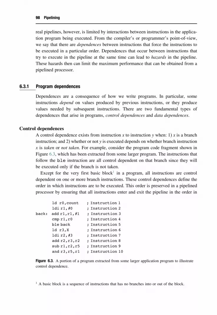
98 Pipelining
real pipelines, however, is limited by interactions between instructions in the applica-tion program being executed. From the compiler’s or programmer’s point-of-view,we say that there are dependences between instructions that force the instructions tobe executed in a particular order. Dependences that occur between instructions thattry to execute in the pipeline at the same time can lead to hazards in the pipeline.These hazards then can limit the maximum performance that can be obtained from apipelined processor.
6.3.1 Program dependences
Dependences are a consequence of how we write programs. In particular, someinstructions depend on values produced by previous instructions, or they producevalues needed by subsequent instructions. There are two fundamental types ofdependences that arise in programs, control dependences and data dependences.
Control dependencesA control dependence exists from instruction x to instruction y when: 1) x is a branchinstruction; and 2) whether or not y is executed depends on whether branch instructionx is taken or not taken. For example, consider the program code fragment shown inFigure 6.3, which has been extracted from some larger program. The instructions thatfollow the ble instruction are all control dependent on that branch since they willbe executed only if the branch is not taken.Except for the very first basic block1 in a program, all instructions are control
dependent on one or more branch instructions. These control dependences define theorder in which instructions are to be executed. This order is preserved in a pipelinedprocessor by ensuring that all instructions enter and exit the pipeline in the order in
ld r0,count ; Instruction 1ldi r1,#0 ; Instruction 2
back: add r1,r1,#1 ; Instruction 3cmp r1,r0 ; Instruction 4ble back ; Instruction 5ld r3,X ; Instruction 6ldi r2,#3 ; Instruction 7add r2,r3,r2 ; Instruction 8sub r1,r2,r5 ; Instruction 9and r3,r5,r1 ; Instruction 10
Figure 6.3. A portion of a program extracted from some larger application program to illustratecontrol dependence.
1 A basic block is a sequence of instructions that has no branches into or out of the block.

Dependences and hazards 99
which they appear in the source code. Furthermore, the pipeline must be able to detectbranch instructions and ensure that instructions that follow a branch are executed inthe pipeline only when the branch direction is known.
Data dependencesData dependences arise between instructions because of the way they use registersand access memory. There are three different types of data dependences, flowdependences, anti-dependences, and output dependences.
Flow dependences: A flow dependence exists from instruction x to instruction ywhen y needs a value produced by x before y can begin executing. In Figure 6.3,for example, there is a flow dependence from Instruction 8 to Instruction9 through register r2. Flow dependences can chain through a sequence ofinstructions so that Instruction 10 also is said to be dependent on Instruction 8since the and needs the value produced by the previous sub, which needs thevalue produced by the preceding add. Flow dependences are often called truedata dependences since the dependent instruction cannot proceed any further inits execution until it has the value produced by the earlier instruction.
Anti-dependences: An anti-dependence occurs between two instructions when afollowing instruction writes to a register or memory location that first needsto be read by a preceding instruction. In Figure 6.3, Instruction 10 is anti-dependent on Instruction 8 since the add instruction must read the value in r3before it is overwritten by the and instruction.
Output dependences: Two instructions have an output dependence when they bothwrite to the same register or memory location. Instructions 3 and 9 in Figure 6.3,for example, both write to r1. As a result, Instruction 9 cannot complete itsexecution until Instruction 3 has completed, otherwise the instructions between3 and 9 would read the wrong value from r1.
Anti- and output dependences are sometimes referred to as name dependencessince the dependence exists only because one of the instructions reuses a registeror memory location that was used by the previous instruction. However, there is nocomputed value that is being passed from one instruction to another. Thus, namedependences are not true dependences. In fact, by using a different register or memorylocation in one of the instructions, that is, by renaming the registers, these namedependences can be eliminated. They are simply a consequence of a programmer orcompiler trying to reuse a storage location that has been used previously.
6.3.2 Pipeline hazards
Program dependences create hazards in the pipeline whenever the dependent instruc-tions could both be in the pipeline simultaneously. The pipeline must detect these

100 Pipelining
hazards and it must take appropriate steps to ensure that instructions do not actu-ally interfere with each other. If dependent instructions are separated by a sufficientdistance in the program, they will not cause a hazard in the pipeline.The types of hazards that the pipeline must watch out for follow the types of
program dependences described above. In particular, control or branch hazards canoccur between instructions that share a control dependence, while data hazards area consequence of data dependences. One additional type of hazard in a pipeline canoccur when two instructions try to simultaneously use the same, limited hardwareresource. This final type of hazard is called a structural hazard.
Branch hazardsA branch (or control) hazard occurs because, in most pipeline implementations, theoutcome of a branch is not known until several cycles after a branch instruction hasbeen fetched into the pipeline. However, the instructions that immediately follow thebranch continue to be fetched into the pipeline. If the branch ultimately turns out tobe not taken, then these instructions can continue their execution through the entirepipeline as normal. If the branch turns out to be taken, though, then these instructionsshould not be executed since they are on the not taken path of the branch.For example, in the VeSPA ISA, branch instructions must test the condition code
register to determine whether the branch should be taken or not. However, thesecondition codes cannot be checked until the pipeline figures out that the instructionactually is a branch instruction. This determination is made in the instruction decode(ID) stage, which is the second stage of the pipeline. After the branch instruction(Instruction 5) in Figure 6.3 moves from the IF stage to the ID stage, Instruction 6will be automatically fetched into the IF stage. If the ble is taken, however, the targetof this branch, Instruction 3, should be the next instruction fetched and executed, notInstruction 6.Unfortunately, determining the outcome of the branch cannot be done until the
ble has completed the ID stage. As a result, once the pipeline detects that the branchdirection is taken, the pipeline’s branch logic must flush the incorrect instructions outof the pipeline and begin fetching the instructions located at the branch target address.In this example program, it must reset the PC to begin fetching from Instruction 3.Figure 6.4 shows how the instructions from this example program would movethrough the pipeline when the branch direction turns out to be taken.The nop instruction that gets inserted in Figure 6.4 introduces a one-cycle delay
after every taken branch. These pipeline bubbles reduce the number of useful instruc-tions that complete per cycle, which obviously reduces the processor’s performance.The number of bubbles (i.e., nop instructions) that must be inserted after a branchis called the pipeline’s branch penalty.One technique for dealing with the branch penalty is to delay the action of the
branch instruction for n cycles. That is, this delayed branch will always execute the
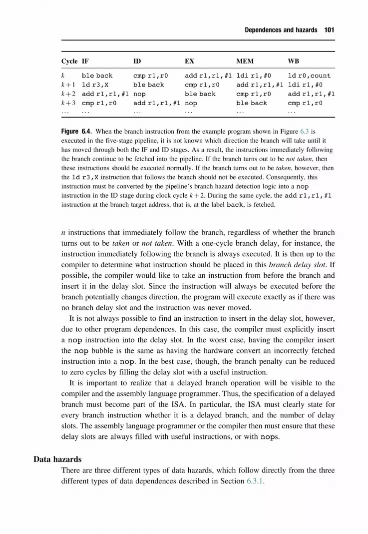
Dependences and hazards 101
Cycle IF ID EX MEM WB
k ble back cmp r1,r0 add r1,r1,#1 ldi r1,#0 ld r0,countk+1 ld r3,X ble back cmp r1,r0 add r1,r1,#1 ldi r1,#0k+2 add r1,r1,#1 nop ble back cmp r1,r0 add r1,r1,#1k+3 cmp r1,r0 add r1,r1,#1 nop ble back cmp r1,r0· · · · · · · · · · · · · · · · · ·
Figure 6.4. When the branch instruction from the example program shown in Figure 6.3 isexecuted in the five-stage pipeline, it is not known which direction the branch will take until ithas moved through both the IF and ID stages. As a result, the instructions immediately followingthe branch continue to be fetched into the pipeline. If the branch turns out to be not taken, thenthese instructions should be executed normally. If the branch turns out to be taken, however, thenthe ld r3,X instruction that follows the branch should not be executed. Consequently, thisinstruction must be converted by the pipeline’s branch hazard detection logic into a nopinstruction in the ID stage during clock cycle k+2. During the same cycle, the add r1,r1,#1instruction at the branch target address, that is, at the label back, is fetched.
n instructions that immediately follow the branch, regardless of whether the branchturns out to be taken or not taken. With a one-cycle branch delay, for instance, theinstruction immediately following the branch is always executed. It is then up to thecompiler to determine what instruction should be placed in this branch delay slot. Ifpossible, the compiler would like to take an instruction from before the branch andinsert it in the delay slot. Since the instruction will always be executed before thebranch potentially changes direction, the program will execute exactly as if there wasno branch delay slot and the instruction was never moved.
It is not always possible to find an instruction to insert in the delay slot, however,due to other program dependences. In this case, the compiler must explicitly inserta nop instruction into the delay slot. In the worst case, having the compiler insertthe nop bubble is the same as having the hardware convert an incorrectly fetchedinstruction into a nop. In the best case, though, the branch penalty can be reducedto zero cycles by filling the delay slot with a useful instruction.
It is important to realize that a delayed branch operation will be visible to thecompiler and the assembly language programmer. Thus, the specification of a delayedbranch must become part of the ISA. In particular, the ISA must clearly state forevery branch instruction whether it is a delayed branch, and the number of delayslots. The assembly language programmer or the compiler then must ensure that thesedelay slots are always filled with useful instructions, or with nops.
Data hazardsThere are three different types of data hazards, which follow directly from the threedifferent types of data dependences described in Section 6.3.1.

102 Pipelining
Read-after-write (RAW) hazards: A RAW hazard is a consequence of a flowdependence between instructions. The problem caused by a RAW hazard is thatthe result value produced by most instructions is not written to a register untilthe WB stage, which is the last stage in the pipeline. However, instructionsread their operands from the registers early in the pipeline in the ID stage. Asa result, if an instruction with a flow dependence on a preceding instructionfollows too closely in the pipeline, it will read the old value in the register. Whatit really should be reading, though, is the new value that is being produced bythe instruction on which it is flow dependent. The pipeline must detect this typeof hazard and take corrective action to ensure that the dependent instructiondoes in fact read the appropriate value.
Write-after-read (WAR) hazards: WAR hazards occur because of anti-dependences. The potential problem is that a subsequent instruction will over-write a value in a register or in memory before the preceding instruction hasa chance to read the old value. WAR hazards do not cause problems in mostpipeline implementations, however, since register values are read early in thepipeline in the ID stage while register values are written in the last stage.This separation ensures that each instruction will read the most current valuesfrom the registers eliminating the need for the pipeline to check for WARhazards.
Write-after-write (WAW) hazards: Output dependences lead to WAW hazards.The potential problem with WAW hazards is that the following instructionwill over-write the register or memory location before the preceding instruc-tion. This incorrect write order would leave the old value in the storagelocation thereby corrupting the computation of any subsequent instructionsthat need to read from this storage location. WAW hazards can occur onlyin pipelines that allow multiple stages to write to the registers or memory,or that allow instructions to execute out of order. In the simple five-stagepipeline discussed in this chapter, only instructions in the WB stage are allowedto write to the registers. Furthermore, instructions must pass through thepipeline in program order. As a result, WAW hazards can never occur in thispipeline.
Structural hazardsStructural hazards occur in a pipeline when two or more instructions try to simul-taneously access some hardware resource beyond its capabilities. For instance, astructural hazard would exist if two instructions both try to read from memory simul-taneously, but the memory has only one read/write port available. In this situation,one of the instructions would have to wait for the other to complete before it can

Dealing with pipeline hazards 103
proceed. Alternatively, the memory could be changed to allow multiple simultaneousreads and writes.This type of structural hazard with memory is actually a common problem in
pipelined processors. It can occur frequently because an instruction must be fetchedfrom memory on every cycle. Additionally, there could be a load or store instructionin the MEM stage trying to read or write memory at the same time. Because of thisconflict, most pipelines separate the top-level memory cache into a data cache and aninstruction cache. The instruction cache is accessed on every cycle to feed instructionsinto the pipeline. Any load or store instructions then can access the separate datacache in the MEM stage without interfering with the instruction fetch stage. (SeeSection 7.5 for more discussion of caches.)
6.4 Dealing with pipeline hazards
Special logic in the pipeline can be used to detect hazards between instructions. If ahazard is detected, the pipeline must take some appropriate action to ensure that theprogram will still produce the correct results. The simplest and most straightforwardaction the pipeline can take is to stall all of the instructions fetched after an instructionthat is the source of hazard. This instruction, and all of those fetched ahead of it,are allowed to continue through the pipeline. After they complete their execution,the stalled instructions are allowed to continue executing. This stalling operation iscalled a pipeline interlock.Separating the instructions in this way ensures that the dependent instruction in
a RAW hazard, for instance, obtains the correct value from the register. Similarly,this stalling can correct a structural hazard or a branch hazard by making sure thatthe conflicting instructions no longer conflict. The pipeline inserts nop instructionsbetween the instruction that is the source of the hazard and the following stalledinstructions because some instruction (i.e., the nop) must continue to flow throughthe pipeline stages.Inserting these pipeline bubbles obviously reduces the performance of the pipeline
compared to its potential ideal performance. Other more sophisticated techniques canbe incorporated into the pipeline to eliminate the need to insert bubbles. For instance,forwarding logic can be used to compensate for RAW hazards. This forwardinglogic passes the value produced in the output of the EX stage back to the input ofthe EX stage directly without going through the registers, as shown in Figure 6.5.Short-circuiting the registers in this way allows the value produced by one instructionto be available as the input to a following instruction much more quickly than if thevalue first had to be written to a register.All of these techniques are discussed more completely in the next chapter where
we describe how to implement a five-stage pipeline for the VeSPA ISA.

104 Pipelining
IF ID EX MEM WB
Figure 6.5. When a RAW hazard is detected between two instructions, forwarding logic in apipeline can be used to bypass the register write operation by passing the value produced in theEX stage by the first instruction back to the input of the EX stage for use by the followingdependent instruction. The register write eventually is performed when the instruction reaches theWB stage so that the value continues to be available for any later instructions that need it.
6.5 Summary
Pipelining is a processor design technique used to speed up the execution of programs.Pipelining does not reduce the amount of time required to execute any single instruc-tion. Rather, it allows multiple instructions to be in various stages of their executionsimultaneously. In the ideal case, a new instruction can complete every cycle resultingin an ideal speedup equal to the number of stages in the pipeline, compared to animplementation that is not pipelined. However, we seldom achieve this ideal speedupdue to program dependences. These dependences lead to pipeline hazards, whichforce the processor to insert bubbles into the pipeline, or require the designer to addlogic to pass values between intermediate pipeline stages. In the next chapter, we willlearn how to use Verilog to implement a pipelined version of the VeSPA processor.
Further reading
The following books provide a comprehensive discussion of the issues involved inpipelining a processor.
H. G. Cragon, Computer Architecture and Implementation. Cambridge, UK: Cambridge UniversityPress, 2000.
V. P. Heuring and H. F. Jordan, Computer Systems Design and Architecture, (2nd edn.) PrenticeHall, 2003.
D. Patterson and J. Hennessy, Computer Organization and Design: The Hardware/SoftwareInterface, 2nd edn. Morgan Kaufmann, 1997.

7 Implementation of the pipelinedprocessor
The problem is not that there are problems. The problem is expecting otherwise and thinking thathaving problems is a problem.
Theodore Rubin
7.1 Pipelining VeSPA
An overview of the structure of a pipelined processor was provided in the previouschapter. We will now fill in the details and add flesh to the skeletal conceptsintroduced earlier, at the end of which we will have developed a block-level structurefor the processor that can be implemented in Verilog. Our processor will consist ofthe following five pipelined stages, the instruction fetch (IF) stage, the instructiondecode (ID) stage, the execute (EX) stage, the memory (MEM) stage, and the writeback (WB) stage. We will interchangeably refer to these as the first through the fifthstages, respectively.Such an instruction pipeline may be defined at the behavioral level or the structural
level. At the behavioral level, the hardware may be modeled as a finite state machinethat performs IF in the first stage, ID in the second, and so on, with Moore outputsgenerated in each stage, corresponding to the control signals that are used to activatethe instructions. An example of such a description is provided for a simple processorin a book on VHDL-based design by Roth (see the Further reading section at the endof this chapter).Instead of such an approach, we choose to describe the circuit at the structural
level in this chapter, in order to get the reader ‘closer to the hardware’. This structuraldescription shows interconnections between blocks such as ALUs, MUXs andregisters, as well as more fundamental gates. To avoid entanglement in cumbersomenotation, we do not specifically show the Verilog implementation here, although aprocessor model in Verilog is available on the companion web site. The top levelmodule instantiates the hazard detection unit and the five stages of the pipeline, inaddition to some global constructs such as the register file, the memory and the
105
106 Implementation of the pipelined processor
clock generator. We now describe the specifics of each of the major modules in thehardware.
7.2 The hazard detection unit
A hazard detection unit is designed to check for potential hazards, and to determinewhen the pipeline is to be stalled, when bubbles are to be introduced, and when datamust be forwarded in each stage of the pipeline. Each stage of the pipeline consistsof several MUXs, and the hazard detection unit generates the control inputs for theseMUXs. We will overview these signals here, and for simplicity, in our subsequentdiscussion of various pipeline stages in Section 7.4, we will not list these controlinputs in detail.As described in the previous chapter, the use of an instruction pipeline implies that
one must allow for and design around three classes of hazards: branch hazards, datahazards, and structural hazards. By construction, we ensure that structural hazardsare not an issue, and therefore we ignore them in this section.Branch hazards may be detected once the instruction enters the ID stage of the
pipeline; if the branch is taken, then the pipeline must be flushed by insertingpipeline bubbles (i.e., NOP instructions). Therefore, these hazards are relatively easyto capture by incorporating circuitry in the second stage that determines whether thebranch condition is satisfied or not, and feeding this to the hazard detection unit thatgenerates appropriate control signals that control MUXs that allow for the possibilityof flushing the pipeline using NOPs when the specified set of branch conditions issatisfied.Due to the structure of the pipeline, data hazards cannot manifest themselves as
WAR or WAW hazards, but allowances must be made to prevent RAW hazards.During the normal operation of the pipeline, the register writes occur at the end ofthe fifth stage (i.e., on the sixth clock), while register reads take place in the secondstage, reading the contents of the register as established at the second clock cycle. Asa consequence, an instruction that requires a register read immediately after a registerwrite can lead to a RAW hazard, implying that early stages of the pipeline must bestalled and NOPs inserted.Therefore, structurally, the pipeline must be modified to permit the insertion of
pipeline bubbles to handle flushing and stalling. The performance of the pipeline canbe improved by the use of forwarding, whereby the number of NOPs to be introducedin the pipeline is minimized. The hazard detection unit generates the control signalsthat enable the MUXs in the instruction pipeline to perform the appropriate functionat each step.

The hazard detection unit 107
Hazard detection may be achieved by examining the instruction set anddetermining:
1. the earliest pipeline stage at which the results of an instruction are available; and2. the latest stage at which the contents of a register are used in the pipeline.
Using this information, instead of waiting for the register write in the sixth clockcycle, the instruction stream in the pipeline may be examined so that data can beforwarded to the next instruction immediately when the results are available, insteadof waiting for the sixth clock cycle. Meanwhile, the next instruction may continueexecution up to the stage at which the results are needed, which is often later thanthe second stage.Table 7.1 shows the RAW dependences between various classes of instructions.
For the various classes of instructions listed in the first row, the earliest pipeline stageat which the results of the instruction are available are shown in parentheses. Forexample, for ALU instructions, the results are available after four clock cycles. Notethat within the entire instruction set, the only instructions that must be consideredhere are the ALU instructions, LD, LDI, LDX, and JMPL. It is easily verified thatthe remaining instructions (NOP, Bxx, JMP, ST, STX and HLT) do not write to aregister and hence cannot create a RAW dependence. For the STX instruction inparticular, two register reads are required: the rs1 register can be read as late as thethird clock cycle, while rst can be read as late as the fourth clock cycle.The latest pipeline stage at which the contents of a register are utilized are shown
in the first column of the table. Here again, the instructions are divided into classes,and only those instructions that require a register read are considered.If an instruction I1 is followed by instruction I2, then the difference between the
earliest write time of I1 and the latest read time of I2 is shown in the cell in Table 7.1
Table 7.1. An analysis of the RAW dependences in the pipeline for operations that perform readand write operations on the register file. The numbers in parentheses in row 1 represent theearliest time when the results of the corresponding instruction in row 1 are available, and thethose in column 1 show the latest read time for the instructions.
Instruction Class ALU (4) LD/LDX (5) LDI (3) JMPL (2)
ALU (3) 1 2 0 −1LDX (3) 1 2 0 −1ST (4) 0 1 −1 −2STX (rs1) (3) 1 2 0 −1STX (rst) (4) 0 1 −1 −2JMP/JMPL (3) 1 2 0 −1Bxx (2) 2 N/A N/A N/A

108 Implementation of the pipelined processor
that corresponds to �I1� I2�. Since I2 lags I1 by one stage in normal operation, if thisnumber is less than or equal to 1, the RAW dependence can be removed by the use offorwarding. In the cases where this number exceeds 1 (shown in boldface), pipelineforwarding alone is insufficient, and it is essential to insert pipeline bubbles.An example of forwarding can be shown for the case where I1 and I2 are both
ALU instructions. A quick glance at the table shows that a difference of one cycleis permissible, provided the data can be forwarded from the result of I1 at the end ofstage 3 (i.e., at the fourth clock cycle for I1) to I2 at the beginning of stage 3 (namely,at the end of the third clock cycle for I2).Note that since a branch instruction Bxx is conditional on the C, N, V or Z flag,
and is therefore only dependent on an ALU operation, the remaining entries in therow of Bxx are not applicable. In case an ALU operation precedes a Bxx instruction,the flags are set at the end of the fourth stage, while the branch decision must bemade in the second stage. Consequently, the pipeline may be stalled and bubblesintroduced until such time as the flags from stage 4 may be forwarded to stage 2.Another example where a pipeline bubble must be inserted is the case when I1
is an LD/LDX instruction and I2 is an ALU instruction; note that in this case, thecorresponding entry in the table is 2. The ALU instruction requires the data in stage3, but the LD/LDX can only provide it in stage 5. This dependence can be detectedwhen the ALU instruction enters the ID stage, and at this time, the pipeline is stalledfor one cycle by inserting a single bubble to create the requisite time gap that thenpermits the correct data from the LD/LDX instruction to be forwarded from stage 5to stage 3, in time for the ALU computation.
7.3 Overview of the pipeline structure
Figure 7.1 illustrates the five stages of the pipeline, the intermediate registers, andthe forwarded data. Notationally, the numeral at the end of each register indicatesthe stage number of the pipeline that it feeds. The IF stage propagates the instructionand program counter to the ID stage through the IR2 and PC2 registers, respectively.From the ID stage to the EX stage, a larger number of intermediate registers is
introduced. As before, we propagate the instruction and program counter, this timethrough IR3 and PC3. As we will see later, this includes mechanisms to handlepipeline stalls and bubbles. Notably, any pipeline stalls are performed at this stage.In addition, we also propagate
• a condition bit that is set to one if the instruction in the ID stage is a branchinstruction, and if the branch condition holds;
• the X3 and Y3 registers that feed the ALU inputs; and• an MD3 register that carries data to be written to the memory.

A detailed description of the pipeline stages 109
Stage 5: Write Back (WB)
Stage 4: Memory (MEM)
Stage 3: Execute (EX)
Stage 2: Instruction Decode (ID)
Stage 1: Instruction Fetch (IF)
X3 MD3
IR4 PC4 Cond CC4 MD4Z4
Z5IR5
IR2 PC2
IR3 PC3 Cond Y3
Figure 7.1. An overview of the structure of the pipeline, showing the stages, registers, andforwarded signals.
During memory write instructions, the ALU inputs may be used for addresscomputation, and hence the data to be written is stored in the MD3 register.The EX stage propagates the condition bit from the ID stage, and also has an
IR4 and PC4 for the instruction register and the program counter, respectively. Asbefore, these may be configured for introducing pipeline bubbles, but configurationfor pipeline stalls is not necessary since these are processed in the ID stage. Besidesthese registers, the memory write data is stored in the MD4 register, the ALU resultsare stored in the Z4 register, and the condition codes in the CC4 register. Finally,the MEM stage only propagates the instruction register to IR5, and the register writedata to the Z5 register.As shown in the figure, data forwarding is implemented by feeding back the Z4,
Z5 and CC4 bits to various pipeline stages.
7.4 A detailed description of the pipeline stages
7.4.1 The instruction fetch (IF) stage
The address of the current instruction is stored in the program counter (PC). Duringnormal operation, the instruction fetch stage addresses the instruction memory usingthe program counter, so that the current instruction may be brought in and loadedinto the instruction register (IR). The program counter is then updated to point to thenext instruction to be introduced into the pipeline. When the pipeline is stalled, the

110 Implementation of the pipelined processor
next instruction in the program is placed on hold, and NOP operations are introducedinto the pipeline.The program counter is therefore updated according to the following scheme,
corresponding to three possible states:
• Since the VeSPA processor uses a byte-addressable memory, and has a 32-bitinstruction, this implies that the next instruction in the program is at the location(PC+ 4). Therefore, if the next instruction in the program is to be brought into theIR, PC is incremented by 4.
• If, instead, a branch instruction is encountered, then the new address specified bythe branch instruction is loaded into PC. In our scheme, the branch address iscomputed at the end of the EX stage of the pipeline, and is fed back from there.
• If the pipeline is stalled, then PC remains unchanged.
A block-level diagram of the circuitry that implements this stage is shown inFigure 7.2. The PC is updated through aMUX, according to the conditions listed above.The IF stage communicates with the ID stage by updating the IR2 and PC2
registers, respectively. The former is updated by a MUX that passes through eitherthe instruction from the instruction memory, or a NOP, or recirculates the currentvalue of IR2 in case of a pipeline stall. The latter is updated through another MUX
Incrementby 4 N
OP
IR2 PC2
32
32
32
32
32
0 1
32
32
32
32
0 1 2 3
MUX MUX
MUX
PC
Stag
e 1:
Ins
truc
tion
Fet
ch (
IF)
Address
Instructionmemory
Data
32
32
Z4
0 1 2 3
Figure 7.2. The IF stage of the instruction pipeline.
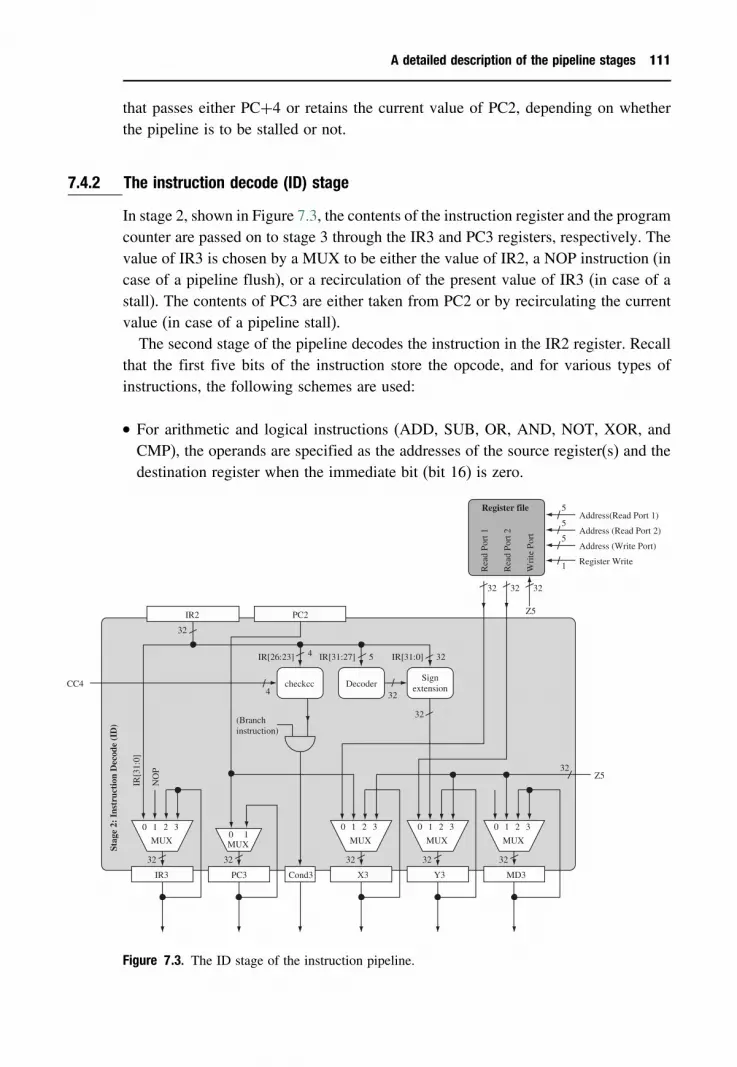
A detailed description of the pipeline stages 111
that passes either PC+4 or retains the current value of PC2, depending on whetherthe pipeline is to be stalled or not.
7.4.2 The instruction decode (ID) stage
In stage 2, shown in Figure 7.3, the contents of the instruction register and the programcounter are passed on to stage 3 through the IR3 and PC3 registers, respectively. Thevalue of IR3 is chosen by a MUX to be either the value of IR2, a NOP instruction (incase of a pipeline flush), or a recirculation of the present value of IR3 (in case of astall). The contents of PC3 are either taken from PC2 or by recirculating the currentvalue (in case of a pipeline stall).The second stage of the pipeline decodes the instruction in the IR2 register. Recall
that the first five bits of the instruction store the opcode, and for various types ofinstructions, the following schemes are used:
• For arithmetic and logical instructions (ADD, SUB, OR, AND, NOT, XOR, andCMP), the operands are specified as the addresses of the source register(s) and thedestination register when the immediate bit (bit 16) is zero.
MUX
32
MUX
32
MUX
32
MUX
32
5
5
5
1
Address(Read Port 1)
Address (Read Port 2)
Address (Write Port)
Register Write
323232
Rea
d Po
rt 2
Wri
te P
ort
Rea
d Po
rt 1
Register file
NO
P
Z5
IR[3
1:0]
32
4
IR[26:23] 4
checkcc DecoderSign
extension
32
32
IR[31:27] 5 32IR[31:0]
32
Stag
e 2:
Ins
truc
tion
Dec
ode
(ID
)
CC4
IR3 PC3 Cond3 X3 Y3 MD3
Z5
(Branchinstruction)
IR2 PC2
MUX
32
0 10 1 2 30 1 2 30 1 2 30 1 2 3
Figure 7.3. The ID stage of the instruction pipeline.

112 Implementation of the pipelined processor
• For control instructions, a condition code is tested based on bits 26 through 23 ofthe instruction word, and a destination address is specified either as an immediateaddress for a branch instruction (Bxx), or as an immediate address with an offsetstored in a register for a jump instruction (JMP, JMPL). JMPL differs from JMPin that bit 16 is one, and that its execution requires the PC to be stored in a registerbefore executing the jump.
• For data transfer instructions1, an immediate address (LD) or data value (LDI) isspecified. The indexed load instruction (LDX) also specifies a register offset. Thestore instructions ST and STX are similar in nature to LD and LDX, respectively,except that the data is stored instead of loaded into memory.
For branch instructions, along with the opcode, the carry (C), zero (Z), negative(N) and overflow (V) flags from the ALU are fed into a condition code checker todetermine whether a branch is to be taken or not. The output of this checker circuitgoes to the condition bit flip-flop at the interface of the second and third stages.A triple-ported register file that permits two simultaneous reads along with a write
operation is used in order to remove the possibility of register file access dependencesin this stage. The registers X3 and Y3 are loaded with the operands to the ALU forthe EX stage. The first operand, X3, is obtained by addressing the register file toobtain the contents of rs1, or from the program counter (in the case of an addresscomputation for an indexed instruction), or from a forwarded output, Z5, from stage 5,or by recirculating the current status of the register in case of a stall, as depicted bythe MUX that feeds X3.Similarly, the second operand, Y3, is chosen from among the contents of rs2, an
immediate operand, Z5, or the recirculated value of Y3. The immediate address isless than 32 bits, and must pass through sign-extension circuitry to create a 32-bitoperand. Depending on the instruction, the bit to be sign-extended may be bit 15 (forarithmetic/logical instructions, JMP and JMPL), bit 16 (for LDX and STX), bit 21(for LDI, LD, and ST), or bit 22 (for Bxx). Therefore, the sign-extension circuitrymust examine the opcode and use the appropriate bit to sign-extend the immediateoperand, if any.For instructions with indexed addressing, an address computation step is required
that sums the contents of the index register with the sign-extended immediate operand.Although this can be carried out in this stage by introducing an adder, we makea design choice here and save on the hardware expense of the adder, and insteadperform the address computation in the next stage of the pipeline, the EX stage.
1 This excludes the MOV instruction, which is implemented as a pseudo-instruction in the form ofan ADD.

A detailed description of the pipeline stages 113
Finally, for store instructions, the operand to be stored is placed in the MD3register. The MUX input to MD3 selects one of rs2 or Z5 in normal operation;additionally, in case of a pipeline stall, the value of MD3 is retained.
7.4.3 The execute (EX) stage
The EX stage performs any arithmetic and logical computations that are necessary,and sets the condition code bits appropriately. The structure of this stage is shown inFigure 7.4.As before, the contents of the IR and PC and transmitted to the next stage, this time
through the IR4 and PC4 registers. The IR4 register may be fed by either the IR3register, or with a NOP in case the pipeline is to be flushed, while the PC4 registersimply transmits the contents of PC3. As mentioned earlier, all stalls are handled instage 2 of the pipeline, so that in this stage, the MUX inputs to the registers thattransmit the values to stage 5 do not have recirculating inputs.The ALU outputs are transmitted to the next stage through the Z4 register; in
addition, this output goes to a condition flag generating circuit that transmits thecondition codes (C, Z, N and V) to the next stage through the CC register. The inputsto the ALU, X and Y, are selected by a pair of MUXs. The MUX input to X may
MUX
32
MUX
32
MUX
32
NO
P
PC4 Cond4 CC4IR4 Z4 MD4
32
323232 32 32
32
NV
C
Z
ALU
Stag
e 3:
Exe
cute
(E
X)
MUX
32
Z5
IR3 PC3 Cond3 X3 Y3 MD3
MUX
32
0 1 2 3 0 1 2 3
0 1 2 30 1
0 1
Figure 7.4. The EX stage of the instruction pipeline.

114 Implementation of the pipelined processor
choose either X3, the forwarded operand Z5, PC4 or Z4. The MUX input to Y issimilar, except that Y3 is used instead of X3.
All addresses for memory accesses are provided by the Z4 register. In case ofaddress computations for indexed instructions, this is natural since the ALU is used toperform these computations. For instructions where an immediate address is provided,the ALU simply passes the immediate instruction directly from Y3 to Z4.
Finally, the condition bit is transmitted to the next stage, and MD4 (for memoryaccess instructions) is selected from one among MD3, Z5, PC4 and Z42.
7.4.4 The memory access (MEM) and write back (WB) stages
The last two stages are illustrated in Figure 7.5. The MEM stage performs thattask of performing read/write operations from and to the memory. Therefore, theprimary task performed here is that of transmitting a memory address, and sendingor receiving the data to be written or read.
For memory accesses, the address is taken from the Z4 register, and read (RD) andwrite (WR) signals are generated and sent to memory: if RD is one, then the memoryaccess is a read, and if WR is one, then the access is a write. If both signals are zero,no memory transactions take place in this stage. The data to be written may eitherbe taken from the MD4 register, or from the Z5 register (in case of data forwarding).
32
MUX
32Address
DatamemoryRead
data
Writedata
32
PC4 Cond4 CC4IR4 Z4 MD4
To stage 2 32 32 32 32
Z5IR5
32
32
Stag
e 4:
Mem
ory
(ME
M)
Stag
e 5:
Wri
te b
ack
(WB
)
(5-bit register addressand registerwrite signal)
(To write portregister file andto stages 2 and 3)
MUX0 1 2 3
0 1
Figure 7.5. The MEM and WB stages of the instruction pipeline.
2 As we look at the MEM stage in Figure 7.5, it may superficially seem that the Cond4 bit is notconnected anywhere. This is, in fact, not true; this bit is used by the hazard detection unit.

Timing considerations 115
The data read from memory goes into the Z5 register. Note that since Z5 is used as aforwarding register, it may also take other inputs in case the instruction that is beingexecuted does not involve a memory read or write. Specifically, an input MUX intoZ5 chooses one among the data from memory, the contents of PC4, and the contentsof Z4.The final stage executes any writes that must be performed in the register file.
Specifically, if the destination in an instruction is a register, then a register addressand data are sent to the register file, along with a write signal.
7.5 Timing considerations
As we discussed previously in Section 6.2, one of the primary goals of pipelining is toincrease the performance of the processor. Pipelining achieves this goal primarily byexecuting several instructions in parallel. Another advantage provided by pipelining,though, is that it allows the designer to use a faster clock frequency than could beused in an equivalent nonpipelined design.The minimum clock period required in a pipelined processor is determined by
the signal propagation delays through each stage of the pipeline. That is, the clockperiod must be long enough to allow every signal in each stage to propagate fromthe pipeline registers at the input to a stage to the pipeline registers at the output of astage. In the ID stage shown in Figure 7.3, for instance, signals must propagate fromregister IR2 through several levels of logic to IR3, Cond3, Y3, and so on. Similarly,signals from the register file also must propagate through several levels of logic tothe corresponding pipeline registers that form the frontier between pipeline stages2 and 3.At least one propagation path from the input pipeline registers to the output pipeline
registers in a stage will be the longest path for that stage. This longest path is calledthe critical path for that stage. The longest of these critical path delays from eachpipeline stage will determine the minimum clock period for the entire pipeline sinceall of the registers in all of the pipeline stages are synchronously clocked with thesame clock. This longest path is called the processor’s critical path delay.To achieve the highest performance, the designer needs to minimize the processor’s
critical path delay. This goal is realized by balancing the number of levels of logicbetween the input and output pipeline registers for each pipeline stage. That is, thesmallest clock period is usually obtained when the critical path delays in each pipelinestage are approximately equal. Balancing the path delays in this way is determined bythe partitioning of the operations required for the fetch-execute cycle into individualpipeline stages.Of particular concern when using the stage partitioning described in Section 6.1 is
the delay in the ID and MEM stages. The problem is that the time required to access

116 Implementation of the pipelined processor
memory to read an instruction, or to read or write a data value, is substantially longerthan the time required to propagate a signal through the logic of the other pipelinestages. If we chose a clock period that allowed a memory access to occur in onecycle, we would end up with an extremely slow processor.To get around this problem of very slow memories, we typically introduce
instruction and data caches. An instruction cache, or i-cache, is a small memory thattemporarily stores instructions that have recently been referenced by the processor.When an instruction is fetched in the IF stage, the processor logic will first lookto see if the desired word from memory, that is, a word with the address currentlybeen referenced, has already been loaded into the i-cache. If it has, we say that thememory reference has hit in the cache. The instruction stored at that address thencan be moved into the IF stage.If the desired address is not in the cache, however, we say that the memory
reference misses in the cache. In this case, the processor logic must read the wordfrom the main memory and move it into the cache. After the word is in the cache, itcan be moved into the IF stage. Since the memory is much slower than the processorpipeline, the logic that services the cache miss must freeze the pipeline until theinstruction has been read from memory and moved into the cache.A separate data cache, or d-cache, can be used to store data values in a similar
manner so that the MEM stage does not have to wait for an entire memory read orwrite operation.The time required to access any memory structure, such as a cache or a register
file, is proportional to its size. That is, a large memory structure requires more time toaccess than a small structure. So that the i- and d-caches can be accessed in a singlecycle, they must be made relatively small compared to the size of the main memory.By carefully adjusting the size of the cache, the designer can make its access timematch the speed required by the IF and MEM pipeline stages.It is possible to increase the number of pipeline stages to help match the pipeline’s
clock frequency to the cache access time. The MEM pipeline stage, for example,could be spread across two separate stages to allow it to access a cache that is slowerthan a single cycle. In this case, a memory read operation would send the address tothe cache in the first MEM stage. The value then would be read from the cache in anew, second MEM stage.Increasing the number of pipeline stages reduces the number of levels of logic
in each stage. Fewer levels of logic then allow for a faster clock. In addition,more instructions will execute simultaneously as the number of pipeline stages isincreased. On the other hand, each additional pipeline stage will add one more cycleto the execution time of each instruction. Furthermore, additional pipeline stages willincrease the branch penalty by forcing more bubbles into the pipeline when a branchis taken. Similarly, more bubbles will be need to be inserted in the pipeline to tolerateother types of hazards. One of the challenges in designing a pipelined processor is
Summary 117
to find the right balance between the number of pipeline stages and the resultingclock period. Cragon (see Further Reading at the end of this chapter) discusses thistrade-off in more detail, and suggests a way of finding an optimal balance.
7.6 Summary
This chapter has demonstrated the implementation of the instruction pipeline, showinghow the design must choose intermediate registers and forwarded signals, anddisplaying the innards of each of the pipeline stages. During our exposition, we havemade several design choices that impact, positively or negatively, the performanceof the pipeline. For instance, the use of forwarding adds hardware overhead butpotentially provides significant speedups. The reader is invited to investigate otherdesign tradeoffs that can result in a hardware/performance tradeoff.
Further reading
H. G. Cragon, Computer Architecture and Implementation. Cambridge, UK: Cambridge UniversityPress, 2000. See Section 6.2, in particular.
C. H. Roth, Jr., Digital Systems Design using VHDL. Boston, MA: PWS Publishing Company,1998. See Chapter 11 in particular.

8 Verification
Aristotle maintained that women have fewer teeth than men; although he was twice married, itnever occurred to him to verify this statement by examining his wives’ mouths.
Bertrand Russell, (1872–1970).
A processor design cannot be considered complete until it has undergone a rigorousverification process. The goal of this verification process is to ensure that the processorbehaves as specified in the ISA under all possible conditions and all possible inputcombinations. Of course, due to the number of potential inputs and states, this isan impossible goal. Instead, we try to verify each component of the processor asrigorously as possible within the given time and resource constraints. We also tryto verify the operation of the entire processor after all of the components have beenassembled into a complete system.In this chapter, we first look at using Verilog test benches to verify the operation of
individual processor modules. We examine two types of test bench. The first, whichwe call directed testing, uses inputs that are carefully chosen to exercise specificaspects of the module being tested. The second type of testing uses pseudorandominputs to automatically exercise a very large number of input combinations.After learning about these module-level testing techniques, we introduce the idea
of self-test programs. These tests are written in the processor’s assembly language, orin a high-level programming language that is compiled into the processor’s assemblylanguage. When the self-test program is executed, it verifies that the differentoperations it performs are actually being executed correctly. This testing techniqueis particularly useful for verifying the operation of the entire processor as eachindividual instruction is executed.
8.1 Component-level test benches
A test bench is a program written in Verilog that is used to stimulate the inputs of aVerilog hardware module and compare the outputs produced to the values expected.Test benches are an important technique for semi-automatically verifying the properoperation of a component.
118

Component-level test benches 119
Test vectors
Module beingtested
Equivalentbehavioral
model
Outputsare equal?
YES: OKNO: Error
Figure 8.1. A test bench requires additional Verilog code to read or generate the test vectors; to drivethese test vectors as inputs to both the module being tested and the behavioral module; and, finally, tocompare the outputs of the module being tested with the outputs of the behavioral module.
As shown in Figure 8.1, the testing process begins with a set of test vectors. Thesetest vectors can be produced either manually by the system designer, or they can begenerated automatically using some sort of pseudorandom test vector generation. Thetest vectors then are applied as the inputs to the Verilog module being tested. Thismodule is simulated and its output values are examined.We could check the outputs manually to verify that they are the results that we
expect for the given inputs. However, it is much more efficient if we can automate thisprocess. The trick to automating this checking process is to somehow automaticallydetermine what the outputs should be when the given inputs are applied.Fortunately, as we have seen previously, Verilog provides us with very powerful
behavioral modeling capabilities. Thus, we can write a simple behavioral model thatprovides the same functionality as the hardware module we are testing. The test benchthen applies the same test vector as the inputs to both the module being tested andto the behavioral model. The outputs of both modules are compared by the checkermodule. If the two sets of outputs do not match, an error is reported. If they do match,though, then the module being tested must be producing the correct output for thattest vector. (This assumes, of course, that the behavioral model produces the correctoutput.) The next test vector then is applied and the entire process is repeated untilwe have no more test vectors.
8.1.1 Using manually generated test vectors
Manually generating test vectors is perhaps the most straightforward way of testinga hardware module. The idea is to provide inputs to the module that will force it

120 Verification
module testbench_setcc;
// This is the top most file. The setcc module is instantiated within// this file.parameter width = 32;wire [width-1:0] op1,op2;wire [width:0] result;
wire add,sub,cmp;
// Instantiate the design under verification.setcc set_condition(op1,op2,result,add,sub,cmp,c,z,n,v);
// Read the manually generated test vectors to test setcc.data_generator datagen(op1,op2,result,add,sub,cmp,clk);
// Check the outputs of the module being tested with the expected outputs.checker check(op1,op2,result,add,sub,cmp,c,z,n,v,clk);
// Instantiate Oscillatoroscillator osc(clk,clk_n);
endmodule
Figure 8.2. A Verilog test bench used to read manually generated test vectors from a file andapply them to the setcc module.
to respond to all of the most basic logical combinations and corner cases1. TheVerilog code in Figure 8.2 shows how to implement a straightforward test benchusing manually generated test vectors for verifying the setcc logic for VeSPA (seeSection 4.6 for a description of this portion of the processor).
The data_generator module instantiated in this test bench, shown inFigure 8.3, reads the test vectors from the input file. It also produces the expectedoutput for the module using the behavioral arithmetic operations. As read by the$fopen statement in this module, the input test vectors are stored in a plain textfile called test_vectors. The $fscanf statement in this module reads each
1 Corner cases are those situations or input combinations that typically do not occur often in anexecuting system. For instance, a corner case may be what happens when a system is executing atits extreme limits along some dimension. Corner cases are important to carefully verify, however,since they often represent the most complex or unusual combinations of events and inputs.Checking the corner cases can very often expose design or implementation errors that can affectthe more common operations.

Component-level test benches 121
module data_generator(op1,op2,result,add,sub,cmp,clk);
parameter width = 32;output [width-1:0] op1,op2;output [width:0] result;output add,sub,cmp;input clk;
integer input_file;integer EOF;reg [width-1:0] op1,op2;reg [width:0] result;reg add,sub,cmp;
initialbegininput_file = $fopen(‘‘./test_vectors’’,‘‘r’’);if (input_file == 0)$stop;
end
always @(posedge clk)begin
#(5);EOF = $fscanf(input_file, ‘‘%h %h %b %b %b’’ ,op1,op2,add, sub,cmp);if(EOF == -1)
$stop;if(add == 1)
result = op1 + op2;else
result = op1 - op2;end
endmodule
Figure 8.3. This module is used in the test bench of Figure 8.2 to read the test vectors andgenerate the expected output.
test vector from this file. The variable EOF is set to −1 when all of the testvectors in the file have been read. The input specification in the $fscanf state-ment shows that the test vector should consist of two hex numbers that representtwo input operands, followed by three binary values. These three binary values,add,sub,cmp, are inputs to the setcc module that indicate what arithmeticoperation has been performed.
Figure 8.4 shows several example test vectors that would be used to drive thistest bench. Each line corresponds to a separate input vector. The first two values ofeach vector are the 32-bit input operand values. The remaining three binary values

122 Verification
ffffffff ffffffff 1 0 000000000 00000000 0 0 111111111 11111111 0 1 000000000 ffffffff 1 0 000000000 ffffffff 0 1 07fffffff 7fffffff 1 0 010000000 10000000 0 1 010000000 10000000 0 0 1
Figure 8.4. Example test vectors used by the module in Figure 8.3.
indicate the specific operation that is being performed by the ALU. Only one of thesethree binary values should be asserted within a test vector, as defined in the VeSPAISA. The first test vector indicates that operation being tested is �−1�+ �−1�, forinstance.The Verilog definition of the checker module instantiated in Figure 8.2 is
shown in Figure 8.5. This module takes as inputs the condition bits generated bythe module being tested, setcc. These inputs are the variables c, z, n, and v. Italso takes as inputs the test vector values and the corresponding result passed fromthe data_generator module, that is, op1, op2, result, add, sub, and cmp.It then uses behavioral statements to generate the values that are expected to beproduced by setcc. These expected values are assigned to the variables ref_c,ref_v, ref_n, and ref_z. Finally, these expected values are compared to thevalues actually produced by the module being tested using the if statement. If thereis a mismatch, an error is reported and the testing is allowed to continue.
The number of test vectors that are manually generated by the designer willdetermine how long this test bench will run. Obviously, the more test vectorsgenerated, the more thoroughly the module will be tested. The test vectors shownin Figure 8.4 provide only enough inputs to verify the most basic operation of thesetcc module. A more complete verification will require substantially more inputvectors. The question, though, is how these additional vectors should be generated.
8.1.2 Using automatically generated test vectors
Manually generated test vectors are very useful for verifying the basic operation of amodule, and for forcing unusual conditions (i.e., corner cases). The primary limitationof manually generated test vectors, however, is the difficulty of generating them. Itsimply is not feasible to generate enough test vectors manually to cover all of thepossible input combinations for the module being tested. For instance, the input testvectors for the example in the previous section each require two 32-bit input operandsand three binary values. Completely verifying all possible input combinations forthis simple module would require 232×232 values to cover all of the input operandpossibilities. These combinations would have to be repeated for each of the three

Component-level test benches 123
module checker(op1,op2,result,add,sub,cmp,c,z,n,v,clk);
parameter width = 32;input add,sub,cmp,clk,c,z,n,v;input [width-1:0] op1,op2;input [width:0] result;
reg ref_c,ref_v,ref_n,ref_z,subt;
initialbegin$display(‘‘OPERAND1\tOPERAND2\tRESULT ADD SUB CMP’’);$display(‘‘==========================================’’);
end
always @(posedge clk)begin#(20);$display(‘‘%h\t%h\t%h %b %b %b at time %d’’,op1,op2, result,
add,sub,cmp,$time);subt = sub || cmp ;ref_c = result[width];ref_z = ˜(|result[width-1:0]);ref_n = result[width-1];ref_v = ( result[width-1] & ˜ op1[width-1] & ˜(subt ˆop2 [width-1]))
| (˜result[width-1] & op1[width-1] & (subt ˆop2 [width-1]));
if( (ref_c != c) || (ref_z != z) || (ref_n != n) || (ref_v !=v) )begin$display(‘‘-E- Error in verifying condition codes’’);$display(‘‘Computed CC : C = %b Z = %b N = %b V = %b’’,c,z,n,v);$display(‘‘Reference CC: C = %b Z = %b N = %b V = %b’’,ref_c,
ref_z,ref_n,ref_v);$stop;
endelse$display(‘‘ConditioncodesverifiedC=%bZ=%bN=%bV=%b’’,c,z,n,v);
endendmodule
Figure 8.5. This module compares the actual values produced by the module being tested with theexpected values.
possible combinations of the single-bit inputs for a total of 3× 232 × 232 = 3× 264
unique test vectors. It would require nearly two million years to test all of theseinput combinations if each test vector could be simulated in only 1 microsecond.Obviously, it is not feasible to exhaustively test even this simple circuit.

124 Verification
Instead of testing every possible input combination, we can randomly generatea very large number of test vectors automatically using Verilog’s pseudorandomnumber generator. This random number generator allows us to cover a wide rangeof values to uncover potential errors without having to generate all possible inputcombinations. Pseudorandom testing also can sometimes generate test vectors forcombinations that a person may not even think of.Figure 8.6 shows how the basic test bench from Figure 8.2 is modified to
perform this type of pseudorandom testing. In fact, all that needs to be changed isto replace the data_generator module with the random_data_generatormodule.The random_data_generator module is shown in Figure 8.7. Instead of
reading the test vectors from a file, as was done in Figure 8.2, this module randomlygenerates operand values using the $random function. The number of randomvectors generated is controlled by the if($time > 100000) statement. Increasingthe 100 000 time unit limit will allow more test vectors to be generated. Otherthan using a different technique for generating test vectors, the remainder of the testprocess is the same as that described in the previous section.
module testbench_setcc;
// This is the top most file. The setcc module is instantiated within// this file.parameter width = 32;wire [width-1:0] op1,op2;wire [width:0] result;
wire add,sub,cmp;
// Instantiate the design under verificationsetcc set_condition(op1,op2,result,add,sub,cmp,c,z,n,v);
// Read the manually generated test vectors to test setcc.random_data_generator datagen(op1,op2,result,add,sub,cmp,clk);
// Check the outputs of the module being tested with the expected outputschecker check(op1,op2,result,add,sub,cmp,c,z,n,v,clk);
// Instantiate Oscillatoroscillator osc(clk,clk_n);
endmodule
Figure 8.6. A Verilog test bench that uses automatically generated test vectors for verifying thesetcc module.
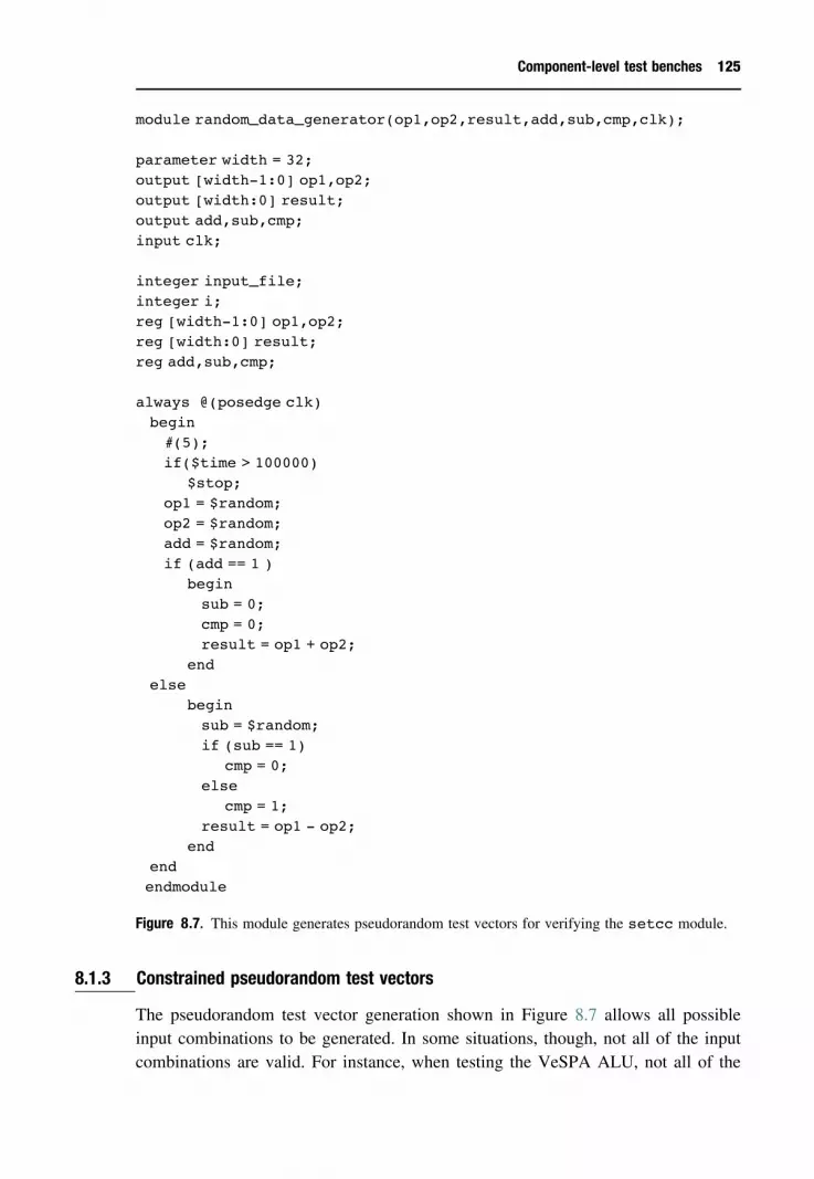
Component-level test benches 125
module random_data_generator(op1,op2,result,add,sub,cmp,clk);
parameter width = 32;output [width-1:0] op1,op2;output [width:0] result;output add,sub,cmp;input clk;
integer input_file;integer i;reg [width-1:0] op1,op2;reg [width:0] result;reg add,sub,cmp;
always @(posedge clk)begin#(5);if($time > 100000)
$stop;op1 = $random;op2 = $random;add = $random;if (add == 1 )
beginsub = 0;cmp = 0;result = op1 + op2;
endelse
beginsub = $random;if (sub == 1)
cmp = 0;else
cmp = 1;result = op1 - op2;
endendendmodule
Figure 8.7. This module generates pseudorandom test vectors for verifying the setcc module.
8.1.3 Constrained pseudorandom test vectors
The pseudorandom test vector generation shown in Figure 8.7 allows all possibleinput combinations to be generated. In some situations, though, not all of the inputcombinations are valid. For instance, when testing the VeSPA ALU, not all of the

126 Verification
possible opcode values are valid ALU opcodes. In this type of situation, each testvector must be compared to the range of valid inputs as it is generated. Any generatedvector that is outside of the range of valid inputs must be thrown away and a newvector generated to replace it. This type of test vector generation is called constrainedpseudorandom test vector generation. An example of how these constraints can beapplied is shown in Figure 8.8 for testing the VeSPA ALU.
module rnd_data_generator(opcode,alu_x,alu_y,clk);
parameter width = 32;
output [4:0] opcode;output [width-1:0] alu_x,alu_y;input clk;
integer i;integer seed_op,seed_x,seed_y;reg [4:0] opcode;reg [width-1:0] alu_x,alu_y;
initialbegini = 0;$display(‘‘OPCODE(dec)\ t\ t\ tALU_X(hex)\ t\ t\ tALU_Y(hex)\ t\ t\ t
TIME’’);$display(‘‘==============================================’’);end
always @(posedge clk)begin#(5);opcode = $random;
// Constrain the opcodes to be an ALU operation// such that 0 <= opcode <= 13while ((opcode > 14) && (opcode < 31))opcode = $random;alu_x = $random;alu_y = $random;$display(‘‘-I-%d\ t\ t\ t%h\ t\ t\ t%h\ t%d’’, opcode,alu_x,alu_y,
$time);i = i+1;// if (i == 17)// $stop;
endendmodule
Figure 8.8. This module generates pseudorandom test vectors for the VeSPA ALU where thepossible opcodes that are generated are constrained to be only valid opcodes.

System-level self-testing 127
Several test benches for the VeSPA processor design are available on thecompanion web site. These include both manually generated test vectors, pluspseudorandom test vectors.
8.1.4 Initialization
When doing this type of testbench testing, it is important to recall that a sequentialcircuit may begin in an arbitrary initial state that is a random function of how it ispowered up. To remove this unpredictability during verification, the hardware maybe designed in such a way that all memory elements can be reset to logic 0 (it is alsopossible to set them to logic 1, but logic 0 is a more conventional choice). This drivesthe finite state machine representing the system to a reset state. If, during testing, itis necessary to drive the data in the memory elements to specific logic values, anappropriate set of state transitions may be selected from the state diagram to drivethe state machine to the corresponding state.For instance, in the previous example in Figure 2.4, resetting all flip-flops would
take the state machine to S0. If the objective is to set the flip-flops corresponding tothe lower two state bits to logic 1, this may be achieved by driving the system to stateS3 in three cycles, setting adventure = 1 in the first, sword_sharpened = 1in the second, and courage = dragon = 1 in the third.
8.2 System-level self-testing
Due to the complexity of generating test vectors for a complete processor, testbenches are typically used to verify only the components within an overall system.A complementary approach for verifying the correct operation of an entire digitalsystem, such as the VeSPA processor, is to write self-test programs in the processor’sassembly language, or in some high-level programming language. These test programsare written, compiled, and assembled on some existing computer system. The resultingobject code then is executed on the processor being tested.If written correctly, these types of self-test programs can quickly identify faulty
areas of the processor. Of course, a certain minimum level of the processor mustbe functional in order to even begin executing a self-test program. For instance,the basic fetch-execute cycle must be working to be able to read instructions frommemory into the IR and begin executing them. It also is necessary for at least someof the conditional branch instructions and the compare instructions to be workingproperly to be able to determine if at least some of the initial self-tests functionedcorrectly.The basic idea behind writing self-test programs is to assume that the absolute
minimum level of functionality is correct from the beginning. A short sequence of

128 Verification
simple instructions then is used to verify the most basic operations. Once this basiclevel of execution is verified, additional instructions are checked one-by-one. Asadditional instructions are verified, they can be used to construct more elaborateinstruction sequences to verify more and more complex operations. Thus, you beginby assuming that almost nothing works. Then you slowly verify additional instructionsuntil, at the end, you have thoroughly verified every instruction using a variety ofreasonable combinations of inputs.To demonstrate this type of self-test process, we will describe the simple self-test
program developed to verify the original VeSPA behavioral model and its corres-ponding assembler. This self-test program is by no means complete. However, it doesdemonstrate the basic principles used to develop this type of program.
8.2.1 Initial steps
Before we can thoroughly verify all of the instructions defined in the ISA, wemust choose a very small subset of basic instructions that are necessary for anysubsequent testing. At a minimum, we need to be able to load values into a register,we need to be able to compare the results produced by an operation with the expectedresults, and we need to be able to make a decision based on the result of thecomparison. It also would be a good idea to stop the processor if our initial testfails. In the VeSPA processor, we can perform these four types of operations withthe load-immediate (ldi), compare (cmp), conditional branch (bxx), and halt (hlt)instructions.With the above observations in mind, we develop the following sequence of
instructions as our basic, initial test of VeSPA:
ldi r0,#0xfcmp r0, #15beq starthlt ; if you ended up here, not much is working
The first instruction in this sequence loads an arbitrary value into register r0. Thenext instruction compares the value we think we moved into r0 to the value that wasactually loaded. The third instruction then makes a decision based on the outcome ofthis comparison using the conditional branch instruction.If the branch instruction itself does not work, the program will fall through to
the hlt instruction. Furthermore, if the two values do not match, the branch willagain fall through to the hlt instruction. In either situation, this action likely meansthat not much of the processor is working properly. We hope that at least the hltinstruction is working! If none of these four instructions are working properly, thereis no way to determine what will happen next. It is likely, though, that the processorwill hang and nothing will happen.

System-level self-testing 129
If this simple sequence of instructions executes correctly, though, we will haveverified that the fetch-execute cycle seems to be working, that the processor canperform a simple data movement operation, that it can compare two values, andthat it can do a simple conditional branch. This is not a very complete test of theseoperations, of course. We simply verified that the processor could test a single value.It is certainly possible that it might be able to manipulate this particular value, butno others. Or it may work fine for most values, but not all. We also do not know ifany registers other than r0 appear to be working properly. Nevertheless, this simpletest is enough to begin the self-testing process for the VeSPA processor.
8.2.2 Program structure
It is useful to pause for a moment and describe the overall structure of the testprogram itself. The basic goal of this structure is to make it easy for the programmerto determine what type of error occurred when an error is detected, or to quicklydetermine that the program executed correctly from the beginning to the end. If thevery simple test described above fails, we hope that the processor will halt at the hltinstruction. Since this is the fourth instruction in the program, the PC will have thevalue 4 when the program terminates. Thus, if the processor halts with this addressin the PC, we know that it did not even complete the most basic operations.However, if it executes beyond this point in the program, we can use the compare
and load instructions to provide a slightly more sophisticated way of communicatingto the programmer how well the test progressed. In particular, we set up the followingsequence of operations at the end of the test program:
; The start of the tests.start: ......; The end of the tests.
ldi r0,#good_exitjmp r0
error_exits:
error_regs:ldi r0,#0x2hlt
error_add:ldi r0,#0x3hlt
error_sub:ldi r0,#0x4

130 Verification
hlt...
.org 0x1000good_exit:ldi r0,#-1hlt
If all of the tests complete successfully, the program will run to the comment; The end of the tests. The next instructions it executes will cause it to jumpto the address at the label good_exit. The instructions at this location load thevalue −1 into register r0 and then halts. By observing the values in r0 and the PCwhen the simulation halts, we can determine if the test was successful or not.This basic idea of gradually testing more and more instructions allows us to
build a very complex test program that can evaluate the functionality of everymajor component within the system. A rather complete program written in VeSPA’sassembly language for performing this type of self-test process is available on thecompanion web site.
8.3 Formal verification
The simulation-based verification approaches described in this chapter are some-what informal and ad hoc. The field of formal verification, in contrast, attempts tofurther automate the verification process using theorem proving-based techniques.Equivalence checking, for instance, compares the design being tested to a known-goodreference design by mathematically transforming one design to the other. If a sequenceof mathematical transformations can be found that links the two designs, they are saidto be equivalent. Since the design being tested now has been shown to be equivalentto a known-good design, we can be assured that new design is correct.Another formal verification technique is called model checking. This approach
attempts to prove a set of logical assertions about a design. For instance, the designermay specify as an input assertion that the memory read and write signals cannever both be asserted at the same time. Additional assertions can be generatedby the designer from the ISA specification, for instance. The model checker thenattempts to prove automatically that these assertions must be true given the specificimplementation of the system.These formal verification techniques typically are faster and more thorough than
conventional simulation-based approaches. However, there is no guarantee that thetransformation process or the assertion prover will actually terminate successfully.As a result, there still is a great need for simulation-based verification.

Summary 131
8.4 Summary
The design of any system is not complete until it has been rigorously verified. Inthis chapter, we have learned about two important techniques for automating theverification process: test benches, and self-test programs.A test bench is a Verilog program that is used to verify the operation of a hardware
module, which also is written in Verilog. The primary operations performed by a testbench program are:
1. generate the test vectors used to drive the inputs of the device being tested;2. apply these test vectors to the device;3. simulate the operation of the device with these inputs applied;4. capture the outputs the device produces;5. compare these outputs to the expected values;6. report when the simulated output values do not match the expected output values.
The test vectors used as the input stimulus in a test bench program can be gener-ated either manually or automatically using a constrained pseudorandom test vectorgenerator. The real power of a test bench program is that it can partially automatethe verification process.Self-test programs are used as a next step beyond test benches. Self-test programs
are written in a high-level programming language, or directly in the processor’sassembly language. As the self-test program is executed on the processor being tested,it automatically verifies the correct operation of each instruction. Self-test programscan be used to verify a system while it is being designed. They also can be usedon operating systems after the design is complete to verify that an actual hardwaredevice is operating correctly. Finally, we note that more sophisticated techniques,such as equivalence checking and model checking, are often used to bring greatermathematical rigor to the verification process.
Further reading
D. R. Smith and P. D. Franzon, Verilog Styles for Synthesis of Digital Systems. Upper Saddle River,NJ: Prentice Hall, 2000. See in particular Chapter 7.

APPENDIXA The VeSPA instruction set
architecture (ISA)
The instruction set architecture (ISA) of the VeSPA (Very Small ProcessorArchitecture) defines the interface between the hardware designer and the assemblylanguage programmer. It consists of all of the programmer accessible storage, plusall of the instructions.
A.1 Notational conventions
The following notation is used in this appendix to describe the ISA.
• #. This symbol is used to identify an immediate operand.• rdst. One of the general-purpose registers that will be used as the destination tostore the result produced by an instruction.
• rs1, rs2. One of the general-purpose registers that will be used as a source valuein an operation.
• rst. The register that will be written to memory in a store operation.• R[rx]. The contents of general-purpose register rx.• Mem[x]. The contents of memory location x.• immedX. An X-bit immediate value used as a literal.• LABEL. Used in the assembler to symbolically specify a memory location, thatis, by name.
• ;. Used in the assembler to mark the beginning of a comment.• sext(x). Sign-extend the value x by replicating the sign bit as many times asnecessary to extend x to a 32-bit value.
• setcc(x). Set the condition code bits according to the value x.
132

Storage elements 133
A.2 Storage elements
The following storage elements are defined in the ISA and are accessible to theassembly language programmer, either directly or indirectly as a side effect of someinstructions.
• Memory. The main memory consists of 232 locations, each of which is eight-bitswide. The memory uses a big-endian organization so that the most-significant byteof a 32-bit value is stored at the smaller memory address.
• General-purpose registers. There are thirty-two 32-bit general-purpose registersavailable to the programmer. They are numbered from 0 to 31 and given the namesr0, r1, r2, · · ·, r31.
• Condition code bits. The condition code bits, C, V, Z, and N, are set by the resultof certain ALU operations and are used by the conditional branch instruction. The Cbit indicates that a carry-out from the most significant bit position has occurred; theV bit indicates a carry-out from the sign bit (i.e., overflow of a two’s-complementoperation); the Z bit is set when the result is zero; and the N bit is set when theresult is a negative value (i.e., when the sign bit of the result is 1).
• Program counter (PC). A 32-bit register that points to the next instruction to beexecuted.
• Instruction register (IR). A 32-bit register that holds the instruction beingexecuted. This register cannot be directly accessed by the programmer.
A.3 The instruction specifications
The operations available in the VeSPA ISA are listed below..
Mnemonic Opcode OperationDecimal Binary
NOP 0 00000 No operation.ADD* 1 00001 Addition.SUB* 2 00010 Subtraction.OR 3 00011 Bit-wise logical OR.AND 4 00100 Bit-wise logical AND.NOT 5 00101 Bit-wise logical complement.XOR 6 00110 Bit-wise exclusive-OR.CMP* 7 00111 Arithmetic comparison.Bxx† 8 01000 Conditional branch (xx = specific condition).
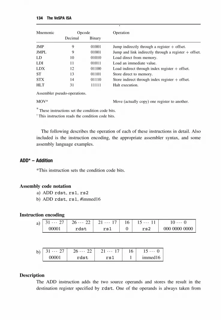
134 The VeSPA ISA
.
Mnemonic Opcode OperationDecimal Binary
JMP 9 01001 Jump indirectly through a register + offset.JMPL 9 01001 Jump and link indirectly through a register + offset.LD 10 01010 Load direct from memory.LDI 11 01011 Load an immediate value.LDX 12 01100 Load indirect through index register + offset.ST 13 01101 Store direct to memory.STX 14 01110 Store indirect through index register + offset.HLT 31 11111 Halt execution.
Assembler pseudo-operations.
MOV* Move (actually copy) one register to another.
* These instructions set the condition code bits.† This instruction reads the condition code bits.
The following describes the operation of each of these instructions in detail. Alsoincluded is the instruction encoding, the appropriate assembler syntax, and someassembly language examples.
ADD* – Addition
*This instruction sets the condition code bits.
Assembly code notationa) ADD rdst, rs1, rs2b) ADD rdst, rs1, #immed16
Instruction encoding
a) 31 · · · 27 26 · · · 22 21 · · · 17 16 15 · · · 11 10 · · · 000001 rdst rs1 0 rs2 000 0000 0000
b) 31 · · · 27 26 · · · 22 21 · · · 17 16 15 · · · 000001 rdst rs1 1 immed16
DescriptionThe ADD instruction adds the two source operands and stores the result in thedestination register specified by rdst. One of the operands is always taken from

The instruction specifications 135
the register pointed to by rs1. If IR[16] == 0, the second operand is taken fromthe register pointed to by rs2. If IR[16] == 1, however, the second operand isthe literal value obtained by sign-extending the 16-bit immediate field, immed16, to32 bits. The condition code values are set according to the result produced by theaddition operation.
Detailed operationif (IR[16] == 0)
R[rdst] ← R[rs1] + R[rs2];else
R[rdst] ← R[rs1] + sext(immed16);setcc(R[rdst]);PC ← PC + 4;
Assembly code examplesADD r2, r3, r5 ; store the sum of r3 and r5 into r2ADD r6, r8, #98 ; store into r6 the sum of r8 and 98
AND – Bit-wise logical AND
Assembly code notationa) AND rdst, rs1, rs2b) AND rdst, rs1, #immed16
Instruction encoding
a) 31 · · · 27 26 · · · 22 21 · · · 17 16 15 · · · 11 10 · · · 000100 rdst rs1 0 rs2 000 0000 0000
b) 31 · · · 27 26 · · · 22 21 · · · 17 16 15 · · · 000100 rdst rs1 1 immed16
DescriptionThe AND instruction forms the logical AND of the two source operands and storesthe result in the destination register specified by rdst. One of the operands is alwaystaken from the register pointed to by rs1. If IR[16] == 0, the second operand istaken from the register pointed to by rs2. If IR[16] == 1, however, the secondoperand is the literal value obtained by sign-extending the 16-bit immediate field,immed16, to 32 bits.

136 The VeSPA ISA
Detailed operationif (IR[16] == 0)
R[rdst] ← R[rs1] AND R[rs2];else
R[rdst] ← R[rs1] AND sext(immed16);PC ← PC + 4;
Assembly code examplesAND r2, r3, r5 ; store the logical AND of r3 and r5 into r2AND r6, r8, #98 ; store into r6 the logical AND of r8 and 98
Bxx – Conditional branch
This instruction reads the condition code bits.
Assembly code notationBxx LABEL ; where xx corresponds to a specific condition to test
Instruction encoding
31 · · · 27 26 · · · 23 22 · · · 001000 cond immed23
where cond is one of the following values:
cond Assembly Condition
0000 BRA branch always1000 BNV branch never0001 BCC branch on carry clear (C̄)1001 BCS branch on carry set (C)0010 BVC branch on overflow clear (V̄ )1010 BVS branch on overflow set (V )0011 BEQ branch on equal (Z)1011 BNE branch on not equal (Z̄)0100 BGE branch on greater than or equal to (N̄ V̄ �NV )1100 BLT branch on less than (NV̄ �N̄V )0101 BGT branch on greater than (Z̄�N̄ V̄ �NV ))1101 BLE branch on less than or equal to (Z��N V̄ �N̄V ))0110 BPL branch on plus (positive) (N̄ )1110 BMI branch on minus (negative) (N )

The instruction specifications 137
DescriptionIf the specified condition evaluates to true, this instruction will branch to the targetaddress. If the condition evaluates to false, the instruction immediately following thebranch is executed.The target address is determined by adding the sign-extended value of the immed23
field to the current value of the program counter, thereby implementing a PC-relativebranch operation. Note that, while the branch instruction is being executed, the PCvalue is pointing to the instruction after the branch instruction. Thus, the assemblermust calculate the literal value to be stored in the immed23 field as follows: immed23= address_of(LABEL) − (PC + 4).To evaluate the condition, the branch instruction reads the condition code bits and
forms the corresponding logical expression shown in the above table. These conditioncodes are set by the most recent instruction that used the ALU. They indicate thevarious arithmetic relationships that exist after the operation X−Y, where X and Yare signed two’s-complement integers.
Detailed operationif (condition == 1)
PC ← PC + 4 + sext(immed23);else
PC ← PC + 4;
where condition is the result of computing the logic equations shown in the abovetable.
Assembly code examplesCMP r2, r3 ; compare r2 and r3 to set the condition codesBGE LABEL ; branch to LABEL if r2 is greater than or equal to r3
CMP* – Compare
*This instruction sets the condition code bits.
Assembly code notationa) CMP rs1, rs2b) CMP rs1, #value
Instruction encoding
a) 31 · · · 27 26 · · · 22 21 · · · 17 16 15 · · · 11 10 · · · 000111 00000 rs1 0 rs2 000 0000 0000

138 The VeSPA ISA
b) 31 · · · 27 26 · · · 22 21 · · · 17 16 15 · · · 000111 00000 rs1 1 immed16
DescriptionThe CMP instruction compares the operand values by subtracting the second operandfrom the first operand. The result of this subtraction is used to set the condition codebits. The result itself is not stored. One of the operands is always taken from theregister pointed to by rs1. If IR[16] == 0, the second operand is taken from theregister pointed to by rs2. If IR[16] == 1, however, the second operand is the literalvalue obtained by sign-extending the 16-bit immediate field, immed16, to 32 bits.
Detailed operationif (IR[16] == 0)
setcc(R[rs1] - R[rs2]);else
setcc(R[rs1] - sext(immed16));PC ← PC + 4;
Assembly code examplesCMP r2, r3 ; Set the condition codes that result from computing
R[r2] - R[r3]CMP r2, #98 ; Set the condition codes that result from computing
R[r2] - 98
HLT – Halt
Assembly code notationHLT
Instruction encoding
31 · · · 27 26 · · · 011111 000 0000 0000 0000 0000 0000 0000
DescriptionStop execution.
Detailed operationNone
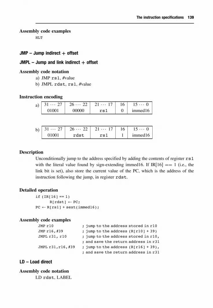
The instruction specifications 139
Assembly code examplesHLT
JMP – Jump indirect + offset
JMPL – Jump and link indirect + offset
Assembly code notationa) JMP rs1, #valueb) JMPL rdst, rs1, #value
Instruction encoding
a) 31 · · · 27 26 · · · 22 21 · · · 17 16 15 · · · 001001 00000 rs1 0 immed16
b) 31 · · · 27 26 · · · 22 21 · · · 17 16 15 · · · 001001 rdst rs1 1 immed16
DescriptionUnconditionally jump to the address specified by adding the contents of register rs1with the literal value found by sign-extending immed16. If IR[16] == 1 (i.e., thelink bit is set), also store the current value of the PC, which is the address of theinstruction following the jump, in register rdst.
Detailed operationif (IR[16] == 1)
R[rdst] ← PC;PC ← R[rs1] + sext(immed16);
Assembly code examplesJMP r10 ; jump to the address stored in r10JMP r16,#39 ; jump to the address (R[r10] + 39)JMPL r31, r10 ; jump to the address stored in r10,
; and save the return address in r31JMPL r31,r16,#39 ; jump to the address (R[r16] + 39),
; and save the return address in r31
LD – Load direct
Assembly code notationLD rdst, LABEL

140 The VeSPA ISA
Instruction encoding
31 · · · 27 26 · · · 22 21 · · · 001010 rdst immed22
DescriptionRead the memory location specified by the sign-extended literal field immed22 andstore the result in register rdst.
Detailed operationR[rdst] ← Mem[sext(immed22)];PC ← PC + 4;
Assembly code examplesLD r6, LABEL ; load the value at LABEL into r6
LDI – Load immediate
Assembly code notationLDI rdst, #value
Instruction encoding
31 · · · 27 26 · · · 22 21 · · · 001011 rdst immed22
DescriptionMove the sign-extended literal field immed22 into register rdst.
Detailed operationR[rdst] ← sext(immed22);PC ← PC + 4;
Assembly code examplesLDI r6, #45 ; move the value 45 into r6LDI r13, #LABEL ; move the address of LABEL into r13
LDX – Load indexed
Assembly code notationLDX rdst, rs1LDX rdst, rs1, #value

The instruction specifications 141
Instruction encoding
31 · · · 27 26 · · · 22 21 · · · 17 16 · · · 001100 rdst rs1 immed17
DescriptionRead the memory location specified by adding the contents of register rs1 and thesign-extended literal field immed17. Store this value in register rdst.
Detailed operationR[rdst] ← Mem[R[rs1] + sext(immed17)];PC ← PC + 4;
Assembly code examplesLDX r6,r8 ; load the value at the address in r8 into r6LDX r6,r8, #46 ; load the value at the address (R[r8] + 46) into r6
MOV* – Move register to register
*This instruction sets the condition code bits.
Assembly code notationMOV rdst, rs1
Instruction encoding
31 · · · 27 26 · · · 22 21 · · · 17 16 15 · · · 000001 rdst rs1 1 0000 0000 0000 0000
DescriptionMove (actually, copy) the contents of register rs1 to register rdst. MOV is reallya pseudo-operation that the assembler converts to the equivalent instruction ADDrdst, rs1, #0. The condition code values are set according to the value moved.
Detailed operationR[rdst] ← R[rs1];setcc(R[rdst]);PC ← PC + 4;
Assembly code examplesMOV r2, r3 ; copy the contents of r3 into r2

142 The VeSPA ISA
NOP – No-operation
Assembly code notationNOP
Instruction encoding
31 · · · 27 26 · · · 000000 000 0000 0000 0000 0000 0000 0000
DescriptionPerform no-operation, except for incrementing the PC to point to the next instructionto execute.
Detailed operationPC ← PC + 4;
Assembly code examplesNOP
NOT – Bit-wise logical complement
Assembly code notationa) NOT rdst, rs1
Instruction encoding
31 · · · 27 26 · · · 22 21 · · · 17 16 · · · 000101 rdst rs1 0 0000 0000 0000 0000
DescriptionForm the logical complement of the value in register rs1 and store the result inregister rdst.
Detailed operationR[rdst]← NOT(R[rs1]);PC← PC + 4;
Assembly code examplesNOT r2, r3,; put the complement of r3 into r2

The instruction specifications 143
OR – Bit-wise logical OR
Assembly code notationa) OR rdst, rs1, rs2b) OR rdst, rs1, #immed16
Instruction encoding
a) 31 · · · 27 26 · · · 22 21 · · · 17 16 15 · · · 11 10 · · · 000011 rdst rs1 0 rs2 000 0000 0000
b) 31 · · · 27 26 · · · 22 21 · · · 17 16 15 · · · 000011 rdst rs1 1 immed16
DescriptionThe OR instruction forms the logical OR of the two source operands and stores theresult in the destination register specified by rdst. One of the operands is alwaystaken from the register pointed to by rs1. If IR[16] == 0, the second operand istaken from the register pointed to by rs2. If IR[16] == 1, however, the secondoperand is the literal value obtained by sign-extending the 16-bit immediate field,immed16, to 32 bits.
Detailed operationif (IR[16] == 0)
R[rdst] ← R[rs1] OR R[rs2];else
R[rdst] ← R[rs1] OR sext(immed16);PC ← PC + 4;
Assembly code examplesOR r2, r3, r5 ; store the logical OR of r3 and r5 into r2OR r6, r8, #98 ; store into r6 the logical OR of r8 and 98
ST – Store direct
Assembly code notationST LABEL, rst

144 The VeSPA ISA
Instruction encoding
31 · · · 27 26 · · · 22 21 · · · 001101 rst immed22
DescriptionStore register rst into the memory location specified by the sign-extended literalfield immed22.
Detailed operationMem[sext(immed22)] ← R[rst];PC ← PC + 4;
Assembly code examplesST LABEL, r6 ; store r6 at the memory location LABEL
STX – Store indexed
Assembly code notationSTX rs1, rstSTX rs1, #value, rst
Instruction encoding
31 · · · 27 26 · · · 22 21 · · · 17 16 · · · 001110 rst rs1 immed17
DescriptionStore the value in register rst into the memory location specified by adding thecontents of register rs1 and the sign-extended literal field immed17.
Detailed operationMem[R[rs1] + sext(immed17)]← R[rst];PC← PC + 4;
Assembly code examplesSTX r8,r6 ; store r6 in memory at the address in r8STX r8,#46,r6 ; store r6 in memory at the address (R[r8] + 46)

The instruction specifications 145
SUB* – Subtraction
*This instruction sets the condition code bits.
Assembly code notationa) SUB rdst, rs1, rs2b) SUB rdst, rs1, #immed16
Instruction encoding
a) 31 · · · 27 26 · · · 22 21 · · · 17 16 15 · · · 11 10 · · · 000010 rdst rs1 0 rs2 000 0000 0000
b) 31 · · · 27 26 · · · 22 21 · · · 17 16 15 · · · 000010 rdst rs1 1 immed16
DescriptionThe SUB instruction subtracts the two source operands and stores the result in thedestination register specified by rdst. The first operand is always taken from theregister pointed to by rs1. If IR[16] == 0, the second operand is taken fromthe register pointed to by rs2. If IR[16] == 1, however, the second operand isthe literal value obtained by sign-extending the 16-bit immediate field, immed16, to32 bits. The condition code values are set according to the result produced by thesubtraction operation.
Detailed operationif(IR[16] == 0)
R[rdst]← R[rs1] - R[rs2];else
R[rdst]← R[rs1] - sext(immed16);setcc(R[rdst]);PC← PC + 4;
Assembly code examplesSUB r2, r3, r5 ; store (r3 - r5) into r2SUB r6, r8, #98 ; store (r8 - 98) into r6

146 The VeSPA ISA
XOR – Bit-wise logical exclusive-OR
Assembly code notationa) XOR rdst, rs1, rs2b) XOR rdst, rs1, #immed16
Instruction encoding
a) 31 · · · 27 26 · · · 22 21 · · · 17 16 15 · · · 11 10 · · · 000110 rdst rs1 0 rs2 000 0000 0000
b) 31 · · · 27 26 · · · 22 21 · · · 17 16 15 · · · 000110 rdst rs1 1 immed16
DescriptionThe XOR instruction forms the logical exclusive-OR of the two source operands andstores the result in the destination register specified by rdst. One of the operandsis always taken from the register pointed to by rs1. If IR[16] == 0, the secondoperand is taken from the register pointed to by rs2. If IR[16] == 1, however, thesecond operand is the literal value obtained by sign-extending the 16-bit immediatefield, immed16, to 32 bits.
Detailed operationif (IR[16] == 0)
R[rdst]← R[rs1] XOR R[rs2];else
R[rdst]← R[rs1] XOR sext(immed16);PC← PC + 4;
Assembly code examplesXOR r2, r3, r5 ; store the logical exclusive OR of r3 and r5 into r2XOR r6, r8, #98 ; store into r6 the logical exclusive OR of r8 and 98

APPENDIXB The VASM assembler
The assembler developed for the VeSPA processor is called VASM, for VeSPAASeMbler. This assembler takes a text file as input and produces as output anobject file consisting of a sequence of hexadecimal values. The contents of this filecan be read into the simulated VeSPA memory by the Verilog simulator using thereadmemh() operation.The error-checking in the VASM assembler is not very robust making it all too easy
to confuse the assembler. Furthermore, the error messages it produces are very briefand can sometimes be misleading. Nevertheless, it is still easier to use this assemblerto produce the object file rather than trying to assemble your programs by hand.This appendix provides a brief summary of the assembler notation. Additionally,Section B.4 shows how to modify the assembler with a detailed example of addinga new instruction.
B.1 Notational conventions
The following notation is interpreted by the assembler to have special meaning.
• ;, //. Both the semicolon (;) and two adjacent forward slash characters (//) indicatethat the following text is a comment. Any characters on a line that follow either ofthese symbols are ignored by the assembler. These two types of comment charactershave identical meanings and can be used interchangeably.
• #. The pound sign is used to denote an immediate operand. For example, #58 tellsthe assembler to use the value 58 as an immediate operand.
• 0x. This character sequence indicates that the following number should beinterpreted as a hexadecimal value. Thus, 0x10 is interpreted as the value 16, while10 would be interpreted as the value ten.
• r and R. Processor registers are identified by the letter r or R followed by an integervalue between 0 and 31. For example, r29 is interpreted as register number 29.
147

148 The VASM assembler
• :. The colon character appears at the end of an alphanumeric character sequence toindicate that this instance of a symbolic label defines its value. This type of label isused as the target of a branch instruction, for instance, or to symbolically referencea location in the memory.
• Identifiers. An identifier used as a label consists of a letter followed byzero or more letters, digits, or the underscore character (_). For example,THE_START_OF_THE_LOOP, B, a45, and vector_23 are all valid identifiers.
• White-space. Extra white-space (i.e., tabs, spaces, and newline characters) isignored by the assembler. This type of white-space is useful for formatting theassembly code to make it more readable.
B.2 Assembler directives
Most of the operations that appear in an assembly language program are translateddirectly into an equivalent machine instruction. Assembler directives, however, arecommands to the assembler itself that force it to perform certain actions. These actionsmay or may not result in code being generated for the processor. The followingdirectives are available in this assembler.
• .byte constant. This directive allocates one byte of memory and initializes it to thegiven value.Example: MAX_I: .byte 12 allocates a byte of memory with the symbolic
name MAX_I and initializes it to the value 12.• .word constant. This command allocates one word (four bytes) of memory andinitializes it to the given value.Example: SUM: .word 3402 allocates four bytes of memory with the symbolic
name SUM and initializes it to the value 3402.• .alloc constant. This command is used to allocate a sequence of bytes, eachinitialized to zero.
Example: ARRAY_A: .alloc 100 allocates 100 bytes of memory with thelabel ARRAY_A corresponding to the address of the first byte.
• .org constant. This command forces the assembler to begin storing the nextsequence of instructions at the given memory address.
Example: .org 0x1000 will force the following instructions to be loadedbeginning at memory location 0x1000.
• .equ. This command assigns a value to an identifier. It typically is used to assigna value to a symbolic constant.Example: LOOPCNT .equ 5 will substitute the value 5 wherever the identifier
LOOPCNT appears in the program.

Example program 149
B.3 Example program
;; A test program that simply loops ’count’ number of times.; r0 = the value read from the variable ’count’; r1 = the current iteration number;
.org 0 ; start the program at address 0ld r0,count ; load the value of count into r0ldi r1,#0 ; initialize r1 to 0
back: add r1,r1,#1 ; add one to the value in r1cmp r1,r0 ; compare the iteration number (r1) to the count (r0)ble back ; loop if r1 <= r0hlt ; otherwise, stop execution
;; Define the storage locations;count:
.word 0xA ; number of times to loop (in hex)
B.4 Modifying the assembler
The VeSPA assembler, VASM, is constructed using the software tools lex andyacc. These tools were developed to help compiler writers perform the tedious tasksnecessary to convert a program from a textual representation into an internalrepresentation in the compiler’s memory that can be used to generate thecorresponding object code. These tools are much more powerful than we need toconstruct a simple two-pass assembler. However, once we have built the assembler,these tools make it relatively straightforward to modify.In this section, we give a very brief introduction to lex and yacc by showing how
to modify VASM to add a new instruction. The same process also could be used toalter the semantics of an existing instruction, for instance.Say that we wish to add a mov instruction to the VeSPA processor. This new
instruction will move a value from one register to another. However, we would liketo minimize the changes that need to be made to both the ISA and the assembler.We realize that we can emulate the operation of a mov instruction by using an addinstruction with the value 0 for one of the two input operands. For instance, addr0,r5,#0 will have the same final effect as mov r0,r5. In both cases, the currentcontents of register r5 will be copied into register r0. Thus, we can add this newinstruction to VeSPA by defining the new pseudo-operation, mov. By making theassembler convert the mov operand into an equivalent add instruction, we do not needto change the processor design itself. Instead, all we need to change is the assembler.

150 The VASM assembler
B.4.1 Lexical analysis and parsing modifications
The first thing that needs to be changed is to make the assembler’s lexical analyzerrecognize mov as a new token. The file vasm.lex contains the lex rules used toperform the lexical analysis. Near the beginning of this file, we see several linessimilar to the following:
add|ADD {yylval = NONE; return(ADD); }
This particular line defines a rule that will return the token ADD to the parserwhenever the the characters add or ADD occur in the assembler’s input. The variableyylval can be used to return additional information to the parser, if needed. In thiscase,we assign it the literal valueNONE sincewe are not returning any additional values.To make the assembler recognize our new mov instruction, we need to add a
similar rule to the lex file:
mov|MOV {yylval = NONE; return(MOV); }
This new rule will cause the assembler to return the token MOV to the parserwhenever the characters mov or MOV are seen in the input stream.The next step is to make the assembler’s parser recognize statements that contain
a mov instruction. Each unique token that is to be recognized by the parser must bedefined in the file vasm.yacc. To declare the new token for mov, the followingline must be added to the list of tokens defined in this file:
%token MOV
The purpose of this definition is simply to tell the parser that MOV is to be treatedas a token.We now must define a new parsing rule that describes the order in which the
operands will appear in this new instruction, and how they should be interpreted.This rule will be used to insert the operands for this statement into the symbol table,and to insert the statement itself into the list of statements from the assembly codesource program. The format of this instruction should be the token mov followed bytwo register identifiers. The register identifiers must be separated by a comma, forexample, move r0,r1.
A parsing rule in yacc that will recognize this new instruction looks like thefollowing:
| MOV reg ’,’ reg{add_stmt(MOV_OP,ADD_CODE,$2,$4,zero_ptr,REG_TYPE,WORD_SIZE);}

Modifying the assembler 151
The vertical bar (�) at the beginning of the rule tells the yacc tool that this is oneof several possible rules for what a program statement could look like. The parserproduced by yacc will scan through the list of rules we have defined looking forone that matches the sequence of tokens that have been read in. When it finds amatching rule, it executes the C program statement following the rule between thebraces.The above rule that we have defined for the new mov instruction will be matched
when the input sequence of tokens is the MOV token followed by a register specifier,a comma, and another register specifier. The register specifiers are identified withthe reg rule. This rule is defined later in the file vasm.yacc to be either of thecharacters R or r followed by a number between 0 and 31. When this rule is matched,the C function call add_stmt will be executed.This function call is defined at the end of the vasm.yacc file. Its primary
operation is to add the parameters into an array of structures that forms a list of all ofthe noncomment statements in the assembly language program being processed. Theparameters that will be stored are determined by the above parsing rule for MOV. Thefirst parameter is a tag that identifies the statement as a mov operation. The secondparameter is the opcode that is associated with this operation. In this case, we havedecided that the mov operation will be translated into an add instruction with theappropriate parameters. Thus, we insert the opcode for the add instruction into thisparameter. If we were adding an entirely new instruction to the VeSPA processor,we would insert the corresponding new opcode here instead of the add opcode. Inaddition, we would have to add a new unique opcode value and name in the filegvars.h and update the ISA specification accordingly.The next three parameters are the operands for this operation. In the yacc tool, a
variable name of the form $1 refers to the first token in the corresponding parsing rule.Thus, the variable $1 corresponds to the token MOV, $2 corresponds to the first regtoken, $3 corresponds to the comma, and $4 corresponds to the second reg token.Since we want the two register specifiers to be used by the mov operation, we insertthe $2 and $4 variables into the first two of the three operand parameter positionsin add_stmt function call. The last parameter should always be 0 for the movoperation, so we insert the variable zero_ptr for this parameter. This variable hasbeen previously defined to be a pointer into the symbol table for the constant value 0.Finally, the last two parameters in the add_stmt function call specify the
addressing mode used in the instruction (register-to-register) and the number of bytesthat this instruction requires (four bytes, or one word).With these additions to the lex and yacc files, we have now added the mov operation
to the first pass of the assembler. It will now recognize statements of the form movr5,r9, for example. An appropriate entry into the list of program statements thenwill be made for this instruction every time it is encountered in the assembly languagesource code file.

152 The VASM assembler
B.4.2 Code generation modifications
The final addition to VASM that must be made is to add the mov operation to thecode generation pass. This pass is in the file codegen.c. The main loop in thispass scans through the internal representation of each statement found in the firstpass. A switch statement is used to select the appropriate section for generatingthe machine language code for each statement individually. Consequently, we needto insert a new case for the mov operation, as follows:
case MOV_OP:code = 0;code |= (0x1f & stmt[i].op_code) << 27;code |= (0x1f & sym_table[stmt[i].op1].value) << 22;code |= (0x1f & sym_table[stmt[i].op2].value) << 17;code |= 1 << 16;print_code(code,4,&lc);break;
The variable code will eventually contain the final machine language code for thisstatement. This is the value that will be written to the object file. After initializingit to 0, we insert the appropriate values for each field in the instruction using the Clanguage logical OR with assignment operator, � =. Since we are implementing themov operation using an add instruction, the appropriate fields are those defined forthe add instruction in the ISA, as shown in Appendix A. The first field to be set is theopcode, which was initialized to the appropriate value in the stmt[i].op_codevariable during the first pass of the assembler. The left shift by 27 bits operation(<< 27) moves the five opcode bits into the most significant bit positions. The nexttwo statements insert the operand register numbers into the appropriate fields usingthe shift operator and the logical OR operator. The statement code |= 1 << 16inserts a 1 into bit 16 to indicate that the second operand is an immediate value, asdefined in the ISA. This operand value was already initialized to 0 when the variablecode was initialized at the start of the case. The last statement in this case printsthe generated machine code for this assembly language statement to the output file.With these simple changes, we have now added a new mov pseudo-operation
to VASM. This new operation now can be used in any VASM assembly languageprogram just like any other type of instruction.
Further reading
This book provides a comprehensive explanation of how to use the lex and yaccprogramming tools. It is accessible to both beginners and advanced users.
A. Mason, J. Levine, and D. Brown, lex & yacc, 2nd ed. O’Reilly and Associates, 1992.

Index
# character in IS, 132# character in VASM, 84, 89, 147# Verilog delay operator, 22$display task, 21, 67, 68$finish task, 67, 68$readmemh statement, 65, 88, 91$stop task, 68$time function, 10$write task, 68– Verilog operator, 14! Verilog operator, 15! = Verilog operator, 15! === Verilog operator, 15! == Verilog operator, 15% Verilog operator, 14& Verilog operator, 15&& Verilog operator, 15* Verilog operator, 14ˆ Verilog operator, 15, 42{} Verilog operator, 15–16�� Verilog operator, 15∼ Verilog operator, 15∼ˆ Verilog operator, 15+ Verilog operator, 14< Verilog operator, 15<< Verilog operator, 15, 60<= Verilog operator, 15, 23== Verilog operator, 15=== Verilog operator, 15> Verilog operator, 15>= Verilog operator, 15>> Verilog operator, 15/ Verilog operator, 14.alloc directive, 89, 148.byte directive, 89, 148
.equ directive, 89–90, 148
.org directive, 86, 148
.word directive, 89, 148// VASM chars, 89, 147: character in VASM, 148; character in ISA, 132@ Verilog keyword, 22’ character in Verilog, 63’define Verilog statement, 18, 62’else Verilog statement, 81’ifdef-’endif Verilog construct, 80’undef Verilog directive, 63’ Verilog symbol, 18, 630x characters in VASM, 147
absolute addressing, 40abstraction gap, 1, 2accumulator, 36ADD instruction in ISA, 36, 43, 50, 62,
134–135add operator, Verilog, 14addressing modes, 35–36, 40, 46, 51, 52
see also byte-addressable memoryand indexed addressing andintermediate addressingand PC-relative addressing andregister addressing
algorithmic behavioral modeldefinition of, 58for ISA testing, 119for medieval knight, 19–20
ALU, 41, 105dependencies, 107
always block/statement, 20, 22
153

154 Index
AND instruction in ISA, 39, 50, 62,135–136
anti-dependencies, 99architected state, 78architectural design level, 2arithmetic carry out, 38–39arithmetic instructions in ISA, 34, 35–39,
51–52decoding, 111execution, 74–75
arithmetic overflow, 37–38arithmetic Verilog operators, 14arrays, Verilog, 12assemblers, 83–84
two-pass, 85–88see also assembly language and VASM
assembly languagedefinition, 82format, 84–85uses, 82–83
see also assemblers and VASMassign keyword, 26assignment statements, 22–24
backquote char, 63basic block, 98BCC instruction in ISA, 43, 44, 50, 63,
136–137BCS instruction in ISA, 43, 44, 50, 63,
136–137behavioral description, medieval knight
FSM, 19–20behavioral design level, 3, 4, 16behavioral model see algorithmic behavioral
modelBEQ instruction in ISA, 43, 44, 50, 63,
136–137BGE instruction in ISA, 44, 50, 63,
136–137BGT instruction in ISA, 44, 50, 63,
136–137big-endian machine, 69–70binary numbers in Verilog, 13–14, 63bitwise operators in Verilog, 14–15BLE instruction in ISA, 44, 50, 63, 136–137blocking assignments, 22–23, 24BLT instruction in ISA, 44, 50, 63, 136–137
BMI instruction in ISA, 43, 44, 50, 64,136–137
BNE instruction in ISA, 44, 50, 63,136–137
BNV instruction in ISA, 44, 50, 63,136–137
Boolean operators in Verilog, 14–15BPL instruction in ISA, 44, 50, 64, 136–137BRA instruction in ISA, 44, 50, 63,
136–137branch hazards, 106branch instructions, 34, 40, 43–44
decoding, 112dependencies, 108
branch penalty, 100bubbles, pipeline, 100, 103BVC instruction in ISA, 43, 44, 50, 63,
136–137BVS instruction in ISA, 43, 44, 50, 63,
136–137Bxx instructions, 75, 136–137byte-addressable memory, 48–49, 69
C bit, 41, 61, 62, 112, 113C flag see C bitcaches, 116carry bit see C bitcarry out, arithmetic, 38–39case statement, 19–20, 73–74casex statement, 20–21casez statement, 20–21CC register, 113CC4 bit, 109checkcc function, 77–79checker module, 119, 122, 123clock frequency, 115clock period, 115–116CMP instruction in ISA, 42–43, 50, 52, 62,
75, 137–138code generation, in VASM, 152codegen.c file, 152comments, in VASM, 85, 89, 147compare-and-branch instructions, 40
see also CMP instructioncompilation, software vs. hardware, 5compiler directives (Verilog), 63

Index 155
compilers, high-level language, 33, 36,82–83
completeness, logical, 39component-level test benches, 118–127concatenation operator, in Verilog, 15–16,
70concurrent assignments and transfers, 23condition codes, 41–43, 77–79, 133
see also C bit and N bit and V bitand Z bit
conditional branching in ISA, 34, 43–44conditional operator, in Verilog, 16constants, in Verilog, 12–13constrained pseudorandom test vectors, 126control dependencies, 98–99control instructions in ISA, 34, 39–44,
52–54decoding, 112execution, 75–76
corner cases, 120critical path, in pipeline, 115
d-caches, 103, 116data caches, 103, 116data dependencies, 99data generator module, 120–121data transfer instructions, 34, 45–47, 54–56,
112dataflow level description, 26De Morgan’s Theorem, 39deassign statement, 26decimal numbers, in Verilog, 13–14, 63decoding see instruction decode stage (ID)defparam statement, 12delay slot, 101delayed branches, 100delays
critical path, 115modelling, 22, 28
dependencies, 98control, 98–99data, 99, 106–107see also hazards
design levels, 1–3direct addressing, 46directed testing, 118directives, in Verilog, 63
divide Verilog operator, 14division in ISA, 37
endian-ness, 69–70endmodule, 9escape chars, in Verilog, 68execute task, 71–77executing ISA instructions, 71–77
tracing, 79–81execution pipeline stage (EX), 95, 96,
108–109, 113–114external references, 91
fall delays, 28fetch-execute cycle, 64, 127fetch task, 68–70field programmable gate array (FPGA), 9finite state machines
initialization, 127medieval knight model, 17–26pipeline model, 105
flip-flop, module for, 30flow dependencies, 99flushing, 106for loops, in Verilog, 25, 81forever loops, in Verilog, 24formal verification, 130format specifications, in Verilog, 67forward quote char, 63forward referencing problem, 86forwarding, 103, 104, 106four-bit ripple-carry adder model, 8–9full adder model, 7–8functions, in Verilog, 28, 30, 69functional design level, 2
gate types, 28ground nets, 10
hardware compilation, 5hardware description languages, vii, 6hardware description level see structural
design levelhazard detection unit, 106–108hazards, 99–100
branch, 100–101, 103data, 101–102

156 Index
hazards (cont.)structural, 102–103see also dependencies
HDL see hardware description languageshexadecimal numbers
in VASM, 147in Verilog, 13–14, 63
hierarchical design flow, 1–3HLT instruction, 47, 50, 56, 62, 76, 138–139
i-caches, 103, 116identifiers, 86, 89, 148immediate addressing, 51, 84immediate operands, in VASM, 89, 147immedX notation, 132indexed addressing, 46, 112indirect addressing, 46initial statement, 20, 23, 65inout port type, 10, 11input port type, 10, 11instruction caches, 103, 116instruction decode stage (ID), 95, 108, 109,
111–113instruction execution, tracing, 79–81instruction fetch stage (IF), 95, 108,
109–111instruction formats, 48–56, 64instruction register see IR registerinstruction set architecture (ISA), 1–2,
32–56arithmetic instructions, 34, 35–39, 51–52
decoding, 111execution, 74–75
control instructions in ISA, 34, 39–44,52–54
decoding, 112execution, 75–76
data transfer instructions, 34, 45–47,54–56, 112
design criteria, 32–33full specification, 132–146instruction formats, 48–50logical instructions in ISA, 34, 39, 51–52
decoding, 111execution, 74–75
see also memory and pipelines andregisters
integer data type, Verilog, 10, 12, 67intermediate registers, 108–109IR register
and condition codes, 77, 78, 79, 113in pipeline, 109, 110, 113ISA notation, 133Verilog modelling, 61
IR2 register, 108, 109, 110, 111IR3 register, 108, 109, 111, 113IR4 register, 109, 113IR5 register, 109ISA see instruction set architecture
Java Virtual machine, 36JMP instruction, 40, 54, 75–76, 139JMPL instruction, 40, 54, 139jump-with-offset operation, 54
LABEL notation, 132labels, assembler, 84, 87, 89LC see location counterLD instruction, 46, 50, 55, 62, 76, 139–140LDI instruction, 46, 50, 54–55, 62, 76, 140LDX instruction, 46–47, 50, 55, 62, 76,
140–141level-sensitive control, 22levels of design, 1–3lex tool, 90, 149lexical analysis, 90, 150link register, 40linking programs, 92literals, 89
see also immediate operandslittle-endian machine, 69–70load-store architecture, 45–46load-store instructions, 46–47loading programs, 92location counter, 85, 89logic level implementation, 26logical instructions in ISA, 34, 39, 51–52
decoding, 111execution, 74–75
logical operators, in Verilog, 14–15, 74–75loops, in Verilog, 24–25
machine code, 82, 91machine language, 82

Index 157
mapping to ports, 10–11MD3 register, 109, 113, 114MD4 register, 109medieval knight model, 17–18
behavioral model, 19–21dataflow description, 27logic level implementation, 26state diagram, 18structural description, 28, 29–30
Mem[x] notation, 132memory
accessing, 45, 115–116cache, 103initial contents, 65ISA definition, 133Verilog modelling, 12, 60, 61
memory access pipeline stage (MEM), 95,96, 109, 114–115
memory-to-memory architecture, 45–46modules, in Verilog, 8–10modulus operator, in Verilog, 14MOV instruction, 47, 50, 56, 141, 149–152multiplication instruction, 37multiplication, in Verilog, 14MUX, 105, 106, 110
N bit, 41, 42, 61, 112, 113N flag 112, 113name dependencies, 99NAND instruction, 39negative bit see N bitnegedge keyword, 21net variables, 10newlines, 148nonblocking assignments, 23–24NOP instruction, 47, 50, 56, 62, 76, 142NOR instruction, 39NOT instruction, 39, 50, 52, 62, 142numbers, in Verilog, 13–14, 63
object code, assembler, 82, 88, 91, 92octal numbers, in Verilog, 13–14, 63offset values, 91offset-plus-index addressing, 46–47one-address machines, 36opcodes, 49–50, 62operand registers, 61–62
operations, in source code, 84operators, in Verilog, 14–16OR instruction in ISA, 39, 50, 62, 143output dependencies, 99
see also register file access dependenciesoutput ports, 10, 11overflow, arithmetic, 37–38overflow bit see V bitoverridding of values, 12–13
parameter keyword/statement, 12,59–60, 62
parsing, 86, 90, 150–151PC, 34–35, 39–40, 60–62, 69, 109–110, 133PC2 register, 108, 109, 110PC3 register, 109, 111, 113PC4 register, 109, 113, 114, 115PC-relative addressing, 40, 53, 91physical design level, 2, 3pipelines, 94–117
and bubbles, 106, 109and condition codes, 41, 43definition, 94dependencies, 98–99hazards, 99–104interlock, 103models for, 105number of stages, 116–117performance, 96–97stages, 95, 109–115structure, 108–109
ports, 8, 10–11posedge keyword, 21power dissipation, 26power nets, 10print trace function, 79–81program counter see PCpseudo-instructions, 47pseudorandom test vectors, 125–127
qvars.h file, 151
R[rx] notation, 132RAW dependencies and hazards, 106–108read-after-write dependencies and hazards,
102, 106–108rdst notation, 132

158 Index
real data type in Verilog, 10realtime data type in Verilog, 10reduction operators, 14–15reg keyword/data type, 10, 12register addressing, 45register file access dependencies, 112
see also output dependenciesregister file, 45, 112, 115register identifiers, in VASM, 147register variables, in Verilog, 10registers
and condition codes, 77, 78, 79, 113CC, 113IR, 77, 78, 79, 109, 110, 113, 133IR2, 108, 109, 110, 111IR3, 108, 109, 111, 113IR4, 109, 113IR5, 109ISA notation, 133lengths of, 48link, 40MD3, 109, 113, 114MD4, 109modelling of, 60–62number of, 49, 60PC, 34–35, 39–40, 60–62, 69, 109–110,
133PC2, 108, 109, 110PC3, 109, 111, 113PC4, 109, 113, 114, 115renaming, 99result, 61–62RUN, 61, 66short-circuiting, 103width, 60X3, 108, 109, 112, 114Y3, 108, 109, 112, 114Z4, 109, 113, 114, 115Z5, 109, 112, 113, 114, 115
register-transfer level of design, 2relational operators, Verilog, 15repeat loops, Verilog, 24replication operator, Verilog, 16representation of numbers, Verilog, 13–14reset state, 127result register, 61–62rise delays, 28
rs1, rs2 notation, 132rst notation, 132RTL see register-transfer level of designRUN register, 61, 66
self-test programs, 118, 127–130semicolon char, 85, 87, 147setcc task, 77setcc(x) notation, 132sext(x) notation, 132shift operators, 15sign extension, 52, 55, 112signal edges, 22sized numbers, 13–14, 63software compilation, 5source code, assembler, 82, 91space chars, 148ST instruction, 47, 50, 55, 62, 76, 143–144stack-based machines, 36stalling, 103, 106, 109, 110, 113state encoding, 25–26state transition diagrams, 16, 18structural descriptions, 25–28, 29–30structural design/modelling, 16structural design level, 2, 3, 4, 26STX instruction, 47, 50, 55–56, 62, 76, 144SUB instruction, 37, 42–43, 50, 62, 145subtract Verilog operator, 14supply0, 10supply1, 10symbol table, 86–87, 90symbolic labels, 84, 87, 89, 148symbolic names, 86, 89, 148syntactical analysis, 90system-level testing, 127–130
initial functionality, 127–129structure, 129–130
tab characters, 148target languages, 83tasks, in Verilog, 28, 30, 67, 68test benches, 118, 119, 131test vectors
automatic, 122–127examples, 121–122manually generated, 119–122number of, 122

Index 159
pseudorandom, 125–127randomly-generated, 124–127
testbench setcc module, 120, 122three-address machines, 35–36, 45time data type, Verilog, 10, 12timing
and behavioural model, 58and pipelining, 115–117modelling of, 21–22
tokens, 86, 90, 150tracing execution, 79–81triand keyword, 10triorfs keyword, 10tristable nets, 10two-address machines, 36
unconditional branching, 34unsized numbers, 13–14
V bit, 41–42, 61, 112, 113V flag see V bitv.out file, 65VASM, 88–91, 147–152
directives, 89, 148example program, 85, 149modifying, 149–152syntax, 88–90, 147–148see also assembly language and
assemblersvasm.lex file, 150vasm.yacc file, 150, 151vectors
in Verilog, 8, 11test, 122–127
verification, 118component-level, 118–127formal, 130system-level, 127–130
Verilog, vii, 6$time function, 10arrays, 11–12assignments, 22–24behavioral modelling, 16–17, 18–25compiler directives, 63constants, 12–13defparameter statement, 12escape characters, 68
format specifications, 67functions and tasks, 28–30, 67, 68, 69integer variables, 10, 12, 67loops, 24–25, 81memory modelling, 60, 61modules, 8, 9net variables, 10number formats, 13–14, 63operators, 14, 70, 74–75parameter statement, 12ports, 8, 9, 10–11real variables, 10realtime data type, 10register modelling, 61–61register variables, 10, 12structural modelling, 16–17, 25–28time data type, 10, 12timing controls, 21vectors, 8, 11–12wire variables, 8
Very Small Processor Architecture, 1top-level definition, 59
VeSPA see Very Small ProcessorArchitecture
VHDL, vii, 6
wait statement, 22wand keyword, 10WAR see write-after-read hazardsWAW see write-after-write hazardsweb site, viii
self-test programs, 130structural model, 105test benches, 127
while loops, 25white-space chars, 148wire data type/keyword, 8, 10wor keyword, 10write-after-read hazards, 102write-after-write hazards, 102write-back pipelining stage (WB), 95, 96,
109, 114–115
x value, 10, 15X3 register, 108, 109, 112, 114XOR instruction in ISA, 39, 50, 62, 146

160 Index
Y3 register, 108, 109, 112, 114yacc tool, 90, 149, 150–151
Z bit, 41–42, 61, 61, 112, 113Z flag see Z bit
z value, 10, 15Z4 register, 109, 113, 114, 115Z5 register, 109, 112, 113, 114, 115zero-address machines, 36zero bit see Z bit

VeSPA Instruction Set
Mnemonic Opcode Operation
Decimal Binary
NOP 0 00000 No operation
ADD 1 00001 Addition
SUB 2 00010 Subtraction
OR 3 00011 Bit-wise logical OR
AND 4 00100 Bit-wise logical AND
NOT 5 00101 Bit-wise logical complement
XOR 6 00110 Bit-wise exclusive-OR
CMP 7 00111 Arithmetic comparison
Bxx 8 01000 Conditional branch (xx = condition)
JMP 9 01001 Jump indirectly through a register + offset
JMPL 9 01001 Jump and link indirectly through a register + offset
LD 10 01010 Load direct from memory
LDI 11 01011 Load an immediate value
LDX 12 01100 Load indirect through index register + offset
ST 13 01101 Store direct to memory
STX 14 01110 Store indirect through index register + offset
HLT 31 11111 Halt execution
Assembler pseudo-operations
MOV 1 00001Move (copy) one register to another. This instructionactually is a pseudo-op that is converted to an ADD bythe assembler.
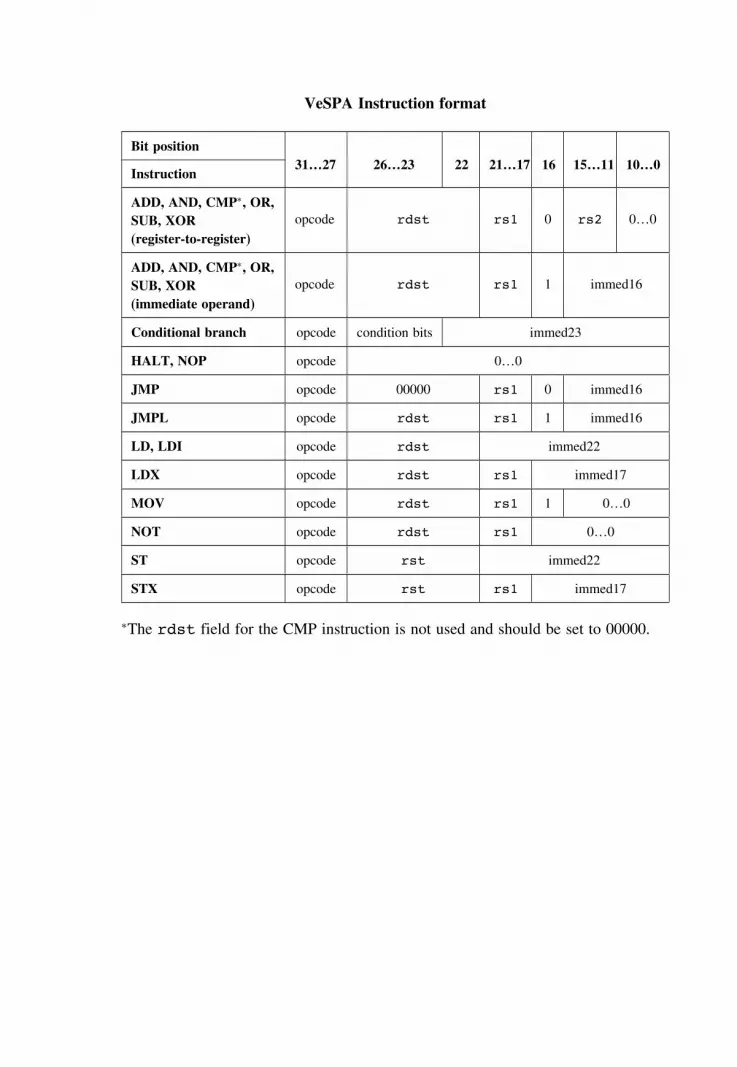
VeSPA Instruction format
Bit position
Instruction31…27 26…23 22 21…17 16 15…11 10…0
ADD, AND, CMP∗, OR,SUB, XOR(register-to-register)
opcode rdst rs1 0 rs2 0…0
ADD, AND, CMP∗, OR,SUB, XOR(immediate operand)
opcode rdst rs1 1 immed16
Conditional branch opcode condition bits immed23
HALT, NOP opcode 0…0
JMP opcode 00000 rs1 0 immed16
JMPL opcode rdst rs1 1 immed16
LD, LDI opcode rdst immed22
LDX opcode rdst rs1 immed17
MOV opcode rdst rs1 1 0…0
NOT opcode rdst rs1 0…0
ST opcode rst immed22
STX opcode rst rs1 immed17
∗The rdst field for the CMP instruction is not used and should be set to 00000.
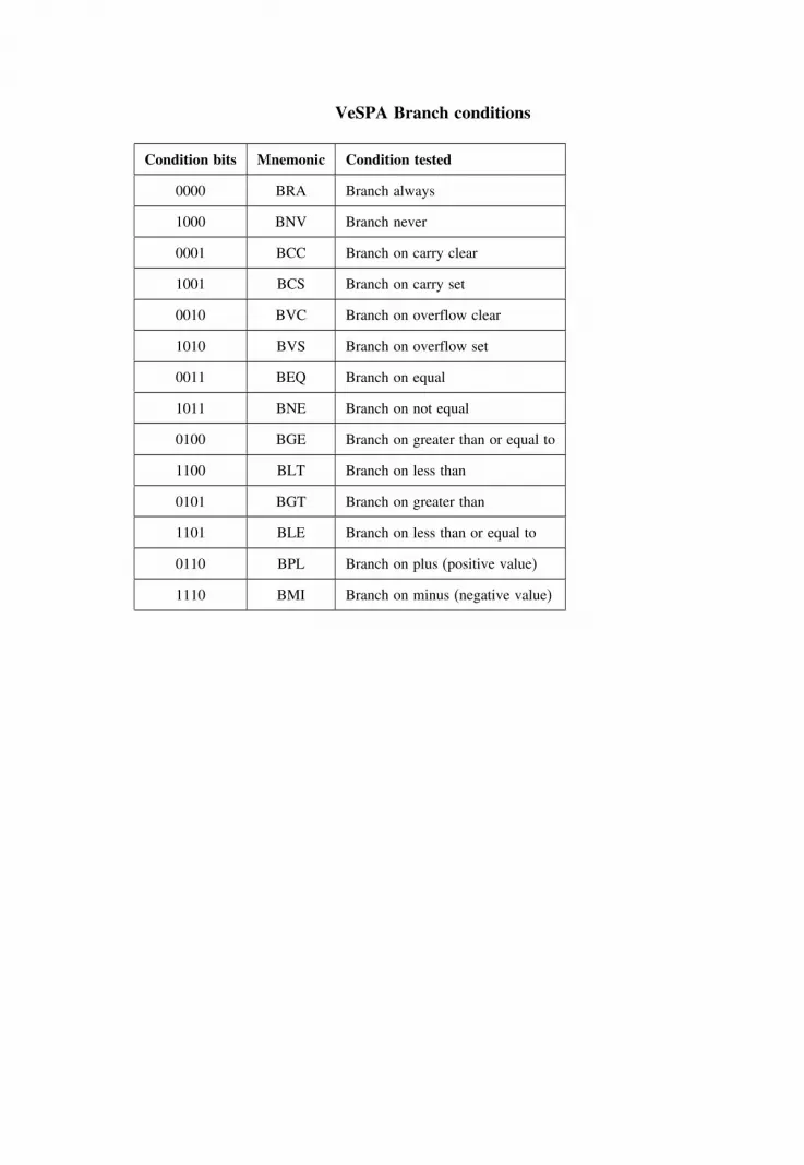
VeSPA Branch conditions
Condition bits Mnemonic Condition tested
0000 BRA Branch always
1000 BNV Branch never
0001 BCC Branch on carry clear
1001 BCS Branch on carry set
0010 BVC Branch on overflow clear
1010 BVS Branch on overflow set
0011 BEQ Branch on equal
1011 BNE Branch on not equal
0100 BGE Branch on greater than or equal to
1100 BLT Branch on less than
0101 BGT Branch on greater than
1101 BLE Branch on less than or equal to
0110 BPL Branch on plus (positive value)
1110 BMI Branch on minus (negative value)

Verilog operators
Arithmetic operators
Operator Add Subtract Multiply Divide Modulus
Symbol + − ∗ / %
Logical, bit-wise, and reduction operators
OperatorBoolean Bit-wise Boolean
and or not and or not xor xnor
Symbol && �� ! & � ˜ ˆ ˜ ˆ
Relational operators
Operatorgreaterthan
lessthan
greaterthan orequal to
less thanor equal
to equalnotequal
equal(case)
notequal(case)
Symbol > < >= <= == ! = === !===
Miscellaneous operators
Operator left shift right shift concatenation replication
Symbol << >> �X�Y� �X�Y��
Conditional operator
condition ? : true_consequence : false_consequence

Format specifications used in the Verilog $display task
Format specifiers
%b Binary value
%c Single ASCII character
%d Decimal value
%h Hexadecimal value
%m A hierarchical name
%o Octal value
%s String of ASCII characters
%t Verilog-defined global time value
%s Signal strength value of a net
Character escape sequences
\n Newline
\t Tab
%% The % character
\” The “character
\\ The \ character