Embed Size (px)
Citation preview
Direct-Write Photolithography for Cylindrical ToolingFabrication in Roll-to-Roll Microcontact Printing
The MIT Faculty has made this article openly available. Please share how this access benefits you. Your story matters.
Citation Nietner, Larissa F., and David E. Hardt. “Direct-WritePhotolithography for Cylindrical Tooling Fabrication in Roll-to-RollMicrocontact Printing.” Journal of Micro and Nano-Manufacturing3.3 (2015): 031006. © 2015 ASME
As Published http://dx.doi.org/10.1115/1.4030766
Publisher American Society of Mechanical Engineers (ASME)
Version Final published version
Citable link http://hdl.handle.net/1721.1/107981
Terms of Use Article is made available in accordance with the publisher'spolicy and may be subject to US copyright law. Please refer to thepublisher's site for terms of use.
Larissa F. NietnerLaboratory for Manufacturing and Productivity,
Massachusetts Institute of Technology,
Room 35-131,
Cambridge, MA 02139
e-mail: [email protected]
David E. Hardt1Fellow ASME
Laboratory for Manufacturing and Productivity,
Massachusetts Institute of Technology,
Room 35-231,
Cambridge, MA 02139
e-mail: [email protected]
Direct-Write Photolithographyfor Cylindrical ToolingFabrication in Roll-to-RollMicrocontact PrintingThe scale-up of microcontact printing (lCP) to a roll-to-roll technique for large-scalesurface patterning requires scalable tooling for continuous pattern printing with lm-scale features (e.g., 1–50 lm). Here, we examine the process of creating such a tool usingan optical direct-write or “maskless” method working on a rotating cylindrical substrate.A predictive model of pattern formation is presented along with experimental results toexamine the key control factors for this process. It is shown that factors can be modulatedto vary the cross-sectional shape in addition to feature height and width. This feature canthen be exploited to improve the robustness of the final printing process.[DOI: 10.1115/1.4030766]
Introduction
lCP can achieve submicrometer-scale patterns as small as30 nm [1,2], but scale-up to production at high rates (�1 m/s webspeed) and large areas (>0.5 m web width) is yet to be achieved.There is considerable interest in roll-to-roll configurations for thispurpose, and the essential element in this process is creation of cy-lindrical image carriers or “stamps” for this process. Oneapproach to this is to wrap a flat stamp around a printing mandrel[3–7], but this presents limitations for size and thickness uniform-ity and creates a noncontinuous cylinder. Master patterns are usu-ally formed on silicon wafers, but wafer sizes are limited, thuspresenting difficulty for scaling the process. There are methodsfor casting larger area lCP stamps (see, e.g., Ref. [5]), but theseresult in low absolute accuracy and have not been fully developed.Additionally, any method that requires the wrapping of a flat-caststamp around a cylinder will result in pattern deformation, resid-ual stresses, and an inevitable discontinuity in the pattern. Thougha stamp can be cut to proper size for wrapping, any deviation atthe seam between its ends will result in a significant once-per-revolution disturbance that might preclude any reliable printing oflm-sized features at medium-to-high speeds. Finally, the stampaccuracy strongly depends on the mounting process, and none ofthe available mounting processes is sufficiently accurate formounting large stamps without causing pattern distortions orthickness variations.
To address these problems, Petrzelka and Hardt [8] developed amethod for the fabrication of seamless cylindrical stamps for lCPusing a centrifugal casting method. In this method, a cylindricalmaster pattern is created by a laser direct-write process on a posi-tive photoresist spun to even thickness within the centrifuge. Pos-sible eccentricity and roughness are eliminated by a planarizinglayer of flood-cured SU-8 photoresist on the cylinder surface,which forms a smooth substrate for the patterning layer. The cen-trifugal force produced by the spinning drum provides for evenspreading of both the photoresist master pattern and the polydime-thylsiloxaone (PDMS) precursors during casting throughout theinterior surface of the drum. This approach produces continuouscylindrical tools of very uniform thickness, is scalable beyond
current size limits, and does not require an additional mask crea-tion step for changes in pattern geometry. As such, it was the firstprocess to produce a seamless cylindrical stamp of consistent uni-formity with micrometer-scale features (an example is shown inFig. 1). The method was demonstrated in an initial proof of con-cept. The achievable aspect ratios, smooth topology, andmicrometer-scale resolution of the pattern combined with the scal-able cylindrical layout render this method highly suitable for cre-ating continuous cylindrical stamps. However, the range offeatures shapes and the key process factors that determine theseremain unexplored.
This paper extends this novel casting method by examining thelaser patterning process in detail. In addition to feature locationand feature size, the process is characterized by the cross-sectional geometry produced. While the former two factors deter-mine where pattern transfer will occur in printing, the latter iscrucial to feature stability when subjected to contact pressures,and therefore determines the precision limits and area robustnessof the printing step. As shown by Petrzelka and Hardt [9], featurecollapse, and therefore printing failure, can occur whenever localpressure exceeds the mechanical limits of the features. Since fea-ture collapse can occur by buckling, over-compression, or
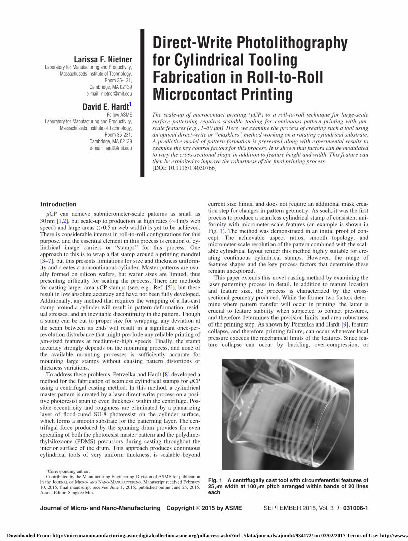
Fig. 1 A centrifugally cast tool with circumferential features of25 lm width at 100 lm pitch arranged within bands of 20 lineseach
1Corresponding author.Contributed by the Manufacturing Engineering Division of ASME for publication
in the JOURNAL OF MICRO- AND NANO-MANUFACTURING. Manuscript received February10, 2015; final manuscript received June 1, 2015; published online June 25, 2015.Assoc. Editor: Sangkee Min.
Journal of Micro- and Nano-Manufacturing SEPTEMBER 2015, Vol. 3 / 031006-1Copyright VC 2015 by ASME
Downloaded From: http://micronanomanufacturing.asmedigitalcollection.asme.org/pdfaccess.ashx?url=/data/journals/ajmnbt/934172/ on 03/02/2017 Terms of Use: http://www.asme.org/about-asme/terms-of-use
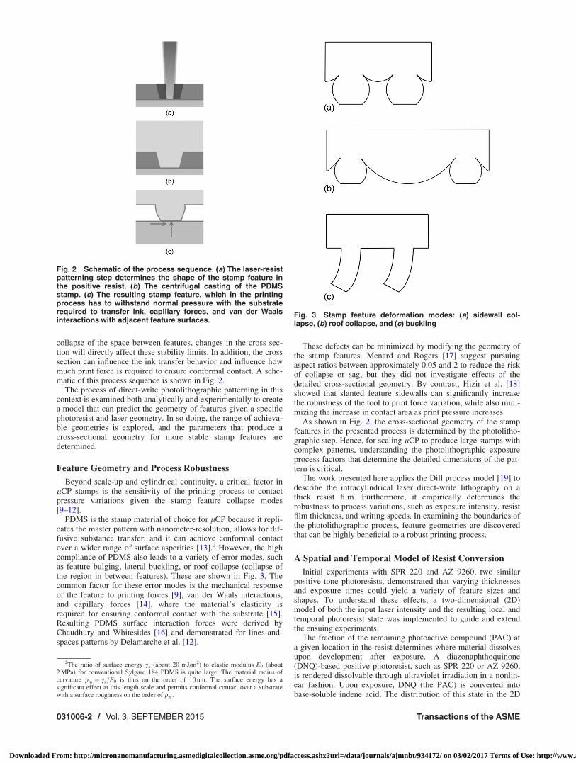
collapse of the space between features, changes in the cross sec-tion will directly affect these stability limits. In addition, the crosssection can influence the ink transfer behavior and influence howmuch print force is required to ensure conformal contact. A sche-matic of this process sequence is shown in Fig. 2.
The process of direct-write photolithographic patterning in thiscontext is examined both analytically and experimentally to createa model that can predict the geometry of features given a specificphotoresist and laser geometry. In so doing, the range of achieva-ble geometries is explored, and the parameters that produce across-sectional geometry for more stable stamp features aredetermined.
Feature Geometry and Process Robustness
Beyond scale-up and cylindrical continuity, a critical factor inlCP stamps is the sensitivity of the printing process to contactpressure variations given the stamp feature collapse modes[9–12].
PDMS is the stamp material of choice for lCP because it repli-cates the master pattern with nanometer-resolution, allows for dif-fusive substance transfer, and it can achieve conformal contactover a wider range of surface asperities [13].2 However, the highcompliance of PDMS also leads to a variety of error modes, suchas feature bulging, lateral buckling, or roof collapse (collapse ofthe region in between features). These are shown in Fig. 3. Thecommon factor for these error modes is the mechanical responseof the feature to printing forces [9], van der Waals interactions,and capillary forces [14], where the material’s elasticity isrequired for ensuring conformal contact with the substrate [15].Resulting PDMS surface interaction forces were derived byChaudhury and Whitesides [16] and demonstrated for lines-and-spaces patterns by Delamarche et al. [12].
These defects can be minimized by modifying the geometry ofthe stamp features. Menard and Rogers [17] suggest pursuingaspect ratios between approximately 0.05 and 2 to reduce the riskof collapse or sag, but they did not investigate effects of thedetailed cross-sectional geometry. By contrast, Hizir et al. [18]showed that slanted feature sidewalls can significantly increasethe robustness of the tool to print force variation, while also mini-mizing the increase in contact area as print pressure increases.
As shown in Fig. 2, the cross-sectional geometry of the stampfeatures in the presented process is determined by the photolitho-graphic step. Hence, for scaling lCP to produce large stamps withcomplex patterns, understanding the photolithographic exposureprocess factors that determine the detailed dimensions of the pat-tern is critical.
The work presented here applies the Dill process model [19] todescribe the intracylindrical laser direct-write lithography on athick resist film. Furthermore, it empirically determines therobustness to process variations, such as exposure intensity, resistfilm thickness, and writing speeds. In examining the boundaries ofthe photolithographic process, feature geometries are discoveredthat can be highly beneficial to a robust printing process.
A Spatial and Temporal Model of Resist Conversion
Initial experiments with SPR 220 and AZ 9260, two similarpositive-tone photoresists, demonstrated that varying thicknessesand exposure times could yield a variety of feature sizes andshapes. To understand these effects, a two-dimensional (2D)model of both the input laser intensity and the resulting local andtemporal photoresist state was implemented to guide and extendthe ensuing experiments.
The fraction of the remaining photoactive compound (PAC) ata given location in the resist determines where material dissolvesupon development after exposure. A diazonaphthoquinone(DNQ)-based positive photoresist, such as SPR 220 or AZ 9260,is rendered dissolvable through ultraviolet irradiation in a nonlin-ear fashion. Upon exposure, DNQ (the PAC) is converted intobase-soluble indene acid. The distribution of this state in the 2D
Fig. 2 Schematic of the process sequence. (a) The laser-resistpatterning step determines the shape of the stamp feature inthe positive resist. (b) The centrifugal casting of the PDMSstamp. (c) The resulting stamp feature, which in the printingprocess has to withstand normal pressure with the substraterequired to transfer ink, capillary forces, and van der Waalsinteractions with adjacent feature surfaces.
Fig. 3 Stamp feature deformation modes: (a) sidewall col-lapse, (b) roof collapse, and (c) buckling
2The ratio of surface energy cs (about 20 mJ/m2) to elastic modulus E0 (about2 MPa) for conventional Sylgard 184 PDMS is quite large. The material radius ofcurvature qm ¼ cs=E0 is thus on the order of 10 nm. The surface energy has asignificant effect at this length scale and permits conformal contact over a substratewith a surface roughness on the order of qm.
031006-2 / Vol. 3, SEPTEMBER 2015 Transactions of the ASME
Downloaded From: http://micronanomanufacturing.asmedigitalcollection.asme.org/pdfaccess.ashx?url=/data/journals/ajmnbt/934172/ on 03/02/2017 Terms of Use: http://www.asme.org/about-asme/terms-of-use
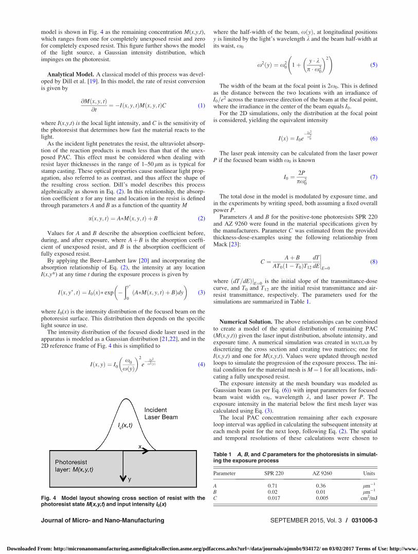
model is shown in Fig. 4 as the remaining concentration M(x,y,t),which ranges from one for completely unexposed resist and zerofor completely exposed resist. This figure further shows the modelof the light source, a Gaussian intensity distribution, whichimpinges on the photoresist.
Analytical Model. A classical model of this process was devel-oped by Dill et al. [19]. In this model, the rate of resist conversionis given by
@M x; y; tð Þ@t
¼ �I x; y; tð ÞM x; y; tð ÞC (1)
where I(x,y,t) is the local light intensity, and C is the sensitivity ofthe photoresist that determines how fast the material reacts to thelight.
As the incident light penetrates the resist, the ultraviolet absorp-tion of the reaction products is much less than that of the unex-posed PAC. This effect must be considered when dealing withresist layer thicknesses in the range of 1–50 lm as is typical forstamp casting. These optical properties cause nonlinear light prop-agation, also referred to as contrast, and thus affect the shape ofthe resulting cross section. Dill’s model describes this processalgebraically as shown in Eq. (2). In this relationship, the absorp-tion coefficient a for any time and location in the resist is definedthrough parameters A and B as a function of the quantity M
a x; y; tð Þ ¼ A�M x; y; tð Þ þ B (2)
Values for A and B describe the absorption coefficient before,during, and after exposure, where AþB is the absorption coeffi-cient of unexposed resist, and B is the absorption coefficient offully exposed resist.
By applying the Beer–Lambert law [20] and incorporating theabsorption relationship of Eq. (2), the intensity at any locationI(x,y*) at any time t during the exposure process is given by
I x; y�; tð Þ ¼ I0ðxÞ� exp �ðy�
0
A�M x; y; tð Þ þ Bð Þdy
� �(3)
where I0(x) is the intensity distribution of the focused beam on thephotoresist surface. This distribution then depends on the specificlight source in use.
The intensity distribution of the focused diode laser used in theapparatus is modeled as a Gaussian distribution [21,22], and in the2D reference frame of Fig. 4 this is simplified to
Iðx; yÞ ¼ I0
x0
xðyÞ
� �2
e� 2x2
x2ðyÞ (4)
where the half-width of the beam, x yð Þ, at longitudinal positionsy is limited by the light’s wavelength k and the beam half-width atits waist, x0
x2 yð Þ ¼ x20 1þ y � k
p � x20
� �2 !
(5)
The width of the beam at the focal point is 2x0. This is definedas the distance between the two locations with an irradiance ofI0=e2 across the transverse direction of the beam at the focal point,where the irradiance in the center of the beam equals I0.
For the 2D simulations, only the distribution at the focal pointis considered, yielding the equivalent intensity
IðxÞ ¼ I0e�2x2
x20 (6)
The laser peak intensity can be calculated from the laser powerP if the focused beam width x0 is known
I0 ¼2P
px20
(7)
The total dose in the model is modulated by exposure time, andin the experiments by writing speed, both assuming a fixed overallpower P.
Parameters A and B for the positive-tone photoresists SPR 220and AZ 9260 were found in the material specifications given bythe manufacturers. Parameter C was estimated from the providedthickness-dose-examples using the following relationship fromMack [23]:
C ¼ Aþ B
AT0 1� T0ð ÞT12
dT
dE
����E¼0
(8)
where ðdT=dEÞjE¼0 is the initial slope of the transmittance-dosecurve, and T0 and T12 are the initial resist transmittance and air-resist transmittance, respectively. The parameters used for thesimulations are summarized in Table 1.
Numerical Solution. The above relationships can be combinedto create a model of the spatial distribution of remaining PAC(M(x,y,t)) given the laser input distribution, absolute intensity, andexposure time. A numerical simulation was created in MATLAB bydiscretizing the cross section and creating two matrices; one forI(x,y,t) and one for M(x,y,t). Values were updated through nestedloops to simulate the progression of the exposure process. The ini-tial condition for the material mesh is M¼ 1 for all locations, indi-cating a fully unexposed resist.
The exposure intensity at the mesh boundary was modeled asGaussian beam (as per Eq. (6)) with input parameters for focusedbeam waist width x0, wavelength k, and laser power P. Theexposure intensity in the material below the first mesh layer wascalculated using Eq. (3).
The local PAC concentration remaining after each exposureloop interval was applied in calculating the subsequent intensity ateach mesh point for the next loop, following Eq. (2). The spatialand temporal resolutions of these calculations were chosen to
Fig. 4 Model layout showing cross section of resist with thephotoresist state M(x,y,t) and input intensity I0(x)
Table 1 A, B, and C parameters for the photoresists in simulat-ing the exposure process
Parameter SPR 220 AZ 9260 Units
A 0.71 0.36 lm�1
B 0.02 0.01 lm�1
C 0.017 0.005 cm2/mJ
Journal of Micro- and Nano-Manufacturing SEPTEMBER 2015, Vol. 3 / 031006-3
Downloaded From: http://micronanomanufacturing.asmedigitalcollection.asme.org/pdfaccess.ashx?url=/data/journals/ajmnbt/934172/ on 03/02/2017 Terms of Use: http://www.asme.org/about-asme/terms-of-use
match the expected feature sizes and ensure a stable yet efficientnumerical integration. For the simulation results presented here,these were 1 lm and 1 ms, respectively.
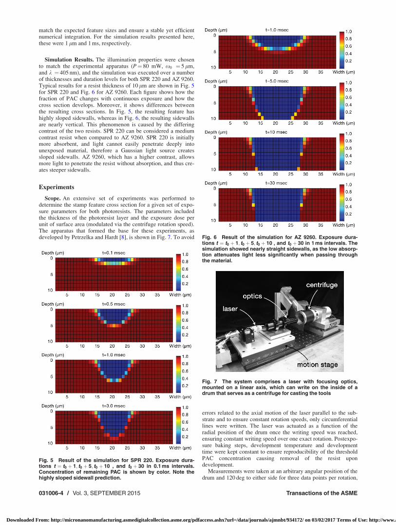
Simulation Results. The illumination properties were chosento match the experimental apparatus (P¼ 80 mW, x0 ¼ 5 lm,and k ¼ 405 nm), and the simulation was executed over a numberof thicknesses and duration levels for both SPR 220 and AZ 9260.Typical results for a resist thickness of 10 lm are shown in Fig. 5for SPR 220 and Fig. 6 for AZ 9260. Each figure shows how thefraction of PAC changes with continuous exposure and how thecross section develops. Moreover, it shows differences betweenthe resulting cross sections. In Fig. 5, the resulting feature hashighly sloped sidewalls, whereas in Fig. 6, the resulting sidewallsare nearly vertical. This phenomenon is caused by the differingcontrast of the two resists. SPR 220 can be considered a mediumcontrast resist when compared to AZ 9260. SPR 220 is initiallymore absorbent, and light cannot easily penetrate deeply intounexposed material, therefore a Gaussian light source createssloped sidewalls. AZ 9260, which has a higher contrast, allowsmore light to penetrate the resist without absorption, and thus cre-ates steeper sidewalls.
Experiments
Scope. An extensive set of experiments was performed todetermine the stamp feature cross section for a given set of expo-sure parameters for both photoresists. The parameters includedthe thickness of the photoresist layer and the exposure dose perunit of surface area (modulated via the centrifuge rotation speed).The apparatus that formed the base for these experiments, asdeveloped by Petrzelka and Hardt [8], is shown in Fig. 7. To avoid
errors related to the axial motion of the laser parallel to the sub-strate and to ensure constant rotation speeds, only circumferentiallines were written. The laser was actuated as a function of theradial position of the drum once the writing speed was reached,ensuring constant writing speed over one exact rotation. Postexpo-sure baking steps, development temperature and developmenttime were kept constant to ensure reproducibility of the thresholdPAC concentration causing removal of the resist upondevelopment.
Measurements were taken at an arbitrary angular position of thedrum and 120 deg to either side for three data points per rotation,
Fig. 5 Result of the simulation for SPR 220. Exposure dura-tions t ¼ t0 þ 1; t0 þ 5; t0 þ 10 , and t0 þ 30 in 0.1 ms intervals.Concentration of remaining PAC is shown by color. Note thehighly sloped sidewall prediction.
Fig. 6 Result of the simulation for AZ 9260. Exposure dura-tions t ¼ t0 þ 1; t0 þ 5; t0 þ 10 , and t0 þ 30 in 1 ms intervals. Thesimulation showed nearly straight sidewalls, as the low absorp-tion attenuates light less significantly when passing throughthe material.
Fig. 7 The system comprises a laser with focusing optics,mounted on a linear axis, which can write on the inside of adrum that serves as a centrifuge for casting the tools
031006-4 / Vol. 3, SEPTEMBER 2015 Transactions of the ASME
Downloaded From: http://micronanomanufacturing.asmedigitalcollection.asme.org/pdfaccess.ashx?url=/data/journals/ajmnbt/934172/ on 03/02/2017 Terms of Use: http://www.asme.org/about-asme/terms-of-use
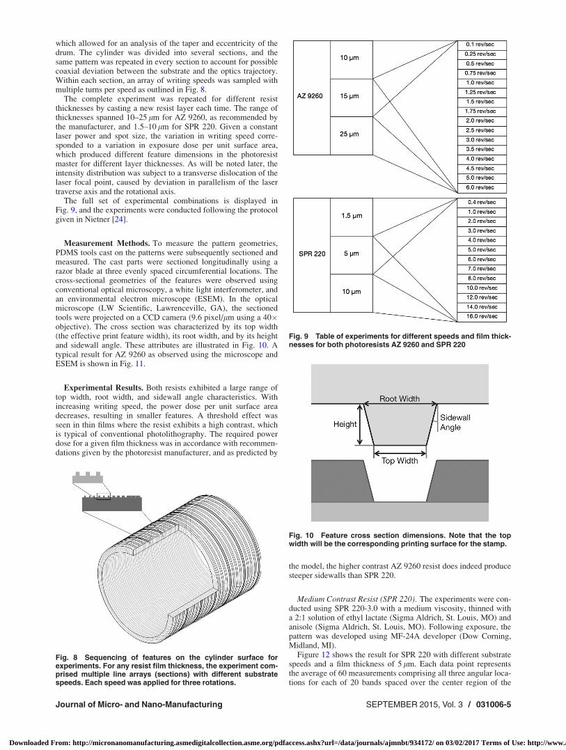
which allowed for an analysis of the taper and eccentricity of thedrum. The cylinder was divided into several sections, and thesame pattern was repeated in every section to account for possiblecoaxial deviation between the substrate and the optics trajectory.Within each section, an array of writing speeds was sampled withmultiple turns per speed as outlined in Fig. 8.
The complete experiment was repeated for different resistthicknesses by casting a new resist layer each time. The range ofthicknesses spanned 10–25 lm for AZ 9260, as recommended bythe manufacturer, and 1.5–10 lm for SPR 220. Given a constantlaser power and spot size, the variation in writing speed corre-sponded to a variation in exposure dose per unit surface area,which produced different feature dimensions in the photoresistmaster for different layer thicknesses. As will be noted later, theintensity distribution was subject to a transverse dislocation of thelaser focal point, caused by deviation in parallelism of the lasertraverse axis and the rotational axis.
The full set of experimental combinations is displayed inFig. 9, and the experiments were conducted following the protocolgiven in Nietner [24].
Measurement Methods. To measure the pattern geometries,PDMS tools cast on the patterns were subsequently sectioned andmeasured. The cast parts were sectioned longitudinally using arazor blade at three evenly spaced circumferential locations. Thecross-sectional geometries of the features were observed usingconventional optical microscopy, a white light interferometer, andan environmental electron microscope (ESEM). In the opticalmicroscope (LW Scientific, Lawrenceville, GA), the sectionedtools were projected on a CCD camera (9.6 pixel/lm using a 40�objective). The cross section was characterized by its top width(the effective print feature width), its root width, and by its heightand sidewall angle. These attributes are illustrated in Fig. 10. Atypical result for AZ 9260 as observed using the microscope andESEM is shown in Fig. 11.
Experimental Results. Both resists exhibited a large range oftop width, root width, and sidewall angle characteristics. Withincreasing writing speed, the power dose per unit surface areadecreases, resulting in smaller features. A threshold effect wasseen in thin films where the resist exhibits a high contrast, whichis typical of conventional photolithography. The required powerdose for a given film thickness was in accordance with recommen-dations given by the photoresist manufacturer, and as predicted by
the model, the higher contrast AZ 9260 resist does indeed producesteeper sidewalls than SPR 220.
Medium Contrast Resist (SPR 220). The experiments were con-ducted using SPR 220-3.0 with a medium viscosity, thinned witha 2:1 solution of ethyl lactate (Sigma Aldrich, St. Louis, MO) andanisole (Sigma Aldrich, St. Louis, MO). Following exposure, thepattern was developed using MF-24A developer (Dow Corning,Midland, MI).
Figure 12 shows the result for SPR 220 with different substratespeeds and a film thickness of 5 lm. Each data point representsthe average of 60 measurements comprising all three angular loca-tions for each of 20 bands spaced over the center region of the
Fig. 8 Sequencing of features on the cylinder surface forexperiments. For any resist film thickness, the experiment com-prised multiple line arrays (sections) with different substratespeeds. Each speed was applied for three rotations.
Fig. 9 Table of experiments for different speeds and film thick-nesses for both photoresists AZ 9260 and SPR 220
Fig. 10 Feature cross section dimensions. Note that the topwidth will be the corresponding printing surface for the stamp.
Journal of Micro- and Nano-Manufacturing SEPTEMBER 2015, Vol. 3 / 031006-5
Downloaded From: http://micronanomanufacturing.asmedigitalcollection.asme.org/pdfaccess.ashx?url=/data/journals/ajmnbt/934172/ on 03/02/2017 Terms of Use: http://www.asme.org/about-asme/terms-of-use
cylinder. As expected, the height is constant over all dose levels,indicating exposure through the full thickness of the resist. More-over, a constant and substantial dependence of the root and topwidth on the speed (�1/dose) is noted, along with a nearly constantdifference between these two. This indicates a nearly constant side-wall angle, which is evident in the cross section shown in Fig. 13.
It is important to note that SPR 220 showed considerable effectsof dual-tone behavior or burning upon over-exposure. Once athreshold exposure dose is reached, the state of the material turnedfrom soluble to insoluble again, showing a “dented” topology inthe resulting stamp. Finally, the exposure of SPR 220 was not
fully rate invariant in that faster exposure times required reducedenergy dose.
The experiments confirmed that for increasing substrate speedand thus decreasing energy dose, the width of the produced fea-ture decreases. Below a certain threshold dose, the cross-sectionalshape of the formed feature did not reveal a flat top with distinctedges at the sidewalls, but instead a round feature. However, theheight of the feature did not immediately decrease, indicating thatthe SU-8 layer (that is, full feature height) was still reached.
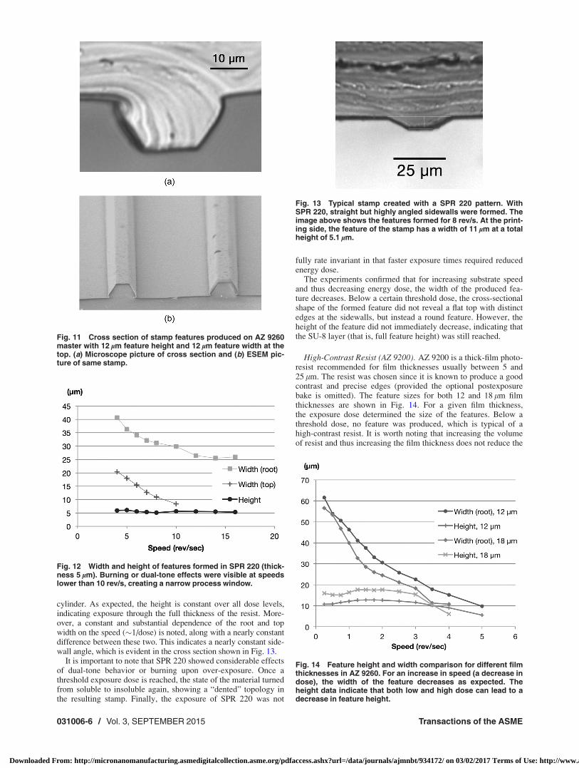
High-Contrast Resist (AZ 9200). AZ 9200 is a thick-film photo-resist recommended for film thicknesses usually between 5 and25 lm. The resist was chosen since it is known to produce a goodcontrast and precise edges (provided the optional postexposurebake is omitted). The feature sizes for both 12 and 18 lm filmthicknesses are shown in Fig. 14. For a given film thickness,the exposure dose determined the size of the features. Below athreshold dose, no feature was produced, which is typical of ahigh-contrast resist. It is worth noting that increasing the volumeof resist and thus increasing the film thickness does not reduce the
Fig. 11 Cross section of stamp features produced on AZ 9260master with 12 lm feature height and 12 lm feature width at thetop. (a) Microscope picture of cross section and (b) ESEM pic-ture of same stamp.
Fig. 12 Width and height of features formed in SPR 220 (thick-ness 5 lm). Burning or dual-tone effects were visible at speedslower than 10 rev/s, creating a narrow process window.
Fig. 13 Typical stamp created with a SPR 220 pattern. WithSPR 220, straight but highly angled sidewalls were formed. Theimage above shows the features formed for 8 rev/s. At the print-ing side, the feature of the stamp has a width of 11 lm at a totalheight of 5.1 lm.
Fig. 14 Feature height and width comparison for different filmthicknesses in AZ 9260. For an increase in speed (a decrease indose), the width of the feature decreases as expected. Theheight data indicate that both low and high dose can lead to adecrease in feature height.
031006-6 / Vol. 3, SEPTEMBER 2015 Transactions of the ASME
Downloaded From: http://micronanomanufacturing.asmedigitalcollection.asme.org/pdfaccess.ashx?url=/data/journals/ajmnbt/934172/ on 03/02/2017 Terms of Use: http://www.asme.org/about-asme/terms-of-use
minimum root width. It can also be seen that when too little or toomuch energy is applied, the feature height decreases, and that inthe speed range between 1.2 rev/s and 2.5 rev/s the feature depthis constant at the expected height.
AZ 9260 was more robust to overexposure effects. A higherexposure dose increased the feature width until adjacent featuresmerged, and a width range up to 100 lm could be observed inthicknesses below 10 lm without burning or dual-tone effects. Inhigher thicknesses, the resist burned before reaching the exposuredose necessary to expand the reaction further to either side of theincoming beam.
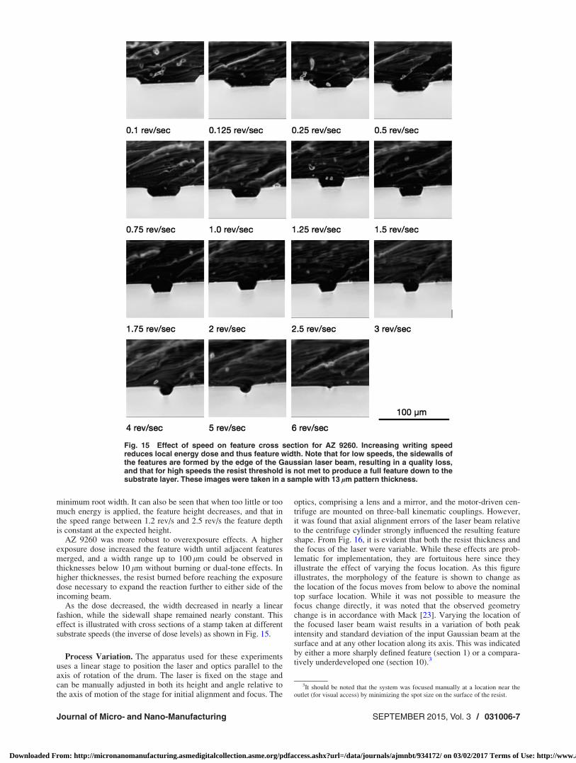
As the dose decreased, the width decreased in nearly a linearfashion, while the sidewall shape remained nearly constant. Thiseffect is illustrated with cross sections of a stamp taken at differentsubstrate speeds (the inverse of dose levels) as shown in Fig. 15.
Process Variation. The apparatus used for these experimentsuses a linear stage to position the laser and optics parallel to theaxis of rotation of the drum. The laser is fixed on the stage andcan be manually adjusted in both its height and angle relative tothe axis of motion of the stage for initial alignment and focus. The
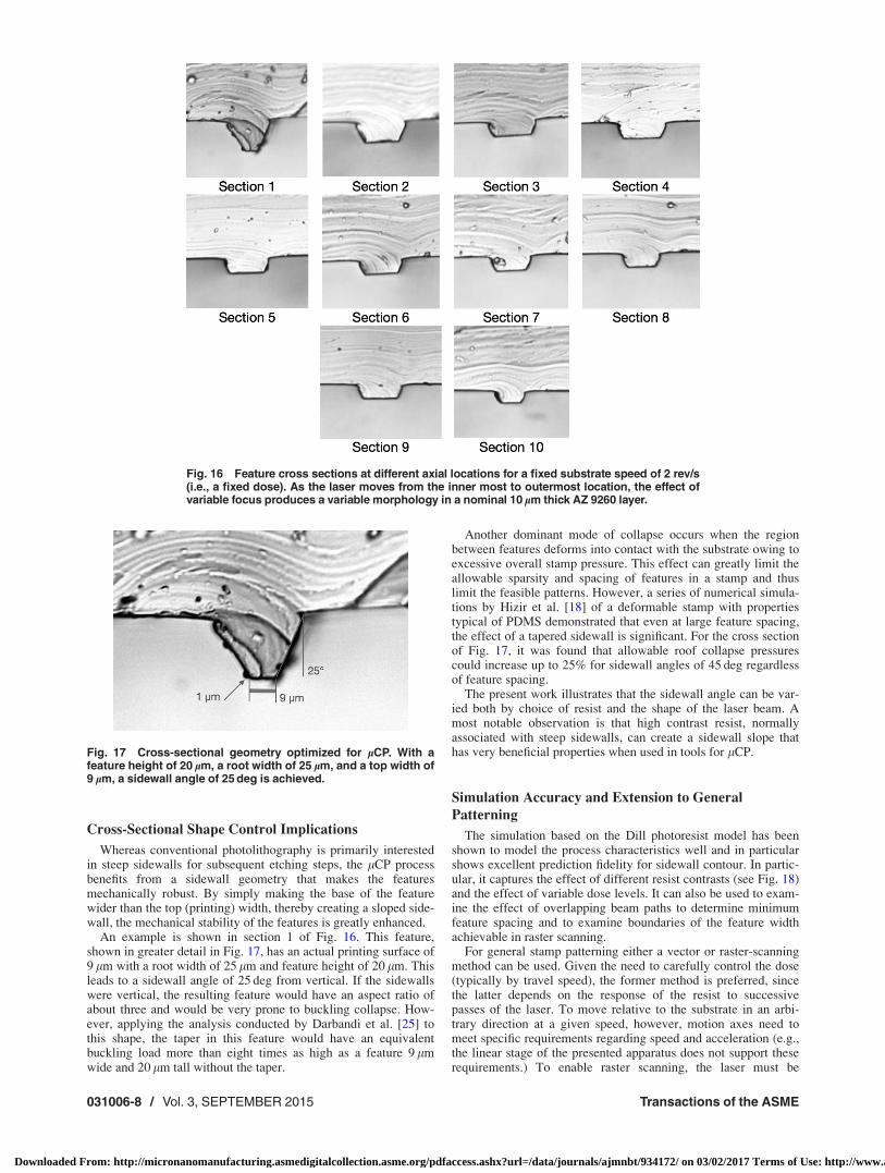
optics, comprising a lens and a mirror, and the motor-driven cen-trifuge are mounted on three-ball kinematic couplings. However,it was found that axial alignment errors of the laser beam relativeto the centrifuge cylinder strongly influenced the resulting featureshape. From Fig. 16, it is evident that both the resist thickness andthe focus of the laser were variable. While these effects are prob-lematic for implementation, they are fortuitous here since theyillustrate the effect of varying the focus location. As this figureillustrates, the morphology of the feature is shown to change asthe location of the focus moves from below to above the nominaltop surface location. While it was not possible to measure thefocus change directly, it was noted that the observed geometrychange is in accordance with Mack [23]. Varying the location ofthe focused laser beam waist results in a variation of both peakintensity and standard deviation of the input Gaussian beam at thesurface and at any other location along its axis. This was indicatedby either a more sharply defined feature (section 1) or a compara-tively underdeveloped one (section 10).3
Fig. 15 Effect of speed on feature cross section for AZ 9260. Increasing writing speedreduces local energy dose and thus feature width. Note that for low speeds, the sidewalls ofthe features are formed by the edge of the Gaussian laser beam, resulting in a quality loss,and that for high speeds the resist threshold is not met to produce a full feature down to thesubstrate layer. These images were taken in a sample with 13 lm pattern thickness.
3It should be noted that the system was focused manually at a location near theoutlet (for visual access) by minimizing the spot size on the surface of the resist.
Journal of Micro- and Nano-Manufacturing SEPTEMBER 2015, Vol. 3 / 031006-7
Downloaded From: http://micronanomanufacturing.asmedigitalcollection.asme.org/pdfaccess.ashx?url=/data/journals/ajmnbt/934172/ on 03/02/2017 Terms of Use: http://www.asme.org/about-asme/terms-of-use
Cross-Sectional Shape Control Implications
Whereas conventional photolithography is primarily interestedin steep sidewalls for subsequent etching steps, the lCP processbenefits from a sidewall geometry that makes the featuresmechanically robust. By simply making the base of the featurewider than the top (printing) width, thereby creating a sloped side-wall, the mechanical stability of the features is greatly enhanced.
An example is shown in section 1 of Fig. 16. This feature,shown in greater detail in Fig. 17, has an actual printing surface of9 lm with a root width of 25 lm and feature height of 20 lm. Thisleads to a sidewall angle of 25 deg from vertical. If the sidewallswere vertical, the resulting feature would have an aspect ratio ofabout three and would be very prone to buckling collapse. How-ever, applying the analysis conducted by Darbandi et al. [25] tothis shape, the taper in this feature would have an equivalentbuckling load more than eight times as high as a feature 9 lmwide and 20 lm tall without the taper.
Another dominant mode of collapse occurs when the regionbetween features deforms into contact with the substrate owing toexcessive overall stamp pressure. This effect can greatly limit theallowable sparsity and spacing of features in a stamp and thuslimit the feasible patterns. However, a series of numerical simula-tions by Hizir et al. [18] of a deformable stamp with propertiestypical of PDMS demonstrated that even at large feature spacing,the effect of a tapered sidewall is significant. For the cross sectionof Fig. 17, it was found that allowable roof collapse pressurescould increase up to 25% for sidewall angles of 45 deg regardlessof feature spacing.
The present work illustrates that the sidewall angle can be var-ied both by choice of resist and the shape of the laser beam. Amost notable observation is that high contrast resist, normallyassociated with steep sidewalls, can create a sidewall slope thathas very beneficial properties when used in tools for lCP.
Simulation Accuracy and Extension to General
Patterning
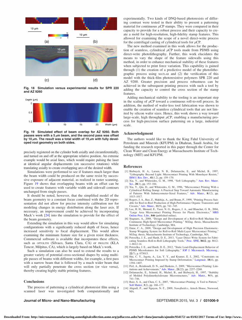
The simulation based on the Dill photoresist model has beenshown to model the process characteristics well and in particularshows excellent prediction fidelity for sidewall contour. In partic-ular, it captures the effect of different resist contrasts (see Fig. 18)and the effect of variable dose levels. It can also be used to exam-ine the effect of overlapping beam paths to determine minimumfeature spacing and to examine boundaries of the feature widthachievable in raster scanning.
For general stamp patterning either a vector or raster-scanningmethod can be used. Given the need to carefully control the dose(typically by travel speed), the former method is preferred, sincethe latter depends on the response of the resist to successivepasses of the laser. To move relative to the substrate in an arbi-trary direction at a given speed, however, motion axes need tomeet specific requirements regarding speed and acceleration (e.g.,the linear stage of the presented apparatus does not support theserequirements.) To enable raster scanning, the laser must be
Fig. 16 Feature cross sections at different axial locations for a fixed substrate speed of 2 rev/s(i.e., a fixed dose). As the laser moves from the inner most to outermost location, the effect ofvariable focus produces a variable morphology in a nominal 10lm thick AZ 9260 layer.
Fig. 17 Cross-sectional geometry optimized for lCP. With afeature height of 20 lm, a root width of 25 lm, and a top width of9 lm, a sidewall angle of 25 deg is achieved.
031006-8 / Vol. 3, SEPTEMBER 2015 Transactions of the ASME
Downloaded From: http://micronanomanufacturing.asmedigitalcollection.asme.org/pdfaccess.ashx?url=/data/journals/ajmnbt/934172/ on 03/02/2017 Terms of Use: http://www.asme.org/about-asme/terms-of-use
precisely registered on the cylinder both axially and circumferentially,and turned on and off at the appropriate relative position. An extremeexample would be axial lines, which would require pulsing the laserat identical angular displacements (on successive rotations) whiletranslating axially to create overlapping arcs of the desired width.
Simulations were performed to see if features much larger thanthe beam width could be produced on the same resist by succes-sive exposure of adjacent material, as realized in raster scanning.Figure 19 shows that overlapping beams with an offset can beused to create features with variable width and sidewall contoursunchanged from single passes.
It should be noted, however, that the simplified model of thebeam geometry to a constant focus combined with the 2D repre-sentation did not allow for precise intensity calibration nor formodeling changes in energy distribution along the laser axis. Ifnecessary, an improvement could be achieved by incorporatingMack’s work [24] into the simulation to provide for the effect ofthe beam geometry.
Extending the simulation in this way would allow for simulatingconfigurations with a significantly reduced depth of focus, henceincreased sensitivity to focal displacement. This would allowexamining the minimum feature size for a given resist thickness.Commercial software is available that incorporates these effects,such as OPTOLITH (Silvaco, Santa Clara, CA) or PROLITH (KLATencor, Milpitas, CA), which is largely based on Mack’s work.
Such a simulation can also be used to extend the results to agreater variety of potential cross-sectional shapes by using multi-ple passes of beams with different widths, for example, a first passwith a narrow beam that is followed by a much wider beam thatwill only partially penetrate the cross section (or vice versa),thereby creating highly stable printing features.
Conclusions
The process of patterning a cylindrical photoresist film using ascanned laser was investigated both computationally and
experimentally. Two kinds of DNQ-based photoresists of differ-ing contrast were tested in their ability to present a patterningmaterial for continuous lCP stamps. They were compared in theircapacity to provide for a robust process and their capacity to cre-ate a mold for high-resolution, high-fidelity stamp features. Thisallowed for examining the scope of a novel direct-write processfor the centrifugal casting of cylindrical tools for lCP.
The new method examined in this work allows for the produc-tion of seamless, cylindrical lCP tools made from PDMS usingdirect-write photolithography. Further, this work elucidates themeans to vary the shape of the feature sidewalls using thismethod, in order to enhance mechanical stability of these featureswhen subjected to print force variation. This capability is gainedthrough (1) the creation of a predictive model of the photolitho-graphic process using MATLAB and (2) the verification of thismodel with the thick-film photoresistive polymers SPR 220 andAZ 9200. Greater precision and process robustness can beachieved in the subsequent printing process with such a tool byadding the capacity to control the cross section of the stampfeatures.
Adding mechanical stability to the tooling is an important stepin the scaling of lCP toward a continuous roll-to-roll process. Inaddition, the method of wafer-less tool fabrication was shown toenable the creation of seamless cylindrical tools that are not lim-ited by silicon wafer sizes. Hence, this work shows a way towardlarge-scale, high throughput lCP, enabling a manufacturing pro-cess for high-precision surface patterning on a large, industrialscale.
Acknowledgment
The authors would like to thank the King Fahd University ofPetroleum and Minerals (KFUPM) in Dhahran, Saudi Arabia, forfunding the research reported in this paper through the Center forClean Water and Clean Energy at Massachusetts Institute of Tech-nology (MIT) and KFUPM.
References[1] Biebuyck, H. A., Larsen, N. B., Delamarche, E., and Michel, B., 1997,
“Lithography Beyond Light: Microcontact Printing With Monolayer Resists,”IBM J. Res. Dev., 41(1.2), pp. 159–170.
[2] Xia, Y., and Whitesides, G. M., 1998, “Soft Lithography,” Ann. Rev. Mater.Sci., 28(1), pp. 153–184.
[3] Xia, Y., Qin, D., and Whitesides, G. M., 1996, “Microcontact Printing With aCylindrical Rolling Stamp: A Practical Step Toward Automatic Manufacturingof Patterns With Submicrometer-Sized Features,” Adv. Mater., 8(12), pp.1015–1017.
[4] Rogers, J. A., Bao, Z., Makhija, A., and Braun, P., 1999, “Printing Process Suit-able for Reel-to-Reel Production of High-Performance Organic Transistors andCircuits,” Adv. Mater., 11(9), pp. 741–745.
[5] Lee, H. H., Menard, E., Tassi, N. G., Rogers, J. A., and Blanchet, G. B., 2004,“Large Area Microcontact Printing Presses for Plastic Electronics,” MRSOnline Proc. Libr., 846 (published online).
[6] Stagnaro, A., 2008, “Design and Development of a Roll-to-Roll Machine forContinuous High-Speed Microcontact Printing,” M.Eng. thesis, MassachusettsInstitute of Technology, Cambridge, MA.
[7] Datar, C. A., 2009, “Design and Development of High Precision Elastomeric-Stamp Wrapping System for Roll-to-Roll Multi-Layer Microcontact Printing,”M.Eng. thesis, Massachusetts Institute of Technology, Cambridge, MA.
[8] Petrzelka, J. E., and Hardt, D. E., 2013, “Laser Direct Write System for Fabri-cating Seamless Roll-to-Roll Lithography Tools,” Proc. SPIE, 8612, pp. 8612-1–8612-14.
[9] Petrzelka, J. E., and Hardt, D. E., 2012, “Static Load-Displacement Behavior ofPDMS Microfeatures for Soft Lithography,” IOP J. Micromech. Microeng.,22(7), p. 075015.
[10] Hui, C. Y., Jagota, A., Lin, Y. Y., and Kramer, E. J., 2002, “Constraints onMicrocontact Printing Imposed by Stamp Deformation,” Langmuir, 18(4), pp.1394–1407.
[11] Perl, A., Reinhoudt, D. N., and Huskens, J., 2009, “Microcontact Printing: Lim-itations and Achievements,” Adv. Mater., 21(22), pp. 2257–2268.
[12] Delamarche, E., Schmid, H., Michel, B., and Biebuyck, H., 1997, “Stabilityof Molded Polydimethylsiloxane Microstructures,” Adv. Mater., 9(9), pp.741–746.
[13] Ruiz, S. A., and Chen, C. S., 2007, “Microcontact Printing: A Tool to Pattern,”Soft Matter, 3(2), pp. 168–177.
[14] Abgrall, P., and Nguyen, N.-T., 2009, Nanofluidics, Artech House, Norwood,MA.
Fig. 18 Simulation versus experimental results for SPR 220and AZ 9260
Fig. 19 Simulated effect of beam overlap for AZ 9260. Bothpasses were with a 5 lm beam, and the second pass was offsetby 10 lm. The result was a total width of 19 lm with fully devel-oped root geometry on both sides.
Journal of Micro- and Nano-Manufacturing SEPTEMBER 2015, Vol. 3 / 031006-9
Downloaded From: http://micronanomanufacturing.asmedigitalcollection.asme.org/pdfaccess.ashx?url=/data/journals/ajmnbt/934172/ on 03/02/2017 Terms of Use: http://www.asme.org/about-asme/terms-of-use

[15] Lipomi, D. J., Martinez, R. V., Cademartiri, L., and Whitesides, G. M., 2012,“7.11: Soft Lithographic Approaches to Nanofabrication,” Polym. Sci. Compr.Ref., 10, pp. 211–231.
[16] Chaudhury, M. K., and Whitesides, G. M., 1991, “Direct Measurement of Inter-facial Interactions Between Semispherical Lenses and Flat Sheets of Poly(dimethylsiloxane) and Their Chemical Derivatives,” Langmuir, 7(5), pp.1013–1025.
[17] Menard, E., and Rogers, J. A., 2010, “Stamping Techniques for Micro- andNanofabrication,” Springer Handbook of Nanotechnology, Springer, New York,pp. 313–332.
[18] Hizir, F. E., Al-Qahtani, H. M., and Hardt, D. E., 2014, “Deformation of StampFeatures With Slanted Walls During Microcontact Printing,” COMSOL Confer-ence, Boston, MA.
[19] Dill, F. H., Hornberger, W. P., Hauge, P. S., and Shaw, J. M., 1975,“Characterization of Positive Photoresist,” IEEE Trans. Electron Devices,22(7), pp. 445–452.
[20] Swinehart, D. F., 1962, “The Beer-Lambert Law,” J. Chem. Educ., 39(7), pp.333–335.
[21] Schilling, A., Herzig, H. P., Stauffer, L., Vokinger, U., and Rossi, M., 2001,“Efficient Beam Shaping of Linear, High-Power Diode Lasers by Use of Micro-Optics,” Appl. Opt., 40(32), pp. 5852–5859.
[22] Sun, H., 2012, Laser Diode Beam Basics, Manipulations and Characterizations,Springer Science & Business Media, Medford, MA.
[23] Mack, C. A., 2007, Fundamental Principles of Optical Lithography: The Sci-ence of Microfabrication, Wiley, Hoboken, NJ.
[24] Nietner, L., 2014, “A Direct-Write Thick-Film Lithography Processfor Multi-Parameter Control of Tooling in Continuous Roll-to-Roll Microcon-tact Printing,” S.M. thesis, Massachusetts Institute of Technology, Cambridge,MA.
[25] Darbandi, S. M., Firouz-Abadi, R. D., and Haddadpour, H., 2010, “Buckling ofVariable Section Columns Under Axial Loading,” J. Eng. Mech., 136(4), pp.472–476.
031006-10 / Vol. 3, SEPTEMBER 2015 Transactions of the ASME
Downloaded From: http://micronanomanufacturing.asmedigitalcollection.asme.org/pdfaccess.ashx?url=/data/journals/ajmnbt/934172/ on 03/02/2017 Terms of Use: http://www.asme.org/about-asme/terms-of-use


