Embed Size (px)
Citation preview

303
Ion-Beam Assisted Surface IslandingDuring Ge MBE on Si
A.V. Dvurechenskii, V.A. Zinovyev, V.A Kudryavtsev, J.V. Smagina, P.L. Novikov, S.A. Teys
Institute of Semiconductors Physics,Russian Academy of Science, Siberian Branch,
pr. Akad. Lavrentjeva 13, Novosibirsk, 630090, Russia
(Received 15 October 2001, accepted for publication 7 December 2001)
Effects of low-energy Ge+ ion irradiation on the transition from two-dimensional (2D) to three-dimensional (3D) growth during Ge/Si(111)heteroepitaxy were studied by in situ reflection high-energy electron diffraction(RHEED) and ex situ scanning tunnelling microscopy (STM). The continuousand pulsed ion beams were used. The data received by these methodsdirectly indicate that ion irradiation leads to facilitation of 2D - 3D transition.The STM investigations have shown that the density of 3D islands is higherand size distribution is more narrow at ion-assisted growth in comparison withconventional epitaxy. The results of Monte-Carlo simulation have shown thattwo mechanisms of ion beam action can be responsible for facilitation of2D - 3D transition. There are: 1) generation of adatoms by ion impacts whichleads to transfer of material from underlying layers to upper layer and 2)enhancement of surface diffusion which may be caused by ion-stimulatedreconstruction of the surface. Both mechanisms promote 2D -3D transition.
1. Introduction
Heterojunctions and nanostructures, formed by SiGe heteroepitaxy, haveattracted considerable interest in recent years because of their potentialapplications in high-speed electronic, infrared detection and promising devicesbased on quantum effects [1,2]. Mechanical stresses in the growing layer causedthe morphological changes of the surface. As a result, the flat surface has grownuntil critical thickness of wetting layer is reached and then this process is interruptedby nucleation of 3D islands on the top of the epilayer (Stranski-Krastanov growthmode). The SiGe nanostructures containing islands are commonly studied at
Phys. Low-Dim. Struct., 1/2 (2002)pp.303-314
© VSV Co.Ltd, 2002

304
present as a system with quantum dots.A conventional manner to control island formation (size, form, density) is to alter
the growth conditions by changing substrate temperature and molecular flow.Tunability in zero-dimensional semiconductor technology thus offers obviousadvantages in extending the range of possibilities for devices. The new facility totune island dimensions and their surface densities is expected to be provided bythe use of ion beam with energy exceeding of energy in the molecular beam, butless energy of defects generation in the bulk of wetting layer (and substrate).Energy of particles in the molecular beam is defined by temperature of the beamsource. Usually its value does not exceed 0.1 eV. Using hyperthermal species(with energy ~100eV) during epitaxy result in dramatically changes in growthkinetics and final physical properties of solid films [3-5]. It promotes crystal growthat extremely low temperature and improvement of surface smoothness.
In this study the morphology of Ge surface of pseudomorphic layer underirradiation by low energy (~200 eV) Ge+ ions during molecular beam epitaxy(MBE) of Ge on Si(111) was investigated. Two different approaches were used. Inthe first, the continuous low-energy ion beam irradiation was carried out throughepitaxy. In the second one, we affected the growing surface by the pulsed low-energy ion beam at selected times during epitaxial growth. This approach wasfound to be a powerful tool to study the mechanism of ion beam induced surfacemorphology modification during Si(111) homoepitaxy [5].
2. Experimental technique
The experimental setup includes a growth chamber with background pressureless then 10-10 Torr equipped with BN crucible evaporation cell. The silicon waferswere Si(111) within 0.15° according to X-ray diffraction data. Density of Ge fluxvaried within 1012–1015 cm–2s-1 by changing crucible temperature. Above thecrucible cell the system for ionisation of Ge flux and accelerating of Ge+ ions waslocated. The ionised part of molecular beam depended on design of the MBEsource and had a value of 0.1% or 0.5%. The pulsed accelerating voltage unitallowed to form pulses of ion current with duration from 0.1 to 1 s. The energy ofGe+ ions varied within 50–270 eV. The molecular and ion beams hit on thesubstrate at 54.5° off-normal direction.
To study the surface morphology in situ, we used the RHEED with observationof specular intensity oscillations during two-dimensional layer-by-layer growth [6].The experiments were made in two irradiation modes: with continuous ion beamand with pulsed ion beam irradiation during Ge MBE. Ion pulsed action was madeat different stages of growth according to the different degree of filling of thesurface layer.
Scanning tunnelling microscopy is capable of imaging surface on the atomicscale. All STM images were taken ex situ at room temperature in the constant-

305
current mode with a tunnelling current.
3. Experimental results
During Ge/Si(111) heteroepitaxy from molecular beam we have observed theRHEED intensity oscillations. The period of RHEED oscillations was equal to thedeposition time of 1 biatomic layer (1 BL=1.56 1015 atoms/cm2). After deposition afew BL the response of the RHEED oscillations is rapidly damping of both theamplitude and the average RHEED intensity level. This is connected withincreasing of surface roughness due to transition from layer-by-layer 2D growth to3D growth mode of Ge islands at the critical thickness of the pseudomorphic film.The results of our experiments with observed 2D-3D transition are in goodagreement with those obtained previously [6,7]. The experiments were performedat different substrate temperatures, deposition rates and ion fluxes.
Recently we have published the temperature and flux density dependencies ofRHEED intensity during Ge/Si(111) heteroepitaxy with low-energy ion irradiation[8]. We used previous results to find the optimal regime of ion action to reach morepronounced effect.
We selected the following experimental parameters: the temperature of Ge/Siheteroepitaxy - 350°C, deposition rates - 0.12 BL/s, the ion flux density - 5.5 1011
cm-2s-1 (the ionized part of molecular beam was 0.5% ), energy of Ge+ ions -200eV.
The irradiation with continuous ion beam during Ge/Si(111) heteroepitaxyresulted in reducing a number of RHEED oscillations (Fig. 1, curve 2) ascompared with the conventional heteroepitaxy (Fig. 1, curve 1). This correspondsto facilitation of 2D-3D transition or decreasing of critical thickness of Ge wettinglayer in Stranski-Krastanov growth mode.
Ion pulsed action was found to increase RHEED specular beam intensity if thepulsed ion beam was turned on at a fractional surface coverage more than half(Fig. 1, curve 3). The intensity enhancement corresponds to the improvement ofsurface smoothness during molecular beam growth apparently due to increasingof adatom mobility on ion-beam reconstructed surface.
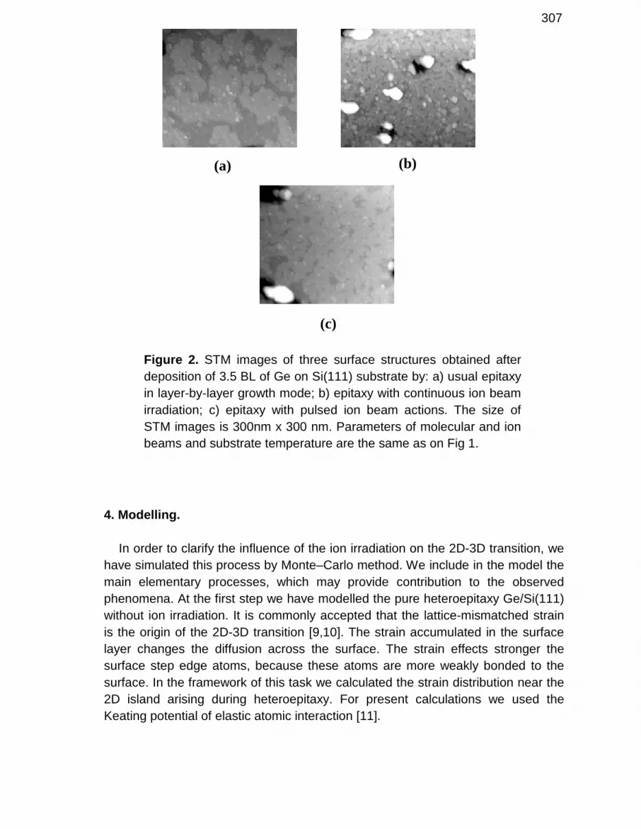
For detailed investigations of observed effects we concentrated on the 3 typesof structures obtained by: 1) usual epitaxy from molecular beam in layer-by-layergrowth mode, 2) epitaxy with continuous ion beam irradiation, 3) epitaxy withpulsed ion beam. The amount of deposited Ge was identical for three types ofstructures and was equal to 3.5 BL. The STM study has shown that type 1structures contained only two-dimensional Ge islands (Fig. 2 a), type 2 and 3structures contained three-dimensional Ge islands (Fig. 2 b, c), formed on thesurface of pseudomorphic Ge(111) layer and having the shape of truncatedpyramids with {113} facets. The density of 3D islands on surface of type 2structures was about three times higher than density of type 3 structures.

306
Near the 3D islands one can observed the vacancy depressions on the surface,which disappear at the latest stages of growth. The data received by STM methoddirectly indicate that irradiation by continuous and pulsed ion beam stimulate thetransition to 3D growth.
The STM investigations at latest growth stages ( after deposition of 5 BL) shownthat the density of 3D islands is higher in the case ion-assisted growth (Fig. 3 b)than without ion beam (Fig. 3 c). The size distribution become more narrow(Fig.3 b, d).
Spe
cula
r R
HE
ED
Inte
nsity
1
2
3
0 10 20 30 40
Time, s
Figure 1. Specular RHEED intensity vs time recorded duringGe/Si(111) heteroepitaxy in the three regimes: 1) without ionirradiation; 2) with continuous ion beam irradiation, 3) with pulsedion beam actions. Substrate temperature - 3500 C; deposition rate- 0.12 BL/ s; the ion flux density - 5.5 1011 cm-2 s-1 ; the energy ofGe ions - 200 eV; pulse duration - 0.5s. The arrows indicate thetimes of pulsed ion beam actions.
307
4. Modelling.
In order to clarify the influence of the ion irradiation on the 2D-3D transition, wehave simulated this process by Monte–Carlo method. We include in the model themain elementary processes, which may provide contribution to the observedphenomena. At the first step we have modelled the pure heteroepitaxy Ge/Si(111)without ion irradiation. It is commonly accepted that the lattice-mismatched strainis the origin of the 2D-3D transition [9,10]. The strain accumulated in the surfacelayer changes the diffusion across the surface. The strain effects stronger thesurface step edge atoms, because these atoms are more weakly bonded to thesurface. In the framework of this task we calculated the strain distribution near the2D island arising during heteroepitaxy. For present calculations we used theKeating potential of elastic atomic interaction [11].
(a) (b)
(c)
Figure 2. STM images of three surface structures obtained afterdeposition of 3.5 BL of Ge on Si(111) substrate by: a) usual epitaxyin layer-by-layer growth mode; b) epitaxy with continuous ion beamirradiation; c) epitaxy with pulsed ion beam actions. The size ofSTM images is 300nm x 300 nm. Parameters of molecular and ionbeams and substrate temperature are the same as on Fig 1.

308
The results of these calculations showed that the maximum of the strain islocated near the island edge (see Fig. 4). The strain energy was found todependent on the island size. When size is increased, the strain energy (Estrain) atthe islands edge rises (Fig. 5). We used these results in simulation of surfacediffusion. We adopted commonly accepted concept that the diffusion activationenergy depends on the bonding environment and elastic energy associated withthe strain is E=Ebond –- Estrain, where Ebond=n1 E1 + n2 E2, (E1 is nearest-neighbourbinding energy, E2 is next nearest-neighbour binding energy, n1 is the number ofnearest neighbours, n2 is the number of next nearest neighbours). The followingparameters were used in modelling: E1 = 1.2 eV, E2 = 0.1 eV. We taken intoaccount Estrain only for atoms on the island edge. So, the probability of atomdetachment from the edge of islands is enhanced, atoms become mobile and canhop to the next level, that can lead to forming of the 3D islands. The simulation ofgrowth within above assumptions results in the 2D-3D transition when the criticalthickness is achieved. The main features of the simulation model presented indetail elsewhere [6,9,10].
Figure 3. STM images and corresponding size distributions of 3Dislands after deposition of 5 BL of Ge at a) usual epitaxy; b) epitaxywith pulsed ion beam actions. The size of STM images is 1000nm x1000nm. Parameters of molecular and ion beams and substratetemperature are the same as on Fig 1.

309
At the second step we include in the model the low energy ion beam irradiation.We assume that the influence of the ion beam consists of following processes:a) the sputtering of the material;b) the generation of additional adatoms and surface vacancy clusters;c) ion-assisted enhancement of adatom diffusion.
According to molecular dynamics simulations of low-energy interaction withSi(111) surface [12], ion impact produces one surface vacancy cluster andadditional adatoms at a few interatomic distance from this cluster. We assume thatthese results remain true qualitatively for Ge(111). Only the quantitativecharacteristics are changed. For simulations the following parameters are taken:the size of vacancy cluster is 10, the number of exited adatoms is 9 and one atomis sputtered [13].
We distinguish the following two mechanisms of ion influence which can beresponsible to observed phenomena of ion-assisted facilitation of 2D-3D transition.1) Generation of adatoms leads to transfer of material from underlying layers toupper adatom layer, in other words, atoms release from bulk to layer of mobileadatoms. 2) Enhancement of surface diffusion may be caused by ion-stimulatedreconstruction of surface. This reconstruction occurs due to release of the energy
0 10 20 30 40 500
2
4
6
8
10
Si(111) substrate
Ge
2D island Strain Energy (eV/atom)
X (110)
Z (
111)
0.1050 -- 0.1200 0.0900 -- 0.1050 0.0750 -- 0.0900 0.0600 -- 0.0750 0.0450 -- 0.0600 0.03000 -- 0.0450 0.01500 -- 0.03000
Figure 4. The strain energy distribution in plane for Ge/Si(111)heterostructure near 2D triangle-shaped island. This plane crossedthe centres of island sides. The distances taken in the number ofatomic layers.

310
of accelerating particles. For our simulations we used the surface diffusioncoefficient in 10 times greater than one for case without ion-irradiation according torecent experimental measurements [14].
As a parameter characterised the surface morphology, we took surface stepdensity (S), which is the analogue to experimental RHEED intensity profiles [15]:
[ ]∑ ∑= =
++ −+−=M
1i
M
1j1j,ij,ij,1ij,i hhhh
M4
1S
,
where M is number of surface lattice sites, hi,j is the surface height at the(i,j) point. This quantity is proportional to the number of atoms along the perimeterof islands and surface vacancy clusters. Also we monitored the surfacemorphology by tracing of the images of the simulated surface at selected times.MC modelling was performed at the same temperatures, molecular and ion beamfluxes as in experiments.
The simulations have shown that the growth can occur in two regimes: 2Dlayer-by-layer growth, when the oscillations of S are observed, and 3D growth,when oscillations disappear (Fig.6). The 2D - 3D transition was also confirmed byimages of the simulated surface. When we simulated growth with the ion beam,we obtained the facilitation of 2D - 3D transition.
For the case when the main mechanism responsible for facilitation is materialtransfer from underlying layers to upper layer due to generation of adatoms, thesimulations have shown, that the 2D - 3D transition occurs earlier (Fig. 6 b) than in
0 400 800 1200 1600 20000.08
0.09
0.10
0.11
0.12
Est
rain ,
eV/a
tom
Number of atoms in 2D island
Figure 5. The strain energy dependence on the island size taken atthe island step edge.

311
the case of the usual heteroepitaxy (Fig. 6 a). The number of oscillations reduceddown to 2. The density of 3D islands is higher, than the one in the case usualepitaxy with the same deposited material (3.4 BL, that corresponded to the onsetof the 2D - 3D transition).
For the case when the main mechanism responsible for facilitation is theenhancement of surface diffusion caused by ion-stimulated reconstruction ofsurface, we obtained that the transition occurred at the same critical thickness asin the first case (Fig. 6 c). But the size and density of islands are different. Theaverage size of islands becomes larger and higher, and density is decreased. In
(d)
(a)
(b)
0 1 2 3 4 5
0.75
0.80
0.85
0.90
0.95
1.00(c)
1-S
Deposited layers (BL)
Figure 6. Simulated step density evolution during Ge/Si(111)heteroepitaxy without ion irradiation-(a) and with ion irradiation-(b),(c),(d). The three latest cases corresponds to differentmechanisms of ion beam influence: (b) adatom generation by ionimpacts leading to transfer of material to higher atomic layers; (c)ion stimulated surface diffusion; (d) including both mechanisms.

312
this case the surface smoothness is higher in comparison with the first case, whenwe only took into account the generation of adatoms by ion beam.
The ion-induced facilitation of 2D - 3D transition by second mechanism is clear.Enhancement of surface diffusion leads to an increase in average size of 2Dislands. As consequence, the strain energy become higher, and the edge atomsare promoted to the higher level. This leads to nucleation of 3D islands at theearlier stage of growth. The same effect can be achieved by raising of thesubstrate temperature.
The facilitation of 2D - 3D transition by first mechanism is not so obviously. Itcan be expected that the ion-beam action will lead to reduction of the average sizeof islands and, as a consequence, to a decrease in the strain energy at the islandedge inhibiting the nucleation of 3D islands. Exactly this phenomena wasobserved in experiment at epitaxy Ge0.5Si0.5 at more higher ion fluxes [4] than inour experiment. This is explained by destruction of 3D islands caused by the ionimpacts. But at our ion beam fluxes the possibility of direct hit into a 3D island islow. And ion action provided the reverse effect. The ion impacts producedadditional adatoms from the surface which can pile up on the top of the existing 2Dislands and nucleate 3D islands. So, both mechanisms promote transition to 3Dgrowth and the simulations including both mechanisms simultaneously haveshown more fast transition (Fig. 6 d), the critical thickness decreasing down to1 BL. The results of MC modelling showed that generation of adatoms and surfacevacancy clusters by ion impacts and ion-enhanced surface diffusion lead tofacilitation of the 2D - 3D transition during Stranski-Krastanov growth. Thus, theobserved experimental results can be explained in terms of these twomechanisms.
5. Summary
We have studied the initial stages of low temperature Ge/Si(111) heteroepitaxyin two modes: in the presence of continuous irradiation and pulsed action by lowenergy Ge ions. We have found that the ion beam irradiation leads to facilitation ofthe 2D - 3D transition, enhancement of 3D island density and narrowing of sizedistribution. In order to clarify the influence of the ion irradiation on the 2D - 3Dtransition, we have simulated this process by Monte–Carlo method. The results ofMC modelling showed that two mechanisms of ion influence can be responsiblefor the observed phenomena of ion-assist facilitation of the 2D-3D transition. Thereare: 1) generation of adatoms, which leads to transfer of material from underlyinglayers to upper adatom layer and 2) enhancement of surface diffusion which maybe caused by ion-stimulated reconstruction of the surface. Both mechanismspromote transition to 3D growth.
Our experimental results demonstrated that the low energy ion beam irradiation

313
during GeSi heteroepitaxy give the possibility to control the size and density ofislands, and moreover, it provides the narrower island size distribution comparedwith conventional epitaxy. This is important for potential applications innanostructure technology.
Acknowledgements
This work was supported by the Russian Fund of Fundamental Research (Grant�� ������������ ��� ���� ���������� ��� ��������� ������� � ������ �����
������������� ��!������"#�#��#

314
References
[1] O.P. Pchelyakov, Yu.B. Bolkhovityanov, A.V. Dvurechenskii et al, Thin SolidFilms, 367 (2000) 75.
[2] A.I. Yakimov, V.A. Markov, A.V.Dvurechenskii, O.P. Pchelyakov, Phil. Mag. B,2 (1992) 701.
[3] J.W. Rabalais, A.H. Al-Bayati, K.J. Boyd et al, Phys. Rev. B, 53 (1996) 10781.[4] S.W. Park, J.Y. Shim, H. K. Baik, J. Appl. Phys., 78 (1995) 5993.[5] A.V. Dvurechenskii, V.A. Zinovyev, V.A. Markov, V.A. Kudryavtsev, Surf. Sci.,
425 (1999) 185.[6] O.P. Pchelyakov, V.A. Markov, A.I. Nikiforov, L.V. Sokolov, Thin Solid Films,
306 (1997) 299.[7] B. Voigtlander and A. Zinner, Appl. Phys. Lett., 63 (1993) 3055.[8] A.V. Dvurechenskii, V.A. Zinovyev, V.A. Kudryavtsev, J.V. Smagina, JETP
Letters, 72 (2000) 131.[9] K.E. Khor and S. Das Sarma, Phys. Rev. B., 62 (2000) 16657.[10] D.V.Brunev, I.G.Neizvestny, N.L.Shwartz, and Z.Sh.Yanovitskaja, Izv. Akad.
Nauk Fiz., 65 (2001) 196.[11] P.N. Keating, Phys. Rev., 145 (1966) 637.[12] V.A. Zinovyev, L.N. Aleksandrov, V.A. Dvurechenskii, K.-H. Heinig, D. Stock,
Thin Solid Films, 241 (1994) 167.[13] J. A. Floro, B.K. Kellerman, E. Chason et. al, J.Appl.Phys., 77 (1995) 2351.[14] R. Ditchfield and E.G. Seebauer, Phys. Rev.B., 63 (2001) 125317.[15] D.D. Vvedensky, S. Clarke, Surf.Sci., 373 (1990) 225.