Embed Size (px)
Citation preview
Edge Position Modulation
for Wireless Infrared Communications
Der Technischen Fakultät der
Universität Erlangen-Nürnberg
zur Erlangung des Grades
DOKTOR-INGENIEUR
vorgelegt von
Thomas Lüftner
Erlangen - 2005

Als Disseration genehmigt von
der Technischen Fakultät der
Universität Erlangen-Nürnberg
Tag der Einreichung: 18. April 2005
Tag der Promotion: 1. August 2005
Dekan: Prof. Dr. rer. nat. Albrecht Winnacker
Berichterstatter: Prof. Dr.-Ing. Dr.-Ing.habil. Robert Weigel
Prof. Dr.-Ing. Richard Hagelauer
Pulsflanken Positions Modulation
für drahtlose Infrarot-Kommunikation
Thomas Lüftner
Erlangen - 2005


Ich widme diese Arbeit meiner liebevollen Freundin Birgit und meiner großartigen Familie:
meinem Vater Alfred und meiner Mutter Gabriele, meinem Bruder Markus und seiner Frau
Silvia und deren Kindern Moritz und Elena, und meinem Opa Willy und meiner Oma Maria.
Thomas
v

vi
Einleitung
Getrieben von der Infrared Data Association (IrDA) wurde die drahtlose Infrarot-
Kommunikation in den letzten Jahren zu einer sehr populären und weit verbreiteten Methode zur
Kurzstrecken-Datenübertragung zwischen mobilen Geräten wie Laptops, PDAs und
Mobiltelefonen. Aufgrund der "Point & Shoot"-Eigenschaft zeichnet sich IrDA im Besonderen
bei Anwendungen aus, die einen schnellen Verbindungsaufbau erfordern. Dabei übertrifft es
andere Lösungen wie die Funkübertragung entsprechend dem Standard "Bluetooth" oder die auf
dem Standard "Universal Serial Bus (USB)" basierende Datenübertragung mittels Kabel.
Qualität und Geschwindigkeit der Infrarot-Kommunikation sind im Wesentlichen durch die
Bandbreite des Infrarot-Transceivers limitiert. Daher ist es wichtig eine Modulationstechnik mit
hoher Bandbreiteneffizienz zu verwenden und dabei gleichzeitig eine niedrige Bitfehlerrate und
eine hohe Leistungseffizienz aufrecht zu erhalten. Konsequenterweise hat die IrDA die
Modulationstechniken ihrer Standards kontinuierlich verbessert. Es wurden schrittweise die
Verfahren "Return to Zero Inverted (RZI)" für die "Serial Infrared (SIR)"-Datenübertragung, "4
Pulse Position Modulation (4-PPM)" für die "Fast Infrared (FIR)"-Datenübertragung und
"HHH(1,13)" für die neueste "Very Fast Infrared (VFIR)"-Datenübertragung eingeführt. Die
vorliegende Arbeit soll mit dem Verfahren "Edge Position Modulation (EPM)" eine neuartige
Modulationstechnik präsentieren, die eine verbesserte Bandbreiteneffizienz und eine
verbesserte Leistungseffizienz gegenüber den oben genannten Verfahren besitzt. Diese neue
Modulationstechnik soll auf die Eigenschaften des drahtlosen Infrarotkanals optimierbar sein
und soll dadurch auch eine niedrige Bitfehlerrate aufrechterhalten können.
vii

viii
Zusammenfassung
Das einführende Kapitel 1 gibt nach einer kurzen Motivation einen Einblick in die Historie und
in den Stand der Technik der drahtlosen Infrarot-Kommunikation. In diesem Kapitel wird der
IrDA Standard vorgestellt und als Referenz für die darauf folgende Arbeit definiert. Die
Anforderungen an die Modulationstechnik für eine zuverlässige Datenübertragung werden
durch die Eigenschaften des drahtlosen Infrarotkanals bestimmt. Daher präsentiert Kapitel 2 die
Komponenten der physikalischen Schicht eines IrDA-Übertragungssystems und die
wesentlichen Eigenschaften der optischen Verbindung. Damit wird dann ein einfaches
mathematisches Modell des drahtlosen Infrarotkanals hergeleitet. Kapitel 3 bereitet dann die
theoretischen Grundlagen der Modulation und Demodulation durch eine generische
mathematische Beschreibung der involvierten Signale und Kodierungsschritte auf. Daraus
werden dann die grundsätzlichen Bewertungskriterien für die Modulationstechniken hergeleitet
und bestimmt. Die Bewertungskriterien werden die Bandbreiteneffizienz, die Leistungseffizienz
und die Fehlerübertragungsrate sein. Als Referenz für EPM präsentiert Kapitel 4 die wichtigsten
auf Puls-Positions-Modulation basierenden Techniken, die zurzeit in den diversen drahtlosen
Infrarot-Übertragungssystemen für mobile Geräte eingesetzt werden. Im Besonderen werden
die Modulationsverfahren, die von den IrDA-Standards verwendet werden, anhand der
Bewertungskriterien aus Kapitel 3 bewertet, wobei für die Evaluierung der
Fehlerübertragungsrate das Kanalmodell aus Kapitel 2 verwendet wird. Die neuartige
Modulationstechnik EPM wird dann in Kapitel 5 eingeführt. Nach der Präsentation der
grundlegenden Idee hinter EPM werden die erreichbaren Bandbreiteneffizienzen für
verschiedene Varianten von EPM hergeleitet. Es wird aufgezeigt, dass die Variante
EPM(5,12,1/3,1) eine viel versprechende Alternative zu den zurzeit verwendeten Methoden ist
und daher analysiert Kapitel 6 diese EPM-Variante näher im Detail. Zuerst werden die
prinzipiellen Modulations- und Demodulationsschritte von EPM(5,12,1/3,1) beschrieben und
dann wird ein neuartiger "1/3-Rate RLL(5,12) Code" eingeführt, der die Realisierung der
EPM(5,12,1/3,1)-Modulationstechnik ermöglicht. (Die Generierung dieses RLL(5,12)-Codes
wird im Anhang A beschrieben.) Anschließend werden die Bewertungskriterien angewandt,
wobei gezeigt wird, dass EPM(5,12,1/3,1) nicht nur eine exzellente Bandbreiteneffizienz
aufweist, sondern auch eine verbesserte Leistungseffizienz besitzt und auch die
Fehlerübertragungsrate konkurrenzfähig ist. Dann wird gezeigt, wie EPM(5,12,1/3,1) in ein
IrDA konformes Infrarot-Kommunikationssystem integriert werden kann. Schließlich wird in
ix

Kapitel 6 noch der angefertigte HW-Prototyp mit den entsprechenden Messergebnissen
präsentiert, wodurch die Funktionalität von EPM(5,12,1/3,1) nachgewiesen wird. Abschließend
wird in Kapitel 7 ein Vergleich zwischen den Leistungsfähigkeiten der einzelnen
Modulationsverfahren gebracht. Als Konklusion werden im Besonderen die Vorteile und
Nachteile des neuartigen EPM-Verfahrens zusammengefasst und hervorgehoben.
x

Inhaltsangabe
KAPITEL 1 Einleitung . . . . . . . . . . . . . . . . . . . . . . . . . . . . . . . . . . . . . . . . . . . . . . . . . . . . . . 1
1.1 Motivation and Ziele der Arbeit . . . . . . . . . . . . . . . . . . . . . . . . . . . . . . . . . . . . . . . . . . . . . . . . . . . . . . . . . . .1
1.2 Geschichte der drahtlosen Infrarot-Kommunikation . . . . . . . . . . . . . . . . . . . . . . . . . . . . . . . . . . . . . . . . . . .2
1.3 Stand der Technik. . . . . . . . . . . . . . . . . . . . . . . . . . . . . . . . . . . . . . . . . . . . . . . . . . . . . . . . . . . . . . . . . . . . . .4
KAPITEL 2 Drahtloser Infrarotkanal . . . . . . . . . . . . . . . . . . . . . . . . . . . . . . . . . . . . . . . . 11
2.1 Definition des drahtlosen Infrarotkanals . . . . . . . . . . . . . . . . . . . . . . . . . . . . . . . . . . . . . . . . . . . . . . . . . . .11
2.2 Optischer Link . . . . . . . . . . . . . . . . . . . . . . . . . . . . . . . . . . . . . . . . . . . . . . . . . . . . . . . . . . . . . . . . . . . . . . .12
2.3 Sender Front-End . . . . . . . . . . . . . . . . . . . . . . . . . . . . . . . . . . . . . . . . . . . . . . . . . . . . . . . . . . . . . . . . . . . . .20
2.4 Empfänger Front-End. . . . . . . . . . . . . . . . . . . . . . . . . . . . . . . . . . . . . . . . . . . . . . . . . . . . . . . . . . . . . . . . . .26
2.5 Basisband Modell des drahtlosen Infrarotkanals . . . . . . . . . . . . . . . . . . . . . . . . . . . . . . . . . . . . . . . . . . . . .32
KAPITEL 3 Elektrische Modulation und Demodulation . . . . . . . . . . . . . . . . . . . . . . . . . 43
3.1 Elektrische Modulation . . . . . . . . . . . . . . . . . . . . . . . . . . . . . . . . . . . . . . . . . . . . . . . . . . . . . . . . . . . . . . . .44
3.2 Electrische Demodulation . . . . . . . . . . . . . . . . . . . . . . . . . . . . . . . . . . . . . . . . . . . . . . . . . . . . . . . . . . . . . .48
3.3 Bewertungskriterien der Modulations Techniken . . . . . . . . . . . . . . . . . . . . . . . . . . . . . . . . . . . . . . . . . . . .55
KAPITEL 4 Puls-Positions basierte Modulation Verfahren . . . . . . . . . . . . . . . . . . . . . . 67
4.1 Return to Zero Inverted . . . . . . . . . . . . . . . . . . . . . . . . . . . . . . . . . . . . . . . . . . . . . . . . . . . . . . . . . . . . . . . .67
4.2 N - Pulse Position Modulation . . . . . . . . . . . . . . . . . . . . . . . . . . . . . . . . . . . . . . . . . . . . . . . . . . . . . . . . . . .74
4.3 Run-Length-Limited Code Modulation RLL(d,k) . . . . . . . . . . . . . . . . . . . . . . . . . . . . . . . . . . . . . . . . . . . .83
KAPITEL 5 Pulseflanken Positions Modulation (EPM). . . . . . . . . . . . . . . . . . . . . . . . . . 95
5.1 Grundlagen von EPM. . . . . . . . . . . . . . . . . . . . . . . . . . . . . . . . . . . . . . . . . . . . . . . . . . . . . . . . . . . . . . . . . .95
5.2 Theorie der RLL Codes . . . . . . . . . . . . . . . . . . . . . . . . . . . . . . . . . . . . . . . . . . . . . . . . . . . . . . . . . . . . . . .101
5.3 EPM Bandbreiten Effizienz . . . . . . . . . . . . . . . . . . . . . . . . . . . . . . . . . . . . . . . . . . . . . . . . . . . . . . . . . . . .112
5.4 EPM Varianten . . . . . . . . . . . . . . . . . . . . . . . . . . . . . . . . . . . . . . . . . . . . . . . . . . . . . . . . . . . . . . . . . . . . . .113
KAPITEL 6 EPM(5,12,1/3,1) - Implementierungsbeispiel . . . . . . . . . . . . . . . . . . . . . . . 117
6.1 EPM(5,12,1/3,1) Bewertung . . . . . . . . . . . . . . . . . . . . . . . . . . . . . . . . . . . . . . . . . . . . . . . . . . . . . . . . . . .117
6.2 System Implementierung mit EPM(5,12,1/3,1) . . . . . . . . . . . . . . . . . . . . . . . . . . . . . . . . . . . . . . . . . . . . .126
6.3 HW Prototyp und Messergebnisse . . . . . . . . . . . . . . . . . . . . . . . . . . . . . . . . . . . . . . . . . . . . . . . . . . . . . . .147
KAPITEL 7 Konklusion and Ausblick . . . . . . . . . . . . . . . . . . . . . . . . . . . . . . . . . . . . . . . 153
ANHANG A RLL(5,12) Generierung . . . . . . . . . . . . . . . . . . . . . . . . . . . . . . . . . . . . . . . . 155
A.1 Encoder Generierung. . . . . . . . . . . . . . . . . . . . . . . . . . . . . . . . . . . . . . . . . . . . . . . . . . . . . . . . . . . . . . . . .155
A.2 Decoder Generierung. . . . . . . . . . . . . . . . . . . . . . . . . . . . . . . . . . . . . . . . . . . . . . . . . . . . . . . . . . . . . . . . .165
Literaturverzeichnis. . . . . . . . . . . . . . . . . . . . . . . . . . . . . . . . . . . . . . . . . . . . . . . . . . . . . . . 171
xi

xii
Abstract
Driven by the Infrared Data Association (IrDA) wireless infrared communication has become a
very popular and widely used method for short range data transmission between mobile devices
like laptops, PDAs and mobile phones. Especially at ad-hoc connection applications IrDA excels
radio based solutions like Bluetooth or cable based solutions like Universal Serial Bus (USB),
due to the point-and-shoot characteristic of infrared communication. Quality and speed of
infrared communications are mainly limited by the bandwidth of the infrared transceivers.
Therefore it is important to use a modulation technique with high bandwidth efficiency, while
simultaneously maintaining low bit error rate and high power efficiency. Consequently, IrDA
has continuously improved the modulation techniques of its standards by introducing Return to
Zero Inverted (RZI) for the Serial Infrared (SIR) standard, 4 Pulse Position Modulation (4-PPM)
for the Fast Infrared (FIR) standard and HHH(1,13) for the latest Very Fast Infrared (VFIR)
standard.
This thesis shall present a novel modulation scheme called Edge Position Modulation (EPM),
which offers both increased bandwidth efficiency and increased power efficiency over the
previous methods. The novel modulation technique shall be capable to be optimized to the
characteristics of the wireless infrared channel, and thereby it shall also maintain low bit error
rates.
For that the introductory Chapter 1 of this thesis gives, after a short motivation for this thesis, a
brief insight in the history and in the state of the art of wireless infrared communications. In this
chapter the IrDA standard is introduced and defined as reference for the following work. The
modulation technique requirements for reliable data transmission are determined by the
characteristics of the wireless infrared channel. Therefore Chapter 2 presents the basic
components of the physical layer of an IrDA transmission system and the characteristics of the
optical link. From that a simple mathematical model of the wireless infrared channel is derived.
Chapter 3 provides the theoretical background for the modulation and demodulation processes
by a generic mathematical description of the involved signals and codecs. From that the basic
evaluation criteria for modulation techniques are then derived and defined. The evaluation
criteria will be bandwidth efficiency, power efficiency and transmission reliability measured in
bit error rate. As reference for EPM Chapter 4 presents the most important pulse position based
xiii
modulation techniques, which are currently used in the various wireless infrared transmission
systems for mobile devices. In particular the modulation techniques used by IrDA are assessed
by means of the evaluation criteria of Chapter 3, whereby for the evaluation of the transmission
reliability the channel model of Chapter 2 is applied. The novel modulation technique EPM is
then introduced in Chapter 5. After the presentation of the basic idea of EPM the achievable
bandwidth efficiencies for different variations of EPM are derived. It is revealed that the variant
EPM(5,12,1/3,1) is a promising alternative to the currently used modulation techniques.
Therefore Chapter 6 analyses this EPM variant in more detail. At first the modulation and
demodulation flows of EPM(5,12,1/3,1) are described and a novel 1/3-rate RLL(5,12) code is
introduced that enables the EPM(5,12,1/3,1) modulation scheme. (The generation of this
RLL(5,12) code is provided in the Appendix A of this work.) Then the evaluation criteria are
applied, whereby it is shown that EPM(5,12,1/3,1) provides not only an excellent bandwidth
efficiency, but also an improved power efficiency and a competitive transmission reliability.
Then it is shown how EPM(5,12,1/3,1) could be integrated in an IrDA compliant infrared
communication system. Eventually in Chapter 6 the HW prototype and the corresponding
measurement results are presented that have proven the functionality of EPM(5,12,1/3,1).
Finally, the conclusion of Chapter 7 provides a comparison of the capabilities of the different
modulation techniques presented in this work. In particular the advantages and disadvantages of
the novel EPM are summarized and highlighted.
xiv
Acknowledgment
I would like to express my acknowledgement to those people and institutions who have enabled
me with their support to write this dissertation.
I want to thank my sponsors Univ.-Prof. Dr. Robert Weigel from the Friedrich-Alexander
University Erlangen-Nuremberg, Germany, and Univ.-Prof. Dr. Richard Hagelauer from the
Johannes Kepler University Linz, Austria. I want to take this opportunity to express my
appreciation about their great attitude to promote and challenge young engineers as they have
done it with me so far. I am very lucky to have them as sponsors.
Then I want to express my acknowledgement to Infineon Technologies and to DICE, the
Infineon Design Center in Linz, where I am employed. During the last four years I have always
got the support and freedom to work on my thesis besides my full-time employment, and
therefore I am very grateful to my line managers Dr. Markus Schutti (DICE) and Dr. Matthias
Sauer (Infineon). My special thank goes to Univ.-Prof. Dr. Josef Hausner, who was during his
time at Infineon always a great mentor for me, and I wish him all the best in his new profession
as professor at the University of Bochum.
Furthermore I am very much indebted to Dipl.-Ing. Hans Margiol and Dipl.-Ing. Christian
Kröpl, whose diploma theses have been a very valuable contribution to my thesis. It was a
pleasure for me to work with them. The thesis of Christian is incorporated in this thesis in the
Chapter 2 about the wireless infrared channel. The work of Hans was very much the basis for
the HW prototype described in Section 6.3.
My thank goes also to the students of the University of Applied Sciences of Upper Austria in
Hagenberg, who implemented my novel modulation technique in VHDL during a practical
course and thereby significantly contributed to the HW prototyping. In particular I want to thank
Dipl.-Ing.(FH) Thomas Pühringer who has performed the measurements shown in Section 6.3.
Finally I am especially grateful to Univ.-Prof. Dr. Mario Huemer, who encouraged me during
his time at DICE to write this thesis. Furthermore he gave me a lot of valuable hints of how to
write papers and how to approach the dissertation at all.
Linz, April 2005 Thomas Lüftner
xv

xvi
Table of Content
CHAPTER 1 Introduction . . . . . . . . . . . . . . . . . . . . . . . . . . . . . . . . . . . . . . . . . . . . . . . . . . . 1
1.1 Motivation and Goals of the Thesis . . . . . . . . . . . . . . . . . . . . . . . . . . . . . . . . . . . . . . . . . . . . . . . . . . . . . . . .1
1.2 History of Wireless Infrared Communications . . . . . . . . . . . . . . . . . . . . . . . . . . . . . . . . . . . . . . . . . . . . . . .2
1.3 State of the Art at Wireless Infrared Communications . . . . . . . . . . . . . . . . . . . . . . . . . . . . . . . . . . . . . . . . .4
1.3.1 Optical Link Design . . . . . . . . . . . . . . . . . . . . . . . . . . . . . . . . . . . . . . . . . . . . . . . . . . . . . . . . . . . . . . . . .5
1.3.2 Optical Modulation / Detection . . . . . . . . . . . . . . . . . . . . . . . . . . . . . . . . . . . . . . . . . . . . . . . . . . . . . . . .6
1.3.3 Electrical Modulation / Demodulation . . . . . . . . . . . . . . . . . . . . . . . . . . . . . . . . . . . . . . . . . . . . . . . . . . .7
1.3.4 Overview of IrDA's Wireless Infrared Communications System . . . . . . . . . . . . . . . . . . . . . . . . . . . . . .8
CHAPTER 2 Wireless Infrared Channel . . . . . . . . . . . . . . . . . . . . . . . . . . . . . . . . . . . . . . 11
2.1 Definition of Wireless Infrared Channel . . . . . . . . . . . . . . . . . . . . . . . . . . . . . . . . . . . . . . . . . . . . . . . . . . .11
2.2 Optical Link . . . . . . . . . . . . . . . . . . . . . . . . . . . . . . . . . . . . . . . . . . . . . . . . . . . . . . . . . . . . . . . . . . . . . . . . .12
2.2.1 Basics of Optics . . . . . . . . . . . . . . . . . . . . . . . . . . . . . . . . . . . . . . . . . . . . . . . . . . . . . . . . . . . . . . . . . . .12
2.2.1.1 What is Infrared Light?. . . . . . . . . . . . . . . . . . . . . . . . . . . . . . . . . . . . . . . . . . . . . . . . . . . . . . . . . . .12
2.2.1.2 Energy related Quantities . . . . . . . . . . . . . . . . . . . . . . . . . . . . . . . . . . . . . . . . . . . . . . . . . . . . . . . . .15
2.2.2 Directed LOS Link according to IrDA. . . . . . . . . . . . . . . . . . . . . . . . . . . . . . . . . . . . . . . . . . . . . . . . . .16
2.2.3 Ambient Radiation and Optical Filtering . . . . . . . . . . . . . . . . . . . . . . . . . . . . . . . . . . . . . . . . . . . . . . . .17
2.2.4 Optical Link Model . . . . . . . . . . . . . . . . . . . . . . . . . . . . . . . . . . . . . . . . . . . . . . . . . . . . . . . . . . . . . . . .18
2.2.4.1 Path Loss. . . . . . . . . . . . . . . . . . . . . . . . . . . . . . . . . . . . . . . . . . . . . . . . . . . . . . . . . . . . . . . . . . . . . .19
2.2.4.2 Ambient Radiation . . . . . . . . . . . . . . . . . . . . . . . . . . . . . . . . . . . . . . . . . . . . . . . . . . . . . . . . . . . . . .20
2.3 Transmitter Front-End . . . . . . . . . . . . . . . . . . . . . . . . . . . . . . . . . . . . . . . . . . . . . . . . . . . . . . . . . . . . . . . . .20
2.3.1 Transmitter Front-End Circuitry. . . . . . . . . . . . . . . . . . . . . . . . . . . . . . . . . . . . . . . . . . . . . . . . . . . . . . .20
2.3.2 Intensity Modulation by LEDs . . . . . . . . . . . . . . . . . . . . . . . . . . . . . . . . . . . . . . . . . . . . . . . . . . . . . . . .21
2.3.2.1 Basic Functionality of LEDs . . . . . . . . . . . . . . . . . . . . . . . . . . . . . . . . . . . . . . . . . . . . . . . . . . . . . .21
2.3.2.2 Radiant Intensity versus Induced Diode Current . . . . . . . . . . . . . . . . . . . . . . . . . . . . . . . . . . . . . . .24
2.3.3 Transfer Function of Transmitter Front-End . . . . . . . . . . . . . . . . . . . . . . . . . . . . . . . . . . . . . . . . . . . . .25
2.4 Receiver Front-End . . . . . . . . . . . . . . . . . . . . . . . . . . . . . . . . . . . . . . . . . . . . . . . . . . . . . . . . . . . . . . . . . . .26
2.4.1 Receiver Front-End Circuitry . . . . . . . . . . . . . . . . . . . . . . . . . . . . . . . . . . . . . . . . . . . . . . . . . . . . . . . . .26
2.4.2 Direct Detection by Photodiodes . . . . . . . . . . . . . . . . . . . . . . . . . . . . . . . . . . . . . . . . . . . . . . . . . . . . . .26
2.4.2.1 Basic Functionality of Photodiodes . . . . . . . . . . . . . . . . . . . . . . . . . . . . . . . . . . . . . . . . . . . . . . . . .27
2.4.2.2 Photocurrent versus Irradiance . . . . . . . . . . . . . . . . . . . . . . . . . . . . . . . . . . . . . . . . . . . . . . . . . . . . .28
2.4.3 Transfer Function of Receiver Front-End . . . . . . . . . . . . . . . . . . . . . . . . . . . . . . . . . . . . . . . . . . . . . . .30
2.4.4 Receiver Noise Current . . . . . . . . . . . . . . . . . . . . . . . . . . . . . . . . . . . . . . . . . . . . . . . . . . . . . . . . . . . . .31
2.4.4.1 Shot Noise. . . . . . . . . . . . . . . . . . . . . . . . . . . . . . . . . . . . . . . . . . . . . . . . . . . . . . . . . . . . . . . . . . . . .31
2.4.4.2 Amplifier Noise . . . . . . . . . . . . . . . . . . . . . . . . . . . . . . . . . . . . . . . . . . . . . . . . . . . . . . . . . . . . . . . .31
2.5 Baseband Model of Wireless Infrared Channel . . . . . . . . . . . . . . . . . . . . . . . . . . . . . . . . . . . . . . . . . . . . . .32
2.5.1 General Channel Model . . . . . . . . . . . . . . . . . . . . . . . . . . . . . . . . . . . . . . . . . . . . . . . . . . . . . . . . . . . . .32
2.5.2 Reference Parameters . . . . . . . . . . . . . . . . . . . . . . . . . . . . . . . . . . . . . . . . . . . . . . . . . . . . . . . . . . . . . . .34
2.5.2.1 Time Constant of Transmitter Front-End . . . . . . . . . . . . . . . . . . . . . . . . . . . . . . . . . . . . . . . . . . . .34
2.5.2.2 Gain Factor KTXFE of Transmitter Front-End . . . . . . . . . . . . . . . . . . . . . . . . . . . . . . . . . . . . . . . .35
2.5.2.3 Path Loss of Optical Link . . . . . . . . . . . . . . . . . . . . . . . . . . . . . . . . . . . . . . . . . . . . . . . . . . . . . . . . .35
2.5.2.4 Ambient Radiation of Optical Link . . . . . . . . . . . . . . . . . . . . . . . . . . . . . . . . . . . . . . . . . . . . . . . . .36
2.5.2.5 Responsivity R of Receiver Front-End. . . . . . . . . . . . . . . . . . . . . . . . . . . . . . . . . . . . . . . . . . . . . . .37
2.5.2.6 Time Constants of Receiver Front-End . . . . . . . . . . . . . . . . . . . . . . . . . . . . . . . . . . . . . . . . . . . . . .37
2.5.2.7 Receiver Front-End Noise . . . . . . . . . . . . . . . . . . . . . . . . . . . . . . . . . . . . . . . . . . . . . . . . . . . . . . . .38
xvii
2.5.3 Reference Channel . . . . . . . . . . . . . . . . . . . . . . . . . . . . . . . . . . . . . . . . . . . . . . . . . . . . . . . . . . . . . . . . . 38
2.5.4 Impulse Response of Reference Channel. . . . . . . . . . . . . . . . . . . . . . . . . . . . . . . . . . . . . . . . . . . . . . . . 39
CHAPTER 3 Electrical Modulation and Demodulation . . . . . . . . . . . . . . . . . . . . . . . . . . 43
3.1 Electrical Modulation. . . . . . . . . . . . . . . . . . . . . . . . . . . . . . . . . . . . . . . . . . . . . . . . . . . . . . . . . . . . . . . . . . 44
3.1.1 Encoder Function . . . . . . . . . . . . . . . . . . . . . . . . . . . . . . . . . . . . . . . . . . . . . . . . . . . . . . . . . . . . . . . . . . 45
3.1.2 Pulse Shaper Function . . . . . . . . . . . . . . . . . . . . . . . . . . . . . . . . . . . . . . . . . . . . . . . . . . . . . . . . . . . . . . 47
3.2 Electrical Demodulation . . . . . . . . . . . . . . . . . . . . . . . . . . . . . . . . . . . . . . . . . . . . . . . . . . . . . . . . . . . . . . . 48
3.2.1 Quantization . . . . . . . . . . . . . . . . . . . . . . . . . . . . . . . . . . . . . . . . . . . . . . . . . . . . . . . . . . . . . . . . . . . . . . 49
3.2.2 Sampling and Receiver Clock Recovery . . . . . . . . . . . . . . . . . . . . . . . . . . . . . . . . . . . . . . . . . . . . . . . . 52
3.2.3 Decoder Function. . . . . . . . . . . . . . . . . . . . . . . . . . . . . . . . . . . . . . . . . . . . . . . . . . . . . . . . . . . . . . . . . . 54
3.3 Evaluation Criteria for Modulation Techniques . . . . . . . . . . . . . . . . . . . . . . . . . . . . . . . . . . . . . . . . . . . . . 55
3.3.1 Reliability. . . . . . . . . . . . . . . . . . . . . . . . . . . . . . . . . . . . . . . . . . . . . . . . . . . . . . . . . . . . . . . . . . . . . . . . 56
3.3.1.1 Quantization Error Robustness . . . . . . . . . . . . . . . . . . . . . . . . . . . . . . . . . . . . . . . . . . . . . . . . . . . . 56
3.3.1.2 Sampling Error Robustness . . . . . . . . . . . . . . . . . . . . . . . . . . . . . . . . . . . . . . . . . . . . . . . . . . . . . . . 62
3.3.2 Bandwidth Efficiency . . . . . . . . . . . . . . . . . . . . . . . . . . . . . . . . . . . . . . . . . . . . . . . . . . . . . . . . . . . . . . 64
3.3.3 Power Efficiency . . . . . . . . . . . . . . . . . . . . . . . . . . . . . . . . . . . . . . . . . . . . . . . . . . . . . . . . . . . . . . . . . . 65
CHAPTER 4 Pulse Position based Modulation Schemes . . . . . . . . . . . . . . . . . . . . . . . . . . 67
4.1 Return to Zero Inverted . . . . . . . . . . . . . . . . . . . . . . . . . . . . . . . . . . . . . . . . . . . . . . . . . . . . . . . . . . . . . . . . 67
4.1.1 1/4-RZI Modulation Scheme . . . . . . . . . . . . . . . . . . . . . . . . . . . . . . . . . . . . . . . . . . . . . . . . . . . . . . . . . 68
4.1.2 1/4-RZI Demodulation Scheme . . . . . . . . . . . . . . . . . . . . . . . . . . . . . . . . . . . . . . . . . . . . . . . . . . . . . . . 69
4.1.3 Reliability of 1/4-RZI. . . . . . . . . . . . . . . . . . . . . . . . . . . . . . . . . . . . . . . . . . . . . . . . . . . . . . . . . . . . . . . 71
4.1.3.1 Quantization Error Robustness . . . . . . . . . . . . . . . . . . . . . . . . . . . . . . . . . . . . . . . . . . . . . . . . . . . . 71
4.1.3.2 Sampling Error Robustness . . . . . . . . . . . . . . . . . . . . . . . . . . . . . . . . . . . . . . . . . . . . . . . . . . . . . . . 72
4.1.4 Bandwidth Efficiency of 1/4-RZI . . . . . . . . . . . . . . . . . . . . . . . . . . . . . . . . . . . . . . . . . . . . . . . . . . . . . 73
4.1.5 Power Efficiency of 1/4-RZI . . . . . . . . . . . . . . . . . . . . . . . . . . . . . . . . . . . . . . . . . . . . . . . . . . . . . . . . . 74
4.2 N - Pulse Position Modulation. . . . . . . . . . . . . . . . . . . . . . . . . . . . . . . . . . . . . . . . . . . . . . . . . . . . . . . . . . . 74
4.2.1 4-PPM Modulation Scheme . . . . . . . . . . . . . . . . . . . . . . . . . . . . . . . . . . . . . . . . . . . . . . . . . . . . . . . . . . 75
4.2.2 4-PPM Demodulation Scheme. . . . . . . . . . . . . . . . . . . . . . . . . . . . . . . . . . . . . . . . . . . . . . . . . . . . . . . . 76
4.2.3 Reliability of 4-PPM . . . . . . . . . . . . . . . . . . . . . . . . . . . . . . . . . . . . . . . . . . . . . . . . . . . . . . . . . . . . . . . 79
4.2.3.1 Quantization Error Robustness . . . . . . . . . . . . . . . . . . . . . . . . . . . . . . . . . . . . . . . . . . . . . . . . . . . . 80
4.2.3.2 Sampling Error Robustness . . . . . . . . . . . . . . . . . . . . . . . . . . . . . . . . . . . . . . . . . . . . . . . . . . . . . . . 81
4.2.4 Bandwidth Efficiency of 4-PPM . . . . . . . . . . . . . . . . . . . . . . . . . . . . . . . . . . . . . . . . . . . . . . . . . . . . . . 82
4.2.5 Power Efficiency of 4-PPM . . . . . . . . . . . . . . . . . . . . . . . . . . . . . . . . . . . . . . . . . . . . . . . . . . . . . . . . . . 83
4.3 Run-Length-Limited Code Modulation RLL(d,k) . . . . . . . . . . . . . . . . . . . . . . . . . . . . . . . . . . . . . . . . . . . . 83
4.3.1 HHH(1,13) Modulation Scheme . . . . . . . . . . . . . . . . . . . . . . . . . . . . . . . . . . . . . . . . . . . . . . . . . . . . . . 84
4.3.2 HHH(1,13) Demodulation Scheme . . . . . . . . . . . . . . . . . . . . . . . . . . . . . . . . . . . . . . . . . . . . . . . . . . . . 86
4.3.3 Reliability of HHH(1,13) . . . . . . . . . . . . . . . . . . . . . . . . . . . . . . . . . . . . . . . . . . . . . . . . . . . . . . . . . . . . 90
4.3.3.1 Quantization Error Robustness . . . . . . . . . . . . . . . . . . . . . . . . . . . . . . . . . . . . . . . . . . . . . . . . . . . . 90
4.3.3.2 Sampling Error Robustness . . . . . . . . . . . . . . . . . . . . . . . . . . . . . . . . . . . . . . . . . . . . . . . . . . . . . . . 91
4.3.4 Bandwidth Efficiency of HHH(1,13). . . . . . . . . . . . . . . . . . . . . . . . . . . . . . . . . . . . . . . . . . . . . . . . . . . 92
4.3.5 Power Efficiency of HHH(1,13) . . . . . . . . . . . . . . . . . . . . . . . . . . . . . . . . . . . . . . . . . . . . . . . . . . . . . . 93
CHAPTER 5 Edge Position Modulation . . . . . . . . . . . . . . . . . . . . . . . . . . . . . . . . . . . . . . . 95
5.1 Basics of EPM . . . . . . . . . . . . . . . . . . . . . . . . . . . . . . . . . . . . . . . . . . . . . . . . . . . . . . . . . . . . . . . . . . . . . . . 95
5.2 RLL Codes in Theory . . . . . . . . . . . . . . . . . . . . . . . . . . . . . . . . . . . . . . . . . . . . . . . . . . . . . . . . . . . . . . . . 101
5.2.1 State Transition Matrix of RLL(d,k) Codes. . . . . . . . . . . . . . . . . . . . . . . . . . . . . . . . . . . . . . . . . . . . . 101
5.2.2 Capacity C(d,k) of RLL Codes . . . . . . . . . . . . . . . . . . . . . . . . . . . . . . . . . . . . . . . . . . . . . . . . . . . . . . 104
xviii
5.2.3 RLL Code Generation . . . . . . . . . . . . . . . . . . . . . . . . . . . . . . . . . . . . . . . . . . . . . . . . . . . . . . . . . . . . .105
5.3 EPM Bandwidth Efficiency in General . . . . . . . . . . . . . . . . . . . . . . . . . . . . . . . . . . . . . . . . . . . . . . . . . . .112
5.4 EPM Variants . . . . . . . . . . . . . . . . . . . . . . . . . . . . . . . . . . . . . . . . . . . . . . . . . . . . . . . . . . . . . . . . . . . . . . .113
5.4.1 EPM Implementation Requirements . . . . . . . . . . . . . . . . . . . . . . . . . . . . . . . . . . . . . . . . . . . . . . . . . .113
5.4.1.1 Implementation Requirement for r . . . . . . . . . . . . . . . . . . . . . . . . . . . . . . . . . . . . . . . . . . . . . . . . .113
5.4.1.2 Implementation Requirements for Tchip . . . . . . . . . . . . . . . . . . . . . . . . . . . . . . . . . . . . . . . . . . . .114
5.4.1.3 Implementation Requirement for k. . . . . . . . . . . . . . . . . . . . . . . . . . . . . . . . . . . . . . . . . . . . . . . . .114
5.4.1.4 Implementation Requirement for RLL Code Rate . . . . . . . . . . . . . . . . . . . . . . . . . . . . . . . . . . . . .115
5.4.2 Selected EPM Variants. . . . . . . . . . . . . . . . . . . . . . . . . . . . . . . . . . . . . . . . . . . . . . . . . . . . . . . . . . . . .115
CHAPTER 6 EPM(5,12,1/3,1) - Implementation Example. . . . . . . . . . . . . . . . . . . . . . . 117
6.1 EPM(5,12,1/3,1) Evaluation. . . . . . . . . . . . . . . . . . . . . . . . . . . . . . . . . . . . . . . . . . . . . . . . . . . . . . . . . . . .117
6.1.1 EPM(5,12,1/3,1) Modulation Scheme . . . . . . . . . . . . . . . . . . . . . . . . . . . . . . . . . . . . . . . . . . . . . . . . .117
6.1.2 EPM(5,12,1/3,1) Demodulation Scheme . . . . . . . . . . . . . . . . . . . . . . . . . . . . . . . . . . . . . . . . . . . . . . .120
6.1.3 Reliability of EPM(5,12,1/3,1) . . . . . . . . . . . . . . . . . . . . . . . . . . . . . . . . . . . . . . . . . . . . . . . . . . . . . . .122
6.1.3.1 Quantization Error Robustness . . . . . . . . . . . . . . . . . . . . . . . . . . . . . . . . . . . . . . . . . . . . . . . . . . . .122
6.1.3.2 Sampling Error Robustness . . . . . . . . . . . . . . . . . . . . . . . . . . . . . . . . . . . . . . . . . . . . . . . . . . . . . .123
6.1.4 Bandwidth Efficiency of EPM(5,12,1/3,1). . . . . . . . . . . . . . . . . . . . . . . . . . . . . . . . . . . . . . . . . . . . . .126
6.1.5 Power Efficiency of EPM. . . . . . . . . . . . . . . . . . . . . . . . . . . . . . . . . . . . . . . . . . . . . . . . . . . . . . . . . . .126
6.2 System Implementation with EPM(5,12,1/3,1) . . . . . . . . . . . . . . . . . . . . . . . . . . . . . . . . . . . . . . . . . . . . .126
6.2.1 System Impact of EPM Extension . . . . . . . . . . . . . . . . . . . . . . . . . . . . . . . . . . . . . . . . . . . . . . . . . . . .126
6.2.2 Infrared Controller with EPM Extension . . . . . . . . . . . . . . . . . . . . . . . . . . . . . . . . . . . . . . . . . . . . . .127
6.2.2.1 CRC Unit . . . . . . . . . . . . . . . . . . . . . . . . . . . . . . . . . . . . . . . . . . . . . . . . . . . . . . . . . . . . . . . . . . . .127
6.2.2.2 Modulation Unit . . . . . . . . . . . . . . . . . . . . . . . . . . . . . . . . . . . . . . . . . . . . . . . . . . . . . . . . . . . . . . .128
6.2.2.3 Synchronization Unit . . . . . . . . . . . . . . . . . . . . . . . . . . . . . . . . . . . . . . . . . . . . . . . . . . . . . . . . . . .129
6.2.2.4 Demodulation Unit . . . . . . . . . . . . . . . . . . . . . . . . . . . . . . . . . . . . . . . . . . . . . . . . . . . . . . . . . . . . .129
6.2.2.5 Bus Interface Unit. . . . . . . . . . . . . . . . . . . . . . . . . . . . . . . . . . . . . . . . . . . . . . . . . . . . . . . . . . . . . .129
6.2.3 Clock Recovery and Edge Detection for EPM(5,12,1/3,1) . . . . . . . . . . . . . . . . . . . . . . . . . . . . . . . . .129
6.2.3.1 Synchronization . . . . . . . . . . . . . . . . . . . . . . . . . . . . . . . . . . . . . . . . . . . . . . . . . . . . . . . . . . . . . . .131
6.2.3.2 Digital PLL for EPM(5,12,1/3,1) . . . . . . . . . . . . . . . . . . . . . . . . . . . . . . . . . . . . . . . . . . . . . . . . . .131
6.2.3.3 Sampling and Edge Detection . . . . . . . . . . . . . . . . . . . . . . . . . . . . . . . . . . . . . . . . . . . . . . . . . . . .138
6.2.3.4 Manner of Operation for Clock Phase Recovery . . . . . . . . . . . . . . . . . . . . . . . . . . . . . . . . . . . . . .138
6.2.3.5 Sampling Clock Phase Accuracy . . . . . . . . . . . . . . . . . . . . . . . . . . . . . . . . . . . . . . . . . . . . . . . . . .144
6.2.4 Framing Structure for EPM . . . . . . . . . . . . . . . . . . . . . . . . . . . . . . . . . . . . . . . . . . . . . . . . . . . . . . . . .145
6.3 HW Prototype and Measurements Results . . . . . . . . . . . . . . . . . . . . . . . . . . . . . . . . . . . . . . . . . . . . . . . . .147
6.3.1 HW Prototype Implementation. . . . . . . . . . . . . . . . . . . . . . . . . . . . . . . . . . . . . . . . . . . . . . . . . . . . . . .147
6.3.2 Measured Eye Diagrams after Quantization. . . . . . . . . . . . . . . . . . . . . . . . . . . . . . . . . . . . . . . . . . . . .148
6.3.3 Measured Frame Processing. . . . . . . . . . . . . . . . . . . . . . . . . . . . . . . . . . . . . . . . . . . . . . . . . . . . . . . . .149
CHAPTER 7 Conclusion and Outlook . . . . . . . . . . . . . . . . . . . . . . . . . . . . . . . . . . . . . . . 153
APPENDIX A RLL(5,12) Generation . . . . . . . . . . . . . . . . . . . . . . . . . . . . . . . . . . . . . . . . 155
A.1 Encoder Generation . . . . . . . . . . . . . . . . . . . . . . . . . . . . . . . . . . . . . . . . . . . . . . . . . . . . . . . . . . . . . . . . . .155
A.2 Decoder Generation. . . . . . . . . . . . . . . . . . . . . . . . . . . . . . . . . . . . . . . . . . . . . . . . . . . . . . . . . . . . . . . . . .165
Bibliography . . . . . . . . . . . . . . . . . . . . . . . . . . . . . . . . . . . . . . . . . . . . . . . . . . . . . . . . . . . . . 171
xix

xx

List of Figures
CHAPTER 1 Introduction ...................................................................................................... 1
Figure 1-1. Wireless Optical Communications System of A.G. Bell (1880) .................................................3Figure 1-2. Wireless Infrared Communications System.................................................................................5Figure 1-3. Classification of Optical Links ....................................................................................................6Figure 1-4. Physical Layer according to IrDA Standard ................................................................................8Figure 1-5. System Architecture.....................................................................................................................9Figure 1-6. Infrared Transceiver .....................................................................................................................9
CHAPTER 2 Wireless Infrared Channel ............................................................................ 11
Figure 2-1. Wireless Infrared Channel .........................................................................................................11Figure 2-2. Principle of Absorption and Emission of Photons.....................................................................12Figure 2-3. Electromagnetic Spectrum.........................................................................................................14Figure 2-4. Radiant Intensity Illustration......................................................................................................15Figure 2-5. Directed LOS Link according to IrDA ......................................................................................17Figure 2-6. Normalized Power Spectra of Ambient Infrared Radiation Sources .........................................18Figure 2-7. Optical Link Model....................................................................................................................19Figure 2-8. TX Path of an Infrared Transceiver............................................................................................20Figure 2-9. LED in Thermal-Equilibrium Condition ...................................................................................22Figure 2-10. LED in Forward Biased Condition ..........................................................................................23Figure 2-11. Emission Spectrum of LEDs....................................................................................................24Figure 2-12. Normalized Radiant Intensity vs. Angular Displacement........................................................25Figure 2-13. Receiver Front-End ..................................................................................................................26Figure 2-14. Cross-Section View of p-i-n Photodiode under Reverse Bias .................................................27Figure 2-15. Operation of a p-i-n Photodiode ..............................................................................................28Figure 2-16. Normalized Responsivity of a Si Diode and a Ge Diode.........................................................30Figure 2-17. Baseband Model of Wireless Infrared Channel .......................................................................32Figure 2-18. Settling Time of the High-Pass Filter due to Disturbance EAmbient......................................33Figure 2-19. Steady State Baseband Model of Wireless Infrared Channel ..................................................33Figure 2-20. Reference Channel Model........................................................................................................38Figure 2-21. Reference Channel Model in Steady State...............................................................................39Figure 2-22. Reference Input Pulse ..............................................................................................................40Figure 2-23. Impulse Response after the Transmitter Front-End .................................................................40Figure 2-24. Impulse Response after Transmitter Front-End and Optical Link...........................................41Figure 2-25. Impulse Response of complete Wireless Infrared Channel .....................................................41Figure 2-26. Settling Time of the High-Pass Filter of the Receiver Front-End............................................42
CHAPTER 3 Electrical Modulation and Demodulation .................................................... 43
Figure 3-1. Binary-Level Electrical Modulation and Demodulation............................................................43Figure 3-2. Electrical Modulation Process ...................................................................................................45Figure 3-3. Electrical Demodulation Process ...............................................................................................50Figure 3-4. Transfer Function of the Quantization Unit ...............................................................................50Figure 3-5. Pulse Extension due to Imprecise Threshold .............................................................................51Figure 3-6. Output of the Binary Level Quantization with Ideal Threshold ................................................52Figure 3-7. Receiver Clock Recovery and Sampling....................................................................................53Figure 3-8. Probability Density Function p0k and p1k ................................................................................58Figure 3-9. Eye Diagram after Receiver Front-End without Noise..............................................................61Figure 3-10. Sample Error: Pulse not Sampled by Corresponding Sample Beat .........................................62Figure 3-11. Sample Error: Pulse Mistakenly Sampled by Next Sample Beat ............................................63
xxi
Figure 3-12. Horizontal Eye Opening of rb(t) ............................................................................................ 63
CHAPTER 4 Pulse Position based Modulation Schemes ................................................... 67
Figure 4-1. 1/4-RZI Modulation .................................................................................................................. 69Figure 4-2. 1/4-RZI Eye Diagram of r(t) after Receiver Front-End............................................................. 70Figure 4-3. 1/4-RZI Demodulation .............................................................................................................. 70Figure 4-4. 1/4-RZI Bit Error Probability due to Quantization Errors ........................................................ 71Figure 4-5. 1/4-RZI Eye Diagram of r(t) without Noise under Worst Case Condition................................ 72Figure 4-6. 1/4-RZI Eye Diagram of rb(t) after Quantization Unit ............................................................. 73Figure 4-7. 4-PPM Modulation .................................................................................................................... 77Figure 4-8. 4-PPM Eye Diagram of r(t) after Receiver Front-End .............................................................. 77Figure 4-9. 4-PPM Error Correction ............................................................................................................ 78Figure 4-10. 4-PPM Demodulation.............................................................................................................. 79Figure 4-11. 4-PPM Bit Error Probability due to Quantization Errors ........................................................ 80Figure 4-12. 4-PPM Eye Diagram of r(t) without Noise under Worst Case Condition ............................... 81Figure 4-13. 4-PPM Eye Diagram of rb(t) after Quantization Unit ............................................................. 82Figure 4-14. HHH(1,13) Modulation ........................................................................................................... 86Figure 4-15. HHH(1,13) Eye Diagram of r(t) after Receiver Front-End ..................................................... 87Figure 4-16. HHH(1,13) Single-Pulse Correction ....................................................................................... 87Figure 4-17. HHH(1,13) Demodulation....................................................................................................... 89Figure 4-18. HHH(1,13) Bit Error Probability due to Quantization Errors ................................................. 90Figure 4-19. HHH(1,13) Eye Diagram of r(t) without Noise under Worst Case Condition ........................ 91Figure 4-20. HHH(1,13) Eye Diagram of rb(t) after Quantization Unit ...................................................... 92
CHAPTER 5 Edge Position Modulation .............................................................................. 95
Figure 5-1. Principle of Pulse Position Modulation Techniques.................................................................. 95Figure 5-2. Principle of Edge Position Modulation Techniques .................................................................. 96Figure 5-3. EPM Modulator Components with Corresponding Signals ...................................................... 97Figure 5-4. EPM Demodulator Components with Corresponding Signals.................................................. 98Figure 5-5. Lower Limit of Time Slot Duration Tchip ................................................................................ 99Figure 5-6. EPM with r = 1, d = 5 and k = 10............................................................................................ 100Figure 5-7. State Transition Diagram of RLL(d,k) Codes ......................................................................... 101Figure 5-8. State Transition Diagram of RLL(d,) Codes ........................................................................... 103Figure 5-9. RLL Code Capacity CRLL(d,k) versus d and k ...................................................................... 106Figure 5-10. RLL(1,3) Transition Diagram ............................................................................................... 107Figure 5-11. Final State Transition Diagram 1/2-rate RLL(1,3)................................................................ 110Figure 5-12. Maximum Bandwidth Efficiency of EPM with r = 1 ........................................................... 113
CHAPTER 6 EPM(5,12,1/3,1) - Implementation Example .............................................. 117
Figure 6-1. EPM(5,12,1/3,1) Modulation .................................................................................................. 120Figure 6-2. EPM(5,12,1/3,1) Eye Diagram of r(t) after the Receiver Front-End....................................... 120Figure 6-3. Edge Detection for EPM(5,12,1/3,1)....................................................................................... 121Figure 6-4. EPM(5,12,1/3,1) Demodulation .............................................................................................. 123Figure 6-5. EPM(5,12,1/3,1) Bit Error Probability due to Quantization Errors ........................................ 124Figure 6-6. EPM(5,12,1/3,1) Eye Diagram of r(t) without Noise under Worst Case Condition ............... 124Figure 6-7. EPM(5,12,1/3,1) Eye Diagram after Quantization Unit.......................................................... 125Figure 6-8. IrDA Compliant Infrared Communication System ................................................................. 127Figure 6-9. IrDA Compliant Infrared Controller with EPM(5,12,1/3,1) Extension .................................. 128Figure 6-10. Clock Recovery and Edge Detection Circuitry for EPM(5,12,1/3,1).................................... 130Figure 6-11. Synchronization of Input Signal rb(t).................................................................................... 131Figure 6-12. DPLL Circuitry...................................................................................................................... 132Figure 6-13. Phase Detector Behavior at Phase Lock when 2nd MSB = ’1’............................................. 132
xxii
Figure 6-14. Phase Detector Behavior at Phase Lock when 2nd MSB = ’0’ .............................................133Figure 6-15. Phase Detector Behavior at a Phase Error of Tsysclk/2 when 2nd MSB = ’1’ .....................133Figure 6-16. Phase Detector Behavior at a Phase Error of Tsysclk/2 when 2nd MSB = ’0’ .....................134Figure 6-17. Phase Detector Behavior at a Phase Error of Tsysclk when 2nd MSB = ’1’.........................134Figure 6-18. Phase Detector Behavior at a Phase Error of Tsysclk when 2nd MSB = ’0’.........................135Figure 6-19. Phase Detector Behavior at a Phase Error of -Tsysclk/2 when 2nd MSB = ’1’ ....................135Figure 6-20. Phase Detector Behavior at a Phase Error of -Tsysclk/2 when 2nd MSB = ’0’ ....................136Figure 6-21. Phase Detector .......................................................................................................................136Figure 6-22. Sampling and Edge Detection................................................................................................138Figure 6-23. Clock Recovery with Average Phase Offset Tsysclk/2 and with 2nd MSB = ’1’ .................139Figure 6-24. Clock Recovery with Average Phase Offset Tsysclk and with 2nd MSB = ’1’.....................140Figure 6-25. Clock Recovery with Average Phase Offset -Tsysclk/2 and with 2nd MSB = ’1’ ................141Figure 6-26. Clock Recovery with Average Phase Offset Tsysclk/2 and with 2nd MSB = ’0’ .................142Figure 6-27. Clock Recovery with Average Phase Offset Tsysclk and with 2nd MSB = ’0’.....................143Figure 6-28. Clock Recovery with Average Phase Offset -Tsysclk/2 and with 2nd MSB = ’0’ ................144Figure 6-29. EPM modulation and packet Generation Flow ......................................................................146Figure 6-30. FPGA Board Description.......................................................................................................147Figure 6-31. Piggyback Prototype with FPGA Board and ARM7 Evaluation Board ................................148Figure 6-32. Measuring Setup for Eye Diagram Measuring ......................................................................148Figure 6-33. Eye Diagram after Quantization at d = 5cm, phi = 0° ...........................................................149Figure 6-34. Eye Diagram after Quantization at d = 10 cm, phi = 30° ......................................................149Figure 6-35. Eye Diagram after Quantization at d = 100 cm, phi = 0° ......................................................150Figure 6-36. Measuring Setup for Frame Processing Measuring ...............................................................150Figure 6-37. Measurement Results of Logic Analyzer...............................................................................151
CHAPTER 7 Conclusion and Outlook............................................................................... 153
APPENDIX A RLL(5,12) Generation ................................................................................ 155
xxiii

xxiv
List of Tables
CHAPTER 1 Introduction ...................................................................................................... 1
CHAPTER 2 Wireless Infrared Channel ............................................................................ 11
Table 2-1. Reference Parameters Overview..................................................................................................39
CHAPTER 3 Electrical Modulation and Demodulation .................................................... 43
CHAPTER 4 Pulse Position based Modulation Schemes................................................... 67
Table 4-1. Encoding Table for 4-PPM ..........................................................................................................75Table 4-2. Decoding Table for 4-PPM..........................................................................................................78
CHAPTER 5 Edge Position Modulation.............................................................................. 95
Table 5-1. RLL Code Capacity C(d,k)........................................................................................................105Table 5-2. State Transition Table D2 ..........................................................................................................108Table 5-3. Splitting Step 0 ..........................................................................................................................108Table 5-4. Splitting Step 1 ..........................................................................................................................109Table 5-5. Encoding Table ..........................................................................................................................109Table 5-6. Reduction of Encoding Table ....................................................................................................110Table 5-7. Final Reduced Encoding Table..................................................................................................110Table 5-8. Decoding Table..........................................................................................................................111Table 5-9. EPM Variants.............................................................................................................................115
CHAPTER 6 EPM(5,12,1/3,1) - Implementation Example.............................................. 117
Table 6-1. Value Table of Phase Detector Logic ........................................................................................137Table 6-2. Phase Shift of Sample Clock .....................................................................................................137Table 6-3. Description of Measured Signals...............................................................................................150
CHAPTER 7 Conclusion and Outlook............................................................................... 153
Table 7-1. Summary of Evaluation Parameters ..........................................................................................154
APPENDIX A RLL(5,12) Generation ................................................................................ 155
Table A-1. State Transition Table D3 .........................................................................................................156Table A-2. Splitting Step 0 .........................................................................................................................157Table A-3. Splitting Step 1 .........................................................................................................................157Table A-4. Splitting Step 2 .........................................................................................................................158Table A-5. Splitting Step 3 .........................................................................................................................159Table A-6. Splitting Step 4 .........................................................................................................................159Table A-7. Encoding Table .........................................................................................................................161Table A-8. First Reduction of Encoding Table ...........................................................................................162Table A-9. Second Reduction of Encoding Table.......................................................................................163Table A-10. Third Reduction of Encoding Table .......................................................................................164Table A-11. Forth Reduction of Encoding Table........................................................................................164Table A-12. Encoder Truth Table ...............................................................................................................165Table A-13. Decoding Table .......................................................................................................................166
xxv

xxvi
1 Introduction
1.1 Motivation and Goals of the Thesis
In recent years mobile digital devices like PDAs, mobile phones, digital cameras, and Laptops
have penetrated the consumer market. All these devices require a powerful short range
communication method for data exchange between each other, for connections with printers or
for local area network (LAN) accesses [2]. Basically, the communication methods can be based
on cable connections, on radio links or on infrared links. Since all of them have their individual
strengths and weaknesses, each type has found its way into the various products [3].
The data exchange via cables is a well established method and especially USB has become a
widely used standard interface. USB excels due to its high baud rates of up to 480 Mbit/s, but
suffers from its limited mobility due to the cable connection [4]. Therefore USB is best for
applications, which require stable high performance connections for transmission of high data
volumes, where mobility is not that important. An example application would be the connection
of a video-conferencing camera with your laptop.
However, mobility is the big advantage of radio based short range communication methods like
Bluetooth, which recently have appeared in many mobile devices. Bluetooth can transmit data
through solid, non-metal objects and supports a nominal link range from 10 cm to 10 m at a
moderate baud rate of up to 721 kbit/s [5]. Because of the nature of radio Bluetooth is a point-
to-multipoint communication system, which supports connections of two devices as well as ad
hoc networking between several devices. But in order to prevent unauthorized access, Bluetooth
requires sophisticated authentication and encryption mechanisms, which hamper a fast
connection establishing. Therefore Bluetooth is best for applications, which require stable point-
to-point or point-to-multipoint connections for data exchange at moderate speed, where mobility
is the key requirement. An example application would be the transmission of audio data from
your mobile phone to your headset.
1
On the contrary to USB and Bluetooth, the infrared transmission based on the IrDA standard
[1][6] enables a fast and simple connection establishing due to its point-and-shoot characteristic.
Together with the high baud rates of up to 16 Mbit/s this makes IrDA transmission perfectly
suited for applications, which require high performance ad hoc point-to-point connections.
Example applications would be the download of pictures from your digital camera on your
laptop or paying your meal in your company’s cafeteria with your mobile phone via the IrDA
port.
In order to provide competitive baud rates, IrDA has continuously improved the modulation
techniques of its standards by introducing Return to Zero Inverted (RZI) for the Serial Infrared
(SIR) standard, 4 Pulse Position Modulation (4-PPM) for the Fast Infrared (FIR) standard and
HHH(1,13)1 for the latest Very Fast Infrared (VFIR) standard [1].
The goal of this thesis is to present in detail a new modulation scheme called Edge Position
Modulation (EPM) with Run-Length-Limited (RLL) coding, which is a consequent further
development of the previous techniques. The basic ideas behind EPM have already been
published in [7], [8], [9] and [10], and have been protected by patent [11] by the author. Basically
EPM shall offer both an increased bandwidth efficiency and an increased power efficiency over
previous methods. Since the novel modulation technique can be optimized to the characteristics
of the wireless infrared channel, it shall also maintain low bit error rates. EPM is intended as a
possible extension of IrDA's physical layer (IrPHY) [1] and shall be transparent for the upper
layers of the IrDA protocol stack [6][12][13][14]. Furthermore it shall be compliant to standard
infrared transceivers [15][16].
1.2 History of Wireless Infrared Communications
[17] Since communication by means of the human voice is insufficient for larger distances,
mankind has always been seeking for alternative ways for information exchange. One
recognized very early that optical signals can be used to overcome large distances very easily.
Therefore the first wide area communication systems were optical ones, like smoking signals,
fire, light-towers, signal-rockets and semaphorical wave-signals.
1. HHH is an abbreviation of the names Hirt, Hassner and Heise, the developers of the code
2
The 19th century was the era of the big discoveries and inventions in the field of communication
science. In 1838 Morse developed the telegraphy with his famous Morse signs. In 1865 Maxwell
developed the theory of electromagnetic radiation, which was verified and improved by Hertz in
1888. Due to further inventions in those years like the telephone of Bell and Gray in 1876, the
artificial electrical light of Edison in 1879, the development of the photo-electrical cell by Bell,
and the radio developments of Marconi and Popov, the reception of information signals was no
longer limited to the human organs of sense.
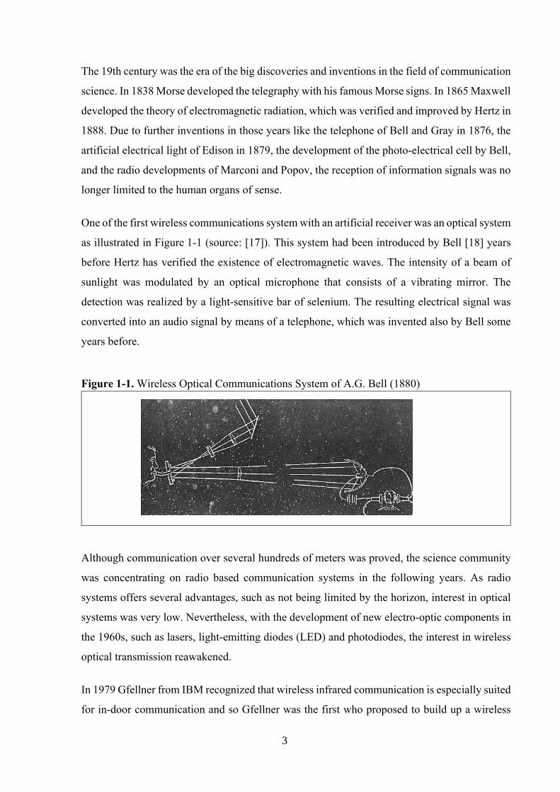
One of the first wireless communications system with an artificial receiver was an optical system
as illustrated in Figure 1-1 (source: [17]). This system had been introduced by Bell [18] years
before Hertz has verified the existence of electromagnetic waves. The intensity of a beam of
sunlight was modulated by an optical microphone that consists of a vibrating mirror. The
detection was realized by a light-sensitive bar of selenium. The resulting electrical signal was
converted into an audio signal by means of a telephone, which was invented also by Bell some
years before.
Figure 1-1. Wireless Optical Communications System of A.G. Bell (1880)
Although communication over several hundreds of meters was proved, the science community
was concentrating on radio based communication systems in the following years. As radio
systems offers several advantages, such as not being limited by the horizon, interest in optical
systems was very low. Nevertheless, with the development of new electro-optic components in
the 1960s, such as lasers, light-emitting diodes (LED) and photodiodes, the interest in wireless
optical transmission reawakened.
In 1979 Gfellner from IBM recognized that wireless infrared communication is especially suited
for in-door communication and so Gfellner was the first who proposed to build up a wireless
3
LAN by means of diffuse infrared [19]. Gfellner's paper can be considered as the basis for all
wireless infrared in-door communications systems, that have come up since then. (In fact, the
paper was even the first wireless LAN proposal using any medium.)
Also in 1979 the company Hewlett-Packard began to integrate infrared-interfaces in the pocket
calculators for interconnections with printers. From then on many infrared communication
systems penetrated the market and became the heart of almost any remote control system. It soon
became obvious that for interoperability between the devices of different companies an infrared
transmission standard was required. Therefore in 1993 the Infrared Data Association (IrDA) has
been founded by about 50 companies with the purpose of establishing a ubiquitous, low-cost,
point-to-point serial infrared standard. Just one year later in 1994 IrDA published its first
standards. The standard for the physical layer was mainly based on the initial work of Hewlett-
Packard (HP) [20][21] and also the name was taken over from HP: Serial Infrared (SIR). The
Link Access Protocol (IrLAP) standard was based on proposals of IBM [22][23][24]. In the
meantime IrDA has come up with several improvements and extensions of its standards and
almost any shortrange infrared communication system is based on the IrDA standard.
1.3 State of the Art at Wireless Infrared Communications
Wireless infrared communications systems are feasible for a wide range of applications like
remote controls, local area computer networks or inter-satellite communication. However, the
focus of this thesis are short-range, point to point, low power and low cost infrared data
interconnection applications as they are the focus of the IrDA standards [25]. The following
provides classification criteria of the different types of wireless infrared communications
systems and specifies the target configuration for this thesis.
In general, for the transmission of single bits over a physical channel, one has to convert the bits
into signals, which can be reliably transmitted over the channel. This process is performed in the
so called physical layer of a communications system [2]. At the physical layer of wireless
infrared communications systems the conversion is performed in two steps called electrical
modulation and optical modulation [17]. In the electrical modulation process the bit stream is
converted into an electrical waveform, which is adapted to the properties of the optical
modulator that finally converts the electrical signal into an infrared signal. The infrared signal is
4
transmitted via an optical link to the receiver, where the bit stream is retrieved by the consecutive
processes detection and electrical demodulation, which are the counterparts of optical
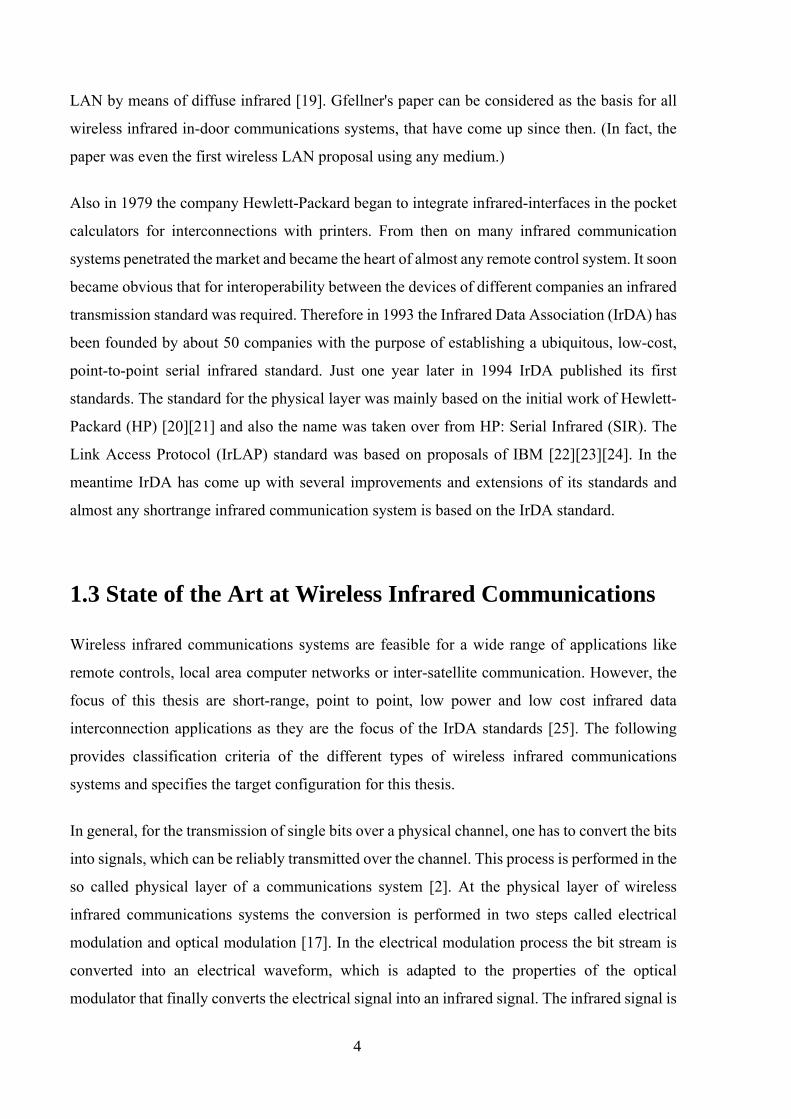
modulation and electrical modulation. Figure 1-2 provides an overview of the physical layer of
a wireless infrared communications system.
Figure 1-2. Wireless Infrared Communications System
ElectricalModulation
OpticalModulationBinary Source
Binary Sink ElectricalDemodulation Detection
Optical Link
1.3.1 Optical Link Design
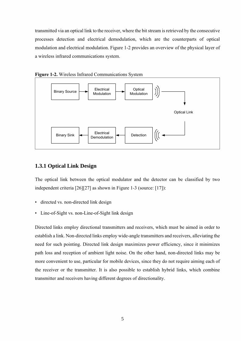
The optical link between the optical modulator and the detector can be classified by two
independent criteria [26][27] as shown in Figure 1-3 (source: [17]):
• directed vs. non-directed link design
• Line-of-Sight vs. non-Line-of-Sight link design
Directed links employ directional transmitters and receivers, which must be aimed in order to
establish a link. Non-directed links employ wide-angle transmitters and receivers, alleviating the
need for such pointing. Directed link design maximizes power efficiency, since it minimizes
path loss and reception of ambient light noise. On the other hand, non-directed links may be
more convenient to use, particular for mobile devices, since they do not require aiming each of
the receiver or the transmitter. It is also possible to establish hybrid links, which combine
transmitter and receivers having different degrees of directionality.
5
Figure 1-3. Classification of Optical Links
The second classification criterion relies on the existence of an uninterrupted line-of-sight (LOS)
path between the transmitter and the receiver. LOS links rely on such a path, while non-LOS
links generally rely on reflection of the light from the ceiling or some other diffusely reflecting
surfaces. LOS link design maximizes power efficiency and minimizes multipath distortion.
Non-LOS link design increases link robustness and ease of use, allowing the link to operate even
when barriers stand between the transmitter and receiver.
The greatest robustness and ease of use are achieved by the non-directed-non-LOS link design,
which is often referred to as a diffuse link. However, directed LOS link design require less power
and allow higher baud rates since multi-path distortion is negligible [17] [26]. Both, power
efficiency and high baud rates, are important features of IrDA's target application. Therefore
IrDA uses directed LOS link design and consequently the focus of this thesis will be put on
directed LOS links in the following.
1.3.2 Optical Modulation / Detection
Considering the best type of optical modulation and detection for mobile systems Otte et al. [17]
evidently indicated that intensity (i.e. optical power) modulation and the corresponding direct
detection are preferable against wavelength and polarization modulation techniques with their
6
coherent detection methods. Thus in the following we are assuming an intensity modulation and
direct detection system, which can be simply realized with an LED and a photodiode (PD)
respectively. Barry [26] presented various types of multi-level intensity modulation schemes
like Pulse Amplitude Modulation (PAM). In this thesis only binary-level intensity modulation
(i.e. LED on and LED off) is addressed, since in mobile applications the distance between the
transmitter and the receiver may vary and consequently a sophisticated adaptation of the
received signal power would be necessary in the receiver, which is not really feasible in low cost
devices. Modulation and demodulation are usually performed by digital signal processing, while
intensity modulation and direct detection are obviously analog tasks, which have to be
performed on an extra chip called infrared transceiver [1][28]. Since low cost infrared
transceivers usually perform binary hard decision, the demodulation and equalization techniques
introduced in [27] and [29], which require multi-bit analog to digital conversion, are not useful
for our applications. For that reason we assume, that the infrared transceiver performs a binary
hard decision in the reception path.
1.3.3 Electrical Modulation / Demodulation
In the electrical modulation process the bit stream that needs to be transmitted is converted into
an electrical waveform, which is adapted to the properties of the optical modulator. As
mentioned above the focus of this thesis lies upon binary-level intensity modulation and
consequently only binary-level electrical modulation techniques (i.e. voltage on and voltage off)
are considered here. In the electrical demodulation process the electrical waveform recovered by
the receiver path of the infrared transceiver is converted back into the original bit stream. Since
the infrared transceiver performs binary hard decision we can assume that the input waveform
of the electrical demodulator is identical to the output waveform of the electrical modulator. I.e.
electrical modulation and electrical demodulation are inverse processes. Currently, the
following binary-level electrical modulation techniques are used by IrDA [1]:
• Return-to-Zero Inverted (RZI)
• Pulse-Position-Modulation (PPM)
• Run-Length-Limited Code HHH(1,13)
7
With Edge Position Modulation (EPM) this thesis will present a completely new binary-level
modulation technique.
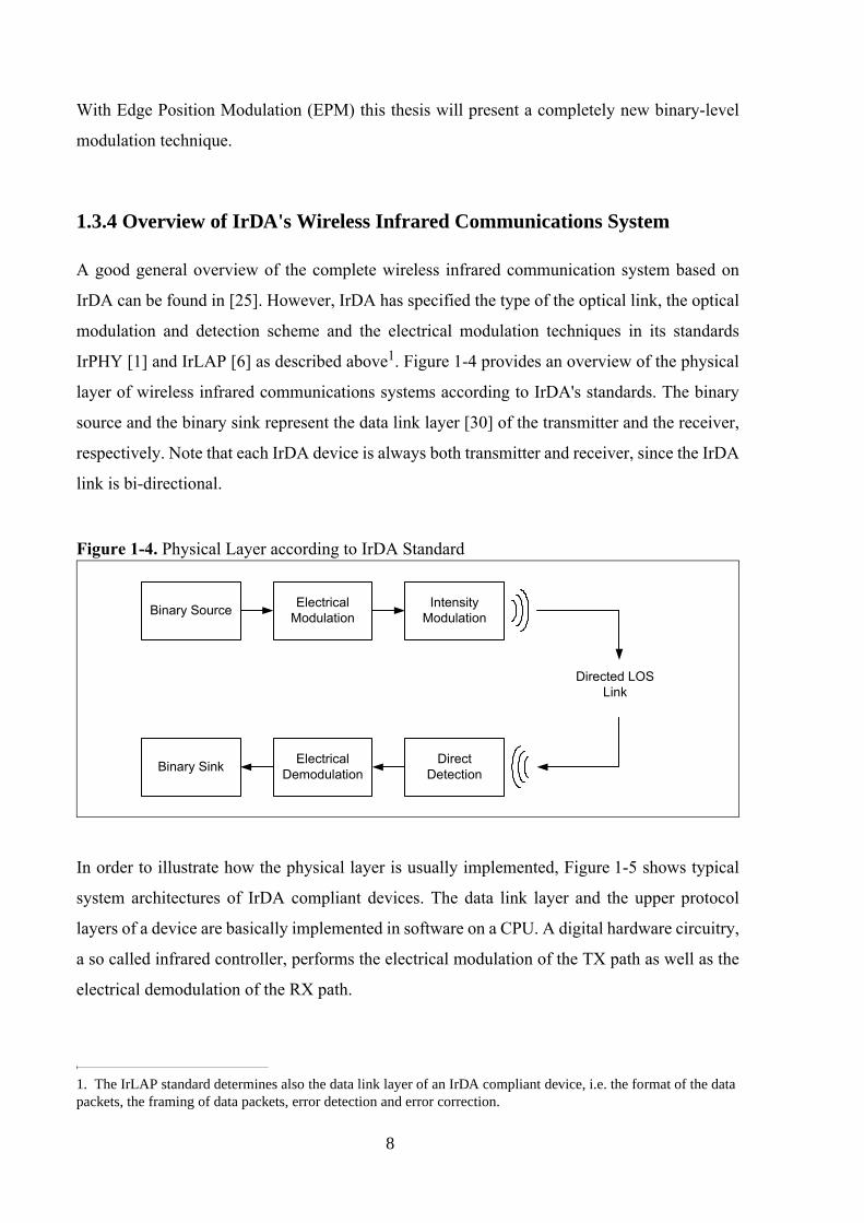
1.3.4 Overview of IrDA's Wireless Infrared Communications System
A good general overview of the complete wireless infrared communication system based on
IrDA can be found in [25]. However, IrDA has specified the type of the optical link, the optical
modulation and detection scheme and the electrical modulation techniques in its standards
IrPHY [1] and IrLAP [6] as described above1. Figure 1-4 provides an overview of the physical
layer of wireless infrared communications systems according to IrDA's standards. The binary
source and the binary sink represent the data link layer [30] of the transmitter and the receiver,
respectively. Note that each IrDA device is always both transmitter and receiver, since the IrDA
link is bi-directional.
Figure 1-4. Physical Layer according to IrDA Standard
ElectricalModulation
IntensityModulationBinary Source
Binary Sink ElectricalDemodulation
DirectDetection
Directed LOSLink
In order to illustrate how the physical layer is usually implemented, Figure 1-5 shows typical
system architectures of IrDA compliant devices. The data link layer and the upper protocol
layers of a device are basically implemented in software on a CPU. A digital hardware circuitry,
a so called infrared controller, performs the electrical modulation of the TX path as well as the
electrical demodulation of the RX path.
1. The IrLAP standard determines also the data link layer of an IrDA compliant device, i.e. the format of the data packets, the framing of data packets, error detection and error correction.
8
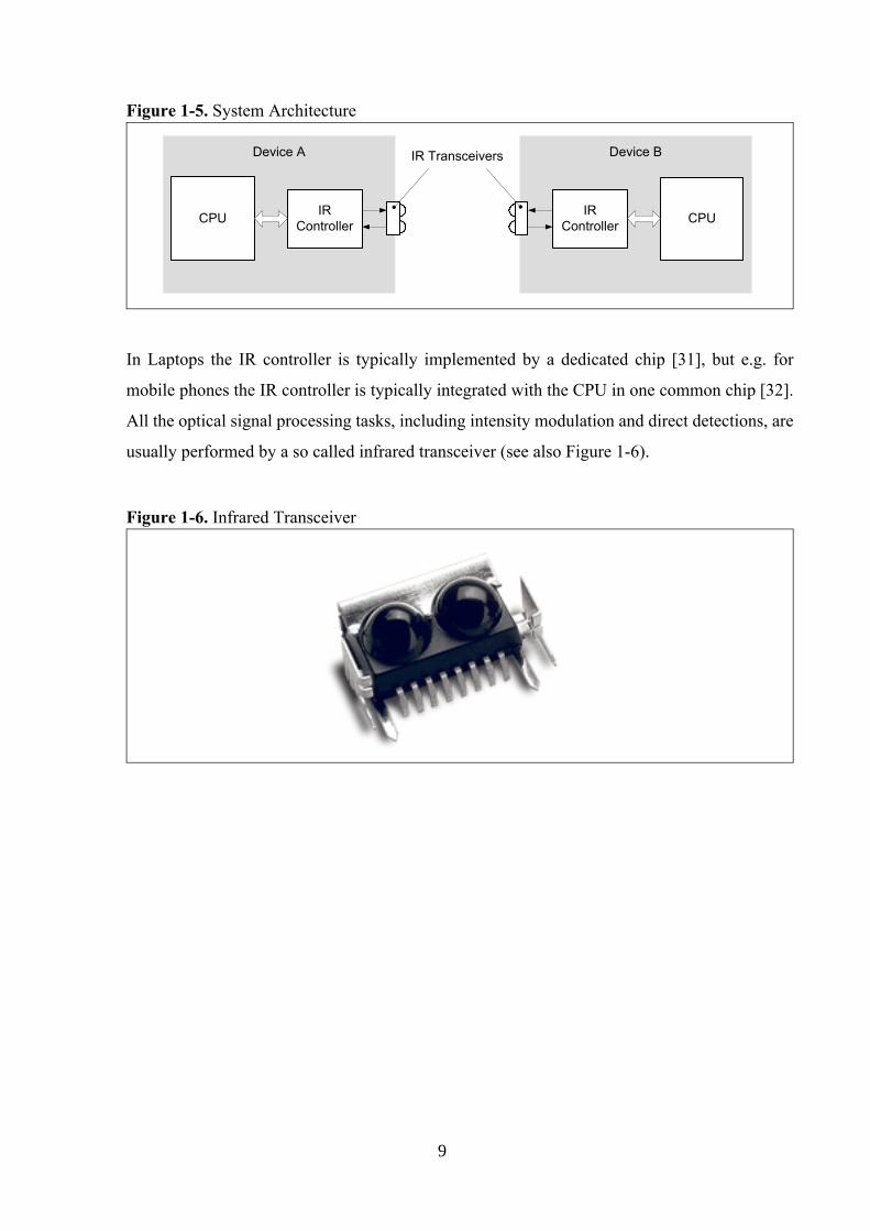
Figure 1-5. System Architecture
CPU CPUIRController
IRController
IR TransceiversDevice A Device B
In Laptops the IR controller is typically implemented by a dedicated chip [31], but e.g. for
mobile phones the IR controller is typically integrated with the CPU in one common chip [32].
All the optical signal processing tasks, including intensity modulation and direct detections, are
usually performed by a so called infrared transceiver (see also Figure 1-6).
Figure 1-6. Infrared Transceiver
9

10
2 Wireless Infrared Channel
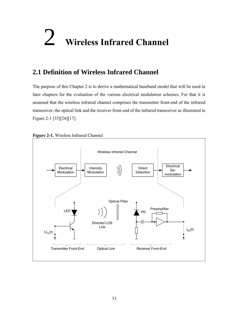
2.1 Definition of Wireless Infrared Channel
The purpose of this Chapter 2 is to derive a mathematical baseband model that will be used in
later chapters for the evaluation of the various electrical modulation schemes. For that it is
assumed that the wireless infrared channel comprises the transmitter front-end of the infrared
transceiver, the optical link and the receiver front-end of the infrared transceiver as illustrated in
Figure 2-1 [33][26][17].
Figure 2-1. Wireless Infrared Channel
LED
UTX(t)
ElectricalModulation
IntensityModulation
ElectricalDe-
modulation
DirectDetection
Directed LOSLink
Wireless Infrared Channel
PreamplifierPD
iRX(t)
Optical Filter
Receiver Front-EndTransmitter Front-End Optical Link
11
2.2 Optical Link
2.2.1 Basics of Optics
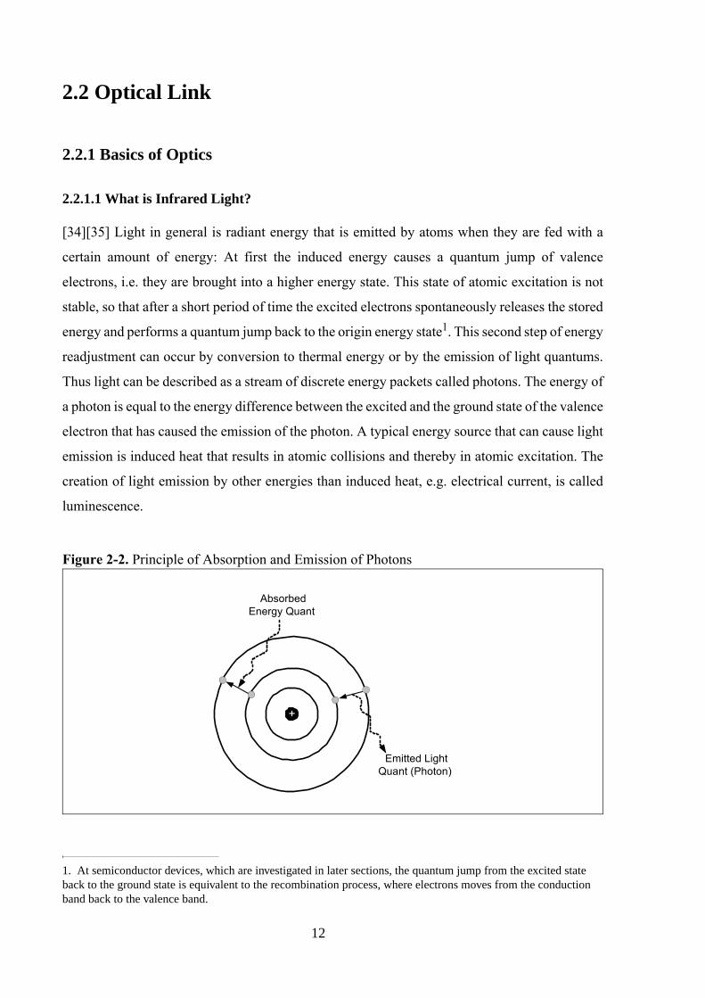
2.2.1.1 What is Infrared Light?
[34][35] Light in general is radiant energy that is emitted by atoms when they are fed with a
certain amount of energy: At first the induced energy causes a quantum jump of valence
electrons, i.e. they are brought into a higher energy state. This state of atomic excitation is not
stable, so that after a short period of time the excited electrons spontaneously releases the stored
energy and performs a quantum jump back to the origin energy state1. This second step of energy
readjustment can occur by conversion to thermal energy or by the emission of light quantums.
Thus light can be described as a stream of discrete energy packets called photons. The energy of
a photon is equal to the energy difference between the excited and the ground state of the valence
electron that has caused the emission of the photon. A typical energy source that can cause light
emission is induced heat that results in atomic collisions and thereby in atomic excitation. The
creation of light emission by other energies than induced heat, e.g. electrical current, is called
luminescence.
Figure 2-2. Principle of Absorption and Emission of Photons
+
AbsorbedEnergy Quant
Emitted LightQuant (Photon)
1. At semiconductor devices, which are investigated in later sections, the quantum jump from the excited state back to the ground state is equivalent to the recombination process, where electrons moves from the conduction band back to the valence band.
12
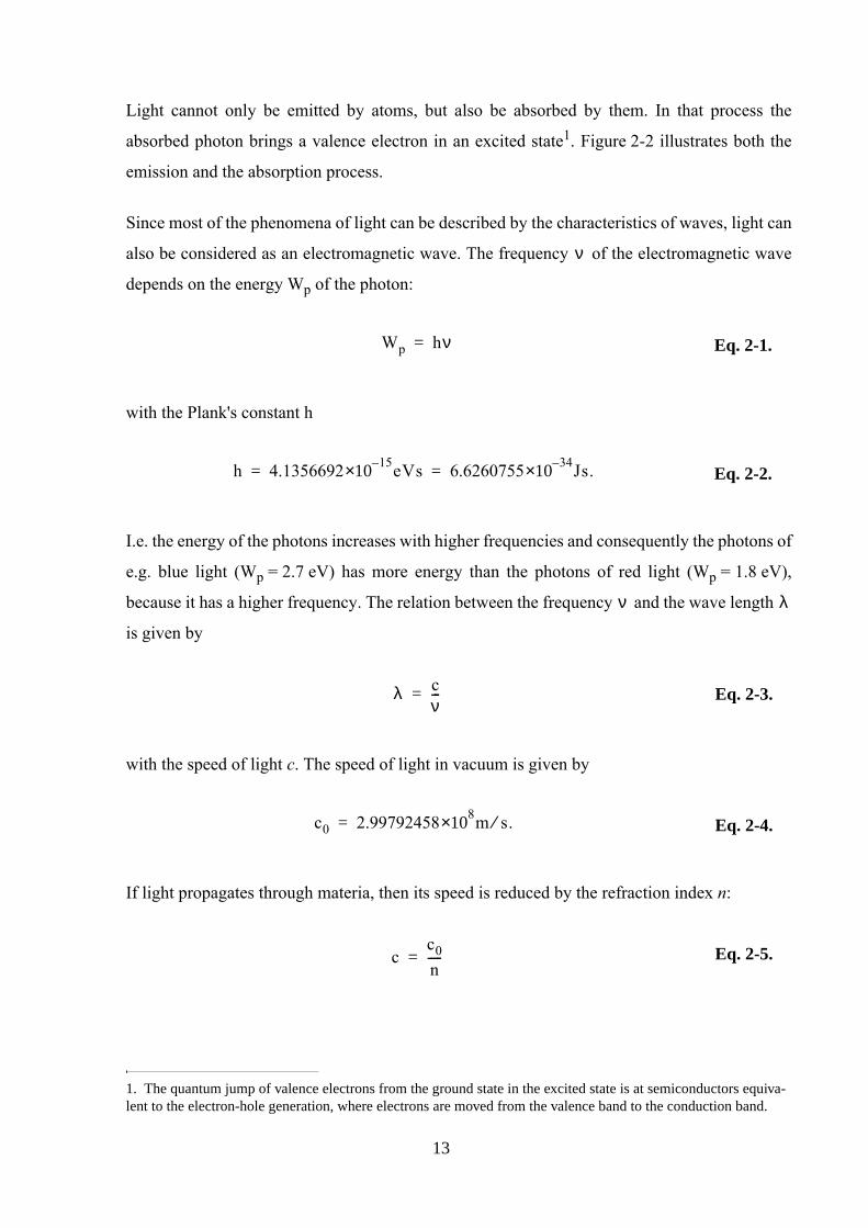
Light cannot only be emitted by atoms, but also be absorbed by them. In that process the
absorbed photon brings a valence electron in an excited state1. Figure 2-2 illustrates both the
emission and the absorption process.
Since most of the phenomena of light can be described by the characteristics of waves, light can
also be considered as an electromagnetic wave. The frequency ν of the electromagnetic wave
depends on the energy Wp of the photon:
Wp hν= Eq. 2-1.
with the Plank's constant h
h 4.1356692 15–×10 eVs 6.6260755 34–×10 Js.= = Eq. 2-2.
I.e. the energy of the photons increases with higher frequencies and consequently the photons of
e.g. blue light (Wp = 2.7 eV) has more energy than the photons of red light (Wp = 1.8 eV),
because it has a higher frequency. The relation between the frequency ν and the wave length λ
is given by
λ cν---= Eq. 2-3.
with the speed of light c. The speed of light in vacuum is given by
c0 2.99792458 8×10 m s⁄ .= Eq. 2-4.
If light propagates through materia, then its speed is reduced by the refraction index n:
cc0n-----= Eq. 2-5.
1. The quantum jump of valence electrons from the ground state in the excited state is at semiconductors equiva-lent to the electron-hole generation, where electrons are moved from the valence band to the conduction band.
13
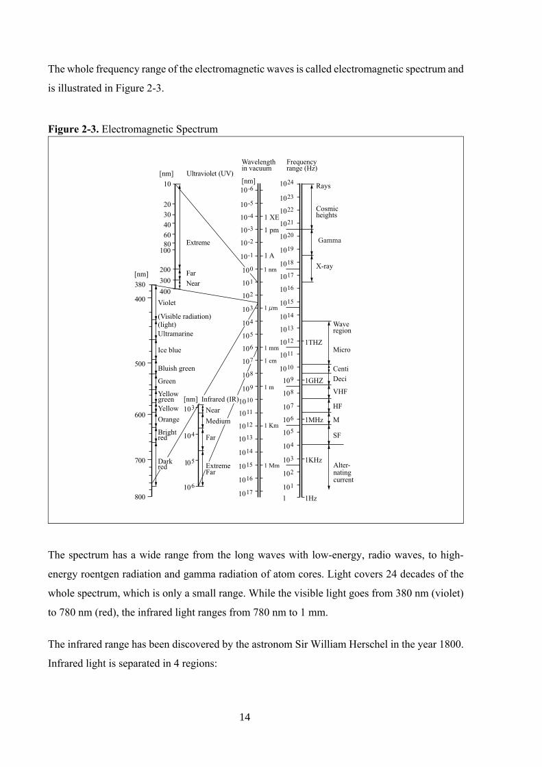
The whole frequency range of the electromagnetic waves is called electromagnetic spectrum and
is illustrated in Figure 2-3.
Figure 2-3. Electromagnetic Spectrum
[nm] Ultraviolet (UV)
Extreme
Far
Near
10
20
30
40
60
80100
200
300
400
1 XE
1 pm
1 A
1 nm
1 m
1 mm
1 cm
1 m
1 Km
1 Mm
µ
10
10
3
4
105
106
[nm]
380
400
500
600
700
800
Wavelengthin vacuum
[nm] 10
10
10
10
10
10
10
10
10
10
10
10
10
10
10
10
10
10
10
10
10
10
10
10
1
24
23
22
21
20
19
18
17
16
15
14
13
12
11
10
9
8
7
6
5
4
3
2
1
Frequencyrange (Hz)
Rays
Cosmicheights
X-ray
1THZ
1GHZ
1MHz
1KHz
1Hz
Waveregion
Micro
Centi
Deci
VHF
HF
M
SF
Alter-natingcurrent
Violet
(Visible radiation)(light)
Ultramarine
Ice blue
Bluish green
Green
Yellowgreen
Yellow
Orange
Brightred
Darkred
[nm] Infrared (IR)
Near
Medium
Far
ExtremeFar
10
10
10
10
10
10
10
10
10
10
10
10
10
10
10
10
10
10
10
10
10
10
10
10
-6
-5
-4
-3
-2
-1
0
1
2
3
4
5
6
7
8
9
10
11
12
13
14
15
16
17
Gamma
The spectrum has a wide range from the long waves with low-energy, radio waves, to high-
energy roentgen radiation and gamma radiation of atom cores. Light covers 24 decades of the
whole spectrum, which is only a small range. While the visible light goes from 380 nm (violet)
to 780 nm (red), the infrared light ranges from 780 nm to 1 mm.
The infrared range has been discovered by the astronom Sir William Herschel in the year 1800.
Infrared light is separated in 4 regions:
14

• Near IR (780 nm - 3000 nm),
• Intermediate IR (3000 nm - 6000 nm),
• Far IR (6000 nm - 15000 nm), and
• Extreme Far IR (15000 nm - 1 mm)
2.2.1.2 Energy related Quantities
As described above light transports energy. The following provides an overview of some energy
related quantities that are required for the characterization of optical links.
• Radiant Energy Q [J] refers to the total amount of energy emitted, transferred, or collected
in a radiation process.
• Radiant Power or Radiant Flux Φ [W] is the time rate of change of radiant energy.
• Radiant Intensity I [W/sr] represents the flux per unit solid angle radiated by an entire
source in a given direction. The direction can be represented by a vector n and thus the radi-
ant intensity is given by
I n( ) dΦ n( )dΩ
---------------- .= Eq. 2-6.
The radiant intensity is of interest if the source is far away so that it can be considered as
point source and if the detector is small so that all rays from the source onto the detector are
essentially parallel. Figure 2-4 illustrates the radiant intensity.
Figure 2-4. Radiant Intensity Illustration
( )ndr
ΦΩd
nr
( ) ( )Ω
Φ=d
ndnIr
r
Φ
15
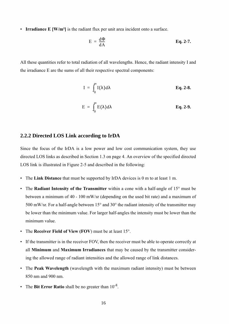
• Irradiance E [W/m²] is the radiant flux per unit area incident onto a surface.
E dΦdA-------= Eq. 2-7.
All these quantities refer to total radiation of all wavelengths. Hence, the radiant intensity I and
the irradiance E are the sums of all their respective spectral components:
I I λ( )dλ0
∞
∫= Eq. 2-8.
E E λ( )dλ0
∞
∫= Eq. 2-9.
2.2.2 Directed LOS Link according to IrDA
Since the focus of the IrDA is a low power and low cost communication system, they use
directed LOS links as described in Section 1.3 on page 4. An overview of the specified directed
LOS link is illustrated in Figure 2-5 and described in the following:
• The Link Distance that must be supported by IrDA devices is 0 m to at least 1 m.
• The Radiant Intensity of the Transmitter within a cone with a half-angle of 15° must be
between a minimum of 40 - 100 mW/sr (depending on the used bit rate) and a maximum of
500 mW/sr. For a half-angle between 15° and 30° the radiant intensity of the transmitter may
be lower than the minimum value. For larger half-angles the intensity must be lower than the
minimum value.
• The Receiver Field of View (FOV) must be at least 15°.
• If the transmitter is in the receiver FOV, then the receiver must be able to operate correctly at
all Minimum and Maximum Irradiances that may be caused by the transmitter consider-
ing the allowed range of radiant intensities and the allowed range of link distances.
• The Peak Wavelength (wavelength with the maximum radiant intensity) must be between
850 nm and 900 nm.
• The Bit Error Ratio shall be no greater than 10-8.
16
Along with that standard specification, IrDA provides also a low power version with reduced
link distances and reduced radiant intensities. For the complete specification of the directed LOS
link of IrDA see [1].
Figure 2-5. Directed LOS Link according to IrDA
0 … 1 m
Transmitter
Receiver15°...30°>15°
2.2.3 Ambient Radiation and Optical Filtering
[19][17][26] At the optical link of wireless infrared communications systems intense ambient
infrared radiation must be taken into account. The most important sources of ambient infrared
radiation are the sun, incandescent and fluorescent lamps. The normalized optical power spectra
of that infrared sources are shown in Figure 2-6 (source: [26]). Additionally, electromagnetic
fields or other infrared transmitter (e.g. IR remote controls) can disturb the infrared link. Here it
should be emphasized that direct sun-light, when present, is typically much stronger than other
sources.
Hence, optical filtering is required to reduce the influence of those ambient light sources. For
that purpose usually bandpass filtering is used that is adapted to the frequency range of the LED.
The frequencies above the upper corner frequency of the LED are basically suppressed due to
the low pass characteristic of the photodiode (see Section 2.4.2 on page 26). The frequencies
below the lower corner frequency of the LED, i.e. the visible light, can be suppressed by means
of an absorption filter. Cheap absorption filters can be realized by colored glass [36].
17
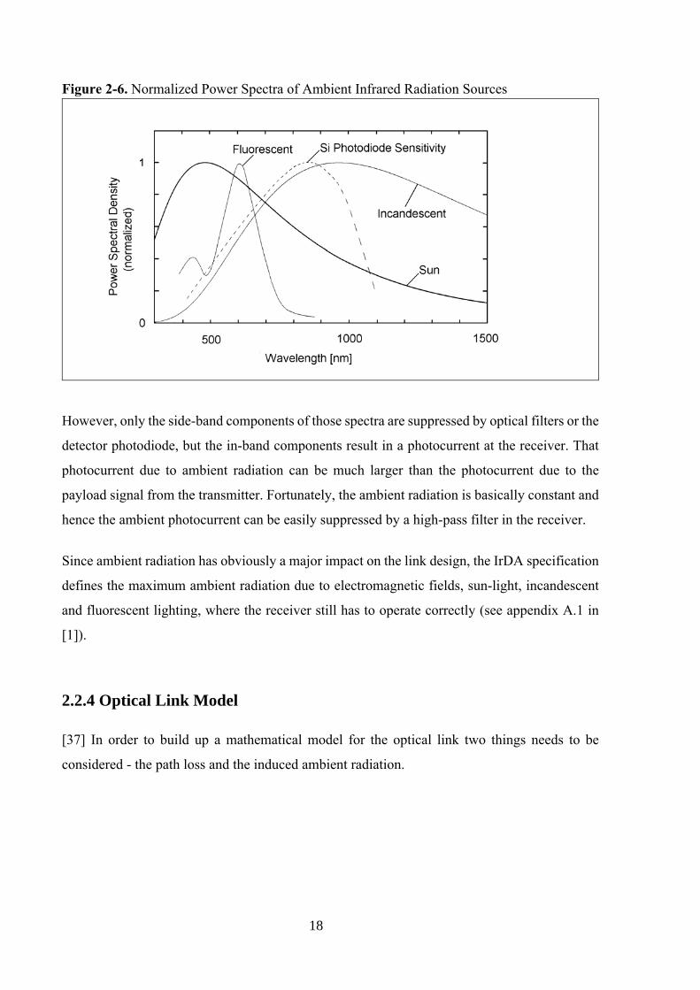
Figure 2-6. Normalized Power Spectra of Ambient Infrared Radiation Sources
However, only the side-band components of those spectra are suppressed by optical filters or the
detector photodiode, but the in-band components result in a photocurrent at the receiver. That
photocurrent due to ambient radiation can be much larger than the photocurrent due to the
payload signal from the transmitter. Fortunately, the ambient radiation is basically constant and
hence the ambient photocurrent can be easily suppressed by a high-pass filter in the receiver.
Since ambient radiation has obviously a major impact on the link design, the IrDA specification
defines the maximum ambient radiation due to electromagnetic fields, sun-light, incandescent
and fluorescent lighting, where the receiver still has to operate correctly (see appendix A.1 in
[1]).
2.2.4 Optical Link Model
[37] In order to build up a mathematical model for the optical link two things needs to be
considered - the path loss and the induced ambient radiation.
18
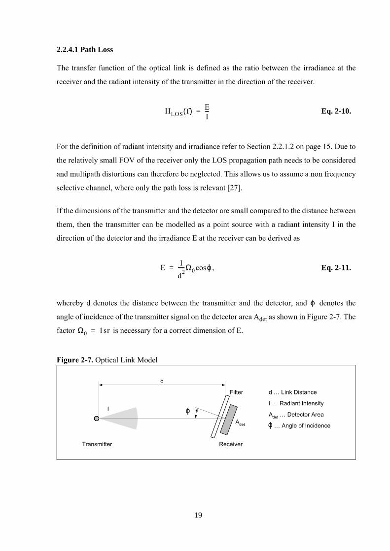
2.2.4.1 Path Loss
The transfer function of the optical link is defined as the ratio between the irradiance at the
receiver and the radiant intensity of the transmitter in the direction of the receiver.
HLOS f( ) EI---= Eq. 2-10.
For the definition of radiant intensity and irradiance refer to Section 2.2.1.2 on page 15. Due to
the relatively small FOV of the receiver only the LOS propagation path needs to be considered
and multipath distortions can therefore be neglected. This allows us to assume a non frequency
selective channel, where only the path loss is relevant [27].
If the dimensions of the transmitter and the detector are small compared to the distance between
them, then the transmitter can be modelled as a point source with a radiant intensity I in the
direction of the detector and the irradiance E at the receiver can be derived as
E Id2-----Ω0 ϕ ,cos= Eq. 2-11.
whereby d denotes the distance between the transmitter and the detector, and ϕ denotes the
angle of incidence of the transmitter signal on the detector area Adet as shown in Figure 2-7. The
factor Ω0 1sr= is necessary for a correct dimension of E.
Figure 2-7. Optical Link Model
Transmitter Receiver
Adet
Filter
I ϕ
d
d … Link Distance
I … Radiant Intensity
Adet … Detector Area
ϕ … Angle of Incidence
19
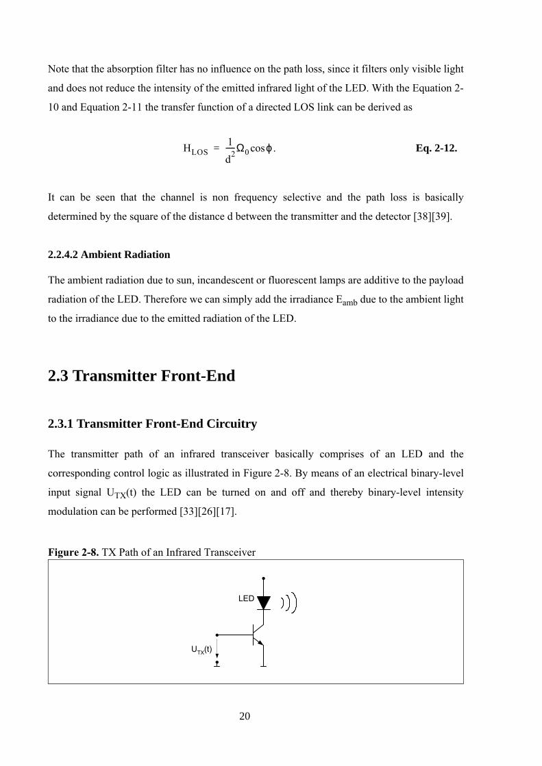
Note that the absorption filter has no influence on the path loss, since it filters only visible light
and does not reduce the intensity of the emitted infrared light of the LED. With the Equation 2-
10 and Equation 2-11 the transfer function of a directed LOS link can be derived as
HLOS1d2-----Ω0 ϕ .cos= Eq. 2-12.
It can be seen that the channel is non frequency selective and the path loss is basically
determined by the square of the distance d between the transmitter and the detector [38][39].
2.2.4.2 Ambient Radiation
The ambient radiation due to sun, incandescent or fluorescent lamps are additive to the payload
radiation of the LED. Therefore we can simply add the irradiance Eamb due to the ambient light
to the irradiance due to the emitted radiation of the LED.
2.3 Transmitter Front-End
2.3.1 Transmitter Front-End Circuitry
The transmitter path of an infrared transceiver basically comprises of an LED and the
corresponding control logic as illustrated in Figure 2-8. By means of an electrical binary-level
input signal UTX(t) the LED can be turned on and off and thereby binary-level intensity
modulation can be performed [33][26][17].
Figure 2-8. TX Path of an Infrared Transceiver
LED
UTX(t)
20
2.3.2 Intensity Modulation by LEDs
[40][41] LEDs can transform an electrical signal into optical radiation, whereby the radiant
intensity has basically the same waveform as the applied electrical signal (voltage). Therefore
LEDs are perfectly suited for the above described intensity modulation.
2.3.2.1 Basic Functionality of LEDs
An LED consists of a semiconductor material containing both p-type and n-type regions that
form a p-n-junction. At the p-n-junction the carrier concentration gradients cause carrier
diffusion. Holes from the p-side diffuse into the n-side, and electrons from the n-side diffuse into
the p-side. As holes continue to leave the p-side, some of the negative acceptor ions near the
junction are left uncompensated, since the acceptors are fixed in the semiconductor lattice,
whereas the holes are mobile. Similarly, some of the positive donor ions near the junction are
left uncompensated as the electrons leave the n-side. Consequently, the uncompensated acceptor
and donor ions forms a potential difference UD that is in the direction opposite to the diffusion
current of the mobile holes and electrons, what hampers further mobile charge carrier diffusion.
The schematic of the p-n-junction in Figure 2-9.a illustrates the resulting charge carrier
distribution in thermal-equilibrium condition, i.e. without an applied external voltage. The
region of the uncompensated donor and acceptor ions is called depletion layer, since it contains
no mobile charge carriers. Figure 2-9.b shows the corresponding energy bands of the p-n-
junction in thermal-equilibrium condition. The potential difference results in potential energy
difference eUD that avoids an electrons diffusion from the n-type to the p-type region and a hole
diffusion from the p-type to the n-type region.
If a forward-bias voltage UF is applied as shown in Figure 2-10, then the potential difference is
reduced and the mobile charge carrier can diffuse through the depletion layer. Electrons from
the n-type region can diffuse into the p-type regions, where they recombine with the mobile
holes, the majority carriers of the p-type semiconductor region. On the other hand, holes from
the p-type region can diffuse into the n-type regions, where they recombine with the mobile
electrons, the majority carriers of the n-type semiconductor region. At LEDs that recombination
is a radiative recombination, i.e. the released energy due to the quantum jump of the
recombination process results in emitting photons as described in Section 2.2.1. That means that
the injected charge carriers due to forward-bias voltage results in light. This process is called
21
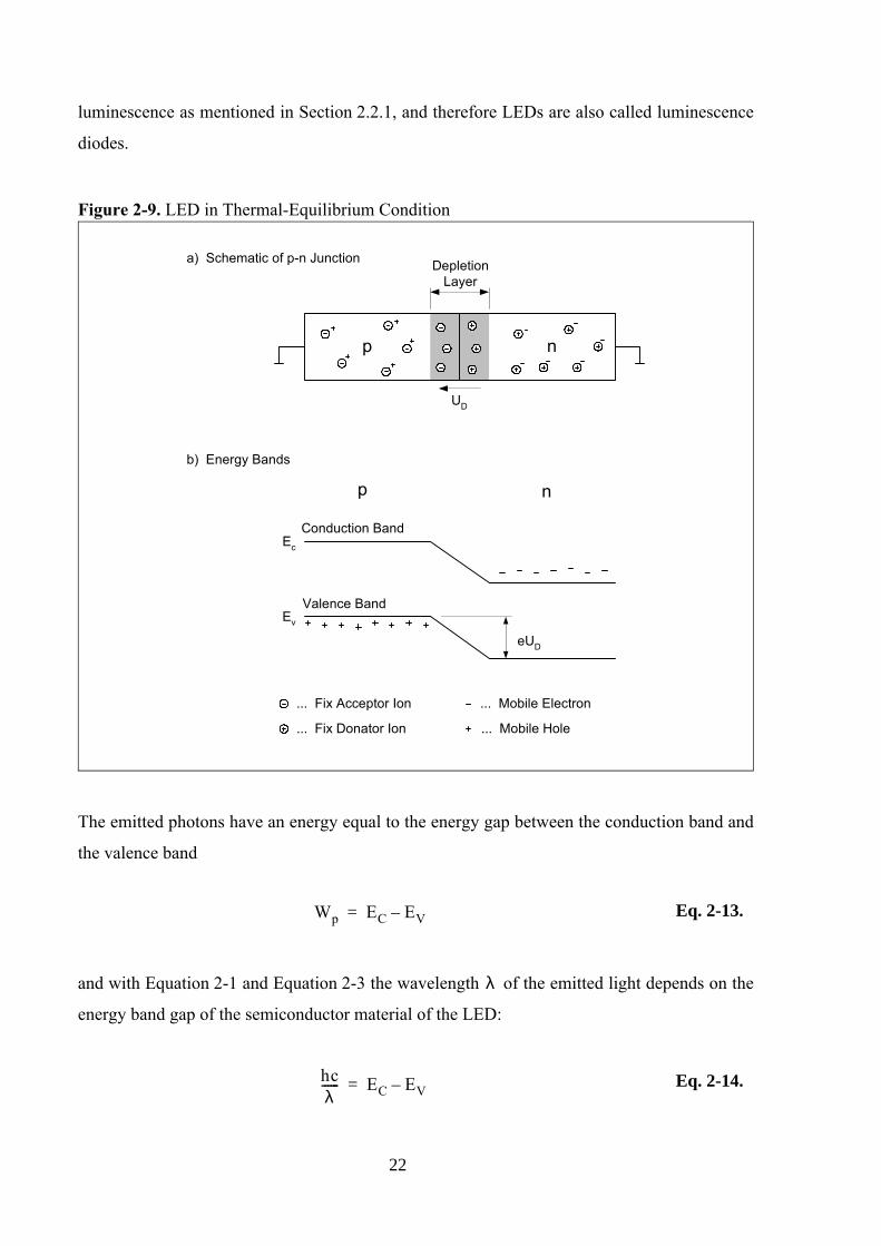
luminescence as mentioned in Section 2.2.1, and therefore LEDs are also called luminescence
diodes.
Figure 2-9. LED in Thermal-Equilibrium Condition
p n
Conduction Band
Valence Band
DepletionLayer
eUD
p n
UD
a) Schematic of p-n Junction
... Fix Donator Ion
... Fix Acceptor Ion
... Mobile Hole
... Mobile Electron
Ec
Ev
b) Energy Bands
The emitted photons have an energy equal to the energy gap between the conduction band and
the valence band
Wp EC EV–= Eq. 2-13.
and with Equation 2-1 and Equation 2-3 the wavelength λ of the emitted light depends on the
energy band gap of the semiconductor material of the LED:
hcλ------ EC EV–= Eq. 2-14.
22
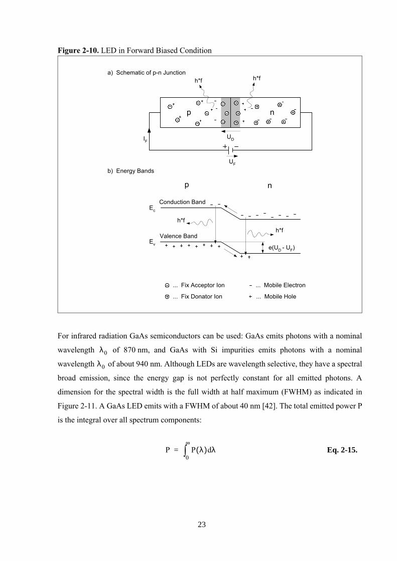
Figure 2-10. LED in Forward Biased Condition
p n
Conduction Band
Valence Band
Ec
e(UD - UF)
p n
UD
... Fix Donator Ion
... Fix Acceptor Ion
... Mobile Hole
... Mobile Electron
h*fh*f
UF
IF
h*f
h*f
Ev
a) Schematic of p-n Junction
b) Energy Bands
For infrared radiation GaAs semiconductors can be used: GaAs emits photons with a nominal
wavelength λ0 of 870 nm, and GaAs with Si impurities emits photons with a nominal
wavelength λ0 of about 940 nm. Although LEDs are wavelength selective, they have a spectral
broad emission, since the energy gap is not perfectly constant for all emitted photons. A
dimension for the spectral width is the full width at half maximum (FWHM) as indicated in
Figure 2-11. A GaAs LED emits with a FWHM of about 40 nm [42]. The total emitted power P
is the integral over all spectrum components:
P P λ( ) λd0
∞
∫= Eq. 2-15.
23
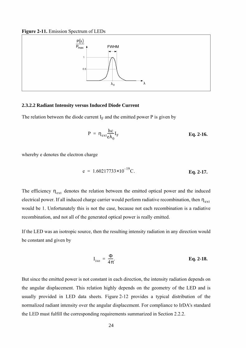
Figure 2-11. Emission Spectrum of LEDs
1
0.5
FWHM( )
maxPP λ
λ0λ
2.3.2.2 Radiant Intensity versus Induced Diode Current
The relation between the diode current IF and the emitted power P is given by
P ηexthceλ0--------IF= Eq. 2-16.
whereby e denotes the electron charge
e 1.60217733 19–×10 C.= Eq. 2-17.
The efficiency ηext denotes the relation between the emitted optical power and the induced
electrical power. If all induced charge carrier would perform radiative recombination, then ηext
would be 1. Unfortunately this is not the case, because not each recombination is a radiative
recombination, and not all of the generated optical power is really emitted.
If the LED was an isotropic source, then the resulting intensity radiation in any direction would
be constant and given by
IisoΦ4π------ .= Eq. 2-18.
But since the emitted power is not constant in each direction, the intensity radiation depends on
the angular displacement. This relation highly depends on the geometry of the LED and is
usually provided in LED data sheets. Figure 2-12 provides a typical distribution of the
normalized radiant intensity over the angular displacement. For compliance to IrDA's standard
the LED must fulfill the corresponding requirements summarized in Section 2.2.2.
24
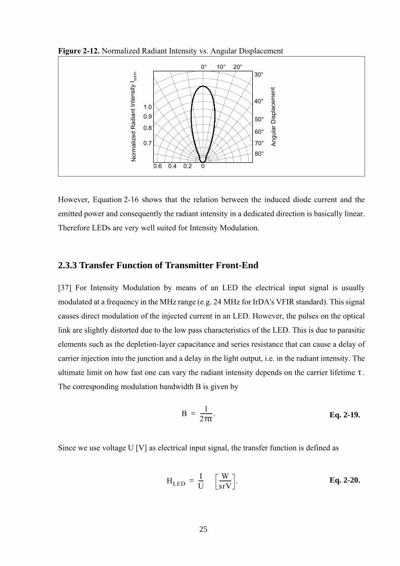
Figure 2-12. Normalized Radiant Intensity vs. Angular Displacement
0° 10° 20°30°
40°
50°
60°
70°
80°
1.00.9
0.7
0.6 0.4 0.2
0.8N
orm
aliz
ed R
adia
nt In
tens
ity I no
rm
0
Ang
ular
Dis
plac
emen
t
However, Equation 2-16 shows that the relation between the induced diode current and the
emitted power and consequently the radiant intensity in a dedicated direction is basically linear.
Therefore LEDs are very well suited for Intensity Modulation.
2.3.3 Transfer Function of Transmitter Front-End
[37] For Intensity Modulation by means of an LED the electrical input signal is usually
modulated at a frequency in the MHz range (e.g. 24 MHz for IrDA's VFIR standard). This signal
causes direct modulation of the injected current in an LED. However, the pulses on the optical
link are slightly distorted due to the low pass characteristics of the LED. This is due to parasitic
elements such as the depletion-layer capacitance and series resistance that can cause a delay of
carrier injection into the junction and a delay in the light output, i.e. in the radiant intensity. The
ultimate limit on how fast one can vary the radiant intensity depends on the carrier lifetime τ .
The corresponding modulation bandwidth B is given by
B 12πτ--------- .= Eq. 2-19.
Since we use voltage U [V] as electrical input signal, the transfer function is defined as
HLEDIU---- W
srV--------- .= Eq. 2-20.
25
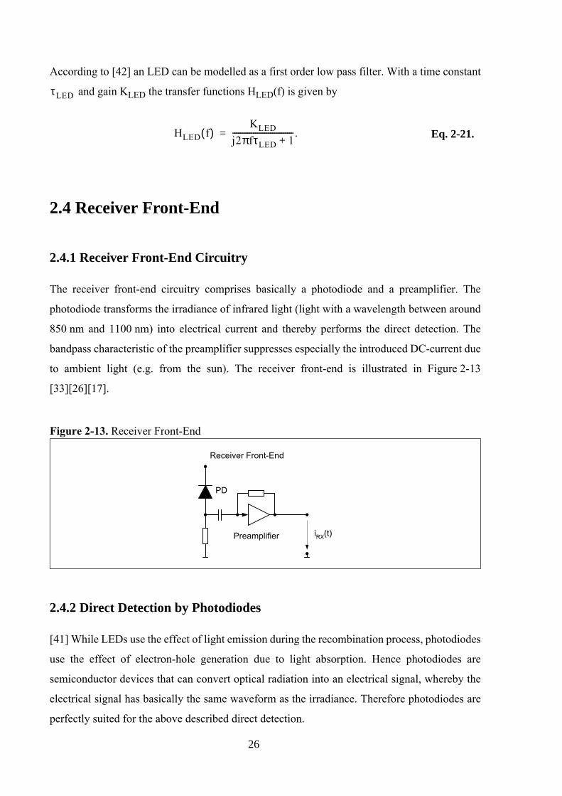
According to [42] an LED can be modelled as a first order low pass filter. With a time constant
τLED and gain KLED the transfer functions HLED(f) is given by
HLED f( )KLED
j2πfτLED 1+--------------------------------.= Eq. 2-21.
2.4 Receiver Front-End
2.4.1 Receiver Front-End Circuitry
The receiver front-end circuitry comprises basically a photodiode and a preamplifier. The
photodiode transforms the irradiance of infrared light (light with a wavelength between around
850 nm and 1100 nm) into electrical current and thereby performs the direct detection. The
bandpass characteristic of the preamplifier suppresses especially the introduced DC-current due
to ambient light (e.g. from the sun). The receiver front-end is illustrated in Figure 2-13
[33][26][17].
Figure 2-13. Receiver Front-End
Preamplifier
PD
iRX(t)
Receiver Front-End
2.4.2 Direct Detection by Photodiodes
[41] While LEDs use the effect of light emission during the recombination process, photodiodes
use the effect of electron-hole generation due to light absorption. Hence photodiodes are
semiconductor devices that can convert optical radiation into an electrical signal, whereby the
electrical signal has basically the same waveform as the irradiance. Therefore photodiodes are
perfectly suited for the above described direct detection.
26
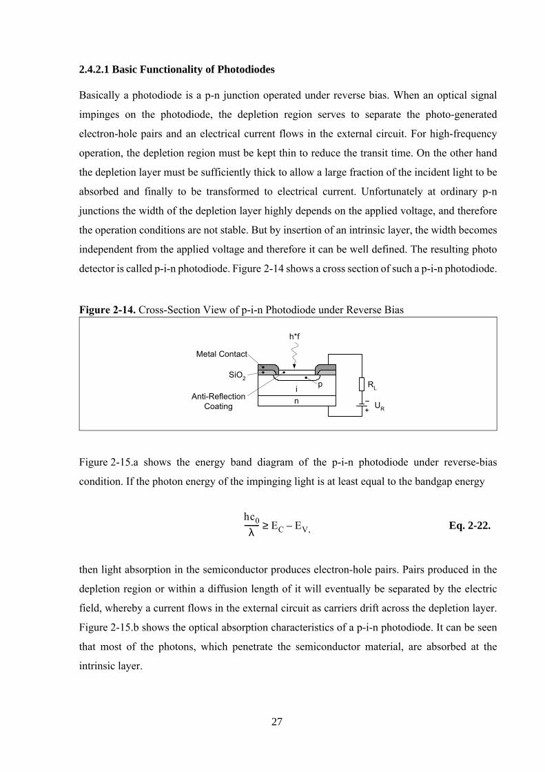
2.4.2.1 Basic Functionality of Photodiodes
Basically a photodiode is a p-n junction operated under reverse bias. When an optical signal
impinges on the photodiode, the depletion region serves to separate the photo-generated
electron-hole pairs and an electrical current flows in the external circuit. For high-frequency
operation, the depletion region must be kept thin to reduce the transit time. On the other hand
the depletion layer must be sufficiently thick to allow a large fraction of the incident light to be
absorbed and finally to be transformed to electrical current. Unfortunately at ordinary p-n
junctions the width of the depletion layer highly depends on the applied voltage, and therefore
the operation conditions are not stable. But by insertion of an intrinsic layer, the width becomes
independent from the applied voltage and therefore it can be well defined. The resulting photo
detector is called p-i-n photodiode. Figure 2-14 shows a cross section of such a p-i-n photodiode.
Figure 2-14. Cross-Section View of p-i-n Photodiode under Reverse Bias
h*f
in
p
Metal Contact
SiO2
Anti-ReflectionCoating
RL
UR
Figure 2-15.a shows the energy band diagram of the p-i-n photodiode under reverse-bias
condition. If the photon energy of the impinging light is at least equal to the bandgap energy
hc0λ
-------- EC EV,–≥ Eq. 2-22.
then light absorption in the semiconductor produces electron-hole pairs. Pairs produced in the
depletion region or within a diffusion length of it will eventually be separated by the electric
field, whereby a current flows in the external circuit as carriers drift across the depletion layer.
Figure 2-15.b shows the optical absorption characteristics of a p-i-n photodiode. It can be seen
that most of the photons, which penetrate the semiconductor material, are absorbed at the
intrinsic layer.
27
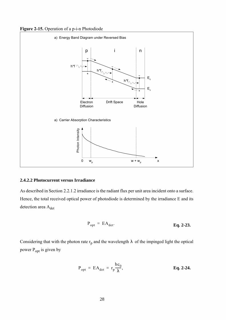
Figure 2-15. Operation of a p-i-n Photodiode
p
Drift Space
a) Energy Band Diagram under Reversed Bias
Ec
Ev
h*fh*f
h*f
i n
HoleDiffusion
ElectronDiffusion
0 wp w + wp x
Pho
ton
Inte
nsity
a) Carrier Absorption Characteristics
2.4.2.2 Photocurrent versus Irradiance
As described in Section 2.2.1.2 irradiance is the radiant flux per unit area incident onto a surface.
Hence, the total received optical power of photodiode is determined by the irradiance E and its
detection area Adet
Popt EAdet.= Eq. 2-23.
Considering that with the photon rate rp and the wavelength λ of the impinged light the optical
power Popt is given by
Popt EAdet rphc0λ
-------- ,= = Eq. 2-24.
28
and that with the electron rate re the photocurrent iphoto is given by
iphoto ree,=Eq. 2-25.
then the relation between the irradiance and the photodiode current can be given by
iphotoE
-------------rerp---- eλ
hc0--------Adet.= Eq. 2-26.
The relation between re and rp is often denoted as quantum efficiency η and it represents the
ratio of absorbed photons that generate an electron-hole pair in the photodiode. Clearly, the
quantum efficiency η depends on the characteristics of the p-i-n photodiode (e.g., width of the
instrinsic layer) and furthermore it is obviously a function of the wavelength λ of the impinged
photons:
η λ( )rerp---- ,= Eq. 2-27.
While the long-wavelength cutoff λ c of the quantum efficiency is established by the bandgap
(see Equation 2-22 on page 27), the short-wavelength cutoff comes about because radiation with
a low wavelength is mostly absorbed very near the surface, where the carriers can recombine
before they can diffuse to the drift space of the intrinsic layer (compare Figure 2-15 on page 28).
In the literature the relation between the irradiance and the photocurrent is often defined as
photodiode responsivity R. With the quantum efficiency the responsivity can be given as
Riphoto
E------------- η λ( ) eλ
hc0--------Adet.= = Eq. 2-28.
Figure 2-16 shows the normalized responsivity of a silicon and of a germanium diode as a
function of the wavelength. It can be seen that a silicon diode fits very well to the requirements
of the optical link defined by IrDA (see Section 2.2.2).
29
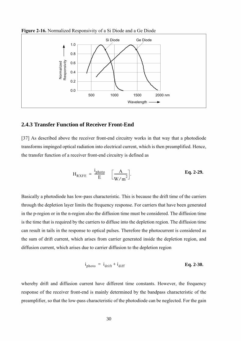
Figure 2-16. Normalized Responsivity of a Si Diode and a Ge Diode
1.0
0.0
0.2
0.4
0.6
0.8
500 1000 1500 2000 nm
Si Diode Ge Diode
Wavelength
Nor
mal
ized
Res
pons
ivity
2.4.3 Transfer Function of Receiver Front-End
[37] As described above the receiver front-end circuitry works in that way that a photodiode
transforms impinged optical radiation into electrical current, which is then preamplified. Hence,
the transfer function of a receiver front-end circuitry is defined as
HRXFEiphoto
E------------- A
W m2⁄---------------- .= Eq. 2-29.
Basically a photodiode has low-pass characteristic. This is because the drift time of the carriers
through the depletion layer limits the frequency response. For carriers that have been generated
in the p-region or in the n-region also the diffusion time must be considered. The diffusion time
is the time that is required by the carriers to diffuse into the depletion region. The diffusion time
can result in tails in the response to optical pulses. Therefore the photocurrent is considered as
the sum of drift current, which arises from carrier generated inside the depletion region, and
diffusion current, which arises due to carrier diffusion to the depletion region
iphoto idrift idiff+= Eq. 2-30.
whereby drift and diffusion current have different time constants. However, the frequency
response of the receiver front-end is mainly determined by the bandpass characteristic of the
preamplifier, so that the low-pass characteristic of the photodiode can be neglected. For the gain
30
factor we stick to the responsivity R of the photodiode for the sake of simplicity. Hence, the
transfer function of the receiver front-end is given by
HRXFE Rj2πfτHP
j2πfτHP 1+( ) j2πfτLP 1+( )-------------------------------------------------------------------- .= Eq. 2-31.
2.4.4 Receiver Noise Current
The main noise sources within the receiver are shot noise and amplifier noise [43][26][17].
2.4.4.1 Shot Noise
Shot noise occurs due to the discrete nature of energy and charge in the photodiode. Carrier pairs
are generated randomly due to the incident photons. Furthermore, carriers traverse the potential
barrier of the p-n junction in a random fashion dependent to their energy. The generation and
transport of carriers generate shot noise in the photocurrent. Basically, the shot noise generation
is a discrete Poisson process with a white power spectral density. Since a Poisson process can be
approximated by a Gaussian process, the shot noise can be modelled as an additive white
Gaussian noise with a variance of
σshot2 ishot
2 t( )⟨ ⟩ 2eBiphoto,= = Eq. 2-32.
whereby B denotes the bandwidth of the front-end circuitry.
2.4.4.2 Amplifier Noise
Due to the impedance of the preamplifier a thermal noise current occurs that also can be
modelled as an additive white gaussian noise. Basically, the variance of the thermal noise of an
impedance R is given by
σth2 ith
2 t( )⟨ ⟩ 4kTBR
-------------- ,= = Eq. 2-33.
31
whereby T is the absolute temperature, B is the front-end bandwidth and k is the Boltzmann
constant that is given by
k 1.3806568 23–×10 J K⁄ .= Eq. 2-34.
However, the actual value of the thermal noise highly depends on the used preamplifier type.
2.5 Baseband Model of Wireless Infrared Channel
2.5.1 General Channel Model
[37] Considering the above described transfer functions and noise sources the baseband model
can be implemented as shown in Figure 2-17.
Figure 2-17. Baseband Model of Wireless Infrared Channel
HRXFE(f)
TransmitterFront-End Optical Link Receiver Front-End
EAmbient
+HLOS(f)HTXFE(f)I(t) E(t)uTX(t)
ishot(t)
++
ith(t)
iRX(t)
Due to the disturbance variable EAmbient the high-pass filter of the receiver front-end requires
some settling time as illustrated in Figure 2-18. But under steady state conditions the disturbance
variable EAmbiant has no influence, and so we are able to provide a simple channel model as
shown in Figure 2-19.
32
Figure 2-18. Settling Time of the High-Pass Filter due to Disturbance EAmbient
curr
ent
time
Figure 2-19. Steady State Baseband Model of Wireless Infrared Channel
n(t)
+HWIrC(f)iRX(t)uTX(t)
The channel transfer function HWIrC(f) and the noise n(t) are given by
HWIrC f( ) HTXFE f( )HLOS f( )HRXFE f( )= Eq. 2-35.
n t( ) ishot t( ) ith t( ).+= Eq. 2-36.
The corresponding transfer functions are given by
HTXFE f( ) Iu---
KTXFEj2πfτLED 1+--------------------------------= = Eq. 2-37.
HLOSEI---
1d2-----Ω0 ϕcos= = Eq. 2-38.
33
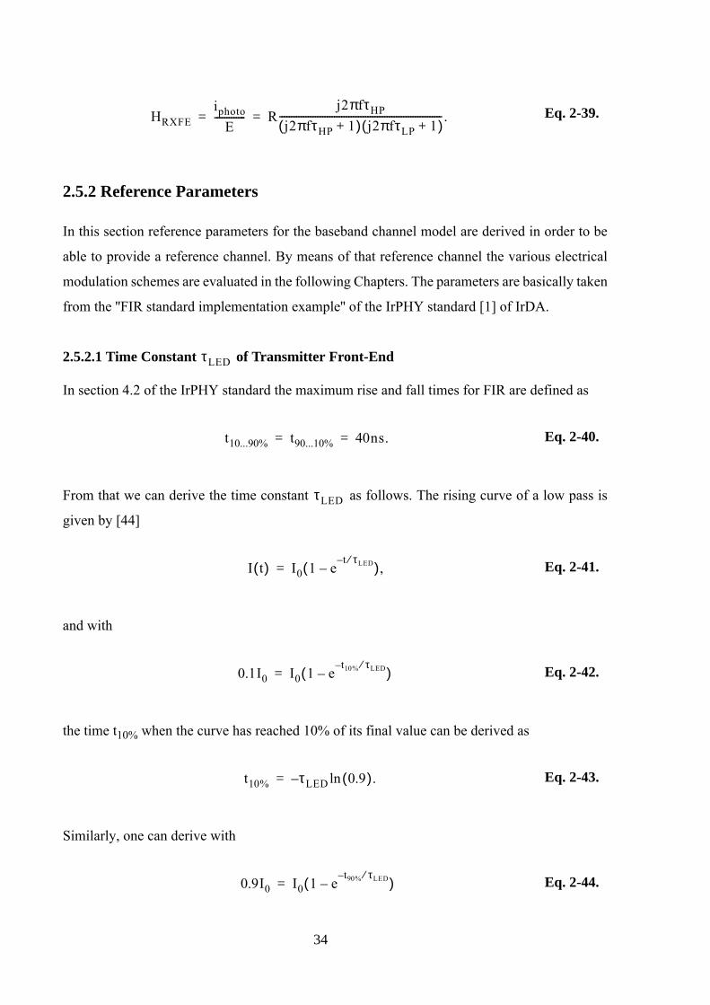
HRXFEiphoto
E------------- R
j2πfτHPj2πfτHP 1+( ) j2πfτLP 1+( )
-------------------------------------------------------------------- .= =
2.5.2 Reference Parameters
In this section reference parameters for the baseband channel model are derived in order to be
able to provide a reference channel. By means of that reference channel the various electrical
modulation schemes are evaluated in the following Chapters. The parameters are basically taken
from the ''FIR standard implementation example'' of the IrPHY standard [1] of IrDA.
2.5.2.1 Time Constant τLED of Transmitter Front-End
In section 4.2 of the IrPHY standard the maximum rise and fall times for FIR are defined as
t10...90% t90...10% 40ns.= = Eq. 2-40.
From that we can derive the time constant τLED as follows. The rising curve of a low pass is
given by [44]
I t( ) I0 1 et– τLED⁄
–( ),= Eq. 2-41.
and with
0.1I0 I0 1 et10%– τLED⁄
–( )= Eq. 2-42.
the time t10% when the curve has reached 10% of its final value can be derived as
t10% τLED 0.9( ).ln–= Eq. 2-43.
Similarly, one can derive with
0.9I0 I0 1 et90%– τLED⁄
–( )= Eq. 2-44.
Eq. 2-39.
34
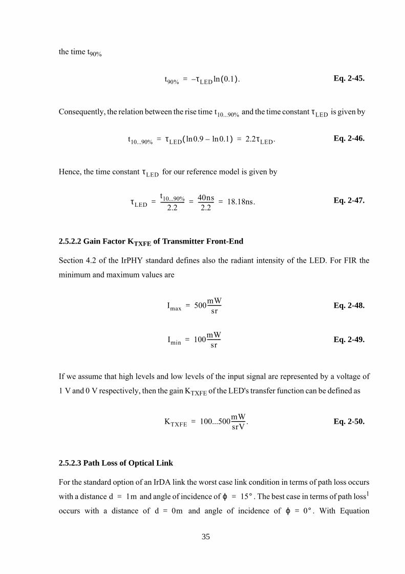
the time t90%
t90% τLED 0.1( ).ln–= Eq. 2-45.
Consequently, the relation between the rise time t10...90% and the time constant τLED is given by
t10...90% τLED 0.9ln 0.1ln–( ) 2.2τLED.= = Eq. 2-46.
Hence, the time constant τLED for our reference model is given by
τLEDt10...90%
2.2------------------ 40ns
2.2------------ 18.18ns.= = = Eq. 2-47.
2.5.2.2 Gain Factor KTXFE of Transmitter Front-End
Section 4.2 of the IrPHY standard defines also the radiant intensity of the LED. For FIR the
minimum and maximum values are
Imax 500mWsr
----------= Eq. 2-48.
Imin 100mWsr
----------= Eq. 2-49.
If we assume that high levels and low levels of the input signal are represented by a voltage of
1 V and 0 V respectively, then the gain KTXFE of the LED's transfer function can be defined as
KTXFE 100...500mWsrV---------- .= Eq. 2-50.
2.5.2.3 Path Loss of Optical Link
For the standard option of an IrDA link the worst case link condition in terms of path loss occurs
with a distance d 1m= and angle of incidence of ϕ 15°= . The best case in terms of path loss1
occurs with a distance of d 0m= and angle of incidence of ϕ 0°= . With Equation
35
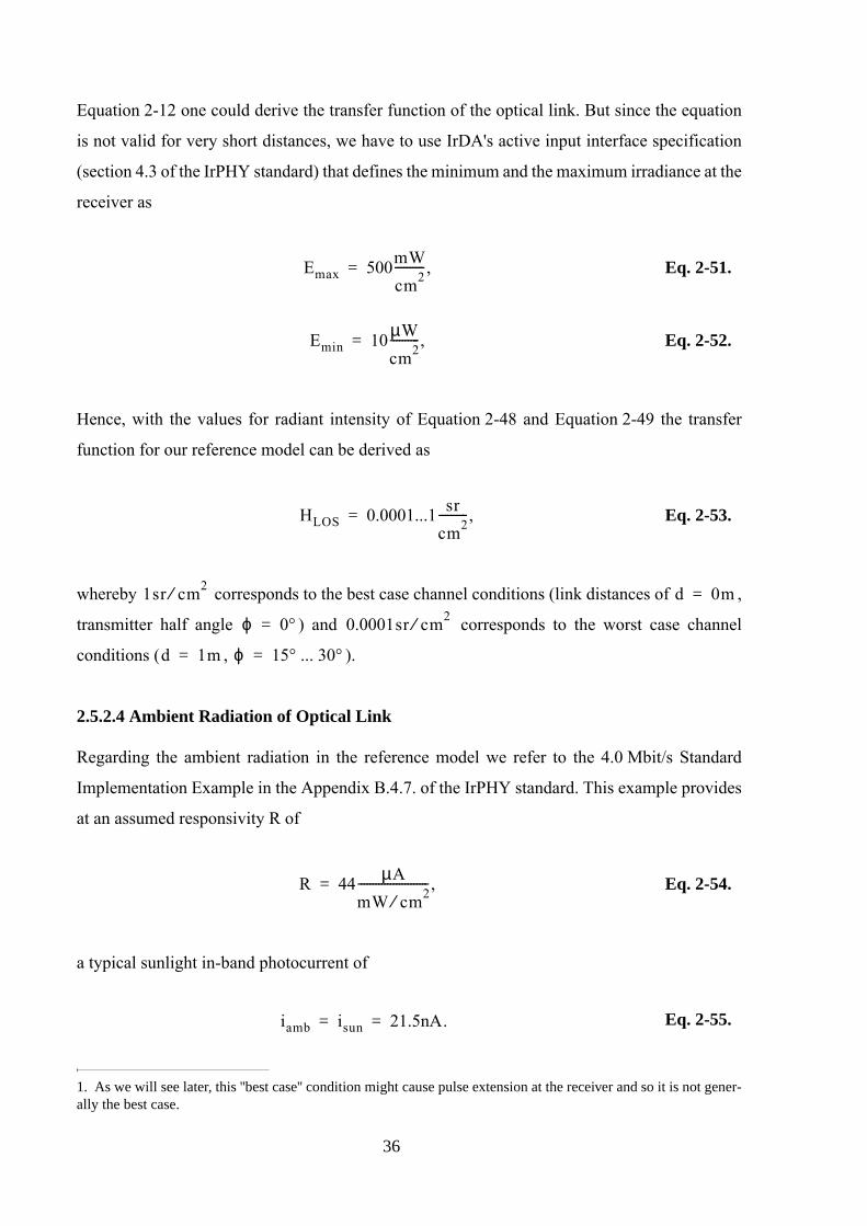
Equation 2-12 one could derive the transfer function of the optical link. But since the equation
is not valid for very short distances, we have to use IrDA's active input interface specification
(section 4.3 of the IrPHY standard) that defines the minimum and the maximum irradiance at the
receiver as
Emax 500mWcm2---------- ,= Eq. 2-51.
Emin 10 µWcm2---------- ,= Eq. 2-52.
Hence, with the values for radiant intensity of Equation 2-48 and Equation 2-49 the transfer
function for our reference model can be derived as
HLOS 0.0001...1 srcm2---------- ,= Eq. 2-53.
whereby 1sr cm2⁄ corresponds to the best case channel conditions (link distances of d 0m= ,
transmitter half angle ϕ 0°= ) and 0.0001sr cm2⁄ corresponds to the worst case channel
conditions (d 1m= , ϕ 15° ... 30°= ).
2.5.2.4 Ambient Radiation of Optical Link
Regarding the ambient radiation in the reference model we refer to the 4.0 Mbit/s Standard
Implementation Example in the Appendix B.4.7. of the IrPHY standard. This example provides
at an assumed responsivity R of
R 44 µAmW c⁄ m2------------------------ ,= Eq. 2-54.
a typical sunlight in-band photocurrent of
iamb isun 21.5nA.= = Eq. 2-55.
1. As we will see later, this ''best case'' condition might cause pulse extension at the receiver and so it is not gener-ally the best case.
36
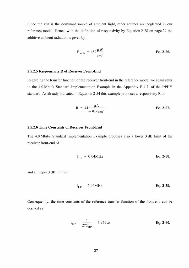
Since the sun is the dominant source of ambient light, other sources are neglected in our
reference model. Hence, with the definition of responsivity by Equation 2-28 on page 29 the
additive ambient radiation is given by
Eamb 489 µWcm2---------- .= Eq. 2-56.
2.5.2.5 Responsivity R of Receiver Front-End
Regarding the transfer function of the receiver front-end in the reference model we again refer
to the 4.0 Mbit/s Standard Implementation Example in the Appendix B.4.7. of the IrPHY
standard. As already indicated in Equation 2-54 this example proposes a responsivity R of
R 44 µAmW c⁄ m2------------------------ .= Eq. 2-57.
2.5.2.6 Time Constants of Receiver Front-End
The 4.0 Mbit/s Standard Implementation Example proposes also a lower 3 dB limit of the
receiver front-end of
fHP 0.04MHz= Eq. 2-58.
and an upper 3 dB limit of
fLP 6.04MHz.= Eq. 2-59.
Consequently, the time constants of the reference transfer function of the front-end can be
derived as
τHP1
2πfHP--------------- 3.979µs= = Eq. 2-60.
37
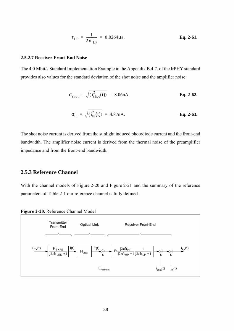
τLP1
2πfLP-------------- 0.0264µs.= =
2.5.2.7 Receiver Front-End Noise
The 4.0 Mbit/s Standard Implementation Example in the Appendix B.4.7. of the IrPHY standard
provides also values for the standard deviation of the shot noise and the amplifier noise:
σshot ishot2 t( )⟨ ⟩ 8.06nA= = Eq. 2-62.
σth ith2 t( )⟨ ⟩ 4.87nA.= = Eq. 2-63.
The shot noise current is derived from the sunlight induced photodiode current and the front-end
bandwidth. The amplifier noise current is derived from the thermal noise of the preamplifier
impedance and from the front-end bandwidth.
2.5.3 Reference Channel
With the channel models of Figure 2-20 and Figure 2-21 and the summary of the reference
parameters of Table 2-1 our reference channel is fully defined.
Figure 2-20. Reference Channel Model
TransmitterFront-End Optical Link Receiver Front-End
EAmbient
+HLOS
I(t) E(t)uTX(t)12
112
2+τπ+τπ
τπ
LPHP
HPfjfj
fjR12 +τπ LED
TXFEfjK
ishot(t)
++
ith(t)
iRX(t)
Eq. 2-61.
38
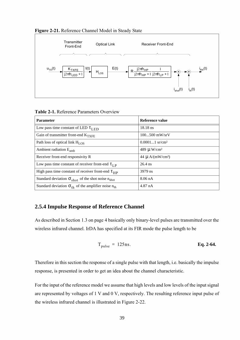
Figure 2-21. Reference Channel Model in Steady State
TransmitterFront-End Optical Link Receiver Front-End
ishot(t)
HLOS ++
ith(t)
I(t) E(t) iRX(t)uTX(t)12
112
2+τπ+τπ
τπ
LPHP
HPfjfj
fjR12 +τπ LED
TXFEfjK
Table 2-1. Reference Parameters Overview
Parameter Reference value
Low pass time constant of LED τLED 18.18 ns
Gain of transmitter front-end KTXFE 100...500 mW/srV
Path loss of optical link HLOS 0.0001...1 sr/cm²
Ambient radiation Eamb 489 µ W/cm²
Receiver front-end responsivity R 44 µ A/(mW/cm²)
Low pass time constant of receiver front-end τLP 26.4 ns
High pass time constant of receiver front-end τHP 3979 ns
Standard deviation σshot of the shot noise nshot 8.06 nA
Standard deviation σth of the amplifier noise nth 4.87 nA
2.5.4 Impulse Response of Reference Channel
As described in Section 1.3 on page 4 basically only binary-level pulses are transmitted over the
wireless infrared channel. IrDA has specified at its FIR mode the pulse length to be
Tpulse 125ns.= Eq. 2-64.
Therefore in this section the response of a single pulse with that length, i.e. basically the impulse
response, is presented in order to get an idea about the channel characteristic.
For the input of the reference model we assume that high levels and low levels of the input signal
are represented by voltages of 1 V and 0 V, respectively. The resulting reference input pulse of
the wireless infrared channel is illustrated in Figure 2-22.
39
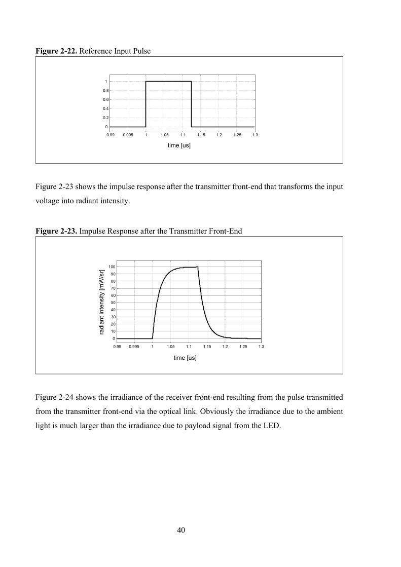
Figure 2-22. Reference Input Pulse
time [us]
0
0.2
0.4
0.6
0.8
1
0.995 1 1.05 1.1 1.15 1.2 1.25 1.30.99
Figure 2-23 shows the impulse response after the transmitter front-end that transforms the input
voltage into radiant intensity.
Figure 2-23. Impulse Response after the Transmitter Front-End
time [us]
0.995 1 1.05 1.1 1.15 1.2 1.25 1.3
0
10
20
30
40
50
60
70
80
90
100
radi
ant i
nten
sity
[mW
/sr]
0.99
Figure 2-24 shows the irradiance of the receiver front-end resulting from the pulse transmitted
from the transmitter front-end via the optical link. Obviously the irradiance due to the ambient
light is much larger than the irradiance due to payload signal from the LED.
40
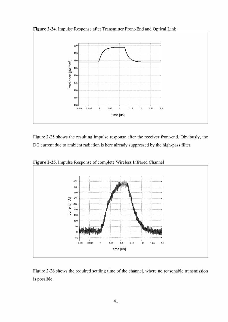
Figure 2-24. Impulse Response after Transmitter Front-End and Optical Link
460
465
470
475
480
485
490
495
500
time [us]
0.995 1 1.05 1.1 1.15 1.2 1.25 1.30.99
irrad
ianc
e [µ
W/c
m2 ]
Figure 2-25 shows the resulting impulse response after the receiver front-end. Obviously, the
DC current due to ambient radiation is here already suppressed by the high-pass filter.
Figure 2-25. Impulse Response of complete Wireless Infrared Channel
time [us]
curr
ent [
nA]
0.995 1 1.05 1.1 1.15 1.2 1.25 1.30.99
-50
0
50
100
150
200
250
300
350
400
450
Figure 2-26 shows the required settling time of the channel, where no reasonable transmission
is possible.
41
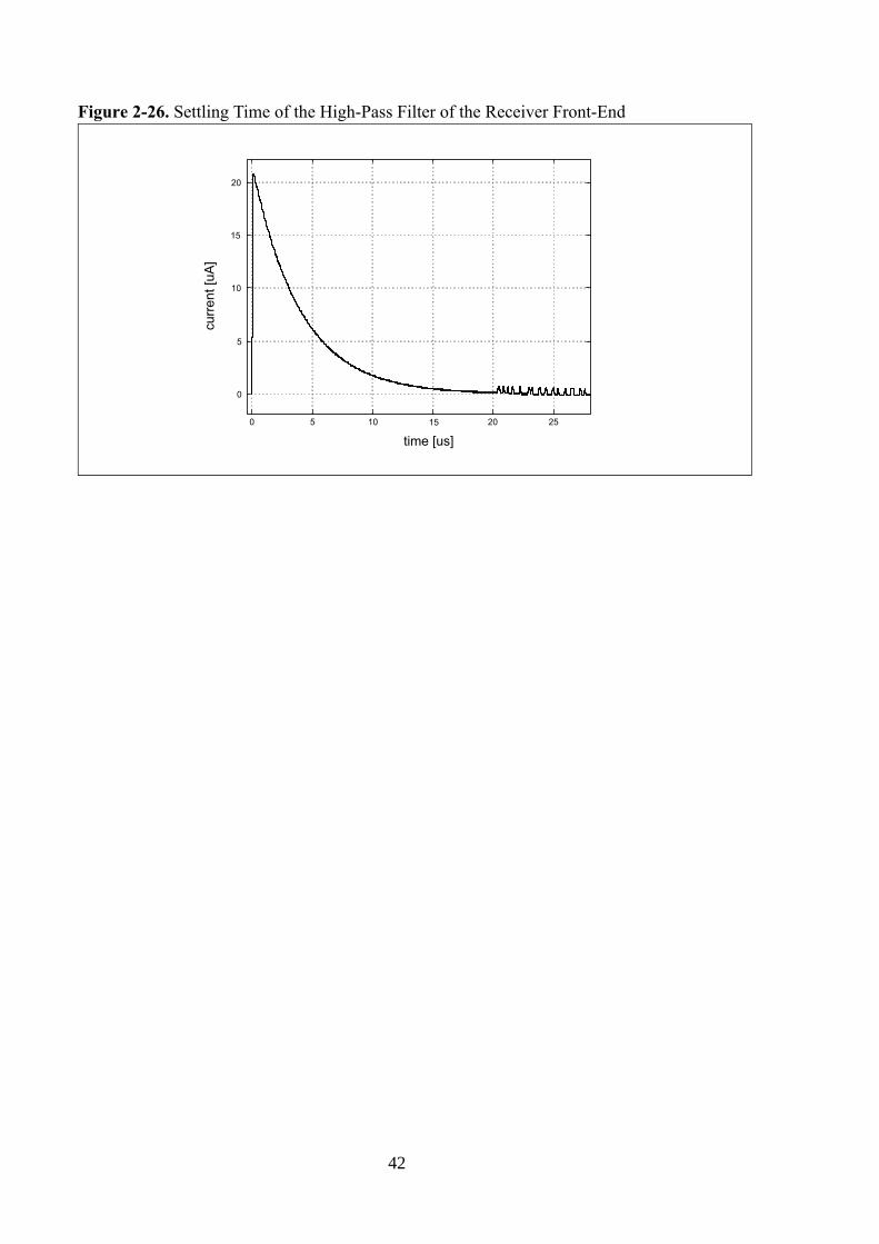
Figure 2-26. Settling Time of the High-Pass Filter of the Receiver Front-End
curre
nt [u
A]
0 5 10 15 20 25
0
5
10
15
20
time [us]
42
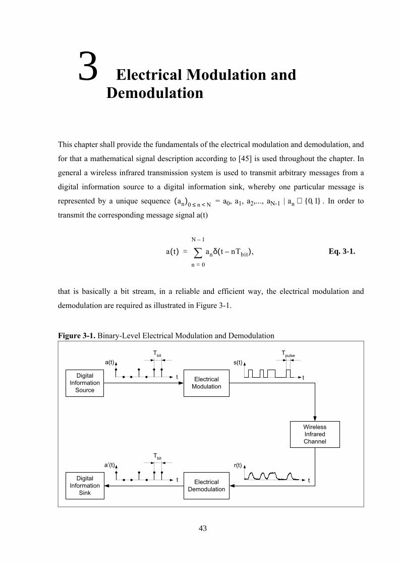
3 Electrical Modulation and Demodulation
This chapter shall provide the fundamentals of the electrical modulation and demodulation, and
for that a mathematical signal description according to [45] is used throughout the chapter. In
general a wireless infrared transmission system is used to transmit arbitrary messages from a
digital information source to a digital information sink, whereby one particular message is
represented by a unique sequence an( )0 n N<≤ = a0, a1, a2,..., aN-1 | an 0 1 , .∈ In order to
transmit the corresponding message signal a(t)
a t( ) anδ t nTbit–( ),n 0=
N 1–
∑= Eq. 3-1.
that is basically a bit stream, in a reliable and efficient way, the electrical modulation and
demodulation are required as illustrated in Figure 3-1.
Figure 3-1. Binary-Level Electrical Modulation and Demodulation
ElectricalModulation
DigitalInformation
Source
DigitalInformation
Sink
ElectricalDemodulation
WirelessInfraredChannel
s(t)
t
r(t)
t
a(t)
t
a’(t)
t
Tbit
Tbit
Tpulse
43
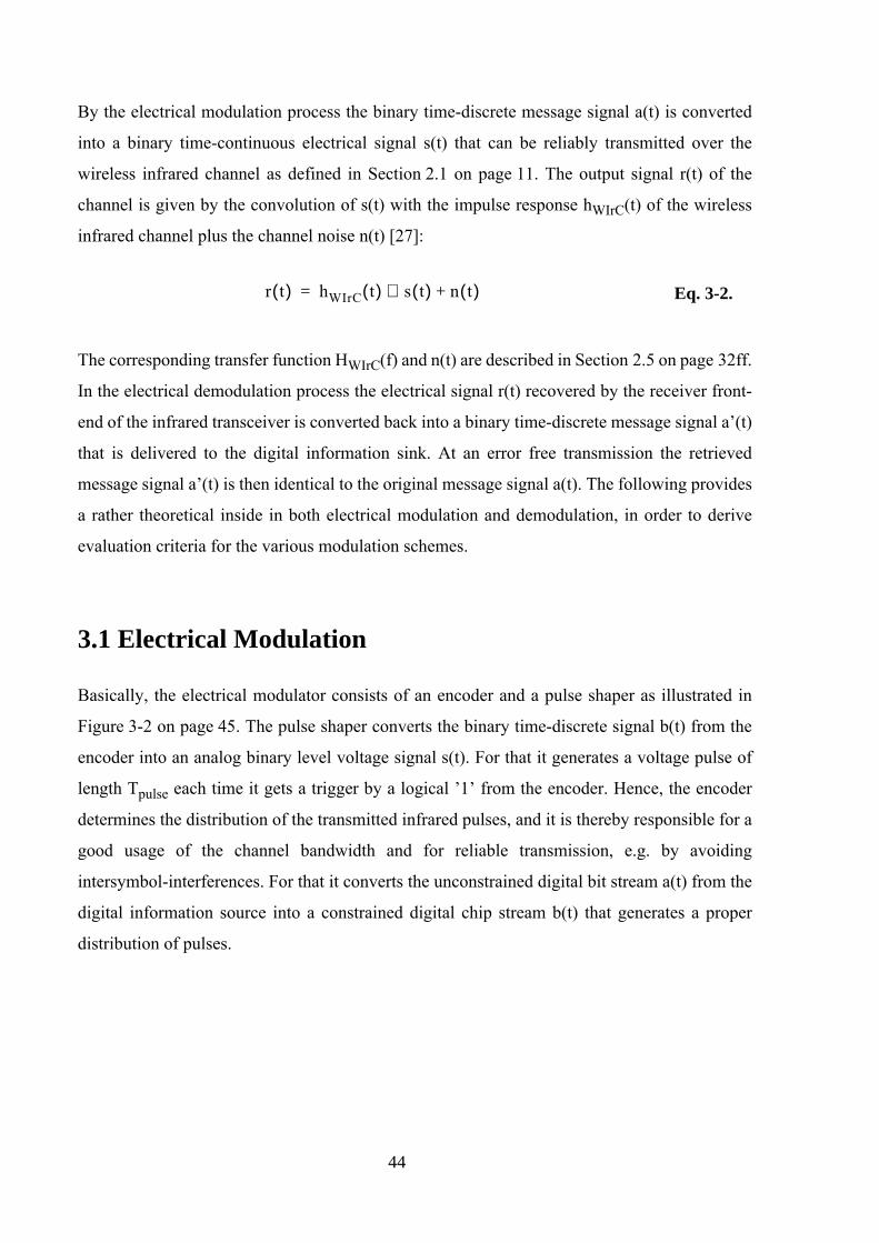
By the electrical modulation process the binary time-discrete message signal a(t) is converted
into a binary time-continuous electrical signal s(t) that can be reliably transmitted over the
wireless infrared channel as defined in Section 2.1 on page 11. The output signal r(t) of the
channel is given by the convolution of s(t) with the impulse response hWIrC(t) of the wireless
infrared channel plus the channel noise n(t) [27]:
r t( ) hWIrC t( ) s t( ) n t( )+⊗= Eq. 3-2.
The corresponding transfer function HWIrC(f) and n(t) are described in Section 2.5 on page 32ff.
In the electrical demodulation process the electrical signal r(t) recovered by the receiver front-
end of the infrared transceiver is converted back into a binary time-discrete message signal a’(t)
that is delivered to the digital information sink. At an error free transmission the retrieved
message signal a’(t) is then identical to the original message signal a(t). The following provides
a rather theoretical inside in both electrical modulation and demodulation, in order to derive
evaluation criteria for the various modulation schemes.
3.1 Electrical Modulation
Basically, the electrical modulator consists of an encoder and a pulse shaper as illustrated in
Figure 3-2 on page 45. The pulse shaper converts the binary time-discrete signal b(t) from the
encoder into an analog binary level voltage signal s(t). For that it generates a voltage pulse of
length Tpulse each time it gets a trigger by a logical ’1’ from the encoder. Hence, the encoder
determines the distribution of the transmitted infrared pulses, and it is thereby responsible for a
good usage of the channel bandwidth and for reliable transmission, e.g. by avoiding
intersymbol-interferences. For that it converts the unconstrained digital bit stream a(t) from the
digital information source into a constrained digital chip stream b(t) that generates a proper
distribution of pulses.
44
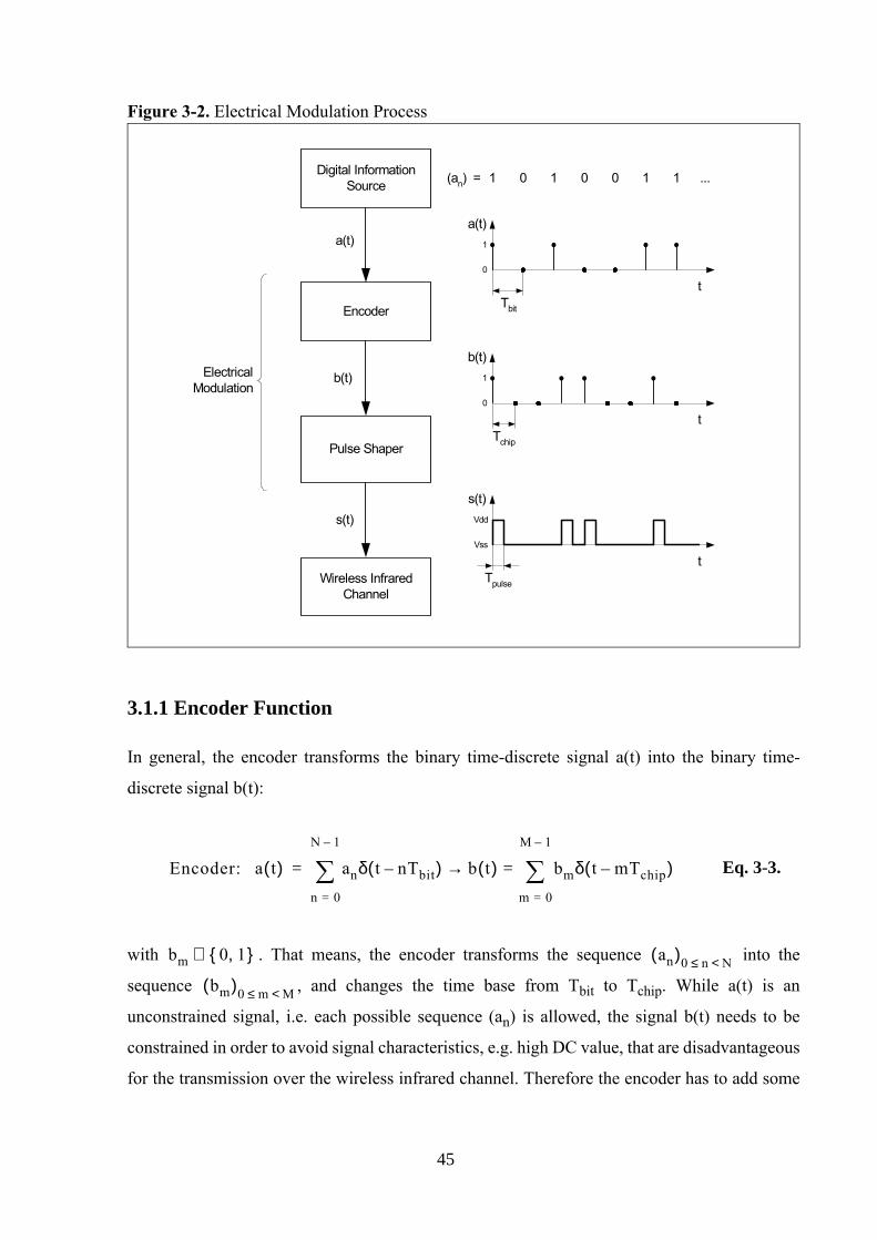
Figure 3-2. Electrical Modulation Process
Encoder
Pulse Shaper
s(t)
0
1
tTchip
Digital InformationSource
a(t)
0
1
tTbit
b(t)
Vss
Vdd
tTpulse
s(t)
ElectricalModulation
a(t)
b(t)
Wireless InfraredChannel
0 1 0 0 1 11(an) = ...
3.1.1 Encoder Function
In general, the encoder transforms the binary time-discrete signal a(t) into the binary time-
discrete signal b(t):
Encoder: a t( ) anδ t nTbit–( ) b t( ) bmδ t mTchip–( )m 0=
M 1–
∑=→n 0=
N 1–
∑= Eq. 3-3.
with bm 0 1, ∈ . That means, the encoder transforms the sequence an( )0 n N<≤ into the
sequence bm( )0 m M<≤ , and changes the time base from Tbit to Tchip. While a(t) is an
unconstrained signal, i.e. each possible sequence (an) is allowed, the signal b(t) needs to be
constrained in order to avoid signal characteristics, e.g. high DC value, that are disadvantageous
for the transmission over the wireless infrared channel. Therefore the encoder has to add some
45
redundancy to the chip stream b(t), so that M > N and consequently Tchip < Tbit. With the code
rate Rcode that is given by
RcodeNM-----= Eq. 3-4.
the time base Tchip of the encoded chip stream b(t) is obviously given by
Tchip RcodeTbit.= Eq. 3-5.
The transformation of (an) to (bm) is done by the encoder map
encoder map: an( ) a0 a1 ..., aN 1–, , bm( )→ b0 b1 ..., bM 1– ,, ,= = Eq. 3-6.
which could be implemented by a look up table that provides for each arbitrary sequence (an) a
unique sequence (bm). But this straightforward implementation would require look-up tables of
unacceptable large sizes, if the input sequences were comparatively long. Therefore usually
encoding algorithms are used instead. For that the sequence (an) is split up into blocks αk with
the length p:
an( ) α0 α1 ..., αN p⁄ 1–, ,= Eq. 3-7.
αk apk apk 1+ ..., apk p 1–+ ,, ,= Eq. 3-8.
and the sequence (bm) is split up into blocks βk with the length q:
bm( ) β0 β1 ..., βM q 1–⁄, ,= Eq. 3-9.
βk bqk bqk 1+ ..., bqk q 1–+ ., ,= Eq. 3-10.
46
With that any output block βk can be derived from a limited number of input blocks by means
of a finite state machine:
βk f αk i– ... αk j+ ζk, , ,( )= Eq. 3-11.
ζk 1+ g αk i– ... αk j+ ζk, , ,( ),= Eq. 3-12.
where ζk denotes the internal state of the encoder. The parameters i and j, called memory and
anticipation, define the number of required input blocks. The function f is called the output
function and g the next state function. The block lengths p and q defines obviously the code rate
of an encoder that is based on a finite state machine:
RcodeNM----- p
q---= = Eq. 3-13.
and with Equation 3-5 on page 46 the chip duration is then given by
Tchip Tbitpq--- .= Eq. 3-14.
3.1.2 Pulse Shaper Function
At the pulse shaper, the second step of the electrical modulation, the encoded sequence b(t) is
convoluted with ps(t) that defines the shape of the transmitted pulses.
s t( ) b t( ) ps t( )⊗=
bmδ t mTchip–( ) ps t( )⊗m 0=
M 1–
∑=
bmps t mTchip–( )m 0=
M 1–
∑=
Eq. 3-15.
47
In our case we have rectangular pulses that are transmitted via the wireless infrared channel and
thus ps(t) is given by
ps t( ) rect tTpulse-------------- 1
2---–
,= Eq. 3-16.
so that the resulting output s(t) of the pulse shaper can be derived as
s t( ) bmrm 0=
M 1–
∑ ectt mTchip–
Tpulse------------------------- 1
2---–
.= Eq. 3-17.
Note that the pulse duration Tpulse is determined by the bandwidth B of the wireless infrared
channel, i.e. of the infrared transceiver
Tpulse1B---- .= Eq. 3-18.
3.2 Electrical Demodulation
Basically, the electrical demodulator consists of a quantization unit, a sampling unit and a
decoder as illustrated in Figure 3-3. With Equation 3-2 and Equation 3-17 the input signal r(t)
of the demodulator is given by
r t( ) hWIrC t( ) bmrm 0=
M 1–
∑ ectt mTchip–
Tpulse------------------------- 1
2---–
n t( )+⊗= Eq. 3-19.
bm
m 0=
M 1–
∑= hWIrC t( ) rectt mTchip–
Tpulse------------------------- 1
2---–
⊗ n t( ).+ Eq. 3-20.
48
If we introduce pd(t) as the convolution of the rectangular pulse ps(t) with the channel impulse
response hWIrC(t):
pd t( ) hWIrC t( ) rect tTpulse-------------- 1
2---–
,⊗= Eq. 3-21.
then r(t) can also be written down as
r t( ) bmpd t mTchip–( )m 0=
M 1–
∑ n t( ).+= Eq. 3-22.
That means r(t) is basically a sequence of distorted pulses pd(t) that originate from the
transmitted rectangular pulses ps(t).
The binary level quantization circuitry transforms r(t) into a binary level signal rb(t), whereby
the pulses pd(t) should result in a logical level of ’1’. The sampling unit transforms the binary
level signal rb(t), which is still time-continuous, into a time-discrete signal b’(t). After that the
decoder converts b’(t) finally into the bit stream a’(t).
3.2.1 Quantization
The quantization unit is basically a comparator that compares the output signal r(t) of the front-
end circuitry with a certain threshold value. If r(t) is below the threshold value, then the output
of the quantization unit has the logical value ’0’, otherwise it has the logical value ’1’. Usually
the quantization unit has a hysteresis in order to be not sensitive to the noise current. Hence, the
quantization unit has obviously a non-linear transfer function as illustrated in Figure 3-4.
49
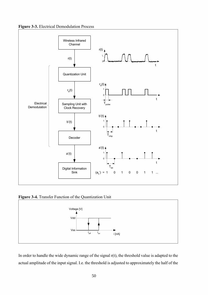
Figure 3-3. Electrical Demodulation Process
Decoder
Digital InformationSink
rb(t)
0
1
tTchip
Sampling Unit withClock Recovery
b’(t)
0
1
tTbit
a’(t)
0
1
tTpulse
rb(t)
ElectricalDemodulation
a’(t)
b’(t)
Quantization Unit
0 1 0 0 1 11(an’) = ...
r(t)
Wireless InfraredChannel
0
i1
t
r(t)
Figure 3-4. Transfer Function of the Quantization Unit
i [nA]
Voltage [V]
Vdd
Vssioff ion
In order to handle the wide dynamic range of the signal r(t), the threshold value is adapted to the
actual amplitude of the input signal. I.e. the threshold is adjusted to approximately the half of the
50
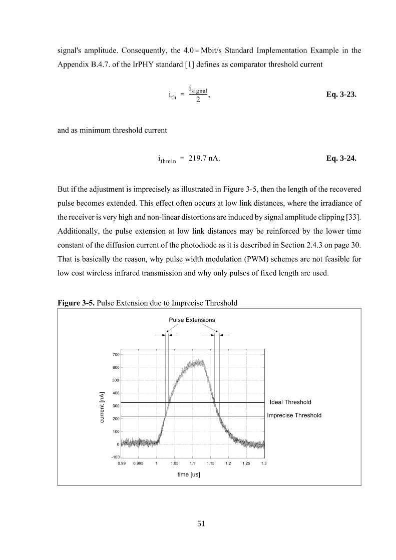
signal's amplitude. Consequently, the 4.0 = Mbit/s Standard Implementation Example in the
Appendix B.4.7. of the IrPHY standard [1] defines as comparator threshold current
ithisignal
2------------- ,= Eq. 3-23.
and as minimum threshold current
ithmin 219.7 nA.= Eq. 3-24.
But if the adjustment is imprecisely as illustrated in Figure 3-5, then the length of the recovered
pulse becomes extended. This effect often occurs at low link distances, where the irradiance of
the receiver is very high and non-linear distortions are induced by signal amplitude clipping [33].
Additionally, the pulse extension at low link distances may be reinforced by the lower time
constant of the diffusion current of the photodiode as it is described in Section 2.4.3 on page 30.
That is basically the reason, why pulse width modulation (PWM) schemes are not feasible for
low cost wireless infrared transmission and why only pulses of fixed length are used.
Figure 3-5. Pulse Extension due to Imprecise Threshold
-100
0
100
200
300
400
500
600
700
time [us]
0.995 1 1.05 1.1 1.15 1.2 1.25 1.30.99
curr
ent [
nA]
Ideal Threshold
Imprecise Threshold
Pulse Extensions
51
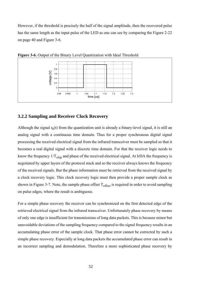
However, if the threshold is precisely the half of the signal amplitude, then the recovered pulse
has the same length as the input pulse of the LED as one can see by comparing the Figure 2-22
on page 40 and Figure 3-6.
Figure 3-6. Output of the Binary Level Quantization with Ideal Threshold
time [us]
volta
ge [V
]
0.995 1 1.05 1.1 1.15 1.2 1.25 1.30.99
0
0.2
0.4
0.6
0.8
1
3.2.2 Sampling and Receiver Clock Recovery
Although the signal rb(t) from the quantization unit is already a binary-level signal, it is still an
analog signal with a continuous time domain. Thus for a proper synchronous digital signal
processing the received electrical signal from the infrared transceiver must be sampled so that it
becomes a real digital signal with a discrete time domain. For that the receiver logic needs to
know the frequency 1/Tchip and phase of the received electrical signal. At IrDA the frequency is
negotiated by upper layers of the protocol stack and so the receiver always knows the frequency
of the received signals. But the phase information must be retrieved from the received signal by
a clock recovery logic. This clock recovery logic must then provide a proper sample clock as
shown in Figure 3-7. Note, the sample phase offset Toffset is required in order to avoid sampling
on pulse edges, where the result is ambiguous.
For a simple phase recovery the receiver can be synchronized on the first detected edge of the
retrieved electrical signal from the infrared transceiver. Unfortunately phase recovery by means
of only one edge is insufficient for transmissions of long data packets. This is because minor but
unavoidable deviations of the sampling frequency compared to the signal frequency results in an
accumulating phase error of the sample clock. That phase error cannot be corrected by such a
simple phase recovery. Especially at long data packets the accumulated phase error can result in
an incorrect sampling and demodulation. Therefore a more sophisticated phase recovery by
52
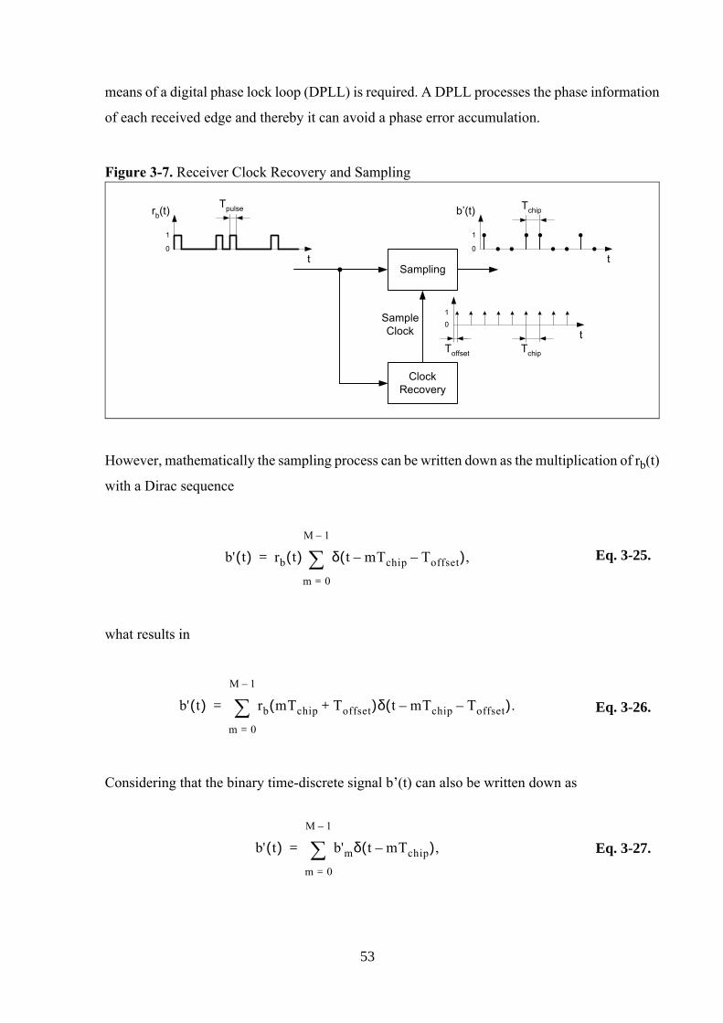
means of a digital phase lock loop (DPLL) is required. A DPLL processes the phase information
of each received edge and thereby it can avoid a phase error accumulation.
Figure 3-7. Receiver Clock Recovery and Sampling
ClockRecovery
Sampling
SampleClock
0
1
t0
1
t
Tpulse b’(t)
01
tTchip
Tchiprb(t)
Toffset
However, mathematically the sampling process can be written down as the multiplication of rb(t)
with a Dirac sequence
b' t( ) rb t( ) δm 0=
M 1–
∑ t mTchip– Toffset–( ),= Eq. 3-25.
what results in
b' t( ) rb mTchip Toffset+( )m 0=
M 1–
∑ δ t mTchip Toffset––( ).= Eq. 3-26.
Considering that the binary time-discrete signal b’(t) can also be written down as
b' t( ) b'mδ t mTchip–( ),m 0=
M 1–
∑= Eq. 3-27.
53
then the terms of the sequence (b’m) with b'm 0 1, ∈ are obviously determined by
b'm rb mTchip Toffset+( ).= Eq. 3-28.
At some modulation schemes the sampling unit can also be used for error correction. If the
sampling unit detects a pulse at a position where it is not allowed to be due to the modulation
characteristic, then it may ignore this pulse. E.g. at some modulation schemes double pulses are
not allowed, and so the sampling unit may treat any double pulse as single pulse. This is very
helpful since pulse extension due to the wireless infrared channel lead very often to unwanted
double pulses.
3.2.3 Decoder Function
The decoder has to perform the inverse transformation of the encoder. Hence, it transforms the
binary time-discrete signal b’(t) into the binary time-discrete signal a’(t):
Decoder: b' t( ) b'mδ t mTchip–( )m 0=
M 1–
∑ a' t( )→ a'nδ t nTbit–( )n 0=
N 1–
∑= = Eq. 3-29.
That means, the decoder converts the sequence bm'( )0 m M<≤ into the sequence a'n( )0 n N<≤
and changes the time base from Tchip back to Tbit:
Tbit1
Rcode-------------Tchip.= Eq. 3-30.
The transformation of (bm) to (an) is done by the decoder map
Decoder map: b'm( ) b'0 b'1 ..., b'M 1– a'n( )→, , a'0 a'1 ..., a'N 1– ,, ,= = Eq. 3-31.
which again could be implemented by a look up table that provides for each possible sequence
(b’m) a unique sequence (a’n). But this again would require look-up tables of unacceptable large
sizes. Therefore usually decoding algorithms are used instead, which also make use of the blocks
54
as defined in the Equations 3-7 to 3-10. With that any output block α 'k of the decoder can be
derived from a limited number of input blocks by means of a finite state machine with an internal
state ζk :
α'k d β'k i–... β'k j+
ζk, , ,( )= Eq. 3-32.
ζk 1+ e β'k i–... β'k j+
ζk, , ,( ),= Eq. 3-33.
whereby the memory i and the anticipation j of the decoder define the number of required input
blocks.
The decoder may have error detection capabilities, i.e. it may be able to detect blocks or a
sequence of blocks that cannot be generated by the encoder. Such an error detection is usually
not mandatory, since transmission error detection is basically done on a higher protocol layer by
CRC codes.
3.3 Evaluation Criteria for Modulation Techniques
In order to be able to evaluate the various modulation techniques and to assess the new
modulation technique EPM, this section provides some evaluation criteria. Clearly, a low bit
error rate is desirable for any transmission system, and therefore the transmission reliability is a
strong criterion for a modulation technique. Additionally, two more things needs to be
considered. On the one hand the achievable bit rate of an infrared communication is mainly
limited by the bandwidth of the infrared transceivers. Therefore it is important to use a
modulation technique with high bandwidth efficiency. And on the other hand mobile devices are
usually battery powered and therefore power efficiency is also very important for our type of
application. Hence, the following provides evaluation criteria for
• the transmission reliability,
• the bandwidth efficiency and
• the power efficiency.
55
3.3.1 Reliability
The reliability of the transmission depends on the capability of the modulation technique to
adapt the signal to the wireless infrared channel in a way that allows demodulation at the receiver
with a low bit error rate. Basically there are two different errors that can occur at the receiver:
• Quantization error
• Sample error
In the following we provide evaluation criteria for the robustness of the various modulation
schemes against quantization and sample errors.
3.3.1.1 Quantization Error Robustness
A quantization error occurs, when the transmitter sends a pulse, but the quantization unit does
not detect anything, or when the transmitter does not send anything, but the quantization unit
detects a pulse. That can happen, when the signal to noise ratio is too low, so that the
quantization unit cannot distinguish between the noise and the signal. The reason for such a
quantization error is an insufficient optical link between the transmitter and the receiver, e.g.
when the distance or the alignment between the transmitter and the receiver is out of the
specification, or when a solid object lies between the transmitter and receiver.
Assuming an ideal sampling clock, the quantized signal rb(t) must take on the correct logical
levels at least at the sampling points in time. That means the signal level of r(t) must be beyond
or beneath the threshold value at least at the sampling points, if a pulse is transmitted or not,
respectively. With Equation 3-22 the value of signal r(t) at a sampling point kTchip + Toffset is
given by
r kTchip Toffset+( ) bmpd kTchip Toffset mTchip–+( ) +
m 0=
M 1–
∑=
n+ kTchip Toffset+( ).
Eq. 3-34.
56
If the respective bk is ’1’, then r(kTchip+Toffset) is given by
r kTchip Toffset+( ) r1k n kTchip Toffset+( ).+= Eq. 3-35.
with
r1k pd Toffset( ) bmpd kTchip Toffset mTchip–+( )m 0=
k 1–
∑ + +=
bmpd kTchip Toffset mTchip–+( ).m k 1+=
M 1–
∑+
Eq. 3-36.
The corresponding probability density function p1k of the level of r(t) at the sampling point
kTchip + Toffset is under the condition of bk = ’1’given by
p1k r kTchip Toffset+( )( ) 1
2πσ2-----------------
x r1k–( )2
2σ2------------------------–
.exp⋅= Eq. 3-37.
If the respective bk of Equation 3-34 is ’0’, then r(kTchip+Toffset) is given by
r kTchip Toffset+( ) r0k n kTchip Toffset+( ).+= Eq. 3-38.
with
r0k bmpd kTchip Toffset mTchip–+( )m 0=
k 1–
∑ +=
bmpd kTchip Toffset mTchip–+( ).m k 1+=
M 1–
∑+
Eq. 3-39.
57
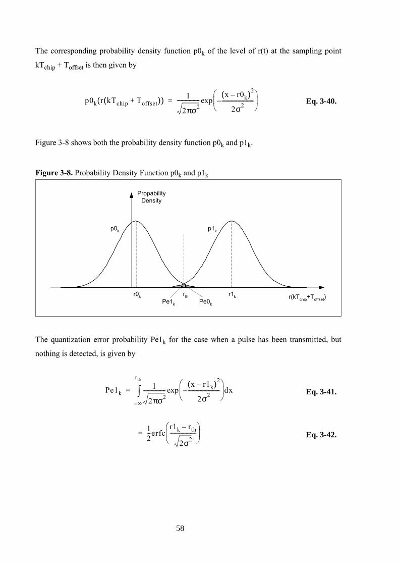
The corresponding probability density function p0k of the level of r(t) at the sampling point
kTchip + Toffset is then given by
p0k r kTchip Toffset+( )( ) 1
2πσ2-----------------
x r0k–( )2
2σ2------------------------–
exp= Eq. 3-40.
Figure 3-8 shows both the probability density function p0k and p1k.
Figure 3-8. Probability Density Function p0k and p1k
r(kTchip+Toffset)r0k rth
p0k p1k
Pe1k
r1kPe0k
PropabilityDensity
The quantization error probability Pe1k for the case when a pulse has been transmitted, but
nothing is detected, is given by
Pe1k1
2πσ2-----------------
∞–
rth
∫x r1k–( )2
2σ2------------------------–
dxexp= Eq. 3-41.
12---erfc
r1k rth–
2σ2-------------------
= Eq. 3-42.
58
The quantization error probability Pe0k for the case when no pulse has been transmitted, but a
pulse is detected, is given by
Pe0k1
2πσ2-----------------
rth
∞
∫x r0k–( )2
2σ2------------------------–
dxexp= Eq. 3-43.
12---erfc
rth r0k–
2σ2-------------------
= Eq. 3-44.
The total quantization error probability Pek obviously depends on the probability of the logical
value of bk:
Pek P bk 0=( )Pe0 P bk 1=( )Pe1+= Eq. 3-45.
P bk 0=( )2
------------------------erfcrth r0k–
2σ2------------------- P bk 1=( )
2------------------------erfc
r1k rth–
2σ2-------------------
+= Eq. 3-46.
An extremum calculation evidently shows that the threshold value
rthr1k r0k+
2----------------------= Eq. 3-47.
is a very good approximation for the ideal threshold value1. With that the total quantization error
probability Pek for a single sample can be provided as
Pek12---erfc
r1k r0k–
2 2σ2--------------------- 1
2---erfc
r1k r0k–( )2
8σ2-----------------------------
.= = Eq. 3-48.
1. Actually it is the ideal threshold value in the case of P(bk = 0) = P(bk = 1) = 0.5.
59
By introducing the signal to noise ratio (SNR)
SNRk
r1k r0k–
2---------------------
2
σ2-----------------------------= Eq. 3-49.
the total quantization error probability of a single sample can be written down as
Pek12---erfc
SNRk2
-------------- .= Eq. 3-50.
Assuming that the complete transmitted sequence is erroneous as soon as a quantization error
has been occurred at one of the M samples, then the sequence error probability due to
quantization errors is given by
Pesequence 1 1 Pek–( ).k 0=
M 1–
∑–= Eq. 3-51.
Unfortunately Pek is generally different for each sample due to varying intersymbol
interferences, and therefore it is difficult to calculate the exact quantization error probabilities
analytically. However, there is a convenient way to determine the upper limit of the quantization
error probability Pemax of a single sample by means of the eye diagram without noise
disturbance [46] as shown in Figure 3-9. By using the vertical eye opening Ever one can easily
derive the minimum signal to noise ratio
SNRmin r1min r0max–( )2
4σ2---------------------------------------------
Ever2
4σ2----------= = Eq. 3-52.
60
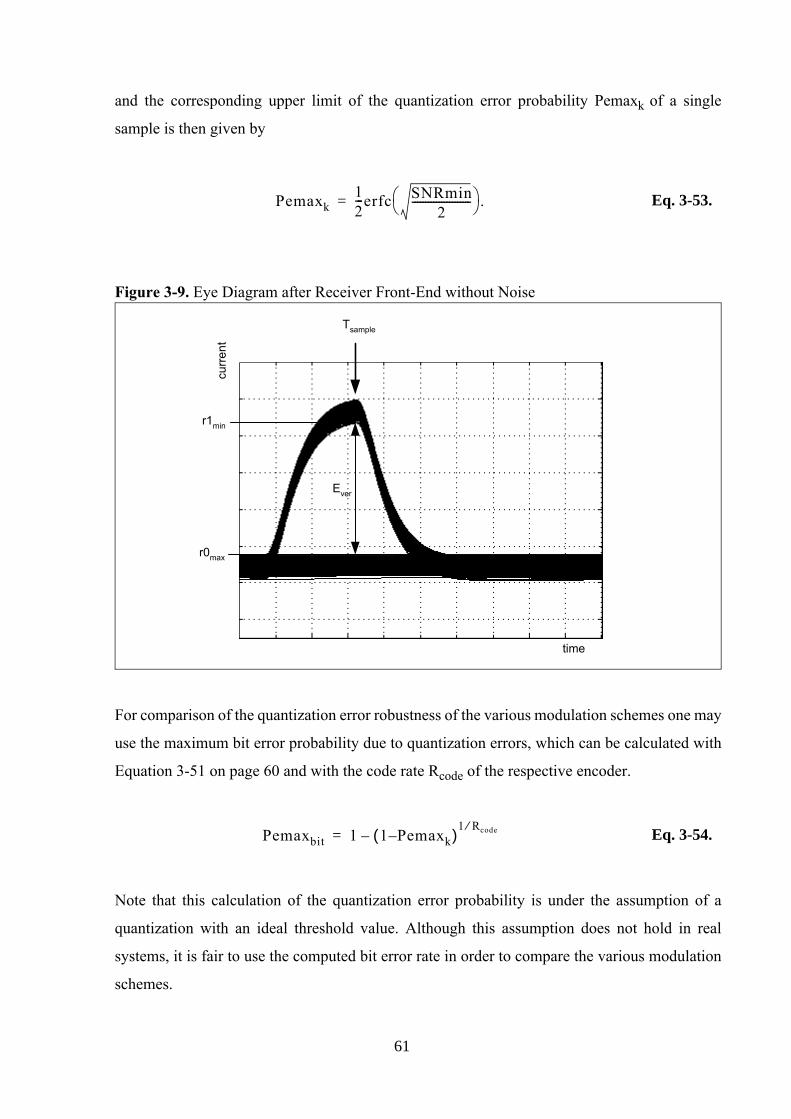
and the corresponding upper limit of the quantization error probability Pemaxk of a single
sample is then given by
Pemaxk12---erfc SNRmin
2----------------------
.= Eq. 3-53.
Figure 3-9. Eye Diagram after Receiver Front-End without Noise
time
curre
nt
r0max
r1min
Tsample
Ever
For comparison of the quantization error robustness of the various modulation schemes one may
use the maximum bit error probability due to quantization errors, which can be calculated with
Equation 3-51 on page 60 and with the code rate Rcode of the respective encoder.
Pemaxbit 1 1 P– emaxk( )–1 Rcode⁄
= Eq. 3-54.
Note that this calculation of the quantization error probability is under the assumption of a
quantization with an ideal threshold value. Although this assumption does not hold in real
systems, it is fair to use the computed bit error rate in order to compare the various modulation
schemes.
61
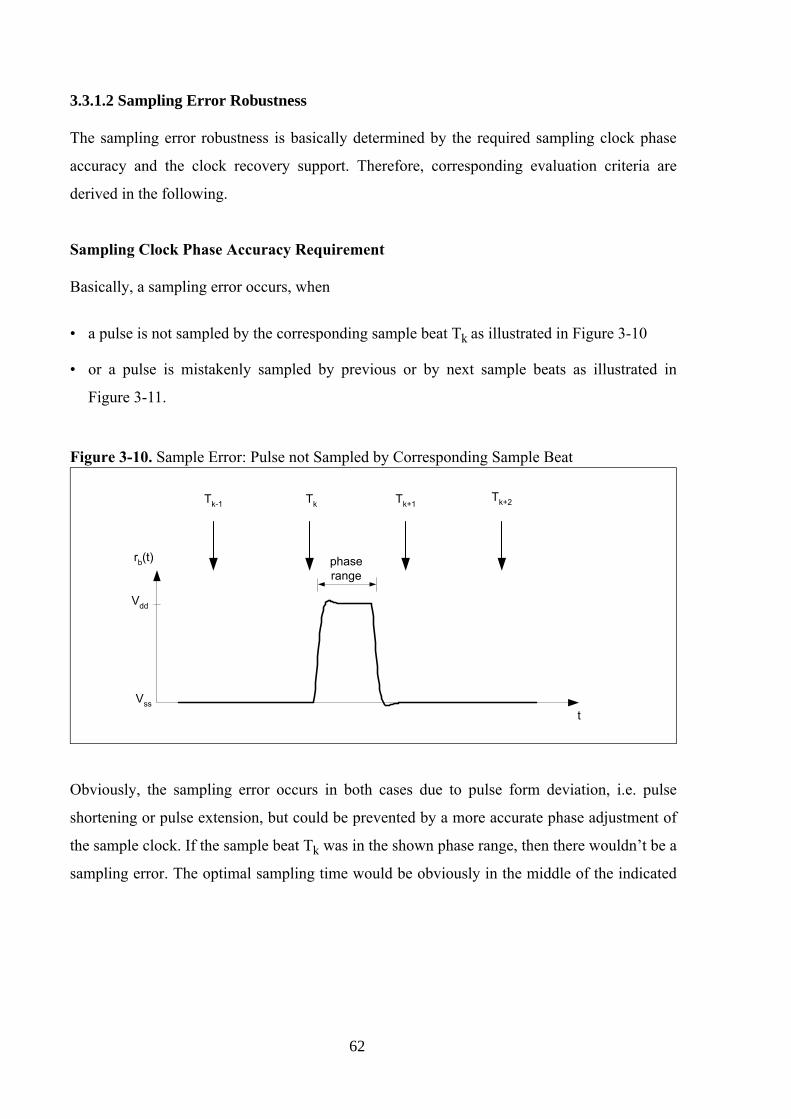
3.3.1.2 Sampling Error Robustness
The sampling error robustness is basically determined by the required sampling clock phase
accuracy and the clock recovery support. Therefore, corresponding evaluation criteria are
derived in the following.
Sampling Clock Phase Accuracy Requirement
Basically, a sampling error occurs, when
• a pulse is not sampled by the corresponding sample beat Tk as illustrated in Figure 3-10
• or a pulse is mistakenly sampled by previous or by next sample beats as illustrated in
Figure 3-11.
Figure 3-10. Sample Error: Pulse not Sampled by Corresponding Sample Beat
Tk-1 Tk Tk+1Tk+2
rb(t)
tVss
Vdd
phaserange
Obviously, the sampling error occurs in both cases due to pulse form deviation, i.e. pulse
shortening or pulse extension, but could be prevented by a more accurate phase adjustment of
the sample clock. If the sample beat Tk was in the shown phase range, then there wouldn’t be a
sampling error. The optimal sampling time would be obviously in the middle of the indicated
62
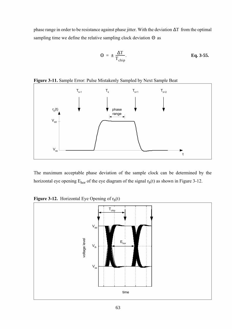
phase range in order to be resistance against phase jitter. With the deviation T∆ from the optimal
sampling time we define the relative sampling clock deviation Θ as
Θ T∆Tchip------------ .±= Eq. 3-55.
Figure 3-11. Sample Error: Pulse Mistakenly Sampled by Next Sample Beat
Tk-1 Tk Tk+1 Tk+2
rb(t)
tVss
Vdd
phaserange
The maximum acceptable phase deviation of the sample clock can be determined by the
horizontal eye opening Ehor of the eye diagram of the signal rb(t) as shown in Figure 3-12.
Figure 3-12. Horizontal Eye Opening of rb(t)
Vss
Vdd
volta
ge le
vel
time
Vth
Ehor
Tchip
63
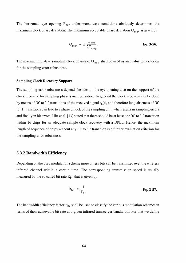
The horizontal eye opening Ehor under worst case conditions obviously determines the
maximum clock phase deviation. The maximum acceptable phase deviation Θmax is given by
Θmax Ehor
2Tchip--------------- .±= Eq. 3-56.
The maximum relative sampling clock deviation Θmax shall be used as an evaluation criterion
for the sampling error robustness.
Sampling Clock Recovery Support
The sampling error robustness depends besides on the eye opening also on the support of the
clock recovery for sampling phase synchronization. In general the clock recovery can be done
by means of ’0’ to ’1’ transitions of the received signal rb(t), and therefore long absences of ’0’
to ’1’ transitions can lead to a phase unlock of the sampling unit, what results in sampling errors
and finally in bit errors. Hirt et al. [33] stated that there should be at least one ’0’ to ’1’ transition
within 16 chips for an adequate sample clock recovery with a DPLL. Hence, the maximum
length of sequence of chips without any ’0’ to ’1’ transition is a further evaluation criterion for
the sampling error robustness.
3.3.2 Bandwidth Efficiency
Depending on the used modulation scheme more or less bits can be transmitted over the wireless
infrared channel within a certain time. The corresponding transmission speed is usually
measured by the so called bit rate Rbit that is given by
Rbit1
Tbit--------- .= Eq. 3-57.
The bandwidth efficiency factor ηB shall be used to classify the various modulation schemes in
terms of their achievable bit rate at a given infrared transceiver bandwidth. For that we define
64
the bandwidth efficiency ηB as the ratio between the achievable bit rate Rbit and the bandwidth
B of the infrared transceiver
ηBRbitB
--------- .= Eq. 3-58.
Consequently, the bandwidth efficiency ηB indicates how good a modulation scheme utilizes
the bandwidth of an infrared transceiver. Together with Equation 3-57 and Equation 3-18 on
page 48 the bandwidth efficiency ηB can be derived as the ratio between the pulse duration
Tpulse and the bit duration Tbit
ηBTpulseTbit
-------------- .= Eq. 3-59.
Note that the definition of the bandwidth efficiency of modulation schemes is very similar to the
code rate definition of channel codes (e.g. block codes, cyclic codes or RLL codes). But the code
rate indicates the added redundancy that can be used for error detection or error correction at the
receiver, while the bandwidth efficiency indicates the utilization of the bandwidth by a
modulation technique.
3.3.3 Power Efficiency
Depending on the used modulation scheme more or less energy is required to transmit a data
packet over the wireless infrared channel. The power efficiency factor ηP shall be used to
classify the various modulation schemes in terms of their power consumption. For that we define
the power efficiency ηP as the ratio between the energy per infrared pulse Epulse and the
required average energy per bit aveEbit.
ηPEpulse
aveEbit------------------= Eq. 3-60.
65
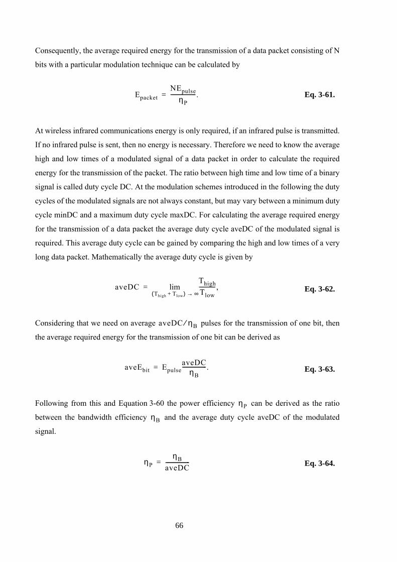
Consequently, the average required energy for the transmission of a data packet consisting of N
bits with a particular modulation technique can be calculated by
EpacketNEpulse
ηP------------------- .= Eq. 3-61.
At wireless infrared communications energy is only required, if an infrared pulse is transmitted.
If no infrared pulse is sent, then no energy is necessary. Therefore we need to know the average
high and low times of a modulated signal of a data packet in order to calculate the required
energy for the transmission of the packet. The ratio between high time and low time of a binary
signal is called duty cycle DC. At the modulation schemes introduced in the following the duty
cycles of the modulated signals are not always constant, but may vary between a minimum duty
cycle minDC and a maximum duty cycle maxDC. For calculating the average required energy
for the transmission of a data packet the average duty cycle aveDC of the modulated signal is
required. This average duty cycle can be gained by comparing the high and low times of a very
long data packet. Mathematically the average duty cycle is given by
aveDCThighTlow------------ ,
Thigh Tlow+( ) ∞→lim= Eq. 3-62.
Considering that we need on average aveDC ηB⁄ pulses for the transmission of one bit, then
the average required energy for the transmission of one bit can be derived as
aveEbit EpulseaveDC
ηB------------------ .= Eq. 3-63.
Following from this and Equation 3-60 the power efficiency ηP can be derived as the ratio
between the bandwidth efficiency ηB and the average duty cycle aveDC of the modulated
signal.
ηPηB
aveDC------------------= Eq. 3-64.
66
4 Pulse Position based Modulation Schemes
In this section we present several pulse position based modulation techniques, which are
currently used in the various wireless infrared transmission systems for mobile devices. The
descriptions are based on the detailed theoretical explanations of Chapter 3, and are therefore
rather straightforward. The various modulation techniques are assessed in terms of transmission
reliability, bandwidth efficiency and power efficiency by means of the evaluation criteria of
Section 3.3 on page 55ff. For the performed simulations a pulse length of 125 ns is used for all
modulation schemes and the reference channel derived in Section 2.5.3 on page 38 is applied.
4.1 Return to Zero Inverted
The simplest form of modulation is Return to Zero Inverted (RZI), which is determined by two
parameters n and m with n < m. Therefore n/m-RZI is a commonly used abbreviation. At n/m-
RZI a bit with the value ’0’ is represented by a pulse with a duration of
Tpulsenm----Tbit= Eq. 4-1.
and a bit with the value ’1’ is represented by the absence of a pulse. Basically, RZI with
n m⁄ 1= , which is de facto the modulation scheme Non Return to Zero Inverted (NRZI),
would have the best bandwidth efficiency, but it allows multiple consecutive pulses with no low
phase in between, so that the pulses would be suppressed by the high pass filter of the receiver.
Therefore NRZI is not feasible for our applications in terms of reliability. Consequently, IrDA
uses 3/16-RZI for bit rates up to 115.2 kbit/s and 1/4-RZI for the bit rates 576 kbit/s and
1.152 Mbit/s [1]. Therefore we will look more closely on the 1/4-RZI modulation.
67
4.1.1 1/4-RZI Modulation Scheme
In general RZI uses as encoder function the so called on-off-keying, where both the input block
αk and output block βk consist of only one term:
αk ak=Eq. 4-2.
βk bk,= Eq. 4-3.
so that the code rate is given by
pq--- 1
1--- 1,= = Eq. 4-4.
and the chip duration is equal to the bit duration
Tchip Tbit.= Eq. 4-5.
The encoder function is state independent:
βk f αk( )= Eq. 4-6.
and is given by
bk ak.= Eq. 4-7.
Basically, the pulse shaper at RZI generates pulses with a duration n/m times of the chip
duration, ergo at 1/4-RZI the pulse duration is given by
Tpulse14---Tchip.= Eq. 4-8.
Figure 4-1 provides an example for the 1/4-RZI modulation.
68
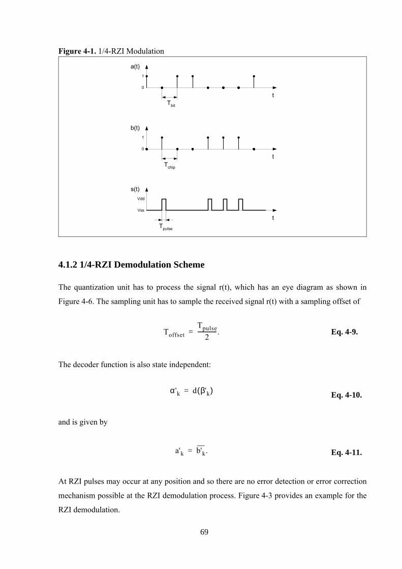
Figure 4-1. 1/4-RZI Modulation
0
1
tTchip
Tbit
Vss
Vdd
tTpulse
s(t)
a(t)
b(t)
0
1
t
4.1.2 1/4-RZI Demodulation Scheme
The quantization unit has to process the signal r(t), which has an eye diagram as shown in
Figure 4-6. The sampling unit has to sample the received signal r(t) with a sampling offset of
ToffsetTpulse
2-------------- .= Eq. 4-9.
The decoder function is also state independent:
α'k d β'k( )= Eq. 4-10.
and is given by
a'k b'k.= Eq. 4-11.
At RZI pulses may occur at any position and so there are no error detection or error correction
mechanism possible at the RZI demodulation process. Figure 4-3 provides an example for the
RZI demodulation.
69
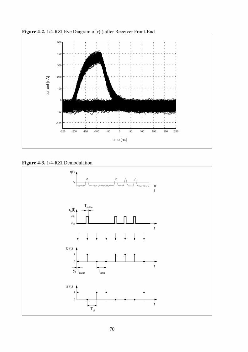
Figure 4-2. 1/4-RZI Eye Diagram of r(t) after Receiver Front-End
-250 -200 -150 -100 -50 0 50 100 150 200 250
-200
-100
0
100
200
300
400
500
time [ns]
curr
ent [
nA]
Figure 4-3. 1/4-RZI Demodulation
0
1
tTchip
Tbit
Vss
Vdd
t
Tpulserb(t)
a’(t)
b’(t)
0
1
t
½ Tpulse
t
r(t)
rth
70
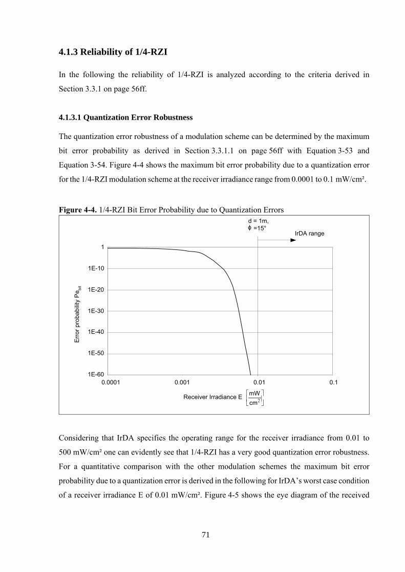
4.1.3 Reliability of 1/4-RZI
In the following the reliability of 1/4-RZI is analyzed according to the criteria derived in
Section 3.3.1 on page 56ff.
4.1.3.1 Quantization Error Robustness
The quantization error robustness of a modulation scheme can be determined by the maximum
bit error probability as derived in Section 3.3.1.1 on page 56ff with Equation 3-53 and
Equation 3-54. Figure 4-4 shows the maximum bit error probability due to a quantization error
for the 1/4-RZI modulation scheme at the receiver irradiance range from 0.0001 to 0.1 mW/cm².
Figure 4-4. 1/4-RZI Bit Error Probability due to Quantization Errors
1E-60
1E-50
1E-40
1E-30
1E-20
1E-10
1
0.0001 0.001 0.01 0.1
IrDA range
Receiver Irradiance E
Erro
r pro
babi
lity
Pe bi
t
d = 1m,=15°
2cm
mW
ϕ
Considering that IrDA specifies the operating range for the receiver irradiance from 0.01 to
500 mW/cm² one can evidently see that 1/4-RZI has a very good quantization error robustness.
For a quantitative comparison with the other modulation schemes the maximum bit error
probability due to a quantization error is derived in the following for IrDA’s worst case condition
of a receiver irradiance E of 0.01 mW/cm². Figure 4-5 shows the eye diagram of the received
71
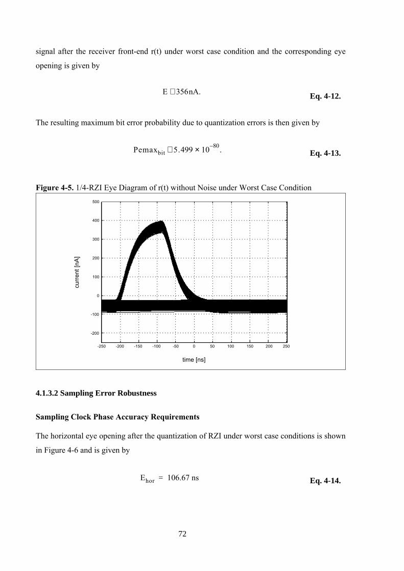
signal after the receiver front-end r(t) under worst case condition and the corresponding eye
opening is given by
E 356nA.≅ Eq. 4-12.
The resulting maximum bit error probability due to quantization errors is then given by
Pemaxbit 5.499 10× 80– .≅ Eq. 4-13.
Figure 4-5. 1/4-RZI Eye Diagram of r(t) without Noise under Worst Case Condition
-250 -200 -150 -100 -50 0 50 100 150 200 250
-200
-100
0
100
200
300
400
500
time [ns]
curr
ent [
nA]
4.1.3.2 Sampling Error Robustness
Sampling Clock Phase Accuracy Requirements
The horizontal eye opening after the quantization of RZI under worst case conditions is shown
in Figure 4-6 and is given by
Ehor 106.67 ns= Eq. 4-14.
72
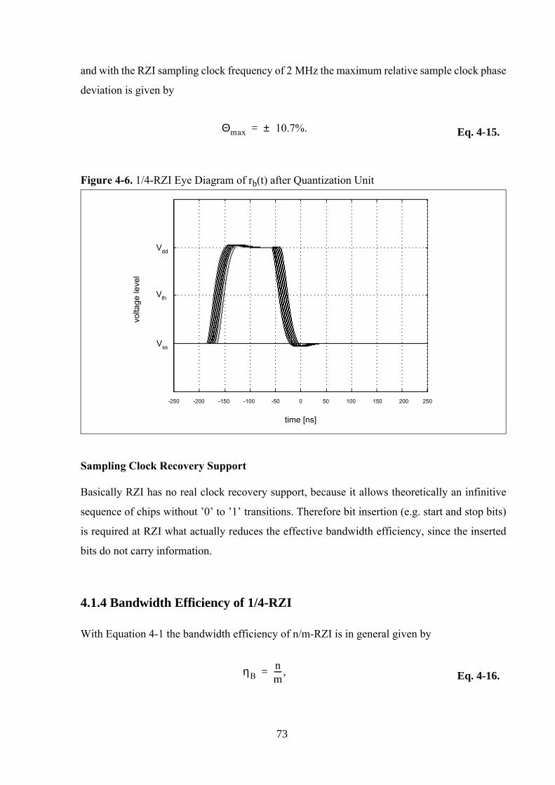
and with the RZI sampling clock frequency of 2 MHz the maximum relative sample clock phase
deviation is given by
Θmax 10.7%.±= Eq. 4-15.
Figure 4-6. 1/4-RZI Eye Diagram of rb(t) after Quantization Unit
-250 -200 -150 -100 -50 0 50 100 150 200 250
time [ns]
Vss
Vdd
volta
ge le
vel
Vth
Sampling Clock Recovery Support
Basically RZI has no real clock recovery support, because it allows theoretically an infinitive
sequence of chips without ’0’ to ’1’ transitions. Therefore bit insertion (e.g. start and stop bits)
is required at RZI what actually reduces the effective bandwidth efficiency, since the inserted
bits do not carry information.
4.1.4 Bandwidth Efficiency of 1/4-RZI
With Equation 4-1 the bandwidth efficiency of n/m-RZI is in general given by
ηBnm---- ,= Eq. 4-16.
73
and consequently the bandwidth efficiency of 1/4-RZI is then
ηB14--- .= Eq. 4-17.
The bandwidth efficiency of 1/4-RZI is obviously not very good, and as mentioned above RZI
do not support sample clock recovery at the receiver, because it allows a long low signal without
any ’0’ to ’1’ transition. The required bit stuffing further decreases the bandwidth efficiency,
since the enforced pulses carry no information.
4.1.5 Power Efficiency of 1/4-RZI
Assuming that the probability of the occurrence of bit with the logical value ’1’ is equal to the
probability of a ’0’, then the average duty cycle aveDC of n/m-RZI is generally given by
aveDC n2m--------= Eq. 4-18.
and thus the power efficiency ηP can be derived as
ηPηB
aveDC------------------
nm----
n2m---------------- 2.= = = Eq. 4-19.
4.2 N - Pulse Position Modulation
In order to overcome the shortcomings of RZI the N - Pulse Position Modulation (N-PPM)
technique has been introduced in many wireless optical applications [47]. With the N-PPM
technique information is transmitted by varying the position of a pulse within a symbol. It allows
one pulse to be set in one of the N possible positions, thus it is called N-PPM. Since data
processing is usually byte oriented, only 2-, 4-, 16- and 256-PPM are useful methods, because
they encode 1, 2, 4 and 8 bits, respectively. While in the physical layer IR PHY of the IEEE
802.11 standard [48] 4-PPM is foreseen for 2 Mbit/s operation and 16-PPM for 1 Mbit/s, IrDA
74
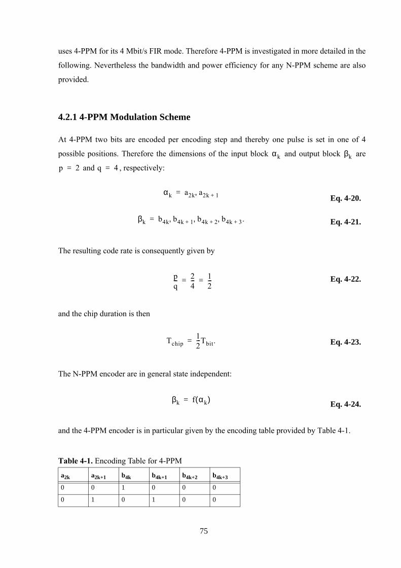
uses 4-PPM for its 4 Mbit/s FIR mode. Therefore 4-PPM is investigated in more detailed in the
following. Nevertheless the bandwidth and power efficiency for any N-PPM scheme are also
provided.
4.2.1 4-PPM Modulation Scheme
At 4-PPM two bits are encoded per encoding step and thereby one pulse is set in one of 4
possible positions. Therefore the dimensions of the input block αk and output block βk are
p 2= and q 4= , respectively:
αk a2k a2k 1+,=Eq. 4-20.
βk b4k b4k 1+ b4k 2+ b4k 3+ ., , ,= Eq. 4-21.
The resulting code rate is consequently given by
pq--- 2
4--- 1
2---= = Eq. 4-22.
and the chip duration is then
Tchip12---Tbit.= Eq. 4-23.
The N-PPM encoder are in general state independent:
βk f αk( )= Eq. 4-24.
and the 4-PPM encoder is in particular given by the encoding table provided by Table 4-1.
Table 4-1. Encoding Table for 4-PPM
a2k a2k+1 b4k b4k+1 b4k+2 b4k+3
0 0 1 0 0 0
0 1 0 1 0 0
75
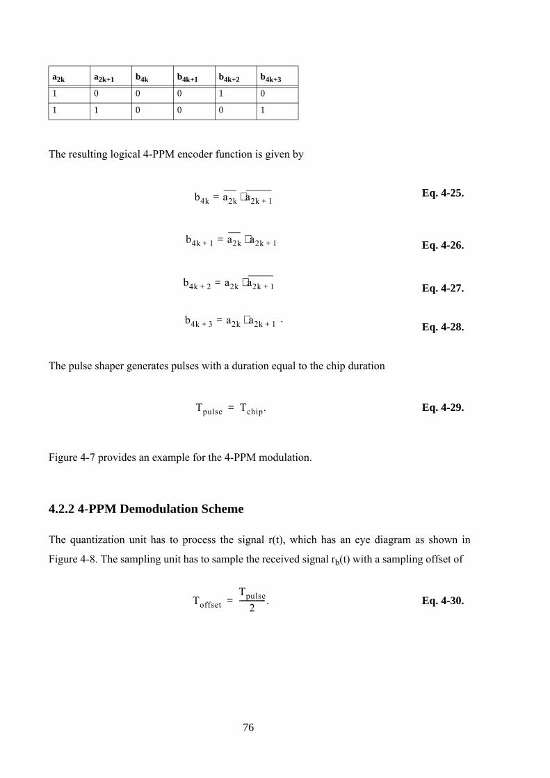
The resulting logical 4-PPM encoder function is given by
b4k a2k a2k 1+⋅= Eq. 4-25.
b4k 1+ a2k a2k 1+⋅= Eq. 4-26.
b4k 2+ a2k a2k 1+⋅= Eq. 4-27.
b4k 3+ a2k a2k 1+⋅= .Eq. 4-28.
The pulse shaper generates pulses with a duration equal to the chip duration
Tpulse Tchip.= Eq. 4-29.
Figure 4-7 provides an example for the 4-PPM modulation.
4.2.2 4-PPM Demodulation Scheme
The quantization unit has to process the signal r(t), which has an eye diagram as shown in
Figure 4-8. The sampling unit has to sample the received signal rb(t) with a sampling offset of
ToffsetTpulse
2-------------- .= Eq. 4-30.
1 0 0 0 1 0
1 1 0 0 0 1
a2k a2k+1 b4k b4k+1 b4k+2 b4k+3
76
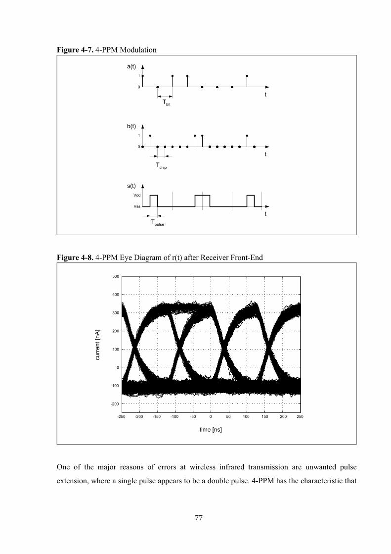
Figure 4-7. 4-PPM Modulation
0
1
t
Tchip
0
1
tTbit
Vss
Vdd
tTpulse
s(t)
a(t)
b(t)
Figure 4-8. 4-PPM Eye Diagram of r(t) after Receiver Front-End
-250 -200 -150 -100 -50 0 50 100 150 200 250
-200
-100
0
100
200
300
400
500
time [ns]
curr
ent [
nA]
One of the major reasons of errors at wireless infrared transmission are unwanted pulse
extension, where a single pulse appears to be a double pulse. 4-PPM has the characteristic that
77
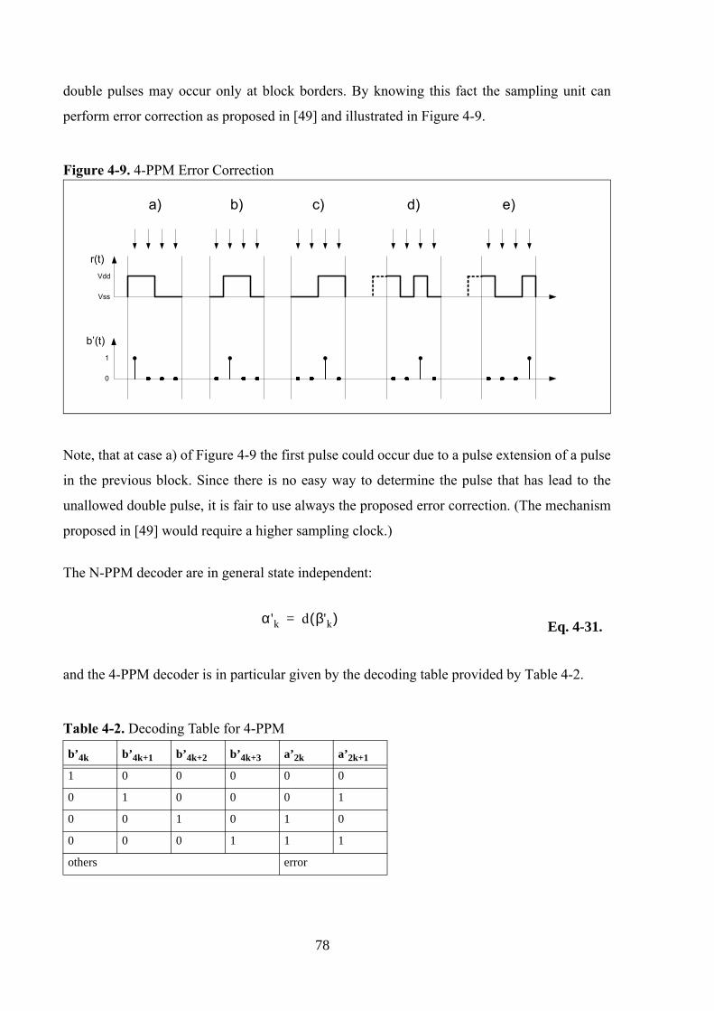
double pulses may occur only at block borders. By knowing this fact the sampling unit can
perform error correction as proposed in [49] and illustrated in Figure 4-9.
Figure 4-9. 4-PPM Error Correction
Vss
Vdd
r(t)
0
1
b’(t)
a) b) c) d) e)
Note, that at case a) of Figure 4-9 the first pulse could occur due to a pulse extension of a pulse
in the previous block. Since there is no easy way to determine the pulse that has lead to the
unallowed double pulse, it is fair to use always the proposed error correction. (The mechanism
proposed in [49] would require a higher sampling clock.)
The N-PPM decoder are in general state independent:
α 'k d β'k( )= Eq. 4-31.
and the 4-PPM decoder is in particular given by the decoding table provided by Table 4-2.
Table 4-2. Decoding Table for 4-PPM
b’4k b’4k+1 b’4k+2 b’4k+3 a’2k a’2k+1
1 0 0 0 0 0
0 1 0 0 0 1
0 0 1 0 1 0
0 0 0 1 1 1
others error
78
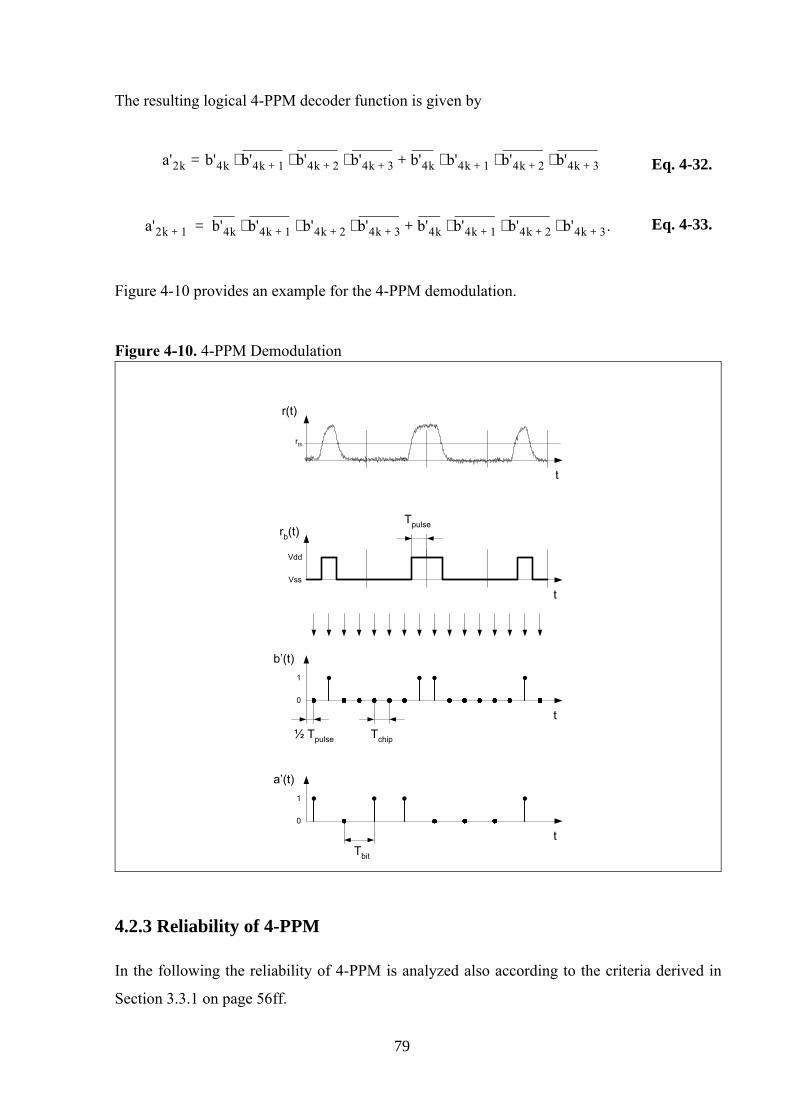
The resulting logical 4-PPM decoder function is given by
a'2k b'4k b'4k 1+⋅ b'4k 2+ b'4k 3+⋅ ⋅ b'4k b'4k 1+⋅ b'4k 2+ b'4k 3+⋅ ⋅+= Eq. 4-32.
a'2k 1+ b'4k b'4k 1+⋅ b'4k 2+ b'4k 3+⋅ ⋅ b'4k b'4k 1+⋅ b'4k 2+ b'4k 3+ .⋅ ⋅+= Eq. 4-33.
Figure 4-10 provides an example for the 4-PPM demodulation.
Figure 4-10. 4-PPM Demodulation
0
1
tTchip
0
1
tTbit
Vss
Vdd
t
Tpulserb(t)
a’(t)
b’(t)
½ Tpulse
t
r(t)
rth
4.2.3 Reliability of 4-PPM
In the following the reliability of 4-PPM is analyzed also according to the criteria derived in
Section 3.3.1 on page 56ff.
79
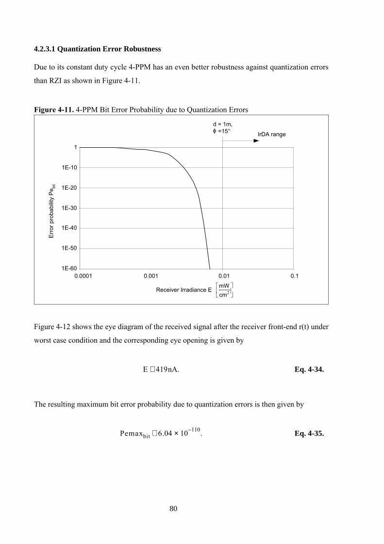
4.2.3.1 Quantization Error Robustness
Due to its constant duty cycle 4-PPM has an even better robustness against quantization errors
than RZI as shown in Figure 4-11.
Figure 4-11. 4-PPM Bit Error Probability due to Quantization Errors
1E-60
1E-50
1E-40
1E-30
1E-20
1E-10
1
0.0001 0.001 0.01 0.1
IrDA range
Receiver Irradiance E
Erro
r pro
babi
lity
Pe bi
t
d = 1m,=15°
2cm
mW
ϕ
Figure 4-12 shows the eye diagram of the received signal after the receiver front-end r(t) under
worst case condition and the corresponding eye opening is given by
E 419nA.≅ Eq. 4-34.
The resulting maximum bit error probability due to quantization errors is then given by
Pemaxbit 6.04 10 110–× .≅ Eq. 4-35.
80
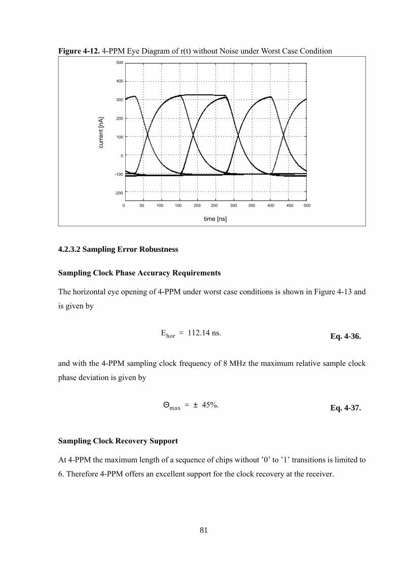
Figure 4-12.
0 50 100 150 200 250 300 350 400 450 500
-200
-100
0
100
200
300
400
500
time [ns]
curr
ent [
nA]
4-PPM Eye Diagram of r(t) without Noise under Worst Case Condition
4.2.3.2 Sampling Error Robustness
Sampling Clock Phase Accuracy Requirements
The horizontal eye opening of 4-PPM under worst case conditions is shown in Figure 4-13 and
is given by
Ehor 112.14 ns.= Eq. 4-36.
and with the 4-PPM sampling clock frequency of 8 MHz the maximum relative sample clock
phase deviation is given by
Θmax 45%.±= Eq. 4-37.
Sampling Clock Recovery Support
At 4-PPM the maximum length of a sequence of chips without ’0’ to ’1’ transitions is limited to
6. Therefore 4-PPM offers an excellent support for the clock recovery at the receiver.
81
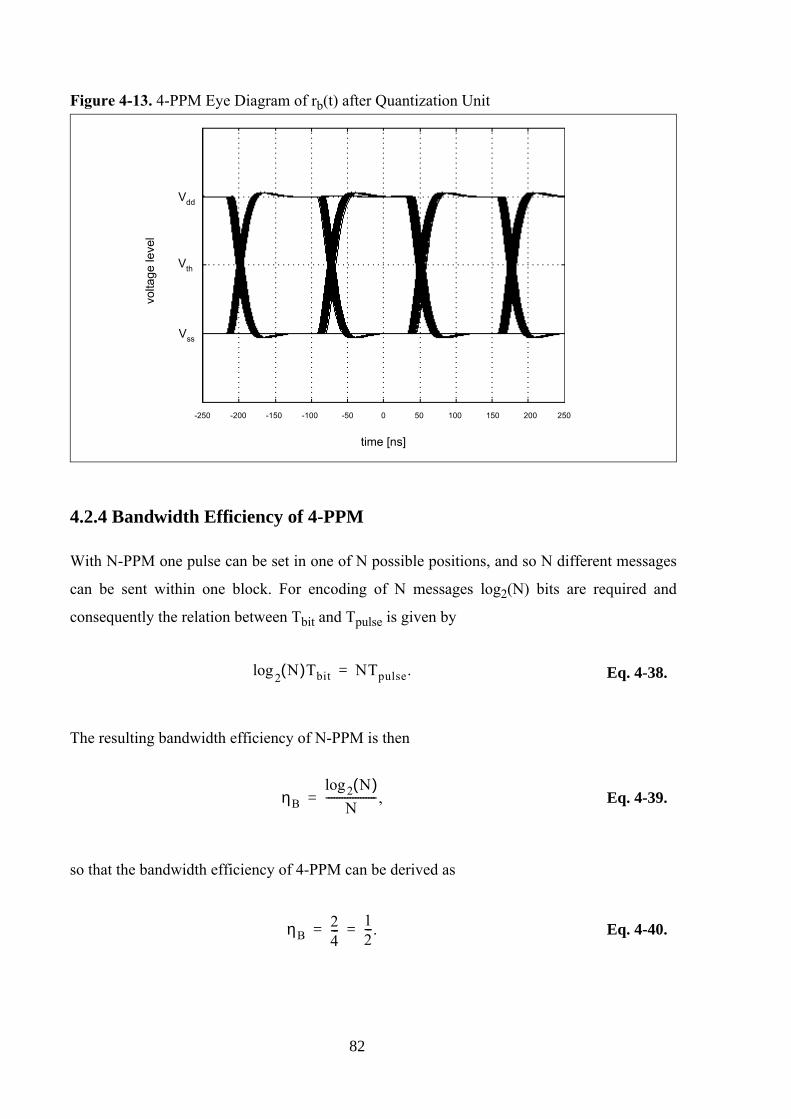
Figure 4-13. 4-PPM Eye Diagram of rb(t) after Quantization Unit
-250 -200 -150 -100 -50 0 50 100 150 200 250
time [ns]
Vss
Vdd
volta
ge le
vel
Vth
4.2.4 Bandwidth Efficiency of 4-PPM
With N-PPM one pulse can be set in one of N possible positions, and so N different messages
can be sent within one block. For encoding of N messages log2(N) bits are required and
consequently the relation between Tbit and Tpulse is given by
N( )Tbit2log NTpulse.= Eq. 4-38.
The resulting bandwidth efficiency of N-PPM is then
ηBN( )2log
N------------------- ,= Eq. 4-39.
so that the bandwidth efficiency of 4-PPM can be derived as
ηB24---
12---.= = Eq. 4-40.
82
I.e. 4-PPM has twice the bandwidth efficiency as 1/4-RZI and furthermore it guarantees enough
’0’ to ’1’ transitions, so that bit stuffing is also not required. Therefore 4-PPM is a considerable
improvement against 1/4-RZI.
4.2.5 Power Efficiency of 4-PPM
Since the average duty cycle of N-PPM is obviously
aveDC 1N---- ,= Eq. 4-41.
the power efficiency of N-PPM is given by
ηPηB
aveDC------------------ N( ).2log= = Eq. 4-42.
Consequently, the power efficiency of 4-PPM can be derived as
ηP 2.= Eq. 4-43.
I.e. 4-PPM has the same power efficiency as n/m-RZI.
4.3 Run-Length-Limited Code Modulation RLL(d,k)
Run-Length-Limited Code modulation is basically a superset of the previous modulation
schemes. With RLL(d,k) codes the various modulation techniques are classified by means of
two parameters d and k, whereby d is the minimum number of ’0’s between ’1’s and k is the
maximum number of ’0’s between ’1’s after the encoder [50]. For example a 4-PPM can be
considered as a 1/2-RLL(0,6), or 1/4-RZI can be considered as a 1/4-RLL(3,∞ ) code. As derived
by Shannon [51] and presented in Section 5.2 on page 101 there exists a maximum achievable
code rate for a code with certain parameters d and k. This maximum code rate is usually called
code capacity. E.g. an RLL(0,6) code has a code capacity of 0.9942. Noting that 4-PPM has with
83
0.5 a relatively poor code rate although it allows error causing double pulses, Hirt, Hassner and
Heise were seeking for an RLL code with the capability to deal with the shortcomings of the
wireless infrared channel in a better way, and with an improved bandwidth efficiency [33]. The
result was a 2/3-RLL(1,13) code, which they called HHH(1,13) code by using their own initials.
With the parameter d = 1 this code guarantees that there are no legal double pulses as they can
occur with the PPM codes. The parameter k = 13 guarantees that there are enough ’0’ to ’1’
transitions for reliable clock recovery at the receiver. At IrDA this code is now used for the latest
physical layer standard called Very Fast Infrared (VFIR)[1]. Therefore we will look more
closely into the HHH(1,13) in the following.
4.3.1 HHH(1,13) Modulation Scheme
At HHH(1,13) two new bits are encoded per encoding step and thereby three chips are generated.
Consequently, the input block αk and the output block βk are given by
αk a2k a2k 1+,= Eq. 4-44.
βk b3k b3k 1+ b3k 2+ ., ,= Eq. 4-45.
The resulting code rate is derived as
pq---
23--- ,= Eq. 4-46.
and the chip duration is then
Tchip23---Tbit.= Eq. 4-47.
The HHH(1,13) encoder is a finite state machine:
βk f αk αk 1+ αk 2+ ζk, , ,( )= Eq. 4-48.
84
ζk 1+ g αk αk 1+ αk 2+ ζk, , ,( ),=
with the internal state
ζk z1k z2k z3k ,= Eq. 4-50.
and the corresponding initial state
ζ0 1 0 0( ).= Eq. 4-51.
The output function of the HHH(1,13) encoder state machine is given by
b3k z1k z2k⋅= Eq. 4-52.
b3k 1+ z1k z2k z1k z3k a2k a2k 1++( )⋅ ⋅ ⋅ ⋅=
z1k z2k z1k z3k⋅ a2k a2k 1+ a2 k 1+( ) a2 k 1+( ) 1+⋅ ⋅ ⋅ ⋅( )⋅ ⋅+
Eq. 4-53.
b3k 2+ z1k z3k a2k a2k 1++( )⋅ ⋅=
z1k z3k⋅ a2k a2k 1+ a2 k 1+( ) a2 k 1+( ) 1+⋅ ⋅ ⋅ ⋅( )+
Eq. 4-54.
and the next state function is
z1k 1+ z1k z3k⋅( ) z3k a2k⋅( ) z1k a2k a2k 1+ a2 k 1+( )⋅ ⋅ ⋅( )+ +=
z1k a2k a2k 1+ a2 k 1+( ) 1+⋅ a2 k 2+( ) a2 k 2+( ) 1+⋅ ⋅ ⋅ ⋅( )+
Eq. 4-49.
Eq. 4-55.
z2k 1+ z3k a2k⋅( ) z1k z2k a2k a2k 1+⋅ ⋅ ⋅( )+= Eq. 4-56.
85
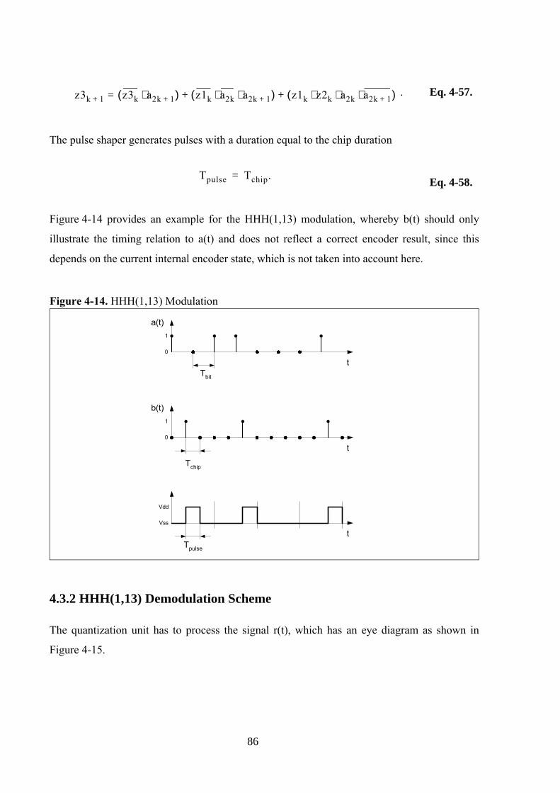
z3k 1+ z3k a2k 1+⋅( ) z1k a2k a2k 1+⋅ ⋅( ) z1k z2k a2k a2k 1+⋅ ⋅ ⋅( )+ += .
The pulse shaper generates pulses with a duration equal to the chip duration
Tpulse Tchip.=Eq. 4-58.
Figure 4-14 provides an example for the HHH(1,13) modulation, whereby b(t) should only
illustrate the timing relation to a(t) and does not reflect a correct encoder result, since this
depends on the current internal encoder state, which is not taken into account here.
Figure 4-14. HHH(1,13) Modulation
0
1
t
Tchip
0
1
tTbit
Vss
Vdd
tTpulse
a(t)
b(t)
4.3.2 HHH(1,13) Demodulation Scheme
The quantization unit has to process the signal r(t), which has an eye diagram as shown in
Figure 4-15.
Eq. 4-57.
86
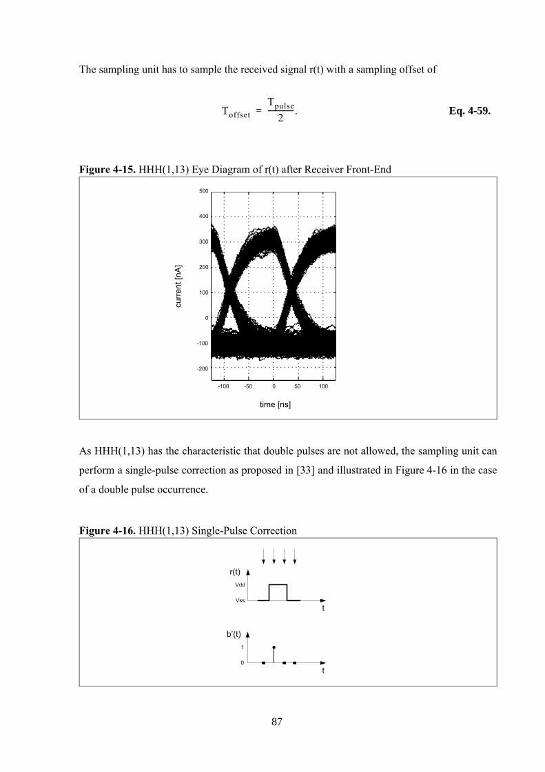
The sampling unit has to sample the received signal r(t) with a sampling offset of
ToffsetTpulse
2-------------- .= Eq. 4-59.
Figure 4-15. HHH(1,13) Eye Diagram of r(t) after Receiver Front-End
-100 -50 0 50 100
-200
-100
0
100
200
300
400
500
time [ns]
curr
ent [
nA]
As HHH(1,13) has the characteristic that double pulses are not allowed, the sampling unit can
perform a single-pulse correction as proposed in [33] and illustrated in Figure 4-16 in the case
of a double pulse occurrence.
Figure 4-16. HHH(1,13) Single-Pulse Correction
Vss
Vdd
r(t)
0
1
b’(t)
t
t
87
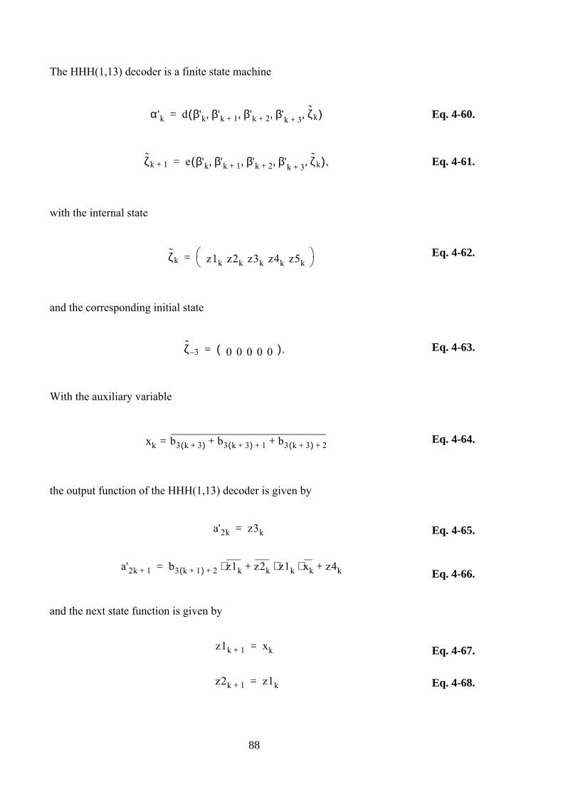
The HHH(1,13) decoder is a finite state machine
α'k d β'k β'k 1+ β'k 2+ β, 'k 3+ ζk, , ,( )= Eq. 4-60.
ζk 1+ e β'k β'k 1+ β'k 2+ β, 'k 3+ ζk, , ,( ),= Eq. 4-61.
with the internal state
ζk z1k z2k z3k z4k z5k = Eq. 4-62.
and the corresponding initial state
ζ 3– 0 0 0 0 0( ).= Eq. 4-63.
With the auxiliary variable
xk b3 k 3+( ) b3 k 3+( ) 1+ b3 k 3+( ) 2++ += Eq. 4-64.
the output function of the HHH(1,13) decoder is given by
a'2k z3k= Eq. 4-65.
a'2k 1+ b3 k 1+( ) 2+ z1k⋅ z2k z1k xk⋅ ⋅ z4k+ +=Eq. 4-66.
and the next state function is given by
z1k 1+ xk= Eq. 4-67.
z2k 1+ z1k= Eq. 4-68.
88
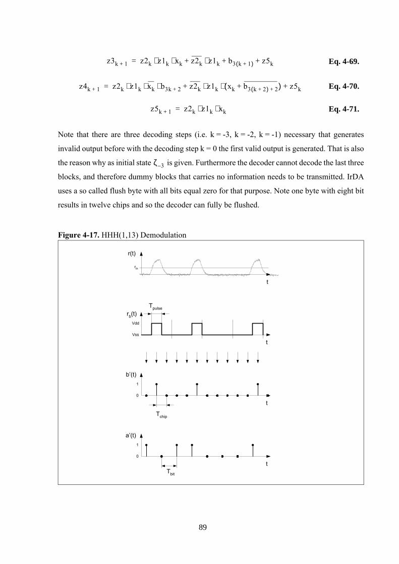
z3k 1+ z2k z1k xk⋅ ⋅ z2k z1k⋅ b3 k 1+( ) z5k+ + +=
Note that there are three decoding steps (i.e. k = -3, k = -2, k = -1) necessary that generates
invalid output before with the decoding step k = 0 the first valid output is generated. That is also
the reason why as initial state ζ 3– is given. Furthermore the decoder cannot decode the last three
blocks, and therefore dummy blocks that carries no information needs to be transmitted. IrDA
uses a so called flush byte with all bits equal zero for that purpose. Note one byte with eight bit
results in twelve chips and so the decoder can fully be flushed.
Figure 4-17. HHH(1,13) Demodulation
0
1
t
Tchip
0
1
tTbit
Vss
Vdd
t
Tpulserb(t)
a’(t)
b’(t)
rth
t
r(t)
Eq. 4-69.
z4k 1+ z2k z1k xk b3k 2+⋅ ⋅ ⋅ z2k z1k xk b3 k 2+( ) 2++( )⋅ ⋅ z5k+ += Eq. 4-70.
z5k 1+ z2k z1k xk⋅ ⋅= Eq. 4-71.
89
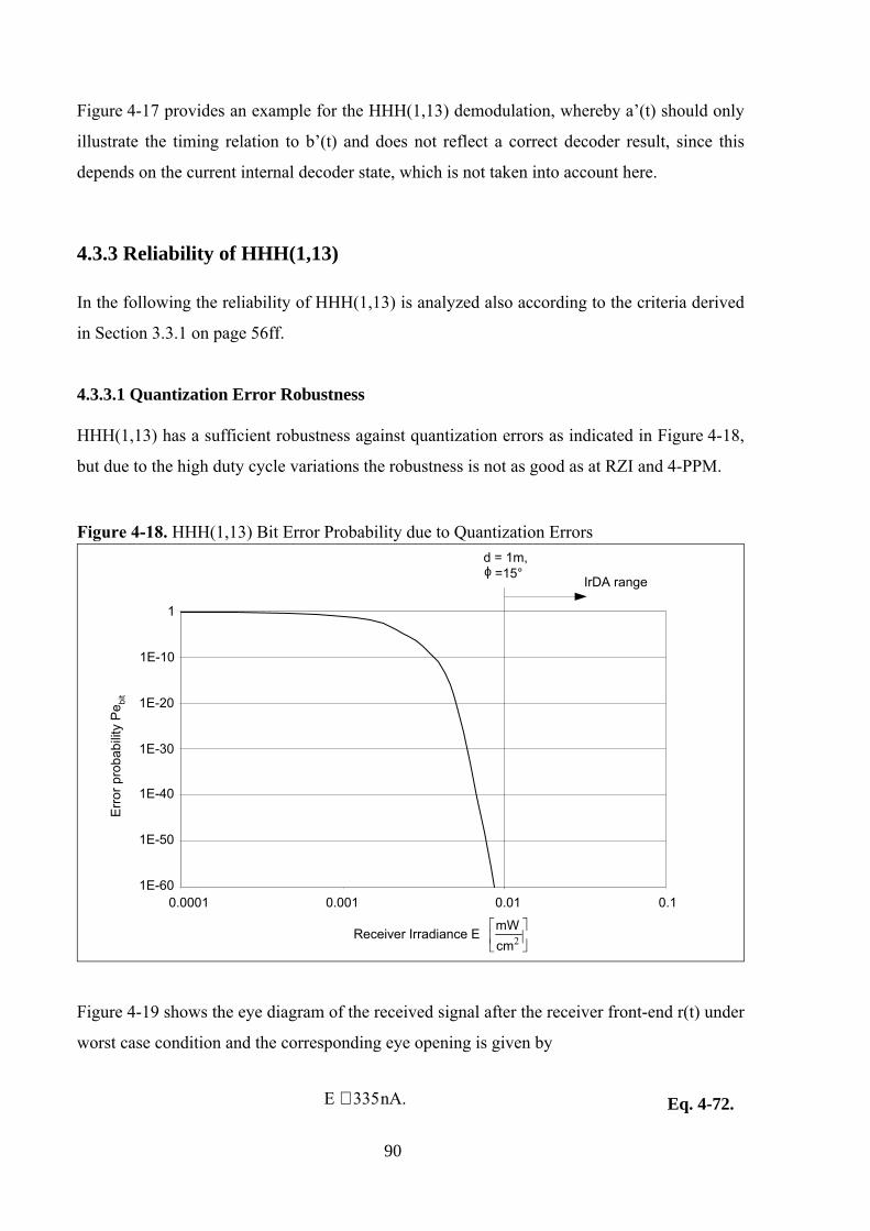
Figure 4-17 provides an example for the HHH(1,13) demodulation, whereby a’(t) should only
illustrate the timing relation to b’(t) and does not reflect a correct decoder result, since this
depends on the current internal decoder state, which is not taken into account here.
4.3.3 Reliability of HHH(1,13)
In the following the reliability of HHH(1,13) is analyzed also according to the criteria derived
in Section 3.3.1 on page 56ff.
4.3.3.1 Quantization Error Robustness
HHH(1,13) has a sufficient robustness against quantization errors as indicated in Figure 4-18,
but due to the high duty cycle variations the robustness is not as good as at RZI and 4-PPM.
Figure 4-18. HHH(1,13) Bit Error Probability due to Quantization Errors
1E-60
1E-50
1E-40
1E-30
1E-20
1E-10
1
0.0001 0.001 0.01 0.1
IrDA range
Receiver Irradiance E
Err
or p
roba
bilit
y P
e bit
d = 1m,=15°ϕ
2cm
mW
Figure 4-19 shows the eye diagram of the received signal after the receiver front-end r(t) under
worst case condition and the corresponding eye opening is given by
E 335nA.≅ Eq. 4-72.
90
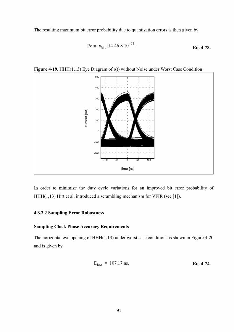
The resulting maximum bit error probability due to quantization errors is then given by
Pemaxbit 4.46 10 71–× .≅ Eq. 4-73.
Figure 4-19. HHH(1,13) Eye Diagram of r(t) without Noise under Worst Case Condition
-200
-100
0
100
200
300
400
500
time [ns]
curr
ent [
nA]
-100 -50 0 50 100
In order to minimize the duty cycle variations for an improved bit error probability of
HHH(1,13) Hirt et al. introduced a scrambling mechanism for VFIR (see [1]).
4.3.3.2 Sampling Error Robustness
Sampling Clock Phase Accuracy Requirements
The horizontal eye opening of HHH(1,13) under worst case conditions is shown in Figure 4-20
and is given by
Ehor 107.17 ns.= Eq. 4-74.
91
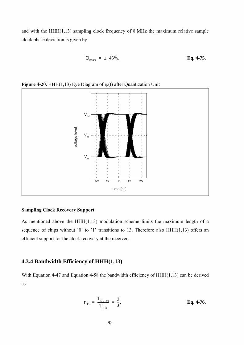
and with the HHH(1,13) sampling clock frequency of 8 MHz the maximum relative sample
clock phase deviation is given by
Θmax 43%.±= Eq. 4-75.
Figure 4-20. HHH(1,13) Eye Diagram of rb(t) after Quantization Unit
Vss
Vdd
volta
ge le
vel
-100 -50 0 50 100
time [ns]
Vth
Sampling Clock Recovery Support
As mentioned above the HHH(1,13) modulation scheme limits the maximum length of a
sequence of chips without ’0’ to ’1’ transitions to 13. Therefore also HHH(1,13) offers an
efficient support for the clock recovery at the receiver.
4.3.4 Bandwidth Efficiency of HHH(1,13)
With Equation 4-47 and Equation 4-58 the bandwidth efficiency of HHH(1,13) can be derived
as
ηBTpulseTbit
--------------23--- .= = Eq. 4-76.
92
I.e. HHH(1,13) offers obviously a further improved bandwidth efficiency compared to 1/4-RZI
(ηB = 0.25) and 4-PPM (ηB = 0.5).
4.3.5 Power Efficiency of HHH(1,13)
According to Hirt et al. [33] HHH(1,13) has an average duty cycle of only 0.258 and with that
the power efficiency ηP of HHH(1,13) can be derived as
ηPηB
aveDC------------------
23---
0.258------------- 2.584 .= = = Eq. 4-77.
I.e. HHH(1,13) has not only a good bandwidth efficiency ηB , but also an attractive power
efficiency ηP .
93

94
5 Edge Position Modulation
In this chapter the novel modulation technique EPM is now introduced. After presenting the
basic idea of EPM we derive the achievable bandwidth efficiencies for different variations of
EPM. It is revealed that the variant EPM(5,12,1/3,1) is a promising alternative to the currently
used modulation techniques.
5.1 Basics of EPM
In general the modulation schemes described above are all pulse position based, i.e. time is
divided into discrete time slots Tchip with a duration equal to or longer than the pulse duration
Tpulse and depending on the information to be transmitted there is a pulse within such a time slot
or not (see Figure 5-1).
Figure 5-1. Principle of Pulse Position Modulation Techniques
ChannelCoded Data
ModulatedSignal
Tpulse
0
1
t
Vss
Vdd
t
Tchip Tpulse
An alternative way is the edge position based modulation scheme, i.e. time is divided into
discrete time slots Tchip with a duration shorter than the pulse duration Tpulse, and depending on
the information to be transmitted there is a rising edge of a pulse within such a time slot or not
(see Figure 5-2).
95
Figure 5-2. Principle of Edge Position Modulation Techniques
ChannelCoded Data
ModulatedSignal
Tpulse
0
1
t
Vss
Vdd
t
Tchip Tpulse
In order to avoid inter-symbol interferences a coding scheme is necessary, which guarantees,
that there is a long enough pause TOFFmin between two pulses, so that the rising edge of the
current pulse is not disturbed by the previous pulse. Furthermore the coding scheme should
guarantee that there is a maximum pause between two pulses TOFFmax, so that the receiver can
recover the clock from the received signal by means of a DPLL. Feasible coding schemes for
that purpose are RLL(d,k) codes, where d and k are the minimum and maximum number of ’0’s
between ’1’s after the encoder as already described in Section 4.3 on page 83. I.e. the bit stream
to be transmitted becomes RLL encoded and then the ’1’s of the encoded data stream indicate
the positions where the pulses should start as shown in Figure 5-2.
Figure 5-3 and Figure 5-4 show the required signal processing steps for data transmission by
means of EPM and the corresponding modulator and demodulator components. While the
modulator consists of an RLL(d,k) Encoder and a Pulse Shaper, the demodulator is built up by
an Edge Detector, a DPLL and an RLL(d,k) Decoder.
Figure 5-3 illustrates the corresponding data streams and waveforms of the EPM modulation
process at the transmitter. Data sequence (an) represents the data from an unconstrained digital
information source that should be transmitted over the wireless infrared channel. The
corresponding discrete signal a(t) is transformed by the RLL encoder into the discrete signal b(t).
Note that the ratio between the baud rates of a(t) and b(t) depends on the code rate RRLL of the
used RLL code. (In Figure 5-4 the code rate RRLL is 1/3.) Finally, the waveform s(t) represents
the EPM modulated binary output signal that is generated by the pulse shaper and is transmitted
over the channel. It can be seen that with each ’1’ of b(t) a new pulse starts.
96
Figure 5-3. EPM Modulator Components with Corresponding Signals
RLL Encoder
Pulse Shaper
s(t)
0
1
t
Digital InformationSource
a(t)
0
1
tTbit
b(t)
Vss
Vdd
tTpulse
s(t)
ElectricalModulation
a(t)
b(t)
Wireless InfraredChannel
0 1 0 0 1 11(an) = ...
Tchip
Figure 5-4 illustrates the data streams and waveforms of the EPM demodulation process at the
receiver. Waveform r(t) and rb(t) represent the EPM modulated signal from the transmission
channel before and after the quantization unit, respectively. The waveform rb(t) should be
basically identical to waveform s(t) of Figure 5-3, but due to the wireless infrared channel there
might be some phase jitter. The discrete signal b’(t) represents the recovered RLL encoded
binary data, which should be identical to discrete signal b(t). For that an edge detection process
is used, where each detected rising edge of rb(t) results in a ’1’, otherwise a ’0’ is generated. The
required phase information is retrieved by the DPLL. Data stream b’(t) is used as input for the
RLL decoder logic that finally recovers the original data represented by data stream a’(t). I.e. at
a transmission without bit errors data streams a(t) and a’(t) are identical.
97
Figure 5-4. EPM Demodulator Components with Corresponding Signals
Decoder
Digital InformationSink
rb(t)
0
1
t
EdgeDetection
b’(t)
0
1
t
a’(t)
rb(t)
ElectricalDemodulation
a’(t)
b’(t)
Quantization Unit
0 1 0 0 1 11(an’) = ...
r(t)
Wireless InfraredChannel
0
i1
t
r(t)
DPLL
Tbit
Vss
Vdd
tTpulse
Tchip
Obviously, the Edge Position Modulation technique has several degrees of freedom and so there
exist many different types of EPM. A specific type of EPM is fully defined by
• the parameter d of the used RLL code that defines the minimum number of ’0’s between ’1’s
of the RLL encoded data stream,
• the parameter k of the RLL code that defines the maximum number of ’0’s between ’1’s of
the encoded data stream,
• the code rate RRLL of the RLL code that defines the ratio between the time slot duration
Tchip and the bit duration Tbit, and
98
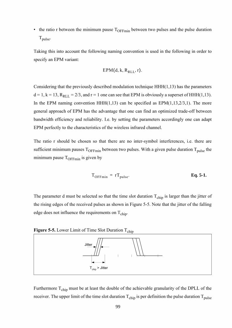
• the ratio r between the minimum pause TOFFmin between two pulses and the pulse duration
Tpulse.
Taking this into account the following naming convention is used in the following in order to
specify an EPM variant:
EPM d k RRLL r, , ,( ).
Considering that the previously described modulation technique HHH(1,13) has the parameters
d = 1, k = 13, RRLL = 2/3, and r = 1 one can see that EPM is obviously a superset of HHH(1,13).
In the EPM naming convention HHH(1,13) can be specified as EPM(1,13,2/3,1). The more
general approach of EPM has the advantage that one can find an optimized trade-off between
bandwidth efficiency and reliability. I.e. by setting the parameters accordingly one can adapt
EPM perfectly to the characteristics of the wireless infrared channel.
The ratio r should be chosen so that there are no inter-symbol interferences, i.e. there are
sufficient minimum pauses TOFFmin between two pulses. With a given pulse duration Tpulse the
minimum pause TOFFmin is given by
TOFFmin rTpulse.= Eq. 5-1.
The parameter d must be selected so that the time slot duration Tchip is larger than the jitter of
the rising edges of the received pulses as shown in Figure 5-5. Note that the jitter of the falling
edge does not influence the requirements on Tchip.
Figure 5-5. Lower Limit of Time Slot Duration Tchip
Tchip > Jitter
Jitter
Furthermore Tchip must be at least the double of the achievable granularity of the DPLL of the
receiver. The upper limit of the time slot duration Tchip is per definition the pulse duration Tpulse
99
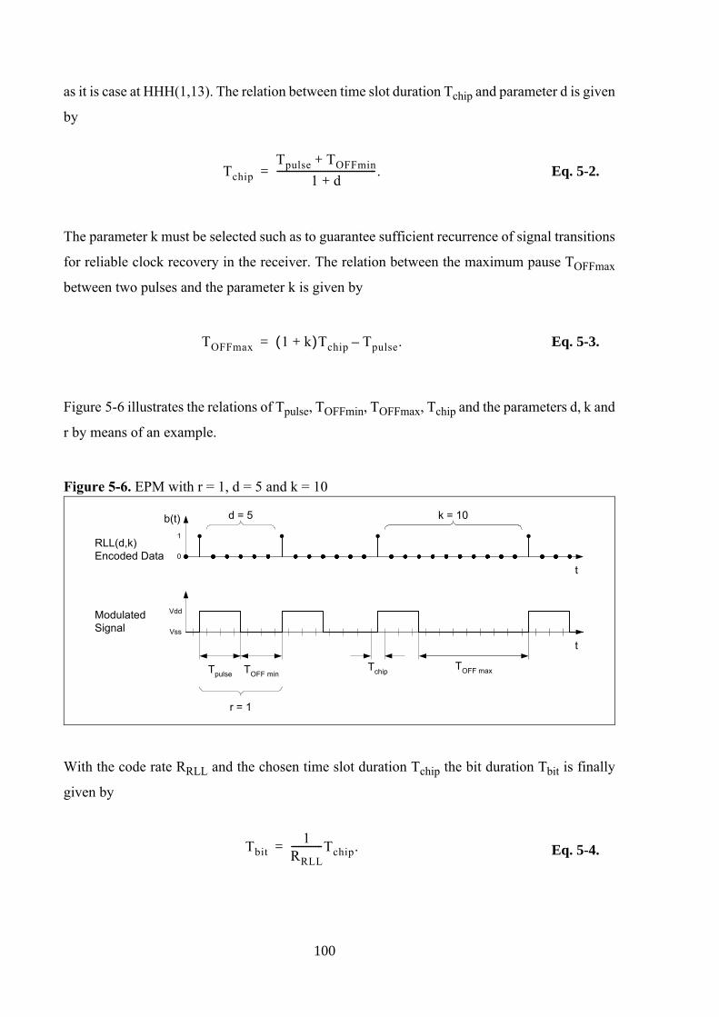
as it is case at HHH(1,13). The relation between time slot duration Tchip and parameter d is given
by
TchipTpulse TOFFmin+
1 d+----------------------------------------- .= Eq. 5-2.
The parameter k must be selected such as to guarantee sufficient recurrence of signal transitions
for reliable clock recovery in the receiver. The relation between the maximum pause TOFFmax
between two pulses and the parameter k is given by
TOFFmax 1 k+( )Tchip Tpulse.–= Eq. 5-3.
Figure 5-6 illustrates the relations of Tpulse, TOFFmin, TOFFmax, Tchip and the parameters d, k and
r by means of an example.
Figure 5-6. EPM with r = 1, d = 5 and k = 10
RLL(d,k)Encoded Data
ModulatedSignal
TOFF maxTOFF minTpulse
d = 5 k = 10
0
1
t
b(t)
Tchip
tVss
Vdd
r = 1
With the code rate RRLL and the chosen time slot duration Tchip the bit duration Tbit is finally
given by
Tbit1
RRLL-------------Tchip.= Eq. 5-4.
100
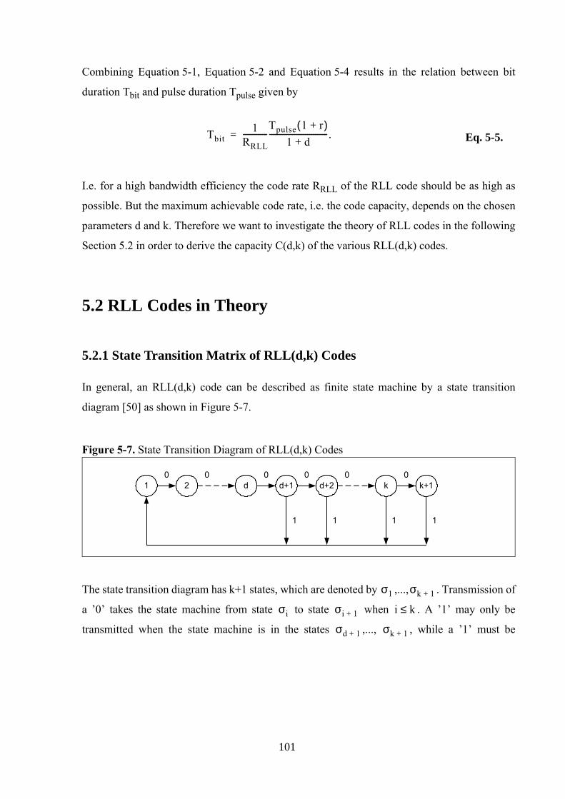
Combining Equation 5-1, Equation 5-2 and Equation 5-4 results in the relation between bit
duration Tbit and pulse duration Tpulse given by
Tbit1
RRLL-------------
Tpulse 1 r+( )1 d+
------------------------------- .= Eq. 5-5.
I.e. for a high bandwidth efficiency the code rate RRLL of the RLL code should be as high as
possible. But the maximum achievable code rate, i.e. the code capacity, depends on the chosen
parameters d and k. Therefore we want to investigate the theory of RLL codes in the following
Section 5.2 in order to derive the capacity C(d,k) of the various RLL(d,k) codes.
5.2 RLL Codes in Theory
5.2.1 State Transition Matrix of RLL(d,k) Codes
In general, an RLL(d,k) code can be described as finite state machine by a state transition
diagram [50] as shown in Figure 5-7.
Figure 5-7. State Transition Diagram of RLL(d,k) Codes
1 2 d0 0 0
1
0k
0 0
11 1
d+1 d+2 k+1
The state transition diagram has k+1 states, which are denoted by σ1 ,...,σk 1+ . Transmission of
a ’0’ takes the state machine from state σi to state σi 1+ when i k≤ . A ’1’ may only be
transmitted when the state machine is in the states σd 1+ ,..., σk 1+ , while a ’1’ must be
101
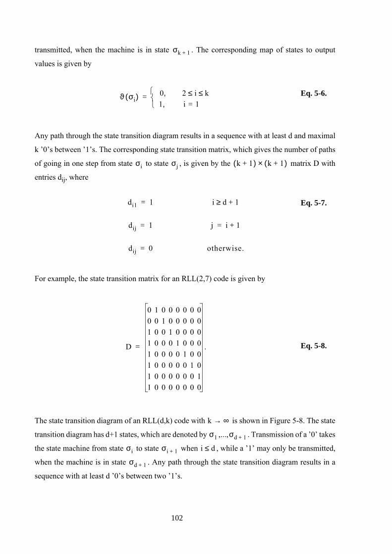
transmitted, when the machine is in state σk 1+ . The corresponding map of states to output
values is given by
ϑ σ i( ) 0 , 2 i k≤ ≤1 , i 1=
= Eq. 5-6.
Any path through the state transition diagram results in a sequence with at least d and maximal
k ’0’s between ’1’s. The corresponding state transition matrix, which gives the number of paths
of going in one step from state σi to state σj , is given by the k 1+( ) k 1+( )× matrix D with
entries dij, where
di1 1= i d 1+≥ Eq. 5-7.
dij 1= j i 1+=
dij 0= otherwise.
For example, the state transition matrix for an RLL(2,7) code is given by
D
0 1 0 0 0 0 0 00 0 1 0 0 0 0 01 0 0 1 0 0 0 01 0 0 0 1 0 0 01 0 0 0 0 1 0 01 0 0 0 0 0 1 01 0 0 0 0 0 0 11 0 0 0 0 0 0 0
.= Eq. 5-8.
The state transition diagram of an RLL(d,k) code with k ∞→ is shown in Figure 5-8. The state
transition diagram has d+1 states, which are denoted by σ1 ,...,σd 1+ . Transmission of a ’0’ takes
the state machine from state σi to state σi 1+ when i d≤ , while a ’1’ may only be transmitted,
when the machine is in state σd 1+ . Any path through the state transition diagram results in a
sequence with at least d ’0’s between two ’1’s.
102
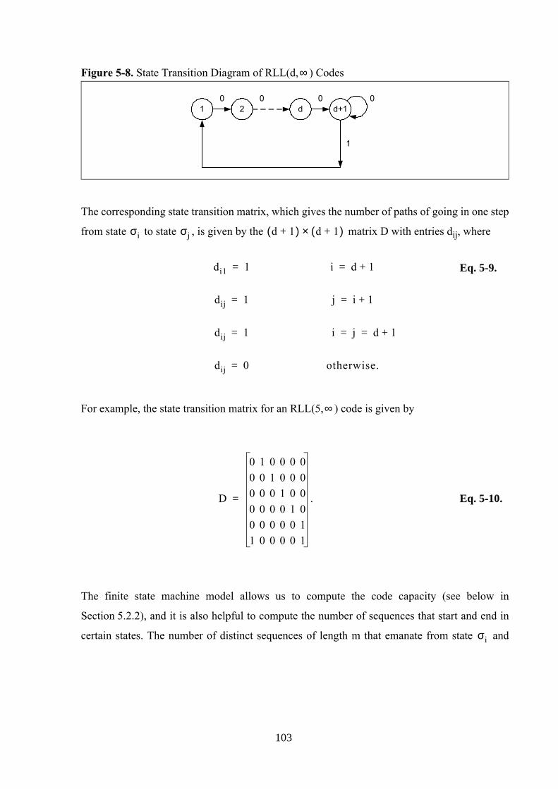
Figure 5-8. State Transition Diagram of RLL(d,∞ ) Codes
2 d d+10 0 0
1
01
The corresponding state transition matrix, which gives the number of paths of going in one step
from state σi to state σj , is given by the d 1+( ) d 1+( )× matrix D with entries dij, where
di1 1= i d 1+= Eq. 5-9.
dij 1= j i 1+=
dij 1= i j d 1+= =
dij 0= otherwise.
For example, the state transition matrix for an RLL(5,∞ ) code is given by
D
0 1 0 0 0 00 0 1 0 0 00 0 0 1 0 00 0 0 0 1 00 0 0 0 0 11 0 0 0 0 1
.= Eq. 5-10.
The finite state machine model allows us to compute the code capacity (see below in
Section 5.2.2), and it is also helpful to compute the number of sequences that start and end in
certain states. The number of distinct sequences of length m that emanate from state σi and
103
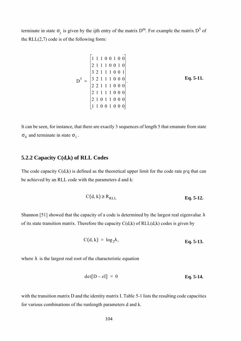
terminate in state σj is given by the ijth entry of the matrix Dm. For example the matrix D5 of
the RLL(2,7) code is of the following form:
D5
1 1 1 0 0 1 0 02 1 1 1 0 0 1 03 2 1 1 1 0 0 13 2 1 1 1 0 0 02 2 1 1 1 0 0 02 1 1 1 1 0 0 02 1 0 1 1 0 0 01 1 0 0 1 0 0 0
.=Eq. 5-11.
It can be seen, for instance, that there are exactly 3 sequences of length 5 that emanate from state
σ4 and terminate in state σ1 .
5.2.2 Capacity C(d,k) of RLL Codes
The code capacity C(d,k) is defined as the theoretical upper limit for the code rate p/q that can
be achieved by an RLL code with the parameters d and k:
C d k,( ) RRLL≥ Eq. 5-12.
Shannon [51] showed that the capacity of a code is determined by the largest real eigenvalue λ
of its state transition matrix. Therefore the capacity C(d,k) of RLL(d,k) codes is given by
C d k,( ) λ2log ,= Eq. 5-13.
where λ is the largest real root of the characteristic equation
det D zI–[ ] 0= Eq. 5-14.
with the transition matrix D and the identity matrix I. Table 5-1 lists the resulting code capacities
for various combinations of the runlength parameters d and k.
104
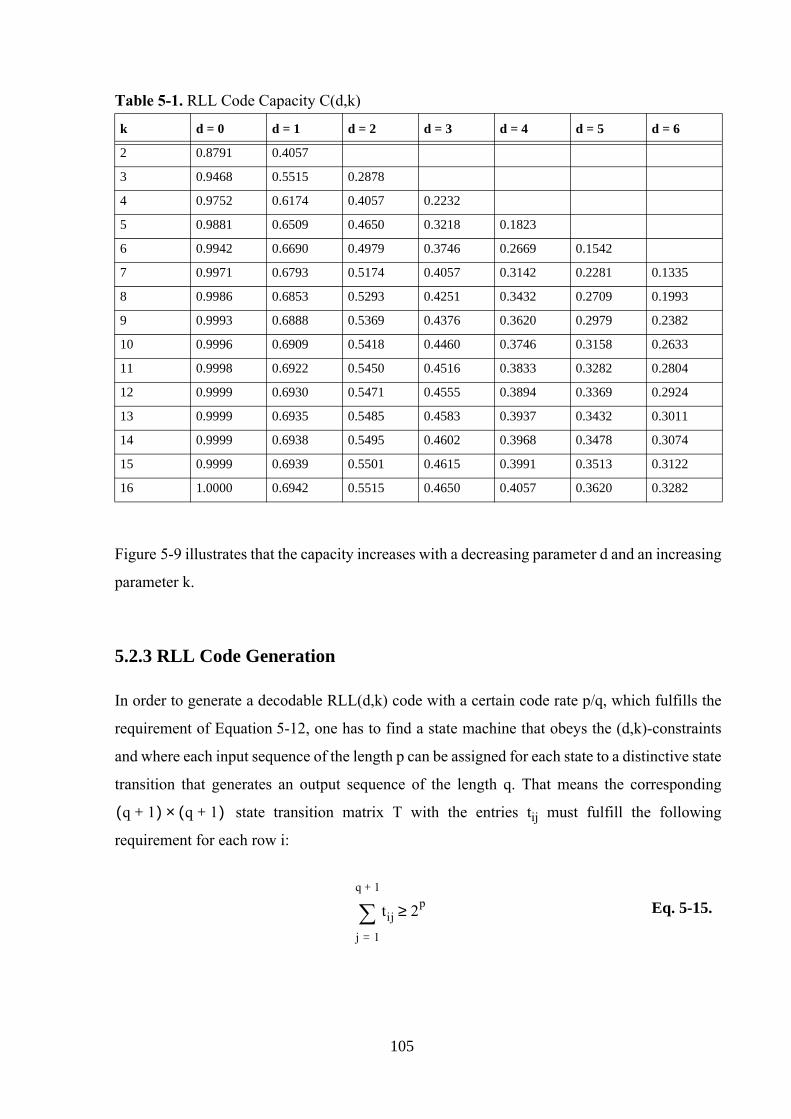
Table 5-1. RLL Code Capacity C(d,k)
k d = 0 d = 1 d = 2 d = 3 d = 4 d = 5 d = 6
2 0.8791 0.4057
3 0.9468 0.5515 0.2878
4 0.9752 0.6174 0.4057 0.2232
5 0.9881 0.6509 0.4650 0.3218 0.1823
6 0.9942 0.6690 0.4979 0.3746 0.2669 0.1542
7 0.9971 0.6793 0.5174 0.4057 0.3142 0.2281 0.1335
8 0.9986 0.6853 0.5293 0.4251 0.3432 0.2709 0.1993
9 0.9993 0.6888 0.5369 0.4376 0.3620 0.2979 0.2382
10 0.9996 0.6909 0.5418 0.4460 0.3746 0.3158 0.2633
11 0.9998 0.6922 0.5450 0.4516 0.3833 0.3282 0.2804
12 0.9999 0.6930 0.5471 0.4555 0.3894 0.3369 0.2924
13 0.9999 0.6935 0.5485 0.4583 0.3937 0.3432 0.3011
14 0.9999 0.6938 0.5495 0.4602 0.3968 0.3478 0.3074
15 0.9999 0.6939 0.5501 0.4615 0.3991 0.3513 0.3122
16 1.0000 0.6942 0.5515 0.4650 0.4057 0.3620 0.3282
Figure 5-9 illustrates that the capacity increases with a decreasing parameter d and an increasing
parameter k.
5.2.3 RLL Code Generation
In order to generate a decodable RLL(d,k) code with a certain code rate p/q, which fulfills the
requirement of Equation 5-12, one has to find a state machine that obeys the (d,k)-constraints
and where each input sequence of the length p can be assigned for each state to a distinctive state
transition that generates an output sequence of the length q. That means the corresponding
q 1+( ) q 1+( )× state transition matrix T with the entries tij must fulfill the following
requirement for each row i:
tij
j 1=
q 1+
∑ 2p≥ Eq. 5-15.
105
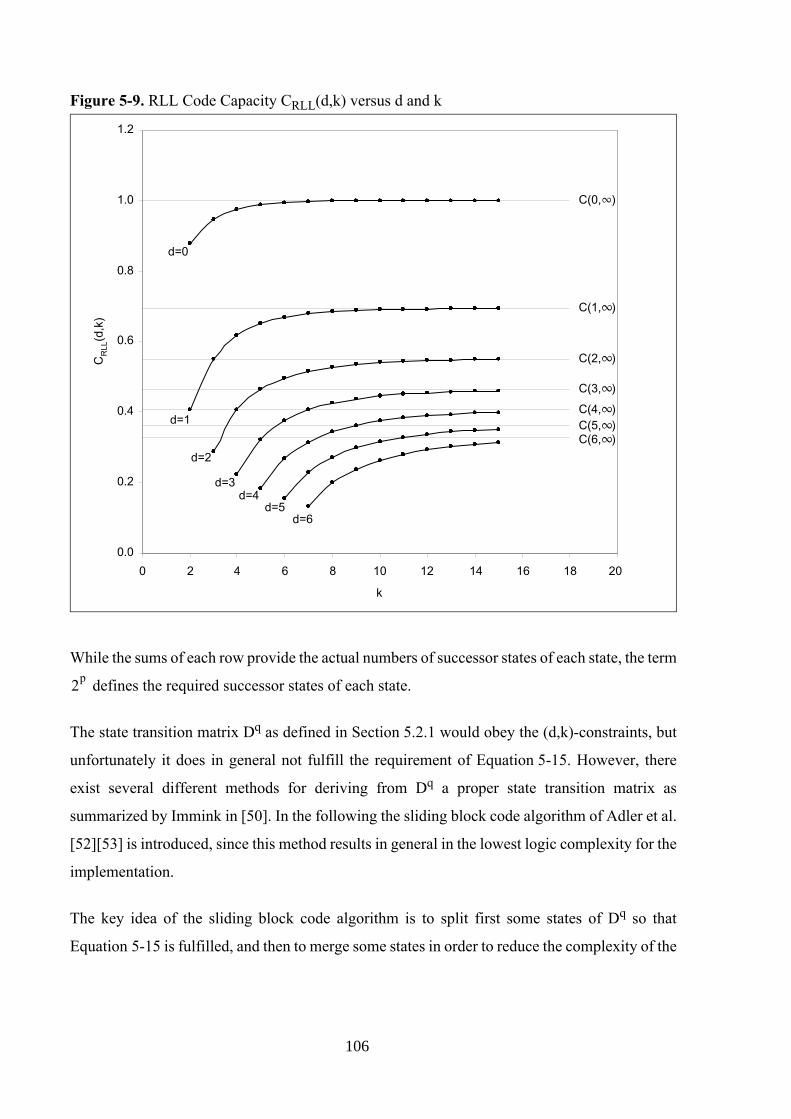
Figure 5-9. RLL Code Capacity CRLL(d,k) versus d and k
C(0, )
d=0
d=1
d=2
d=3d=4
d=5d=6
0.0
0.2
0.4
0.6
0.8
1.0
1.2
0 2 4 6 8 10 12 14 16 18 20
k
CR
LL(d
,k)
∞
C(1, )∞
C(2, )∞
C(3, )∞C(4, )∞C(5, )∞C(6, )∞
While the sums of each row provide the actual numbers of successor states of each state, the term
2p defines the required successor states of each state.
The state transition matrix Dq as defined in Section 5.2.1 would obey the (d,k)-constraints, but
unfortunately it does in general not fulfill the requirement of Equation 5-15. However, there
exist several different methods for deriving from Dq a proper state transition matrix as
summarized by Immink in [50]. In the following the sliding block code algorithm of Adler et al.
[52][53] is introduced, since this method results in general in the lowest logic complexity for the
implementation.
The key idea of the sliding block code algorithm is to split first some states of Dq so that
Equation 5-15 is fulfilled, and then to merge some states in order to reduce the complexity of the
106
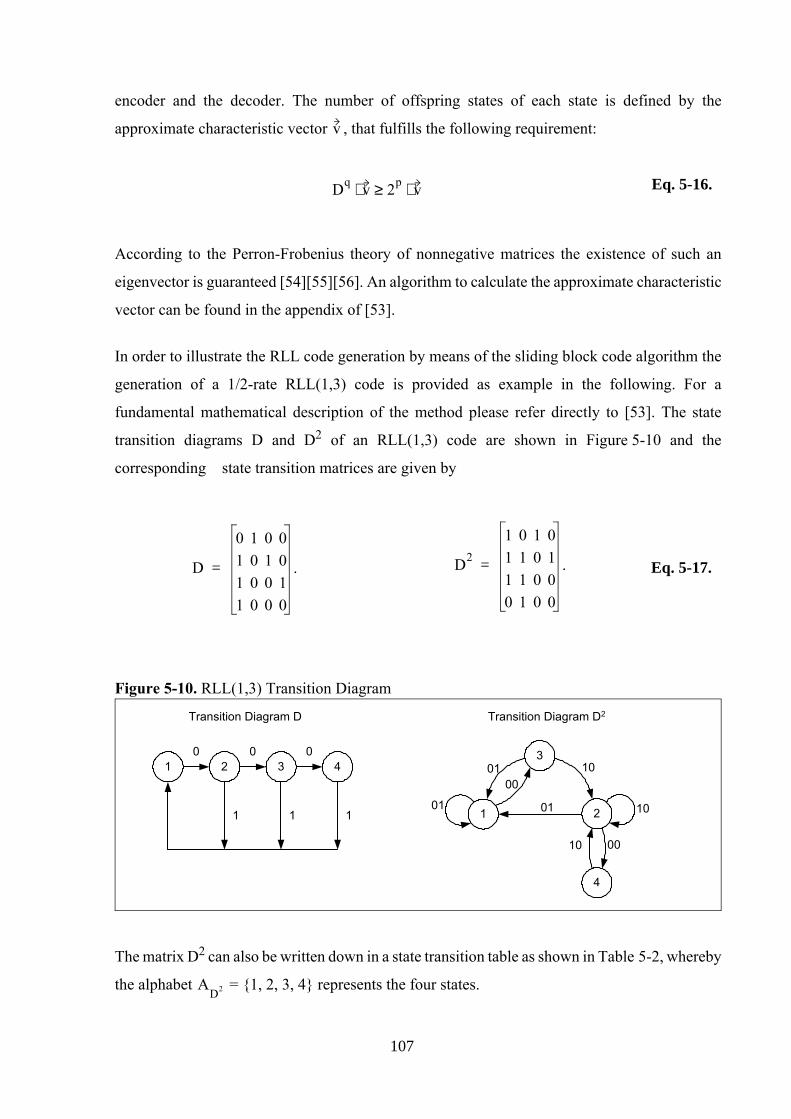
encoder and the decoder. The number of offspring states of each state is defined by the
approximate characteristic vector v , that fulfills the following requirement:
Dq v⋅ 2p v⋅≥ Eq. 5-16.
According to the Perron-Frobenius theory of nonnegative matrices the existence of such an
eigenvector is guaranteed [54][55][56]. An algorithm to calculate the approximate characteristic
vector can be found in the appendix of [53].
In order to illustrate the RLL code generation by means of the sliding block code algorithm the
generation of a 1/2-rate RLL(1,3) code is provided as example in the following. For a
fundamental mathematical description of the method please refer directly to [53]. The state
transition diagrams D and D2 of an RLL(1,3) code are shown in Figure 5-10 and the
corresponding state transition matrices are given by
D
0 1 0 01 0 1 01 0 0 11 0 0 0
.= D2
1 0 1 01 1 0 11 1 0 00 1 0 0
.= Eq. 5-17.
Figure 5-10. RLL(1,3) Transition Diagram
1 20 0
1
30
4
11 1 2
3
4
10
0010
01
0001
01
10
Transition Diagram D Transition Diagram D2
The matrix D2 can also be written down in a state transition table as shown in Table 5-2, whereby
the alphabet AD2 = 1, 2, 3, 4 represents the four states.
107
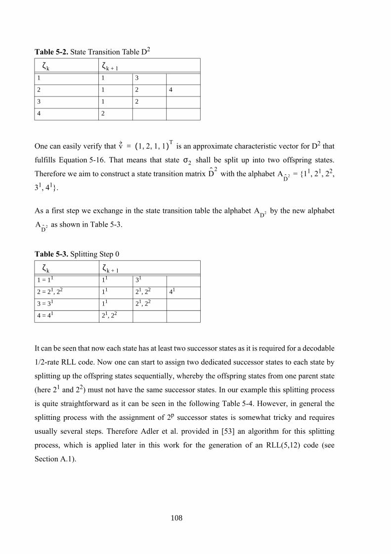
Table 5-2. State Transition Table D2
ζk ζk 1+
1 1 3
2 1 2 4
3 1 2
4 2
One can easily verify that v 1 2 1 1, , ,( )T= is an approximate characteristic vector for D2 that
fulfills Equation 5-16. That means that state σ2 shall be split up into two offspring states.
Therefore we aim to construct a state transition matrix D2
with the alphabet AD2 = 11, 21, 22,
31, 41.
As a first step we exchange in the state transition table the alphabet AD2 by the new alphabet
AD2 as shown in Table 5-3.
Table 5-3. Splitting Step 0
ζk ζk 1+
1 = 11 11 31
2 = 21, 22 11 21, 22 41
3 = 31 11 21, 22
4 = 41 21, 22
It can be seen that now each state has at least two successor states as it is required for a decodable
1/2-rate RLL code. Now one can start to assign two dedicated successor states to each state by
splitting up the offspring states sequentially, whereby the offspring states from one parent state
(here 21 and 22) must not have the same successor states. In our example this splitting process
is quite straightforward as it can be seen in the following Table 5-4. However, in general the
splitting process with the assignment of 2p successor states is somewhat tricky and requires
usually several steps. Therefore Adler et al. provided in [53] an algorithm for this splitting
process, which is applied later in this work for the generation of an RLL(5,12) code (see
Section A.1).
108
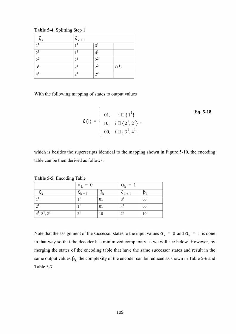
Table 5-4. Splitting Step 1
ζk ζk 1+
11 11 31
21 11 41
22 21 22
31 21 22 (11)
41 21 22
With the following mapping of states to output values
ϑ i( )01 , i 11 ∈
10 , i 21 22, ∈
00 , i 31 41, ∈
,
=
Eq. 5-18.
which is besides the superscripts identical to the mapping shown in Figure 5-10, the encoding
table can be then derived as follows:
Table 5-5. Encoding Tableαk 0= αk 1=
ζk ζk 1+ βk ζk 1+ βk11 11 01 31 00
21 11 01 41 00
41, 31, 22 21 10 22 10
Note that the assignment of the successor states to the input values αk 0= and αk 1= is done
in that way so that the decoder has minimized complexity as we will see below. However, by
merging the states of the encoding table that have the same successor states and result in the
same output values βk the complexity of the encoder can be reduced as shown in Table 5-6 and
Table 5-7.
109
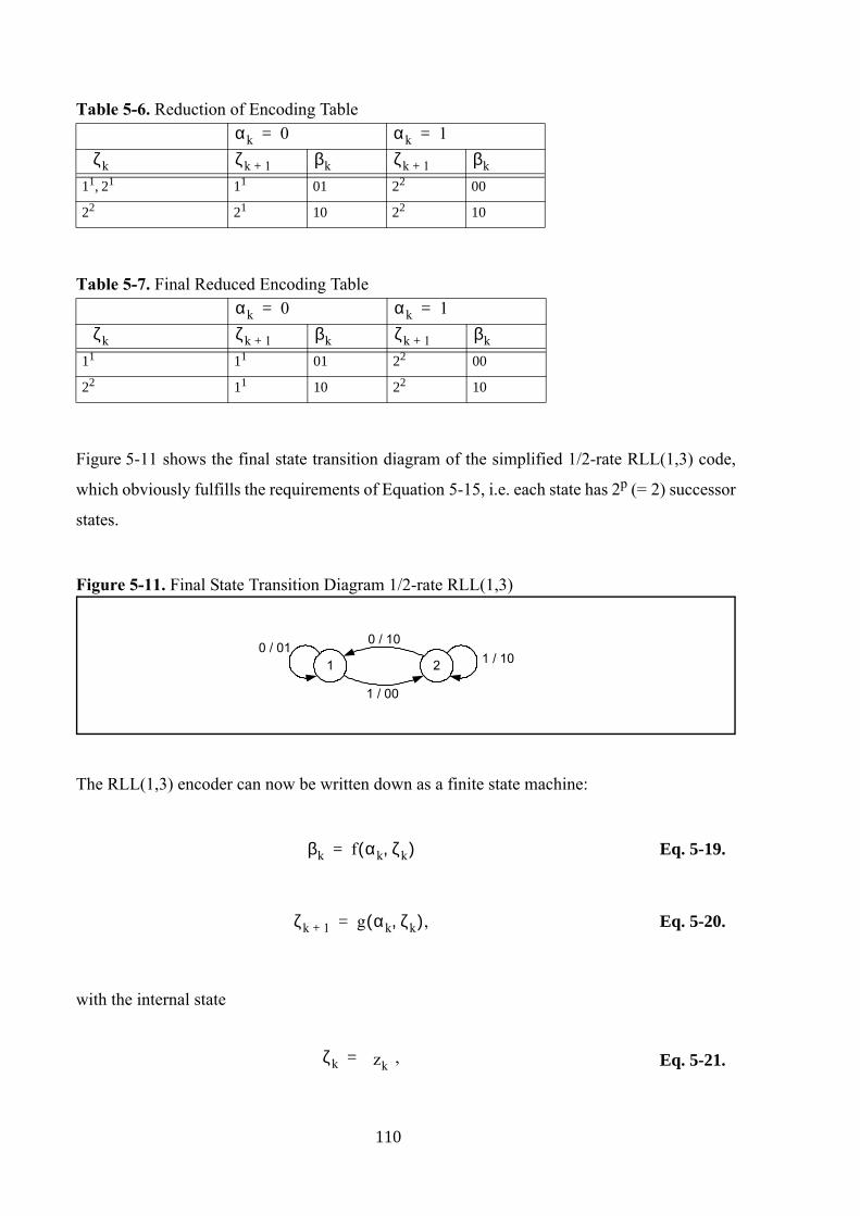
Table 5-6. Reduction of Encoding Tableαk 0= αk 1=
ζk ζk 1+ βk ζk 1+ βk11, 21 11 01 22 00
22 21 10 22 10
Table 5-7. Final Reduced Encoding Tableαk 0= αk 1=
ζk ζk 1+ βk ζk 1+ βk11 11 01 22 00
22 11 10 22 10
Figure 5-11 shows the final state transition diagram of the simplified 1/2-rate RLL(1,3) code,
which obviously fulfills the requirements of Equation 5-15, i.e. each state has 2p (= 2) successor
states.
Figure 5-11. Final State Transition Diagram 1/2-rate RLL(1,3)
1 2
0 / 10
1 / 00
1 / 100 / 01
The RLL(1,3) encoder can now be written down as a finite state machine:
βk f αk ζk,( )= Eq. 5-19.
ζk 1+ g αk ζk,( ),= Eq. 5-20.
with the internal state
ζk zk ,= Eq. 5-21.
110
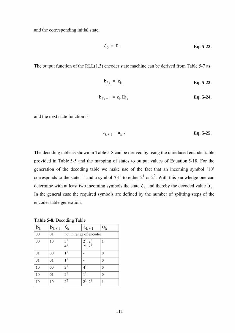
and the corresponding initial state
ζ0 0.= Eq. 5-22.
The output function of the RLL(1,3) encoder state machine can be derived from Table 5-7 as
b2k zk= Eq. 5-23.
b2k 1+ zk ak⋅= Eq. 5-24.
and the next state function is
zk 1+ ak= . Eq. 5-25.
The decoding table as shown in Table 5-8 can be derived by using the unreduced encoder table
provided in Table 5-5 and the mapping of states to output values of Equation 5-18. For the
generation of the decoding table we make use of the fact that an incoming symbol ’10’
corresponds to the state 11 and a symbol ’01’ to either 21 or 22. With this knowledge one can
determine with at least two incoming symbols the state ζk and thereby the decoded value αk .
In the general case the required symbols are defined by the number of splitting steps of the
encoder table generation.
Table 5-8. Decoding Tableβk βk 1+ ζk ζk 1+ αk00 01 not in range of encoder
00 10 31
4121, 22
21, 221
01 00 11 - 0
01 01 11 - 0
10 00 21 41 0
10 01 21 11 0
10 10 22 21, 22 1
111
Note that it is obviously helpful that the states 31 and 41 have been assigned to the same output
value αk = 1 in Table 5-5, otherwise the decoder would require more input symbols. However,
our RLL(1,3) decoder is obviously a finite look-ahead but state independent machine:
αk d βk( ),= Eq. 5-26.
whereby the logical RLL(1,3) decoder function can be written down as
a'k b'2k 1+ b'2k 2+ b'2k 3+⋅ ⋅= . Eq. 5-27.
5.3 EPM Bandwidth Efficiency in General
As stated in Equation 3-59 on page 65 the bandwidth efficiency is given by
ηBTpulseTbit
-------------- .= Eq. 5-28.
Together with Equation 5-5 on page 101 the bandwidth efficiency of EPM is consequently given
by
ηB RRLL1 d+1 r+------------ .= Eq. 5-29.
Considering that the maximum achievable RLL code rate RRLL is given by the RLL code
capacity C(d,k), which we have derived above in Section 5.2.2 on page 104, the maximum
achievable bandwidth efficiency ηB is given by
ηBmax C d k,( )1 d+1 r+------------ .= Eq. 5-30.
Figure 5-12 shows the maximum achievable bandwidth efficiency ηBmax of EPM with r = 1 as
a function of d and k.
112
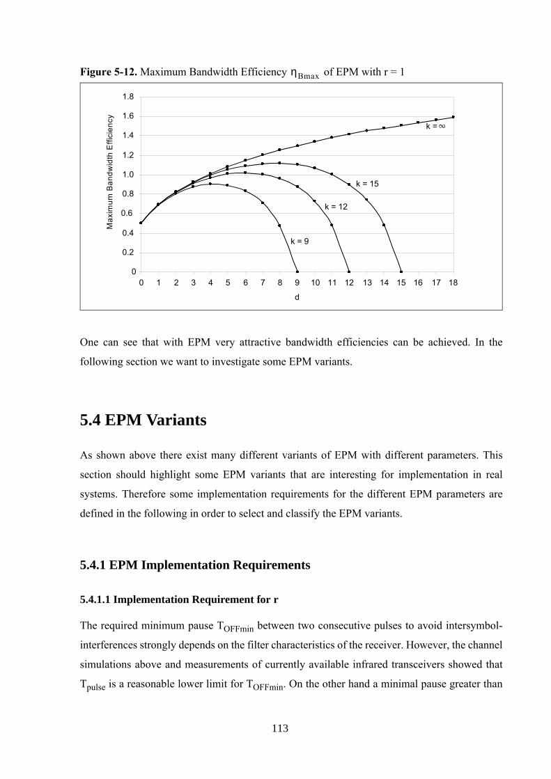
Figure 5-12. Maximum Bandwidth Efficiency ηBmax of EPM with r = 1
0
0.2
0.4
0.6
0.8
1.0
1.2
1.4
1.6
1.8
0 1 2 3 4 5 6 7 8 9 10 11 12 13 14 15 16 17 18
d
Max
imum
Ban
dwid
th E
ffici
ency
k = 9
k = 12
k = 15
k =∞
One can see that with EPM very attractive bandwidth efficiencies can be achieved. In the
following section we want to investigate some EPM variants.
5.4 EPM Variants
As shown above there exist many different variants of EPM with different parameters. This
section should highlight some EPM variants that are interesting for implementation in real
systems. Therefore some implementation requirements for the different EPM parameters are
defined in the following in order to select and classify the EPM variants.
5.4.1 EPM Implementation Requirements
5.4.1.1 Implementation Requirement for r
The required minimum pause TOFFmin between two consecutive pulses to avoid intersymbol-
interferences strongly depends on the filter characteristics of the receiver. However, the channel
simulations above and measurements of currently available infrared transceivers showed that
Tpulse is a reasonable lower limit for TOFFmin. On the other hand a minimal pause greater than
113
1.5 Tpulse does not increase the transmission reliability anymore. I.e. we want to limit
r TOFFmin Tpulse⁄= as follows:
1 r 1.5≤ ≤ . Eq. 5-31.
5.4.1.2 Implementation Requirements for Tchip
The upper limit of the time slot duration Tchip is per definition the pulse duration Tpulse. For the
lower limit we have to consider that Tchip must be larger than the jitter of the rising edges of the
received pulses. Taking the investigations of the wireless infrared channel into account we can
assume that the jitter is less than one third of Tpulse. I.e. we want to limit the relation Tchip/Tpulse
as follows:
13---
TchipTpulse-------------- 1≤ ≤ . Eq. 5-32.
Additionally the relation between Tchip and Tpulse should be chosen in a way that the respective
signals b(t) and s(t) can be both derived from the same system clock, which should be not larger
than the twelvefold of 1/Tpulse. This requirement can be written down as follows:
TchipTpulse--------------
uv--- v 6, and u, v are integer values≤= Eq. 5-33.
5.4.1.3 Implementation Requirement for k
As already mentioned in Section 3.3.1.2 on page 62 Hirt et al. [33] stated that there should be at
least one ’0’ to ’1’ transition within 16 chips for an adequate sample clock recovery with a
DPLL. Although this is certainly only a soft limitation, since the clock recovery capability
strongly depends on the DPLL itself, we will use a similar1 limitation for the parameter k.
k 16≤ . Eq. 5-34.
1. The limitation of Hirt et al. is with k 15≤ a bit lower, but this would exclude some interesting EPM variants as it can be seen in Table 5-9.
114
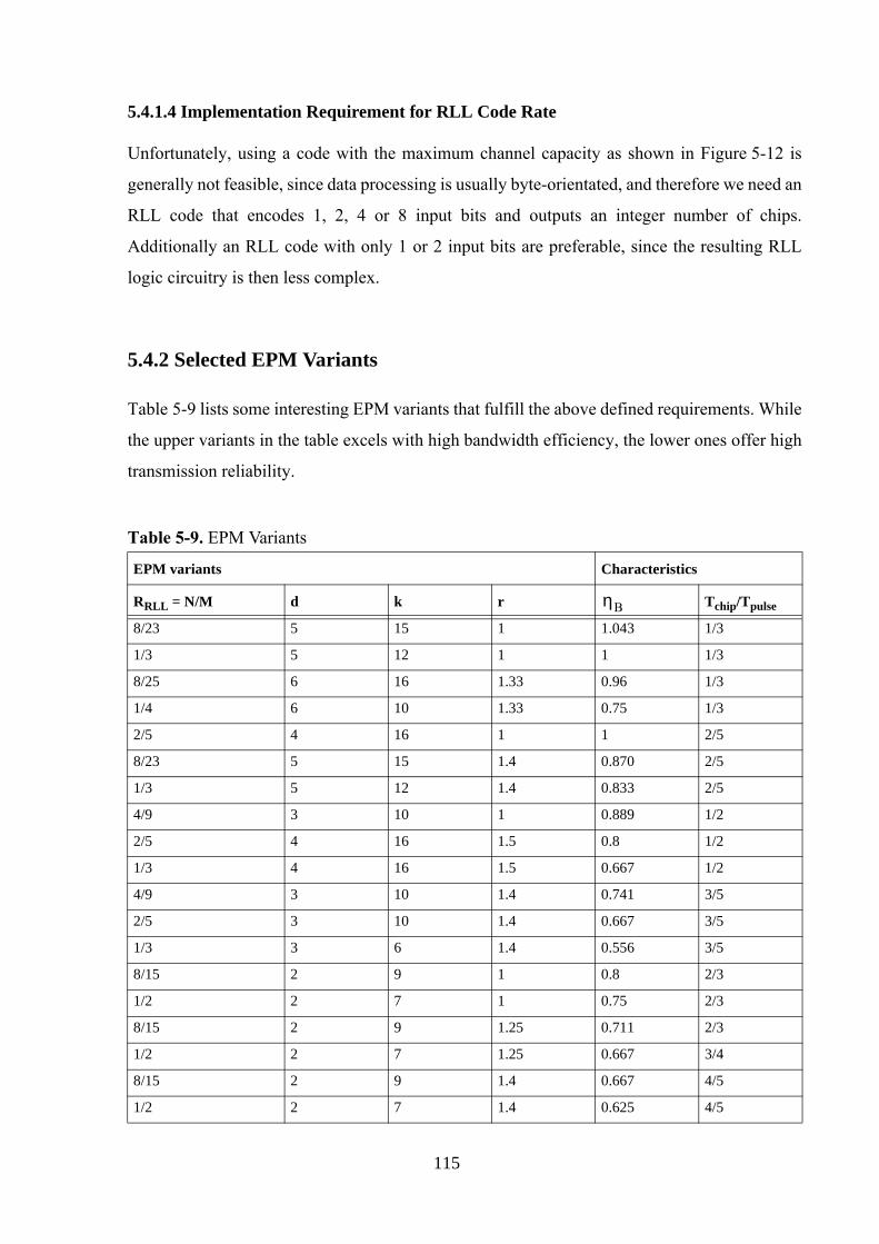
5.4.1.4 Implementation Requirement for RLL Code Rate
Unfortunately, using a code with the maximum channel capacity as shown in Figure 5-12 is
generally not feasible, since data processing is usually byte-orientated, and therefore we need an
RLL code that encodes 1, 2, 4 or 8 input bits and outputs an integer number of chips.
Additionally an RLL code with only 1 or 2 input bits are preferable, since the resulting RLL
logic circuitry is then less complex.
5.4.2 Selected EPM Variants
Table 5-9 lists some interesting EPM variants that fulfill the above defined requirements. While
the upper variants in the table excels with high bandwidth efficiency, the lower ones offer high
transmission reliability.
Table 5-9. EPM Variants
EPM variants Characteristics
RRLL = N/M d k r ηB Tchip/Tpulse
8/23 5 15 1 1.043 1/3
1/3 5 12 1 1 1/3
8/25 6 16 1.33 0.96 1/3
1/4 6 10 1.33 0.75 1/3
2/5 4 16 1 1 2/5
8/23 5 15 1.4 0.870 2/5
1/3 5 12 1.4 0.833 2/5
4/9 3 10 1 0.889 1/2
2/5 4 16 1.5 0.8 1/2
1/3 4 16 1.5 0.667 1/2
4/9 3 10 1.4 0.741 3/5
2/5 3 10 1.4 0.667 3/5
1/3 3 6 1.4 0.556 3/5
8/15 2 9 1 0.8 2/3
1/2 2 7 1 0.75 2/3
8/15 2 9 1.25 0.711 2/3
1/2 2 7 1.25 0.667 3/4
8/15 2 9 1.4 0.667 4/5
1/2 2 7 1.4 0.625 4/5
115

ηB
The EPM concept obviously allows to find an ideal trade-off between transmission speed and
reliability, and therefore EPM enables the implementation of communication systems that are
tailored to the targeted transmission channel.
In the following chapter we want to investigate EPM(5,12,1/3,1) in more detail, because this
variant appears to offer a high bandwidth efficiency at low hardware complexity.
8/15 2 9 1.5 0.64 5/6
1/2 2 7 1.5 0.6 5/6
2/3 1 13 1 0.667 1
EPM variants Characteristics
RRLL = N/M d k r Tchip/Tpulse
116
6 EPM(5,12,1/3,1) - Implementation Example
6.1 EPM(5,12,1/3,1) Evaluation
As derived in Section 5.4 the modulation scheme EPM(5,12,1/3,1) appears to be a promising
candidate for the electrical modulation of a wireless infrared communication system. Therefore
we analyze this EPM variant in this chapter in more detail and for that we use the a novel 1/3-
rate RLL(5,12) code that was presented by the author in [9]. The generation of this RLL(5,12)
code is provided in Appendix A of this work. Adler presented in [57] already an other 1/3-rate
RLL(5,12) code, but this one requires more states in the encoder and is therefore a bit more
complex than the new one.
6.1.1 EPM(5,12,1/3,1) Modulation Scheme
At EPM(5,12,1/3,1) one bit is encoded per encoding step and thereby three chips are generated.
Consequently, the input block αk and the output block βk are given by
αk ak= Eq. 6-1.
βk b3k b3k 1+ b3k 2+ ., ,= Eq. 6-2.
The resulting code rate is derived as
pq--- 1
3---= Eq. 6-3.
117
and the chip duration is then
Tchip13---Tpulse.= Eq. 6-4.
The EPM(5,12,1/3,1) encoder is a finite state machine:
βk f αk ζk,( )= Eq. 6-5.
ζk 1+ g αk ζk,( ),= Eq. 6-6.
with the internal state
ζk z1k z2k z3k z4k = Eq. 6-7.
and the corresponding initial state
ζ0 0 0 0 0( ).= Eq. 6-8.
The output function of the EPM(5,12,1/3,1) encoder state machine is given by
b3k z1k z2k z3k ak z1k z3k z4k⋅⋅⋅+⋅⋅= Eq. 6-9.
b3k 1+ z1k z2k z3k z4k z1k z2k z3k z4k⋅⋅ ⋅+⋅⋅ ⋅= Eq. 6-10.
b3k 2+ ak z2k z3k z4k ak z1k z2k z3k z4k⋅⋅⋅⋅+⋅⋅⋅=
ak z1k z3k z4k ak z2k z3k z4k⋅⋅⋅+⋅⋅⋅+Eq. 6-11.
118
and the next state function is
z1k 1+ ak z1k z3k z4k⋅ ⋅ ⋅( ) z1k z2k z3k z4k⋅ ⋅ ⋅( )+=
z1k z2k z3k z4k⋅ ⋅ ⋅( ) ak z1k z2k z4k⋅ ⋅ ⋅( )+ +
Eq. 6-12.
z2k 1+ ak z1k z3k z4k⋅ ⋅ ⋅( ) ak z2k z3k z4k⋅ ⋅ ⋅( )+=
ak z1k z2k z3k⋅ ⋅ ⋅( ) ak z1k z2k⋅ ⋅( ) ak z2k z3k z4k⋅ ⋅ ⋅( )+ + +
ak z2k z3k z4k⋅ ⋅ ⋅( ) z1k z2k z3k z4k⋅ ⋅ ⋅( )+ +
Eq. 6-13.
z3k 1+ ak z1k z2k z3k⋅ ⋅ ⋅( ) ak z1k z2k z4k⋅ ⋅ ⋅( )+=
z1k z2k z4k⋅ ⋅( ) ak z1k z3k⋅ ⋅( ) z1k z2k z4k⋅ ⋅( )+ + +
ak z1k z2k z4k⋅ ⋅ ⋅( ) ak z2k z3k z4k⋅ ⋅ ⋅( )+ +
ak z1k z2k z4k⋅ ⋅ ⋅( )+
Eq. 6-14.
z4k 1+ ak z1k z3k z4k⋅ ⋅ ⋅( ) ak z1k z2k z4k⋅ ⋅ ⋅( )+=
ak z⋅ 2k z3k z4k⋅ ⋅( ) ak z2k z3k z4k⋅ ⋅ ⋅( )+ +
ak z⋅ 1k z2k z3k z4k⋅ ⋅ ⋅( ) ak z1k z3k z4k⋅ ⋅ ⋅( )+ +
ak z2k z3k z4k⋅ ⋅ ⋅( ) ak z1k z2k z4k⋅ ⋅ ⋅( )+ +
ak z2k z3k z4k⋅ ⋅ ⋅( ) ak z2k z3k z4k⋅ ⋅ ⋅( )+ +
Eq. 6-15.
The pulse shaper generates pulses with a duration three times the chip duration
Tpulse 3Tchip.= Eq. 6-16.
Figure 6-1 provides an example for the EPM(5,12,1/3,1) modulation, whereby b(t) should only
illustrate the timing relation to a(t) and does not reflect a correct encoder result, since this
depends on the current internal encoder state, which is not taken into account here.
119
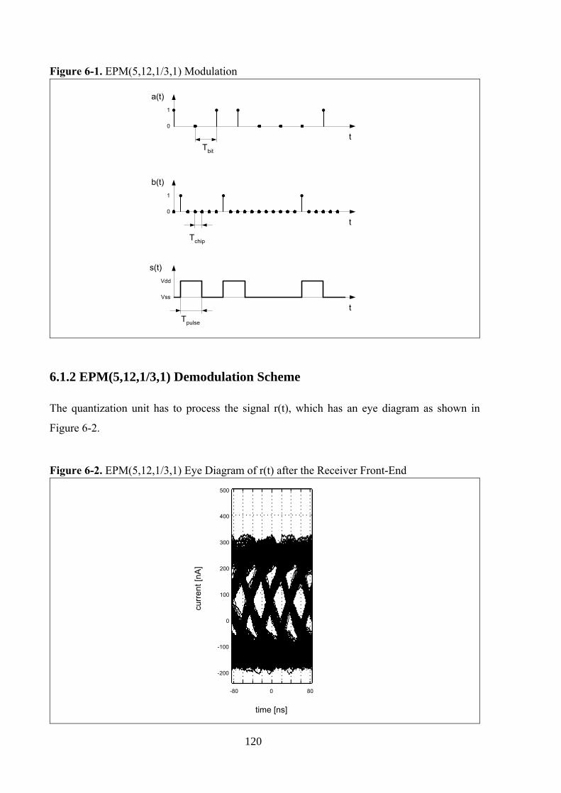
Figure 6-1. EPM(5,12,1/3,1) Modulation
0
1
t
Tchip
0
1
tTbit
Vss
Vdd
tTpulse
s(t)
a(t)
b(t)
6.1.2 EPM(5,12,1/3,1) Demodulation Scheme
The quantization unit has to process the signal r(t), which has an eye diagram as shown in
Figure 6-2.
Figure 6-2. EPM(5,12,1/3,1) Eye Diagram of r(t) after the Receiver Front-End
-80 0 80
-200
-100
0
100
200
300
400
500
time [ns]
curr
ent [
nA]
120
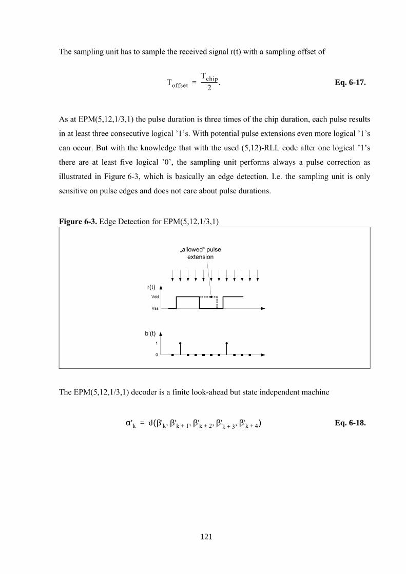
The sampling unit has to sample the received signal r(t) with a sampling offset of
ToffsetTchip
2------------ .= Eq. 6-17.
As at EPM(5,12,1/3,1) the pulse duration is three times of the chip duration, each pulse results
in at least three consecutive logical ’1’s. With potential pulse extensions even more logical ’1’s
can occur. But with the knowledge that with the used (5,12)-RLL code after one logical ’1’s
there are at least five logical ’0’, the sampling unit performs always a pulse correction as
illustrated in Figure 6-3, which is basically an edge detection. I.e. the sampling unit is only
sensitive on pulse edges and does not care about pulse durations.
Figure 6-3. Edge Detection for EPM(5,12,1/3,1)
Vss
Vdd
r(t)
0
1
b’(t)
„allowed“ pulseextension
The EPM(5,12,1/3,1) decoder is a finite look-ahead but state independent machine
α'k d β'k β'k 1+ β'k 2+ β, 'k 3+ β'k 4+, , ,( )= Eq. 6-18.
121
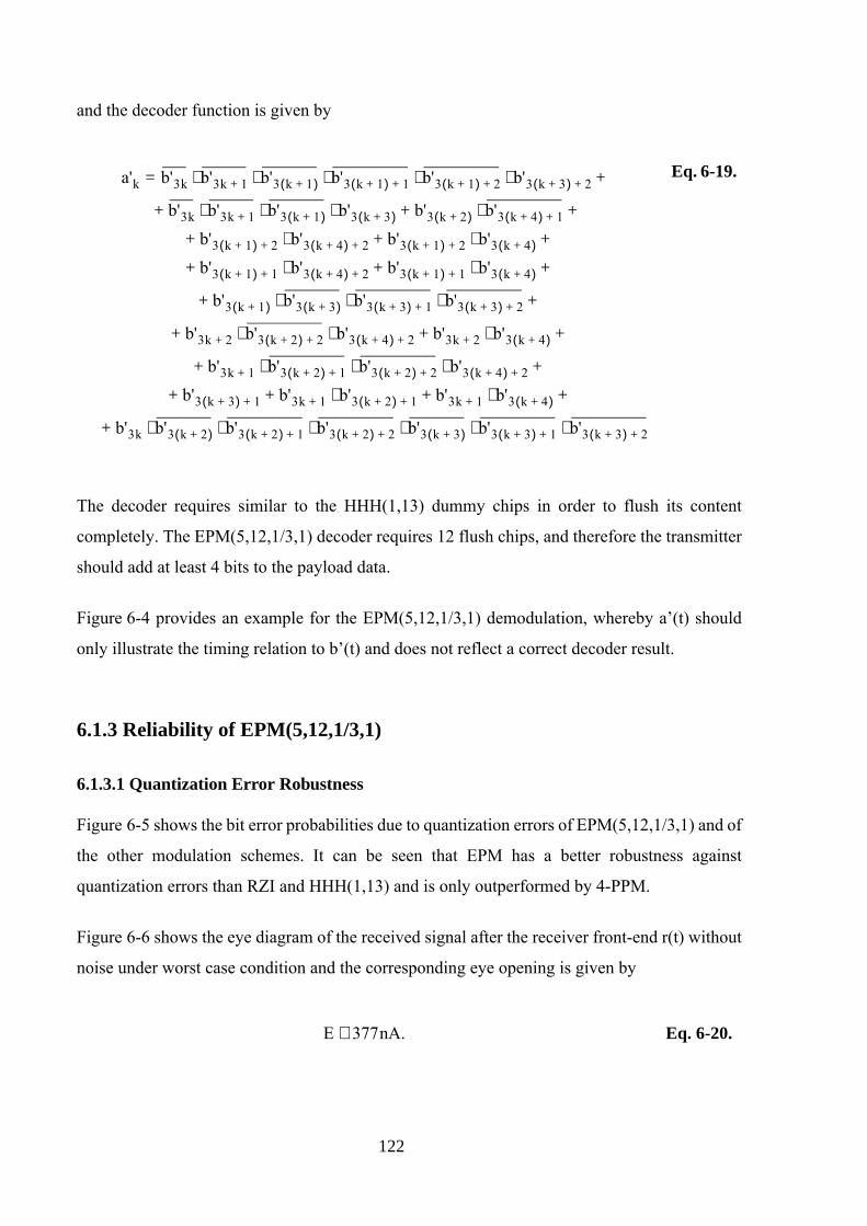
and the decoder function is given by
a'k b'3k b'3k 1+ b'3 k 1+( ) b'3 k 1+( ) 1+ b'3 k 1+( ) 2+ b'3 k 3+( ) 2+⋅ ⋅ ⋅ ⋅ ⋅ +=
b'3k b'3k 1+ b'3 k 1+( ) b'3 k 3+( )⋅ ⋅ ⋅ b'3 k 2+( ) b'3 k 4+( ) 1+⋅+ + +
b'3 k 1+( ) 2+ b'3 k 4+( ) 2+⋅ b'3 k 1+( ) 2+ b'3 k 4+( )⋅+ + +
b'3 k 1+( ) 1+ b'3 k 4+( ) 2+⋅ b'3 k 1+( ) 1+ b'3 k 4+( )⋅+ + +
b'3 k 1+( ) b'3 k 3+( ) b'3 k 3+( ) 1+ b'3 k 3+( ) 2+⋅ ⋅ ⋅+ +
b'3k 2+ b'3 k 2+( ) 2+ b'3 k 4+( ) 2+⋅ ⋅ b'3k 2+ b'3 k 4+( )⋅+ + +
b'3k 1+ b'3 k 2+( ) 1+ b'3 k 2+( ) 2+ b'3 k 4+( ) 2+⋅ ⋅ ⋅+ +
b'3 k 3+( ) 1++ b'3k 1+ b'3 k 2+( ) 1+⋅ b'3k 1+ b'3 k 4+( )⋅+ + +
b'3k b'3 k 2+( ) b'3 k 2+( ) 1+ b'3 k 2+( ) 2+ b'3 k 3+( ) b'3 k 3+( ) 1+ b'3 k 3+( ) 2+⋅ ⋅ ⋅ ⋅ ⋅ ⋅+
Eq. 6-19.
The decoder requires similar to the HHH(1,13) dummy chips in order to flush its content
completely. The EPM(5,12,1/3,1) decoder requires 12 flush chips, and therefore the transmitter
should add at least 4 bits to the payload data.
Figure 6-4 provides an example for the EPM(5,12,1/3,1) demodulation, whereby a’(t) should
only illustrate the timing relation to b’(t) and does not reflect a correct decoder result.
6.1.3 Reliability of EPM(5,12,1/3,1)
6.1.3.1 Quantization Error Robustness
Figure 6-5 shows the bit error probabilities due to quantization errors of EPM(5,12,1/3,1) and of
the other modulation schemes. It can be seen that EPM has a better robustness against
quantization errors than RZI and HHH(1,13) and is only outperformed by 4-PPM.
Figure 6-6 shows the eye diagram of the received signal after the receiver front-end r(t) without
noise under worst case condition and the corresponding eye opening is given by
E 377nA.≅ Eq. 6-20.
122
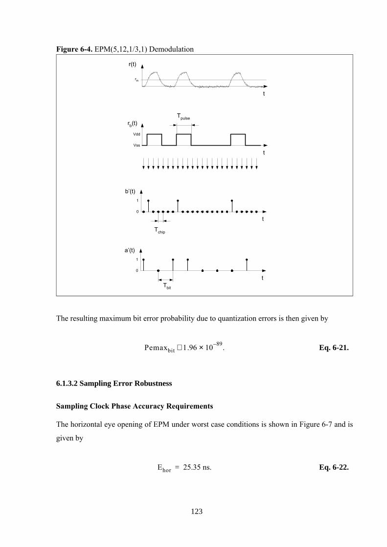
Figure 6-4. EPM(5,12,1/3,1) Demodulation
0
1
t
Tchip
0
1
tTbit
Vss
Vdd
t
Tpulserb(t)
a’(t)
b’(t)
rth
t
r(t)
The resulting maximum bit error probability due to quantization errors is then given by
Pemaxbit 1.96 10 89–× .≅ Eq. 6-21.
6.1.3.2 Sampling Error Robustness
Sampling Clock Phase Accuracy Requirements
The horizontal eye opening of EPM under worst case conditions is shown in Figure 6-7 and is
given by
Ehor 25.35 ns.= Eq. 6-22.
123
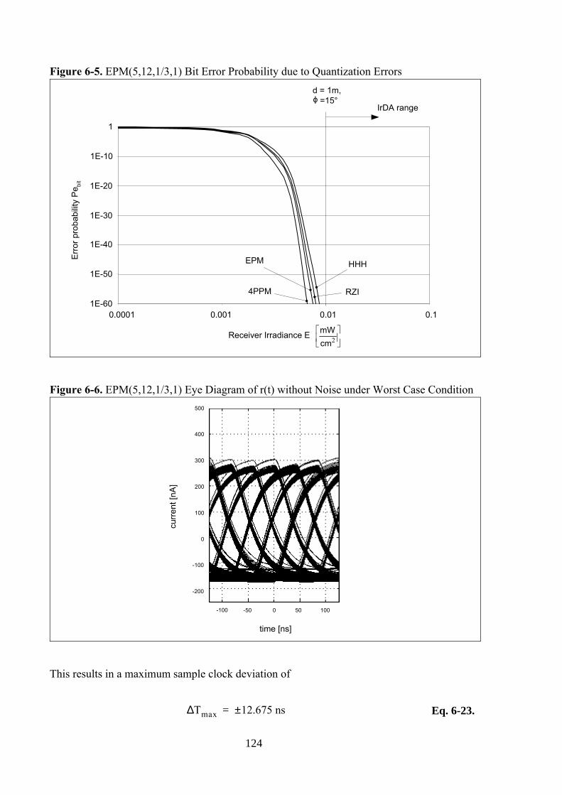
Figure 6-5. EPM(5,12,1/3,1) Bit Error Probability due to Quantization Errors
1E-60
1E-50
1E-40
1E-30
1E-20
1E-10
1
0.0001 0.001 0.01 0.1
HHH
RZI
EPM
4PPM
IrDA range
d = 1m,=15°
Receiver Irradiance E
Err
or p
roba
bilit
y P
e bit
2cm
mW
ϕ
Figure 6-6. EPM(5,12,1/3,1) Eye Diagram of r(t) without Noise under Worst Case Condition
-200
-100
0
100
200
300
400
500
curr
ent [
nA]
-100 -50 0 50 100
time [ns]
This results in a maximum sample clock deviation of
Tmax∆ 12.675 ns±= Eq. 6-23.
124
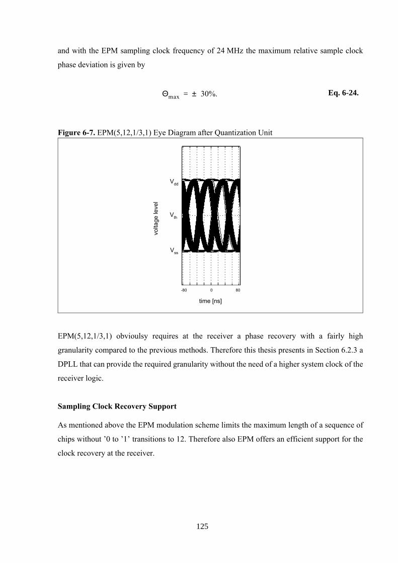
and with the EPM sampling clock frequency of 24 MHz the maximum relative sample clock
phase deviation is given by
Θmax 30%.±= Eq. 6-24.
Figure 6-7. EPM(5,12,1/3,1) Eye Diagram after Quantization Unit
time [ns]
-80 0 80
Vss
Vdd
volta
ge le
vel
Vth
EPM(5,12,1/3,1) obvioulsy requires at the receiver a phase recovery with a fairly high
granularity compared to the previous methods. Therefore this thesis presents in Section 6.2.3 a
DPLL that can provide the required granularity without the need of a higher system clock of the
receiver logic.
Sampling Clock Recovery Support
As mentioned above the EPM modulation scheme limits the maximum length of a sequence of
chips without ’0 to ’1’ transitions to 12. Therefore also EPM offers an efficient support for the
clock recovery at the receiver.
125
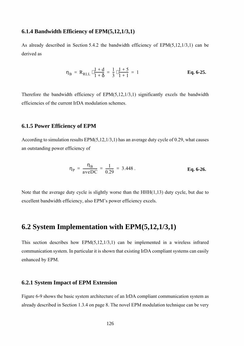
6.1.4 Bandwidth Efficiency of EPM(5,12,1/3,1)
As already described in Section 5.4.2 the bandwidth efficiency of EPM(5,12,1/3,1) can be
derived as
ηB RRLL1 d+1 δ+------------⋅ 1
3--- 1 5+
1 1+------------⋅ 1= = = Eq. 6-25.
Therefore the bandwidth efficiency of EPM(5,12,1/3,1) significantly excels the bandwidth
efficiencies of the current IrDA modulation schemes.
6.1.5 Power Efficiency of EPM
According to simulation results EPM(5,12,1/3,1) has an average duty cycle of 0.29, what causes
an outstanding power efficiency of
ηPηB
aveDC------------------ 1
0.29---------- 3.448 .= = = Eq. 6-26.
Note that the average duty cycle is slightly worse than the HHH(1,13) duty cycle, but due to
excellent bandwidth efficiency, also EPM’s power efficiency excels.
6.2 System Implementation with EPM(5,12,1/3,1)
This section describes how EPM(5,12,1/3,1) can be implemented in a wireless infrared
communication system. In particular it is shown that existing IrDA compliant systems can easily
enhanced by EPM.
6.2.1 System Impact of EPM Extension
Figure 6-9 shows the basic system architecture of an IrDA compliant communication system as
already described in Section 1.3.4 on page 8. The novel EPM modulation technique can be very
126
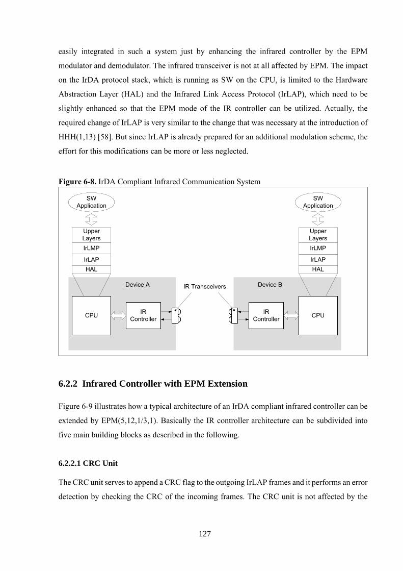
easily integrated in such a system just by enhancing the infrared controller by the EPM
modulator and demodulator. The infrared transceiver is not at all affected by EPM. The impact
on the IrDA protocol stack, which is running as SW on the CPU, is limited to the Hardware
Abstraction Layer (HAL) and the Infrared Link Access Protocol (IrLAP), which need to be
slightly enhanced so that the EPM mode of the IR controller can be utilized. Actually, the
required change of IrLAP is very similar to the change that was necessary at the introduction of
HHH(1,13) [58]. But since IrLAP is already prepared for an additional modulation scheme, the
effort for this modifications can be more or less neglected.
Figure 6-8. IrDA Compliant Infrared Communication System
CPU CPUIRController
IRController
IR TransceiversDevice A Device B
HALIrLAP
IrLMP
UpperLayers
SWApplication
HALIrLAP
IrLMP
UpperLayers
SWApplication
6.2.2 Infrared Controller with EPM Extension
Figure 6-9 illustrates how a typical architecture of an IrDA compliant infrared controller can be
extended by EPM(5,12,1/3,1). Basically the IR controller architecture can be subdivided into
five main building blocks as described in the following.
6.2.2.1 CRC Unit
The CRC unit serves to append a CRC flag to the outgoing IrLAP frames and it performs an error
detection by checking the CRC of the incoming frames. The CRC unit is not affected by the
127
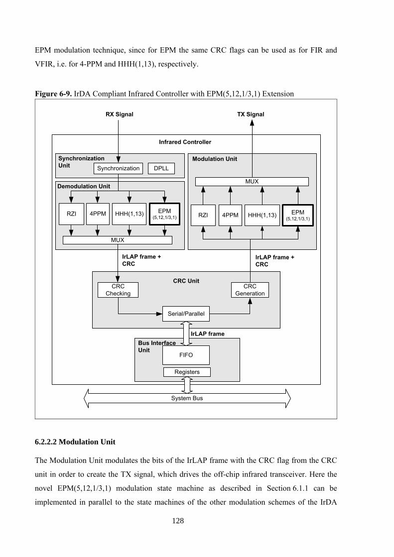
EPM modulation technique, since for EPM the same CRC flags can be used as for FIR and
VFIR, i.e. for 4-PPM and HHH(1,13), respectively.
Figure 6-9. IrDA Compliant Infrared Controller with EPM(5,12,1/3,1) Extension
System Bus
CRCChecking
Serial/Parallel
TX SignalRX Signal
MUX
CRC Unit
Modulation UnitSynchronizationUnit
Infrared Controller
IrLAP frame +CRC
Demodulation Unit
RZI
FIFO
Bus InterfaceUnit
4PPM HHH(1,13) EPM(5,12,1/3,1)
RZI 4PPM HHH(1,13) EPM(5,12,1/3,1)
CRCGeneration
DPLL
MUX
Synchronization
Registers
IrLAP frame +CRC
IrLAP frame
6.2.2.2 Modulation Unit
The Modulation Unit modulates the bits of the IrLAP frame with the CRC flag from the CRC
unit in order to create the TX signal, which drives the off-chip infrared transceiver. Here the
novel EPM(5,12,1/3,1) modulation state machine as described in Section 6.1.1 can be
implemented in parallel to the state machines of the other modulation schemes of the IrDA
128
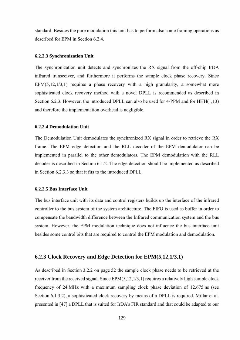
standard. Besides the pure modulation this unit has to perform also some framing operations as
described for EPM in Section 6.2.4.
6.2.2.3 Synchronization Unit
The synchronization unit detects and synchronizes the RX signal from the off-chip IrDA
infrared transceiver, and furthermore it performs the sample clock phase recovery. Since
EPM(5,12,1/3,1) requires a phase recovery with a high granularity, a somewhat more
sophisticated clock recovery method with a novel DPLL is recommended as described in
Section 6.2.3. However, the introduced DPLL can also be used for 4-PPM and for HHH(1,13)
and therefore the implementation overhead is negligible.
6.2.2.4 Demodulation Unit
The Demodulation Unit demodulates the synchronized RX signal in order to retrieve the RX
frame. The EPM edge detection and the RLL decoder of the EPM demodulator can be
implemented in parallel to the other demodulators. The EPM demodulation with the RLL
decoder is described in Section 6.1.2. The edge detection should be implemented as described
in Section 6.2.3.3 so that it fits to the introduced DPLL.
6.2.2.5 Bus Interface Unit
The bus interface unit with its data and control registers builds up the interface of the infrared
controller to the bus system of the system architecture. The FIFO is used as buffer in order to
compensate the bandwidth difference between the Infrared communication system and the bus
system. However, the EPM modulation technique does not influence the bus interface unit
besides some control bits that are required to control the EPM modulation and demodulation.
6.2.3 Clock Recovery and Edge Detection for EPM(5,12,1/3,1)
As described in Section 3.2.2 on page 52 the sample clock phase needs to be retrieved at the
receiver from the received signal. Since EPM(5,12,1/3,1) requires a relatively high sample clock
frequency of 24 MHz with a maximum sampling clock phase deviation of 12.675 ns (see
Section 6.1.3.2), a sophisticated clock recovery by means of a DPLL is required. Millar et al.
presented in [47] a DPLL that is suited for IrDA's FIR standard and that could be adapted to our
129
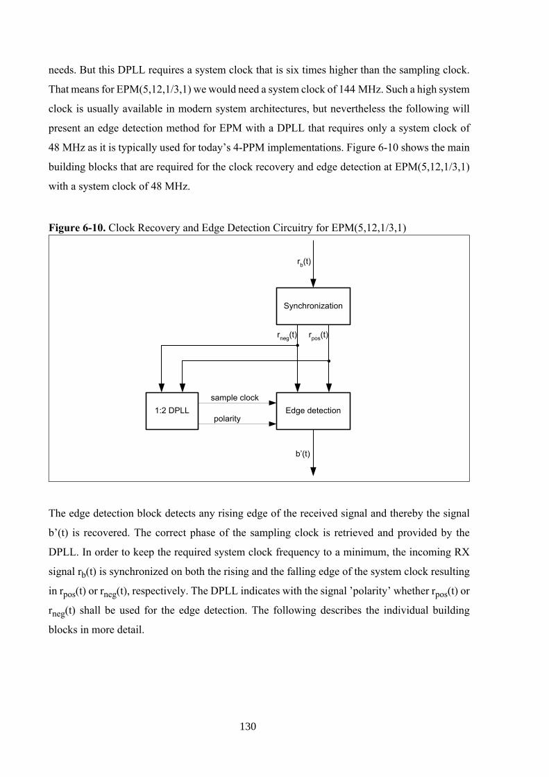
needs. But this DPLL requires a system clock that is six times higher than the sampling clock.
That means for EPM(5,12,1/3,1) we would need a system clock of 144 MHz. Such a high system
clock is usually available in modern system architectures, but nevertheless the following will
present an edge detection method for EPM with a DPLL that requires only a system clock of
48 MHz as it is typically used for today’s 4-PPM implementations. Figure 6-10 shows the main
building blocks that are required for the clock recovery and edge detection at EPM(5,12,1/3,1)
with a system clock of 48 MHz.
Figure 6-10. Clock Recovery and Edge Detection Circuitry for EPM(5,12,1/3,1)
rneg(t)
Edge detection
b’(t)
1:2 DPLL
Synchronization
rb(t)
rpos(t)
sample clock
polarity
The edge detection block detects any rising edge of the received signal and thereby the signal
b’(t) is recovered. The correct phase of the sampling clock is retrieved and provided by the
DPLL. In order to keep the required system clock frequency to a minimum, the incoming RX
signal rb(t) is synchronized on both the rising and the falling edge of the system clock resulting
in rpos(t) or rneg(t), respectively. The DPLL indicates with the signal ’polarity’ whether rpos(t) or
rneg(t) shall be used for the edge detection. The following describes the individual building
blocks in more detail.
130
6.2.3.1 Synchronization
In general input signals to digital circuits are usually synchronized to the rising edge of the
system clock in order to achieve a fully synchronous design. This is also done in our case with
the input signal rb(t) from the infrared transceiver, which is sampled by the rising edge of the
48 MHz system clock. But in addition to that the signal rb(t) is also sampled with the falling edge
of the system clock, as shown in Figure 6-11, in order to preserve important phase information
for the sample clock recovery.
Figure 6-11. Synchronization of Input Signal rb(t)
D Q
Clk
D Q
Clk
D Q
Clk
rpos(t) D Q
Clk
rneg(t)
rb(t)
Synchronization
Note that for each path two consecutive flip-flops are used. Although one flip-flop would be
sufficient from a pure functional perspective, it is recommend to use two flip-flops in order to
avoid unambiguous states after the synchronization.
6.2.3.2 Digital PLL for EPM(5,12,1/3,1)
Figure 6-12 shows the proposed DPLL for EPM(5,12,1/3,1) that retrieves the sample clock with
additional phase information, i.e. signal ’polarity’, from the synchronized RX signals rneg(t) and
rpos(t). The DPLL consists basically of a phase detector, a filter and a variable oscillator that are
all clocked by the positive edge of the 48 MHz system clock. They are described in the
following:
Phase Detector
The phase detector is a state machine that compares the rising edges of the synchronized RX
signals rpos(t) and rneg(t) with those of the recovered sample clock. If the rising edges of the RX
131
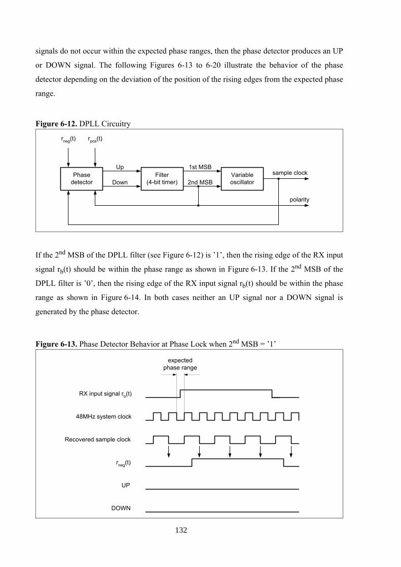
signals do not occur within the expected phase ranges, then the phase detector produces an UP
or DOWN signal. The following Figures 6-13 to 6-20 illustrate the behavior of the phase
detector depending on the deviation of the position of the rising edges from the expected phase
range.
Figure 6-12. DPLL Circuitry
Phasedetector
Filter(4-bit timer)
Variableoscillator
Up
Down
1st MSB
2nd MSB
rneg(t) rpos(t)
sample clock
polarity
If the 2nd MSB of the DPLL filter (see Figure 6-12) is ’1’, then the rising edge of the RX input
signal rb(t) should be within the phase range as shown in Figure 6-13. If the 2nd MSB of the
DPLL filter is ’0’, then the rising edge of the RX input signal rb(t) should be within the phase
range as shown in Figure 6-14. In both cases neither an UP signal nor a DOWN signal is
generated by the phase detector.
Figure 6-13. Phase Detector Behavior at Phase Lock when 2nd MSB = ’1’
48MHz system clock
RX input signal rb(t)
Recovered sample clock
UP
DOWN
rneg(t)
expectedphase range
132
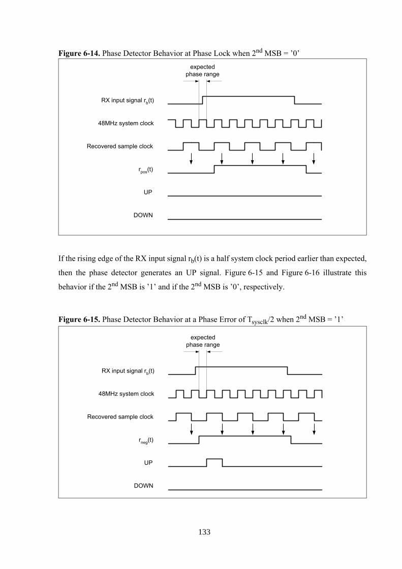
Figure 6-14. Phase Detector Behavior at Phase Lock when 2nd MSB = ’0’
48MHz system clock
RX input signal rb(t)
Recovered sample clock
UP
DOWN
rpos(t)
expectedphase range
If the rising edge of the RX input signal rb(t) is a half system clock period earlier than expected,
then the phase detector generates an UP signal. Figure 6-15 and Figure 6-16 illustrate this
behavior if the 2nd MSB is ’1’ and if the 2nd MSB is ’0’, respectively.
Figure 6-15. Phase Detector Behavior at a Phase Error of Tsysclk/2 when 2nd MSB = ’1’
48MHz system clock
RX input signal rb(t)
Recovered sample clock
UP
DOWN
rneg(t)
expectedphase range
133
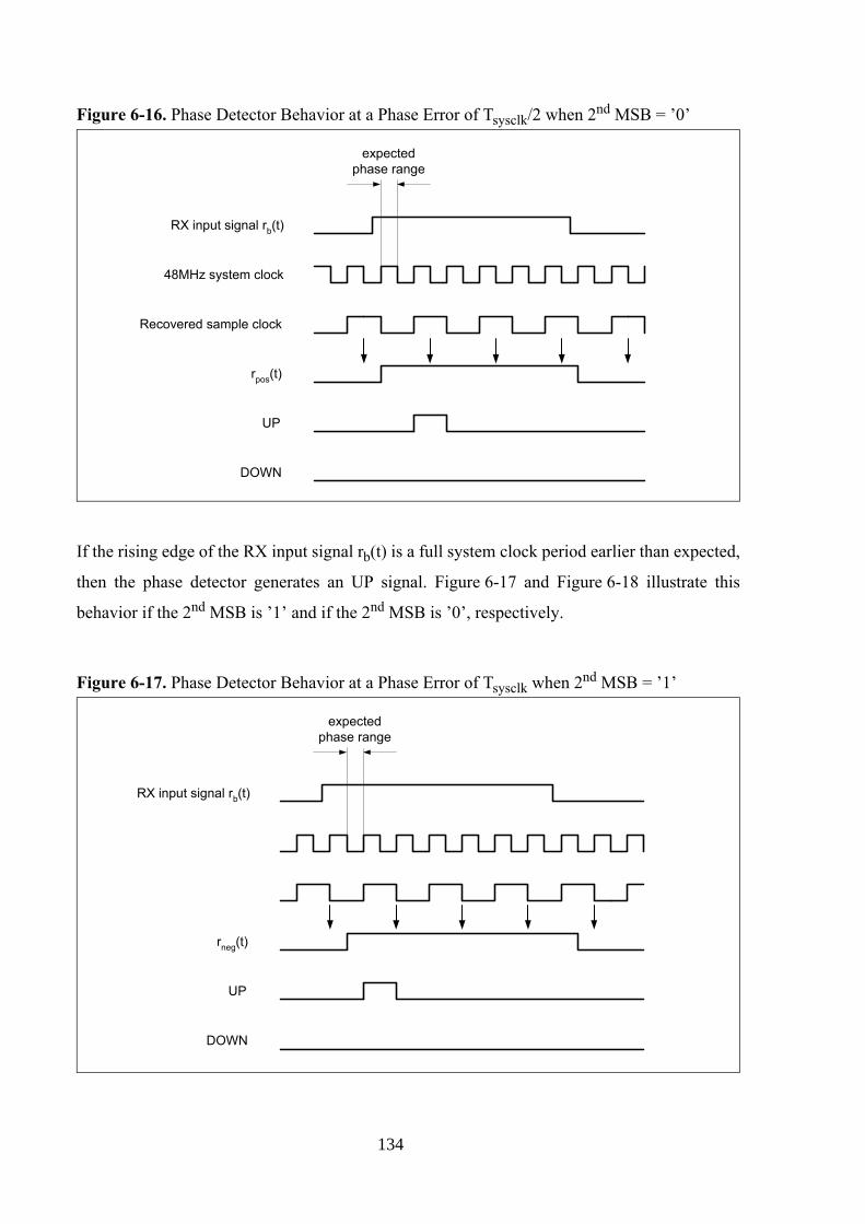
Figure 6-16. Phase Detector Behavior at a Phase Error of Tsysclk/2 when 2nd MSB = ’0’
48MHz system clock
RX input signal rb(t)
Recovered sample clock
UP
DOWN
rpos(t)
expectedphase range
If the rising edge of the RX input signal rb(t) is a full system clock period earlier than expected,
then the phase detector generates an UP signal. Figure 6-17 and Figure 6-18 illustrate this
behavior if the 2nd MSB is ’1’ and if the 2nd MSB is ’0’, respectively.
Figure 6-17. Phase Detector Behavior at a Phase Error of Tsysclk when 2nd MSB = ’1’
RX input signal rb(t)
UP
DOWN
rneg(t)
expectedphase range
134
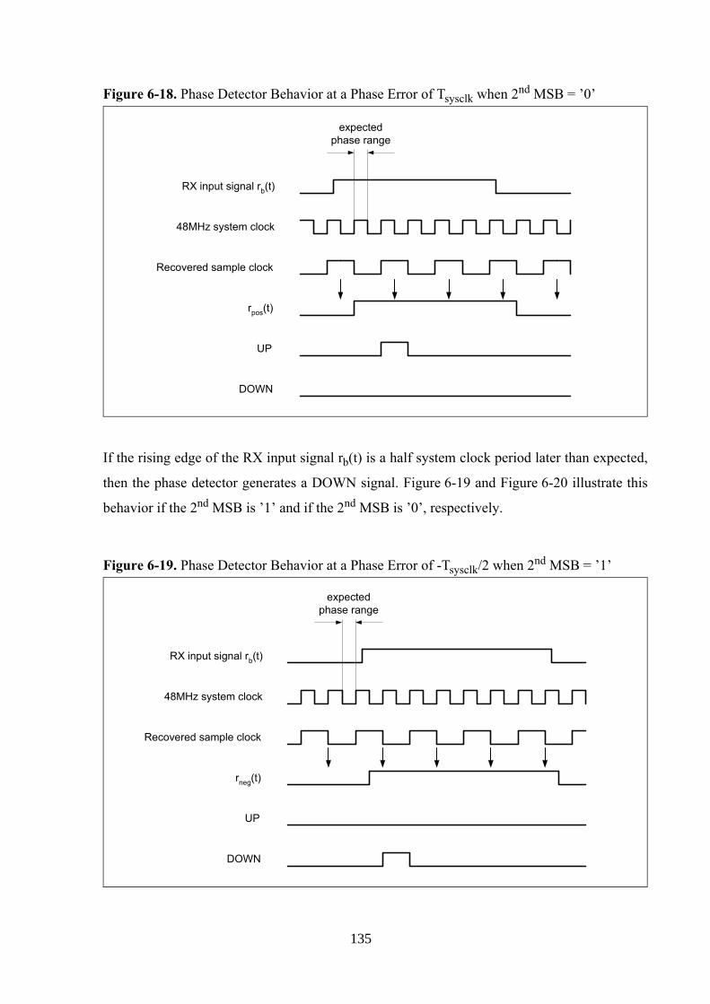
Figure 6-18. Phase Detector Behavior at a Phase Error of Tsysclk when 2nd MSB = ’0’
48MHz system clock
RX input signal rb(t)
Recovered sample clock
UP
DOWN
rpos(t)
expectedphase range
If the rising edge of the RX input signal rb(t) is a half system clock period later than expected,
then the phase detector generates a DOWN signal. Figure 6-19 and Figure 6-20 illustrate this
behavior if the 2nd MSB is ’1’ and if the 2nd MSB is ’0’, respectively.
Figure 6-19. Phase Detector Behavior at a Phase Error of -Tsysclk/2 when 2nd MSB = ’1’
48MHz system clock
RX input signal rb(t)
Recovered sample clock
UP
DOWN
rneg(t)
expectedphase range
135
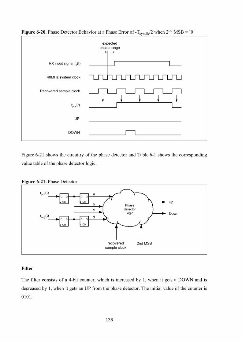
Figure 6-20. Phase Detector Behavior at a Phase Error of -Tsysclk/2 when 2nd MSB = ’0’
48MHz system clock
RX input signal rb(t)
Recovered sample clock
UP
DOWN
rpos(t)
expectedphase range
Figure 6-21 shows the circuitry of the phase detector and Table 6-1 shows the corresponding
value table of the phase detector logic.
Figure 6-21. Phase Detector
D Q
Clk
rpos(t)
rneg(t)
Phasedetector
logic
Up
2nd MSBrecoveredsample clock
Down
a
bc
d
D Q
Clk
D Q
Clk
D Q
Clk
Filter
The filter consists of a 4-bit counter, which is increased by 1, when it gets a DOWN and is
decreased by 1, when it gets an UP from the phase detector. The initial value of the counter is
0101.
136
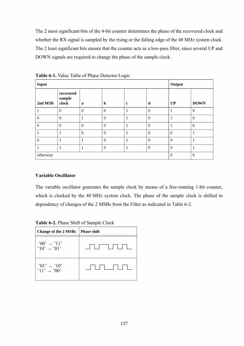
The 2 most significant bits of the 4-bit counter determines the phase of the recovered clock and
whether the RX signal is sampled by the rising or the falling edge of the 48 MHz system clock.
The 2 least significant bits ensure that the counter acts as a low-pass filter, since several UP and
DOWN signals are required to change the phase of the sample clock.
Table 6-1.
Input Output
2nd MSB
recovered sample clock a b c d UP DOWN
1 0 0 0 1 0 1 0
0 0 1 0 1 0 1 0
0 0 0 0 1 0 1 0
1 1 0 0 1 0 0 1
0 1 1 0 1 0 0 1
1 1 1 0 1 0 0 1
otherwise 0 0
Value Table of Phase Detector Logic
Variable Oscillator
The variable oscillator generates the sample clock by means of a free-running 1-bit counter,
which is clocked by the 48 MHz system clock. The phase of the sample clock is shifted in
dependency of changes of the 2 MSBs from the Filter as indicated in Table 6-2.
Table 6-2. Phase Shift of Sample Clock
Change of the 2 MSBs Phase shift
’00’ ’11’→ ’10’ ’01’→
’01’ ’10’→ ’11’ ’00’→
137
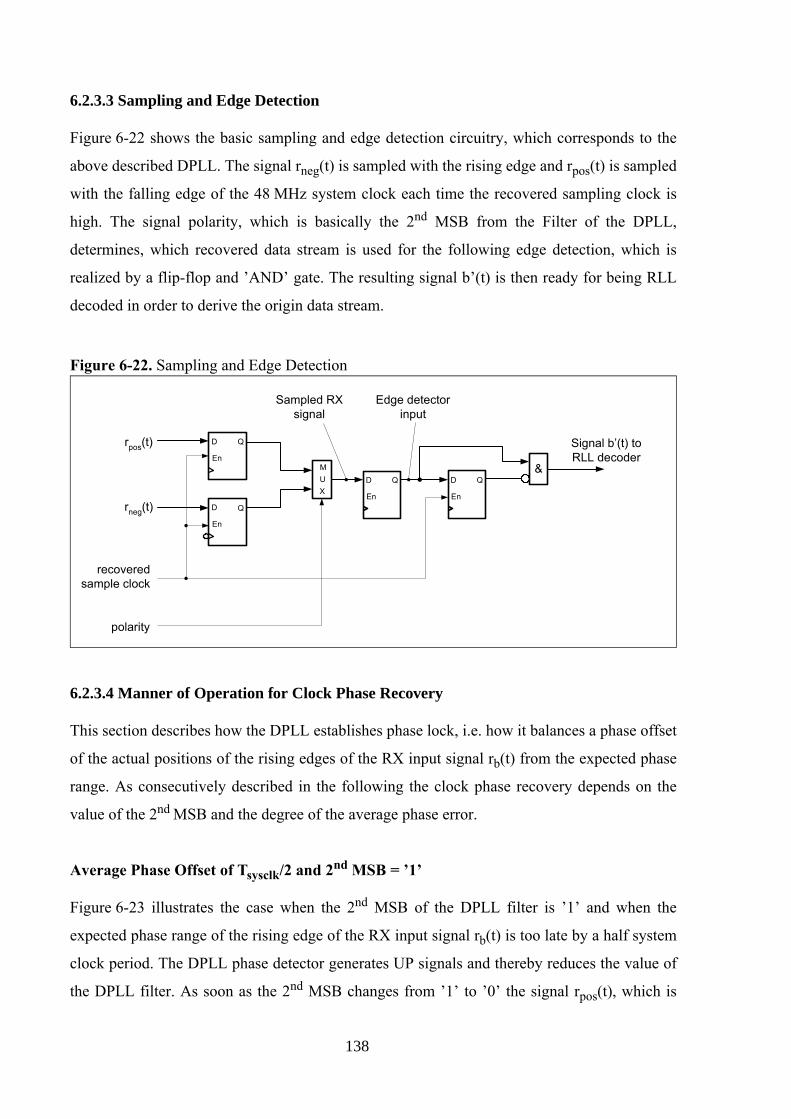
6.2.3.3 Sampling and Edge Detection
Figure 6-22 shows the basic sampling and edge detection circuitry, which corresponds to the
above described DPLL. The signal rneg(t) is sampled with the rising edge and rpos(t) is sampled
with the falling edge of the 48 MHz system clock each time the recovered sampling clock is
high. The signal polarity, which is basically the 2nd MSB from the Filter of the DPLL,
determines, which recovered data stream is used for the following edge detection, which is
realized by a flip-flop and ’AND’ gate. The resulting signal b’(t) is then ready for being RLL
decoded in order to derive the origin data stream.
Figure 6-22. Sampling and Edge Detection
MUX
D
En
recoveredsample clock
rpos(t)
rneg(t)
polarity
Q
D Q
En
D Q
En
D Q
En
&
Signal b’(t) toRLL decoder
Sampled RXsignal
Edge detectorinput
6.2.3.4 Manner of Operation for Clock Phase Recovery
This section describes how the DPLL establishes phase lock, i.e. how it balances a phase offset
of the actual positions of the rising edges of the RX input signal rb(t) from the expected phase
range. As consecutively described in the following the clock phase recovery depends on the
value of the 2nd MSB and the degree of the average phase error.
Average Phase Offset of Tsysclk/2 and 2nd MSB = ’1’
Figure 6-23 illustrates the case when the 2nd MSB of the DPLL filter is ’1’ and when the
expected phase range of the rising edge of the RX input signal rb(t) is too late by a half system
clock period. The DPLL phase detector generates UP signals and thereby reduces the value of
the DPLL filter. As soon as the 2nd MSB changes from ’1’ to ’0’ the signal rpos(t), which is
138
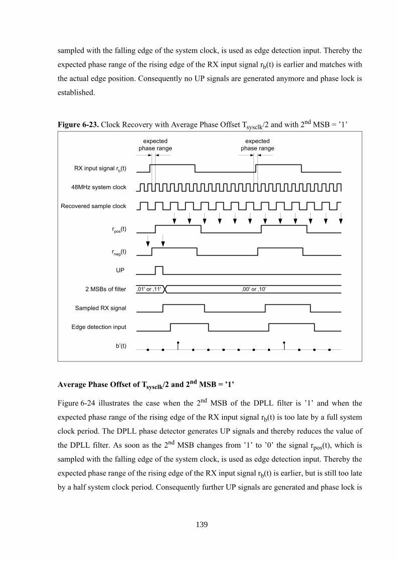
sampled with the falling edge of the system clock, is used as edge detection input. Thereby the
expected phase range of the rising edge of the RX input signal rb(t) is earlier and matches with
the actual edge position. Consequently no UP signals are generated anymore and phase lock is
established.
Figure 6-23. Clock Recovery with Average Phase Offset Tsysclk/2 and with 2nd MSB = ’1’
48MHz system clock
Recovered sample clock
RX input signal rb(t)
rpos(t)
b’(t)
Sampled RX signal
Edge detection input
rneg(t)
UP
2 MSBs of filter ‚01' or ‚11' ‚00' or ‚10'
expectedphase range
expectedphase range
Average Phase Offset of Tsysclk/2 and 2nd MSB = ’1’
Figure 6-24 illustrates the case when the 2nd MSB of the DPLL filter is ’1’ and when the
expected phase range of the rising edge of the RX input signal rb(t) is too late by a full system
clock period. The DPLL phase detector generates UP signals and thereby reduces the value of
the DPLL filter. As soon as the 2nd MSB changes from ’1’ to ’0’ the signal rpos(t), which is
sampled with the falling edge of the system clock, is used as edge detection input. Thereby the
expected phase range of the rising edge of the RX input signal rb(t) is earlier, but is still too late
by a half system clock period. Consequently further UP signals are generated and phase lock is
139
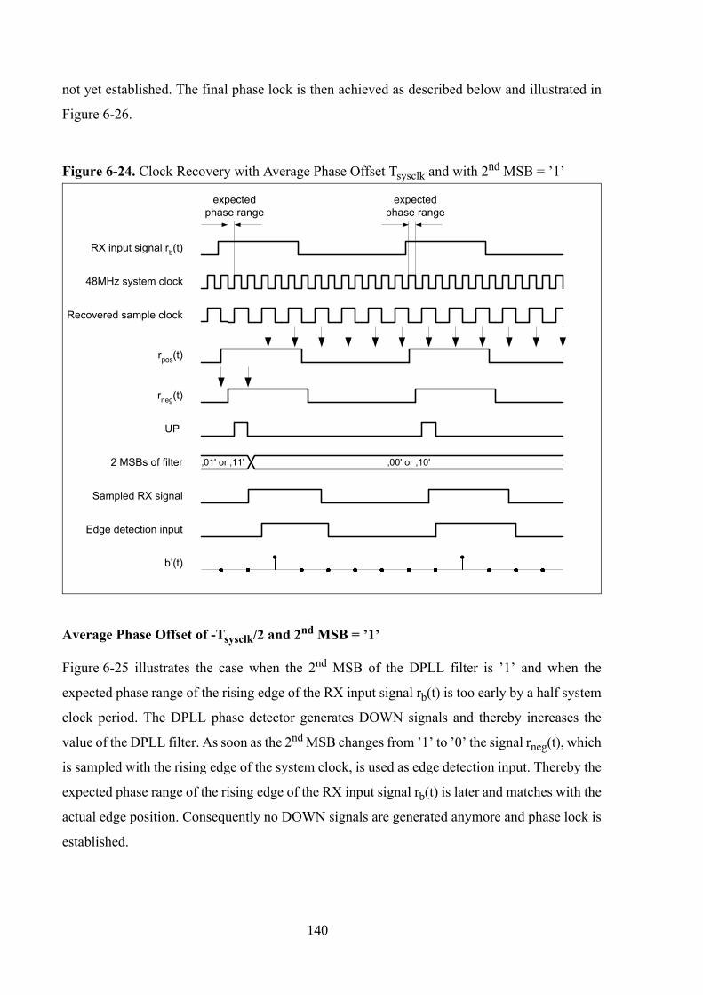
not yet established. The final phase lock is then achieved as described below and illustrated in
Figure 6-26.
Figure 6-24. Clock Recovery with Average Phase Offset Tsysclk and with 2nd MSB = ’1’
48MHz system clock
Recovered sample clock
RX input signal rb(t)
rpos(t)
b’(t)
Sampled RX signal
Edge detection input
rneg(t)
UP
2 MSBs of filter ‚01' or ‚11' ‚00' or ‚10'
expectedphase range
expectedphase range
Average Phase Offset of -Tsysclk/2 and 2nd MSB = ’1’
Figure 6-25 illustrates the case when the 2nd MSB of the DPLL filter is ’1’ and when the
expected phase range of the rising edge of the RX input signal rb(t) is too early by a half system
clock period. The DPLL phase detector generates DOWN signals and thereby increases the
value of the DPLL filter. As soon as the 2nd MSB changes from ’1’ to ’0’ the signal rneg(t), which
is sampled with the rising edge of the system clock, is used as edge detection input. Thereby the
expected phase range of the rising edge of the RX input signal rb(t) is later and matches with the
actual edge position. Consequently no DOWN signals are generated anymore and phase lock is
established.
140
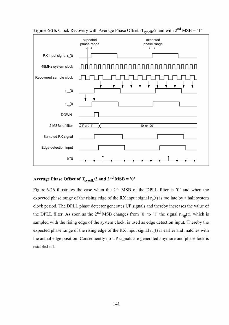
Figure 6-25. Clock Recovery with Average Phase Offset -Tsysclk/2 and with 2nd MSB = ’1’
48MHz system clock
Recovered sample clock
RX input signal rb(t)
rpos(t)
b’(t)
Sampled RX signal
Edge detection input
rneg(t)
DOWN
2 MSBs of filter ‚01' or ‚11' ‚10' or ‚00'
expectedphase range
expectedphase range
Average Phase Offset of Tsysclk/2 and 2nd MSB = ’0’
Figure 6-26 illustrates the case when the 2nd MSB of the DPLL filter is ’0’ and when the
expected phase range of the rising edge of the RX input signal rb(t) is too late by a half system
clock period. The DPLL phase detector generates UP signals and thereby increases the value of
the DPLL filter. As soon as the 2nd MSB changes from ’0’ to ’1’ the signal rneg(t), which is
sampled with the rising edge of the system clock, is used as edge detection input. Thereby the
expected phase range of the rising edge of the RX input signal rb(t) is earlier and matches with
the actual edge position. Consequently no UP signals are generated anymore and phase lock is
established.
141
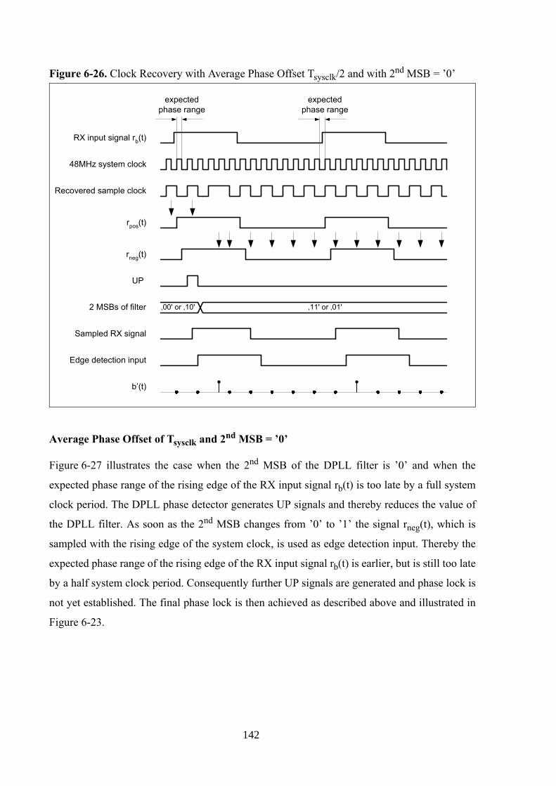
Figure 6-26. Clock Recovery with Average Phase Offset Tsysclk/2 and with 2nd MSB = ’0’
48MHz system clock
Recovered sample clock
RX input signal rb(t)
rpos(t)
b’(t)
Sampled RX signal
Edge detection input
rneg(t)
UP
2 MSBs of filter ‚00' or ‚10' ‚11' or ‚01'
expectedphase range
expectedphase range
Average Phase Offset of Tsysclk and 2nd MSB = ’0’
Figure 6-27 illustrates the case when the 2nd MSB of the DPLL filter is ’0’ and when the
expected phase range of the rising edge of the RX input signal rb(t) is too late by a full system
clock period. The DPLL phase detector generates UP signals and thereby reduces the value of
the DPLL filter. As soon as the 2nd MSB changes from ’0’ to ’1’ the signal rneg(t), which is
sampled with the rising edge of the system clock, is used as edge detection input. Thereby the
expected phase range of the rising edge of the RX input signal rb(t) is earlier, but is still too late
by a half system clock period. Consequently further UP signals are generated and phase lock is
not yet established. The final phase lock is then achieved as described above and illustrated in
Figure 6-23.
142
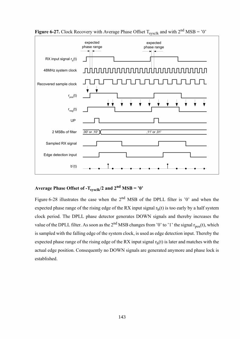
Figure 6-27. Clock Recovery with Average Phase Offset Tsysclk and with 2nd MSB = ’0’
48MHz system clock
Recovered sample clock
RX input signal rb(t)
rpos(t)
b’(t)
Sampled RX signal
Edge detection input
rneg(t)
UP
2 MSBs of filter ‚00' or ‚10' ‚11' or ‚01'
expectedphase range
expectedphase range
Average Phase Offset of -Tsysclk/2 and 2nd MSB = ’0’
Figure 6-28 illustrates the case when the 2nd MSB of the DPLL filter is ’0’ and when the
expected phase range of the rising edge of the RX input signal rb(t) is too early by a half system
clock period. The DPLL phase detector generates DOWN signals and thereby increases the
value of the DPLL filter. As soon as the 2nd MSB changes from ’0’ to ’1’ the signal rpos(t), which
is sampled with the falling edge of the system clock, is used as edge detection input. Thereby the
expected phase range of the rising edge of the RX input signal rb(t) is later and matches with the
actual edge position. Consequently no DOWN signals are generated anymore and phase lock is
established.
143
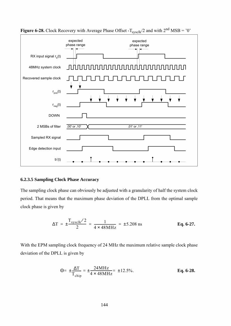
Figure 6-28. Clock Recovery with Average Phase Offset -Tsysclk/2 and with 2nd MSB = ’0’
48MHz system clock
Recovered sample clock
RX input signal rb(t)
rpos(t)
b’(t)
Sampled RX signal
Edge detection input
rneg(t)
DOWN
2 MSBs of filter ‚00' or ‚10' ‚01' or ‚11'
expectedphase range
expectedphase range
6.2.3.5 Sampling Clock Phase Accuracy
The sampling clock phase can obviously be adjusted with a granularity of half the system clock
period. That means that the maximum phase deviation of the DPLL from the optimal sample
clock phase is given by
T∆Tsysclk 2⁄
2-----------------------± 1
4 48MHz×---------------------------- 5.208 ns±= = = Eq. 6-27.
With the EPM sampling clock frequency of 24 MHz the maximum relative sample clock phase
deviation of the DPLL is given by
Θ T∆Tchip------------
24MHz4 48× MHz---------------------------- 12.5%.±=±=±= Eq. 6-28.
144
Considering that the introduced EPM(5,12,1/3,1) scheme allows a maximum sample clock
deviation of Tmax∆ 12.675 ns±= respectively a maximum relative deviation of Θmax 30%±=
(see Section 6.1.3.2), one can see that the proposed clock recovery method fulfills obviously our
requirements for EPM.
6.2.4 Framing Structure for EPM
In order to transmit payload data (e.g. an IrLAP frame according to the IrDA standard) over the
wireless infrared channel in a secure manner, it needs to be packed into a frame that consists of
a preamble PA, a start flag STA, the payload data itself, Flush bits FB, a CRC field, a stop flag
STO and a NULL field [1][2].
The preamble is necessary for phase synchronization at the receiver. It should have enough ’0’
to ’1’ transitions, so that the DPLL at the receiver can achieve its phase-lock, and it should have
the same average duty cycle as the RLL code. We define the preamble PA for EPM as the
concatenation of ten times the 72-chip preamble period PP.
PP = [100000000 000100000 000100000 000000100 000000100 000100000 100000000]
PA = [PP PP PP PP PP PP PP PP PP PP]
The start and stop flags are necessary to indicate the beginning and the end of the frame. In order
to distinguish these flags from payload data we use a sequence that cannot be generated by the
RLL(5,12) encoder. By using such “illegal” sequences we can avoid bit or character stuffing as
it is necessary at the RZI modulation technique. The start and stop flags are given by:
STA = [000001000 000000000 100000000 000100000 010000001 000000000 000100000
000000100 000001000 000000000 100000000 000100000 010000001 000000000 000100000
000000100]
STO = [000001000 000000000 100000000 000100000 010000001 000000000 000100000
000000100 000001000 000000000 100000000 000100000 010000001 000000000 000100000
000000100]
145
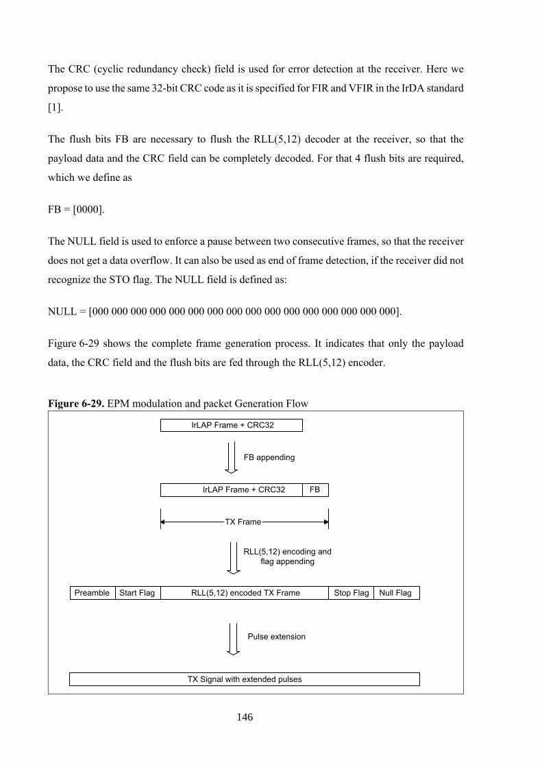
The CRC (cyclic redundancy check) field is used for error detection at the receiver. Here we
propose to use the same 32-bit CRC code as it is specified for FIR and VFIR in the IrDA standard
[1].
The flush bits FB are necessary to flush the RLL(5,12) decoder at the receiver, so that the
payload data and the CRC field can be completely decoded. For that 4 flush bits are required,
which we define as
FB = [0000].
The NULL field is used to enforce a pause between two consecutive frames, so that the receiver
does not get a data overflow. It can also be used as end of frame detection, if the receiver did not
recognize the STO flag. The NULL field is defined as:
NULL = [000 000 000 000 000 000 000 000 000 000 000 000 000 000 000 000].
Figure 6-29 shows the complete frame generation process. It indicates that only the payload
data, the CRC field and the flush bits are fed through the RLL(5,12) encoder.
Figure 6-29.
Stop FlagStart FlagPreamble
TX Frame
IrLAP Frame + CRC32
IrLAP Frame + CRC32
FB appending
RLL(5,12) encoded TX Frame Null Flag
TX Signal with extended pulses
Pulse extension
RLL(5,12) encoding andflag appending
FB
EPM modulation and packet Generation Flow
146
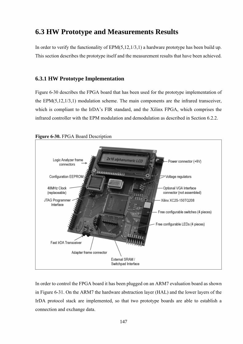
6.3 HW Prototype and Measurements Results
In order to verify the functionality of EPM(5,12,1/3,1) a hardware prototype has been build up.
This section describes the prototype itself and the measurement results that have been achieved.
6.3.1 HW Prototype Implementation
Figure 6-30 describes the FPGA board that has been used for the prototype implementation of
the EPM(5,12,1/3,1) modulation scheme. The main components are the infrared transceiver,
which is compliant to the IrDA’s FIR standard, and the Xilinx FPGA, which comprises the
infrared controller with the EPM modulation and demodulation as described in Section 6.2.2.
Figure 6-30. FPGA Board Description
In order to control the FPGA board it has been plugged on an ARM7 evaluation board as shown
in Figure 6-31. On the ARM7 the hardware abstraction layer (HAL) and the lower layers of the
IrDA protocol stack are implemented, so that two prototype boards are able to establish a
connection and exchange data.
147
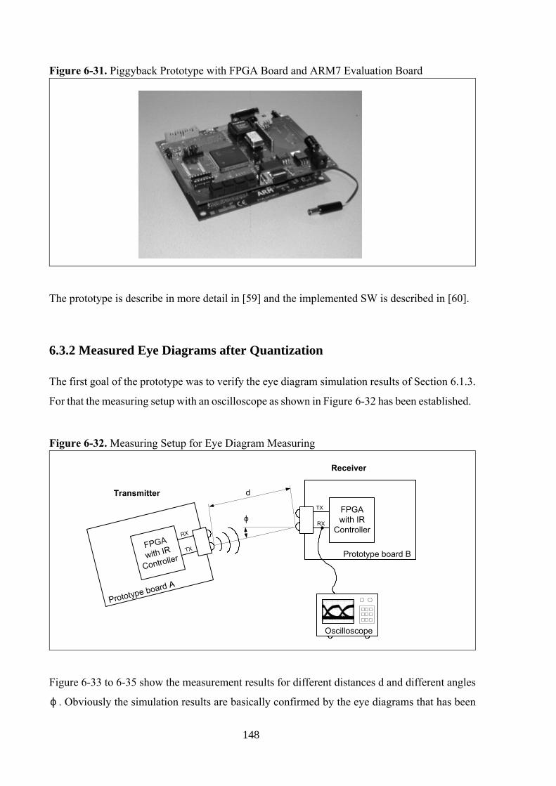
Figure 6-31. Piggyback Prototype with FPGA Board and ARM7 Evaluation Board
The prototype is describe in more detail in [59] and the implemented SW is described in [60].
6.3.2 Measured Eye Diagrams after Quantization
The first goal of the prototype was to verify the eye diagram simulation results of Section 6.1.3.
For that the measuring setup with an oscilloscope as shown in Figure 6-32 has been established.
Figure 6-32. Measuring Setup for Eye Diagram Measuring
FPGAwith IR
Controller
Prototype board B
Transmitter
Receiver
Oscilloscope
FPGA
with IR
Controller
Prototype board A
RX
TX
RX
TX
d
ϕ
Figure 6-33 to 6-35 show the measurement results for different distances d and different angles
ϕ . Obviously the simulation results are basically confirmed by the eye diagrams that has been
148
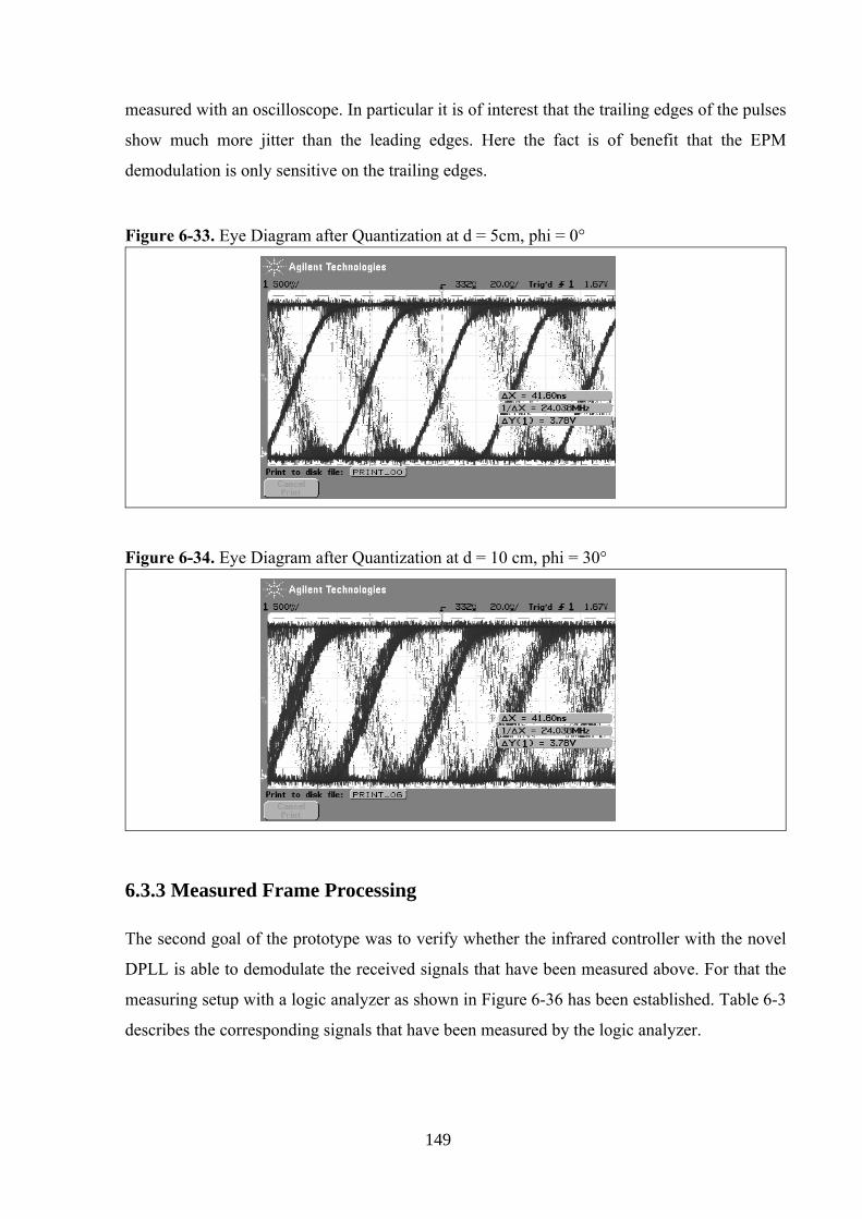
measured with an oscilloscope. In particular it is of interest that the trailing edges of the pulses
show much more jitter than the leading edges. Here the fact is of benefit that the EPM
demodulation is only sensitive on the trailing edges.
Figure 6-33. Eye Diagram after Quantization at d = 5cm, phi = 0°
Figure 6-34. Eye Diagram after Quantization at d = 10 cm, phi = 30°
6.3.3 Measured Frame Processing
The second goal of the prototype was to verify whether the infrared controller with the novel
DPLL is able to demodulate the received signals that have been measured above. For that the
measuring setup with a logic analyzer as shown in Figure 6-36 has been established. Table 6-3
describes the corresponding signals that have been measured by the logic analyzer.
149
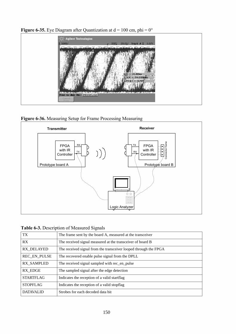
Figure 6-35. Eye Diagram after Quantization at d = 100 cm, phi = 0°
Figure 6-36. Measuring Setup for Frame Processing Measuring
FPGAwith IR
Controller
Prototype board B
Transmitter Receiver
RX
TXFPGAwith IR
Controller
Prototype board A
TX
RX
Logic Analyzer
Con
nect
or fr
ame
Table 6-3. Description of Measured SignalsTX The frame sent by the board A, measured at the transceiver
RX The received signal measured at the transceiver of board B
RX_DELAYED The received signal from the transceiver looped through the FPGA
REC_EN_PULSE The recovered enable pulse signal from the DPLL
RX_SAMPLED The received signal sampled with rec_en_pulse
RX_EDGE The sampled signal after the edge detection
STARTFLAG Indicates the reception of a valid startflag
STOPFLAG Indicates the reception of a valid stopflag
DATAVALID Strobes for each decoded data bit
150
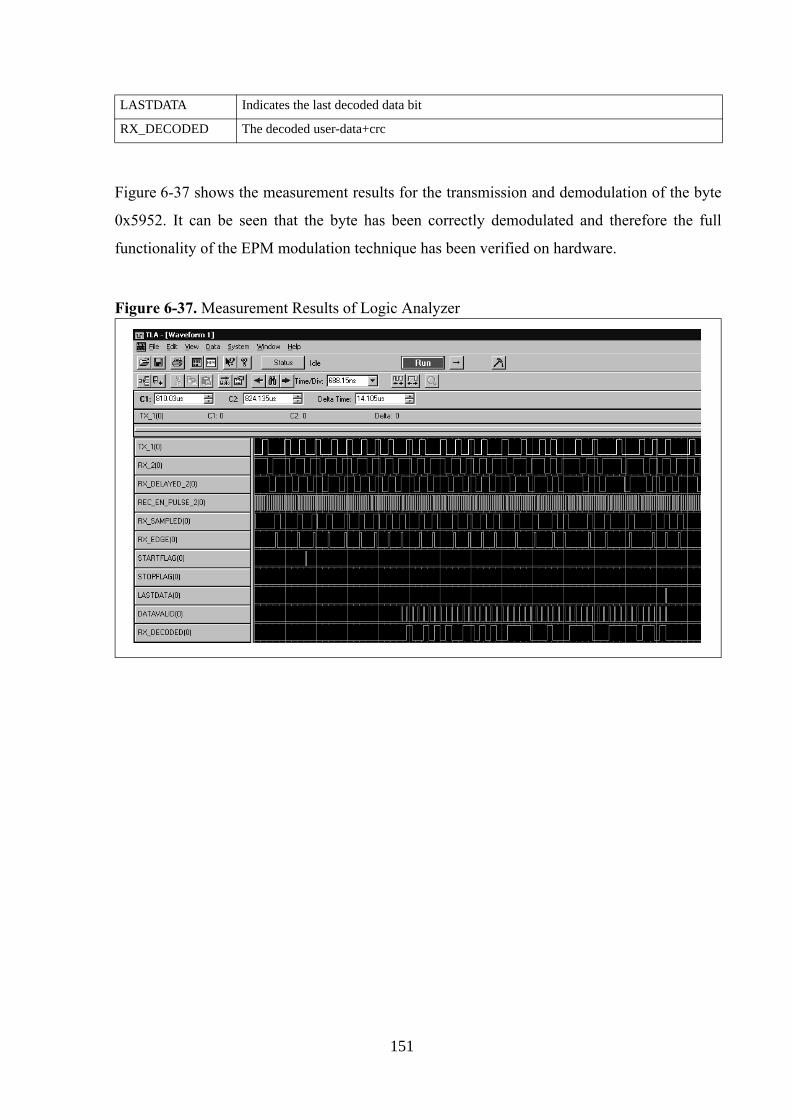
Figure 6-37 shows the measurement results for the transmission and demodulation of the byte
0x5952. It can be seen that the byte has been correctly demodulated and therefore the full
functionality of the EPM modulation technique has been verified on hardware.
Figure 6-37. Measurement Results of Logic Analyzer
LASTDATA Indicates the last decoded data bit
RX_DECODED The decoded user-data+crc
151

152
7 Conclusion and Outlook
This thesis investigated various modulation techniques that are appropriate for mobile, short-
range, point to point and low cost infrared data interconnection applications. In particular the
novel Edge Position Modulation with Run-Length-Limited coding has been introduced, which
is a consequent further development of the existing methods. The evaluation criteria of the
modulation techniques were the bandwidth efficiency, the power efficiency, and the
transmission reliability.
The achievable bit rate of infrared communications systems is mainly limited by the bandwidth
of the infrared transceivers, thus the bandwidth efficiency is a major criterion of the modulation
techniques. We showed that certain EPM variants offer a significantly increased bandwidth
efficiency over existing methods. For example by using EPM(5,12,1/3,1) in combination with a
FIR infrared transceiver, which has a specified bandwidth of 8 MHz, one could achieve a bit rate
of 8 Mbit/s in contrary to HHH(1,13) that would enable only a bit rate of 5.33 Mbit/s with a FIR
transceiver.
But EPM excels not only with superior bandwidth efficiency, but also with an excellent power
efficiency as proven in this thesis. This is in particular of importance, since mobile devices are
usually battery powered and therefore power efficiency is a key requirement for our type of
applications.
The transmission reliability mainly depends on the capability of the modulation technique to
adapt the signal to the wireless infrared channel in a way that allows demodulation at the receiver
with a low bit error rate. Therefore a linear baseband model of the wireless infrared channel had
been derived in this thesis and then the various modulation schemes were applied to this model.
The thesis revealed the strengths and weaknesses of the different methods and showed that EPM
can guarantee a reliable transmission, since it can easily be optimized for the wireless infrared
channel. However, EPM requires at the receiver a phase recovery with a fairly high granularity,
what is the only major drawback of this novel modulation technique. But this thesis presented
153
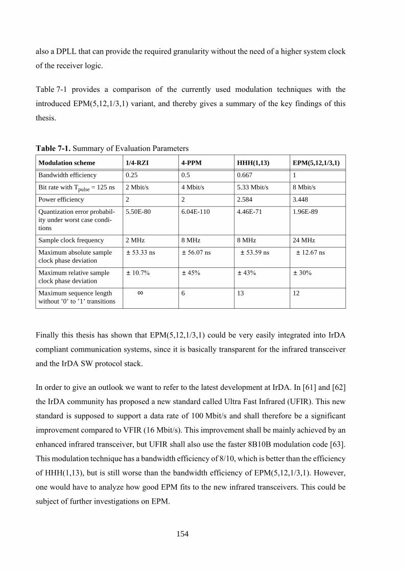
also a DPLL that can provide the required granularity without the need of a higher system clock
of the receiver logic.
Table 7-1 provides a comparison of the currently used modulation techniques with the
introduced EPM(5,12,1/3,1) variant, and thereby gives a summary of the key findings of this
thesis.
Table 7-1. Summary of Evaluation Parameters
Modulation scheme 1/4-RZI 4-PPM HHH(1,13) EPM(5,12,1/3,1)
Bandwidth efficiency 0.25 0.5 0.667 1
Bit rate with Tpulse = 125 ns 2 Mbit/s 4 Mbit/s 5.33 Mbit/s 8 Mbit/s
Power efficiency 2 2 2.584 3.448
Quantization error probabil-ity under worst case condi-tions
5.50E-80 6.04E-110 4.46E-71 1.96E-89
Sample clock frequency 2 MHz 8 MHz 8 MHz 24 MHz
Maximum absolute sample clock phase deviation
53.33 ns± 56.07 ns± 53.59 ns± 12.67 ns±
Maximum relative sample clock phase deviation
10.7%± 45%± 43%± 30%±
Maximum sequence length without ’0’ to ’1’ transitions
∞ 6 13 12
Finally this thesis has shown that EPM(5,12,1/3,1) could be very easily integrated into IrDA
compliant communication systems, since it is basically transparent for the infrared transceiver
and the IrDA SW protocol stack.
In order to give an outlook we want to refer to the latest development at IrDA. In [61] and [62]
the IrDA community has proposed a new standard called Ultra Fast Infrared (UFIR). This new
standard is supposed to support a data rate of 100 Mbit/s and shall therefore be a significant
improvement compared to VFIR (16 Mbit/s). This improvement shall be mainly achieved by an
enhanced infrared transceiver, but UFIR shall also use the faster 8B10B modulation code [63].
This modulation technique has a bandwidth efficiency of 8/10, which is better than the efficiency
of HHH(1,13), but is still worse than the bandwidth efficiency of EPM(5,12,1/3,1). However,
one would have to analyze how good EPM fits to the new infrared transceivers. This could be
subject of further investigations on EPM.
154
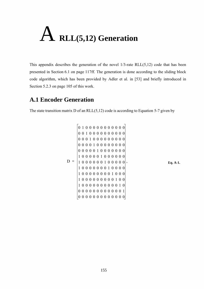
A RLL(5,12) Generation
This appendix describes the generation of the novel 1/3-rate RLL(5,12) code that has been
presented in Section 6.1 on page 117ff. The generation is done according to the sliding block
code algorithm, which has been provided by Adler et al. in [53] and briefly introduced in
Section 5.2.3 on page 105 of this work.
A.1 Encoder Generation
The state transition matrix D of an RLL(5,12) code is according to Equation 5-7 given by
D
0 1 0 0 0 0 0 0 0 0 0 0 00 0 1 0 0 0 0 0 0 0 0 0 00 0 0 1 0 0 0 0 0 0 0 0 00 0 0 0 1 0 0 0 0 0 0 0 00 0 0 0 0 1 0 0 0 0 0 0 01 0 0 0 0 0 1 0 0 0 0 0 01 0 0 0 0 0 0 1 0 0 0 0 01 0 0 0 0 0 0 0 1 0 0 0 01 0 0 0 0 0 0 0 0 1 0 0 01 0 0 0 0 0 0 0 0 0 1 0 01 0 0 0 0 0 0 0 0 0 0 1 00 0 0 0 0 0 0 0 0 0 0 0 10 0 0 0 0 0 0 0 0 0 0 0 0
,= Eq. A-1.
155

and the corresponding matrix D3, which we need for the 1/3-rate code, can be derived as
D3
0 0 0 1 0 0 0 0 0 0 0 0 00 0 0 0 1 0 0 0 0 0 0 0 00 0 0 0 0 1 0 0 0 0 0 0 01 0 0 0 0 0 1 0 0 0 0 0 01 1 0 0 0 0 0 1 0 0 0 0 01 1 1 0 0 0 0 0 1 0 0 0 01 1 1 0 0 0 0 0 0 1 0 0 01 1 1 0 0 0 0 0 0 0 1 0 01 1 1 0 0 0 0 0 0 0 0 1 01 1 1 0 0 0 0 0 0 0 0 0 11 1 1 0 0 0 0 0 0 0 0 0 00 1 1 0 0 0 0 0 0 0 0 0 00 0 1 0 0 0 0 0 0 0 0 0 0
.= Eq. A-2.
The matrix D3 can also be written down in a state transition table as shown in Table A-1,
whereby the alphabet AD2 = 1, 2, 3, 4, 5, 6, 7, 8, 9, 10, 11, 12, 13 represents the thirteen states.
Table A-1. State Transition Table D3
ζk ζk 1+
1 4
2 5
3 6
4 1 7
5 1 2 8
6 1 2 3 9
7 1 2 3 10
8 1 2 3 11
9 1 2 3 12
10 1 2 3 13
11 1 2 3
12 2 3
13 3
156
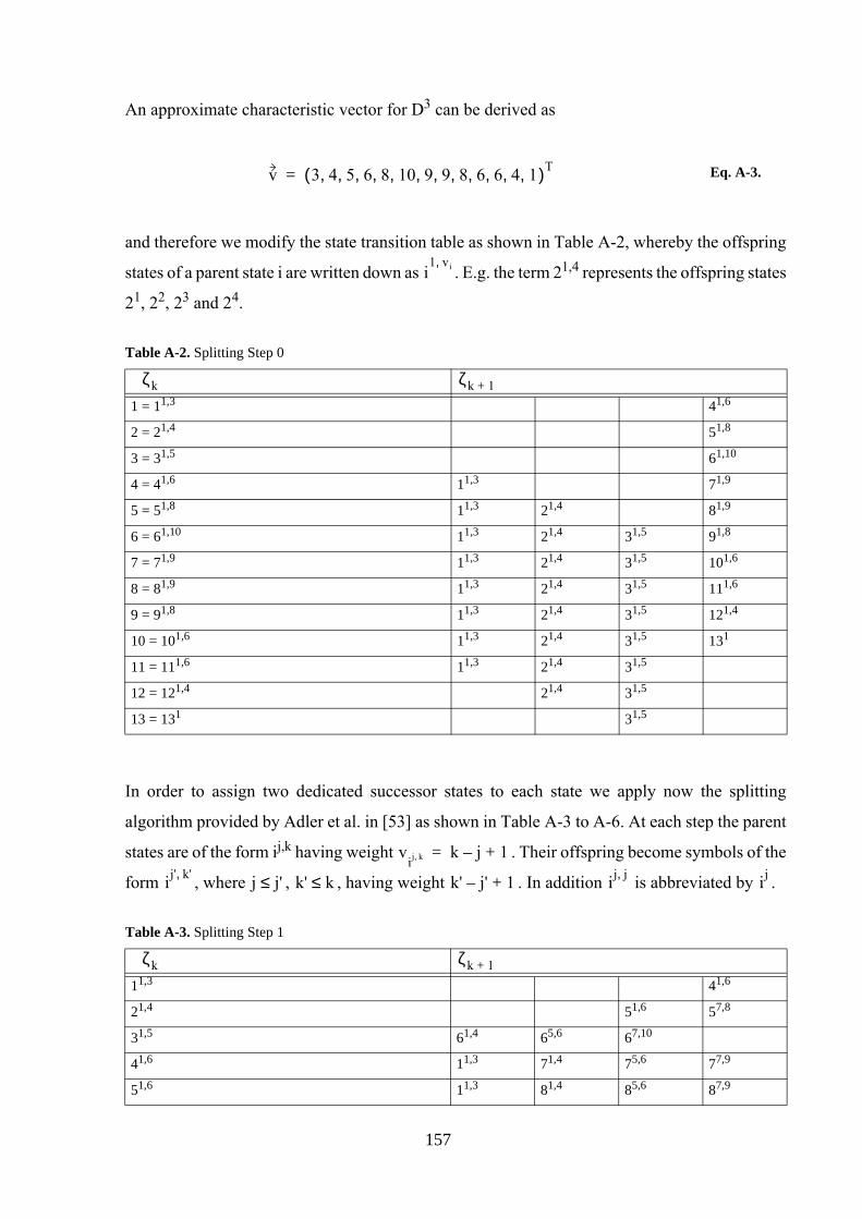
An approximate characteristic vector for D3 can be derived as
v 3 4 5 6 8 10 9 9 8 6 6 4 1, , , , , , , , , , , ,( )T= Eq. A-3.
and therefore we modify the state transition table as shown in Table A-2, whereby the offspring
states of a parent state i are written down as i1 vi,
. E.g. the term 21,4 represents the offspring states
21, 22, 23 and 24.
Table A-2. Splitting Step 0
ζk ζk 1+
1 = 11,3 41,6
2 = 21,4 51,8
3 = 31,5 61,10
4 = 41,6 11,3 71,9
5 = 51,8 11,3 21,4 81,9
6 = 61,10 11,3 21,4 31,5 91,8
7 = 71,9 11,3 21,4 31,5 101,6
8 = 81,9 11,3 21,4 31,5 111,6
9 = 91,8 11,3 21,4 31,5 121,4
10 = 101,6 11,3 21,4 31,5 131
11 = 111,6 11,3 21,4 31,5
12 = 121,4 21,4 31,5
13 = 131 31,5
In order to assign two dedicated successor states to each state we apply now the splitting
algorithm provided by Adler et al. in [53] as shown in Table A-3 to A-6. At each step the parent
states are of the form ij,k having weight vij k, k j– 1+= . Their offspring become symbols of the
form ij' k, ' , where j j'≤ , k' k≤ , having weight k' j'– 1+ . In addition ij j, is abbreviated by ij .
Table A-3. Splitting Step 1
ζk ζk 1+
11,3 41,6
21,4 51,6 57,8
31,5 61,4 65,6 67,10
41,6 11,3 71,4 75,6 77,9
51,6 11,3 81,4 85,6 87,9
157

ζk ζk 1+
Table A-4. Splitting Step 2
ζk ζk 1+
11,3 41,3 44,5 46
21,3 51,3 54,5 56
24 57,8
31,2 61,4
33 65,6
34,5 67,8 69 610
41,3 11,3 77,8 79
44,5 71,4
46 75,6
51,3 11,3 87,8 89
54,5 81,4
56 85,6
123,4, 115,6, 105,6, 95,6, 85,6, 75,6, 65,6, 57,8 21,3 24
111,4, 101,4, 91,4, 81,4, 71,4, 61,4 11,3 31,2 33 34,5
67,8 91,4
69 95,6
610 97 98
77,8 101,4
79 105,6
87,8 111,4
89 115,6
97 121,2
98 123,4
121,2 31,2 (33) 34,5
123,4, 115,6, 105,6, 95,6, 85,6, 75,6, 65,6, 57,8 21,4
111,4, 101,4, 91,4, 81,4, 71,4, 61,4 11,3 31,5
67,10 91,4 95,6 97,8
77,9 101,4 105,6
87,9 111,4 115,6
97,8 121,2 123,4
121,2 31,5
158

Table A-5. Splitting Step 3
ζk ζk 1+
11,2 41,2 43 46
13 44,5
21,2 51,2 53 56
23 54,5
24 57,8
31,2 61,2 63 64
33 65,6
34 67,8
35 69 610
41,2 11,2 13 79
43 77,8
44,5 71,2 73 74
46 75,6
51,2 11,2 13 89
53 87,8
54,5 81,2 83 84
56 85,6
123,4, 115,6, 105,6, 95,6, 85,6, 75,6, 65,6, 57,8 21,2 23 24
111,2, 101,2, 91,2, 81,2, 71,2, 61,2 11,2 13 33
121, 113, 103, 93, 83, 73, 63 31,2
122, 114, 104, 94, 84, 74, 64 34 35
67,8 91,2 93 94
69 95,6
610 97 98
77,8 101,2 103 104
79 105,6
87,8 111,2 113 114
89 115,6
97 121 122
98 123,4
Table A-6. Splitting Step 4
ζk ζk 1+
11 41 42
12 43 46
13 44 45
159

ζk ζk 1+
21 51 52
22 53 56
23 54 55
24 57 58
31 61 62
32 63 64
33 65 66
34 67 68
35 69 610
111, 101, 91, 81, 71, 61, 51, 41 11 12
42 13 79
43 77 78
44 71 72
45 73 74
46 75 76
52 13 89
53 87 88
54 81 82
55 83 84
56 85 86
123, 115, 105, 95, 85, 75, 65, 57 21 22
124, 116, 106, 96, 86, 76, 66, 58 23 24
112, 102, 92, 82, 72, 62 13 33
121, 113, 103, 93, 83, 73, 63 31 32
122, 114, 104, 94, 84, 74, 64 34 35
67 91 92
68 93 94
69 95 96
610 97 98
77 101 102
78 103 104
79 105 106
87 111 112
88 113 114
89 115 116
97 121 122
98 123 124
160
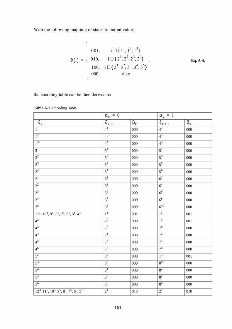
With the following mapping of states to output values
ϑ i( )
001 , i 11 12 13, , ∈
010 , i 21 22 23 24, , , ∈
100 , i 31 32 33 34 35, , , , ∈000 , else
,
= Eq. A-4.
the encoding table can be then derived as
Table A-7. Encoding Table
αk 0= αk 1=
ζk ζk 1+ βk ζk 1+ βk11 41 000 42 000
12 46 000 43 000
13 44 000 45 000
21 51 000 52 000
22 56 000 53 000
23 54 000 55 000
24 57 000 58 000
31 61 000 62 000
32 63 000 64 000
33 65 000 66 000
34 67 000 68 000
35 69 000 610 000
111, 101, 91, 81, 71, 61, 51, 41 11 001 12 001
42 79 000 13 001
43 77 000 78 000
44 71 000 72 000
45 73 000 74 000
46 75 000 76 000
52 89 000 13 001
53 87 000 88 000
54 81 000 82 000
55 83 000 84 000
56 85 000 86 000
123, 115, 105, 95, 85, 75, 65, 57 21 010 22 010
161

αk 0= αk 1=
ζk ζk 1+ βk ζk 1+ βk
Note that the assignment of the successor states to the input values αk 0= and αk 1= is done
in that way so that the decoder has minimized complexity as we will see below in Section A.2.
By merging the states of the encoding table, which have the same successor states and result in
the same output values βk , the complexity of the encoder can be reduced as shown in Table A-
8 to A-11.
Table A-8. First Reduction of Encoding Table
αk 0= αk 1=
ζk ζk 1+ βk ζk 1+ βk
124, 116, 106, 96, 86, 76, 66, 58 23 010 24 010
112, 102, 92, 82, 72, 62 33 100 13 001
121, 113, 103, 93, 83, 73, 63 31 100 32 100
122, 114, 104, 94, 84, 74, 64 34 100 35 100
67 91 000 92 000
68 93 000 94 000
69 95 000 96 000
610 98 000 97 000
77 101 000 102 000
78 103 000 104 000
79 105 000 106 000
87 111 000 112 000
88 113 000 114 000
89 115 000 116 000
97 121 000 122 000
98 123 000 124 000
11 41 000 42 000
12 46 000 43 000
13 44 000 45 000
21 41 000 52 000
22 56 000 53 000
23 54 000 55 000
98, 89, 79, 69, 56, 46, 33, 24 57 000 58 000
87, 77, 67, 54, 44, 31 41 000 62 000
162
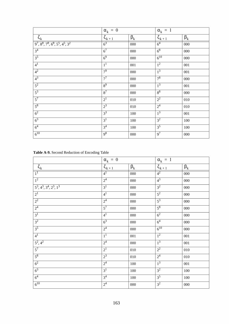
αk 0= αk 1=
ζk ζk 1+ βk ζk 1+ βk
Table A-9. Second Reduction of Encoding Table
αk 0= αk 1=
ζk ζk 1+ βk ζk 1+ βk11 41 000 42 000
12 24 000 43 000
53, 43, 34, 23, 13 31 000 32 000
21 41 000 52 000
22 24 000 53 000
24 57 000 58 000
31 41 000 62 000
32 63 000 64 000
35 24 000 610 000
41 11 001 12 001
52, 42 24 000 13 001
57 21 010 22 010
58 23 010 24 010
62 24 100 13 001
63 31 100 32 100
64 34 100 35 100
610 24 000 32 000
97, 88, 78, 68, 55, 45, 32 63 000 64 000
34 67 000 68 000
35 69 000 610 000
41 11 001 12 001
42 79 000 13 001
43 77 000 78 000
52 89 000 13 001
53 87 000 88 000
57 21 010 22 010
58 23 010 24 010
62 33 100 13 001
63 31 100 32 100
64 34 100 35 100
610 98 000 97 000
163

Table A-10. Third Reduction of Encoding Table
αk 0= αk 1=
ζk ζk 1+ βk ζk 1+ βk21, 11 41 000 42 000
22, 12 24 000 13 000
13 31 000 32 000
24 57 000 58 000
31 41 000 62 000
32 63 000 64 000
35 24 000 610 000
41 11 001 12 001
42 24 000 13 001
57 21 010 22 010
58 13 010 24 010
62 24 100 13 001
63 31 100 32 100
64 13 100 35 100
610 24 000 32 000
Table A-11. Forth Reduction of Encoding Table
αk 0= αk 1=
ζk ζk 1+ βk ζk 1+ βk11 41 000 42 000
12 24 000 13 000
13 31 000 32 000
24 57 000 58 000
31 41 000 62 000
32 63 000 64 000
35 24 000 610 000
41 11 001 12 001
42 24 000 13 001
57 11 010 12 010
58 13 010 24 010
62 24 100 13 001
63 31 100 32 100
64 13 100 35 100
610 24 000 32 000
164
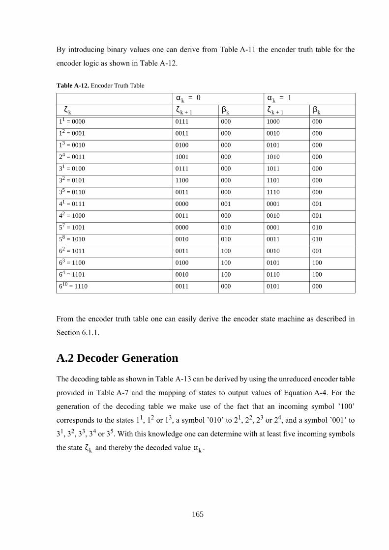
By introducing binary values one can derive from Table A-11 the encoder truth table for the
encoder logic as shown in Table A-12.
Table A-12. Encoder Truth Table
αk 0= αk 1=
ζk ζk 1+ βk ζk 1+ βk11 = 0000 0111 000 1000 000
12 = 0001 0011 000 0010 000
13 = 0010 0100 000 0101 000
24 = 0011 1001 000 1010 000
31 = 0100 0111 000 1011 000
32 = 0101 1100 000 1101 000
35 = 0110 0011 000 1110 000
41 = 0111 0000 001 0001 001
42 = 1000 0011 000 0010 001
57 = 1001 0000 010 0001 010
58 = 1010 0010 010 0011 010
62 = 1011 0011 100 0010 001
63 = 1100 0100 100 0101 100
64 = 1101 0010 100 0110 100
610 = 1110 0011 000 0101 000
From the encoder truth table one can easily derive the encoder state machine as described in
Section 6.1.1.
A.2 Decoder Generation
The decoding table as shown in Table A-13 can be derived by using the unreduced encoder table
provided in Table A-7 and the mapping of states to output values of Equation A-4. For the
generation of the decoding table we make use of the fact that an incoming symbol ’100’
corresponds to the states 11, 12 or 13, a symbol ’010’ to 21, 22, 23 or 24, and a symbol ’001’ to
31, 32, 33, 34 or 35. With this knowledge one can determine with at least five incoming symbols
the state ζk and thereby the decoded value αk .
165
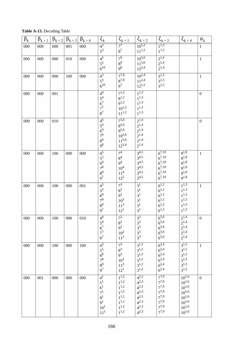
Table A-13. Decoding Table
βk βk 1+ βk 2+ βk 3+ βk 4+ ζk ζk 1+ ζk 2+ ζk 3+ ζk 4+ αk000 000 000 001 000 43
5377
87101,2
111,211,3
11,31
000 000 000 010 000 42
52
610
79
89
98
105,6
115,6
123,4
21,4
21,4
21,4
1
000 000 000 100 000 43
53
610
77,8
87,8
97
102,4
112,4
121,2
31,5
31,5
31,5
1
000 000 001 44
54
67
77
87
71,2
81,2
91,2
101,2
111,2
11,3
11,3
11,3
11,3
11,3
0
000 000 010 46
56
69
79
89
98
75,6
85,6
95,6
105,6
115,6
123,4
21,4
21,4
21,4
21,4
21,4
21,4
0
000 000 100 000 000 45
55
68
78
88
97
74
84
94
104
114
122
34,5
34,5
34,5
34,5
34,5
34,5
67,10
67,10
67,10
67,10
67,10
67,10
91,8
91,8
91,8
91,8
91,8
91,8
1
000 000 100 000 001 45
55
68
78
88
97
73
83
93
103
113
121
31
31
31
31
31
31
61,2
61,2
61,2
61,2
61,2
61,2
11,3
11,3
11,3
11,3
11,3
11,3
1
000 000 100 000 010 44
54
67
77
87
72
82
92
102
112
33
33
33
33
33
65,6
65,6
65,6
65,6
65,6
21,4
21,4
21,4
21,4
21,4
0
000 000 100 000 100 45
55
68
78
88
97
73
83
93
103
113
121
31,2
31,2
31,2
31,2
31,2
31,2
62,4
62,4
62,4
62,4
62,4
62,4
31,5
31,5
31,5
31,5
31,5
31,5
1
000 001 000 000 000 41
51
61
71
81
91
101
111
11,2
11,2
11,2
11,2
11,2
11,2
11,2
11,2
42,3
42,3
42,3
42,3
42,3
42,3
42,3
42,3
77,9
77,9
77,9
77,9
77,9
77,9
77,9
77,9
101,6
101,6
101,6
101,6
101,6
101,6
101,6
101,6
0
166
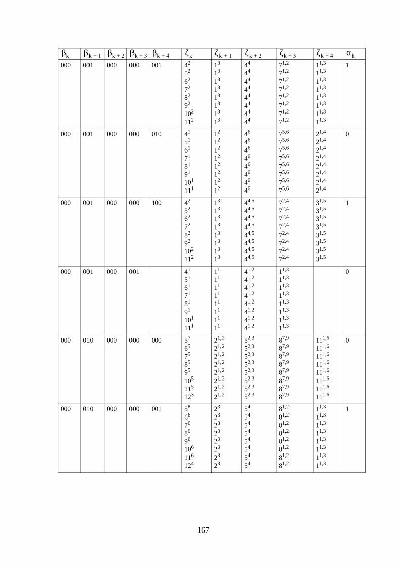
βk βk 1+ βk 2+ βk 3+ βk 4+ ζk ζk 1+ ζk 2+ ζk 3+ ζk 4+ αk000 001 000 000 001 42
52
62
72
82
92
102
112
13
13
13
13
13
13
13
13
44
44
44
44
44
44
44
44
71,2
71,2
71,2
71,2
71,2
71,2
71,2
71,2
11,3
11,3
11,3
11,3
11,3
11,3
11,3
11,3
1
000 001 000 000 010 41
51
61
71
81
91
101
111
12
12
12
12
12
12
12
12
46
46
46
46
46
46
46
46
75,6
75,6
75,6
75,6
75,6
75,6
75,6
75,6
21,4
21,4
21,4
21,4
21,4
21,4
21,4
21,4
0
000 001 000 000 100 42
52
62
72
82
92
102
112
13
13
13
13
13
13
13
13
44,5
44,5
44,5
44,5
44,5
44,5
44,5
44,5
72,4
72,4
72,4
72,4
72,4
72,4
72,4
72,4
31,5
31,5
31,5
31,5
31,5
31,5
31,5
31,5
1
000 001 000 001 41
51
61
71
81
91
101
111
11
11
11
11
11
11
11
11
41,2
41,2
41,2
41,2
41,2
41,2
41,2
41,2
11,3
11,3
11,3
11,3
11,3
11,3
11,3
11,3
0
000 010 000 000 000 57
65
75
85
95
105
115
123
21,2
21,2
21,2
21,2
21,2
21,2
21,2
21,2
52,3
52,3
52,3
52,3
52,3
52,3
52,3
52,3
87,9
87,9
87,9
87,9
87,9
87,9
87,9
87,9
111,6
111,6
111,6
111,6
111,6
111,6
111,6
111,6
0
000 010 000 000 001 58
66
76
86
96
106
116
124
23
23
23
23
23
23
23
23
54
54
54
54
54
54
54
54
81,2
81,2
81,2
81,2
81,2
81,2
81,2
81,2
11,3
11,3
11,3
11,3
11,3
11,3
11,3
11,3
1
167

βk βk 1+ βk 2+ βk 3+ βk 4+ ζk ζk 1+ ζk 2+ ζk 3+ ζk 4+ αk000 010 000 000 010 57
65
75
85
95
105
115
123
22
22
22
22
22
22
22
22
56
56
56
56
56
56
56
56
85,6
85,6
85,6
85,6
85,6
85,6
85,6
85,6
21,4
21,4
21,4
21,4
21,4
21,4
21,4
21,4
0
000 010 000 000 100 58
66
76
86
96
106
116
124
23
23
23
23
23
23
23
23
54,5
54,5
54,5
54,5
54,5
54,5
54,5
54,5
82,4
82,4
82,4
82,4
82,4
82,4
82,4
82,4
31,5
31,5
31,5
31,5
31,5
31,5
31,5
31,5
1
000 010 000 001 57
65
75
85
95
105
115
123
21
21
21
21
21
21
21
21
51,2
51,2
51,2
51,2
51,2
51,2
51,2
51,2
11,3
11,3
11,3
11,3
11,3
11,3
11,3
11,3
0
000 010 000 010 58
66
76
86
96
106
116
124
24
24
24
24
24
24
24
24
57,8
57,8
57,8
57,8
57,8
57,8
57,8
57,8
21,4
21,4
21,4
21,4
21,4
21,4
21,4
21,4
1
000 100 000 000 64
74
84
94
104
114
122
34,5
34,5
34,5
34,5
34,5
34,5
34,5
67,10
67,10
67,10
67,10
67,10
67,10
67,10
91,8
91,8
91,8
91,8
91,8
91,8
91,8
1
000 100 000 001 63
73
83
93
103
113
121
31
31
31
31
31
31
31
61,2
61,2
61,2
61,2
61,2
61,2
61,2
11,3
11,3
11,3
11,3
11,3
11,3
11,3
0
000 100 000 010 62
72
82
92
102
112
33
33
33
33
33
33
65,6
65,6
65,6
65,6
65,6
65,6
21,4
21,4
21,4
21,4
21,4
21,4
1
168
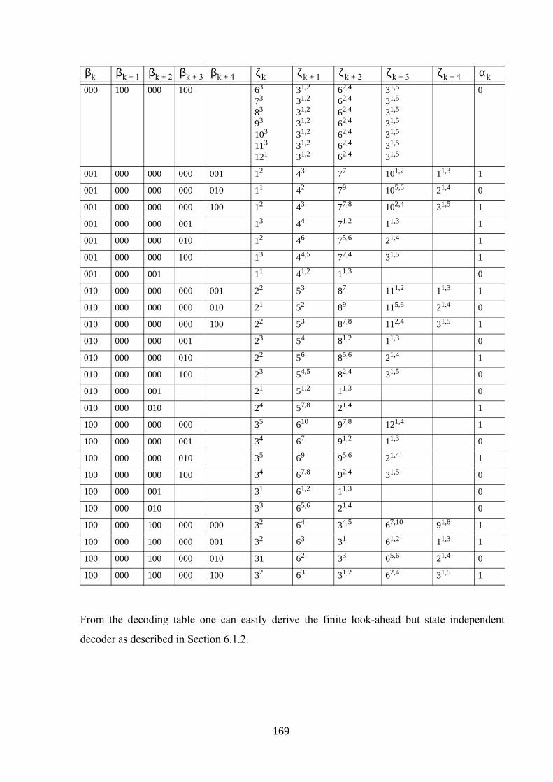
βk βk 1+ βk 2+ βk 3+ βk 4+ ζk ζk 1+ ζk 2+ ζk 3+ ζk 4+ αk
From the decoding table one can easily derive the finite look-ahead but state independent
decoder as described in Section 6.1.2.
000 100 000 100 63
73
83
93
103
113
121
31,2
31,2
31,2
31,2
31,2
31,2
31,2
62,4
62,4
62,4
62,4
62,4
62,4
62,4
31,5
31,5
31,5
31,5
31,5
31,5
31,5
0
001 000 000 000 001 12 43 77 101,2 11,3 1
001 000 000 000 010 11 42 79 105,6 21,4 0
001 000 000 000 100 12 43 77,8 102,4 31,5 1
001 000 000 001 13 44 71,2 11,3 1
001 000 000 010 12 46 75,6 21,4 1
001 000 000 100 13 44,5 72,4 31,5 1
001 000 001 11 41,2 11,3 0
010 000 000 000 001 22 53 87 111,2 11,3 1
010 000 000 000 010 21 52 89 115,6 21,4 0
010 000 000 000 100 22 53 87,8 112,4 31,5 1
010 000 000 001 23 54 81,2 11,3 0
010 000 000 010 22 56 85,6 21,4 1
010 000 000 100 23 54,5 82,4 31,5 0
010 000 001 21 51,2 11,3 0
010 000 010 24 57,8 21,4 1
100 000 000 000 35 610 97,8 121,4 1
100 000 000 001 34 67 91,2 11,3 0
100 000 000 010 35 69 95,6 21,4 1
100 000 000 100 34 67,8 92,4 31,5 0
100 000 001 31 61,2 11,3 0
100 000 010 33 65,6 21,4 0
100 000 100 000 000 32 64 34,5 67,10 91,8 1
100 000 100 000 001 32 63 31 61,2 11,3 1
100 000 100 000 010 31 62 33 65,6 21,4 0
100 000 100 000 100 32 63 31,2 62,4 31,5 1
169

170
Bibliography
[1] Infrared Data Association, Serial Infrared Physical Layer Specification, Version 1.4, May 2001.
[2] A.S. Tanenbaum, Computer Networks, 3rd edition, Prentice Hall, 2000.
[3] R. Latuske, "USB (Universal Serial Bus), IEEE1394 (Firewire), IrDA (Infrared Data Association) und Bluetooth für embedded Systeme", ARS Software GmbH, Munich, 2000, in German.
[4] USB Implementers Forum, Inc., Universal Serial Bus Specification, Revision 2.0, 2000.
[5] Bluetooth, Specification of the Bluetooth System (Volume 1, Core), v1.0 B, 1999.
[6] Infrared Data Association, Serial Infrared Link Access Protocol (IrLAP), Version 1.1, June 1996.
[7] T. Lüftner, C. Kröpl, M. Huemer, J. Hausner, R. Hagelauer, R. Weigel, "Edge-position modulation for high-speed wireless infrared communications", IEE Proceedings on Optoelectronics, Vol. 150, No. 5, pp. 427-437, October 2003.
[8] T. Lüftner, M. Huemer, J. Hausner, R. Hagelauer, R. Weigel, "Wireless infrared commu-nication system based on Edge Position Modulation with novel RLL(5,12) code", Con-ference Proceedings - 6th European Conference on Wireless Technology, pp. 333-336, October 2003.
[9] T. Lüftner, M. Huemer, C. Kröpl, J. Hausner, R. Hagelauer, R. Weigel, "Wireless infrared communication system based on Edge Position Modulation", OVE Verbandszeitschrift E&I - elekrotechnik und informationstechnik , Heft 7/8.2003, pp. 251-255, Springer Wien New York, Juli/August 2003.
[10] T. Lüftner, C. Kröpl, M. Huemer, R. Weigel, R. Hagelauer, J. Hausner, "Wireless infrared Communications with Edge Position Modulation for mobile devices", IEEE Wireless Communications - Optical Wireless Communications, Vol. 10, No. 2, pp. 15-21, April 2003.
171
[11] T. Lüftner, Verfahren und System zur Übertragung binärer Datenfolgen mit Hilfe eines Pulsflanken-Positions-Modulationsverfahrens, German Patent No. DE 10310129 B3, Assignee: Infineon Technology AG, October 14th, 2004, in German.
[12] Infrared Data Association, IrDA Link Management Protocol (IrLMP), Version 1.1, Janu-ary 1996.
[13] Infrared Data Association, Tiny TP: A Flow-Control Mechanism for use with IrLMP, Ver-sion 1.1, October 1996.
[14] Infrared Data Association, IrDA Object Exchange Protocol (IrOBEX), Version 1.2, March 1999.
[15] Vishay, TFDU8108 - Very Fast Infrared Transceiver Module (VFIR, 16 Mbit/s), Datasheet, Rev. 1.3, November 2003, downloaded from www.vishay.com.
[16] Agilent Technologies, Agilent HSDL-3603 - IrDA Data Compliant 4 Mbit/s Infrared Transceiver, Datasheet, December 2003, downloaded from www.agilent.com/semicon-ductors.
[17] R. Otte, L.P. de Jong, A.H.M. van Roermund, Low-Power Wireless Infrared Communica-tions, Kluwer Academic Publishers, 1999.
[18] A.G. Bell, "On the Production and Reproduction of Sound by Light", Proc. Amer. Assoc. for the Advancement of Science, vol. 29, 1880.
[19] F.R. Gfeller, U. Bapst, "Wireless In-House Data Communication via Diffuse Infrared Radiation", Proceedings of the IEEE, Vol. 67, No. 11, pp. 1474-1486, November 1979.
[20] P.D. Brown, L.S. Moore, D.C. York, Low Power Optical Transceiver for Portable Com-puting Devices, U.S. Patent No. 5,075,792, Assignee: Hewlett-Packard Company, December 24, 1991.
[21] Infrared Data Association, Serial Infrared (SIR) Physical Layer Link Specification, Ver-sion 1.0, April 27, 1994.
[22] International Organisation for Standardisation (ISO), High Level Data Link Control (HDLC) Procedures - Elements of Procedures, ISO/IEC 4335, September 15, 1991.
[23] T.F. Williams, P.D. Hortensius and F. Novak, Proposal for Infrared Data Association Serial Infrared Link Protocol Specification, Version 1.0, IBM Corporation, August 27, 1993.
172
[24] Infrared Data Association, Serial Infrared Link Access Protocol (IrLAP), Version 1.0, June 23, 1994.
[25] S. Williams, I. Millar, The IrDA Platform, HP Laboratories, Bristol, 1995, downloaded from www.hpl.hp.com/techreports/95/.
[26] J.R. Barry, Wireless Infrared Communications, Kluwer Academic Publishers, 1994.
[27] J.M. Kahn, J.R. Barry, "Wireless Infrared Communications", Proceedings of the IEEE, Vol. 85, No. 2, pp. 265-298, February 1997.
[28] Agilent Technologies, Agilent IrDA Data Link Design Guide, 2002, downloaded from http://www.agilent.com/view/ir.
[29] M.D. Audeh, J.M. Kahn, J.R. Barry, "Decision-Feedback Equalization of Pulse-Position Modulation on Measured Non-Directed Indoor Infrared Channels", IEEE Transaction on Communications, Vol. 47, No. 4, pp. 500-503, April 1999.
[30] International Organisation for Standardisation (ISO), Information technology - Open Sys-tems Interconnection - Data link serivce definition, International standard, Second Edi-tion, Reference number ISO/IEC 8886:1996(E), September 15th 1996.
[31] IBM Corporation, IBM31TFIRC Infrared Communications Controller Macro Data Sheet, Data sheet, Release 2.7, April 1998.
[32] M. Huemer, T. Lüftner, J. Hausner, "A highly integrated single chip baseband IC for 2.5th generation multimedia oriented mobile phones", OVE Verbandszeitschrift E&I - elekro-technik und informationstechnik , Heft 11.2002, pp. 407-410, Springer Wien New York, November 2002.
[33] W. Hirt, M. Hassner, N. Heise, "IrDA-VFIR (16 Mbit/s): Modulation Code and System Design", IEEE Personal Communications, pp. 58-71, February 2001.
[34] M.V. Klein, Optics, John Wiley & sons, New York, 1970.
[35] E. Hecht, Optics, Second Edition, Addison-Wesley Publishing Company, 1987.
[36] M. Wolf, Zur breitbandigen Infrarot-Indoorkommunikation, PhD thesis, Fakultät für Ele-ktrotechnik und Informationstechnik, Technische Universität Ilmenau, 2001, in German.
[37] C. Kröpl, Modellierung und Simulation eines Infrarot-Übertragungssystems für mobile Geräte, Diploma thesis, Institute for Communications and Information Engineering, Johannes Kepler University Linz, January 2003, in German.
173
[38] J.M. Kahn, W.J. Krause, J.B. Carruthers, "Experimental Characterization of Non-Directed Indoor Infrared Channels", IEEE Transactions on Communications, Vol. 43, No. 4, pp. 1613-1623, April 1995.
[39] V. Jungnickel, V. Pohl, S. Nönning, C. von Helmolt, "A Physical Model of the Wireless Infrared Communication Channel", IEEE Journal On Selected Areas In Communica-tions, Vol. 20, No. 3, pp. 631-640, April 2002.
[40] S.M. Sze, Physics of Semiconductor Devices, Wiley-Interscience, New York, 1981.
[41] S.M. Sze, Semiconductor Devices, Physics and Technology, 2nd Edition, John Wiley & Sons, Inc., 2001.
[42] U. Barabas, Optische Signalübertragung, R. Oldenbourg Verlag München Wien, 1993, in German.
[43] A.C. Boucouvalas, "Indoor ambient light noise and its effect on wireless optical links", IEE Proceedings on Optoelectronics, Vol. 143, pp. 334-338, December 1996.
[44] U. Tietze, Ch. Schenk, Halbleiterschaltungstechnik, Springer-Verlag, Berlin Heidelberg, 1999, in German.
[45] H.D. Lüke, Signalübertragung, 5. Auflage, Springer-Verlag, 1992, in German.
[46] G. Söder, "Impulsinterferenzen & Entzerrung", Anleitung zum Praktikum Simulation dig-italer Übertragungssysteme, Lehrstuhl für Nachrichtentechnik, Technische Universität München, October 1997, in German.
[47] I. Millar, M. Beale, B.J. Donoghue, K.W. Lindstrom, S. Williams, "The IrDA Standards for High-Speed Infrared Communications", The Hewlett-Packard Journal, Article 2, Feb-ruary 1998.
[48] B. O'Hara, A. Petrick, "IR PHY Modulation Method", 802.11 Handbook: A Designer's Companion, p.135, Standards Information Network IEEE Press, 1999.
[49] H. Uno, K. Kumatani, H. Okuhata, I. Shirakawa, T. Chiba, "A 4Mbps infrared wireless communication system dedicated to mobile computing", Proceedings of IEEE Asia Pacific Conference on Circuits and Systems ’96, pp. 334-337, Seoul, November 1996.
[50] K.A.S. Immink, "Runlength-Limited Sequences", Proceedings of the IEEE, Vol. 78, No. 11, pp. 1745-1758, November 1990.
174
[51] C.E. Shannon, "A mathematical theory of communication", Bell Syst. Techn. J., Vol. 27, pp.379-423, July 1948.
[52] R.L. Adler, M. Hassner, J.P. Moussouris, Method and apparatus for generating a noise-less sliding block code for a (1,7) channel with rate 2/3, United States Patent 4'413'251, November 1983.
[53] R.L. Adler, D. Coppersmith, M. Hassner, "Algorithms for Sliding Block Codes", IEEE Transactions on Information Theory, Vol. IT-29, No. 1, pp 5-22, January 1983.
[54] F.R. Gantmacher, The Theory of Matrices, Vol.II, Chelsea, New York, 1959.
[55] R.S. Varga, Matrix Iterative Analysis, Prentice-Hall, Englewood Cliffs, 1962.
[56] E. Seneta, Non Negative Matrices, John Wiley, New York, 1973.
[57] R.L. Adler, R.K. Brayton, B.P. Kitchens, "A Rate 1/3 (5,12) RLL Code", IBM Technical Disclosure Bulletin, Vol.27, No. 8, pp. 4722-4724, January 1985.
[58] D.W. Suvak, IrDA Serial Infrared - Link Access Protocol Specification for 16 Mbit/s Addition (VFIR), Errata to IrLAP Version 1.1., January 1999.
[59] H.C. Margiol, Analyse und Messung von Infrarotübertragung nach IrDA-Standard und Aufbau eines Testprototypen, Project seminar, Institute for Communications and Informa-tion Engineering, Johannes Kepler University Linz, February 2002, in German.
[60] H.C. Margiol, Analyse und Implementierung des IrDA-Protokolls für die Infrarotkommu-nikation, Diploma thesis, Institute for Integrated Circuits, Johannes Kepler University Linz, September 2002, in German.
[61] T. Hiramatsu, Proposed Changes to Infrared Data Association Serial Infrared Physical Layer Link Specification for UFIR (100Mbit/s) Addition, Proposal Version 0.5, August 28, 2004.
[62] Infrared Data Association, IrDA Serial Infrared Link Access Protocol Specification for 100 Mbit/s Addition (UFIR) Errata to IrLAP Version 1.1, Draft Errata Proposal, Version 0.1.0, Aug 28th , 2004.
[63] A.N. Coles, A new 8B10B block code for high speed data transmission over unshielded twisted pair channels, Hewlett-Packard Laboratories, Bristol, October 1996, downloaded from www.hpl.hp.com/techreports/96/.
175

176

Lebenslauf
Thomas Lüftner
A-4040 Linz, Leopold-Figl-Str. 46
Persönliche Daten
Geburtsdatum / -ort: 16.04.1975 / Linz, Oberösterreich
Staatsbürgerschaft: Österreich
Familienstand: Ledig
Werdegang
1981 bis 1989 Grundschule in Oftering und Linz
1989 bis 1994 Höhere Technische Bundeslehranstalt für Maschinenbau Linz
Reifeprüfung mit ausgezeichnetem Erfolg bestanden
10/1994 bis 06/2000 Diplom-Studium der Mechatronik
Johannes Kepler Universität Linz
Abschluss mit Auszeichnung
07/1999 bis 10/1999 Forschungsaufenthalt an der University of California, Berkeley
01/2000 bis 09/2000 Präsenzdienst beim Österreichischen Bundesheer
10/2000 bis 06/2005 Mitarbeiter bei Danube Integrated Circuits Engineering
Design Center von Infineon Technologies in Linz
10/2002 Abschluss 1. Studienabschnitt Wirtschaftswissenschaften
Johannes Kepler Universität Linz
03/2002 bis 06/2003 Lehrbeauftragter für Project Engineering
Fachhochschule Hagenberg, Oberösterreich
seit 07/2005 Mitarbeiter bei Infineon Technologies in München
177

Curriculum Vitae
Thomas Lüftner
A-4040 Linz, Leopold-Figl-Str. 46
Personal Information
Day / Place of Birth: 16.04.1975 / Linz, Austria
Nationality: Austria
Maritial Status: Single
Educational and Professional Career
1981 to 1989 Elementary school in Oftering und Linz
1989 to 1994 Higher Technical School for Mechanical Engineering in Linz
Graduation with honors
10/1994 to 06/2000 Study of Mechatronics
Johannes Kepler University, Linz
Graduation with honors
07/1999 to 10/1999 Research internship at University of California, Berkeley
01/2000 to 09/2000 Military service
10/2000 to 06/2005 Employee at Danube Integrated Circuits Engineering
Design Center of Infineon Technologies in Linz
10/2002 Degree in Economics (1. Studienabschnitt)
Johannes Kepler University Linz
03/2002 to 06/2003 Visiting lecturer for Project Engineering
Fachhochschule Hagenberg, Upperaustria
since 07/2005 Employee at Infineon Technologies in Munich, Germany
178


