Embed Size (px)
Citation preview
Effects of Surface Acoustic Waves in
Ferromagnetic Nanostripes
By David Castilla Aragón
Doctorado en Tecnologías de la Información y las
Comunciaciones: Materiales y Dispositivos (R.D. 99/2011)
Advisors:
Dr. Jose Luis Prieto Martín
Dr. Manuel Muñoz Sánchez
Departamento de Física Electrónica
Escuela Técnica Superior de Ingenieros de Telecomunicación
Universidad Politécnica de Madrid

Title: Effects of Surface Acoustic waves on Ferromagnetic nanostripes
1

2
Abstract
The study of magnetic nanostripes has gained importance in the last decade since this
nanostructure is the basic element of proposed non-volatile memory devices. The achieve-
ment of the low power control of the magnetization states and the DW dynamics of the
nanostripes would mean a considerable step forward for the technological development of
these devices.
The magnetoelastic effect can be taken advantage of in order to assist the magnetization
dynamics in the nanostripes, either in addition or instead of the most common method, the
injection of a spin-polarized current. Surface acoustic waves (SAW’s) are able to propagate
strain in a periodic fashion and generate changes in the magnetic properties of the nanos-
tructures. SAW’s can induce an additional anisotropy in the direction of propagation of the
waves as well as a decrease in the coercive fields of magnetic nanostructures.
The application of surface acoustic waves to magnetic nanostructure can also force the
magnetic precession of the spins within the ferromagnets and the emission of a spin current
in ferromagnetic/non-magnetic bilayers, in analogy to the mechanism of the ferromagnetic
resonance.
3

4
Table of Contents
Abstract.........................................................................................................3
Chapter I: Introduction ................................................................................7
Chapter II: Experimental Techniques ..........................................................15
II. A. Sample Preparation....................................................................................15
II. B. Structural Characterization.........................................................................22
II. C. Network Analyzer.........................................................................................25
II. D. Magnetic Characterization..........................................................................28
Chapter III : Fe/Gd Multilayers....................................................................35
III. A. Ferromagnetic Resonance ..........................................................................36
III. B. Fe (20)/ Gd (5) Multilayer Sample............................................................39
III. C. Fe (5)/ Gd (15) Multilayer Sample ............................................................42
III. D. Fe (10)/ Gd (10) Multilayer Sample............................................................45
III. E. Conclusions................................................................................................48
Chapter IV : Micromagnetic Simulations On Ni Nanowires...........................51
IV. A. Non-Magnetic Constraint .........................................................................52
IV. B. Paramagnetic Constraint ...........................................................................53
IV. C. Nucleating an Initial Transverse DW .......................................................55
IV. D. Ferromagnetic Constraint .........................................................................56
IV. E. Conclusions................................................................................................57
Chapter V : Structural Characterization......................................................59
V. A. Characterization of ScAlN Thin Films.........................................................61
V. B. Characterization of Ni Thin Films..............................................................64
Chapter VI : Magnetic Characterization......................................................73
VI. A. VSM Measurements ..................................................................................76
Chapter VII : Straintronics Device................................................................81
VII. A. Device Description....................................................................................81
VII. B. SAW Resonator Characterization.............................................................84
VII. C. Nanostripes Characterization...................................................................86
VII. D. Magnetic Structure of Ni Nanostripes.......................................................90
VII. E. Coercive Fields..........................................................................................96
5
VII. F. Domain Wall Injection...............................................................................98
VII. G. Conclusions..............................................................................................102
Chapter VIII : Effects of SAW’s in Magnetostrictive Nanostripes ...............105
VIII. A. Characteristics of the Applied SAW’s......................................................106
VIII. B. Effects of SAW’s in Magnetoresistance of Ni nanostripes ........................108
VIII. C. DW Dynamics Assisted by SAW’s...........................................................116
VIII. D. MR Measurements on an AC Current ....................................................121
VIII. E. Effects of SAW’s in Magnetoresistance of FeCoB Nanostripes.................125
VIII. F. Conclusions............................................................................................128
Chapter IX : SAW’s-Induced Voltage in Magnetostrictive Nanostripes ......131
IX. A. Electroacoustic Effect................................................................................132
IX. B. Direct Measruement of the Induced Voltage in the Nanostripes.............135
IX. C. Induced Voltage in Ni Nanostripes............................................................139
IX. D. Induced Voltage in FeCoB Nanostripes.....................................................146
IX. D. Conclusions...............................................................................................153
Appendix: Surface Acoustic Waves ....................................................................157
Bibliography........................................................................................................161
6
I. INTRODUCTION
The objective of this introductory chapter is to present a background of the spintronics
field in order to offer the reader a context in which the development of our experiments
constitute a logical step forward. This chapter consists in a brief summary of the current
state of the spintronics field. A large amount of spintronics devices rely on the spin transfer
torque (STT) for the control of magnetization states, however this effect typically needs high
current densities in order to perform switching. This has pushed the scientific community
in the pursuit for another paradigm to control and assist these processes. The concept of
Straintronics is introduced as a new approach for the low power control of magnetization
states of nanostructures via magnetoelastic effect (ME).
Spintronics is the area of condensed matter physics that studies the properties of the elec-
tron spin, with a view to improve the efficiency of electronic devices and to enrich them with
new functionalities [Pullizi, 2012]. In this broad definition are included a wide variety of
phenomena such as spin Hall effect (SHE), Rashba effect, Dresselhaus Effect, spin transfer
torque (STT), giant magnetoresistance (GMR), tunnel magnetoresistance (TMR) among
others. Spintronics emerged from discoveries in the 80’s concerning spin dependent electron
transport phenomena in solid state devices. This includes the observation of spin-polarized
electron injection from a ferromagnetic metal to a normal metal by Johnson and Silsbee
[Johnson, 1985] and the discovery of giant magnetoresistance independently by Albert Fert
[Baibich, 1988] and Peter Grunberg [Binasch, 1988]. In the last decades the field has expe-
rienced a big boost, meanwhile the major problem which is the realization and fabrication
of spintronics-based devices is gradually solved. Spintronics has already delivered functional
devices (GMR read heads in large capacity hard disk drives), and magnetic RAM of insu-
lator spintronics (magnetic tunnel junctions) is in an advance phase of development. An
important line of research aims to the fabrication of memory devices based in magnetic
structures delimited by different magnetic domains (bits) used to store information. The
spin transfer torque is usually proposed in these devices as the mechanism that governs the
processes of reading and writing via the injection of spin currents.
7
Spin transfer occurs when a current of polarized electrons enters a ferromagnet, since
there is generally a transfer of angular momentum between the propagating electrons and
the magnetization of the film. This concept of spin transfer was proposed independently
by [Slonczewski, 1996] and [Berger, 1996]. Experimental confirmation of STT was obtained
when GMR was used to detect magnetization reversal in ferromagnetic multilayers with large
current densities flowing perpendicular to the plane of the layers [Myers, 2000], [Grollier,
2001], [Wegrowe, 2001]. Subsequently, spin transfer has been implicated to explain the
observation of spin precession for spin-polarized electrons that traverse a magnetic thin film
[Weber, 2001] and enhanced Gilbert damping in magnetic multilayers compared to one-
component magnetic films [Urban, 2001]. A great advance in STT research was reached in
early 2004 by first demonstration of STT switching in Al2O3 based magnetic tunnel junctions
(MTJ’s) by [Huai, 2004]. The resistance of MTJ’s depends on the relative orientation
of magnetization in two ferromagnetic layers. This resistance change is called the tunnel
magneto-resistance (TMR) ratio, defined by ∆R /R = (Rap−Rp)/Rp, where Rap and Rp are
the resistances for antiparallel (AP) and parallel (P) magnetization configurations between
the two ferromagnetic films, respectively.
STT switching demonstrated in submicron sized MTJ’s stimulated considerable interest
for developments of STT switched magnetic random access memory (STT-MRAM) [Kishi,
2008], [Zhao, 2012]. STT driven by a radio-frequency (RF) electrical current were carried
out in MTJ’s in the work of [Sankey, 2008], where the magnitude of the STT is measured by
ferromagnetic resonance (STT-FMR). The fast switching in current-induced magnetization
precession also enables the fabrication of magnetic nanostructures to be new type of high
frequency (microwave) tuneable nanoscale oscillators, namely spin-transfer nanooscillators
(STNO’s). They are frequency tuneable by current and magnetic field, low operation voltage
and easy to integration on-chip [Rippard, 2005] [Mancoff, 2005], [Zeng, 2013].
A widely-spread experiment that takes advantage of the momentum transfer via STT and
spin Hall effect (SHE) consists in the application of a RF current in a ferromagnetic/non-
magnetic bilayer [Liu, 2011]. In this experiment the RF current is forced to flow along the
bilayer sample, while a dc voltage is generated across the sample due to the mixing of the RF
current and the oscillating resistance. The non-magnetic layer must have strong spin-orbit
8
scattering, since it has to convert the longitudinal charge current into a transversal spin
current via SHE. When the RF current flows along the non magnetic layer, an oscillating
spin current is injected into the ferromagnetic layer and when the resonance condition is
reached, the spin current forces the precession of the spins within the ferromagnet, which
generates a dc voltage across the sample due to the oscillating magnetization. Furthermore,
the RF current generates an Oersted field that at the resonance condition also forces the
precession of the spin in the ferromagnet. These two mechanisms that force the precession
of the spins have two different contributions to the final dc voltage signal. The separation
of each contribution is used in many works to compute quantitatively the ratio of the spin
current density entering the ferromagnet to the charge current density flowing through the
non-magnetic layer. This ratio is usually known as the spin Hall angle. This procedure
has been carried out in order to compute the spin Hall angle in a wide variety of hard
metals, like Pt, Pd, Au and Mo [Mosendz, 2010]. Several parameters can be extracted out
of this type of measurement, such as the spin mixing conductance in the bilayers [Yoshino,
2011] and the spin diffusion length in the hard metal [Roy, 2017]. Another mechanism that
appears in this type of bilayer structures is the inverse spin Hall effect, which consists in
the conversion of a spin current density into a charge current density due to the spin-orbit
scattering. Experiments that bring out this type of mechanism use microwave excitations
in microwave cavities in order to force the precession of the spins in the ferromagnet. The
precession of the magnetization generates the emission of a transversal spin current from
the ferromagnet to the hard metal. The spin current injected in the hard metal generates a
longitudinal dc voltage due to the inverse spin Hall effect. This process is the counterpart
of the SHE, and requires the same structures and the computation of the same parameters
[Czeschka, 2011].
STT is also involved in the reading and writing processes that take part in proposed
non-volatile memories like the Racetrack Memory (RM) [Parkin, 2004]. A RM is a memory
device whose basic elements are magnetic nanowires (NW’s). In the RM the nanowires
are U-shaped and arranged perpendicularly to the surface of a silicon wafer. The magnetic
domains of the NW’s are used to store information with the data encoded as a pattern of
magnetic domains along a portion of the NW’s. Domain walls (DWs) are formed at the
boundaries between magnetic domains magnetized in opposite directions along a racetrack.
9
The spacing between consecutive DW’s (bit length) is controlled by pinning sites fabricated
along the NW’s. The DWs in the magnetic racetrack can be read with magnetic tunnel
junction magnetoresistive devices placed close to or in contact with the nanowires. Writing
DWs can be carried out using the self-field of currents passed along neighboring metallic
nanowires; using the spin-momentum transfer torque effect derived from current injected
into the racetrack from magnetic nanoelements [Parkin, 2004].
Since the RM was first proposed, the amount of researches that have focused on the con-
trol of the motion, nucleation, pinning and depinning of DWs in nanostripes and nanowires
has grown very rapidly. Nowadays the literature in this topic is extremely rich. One of the
most promising achievements in the field was the controlled DW injection and pinning by
single current pulses [Parkin, 2008], [Munoz, 2011]. To this day all the works that study
nanostripes and nanowires use STT as the only effect to control the magnetization dynam-
ics. However STT still has a main disadvantage that remains to be solved, which is the high
current densities required in these nanostructures for the DW motion assistance. Several
works have shown that the necessary current densities are too high (∼ 107 A/cm2), e.g.
in Permalloy (Py) [Parkin, 2007], [Thiaville, 2009], [Grollier, 2011] and [Lepadatu, 2012].
Nevertheless, this is not exclusive of nanostripes, for example, typical critical current den-
sities for excitations in point-contact MTJ-devices are 108− 109 A/cm2, whereas nanopillar
MTJ-devices have achieved current densities of < 107 A/cm2. This has encouraged us to
follow a line of work to explore the possibilities of magnetization dynamics assistance in
magnetic nanostripes beyond the STT.
One of this novel direction of spintronics is called spin-orbitronics and exploits the spin-
orbit coupling (SOC) in non-magnetic materials instead of the exchange interaction in mag-
netic materials to generate or detect spin polarized currents. This opens the way to spin
devices made of only nonmagnetic materials and operated without magnetic fields. The
interplay between current-driven spin-orbit torques and chiral magnetic texture at transi-
tion metal interfaces has resulted in very fast current-driven magnetization reversal [Miron,
2011], [Liu, 2012], [Garello, 2014] and ultrafast domain wall propagation [Miron, 2011],
[Yang, 2015]. Spin-orbit coupling can also be used to create new types of topological mag-
netic objects as the magnetic skyrmions [Romming, 2013], [Hsu, 2016].
10
Another new field that has developed rapidly in the last decade in this direction, is the
possibility of control the magnetic properties via strain and deformation. This new field
has been named as ”Straintronics” and takes advantage of the magneto-elastic effect also
known as the Villari effect, which is the change of the magnetic susceptibility of a material
when subjected to a mechanical stress. The effects of static stress in magnetic materials
have been known for many years, but only to put into perspective we comment some works
that use stress to modify the magnetic behaviour of nanostructures; The works of [Zhukov,
2012] and [bhatti, 2018] showed an enhacement in the DW velocity due to static strain in
FeCoB nano- and microwires, static strain can also achieved the decrease in coercive field
in galfenol thin films [Li, 2014] and the work of [Finizio, 2014] proved the change in relative
area domains of Ni nanosquares under a stress induced via magnetoelastic coupling. Since a
large magnetostriction coefficient is a requisite for a strong magneto-elastic effect, we choose
nickel (Ni) and iron-cobalt-boron (FeCoB), materials with a high magnetostriction of up to
∼ 100 ppm [Lee, 1971], [Diaz, 2012] in our experiments in nanostripes.
Nickel is not used very often when fabricating nanostripes or nanowires for studying
magnetization dynamics, due to its crystalline anisotropy, magnetostrictive behaviour and
polycrystalline structure which make it unsuitable to study DW dynamics, since the grain
boundaries force unpredictable pinning along the nanostripes during the reversal process
[Kozlov, 2019]. This makes Ni a difficult material for the DW injection and magnetization
dynamics study at nanometer range. However, the choice for the Ni is based in its magne-
tostrictive behaviour which has been well studied and because of its well-known magnetic
paramateres, which make it appropriate for simulation studies. Actually, in this manuscript
we present the results of a series of magnetic simulations performed with the object ori-
ented micromagnetic framework (OOMF) software, where Ni cylindrical-shaped nanowires
are simulated with a chemical constraint (paramagnetic and non-magnetic) in the middle
of it. Different types of DW (vortex and transverse) are initially nucleated in one of the
ends of the nanowires. Pinning and depinning fields as well as the evolution of the DW’s
behaviour in the constraint and in motion are studied. Results of this simulations works
were published [Castilla, 2017]. Other material more common in the fabrication of nanowires
and nanostripes is permalloy (Py) [Beach, 2005], [Parkin, 2007], [Thiaville, 2009], [Munoz,
11
2011], whose crystalline anisotropy is much lower and the DW dynamics is governed by the
shape anisotropy, what makes it more suitable for the magnetization dynamics study.
The field of straintronics has recently started to explore the advantages of coupling sur-
face acoustic waves (SAW’s) with nanomagnets. SAW’s are often generated at the surface
of a piezoelectric substrate with the help of an interdigital transducer (IDT). The works
of [Davis, 2010] and [Forster, 2016] show that SAW’s induce an additional anisotropy in
the nanomagnets in the direction of propagation of the wave. [Li, 2014] and [Thevenard,
2016] achieved the reduction of coercive fields in galfenol thin films and in (Ga,Mn)(As,P)
thin films respectively in presence of SAW’s. SAW’s have also been shown to promote the
switching in ferromagnetic films or nano-elements [Sampath, 2016] and [Tejada, 2017] to as-
sist magnetic recording [Li, 20014] or to reduce the energy dissipation in spin transfer-torque
random access memories [Biswas, 2013]. Additionally, as many of the modern spintronic de-
vices are based on magnetic domain walls (DW), there have been interesting proposals to
use SAW’s to control the movement of DWs and indeed there has been a recent experimental
demonstration of SAW assisted DW motion in films with perpendicular magnetic anisotropy
[Edrington, 2018]. Nevertheless, despite being the ferromagnetic nanostripes the fundamen-
tal unit of many spintronic nanodevices, to our knowledge, there are still no experimental
studies dealing with the interactions between SAW’s and DW’s in nanostripes. In this work
we explore the effect of SAW’s on the magnetization process of Ni and FeCoB ferromagnetic
nanostripe.
From fundamental point of view, SAW’s have been used to promote elastically driven
ferromagnetic resonance in a thin film, in the work of [Weiler, 2011], where the SAW’s are
sent towards a ferromagnetic thin film and the power absorbed by the magnetic structure is
measured as a function of the amplitude and orientation of an external magnetic field. In
this work it is exposed that the absorption of the SAW’s by the ferromagnet is dependent on
the magnetization orientation, which in practice is a compromise between the anisotropy of
the magnetic film and the Zeeman energy. Furthermore, it is conclude that the acoustically-
driven resonance is excited by an internal RF magnetic field generated by the periodical
strain in contrast to the classical FMR, which exploits an external RF magnetic field to
drive the resonance [Thevenard, 2014]. SAW’s have also been proven to pump spin current
12
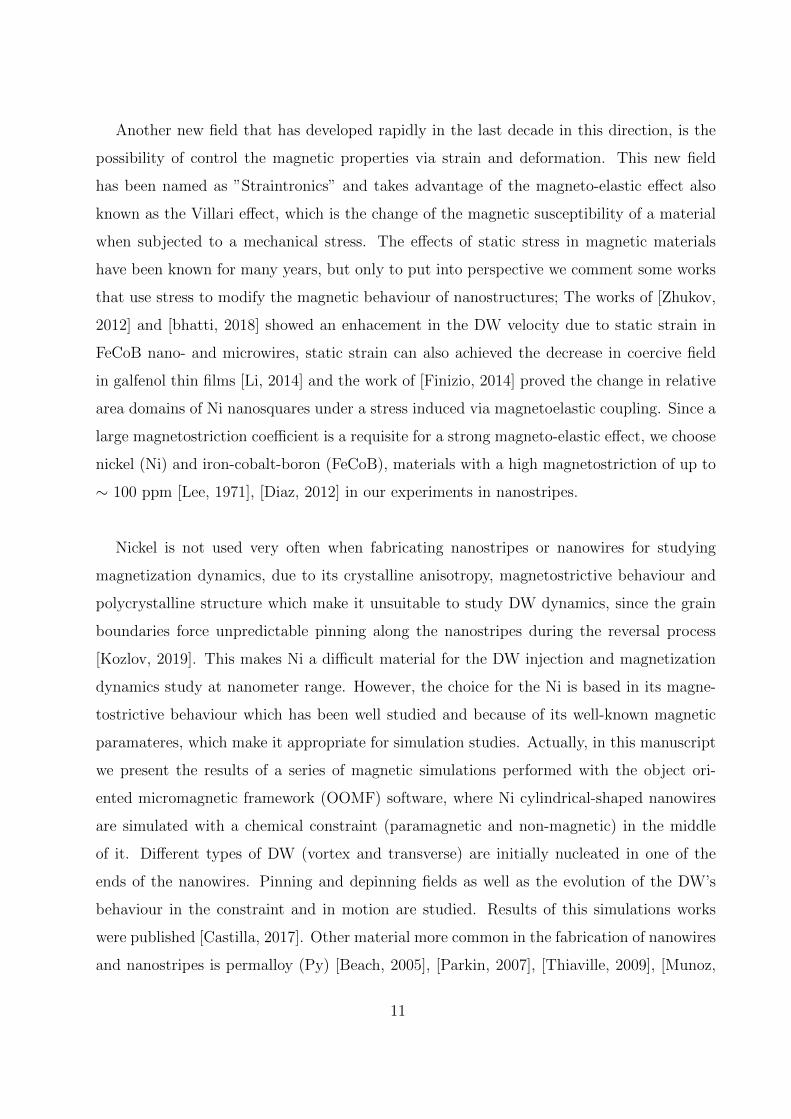
FIG. 1: Example of an experiment setup of the SAW’s application in nanostructures. Rectangle
nanomagnets are placed in front of a SAW device. [Davis, 2010].
in ferromagnetic/non-magnetic bilayers [Weiler, 2012]. This type of experiment takes ad-
vantage of the SAW’s, similarly to an electromagnetic excitation in order to promote the
precession of the spins within the ferromagnet. The precession of the spin can relax via
emission of a spin current into the hard metal. This spin current can be measured by the
inverse spin Hall effect, which generates a longitudinal dc voltage across the bilayer struc-
trure. SAW’s have also been used to detect delayed magneto-dynamic modes [Forster, 2016]
or magnon-phonon dynamics [Berk, 2019], or even to measure the intrinsic Gilbert damping
of a single nanomagnet .
This doctoral thesis is organized in nine chapters. Chapter two covers the experimental
techniques employed to fabricate and characterize samples. Chapter three collects the results
of the measurements performed in Fe/Gd multilayers, consisting in ferromagnetic resonance
and VSM measurements. Chapter four presents the results of the simulations performed
by the OOMF software in cylindrical-shaped nanowires with a chemical constraint that
studied the DW behaviour in them. Chapter five focuses on structural characterization of
the piezoelectric layers (ScAlN) and X-ray diffraction characterization of thin films whose
structure and crystalline properties are analogous to the nanostripes’. Chapter six presents
13
VSM measurements in thin films whose cyrstalline properties were studied in chapter five
in order to obtain the anisotropies directions and constants. Chapter seven covers the
description of the straintronics device by the characterization of the SAW resonator and
the magnetoresistance of the different nanostripes as well as their DW injection efficiency.
Chapter eight presents the effects of the application of the SAW’s in the magnetic nanostripes
through magnetoresistance measurements. In chapter nine is presented the electroacoustic
effect, its consequences and the acoustically driven precession forced by the SAW’s.
14
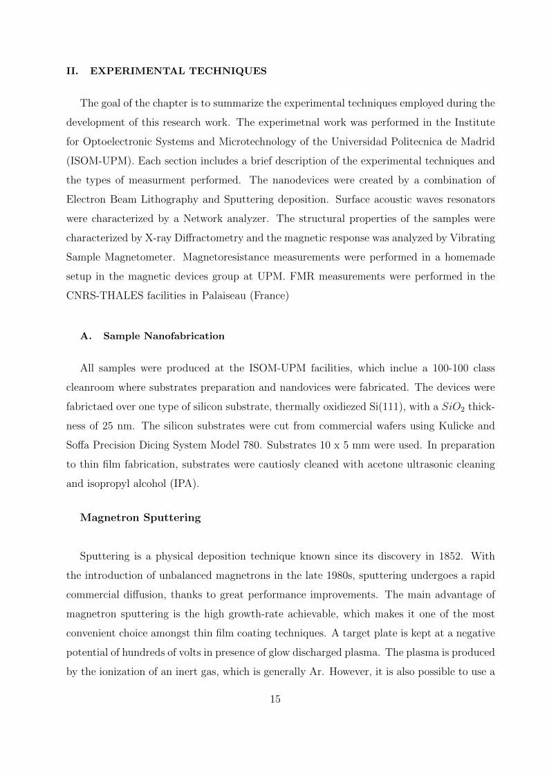
II. EXPERIMENTAL TECHNIQUES
The goal of the chapter is to summarize the experimental techniques employed during the
development of this research work. The experimetnal work was performed in the Institute
for Optoelectronic Systems and Microtechnology of the Universidad Politecnica de Madrid
(ISOM-UPM). Each section includes a brief description of the experimental techniques and
the types of measurment performed. The nanodevices were created by a combination of
Electron Beam Lithography and Sputtering deposition. Surface acoustic waves resonators
were characterized by a Network analyzer. The structural properties of the samples were
characterized by X-ray Diffractometry and the magnetic response was analyzed by Vibrating
Sample Magnetometer. Magnetoresistance measurements were performed in a homemade
setup in the magnetic devices group at UPM. FMR measurements were performed in the
CNRS-THALES facilities in Palaiseau (France)
A. Sample Nanofabrication
All samples were produced at the ISOM-UPM facilities, which inclue a 100-100 class
cleanroom where substrates preparation and nandovices were fabricated. The devices were
fabrictaed over one type of silicon substrate, thermally oxidiezed Si(111), with a SiO2 thick-
ness of 25 nm. The silicon substrates were cut from commercial wafers using Kulicke and
Soffa Precision Dicing System Model 780. Substrates 10 x 5 mm were used. In preparation
to thin film fabrication, substrates were cautiosly cleaned with acetone ultrasonic cleaning
and isopropyl alcohol (IPA).
Magnetron Sputtering
Sputtering is a physical deposition technique known since its discovery in 1852. With
the introduction of unbalanced magnetrons in the late 1980s, sputtering undergoes a rapid
commercial diffusion, thanks to great performance improvements. The main advantage of
magnetron sputtering is the high growth-rate achievable, which makes it one of the most
convenient choice amongst thin film coating techniques. A target plate is kept at a negative
potential of hundreds of volts in presence of glow discharged plasma. The plasma is produced
by the ionization of an inert gas, which is generally Ar. However, it is also possible to use a
15
FIG. 2: Schematics representation of a magnetron Sputtering system [www.semicore.com]
non inert gas such as oxygen or nitrogen either in place of, or (more commonly) in addition to
the inert gas (argon). When this is done, the ionized non inert gas can react chemically with
the target material vapor cloud and produce a molecular compound which then becomes
the deposited film. This is called, reactive sputtering. In order to deposit a non-conductive
target, a radiofrequency (RF) magnetron is required, since the applying of a DC negative
potential will quickly induced a positive charge on the non-conductive target surface, a
RF power allows to balance the surface charges when the positive potential is applied. The
ionization of the plasma is increased by the presence of a magnetic field parallel to the target,
produced by permanent magnets properly placed underneath the field lines, increasing the
probability of electron-atom collisions by an order of magnitude. The energetic ions of the
plasma are accelerated towards the target and the collisions result in the removal of target
atoms, which eventually deposit on the substrate.
All the samples in this work were grown and deposited in two different sputtering systems
in the ISOM-UPM facility. The first system consists of a main chamber which reaches a base
pressure of 10−6 mbar and a comercial RF magnetron where a ScAl target is placed. The
magnetron is positioned at the top of the vacuum chamber. The first step is the deposition
of the ScAlN on our silicon oxide substrates. We deposit this piezoelectric material through
the RF reactive sputtering. Nitrogen gas is pumped inside the chamber and its flux is
16
regulated with a mass flow controller in order to control the pressure of Nitrogen insde. The
target plate is ketp to a potential of hundreds of volts and the Nitrogen gets ionized in a
plasma. The ionized Nitrogen can reacts chemically with the target material vapor cloud of
ScAl producing a molecular compound which then becomes the deposited film of ScAlN.
The second system also consists in a main vacuum chamber which can reach a base
pressure of 10−8 mbar with five DC magnetrons and a RF magnetron properly separated to
avoid contamination among the targets. The magnetrons are located on top of the chamber,
beneath them, the sample holder can rotate freely in order to be placed under the desired
target of the material to be deposited. Two permanent magnets are present at opposite
edges of the sample holder so to generate a magnetic field parallel to substrate surface. This
magnet field is about 300 Oe and it is suffiecient to induce magnetocrystalline anisotropy in
the sputtered magnetic materials.
Both systems have load lock chambers which allows to reach the base pressure in few
minutes when loading a substrate. There is a large dependence between the growth rates
of the materials and their distance to the sample holder. This may explain the reason why
these growth rates are relatevely high compared to other works. Table I summarizes most of
the materials deposited during this thesis, their growth conditions and their growth rates.
Stepping Motor in the Sputtering Chamber In this thesis we carried out the
fabrication of multilayered samples. The thicknesses of individual layers fabricated are thin
enough for us to require a high precission method able to rotate fast the position of the
sample holder inside the sputteing chamber. In order to achieve this control, the sample
holder is attached through a stem inside the chamber to a stepping motor, which is placed
and handled from the outside of the chamber. The stepping motor is connected to a Stogra
position control, model WSERS xx.230 AC V01, programmable via standard Windows-PC.
This allows a precission in time of 0.1 s and 1 in the position of the stepping motor.
17
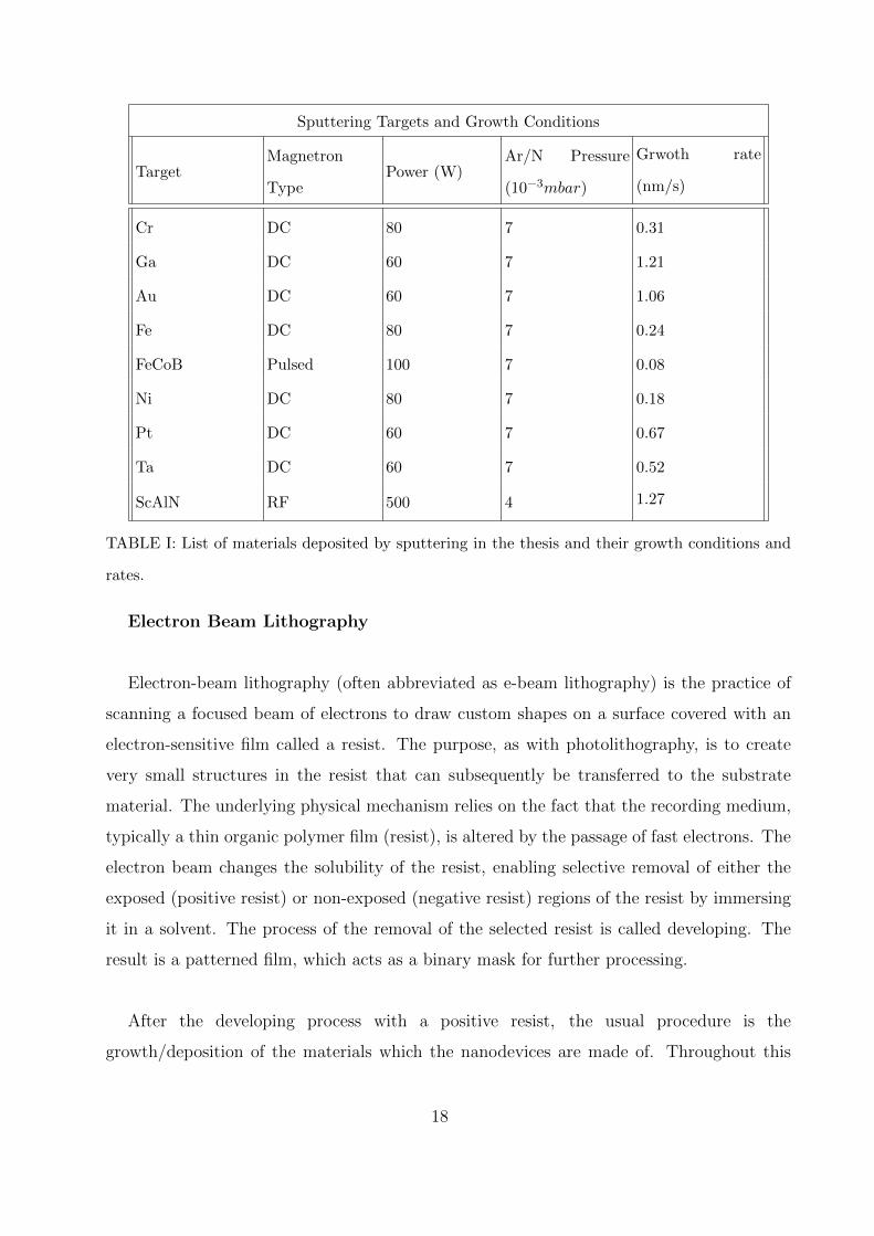
Sputtering Targets and Growth Conditions
TargetMagnetron
TypePower (W)
Ar/N Pressure
(10−3mbar)
Grwoth rate
(nm/s)
Cr DC 80 7 0.31
Ga DC 60 7 1.21
Au DC 60 7 1.06
Fe DC 80 7 0.24
FeCoB Pulsed 100 7 0.08
Ni DC 80 7 0.18
Pt DC 60 7 0.67
Ta DC 60 7 0.52
ScAlN RF 500 4 1.27
TABLE I: List of materials deposited by sputtering in the thesis and their growth conditions and
rates.
Electron Beam Lithography
Electron-beam lithography (often abbreviated as e-beam lithography) is the practice of
scanning a focused beam of electrons to draw custom shapes on a surface covered with an
electron-sensitive film called a resist. The purpose, as with photolithography, is to create
very small structures in the resist that can subsequently be transferred to the substrate
material. The underlying physical mechanism relies on the fact that the recording medium,
typically a thin organic polymer film (resist), is altered by the passage of fast electrons. The
electron beam changes the solubility of the resist, enabling selective removal of either the
exposed (positive resist) or non-exposed (negative resist) regions of the resist by immersing
it in a solvent. The process of the removal of the selected resist is called developing. The
result is a patterned film, which acts as a binary mask for further processing.
After the developing process with a positive resist, the usual procedure is the
growth/deposition of the materials which the nanodevices are made of. Throughout this
18
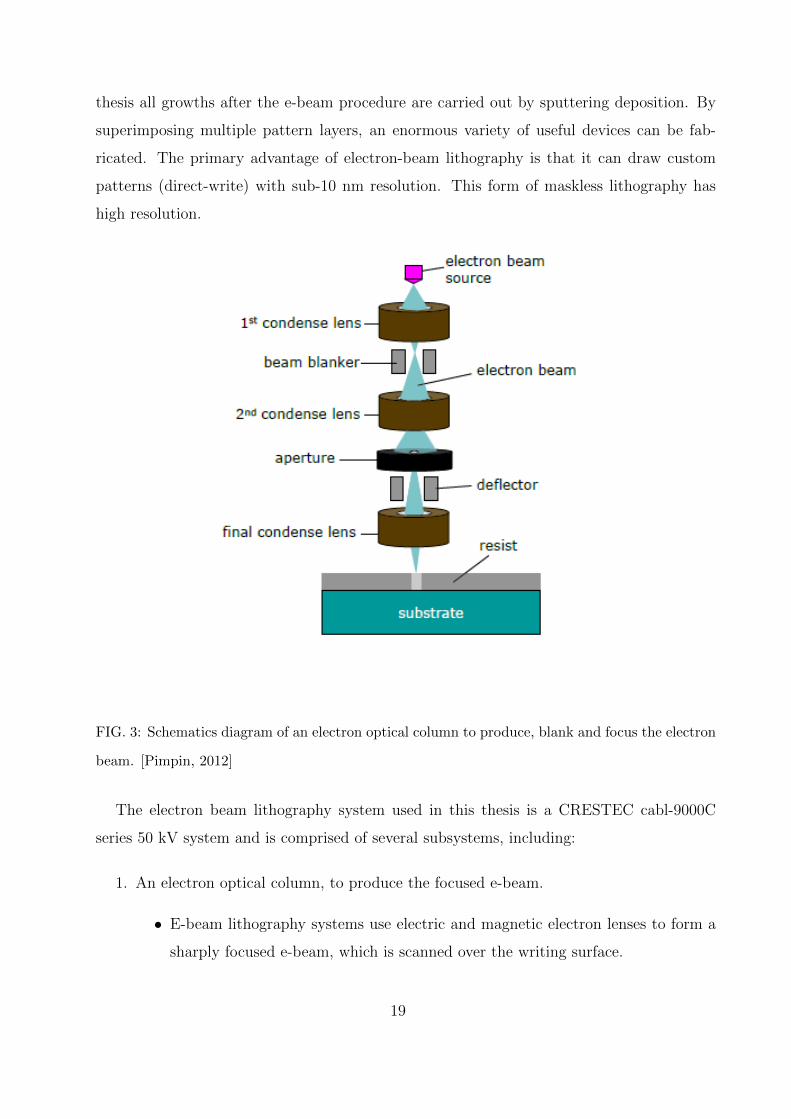
thesis all growths after the e-beam procedure are carried out by sputtering deposition. By
superimposing multiple pattern layers, an enormous variety of useful devices can be fab-
ricated. The primary advantage of electron-beam lithography is that it can draw custom
patterns (direct-write) with sub-10 nm resolution. This form of maskless lithography has
high resolution.
FIG. 3: Schematics diagram of an electron optical column to produce, blank and focus the electron
beam. [Pimpin, 2012]
The electron beam lithography system used in this thesis is a CRESTEC cabl-9000C
series 50 kV system and is comprised of several subsystems, including:
1. An electron optical column, to produce the focused e-beam.
• E-beam lithography systems use electric and magnetic electron lenses to form a
sharply focused e-beam, which is scanned over the writing surface.
19
2. Analog electronics to produce, focus, blank/unblank, and scan the beam.
• The e-beam scans over the writing surface using electric fields, turning on and of
while scanning. Fig. 3 presents the optical column with its magnetic lenses and
blankers needed to focus and control the diameter of the electron beam.
3. Digital electronics to store and transmit the pattern data.
• The pattern data are typically created using CABL-2000 software for computer
design. These data must then be turn into a format usable by the e-beam writer.
A digital electronic data path automatically converts and sends the data to the
e-beam writer.
4. A high-precision mechanical XY stage to position the writing substrate relative to the
e-beam.
• The XY stage moves under the optical column in order to draw the pattern in
the resist. The stitching accuracy depends on the precision of the stage in XY.
5. A high-vacuum system, with provision to move the writing substrate in and out of the
vacuum.
• A prevaccuum chamber is part of the system in order to introduce the samples
and not breaking the high vacuum in the internal chamber.
6. High-speed computers and microprocessors, to automatically perform all of the nec-
essary tasks.
7. An extensive software system
A considerable engineering effort is needed to make all of these components work reliably
together.
20
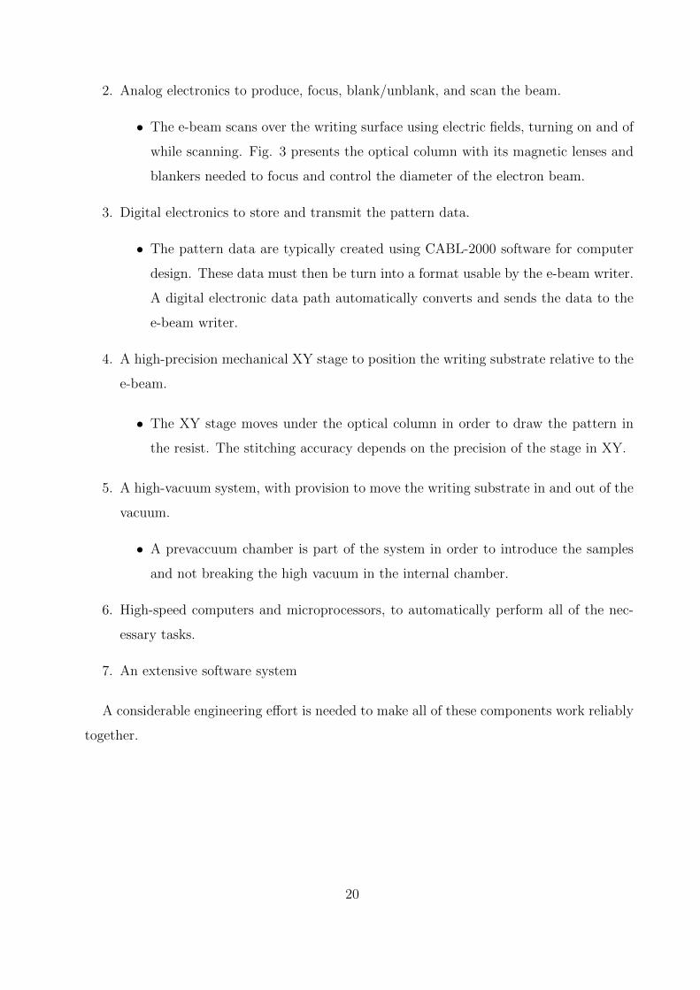
Nanofabrication Procedure
As we stated before, the advantage of fabricating by EBL system is the possibility of an
infinite variety of devices made by different metals by superimposing different nanolithog-
raphy phases. In this section we will explain which is the procedure to follow during this
thesis to the growth phase of the device. The procedure of fabricating devices from start is
as follows:
First, we spin coated a resist, PMMA/ZEP, which are positive resists, over a substrate
of SiO2/ScAlN at 5000 rpm. Then, the specimen is baked in order to evaporate the solvant
of the resist. As the substrate has insulating behaviour and in order to avoid that it gets
charged during the exposure in the electron beam lithography, a conductive polymer is spin
coated over the resist. The sample undergoes an electron exposure with a defined pattern
in the EBL system, which alters the solubility of the polymer. Once the pattern is drawn
in the resist sample, this is immersed in a liquid called developer, whose task is remove the
exposed (in case of positive resist) polymer. When the exposed pattern is removed a binary
mask is obtained. Then the growth procedure is performed and the metals are deposited by
sputtering deposition. Once the deposition of the metal is performed. The excess of resist
and metal is eliminated by immersing the sample in an organic disolvant, which is acetone
in case of PMMA resist and 3-metylpirrolidone in case of ZEP resist.
FIG. 4: Representation of the nanofabrication steps: a) The resist is spin coated over the substrate,
b) The resist is exposed by electron beam c) The exposed resist is removed, developing step, d),
e) The metal is deposited by sputtering and f) The resist and excess of metal are removed by
immersing the sample in an organic disolvant (lift-off)
21
B. Structural Characterization
The magnetic properties of the nanodevices studied trhoughout this thesis are dependent
on their structural characteristics. The study of samples through X-ray diffraction relates
the crystallographic properties of the samples with their magnetic properties.
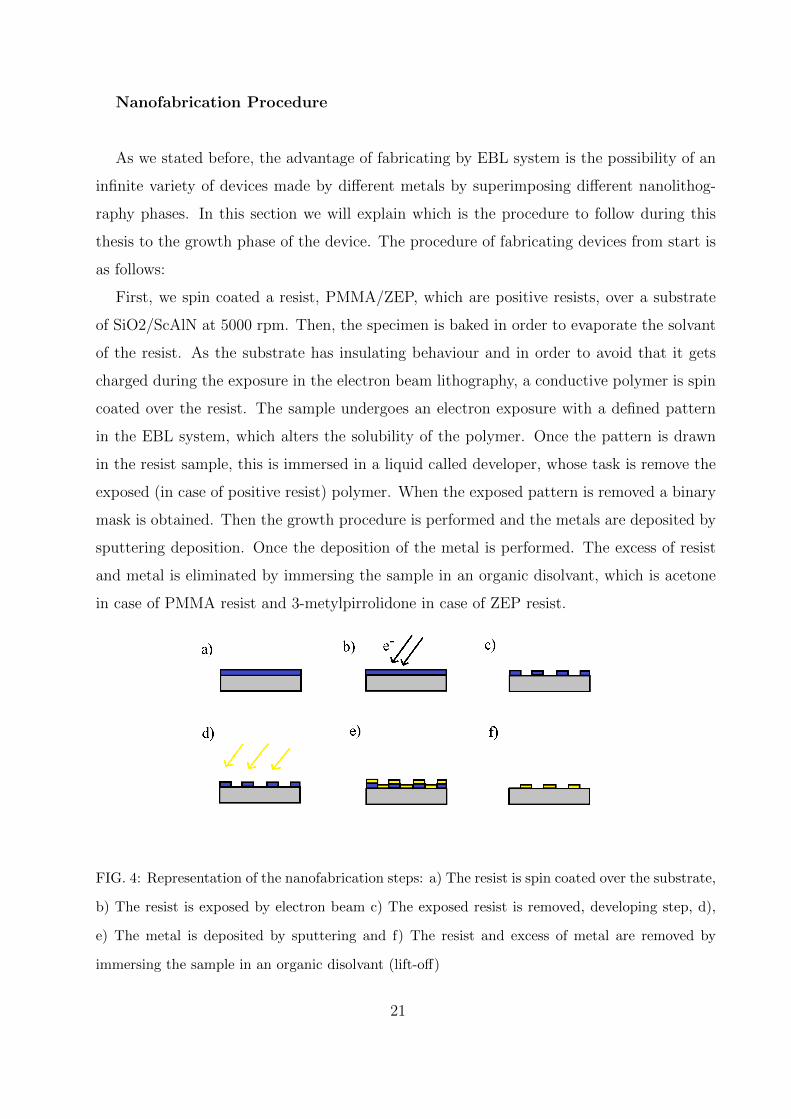
X-ray Diffraction
X-Ray crystallography is an experimental technique used for studying structural order,
based on diffraction of X-rays by long range ordered atoms. The interaction between X-rays
and atoms are mostly elastic scattering due their electronic shells. Scattered X-rays add
constructively when the material has crystallographic ordered and they cancel out if the
atoms in the material are randomly positioned by desctructive interference. The specific
directions, where they add constructively are determined by Bragg’s law:
nλ = 2d sin θ (1)
where d is the lattice spacing of the crystal, θ is the incidenet angle, n is any integer, and
λ is the wavelength of the incident X-rays.
FIG. 5: Schematic diagram of Bragg’s diffraction
Structural characterization with an X-ray diffractometer consists in determining the lat-
tice spacing d of a crystalline sample by using X-rays of known wavelength and measuring
for which θ is fulfilled.
22
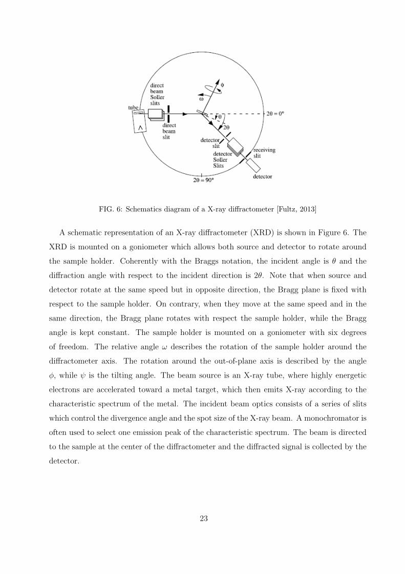
FIG. 6: Schematics diagram of a X-ray diffractometer [Fultz, 2013]
A schematic representation of an X-ray diffractometer (XRD) is shown in Figure 6. The
XRD is mounted on a goniometer which allows both source and detector to rotate around
the sample holder. Coherently with the Braggs notation, the incident angle is θ and the
diffraction angle with respect to the incident direction is 2θ. Note that when source and
detector rotate at the same speed but in opposite direction, the Bragg plane is fixed with
respect to the sample holder. On contrary, when they move at the same speed and in the
same direction, the Bragg plane rotates with respect the sample holder, while the Bragg
angle is kept constant. The sample holder is mounted on a goniometer with six degrees
of freedom. The relative angle ω describes the rotation of the sample holder around the
diffractometer axis. The rotation around the out-of-plane axis is described by the angle
φ, while ψ is the tilting angle. The beam source is an X-ray tube, where highly energetic
electrons are accelerated toward a metal target, which then emits X-ray according to the
characteristic spectrum of the metal. The incident beam optics consists of a series of slits
which control the divergence angle and the spot size of the X-ray beam. A monochromator is
often used to select one emission peak of the characteristic spectrum. The beam is directed
to the sample at the center of the diffractometer and the diffracted signal is collected by the
detector.
23
There are several types of techniques of X-Ray measurements, that depend on the ge-
ometry and angles between the incident and reflected or diffracted beams and the sample,
which allows the structural characterization of thin films. Here,only the relevant ones are
presented.
Out-of-plane θ/2θ scan This is a standard characterization for thin films. It consists
in rotating both source and detector at same speed and opposite directions. By this method,
Bragg planes are kept constant. If the system is aligned with the sample, Bragg planes will
be parallel to the sample surface. This technique will analyze the crystal texture in the
out-of-plane direction. By this configuration the volume of the sample that is irradiated,
diminishes as the incident beam angle increases.
Grazing Incident Angle (GID) In this measurement the incident angle is kept con-
stant, around 1 degree and we perform a 2θ scan with the detector. The idea is to obtain the
diffraction of the planes that are not parallel to the sample surface. Doing this we can rotate
the Braggs planes as the detector moves. The sample surface is kept still and is never parallel
to the Bragg planes. This technique is suitable for non-textured polycrystalline materiales.
By this technique the irradiated volume is larger, because it only depends on the incident
angle, which is very low. Out-of-plane θ/2θ and GID measurement give complementary
information about the structure of materials.
Rocking curves It consists in keeping both the beam source and the detecter at fixed
positions while ”rocking” the sample holder by varying the angle ω. The system is firstly
located at Bragg condition in the sample while the sample is being rotated around the bragg
condition. This measurements gives information about how the planes are spread around
the direction parallel to the sample substrate. This is known as the mosaicity.
X-Ray reflection In order to measure the thickness or thin films, the sample is placed
with a very low incident beam angle below the critical angle, where no beam is diffracted by
the sample. The detector is also located in a ver small angle so that the Bragg’s condition is
maintained. The information obtained can be usefuel in the measurment of bilayer thickness
repetition
24
The system used for XRD measurements during this research work are a PANalytical
X’pert Pro diffractometer of ISOM-UPM. This system use a Cu target which emits Kα1
X-rays whose wavelength is 1.541 A
C. Network Analyzer
A network analyzer is an instrument capable to measure properties of electrical networks,
specially those associated with reflectivity and transmission of electrical signals known as
scattering parameters or S-parameters. They are often used to characterize two-port net-
works such as amplifiers and filters, but they can be used on networks with an arbitrary
number of ports. Network analyzers can measure and display a device under tests (DUT)
magnitude and phase information across a frequency range. In essence, a network analyzer
characterizes a DUT in terms of scattering parameters, or S-parameters.
FIG. 7: Schematics diagram of network analyzer
The network analyzer used to characterize the resonator in this work is Agilent PNA-L
model N5230A with four ports and a range spectra of 300kHz − 20GHz. The Network
analyzer is embeded in a system that consists in an analytical probe-station Cascade Mi-
crotech 9000. Coaxial cables W.L. Gore 3GW40 connect the ports with the probe heads.
The probe heads are locked/placed in a micropositioner with one inch movement in all axes
and captured cross-roller bearings to prevent accidentally moving the tip.
S-Parameters S-parameters are used to characterize performance at RF and mi-
crowave frequencies in terms of incident and reflected waves. S-parameters are vector quan-
tities, meaning they contain both magnitude and phase information. A scalar network
analyzer (SNA) can only measure magnitude, while a vector network analyzer (VNA) can
measure both magnitude and phase.
25
b1
b2
=
S11 S12
S21 S22
a1
a2
(2)
where ai is the singal applied to the DUT from the port i and bi is the signal measured in
the port i. S-parameters are complex matrix that show Reflection/Transmission character-
istics (Amplitude/Phase) in frequency domain. Two port device has a four S-parameters.
As stated earlier, S-parameters contain both magnitude and phase information. Magnitude
is typically expressed in decibels (dB). This is mathematically defined as:
Sij(dB) = 20log|Sij| (3)
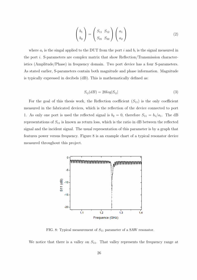
For the goal of this thesis work, the Reflection coefficient (S11) is the only coefficient
measured in the fabricated devices, which is the reflection of the device connected to port
1. As only one port is used the reflected signal is b2 = 0, therefore S11 = b1/a1. The dB
representations of S11 is known as return loss, which is the ratio in dB between the reflected
signal and the incident signal. The usual representation of this parameter is by a graph that
features power versus frequency. Figure 8 is an example chart of a typical resonator device
measured throughout this project.
FIG. 8: Typical measurement of S11 parameter of a SAW resonator.
We notice that there is a valley on S11. That valley represents the frequency range at
26
which the device reflects the least amount of power.
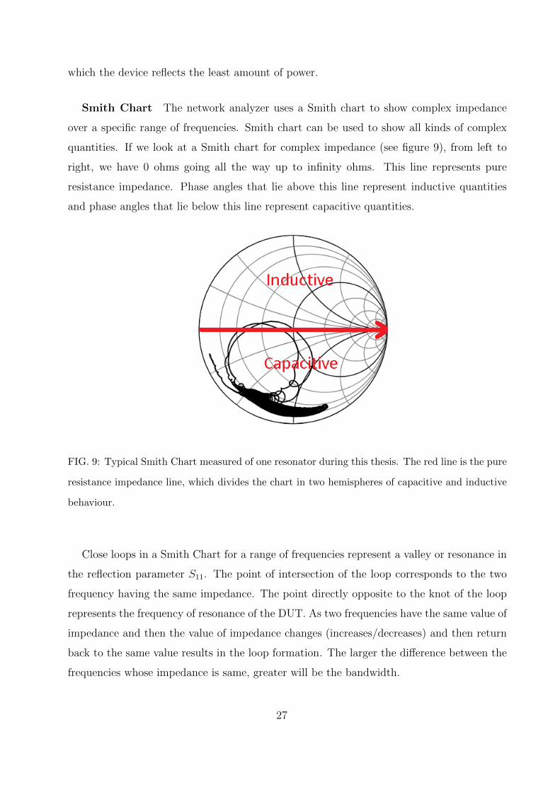
Smith Chart The network analyzer uses a Smith chart to show complex impedance
over a specific range of frequencies. Smith chart can be used to show all kinds of complex
quantities. If we look at a Smith chart for complex impedance (see figure 9), from left to
right, we have 0 ohms going all the way up to infinity ohms. This line represents pure
resistance impedance. Phase angles that lie above this line represent inductive quantities
and phase angles that lie below this line represent capacitive quantities.
FIG. 9: Typical Smith Chart measured of one resonator during this thesis. The red line is the pure
resistance impedance line, which divides the chart in two hemispheres of capacitive and inductive
behaviour.
Close loops in a Smith Chart for a range of frequencies represent a valley or resonance in
the reflection parameter S11. The point of intersection of the loop corresponds to the two
frequency having the same impedance. The point directly opposite to the knot of the loop
represents the frequency of resonance of the DUT. As two frequencies have the same value of
impedance and then the value of impedance changes (increases/decreases) and then return
back to the same value results in the loop formation. The larger the difference between the
frequencies whose impedance is same, greater will be the bandwidth.
27
D. Magnetic Characterization
The line of work followed in this thesis was encouraged by a simulation study that de-
scribed the DW dynamics in Ni nanowires. The software used for the study as well as
a description of the simulations is commented in this section. For the straintronics part,
we have analyzed the anisotropy of the grown-by-sputtering nanostripes by measuring the
hysteresis loops of identically structured thin films, with a vibrating sample magnetometer
(VSM). We also described the resonance modes in multilayered Fe/Gd samples by ferromag-
netic resonance (FMR). Finally, by carrying out magnetoresistance measurements (AMR) in
the magnetic nanostripes the magnetization states of them can be infered. The descriptions
of the setup experiments of these techniques are presented in each subsection.
Micromagnetic Simulations
Micromagnetic simulations is an useful way to understand the processes that govern the
magnetization dynamics observed in experiments. At micro- and nanoscale these are de-
scribed through the Landau-Lifshitz-Gilbert equation (LLG), which is an ordinary differen-
tial equation in time. We perform the simulations using the object oriented micromagnetic
framework (OOMF) software. This software allows to mesh the space in several cells of
defined-by-user dimensions, define the magnetization (−→M), exchange constant between cells
(A), magnetocrystalline anisotropy (Kc) and let the system reach the stability through the
LLG equation from an initial defined-by-user magnetization state. The simulations carried
out in this work were performed in a 50 nm circular-section and 1 µm long nanowires with
parameters of saturation magnetization (Ms = 4.9·105 A/m), exchange energy (A = 9·10−12
J/m) and anisotropy constant (K = 5.7 · 103 J/m3) that emulates the Ni. Mid length in
the nanowire there is a section with different composition (chemical constraint). For a Ni
nanocylinder 50 nm in diameter, there is no a clear energetically favored type of DW, and
both transverse and vortex DWs can be present. By fixing the spins at the edge of the NW
at the start of the simulations it is possible to choose the type of DW initially nucleated.
This simulation work studies the pinning and depinning fields at the chemical constraint as
a function of the nature of this and the type of DW pinned in the constraint. Results of this
study were published in [Castilla, 2017].
28
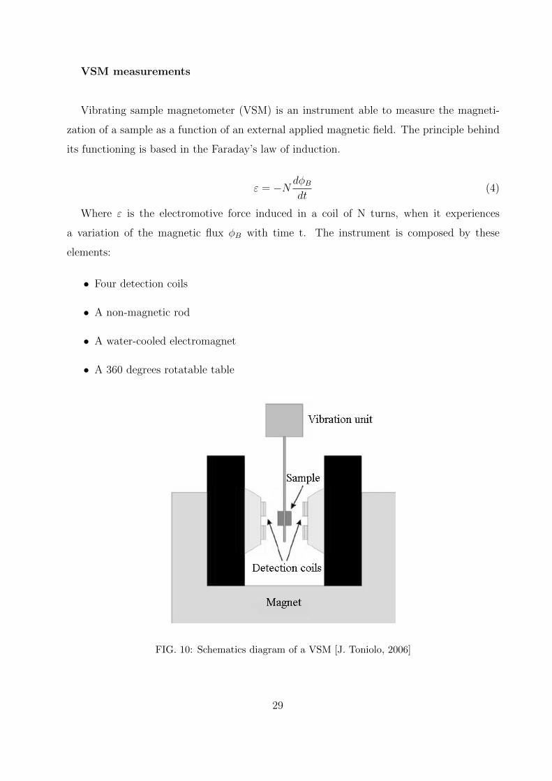
VSM measurements
Vibrating sample magnetometer (VSM) is an instrument able to measure the magneti-
zation of a sample as a function of an external applied magnetic field. The principle behind
its functioning is based in the Faraday’s law of induction.
ε = −N dφBdt
(4)
Where ε is the electromotive force induced in a coil of N turns, when it experiences
a variation of the magnetic flux φB with time t. The instrument is composed by these
elements:
• Four detection coils
• A non-magnetic rod
• A water-cooled electromagnet
• A 360 degrees rotatable table
FIG. 10: Schematics diagram of a VSM [J. Toniolo, 2006]
29
In presence of a magnetic sample, the magnetic flux that the coil experience is propor-
tional to the magnetic moment of the sample. The principle of operation of a VSM is based
on the observation of the voltage induced in a detection coil as the flux changes when the
sample position oscillates. The induced voltage in the detection coil is proportional to the
sample’s magnetic moment, but does not depend on the strength of the applied magnetic
field. A uniform DC magnetic field is generated by a water-cooled electromagnet. Four
detection coils are placed in a fixed position to avoid unwanted vibrations. The sample is
placed at the end of a rod and positioned in the center of the magnetic field. The rod is
connected to a vibrator head which generates a sinusoidal oscillation perpendicular to the
magnetic field lines. The oscillation of the magnetic sample generates a field distortion and
hence a change in the magnetic flux experienced by the detecting coils. The voltage output
from the coils is processed to extract a value of the magnetic sample. The rod can rotate
freely, allowing to measure in-plane and out-of-plane directions. A LakeShore Model 7304
of the ISOM-UPM was used for hysteresis loop measurements at room temperature. This
system hs a sensitivity of 5 · 10−6 emu and can reach 1.5 T.
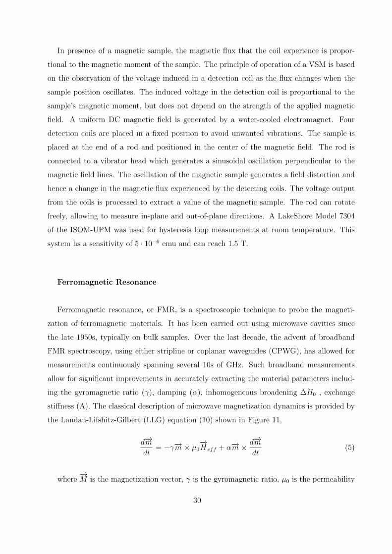
Ferromagnetic Resonance
Ferromagnetic resonance, or FMR, is a spectroscopic technique to probe the magneti-
zation of ferromagnetic materials. It has been carried out using microwave cavities since
the late 1950s, typically on bulk samples. Over the last decade, the advent of broadband
FMR spectroscopy, using either stripline or coplanar waveguides (CPWG), has allowed for
measurements continuously spanning several 10s of GHz. Such broadband measurements
allow for significant improvements in accurately extracting the material parameters includ-
ing the gyromagnetic ratio (γ), damping (α), inhomogeneous broadening ∆H0 , exchange
stiffness (A). The classical description of microwave magnetization dynamics is provided by
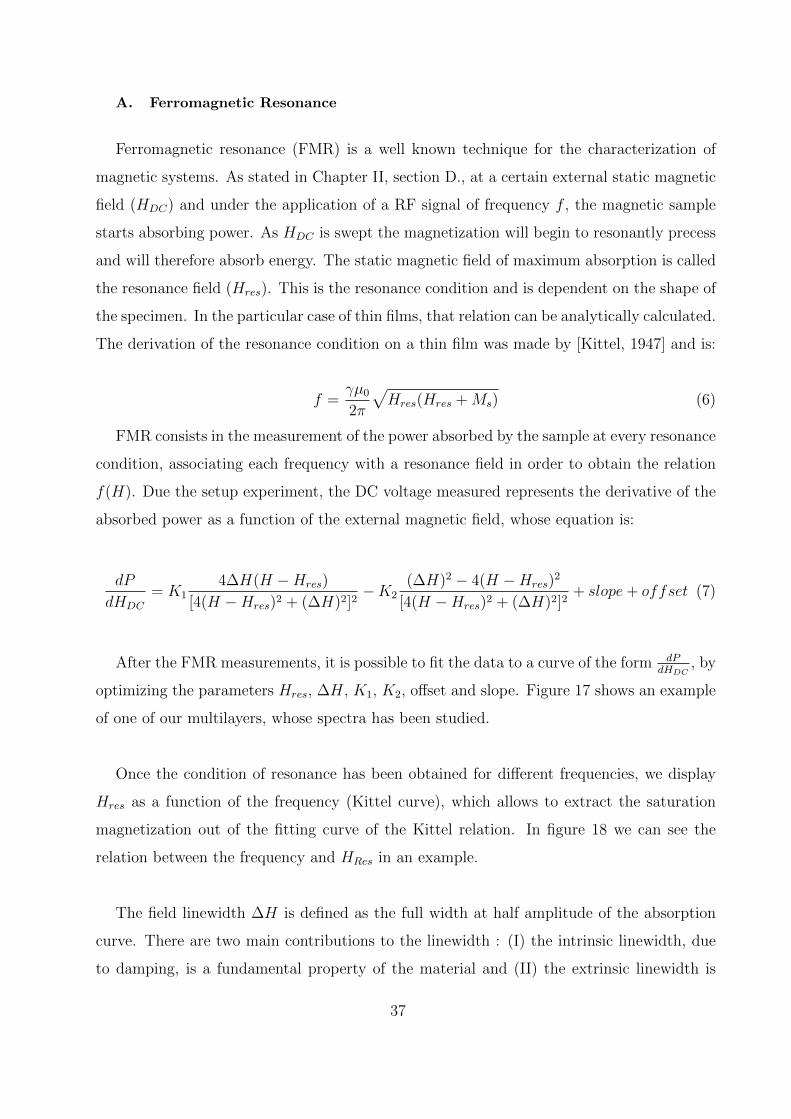
the Landau-Lifshitz-Gilbert (LLG) equation (10) shown in Figure 11,
d−→mdt
= −γ−→m × µ0−→H eff + α−→m × d−→m
dt(5)
where−→M is the magnetization vector, γ is the gyromagnetic ratio, µ0 is the permeability
30
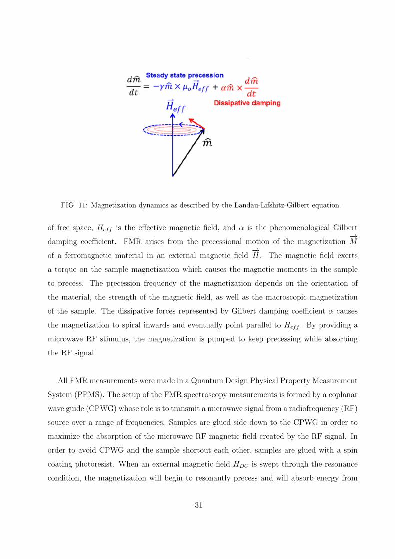
FIG. 11: Magnetization dynamics as described by the Landau-Lifshitz-Gilbert equation.
of free space, Heff is the effective magnetic field, and α is the phenomenological Gilbert
damping coefficient. FMR arises from the precessional motion of the magnetization−→M
of a ferromagnetic material in an external magnetic field−→H . The magnetic field exerts
a torque on the sample magnetization which causes the magnetic moments in the sample
to precess. The precession frequency of the magnetization depends on the orientation of
the material, the strength of the magnetic field, as well as the macroscopic magnetization
of the sample. The dissipative forces represented by Gilbert damping coefficient α causes
the magnetization to spiral inwards and eventually point parallel to Heff . By providing a
microwave RF stimulus, the magnetization is pumped to keep precessing while absorbing
the RF signal.
All FMR measurements were made in a Quantum Design Physical Property Measurement
System (PPMS). The setup of the FMR spectroscopy measurements is formed by a coplanar
wave guide (CPWG) whose role is to transmit a microwave signal from a radiofrequency (RF)
source over a range of frequencies. Samples are glued side down to the CPWG in order to
maximize the absorption of the microwave RF magnetic field created by the RF signal. In
order to avoid CPWG and the sample shortout each other, samples are glued with a spin
coating photoresist. When an external magnetic field HDC is swept through the resonance
condition, the magnetization will begin to resonantly precess and will absorb energy from
31
the CPWG.
FIG. 12: Schematic of the FMR measurment set up with the critical components are highlighted,
[qdusa.com]
This decrease in transmitted RF energy when sweeping through the resonance field is
converted to a DC voltage by a broadband RF diode. In order to improve the signal-to-noise
ratio (SNR), a lock-in detection technique is often employed, which requires modulating the
signal at a known frequency. This modulation is provided by an additional set of Helmholtz
coils powered by an AC source. This measurement scheme actually measures the derivative
of the transmitted power.
Magnetoresistance measurements
The magnetoresistance is the tendency of a ferromagnetic material to change its resistance
in presence of an external magnetic field. Anisotropic magnetoresistance (AMR) is the
change of magnetization due to the angle between the magnetization of the sample and the
electrical current that flows through it. This effect arises from the simultaneous action of
magnetization and spin-orbit coupling and its detailed mechanism depends on the material.
All the magnetoresistance measurements are performed in a circuit board (CB), where the
sample is previously glued with a photosensitive resist at 150 C. The CB consists in
32
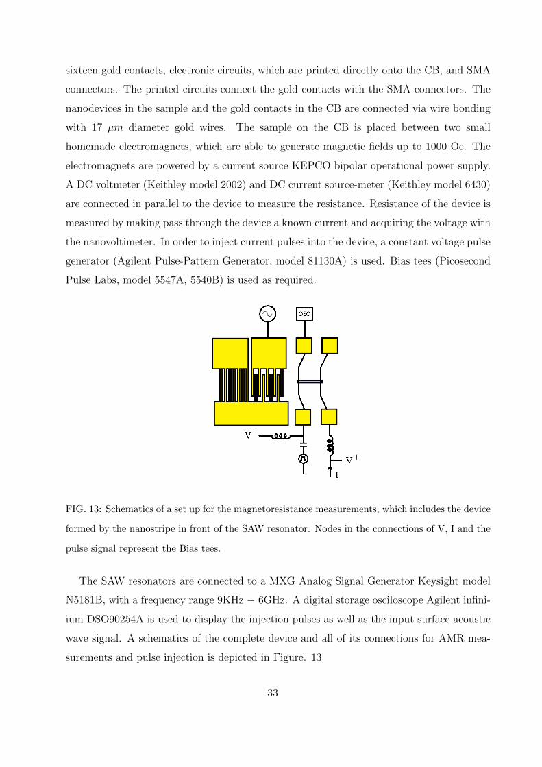
sixteen gold contacts, electronic circuits, which are printed directly onto the CB, and SMA
connectors. The printed circuits connect the gold contacts with the SMA connectors. The
nanodevices in the sample and the gold contacts in the CB are connected via wire bonding
with 17 µm diameter gold wires. The sample on the CB is placed between two small
homemade electromagnets, which are able to generate magnetic fields up to 1000 Oe. The
electromagnets are powered by a current source KEPCO bipolar operational power supply.
A DC voltmeter (Keithley model 2002) and DC current source-meter (Keithley model 6430)
are connected in parallel to the device to measure the resistance. Resistance of the device is
measured by making pass through the device a known current and acquiring the voltage with
the nanovoltimeter. In order to inject current pulses into the device, a constant voltage pulse
generator (Agilent Pulse-Pattern Generator, model 81130A) is used. Bias tees (Picosecond
Pulse Labs, model 5547A, 5540B) is used as required.
FIG. 13: Schematics of a set up for the magnetoresistance measurements, which includes the device
formed by the nanostripe in front of the SAW resonator. Nodes in the connections of V, I and the
pulse signal represent the Bias tees.
The SAW resonators are connected to a MXG Analog Signal Generator Keysight model
N5181B, with a frequency range 9KHz − 6GHz. A digital storage osciloscope Agilent infini-
ium DSO90254A is used to display the injection pulses as well as the input surface acoustic
wave signal. A schematics of the complete device and all of its connections for AMR mea-
surements and pulse injection is depicted in Figure. 13
33
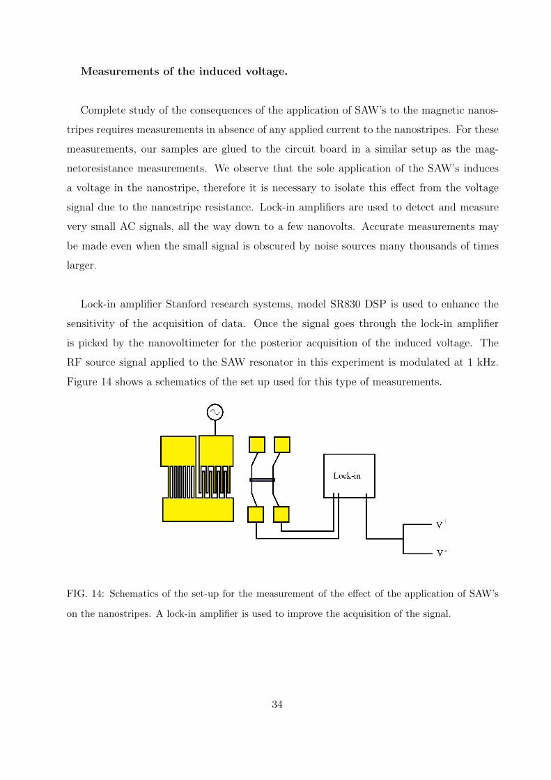
Measurements of the induced voltage.
Complete study of the consequences of the application of SAW’s to the magnetic nanos-
tripes requires measurements in absence of any applied current to the nanostripes. For these
measurements, our samples are glued to the circuit board in a similar setup as the mag-
netoresistance measurements. We observe that the sole application of the SAW’s induces
a voltage in the nanostripe, therefore it is necessary to isolate this effect from the voltage
signal due to the nanostripe resistance. Lock-in amplifiers are used to detect and measure
very small AC signals, all the way down to a few nanovolts. Accurate measurements may
be made even when the small signal is obscured by noise sources many thousands of times
larger.
Lock-in amplifier Stanford research systems, model SR830 DSP is used to enhance the
sensitivity of the acquisition of data. Once the signal goes through the lock-in amplifier
is picked by the nanovoltimeter for the posterior acquisition of the induced voltage. The
RF source signal applied to the SAW resonator in this experiment is modulated at 1 kHz.
Figure 14 shows a schematics of the set up used for this type of measurements.
FIG. 14: Schematics of the set-up for the measurement of the effect of the application of SAW’s
on the nanostripes. A lock-in amplifier is used to improve the acquisition of the signal.
34
III. FERROMAGNETIC RESONANCE ON FE/GD MULTILAYERS
Magnetic layered structures have been an object of extensive research in the last decades.
The periodic stacking of two distinct ferromagnetic materials gives rise to a variety of mag-
netic exchange interactions. Magnetic multilayers composed of a rare-earth (RE) element,
such as Gd, and a transition metal (TM) like Fe, Co and Ni are interesting example systems.
Due to their very different ordering temperatures, magnetic configurations depending on the
structural parameters may occur. The Fe/Gd is one of the most interesting systems since it
posseses a very rich magnetic state diagram. Depending on the temperature T , the external
magnetic field applied H or the ratio between the thickness of the different layers, these
systems have different magnetic orders, based on which of both materials alings with the
external magnetic field, since the coupling between the different layers is antiferromagnetic.
In weak magnetic fields antiparallel coupling between Fe and Gd prevails, with either the
Fe layers magnetization oriented in the direction of the external field (F state) or the Gd
layers magnetization oriented along the external magnetic field (G state). On the other hand,
when the magnetic field applied becomes stronger there must be a compromise between the
minimization of the Zeeman energy and the AFM coupling in the interlayer. In this situation
only the magnetization of the bulk of the layers lies parallel to the external magnetic field,
except for very thin films. Nevertheless generally, magnetization in adjacent layers are tilted
from the external magnetic field direction. This is called the twisted state (T state). The
magnetic state of the system is dependent on the ratio of the total magnetic moment of
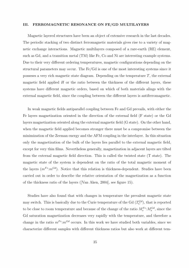
the layers (mFe:mGd). Notice that this relation is thickness-dependent. Studies have been
carried out in order to describe the relative orientation of the magnetization as a function
of the thickness ratio of the layers ([Van Aken, 2004], see figure 15).
Studies have also found that with changes in temperature the prevalent magnetic state
may switch. This is basically due to the Curie temperature of the Gd (TGdC ), that is reported
to be close to room temperature and because of the change of the ratio MFes :MGd
s , since the
Gd saturation magnetization decreases very rapidly with the temperature, and therefore a
change in the ratio mFe:mGd occurs. In this work we have studied both variables, since we
characterize different samples with different thickness ratios but also work at different tem-
35
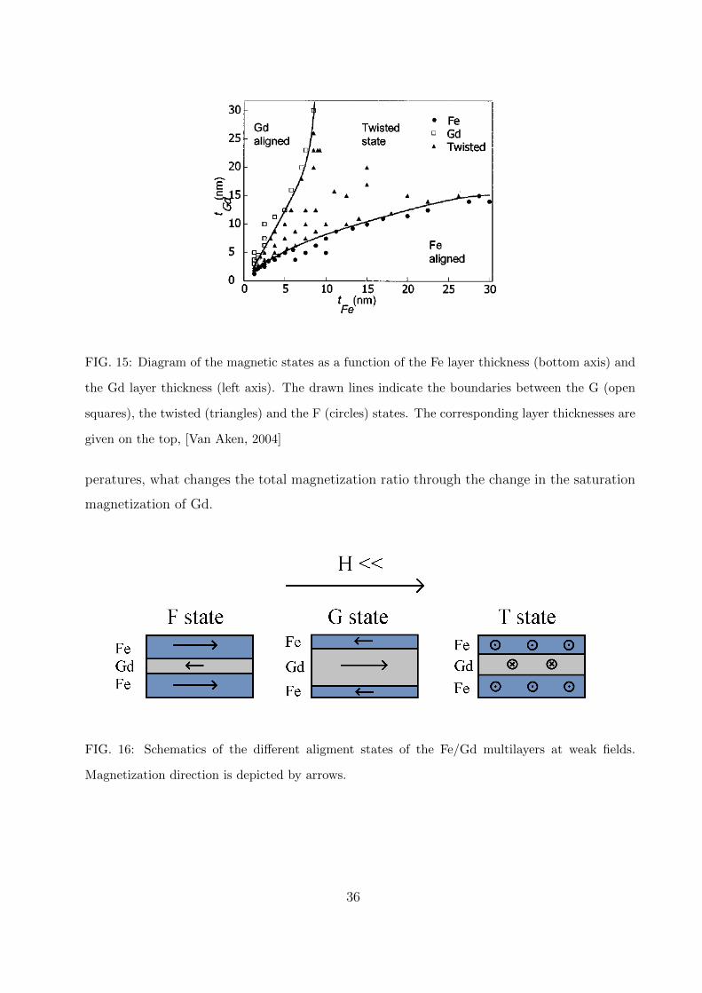
FIG. 15: Diagram of the magnetic states as a function of the Fe layer thickness (bottom axis) and
the Gd layer thickness (left axis). The drawn lines indicate the boundaries between the G (open
squares), the twisted (triangles) and the F (circles) states. The corresponding layer thicknesses are
given on the top, [Van Aken, 2004]
peratures, what changes the total magnetization ratio through the change in the saturation
magnetization of Gd.
FIG. 16: Schematics of the different aligment states of the Fe/Gd multilayers at weak fields.
Magnetization direction is depicted by arrows.
36
A. Ferromagnetic Resonance
Ferromagnetic resonance (FMR) is a well known technique for the characterization of
magnetic systems. As stated in Chapter II, section D., at a certain external static magnetic
field (HDC) and under the application of a RF signal of frequency f , the magnetic sample
starts absorbing power. As HDC is swept the magnetization will begin to resonantly precess
and will therefore absorb energy. The static magnetic field of maximum absorption is called
the resonance field (Hres). This is the resonance condition and is dependent on the shape of
the specimen. In the particular case of thin films, that relation can be analytically calculated.
The derivation of the resonance condition on a thin film was made by [Kittel, 1947] and is:
f =γµ0
2π
√Hres(Hres +Ms) (6)
FMR consists in the measurement of the power absorbed by the sample at every resonance
condition, associating each frequency with a resonance field in order to obtain the relation
f(H). Due the setup experiment, the DC voltage measured represents the derivative of the
absorbed power as a function of the external magnetic field, whose equation is:
dP
dHDC
= K14∆H(H −Hres)
[4(H −Hres)2 + (∆H)2]2−K2
(∆H)2 − 4(H −Hres)2
[4(H −Hres)2 + (∆H)2]2+ slope+ offset (7)
After the FMR measurements, it is possible to fit the data to a curve of the form dPdHDC
, by
optimizing the parameters Hres, ∆H, K1, K2, offset and slope. Figure 17 shows an example
of one of our multilayers, whose spectra has been studied.
Once the condition of resonance has been obtained for different frequencies, we display
Hres as a function of the frequency (Kittel curve), which allows to extract the saturation
magnetization out of the fitting curve of the Kittel relation. In figure 18 we can see the
relation between the frequency and HRes in an example.
The field linewidth ∆H is defined as the full width at half amplitude of the absorption
curve. There are two main contributions to the linewidth : (I) the intrinsic linewidth, due
to damping, is a fundamental property of the material and (II) the extrinsic linewidth is
37
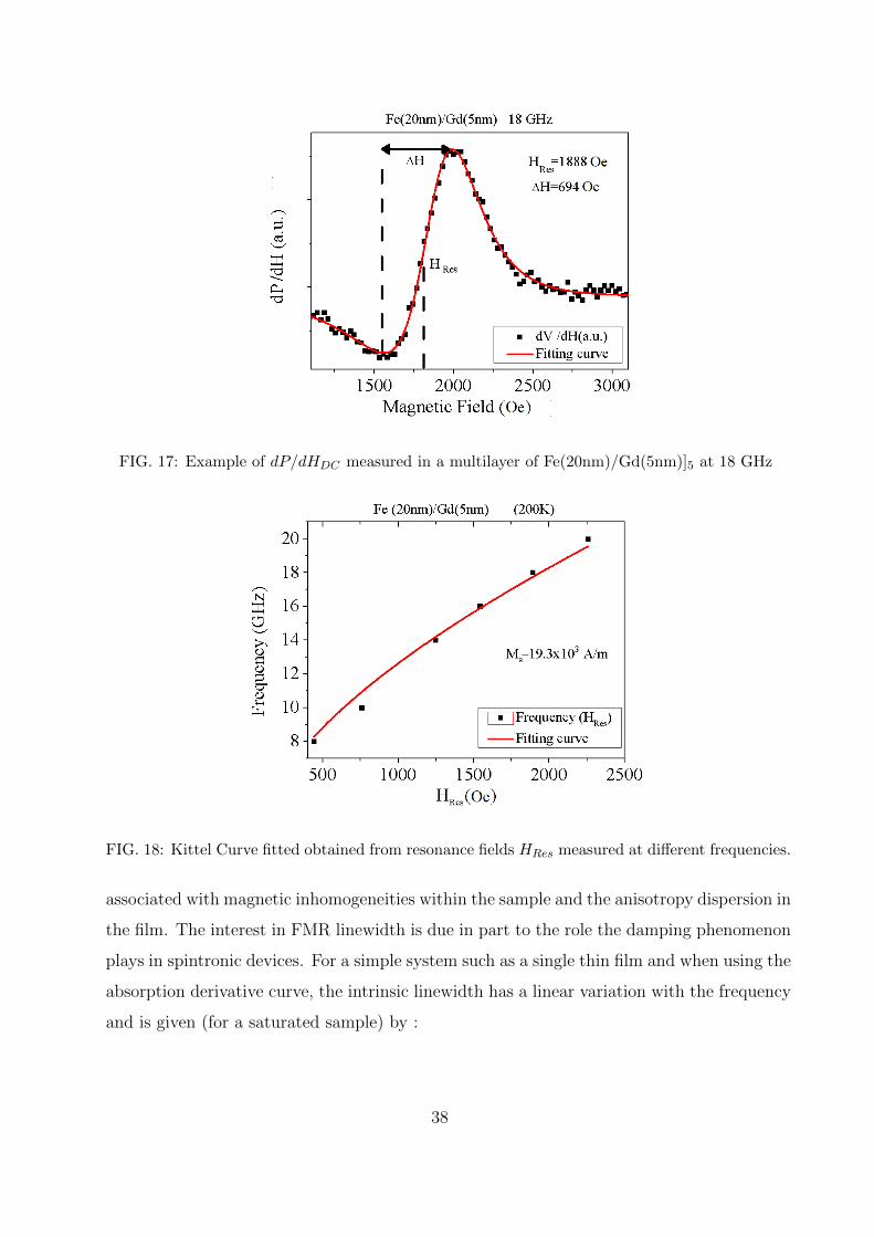
FIG. 17: Example of dP/dHDC measured in a multilayer of Fe(20nm)/Gd(5nm)]5 at 18 GHz
FIG. 18: Kittel Curve fitted obtained from resonance fields HRes measured at different frequencies.
associated with magnetic inhomogeneities within the sample and the anisotropy dispersion in
the film. The interest in FMR linewidth is due in part to the role the damping phenomenon
plays in spintronic devices. For a simple system such as a single thin film and when using the
absorption derivative curve, the intrinsic linewidth has a linear variation with the frequency
and is given (for a saturated sample) by :
38
∆H =2ωα√
3γ(8)
where ω is the angular frequency, γ is the gyromagnetic ratio and α the damping constant.
Fe/Gd multilayer samples are grown in the ISOM facilities, deposited by sputtering
method. In order to control their thickness we used a controlled- by-software stepper motor
that allowed the control of the sample holder inside the sputtering chamber with a pre-
cission in time of 0.1 s and angle precission of 1. Samples have the following structure
: Substrate/Cr (4 nm)/Fe (tFe nm) /Gd (tGd nm) (x5)/ Fe (tFe nm)/Pt (2 nm). FMR
measurements where performed in a Physical Proeperty Measurment System (PPMS) in the
CNRS/THALES facilities in Palaiseau (France).
39
B. Fe (20)/ Gd (5) Multilayer Sample.
We present the FMR results of a sample whose structure is:
Substrate/Cr(4)/[Fe(20)/Gd(5)]5/Fe(20)/Pt(2). We perform FMR measurements at a
range of temperature that goes from 300 K to 50 K. In this structure the width of the Fe
layers are thicker, therefore, measurements are carried out in a range of frequencies (10
GHz − 20 GHz) suitable for this material. Fe/Gd multilayers that fulfill the condition
mFe > mGd present a F state, which are characterized by the alignment at weak magnetic
fields of magnetic moments of the Fe layers and the external magnetic field, whereas the
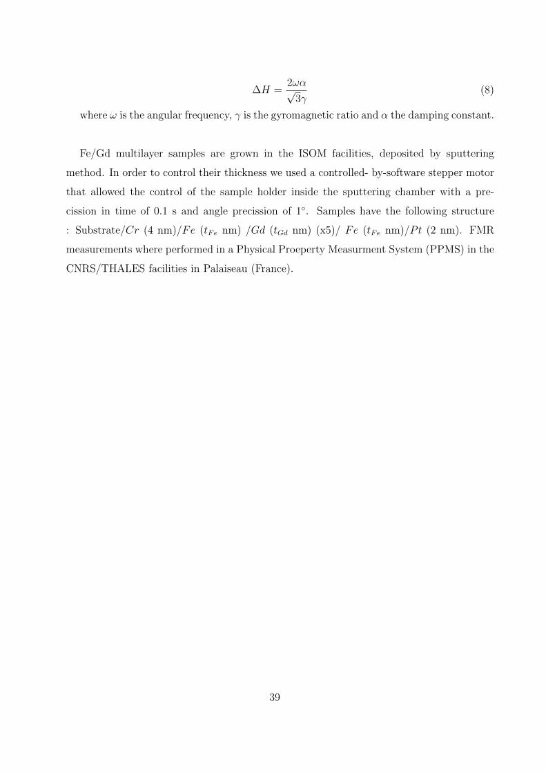
magnetic moments in Gd layers align opposite to the external H. Figure 19 plots FMR
curves at f=18 GHz for different temperatures.
FIG. 19: Resonance spectra at f=18 GHz and different temperatures (50 − 300K) shown in the
plot. Hres at every temperature is marked by arrows.
Hres is marked by red arrows at every temperature. At 300 K this sample did not show
any visible resonance at a frequency of 18 GHz. Nevertheless, the resonance condition is
achieved at lower temperatures. For the sake of clarity, we present a comparison of the
resonance spectra at two different temperatures (300 K and 50 K) with the same offset in
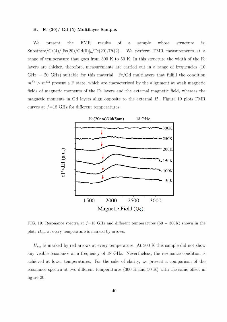
figure 20.
40
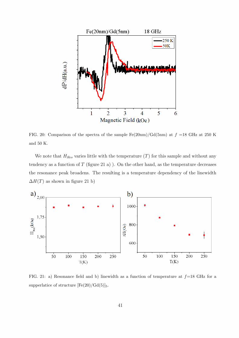
FIG. 20: Comparison of the spectra of the sample Fe(20nm)/Gd(5nm) at f =18 GHz at 250 K
and 50 K.
We note that HRes varies little with the temperature (T ) for this sample and without any
tendency as a function of T (figure 21 a) ). On the other hand, as the temperature decreases
the resonance peak broadens. The resulting is a temperature dependency of the linewidth
∆H(T ) as shown in figure 21 b)
FIG. 21: a) Resonance field and b) linewidth as a function of temperature at f=18 GHz for a
supperlatice of structure [Fe(20)/Gd(5)]5.
41
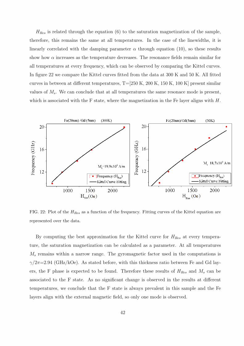
HRes is related through the equation (6) to the saturation magnetization of the sample,
therefore, this remains the same at all temperatures. In the case of the linewidths, it is
linearly correlated with the damping parameter α through equation (10), so these results
show how α increases as the temperature decreases. The resonance fields remain similar for
all temperatures at every frequency, which can be observed by comparing the Kittel curves.
In figure 22 we compare the Kittel curves fitted from the data at 300 K and 50 K. All fitted
curves in between at different temperatures, T=[250 K, 200 K, 150 K, 100 K] present similar
values of Ms. We can conclude that at all temperatures the same resonace mode is present,
which is associated with the F state, where the magnetization in the Fe layer aligns with H.
FIG. 22: Plot of the HRes as a function of the frequency. Fitting curves of the Kittel equation are
represented over the data.
By computing the best approximation for the Kittel curve for HRes at every tempera-
ture, the saturation magnetization can be calculated as a parameter. At all temperatures
Ms remains within a narrow range. The gyromagnetic factor used in the computations is
γ/2π=2.94 (GHz/kOe). As stated before, with this thickness ratio between Fe and Gd lay-
ers, the F phase is expected to be found. Therefore these results of HRes and Ms can be
associated to the F state. As no significant change is observed in the results at different
temperatures, we conclude that the F state is always prevalent in this sample and the Fe
layers align with the external magnetic field, so only one mode is observed.
42
C. Fe (5)/ Gd (15) Multilayer Sample.
We now describe FMR measurements of samples whose structure is:
Substrate/Cr(4)/[Fe(5)/Gd(15)]5/Fe(5)/Pt(2). This structure is expected to present
a G alignment state upon a weak external magnetic field, due to the larger thickness of the
Gd layers. In this state, the Gd layers aling with H, whereas the Fe layers align opposite to
H because of the AFM coupling in the interlayer. Nevertheless at high fields this sample it
is expected to present a twisted state. The Curie temperature of the Gd is TGdc = 293 K,
therefore, a transition is expected to occur at this temperature. However, different works,
e.g. [Hosoito, 2012], reported that in this type of samples, G state is present for lower
temperatures T < 120K and F state prevails for higher temperatures T ≥ 140K. Spectra
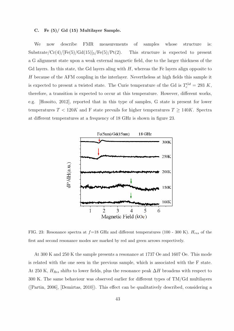
at different temperatures at a frequency of 18 GHz is shown in figure 23.
FIG. 23: Resonance spectra at f=18 GHz and different temperatures (100 - 300 K). Hres of the
first and second resonance modes are marked by red and green arrows respectively.
At 300 K and 250 K the sample presents a resonance at 1737 Oe and 1607 Oe. This mode
is related with the one seen in the previous sample, which is associated with the F state.
At 250 K, HRes shifts to lower fields, plus the resonance peak ∆H broadens with respect to
300 K. The same behaviour was observed earlier for different types of TM/Gd multilayers
([Partin, 2006], [Demirtas, 2010]). This effect can be qualitatively described, considering a
43
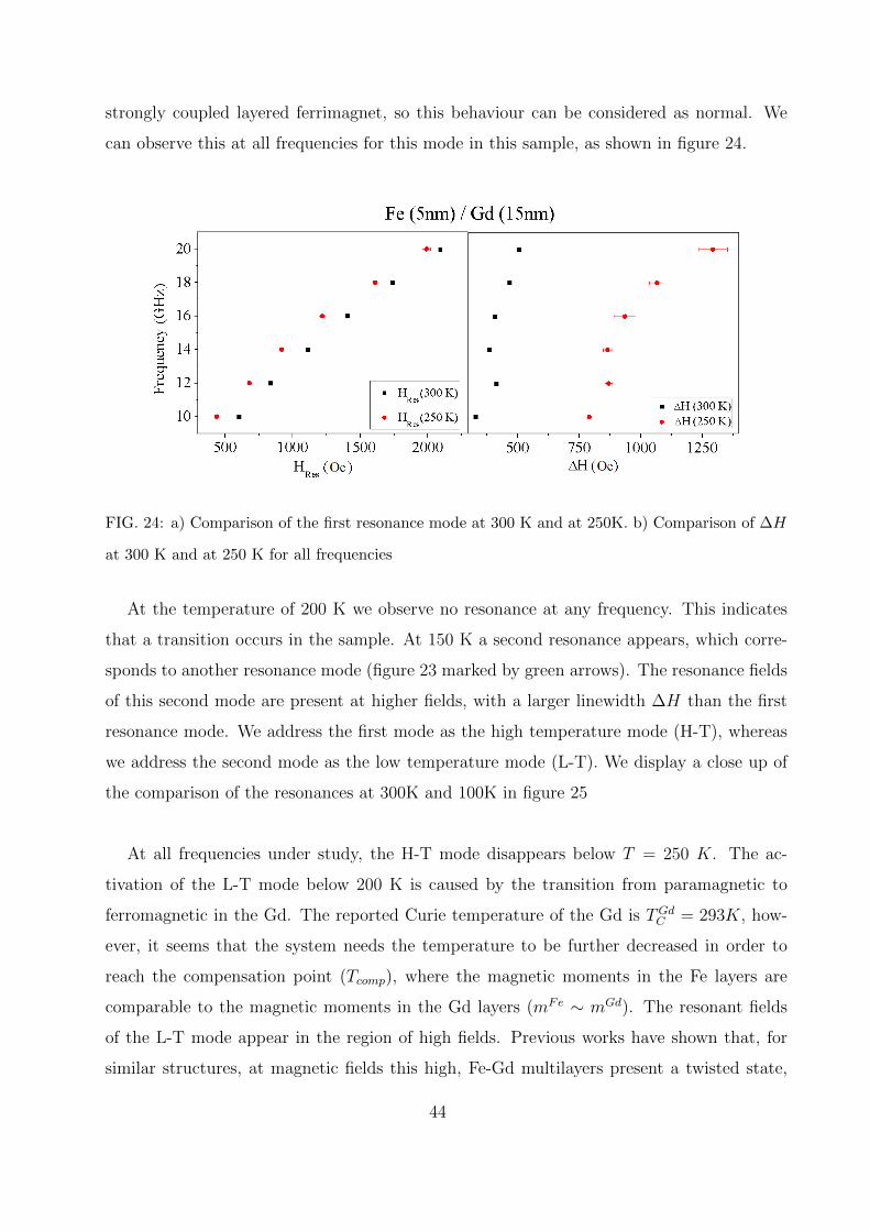
strongly coupled layered ferrimagnet, so this behaviour can be considered as normal. We
can observe this at all frequencies for this mode in this sample, as shown in figure 24.
FIG. 24: a) Comparison of the first resonance mode at 300 K and at 250K. b) Comparison of ∆H
at 300 K and at 250 K for all frequencies
At the temperature of 200 K we observe no resonance at any frequency. This indicates
that a transition occurs in the sample. At 150 K a second resonance appears, which corre-
sponds to another resonance mode (figure 23 marked by green arrows). The resonance fields
of this second mode are present at higher fields, with a larger linewidth ∆H than the first
resonance mode. We address the first mode as the high temperature mode (H-T), whereas
we address the second mode as the low temperature mode (L-T). We display a close up of
the comparison of the resonances at 300K and 100K in figure 25
At all frequencies under study, the H-T mode disappears below T = 250 K. The ac-
tivation of the L-T mode below 200 K is caused by the transition from paramagnetic to
ferromagnetic in the Gd. The reported Curie temperature of the Gd is TGdC = 293K, how-
ever, it seems that the system needs the temperature to be further decreased in order to
reach the compensation point (Tcomp), where the magnetic moments in the Fe layers are
comparable to the magnetic moments in the Gd layers (mFe ∼ mGd). The resonant fields
of the L-T mode appear in the region of high fields. Previous works have shown that, for
similar structures, at magnetic fields this high, Fe-Gd multilayers present a twisted state,
44
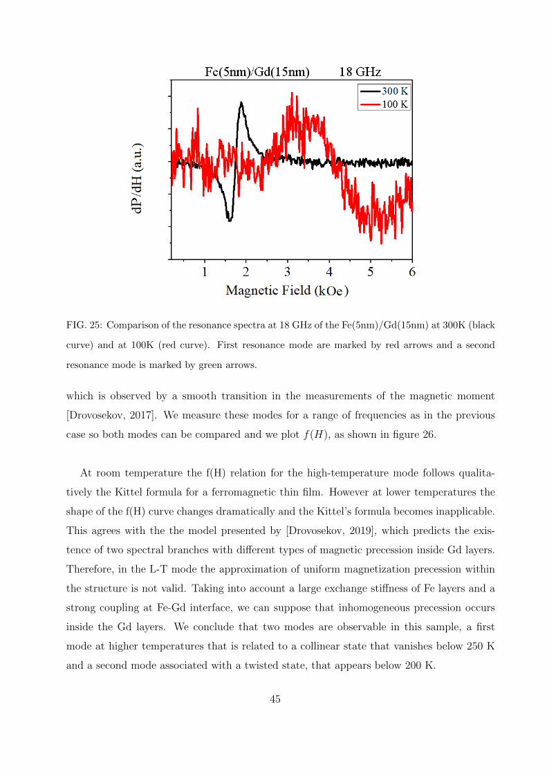
FIG. 25: Comparison of the resonance spectra at 18 GHz of the Fe(5nm)/Gd(15nm) at 300K (black
curve) and at 100K (red curve). First resonance mode are marked by red arrows and a second
resonance mode is marked by green arrows.
which is observed by a smooth transition in the measurements of the magnetic moment
[Drovosekov, 2017]. We measure these modes for a range of frequencies as in the previous
case so both modes can be compared and we plot f(H), as shown in figure 26.
At room temperature the f(H) relation for the high-temperature mode follows qualita-
tively the Kittel formula for a ferromagnetic thin film. However at lower temperatures the
shape of the f(H) curve changes dramatically and the Kittel’s formula becomes inapplicable.
This agrees with the the model presented by [Drovosekov, 2019], which predicts the exis-
tence of two spectral branches with different types of magnetic precession inside Gd layers.
Therefore, in the L-T mode the approximation of uniform magnetization precession within
the structure is not valid. Taking into account a large exchange stiffness of Fe layers and a
strong coupling at Fe-Gd interface, we can suppose that inhomogeneous precession occurs
inside the Gd layers. We conclude that two modes are observable in this sample, a first
mode at higher temperatures that is related to a collinear state that vanishes below 250 K
and a second mode associated with a twisted state, that appears below 200 K.
45
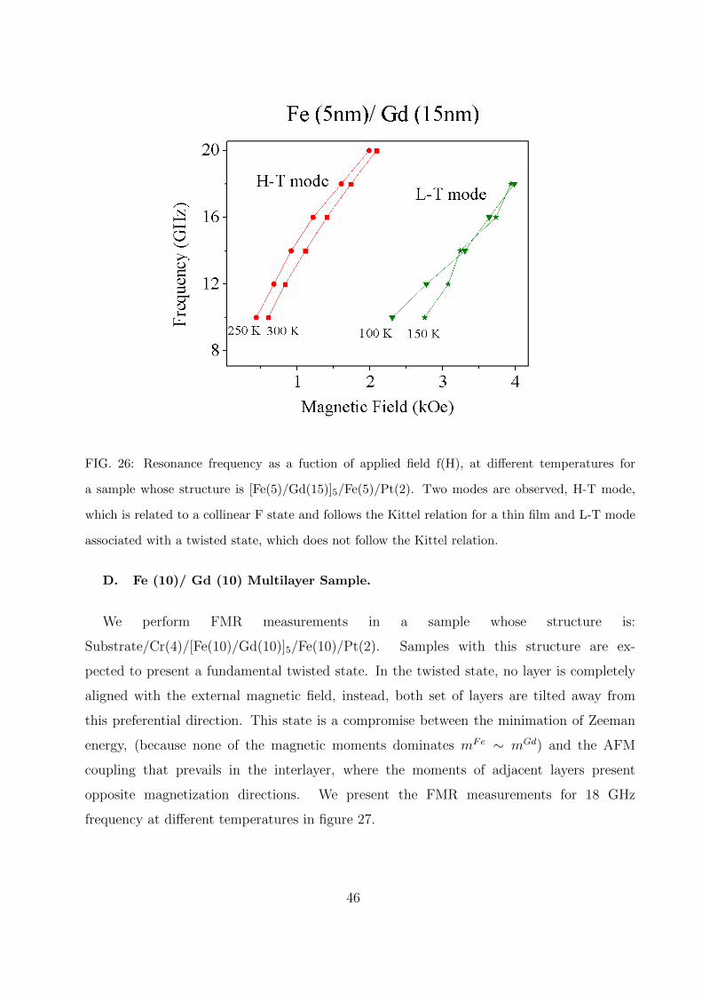
FIG. 26: Resonance frequency as a fuction of applied field f(H), at different temperatures for
a sample whose structure is [Fe(5)/Gd(15)]5/Fe(5)/Pt(2). Two modes are observed, H-T mode,
which is related to a collinear F state and follows the Kittel relation for a thin film and L-T mode
associated with a twisted state, which does not follow the Kittel relation.
D. Fe (10)/ Gd (10) Multilayer Sample.
We perform FMR measurements in a sample whose structure is:
Substrate/Cr(4)/[Fe(10)/Gd(10)]5/Fe(10)/Pt(2). Samples with this structure are ex-
pected to present a fundamental twisted state. In the twisted state, no layer is completely
aligned with the external magnetic field, instead, both set of layers are tilted away from
this preferential direction. This state is a compromise between the minimation of Zeeman
energy, (because none of the magnetic moments dominates mFe ∼ mGd) and the AFM
coupling that prevails in the interlayer, where the moments of adjacent layers present
opposite magnetization directions. We present the FMR measurements for 18 GHz
frequency at different temperatures in figure 27.
46
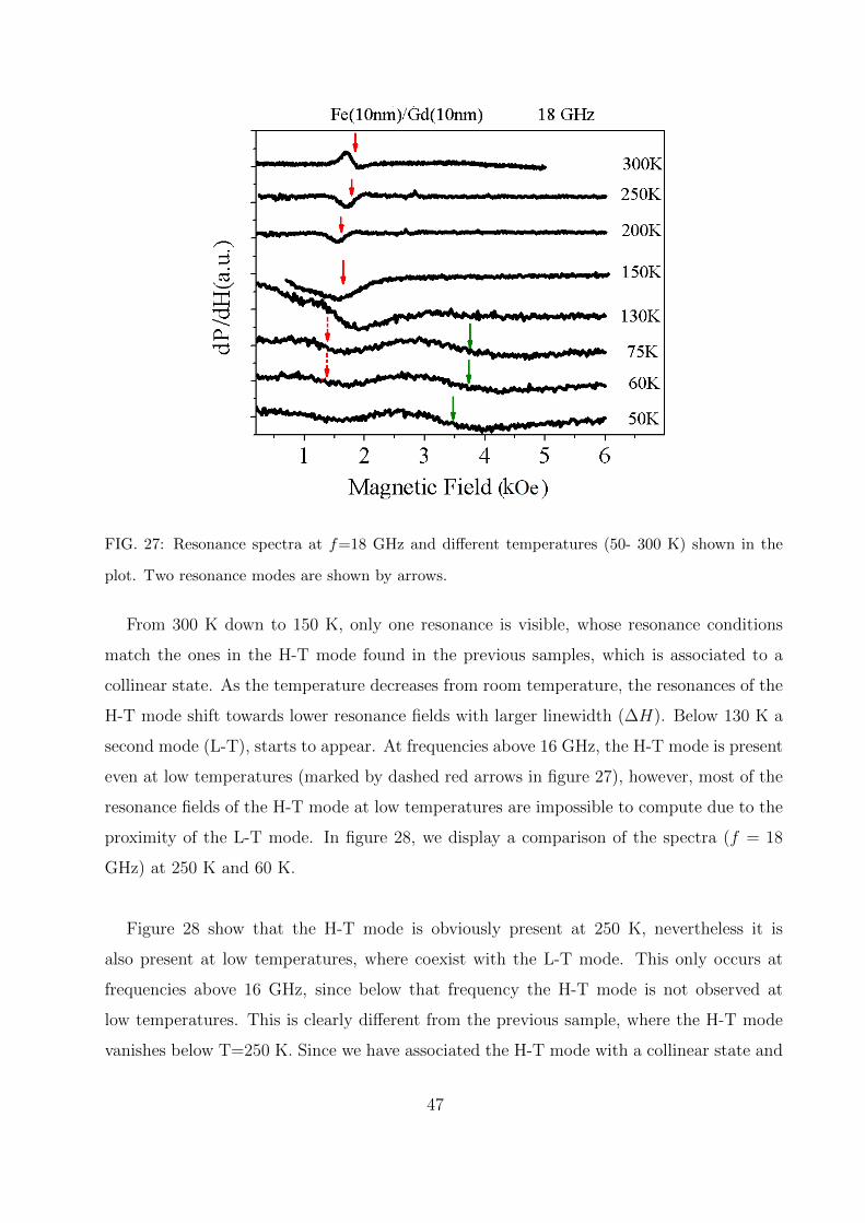
FIG. 27: Resonance spectra at f=18 GHz and different temperatures (50- 300 K) shown in the
plot. Two resonance modes are shown by arrows.
From 300 K down to 150 K, only one resonance is visible, whose resonance conditions
match the ones in the H-T mode found in the previous samples, which is associated to a
collinear state. As the temperature decreases from room temperature, the resonances of the
H-T mode shift towards lower resonance fields with larger linewidth (∆H). Below 130 K a
second mode (L-T), starts to appear. At frequencies above 16 GHz, the H-T mode is present
even at low temperatures (marked by dashed red arrows in figure 27), however, most of the
resonance fields of the H-T mode at low temperatures are impossible to compute due to the
proximity of the L-T mode. In figure 28, we display a comparison of the spectra (f = 18
GHz) at 250 K and 60 K.
Figure 28 show that the H-T mode is obviously present at 250 K, nevertheless it is
also present at low temperatures, where coexist with the L-T mode. This only occurs at
frequencies above 16 GHz, since below that frequency the H-T mode is not observed at
low temperatures. This is clearly different from the previous sample, where the H-T mode
vanishes below T=250 K. Since we have associated the H-T mode with a collinear state and
47
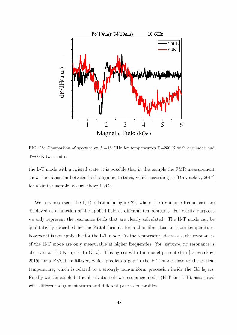
FIG. 28: Comparison of spectras at f =18 GHz for temperatures T=250 K with one mode and
T=60 K two modes.
the L-T mode with a twisted state, it is possible that in this sample the FMR measurement
show the transition between both alignment states, which according to [Drovosekov, 2017]
for a similar sample, occurs above 1 kOe.
We now represent the f(H) relation in figure 29, where the resonance frequencies are
displayed as a function of the applied field at different temperatures. For clarity purposes
we only represent the resonance fields that are clearly calculated. The H-T mode can be
qualitatively described by the Kittel formula for a thin film close to room temperature,
however it is not applicable for the L-T mode. As the temperature decreases, the resonances
of the H-T mode are only measurable at higher frequencies, (for instance, no resonance is
observed at 150 K, up to 16 GHz). This agrees with the model presented in [Drovosekov,
2019] for a Fe/Gd multilayer, which predicts a gap in the H-T mode close to the critical
temperature, which is related to a strongly non-uniform precession inside the Gd layers.
Finally we can conclude the observation of two resonance modes (H-T and L-T), associated
with different alignment states and different precession profiles.
48
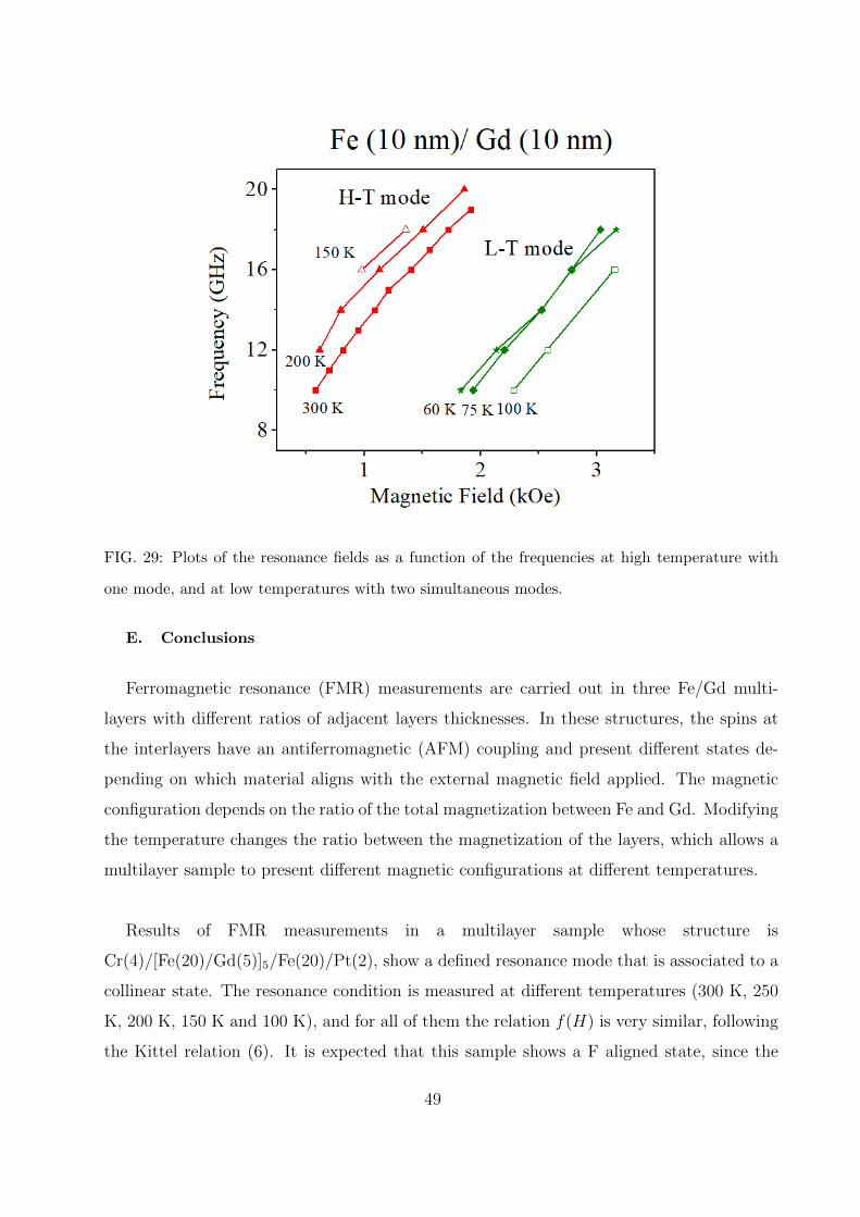
FIG. 29: Plots of the resonance fields as a function of the frequencies at high temperature with
one mode, and at low temperatures with two simultaneous modes.
E. Conclusions
Ferromagnetic resonance (FMR) measurements are carried out in three Fe/Gd multi-
layers with different ratios of adjacent layers thicknesses. In these structures, the spins at
the interlayers have an antiferromagnetic (AFM) coupling and present different states de-
pending on which material aligns with the external magnetic field applied. The magnetic
configuration depends on the ratio of the total magnetization between Fe and Gd. Modifying
the temperature changes the ratio between the magnetization of the layers, which allows a
multilayer sample to present different magnetic configurations at different temperatures.
Results of FMR measurements in a multilayer sample whose structure is
Cr(4)/[Fe(20)/Gd(5)]5/Fe(20)/Pt(2), show a defined resonance mode that is associated to a
collinear state. The resonance condition is measured at different temperatures (300 K, 250
K, 200 K, 150 K and 100 K), and for all of them the relation f(H) is very similar, following
the Kittel relation (6). It is expected that this sample shows a F aligned state, since the
49
thickness of the Fe layers are larger than the Gd ones. Therefore the total magnetic moment
of the Fe layers is larger at every temperature (mFe > mGd), which forces a F aligned state.
Results of FMR measurements in the multilayer sample with structure
Cr(4)/[Fe(5)/Gd(15)]5/Fe(15)/Pt(2), show a resonance mode at high temperatures
(H-T) (300 K, 250 K) which matches the one observed in the previous sample. This mode
is associated with a collinear F state. In the vecinity of room temperature, the H-T mode
shift towards lower resonance fields and larger linewidth with decreasing temperature. Due
to the paramagnetic-ferromagnetic transition that the Gd undergoes at TGdC =293 K and
the larger thickness of the Gd sublayers in this sample, a tranisition is expected to occur.
However this transition does not happen at TGdC , but at ∼ 200 K where no resonances
are observed. At this point the magnetic moments in the Fe layers are comparable to the
magnetic moments in the Gd layers (mFe ∼ mGd). Below that temperature a second mode
(L-T) at low temperatures arises. This second mode appears in the region of the high
fields, where a twisted state is expected in the sample. Although the H-T mode follows
qualitatively the Kittel relation for a thin film the L-T mode does not, which is explained
by an inhomogeneous precession of the magnetic moments inside the Gd layers
Finally we presented the results of FMR measurements in a multilayer sample whose
structure is Cr(4)/[Fe(10)/Gd(10)]5/Fe(10)/Pt(2). Similar to the sample whose Gd layer
thickness was predominant, this sample presents two resonant modes at different range
in temperatures (H-T and L-T), however at larger frequencies (16 and 18 GHz) and low
temperatures, both modes can be observed in the same measurement. This may be due to
the larger thickness of the Fe layers, which would imply that a collinear Fe state is present
even at low temperatures at low fields, however, as the magnetic field is increased, a twisted
state is reached in the multilayer and the second mode (L-T) can be observed.
50
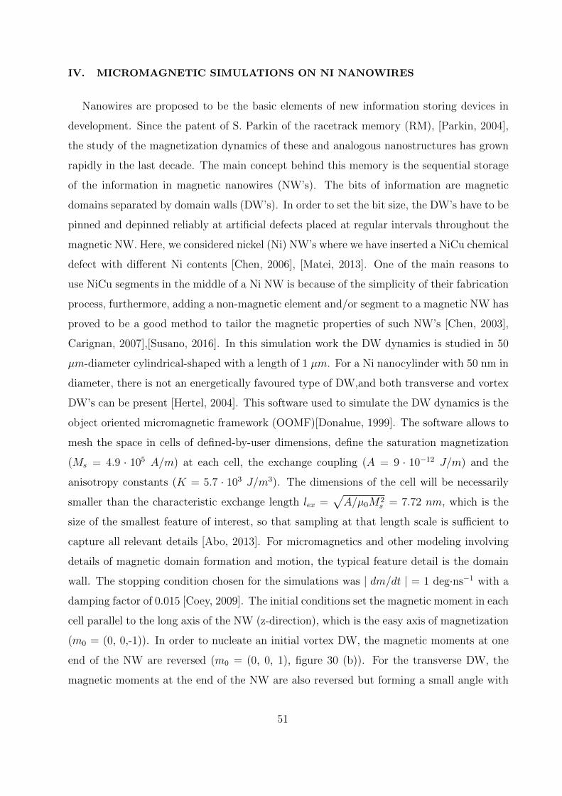
IV. MICROMAGNETIC SIMULATIONS ON NI NANOWIRES
Nanowires are proposed to be the basic elements of new information storing devices in
development. Since the patent of S. Parkin of the racetrack memory (RM), [Parkin, 2004],
the study of the magnetization dynamics of these and analogous nanostructures has grown
rapidly in the last decade. The main concept behind this memory is the sequential storage
of the information in magnetic nanowires (NW’s). The bits of information are magnetic
domains separated by domain walls (DW’s). In order to set the bit size, the DW’s have to be
pinned and depinned reliably at artificial defects placed at regular intervals throughout the
magnetic NW. Here, we considered nickel (Ni) NW’s where we have inserted a NiCu chemical
defect with different Ni contents [Chen, 2006], [Matei, 2013]. One of the main reasons to
use NiCu segments in the middle of a Ni NW is because of the simplicity of their fabrication
process, furthermore, adding a non-magnetic element and/or segment to a magnetic NW has
proved to be a good method to tailor the magnetic properties of such NW’s [Chen, 2003],
Carignan, 2007],[Susano, 2016]. In this simulation work the DW dynamics is studied in 50
µm-diameter cylindrical-shaped with a length of 1 µm. For a Ni nanocylinder with 50 nm in
diameter, there is not an energetically favoured type of DW,and both transverse and vortex
DW’s can be present [Hertel, 2004]. This software used to simulate the DW dynamics is the
object oriented micromagnetic framework (OOMF)[Donahue, 1999]. The software allows to
mesh the space in cells of defined-by-user dimensions, define the saturation magnetization
(Ms = 4.9 · 105 A/m) at each cell, the exchange coupling (A = 9 · 10−12 J/m) and the
anisotropy constants (K = 5.7 · 103 J/m3). The dimensions of the cell will be necessarily
smaller than the characteristic exchange length lex =√A/µ0M2
s = 7.72 nm, which is the
size of the smallest feature of interest, so that sampling at that length scale is sufficient to
capture all relevant details [Abo, 2013]. For micromagnetics and other modeling involving
details of magnetic domain formation and motion, the typical feature detail is the domain
wall. The stopping condition chosen for the simulations was | dm/dt | = 1 deg·ns−1 with a
damping factor of 0.015 [Coey, 2009]. The initial conditions set the magnetic moment in each
cell parallel to the long axis of the NW (z-direction), which is the easy axis of magnetization
(m0 = (0, 0,-1)). In order to nucleate an initial vortex DW, the magnetic moments at one
end of the NW are reversed (m0 = (0, 0, 1), figure 30 (b)). For the transverse DW, the
magnetic moments at the end of the NW are also reversed but forming a small angle with
51
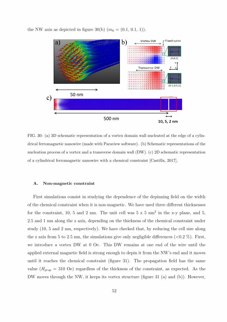
the NW axis as depicted in figure 30(b) (m0 = (0.1, 0.1, 1)).
FIG. 30: (a) 3D schematic representation of a vortex domain wall nucleated at the edge of a cylin-
drical ferromagnetic nanowire (made with Paraview software). (b) Schematic representations of the
nucleation process of a vortex and a transverse domain wall (DW). (c) 2D schematic representation
of a cylindrical ferromagnetic nanowire with a chemical constraint [Castilla, 2017].
A. Non-magnetic constraint
First simulations consist in studying the dependence of the depinning field on the width
of the chemical constraint when it is non-magnetic. We have used three different thicknesses
for the constraint, 10, 5 and 2 nm. The unit cell was 5 x 5 nm2 in the x-y plane, and 5,
2.5 and 1 nm along the z axis, depending on the thickness of the chemical constraint under
study (10, 5 and 2 nm, respectively). We have checked that, by reducing the cell size along
the z axis from 5 to 2.5 nm, the simulations give only negligible differences (<0.2 %). First,
we introduce a vortex DW at 0 Oe. This DW remains at one end of the wire until the
applied external magnetic field is strong enough to depin it from the NW’s end and it moves
until it reaches the chemical constraint (figure 31). The propagation field has the same
value (Hprop = 310 Oe) regardless of the thickness of the constraint, as expected. As the
DW moves through the NW, it keeps its vortex structure (figure 31 (a) and (b)). However,
52
when the DW reaches the non-magnetic spacer, it gradually evolves to a transverse DW
(figure 31 (c)). The transverse DW remains pinned at the spacer as the applied magnetic
field increases, until it reaches a certain value (Hdep) at which the DW depins from the
nonmagnetic constraint and moves towards the opposite end of the NW. After depinning,
the DW moves forward with a mixed vortex-transverse structure, rotating as it travels. The
depinning field increases with the thickness of the chemical constraint. The values obtained
are 670, 540 and 420 Oe for a 10, 5 and 2 nm constraint, respectively.
FIG. 31: 2D schematic representations of (a) a vortex domain wall nucleated at the left end
of the nanowire; (b) a vortex domain wall moving though the cylindrical nanowire; and (c) the
reconfigured transverse domain wall pinned at the 5 nm-thick non-magnetic constraint. (d) Change
in the domain wall energy with the applied magnetic field.
B. Paramagnetic constraint
In this section, the chemical constraint is simulated to be of paramagnetic NiCu. The
exchange coupling between the magnetic moments of adjacent cells in the chemical con-
straint is ignored. The initial nucleated domain wall is again a vortex. Table II summarizes
the magnetic moments used for the simulations for the NiCu alloy with different Ni per-
centages25. Note that these are values for bulk. The column with exchange energy can be
ignored for this section since NiCu is considered paramagnetic. Cubic cells of 5 x 5 x 5
53
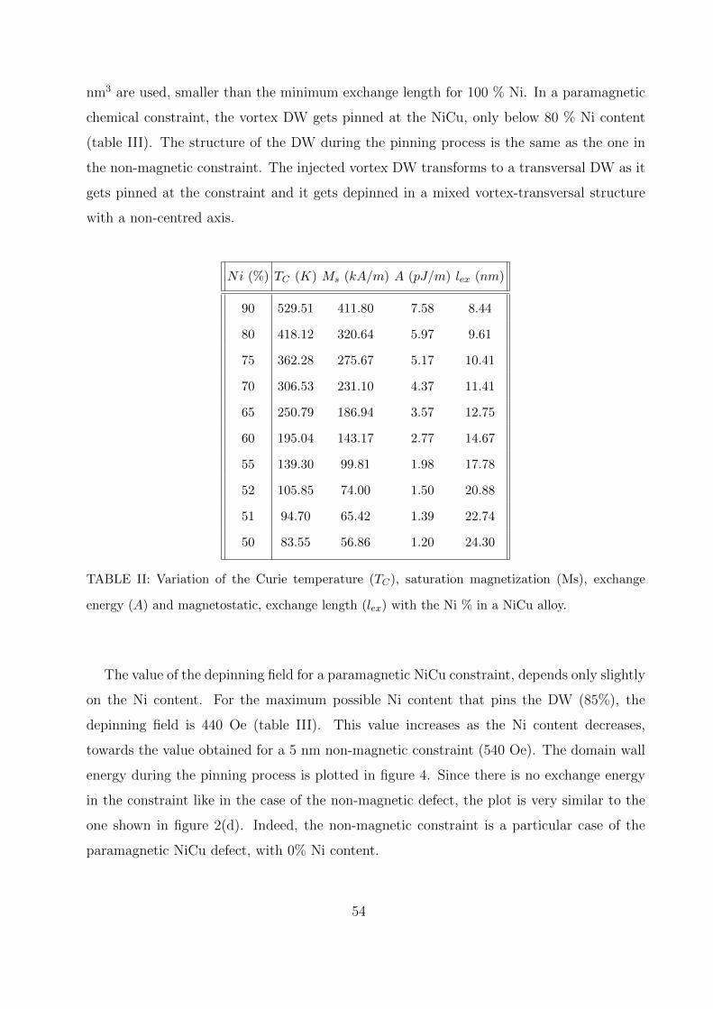
nm3 are used, smaller than the minimum exchange length for 100 % Ni. In a paramagnetic
chemical constraint, the vortex DW gets pinned at the NiCu, only below 80 % Ni content
(table III). The structure of the DW during the pinning process is the same as the one in
the non-magnetic constraint. The injected vortex DW transforms to a transversal DW as it
gets pinned at the constraint and it gets depinned in a mixed vortex-transversal structure
with a non-centred axis.
Ni (%) TC (K) Ms (kA/m) A (pJ/m) lex (nm)
90 529.51 411.80 7.58 8.44
80 418.12 320.64 5.97 9.61
75 362.28 275.67 5.17 10.41
70 306.53 231.10 4.37 11.41
65 250.79 186.94 3.57 12.75
60 195.04 143.17 2.77 14.67
55 139.30 99.81 1.98 17.78
52 105.85 74.00 1.50 20.88
51 94.70 65.42 1.39 22.74
50 83.55 56.86 1.20 24.30
TABLE II: Variation of the Curie temperature (TC), saturation magnetization (Ms), exchange
energy (A) and magnetostatic, exchange length (lex) with the Ni % in a NiCu alloy.
The value of the depinning field for a paramagnetic NiCu constraint, depends only slightly
on the Ni content. For the maximum possible Ni content that pins the DW (85%), the
depinning field is 440 Oe (table III). This value increases as the Ni content decreases,
towards the value obtained for a 5 nm non-magnetic constraint (540 Oe). The domain wall
energy during the pinning process is plotted in figure 4. Since there is no exchange energy
in the constraint like in the case of the non-magnetic defect, the plot is very similar to the
one shown in figure 2(d). Indeed, the non-magnetic constraint is a particular case of the
paramagnetic NiCu defect, with 0% Ni content.
54

FIG. 32: a) Cross sections of the mixed vortex-transverse domain wall structure moving along
the NW. Top image shows a cross-section on the x-z plane and bottom images show a spatial
fixed cross-section frames of the x-y plane, taken every 0.1 ns. b) Energy of the domain walls for
paramagnetic constraints with different percentages of Ni.
C. Nucleating an initial transverse DW
Still in the paramagnetic constraint, we now explore the depinning process when the
nucleated domain wall is transversal. The propagation field Hprop, is slightly higher for a
transversal DW (table III), although the pinning at the chemical paramagnetic defect still
happens in a narrow range of external magnetic fields (400-500 Oe) (table III). During
the propagation of the transversal DW, in both sections of the NW, its structure is in a
mixed vortex-transverse state, although it is purely transversal while pinned. Therefore,
the depinning field associated to a NiCu paramagnetic defect is almost independent of the
structure of the nucleated DW because in either case, the structure evolves to a transversal
DW while pinned at the defect.
55
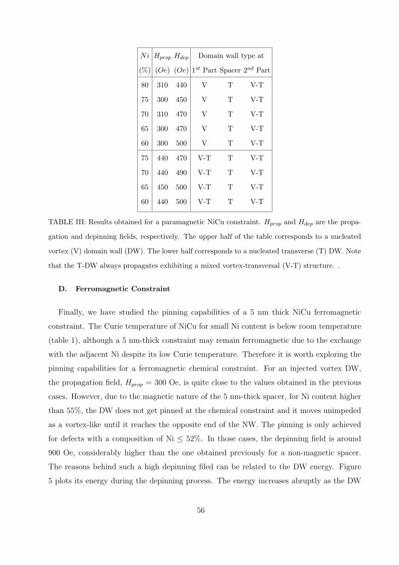
Ni Hprop Hdep Domain wall type at
(%) (Oe) (Oe) 1st Part Spacer 2nd Part
80 310 440 V T V-T
75 300 450 V T V-T
70 310 470 V T V-T
65 300 470 V T V-T
60 300 500 V T V-T
75 440 470 V-T T V-T
70 440 490 V-T T V-T
65 450 500 V-T T V-T
60 440 500 V-T T V-T
TABLE III: Results obtained for a paramagnetic NiCu constraint. Hprop and Hdep are the propa-
gation and depinning fields, respectively. The upper half of the table corresponds to a nucleated
vortex (V) domain wall (DW). The lower half corresponds to a nucleated transverse (T) DW. Note
that the T-DW always propagates exhibiting a mixed vortex-transversal (V-T) structure. .
D. Ferromagnetic Constraint
Finally, we have studied the pinning capabilities of a 5 nm thick NiCu ferromagnetic
constraint. The Curie temperature of NiCu for small Ni content is below room temperature
(table 1), although a 5 nm-thick constraint may remain ferromagnetic due to the exchange
with the adjacent Ni despite its low Curie temperature. Therefore it is worth exploring the
pinning capabilities for a ferromagnetic chemical constraint. For an injected vortex DW,
the propagation field, Hprop = 300 Oe, is quite close to the values obtained in the previous
cases. However, due to the magnetic nature of the 5 nm-thick spacer, for Ni content higher
than 55%, the DW does not get pinned at the chemical constraint and it moves unimpeded
as a vortex-like until it reaches the opposite end of the NW. The pinning is only achieved
for defects with a composition of Ni ≤ 52%. In those cases, the depinning field is around
900 Oe, considerably higher than the one obtained previously for a non-magnetic spacer.
The reasons behind such a high depinning filed can be related to the DW energy. Figure
5 plots its energy during the depinning process. The energy increases abruptly as the DW
56
arrives to the chemical constraint due to the change in its shape. Then the energy increases
slightly as the structure of the DW is slightly altered under the increasing magnetic field.
Finally, the depinning occurs when the field reaches Hdep and the energy drops abruptly to
complete the switching.
FIG. 33: Plot of the domain wall energy as a function of the external magnetic field applied in the
ferromagnetic constraint case. Different curves represent simulations with different percentages of
Ni.
E. Consclusions
To summaraize the results, for constraints much smaller than the width of the DW,
the depinning field increases with the width of the defect. For a ferromagnetic constraint,
there is no pinning unless the saturation magnetization and the exchange energy of the
constraint is reduced notably (for Ni content smaller than 55%). However, in this case,
when the domain wall gets pinned, the depinning field results quite large (about 900 Oe).
If the constraint behaves paramagnetically, the defect can pin the DW for a much larger
saturation magnetization (i.e. Ni content), due to the null contribution of the exchange
energy to the energy of the pinned DW. The depinning process in the paramagnetic case
is quite similar to the one for a non-magnetic constraint with zero Ni content. The type of
the DW injected (vortex or transversal) does not alter the results as the pinned DW adopts
always a transversal geometry.
57

58
V. STRUCTURAL CHARACTERIZATION
The objective of this thesis is the control of the magnetization dynamics in nanostripes
through the application of elastic strain. In order to generate this type of perturbation we
use a piezoelectric material (ScAlN), capable to convert electrical signals into strain and
viceversa by exploiting the piezoelectric effect. The first part of this chapter is oriented to
the structural characterization of ScAlN thin films, whose piezoelectric properties depend
on its structural characteristics. X-ray diffraction is performed on thin films of ScAlN
samples used as substrate for the fabrication of our devices. Furthermore, piezolectric force
microscopy (PFM), Rutherford backscattering (RBS) and measurements of the d33 constant
are performed on identical ScAlN samples, exclusively fabricated for their characterization.
The goal of the second part of this chapter is to describe the structural characteristics
of Ni thin films that are grown along the magnetic nanostripes that are the core of our
study. As both nanostructures are grown simultaneously and nearby each other by sputtering
deposition, we assume that their crystalline properties are identical. The magnetic behaviour
of the nanostripes is dependent on their crystalline properties, therefore, it is useful to
perform X-ray studies in order to achieve a better understanding of the magnetic behaviour
of the nanostripes. We perform X-ray diffraction measurements on the Ni thin films. Out-
of-plane 2θ scans are carried out in order to obtain the diffraction peaks of the crystals
whose Bragg planes are parallel to the surface of the sample. A deeper picture is achieved
by analyzing the FWHM of the diffraction peaks in order to compute the mean crystallite
size through the Scherrer equation. Grazing incident diffraction (GID) scans are performed
to detect signal from randomly oriented grains. This measurement complements the out-of-
plane 2θ scans. Finally, rocking curves are carried out in order to study the dispersion and
orientation of the crystals with respect to the sample surface.
59
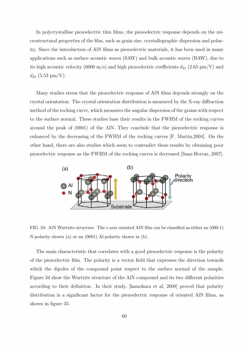
In polycrystalline piezoelectric thin films, the piezoelectric response depends on the mi-
crostructural properties of the film, such as grain size, crystallographic dispersion and polar-
ity. Since the introduction of AlN films as piezoelectric materials, it has been used in many
applications such as surface acoustic waves (SAW) and bulk acoustic waves (BAW), due to
its high acoustic velocity (6000 m/s) and high piezoelectric coefficients d31 (2.65 pm/V) and
d33 (5.53 pm/V).
Many studies stress that the piezoelectric response of AlN films depends strongly on the
crystal orientation. The crystal orientation distribution is measured by the X-ray diffraction
method of the rocking curve, which measures the angular dispersion of the grains with respect
to the surface normal. These studies base their results in the FWHM of the rocking curves
around the peak of (0001) of the AlN. They conclude that the piezoelectric response is
enhanced by the decreasing of the FWHM of the rocking curves [F. Martin,2004]. On the
other hand, there are also studies which seem to contradict these results by obtaining poor
piezoelectric response as the FWHM of the rocking curves is decreased [Sanz-Hervas, 2007].
FIG. 34: AlN Wurtzite structure. The c-axis oriented AlN film can be classified as either an (000-1)
N-polarity shown (a) or an (0001) Al-polarity shown in (b).
The main characteristic that correlates with a good piezoelectric response is the polarity
of the piezoelectric film. The polarity is a vector field that expresses the direction towards
which the dipoles of the compound point respect to the surface normal of the sample.
Figure 34 show the Wurtzite structure of the AlN compound and its two different polarities
according to their definition. In their study, [kamohara et al, 2008] proved that polarity
distribution is a significant factor for the piezoelectric response of oriented AlN films, as
shown in figure 35.
60
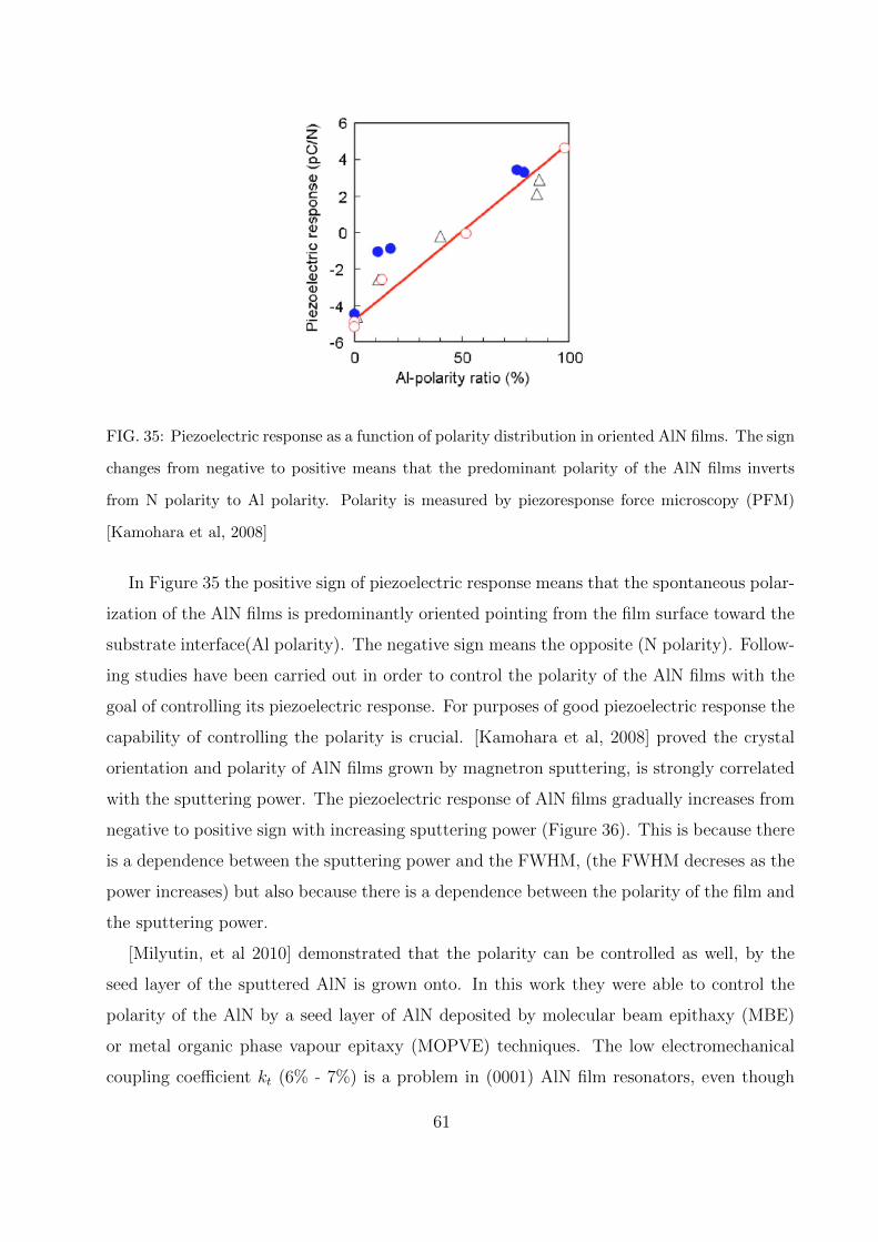
FIG. 35: Piezoelectric response as a function of polarity distribution in oriented AlN films. The sign
changes from negative to positive means that the predominant polarity of the AlN films inverts
from N polarity to Al polarity. Polarity is measured by piezoresponse force microscopy (PFM)
[Kamohara et al, 2008]
In Figure 35 the positive sign of piezoelectric response means that the spontaneous polar-
ization of the AlN films is predominantly oriented pointing from the film surface toward the
substrate interface(Al polarity). The negative sign means the opposite (N polarity). Follow-
ing studies have been carried out in order to control the polarity of the AlN films with the
goal of controlling its piezoelectric response. For purposes of good piezoelectric response the
capability of controlling the polarity is crucial. [Kamohara et al, 2008] proved the crystal
orientation and polarity of AlN films grown by magnetron sputtering, is strongly correlated
with the sputtering power. The piezoelectric response of AlN films gradually increases from
negative to positive sign with increasing sputtering power (Figure 36). This is because there
is a dependence between the sputtering power and the FWHM, (the FWHM decreses as the
power increases) but also because there is a dependence between the polarity of the film and
the sputtering power.
[Milyutin, et al 2010] demonstrated that the polarity can be controlled as well, by the
seed layer of the sputtered AlN is grown onto. In this work they were able to control the
polarity of the AlN by a seed layer of AlN deposited by molecular beam epithaxy (MBE)
or metal organic phase vapour epitaxy (MOPVE) techniques. The low electromechanical
coupling coefficient kt (6% - 7%) is a problem in (0001) AlN film resonators, even though
61
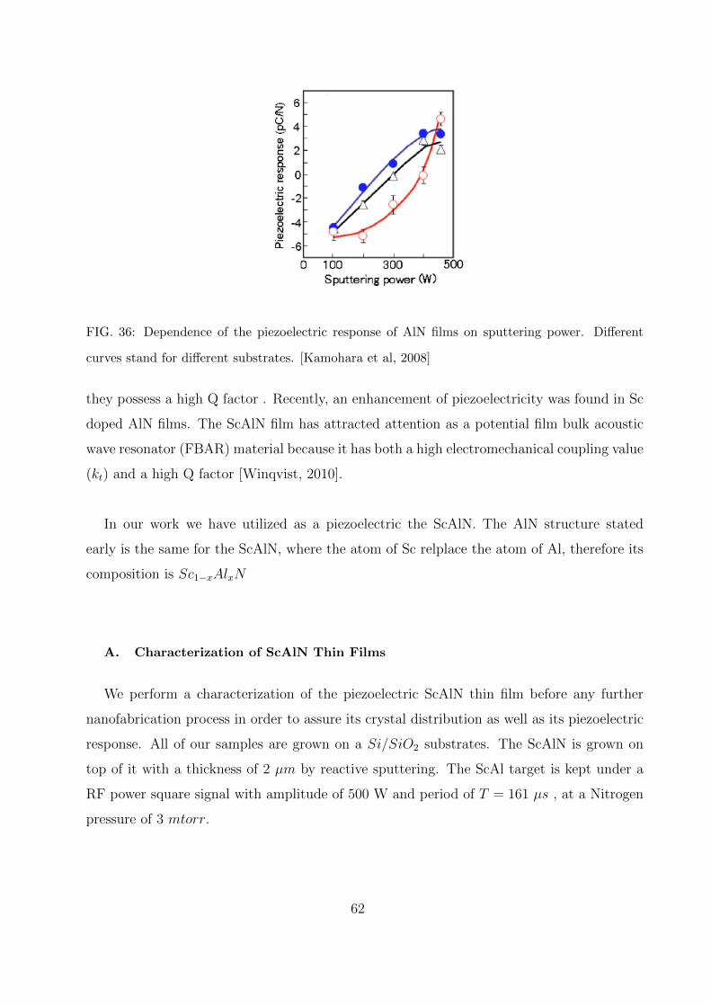
FIG. 36: Dependence of the piezoelectric response of AlN films on sputtering power. Different
curves stand for different substrates. [Kamohara et al, 2008]
they possess a high Q factor . Recently, an enhancement of piezoelectricity was found in Sc
doped AlN films. The ScAlN film has attracted attention as a potential film bulk acoustic
wave resonator (FBAR) material because it has both a high electromechanical coupling value
(kt) and a high Q factor [Winqvist, 2010].
In our work we have utilized as a piezoelectric the ScAlN. The AlN structure stated
early is the same for the ScAlN, where the atom of Sc relplace the atom of Al, therefore its
composition is Sc1−xAlxN
A. Characterization of ScAlN Thin Films
We perform a characterization of the piezoelectric ScAlN thin film before any further
nanofabrication process in order to assure its crystal distribution as well as its piezoelectric
response. All of our samples are grown on a Si/SiO2 substrates. The ScAlN is grown on
top of it with a thickness of 2 µm by reactive sputtering. The ScAl target is kept under a
RF power square signal with amplitude of 500 W and period of T = 161 µs , at a Nitrogen
pressure of 3 mtorr.
62
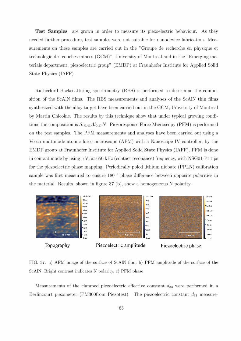
Test Samples are grown in order to measure its piezoelectric behaviour. As they
needed further procedure, test samples were not suitable for nanodevice fabrication. Mea-
surements on these samples are carried out in the ”Groupe de recherche en physique et
technologie des couches minces (GCM)”, University of Montreal and in the ”Emerging ma-
terials department, piezoelectric group” (EMDP) at Fraunhofer Institute for Applied Solid
State Physics (IAFF)
Rutherford Backscattering spectrometry (RBS) is performed to determine the compo-
sition of the ScAlN films. The RBS measurements and analyses of the ScAlN thin films
synthesized with the alloy target have been carried out in the GCM, University of Montreal
by Martin Chicoine. The results by this technique show that under typical growing condi-
tions the composition is Sc0.43Al0.57N . Piezoresponse Force Microscopy (PFM) is performed
on the test samples. The PFM measurements and analyses have been carried out using a
Veeco multimode atomic force microscope (AFM) with a Nanoscope IV controller, by the
EMDP group at Fraunhofer Institute for Applied Solid State Physics (IAFF). PFM is done
in contact mode by using 5 V, at 650 kHz (contact resonance) frequency, with NSG01-Pt tips
for the piezoelectric phase mapping. Periodically poled lithium niobate (PPLN) calibration
sample was first measured to ensure 180 phase difference between opposite polarities in
the material. Results, shown in figure 37 (b), show a homogeneous N polarity.
FIG. 37: a) AFM image of the surface of ScAlN film, b) PFM amplitude of the surface of the
ScAlN. Bright contrast indicates N polarity, c) PFM phase
Measurements of the clamped piezoelectric effective constant d33 were performed in a
Berlincourt piezometer (PM300from Piezotest). The piezoelectric constant d33 measure-
63
ments were carried out using a Berlincourt piezometer (PM300 Piezotest), by the ”Emerging
materials department, piezoelectric group” at Fraunhofer Institute for Applied Solid State
Physics (IAFF). For contact stability between the sample and the probe, titanium top elec-
trodes were sputtered on top of ScAlN through a shadow mask. The samples were clamped
with a constant force of 10 N. An oscillating load of 0.25 N at a frequency of 110 Hz was
applied and the stress-induced charge was measured and compared to a reference sample.
No correction of the experimental d33 values for clamping effects was performed. Results for
piezoelectric response by this method show a piezoelectric constant whose value is d33 = −24
pC/N
Samples for nanofabrication All piezoelectric films are grown alongside a calibration
10 x 10 mm sample with a shadow mask, to form a step on it. That step is later measured
in profilometer to assure the thickness grown of ScAlN on the substrate is accurate. After
deposition, samples are taken to the X-ray diffractometer to perform out-of-plane 2θ/θ scans.
In a typical scan we can observe four peaks: at 2θ=32.83 at 2θ=35.58 , at 2θ=69.13 and at
2θ=75.5. The first diffraction peak corresponds to the ScAlN (0,0,0,1) reflection, the second
peak corresponds to the ScAlN (0,0,0,2) reflection, the third one is the Si(4,0,0) reflection
and the last one to the ScAlN (0,0,0,4) [Martin et al, 2004]. This is consistent with previous
studies. The hexagonal axis (c axis, [0001]) is the polar direction, and at suitable process
conditions, ScAlN grows preferentially with c-axis orientation on SiO2, [Englemark, 2001].
In order to measure the crystal dispersion respect to the sample surface normal of the
ScAlN, we perform a rocking curve around one of the peaks. We choose the most intense
peak, therefore the rocking curve measurement is performed around the (0,0,0,2) reflection
(figure 38).
As stated before, a narrow FWHM of the rocking curves by itself is not enough condition
to assure the ScAlN to have a piezoelectric response. However, previous measurements of
d33 coefficient and PFM measruements of test samples films grown in the same sputtering
conditions plus these rocking curves, will be sufficient to suppose the piezelectric beahaviour.
The range of FWHM measured of all the ScAlN films were [1.7 < FWHM < 7.8]. No
sample showed a FHWM larger than 7.8, and all samples gave evidence of piezoelectric
response after the devices nanofabrication, at calibrating the SAW resonators in the Network
64
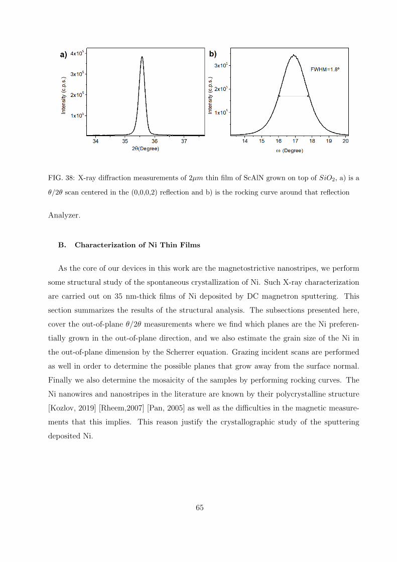
FIG. 38: X-ray diffraction measurements of 2µm thin film of ScAlN grown on top of SiO2, a) is a
θ/2θ scan centered in the (0,0,0,2) reflection and b) is the rocking curve around that reflection
Analyzer.
B. Characterization of Ni Thin Films
As the core of our devices in this work are the magnetostrictive nanostripes, we perform
some structural study of the spontaneous crystallization of Ni. Such X-ray characterization
are carried out on 35 nm-thick films of Ni deposited by DC magnetron sputtering. This
section summarizes the results of the structural analysis. The subsections presented here,
cover the out-of-plane θ/2θ measurements where we find which planes are the Ni preferen-
tially grown in the out-of-plane direction, and we also estimate the grain size of the Ni in
the out-of-plane dimension by the Scherrer equation. Grazing incident scans are performed
as well in order to determine the possible planes that grow away from the surface normal.
Finally we also determine the mosaicity of the samples by performing rocking curves. The
Ni nanowires and nanostripes in the literature are known by their polycrystalline structure
[Kozlov, 2019] [Rheem,2007] [Pan, 2005] as well as the difficulties in the magnetic measure-
ments that this implies. This reason justify the crystallographic study of the sputtering
deposited Ni.
65
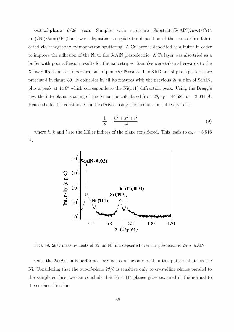
out-of-plane θ/2θ scan Samples with structure Substrate/ScAlN(2µm)/Cr(4
nm)/Ni(35nm)/Pt(2nm) were deposited alongside the deposition of the nanostripes fabri-
cated via lithography by magnetron sputtering. A Cr layer is deposited as a buffer in order
to improve the adhesion of the Ni to the ScAlN piezoelectric. A Ta layer was also tried as a
buffer with poor adhesion results for the nanostripes. Samples were taken afterwards to the
X-ray diffractometer to perform out-of-plane θ/2θ scans. The XRD out-of-plane patterns are
presented in figure 39. It coincides in all its features with the previous 2µm film of ScAlN,
plus a peak at 44.6 which corresponds to the Ni(111) diffraction peak. Using the Bragg’s
law, the interplanar spacing of the Ni can be calculated from 2θ(111) =44.58, d = 2.031 A.
Hence the lattice constant a can be derived using the formula for cubic crystals:
1
d2=h2 + k2 + l2
a2(9)
where h, k and l are the Miller indices of the plane considered. This leads to aNi = 3.516
A.
FIG. 39: 2θ/θ measurements of 35 nm Ni film deposited over the piezoelectric 2µm ScAlN
Once the 2θ/θ scan is performed, we focus on the only peak in this pattern that has the
Ni. Considering that the out-of-plane 2θ/θ is sensitive only to crystalline planes parallel to
the sample surface, we can conclude that Ni (111) planes grow textured in the normal to
the surface direction.
66
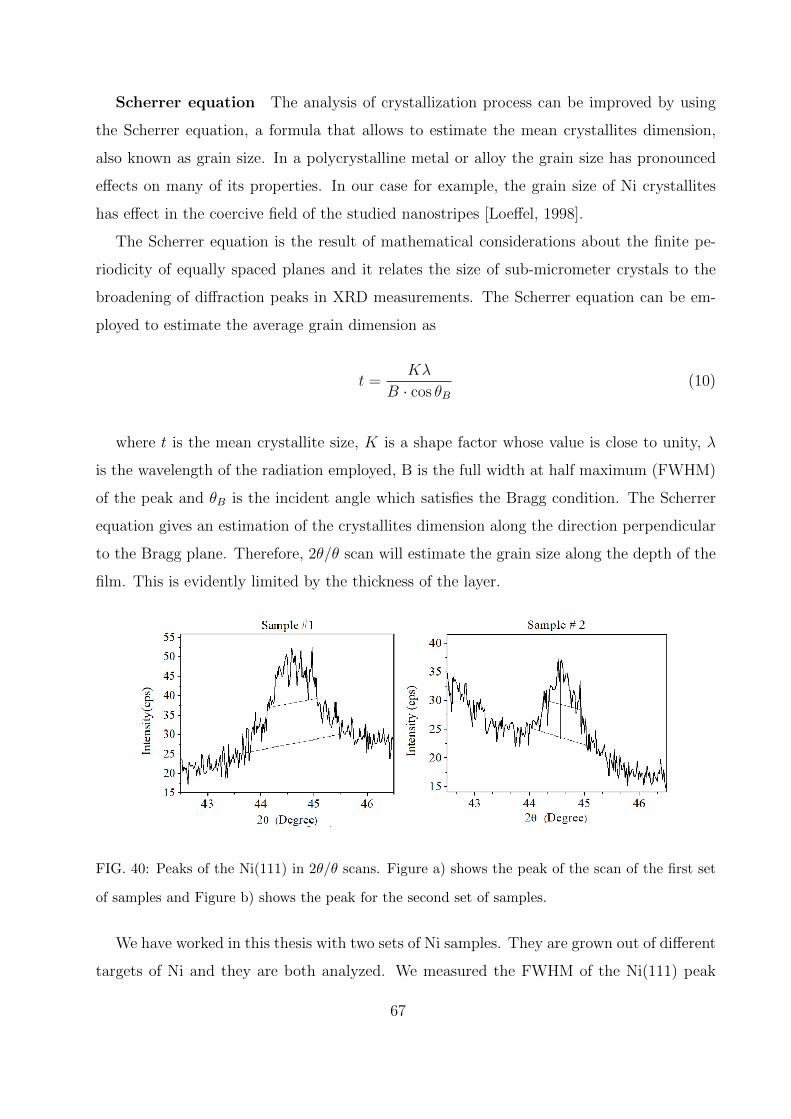
Scherrer equation The analysis of crystallization process can be improved by using
the Scherrer equation, a formula that allows to estimate the mean crystallites dimension,
also known as grain size. In a polycrystalline metal or alloy the grain size has pronounced
effects on many of its properties. In our case for example, the grain size of Ni crystallites
has effect in the coercive field of the studied nanostripes [Loeffel, 1998].
The Scherrer equation is the result of mathematical considerations about the finite pe-
riodicity of equally spaced planes and it relates the size of sub-micrometer crystals to the
broadening of diffraction peaks in XRD measurements. The Scherrer equation can be em-
ployed to estimate the average grain dimension as
t =Kλ
B · cos θB(10)
where t is the mean crystallite size, K is a shape factor whose value is close to unity, λ
is the wavelength of the radiation employed, B is the full width at half maximum (FWHM)
of the peak and θB is the incident angle which satisfies the Bragg condition. The Scherrer
equation gives an estimation of the crystallites dimension along the direction perpendicular
to the Bragg plane. Therefore, 2θ/θ scan will estimate the grain size along the depth of the
film. This is evidently limited by the thickness of the layer.
FIG. 40: Peaks of the Ni(111) in 2θ/θ scans. Figure a) shows the peak of the scan of the first set
of samples and Figure b) shows the peak for the second set of samples.
We have worked in this thesis with two sets of Ni samples. They are grown out of different
targets of Ni and they are both analyzed. We measured the FWHM of the Ni(111) peak
67
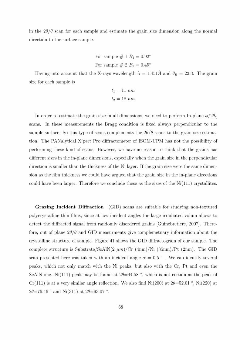
in the 2θ/θ scan for each sample and estimate the grain size dimension along the normal
direction to the surface sample.
For sample # 1 B1 = 0.92
For sample # 2 B2 = 0.45
Having into account that the X-rays wavelength λ = 1.451A and θB = 22.3. The grain
size for each sample is
t1 = 11 nm
t2 = 18 nm
In order to estimate the grain size in all dimensions, we need to perform In-plane φ/2θχ
scans. In these measurements the Bragg condition is fixed always perpendicular to the
sample surface. So this type of scans complements the 2θ/θ scans to the grain size estima-
tion. The PANalytical X’pert Pro diffractometer of ISOM-UPM has not the possibility of
performing these kind of scans. However, we have no reason to think that the grains has
different sizes in the in-plane dimensions, especially when the grain size in the perpendicular
direction is smaller than the thickness of the Ni layer. If the grain size were the same dimen-
sion as the film thickness we could have argued that the grain size in the in-plane directions
could have been larger. Therefore we conclude these as the sizes of the Ni(111) crystallites.
Grazing Incident Diffraction (GID) scans are suitable for studying non-textured
polycrystalline thin films, since at low incident angles the large irradiated volum allows to
detect the diffracted signal from randomly disordered grains [Guinebretiere, 2007]. There-
fore, out of plane 2θ/θ and GID measurments give complemetnary information about the
crystalline structure of sample. Figure 41 shows the GID diffractogram of our sample. The
complete structure is Substrate/ScAlN(2 µm)/Cr (4nm)/Ni (35nm)/Pt (2nm). The GID
scan presented here was taken with an incident angle α = 0.5 . We can identify several
peaks, which not only match with the Ni peaks, but also with the Cr, Pt and even the
ScAlN one. Ni(111) peak may be found at 2θ=44.58 , which is not certain as the peak of
Cr(111) is at a very similar angle reflection. We also find Ni(200) at 2θ=52.01 , Ni(220) at
2θ=76.46 and Ni(311) at 2θ=93.07 .
68
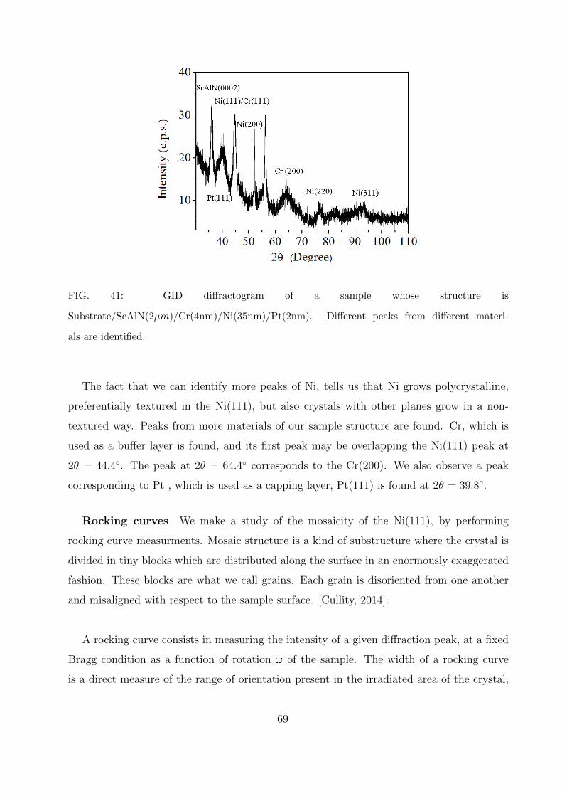
FIG. 41: GID diffractogram of a sample whose structure is
Substrate/ScAlN(2µm)/Cr(4nm)/Ni(35nm)/Pt(2nm). Different peaks from different materi-
als are identified.
The fact that we can identify more peaks of Ni, tells us that Ni grows polycrystalline,
preferentially textured in the Ni(111), but also crystals with other planes grow in a non-
textured way. Peaks from more materials of our sample structure are found. Cr, which is
used as a buffer layer is found, and its first peak may be overlapping the Ni(111) peak at
2θ = 44.4. The peak at 2θ = 64.4 corresponds to the Cr(200). We also observe a peak
corresponding to Pt , which is used as a capping layer, Pt(111) is found at 2θ = 39.8.
Rocking curves We make a study of the mosaicity of the Ni(111), by performing
rocking curve measurments. Mosaic structure is a kind of substructure where the crystal is
divided in tiny blocks which are distributed along the surface in an enormously exaggerated
fashion. These blocks are what we call grains. Each grain is disoriented from one another
and misaligned with respect to the sample surface. [Cullity, 2014].
A rocking curve consists in measuring the intensity of a given diffraction peak, at a fixed
Bragg condition as a function of rotation ω of the sample. The width of a rocking curve
is a direct measure of the range of orientation present in the irradiated area of the crystal,
69
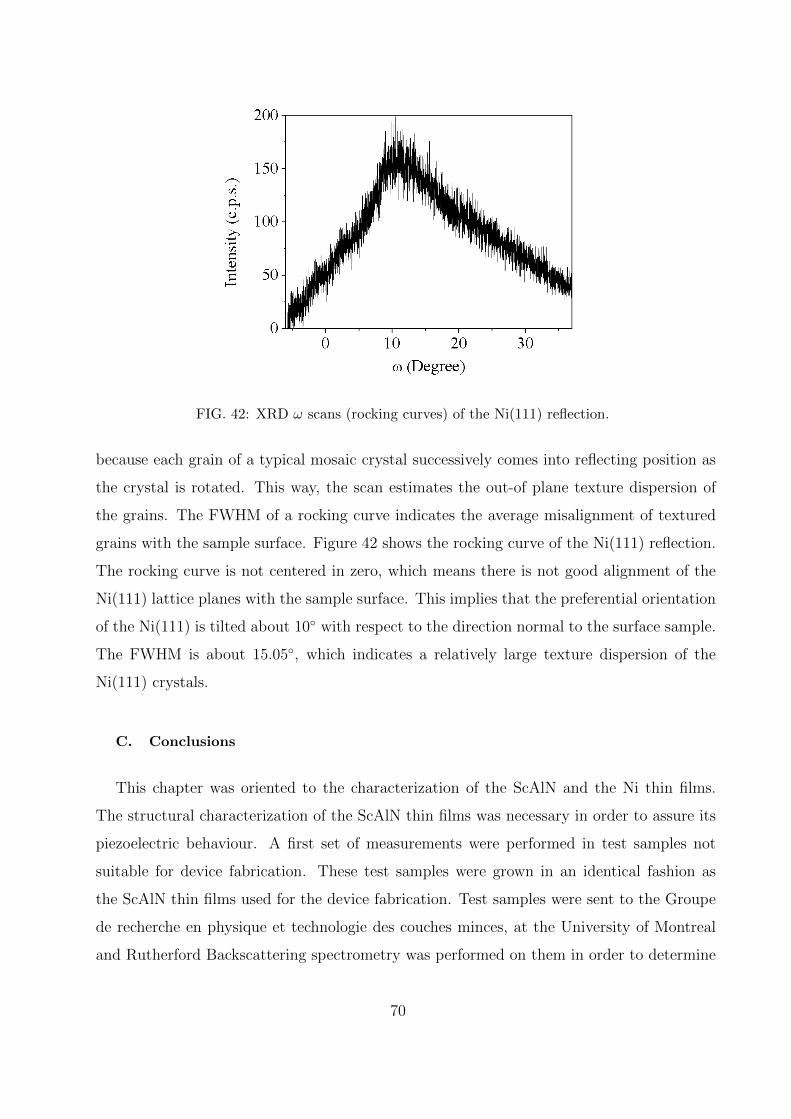
FIG. 42: XRD ω scans (rocking curves) of the Ni(111) reflection.
because each grain of a typical mosaic crystal successively comes into reflecting position as
the crystal is rotated. This way, the scan estimates the out-of plane texture dispersion of
the grains. The FWHM of a rocking curve indicates the average misalignment of textured
grains with the sample surface. Figure 42 shows the rocking curve of the Ni(111) reflection.
The rocking curve is not centered in zero, which means there is not good alignment of the
Ni(111) lattice planes with the sample surface. This implies that the preferential orientation
of the Ni(111) is tilted about 10 with respect to the direction normal to the surface sample.
The FWHM is about 15.05, which indicates a relatively large texture dispersion of the
Ni(111) crystals.
C. Conclusions
This chapter was oriented to the characterization of the ScAlN and the Ni thin films.
The structural characterization of the ScAlN thin films was necessary in order to assure its
piezoelectric behaviour. A first set of measurements were performed in test samples not
suitable for device fabrication. These test samples were grown in an identical fashion as
the ScAlN thin films used for the device fabrication. Test samples were sent to the Groupe
de recherche en physique et technologie des couches minces, at the University of Montreal
and Rutherford Backscattering spectrometry was performed on them in order to determine
70
the composition. RBS measurements show that under typical growing conditions the com-
position is Sc0.43Al0.57N . Piezoresponse Force Microscopy (PFM) was also performed in
this samples in order to check that the polarity of the ScAlN thin films. Result show ho-
mogeneous N polarity in the test samples. The polarity is found in the literature as the
main characteristic that relates to the piezoelectric behaviour of the thin films. Finally,
measurements of the d33 parameter were performed in the test samples. Results for piezo-
electric response show a piezoelectric constant whose value is d33 = −24 pC/N . These
measurements were carried out in order to verify the piezelectricity behaviour of the sam-
ples grown by our sputtering method. Samples of ScAlN thin films that were used for the
fabrication of devices underwent X-ray diffraction measurements, where we could find the
peaks corresponding to the ScAlN (0,0,0,1), (0,0,0,2) and (0,0,0,4). In order to measure the
crystal dispersion respect to the sample surface normal we perform rocking curves around
the (0,0,0,2) reflection. Rocking curves measurements for this reflection show a full width
at half maximum in a range of [1.7 < FWHM < 7.8].
Ni thin films that are grown alongside the Ni nanostripes in the sputtering chamber,
underwent X-ray diffraction measurements. Out of plane 2θ/θ measurements show that
Ni grow textured in the plane (1,1,1). The Scherrer equation is used to perform a deeper
analysis of the 2θ/θ scans. By measuring the full width at half maximum of the Ni(1,1,1)
peak, we are able to estimate the mean size of the crystallites in the direction perpendicular
to the film plane. Throughout this thesis we have worked with Ni samples grown out of two
different Ni targets. Ni thin films show two different grain sizes, t1 = 11 nm and t2 = 18
nm. Grazing incident diffraction measurements are performed in the Ni thin films in order
to give complementary information to the 2θ/θ scan. Due to the GID diffractogram we
can identify that besides the Ni(1,1,1) planes, the crystals grow with other planes in a non-
textured way (Ni(2,0,0) and Ni(2,2,0)). Finally we perform a rocking curve of the Ni(1,1,1)
diffraction peak, which is a direct measurement of how the crystals are oriented with respect
to the sample surface. Results show a FWHM about 15.05, which indicates a relatively
large texture dispersion of the Ni(1,1,1) crystals.
71

72
VI. MAGNETIC CHARACTERIZATION
In the pervious chapter we studied the crystalline properties of Ni films whose structures
are identical to the nanostripes fabricated through this thesis. This chapter is aimed to the
study of the magnetic anisotropy of those thin films, by studying the dependence of the
magnetization on the orientation of the thin film. The two types of magnetic anisotropies
that are relevant for this work are the shape anisotropy and the crystal anisotropy. In this
chapter we describe the study of preferential direction of magnetization of the Ni thin films
that are fabricated along with the nanostripes, with the same structure and we describe
the VSM measurements performed on the thin films along different directions. Out of
these measurements easy and hard axis in the film, as well as anisotropy constants can be
calculated.
Magnetocrystalline Anisotropy The magnetocrystalline anisotropy occurs in a crys-
tal lattice if it takes more energy to magnetize in certain directions than in others. These
directions usually coincide with the principal axes of the crystal lattice. The magnetocrys-
tal anisotropy energy (MAE) arises from the spin-orbit coupling. This comes from the fact
that in a real lattice, the orbital magnetic moments are quenched, and its orientation is
fixed very strongly. As there is a coupling between the spin and the orbital motion of the
electron, orientating the magnetic moments away from the crystalline direction, requires an
external source of energy. The energy required to rotate the magnetization away from the
easy direction is called the anisotropy energy and it is defined as the energy necessary to
overcome the spin orbit coupling.
Uniaxial anisotropy It refers to the existence of one only easy direction. If the easy
axis is defined in the z direction, thus, the anisotropy energy will be rotationally-symmetric
with respect to the z direction and will depend only on the relative orientation of the
magnetization with respect to this axis. The uniaxial anisotropy energy can be expressed
as :
E = K0 +K1 sin2 θ +K2 sin4 θ + ... (11)
73
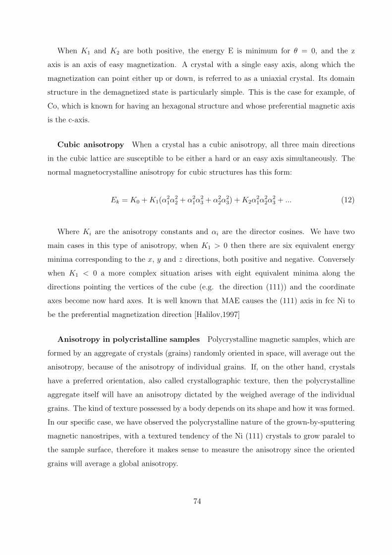
When K1 and K2 are both positive, the energy E is minimum for θ = 0, and the z
axis is an axis of easy magnetization. A crystal with a single easy axis, along which the
magnetization can point either up or down, is referred to as a uniaxial crystal. Its domain
structure in the demagnetized state is particularly simple. This is the case for example, of
Co, which is known for having an hexagonal structure and whose preferential magnetic axis
is the c-axis.
Cubic anisotropy When a crystal has a cubic anisotropy, all three main directions
in the cubic lattice are susceptible to be either a hard or an easy axis simultaneously. The
normal magnetocrystalline anisotropy for cubic structures has this form:
Ek = K0 +K1(α21α
22 + α2
1α23 + α2
2α23) +K2α
21α
22α
23 + ... (12)
Where Ki are the anisotropy constants and αi are the director cosines. We have two
main cases in this type of anisotropy, when K1 > 0 then there are six equivalent energy
minima corresponding to the x, y and z directions, both positive and negative. Conversely
when K1 < 0 a more complex situation arises with eight equivalent minima along the
directions pointing the vertices of the cube (e.g. the direction (111)) and the coordinate
axes become now hard axes. It is well known that MAE causes the (111) axis in fcc Ni to
be the preferential magnetization direction [Halilov,1997]
Anisotropy in polycristalline samples Polycrystalline magnetic samples, which are
formed by an aggregate of crystals (grains) randomly oriented in space, will average out the
anisotropy, because of the anisotropy of individual grains. If, on the other hand, crystals
have a preferred orientation, also called crystallographic texture, then the polycrystalline
aggregate itself will have an anisotropy dictated by the weighed average of the individual
grains. The kind of texture possessed by a body depends on its shape and how it was formed.
In our specific case, we have observed the polycrystalline nature of the grown-by-sputtering
magnetic nanostripes, with a textured tendency of the Ni (111) crystals to grow paralel to
the sample surface, therefore it makes sense to measure the anisotropy since the oriented
grains will average a global anisotropy.
74
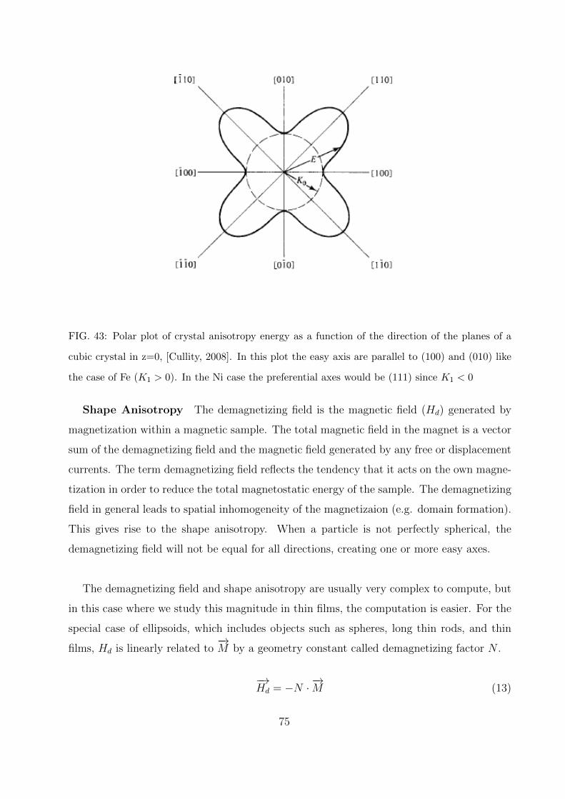
FIG. 43: Polar plot of crystal anisotropy energy as a function of the direction of the planes of a
cubic crystal in z=0, [Cullity, 2008]. In this plot the easy axis are parallel to (100) and (010) like
the case of Fe (K1 > 0). In the Ni case the preferential axes would be (111) since K1 < 0
Shape Anisotropy The demagnetizing field is the magnetic field (Hd) generated by
magnetization within a magnetic sample. The total magnetic field in the magnet is a vector
sum of the demagnetizing field and the magnetic field generated by any free or displacement
currents. The term demagnetizing field reflects the tendency that it acts on the own magne-
tization in order to reduce the total magnetostatic energy of the sample. The demagnetizing
field in general leads to spatial inhomogeneity of the magnetizaion (e.g. domain formation).
This gives rise to the shape anisotropy. When a particle is not perfectly spherical, the
demagnetizing field will not be equal for all directions, creating one or more easy axes.
The demagnetizing field and shape anisotropy are usually very complex to compute, but
in this case where we study this magnitude in thin films, the computation is easier. For the
special case of ellipsoids, which includes objects such as spheres, long thin rods, and thin
films, Hd is linearly related to−→M by a geometry constant called demagnetizing factor N .
−→Hd = −N ·
−→M (13)
75
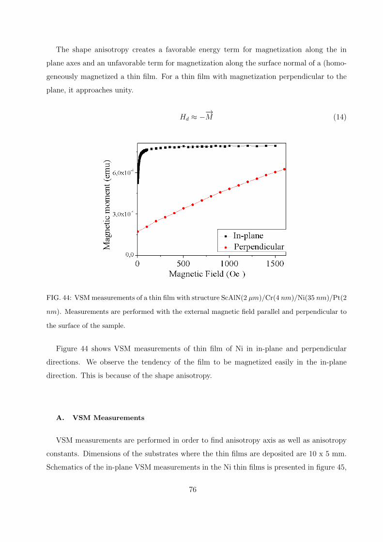
The shape anisotropy creates a favorable energy term for magnetization along the in
plane axes and an unfavorable term for magnetization along the surface normal of a (homo-
geneously magnetized a thin film. For a thin film with magnetization perpendicular to the
plane, it approaches unity.
Hd ≈ −−→M (14)
FIG. 44: VSM measurements of a thin film with structure ScAlN(2 µm)/Cr(4 nm)/Ni(35 nm)/Pt(2
nm). Measurements are performed with the external magnetic field parallel and perpendicular to
the surface of the sample.
Figure 44 shows VSM measurements of thin film of Ni in in-plane and perpendicular
directions. We observe the tendency of the film to be magnetized easily in the in-plane
direction. This is because of the shape anisotropy.
A. VSM Measurements
VSM measurements are performed in order to find anisotropy axis as well as anisotropy
constants. Dimensions of the substrates where the thin films are deposited are 10 x 5 mm.
Schematics of the in-plane VSM measurements in the Ni thin films is presented in figure 45,
76
where θ is the angle that forms the external magnetic field with the long axis of the sample.
Long axis of the magnetic nanostripes is fabricated parallel to the long axis of the sample.
For future computations we need the volume of the Ni deposited over the substrate. As the
Ni thin film is 35 nm thick, the total volume of Ni is:
VNi = 1.75 · 10−6cm3
FIG. 45: Schematics of the VSM measurements performed on thin film. θ is the angle that forms
the external magnetic field with the long axis of the sample.
Determining the anisotropy with the area method This method of determining
anisotropy constants from magnetization curves is based directly on the definition of the
anisotropy energy E, namely, the energy stored in a crystal when it is magnetized to satura-
tion in a non easy direction. If we can calculate W (eq. 17), the work done on the crystal to
bring it to saturation, we can equate E and W and so compute the anisotropy constants. We
determine the energy density by calculating the area that is enclosed between two saturation
curves along the two different axes
E =
∫ M
0
HdM (15)
As stated in the previous chapter, we have two sets of samples, grown out of different
targets of Ni. We perform VSM measurements on these thin films, which are grown simul-
taneously with the nanostripes of our devices. Our thin films are measured with the same
exact structure of the nanostripes, which is Substrate/ScAlN( 2 µm)/Cr( 4 nm)/Ni( 35
nm)/Pt( 2 nm).
77
Sample # 1 The first set of samples with a grain size of D1 = 11 nm is measured. We
find the easy axis directions by measuring hysteresis loops in different orientations. In this
case the easy axis is found to be forming 45 with the long axis of the sample and the long
axis of the nanostripes, as shown in figure 46. The hard axis is found to be perpendicular
to this (still within the plane) at 135 rotating the thin film 90 in the plane.
FIG. 46: VSM measurements in the first set of thin films. Black data are taken with an angle of
45 between the long axis of the sample and the magnetic field, and the red data are taken with
an angle of 135
The area computed out of this first measurement is 0.0048 emu · G. In order to obtain
the anisotropy energy we have to divide this value between the total volume of the thin film.
With proper changes of unities we compute the value of the anisotropy as:
E1 = 0.3 · 103J/m3
We treat this anisotropy as an uniaxial anisotropy, which is in fact, an average value of the
anisotropy of all the grains (crystals) that form the thin film. As the Ni film grows textured,
the Ni (111) planes grow parallel to the sample surface. The value of the anisotropy depends
not only on the texture of the sample, but also depends on the crystallites size.
78
Sample # 2 The second set of samples with a grain size of D2 = 18 nm is measured.
We find the easy axis directions by measuring hysteresis loops in different orientations. In
this case we find the easy axis at 0 with respect the long axis of the sample and the long
axis of the nanostripes. Hard axis is found perpendicular to the long axis at 90
FIG. 47: VSM measurements in the second set of thin films. Black data are taken with an angle
of 0 between the long axis of the sample and the magnetic field, and the red data are taken with
an angle of 90
It is observed in figure 47 that, although there is a preferential axis, there is an anisotropy
dispersion, since the approximation to saturation is by rotation, as well in the black curve.
The area computed out of this second sample is 0.049 emu · G. In order to obtain the
anisotropy energy we have to divide this value between the total volume of the thin film.
With proper changes of unity we compute the value of the anisotropy as:
E2 = 2.8 · 103J/m3
We observe a difference in the anisotropy energy of one order of magnitude. Such a
difference in the anisotropy is explained by the different crystal properties, such as the grain
size and the dispersion of the Ni crystals. When decreasing the grain size, exchange coupling
between neighboring grains may overcome the magnetocrystalline anisotropy of each grain.
79
This results in a reduced effective anisotropy < K >, which represents an average over the
magnetocrystalline anisotropies of the correlated grains. For a random orientation of the
anisotropy axes of the grains the effective anisotropy is reduced by a factor of 1/√N , where
N is the number of the magnetically correlated grains. Regarding the crystal dispersion,
when crystals have a preferred orientation (crystalographic texture), then the polycrystalline
aggregate will have an anisotropy dictated by the weighed average of the individual crystals.
Therefore, an enhanced crystal texture turns out as a larger anisotropy.
B. Conclusions
This chapter was oriented to the measurements of the anisotropy directions and
anisotropy constants in Ni thin films that are assumed to be identical in the crystalline
sturcture to the Ni nanostripes which are the core of this thesis. This is carried out by the
measurements of hysteresis cycles in a vibration sample magnetometer (VSM) applying the
external magnetic field at different orientations. VSM measurements were performed in sam-
ples grown out of two different Ni targets by sputtering deposistions, resulting in different
characteristics for thin films coming out of different Ni targets. Results show that for the Ni
films with smaller grin size the anisotropy energy was noticeably smaller than the thin films
whose grain size was larger. This is because when decreasing the grain size, the exchange
coupling between neighboring grains may overcome the magnetocrystalline anisotropy of
individual grains, resulting in a reduced anistoropy averaged over all the correlated grains.
80
VII. STRAINTRONICS DEVICE
The main straintronics devices fabricated in this thesis are formed by a SAW resonator
and a ferromagnetic nanostripe. The SAW resonator is introduced along with the explana-
tion of the generation of surface acoustic waves in the Appendix in page 151. The charac-
terization of the SAW resonator is carried out by the measurement of the S11 parameter in
a network analyzer. By this, the fundamental excitation modes of the SAW resonator are
found. The magnetic dynamics of the nanostripes are studied from anisotropic magnetore-
sistance measurements (AMR) [Smit, 1951] [Fert, 1968] [Campbell, 1970]. From AMR, the
presence of DW’s can be directly measured through the resistance of the magnetic layer that
carries them, since the AMR effect is a bulk scattering phenomenon. The AMR effect is typ-
ically small, a few percents at room temperature compare to GMR [Baibich, 1988], [Pratt,
1991], [Yuasa, 2003]. One particular advantage of a GMR structure, is that the resistance of
the nanowire varies almost linearly with the position of the DW along the nanowire so that
the position of the DW can be directly determined. This is not the case with AMR which
only detects the presence of a DW regardless of its position.
A. Device Description
The device fabricated is formed by two elements and it is shown in figure 48. The left
side half of the device is a surface acoustic wave (SAW) resonator (figure 48 a). The SAW
resonator consists in four pads and an interdigital transducer (IDT). The IDT is a periodic
array of metallic bars, which are alternatively connected to different pads. When the SAW
resonator is at function, the signal is applied to the contact pad number 2, whereas the rest
are connected to ground. Contact pads 1, 3 and 4 are shorted between them and half of the
metallic bars. The right half of the device includes the ferromagnetic nanostripe and four
contact pads in order to carry out four point measurements. The pads and the nanostripe
are in contact through two current lines.
A close-up of the IDT is shown in figure 48 b). The periodicity is 2.8 µm that is the
wavelength (λ) of the generated SAW’s. The nanostripe is placed as close as possible to
the IDT (L = 40 µm), for the SAW’s to reach the nanostripe with minimum dissipation.
81
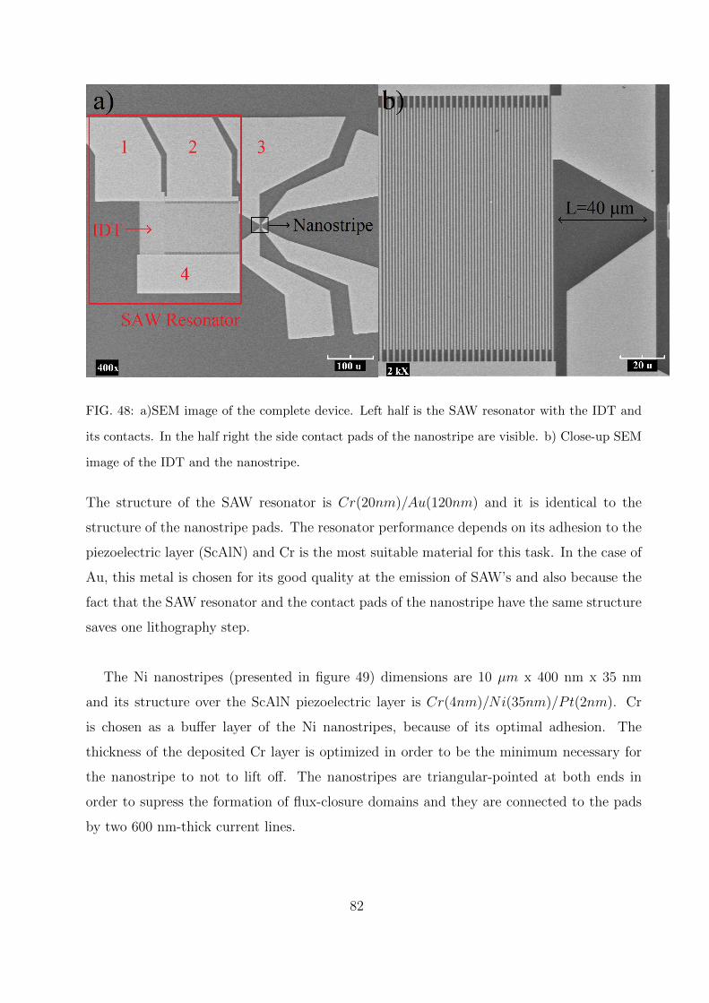
FIG. 48: a)SEM image of the complete device. Left half is the SAW resonator with the IDT and
its contacts. In the half right the side contact pads of the nanostripe are visible. b) Close-up SEM
image of the IDT and the nanostripe.
The structure of the SAW resonator is Cr(20nm)/Au(120nm) and it is identical to the
structure of the nanostripe pads. The resonator performance depends on its adhesion to the
piezoelectric layer (ScAlN) and Cr is the most suitable material for this task. In the case of
Au, this metal is chosen for its good quality at the emission of SAW’s and also because the
fact that the SAW resonator and the contact pads of the nanostripe have the same structure
saves one lithography step.
The Ni nanostripes (presented in figure 49) dimensions are 10 µm x 400 nm x 35 nm
and its structure over the ScAlN piezoelectric layer is Cr(4nm)/Ni(35nm)/Pt(2nm). Cr
is chosen as a buffer layer of the Ni nanostripes, because of its optimal adhesion. The
thickness of the deposited Cr layer is optimized in order to be the minimum necessary for
the nanostripe to not to lift off. The nanostripes are triangular-pointed at both ends in
order to supress the formation of flux-closure domains and they are connected to the pads
by two 600 nm-thick current lines.
82
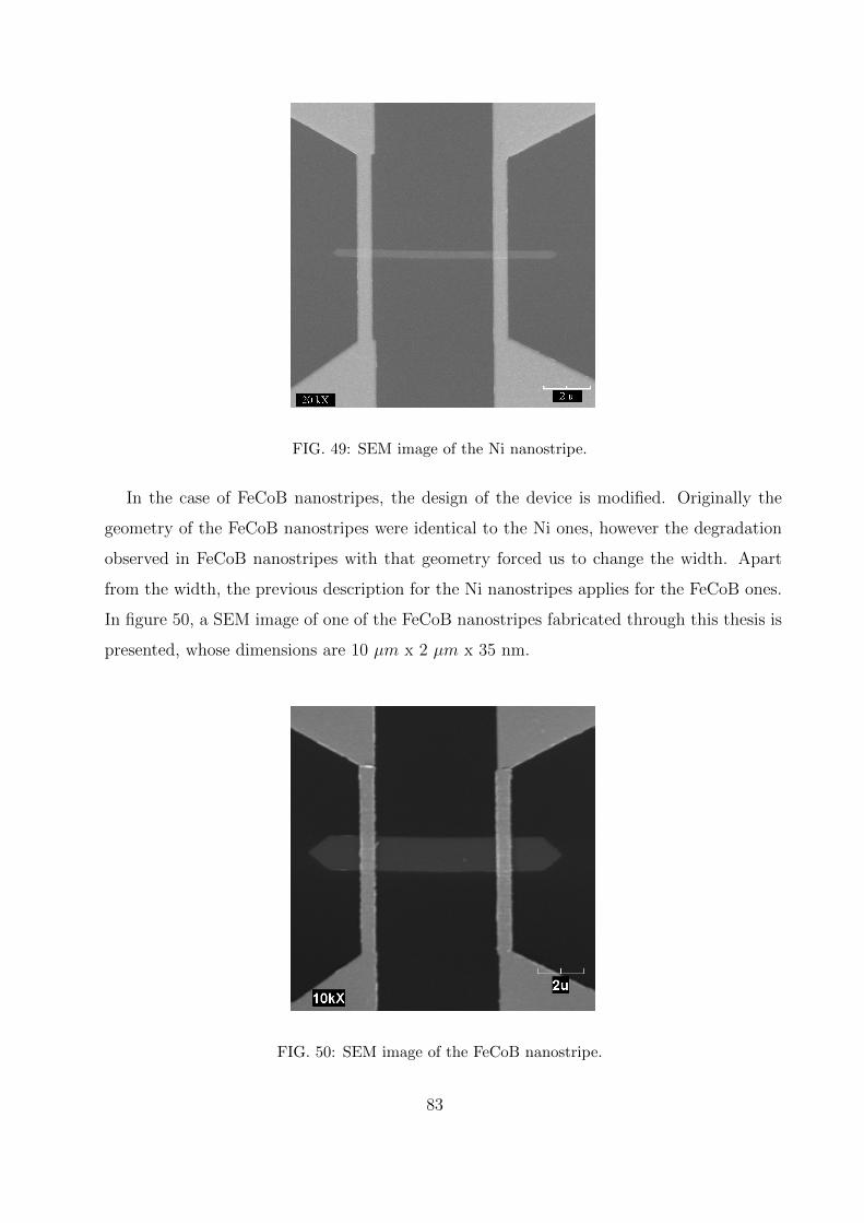
FIG. 49: SEM image of the Ni nanostripe.
In the case of FeCoB nanostripes, the design of the device is modified. Originally the
geometry of the FeCoB nanostripes were identical to the Ni ones, however the degradation
observed in FeCoB nanostripes with that geometry forced us to change the width. Apart
from the width, the previous description for the Ni nanostripes applies for the FeCoB ones.
In figure 50, a SEM image of one of the FeCoB nanostripes fabricated through this thesis is
presented, whose dimensions are 10 µm x 2 µm x 35 nm.
FIG. 50: SEM image of the FeCoB nanostripe.
83
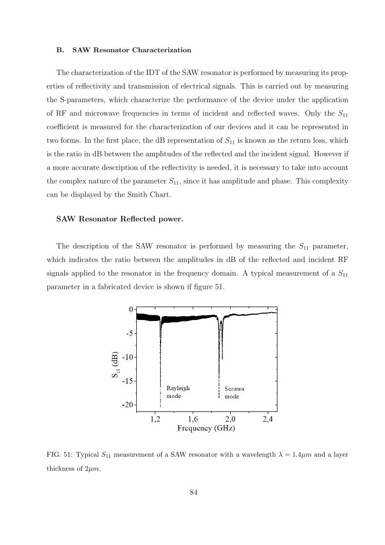
B. SAW Resonator Characterization
The characterization of the IDT of the SAW resonator is performed by measuring its prop-
erties of reflectivity and transmission of electrical signals. This is carried out by measuring
the S-parameters, which characterize the performance of the device under the application
of RF and microwave frequencies in terms of incident and reflected waves. Only the S11
coefficient is measured for the characterization of our devices and it can be represented in
two forms. In the first place, the dB representation of S11 is known as the return loss, which
is the ratio in dB between the amplitudes of the reflected and the incident signal. However if
a more accurate description of the reflectivity is needed, it is necessary to take into account
the complex nature of the parameter S11, since it has amplitude and phase. This complexity
can be displayed by the Smith Chart.
SAW Resonator Reflected power.
The description of the SAW resonator is performed by measuring the S11 parameter,
which indicates the ratio between the amplitudes in dB of the reflected and incident RF
signals applied to the resonator in the frequency domain. A typical measurement of a S11
parameter in a fabricated device is shown if figure 51.
FIG. 51: Typical S11 measurement of a SAW resonator with a wavelength λ = 1.4µm and a layer
thickness of 2µm.
84
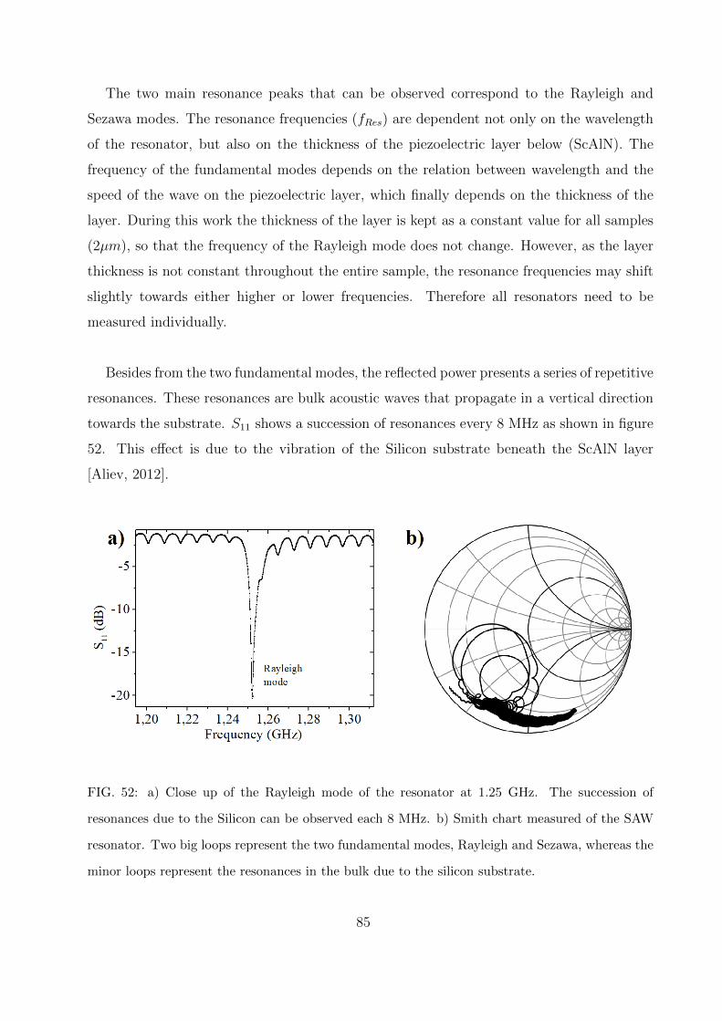
The two main resonance peaks that can be observed correspond to the Rayleigh and
Sezawa modes. The resonance frequencies (fRes) are dependent not only on the wavelength
of the resonator, but also on the thickness of the piezoelectric layer below (ScAlN). The
frequency of the fundamental modes depends on the relation between wavelength and the
speed of the wave on the piezoelectric layer, which finally depends on the thickness of the
layer. During this work the thickness of the layer is kept as a constant value for all samples
(2µm), so that the frequency of the Rayleigh mode does not change. However, as the layer
thickness is not constant throughout the entire sample, the resonance frequencies may shift
slightly towards either higher or lower frequencies. Therefore all resonators need to be
measured individually.
Besides from the two fundamental modes, the reflected power presents a series of repetitive
resonances. These resonances are bulk acoustic waves that propagate in a vertical direction
towards the substrate. S11 shows a succession of resonances every 8 MHz as shown in figure
52. This effect is due to the vibration of the Silicon substrate beneath the ScAlN layer
[Aliev, 2012].
FIG. 52: a) Close up of the Rayleigh mode of the resonator at 1.25 GHz. The succession of
resonances due to the Silicon can be observed each 8 MHz. b) Smith chart measured of the SAW
resonator. Two big loops represent the two fundamental modes, Rayleigh and Sezawa, whereas the
minor loops represent the resonances in the bulk due to the silicon substrate.
85
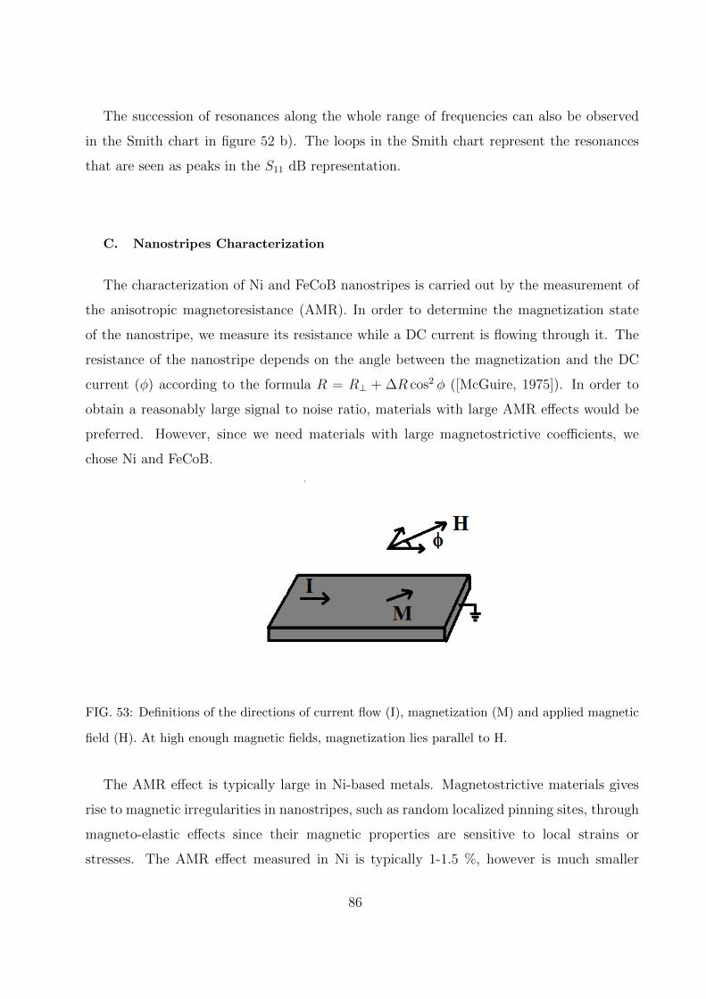
The succession of resonances along the whole range of frequencies can also be observed
in the Smith chart in figure 52 b). The loops in the Smith chart represent the resonances
that are seen as peaks in the S11 dB representation.
C. Nanostripes Characterization
The characterization of Ni and FeCoB nanostripes is carried out by the measurement of
the anisotropic magnetoresistance (AMR). In order to determine the magnetization state
of the nanostripe, we measure its resistance while a DC current is flowing through it. The
resistance of the nanostripe depends on the angle between the magnetization and the DC
current (φ) according to the formula R = R⊥ + ∆R cos2 φ ([McGuire, 1975]). In order to
obtain a reasonably large signal to noise ratio, materials with large AMR effects would be
preferred. However, since we need materials with large magnetostrictive coefficients, we
chose Ni and FeCoB.
FIG. 53: Definitions of the directions of current flow (I), magnetization (M) and applied magnetic
field (H). At high enough magnetic fields, magnetization lies parallel to H.
The AMR effect is typically large in Ni-based metals. Magnetostrictive materials gives
rise to magnetic irregularities in nanostripes, such as random localized pinning sites, through
magneto-elastic effects since their magnetic properties are sensitive to local strains or
stresses. The AMR effect measured in Ni is typically 1-1.5 %, however is much smaller
86
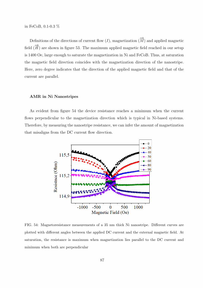
in FeCoB, 0.1-0.3 %
Definitions of the directions of current flow (I), magnetization (−→M) and applied magnetic
field (−→H ) are shown in figure 53. The maximum applied magnetic field reached in our setup
is 1400 Oe, large enough to saturate the magnetization in Ni and FeCoB. Thus, at saturation
the magnetic field direction coincides with the magnetization direction of the nanostripe.
Here, zero degree indicates that the direction of the applied magnetic field and that of the
current are parallel.
AMR in Ni Nanostripes
As evident from figure 54 the device resistance reaches a minimum when the current
flows perpendicular to the magnetization direction which is typical in Ni-based systems.
Therefore, by measuring the nanostripe resistance, we can infer the amount of magnetization
that misaligns from the DC current flow direction.
FIG. 54: Magnetoresistance measurements of a 35 nm thick Ni nanostripe. Different curves are
plotted with different angles between the applied DC current and the external magnetic field. At
saturation, the resistance is maximum when magnetization lies parallel to the DC current and
minimum when both are perpendicular
87
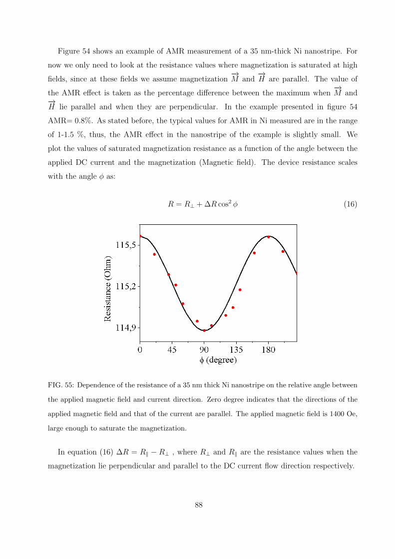
Figure 54 shows an example of AMR measurement of a 35 nm-thick Ni nanostripe. For
now we only need to look at the resistance values where magnetization is saturated at high
fields, since at these fields we assume magnetization−→M and
−→H are parallel. The value of
the AMR effect is taken as the percentage difference between the maximum when−→M and
−→H lie parallel and when they are perpendicular. In the example presented in figure 54
AMR= 0.8%. As stated before, the typical values for AMR in Ni measured are in the range
of 1-1.5 %, thus, the AMR effect in the nanostripe of the example is slightly small. We
plot the values of saturated magnetization resistance as a function of the angle between the
applied DC current and the magnetization (Magnetic field). The device resistance scales
with the angle φ as:
R = R⊥ + ∆R cos2 φ (16)
FIG. 55: Dependence of the resistance of a 35 nm thick Ni nanostripe on the relative angle between
the applied magnetic field and current direction. Zero degree indicates that the directions of the
applied magnetic field and that of the current are parallel. The applied magnetic field is 1400 Oe,
large enough to saturate the magnetization.
In equation (16) ∆R = R‖ − R⊥ , where R⊥ and R‖ are the resistance values when the
magnetization lie perpendicular and parallel to the DC current flow direction respectively.
88
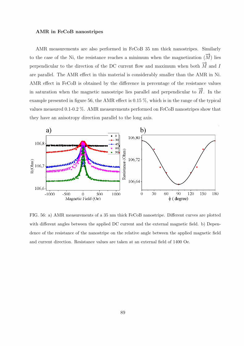
AMR in FeCoB nanostripes
AMR measurements are also performed in FeCoB 35 nm thick nanostripes. Similarly
to the case of the Ni, the resistance reaches a minimum when the magnetization (−→M) lies
perpendicular to the direction of the DC current flow and maximum when both−→M and I
are parallel. The AMR effect in this material is considerably smaller than the AMR in Ni.
AMR effect in FeCoB is obtained by the difference in percentage of the resistance values
in saturation when the magnetic nanostripe lies parallel and perpendicular to−→H . In the
example presented in figure 56, the AMR effect is 0.15 %, which is in the range of the typical
values measured 0.1-0.2 %. AMR measurements performed on FeCoB nanostripes show that
they have an anisotropy direction parallel to the long axis.
FIG. 56: a) AMR measurements of a 35 nm thick FeCoB nanostripe. Different curves are plotted
with different angles between the applied DC current and the external magnetic field. b) Depen-
dence of the resistance of the nanostripe on the relative angle between the applied magnetic field
and current direction. Resistance values are taken at an external field of 1400 Oe.
89
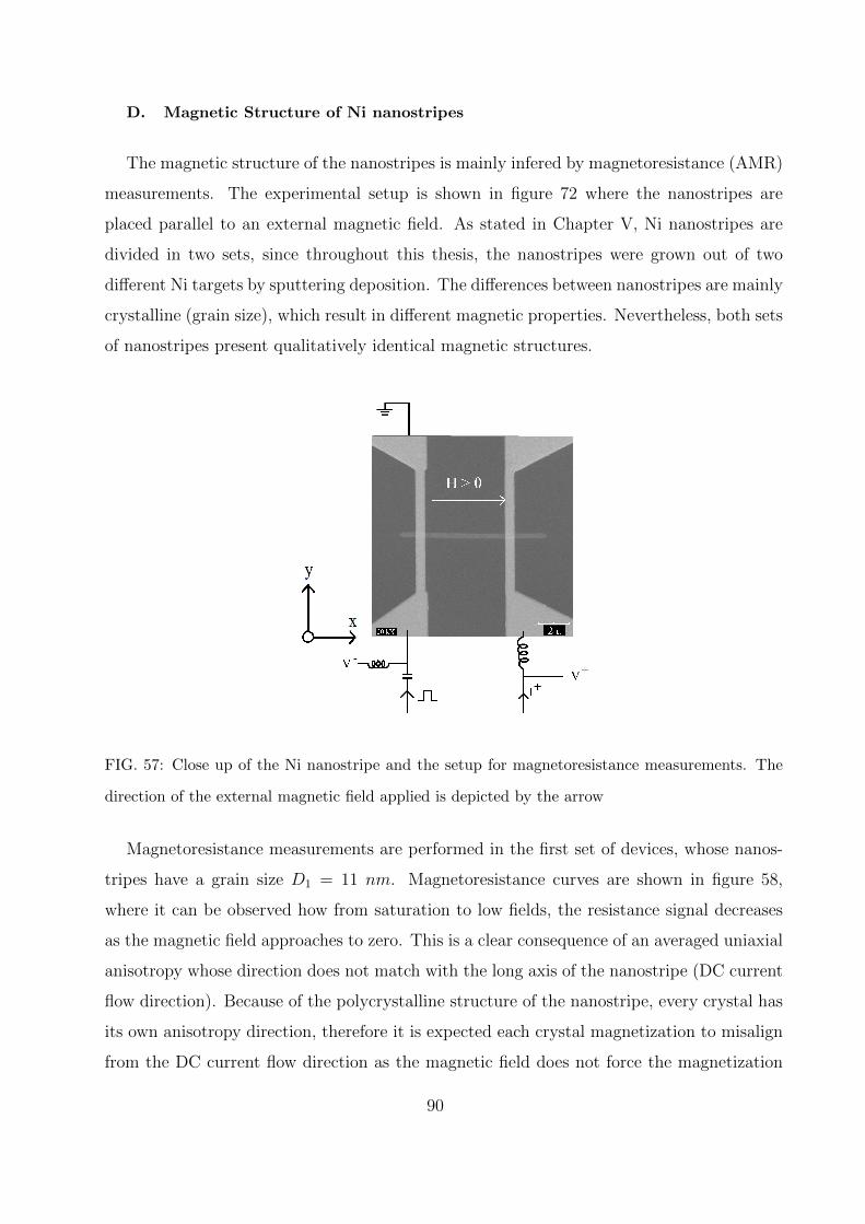
D. Magnetic Structure of Ni nanostripes
The magnetic structure of the nanostripes is mainly infered by magnetoresistance (AMR)
measurements. The experimental setup is shown in figure 72 where the nanostripes are
placed parallel to an external magnetic field. As stated in Chapter V, Ni nanostripes are
divided in two sets, since throughout this thesis, the nanostripes were grown out of two
different Ni targets by sputtering deposition. The differences between nanostripes are mainly
crystalline (grain size), which result in different magnetic properties. Nevertheless, both sets
of nanostripes present qualitatively identical magnetic structures.
FIG. 57: Close up of the Ni nanostripe and the setup for magnetoresistance measurements. The
direction of the external magnetic field applied is depicted by the arrow
Magnetoresistance measurements are performed in the first set of devices, whose nanos-
tripes have a grain size D1 = 11 nm. Magnetoresistance curves are shown in figure 58,
where it can be observed how from saturation to low fields, the resistance signal decreases
as the magnetic field approaches to zero. This is a clear consequence of an averaged uniaxial
anisotropy whose direction does not match with the long axis of the nanostripe (DC current
flow direction). Because of the polycrystalline structure of the nanostripe, every crystal has
its own anisotropy direction, therefore it is expected each crystal magnetization to misalign
from the DC current flow direction as the magnetic field does not force the magnetization
90
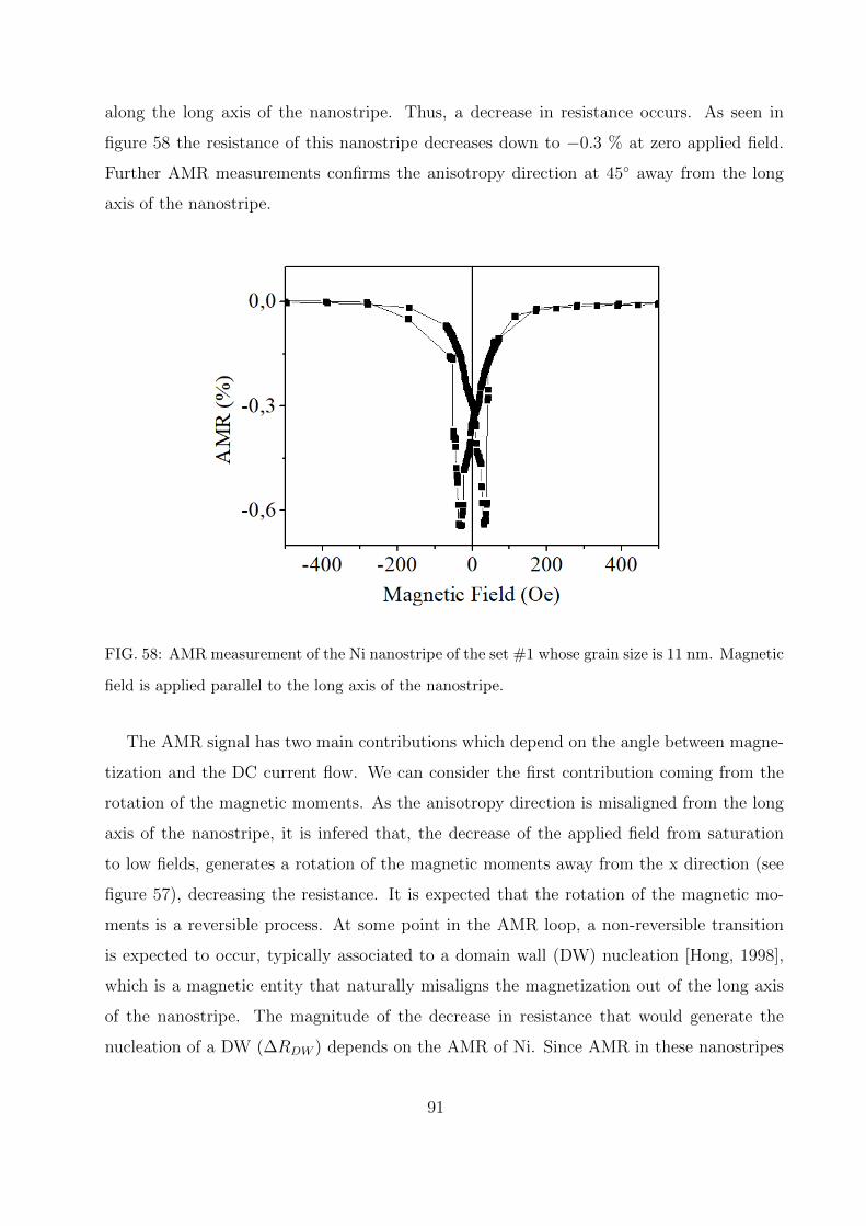
along the long axis of the nanostripe. Thus, a decrease in resistance occurs. As seen in
figure 58 the resistance of this nanostripe decreases down to −0.3 % at zero applied field.
Further AMR measurements confirms the anisotropy direction at 45 away from the long
axis of the nanostripe.
FIG. 58: AMR measurement of the Ni nanostripe of the set #1 whose grain size is 11 nm. Magnetic
field is applied parallel to the long axis of the nanostripe.
The AMR signal has two main contributions which depend on the angle between magne-
tization and the DC current flow. We can consider the first contribution coming from the
rotation of the magnetic moments. As the anisotropy direction is misaligned from the long
axis of the nanostripe, it is infered that, the decrease of the applied field from saturation
to low fields, generates a rotation of the magnetic moments away from the x direction (see
figure 57), decreasing the resistance. It is expected that the rotation of the magnetic mo-
ments is a reversible process. At some point in the AMR loop, a non-reversible transition
is expected to occur, typically associated to a domain wall (DW) nucleation [Hong, 1998],
which is a magnetic entity that naturally misaligns the magnetization out of the long axis
of the nanostripe. The magnitude of the decrease in resistance that would generate the
nucleation of a DW (∆RDW ) depends on the AMR of Ni. Since AMR in these nanostripes
91
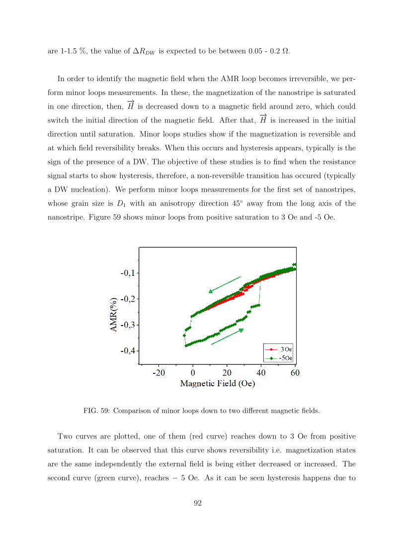
are 1-1.5 %, the value of ∆RDW is expected to be between 0.05 - 0.2 Ω.
In order to identify the magnetic field when the AMR loop becomes irreversible, we per-
form minor loops measurements. In these, the magnetization of the nanostripe is saturated
in one direction, then,−→H is decreased down to a magnetic field around zero, which could
switch the initial direction of the magnetic field. After that,−→H is increased in the initial
direction until saturation. Minor loops studies show if the magnetization is reversible and
at which field reversibility breaks. When this occurs and hysteresis appears, typically is the
sign of the presence of a DW. The objective of these studies is to find when the resistance
signal starts to show hysteresis, therefore, a non-reversible transition has occured (typically
a DW nucleation). We perform minor loops measurements for the first set of nanostripes,
whose grain size is D1 with an anisotropy direction 45 away from the long axis of the
nanostripe. Figure 59 shows minor loops from positive saturation to 3 Oe and -5 Oe.
FIG. 59: Comparison of minor loops down to two different magnetic fields.
Two curves are plotted, one of them (red curve) reaches down to 3 Oe from positive
saturation. It can be observed that this curve shows reversibility i.e. magnetization states
are the same independently the external field is being either decreased or increased. The
second curve (green curve), reaches − 5 Oe. As it can be seen hysteresis happens due to
92
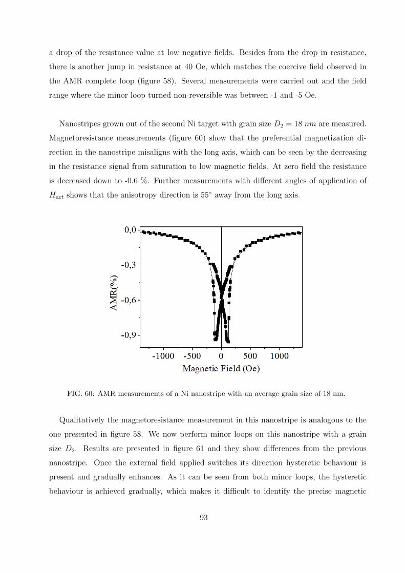
a drop of the resistance value at low negative fields. Besides from the drop in resistance,
there is another jump in resistance at 40 Oe, which matches the coercive field observed in
the AMR complete loop (figure 58). Several measurements were carried out and the field
range where the minor loop turned non-reversible was between -1 and -5 Oe.
Nanostripes grown out of the second Ni target with grain size D2 = 18 nm are measured.
Magnetoresistance measurements (figure 60) show that the preferential magnetization di-
rection in the nanostripe misaligns with the long axis, which can be seen by the decreasing
in the resistance signal from saturation to low magnetic fields. At zero field the resistance
is decreased down to -0.6 %. Further measurements with different angles of application of
Hext shows that the anisotropy direction is 55 away from the long axis.
FIG. 60: AMR measurements of a Ni nanostripe with an average grain size of 18 nm.
Qualitatively the magnetoresistance measurement in this nanostripe is analogous to the
one presented in figure 58. We now perform minor loops on this nanostripe with a grain
size D2. Results are presented in figure 61 and they show differences from the previous
nanostripe. Once the external field applied switches its direction hysteretic behaviour is
present and gradually enhances. As it can be seen from both minor loops, the hysteretic
behaviour is achieved gradually, which makes it difficult to identify the precise magnetic
93
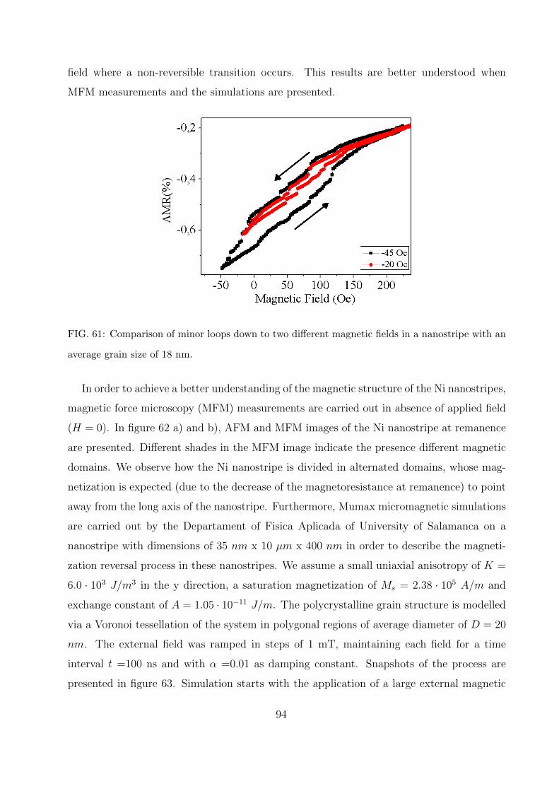
field where a non-reversible transition occurs. This results are better understood when
MFM measurements and the simulations are presented.
FIG. 61: Comparison of minor loops down to two different magnetic fields in a nanostripe with an
average grain size of 18 nm.
In order to achieve a better understanding of the magnetic structure of the Ni nanostripes,
magnetic force microscopy (MFM) measurements are carried out in absence of applied field
(H = 0). In figure 62 a) and b), AFM and MFM images of the Ni nanostripe at remanence
are presented. Different shades in the MFM image indicate the presence different magnetic
domains. We observe how the Ni nanostripe is divided in alternated domains, whose mag-
netization is expected (due to the decrease of the magnetoresistance at remanence) to point
away from the long axis of the nanostripe. Furthermore, Mumax micromagnetic simulations
are carried out by the Departament of Fisica Aplicada of University of Salamanca on a
nanostripe with dimensions of 35 nm x 10 µm x 400 nm in order to describe the magneti-
zation reversal process in these nanostripes. We assume a small uniaxial anisotropy of K =
6.0 · 103 J/m3 in the y direction, a saturation magnetization of Ms = 2.38 · 105 A/m and
exchange constant of A = 1.05 · 10−11 J/m. The polycrystalline grain structure is modelled
via a Voronoi tessellation of the system in polygonal regions of average diameter of D = 20
nm. The external field was ramped in steps of 1 mT, maintaining each field for a time
interval t =100 ns and with α =0.01 as damping constant. Snapshots of the process are
presented in figure 63. Simulation starts with the application of a large external magnetic
94
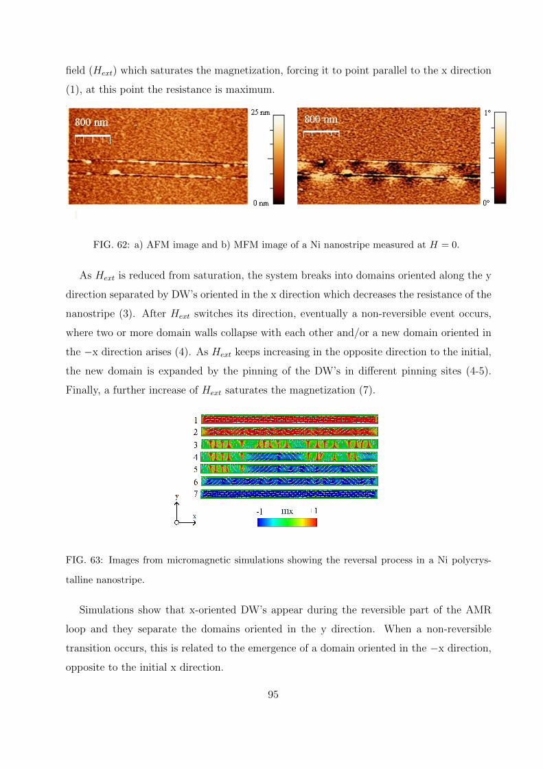
field (Hext) which saturates the magnetization, forcing it to point parallel to the x direction
(1), at this point the resistance is maximum.
FIG. 62: a) AFM image and b) MFM image of a Ni nanostripe measured at H = 0.
As Hext is reduced from saturation, the system breaks into domains oriented along the y
direction separated by DW’s oriented in the x direction which decreases the resistance of the
nanostripe (3). After Hext switches its direction, eventually a non-reversible event occurs,
where two or more domain walls collapse with each other and/or a new domain oriented in
the −x direction arises (4). As Hext keeps increasing in the opposite direction to the initial,
the new domain is expanded by the pinning of the DW’s in different pinning sites (4-5).
Finally, a further increase of Hext saturates the magnetization (7).
FIG. 63: Images from micromagnetic simulations showing the reversal process in a Ni polycrys-
talline nanostripe.
Simulations show that x-oriented DW’s appear during the reversible part of the AMR
loop and they separate the domains oriented in the y direction. When a non-reversible
transition occurs, this is related to the emergence of a domain oriented in the −x direction,
opposite to the initial x direction.
95
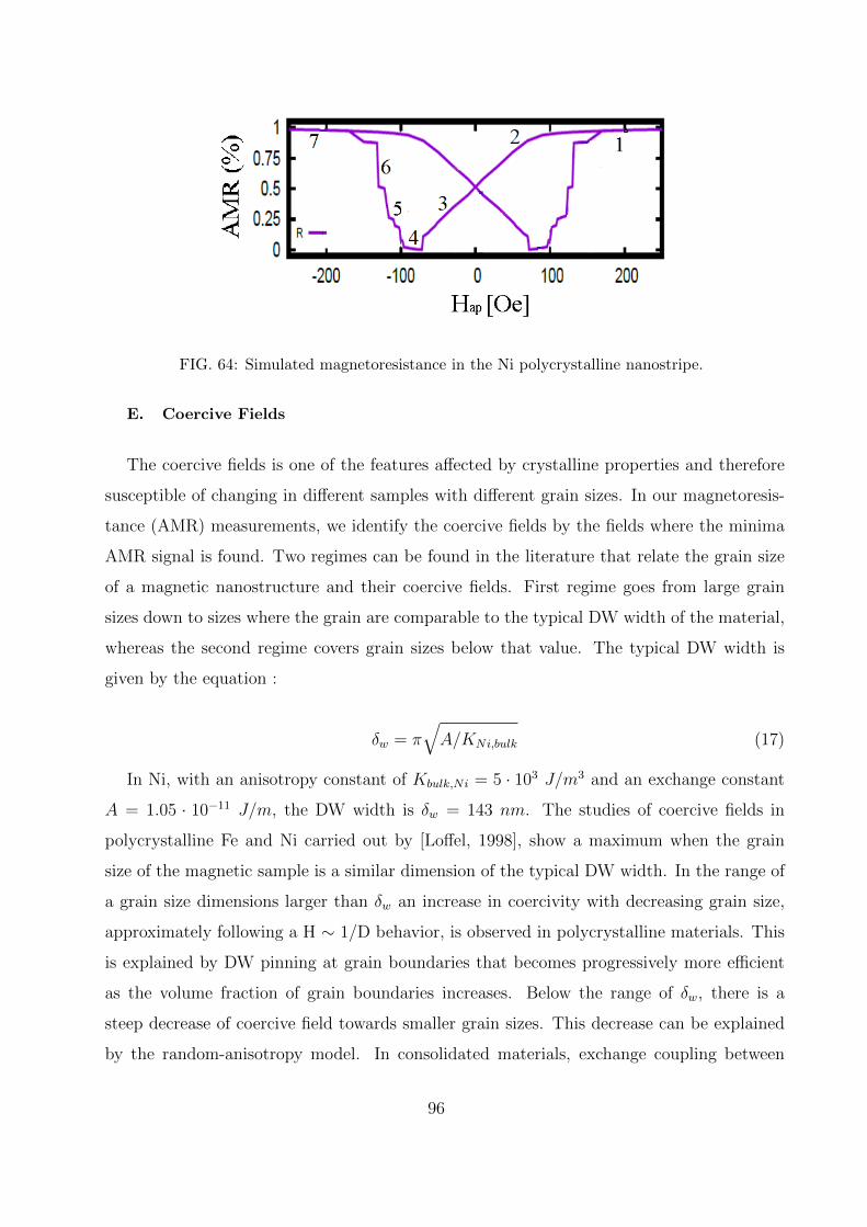
FIG. 64: Simulated magnetoresistance in the Ni polycrystalline nanostripe.
E. Coercive Fields
The coercive fields is one of the features affected by crystalline properties and therefore
susceptible of changing in different samples with different grain sizes. In our magnetoresis-
tance (AMR) measurements, we identify the coercive fields by the fields where the minima
AMR signal is found. Two regimes can be found in the literature that relate the grain size
of a magnetic nanostructure and their coercive fields. First regime goes from large grain
sizes down to sizes where the grain are comparable to the typical DW width of the material,
whereas the second regime covers grain sizes below that value. The typical DW width is
given by the equation :
δw = π√A/KNi,bulk (17)
In Ni, with an anisotropy constant of Kbulk,Ni = 5 · 103 J/m3 and an exchange constant
A = 1.05 · 10−11 J/m, the DW width is δw = 143 nm. The studies of coercive fields in
polycrystalline Fe and Ni carried out by [Loffel, 1998], show a maximum when the grain
size of the magnetic sample is a similar dimension of the typical DW width. In the range of
a grain size dimensions larger than δw an increase in coercivity with decreasing grain size,
approximately following a H ∼ 1/D behavior, is observed in polycrystalline materials. This
is explained by DW pinning at grain boundaries that becomes progressively more efficient
as the volume fraction of grain boundaries increases. Below the range of δw, there is a
steep decrease of coercive field towards smaller grain sizes. This decrease can be explained
by the random-anisotropy model. In consolidated materials, exchange coupling between
96
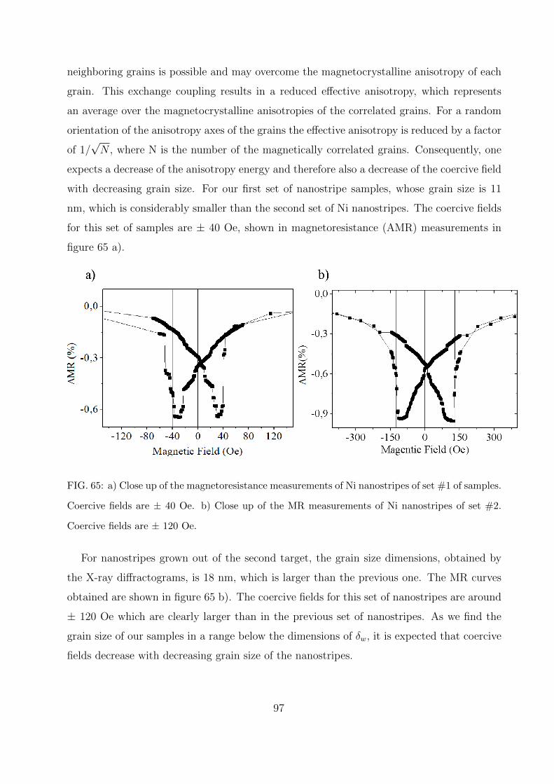
neighboring grains is possible and may overcome the magnetocrystalline anisotropy of each
grain. This exchange coupling results in a reduced effective anisotropy, which represents
an average over the magnetocrystalline anisotropies of the correlated grains. For a random
orientation of the anisotropy axes of the grains the effective anisotropy is reduced by a factor
of 1/√N , where N is the number of the magnetically correlated grains. Consequently, one
expects a decrease of the anisotropy energy and therefore also a decrease of the coercive field
with decreasing grain size. For our first set of nanostripe samples, whose grain size is 11
nm, which is considerably smaller than the second set of Ni nanostripes. The coercive fields
for this set of samples are ± 40 Oe, shown in magnetoresistance (AMR) measurements in
figure 65 a).
FIG. 65: a) Close up of the magnetoresistance measurements of Ni nanostripes of set #1 of samples.
Coercive fields are ± 40 Oe. b) Close up of the MR measurements of Ni nanostripes of set #2.
Coercive fields are ± 120 Oe.
For nanostripes grown out of the second target, the grain size dimensions, obtained by
the X-ray diffractograms, is 18 nm, which is larger than the previous one. The MR curves
obtained are shown in figure 65 b). The coercive fields for this set of nanostripes are around
± 120 Oe which are clearly larger than in the previous set of nanostripes. As we find the
grain size of our samples in a range below the dimensions of δw, it is expected that coercive
fields decrease with decreasing grain size of the nanostripes.
97
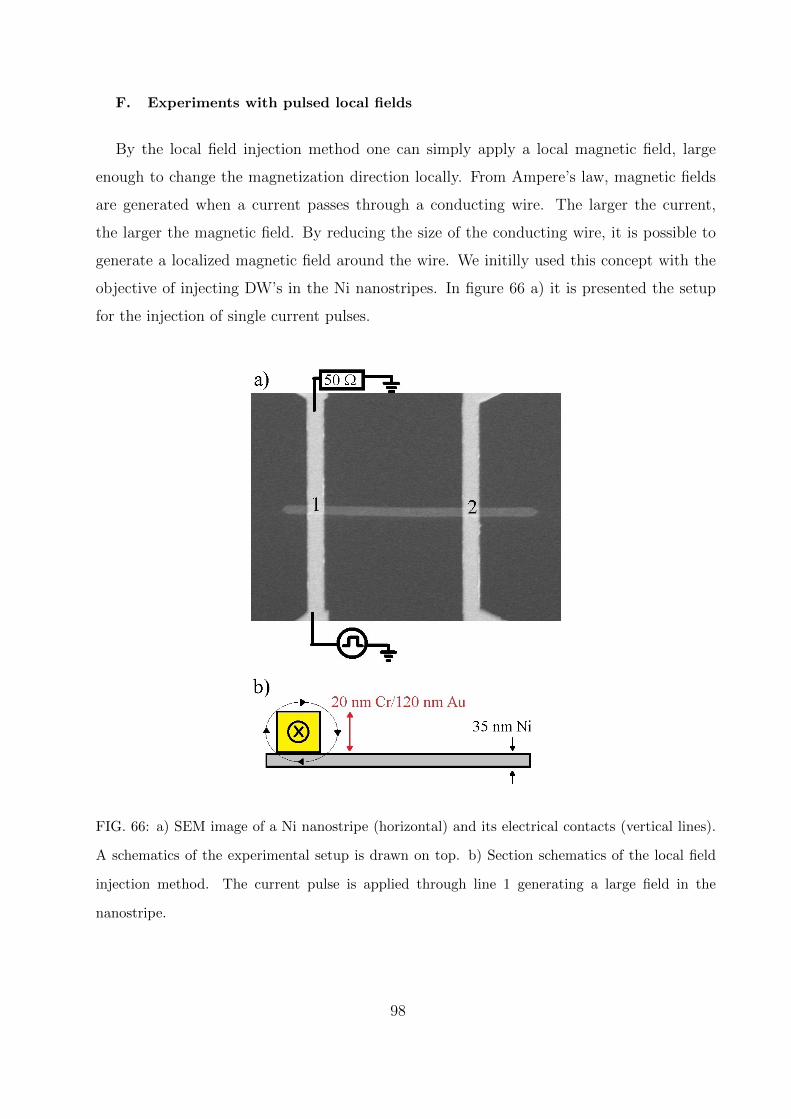
F. Experiments with pulsed local fields
By the local field injection method one can simply apply a local magnetic field, large
enough to change the magnetization direction locally. From Ampere’s law, magnetic fields
are generated when a current passes through a conducting wire. The larger the current,
the larger the magnetic field. By reducing the size of the conducting wire, it is possible to
generate a localized magnetic field around the wire. We initilly used this concept with the
objective of injecting DW’s in the Ni nanostripes. In figure 66 a) it is presented the setup
for the injection of single current pulses.
FIG. 66: a) SEM image of a Ni nanostripe (horizontal) and its electrical contacts (vertical lines).
A schematics of the experimental setup is drawn on top. b) Section schematics of the local field
injection method. The current pulse is applied through line 1 generating a large field in the
nanostripe.
98
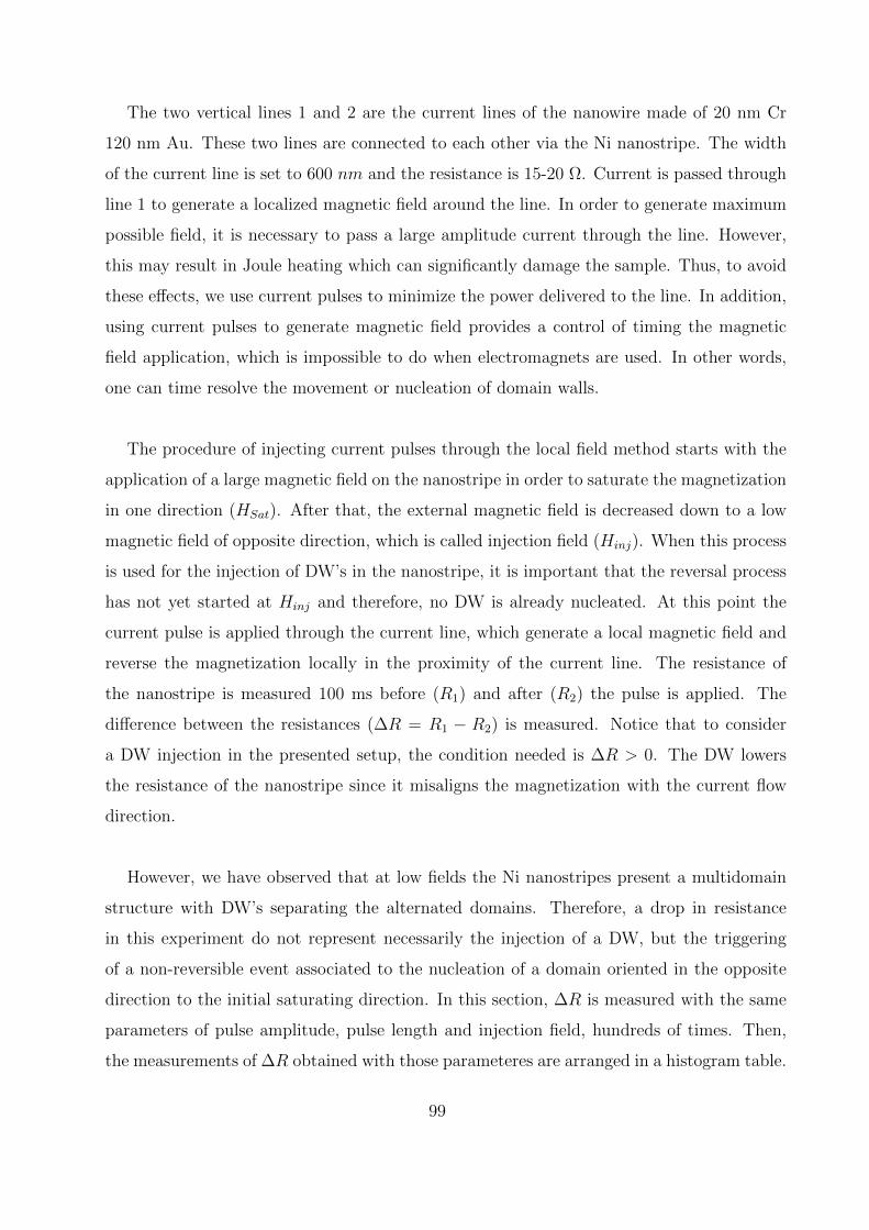
The two vertical lines 1 and 2 are the current lines of the nanowire made of 20 nm Cr
120 nm Au. These two lines are connected to each other via the Ni nanostripe. The width
of the current line is set to 600 nm and the resistance is 15-20 Ω. Current is passed through
line 1 to generate a localized magnetic field around the line. In order to generate maximum
possible field, it is necessary to pass a large amplitude current through the line. However,
this may result in Joule heating which can significantly damage the sample. Thus, to avoid
these effects, we use current pulses to minimize the power delivered to the line. In addition,
using current pulses to generate magnetic field provides a control of timing the magnetic
field application, which is impossible to do when electromagnets are used. In other words,
one can time resolve the movement or nucleation of domain walls.
The procedure of injecting current pulses through the local field method starts with the
application of a large magnetic field on the nanostripe in order to saturate the magnetization
in one direction (HSat). After that, the external magnetic field is decreased down to a low
magnetic field of opposite direction, which is called injection field (Hinj). When this process
is used for the injection of DW’s in the nanostripe, it is important that the reversal process
has not yet started at Hinj and therefore, no DW is already nucleated. At this point the
current pulse is applied through the current line, which generate a local magnetic field and
reverse the magnetization locally in the proximity of the current line. The resistance of
the nanostripe is measured 100 ms before (R1) and after (R2) the pulse is applied. The
difference between the resistances (∆R = R1 − R2) is measured. Notice that to consider
a DW injection in the presented setup, the condition needed is ∆R > 0. The DW lowers
the resistance of the nanostripe since it misaligns the magnetization with the current flow
direction.
However, we have observed that at low fields the Ni nanostripes present a multidomain
structure with DW’s separating the alternated domains. Therefore, a drop in resistance
in this experiment do not represent necessarily the injection of a DW, but the triggering
of a non-reversible event associated to the nucleation of a domain oriented in the opposite
direction to the initial saturating direction. In this section, ∆R is measured with the same
parameters of pulse amplitude, pulse length and injection field, hundreds of times. Then,
the measurements of ∆R obtained with those parameteres are arranged in a histogram table.
99
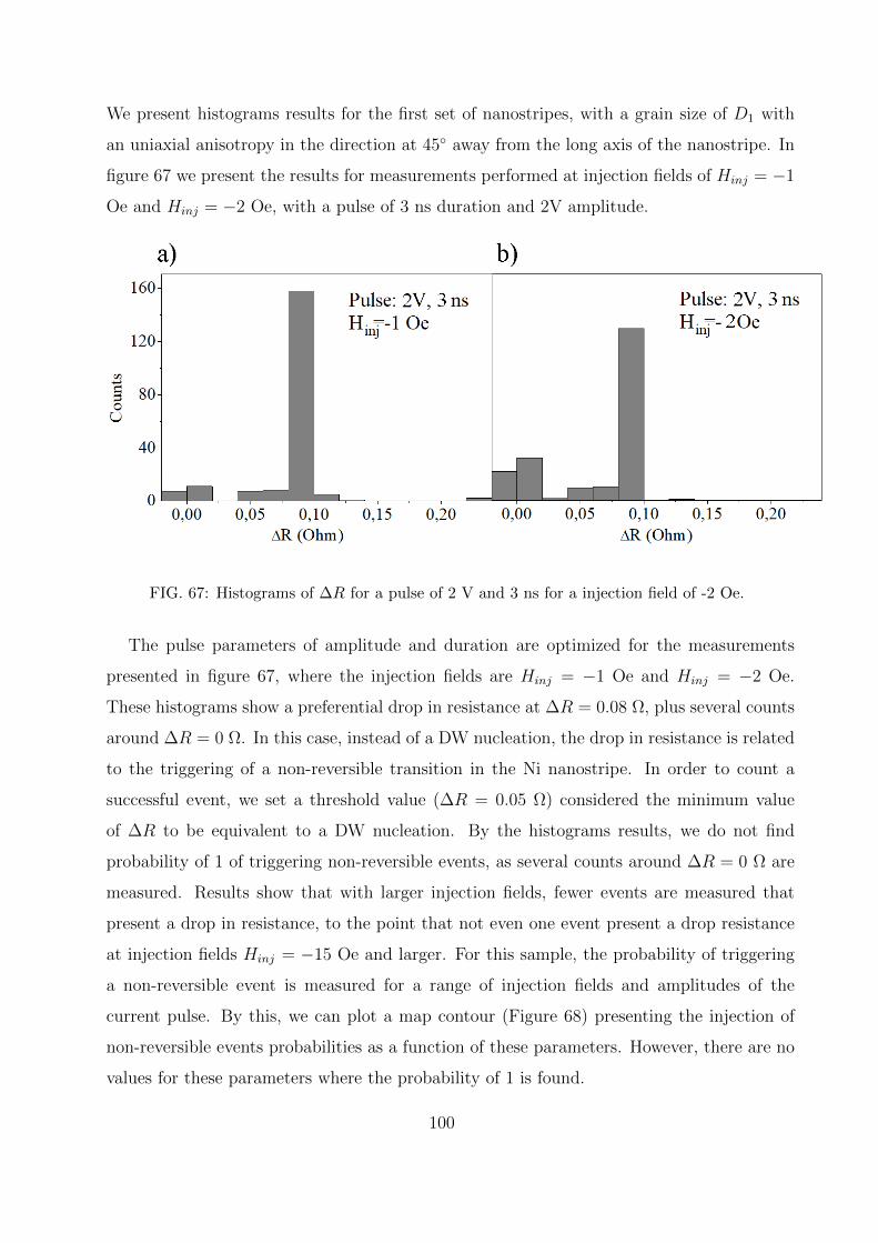
We present histograms results for the first set of nanostripes, with a grain size of D1 with
an uniaxial anisotropy in the direction at 45 away from the long axis of the nanostripe. In
figure 67 we present the results for measurements performed at injection fields of Hinj = −1
Oe and Hinj = −2 Oe, with a pulse of 3 ns duration and 2V amplitude.
FIG. 67: Histograms of ∆R for a pulse of 2 V and 3 ns for a injection field of -2 Oe.
The pulse parameters of amplitude and duration are optimized for the measurements
presented in figure 67, where the injection fields are Hinj = −1 Oe and Hinj = −2 Oe.
These histograms show a preferential drop in resistance at ∆R = 0.08 Ω, plus several counts
around ∆R = 0 Ω. In this case, instead of a DW nucleation, the drop in resistance is related
to the triggering of a non-reversible transition in the Ni nanostripe. In order to count a
successful event, we set a threshold value (∆R = 0.05 Ω) considered the minimum value
of ∆R to be equivalent to a DW nucleation. By the histograms results, we do not find
probability of 1 of triggering non-reversible events, as several counts around ∆R = 0 Ω are
measured. Results show that with larger injection fields, fewer events are measured that
present a drop in resistance, to the point that not even one event present a drop resistance
at injection fields Hinj = −15 Oe and larger. For this sample, the probability of triggering
a non-reversible event is measured for a range of injection fields and amplitudes of the
current pulse. By this, we can plot a map contour (Figure 68) presenting the injection of
non-reversible events probabilities as a function of these parameters. However, there are no
values for these parameters where the probability of 1 is found.
100
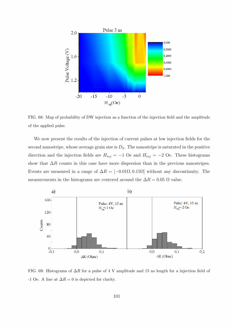
FIG. 68: Map of probability of DW injection as a function of the injection field and the amplitude
of the applied pulse.
We now present the results of the injection of current pulses at low injection fields for the
second nanostripe, whose average grain size is D2. The nanostripe is saturated in the positive
direction and the injection fields are Hinj = −1 Oe and Hinj = −2 Oe. These histograms
show that ∆R counts in this case have more dispersion than in the previous nanostripes.
Events are measured in a range of ∆R = [−0.01Ω, 0.15Ω] without any discontinuity. The
measurements in the histograms are centered around the ∆R = 0.05 Ω value.
FIG. 69: Histograms of ∆R for a pulse of 4 V amplitude and 15 ns length for a injection field of
-1 Oe. A line at ∆R = 0 is depicted for clarity.
101
The histograms in both nanostripes are comparable to the minor loops measurements
(figures 59 and 61). In the nanostripe with grain size D1 = 11 nm, the non-reversible events
occur in an abrupt manner by sudden jumps, whereas in the nanostripe with grain size
D2 = 18 nm, the minor loop present irreversibility in a gradual manner that indicates the
non-reversible event occurs gradually.
G. Conclusions
In this chapter we have presented all the measurements performed on the straintronics
devices in order to characterize them and collect all the information possible in absence
of surface acoustic waves (SAW’s). We start this chapter with a visual description of the
devices which is formed by a SAW resonator and a ferromagnetic nanostripes with their
contact pads.
The SAW resonator is the device that generates strain by the emission of SAW’s. It
is formed by the IDT’s (interdigital transducers), which is an array of metallic bars alter-
natively connected to different contact pads. The resonators are characterized by the S11
parameter, which indicates the ratio between the amplitudes in dB of the reflected and in-
cident RF signals applied to them in the frequency domain. The measurements of S11 in
our SAW resonator show two fundamental modes, Rayleigh (∼1.25 GHz) and Sezawa (∼1.8
GHz) that propagate along the surface of the piezoelectric layer. Meanwhile it presents a
successions of resonances each 8 MHz, that corresponds to bulk acoustic waves that propa-
gate along the perpendicular direction of the sample forcing the Si beneath the piezoelectric
layer to vibrate.
The second part of this hybrid device is formed by the ferromagnetic nanostripes and
its contact pads. The crystalline structure of the Ni nanostripes is presented in previous
chapters, and it is important to know it, in order to understand the behaviour of the mag-
netization of the nanostripes. Ni nanostripes have polycrystalline structure, with different
grain sizes (D1=11 and D2=18 nm). The AMR values obtained by measurements in the Ni
nanostripes are within the range of 1% − 1.5%. Furthermore, these measurements show that
102
the preferential magnetization direction (anisotropy) is misaligned 45 and 55 away from
the long axis of the nanostripe. The main information about the magnetic structure of the
nanostripes are obtained through magnetoresistance (AMR) measurements performed with
a magnetic field applied parallel to the long axis of the nanostripe. Two main contributions
to the AMR measurements can be observed. The first one depends on the rotation of the
magnetization that occurs when sweeping the magnetic field from saturation to low fields.
This generates a decrease in the AMR signal, which shows that magnetization is misaligned
from the long axis of the nanostripe at remanence (H=0). Meanwhile, measurements of
magnetic force microscopy (MFM) show that at remanence, the Ni nanostripes form a mag-
netic structure of alternated oriented magnetic domains. Therefore, it is concluded that the
nanostripes at low fields present a multi-domain structure, whose magnetization is oriented
away from the long axis of the nanostripe. This magnetic structure is also obtained by
the micromagnetic simulations performed the Dpto of Fisica Aplicada of University of Sala-
manca, where y-oriented magnetic domains can be observed separated by x-oriented domain
walls (DW’s). Minor loop measurements show that the dynamic process from saturation
to the multi-domain structure is perfomed by rotation, due to the reversibility presented
in the minor loops, whereas irreversibility observed in the minor loops are related to non-
reversible transitions associated to the emergence of a domain whose magnetization points
in the opposite direction to the initial saturating direction
Current pulse injection experiments are performed in the Ni nanostripes. These experi-
ments are carried out by saturating the magnetization in one direction and then, taking the
external magnetic field to a low field of opposite direction, called injection field Hinj. At this
point a controlled single current pulse is passed through one of the current lines that connect
the nanostripe. By this, we can generate a large magnetic field of a controlled amplitude
and time span in order to initiate the reversal process. Experiments are performed where
several hundreds of single current pulses were injected in the nanostripe in order observe the
triggering of non-reversible events. By the measurement of the resistance 100 ms before (R1)
and 100 ms after (R2) the current pulse application, we are able to determine the triggering
of non-reversible events. Results presented in the nanostripe with a grain size of D1 =11 nm
show that at very low injection fields, non-reversible events can be triggered, however 100%
effiency is not found with any parameters of the current pulses. The threshold to count as
103
positive a non-reversible event is chosen as the resistance drop due to the nucleation of a
DW in Ni (∆R = 0.05 Ω). The second nanostripe with a grain size of D2 =18 nm present
even fewer events that can be counted as positive (∆R > 0.5 Ω) and the histograms show
a larger dispersion as a function of ∆R without any discontinuity. This could be related to
the gradually triggering of the non-reversible events that in this nanostripe can be observed
in figure 61.
104
VIII. EFFECTS OF SAW’S IN MAGNETOSTRICTIVE NANOSTRIPES
The effects that generate the application of surface acoustic waves (SAW’s) have been
studied, up to this day, in several magnetic nanostructures. However, in this thesis we report
to our knowledge, the first experiments of application of SAW’s in magnetic nanostripes.
The expected effects of the application of the SAW’S are reported in previous works carried
out on this topic. The SAW’s have been proven to induce an additional anisotropy in
Co nanorectangles [Davis, 2010] and in Ni nanosquares [Forster, 2016] in the direction of
the propagation of the waves. SAW’s have also been shown to promote the switching in
ferromagnetic thin films [Tejada, 2017] and elliptical Co nano-elements [Sampath, 2016].
Another effect reported of the application of the SAW’s is the reduction of coercive fields
in thin films of galfenol [Li, 2014] and (Ga,Mn)(As,P) [Thevenard, 2016]. Therefore, it is
worth to study the possibility of the SAW’s enhancing the DW nucleation, since [Parkes,
2012] showed experimentally that in an epitaxial-deposited Galfenol film, an irreversible 90
switching of the magnetization, mediated by DW movement, can be achieved in absence of
any external magnetic field. We have also studied the enhacement of the DW dynamics in
the nanostripes due to the presence of SAW’s.
In this chapter the magnetization of magnetic nanostripes is probed, through magnetore-
sistance (AMR) measurements, under the application of SAW’s. We perform complete AMR
loops in order to observe the decrease in coercivity and also minor loops in case the SAW’s
assist the DW nucleation. Furthermore, current pulse injection experiments are performed
when a non-reversible event has occured in the nanostripe in order to observe differences in
the DW dynamics in absence and in presence of SAW’s.
105
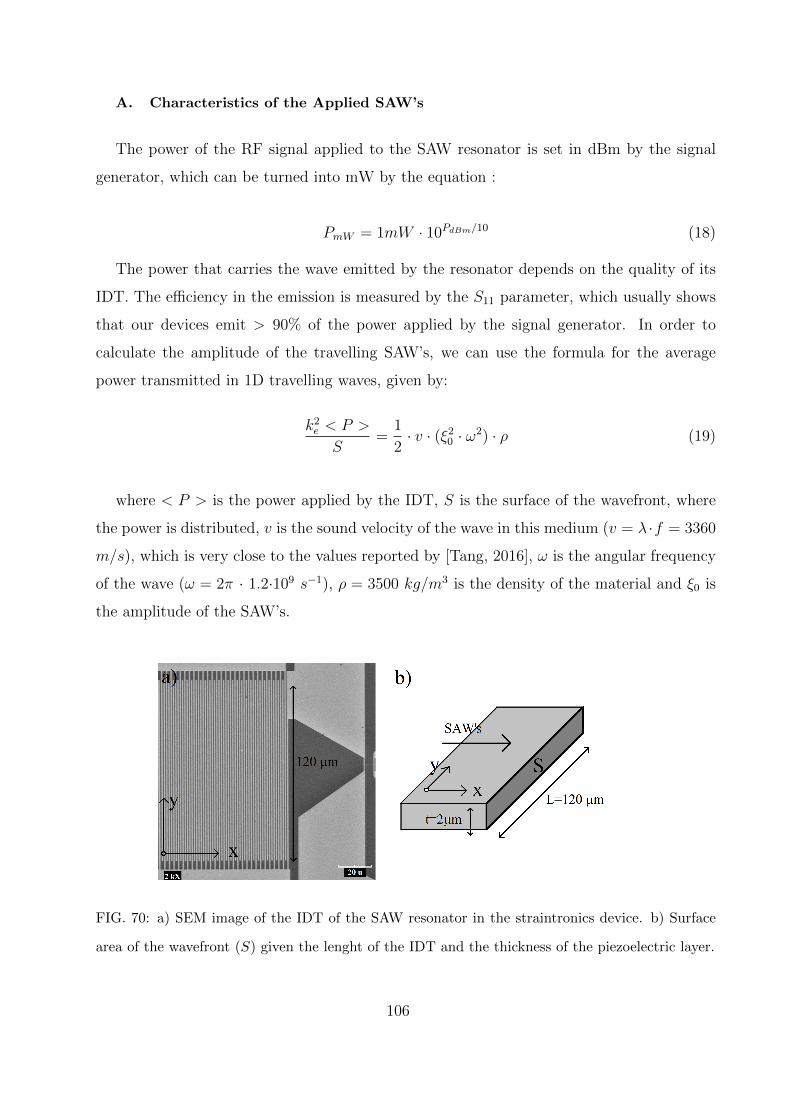
A. Characteristics of the Applied SAW’s
The power of the RF signal applied to the SAW resonator is set in dBm by the signal
generator, which can be turned into mW by the equation :
PmW = 1mW · 10PdBm/10 (18)
The power that carries the wave emitted by the resonator depends on the quality of its
IDT. The efficiency in the emission is measured by the S11 parameter, which usually shows
that our devices emit > 90% of the power applied by the signal generator. In order to
calculate the amplitude of the travelling SAW’s, we can use the formula for the average
power transmitted in 1D travelling waves, given by:
k2e < P >
S=
1
2· v · (ξ20 · ω2) · ρ (19)
where < P > is the power applied by the IDT, S is the surface of the wavefront, where
the power is distributed, v is the sound velocity of the wave in this medium (v = λ ·f = 3360
m/s), which is very close to the values reported by [Tang, 2016], ω is the angular frequency
of the wave (ω = 2π · 1.2·109 s−1), ρ = 3500 kg/m3 is the density of the material and ξ0 is
the amplitude of the SAW’s.
FIG. 70: a) SEM image of the IDT of the SAW resonator in the straintronics device. b) Surface
area of the wavefront (S) given the lenght of the IDT and the thickness of the piezoelectric layer.
106
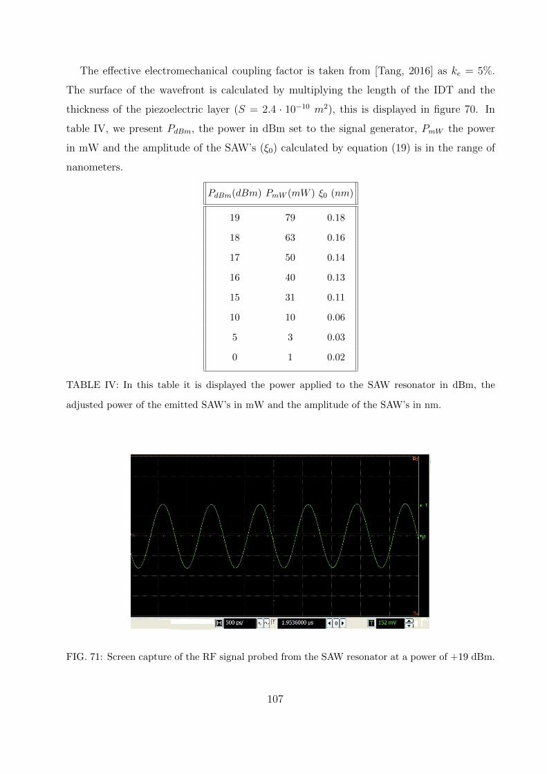
The effective electromechanical coupling factor is taken from [Tang, 2016] as ke = 5%.
The surface of the wavefront is calculated by multiplying the length of the IDT and the
thickness of the piezoelectric layer (S = 2.4 · 10−10 m2), this is displayed in figure 70. In
table IV, we present PdBm, the power in dBm set to the signal generator, PmW the power
in mW and the amplitude of the SAW’s (ξ0) calculated by equation (19) is in the range of
nanometers.
PdBm(dBm) PmW (mW ) ξ0 (nm)
19 79 0.18
18 63 0.16
17 50 0.14
16 40 0.13
15 31 0.11
10 10 0.06
5 3 0.03
0 1 0.02
TABLE IV: In this table it is displayed the power applied to the SAW resonator in dBm, the
adjusted power of the emitted SAW’s in mW and the amplitude of the SAW’s in nm.
FIG. 71: Screen capture of the RF signal probed from the SAW resonator at a power of +19 dBm.
107
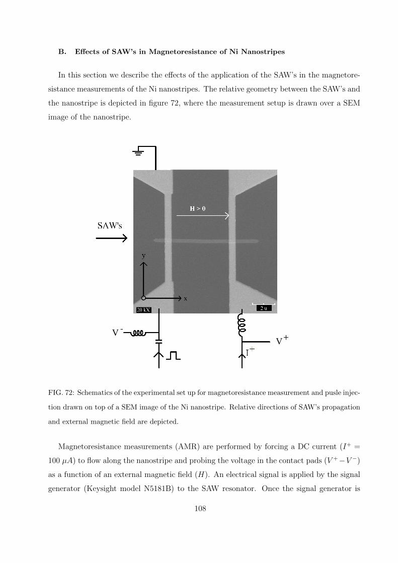
B. Effects of SAW’s in Magnetoresistance of Ni Nanostripes
In this section we describe the effects of the application of the SAW’s in the magnetore-
sistance measurements of the Ni nanostripes. The relative geometry between the SAW’s and
the nanostripe is depicted in figure 72, where the measurement setup is drawn over a SEM
image of the nanostripe.
FIG. 72: Schematics of the experimental set up for magnetoresistance measurement and pusle injec-
tion drawn on top of a SEM image of the Ni nanostripe. Relative directions of SAW’s propagation
and external magnetic field are depicted.
Magnetoresistance measurements (AMR) are performed by forcing a DC current (I+ =
100 µA) to flow along the nanostripe and probing the voltage in the contact pads (V +−V −)
as a function of an external magnetic field (H). An electrical signal is applied by the signal
generator (Keysight model N5181B) to the SAW resonator. Once the signal generator is
108
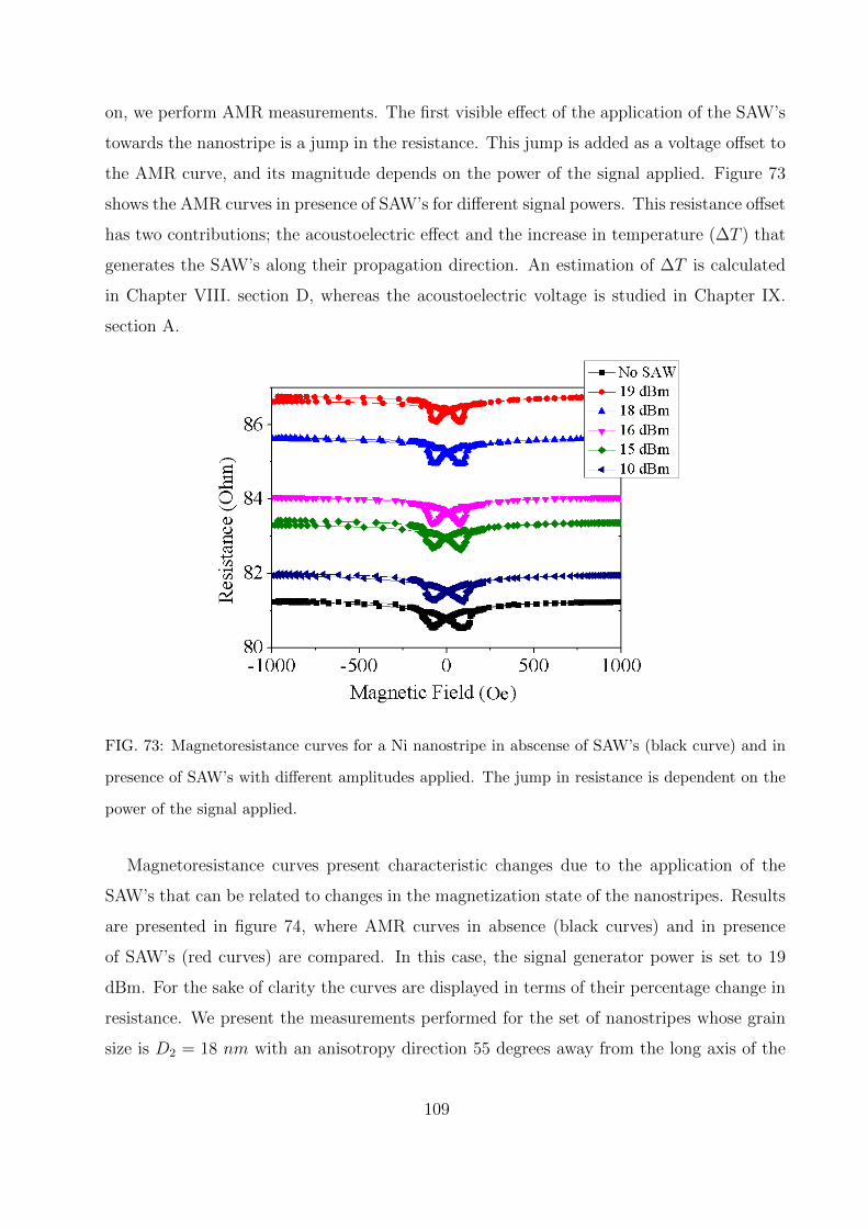
on, we perform AMR measurements. The first visible effect of the application of the SAW’s
towards the nanostripe is a jump in the resistance. This jump is added as a voltage offset to
the AMR curve, and its magnitude depends on the power of the signal applied. Figure 73
shows the AMR curves in presence of SAW’s for different signal powers. This resistance offset
has two contributions; the acoustoelectric effect and the increase in temperature (∆T ) that
generates the SAW’s along their propagation direction. An estimation of ∆T is calculated
in Chapter VIII. section D, whereas the acoustoelectric voltage is studied in Chapter IX.
section A.
FIG. 73: Magnetoresistance curves for a Ni nanostripe in abscense of SAW’s (black curve) and in
presence of SAW’s with different amplitudes applied. The jump in resistance is dependent on the
power of the signal applied.
Magnetoresistance curves present characteristic changes due to the application of the
SAW’s that can be related to changes in the magnetization state of the nanostripes. Results
are presented in figure 74, where AMR curves in absence (black curves) and in presence
of SAW’s (red curves) are compared. In this case, the signal generator power is set to 19
dBm. For the sake of clarity the curves are displayed in terms of their percentage change in
resistance. We present the measurements performed for the set of nanostripes whose grain
size is D2 = 18 nm with an anisotropy direction 55 degrees away from the long axis of the
109
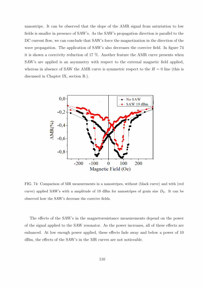
nanostripe. It can be observed that the slope of the AMR signal from saturiation to low
fields is smaller in presence of SAW’s. As the SAW’s propagation direction is parallel to the
DC current flow, we can conclude that SAW’s force the magnetization in the direction of the
wave propagation. The application of SAW’s also decreases the coercive field. In figure 74
it is shown a coercivity reduction of 17 %. Another feature the AMR curve presents when
SAW’s are applied is an asymmetry with respect to the external magnetic field applied,
whereas in absence of SAW the AMR curve is symmetric respect to the H = 0 line (this is
discussed in Chapter IX, section B.).
FIG. 74: Comparison of MR measurements in a nanostripes, without (black curve) and with (red
curve) applied SAW’s with a amplitude of 19 dBm for nanostripes of grain size D2. It can be
observed how the SAW’s decrease the coercive fields.
The effects of the SAW’s in the magnetoresistance measurements depend on the power
of the signal applied to the SAW resonator. As the power increases, all of these effects are
enhanced. At low enough power applied, these effects fade away and below a power of 10
dBm, the effects of the SAW’s in the MR curves are not noticeable.
110
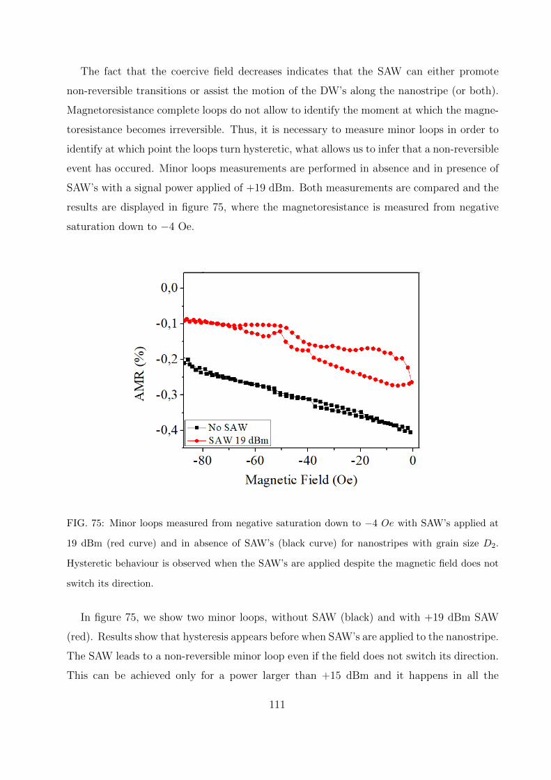
The fact that the coercive field decreases indicates that the SAW can either promote
non-reversible transitions or assist the motion of the DW’s along the nanostripe (or both).
Magnetoresistance complete loops do not allow to identify the moment at which the magne-
toresistance becomes irreversible. Thus, it is necessary to measure minor loops in order to
identify at which point the loops turn hysteretic, what allows us to infer that a non-reversible
event has occured. Minor loops measurements are performed in absence and in presence of
SAW’s with a signal power applied of +19 dBm. Both measurements are compared and the
results are displayed in figure 75, where the magnetoresistance is measured from negative
saturation down to −4 Oe.
FIG. 75: Minor loops measured from negative saturation down to −4 Oe with SAW’s applied at
19 dBm (red curve) and in absence of SAW’s (black curve) for nanostripes with grain size D2.
Hysteretic behaviour is observed when the SAW’s are applied despite the magnetic field does not
switch its direction.
In figure 75, we show two minor loops, without SAW (black) and with +19 dBm SAW
(red). Results show that hysteresis appears before when SAW’s are applied to the nanostripe.
The SAW leads to a non-reversible minor loop even if the field does not switch its direction.
This can be achieved only for a power larger than +15 dBm and it happens in all the
111
nanostripes measured, even in nanostripes deposited in different conditions with slightly
smaller average grain size (11 nm). This irreversible minor loop indicates that the SAW can
assist the nucleation and the movement of magnetic domain walls, even before switching the
direction of the external field.
Micromagnetic simulations
Micromagnetic simulations were performed using the Mumax program [Vansteenkiste,
2017] by the Departament of Fisica Aplicada of University of Salamanca on a nanostripe
with dimensions of 35 nm x 10 µm x 400 nm and magnetic parameters of exchange coupling
A = 1.05 ·10−11 J/m, saturation magnetization Ms = 2.38 ·105 A/m and uniaxial anisotropy
K = 6.0·103 J/m3. The polycrystalline grain structure is modelled via a Voronoi tessellation
of the system in polygonal regions of average diameter of D = 20 nm. The external field
was ramped in steps of 1 mT, maintaining each field for a time interval t =100 ns and
with α =0.01 as damping constant. In the simulations presented in figure 76 a), SAW’s of
different amplitudes are applied to the nanostripe and the magnetization is displayed as a
function of the external magnetic field. As it can be observed in figure 76 a) the simulations
reproduce most of the features observed in the experimental data. Most significantly, SAW’s
promote a reduction of the coercivity. Also, the simulations reproduce that the slope of the
initial reversible part of the loop, when the field is decreased from saturation, is smaller in
presence of SAW’s. Finally, the approach to saturation is more abrupt once the coercive
field is surpassed, with fewer but more pronounced jumps. The simulations are compared
with the experimental measurements of the magnetoresistance in presence of SAW’s for
different signal powers (figure 76 b) ). The pressure carried by the SAW’s experimentally,
is computed from the amplitudes presented in table IV (Chapter VIII. section A) by the
Hook’s law (20), where Y is the Young modulus of the ScAlN (180 GPa) [Teshigahara, 2012],
k is the wavenumber of the SAW’s (k = 2π2.8µm
), ξ is the expression for the acoustic wave and
ξ0 is the amplitude of the wave.
p = Y · ∂ξ∂x→ |p| = Y · k · ξ0 (20)
All the features observed in the simulations (figure 76 c)) can be understood considering
that, to a first approximation, the effect of SAW’s is equivalent to a field along the long
112
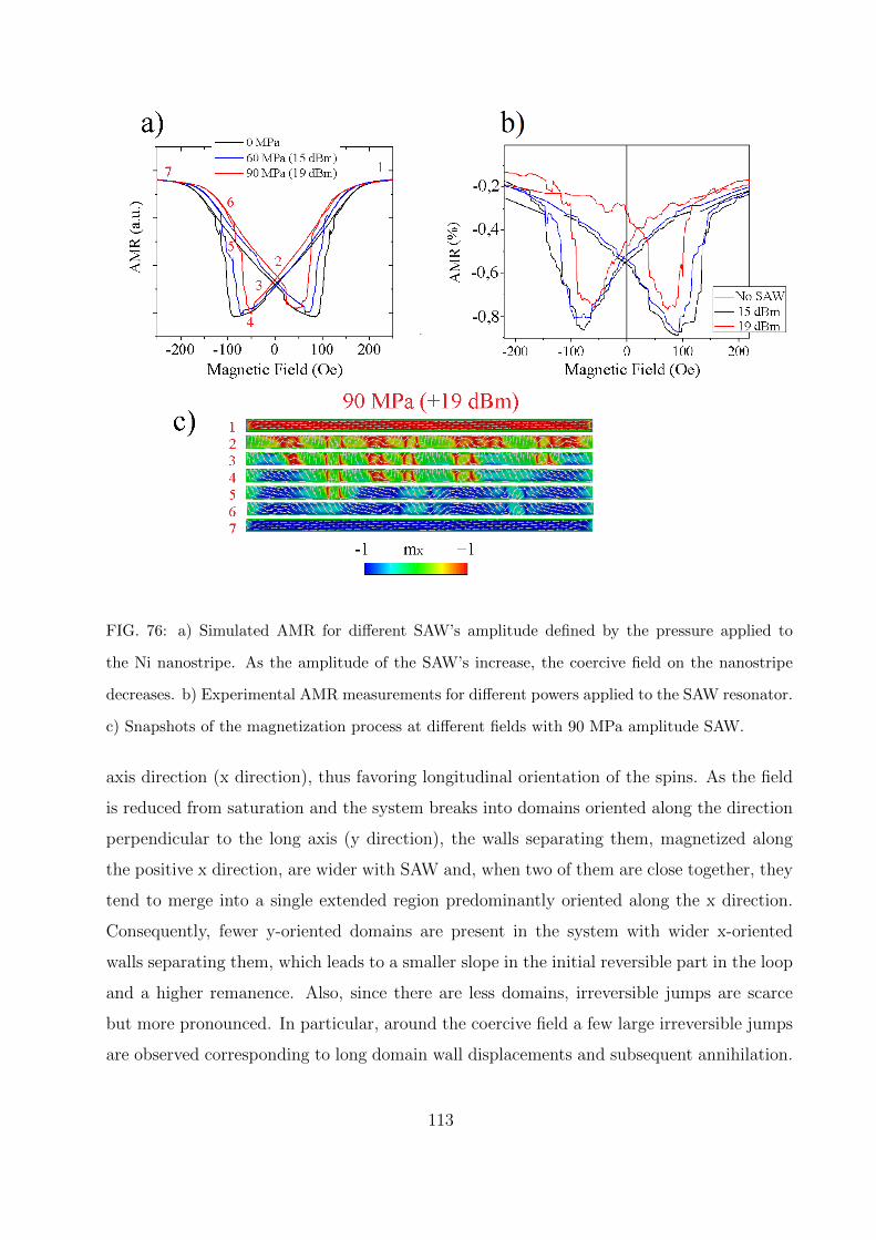
FIG. 76: a) Simulated AMR for different SAW’s amplitude defined by the pressure applied to
the Ni nanostripe. As the amplitude of the SAW’s increase, the coercive field on the nanostripe
decreases. b) Experimental AMR measurements for different powers applied to the SAW resonator.
c) Snapshots of the magnetization process at different fields with 90 MPa amplitude SAW.
axis direction (x direction), thus favoring longitudinal orientation of the spins. As the field
is reduced from saturation and the system breaks into domains oriented along the direction
perpendicular to the long axis (y direction), the walls separating them, magnetized along
the positive x direction, are wider with SAW and, when two of them are close together, they
tend to merge into a single extended region predominantly oriented along the x direction.
Consequently, fewer y-oriented domains are present in the system with wider x-oriented
walls separating them, which leads to a smaller slope in the initial reversible part in the loop
and a higher remanence. Also, since there are less domains, irreversible jumps are scarce
but more pronounced. In particular, around the coercive field a few large irreversible jumps
are observed corresponding to long domain wall displacements and subsequent annihilation.
113
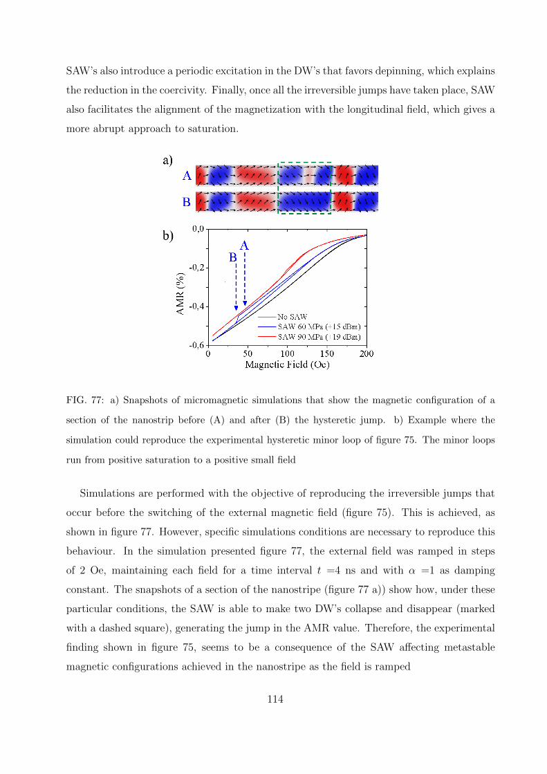
SAW’s also introduce a periodic excitation in the DW’s that favors depinning, which explains
the reduction in the coercivity. Finally, once all the irreversible jumps have taken place, SAW
also facilitates the alignment of the magnetization with the longitudinal field, which gives a
more abrupt approach to saturation.
FIG. 77: a) Snapshots of micromagnetic simulations that show the magnetic configuration of a
section of the nanostrip before (A) and after (B) the hysteretic jump. b) Example where the
simulation could reproduce the experimental hysteretic minor loop of figure 75. The minor loops
run from positive saturation to a positive small field
Simulations are performed with the objective of reproducing the irreversible jumps that
occur before the switching of the external magnetic field (figure 75). This is achieved, as
shown in figure 77. However, specific simulations conditions are necessary to reproduce this
behaviour. In the simulation presented figure 77, the external field was ramped in steps
of 2 Oe, maintaining each field for a time interval t =4 ns and with α =1 as damping
constant. The snapshots of a section of the nanostripe (figure 77 a)) show how, under these
particular conditions, the SAW is able to make two DW’s collapse and disappear (marked
with a dashed square), generating the jump in the AMR value. Therefore, the experimental
finding shown in figure 75, seems to be a consequence of the SAW affecting metastable
magnetic configurations achieved in the nanostripe as the field is ramped
114
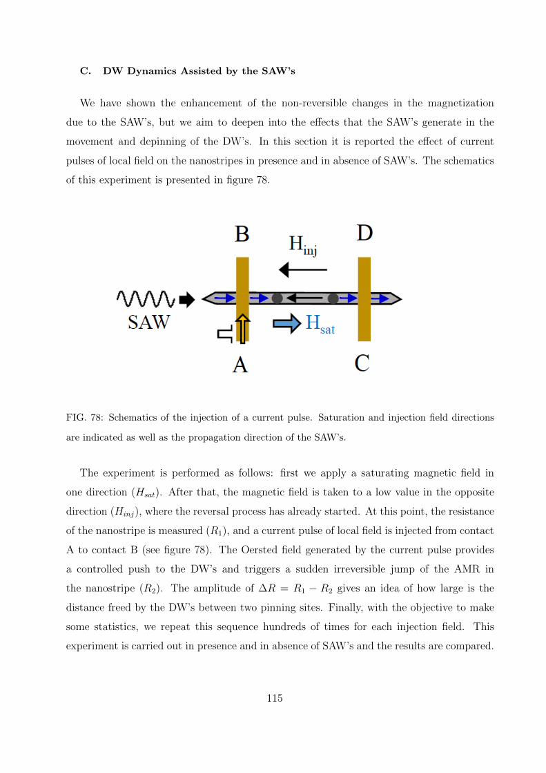
C. DW Dynamics Assisted by the SAW’s
We have shown the enhancement of the non-reversible changes in the magnetization
due to the SAW’s, but we aim to deepen into the effects that the SAW’s generate in the
movement and depinning of the DW’s. In this section it is reported the effect of current
pulses of local field on the nanostripes in presence and in absence of SAW’s. The schematics
of this experiment is presented in figure 78.
FIG. 78: Schematics of the injection of a current pulse. Saturation and injection field directions
are indicated as well as the propagation direction of the SAW’s.
The experiment is performed as follows: first we apply a saturating magnetic field in
one direction (Hsat). After that, the magnetic field is taken to a low value in the opposite
direction (Hinj), where the reversal process has already started. At this point, the resistance
of the nanostripe is measured (R1), and a current pulse of local field is injected from contact
A to contact B (see figure 78). The Oersted field generated by the current pulse provides
a controlled push to the DW’s and triggers a sudden irreversible jump of the AMR in
the nanostripe (R2). The amplitude of ∆R = R1 − R2 gives an idea of how large is the
distance freed by the DW’s between two pinning sites. Finally, with the objective to make
some statistics, we repeat this sequence hundreds of times for each injection field. This
experiment is carried out in presence and in absence of SAW’s and the results are compared.
115
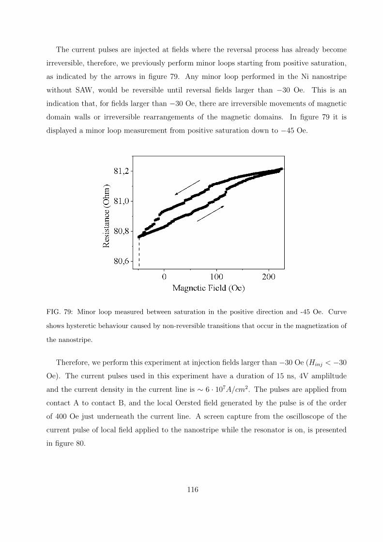
The current pulses are injected at fields where the reversal process has already become
irreversible, therefore, we previously perform minor loops starting from positive saturation,
as indicated by the arrows in figure 79. Any minor loop performed in the Ni nanostripe
without SAW, would be reversible until reversal fields larger than −30 Oe. This is an
indication that, for fields larger than −30 Oe, there are irreversible movements of magnetic
domain walls or irreversible rearrangements of the magnetic domains. In figure 79 it is
displayed a minor loop measurement from positive saturation down to −45 Oe.
FIG. 79: Minor loop measured between saturation in the positive direction and -45 Oe. Curve
shows hysteretic behaviour caused by non-reversible transitions that occur in the magnetization of
the nanostripe.
Therefore, we perform this experiment at injection fields larger than −30 Oe (Hinj < −30
Oe). The current pulses used in this experiment have a duration of 15 ns, 4V ampliltude
and the current density in the current line is ∼ 6 · 107A/cm2. The pulses are applied from
contact A to contact B, and the local Oersted field generated by the pulse is of the order
of 400 Oe just underneath the current line. A screen capture from the oscilloscope of the
current pulse of local field applied to the nanostripe while the resonator is on, is presented
in figure 80.
116
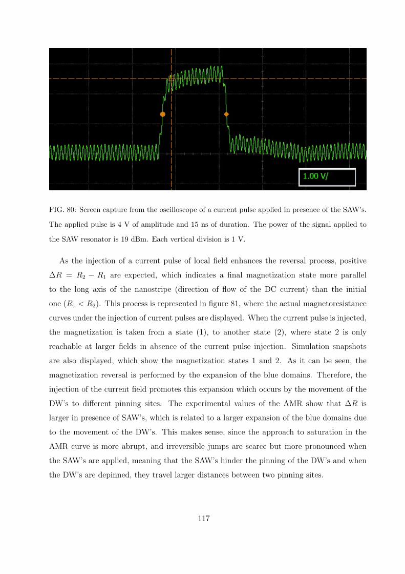
FIG. 80: Screen capture from the oscilloscope of a current pulse applied in presence of the SAW’s.
The applied pulse is 4 V of amplitude and 15 ns of duration. The power of the signal applied to
the SAW resonator is 19 dBm. Each vertical division is 1 V.
As the injection of a current pulse of local field enhances the reversal process, positive
∆R = R2 − R1 are expected, which indicates a final magnetization state more parallel
to the long axis of the nanostripe (direction of flow of the DC current) than the initial
one (R1 < R2). This process is represented in figure 81, where the actual magnetoresistance
curves under the injection of current pulses are displayed. When the current pulse is injected,
the magnetization is taken from a state (1), to another state (2), where state 2 is only
reachable at larger fields in absence of the current pulse injection. Simulation snapshots
are also displayed, which show the magnetization states 1 and 2. As it can be seen, the
magnetization reversal is performed by the expansion of the blue domains. Therefore, the
injection of the current field promotes this expansion which occurs by the movement of the
DW’s to different pinning sites. The experimental values of the AMR show that ∆R is
larger in presence of SAW’s, which is related to a larger expansion of the blue domains due
to the movement of the DW’s. This makes sense, since the approach to saturation in the
AMR curve is more abrupt, and irreversible jumps are scarce but more pronounced when
the SAW’s are applied, meaning that the SAW’s hinder the pinning of the DW’s and when
the DW’s are depinned, they travel larger distances between two pinning sites.
117
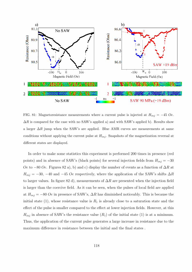
FIG. 81: Magnetoresistance measurements where a current pulse is injected at Hinj = −45 Oe.
∆R is compared for the case with no SAW’s applied a) and with SAW’s applied b). Results show
a larger ∆R jump when the SAW’s are applied. Blue AMR curves are measurements at same
conditions without applying the current pulse at Hinj . Snapshots of the magnetization reversal at
different states are displayed.
In order to make some statistics this experiment is performed 200 times in presence (red
points) and in absence of SAW’s (black points) for several injection fields from Hinj = −30
Oe to −80 Oe. Figures 82 a), b) and c) display the number of events as a function of ∆R at
Hinj = −30, −40 and −45 Oe respectively, where the application of the SAW’s shifts ∆R
to larger values. In figure 82 d), measurements of ∆R are presented when the injection field
is larger than the coercive field. As it can be seen, when the pulses of local field are applied
at Hinj = −80 Oe in presence of SAW’s, ∆R has diminished noticeably. This is because the
initial state (1), whose resistance value is R1 is already close to a saturation state and the
effect of the pulse is smaller compared to the effect at lower injection fields. However, at this
Hinj in absence of SAW’s the resistance value (R1) of the initial state (1) is at a minimum.
Thus, the application of the current pulse generates a large increase in resistance due to the
maximum difference in resistance between the initial and the final states .
118
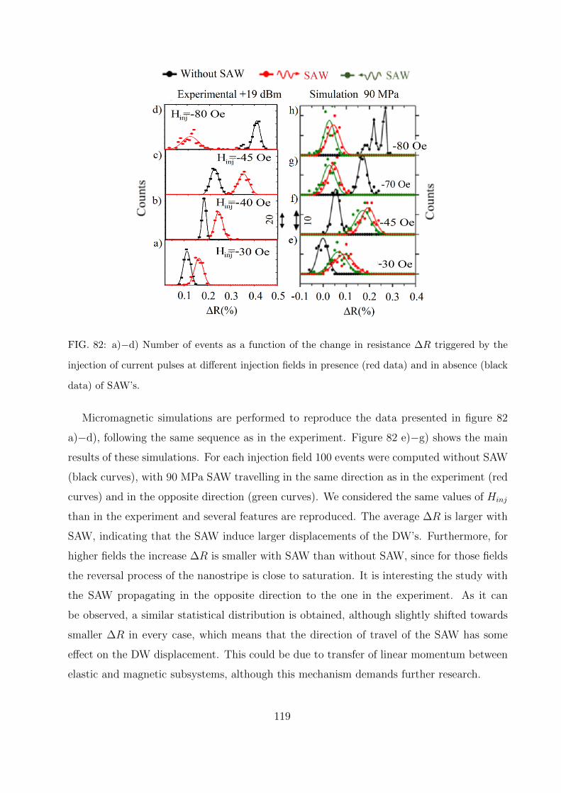
FIG. 82: a)−d) Number of events as a function of the change in resistance ∆R triggered by the
injection of current pulses at different injection fields in presence (red data) and in absence (black
data) of SAW’s.
Micromagnetic simulations are performed to reproduce the data presented in figure 82
a)−d), following the same sequence as in the experiment. Figure 82 e)−g) shows the main
results of these simulations. For each injection field 100 events were computed without SAW
(black curves), with 90 MPa SAW travelling in the same direction as in the experiment (red
curves) and in the opposite direction (green curves). We considered the same values of Hinj
than in the experiment and several features are reproduced. The average ∆R is larger with
SAW, indicating that the SAW induce larger displacements of the DW’s. Furthermore, for
higher fields the increase ∆R is smaller with SAW than without SAW, since for those fields
the reversal process of the nanostripe is close to saturation. It is interesting the study with
the SAW propagating in the opposite direction to the one in the experiment. As it can
be observed, a similar statistical distribution is obtained, although slightly shifted towards
smaller ∆R in every case, which means that the direction of travel of the SAW has some
effect on the DW displacement. This could be due to transfer of linear momentum between
elastic and magnetic subsystems, although this mechanism demands further research.
119
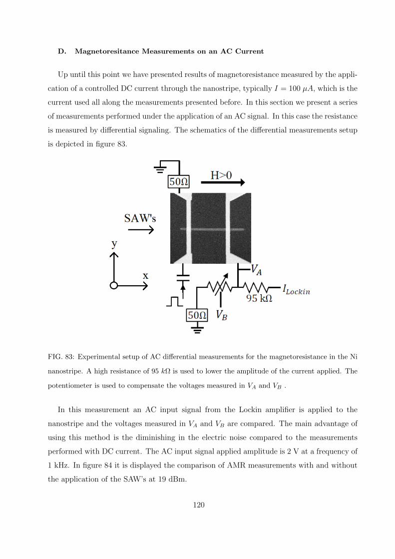
D. Magnetoresitance Measurements on an AC Current
Up until this point we have presented results of magnetoresistance measured by the appli-
cation of a controlled DC current through the nanostripe, typically I = 100 µA, which is the
current used all along the measurements presented before. In this section we present a series
of measurements performed under the application of an AC signal. In this case the resistance
is measured by differential signaling. The schematics of the differential measurements setup
is depicted in figure 83.
FIG. 83: Experimental setup of AC differential measurements for the magnetoresistance in the Ni
nanostripe. A high resistance of 95 kΩ is used to lower the amplitude of the current applied. The
potentiometer is used to compensate the voltages measured in VA and VB .
In this measurement an AC input signal from the Lockin amplifier is applied to the
nanostripe and the voltages measured in VA and VB are compared. The main advantage of
using this method is the diminishing in the electric noise compared to the measurements
performed with DC current. The AC input signal applied amplitude is 2 V at a frequency of
1 kHz. In figure 84 it is displayed the comparison of AMR measurements with and without
the application of the SAW’s at 19 dBm.
120
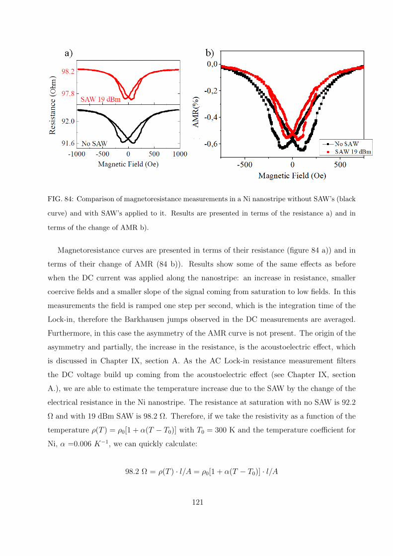
FIG. 84: Comparison of magnetoresistance measurements in a Ni nanostripe without SAW’s (black
curve) and with SAW’s applied to it. Results are presented in terms of the resistance a) and in
terms of the change of AMR b).
Magnetoresistance curves are presented in terms of their resistance (figure 84 a)) and in
terms of their change of AMR (84 b)). Results show some of the same effects as before
when the DC current was applied along the nanostripe: an increase in resistance, smaller
coercive fields and a smaller slope of the signal coming from saturation to low fields. In this
measurements the field is ramped one step per second, which is the integration time of the
Lock-in, therefore the Barkhausen jumps observed in the DC measurements are averaged.
Furthermore, in this case the asymmetry of the AMR curve is not present. The origin of the
asymmetry and partially, the increase in the resistance, is the acoustoelectric effect, which
is discussed in Chapter IX, section A. As the AC Lock-in resistance measurement filters
the DC voltage build up coming from the acoustoelectric effect (see Chapter IX, section
A.), we are able to estimate the temperature increase due to the SAW by the change of the
electrical resistance in the Ni nanostripe. The resistance at saturation with no SAW is 92.2
Ω and with 19 dBm SAW is 98.2 Ω. Therefore, if we take the resistivity as a function of the
temperature ρ(T ) = ρ0[1 + α(T − T0)] with T0 = 300 K and the temperature coefficient for
Ni, α =0.006 K−1, we can quickly calculate:
98.2 Ω = ρ(T ) · l/A = ρ0[1 + α(T − T0)] · l/A
121
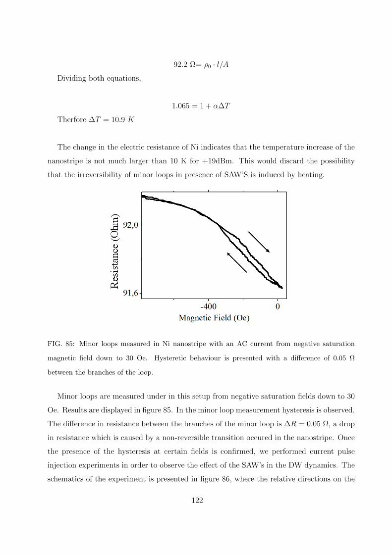
92.2 Ω= ρ0 · l/A
Dividing both equations,
1.065 = 1 + α∆T
Therfore ∆T = 10.9 K
The change in the electric resistance of Ni indicates that the temperature increase of the
nanostripe is not much larger than 10 K for +19dBm. This would discard the possibility
that the irreversibility of minor loops in presence of SAW’S is induced by heating.
FIG. 85: Minor loops measured in Ni nanostripe with an AC current from negative saturation
magnetic field down to 30 Oe. Hysteretic behaviour is presented with a difference of 0.05 Ω
between the branches of the loop.
Minor loops are measured under in this setup from negative saturation fields down to 30
Oe. Results are displayed in figure 85. In the minor loop measurement hysteresis is observed.
The difference in resistance between the branches of the minor loop is ∆R = 0.05 Ω, a drop
in resistance which is caused by a non-reversible transition occured in the nanostripe. Once
the presence of the hysteresis at certain fields is confirmed, we performed current pulse
injection experiments in order to observe the effect of the SAW’s in the DW dynamics. The
schematics of the experiment is presented in figure 86, where the relative directions on the
122
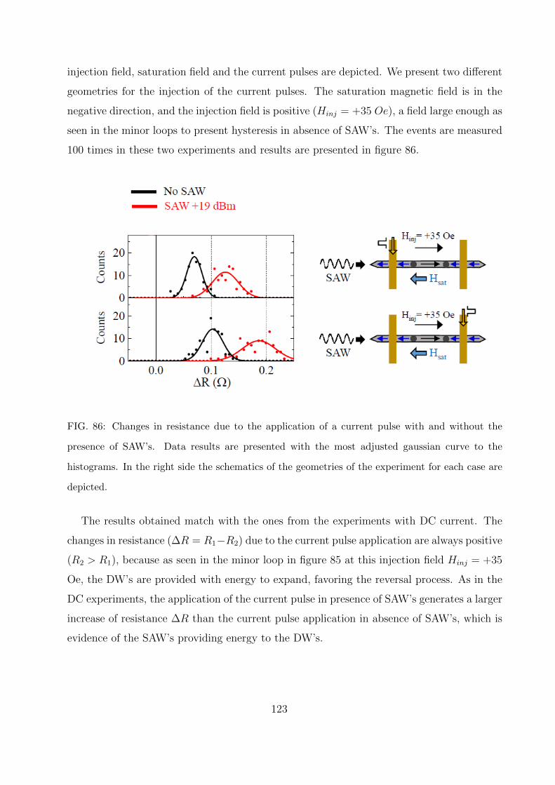
injection field, saturation field and the current pulses are depicted. We present two different
geometries for the injection of the current pulses. The saturation magnetic field is in the
negative direction, and the injection field is positive (Hinj = +35 Oe), a field large enough as
seen in the minor loops to present hysteresis in absence of SAW’s. The events are measured
100 times in these two experiments and results are presented in figure 86.
FIG. 86: Changes in resistance due to the application of a current pulse with and without the
presence of SAW’s. Data results are presented with the most adjusted gaussian curve to the
histograms. In the right side the schematics of the geometries of the experiment for each case are
depicted.
The results obtained match with the ones from the experiments with DC current. The
changes in resistance (∆R = R1−R2) due to the current pulse application are always positive
(R2 > R1), because as seen in the minor loop in figure 85 at this injection field Hinj = +35
Oe, the DW’s are provided with energy to expand, favoring the reversal process. As in the
DC experiments, the application of the current pulse in presence of SAW’s generates a larger
increase of resistance ∆R than the current pulse application in absence of SAW’s, which is
evidence of the SAW’s providing energy to the DW’s.
123
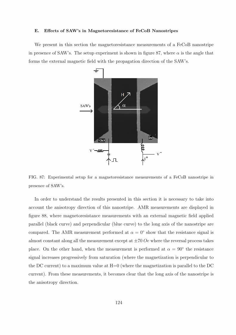
E. Effects of SAW’s in Magnetoresistance of FeCoB Nanostripes
We present in this section the magnetoresistance measurements of a FeCoB nanostripe
in presence of SAW’s. The setup experiment is shown in figure 87, where α is the angle that
forms the external magnetic field with the propagation direction of the SAW’s.
FIG. 87: Experimental setup for a magnetoresistance measurements of a FeCoB nanostripe in
presence of SAW’s.
In order to understand the results presented in this section it is necessary to take into
account the anisotropy direction of this nanostripe. AMR measurements are displayed in
figure 88, where magnetoresistance measurements with an external magnetic field applied
parallel (black curve) and perpendicular (blue curve) to the long axis of the nanostripe are
compared. The AMR measurement performed at α = 0 show that the resistance signal is
almost constant along all the measurement except at±70 Oe where the reversal process takes
place. On the other hand, when the measurement is performed at α = 90 the resistance
signal increases progressively from saturation (where the magnetization is perpendicular to
the DC current) to a maximum value at H=0 (where the magnetization is parallel to the DC
current). From these measurements, it becomes clear that the long axis of the nanostripe is
the anisotropy direction.
124
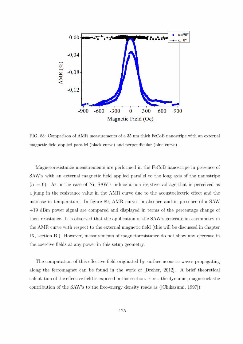
FIG. 88: Comparison of AMR measurements of a 35 nm thick FeCoB nanostripe with an external
magnetic field applied parallel (black curve) and perpendicular (blue curve) .
Magnetoresistance measurements are performed in the FeCoB nanostripe in presence of
SAW’s with an external magnetic field applied parallel to the long axis of the nanostripe
(α = 0). As in the case of Ni, SAW’s induce a non-resistive voltage that is perceived as
a jump in the resistance value in the AMR curve due to the acoustoelectric effect and the
increase in temperature. In figure 89, AMR curves in absence and in presence of a SAW
+19 dBm power signal are compared and displayed in terms of the percentage change of
their resistance. It is observed that the application of the SAW’s generate an asymmetry in
the AMR curve with respect to the external magnetic field (this will be discussed in chapter
IX, section B.). However, measurements of magnetoresistance do not show any decrease in
the coercive fields at any power in this setup geometry.
The computation of this effective field originated by surface acoustic waves propagating
along the ferromagnet can be found in the work of [Dreher, 2012]. A brief theoretical
calculation of the effective field is exposed in this section. First, the dynamic, magnetoelastic
contribution of the SAW’s to the free-energy density reads as ([Chikazumi, 1997]):
125
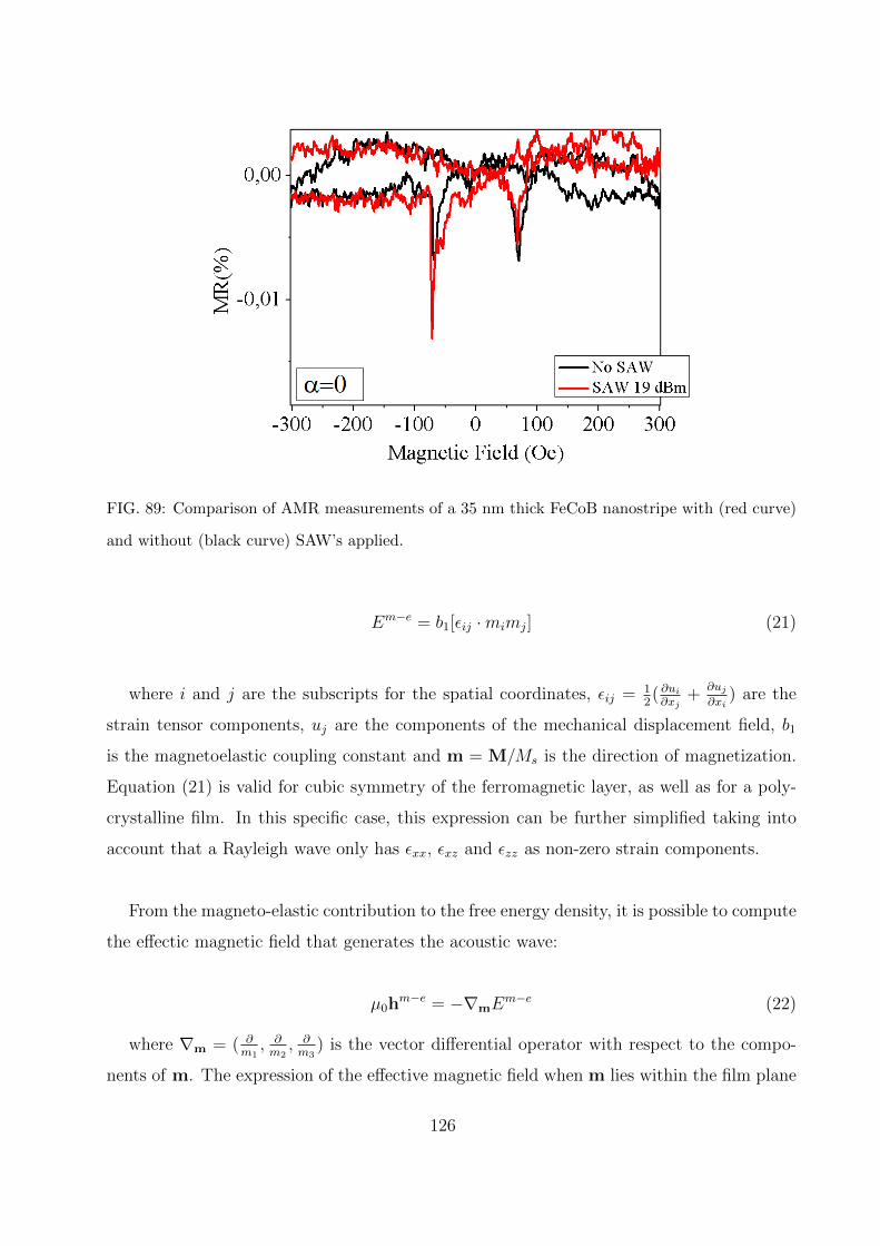
FIG. 89: Comparison of AMR measurements of a 35 nm thick FeCoB nanostripe with (red curve)
and without (black curve) SAW’s applied.
Em−e = b1[εij ·mimj] (21)
where i and j are the subscripts for the spatial coordinates, εij = 12( ∂ui∂xj
+∂uj∂xi
) are the
strain tensor components, uj are the components of the mechanical displacement field, b1
is the magnetoelastic coupling constant and m = M/Ms is the direction of magnetization.
Equation (21) is valid for cubic symmetry of the ferromagnetic layer, as well as for a poly-
crystalline film. In this specific case, this expression can be further simplified taking into
account that a Rayleigh wave only has εxx, εxz and εzz as non-zero strain components.
From the magneto-elastic contribution to the free energy density, it is possible to compute
the effectic magnetic field that generates the acoustic wave:
µ0hm−e = −∇mE
m−e (22)
where ∇m = ( ∂m1, ∂m2, ∂m3
) is the vector differential operator with respect to the compo-
nents of m. The expression of the effective magnetic field when m lies within the film plane
126
is dependent on the orientation of the magnetization:
µ0 · hm−e(t) = −2 · b1 · εxx(t) · cos(θ) · sin(θ) (23)
where θ is the equilibrium in-plane angle that forms the magnetization with the direction
of propagation of the SAW’s. It is necessary to take into account that θ depends on the
compromise between the Zeeman energy and the in-plane anisotropy. In this specific case,
figure 89 displays the magnetoresistance measurements for a FeCoB nanostripe where the
magnetic field is applied parallel to the anisotropy direction (α = 0) and they both match the
propagation direction of the SAW’s. Therefore, both magnetization and SAW’s propagation
direction are mostly parallel, making expression 23 tend to zero.
An experimental solid support for this argument can be found in [Weiler, 2011], where
the absorption of SAW’s by a ferromagnet is measured as a function of the orientation of an
external magnetic field applied. Results show minimum absorption when the magnetic field
is either parallel or perpendicular to the propagation direction of the SAW’s and maximum
absortion in the range of α = [30 − 60], which agrees with equation 23.
F. Conclusions
This chapter was oriented to describe the effects that the application of a RF signal to
the IDT of the SAW resonator generates in the magnetization of the magnetic nanostripes
through the measurements of the magnetoresistance. In this chapter most measurements are
carried out in Ni nanostripes and only ordinary AMR complete loops in presence of SAW’s
are performed with a FeCoB nanostripe.
The first consequence observed after the application of a RF signal to the SAW resonator
is an immediate jump of the resistance of the nanostripe. This sudden increase depends on
the magnitude of the power applied to the SAW resonator and it is related to the acousto-
electric effect and an increase in temperature (∆T ). However, under the application of a DC
current through the nanostripe it was not possible to compute the contribution of each effect
to this increase in voltage (see Chapter IX, section A.). The calculation of the increase in
127
temperature is performed under the application of an AC current. In that case, the increase
in resistance is completely associated to ∆T . Results show that under an application of a
+19 dBm power signal, the increase in temperature in a Ni nanostripe is ∆T = 10.9 K.
Another effect on the magnetization of the Ni nanostripe caused by the SAW’s is an
additional anisotropy forced in the direction of propagation of the SAW’s. This is observed
in the magnetoresistance measurements, where, from saturation down to low fields, the slope
of the decreasing curve is lower in the presence of SAW’s. This effect can be described by the
simulations, which show that in presence of SAW’s as the field decreases from saturation,
there are fewer y-oriented domains with wider x-oriented DW’s separating them, which
leads to a smaller slope in the initial reversible part of the loop and a higher remanence.
The magnetoresistance curves measured in presence of SAW’s also present a decrease in the
coercivity proportional to the power of the signal applied to the resonator. This decrease is
related to an enhancement of non-reversible transitions and related to the addition of energy
to the DW’s, favoring the DW movement. The enhancement of non-reversible transitions is
tested by performing magnetorestance minor loops in presence of SAW’s. When a minor loop
(sweeping the magnetic field from saturation to low fields and reverse) becomes hysteretic
is a sign of a non-reversible transition. Results show that in every case the minor loops
become irreversible before in presence of SAW’s than in absence of them. It can also be
observed that the stress carried by the SAW’s is able to trigger an irreversible magnetic
transition even before the external magnetic field switches direction. This behaviour can
be described through the simulations, where these irreversible jumps are generated by two
x-oriented DW’s collapsing and dissapearing.
In order to test that the SAW’s provide the DW with additional energy to perform the
reversal process, we carry out current pulse measurements to assist de DW dynamics while
SAW’s are applied. The premise is that a single current pulse passing through one of the
current lines, generates a large magnetic field in a local area in a defined time gap. This
current pulse assists the reversal process, however in combination with the SAW’s the assist
process is assisted even more. Measurements of the resistance of the nanostripes are taken
100 ms before (R1) and 100 ms after (R2) the application of the current pulse. The increase
in resistance (∆R = R1 −R2) is always larger in presence of SAW’s, which implies a larger
128
change in the magnetization towards the saturation stage, which implies an addition of
energy to the DW’s that carry out the reversal process.
Finally we measure the magnetoresistance in presence of SAW’s of a FeCoB nanostripe,
however, not all effects observed previously in the Ni nanostripe were present. The acousto-
electric effect generates an increase in the resistance of the nanostripe. However, no induced
anisotropy nor decrease in the coercive fields were observed in this nanostripe. The reason
proposed to explain this lack of effects is the preferential orientation of the magnetization,
parallel to the propagation direction of the SAW’s.
129

130
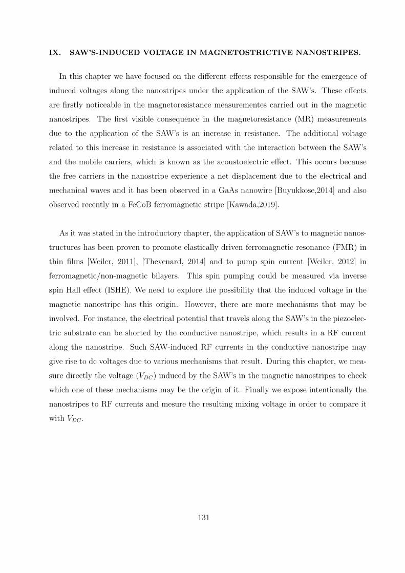
IX. SAW’S-INDUCED VOLTAGE IN MAGNETOSTRICTIVE NANOSTRIPES.
In this chapter we have focused on the different effects responsible for the emergence of
induced voltages along the nanostripes under the application of the SAW’s. These effects
are firstly noticeable in the magnetoresistance measurementes carried out in the magnetic
nanostripes. The first visible consequence in the magnetoresistance (MR) measurements
due to the application of the SAW’s is an increase in resistance. The additional voltage
related to this increase in resistance is associated with the interaction between the SAW’s
and the mobile carriers, which is known as the acoustoelectric effect. This occurs because
the free carriers in the nanostripe experience a net displacement due to the electrical and
mechanical waves and it has been observed in a GaAs nanowire [Buyukkose,2014] and also
observed recently in a FeCoB ferromagnetic stripe [Kawada,2019].
As it was stated in the introductory chapter, the application of SAW’s to magnetic nanos-
tructures has been proven to promote elastically driven ferromagnetic resonance (FMR) in
thin films [Weiler, 2011], [Thevenard, 2014] and to pump spin current [Weiler, 2012] in
ferromagnetic/non-magnetic bilayers. This spin pumping could be measured via inverse
spin Hall effect (ISHE). We need to explore the possibility that the induced voltage in the
magnetic nanostripe has this origin. However, there are more mechanisms that may be
involved. For instance, the electrical potential that travels along the SAW’s in the piezoelec-
tric substrate can be shorted by the conductive nanostripe, which results in a RF current
along the nanostripe. Such SAW-induced RF currents in the conductive nanostripe may
give rise to dc voltages due to various mechanisms that result. During this chapter, we mea-
sure directly the voltage (VDC) induced by the SAW’s in the magnetic nanostripes to check
which one of these mechanisms may be the origin of it. Finally we expose intentionally the
nanostripes to RF currents and mesure the resulting mixing voltage in order to compare it
with VDC .
131
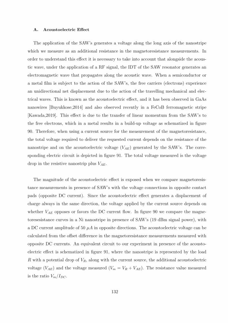
A. Acoustoelectric Effect
The application of the SAW’s generates a voltage along the long axis of the nanostripe
which we measure as an additional resistance in the magnetoresistance measurements. In
order to understand this effect it is necessary to take into account that alongside the acous-
tic wave, under the application of a RF signal, the IDT of the SAW resonator generates an
electromagnetic wave that propagates along the acoustic wave. When a semiconductor or
a metal film is subject to the action of the SAW’s, the free carriers (electrons) experience
an unidirectional net displacement due to the action of the travelling mechanical and elec-
trical waves. This is known as the acoustoelectric effect, and it has been observed in GaAs
nanowires [Buyukkose,2014] and also observed recently in a FeCoB ferromagnetic stripe
[Kawada,2019]. This effect is due to the transfer of linear momentum from the SAW’s to
the free electrons, which in a metal results in a build-up voltage as schematized in figure
90. Therefore, when using a current source for the measurement of the magnetoresistance,
the total voltage required to deliver the requested current depends on the resistance of the
nanostripe and on the acoustoelectric voltage (VAE) generated by the SAW’s. The corre-
sponding electric circuit is depicted in figure 91. The total voltage measured is the voltage
drop in the resistive nanostrip plus VAE.
The magnitude of the acoustoelectric effect is exposed when we compare magnetoresis-
tance measurements in presence of SAW’s with the voltage connections in opposite contact
pads (opposite DC current). Since the acoustoelectric effect generates a displacement of
charge always in the same direction, the voltage applied by the current source depends on
whether VAE opposes or favors the DC current flow. In figure 90 we compare the magne-
toresesistance curves in a Ni nanostripe in presence of SAW’s (19 dBm signal power), with
a DC current amplitude of 50 µA in opposite directions. The acoustoelectric voltage can be
calculated from the offset difference in the magnetoresistance measurements measured with
opposite DC currents. An equivalent circuit to our experiment in presence of the acousto-
electric effect is schematized in figure 91, where the nanostripe is represented by the load
R with a potential drop of VR, along with the current source, the additional acoustoelectric
voltage (VAE) and the voltage measured (Vm = VR + VAE). The resistance value measured
is the ratio Vm/IDC .
132
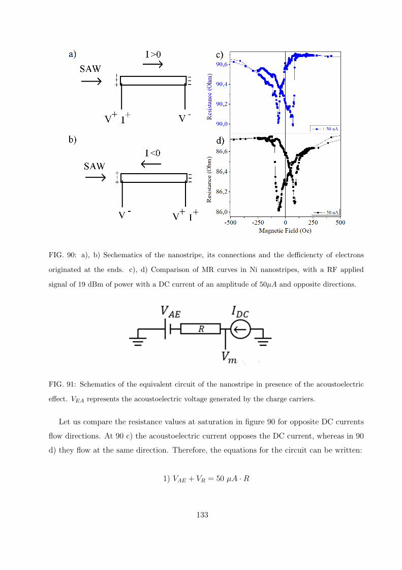
FIG. 90: a), b) Sechematics of the nanostripe, its connections and the defficiencty of electrons
originated at the ends. c), d) Comparison of MR curves in Ni nanostripes, with a RF applied
signal of 19 dBm of power with a DC current of an amplitude of 50µA and opposite directions.
FIG. 91: Schematics of the equivalent circuit of the nanostripe in presence of the acoustoelectric
effect. VEA represents the acoustoelectric voltage generated by the charge carriers.
Let us compare the resistance values at saturation in figure 90 for opposite DC currents
flow directions. At 90 c) the acoustoelectric current opposes the DC current, whereas in 90
d) they flow at the same direction. Therefore, the equations for the circuit can be written:
1) VAE + VR = 50 µA ·R
133
2) −VAE + VR = 50 µA · (R + 3.9 Ω)
Solving the system, we obtain VAE = 95 µV , which is the additional voltage induced by
the acoustoelectric effect in the Ni nanostripe at 19 dBm.
Aditionally to the increase in resistance that we relate to the acoustoelectric effect, when
we measure the magnetoresistance curves of magnetic nanostripes in presence of SAW’s, the
MR curves present an asymmetry with respect to the external magnetic field. Results show
a clear correlation between the asymmetry and the power of the signal. Figure 92 displays
the MR curves for different powers, where it is clear how the larger the power applied, the
more pronounced the asymmetry.
FIG. 92: Comparison of MR measurements in presence of SAW’s for different powers of the applied
to the resonator. The asymmetry becomes gradually more prominent as the power is increased.
This distorsion is associated to another type of voltage that the SAW’s induce in the
magnetic nanostripes. The effect of this voltage in the magnetoresistance measurements is
134
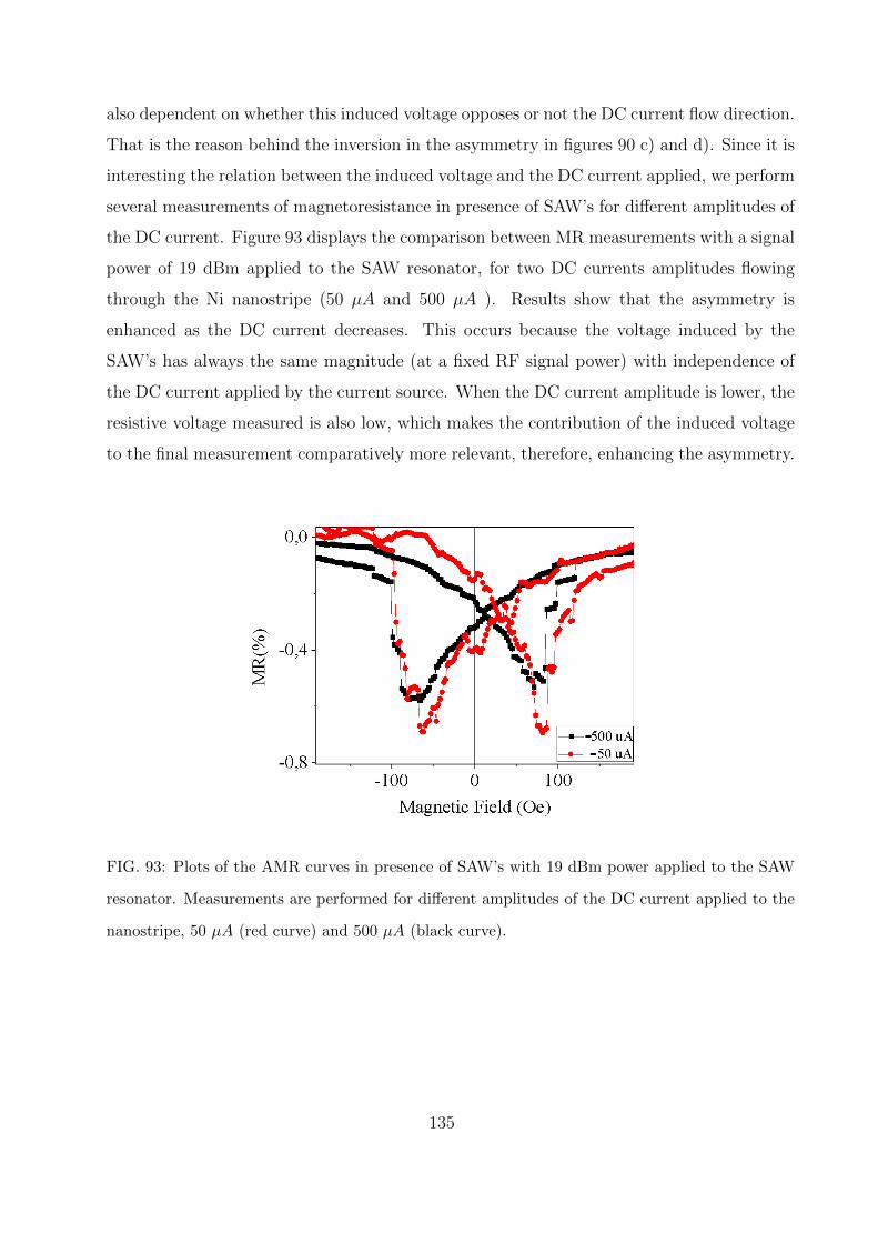
also dependent on whether this induced voltage opposes or not the DC current flow direction.
That is the reason behind the inversion in the asymmetry in figures 90 c) and d). Since it is
interesting the relation between the induced voltage and the DC current applied, we perform
several measurements of magnetoresistance in presence of SAW’s for different amplitudes of
the DC current. Figure 93 displays the comparison between MR measurements with a signal
power of 19 dBm applied to the SAW resonator, for two DC currents amplitudes flowing
through the Ni nanostripe (50 µA and 500 µA ). Results show that the asymmetry is
enhanced as the DC current decreases. This occurs because the voltage induced by the
SAW’s has always the same magnitude (at a fixed RF signal power) with independence of
the DC current applied by the current source. When the DC current amplitude is lower, the
resistive voltage measured is also low, which makes the contribution of the induced voltage
to the final measurement comparatively more relevant, therefore, enhancing the asymmetry.
FIG. 93: Plots of the AMR curves in presence of SAW’s with 19 dBm power applied to the SAW
resonator. Measurements are performed for different amplitudes of the DC current applied to the
nanostripe, 50 µA (red curve) and 500 µA (black curve).
135
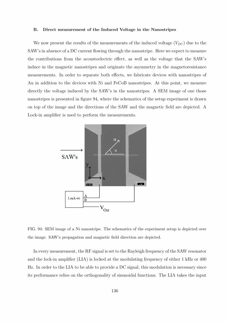
B. Direct measurement of the Induced Voltage in the Nanostripes
We now present the results of the measurements of the induced voltage (VDC) due to the
SAW’s in absence of a DC current flowing through the nanostripe. Here we expect to measure
the contributions from the acoustoelectric effect, as well as the voltage that the SAW’s
induce in the magnetic nanostripes and originate the asymmetry in the magnetoresistance
measurements. In order to separate both effects, we fabricate devices with nanostripes of
Au in addition to the devices with Ni and FeCoB nanostripes. At this point, we measure
directly the voltage induced by the SAW’s in the nanostripes. A SEM image of one those
nanostripes is presented in figure 94, where the schematics of the setup experiment is drawn
on top of the image and the directions of the SAW and the magnetic field are depicted. A
Lock-in amplifier is used to perform the measurements.
FIG. 94: SEM image of a Ni nanostripe. The schematics of the experiment setup is depicted over
the image. SAW’s propagation and magnetic field direction are depicted.
In every measurement, the RF signal is set to the Rayleigh frequency of the SAW resonator
and the lock-in amplifier (LIA) is locked at the modulating frequency of either 1 kHz or 400
Hz. In order to the LIA to be able to provide a DC signal, this modulation is necessary since
its performance relies on the orthogonality of sinusoidal functions. The LIA takes the input
136
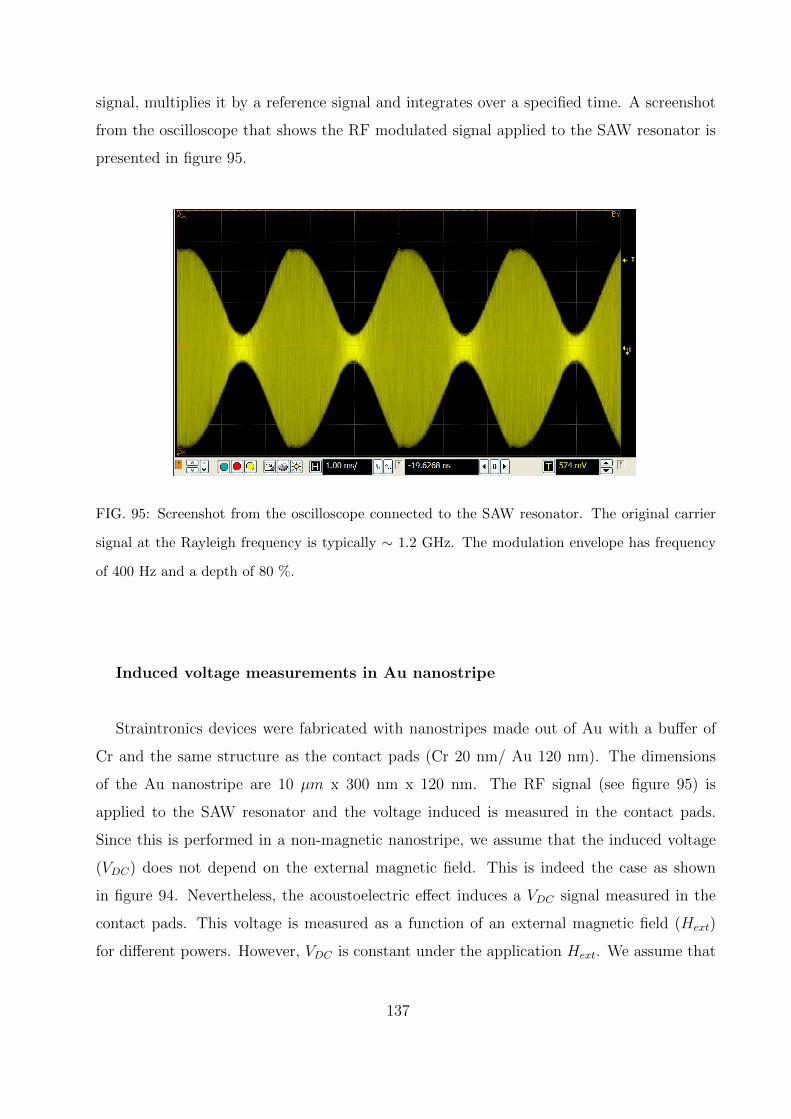
signal, multiplies it by a reference signal and integrates over a specified time. A screenshot
from the oscilloscope that shows the RF modulated signal applied to the SAW resonator is
presented in figure 95.
FIG. 95: Screenshot from the oscilloscope connected to the SAW resonator. The original carrier
signal at the Rayleigh frequency is typically ∼ 1.2 GHz. The modulation envelope has frequency
of 400 Hz and a depth of 80 %.
Induced voltage measurements in Au nanostripe
Straintronics devices were fabricated with nanostripes made out of Au with a buffer of
Cr and the same structure as the contact pads (Cr 20 nm/ Au 120 nm). The dimensions
of the Au nanostripe are 10 µm x 300 nm x 120 nm. The RF signal (see figure 95) is
applied to the SAW resonator and the voltage induced is measured in the contact pads.
Since this is performed in a non-magnetic nanostripe, we assume that the induced voltage
(VDC) does not depend on the external magnetic field. This is indeed the case as shown
in figure 94. Nevertheless, the acoustoelectric effect induces a VDC signal measured in the
contact pads. This voltage is measured as a function of an external magnetic field (Hext)
for different powers. However, VDC is constant under the application Hext. We assume that
137
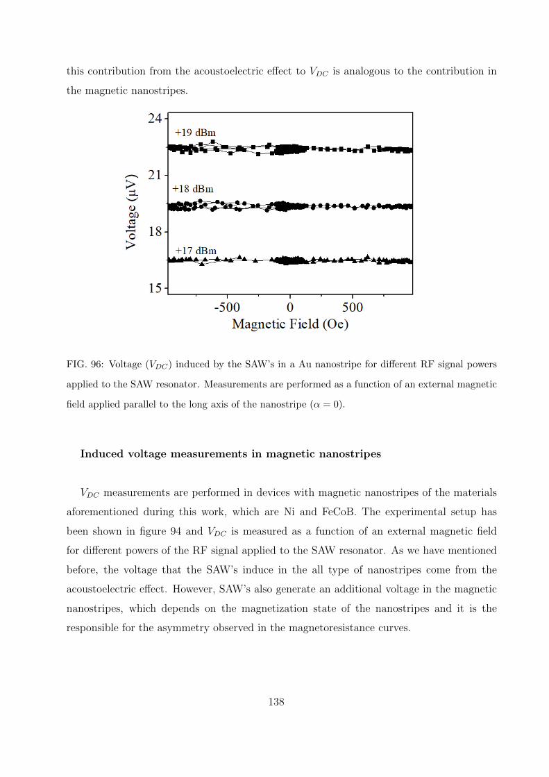
this contribution from the acoustoelectric effect to VDC is analogous to the contribution in
the magnetic nanostripes.
FIG. 96: Voltage (VDC) induced by the SAW’s in a Au nanostripe for different RF signal powers
applied to the SAW resonator. Measurements are performed as a function of an external magnetic
field applied parallel to the long axis of the nanostripe (α = 0).
Induced voltage measurements in magnetic nanostripes
VDC measurements are performed in devices with magnetic nanostripes of the materials
aforementioned during this work, which are Ni and FeCoB. The experimental setup has
been shown in figure 94 and VDC is measured as a function of an external magnetic field
for different powers of the RF signal applied to the SAW resonator. As we have mentioned
before, the voltage that the SAW’s induce in the all type of nanostripes come from the
acoustoelectric effect. However, SAW’s also generate an additional voltage in the magnetic
nanostripes, which depends on the magnetization state of the nanostripes and it is the
responsible for the asymmetry observed in the magnetoresistance curves.
138
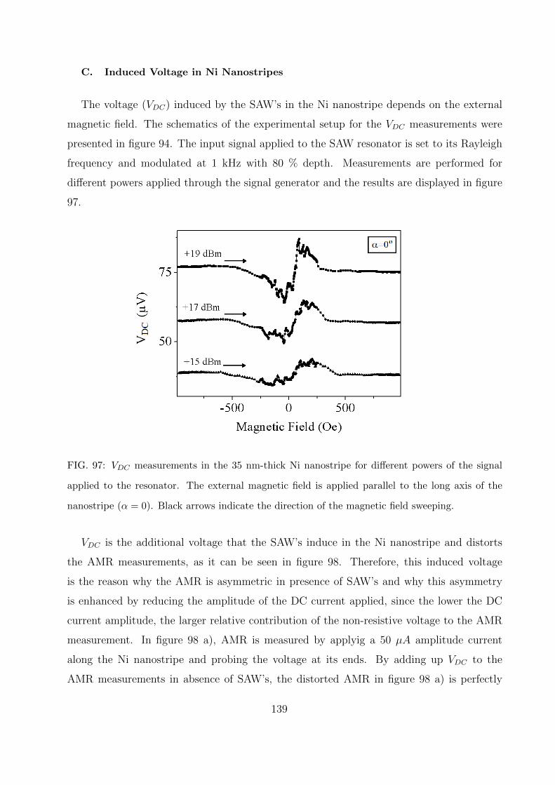
C. Induced Voltage in Ni Nanostripes
The voltage (VDC) induced by the SAW’s in the Ni nanostripe depends on the external
magnetic field. The schematics of the experimental setup for the VDC measurements were
presented in figure 94. The input signal applied to the SAW resonator is set to its Rayleigh
frequency and modulated at 1 kHz with 80 % depth. Measurements are performed for
different powers applied through the signal generator and the results are displayed in figure
97.
FIG. 97: VDC measurements in the 35 nm-thick Ni nanostripe for different powers of the signal
applied to the resonator. The external magnetic field is applied parallel to the long axis of the
nanostripe (α = 0). Black arrows indicate the direction of the magnetic field sweeping.
VDC is the additional voltage that the SAW’s induce in the Ni nanostripe and distorts
the AMR measurements, as it can be seen in figure 98. Therefore, this induced voltage
is the reason why the AMR is asymmetric in presence of SAW’s and why this asymmetry
is enhanced by reducing the amplitude of the DC current applied, since the lower the DC
current amplitude, the larger relative contribution of the non-resistive voltage to the AMR
measurement. In figure 98 a), AMR is measured by applyig a 50 µA amplitude current
along the Ni nanostripe and probing the voltage at its ends. By adding up VDC to the
AMR measurements in absence of SAW’s, the distorted AMR in figure 98 a) is perfectly
139
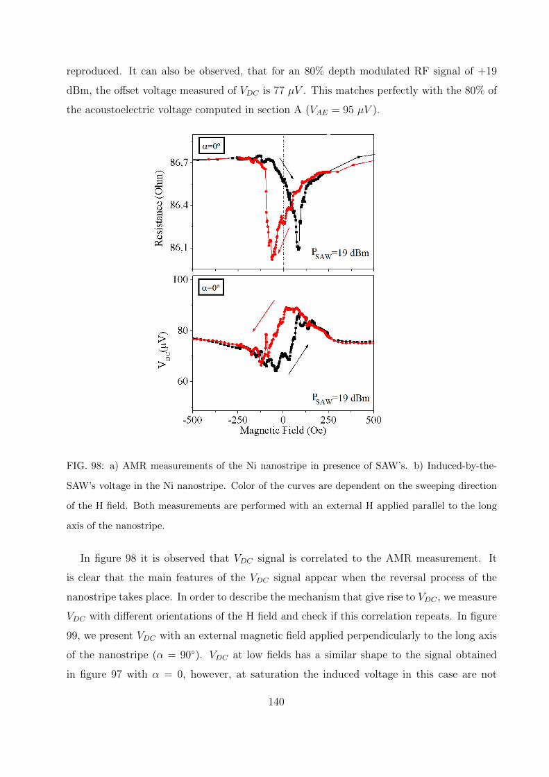
reproduced. It can also be observed, that for an 80% depth modulated RF signal of +19
dBm, the offset voltage measured of VDC is 77 µV . This matches perfectly with the 80% of
the acoustoelectric voltage computed in section A (VAE = 95 µV ).
FIG. 98: a) AMR measurements of the Ni nanostripe in presence of SAW’s. b) Induced-by-the-
SAW’s voltage in the Ni nanostripe. Color of the curves are dependent on the sweeping direction
of the H field. Both measurements are performed with an external H applied parallel to the long
axis of the nanostripe.
In figure 98 it is observed that VDC signal is correlated to the AMR measurement. It
is clear that the main features of the VDC signal appear when the reversal process of the
nanostripe takes place. In order to describe the mechanism that give rise to VDC , we measure
VDC with different orientations of the H field and check if this correlation repeats. In figure
99, we present VDC with an external magnetic field applied perpendicularly to the long axis
of the nanostripe (α = 90). VDC at low fields has a similar shape to the signal obtained
in figure 97 with α = 0, however, at saturation the induced voltage in this case are not
140
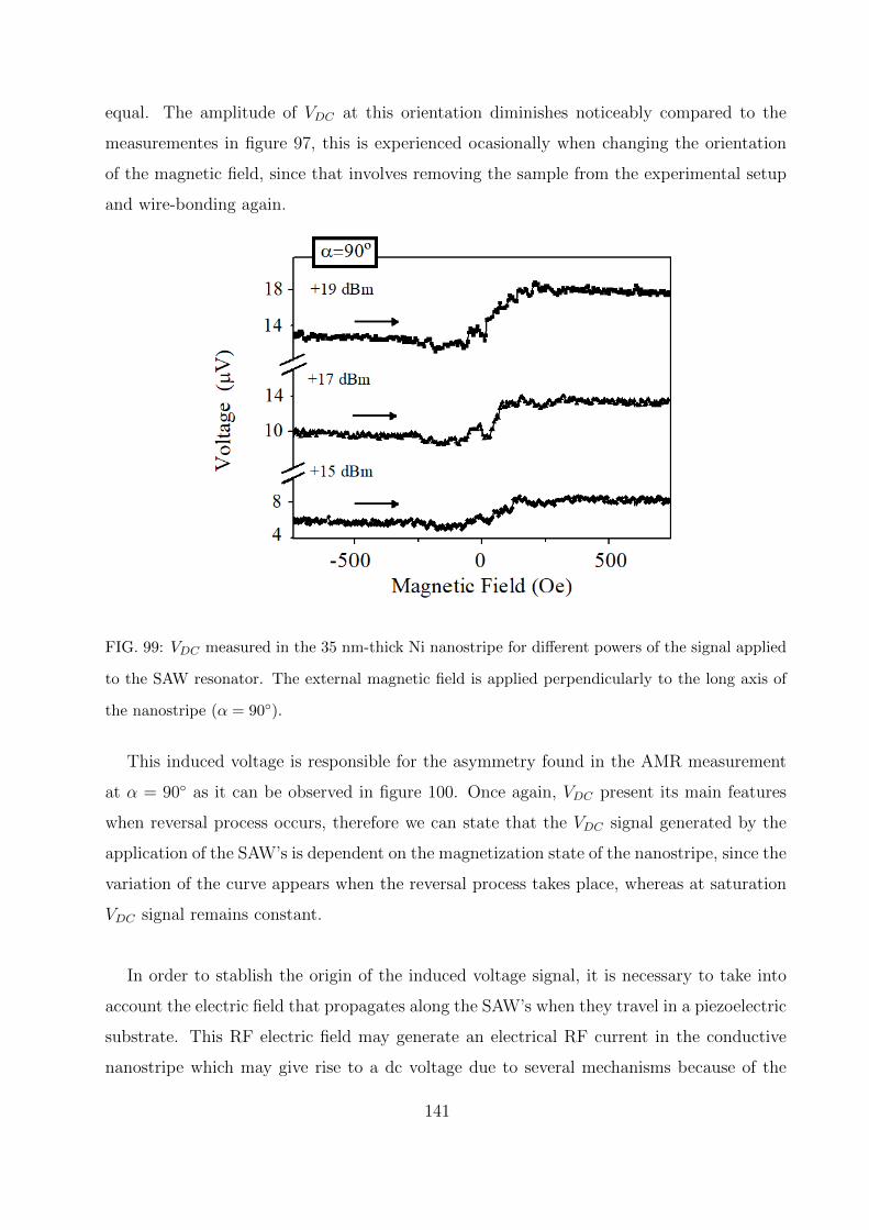
equal. The amplitude of VDC at this orientation diminishes noticeably compared to the
measurementes in figure 97, this is experienced ocasionally when changing the orientation
of the magnetic field, since that involves removing the sample from the experimental setup
and wire-bonding again.
FIG. 99: VDC measured in the 35 nm-thick Ni nanostripe for different powers of the signal applied
to the SAW resonator. The external magnetic field is applied perpendicularly to the long axis of
the nanostripe (α = 90).
This induced voltage is responsible for the asymmetry found in the AMR measurement
at α = 90 as it can be observed in figure 100. Once again, VDC present its main features
when reversal process occurs, therefore we can state that the VDC signal generated by the
application of the SAW’s is dependent on the magnetization state of the nanostripe, since the
variation of the curve appears when the reversal process takes place, whereas at saturation
VDC signal remains constant.
In order to stablish the origin of the induced voltage signal, it is necessary to take into
account the electric field that propagates along the SAW’s when they travel in a piezoelectric
substrate. This RF electric field may generate an electrical RF current in the conductive
nanostripe which may give rise to a dc voltage due to several mechanisms because of the
141
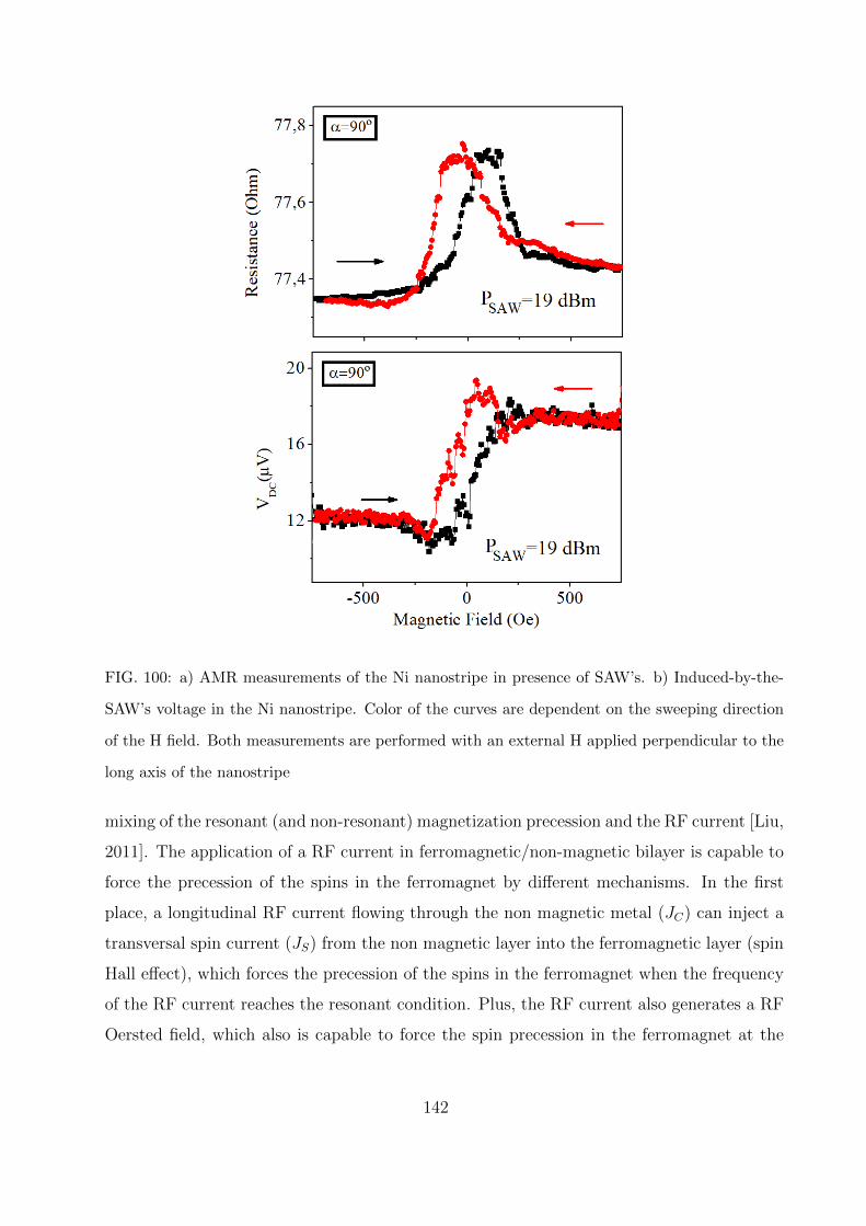
FIG. 100: a) AMR measurements of the Ni nanostripe in presence of SAW’s. b) Induced-by-the-
SAW’s voltage in the Ni nanostripe. Color of the curves are dependent on the sweeping direction
of the H field. Both measurements are performed with an external H applied perpendicular to the
long axis of the nanostripe
mixing of the resonant (and non-resonant) magnetization precession and the RF current [Liu,
2011]. The application of a RF current in ferromagnetic/non-magnetic bilayer is capable to
force the precession of the spins in the ferromagnet by different mechanisms. In the first
place, a longitudinal RF current flowing through the non magnetic metal (JC) can inject a
transversal spin current (JS) from the non magnetic layer into the ferromagnetic layer (spin
Hall effect), which forces the precession of the spins in the ferromagnet when the frequency
of the RF current reaches the resonant condition. Plus, the RF current also generates a RF
Oersted field, which also is capable to force the spin precession in the ferromagnet at the
142
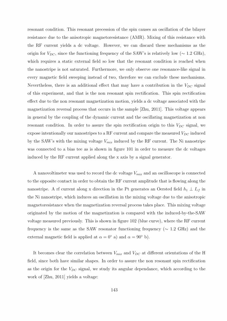
resonant condition. This resonant precession of the spin causes an oscillation of the bilayer
resistance due to the anisotropic magnetoresistance (AMR). Mixing of this resistance with
the RF current yields a dc voltage. However, we can discard these mechanisms as the
origin for VDC , since the functioning frequency of the SAW’s is relatively low (∼ 1.2 GHz),
which requires a static external field so low that the resonant condition is reached when
the nanostripe is not saturated. Furthermore, we only observe one resonance-like signal in
every magnetic field sweeping instead of two, therefore we can exclude these mechanisms.
Nevertheless, there is an additional effect that may have a contribution in the VDC signal
of this experiment, and that is the non resonant spin rectification. This spin rectification
effect due to the non resonant magnetization motion, yields a dc voltage associated with the
magnetization reversal process that occurs in the sample [Zhu, 2011]. This voltage appears
in general by the coupling of the dynamic current and the oscillating magnetization at non
resonant condition. In order to assure the spin rectification origin to this VDC signal, we
expose intentionally our nanostripes to a RF current and compare the measured VDC induced
by the SAW’s with the mixing voltage Vmix induced by the RF current. The Ni nanostripe
was connected to a bias tee as is shown in figure 101 in order to measure the dc voltages
induced by the RF current applied along the x axis by a signal generator.
A nanovoltimeter was used to record the dc voltage Vmix and an oscilloscope is connected
to the opposite contact in order to obtain the RF current amplitude that is flowing along the
nanostripe. A rf current along x direction in the Pt generates an Oersted field h1 ⊥ Irf in
the Ni nanostripe, which induces an oscillation in the mixing voltage due to the anisotropic
magnetoresistance when the magnetization reversal process takes place. This mixing voltage
originated by the motion of the magnetization is compared with the induced-by-the-SAW
voltage measured previously. This is shown in figure 102 (blue curve), where the RF current
frequency is the same as the SAW resonator functioning frequency (∼ 1.2 GHz) and the
external magnetic field is applied at α = 0 a) and α = 90 b).
It becomes clear the correlation between Vmix and VDC at different orientations of the H
field, since both have similar shapes. In order to assure the non resonant spin rectification
as the origin for the VDC signal, we study its angular dependance, which according to the
work of [Zhu, 2011] yields a voltage:
143
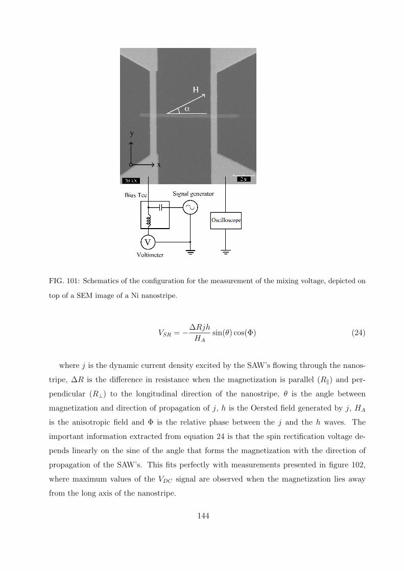
FIG. 101: Schematics of the configuration for the measurement of the mixing voltage, depicted on
top of a SEM image of a Ni nanostripe.
VSR = −∆Rjh
HA
sin(θ) cos(Φ) (24)
where j is the dynamic current density excited by the SAW’s flowing through the nanos-
tripe, ∆R is the difference in resistance when the magnetization is parallel (R‖) and per-
pendicular (R⊥) to the longitudinal direction of the nanostripe, θ is the angle between
magnetization and direction of propagation of j, h is the Oersted field generated by j, HA
is the anisotropic field and Φ is the relative phase between the j and the h waves. The
important information extracted from equation 24 is that the spin rectification voltage de-
pends linearly on the sine of the angle that forms the magnetization with the direction of
propagation of the SAW’s. This fits perfectly with measurements presented in figure 102,
where maximum values of the VDC signal are observed when the magnetization lies away
from the long axis of the nanostripe.
144
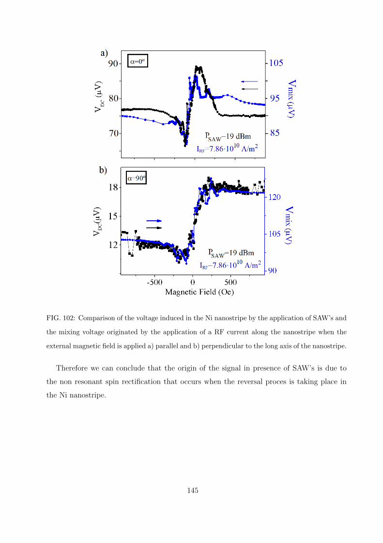
FIG. 102: Comparison of the voltage induced in the Ni nanostripe by the application of SAW’s and
the mixing voltage originated by the application of a RF current along the nanostripe when the
external magnetic field is applied a) parallel and b) perpendicular to the long axis of the nanostripe.
Therefore we can conclude that the origin of the signal in presence of SAW’s is due to
the non resonant spin rectification that occurs when the reversal proces is taking place in
the Ni nanostripe.
145
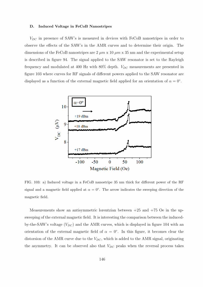
D. Induced Voltage in FeCoB Nanostripes
VDC in presence of SAW’s is measured in devices with FeCoB nanostripes in order to
observe the effects of the SAW’s in the AMR curves and to determine their origin. The
dimensions of the FeCoB nanostripes are 2 µm x 10 µm x 35 nm and the experimental setup
is described in figure 94. The signal applied to the SAW resonator is set to the Rayleigh
frequency and modulated at 400 Hz with 80% depth. VDC measurements are presented in
figure 103 where curves for RF signals of different powers applied to the SAW resonator are
displayed as a function of the external magnetic field applied for an orientation of α = 0.
FIG. 103: a) Induced voltage in a FeCoB nanostripe 35 nm thick for different power of the RF
signal and a magnetic field applied at α = 0. The arrow indicates the sweeping direction of the
magnetic field.
Measurements show an antisymmetric lorentzian between +25 and +75 Oe in the up-
sweeping of the external magnetic field. It is interesting the comparison between the induced-
by-the-SAW’s voltage (VDC) and the AMR curves, which is displayed in figure 104 with an
orientation of the external magnetic field of α = 0. In this figure, it becomes clear the
distorsion of the AMR curve due to the VDC , which is added to the AMR signal, originating
the asymmetry. It can be observed also that VDC peaks when the reversal process takes
146
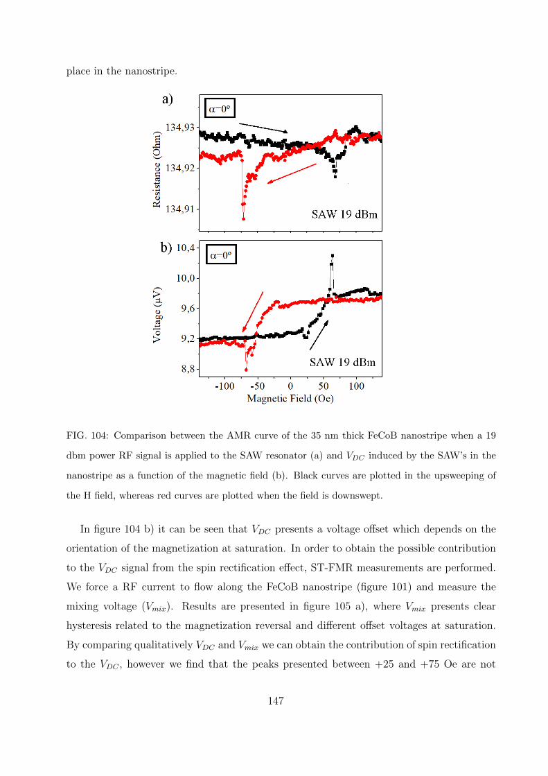
place in the nanostripe.
FIG. 104: Comparison between the AMR curve of the 35 nm thick FeCoB nanostripe when a 19
dbm power RF signal is applied to the SAW resonator (a) and VDC induced by the SAW’s in the
nanostripe as a function of the magnetic field (b). Black curves are plotted in the upsweeping of
the H field, whereas red curves are plotted when the field is downswept.
In figure 104 b) it can be seen that VDC presents a voltage offset which depends on the
orientation of the magnetization at saturation. In order to obtain the possible contribution
to the VDC signal from the spin rectification effect, ST-FMR measurements are performed.
We force a RF current to flow along the FeCoB nanostripe (figure 101) and measure the
mixing voltage (Vmix). Results are presented in figure 105 a), where Vmix presents clear
hysteresis related to the magnetization reversal and different offset voltages at saturation.
By comparing qualitatively VDC and Vmix we can obtain the contribution of spin rectification
to the VDC , however we find that the peaks presented between +25 and +75 Oe are not
147
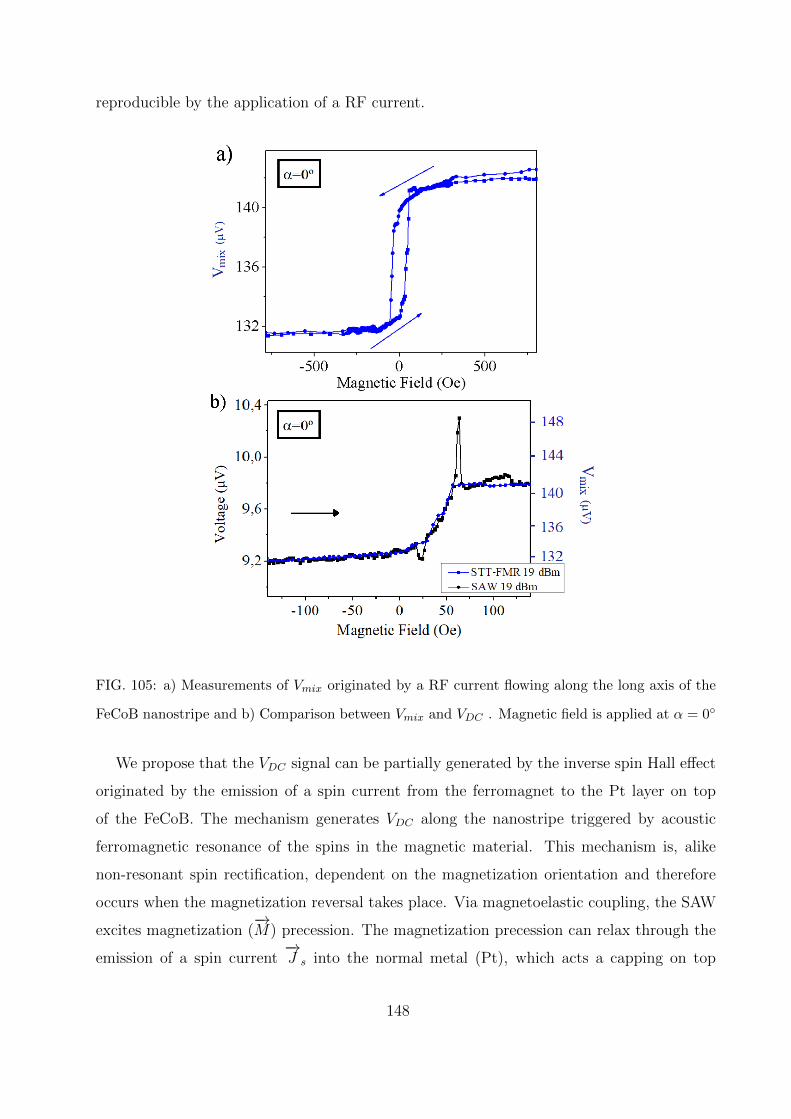
reproducible by the application of a RF current.
FIG. 105: a) Measurements of Vmix originated by a RF current flowing along the long axis of the
FeCoB nanostripe and b) Comparison between Vmix and VDC . Magnetic field is applied at α = 0
We propose that the VDC signal can be partially generated by the inverse spin Hall effect
originated by the emission of a spin current from the ferromagnet to the Pt layer on top
of the FeCoB. The mechanism generates VDC along the nanostripe triggered by acoustic
ferromagnetic resonance of the spins in the magnetic material. This mechanism is, alike
non-resonant spin rectification, dependent on the magnetization orientation and therefore
occurs when the magnetization reversal takes place. Via magnetoelastic coupling, the SAW
excites magnetization (−→M) precession. The magnetization precession can relax through the
emission of a spin current−→J s into the normal metal (Pt), which acts a capping on top
148
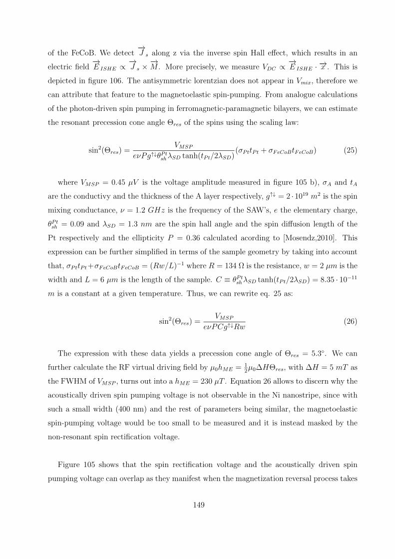
of the FeCoB. We detect−→J s along z via the inverse spin Hall effect, which results in an
electric field−→E ISHE ∝
−→J s ×
−→M . More precisely, we measure VDC ∝
−→E ISHE · −→x . This is
depicted in figure 106. The antisymmetric lorentzian does not appear in Vmix, therefore we
can attribute that feature to the magnetoelastic spin-pumping. From analogue calculations
of the photon-driven spin pumping in ferromagnetic-paramagnetic bilayers, we can estimate
the resonant precession cone angle Θres of the spins using the scaling law:
sin2(Θres) =VMSP
eνPg↑↓θPtshλSD tanh(tPt/2λSD)(σPttPt + σFeCoBtFeCoB) (25)
where VMSP = 0.45 µV is the voltage amplitude measured in figure 105 b), σA and tA
are the conductivy and the thickness of the A layer respectively, g↑↓ = 2 ·1019 m2 is the spin
mixing conductance, ν = 1.2 GHz is the frequency of the SAW’s, e the elementary charge,
θPtsh = 0.09 and λSD = 1.3 nm are the spin hall angle and the spin diffusion length of the
Pt respectively and the ellipticity P = 0.36 calculated acording to [Mosendz,2010]. This
expression can be further simplified in terms of the sample geometry by taking into account
that, σPttPt+σFeCoBtFeCoB = (Rw/L)−1 where R = 134 Ω is the resistance, w = 2 µm is the
width and L = 6 µm is the length of the sample. C ≡ θPtshλSD tanh(tPt/2λSD) = 8.35 · 10−11
m is a constant at a given temperature. Thus, we can rewrite eq. 25 as:
sin2(Θres) =VMSP
eνPCg↑↓Rw(26)
The expression with these data yields a precession cone angle of Θres = 5.3. We can
further calculate the RF virtual driving field by µ0hME = 12µ0∆HΘres, with ∆H = 5 mT as
the FWHM of VMSP , turns out into a hME = 230 µT . Equation 26 allows to discern why the
acoustically driven spin pumping voltage is not observable in the Ni nanostripe, since with
such a small width (400 nm) and the rest of parameters being similar, the magnetoelastic
spin-pumping voltage would be too small to be measured and it is instead masked by the
non-resonant spin rectification voltage.
Figure 105 shows that the spin rectification voltage and the acoustically driven spin
pumping voltage can overlap as they manifest when the magnetization reversal process takes
149
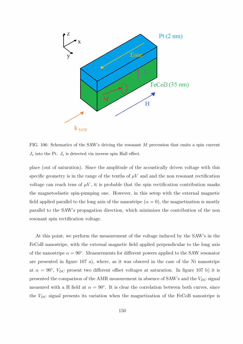
FIG. 106: Schematics of the SAW’s driving the resonant M precession that emits a spin current
Js into the Pt. Js is detected via inverse spin Hall effect.
place (out of saturation). Since the amplitude of the acoustically driven voltage with this
specific geometry is in the range of the tenths of µV and and the non resonant rectification
voltage can reach tens of µV , it is probable that the spin rectification contribution masks
the magnetoelastic spin-pumping one. However, in this setup with the external magnetic
field applied parallel to the long axis of the nanostripe (α = 0), the magnetization is mostly
parallel to the SAW’s propagation direction, which minimizes the contribution of the non
resonant spin rectification voltage.
At this point, we perform the measurement of the voltage induced by the SAW’s in the
FeCoB nanostripe, with the external magnetic field applied perpendicular to the long axis
of the nanostripe α = 90. Measurements for different powers applied to the SAW resonator
are presented in figure 107 a), where, as it was obsered in the case of the Ni nanostripe
at α = 90, VDC present two different offset voltages at saturation. In figure 107 b) it is
presented the comparison of the AMR measurement in absence of SAW’s and the VDC signal
measured with a H field at α = 90. It is clear the correlation between both curves, since
the VDC signal presents its variation when the magnetization of the FeCoB nanostripe is
150
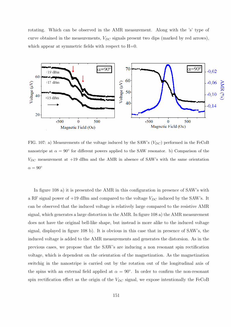
rotating. Which can be observed in the AMR measurement. Along with the ’s’ type of
curve obtained in the measurements, VDC signals present two dips (marked by red arrows),
which appear at symmetric fields with respect to H=0.
FIG. 107: a) Measurements of the voltage induced by the SAW’s (VDC) performed in the FeCoB
nanostripe at α = 90 for different powers applied to the SAW resonator. b) Comparison of the
VDC measurement at +19 dBm and the AMR in absence of SAW’s with the same orientation
α = 90
In figure 108 a) it is presented the AMR in this configuration in presence of SAW’s with
a RF signal power of +19 dBm and compared to the voltage VDC induced by the SAW’s. It
can be observed that the induced voltage is relatively large compared to the resistive AMR
signal, which generates a large distortion in the AMR. In figure 108 a) the AMR measurement
does not have the original bell-like shape, but instead is more alike to the induced voltage
signal, displayed in figure 108 b). It is obvious in this case that in presence of SAW’s, the
induced voltage is added to the AMR measurements and generates the distorsion. As in the
previous cases, we propose that the SAW’s are inducing a non resonant spin rectification
voltage, which is dependent on the orientation of the magnetization. As the magnetization
switchig in the nanostripe is carried out by the rotation out of the longitudinal axis of
the spins with an external field applied at α = 90. In order to confirm the non-resonant
spin rectification effect as the origin of the VDC signal, we expose intentionally the FeCoB
151
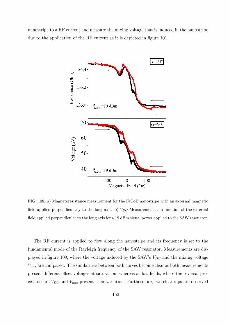
nanostripe to a RF current and measure the mixing voltage that is induced in the nanostripe
due to the application of the RF current as it is depicted in figure 101.
FIG. 108: a) Magnetoresistance measurement for the FeCoB nanostripe with an external magnetic
field applied perpendicularly to the long axis. b) VDC Measurement as a function of the external
field applied perpendicular to the long axis for a 19 dBm signal power applied to the SAW resonator.
The RF current is applied to flow along the nanostripe and its frequency is set to the
fundamental mode of the Rayleigh frequency of the SAW resonator. Measurements are dis-
played in figure 109, where the voltage induced by the SAW’s VDC and the mixing voltage
Vmix are compared. The similarities between both curves become clear as both measurements
present different offset voltages at saturation, whereas at low fields, where the reversal pro-
cess occurs VDC and Vmix present their variation. Furthermore, two clear dips are observed
152
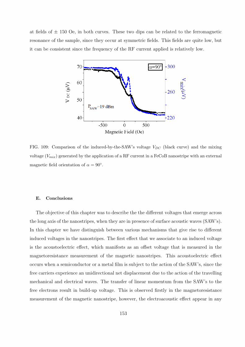
at fields of ± 150 Oe, in both curves. These two dips can be related to the ferromagnetic
resonance of the sample, since they occur at symmetric fields. This fields are quite low, but
it can be consistent since the frequency of the RF current applied is relatively low.
FIG. 109: Comparison of the induced-by-the-SAW’s voltage VDC (black curve) and the mixing
voltage (Vmix) generated by the application of a RF current in a FeCoB nanostripe with an external
magnetic field orientation of α = 90.
E. Conclusions
The objective of this chapter was to describe the the different voltages that emerge across
the long axis of the nanostripes, when they are in presence of surface acoustic waves (SAW’s).
In this chapter we have distinguish between various mechanisms that give rise to different
induced voltages in the nanostripes. The first effect that we associate to an induced voltage
is the acoustoelectric effect, which manifests as an offset voltage that is measured in the
magnetoresistance measurement of the magnetic nanostripes. This acoustoelectric effect
occurs when a semiconductor or a metal film is subject to the action of the SAW’s, since the
free carriers experience an unidirectional net displacement due to the action of the travelling
mechanical and electrical waves. The transfer of linear momentum from the SAW’s to the
free electrons result in build-up voltage. This is observed firstly in the magnetoresistance
measurement of the magnetic nanostripe, however, the electroacoustic effect appear in any
153
type of material. We measure directly the voltage induced by the SAW’s in a nanostripe
made of Au, as a function of an external magnetic field, and we obtained a constant voltage
independent of H. This is the expected voltage induced by the electroacoustic effect in every
nanostripe.
We also measure directly the voltage VDC induced by the SAW’s in the Ni nanostripes.
It is observed, once the VDC measurements are carried out, that this voltage is the respon-
sible for the asymmetry in the magnetoresistance measurements measured in presence of
SAW’s. Furthermore, VDC for different orientations of the external magnetic field present
a clear correlation between their features and the AMR measurements, meaning that the
VDC present its main variations when the reversal process of the magnetization takes place.
In order to understand the origin for this voltage, it is necessary to understand that along
with the SAW’s, an electrical potential travels in the piezoelectric substrate in addition to
the mechanical displacement. This electrical potential can be electrically shorted by the
conductive nanostripe resulting in a radiofrequency RF current across the nanostripe. We
found that the induced voltage is due to a non resonant spin rectification voltage due to
the mixing of the motion of the magnetization in presence of a SAW-induced RF current.
In the case of the magnetic nanostripes, this non resonant spin rectification voltage is over-
lapped with the constant electroacoustic voltage that appears in the nanostripes because
its conductive behaviour. Finally the non resonant spin rectification origin is confirmed by
the application of a RF current directly to the Ni nanostripes and comparing the mixing
voltage generated with the induced-by-the-SAW’s voltage. At every orientation they match
qualitatively, confirming the origin of the voltage induced by the SAW’s.
We have also measured directly the voltage induced by the SAW’s VDC in the FeCoB
nanostripes and we found again that VDC is the responsible for the asymmetry measured in
the magnetoresistance measurements in presence of SAW’s. Besides from VDC , we measure in
this FeCoB nanostripe the voltage that it is originated from the mixing of a RF current with
the oscillating magnetization (Vmix), in order to compare this voltge with the induced-by-
the-SAW’s voltage and check if they have the same origin. Measurements with the external
magnetic field pplied parallel to the long axis of the nanostripe, show that Vmix and VDC show
some similiarities, however, VDC present some peaks that can not be related to the mixing
154
voltage. Those peaks are instead, related to the acoustically-driven spin pumpin, since the
SAW’s are capable of forcing the precession of the spins within the ferromagnet and inject a
spin current from the ferromagnet into the Pt layer grown on top of the FeCoB layer. That
spin current is detected via inverse spin Hall effect, which is the responsible for the final VDC
signal that is measured. This contribution as well as the one coming from the non resonant
spin rectification effect are overlapped since both occur when the magnetization reversal
takes place. We use the comparison between Vmix and VDC to separate each contribution
apart. The voltage induced by the SAW’s VDC , is also measured when the orientation of the
external magnetic field is perpendicular to the long axis of the FeCoB nanostripe, however
in this case the non-resonant spin rectification voltage is so large that masks completely any
voltage due to the acoustically-driven spin pumping. We perform for this FeCoB nanostripe
and at α = 90, measurements of Vmix. By comparing Vmix and VDC we conclude that
they both have the same origin. Finally, from all the VDC measurements acquired during
this chapter, we conclude that the amplitude of the non-resonant spin rectification voltage
is dependent on the angle that forms the magnetization with the direction of propagation
of the SAW’s, being maximum when they are perpendicular and minimum when they are
parallel.
155

156
Appendix: Surface Acoustic Waves
The existence of Rayleigh waves was predicted in 1885 by Lord Rayleigh [Rayleigh, 1885],
after whom they were named. He described the behaviour and properties of acoustic waves
that propagate on the plane surface of an elastic solid. The particles in Rayleigh waves
move in ellipses in planes normal to the surface and parallel to the direction of propagation,
the major axis of the ellipse is normal to the surface. At the surface and at shallow depths
this motion is retrograde (counterclockwise when the wave travels from left to right). At
greater depths the particle motion becomes prograde. In addition, the motion amplitude
decays and the eccentricity changes as the depth into the material increases. The depth of
significant displacement in the solid is approximately equal to the acoustic wavelength. A
visual representation of the Rayleigh wave is displayed in figure 110.
FIG. 110: Picture of a Rayleigh wave. The motion of a surface particle and the propagation
direction are depicted [mtu.edu].
In this thesis, the generation of the SAW’s that travel towards our magnetic nanostruc-
tures is carried out by a SAW resonator. First described in 1965 by [White, 1965], this
technique allows the launching and detection of surface acoustic waves. The SAW resonator
is a device fabricated on top of a piezoelectric layer characterized by its IDTs, (interdigital
transducers) a series of metallic bars alternatively connected to different contact pads. The
IDTs convert acoustic waves to electrical signals and vice versa by exploiting the piezoelectric
effect.
157
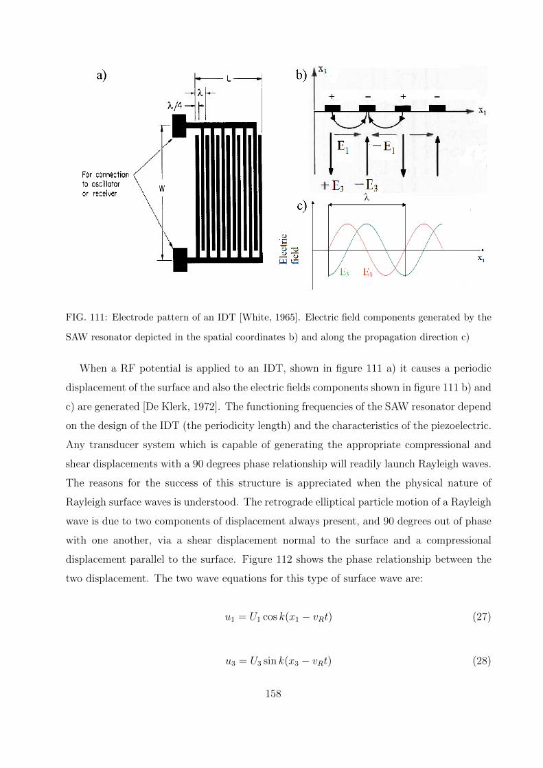
FIG. 111: Electrode pattern of an IDT [White, 1965]. Electric field components generated by the
SAW resonator depicted in the spatial coordinates b) and along the propagation direction c)
When a RF potential is applied to an IDT, shown in figure 111 a) it causes a periodic
displacement of the surface and also the electric fields components shown in figure 111 b) and
c) are generated [De Klerk, 1972]. The functioning frequencies of the SAW resonator depend
on the design of the IDT (the periodicity length) and the characteristics of the piezoelectric.
Any transducer system which is capable of generating the appropriate compressional and
shear displacements with a 90 degrees phase relationship will readily launch Rayleigh waves.
The reasons for the success of this structure is appreciated when the physical nature of
Rayleigh surface waves is understood. The retrograde elliptical particle motion of a Rayleigh
wave is due to two components of displacement always present, and 90 degrees out of phase
with one another, via a shear displacement normal to the surface and a compressional
displacement parallel to the surface. Figure 112 shows the phase relationship between the
two displacement. The two wave equations for this type of surface wave are:
u1 = U1 cos k(x1 − vRt) (27)
u3 = U3 sin k(x3 − vRt) (28)
158
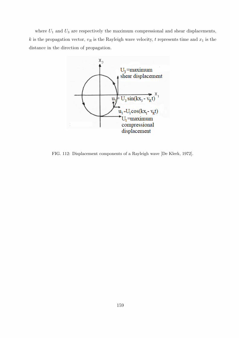
where U1 and U3 are respectively the maximum compressional and shear displacements,
k is the propagation vector, vR is the Rayleigh wave velocity, t represents time and x1 is the
distance in the direction of propagation.
FIG. 112: Displacement components of a Rayleigh wave [De Klerk, 1972].
159
Bibliography
Aliev, G.N., Goller, B., Snow, P.A., Heinrich, H. and Aigner, R., Porous Silicon Bulk
Acoustic Wave Resonator with Integrated Transducer, Nanoscale Research Letters 2012,
7:378.
Bai, L., Feng, Z., Hyde, P., Ding, H.F. and Mu, C.-M., Distinguishing Spin Pumping
from Spin Rectification in a Pt/Py Bilayer through Angle Dependent Line Shape Analysis,
Applied Physics Letters 102, 242402, (2013).
Baibich, M. N., Broto, J.M., Fert, A., Nguyen van Dau, F., Petroff, F., Etienne, P.,
Creuzet, G., Friedrich, A. and Chazelas, J., Giant Magnetoresistance of (001)Fe/(001)Cr
Magnetic Superlattices, Physical Review Letters 61, 2472 - (1988).
Bartoli, F., Aubert, T., Moutaouekkil, M., Streque, J., Pigeat, P., Hage-Ali, S., Boulet,
P., M’Jahed, H., Bou Matar, O. and Talbi, A., Theoretical and Experimental Study of
ScAlN/Sapphire Structure Based SAW Sensor. IEEE Sensors, (2017).
Bauer, U., Emori, S. and Beach, G.S.D., Voltage-Controlled Domain Wall Traps in Fer-
romagnetic Nanowires, Nature Nanotechnology 8, 411-416 (2013).
Beach, G.S.D., Nistor, C., Knutson, C., Tsoi, M. and Erksine, J.L., Dynamics of Field-
Driven Domain-Wall Propagation in Ferromagnetic Nanowires, Nature Materials 4, 741-744
(2005).
Berk, C., Jaris, M. , Yang, W. , Dhuey, S. , Cabrini S. and Schmidt, H., Strongly
Coupled Magnon-Phonon Dynamics in a Single Nanomagnet, Nature Communications 10,
2652 (2019).
Bhatti, S., Ma, C., Xiaoxi Liu, X. and Piramanayagam S. N., Stress-Induced Domain Wall
Motion in FeCo-Based Magnetic Microwires for Realization of Energy Harvesting, Advance
Electronics Materials (2018), 1800467.
160
Binasch, G., Grunberg, P., Saurenbach, F. and Zinn, W., Enhanced Magnetoresistance in
Layered Magnetic Structures with Antiferromagnetic Interlayer Exchange, Physical Review
B 39, 4828(R), (1989).
Biswas, A.K., Bandyopadhyay, S. and Atulasimha, J., Acoustically Assisted Spin-
Transfer-Torque Switching of Nanomagnets: An Energy-efficient Hybrid Writing Scheme
for Nonvolatile Memory, Applied Physics Letter 103, 232401 (2013).
Bryan, M.T., Dean, J. and Allwood, D.A., Dynamics of Stress-Induced Domain Wall
Motion, Physical Review B 85, 144411 (2012).
Buyukkose, S., Hernandez-Mınguez, A., Vratzov, B., Somaschini, C., Geelhaar, L.,
Riechert, H., van der Wiel, W. G. and Santos, P. V., High-Frequency Acoustic Charge
Transport in GaAs Nanowires. Nanotechnology 25, 135204 (2014).
Carignan, L-P., Lacroix, C., Ouimet, A., Ciureanu, M., Yelon, A. and Menard, A., Mag-
netic Anisotropy in Arrays of Ni, CoFeB, and Ni/Cu Nanowires, Journal of Applied Physics
102, 023905 (2007)
Chen, M., Chien, C-L. Searson, P.C., Potential Modulated Multilayer Deposition of Mul-
tisegment Cu/Ni Nanowires with Tunable Magnetic Properties, Chemistry of Materials, 18,
6, 1595-1601, (2006).
Chen, M. and Searson, P.C., Micromagnetic Behavior of Electrodeposited Ni/Cu Multi-
layer Nanowires, Journal of Applied Physics 93, 8253 (2003).
Collins, J.H., Lakin, K.M., Quate, C.F. and Shaw, H.J., Amplification of Acoustic Surface
Waves with Adjacent Semiconductor and Piezoelectric Crystals. Applied Physics Letters 13,
314 (1968).
Davis, S., Baruth, A. and Adenwalla, S., Magnetization Dynamics Triggered by Surface
161
Acoustic Waves, Applied Physics Letters 97, 232507 (2010).
De Klerk, J., Past, Present and Future of Surface Elastic Waves, Journal de Physique
Colloques, (1972), 33 (C6), 182-188.
Dean, J., Bryan, M. T., Cooper, J. D., Virbule, A., Cunningham, J. E. and Hayward,
T. J., A sound Idea: Manipulating Domain Walls in Magnetic Nanowires Using Surface
Acoustic Waves, Applied Physics Letters 107, 142405 (2015).
Dıaz, J., Quiros, C., Alvarez-Prado, L.M., Aroca, C., Ranchal, R., Ruffoni, R. and Pas-
carelli, S., Determination of the magnetostrictive atomic environments in FeCoB alloys,
Physical Review B 85, 134437 - (2012).
Dreher, L., Weiler, M., Pernpeintner, M., Huebl, H., Gross, R., Brandt, M.S. and Goen-
nenwein, S.T.B., Surface acoustic wave driven ferromagnetic resonance in nickel thin films:
Theory and experiment, Physical Review B 86, 134415 (2012)
Drovosekov, A.B., Kreines, N.M., Savitsky, A.O., Kravtsov, E.A., Ryabukhina, M.V.,
Proglyado, V.V. and Ustinov, V.V., Magnetization and Ferromagnetic Resonance in Fe/Gd
Multilayer: Experiment and Modelling, Journal of Physics: Condensed Matter, 29, 11,
(2017).
Drovosekov, A.B., Savitsky, A.O., Kholin, D.I., Kreines, N.M., Proglyado, V.V.,
Ryabukhina, M.V., Kravtsov, E.A. and Ustinov, V.V., Twisted Magnetization States and
Inhomogeneous Resonance Modes in a Fe/Gd Ferrimagnetic Multilayer, Journal of Mag-
netism and Magnetic Materials, 475, 668 (2019).
Edrington, W., Singh, U., Dominguez, M. A., Alexander, J. R., Nepal, R. and Adenwalla.
S., SAW Assisted Domain Wall Motion in Co/Pt Multilayers, Applied Physics Letters 112,
052402 (2018).
Finizio, S., Foerster, M., Buzzi, M., Kruger, B., Jourdan, M., Vaz, C. A. F., Hockel, J.,
162
Miyawaki, T., Tkach, A., Valencia, S., Kronast, F., Carman, G.P., Nolting, F. and Klaui,
M., Magnetic Anisotropy Engineering in Thin Film Ni Nanostructures by Magnetoelastic
Coupling, Physical Review Applied 1, 021001 (2014).
Foerster, M., Macia F., Statuto, N., Finizio, S., Hernandez-Mınguez, A., Lendınez S.,
Santos, P., Fontcuberta, J., Hernandez, J.M., Klaui, M. and Aballe, L., Direct Imaging of
Delayed Magneto-Dynamic Modes Induced by Surface Acoustic Waves, Nature Communi-
cations 8, 407 (2017).
Grollier, J., Chanthbouala, A., Matsumoto, R., Anane, A., Cros, V., Nguyen van Dau, F.
and Fert, A., Magnetic Domain Wall Motion by Spin Transfer, Comptes Rendus Physique
12 (2011) 309-317.
Grollier, J., Cros, V. and Fert, A., Synchronization of Spin-Transfer Oscillators Driven
by Stimulated Microwave Currents, Physical Review B 73, 060409(R) - (2006).
Groves, T.R., Electron Beam Lithography, The Art of Fabricating Nanoelectronic and
Nanophotonic Devices and Systems (2014), 80-115.
Halilov, S.V., Perlov A. Y., Oppeneer, P.M., Yaresko, A.N. and Antonov, V.N., Magne-
tocrystalline anisotropy energy in cubic Fe, Co, and Ni: Applicability of local-spin-density
theory reexamined, Physical Review B 57, 16 (1998)
Hertel, R. and Kirschner, J., Magnetization Reversal Dynamics in Nickel Nanowires,
Physica B 343 206-210, (2004).
Herzer, G., Grain Structure and Magnetism of Nanocrystalline Ferromagnets. IEEE
Transactions on Magnetics, 25, 5 (1989).
Ho, P., Zhang, J., Bono, D. and Chen, J., Oersted Field and Spin Current Effects on
Magnetic Domains in [Co/Pd]15 Nanowires, IEEE Transactions on Magnetics 52(6), (2016).
163
Hong, K. and Giordano, N., Resistance of a Domain Wall in a Thin Ferromagnetic Wire,
Journal of Physics: Condensed Matter 10, 401 (1998).
Hosoito, N., Hashizume, H., Ishimatsu, N., Bae, I.-T., Srajer, G., Lang, C., Ventakara-
man, C. and Nelson, C., Magnetic Structures of an Iron-Gadolinium Multilayer at Low
Temperatures, Japanese Journal of Applied Physics, 41, 1331 (2002).
Hsu, P-J., Kubetzka, A., Finco, A., Romming, N., von Bergmann, K. and Wiesendanger,
R., Electric-Field-Driven Switching of Individual Magnetic Skyrmions, Nature Nanotechnol-
ogy 12, 123-126 (2017).
Huai, Y., Albert, F., Nguyen, P., Pakala, M. and Valet, T., Observation of Spin-Transfer
Switching in Deep Submicron-Sized and Low Resistance Magnetic Tunnel Junctions, Applied
Physics Letters 84, 3118 (2004).
Huai, Y., Spin-Transfer Torque MRAM (STT-MRAM): Challenges and Prospects,
AAPPS Bulletin (2008), 18, 6.
Insepov, Z., Emelin, E., Kononenko, O., Roshuchupkin, D.V., Tnyshtykbayev, K.B. and
Baigarin, K.A., Surface Acoustic Wave Amplification by Direct Current-Voltage Supplied
to Graphene Film. Applied Physics Letters 106 023505 (2015).
Kamohara, T., Akiyama, M. and Kuwano, N., Influence of Polar Distribution on Piezo-
electric Response of Aluminum Nitride Thin Films, Applied Physics Letters 92, 093506
(2008).
Kawada, T., Kawaguchi, M. and Hayashi, M., Unidirectional planar Hall voltages induced
by surface acoustic waves in ferromagnetic thin films. Physical Review B 99, 184435 (2019).
Kozlov, S. N., Skryabina, O. V., Egorov, S. V., Golovchanskiy, I. A., Klimenko, A. A.,
Napolskii, K. S. and Stolyarov, V. S., Magnetoresistance of a Single Polycrystalline Nickel
Nanowire. Journal of Applied Physics 125, 063902 (2019).
164
Laur, V., Queffelec, P., Rasoanoavy, F., Lebedev, G., Viala, B. and Thi, M.P., Microwave
Magnetoelectric Couplings in FeCoB/Piezoelectric Bilayers, IEEE Transactions on Magnet-
ics 49 , 3 ,(2013)
Lee, E.W. and Asgar, M.A., The Magnetostriction of Nickel, Proceedings of the Royal
Society of London. Series A, Mathematical and PhysicalSciences,326, 1564 (1971), 73-85
Lee, D., Lee, N., Choi, G. and Hee Cho, H., Heat Transfer Characteristics of a Focused
Surface Acoustic Wave (F-SAW) Device for Interfacial Droplet Jetting, Inventions 2018,
3(2), 38.
Lepadatu, S., Mihai, A.P., Claydon, J.S., Maccherozzi, F., Dhessi, S.S., Kinane, C.J.,
Langridge, S. and Marrows, C.H., The Increase of the Spin-Transfer Torque Threshold
Current density in Coupled Vortex Domain Walls, Journal of Physics: Condensed Matter,
24 (2012) 024210.
Li, W., Buford, B., Jander, A. and Dhagat, P., Magnetic Recording with Acoustic Waves,
Physica B 448 (2014) 151-154.
Li, W., Buford, B., Jander, A. and Dhagat, P., Acoustically Assisted Magnetic Recording:
A New Paradigm in Magnetic Data Storage, IEEE Transactions on Magnetics, 50, 3, (2014).
Liu, L., Moriyama, T., Ralph, D.C. and Burham R.A., Spin-Torque Ferromagnetic Res-
onance Induced by the Spin Hall Effect, Physical Review Letters, 106, 036601, (2011).
Loffel, J.F., Meier, J.P., Doudin, B., Asermet, J-P. and Wegner, W., Random and Ex-
change Anisotropy in Consolidated Nanostructured Fe and Ni: Role of Grain Size and Trace
Oxides on the Magnetic Properties, Physical Review B 57, 5, (1998).
Mancoff, F.B., Rizzo, N.D., Engel, B.N. and Tehrani, S., Phase-locking in Double-Point-
Contact Spin-Transfer Devices, Nature 437, 393-395, (2005).
165
Martin, F., Muralt, P., Dubois, M-A. and Pezous, A., Thickness Dependence of the Prop-
erties of Highly c-Axis Textured AlN Thin Films, Journal of Vacuum Science & Technology
A 22, 361 (2004).
Matei, E., Enculescu, I., Toimil-Morales, M-E. and Leca, A., Magnetic Configurations
of Ni-Cu Alloy Nanowires Obtained by the Template Method, Journal of Nanoparticle Re-
search, 15:1863, (2013).
McGuire, T. and Potter, R., Aniostropic Magnetoresistance in ferromagnetic 3d Alloys
IEEE Transactions on Magnetics 11, 1018 (1975).
Mellnik, A.R., Lee, J.S., Richardella, A., Grab, J.L., Mintum, P.J., Fischer, M.H., Vaezi,
A., Manchon, A., Kim, E-A., Samarth, N. and Ralph, D.C., Spin Transfer Torque Generated
by the Topological Insulator Bi2Se3, Nature 511, 449-451 (2014).
Milyutin, E., Harada, S., Martin, D., Carlin, J.F., Grandjean, N., Savu, V., Vasquez-
Mena, O., Brugger, J. and Muralt, P., Sputtering of (001) AlN Thin Films: Control of
Polarity by a Seed Layer, Journal of Vacuum Science & Technology 28, 61 (2010).
Montoya, S.A., Couture, S., Chess, J.J., Lee, J.C.T., Kent, N., Im, M-Y., Kevan, S.D.,
Fischer, P., McMorran, B.J., Roy, S., Lomakin, V. and Fullerton, E.E., Resonant properties
of dipole skyrmions in amorphous Fe/Gd multilayers, Physical Review B 95, 224405 - (2017)
Munoz, M. and Prieto, J.L., Supression of the Intrinsic Stochastic Pinning of Domain
Walls in Magnetic Nanostripes, Nature Communications, 2, 562 (2011).
Naik, R.S., Lutsky, J.J., Reif, R., Sodini, C.G., Becker, A., Fetter, L., Huggins, H.,
Miller, R., Pastalan, J., Rittenhouse, G. and Wong, Y.H., Measurements of the Bulk, C-Axis
Electromechanical Coupling Constant as a Function of A1N Film Quality, IEEE Transactions
on Ultrasonics, Ferroelectrics, and Frequency Control, 47, 1, (2000).
166
Neu, V., Biele R., Singh, A. and Schultz, L., Modeling of Intergrain Exchange Coupling
for Quantitative Predictions of δm Plots, IEEE Transactions on Magnetics, 46, 6 (2010).
Pai, C-F., Liu, L., Li, Y., Tseng, H.W., Ralph, D.C. and Buhrman, R.A., Spin Transfer
Torque Devices Utilizing the Giant Spin Hall Effect of Tungsten, Applied Physics Letters
101, 122404 (2012).
Parkes, D. E., Cavill, S. A., Hindmarch, A. T., Wadley, P., McGee, F., Staddon, C.
R., Edmonds, K. W., Campion, R. P., Gallagher, B. L. and Rushforth, A. W., Non-Volatile
Voltage Control of Magnetization and Magnetic Domain Walls in Magnetostrictive Epitaxial
Thin Films. Applied Physics Letters 101, 072402 (2012).
Parkin, S.S.P., Hayashi, M. and Thomas, L., Magnetic Domain-Wall Racetrack Memory,
Science 320, 190 (2008).
Partin, G.S., Vas’kovskii, V.O., Svalov, A.V., Eremin, E.V., Panova, M.A. and Vasil’ev,
V.N, Magnetic Resonance in Multilayer Gd/Si/Co Magnetic Films, Journal of Experimental
and Theoretical Physics, 102, 1, 131 (2006).
Pimpin, A. and Srituravanich, W., Review on Micro- and Nanolithography Techniques
and their Applications, Engineering Journal, 16 Issue 1, ISSN 0125-8281, (2012).
Pfeiffer, H.C., Recent Advances in Electron-Beam Lithography for the High-Volume Pro-
duction of VLSI Devices, IEEE Transactions on Electric Devices, 26, 4, (1979).
Prieto, J. L., Aroca, C., Lopez, E., Sanchez, M. C. and Sanchez, P., Reducing Hysteresis
in Magnetostrictive-Piezoelectric Magnetic Sensors. IEEE Transactions on Magnetism 34,
3913 (1998).
Qin, G. W. and Zuo L. , Tailoring Exchange Coupling between Magnetic Nano-Grains
of High Density Magnetic Recording Media, Materials Science Forum, 638-642, 2944-2949,
(2010).
167
Ralph, D.C. and Stiles, M.D., Spin Transfer Torques, Journal of Magnetism and Magnetic
Materials 320 (2008) 1190-1216.
Rippard, W.H., Pufall, M.R., Kaka, S., Silva, T.J., Russek, S.E. and Katine, J.A., Injec-
tion Locking and Phase Control of Spin Transfer Nano-oscillators, Physics Review Letters
95, 067203 - (2005).
Romming, N., Hanneken, C., Menzel, M., Bickel, J.E., Wolter, B., von Bergmann, K.,
Kubetzka, A. and Wiesendanger, R., Writing and Deleting Single Magnetic Skyrmions,
Science 341, 636 (2013).
Roy, K., Ultra-Low-Energy Straintronics Using Multiferroic Composites, Proceedings of
SPIE - The International Society for Optical Engineering 03(02):91670U (2014).
Sampath, V., D’Souza, N., Bhattacharya, D., Atkinson, G.M., Bandyopadhyay, S. and
Atulasimha, J., Acoustic-Wave-Induced Magnetization Switching of Magnetostrictive Nano-
magnets from Single-Domain to Nonvolatile Vortex States, Nano Letters (2016), 16, 9,
5681-5687.
Sankey, J.C., Cui, Y-T., Sun, J.Z., Sloczewski, J.C., Burharm, R.A. and Ralph, D.C.,
Measurement of the spin-transfer-torque vector in magnetic tunnel junctions, Nature Physics
4,67-71 (2008).
Sanz-Hervas, A., Clement, M., Iborra, E., Vergara, L., Olivares, J. and Sangrador, J.,
Degradation of the Piezoelectric Response of Sputtered -Axis AlN Thin Films with Traces
of non-(0002) x-Ray Diffraction Peaks, Applied Physics Letters 88, 161915 (2006).
Stiles, M.D. and Zangwill, A. Anatomy of Spin-Transfer Torque, Physical Review B 66,
014407 - (2002).
Susano, M., Proenca, M-P, Moraes, S., Sousa, C-T. and Araujo, J-P., Tuning the Mag-
168
netic Properties of Multisegmented Ni/Cu Electrodeposited Nanowires with Controllable Ni
Lengths, Nanotechnology, 19, 27(33):335301, (2016).
Suzuki, M., Yanagitani, T. and Odagawa, H., Polarity-Inverted ScAlN Film Growth
by Ion Beam Irradiation and Application to Overton Acoustic Wave (000-1)/(0001) Film
Resonators, Applied Physics Letters 104, 172905 (2014).
Tang, G., Han, T., Teshigahara, A., Iwaki, T. and Hashimoto, K.-Y., Enhancement of
Electromechanical Coupling Factor by Mass Loading in Layered SAW Device Structures,
IEEE, Frequency Control Symposium and the European Frequency and Time Forum, 416-
419, (2015).
Tejada, J., Chudnovsky, E. M., Zarzuela, R., Statuto, N., Calvo-de la Rosa, J., Santos, P.
V. and Hernandez-Mınguez, A., Switching of magnetic moments of nanoparticles by surface
acoustic waves. Euro Physics Letters 118, 37005 (2017).
Teshigahara, A., Hashimoto K. and Akiyama, M., Scandium Aluminum Nitride : Highly
Piezoelectric Thin Film for RF SAW Devices in multi GHz Range. (2012) IEEE International
Ultrasonics Symposium.
Thevenard, L., Gourdon, C., Prieur, J-Y, von Bardeleben, H.J., Vincent, S., Becerra, L,
Largeau L. and Duquesne J-Y, Surface-Acoustic-Wave-Driven Ferromagnetic Resonance in
(Ga,Mn)(As,P) Epilayers, Physical Review B 90, 094401 - (2014).
Thevenard, L., Camara, I., Prieur, J-Y, Rovillain, P., Lemaitre, A., Gourdon, C. and
Duquesne J-Y, Strong Reduction of the Coercivity by a Surface Acoustic Wave in an Out-
of-Plane Magnetized Epilayer, Physical Review B 93, 140405(R) (2016).
Thevenard, L., Camara, I. S., Majrab, S., Bernard, M., Rovillain, P., Lemaitre, A., Gour-
don, C. and Duquesne, J.-Y., Precessional Magnetization Switching by a Surface Acoustic
Wave, Physical Review B. 93, 134430 (2016).
169
Weiler, M., Dreher, L., Heeg, C., Huebl, H., Gross, R., Brandt, M. S. and Goennenwein1,
S. T. B. Elastically Driven Ferromagnetic Resonance in Nickel Thin Films, Physical Review
Letter 106, 117601 (2011).
Weiler, M., Huebl, H., F. S. Goerg, F.S., Czeschka, F.D., Gross, R. and Goennenwein,
S. T. B. Spin Pumping with Coherent ElasticWaves, Physical Review Letter 108, 176601
(2012).
White, D.L., Amplification of Ultrasonic Waves in Piezoelectric Semiconductors. Journal
of Applied Physics 33, 2547 (1962).
White, R. M. and Voltmer, F. W., Direct Piezoelectric Coupling to Surface Elastic Waves.
Applied Physics Letters 7, 314 (1965).
Wu, T., Bur, A., Wong, K., Zhao, P., Lynch, C. S., Amiri, P.K., Wang K. L. and
Carman, G. P., Electrical Control of Reversible and Permanent Magnetization Reorientation
for Magnetoelectric Memory Devices. Applied Physics Letters 98, 262504 (2011).
Yang, W. G. , Jaris, M., Hibbard-Lubow,D. L., Berk, C. and Schmidt, H., Magnetoelastic
Excitation of Single Nanomagnets for Optical Measurement of Intrinsic Gilbert Damping,
Physical Review B. 97, 224410 (2018).
Yoshida, K. and Yamanishi, M., Interaction Between Surface Elastic Waves and Drifting
Carriers in Layered System. Japan Journal of Applied Physics 7 (1968) 1143-1144.
Zeng, Z., Finocchio, G. and Jiang, H., Spin Transfer Nano-Oscillators, Nanoscale, (2013),
5, 2219-2231.
Zhu, X.F., Harder, M., Tayler, J., Wirthmann, A., Zhang, B., Lu, W., Gui, Y.S. and Hu,
C.-M., Non Resonant Spin Rectification in the Absence of an External Applied Magnetic
Field, Physical Review B, 83, 140402 (R), (2011).
170
Zhukov, A., Blanco J.M., Ipatov, M., Chizhik A. and Zhukov, V., Manipulation of Do-
main Wall Dynamics in Amorphous Microwires Through the Magnetoelastic Anisotropy,
Nanoscale Research Letters (2012), 7:223.
171


