Embed Size (px)
Citation preview
energies
Article
Electrical Characterization of MIS Schottky BarrierDiodes Based on Nanostructured Porous Silicon andSilver Nanoparticles with Applications in Solar Cells
Rehab Ramadan 1,2,* and Raúl J. Martín-Palma 1,3
1 Departamento de Física Aplicada, Universidad Autónoma de Madrid, 28049 Madrid, Spain;[email protected]
2 Department of Physics, Faculty of Science, Minia University, Minia 61519, Egypt3 Instituto Universitario de Ciencia de Materiales “Nicolás Cabrera”, Universidad Autónoma de Madrid,
28049 Madrid, Spain* Correspondence: [email protected]
Received: 25 March 2020; Accepted: 23 April 2020; Published: 1 May 2020
Abstract: The accurate determination of the electrical properties of photovoltaic devices is ofutmost importance to predict and optimize their overall optoelectronic performance. For example,the minority carrier lifetime and the carrier diffusion length have a strong relationship with the carrierrecombination rate. Additionally, parasitic resistances have an important effect on the fill factorof a solar cell. Within this context, the alternating current (AC) and direct current (DC) electricalcharacteristics of Si-based metal–insulator–semiconductor (MIS) Schottky barrier diodes with the basicstructure Al/Si/TiO2/NiCr were studied, aiming at using them as photovoltaic devices. The basic diodestructure was modified by adding nanostructured porous silicon (nanoPS) layers and by infiltratingsilver nanoparticles (AgNPs) into the nanoPS layers, leading to Al/Si+nanoPS/TiO2/NiCr andAl/Si+nanoPS+AgNPs/TiO2/NiCr structures, respectively. The AC electrical properties were studiedusing a combination of electrochemical impedance spectroscopy and Mott–Schottky analysis, while theDC electrical properties were determined from current–voltage measurements. From the experimentalresults, an AC equivalent circuit model was proposed for the three different MIS Schottky barrier diodesunder study. Additionally, the most significant electrical parameters were calculated. The resultsshow a remarkable improvement in the performance of the MIS Schottky barrier diodes upon theaddition of hybrid nanoPS layers with embedded Ag nanoparticles, opening the way to their use asphotovoltaic devices.
Keywords: MIS Schottky barrier diodes; nanoporous silicon; silver nanoparticles; electrochemicalimpedance spectroscopy; Mott–Schottky theory
1. Introduction
During the past few years, there has been a great interest towards the integration of nanostructuredporous silicon (nanoPS) with silicon micro- and optoelectronic devices [1,2]. For applications in thesefields, including as photodiodes and solar cells, the efficiency and performance of the electrical contactsto nanoPS is a key factor. In particular, it is of great importance to determine the specific mechanismsof carrier transport, since these will play a crucial role in the performance of nanoPS-based devices.Previous low-temperature DC studies of metal/nanoPS/Si structures showed rectifying behavior,and the subsequent analysis of their current-voltage (I-V) characteristics allowed identification of themas metal–insulator–semiconductor (MIS) Schottky junctions [3,4].
MIS Schottky junctions have found important applications in the broad fields of micro- andoptoelectronics, including diodes [5], near-infrared (NIR) photodetectors [6], photoelectrochemical
Energies 2020, 13, 2165; doi:10.3390/en13092165 www.mdpi.com/journal/energies
Energies 2020, 13, 2165 2 of 15
water oxidation devices [7], and photovoltaic solar cells [8]. In the particular case of Schottky barrier solarcells, the presence of an insulator thin film avoids the principal shortcoming of metal–semiconductor(MS) Schottky barriers, which is their typically low open-circuit voltage, Voc [9]. In fact, it has beenfound by several authors that the use of MIS junctions results in increased Voc, compared to that of MSSchottky barrier solar cells [10–13]. This increase in Voc leads to (1) decreased reverse saturation currentdensity associated with thermionic emission in the Schottky barrier, (2) increased value of the diodeideality factor, and/or (3) increased effective Schottky barrier height [14]. In fact, the key transportmechanisms of MIS Schottky barrier diodes are tunneling through the insulator or the interfacial layerby the majority carriers or diffusion current due to the minority carriers [15,16]. This effect is drasticallymanifested in nanoPS, given its high specific surface area.
A thorough study of the AC and DC electrical properties of MIS Schottky barrier diodes isessential to understand their fundamental electrical conduction properties. In this line, electrochemicalimpedance spectroscopy (EIS) enables determination of the electrical parameters which characterize theelectrical conduction properties of the interfaces of a device in a given frequency range [17]. EIS has beenpreviously used to investigate the internal electrical properties of the interfaces of multilayer structures,such as light-emitting diodes [18], electrochromic smart windows [19,20], Li+-ion batteries, [21] andphotovoltaic devices [17], by establishing an equivalent circuit model. Capacitance-voltage (C-V)characterization at a fixed frequency allows evaluation of other essential electrical parameters. Withinthis context, the Mott–Schottky model [22] allows determination of the built-in potential, semiconductortype, and doping density. Since not all the electrical conduction parameters for a given device can beobtained from EIS and C-V measurements, DC current–voltage (I-V) analysis provides some additionalsemiconductor device electrical parameters, including diffusion and recombination currents in darkand bulk resistances [23].
The main aim of the present work is to study the AC and DC electrical conduction propertiesof three different Si-based MIS Schottky barrier diodes to assess their potential use in the field ofphotovoltaics. The optoelectronic properties of similar structures were recently studied [24]. The basicstructure of the MIS Schottky barrier devices is Al/Si/TiO2/NiCr, with the Al/Si interface behaving asan ohmic contact. A variation of the basic device includes a nanoPS layer grown on the Si substrate,leading to diodes with the structure Al/Si+nanoPS/TiO2/NiCr. The last modification includes alayer consisting of silver nanoparticles (AgNPs) embedded into nanoPS, resulting in the structureAl/Si+nanoPS+AgNPs/TiO2/NiCr. The AC electrical properties were determined using a combinationof EIS and C-V measurements, while the DC electrical properties were obtained from I-V measurements.From the experimental EIS results, an AC equivalent circuit model was proposed for the three differentMIS Schottky devices, and the internal resistance and capacitance associated to each interface werecalculated. Additionally, both the minority carrier lifetimes and minority carrier diffusion coefficientswere calculated. From the C-V results at fixed frequencies, the built-in potential, doping concentration,and the type of the semiconductor were determined. Finally, the reverse saturation current, idealityfactor, parasitic resistances, and built-in potential were obtained from the experimental I-V data.
2. Experimental
2.1. Fabrication of the Si-Based MIS Schottky Barrier Diodes
2.1.1. Fabrication of the NanoPS Layers
Low-resistivity ohmic back contacts to boron-doped (p-type) silicon wafers (100) orientation andresistivity of 25–30 Ω·cm) were fabricated by electron beam evaporation of 150 nm-thick Al layersand subsequent thermal annealing in a nitrogen atmosphere for 5 min. The Si wafers were cut into1.5 × 1.5 cm2 pieces, each of which were mounted in a sample holder and exposed to the etchingsolution, consisting of a 1:6 HF (48 wt%):dimethyl formamide (99 wt%) mixture. The native oxide layerwas removed before starting the etching process by immersing, for 60 s, the Si pieces in a HF:H2O (1:20)solution. The anodization process was carried out under an applied current density of 10 mA/cm2
Energies 2020, 13, 2165 3 of 15
and a fixed anodization time of 120 s, leading to nanoPS layers with thickness of around 120 nm.Once the etching process was completed, the nanoPS layers grown onto Si were cleaned with ethanol toremove any residuals from the HF solution, and finally blown dry with a mild stream of dry nitrogen.The experimental setup of the anodization process has previously been described and is schematicallypresented in [25].
2.1.2. Infiltration of Silver Nanoparticles (AgNPs)
Silver nanoparticles (AgNPs) were grown inside the nanoPS layers using an electrochemicaldeposition process described in previous work [25]. An aqueous solution of silver nitrate, sodiumcitrate, and nitric acid (pH = 3) was used. The current density was, in all cases, 1 µA/cm2 and theinfiltration time was 4 min. The electrochemical deposition process led to the formation of hybridlayers composed of nanoPS and silver nanoparticles (nanoPS+AgNPs).
2.1.3. Spin Coating of TiO2 Thin Films
A solution of titanium isopropoxide (Ti[OCH(CH3)2]4) in ethanol was prepared with a 0.4 Mconcentration. Afterwards, 115 µL of HCl acid was added to the solution to induce an acid catalysisto prevent nanoPS from damage. The solution was stirred at 3000 rpm at room temperature for30 min to obtain a clear solution. A total of 60 µL of the solution was cast on either the Si substrate,the nanoPS layers, or the nanoPS+AgNPs hybrid layers at a spinning speed of 3000 rpm for 30 s.Finally, the resulting TiO2 thin films were annealed on a hot plate at 150 C for 5 min to evaporate theremaining solvents.
2.1.4. Ni/Cr Top Contact
Electron beam evaporation was used to deposit 100 nm-thick Ni/Cr (80%/20%) top contacts on theTiO2 thin films. The base pressure was 2.5 × 10⁻⁵ mbar, and the evaporation time was 5 min. A metallicmask was used to define the geometry at the microscale of the Ni/Cr front contacts. The area was 0.15 cm2.
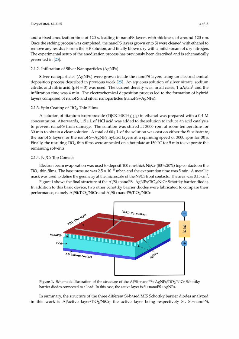
Figure 1 shows the final structure of the Al/Si+nanoPS+AgNPs/TiO2/NiCr Schottky barrier diodes.In addition to this basic device, two other Schottky barrier diodes were fabricated to compare theirperformance, namely Al/Si/TiO2/NiCr and Al/Si+nanoPS/TiO2/NiCr.
Energies 2020, 11, x FOR PEER REVIEW 3 of 16
120 nm. Once the etching process was completed, the nanoPS layers grown onto Si were cleaned with
ethanol to remove any residuals from the HF solution, and finally blown dry with a mild stream of
dry nitrogen. The experimental setup of the anodization process has previously been described and
is schematically presented in [25].
2.1.2. Infiltration of Silver Nanoparticles (AgNPs)
Silver nanoparticles (AgNPs) were grown inside the nanoPS layers using an electrochemical
deposition process described in previous work [25]. An aqueous solution of silver nitrate, sodium
citrate, and nitric acid (pH = 3) was used. The current density was, in all cases, 1μA/cm2 and the
infiltration time was 4 minutes. The electrochemical deposition process led to the formation of hybrid
layers composed of nanoPS and silver nanoparticles (nanoPS+AgNPs).
2.1.3. Spin Coating of TiO2 Thin Films
A solution of titanium isopropoxide (Ti[OCH(CH3)2]4) in ethanol was prepared with a 0.4 M
concentration. Afterwards, 115 μl of HCl acid was added to the solution to induce an acid catalysis
to prevent nanoPS from damage. The solution was stirred at 3000 rpm at room temperature for 30
minutes to obtain a clear solution. A total of 60 μL of the solution was cast on either the Si substrate,
the nanoPS layers, or the nanoPS+AgNPs hybrid layers at a spinning speed of 3000 rpm for 30 s.
Finally, the resulting TiO2 thin films were annealed on a hot plate at 150 for 5 minutes to evaporate
the remaining solvents.
2.1.4. Ni/Cr Top Contact
Electron beam evaporation was used to deposit 100 nm‐thick Ni/Cr (80%/20%) top contacts on
the TiO2 thin films. The base pressure was 2.5 × 10⁻⁵ mbar, and the evaporation time was 5 minutes.
A metallic mask was used to define the geometry at the microscale of the Ni/Cr front contacts. The
area was 0.15 cm2.
Figure 1 shows the final structure of the Al/Si+nanoPS+AgNPs/TiO2/NiCr Schottky barrier
diodes. In addition to this basic device, two other Schottky barrier diodes were fabricated to compare
their performance, namely Al/Si/TiO2/NiCr and Al/Si+nanoPS/TiO2/NiCr.
Figure 1. Schematic illustration of the structure of the Al/Si+nanoPS+AgNPs/TiO2/NiCr Schottky
barrier diodes connected to a load. In this case, the active layer is Si+nanoPS+AgNPs.
In summary, the structure of the three different Si‐based MIS Schottky barrier diodes analyzed
in this work is Al/active layer/TiO2/NiCr, the active layer being respectively Si, Si+nanoPS, or
Si+nanoPS+AgNPs. Therefore, the electrical conduction properties of the different active layers are
expected to have a pivotal role in the overall performance of the diodes.
Figure 1. Schematic illustration of the structure of the Al/Si+nanoPS+AgNPs/TiO2/NiCr Schottkybarrier diodes connected to a load. In this case, the active layer is Si+nanoPS+AgNPs.
In summary, the structure of the three different Si-based MIS Schottky barrier diodes analyzedin this work is Al/active layer/TiO2/NiCr, the active layer being respectively Si, Si+nanoPS,
Energies 2020, 13, 2165 4 of 15
or Si+nanoPS+AgNPs. Therefore, the electrical conduction properties of the different active layers areexpected to have a pivotal role in the overall performance of the diodes.
2.2. Characterization
The morphologies of the different layers and interfaces were analyzed by field emission scanningelectron microscopy (XL-40 FEG, Philips, Eindhoven, The Netherlands) operated at 5 kV.
Alternating current (AC) and direct current (DC) electrical measurements were carried out usinga potentiostat instruments (SP-150, BioLogic, Seyssinet-Pariset, France).
For electrochemical impedance spectroscopy (EIS) measurements, a voltage amplitude of 500 mVand a frequency range between 1 Hz and 1 MHz were used. Capacitance-voltage (C-V) characterizationwas performed at three specific frequencies, 1 KHz, 5 KHz, and 10 KHz, under reverse bias from 0 Vto −1 V with a scan rate of 20 mV/s. For current–voltage (I-V) measurements, the applied potentialwas varied between −1.5 and +1.5 V, and the scan rate was set at 5 mV/s. All the measurements werecarried out at room temperature in a Faraday cage to shield the electrical measurements from anyexternal signals.
3. Experimental Results
3.1. Morphology
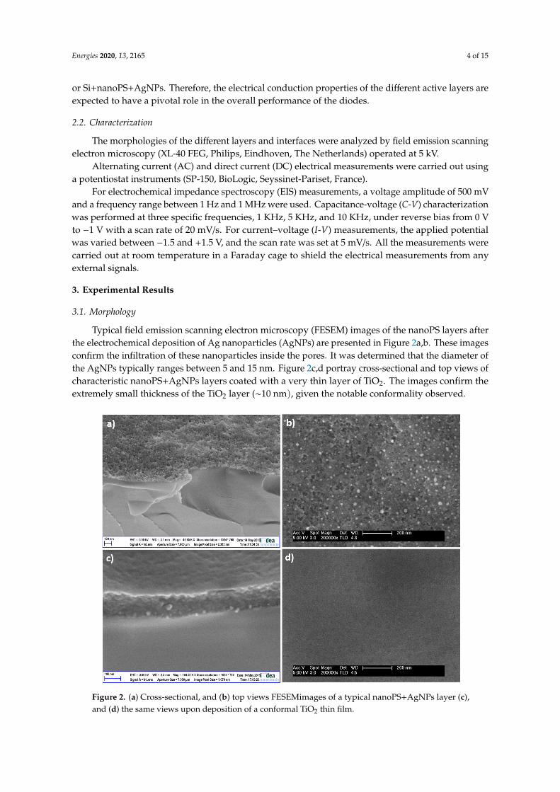
Typical field emission scanning electron microscopy (FESEM) images of the nanoPS layers afterthe electrochemical deposition of Ag nanoparticles (AgNPs) are presented in Figure 2a,b. These imagesconfirm the infiltration of these nanoparticles inside the pores. It was determined that the diameter ofthe AgNPs typically ranges between 5 and 15 nm. Figure 2c,d portray cross-sectional and top views ofcharacteristic nanoPS+AgNPs layers coated with a very thin layer of TiO2. The images confirm theextremely small thickness of the TiO2 layer (∼10 nm), given the notable conformality observed.
Energies 2020, 11, x FOR PEER REVIEW 4 of 16
2.2. Characterization
The morphologies of the different layers and interfaces were analyzed by field emission
scanning electron microscopy (XL‐40 FEG, Philips, Eindhoven, Netherlands) operated at 5 kV.
Alternating current (AC) and direct current (DC) electrical measurements were carried out using
a potentiostat instruments (SP‐150, BioLogic, Seyssinet‐Pariset, France).
For electrochemical impedance spectroscopy (EIS) measurements, a voltage amplitude of 500
mV and a frequency range between 1 Hz and 1 MHz were used. Capacitance‐voltage (C‐V)
characterization was performed at three specific frequencies, 1 KHz, 5 KHz, and 10 KHz, under
reverse bias from 0 V to −1 V with a scan rate of 20 mV/s. For current–voltage (I‐V) measurements,
the applied potential was varied between −1.5 and +1.5 V, and the scan rate was set at 5 mV/s. All the
measurements were carried out at room temperature in a Faraday cage to shield the electrical
measurements from any external signals.
3. Experimental Results
3.1. Morphology
Typical field emission scanning electron microscopy (FESEM) images of the nanoPS layers after
the electrochemical deposition of Ag nanoparticles (AgNPs) are presented in Figure 2a, b. These
images confirm the infiltration of these nanoparticles inside the pores. It was determined that the
diameter of the AgNPs typically ranges between 5 and 15 nm. Figure 2c, d portray cross‐sectional
and top views of characteristic nanoPS+AgNPs layers coated with a very thin layer of TiO2. The
images confirm the extremely small thickness of the TiO2 layer (~10 nm , given the notable
conformality observed.
Figure 2. (a) Cross‐sectional, and (b) top views FESEMimages of a typical nanoPS+AgNPs layer (c),
and (d) the same views upon deposition of a conformal TiO2 thin film.
Figure 2. (a) Cross-sectional, and (b) top views FESEMimages of a typical nanoPS+AgNPs layer (c),and (d) the same views upon deposition of a conformal TiO2 thin film.
Energies 2020, 13, 2165 5 of 15
3.2. Electrical Characterization
3.2.1. AC Electrical Measurements
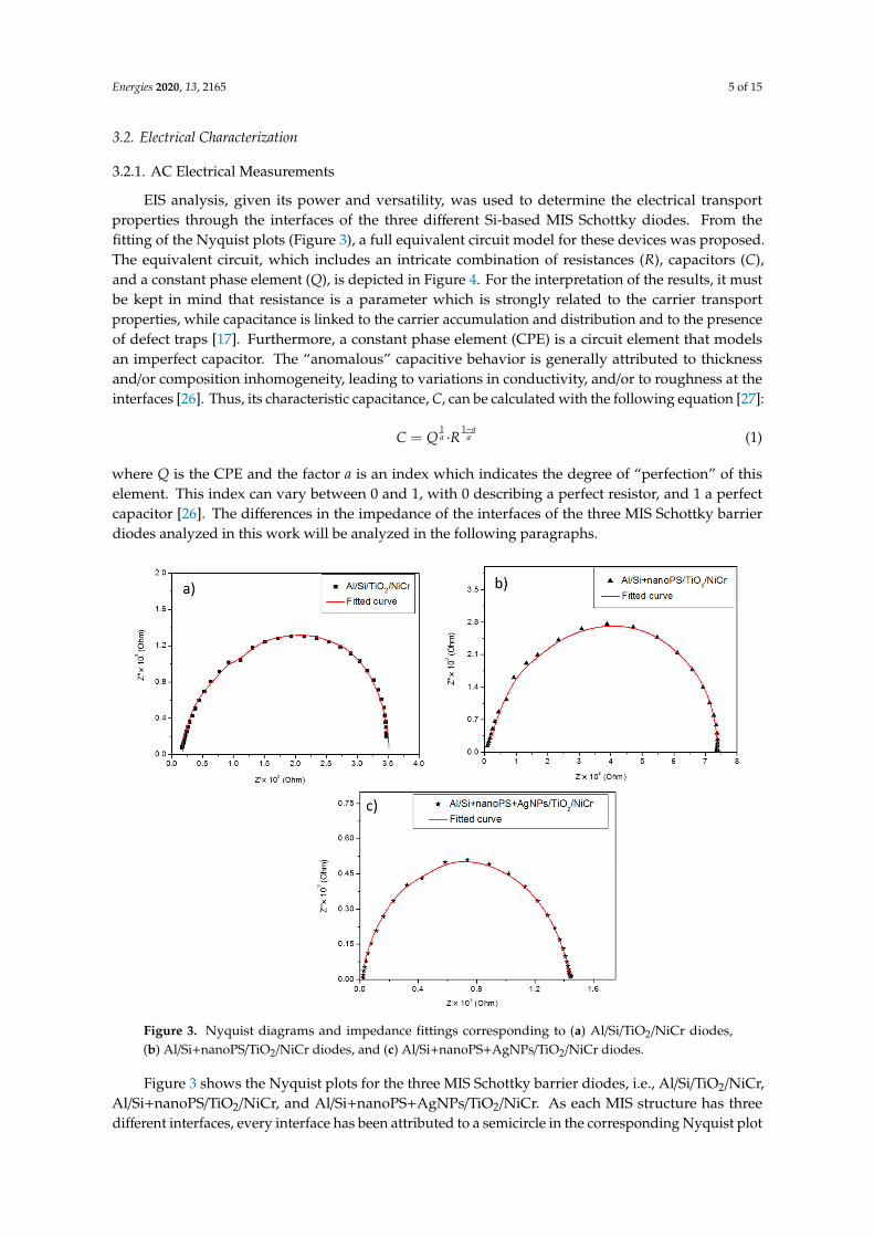
EIS analysis, given its power and versatility, was used to determine the electrical transportproperties through the interfaces of the three different Si-based MIS Schottky diodes. From thefitting of the Nyquist plots (Figure 3), a full equivalent circuit model for these devices was proposed.The equivalent circuit, which includes an intricate combination of resistances (R), capacitors (C),and a constant phase element (Q), is depicted in Figure 4. For the interpretation of the results, it mustbe kept in mind that resistance is a parameter which is strongly related to the carrier transportproperties, while capacitance is linked to the carrier accumulation and distribution and to the presenceof defect traps [17]. Furthermore, a constant phase element (CPE) is a circuit element that modelsan imperfect capacitor. The “anomalous” capacitive behavior is generally attributed to thicknessand/or composition inhomogeneity, leading to variations in conductivity, and/or to roughness at theinterfaces [26]. Thus, its characteristic capacitance, C, can be calculated with the following equation [27]:
C = Q1a ·R
1−aa (1)
where Q is the CPE and the factor a is an index which indicates the degree of “perfection” of thiselement. This index can vary between 0 and 1, with 0 describing a perfect resistor, and 1 a perfectcapacitor [26]. The differences in the impedance of the interfaces of the three MIS Schottky barrierdiodes analyzed in this work will be analyzed in the following paragraphs.
Energies 2020, 11, x FOR PEER REVIEW 5 of 16
3.2. Electrical Characterization
3.2.1. AC Electrical Measurements
EIS analysis, given its power and versatility, was used to determine the electrical transport
properties through the interfaces of the three different Si‐based MIS Schottky diodes. From the fitting
of the Nyquist plots (Figure 3), a full equivalent circuit model for these devices was proposed. The
equivalent circuit, which includes an intricate combination of resistances (R), capacitors (C), and a
constant phase element (Q), is depicted in Figure 4. For the interpretation of the results, it must be
kept in mind that resistance is a parameter which is strongly related to the carrier transport
properties, while capacitance is linked to the carrier accumulation and distribution and to the
presence of defect traps [17]. Furthermore, a constant phase element (CPE) is a circuit element that
models an imperfect capacitor. The “anomalous” capacitive behavior is generally attributed to
thickness and/or composition inhomogeneity, leading to variations in conductivity, and/or to
roughness at the interfaces [26]. Thus, its characteristic capacitance, C, can be calculated with the
following equation [27]:
𝐶 𝑄 𝑅 (1)
where Q is the CPE and the factor a is an index which indicates the degree of “perfection” of this
element. This index can vary between 0 and 1, with 0 describing a perfect resistor, and 1 a perfect
capacitor [26]. The differences in the impedance of the interfaces of the three MIS Schottky barrier
diodes analyzed in this work will be analyzed in the following paragraphs.
Figure 3. Nyquist diagrams and impedance fittings corresponding to (a) Al/Si/TiO2/NiCr diodes, (b)
Al/Si+nanoPS/TiO2/NiCr diodes, and (c) Al/Si+nanoPS+AgNPs/TiO2/NiCr diodes.
Figure 3. Nyquist diagrams and impedance fittings corresponding to (a) Al/Si/TiO2/NiCr diodes,(b) Al/Si+nanoPS/TiO2/NiCr diodes, and (c) Al/Si+nanoPS+AgNPs/TiO2/NiCr diodes.
Figure 3 shows the Nyquist plots for the three MIS Schottky barrier diodes, i.e., Al/Si/TiO2/NiCr,Al/Si+nanoPS/TiO2/NiCr, and Al/Si+nanoPS+AgNPs/TiO2/NiCr. As each MIS structure has threedifferent interfaces, every interface has been attributed to a semicircle in the corresponding Nyquist plot
Energies 2020, 13, 2165 6 of 15
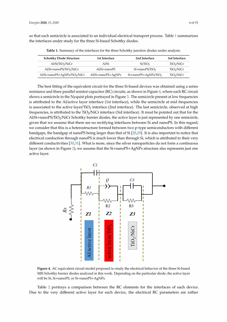
so that each semicircle is associated to an individual electrical transport process. Table 1 summarizesthe interfaces under study for the three Si-based Schottky diodes.
Table 1. Summary of the interfaces for the three Schottky junction diodes under analysis.
Schottky Diode Structure 1st Interface 2nd Interface 3rd Interface
Al/Si/TiO2/NiCr Al/Si Si/TiO2 TiO2/NiCr
Al/Si+nanoPS/TiO2/NiCr Al/Si+nanoPS Si+nanoPS/TiO2 TiO2/NiCr
Al/Si+nanoPS+AgNPs/TiO2/NiCr Al/Si+nanoPS+AgNPs Si+nanoPS+AgNPs/TiO2 TiO2/NiCr
The best fitting of the equivalent circuit for the three Si-based devices was obtained using a seriesresistance and three parallel resistor-capacitor (RC) circuits, as shown in Figure 4, where each RC circuitshows a semicircle in the Nyquist plots portrayed in Figure 3. The semicircle present at low frequenciesis attributed to the Al/active layer interface (1st interface), while the semicircle at mid frequenciesis associated to the active layer/TiO2 interface (2nd interface). The last semicircle, observed at highfrequencies, is attributed to the TiO2/NiCr interface (3rd interface). It must be pointed out that for theAl/Si+nanoPS/TiO2/NiCr Schottky barrier diodes, the active layer is just represented by one semicircle,given that we assume that there are no rectifying interfaces between Si and nanoPS. In this regard,we consider that this is a heterostructure formed between two p-type semiconductors with differentbandgaps, the bandgap of nanoPS being larger than that of Si [28,29]. It is also important to notice thatelectrical conduction through nanoPS is much lower than through Si, which is attributed to their verydifferent conductivities [30,31]. What is more, since the silver nanoparticles do not form a continuouslayer (as shown in Figure 2), we assume that the Si+nanoPS+AgNPs structure also represents just oneactive layer.
Energies 2020, 11, x FOR PEER REVIEW 6 of 16
Figure 3 shows the Nyquist plots for the three MIS Schottky barrier diodes, i.e., Al/Si/TiO2/NiCr,
Al/Si+nanoPS/TiO2/NiCr, and Al/Si+nanoPS+AgNPs/TiO2/NiCr. As each MIS structure has three
different interfaces, every interface has been attributed to a semicircle in the corresponding Nyquist
plot so that each semicircle is associated to an individual electrical transport process. Table 1
summarizes the interfaces under study for the three Si‐based Schottky diodes.
Table 1. Summary of the interfaces for the three Schottky junction diodes under analysis.
Schottky Diode Structure 1st Interface 2nd Interface 3rd Interface
Al/Si/TiO2/NiCr Al/Si Si/TiO2 TiO2/NiCr
Al/Si+nanoPS/TiO2/NiCr Al/Si+nanoPS Si+nanoPS/TiO2 TiO2/NiCr
Al/Si+nanoPS+AgNPs/TiO2/NiCr Al/Si+nanoPS+AgNPs Si+nanoPS+AgNPs/TiO2 TiO2/NiCr
The best fitting of the equivalent circuit for the three Si‐based devices was obtained using a series
resistance and three parallel resistor‐capacitor (RC) circuits, as shown in Figure 4, where each RC
circuit shows a semicircle in the Nyquist plots portrayed in Figure 3. The semicircle present at low
frequencies is attributed to the Al/active layer interface (1st interface), while the semicircle at mid
frequencies is associated to the active layer/TiO2 interface (2nd interface). The last semicircle,
observed at high frequencies, is attributed to the TiO2/NiCr interface (3rd interface). It must be
pointed out that for the Al/Si+nanoPS/TiO2/NiCr Schottky barrier diodes, the active layer is just
represented by one semicircle, given that we assume that there are no rectifying interfaces between
Si and nanoPS. In this regard, we consider that this is a heterostructure formed between two p‐type
semiconductors with different bandgaps, the bandgap of nanoPS being larger than that of Si [28,29].
It is also important to notice that electrical conduction through nanoPS is much lower than through
Si, which is attributed to their very different conductivities [30,31]. What is more, since the silver
nanoparticles do not form a continuous layer (as shown in Figure 2), we assume that the
Si+nanoPS+AgNPs structure also represents just one active layer.
Figure 4. AC equivalent circuit model proposed to study the electrical behavior of the three Si‐based
MIS Schottky barrier diodes analyzed in this work. Depending on the particular diode, the active
layer will be Si, Si+nanoPS, or Si+nanoPS+AgNPs.
Figure 4. AC equivalent circuit model proposed to study the electrical behavior of the three Si-basedMIS Schottky barrier diodes analyzed in this work. Depending on the particular diode, the active layerwill be Si, Si+nanoPS, or Si+nanoPS+AgNPs.
Table 2 portrays a comparison between the RC elements for the interfaces of each device.Due to the very different active layer for each device, the electrical RC parameters are rather
Energies 2020, 13, 2165 7 of 15
dissimilar. It is observed that for the three active layer/TiO2 interfaces, the electrical conductionof the Al/Si+nanoPS/TiO2/NiCr devices is lower than that of the Al/Si/TiO2/NiCr devices, most likelydue to the formation of the nanopores in the heavily-doped regions of the Si substrate, leading toan effective reduction of the doping concentration [29]. The experimental results also show that theelectrical conduction is notably increased in the devices based on nanoPS combined with metallic Agnanoparticles. This behavior is attributed to increased electrical conduction due to the presence of theAgNPs embedded into the nanoPS layers. A comparable enhancement in the electrical conduction ofsilica nanofiber structures was recently observed upon incorporation of gold nanoparticles [32].
Table 2. Comparison between the electrical RC elements for the three Si-based MIS Schottky barrierdiodes studied in this work.
Calculated ParameterDevice Structure
Al/Si/TiO2/NiCr Al/Si+nanoPS/TiO2/NiCr Al/Si+nanoPS+AgNPs/TiO2/NiCr
Rs (Ω) 173 51 23.2
C1 (nf)
Al/active layer Interface
5.7 2.3 15.5
R1 (kΩ) 0.6 0.7 0.05
τ1 (µs) 3.42 1.61 0.77
Q (nS)
Active layer/TiO2 Interface
54 16.8 21
a 0.9 0.89 0.8
C2 (nf) 4.01 0.91 0.04
R2 (kΩ) 1.3 3.4 0.7
τ2 (µs) 5.21 3.09 0.03
C3 (nf)
TiO2/NiCr Interface
19.7 31.5 13.2
R3 (kΩ) 1.5 3.4 0.518
τ3 (µs) 29.55 97.65 5.52
Additionally, the changes in the structure of the active layer could have an important effect onthe electrical conduction properties of all the interfaces of the devices. The electrical conduction forthe interface’s Al/active layer and TiO2/NiCr decreases for the Al/Si/TiO2/NiCr devices, due to thelarge thickness of the TiO2 thin films. Also, the reduction for the Al/Si+nanoPS/TiO2/NiCr devices isattributed to the lower conduction of nanoPS, compared to Si. However, the improved conductionfor the Al/Si+nanoPS+AgNPs/TiO2/NiCr devices is attributed to the combination of the nanoPS andmetallic nanoparticles.
The minority carrier lifetime (τ) for every interface can be obtained from the well-knownrelationship [33]:
τ = RC (2)
where R is the electrical resistance and C is the electrical capacitance at each interface. The resultsare compiled in Table 2. It can be observed that the Al/Si+nanoPS+AgNPs/TiO2/NiCr device showsthe lowest values for τ1, τ2, and τ3, which are associated with increased conduction. The observedincrease in τ1, τ2, and τ3 for the Al/Si/TiO2/NiCr devices is related to the large thickness of theTiO2 thin films and the large carrier recombination rates of Si [34], as previously indicated in theanalysis of the Nyquist plots. The values obtained for τ1, τ2, and τ3 for the Al/Si+nanoPS/TiO2/NiCrdevices are attributed to conduction losses associated with the porous structure of the nanoPS layers,as well as with the formation of defects on their surface [35]. The combination of the nanoPS layerswith metallic nanoparticles has a notable effect on the electrical conduction at the active layer/TiO2
interfaces, which leads to a small value of τ2. More specifically, τ2 decreases from 3.09 µs for theAl/Si+nanoPS/TiO2/NiCr devices to 0.03 µs for the Al/Si+nanoPS+AgNPs/TiO2/NiCr devices.
Table 2 shows that C1 and C2 are lower for the Al/Si+nanoPS/TiO2/NiCr devices than for theAl/Si/TiO2/NiCr devices. The observed decrease in the capacitance at the two nanoPS interfaces couldbe due to the particular structure of the nanoPS layers, which would induce quite large leakage currents.
Energies 2020, 13, 2165 8 of 15
However, at the TiO2/NiCr interface, the capacitance increased from 19.7 nF for the Al/Si/TiO2/NiCrdevices to 31.5 nF for the Al/Si+nanoPS/TiO2/NiCr devices. This variation could be due to a morehomogeneous TiO2 thin film when grown on the nanoPS layers, as discussed above.
The minority carrier diffusion coefficient can be calculated using the thickness of the interfaces (L)and τ, by means of the following relationship [36]:
D =L2
τ(3)
Since the smallest values for τ are obtained for the Al/Si+nanoPS+AgNPs/TiO2/NiCr Schottkydevices, D will show the largest values. A higher diffusion coefficient indicates a larger averagelength for a carrier between generation and recombination [33]. These results are further confirmed bythe improvement of the optoelectronic performance of the Al/Si+nanoPS+AgNPs/TiO2/NiCr devices,as demonstrated in a previous work [24].
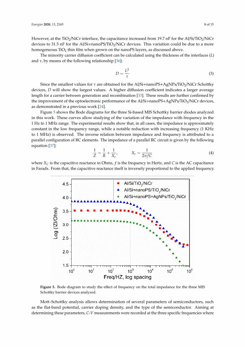
Figure 5 shows the Bode diagrams for the three Si-based MIS Schottky barrier diodes analyzedin this work. These curves allow studying of the variation of the impedance with frequency in the1 Hz to 1 MHz range. The experimental results show that, in all cases, the impedance is approximatelyconstant in the low frequency range, while a notable reduction with increasing frequency (1 KHzto 1 MHz) is observed. The inverse relation between impedance and frequency is attributed to aparallel configuration of RC elements. The impedance of a parallel RC circuit is given by the followingequation [37]:
1Z
=1R+
1Xc
, Xc =1
2π f C(4)
where XC is the capacitive reactance in Ohms, ƒ is the frequency in Hertz, and C is the AC capacitancein Farads. From that, the capacitive reactance itself is inversely proportional to the applied frequency.
Energies 2020, 11, x FOR PEER REVIEW 8 of 16
be due to the particular structure of the nanoPS layers, which would induce quite large leakage
currents. However, at the TiO2/NiCr interface, the capacitance increased from 19.7 nF for the
Al/Si/TiO2/NiCr devices to 31.5 nF for the Al/Si+nanoPS/TiO2/NiCr devices. This variation could be
due to a more homogeneous TiO2 thin film when grown on the nanoPS layers, as discussed above.
The minority carrier diffusion coefficient can be calculated using the thickness of the interfaces
(L) and τ, by means of the following relationship [36]:
𝐷𝐿 𝜏
(3)
Since the smallest values for τ are obtained for the Al/Si+nanoPS+AgNPs/TiO2/NiCr Schottky
devices, D will show the largest values. A higher diffusion coefficient indicates a larger average
length for a carrier between generation and recombination [33]. These results are further confirmed
by the improvement of the optoelectronic performance of the Al/Si+nanoPS+AgNPs/TiO2/NiCr
devices, as demonstrated in a previous work [24].
Figure 5 shows the Bode diagrams for the three Si‐based MIS Schottky barrier diodes analyzed
in this work. These curves allow studying of the variation of the impedance with frequency in the 1
Hz to 1 MHz range. The experimental results show that, in all cases, the impedance is approximately
constant in the low frequency range, while a notable reduction with increasing frequency (1 KHz to
1 MHz) is observed. The inverse relation between impedance and frequency is attributed to a parallel
configuration of RC elements. The impedance of a parallel RC circuit is given by the following
equation [37]:
1𝑍
1𝑅
1𝑋
, 𝑋1
2𝜋𝑓𝐶 (4)
where XC is the capacitive reactance in Ohms, ƒ is the frequency in Hertz, and C is the AC capacitance
in Farads. From that, the capacitive reactance itself is inversely proportional to the applied frequency.
Figure 5. Bode diagram to study the effect of frequency on the total impedance for the three MISSchottky barrier devices analyzed.
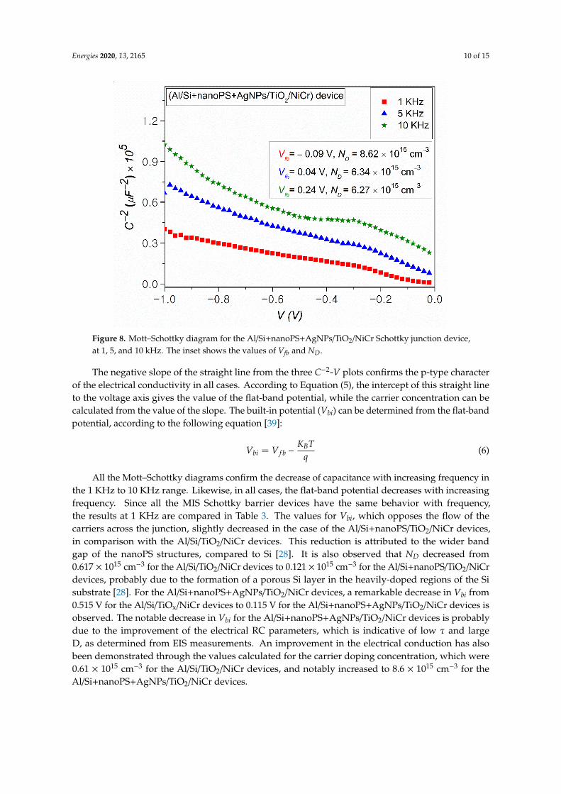
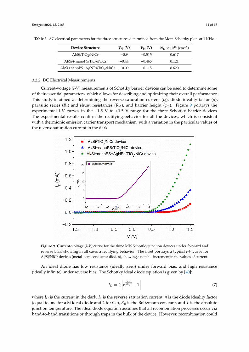
Mott–Schottky analysis allows determination of several parameters of semiconductors, suchas the flat-band potential, carrier doping density, and the type of the semiconductor. Aiming atdetermining these parameters, C-V measurements were recorded at the three specific frequencies where
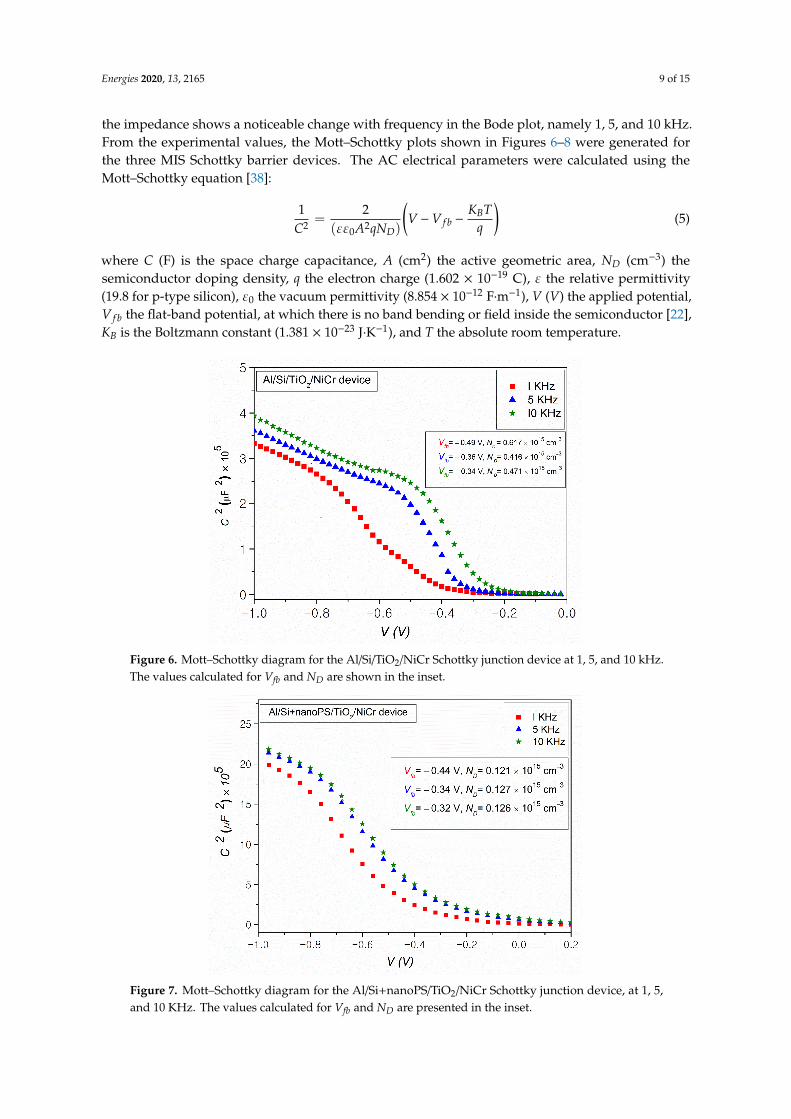
Energies 2020, 13, 2165 9 of 15
the impedance shows a noticeable change with frequency in the Bode plot, namely 1, 5, and 10 kHz.From the experimental values, the Mott–Schottky plots shown in Figures 6–8 were generated forthe three MIS Schottky barrier devices. The AC electrical parameters were calculated using theMott–Schottky equation [38]:
1C2 =
2(εε0A2qND)
(V −V f b −
KBTq
)(5)
where C (F) is the space charge capacitance, A (cm2) the active geometric area, ND (cm−3) thesemiconductor doping density, q the electron charge (1.602 × 10⁻¹⁹ C), ε the relative permittivity(19.8 for p-type silicon), ε0 the vacuum permittivity (8.854 × 10⁻¹² F·m−1), V (V) the applied potential,V f b the flat-band potential, at which there is no band bending or field inside the semiconductor [22],KB is the Boltzmann constant (1.381 × 10⁻²³ J·K−1), and T the absolute room temperature.
Energies 2020, 11, x FOR PEER REVIEW 9 of 16
Figure 5. Bode diagram to study the effect of frequency on the total impedance for the three MIS
Schottky barrier devices analyzed.
Mott–Schottky analysis allows determination of several parameters of semiconductors, such as
the flat‐band potential, carrier doping density, and the type of the semiconductor. Aiming at
determining these parameters, C‐V measurements were recorded at the three specific frequencies
where the impedance shows a noticeable change with frequency in the Bode plot, namely 1, 5, and
10 kHz. From the experimental values, the Mott–Schottky plots shown in Figures 6, 7, and 8 were
generated for the three MIS Schottky barrier devices. The AC electrical parameters were calculated
using the Mott–Schottky equation [38]:
1𝐶
2ℇℇ 𝐴 𝑞𝑁
𝑉 𝑉𝐾 𝑇
𝑞 (5)
where C (F) is the space charge capacitance, A (cm2) the active geometric area, ND (cm−3) the
semiconductor doping density, q the electron charge (1.602 × 10⁻¹⁹ C), ε the relative permittivity (19.8
for p‐type silicon), ε0 the vacuum permittivity (8.854 × 10⁻¹² F∙m−1), V (V) the applied potential, 𝑉
the flat‐band potential, at which there is no band bending or field inside the semiconductor [22], KB
is the Boltzmann constant (1.381 × 10⁻²³ J∙K−1), and T the absolute room temperature.
Figure 6. Mott–Schottky diagram for the Al/Si/TiO2/NiCr Schottky junction device at 1, 5, and 10 kHz.
The values calculated for Vfb and ND are shown in the inset.
Figure 6. Mott–Schottky diagram for the Al/Si/TiO2/NiCr Schottky junction device at 1, 5, and 10 kHz.The values calculated for Vfb and ND are shown in the inset.
Energies 2020, 11, x FOR PEER REVIEW 10 of 16
Figure 7. Mott–Schottky diagram for the Al/Si+nanoPS/TiO2/NiCr Schottky junction device, at 1, 5,
and 10 KHz. The values calculated for Vfb and ND are presented in the inset.
Figure 7. Mott–Schottky diagram for the Al/Si+nanoPS/TiO2/NiCr Schottky junction device, at 1, 5,and 10 KHz. The values calculated for Vfb and ND are presented in the inset.
Energies 2020, 13, 2165 10 of 15
Energies 2020, 11, x FOR PEER REVIEW 10 of 16
Figure 7. Mott–Schottky diagram for the Al/Si+nanoPS/TiO2/NiCr Schottky junction device, at 1, 5,
and 10 KHz. The values calculated for Vfb and ND are presented in the inset.
Figure 8. Mott–Schottky diagram for the Al/Si+nanoPS+AgNPs/TiO2/NiCr Schottky junction device,at 1, 5, and 10 kHz. The inset shows the values of Vfb and ND.
The negative slope of the straight line from the three C−2-V plots confirms the p-type characterof the electrical conductivity in all cases. According to Equation (5), the intercept of this straight lineto the voltage axis gives the value of the flat-band potential, while the carrier concentration can becalculated from the value of the slope. The built-in potential (Vbi) can be determined from the flat-bandpotential, according to the following equation [39]:
Vbi = V f b −KBT
q(6)
All the Mott–Schottky diagrams confirm the decrease of capacitance with increasing frequency inthe 1 KHz to 10 KHz range. Likewise, in all cases, the flat-band potential decreases with increasingfrequency. Since all the MIS Schottky barrier devices have the same behavior with frequency,the results at 1 KHz are compared in Table 3. The values for Vbi, which opposes the flow of thecarriers across the junction, slightly decreased in the case of the Al/Si+nanoPS/TiO2/NiCr devices,in comparison with the Al/Si/TiO2/NiCr devices. This reduction is attributed to the wider bandgap of the nanoPS structures, compared to Si [28]. It is also observed that ND decreased from0.617 × 1015 cm−3 for the Al/Si/TiO2/NiCr devices to 0.121 × 1015 cm−3 for the Al/Si+nanoPS/TiO2/NiCrdevices, probably due to the formation of a porous Si layer in the heavily-doped regions of the Sisubstrate [28]. For the Al/Si+nanoPS+AgNPs/TiO2/NiCr devices, a remarkable decrease in Vbi from0.515 V for the Al/Si/TiOx/NiCr devices to 0.115 V for the Al/Si+nanoPS+AgNPs/TiO2/NiCr devices isobserved. The notable decrease in Vbi for the Al/Si+nanoPS+AgNPs/TiO2/NiCr devices is probablydue to the improvement of the electrical RC parameters, which is indicative of low τ and largeD, as determined from EIS measurements. An improvement in the electrical conduction has alsobeen demonstrated through the values calculated for the carrier doping concentration, which were0.61 × 1015 cm−3 for the Al/Si/TiO2/NiCr devices, and notably increased to 8.6 × 1015 cm−3 for theAl/Si+nanoPS+AgNPs/TiO2/NiCr devices.
Energies 2020, 13, 2165 11 of 15
Table 3. AC electrical parameters for the three structures determined from the Mott–Schottky plots at 1 KHz.
Device Structure Vfb (V) Vbi (V) ND × 1015 (cm−3)
Al/Si/TiO2/NiCr −0.9 −0.515 0.617
Al/Si+ nanoPS/TiO2/NiCr −0.44 −0.465 0.121
Al/Si+nanoPS+AgNPs/TiO2/NiCr −0.09 −0.115 8.620
3.2.2. DC Electrical Measurements
Current-voltage (I-V) measurements of Schottky barrier devices can be used to determine someof their essential parameters, which allows for describing and optimizing their overall performance.This study is aimed at determining the reverse saturation current (I0), diode ideality factor (n),parasitic series (Rs) and shunt resistances (Rsh), and barrier height (ϕB). Figure 9 portrays theexperimental I-V curves in the −1.5 V to +1.5 V range for the three Schottky barrier devices.The experimental results confirm the rectifying behavior for all the devices, which is consistentwith a thermionic emission carrier transport mechanism, with a variation in the particular values ofthe reverse saturation current in the dark.
Energies 2020, 11, x FOR PEER REVIEW 12 of 16
Figure 9. Current‐voltage (I‐V) curve for the three MIS Schottky junction devices under forward and
reverse bias, showing in all cases a rectifying behavior. The inset portrays a typical I‐V curve for Al/Si/
NiCr devices (metal–semiconductor diodes), showing a notable increment in the values of current.
An ideal diode has low resistance (ideally zero) under forward bias, and high resistance (ideally
infinite) under reverse bias. The Schottky ideal diode equation is given by [40]:
𝐼 𝐼 e 1 (7)
where 𝐼 is the current in the dark, I0 is the reverse saturation current, n is the diode ideality factor (equal to one for a Si ideal diode and 2 for Ge), KB is the Boltzmann constant, and T is the absolute
junction temperature. The ideal diode equation assumes that all recombination processes occur via
band‐to‐band transitions or through traps in the bulk of the device. However, recombination could
occur in other areas of the device, leading to losses in the overall performance of the diode. As such,
a modified equation widely used for non‐ideal diodes is given by the expression [40]:
𝐼 𝐼 𝑒 1𝑉 𝐼𝑅
𝑅 (8)
Large values of Rs cause power to be dissipated in solar cells, while low Rsh leads to power losses
by providing an alternate current path for the light‐generated current.
The Al/Si/TiO2/NiCr devices show the lowest values of ID, probably as a consequence of coating
the Si substrates with a compact and continuous interfacial thin film of TiO2, which acts as a very
effective insulating thin film. To analyze the effect of the TiO2 thin film on the reduction in the current
through the device, the inset of Figure 9 shows the I‐V curve corresponding to the Al/Si/TiO2/NiCr
devices without TiO2 layer. The Al/Si+nanoPS/TiO2/NiCr devices show larger ID values than those of
the Al/Si/TiO2/NiCr devices. This effect, similar to the case of the series resistance determined from
the Nyquist plots, is attributed to a much thinner TiO2 layer covering the nanoPS layer than when
TiO2 is grown over flat Si, or even to the presence of small pits or pores. As pointed out before, this
is probably a consequence of the filling of the pores of nanoPS with TiO2 during the spin coating
Figure 9. Current-voltage (I-V) curve for the three MIS Schottky junction devices under forward andreverse bias, showing in all cases a rectifying behavior. The inset portrays a typical I-V curve forAl/Si/NiCr devices (metal–semiconductor diodes), showing a notable increment in the values of current.
An ideal diode has low resistance (ideally zero) under forward bias, and high resistance(ideally infinite) under reverse bias. The Schottky ideal diode equation is given by [40]:
ID = I0
[e
qVnKBT − 1
](7)
where ID is the current in the dark, I0 is the reverse saturation current, n is the diode ideality factor(equal to one for a Si ideal diode and 2 for Ge), KB is the Boltzmann constant, and T is the absolutejunction temperature. The ideal diode equation assumes that all recombination processes occur viaband-to-band transitions or through traps in the bulk of the device. However, recombination could
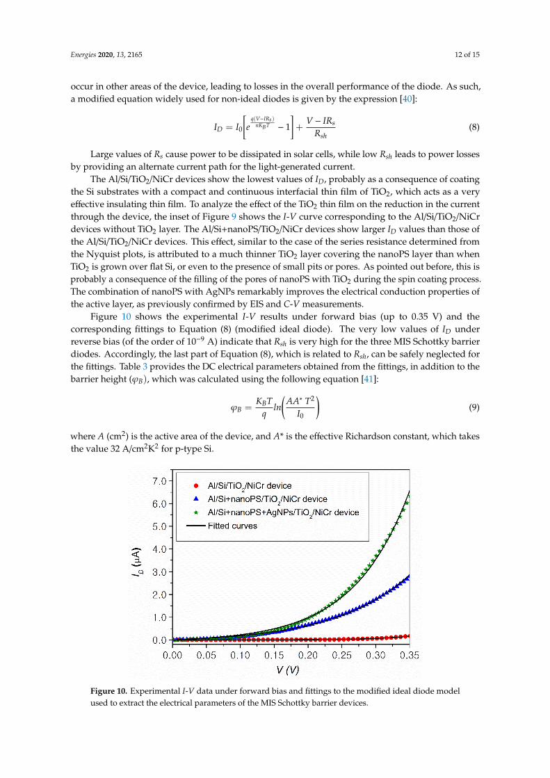
Energies 2020, 13, 2165 12 of 15
occur in other areas of the device, leading to losses in the overall performance of the diode. As such,a modified equation widely used for non-ideal diodes is given by the expression [40]:
ID = I0
[e
q(V−IRs)nKBT − 1
]+
V − IRs
Rsh(8)
Large values of Rs cause power to be dissipated in solar cells, while low Rsh leads to power lossesby providing an alternate current path for the light-generated current.
The Al/Si/TiO2/NiCr devices show the lowest values of ID, probably as a consequence of coatingthe Si substrates with a compact and continuous interfacial thin film of TiO2, which acts as a veryeffective insulating thin film. To analyze the effect of the TiO2 thin film on the reduction in the currentthrough the device, the inset of Figure 9 shows the I-V curve corresponding to the Al/Si/TiO2/NiCrdevices without TiO2 layer. The Al/Si+nanoPS/TiO2/NiCr devices show larger ID values than those ofthe Al/Si/TiO2/NiCr devices. This effect, similar to the case of the series resistance determined fromthe Nyquist plots, is attributed to a much thinner TiO2 layer covering the nanoPS layer than whenTiO2 is grown over flat Si, or even to the presence of small pits or pores. As pointed out before, this isprobably a consequence of the filling of the pores of nanoPS with TiO2 during the spin coating process.The combination of nanoPS with AgNPs remarkably improves the electrical conduction properties ofthe active layer, as previously confirmed by EIS and C-V measurements.
Figure 10 shows the experimental I-V results under forward bias (up to 0.35 V) and thecorresponding fittings to Equation (8) (modified ideal diode). The very low values of ID underreverse bias (of the order of 10−9 A) indicate that Rsh is very high for the three MIS Schottky barrierdiodes. Accordingly, the last part of Equation (8), which is related to Rsh, can be safely neglected forthe fittings. Table 3 provides the DC electrical parameters obtained from the fittings, in addition to thebarrier height (ϕB), which was calculated using the following equation [41]:
ϕB =KBT
qln
(AA∗ T2
I0
)(9)
where A (cm2) is the active area of the device, and A* is the effective Richardson constant, which takesthe value 32 A/cm2K2 for p-type Si.
Energies 2020, 11, x FOR PEER REVIEW 13 of 16
process. The combination of nanoPS with AgNPs remarkably improves the electrical conduction
properties of the active layer, as previously confirmed by EIS and C‐V measurements.
Figure 10 shows the experimental I‐V results under forward bias (up to 0.35 V) and the
corresponding fittings to Equation (8) (modified ideal diode). The very low values of ID under reverse
bias (of the order of 10−9 A) indicate that Rsh is very high for the three MIS Schottky barrier diodes.
Accordingly, the last part of Equation (8), which is related to Rsh, can be safely neglected for the
fittings. Table 3 provides the DC electrical parameters obtained from the fittings, in addition to the
barrier height (𝜑 , which was calculated using the following equation [41]:
𝜑𝐾 𝑇
𝑞𝑙𝑛
𝐴𝐴∗ 𝑇𝐼
(9)
where A (cm2) is the active area of the device, and A* is the effective Richardson constant, which takes
the value 32 A/cm2K2 for p‐type Si.
Figure 10. Experimental I‐V data under forward bias and fittings to the modified ideal diode model
used to extract the electrical parameters of the MIS Schottky barrier devices.
Table 4 presents a comparison between the DC electrical parameters, namely I0, n, Rs, and φB for
the three MIS Schottky barrier devices. Since the values of ID are rather small for the Al/Si/TiO2/NiCr
devices compared with the other two Schottky barrier devices, I0 is very small. Likewise, n shows the
lowest value in this case. The increase in n observed for the Al/Si+nanoPS/TiO2/NiCr devices is
attributed to the higher porosity of the surface of Si after the etching process, which causes an increase
in the defects on the surface of the nanoPS layers [35]. The reduction of the value of the ideality factor
for the Al/Si+nanoPS+AgNPs/TiO2/NiCr devices (n = 3.29) is considered a consequence of a change
of the type of charge carrier recombination that is taking place in the active layer associated to the Ag
nanoparticles embedded into nanoPS.
Table 4. DC electrical parameters obtained from the fitting of the experimental I‐V curves.
Figure 10. Experimental I-V data under forward bias and fittings to the modified ideal diode modelused to extract the electrical parameters of the MIS Schottky barrier devices.
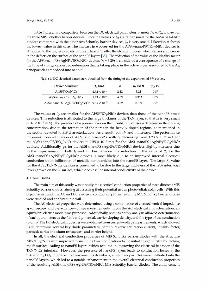
Energies 2020, 13, 2165 13 of 15
Table 4 presents a comparison between the DC electrical parameters, namely I0, n, Rs, and ϕB forthe three MIS Schottky barrier devices. Since the values of ID are rather small for the Al/Si/TiO2/NiCrdevices compared with the other two Schottky barrier devices, I0 is very small. Likewise, n showsthe lowest value in this case. The increase in n observed for the Al/Si+nanoPS/TiO2/NiCr devices isattributed to the higher porosity of the surface of Si after the etching process, which causes an increasein the defects on the surface of the nanoPS layers [35]. The reduction of the value of the ideality factorfor the Al/Si+nanoPS+AgNPs/TiO2/NiCr devices (n = 3.29) is considered a consequence of a change ofthe type of charge carrier recombination that is taking place in the active layer associated to the Agnanoparticles embedded into nanoPS.
Table 4. DC electrical parameters obtained from the fitting of the experimental I-V curves.
Device Structure I0 (mA) n Rs (kΩ) ϕB (V)
Al/Si/TiO2/NiCr 2.32 × 10⁻⁷ 2.12 3.21 0.87
Al/Si+nanoPS/TiO2/NiCr 1.23 × 10⁻⁴ 4.39 0.363 0.72
Al/Si+nanoPS+AgNPs/TiO2/NiCr 9.55 × 10⁻⁵ 3.29 0.139 0.73
The values of ID are smaller for the Al/Si/TiO2/NiCr devices than those of the nanoPS-baseddevices. This reduction is attributed to the large thickness of the TiO2 layer, so that I0 is very small(2.32 × 10⁻⁷ mA). The presence of a porous layer on the Si substrate causes a decrease in the dopingconcentration, due to the formation of the pores in the heavily doped regions, as mentioned inthe section devoted to EIS characterization. As a result, both I0 and n increase. The performanceimproves upon infiltration of AgNPs into nanoPS, with I0 decreasing from 1.23 × 10⁻⁴ mA forthe Al/Si+nanoPS/TiO2/NiCr devices to 9.55 × 10⁻⁵ mA for the Al/Si+nanoPS+AgNPs/TiO2/NiCrdevices. Additionally, ϕB for the Al/Si+nanoPS+AgNPs/TiO2/NiCr devices slightly increases dueto the improvement in both I0 and n. Furthermore, the reduction in the value of Rs for theAl/Si+nanoPS+AgNPs/TiO2/NiCr devices is most likely due to an improved internal electricalconduction upon infiltration of metallic nanoparticles into the nanoPS layer. The large Rs valuefor the Al/Si/TiO2/NiCr devices is presumed to be due to the large thickness of the TiO2 interfaciallayers grown on the Si surface, which decrease the internal conductivity of the device.
4. Conclusions
The main aim of this study was to study the electrical conduction properties of three different MISSchottky barrier diodes, aiming at assessing their potential use as photovoltaic solar cells. With thisobjective in mind, the AC and DC electrical conduction properties of the MIS Schottky barrier diodeswere studied and analyzed in detail.
The AC electrical properties were determined using a combination of electrochemical impedancespectroscopy and capacitance–voltage measurements. From the AC electrical characterization, anequivalent electric model was proposed. Additionally, Mott–Schottky analysis allowed determinationof such parameters as the flat-band potential, carrier doping density, and the type of the conduction(p or n). The DC electrical properties were obtained from current–voltage measurements, which allowedus to determine several key diode parameters, namely reverse saturation current, ideality factor,parasitic series and shunt resistances, and barrier height.
In all, the electrical conduction properties of MIS Schottky barrier diodes with the structureAl/Si/TiO2/NiCr were improved by including two modifications to the initial design. Firstly, by etchingthe Si surface leading to nanoPS layers, which resulted in improving the electrical behavior of theTiO2/NiCr interface. However, the presence of nanoPS layers leads to conduction losses at theSi+nanoPS/TiO2 interface. To overcome this drawback, silver nanoparticles were infiltrated into thenanoPS layers, which led to a notable enhancement in the overall electrical conduction propertiesof the resulting Al/Si+nanoPS+AgNPs/TiO2/NiCr MIS Schottky barrier diodes. The enhancement
Energies 2020, 13, 2165 14 of 15
observed in the electrical conduction and carrier separation for these devices was recently reported toalso improve their optoelectronic performance, thus enabling their use in the field of photovoltaics.
Author Contributions: Conceptualization, R.R. and R.J.M.-P.; Methodology, R.R.; Validation, R.R. and R.J.M.-P.;Formal Analysis, R.R. and R.J.M.-P. Investigation, R.R. and R.J.M.-P.; Resources R.R. and R.J.M.-P.; Data Curation,R.R. and R.J.M.-P.; Writing-Original Draft Preparation, R.R.; Writing-Review & Editing, R.R. and R.J.M.-P.;Visualization, R.R. and R.J.M.-P.; Supervision, R.J.M.-P.; Project Administration, R.J.M.-P.; Funding Acquisition,R.J.M.-P. All authors have read and agreed to the published version of the manuscript.
Funding: This work was partially supported by the Egyptian Ministry of Higher Education, Missions Sectionunder an Egyptian joint supervision grant at UAM Spain for PhD degree.
Acknowledgments: We would like to thank the Egyptian Institute, Cultural Office of the Egyptian Embassy inMadrid, Spain. The authors are thankful to Luis García Pelayo and Valentin Constantin Nistor for technical support.
Conflicts of Interest: The authors declare no conflict of interest.
References
1. Gautier, G.; Defforge, T.; Desplobain, S.; Billoué, J.; Capelle, M.; Povéda, P.; Vanga, K.; Lu, B.; Bardet, B.;Lascaud, J. Porous silicon in microelectronics: From academic studies to industry. ECS Trans. 2015, 69, 123–134.[CrossRef]
2. Canham, L. Handbook of Porous Silicon; Springer: Berlin/Heidelberg, Germany, 2014.3. Martın-Palma, R.; Pérez-Rigueiro, J.; Martınez-Duart, J. Study of carrier transport in metal/porous silicon/Si
structures. J. Appl. Phys. 1999, 86, 6911–6914. [CrossRef]4. Martín-Palma, R.; Pérez-Rigueiro, J.; Guerrero-Lemus, R.; Moreno, J.; Martínez-Duart, J. Ageing of aluminum
electrical contacts to porous silicon. J. Appl. Phys. 1999, 85, 583–586. [CrossRef]5. Shetty, A.; Roul, B.; Mukundan, S.; Mohan, L.; Chandan, G.; Vinoy, K.; Krupanidhi, S. Temperature dependent
electrical characterisation of Pt/HfO2/n-GaN metal-insulator-semiconductor (MIS) Schottky diodes. AIP Adv.2015, 5, 097103. [CrossRef]
6. Kim, H.; Kumar, M.D.; Kim, J. Highly-performing Ni/SiO2/Si MIS photodetector for NIR detecting applications.Sens. Actuators A Phys. 2015, 233, 290–294. [CrossRef]
7. Digdaya, I.A.; Adhyaksa, G.W.; Trzesniewski, B.J.; Garnett, E.C.; Smith, W.A. Interfacial engineering ofmetal-insulator-semiconductor junctions for efficient and stable photoelectrochemical water oxidation.Nat. Commun. 2017, 8, 15968. [CrossRef]
8. Chang, T.-Y.; Chang, C.-L.; Lee, H.-Y.; Lee, P.-T. A metal-insulator-semiconductor solar cell with highopen-circuit voltage using a stacking structure. IEEE Electron Device Lett. 2010, 31, 1419–1421. [CrossRef]
9. Pulfrey, D.L. MIS solar cells: A review. IEEE Trans. Electron Devices 1978, 25, 1308–1317. [CrossRef]10. Fahrenbruch, A.; Bube, R. Fundamentals of Solar Cells: Photovoltaic Solar Energy Conversion; Elsevier:
Amsterdam, The Netherlands, 2012.11. Fonash, S. Solar Cell Device Physics; Elsevier: Amsterdam, The Netherlands, 2012.12. Singh, R.; Green, M.; Rajkanan, K. Review of conductor-insulator-semiconductor (CIS) solar cells. Sol. Cells
1981, 3, 95–148. [CrossRef]13. Srivastava, A.; Arora, B.; Guha, S. Current-voltage characteristics of GaAs metal-insulator-semiconductor
solar cells under illumination. Sol. Cells 1984, 12, 277–283. [CrossRef]14. Wang, F.; Fahrenbruch, A.; Bube, R. Properties of metal-semiconductor and metal-insulator-semiconductor
junctions on CdTe single crystals. J. Appl. Phys. 1989, 65, 3552–3559. [CrossRef]15. Shewchun, J.; Burk, D.; Spitzer, M.B. MIS and SIS solar cells. IEEE Trans. Electron Devices 1980, 27, 705–716.
[CrossRef]16. Sharma, B. Metal-Semiconductor Schottky Barrier Junctions and Their Applications; Springer Science & Business
Media: Berlin/Heidelberg, Germany, 2013.17. Mora-Sero, I.; Garcia-Belmonte, G.; Boix, P.P.; Vazquez, M.A.; Bisquert, J. Impedance spectroscopy
characterisation of highly efficient silicon solar cells under different light illumination intensities.Energy Environ. Sci. 2009, 2, 678–686. [CrossRef]
18. Lee, G.W.; Kim, H.; Park, J.; Shim, J.-I.; Shin, D.-S. Investigation of luminance degradation in organiclight-emitting diodes by impedance spectroscopy. IEEE Photonics Technol. Lett. 2018, 30, 1183–1185.[CrossRef]
Energies 2020, 13, 2165 15 of 15
19. Ramadan, R.; Kamal, H.; Hashem, H.; Abdel-Hady, K. Gelatin-based solid electrolyte releasing Li+ for smartwindow applications. Sol. Energy Mater. Sol. Cells 2014, 127, 147–156. [CrossRef]
20. Ramadan, R.; Elshorbagy, M.; Kamal, H.; Hashem, H.; Abdelhady, K. Preparation and characterizationof protonic solid electrolyte applied to a smart window device with high optical modulation. Optik2017, 135, 85–97. [CrossRef]
21. Schönleber, M.; Uhlmann, C.; Braun, P.; Weber, A.; Ivers-Tiffée, E. A consistent derivation of the impedance ofa lithium-ion battery electrode and its dependency on the state-of-charge. Electrochim. Acta 2017, 243, 250–259.[CrossRef]
22. Gelderman, K.; Lee, L.; Donne, S. Flat-band potential of a semiconductor: Using the Mott–Schottky equation.J. Chem. Educ. 2007, 84, 685. [CrossRef]
23. Kim, W.; Choi, W. A novel parameter extraction method for the one-diode solar cell model. Sol. Energy2010, 84, 1008–1019. [CrossRef]
24. Ramadan, R.; Manso-Silván, M.; Martín-Palma, R.J. Hybrid porous silicon/silver nanostructures for thedevelopment of enhanced photovoltaic devices. J. Mater. Sci. 2020, 55, 5458–5470. [CrossRef]
25. Martín-Palma, R.J.; McAtee, P.D.; Ramadan, R.; Lakhtakia, A. Hybrid Nanostructured porous silicon-silverLayers for Wideband optical Absorption. Sci. Rep. 2019, 9, 7291. [CrossRef] [PubMed]
26. Orazem, M.E.; Tribollet, B. Electrochemical Impedance Spectroscopy; John Wiley & Sons: Hoboken, NJ, USA, 2017.27. Ribeiro, D.; Souza, C.; Abrantes, J. Use of Electrochemical Impedance Spectroscopy (EIS) to monitoring the
corrosion of reinforced concrete. Rev. Ibracon De Estrut. E Mater. 2015, 8, 529–546. [CrossRef]28. Kim, J.H.; Shin, D.H.; Lee, H.S.; Jang, C.W.; Kim, J.M.; Seo, S.W.; Kim, S.; Choi, S.-H. Enhancement of
efficiency in graphene/porous silicon solar cells by co-doping graphene with gold nanoparticles and bis(trifluoromethanesulfonyl)-amide. J. Mater. Chem. C 2017, 5, 9005–9011. [CrossRef]
29. Chavarria, M.; Fonthal, F. Electrical Investigation of Porous Silicon/p-Si Heterojunction Prepared byElectrochemical Etching. ECS J. Solid State Sci. Technol. 2016, 5, P3172–P3175. [CrossRef]
30. Kulathuraan, K.; Mohanraj, K.; Natarajan, B. Structural, optical and electrical characterization ofnanostructured porous silicon: Effect of current density. Spectrochim. Acta Part A Mol. Biomol. Spectrosc.2016, 152, 51–57. [CrossRef]
31. Sultan, F.I.; Slman, A.A.; Nayef, U.M. IV and CV Characteristics of Porous Silicon Nanostructures byElectrochemical Etching. Eng. Technol. J. 2013, 31, 332–338.
32. Hamza, S.; Ignaszak, A.; Kiani, A. Synthesis of electrical conductive silica nanofiber/gold nanoparticlecomposite by laser pulses and sputtering technique. Nanoscale Res. Lett. 2017, 12, 432. [CrossRef]
33. Wang, D.; Zhu, J.; Ding, L.; Gao, P.; Pan, X.; Sheng, J.; Ye, J. Interface electric properties of Si/organic hybridsolar cells using impedance spectroscopy analysis. Jpn. J. Appl. Phys. 2016, 55, 056601. [CrossRef]
34. Youssef, G.; El-Nahass, M.; El-Zaiat, S.; Farag, M. Effect of porosity on the electrical and photoelectricalproperties of textured n+ p silicon solar cells. Mater. Sci. Semicond. Process. 2015, 39, 457–466. [CrossRef]
35. Harizi, A.; Laatar, F.; Ezzaouia, H. Physical properties enhancement of porous silicon treated with In2O3 as aantireflective coating. Results Phys. 2019, 12, 1716–1724. [CrossRef]
36. Fabregat-Santiago, F.; Garcia-Belmonte, G.; Mora-Sero, I.; Bisquert, J. Characterization of nanostructuredhybrid and organic solar cells by impedance spectroscopy. Phys. Chem. Chem. Phys. 2011, 13, 9083–9118.[CrossRef] [PubMed]
37. Shibayama, N.; Zhang, Y.; Satake, T.; Sugiyama, M. Modelling of an equivalent circuit for Cu 2 ZnSnS 4-andCu 2 ZnSnSe 4-based thin film solar cells. RSC Adv. 2017, 7, 25347–25352. [CrossRef]
38. Ma, Y.; Pendlebury, S.R.; Reynal, A.; Le Formal, F.; Durrant, J.R. Dynamics of photogenerated holes inundoped BiVO 4 photoanodes for solar water oxidation. Chem. Sci. 2014, 5, 2964–2973. [CrossRef]
39. Gupta, G.K.; Garg, A.; Dixit, A. Electrical and impedance spectroscopy analysis of sol-gel derived spin coatedCu2ZnSnS4 solar cell. J. Appl. Phys. 2018, 123, 013101. [CrossRef]
40. Darwish, A.; El-Shazly, E.; Attia, A.; El-Rahman, K.A. Dark electrical properties and photovoltaic performanceof organic/inorganic (SnPcCl 2/p-Si) solar cells. J. Mater. Sci. Mater. Electron. 2016, 27, 8786–8792. [CrossRef]
41. Sze, S.M.; Ng, K.K. Physics of Semiconductor Devices; John Wiley & Sons: Hoboken, NJ, USA, 2006.
© 2020 by the authors. Licensee MDPI, Basel, Switzerland. This article is an open accessarticle distributed under the terms and conditions of the Creative Commons Attribution(CC BY) license (http://creativecommons.org/licenses/by/4.0/).


