Embed Size (px)
Citation preview

Energy level spectroscopy of InSb quantum wells using quantum-well LED emission
T. G. Tenev and A. Palyi*Department of Physics, University of Lancaster, Lancaster LA1 4YB, United Kingdom
B. I. MirzaDepartment of Electrical and Electronic Engineering, Photonics Group, University of Bristol, Bristol BS8 1UB, United Kingdom
G. R. Nash†
QinetiQ, Malvern Technology Centre, Malvern WR14 3PS, United Kingdomand Department of Electrical and Electronic Engineering, Photonics Group, University of Bristol, Bristol BS8 1UB, United Kingdom
M. Fearn, S. J. Smith, L. Buckle, M. T. Emeny, T. Ashley, and J. H. JeffersonQinetiQ, Malvern Technology Centre, Malvern WR14 3PS, United Kingdom
C. J. LambertDepartment of Physics, University of Lancaster, Lancaster LA1 4YB, United Kingdom
�Received 11 July 2008; revised manuscript received 21 September 2008; published 2 February 2009�
We have investigated the low-temperature optical properties of InSb quantum-well �QW� light-emittingdiodes, with different barrier compositions, as a function of well width. Three devices were studied: QW1 hada 20 nm undoped InSb quantum well with a barrier composition of Al0.143In0.857Sb, QW2 had a 40 nm undopedInSb well with a barrier composition of Al0.077In0.923Sb, and QW3 had a 100 nm undoped InSb well with abarrier composition of Al0.025In0.975Sb. For QW1, the signature of two transitions �CB1-HH1 and CB1-HH2�can be seen in the measured spectrum, whereas for QW2 and QW3 the signature of a large number oftransitions is present in the measured spectra. In particular transitions to HH2 can be seen, the first time this hasbeen observed in AlInSb/InSb heterostructures. To identify the transitions that contribute to the measuredspectra, the spectra have been simulated using an eight-band k .p calculation of the band structure togetherwith a first-order time-dependent perturbation method �Fermi golden rule� calculation of spectral emittance,taking into account broadening. In general there is good agreement between the measured and simulatedspectra. For QW2 we attribute the main peak in the experimental spectrum to the CB2-HH1 transition, whichhas the highest overall contribution to the emission spectrum of QW2 compared with all the other interbandtransitions. This transition normally falls into the category of “forbidden transitions,” and in order to under-stand this behavior we have investigated the momentum matrix elements, which determine the selection rulesof the problem.
DOI: 10.1103/PhysRevB.79.085301 PACS number�s�: 78.67.De, 78.60.Fi, 42.72.Ai
I. INTRODUCTION
There is growing interest in the development ofInSb /AlxIn1−xSb-based quantum wells �QWs� for uncooled,low power dissipation high-speed transistors,1 for lasers,2
and for devices exhibiting quantum effects such as quantizedconductance,3,4 where the low electron effective mass�0.014me� offers the prospect for elevated temperature opera-tion due to enhanced quantum confinement.4 The high elec-tron g factor ��−51� also makes InSb /AlxIn1−xSb QWs par-ticularly attractive for quantum information applications.5
Quantum confinement was first demonstrated inInSb /AlxIn1−xSb multiquantum-well �MQW� samples, grownon InSb substrates, using photoluminescence �PL�spectroscopy.6 Recent developments in growth techniqueshave allowed high quality heterostructures to be grown onsemi-insulating �SI� GaAs substrates, which is important formany device applications, and the optical properties ofMQW structures grown on GaAs have been studied in ab-sorption spectroscopy7–9 and photoluminescencemeasurements.10 However only one study of the opticalproperties of single InSb QWs, using photoluminescence,
has so far been published,11 although many novel devicescould be perhaps realized using single InSb QWs. For ex-ample, such a well could be used to develop a high-frequency single-photon source emitting in the technologi-cally important 3–5 �m wavelength region,5 for example,at 3.9 �m, which could enable long-distance, free-space se-cure communication, via quantum cryptography, with lowatmospheric scattering and absorption. In this proposed de-vice, single electrons would be injected into the p-type re-gion of a lateral InSb QW light-emitting diode �LED�.12 Agreater understanding of the optical properties of single InSbQWs is therefore required before their unique characteristics,such as the high electron g factor can be fully exploited, andin this paper we analyze the low-temperature emission spec-tra of conventional vertical LEDs containing active regionsconsisting of InSb quantum wells of varying thicknesses.13
Electroluminescence studies provide an exciting experimen-tal platform that offers additional degrees of freedom, suchas the ability to vary the net bias across the quantum wellsthat complement photoluminescence techniques. The mea-sured emission spectra, which are compared to simulationscarried out using an eight-band k .p model, exhibit a number
PHYSICAL REVIEW B 79, 085301 �2009�
1098-0121/2009/79�8�/085301�14� ©2009 The American Physical Society085301-1

of features, including a large number of observed transitions,which reflect the unique properties of this material system.
II. THEORETICAL MODEL
A. Band-structure model
For the theoretical description of the QW-based LED wehave chosen the z axis of the Cartesian coordinate system tolie along the growth direction of the device. The bulk bandstructure in the vicinity of the � point of InSb and its alloysis well described14 by the semiempirical k .p method.15,16 Tofind the energy spectrum and wave functions of electrons andholes localized in the QWs we employed the envelope func-tion approximation �EFA� �Ref. 16–22� as the generalizationof the k .p method for heterostructures. We took into accountthe heavy- and light-hole bands, with symmetry �8
v, the spin-orbit split bands �7
v, and the lowest conduction bands �6c, the
ones used in an eight-band k .p description of bulk materials.For the band-edge Bloch functions uj,k=0�r� we used thephase convention defined by Weiler.23 Their explicit formcan also be found in the Appendix of Ref. 24. FollowingRam-Mohan et al.24 we assumed that the basis set of zone-center Bloch functions uj,k=0�r� is identical for the well�InSb� and barrier �AlxIn1−xSb� materials.
Within the above framework the eigenfunctions of thesingle-particle Hamiltonian H are expressed as linear combi-nations of the band-edge Bloch functions
�n,k�r� = eik�·r��j
fnr�
j �z�uj,k=0�r� , �1�
where k� = �kx ,ky ,0� and r� = �rx ,ry ,0� and the expansion co-efficients, the envelope functions fnk!!
j �z�, are supposed tovary slowly over the lattice unit cells. The eigenvalue prob-lem H�n,k�
�r�=En�k���n,k��r� reduces to a set of eight
coupled differential equations for the envelope functions
fnk�
j� �z�
�j�
Hjj��kx,ky,− i � /�z�fnk�
j� �z� = En�k��fnk�
j� �z� . �2�
In the chosen representation23 the matrix elements Hjj� of theHamiltonian are identical to the one given in Table III of Ref.24. In the absence of magnetic field the Hamiltonian matrixelements Hjj� are parametrized by the interband matrix ele-ment P 14; the Kane parameter F;14 themodified-Luttinger24–27 parameters �1, �2, and �3; and theband gap Eg and spin-orbit split-off energies � relative to the�8
v valence-band edge.We used the axial approximation by setting the modified
Luttinger parameters �2 and �3 equal to each other and equalto �= �2�2+3�3� /5.24 The axial approximation neglects theanisotropy in the dispersion relations En�k��. Furthermore weneglected the material dependence of the parameters P, F,�1, �2, and �3. For the interband matrix element P we usedthe value for InSb reported by Auvergne et al.28 We took therecommended values from Table IX of Ref. 14 for the otherband-structure parameters of InSb.
The temperature dependencies of the InSb and AlSb bandgaps Eg were taken into account through the empirical
Varshni law14 using the values for the Varshni parameters �and � given in Ref. 14. The band gap and spin-orbit splittingdependence of the AlxIn1−xSb alloy of composition fraction xwere accounted for using the following quadratic interpola-tion formula:14,29
T�AlxIn1−xSb� = xT�AlSb� + �1 − x�T�InSb� − x�1 − x�CT,
�3�
where T stands for either Eg or �. We have used the valuesrecommended by Vurgaftman et al.14 for the bowing param-eters CT. Through Eq. �3� we have also accounted for thetemperature dependence of the alloy band gap by usingtemperature-dependent values for the InSb and AlSb bandgaps.
Strain due to the lattice constant mismatch between theAlxIn1−xSb alloy and InSb was included in our modelthrough its effect on the InSb band gap. The lattice constantof AlxIn1−xSb was determined by Vegard’s law30 withtemperature-dependent values of InSb and AlSb lattice con-stants taken from Ref. 14. The compressive biaxial strainlifts the light- and heavy-hole degeneracies at the � point.32
Using the methods described by Dai et al.7 and Kasturiarach-chi et al.31 and material parameters for InSb and AlSb asrecommended by Vurgaftman et al.,14 we have calculated thestrained band gaps between the conduction and heavy- andlight-hole bands, respectively, and used them as input param-eters in our simulations. For the conduction-band offset ratioQc we assumed the value Qc=0.62.31
We treated the model given by Eq. �2� numerically, as-suming that the envelope functions vanish at the surface ofthe sample and deep inside the substrate. The solutions of theeigenvalue problem were found by expanding the envelopefunctions in a Fourier series and expressing the matrix ele-ments Hjj� of the EFA Hamiltonian in the Fourier basis. Theresulting matrix was diagonalized numerically using stan-dard LAPACK routines.
B. Luminescence model
The microscopic mechanism underlying electrolumines-cence in semiconductor quantum wells is the spontaneousemission of light due to electron-hole recombination. Thespontaneous emission is purely a quantum mechanical pro-cess which requires a quantum description of the electromag-netic �EM� field. We have used the standard quantization in afinite volume procedure33 for the EM vector-potential opera-
tor A�̂ �r� , t� and worked in SI units. In this paradigm a classicalEM wave characterized by wave vector q� , polarization vector���q� , and angular frequency q=c�q� � is viewed as a collec-tion of photons in single-particle modes �q�� characterizedby two quantum numbers q� and . The number of possiblephoton modes per unit energy describing photons propagat-ing in solid angle d� with definite polarization is given bythe photon density of states �� �=V2n3 / �2�c�3,33,34
where n is the refractive index of the medium and V is thequantization volume.
The number of polarized photons emitted per unit en-ergy interval per second in a solid angle d� due to electron-
TENEV et al. PHYSICAL REVIEW B 79, 085301 �2009�
085301-2

hole recombination in the volume of a quantum well is givenby the expression
Nq̂� � = �n,m
�k��
Wnmk��,q��� �f�En�k���1 − f�Em�k���� ,
�4�
where the summation is over all pairs of electron-hole states,f�En�k��� is the statistical probability that the conduction-band state �nk��� is occupied, and 1− f�Em�k��� is the probabil-ity that the valence band state �mk��� is empty. We assume thatthe relaxation time of electrons and holes injected into thequantum well is much shorter than the radiative recombina-tion time. Therefore, on the timescale of electron-hole re-combination, the hole and electron gases behave effectivelyas being in thermodynamic equilibrium characterized bysome effective temperature Te, which in general is differentand higher than the temperature of the host crystal lattice Tc.In this approximation the statistical distribution function f�E�takes the simplified form of the Fermi-Dirac function f�E�=1 / 1+exp��E−�� /kBTe�, where kB is the Boltzmann con-stant and � is the chemical potential of either electrons orholes. The probability for a transition from conduction-bandstate �nk��� to valence-band state �mk��� per unit time Wnmk��,q�
is calculated within the first-order, time-dependent perturba-tion method �Fermi golden rule�,35 using the following di-pole approximation:33,36
Wnmk��,q� =2�
�� nm�k��� −
2�V
e2
m2n2 ��mk���p� . ���nk����2,
�5�
where m is the free-electron mass, � is the dielectric constantof the medium, e is the electron charge, n is the refractiveindex of the medium, �� is the polarization vector of the EMfield, and nm�k��� is the Bohr frequency of the transitionbetween states �nk��� and �mk��� determined by the equation nm�k���=En�k���−Em�k���. The conservation of energy in theemission process is enforced by the Dirac delta function inEq. �5� which also ensures that only resonant transitions ful-filling the condition =nm�k��� contribute to the emitted ra-diation. Information about the effects of the electron energysubband structure in the quantum well is contained in themomentum matrix element �mk���p� �nk��� and the electron andhole subband dispersion relations En�k��� and Em�k���.
Photons with the same frequency resulting from sponta-neous emission between different states have uncorrelatedpropagation directions and polarizations. The resulting EMfield is represented by the total number of emitted photonsN� � with angular frequency which is obtained by sum-ming Nq̂� � over the two linearly independent polarizationmodes = �1 and integrating over all propagation directionsN� �= �d��Nq̂� �, where � is the unit sphere. Thetotal energy carried by the emitted radiation per unit energyinterval per unit time is given by the product of N� � andthe energy carried by each photon , P� �=N� � .The experimentally observable spectral emittance is the EM
energy per unit time and unit energy interval passing throughunit surface area at distance r, I� �= P� � /4�r2
�WJ−1m−2�.In the derivation of Eq. �5� we have assumed that the
conduction- and valence-band energy levels are well defined.In practice there are a number of environmental factorswhich lead to deviation from the ideal delta peak shape ofthe transition introducing broadening into the line shape. Theunderlying mechanisms are usually classified into the twogroups of homogeneous and inhomogeneous broadening.The natural linewidth and electron-phonon scattering areusual sources of homogeneous broadening. As is usuallyaccepted37–39 we modeled their effect on the emission lineshape by the substitution of the Lorentzian functionL� , nm�k��� ;�H� instead of the Dirac delta in Eq. �5�where the homogeneous linewidth �H is the full width at halfmaximum �FWHM� of the Lorentzian. The combined effectof the individual homogeneous mechanisms is modeled by aconvolution of Lorentzians, which is again Lorentzian withFWHM �H=�H� +�H� +¯, where the primed FWHM are thecontributions from the individual mechanisms.
Possible sources of inhomogeneous broadening are wellwidth fluctuations across an individual well or well-to-wellwidth fluctuations arising during QW growth. They lead tostatistical distribution of the Bohr frequencies of the transi-tion nm�k��� around the values for an ideal well. We haveassumed that the transition energies E associated with theBohr frequencies are normally distributed around the idealvalue nm�k��� for the transition �nk���→ �mk��� with FWHMof the Gaussian �I. Contributions of the individual mecha-nisms to the overall inhomogeneous broadening is given bythe expression40 �I
2=�I�2+�I�
2+¯.The combined effects of the two types of broadening are
taken into account by the Voight function which is a convo-lution of the Lorentzian and Gaussian functions describedabove and is explicitly given by
U� , nm�k���;�I,�H
=A
�3/2�2�I�
0
�
dE��H/2�
� − E�2 + ��H/2�2
�exp�−�E − nm�k���2
2�I2 � , �6�
where the lower limit of the integration is restricted to zerobecause of the interpretation of the integration variable as atransition energy. This line shape has been used for the de-termination of the linewidth of intersubband transitions37 inthe InGaAs/AlGaAs system and for the description of theline shape in the vicinity of the exciton absorption lines inGaAs multiple quantum wells.41 The normalization constantA arises from the conservation of energy principle enforcedby the integral of the Voight function over all possible tran-sition energies dnmU� , nm�k��� ;�I ,�H�=1. For thesake of computational efficiency we have used the approxi-mation to the Voight function developed in Ref. 40.
ENERGY LEVEL SPECTROSCOPY OF InSb QUANTUM… PHYSICAL REVIEW B 79, 085301 �2009�
085301-3

The final explicit form of the spectral emittance which wehave used to interpret the experimental data is thus given asfollows:
I� � = �n,m
�k��
e2
4�2�r2
2n
3m2c3U� , nm�k���;�I,�H
���mk���p�̂ �nk����2f�En�k���1 − f�Em�k���� , �7�
III. EXPERIMENTAL METHOD
The samples studied were grown by molecular-beam epi-taxy at QinetiQ Malvern on SI GaAs substrates.1 A sche-matic diagram of the QW LED structure is shown in Fig. 1.The InSb QWs were grown on top of a 3-�m-thickAlxIn1−xSb barrier and were capped with a 120-nm-thicklayer of AlxIn1−xSb. Tellurium and beryllium were used todope the layers n type and p type to nominal levels of 2�1017 and 5�1018 cm−3, respectively. Three QW LEDstructures were investigated: QW1 had a 20 nm undopedInSb quantum well with a barrier composition of x=0.143;QW2 had a 40 nm undoped InSb well with a barrier compo-sition of x=0.077; and QW3 had a 100 nm undoped InSbwell with a barrier composition of x=0.025. The compositionof the barrier layers was determined by x-ray diffractionmeasurements. Devices consisted of 16 elements connectedin series yielding a total emitting area of 1 mm2. More de-tails concerning device structure, growth, and doping can befound in Ref. 13 �and references therein�. The devices weremounted on ceramic packages in a closed cycle cryostat,with optical access through a CaF2 window. Emitted lightfrom the devices was collimated using a CaF2 lens and di-rected to a SPEX 270 M grating spectrometer �with a 5 �mblazed grating�. Peak injection currents used were 2 mA forQW1 and 20 mA for QW2 and QW3. Measurements werecarried out at either 15 or 25 K.
IV. RESULTS AND DISCUSSION
A. Overview
The interpretation of the experimental results in thepresent study is an example of the reverse problem in theo-
retical physics. In its most general formulation one has tounderstand and describe a set of interrelated physical effectsand mechanisms determining the experimental results basedmostly on the experimental observations. We solved theproblem for the spontaneous emission from QW1, QW2, andQW3 by the method of line-shape fitting employing the the-oretical model described in Sec. II which contains five fittingparameters: the effective temperature Te, the injected carrierdensity in the well n, the homogeneous broadening �H, theinhomogeneous broadening �I, and the net bias across thequantum well Vnet.
We have assumed that the electron and hole gases can becharacterized by the same effective temperature Te.
39 Thecondition for charge neutrality in the quantum well as awhole requires that the injected carrier density for electronsis equal to that of holes ne=nh=n. The net bias across thewell is the difference between the built-in potential of thep-i-n junction and the voltage drop across it due to the ex-ternally applied voltage. Estimation of this voltage drop isunreliable due to the contact resistance present in the devicearchitecture. The contact resistance depends on the growthconditions which may vary from sample to sample. We havetherefore treated the net bias across the quantum well as afitting parameter. We have minimized the weighted chi-squared �2�Te ,n ,�H ,�I ,Vnet� function in the five-dimensional parameter space using the global nonlinearminimization algorithm of simulated annealing �SA� �Refs.42 and 43� subject to constraints in the parameter space. Forselected cases we have compared the results of the �2 mini-mization by the SA with the more accurate, but computation-ally much more intensive, differential evolution algorithm.44
The results were in satisfactory agreement, giving us confi-dence in the parameter estimates obtained by SA.
The best fit between experiment measurements and theo-retical calculations and the values of the five fitting param-eters have been determined as the values of Te ,n ,�H ,�I ,Vnetwhich give the minimum value of �2, according to the gen-eral theory of optimization. We have not supposed any par-ticular values for the fitting parameters Te ,n ,�H ,�I ,Vnet,rather their values have been calculated by the SA �Refs. 42and 43� minimization algorithm. Furthermore the compari-son between the experimental and theoretical line shapes pre-sented in Figs. 3�a�, 4�a�, and 5�a� is to serve only as a visualconfirmation for the quality of the fit and not as the criterionfor it. The criteria for the best fit is the minimum of themaximum-likelihood estimator �2�Te ,n ,�H ,�I ,Vnet�.45 Thecontribution of different types of transitions to the observedspectrum has not been determined on the basis of simpleidentification of sharp features in the experimental spectrumbut rather upon the examination of the simulated thresholdenergies for the transitions �designated with arrows in Figs.3�a�, 4�a�, and 5�a�, the optical transition matrix elements asthe generalization of the “optical selection rules,” and ulti-mately from the simulated emission from a particular transi-tion for the estimated values of the fitting parametersTe ,n ,�H ,�I ,Vnet.
B. Basic band-structure effects
1. Zero-bias simulations
In order to gain a better understanding of the mechanismsof electroluminescence in the studied low-dimensional het-
AlxIn1-xSb,p type 5 x 1018cm-3 100 nm
undoped AlxIn1-xSb
undoped InSb
20 nm
L nm
undoped AlxIn1-xSb 20 nm
AlxIn1-xSb,n type 2 x 1017cm-3
Buffer system/S.I. GaAs substrate
3 �m
FIG. 1. Schematic cross section showing the structure of theQW LEDs. L is the quantum-well thickness.
TENEV et al. PHYSICAL REVIEW B 79, 085301 �2009�
085301-4
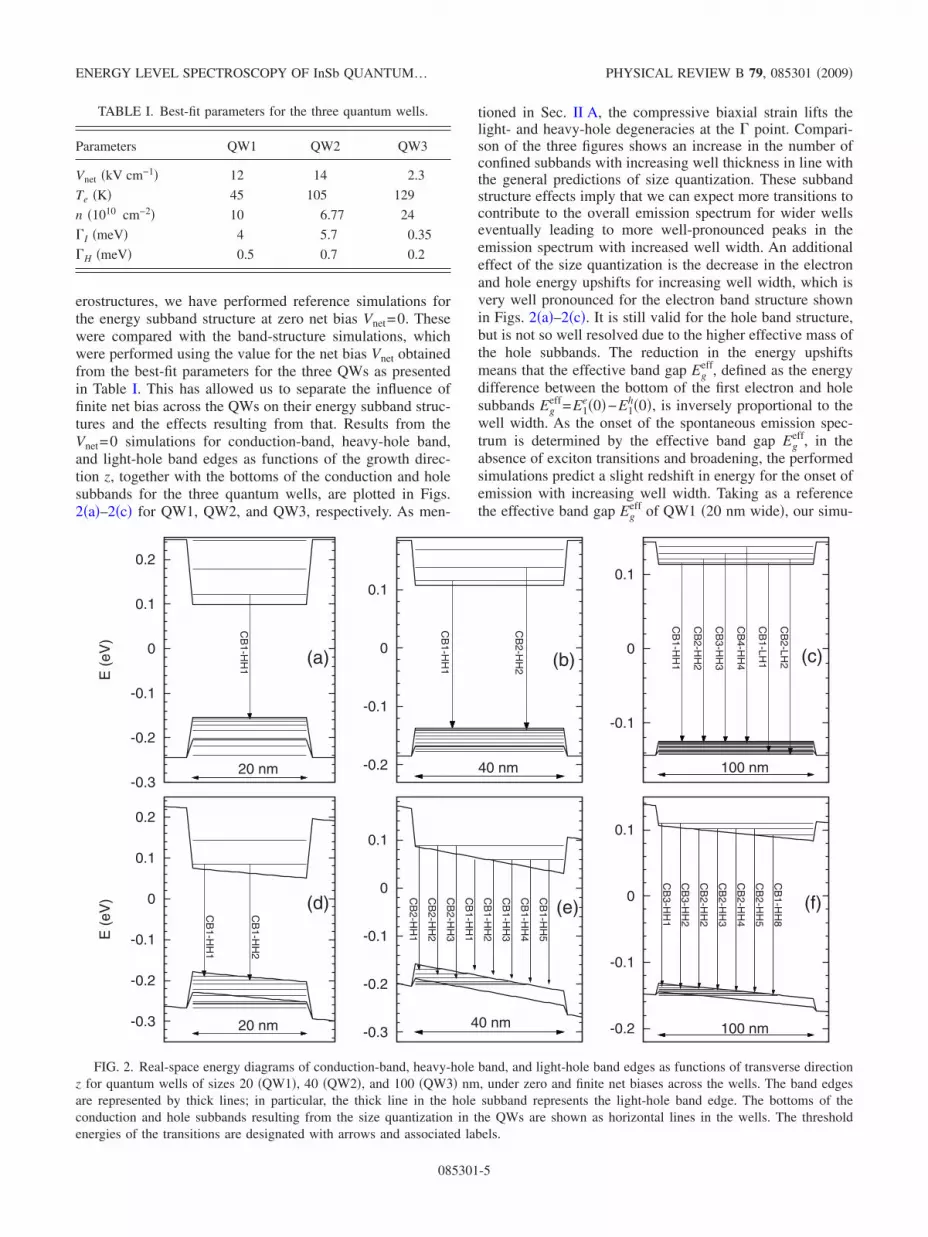
erostructures, we have performed reference simulations forthe energy subband structure at zero net bias Vnet=0. Thesewere compared with the band-structure simulations, whichwere performed using the value for the net bias Vnet obtainedfrom the best-fit parameters for the three QWs as presentedin Table I. This has allowed us to separate the influence offinite net bias across the QWs on their energy subband struc-tures and the effects resulting from that. Results from theVnet=0 simulations for conduction-band, heavy-hole band,and light-hole band edges as functions of the growth direc-tion z, together with the bottoms of the conduction and holesubbands for the three quantum wells, are plotted in Figs.2�a�–2�c� for QW1, QW2, and QW3, respectively. As men-
tioned in Sec. II A, the compressive biaxial strain lifts thelight- and heavy-hole degeneracies at the � point. Compari-son of the three figures shows an increase in the number ofconfined subbands with increasing well thickness in line withthe general predictions of size quantization. These subbandstructure effects imply that we can expect more transitions tocontribute to the overall emission spectrum for wider wellseventually leading to more well-pronounced peaks in theemission spectrum with increased well width. An additionaleffect of the size quantization is the decrease in the electronand hole energy upshifts for increasing well width, which isvery well pronounced for the electron band structure shownin Figs. 2�a�–2�c�. It is still valid for the hole band structure,but is not so well resolved due to the higher effective mass ofthe hole subbands. The reduction in the energy upshiftsmeans that the effective band gap Eg
eff, defined as the energydifference between the bottom of the first electron and holesubbands Eg
eff=E1e�0�−E1
h�0�, is inversely proportional to thewell width. As the onset of the spontaneous emission spec-trum is determined by the effective band gap Eg
eff, in theabsence of exciton transitions and broadening, the performedsimulations predict a slight redshift in energy for the onset ofemission with increasing well width. Taking as a referencethe effective band gap Eg
eff of QW1 �20 nm wide�, our simu-
TABLE I. Best-fit parameters for the three quantum wells.
Parameters QW1 QW2 QW3
Vnet �kV cm−1� 12 14 2.3
Te �K� 45 105 129
n �1010 cm−2� 10 6.77 24
�I �meV� 4 5.7 0.35
�H �meV� 0.5 0.7 0.2
-0.2
-0.1
0
0.1
100 nm
(f)
CB
3-HH
1
CB
3-HH
2
CB
2-HH
2
CB
2-HH
3
CB
2-HH
4
CB
2-HH
5
CB
1-HH
8
-0.3
-0.2
-0.1
0
0.1
40 nm
(e)
CB
2-HH
1
CB
2-HH
2
CB
2-HH
3
CB
1-HH
1
CB
1-HH
2
CB
1-HH
3
CB
1-HH
4
CB
1-HH
5
-0.3
-0.2
-0.1
0
0.1
0.2
E(e
V)
20 nm
CB
1-HH
1 (a)
-0.3
-0.2
-0.1
0
0.1
0.2
E(e
V)
20 nm
CB
1-HH
1
CB
1-HH
2
(d)
-0.2
-0.1
0
0.1
40 nm
CB
1-HH
1
CB
2-HH
2 (b)
-0.1
0
0.1
100 nm
CB
1-HH
1
CB
2-HH
2
CB
3-HH
3
CB
4-HH
4
CB
1-LH1
CB
2-LH2 (c)
FIG. 2. Real-space energy diagrams of conduction-band, heavy-hole band, and light-hole band edges as functions of transverse directionz for quantum wells of sizes 20 �QW1�, 40 �QW2�, and 100 �QW3� nm, under zero and finite net biases across the wells. The band edgesare represented by thick lines; in particular, the thick line in the hole subband represents the light-hole band edge. The bottoms of theconduction and hole subbands resulting from the size quantization in the QWs are shown as horizontal lines in the wells. The thresholdenergies of the transitions are designated with arrows and associated labels.
ENERGY LEVEL SPECTROSCOPY OF InSb QUANTUM… PHYSICAL REVIEW B 79, 085301 �2009�
085301-5

lations predict a 21.6 meV decrease in Egeff for QW2 �40 nm
wide� and a 28.5 meV decrease in Egeff for QW3 �100 nm
wide�.The variation in the aluminum �Al� concentration x in the
barrier material AlxIn1−xSb of the three QW structures influ-ences the energy band structure in two ways. First, accordingto the combination of Eq. �3� with the value of the bowingparameter CT,14 the band gap of the barrier materialAlxIn1−xSb is directly proportional to the Al concentration x.The Al concentration in the experimental samples increaseswith decreasing well width having the largest value for QW1�20 nm wide�. We have estimated that the barrier band gapfor QW1 is Eg�Al0.143In0.857Sb�=489.4 meV, while the bar-rier band gap for QW3 is Eg�Al0.025In0.975Sb�=286.6 meV.In addition to the modification of the barrier band gap thepresence of Al in the barrier changes its lattice constant lead-ing to mismatch between the lattice constants of the well andbarrier materials. The resulting compressive biaxial strainmodifies the bulk band edges in the QWs lifting the HH-LHdegeneracy at the � point as indicated in Fig. 2 and changesthe fundamental energy band gap, which in the present caseis CB-HH. The fundamental band gap therefore increaseswith increasing Al concentration, thus having an oppositeeffect on the depths of the electron and hole potential wellsthan the increase in the barrier band gap. Using themethod7,14,30,31 described in Sec. II, we have calculated thatthe fundamental energy gap for QW1 is Eg
well=253.8 meV,while that for QW2 is Eg
well=238.7 meV. This energy differ-ence caused by the variation in Al concentration is of theorder of 20 meV or an order of magnitude smaller than the200 meV energy difference due to the change in the barrierband gap. Therefore we conclude that the dominant effect ofthe Al concentration on the electron and hole potential welldepths is due to the modification of the barrier band gapEg�AlxIn1−xSb�. For the studied devices the resulting de-crease in the potential well depths with increasing QWwidth, which can be clearly seen by comparing Figs.2�a�–2�c�, competes against the size quantization effects withregard to the number of confined electron and hole subbands.Inspection of Figs. 2�a�–2�c� shows that the two competingfactors nearly balance each other for the case of electronsubbands, although the size quantization prevails with fourconfined subbands in QW3 against two in QW1. In the caseof hole subbands the size quantization is the prevailing effectleading to a considerable amount of confined hole subbandsfor QW3 as can be easily verified by inspecting Figs.2�a�–2�c�. This leads to a considerable effect on the emissionspectrum by increasing the number of transitions which con-tribute.
2. Finite bias simulations
The results for the energy subband structure and electronand hole potential wells from simulations performed with thebest-fit value of the net bias Vnet are shown in Figs. 2�d�–2�f�for QW1, QW2, and QW3, respectively. The net bias Vnetmodifies both the energy subband structure and the electron�nk��� and hole states �mk���, through which it has influence onthe emission spectrum of the QWs. The changes induced byVnet on the electron En
e�k��� and hole spectra Eme �k��� through
the quantum confined Stark effect �QCSE� �Ref 46� lead to adecrease in Eg
eff with increasing net bias. For the three QWsstudied the decrease in Eg
eff is of the order of 10 meV over therelevant bias range. The decrease in Eg
eff is reflected as aredshift in energy to the onset of the spontaneous emissionspectrum. In general the increase in the net bias does notnecessary lead to a decrease in the threshold transition ener-gies Enm=En�0�−Em�0� for every pair of possible transitions.It is possible that some threshold transition energies Enm ac-tually increase, but the detection of these in the emissionspectrum can be difficult due to a background of other sub-band transitions Enm�k���=En�k���−Em�k��� for higher values ofthe two-dimensional �2D� crystal momentum wave vector k��.In addition to the QCSE the bias Vnet across the well leads tolifting of the spin degeneracy away from the � point in theabsence of external magnetic field, due to spin-orbit couplingeffects,16 but our simulations showed that these effects areirrelevant for the unpolarized emission spectrum. This isconsistent with the fact that only energy splittings at the �point can eventually manifest themselves in the unpolarizedluminescence spectrum.
The influence of the net bias on the electroluminescencespectrum through the modification of the electron �nk��� andhole �mk��� states leads not only to quantitative changes as inthe case of QSCE but also to qualitative modification of theproperties of the momentum matrix elements �mk���p� �nk���which may be manifested as observable features in the spon-taneous emission spectrum. Furthermore the presence of anet bias across the quantum wells breaks the inversion sym-metry of the heterostructure potential with respect to the cen-ter of the devices, referred to as structure inversion asymme-try �SIA�.
Standard selection rules, as described in Ref. 36, arebased on a model for the electron and hole states which doesnot take into account band mixing. Under this approxima-tion, for symmetrical quantum wells, the selection rule on thesubband quantum numbers n ,m, which is obtained from theoverlap of the envelope functions, is determined from theglobal property that the envelope functions have definite par-ity with respect to the center of the well. This restricts the setof allowed transitions to those satisfying the condition n+m=even.36 In the GaAs/AlGaAs material system the tran-sitions n−m=0 are much stronger that the remainder of theallowed transitions.36 This has limited studies of theInSb /AlxIn1−xSb system only to such transitions.7,31 Oftentransitions satisfying the conditions n+m=even, or just thestronger condition n−m=0, are referred to as “allowed tran-sitions,” while the rest are referred to as “forbidden transi-tions.” Transitions of this type, relevant for the studied QWs,are shown in Fig. 2�a�–2�c�. In the case of SIA the transitionsfor which n+m is odd are also allowed, although the asym-metry must be very strong.36 In the eight-band model forelectron and hole states, Eq. �1�, due to the mixing of theelectron and the three different hole states of both even andodd parities at k��, points away from the � point and verticaltransitions between all pairs of subband states becomepossible47–49 even in symmetric quantum wells. However,the question of which are the strongest transitions, whichtransitions have dominant contribution to the observed spec-
TENEV et al. PHYSICAL REVIEW B 79, 085301 �2009�
085301-6

trum, and why exactly these transitions contribute to themeasured spectra in the presence of net bias across the QWsneed to be addressed. We have indicated with arrows andassociated labels the relevant transitions, determined to con-tribute to the observed spectrum in Figs. 2�d�–2�f� for QW1,QW2, and QW3, respectively.
C. QW1 (20 nm)
To gain insight into the problems described above wehave first performed line-shape fitting of the experimentallymeasured spectrum using the model described in Sec. II, inparticular using the expression for spectral emittance givenby Eq. �7�. The fitting parameter values, as determined by theminimum of the weighted �2 function found by the simulatedannealing algorithm,42,43 are given in Table I. Using theseparameter estimates we have simulated the separate contri-butions of every transition to the overall spectrum by exam-ining the spectral emittance due to every term in the sumover the different transitions in Eq. �7�. The results from thisprocedure are presented in Figs. 3–5 for QW1, QW2, andQW3, respectively. In the upper plots we have shown theexperimentally measured spectrum as dashed lines, with thecalculated best fit represented as solid lines. Minima in allthe measured spectra seen at around 292 meV are due to CO2absorption, which we have attempted to account for in theinterpretation of the experimental results by using weightingfactors in the calculation of the �2 function for the energyrange of 284–300 meV.
For QW1 �Fig. 3�a� there is some discrepancy betweenthe measured and best fit at the onset of the spectrum in theenergy range of 256–280 meV. We propose that this is due toexciton transitions, based on the knowledge that the excitonbinding energies in general increase with decreasing wellsize,36 that the optical properties of GaAs/AlGaAs QWs aredominated by the exciton transitions,36 and the size of theexciton binding energy in bulk InSb.50 The shoulder visibleat �265 meV in the data taken at 2 mA becomes muchlarger �in comparison to the peak at higher currents� as thecurrent is decreased. The energy separation between thisshoulder and the main peak is consistent with recent obser-vations of bound excitons in the same material system.51
Coupled with the small change in the energy at which thisshoulder occurs with decreasing current, these results suggestthat this feature is due to a bound exciton. Extensive treat-ment of the exciton states within the eight-band EFA Hamil-tonian and exciton optical transitions for the InSb/AlInSbsystem is in development.
The simulated contributions from the relevant transitionsn→m to the total simulated signal for QW1 using the best-fitparameters from Table I are shown in Fig. 3�b� together withthe total simulated signal. Clearly the transitions from thefirst conduction subband �CB1� to the first �HH1� and second�HH2� hole subbands are the ones which form the shape ofthe full signal. The peak of the full signal is associated withthe CB1-HH1 transition, while the CB1-HH2 transition con-tributes mainly to the higher-energy part of the full signalwhere its contribution is masked by the CO2 absorption. Thetwo hole subbands have heavy-hole character at the � point,
although away from it, k���0, the hole subband states mayhave strong admixture from light-hole zone-center states andless from conduction-band and split-off subband contribu-tions. Despite this we will use the traditional labeling of thehole subbands by the dominant zone-center Bloch statesuj,k=0�r� in the linear combination �Eq. �1� at the � point.The observation that mainly transitions to heavy-hole statescontribute to the observed spectrum applies also to QW2 andQW3. This can be explained by the heavy-hole light-holesplitting at the � point caused by the compressive biaxialstrain due to Al in the barrier. The effect is clearly illustratedin Fig. 2, where one can see that the HH-LH splitting islarger than half the depth of the hole potential well. In addi-tion we see clearly that the ratio of the HH-LH splitting to
0
0.2
0.4
0.6
0.8
1
250 260 270 280 290 300 310 320
Spe
ctra
lEm
ittan
ce(a
rb.u
nits
)
hν (meV)
(b)
QW1
Full SignalCB1-HH1 SignalCB1-HH2 Signal
0
0.2
0.4
0.6
0.8
1
Spe
ctra
lEm
ittan
ce(a
rb.u
nits
)
CB
1-HH
1
CB
1-HH
2
(a)
QW1
TheoryExperiment
FIG. 3. Measured �at 15 K� and simulated spectral emittancefrom LED sample QW1 �20 nm�. The upper subplot shows theexperimentally measured and theoretically simulated spectral emit-tance for QW1. The threshold energies of the relevant interbandtransitions are designated with arrows and associated labels. Thelower subplot shows the simulated spectral emittance due to spon-taneous emission from the well together with the signal due to therelevant interband transitions.
ENERGY LEVEL SPECTROSCOPY OF InSb QUANTUM… PHYSICAL REVIEW B 79, 085301 �2009�
085301-7
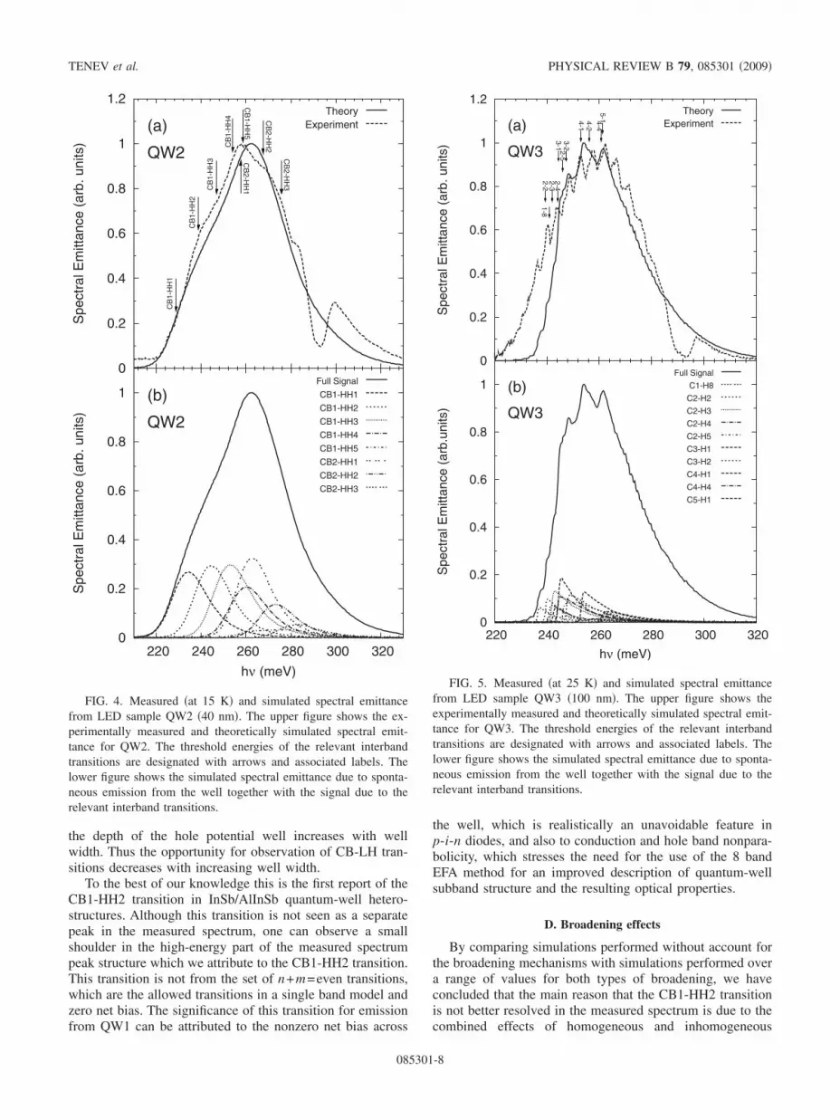
the depth of the hole potential well increases with wellwidth. Thus the opportunity for observation of CB-LH tran-sitions decreases with increasing well width.
To the best of our knowledge this is the first report of theCB1-HH2 transition in InSb/AlInSb quantum-well hetero-structures. Although this transition is not seen as a separatepeak in the measured spectrum, one can observe a smallshoulder in the high-energy part of the measured spectrumpeak structure which we attribute to the CB1-HH2 transition.This transition is not from the set of n+m=even transitions,which are the allowed transitions in a single band model andzero net bias. The significance of this transition for emissionfrom QW1 can be attributed to the nonzero net bias across
the well, which is realistically an unavoidable feature inp-i-n diodes, and also to conduction and hole band nonpara-bolicity, which stresses the need for the use of the 8 bandEFA method for an improved description of quantum-wellsubband structure and the resulting optical properties.
D. Broadening effects
By comparing simulations performed without account forthe broadening mechanisms with simulations performed overa range of values for both types of broadening, we haveconcluded that the main reason that the CB1-HH2 transitionis not better resolved in the measured spectrum is due to thecombined effects of homogeneous and inhomogeneous
0
0.2
0.4
0.6
0.8
1
220 240 260 280 300 320
Spe
ctra
lEm
ittan
ce(a
rb.u
nits
)
hν (meV)
(b)
QW2
Full Signal
CB1-HH1
CB1-HH2
CB1-HH3
CB1-HH4
CB1-HH5
CB2-HH1
CB2-HH2
CB2-HH3
0
0.2
0.4
0.6
0.8
1
1.2
Spe
ctra
lEm
ittan
ce(a
rb.u
nits
)
CB
1-H
H1
CB
1-H
H2
CB
1-H
H3
CB
1-H
H4
CB
1-HH
5C
B2-H
H1
CB
2-HH
2
CB
2-HH
3
(a)
QW2
TheoryExperiment
FIG. 4. Measured �at 15 K� and simulated spectral emittancefrom LED sample QW2 �40 nm�. The upper figure shows the ex-perimentally measured and theoretically simulated spectral emit-tance for QW2. The threshold energies of the relevant interbandtransitions are designated with arrows and associated labels. Thelower figure shows the simulated spectral emittance due to sponta-neous emission from the well together with the signal due to therelevant interband transitions.
0
0.2
0.4
0.6
0.8
1
220 240 260 280 300 320
Spe
ctra
lEm
ittan
ce(a
rb.u
nits
)
hν (meV)
QW3
(b)Full Signal
C1-H8
C2-H2
C2-H3
C2-H4
C2-H5
C3-H1
C3-H2
C4-H1
C4-H4
C5-H1
0
0.2
0.4
0.6
0.8
1
1.2
Spe
ctra
lEm
ittan
ce(a
rb.u
nits
)
1-82-22-32-4
2-53-13-2
4-14-2
4-45-1
QW3
(a)Theory
Experiment
FIG. 5. Measured �at 25 K� and simulated spectral emittancefrom LED sample QW3 �100 nm�. The upper figure shows theexperimentally measured and theoretically simulated spectral emit-tance for QW3. The threshold energies of the relevant interbandtransitions are designated with arrows and associated labels. Thelower figure shows the simulated spectral emittance due to sponta-neous emission from the well together with the signal due to therelevant interband transitions.
TENEV et al. PHYSICAL REVIEW B 79, 085301 �2009�
085301-8

broadening. This can be understood by examining the effectof the broadening function U� , nm�k��� ;�I ,�H� in the ex-pression for the spontaneous emission in Eq. �7�. Without it,electron-hole recombination �n ,k���→ �m ,k��� with transitionenergy nm�k��� will lead to emission of radiation with an-gular frequency , which is in resonance with the Bohr fre-quency of the transition =nm�k���. On the other hand thepresence of the broadening function U� , nm�k��� ;�I ,�H�introduces a finite probability for the energy nm�k���, re-leased in the �n ,k���→ �m ,k��� transition, to be emitted as ra-diation with angular frequency �nm�k���, thus effectivelydescribing nonresonant emission processes. The principle ofconservation of energy then requires the probability for reso-nant emission in which =nm�k��� to be reduced appropri-ately. The effect on the spectral emittance line shape is two-fold. First the value I� � of the emittance at energy nm�k��� will be smaller for higher values of the broadeningparameters �I and �H. Second for higher values of the broad-ening parameters �I and �H the increased probability foroff-resonance emission leads to increase in the value of thespectral emittance I� � for energies in the neighborhood ofthe energy of the transition nm�k���. The combination ofthese two effects forms the mechanism behind the smearingof the sharp peaks in the emission spectrum associated withthreshold energies Enm�0� for transitions between the elec-tron and hole subbands n→m. This mechanism of course isnot restricted only to the CB1-HH2 transition in QW1 but isgeneral. It can be used to explain the smearing of, or lack of,sharp features in the emission spectrum for different quan-tum wells and all types of transitions. In particular we at-tribute the lack of sharp features in the measured electrolu-minescence spectrum of QW2 presented in Fig. 4 to theabove described mechanism and not due to the lack of for-bidden transitions.
These conclusions are supported by our estimates of thebroadening parameters �I and �H presented in Table I, whichwe have obtained by the method of line-shape fitting.37 Theinhomogeneous broadening parameter �I attracts particularattention. Its values for QW1 and QW2 are similar �4 and 5.7
meV, respectively�, while its value for QW3 �0.35 meV� isan order of magnitude smaller than those of QW1 and QW2.This is in qualitative agreement with the rapid nonlinear de-crease in inhomogeneous broadening with well width exam-ined in Ref 52. Inspection of the spontaneous emission spec-trum of QW3, shown in Fig. 5, shows the presence of manywell-resolved peaks, which, together with the data in Figs. 3and 4, is consistent with the mechanism described in theprevious paragraph. As mentioned in Sec. II the main physi-cal factor behind the inhomogeneous broadening in this caseis probably width fluctuations along a particular well. Thisimplies that well width fluctuations play stronger role forQW1 and QW2, and for these two cases the inhomogeneousdominates over homogeneous broadening. For the widestwell �QW3� the two types of broadening are of comparablemagnitude. We have illustrated the effect of the homoge-neous and inhomogeneous broadenings on the simulatedspectrum for QW1 in Figs. 6�a� and 6�b�, respectively. Anincrease in the two types of broadening decreases the peakheight in accordance with the described mechanism andbroadens the emittance lineshape. As an implication of theabove discussion we predict that well-resolved peaks in theelectroluminescence spectrum from QW heterostructurescorresponding to transitions satisfying the conditions n+m=even or forbidden transitions should be observable forsmall-enough values of the broadening parameters �I and�H. In practice this requires quantum wells of very goodquality to reduce the well width fluctuations, and the associ-ated phenomenological parameter �I, as the measured signalis more sensitive to changes in the value of the inhomoge-neous broadening.
E. QW2 (40 nm)
In Fig. 4�a� the measured and calculated spectra, using theparameters in Table I, are plotted for QW2. There is goodoverall agreement between the two curves especially regard-ing the onset. Note that we have used a single broadeningparameter to achieve the best overall fit between the totalmeasured spectra and the total simulated spectra. This has a
0
0.2
0.4
0.6
0.8
1
240 260 280 300 320 340
Em
ittan
ce(a
rb.u
nits
)
hν (meV)
QW1
ΓH=0.5 meVΓH=1.5 meVΓH=2.5 meVΓH=3.5 meV
0
0.2
0.4
0.6
0.8
1
240 260 280 300 320 340
Em
ittan
ce(a
rb.u
nits
)
hν (meV)
QW1
ΓI=2 meVΓI=3 meVΓI=4 meVΓI=5 meV
(b)(a)
FIG. 6. Simulated emission spectra for QW1 �at 15 K� as a function of homogeneous and inhomogeneous broadenings. Spectralemittance line shape as a function of homogeneous and inhomogeneous broadenings for the 20 nm well simulated for effective temperatureand injected carrier density. The peak height of the data resulting from simulation with homogenous broadening and inhomogeneousbroadening has been normalized, and the results of the other simulations have been scaled with respect to it.
ENERGY LEVEL SPECTROSCOPY OF InSb QUANTUM… PHYSICAL REVIEW B 79, 085301 �2009�
085301-9

tendency to lead to an overestimation of the amount ofbroadening and consequently smooth out the simulated spec-tra to some degree. Future work will examine the importanceof different amounts of broadening for each transition, whichcould lead to more precise reproduction of the sharp featuresin the measured spectra. The slight difference in the peakposition can be mainly attributed to underestimation of Vnet,and the disagreement in the tail structure can be attributed toboth the CO2 absorption and the slight underestimation of Te.These small discrepancies in the exact numerical estimationof the fit parameters could be due to the fact that the mini-mum of �2 is not exactly the global one but close to it, or dueto the resolution in the fitting parameter values. However,these slight numerical differences do not affect the conclu-sions in any way.
The simulations performed for the contribution from thedifferent subband transitions n→m are presented in Fig.4�b�. We have found that the main transitions that contributeto the electroluminescence spectrum are the transitions fromCB1 to the first five hole subbands HH1-HH5 and from thesecond conduction subband �CB2� to the first three heavy-hole subbands HH1-HH3. Their contribution was calculatedusing the best-fit parameters from Table I and is shown inFig. 4�b�. Note that in this case there are no confined LHstates within the quantum well due to the lifting of the light-heavy-hole degeneracy by the compressive strain. We havefound that transitions from the conduction subbands CB1and CB2 to more remote hole subbands also contribute to thehigh-energy �tail� part of the spectrum, but due to very lowstatistical occupation of these states according to the Fermi-Dirac function their separate effect is marginal �for clarity wehave not plotted these in Fig. 4�b�. The contribution of sig-nificantly more transitions to the spectrum of QW2 �whichcontains the 40-nm-wide well� is commensurate with the ef-fects of size quantization discussed earlier. The onset of theemission is almost entirely due to three transitions: CB1-HH1, CB1-HH2, and CB1-HH3. The slight shoulder near theCB1-HH2 marker is probably due to the CB1-HH2 transi-tion, although, due to the combined statistical and broaden-ing effects, the transitions CB1-HH1 and CB1-HH3 alsocontribute at this emission energy. The small shoulder in theexperimental spectrum near the marker CB2-HH2 in Fig.4�a�, which designates the threshold energy of the CB2-HH2transition, is probably due to the CB2-HH2 transition. Thebetter resolved shoulder before the dip in the experimentalspectrum is probably predominantly due to the contributionfrom the CB2-HH3 transition. We attribute the main peak inthe experimental spectrum to the CB2-HH1 transition. Back-ground signal at this emission frequency is also provided bythe CB1-HH3, CB1-HH4, and CB2-HH2 transitions, but ascan be seen in Fig. 4�b� the strength of the signal from thesetransitions is around two times smaller than the CB2-HH1transition. The CB2-HH1 transition has the highest overallcontribution to the emission spectrum of QW2 comparedwith all the other interband transitions.
F. Matrix elements and selection rules
In QW2 therefore, more clearly than in the case of QW1,because of the larger number of transitions present we see
that the notion of forbidden transitions cannot be used in theinterpretation of an electroluminescence spectrum of a QWheterostructure. Even more strikingly a transition, which in asimplified model falls in the category of forbidden transi-tions, actually contributes the strongest signal and gives themain contribution to the best observable feature in the ex-perimental spectrum—its main peak. In order to understandthis behavior we have investigated the momentum matrixelements �mk���p� �nk���, which determine the selection rules ofthe problem. For unpolarized emission only the modulussquared of the momentum matrix elements �pnm�k����2
= ��mk���p� �nk����2 contributes to the emittance I� �, so we willfocus on them. We would like to stress that the k�� depen-dence of the squared matrix elements �pnm�k����2 is importantand needs to be taken into account even for qualitative ex-planation of the emission spectrum. Because of the k�� depen-dence, discussing selection rules or comparing strengths oftransitions without regard for the 2D wave vector k�� is inac-curate. In order to examine these effects on the spontaneousemission spectrum we have performed two steps. First, in theaxial approximation all quantities in Eq. �7� are independentof the direction of the 2D wave vector k��. For this isotropicband structure we have used a set of standard mathematicaltools to perform the summation over the directional depen-dence in the wave vector k��
�k��
→L2
�2��2�2DFBZ
dk�2 →
L2
�2��22��0
2�/a
dk�k�
→2�
L�k�
g�2D��k�� , �8�
where a is the lattice constant of the direct lattice, L is thelinear size of the sample in the x-y plane, g�2D��k�����k����k��−k���= L2
2�k�� is the density of states per unit modulusk� of the 2D crystal wave vector k��, and the summation overthe 2D wave vector k� takes all possible values within thetwo-dimensional first Brillouin zone �2DFBZ�. The impor-tant quantity in the resulting summation over the magnitudeof the wave vector k�� is the product between the squaredmomentum matrix element and the density of states per unitk�: g�2D��k���pnm�k���2. All the optically relevant informationabout the electron �n ,k��� and hole �m ,k��� wave functions,with 2D crystal wave vector quantum numbers satisfying thecondition �k���=k�, are contained in this product which deter-mines the strength of the transitions. The second step was torelate the above product directly to the transition energies byg�2D��k�� nm��pnm�k�� nm��2 using the function k�� nm�,which is the inverse of nm�k��=En�k��−Em�k��. Figure 7depicts the functions g�2D��k�� nm��pnm�k�� nm��2 for thesubband transitions CB1-HH1:HH5 and CB2-HH1:HH5, asobtained from the simulations of QW2 for zero net bias andthe net bias from the best-fit parameters in Table I.
The fact that the selection rules n+m=even do not holdwithin the eight-band EFA approach and do not offer realisticdescription of the physical processes even in the case of sym-metric quantum wells �Vnet=0� is clearly demonstrated in
TENEV et al. PHYSICAL REVIEW B 79, 085301 �2009�
085301-10

Figs. 7�a� and 7�b� by the fact that the productg�2D��k���pnm�k���2 is nonzero for all the depicted transitions.In addition we see that when we compare the strengths ofdifferent transitions we need to do so with regard to a par-ticular transition energy mn. There are no strong or weaktransitions, rather there are transitions that dominate over apart of the energy range. In particular, based on the informa-tion in Figs. 7�a� and 7�b�, we would expect that the lumi-nescence signal from QW2 under zero net bias would bedominated by the CB1-HH1 transition in the 252–265 meVrange, CB1-HH2 in the 265–272 meV range, while beyond272 meV the signal would be a mixture from several transi-tions.
The results for the dependence of the productg�2D��k���pnm�k���2 on the transition energies nm for QW2,at the bias from the best-fit parameters in Table I, are pre-sented in Figs. 7�c� and 7�d�. The effect of the QCSE causedby the bias Vnet manifests itself in the redshift of the onsets ofthe product g�2D��k���pnm�k���2 for all different transitions; forexample, the onset of CB1-HH1 transition in Fig. 7�a� is ataround 252 meV, while the onset of the same transition inFig. 5�c� is at 228 meV. The effect that leads to qualitativedifference is the change in the functionsg�2D��k�� nm��pnm�k�� nm��2. For most of the transitionsthe peak value of the examined functions is lower for thefinite bias case than for the zero bias. We attribute this to the
overall decreased overlap of the electron and hole wavefunctions which tend to become localized in the oppositesides of the quantum well due to the SIA induced by the biasacross the well. The major consequence of this effect on theluminescence properties would be the decrease in the valueof the spectral emittance for increasing bias, if all the otherfactors were kept constant and were not influenced by thebias.
Another interesting trend that one can notice in Figs. 7�c�and 7�d� is that transitions from a particular conduction sub-band to lower heavy-hole subbands tend to have slightlyhigher values of the product g�2D��k���pnm�k���2 compared totransitions with smaller threshold energy. For example, inFig. 7�c� the transition CB1-HH4 dominates over the transi-tions CB1-HH1:HH3, which have lower threshold energies,after some crossover energies specific to the transitions pair.This behavior can be explained qualitatively by the interplayof two effects. The first is the localization of the electron andhole wave functions on the opposite sides of a quantum welldue to SIA induced by the net bias. The second is the factthat wave functions associated with higher eigenenergiestend to be less localized. As a consequence, in a biased quan-tum well the overlap between the electron and hole wavefunctions will increase with increased electron/hole energy,which will increase the momentum matrix element �pnm�k���2,and from there will tend to increase the product
0
5
10
15
20
|Pav nm
|2(a
rb.u
nits
)
(a)
Vnet=0
CB1-HH1CB1-HH2CB1-HH3CB1-HH4CB1-HH5
0
5
10
15
20
220 240 260 280 300 320
|Pav nm
|2(a
rb.u
nits
)
h νnm (meV)
(b)
Vnet=0
CB2-HH1CB2-HH2CB2-HH3CB2-HH4CB2-HH5
(c)
Vnet=1.4 (104 Vcm-1)
CB1-HH1CB1-HH2CB1-HH3CB1-HH4CB1-HH5
220 240 260 280 300 320h νnm (meV)
(d)
Vnet=1.4 (104V cm-1)
CB2-HH1CB2-HH2CB2-HH3CB2-HH4CB2-HH5
FIG. 7. �Color online� Momentum matrix elements as functions of transition energies obtained from the simulations for QW2 �40 nmwide� for zero net bias and finite net bias.
ENERGY LEVEL SPECTROSCOPY OF InSb QUANTUM… PHYSICAL REVIEW B 79, 085301 �2009�
085301-11

g�2D��k���pnm�k���2. In the present model the increase in theelectron/hole energy is equivalent to an increase in either thesubband index n /m or the 2D crystal wave vector k��, whichcan explain the observed trend. The same mechanism canexplain why the product g�2D��k���pnm�k���2 is higher for thetransitions from CB2 to the heavy-hole subbands comparedwith transitions from CB1 to the heavy-hole subbands. Theabove described mechanism is important for the understand-ing of the spectrum of QW2 in particular and to the elec-troluminescence spectra of QWs in general.
The data presented in Figs. 7�c� and 7�d� offer part of theexplanation for the structure of the contribution of differentsubband transitions to the full luminescence signal. The otherpart of the explanation is statistical in nature—the electronand hole states occupational probabilities which in our modelare described by the Fermi-Dirac function. A way to separatethe two parts is to use the following gedanken—suppose thatthe electron and hole gases are degenerate with suitably cho-sen chemical potentials �e and �h such that �e−�h=276 meV. Within this approximation inspection of Figs.7�c� and 7�d� would imply that the dominant contribution tothe spectrum is due to the CB2-HH1 transition with a sig-nificant contribution from CB1-HH3 and CB1-HH4, due tothe mechanism qualitatively explained in the previous para-graph. The strengths of the CB1-HH1 and CB1-HH2 transi-tions are an order of magnitude smaller. On the other handthe data shown in Fig. 4�b� shows a much smaller differencebetween the peak heights of CB1-HH1, CB1-HH2, CB1-HH3, and CB2-HH1. To explain this we need to abandon thedegenerate gas approximation and account for the statisticaloccupation of the electron/hole subband states. Comparisonof the signal from CB1-HH1 with the CB1-HH2 transition inFig. 4�b� shows that the statistical factor does not alter therelative contribution as implied within the degenerate gasapproximation from the products g�2D��k���pnm�k���2 in Fig.7�c�. This can be attributed to the relatively small energydifference between HH1 and HH2 subbands. In contrast, de-spite the order-of-magnitude difference between the productsg�2D��k���pnm�k���2 of the CB1-HH1 and CB2-HH1 transitionsthe peak height of their signal on Fig. 4�b� is of the sameorder of magnitude. The reason is the relatively big differ-ence between the first and second conduction subbands asdepicted in Fig. 2�e�, as a result of which the relevantconduction-band states �1,k��� have significantly higher occu-pational probability than their counterparts �2,k���, thus com-pensating the order-of-magnitude difference between theg�2D��k���pnm�k���2 in this case. The same argument of combi-nation of the band-structure effects with statistical factorscan be used to explain the contribution of the other signals.The main conclusion of the above argument is that all theeffects of the symmetry and overlap of electron and holewave functions, including the selection rules if any, can besignificantly modified by the occupational statistics, thus di-minishing their significance for the analysis of the electrolu-minescence spectrum.
G. QW3 (100 nm QW)
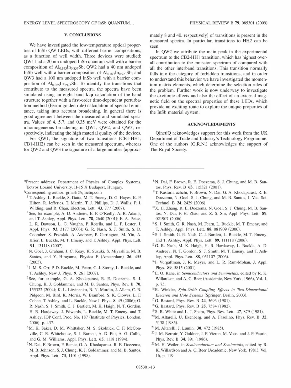
The results from the line-shape fitting for QW3 are pre-sented in Fig. 5�a� with the best-fit parameters given in Table
I. �Note that in this case, we believe that some of the featuresin the measured spectra may be due to temperature fluctua-tions caused by the closed cycle helium cryostat used. Inparticular, the features observed in the measured spectraabove 260 meV in QW3 are much less pronounced in mea-surements made at a different time on another LED, fabri-cated from the same wafer. However, it is very difficult ex-perimentally to unambiguously confirm that the featuresabove 260 meV in the data shown in Fig. 5 are solely due totemperature fluctuations. Further work is underway to inves-tigate this.� The agreement between the measured spectrum�at 25 K� and the theoretical fit is satisfactory in the tailstructure, indicating a good estimate of the effective tem-perature. There is good agreement between the three majorpeaks of the measured spectrum and theoretical calculations,including some shoulders in both the experimental and the-oretical curves. The onset of the theoretical calculationsshows small shoulders at energies close to the energies of thepeaks at the onset of the experimental spectrum.
A possible explanation for the discrepancies between ex-perimental measurements and theoretical simulations is thefact that we have performed the electronic structure calcula-tions in the standard single-particle approximation instead ofusing some many-body scheme such as the Hartree-Fock ap-proximation or the density functional theory �DFT�. Manybody effects might play more prominent roles in wider wellsthan in narrow ones. Another possible reason for the discrep-ancy is the band bending due to the modulation doping of thebarrier materials which we have not taken into account. Moreextensive treatment of the problem including the above ap-proximation is in advanced stage of development and will bereported elsewhere. Finally it is possible that the found mini-mum in �2 is not exactly the true global one but close to it.However these small discrepancies do not affect our conclu-sions.
The size quantization effects manifest themselves in themany possible transitions that contribute to the spectrum ofQW3. We have found that more than 40 transitions contrib-ute to the spectrum of QW3. The considerable number oftransitions that contribute is a consequence of both the sizequantization and the contribution from the so called forbid-den transitions, confirming our conclusions from Secs. I–III.This, in combination with the low estimates for the homoge-neous �H and inhomogeneous �I broadening parameters�presented in Table I�, is consistent with the many observedsharp peaks in the experimental spectrum. The appreciablenumber of transitions contributing to the spontaneous emis-sion spectrum of QW3 demonstrates the difficulties in theinterpretation of luminescence experiments of wide quantumwells. Only ten transitions, assessed to be most relevant de-pending on their contribution to the full signal, have beenshown in Fig. 5�b�. We have found the CB1-HH8 transitionto be the first significant contribution due to the very smallvalue of the product g�2D��k���pnm�k���2 for the transitionsCB1-HH1:HH7 which in this case cannot be compensated bythe statistical factors as in QW2. This is the primary reasonbehind the absence of the three initial peaks, observed in theexperimental curve, from the theoretical one. The transitionsfrom higher lying conduction bands have more weight in thespectrum compared with QW2 and QW1.
TENEV et al. PHYSICAL REVIEW B 79, 085301 �2009�
085301-12
V. CONCLUSIONS
We have investigated the low-temperature optical proper-ties of InSb QW LEDs, with different barrier compositions,as a function of well width. Three devices were studied:QW1 had a 20 nm undoped InSb quantum well with a barriercomposition of Al0.143In0.857Sb; QW2 had a 40 nm undopedInSb well with a barrier composition of Al0.077In0.923Sb; andQW3 had a 100 nm undoped InSb well with a barrier com-position of Al0.025In0.975Sb. To identify the transitions thatcontribute to the measured spectra, the spectra have beensimulated using an eight-band k .p calculation of the bandstructure together with a first-order time-dependent perturba-tion method �Fermi golden rule� calculation of spectral emit-tance, taking into account broadening. In general there isgood agreement between the measured and simulated spec-tra. Values of 4, 5.7, and 0.35 meV were obtained for theinhomogeneous broadening in QW1, QW2, and QW3, re-spectively, indicating the high material quality of the devices.
For QW1, the signature of two transitions �CB1-HH1,CB1-HH2� can be seen in the measured spectrum, whereasfor QW2 and QW3 the signature of a large number �approxi-
mately 8 and 40, respectively� of transitions is present in themeasured spectra. In particular, transitions to HH2 can beseen.
In QW2 we attribute the main peak in the experimentalspectrum to the CB2-HH1 transition, which has highest over-all contribution to the emission spectrum of compared withall the other interband transitions. This transition normallyfalls into the category of forbidden transitions, and in orderto understand this behavior we have investigated the momen-tum matrix elements, which determine the selection rules ofthe problem. Further work is now underway to investigatethe excitonic effects and also the effect of an external mag-netic field on the spectral properties of these LEDs, whichprovide an exciting route to explore the unique properties ofthe InSb material system.
ACKNOWLEDGMENTS
QinetiQ acknowledges support for this work from the UKDepartment of Trade and Industry’s Technology Programme.One of the authors �G.R.N.� acknowledges the support ofThe Royal Society.
*Present address: Department of Physics of Complex Systems,Eötvös Loránd University, H-1518 Budapest, Hungary.
†Corresponding author; [email protected] T. Ashley, L. Buckle, S. Datta, M. T. Emeny, D. G. Hayes, K. P.
Hilton, R. Jefferies, T. Martin, T. J. Phillips, D. J. Wallis, P. J.Wilding, and R. Chau, Electron. Lett. 43, 777 �2007�.
2 See, for example, A. D. Andreev, E. P. O’Reilly, A. R. Adams,and T. Ashley, Appl. Phys. Lett. 78, 2640 �2001�; E. A. Pease,L. R. Dawson, L. G. Vaughn, P. Rotella, and L. F. Lester, J.Appl. Phys. 93, 3177 �2003�; G. R. Nash, S. J. Smith, S. D.Coomber, S. Przeslak, A. Andreev, P. Carrington, M. Yin, A.Krier, L. Buckle, M. T. Emeny, and T. Ashley, Appl. Phys. Lett.91, 131118 �2007�.
3 N. Goel, J. Graham, J. C. Keay, K. Suzuki, S. Miyashita, M. B.Santos, and Y. Hirayama, Physica E �Amsterdam� 26, 455�2005�.
4 J. M. S. Orr, P. D. Buckle, M. Fearn, C. J. Storey, L. Buckle, andT. Ashley, New J. Phys. 9, 261 �2007�.
5 See, for example, G. A. Khodaparast, R. E. Doezema, S. J.Chung, K. J. Goldammer, and M. B. Santos, Phys. Rev. B 70,155322 �2004�; K. L. Litvinenko, B. N. Murdin, J. Allam, C. R.Pidgeon, M. Bird, K. Morris, W. Branford, S. K. Clowes, L. F.Cohen, T. Ashley, and L. Buckle, New J. Phys. 8, 49 �2006�; G.R. Nash, S. J. Smith, C. J. Bartlett, M. K. Haigh, N. T. Gordon,H. R. Hardaway, J. Edwards, L. Buckle, M. T. Emeny, and T.Ashley, IOP Conf. Proc. No. 187 �Institute of Physics, London,2006�, p. 437.
6 M. K. Saker, D. M. Whittaker, M. S. Skolnick, C. F. McCon-ville, C. R. Whitehouse, S. J. Barnett, A. D. Pitt, A. G. Cullis,and G. M. Williams, Appl. Phys. Lett. 65, 1118 �1994�.
7 N. Dai, F. Brown, P. Barsic, G. A. Khodaparast, R. E. Doezema,M. B. Johnson, S. J. Chung, K. J. Goldammer, and M. B. Santos,Appl. Phys. Lett. 73, 1101 �1998�.
8 N. Dai, F. Brown, R. E. Doezema, S. J. Chung, and M. B. San-tos, Phys. Rev. B 63, 115321 �2001�.
9 T. Kasturiarachchi, F. Brown, N. Dai, G. A. Khodaparast, R. E.Doezema, N. Goel, S. J. Chung, and M. B. Santos, J. Vac. Sci.Technol. B 24, 2429 �2006�.
10 X. H. Zhang, R. E. Doezema, N. Goel, S. J. Chung, M. B. San-tos, N. Dai, F. H. Zhao, and Z. S. Shi, Appl. Phys. Lett. 89,021907 �2006�.
11 S. J. Smith, G. R. Nash, M. Fearn, L. Buckle, M. T. Emeny, andT. Ashley, Appl. Phys. Lett. 88, 081909 �2006�.
12 S. J. Smith, G. R. Nash, C. J. Bartlett, L. Buckle, M. T. Emeny,and T. Ashley, Appl. Phys. Lett. 89, 111118 �2006�.
13 G. R. Nash, M. K. Haigh, H. R. Hardaway, L. Buckle, A. D.Andreev, N. T. Gordon, S. J. Smith, M. T. Emeny, and T. Ash-ley, Appl. Phys. Lett. 88, 051107 �2006�.
14 I. Vurgaftman, J. R. Meyer, and L. R. Ram-Mohan, J. Appl.Phys. 89, 5815 �2001�.
15 E. O. Kane, in Semiconductors and Semimetals, edited by R. K.Willardson and A. C. Beer �Academic, New York, 1966�, Vol. 1,p. 75.
16 R. Winkler, Spin-Orbit Coupling Effects in Two-DimensionalElectron and Hole Systems �Springer, Berlin, 2003�.
17 G. Bastard, Phys. Rev. B 24, 5693 �1981�.18 G. Bastard, Phys. Rev. B 25, 7584 �1982�.19 S. R. White and L. J. Sham, Phys. Rev. Lett. 47, 879 �1981�.20 M. Altarelli, U. Ekenberg, and A. Fasolino, Phys. Rev. B 32,
5138 �1985�.21 M. Altarelli, J. Lumin. 30, 472 �1985�.22 J. M. Berroir, Y. Guldner, J. P. Vieren, M. Voos, and J. P. Faurie,
Phys. Rev. B 34, 891 �1986�.23 M. H. Weiler, in Semiconductors and Semimetals, edited by R.
K. Willardson and A. C. Beer �Academic, New York, 1981�, Vol.16, p. 119.
ENERGY LEVEL SPECTROSCOPY OF InSb QUANTUM… PHYSICAL REVIEW B 79, 085301 �2009�
085301-13

24 L. R. Ram-Mohan, K. H. Yoo, and R. L. Aggarwal, Phys. Rev. B38, 6151 �1988�.
25 J. M. Luttinger and W. Kohn, Phys. Rev. 97, 869 �1955�.26 J. M. Luttinger, Phys. Rev. 102, 1030 �1956�.27 C. R. Pidgeon and R. N. Brown, Phys. Rev. 146, 575 �1966�.28 D. Auvergne, J. Camassel, H. Mathieu, and A. Joulie, J. Phys.
Chem. Solids 35, 133 �1974�.29 M. P. C. M. Krijn, Semicond. Sci. Technol. 6, 27 �1991�.30 D. Zhou and B. F. Usher, J. Phys. D 34, 1461 �2001�.31 T. Kasturiarachchi, F. Brown, N. Dai, G. A. Khodaparast, R. E.
Doezema, S. J. Chung, and M. B. Santos, Appl. Phys. Lett. 88,171901 �2006�.
32 J. Singh, Physics of Semiconductors and Their Heterostructures�McGraw-Hill, New York, 1993�.
33 R. Loundon, The Quantum Theory of Light �Oxford UniversityPress, New York, 2003�.
34 A. J. Wojtowicz, M. Kazmierczak, and A. Lempicki, J. Opt. Soc.Am. B 6, 1106 �1989�.
35 A. Messiah, Quantum Mechanics �Dover, New York, 1999�.36 G. Bastard, Wave Mechanics Applied to Semiconductor Hetero-
structures �EDP Sciences, France, 1992�.37 G. Beadie, W. S. Rabinovich, D. S. Katzer, and M. Goldenberg,
Phys. Rev. B 55, 9731 �1997�.38 A. Monakhov, A. Krier, and V. V. Sherstnev, Semicond. Sci.
Technol. 19, 480 �2004�.39 M. Grupen and K. Hess, IEEE J. Quantum Electron. 34, 120
�1998�.
40 J. F. Kielkopf, J. Opt. Soc. Am. 63, 987 �1973�.41 S. Kaushik and P. L. Hagelstein, IEEE J. Quantum Electron. 30,
2547 �1994�.42 W. H. Press, S. A. Teukolsky et al., Numerical Recipes �Cam-
bridge University Press, Cambridge, 2007�.43 S. Kirkpatrick, C. D. Gelatt, and M. P. Vecchi, Science 220, 671
�1983�.44 K. V. Price, R. M. Storn, and J. A. Lampinen, Differential Evo-
lution: A Practical Approach to Global Optimization �Springer,New York, 2005�.
45 K. F. Riley, M. P. Hobson, and S. J. Bence, Mathematical Meth-ods for Physics and Engineering �Cambridge University Press,Cambridge, 2002�.
46 E. Rosencher and B. Vinter, Optoelectronics �Cambridge Univer-sity Press, Cambridge, England, 2002�.
47 G. D. Sanders and Y. C. Chang, Phys. Rev. B 31, 6892 �1985�.48 G. D. Sanders and Yia-Chung Chang, Phys. Rev. B 32, 5517
�1985�.49 R. C. Miller, A. C. Gossard, and G. D. Sanders, Yia-Chung
Chang, and J. N. Schulman, Phys. Rev. B 32, 8452 �1985�.50 A. Baldereschi and N. O. Lipari, Phys. Rev. B 3, 439 �1971�.51 X. H. Zhang, R. E. Doezema, N. Goel, S. J. Chung, M. B. San-
tos, N. Dai, F. H. Zhao, and Z. S. Shi, Appl. Phys. Lett. 89,021907 �2006�.
52 F. T. Vasko, P. Aceituno, and A. Hernández-Cabrera, Phys. Rev.B 66, 125303 �2002�.
TENEV et al. PHYSICAL REVIEW B 79, 085301 �2009�
085301-14


