Embed Size (px)
Citation preview

Epitaxial lift-off and its applications
This article has been downloaded from IOPscience. Please scroll down to see the full text article.
1993 Semicond. Sci. Technol. 8 1124
(http://iopscience.iop.org/0268-1242/8/6/021)
Download details:
IP Address: 128.32.39.239
The article was downloaded on 29/04/2010 at 03:44
Please note that terms and conditions apply.
View the table of contents for this issue, or go to the journal homepage for more
Home Search Collections Journals About Contact us My IOPscience

Semicond. Sci. Technol. 8 (1993) 1124-1135. Printed in the UK
Epitaxial lift-off and its applications I I
P Demeester, I Pollentier, P De Dobbelaere, C Brys and P Van Daele University of Gent-IMEC, Laboratory of Electromagnetics and Acoustics, Sint-Pietersnieuwtraat 41, 59000 Gent, Belgium
Received 16 December 1992, accepted for publication 11 January 1993
Abstract. In th i s paper we will give an overview of the epitaxial lift-off (ELO) technique and i t s applications. The first part will describe the basic technology, which includes chemical lift-off, handling, bonding, stress, alignment, etc. The second part will give an overview of device results obtained with ELO (LEO and lasers on Si, MESFETS on InP, OEICS, etc).
1. Introduction
The technology of combining different semiconductor materials on a single substrate has been a subject of research for many years now. Initially this was mainly done by the growth of single-crystalline epitaxial multi- layers (e.g. GaAs/AlGaAs) on a lattice-matched substrate (e.g. GaAs). The increasing demand for more advanced optoelectronic integrated circuits (OEIC) has created the need for combining materials with different lattice con- stants (e.g. GaAs on Si). This very challenging problem of heteroepitaxial growth has had varying success, due to problems with large dislocation densities (typically > 10' a-') and thermal stresses [l]. One ofthemost sensitive devices is the laser diode, and it is only recently that good-quality InP lasers on Si have been obtained with acceptable lifetime (>2000 h) [2]. For the GaAs on Si material combination one is still struggling with the very short laser lifetime [3]. Another important problem encountered is the incompatibility of the different process steps: growth of GaAs on Si requires high temperatures; and therefore processing of the devices can only be done after growth. GaAs on Si wafers are, however, not allowed in a standard Si process line. It is only recently that very promising results have been obtained with low- temperature growth [4]. In this way it has been possible to grow on hished Si circuits.
The problems encountered with heteroepitaxial growth have stimulated different research groups to investigate alternative routes to achieve monolithic inte- gration of dissimilar crystalline materials. A recently introduced technique is bonding by atomic rearrange- ment (BAR), where two wafers are bonded together at an elevated temperature and in a clean environment [SI. This has resulted in a 1 hm InP layer bonded on Si, with an x-ray FWHM of 50 arcsec. This has to be compared with a value of 1000 arcsec obtained when growing 1 pm InP directly on Si [6 ] . Although the material quality obtainable is much better than that for the heteroepitax-
0268-124U93/061124 t 12 $07.50 @ 1993 IOP Publishing Ltd
\,
ial growth, one still has to cope with the incompatibilities in process steps.
Lo this review paper we will describe the epitaxial lift- off (ELO) technique, which is mainly used to combine GaAs with other materials (e.g. Si, InP, LiNbO,, glass, etc). This technique makes use of the selective removal of a very thin AlAs sacrificial layer between the substrate and the layer structure. After the lift-off, the layer struc- ture can be grafted to quasi arbitrary substrates [7]. It is clear that this technique does not suffer from the prob- lems encountered with heteroepitaxial growth, although some other challenges are encountered: chemical lift-off, handling, bonding etc.
This paper is arranged as follows: section 2 gives a description of the ELO technique, section 3 discusses the problems encountered and some possible solutions, sec- tion 4 considers applications and conclusions, and per- spectives are given in section 5. For a comparison with monolithic and hybrid technologies we refer to [SI and for a review on ELo-based photonic integrated circuits we refer to [9].
2. Epitaxial lift-off
Epitaxial lift-off (ELO) (then called peeled film techno- logy) was first reported by Konagai et al in 1978 [IO], and it showed the possibility of grafting GaAs solar cells onto an A1 plate. Interest in thin film grafting techniques has increased rapidly recently, mainly due to the difficul- ties in heteroepitaxial growth, the new approach for epitaxial lift-off proposed by Yablonovitch [7], and the interesting results obtained with bond and etchback silicon on insulator (BESOI) technology [l I].
The principle of ELO is shown in figure 1. In a first step the device layer structure is grown lattice-matched on the GaAs substrate with an intermediate AlAs lift-off layer. Then optimized processing of the device can be done using standard technologies (preprocessing ap-

Flgure 1. The epitaxial lift-off (ELO) process: preprocessing and post-processing approach.
proach), after which the complete structure is covered with black wax. In the post-processing approach one puts the wax directly on the unprocessed layer structure. The next step is the lift-off of the layer or device structure using a selective etchant for the AIAs. After lift-off one can graft the thin film onto a quasi arbitrary substrate if it is sufficiently flat. In the preprocessing approach one will typically finish the OEIC by interconnection of the devices on the grafted ELO film and the devices on the nzw host substrate. In the post-processing approach one will process the devices when the ELO film is grafted on the host substrate. The major advantage of the prepro- cessing technique is the fact that the GaAs devices and the devices on the host substrate can be processed separately in an optimized way (as is the case for hybrid integration) although the final result will be a monolithic integration. Specific problems with this approach are the lift-off of the finished devices (with the stresses induced by the metallizations and dielectrics) and the alignment of the ELO devices with respect to devices on the host substrate. The latter problem is solved when using post- processing, but the advantage of separate optimized processing disappears.
3. ELO technology
In this section we will describe the major problems encountered during epitaxial lift-off, together with some possible solutions. It will become clear that although much progress has been made and promising results have been obtained (despite the relatively small effort com- pared with heteroepitaxial growth for example) there is
Epitaxial lift-off and its applications
still much development required to come to a technique useful in a production environment. An in-depth discus- sion of the results obtained in our laboratory is given by Pollentier et al [12].
3.1. ELO film separation and handling
The ELO film separation is based on the very high selectivity one can obtain to remove the AlAs lift-off layer. Etching of the AlAs in a 10% hydrofluoric acid solution at 0 "C results in a selectivity of 10' compared with GaAs. The selectivity drops drastically if A1,GaI_,As (x > 0.4) is used in the layer structure. In that case one has to take special precautions to protect the layer structure from the HF solution [13]. The thickness of the AlAs lift-off layer is typically between 10 and 100 nm and the undercutting speed is 0.3 mm h- I. It is very important to use thin AlAs layers and a low HF concentration, because otherwise the hydrogen produced during the etching process can form gas bubbles, result- ing in cracks in the layer structure and blocking of the etching channel.
The black wax used on top of the ELO film plays a very important role in the epitaxial lift-off process. The stress induced by the black wax is important to bow up the epilayer structure, providing a channel of enhanced diffusion for the etching process. The black wax (typically 200 to 300 pm thick) also provides a sufficiently rigid carrier for the thin films (typically 0.5 to 5 pm thick). In this way one can use a vacuum pencil as a pick-and-place tool. The deposition of the black wax (Apiezon W) can be done by using a solution diluted with trichloroethylene (TCE) (25 g wax:100 ml TCE). After deposition the substrate is dried and baked-out (15 min at room temper- ature and 30 min at 100 "C) and during cooldown there is a contraction of the wax which results in the required stress. A recently developed technique makes use of a heated syringe and needle (typically 100 to 120 "C) where pure molten wax is used to write lines directly onto the substrate. A reflow at an elevated temperature (typically 100 "C) will form a smooth film. This technique can be used to deposit wax selectively on mesas etched through the epilayers and AlAs lift-off layer. A schematic cross section and top view after deposition and partial reflow are shown in figure 2. This technique will play a major role when using wafers with a large number of circuits supplied by a commercial foundry (as will be explained in section 3.5).
3.2. ELO film bonding
One of the major problems with ELO is the mechanical adhesion of the thin films to a new host substrate. The different requirements for the bonding process are: low defect density, low-temperature process, sttmg bonding, no degradation of the layer structure or device and compatibility with the new host substrate (with or with- out devices). Some special requirements are formation of a good electrical and thermal contact between the sub- strate and the grafted film, bonding of two or more ELO
1125

P Demeester et a/
film is vdw bonded. A bake-out under vacuum by increasing the temperature slowly to 450 "C was neces- sary to get a good bonding strength on glass or on a SiO, bonding-assisting layer (which is deposited, for example, on Si or InP). A temperature of only 170 "C is required for good bonding on a few hundred nanometre thick polyimide, which makes this polyimide bonding-assisting layer very attractive for the preprocessing approach. Figure 4 shows the percentage of released area when using a 'Scotch Tape' test on a 0.7 Nm GaAs film bonded on high-purity Corning 1059 glass. For temperatures around 500°C strong bonding is obtained (only very small areas around the edge of the ELO film are released after the tape test). This temperature could he even lower by using a bake-out under vacuum.
The ability to remove an ELO film again from its host substrate can drastically improve the overall yield of an OEIC process. Because the ELO is almost the last step in the preprocessing approach, it is very important to have the possibility of repairing the nearly finished OEIC if the ELO device were damaged during lift-off or bonding. This can he done when inspecting and testing the E L 0 device or circuit immediately after lift-off and before the bake- out procedure. Owing to the relatively weak bonding of the ELO film at this stage of the process it is possible to remove it again and put a new film on the same place.
An important issue in the bonding procedure used is the number of defects introduced in the bonding of the ELO film. An example of a bonded ELO film with a non- optimized procedure is shown in figure 5. In case of the non-optimized procedure, we observe a large density of defects which are bubbles (unbonded areas) formed between the substrate and the ELO film. This is most probably due to dust particles trapped on the back side of the ELO film during the transfer from the original sub- strate to the new host substrate. These bubbles have to be avoided since they are a place of localized stress, a barrier for heat dissipation and a nucleation point for further release of the film during temperature cycling. The bub- ble density can be improved by a factor of 100 to below 100 cn-* (mainly determined by the quality of the host
Figure 2. Selective black wax deposition: (a) schematic cross section and ( b ) top view.
films on the same substrate, removal of the E L 0 film after (partial) bonding (in cases when the film was damaged) and alignment of the E L 0 film with respect to features on the new host substrate (the latter will be discussed separately).
The most interesting bonding method is certainly van der Waals (vdw) bonding (figure 3). The released surface of the wax-coated E L 0 film is squeezed to the host substrate in a pure deionized (PI) water medium. After drying, typically for one day under a weight of 20 g mm-', a close-contact bonding is obtained which is based on electrostatic forces. After this, the wax can be removed using trichloroethylene. An advantage of the vdw bonding is therefore that the bonding occurs at low temperature, although an additional bake-out is neces- sary to get a high bonding strength. The bake-out temperature depends on the material on which the ELO
Figure 3. The van der Waals bonding procedure.
1126
Figure b. Influence of the bake-out temperature on the bonding strength (measured as the amount of released film after a tape test).
Figure 5. Morphology of a van der Waals-bonded ELO film: (a) non-optimized procedure and (6) optimized procedure using 'underwater processing'.
substrate) when using the optimized 'underwater pro- cessing' procedure. In this case one removes the HF etchant while continuously adding fresh DI water. The ELO film is transferred and bonded without leaving the water, because crossing the water surface (which is conta- minated with particles from the environment) leads to a large number of dust particles on the back side of the ELO film. The result could he even further improved by using a polyimide bonding-assisting layer, because this layer planarizes small particles and irregularities on the host substrate.
Recently Yahlonovitch et al introduced the use of Pd as a bonding-assisting layer (called topotaxy) [14]. They found that Pd is the only metal which reacts with both elemental and compound semiconductors at relatively low temperatures (<200 "C). We have recently investi- gated this approach, and very promising results have been obtained when using e-beam evaporation to deposit a 40 nm Pd layer on a 50 nm polycrystalline Si layer on a Si substrate. Very good bonding morphology and strength were obtained after a bake-out (30 min at 250 "C) of a van der Waals bonded ELO film on the Pd/Si/ Si [IS].
Another interesting approach is the Georgia Tech vdw bonding approach [16]. This rather complex hond- ing procedure uses a transparent polyimide carrier, which allows double-sided processing and manual align- ment before the Zn/Au-coated backside of the ELO device is bonded to Au-coated Si. Rapid thermal annealing is, however, necessary for increased electrical and mechani- cal adhesion.
3.3. Alignment
In the preprocessing approach one has to align the ELO devices with respect to devices on the host substrate. This requires alignment accuracy of the order of IO pm, because in most cases an electrical interconnection be- tween the different devices is required. Different ap- proaches have been tested to overcome the problem. A first approach is to let the ELO film float on a thin water
Figure e. Self-aligning procedure: (a) G ~ A ~ film not aligned to SiO, island, (6) GaAs film aligned to the SiO, rectangle.
1127
Epitaxial lift-off and its applications
film on the host substrate and push the ELO film into a corner of an etched window. This resulted in an accuracy of IO pm. Another more elegant way is the self-aligning bonding procedure based on the definition of hydrophilic areas on the host substrate [17]. An example is shown in figure 6 where a 400 fim x 600 pm film is shown before and after alignment to a SiO, rectangle on the host Si substrate. The SiO, rectangles were made hydrophilic by a dip in dilute HF. On immersing the substrate in water, only the SiO, islands were wetted. When depositing ELO films of the same size on the water islands, they were forced by surface tension to align with the SiO, island. After drying, the result shown in figure 6(b) was obtained. An accuracy of 5 pm was obtained. Although both techniques described above gave very good results, they are not used much because they are not easily combined with 'underwater processing'. It was therefore decided to develop a manual alignment technique where the ELO film is held by a vacuum pencil which can be aligned accurately using motorized micrometer translation and rotation stages, the whole process being done under water. This will he described in more detail in section 3.5
The alignment problem is easily solved in the post- processing approach because the devices are processed after the ELO film is grafted to the host substrate [18,25]. This means that the devices are aligned by the photo- lithographic process and therefore only rough position- ing of the ELO film is required. This is probably one of the reasons why most research groups work on the post-processing approach.
3.4. Stress
Different types of stress play an important role in the ELO process: wax-induced stress (due to the difference in thermal expansion between the wax and the ELO film), stress induced by the layer structure (due to different lattice constants of the different layers) and stress in- duced by the metallizations and isolation layers (depend- ing on the deposition process and material used).
on the LEA EL0 set-up.

P Demeester et a/
The stress induced by the black wax is almost the only one which is beneficial and even necessary for the ELO process, because it keeps a channel open during the chemical lift-off.
The stress induced in the epitaxial layers can counter- act the stress induced by the wax and can therefore result in very difficult or even impossible lift-off. An example is an ELO film composed of an AlGaAs layer on a GaAs layer. Because the lattice constant of the AlGaAs is larger than that ofGaAs, it will try to bow the film down during chemical etching. This can ultimately result in blocking of the etch channel, when the stress induced by the layers is larger and opposite to the stress induced by the black wax. We have shown that for complex laser structures this problem can be solved by designing an appropriate layer structure using stress calculations [13].
In the preprocessing approach, deposited metalliza- tions and dielectrics form an additional group of possible sources of stress. An example is shown in figure 7 where the back side of a released preprocessed ELO film (with the black wax still in place) is shown under interference contrast. The bonding pads and MESFET structures are clearly observed in relief on the surface. A first approach to solve this problem is the use of materials with low intrinsic stress. An overview of stresses induced by differ- ent metallizations and dielectrics is shown in figure 8 [19]. From this we observe that PdGe and polyimide (PI) are materials with low intrinsic stresses. In many applications, however, it is not possible to use the low- stress materials because they are not compatible with the standard processes used (e.g. in a foundry). In these cases one has to use other solutions, such as the reduction in area of high stressed regions where possible, the use of additional stress-compensating layers, or the proper design of circuit layout.
3.5. LEA E L 0 Wt-Up [20]
In what follows it will become clear that the ELO process has a large number of potential applications. One of the major issues, however, is still whether the process can he
Figure 8. Stress induced by different metallizations and dielectrics (measured on a 4 pm thick GaAs ELO film).
used in a production environment where automation, yield and cost are extremely important. Although we are not an industrial laboratory, it was put as a major goal the development of an epitaxial lift-off process which could be implemented in an easily controllable, reliable and reproducible way. These considerations led to the design and development of a motorized and remote- controlled ELO set-up, allowing selective deposition of wax, the lift-off process itself, the pick-and-place proce- dure and the alignment of the film.
The new set-up is based on the underwater processing strategy (figure 9). After covering the surface of the sample with wax, etching of the sacrificial AlAs layer is carried out in a 10% HF solution at O°C for several hours. Next, the etchant is diluted by continuously adding DI water until pure DI is obtained. Still under water the released film is picked up by a vacuum pencil and transferred to the host substrate. This process is controlled remotely with motorized micromanipulators connected to the vacuum pencil and using a microscope with a camera. At this stage, with the vacuum pencil holding the film in place, the water level is decreased and the sample is blown dry with nitrogen. The water mole- cules between device layers and host substrate ensure van der Waals bonding. To complete the process, the sample is dried under a weight and baked out in a nitrogen atmosphere. The ELO set-up and a detailed view of the
Figure 7. Back side of a preprocessed ELO film. T h e bonding paths and transistor circuits are clearly visible as a relief on the back side of the ELO film.
1128
Figure 9. Principle of the underwater processing strategy.

Epitaxial lift-off and its applications Epitaxial lift-off and its applications
manipulator and etching container are shown in figure 10. From top to bottom we observe the optical viewing system with camera and objective, the motorized micrometer stages, the vacuum pencil, the etching container and the motor drives in the front. The whole set-up is built on a rigid vibration-free construction because micrometer manipulations are required.
The set-up also has a second function, namely the direct writing of pure wax islands on the wafer surface, which has been divided into a number of mesas. For this purpose the vacuum manipulator is replaced by a resis- tance-heated syringe (containing the wax), the tempera- ture of which is monitored and controlled (figure 11). Once again, the translation stages allow accurate posi- tioning and thus selective deposition. After the writing, a reflow is done at 100 “C giving the result shown schemat- ically in figure 2. This wax writing is very important when using commercial circuits processed on full wafers. In most of the experiments so far we have cleaved the GaAs samples to separate the different transistors or circuits. Black wax could then be deposited directly on these small samples (typically 1 x 2 mm’). When using a commercial wafer this was no longer possible, because the circuits are not aligned w m respect to the cleavage directions of the wafer. Sawing of the wafers, which is an obvious solution, is not possible due to the large number of small dust particles introduced and the poor edge definition. We therefore adopted a lithographic tech- nique where deep trenches are dry etched between the circuits, leaving mesas for selective wax deposition.
Although this new set-up has been used successfully in a number of applications there is still room for improvement. One of the remaining problems is in making the ELO surface parallel to the host substrate
Figure 11. Photograph of t h e wax writing syringe.
surface. This is necessary to obtain reproducible accuracy in the range of a few micrometres.
4. Applications
In the last few years, there have been many reports of ELO devices and optoelectronic and photonic ICS. MESFET,
Figure 10. Photograph of the LEA ELO set-up and detail$ of the manipulator and etching container.
1129
Figure 10. Photograph of the LEA ELO set-up and detail$ of the manipulator and etching container.
1129

P Demeester et a /
LEV, laser, solar cell, waveguide, detector, filter and modulator layer structures or devices have been success- fully transplanted onto various substrate materials, and some of them have already been integrated with host substrate components such as LEDS, optical waveguides and switches.
4.1. Metal semiconductor field effect transistor (MESFET) devices and circuits
It is our opinion that the ELO of GaAs MESFETS is one of the most important applications of the ELO process for the near future. It allows the possibility of integrating high-quality commercially available GaAs MESFET cir- cuits in a quasi monolithic way with a number of clcctronic (e.g. Si VLSI circuits) or optoelectronic (e.g. laser diodes) devices. In this way one is able to combine the advantages of pun monolithic and hybrid integra- tion, which has never ban possible before.
The first transplantation of a GaAs MESFET was
reported by Van Hoof et al [Zl]. They observed some changes in MESFET characteristics, most probably due to the use of a very thin buffer layer and a non-optimized process. When using a thicker buffer layer we did not observe significant changes after bonding to Si or InP [19, 221. A more recent study on single MESFETs has shown that there are small changes in the DC characteris- tics but no significant changes in the RF, gate leakage and stability characteristics c231. Figure 12 shows a cam- parison of vc characteristics on a number ofdifferent ELO samples grafted onto InP. Figure 12(a) shows the input/ output characteristic and 12(b) a reproducibility test of transconductance and threshold voltage. The small shifts observed are very reproducible and one can compensate for this during the design of more complex circuits. The current gain as a function of frequency and the leakage current as a function of the reverse gate-source voltage show very similar results both before and after ELO (figure 13). Our latest experiments have concentrated on the use of commercially available MESFETS obtained from
Flgure 12. Comparison of DC MESFET characteristics: (a) inputloutput characteristics and (b ) reproducibility of DC
parameters (transconductance and threshold voltage) for devices before and after ELO onto InP.
Figure 13. Comparison of (a) RF characteristics and ( b ) gate leakage characteristics of MESFETS before and after ELO onto InP.
1130
Epitaxial lift-off and its applications
18
3 ?? v 01
16
I5
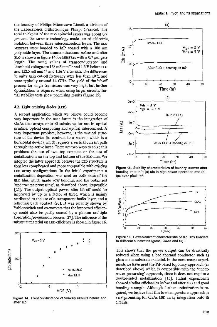
the foundry of Philips Microwave Limeil, a division of the Laboratoires d'Electronique Philips (France). The total thickness of the ELO epitaxial layers was about 0.7 p and the MESFET technology made use of dielectric isolation between three interconnection levels. The ELO MESFETS were bonded to Inp coated with a 300 nm polyimide layer. The transconductance before and after EL0 is shown in figure 14 for MESFEm with a 0.7 pm gate length. The mean values of transconductance and threshold voltage are 158 mS mm-' and 1.6 V before ELO and 152.5 mS mm-' and 1.56 V after ELO. The differences in unity gain cut-off frequency were less than 10% and were typically around 14 GHz. The yield of the lift-off process for single transistors was very high, but further optimization is required when using larger circuits. Ini- tial stability tests show promising results (figure 15).
/ Before EL0 v g s = o v V d s = S V
7 After EL0 + bonding on InP
4.2. Light emitting diodes (LED)
A second application which we believe could become very important in the near future is the integration of GaAs LED arrays onto Si substrates for use in optical printing, optical computing and optical interconnect. A very important problem, however, is the vertical struc- ture of the device (in contrast to a MESFET which is a horizontal device), which requires a vertical current path through the active layer. There are two ways to solve this problem: the use of two top contacts or the use of metallizations on the top and bottom of the ELO film. We adopted the latter approach because the LED structure is then less complicated and more compatible with existing LED array configurations. In the initial experiments a metallization deposition was used on both sides of the ELO film, which made vdw bonding and the optimized 'underwater processing', as described above, impossible [25]. The output optical power after lift-off could be improved by up to a factor of three, whicb is mainly attributed to the use of a transparent buffer layer, and a reflecting back contact [26]. It was recently shown by Yablonovitch and co-workers that the improved efficien- cy could also be partly caused by a photon multiple absorptioqre-emission process [27]. The influence of the substrate material on LED efficiency is shown in figure 16.
* beforcELO
9 abrrELO
I -2 -1 1) I
VGS (V)
0 ' . . Figure 14. Transconductance of foundry MESFE~S before and after ELO.
Vds = 5 V vgs = -2.5 v
-2e-I Bclbrc F.I.0.
-4e.7 / h
3
-Se-7 After E L 0 + honding o n InP
v1
e M
-le-6 0 I O 21) 30 40
Time (hr) I
Figure 15. Stability characteristics of foundry MESFETS after bonding onto InP: (a) Ids in high power operation and (b) Igs near pinch-off.
1 I
" 1 -0 10 20 30 40 50 60
I (mA) Figure 16. Powerlcurrent characteristic of ELO LEOS bonded to different substrates (glass, GaAs and Si).
This shows that the power output can be drastically reduced when using a bad thermal conductor such as glass as the substrate material. In the most recent experi- ments we have used the Pd-based topotaxy approach (as described above) which is compatible with the 'under- water processing' approach, since it does not require a double-sided metallization [l5]. Initial experiments showed similar efficiencies before and after ELO and good bonding strength. Although further optimization is re- quired, we believe that this low-temperature approach is very promising for GaAs LED array integration onto Si circuits.
1131

P Demeester et a /
4.3. Laser diodes
One of the first ELO devices to be successfully transferred
on glass 1281. The laser had P and N contacts on the top side, and complete processing (including facet formation) was done before the ELO. The lasers had a threshold
comparable to similar lasers on GaAs. Although these results are much more promising than for lasers grown directly on si, there is still much work required in order
was a GaAs/A10.3Ga0.7As double~heterostructure laser to obtain a reliable and simple integration strategy,
4.4. Free-space optical modulators current density of 1 kA cm-’, which remained the Same before and after lift-off. More recently we also reported
One type of free.space optical modulator makes use of the quantum confined Stark eRect (QCSE) to modulate the
the successful fabrication Of an ELo GaAs/AIGaAs GRINSCH SQW laser on Si 1131. Major differences from the
Structure (which required a moat etch ‘or protection during the chemical lift-off), compensation of the epitax- ial Stresses by appropriate layer design, double-sided metallization and a novel technique for cleaving the
wedges were etched by reactive ion etching (RIB) on one
facets at well defined locations. Figure 17(4 shows a thin film with an uncleaved and cleaved wedge, and figure
transmission of light incident on the modulator. One has to integrate a modulator onto a substrate which is
(which corresponds to the bandgap of the quantum wells in the caSe of the QCSE), We reported the first GaAs, AIGaAs MQW transmission modulator to be grafted Onto glass [291, A cOntraSt ratio of 2,9 dB and an insertion loss
normally-off asymmetric Fabry-ptrOt G ~ A ~ / A ~ G ~ A ~
rear mirror and electrical contact, Modulation ratios up to 40: 1 and reRectivity changes of Over 60% were
first approach were the Use Of A10.6Ga0.4As in the layer transparent for the wavelength of the modulated light
lasers after ELO. The cleavage was done on the finished of 2,8 dB was obtained at A = 831 nm, yofie et a, E L 0 laser StruCtUreS (6 pm thick). In a first step, sma11
side of the E L 0 film. When the film was bowed slightly, cleavage nucleated at these wedges, resulting in perfect
reported the lift-off of higlpeficiency normally-on and
MQW repction modulators (AFPM) ~301. These were bonded onto Si coated with gold, the latter used as both a
17(b) shows the finished broad stripe laser diodeS. The obtained, comparable to all-epitaxial devices on GaAs, Figure 18 shows the modulation characteristic of a GaAsiAlGaAs AFPM on Si (collaboration with Univer- sity College London and Sheffield University) [3l].
4.5. Other devices
A number of other interesting devices have been re- ported. A GaAs solar cell on AI resulted in a conversion efficiency of 13.5 % [SI. AlGaAs rib waveguides on InP resulted in fairly high losses of 7 dB cm-’ due to problems during the MBE growth [32]. GaAs MSM photo- detectors have been integrated successfully on glass or LiNbO, (see below) [33]. A more challenging realization was the lift-off of InGaAs photodetectors which were grown on an InP substrate with a very thin ( < 2 nm) AlAs lift-offlayer in between [34]. The detector showed a high internal quantum efficiency (90%) and a large bandwidth (13.5 GHz). The large increase in dark current ( x 20) was attributed to relaxation in the AlAs layer. An ELO dielectric filter structure with a quarter-wave reflec- tor was bonded between two GRIN rod lenses using uv
threshold current density was 0.5 kA cm-z, which is
Figure 18. Contrast ratio spectrum (reflection) of an asymmetric Fabry-PBrot modulator (AFPM) as function of reverse bias voltage.
Figure 17. Photograph of (a) a thin film with an uncleaved and cleaved wedge and (b) finished broad stripe lasers.
1132

Epitaxial lift-off and its applications
curable optical adhesive [35]. Near theoretical perfor- mance was demonstrated (20.6 dB rejection and less than 0.5 dB insertion loss).
4.6. Optoelectronic and photonic integrated circuits (OEIC and PIC)
Epitaxial lift-off is an integration technology and it will play a major role in the development of future optoelec- tronic and photonic integrated circuits. Although it com- bines the advantages of both monolithic and hybrid integration, a number of problems have to he solved before ELO will be accepted as a viable technique for OEIC and PIC fabrication. Our work has concentrated on the use of E L 0 for the integration Of GaAs electronic circuits with InP optoelectronic devices and for the integration of GaAs LED arrays with Si electronics. These two applica- tions are likely to become very important in the near future. Bellcore bas concentrated more on the use of ELO for the realization of PICS.
The first ELO OEIC was reported in 1990 by our group using the post-processing approach 1361. A MESFET epitaxial layer Structure was grafted Onto a G ~ A ~ sub- Strate on which an I ~ G ~ A ~ / A ~ G ~ A ~ quantum well LED structure had been grown. Both devices were then pro. cessed simultaneously, including the lithographic inter. connection between the two devices. Figure 19 shows, in the centre, the MESFETS processed on the ELO film and, on the left, the LEDs which are connected to the M E S F E ~ ~ .
The LEDS showed an external quantum efficiency of 1.7 % and the input/output ratio of the LED-FET combination was 54 pW sr-' V-'. Shortly afterwards the integration of an ELO GaAs MESFET and a LiNb03 optical switch was demonstrated using the preprocessing approach (in col~aboration with GEC Marconi) ~371, The interfere- metric switch produced an extinction ratio ,313 dB at 1300 nm for an input voltage swing to the MESFET of only 0.25 V. The first integration, including lithographic inter- connection, of a fully preprocessed ELO MESFET and InP optical switch is shown in figure 20 (made in collabora-
Figure 20. integration of a preprocessed G a A s ELO MESFET with InP buried waveguide switches.
tion with Thomson CSF) [38]. Alignment to the buried waveguide switches was done manually using mesa edges. MESFET integration with InP/InGaAsP carrier depletion directional couplers has also been imple- mented, resulting in a switching voltage reduction from 9 V to 1 V (in collaboration with Alcatel Alsthom Recherche) V71. This corresponds to a modulation efficiency of 135" v-' "-'. Finally we show in figure 21 an optical switching OEIC where a GaAs receiver amplifier (centre) is integrated with two InGaAs photo- detectors (top left) Connected to InP waveguides [39]. The GaAs receiver amplifier was designed by ETH Zurich and fabricated by the commercial Philips Micro- wave Limeil foundry, a division of the Lahoratoire d'Electronique Philips (PML/LEP-Limeil, Brevannes, France). The InP chip was fabricated by Alcatel A m o m Recherche and the finished device will be used by Ascom Tech for Operation in a very high speed optical loop (VHSOL) network [40]. With this work, which is done within the RACE I project OSCAR and the RACE I1 project ATMOS, we hope to show that ELO can become a key technology in the fabrication of InP-based OEICS.
The first P ir was renorted by Bellcore in 1989 [33]. GaAs MSM photodetectors were integrated with glass and
Figure 19. Photograph of t h e integration of ELO MESFETS with InGaAs ow LEOS.
Figure 21. Optical switching OEIC showing a GaAs receiver amplifier integrated with two InGaAs photodetectors connected to waveguides.
1133

P Demeester et a/
LiNb03 waveguides, resulting in absorption coefficients of 0.14 and 40 cm-' for glass and LiNbO, respectively. The latter result is comparable to those from all semicon- ductor waveguide detectors. GaAs detectors have also been integrated with glass waveguides in an embedded form [41]. The quantum efficiency was 60% and the absorption coefficient 38 cm-', almost two orders of magnitude better than for the non-embedded vertically coupled devices.
5. Conclusions and perspectives
In this paper we have reviewed epitaxial lift-off techno- logy and its applications. Emphasis has been put on the importance of ELO for the realization Of OEICS. The major advantages of ELO with respect to 'singlecrystal' mono- lithic integration are the material quality, the possibility of processing the different devices in an optimized way, and the possibility of testing the devices before final monolithic integration. The major advantage over hy- brid integration is the ability of ELO to achieve mono- lithic integration, with all its usual advantages (cost, size, reliability, complexity, etc). Despite these very important advantages one has to cope with a number of new problems of varying severity, such as chemical lift-off, thin-film handling, bonding, alignment, etc. In this paper we have shown that there are various different solutions to solve these problems, but further optimization is certainly possible. One of the major issues which remains open is that of the reliability of devices after ELO. Although initial results are promising, a further in-depth investigation is required. Bonding strength and aging tests such as thermal shock, thermal cycling, high-tem- perature/bigh-humidity tests, etc, will have to be used for evaluation. As is common in IC fabrication, it is most likely that a final passivation layer should be deposited on the OEIC top surface, which will also protect the sidewalls of the ELO film. A second very important issue which has to be resolved is whether the ELO process can be used in a production environment. The LEA ELO set-up in combination with the use of foundry-supplied ELO circuits is certainly a major step in the right direction, but further automation is required.
Acknowledgments
We would like to thank all the people of PML-LEP who are involved in the foundry project, especially the epitax- ial group. In our group (LEA) we would like to thank L Buydens, G Coudenys, I Moerman and G Vermeire for epitaxial growth, C Eeckhout for device processing and F Dobbelaere, M Herreman, G Janssens and L Martens for device characterization. Part of this work was carried out within the RACE I project OSCAR, the RACE 11' project ATMOS and the US A m y project DAJA-90-C-. 0003. I Pollentier and C Brys thank the IWONL for financial support.
1134
References
[l] Demeester P, Ackaert A, Coudenys G, Moerman I, Buydens L, Pollentier I and Van Daele P 1991 Prog. Crystal Growth Ckaract. 22 53-141
[Zl Sugo M, Mori H, Sakai Y and Itoh Y 1992 Appl. Phys. Lett. 60 412
131 Choi H, Wang C and Karam N 1991 Appl. Pkys. Lett. 59 2634
[41 Briones F 1992 ESSDERC'92 (14-17 September 1992, Leuuen, Belgium)
Appl. Phys. Lett. 58 1961
results
[a Lo Y, Bhat R, Hwang D, Koza M and Lee T 1991
[61 Coudenys G, Moerman I and Demeester P unpublished . . ~ ~ ~ ~ .
[7] Yablonovitch E, Gmitter T, Harbison J and Bhat R
[SI Pollentier I, Demeester P and Van Daele P 1992 Proc.
[9] Chan W, Yi-Yan A and Gmitter T 1991 IEEE
Cl01 Konagai M, Sugimoto M and Takahashi T 1978
1111 Maszara W P 1991 J. Electrochem. Soc. 138 341 [lZ] Pollentier I 1993 PhD 27zesis (in Dutch) [I31 Pollentier I. Buvdens L, .Van Daele P and Demeester P
1987 Appl. Phys. Lett. 51 2222
EFOCILAN '92 (Paris) (IC1 Europe) pp 66-71
J. Quantum Electron. 27 717
J . Crystal Growth 45 211
. _ 1991 IEEE Photon. Technol. Lett. 3 115
r141 Yablonovitch E. Sands T. Hwane D M. Schnitzer I. _ _ Gmitter T J,'Shastry S K, Hili D S and Fan J C C 1991 Appl. Phys. Lett. 59 3159
[l5] Cowin M, Pollentier I, Brys C, De Dobbelaere P, Van Daele P and Demeester P Electron. Lett. (submitted)
[161 Camperi-Ginestet C, Hargis M, Jokerst N and Allen M 1991 IEEE Photon Technol. Lett. 3 1123
[ln Renand M, Pollentier I, Vinchant J F, Demeester P, Cavaillts J A. Van Daele P and Erman M 1991 Proc. ECOCilOOC '91 pp 453-6
r181 Yi-Yan A. Chan W. Gmitter T. Florez L. Jackel J. - - Yablonovitch E,'Bhat Rand Harbison J 1989 iEEE Photon. Technol. Lett. 1 379
[19] Pollentier I, Zhu Y, De Meulemeester B, Van Daele P and Demeester P 1991 Microelectron. Eng. 15 153
[20] Pollentier I, Brys C, De Dobbelaere P, Van Daele P and Demeester P IEEE Trans. Hvbrids Como. Manufact. Technol. (submitted)
G 1989 Electron. Lett. 25 136
" 756
[211 Van Hoof C, De Raedt W, Van Rossum M and Borghs
[221 Demeester P er a1 1989 Proc. ECOC '89 (Gothenburg) r - - -
[23] Pollentier I, Buydens L, Van Daele P and Demeester P 1992 Microelectron Eng. 19 207-10
[24] Pollentier I, Brys C, Demeester P, Van Daele P and Martens L 1993 Electron Lett. 29 291-3
[25l Pollentier I, Demeester P, Ackaert A, Buydens L, Van Daele P and Baets R 1990 Electron. Lett. 26 193
C261 Pollentier I, Ackaert A, De Dobbelaere P, Buvdens L, Demeester P and Van Daele P 1990 SPIE-Proc. 1361 1056-63
Schnitzer I, Yablonovitch E, Caneau C, Ersen A and Gmitter T 1992 LEOS Summer Topical Meeting on Integrated Optoelectronics (5-7 August 1992, Santa Barbara, CA) (New York: IEEE)
Yablonovitch E, Kapon E, Gmitter T J, Yun C P and Bhat R 1989 IEEE Photon Technol. Lett. 141
1 Buydens L, De Dobbelaere P, Demeester P, Pollentier I and Van Daele P 1991 Opt. Lett. 16 916
Yoffe G 1991 Electron. Lett. 27 1580 2317 Buydens L, Pollentier I, Van Daele P and Demeester P
unpublished results C321 Yi-Yan A, Seto M, Gmitter T J, Hwang D M and
Florez L T 1990 Electron. Lett. 26 1561 [331 Yi-Yan A, Chan W K, Gmitter T J, Florez L T,

Epitaxial lift-off and its applications
Jackel J L, Yablonovitch E, Bhat R and Harbison J P 1989 IEEE Photon. Teihnol. Lett. 1 379
Yablonovitch E and Koza M A 1989 Electron. Lett. 25 1653
[35J Dell J and Yoffe G 1991 Proc. ECOC/IOOC '91 (Pais ) P 53
[36] Pollentier I, Buydens L, Ackaert A, Demeester P, Van Daele P, De Pestel F, Lootens D and Baets R 1990 Electron. Lett. 26 925
[3q O'Donnell A C, Pollentier I, Demeester P, Van Daele P and Car A D 1990 Electron. Lett. 26 1179
[38] Pollentier I, Demeester P, Van Daele P, Rondi D, Glastre G, Enard A and Blondeau R 1991 Proc. I n P and Related Materials '91 (New York: IEEE) pp 268-71
[34] Shumacher H, Gmitter T J, LeBlanc H P, Bhat R,
[39] Pollentier I et al unpublished results [40] Martinson T M 1990 Proc. EFOC-LAN'90 pp 309 [41] Chan W K, Yi-Yan A, Gmitter T J, Florez L T,
Andreadakis N and Nguyen C K 1991 Electron. Lett. 27 410
1135