Embed Size (px)
Citation preview

Error Detection and Correction in Content AddressableMemories
S. Pontarelli, M. Ottavi,∗A. Salsano
{pontarelli, ottavi, salsano}@ing.uniroma2.it
University of Rome ”Tor Vergata”, Via del Politecnico 1, 00191, Rome, ITALY
Abstract
A Content Addressable Memory (CAM) is an SRAM based memory which can be accessed in
parallel in order to search for a given search word, providing as result the address of the matching
data. The use of CAM is widespread in many applications ranging from the controller of a CPU
memory cache to the implementation of lookup tables of high speed routers. Like conventional
memories, CAM can be affected by the occurrence of Single Event Upsets (SEU) which can alter its
operation causing different effects such as pseudo-HIT or pseudo-MISS events. In order to avoid
the effects of SEUs different approaches have been proposed in previous literature, but all of these
solutions require changes to the internal structure of the CAM itself. Differently from previous
approaches, in this paper we propose a method that does not require any modification to a CAM’s
internal structure and therefore can be easily applied at system level, using a suitable redundant
CAM component in order to obtain a CAM module with error detection and correction capabilities.
1 Introduction
A Content Addressable Memory (CAM) is an SRAM based memory able to compare the inputdata against the data stored in the memory, providing as result the address of the matching data[1]. Conceptually a CAM can be used to perform the inverse function of a RAM where we are givendata providing an address as input while in a CAM we give as input a data, receiving as result if andwhere the data is stored in the memory. A CAM is therefore able to access within a clock cycle, toall of the entries stored in its memory table and to compare them to the provided input. CAM withsmall dimensions are commonly used in cache or Translation Lookaside Buffers (TLB), [2] whilelarge CAM are used in systems that must be able to a perform rapid search within a large amountof data. Nowadays one of the most used application of CAM are related to packet forwarding andclassification in high speed network systems [3].
In recent years the implementation of CAM with large memory has been driven by their usein network systems, that continuously increases the performance request of such components. Tosatisfy these requests, state of the art CMOS technology nodes are being used to manufacture largeCAM circuits, however with the use nanometric scale systems, and the increase in the overall numberof stored bits, there has been a consequent increase in the error rate due to the occurrence of SingleEvent Upsets also at sea level. These effects are well known for SRAM and DRAM memories andmany strategies have already been proposed to mitigate the effect of SEU in memories. Howeverthese techniques are not suitable to be applied directly to CAM, and therefore new techniques tomitigate SEU effects in CAM must be developed in order to use large CAM in complex systems whileensuring high levels of reliability. In literature different techniques have been proposed to enhance
∗This research was partially funded by the Italian Ministry for University and Research; Program “In-centivazione alla mobilita di studiosi stranieri e italiani residenti all’estero”, D.M. n.96, 23.04.2001
!000111000 !555ttthhh IIInnnttteeerrrnnnaaatttiiiooonnnaaalll SSSyyymmmpppooosssiiiuuummm ooonnn DDDeeefffeeecccttt aaannnddd FFFaaauuulllttt TTTooollleeerrraaannnccceee iiinnn VVVLLLSSSIII SSSyyysssttteeemmmsss
!555555000---555777777444///!000 $$$222666...000000 ©©© 222000!000 IIIEEEEEEEEE
DDDOOOIII !000...!!000999///DDDFFFTTT...222000!000...555666
444222000

robustness against SEU in CAM. For example in [4] the use of DRAM instead of SRAM has beenproposed, exploiting the assumption that DRAM are less susceptible to SEU that SRAM. In [5] thecontent of the CAM is continuously refreshed by an associated DRAM with ECC features, in orderto scrub the memory recovering the CAM from errors due to SEU. Instead, in [6] the use of Hammingcodes, in conjunction with a modified match line circuit is proposed. SEU effects in cache memorieshas been also investigated in [7], [8], [9]. The techniques proposed in these papers to prevent errorsdue to SEU use a circuital approach that requires changes in the internal structure of the CAM,and consequently a redesign of the entire chip, in order to be applied. Differently from the previousapproaches, in this paper we propose a method that does not require any modification to the internalstructure of a CAM, and therefore can be applied at a system level, using suitable redundant CAMcomponent in order to obtain a CAM with error detection and correction capabilities.
The rest of the paper is structured as follows: Section II discusses the basic properties of a CAM,while section III shows the effects of a SEU hitting a CAM. In section IV the proposed architectureof a CAM with error detection and error correction capabilities is presented. Finally, in Section Vthe conclusions are drawn.
2 Description of a Content Addressable Memory
Figure 1. Scheme of a CAM
Figure 1 shows a schematic depiction a CAM. A CAM has an array based structure similar to aRAM, with an arrangement in rows and columns. When a word has to be read or modified it canbe accessed similarly to a RAM through bitlines and wordlines. However, when the specific CAMfunctionality has to be performed the operation is carried out in parallel. The input search word isan n bit string which is concurrently compared to all the 2M words stored in the CAM. The numberof bits the search word (n) ranging from 36 to 144 bits is usually much larger than M which usuallyranges from from 7 bits to 15 bits [1]. For each line of the CAM a match-line wire signals whetherthat word matches the searched word. If no match occurs an output ”‘miss”’ signal is raised fromthe CAM. This miss signal can be easily derived as the NOR of all the match-line wires. It caneasily seen that the size of a CAM grows linearly with either the number of the entries and withthe size of the search word.
Figure 2 a) shows a circuit level representation of a CAM where only the structures related tothe search function are reported. The driver circuitry provides the search word to all the n-bitsCAM entries which are composed of n C blocks. Figure 2 b) shows a possible implementation ofthe C block to work in a NOR fashion. The value on SL is compared with the D value stored inthe SRAM cell, when the values are different either the series of the transistors M1 and M2 or theseries of the transistors M3 and M4 connect ML to ground. Therefore, if at least one of the bits of
444222!

Figure 2. a) Circuit level description of a CAM b) Circuit level description of a C
block
the search line being compared is different to the corresponding bit of the CAM entry the ML willbe connected to ground thus effectively behaving as a NOR gate.
All the computed matchlines are input to an encoder which if only one match has occurredprovides a normal one-hot to binary encoding of the matchline signals. Instead, if more than onematch has occurred two different policies can be applied.
The first policy is to use a priority encoder designed to establish a priority in the encoded outputthus providing only one output. For instance the priority encoder provides as an output the matchingword with the highest (or lowest) value: we call this resolved multimatch approach. A second policyrequires the introduction of an signal called Nmatch which provides the number of matched lines ;on the encoder output the matched lines will be provided as an output one per clock cycle: we callthis unresolved multimatch approach.
By looking at the schematic of Figure 2 b) it can also be noticed that, a rough computationof the transistor count for a CAM memory cell gives as a result about twice as many transistorsthan a standard RAM cell. Therefore the memory density of a CAM is usually half of a SRAMmanufactured with the same technology node [1].
Entry Input Output0 00100110 001001101 00110000 000000002 11111110 000000003 11111111 11111111
Table 1. Example of a routing table
As previously stated in the introduction, CAM find a wide usage in the implementation of fastlookup tables for network routers. Table 1 shows an example of a routing table where each n = 8bits input is matched against 4 entries coded with M = 2 bits. Each entry corresponds to an 8 bitsoutput which provides the final result of the search query. Therefore with the lookup operation, theprovided input corresponds to an output of the same size. Figure 3 shows how this table can beimplemented by using the combination of a four 8-bits entries CAM that provides a correspondencebetween the 8 bits input and the 2 bits output, and a RAM that given the 2 bits as an addressprovides the final 8 bit output.
444222222
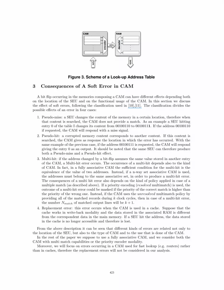
Figure 3. Scheme of a Look-up Address Table
3 Consequences of A Soft Error in CAM
A bit flip occurring in the memories composing a CAM can have different effects depending bothon the location of the SEU and on the functional usage of the CAM. In this section we discussthe effect of soft errors, following the classification used in [10],[11]. The classification divides thepossible effects of an error in four cases:
1. Pseudo-miss: a SEU changes the content of the memory in a certain location, therefore whenthat content is searched, the CAM does not provide a match. As an example a SEU hittingentry 0 of the table I changes its content from 00100110 to 00100111. If the address 00100110if requested, the CAM will respond with a miss signal.
2. Pseudo-hit: a corrupted memory content corresponds to another content. If this content issearched, the CAM gives as response the location in which the error has occurred. With thesame example of the previous case, if the address 00100111 is requested, the CAM will respondgiving the entry 0 as an output. It should be noted that the same SEU can therefore produceboth a Pseudo-miss and a Pseudo-hit effect.
3. Multi-hit: if the address changed by a bit-flip assumes the same value stored in another entryof the CAM, a Multi-hit error occurs. The occurrence of a multi-hit depends also to the kindof CAM. In fact, in a fully associative CAM the sufficient condition for the multi-hit is theequivalence of the value of two addresses. Instead, if a n-way set associative CAM is used,the addresses must belong to the same associative set, in order to produce a multi-hit error.The consequences of a multi hit error also depends on the kind of policy applied in case of amultiple match (as described above). If a priority encoding (resolved multimatch) is used, theoutcome of a multi-hit error could be masked if the priority of the correct match is higher thanthe priority of the wrong one. Instead, if the CAM uses the unresolved multimatch policy byproviding all of the matched records during k clock cycles, then in case of a multi-hit error,the number Nmatch of matched output lines will be k + 1.
4. Replacement error: this error occurs when the CAM is used in a cache. Suppose that thecache works in write-back modality and the data stored in the associated RAM is differentfrom the correspondent data in the main memory. If a SEU hit the address, the data storedin the cache is no longer accessible and therefore is lost.
From the above description it can be seen that different kinds of errors are related not only tothe location of the SEU, but also to the type of CAM and to the use that is done of the CAM.
In the rest of the paper we suppose to use a fully associative CAM, and we consider both theCAM with multi match capabilities or the priority encoder modality.
Moreover, we will focus on errors occurring in a CAM used for fast lookup (e.g. routers) ratherthan in caches, therefore the replacement errors will not be considered in our analysis.
444222333

4 Error Detection and Correction in a CAM
In this section we discuss how to detect and correct SEU induced errors in a CAM. As statedin the introduction we will focus on a solution that will not require substantial modifications toexisting CAM circuits. As an example in [6] the words stored in a CAM are protected againstSEUs by utilizing one or more parity bits, and the SEU induced errors detection and correction isdemanded to a modified encoder block which effectively works also as an embedded Error Correctionblock based on Hamming codes. This encoder therefore requires a number of several cascaded XORgates (see also [12]), which degrade area occupancy and most of all the timing performances withrespect to a non protected CAM. Moreover the solution proposed in [6] for matchline sense amplifiersalthough quite interesting, could be affected by issues both related to power consumption and noiseimmunity. In our proposed solution we also make use of parity check but we limit to a single paritybit, and, by introducing a redundant copy of the CAM we correct SEU induced errors at a highersystem level. Therefore while we assume that the CAM output could be affected by an error, wemonitor the inputs and outputs of the CAM and by leveraging the characteristics of the fault modeldescribed above, we show that we can correct the occurrence of errors. Differently from [6] theaddress that is provided to the CAM already includes a parity bit, this encoding can be performedinside of a block that is externally instantiated with respect to the CAM itself therefore not requiringany structural modification to existing commercial CAMs. First we make preliminary considerationregarding a parity encoded CAM: if the a CAM search word is encoded with a single parity bit andwe are in the common assumption that multiple bit upsets (MBU) can be avoided, then, we canalways say that a pseudo hit can never occur. In fact, with a parity encoded CAM if a SEU hitsa codeword it will turn it into a non codeword (rather than a wrong codeword) and thus since theCAM search words are always codewords a false hit will never occur.
Figure 4. Scheme of the proposed error correction scheme for a CAM
Based on this assumption we can describe the proposed solution as shown in figure 4 The addressis parity encoded by passing through the ”‘PARITY ENCODER”’ module and then fed to the twocopies of the CAM. The outputs of the two CAMs are input to the ”‘CHECKER”’ which detectswhether there has been an error in the CAMs and provides the correct output. First we considerthe case where there are no multiple matches, then we will extend our analysis to the case thatthe same word is stored into different CAM entries. The possible cases are summarized in Table 4.When both CAM respond with a HIT then, because of the previous consideration that with parityencoding there are no false HITs then either CAM A or CAM B outputs can be considered correctand sent to the output (this will be different when we will make also the assumption of multipleHITs as we will discuss below). Instead when the two CAMs provide a discordant HIT/MISS signal,then for the same consideration that there are no false HITs the ”‘CHECKER”’ module will haveto choose as correct, the output of the CAM giving HIT. Therefore, the CAM that provided a MISS
444222444

signal has been affected by a SEU induced pseudo miss error. Finally when both CAMs give a MISSsignal, because of the assumption of single fault applies, then neither of the CAMs is a HIT and theoverall status is MISS.
CAM A CAM B Correct Output/StatusHIT HIT A,B/HITHIT MISS A/HITMISS HIT B/HITMISS MISS none/MISS
Table 2. Possible error cases and correct output selection
When we are also making the assumption that multiple matches can occur on the CAM thenwe must also further divide our analysis into two cases: the resolved and unresolved multimatchpolicies. We are in the assumption that more than one entry of the CAM store the same word andthat one of these entries is affected by a SEU. Therefore in a copy of the CAM there will be k > 1matching entries whereas in the other there will be k − 1 matching entries. First of all we noticethat both CAM will provide a HIT response, and that the CAM with k − 1 matches is affected byan error (i.e. pseudo-miss). Therefore when the unresolved multimatch policy is used then it willbe sufficient to compare the Nmatch signals of the two CAMs and take as correct the output of theCAM with the highest Nmatch value. Instead suppose that we are using the resolved multimatchpolicy and that the priority encoder selects the word with the highest entry value; in this casethere as previously mentioned, it could be possible that the pseudo-MISS error would be maskedby the presence of another matching entry with a higher priority. However if this masking does notoccur, the two CAM provide different values. Since we know that no pseudo-HIT can occur, theCHECKER block will be able to correct the error by selecting the entry with the highest priority(i.e. in our example the entry with the highest value).
The error correction strategies based on the multimatch resolution policy are summarized inTable 4.
CAM A CAM B Policy Correct Output/StatusHIT HIT resolved multimatch (highest priority entry)/HITHIT HIT unresolved multimatch highest Nmatch /HITHIT MISS either A/HITMISS HIT either B/HITMISS MISS either none/MISS
Table 3. Error correction based on the multimatch resolution policy
A different version of the above described approach can used when the CAM is used in conjunctionwith a RAM to implement for example a Look-up address table as described in Figure 3. Becauseof the fact that RAM are generally more dense and cheaper than similar sized CAMs it makes senseto move the parity bits from the CAM to the RAM part of the circuit.
Figure 5 shows an example where a solution similar to what described in Figure 4 is adopted to acase when also a RAM is used. Data written in CAM A and CAM B is not parity coded and thus,differently from the previous example errors at the outputs of these CAMs can be either pseudo-HIT or pseudo-MISS. Instead in the RAM A and RAM B modules redundant information is storedwhich allows to correct errors occurring in either the RAM and the CAM side of the circuit. Theintegrity of the data stored in the RAM itself is ensured by using an ECC code such as Hamming,moreover in a RAM entry a further bit is used to store the parity of the address (input of the CAMmodule) that yields to that entry of the RAM. As described in table 1 a CAM provides as an outputthe index associated to the entry matching the search word at its input. This index is the address
444222555

Figure 5. Error detection and correction for a CAM used in conjunction with a RAM
provided as an input to the RAM associated to the CAM which therefore provides always a value.In every address of the RAM store the parity of the value given to the CAM as an input. Thereforewhen the search word is matched in the CAM, the associated RAM provides as an output, thecorresponding output and the parity of the search word. The CAM system shown in figure 5 iscomposed of two copies of CAM/RAM blocks, a parity encoder which provides the parity of theinput address (search word) and a checker that choses the correct output from the two copies basedon the policy described in Table 4. If a SEU hits a CAM entry the stored word will consequentlyhave an opposite parity to that stored in the corresponding RAM entry. We can assume that noerror has occurred in the CAMs when they both provide a MISS signal, as well as when they bothprovide a HIT with correct search word parity P . Instead when both CAMs provide a HIT but thecorresponding parities P are different, then we can safely assume that the correct output is thatassociated to the correct parity. In the latter case it should be noticed that the data stored in theRAMs could even be identical although they are being read on different addresses (indexes). Finallyif the two CAMs provide conflicting HIT/MISS signals, we can check the parity associated to theCAM that provided a HIT signal. If the parity is correct then the HIT is real otherwise if the parityis not correct then the correct output was a MISS.
CAM A CAM B P(A) P(B) Correct Output/StatusHIT HIT good good (A,B)/ HITHIT HIT good wrong (A)/ HITHIT MISS good N/A (A)/HITHIT MISS wrong N/A none/MISSMISS MISS N/A N/A none/MISS
Table 4. Error correction based on the CAM/RAM system
Finally we can discuss what happens in case of multimatch. As in the previously discussed case,different policies should be applied. First it should be noticed that if a pseudo-HIT has happenedthen parity of the outputs of the two RAMs will be different so the choice of the correct output onthe CHECKER can be done by just checking the parities, however if a pseudo-MISS has happened,the parities of the two RAM outputs would be correct. When the chosen resolution policy is resolvedmultimatch and there are two RAM outputs with correct parity but different values, (pseudo-MISS)then the CHECKER has also to be fed with the entry outputs from both CAMs (dashed arrowsin figure 5) in order to choose the RAM output corresponding to the highest priority. Instead if
444222666
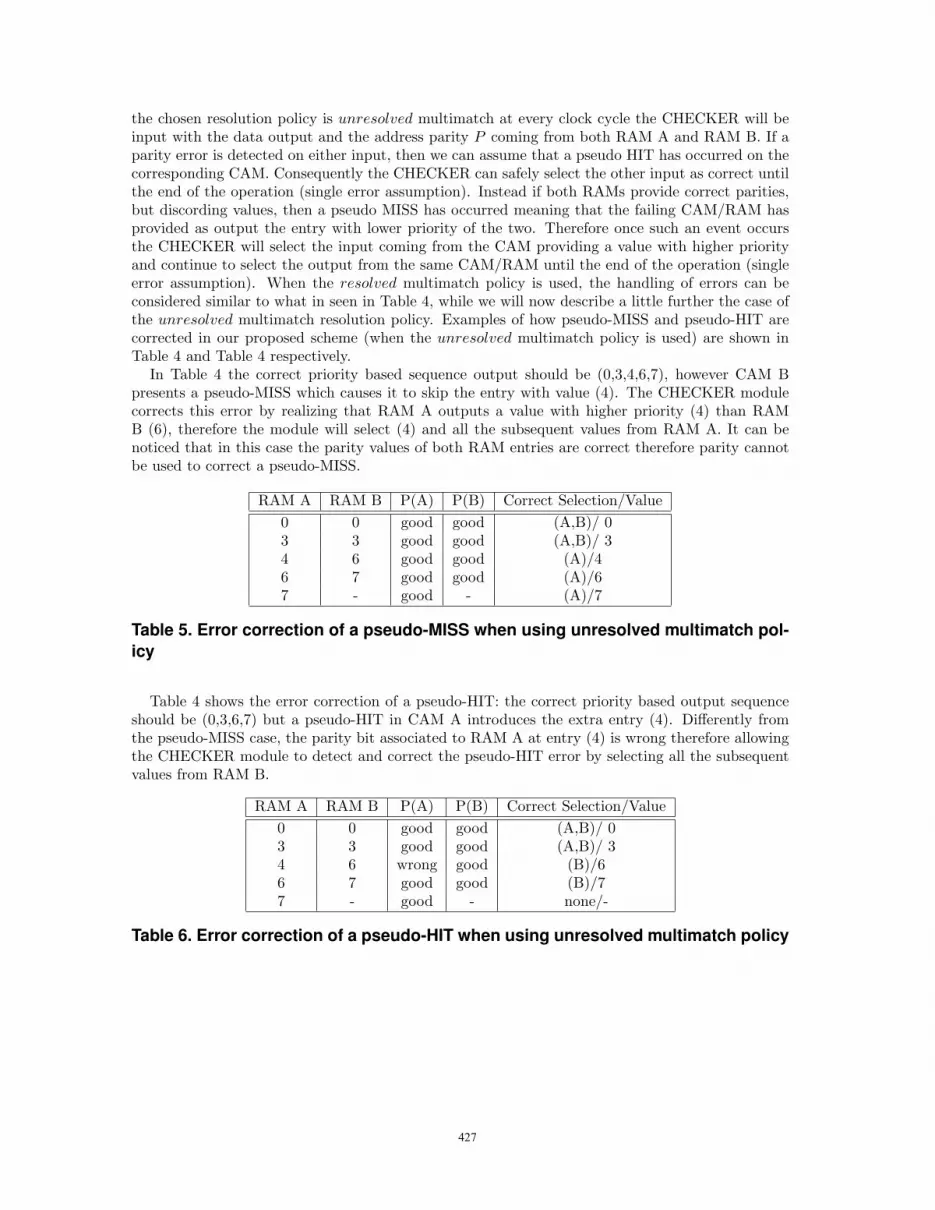
the chosen resolution policy is unresolved multimatch at every clock cycle the CHECKER will beinput with the data output and the address parity P coming from both RAM A and RAM B. If aparity error is detected on either input, then we can assume that a pseudo HIT has occurred on thecorresponding CAM. Consequently the CHECKER can safely select the other input as correct untilthe end of the operation (single error assumption). Instead if both RAMs provide correct parities,but discording values, then a pseudo MISS has occurred meaning that the failing CAM/RAM hasprovided as output the entry with lower priority of the two. Therefore once such an event occursthe CHECKER will select the input coming from the CAM providing a value with higher priorityand continue to select the output from the same CAM/RAM until the end of the operation (singleerror assumption). When the resolved multimatch policy is used, the handling of errors can beconsidered similar to what in seen in Table 4, while we will now describe a little further the case ofthe unresolved multimatch resolution policy. Examples of how pseudo-MISS and pseudo-HIT arecorrected in our proposed scheme (when the unresolved multimatch policy is used) are shown inTable 4 and Table 4 respectively.
In Table 4 the correct priority based sequence output should be (0,3,4,6,7), however CAM Bpresents a pseudo-MISS which causes it to skip the entry with value (4). The CHECKER modulecorrects this error by realizing that RAM A outputs a value with higher priority (4) than RAMB (6), therefore the module will select (4) and all the subsequent values from RAM A. It can benoticed that in this case the parity values of both RAM entries are correct therefore parity cannotbe used to correct a pseudo-MISS.
RAM A RAM B P(A) P(B) Correct Selection/Value0 0 good good (A,B)/ 03 3 good good (A,B)/ 34 6 good good (A)/46 7 good good (A)/67 - good - (A)/7
Table 5. Error correction of a pseudo-MISS when using unresolved multimatch pol-
icy
Table 4 shows the error correction of a pseudo-HIT: the correct priority based output sequenceshould be (0,3,6,7) but a pseudo-HIT in CAM A introduces the extra entry (4). Differently fromthe pseudo-MISS case, the parity bit associated to RAM A at entry (4) is wrong therefore allowingthe CHECKER module to detect and correct the pseudo-HIT error by selecting all the subsequentvalues from RAM B.
RAM A RAM B P(A) P(B) Correct Selection/Value0 0 good good (A,B)/ 03 3 good good (A,B)/ 34 6 wrong good (B)/66 7 good good (B)/77 - good - none/-
Table 6. Error correction of a pseudo-HIT when using unresolved multimatch policy
444222777

5 Conclusion
Content Addressable Memories like other memories can be affected by the occurrence of SingleEvent Upsets (SEU) which can alter its operation causing different effects such as pseudo-HIT orpseudo-MISS events. In order to avoid the effects of SEUs different approaches have been proposedin previous literature, but all of these solutions required changes to the internal structure of theCAM itself. This paper has proposed a method to detect and correct errors occurring on a CAMby a combination of CAM duplication and the usage of single parity bit encoding therefore notrequiring any modification to the internal structure of existing CAM architectures. It has beenshown that the proposed approach can be used to detect and correct errors occurring also whendifferent multimatch resolution policies are employed. Finally it has been shown that the proposedapproach can also be applied to a CAM/RAM combined system by including the parity encodingin the RAM side of the system thus allowing to double the number of possible entries in the CAM.
References
[1] K. Pagiamtzis, A. Sheikholeslami, “Content Addressable Memory (CAM) Circuits and Archi-tectures: A Tutorial and Survey”, Solid-State Circuits, IEEE Journal of, Vol. 41, n. 3, pp. 712 -727, 2006
[2] D. A. Patterson, J. L. Hennessy. “Computer Architecture: A Quantitative Approach”, 3rdedition, Morgan Kaufmann, 2003.
[3] H.Chao, ”Next generation routers”, Proc. IEEE, vol.90, no.9, pp.1518-1558, September 2002.[4] H. Noda, K Inoue M. Kuroiwa, F. Igaue, et at., ” A cost-efficient high-performance dynamic
TCAM with pipelined hierarchical search and shift redundancy architecture,” IEEE J. Solid-StateCircuits, vol. 40, no. 1, pp. 245-253,
[5] H.Noda, K.Dosaka, F. Morishita, K.Arimoto “A soft-error immune maintenance-free TCAMarchitecture with associated embedded DRAM”, IEEE Custom Integrated Circuits Conf, pp.451-454, September 2005
[6] K. Pagiamtzis, N. Azizi, F. N. Najm, “A Soft-Error Tolerant Content-Addressable Memory(CAM) Using An Error-Correcting-Match Scheme” IEEE Custom Integrated Circuits Conf, 2006
[7] A. Hossein S. Vilas M.B. Tahoori, D. Kaeli, “Vulnerability Analysis of L2 Cache Elements toSingle Event Upsets”, Design, Automation and Test in Europe, 2006. DATE ’06. Proceedings,Vol. 1, pp. 1-6, 2006
[8] W. Zhang, “Replication Cache: A Small Fully Associative Cache to Improve Data Cache Relia-bility” Computers, IEEE Transactions on, Vol. 54 , n. 12, pp. 1547 - 1555, 2005
[9] H. Sun, N. Zheng, and T. Zhang. “Realization of L2 cache defect tolerance using multi-bit ECC”,Defect and Fault Tolerance of VLSI Systems, 2008. DFT’ 08. IEEE International Symposium on,pp. 254262, 2008.
[10] S. Kim and A. K. Somani, Area Efficient Architectures for Information Integrity in CacheMemories, Proc. of the Intl. Symp. on Computer Architecture (ISCA99), pp. 246- 255, Atlanta,Georgia, May 1999.
[11] Hossein Asadi, Vilas Sridharan, Mehdi B. Tahoori, David Kaeli, “Reliability Tradeoffs in Designof Cache Memories”, 1st Workshop on Architectural Reliability, 2005
[12] H. J. Lee, “Immediate soft error detection using pass gate logic for content addressable mem-ory”, IEE Electronics Letters, Vol. 44 , n. 4 pp. 269 - 270, 2008
444222888


