Embed Size (px)
Citation preview

www.infineon.com
Please note that Cypress is an Infineon Technologies Company.The document following this cover page is marked as “Cypress” document as this is the company that originally developed the product. Please note that Infineon will continue to offer the product to new and existing customers as part of the Infineon product portfolio.
Continuity of document contentThe fact that Infineon offers the following product as part of the Infineon product portfolio does not lead to any changes to this document. Future revisions will occur when appropriate, and any changes will be set out on the document history page.
Continuity of ordering part numbersInfineon continues to support existing part numbers. Please continue to use the ordering part numbers listed in the datasheet for ordering.
EZ-PD CCG6DF, CCG6SF
USB Type-C Port Controller
Cypress Semiconductor Corporation • 198 Champion Court • San Jose, CA 95134-1709 • 408-943-2600Document Number: 002-27161 Rev. *I Revised April 14, 2021
EZ-PD CCG6DF, CCG6SF, USB Type-C Port Controller
General Description
EZ-PD™ CCG6DF and EZ-PD CCG6SF are dual-port and single-port USB Type-C controllers that comply with the latest USB Type-Cand PD specifications. These devices provide a complete USB Type-C and USB-Power Delivery port control solution for PCs andnotebooks. Both of these devices include a VBUS provider path load switch. These devices also contain a True Random NumberGenerator for authentication, a 32-bit, 48-MHz Arm® Cortex®-M0 processor with 64-KB flash and 96-KB ROM, integrating a completeType-C Transceiver including the Type-C termination resistors Rp, Rd, and dead battery Rd termination. CCG6DF is available in a96-ball BGA package, whereas CCG6SF is available in 48-pin QFN package.
Applications
Notebooks and desktops
Thunderbolt hosts, non-Thunderbolt hosts
Features
USB-PD Supports latest USB PD 3.0 specification
Fast Role Swap (FRS)
Extended Data Messaging
Type-C
Integrated current sources for DFP[1] role (Rp) Default current at 900 mA 1.5 A 3 A
Integrated Rd resistor for UFP[2] role
Integrated VCONN FETs to power EMCA cables
Integrated dead battery termination
Integrated high-voltage protection on CC and SBU pins toprotect against accidental shorts to the VBUS pin on the Type-Cconnector
Integrated pass through SBU Switch for 20-V protection
Mux Integrated USB 2.0 Analog Mux for USB 2.0 HS and UART
data
Integrated Provider VBUS Load Switch VBUS Provider Switch (5 V/3A)
Slew rate controlled turn-on on the VBUS provider path,tolerant to 24 V
Configurable hardware-controlled VBUS overvoltage, under-voltage, overcurrent, short circuit, reverse current protection,and thermal shutdown
VBUS high-side current sense amplifier capable of measuringcurrent across 5-m series resistance on the provider path
In response to Fast Role Swap request, turns OFF externalconsumer N-channel Field Effect Transistor (NFET) and turnsON internal provider load switch
LDO
Integrated high-voltage LDO operational up to 21.5 V for deadbattery mode operation
32-bit MCU Subsystem 48-MHz Arm Cortex-M0 CPU
64-KB Flash
96-KB ROM
16-KB SRAM
Integrated Digital Blocks Two integrated timers and counters to meet response times
required by the USB-PD protocol
Four run-time serial communication blocks (SCBs) withreconfigurable I2C, SPI, or UART functionality
Authentication True Random Number Generator
Clocks and Oscillators Integrated oscillator eliminating the need for an external clock
Operating Range VSYS (2.75 V–5.5 V)
VBUS (4 V–21.5 V)
Hot-Swappable I/Os
I2C pins from SCB0 are hot-swappable
Packages CCG6DF: 6.0 mm 6.0 mm 1.0 mm, 96-ball BGA with 0.5-mm
pitch
CCG6SF: 6.0 mm 6.0 mm 0.6 mm, 48-pin QFN with 0.4-mmpitch
Notes1. DFP refers to power source.2. UFP refers to power sink.
Document Number: 002-27161 Rev. *I Page 2 of 51
EZ-PD CCG6DF, CCG6SF
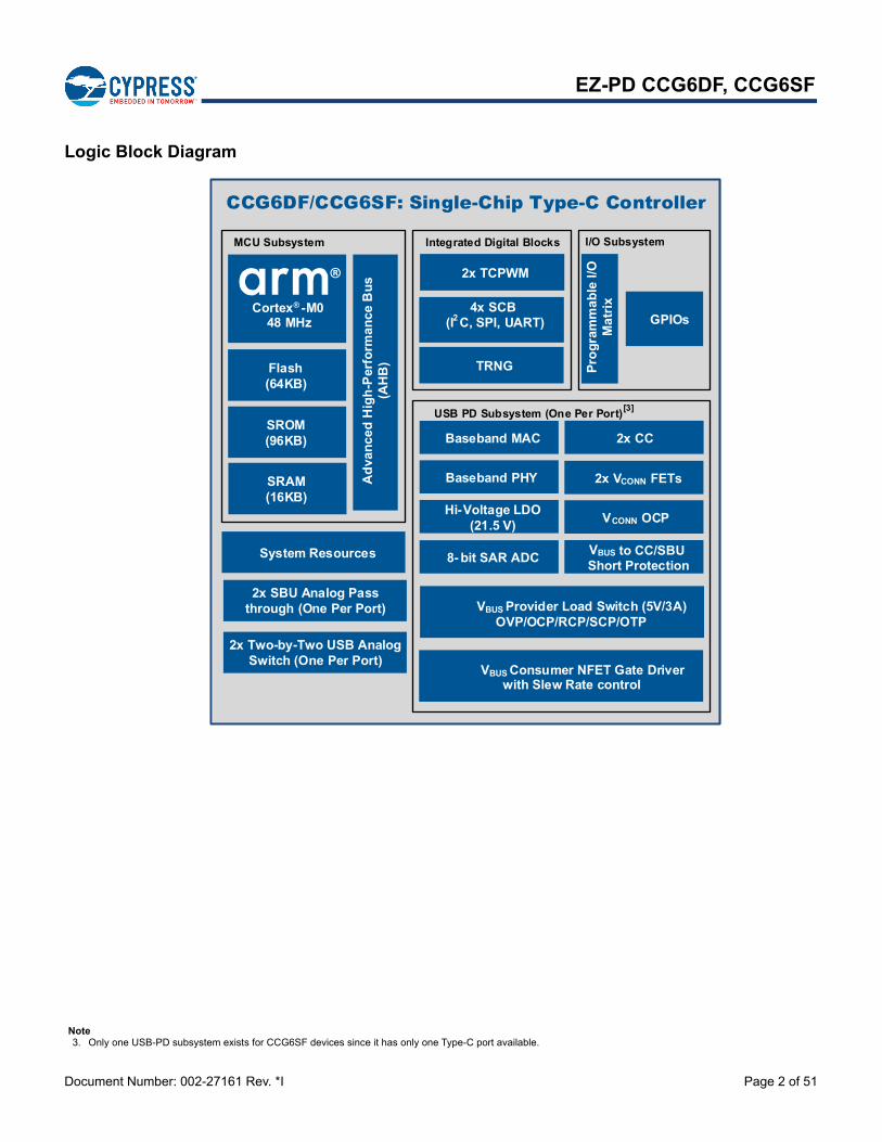
Logic Block Diagram
Flash(64KB)
Pro
gra
mm
ab
le I/
O
Ma
trix
Integrated Digital Blocks I/O SubsystemMCU Subsystem
Ad
van
ce
d H
igh
-Per
form
an
ce
Bu
s(A
HB
)
GPIOs
Baseband MAC
Baseband PHY
4x SCB(I2 C, SPI, UART)
2x TCPWM
USB PD Subsystem (One Per Port)[3]
2x VCONN FETs
Hi-Voltage LDO (21.5 V)
8- bit SAR ADCVBUS to CC/SBU Short Protection
VCONN OCP
2x CC
VBUS Provider Load Switch (5V/3A) OVP/OCP/RCP/SCP/OTP
®
System Resources
Cortex® -M048 MHz
VBUS Consumer NFET Gate Driver with Slew Rate control
2x SBU Analog Pass through (One Per Port)
SROM(96KB)
SRAM(16KB)
TRNG
2x Two-by-Two USB Analog Switch (One Per Port)
CCG6DF/CCG6SF: Single-Chip Type-C Controller
Note3. Only one USB-PD subsystem exists for CCG6SF devices since it has only one Type-C port available.
Document Number: 002-27161 Rev. *I Page 3 of 51
EZ-PD CCG6DF, CCG6SF
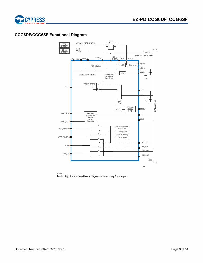
CCG6DF/CCG6SF Functional Diagram
CONSUMER PATHNFET
VBUS_C
PROVIDER PATHVBUS_CVSYS
VBUS_C_CTRL
VBUS_CVBUS_P
VDDIO
VDDD
VCCD
CSNCSP
VCONN SWITCH
V5V
SBU1_SYS
SBU2_SYS
UART_TX/GPIO
UART_RX/GPIO
DP_SYS
DM_SYS
MCU Subsystem
SBU2
SBU1
GPIOs
CC1
CC2
DP_TOP
DP_BOT
DM_TOP
DM_BOT
VSSD
5 mΩ
TOBATTERY
FROMBATTERY
VBUS Switch
Load Switch Controller Slew Rate Controlled Gate Driver
LDO
LDO
Discharge
ADC
BMCPHY
SCB (4x),AMUX &
GPIO
Cortex-M0
Flash (64KB)
SROM (96KB)
2x TCPWM
US
B-C
Po
rt
Note To simplify, the functional block diagram is shown only for one port.
SBU Pass Through with VBUS Short
Circuit Protection
Document Number: 002-27161 Rev. *I Page 4 of 51
EZ-PD CCG6DF, CCG6SF
Contents
Functional Overview ........................................................ 5MCU Subsystem .........................................................5USB-PD Subsystem (SS) ............................................ 5Provider Load Switch .................................................. 6Serial Communication Block (SCB) ............................. 7Timer, Counter, Pulse-Width Modulator (TCPWM) ..... 7True Random Number Generator (TRNG) .................. 7GPIO Interface ............................................................ 7System Resources ...................................................... 7
Power ................................................................................. 8Pinouts ............................................................................ 10Application Diagrams ..................................................... 15CCG6DF Layout Design Guidelines for BGA Package ............................................................ 17
Usage of Via Size of 8-mil drill/16-mil Diameter and 10-mil drill/16-mil Diameter ................................. 17
CCG6SF Layout Design Guidelines for 48-QFN Package .......................................................24
Recommended Pad Size ........................................... 24Stackup .....................................................................2548-QFN Fanout ......................................................... 25Via Count on Thermal Pads ...................................... 26Via Count for VBUS_P and VBUS_C Pads ............... 26
High-Speed (DP/DM_SYS, DP/DM_BOT, DP/DM_TOP) USB Connections Fanout ................... 27CC Connections ........................................................ 27VDDIO, VCCD, VSYS, and VDDD Connections ....... 28
Electrical Specifications ................................................ 29Absolute Maximum Ratings ....................................... 29Device-Level Specifications ...................................... 30Digital Peripherals ..................................................... 32System Resources .................................................... 34
Ordering Information ...................................................... 42Ordering Code Definitions ......................................... 42
Packaging ........................................................................ 43Acronyms ........................................................................ 46Document Conventions ................................................. 47
Units of Measure ....................................................... 47References and Links to Applications Collateral ....... 48
Document History Page ................................................. 49Sales, Solutions, and Legal Information ...................... 51
Worldwide Sales and Design Support ....................... 51Products .................................................................... 51PSoC® Solutions ....................................................... 51Cypress Developer Community ................................. 51Technical Support ..................................................... 51
Document Number: 002-27161 Rev. *I Page 5 of 51
EZ-PD CCG6DF, CCG6SF
Functional Overview
MCU Subsystem
CPU
The Cortex M0 in CCG6DF and CCG6SF devices is a 32-bitMCU, which is optimized for low-power operation with extensiveclock gating. It mostly uses 16-bit instructions and executes asubset of the Thumb-2 instruction set, which enables fullycompatible binary upward migration of code to higher perfor-mance processors such as Cortex M3 and M4. Also included isa hardware multiplier, which provides a 32-bit result in one cycle.It includes an Interrupt Controller (the NVIC block) with 32Interrupt inputs and a Wakeup Interrupt Controller (WIC), whichcan wake the processor up from Deep Sleep mode.
Flash, SROM, and RAMThe 64-KB Flash and 96-KB ROM store the firmwareimplementing PD functionality.
The 16-KB RAM is used under software control to storetemporary status of system variables and parameters. Asupervisory ROM that contains boot and configuration routinesis provided.
USB-PD Subsystem (SS)
This subsystem provides the interface to the Type-C USB port.This subsystem comprises of:
USB-PD Physical Layer
VCONN FETs
ADC
SBU pass-through switch and USB HS mux
Undervoltage, overvoltage and Reverse-Current Protection onVBUS
High-side current sense amplifier for VBUS
VBUS Discharge
VBUS Regulator
Consumer Gate Driver for VBUS NFET
Integrated VBUS Provider path load switch with FRS
VBUS tolerant SBU and CC pins
USB-PD Physical Layer
The USB-PD subsystem contains the USB-PD physical layerblock and supporting circuits. The USB-PD Physical Layerconsists of a transmitter and receiver that communicate BMCencoded data over the CC channel per the PD 3.0 standard. Allcommunication is half-duplex.The Physical Layer or PHYpractices collision avoidance to minimize communication errorson the channel.
In addition, the USB-PD block includes all termination resistors(RP and RD) and their switches as required by the USB Type-Cspec. Rp and Rd resistors are required to implement connectiondetection, plug orientation detection and for establishment of theUSB source/sink roles. The RP resistor is implemented as acurrent source.
The RD resistors on CC pins are required even when the part isnot powered on. This is required for dead battery terminationdetection and charging.
To support the latest USB-PD 3.0 specification, CCG6DF andCCG6SF devices implement the FRS feature. Fast Role Swapenables externally powered docks and hubs to rapidly switch tobus power when their external power supply is removed. Thisfeature is supported for provider N-FET Gate Driver Output(NGDO). SCP and RCP fault detection are not enabled duringthe FRS sequence and it is assumed that provider side supply ispresent and higher than 4.85 V.
CCG6DF and CCG6SF devices are designed to be fully interop-erable with revision 3.0 of the USB Power Delivery specificationas well as revision 2.0 of the USB Power Delivery specification.
VCONN FET
CCG6DF and CCG6SF devices have power supply input V5Vpin for providing power to EMCA cables through integratedVCONN FETs. There are two VCONN FETs per port in CCG6DFand CCG6SF devices to power either CC1 or CC2 pins. TheseFETs source a minimum of 1.5-W power per port over the validVCONN range of 4.85 V to 5.5 V on the CC1/2 pins whenproviding power to EMCA cables. At any given time, only one ofthe VCONN FETs is in ON state to provide VCONN on eitherCC1 or CC2 lines depending on the cable orientation. Thefloating V5V pin does not cause CCG6DF to malfunction anddraw more current.
ADC
CCG6DF and CCG6SF devices have a low power 8-bit SARADC that has access to the chip-wide analog mux. All GPIOs onthese devices have access to the ADCs through the chip-wideanalog mux.
SBU Pass-Through Switch and USB HS Mux
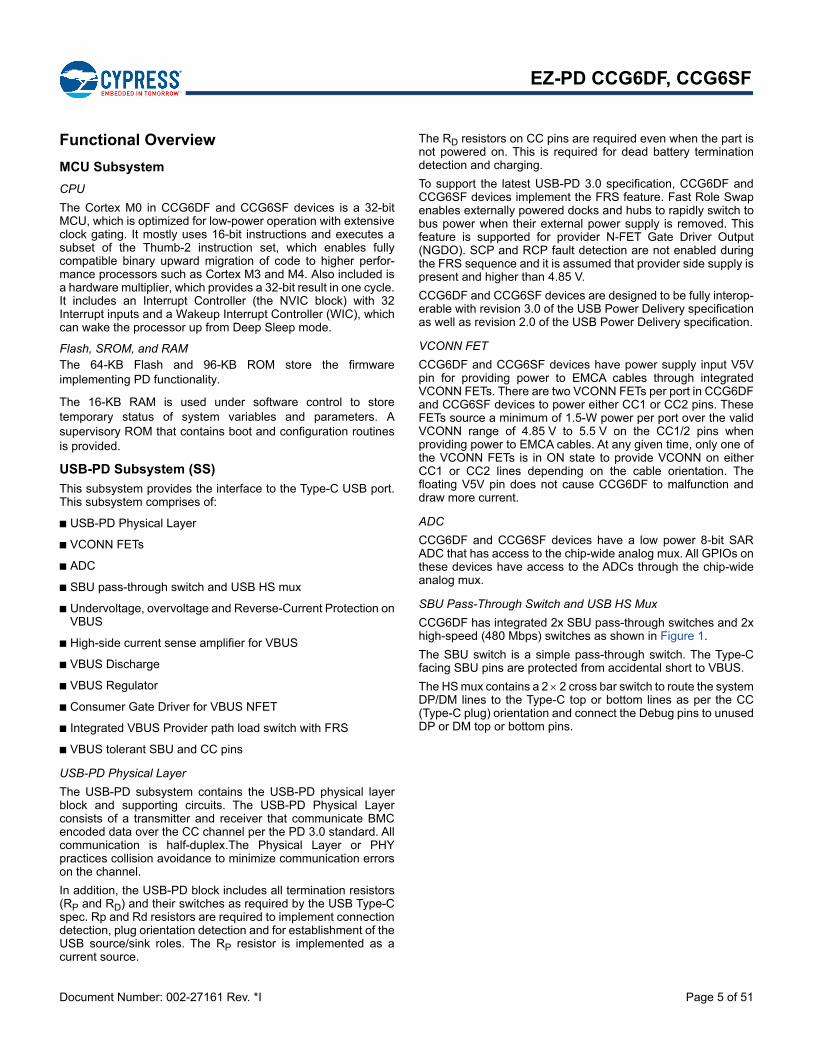
CCG6DF has integrated 2x SBU pass-through switches and 2xhigh-speed (480 Mbps) switches as shown in Figure 1.
The SBU switch is a simple pass-through switch. The Type-Cfacing SBU pins are protected from accidental short to VBUS.
The HS mux contains a 2 2 cross bar switch to route the systemDP/DM lines to the Type-C top or bottom lines as per the CC(Type-C plug) orientation and connect the Debug pins to unusedDP or DM top or bottom pins.
Document Number: 002-27161 Rev. *I Page 6 of 51
EZ-PD CCG6DF, CCG6SF
Figure 1. SBU Protection and High-Speed Crossbar Switch Block Diagram
Provider Load Switch
CCG6DF and CCG6SF devices have an integrated provider load switch with the following functions.
Undervoltage and Overvoltage Protection on VBUS
CCG6DF and CCG6SF devices implement an under-voltage/overvoltage (UVOV) detection circuit for the VBUSsupply. The thresholds for both OCP and UVOV are program-mable.
High-side Current Sense Amplifier for VBUS
CCG6DF and CCG6SF devices support the programmablethreshold VBUS current sensing through VBUS provider path.External resistor (5 m) placed in VBUS provider pathconnecting to the chip, the drop across this resistor is monitoredto sense the magnitude of current.
VBUS Reverse Current Protection
CCG6DF and CCG6SF devices restrict reverse current to zeroon the VBUS provider path when the Type-C VBUS is greaterthan VIN (provider voltage before the VBUS NFET).
VBUS Short Circuit Protection
CCG6DF and CCG6SF devices have a VBUS short circuitprotection function of which the SCP threshold is programmable.Whenever current through the VBUS Provider Load Switchexceeds the programmed threshold, the SCP gets triggeredinstantly and turns off the VBUS provider path within a shortduration.
VBUS Discharge
CCG6DF and CCG6SF devices support high-voltage (21.5 V)VBUS discharge circuitry inside. After cable removal detection,the chips discharge the residual charge and bring the floatingVBUS to less than 0.8 V.
VBUS Regulator
CCG6DF and CCG6SF devices can either be powered by VSYSor VBUS power supplies. There is one VBUS per port. Hence theCCG6DF device can be powered by either VBUS (Port0 orPort1) or VSYS. A regulator operating on these power suppliesderives the chip operating supply. When both power supplies arepresent, VSYS always takes priority over VBUS supplies. Inabsence of VSYS, the regulator powers the chip from VBUS.
Gate Driver for VBUS NFET
CCG6DF and CCG6SF devices have integrated gate drivers todrive external NFETs on the VBUS consumer path. The providerNFETs are integrated. The consumer side supports only theexternal NFET driver and these NFETs must be capable ofsupporting ±VBUS_MAX VGS. CCG6DF and CCG6SF must bein active mode to enable the consumer-side NGDO.
VBUS Tolerant SBU and CC Lines
CCG6DF and CCG6SF devices support VBUS tolerant SBU andCC lines. In case of SBU/CC short to VBUS through connectors,these lines are protected internally. Accidental shorts may occurbecause the SBU/CC pins are placed next to the VBUS pins inthe USB Type-C connector. A Power Delivery controller withoutthe high-voltage VBUS short protection will be damaged in theevent of such accidental shorts. When overvoltage is detectedon the SBU/CC lines, the internal protection circuit will turn offthe connection between the Type-C connector and the rest of thedevice.
SBU1_SYS
SBU2_SYS
24V Protection
SBU Protection Internal Block Diagram
HS Cross Bar Switch Internal Block Diagram
SBU1
SBU2
UART_TX
UART_RX
DP_SYS
DM_SYS
DP_Top/Bottom
DM_Top/Bottom
Document Number: 002-27161 Rev. *I Page 7 of 51
EZ-PD CCG6DF, CCG6SF
Serial Communication Block (SCB)
CCG6DF and CCG6SF devices have four SCB blocks that canbe configured for I2C, SPI, or UART. These blocks implement fullmulti-master and slave I2C interfaces capable of multi-masterarbitration. I2C is compatible with the standard Philips I2C Speci-fication V3.0. These blocks operate at speeds of up to 1 Mbpsand have flexible buffering options to reduce interrupt overheadand latency for the CPU.
The SCB blocks support 8-byte deep FIFOs for Receive andTransmit, which, by increasing the time given for the CPU to readdata, greatly reduces the need for clock stretching caused by theCPU not having read data on time.
Timer, Counter, Pulse-Width Modulator (TCPWM)
The TCPWM block of CCG6DF and CCG6SF supports up to twotimers or counters or pulse-width modulators. These timers areavailable for internal timer use by firmware or for providingPWM-based functions on the GPIOs.
True Random Number Generator (TRNG)
In notebook designs, CCG6DF’s and CCG6SF’s TRNG block isused in authenticating connected devices such as poweradapters or docks that include support for USB Type-C Authen-tication Specification (USBTCAS). CCG6DF and CCG6SFdevices, within notebook applications, are implemented as aninitiate role as defined in USBTCAS, while the connected devicewould implement the responder-role. USBTCAS provides ameans for authenticating Type-C devices with regards to identi-fication and configuration.
GPIO Interface
The CCG6DF device has 23 GPIOs and the CCG6SF device has19 GPIOs including the I2C and SWD pins, which can also beused as GPIOs.
The GPIO block implements the following:
Eight drive strength modes including strong push-pull, resistivepull-up and pull-down, weak (resistive) pull-up and pull-down,open drain and open source, input only, and disabled.
Input threshold select (CMOS or LVTTL)
Individual control of input and output disables.
Hold mode for latching previous state (used for retaining I/Ostate in Deep Sleep mode).
Selectable slew rates for dV/dt related noise control.
During power-on and reset, the blocks are forced to the Disablestate so as not to crowbar any inputs and/or cause excessturn-on current. A multiplexing network known as a high-speedI/O matrix is used to multiplex between various signals that may
connect to an I/O pin. Pin locations for fixed-function peripherals,such as USB Type-C ports, are also fixed to reduce internalmultiplexing complexity. Data Output Registers and Pin StateRegister store, respectively, the values to be driven on the pinsand the states of the pins themselves. The configuration of thepins can be done by programming of registers through softwarefor each digital I/O Port.
Every I/O pin can generate an interrupt if so enabled and eachI/O port has an IRQ and ISR vector associated with it.
The I/O ports retain their state during Deep Sleep mode orremain ON. If operation is restored using reset, then the pinsshall go the High-Z state. If operation is restored by an interruptevent, then the pin drivers shall retain their state until firmwarechooses to change it. The I/Os (on data bus) do not draw currenton power down.
All GPIOs reside in a separate I/O power domain – VDDIO toprovide flexible system-level interfacing.
System Resources
Watchdog Timer (WDT)
A watchdog timer is implemented in the Clock block running fromthe internal low-speed oscillator (ILO) for CCG6DF and CCG6SFdevices. This allows watchdog operation during Deep Sleep andgenerates a Watchdog Reset if not serviced before the timeoutoccurs.
In addition to the chip-level watchdog timer, each USB-PD blockimplements a counter based on ILO (Low frequency) clock whichcan be used to wake/trigger the part periodically. This countercan be used to drive any periodic tasks to be performed by thedevice.
Clock System
CCG6DF and CCG6SF have a fully integrated clock with noexternal crystal required. CCG6DF/CCG6SF clock system isresponsible for providing clocks to all subsystems that requireclocks (SCB and USB-PD) and for switching between differentclock sources, without glitches. The clock system for thesedevices consists of the internal main oscillator (IMO) and the ILO.
IMO Clock Source
The IMO is the primary source of internal clocking in CCG6DFand CCG6SF devices with an accuracy of 2%. The default IMOfrequency for CCG6DF and CCG6SF devices is 48 MHz 2%.
ILO Clock Source
The ILO is a very low power, relatively inaccurate, oscillator,which is primarily used to generate clocks for peripheraloperation in USB Suspend (Deep Sleep) mode. The typicalfrequency of the ILO is 32-kHz.
Document Number: 002-27161 Rev. *I Page 8 of 51
EZ-PD CCG6DF, CCG6SF
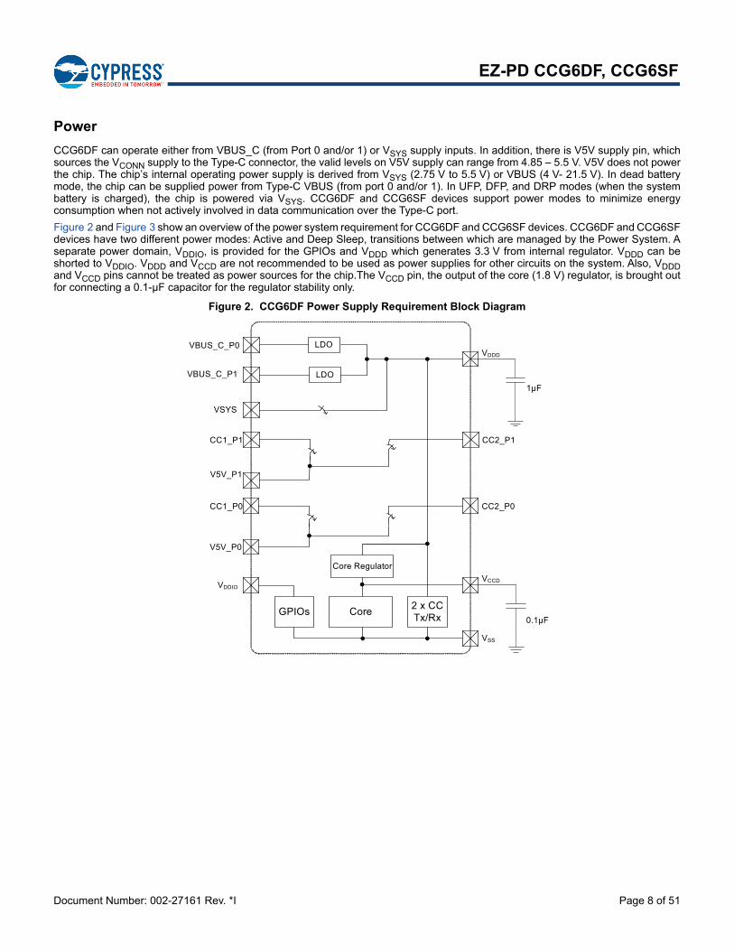
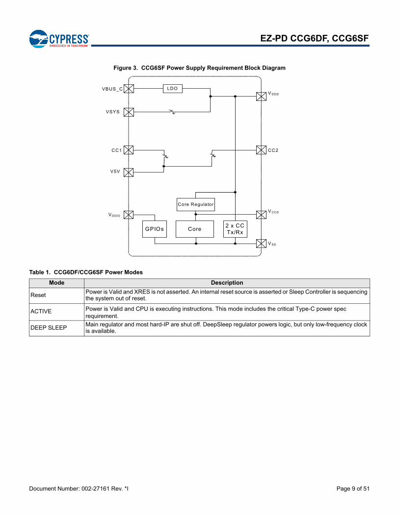
Power
CCG6DF can operate either from VBUS_C (from Port 0 and/or 1) or VSYS supply inputs. In addition, there is V5V supply pin, whichsources the VCONN supply to the Type-C connector, the valid levels on V5V supply can range from 4.85 – 5.5 V. V5V does not powerthe chip. The chip’s internal operating power supply is derived from VSYS (2.75 V to 5.5 V) or VBUS (4 V- 21.5 V). In dead batterymode, the chip can be supplied power from Type-C VBUS (from port 0 and/or 1). In UFP, DFP, and DRP modes (when the systembattery is charged), the chip is powered via VSYS. CCG6DF and CCG6SF devices support power modes to minimize energyconsumption when not actively involved in data communication over the Type-C port.
Figure 2 and Figure 3 show an overview of the power system requirement for CCG6DF and CCG6SF devices. CCG6DF and CCG6SFdevices have two different power modes: Active and Deep Sleep, transitions between which are managed by the Power System. Aseparate power domain, VDDIO, is provided for the GPIOs and VDDD which generates 3.3 V from internal regulator. VDDD can beshorted to VDDIO. VDDD and VCCD are not recommended to be used as power supplies for other circuits on the system. Also, VDDDand VCCD pins cannot be treated as power sources for the chip.The VCCD pin, the output of the core (1.8 V) regulator, is brought outfor connecting a 0.1-µF capacitor for the regulator stability only.
Figure 2. CCG6DF Power Supply Requirement Block Diagram
VSS
CC2_P0
VDDD
Core Regulator
CC1_P0
VCCD
Core
VDDIO
GPIOs2 x CCTx/Rx
V5V_P0
CC2_P1CC1_P1
V5V_P1
LDO
LDO
VBUS_C_P0
VBUS_C_P1
VSYS
1µF
0.1µF
Document Number: 002-27161 Rev. *I Page 9 of 51
EZ-PD CCG6DF, CCG6SF
Figure 3. CCG6SF Power Supply Requirement Block Diagram
Table 1. CCG6DF/CCG6SF Power Modes
Mode Description
Reset Power is Valid and XRES is not asserted. An internal reset source is asserted or Sleep Controller is sequencing the system out of reset.
ACTIVE Power is Valid and CPU is executing instructions. This mode includes the critical Type-C power spec requirement.
DEEP SLEEPMain regulator and most hard-IP are shut off. DeepSleep regulator powers logic, but only low-frequency clock is available.
V SS
CC2
V DDD
Core Regulator
CC1
V CCD
Core
VDDIO
GPIOs2 x CCTx/Rx
V5V
LDOVBUS_C
VSYS
Document Number: 002-27161 Rev. *I Page 10 of 51
EZ-PD CCG6DF, CCG6SF
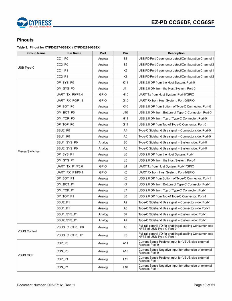
Pinouts
Table 2. Pinout for CYPD6227-96BZXI / CYPD6228-96BZXI
Group Name Pin Name Port Pin Description
USB Type-C
CC1_P0 Analog B3 USB PD Port-0 connector detect/Configuration Channel 1
CC2_P0 Analog B5 USB PD Port-0 connector detect/Configuration Channel 2
CC1_P1 Analog K5 USB PD Port-1 connector detect/Configuration Channel 1
CC2_P1 Analog K3 USB PD Port-1 connector detect/Configuration Channel 2
Muxes/Switches
DP_SYS_P0 Analog K11 USB 2.0 DP from the Host System: Port-0
DM_SYS_P0 Analog J11 USB 2.0 DM from the Host System: Port-0
UART_TX_P0/P1.4 GPIO H10 UART Tx from Host System: Port-0/GPIO
UART_RX_P0/P1.3 GPIO G10 UART Rx from Host System: Port-0/GPIO
DP_BOT_P0 Analog K10 USB 2.0 DP from Bottom of Type-C Connector: Port-0
DM_BOT_P0 Analog J10 USB 2.0 DM from Bottom of Type-C Connector: Port-0
DM_TOP_P0 Analog H11 USB 2.0 DM from Top of Type-C Connector: Port-0
DP_TOP_P0 Analog G11 USB 2.0 DP from Top of Type-C Connector: Port-0
SBU2_P0 Analog A4 Type-C Sideband Use signal – Connector side: Port-0
SBU1_P0 Analog A5 Type-C Sideband Use signal – Connector side: Port-0
SBU1_SYS_P0 Analog B6 Type-C Sideband Use signal – System side: Port-0
SBU2_SYS_P0 Analog A6 Type-C Sideband Use signal – System side: Port-0
DP_SYS_P1 Analog L6 USB 2.0 DP from the Host System: Port-1
DM_SYS_P1 Analog L5 USB 2.0 DM from the Host System: Port-1
UART_TX_P1/P0.0 GPIO L4 UART Tx from Host System: Port-1/GPIO
UART_RX_P1/P0.1 GPIO K6 UART Rx from Host System: Port-1/GPIO
DP_BOT_P1 Analog K8 USB 2.0 DP from Bottom of Type-C Connector: Port-1
DM_BOT_P1 Analog K7 USB 2.0 DM from Bottom of Type-C Connector Port-1
DM_TOP_P1 Analog L7 USB 2.0 DM from Top of Type-C Connector: Port-1
DP_TOP_P1 Analog L8 USB 2.0 DP from Top of Type-C Connector: Port-1
SBU2_P1 Analog A9 Type-C Sideband Use signal – Connector side: Port-1
SBU1_P1 Analog A8 Type-C Sideband Use signal – Connector side Port-1
SBU1_SYS_P1 Analog B7 Type-C Sideband Use signal – System side: Port-1
SBU2_SYS_P1 Analog A7 Type-C Sideband Use signal – System side: Port-1
VBUS ControlVBUS_C_CTRL_P0 Analog A3 Full rail control I/O for enabling/disabling Consumer load
NFET of USB Type-C Port-0
VBUS_C_CTRL_P1 Analog L3 Full rail control I/O for enabling/disabling Consumer load NFET of USB Type-C Port-1
VBUS OCP
CSP_P0 Analog A11 Current Sense Positive Input for VBUS side external Rsense: Port-0
CSN_P0 Analog A10 Current Sense Negative input for other side of external Rsense: Port-0
CSP_P1 Analog L11 Current Sense Positive Input for VBUS side external Rsense: Port-1
CSN_P1 Analog L10 Current Sense Negative input for other side of external Rsense: Port-1
Document Number: 002-27161 Rev. *I Page 11 of 51
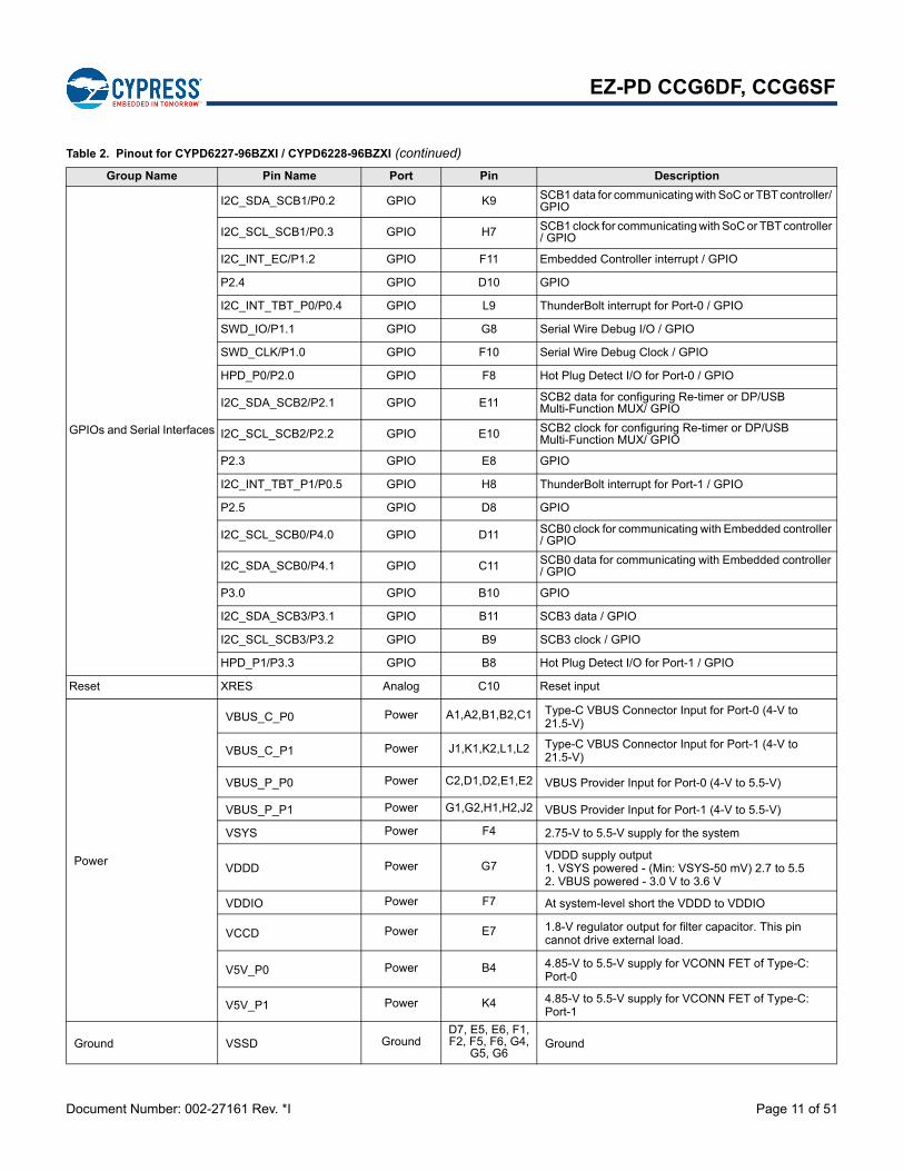
EZ-PD CCG6DF, CCG6SF
GPIOs and Serial Interfaces
I2C_SDA_SCB1/P0.2 GPIO K9 SCB1 data for communicating with SoC or TBT controller/ GPIO
I2C_SCL_SCB1/P0.3 GPIO H7 SCB1 clock for communicating with SoC or TBT controller / GPIO
I2C_INT_EC/P1.2 GPIO F11 Embedded Controller interrupt / GPIO
P2.4 GPIO D10 GPIO
I2C_INT_TBT_P0/P0.4 GPIO L9 ThunderBolt interrupt for Port-0 / GPIO
SWD_IO/P1.1 GPIO G8 Serial Wire Debug I/O / GPIO
SWD_CLK/P1.0 GPIO F10 Serial Wire Debug Clock / GPIO
HPD_P0/P2.0 GPIO F8 Hot Plug Detect I/O for Port-0 / GPIO
I2C_SDA_SCB2/P2.1 GPIO E11 SCB2 data for configuring Re-timer or DP/USB Multi-Function MUX/ GPIO
I2C_SCL_SCB2/P2.2 GPIO E10 SCB2 clock for configuring Re-timer or DP/USB Multi-Function MUX/ GPIO
P2.3 GPIO E8 GPIO
I2C_INT_TBT_P1/P0.5 GPIO H8 ThunderBolt interrupt for Port-1 / GPIO
P2.5 GPIO D8 GPIO
I2C_SCL_SCB0/P4.0 GPIO D11 SCB0 clock for communicating with Embedded controller / GPIO
I2C_SDA_SCB0/P4.1 GPIO C11 SCB0 data for communicating with Embedded controller / GPIO
P3.0 GPIO B10 GPIO
I2C_SDA_SCB3/P3.1 GPIO B11 SCB3 data / GPIO
I2C_SCL_SCB3/P3.2 GPIO B9 SCB3 clock / GPIO
HPD_P1/P3.3 GPIO B8 Hot Plug Detect I/O for Port-1 / GPIO
Reset XRES Analog C10 Reset input
Power
VBUS_C_P0 Power A1,A2,B1,B2,C1 Type-C VBUS Connector Input for Port-0 (4-V to 21.5-V)
VBUS_C_P1 Power J1,K1,K2,L1,L2 Type-C VBUS Connector Input for Port-1 (4-V to 21.5-V)
VBUS_P_P0 Power C2,D1,D2,E1,E2 VBUS Provider Input for Port-0 (4-V to 5.5-V)
VBUS_P_P1 Power G1,G2,H1,H2,J2 VBUS Provider Input for Port-1 (4-V to 5.5-V)
VSYS Power F4 2.75-V to 5.5-V supply for the system
VDDD Power G7VDDD supply output1. VSYS powered - (Min: VSYS-50 mV) 2.7 to 5.52. VBUS powered - 3.0 V to 3.6 V
VDDIO Power F7 At system-level short the VDDD to VDDIO
VCCD Power E7 1.8-V regulator output for filter capacitor. This pin cannot drive external load.
V5V_P0 Power B4 4.85-V to 5.5-V supply for VCONN FET of Type-C: Port-0
V5V_P1 Power K4 4.85-V to 5.5-V supply for VCONN FET of Type-C: Port-1
Ground VSSD GroundD7, E5, E6, F1, F2, F5, F6, G4,
G5, G6Ground
Table 2. Pinout for CYPD6227-96BZXI / CYPD6228-96BZXI (continued)
Group Name Pin Name Port Pin Description
Document Number: 002-27161 Rev. *I Page 12 of 51
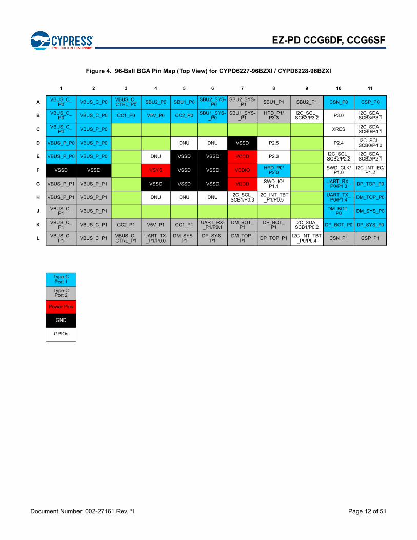
EZ-PD CCG6DF, CCG6SF
Figure 4. 96-Ball BGA Pin Map (Top View) for CYPD6227-96BZXI / CYPD6228-96BZXI
1 2 3 4 5 6 7 8 9 10 11
A VBUS_C_P0 VBUS_C_P0 VBUS_C_
CTRL_P0 SBU2_P0 SBU1_P0 SBU2_SYS-_P0
SBU2_SYS-_P1 SBU1_P1 SBU2_P1 CSN_P0 CSP_P0
B VBUS_C_P0 VBUS_C_P0 CC1_P0 V5V_P0 CC2_P0 SBU1_SYS-
_P0SBU1_SYS-
_P1HPD_P1/
P3.3I2C_SCL_SCB3/P3.2 P3.0 I2C_SDA_
SCB3/P3.1
C VBUS_C_P0 VBUS_P_P0 XRES I2C_SDA_
SCB0/P4.1
D VBUS_P_P0 VBUS_P_P0 DNU DNU VSSD P2.5 P2.4 I2C_SCL_SCB0/P4.0
E VBUS_P_P0 VBUS_P_P0 DNU VSSD VSSD VCCD P2.3 I2C_SCL_SCB2/P2.2
I2C_SDA_SCB2/P2.1
F VSSD VSSD VSYS VSSD VSSD VDDIO HPD_P0/P2.0
SWD_CLK/P1.0
I2C_INT_EC/P1.2
G VBUS_P_P1 VBUS_P_P1 VSSD VSSD VSSD VDDD SWD_IO/P1.1
UART_RX_P0/P1.3 DP_TOP_P0
H VBUS_P_P1 VBUS_P_P1 DNU DNU DNU I2C_SCL_SCB1/P0.3
I2C_INT_TBT_P1/P0.5
UART_TX_P0/P1.4 DM_TOP_P0
J VBUS_C_P1 VBUS_P_P1 DM_BOT_
P0 DM_SYS_P0
K VBUS_C_P1 VBUS_C_P1 CC2_P1 V5V_P1 CC1_P1 UART_RX-
_P1/P0.1DM_BOT_
P1DP_BOT_
P1I2C_SDA_SCB1/P0.2 DP_BOT_P0 DP_SYS_P0
L VBUS_C_P1 VBUS_C_P1 VBUS_C_
CTRL_P1UART_TX-_P1/P0.0
DM_SYS_P1
DP_SYS_P1
DM_TOP_P1 DP_TOP_P1 I2C_INT_TBT
_P0/P0.4 CSN_P1 CSP_P1
Type-C Port 1
Type-C Port 2
Power Pins
GND
GPIOs
Document Number: 002-27161 Rev. *I Page 13 of 51
EZ-PD CCG6DF, CCG6SF
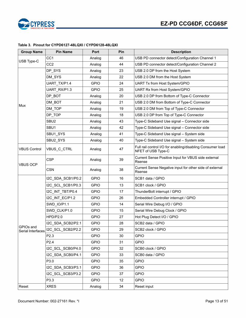
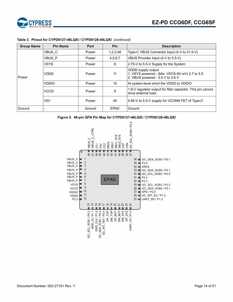
Table 3. Pinout for CYPD6127-48LQXI / CYPD6128-48LQXI
Group Name Pin Name Port Pin Description
USB Type-CCC1 Analog 46 USB PD connector detect/Configuration Channel 1
CC2 Analog 44 USB PD connector detect/Configuration Channel 2
Mux
DP_SYS Analog 23 USB 2.0 DP from the Host System
DM_SYS Analog 22 USB 2.0 DM from the Host System
UART_TX/P1.4 GPIO 24 UART Tx from Host System/GPIO
UART_RX/P1.3 GPIO 25 UART Rx from Host System/GPIO
DP_BOT Analog 20 USB 2.0 DP from Bottom of Type-C Connector
DM_BOT Analog 21 USB 2.0 DM from Bottom of Type-C Connector
DM_TOP Analog 19 USB 2.0 DM from Top of Type-C Connector
DP_TOP Analog 18 USB 2.0 DP from Top of Type-C Connector
SBU2 Analog 43 Type-C Sideband Use signal – Connector side
SBU1 Analog 42 Type-C Sideband Use signal – Connector side
SBU1_SYS Analog 41 Type-C Sideband Use signal – System side
SBU2_SYS Analog 40 Type-C Sideband Use signal – System side
VBUS Control VBUS_C_CTRL Analog 47Full rail control I/O for enabling/disabling Consumer load NFET of USB Type-C
VBUS OCPCSP Analog 39 Current Sense Positive Input for VBUS side external
Rsense
CSN Analog 38 Current Sense Negative input for other side of external Rsense
GPIOs and Serial Interfaces
I2C_SDA_SCB1/P0.2 GPIO 16 SCB1 data / GPIO
I2C_SCL_SCB1/P0.3 GPIO 13 SCB1 clock / GPIO
I2C_INT_TBT/P0.4 GPIO 17 ThunderBolt interrupt / GPIO
I2C_INT_EC/P1.2 GPIO 26 Embedded Controller interrupt / GPIO
SWD_IO/P1.1 GPIO 14 Serial Wire Debug I/O / GPIO
SWD_CLK/P1.0 GPIO 15 Serial Wire Debug Clock / GPIO
HPD/P2.0 GPIO 27 Hot Plug Detect I/O / GPIO
I2C_SDA_SCB2/P2.1 GPIO 28 SCB2 data / GPIO
I2C_SCL_SCB2/P2.2 GPIO 29 SCB2 clock / GPIO
P2.3 GPIO 30 GPIO
P2.4 GPIO 31 GPIO
I2C_SCL_SCB0/P4.0 GPIO 32 SCB0 clock / GPIO
I2C_SDA_SCB0/P4.1 GPIO 33 SCB0 data / GPIO
P3.0 GPIO 35 GPIO
I2C_SDA_SCB3/P3.1 GPIO 36 GPIO
I2C_SCL_SCB3/P3.2 GPIO 37 GPIO
P3.3 GPIO 12 GPIO
Reset XRES Analog 34 Reset input
Document Number: 002-27161 Rev. *I Page 14 of 51
EZ-PD CCG6DF, CCG6SF
Figure 5. 48-pin QFN Pin Map for CYPD6127-48LQXI / CYPD6128-48LQXI
Power
VBUS_C Power 1,2,3,48 Type-C VBUS Connector Input (4-V to 21.5-V)
VBUS_P Power 4,5,6,7 VBUS Provider Input (4-V to 5.5-V)
VSYS Power 8 2.75-V to 5.5-V Supply for the System
VDDD Power 11VDDD supply output1. VSYS powered - (Min: VSYS-50 mV) 2.7 to 5.52. VBUS powered - 3.0 V to 3.6 V
VDDIO Power 10 At system-level short the VDDD to VDDIO
VCCD Power 9 1.8-V regulator output for filter capacitor. This pin cannot drive external load.
V5V Power 45 4.85-V to 5.5-V supply for VCONN FET of Type-C
Ground - Ground EPAD Ground
Table 3. Pinout for CYPD6127-48LQXI / CYPD6128-48LQXI (continued)
Group Name Pin Name Port Pin Description
234
56
1
EPAD
UA
RT
_TX
/ P
1.4
CS
N
SB
U1
SB
U1_
SY
SS
BU
2_S
YS
CS
P
SB
U2
CC
2
V5V
CC
1
VB
US
_C
_C
TR
L
VBUS_CVBUS_CVBUS_C
VBUS_PVBUS_P
SW
D_I
O /
P1.
1
SW
D_C
LK /
P1.
0I2
C_S
DA
_S
CB
1 /
P0.
2I2
C_I
NT
_TB
T /
P0.
4
DM
_TO
P
DP
_BO
T
DM
_B
OT
DM
_S
YS
DP
_SY
S
DP
_TO
P
12
91011
VSYS
VCCDVDDIOVDDD
78
VBUS_PVBUS_P
I2C
_SC
L_S
CB
1 / P
0.3
13 14 15 16 17 18 19 20 21 22 23 24
363534333231302928272625
HPD / P2.0I2C_SDA_SCB2 / P2.1I2C_SCL_SCB2 / P2.2
I2C_SDA_SCB0 / P4.1
UART_RX / P1.3I2C_INT_EC / P1.2
P3.0I2C_SDA_SCB3 / P3.1
I2C_SCL_SCB0 / P4.0
P2.3P2.4
I2C
_SC
L_S
CB
3 / P
3.2
373839404142434445464748
XRES
P3.3
VB
US
_C
Document Number: 002-27161 Rev. *I Page 15 of 51
EZ-PD CCG6DF, CCG6SF
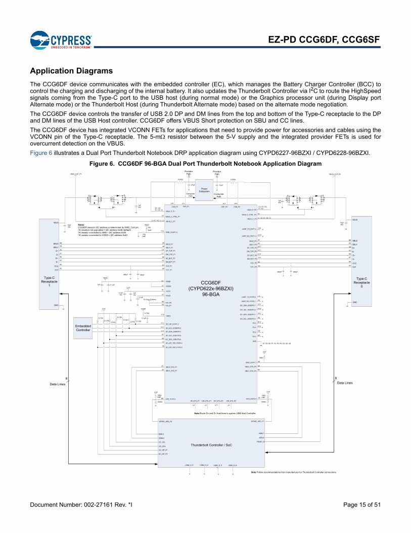
Application Diagrams
The CCG6DF device communicates with the embedded controller (EC), which manages the Battery Charger Controller (BCC) tocontrol the charging and discharging of the internal battery. It also updates the Thunderbolt Controller via I2C to route the HighSpeedsignals coming from the Type-C port to the USB host (during normal mode) or the Graphics processor unit (during Display portAlternate mode) or the Thunderbolt Host (during Thunderbolt Alternate mode) based on the alternate mode negotiation.
The CCG6DF device controls the transfer of USB 2.0 DP and DM lines from the top and bottom of the Type-C receptacle to the DPand DM lines of the USB Host controller. CCG6DF offers VBUS Short protection on SBU and CC lines.
The CCG6DF device has integrated VCONN FETs for applications that need to provide power for accessories and cables using theVCONN pin of the Type-C receptacle. The 5-m resistor between the 5-V supply and the integrated provider FETs is used forovercurrent detection on the VBUS.
Figure 6 illustrates a Dual Port Thunderbolt Notebook DRP application diagram using CYPD6227-96BZXI / CYPD6228-96BZXI.
Figure 6. CCG6DF 96-BGA Dual Port Thunderbolt Notebook Application Diagram
CCG6DF(CYPD622x-96BZXI)
96-BGA
K10
B5
DP_TOP_P0G11
DM_TOP_P0H11
VDDD
VDDIOF7
VSYSF4
XRES
K4
Type-C Receptacle
01µF
F8
A6
SWD_IO//P1.1 G8
SBU1_SYS_P0B6
V5V_P1
3.3V
I2C_SCL_SCB0/P4.0D11
C11
H7
K9
L9
I2C_SDA_SCB0/P4.1
F11
I2C_SCL_SCB1/P0.3
I2C_SDA_SCB1/P0.2
I2C_INT_TBT_P0/P0.4
I2C_INT_EC/P1.2
C10
0.1μF
CC1_P0 B3
CSN_P0
A10
HPD_P0/P2.0
SBU2_SYS_P0
DP_BOT_P0
CC2_P0
VBUS_C_CTRL_P0A3
CSP_P0
VBUS_P_P0
2.2 K
2.2 K
2.2 K
C2, D1, D2, E1, E2
A11
CC1
CC2
GND
VBUS
E7VCCD
G7
0.1µF
1µF10V
0.1µF10V
0.1µF
VDDD
3.3V
5V (from System)
Embedded Controller
3.3V
10KDNP
100K
Thunderbolt Controller / SoC
BSBU1
BSBU2
I2C_SCL
I2C_SDA
I2C_INT_P1
I2C_INT_P2
3.3V
10K
Data Lines
8
USB2_D_P USB2_D_N
XX
390pF 390pF
J10DM_BOT_P0
A4SBU2_P0
A5SBU1_P0
UART_RX_P0/P1.3G10
UART_TX_P0/P1.4 H10
VBUS_OUT_P0
0.005
1µF35V
Power Subsystem
Provider Path
Consumer Path
5V
D-
D+
D-
D+
SBU1
SBU2
A6
A7
B6
B7
B5
A5
A8
B8
10µF50V
DP_SYS_P0
K11
DM_SYS_P0
J11
VDDD
1K
1KSWD_CLK/P1.0
F10
NotesCCG6DF device’s I2C address is determined by SWD_CLK pin.1K resistors not populated = I2C address 0x08 (default)1K resistor connected to GND = I2C address 0x401K resistor connected to VDDD = I2C address 0x42
Note Route D+ and D- Host lines to system USB Host Controller.
Note Follow recommendations from manufacturer for Thunderbolt Controller connections.
L10
CSN_P1
L11
0.005
VBUS_OUT_P1
VBUS_P_P1
G1, G2, H1, H2, J2
VBUS_C_CTRL_P1L3
1µF35V
Provider Path
Consumer Path
5V
K8
K3
DP_TOP_P1L8
DM_TOP_P1L7
CC1_P1K5
DP_BOT_P1
CC2_P1
390pF390pF
K7DM_BOT_P1
A9SBU2_P1
A8SBU1_P1
Type-C Receptacle
1
CC1
CC2
GND
VBUS
D-
D+
D-
D+
SBU1
SBU2
A6
A7
B6
B7
B5
A5
A8
B8
10µF50V
B4V5V_P0
I2C_SDA_SCB3/P3.1
I2C_SCL_SCB3/P3.2
B11
B9
X
X2.2 K
2.2 K2.2 K 2.2 K
H8I2C_INT_TBT_P1/P0.5
I2C_SDA_SCB2/P2.1
I2C_SCL_SCB2/P2.2
E11
E10
X
X
DP_SYS_P1
L6
DM_SYS_P1
L5
P3.0
GND
B10
D7, E5, E6, F1, F2, F5, F6, G4, G5, G6
X
SBU2_SYS_P1A7
SBU1_SYS_P1B7
B8 HPD_P1/P3.3
3.3V
10KDNP
100K
DPSRC_HPD_P2
ASBU1
ASBU2
RESET_N
DPSRC_HPD_P1
Data Lines
8
USB2_D_P USB2_D_N
XX
CSP_P1
VDDD
4.7K
57µF57µF
P2.5D8
DNP
DNP
J1, K1, K2, L1, L2 VBUS_C_P1
VBUS_C_P0 A1, A2, B1, B2, C1
P2.4D10
X
UART_TX_P1/P0.0
UART_RX_P1/P0.1
L4
K6
X
X
123
4
5678
4
5678
123
X
X
P2.3E8
X
X
123
4
5678
4
5678
123
Document Number: 002-27161 Rev. *I Page 16 of 51
EZ-PD CCG6DF, CCG6SF
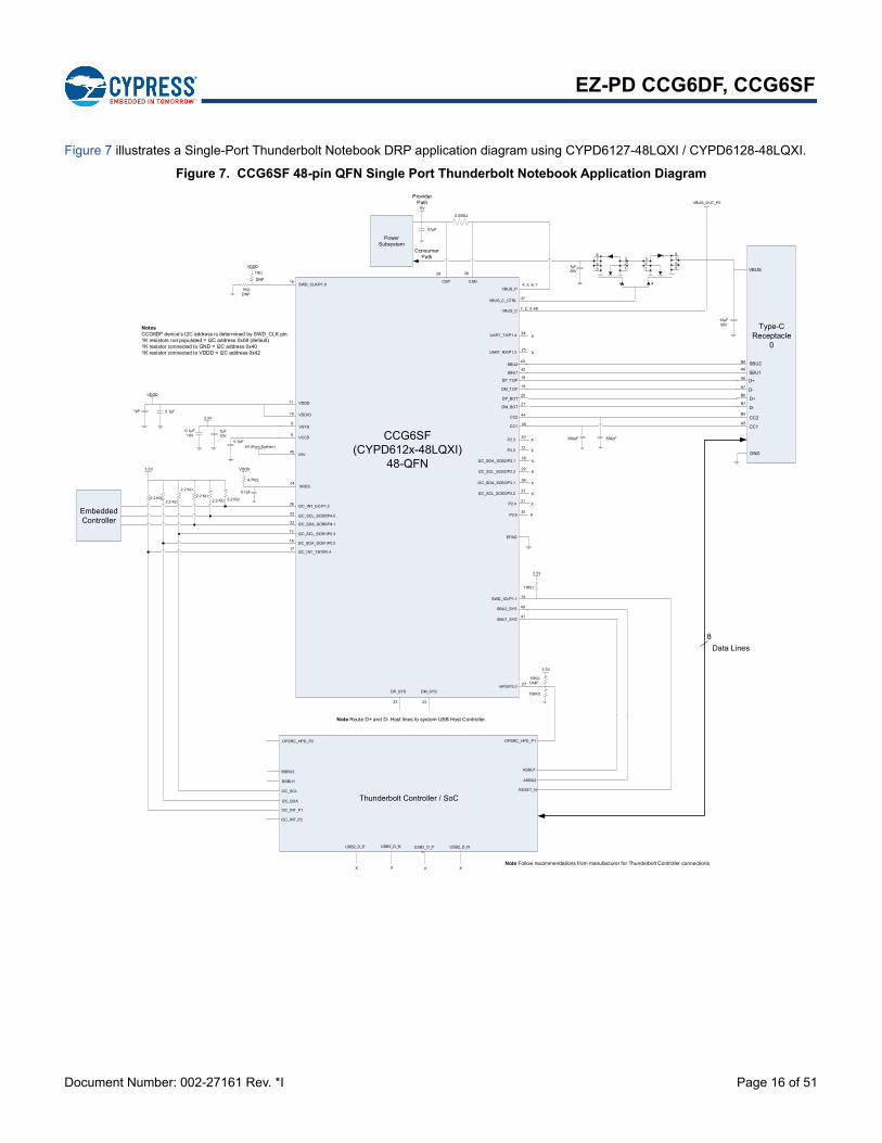
Figure 7 illustrates a Single-Port Thunderbolt Notebook DRP application diagram using CYPD6127-48LQXI / CYPD6128-48LQXI.
Figure 7. CCG6SF 48-pin QFN Single Port Thunderbolt Notebook Application Diagram
CCG6SF(CYPD612x-48LQXI)
48-QFN
20
44
DP_TOP18
DM_TOP19
VDDD
VDDIO10
VSYS8
XRES
Type-C Receptacle
0
1µF
27
40
SWD_IO//P1.1 14
SBU1_SYS41
3.3V
I2C_SCL_SCB0/P4.032
33
13
16
17
I2C_SDA_SCB0/P4.1
26
I2C_SCL_SCB1/P0.3
I2C_SDA_SCB1/P0.2
I2C_INT_TBT/P0.4
I2C_INT_EC/P1.2
34
0.1μF
CC1 46
CSN
38
HPD/P2.0
SBU2_SYS
DP_BOT
CC2
VBUS_C_CTRL47
CSP
VBUS_P
2.2 K2.2 K
4, 5, 6, 7
39
CC1
CC2
GND
VBUS
9VCCD
11
0.1µF
1µF10V
0.1µF10V
0.1µF
VDDD
3.3V
5V (from System)
Embedded Controller
3.3V
10KDNP
100K
Thunderbolt Controller / SoC
BSBU2
BSBU1
I2C_SCL
I2C_SDA
I2C_INT_P1
I2C_INT_P2
3.3V
10K
Data Lines
8
USB2_D_P USB2_D_N
XX
390pF 390pF
21DM_BOT
43SBU2
42SBU1
UART_RX/P1.325
UART_TX/P1.4 24
VBUS_OUT_P0
0.005
1µF35V
Power Subsystem
Provider Path
Consumer Path
5V
D-
D+
D-
D+
SBU1
SBU2
A6
A7
B6
B7
B5
A5
A8
B8
10µF50V
DP_SYS
23
DM_SYS
22
VDDD
1K
1KSWD_CLK/P1.0
15
NotesCCG6DF device’s I2C address is determined by SWD_CLK pin.1K resistors not populated = I2C address 0x08 (default)1K resistor connected to GND = I2C address 0x401K resistor connected to VDDD = I2C address 0x42
Note Route D+ and D- Host lines to system USB Host Controller.
Note Follow recommendations from manufacturer for Thunderbolt Controller connections.
45V5V
I2C_SDA_SCB3/P3.1
I2C_SCL_SCB3/P3.2
36
37
X
X2.2 K
2.2 K2.2 K 2.2 K
I2C_SDA_SCB2/P2.1
I2C_SCL_SCB2/P2.2
28
29
X
X
P2.4
EPAD
31X
DPSRC_HPD_P2
ASBU1
ASBU2
RESET_N
DPSRC_HPD_P1
USB2_D_P USB2_D_N
XX
VDDD
4.7K
57µF
P3.035
DNP
DNP
VBUS_C 1, 2, 3, 48
123
4
5678
4
5678
123
P2.3
P3.3
30
12
X
X
X
X
X
Document Number: 002-27161 Rev. *I Page 17 of 51
EZ-PD CCG6DF, CCG6SF
CCG6DF Layout Design Guidelines for BGA Package
Proper routing and placement help to maintain signal integrity for high-speed signals, improve thermal dissipation and reduce powerconsumption for CCG6DF/SF. The combination of power and high-speed data signals can be better routed if these design guidelinesare followed. It is highly recommended to consult with a PCB manufacturer to verify the manufacturing capabilities to propose the rightdesign guidelines. This section provides layout recommendations which are applicable to both CCG6DF and CCG6SF devices.
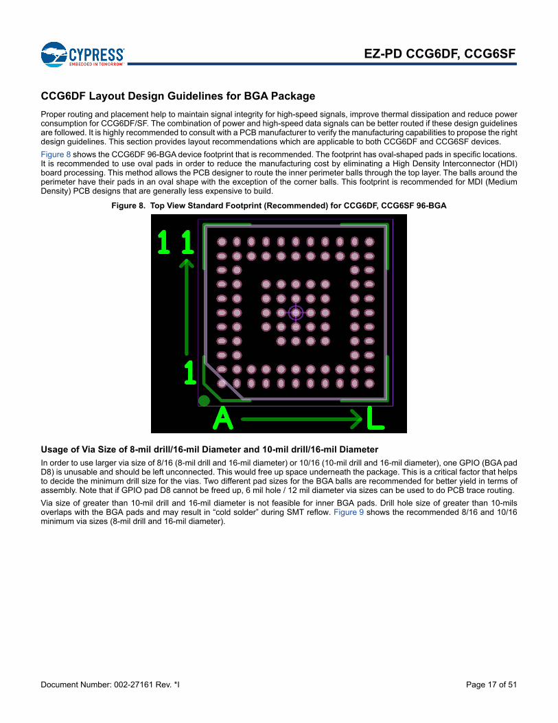
Figure 8 shows the CCG6DF 96-BGA device footprint that is recommended. The footprint has oval-shaped pads in specific locations.It is recommended to use oval pads in order to reduce the manufacturing cost by eliminating a High Density Interconnector (HDI)board processing. This method allows the PCB designer to route the inner perimeter balls through the top layer. The balls around theperimeter have their pads in an oval shape with the exception of the corner balls. This footprint is recommended for MDI (MediumDensity) PCB designs that are generally less expensive to build.
Figure 8. Top View Standard Footprint (Recommended) for CCG6DF, CCG6SF 96-BGA
Usage of Via Size of 8-mil drill/16-mil Diameter and 10-mil drill/16-mil Diameter
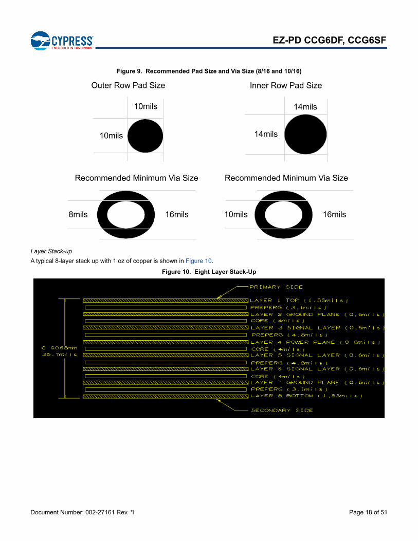
In order to use larger via size of 8/16 (8-mil drill and 16-mil diameter) or 10/16 (10-mil drill and 16-mil diameter), one GPIO (BGA padD8) is unusable and should be left unconnected. This would free up space underneath the package. This is a critical factor that helpsto decide the minimum drill size for the vias. Two different pad sizes for the BGA balls are recommended for better yield in terms ofassembly. Note that if GPIO pad D8 cannot be freed up, 6 mil hole / 12 mil diameter via sizes can be used to do PCB trace routing.
Via size of greater than 10-mil drill and 16-mil diameter is not feasible for inner BGA pads. Drill hole size of greater than 10-milsoverlaps with the BGA pads and may result in “cold solder” during SMT reflow. Figure 9 shows the recommended 8/16 and 10/16minimum via sizes (8-mil drill and 16-mil diameter).
Document Number: 002-27161 Rev. *I Page 18 of 51
EZ-PD CCG6DF, CCG6SF
Figure 9. Recommended Pad Size and Via Size (8/16 and 10/16)
Layer Stack-up
A typical 8-layer stack up with 1 oz of copper is shown in Figure 10.
Figure 10. Eight Layer Stack-Up
Recommended Minimum Via Size
16mils8mils
Outer Row Pad Size
10mils
10mils
Recommended Minimum Via Size
16mils10mils
Inner Row Pad Size
14mils
14mils
Document Number: 002-27161 Rev. *I Page 19 of 51
EZ-PD CCG6DF, CCG6SF
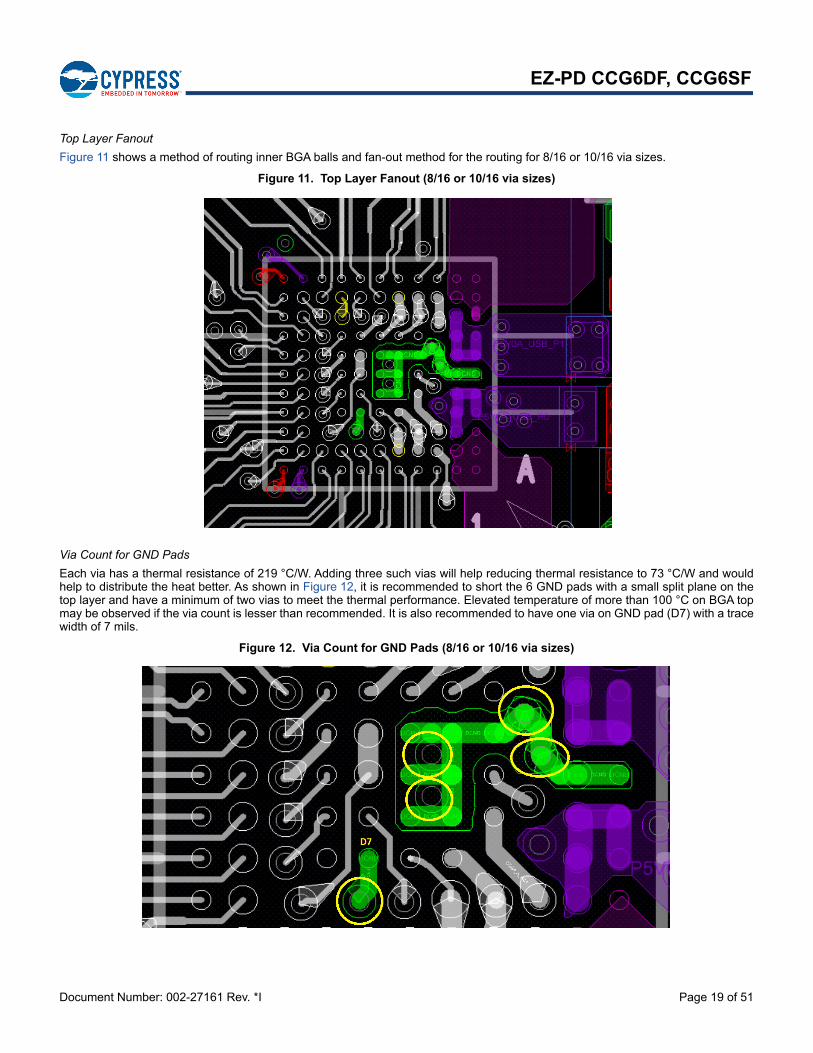
Top Layer Fanout
Figure 11 shows a method of routing inner BGA balls and fan-out method for the routing for 8/16 or 10/16 via sizes.
Figure 11. Top Layer Fanout (8/16 or 10/16 via sizes)
Via Count for GND Pads
Each via has a thermal resistance of 219 °C/W. Adding three such vias will help reducing thermal resistance to 73 °C/W and wouldhelp to distribute the heat better. As shown in Figure 12, it is recommended to short the 6 GND pads with a small split plane on thetop layer and have a minimum of two vias to meet the thermal performance. Elevated temperature of more than 100 °C on BGA topmay be observed if the via count is lesser than recommended. It is also recommended to have one via on GND pad (D7) with a tracewidth of 7 mils.
Figure 12. Via Count for GND Pads (8/16 or 10/16 via sizes)
Document Number: 002-27161 Rev. *I Page 20 of 51
EZ-PD CCG6DF, CCG6SF
Via Count for Provider Pads
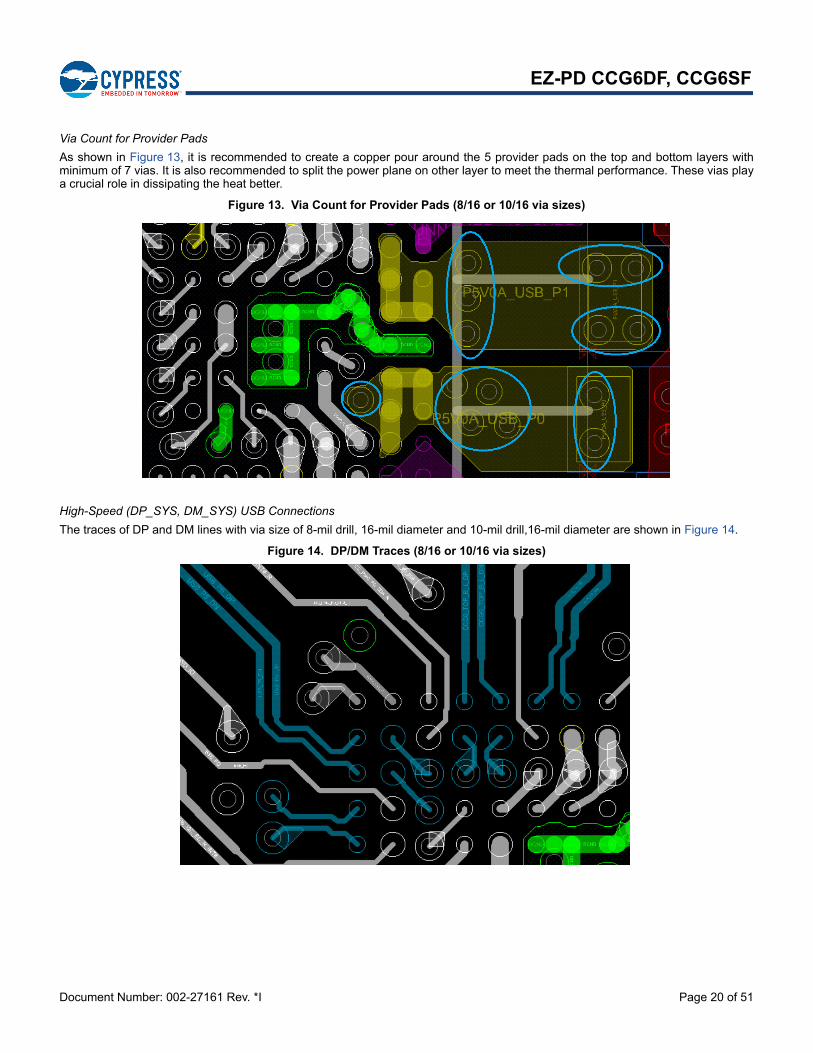
As shown in Figure 13, it is recommended to create a copper pour around the 5 provider pads on the top and bottom layers withminimum of 7 vias. It is also recommended to split the power plane on other layer to meet the thermal performance. These vias playa crucial role in dissipating the heat better.
Figure 13. Via Count for Provider Pads (8/16 or 10/16 via sizes)
High-Speed (DP_SYS, DM_SYS) USB Connections
The traces of DP and DM lines with via size of 8-mil drill, 16-mil diameter and 10-mil drill,16-mil diameter are shown in Figure 14.
Figure 14. DP/DM Traces (8/16 or 10/16 via sizes)
Document Number: 002-27161 Rev. *I Page 21 of 51
EZ-PD CCG6DF, CCG6SF
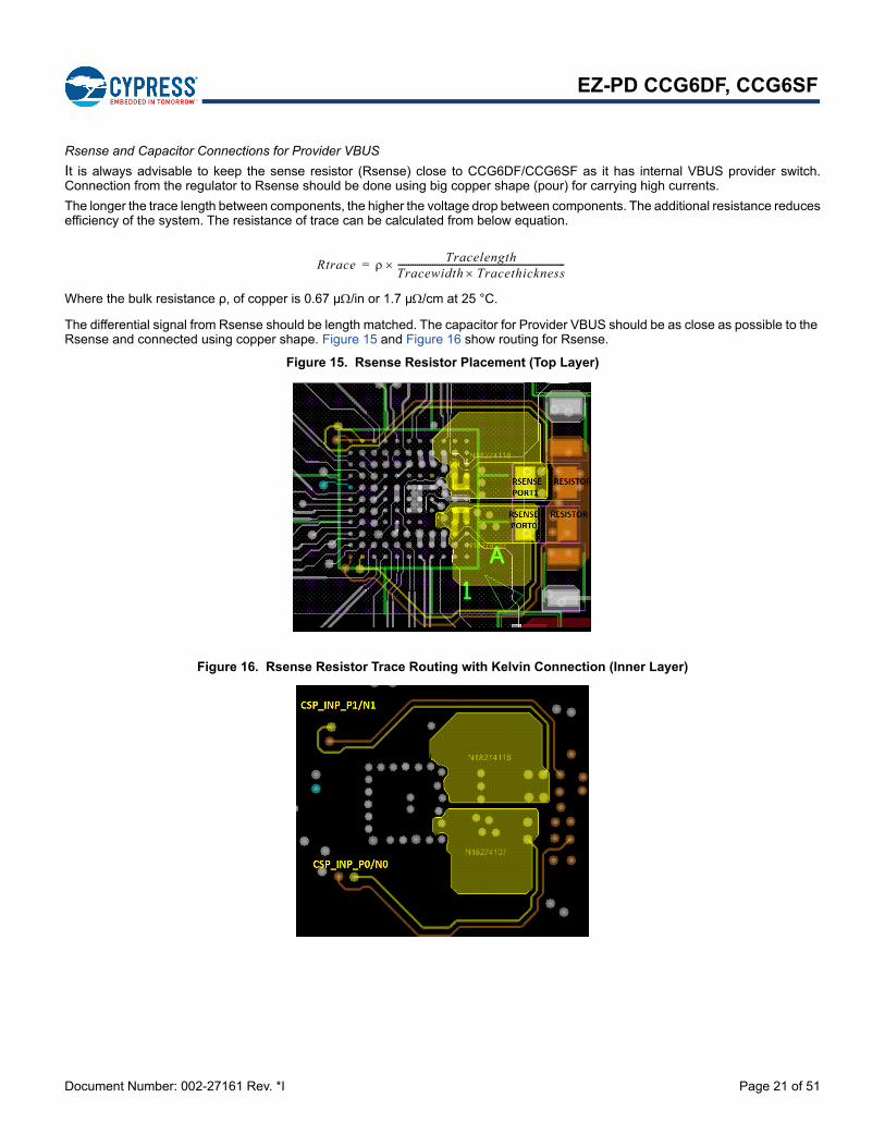
Rsense and Capacitor Connections for Provider VBUS
It is always advisable to keep the sense resistor (Rsense) close to CCG6DF/CCG6SF as it has internal VBUS provider switch.Connection from the regulator to Rsense should be done using big copper shape (pour) for carrying high currents.
The longer the trace length between components, the higher the voltage drop between components. The additional resistance reducesefficiency of the system. The resistance of trace can be calculated from below equation.
Where the bulk resistance ρ, of copper is 0.67 µ/in or 1.7 µ/cm at 25 °C.
The differential signal from Rsense should be length matched. The capacitor for Provider VBUS should be as close as possible to the Rsense and connected using copper shape. Figure 15 and Figure 16 show routing for Rsense.
Figure 15. Rsense Resistor Placement (Top Layer)
Figure 16. Rsense Resistor Trace Routing with Kelvin Connection (Inner Layer)
Rtrace TracelengthTracewidth Tracethickness-----------------------------------------------------------------------------=
Document Number: 002-27161 Rev. *I Page 22 of 51
EZ-PD CCG6DF, CCG6SF
Trace Width Details for Critical Signals
Table 4 provides information on routing trace width for this layout example.
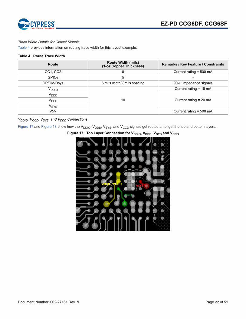
VDDIO, VCCD, VSYS, and VDDD Connections
Figure 17 and Figure 18 show how the VDDIO, VDDD, VSYS, and VCCD signals get routed amongst the top and bottom layers.
Figure 17. Top Layer Connection for VDDIO, VDDD, VSYS and VCCD
Table 4. Route Trace Width
Route Route Width (mils) (1-oz Copper Thickness) Remarks / Key Feature / Constraints
CC1, CC2 8 Current rating = 500 mA
GPIOs 5 -
DP/DM/Dsys 6 mils width/ 8mils spacing 90- impedance signals
VDDIO
10
Current rating = 15 mA
VDDD
Current rating = 20 mAVCCD
VSYS
V5V Current rating = 500 mA
Document Number: 002-27161 Rev. *I Page 23 of 51
EZ-PD CCG6DF, CCG6SF
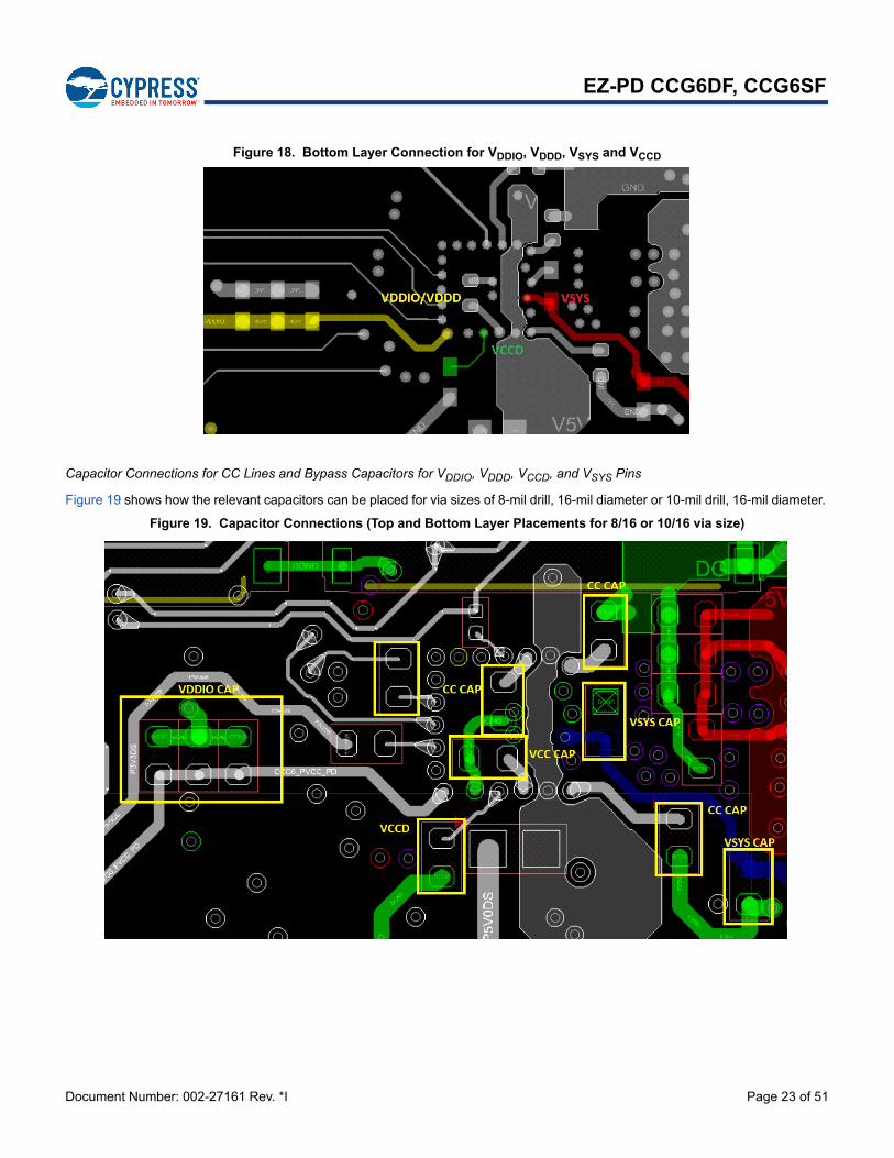
Figure 18. Bottom Layer Connection for VDDIO, VDDD, VSYS and VCCD
Capacitor Connections for CC Lines and Bypass Capacitors for VDDIO, VDDD, VCCD, and VSYS Pins
Figure 19 shows how the relevant capacitors can be placed for via sizes of 8-mil drill, 16-mil diameter or 10-mil drill, 16-mil diameter.
Figure 19. Capacitor Connections (Top and Bottom Layer Placements for 8/16 or 10/16 via size)
Document Number: 002-27161 Rev. *I Page 24 of 51
EZ-PD CCG6DF, CCG6SF
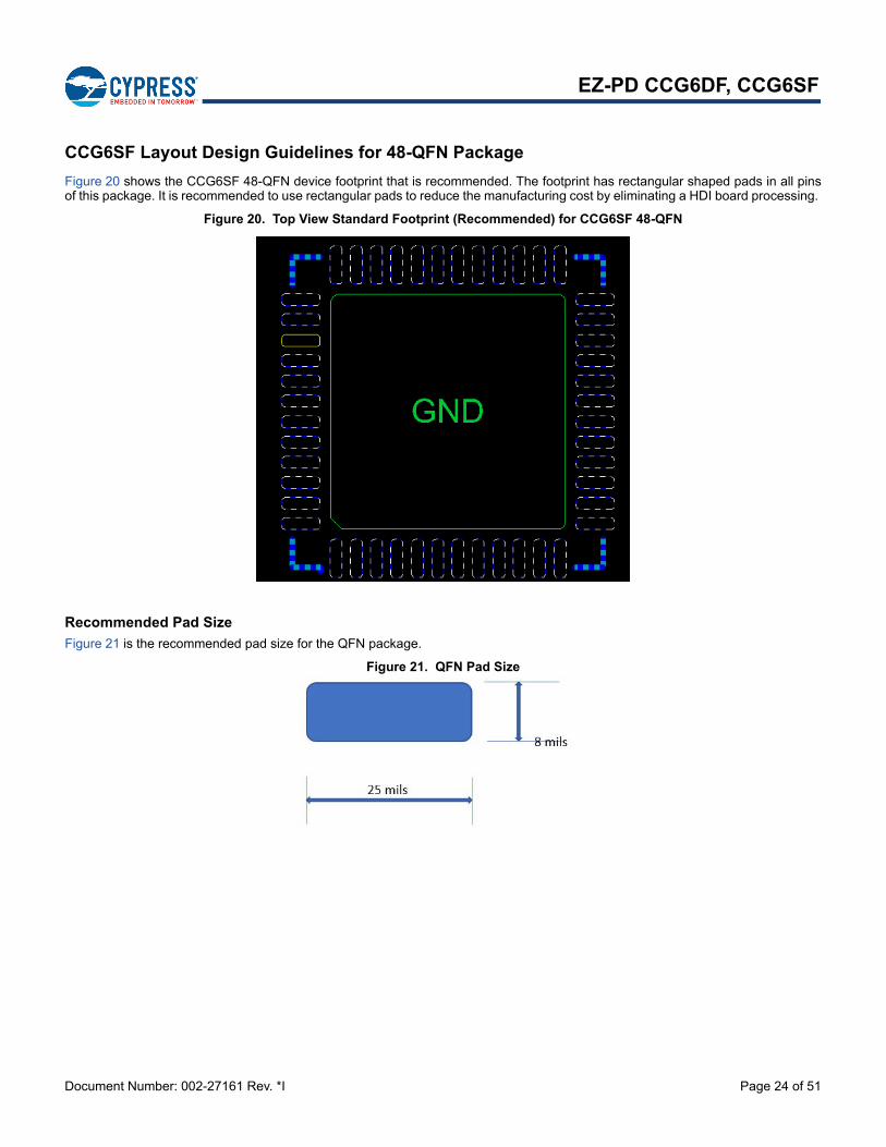
CCG6SF Layout Design Guidelines for 48-QFN Package
Figure 20 shows the CCG6SF 48-QFN device footprint that is recommended. The footprint has rectangular shaped pads in all pinsof this package. It is recommended to use rectangular pads to reduce the manufacturing cost by eliminating a HDI board processing.
Figure 20. Top View Standard Footprint (Recommended) for CCG6SF 48-QFN
Recommended Pad Size
Figure 21 is the recommended pad size for the QFN package.
Figure 21. QFN Pad Size
Document Number: 002-27161 Rev. *I Page 25 of 51
EZ-PD CCG6DF, CCG6SF
Stackup
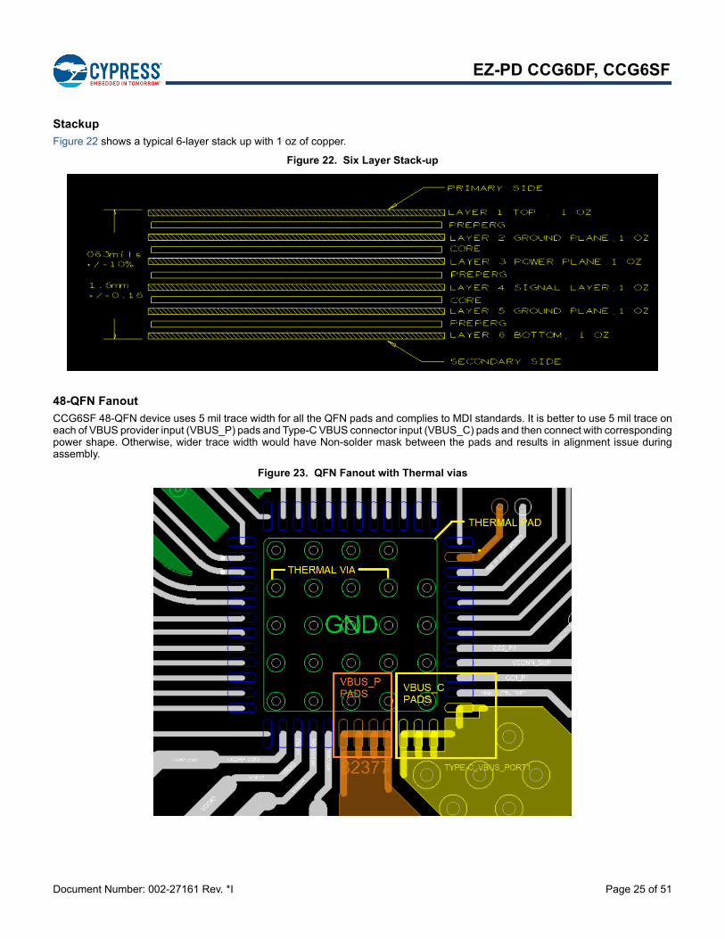
Figure 22 shows a typical 6-layer stack up with 1 oz of copper.
Figure 22. Six Layer Stack-up
48-QFN Fanout
CCG6SF 48-QFN device uses 5 mil trace width for all the QFN pads and complies to MDI standards. It is better to use 5 mil trace oneach of VBUS provider input (VBUS_P) pads and Type-C VBUS connector input (VBUS_C) pads and then connect with correspondingpower shape. Otherwise, wider trace width would have Non-solder mask between the pads and results in alignment issue duringassembly.
Figure 23. QFN Fanout with Thermal vias
Document Number: 002-27161 Rev. *I Page 26 of 51
EZ-PD CCG6DF, CCG6SF
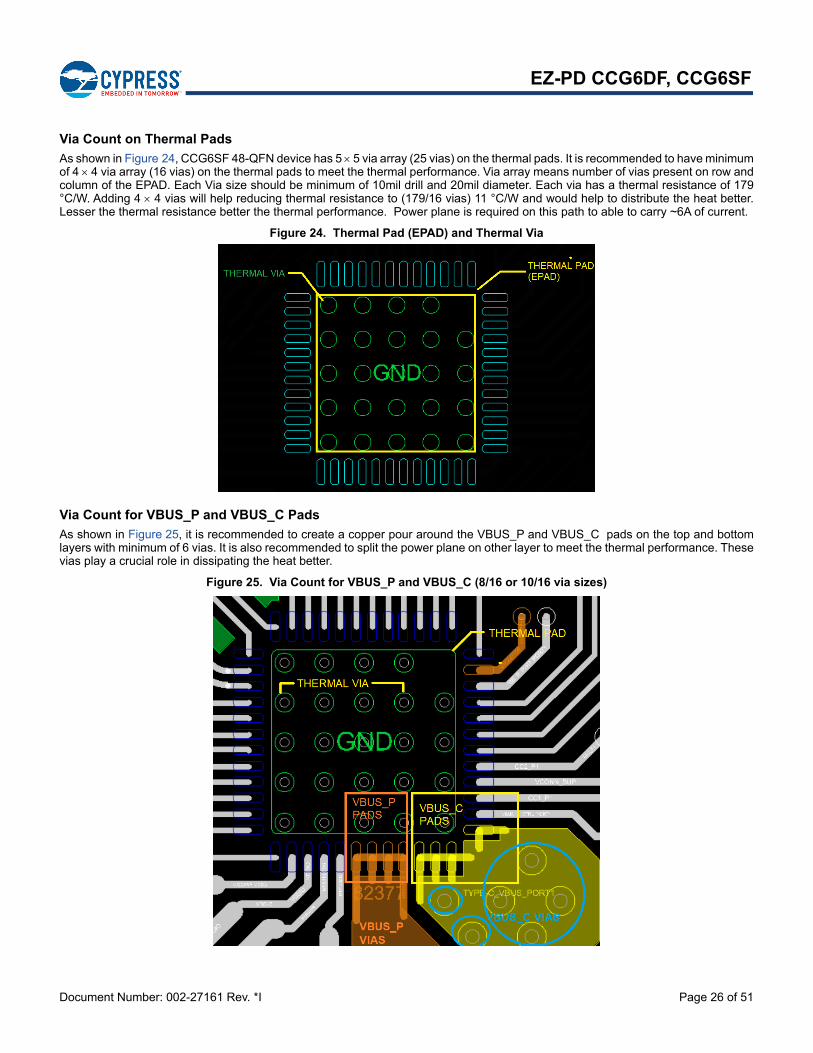
Via Count on Thermal Pads
As shown in Figure 24, CCG6SF 48-QFN device has 5 5 via array (25 vias) on the thermal pads. It is recommended to have minimumof 4 4 via array (16 vias) on the thermal pads to meet the thermal performance. Via array means number of vias present on row andcolumn of the EPAD. Each Via size should be minimum of 10mil drill and 20mil diameter. Each via has a thermal resistance of 179°C/W. Adding 4 4 vias will help reducing thermal resistance to (179/16 vias) 11 °C/W and would help to distribute the heat better.Lesser the thermal resistance better the thermal performance. Power plane is required on this path to able to carry ~6A of current.
Figure 24. Thermal Pad (EPAD) and Thermal Via
Via Count for VBUS_P and VBUS_C Pads
As shown in Figure 25, it is recommended to create a copper pour around the VBUS_P and VBUS_C pads on the top and bottomlayers with minimum of 6 vias. It is also recommended to split the power plane on other layer to meet the thermal performance. Thesevias play a crucial role in dissipating the heat better.
Figure 25. Via Count for VBUS_P and VBUS_C (8/16 or 10/16 via sizes)
Document Number: 002-27161 Rev. *I Page 27 of 51
EZ-PD CCG6DF, CCG6SF
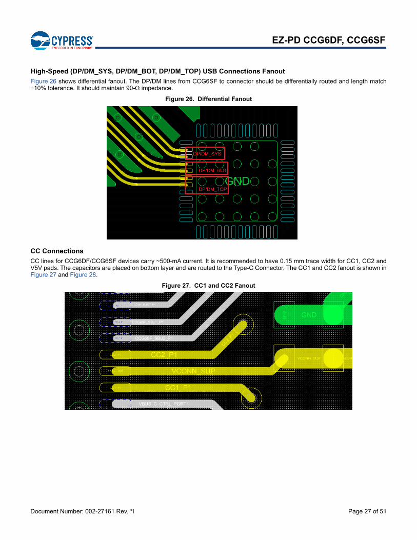
High-Speed (DP/DM_SYS, DP/DM_BOT, DP/DM_TOP) USB Connections Fanout
Figure 26 shows differential fanout. The DP/DM lines from CCG6SF to connector should be differentially routed and length match10% tolerance. It should maintain 90- impedance.
Figure 26. Differential Fanout
CC Connections
CC lines for CCG6DF/CCG6SF devices carry ~500-mA current. It is recommended to have 0.15 mm trace width for CC1, CC2 andV5V pads. The capacitors are placed on bottom layer and are routed to the Type-C Connector. The CC1 and CC2 fanout is shown inFigure 27 and Figure 28.
Figure 27. CC1 and CC2 Fanout
Document Number: 002-27161 Rev. *I Page 28 of 51
EZ-PD CCG6DF, CCG6SF
Figure 28. CC1 and CC2 Caps
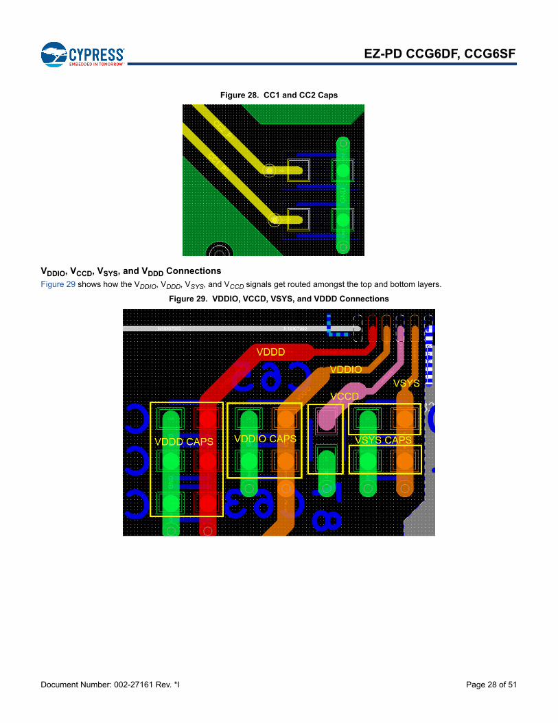
VDDIO, VCCD, VSYS, and VDDD Connections
Figure 29 shows how the VDDIO, VDDD, VSYS, and VCCD signals get routed amongst the top and bottom layers.
Figure 29. VDDIO, VCCD, VSYS, and VDDD Connections
Document Number: 002-27161 Rev. *I Page 29 of 51
EZ-PD CCG6DF, CCG6SF
Electrical Specifications
Absolute Maximum Ratings
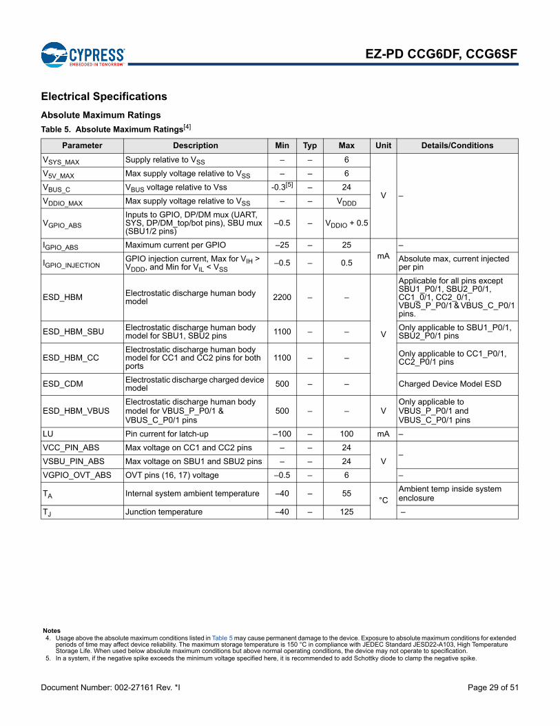
Table 5. Absolute Maximum Ratings[4]
Parameter Description Min Typ Max Unit Details/Conditions
VSYS_MAX Supply relative to VSS – – 6
V –
V5V_MAX Max supply voltage relative to VSS – – 6
VBUS_C VBUS voltage relative to Vss -0.3[5] – 24
VDDIO_MAX Max supply voltage relative to VSS – – VDDD
VGPIO_ABS
Inputs to GPIO, DP/DM mux (UART, SYS, DP/DM_top/bot pins), SBU mux (SBU1/2 pins)
–0.5 – VDDIO + 0.5
IGPIO_ABS Maximum current per GPIO –25 – 25mA
–
IGPIO_INJECTIONGPIO injection current, Max for VIH > VDDD, and Min for VIL < VSS
–0.5 – 0.5 Absolute max, current injected per pin
ESD_HBM Electrostatic discharge human body model 2200 – –
V
Applicable for all pins exceptSBU1_P0/1, SBU2_P0/1, CC1_0/1, CC2_0/1, VBUS_P_P0/1 & VBUS_C_P0/1 pins.
ESD_HBM_SBU Electrostatic discharge human body model for SBU1, SBU2 pins 1100 – – Only applicable to SBU1_P0/1,
SBU2_P0/1 pins
ESD_HBM_CCElectrostatic discharge human body model for CC1 and CC2 pins for both ports
1100 – – Only applicable to CC1_P0/1, CC2_P0/1 pins
ESD_CDM Electrostatic discharge charged device model 500 – – Charged Device Model ESD
ESD_HBM_VBUSElectrostatic discharge human bodymodel for VBUS_P_P0/1 & VBUS_C_P0/1 pins
500 – – VOnly applicable to VBUS_P_P0/1 and VBUS_C_P0/1 pins
LU Pin current for latch-up –100 – 100 mA –
VCC_PIN_ABS Max voltage on CC1 and CC2 pins – – 24
V–
VSBU_PIN_ABS Max voltage on SBU1 and SBU2 pins – – 24
VGPIO_OVT_ABS OVT pins (16, 17) voltage –0.5 – 6 –
TA Internal system ambient temperature –40 – 55°C
Ambient temp inside system enclosure
TJ Junction temperature –40 – 125 –
Notes4. Usage above the absolute maximum conditions listed in Table 5 may cause permanent damage to the device. Exposure to absolute maximum conditions for extended
periods of time may affect device reliability. The maximum storage temperature is 150 °C in compliance with JEDEC Standard JESD22-A103, High Temperature Storage Life. When used below absolute maximum conditions but above normal operating conditions, the device may not operate to specification.
5. In a system, if the negative spike exceeds the minimum voltage specified here, it is recommended to add Schottky diode to clamp the negative spike.
Document Number: 002-27161 Rev. *I Page 30 of 51
EZ-PD CCG6DF, CCG6SF
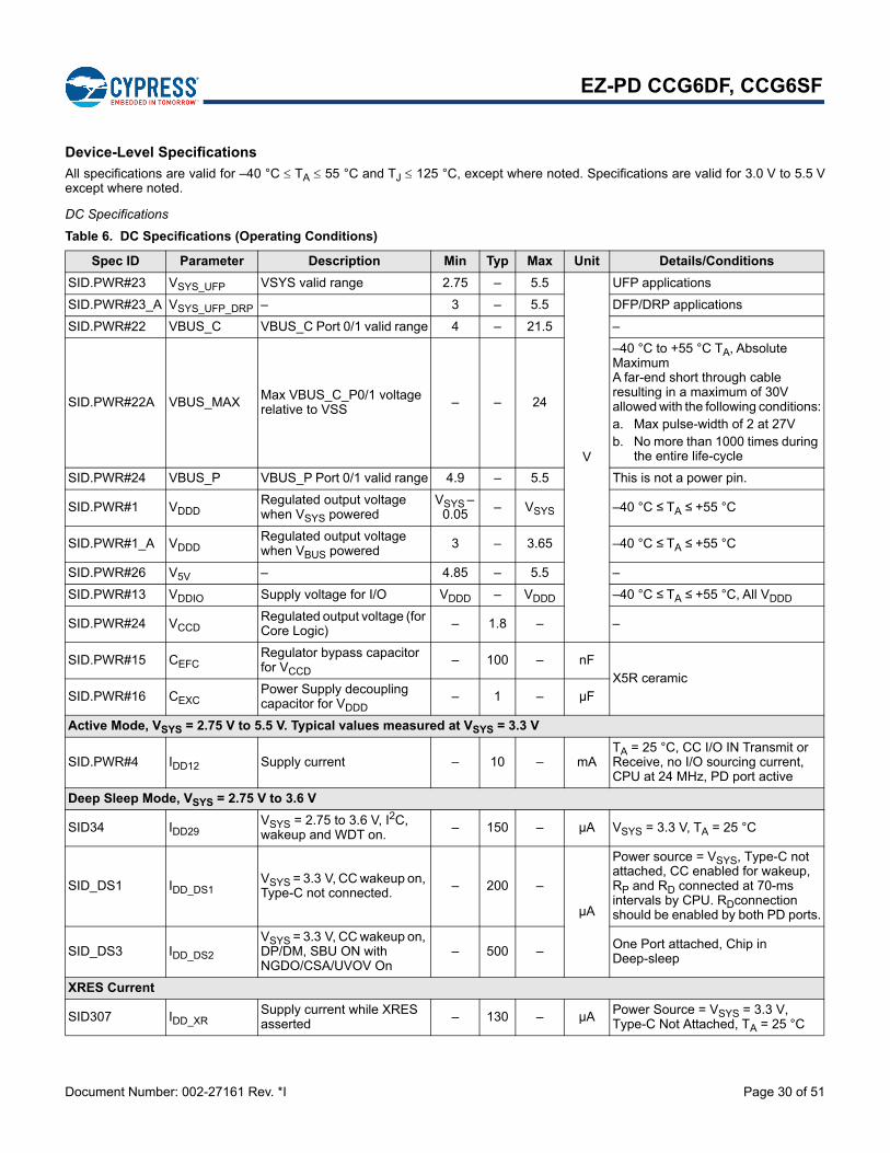
Device-Level Specifications
All specifications are valid for –40 °C TA 55 °C and TJ 125 °C, except where noted. Specifications are valid for 3.0 V to 5.5 Vexcept where noted.
DC Specifications
Table 6. DC Specifications (Operating Conditions)
Spec ID Parameter Description Min Typ Max Unit Details/Conditions
SID.PWR#23 VSYS_UFP VSYS valid range 2.75 – 5.5
V
UFP applications
SID.PWR#23_A VSYS_UFP_DRP – 3 – 5.5 DFP/DRP applications
SID.PWR#22 VBUS_C VBUS_C Port 0/1 valid range 4 – 21.5 –
SID.PWR#22A VBUS_MAXMax VBUS_C_P0/1 voltage relative to VSS – – 24
–40 °C to +55 °C TA, Absolute MaximumA far-end short through cable resulting in a maximum of 30V allowed with the following conditions:a. Max pulse-width of 2 at 27Vb. No more than 1000 times during
the entire life-cycle
SID.PWR#24 VBUS_P VBUS_P Port 0/1 valid range 4.9 – 5.5 This is not a power pin.
SID.PWR#1 VDDDRegulated output voltage when VSYS powered
VSYS – 0.05 – VSYS –40 °C ≤ TA ≤ +55 °C
SID.PWR#1_A VDDDRegulated output voltage when VBUS powered
3 – 3.65 –40 °C ≤ TA ≤ +55 °C
SID.PWR#26 V5V – 4.85 – 5.5 –
SID.PWR#13 VDDIO Supply voltage for I/O VDDD – VDDD –40 °C ≤ TA ≤ +55 °C, All VDDD
SID.PWR#24 VCCDRegulated output voltage (for Core Logic) – 1.8 – –
SID.PWR#15 CEFCRegulator bypass capacitor for VCCD
– 100 – nFX5R ceramic
SID.PWR#16 CEXCPower Supply decoupling capacitor for VDDD
– 1 – µF
Active Mode, VSYS = 2.75 V to 5.5 V. Typical values measured at VSYS = 3.3 V
SID.PWR#4 IDD12 Supply current – 10 – mATA = 25 °C, CC I/O IN Transmit or Receive, no I/O sourcing current, CPU at 24 MHz, PD port active
Deep Sleep Mode, VSYS = 2.75 V to 3.6 V
SID34 IDD29VSYS = 2.75 to 3.6 V, I2C, wakeup and WDT on.
– 150 – µA VSYS = 3.3 V, TA = 25 °C
SID_DS1 IDD_DS1VSYS = 3.3 V, CC wakeup on, Type-C not connected. – 200 –
µA
Power source = VSYS, Type-C not attached, CC enabled for wakeup, RP and RD connected at 70-ms intervals by CPU. RDconnection should be enabled by both PD ports.
SID_DS3 IDD_DS2
VSYS = 3.3 V, CC wakeup on, DP/DM, SBU ON with NGDO/CSA/UVOV On
– 500 – One Port attached, Chip in Deep-sleep
XRES Current
SID307 IDD_XRSupply current while XRES asserted
– 130 – µA Power Source = VSYS = 3.3 V, Type-C Not Attached, TA = 25 °C
Document Number: 002-27161 Rev. *I Page 31 of 51
EZ-PD CCG6DF, CCG6SF
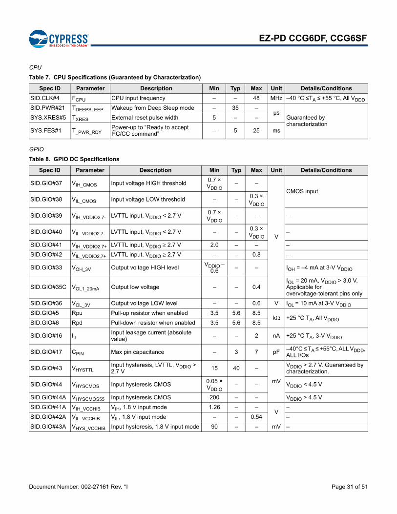
CPU
GPIO
Table 7. CPU Specifications (Guaranteed by Characterization)
Spec ID Parameter Description Min Typ Max Unit Details/Conditions
SID.CLK#4 FCPU CPU input frequency – – 48 MHz –40 °C ≤TA ≤ +55 °C, All VDDD
SID.PWR#21 TDEEPSLEEP Wakeup from Deep Sleep mode – 35 –µs
Guaranteed by characterization
SYS.XRES#5 TXRES External reset pulse width 5 – –
SYS.FES#1 T_PWR_RDYPower-up to “Ready to accept I2C/CC command” – 5 25 ms
Table 8. GPIO DC Specifications
Spec ID Parameter Description Min Typ Max Unit Details/Conditions
SID.GIO#37 VIH_CMOS Input voltage HIGH threshold0.7 × VDDIO
– –
V
CMOS inputSID.GIO#38 VIL_CMOS Input voltage LOW threshold – – 0.3 ×
VDDIO
SID.GIO#39 VIH_VDDIO2.7- LVTTL input, VDDIO < 2.7 V 0.7 × VDDIO
– – –
SID.GIO#40 VIL_VDDIO2.7- LVTTL input, VDDIO < 2.7 V – –0.3 × VDDIO
–
SID.GIO#41 VIH_VDDIO2.7+ LVTTL input, VDDIO 2.7 V 2.0 – – –
SID.GIO#42 VIL_VDDIO2.7+ LVTTL input, VDDIO 2.7 V – – 0.8 –
SID.GIO#33 VOH_3V Output voltage HIGH level VDDIO – 0.6
– – IOH = –4 mA at 3-V VDDIO
SID.GIO#35C VOL1_20mA Output low voltage – – 0.4IOL = 20 mA, VDDIO > 3.0 V, Applicable for overvoltage-tolerant pins only
SID.GIO#36 VOL_3V Output voltage LOW level – – 0.6 V IOL = 10 mA at 3-V VDDIO
SID.GIO#5 Rpu Pull-up resistor when enabled 3.5 5.6 8.5k +25 °C TA, All VDDIO
SID.GIO#6 Rpd Pull-down resistor when enabled 3.5 5.6 8.5
SID.GIO#16 IILInput leakage current (absolute value)
– – 2 nA +25 °C TA, 3-V VDDIO
SID.GIO#17 CPIN Max pin capacitance – 3 7 pF –40°C ≤ TA ≤ +55°C, ALL VDDD, ALL I/Os
SID.GIO#43 VHYSTTLInput hysteresis, LVTTL, VDDIO > 2.7 V 15 40 –
mV
VDDIO > 2.7 V. Guaranteed by characterization.
SID.GIO#44 VHYSCMOS Input hysteresis CMOS 0.05 × VDDIO
– – VDDIO < 4.5 V
SID.GIO#44A VHYSCMOS55 Input hysteresis CMOS 200 – – VDDIO > 4.5 V
SID.GIO#41A VIH_VCCHIB VIH, 1.8 V input mode 1.26 – –V
–
SID.GIO#42A VIL_VCCHIB VIL, 1.8 V input mode – – 0.54 –
SID.GIO#43A VHYS_VCCHIB Input hysteresis, 1.8 V input mode 90 – – mV –
Document Number: 002-27161 Rev. *I Page 32 of 51
EZ-PD CCG6DF, CCG6SF
XRES
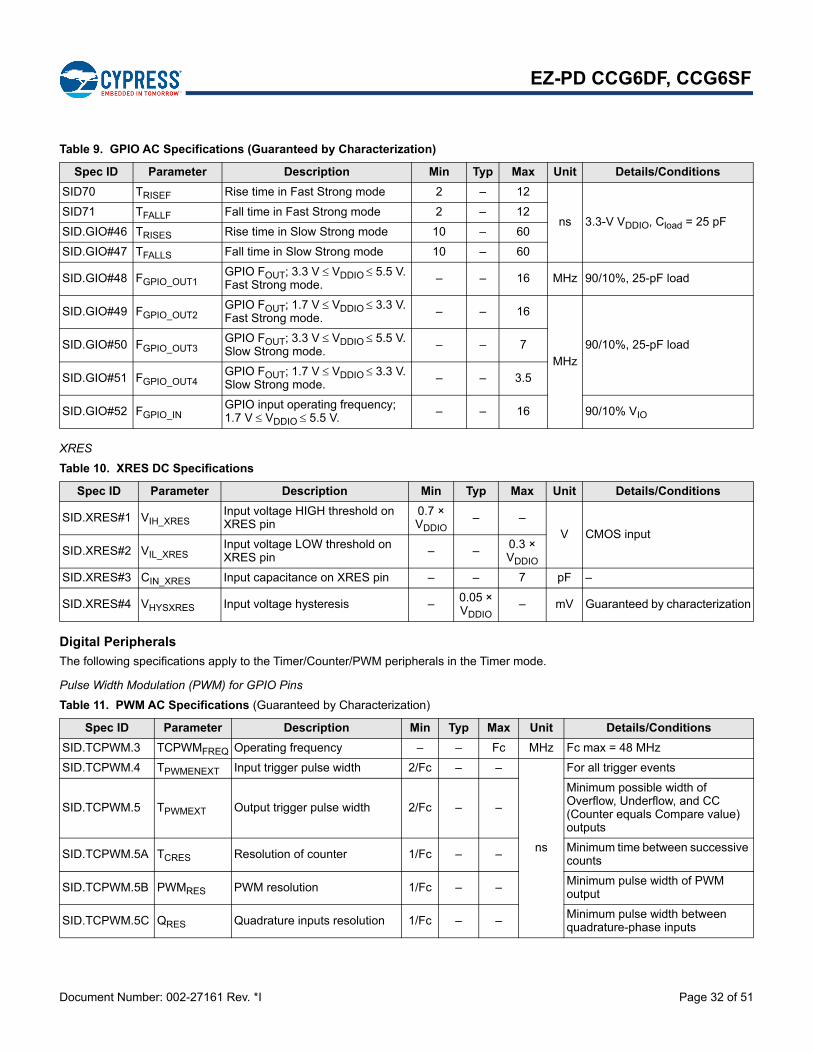
Digital Peripherals
The following specifications apply to the Timer/Counter/PWM peripherals in the Timer mode.
Pulse Width Modulation (PWM) for GPIO Pins
Table 9. GPIO AC Specifications (Guaranteed by Characterization)
Spec ID Parameter Description Min Typ Max Unit Details/Conditions
SID70 TRISEF Rise time in Fast Strong mode 2 – 12
ns 3.3-V VDDIO, Cload = 25 pFSID71 TFALLF Fall time in Fast Strong mode 2 – 12
SID.GIO#46 TRISES Rise time in Slow Strong mode 10 – 60
SID.GIO#47 TFALLS Fall time in Slow Strong mode 10 – 60
SID.GIO#48 FGPIO_OUT1GPIO FOUT; 3.3 V VDDIO 5.5 V. Fast Strong mode. – – 16 MHz 90/10%, 25-pF load
SID.GIO#49 FGPIO_OUT2GPIO FOUT; 1.7 V VDDIO 3.3 V. Fast Strong mode. – – 16
MHz90/10%, 25-pF loadSID.GIO#50 FGPIO_OUT3
GPIO FOUT; 3.3 V VDDIO 5.5 V. Slow Strong mode.
– – 7
SID.GIO#51 FGPIO_OUT4GPIO FOUT; 1.7 V VDDIO 3.3 V. Slow Strong mode. – – 3.5
SID.GIO#52 FGPIO_INGPIO input operating frequency; 1.7 V VDDIO 5.5 V. – – 16 90/10% VIO
Table 10. XRES DC Specifications
Spec ID Parameter Description Min Typ Max Unit Details/Conditions
SID.XRES#1 VIH_XRESInput voltage HIGH threshold on XRES pin
0.7 × VDDIO
– –V CMOS input
SID.XRES#2 VIL_XRESInput voltage LOW threshold on XRES pin – –
0.3 × VDDIO
SID.XRES#3 CIN_XRES Input capacitance on XRES pin – – 7 pF –
SID.XRES#4 VHYSXRES Input voltage hysteresis – 0.05 × VDDIO
– mV Guaranteed by characterization
Table 11. PWM AC Specifications (Guaranteed by Characterization)
Spec ID Parameter Description Min Typ Max Unit Details/Conditions
SID.TCPWM.3 TCPWMFREQ Operating frequency – – Fc MHz Fc max = 48 MHz
SID.TCPWM.4 TPWMENEXT Input trigger pulse width 2/Fc – –
ns
For all trigger events
SID.TCPWM.5 TPWMEXT Output trigger pulse width 2/Fc – –
Minimum possible width of Overflow, Underflow, and CC (Counter equals Compare value) outputs
SID.TCPWM.5A TCRES Resolution of counter 1/Fc – –Minimum time between successive counts
SID.TCPWM.5B PWMRES PWM resolution 1/Fc – –Minimum pulse width of PWM output
SID.TCPWM.5C QRES Quadrature inputs resolution 1/Fc – – Minimum pulse width between quadrature-phase inputs
Document Number: 002-27161 Rev. *I Page 33 of 51
EZ-PD CCG6DF, CCG6SF
I2C
UART
SPI
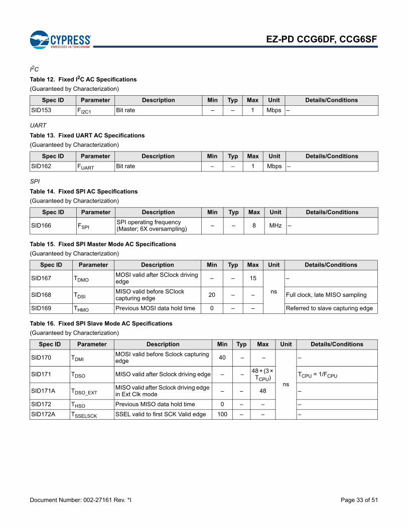
Table 12. Fixed I2C AC Specifications
(Guaranteed by Characterization)
Spec ID Parameter Description Min Typ Max Unit Details/Conditions
SID153 FI2C1 Bit rate – – 1 Mbps –
Table 13. Fixed UART AC Specifications
(Guaranteed by Characterization)
Spec ID Parameter Description Min Typ Max Unit Details/Conditions
SID162 FUART Bit rate – – 1 Mbps –
Table 14. Fixed SPI AC Specifications
(Guaranteed by Characterization)
Spec ID Parameter Description Min Typ Max Unit Details/Conditions
SID166 FSPISPI operating frequency (Master; 6X oversampling) – – 8 MHz –
Table 15. Fixed SPI Master Mode AC Specifications
(Guaranteed by Characterization)
Spec ID Parameter Description Min Typ Max Unit Details/Conditions
SID167 TDMOMOSI valid after SClock driving edge – – 15
ns
–
SID168 TDSIMISO valid before SClock capturing edge
20 – – Full clock, late MISO sampling
SID169 THMO Previous MOSI data hold time 0 – – Referred to slave capturing edge
Table 16. Fixed SPI Slave Mode AC Specifications
(Guaranteed by Characterization)
Spec ID Parameter Description Min Typ Max Unit Details/Conditions
SID170 TDMIMOSI valid before Sclock capturing edge 40 – –
ns
–
SID171 TDSO MISO valid after Sclock driving edge – –48 + (3 × TCPU) TCPU = 1/FCPU
SID171A TDSO_EXTMISO valid after Sclock driving edge in Ext Clk mode
– – 48 –
SID172 THSO Previous MISO data hold time 0 – – –
SID172A TSSELSCK SSEL valid to first SCK Valid edge 100 – – –
Document Number: 002-27161 Rev. *I Page 34 of 51
EZ-PD CCG6DF, CCG6SF
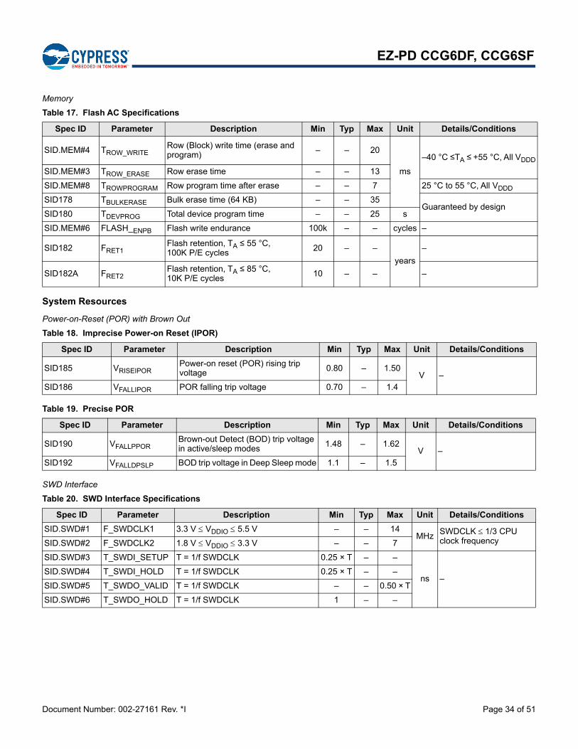
Memory
System Resources
Power-on-Reset (POR) with Brown Out
SWD Interface
Table 17. Flash AC Specifications
Spec ID Parameter Description Min Typ Max Unit Details/Conditions
SID.MEM#4 TROW_WRITERow (Block) write time (erase and program)
– – 20
ms
–40 °C ≤TA ≤ +55 °C, All VDDD
SID.MEM#3 TROW_ERASE Row erase time – – 13
SID.MEM#8 TROWPROGRAM Row program time after erase – – 7 25 °C to 55 °C, All VDDD
SID178 TBULKERASE Bulk erase time (64 KB) – – 35Guaranteed by design
SID180 TDEVPROG Total device program time – – 25 s
SID.MEM#6 FLASH_ENPB Flash write endurance 100k – – cycles –
SID182 FRET1Flash retention, TA ≤ 55 °C, 100K P/E cycles
20 – –
years
–
SID182A FRET2Flash retention, TA ≤ 85 °C, 10K P/E cycles
10 – – –
Table 18. Imprecise Power-on Reset (IPOR)
Spec ID Parameter Description Min Typ Max Unit Details/Conditions
SID185 VRISEIPORPower-on reset (POR) rising trip voltage 0.80 – 1.50
V –SID186 VFALLIPOR POR falling trip voltage 0.70 – 1.4
Table 19. Precise POR
Spec ID Parameter Description Min Typ Max Unit Details/Conditions
SID190 VFALLPPORBrown-out Detect (BOD) trip voltage in active/sleep modes
1.48 – 1.62V –
SID192 VFALLDPSLP BOD trip voltage in Deep Sleep mode 1.1 – 1.5
Table 20. SWD Interface Specifications
Spec ID Parameter Description Min Typ Max Unit Details/Conditions
SID.SWD#1 F_SWDCLK1 3.3 V VDDIO 5.5 V – – 14MHz SWDCLK 1/3 CPU
clock frequencySID.SWD#2 F_SWDCLK2 1.8 V VDDIO 3.3 V – – 7
SID.SWD#3 T_SWDI_SETUP T = 1/f SWDCLK 0.25 × T – –
ns –SID.SWD#4 T_SWDI_HOLD T = 1/f SWDCLK 0.25 × T – –
SID.SWD#5 T_SWDO_VALID T = 1/f SWDCLK – – 0.50 × T
SID.SWD#6 T_SWDO_HOLD T = 1/f SWDCLK 1 – –
Document Number: 002-27161 Rev. *I Page 35 of 51
EZ-PD CCG6DF, CCG6SF
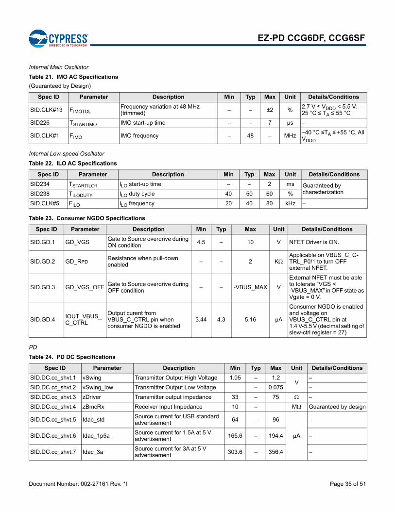
Internal Main Oscillator
Internal Low-speed Oscillator
PD
Table 21. IMO AC Specifications
(Guaranteed by Design)
Spec ID Parameter Description Min Typ Max Unit Details/Conditions
SID.CLK#13 FIMOTOLFrequency variation at 48 MHz (trimmed) – – ±2 % 2.7 V ≤ VDDD < 5.5 V. –
25 °C ≤ TA ≤ 55 °C
SID226 TSTARTIMO IMO start-up time – – 7 µs –
SID.CLK#1 FIMO IMO frequency – 48 – MHz–40 °C ≤TA ≤ +55 °C, All VDDD
Table 22. ILO AC Specifications
Spec ID Parameter Description Min Typ Max Unit Details/Conditions
SID234 TSTARTILO1 ILO start-up time – – 2 ms Guaranteed by characterizationSID238 TILODUTY ILO duty cycle 40 50 60 %
SID.CLK#5 FILO ILO frequency 20 40 80 kHz –
Table 23. Consumer NGDO Specifications
Spec ID Parameter Description Min Typ Max Unit Details/Conditions
SID.GD.1 GD_VGSGate to Source overdrive during ON condition 4.5 – 10 V NFET Driver is ON.
SID.GD.2 GD_RPDResistance when pull-down enabled – – 2 K
Applicable on VBUS_C_C-TRL_P0/1 to turn OFF external NFET.
SID.GD.3 GD_VGS_OFF Gate to Source overdrive during OFF condition
– – -VBUS_MAX V
External NFET must be able to tolerate “VGS < -VBUS_MAX” in OFF state as Vgate = 0 V.
SID.GD.4IOUT_VBUS_C_CTRL
Output curent from VBUS_C_CTRL pin when consumer NGDO is enabled
3.44 4.3 5.16 µA
Consumer NGDO is enabled and voltage on VBUS_C_CTRL pin at 1.4 V-5.5 V (decimal setting of slew-ctrl register = 27)
Table 24. PD DC Specifications
Spec ID Parameter Description Min Typ Max Unit Details/Conditions
SID.DC.cc_shvt.1 vSwing Transmitter Output High Voltage 1.05 – 1.2V
–
SID.DC.cc_shvt.2 vSwing_low Transmitter Output Low Voltage – 0.075 –
SID.DC.cc_shvt.3 zDriver Transmitter output impedance 33 – 75 –
SID.DC.cc_shvt.4 zBmcRx Receiver Input Impedance 10 – M Guaranteed by design
SID.DC.cc_shvt.5 Idac_std Source current for USB standard advertisement
64 – 96
µA
–
SID.DC.cc_shvt.6 Idac_1p5a Source current for 1.5A at 5 V advertisement 165.6 – 194.4 –
SID.DC.cc_shvt.7 Idac_3aSource current for 3A at 5 V advertisement 303.6 – 356.4 –
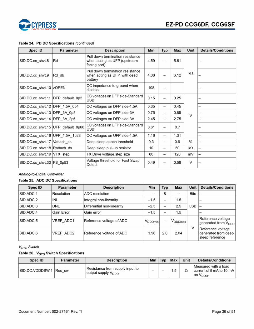
Document Number: 002-27161 Rev. *I Page 36 of 51
EZ-PD CCG6DF, CCG6SF
Analog-to-Digital Converter
VSYS Switch
SID.DC.cc_shvt.8 RdPull down termination resistance when acting as UFP (upstream facing port)
4.59 – 5.61
k
–
SID.DC.cc_shvt.9 Rd_dbPull down termination resistance when acting as UFP, with dead battery
4.08 – 6.12 –
SID.DC.cc_shvt.10 zOPEN CC impedance to ground when disabled
108 – –
SID.DC.cc_shvt.11 DFP_default_0p2 CC voltages on DFP side-Standard USB 0.15 – 0.25
V
–
SID.DC.cc_shvt.12 DFP_1.5A_0p4 CC voltages on DFP side-1.5A 0.35 – 0.45 –
SID.DC.cc_shvt.13 DFP_3A_0p8 CC voltages on DFP side-3A 0.75 – 0.85 –
SID.DC.cc_shvt.14 DFP_3A_2p6 CC voltages on DFP side-3A 2.45 – 2.75 –
SID.DC.cc_shvt.15 UFP_default_0p66CC voltages on UFP side-Standard USB 0.61 – 0.7 –
SID.DC.cc_shvt.16 UFP_1.5A_1p23 CC voltages on UFP side-1.5A 1.16 – 1.31 –
SID.DC.cc_shvt.17 Vattach_ds Deep sleep attach threshold 0.3 – 0.6 % –
SID.DC.cc_shvt.18 Rattach_ds Deep sleep pull-up resistor 10 – 50 k –
SID.DC.cc_shvt.19 VTX_step TX Drive voltage step size 80 – 120 mV –
SID.DC.cc_shvt.30 FS_0p53 Voltage threshold for Fast Swap Detect
0.49 – 0.58 V –
Table 24. PD DC Specifications (continued)
Spec ID Parameter Description Min Typ Max Unit Details/Conditions
Table 25. ADC DC Specifications
Spec ID Parameter Description Min Typ Max Unit Details/Conditions
SID.ADC.1 Resolution ADC resolution – 8 – Bits –
SID.ADC.2 INL Integral non-linearity –1.5 – 1.5
LSB
–
SID.ADC.3 DNL Differential non-linearity –2.5 – 2.5 –
SID.ADC.4 Gain Error Gain error –1.5 – 1.5 –
SID.ADC.5 VREF_ADC1 Reference voltage of ADC VDDDmin – VDDDmax
V
Reference voltage generated from VDDD
SID.ADC.6 VREF_ADC2 Reference voltage of ADC 1.96 2.0 2.04Reference voltage generated from deep sleep reference
Table 26. VSYS Switch Specifications
Spec ID Parameter Description Min Typ Max Unit Details/Conditions
SID.DC.VDDDSW.1 Res_sw Resistance from supply input to output supply VDDD
– – 1.5 Measured with a load current of 5 mA to 10 mA on VDDD.
Document Number: 002-27161 Rev. *I Page 37 of 51
EZ-PD CCG6DF, CCG6SF
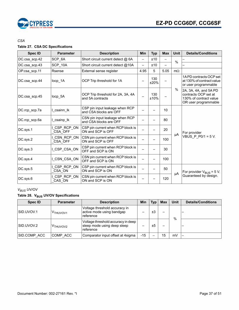
CSA
VBUS UV/OV
Table 27. CSA DC Specifications
Spec ID Parameter Description Min Typ Max Unit Details/Conditions
DC.csa_scp.42 SCP_6A Short circuit current detect @ 6A – ±10 –%
–
DC.csa_scp.43 SCP_10A Short circuit current detect @10A – ±10 – –
OP.csa_scp.11 Rsense External sense register 4.95 5 5.05 m
DC.csa_scp.44 Iocp_1A OCP Trip threshold for 1A – 130±20% –
%
1A PD contracts OCP set at 130% of contract value or user programmable
DC.csa_scp.45 Iocp_5A OCP Trip threshold for 2A, 3A, 4A and 5A contracts –
130±10% –
2A, 3A, 4A, and 5A PD contracts OCP set at 130% of contract value OR user programmable
DC.rcp_scp.7a I_csainn_lk CSP pin input leakage when RCP and CSA blocks are OFF – – 10
µAFor provider VBUS_P_P0/1 = 5 V.
DC.rcp_scp.6a I_csainp_lkCSN pin input leakage when RCP and CSA blocks are OFF – – 80
DC.sys.1 I_CSP_RCP_ON_CSA_OFF
CSP pin current when RCP block is ON and SCP is OFF
– – 20
DC.sys.2 I_CSN_RCP_ON_CSA_OFF
CSN pin current when RCP block is ON and SCP is OFF – – 100
DC.sys.3 I_CSP_CSA_ONCSP pin current when RCP block is OFF and SCP is ON – – 30
DC.sys.4 I_CSN_CSA_ON CSN pin current when RCP block is OFF and SCP is ON
– – 100
DC.sys.5 I_CSP_RCP_ON_CSA_ON
CSP pin current when RCP block is ON and SCP is ON – – 50
µA For provider VBUS = 5 V. Guaranteed by design.
DC.sys.6I_CSP_RCP_ON_CAS_ON
CSN pin current when RCP block is ON and SCP is ON – – 120
Table 28. VBUS UV/OV Specifications
Spec ID Parameter Description Min Typ Max Unit Details/Conditions
SID.UVOV.1 VTHUVOV1
Voltage threshold accuracy in active mode using bandgap reference
– ±3 –
%
–
SID.UVOV.2 VTHUVOV2
Voltage threshold accuracy in deep sleep mode using deep sleep reference
– ±5 – –
SID.COMP_ACC COMP_ACC Comparator input offset at 4sigma -15 – 15 mV –
Document Number: 002-27161 Rev. *I Page 38 of 51
EZ-PD CCG6DF, CCG6SF
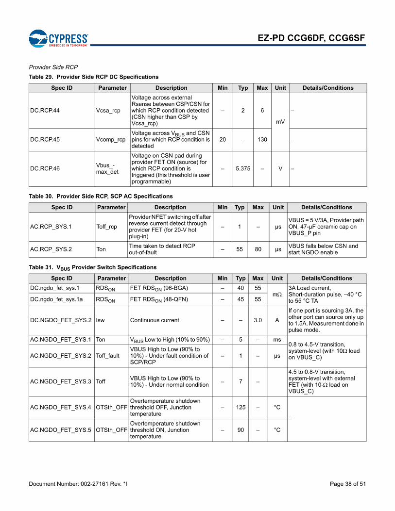
Provider Side RCP
Table 29. Provider Side RCP DC Specifications
Spec ID Parameter Description Min Typ Max Unit Details/Conditions
DC.RCP.44 Vcsa_rcp
Voltage across external Rsense between CSP/CSN for which RCP condition detected (CSN higher than CSP by Vcsa_rcp)
– 2 6
mV
–
DC.RCP.45 Vcomp_rcpVoltage across VBUS and CSN pins for which RCP condition is detected
20 – 130 –
DC.RCP.46Vbus_-max_det
Voltage on CSN pad during provider FET ON (source) for which RCP condition is triggered (this threshold is user programmable)
– 5.375 – V –
Table 30. Provider Side RCP, SCP AC Specifications
Spec ID Parameter Description Min Typ Max Unit Details/Conditions
AC.RCP_SYS.1 Toff_rcp
Provider NFET switching off after reverse current detect through provider FET (for 20-V hot plug-in)
– 1 – µsVBUS = 5 V/3A, Provider path ON, 47-µF ceramic cap on VBUS_P pin
AC.RCP_SYS.2 Ton Time taken to detect RCP out-of-fault – 55 80 µs VBUS falls below CSN and
start NGDO enable
Table 31. VBUS Provider Switch Specifications
Spec ID Parameter Description Min Typ Max Unit Details/Conditions
DC.ngdo_fet_sys.1 RDSON FET RDSON (96-BGA) – 40 55m
3A Load current, Short-duration pulse, –40 °C to 55 °C TADC.ngdo_fet_sys.1a RDSON FET RDSON (48-QFN) – 45 55
DC.NGDO_FET_SYS.2 Isw Continuous current – – 3.0 A
If one port is sourcing 3A, the other port can source only up to 1.5A. Measurement done in pulse mode.
AC.NGDO_FET_SYS.1 Ton VBUS Low to High (10% to 90%) – 5 – ms0.8 to 4.5-V transition, system-level (with 10 load on VBUS_C)AC.NGDO_FET_SYS.2 Toff_fault
VBUS High to Low (90% to 10%) - Under fault condition of SCP/RCP
– 1 – µs
AC.NGDO_FET_SYS.3 ToffVBUS High to Low (90% to 10%) - Under normal condition – 7 –
4.5 to 0.8-V transition, system-level with external FET (with 10-load on VBUS_C)
AC.NGDO_FET_SYS.4 OTSth_OFFOvertemperature shutdown threshold OFF, Junction temperature
– 125 – °C
–
AC.NGDO_FET_SYS.5 OTSth_OFFOvertemperature shutdown threshold ON, Junction temperature
– 90 – °C
Document Number: 002-27161 Rev. *I Page 39 of 51
EZ-PD CCG6DF, CCG6SF
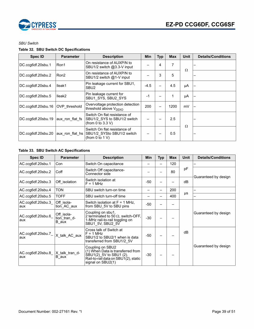
SBU Switch
Table 32. SBU Switch DC Specifications
Spec ID Parameter Description Min Typ Max Unit Details/Conditions
DC.ccg6df.20sbu.1 Ron1On resistance of AUXP/N to SBU1/2 switch @3.3-V input – 4 7
–
DC.ccg6df.20sbu.2 Ron2 On resistance of AUXP/N to SBU1/2 switch @1-V input
– 3 5 –
DC.ccg6df.20sbu.4 Ileak1 Pin leakage current for SBU1, SBU2 -4.5 – 4.5 µA –
DC.ccg6df.20sbu.5 Ileak2Pin leakage current for SBU1_SYS, SBU2_SYS -1 – 1 µA –
DC.ccg6df.20sbu.16 OVP_threshold Overvoltage protection detection threshold above VDDIO
200 – 1200 mV –
DC.ccg6df.20sbu.19 aux_ron_flat_fsSwitch On flat resistance of SBU1/2_SYS to SBU1/2 switch (from 0 to 3.3 V)
– – 2.5
–
DC.ccg6df.20sbu.20 aux_ron_flat_hsSwitch On flat resistance of SBU1/2_SYSto SBU1/2 switch (from 0 to 1 V)
– – 0.5 –
Table 33. SBU Switch AC Specifications
Spec ID Parameter Description Min Typ Max Unit Details/Conditions
AC.ccg6df.20sbu.1 Con Switch On capacitance – – 120pF
–
AC.ccg6df.20sbu.2 Coff Switch Off capacitance- Connector side – – 80
Guaranteed by designAC.ccg6df.20sbu.3 Off_isolation Switch isolation at
F = 1 MHz -50 – – dB
AC.ccg6df.20sbu.4 TON SBU switch turn-on time – – 200µs
–
AC.ccg6df.20sbu.5 TOFF SBU switch turn-off time – – 400 –
AC.ccg6df.20sbu.3_aux
Off_isola-tion_AC_aux
Switch isolation at F = 1 MHz, from SBU_5V to SBU pins -50 – –
dB
Guaranteed by designAC.ccg6df.20sbu.6_aux
Off_isola-tion_tran_d-B_aux
Coupling on sbu1,2 terminated to 50 , switch-OFF,1-MHz rail-to-rail toggling on SBU1_5V, SBU2_5V
-30 – –
AC.ccg6df.20sbu.7_aux X_talk_AC_aux
Cross talk of Switch at F = 1 MHzSBU1/2 to SBU2/1 when is data transferred from SBU1/2_5V
-50 – –
Guaranteed by design
AC.ccg6df.20sbu.8_aux
X_talk_tran_d-B_aux
Coupling on SBU2(1) When Data is transferred from SBU1(2)_5V to SBU1 (2). Rail-to-rail data on SBU1(2), static signal on SBU2(1)
-30 – –
Document Number: 002-27161 Rev. *I Page 40 of 51
EZ-PD CCG6DF, CCG6SF
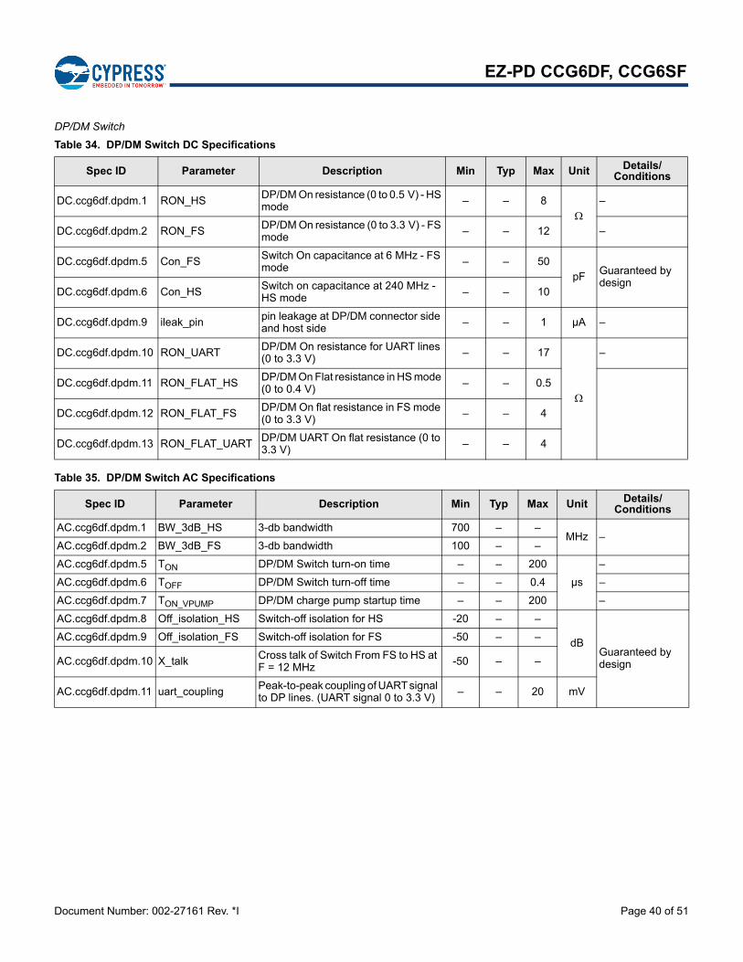
DP/DM Switch
Table 34. DP/DM Switch DC Specifications
Spec ID Parameter Description Min Typ Max Unit Details/Conditions
DC.ccg6df.dpdm.1 RON_HSDP/DM On resistance (0 to 0.5 V) - HS mode – – 8
–
DC.ccg6df.dpdm.2 RON_FS DP/DM On resistance (0 to 3.3 V) - FS mode
– – 12 –
DC.ccg6df.dpdm.5 Con_FS Switch On capacitance at 6 MHz - FS mode – – 50
pF Guaranteed by design
DC.ccg6df.dpdm.6 Con_HSSwitch on capacitance at 240 MHz - HS mode – – 10
DC.ccg6df.dpdm.9 ileak_pin pin leakage at DP/DM connector side and host side
– – 1 µA –
DC.ccg6df.dpdm.10 RON_UART DP/DM On resistance for UART lines (0 to 3.3 V) – – 17
–
DC.ccg6df.dpdm.11 RON_FLAT_HSDP/DM On Flat resistance in HS mode (0 to 0.4 V) – – 0.5
DC.ccg6df.dpdm.12 RON_FLAT_FS DP/DM On flat resistance in FS mode (0 to 3.3 V)
– – 4
DC.ccg6df.dpdm.13 RON_FLAT_UART DP/DM UART On flat resistance (0 to 3.3 V) – – 4
Table 35. DP/DM Switch AC Specifications
Spec ID Parameter Description Min Typ Max Unit Details/Conditions
AC.ccg6df.dpdm.1 BW_3dB_HS 3-db bandwidth 700 – –MHz –
AC.ccg6df.dpdm.2 BW_3dB_FS 3-db bandwidth 100 – –
AC.ccg6df.dpdm.5 TON DP/DM Switch turn-on time – – 200
µs
–
AC.ccg6df.dpdm.6 TOFF DP/DM Switch turn-off time – – 0.4 –
AC.ccg6df.dpdm.7 TON_VPUMP DP/DM charge pump startup time – – 200 –
AC.ccg6df.dpdm.8 Off_isolation_HS Switch-off isolation for HS -20 – –
dBGuaranteed by design
AC.ccg6df.dpdm.9 Off_isolation_FS Switch-off isolation for FS -50 – –
AC.ccg6df.dpdm.10 X_talk Cross talk of Switch From FS to HS at F = 12 MHz
-50 – –
AC.ccg6df.dpdm.11 uart_coupling Peak-to-peak coupling of UART signal to DP lines. (UART signal 0 to 3.3 V) – – 20 mV
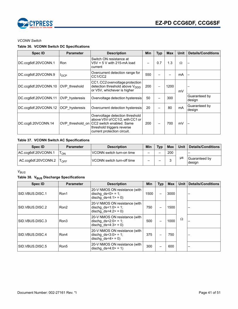
Document Number: 002-27161 Rev. *I Page 41 of 51
EZ-PD CCG6DF, CCG6SF
VCONN Switch
VBUS
Table 36. VCONN Switch DC Specifications
Spec ID Parameter Description Min Typ Max Unit Details/Conditions
DC.ccg6df.20VCONN.1 RonSwitch ON resistance at V5V = 5 V with 215-mA load current
– 0.7 1.3 –
DC.ccg6df.20VCONN.9 IOCPOvercurrent detection range for CC1/CC2 550 – – mA –
DC.ccg6df.20VCONN.10 OVP_thresholdCC1, CC2 overvoltage protection detection threshold above VDDD or V5V, whichever is higher
200 – 1200mV
–
DC.ccg6df.20VCONN.11 OVP_hysteresis Overvoltage detection hysteresis 50 – 300 Guaranteed by design
DC.ccg6df.20VCONN.12 OCP_hysteresis Overcurrent detection hysteresis 20 – 80 mAGuaranteed by design
DC.ccg6.20VCONN.14 OVP_threshold_on
Overvoltage detection threshold above V5V of CC1/2, with CC1 or CC2 switch enabled. Same threshold triggers reverse current protection circuit.
200 – 700 mV –
Table 37. VCONN Switch AC Specifications
Spec ID Parameter Description Min Typ Max Unit Details/Conditions
AC.ccg6df.20VCONN.1 TON VCONN switch turn-on time – – 200µs
–
AC.ccg6df.20VCONN.2 TOFF VCONN switch turn-off time – – 3Guaranteed by design
Table 38. VBUS Discharge Specifications
Spec ID Parameter Description Min Typ Max Unit Details/Conditions
SID.VBUS.DISC.1 Ron120-V NMOS ON resistance (with dischg_ds<0> = 1; dischg_ds<4:1> = 0)
1500 – 3000
–
SID.VBUS.DISC.2 Ron220-V NMOS ON resistance (with dischg_ds<1:0> = 1; dischg_ds<4:2> = 0)
750 – 1500 –
SID.VBUS.DISC.3 Ron320-V NMOS ON resistance (with dischg_ds<2:0> = 1; dischg_ds<4:3> = 0)
500 – 1000 –
SID.VBUS.DISC.4 Ron420-V NMOS ON resistance (with dischg_ds<3:0> = 1; dischg_ds<4> = 0)
375 – 750 –
SID.VBUS.DISC.5 Ron5 20-V NMOS ON resistance (with dischg_ds<4:0> = 1)
300 – 600 –
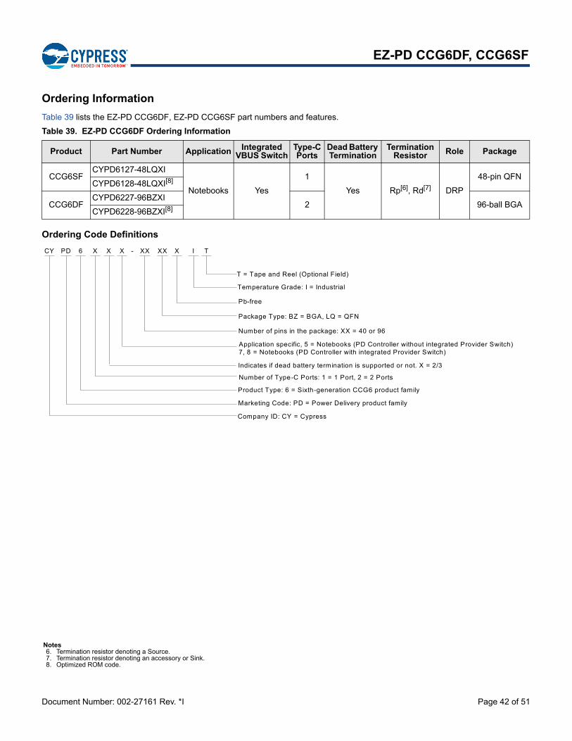
Document Number: 002-27161 Rev. *I Page 42 of 51
EZ-PD CCG6DF, CCG6SF
Ordering Information
Table 39 lists the EZ-PD CCG6DF, EZ-PD CCG6SF part numbers and features.
Ordering Code Definitions
Table 39. EZ-PD CCG6DF Ordering Information
Product Part Number Application Integrated VBUS Switch
Type-C Ports
Dead Battery Termination
Termination Resistor Role Package
CCG6SFCYPD6127-48LQXI
Notebooks Yes
1
Yes Rp[6], Rd[7] DRP
48-pin QFNCYPD6128-48LQXI[8]
CCG6DFCYPD6227-96BZXI
2 96-ball BGACYPD6228-96BZXI[8]
Company ID: CY = Cypress
CY 6
Product Type: 6 = Sixth-generation CCG6 product family
Marketing Code: PD = Power Delivery product family
X X XX XX X I T
Indicates if dead battery termination is supported or not. X = 2/3
Application specific, 5 = Notebooks (PD Controller without integrated Provider Switch)7, 8 = Notebooks (PD Controller with integrated Provider Switch)
Number of pins in the package: XX = 40 or 96
Package Type: BZ = BGA, LQ = QFN
Temperature Grade: I = Industrial
T = Tape and Reel (Optional Field)
PD X -
Number of Type-C Ports: 1 = 1 Port, 2 = 2 Ports
Pb-free
Notes6. Termination resistor denoting a Source.7. Termination resistor denoting an accessory or Sink.8. Optimized ROM code.
Document Number: 002-27161 Rev. *I Page 43 of 51
EZ-PD CCG6DF, CCG6SF
Packaging
Table 40. Package Characteristics
Parameter Description Conditions Min Typ Max Unit
TA Operating ambient temperatureIndustrial –40 25
55°C
TJ Operating junction temperature 125
TJA Package JA (96-ball BGA)–
– – 56.9
°C/WTJC Package JC (96-ball BGA) – – 36.9
TJA Package JA (48-pin QFN)–
– – 40.2
TJC Package JC (48-pin QFN) – – 40.1
Table 41. Solder Reflow Peak Temperature
Package Maximum Peak Temperature Maximum Time within 5 °C of Peak Temperature
96-ball BGA260 °C 30 seconds
48-pin QFN
Table 42. Package Moisture Sensitivity Level (MSL), IPC/JEDEC J-STD-2
Package MSL
96-ball BGAMSL 3
48-pin QFN
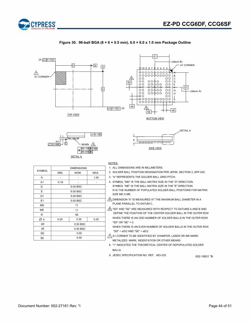
Document Number: 002-27161 Rev. *I Page 44 of 51
EZ-PD CCG6DF, CCG6SF
Figure 30. 96-ball BGA (6 × 6 × 0.5 mm), 6.0 × 6.0 x 1.0 mm Package Outline
N IS THE NUMBER OF POPULATED SOLDER BALL POSITIONS FOR MATRIX
WHEN THERE IS AN EVEN NUMBER OF SOLDER BALLS IN THE OUTER ROW
WHEN THERE IS AN ODD NUMBER OF SOLDER BALLS IN THE OUTER ROW
DEFINE THE POSITION OF THE CENTER SOLDER BALL IN THE OUTER ROW"SD" AND "SE" ARE MEASURED WITH RESPECT TO DATUMS A AND B AND
SYMBOL "ME" IS THE BALL MATRIX SIZE IN THE "E" DIRECTION. SYMBOL "MD" IS THE BALL MATRIX SIZE IN THE "D" DIRECTION.
"e" REPRESENTS THE SOLDER BALL GRID PITCH.
DIMENSION "b" IS MEASURED AT THE MAXIMUM BALL DIAMETER IN A
SOLDER BALL POSITION DESIGNATION PER JEP95, SECTION 3, SPP-020.
"+" INDICATES THE THEORETICAL CENTER OF DEPOPULATED SOLDER
A1 CORNER TO BE IDENTIFIED BY CHAMFER, LASER OR INK MARK
8.
7.
6.
NOTES:
5.
4.
3.
2.1. ALL DIMENSIONS ARE IN MILLIMETERS.
SD
b
eE
eD
ME
N
0.25
0.000.50 BSC
0.50 BSC
0.30
96
11
0.35
DIMENSIONS
D1
MD
E1
E
D
A
A1
SYMBOL
0.16
MIN.
-
5.00 BSC
5.00 BSC
11
6.00 BSC
6.00 BSC
NOM.
- 1.00-
MAX.
SE 0.00
D1
E1
96XØb
A
SD
SE eE
5
6
6
Ø0.15 CMCØ0.05 M
A B
E
D
TOP VIEWBOTTOM VIEW
SIDE VIEW
A1 CORNER7
0.102X C
eD
JEDEC SPECIFICATION NO. REF. : MO-225.9.
B
0.10 2XC
CA1
0.08 C
0.10 C
DETAIL A
(datum A)
(datum B)
DETAIL A
-
A
METALIZED MARK, INDENTATION OR OTHER MEANS.
"SD" = eD/2 AND "SE" = eE/2.
PLANE PARALLEL TO DATUM C.
"SD" OR "SE" = 0.
SIZE MD X ME.
A1 CORNER
BALLS.
A
1234
BCDEFGH
6 5
J
78910
K
11
L
002-10631 *B
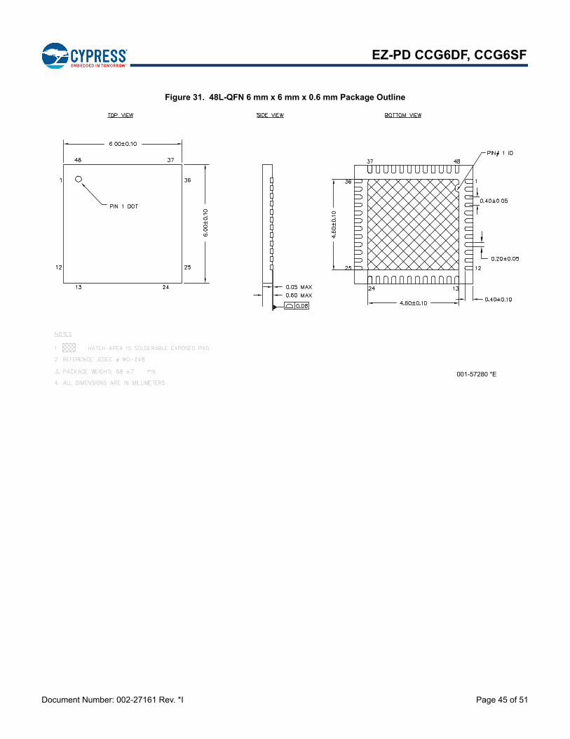
Document Number: 002-27161 Rev. *I Page 45 of 51
EZ-PD CCG6DF, CCG6SF
Figure 31. 48L-QFN 6 mm x 6 mm x 0.6 mm Package Outline
001-57280 *E
Document Number: 002-27161 Rev. *I Page 46 of 51
EZ-PD CCG6DF, CCG6SF
Acronyms
Table 43. Acronyms Used in this Document
Acronym Description
ADC analog-to-digital converter
API application programming interface
Arm® advanced RISC machine, a CPU architecture
CC configuration channel
CSN current sense negative
BCC battery charger controller
BOD Brown out Detect
CC configuration channel
CPU central processing unit
CRC cyclic redundancy check, an error-checking protocol
CS current sense
CSA current sense amplifier
CSN current sense negative
CSP current sense positive
DFP downstream facing port
DM data minus
DP data plus signal
DP DisplayPort, digital display interface developed by Video Electronics Standards Association
DIO digital input/output, GPIO with only digital capabilities, no analog. See GPIO.
DRP dual role power
EC embedded controller
EEPROM electrically erasable programmable read-only memory
EMCA a USB cable that includes an IC that reports cable characteristics (e.g., current rating) to the Type-C ports
EMI electromagnetic interference
ESD electrostatic discharge
FPB flash patch and breakpoint
FRS fast role swap
FS full-speed
GPIO general-purpose input/output
HDI high density interconnect
HSCSA high-side current sense amplifier
IC integrated circuit
IDE integrated development environment
I2C, or IIC Inter-Integrated Circuit, a communications protocol
ILO internal low-speed oscillator, see also IMO
IMO internal main oscillator, see also ILO
I/O input/output, see also GPIO
IPOR imprecise POR
IRQ interrupt request
ISR interrupt service request
LVD low-voltage detect
LVTTL low-voltage transistor-transistor logic
MCU microcontroller unit
MDI medium density
NC no connect
NGDO N-FET gate driver output
NMI nonmaskable interrupt
NVIC nested vectored interrupt controller
opamp operational amplifier
OCP overcurrent protection
OVP overvoltage protection
PCB printed circuit board
PD power delivery
PGA programmable gain amplifier
PHY physical layer
POR power-on reset
PRES precise power-on reset
PSoC® Programmable System-on-Chip™
PWM pulse-width modulator
RAM random-access memory
RCP reverse current protection
RISC reduced-instruction-set computing
RMS root-mean-square
RTC real-time clock
RX receive
SAR successive approximation register
SCB serial communication block
SCL I2C serial clock
SDA I2C serial data
S/H sample and hold
SMT surface-mount technology
SPI Serial Peripheral Interface, a communications protocol
SRAM static random access memory
Table 43. Acronyms Used in this Document (continued)
Acronym Description
Document Number: 002-27161 Rev. *I Page 47 of 51
EZ-PD CCG6DF, CCG6SF
Document Conventions
Units of MeasureSWD serial wire debug, a test protocol
TBT Thunderbolt, hardware interface standard for peripherals developed by Intel
TCPWM timer/counter pulse-width modulation
TRNG true random number generator
TX transmit
Type-C a new standard with a slimmer USB connector and a reversible cable, capable of sourcing up to 100 W of power
UART Universal Asynchronous Transmitter Receiver, a communications protocol
UFP upstream facing port
USB Universal Serial Bus
USBIO USB input/output, CCG6D/CCG6DF pins used to connect to a USB port
USBTCAS USB Type-C Authentication Specification
UVOV under-voltage/over-voltage
WDT watchdog timer
XRES external reset I/O pin
Table 43. Acronyms Used in this Document (continued)
Acronym Description
Table 44. Units of Measure
Symbol Unit of Measure
°C degrees Celsius
Hz hertz
KB 1024 bytes
kHz kilohertz
k kilo ohm
Mbps megabits per second
MHz megahertz
M mega-ohm
Msps megasamples per second
µA microampere
µF microfarad
µs microsecond
µV microvolt
µW microwatt
mA milliampere
m milliohm
ms millisecond
mV millivolt
nA nanoampere
ns nanosecond
ohm
pF picofarad
ppm parts per million
ps picosecond
s second
sps samples per second
V volt
Document Number: 002-27161 Rev. *I Page 48 of 51
EZ-PD CCG6DF, CCG6SF
References and Links to Applications Collateral
Knowledge Base Articles
Key Differences Among EZ-PD™ CCG1, CCG2, CCG3 andCCG5 - KBA210740
Programming EZ-PD™ CCG2, EZ-PD™ CCG3 and EZ-PD™CCG5 Using PSoC® Programmer and MiniProg3 - KBA96477
CCGX Frequently Asked Questions (FAQs) - KBA97244
Cypress EZ-PD™ CCGx Hardware - KBA204102
Difference between USB Type-C and USB-PD - KBA204033
CCGx Programming Methods - KBA97271
Getting started with Cypress USB Type-C Products -KBA04071
Type-C to DisplayPort Cable Electrical Requirements
Dead Battery Charging Implementation in USB Type-CSolutions - KBA97273
Termination Resistors Required for the USB Type-C Connector– KBA97180
VBUS Bypass Capacitor Recommendation for Type-C Cableand Type-C to Legacy Cable/Adapter Assemblies – KBA97270
Need for Regulator and Auxiliary Switch in Type-C toDisplayPort (DP) Cable Solution - KBA97274
Need for a USB Billboard Device in Type-C Solutions –KBA97146
Cypress USB Type-C Controller Supported Solutions –KBA97179
Termination Resistors for Type-C to Legacy Ports – KBA97272
Handling Instructions for CY4502 CCG2 Development Kit –KBA97916
Thunderbolt™ Cable Application Using CCG3 Devices -KBA210976
Power Adapter Application Using CCG3 Devices - KBA210975
Methods to Upgrade Firmware on CCG3 Devices - KBA210974
Device Flash Memory Size and Advantages - KBA210973
Applications of EZ-PD™ CCG5 - KBA210739
Application Notes
AN95615 - Designing USB 3.1 Type-C Cables Using EZ-PD™CCG2
AN95599 - Hardware Design Guidelines for EZ-PD™ CCG2
AN210403 - Hardware Design Guidelines for Dual Role PortApplications Using EZ-PD™ USB Type-C Controllers
AN210771 - Getting Started with EZ-PD™ CCG4
Reference Designs
EZ-PD™ CCG2 Electronically Marked Cable Assembly(EMCA) Paddle Card Reference Design
EZ-PD™ CCG2 USB Type-C to DisplayPort Cable Solution
EZ-PD™ CCG2 USB Type-C to HDMI Adapter Solution
EZ-USB GX3 USB Type-C to Gigabit Ethernet Dongle
EZ-PD™ CCG2 USB Type-C Monitor/Dock Solution
CCG2 20W Power Adapter Reference Design
CCG2 18W Power Adapter Reference Design
EZ-USB GX3 USB Type-A to Gigabit Ethernet ReferenceDesign Kit
Kits
CY4502 EZ-PD™ CCG2 Development Kit
CY4531 EZ-PD CCG3 Evaluation Kit
CY4541 EZ-PD™ CCG4 Evaluation Kit
Datasheets
CYPD1120 Datasheet: USB Power Delivery Alternate ModeController on Type-C
CCG2: USB Type-C Port Controller Datasheet
CCG3: USB Type-C Controller Datasheet
CCG5C: USB Type-C Controller Datasheet
Document Number: 002-27161 Rev. *I Page 49 of 51
EZ-PD CCG6DF, CCG6SF
Document History Page
Document Title: EZ-PD CCG6DF, CCG6SF, USB Type-C Port ControllerDocument Number: 002-27161
Revision ECN Submission Date Description of Change
** 6580063 05/27/2019 Initial release
*A 6649813 08/09/2019 Modified Document Tile for EZ-PD CCG6DF, CCG6SF, USB Type-C Controller.Updated EZ-PD CCG6DF, CCG6SF, USB Type-C Port Controller, Features, Logic Block Diagram, CCG6DF/CCG6SF Functional Diagram and Application Diagrams sections.Updated Table 2, Table 39, Table 40, Table 41, Table 42. Added Table 3.Updated Figure 4, added Figure 4, removed Figure 2 and Figure 3 from previous version.
*B 6673392 09/13/2019 Changed status from “Advance” to “Preliminary”.Updated Logic Block Diagram, Features, CCG6DF/CCG6SF Functional Diagram, and References and Links to Applications Collateral.Added Functional Overview, Power, Application Diagrams, and CCG6SF 48-pin QFN Single Port Thunderbolt Notebook Application Diagram.Updated Table 2, Table 3, Table 39, and Table 42.Updated Figure 4 and Figure 4.Added Electrical Specifications in Table 5 through Table 38.
*C 6682221 09/26/2019 Updated Pinouts (added Figure 5 and Table 3).Updated Ordering Information, and Packaging (added Figure 31).Updated Table 31: Updated typical and max values for DC.ngdo.fet_sys.1 spec. Added new spec DC.ngdo.fet_sys.1a for QFN package.
*D 6732422 11/18/2019 Updated General Description and Features.Updated Figure 5, Figure 6, and Figure 8.Updated Table 3, Table 40, Table 41, and Table 42.Added Figure 3 and Figure 7.Updated Figure 30.
*E 6769410 01/14/2020 Updated Logic Block Diagram.Updated Figure 1, Figure 4, Figure 4, Figure 6, and Figure 8.Updated Table 2, Table 3, Table 6 (SID.PWR#1_A and SID_DS3 parameters), Table 29 (added DC.RCP.46 parameter) and Table 31 (RDSON parameter for 96-BGA).Removed Usage of Via Size of 6-mil drill and 12-mil diameter section.Added Usage of Via Size of 8-mil drill/16-mil Diameter and 10-mil drill/16-mil Diameter section.Updated Copyright information.
*F 6797977 03/13/2020 Updated General Description and Features.Updated Watchdog Timer (WDT) section.Removed Pinout for CYPD6127-96BZXI table.Removed 96-Ball BGA Pin Map (Top View) for CYPD6127-96BZXI and CCG6SF 96-ball BGA Single Port Thunderbolt Notebook Application Diagram figures.Updated Table 40.Updated Acronyms.
*G 6864182 05/28/2020 Removed PRELIMINARY document status.Added CCG6SF Layout Design Guidelines for 48-QFN Package.Deleted CC Connections subsection in CCG6DF Layout Design Guidelines for BGA Package.Added Table 23.Updated Table 5, Table 36, and Table 39.
*H 6897712 07/23/2020 Updated Table 6, Table 8, and Table 23.
Document Number: 002-27161 Rev. *I Page 50 of 51
EZ-PD CCG6DF, CCG6SF
*I 7118146 04/14/2021 Added MPNs CYPD6128-48LQXI and CYPD6228-96BZXI in Ordering Information.Updated Ordering Code Definitions.Updated captions for Table 2, Table 3, Figure 4, and Figure 5.Updated Figure 6 and Figure 7.
Document History Page (continued)
Document Title: EZ-PD CCG6DF, CCG6SF, USB Type-C Port ControllerDocument Number: 002-27161
Revision ECN Submission Date Description of Change
Document Number: 002-27161 Rev. *I Revised April 14, 2021 Page 51 of 51
© Cypress Semiconductor Corporation, 2019-2021. This document is the property of Cypress Semiconductor Corporation, an Infineon Technologies company, and its affiliates ("Cypress"). Thisdocument, including any software or firmware included or referenced in this document ("Software"), is owned by Cypress under the intellectual property laws and treaties of the United States and othercountries worldwide. Cypress reserves all rights under such laws and treaties and does not, except as specifically stated in this paragraph, grant any license under its patents, copyrights, trademarks,or other intellectual property rights. If the Software is not accompanied by a license agreement and you do not otherwise have a written agreement with Cypress governing the use of the Software,then Cypress hereby grants you a personal, non-exclusive, nontransferable license (without the right to sublicense) (1) under its copyright rights in the Software (a) for Software provided in sourcecode form, to modify and reproduce the Software solely for use with Cypress hardware products, only internally within your organization, and (b) to distribute the Software in binary code form externallyto end users (either directly or indirectly through resellers and distributors), solely for use on Cypress hardware product units, and (2) under those claims of Cypress's patents that are infringed by theSoftware (as provided by Cypress, unmodified) to make, use, distribute, and import the Software solely for use with Cypress hardware products. Any other use, reproduction, modification, translation,or compilation of the Software is prohibited.
TO THE EXTENT PERMITTED BY APPLICABLE LAW, CYPRESS MAKES NO WARRANTY OF ANY KIND, EXPRESS OR IMPLIED, WITH REGARD TO THIS DOCUMENT OR ANY SOFTWAREOR ACCOMPANYING HARDWARE, INCLUDING, BUT NOT LIMITED TO, THE IMPLIED WARRANTIES OF MERCHANTABILITY AND FITNESS FOR A PARTICULAR PURPOSE. No computingdevice can be absolutely secure. Therefore, despite security measures implemented in Cypress hardware or software products, Cypress shall have no liability arising out of any security breach, suchas unauthorized access to or use of a Cypress product. CYPRESS DOES NOT REPRESENT, WARRANT, OR GUARANTEE THAT CYPRESS PRODUCTS, OR SYSTEMS CREATED USINGCYPRESS PRODUCTS, WILL BE FREE FROM CORRUPTION, ATTACK, VIRUSES, INTERFERENCE, HACKING, DATA LOSS OR THEFT, OR OTHER SECURITY INTRUSION (collectively, "SecurityBreach"). Cypress disclaims any liability relating to any Security Breach, and you shall and hereby do release Cypress from any claim, damage, or other liability arising from any Security Breach. Inaddition, the products described in these materials may contain design defects or errors known as errata which may cause the product to deviate from published specifications. To the extent permittedby applicable law, Cypress reserves the right to make changes to this document without further notice. Cypress does not assume any liability arising out of the application or use of any product orcircuit described in this document. Any information provided in this document, including any sample design information or programming code, is provided only for reference purposes. It is theresponsibility of the user of this document to properly design, program, and test the functionality and safety of any application made of this information and any resulting product. "High-Risk Device"means any device or system whose failure could cause personal injury, death, or property damage. Examples of High-Risk Devices are weapons, nuclear installations, surgical implants, and othermedical devices. "Critical Component" means any component of a High-Risk Device whose failure to perform can be reasonably expected to cause, directly or indirectly, the failure of the High-RiskDevice, or to affect its safety or effectiveness. Cypress is not liable, in whole or in part, and you shall and hereby do release Cypress from any claim, damage, or other liability arising from any use ofa Cypress product as a Critical Component in a High-Risk Device. You shall indemnify and hold Cypress, including its affiliates, and its directors, officers, employees, agents, distributors, and assignsharmless from and against all claims, costs, damages, and expenses, arising out of any claim, including claims for product liability, personal injury or death, or property damage arising from any useof a Cypress product as a Critical Component in a High-Risk Device. Cypress products are not intended or authorized for use as a Critical Component in any High-Risk Device except to the limitedextent that (i) Cypress's published data sheet for the product explicitly states Cypress has qualified the product for use in a specific High-Risk Device, or (ii) Cypress has given you advance writtenauthorization to use the product as a Critical Component in the specific High-Risk Device and you have signed a separate indemnification agreement.
Cypress, the Cypress logo, and combinations thereof, PSoC, CapSense, EZ-USB, F-RAM, Traveo, WICED, and ModusToolbox are trademarks or registered trademarks of Cypress or a subsidiary ofCypress in the United States or in other countries. For a more complete list of Cypress trademarks, visit cypress.com. Other names and brands may be claimed as property of their respective owners.
EZ-PD CCG6DF, CCG6SF
Notice regarding compliance with Universal Serial Bus specification. Cypress offers firmware and hardware solutions that are certified to comply with the Universal Serial Bus specification, USBType-C™ Cable and Connector Specification, and other specifications of USB Implementers Forum, Inc (USB-IF). You may use Cypress or third party software tools, including sample code, to modifythe firmware for Cypress USB products. Modification of such firmware could cause the firmware/hardware combination to no longer comply with the relevant USB-IF specification. You are solelyresponsible ensuring the compliance of any modifications you make, and you must follow the compliance requirements of USB-IF before using any USB-IF trademarks or logos in connection withany modifications you make. In addition, if Cypress modifies firmware based on your specifications, then you are responsible for ensuring compliance with any desired standard or specifications asif you had made the modification. CYPRESS IS NOT RESPONSIBLE IN THE EVENT THAT YOU MODIFY OR HAVE MODIFIED A CERTIFIED CYPRESS PRODUCT AND SUCH MODIFIEDPRODUCT NO LONGER COMPLIES WITH THE RELEVANT USB-IF SPECIFICATIONS.
Sales, Solutions, and Legal Information
Worldwide Sales and Design Support
Cypress maintains a worldwide network of offices, solution centers, manufacturer’s representatives, and distributors. To find the office closest to you, visit us at Cypress Locations.
Products
Arm® Cortex® Microcontrollers cypress.com/arm
Automotive cypress.com/automotive
Clocks & Buffers cypress.com/clocks
Interface cypress.com/interface
Internet of Things cypress.com/iot
Memory cypress.com/memory
Microcontrollers cypress.com/mcu
PSoC cypress.com/psoc
Power Management ICs cypress.com/pmic
Touch Sensing cypress.com/touch
USB Controllers cypress.com/usb
Wireless Connectivity cypress.com/wireless
PSoC® Solutions
PSoC 1 | PSoC 3 | PSoC 4 | PSoC 5LP | PSoC 6 MCU
Cypress Developer Community
Community | Code Examples | Projects | Video | Blogs | Training | Components
Technical Support
cypress.com/support


