Embed Size (px)
Citation preview
F
MSa
b
c
d
D
a
ARRAA
KNPNYS
1
rgistcsltiaaali
2
0d
Materials Science and Engineering A 528 (2011) 5822–5832
Contents lists available at ScienceDirect
Materials Science and Engineering A
journa l homepage: www.e lsev ier .com/ locate /msea
abrication, microstructure, and mechanical properties of tin nanostructures
ichael J. Bureka,1, Arief Suriadi Budimanb, Zeinab Jaheda, Nobumichi Tamurac, Martin Kunzc,umin Jina, Seung Min J. Hand, Gyuhyon Leea, Colin Zamecnika, Ting Y. Tsuia,∗
Waterloo Institute for Nanotechnology, University of Waterloo, 200 University Ave. W., Waterloo, ON N2L 3G1, CanadaCenter for Integrated Nanotechnologies, Los Alamos National Laboratory, Los Alamos, NM 87545, USAAdvanced Light Source, Lawrence Berkeley National Laboratory, 1 Cyclotron Road, Berkeley, CA 94720, USAGraduate School of Energy Environment Water Sustainability, Korea Advanced Institute of Science and Technology, 373-1 Guseong Dong, Yuseong Gu,aejeon 305-701, Republic of Korea
r t i c l e i n f o
rticle history:eceived 15 February 2011eceived in revised form 23 March 2011ccepted 7 April 2011vailable online 14 April 2011
eywords:anoindentation
a b s t r a c t
Vertically aligned, cylindrical tin nanopillars have been fabricated via an electron beam lithographyand electroplating method. Characterization by a non-destructive synchrotron X-ray microdiffraction(�SXRD) technique revealed that the tin nanostructures are body-centered tetragonal and are likelysingle-crystalline, or consist of a few large grains. The mechanical properties of tin nanopillars with aver-age diameters of 920 nm, 560 nm, and 350 nm were studied by uniaxial compression in a nanoindenteroutfitted with a flat punch diamond tip. The results of compression tests reveal strain rate sensitivityfor nanoscale tin deformation, which matches closely to the previously reported bulk tin values. How-
lastic deformationanostructureield phenomenonize effects
ever, unlike bulk, tin nanopillars exhibit size-dependent flow stresses where smaller diameter specimensexhibit greater attained strengths. The observed size-dependence matches closely to that previouslyreported for single-crystalline face centered cubic metals at the nanoscale. �SXRD data was used tocompare the dislocation density between as-fabricated and deformed tin nanopillars. Results of this com-parison suggest that there is no measurable accumulation of dislocations within deformed tin nanopillars.
. Introduction
With the advancement of small-scale fabrication techniques inecent years, applications of nanometer sized tin structures haveained considerable interest. In the microelectronics industry, tins a promising replacement of lead in elemental metal and alloyolders for chip packaging. This is in part due to their low meltingemperature, ductility, excellent wetting properties, high electricalonductivity, and electrical reliability [1–3]. Since tin and tin-alloytructures used in microelectronic solder technology are part of theoad bearing components, their mechanical properties approachinghe nanometer scale are critically important for product reliabil-ty and lifetime. Another interesting application of tin is in therea of lithium ion battery anodes, where nanostructured tin-basednodes are being studied in order to improve charge storage and
node lifetime [4]. In order to attain the desired functionality andifetime of these small-scale components, a thorough understand-ng of nanoscale tin deformation mechanisms are required.∗ Corresponding author. Tel.: +1 519 888 4567x38404; fax: +1 519 746 4979.E-mail address: [email protected] (T.Y. Tsui).
1 New address: School of Engineering and Applied Sciences, Harvard University,9 Oxford St., Cambridge, MA 02138, USA.
921-5093/$ – see front matter © 2011 Elsevier B.V. All rights reserved.oi:10.1016/j.msea.2011.04.019
© 2011 Elsevier B.V. All rights reserved.
This work has two main goals. Initially, we develop fabricationprocesses and integration methods for cylindrical tin nanopil-lars. Secondly, the time dependent mechanical behaviors of thesetin nanopillars are characterized by uniaxial compressive load-ing. The results presented here will help to understand how tinnanostructures behave during mechanical deformation. In addi-tion, the new knowledge gained from this work will also expandthe current understanding in small-scale mechanical propertiesto the deformation mechanisms governing low melting temper-ature nanostructures. The melting temperature of tin is ∼232 ◦C,corresponding to a homologous temperature of approximately 0.6in ambient conditions. At room temperature, tin exists as its �-allotrope, also known as white tin. It has a body centered tetragonal(BCT) crystal structure with c/a = 0.5456 [5]. Of the three stable tinallotropes, only white tin is of interest in chip packaging and elec-tronic applications due to its metallic nature. According to Yangand Li, there are twelve possible slip systems in the BCT tin crys-tal, with at least six readily observed in the bulk scale deformationof tin [5]. Three of the most commonly observed BCT tin slip sys-tems near room temperatures are: (a) (1 1 0)[1̄ 1 1], (b) (1 1 0)[0 0 1],
(c) (1 0 0)[0 1 0] [6]. The dimension of the Burgers vectors areb[1 1 1] = 0.4411 nm, b[0 0 1] = 0.3157 nm, b[1 0 0] = 0.5819 nm, andb[1 0 1] = 0.6629 nm [5]. The shear modulus of tin is 17.93 GPa atroom temperature [5]. Like many other metals, bulk �-tin exhibits
nd En
smbi[M[mr
ε
we(∼tsWcvcLe[tceHspmrmet
wnotlensrsPttddssan
otoaoesmti
Corp.), then baked at 180 C for approximately 15 min. An arrayholes with various diameters was patterned in the PMMA resist byexposure using a Leica EBPG 5000+ electron beam lithography sys-tem operating with an acceleration voltage of 100 kV. The patterned
M.J. Burek et al. / Materials Science a
train rate sensitivity where the flow stress varies with the defor-ation rate. Strain rate and other time dependent mechanical
ehaviors, i.e. creep deformation, of bulk-scale tin have been stud-ed in detail by Sherby [7], Frenkel et al. [8], Weertman and Breen9], Breen and Weertman [10], Yang and Li [5], Chu and Li [6],
ohamed et al. [11], Raman and Berriche [12], and Mayo and Nix13]. They observed that the relationship between the creep defor-
ation rate (ε̇) and the stress (�) can be described by a simpleelationship:
˙ = K�n (1)
here K is a constant depends on material parameters, such as, thelastic modulus and the diffusivity of the metal. The stress exponentn) for tin reported in the literature has a wide range of values, from3.6 to ∼11. These variations depend on several factors, including
esting temperature, microstructure, crystalline orientation, grainize, stress level applied, and measurement technique. Breen and
eertman [10] measured the steady state creep properties of poly-rystalline tin at 21.1 ◦C and their results indicate a stress exponentalue of ∼4.6. Creep deformation behaviors of bulk tin single-rystals near the ambient conditions were characterized by Chu andi [6] with impression creep techniques. They reported the stressxponent values with the ingot orientations of [0 0 1], [1 0 0], and1 1 0] are 4.4 (40 ◦C), 4.5 (50 ◦C), and 5.0 (60 ◦C), respectively. Theemperature values shown correspond to the isothermal testingonditions. With the reports discussed above, the mechanical prop-rties of bulk tin structures are well characterized and documented.owever, to the best of our knowledge no investigations on the
mall-scale deformation behaviors of tin nanostructures have beenerformed. Nanoscale mechanical properties of a wide variety ofetals (e.g. Au, Ni, Cu, and Mo) have been the focus of numerous
esearch activities [14–40]. Nearly all of these studies reveal thatetals, when reduced to the nanoscale, exhibit remarkably differ-
nt mechanical behaviors compared to that in bulk [41]. However,his effect had not been properly studied in tin nanostructures.
It is important to distinguish the current study with the previousork by Raman and Berriche [12] or Mayo and Nix [13] who usedanoindentation to characterize the creep deformation behaviorf tin. One of the most important distinctions is the nanoinden-er tip geometry. These authors used sharp pyramid tips whichocally concentrate stress at the apex of the contact and along thedges of the pyramid. Therefore, mechanical strains introduced areot uniformly distributed within the contact area. In the currenttudy, a flat diamond punch is used and the nanoscale stress–strainesponse is homogeneously distributed throughout the nanopillarpecimen. Another important difference is the sample geometry.ervious authors used bulk samples with the configuration of elas-ic half-spaces. The stress field generated on these samples duringhe indentation is extremely complex and consequently, it is veryifficult to eliminate all artifacts. In the current work, the cylin-rical tin nanopillars produced are geometrically similar to thepecimen configurations used in conventional uniaxial compres-ion tests. The stress–strain response generated in our tests withflat diamond punch is expected to be uniform throughout the
anoscale column.Herein, we report an integration method to fabricate arrays
f isolated, vertically aligned tin nanopillars by using the elec-ron beam lithography and electroplating technique [42]. Arraysf tin nanopillars ranging from ∼70 to 920 nm in diameter withspect ratios (height/diameter) of ∼2–4 and separation distancef 10 �m were successfully manufactured. The microstructure oflectroplated tin nanopillars was investigated by a non-destructive
ynchrotron X-ray micro-diffraction (�SXRD) technique. Thisethod uses a micron-focused polychromatic (white) X-ray beamo obtain Laue diffraction patterns of the tin nanostructures whichn turn can be used to determine the grain orientations, local
gineering A 528 (2011) 5822–5832 5823
residual stresses and strains, and dislocation densities of the tinnanopillars.
The mechanical properties of tin nanopillars with average diam-eters of 350 nm, 560 nm, and 920 nm were characterized by usinga uniaxial microcompression technique. The results show thatsize-dependent flow stresses are observed for both deformationmodes and show a power-law relationship similar to that previ-ously reported for other single-crystalline metallic nanopillars [41].The flow stress data also revealed that the strain rate sensitivity intin nanostructures is very similar to the bulk tin creep deforma-tion results reported by Chu and Li [6]. Mechanically compressedtin nanopillars were inspected carefully by scanning electronmicroscopy (SEM). The post-deformation SEM analysis revealedevidence of bulging, extrusion, and fine wrinkling in additional tocrystallographic shear off-sets. Analysis of tin nanopillars followingcompressive loading by �SXRD yielded a qualitative comparison ofdislocation density change. The results show no discernable changein the dislocation density within the tin nanopillar microstructurefollowing deformation to over 20% engineering strain.
2. Experimental methods
2.1. Electron beam lithography process
Fig. 1 shows the integration scheme used to produce tin nanopil-lars. The fabrication method involves lithographic patterning ofpolymethylmethacrylate (PMMA) resist with electron beam lithog-raphy, followed by tin electroplating into the prescribed resisttemplate. Preparation of the substrate began with Si (001) wafers,which were coated with a 20 nm-thick titanium adhesion layerand a 100 nm-thick gold layer deposited by electron beam evap-oration. The metalized substrates were spin coated with variousconcentrations of 950 kD PMMA dissolved in anisole (MicroChem
◦
Fig. 1. Schematic drawings of electron beam lithography and electroplating fabri-cation process for tin nanopillars developed in this work.
5 and Engineering A 528 (2011) 5822–5832
PtI7dp
2
dsftwaia9Tiacgtgt
5aha7a
F
824 M.J. Burek et al. / Materials Science
MMA layer was developed in 1:3 solution of methylisobutylke-one and isopropyl alcohol (IPA) for ∼60 s followed by 5 s rinse withPA. The resulting feature size after PMMA development was holes0–920 nm in diameter. Before electroplating, the silicon wafer wasiced into square 1 cm2 chips with the patterned PMMA resist tem-late in the chip center.
.2. Tin nanopillar electroplating
Tin electroplating was performed under alternating current con-itions using a parallel two-electrode configuration. The tin platingolution was made in-house and consisted of 22 g/L tin(II) sul-ate (95.5%, Alfa Aesar) and 75 g/L sulfuric acid. About 200 mL ofhe prepared solution was used for electroplating. The solutionas prepared fresh for each sample and mechanically stirred for
pproximately 30 min prior to deposition to ensure its homogene-ty. The gold/titanium seed layer underneath the resist templatected as the cathode, and a high purity tin rod (6 mm diameter,9.9985%, Puratronic® from Alfa Aesar) was used as a soluble anode.he plating bath was maintained at room temperature and mechan-cally stirred throughout the deposition process. A Teflon backingnd custom gold coated brass clips were used to mount the PMMAoated substrates in the solution and electrically interface with theold/titanium cathode layer. The total cathode area, which includedhe patterned PMMA coated substrate, a blank 1 cm2 chip, and theold clips, was maintained at ∼3.5 cm2, and the distance betweenhe anode and the cathode was kept at approximately 25 mm.
Tin electroplating was initiated with a short current pulse at0 mA/cm2 for 5 s. This step was necessary to promote metal nucle-tion in all pores and to increase the final nanopillar yield and
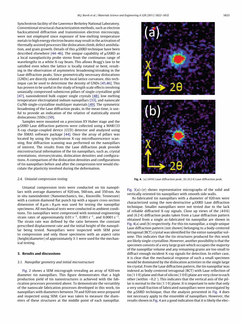
omogeneity. Subsequently, electroplating was conducted usingn alternating current technique with 0.5 s of cathodic current at.5 mA/cm2 followed by 0.1 s of anodic current at 5 mA/cm2. Thelternating current technique was used to promote homogeneousig. 3. SEM images of tin nanopillars intended fabricated with diameters of (a) 920 nm (b
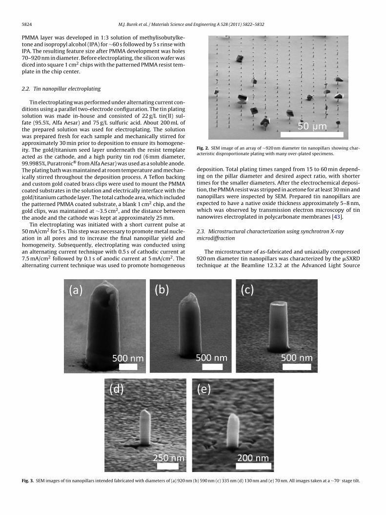
Fig. 2. SEM image of an array of ∼920 nm diameter tin nanopillars showing char-acteristic disproportionate plating with many over-plated specimens.
deposition. Total plating times ranged from 15 to 60 min depend-ing on the pillar diameter and desired aspect ratio, with shortertimes for the smaller diameters. After the electrochemical deposi-tion, the PMMA resist was stripped in acetone for at least 30 min andnanopillars were inspected by SEM. Prepared tin nanopillars areexpected to have a native oxide thickness approximately 5–8 nm,which was observed by transmission electron microscopy of tinnanowires electroplated in polycarbonate membranes [43].
2.3. Microstructural characterization using synchrotron X-raymicrodiffraction
The microstructure of as-fabricated and uniaxially compressed920 nm diameter tin nanopillars was characterized by the �SXRDtechnique at the Beamline 12.3.2 at the Advanced Light Source
) 590 nm (c) 335 nm (d) 130 nm and (e) 70 nm. All images taken at a ∼70◦ stage tilt.
nd Engineering A 528 (2011) 5822–5832 5825
SCbwmttdawsiL(nhu[tCbfd
�Xtlnomotoc
2
liwdstsTplt(i
3
3
dpronae
M.J. Burek et al. / Materials Science a
ynchrotron facility of the Lawrence Berkeley National Laboratory.onventional structural characterization methods, such as electronackscattered diffraction and transmission electron microscopy,ere not employed since exposure of low-melting temperatureetals to high energy electron beams may result in the activation of
hermally assisted processes like dislocation climb, defect annihila-ion, and grain growth. Details of this �SXRD technique have beenescribed elsewhere [44–46]. The unique capability of �SXRD aslocal nanoplasticity probe stems from the continuous range ofavelengths in a white X-ray beam. This allows Bragg’s law to be
atisfied even when the lattice is locally rotated or bent, result-ng in the observation of asymmetric broadening/streaking in theaue diffraction peaks. Since geometrically necessary dislocationsGNDs) are directly related to the local lattice curvature, this tech-ique can be used to determine the density of GNDs [45,46]. Thisas proven to be useful in the study of length scale effects involvingniaxially compressed submicron pillars of single-crystalline gold47], nanoindented bulk copper single crystals [48], low meltingemperature electroplated indium nanopillars [33], and nanoscaleu/Nb single-crystalline multilayer materials [49]. The symmetricroadening of the Laue diffraction peaks, in the mean time, is use-ul to provide an indication of the relative of statistically storedislocations (SSDs) [50].
Samples were mounted on a precision XY Huber stage and theSXRD Laue diffraction patterns were collected using a MAR133-ray charge-coupled device (CCD) detector and analyzed using
he XMAS software package [44]. Once the array of pillars wasocated by using the synchrotron X-ray microfluorescence scan-ing, fine diffraction scanning was performed on the nanopillarsf interest. The results from the Laue diffraction peak provideicrostructural information of the tin nanopillars, such as, crystal
rientations, stresses/strains, dislocation densities and configura-ions. A comparison of the dislocation densities and configurationsf tin nanopillars before and after the compression test would elu-idate the plasticity involved during the deformation.
.4. Uniaxial compression testing
Uniaxial compression tests were conducted on tin nanopil-ars with average diameters of 920 nm, 560 nm, and 350 nm. Ann situ nanoindenter (Nanomechanics, Inc., Knoxville, Tennessee)
ith a custom diamond flat punch tip with a square cross-sectionimension of 8 �m × 8 �m was used for testing the nanopillarpecimens. All mechanical tests were conducted in ambient condi-ions. Tin nanopillars were compressed with nominal engineeringtrain rates of approximately 0.01 s−1, 0.001 s−1, and 0.0001 s−1.he strain rate was defined by the ratio between the constantrescribed displacement rate and the initial height of the nanopil-
ar being tested. Nanopillars were inspected with SEM prioro compression and only those specimens with an aspect ratioheight/diameter) of approximately 3:1 were used for the mechan-cal testing.
. Results and discussions
.1. Nanopillar geometry and initial microstructure
Fig. 2 shows a SEM micrograph revealing an array of 920 nmiameter tin nanopillars. This figure demonstrates that a highroduction yield of tin nanostructures is achieved with the fab-ication processes presented above. To demonstrate the versatility
f the nanoscale fabrication processes developed in this work, tinanopillars with diameters between 70 and 920 nm were preparednd inspected using SEM. Care was taken to measure the diam-ters of these structures at the middle point of each nanopillar.Fig. 4. (a) (4 0 6) Laue diffraction peak; (b) (6 2 4) Laue diffraction peak.
Fig. 3(a)–(e) shows representative micrographs of the solid andvertically oriented tin nanopillars with smooth side walls.
As-fabricated tin nanopillars with a diameter of 920 nm werecharacterized using the non-destructive �SXRD Laue diffractiontechnique. Smaller nanopillars were not tested due to the lackof reliable diffracted X-ray signals. Close up views of the (4 0 6)and (6 2 4) diffraction peaks taken from a Laue diffraction patternobtained from a single as-fabricated tin nanopillar are shown inFig. 4(a) and (b) respectively. For this tin nanopillar, a single uniqueLaue diffraction pattern (not shown) belonging to a body-centeredtetragonal (BCT) crystal was identified for the entire nanopillar vol-ume. This indicates that the tin structures produced for this workare likely single-crystalline. However, another possibility is that thespecimen consists of a very large grain which occupies the majorityof the nanopillar volume and any remaining grains are too small todiffract enough incident X-ray signals for detection. In either case,it is clear that the mechanical response of such a small specimenwould be dominated by the dislocation activities in the single largetin crystal. From the Laue diffraction pattern, the tin nanopillar wasindexed as body-centered tetragonal (BCT) with Laue reflection oftin (1 1 0) plane and that of silicon (1 0 0) plane are very close to eachother (within ∼0.2◦). This indicates that the vertical axis of the pil-lar is normal to the tin (1 1 0) plane. It is important to note that only
a very small fraction of fabricated nanopillars were investigated bythe �SXRD technique, thus the analysis presented in Fig. 4 doesnot necessary apply to the ensemble of nanopillars. However, theresults shown in Fig. 4 are a good indication that it is likely the elec-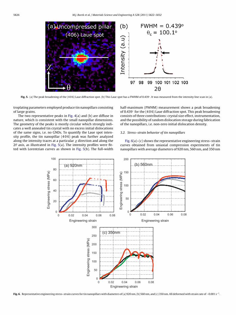
5826 M.J. Burek et al. / Materials Science and Engineering A 528 (2011) 5822–5832
ue spo
to
nTcosa2t
F
Fig. 5. (a) The peak broadening of the (4 0 6) Laue diffraction spot. (b) This La
roplating parameters employed produce tin nanopillars consistingf large grains.
The two representative peaks in Fig. 4(a) and (b) are diffuse inature, which is consistent with the small nanopillar dimensions.he geometry of the peaks is mostly circular which strongly indi-ates a well annealed tin crystal with no excess initial dislocationsf the same signs, i.e. no GNDs. To quantify the Laue spot inten-
ity profile, the tin nanopillar (4 0 6) peak was further analyzedlong the intensity traces at a particular � direction and along the� axis, as illustrated in Fig. 5(a). The intensity profiles were fit-ed with Lorentzian curves as shown in Fig. 5(b). The full-width0
50
100
150
200
250
300
0 0.02
Eng
inee
ring
stre
ss (M
Pa)
Engine
0
20
40
60
80
100
0 0.02 0.04 0.06 0.08
Eng
inee
ring
stre
ss (M
Pa)
Engineering strain
(c) 350nm
(a) 920nm
ig. 6. Representative engineering stress–strain curves for tin nanopillars with diameters o
t has a FWHM of 0.439◦ . It was measured from the intensity line scan in (a).
half-maximum (FWHM) measurement shows a peak broadeningof 0.439◦ for the (4 0 6) Laue diffraction spot. This peak broadeningconsists of three contributions: crystal size effect, instrumentation,and the possibility of random dislocation storage during fabricationof the nanopillars, i.e. non-zero initial dislocation density.
3.2. Stress–strain behavior of tin nanopillars
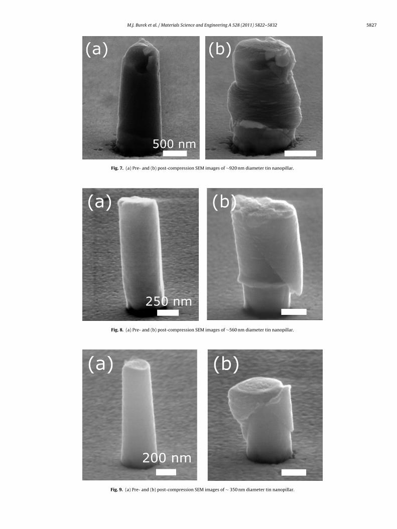
Fig. 6(a)–(c) shows the representative engineering stress–straincurves obtained from uniaxial compression experiments of tinnanopillars with average diameters of 920 nm, 560 nm, and 350 nm
0.04 0.06 0.08ering strain
0
50
100
150
200
0 0.02 0.04 0.06 0.08
Engi
neer
ing
stre
ss (M
Pa)
Engineering strain
(b) 560nm
f (a) 920 nm, (b) 560 nm, and (c) 350 nm. All deformed with strain rate of ∼0.001 s−1.
M.J. Burek et al. / Materials Science and Engineering A 528 (2011) 5822–5832 5827
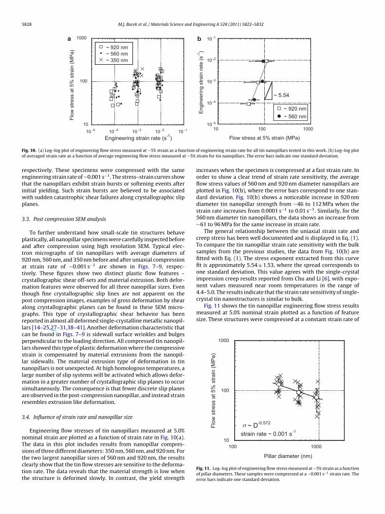
Fig. 7. (a) Pre- and (b) post-compression SEM images of ∼920 nm diameter tin nanopillar.
Fig. 8. (a) Pre- and (b) post-compression SEM images of ∼560 nm diameter tin nanopillar.
Fig. 9. (a) Pre- and (b) post-compression SEM images of ∼ 350 nm diameter tin nanopillar.
5828 M.J. Burek et al. / Materials Science and Engineering A 528 (2011) 5822–5832
10
100
1000
10 -5 10 -4 10 -3 10 -2 10 -1
~ 920 nm~ 560 nm~ 350 nm
Flow
stre
ss a
t 5%
stra
in (M
Pa)
Engineering strain rate (s
a b
-1)
10 -5
10 -4
10 -3
10 -2
10 -1
10 100 1000
~ 920 nm~ 560 nm
Engi
neer
ing
stra
in ra
te (s
-1)
Flow stress at 5% strain (MPa)
~ 5.54
F ction oo ∼5%
retiwp
3
pat9atcmtpagrlcplslnlmsar
3
nTstctt
Fig. 11 shows the tin nanopillar engineering flow stress resultsmeasured at 5.0% nominal strain plotted as a function of featuresize. These structures were compressed at a constant strain rate of
10
100
1000
100 1000
Flow
stre
ss a
t 5%
stra
in (M
Pa)
strain rate ~ 0.001 sσ
-1 ~ D-0.572
ig. 10. (a) Log–log plot of engineering flow stress measured at ∼5% strain as a funf averaged strain rate as a function of average engineering flow stress measured at
espectively. These specimens were compressed with the samengineering strain rate of ∼0.001 s−1. The stress–strain curves showhat the nanopillars exhibit strain bursts or softening events afternitial yielding. Such strain bursts are believed to be associated
ith sudden catastrophic shear failures along crystallographic sliplanes.
.3. Post compression SEM analysis
To further understand how small-scale tin structures behavelastically, all nanopillar specimens were carefully inspected beforend after compression using high resolution SEM. Typical elec-ron micrographs of tin nanopillars with average diameters of20 nm, 560 nm, and 350 nm before and after uniaxial compressiont strain rate of ∼0.001 s−1 are shown in Figs. 7–9, respec-ively. These figures show two distinct plastic flow features –rystallographic shear off-sets and material extrusion. Both defor-ation features were observed for all three nanopillar sizes. Even
hough fine crystallographic slip lines are not apparent on theost compression images, examples of gross deformation by shearlong crystallographic planes can be found in these SEM micro-raphs. This type of crystallographic shear behavior has beeneported in almost all deformed single-crystalline metallic nanopil-ars [14–25,27–31,38–41]. Another deformation characteristic thatan be found in Figs. 7–9 is sidewall surface wrinkles and bulgeserpendicular to the loading direction. All compressed tin nanopil-
ars showed this type of plastic deformation where the compressivetrain is compensated by material extrusions from the nanopil-ar sidewalls. The material extrusion type of deformation in tinanopillars is not unexpected. At high homologous temperatures, a
arge number of slip systems will be activated which allows defor-ation in a greater number of crystallographic slip planes to occur
imultaneously. The consequence is that fewer discrete slip planesre observed in the post-compression nanopillar, and instead strainesembles extrusion like deformation.
.4. Influence of strain rate and nanopillar size
Engineering flow stresses of tin nanopillars measured at 5.0%ominal strain are plotted as a function of strain rate in Fig. 10(a).he data in this plot includes results from nanopillar compres-ions of three different diameters: 350 nm, 560 nm, and 920 nm. For
he two largest nanopillar sizes of 560 nm and 920 nm, the resultslearly show that the tin flow stresses are sensitive to the deforma-ion rate. The data reveals that the material strength is low whenhe structure is deformed slowly. In contrast, the yield strengthf engineering strain rate for all tin nanopillars tested in this work. (b) Log–log plotstrain for tin nanopillars. The error bars indicate one standard deviation.
increases when the specimen is compressed at a fast strain rate. Inorder to show a clear trend of strain rate sensitivity, the averageflow stress values of 560 nm and 920 nm diameter nanopillars areplotted in Fig. 10(b), where the error bars correspond to one stan-dard deviation. Fig. 10(b) shows a noticeable increase in 920 nmdiameter tin nanopillar strength from ∼46 to 112 MPa when thestrain rate increases from 0.0001 s−1 to 0.01 s−1. Similarly, for the560 nm diameter tin nanopillars, the data shows an increase from∼61 to 96 MPa for the same increase in strain rate.
The general relationship between the uniaxial strain rate andcreep stress has been well documented and is displayed in Eq. (1).To compare the tin nanopillar strain rate sensitivity with the bulksamples from the previous studies, the data from Fig. 10(b) arefitted with Eq. (1). The stress exponent extracted from this curvefit is approximately 5.54 ± 1.53, where the spread corresponds toone standard deviation. This value agrees with the single-crystalimpression creep results reported from Chu and Li [6], with expo-nent values measured near room temperatures in the range of4.4–5.0. The results indicate that the strain rate sensitivity of single-crystal tin nanostructures is similar to bulk.
Pillar diameter (nm)
Fig. 11. Log–log plot of engineering flow stress measured at ∼5% strain as a functionof pillar diameters. These samples were compressed at a ∼0.001 s−1 strain rate. Theerror bars indicate one standard deviation.
M.J. Burek et al. / Materials Science and Engineering A 528 (2011) 5822–5832 5829
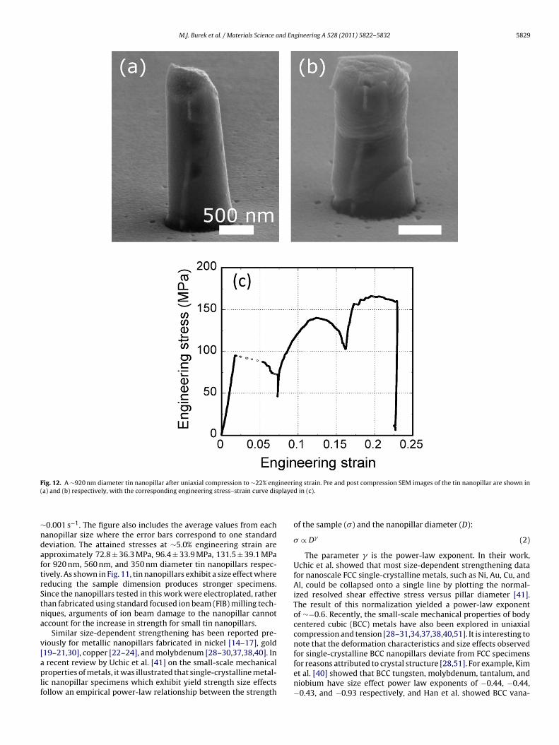
Fig. 12. A ∼920 nm diameter tin nanopillar after uniaxial compression to ∼22% engineering strain. Pre and post compression SEM images of the tin nanopillar are shown in( playe
∼ndaftrStna
v[aplf
a) and (b) respectively, with the corresponding engineering stress–strain curve dis
0.001 s−1. The figure also includes the average values from eachanopillar size where the error bars correspond to one standardeviation. The attained stresses at ∼5.0% engineering strain arepproximately 72.8 ± 36.3 MPa, 96.4 ± 33.9 MPa, 131.5 ± 39.1 MPaor 920 nm, 560 nm, and 350 nm diameter tin nanopillars respec-ively. As shown in Fig. 11, tin nanopillars exhibit a size effect whereeducing the sample dimension produces stronger specimens.ince the nanopillars tested in this work were electroplated, ratherhan fabricated using standard focused ion beam (FIB) milling tech-iques, arguments of ion beam damage to the nanopillar cannotccount for the increase in strength for small tin nanopillars.
Similar size-dependent strengthening has been reported pre-iously for metallic nanopillars fabricated in nickel [14–17], gold19–21,30], copper [22–24], and molybdenum [28–30,37,38,40]. In
recent review by Uchic et al. [41] on the small-scale mechanicalroperties of metals, it was illustrated that single-crystalline metal-ic nanopillar specimens which exhibit yield strength size effectsollow an empirical power-law relationship between the strength
d in (c).
of the sample (�) and the nanopillar diameter (D):
� ∝ D� (2)
The parameter � is the power-law exponent. In their work,Uchic et al. showed that most size-dependent strengthening datafor nanoscale FCC single-crystalline metals, such as Ni, Au, Cu, andAl, could be collapsed onto a single line by plotting the normal-ized resolved shear effective stress versus pillar diameter [41].The result of this normalization yielded a power-law exponentof ∼−0.6. Recently, the small-scale mechanical properties of bodycentered cubic (BCC) metals have also been explored in uniaxialcompression and tension [28–31,34,37,38,40,51]. It is interesting tonote that the deformation characteristics and size effects observedfor single-crystalline BCC nanopillars deviate from FCC specimens
for reasons attributed to crystal structure [28,51]. For example, Kimet al. [40] showed that BCC tungsten, molybdenum, tantalum, andniobium have size effect power law exponents of −0.44, −0.44,−0.43, and −0.93 respectively, and Han et al. showed BCC vana-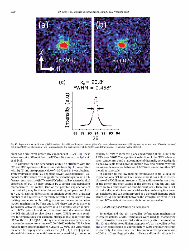
5830 M.J. Burek et al. / Materials Science and Engineering A 528 (2011) 5822–5832
F opilla( 0 4) La
dve
Fwabfpmtanmm1lttCtrfa
ig. 13. Representative qualitative �SXRD analysis of a ∼920 nm diameter tin nan2 0 4) and (1 0 5) are shown in (a) and (b) respectively. The peak intensity of the (2
ium has a size effect power-law exponents of −0.79 [34]. Thesealues are quite different from the FCC results summarized by Uchict al. [41].
To compare the size dependence of BCT tin structure with theCC and BCC specimens, flow stress data from Fig. 11 were fittedith Eq. (2) and an exponent value of −0.572 ± 0.114 was obtained,value very close to the FCC size effect power-law exponent of −0.6,ut not the BCC values. This suggests that even though tin has a dif-erent crystal structure (BCT versus FCC) the small-scale mechanicalroperties of BCT tin may operate by a similar size-dependentechanism to FCC metals. One of the possible explanations of
he similarity may be due to the low melting temperature of tint ∼232 ◦C. During deformation in ambient conditions, a greaterumber of slip systems are thermally activated in metals with lowelting temperatures. According to a recent review on tin defor-ation mechanisms by Yang and Li [5], there can be as many as
2 possible activated slip systems in a tin crystal, which is simi-ar to FCC crystals. In addition, it has been well documented thathe BCT tin critical resolve shear stresses (CRSS) are very sensi-ive to temperatures. For example, Nagasaka [52] report that theRSS of the tin (1 0 0)[0 1 0] slip system decreases nearly exponen-
ially in the temperature range of 200–320 K, with the CRSS valueseduced from approximately 0.7 MPa to 0.2 MPa. The CRSS valuesor other tin slip systems, such as the (1 1̄ 0) 1/2 [1 1 1] system,lso exhibits near exponential temperature sensitivity. It requiresr after uniaxial compression to ∼22% engineering strain. Laue diffraction spots ofue diffraction spot (c) yields a FWHM of 0.458◦ .
roughly 4.6 MPa to shear this plane and direction at 200 K, but only1 MPa near 320 K. The significant reduction of the CRSS values atroom temperature and a large number of thermally activated glideplanes available for dislocation motion may also explain why thenanoscale deformation behavior of BCT tin is similar to other FCCmetals at nanoscale.
In addition to the low melting temperature of tin, a detailedinspection of a BCT tin unit cell reveals that it has a close resem-blance of a FCC diamond structure [5]. In addition to the one atomat the center and eight atoms at the corners of the tin unit cell,there are four other atoms on four different faces. Therefore, a BCTtin unit cell contains four atoms with each atom having four near-est neighbors and can be interpreted as a distorted diamond cubicstructure [5]. The similarity between the strength size effect in BCTtin and FCC metals at the nanoscale is not unreasonable.
3.5. �SXRD study of deformed tin nanopillars
To understand the tin nanopillar deformation mechanismsin greater details, �SXRD techniques were used to characterizetheir microstructures and dislocation density after deformation.
Fig. 12(a) and (b) shows SEM micrographs of a tin nanopillar beforeand after compression to approximately 22.0% engineering strainrespectively. The strain rate used to compress this specimen was∼0.001 s−1. Crystallographic shear off-sets and lateral surface wrin-
nd En
kivcstpN
idcpppwrwcdf
FpLpnft∼o�citsmscLsatiantBns
4
teapwtwtmti
[
[
[[[[
[
[
[
[[[
[
[[[[
[[
[[[[[
[
M.J. Burek et al. / Materials Science a
ling/extrusion are both observed in the post-compression SEMmage. This is consistent with the deformation mechanisms obser-ations in Figs. 7–9. The stress–strain data collected from uniaxialompression of this tin nanopillar is plotted in Fig. 12(c). Thetress–strain behavior includes similar strain bursts to those illus-rated previously in Fig. 6. It is important to note that this particularillar was only characterized by �SXRD after the compression test.o information was collected in the as-fabricated state.
The �SXRD analysis of the deformed tin nanopillar againdentified only one unique body-centered tetragonal (BCT) Laueiffraction pattern for the entire nanopillar volume, indicating theompressed nanopillar is single-crystalline. The Laue diffractionattern indicates the compressed tin nanopillar is BCT with thelane normal to the vertical axis of the pillar close to the tin (2 0 4)lane. Two individual Laue diffraction spots of (2 0 4) and (1 0 5)ere extracted from this pattern and plotted in Fig. 12(a) and (b),
espectively. The shapes of these two Laue spots are fairly regularith circular geometry suggesting random distribution of dislo-
ations due to the nanopillar deformation. Qualitatively, the Laueiffraction peaks of this deformed specimen are similar to the as-abricated tin nanopillar shown in Fig. 4(a) and (b).
Qualitative analysis of the (2 0 4) Laue diffraction peak inig. 13(a) were also conducted along the intensity traces at aarticular � and along the 2� axis. This profile was fitted withorentzian curves as shown in Fig. 13(c). The FWHM value of thiseak broadening is approximately 0.458◦ for the compressed tinanopillar. When compared with the peak broadening between as-
abricated and post compression spots shown in Figs. 5(b) and 13(c),he results show that there is an angular width difference of0.019◦. This variation is within the experimental error and res-lution of the �SXRD technique. The angular resolution in theSXRD experiments is limited by the charge-coupled device (CCD)
amera pixel size which translates to resolution limit of ∼0.03◦
n the Laue spot width measurement. No significant change inhe peak broadening is expected here from the small crystalize, as well as the instrumentation before or after the defor-ation. It is then also reasonable to propose that there is no
ignificant change in the peak broadening due to random dislo-ation density associated with the nanopillar deformation. Theaue diffraction results discussed here suggest that the defect den-ity in this tin nanopillar after compression is very similar to thes-fabricated tin nanopillar described in Fig. 4. This may indicatehat the nucleation and multiplication rates of dislocations dur-ng the uniaxial compression process are offset by the dislocationnnihilation rate at the nanopillar surface. Thus, there is no sig-ificant increase or accumulation of dislocations in these smallin structures. Such a finding is similar to that reported earlier byudiman et al. [47] in an ex situ study of single-crystalline goldanopillars fabricated from by FIB milling, despite different crystaltructures.
. Conclusions
In conclusion, we have developed fabrication and integrationechniques to produce large grain BCT tin nanopillars with diam-ters as small as 70 nm. Tin nanopillar flow stress data measuredt different deformation rates indicate that these nanostructuresossess similar strain rate sensitivity to their bulk counterpart,here the strength of tin increases with deformation rate. Addi-
ionally, the strength of tin nanopillars was observed to increaseith reduced diameter. This flow stress size dependence appears
o have the same characteristics as other single-crystalline FCCetals tested in uniaxial compression at the nanoscale. Microstruc-
ural characterization by �SXRD indicates that there is no drasticncrease of dislocation within the compressed tin nanopillars. This
[[
[
gineering A 528 (2011) 5822–5832 5831
suggests that the rate of dislocation generated by the deformationprocess is offset by annihilation at the nanopillar surface
Acknowledgements
T.Y. Tsui thanks Canadian NERSC Discovery, NERSC ResearchTools and Instruments, and the Canada Foundation for Innova-tion (CFI) for the financial support of this research. The authorsgratefully acknowledge critical support and infrastructure pro-vided for this work by the Department of Energy (DOE), Officeof Science, Office of Basic Energy Sciences. The Advanced LightSource is supported by the Director, Office of Science, Office ofBasic Energy Sciences, Materials Sciences Division, of the U.S.Department of Energy under Contract No. DE-AC02-05CH11231 atLawrence Berkeley National Laboratory and University of Califor-nia, Berkeley, California. The move of the micro-diffraction programfrom ALS beamline 7.3.3 onto to the ALS superbend source 12.3.2was enabled through the NSF grant #0416243. One of the authors(ASB) is supported by the Director, Los Alamos National Labora-tory (LANL), under the Director’s Postdoctoral Research Fellowshipprogram (#20090513PRD2).
References
[1] M. Abtew, G. Selvaduray, Materials Science and Engineering R: Reports 27(2000) 95–141.
[2] J. Glazer, International Materials Reviews 40 (1995) 65–93.[3] W.J. Plumbridge, Materials at High Temperatures 17 (2000) 381–387.[4] H. Mukaibo, T. Momma, M. Mohamedi, T. Osaka, Journal of the Electrochemical
Society 152 (2005) A560–A565.[5] F. Yang, J.C.M. Li, Journal of Materials Science: Materials in Electronics 18 (2007)
191–210.[6] S.N.G. Chu, J.C.M. Li, Materials Science and Engineering 39 (1979) 1–10.[7] O.D. Sherby, Acta Metallurgica 10 (1962) 135–147.[8] R.E. Frenkel, O.D. Sherby, J.E. Dorn, Acta Metallurgica 3 (1955) 470–472.[9] J. Weertman, J.E. Breen, Journal of Applied Physics 27 (1956) 1189–1193.10] J.E. Breen, J. Weertman, Transactions of the American Institute of Mining and
Metallurgical Engineers 203 (1955) 1230.11] F. Mohamed, K. Murty, J. Morris, Metallurgical and Materials Transactions B 4
(1973) 935–940.12] V. Raman, R. Berriche, Journal of Materials Research 7 (1992) 627–638.13] M.J. Mayo, W.D. Nix, Acta Metallurgica 36 (1988) 2183–2192.14] M.D. Uchic, D.M. Dimiduk, J.N. Florando, W.D. Nix, Science 305 (2004) 986–989.15] M.D. Uchic, D.M. Dimiduk, Materials Science and Engineering A 400–401 (2005)
268–278.16] D.M. Dimiduk, M.D. Uchic, T.A. Parthasarathy, Acta Materialia 53 (2005)
4065–4077.17] C.P. Frick, B.G. Clark, S. Orso, A.S. Schneider, E. Arzt, Materials Science and
Engineering A 489 (2008) 319–329.18] Z.W. Shan, R.K. Mishra, S.A. Syed Asif, O.L. Warren, A.M. Minor, Nature Materials
7 (2008) 115–119.19] J.R. Greer, W.C. Oliver, W.D. Nix, Acta Materialia 53 (2005) 1821–1830.20] C.A. Volkert, E.T. Lilleodden, Philosophical Magazine 86 (2006) 5567–5579.21] J.R. Greer, W.D. Nix, Applied Physics A: Materials Science and Processing 80
(2005) 1625–1629.22] D. Kiener, C. Motz, T. Schöberl, M. Jenko, G. Dehm, Advanced Engineering Mate-
rials 8 (2006) 1119–1125.23] D. Kiener, W. Grosinger, G. Dehm, R. Pippan, Acta Materialia 56 (2008) 580–592.24] A.T. Jennings, M.J. Burek, J.R. Greer, Physical Review Letters 104 (2010) 135503.25] K.S. Ng, A.H.W. Ngan, Acta Materialia 56 (2008) 1712–1720.26] H. Bei, S. Shim, E.P. George, M.K. Miller, E.G. Herbert, G.M. Pharr, Scripta Mate-
rialia 57 (2007) 397–400.27] H. Bei, S. Shim, G.M. Pharr, E.P. George, Acta Materialia 56 (2008) 4762–4770.28] S. Brinckmann, J.-Y. Kim, J.R. Greer, Physical Review Letters 100 (2008)
155502–155504.29] J.-Y. Kim, J.R. Greer, Applied Physics Letters 93 (2008) 101913–101916.30] J.-Y. Kim, J.R. Greer, Acta Materialia 57 (2009) 5245–5253.31] J.-Y. Kim, D. Jang, J.R. Greer, Scripta Materialia 61 (2009) 300–303.32] J.-Y. Kim, D. Jang, J.R. Greer, Acta Materialia (2009).33] G. Lee, J.-Y. Kim, A.S. Budiman, N. Tamura, M. Kunz, K. Chen, M.J. Burek, J.R.
Greer, T.Y. Tsui, Acta Materialia 58 (2010) 1361–1368.34] S.M. Han, T. Bozorg-Grayeli, J.R. Groves, W.D. Nix, Scripta Materialia 63 (2010)
1153–1156.
35] J. Greer, J.-Y. Kim, M.J. Burek, JOM 61 (2009) 19–25.36] J.R. Greer, D. Jang, J.-Y. Kim, M.J. Burek, Advanced Functional Materials 19 (2009)2880–2886.37] A.S. Schneider, B.G. Clark, C.P. Frick, P.A. Gruber, E. Arzt, Materials Science and
Engineering A 508 (2009) 241–246.

5 and En
[
[[[
[[
[
[
[[
[
[
[50] Z. Budrovic, H. Van Swygenhoven, P.M. Derlet, S. Van Petegem, B. Schmitt,
832 M.J. Burek et al. / Materials Science
38] A.S. Schneider, D. Kaufmann, B.G. Clark, C.P. Frick, P.A. Gruber, R. Mönig, O. Kraft,E. Arzt, Physical Review Letters 103 (2009) 105501.
39] S.-W. Lee, S.M. Han, W.D. Nix, Acta Materialia 57 (2009) 4404–4415.40] J.-Y. Kim, D. Jang, J.R. Greer, Acta Materialia 58 (2010) 2355–2363.41] M.D. Uchic, P.A. Shade, D.M. Dimiduk, Annual Review of Materials Research 39
(2009) 361–386.42] M.J. Burek, J.R. Greer, Nano Letters 10 (2010) 69–76.43] M. Tian, J. Wang, J. Snyder, J. Kurtz, Y. Liu, P. Schiffer, T.E. Mallouk, M.H.W. Chan,
Applied Physics Letters 83 (2003) 1620–1622.
44] N. Tamura, A.A. MacDowell, R. Spolenak, B.C. Valek, J.C. Bravman, W.L. Brown,R.S. Celestre, H.A. Padmore, B.W. Batterman, J.R. Patel, Journal of SynchrotronRadiation 10 (2003) 137–143.
45] A.S. Budiman, Department of Materials Science and Engineering, Stanford,2008.
[
[
gineering A 528 (2011) 5822–5832
46] B.C. Valek, Stanford University, 2003.47] A.S. Budiman, S.M. Han, J.R. Greer, N. Tamura, J.R. Patel, W.D. Nix, Acta Materialia
56 (2008) 602–608.48] G. Feng, A.S. Budiman, W.D. Nix, N. Tamura, J.R. Patel, Journal of Applied Physics
104 (2008) 043501–043512.49] A.S. Budiman, N. Li, Q. Wei, J.K. Baldwin, J. Xiong, H. Luo, D. Trugman, Q.X.
Jia, N. Tamura, M. Kunz, K. Chen, A. Misra, Thin Solid Films 519 (2011)4137–4143.
Science 304 (2004) 273–276.51] J.R. Greer, C.R. Weinberger, W. Cai, Materials Science and Engineering A 493
(2008) 21–25.52] M. Nagasaka, Japanese Journal of Applied Physics 28 (1989) 446–452.


