Embed Size (px)
Citation preview
Journal of Alloys and Compounds 586 (2014) 549–554
Contents lists available at ScienceDirect
Journal of Alloys and Compounds
journal homepage: www.elsevier .com/locate / ja lcom
Ferroelectric and piezoelectric properties of lead-free Bi0.5Na0.5
TiO3–Bi0.5K0.5TiO3–BaTiO3-thin films near the morphotropicphase boundary
0925-8388/$ - see front matter � 2013 Elsevier B.V. All rights reserved.http://dx.doi.org/10.1016/j.jallcom.2013.10.028
⇑ Corresponding authors. Tel.: +82 2 820 5455; fax: +82 2 825 4988.E-mail addresses: [email protected] (B.-G. Ahn), [email protected] (S.-
K. Lee).
Susant Kumar Acharya a, Tae-Min Kim a, Jung-Hwan Hyung b, Byung-Guk Ahn a,⇑, Sang-Kwon Lee c,⇑a Division of Advanced Materials Engineering, Hydrogen and Fuel Cell Research Center, Chonbuk National University, Jeonju 561-756, Republic of Koreab Basic Research Laboratory (BRL), Department of Semiconductor Science and Technology, Chonbuk National University, Jeonju 561-756, Republic of Koreac Department of Physics, Chung-Ang University, Seoul 156-756, Republic of Korea
a r t i c l e i n f o
Article history:Received 27 June 2013Received in revised form 4 October 2013Accepted 4 October 2013Available online 18 October 2013
Keywords:BNT–BT thin filmPiezoelectricFerroelectricMorphotropicPhase boundaryPerovskite structure
a b s t r a c t
Lead-free Bi0.5Na0.5TiO3 (BNT)–Bi0.5K0.5TiO3 (BKT)–BaTiO3 (BT) piezoelectric thin films with compositionsnear the morphotropic phase boundary (MPB) were deposited by metal-organic solution deposition onPt/Ti/SiO2/Si (100) substrates. The compositional dependences of their microstructure and ferroelec-tric/piezoelectric properties were investigated. The results indicated that all the thin films have a sin-gle-phase perovskite structure and show outstanding electrical properties at room temperature. Wefound that the thin film with a composition of 0.884BNT–0.08BKT–0.036BT showed the best structuraland electrical properties, with a dielectric constant, remnant polarization, and effective piezoelectric con-stant of �638, �27 lC/cm2 and �79 pC/N, respectively. We suggest that these superior properties are dueto this sample’s high degree of alignment of ferroelectric domains in the MPB region and largest grainsize.
� 2013 Elsevier B.V. All rights reserved.
1. Introduction
It is well-known that Pb(Zr,Ti)O3 (PZT) materials play a domi-nant role in piezoelectric devices, such as sensors, actuators andtransducers. However, it has been noted that waste products con-taining lead (Pb) cause critical environmental problems. Moreover,the high volatility of toxic lead fumes during processing makes PZTcompounds dangerous to handle. To resolve these problems, con-siderable attention has been directed toward the development oflead-free ferroelectric materials [1]. Among several lead-free pie-zoelectric materials, bismuth sodium titanate (Bi0.5Na0.5TiO3,BNT) is intensively studied as an alternative to its lead-basedcounterparts because it exhibits a large remnant polarization(Pr = 38 lC/cm2) and a relatively high Curie temperature (Tc =320 �C) [2–4]. A morphotropic phase boundary (MPB) is knownto play a very important role in piezoelectric ceramics such asPZT materials in which both rhombohedral (FR) and tetragonal(FT) ferroelectric phases exist simultaneously [5]. Because morepossible polarization variants are available, the dielectric, ferro-electric, and piezoelectric properties are enhanced at MPB compo-sitions [6]. BNT material has an FR perovskite structure (R3c) below
its Tc [7]. A number of materials possessing the tetragonal (FT)phase, such as BaTiO3 (BT) and Bi0.5K0.5TiO3 (BKT) (P4 mm), havebeen added to BNT ceramics to create MPB compositions [8–10].In BNT–BT and BNT–BKT systems the MPB composition reportedlyexists in the range of 0.6�0.7 mol BT and 0.16–0.20 mol BKT,respectively, providing relatively high piezoelectric and dielectricproperties [10–13]. Accordingly, the use of a multi-component sys-tem (i.e., BNT–BKT–BT) is effective for further increasing the elec-trochemical properties. To date, the BNT–BKT–BT system has beenextensively explored in bulk form [6,14–17]. Although the achieve-ment of enhanced electrochemical behaviors in bulk materials ispromising, many of the ultimate applications of these systems,such as a microelectromechanical system (MEMS) device, require2D thin films. Compared to their ceramic counterparts, the growthand the characterization of BNT-based thin films are still at an in-fancy stage, but substantial progress has been made in improvingthe electrochemical properties of BNT-based thin films in the lasttwo years [18–20]. Various deposition techniques such as chemicalsolution deposition [21,22], sol–gel spin coating [23,24], metal or-ganic solution deposition [25], and pulse laser deposition [26,27],are employed to achieve high quality BNT-based thin films. Besidesvarious fabrication techniques utilized, various dopants such as Mn[20,28,29], Li [30], Ce and Fe [31], and La and Ce [32] have beenused to further improve the electrical properties. Furthermore,La0.7Ca0.3MnO3 (LCMO) [18] and SrTiO3 [33] as seeding layers have
550 S.K. Acharya et al. / Journal of Alloys and Compounds 586 (2014) 549–554
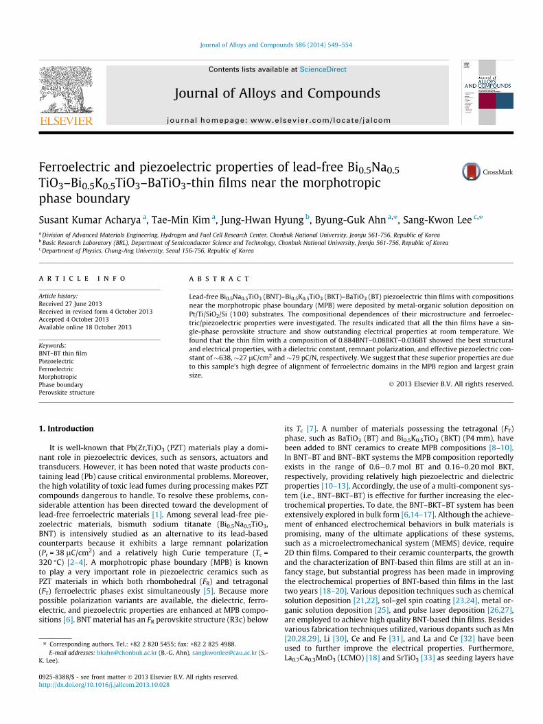
also been used to obtain highly oriented BNT-based thin films forimproving the electrical properties of the thin films. However,the BNT–BKT–BT ternary system has yet to be explored exten-sively. For the BNT–BKT–BT thin film system, Abazari et al. re-ported 88BNT–8BKT–4BT epitaxial thin films synthesized throughpulsed laser deposition (PLD) on SrRuO3-coated SrTiO3 substrates[34]. They showed a saturated polarization hysteresis loop with alarge Pr = 30 lC/cm2. More recently, Jeon et al. deposited polycrys-talline BNT–BKT–BT thin films on SiO2/Ti/Pt substrates through achemical solution deposition method and obtained superior resultscompared with the bulk materials [35]. The MPB region in theBNT–BKT–BT system can be determined using the four points P1,P2, P3, and P4, as shown schematically in Fig. 1 [6,14,36]. Recently,Zhang et al. suggested that the BNT–BKT–BT triple phase systemwithin the MPB region gives superior results compared to thosealong the MPB line [6].
In this work, thin films with six compositions, along a red linecombining 0.94BNT–0.06BT (P1) and 0.80BNT–0.20BKT (P3), as de-picted in Fig. 1, were deposited on Pt/Ti/SiO2/Si substrates by usinga metal-organic solution deposition method. These compositionscan be described as (0.94–0.028n)BNT–(0.06–0.012n)BT–0.04nBKT,where n = 0, 1, 2, 3, 4, and 5. For n = 0 and n = 5, they are 0.94BNT–0.06BT and 0.80BNT–0.20BKT, respectively. The phase composi-tion, microstructure, and dielectric and ferroelectric properties ofthese crystalline thin films were investigated and analyzed indetail.
2. Experimental details
Barium acetate [Ba(CH3COO)2], bismuth nitrate [Bi(NO3)3�5H2O], sodium ace-tate (NaOOCCH3), potassium–nitrate (KNO3), and titanium isopropoxide(Ti[OCH(CH3)2]4) were used as starting materials, and acetyl acetone, isopropylalcohol, distilled water, and acetic acid were used as solvents. Diethanolamine[HN(CH2CH2OH)2] was selected as ligands. The detailed solution preparation wasreported previously [25,30]. The stock solutions were spin-coated onto Pt/Ti/SiO2/Si (100) substrates at a spin rate of 4500 rpm for 30 s using a commercial photore-sist spinner. After each coating step, the gel films were dried at 170 �C for 10 minand pyrolyzed at 450 �C for 10 min on a hot plate before further annealing. Theseamorphous films were then crystallized at 700 �C by rapid thermal annealing underan O2 atmosphere with a soak time of 5 min [25]. Deposition, drying, pyrolysis, andcrystallization were repeated several times to increase the film thickness. Phasestructures and surface microstructure and roughness of the as-prepared thin filmswere characterized using X-ray diffraction (XRD, Model D/MAX-111A, Rigaku Cor-poration, Japan) with Cu Ka radiation and using a NanoScope IIIa (Digital Instru-ments, Santa Barbara, CA, USA) atomic force microscope (AFM), respectively. Thethicknesses of the BNT–BKT–BT thin films were estimated according to theircross-sectional field emission scanning electron microscope images. Electrical prop-erties of the BNT–BT thin films were evaluated using a capacitor structure of Au/BNT–BT/Pt, in which Au electrodes with a radius of 200 lm were prepared on topof the surface through a shadow mask in a vacuum using the e-beam depositiontechnique. Polarization–electric-field (P–E) hysteresis loop was obtained using a
etra Rombo.
MPB
P1: 0.94BNT-0.06BTP2: 0.93BNT-0.07BTP3: 0.80BNT-0.20BKTP4: 0.84BNT-0.16BKT
Fig. 1. Phase relationship of Bi0.5Na0.5TiO3–Bi0.5K0.5TiO3–BaTiO3 system around theMPB region.
TF Analyzer 2000 (aix-ACCT, Aachen, Germany) system. A precision LCR meter(HP 4284A, Agilent Technologies, CA, USA) was used to analyze the dielectric prop-erties of the BNT–BT-based thin films. Leakage current though the Au/BNT–BT/Ptcapacitor was measured using a programmable electrometer (Keithley 6517A,OH, USA) at room temperature. Piezoelectric properties were obtained by piezo-force microscopy (PFM) (Digital Instruments, NanoScope IV, Plainview, NY, USA)incorporating a lock-in technique.
3. Results and discussion
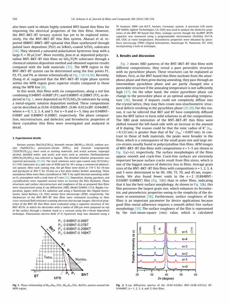
Fig. 2 shows XRD patterns of the BNT–BKT–BT thin films withdifferent compositions; they reveal a pure perovskite structurewith no pyrochlore phases. These structures can be explained asfollows. First, as the BNT-based thin films nucleate from the amor-phous phase and then grow during annealing, they pass through anintermediate pyrochlore phase and are partly changed into aperovskite structure if the annealing temperature is not sufficientlyhigh [37]. On the other hand, the entire pyrochlore phase canchange to the perovskite phase at an optimal annealing tempera-ture [38]. Second, if dopants could not completely diffuse intothe crystal lattice, they may then create non-stoichiometric struc-tural defects resulting in the pyrochlore phase [25,30]. For this rea-son, it can be inferred that BKT and BT have completely diffusedinto the BNT lattice to form solid solutions in all the compositions.The XRD peak intensities of the BNT–BKT–BT thin films wereshifted toward the left-hand-side with an increase in the amountof K doping. The reason could be that the ionic radius of K+ (rk+
= 0.133 nm) is greater than that of Na+ (rNa+ = 0.097 nm). In con-
trast to those of bulk materials, the peaks were broader in thefilms, which is a consequence of the small grain size and large mi-cro-strains usually found in polycrystalline thin films. AFM imagesof BNT–BKT–BT thin films with compositions n = 1–5 are shown inFig. 3(a)–(e), respectively. The surface morphologies of the filmsappear smooth and crack-free. Crack-free surfaces are extremelyimportant because surface cracks result from film stress, which isone of the biggest sources of dielectric loss in films. Average grainsizes of the BNT–BKT–BT thin films with compositions n = 1, 2, 3, 4,and 5 were determined to be 90, 100, 75, 70, and 45 nm, respec-tively. We also found fewer voids in the n = 2 (0.884BNT–0.036BT–0.08BKT) film (Fig. 3(b)) than in other films, indicatingthat it has the best surface morphology. As shown in Fig. 3(b), thisfilm possesses the largest grain size, which enhances its ferroelec-tric and piezoelectric properties owing to the simplicity of the do-main re-orientation [38]. Furthermore, surface roughness of thefilms is an important parameter for device applications becausegood film–metal adherence requires a smooth defect free surfacemorphology [39]. The surface roughness of the film is representedby the root-mean-square (rms) value, which is calculated
Fig. 2. X-ray diffraction spectra of the (0.94–0.028n) BNT–(0.06–0.012n) BT–0.04nBKT (n = 1, 2, 3, 4, and 5) thin films.
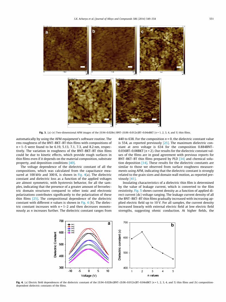
Fig. 3. (a)–(e) Two-dimensional AFM images of the (0.94–0.028n) BNT–(0.06–0.012n)BT–0.04nBKT (n = 1, 2, 3, 4, and 5) thin films.
S.K. Acharya et al. / Journal of Alloys and Compounds 586 (2014) 549–554 551
automatically by using the AFM equipment’s software routine. Therms roughness of the BNT–BKT–BT thin films with compositions ofn = 1–5 were found to be 6.19, 5.13, 7.1, 7.3, and 8.2 nm, respec-tively. The variation in roughness of the BNT–BKT–BT thin filmscould be due to kinetic effects, which provide rough surfaces inthin films even if it depends on the material composition, substrateproperty, and deposition conditions [40].
The voltage dependence of the dielectric constant of all thecompositions, which was calculated from the capacitance mea-sured at 100 kHz and 300 K, is shown in Fig. 4(a). The dielectricconstant and dielectric loss as a function of the applied voltagesare almost symmetric, with hysteresis behavior, for all the sam-ples, indicating that the presence of a greater amount of ferroelec-tric domain structures compared to other ionic and electronicpolarizations contributes significantly to the polarization of thesethin films [25]. The compositional dependence of the dielectricconstant with different n values is shown in Fig. 4 (b). The dielec-tric constant increases with n = 1–2 and then decreases monoto-nously as n increases further. The dielectric constant ranges from
Fig. 4. (a) Electric field dependences of the dielectric constant of the (0.94–0.028n)BNTdependent dielectric constants of the films.
440 to 638. For the composition n = 0, the dielectric constant valueis 554, as reported previously [25]. The maximum dielectric con-stant at zero voltage is 634 for the composition 0.884BNT–0.036BT–0.08BKT (n = 2). Our results for the dielectric constant val-ues of the films are in good agreement with previous reports forBNT–BKT–BT thin films prepared by PLD [34] and chemical solu-tion deposition [14]. These results for the dielectric constants aresimilar to those we observed from surface roughness measure-ments using AFM, indicating that the dielectric constant is stronglyrelated to the grain sizes and domain wall motion, as reported pre-viously [41].
Insulating characteristics of a dielectric thin film is determinedby the value of leakage current, which is converted to the filmresistivity. Fig. 5 shows current density as a function of applied di-rect current (dc) voltage ranging. The leakage current density of allthe BNT–BKT–BT thin films gradually increased with increasing ap-plied electric field up to 10 V. For all samples, the current densityincreased linearly with external electric field at low electric fieldstrengths, suggesting ohmic conduction. At higher fields, the
–(0.06–0.012n)BT–0.04nBKT (n = 1, 2, 3, 4, and 5) thin films and (b) composition-
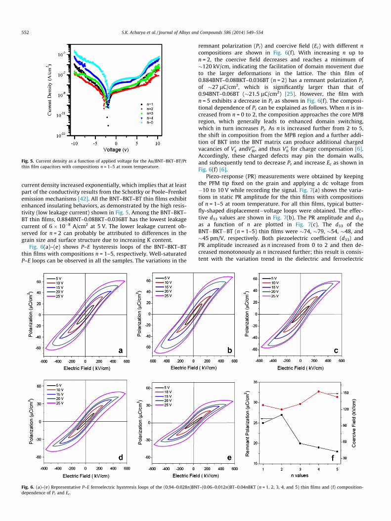
Fig. 5. Current density as a function of applied voltage for the Au/BNT–BKT–BT/Ptthin film capacitors with compositions n = 1–5 at room temperature.
552 S.K. Acharya et al. / Journal of Alloys and Compounds 586 (2014) 549–554
current density increased exponentially, which implies that at leastpart of the conductivity results from the Schottky or Poole–Frenkelemission mechanisms [42]. All the BNT–BKT–BT thin films exhibitenhanced insulating behaviors, as demonstrated by the high resis-tivity (low leakage current) shown in Fig. 5. Among the BNT–BKT–BT thin films, 0.884BNT–0.08BKT–0.036BT has the lowest leakagecurrent of 6 � 10�8 A/cm2 at 5 V. The lower leakage current ob-served for n = 2 can probably be attributed to differences in thegrain size and surface structure due to increasing K content.
Fig. 6(a)–(e) shows P–E hysteresis loops of the BNT–BKT–BTthin films with compositions n = 1–5, respectively. Well-saturatedP–E loops can be observed in all the samples. The variations in the
Fig. 6. (a)–(e) Representative P–E ferroelectric hysteresis loops of the (0.94–0.028n)BNdependence of Pr and Ec.
remnant polarization (Pr) and coercive field (Ec) with different ncompositions are shown in Fig. 6(f). With increasing n up ton = 2, the coercive field decreases and reaches a minimum of�120 kV/cm, indicating the facilitation of domain movement dueto the larger deformations in the lattice. The thin film of0.884BNT–0.08BKT–0.036BT (n = 2) has a remnant polarization Pr
of �27 lC/cm2, which is significantly larger than that of0.94BNT–0.06BT (�21.5 lC/cm2) [25]. However, the film withn = 5 exhibits a decrease in Pr as shown in Fig. 6(f). The composi-tional dependence of Pr can be explained as follows. When n is in-creased from n = 0 to 2, the composition approaches the core MPBregion, which generally leads to enhanced domain switching,which in turn increases Pr. As n is increased further from 2 to 5,the shift in composition from the MPB region and a further addi-tion of BKT into the BNT matrix can produce additional chargedvacancies of V 0k andV 000Bi, and thus V 000 for charge compensation [6].Accordingly, these charged defects may pin the domain walls,and subsequently tend to decrease Pr and increase Ec as shown inFig. 6(f) [6].
Piezo-response (PR) measurements were obtained by keepingthe PFM tip fixed on the grain and applying a dc voltage from�10 to 10 V while recording the signal. Fig. 7(a) shows the varia-tions in static PR amplitude for the thin films with compositionsof n = 1–5 at room temperature. For all thin films, typical butter-fly-shaped displacement�voltage loops were obtained. The effec-tive d33 values are shown in Fig. 7(b). The PR amplitude and d33
as a function of n are plotted in Fig. 7(c). The d33 of theBNT�BKT�BT (n = 1–5) thin films were �74, �79, �54, �48, and�45 pm/V, respectively. Both piezoelectric coefficient (d33) andPR amplitude increased as n increased from 0 to 2 and then de-creased monotonously as n increased further; this result is consis-tent with the variation trend in the dielectric and ferroelectric
T–(0.06–0.012n)BT–0.04nBKT (n = 1, 2, 3, 4, and 5) thin films and (f) composition-
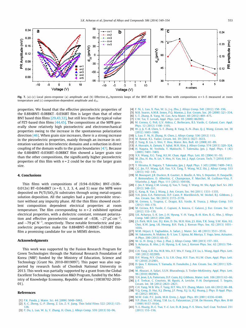
Fig. 7. (a)–(c) Local piezo-response (a) amplitude and (b) Effective d33 hysteresis loops of the BNT–BKT–BT thin films with compositions n = 1–5 measured at roomtemperature and (c) composition-dependent amplitude and d33.
S.K. Acharya et al. / Journal of Alloys and Compounds 586 (2014) 549–554 553
properties. We found that the effective piezoelectric properties ofthe 0.884BNT–0.08BKT�0.036BT film is larger than that of otherBNT based thin films [29,43,32], but still less than the typical valueof PZT-based thin films [44,45]. The compositions at the MPB gen-erally show relatively high piezoelectric and electromechanicalproperties owing to the increase in the spontaneous polarizationdirection [46]. When grain size increases, there is a strong increasein the piezoelectric properties, mainly through an increase in ori-entation variants in ferroelectric domains and a reduction in directcoupling of the domain walls to the grain boundaries [47]. Becausethe 0.884BNT–0.036BT–0.08BKT film showed a larger grain sizethan the other compositions, the significantly higher piezoelectricproperties of this film with n = 2 could be due to the larger grainsize.
4. Conclusions
Thin films with compositions of (0.94–0.028n) BNT–(0.06–0.012n) BT–0.04nBKT (n = 0, 1, 2, 3, 4, and 5) near the MPB weredeposited on Pt/Ti/SiO2/Si substrates through using metal-organicsolution deposition. All the samples had a pure perovskite struc-ture without any impurity phase. All the thin films showed excel-lent composition dependent electrical properties at roomtemperature. The film corresponding to n = 2 exhibited optimalelectrical properties, with a dielectric constant, remnant polariza-tion and effective piezoelectric constant of �638, �27 lC cm�2,and �79 pC N�1, respectively. These notable ferroelectric and pie-zoelectric properties make the 0.884BNT–0.08BKT–0.036BT thinfilm a promising candidate for use in MEMS devices.
Acknowledgments
This work was supported by the Fusion Research Program forGreen Technologies through the National Research Foundation ofKorea (NRF) funded by the Ministry of Education, Science andTechnology (Grant No. 2010-0019097). This paper was also sup-ported by research funds of Chonbuk National Universtiy in2013. This work was partially supported by a grant from the GlobalExcellent Technology Innovation R&D Program, funded by the Min-istry of Knowledge Economy, Republic of Korea (10038702-2010-01).
References
[1] P.K. Panda, J. Mater. Sci. 44 (2009) 5049–5062.[2] X.-C. Zheng, G.-P. Zheng, Z. Lin, Z.-Y. Jiang, Thin Solid Films 522 (2012) 125–
128.[3] P. Du, L. Luo, W. Li, Y. Zhang, H. Chen, J. Alloys Comp. 559 (2013) 92–96.
[4] F. Ni, L. Luo, X. Pan, W. Li, J-q. Zhu, J. Alloys Comp. 541 (2012) 150–156.[5] M.R. Soares, A.M.R. Senos, P.Q. Mantas, J. Eur. Ceram. Soc. 20 (2000) 321–334.[6] S.-T. Zhang, B. Yang, W. Cao, Acta Mater. 60 (2012) 469–475.[7] C.W. Tai, Y. Lereah, Appl. Phys. Lett. 95 (2009) 062901.[8] M. Cernea, G. Poli, G.V. Aldica, C. Berbecaru, B.S. Vasile, C. Galassi, Curr. Appl.
Phys. 12 (2012) 1100–1105.[9] W.-J. Ji, Y.-B. Chen, S.-T. Zhang, B. Yang, X.-N. Zhao, Q.-J. Wang, Ceram. Int. 38
(2012) 1683–1686.[10] L. Luo, F. Ni, H. Zhang, H. Chen, J. Alloys Comp. 536 (2012) 113.[11] M. Rawat, K.L. Yadav, Ceram. Int. 39 (2013) 3627–3633.[12] Z. Yang, B. Liu, L. Wei, Y. Hou, Mater. Res. Bull. 43 (2008) 81–89.[13] A. Hussain, A. Zaman, Y. Iqbal, M.H. Kim, J. Alloys Comp. 574 (2013) 320–324.[14] H. Nagata, M. Yoshida, Y. Makiuchi, T. Takenaka, Jpn. J. Appl. Phys. 1 (42)
(2003) 7401–7403.[15] X.X. Wang, X.G. Tang, H.L.W. Chan, Appl. Phys. Lett. 85 (2004) 91–93.[16] M. Zhu, H. Hu, N. Lei, Y. Hou, H. Yan, Int. J. Appl. Ceram. Tech. 7 (2010) E107–
E113.[17] Y. Hiruma, H. Nagata, T. Takenaka, Jpn. J. Appl. Phys. 1 (45) (2006) 7409–7412.[18] C.C. Jin, F.F. Wang, Q.R. Yao, Y.X. Tang, T. Wang, W.Z. Shi, J. Alloys Comp. 553
(2013) 142–145.[19] M. Bousquet, J.R. Duclere, B. Gautier, A. Boulle, A. Wu, S. Deputier, D. Fasquelle,
F. Remondiere, D. Albertini, C. Champeaux, P. Marchet, M. Guilloux-Viry, P.Vilarinho, J. Appl. Phys. 111 (2012) 104106.
[20] C. Jin, F. Wang, C.M. Leung, Q. Yao, Y. Tang, T. Wang, W. Shi, Appl. Surf. Sci. 283(2013) 348–351.
[21] G. Kang, K. Yao, J. Wang, J. Am. Ceram. Soc. 94 (2011) 1331–1335.[22] Y.H. Jeon, E.A. Patterson, D.P. Cann, P. Mardilovich, W. Stickel, B.J. Gibbons, J.
Am. Ceram. Soc. 96 (2013) 2172–2178.[23] M. Cernea, L. Trupina, C. Dragoi, B.S. Vasile, R. Trusca, J. Alloys Comp. 515
(2012) 166–170.[24] M. Cernea, B.S. Vasile, C. Capiani, A. Ioncea, C. Galassi, J. Eur. Ceram. Soc. 32
(2012) 133–139.[25] S.K. Acharya, S.-K. Lee, J.-H. Hyung, Y.-H. Yang, B.-H. Kim, B.-G. Ahn, J. Alloys
Comp. 540 (2012) 204–209.[26] J.S. Park, M.H. Lee, D.J. Kim, D. Do, M.H. Kim, J.S. Kim, T.K. Song, S.W. Kim, H.I.
Choi, K.W. Jang, I.R. Hwang, B.H. Park, J. Korean Phys. Soc. 62 (2013) 1031–1034.
[27] M.M. Hejazi, E. Taghaddos, A. Safari, J. Mater. Sci. 48 (2013) 3511–3516.[28] W. Sakamoto, N. Makino, B.-Y. Lee, T. Iijima, M. Moriya, T. Yogo, Sens. Actuator.
A-Phys. 200 (2013) 60–67.[29] W. Li, H. Zeng, J. Hao, J. Zhai, J. Alloys Comp. 580 (2013) 157–161.[30] S. Acharya, B. Ahn, J.-H. Hyung, S.-K. Lee, J. Korean Phys. Soc. 62 (2013) 794–
799.[31] C.H. Yang, G.D. Hu, W.B. Wu, H.T. Wu, F. Yang, Z.Y. Lu, L. Wang, Appl. Phys. Lett.
100 (2012) 022909.[32] D.Y. Wang, N.Y. Chan, S. Li, S.H. Choy, H.Y. Tian, H.L.W. Chan, Appl. Phys. Lett.
97 (2010) 212901.[33] D. Ijuu, T. Kimura, T. Yamada, H. Funakubo, J. Am. Ceram. Soc. 94 (2011) 329–
32951.[34] M. Abazari, A. Safari, S.S.N. Bharadwaja, S. Trolier-McKinstry, Appl. Phys. Lett.
96 (2010) 082903.[35] Y.H. Jeon, E.A. Patterson, D.P. Cann, B.J. Gibbons, Mater. Lett. 106 (2013) 63–66.[36] J.-F. Trelcat, C. Courtois, M. Rguiti, A. Leriche, P.-H. Duvigneaud, T. Segato,
Ceram. Int. 38 (2012) 2823–2827.[37] C.H. Yang, W.B. Wu, F. Yang, H.T. Wu, X.Y. Zhang, Mater. Lett. 66 (2012) 86–88.[38] Y.Q. Gong, D. Hui, X.J. Zheng, J.F. Peng, X.J. Li, R.J. Huang, J. Phys. D Appl. Phys.
45 (2012) 305301.[39] M.W. Cole, P.C. Joshi, M.H. Ervin, J. Appl. Phys. 89 (2001) 6336–6340.[40] Y.P. Zhao, G.C. Wang, T.M. Lu, G. Palasantzas, J.T.M. De Hosson, Phys. Rev. B 60
(1999) 9157–9164.[41] Y.-L. Huang, D.-C. Tsai, Y.-C. Lee, D.-R. Jung, F.-S. Shieu, Surf. Coat. Technol. 231
(2013) 153–156.
554 S.K. Acharya et al. / Journal of Alloys and Compounds 586 (2014) 549–554
[42] A.Z. Simões, M.A. Ramírez, E. Longo, J.A. Varela, Mater. Chem. Phys. 107 (2008)72–76.
[43] D.Z. Zhang, X.J. Zheng, X. Feng, T. Zhang, J. Sun, S.H. Dai, L.J. Gong, Y.Q. Gong, L.He, Z. Zhu, J. Huang, X. Xu, J. Alloys Comp. 504 (2010) 129–133.
[44] P. Muralt, IEEE T. Ultrason. Ferr. 47 (2000) 903–915.
[45] S. Trolier-McKinstry, P. Muralt, J. Electroceram. 12 (2004) 7–17.[46] Y. Li, W. Chen, Q. Xu, J. Zhou, X. Gu, S. Fang, Mater. Chem. Phys. 94 (2005) 328–
332.[47] C.A. Randall, N. Kim, J.-P. Kucera, W. Cao, T.R. Shrout, J. Am. Ceram. Soc. 81
(1998) 677–688.


](https://img.pdfslide.net/doc/110x75/6336ac0eb5f91cb18a0beec4/adsorption-of-bi-isonicotinic-acid-on-rutile-tiosub-2110.jpg)


