Embed Size (px)
Citation preview

Finite Element Multi-physics Modeling for Ohmic Contact of Microswitches
H.Liu1, 2, D. Leray1, 2, P. Pons2, S. Colin1 1Institut Clément Ader, INSA, Univ de Toulouse 2CNRS, LAAS, Univ de Toulouse, INSA, LAAS
Toulouse, France [email protected]
Abstract The purpose of this paper is to investigate the
thermoelectrical behaviour of ohmic microcontacts under low force. The temperature in the contact zone is very important for the reliability of microswitches. As it is very difficult to measure the inner temperature, the numerical thermal modelling of electrical contacts offers interesting perspectives. A multi-physics modelling of electrical contact is accomplished with the finite element commercial package ANSYSTM. Two approaches for coupled-field analysis are investigated, namely direct and load transfer. The thermo-electro-mechanical modelling is firstly validated with a smooth sphere-plane contact, and then applied for a real rough contact computation, elastic-plastic material deformation is included in the modelling. The temperature distribution on the contact surface is plotted, and the maximum temperature is found around the asperities with the highest deformation. The multi-physics model offers a reliable method to investigate the steady-state thermal behaviour of electrical contact with rough surface included.
Keywords: multi-physics, finite element modelling, ohmic contact, microswitches
1. Introduction and Motivations Reliability of ohmic contacts is a great challenge for
microswitches [1]. Since Joule heating is extremely localized in the contact zone, the temperature there may reach the softening or melting temperature while the device remains at room temperature [2-3].
The numerical coupled-simulations have been proved to be an efficient method to study the thermoelectrical behaviour of contact, and have been carried out by many researchers (see [4-10]). Monnier et al. [5] investigated a macro smooth sphere-plane contact problem using a coupled-field finite element (FE) simulation. Based on this, Ghaednia et al. [7] studied the influence of thermal expansion and plastic deformation on an asperity contact with a 3D thermo-electro-mechanical model. However, for microcontacts, low force and weak current are required, which makes them different from the macro-scale contact behaviour. Also, the temperature reached more than 1000 K in [7] while the temperature-dependent material properties were not taken into account. The research of Leidner et al. ([9-10]) seems more pertinent, in which the current density distribution for contact with layered structure and ‘real world’ contact topographies was discussed, and the simulation results were confirmed with the thermal images by infrared thermography. However, the study focused on the connector system, in
which the contacting spots were much larger than that of microswitches. Motivated by microswitches contact, a 2D elastic multiphysics contact model was developed using ANSYSTM in [8], and the study presented a distinct difference on contact radius between force control and displacement control with a voltage or current applied. However, the resulting temperature would reach to 662 K with the applied voltage V*=0.221, the temperature-dependent material properties were not considered in the modelling, and only elastic deformation was considered. Also for the electrical contact of microswitches, Shanthraj et al. [6] developed an iterative procedure to solve the electro-thermo-mechanical field equations with three-dimensional fractal surface included. Interesting results were obtained, such as the influence of the initial residual strain and ambient temperature. However, there were no experimental results to validate the model.
Summarizing the published works, a promising multi-physics model is still missing for microcontacts problem, especially with rough surface and elastic-plastic material deformation involved.
The organization of the paper is as follows: the introduction and motivations are presented in the first part, followed by the theoretical background of the electrical contact. The description of the FE model and the methodology of multiphysics calculation are presented in the third part, and then the model validation and the simulation results are discussed, finally comes the conclusion.
2. Theoretical Background In the case of a unique contact spot, the electrical
contact resistance (ECR) is calculated according to its radius a. Comparing the contact radius to the electron mean free path l, three electrical transport regimes are defined: diffusive, ballistic and intermediary, and the electrical resistance can be calculated with the following equations (1-3):
aRD 2/ (1)
23/4 alRB (2)
BDBD RR
al
alRRalfR
/33.11
/83.01int (3)
Where ρ is the electrical resistivity and l is the electron mean free path. RD, RB and Rint are the electrical resistance for diffusive, ballistic and intermediary transport regimes respectively. f(l/a) is the interpolation
978-1-4799-4790-4/14/$31.00 ©2014 IEEE
2014 15th International Conference on Thermal, Mechanical and Multi-Physics Simulation and Experiments in Microelectronics and Microsystems, EuroSimE 2014
— 1 / 8 —

function, which accounts for the transition from the ballistic to diffusive regime.
When multiple spots are in contact, the effective contact resistance depends on the radii of the spots and their distribution. Formulae used to calculate the ECR for multiple spot contact [11-12] do not deal with spots under different transport regimes, and this leads us to define a lower and an upper ECR limit, as [13] proposed.
For the lower limit, it is assumed that the contact spots are in parallel without interacting with each other. For the upper limit, the ECR is obtained by replacing all contact asperities with one single spot while keeping the contact area constant, and the effective radius aeff is defined. The two ECR limits can be calculated with equations (4-5):
N
i cil RR1
11
(4)
23
4
2 eff
av
eff
avu
aafR
(5)
Where N is the number of the asperities in contact and ρav is the average electrical resistivity, Rci is the resistance of contact spot i, and the subscripts l and u refer to the lower and upper limits for the contact resistance, respectively.
In the thermal domain, the calculation of the maximum temperature of the contact, also called contact temperature TC, was firstly proposed by Holm [14]:
20
2
4T
L
VT C
C
(6)
Where L=2.45×10⁻⁸ (W×Ω/K2) is the Lorentz constant and T0 is the ambient temperature. However, the recent experiments [15-16] indicated the breakdown of the V-T relation. It was found that with small size contact spots whose radius is the order of or smaller than the mean free path, the contact “melting” was not observed although the contact exceeded the ‘melting voltage’ of the contact pairs. It is due to the ballistic transport of electrons in contact which is not responsible for the contact heating, Jensen et al. [2] then proposed a new expression:
L
V
Rc
RalfTT CB
C 4
)( 22
02
(7)
Considering the temperature distribution in the contact area, it was found that, most of the Joule heating is located close at the periphery of the contact area [17], this was also validated by the thermographic measurements [18-19]. While for the steady-state temperature, Greenwood and Williamson [17] predicted that it falls off with distance from the contact area, but the FEM by Hennessy et al. [8] predicted that the maximum temperature occurred slightly on the asperity side. Regarding this disagreement, the study presented focuses on the steady-state thermal behaviour, and zooms in the temperature distribution on the contact surface.
3. Finite Element Modelling This work is based on the previous study [20], in
which a determinist method was used to describe the
rough surface of microcontacts. As the determinist method, an atomic force microscopy (AFM) was used to scan the topography of a microswitch bump, and this described well the topographies of micro-scale asperities and macro-scale bump shape. The AFM scan data was then imported to ANSYSTM (package 11.0 used), and a FE contact model was developed.
A. Topography of contact surface in microswitches A real microswitch is used for AFM scanning, as
shown in Figure 1(a). Contact pairs are as follows: - Bridge is fabricated in gold, with thickness of 4 μm. - Bump is also fabricated in gold, with a layer of 1
μm-thick coated on a silicon substrate, and it is with a hemi-sphere form of radius 4 μm.
Since microswitches usually work under low force, it is the highest asperities making contact, also called a-spots, which are in the dimension of few hundreds or even tens of nanometers [21], so high resolution is required to properly map the surface topography.
A 4 μm-wide square AFM scan is carried out on the microswitch bump. Scan X-Y grid is set to 256 lines, which gives a 15.6 nm horizontal resolution. This horizontal resolution was proved to be fine enough for modelling contact behaviour and evaluating ECR properly [22]. Figure 1(b) shows the surface topography, generated with AFM data and treated by Matlab.
(a)
(b)
Figure 1: (a) Schematic of the microswitch, (b) Surface topography of the microswitch bump: obtained by AFM
scanning
B. Geometry of the FE model Both contact parts are modelled as deformable bodies.
The top surface of the lower body is built using AFM data. The bottom surface of the upper body is defined as perfectly flat surface. Due to the coupling effect between the mechanical, thermal and electrical behaviors, modelling both volumes as deformable bodies with real
2014 15th International Conference on Thermal, Mechanical and Multi-Physics Simulation and Experiments in Microelectronics and Microsystems, EuroSimE 2014
— 2 / 8 —
material is more accurate and practical for multiphysics problems [7].
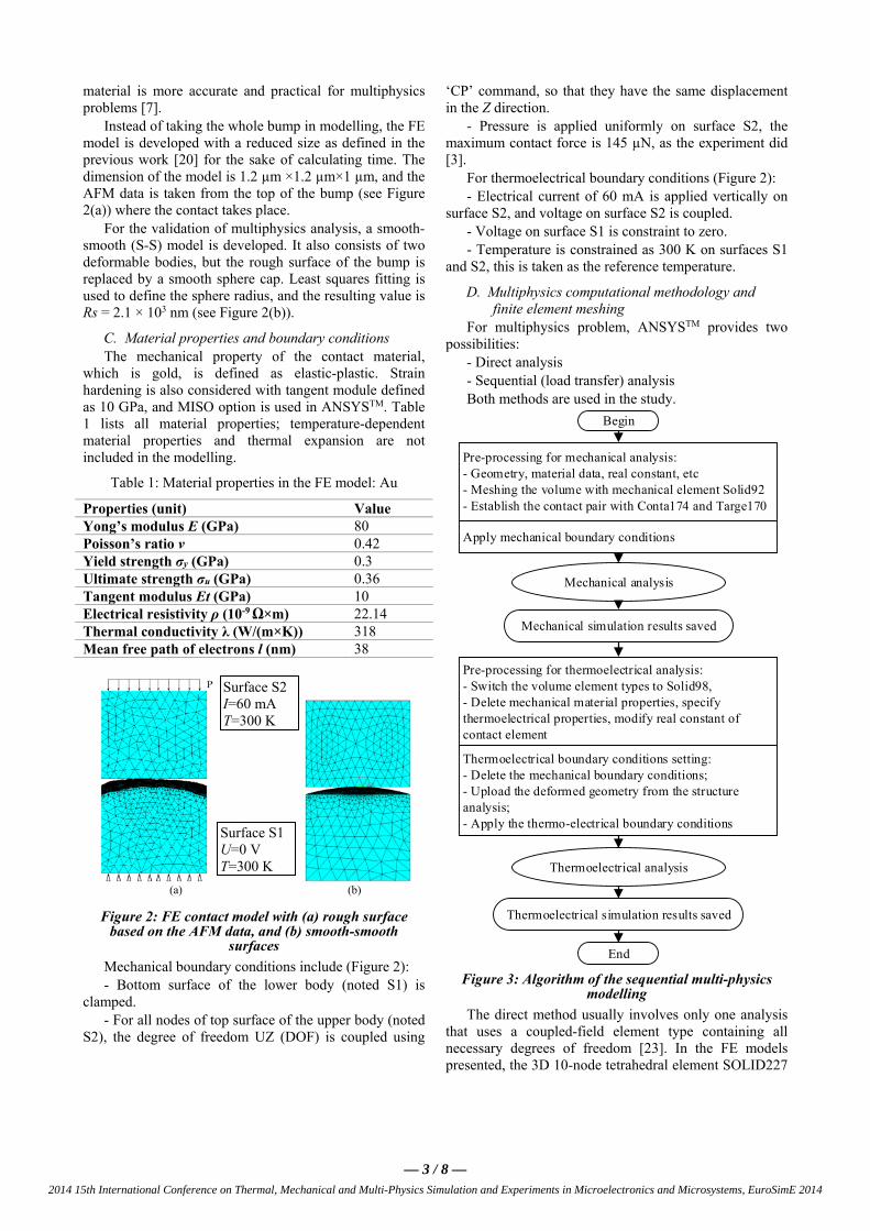
Instead of taking the whole bump in modelling, the FE model is developed with a reduced size as defined in the previous work [20] for the sake of calculating time. The dimension of the model is 1.2 µm ×1.2 µm×1 µm, and the AFM data is taken from the top of the bump (see Figure 2(a)) where the contact takes place.
For the validation of multiphysics analysis, a smooth-smooth (S-S) model is developed. It also consists of two deformable bodies, but the rough surface of the bump is replaced by a smooth sphere cap. Least squares fitting is used to define the sphere radius, and the resulting value is Rs = 2.1 × 10³ nm (see Figure 2(b)).
C. Material properties and boundary conditions The mechanical property of the contact material,
which is gold, is defined as elastic-plastic. Strain hardening is also considered with tangent module defined as 10 GPa, and MISO option is used in ANSYSTM. Table 1 lists all material properties; temperature-dependent material properties and thermal expansion are not included in the modelling.
Table 1: Material properties in the FE model: Au
Properties (unit) Value Yong’s modulus E (GPa) 80 Poisson’s ratio ν 0.42 Yield strength σy (GPa) 0.3 Ultimate strength σu (GPa) 0.36 Tangent modulus Et (GPa) 10 Electrical resistivity ρ (10-9 Ω×m) 22.14 Thermal conductivity λ (W/(m×K)) 318 Mean free path of electrons l (nm) 38
(a) (b)
Figure 2: FE contact model with (a) rough surface based on the AFM data, and (b) smooth-smooth
surfaces
Mechanical boundary conditions include (Figure 2): - Bottom surface of the lower body (noted S1) is
clamped. - For all nodes of top surface of the upper body (noted
S2), the degree of freedom UZ (DOF) is coupled using
‘CP’ command, so that they have the same displacement in the Z direction.
- Pressure is applied uniformly on surface S2, the maximum contact force is 145 µN, as the experiment did [3].
For thermoelectrical boundary conditions (Figure 2): - Electrical current of 60 mA is applied vertically on
surface S2, and voltage on surface S2 is coupled. - Voltage on surface S1 is constraint to zero. - Temperature is constrained as 300 K on surfaces S1
and S2, this is taken as the reference temperature.
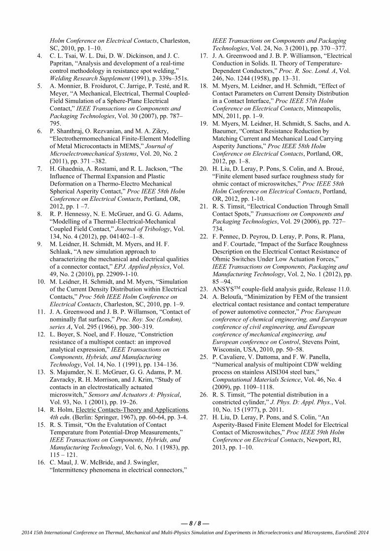
D. Multiphysics computational methodology and finite element meshing
For multiphysics problem, ANSYSTM provides two possibilities:
- Direct analysis - Sequential (load transfer) analysis Both methods are used in the study.
Begin
Pre-processing for mechanical analysis:- Geometry, material data, real constant, etc- Meshing the volume with mechanical element Solid92- Establish the contact pair with Conta174 and Targe170
Apply mechanical boundary conditions
Mechanical analysis
Mechanical simulation results saved
Pre-processing for thermoelectrical analysis:- Switch the volume element types to Solid98, - Delete mechanical material properties, specify thermoelectrical properties, modify real constant of contact element
Thermoelectrical boundary conditions setting:- Delete the mechanical boundary conditions;- Upload the deformed geometry from the structure analysis;- Apply the thermo-electrical boundary conditions
Thermoelectrical analysis
Thermoelectrical simulation results saved
End Figure 3: Algorithm of the sequential multi-physics
modelling
The direct method usually involves only one analysis that uses a coupled-field element type containing all necessary degrees of freedom [23]. In the FE models presented, the 3D 10-node tetrahedral element SOLID227
Surface S2 I=60 mA T=300 K
Surface S1 U=0 V T=300 K
2014 15th International Conference on Thermal, Mechanical and Multi-Physics Simulation and Experiments in Microelectronics and Microsystems, EuroSimE 2014
— 3 / 8 —

is used to mesh the volume, and the DOF option is set as "111" to activate the fields of mechanical, thermal and electrical.
The principle of the sequential method is: the input of one physics analysis depends on the results from another analysis, the analyses are then coupled [23]. Figure 3 shows the algorithm of the method. For meshing the volume, instead of using one element SOLID227 in the direct method, SOLID92 is used for the structural analysis and SOLID98 for the thermoelectrical analysis. Both elements are 3D 10-node tetrahedral elements.
For the contact pair, 3D surface-to-surface contact element CONTA174 and target element TARGE170 are used to mesh the contact surfaces belonging to the bump and bridge respectively. These elements are selected to consider the large deflection and nonlinear behaviour of contact asperities. Table 2 and Table 3 summarize all of the elements used. Also, the augmented Lagrange method is used to seek contact, and large deformation is considered in the calculation.
Table 2: Element types for FE model: structural and direct multiphysics analysis
Structure Multiphysics SOLID Element 187 227
DOF UX, UY, UZ UX, UY, UZ, Volt, Temp
TARGE Element 170 170
CONTA Element 174
174
DOF UX, UY, UZ UX, UY, UZ, Volt, Temp
Real constant
TCC=318×109 (W/(m2×K) ECC=4.52×10¹⁶ (S/m2)
Table 3: Solid element types for FE model: sequential multiphysics method
Analysis Structure Thermoelectric Element SOLID92 SOLID98 DOF UX, UY, UZ Volt, Temp, Mag
E. Electrical and thermal contact conditions To take into account the surface interaction for electric
contact, a parameter called ECC (Electrical Contact Conductance) is defined in ANSYSTM by:
VJECC (8)
Since the electrical and heat transfer are much localized, conduction phenomena at the contact interface depend on the surface geometry, the roughness of the contact area, etc. ([23-25]), the theoretical determination of ECC is very difficult.
It is assumed in the study that the contact and target interfaces are perfect, that there is no potential jump at the
interface, and ECC can be considered as the inverse of the electrical resistance of interface per unit area [24]. In the presented models, the value of ECC is defined as the interface resistance equaling to the resistance of a 1 nm-thick layer of the material, so that ECC = 1 / (ρ. e), where e = 1 nm.
Similarly, the conductive heat transfer between two contacting surfaces is defined by TCC (Thermal Conductance Contact):
TQTCC (9)
Its value is defined as the conductance equaling to that of a 1 nm-thick layer: TCC = λ / e with λ the thermal conductivity of the material.
4. Results with direct method The multiphysics analysis was firstly developed with
the smooth-smooth contact model. The meshing grid is about 40 nm-60 nm for the contact surfaces, and the whole FE model includes:
- 11500 solid elements - 1210 contact elements - 200 target elements. A loading-unloading cycle is applied on the model
with 10 steps for loading and 10 steps for unloading.
A. Validation of direct multiphysics modelling The validation of multiphysics contact analysis is
carried out in two terms: - Mechanical behaviour - Thermoelectrical behaviour For the mechanical behavior, the multiphysics
simulations are compared with the counterpart mechanical simulations in which the block is meshed with SOLID 187 (see Table 2), which is also a 3D 10-node tetrahedral structural solid element. The contact area as a function of load steps is plotted in Figure 4. It shows that the mechanical and multiphysics simulations predict the identical results, so the multiphysics simulations are validated in terms of mechanical behavior.
0 2 4 6 8 10 12 14 16 18 200
2
4
6
8
10
12
14
16
18x 10
4
Load step
Co
nta
ct a
rea
(n
m2)
ET187
ET227
Figure 4: Contact area as a function of load steps:
comparison between the direct multiphysics simulation and structural simulation
2014 15th International Conference on Thermal, Mechanical and Multi-Physics Simulation and Experiments in Microelectronics and Microsystems, EuroSimE 2014
— 4 / 8 —

For the thermoelectrical behaviour, the criteria chosen are the contact resistance and the maximum temperature.
With FE simulations, contact occurs at a finite number of elements. After the calculation, contact results data are exported out as text files, then Matlab is used to calculate the number of spots and the area of each contact spot, and finally the constriction resistance is calculated with equations (1-3) for one spot or (4-5) for multiple spots. This method of contact resistance calculation is denoted as ‘Method A’.
However, one issue should be addressed is that the contact radius is about 220 nm under the highest load (see Figure 4), compared to the dimension of the model which is of 1200 nm, the spot size is too large to satisfy the assumption of Holm resistance analytical calculation, which considers two semi-infinite spaces in contact on a disc [14]. So the ‘cylindrical resistance’ is then calculated instead as Timsit proposed [26]:
43
2
/19998.0/15261.0
/06322.0/41581.112/
RaRa
RaRaaRc (10)
where R is the radius of cylinder. In our models, the section geometry is a square, so an equivalent cross-sectional area is defined to adapt Timsit’s formula with LR . Nevertheless, no available formulas are
found for the ballistic and intermediary regimes in the ‘cylindrical’ condition, so equations (2-3) are still used. Considering that the spot is quite small in the ballistic and intermediary transport mode, the ratio a/R is small, so the effect of ‘cylindrical resistance’ should be ignorable.
With multiphysics simulation, on the other hand, an electrical resistance can be obtained directly with the resulting voltage divided by the current applied. This simulated resistance, also called total resistance Rt herein, is the sum of bulk resistance Rb and contact resistance Rc. Hence, contact resistance should be calculated by:
btc RRR (11)
This method for obtaining the contact resistance is denoted as ‘Method B’.
The validation of the thermoelectrical behaviours for multiphysics simulations is carried out firstly by comparing the contact resistance obtained by ‘Method A’ and ‘Method B’. This is to validate whether the ECC value is proper, so that the electrical interface can be considered prefect in FE modelling. The contact resistance as a function of load steps is plotted in Figure 5(a), the resistances obtained by two methods are very close except for a sensible difference of 13% under very low force.
Similarly, for the TCC value, the simulated contact temperature as a function of load steps is compared with the ones calculated by equation (6) using the simulated voltage, labelled ‘analytical’ in Figure 5(b). A good agreement is found between the simulation and the analytical calculation, and this validates that the Joule heating calculation is well implanted in the simulation.
And thus the multiphysics analysis is validated in terms of thermoelectrical behaviour.
0 2 4 6 8 10 12 14 16 18 200
0.02
0.04
0.06
0.08
0.1
0.12
0.14
Load step
Co
nta
ct r
esi
sta
nce
( )
Method A
Method B
(a)
0 2 4 6 8 10 12 14 16 18 20300
300.2
300.4
300.6
300.8
301
301.2
301.4
Load step
Ma
xim
um
tem
pra
ture
(K)
Analytical
Multiphysics
(b)
Figure 5: Validation of the direct multiphysics modelling: (a) contact resistance obtained with ‘Method
A’ vs. ‘Method B’, (b) contact temperature calculated with the simulated voltage vs. obtained directly from the
simulations
B. Problem with the direct method The direct method could be the best choice since it can
couple the mechanical, electrical and thermal behaviors together at one time, so that the temperature-dependent material properties and thermal expansion can be implanted in the model easily. However, the computation time is too long, it took 27 hours for the smooth contact simulation discussed above (Linux system with 4 [email protected], and 16 GB Memory), compared to only 38 minutes a mechanical simulation took. One mechanical simulation with rough surface and 32 nm meshing grid asked for 50 calculation hours, and it makes using the direct method for the rough contact modelling unreasonable.
5. Results with sequential method
A. Validation of sequential multiphysics modelling With the sequential model, the parameters in the
mechanical analysis is just the same as pure mechanical simulation, but for the thermoelectrical analysis, one
2014 15th International Conference on Thermal, Mechanical and Multi-Physics Simulation and Experiments in Microelectronics and Microsystems, EuroSimE 2014
— 5 / 8 —

parameter should be addressed is the PINB value (pinball region), which determines the contact status of the elements. It is either a 2-D circle or a 3-D sphere (see Figure 6), and the elements are considered to be near-field contact when they enter into the pinball region. In the thermoelectrical analysis, the contact surface behaviour is defined as bonded always, so a relatively small PINB value is required to prevent any false contact detection. Our simulations showed that the PINB value has much influence on the electrical and thermal interaction on contact surfaces. Indeed, the transfer of current and heating happens when the elements locate within the pinball region, so for the same mechanical analysis, a larger PINB value causes an easier electrical contact and a smaller contact resistance.
The influence of the PINB value on the total contact resistance is presented in Figure 7. The simulations were carried out with the S-S model and a coarse mesh grid of about 130 nm on the contact surface. As discussed above, with PINB decreases, the simulated resistance increases. Compared the electrical resistance and the contact temperature with the direct method, 0.01 was chosen for PINB value. Further simulation were then launched with finer meshing grid of 40 nm - 60 nm, and good results were found, so in the following simulations, PINB is set as 0.01.
Figure 6: The definition of ‘PINB region’ in the contact
model (ANSYS thermal analysis guide, 2009)
0 0.01 0.02 0.03 0.04 0.05 0.06 0.07 0.08 0.09 0.10.04
0.042
0.044
0.046
0.048
0.05
0.052
0.054
PINB value
Tota
l resi
stance
EF
( )
Figure 7: Influence of PINB value on the FE total
resistance
The validation of the sequential method is also accomplished in two terms: mechanical behaviour and thermoelectrical behaviour. The presented model is with smooth surface, and the meshing is the same as described in the direct method part. For mechanical behaviour, the simulated contact deformation and contact area is
compared with the pure structural model, and the results are listed in Table 4. For thermoelectrical behaviour, the simulated total electrical resistance and the contact temperature are compared with the ones from direct method, and the results are listed in Table 5. The results are pretty close in both terms, while a little more sensible difference is found for thermoelectrical behaviour. It should be taken into mind that the PINB value influences the resulting resistance and temperature. However, a great advantage with sequential method is that it takes much less time than the direct method, just about 1.6 times of a pure mechanical simulation.
Table 4: Mechanical results comparison: between the sequential model and structure model
Results Structure model
Sequential model
Relative diff (%)
Deformation (nm)
17.89 18.41 2.9
Contact area (nm2)
168679 171422 1.6
Table 5: Thermoelectrical results comparison: between the sequential model and direct model
Results Direct model
Sequential model
Relative diff (%)
Rt - EF (Ω) 0.0565 0.0545 3.6 ∆T - EF (K) 0.206 0.192 7.0
B. Results with the rough contact model The sequential method was then applied for the rough
contact modelling. Two simulations with different meshing grid size were launched, one with coarse meshing, which is 96 nm for the bump contact surface, and the other with finer meshing of 32 nm. The results for the contact force of 145 µN are presented in Table 6. Although the time cost is quite different for two simulations, the results are very close, so this confirms that the meshing grid of 32 nm is fine enough to predict the thermoelectrical behavior of electrical contact exactly.
The contact pressure and temperature distribution on the bump surface with fine meshing are shown in Figure 8. The highest temperature is found to be not located on the asperities with highest deformation, but around them. And it seems that the temperature distribution matches well with the contact pressure. Considering that the asperities tend to form a large spot, and it is easier for larger spots to dissipate the heating because of larger area, so it is reasonable that the highest temperature is found located on the outer rim of highest deformation zone, as the measurement presented [18]. Though there are some temperature differences between the asperities and the proximity, the temperature is almost uniform on the contact zone, and this explains why the meshing grid has little influence on the maximum temperature.
The results also present that, the temperature increases very little (about 0.2°C with current 60 mA) as the reason of low resistance, so the temperature dependence of the
2014 15th International Conference on Thermal, Mechanical and Multi-Physics Simulation and Experiments in Microelectronics and Microsystems, EuroSimE 2014
— 6 / 8 —

material properties can be ignored. As we discussed in the previous study [27], the measured high contact resistances were most likely due to the oxide or contamination film on the surface, so the next step is to take them into account in the FE modelling, to have the contact resistance and thermoelectrical behaviour close to the realistic case.
Table 6: Simulations results with rough contact model
Results Meshing 96 nm
Meshing 32 nm
Relative diff (%)
Rt - EF (Ω) 0.0219 0.0225 2.7 ∆T - EF (K) 0.18 0.183 1.65 Time cost (mins)
73 2298
(a)
(b)
(c)
(d)
Figure 8: Simulation results with sequential method on rough contact surface: (a) temperature distribution:
TMin=300 K, TMax=300,183 K (b) temperature distribution- zoom in the contact zone: TMin=300,168 K, TMax=300,183 K, (c) contact deformation, UZMax=11.945
nm, (d) contact pressure: 0-1.224 GPa
6. Conclusions A multi-physics FE modelling was developed with
commercial package ANSYSTM to investigate the thermo-electrical-mechanical behavior of electrical contact of microswitches. Two approaches namely, direct and load transfer, were studied. The multiphysics modelling was validated in terms of mechanical and thermoelectrical behavior of electrical micro-contact. Considering the computation cost, the load transfer method was applied to investigate the rough contact problem. The results indicate that the temperature distribution is almost uniform in the contact zone, while the maximum temperature is located around the asperities with the highest deformation.
In a general way, the finite element multi-physics modelling provides a reliable method to investigate the thermal-electrical-mechanical behavior of electrical contact, especially for the problem with rough surfaces and the elastic-plastic deformation included. Further study should be accomplished with the oxide film included, and with temperature-dependent material properties.
Acknowledgments The authors would like to thank Dr. F. Pennec for the
kindly support on ANSYS programming.
References 1. W. M. van Spengen, “MEMS reliability from a
failure mechanisms perspective,” Microelectronics Reliability, Vol. 43, No. 7 (2003), pp. 1049–1060.
2. B. D. Jensen, L. L.-W. Chow, K. Huang, K. Saitou, J. L. Volakis, and K. Kurabayashi, “Effect of nanoscale heating on electrical transport in RF MEMS switch contacts,” Journal of Microelectromechanical Systems, Vol. 14, No. 5 (2005), pp. 935 – 946.
3. A. Broue, J. Dhennin, P. Charvet, P. Pons, N. B. Jemaa, P. Heeb, F. Coccetti, and R. Plana, “Multi-Physical Characterization of Micro-Contact Materials for MEMS Switches,” Proc IEEE 56th
2014 15th International Conference on Thermal, Mechanical and Multi-Physics Simulation and Experiments in Microelectronics and Microsystems, EuroSimE 2014
— 7 / 8 —
Holm Conference on Electrical Contacts, Charleston, SC, 2010, pp. 1–10.
4. C. L. Tsai, W. L. Dai, D. W. Dickinson, and J. C. Papritan, “Analysis and development of a real-time control methodology in resistance spot welding,” Welding Research Supplement (1991), p. 339s–351s.
5. A. Monnier, B. Froidurot, C. Jarrige, P. Testé, and R. Meyer, “A Mechanical, Electrical, Thermal Coupled-Field Simulation of a Sphere-Plane Electrical Contact,” IEEE Transactions on Components and Packaging Technologies, Vol. 30 (2007), pp. 787–795.
6. P. Shanthraj, O. Rezvanian, and M. A. Zikry, “Electrothermomechanical Finite-Element Modelling of Metal Microcontacts in MEMS,” Journal of Microelectromechanical Systems, Vol. 20, No. 2 (2011), pp. 371 –382.
7. H. Ghaednia, A. Rostami, and R. L. Jackson, “The Influence of Thermal Expansion and Plastic Deformation on a Thermo-Electro Mechanical Spherical Asperity Contact,” Proc IEEE 58th Holm Conference on Electrical Contacts, Portland, OR, 2012, pp. 1 –7.
8. R. P. Hennessy, N. E. McGruer, and G. G. Adams, “Modelling of a Thermal-Electrical-Mechanical Coupled Field Contact,” Journal of Tribology, Vol. 134, No. 4 (2012), pp. 041402–1–8.
9. M. Leidner, H. Schmidt, M. Myers, and H. F. Schlaak, “A new simulation approach to characterizing the mechanical and electrical qualities of a connector contact,” EPJ. Applied physics, Vol. 49, No. 2 (2010), pp. 22909-1-10.
10. M. Leidner, H. Schmidt, and M. Myers, “Simulation of the Current Density Distribution within Electrical Contacts,” Proc 56th IEEE Holm Conference on Electrical Contacts, Charleston, SC, 2010, pp. 1–9.
11. J. A. Greenwood and J. B. P. Willamson, “Contact of nominally flat surfaces,” Proc. Roy. Soc (London), series A, Vol. 295 (1966), pp. 300–319.
12. L. Boyer, S. Noel, and F. Houze, “Constriction resistance of a multispot contact: an improved analytical expression,” IEEE Transactions on Components, Hybrids, and Manufacturing Technology, Vol. 14, No. 1 (1991), pp. 134–136.
13. S. Majumder, N. E. McGruer, G. G. Adams, P. M. Zavracky, R. H. Morrison, and J. Krim, “Study of contacts in an electrostatically actuated microswitch,” Sensors and Actuators A: Physical, Vol. 93, No. 1 (2001), pp. 19–26.
14. R. Holm, Electric Contacts-Theory and Applications, 4th edn. (Berlin: Springer, 1967), pp. 60-64, pp. 3-4.
15. R. S. Timsit, “On the Evalutation of Contact Temperature from Potential-Drop Measurements,” IEEE Transactions on Components, Hybrids, and Manufacturing Technology, Vol. 6, No. 1 (1983), pp. 115 – 121.
16. C. Maul, J. W. McBride, and J. Swingler, “Intermittency phenomena in electrical connectors,”
IEEE Transactions on Components and Packaging Technologies, Vol. 24, No. 3 (2001), pp. 370 –377.
17. J. A. Greenwood and J. B. P. Williamson, “Electrical Conduction in Solids. II. Theory of Temperature-Dependent Conductors,” Proc. R. Soc. Lond. A, Vol. 246, No. 1244 (1958), pp. 13–31.
18. M. Myers, M. Leidner, and H. Schmidt, “Effect of Contact Parameters on Current Density Distribution in a Contact Interface,” Proc IEEE 57th Holm Conference on Electrical Contacts, Minneapolis, MN, 2011, pp. 1–9.
19. M. Myers, M. Leidner, H. Schmidt, S. Sachs, and A. Baeumer, “Contact Resistance Reduction by Matching Current and Mechanical Load Carrying Asperity Junctions,” Proc IEEE 58th Holm Conference on Electrical Contacts, Portland, OR, 2012, pp. 1–8.
20. H. Liu, D. Leray, P. Pons, S. Colin, and A. Broué, “Finite element based surface roughness study for ohmic contact of microswitches,” Proc IEEE 58th Holm Conference on Electrical Contacts, Portland, OR, 2012, pp. 1-10.
21. R. S. Timsit, “Electrical Conduction Through Small Contact Spots,” Transactions on Components and Packaging Technologies, Vol. 29 (2006), pp. 727–734.
22. F. Pennec, D. Peyrou, D. Leray, P. Pons, R. Plana, and F. Courtade, “Impact of the Surface Roughness Description on the Electrical Contact Resistance of Ohmic Switches Under Low Actuation Forces,” IEEE Transactions on Components, Packaging and Manufacturing Technology, Vol. 2, No. 1 (2012), pp. 85 –94.
23. ANSYSTM couple-field analysis guide, Release 11.0. 24. A. Beloufa, “Minimization by FEM of the transient
electrical contact resistance and contact temperature of power automotive connector,” Proc European conference of chemical engineering, and European conference of civil engineering, and European conference of mechanical engineering, and European conference on Control, Stevens Point, Wisconsin, USA, 2010, pp. 50–58.
25. P. Cavaliere, V. Dattoma, and F. W. Panella, “Numerical analysis of multipoint CDW welding process on stainless AISI304 steel bars,” Computational Materials Science, Vol. 46, No. 4 (2009), pp. 1109–1118.
26. R. S. Timsit, “The potential distribution in a constricted cylinder,” J. Phys. D: Appl. Phys., Vol. 10, No. 15 (1977), p. 2011.
27. H. Liu, D. Leray, P. Pons, and S. Colin, “An Asperity-Based Finite Element Model for Electrical Contact of Microswitches,” Proc IEEE 59th Holm Conference on Electrical Contacts, Newport, RI, 2013, pp. 1–10.
2014 15th International Conference on Thermal, Mechanical and Multi-Physics Simulation and Experiments in Microelectronics and Microsystems, EuroSimE 2014
— 8 / 8 —


