Embed Size (px)
Citation preview

J Sign Process Syst (2010) 58:281–299DOI 10.1007/s11265-009-0364-1
Fully Systolic FFT Architecture for Giga-sampleApplications
K. Babionitakis · V. A. Chouliaras · K. Manolopoulos ·K. Nakos · D. Reisis · N. Vlassopoulos
Received: 11 January 2008 / Revised: 26 March 2009 / Accepted: 27 March 2009 / Published online: 30 April 2009© 2009 Springer Science + Business Media, LLC. Manufactured in The United States
Abstract We present a novel 4096 complex-point, fullysystolic VLSI FFT architecture based on the combina-tion of three consecutive radix-4 stages resulting in a64-point FFT engine. The outcome of cascading these64-point FFT engines is an improved architecture thatefficiently processes large input data sets in real time.Using 64-point FFT engines reduces the buffering andthe latency to one third of a fully unfolded radix-4 archi-tecture, while the radix-4 schema simplifies the calcula-tions within each engine. The proposed 4096 complexpoint architecture has been implemented on a FPGAachieving a post-route clock frequency of 200 MHz re-sulting in a sustained throughput of 4096 point/20.48 μs.It has also been implemented on a high performance0.13 μm, 1P8M CMOS process achieving a worst-case(0.9 V, 125 C) post-route clock frequency of 604.5 MHzand a sustained throughput of 4096 point/3.89 μs whileconsuming 4.4 W. The architecture is extended to ac-complish FFT computations of 16K, 64K and 256Kcomplex points with 352, 256 and 188 MHz operatingfrequencies respectively.
Keywords Fast Fourier transform (FFT) · VLSI ·FPGA · Radix-2 · Radix-4 · Real-time processing
K. Babionitakis · K. Manolopoulos · K. Nakos ·D. Reisis (B) · N. VlassopoulosDepartment of Physics, Electronics Laboratory,National Kapodistrian University of Athens, Athens, Greecee-mail: [email protected]
V. A. ChouliarasDepartment of Electronics and Electrical Engineering,Loughborough University, Loughborough, UKe-mail: [email protected]
1 Introduction
A plethora of applications in telecommunications andsignal processing require the real time execution ofFast Fourier Transform (FFT) algorithms involving alarge number of complex points [1]. Moreover, theydemand silicon efficiency and low power consumption.Such strict requirements can be met via high frequencyembedded processors [8] or Application Specific In-tegrated Circuits (ASIC). Towards addressing theserequirements researchers and engineers have presentedtechniques and FFT architectures [2–6, 16–24] varyingwith respect to the level of parallelism, the throughputrate, the latency, the hardware cost and the power con-sumption. Among the most common ASIC architec-tures are the fully unfolded FFT realizations [10], whichachieve their maximum throughput at lower clock ratescompared to single processor organizations. Unfoldedimplementations occupy more VLSI area and utilizelarger memory arrays between their successive stagescompared to the latency and memory efficient cascadeFFT topologies [2, 4, 9]. The design of Cascade archi-tectures targeting high performance though, becomescomplicated in the case of increased pipeline depthwithin the butterflies. In this case, the cascade archi-tectures must include larger size memory within eachbutterfly and complicated control specifically designedfor different pipeline depths. Higher Radix techniquesreduce the number of stages of the FFT at an increasedcost in terms of VLSI area for each stage. An inter-esting alternative approach utilizes asynchronous FFTarchitectures [11].
This paper presents an efficient, very high speed,deeply-pipelined FFT architecture maximizing through-put and keeping control and memory organizations

282 J Sign Process Syst (2010) 58:281–299
simple compared to the cascade and unfolded FFT ar-chitectures. Moreover, it is proven more efficient com-paring to the previously mentioned architectures interms of scalability of the maximum operating frequen-cy and consequently, in terms of power consumption,pipeline depth and data and/or twiddle bit-widths. Inorder to improve latency and memory requirements -particularly for large input data sets- the proposed ar-chitecture combines three (3) Radix-4 circuits to resultin a 64-point FFT engine.
To demonstrate the efficiency of organizing 64-pointFFT engines based on Radix-4 FFT engines this pa-per presents the architecture of a 4096-complex pointdesign implemented on a Xilinx Virtex II FPGA.The FPGA implementation requires only two memorybanks, each of 4096 complex words depth. It achieves amaximum operating frequency of 200 MHz sustaininga throughput of 4096 points/20.48 μs, while consuming6.4 W for a typical workload. This architecture has alsobeen implemented on a high performance 0.13 μm,1P8M CMOS (standard cell) process from UMC whereit achieved a worst-case (0.9V, 125 C) post-route fre-quency of 604.5 MHz, while consuming 4.4 W. It isinteresting to point out that the design exceeded the1 GHz frequency (rate of 1 GSample/s) for typicalconditions (1.0V, 25C).
The 4096 complex point FFT architecture constitutesa core, which forms the basis of FFT architecturescomputing transforms of 16K, 64K and 256K complexpoints. These architectures implemented in the 0.13CMOS process perform at 352, 256 and 188 MHz worst-case (0.9V, 125 C) post-route frequencies respectively.The 16K and the 64K architectures have a four pointparallel input/output achieving throughputs of 1.4 and1 GSample/s respectively.
The paper is organized with the following section de-scribing the derivation of the Radix-43 schema. Section3 gives the 4096 complex point FFT architecture de-scription and performance and compares this to otherrelevant results. Section 4 describes how the proposedarchitecture is extended to compute FFT of 16K com-plex points. Section 5 shows the 64K and 256K complexpoints FFT architectures and their VLSI implementa-tion and finally, Section 6 concludes the paper.
2 Producing the R43 Engine
Applications involving large scale FFT computationsat high frequencies require the optimization of thearchitecture’s specifics including the memory size, thecontrol, the resource utilization and the efficiency de-fined as the performance with respect to the VSLI used.
Memory is optimized in cascaded designs [2, 9, 15]or unfolded [2] with high radix FFT stages, such asradix 16, 32, 64 or 128. While the memory and latencyrequirements favor the cascade structures, the unfoldedcombine simple control, pipeline depth independent ofthe control and hence, they become scalable and moreefficient designs for variations on the performance re-quirements. An attractive solution combining the ad-vantages of both structures is the unfolded organizationusing radix-64 (R64) stages, because 64 is a power ofeither 2 or 4 and it is sufficiently large to result insmall number of stages. Realizing the 64 point FFT athigh speed with radices greater than 2 and 4 becomesinefficient, because of higher radices imposing compli-cated structures and leading to lower the architecture’sperformance. R4 computations are equally straightfor-ward to implement as the R2, but R4 designs reducethe number of complex multipliers to the half of thoserequired by the R2 designs. Also, R4 process 4 pointsin a 2-step computation accumulating-multiplying withthe multiplying reduced to sign-inversion and swap op-erations. This result minimizes the number of possiblebottlenecks in the data flow and allows the maximalpipelining and/or parallelization of the four computingsteps. Consequently, the choice of R4 leads to a moreefficient design with respect to the multipliers used,the pipeline depth and the scalability of the operatingfrequency and/or of the word length.
To produce the R43 structure we start with theDiscrete Fourier Transform (DFT) of a signal x[n] oflength N,
X[k] =N−1∑
n=0
x[n]WknN (1)
where, WN = e− j 2πN are the twiddle factors and denote
the N-th primitive root of unity [7]. The architecturepresented in this paper is based on a four-dimensionalindex map and on a R4 decomposition of the DFTseries.
2.1 Radix-43 Algorithm
The derivation of the Radix − 43 algorithm lies on three(3) steps in the cascade decomposition. In the framework of these 3 steps, the linear mapping transformsinto a four-dimensional index map [4, 9] as follows:
n = n1 + N64
n2 + N16
n3 + N4
n4
k = 64k1 + 16k2 + 4k3 + k4
(2)

J Sign Process Syst (2010) 58:281–299 283
Applying Eq. 2 to the DFT equation yields
X(64k1 + 16k2 + 4k3 + k4) =N64 −1∑
n1=0
3∑
n2=0
3∑
n3=0
3∑
n4=0
x(
n1 + N64
n2 + N16
n3 + N4
n4
)Wnk
N (3)
The composite twiddle factors can be expressed asfollows
WknN = W
[n1+ N
64 n2+ N16 n3+ N
4 n4][64k1+16k2+4k3+k4]
N ⇒Wkn
N = (− j )n2k2+n3k3+n4k4 Wn3k416 Wn2(4k3+k4)
64 ××Wn1(16k2+4k3+k4)
N Wn1k1N64
(4)
Applying Eq. 4 into Eq. 3 and expanding the summa-tion with index n4 yield
X(64k1 + 16k2 + 4k3 + k4)
=N64 −1∑
n1=0
3∑
n2=0
3∑
n3=0
[Bk4
N4
(n1 + N
64n2 + N
16n3
)]×
× (− j)n2k2+n3k3 Wn3k416 Wn2(4k3+k4)
64 ××Wn1(16k2+4k3+k4)
N Wn1k1N64
(5)
where Bk4N4
(n1 + N
64 n2 + N16 n3
)denotes the first butterfly
unit and can be written as
Bk4N4
(n1 + N
64n2 + N
16n3
)= x
(n1 + N
64n2 + N
16n3
)
+ (− j)k4 x(
n1 + N64
n2 + N16
n3 + N4
)+
+ (−1)k4 x(
n1 + N64
n2 + N16
n3 + N2
)+
+ jk4 x(
n1 + N64
n2 + N16
n3 + 3N4
)
(6)
Expanding Eq. 5 with respect to the next summationwith index n3 yields
X(64k1 + 16k2 + 4k3 + k4)
=N64 −1∑
n1=0
3∑
n2=0
Hk3k4N16
(n1 + N
64n2
)(− j)n2k2 ×
×Wn2(4k3+k4)64 Wn1(16k2+4k3+k4)
N Wn1k1N64
(7)
where Hk3k4N16
(n1 + N
64 n2)
is the secondary butterfly
structure and can be expressed as
Hk3k4N16
(n1 + N
64n2
)= Bk4
N4
(n1 + N
64n2
)+
+ (− j)k3 Wk416 Bk4
N4
(n1 + N
64n2 + N
16
)+
+ (−1)k3 Wk48 Bk4
N4
(n1 + N
64n2 + N
8
)+
+ jk3 Wk48 Wk4
16 Bk4N4
(n1 + N
64n2 + 3N
16
)
(8)
Finally, expanding the summation of Eq. 7 with regardto index n2 provides a set of 64 DFTs of length N/64.
X(64k1 + 16k2 + 4k3 + k4)
=N64 −1∑
n1=0
[Tk2k3k4
N64
(n1) Wn1(6k2+4k3+k4)
N
]Wn1k1
N64
(9)
where Tk2k3k4N64
(n1) represents the third butterfly and is
expressed according to Eq. 10
Tk2k3k4N64
(n1) = Hk3k4N16
(n1) +
+ (− j)k2 Wk316 W(k4)
64 Hk3k4N16
(n1 + N
64
)+
+ (−1)k2 Wk38 Wk4
32 Hk3k4N16
(n1 + N
32
)+
+ jk2 W3(4k3+k4)64 Hk3k4
N16
(n1 + 3N
64
)(10)
Equations 5 to 10 describe a radix-64 based FFT. Fur-ther, Eqs. 6, 8 and 10 describe the internal structure ofthe radix-64 butterfly based on three radix-4 butterfliesand therefore called Radix-43 (R43).
2.2 R43 Features
Figure 1 shows the flow diagram of the R43 com-putations where �, ◦ and � present multiplicationsby (− j)k3 Wk3
16 , (−1)k3 Wk48 and jk3 Wk4
8 Wk416 respec-
tively, while the �, �, � present multiplications by(− j)k3 Wk3
16 Wk464 , (−1)k2 Wk3
8 Wk432 and jk2 W3(4k3+k4)
64 . Notethat the order of the twiddle factors in the R43 differsfrom the respective order of the R64.
The FFT architecture with R43 stages and inputN complex points uses log4 N − 1 complex multipliers.With each R4 using 3 complex adders to produce 1

284 J Sign Process Syst (2010) 58:281–299
Figure 1 Radix − 43 butterfly SFG.
result/cycle the architecture has 3log4 N complexadders. The memory size is (N/3)log4 N.
Comparing to the cascaded R22 [9] and R24 [15] theproposed unfolded R43 has equal number of multipliers
(Table 1). The R43 has less complex adders (3log4 N)than the cascaded (4log4 N) but uses larger memorysize. The R43 FFT design achieves the least numberof multipliers and adders in the literature- equal to

J Sign Process Syst (2010) 58:281–299 285
Table 1 FFT architecturehardware complexitycomparison.
Complex multipliers Complex adders Memory Control
R2MDC [9] 2log4 N − 1 4log4 N 3N/2-2 SimpleR2SDF [9] 2log4 N − 1 4log4 N N − 1 SimpleR4SDF [9] log4 N − 1 8log4 N N − 1 MediumR4MDC [9] 3 (log4 N − 1) 8log4 N 5N/2 − 4 SimpleR4SDC [9] log4 N − 1 3log4 N 2N − 2 ComplexR22SDF [15] log4 N − 1 4log4 N N − 1 SimpleR43 log4 N − 1 3log4 N (N/3)log4 N Simple
that in [25]—and although it requires larger memory,it uses simple control and it can achieve high frequencyperformance as it is shown in the following section.
3 Architecture
Figure 2 depicts the architecture of the 4096-point FFT.The implementation of the 4096-point FFT using R43
butterflies includes: first the use of a 2-dimensionalindex map based on R64, second the decompositionof the 4096-point series into two sums using the R64butterfly and finally the replacement of each R64 with aR43. Consequently, the architecture consists of two R43
engines, two 4096-word dual bank memory modules,one 4096 point read-only memory storing the W4096
twiddles and one complex multiplier. The control islocal to each module and a global sync signal syn-chronizes the modules. The throughput is 1 complex-point/clock-cycle.
The overall design allows the optimization of thearchitecture, either globally, or locally: The architec-ture can be improved with respect to the operatingfrequency, or the area, or both without alterations inthe control, the scheduling of the 4K buffers, the regis-
ters and the memories within the R43 engines. Hence,local modifications in the pipelined computations thatexploit the specifics of each technology, lead to themaximization of the operating frequency.
The following subsections describe the details of theR4 processor used as the basis of the R43, the R43
architecture, the addressing scheme used for each R43
engine and discuss the performance of the entire FFTarchitecture.
3.1 The Radix-4 Basis of the R43
Figure 3 depicts the Radix-4 engine architecture usedin the R43. Each Radix-4 engine consists of one com-plex Accumulator and one “Swap” module. The taskof the “Swap” module is to switch the real part ofeach input value with the corresponding imaginary andthe opposite in order to perform the correct butterflyoperations. Figure 4 depicts the architecture of theAccumulator module. The accumulator consists of 8registers and 3 add/sub units. The four “A” registersare used as input registers storing every 4-tuple of data,on which a butterfly operation will occur. The four “B”resisters are used as an intermediate stage, holding the4-tuple while the next 4-tuple of input data is shifted
Figure 2 Block diagram of the proposed 4K FFT architecture.

286 J Sign Process Syst (2010) 58:281–299
Figure 3 Overall engine ofthe Radix − 4.
into the “A” registers, and load them in parallel to theadd/sub units. The add-sub units form an adder-treearchitecture, thus avoiding the feedback loops that thecommon accumulators use.
The data flow of the Radix-4 engine starts with thedata entering the Radix-4 engine as a word serial inputstream at a rate of one complex-point/cycle. Duringeach period of 4 cycles four consecutive input data areshifted in the 4 input registers (Reg A). In the fifthcycle this 4-tuple is latched in the 4 “storage” registers(Reg B), while the next input 4-tuple is starting itsinput to the “A” registers. During the sixth cycle the4-tuple enters in parallel the adder-tree to producethe first of the four R4 results. During the following3 cycles, the adder-tree has input the 4-tuple storedin the “B” registers and it produces one result/cycle,following the Radix-4 computational flow. Therefore,the total latency of each accumulator is 5 + 2k cycles,
Figure 4 The adder tree of the complex accumulator.
where k is the latency of each add/sub unit, k = 5 in theimplementation.
A control unit synchronizes the operations of the‘Swap’ module and the accumulator. A 2-bit countergenerates the necessary signals, controlling the add/subunits in order to perform the correct additions and/orsubtractions according to the Radix-4 butterfly schema.
3.2 The R43 Architecture
Figure 5 shows the R43 engine consisting of 3 R4butterflies, 2 complex multipliers, 2 Dual Bank memoryelements (1 consisting of 2 × 64 words and 1 of 2 ×16 words) and 2 Read Only Memories storing the W64
and W16 twiddles. The complex twiddle multipliers are4 integer multipliers of input 14 × 14 and are pipelinedwith depth 5. The control of each pipeline-stage islocal and all stages are synchronized through a globalsync signal. Realizing the R64 stage by the R43 engineoffers a combination of advantages: the simplicity ofthe circuits as a result of using as basic butterfly smallradix (4) and the regularity of the architecture, whichis built hierarchically with contiguous R43 engines atthe higher level and with each R43 formed by three R4pipelined computations at the basic level. Furthermore,the R43 design is VSLI area efficient because it utilizesthe complex multipliers 75% of the cycles and 100%of the other resources at each cycle. The FFT achievesthe dynamic range of 84 dB (amplitude) by usingthe width of 14 bits for each real and imaginary partof each sample. To maintain the maximum precision(14 bits) for each part, the R43 uses increased precisionfor internal calculations. The bit width of each part is16 and 20 bits at the output of the first and second R4stages respectively. At the output of the final (third)R4 stage, the real and imaginary parts are truncated toprovide an output of 14 bits each. The twiddle factorsare 18 bits real and 18 bits imaginary. By applyingthe above mentioned data format, the implementationof the 4096 point FFT with fixed point calculations isalmost as accurate as a floating point implementation

J Sign Process Syst (2010) 58:281–299 287
Figure 5 Block diagram ofthe Radix − 43 butterflyarchitecture.
given the dynamic range of 84 dB. The fixed pointFFT’s outputs are within a margin of +/−(1) comparedto the output of a floating point FFT whose values arenormalized (divided by N = 4096) and truncated to 14bit integers.
3.3 Data Scheduling and Addressing in R43
The first stage of the algorithm is realized by the firstR43 processor, which computes 4096
64 FFTs with eachtransform consisting of 64 points. Each transformation64-tuple contains the elements whose address is of theform 64i + k, where i = 0, . . . , 63 and k is the tupleindex, ranging from 0 to 4096
64 − 1.The data within each 64-tuple are processed in terms
of quadruples, so that the first R4 processor computesthe DFT of the elements with address 16i1 + k1, i1 =0, . . . , 3 and k1 = 0, . . . , 64
4 − 1 is again the tuple index.We can use the notation [a11, . . . , a0] for each point’sinput address (position within the 4096 points) and[d5d4d3d2d1d0] for the address of each bank of thefirst intermediate memory. The resulting 64 elementsare written in one bank of the first intermediate mem-ory in consecutive addresses, i.e. [a11a10a9a8a7a6] →[d5d4d3d2d1d0].
The second R4 reads the data from the first interme-diate bank of size 64 by using the address permutation[a1a0a3a2a5a4] → [d5d4d3d2d1d0]. Every 4 consecutiveresults of 4-point DFTs produced by the second R4 arestored in one of the two banks of the second interme-diate memories of size 16. When the third R4 startsreading these data the second R4 will store the next 4DFT results into the second intermediate memory ofsize 16.
Note that the second R4 produces results so that thethird R4 can use all the data stored in the intermediatememory to complete its 4-point DFT fully pipelinedand with 100% resource utilization. With [d3d2d1d0]denoting the address within the second intermediate
memory, the third R4 reads the data with addresspermutation [a1a0a3a2] → [d3d2d1d0].
During the second stage of the entire 4K FFT algo-rithm, the second R43 processor computes 4096
64 FFTswith each transform consisting of 64 points, so that eachtransformation 64-tuple contains the elements whoseaddress is of the form 64k + i, where i = 0, . . . , 63 andk is the tuple index, ranging from 0 to 4096
64 − 1. Thefirst R4 produces 64 elements, which are written inone bank of the first intermediate memory in consec-utive addresses, i.e. [a5a4a3a2a1a0] → [d5d4d3d2d1d0].Apart from this difference the addressing and the datascheduling within the second R43 is exactly the same asin the first R43 described above.
3.4 FPGA and VLSI Implementation
The proposed architecture has been implemented inRTL VHDL using fixed point arithmetic. The projectaims at both high capacity and high speed FPGA de-vices such as the XILINX Virtex II 6000, as well as ahigh performance 0.13 μm standard cell process. Forthe Xilinx implementation we have used the Xilinx tooland the automatic floor planning option. The Xilinximplementation on the 6000 part results in 20% of logicarea utilization and 25% Blocks RAM utilization. Theuse of optimized Xilinx components (CoreLib multipli-ers) reduces the area to 13% of the total resources ofthe 6000 part.
The TSMC 0.13 library implementation achieved604 MHz worst case. It includes 96K standard cellsand 64 RAMs (1361 standard cell rows), (×64 config-uration in Table 2) occupying a silicon area of 2630× 5129 μm square (1.42*10E7 μm sq) at 84.2% uti-lization and achieves a worst-case (0.9V, 125C) post-route performance of 604.5 MHz and a 4.4 W powerconsumption. The use of typical process parameters(1V, 25C) results in exceeding the 1GHz post-routefrequency mark (data rate 1 GSample/s), making the

288 J Sign Process Syst (2010) 58:281–299
Table 2 4K FFT VLSI implementation routing results.
FFT 4096 Rams × 16 FFT 4096 Rams × 64
Clock (period) 1.6 ns 1.2 nsFmax in MHz 386.8 604.5Std cells (RAMs) 100347(16) 95897(64)Std cells (rows) 805 1361Chip size (μm sq) 5.34E + 06 1.42E + 07Util (%) 80.30% 84.20%x(μm) 1681 2630y(μm) 3165 5129Power (mW) 722.8 4414.1
proposed architecture the fastest standard-cell 4096complex point FFT implementation reported in theliterature. In addition, a second 4094 complex pointengine has been implemented in the same standard celllibrary, this time using deeper RAMs (×16 configura-tion in Table 2). Power consumption in this case wassubstantially reduced to 722.8 mW from the 4.4 W ofthe ×64 configuration. Figure 6 depicts the VLSI layoutof the Radix − 43 engine, while Fig. 7 depicts the finallayouts of the 4K FFT, of both the ×16 and the ×64implemented.
The 4K FFT has been designed for an experimentinvolving a frequency analyzer for a bandwidth of200 MHz. The band has been divided into four sub-bands and each sub-band has been accommodated by a
4K FFT architecture. The FPGAs perform at102.5 MHz on a 18-layer board which has a compact-PCI interface performing at 51.25 MHz. The taskis to perform FFT and use a “Threshold” filter toidentify the frequencies of high power within eachsub-band. The expected output set includes at most10 frequencies per sub-band, per FFT. After theprototype completion the 4K FFT has been deliveredas an IP core with specifications achieving 5 times theperformance of the FPGA prototype. The 16K, 64Kand 256K have been realized as IP cores for researchpurposes.
3.5 Architecture’s Performance and Advantages
The proposed architecture demonstrates improved la-tency compared to other unfolded architectures be-cause it requires data buffering only between the twoR43 stages instead of the buffering required at all the6 stages of the unfolded FFT using R4. The existingcascade FFT architectures require 6 R22 [4, 9] andalthough they use 1/4 of the memory of the proposedR43 architecture for 4096 points, they are not scalableand they have to be designed for specific performancedue to their organization involving “closed computingloops”.
Figure 6 VLSI implementation layout of the Radix − 43 engine.

J Sign Process Syst (2010) 58:281–299 289
ba
Figure 7 VLSI implementation layout of the 4K FFT processor a 16 × 4096 configuration b 64 × 4096 configuration.
The achieved performance establishes the proposedarchitecture as a real-time high performance FFTrealization, the importance of which can be furtherpointed out by comparing its characteristics to otherrelevant results. Tables 3 and 4 present a comparisonof the proposed FFT architecture with related results.The FFT designs, which are cited and presented inthe tables are related to the proposed design with re-spect to the FFT size and the performance. We havedivided the presentation of the comparison into 2 cat-egories: the first includes relatively small size FFTs
with input data set up to 128 complex points, pre-sented in Table 3. In this category we compare thehitherto published FFT architectures to the features ofthe R − 43 playing the role of a complete 64 complexpoint FFT architecture. The second category includesthe architectures solving FFTs of size 1024 to 4096points presented in Table 4. The comparison includesFFT size, word length, algorithm, FFT architecture,technology process, voltage, area, power, maximumoperating frequency and sustained throughput in bothMSamples/s and Gbits/s. Since the FFT designs vary

290 J Sign Process Syst (2010) 58:281–299
Table 3 Comparison tablewith FFT designs from64–128 points.
Characteristics [21] [14] Proposed design (R − 43)
FFT size 128p 64p 64pWord length, bit 10 16 14Algorithm R-2, R-8 R-2 R − 43
FFT architecture MRMDF Unrolled UnrolledProcess (μm) 0.18 0.25 0.13Voltage (V) 3.3 1.8 0.9Area (mm2) 3.52 6.8 5.09Normalized area (mm2) 3.52 3.5 9.7Power (mW) 77.6 41 78.2Fmax (MHz) 110 20 604.5Sustained throughput in MSamples/s 480 16.6 1052Sustained throughput in Gb/s 9.6 0.53 29.5Throughput(Gb/s)
Norm.area2.72 0.15 3.04
with respect to FFT size, algorithm and architecture wehave also included the Normalized Area [25], in orderto evaluate the silicon cost. Moreover, we compare theefficiency (performance/cost) of the proposed designto the related results by using the fraction SustainedThroughput/Normalized Area.
The proposed FFT architecture achieves the high-est sustained throughput compared to all the otherdesigns. Furthermore, the efficiency expressed as thefraction Sustained Throughput/Normalized Area ofthe proposed design is the highest considering bothsmall input size (Table 3) and large input size FFTarchitectures (Table 4). Note that, in both categoriesthe architectures R − 43 and the proposed 4K occupymore area than their competitors respectively. This isa penalty though in achieving the highest throughputpossible.
Also note that [21] performs transformations of only128 points, and there is no provision taken so that itwill constitute a core for scalable architectures withrespect to FFT size. The 64-point Fourier transform
chip, presented in [14] operates at 20 MHz with latency3.85 μs, comparing to the R43 processor performing a64 complex point FFT while operating at a 200 MHzclock frequency with latency 0.32 μs.
The architecture described in [12] is a 2K complexpoint FFT processor which achieves maximum operat-ing frequency of 76 MHz and sustains a throughput of2048 points/26 μs. The design presented in [13] imple-ments a 2K/4K/8K multimode FFT and achieves 9 MHzclock frequency, at a computation time of up to 450 μs.Finally, a single ASIC chip, systolic FFT processor,developed by the Mayo Foundation computes 4096-point FFTs sustaining a throughput of 200 Ms/s [26].Considering FPGA implementations, the correspond-ing XILINX designs (www.xilinx.com) achieve equalmaximum operating frequency of 200 MHz, but occupyconsiderably larger chip area than the R43 approach.Also note that, ALTERA designs (www.altera.com)utilize FFT cores with FFT length varying from 64points up to 4K points. They demonstrate a maxi-mum operating frequency of 300 MHz. Among the
Table 4 Comparison tablewith FFT designs from1K–4K.
Characteristics [12] [13] [26] Proposed design
FFT size 2K 2K/4K/8K 4K 4KWord length, bit 10 16 16 14Algorithm R − 22 R − 22 R-2 R − 43
FFT architecture SDF SDF Split systolic UnrolledProcess (μm) 0.35 0.35 0.25 0.13Voltage (V) N/A 3.3 N/A 0.9Area (mm2) 6 18.7 N/A 13.48Normalized area (mm2) 1.58 4.9 N/A 25.84Power (mW) N/A 114.65 260 4414.1Fmax (MHz) 76 9.1 100 604.5Sustained throughput in MSamples/s 75.8 18.2 200 1052Sustained throughput in Gb/s 1.5 0.582 6.4 29.5Throughput(Gb/s)
Norm.area0.94 0.11 N/A 1.14

J Sign Process Syst (2010) 58:281–299 291
Figure 8 Block diagramof the 16KFFT—sequential/parallelarchitecture.
ALTERA’s FFT designs we compare the 64 point FFTat 300 MHz to the R43 performance, which realizedon the same ALTERA FPGA (ALTERA STRATIXII EP2S30F484C3) achieves operating frequency of350 MHz.
4 Extending the Proposed Architecture to 16KComplex Points FFT
The high utility prospects of the efficient 4K point FFTdesign as presented above becomes tangible throughthe utilization of this architecture to develop larger sizeFFT architectures to compute 16K, 64K and 256K pointtransforms. This section describes the exploitation of
the 4K point FFT as a “radix-4096” processor resultingin architectures meeting different requirements withrespect to parallelism, silicon area and throughput.These architectures can be tailored to a broad area ofapplications.
4.1 Deriving the Extended Architectures
The DFT equation for a 16K point FFT takes the form
X[k] =16383∑
n=0
x[n]Wnk16384 =
4·4096−1∑
n=0
x[n]Wnk4·4096 (11)
Figure 9 Block diagram ofthe 16KFFT—parallel/parallelarchitecture.

292 J Sign Process Syst (2010) 58:281–299
Table 5 VLSI implementation routing results of the 16K FFTparallel/parallel architecture.
Parameter FFT 16K
Core size 1.6561e + 07 μm2
Std cell rows 1102Number of cells 885456Number of RAMs 64Statistical power 3.45 WFmax 352 MHz
Setting n = n1 + N4096 n2 and k = k14096 + k2:
k · n =(
n1 + N4096
n2
)(4096k1 + k2) ⇒
k · n = n1k1 + n1k2 + Nn2k1 + N4096
k2 ⇒
Wkn4·4096 = Wn1k1
4 Wn1k24·4096Wn2k2
4096
Figure 10 VLSI implementation layout of the 16K FFT parallel/parallel architecture.

J Sign Process Syst (2010) 58:281–299 293
Therefore, the transform becomes
X[k] =3∑
n1=0
Wn1k14
⎛
⎝4095∑
n2=0
x[n]Wn2k24096
⎞
⎠ Wn1k24·4096 (12)
The above straightforward decomposition yields two(2) interesting architectures. According to Eq. 12,the 4K points FFT can be extended to 16K points.This is accomplished by first performing four (4) con-secutive 4K point FFT transforms. Next, the datais multiplied by the twiddle factors that correspondto a 16K points FFT and finally, a radix-4 stagecompletes the 16K point FFT computation. The follow-ing subsections describe two (2) architectures consti-tuting straightforward applications of Eq. 12: The first,called sequential/parallel, uses a single “radix-4096”processor and a radix-4 stage. The second, called par-allel/parallel, involves four (4) “radix-4096” processorsin parallel and a radix-4 stage.
4.2 Sequential/Parallel Architecture
The sequential/parallel architecture derived from theuse of the 4K FFT block of Section 3 is presentedin Fig. 8. The 4K FFT block performs four (4) con-secutive transforms generating results stored to four(4) 4K word memories. Then, the data is multipliedwith the corresponding twiddle factors and processedby the parallel radix-4 engine. In this architecture,the 4K FFT block is utilized 100%, while the radix-4engine is utilized 25%. The overall time required forthis architecture to complete a 16K point transformis approximately 4 × T4k−F FT , where T4k−F FT denotes
the time required to complete the 4K FFT transform.The fundamental advantage of this architecture is thememory required to complete a 16K point transformdue to the lack of double buffering during the outputstage and also the lack of storage of the full 16K pointsin the intermediate stages of each 4K point FFT. Toavoid the use of double buffers at the final stage of thealgorithm we use an addressing scheme that replacesthe existing elements in the memory banks with thoseproduced by the R4 processors. The memory banks arearranged to use a read-before-write configuration andthe same address sequence is used for both storing theoutputs of the processors and reading the results of theprevious stage.
This technique complicates the digit reversal at theoutput of the 16K transform but it reduces the overallmemory size. In an alternative mode, the data storagetakes place in its respective digit reversed position ateach memory, and performs the radix-4 computationsin the same digit-reversed order. By utilizing thesetechniques, a 16K point FFT transform uses a totalof 2 × 2 × 4K + 16K memory words, exceeding onlyby 16K more the memory required by the 4K FFTtransform.
4.3 Parallel/Parallel Architecture
The second architectural mode is presented in Fig. 9and follows the same decomposition as described abovebut differs at a single detail. In this case, there are four4K FFT blocks operating in parallel. The architecturehas a four complex point input per cycle and hence,it has a throughput four times greater than the above
Figure 11 Block diagram ofthe 64K complex point FFTarchitecture.

294 J Sign Process Syst (2010) 58:281–299
Figure 12 VLSI implementation layout of the 64K FFT.
sequential/parallel scheme. A parallel radix-4 enginefollows these blocks and operates on the results of the4K FFTs. The main advantage of this approach is thatit takes T4k−F FT to complete a 16K FFT, however thiscomes at an increase of the VLSI area compared tothe sequential/parallel architecture. Both the 64K FFTarchitectures follow the same principles and include upto sixteen (16) 4K blocks.
The 16K parallel/parallel FFT architectures was im-plemented in a high performance, 0.13 μm, 1Poly-
8Copper layer standard cell technology from TSMC.A flat back-end flow was used in which the designwas first synthesized to gates using Synopsys DesignCompiler and optimized for a frequency of 300 MHz.The uniquified netlists was then read into CadenceSoC Encounter where floorplanning, power planning,clock-tree-synthesis, placement, routing and IPO rout-ing took place. Finally, the design was brought backinto the top-level for final top-level placement, routingand timing analysis. Table 5 shows the Implementation

J Sign Process Syst (2010) 58:281–299 295
Routing Results and Fig. 10 depicts the VLSI Cells forthe 16K FFT. The throughput is 1.4 Gs/s (39.2 Gbits/s).
The 16K parallel/parallel architecture has also beenimplemented first on the Xilinx Virtex 5 (−2) achiev-ing an operating frequency of 250 MHz and it uses12264 slices. The architecture has a four data parallelinput and output and sustains a throughput of 1Gs/s(28 Gbits/s).
5 64K and 256K Complex Points FFT Architectures
The present section shows how to exploit the aforementioned architectures to build two FFT architec-tures, which process 64K and 256K complex points.
5.1 64K Complex Points FFT Architecture
The DFT equation for a 64K point FFT takes the form
X[k] =65535∑
n=0
x[n]Wnk65536
=4·16384−1∑
n=0
x[n]Wnk4·16384 (13)
Setting n = n1 + N16384 n2 and k = k116384 + k2:
k · n = 16384n1k1 + n1k2 + Nn2k1 + N16384
k2 ⇒
Wkn4·16384 = Wn1k1
4 Wn1k24·16384Wn2k2
16384
Therefore, the transform becomes
X[k] =3∑
n1=0
Wn1k14
⎛
⎝16383∑
n2=0
x[n]Wn2k216384
⎞
⎠ Wn1k24·16384 (14)
According to Eq. 14, the 16K points FFT can beextended to 64K points. This is accomplished by firstperforming a 16K point FFT transform (Section 4).Next, the data is multiplied by the twiddle factors that
correspond to a 64K points FFT and finally, a R4 stagecompletes the 64K point FFT computation, as shown inFigure 11. The 64K FFT has been VLSI (and FPGA)implemented by using the 16K parallel/parallel com-putation with a R4 stage with four parallel inputs andoutputs. The architecture has a post routing frequencyof 256 MHz with a throughput of 1 Gs/s (28 Gbits/s).Figure 12 depicts the VLSI Cell for the 64K FFT design.The 64K has been implemented on the Xilinx Virtex5 (−2) achieving an operating frequency of 125 MHzand using 13461 slices. The architecture has a four dataparallel input and output and sustains a throughput of500 Ms/s (14 Gbits/s).
5.2 256K Complex Points FFT Architecture
Figure 13 depicts the 256K FFT architecture, whichis a straightforward application of the R43 algorithm.Three consecutive R43 engines are used to accomplishthe task.
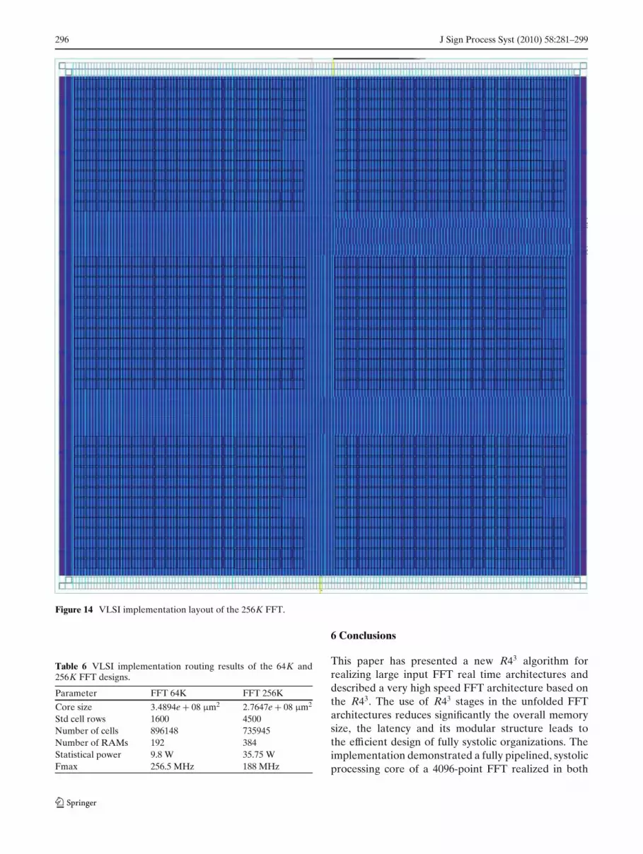
In the case of the very large 256K FFT, tool capacitymandated the use of a hierarchical flow. Following thesame front-end synthesis process (again optimized for300 MHz), the optimized netlist was read into CadenceSoC encounter where partitioning was first performed.This process created six instances of the 256K memoryblock (for a total of 1.5 MB of on-chip SRAM) whichwere individually placed and routed. The same processwas performed for the R43 engines and the twiddleROM block. Note that to complete the entire FFT com-putation it requires a 3-frame latency (786792 cycles)and the computation latency within the three R43 (360cycles), which is 4.1 ms.The 256K FFT architecturehas a post routing frequency of 188 MHz. Finally, thedesign was brought back into the top-level for final top-level placement, routing and timing analysis.Figure 14depicts the VLSI Cell for the 256K FFT design andTable 6 shows the VLSI Implementation Routing Re-sults of the 64K and 256K FFT designs.
Figure 13 Block diagram ofthe 256K FFT architecture.
296 J Sign Process Syst (2010) 58:281–299
Figure 14 VLSI implementation layout of the 256K FFT.
Table 6 VLSI implementation routing results of the 64K and256K FFT designs.
Parameter FFT 64K FFT 256K
Core size 3.4894e + 08 μm2 2.7647e + 08 μm2
Std cell rows 1600 4500Number of cells 896148 735945Number of RAMs 192 384Statistical power 9.8 W 35.75 WFmax 256.5 MHz 188 MHz
6 Conclusions
This paper has presented a new R43 algorithm forrealizing large input FFT real time architectures anddescribed a very high speed FFT architecture based onthe R43. The use of R43 stages in the unfolded FFTarchitectures reduces significantly the overall memorysize, the latency and its modular structure leads tothe efficient design of fully systolic organizations. Theimplementation demonstrated a fully pipelined, systolicprocessing core of a 4096-point FFT realized in both

J Sign Process Syst (2010) 58:281–299 297
FPGA and standard cell technologies and validated inreal hardware in the former case. The results proved thevery high operating frequencies and the low latencies ofboth the FPGA and VLSI implementations.
Furthermore, this work has described the design of16K and 64K complex point FFT architectures, whichare based on the 4096 FFT core and they accommo-date giga-sample applications. Also, to show the highutility prospects of the efficient 4K point FFT core indesigning large input FFT architectures this paper haspresented the straightforward implementation of 256Kpoint FFT VLSI solution.
References
1. Ersoy, O. K. (1997). Fourier-related transforms, fast algo-rithms and applications. Englewood Cliffs: Prentice Hall.
2. Thompson, C. D. (1983). Fourier transform in VLSI. IEEETransactions on Computers, 32, 1047–1057.
3. Wold, E. H., & Despain, A. M. (1984). Pipeline and parallelFFT processors for VLSI implementations. IEEE Transac-tions on Computers, C-33, 414-426.
4. He, S., & Torkelson, M. (1996). A new approach to pipelineFFT processor. In Proceedings of the IPPS.
5. Choi, S., Govindu, G., Jang, J. W., & Prasanna, V. K. (2003).Energy-efficient and parameterized designs of fast fouriertransforms on FPGAs. In The 28th international conferenceon acoustics, speech, and signal processing (ICASSP).
6. Uzun, I. S., Amira, A., & Bouridane, A. (2005). FPGA imple-mentations of fast fourier transforms for real-time signal andimage processing. IEEE Vision, Image and Signal Processing,152, 283–296.
7. Oppenheim, A., & Schafer, R. (1975). Digital signal process-ing. Englewood Cliffs: Prentice Hall.
8. Lee, J., Lee, J., Sunwoo, M. H., Moh, S., & Oh, S. (2002).A DSP architecture for high-speed FFT in OFDM systems.ETRI Journal, 24, 391–397.
9. He, S., & Torkelson, M. (1998). Design and implementationof a 1024-point pipeline FFT processor. In IEEE 1998 Cus-tom integrated circuits.
10. Rabiner, L. R., & Gold, B. (1975). Theory and application ofdigital signal processing. Englewood Cliffs: Prentice-Hall.
11. Suter, B., & Stevens, K. S. (1998). A low power, high per-formance approach for time-frequency / time-scale computa-tions. In Proceedings SPIE98 conference on advanced signalprocessing algorithms, architectures and implementations VIII(Vol. 3461, pp. 86–90).
12. Lenart, T., & Owall, V. (2003). A 2048 complex point FFTprocessor using a novel data scaling approach. In IEEEISCAS.
13. Cortes, A., Velez, I., Zalbide, I., Irizar, A., & Sevillano,J. F. (2006). An FFT core for DVB-T/DVB-H receivers. InICECS’06 (pp. 102–105).
14. Maharatna, K., Grass, E., & Jagdhold, U. (2004). A 64-pointfourier transform chip for high-speed wireless LAN appli-cations using OFDM. IEEE Journal of Solid-State Circuits,39(3), 484–493.
15. Oh, J. Y., & Lim, M. S. (2005). New radix-2 to the 4th powerpipeline FFT processor. IEICE Transactions on Electronics,E88-C(8), 1740–1746.
16. Bouguezel, S., Ahmad, M. O., & Swamy, M. N. S. (2004). Anew radix-2/8 FFT algorithm for length−q × 2m DFTs. IEEETransactions on Circuits and Systems I, 51(9), 1723–1732.
17. Jo, B. G., & Sunwoo, M. H. (2005). New cotinuous-flowmixed-radix (CFMR) FFT processor using novel in-placestrategy. IEEE Transactions on Circuits and Systems I, 52(5),911–919.
18. Bouguezel, S., Ahmad, M. O., & Swamy, M. N. S. (2006).New radix-(2 × 2 × 2)/(4 × 4 × 4) and radix-(2 × 2 × 2)/(8 ×8 × 8) DIF FFT algorithms for 3-D DFT. IEEE Transactionson Circuits and Systems I, 53(2), 306—315.
19. Chang, W. H., & Nguyen, T. (2006). An OFDM-specifiedlossless FFT architecture. IEEE Transactions on Circuits andSystems I, 53(6), 1235–1243.
20. Yang, L., Zhang, K., Liu, H., Huang, J., & Huang, S. (2006).An efficient locally pipelined FFT processor. IEEE Transac-tions on Circuits and Systems II, 53(7), 585–589.
21. Lin, Y. N., Liu, H. Y., & Lee, C. Y. (2005). A 1-GS/sFFT/IFFT processor for UWB applications. IEEE Journal ofSSC, 40(8).
22. Takala, J., & Punkka, K. (2006). Scalable FFT processors andpipelined butterfly units. Journal of VLSI Signal Processing,43, 113–123.
23. Wang, S. S., & Li, C. S. (2007). An area-efficient design ofvariable-length fast Fourier transform processor. Journal ofVLSI Signal Processing.
24. Reisis, D., & Vlassopoulos, N. (2006). Address generationtechniques for conflict free parallel memory accessing in FFTarchitectures. In ICECS (1188–1191), December.
25. Bidet, E., Castelain, D., Joanblanq, C., & Stenn, P. (1995). Afast single-chip implementation of 8192 complex point FFT.IEEE Journal of SSC, 30(3), 300–305.
26. Swartzlander, E. E. Jr. (2007). Systolic FFT processors: Apersonal perspective. Journal of VLSI Signal Processing, 53,3–14.
K. Babionitakis has received his M.Sc. in Electronics and Au-tomation and B.Sc. in Physics studying at the Department ofPhysics of the National and Kapodistrian University of Athens.His research interests include parallel algorithms and efficientVLSI implementations.

298 J Sign Process Syst (2010) 58:281–299
Vassilios A. Chouliaras was born in Athens, Greece in 1969.He received a B.Sc. in Physics and Laser Science from Heriot-Watt University, Edinburgh in 1993, a M.Sc. in VLSI SystemsEngineering from UMIST in 1995 and a PhD in embeddedsystems and the software hardware interface from LoughboroughUniversity, UK, in 2005. He worked as an ASIC design engineerfor INTRACOM SA and as a senior R&D engineer/processorarchitect for ARC International. Currently, he is a senior lecturerin microelectronics in the Department of Electronic and Electri-cal Engineering at the University of Loughborough, UK wherehe’s leading the research in CPU architecture and microarchi-tecture, SoC modeling and software parallelization. His researchinterests include CPU microarchitecture, high-performance em-bedded CPU implementations, performance modeling, custominstruction set design and Electronic System Level (ESL) designmethodologies. He is one of the founders of Axilica Ltd.
K. Manolopoulos is a Ph.D. candidate at the Departmentof Physics of the National and Kapodistrian University ofAthens. In 2003 he received his M.Sc. in Electronics andAutomation and in 2001 his degree in Physics, both from theDepartment of Physics in Athens. His research interests includein computational models and algorithms for parallel processing,reconfigurable and parallel architectures, power analysis andoptimization in digital designs.
K. Nakos received his Ph.D. at the Department of Physics ofthe National and Kapodistrian University of the Athens with re-search subject: “Parallel and Real-Time Architectures for Signal,Image and Video Processing” in 2008. In 2003 he was awardedhis M.Sc. in Electronics and Automation and in 2001 his degreein Physics, both from the Department of Physics in Athens. Hisresearch interests lie in parallel algorithms, reconfigurable andparallel architectures, computational complexity and theory ofalgorithms and computational geometry.
D. Reisis has received his Ptychion in Electrical Engineeringfrom the University of Patras, Greece, in 1983, and his M.Sc. andPh.D. degrees in Computer Engineering from the Departmentof Electrical and Computer Engineering of the University ofSouthern California, USA, in 1989 with Ph.D. thesis: “Paral-lel Algorithms on Mesh Connected Computer with Static andReconfigurable Buses”. This research involved parallel meshcomputers and algorithms for signal, image and graph processing,vision and VLSI architectures. In 1990 he started cooperationwith the Telecommunications lab of the Division of ComputerScience of NTUA as a research associate. In 1991 he has beenelected Lecturer and in 1996 Assistant Professor of the Electron-ics Laboratory of the Department of Physics of the Universityof Athens (NKUA). His interests include parallel architecturesand algorithms for image and graph signal processing with ap-plications in VLSI environment, as well as real time hardwaredesign and efficient algorithms design for telecommunicationsystem support. Apart from his participation in projects (ONR,DARPA, NSF, RACE, ACTS, IST) he has publications in sci-entific magazines (IEEE transactions on Computers, on PAMI)and conferences (ICPP, IPPS, MIT on VLSI, CVPR, UUCP,ISS, etc.) and has co-written books on parallel processing. Heis a reviewer in magazines (IEEE transactions, JPDC, SIAM onComputing, etc.) and conferences (ICPP, IPPS, CVPR, etc.).

J Sign Process Syst (2010) 58:281–299 299
N. Vlassopoulos graduated from the Department of Physics atthe National and Kapodistrian University of Athens in 2000. Hecontinued his studies attaining a M.Sc. in Electronics Automa-tion in 2002. He received his Ph.D. with subject “Parallel andReconfigurable Architectures” in 2008. His research interests liein computational complexity and theory of algorithms, parallelalgorithms, computational models and cryptography.


