Embed Size (px)
Citation preview

bard060100
1
1Fundamentals of SemiconductorElectrochemistry andPhotoelectrochemistry
Krishnan RajeshwarThe University of Texas at Arlington, Arlington,Texas
1.1Introduction and Scope
The study of semiconductor–electrolyteinterfaces has both fundamental and prac-tical incentives. These interfaces have in-teresting similarities and differences withtheir semiconductor–metal (or metal ox-ide) and metal–electrolyte counterparts.Thus, approaches to garnering a funda-mental understanding of these interfaceshave stemmed from both electrochem-istry and solid-state physics perspectivesand have proven to be equally fruitful.On the other hand, this knowledge basein turn impacts many technologies, in-cluding microelectronics, environmentalremediation, sensors, solar cells, and en-ergy storage. Some of these are discussedelsewhere in this volume.
It is instructive to first examine thehistorical evolution of this field. Earlywork in the fifties and sixties undoubtedlywas motivated by application possibili-ties in electronics and came on the heelsof discovery of the first transistor. Elec-tron transfer theories were also rapidlyevolving during this period, starting fromhomogeneous systems to heterogeneous
metal-electrolyte interfaces leading, inturn, to semiconductor-electrolyte junc-tions. The 1973 oil embargo and the ensu-ing energy crisis caused a dramatic spurtin studies on semiconductor–electrolyteinterfaces once the energy conversionpossibilities of the latter were realized.Subsequent progress at both fundamen-tal and applied levels in the late eightiesand nineties has been more gradual andsustained. Much of this later research hasbeen spurred by technological applicabilityin environmental remediation scenarios.Very recently, however, renewed interestin clean energy sources that are nonfos-sil in origin, has provided new impetusto the study of semiconductor–electrolyteinterfaces. As we also learn to under-stand and manipulate these interfaces atan increasingly finer (atomic) level, newmicroelectronics application possibilitiesmay emerge, thus completing the cyclethat first began in the 1950s.
The ensuing discussion of the progressthat has been made in this field mainlyhinges on studies that have appeared sinceabout 1990. Several review articles andchapters have appeared since then thatdeal with semiconductor–electrolyte in-terfaces [1–10]; aspects related to electrontransfer are featured in several of these.This author is also aware of at least threebooks/monographs/proceedings volumes

bard060100
2 1 Fundamentals of Semiconductor Electrochemistry and Photoelectrochemistry
that have appeared since 1990 [11–13]. Thereader is referred to the many authorita-tive accounts that exist before this timeframe for a thorough coverage of detailson semiconductor–electrolyte interfacesin general. Entry to this early literaturemay be found in the references citedearlier. In some instances, however, thediscussion that follows necessarily delvesinto research dating back to the 1970s and1980s.
To facilitate a self-contained descrip-tion, we will start with well-establishedaspects related to the semiconductor en-ergy band model and the electrostaticsat semiconductor–electrolyte interfaces inthe ‘‘dark’’. We shall then examine theprocesses of light absorption, electron-holegeneration, and charge separation at theseinterfaces. The steady state and dynamicaspects of charge transfer are then brieflyconsidered. Nanocrystalline semiconduc-tor films and size quantization are thendiscussed as are issues related to elec-tron transfer across chemically modifiedsemiconductor–electrolyte interfaces. Fi-nally, we shall introduce the various typesof photoelectrochemical devices rangingfrom regenerative and photoelectrolysiscells to dye-sensitized solar cells.
1.2Electron Energy Levels in Semiconductorsand Energy Band Model
Unlike in molecular systems, semiconduc-tor energy levels are so dense that theyform, instead of discrete molecular or-bital energy levels, broad energy bands.Consider a solid composed of N atoms.Its frontier band will have 2-N energyeigenstates, each with an occupancy oftwo electrons of paired spin. Thus, a solidhaving atoms with odd number of valence
electrons (e.g. Al with [Ne]3s23p1) will havea partially occupied frontier band in whichthe electrons are delocalized. On the otherhand, a solid with an even number of va-lence electrons (e.g. Si having an electronconfiguration of [Ne]3s22p2) will have afully occupied frontier band (termed a va-lence band, (VB)). The situation for Si isschematized in Fig. 1.
As Fig. 2 illustrates, the distinctionbetween semiconductors and insulatorsis rather arbitrary and resides with themagnitude of the energy band gap (Eg)between the filled and vacant bands.Semiconductors typically have Eg in the1 eV–4 eV range (Table 1). The vacantfrontier band is termed a conduction band,(CB) (Fig. 2). We shall see later that Eg
has an important bearing on the opticalresponse of a semiconductor.
For high density electron ensemblessuch as valence electrons in metals, Fermistatistics is applicable. In a thermodynamicsense, the Fermi level, EF (defined at 0 K
Tab. 1 Some elemental and compoundsemiconductors for photoelectrochemicalapplications
Semi- Conductivity Opticalconductor type(s) band gap
energy [eV]a
Si n, p 1.11GaAs n, p 1.42GaP n, p 2.26InP n, p 1.35CdS n 2.42CdSe n 1.70CdTe n, p 1.50TiO2 n 3.00(rutile)
3.2(anatase)ZnO n 3.35
aThe values quoted are for the bulksemiconductor. The gap energies increase in thesize quantization regime (see Sect. 7).

bard060100
1 Fundamentals of Semiconductor Electrochemistry and Photoelectrochemistry 3
4 N states0 electrons
4 N states4 N electrons
Distance
Ele
ctro
n en
ergy
6 N electrons
2 N states
2 N states
2 N electrons
3p
3s
Eg
ro
Fig. 1 Schematic illustration of how energy bands insemiconductors evolve from discrete atomic states for the specificexample of silicon.
Fig. 2 Relative disposition ofthe CB and VB for a semi-conductor (a) and an insu-lator (b). Eg is the optical bandgap energy.
CB
VB
(a) (b)
VB
CB
Eg
Eg
as the energy at which the probabilityof finding an electron is 1/2) can beregarded as the electrochemical potentialof the electron in a particular phase (inthis case, a solid). Thus, all electronicenergy levels below EF are occupied
and those above EF are likely to beempty.
Electrons in semiconductors may beregarded as low-density particle ensemblessuch that their occupancy in the valenceand CBs may be approximated by the

bard060100
4 1 Fundamentals of Semiconductor Electrochemistry and Photoelectrochemistry
Boltzmann function [14, 15]:
ne ≈ No exp[−Eo − EF
kT
](1)
Now we come to another impor-tant distinction between metals andsemiconductors in that two types of elec-tronic carriers are possible in the latter.Consider the thermal excitation of an elec-tron from VB to CB. This gives rise to afree electron in the CB and a vacancy orhole in the VB. A localized chemical pic-ture for the case of Si shows that the holemay be regarded as a missing electron ina chemical bond (Fig. 3). There is a crudechemical analogy here with the dissocia-tion of a solvent such as water into H3O+and OH−. In either case, equal numbers ofoppositely charged species are produced.Thus, Eq. (1) becomes:
ni ≈ Nc exp
[−EF − Ec
kT
](2)
pi ≈ Nv exp
[−Ev − EF
kT
](3)
In Eqs. (2) and (3), Nc and Nv are theeffective density of states (in cm−3) atthe lower edge and top edge of CB andVB, respectively. These expressions canbe combined with the recognition thatni = pi to yield
n2i ≈ No exp
[−Ec − Ev
kT
]
≈ No exp[−Eg
kT
](4)
To provide a numerical sense of thesituation, Nc and Nv are typically both ap-proximately 1019 cm−3 so that the constantNo (NcNv) in Eq. (1) is about 1038 cm−3.For a semiconductor such as Si (withEg = 1.11 eV, Table 1), ni will be about1010 cm−3 at 300 K according to Eq. (4).This rough calculation lends credence tothe original rationale for the use of Boltz-mann statistics for the electron energydistribution in semiconductors (see pre-ceding section).
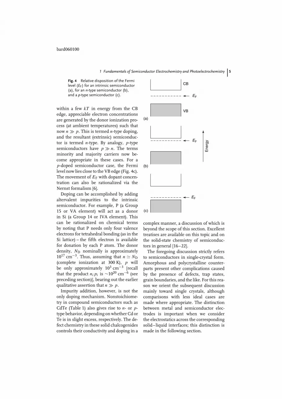
The preceding case refers to the semi-conductor in its intrinsic state with verylow carrier concentrations under ambientconditions. The Fermi level, EF, in thiscase lies approximately in the middle ofthe energy band gap (Fig. 4a). This sim-ply reflects the fact that the probability ofelectron occupancy is very high in VB andvery low in CB and does not imply anoccupiable energy level at EF itself.
In extrinsic semiconductors the carrierconcentrations are perturbed such thatn = p. Again the analogy with the addi-tion of an acid or base to water is quiteinstructive here. Consider the case whendonor impurities are added to a neutralsemiconductor. Since the intrinsic carrierconcentrations are so low (sub-parts pertrillion), even additions in parts per bil-lion levels can have a profound electricaleffect. This process is known as dopingof the semiconductor. In this particularcase, the Fermi level shifts toward the CBedge (Fig. 4b). When the donor level is
e−
h+e−
h+
Si SiSi
(+) (−)
SiSiSi Si Fig. 3 A localized picture ofelectron-hole pair generation(see also Fig. 2a) in silicon.
bard060100
1 Fundamentals of Semiconductor Electrochemistry and Photoelectrochemistry 5
within a few kT in energy from the CBedge, appreciable electron concentrationsare generated by the donor ionization pro-cess (at ambient temperatures) such thatnow n p. This is termed n-type doping,and the resultant (extrinsic) semiconduc-tor is termed n-type. By analogy, p-typesemiconductors have p n. The termsminority and majority carriers now be-come appropriate in these cases. For ap-doped semiconductor case, the Fermilevel now lies close to the VB edge (Fig. 4c).The movement of EF with dopant concen-tration can also be rationalized via theNernst formalism [6].
Doping can be accomplished by addingaltervalent impurities to the intrinsicsemiconductor. For example, P (a Group15 or VA element) will act as a donorin Si (a Group 14 or IVA element). Thiscan be rationalized on chemical termsby noting that P needs only four valenceelectrons for tetrahedral bonding (as in theSi lattice) – the fifth electron is availablefor donation by each P atom. The donordensity, ND nominally is approximately1017 cm−3. Thus, assuming that n ND
(complete ionization at 300 K), p willbe only approximately 103 cm−3 [recallthat the product nipi is ∼1020 cm−6 (seepreceding section)], bearing out the earlierqualitative assertion that n p.
Impurity addition, however, is not theonly doping mechanism. Nonstoichiome-try in compound semiconductors such asCdTe (Table 1) also gives rise to n- or p-type behavior, depending on whether Cd orTe is in slight excess, respectively. The de-fect chemistry in these solid chalcogenidescontrols their conductivity and doping in a
Fig. 4 Relative disposition of the Fermilevel (EF) for an intrinsic semiconductor(a), for an n-type semiconductor (b),and a p-type semiconductor (c).
Ene
rgy
CB
(a)
VB
EF
(b)
EF
(c)
EF
complex manner, a discussion of which isbeyond the scope of this section. Excellenttreatises are available on this topic and onthe solid-state chemistry of semiconduc-tors in general [16–22].
The foregoing discussion strictly refersto semiconductors in single-crystal form.Amorphous and polycrystalline counter-parts present other complications causedby the presence of defects, trap states,grain boundaries, and the like. For this rea-son we orient the subsequent discussionmainly toward single crystals, althoughcomparisons with less ideal cases aremade where appropriate. The distinctionbetween metal and semiconductor elec-trodes is important when we considerthe electrostatics across the correspondingsolid–liquid interfaces; this distinction ismade in the following section.

bard060100
6 1 Fundamentals of Semiconductor Electrochemistry and Photoelectrochemistry
1.3The Semiconductor–Electrolyte Interface atEquilibrium
1.3.1 The Equilibration ProcessThe electrochemical potential of electronsin a redox electrolyte is given by the Nernstexpression
Eredox = Eredox + RT
nFln
[cox
cred
](5)
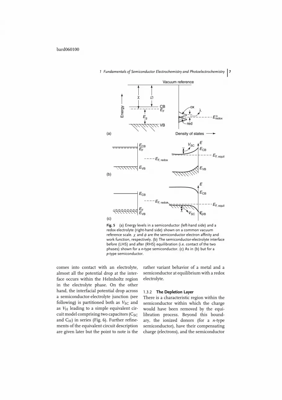
In Eq. (5), cox and cred are the concen-trations (roughly activities) of the oxidizedand reduced species, respectively, in theredox couple. The parameter (Eredox =µe,redox) as defined by Eq. (5) can be iden-tified with the Fermi level (EF,redox) inthe electrolyte. This was the topic of de-bate some years back [23], although thispremise now appears to be well founded.The task now is to relate the electron en-ergy levels in the solid and liquid phaseson a common basis.
The semiconductor solid-state physicscommunity has adopted the electronenergy in vacuum as reference, whereaselectrochemists have traditionally usedthe standard hydrogen electrode (SHE)scale. While estimates vary [23–25], SHEappears to lie at −4.5 eV with respect to thevacuum level. We are now in a position torelate the redox potentialEredox (as definedwith reference to SHE) with the FermilevelEF,redox expressed versus the vacuumreference (Fig. 5a)
EF,redox = −4.5 eV − eoEredox (6)
When a semiconductor is immersed inthis redox electrolyte, the electrochemicalpotential (Fermi level) is disparate acrossthe interface. Equilibration of this inter-face thus necessitates the flow of chargefrom one phase to the other and a ‘‘bandbending’’ ensues within the semiconduc-tor phase. The situation before and after
contact of the two phases is illustratedin Fig. 5(b) and (c) for an n-type andp-type semiconductor, respectively. Aftercontact, the net result of equilibration isthatEF = EF,redox and a ‘‘built-in’’ voltage,VSC develops within the semiconductorphase, as illustrated in the right handframes of Fig. 5(b) and (c).
It is instructive to further examinethis equilibration process. Consider againan n-type semiconductor for illustrativepurposes (Fig. 5b). The electronic chargeneeded for Fermi level equilibration in thesemiconductor phase originates from thedonor impurities (rather than from bond-ing electrons in the semiconductor lattice).Thus, the depletion layer that arises asa consequence within the semiconduc-tor contains positive charges from theseionized donors. The Fermi level in thesemiconductor (EF,n) moves ‘‘down’’ andthe process stops when the Fermi level isthe same on either side of the interface.The rather substantial difference in thedensity of states on either side dictates thatEF,n moves farther than the correspondinglevel, EF,redox in the electrolyte. A partic-ularly lucid account of this initial chargetransfer is contained in Ref. 6.
The band-bending phenomenon, shownin Fig. 5(b) and (c), is by no meansunique to the semiconductor–electrolyteinterface. Analogous electrostatic adjust-ments occur whenever two dissimilarphases are in contact (e.g. semiconductor-gas, semiconductor–metal). An importantpoint of distinction from the correspond-ing metal case now becomes apparent.For a metal, the charge, and thus the as-sociated potential drop, is concentratedat the surface penetrating at most afew A into the interior. Stated differ-ently, the high electronic conductivity ofa metal cannot support an electric fieldwithin it. Thus, when a metal electrode
bard060100
1 Fundamentals of Semiconductor Electrochemistry and Photoelectrochemistry 7
Vacuum reference
CB
χ ∅
ox
VB red
E
Density of states
EF
EF
EF
ECB
ECB
VSC
EVB
EVB
ECB
EVB
ECB
EVB
VSC
EF, equil
EF, equil
E
EF, redox
EF, redox
Eg
(a)
(c)
(b)
Ene
rgy
Eredoxo
λ
Fig. 5 (a) Energy levels in a semiconductor (left-hand side) and aredox electrolyte (right-hand side) shown on a common vacuumreference scale. χ and φ are the semiconductor electron affinity andwork function, respectively. (b) The semiconductor-electrolyte interfacebefore (LHS) and after (RHS) equilibration (i.e. contact of the twophases) shown for a n-type semiconductor. (c) As in (b) but for ap-type semiconductor.
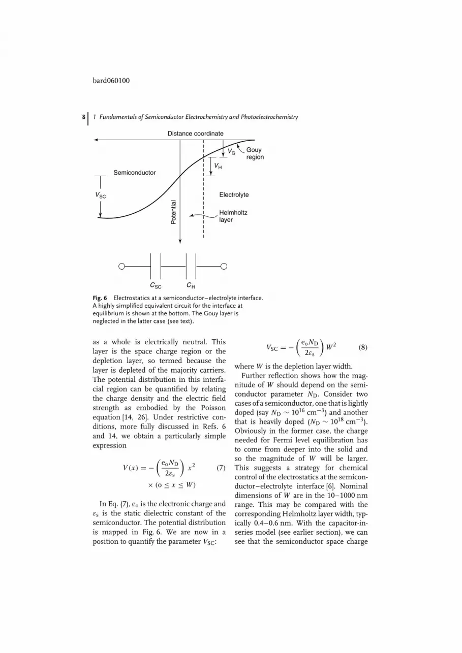
comes into contact with an electrolyte,almost all the potential drop at the inter-face occurs within the Helmholtz regionin the electrolyte phase. On the otherhand, the interfacial potential drop acrossa semiconductor-electrolyte junction (seefollowing) is partitioned both as VSC andas VH leading to a simple equivalent cir-cuit model comprising two capacitors (CSC
and CH) in series (Fig. 6). Further refine-ments of the equivalent circuit descriptionare given later but the point to note is the
rather variant behavior of a metal and asemiconductor at equilibrium with a redoxelectrolyte.
1.3.2 The Depletion LayerThere is a characteristic region within thesemiconductor within which the chargewould have been removed by the equi-libration process. Beyond this bound-ary, the ionized donors (for a n-typesemiconductor), have their compensatingcharge (electrons), and the semiconductor
bard060100
8 1 Fundamentals of Semiconductor Electrochemistry and Photoelectrochemistry
Distance coordinate
Gouyregion
Electrolyte
SemiconductorP
oten
tial
Helmholtzlayer
VH
VSC
CSC CH
VG
Fig. 6 Electrostatics at a semiconductor–electrolyte interface.A highly simplified equivalent circuit for the interface atequilibrium is shown at the bottom. The Gouy layer isneglected in the latter case (see text).
as a whole is electrically neutral. Thislayer is the space charge region or thedepletion layer, so termed because thelayer is depleted of the majority carriers.The potential distribution in this interfa-cial region can be quantified by relatingthe charge density and the electric fieldstrength as embodied by the Poissonequation [14, 26]. Under restrictive con-ditions, more fully discussed in Refs. 6and 14, we obtain a particularly simpleexpression
V (x) = −(
eoND
2εs
)x2 (7)
× (o ≤ x ≤ W)
In Eq. (7), eo is the electronic charge andεs is the static dielectric constant of thesemiconductor. The potential distributionis mapped in Fig. 6. We are now in aposition to quantify the parameter VSC:
VSC = −(
eoND
2εs
)W 2 (8)
whereW is the depletion layer width.Further reflection shows how the mag-
nitude of W should depend on the semi-conductor parameter ND. Consider twocases of a semiconductor, one that is lightlydoped (say ND ∼ 1016 cm−3) and anotherthat is heavily doped (ND ∼ 1018 cm−3).Obviously in the former case, the chargeneeded for Fermi level equilibration hasto come from deeper into the solid andso the magnitude of W will be larger.This suggests a strategy for chemicalcontrol of the electrostatics at the semicon-ductor–electrolyte interface [6]. Nominaldimensions of W are in the 10–1000 nmrange. This may be compared with thecorresponding Helmholtz layer width, typ-ically 0.4–0.6 nm. With the capacitor-in-series model (see earlier section), we cansee that the semiconductor space charge

bard060100
1 Fundamentals of Semiconductor Electrochemistry and Photoelectrochemistry 9
layer is usually the determinant factor inthe total capacity of the interface. Onceagain, the contrast with the correspond-ing metal–electrolyte interface is striking.Only when the semiconductor is degener-ately doped (leading to rather large spacecharge layer charge,QSC and ‘‘thin’’ deple-tion layer widths) or when its surface is inaccumulation does the situation becomeakin to the metal–electrolyte interface (seefollowing).
1.3.3 Mapping of the SemiconductorBand-edge Positions Relative to SolutionRedox LevelsConsiderations of interfacial electrontransfer require knowledge of the relativepositions of the participating energy levelsin the two (semiconductor and solution)phases. Models for redox energy levelsin solution have been exhaustively treatedelsewhere [27, 28]. Besides the Fermi levelof the redox system (Eq. 6), the thermalfluctuation model [27, 28] leads to a Gaus-sian distribution of the energy levels for theoccupied (reduced species) and the empty(oxidized species) states, respectively, asillustrated in Fig. 5(a). The distributionfunctions for the states are given by
Dox = exp
[−E − EF,redox − λ2
4 kT λ
](9a)
Dred = exp
[−E − EF,redox + λ2
4 kT λ
](9b)
In Eqs. (9a) and (9b), λ is the solventreorganization energy.
Now consider the relative disposition ofthese solution energy levels with respect tothe semiconductor band edge positions atthe interface. The total potential differenceacross this interface (Fig. 6) is given by
Vt = VSC + VH + VG (10)
In Eq. (10), Vt is the potential as measuredbetween an ohmic contact on the rearsurface of the semiconductor electrodeand the reference electrode (Fig. 6). Theproblematic factors in placing the semi-conductor and solution energy levels ona common basis involve VH and VG. Inother words, theoretical predictions of themagnitude of VSC (and how it changes asthe redox couple is varied) are hamperedby the lack of knowledge on the magnitudeof VH and VG. A degree of simplificationis afforded by employing relatively con-centrated electrolytes such that VG can beignored.
As with metals, the Helmholtz layeris developed by adsorption of ions ormolecules on the semiconductor surface,by oriented dipoles, or especially in thecase of oxides, by the formation of sur-face bonds between the solid surface andspecies in solution. Recourse to bandedge placement can be sought throughdifferential capacitance measurements onthe semiconductor–redox electrolyte inter-face [29].
In the simplest case as more fully dis-cussed elsewhere [14, 15, 29], one obtainsthe Mott-Schottky relation (for the spe-cific instance of a n-type semiconductor) ofthe semiconductor depletion layer capaci-tance (CSC), again by invoking the Poissonequation
1/C2SC = 2
NDeoεs
[(V − Vfb)− kT
eo
](11)
In Eq. (11), Vfb is the so-called flat bandpotential, that is the applied potential(V ) at which the semiconductor energybands are ‘‘flat’’, leading up to the solutionjunction. Several points with respect to theapplicability of Eq. (11) must be noted.
The Mott-Schottky regime spans about1 V in applied bias potential for mostsemiconductor–electrolyte interfaces (i.e.

bard060100
10 1 Fundamentals of Semiconductor Electrochemistry and Photoelectrochemistry
in the region of depletion layer formationof the semiconductor space charge layer,see preceding section) [15]. The simplecase considered here involves no mediatortrap states or surface states at the inter-face such that the equivalent circuit of theinterface essentially collapses to its mostrudimentary form of CSC in series withthe bulk resistance of the semiconductor.Further, in all the earlier discussions, it isreiterated that the redox electrolyte is suffi-ciently concentrated that the potential dropacross the Gouy (diffuse) layer in the solu-tion can be neglected. Specific adsorptionand other processes at the semiconduc-tor–electrolyte interface will influence Vfb;these are discussed elsewhere [29, 30] asare anomalies related to the measurement
process itself [31]. Figure 7 contains repre-sentative Mott-Schottky plots for both n-and p-type GaAs electrodes in an ambienttemperature molten salt electrolyte [32].
Once Vfb is known (from measure-ments), the Fermi level of the semicon-ductor at the surface is defined. It isthen a simple matter to place the ener-gies corresponding to the conduction andVBs at the surface (ECB and EVB, respec-tively) if the relevant doping levels areknown. The difference between ECB andEVB should approximately correspond tothe semiconductor band gap energy, Eg(see Figs. 4 and 7). Alternatively, if Vfb ismeasured for one given state of dopingof the semiconductor (n- or p-doped), theother band edge position can be fixed from
8.0 × 1013 × 1015
6.4
4.8
I C−2
[fara
d−2]
I C−2
[fara
d−2]
3.2
1.6
0
4.0
3.2
2.4
1.6
0.8
0−0.5 −0.1 0.3 0.7
Potential
[V vs Al0/3+]
1.1 1.5
Fig. 7 Mott-Schottky plots for n- and p-type GaAs electrodes in an AlCl3/n-butylpyridinium chloridemolten-salt electrolyte. (Reproduced with permission from Ref. 32.)

bard060100
1 Fundamentals of Semiconductor Electrochemistry and Photoelectrochemistry 11
knowledge of Eg. It is important to stressthat the semiconductor surface band edgepositions (as estimated from Vfb measure-ments) comprises all the terms in Eq. (10)and reflects the situation in situ for agiven set of conditions (solution pH, redoxconcentration, etc.) of the semiconductor-redox electrolyte. The situation obviouslybecomes complex when the charge dis-tribution and mediation at the interfacechanges either via surface states and illu-mination or in a both. These complicationsare considered later. Figure 8 contains therelative dispositions of the surface bandedges mapped for a number of semicon-ductors in aqueous media.
Having located the semiconductor bandedge positions (relative either to thevacuum reference or a standard referenceelectrode), we can also place the Fermi
level of the redox system, EF,redox, onthe same diagram. Energy diagrams suchas those in Fig. 8 are important inconsiderations of charge transfer as weshall see later. In anticipation of thisdiscussion, it is apparent that the threesituations illustrated in Fig. 9 for an n-typesemiconductor–electrolyte interface entailthe participation of the semiconductor CB,VB, and even states in its band gap incharge exchange with the solution species.Here again is a point of departure fromthe metal case; viz., for a semiconductor,hole, electron, and surface state pathwaysmust all be considered.
Let us return to the band bendingprocess at the interface. For a givensemiconductor, the expectation is that asthe redox Fermi level is moved morepositive (‘‘down’’ on the energy diagram),
Vacuum scale[eV] SHE
[V]
CdS
CdSe
1.7 eV
1.4 eV
2.3 eV 1.1 eV 1.5 eV
TiO2
GaAs GaP
∼3.0 eV
∼1.3 eV
Si CdTeInP2.4 eV
0
−3.0 −1.5
−4.0 −0.5
+1.0
+2.0
+3.0
0
Ene
rgy
Pot
entia
l
−4.5
−5.0
−6.0
−7.0
−8.0
Fig. 8 Relative dispositions of various semiconductor band edge positionsshown both on the vacuum scale and with respect to the SHE reference.These band edge positions are for an aqueous medium of pH ∼1.

bard060100
12 1 Fundamentals of Semiconductor Electrochemistry and Photoelectrochemistry
CB CB
VB VBVB
(a) (b) (c)
CB
Ene
rgy
EFEFEF
ESS Eredoxo
Eredoxo
Eredox
Fig. 9 Three situations for a n-typesemiconductor–electrolyte interface atequilibrium showing overlap of the redox energylevels with the semiconductor CB (a), with
surface states (b), and with the semiconductorVB (c). A discrete energy level is assumed for thesurface states as a first approximation.
VSC should increase concomitantly. This isthe ideal (band edge ‘‘pinned’’) situation.In other words [23]
dVSC
dEredox= 1 (12)
Equation (12) reflects the fact that thechange in band bending faithfully tracksthe redox potential change. A mea-sure of the former is the open-circuit
photopotential (see following). Figure 10shows that this ideal situation indeedis realized for selected semiconduc-tor–electrolyte interfaces [33]. As furtherdiscussed later, the analogy with the corre-sponding metal-semiconductor junctions(Schottky barriers) is direct [5, 34–36].
Complications arise when there are sur-face states that mediate charge exchangeat the interface. When their density is
1.2
0.8
Vph [V]
0.4
0.0−0.4 0.0
I
Vredox[V vs. SCE]
+0.4
slope = 1.0
Fig. 10 Plot of the open-circuitphotovoltage for amorphousSi-methanol interfacescontaining a series ofone-electron redox couples.(Reproduced with permissionfrom Ref. 33.)

bard060100
1 Fundamentals of Semiconductor Electrochemistry and Photoelectrochemistry 13
high [37], they act as a ‘‘buffer’’, in thatin the extreme case, carriers in the semi-conductor energy bands are completelyexcluded from the equilibration process.
1.3.4 Surface States and OtherComplicationsSurface states arise because of the abrupttermination of the crystal lattice at thesurface; obviously the bonding arrange-ment is different from that in the bulk.Consider our prototype semiconductor, Si.The tetrahedral bonding characteristic ofthe bulk gives way to coordinative unsat-uration of the bonds for the Si surfaceatoms. This unsaturation is relieved ei-ther by surface reconstruction or bondswith extraneous (e.g. solvent) species [29,38–40]. The surface bonding results in alocalized electronic structure for the sur-face that is different from the bulk. Theenergies of these localized surface orbitalsnominally lie in the forbidden band gapregion. The corresponding states are thusable (depending on their energy location)to exchange charge with the conductionor VBs of the semiconductor and/or theredox electrolyte [29].
Unlike the case illustrated in Fig. 10,changes in the solution redox potentialhave been observed to cause no changein the magnitude of VSC. This situa-tion is termed Fermi level pinning; inother words, the band edge positions areunpinned in these cases so that the move-ment of Eredox is accommodated by VH
rather than by VSC. As mentioned earlier,it appears [37] that surface state densitiesas low as 1013 cm−2 (∼1% of a mono-layer) suffice to induce complete Fermilevel pinning in certain cases. Of course,intermediate situations are possible. Thus,the ideal case manifests a slope of 1 in aplot of VSC (or an equivalent parameter)versus Eredox (see Fig. 10). On the other
hand, complete pinning results in a slopeof zero. Intermediate cases of Fermi levelexhibit slopes between 0 and 1 [41]. Asstated earlier, there is a direct analogyhere with the metal/semiconductor junc-tion counterparts [42, 43]:
φB = Sφm + const (13)
In Eq. (13), φB is the so-called Schottkybarrier height, φm is the metal work func-tion, and S is a dimensionless parameter.Attempts have been made to relate S tosemiconductor properties [44–48].
To further complicate matters, thenonideal behavior of semiconduc-tor–electrolyte interfaces as noted earlieris exacerbated when the latter are irradi-ated. Changes in the occupancy of thesestates cause further changes in VH, sothat the semiconductor surface band edgepositions are different in the dark and un-der illumination. These complications areconsidered later. The surface states as con-sidered earlier are shallow (with respect tothe band edge positions) and can essen-tially be considered as completely ionizedat room temperature. However, for manyoxide semiconductors, the trap states maybe deep and thus are only partially ionized.Specifically, they may be disposed withrespect to the semiconductor Fermi levelsuch that they are ionized only to a depththat is small relative to W [49]. The phys-ical manifestation of such deep traps asobserved in the AC impedance behavior ofsemiconductor–electrolyte interfaces hasbeen discussed [14, 49].
Finally, within the Mott-Schottky ap-proximation (Eq. 11), large values of εs orND can lead to the ratio VH/VSC becomingsignificant. Figure 11 contains estimatesof this ratio for several values of ND for asemiconductor with a large εs value (TiO2,εs = 173) mapped as a function of the totalpotential drop across the interface [50].

bard060100
14 1 Fundamentals of Semiconductor Electrochemistry and Photoelectrochemistry
23
1
45
6
7
8
9
10
11
12
13
1.0
0.8
0.6
0.4
∆VH
/∆V
SC
+ ∆
VH
∆VSC + ∆VH /V
0.2
00 0.2 0.4 0.6 0.8 1.0
Fig. 11 The ratio of the potential drop in the Helmholtz to thetotal potential change computed as a function of the totalpotential change. A static dielectric constant of 173 (typical ofTiO2) and a Helmholtz capacitance of 10 µF/cm2 were assumedand the doping density was allowed to vary from 1016 cm−3
(curve 1) to 1020 cm−3 (curve 13).
ClearlyVH can become a sizable fraction ofthe total potential drop (approaching thesituation for metals) under certain con-ditions. It has been shown [51] that theMott-Schottky plots will still be linear butthe intercept on the potential axis is shiftedfrom the Vfb value.
1.4Charge Transfer Processes in the Dark
1.4.1 Current-potential BehaviorLet us return to the equilibrium situationof an n-type semiconductor in contactwith a redox electrolyte and reconsiderthe situation in Fig. 9(a). This is shownagain in Fig. 12(a) to underscore the factthat the interface is in a state of dynamicequilibrium. That is, the forward andreverse (partial) currents exactly balanceeach other and there is no net currentflow across the interface. In fact, the
situation here is similar to that occurringfor a metal–redox electrolyte interface atthe rest potential. We can write downexpressions for the net current using akinetics methodology as in Ref. 6 withsome minor changes in notation:
ic = −eoAketcox(ns − nso) (14)
In Eq. (14), ket is the rate constant forelectron transfer, cox is the concentra-tion of empty (acceptor) state in the redoxelectrolyte, ns and nso are the surface con-centrations of electrons, the subscript ‘‘o’’in the latter case denoting the equilibriumsituation. Thus, as long as the semiconduc-tor–electrolyte interface is not perturbedby an external (bias) potential, ns ≡ nso
and the net current is zero. The voltagedependence of the current is embodied inthe ratio, ns/nso, which can be regardedas a measure of the extent to which the

bard060100
1 Fundamentals of Semiconductor Electrochemistry and Photoelectrochemistry 15
ECB
EVB EVB EVB
ECB ECBEF, redox EF, redox EF, redoxVbias
Vbias
E
(a) (b) (c)
E E
Fig. 12 Three situations for a n-type semiconductor–electrolyte interface at equilibrium (a),under reverse bias (b), and under forward bias (c). The size of the arrows denotes themagnitudes of the current in the two (i.e. anodic and cathodic) directions.
interface is driven away from equilibrium.It must be noted that nso is not the bulkconcentration of majority carriers (n) inthe semiconductor because of the potentialdrop across the space charge layer [6, 35].
nso = n exp(
−eoVSC
kT
)(15)
A few words about the units of the termsin Eq. (14) are in order at this juncture.The term i/eoA may be regarded as aflux (J ) in units of number of carrierscrossing per unit area per second [1, 3,8]. The concentration terms are in cm−3;thus ket has the dimensions of cm4s−1
because of the second-order kinetics na-ture stemming from the two multipliedconcentration terms in Eq. (14) [1, 3, 8].
Consider now the application of a biaspotential to the interface. Intuitively whenit is such that ns > nso, a reduction cur-rent (cathodic current) should flow acrossthe interface such that the oxidized redoxspecies are converted to reduced species(Ox → Red). On the other hand, whennso > ns, the current flow direction is re-versed and an anodic current should flow.Once again the situation here is somewhatsimilar to the metal case. The major dif-ference resides in the vastly different state
densities in the solid and the existence ofan energy gap region. The two nonequilib-rium situations are shown in Figs. 12(b)and 12(c), respectively. Away from equilib-rium, we have the analogous Boltzmannexpression counterpart to Eq. (15)
ns = n exp[−eo(VSC + V )
kT
](16)
leading, in turn, to
ic = −eoAketcoxnso
×[
exp
(−eoV
kT
)− 1
](17)
The assumption is inherent in the pre-ceding discussion that all of the appliedbias (V ) drops across the space chargelayer such that we are modulating onlythe majority carrier population at the sur-face (and not the potential drop acrossthe Helmholtz layer). In other words, theband edge positions are pinned or there isno Fermi level pinning (see Sect. 1.3.4).
Analogous expressions may be devel-oped for majority carrier flow for a p-typesemiconductor in contact with a redox elec-trolyte, with the important caveat that theVB is involved in this process instead.

bard060100
16 1 Fundamentals of Semiconductor Electrochemistry and Photoelectrochemistry
Equation (17) suggests that the cathodiccurrent is exponentially dependent on po-tential for V < 0. This is the so-calledforward-bias regime. On the other hand,when V > 0 (reverse-bias regime) the cur-rent is essentially independent of potentialand, importantly, is of opposite sign. Sim-ply put, in this case, the electron flowdirection (i.e. anodic) is from the occu-pied redox states into the semiconductorCB (Fig. 12c). It should not, thus, be sur-prising that this process is independent ofpotential. Both bias regimes are containedin curve 1 in Fig. 13.
Of particular interest to this discussionis the ‘‘preexponential’’ term in Eq. (17):
io = eoAketcoxnso (18)
Analogous to the metal case, we can callthis term the exchange current; it is thecurrent that flows at equilibrium when thepartial cathodic and anodic componentsexactly balance one another. Of particularinterest is the dependence of io on nso.Also, variations in cox will affect themagnitude of io. Both these trends can be
readily rationalized. Finally, io will increasewith doping because of the ‘‘thinness’’ ofthe resultant barrier at the surface.
When EF,redox is moved ‘‘down,’’ that ismore positive, the band bending increases,VSC increases and thus nso decreases. Asimilar alteration in cox affects EF,redoxthrough the Nernst expression. In bothinstances, we are influencing the Fermilevel at the interface at equilibrium. Thus,in a sense, io is a quantitative measureof the extent of rectification of a giveninterface; that is, a smaller io valuetranslates to better rectification.
The reverse bias current remains at avery low value because of the lack ofminority carriers (i.e. holes for n-typesemiconductor) in the dark. Alternatively,injection of electrons from occupied redoxlevels (also an anodic current) has to ther-mally surmount the surface barrier [5, 34,35]. Under extreme reverse bias, however,this barrier becomes ‘‘thin’’ and electronscan tunnel through it, leading to an abruptincrease in the anodic current. This pro-cess was studied even in the early days of
Light, I2 (> I1)
Light, I1
Dark
Voltage
0
Ano
dic
Cur
rent
Cat
hodi
c
− +
Fig. 13 Current-potential curves for an-type semiconductor in the dark(curve 1) and under band gapillumination (curves 2 and 3). Two levelsof photon fluxes are shown in thelatter case.

bard060100
1 Fundamentals of Semiconductor Electrochemistry and Photoelectrochemistry 17
semiconductor electrochemistry [52] and adetailed discussion is found in a book chap-ter [14]. Ultimately the junction ‘‘breaksdown’’ (at the so-called Zener limit). Thisdark current flow is not shown in Fig. 13(curve 1).
Returning to the forward-bias (cathodic)current flow, Eq. (17) bears some analogyto the famous Tafel expressions in electro-chemical kinetics. Thus, ignoring the unityterm within the square brackets, Eq. (17)predicts a Tafel slope of 60 mV per decadeat 298 K. In many instances [53, 54], sucha slope indeed is observed. In many cases,however, the slopes are higher than the‘‘ideal’’ value [14, 55–59].
The causes for this anomalous behaviorare still not fully understood. It appearslikely that many factors are involved:surface film formation, varying potentialdrop across the Helmholtz region caused,for example, by surface state charging, andso on. Even crystallographic orientationsappear to be important [59]. These aspectshave been discussed by other authors [14,55, 60].
We have so far considered only (majoritycarrier) processes involving the CB (againassuming for illustrative purposes a n-typesemiconductor). Consider the interfacialsituation depicted in Fig. 9(c). The energystates of the redox system now overlap withthe VB of the semiconductor such that holeinjection in the ‘‘dark’’ is possible. Whenthe band bending is large, the injectedholes remain at the surface and attack thesemiconductor itself, causing the latter toundergo corrosion. If the bias potential is
such that the band bending is modest andthe holes recombine with electrons (eithervia the surface states or in the space chargeregion itself), a cathodic current flows thatis carried by the majority carriers in thebulk. This recombination current pathwayis schematized in Fig. 14 and is furtherdiscussed in the next section. Hole injec-tion has been extensively studied especiallyfor III–V (Group 13–15) semiconductorssuch as GaAs and GaP because of therelevance of this process to electroless etch-ing and device fabrication technology. Thistopic has been reviewed [61–64].
The invokement of either the CB or theVB of the semiconductor in charge ex-change in the dark with solution redoxspecies is not always straightforward. Thisis particularly true for multielectron redoxprocesses to be discussed later. Movementof the semiconductor band edge positions(i.e. band edge unpinning) relative to theredox energy levels also presents a com-plicating situation (see following). Somecases (e.g. Eu2+/3+ in contact with GaAselectrodes) are interesting in that the same
Fig. 14 Hole injection into the VB of an-type semiconductor from an oxidant(e.g. Fe3+) and the injection orrecombination pathway. Both surfacestate–mediated and depletion layertrap–mediated routes are shown for therecombination.
Et ESS
EVB
e−
e−
e−
e− e−
Electrolyte
Diffusion e−e−
h+h+
ECB
E
bard060100
18 1 Fundamentals of Semiconductor Electrochemistry and Photoelectrochemistry
couple can interact with both bands [55,65]. Thus, the oxidation of Eu2+ is a VBprocess (occurring at p-GaAs but not at n-GaAs in the dark), whereas the reductionof Eu3+ (a facile process that reportedlyoccurs at rates close to the thermionicemission limit, Ref. 55) is mediated by CBelectrons [65]. The [Cr(CN)6]3−/4− redoxsystem behaves in a similar manner withrespect to GaAs [66].
Electroluminescence, (EL), is a versatileprobe for studying such carrier injectionprocesses. Thus, hole injection into the VBof a n-type semiconductor leads to cathodicEL, whereas electron injection into the CBof a p-type semiconductor leads to anodicEL [67]. Examples of studies of cathodicEL are commonplace [68–70]; however,anodic EL is not very common becausethe energy requirement for the redoxcouple has a very negative redox potential.Nonetheless, anodic EL has been reportedfor the p-InP-[Cr(CN)6]4− interface [71].Radical intermediates can also cause ELas discussed later for multielectron redoxprocesses. EL is treated in more depth inanother chapter.
This finally brings us to the compa-rability of the current-potential behavior
of n-type and p-type samples of a givensemiconductor. It may be noted that fora redox process occurring via one of thebands (e.g. VB), the cathodic currents (elec-tron transfer from VB to Ox) are expectedto be equal for n- and p-type materials.This idea has been pursued using the so-called quasi-Fermi level concept [55, 72,73]. This model has been demonstratedquantitatively by studying the anodic de-composition of GaAs and the oxidation ofredox species such as Cu+ and Fe2+ at n-and p-type GaAs electrodes [72, 73].
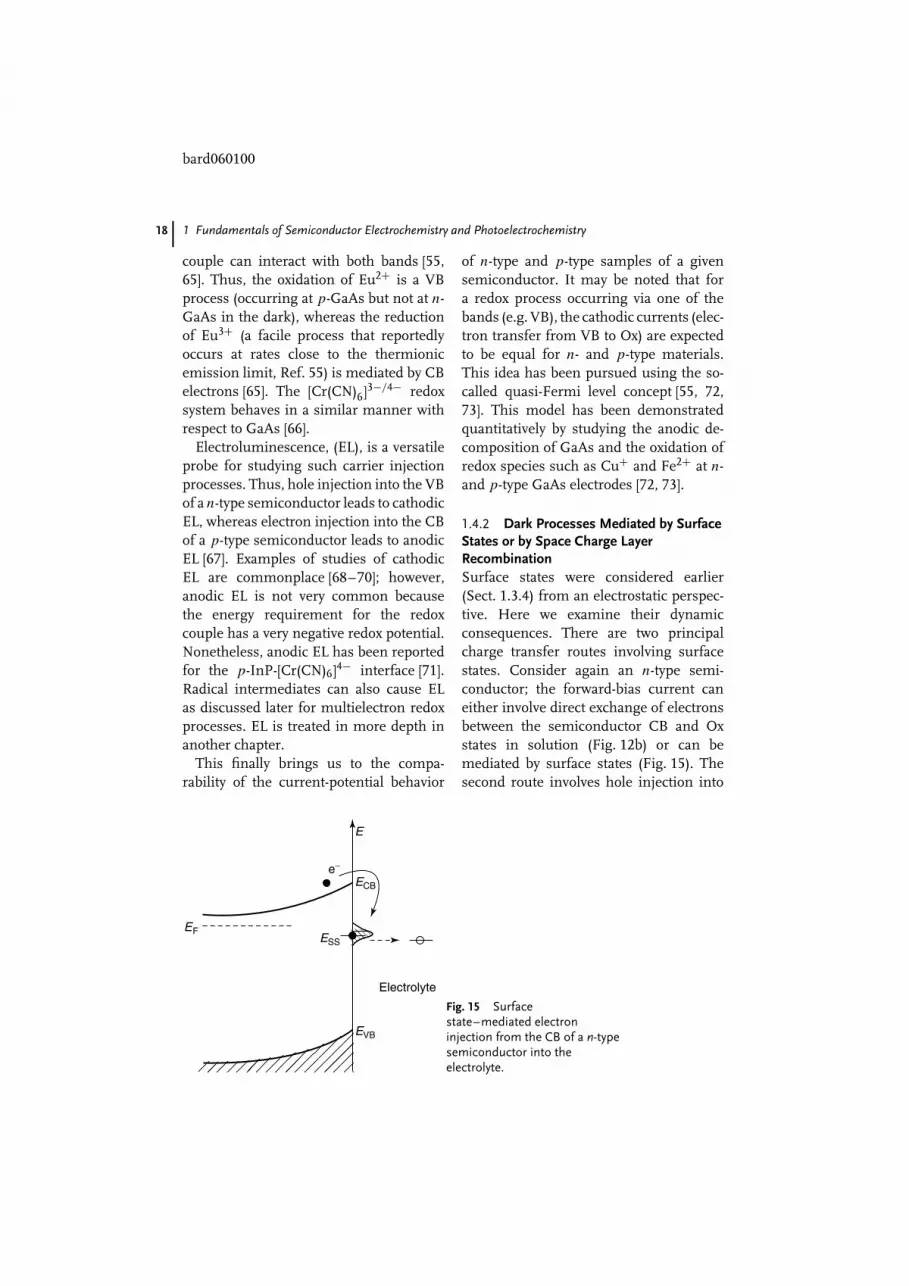
1.4.2 Dark Processes Mediated by SurfaceStates or by Space Charge LayerRecombinationSurface states were considered earlier(Sect. 1.3.4) from an electrostatic perspec-tive. Here we examine their dynamicconsequences. There are two principalcharge transfer routes involving surfacestates. Consider again an n-type semi-conductor; the forward-bias current caneither involve direct exchange of electronsbetween the semiconductor CB and Oxstates in solution (Fig. 12b) or can bemediated by surface states (Fig. 15). Thesecond route involves hole injection into
Electrolyte
E
EF
e−
ECB
ESS
EVB
Fig. 15 Surfacestate–mediated electroninjection from the CB of a n-typesemiconductor into theelectrolyte.

bard060100
1 Fundamentals of Semiconductor Electrochemistry and Photoelectrochemistry 19
the semiconductor VB again from Oxstates in solution (Figs. 9c and 14). Therecombination current is mediated eitherby surface states or via space charge layerrecombination. We will consider first theCB process.
Initial evidence for the intermediacy ofsurface states came from dark currentmeasurements on n-TiO2 and n-SrTiO3
in the presence of oxidizing agents such as[Fe(CN]63−, Fe3+, and [IrCl6]2− [74, 75].Similar early evidence that the chargetransfer process was more complex thandirect transfer of electrons from the
semiconductor CB also came from ACimpedance spectroscopy measurementson n-ZnO, n-CdS, and n-CdSe in contactwith [Fe(CN)6]3− species [76, 77].
The electrochemical impedance forsurface state–mediated charge transferhas been computed recently [78]. Thekey results are summarized in Fig. 16.Figure 16(a) contains the proposed equiv-alent circuit for the process and features aparallel connection of the impedance forthe Faradaic process [ZF(ω)] (ω = angularfrequency, 2πf ) and the capacitance of thesemiconductor depletion layer, CSC. The
−1500
−1000
−500
0
0 500
100 kHz 100 mHz100 Hz
10 Hz
C1
C2
R2 ∆
R1
10 mHz10 kHz
1 kHz
1 Hz
1 MHz
1000 1500 2000
Rs/Ω
Xs/Ω
2500 3000 3500
Fig. 16 Equivalent circuit (a) and a simulatedQ1Nyquist plot (b) for the charge-transfer pathwayillustrated in Fig. 15. The capacitance C1represents that of the space charge layer and the
parallel branch components represent theFaradaic charge-transfer process. Refer to theoriginal work for further details. (Reproducedwith permission from Ref. 78.)

bard060100
20 1 Fundamentals of Semiconductor Electrochemistry and Photoelectrochemistry
former also involves a diffusion impedance() of the Warburg type (see following).The complex plane (Nyquist) plot predictedfor the circuit is illustrated in Fig. 16(b).The theoretically predicted AC impedanceresponse was compared with experimentson n-GaAs rotating disk electrodes insulfuric acid media [79]. The equivalentcircuit in Fig. 16(a) was also comparedwith previous versions proposed by otherauthors [80–83]. These alternate versionsdiffer in their assumption of no variationsin potential drop across the Helmholtzregion (i.e. infinite CH) and no concentra-tion polarization in the electrolyte phase(infinite diffusion coefficient for the redoxspecies). Also discussed is the applicationof AC impedance spectroscopy for study-ing the kinetic reversibility of majoritycarrier charge transfer via the CB of an-type semiconductor [82].
AC impedance spectroscopy also hasseen extensive utility in the study of thehole injection or recombination processdepicted in Fig. 14. An equivalent circuitfor this process is illustrated in Fig. 17;it does resemble the circuit in Fig. 16(a),except for the Warburg component [84].Early studies [85–88] utilized the recombi-nation resistance parameter, Rr, that wasextracted from model fits of the measuredAC impedance data. This parameter wasseen to be inversely related to the hole in-jection current, thus signifying that it is in-deed related to the recombination process.However, the challenge is to differentiate
whether recombination is mediated viasurface states or whether it occurs in thedepletion layer. Thus, the parameter Rr
alone cannot afford this information andboth the real and the imaginary parts ofthis additional impedance must be consid-ered. Subsequent studies have addressedthis aspect [85, 89–93]. The admittancecorresponding to recombination at the sur-face [92] and in the space charge layer [93]was calculated from first principles. Thesecomputations show that the recombina-tion capacitance increases monotonicallywith decreasing band bending in the lattercase, whereas it shows a peak in the formercase as a function of potential.
Experimental studies [91] show that inthe case of n-GaAs electrodes in contactwith Ce4+ as the hole injection agent, sur-face recombination prevails. On the otherhand, with n-GaP electrodes, recombina-tion in the depletion layer must also betaken into account. Other discussions ofthe use of AC impedance spectroscopy forthe study of hole injection or recombina-tion are contained in Refs. 78 and 84.
The consequences of potential drop vari-ations across the Helmholtz layer in thehole injection process have been exam-ined by a variety of techniques [94, 95]. Forexample, chemical reaction of the GaAssurface with iodine results in a downwardshift of the semiconductor band edge po-sitions such that the reduction of iodineis mediated by CB electrons [95]. Whensufficient negative charge accumulates at
R1R2
Csc
C Fig. 17 Equivalent circuitrepresentation of the injectionor recombination process.(Reproduced with permissionfrom Ref. 84.)

bard060100
1 Fundamentals of Semiconductor Electrochemistry and Photoelectrochemistry 21
the surface, the potential is redistributedbetween the semiconductor spacechargelayer and the Helmholtz region. Nowiodine is reduced by hole injection asgauged by EL and AC impedance mea-surements [95].
1.4.3 Rate-limiting Steps in ChargeTransfer Processes in the DarkThe assumption is implicit in the discus-sion in Sect. 1.4.1 (leading to Eq. 18) thatcharge transfer kinetics at the semicon-ductor–electrolyte interface is the rate-limiting step. Fundamentally, we haveto differentiate majority carrier captureand minority carrier injection processesin the dark. In the former case, tran-sit through the semiconductor itself orcharge exchange with the surface statescan be potentially rate-limiting. In the lat-ter case, there are three steps involved:hole injection into the semiconductor VB,charge exchange between the recombina-tion center and the semiconductor CB,and diffusion of majority carriers (elec-trons) from the neutral region. Finally,mass transport processes in the electrolytephase itself can be a limiting factor inthe overall current flow. We shall exam-ine carrier capture and injection processesin turn.
The vast majority of outer-sphere, non-adsorbing redox systems to date haveyielded values for ket in the 10−17 −10−16 cm4 s−1 range [3, 8]. These includen-Si-CH3OH [96, 97], n-InP-CH3OH [98],GaInP2-coated n-GaAs-acetonitrile [99],and p-GaAs-HCl [100] interfaces. The re-dox couples in these studies have mostlyinvolved metallocenes that show low pro-clivity to adsorb on the semiconductor sur-face. In these cases, the rate-determiningstep in the overall current flow undoubt-edly lies in the electron transfer event atthe interface itself. However, values for ket
approximately three orders of magnitudehigher have also been reported for simi-lar interfaces, namely, n-GaAs-acetonitrile-containing cobaltocenium [Co(Cp)2
+] ac-ceptors [99, 101]. Similarly, high valueswere reported for p-GaAs-acetonitrile in-terfaces with ferricenium and cobaltoce-nium redox species [102]. In these lat-ter cases, alternative mechanisms (e.g.thermionic emission, see following) mustbe invoked in a rate-limiting role. Quartzcrystal microbalance measurements haveyielded evidence for adsorption of redoxspecies (and consequently high local sub-strate concentration) in some of these‘‘anomalous’’ instances [101].
In the majority carrier capture process, ifthe interfacial charge transfer kinetics arefacile, the transport of majority carriersthrough the space charge region canplay a rate-limiting role. The thermionicemission theory [34] assumes that everyelectron that reaches the semiconductorsurface, and has the appropriate energy toovercome the potential barrier there, willcross the interface with a tunnel probabilityof unity. However, if the interfacial kineticsare sluggish, some of the electrons will bereflected at the interface. In this case, theexchange current io is no longer describedby Eq. (18) but by Eq. (19) [34]
io = AA∗(m∗me
)T 2
(ns
n
)(19)
In Eq. (19),A is the electrode area,A∗ is theRichardson constant (120 A K−2 cm−2),m∗/me is the relative effective electronmass in the CB, and T is the absolutetemperature.
In many of the reported instances [53,55, 103], the current calculated fromEq. (19) is much higher than that mea-sured experimentally, signaling that inter-facial charge-transfer kinetics are limiting

bard060100
22 1 Fundamentals of Semiconductor Electrochemistry and Photoelectrochemistry
the overall rate. On the other hand, in then-GaAs-acetonitrile-Co(Cp)2
+ case [101], ACimpedance spectroscopy data appear tosupport the assumption that thermionicemission is the current-limiting transportmechanism.
Another factor that enters into thisdiscussion is the mobility of the majoritycarriers. It has been argued [14] that in thecase of low mobility materials (e.g. µn ∼1 cm2 V−1s−1), carrier transport from thesemiconductor bulk to the interface itselfcan become limiting. Clearly a multitudeof factors are important in majority carriercapture: ket, acceptor concentration in theelectrolyte and carrier mobility.
What about the minority carrier injec-tion process depicted in Fig. 14? Here,contrasting with the process consideredearlier, the hole injection step is usuallyvery fast (see following). Then the currentis limited by diffusion or recombinationdescribed by the Shockley equation [104]
io = eoADpn2i
nLp(20a)
for bulk recombination, and
io = 0.5 eoAWσνthNtni (20b)
for recombination within the semiconduc-tor space charge region. In Eqs. (20a) and(20b), Dp is the diffusion coefficient forholes, Lp is the hole diffusion length, ni isthe intrinsic carrier concentration, σ is anaverage capture cross-section for electronsand holes, νth is the thermal velocity ofcharge carriers, and Nt is the areal den-sity of recombination (trap) centers in themiddle of the energy gap (Fig. 14).
The diffusion or recombination mecha-nism results in considerable overpotentialfor (cathodic) current flow in the dark(again assuming a n-type semiconduc-tor for illustration). Such a rate-limiting
process was found to describe the chargetransfer at n-GaAs in 6 M HCl containingCu+ as the hole injecting species [55, 73].
Whatever the limiting mechanism, ul-timately the current becomes limited byconcentration polarization, that is, by thetransport of redox species from the bulkelectrolyte to the semiconductor surface.The situation in this regard is no differentfrom that at metal electrode–electrolyteinterfaces. As in the latter case, hydro-dynamic voltammetry is best suited tostudy mass transport. AC impedance spec-troscopy can be another useful tool in thisregard [105].
In the former case, the data can beprocessed via Levich plots of current vs.ω1/2 (ω = angular frequency). If processesother than solution mass transport becomerate-limiting, then the plot will show acurvature and the current will even becomeindependent of the electrode rotation rate.In this case, inverse Levich (or Koutecky-Levich) plots of 1/i vs. ω−1/2 can beused for further analyses. Such analyseshave been done, for example, for n-GaAs-acetonitrile-Co(Cp)2
+ interfaces [101] andn- and p-GaAs electrodes in contactwith the Cu+/2+ redox couple in HClelectrolyte [55, 73].
The diffusion impedance at semicon-ductor electrodes has been consideredrecently [105]. This author described theapplicability of AC impedance spec-troscopy for the study of electron captureand hole injection processes at n-GaAs-H2O/C2H5OH-methyl viologen, p-InP-aq. KOH-Fe(CN)6
3, n-GaAs-H2SO4-Ce4+,and n-InP-aq. KOH-Fe(CN)6
3− interfaces.In the case of electron capture processes, aRandles-like equivalent circuit was foundto be applicable [105]. On the other hand,no Warburg component was present inthe hole injection case when the reverse

bard060100
1 Fundamentals of Semiconductor Electrochemistry and Photoelectrochemistry 23
reaction was negligible (Fig. 17). For a non-ideal semiconductor–electrolyte contact(see Sect. 1.3.4), a Warburg impedance ap-peared in the electrochemical impedanceof an injection reaction as well, as exem-plified by the n-InP-Fe(CN)6
3− case [105].
1.5Light Absorption by the SemiconductorElectrode and Carrier Collection
1.5.1 Light Absorption and CarrierGenerationThe optical band gap of the semiconduc-tor (Sect. 2) is an important parameterin defining its light absorption behavior.In this quantized process, an electron-hole pair is generated in the semicon-ductor when a photon of energy hν
(ν = frequency and hν > Eg) is absorbed.Optical excitation thus results in a delo-calized electron in the CB, leaving behinda delocalized hole in the VB; this is theband-to-band transition. Such transitionsare of two types: direct and indirect. In theformer, momentum is conserved and thetop of VB and the bottom of CB are bothlocated at k = 0 (k is the electron wavevector). The absorption coefficient (α) forsuch transitions is given by [106]
α = A′(hν − Eg)1/2 (21)
In Eq. (21), A′ is a proportionality con-stant. Indirect transitions involve phononmodes; in this case Eq. (21) takes the form
α = A′(hν − Eg)2 (22)
A given material can exhibit a direct or in-direct band-to-band transition dependingon its crystal structure. For example, Sisingle crystals have an indirect transitionlocated at 1.1 eV (Table 1). On the otherhand, amorphous Si is characterized by adirect optical transition with a larger Eg
value (shorter wavelengths). Both types oftransitions can also be seen in the samematerial, for example GaP [107].
Within the present context, the impor-tant point to note is that the absorptiondepths (given by 1/α) are vastly differentfor direct and indirect transitions. While inthe former case absorption depths span the100–1000 nm range, they can be as largeas 104 nm for an indirect transition [9].
Optical transitions in semiconductorscan also involve localized states in the bandgap. These become particularly impor-tant for semiconductors in nanocrystallineform (see following). Sub–band gap transi-tions can be probed with photons of energybelow the threshold defined by Eg.
1.5.2 Carrier CollectionThe number of carriers collected (in anexternal circuit, for example) versus thoseoptically generated defines the quantumyield (+) – a parameter of considerable in-terest to photochemists. The difficulty hereis to quantify the amount of light actuallyabsorbed by the semiconductor as the cellwalls, the electrolyte, and other compo-nents of the assembly are all capable ofeither absorbing or scattering some of theincident light. Unfortunately, this problemhas not been comprehensively tackled, un-like in the situation with photocatalyticreactors involving semiconductor partic-ulate suspensions, where such analysesare available [108–111]. Pending these, aneffective quantum yield can still be defined.
Returning to the carrier collectionproblem, consider Fig. 18 for an n-semiconductor–electrolyte interface. Ascan be seen, the electron-hole pairs areoptically generated, both in the field-freeand in the space charge regions within thesemiconductor. Recombination of thesecarriers must be considered in the bulk, in

bard060100
24 1 Fundamentals of Semiconductor Electrochemistry and Photoelectrochemistry
1/α
LD + W
W
CB
VB
RedoxelectrolyteSemiconductor
hν
Fig. 18 Photogeneration of electron-hole pairs in the field-freeregion and depletion layer for a n-type semiconductor–electrolyte interface. The characteristic regions defined by thedepletion layer (W), Debye length (LD), and the light penetrationdepth (1/α) are also compared.
the space charge layer, and on the semicon-ductor surface (the latter in contact withthe redox electrolyte). We are assuminghere that light is incident from the elec-trolyte side. Rear illumination geometrycan be profitably employed and is consid-ered later for the nanocrystalline film case.
The direction of the electric field at theinterface (Fig. 6, Sect. 1.3.2) is such thatthe minority carriers (holes in this case)are swept to the surface and the electronsare driven to the rear ohmic contact. Howfast the holes are drained away (by Faradaicreactions involving the redox electrolyte)will dictate how the Fermi levels comparewith the equilibrium situation discussedearlier. The departure from equilibriumhas been quantified in terms of the quasi-Fermi level concept discussed later.
The extent of collection of minoritycarriers from the region beyond the
depletion layer is dictated by the diffusionprocess. A diffusion length, L, can bedefined
Lp =√Dpτp =
√kT µpτp
(for n-type semiconductor) (23)
The subscripts in Eq. (23) remind usthat we are dealing with minority carriercollection; µp is the hole mobility and τpis the hole life-time. The characteristiclength Lp defines the region withinwhich electron-hole pair generation is fullyeffective. Pairs generated at depths longerthan the Debye length, LD (LD = W + L)will simply recombine. Thus, the effectivequantum yield for a given interface willdepend on the relative magnitudes ofLD and the light penetration depth, 1/α(Fig. 18) [112, 113].

bard060100
1 Fundamentals of Semiconductor Electrochemistry and Photoelectrochemistry 25
An expression for the flux of photo-generated minority carriers arriving at thesurface was originally given for a solid-statejunction [114] and subsequently adapted tosemiconductor-liquid junctions [115]. Themajor weakness of these early modelshinges on their underlying assumptionfor the boundary condition that the sur-face concentration of minority carriers iszero. As pointed out elsewhere [14], this isa demanding condition necessitating veryhigh magnitudes for the interfacial chargetransfer rate constant, ket (see previoussection). A modicum of improvement tothe basic Gartner model was found [116]by defining a flux rather than a concen-tration expression for the holes and acharacteristic length where the bulk diffu-sion current transitions into a drift current.However, this treatment still assumes thatevery hole entering the depletion layer edgeexits this region and out into the electrolytephase.
The Gartner equation [114] can be writ-ten in normalized form [113]
+ ≡ jph
Io= 1 − exp(−αW)
1 + αLp(24)
In Eq. (24), + is the effective quantumyield (see previous section), given by theratio of the photocurrent density (iph/A),jph, to the incident light flux, Io. RecastingEq. (24) in the form
− ln(1 −+) = ln(1 + αLp)+ αW (25)
and recalling that W is proportional toVSC
1/2 (Eq. 8), andVSC = V − Vfb, a test ofthe rudimentary model would lie in a plotof the LHS of Eq. (25) against (Vfb − V )1/2.Such plots are shown in Fig. 19 at fourselected wavelengths for thep-GaP-H2SO4
electrolyte interface [117].While adherence to the Gartner model
is satisfactory for large values of VSC (i.e.large band bending, see Fig. 6), the modelfails close to the flat band situation. In-terestingly, this problem is exacerbated asthe semiconductor excitation wavelengthbecomes shorter (Fig. 19). Thus, anotherweakness of the basic Gartner model [114,115] is the neglect of surface recombina-tion. At the flat band situation, this modelstill predicts finite current flow arisingfrom the diffusive flow of minority carrierstoward and out of the interface (Fig. 20).
A variety of refinements have been madeto take into account the surface recom-bination effect [117–132]. The earliest ofthese [119, 120, 123] involve some simpli-fying assumptions:
Fig. 19 G..artner plots (see Eq. 25) for
the p-GaP −0.5 M H2SO4 interface. Thenumbers on the plots refer to theexcitation wavelength; Efb is the flatband potential and E is the biaspotential. (Note that this notation isdifferent from that employed in thetext.) (Reproduced with permissionfrom Ref. 117.)
0.002
0.001
0 0.5 1.0
(Efb − E )1/2/V 1/2
1.5
500
510
520
530
−ln
(1 −
Φ)

bard060100
26 1 Fundamentals of Semiconductor Electrochemistry and Photoelectrochemistry
1.0
0.8
0.6
0.4
0.2
0
−0.2
−0.4
Cur
rent
den
sity
[mA
cm
2 ]
0.1 0.2 0.3
(d)
(c) (b)
(a)
0.4 0.5
Voltage[V]
0.6
Fig. 20 Comparison of calculatedcurrent voltage profiles in the dark(curve d) and under illumination(curves a–c). Curve a is obtained fromthe basic G
..artner model. Curve (b)
considers surface recombination andcurve (c) considers both surfacerecombination and recombination in thespace charge layer. These simulationsare for a n-typesemiconductor–electrolyte interface.(Reproduced with permissionfrom Ref. 138.)
1. There is no recombination in thedepletion layer. That is, all the holesoptically generated in the bulk andwithin the depletion layer (Fig. 18) areswept to the surface without loss;
2. The steady state concentration of the op-tically generated minority carriers doesnot perturb the potential distribution inthe dark (Fig. 6); and
3. There is a quasi-thermodynamic dis-tribution of minority carriers withinthe depletion layer. This translates toa constant product term np across thisregion.
Surface recombination in the vast ma-jority of these treatments invoke the Hall-Shockley-Read model [133, 134]. Definingthe Gartner limiting expression (Eq. 24) as+G, we obtain [14]
+ss = +G
/ (1 + Dp expVSC
LD(kt + St)
)(26)
In Eq. (26), we have two new parameters,kt and St. These are the first-order rate con-stant for hole transfer (units of cm s−1, seefollowing) and the surface recombinationvelocity, St. In the combined situation ofhigh LD, high kt, and very low (or zero) St,Eq. (26) collapses to the Gartner limit.
At this juncture, it is worth noting thatonly one trap state at the surface hasbeen assumed till now; further it is as-sumed that this surface state functionsboth as a carrier recombination site and asa charge-transfer pathway (Fig. 21). Boththese assumptions are open to criticism.An alternative model invoking two dis-tinct types of surface states – one activein recombination and the other capableof mediating charge transfer – has beenconsidered [135]. Nonetheless, the mostserious flaw in the sc treatments lie inthe neglect of carrier recombination inthe depletion layer itself (as distinct fromrecombination at the surface). Reexami-nation of Eqs. (24) and (26) shows thatthe larger the Debye length, LD, and thedepletion layer width, W , the higher thequantum yield. However, recombinationin the space charge layer must become sig-nificant at some value ofW , thus providinga further limit to carrier collection.
Recombination within the space chargeregion is a nontrivial problem to treatfrom a computational perspective [14].The methodology of Sah, Noyce, andShockley [136] has been used by severalauthors [126, 127, 128, 131, 138–140].Figure 20 illustrates the sensitivity of the

bard060100
1 Fundamentals of Semiconductor Electrochemistry and Photoelectrochemistry 27
h+
e−
ECB
ESS
EVB
hν
hν
Fig. 21 Surface state mediation of both minority carrier (i.e. hole)transfer and recombination for a n-type semiconductor electrolyteinterface.
current-potential profiles at the semicon-ductor–electrolyte interface to this recom-bination mode [137].
Other models taking the above nonideal-ities to varying extent have been proposed;a detailed discussion of these lies be-yond the scope of this section [141–147].However, it is worth noting here thatin some instances involving high-qualitysemiconductor–electrolyte interfaces therate-determining recombination step doesindeed appear to lie in the bulk semi-conductor [1, 148]. Silicon photoelectrodesin methanolic media containing fast, one-electron, outer-sphere redox couples werestudied in these cases.
1.5.3 Photocurrent-potential BehaviorThe current-voltage characteristics of anilluminated semiconductor electrode incontact with a redox electrolyte can beobtained by simply adding together themajority and minority current compo-nents. The majority carrier component isgiven by the diode equation (Eq. 17) whilethe minority carrier current (iph) is directly
proportional to the photon flux (Eq. 24).Thus, the net current is given by:
i = iph − io[
exp
(−eoV
kT
)− 1
](27)
The minus sign in Eq. (27) underscores thefact that the majority carrier componentflows opposite (or ‘‘bucks’’) the minoritycarrier current flow. This photocurrentcomponent is shown as curves 2 and 3in Fig. 13.
Equation (27) shows that the diodeequation is offset by the iph term; this isexactly what is seen in Fig. 13. The plateauphotocurrent is proportional to the photonflux, Io, as illustrated for two differentvalues of the incident light intensity inFig. 13. At the open-circuit condition of theinterface, i = 0 (and neglecting the unityterm within the square brackets relative tothe exponential quantity), Eq. (27) leads to
Voc kT
eolniph
io(28)
Equation (28) underlines two importanttrends: First, Voc increases logarithmically

bard060100
28 1 Fundamentals of Semiconductor Electrochemistry and Photoelectrochemistry
with the photon flux (with a slope of∼60 mV at 298 K). Second, Voc decreaseswith an increase of io (again logarithmi-cally). This underlines the importance ofensuring that the majority carriers do not‘‘leak’’ through the interface. Because ofthe diode nature of the interface, froma device perspective, the semiconductorsurface must be designed to have fast mi-nority carrier transfer kinetics (and thushigh iph), but must be blocking to theflow of majority carriers (from the CBfor a n-type semiconductor) into the re-dox electrolyte. This challenge is similar towhat the solid-state device physicists face,but relative to metals (with a high densityof acceptor states), chemical control of re-dox electrolytes offers a powerful route toperformance optimization of liquid-basedinterfaces as also pointed out by previousauthors [1, 6, 8, 149–154].
Referring back to Fig. 13, the current-potential curves under illumination ofthe semiconductor simply appear shifted‘‘up’’ relative to the dark i − V counter-part. This, however, is the ideal scenario.Anomalous photoeffects (APEs) are of-ten observed that manifest as a cross-over of light and dark current-voltage
curves, as illustrated in Fig. 22. Thus,the superposition principle [149–154] isnot obeyed in this instance. The dashedline in Fig. 22 is produced by translat-ing the photocurrent-voltage data by jSC,the short-circuit current density. If the su-perposition principle is held, this dashedcurve would have overlaid the dark current-voltage curve. Thus, this ‘‘excess’’ (forwardbias) current embodies the APE, and thefailure of superposition is quantified as thevoltage difference (V ) between the darkj − V data and the dashed line.
What are the ramifications of the cross-over or the APE? First, mathematicalmodeling of carrier transport in a junction-based solar photovoltaic system, accord-ing to
j = jSC − jbk(V ) (27a)
is not valid in the presence of this effect.(In Eq. (27a), jbk is the ‘‘bucking’’ cur-rent density in the forward-bias regime,see previous section.) That is, a fully lin-earized system of differential equationsand boundary conditions cannot be usedto model the interface carrier transport.Second, computation and modeling of theopen-circuit voltage for such devices by
Potential
Cur
rent
den
sity
Dark
Light
∆V
Fig. 22 Anomalous photoeffect (APE)showing cross-over of the dark and lightcurrent-voltage curves again for a n-typesemiconductor-based interface. Thedashed line is obtained as described inthe text.

bard060100
1 Fundamentals of Semiconductor Electrochemistry and Photoelectrochemistry 29
simply equating a constant photocurrentflux, jph against the dark (recombina-tion) current, jo is no longer possible(see Eq. (28) and the accompanying earlierdiscussion).
Third, and perhaps practically of mostsignificance, the V component repre-sents a loss pathway in the photovoltagedeliverable by the given device. Thus, the(open-circuit) photovoltage is Voc insteadof Voc +V in the ideal case in the ab-sence of the APE. Therefore, it is importantto quantify and understand the molecularand chemical origins of this effect. This hasnot been done so far, at least to this writer’sknowledge, for semiconductor–electrolyteinterfaces.
Of course, the cross-over effect is notconfined to such interfaces. It is interestingthat a recent textbook [149–154], dealingprimarily with solid-state solar cell devices,makes only a fleeting reference to theunderlying origin of the APE. Referencewas made in this book to the cross-over of experimental dark and light j − Vcharacteristics for a Cu2S-CdS solid-stateheterojunction solar cell but its originwas not explored. A light-induced junctionmodification has also been reported for the(Cd, Zn)S-CuInSe2 solid-state system [155,156]. The cross-over effect appears tohave been treated in even lesser depth insome classical textbooks on semiconductordevices [104, 157].
Probably the first reported instance ofobservation of an APE was in 1977 fora n-TiO2-NaOH electrolyte interface [158].The APE was observed in the saturationregion of cathodic current flow and wasinduced by sub–band gap irradiation ofthe photoanode. A peak in the spectrumof the photoresponse at 800 nm (the cor-responding photon energy being lowerthan the 3.0 eV band gap of TiO2) wasused by the authors to invoke a surface
state–mediated electron transfer to O2 (inthe electrolyte) as the origin of the photo-effect. Surface states were again invokedto explain a cathodic photoeffect at n-CdS-aqueous polysulfide interfaces [159].This photoeffect was only observed for the(0001) single-crystal face of n-CdS but notfor the (0001) orientation. A subsequentstudy of photoelectrochemical effects atselenium films reported an anomalousanodic photocurrent at potentials positiveof the flat band location for the p-typefilm [160]. This effect was assigned toa hole injection process via a tunnelingmechanism. An increase of the tunnel-ing probability under illumination wasaccommodated by a shrinking of the spacecharge layer at the interface. Photoen-hancement of the forward current flowwas observed again for n-CdS, in this in-stance in contact with a [Fe(CN)6]3−/4−redox electrolyte [161]. This effect was ob-served only with a mechanically damagedsurface, and disappeared after it had beenetched with concentrated HCl.
Subsequent work [162] describes sup-pression of the cathodic photocurrentfor n-CdS-[Fe(CN)6]3−/4− interfaces me-chanical polishing of the electrode. Aswith an earlier study [163], the spectraldependence of the photocathodic effectimplicated sub–band gap states. The sup-pression was explained by two alternativemodels involving a compensated insu-lating layer or by Fermi-level pinning.Illumination was claimed to result in a dra-matic increase of the (suppressed) cathodiccurrent, which interestingly enough wasobserved only for n-CdS films but notfor crystals including n-CdTe, n-CdSe, n-GaAs, n-ZnO, n-TiO2 and n-ZnSe. On theother hand, a subsequent paper describesa photocathodic effect for n-CdSe-sulfideinterfaces in which an interfacial layer ofselenium was implicated [163].

bard060100
30 1 Fundamentals of Semiconductor Electrochemistry and Photoelectrochemistry
−50 −150 −350 −5505 × 10−5
5 × 10⁻⁴
5 × 10⁻³
5 × 10⁻²
5 × 10⁻¹
5 × 100
Cur
rent
[m
A c
m−2
]
Voltage vs. (Al/Al+3) [mV]
Fig. 23 Experimental data embodyingAPE for the n-GaAs-AlCl3/n-butylpyridi-nium chloride molten-salt electrolyteinterface. Refer to the text for details.(Reproduced with permission fromRefs. 168, 169.)
More recent studies on n-CdS [164, 165]and n-TiO2 photoanodes [166] implicatethe formation of photoconductive layersin the APEs. Thus, the foregoing reviewsuggests the following
1. APE is a very general phenomenon thathas been observed for solid-state junc-tions for n- and p-type semiconductorsalike, and for a wide variety of semicon-ductor materials.
2. The reported results and trends areoften contradictory. It is quite possiblethat the experimental conditions inthese studies were quite variant, thusprecluding direct comparison of theresults.
3. The mechanistic reasons given forthe APE are possibly many, and gen-eralizations may not be warranted.Clearly, more research is needed onthis topic.
Figure 23 contains an example of theAPE for the n-GaAs-AlCl3/n-butylpyridi-nium chloride molten salt electrolyte inter-face [167]. The bottom curve in Fig. 23 isthe measured dark current-voltage profile.The top curve was obtained from thephotocurrent-voltage data (under irradi-ation of the semiconductor). Clearly, ifthe superposition principle held, the twocurves would have coincided with oneanother.
APEs have also been observed fornanocrystalline and chemically modifiedfilms, as discussed in a subsequent section.
Light-induced changes in the electro-statics at the semiconductor–electrolyteinterface are conveniently probed bycapacitance-voltage measurements in thedark and under illumination of the semi-conductor electrode. If charge trappingat the interface plays a decisive role(whatever be the mechanism), the voltage

bard060100
1 Fundamentals of Semiconductor Electrochemistry and Photoelectrochemistry 31
drop across the illuminated interface isaltered, and consequently the semicon-ductor band edge positions are shifted.This, of course, is the Fermi-level pin-ning situation that was encountered earlier(Sect. 1.3.4). Examples of studies address-ing this aspect may be found, for ex-ample on p – GaAs [124] and CdTe [168,169]–based aqueous electrolyte interfaces.
1.5.4 Dynamics of Photoinduced ChargeTransferSo far the discussion has centered onthe steady state aspects of carrier gen-eration and collection at semiconduc-tor–electrolyte interfaces. As with theirmetal electrode counterparts, a wealthof information can be gleaned fromperturbation-response type of measure-ments. An important difference, however,lies in the vastly different timescale win-dows that are accessible in the two cases.The critical RC time-constant of the cell ina transient experiment is given by
τcell = C(Rm + Rel) (29)
In Eq. (29), Rm is the measurementresistor (across which the current orphotocurrent is measured) and Rel is theelectrolyte resistance. The term C is thecapacitance, which, in the metal case, is theHelmholtz layer capacitance, CH. (Onceagain, the Gouy region is ignored here.)For semiconductor–electrolyte interfaces,we have seen that two layers are involvedin a series circuit configuration withcorresponding capacitances of CSC andCH (Fig. 6). Because CH CSC, C CSC. This assumption is usually justifiedbecause CH 10−5 F cm−2 and CSC =10−8 − 10−0 F cm−2. If the compositeresistance (Rm + Rel) is 100 ohm, thenτcell for metal electrodes is ∼10−3 sand that for the semiconductor case is10−6 − 10−7 s.
What are the processes important in adynamic interrogation of the semiconduc-tor–electrolyte interface?
1. Carrier generation within the semicon-ductor,
2. diffusion of minority carriers from thefield-free region to the space chargelayer edge,
3. transit through this layer,4. charge transfer across the interface, and5. carrier recombination via surface states
or via traps in the space charge layer.
Other phenomena such as thermaliza-tion also are important as discussed laterin the context of hot carrier effects. Thetime constant (τcell) of the cell and themeasurement circuitry has complicatedmatters further has caused some confu-sion in the interpretation of transient data.If a potentiostat is not used, then this timeconstant is given by Eq. (29).
One can envision three types of per-turbation: an infinitesimally narrow lightpulse (a Dirac or δ-functional), a rectan-gular pulse (characteristic of chopped orinterrupted irradiation), or periodic (usu-ally sinusoidal) excitation. All three typesof excitation and the corresponding re-sponses have been treated on a commonplatform using the Laplace transform ap-proach and transfer functions [170]. Theseperturbations refer to the temporal be-havior adopted for the excitation light.However, classical AC impedance spec-troscopy methods employing periodic po-tential excitation can be combined withsteady state irradiation (the so-called PEISexperiment). In the extreme case, boththe light intensity and potential can bemodulated (at different frequencies) andthe (nonlinear) response can be mea-sured at sum and difference frequencies.The response parameters measured in

bard060100
32 1 Fundamentals of Semiconductor Electrochemistry and Photoelectrochemistry
all these cases are many but includethe photocurrent, voltage, luminescence,or microwave conductivity. Clearly, semi-conductor–electrolyte interfaces present arich, albeit demanding landscape for prob-ing non–steady state phenomena.
The dynamics of charge transfer acrosssemiconductor–electrolyte interfaces areconsidered in more detail elsewhere inthis volume.
1.5.5 Hot Carrier TransferShort wavelength photons (of energy muchgreater than Eg) create ‘‘hot’’ carriers. If,somehow, thermalization of these carri-ers can be avoided, photoelectrochemicalreactions that would otherwise be impos-sible with the ‘‘cooled’’ counterparts, thatis, at very negative potentials for n-typesemiconductors, would be an intriguingpossibility. The key issue here is whetherthe rate of electron transfer across theinterface can exceed the rate of hot elec-tron cooling. The observation of hot carriereffects at semiconductor–electrolyte inter-faces is a controversial matter [3, 7, 11, 171]and practical difficulties include problemswith band edge movement at the interfaceand the like [4]. Under certain circum-stances (e.g. quantum-well electrodes, ox-ide film-covered metallic electrodes), it hasbeen claimed that hot carrier transfer canindeed be sustained across the semicon-ductor–electrolyte interface [7, 172, 173].
1.6Multielectron Photoprocesses
This section has thus far considered redoxelectrolytes comprising one electron oxi-dizing or reducing agents. Multielectronredox processes, however, are importantin a variety of scenarios. Consider thereduction of protons to H2 (HER) – atechnologically important electrochemical
process that has also been extensivelystudied from a mechanistic perspective onmetallic electrodes.
Photoelectrolytic processes such as HERcan be carried out on semiconductorelectrodes. One can envision a HERmechanism on a p-type semiconductor ofthe sort:
p − SChν−−−→ e−
CB + h+VB (30)
e−CB + S −−−→ S− (30a)
S− + H+ −−−→ S + H• (30b)
e−CB + H+ −−−→ H• (30c)
H+ + H• + e−CB −−−→ H2 (30d)
H+ + H• + S− −−−→ H2 + S (30e)
h+VB + H• −−−→ H+ (30f)
h+VB + S− −−−→ S (30g)
In this above scheme, S denotes asurface state and both direct (Reactions30c and 30d) and indirect (i.e. surfacestate–mediated) (Reactions 30b and 30e)radical and H2-generating pathways areshown. Reactions 30f and 30g represent re-combination routes involving the reactionintermediates.
Admittedly, this scheme is daunting inits complexity, and the kinetics implica-tions are as yet unclear. Early studies onp-GaP, p-GaAs, and other Group III–V(13–15) semiconductors reported onsetof cathodic photocurrents (attributableto HER) only at potentials far removed(ca. 0.6 V) from Vfb [174]. This was at-tributed to Steps 30b and 30g in thepreceding scheme. More recent work [175]has shown that the HER at illuminatedp-InP-electrolyte contacts is accompaniedby a photocorrosion reaction, leading toindium formation on the semiconductorsurface.

bard060100
1 Fundamentals of Semiconductor Electrochemistry and Photoelectrochemistry 33
Interestingly, surface states themselveswere chemically identified with H•
ads (ad-sorbed hydrogen atom intermediates) inthe aforementioned study [166]. Thesespecies have also been implicated in ac-cumulation layer formation and anodicEL at n- and p-GaAs-electrolyte inter-faces [176–178].
Another interesting characteristic ofmany multiequivalent redox systems isthe phenomenon of photocurrent mul-tiplication. This phenomenon may beillustrated for two systems utilizing illu-minated n-type andp-type semiconductorsrespectively
n-type
n-SChν−−−→ e− + h+ (31)
HCOOH + h+ −−−→ COOH• + H+
(31a)
COOH• −−−→ CO2 + H+ + e−
(31b)
p-type
p-SChν−−−→ h+ + e− (31)
O2 + H+ + e− −−−→ HO2• (31c)
HO2• + H+ −−−→ H2O2 + h+
(31d)
Thus, the key feature of photocurrent mul-tiplication is a majority carrier injectionstep (Reactions 31b or 31d) from a reactionintermediate (usually a free radical) intothe semiconductor CB or VB, respectively.In the preceding examples, each photongenerates two carriers in the external cir-cuit, affording a quantum yield (in the idealcase) of 2. This is the ‘‘current-doubling’’process.
Practically, however, quantum yieldssomewhat lower than 2 are usually
measured because Steps 31b or 31dcompete with the further photooxidationor photoreduction of these intermediates,respectively. This is true especially at highphoton flux values. Even multiplicationfactors as high as 4 are possible as inthe photodissolution of n-Si in NH4F me-dia [179–182].
Photocurrent multiplication has beenobserved for a variety of semiconduc-tors including Ge [180], Si [179–182],ZnO [183–189], TiO2 [190–193], CdS [194,195], GaP [196], InP [197], and GaAs [198–200]. These studies have included bothn- and p-type semiconductors, and havespanned a range of substrates, both or-ganic and inorganic. As in the Si case,this phenomenon can also be caused byphotodissolution reactions involving thesemiconductor itself. The earlier studieshave mainly employed voltammetry, par-ticularly hydrodynamic voltammetry [193].As more recent examples [2, 9, 10] reveal,intensity-modulated photocurrent spec-troscopy, (IMPS), is also a powerfultechnique for the study of photocurrentmultiplication.
This leads us to another importantcategory of multielectron photoprocessesinvolving the semiconductor itself. Whilephotocorrosion is a nuisance from a deviceoperation perspective, it is an importantcomponent of a device fabrication se-quence in the microelectronics industry.Two types of wet etching of semiconduc-tors can be envisioned [201]. Both occurat open-circuit but one involves the actionof chemical agents that cause the simul-taneous rupture and formation of bonds.Several aspects of photoetching have beenreviewed [62–64, 202, 203] including re-action mechanisms, morphology of theetched surfaces, and etching kinetics inthe dark and under illumination. Gen-eral rules for the design of anisotropic

bard060100
34 1 Fundamentals of Semiconductor Electrochemistry and Photoelectrochemistry
photoetching systems have also been for-mulated [204]. Photoelectrochemical etch-ing is considered in more detail elsewherein this volume.
1.7Nanocrystalline Semiconductor Films andSize Quantization
1.7.1 Introductory RemarksFrom a materials perspective, the field ofsemiconductor electrochemistry and pho-toelectrochemistry has evolved from theuse of semiconductor single crystals topolycrystalline thin films and, more re-cently, to nanocrystalline films. The latterhave been variously termed membranes,nanoporous or nanophase films, meso-porous films, nanostructured films, andso on; they are distinguished from theirpolycrystalline electrode predecessors bythe crystallite size (nm versus µm inthe former) and by their permeabilityto the electrolyte phase. These films arereferred to as ‘‘nanocrystalline in the fol-lowing sections. These features renderthree-dimensional geometry to nanocrys-talline films as opposed to the ‘‘flat’’ ortwo-dimensional (planar) nature of singlecrystal or polycrystalline counterparts.
What are the virtues of these emergingphotoelectrode materials? The first isrelated to their enormous surface area.Consider that the 3D structure is built upof close-packed spheres of radius, r . Thenignoring the void space, the specific area,As (area/volume) is given by 3/r [205].For r = 10 nm, As is on the order of106 cm−1, and for a 1 cm2 film of 1 µmthickness, this value corresponds to aninternal surface area of ∼100 cm2 (i.e.a ‘‘surface roughness factor’’ of 100).Clearly, this becomes important if wewant the electrolyte redox species to beadsorbed on the electrode surface (see
following). Alternatively, a large amount ofsensitization dye can be adsorbed onto thesupport semiconductor although this dyesensitization approach is not consideredin this chapter. By way of contrast, theamount of species that can be confinedin a monolayer on a corresponding flatsurface would be negligibly small.
As we shall see later, electron trans-port in nanocrystalline films is necessar-ily accompanied by charge-compensatingcations because the holes are rapidly in-jected into the flooded electrolyte phase.This provides opportunities for studyingion transport processes in mesoporousmedia that are coupled to electron mo-tion. Ion insertion also has practical con-sequences as in energy storage deviceapplications [206].
Surface state densities on the order of∼1012 cm2 are commonplace for semi-conductor electrodes of the sort consid-ered in previous sections of this chapter.These translate to equivalent volume den-sities of ∼1018 cm−3 for nanocrystallinefilms. Such high densities enhance lightabsorption by trapped electrons in sur-face states, giving rise to photochromicand electrochromic effects [198–200] (seefollowing). Unusually high photocurrentquantum yields are also observed withsub–band gap light with these photoelec-trode materials. Corresponding sub–bandgap phenomena are rather weak anddifficult to detect with single-crystal coun-terparts.
1.7.2 The NanocrystallineFilm–Electrolyte Interface and ChargeStorage Behavior in the DarkUnderstanding of the electrostatics acrossnanocrystalline semiconductor film-elec-trolyte junctions presents interesting chal-lenges, particularly from a theoretical per-spective. Concepts related to space charge

bard060100
1 Fundamentals of Semiconductor Electrochemistry and Photoelectrochemistry 35
layers, band bending, flat band potential,and the like (Sect. 3) are not applicablehere because the crystallite dimensionscomprising these layers are comparable to(or even smaller than) nominal depletionlayer widths.
The rather complete interpenetration ofthe electrode and electrolyte phases mustmean that the Helmholtz double layer ex-tends throughout the interior surface of thenanoporous network, much like a superca-pacitor [9, 210] situation. Finally, unlike inthe cases treated earlier, the semiconduc-tor (especially if it is a metal oxide) is notheavily doped such that free majority carri-ers are not present in appreciable amounts.This is indicated, for example, by the sensi-tivity of the conductivity of nanocrystallineTiO2 layers to UV light – the conductivityis strongly enhanced on UV exposure, sim-ilar to a photoconductive effect. This effecthas been interpreted, in terms of trap fill-ing with recombination times considerablyslower than the trapping processes underreverse bias [211, 212]. The light sensitivityalso is diagnostic of the fact that the lowelectronic conductivity in the dark is notdue to high interparticle resistances (i.e. inthe ‘‘neck’’ regions), but rather is indicativeof the low electron concentrations.
The electron concentration can be in-creased by forward-biasing the nanocrys-talline electrode–electrolyte interface po-tentiostatically. The interface is driven thusinto the accumulation regime for the ma-jority carriers, and if a transparent rearcontact (e.g. F-doped, SnO2 or Sn-dopedindium oxide) is used, the resultant blue(or bluish-black) coloration of the filmcan be spectroscopically monitored [208,209, 213]. Whether the optical responsearises from CB electrons or from electronstrapped in surface states is not entirelyclear. It has been claimed [214] that theabsorption spectrum of the latter differs
significantly from CB electrons. Electronsin surface states can be chemically iden-tified with Ti3+ defect sites that can bedetected, for example, by electron param-agnetic resonance spectroscopy [215, 216].
In either case, the resultant negativecharge generated by electron accumula-tion at the internal surfaces has to bebalanced by cations (from the electrolytephase) for charge compensation. Suchion insertion reactions have been stud-ied using techniques such as voltammetry,reflectance or absorption spectroscopy,chronoamperometry, and electrochemi-cal quartz-crystal microgravimetry [213,217–22]. Both aqueous and aprotic elec-trolytes have been deployed for thesestudies.
Unlike in the single-crystal cases treatedearlier, placement of the semiconductorenergy band positions at the interfacevia Mott-Schottky analyses is not straight-forward for nanocrystalline films. Abruptchanges in slope and other nonideali-ties [215, 227, 223] have been observed,for example, in the Mott-Schottky plots forTiO2 films and attributed to the influenceof the conductive glass that is normallyemployed to support these films. This be-havior is especially prevalent under reversebias. The onset of majority carrier op-tical absorption (in the visible and nearIR range) under forward-bias instead hasbeen profitably employed to place the CBpositions of TiO2 in aqueous media [208].
Impedance spectroscopy and electro-chemical dye desorption experiments havebeen employed [224] to study the electri-cal characteristics of TiO2 nanocrystallinefilms in the dark. This study as well as theothers cited earlier demonstrate how theconductivity changes (as a result of elec-tron injection from the support electrode)can cause the porous or nanocrystallinelayer to manifest itself electrically, such

bard060100
36 1 Fundamentals of Semiconductor Electrochemistry and Photoelectrochemistry
that the active region moves away (i.e. out-ward) from the support as the forward-biasvoltage is increased. The potential distribu-tion has also been analyzed depending onwhether the depletion layer width exceedsor is smaller than the typical dimension ofthe structural units in the nanocrystallinenetwork [223].
1.7.3 Photoexcitation and CarrierCollection: Steady State BehaviorFigure 24 contains a schematic representa-tion of the nanocrystalline semiconductorfilm–electrolyte interface at equilibrium(Fig. 24a) and the corresponding situationunder band gap irradiation of the semicon-ductor (Fig. 24b) [9]. Because the diffusionlength of the photogenerated carriers isusually larger than the physical dimen-sions of the structural units, holes andelectrons can reach the impregnated elec-trolyte phase before they are lost via bulkrecombination. This contrasts the situa-tion with the single-crystal cases discussedearlier.
If, as is the case with TiO2 nanocrys-talline films, the holes are rapidly scav-enged by the electrolyte redox (specificallyRed) species, collection of the photo-generated electrons at the rear contactbecomes the determinant factor in thequantum yield. Thus, the quasi-Fermi levelfor holes remains close to EF,redox andthat for electrons, EF,e moves ‘‘up’’, asdepicted in Fig. 24b. Illumination thusinduces an electron flux, Jn(x) throughthe nanocrystalline phase. Under steadystate conditions, the photocurrent density(jph) is equal to eoJn(x = d). The drivingforce for electron diffusion through thenetwork of nanocrystallites has been cal-culated from first principles [225]. It hasbeen found that the driving force is approx-imately kT/eo divided by the thickness ofthe network. Importantly, this free-energygradient is found to be independent of theincident photon flux.
It is important to reiterate that thecharge separation in a nanocrystallinesemiconductor–electrolyte interface does
(a)0d
x
E
EC
EV
EF,redox
Substrate
(b)0d
x
Red OxSubstrate
je(d)
E
EF,eEF,redox
− − −
+
Fig. 24 Schematic representation of ananocrystalline semiconductor–electrolyte interface in the dark (a) andunder illumination from the electrolyteside (b). Ec and Ev correspond to ECBand EVB in our notation. (Reproducedwith permission from the authors ofRef. 9.)

bard060100
1 Fundamentals of Semiconductor Electrochemistry and Photoelectrochemistry 37
not depend on a built-in electric fieldat the junction as in the single-crystalcase. Instead, the differential kinetics forthe reactions of photogenerated electronsand holes with electrolyte redox speciesaccount for the charge separation (and thegenerated photovoltage). The molecularfactors underlying the sluggish scavengingof electrons at the nanocrystalline film-electrolyte boundary (by the redox species)are as yet unclear. Clearly, the competitionbetween surface recombination of theseelectrons (with the photogenerated holes)and collection at the rear contact dictatesthe magnitude of the quantum yield that isexperimentally measured for a particularjunction.
Photocurrent losses have been recordedfor electrolytes dosed with electron accep-tors such as O2 and iodine [226]. Nanocrys-talline TiO2 electrodes with thicknessesranging from 2 µm to 38 µm were includedin this study. In the presence of theseelectron-capture agents, electron collec-tion (i.e. photocurrent) at the rear contactwas seriously compromised. On the otherhand, as high as 10% of the photons wereconverted to current for a 38 µm thick filmin a N2-purged solution [226].
The result was obtained with front-sideillumination geometry. As one would in-tuitively expect, carrier collection is mostefficient close to the rear contact. In-deed, marked differences have been ob-served for photoaction spectra with thetwo irradiation (i.e. through the elec-trolyte side vs. through the transparentrear contact) geometries for TiO2, CdS, andCdSe nanocrystalline films [227, 228]. Ob-viously, the relative magnitudes of the ex-citation wavelength and the film thicknesscritically enter into this variant behavior.
In the vast majority of cases, theiodide/triiodide redox couple has been em-ployed (presumably because of its success
in shuttling the photooxidized dye in thesensitization experiments) although otherredox electrolytes [e.g. SCN−/(SCN)2
−;228] have been employed as well. For thechalcogenide films, sodium selenosulfitewas employed [227]. It must be noted that,aside from losses caused by the surfacerecombination and back-reactions, an ad-ditional loss component from the increasein film resistance must also be recog-nized, especially as the film thickness isincreased. The resistance loss manifestsas a deterioration in the photovoltage andfill factor.
In the discussion to this point, we havenot considered trapping or release of thephotogenerated electrons as they undergotransit to the rear contact. However, elec-trons trapped in localized interfacial statesinduce a countercharge in the Helmholtzdouble-layer, as discussed in the preced-ing discussion. The resultant voltage dropcan introduce a nonnegligible field com-ponent into the diffusional process. Thetime-dependence of the electron density,n(x, t) is given by [9]
∂n(x, t)
∂t= ηαIoe−αx +Dn ∂
2n(x, t)
∂x2
− n(x, t)− no
τ(32)
In Eq. (32), η is the electron injectionefficiency, Dn is the diffusion coefficientof electrons, and τ is the pseudo first-order lifetime of electrons determined byback-reaction with Ox.
Even if the migration component isnegligible (but see following), solution ofEq. (32) presents difficulties because of thepossible dependence of Dn on n and x.Similarly, τ may depend on these two vari-ables also. Nonetheless, the steady statesolution of Eq. (32) has been obtained [229]by assuming that D and τ are constantand that η = 1. Under these conditions,
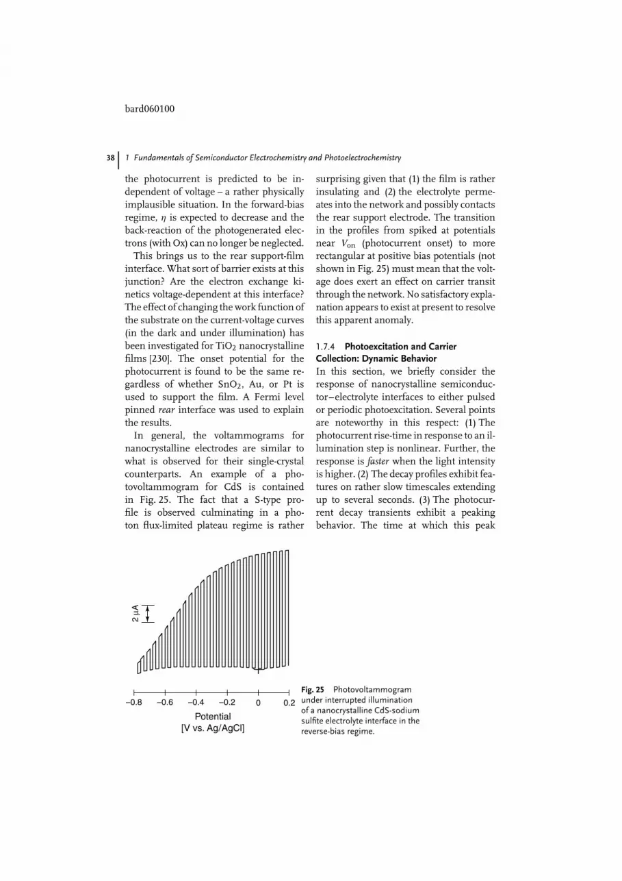
bard060100
38 1 Fundamentals of Semiconductor Electrochemistry and Photoelectrochemistry
the photocurrent is predicted to be in-dependent of voltage – a rather physicallyimplausible situation. In the forward-biasregime, η is expected to decrease and theback-reaction of the photogenerated elec-trons (with Ox) can no longer be neglected.
This brings us to the rear support-filminterface. What sort of barrier exists at thisjunction? Are the electron exchange ki-netics voltage-dependent at this interface?The effect of changing the work function ofthe substrate on the current-voltage curves(in the dark and under illumination) hasbeen investigated for TiO2 nanocrystallinefilms [230]. The onset potential for thephotocurrent is found to be the same re-gardless of whether SnO2, Au, or Pt isused to support the film. A Fermi levelpinned rear interface was used to explainthe results.
In general, the voltammograms fornanocrystalline electrodes are similar towhat is observed for their single-crystalcounterparts. An example of a pho-tovoltammogram for CdS is containedin Fig. 25. The fact that a S-type pro-file is observed culminating in a pho-ton flux-limited plateau regime is rather
surprising given that (1) the film is ratherinsulating and (2) the electrolyte perme-ates into the network and possibly contactsthe rear support electrode. The transitionin the profiles from spiked at potentialsnear Von (photocurrent onset) to morerectangular at positive bias potentials (notshown in Fig. 25) must mean that the volt-age does exert an effect on carrier transitthrough the network. No satisfactory expla-nation appears to exist at present to resolvethis apparent anomaly.
1.7.4 Photoexcitation and CarrierCollection: Dynamic BehaviorIn this section, we briefly consider theresponse of nanocrystalline semiconduc-tor–electrolyte interfaces to either pulsedor periodic photoexcitation. Several pointsare noteworthy in this respect: (1) Thephotocurrent rise-time in response to an il-lumination step is nonlinear. Further, theresponse is faster when the light intensityis higher. (2) The decay profiles exhibit fea-tures on rather slow timescales extendingup to several seconds. (3) The photocur-rent decay transients exhibit a peakingbehavior. The time at which this peak
−0.8 −0.6 −0.4 −0.2 0 0.2
Potential[V vs. Ag/AgCl]
2 µA
Fig. 25 Photovoltammogramunder interrupted illuminationof a nanocrystalline CdS-sodiumsulfite electrolyte interface in thereverse-bias regime.

bard060100
1 Fundamentals of Semiconductor Electrochemistry and Photoelectrochemistry 39
occurs varies with the square of the filmthickness, d. (4) A similar pattern is alsoseen in IMPS data where the transit time,τ is seen to be proportional to d2.
These observations have been inter-preted within the framework of two dis-tinct models, one involving trapping ordetrapping of the photogenerated elec-trons [231, 232] and the other based onelectron diffusion (or field-assisted dif-fusion) not attenuated by electron local-ization [233, 234]. The millisecond transittimes also mean that the transit timesare very long compared to equilibrationof majority carriers in a bulk semiconduc-tor or electron-hole pair separation withinthe depletion layer of a flat electrode. Theslow transport is rationalized by a weakdriving force and by invoking percolationeffects [223].
It is interesting that the response pat-terns differ for different nanocrystallineelectrodes [223]. For example, while trap-ping or detrapping effects appear to berelatively unimportant for GaP, the re-sponse for TiO2, especially at low photonfluxes, is governed by electron trappingor detrapping kinetics. This accounts forthe faster response at higher photon fluxes(see preceding section).
1.7.5 Size QuantizationWhen electronic particles such as electronsand holes are constrained by potentialbarriers to regions of space that are com-parable to or smaller than their de Brogliewavelength, the corresponding allowed en-ergy states become discrete (i.e. quantized)rather than continuous. This manifestsin the absorption (or emission) spectraas discrete lines that are reminiscent ofatomic (line) transitions; these sharperfeatures often appear superimposed on abroader envelope. Another manifestationfor semiconductors is that the energy band
gap (Eg) increases, or equivalently, the ab-sorption threshold exhibits a blue shift.The critical dimension for size quantiza-tion effects to appear in semiconductorsdepends on the effective mass (m∗) of theelectronic charge carriers. For m∗ ∼ 0.05,the critical dimension is about 300 A; itdecreases approximately linearly with in-creasing m∗ [7].
Size quantization effects and quantumdot photoelectrochemistry are discussed inmore detail elsewhere in this volume.
1.8Chemically ModifiedSemiconductor–Electrolyte Interfaces
1.8.1 Single CrystalsMuch of the research in the early1980s on chemically modified semicon-ductor–electrolyte interfaces was directedtoward protecting them from photocor-rosion; this body of work has been re-viewed [226]. Parallel efforts also wentinto improving minority carrier transferat the interface by chemisorbing metalions such as Ru3+ on the semiconductorsurface. Chemical agents such as sulfideions are known to passivate the semicon-ductor against surface recombination [6].A study [22a] on electron transfer dynam-ics at p-GaAs-acetonitrile interfaces wherethe semiconductor surface was sulfide-passivated exemplifies this fact. In gen-eral, the mechanistic issue of whetherthese chemical agents improve minor-ity carrier charge transfer by minimizingsurface recombination or by a true cat-alytic action has not been completelyresolved [1].
Yet another tactic involves perturb-ing the electrostatics at the semicon-ductor–electrolyte interface by adsorbing(or even chemically attaching) electrondonors or acceptors on the semiconductor

bard060100
40 1 Fundamentals of Semiconductor Electrochemistry and Photoelectrochemistry
Tab. 2 A summary of approachesa to chemical modification ofsemiconductor–electrolyte interfaces
Modification Semiconductor(s) Modification Sampleagent(s) objectiveb Reference(s)
Ru3+ n-GaAs A 239, 240Co3+ n-GaAs A 241Os3+ n-GaAs A 241Ag+ p-InP A 242S2− p-GaAs A 236HS− CdS, CdSe B 243Thiolates CdS, CdSe B 244Dithiocarbamate CdS, CdSe B 245, 246Lewis acids CdS, CdSe B 247, 248Lewis bases CdS, CdSe B 249Cl− n-GaAs B 238Benzoic acid derivatives n+-GaAs B 250Noble metals n-TiO2 C 251Noble metals p-InP C 239, 252–254RuO2
c n-CdS C 255, 256RuO2
c n-Si C 257Ptc p-Si C 257, 258Ptc n-CdS C 259Noble metals n-CdS C 254Noble metalsd p-InP C 260
aApproaches to photoanode stabilization based on polymer films containingredox functionalities have been reviewed elsewhere, e.g. Refs. 6 and 226.bA: minority carrier transfer catalysis and or surface state passivation;B: electrostatic modification; C: catalysis of multielectron photoprocesses(refer to text).cIn these cases, the semiconductor electrode also contained a coating, eitherpolymeric or indium tin oxide.dThe chemically modified photocathode was used in conjunction withn-MoSe2 (or n-WSe2) in a two-photoelectrode cell configuration.
surface [237]. In favorable cases, thisincreases the band bending at the inter-face by thus introducing a fixed counter-charge of opposite polarity (negative fora n-type semiconductor) at the junction.Chloride ion adsorption on then-GaAs sur-face from ambient temperature AlCl3/n-butylpyridinium chloride melts [30, 238] isa case in point; this process serves to im-prove the junction and the photovoltagethat it delivers. Of course, such ‘‘fixed-charge’’ effects have long been known to
the solid-state device physics and gas phasecatalysis communities. Other agents thathave been deployed for chemical tuningof the interfacial energetics at the semi-conductor–electrolyte interface are listedin Table 2.
Native semiconductor surfaces are fairlyinactive from a catalysis perspective.Thus, noble metal or metal oxide is-lands have been implanted on photoelec-trode surfaces as electron storage centersto drive multielectron redox processes

bard060100
1 Fundamentals of Semiconductor Electrochemistry and Photoelectrochemistry 41
such as HER, photooxidation of H2O,and photooxidation of HCl, HBr, or HI.Examples of this sort of chemical mod-ification strategy are also contained inTable 2.
The advent of self-assembled mono-layer (SAM) films on electrode surfaceshas rendered a high degree of molecularorder and predictability to the chemi-cal modification approach. In particular,the use of these insulating, molecularspacers enables interrogation of criticalissues in electron transfer such as theinfluence of chemical bonding and dis-tance between the support electrode andthe redox moieties on the rate constantfor electron transfer. Many such studieson gold-confined SAMs have appearedrecently [261–263]. Corresponding stud-ies on semiconductor surfaces (particularlyGroup II–V compounds such as GaAs andInP [264–266] and elemental semiconduc-tors such as Si 267) have also begun toappear.
Alkanethiol-based or alkylsiloxane-basedSAMs have been profitably employed in allthese instances to probe the distance effectin electron transfer dynamics. The thiol-based SAMs have the virtue that the spacerlength can be predictably altered simply byvarying the number of methylene unitsin the chain. The distance dependenceof ket is embodied in the parameter β,the decay coefficient. For a critical dis-cussion of the subtleties involved in theextraction and interpretation of this pa-rameter, we refer to Ref. 252. A value of0.49 ± 0.07 has been reported for this pa-rameter for n-InP-alkanethiol-ferrocyanideinterfaces [266]. This value is smaller thanits counterpart for corresponding films ongold surfaces, which range from ∼0.6 to1.1 per methylene unit. The reason for thisdifference is not entirely clear, although
several hypotheses were advanced by theauthors [266].
1.8.2 Nanocrystalline SemiconductorFilms and CompositesDye sensitization of nanocrystalline semi-conductor films certainly represents onepopular approach to chemical modifica-tion of the interface. However, this topicis covered in detail elsewhere in this vol-ume. Other examples, from a non–dyesensitization perspective, are less com-mon but two recent studies are noted [268,269]. One utilizes the surface affinityof TiO2 toward suitably derivatized vio-logens to construct chemically modifiednanocrystalline films suitable for displays,electrochromic (smart) windows, sensors,and the like [268]. In the other study [269],the TiO2 film surface was modified withphosphotungstic acid (PWA). This com-pound belongs to a family of polyoxomet-allates that exhibit interesting electron-and proton-transfer or storage propertiesand also high thermal stability [269]. Thus,these modified films would be applicablein areas such as catalysis, sensors, elec-tronics, and even medicine.
These TiO2-PWA films represent alogical bridge connecting single-phasesemiconductor films and multicompo-nent composite systems. Of course, highlyevolved multicomponent assemblies occurin nature and there is no better exam-ple than the plant photosynthetic system.The plant photosynthetic architecture con-tains synergistic components (e.g. light-harvesting antennae, membranes) eachwith a well-defined and complementaryfunction, to convert the incident pho-ton energy, to move electrons vectorially,and to store the reaction products. Thedesign and implementation of artificialanalogs have proved to be a daunting task,both from a synthetic and characterization

bard060100
42 1 Fundamentals of Semiconductor Electrochemistry and Photoelectrochemistry
perspective. While this topic is coveredelsewhere in this series of volumes, webriefly discuss in what follows, somesimple multicomponent assemblies basedon semiconductors.
Early examples in the 1980s were aimedat the design of composite systems forphotoelectrolytic generation of H2. Thus,Nafion and SiO2 were used as supportsfor coprecipitated ZnS and CdS for pho-toassisted HER from aqueous sulfide me-dia [270]. Subsequent work has addressedthe mechanistic role of the support in thephotoassisted HER [271]. Vectorial elec-tron transfer was demonstrated in bipolarTiO2/Pt or CdSe/CoS photoelectrode pan-els arranged in series arrays for thephotodecomposition of water to H2 andO2 [272, 273].
More recently, matrix-semiconductorcomposites, that is, films comprisingof semiconductor particles that are dis-persed in a nonphotoactive continu-ous matrix have been developed. Ex-amples of matrix candidates are metalsand polymers [274–279]. Occlusion elec-trosynthesis is a versatile method forpreparing such composite films as ex-emplified by the Ni/TiO2 and Ni/CdSfamily [280–282].
Matrix-semiconductor composite filmshave two virtues from a photoelectro-chemical perspective. First, their com-ponents can be separately chosen andoptimized for a specific function. Thus,the matrix component can be chosen tohave good adsorption tendency towarda targeted substrate. The semiconductorcomponent then functions in the roleof photogenerating charge carriers eitherfor reducing or oxidizing this sequesteredsubstrate. This photocatalytic strategy hasbeen recently demonstrated both for or-ganic substrates (methanol and formateion) [283, 284] and an inorganic substrate
(sulfite) [285]. The net result in either caseis an enhanced photocatalytic performanceof the composite because of the high localconcentration of the substrate resultingfrom the matrix adsorption process. Inprinciple, high surface area supports of thesort that are normally used in the gas-phasecatalysis community can also be used inconjunction with TiO2 [286, 287]. Thesewould include materials such as Al2O3,SiO2, or diatomaceous earth. The resul-tant composite films, however, cannot beused as electrodes because of their poorelectronic conductivity.
The second important feature of ametal-semiconductor composite approachis that the metal can function as atemplate for chemical or electrochemi-cal derivatization to afford a film com-prising molecular redox-semiconductor(or even semiconductor-semiconductor)contacts. Figure 26 generically illus-trates the occlusion electrosynthesis ap-proach for preparing M/TiO2 compos-ite films and a subsequent derivati-zation with ferri/ferrocyanide to affordthe corresponding metal hexacyanoferrate(MHCF)/TiO2 counterparts [288]. Thesechemically modified films exhibit interest-ing ‘‘bipolar’’ photoelectrochemical behav-ior [289] and photoelectrochromic proper-ties [290].
1.9Types of Photoelectrochemical Devices
As Fig. 27 illustrates, there are basi-cally three types of photoelectrochemi-cal devices for solar energy conversion.The first type is regenerative in natureand the species that are photooxidizedat the n-type semiconductor electrodeare simply re-reduced at the counter-electrode (Fig. 27a). Instead of an elec-trocatalytic electrode [291, 292] where the

bard060100
1 Fundamentals of Semiconductor Electrochemistry and Photoelectrochemistry 43
Au
TiO2
Mn+
Au
M-TiO2composite
TiO2 occlusion
Au
Derivatization
MHCF-TiO2composite
Fig. 26 Schematic illustration of the occlusion electrosynthesis approach for thepreparation of M/TiO2 (M = metal) composite films and subsequent chemicalderivatization to yield the MHCF/TiO2 counterparts. Refer to the text for furtherdetails.
counterelectrode reaction occurs in thedark (this is the situation schematized inFig. 27a), a p-type semiconductor photo-cathode may also be deployed in a tandemregenerative cell. In all these cases, thecells operate in the photovoltaic modewhere the input photon energy is con-verted into electricity.
Interesting enough, it is the second typeof device, namely a photoelectrolytic cell(Fig. 27b), that first caught the attention of
a scientific and technological communityin the 1970s that was searching for alterna-tive energy sources to fossil-derived fuels.Thus in a landmark paper, Fujishima andHonda [293] demonstrated that sunlightcould be used to drive the photoelectrol-ysis water using an n-TiO2 photoanodeand a Pt counterelectrode. Unfortunately,the requirements for efficiently splittingwater are rather stringent, as discussedelsewhere in this volume.

bard060100
44 1 Fundamentals of Semiconductor Electrochemistry and Photoelectrochemistry
e−
e−
h+
e−
Ox′
Ox
Red Red′
hν
e−
e−e−
Ox
Ox
Red
Red
D
D+
D +/D
D∗/D +
(a)
(b)
(c)
e−
e−
h+
e−
hν
ElectrolyteSemiconductor Metal
Ox
Red
Fig. 27 Types of photoelectrochemicaldevices for solar energy conversion. (a),(b), and (c) depict regenerative,photoelectrolytic, and dye-sensitizedconfigurations, respectively. As in theremainder of this chapter, an n-typesemiconductor is assumed in thesecases for specificity.
In the third type of energy conversiondevice, the initial photoexcitation does notoccur in the semiconductor (unlike in thedevice counterparts in Figs. 27a and b) butoccurs instead in a visible light-absorbingdye (Fig. 27c). Subsequent injection ofan electron from the photoexcited dyeinto the semiconductor CB results inthe flow of a current in the externalcircuit. Sustained conversion of lightenergy is facilitated by regeneration of thereduced form of the dye via a reversibleredox couple (e.g. iodide/triiodide) [294].Therefore, this device, as its counterpart inFig. 27(a), also operates in a photovoltaicmode, or perhaps more appropriately, in aphotogalvanic mode.
Other variants of the three types ofdevice operation may be envisioned forsemiconductor-liquid junctions. Thus, inthe photoelectrolytic mode, the cell reac-tion clearly is driven (by light) in the contra-thermodynamic direction, that is,G > 0.However, there are many instances, involv-ing, for example, the photooxidation oforganic compounds in which light merelyserves to accelerate the reactions rate. Thusthese cells operate in the photocatalyticmode. In fact, aqueous suspensions com-prising irradiated semiconductor particlesmay be considered to be an assemblage ofshort-circuited microelectrochemical cellsoperating in the photocatalytic mode.
Finally, a storage electrode may be incor-porated even in a regenerative photoelec-trochemical cell of the sort schematized inFig. 27(a). Thus, when the sun is shining,this storage electrode is ‘‘charged’’; in thedark, energy may be tapped (as from a bat-tery) from this storage electrode [295–297].
Further details of these device typesas well as nonenergy-related applicationsof photoelectrochemical cells (such as inenvironmental remediation) may be foundin the chapters that follow in this volume.
1.10Conclusion
In this introductory chapter, we havediscussed the electrostatics of the semi-conductor–liquid interface consideringboth single crystals as well as theirnanocrystalline counterparts. The charge

bard060100
1 Fundamentals of Semiconductor Electrochemistry and Photoelectrochemistry 45
transfer dynamics across both these typesof interfaces have been described in thedark and under photoexcitation of thesemiconductor. Finally, the various typesof photoelectro-chemical devices for solarenergy conversion are introduced. Sub-sequent chapters in this volume providefurther elaboration of some of these topicsconsidered herein.
Acknowledgments
Research in the author’s laboratory onsemiconductor electrochemistry and pho-toelectrochemistry since 1995 is funded,in part, by the Office of Basic Energy Sci-ences, the US Department of Energy. Anumber of talented and dedicated cowork-ers and colleagues have been involved incollaborative research with the author overthe past twenty years; their names appearin the publications cited from this labora-tory. I also thank the University of Texasat Arlington for providing the facilitiesand infrastructure. I am grateful to Prof.S. Licht for comments on an earlier ver-sion of the manuscript. Last but not least,I thank Ms. Gloria Madden and Ms. RitaAnderson for assistance in the preparationof this chapter.
References
1. N. S. Lewis, Acc. Chem. Res. 1990, 23, 176.2. L. M. Peter, Chem. Rev. 1990, 90, 753.3. N. S. Lewis, Annu. Rev. Phys. Chem. 1991,42, 543.
4. C. A. Koval, J. N. Howard, Chem. Rev. 1992,92, 411.
5. A. Kumar, W. C. A. Wilisch, N. S. Lewis,Crit. Rev. Solid State Mater. Sci. 1993, 18,327.
6. M. X. Tan, P. E. Laibinis, S. T. Nguyen et al.,Prog. Inorg. Chem. 1994, 41, 21.
7. A. J. Nozik, R. Memming, J. Phys. Chem.1996, 100, 13061.
8. N. S. Lewis, J. Phys. Chem. 1998, 102, 4843.
9. L. M. Peter, D. Vanmaekelbergh, Adv. Elec-trochem. Sci. Eng. 1999, 6, 77.
10. L. M. Peter in Comprehensive Chemical Ki-netics, (Eds.: R. G. Compton, G. Hancock),Elsevier, Amsterdam, 1999, pp. 223–280.
11. R. J. D. Miller, G. McLendon, A. J. Noziket al., in Surface Electron-transfer Processes,VCH Publishers, New York, 1995.
12. K. Rajeshwar, L. M. Peter, A. Fujishimaet al., Eds., in Photoelectrochemistry, Proc.,The Electrochemical Society, Pennington,NJ, 1997, Vol. 97–20.• Q2
13. N. Sato in Electrochemistry at Metal andSemiconductor Electrodes, Elsevier, Amster-dam, 1998.
14. A. Hamnett in Comprehensive ChemicalKinetics (Eds.: R. G. Compton), Elsevier,Amsterdam, 1987, p. 61, Vol. 27.
15. J. S. Newman in Electrochemical Systems,2nd edition, Prentice-Hall, EnglewoodCliffs, NJ, 1991, p. 496.
16. R. A. Smith in Semiconductors, CambridgeUniversity Press,• 1964. Q3
17. F. A. Kroger, H. J. Vink inSolid State Physics(Eds.: F. Seitz, D. Turnbull), AcademicPress, New York, 1956, Vol. 3.
18. F. A. Kroger in The Chemistry of ImperfectCrystals, North Holland, Amsterdam, 1964.
19. N. B. Hannay, Ed., in Semiconductors, Rein-hold, New York, 1959.
20. A. R. West in Solid State Chemistry and ItsApplications, John Wiley, New York, 1984.
21. P. A. Cox in The Electronic Structure andChemistry of Solids, Oxford University Press,Oxford, England, 1987.
22. R. Hoffmann in Solids and Surfaces, VCH,New York and Weinheim, 1988.
23. K. Uosaki, H. Kita in Modern Aspects ofElectrochemistry (Eds.: R. E. White, J. O’M.Bockris, B. E. Conway), Plenum, New York,1986, pp. 1–60, Vol. 18.
24. S. Trasatti inTheAbsolute Electrode Potential:An Explanatory Note, IUPAC CommissionI.3 (Electrochemistry),• 1984. Q4
25. H. Reiss, J. Electrochem. Soc. 1978, 125, 937.26. Yu. V. Pleskov, Yu. Ya. Gurevich in Semi-
conductor Photoelectrochemistry, ConsultantsBureau, New York, 1986.
27. H. Gerischer, Adv. Electrochem. Eng. 1961,1, 139.
28. H. Gerischer in Physical Chemistry: An Ad-vanced Treatise (Eds.: H. Eyring, D. Hender-son, W. Jost), Academic Press, New York,1970, Vol. 9A.

bard060100
46 1 Fundamentals of Semiconductor Electrochemistry and Photoelectrochemistry
29. S. R. Morrison in The Chemical Physics ofSurfaces, Plenum, New York and London,1977.
30. P. Singh, R. Singh, R. Gale et al., J. Appl.Phys. 1980, 51, 6286.
31. K. Rajeshwar in Molten Salt Techniques(Eds.: R. J. Gale, D. G. Lovering), Plenum,New York and London, 1984, pp. 221–252,Vol. 2.
32. R. Thapar, K. Rajeshwar, Electrochim. Acta1983, 28, 198.
33. C. M. Gronet, N. S. Lewis, G. W. Coganet al., J. Electrochem. Soc. 1984, 131, 2873.
34. E. H. Rhoderick in Metal-SemiconductorContacts, Clarendon Press, Oxford, 1980.
35. S. Kar, K. Rajeshwar, P. Singh et al., Sol.Energy 1979, 23, 129.
36. G. Horowitz, P. Allongue, H. Cachet,J. Electrochem. Soc. 1984, 131, 2563.
37. A. J. Bard, A. B. Bocarsly, F. R. F. Fan et al.,J. Am. Chem. Soc. 1980, 102, 3671.
38. A. Many, Y. Goldstein, N. B. Grover inSemiconductor Surfaces, North Holland,Amsterdam,• 1965.Q5
39. G. A. Somorjai in Introduction to SurfaceChemistry and Catalysis, John Wiley, NewYork, 1994.
40. A. W. Adamson, A. P. Gast in PhysicalChemistry of Surfaces, John Wiley, New York,1997.
41. R. L. Van Meirhaeghe, F. Cardon, W. P.Gomes, J. Electroanal. Chem. 1985, 188, 287.
42. J. Bardeen, Phys. Rev. 1947, 71, 717.43. A. M. Cowley, S. M. Sze, J. Appl. Phys. 1965,
36, 3212.44. S. Kurtin, T. C. McGill, C. A. Mead, Phys.
Rev. Lett. 1969, 22, 1433.45. T. C. McGill, J. Vac. Sci. Technol. 1974, 11,
935.46. L. J. Brillson, Phys. Rev. Lett. 1978, 40, 260.47. L. J. Brillson, J. Vac. Sci. Technol. 1979, 16,
1137.48. W. E. Spicer, P. W. Chye, P. R. Skeath et al.,
J. Vac. Sci. Technol. 1979, 16, 1422.49. G. Nogami, J. Electrochem. Soc. 1982, 129,
2219.50. K. Uosaki, H. Kita, J. Electrochem. Soc. 1983,
130, 895.51. R. de Gruyse, W. P. Gomes, F. Cardon
et al., J. Electrochem. Soc. 1975, 125, 711.52. J. C. Tranchart, L. Hollan, R. Memming,
J. Electrochem. Soc. 1978, 125, 1185.53. S. R. Morrison, Surf. Sci. 1969, 15, 363.
54. R. A. L. Vanden Berghe, F. Cardon, W. P.Gomes, Surf. Sci. 1973, 39, 368.
55. D. Meissner, R. Memming, Electrochim.Acta 1992, 37, 799.
56. H. Gerischer, Ber. Bunsen-Ges. Phys. Chem.1965, 69, 578.
57. R. Memming, G. Schwandt, Electrochim.Acta 1968, 13, 1299.
58. M. J. Madou, F. Cardon, W. P. Gomes, Ber.Bunsen-Ges. Phys. Chem. 1977, 81, 1186.
59. H. H. Goossens, W. P. Gomes, J. Electro-chem. Soc. 1991, 138, 1696.
60. D. Vanmaekelbergh, L. S. Yun, W. P.Gomes et al., J. Electroanal. Chem. 1987,221, 187.
61. J. J. Kelly, J. E. A. M. van den Meerakker,P. H. L. Notten et al.,Philips Tech. Rev. 1988,44, 61.
62. P. H. L. Notten, J. E. A. M. van den Meer-akker, J. J. Kelly in Etching of III-V Semicon-ductors: An Electrochemical Approach, Else-vier, Oxford, 1991.
63. H. H. Goossens, W. P. Gomes, Electrochim.Acta 1992, 37, 811.
64. W. P. Gomes, H. H. Goossens in Adv. Elec-trochem. Sci. Eng. (Eds.: H. Gerischer,C. W. Tobias), VCH, Weinheim, 1994,Vol. 3.
65. D. Meissner, C. Sinn, R. Memminget al., in Homogeneous Photocatalysis (Eds.:E. Pelizetti, N. Serpone, D. Reidel), Dor-drecht, 1986.
66. J. E. A. M. van den Meerakker, J. Electro-anal. Chem. 1988, 243, 161.
67. B. Pettinger, H-R. Schoppel, H. Gerischer,Ber. Bunsen-Ges. Phys. Chem. 1976, 80, 849.
68. K. Uosaki, Trends Anal. Chem. 1990, 9, 98.69. K. Uosaki, H. Kita, Ber. Bunsen-Ges. Phys.
Chem. 1984, 91, 447.70. A. Manivannan, A. Fujishima, J. Lumin.
1988, 42, 43.71. G. Oskam, E. A. Meulenkamp, J. Elec-
troanal. Chem. 1992, 326, 213.72. R. Reincke, R. Memming, J. Phys. Chem.
1992, 96, 1310.73. R. Reineke, R. Memming, J. Phys. Chem.
1992, 96, 1317.74. J. Vandermolen, W. P. Gomes, F. Cardon,
J. Electrochem. Soc. 1980, 127, 324.75. P. Salvador, C. Gutierrez, J. Electrochem.
Soc. 1984, 131, 326.76. V. A. Tyagai, G. Ya. Kolbasov, Surf. Sci.
1971, 28, 423.
bard060100
1 Fundamentals of Semiconductor Electrochemistry and Photoelectrochemistry 47
77. W. P. Gomes, F. Cardon, Ber. Bunsen-Ges.Phys. Chem. 1970,74, 431.
78. Z. Hens, J. Phys. Chem. B 1999, 103, 122.79. Z. Hens, W. P. Gomes, J. Phys. Chem. B
1999, 103, 130.80. F. Cardon, Physica 1972, 57, 390.81. G. Horowitz, J. Electroanal. Chem. 1983,
159, 421.82. D. Vanmaekelbergh,Electrochim.Acta 1997,
42, 1135.83. Z. Hens, W. P. Gomes, Electrochim. Acta
1998, 43, 2577.84. W. P. Gomes, D. Vanmaekelbergh, Elec-
trochim. Acta 1996, 41, 967.85. P. A. Allongue, H. Cachet, J. Electrochem.
Soc. 1985, 132, 45.86. J. E. A. M. Van der Meerakker, J. J. Kelly,
P. H. L. Notten, J. Electrochem. Soc. 1985,132, 638.
87. K. Schroder, R. Memming,Ber. Bunsen-Ges.Phys. Chem. 1985, 89, 385.
88. D. Vanmaekelbergh, W. P. Gomes,F. Cardon, Ber. Bunsen-Ges. Phys. Chem.1986, 90, 431.
89. D. Vanmaekelbergh, W. P. Gomes,F. Cardon, Ber. Bunsen-Ges. Phys. Chem.1985, 89, 994.
90. D. Vanmaekelbergh, W. P. Gomes,F. Cardon, J. Electrochem. Soc. 1987, 134,891.
91. D. Vanmaekelbergh, R. P. ter Heide,W. Kruijt, Ber. Bunsen-Ges. Phys. Chem.1989, 93, 1103.
92. D. Vanmaekelbergh, F. Cardon, J. Phys. D:Appl. Phys. 1986, 19, 643.
93. D. Vanmaekelbergh, F. Cardon, Semicond.Sci. Technol. 1988, 3, 124.
94. J. J. Kelly, P. H. L. Notten, Electrochim. Acta1984, 29, 589.
95. J. E. A. M. van den Meerakker, Electrochim.Acta 1985, 30, 435.
96. A. M. Fajardo, N. S. Lewis, Science 1996,274, 969.
97. A. M. Fajardo, N. S. Lewis, J. Phys. Chem. B1997, 101, 11136.
98. K. E. Pomykal, N. S. Lewis, J. Phys. Chem. B1997, 101, 2476.
99. A. Meier, S. S. Kocha, M. C. Hanna et al.,J. Phys. Chem. B 1997, 101, 7038.
100. I. Uhlendorf, R. Reincke-Koch, R. Mem-ming, J. Phys. Chem. 1996, 100, 4930.
101. A. Meier, D. C. Selmarten, K. Siemoneitet al., J. Phys. Chem. B 1999, 103, 2122.
102. Y. Rosenwaks, B. R. Thacker, R. K. Ahren-kiel et al., J. Phys. Chem. 1992, 96, 10096.
103. H. Gerischer, J. Phys. Chem. 1991, 95, 1356.104. S. M. Sze in Physics of Semiconductor De-
vices, John Wiley, New York, 1981.105. Z. Hens, W. P. Gomes, J. Phys. Chem. B
1997, 101, 5814.106. J. L. Pankove in Optical Processes in Semi-
conductors, Prentice Hall, Englewood Cliffs,NJ, 1971.
107. D. Vanmaekelbergh, B. H. Erne, C. W. Che-ung et al., Electrochim. Acta 1995, 40, 686.
108. I. Rosenberg, J. R. Brock, A. Heller, J. Mol.Catal. 1992, 96, 3423.
109. J. Valladares, J. R. Bolton in PhotocatalyticPurification and Treatment of Water andAir (Eds.: D. F Ollis, H. Al-Ekabi), Elsevier,Amsterdam, 1993, p. 111.
110. M. I. Cabrera, O. M. Alfano, A. E. Cassano,J. Phys. Chem. 1996, 100, 20043.
111. C. A. Martin, M. A. Baltanas, A. E. Casano,Environ. Sci. Technol. 1996, 30, 2355.
112. K. Rajeshwar, Spectroscopy 1993, 8, 16.113. L. M. Peter in Comprehensive Chemical Ki-
netics (Eds.: R. G. Compton), Elsevier, Am-sterdam, 1989, pp. 353–383, Vol. 29.
114. W. W. Gartner, Phys. Rev. 1959, 116, 84.115. M. A. Butler, J. Appl. Phys. 1977, 48, 1914.116. V. A. Tyagai, Russ. J. Phys. Chem. 1965, 38,
1335.117. J. Li, L. M. Peter, J. Electroanal. Chem. 1984,
165, 41.118. L. M. Peter, J. Li, R. Peat, J. Electroanal.
Chem. 1984, 165, 29–41.119. R. H. Wilson, CRC Crit. Rev. Solid State
Mater. Sci. 1980, 10, 1.120. R. H. Wilson, J. Appl. Phys. 1977, 48, 4297.121. K. Rajeshwar, J. Electrochem. Soc. 1980, 129,
1003.122. J. F. McCann, D. Haneman, J. Electrochem.
Soc. 1982, 129, 1134.123. R. Memming, Surf. Sci. 1964, 1, 88.124. J. J. Kelly, R. Memming, J. Electrochem. Soc.
1982, 129, 730.125. S. U. M. Khan, J. O’M. Bockris, J. Phys.
Chem. 1984, 88, 2504.126. F. E. Guibaly, K. Colbow, B. L. Funt, J. Appl.
Phys. 1981, 52, 3480.127. F. E. Guibaly, K. Colbow, J. Appl. Phys.
1982, 53, 1737.128. F. E. Guibaly, K. Colbow, J. Appl. Phys.
1983, 54, 6488.129. J-N. Chazalviel, J. Electrochem. Soc. 1982,
129, 963.

bard060100
48 1 Fundamentals of Semiconductor Electrochemistry and Photoelectrochemistry
130. M. Nishida, J. Appl. Phys. 1980, 51, 1669.131. F. E. Guibaly, K. Colbow,Can. J. Phys. 1981,
59, 1682.132. D. L. Ullman, J. Electrochem. Soc. 1981, 128,
1269.133. S. Ramakrishna, S. K. Rangarajan,
J. Electroanal. Chem. 1991, 308, 49.134. W. Shockley, W. T. Read, Phys. Rev. 1952,
87, 835.135. R. N. Hall, Phys. Rev. 1982, 87, 387.136. S. J. Fonash in Solar Cell Device Physics, Aca-
demic Press, San Diego, 1981, Chapter 6,pp. 262–326.
137. C. T. Sah, R. N. Noyce, W. Shockley, Proc.IRE 1957, 45, 1228.
138. J. Reichman, Appl. Phys. Lett. 1980, 36, 574.139. W. I. Albery, P. N. Bartlett, A. Hamnett
et al., J. Electrochem. Soc. 1981, 128, 1492.140. W. J. Albery, P. N. Bartlett, J. Electrochem.
Soc. 1983, 130, 1699.141. H. Reiss, J. Electrochem. Soc. 1978, 125, 937.142. J. Thomchick, A. M. Buoncristiani, J. Appl.
Phys. 1980, 51, 6265.143. W. Lorenz, M. Handschuh, J. Electroanal.
Chem. 1980, 111, 181.144. W. Lorenz, C. Aegerter, M. Handschuh,
J. Electroanal. Chem. 1987, 221, 33.145. M. Handschuh, W. Lorenz, J. Electroanal.
Chem. 1988, 251, 1.146. P. Lemasson, A. Etcheberry, J. Gautron,
Electrochim. Acta 1982, 27, 607.147. S. Ramakrishna, S. K. Rangarajan,
J. Electroanal. Chem. 1994, 369, 289.148. M. L. Rosenbluth, C. M. Lieber, N. S. Lewis,
Appl. Phys. Lett. 1984, 45, 423.149. S. Licht, Nature 1987, 330, 148.150. S. Licht, D. Peramunage, Nature 1990, 345,
330.151. S. Licht, N. Myung, J. Electrochem. Soc.
1995, 142, 840.152. S. Licht, N. Myung, J. Electrochem. Soc.
1995, 142, 845.153. S. Licht, F. Forouzan, J. Electrochem. Soc.
1995, 192, 1539.154. S. Licht, D. Peramunage, J. Phys. Chem. B
1996, 100, 9082.155. R. R. Potter, J. R. Sites, IEEE Trans. Electron
Devices 1984, ED-31, 571.156. R. R. Potter, J. R. Sites, Appl. Phys. Lett.
1983, 43, 843.157. H. J. Hovel in Semiconductors and Semimet-
als, Solar Cells, Academic Press, New York,1975, Vol. 11.
158. H. Morisaki, M. Hariya, K. Yazawa, Appl.Phys. Lett. 1977, 30, 7.
159. H. Minoura, M. Tsuiki, Chem. Lett. 1978,• Q6
205.160. W. Gissler, J. Electrochem. Soc. 1980, 127,
1713.161. B. Vainas, G. Hodes, J. DuBow, J. Elec-
troanal. Chem. 1981, 130, 391.162. N. Muller, G. Hodes, B. Vainas, J. Elec-
troanal. Chem. 1984, 172, 155.163. R. Tenne, W. Giriat, J. Electroanal. Chem.
1985, 186, 127.164. D. P. Amalnerkar, S. Radhakrishnan,
H. Minoura et al., Sol. Energy Mater. 1988,18, 37.
165. D. P. Amalnerkar, S. Radhakrishnan,H. Minoura et al., J. Electroanal. Chem.1989, 260, 433.
166. S.-E. Lindquist, H. Vidarsson, J. Mol. Catal.1986, 38, 131.
167. P. Singh, R. Singh, K. Rajeshwar et al.,J. Electrochem. Soc. 1981, 128, 1145.
168. D. Lincot, J. Vedel, J. Electroanal. Chem.1987, 220, 179.
169. D. Lincot, J. Vedel, J. Phys. Chem. 1988, 92,4103.
170. L. M. Peter in Photocatalysis and the Envi-ronment (Ed.: M. Schiavello), Kluwer Aca-demic Publishers, Dordrecht, 1988, p. 243,Vol. 237.
171. B. Ba, H. Cachet, B. Fotouhi et al., Elec-trochim. Acta 1992, 37, 309.
172. Y-E. Sung, F. Galliard, A. J. Bard, J. Phys.Chem. B 1998, 102, 9797.
173. Y-E. Sung, A. J. Bard, J. Phys. Chem. B 1998,102, 9806.
174. M. P. Dare-Edwards, A. Hamnett, J. B.Goodenough, J. Electroanal. Chem. 1981,119, 109.
175. J. Schefold, J. Phys. Chem. 1992, 96, 8692.176. K. Uosaki, H. Kita, J. Am. Chem. Soc. 1986,
108, 4294.177. S. Kaneko, K. Uosaki, H. Kita, J. Phys. Chem.
1986, 90, 6654.178. K. Uosaki, Y. Shigematsu, S. Kaneko et al.,
J. Phys. Chem. 1989, 93, 6521.179. M. Matsumura, S. R. Morrison,
J. Electroanal. Chem. 1983, 144, 113.180. M. Matsumura, S. R. Morrison, J. Elec-
troanal. Chem. 1983, 147, 157.181. H. J. Lewerenz, J. Stumper, L. M. Peter,
Phys. Rev. Lett. 1988, 61, 1989.182. L. M. Peter, A. N. Borazio, H. J. Lewerenz
et al., J. Electroanal. Chem. 1990, 290, 229.

bard060100
1 Fundamentals of Semiconductor Electrochemistry and Photoelectrochemistry 49
183. S. R. Morrison, T. Freund, J. Chem. Phys.1967, 47, 1543.
184. W. P. Gomes, T. Freund, S. R. Morrison,Surf. Sci. 1968, 13, 201.
185. W. P. Gomes, T. Freund, S. R. Morrison,J. Electrochem. Soc. 1968, 115, 818.
186. K. Micka, H. Gerischer, J. Electroanal.Chem. 1972, 38, 397.
187. J.-S. Lee, T. Kato, A. Fujishima et al., Bull.Chem. Soc. Jpn. 1984, 57, 1179.
188. G. H. Schoenmakers, D. Vanmaekelbergh,J. J. Kelly, J. Phys. Chem. 1996, 100, 3215.
189. G. H. Schoenmakers, D. Vanmaekelbergh,J. J. Kelly, J. Chem. Soc., Faraday Trans.1997, 93, 1127.
190. M. Miyake, H. Yoneyama, H. Tamura,Chem. Lett. 1976,• 635.Q7
191. N. Hykaway, W. M. Sears, H. Morisakiet al., J. Phys. Chem. 1986, 90, 6663.
192. D. J. Fermin, E. A. Ponomarev, L. M. Peterin Ref. 12, p. 62.•Q8
193. G. Nogami, J. H. Kennedy, J. Electrochem.Soc. 1989, 136, 2583.
194. W. J. Albery, N. L. Dias, C. P. Wilde, J. Elec-trochem. Soc. 1987, 134, 601.
195. P. Herrasti, L. M. Peter, J. Electroanal.Chem. 1991, 305, 241.
196. J. Li, L. M. Peter, J. Electroanal. Chem. 1985,182, 399.
197. B. H. Erne, D. Vanmaekelbergh, I. E. Ver-meir, Electrochim. Acta 1993, 38, 2559.
198. J. Li, R. Peat, L. M. Peter, J. Electroanal.Chem. 1986, 200, 333.
199. R. Peat, L. M. Peter, Electrochim. Acta 1986,31, 731.
200. R. Peat, L. M. Peter, J. Electroanal. Chem.1986, 209, 307.
201. D. Vanmaekelbergh, J. J. Kelly, J. Phys.Chem. 1990, 94, 5406.
202. W. P. Gomes, S. Lingier, D. Vanmaekel-bergh, J. Electroanal. Chem. 1989, 269, 237.
203. R. Tenne in Semiconductor Micromachining:Fundamentals Electrochemistry and Physics(Eds.: S. A. Campbell, H.-J. Lewerenz), JohnWiley, New York, 1994, pp. 139–175, Vol. 1.
204. J. van de Ven, H. J. P. Nabben, J. Elec-trochem. Soc. 1990, 137, 1603.
205. G. A. Somorjai in Chemistry in Two Dimen-sions: Surfaces, Cornell University Press,Ithaca, NY, 1981.
206. S. Y. Huang, L. Kavan, I. Exnar et al., J. Elec-trochem. Soc. 1995, 142, L142.
207. J. G. Highfield, M. Gratzel, J. Phys. Chem.1988, 92, 464.
208. B. O’Regan, M. Gratzel, D. Fitzmaurice,Chem. Phys. Lett. 1991, 183, 89.
209. B. O’Regan, M. Gratzel, D. Fitzmaurice,J. Phys. Chem. 1991, 95, 10525.
210. B. E. Conway, J. Electrochem. Soc. 1991, 138,1539.
211. R. Konenkamp, R. Henninger, P. Hoyer,J. Phys. Chem. 1993, 97, 7328.
212. R. Konenkamp, R. Henninger, Appl. Phys.A 1994, 58, 87.
213. I. Bedja, S. Hotchandani, P. V. Kamat,J. Phys. Chem. 1996, 100, 19489.
214. G. Boschloo, D. Fitzmaurice, J. Phys. Chem.B 1999, 103, 2228.
215. F. Cao, G. Oskam, P. C. Searson et al.,J. Phys. Chem. 1995, 99, 11974.
216. R. F. Howe, M. Gratzel, J. Phys. Chem.1985, 89, 4495.
217. L. A. Lyon, J. T. Hupp, J. Phys. Chem. 1995,99, 15718.
218. H. Lindstrom, S. Sodergren, A. Solbrandet al., J. Phys. Chem. B 1997, 101, 7710.
219. H. Lindstrom, S. Sodergren, A. Solbrandet al., J. Phys. Chem. B 1997, 101, 7717.
220. S. Lunell, A. Stashans, L. Ojamae et al.,J. Am. Chem. Soc. 1997, 119, 7374.
221. L. A. Lyon, J. T. Hupp, J. Phys. Chem. B1999, 103, 4623.
222. R. van de Krol, A. Goossens, J. Schoonman,J. Electrochem. Soc. 1997, 144, 1723.
223. J. J. Kelly, D. Vanmaekelbergh, Electrochim.Acta 1998, 43, 2773.
224. A. Zaban, A. Meier, B. A. Gregg, J. Phys.Chem. B 1997, 101, 7985.
225. D. Vanmaekelbergh, P. E. de Jongh, J. Phys.Chem. B 1999, 103, 747.
226. H. Rensmo, H. Lindstrom, S. Sodergrenet al., J. Electrochem. Soc. 1996, 143, 3173.
227. G. Hodes, I. D. J. Howell, L. M. Peter,J. Electrochem. Soc. 1992, 139, 3136.
228. A. Hagfeldt, U. Bjorksten, S.-E. Lindquist,Sol. Energy Mater. Sol. Cells 1992, 27, 293.
229. S. Sodergren, A. Hagfeldt, J. Olsson et al.,J. Phys. Chem. 1994, 98, 5552.
230. A. Shiga, A. Tsujiko, T. Ide et al., J. Phys.Chem. B 1998, 102, 6049.
231. K. Schwarzburg, F. Willig, Appl. Phys. Lett.1991, 58, 2520.
232. P. E. de Jongh, D. Vanmaekelbergh, Phys.Rev. Lett. 1996, 77, 3427.
233. A. Solbrand, A. Henningson, S. Sodergrenet al., J. Phys. Chem. B 1999, 103, 1078.
234. A. Solbrand, H. Lindstrom, H. Rensmoet al., J. Phys. Chem. B 1997, 101, 2514.

bard060100
50 1 Fundamentals of Semiconductor Electrochemistry and Photoelectrochemistry
235. K. Rajeshwar, J. Appl. Electrochem. 1985, 15,1.
236. Y. Rosenwaks, B. R. Thacker, R. K.Ahrenkiel et al., J. Phys. Chem. 1992, 96,10096.
237. S. Licht, V. Marcu, J. Electroanal Chem.1986, 210, 197.
238. P. Singh, K. Rajeshwar, J. Electrochem. Soc.1981, 128, 1724.
239. A. Heller, Acc. Chem. Res. 1981, 14, 154.240. B. A. Parkinson, A. Heller, B. Miller, Appl.
Phys. Lett. 1978, 33, 521.241. B. J. Tufts, I. L. Abrahams, L. G. Casa-
grande et al., J. Phys. Chem. 1989, 93, 3260.242. A. Heller, H. J. Leamy, B. Miller et al.,
J. Phys. Chem. 1983, 87, 3239.243. K. Uosaki, Y. Shigematsu, H. Kita et al.,
Anal. Chem. 1989, 61, 1980.244. M. J. Natan, J. W. Thackeray, M. S.
Wrighton, J. Phys. Chem. 1986, 90, 4089.245. J. W. Thackeray, M. J. Natan, P. Ng et al.,
J. Am. Chem. Soc. 1986, 108, 3570.246. J. J. Hickman, M. S. Wrighton, J. Am.
Chem. Soc. 1991, 113, 4440.247. C. J. Murphy, A. B. Ellis, J. Phys. Chem.
1990, 94, 3082.248. J. Z. Zhang, A. B. Ellis, J. Phys. Chem. 1992,
96, 2700.249. C. J. Murphy, G. C. Lisensky, L. K. Leung
et al., J. Am. Chem. Soc. 1990, 112, 8344.250. S. Bastide, R. Butruille, D. Cahen et al.,
J. Phys. Chem. B 1997, 101, 2678.251. C -M. Wang, A. Heller, H. Gerischer, J. Am.
Chem. Soc. 1992, 114, 5230.252. E. Aharon-Shalom, A. Heller, J. Electrochem.
Soc. 1982, 129, 2865.253. A. Heller, E. Aharon-Shalom, W. A. Bonner
et al., J. Am. Chem. Soc. 1982, 104, 6942.254. D. E. Aspnes, A. Heller, J. Phys. Chem.
1983, 87, 4919.255. K. Rajeshwar, M. Kaneko, A. Yamada et al.,
J. Phys. Chem. 1985, 89, 806.256. K. Rajeshwar, M. Kaneko, J. Phys. Chem.
1985, 89, 3587.257. L. Thompson, J. DuBow, K. Rajeshwar,
J. Electrochem. Soc. 1982, 129, 1934.258. G. Hodes, L. Thompson, J. DuBow et al.,
J. Am. Chem. Soc. 1983, 105, 324.259. A. W.-H. Mau, C-B. Huang, N. Kakuta et al.,
J. Am. Chem. Soc. 1984, 106, 6537.260. C. Levy-Clement, A. Heller, W. A. Bonner
et al., J. Electrochem. Soc. 1982, 129, 1701.261. C. E. D. Chidsey, Science 1991, 251, 919.
262. J. F. Smalley, S. W. Feldberg, C. E. D. Chid-sey et al., J. Phys. Chem. 1995, 99, 13141.
263. S. B. Sachs, S. P. Dudek, R. P. Hsung et al.,J. Am. Chem. Soc. 1997, 119, 10563.
264. C. W. Sheen, J. X. Shi, J. Martensson et al.,J. Am. Chem. Soc. 1992, 114, 1514.
265. Y. Gu, D. H. Waldeck, J. Phys. Chem. 1996,100, 9573.
266. Y. Gu, D. H. Waldeck, J. Phys. Chem. B1998, 102, 9015.
267. A. Haran, D. H. Waldeck, R. Naaman et al.,Science 1994, 263, 948.
268. A. Hagfeldt, L. Walder, M. Gratzel, Proc.Soc. Photo-Opt. Instrum. Eng. 1995, 2531,60.
269. H. Lindstrom, H. Rensmo, S.-E. Lindquistet al., Thin Solid Films 1998, 323, 141.
270. N. Kakuta, K. H. Park, M. F. Finlayson et al.,J. Phys. Chem. 1985, 89, 732.
271. A. Ueno, N. Kakuta, K. H. Park et al.,J. Phys. Chem. 1985, 89, 3828.
272. E. S. Smotkin, A. J. Bard, A. Campion et al.,J. Phys. Chem. 1986, 90, 4604.
273. E. S. Smotkin, S. Cervera-March, A. J. Bardet al., J. Phys. Chem. 1987, 91, 6.
274. S. Kuwabata, N. Takahashi, S. Hirao et al.,Chem. Mater. 1993, 5, 437.
275. C. S. C. Bose, K. Rajeshwar, J. Electroanal.Chem. 1992, 333, 235.
276. Y. Son, N. R. de Tacconi, K. Rajeshwar,J. Electroanal. Chem. 1993, 345, 135.
277. N. R. de Tacconi, Y. Son, K. Rajeshwar,J. Phys. Chem. 1993, 97, 1042.
278. N. R. Avvaru, N. R. de Tacconi, K. Rajesh-war, Analyst 1998, 123, 113.
279. S. Ito, T. Deguchi, K. Imai et al., Elec-trochem. Solid State Lett. 1999, 2, 440.
280. M. Zhou, W-Y. Lin, N. R. de Tacconi et al.,J. Electroanal. Chem. 1996, 402, 221.
281. M. Zhou, N. R. de Tacconi, K. Rajeshwar,J. Electroanal. Chem. 1997, 421, 111.
282. N. R. de Tacconi, H. Wenren, K. Rajeshwar,J. Electrochem. Soc. 1997, 144, 3159.
283. N. R. de Tacconi, H. Wenren, D. McChes-ney et al., Langmuir 1998, 14, 2933.
284. N. R. de Tacconi, J. Carmona, K. Rajeshwar,to be published.• Q9
285. M. Mrkic, N. R. de Tacconi, K. Rajeshwar,manuscript in preparation.• Q10
286. C. Anderson, A. J. Bard, J. Phys. Chem. B1997, 101, 2611.
287. N. Takeda, M. Ohtani, T. Torimoto et al.,J. Phys. Chem. B 1997, 101, 2644.

bard060100
1 Fundamentals of Semiconductor Electrochemistry and Photoelectrochemistry 51
288. N. R. de Tacconi, K. Rajeshwar, R. O. Lezna,submitted for publication.•Q11
289. N. R. de Tacconi, J. Carmona, K. Rajeshwar,J. Phys. Chem. B 1998, 101, 10151.
290. N. R. de Tacconi, J. Carmona, W. L. Balsamet al., Chem. Mater. 1998, 10, 25.
291. G. Hodes, J. Manassen, D. Cahen, J. Appl.Electrochem. 1977, 7, 182.
292. G. Hodes, J. Manassen, D. Cahen,J. Electrochem. Soc. 1977, 127, 544.
293. A. Fujishima, K. Honda, Nature 1972, 238,37.
294. B. O’Regan, M. Gratzel, Nature 1991, 353,737.
295. J. Manassen, G. Hodes, D. Cahen,J. Electrochem. Soc. 1977, 124, 532.
296. S. Licht, G. Hodes, R. Tenne et al., Nature1987, 326, 863.
297. S. Licht, B. Wang, T. Soga et al., Appl. Phys.Lett. 1999, 74, 4055.

bard060100
Author Queries
Query No. Query
Q1 Please provide ‘‘a’’ and ‘‘b’’ labelling for the figures as the captionrefers to ‘‘a’’ and ‘‘b’’ labels
Q2 Please clarify if 97–20 is a correct vol. rangeQ3 Please provide city/state of publicationQ4 Please provide publisher & place of publicationQ5 Please provide publisherQ6,Q7 Please provide Vol. no.Q8 Please clarify the nature of this referenceQ9,Q10,Q11 Please provide complete details of publication


