Embed Size (px)
Citation preview

arX
iv:c
ond-
mat
/050
5343
v2 [
cond
-mat
.oth
er]
2 A
ug 2
005
APS/123-QED
Ga-induced atom wire formation and passivation of stepped Si(112)
P.C. Snijders∗ and S. RoggeKavli Institute of NanoScience Delft, Delft University of Technology, 2628 CJ Delft, The Netherlands
C. Gonzalez, R. Perez, J. Ortega, and F. FloresFacultad de Ciencias, Departamento de Fisica Teorica de la Materia Condensada,
Universidad Autonoma de Madrid, Madrid 28049, Spain
H.H. WeiteringDepartment of Physics and Astronomy, The University of Tennessee, Knoxville, TN 37996, USA, and
Condensed Matter Sciences Division, Oak Ridge National Laboratory, Oak Ridge, TN 37831, USA
(Dated: February 2, 2008)
We present an in-depth analysis of the atomic and electronic structure of the quasi one-dimensional(1D) surface reconstruction of Ga on Si(112) based on Scanning Tunneling Microscopy and Spec-troscopy (STM and STS), Rutherford Backscattering Spectrometry (RBS) and Density FunctionalTheory (DFT) calculations. A new structural model of the Si(112)6 × 1-Ga surface is inferred. Itconsists of Ga zig-zag chains that are intersected by quasi-periodic vacancy lines or misfit disloca-tions. The experimentally observed meandering of the vacancy lines is caused by the co-existence ofcompeting 6 × 1 and 5 × 1 unit cells and by the orientational disorder of symmetry breaking Si-Gadimers inside the vacancy lines. The Ga atoms are fully coordinated, and the surface is chemicallypassivated. STS data reveal a semiconducting surface and show excellent agreement with calculatedLocal Density of States (LDOS) and STS curves. The energy gain obtained by fully passivatingthe surface calls the idea of step-edge decoration as a viable growth method toward 1D metallicstructures into question.
PACS numbers: 68.35.-p, 68.37.Ef, 73.20.At, 81.07.Vb
I. INTRODUCTION
Nature only provides few one-dimensional (1D) elec-tronic systems, such as carbon nanotubes,1 organiccharge transfer salts, and inorganic blue bronzes (seefor example the discussion in Ref. 2). Electrons con-fined to one dimension are fundamentally different fromthe quasi-particles of Fermi liquid theory.3 In 1D, evenin the case of arbitrary low interaction strength, thesingle-particle description of the system breaks down andmust be replaced by a description based on collectiveexcitations.3 Experimental realization and verification ofthis Luttinger liquid phenomenon continues to capturethe imagination of physicists, especially since the fab-rication of structurally uniform 1D nanostructures nowappears to be within the realm of possibilities.
A very intuitive approach to produce 1D systems isto utilize high index silicon surfaces.4 Based on the con-cept of metal-adatom step-edge decoration, deposition ofa submonolayer amount of metal atoms onto a stepped Sisurface is expected to result in a single domain of quasi1D, metallic atomic wires, i.e. an atom wire array.4 Incontrast to for example carbon nanotubes, such a sin-gle domain surface quantum wire array would be eas-ily accessible to both nanoscopic and macroscopic tech-niques such as Scanning Tunneling Microscopy and Spec-troscopy (STM and STS), photoemission spectroscopy,and (surface) transport measurements. In addition, thecoupling strength between the atom wires can be tunedby changing the miscut angle of the vicinal Si surface,
i.e. adjusting the separation between the wires.5
Indeed such single domain 1D metallic systems havebeen produced on high index Si surfaces.5,6,7,8,9 How-ever, the metal adatoms in these studies are generallynot adsorbed at the step edges. Instead, rather com-plicated reconstructions are formed with chains of metalatoms that are incorporated into the (111)-like terracesin the unit cell.5,10,11 This questions the idea of form-ing atom wires via step-edge decoration on Si. Further-more, it was noticed12 that these 1D atomic-scale sys-tems all exhibit intrinsic spatial disorder in the atomicstructure, which will have important consequences forelectronic transport in these systems. It should be notedthat in the case that step-edge decoration does not occurin these studies, the miscut or vicinal orientation of theSi surfaces mainly serves to create a single domain sur-face reconstruction; similar or ”parent” reconstructionsexist on the corresponding planar surfaces. These singledomain quantum wire arrays have been studied success-fully with Angle Resolved Photoelectron Spectroscopy(ARPES)5,9,13,14,15 and transport measurements.16
In this paper, we investigate the formation of Ga chainson the vicinal Si(112) surface. A structural model for thisinterface was devised by Jung, Kaplan and Prokes (theJKP-model).17,18,19,20,21,22 The unit cell of the bulk ter-minated vicinal Si(112) surface contains a double-width(111)-like terrace with single (111)-like steps. Basedon Low Energy Electron Diffraction (LEED) and AugerElectron Spectroscopy (AES) experiments,17,18,19 it wasproposed that Ga atoms adsorb at the step edges of the

2
bulk terminated unit cell, thus forming atom rows alongthe [110] direction. Missing Ga atoms or vacancies inthese Ga rows align into quasi 1D vacancy lines thatrun orthogonal to the Ga rows, resulting in the observed6× 1 periodicity. In this model the Ga coverage is 1
6 of a
Si(111) bilayer, or five atoms per 6 × 1 unit cell.18 LaterSTM experiments by Baski et al.20,23 seemed to confirmthis model. These authors observed a well-ordered ar-ray of single-atom rows with a regular row spacing 9.4 A,equal to the step-edge spacing of bulk terminated Si(112);see for example Fig. 1 of Ref. 20. A side view and a topview representation of this JKP-model is shown in Fig. 1.
FIG. 1: (a) Topview and (b) side view of the JKP-modelof the Si(112)6 × 1-Ga surface. In (a) the 6 × 1 unit cell isindicated dotted. In (b) a (111) plane is indicated. Si atoms:light, Ga atoms: dark.
As a consequence of the three-fold coordination of theadsorption sites, the trivalent Ga atoms are fully coordi-nated. There are no partially filled dangling bonds on theGa atoms and the covalently bonded Ga atoms would notcontribute any state density near the Fermi level. How-ever, an interesting feature which has remained largelyunnoticed in literature is the fact that within the JKPmodel, there should exist a metallic dangling bond wirethat is located on the row of Si surface atoms locatedin between the Ga rows. However, the predicted 1Dmetallicity turned out to be unstable with respect to aJahn-Teller distortion, leaving only one unpaired electronper 6 × 1 unit cell. Interestingly, the resulting electronicstructure implied the existence of conduction channelsorthogonal to the Ga chains.22
We have performed a detailed Scanning Tunneling Mi-croscopy (STM) study of the Si(112)6 × 1-Ga surface.Because of the unprecedented resolution in the STM im-ages of the Si(112)6 × 1-Ga surface, a detailed investi-gation of the atomic structure of the Si(112)6 × 1-Gasurface could be carried out. Extensive Density Func-tional Theory (DFT) calculations have been performedto explore new candidate structural models. TheoreticalSTM images were calculated for the new structures andcompared with the experimental STM images. From a
detailed analysis of all experimental and theoretical in-formation, a new structural model for the Si(112)6×1-Gasurface emerged, which shows excellent agreement withthe experimental evidence. It contains two Ga atom rowsamounting to a total of ten Ga atoms per 6 × 1 unitcell, consistent with RBS experiments. The two Ga rowsform zig-zag chains while quasi-periodic vacancy lines in-tersect these Ga chains. The observed meandering ofthe vacancy lines can also be fully explained within thismodel. STS measurements show that the surface is semi-conducting, and are consistent with our band structurecalculations and theoretical STS simulations. This paperpresents a follow-up of an initial report12 with new dataand provides a more detailed and in depth analysis, in-cluding a detailed comparison between spatially resolvedSTS and theoretical local density of states (LDOS) cal-culations.
II. EXPERIMENTAL AND THEORETICAL
PROCEDURES
Experiments were carried out in an ultra-high vacuumsystem with a base pressure < 5 × 10⁻¹¹ mbar. The sys-tem was equipped with a Ga effusion cell, direct currentsample heating facilities, an Omicron variable tempera-ture STM and a LEED system. An n-type Si(112) wafer(∼ 5 × 1014cm−3, orientation ± 2◦ of the nominal (112)orientation) was cut into (10×2)-mm2 samples and rinsedin acetone and isopropanol. After introduction into UHVthe samples were degassed at 775 K overnight and sub-sequently the sample temperature was slowly raised to1025 K and kept there for 4 hrs. Next, the sample wasflashed at 1475 K to remove the native oxide. Duringresistive heating, the current was directed parallel to thenano-facets of the clean (112) surface (i.e. in the [110]direction) in order to avoid current-induced step bunch-ing. The surface reconstruction was prepared in two dif-ferent ways. In the ”one-step” procedure, Ga was de-posited with the Si substrate held at 825 ± 50 K.24 Inthe ”two-step” procedure, Ga is deposited onto a Si(112)substrate kept at room temperature. After Ga depositionthe sample was annealed at about 825 ± 50 K to formthe 6×1 reconstruction and to desorb excess Ga atoms.20
Both surface preparation procedures resulted in identicalLEED patterns and STM images. The pressure remainedbelow 2×10⁻¹⁰ mbar during sample preparation. Thesample temperature during sample preparation was mea-sured using an optical pyrometer. STM and STS exper-iments were performed at room temperature and at lowtemperature (∼ 40 K) using etched tungsten tips. STMimages of the filled and empty electronic states were ob-tained with a constant current between 0.05 and 0.2 nAand bias voltages between 1 and 2 V. STS data wereacquired with a setpoint of 0.3 nA at 1 V.
RBS experiments were carried out at the AMOLF in-stitute in Amsterdam to determine the amount of Gaatoms per surface unit cell. A normal incident 2.0 MeV

3
He+ ion beam from a Van de Graaf accelerator wasbackscattered from the Si crystal and detected at abackscattering angle of 165◦. The beam current was typ-ically about 20 nA.
The atomic and electronic structure of new candidatestructural models for the Si(112)6× 1-Ga surface, corre-sponding to Ga-coverages ranging from 5 to 11 Ga atomsper 6×1 unit cell were explored using an efficient local-orbital (LO) DFT technique (the Fireball96 code).25
In these calculations, we have used a minimal atomic-like basis set using the following cut-off radii (Rc) for thedefinition of the Fireball96 orbitals26: Rc(Si) = 5.0,Rc(Ga) = 5.2. For the most promising structures, Plane-Waves (PW) DFT calculations (Castep code)27 werealso performed to check the validity of the Fireball96
findings. In these PW calculations, we have used a ki-netic energy cut-off Ec of 200 eV for the definition ofthe PW basis set, and 4 special k-points for the Brillouinzone sampling (test calculations with 250 eV and 8 spe-cial k-points were also performed). In both the LO andPW calculations we have used a slab of 11 Si layers withhydrogen atoms saturating the bonds of the deeper Silayers (see Fig. 1).
Using the DFT local-orbital hamiltonian of the sur-face together with non-equilibrium Keldysh Green func-tion techniques,28,29 we calculated theoretical STM im-ages for the new relaxed atomic structures. The theoret-ical images were then compared with the experimentalSTM images. In our approach, we divide the total hamil-tonian, H , of our tip-sample system into three parts,H = Ht + Hs + Hint, Ht, Hs and Hint referring to thetip, sample and their interaction. Hs is obtained from theFireball-code used to calculate the Si(112)6×1-Ga sur-
face; Ht is calculated using the same DFT local-orbitalcode for a W-tip having a pyramid with four atoms, at-tached to a W-(100) surface; Hint is obtained using adimer approximation, whereby the different tip-samplehopping interactions, Tts, are calculated from the dimerformed by the respective tip and sample atoms whose in-teraction we want to obtain (it is shown in Ref. 30 thatthis approximation yields a good description of the STMimages if orbitals with long-range tails are used in thehopping calculations). A more detailed description of ourprocedure to obtain theoretical STM images can be foundin Refs. 30,31. Making use of the total Hamiltonian andthe Keldysh Green-function techniques, we can calculatethe tunneling current from the following equation28
I =4πe
h
∫
∞
−∞
dωTr[
Ttsρss(ω)Drss(ω)Tstρtt(ω)Da
tt(ω)]
×(ft(ω) − fs(ω)) (1)
where
Drss = [1 − Tstg
rtt(ω)Ttsg
rss(ω)]−1 (2)
and
Datt = [1 − Ttsg
ass(ω)Tstg
att(ω)]−1 (3)
include all the interface multiple scattering processes.
Tr stands for the Trace of the current matrix. ga(r)ss and
ga(r)tt are the advanced (retarded) Green-functions of the
sample and the tip, respectively (calculated taking Tts =0); ρss and ρtt are the sample and tip density of states
(also for Tts = 0); and ft (fs) the Fermi distributionfunctions.
In the tunneling regime, Tts is very small and Drss
and Datt can be replaced by I. In this limit, for zero-
temperature, we recover the following equation:
I =4πe
h
∫ EF +eV
EF
dωTr[
Ttsρss(ω)Tstρtt(ω)]
(4)
which we have used to calculate the STM images ofthe different surface structures.
We should comment that the detailed comparison be-tween theory and experimental results that we intendin this work requires the use of equation (4) instead ofother simpler approaches (like the Tersoff-Hamann for-malism) that are common in the literature. Our methodincludes a realistic description of the geometry and thefull electronic structure of the tip, and incorporates quan-titatively the influence of the tunneling parameters (biasand current conditions) and the tip-sample distance.30,31
This quantitative accuracy, crucial to understand thecontradictory experimental results in terms of contrastand symmetry of the STM images of an apparently sim-ple system like O/Pd(111)-2×2,31 is necessary in our caseto discriminate among all the different surface structuresthat have been analyzed in this work. Notice, in particu-lar, that we show below that our proposed model is fullycompatible with the STM images by Baski et al.20 pro-vided that their tunneling parameters are used in the sim-ulation of the STM images. On top of these advantages,we have to mention that our approach does not requirea significantly larger computational time than other sim-pler methods, as equation (4) provides a very compactprocedure for calculating the tip-sample tunneling cur-rent that takes full advantage of the LDOS (ρss and ρtt)obtained from our DFT calculations.
III. STM OBSERVATIONS
The high index Si(112) surface is tilted 19.5◦ away fromthe (111) surface towards (001). But the pristine Si(112)surface is not thermodynamically stable, and breaks upinto approximately 10 nm wide nano-facets of recon-structed (111)- and (337)-like planes.23,32 An STM imageof pristine Si(112) is shown in Fig. 2(a). One might ex-pect that metal deposition on this surface would result inthe formation of metallic nanowires in these prepatternedgrooves. However, it was shown by Baski et al.23 thatupon deposition and post-annealing of a sub-monolayeramount of Ga the faceted Si(112) surface undergoes a

4
massive restructuring. It returns to its basal (112) orien-tation, reconstructing as described in the introduction.This preparation procedure of deposition and postan-nealing of the surface resulted in a reproducible self-limiting surface reconstruction with a 6 × 1 unit cell.18
A large scale STM image of Ga covered Si(112) is shownin Fig. 2(b). The nanoscale facets have developed intolarge anisotropic (112) terraces that can extend for upto microns along [110] direction but are less than 100nm wide. On the terraces, the vacancy lines appear asdark trenches which run perpendicular to the step edgespresent in this image. Closer inspection reveals that thesevacancy lines are not exactly straight, but their positionfluctuates around an average position. As discussed be-low, this is due to the coexistence of 6 × 1 and 5 × 1units in the surface and due to the presence of intrinsic
fluctuations in the vacancy lines.12
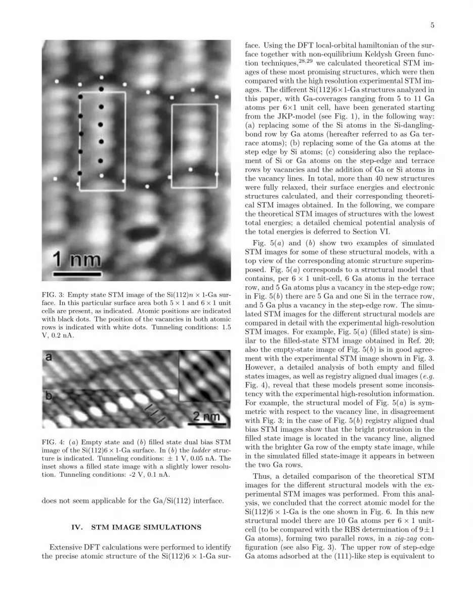
Detailed atomic resolution STM images were acquiredto investigate the atomic structure of the Si(112)6 × 1-Ga surface. In Fig. 3 an atomic resolution empty stateSTM image is shown. Note that this particular area ofthe surface shows both 5× 1 and 6× 1 unit cells as indi-cated in the figure. Two parallel atom rows are observedper unit cell, running in the [110] direction, intersectedby the quasi-periodical vacancy lines. Comparing thisimage with the results of Baski et al.,20 we observe thesame spacing of the brightest atom rows (i.e. 9.4 A). Fur-thermore, the mixed periodicities and the similar LEEDpattern (see Refs. 20 and 18, respectively), indicate thatthe same surface reconstruction is studied here. Con-sequently we conclude that the brightest atom rows inFig. 3 are the same atom rows as imaged by Baski et
al.20 (henceforth, the ”step-edge Ga row”). But in ad-dition we observe a 2nd atom row lying in between thebrighter rows. In terms of the JKP-model, this row ofatoms could be interpreted as the Si dangling bond rowwhich might form a quasi 1D band. However, these twoparallel atomic lines clearly form a zig-zag pattern as in-dicated in figures 3 (see also Fig. 13), which results ina structural asymmetry in the vacancy line. This is incontradiction with the JKP-model, which implies mirrorplane symmetry with respect to the (110) plane in thevacancy line.
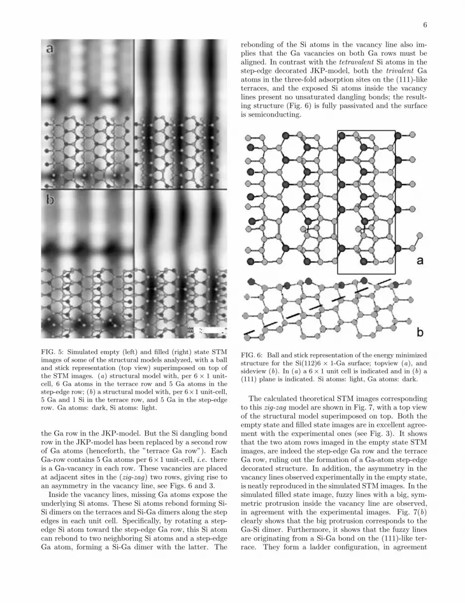
In Fig. 4 a set of registry aligned dual bias images ispresented. These images have been recorded simultane-ously on the same area of the surface, but with oppositetunneling bias polarities resulting in a set of spatially cor-related empty and filled state images. In this case, theempty state image, Fig. 4(a), has suffered from a slightdecrease in resolution, as compared with Fig. 3, but theasymmetry in the vacancy line is still visible. In thefilled state image, Fig. 4(b), a relatively big, symmetricprotrusion prevents a detailed observation of the atomicstructure in the vacancy line. As in the empty state im-age, two parallel atom rows are also visible in the filledstate image. They form a ladder structure instead of thezig-zag pattern of the rows observed in the empty stateimage.
FIG. 2: (a) STM image of pristine Si(112). (b) STM imageof the Ga covered Si(112) surface. Tunneling conditions: 1.5V, 0.1 nA and 2 V, 0.1 nA, for (a) and (b), respectively.
RBS measurements were performed to determine ex-perimentally the amount of Ga at the surface. Integra-tion of the Ga peak in the backscattered He spectrumyielded an amount of 9± 1 Ga atoms per 6× 1 unit cell,to be compared with 5 Ga per 6 × 1 unit cell for theJKP-model of Fig. 1.
In summary, these experimental results (STM andRBS) consistently show that the step-edge decoratedJKP-model of the Si(112)6 × 1-Ga surface is at variancewith the new experimental observations. Consequently,the intuitive idea of metal adatom step-edge decoration
5
FIG. 3: Empty state STM image of the Si(112)n × 1-Ga sur-face. In this particular surface area both 5× 1 and 6× 1 unitcells are present, as indicated. Atomic positions are indicatedwith black dots. The position of the vacancies in both atomicrows is indicated with white dots. Tunneling conditions: 1.5V, 0.2 nA.
FIG. 4: (a) Empty state and (b) filled state dual bias STMimage of the Si(112)6× 1-Ga surface. In (b) the ladder struc-ture is indicated. Tunneling conditions: ± 1 V, 0.05 nA. Theinset shows a filled state image with a slightly lower resolu-tion. Tunneling conditions: -2 V, 0.1 nA.
does not seem applicable for the Ga/Si(112) interface.
IV. STM IMAGE SIMULATIONS
Extensive DFT calculations were performed to identifythe precise atomic structure of the Si(112)6 × 1-Ga sur-
face. Using the DFT local-orbital hamiltonian of the sur-face together with non-equilibrium Keldysh Green func-tion techniques,28,29 we calculated theoretical STM im-ages of these most promising structures, which were thencompared with the high resolution experimental STM im-ages. The different Si(112)6×1-Ga structures analyzed inthis paper, with Ga-coverages ranging from 5 to 11 Gaatoms per 6×1 unit cell, have been generated startingfrom the JKP-model (see Fig. 1), in the following way:(a) replacing some of the Si atoms in the Si-dangling-bond row by Ga atoms (hereafter referred to as Ga ter-race atoms); (b) replacing some of the Ga atoms at thestep edge by Si atoms; (c) considering also the replace-ment of Si or Ga atoms on the step-edge and terracerows by vacancies and the addition of Ga or Si atoms inthe vacancy lines. In total, more than 40 new structureswere fully relaxed, their surface energies and electronicstructures calculated, and their corresponding theoreti-cal STM images obtained. In the following, we comparethe theoretical STM images of structures with the lowesttotal energies; a detailed chemical potential analysis ofthe total energies is deferred to Section VI.
Fig. 5(a) and (b) show two examples of simulatedSTM images for some of these structural models, with atop view of the corresponding atomic structure superim-posed. Fig. 5(a) corresponds to a structural model thatcontains, per 6 × 1 unit-cell, 6 Ga atoms in the terracerow, and 5 Ga atoms plus a vacancy in the step-edge row;in Fig. 5(b) there are 5 Ga and one Si in the terrace row,and 5 Ga plus a vacancy in the step-edge row. The simu-lated STM images for the different structural models arecompared in detail with the experimental high-resolutionSTM images. For example, Fig. 5(a) (filled state) is sim-ilar to the filled-state STM image obtained in Ref. 20;also the empty-state image of Fig. 5(b) is in good agree-ment with the experimental STM image shown in Fig. 3.However, a detailed analysis of both empty and filledstates images, as well as registry aligned dual images (e.g.Fig. 4), reveal that these models present some inconsis-tency with the experimental high-resolution information.For example, the structural model of Fig. 5(a) is sym-metric with respect to the vacancy line, in disagreementwith Fig. 3; in the case of Fig. 5(b) registry aligned dualbias STM images show that the bright protrusion in thefilled state image is located in the vacancy line, alignedwith the brighter Ga row of the empty state image, whilein the simulated filled state-image it appears in betweenthe two Ga rows.
Thus, a detailed comparison of the theoretical STMimages for the different structural models with the ex-perimental STM images was performed. From this anal-ysis, we concluded that the correct atomic model for theSi(112)6 × 1-Ga is the one shown in Fig. 6. In this newstructural model there are 10 Ga atoms per 6 × 1 unit-cell (to be compared with the RBS determination of 9±1Ga atoms), forming two parallel rows, in a zig-zag con-figuration (see also Fig. 3). The upper row of step-edgeGa atoms adsorbed at the (111)-like step is equivalent to
6
FIG. 5: Simulated empty (left) and filled (right) state STMimages of some of the structural models analyzed, with a balland stick representation (top view) superimposed on top ofthe STM images. (a) structural model with, per 6 × 1 unit-cell, 6 Ga atoms in the terrace row and 5 Ga atoms in thestep-edge row; (b) a structural model with, per 6×1 unit-cell,5 Ga and 1 Si in the terrace row, and 5 Ga in the step-edgerow. Ga atoms: dark, Si atoms: light.
the Ga row in the JKP-model. But the Si dangling bondrow in the JKP-model has been replaced by a second rowof Ga atoms (henceforth, the ”terrace Ga row”). EachGa-row contains 5 Ga atoms per 6×1 unit-cell, i.e. thereis a Ga-vacancy in each row. These vacancies are placedat adjacent sites in the (zig-zag) two rows, giving rise toan asymmetry in the vacancy line, see Figs. 6 and 3.
Inside the vacancy lines, missing Ga atoms expose theunderlying Si atoms. These Si atoms rebond forming Si-Si dimers on the terraces and Si-Ga dimers along the stepedges in each unit cell. Specifically, by rotating a step-edge Si atom toward the step-edge Ga row, this Si atomcan rebond to two neighboring Si atoms and a step-edgeGa atom, forming a Si-Ga dimer with the latter. The
rebonding of the Si atoms in the vacancy line also im-plies that the Ga vacancies on both Ga rows must bealigned. In contrast with the tetravalent Si atoms in thestep-edge decorated JKP-model, both the trivalent Gaatoms in the three-fold adsorption sites on the (111)-liketerraces, and the exposed Si atoms inside the vacancylines present no unsaturated dangling bonds; the result-ing structure (Fig. 6) is fully passivated and the surfaceis semiconducting.
FIG. 6: Ball and stick representation of the energy minimizedstructure for the Si(112)6 × 1-Ga surface; topview (a), andsideview (b). In (a) a 6× 1 unit cell is indicated and in (b) a(111) plane is indicated. Si atoms: light, Ga atoms: dark.
The calculated theoretical STM images correspondingto this zig-zag model are shown in Fig. 7, with a top viewof the structural model superimposed on top. Both theempty state and filled state images are in excellent agree-ment with the experimental ones (see Fig. 3). It showsthat the two atom rows imaged in the empty state STMimages, are indeed the step-edge Ga row and the terraceGa row, ruling out the formation of a Ga-atom step-edgedecorated structure. In addition, the asymmetry in thevacancy lines observed experimentally in the empty state,is neatly reproduced in the simulated STM images. In thesimulated filled state image, fuzzy lines with a big, sym-metric protrusion inside the vacancy line are observed,in agreement with the experimental images. Fig. 7(b)clearly shows that the big protrusion corresponds to theGa-Si dimer. Furthermore, it shows that the fuzzy linesare originating from a Si-Ga bond on the (111)-like ter-race. They form a ladder configuration, in agreement

7
FIG. 7: Simulated empty (a) and filled (b) state STM imagesof the zig-zag model of Fig. 6. A top view of the ball and stickrepresentation is superimposed on top of the STM images.Ga atoms: dark, Si atoms: light. Zig-zag symmetry andladder symmetry indicated with white bars in (a) and (b),respectively. Tunneling bias 2 V (a), and - 1.3 V (b). (c)Side view of the proposed model. The (111) plane is indicatedwith a dotted line. (d) Simulated filled state image, -2 V.
with the atomic resolution experimental image in Fig. 4.The only feature which was not reproduced is the slightlyhigher apparent height, in the empty state experimentalimages, of the Ga atoms in the two terrace Ga rows di-rectly adjacent to the vacancy line. Finally, we mentionthat changing the tunneling conditions in the simulatedSTM images (tip-sample distance, voltage), the experi-mental STM images of Ref. 20 can be recovered, as shownin Fig. 7(d).
V. SPECTROSCOPY
We also have studied this surface reconstruction withscanning tunneling spectroscopy. While imaging the sur-face with constant tunneling current, at every third datapoint an I −V curve is measured with the feedback loopswitched off during this I−V measurement. In Fig. 8 wehave averaged I −V curves measured on the upper atomrows, the lower atom rows, and on the vacancy lines sep-arately (the respective areas being determined from the
FIG. 8: Semilogarithmic (a) and normalized derivative (b)plots of I − V -curves averaged over the step-edge (dotted)and terrace (dashed) atom rows, and the vacancy lines (solid),respectively. STS setpoint: 1 V, 0.3 nA. The inset in (a)shows the bandstructure inferred from the data.
empty state STM image). This results in three curves,representing the electronic structure on the terrace andstep-edge Ga rows, and the electronic structure insidethe vacancy line. At bias voltages below the bulk con-duction band minimum, the tunneling current is limitedby thermionic emission, as is evident from the linear in-crease of the log(I) − V curve,33 up to the conductionband minimum (CBM) at 0.7 V, see Fig. 8(a). Conse-quently, the bulk valence band maximum (VBM) at thesurface should be located at ∼ −0.4 V, implying an up-ward band bending of ∼ 0.5 eV for this n-type specimen(1015cm−3), Ef − EV BM and ECBM − Ef being ∼ 0.4and ∼ 0.7 eV at the surface, respectively, as shown inthe inset of Fig. 8(a). These data are consistent withthe measured surface photovoltage in Refs. 22,34. InFig. 8(b) we have plotted the normalized derivative ofthe three I − V curves (i.e. ∂ln I
∂ln V), originating from the
three different areas within the unit cell. These tunnel-ing spectra are proportional to the local density of states(LDOS) at the respective areas of the sample surface overwhich the averaging took place (see Refs. 35,36,37). Inall curves, there is no DOS at the Fermi level, but agap of exists between the filled and empty state bandsshowing that indeed the surface is semiconducting. Thetunneling spectra on the two Ga atom rows appears to be

8
FIG. 9: (a) ∂I
∂V-map of measured STS curves at -0.31 V. STS
setpoint: 1 V, 0.3 nA. (b) Corresponding topographic STMimage. Tunneling conditions 1 V, 0.3 nA.
similar in shape, whereas the tunneling spectra inside thevacancy line deviates from the former two. The leadingedge of the total tunneling spectrum in the filled statespectrum arises from a state (B) that is located mainlyinside the vacancy lines at about ∼ −0.3 eV. The twoGa rows feature a broad filled state at higher binding en-ergy (C). In the empty state tunneling spectra the twoatom rows show a small shoulder (A) at about ∼ 0.6eV, just below the bulk CBM. Thus a surface band gapof ∼ 0.9 eV is deduced. These experimental data areentirely consistent with the presence of two equivalent,threefold coordinated rows of Ga atoms at these posi-tions, fully passivating the surface. Notice that we in-ferred the surface band gap from the separation betweenpeaks A and B using the peak position or centroids, andnot the onsets. The justification for this procedure comesfrom a detailed comparison with theoretical STS data, aswill be discussed below.
In addition, we have constructed a ∂I∂V
-map of the STS
measurements. In a ∂I∂V
-map, the value of the derivativeof the I −V -curves at a certain voltage V is plotted as atwo-dimensional image, with the x and y coordinates cor-responding to the topographic STM image. In Fig. 9(a)the derivative of the I − V -curves at -0.31 V is plotted,the corresponding empty state STM image is shown inFig. 9(b). Indeed, the largest slope in the I−V -curves at-0.31 V is located inside the vacancy lines (i.e. here the
largest increase in tunneling current is observed, corre-sponding to the largest LDOS as compared to the LDOSat this specific energy at other locations on the surface).Only a very small intensity variation is observed perpen-dicular to the atom rows, consistent with the similar filledstate tunneling spectra on the two Ga rows in Fig. 8(a).
From the structural model and its spatially re-solved DOS, theoretical STS curves were calculated, seeFig. 10(b). As for the STM images, these results areobtained using the LO-DFT Fireball96 hamiltonian ofthe surface and the Keldysh Green function approach.The corresponding calculated LDOS of the zig-zag model,averaged over different areas is shown in Fig. 10(a) (abroadening of 0.1 eV has been used). The calculated STScurves shown in Fig. 10(b) were obtained by placing thetip over the respective areas, calculating the current asa function of a voltage sweep using the calculated LDOS(Fig. 10), and averaging over the areas of interest. TheFireball96 local orbital calculations employ a minimalbasis set, resulting typically in band gaps that are toolarge. Nonetheless, excellent qualitative agreement ex-ists between the calculated STS curves and normalizedderivatives of the experimental STS curves (Fig. 8(b)).The calculated LDOS and STS curves confirm that thelarge peak B just beneath the band gap indeed is mainlyassociated with states that are located on the Si-Ga dimerinside the vacancy lines. The two Ga rows contributealmost equally to a broad peak in the DOS at higherbinding energy (C) and a small shoulder in the DOS justabove the band gap (A), in full agreement with the nor-malized derivative of the tunneling spectra in Fig. 8(b).The empty state DOS is very similar for both Ga rows.Consequently the ∼ 0.4 Ahigher appearance of the Gaatoms at the step edge in the empty state image is dueto their on average higher atomic positions, and thus theempty state STM image reflects the real surface topog-raphy at these voltages.
We have calculated the surface bandstructure usingboth the LO and PW-DFT methods, within the LDA forexchange-correlation contributions. While the LO calcu-lation overestimates the value of the bulk band gap, thePW calculation typically underestimates the band gap.In the LO bandstructure (not shown) a surface state bandgap of 1.2 eV is obtained between the states A and B,while the separation between peaks A and B in the calcu-lated STS is close to 1.4 eV. This suggests that in order tomeasure the band gap, it is reasonably accurate to use thepeak positions instead of the (poorly defined) peak onsetsin the experimental ∂ln I
∂lnVcurves. The observed splitting
between A and B in the experimental curves is ∼ 0.9 eVindicating that the experimental band gap is ∼ 0.8 eV.Fig. 11 shows the bandstructure as calculated with thePW-DFT code, showing a surface band gap of 0.77 eVbetween states A and B.40 The calculations place filledstate B slightly above the VBM, in agreement with theexperimental observation. On the other hand, the emptysurface state A is located at or slightly above the CBMaccording to the PW-DFT calculations, while experimen-

9
tally state A appears slightly below the bulk CBM; seeFig 8(b). The PW gap of 0.77 eV is comparable to theexperimental band gap of 0.8 eV. However, the preciselocation of state A in the calculations directly affects thevalue of the band gap.
FIG. 10: (a) Calculated LDOS (Fireball96), averaged overthe step-edge (dotted), terrace (dashed) Ga-rows, and va-cancy line (solid), respectively. The LDOS at the vacancyline is calculated as the average density of states of the Ga-Sidimer and Si-Si dimer. (b) Normalized derivative of the I−V -curves shown in (a). A broadening of 0.1 eV has been applied.Note the larger energy scale as compared to Fig. 8 due to theoverestimation of the gap in the local orbital calculation.
Despite the fact that the Ga/Si(112) overlayer ap-pears to be quasi two-dimensional in atomic structure,the electronic structure of this overlayer is quasi one-dimensional. The Ga-atom induced surface band A dis-perses around the X-point minimum in the upper partof the band gap. The dispersion of this band near the X-point yields an effective mass of m∗
∼ 1.48 me along theX − Γ direction, and m∗
∼ 0.15 me along X − K. Thisindicates a quasi-one-dimensional dispersion. This Ga-band is initially empty but could perhaps be populatedin a controllable way, using a biased gate electrode, or aheavily n-type doped substrate, making the Si(112)6×1-Ga surface a promising system for the experimental studyof electron transport in one dimensional atomic wires.
FIG. 11: Calculated band structure (Castep) of the zig-zag
structural model. Surface states labelled A and B are men-tioned in the text. The shaded area shows the bulk projectedbandstructure of the Si substrate. The inset shows the surfaceBrillouin zone probed.
VI. COMPETING STRUCTURES
The discussion above shows that, to elucidate the pre-cise atomic structure of a complex surface like Si(112)6×1-Ga from the comparison of theoretical and experimen-tal STM images, it is necessary to use high-resolution ex-perimental STM images, including registry aligned dualbias information and STS data, combined with state ofthe art theoretical STM simulations. These simulationswere performed on the subset of possible structures thatwere deemed most realistic on the basis of total energyconsiderations. In this section, we explore the relativestability of the various structures, which gives a morephysical basis to the proposed structural model.
In general, the precise stoichiometry of the surface isnot known, and thus the analysis of the relative stabilityof different structural models requires the calculation ofthe surface energy F as a function of the different chem-ical potentials.
A. Chemical potential analysis
For the analysis of the relative stabilities of the vari-ous structures, we need to calculate the surface energyF = Etot − µGaNGa − µSiNSi, where Etot is the totalenergy per unit-cell, µGa, µSi are the Ga and Si chemicalpotentials, and NGa, NSi are the number of Ga and Siatoms in the unit-cell. For µSi we use the total energy(per atom) of bulk-Si (i.e. the surface is in equilibriumwith the substrate). The value of µGa is not determinedby the substrate, but it can be estimated analyzing theexperimental conditions (see below).
Fig. 12 shows the surface energy F = Etot−µGaNGa−
µSiNSi as a function of µGa. In this figure we use the

10
structural model of Fig. 6 as reference, and plot F forsome of the most promising models, as calculated withthe PW code (Castep). In order to estimate the valueof µGa we have to analyze the experimental conditions ofthe Ga deposition. In the ”one-step” process the (6× 1)-phase is formed under a Ga flux from the effusion cellwith the sample held at a temperature of T = 825 K. Atthis temperature the incoming flux of Ga atoms is bal-anced by a flux of Ga atoms desorbing from the surface,thus establishing a quasi-equilibrium. This allows us torelate the chemical potential µGa in the effusion cell withthe chemical potential µGa at the sample. The chemicalpotential in the effusion cell may be approximated by thetotal energy of bulk-Ga, µGa(bulk), i.e. the Ga vapor inthe effusion cell is in equilibrium with the solid.41
Considering also the equilibrium between the sampleand the Ga vapor in contact with the sample, we canestimate the chemical potential at the sample
µGa = µGa(bulk) − kBT ln(pc
ps
)
where pc is the Ga vapor pressure in the effusion cell andps the Ga vapor pressure at the sample. Since the effusioncell flux is proportional to its vapour pressure, pc, timesthe cell aperture area, and the sample flux is also pro-portional to its corresponding vapour pressure, ps, timesthe sample area, we conclude that (pc/ps) ∼ 102(103),and µGa = µGa−bulk − 0.32(0.48) eV. In Fig. 12 we seethat for this range of µGa the structural model of Fig. 6presents the lowest surface energy F . This result stronglysupports our conclusion that the structural model for theSi(112)6 × 1-Ga surface is the one depicted in Fig. 6.
FIG. 12: Surface energy as a function of the Ga chemicalpotential (Castep). The Ga chemical potential is plottedrelative to the chemical potential in bulk Ga. 5Ga (filledsquares) is the step-edge decorated JKP-model
Comparing our model with the step-edge decoratedJKP-model, an important difference is that the newstructural model (Fig. 6) presents no partially-filled dan-gling bonds as discussed above. The stability of the newmodel is related to the full passivation of the substrate,removing all dangling bonds, and the associated decrease
in surface free energy. The results shown in Fig. 12 sug-gest, however, that the JKP-model might be stabilizedfor very low µGa values. We should stress that our the-oretical analysis has been directed to search for surfaceatomic structures that could explain the experimentalresults (STM and RBS) for the Si(112)6× 1-Ga surface,and thus surface structures with lower Ga coverages, thatshould be favored for low µGa values have not been ana-lyzed as thoroughly as those with coverages close to 9-10Ga atoms/6× 1 unit cell. Nevertheless, we may performa simple analysis, comparing the surface energy of thestep-edge decorated JKP-model, with the surface energyof a simple hypothetical surface: half the surface is cov-ered with the structure of Fig. 6 (i.e. both step-edge andterrace Ga rows) while the other half consists of cleanSi(112). Both the step-edge decorated JKP system andthis hypothetical half-half case present the same Ga cov-erage and thus the same behavior of F as a function ofµGa (i.e. the same slope in Fig. 12). This comparisonreveals that the hypothetical case is lower in energy (by∼ 0.7 eV/(10 Ga atoms), for all µGa values, showingthat the step-edge decorated case is unlikely to be sta-bilized at lower Ga coverage, and phase separation intobare Si(112) and the Si(112)6× 1-Ga zig-zag surface willoccur instead. Note that the facetting of the unstableSi(112) surface, which was not accounted for in this cal-culation, would increase this energy difference, makingphase separation even more favorable compared to thestep-edge decorated JKP-model.
Another possible scenario for obtaining a step-edgedecorated Ga row would be to use the experimentally ob-served fully passivated Si(112)6 × 1-Ga surface (Fig. 6)as starting point, and try to kinetically stabilize ametastable step-edge decorated structure by selectivelydesorbing the Ga atoms from the terraces. Experimen-tally, this might happen in the ’two-step’ preparation pro-cedure, see Section II. We have studied this possibility bycalculating desorption energies of terrace and step-edgeGa atoms from the Si(112)6 × 1-Ga surface (Fig. 6). Inparticular, we have considered removing the Ga atomsclose to the vacancy line as well as the replacement ofthose Ga atoms by Si atoms. In both cases the desorp-tion energies are lower by ∼ 0.7 eV for step-edge Gaatoms than for Ga atoms on the terraces. This resultsuggests that a metastable step-edge decorated structurelikely can not be achieved by thermally desorbing the Gaterrace atoms.
B. Intrinsic structural disorder
In the experimental STM images, the vacancy lines arenot exactly straight, but some meandering is observed, asshown in Fig. 13 (see also Figs. 2(b) and Fig. 3). The newstructural model is able to fully explain the experimen-tally observed meandering.12 It was proposed by Erwinet al.21 that this meandering of the vacancy lines couldbe explained by the co-existence of 6 × 1 and 5 × 1 unit

11
cells on the surface. This results in occasional steps inthe vacancy lines, equivalent to the observed meander-ing of the dimer-vacancy lines on the Ge covered Si(001)surfaces.38 We have analyzed the stability of the zig-zag
structural model as a function of the longitudinal period-icity. Fig. 14 shows the surface energies F of this modelfor different periodicities: 5 × 1, 6 × 1 and 7 × 1. The5 × 1 surface corresponds to 4 Ga atoms in each Ga-rowbetween vacancy lines, while the 7 × 1 surface presents6 Ga atoms in each row between vacancy lines. For ourestimated range of µGa the 6 × 1 surface presents thelowest F , while the 5 × 1 is only 0.1-0.2 eV higher, per6 × 1 unit-cell. This small energy difference should leadto the experimental observation of 5×1 unit cells. Indeedthese unit cells are frequently observed in the experimen-tal images, see Fig. 13. It thus appears that the pre-dictions from the 1D Frenkel-Kontorova model regard-ing the vacancy-line spacing in the step-edge decoratedstructure21 also apply to the quasi 2D zig-zag arrange-ment of Ga atoms presented here. This conclusion isnot very surprising as it was concluded in Ref. 21 thatthe strain induced by the size difference of Ga and Sicompletely dominates the energetics of the periodicities.Apparently this conclusion still holds when an extra Garow is added.
FIG. 13: Detailed STM image, showing the two contributionsto the meandering of the vacancy lines. Straight lines aredrawn through domains with unit cells of the same size. Oc-casional jumps in the lines are due to different unit cell sizes,as explained in the text. Dots are placed on the Ga atom ofthe Ga-Si dimer at the vacancy of the step-edge rows, showingthe fluctuations due to the intrinsic disorder of the randomorientation of the Ga-Si dimer.
However, careful investigation of the experimental im-ages reveals that the meandering of the vacancy lines as
FIG. 14: Free energy as a function of the Ga chemical po-tential for 5x1, 6x1 and 7x1. The Ga chemical potential isplotted relative to the chemical potential in bulk Ga. Notethe difference in scale on the abcissa as compared to Fig. 12.
observed in Fig. 2 is not only due to the competing lon-gitudinal periodicities. Instead, for large sections of thesurface, the terrace Ga rows are perfectly periodic in the×1 direction with (n-1) Ga atoms per terrace Ga rowin the n×1 unit cell. But in these ordered sections thenumber of Ga atoms in the step-edge Ga rows appearsto fluctuate between n-2 and n. The proposed structuralmodel perfectly explains these intrinsic fluctuations (i.e.fluctuations within a n×1 domain); they are related tothe orientation of the Si-Ga dimer in the step-edge rows.The twofold symmetry of the 112 substrate in the [110]direction is broken by the Si-Ga dimers, resulting in twodegenerate orientations of these dimers. The energy as-sociated with interchanging the atoms of a Si-Ga dimerhas been calculated12 to be less than 10 meV per 12 × 1unit cell. This small energy difference explains the ap-pearance of frequent meandering in the aligned vacanciesin the step-edge Ga rows, thus accounting for the major-ity of the fluctuations in the vacancy lines observed inthe experimental images. The absence of these fluctua-tions in the filled state images (compare Figs. 4(a) and(b) and also Figs. 9(a) and (b)) is the result of the factthat the bright protrusion in the vacancy line appearsin the center of the Ga-Si dimer, making its appearanceinsensitive to the orientation of the Ga-Si dimer.
VII. SUMMARY AND CONCLUSIONS
The 6 × 1 reconstruction of Ga on vicinal Si(112) wasstudied with STM, STS, RBS, and extensive DFT cal-culations. High resolution STM experiments revealed anasymmetry in the vacancy lines of the Si(112)6 × 1-Gasurface that is inconsistent with the JKP-model of step-edge decoration. STS measurements also rule out for-mation of quasi 1D metal wires while RBS experiments

12
indicated a Ga coverage twice as large as previously in-ferred from the JKP model. Extensive DFT calculationswere used to analyze the relative stability of more thanforty structures, taking the chemical potential of the Gaadsorbate into account. Theoretical STM images werecalculated for the most promising structures and com-pared in detail with the experimental STM images.
A new structure emerged containing 10 Ga atoms per6×1 unit cell. The Ga atoms decorate the step edge andpassivate the terrace atoms, thereby forming a zig-zag
pattern. Excellent agreement between experimental andtheoretical STM and STS data confirmed the validity ofthe proposed zig-zag model and demonstrate the power ofsuch a comparison. Ga atoms are threefold coordinatedand Si dangling bonds are all passivated so the surfaceis semiconducting. The ”broken bond orbitals” insidethe vacancy lines rebond to form Si-Ga and Si-Si dimers.The observed meandering of the vacancy lines originatesfrom thermal fluctuations between the two symmetry-degenerate orientations of the Si-Ga dimer, in conjunc-tion with thermal fluctuations between competing 6 × 1and 5 × 1 units.
While step-edge decoration of vicinal metal surfacesworks,39 the observed drive toward chemical passivationsuggests that step-edge decoration of vicinal semiconduc-tors is not a viable method to produce 1D metal wires.Although this general conclusion remains to be testedfurther, it is clear that partially-filled dangling bonds onthe terraces of vicinal surfaces are always greatly reducedin number or eliminated altogether in the reconstruction.
As shown in this paper, predictive calculations alongthese lines should always take into account the chemi-cal potential of the adsorbate. The latter depends onthe experimental preparation conditions (see e.g. equa-tion (4)). Successful prediction of systems with perfect1D metal adatom step-edge decoration could facilitatethe quest for the experimental realization of Luttingerliquids in such systems, possibly enabling a convincingproof of spin-charge separation with angle resolved pho-toemission spectroscopy.
VIII. ACKNOWLEDGEMENTS
This work is part of the research programme of the’Stichting voor Fundamenteel Onderzoek der Materie(FOM)’, which is financially supported by the ’Ned-erlandse Organisatie voor Wetenschappelijk Onderzoek(NWO)’. This work was sponsored in part by the NSF un-der contract No. DMR-0244570, the Ministerio de Cien-cia y Tecnologia (Spain) under grants No. MAT2001-0665 and MAT2004-01271. One of us, S.R., wishes to ac-knowledge the Royal Netherlands Academy of Arts andSciences. We thank T.M. Klapwijk for his stimulatingsupport, and the AMOLF institute in Amsterdam forperforming the RBS experiments. Oak Ridge NationalLaboratory is managed by UT-Battelle, LLC, for the USDepartment of Energy under contract No. DE-AC-05-00OR22725.
∗ Electronic address: [email protected] H. W. C. Postma, M. de Jonge, Z. Yao, and C. Dekker,
Phys. Rev. B 62, R10653 (2000).2 M. Grioni, I. Vobornik, F. Zwick, and G. Margaritondo, J.
Electron Spectrosc. Relat. Phenom. 100, 313 (1999).3 J. Voit, Rep. Prog. Phys. 58, 977 (1994).4 F. J. Himpsel, K. N. Altmann, R. Bennewitz, J. N. Crain,
A. Kirakosian, J.-L. Lin, and J. L. McChesney, J. Phys.:Condens. Matter 13, 11097 (2001).
5 J. N. Crain, J. L. McChesney, F. Zheng, M. C. Gallagher,P. C. Snijders, M. Bissen, C. Gundelach, S. C. Erwin, andF. J. Himpsel, Phys. Rev. B 69, 125401 (2004).
6 P. Starowicz, O. Gallus, T. Pillo, and Y. Baer, Phys. Rev.Lett. 89, 256402 (2002).
7 P. Segovia, D. Purdie, M. Hengsberger, and Y. Baer, Na-ture 402, 504 (1999).
8 H. W. Yeom, S. Takeda, E. Rotenberg, I. Matsuda,K. Horikoshi, J. Schaefer, C. M. Lee, S. D. Kevan, T. Ohta,T. Nagao, et al., Phys. Rev. Lett. 82, 4898 (1999).
9 J. R. Ahn, H. W. Yeom, E. S. Cho, and C. Y. Park, Phys.Rev. B 69, 233311 (2004).
10 O. Bunk, G. Falkenberg, J. H. Zeysing, L. Lottermoser,R. L. Johnson, M. Nielsen, F. Berg-Rasmussen, J. Baker,and R. Feidenhansl, Phys. Rev. B 59, 12228 (1999).
11 I. K. Robinson, P. A. Bennett, and F. J. Himpsel, Phys.Rev. Lett. 88, 096104 (2002).
12 C. Gonzalez, P. C. Snijders, J. Ortega, R. Perez, F. Flores,S. Rogge, and H. H. Weitering, Phys. Rev. Lett. 93, 126106(2004).
13 J. N. Crain, A. Kirakosian, K. N. Altmann, C. Bromberger,S. C. Erwin, J. L. McChesney, J.-L. Lin, and F. J. Himpsel,Phys. Rev. Lett. 90, 176805 (2003).
14 J. R. Ahn, H. W. Yeom, H. S. Yoon, and I.-W. Lyo, Phys.Rev. Lett. 91, 196403 (2003).
15 I. Matsuda, M. Hengsberger, F. Baumberger, T. Greber,H. W. Yeom, and J. Osterwalder, Phys. Rev. B 68, 195319(2003).
16 T. Kanagawa, R. Hobara, I. Matsuda, T. Tanikawa, A. Na-tori, and S. Hasegawa, Phys. Rev. Lett. 91, 036805 (2003).
17 T. M. Jung, R. Kaplan, and S. M. Prokes, Surf. Sci. 289,L577 (1993).
18 T. M. Jung, S. M. Prokes, and R. Kaplan, J. Vac. Sci.Technol. A 12, 1838 (1994).
19 J. E. Yater, A. Shih, and Y. U. Idzerda, Phys. Rev. B 51,R7365 (1995).
20 A. A. Baski, S. C. Erwin, and L. J. Whitman, Surf. Sci.423, L265 (1999).
21 S. C. Erwin, A. A. Baski, L. J. Whitman, and R. E. Rudd,Phys. Rev. Lett. 83, 1818 (1999).
22 K. Yoo, S. J. Tang, P. T. Sprunger, I. Benito, J. Ortega,F. Flores, P. C. Snijders, M. C. Demeter, and H. H. Weit-ering, Surf. Sci. 514, 100 (2002).

13
23 A. A. Baski and L. J. Whitman, J. Vac. Sci. Technol. B14, 992 (1996).
24 O. J. Glembocki and S. M. Proke, Appl. Phys. Lett. 71,2355 (1997).
25 A. A. Demkov, J. Ortega, O. F. Sankey, and M. P. Grum-bach, Phys. Rev. B 52, 1618 (1995).
26 O. F. Sankey and D. J. Niklewski, Phys. Rev. B 40, 3979(1989).
27 CASTEP 4.2 Academic version, licensed under the UKCP-MSI Agreement, 1999.
28 N. Mingo, L. Jurczyszyn, F. J. Garcia-Vidal, R. Saiz-Pardo, P. L. de Andres, F. Flores, S. Y. Wu, and W. More,Phys. Rev. B 54, 2225 (1996).
29 L. Jurczyszyn, J.Ortega, R. Perez, and F. Flores, Surf. Sci.482-5, 1350 (2001).
30 J. M. Blanco, C. Gonzalez, P. Jelinek, J. Ortega, F. Flores,and R. Perez, Phys. Rev. B 70, 085405 (2004).
31 J. M. Blanco, C. Gonzalez, P. Jelinek, J. Ortega, F. Flores,R. Perez, M. Rose, M. Salmeron, J. Mendez, J. Wintterlin,et al., Phys. Rev. B 71, 113402 (2005).
32 A. A. Baski and L. J. Whitman, Phys. Rev. Lett. 74, 956(1995).
33 S. M. Sze, Physics of Semiconductor Devices (John Wileyand Sons, 1981).
34 P. C. Snijders, J. N. Crain, J. L. McChesney, M. C. Gal-lagher, and F. J. Himpsel, unpublished data.
35 R. M. Feenstra, J. A. Stroscio, and A. P. Fein, Surf. Sci.181, 295 (1986).
36 J. Tersoff and D. R. Hamann, Phys. Rev. Lett. 50, 1998(1983).
37 J. Tersoff and D. R. Hamann, Phys. Rev. B 31, 805 (1985).38 X. Chen, F. Wu, Z. Zhang, and M. G. Lagally, Phys. Rev.
Lett. 73, 850 (1994).39 P. Gambardella, A. Dallmeyer, K. Maiti, M. C. Malagoli,
W. Eberhardt, K. Kern, and C. Carbone, Nature 416, 301(2002).
40 Note that the bulk projected gap for the PW (LDA) calcu-lation is not equal to ∼ 0.67 eV, as a fully converged PW(LDA) calculation should give. This is caused by the factthat the bands are plotted along symmetry directions inthe surface Brillouin zone that do not contain the k-pointcorresponding to the bulk Si CBM.
41 The chemical potential of liquid Ga is approximated by thechemical potential of solid, bulk Ga at T=0K. Finite tem-perature corrections which include the enthalpy of meltingand the integrated heat capacity are very small (< 0.1 eV)and have been neglected.


