Embed Size (px)
Citation preview
1
Giant enhancement of spin accumulation and long-distance spin precession
in metallic lateral spin valves
Yasuhiro Fukuma1*, Le Wang1,2, Hiroshi Idzuchi3, Saburo Takahashi4,5, Sadamichi
Maekawa5,6 and YoshiChika Otani1,2,3*
1Advanced Science Institute, RIKEN, 2-1 Hirosawa, Wako 351-0198, Japan 2Department of Material Physics and Chemistry, University of Science and Technology
Beijing, Beijing 100083, People’s Republic of China 3Institute for Solid State Physics, University of Tokyo, Kashiwa 277-858, Japan 4Institute for Materials Research, Tohoku University, Sendai 980-8577, Japan
5CREST, Japan Science and Technology, Tokyo 102-0075, Japan 6Advanced Science Research Center, Japan Atomic Energy Agency, Tokai 319-1195, Japan
The nonlocal spin injection in lateral spin valves is highly expected to be an effective
method to generate a pure spin current for potential spintronic application. However, the
spin valve voltage, which decides the magnitude of the spin current flowing into an
additional ferromagnetic wire, is typically of the order of 1 μV. Here we show that
lateral spin valves with low resistive NiFe/MgO/Ag junctions enable the efficient spin
injection with high applied current density, which leads to the spin valve voltage
increased hundredfold. Hanle effect measurements demonstrate a long-distance
collective 2π spin precession along a 6 μm long Ag wire. These results suggest a route to
faster and manipulable spin transport for the development of pure spin current based
memory, logic and sensing devices.
*e-mail: [email protected]; [email protected]
2
MgO based magnetic tunnel junction (MTJ) is a building block of spintronic
devices such as read heads for magnetic recording and memory cells for spin random
access memory1,2. A typical MTJ consists of two ferromagnetic electrodes separated by
an insulating tunnel barrier and exhibits a large resistance change between the
antiparallel and parallel alignments of the ferromagnetic electrodes, in which the spin
current is accompanied by a charge current (spin-polarized current). For spin-torque
switching and spin-torque nano-oscillators3-9, a large spin-polarized current of the order
of 1010 – 1012 A/m2 needs to be applied to the junction, so that the accompanying charge
current may cause adverse effects due to Joule heating and Oersted field.
Pure spin current is a flow of spin angular momentum accompanying no charge
current. The nonlocal spin injection in lateral spin valves (LSVs) has proven to be an
effective method to generate the pure spin current IS flowing along the slope of the spin
accumulation which decays exponentially with a factor of exp (-d/λS) where d is the
distance from the interface and λS is the spin-diffusion length in the nonmagnetic
wire10,11. Subsequent spin relaxation takes place in an additional ferromagnet in Ohmic
contact with the nonmagnetic wire sustaining the spin accumulation. This is so called
“spin absorption” and provides an attractive means to manipulate the magnetization in
magnetic nanostructures12-15. Therefore, it is beneficial to develop more efficient way to
generate a large pure spin current as well as a large spin accumulation for advancement
of novel spintronic devices utilizing lateral geometry. However, the amplitude of the
voltage change ΔVS between antiparallel and parallel alignments of the magnetization of
the two ferromagnetic wires detected at the second ferromagnetic wire in LSVs is
3
typically of the order of 1 μV. The nonlocal measurement involves no charge current
flow but the spin accumulation in the vicinity of the detector. The spin accumulation is
the difference in the electrochemical potential between majority and minority spins, i.e.
ΔVS is the measurable physical quantity and also decides the magnitude of pure spin
current absorbed into the detector ferromagnet. Therefore efficient spin injection into
the nonmagnet from the ferromagnet, being proportional to the spin valve signal
ΔRS=ΔVS/I, and the high applied current I are indispensable in realizing further
enhancement of the spin accumulation16-23.
Here, we report on the effect of interface on the spin accumulation in metallic LSVs
with NiFe/MgO/Ag junctions. For achieving efficient spin injection as well as high
applied current density, the NiFe/MgO/Ag junction is annealed in a nitrogen and
hydrogen atmosphere. The low areal resistance of around 0.2 Ωμm2 of the interface
MgO layer could effectively overcome the spin resistance mismatch between NiFe and
Ag and leads to significant enhancement of the spin accumulation. The spin transport
characteristics in the Ag nanowires have been investigated by spin valve signal and
Hanle effect measurements. These experimental results are indeed consistent with the
one-dimensional spin-dependent diffusion model.
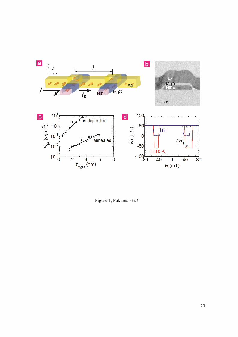
Figure 1a shows a schematic illustration of our device structure. The spin polarized
current is injected into an Ag wire through a MgO layer and the pure spin current flows
along the slope of the spin accumulation on the right hand side in the Ag wire. The size
of the NiFe/MgO/Ag junctions is 0.022 μm2. The cross-sectional transmission electron
micrograph (TEM) image is shown in Fig. 1b. The edges of the NiFe wires are covered
4
by the MgO layer with no pinholes. Figure 1c shows the MgO thickness tMgO
dependence of the interface resistance per 1 μm2 area (resistance-area product RIA) for
the NiFe/MgO/Ag junctions at room temperature. There is no temperature dependence
of RIA. The value of RIA increases exponentially with tMgO, however, the RIA is much
lower than that for a typical tunnel junction1,2. The data for as-deposited and annealed
NiFe/MgO/Ag junctions are respectively fitted by RIA = aexp(btMgO) with a = 0.066
Ωμm2 and b = 1.41 (nm)-1, and a = 0.002 Ωμm2 and b = 0.76 (nm) -1, which are shown
by the solid lines in Fig. 1 c. The RIA is drastically decreased by annealing at 400 °C for
40 min in the 97% nitrogen + 3% hydrogen atmosphere. While it is hard to determine
the composition of the MgO layer quantitatively, energy dispersive X-ray spectroscopy
reveals that 6 % oxygen in MgO is decreased qualitatively after the annealing. The low
RIA in our devices can be attributed to the oxygen vacancies24. The nano-beam
diffraction shows a typical polycrystalline pattern identified by a JCPDS card (No. 4-
0829) despite the drastic change in stoichiometry of the MgO layer. Preferential growth
direction is not observed in the high resolution TEM and electron diffraction
measurements.
The spin valve signal of nonlocal spin injection measurements for LSV with tMgO =
5.5 nm and the centre-to-centre separation between the injector and the detector L = 300
nm after the annealing is shown in Fig. 1d. The high and low resistances correspond to
the parallel and antiparallel configurations of the two NiFe wires. The zero baseline
resistance at low temperatures suggests ideal behavior for nonlocal geometry without
any spurious effects due to inhomogeneous current distribution toward the detector,
5
anisotropic magnetoresistance (AMR) and Joule heating18,25. Clear spin valve signals
ΔRS of 48.0 mΩ and 112.3 mΩ are respectively detected at room temperature and 10 K.
In contrast, the maximum ΔRS for as-deposited LSVs are 3.5 mΩ at room temperature
and 7.5 mΩ at 10 K 26. This fact infers that the magnitude of ΔRS is enhanced
remarkably by a factor of about 15 after the annealing.
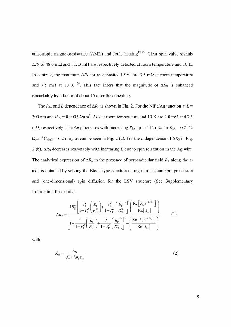
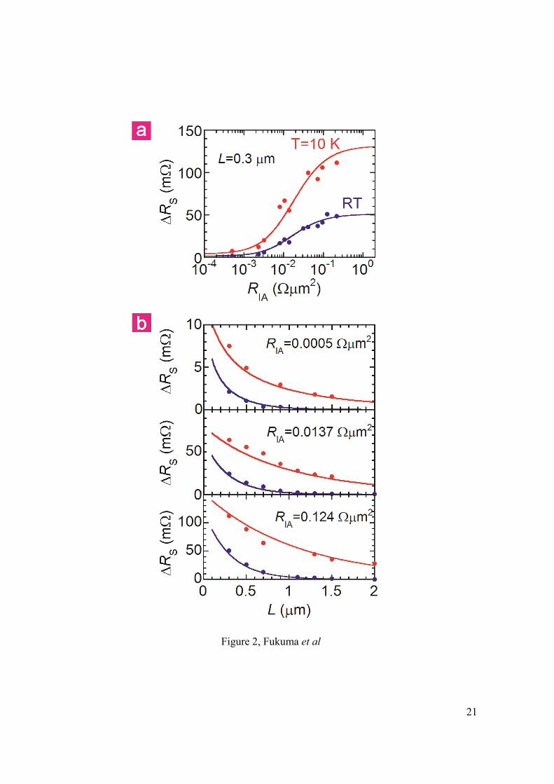
The RIA and L dependence of ΔRS is shown in Fig. 2. For the NiFe/Ag junction at L =
300 nm and RIA = 0.0005 Ωμm2, ΔRS at room temperature and 10 K are 2.0 mΩ and 7.5
mΩ, respectively. The ΔRS increases with increasing RIA up to 112 mΩ for RIA = 0.2152
Ωμm2 (tMgO = 6.2 nm), as can be seen in Fig. 2 (a). For the L dependence of ΔRS in Fig.
2 (b), ΔRS decreases reasonably with increasing L due to spin relaxation in the Ag wire.
The analytical expression of ΔRS in the presence of perpendicular field B⊥ along the z-
axis is obtained by solving the Bloch-type equation taking into account spin precession
and (one-dimensional) spin diffusion for the LSV structure (See Supplementary
Information for details),
[ ]
[ ]
2 /I I F F
N 2 2I N F N
22 /I F
2 2I N F N
Re4
1 1 Re ,
Re2 211 1 Re
L
SL
eP R P RRP R P R
ReR R
P R P R
ω
ω
λωω
ω ωω
λω
ω ωω
λλ
λλ
−
−
⎛ ⎞⎡ ⎤⎡ ⎤⎛ ⎞ ⎛ ⎞ ⎣ ⎦⎜ ⎟+⎢ ⎥⎜ ⎟ ⎜ ⎟ ⎜ ⎟− −⎝ ⎠ ⎝ ⎠⎣ ⎦ ⎝ ⎠Δ =⎛ ⎞⎡ ⎤⎡ ⎤⎛ ⎞ ⎛ ⎞ ⎣ ⎦⎜ ⎟+ + −⎢ ⎥⎜ ⎟ ⎜ ⎟ ⎜ ⎟− −⎝ ⎠ ⎝ ⎠⎣ ⎦ ⎝ ⎠
(1)
with
N
L sf
,1 iω
λλω τ
=+
(2)
6
where PI and PF are the spin polarization of the currents through MgO and the
ferromagnetic NiFe, respectively, N N NRe /[ ]R Rωωλ λ= is the spin resistance of the
nonmagnetic Ag in the presence of the spin precession, RN and RF, respectively, are the
spin resistance of Ag and NiFe in a static condition (B⊥=0), and λN the spin diffusion
length of Ag, τsf = λN2/DN the spin relaxation time, DN the diffusion constant, ωL = γeB⊥
the Larmor frequency, B /e gγ μ= the gyromagnetic ratio, g the g-factor and μB the
Bohr magneton. For the analysis of the Hanle effect data, the equation (4) in ref. 28 has
been widely used but is valid only for LSVs with no spin absorption into the
ferromagnetic contact, e.g. tunnel or Schottky nonlocal junctions. On the other hand, the
equation (1) in this study takes into account the contribution of this spin absorption to
the L dependence and the Hanle effects, thus enabling us to analyze ΔRS in a unified
manner27. Therefore, the experimental data in Fig. 2 are fitted to the equation (1) by
adjusting parameters, PI, PF, and λN with setting the value of the spin diffusion length of
NiFe, λF = 5 nm, reported by Dubois et al.29. Then we obtain PI = 0.42 and 0.44, PF =
0.3 and 0.35, λN = 300 nm and 1100 nm at room temperature and 10 K, respectively.
The spin diffusion length and the interface spin polarization corresponding to the spin
injection efficiency of the junction are substantially improved by the annealing; for as-
deposited LSVs, PI and λN are respectively 0.11 and 270 nm at room temperature, and
0.11 and 550 nm at 10 K26. Moreover ΔRS for the as-deposited LSVs is drastically
decreased when tMgO > 1 nm due to the spin relaxation in the MgO layer26, whereas in
the present study the ΔRS increases monotonically with tMgO. This implies that spin
7
transport characteristics of the NiFe/MgO/Ag junction are much improved. The
experimental results are indeed consistent with the one-dimensional spin transport
model. For the NiFe/Ag junction, injecting spin current relaxes at the interface because
of the spin resistance mismatch between RAg = ρNλΝ/tNwN = 0.89 Ω and RNiFe =
ρFλF/wFwN = 0.08 Ω for T = 10 K, where tN and wN are the thickness and the width of the
nonmagnetic wire, respectively, and wF is the width of the ferromagnetic wire. When RI
reaches to the value of RNiFe, ΔRS starts to increase because a backflow of the injected
spin current into NiFe, which may also be spin absorption, starts to be suppressed. Then,
ΔRS increases with RI and takes a maximum when RIA ~ 0.2 Ωμm2 (RI ~ 9 Ω). This
means that the interface resistance should be ten times larger than RN to overcome the
spin resistance mismatch between the ferromagnetic and nonmagnetic metals.
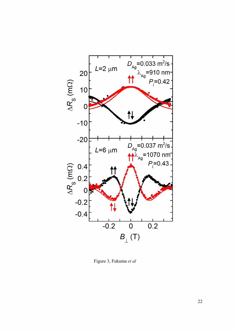
To gain more insight into the spin transport characteristics in the Ag nanowire, the
Hanle effect measurements30,31 were performed. Figure 3 shows the modulated ΔRS due
to spin precession as a function of the perpendicular magnetic field for LSVs with
NiFe/MgO/Ag junctions. For the large perpendicular field, the magnetization of NiFe
tends to align toward the field direction, causing undesired change in ΔRS, the value of
which is therefore corrected by using the information of magnetization process
measured by AMR. The Hanle effect measurements are started from parallel or
antiparallel configuration of the magnetization of the two NiFe wires. For L = 2 μm, the
two curves cross each other at around 0.27 T of which spin precession angle is π/2. In
contrast, the Hanle effect measurements for Al based LSVs with the same injector-
detector separation exhibit a clear 3π/2 spin precession32, inferring much faster spin
8
diffusion in Ag than Al. The value of DAg estimated from the Einstein relation
2N N Ne N Dσ = , where e is the electron charge, NAg = 1.55×10²² (eVcm3)-1 is density of
state at the Fermi energy33 and σAg = 8.20×10⁷ (Ωm)-1 is the conductivity, is 3.30×10⁻²
m2/s, which is indeed about ten times larger than that of Al (DAl = 4.3×10⁻³ m2/s)32.
Such fast diffusive spin transport may be suitable for faster memory, logic and sensing
applications. However this fast spin diffusion hinders a large precession in the LSV with
the small injector-detector separation because of short traveling time. Therefore, we
fabricated NiFe/MgO/Ag LSV with L = 6 μm, which is much longer than the spin
diffusion length. The clear spin precession up to almost 2π rotation with large amplitude
is observed, as shown in Fig. 3. The experimental data are also fitted to equation (1),
and the best-fit parameters PI and λN are very close to the results obtained from the RIA
and L dependent measurements shown in Fig. 2. The Hanle effect measurements are
known to determine the transverse spin relaxation time T2, whereas the separation
dependence measurements do the longitudinal spin relaxation time T1. In a non-
magnetic metal, T1 = T2 is predicted from analytical calculation31,34 and is confirmed
experimentally only for LSVs with L ~ λN32. Our experimental results clearly show that
T1 and T2 are almost identical even for L > λN.
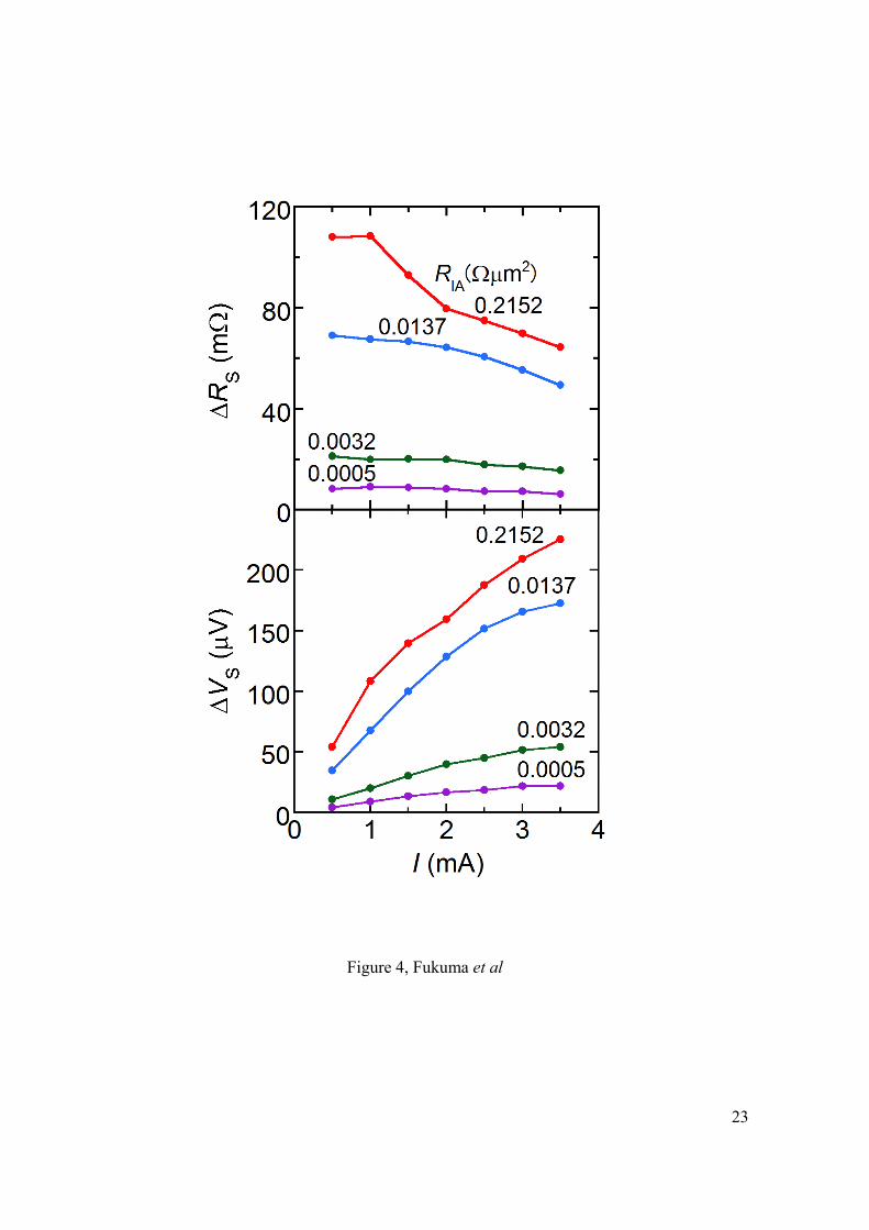
Finally we stress here that the low resistive NiFe/MgO/Ag junction offers a big
advantage for realizing large spin accumulation in the Ag nanowire. As can be seen in
the RIA dependence of ΔRS in Fig. 2a, theoretical values of ΔRS at room temperature and
10 K reach the values of saturation, 55 mΩ and 131 mΩ, respectively. Note that even
though the interface resistance is as low as 0.2 Ωμm2, ΔRS shows 51 mΩ at RT and 112
9
mΩ at 10 K, which are close to the saturation values. Such a low RI junction allows
increasing the applied current density with keeping high spin injection efficiency, as
shown in Fig. 4. The large spin valve voltage over 220 μV is only realized by applying
high bias current of 3.5 mA at the injector, although ΔRS decreases due to Joule heating.
The decrease of ΔRS in high bias currents may be attributed to the spin relaxation via
phonon in the Ag nanowire because the value of PI, which is proportional to the spin
injection efficiency into Ag through MgO, is insensitive to the temperature, as discussed
for the fitting data in Fig. 2. We should note here that this spin valve voltage is much
larger than that so far reported for LSVs not only for metals16-26 but also semiconductors
such as Si and GaAs35-38 because of the efficient spin injection for the NiFe/MgO/Ag
junction. There is still a possibility to further increase the spin accumulation in LSVs as
CoFe/MgO1 and CoFeB/MgO39 interfaces in MTJs show the spin injection efficiency
better than for NiFe/MgO. In this way, the low resistive MgO based junction will not
only lead to efficient control of the magnetization and the domain wall by using pure
spin current12-15 but also accelerate progress towards developing novel multi-terminal
spintronic devices in lateral geometry such as spin-logic devices40.
10
METHODS
Lateral spin valves with clean NiFe/MgO/Ag interfaces are prepared on a Si/SiO2
substrate without breaking vacuum by means of shadow evaporation using a suspended
resist mask. The resist mask pattern consisting of 500 nm-thick methyl-methacrylate
(MMA) and 50 nm-thick polymethyl methacrylate (PMMA) is fabricated by e-beam
lithography. All the layers are e-beam deposited in an ultra-high vacuum condition of
about 10-7 Pa, but the ferromagnetic and nonmagnetic materials are deposited separately
in the interconnected two different evaporation chambers to prevent magnetic impurities
into the nonmagnetic nanowire, which degrade the spin diffusion length. Firstly, the
injector and detector NiFe wires 140 nm in width and 20 nm in thickness are obliquely
deposited at a tilting angle of 45° from substrate normal. Secondly, the interface MgO
layer with various thicknesses ranging from 0 to 6 nm is deposited on a 20×20 mm
substrate at the same tilting angle of 45°. Thirdly, the Ag wire 160 nm in width and 50
nm in thickness is deposited normal to the substrate. Finally, 3 nm thick capping MgO
layer is deposited to prevent surface contamination of the devices. After the liftoff
process, the LSV devices are annealed at 400 °C for 40 min in an N2 (97%) + H2 (3%)
atmosphere.
The interface resistance is determined by a typical four-terminal method at the cross
junction. The nonlocal measurements with low bias current are carried out by
conventional current-bias lock-in technique. The ac current with the amplitude of 200
μA and the frequency of 79 Hz is used for the lock-in detection. The magnetic field is
applied parallel to the NiFe wires for the spin valve measurements. The switching field
11
of two NiFe wires is controlled by attaching a large domain wall reservoir at the edge.
To measure the bias current dependence of the nonlocal signal, the positive dc current
with the duration of 200 μs is applied at the injector (Ag (+) and NiFe (-)) and then the
corresponding dc voltage is measured at the detector by using a nano-voltmeter (Ag (+)
and NiFe (-)). There is no change of the magnitude of ΔRS depending of the sign of the
current. For the Hanle effect measurements, the perpendicular field along the z-axis in
Fig. 1a is applied. The applied field direction is carefully controlled to rule out the
misalignment which causes the in-plane field component which switches the
magnetization of the NiFe wires during the measurements in a high magnetic field.
12
References
1. Parkin, S. S. P., Kaiser, C., Panchula, A., Rice, P. M., Hughes, B., Samant, M. &
Yang, S. H. Giant tunneling magnetoresistance at room temperature with MgO (100)
tunnel barriers. Nature Mater. 3, 862-867 (2004).
2. Yuasa, S., Nagahama, T., Fukushima, A., Suzuki, Y. & Ando, K. Giant room-
temperature magnetoresistance in single-crystal Fe/MgO/Fe magnetic tunnel
junctions. Nature Mater. 3, 868-871 (2004).
3. Slonczewski, J. C. Current-driven excitation of magnetic multilayers. J. Magn. Magn.
Mater. 159, L1–L7 (1996).
4. Berger, L. Emission of spin waves by a magnetic multilayer traversed by a current.
Phys. Rev. B 54, 9353–9358 (1996).
5. Tsoi, M. et al. Excitation of a magnetic multilayer by an electric current. Phys. Rev.
Lett. 80, 4281–4284 (1998).
6. Sun, J. Z. Current-driven magnetic switching in manganite trilayer junctions. J.
Magn. Magn. Mater. 202, 157-162 (1999).
7. Myers, E. B., Ralph, D. C., Katine, J. A., Louie, R. N. & Buhrman, R. A. Current-
induced switching of domains in magnetic multilayer devices. Science 285, 867-870
(1999).
8. Katine, J. A., Albert, F. J., Buhrman, R. A., Myers, E. B. & Ralph, D. C. Current-
driven magnetization reversal and spin-wave excitations in Co /Cu /Co pillars. Phys.
Rev. Lett. 84, 3149 - 3152 (2000).
9. Kiselev, S. I., Sankey, J. C., Krivorotov, I. N., Emley, N. C., Schoelkopf, R. J.,
13
Buhrman, R. A. & Ralph, D. C. Microwave oscillations of a nanomagnet driven by a
spin-polarized current. Nature 425, 380-383 (2003).
10. Johnson, M. & Silsbee, R. H. Thermodynamic analysis of interfacial transport and of
the thermomagnetoelectric system. Phys. Rev. B 35, 4959-4972 (1987).
11. Van Son, P. C., van Kempen, H. & Wyder, P. Boundary resistance of ferromagnetic-
nonferromagnetic metal interface. Phys. Rev. Lett. 58, 2271-2273 (1987).
12. Kimura, T., Otani, Y. & Hamrle, J. Switching magnetization of nanoscale
ferromagnetic particle using nonlocal spin injection. Phys. Rev. Lett. 96, 037201
(2006).
13. Yang, T., Kimura, T. & Otani, Y. Giant spin-accumulation signal and pure spin-
current-induced reversible magnetization switching. Nature Phys. 4, 851-854 (2008).
14. Sun, J. Z. et al. A three-terminal spin-torque-driven magnetic switch. Appl. Phys.
Lett. 95, 083506 (2009).
15. Ilgaz, D. et al. Domain-wall depinning assisted by pure spin currents. Phys. Rev. Lett.
105, 076601 (2010).
16. Jedema, F. J., Filip, A. T. & van Wees, B. J. Electrical spin injection and
accumulation at room temperature in an all-metal mesoscopic spin valve. Nature
410, 345-348 (2001).
17. Jedema, F. J., Heershe, H. B., Filip, A. T., Baselmans J. J. A. & van Wees, B. J.
Electrical detection of spin precession in a metallic mesoscopic spin valve. Nature
416, 713-716 (2002).
18. Garzon, S., Žutić, I. & Webb, R. A. Temperature-dependent asymmetry of the
14
nonlocal spin-injection resistance: evidence for spin nonconserving interface
scattering. Phys. Rev. Lett. 94, 176601 (2005).
19. Valenzuela, S. O., Monsma, D. J., Marcus, C. M., Narayanamurti, V. & Tinkham, M.
Spin polarized tunneling in room-temperature mesoscopic spin valves. Phys. Rev.
Lett. 94, 166601 (2005).
20. Godfrey, R. & Johnson, M. Spin injection in mesoscopic silver wires: experimental
test of resistance mismatch. Phys. Rev. Lett.96, 136601 (2006).
21. Kimura, T. & Otani, Y. Large Spin Accumulation in a Permalloy-Silver Lateral Spin
Valve. Phys. Rev. Lett.99, 196604 (2007).
22. Vogel, A., Wulfhorst, J. & Meier, G. Enhanced spin injection and detection in spin
valves with intergrated tunnel barrier. Appl. Phys. Lett. 94, 122510 (2009).
23. Wang, X. J., Zou, H., Ocola, L. E. & Ji, Y. High spin injection polarization at an
elevated dc bias in tunnel-junction-based lateral spin valves. Appl. Phys. Lett. 95,
022519 (2009).
24. Wulfhekel, W., Klaua, M., Ullmann, D., Zavaliche, F., Kirschner, J., Urban, R.,
Monchesky, T., & Heinrich, B. Single-crystal magnetotunnel junctions. Appl. Phys.
Lett. 78, 509 (2001).
25. Bakker, F. L., Slachter, A., Adam, J. P. & van Wees, B. J. Interplay of Peltier and
Seebeck effects in nanoscale nonlocal spin valves. Phys. Rev. Lett.105 136601
(2010).
26. Fukuma, Y., Wang, L., Idzuchi, H. & Otani, Y. Enhanced spin accumulation
obtained by inserting low-resistance MgO interface in metallic lateral spin valves.
15
Appl. Phys. Lett. 97, 012507 (2010).
27. Takahashi, S. & Maekawa, S. Spin injection and detection in magnetic
nanostructures. Phys. Rev. B 67, 052409 (2003).
28. Jedema, F. J., Costache M. V., Heersche H. B., Baselmans J. J. A., & van Wees, B. J.
Electrical detection of spin accumulation and spin precession at room temperature in
metallic spin valves. Appl. Phys. Lett. 81, 5162 (2002).
29. Dubois, S., Piraux, L., George, J. M., Ounadjela, K., Duvail, J. L., & Fert, A.
Evidence for a short spin diffusion length in permalloy from the giant
magnetoresistance of multilayered nanowires. Phys. Rev. B, 60, 477-484 (1999).
30. Johnson, M. & Silsbee, R. H. Interfacial charge-spin coupling: injection and
detection of spin magnetization in metals. Phys. Rev. Lett. 55, 1790-1793 (1985).
31. Johnson, M. & Silsbee, R. H. Coupling of electronic charge and spin at a
ferromagnetic-paramagnetic metal interface. Phys. Rev. B 37, 5312-5325 (1988).
32. Valenzuela, S. O. & Tinkham, M. Direct electronic measurement of the spin Hall
effect. Nature 442, 176-179 (2006).
33. Papaconstantopoulos, D. A. Handbook of the band structure of elemental solids
(Plenum press, New York, 1986).
34. Žutić, I., Fabian, J., & Sarma, S. D. Spintronics: fundamentals and applications. Rev.
Mod. Phys. 76, 323-410 (2004).
35. Lou, X., Adelmann, C., Crooker, S. A, Garlid, E. S., Zhang, J., Reddy, K. S. M.,
Flexner, S. D., Palmstrom, C. J. & Crowell, P. A. Electrical detection of spin
transport in lateral ferromagnet-semiconductor devices. Nature Phys. 3, 197-202
16
(2007).
36. Vant Erve, O. M. J., Affouda, C. A., Hanbicki, A. T., Li, C. H., Thompson, P. E. &
Jonker, B. T. Information Processing With Pure Spin Currents in Silicon: Spin
Injection, Extraction, Manipulation, and Detection. IEEE Trans. Electron Devices 56,
2343-2347 (2009)
37. Koo, H. C., Kwon, J. H., Eom, J., Chang, J., Han, S. H. & Johson, M. Control of spin
precession in a spin-injection field effect transistor. Science 325, 1515-1518 (2009).
38. Sasaki, T., Oikawa, T., Suzuki, T., Shiraishi, M., Suzuki, Y. & Noguchi, K.
Temperatrue dependence of spin diffusion length in silicon by Hanle-type spin
precession. Appl. Phys. Lett. 96, 122101 (2010).
39. Djayaprawira, D. D., Tsunekawa, K., Nagai, M., Maehara, H., Yamagata, S.,
Watanabe, N., Yuasa, S., Suzuki, Y. & Ando. Y. 230% room-temperature
magnetoresistance in CoFeB/MgO/CoFeB magnetic tunnel junctions. Appl. Phys.
Lett. 86, 092502 (2005).
40. Behin-Aein, B., Datta, D. Salahuddin, S. & Datta. S. Proposal for an all-spin logic
device with built-in memory. Nature Nanotech. 5, 266-270 (2010).
17
Acknowledgements
This work is partly supported by Grant-in-Aid for Scientific Research in Priority
Area ‘Creation and control of spin current’ (No. 19048013) from the Ministry of
Education, Culture, Sports, Science and Technology, Japan.
Author contributions
Y.F., L.W., and H. I., designed the experiments, fabricated devices and performed
analysis. S. T. and S. M. developed the theoretical analysis. Y. O. planned and
supervised the project. All authors discussed the results and commented on the
manuscript.
18
Figure Legends
Figure 1. Sample structure and representative nonlocal spin valve signal. a, A
schematic diagram of lateral spin valves. The NiFe wires are 140 nm in width and 20 nm
in thickness. The Ag wire is 160 nm in width and 50 nm in thickness. The centre-to-
centre separation L between the injector and the detector changes from 0.3 μm to 6 μm.
Spin polarized current I is injected along the arrow on the left hand side in the Ag
nanowire. Pure spin current IS diffuses in the other side of the Ag nanowire and then the
spin accumulation is detected at the detector. b, Cross-sectional TEM image of the
NiFe/MgO/Ag junction. c, MgO thickness dependence of interface resistance per 1 μm2
area at room temperature. The as-deposited values are obtained from our previous data
reported in ref. 26. d, Nonlocal spin signal as a function of magnetic field for LSV with
NiFe/MgO(5.5 nm)/Ag junctions and L = 0.3 μm. The magnetic field is applied along
the NiFe wires.
Figure 2. Interface resistance and injector-detector separation dependence of
nonlocal spin valve signal. a, Spin valve signal as a function of interface resistance of
the NiFe/MgO/Ag junction at room temperature and T = 10 K. The injector-detector
separation L is fixed at 0.3 μm. The solid lines are the fitting curves using equation (1).
b, Spin valve signal as a function of injector-detector separation at room temperature
and T = 10 K. The thickness of the MgO layer for RIA = 0.0005 Ωμm2, 0.0137 Ωμm2 and
19
0.1245 Ωμm2 is 0, 2.6 nm and 5.5 nm, respectively. The solid lines are the fitting curves
using equation (1) with the same parameters used in Fig. 2 a.
Figure 3. Spin precession measurements by using Hanle effect. Spin valve signal as a
function of perpendicular field for LSVs with NiFe/MgO/Ag junctions with different
injector-detector separation L at T = 10 K. The arrows indicate the relative
magnetization configuration of two NiFe wires. The solid lines are the fitting curves
using equation (1) with diffusion constant DAg, spin diffusion length λAg and spin
polarization PI listed in the inset.
Figure 4. Spin valve signal and voltage for various NiFe/MgO/Ag junctions. Spin
valve signal and voltage as a function of applied bias current at the injector at T = 10 K.
The injector-detector separation is 0.3 μm and the thickness of the MgO layer for RIA =
0.0005Ωμm2, 0.0032 Ωμm2, 0.0137 Ωμm2 and 0.2152 Ωμm2 is 0, 1.2 nm, 2.5 nm and
6.2 nm, respectively.
20
Figure 1, Fukuma et al
21
Figure 2, Fukuma et al
22
Figure 3, Fukuma et al
23
Figure 4, Fukuma et al


