Embed Size (px)
Citation preview
GOVERNMENT COLLEGE OF ENGINEERING
Sethurappatti Village, Fathima Nagar Post, Srirangam Taluk, Tiruchirappalli – 12. (Affiliated by Anna University, Chennai)
Department of electronics and communication engineering
EE6201 – CKTT / R2013 / II SEM / ECE / GCE-S
Prepared by: - Mr. V.KOUSHICK M.E., P.G.D.VLSI.,
EE6201 CIRCUIT THEORY
L T P C
3 1 0 4
UNIT I BASIC CIRCUITS ANALYSIS 12
Ohm’s Law – Kirchhoff’s laws – DC and AC Circuits – Resistors in series and parallel circuits –
Mesh current and node voltage method of analysis for D.C and A.C. circuits – Phasor Diagram –
Power, Power Factor and Energy
UNIT II NETWORK REDUCTION AND NETWORK THEOREMS FOR DC AND AC
CIRCUITS 12
Network reduction: voltage and current division, source transformation – star delta conversion.
Thevenins and Norton & Theorem – Superposition Theorem – Maximum power transfer theorem
– Reciprocity Theorem.
UNIT III RESONANCE AND COUPLED CIRCUITS 12
Series and parallel resonance – their frequency response – Quality factor and Bandwidth - Self
and mutual inductance – Coefficient of coupling – Tuned circuits – Single tuned circuits.
UNIT IV TRANSIENT RESPONSE FOR DC CIRCUITS 12
Transient response of RL, RC and RLC Circuits using Laplace transform for DC input and A.C.
with sinusoidal input – Characterization of two port networks in terms of Z, Y and h parameters.
UNIT V THREE PHASE CIRCUITS 12
Three phase balanced / unbalanced voltage sources – analysis of three phase 3-wire and 4-wire
circuits with star and delta connected loads, balanced & un balanced – Phasor diagram of
voltages and currents – power and power factor measurements in three phase circuits
TEXT BOOKS:
1. William H. Hayt Jr, Jack E. Kemmerly and Steven M. Durbin, “Engineering Circuits
Analysis”, Tata McGraw Hill publishers, 6th edition, New Delhi, 2003.
2. Joseph A. Edminister, Mahmood Nahri, “Electric circuits”, Schaum‟s series, Tata McGraw-
Hill, New Delhi, 2001.
REFERENCES:
1. Paranjothi SR, “Electric Circuits Analysis,” New Age International Ltd., New Delhi, 1996.
2. Sudhakar A and Shyam Mohan SP, “Circuits and Network Analysis and Synthesis”, Tata
McGraw Hill, 2007.
3. Chakrabati A, “Circuits Theory (Analysis and synthesis), Dhanpath Rai & Sons, New Delhi,
1999.
4. Charles K. Alexander, Mathew N.O. Sadiku, “Fundamentals of Electric Circuits”, Second
Edition, McGraw Hill, 2003.
www.Vidyarthiplus.com
www.Vidyarthiplus.com
GOVERNMENT COLLEGE OF ENGINEERING
Sethurappatti Village, Fathima Nagar Post, Srirangam Taluk, Tiruchirappalli – 12. (Affiliated by Anna University, Chennai)
Department of electronics and communication engineering
EE6201 – CKTT / R2013 / II SEM / ECE / GCE-S
Prepared by: - Mr. V.KOUSHICK M.E., P.G.D.VLSI.,
TWO MARKS
UNIT 1
BASIC CIRCUITS ANALYSIS
1. What is meant by linear and nonlinear elements?
Linear element shows the linear characteristics of voltage Vs current. Nonlinear element
the current passing through it does not change linearity with the linear change in applied
voltage at a particular frequency.
2. What is meant by active and passive elements?
If a circuit element has the capability of enhancing the energy level of a signal passing
through it is called an active element. Passive elements do not have any intrinsic means
of signal boosting.
3. What is meant by unilateral and bilateral elements?
If the magnitude of the current passing through an element is affected due to change in
the polarity of the applied voltage is called unilateral elements. If the current magnitude
remains the same even if the applied EMFs polarity is changed is called bilateral
elements.
4. What is a dual network?
In an electrical circuit itself there are pairs of terms, which can be interchanged to get
new circuits. Such pair of dual terms is given below
Current- Voltage
Open- Short
Series – Parallel
Voltage source- Current source
KCL-KVL
L – C
R – G
5. Define Ohms Law.
The potential difference across any two ends of a conductor is directly proportional to the
current flowing between the two ends provided the temperature of the conductor remains
constant.
www.Vidyarthiplus.com
www.Vidyarthiplus.com
GOVERNMENT COLLEGE OF ENGINEERING
Sethurappatti Village, Fathima Nagar Post, Srirangam Taluk, Tiruchirappalli – 12. (Affiliated by Anna University, Chennai)
Department of electronics and communication engineering
EE6201 – CKTT / R2013 / II SEM / ECE / GCE-S
Prepared by: - Mr. V.KOUSHICK M.E., P.G.D.VLSI.,
6. Mention the disadvantages of Ohm’s Law.
It does not apply to all non metallic conductors
It also does not apply to non linear devices such as zener diode, vacuum tubes etc.
It is true for metal conductors at constant temperature. If the temperature changes the
law is not applicable.
7. What is a node, a junction and a branch?
Node: A node of a network is an equi-potential surface at which two or more circuit
elements are joined.
Junction: A junction is that point in a network where three or more circuit elements are
joined.
Branch: A branch is that part of a network which lies between two junction points.
8. State voltage division rule.
Voltage across a resistor in a series circuit is equal to the total voltage across the series an
element multiplies by the value of that resistor divided by the total resistance of the series
elements.
9. State current division rule.
The current in any branch is equal to the ratio of the opposite parallel branch resistance to
the total resistance value, multiplies by the total current in the circuit.
10. Give the steps to draw a Dual Network
In each loop of a network place a node can draw the lines connecting adjacent nodes
passing through each element and also to the reference node.
11. Compare series and parallel circuit.
S.No Series circuit Parallel circuit
1 The total effective resistance is the sum
of the individual resistance
i.e., Reff=R1+R2+……R n
The reciprocal of the total effective
resistance is the sum of the reciprocals of
individual resistance.
i.e., 1/Reff= 1/R1+1/R2+….1/R n
2 Only one path for the current flow More than one path for the current to flow
3 The current flowing through all the
resistances will be the same and equal to
the total current
The current flowing through each
resistance is different
4 The voltage is divided across each
resistance according to the value of
resistance.
The voltage across each resistance is same
which will be equal to the input voltage.
www.Vidyarthiplus.com
www.Vidyarthiplus.com

GOVERNMENT COLLEGE OF ENGINEERING
Sethurappatti Village, Fathima Nagar Post, Srirangam Taluk, Tiruchirappalli – 12. (Affiliated by Anna University, Chennai)
Department of electronics and communication engineering
EE6201 – CKTT / R2013 / II SEM / ECE / GCE-S
Prepared by: - Mr. V.KOUSHICK M.E., P.G.D.VLSI.,
12. What are the classifications of Circuit elements?
Active element
Passive element
Lumped and distributed elements
Bilateral and unilateral elements
Linear and non linear elements.
13. What is a non planar circuit?
A circuit is said to be non planar if it cannot be drawn on a plane surface without cross
overs.
14. State Kirchhoff’s current law.
It states that “the algebraic sum of the currents meeting at a junction is equal to zero”.
15. State Kirchhoff’s voltage law.
It states that “the algebraic sum of electromotive forces plus the algebraic sum of voltages
across the impedances, in any closed electrical circuit is equal to zero.”
i.e. KVL states that the algebraic sum of voltages in a closed path is zero.
16. What is a planar circuit?
A circuit is said to be planar, if it can be drawn on a plane surface without a crossovers.
17. Define super mesh.
The loop existing, around a current source which is common to the two loops is called
super mesh.
18. Define peak factor.
The peak factor of any wave form is defined as the ratio of the peak value of the wave to
the RMS value of the wave.
Peak factor = Max.Value/ RMS Value. (Vm / Vrms)
19. Define form factor.
It is defined as the ratio of RMS value to the average value of the wave.
Form factor = RMS value / Avg. Value.
For a sinusoidal wave, Form factor = 1.11
**********
www.Vidyarthiplus.com
www.Vidyarthiplus.com
GOVERNMENT COLLEGE OF ENGINEERING
Sethurappatti Village, Fathima Nagar Post, Srirangam Taluk, Tiruchirappalli – 12. (Affiliated by Anna University, Chennai)
Department of electronics and communication engineering
EE6201 – CKTT / R2013 / II SEM / ECE / GCE-S
Prepared by: - Mr. V.KOUSHICK M.E., P.G.D.VLSI.,
UNIT II
NETWORK REDUCTION AND NETWORK THEOREMS FOR DC AND AC
CIRCUITS
1. State superposition theorem.
It states that the response of a linear circuit with multiple sources is given by algebraic
sum of response due to individual sources acting alone.
2. State Thevenins theorem
It states that any linear bilateral network can be replaced by a single current source VTH,
in series with single impedance ZTH.
3. State Norton’s theorem
It states that any linear bilateral network can be replaced by a single current source, in
parallel with single impedance ZTH.
4. State maximum power transfer theorem.
Max power is transferred to load impedance if the load impedance is the complex
conjugate of the source impedance.
5. State the steps to solve the super position theorem.
Take only one independent voltage or current source and obtain the branch currents.
Repeat the above for other sources.
To determine the net branch current just add the current obtained above.
6. What is the limitation of superposition theorem?
Superposition theorem is valid only for linear systems.
This theorem can be applied for calculating the current through or voltage across in
particular element.
But this superposition theorem is not applicable for calculation of the power.
7. State the steps to solve the Thevenins Theorem
Remove the load resistance and find the open circuit voltage Voc
Deactivate the constant sources (fro voltage source remove it by internal resistance &
for current source delete the source by OC) and find the internal resistance (RTH) of
the source side looking through the open circuited load terminals
Obtain the Thevenins equivalent circuit by connecting VOC in series with RTH.
Reconnect the load resistance across the load terminals.
www.Vidyarthiplus.com
www.Vidyarthiplus.com
GOVERNMENT COLLEGE OF ENGINEERING
Sethurappatti Village, Fathima Nagar Post, Srirangam Taluk, Tiruchirappalli – 12. (Affiliated by Anna University, Chennai)
Department of electronics and communication engineering
EE6201 – CKTT / R2013 / II SEM / ECE / GCE-S
Prepared by: - Mr. V.KOUSHICK M.E., P.G.D.VLSI.,
8. List the applications of Thevenins theorem.
It is applied to all linear circuits including electronic circuits represented by the
controlled source.
This theorem is useful when t is desired to know the effect of the response in network
or varying part of the network.
9. State the steps to solve the Norton’s theorem.
Remove the load resistor and find the internal resistance of the source N/W by
deactivating the constant source.
Short the load terminals and find the short circuit current.
Norton’s equivalent circuit is drawn by keeping RTH in parallel with ISC.
10. What is the maximum power in a circuit?
The maximum power transfer in the circuit is given by,
11. Write some applications of maximum power transfer theorem.
Power amplifiers
Communication system
Microwave transmission
12. What are the limitations of maximum power transfer theorem?
The maximum efficiency can be obtained by using this theorem is only 50%. It is
because of 50% of the power is unnecessarily wasted in Rth.
Therefore this theorem only applicable for communication circuits and not for power
circuits where efficiency is greater importance rather than power delivered.
13. Define source transformation.
The current and voltage sources may be interchanged without affecting the remainder of
the circuit; this technique is the source transformation. It is the tool for simplifying the
circuit.
www.Vidyarthiplus.com
www.Vidyarthiplus.com
GOVERNMENT COLLEGE OF ENGINEERING
Sethurappatti Village, Fathima Nagar Post, Srirangam Taluk, Tiruchirappalli – 12. (Affiliated by Anna University, Chennai)
Department of electronics and communication engineering
EE6201 – CKTT / R2013 / II SEM / ECE / GCE-S
Prepared by: - Mr. V.KOUSHICK M.E., P.G.D.VLSI.,
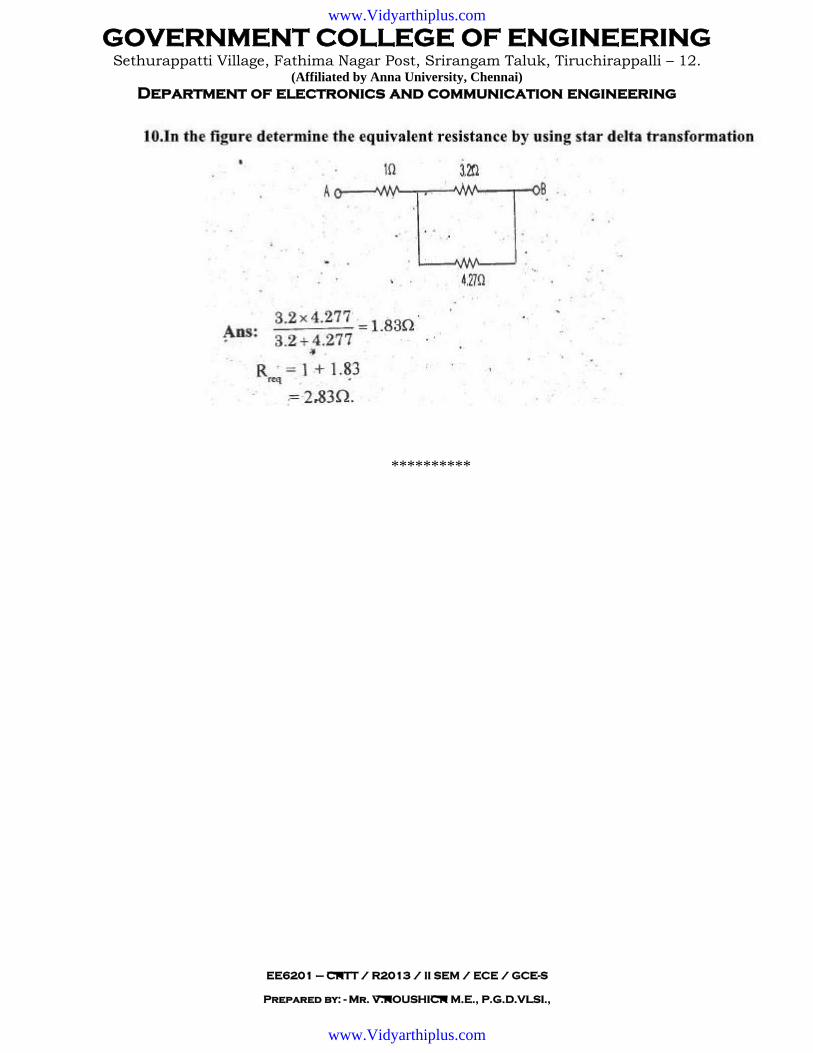
14. Explain the purpose of star delta transformation.
The transformation of a given set of resistances in star to delta or vice versa proves
extremely useful in circuit analysis and the apparent complexity of a given circuit can
sometime by very much reduce.
15. State Reciprocity Theorem.
It states that if an input is applied to a circuit, the ratio of response (output) in any
element to the input is constant, even when the position of input and output are
interchanged.
16. What is star and delta conversion?
Star: One end of each resistance is connected at a point called star point and the other;
three terminals are connected to A, B, C.
Delta: When three resistances are connected end to end to form delta shape.
www.Vidyarthiplus.com
www.Vidyarthiplus.com
GOVERNMENT COLLEGE OF ENGINEERING
Sethurappatti Village, Fathima Nagar Post, Srirangam Taluk, Tiruchirappalli – 12. (Affiliated by Anna University, Chennai)
Department of electronics and communication engineering
EE6201 – CKTT / R2013 / II SEM / ECE / GCE-S
Prepared by: - Mr. V.KOUSHICK M.E., P.G.D.VLSI.,
www.Vidyarthiplus.com
www.Vidyarthiplus.com
GOVERNMENT COLLEGE OF ENGINEERING
Sethurappatti Village, Fathima Nagar Post, Srirangam Taluk, Tiruchirappalli – 12. (Affiliated by Anna University, Chennai)
Department of electronics and communication engineering
EE6201 – CKTT / R2013 / II SEM / ECE / GCE-S
Prepared by: - Mr. V.KOUSHICK M.E., P.G.D.VLSI.,
**********
www.Vidyarthiplus.com
www.Vidyarthiplus.com
GOVERNMENT COLLEGE OF ENGINEERING
Sethurappatti Village, Fathima Nagar Post, Srirangam Taluk, Tiruchirappalli – 12. (Affiliated by Anna University, Chennai)
Department of electronics and communication engineering
EE6201 – CKTT / R2013 / II SEM / ECE / GCE-S
Prepared by: - Mr. V.KOUSHICK M.E., P.G.D.VLSI.,
UNIT III
RESONANCE AND COUPLED CIRCUITS
1. What is meant by Resonance?
An A.C circuit is said to be resonance if it behaves as a purely resistive circuit. The total
current drawn by the circuit is then in phase with the applied voltage, and the power
factor will then unity. Thus at resonance the equivalent complex impedance of the circuit
has no j component.
2. What is resonant frequency?
The frequency at which resonance occurs is called resonant frequency.
At resonant frequency XL=XC
3. Define series resonance.
A resonance occurs in RLC series circuit called series resonance. Under resonance
condition, the input current is in phase with applied voltage.
4. Define Quality factor.
The quality factor is defined as the ratio of maximum energy stored to the energy
dissipated in one period.
5. What are half power frequencies?
In RLC circuits the frequencies at which the power is half the max/min power are called
half power frequencies.
6. Write the characteristics of series resonance.
At resonance impedance in min and equal to resistance therefore current is max. Before
resonant frequency the circuit behaves as capacitive circuit and above resonant frequency
the circuit will behave as inductive circuit.
At resonance the magnitude of voltage across the inductance and capacitance will be Q
Times the supply voltage but they are in phase opposition.
7. Write the characteristics of parallel resonance.
At resonance admittance in min and equal to conductance therefore the current is min.
below resonant frequency the circuits behave as inductive circuit and above resonant
frequency the circuit behaves as capacitive circuit.
At resonance the magnitude of current through inductance and capacitance will be q
times the current supplied by the source but they are in phase opposition.
www.Vidyarthiplus.com
www.Vidyarthiplus.com
GOVERNMENT COLLEGE OF ENGINEERING
Sethurappatti Village, Fathima Nagar Post, Srirangam Taluk, Tiruchirappalli – 12. (Affiliated by Anna University, Chennai)
Department of electronics and communication engineering
EE6201 – CKTT / R2013 / II SEM / ECE / GCE-S
Prepared by: - Mr. V.KOUSHICK M.E., P.G.D.VLSI.,
8. What is Bandwidth and selectivity?
Bandwidth: The frequency band within the limits of lower and upper half frequency is
called bandwidth.
BW=f2-f1
Selectivity: It is the ratio of resonant frequency (fr) to the bandwidth (BW).
Selectivity= fr / (f2-f1) [or] β/ωr [or] 1/Qr
9. Define self inductance.
When permeability is constant the self inductance of a coil is defined as the ratio of flux
linkage and current.
10. Define mutual inductance.
When permeability is constant the mutual inductance between two coupled coils is
defined as the ratio of flux linkage in one coil due to common flux and current through
another coil.
11. Define coefficient of coupling.
In coupled coils the coefficient of coupling is defined as the reaction of the total flux
produced by one coil linking another coil.
12. State dot rule for coupled circuit.
It states that in coupled coils current entering at the dotted terminal of one coil induce an
emf in second coil which is +ve at dotted terminal of second coil. Current entering at the
undotted terminal of one coil induces an emf in second coil which is +ve at un dotted
terminal of second coil.
13. What is DOT convention?
The sign of mutual induced emf depends on the winding sense and the current through
the coil. The winding sense is decided by the manufacturer and to inform the user about
the winding sense a dot is placed at one end of each coil. When current enter at dotted
end in one coil then the mutual induced emf in the other coil is positive at dot end.
14. What is the tuned circuit?
In a coupled circuit, when capacitors are added to primary and secondary of coupled coils
to resonate the coils to achieve maximum power transfer condition then the coupled
circuit is called tuned coupled circuit.
www.Vidyarthiplus.com
www.Vidyarthiplus.com
GOVERNMENT COLLEGE OF ENGINEERING
Sethurappatti Village, Fathima Nagar Post, Srirangam Taluk, Tiruchirappalli – 12. (Affiliated by Anna University, Chennai)
Department of electronics and communication engineering
EE6201 – CKTT / R2013 / II SEM / ECE / GCE-S
Prepared by: - Mr. V.KOUSHICK M.E., P.G.D.VLSI.,
15. What is single tuned and double tuned circuit?
Single tuned: In a coupled circuit, when capacitors added to secondary coil to resonate
the secondary, the coupled circuit is called single tuned coupled circuits.
Double tuned: in coupled circuit when capacitors are added both to primary and
secondary coils to resonate the primary and secondary, the coupled circuit is called
double tuned coupled circuits.
16. Give the expression for quality factor of series RLC circuits.
The expression for quality factor of series RLC circuits is given by
Q = [(1/R) * √L/C]
17. Give the expression for quality factor of parallel RLC circuits.
The expression for quality factor of parallel RLC circuits is given by
Q = [R*(√C/L)]
18. What is the maximum possible mutual inductance of two inductively coupled coils
with self inductances L1 = 25mH, L2 = 100mH?
Maximum mutual inductance M = √L1L2
= √ (25*10-3
* 100*10-3
)
= 50mH.
19. What is the resonant frequency in the ideal parallel LC circuit with L = 40mH and
C = 0.01µƒ.
Resonant frequency (ƒr) =
ƒr = 7985Hz ≈ 7.98kHz.
**********
www.Vidyarthiplus.com
www.Vidyarthiplus.com
GOVERNMENT COLLEGE OF ENGINEERING
Sethurappatti Village, Fathima Nagar Post, Srirangam Taluk, Tiruchirappalli – 12. (Affiliated by Anna University, Chennai)
Department of electronics and communication engineering
EE6201 – CKTT / R2013 / II SEM / ECE / GCE-S
Prepared by: - Mr. V.KOUSHICK M.E., P.G.D.VLSI.,
UNIT IV
TRANSIENT RESPONSE FOR DC CIRCUITS
1. What is transient state?
If a network contains energy storage elements, with change in excitation, the current and
voltage change from one state to other state the behavior of the voltage or current when it
is changed from one state to another state is called transient state.
2. What is transient time?
The time taken for the circuit to change from one steady state to another steady state is
called transient time.
3. What is transient response?
The storage elements deliver their energy to the resistance; hence the response changes
with time, get saturated after sometime, and are referred to the transient response.
4. Define time constant of RLC circuit.
The time taken to reach 63.2% of final value in a RL circuit is called the time constant of
RL circuit.
Time constant=L/R
5. Define time constant of RC circuit.
The time to taken to reach 36.8% of initial current in an RC circuit is called the time
constant of RC circuit.
Time constant= RC
6. What is meant by natural frequency?
If the damping is made zero then the response oscillates with natural frequency without
any opposition, such a frequency is called natural frequency of oscillations.
7. Define damping ratio.
It is the ratio of actual resistance in the circuit to the critical resistance.
8. What is forced response?
The response of the circuit due to the external source is called forced response.
www.Vidyarthiplus.com
www.Vidyarthiplus.com

GOVERNMENT COLLEGE OF ENGINEERING
Sethurappatti Village, Fathima Nagar Post, Srirangam Taluk, Tiruchirappalli – 12. (Affiliated by Anna University, Chennai)
Department of electronics and communication engineering
EE6201 – CKTT / R2013 / II SEM / ECE / GCE-S
Prepared by: - Mr. V.KOUSHICK M.E., P.G.D.VLSI.,
9. Define apparent power.
The apparent power is defined as the product of magnitude of voltage and magnitude of
current.
10. What is natural response?
The response of a circuit due to stored energy alone without external source is called
natural response or source free response.
11. Write down the few applications of RL, RC and RLC circuits.
Coupling circuits
Phase shift circuits
Filters
Resonant circuits
AC bridge circuits
Transformers
12. What is critical damping?
The critical damping is the condition of the circuit at which the oscillations in the
response are just eliminated. This is possible by increasing the value of resistance in the
circuit.
13. What is critical resistance?
It is the value of the resistance of the circuit to achieve critical damping.
14. Define dual networks.
Two networks are called dual networks if mesh equations of one have the same form as
the nodal equations of the other. The property of duality is a mutual property.
15. What are the methods of solving AC parallel circuit?
The methods of solving AC parallel circuits are:
Admittance method.
Symbolic method.
Vector method.
16. List the types of parameters in the two port network.
Z – parameter (or) Open circuit impedance parameter
Y – parameter (or) Short circuit impedance parameter
h – parameter (or) hybrid parameter.
Transmission parameter (or) ABCD parameter.
www.Vidyarthiplus.com
www.Vidyarthiplus.com
GOVERNMENT COLLEGE OF ENGINEERING
Sethurappatti Village, Fathima Nagar Post, Srirangam Taluk, Tiruchirappalli – 12. (Affiliated by Anna University, Chennai)
Department of electronics and communication engineering
EE6201 – CKTT / R2013 / II SEM / ECE / GCE-S
Prepared by: - Mr. V.KOUSHICK M.E., P.G.D.VLSI.,
17. Define port.
A pair of terminals is called port. It is generally classified into two types:
Single port network
Two port (or) dual port network.
18. What is power factor and reactive factor?
Power factor: It is defined as the cosine of the phase difference between voltage and
current.
(i.e) power factor = cosΦ
Reactive factor: It is defined as the sine of the phase angle.
(i.e) reactive factor = sinΦ
**********
www.Vidyarthiplus.com
www.Vidyarthiplus.com
GOVERNMENT COLLEGE OF ENGINEERING
Sethurappatti Village, Fathima Nagar Post, Srirangam Taluk, Tiruchirappalli – 12. (Affiliated by Anna University, Chennai)
Department of electronics and communication engineering
EE6201 – CKTT / R2013 / II SEM / ECE / GCE-S
Prepared by: - Mr. V.KOUSHICK M.E., P.G.D.VLSI.,
UNIT V
THREE PHASE CIRCUITS
1. What is phase sequence?
Phase sequence of a polyphase system in the order in which different phase quantities
reach their maximum values.
2. Define line current and phase current.
Line Current: The current flowing through the line is called line current.
Phase Current: The current flowing through the phase is called phase current.
3. Define line and phase voltage
Line Voltage: The voltage between two lines is called the line voltage
Phase Voltage: The voltage between any line and the neutral point is called phase
voltage.
4. Give the line and phase values in star connection
The relation between line and phase voltage in star connection is
EL=√3Eph
The relation between line current and phase current in a star connection is
IL=Iph
5. Give the line and phase values in delta connection
The relation between line voltage and phase voltage in a delta connection is
EL=Eph
The relation between line current and phase current in delta connection is
IL=√3Iph
6. Write the methods of connections of 3 phase windings?
Independent connection
Star connection and
Delta connection
7. Write few methods available for measuring in 3-phase load.
One wattmeter method
Two wattmeter method
Three wattmeter method
www.Vidyarthiplus.com
www.Vidyarthiplus.com
GOVERNMENT COLLEGE OF ENGINEERING
Sethurappatti Village, Fathima Nagar Post, Srirangam Taluk, Tiruchirappalli – 12. (Affiliated by Anna University, Chennai)
Department of electronics and communication engineering
EE6201 – CKTT / R2013 / II SEM / ECE / GCE-S
Prepared by: - Mr. V.KOUSHICK M.E., P.G.D.VLSI.,
8. List the methods used for power measurement with single wattmeter
Potential lead shift method
T- method
Artificial neutral method
Current transformer method
9. List the methods for unbalanced star connected load
Equivalents delta method
Mesh method
Neutral voltage displacement method
10. Define balanced load.
A three phase load has three separate load impedances which may be connected in star or
delta. When the 3 impedances are identical; then the three phase load is called balanced
load.
11. Write the expression for power factor in a balanced three phase circuit.
The expression for power factor in a balanced three phase circuit is given by
Power factor = cos [tan-1
(√3 (w2-w1) / (w1+w2)]
12. Write expression for total power in a 3Φ system.
PT = √3VLILCosΦ
13. Write the expression for calculating real, reactive and apparent power of a 3 phase
system.
Real power P = √3VLILCosΦ
Reactive power Q = √3VLILSinΦ
Apparent power S = √3VLIL
14. A 3Φ balanced star connected load has 400V line to line voltage and 10Amps line
current. Determine the line to neutral voltage and phase current.
Solution:
Phase voltage = line voltage / √3
= 400 / √3 = 231 volts.
Phase current = line current
= 10 Amps.
www.Vidyarthiplus.com
www.Vidyarthiplus.com
GOVERNMENT COLLEGE OF ENGINEERING
Sethurappatti Village, Fathima Nagar Post, Srirangam Taluk, Tiruchirappalli – 12. (Affiliated by Anna University, Chennai)
Department of electronics and communication engineering
EE6201 – CKTT / R2013 / II SEM / ECE / GCE-S
Prepared by: - Mr. V.KOUSHICK M.E., P.G.D.VLSI.,
15. When a 3Φ supply system is called balanced supply system?
When all the 3Φ voltages are equal in magnitude and displayed by 120º in space, the
supply system is called 3Φ balanced system.
16. What are the advantages of three phase system?
The generation and transmission of electrical power are more efficient.
The power transmission in a 3Φ circuit is constant rather than pulsating as in a 1Φ
circuit.
3Φ motors starts and run much better than single phase motors.
17. How can a wattmeter be used to measure reactive power?
In case of balanced 3Φ circuit, the reactive power can be determined by using one
wattmeter. The current coil of the wattmeter is connected in one line and its pressure coil
is connected across the other two lines. Let the reading of wattmeter be Wr.
Then, the total reactive power = √3 Wr.
18. Compare balanced and unbalanced network.
Balanced network: Let the 3Φ circuit consist of loads Z1, Z2, and Z3. If all the loads are
equal in magnitude and phase angle and they are connected to a balanced supply system,
then it is said to be balanced network.
Eg: Z1 = Z2 = Z3
Unbalanced network: If all the loads are different in magnitude and phase angle, then it
is said to be unbalanced network; even when the supply system is balanced.
Eg: Z1 ≠ Z2 ≠ Z3
**********
www.Vidyarthiplus.com
www.Vidyarthiplus.com


