Embed Size (px)
Citation preview

Available online at www.sciencedirect.com
008) 1725–1735www.elsevier.com/locate/tsf
Thin Solid Films 516 (2
Growth and characterisation of epitaxially ordered zinc aluminate domainson c-sapphire
J. Grabowska a, R.T. Rajendra Kumar a, E. McGlynn a,⁎, K.K. Nanda a,1, S.B. Newcomb b,P.J. McNally c, L. O'Reilly c, J.-P. Mosnier a, M.O. Henry a
a School of Physical Sciences/National Centre for Plasma Science and Technology, Dublin City University, Irelandb Glebe Scientific Ltd., Newport, Co. Tipperary, Ireland
c School of Electronic Engineering/Research Institute for Networks and Communications Engineering, Dublin City University, Ireland
Received 5 January 2007; received in revised form 4 May 2007; accepted 15 May 2007Available online 21 May 2007
Abstract
Epitaxially ordered zinc aluminate domains with sub-micron dimensions are formed on bare c-sapphire substrates using a vapour phasemethod (with vapour generated by carbothermal reduction of ZnO) at various temperatures and growth durations. A zinc aluminate (ZnAl2O4)layer is formed by reaction of the source materials (Zn and O) with the substrate. We observe crystallites with a well-defined epitaxial relationshipon the sapphire substrate in addition to polycrystalline material. The epitaxially oriented deposit displays the form of characteristically twinned(singly or multiply) grains of sub-micron dimensions with three variants, consistent with the c-sapphire substrate symmetry. Scanning electronmicroscopy and transmission electron microscopy studies show that the formation of these grains is associated with the presence of extendeddefects in the sapphire substrate. Epitaxially ordered grains formed at higher temperatures show a change in the nature of the twin boundaries andepitaxial relations as a function of growth time, attributed to the effects of annealing during growth.© 2007 Elsevier B.V. All rights reserved.
Keywords: Zinc aluminate; Spinel; Epitaxy; Sapphire; Growth; SEM; TEM
1. Introduction
Controllable growth of oxide materials is an importantresearch area, with applications ranging from photonic devices,transparent conducting oxides (TCO) and high temperatureelectronics (HTE) to catalysis and biocompatibility applications[1,2]. Among these oxides, spinel materials (of the type AB2O4)have been widely studied, with their growth mechanisms andstructural properties the subject of extensive investigations. Zincaluminate (ZnAl2O4) is a spinel of particular interest technolog-ically, given its wide potential functionality [3]. A recent reporthas used zinc aluminate as a platform material to demonstrate ageneric technique for core-shell nanostructure synthesis using the
⁎ Corresponding author. Tel.: +353 1 7005387; fax: +353 1 7005384.E-mail address: [email protected] (E. McGlynn).
1 Present address: Materials Research Centre, Indian Institute of Science,Bangalore 560 012, India.
0040-6090/$ - see front matter © 2007 Elsevier B.V. All rights reserved.doi:10.1016/j.tsf.2007.05.024
nano-Kirkendall effect, indicating the great potential this materialhas for nanoscale applications [4]. Its wide bandgap (∼3.8 eV)may lead to applications in TCO and HTE, and, when doped withrare-earth elements, it may function as an effective luminescentmaterial for phosphor applications [5,6]. Zinc aluminate is alsobeing considered for optical coating applications in aerospacetechnology, is used in many catalytic applications, includingcracking, dehydration of saturated alcohols, synthesis ofmethanoland other alcohols in addition to acting as a support for catalysis[7,8]. The catalytic functionality of materials, particularly for sub-micron particles, is known to be affected by the microstructure,and various facets show substantial differences in catalyticactivity [9]. Controllable, ordered growth of microstructuredcatalytic material on a chemically and physically robust substrateis therefore an important technological focus.
We report results that demonstrate the formation of zincaluminate domains with well-defined epitaxial relationships onc-sapphire substrates. Our data show that we can control thedegree of faceting and the epitaxial relationships by controlling

1726 J. Grabowska et al. / Thin Solid Films 516 (2008) 1725–1735
the growth conditions, thus potentially controlling the func-tionality of zinc aluminate microstructures on sapphire. Thealuminate microstructures formed also show a number ofintrinsically interesting features, including a strikingly sym-metrical appearance in scanning electron microscope (SEM)images, enhanced diffusional transport along the lower density“open” twin boundary and two well-defined types of twinboundary, related to the epitaxial relationships mentionedabove.
2. Experimental details
Zinc aluminate was grown on c-sapphire substrates byvapour phase transport. Most of the substrates used wereobtained from Testbourne Ltd, Hampshire, UK, althoughsubstrates from other suppliers were also used. The substratesare ultrasonically cleaned before growth and are not coated withgold (note: some reference samples have been covered withgold to catalyse the formation of wurtzite phase ZnO nanorodsby the vapour–liquid–solid mechanism, using otherwise similargrowth conditions) [10]. A ZnO/graphite powder mix (1:1 wt.)is placed at one end of a quartz boat and the substrate is placed∼0.5 to 5.0 cm from the source in a single zone horizontal tubefurnace with argon carrier flow (90 sccm). The nominaltemperature of the furnace is set in the range 950–1125 °Cand the set temperature is achieved in ∼15–20 min. The actualsubstrate temperature is 35 °C lower than the nominaltemperature for growth at 950 °C and 50 °C lower for growthat 1125 °C, due to the temperature gradient of the furnace.
Samples were characterised by SEM and field emission (FE-)SEM (LEO Stereoscan 440 operating at 15 kV and Hitachi S-4300 Field Emission operating either at 5 kVor 20 kV), atomicforce microscopy (AFM: Nanoscope IIIa, Digital Instruments;contact mode) and transmission electron microscopy (TEM:JEOL2000FX operating at 200 kV). Sections for TEMmicrostructural evaluation were made using standard focusedion beam thinning (FEI FIB 200 workstation operating at 30 kVusing a Ga ion source with currents of 11 nA and 150 pA for boxmilling and final polishing, respectively; see Ref. [11]). X-raydiffraction measurements were made using a Bruker AXS D8advance texture diffractometer (using Cu Kα radiation). Lauepatterns were acquired at the Fluo-Topo X-ray topographybeamline of the ANKA (Ångström Karlsruhe) at the Institute forSynchrotron Radiation, in Karlsruhe, Germany, using thecontinuous spectrum of synchrotron radiation from a 2.5 GeVstorage ring at typical currents of 100–180 mA, and at theInstitute for Crystal Growth in Berlin, Germany; details aregiven in Ref. [12].
3. Results
The results section describes the characterisation of zincaluminate microstructures and is divided into three sub-sections, based on the growth durations and substratepreparation (Section 3.1 describes growth for 30 min duration,Section 3.2 describes 60 min duration growth and Section 3.3describes the effects of substrate preparation).
3.1. 30 min growth duration
A series of SEM images of samples grown for 30 min atfurnace temperatures of 950 °C (A) and (B) and 1125 °C (C) and(D) are shown in Fig. 1 (A)–(D). Prominent structures with alinear appearance are seen with a high secondary electroncontrast, aligned in three specific in-plane directions with anangle of 120° between them. These structures are uniformlydistributed among these directions. The width of the linear highintensity region in all cases is ∼70 nm and the length of thisregion is distributed in the range 400–600 nm for samples grownat 950 °C, and in the range 700–1500 nm for samples grown at1125 °C, though shorter and longer examples are seen in bothcases. We have performed atomic force microscopy (AFM) tostudy the surface topography, shown in Fig. 2 for a samplegrown at∼1125 °C for 30min. Three-fold symmetric structures,similar to those observed in SEM, are again visible andlongitudinal and transverse height profiles are displayed fromvarious regions of the AFM image. These show that thestructures have an average height of ∼90–100 nm, and that thewidth of the structures (at their base) deduced from these profilesis ∼200 nm. This is substantially greater than the width of thebright linear regions seen SEM, and the difference is muchgreater than can be explained by tip-broadening effects in theAFM. Thus the bright linear structures seen in the SEM imagesare not solely due to contrast effects due to surface topography.Height profiles in regions of the sample with no symmetricstructures (profile 4 in Fig. 2) show a substantial degree ofroughness, indicating that layer deposition has taken place in thisregion also. Evidence of this deposition from SEM data is alsoshown in the circled region in the inset of Fig. 1(B) above.
The symmetric distribution of these microstructures with athree-fold symmetry suggests an epitaxial relationship to thehexagonal sapphire c-plane substrate. The crystallographicorientation of the c-sapphire substrates relative to their physicaledges has been found by Laue pattern analysis and confirmed byX-ray phi scan measurements (data not shown). When theorientation of the sapphire substrates is known, the relativeorientation of the nanowires thereon was found using SEMimages at various magnifications, allowing comparison with thephysical sample edges. We find that the long direction of thebright symmetric structures lie parallel to the b1010N sapphirein-plane directions in all cases studied. This alignment along ahigh symmetry in-plane sapphire direction further suggests thatat least the portion of the deposit associated with thesemicrostructures grows with an epitaxial relationship to thesubstrate.
We have performed transmission electron microscopy (TEM)and selected area electron diffraction (SAED) measurements inboth cross-section and plan-view mode in order to ascertain thematerial phase, elucidate the origin of the symmetric micro-structures seen in SEM and AFM and to study the epitaxialrelationships between the substrate and the deposited layer.Fig. 3 shows cross-sectional TEM data for a sample grown at950 °C for 30 min (the sample shown in Fig. 1(A) above). Fig. 3(A) shows a broad area at relatively lowmagnification which is amontage of two bright field micrographs. An immediate

Fig. 1. SEM/FE-SEM images of samples grown on c-sapphire; (A) growth temperature 950 °C (growth duration 30 min); (B) higher magnification of sample in (A),inset shows FE-SEM image at higher magnification; (C) growth temperature 1125 °C (growth duration 30 min); (D) higher magnification of sample in (C); (E) growthtemperature 1125 °C (growth duration 60 min); (F) higher magnification of sample in (E).
1727J. Grabowska et al. / Thin Solid Films 516 (2008) 1725–1735
distinction can be made between the substrate marked at (i) andthe Pt-based coating marked at (ii) that was deposited onto thesurface of the sample prior to the ion beam thinning of thesample. It is also possible to distinguish the surface layer markedat (iii) that has been capped by the high thickness layer of Aumarked at (iv), the latter serving to prevent any ‘top down’ iondamage of the layering prior to the deposition of the Pt. It shouldbe noted that there are a number of regions located at the base ofthe Au where ‘pockets’ of low atomic number debris from theTEM sample preparation have been retained (as at (v)) and thatelsewhere the same boundary areas are decorated with the typeof large hole marked at (vi). We note also that the defect densityof the near surface regions of the c-plane sapphire ischaracteristically high (as at (vii)) and that the surface layermarked at (iii) exhibits significant variations in thickness. The
latter aspect is underlined by the presence of the well-definedzones marked at (viii)–(xi) where the film thickness is so muchhigher than elsewhere.
A SAED pattern is shown in Fig. 3(B) from one of thelower thickness regions (e.g. between (viii) and (ix)) of thedeposit where the sapphire substrate is at a [1010] zonenormal. The d-spacings for the diffraction rings marked at 1–6 are given in the table in the inset and a comparison can bemade with the cubic ZnAl2O4 phase which has a latticeparameter of 0.80848 nm [3]. The diffraction pattern clearlydemonstrates the formation of zinc aluminate, and we havecarefully ruled out the possibility of the layer beingassociated with other zinc-related oxides, such as cubic andhexagonal ZnO phases as well as two cubic ZnO2 phases.Thus the assignment to zinc aluminate is unambiguous, and
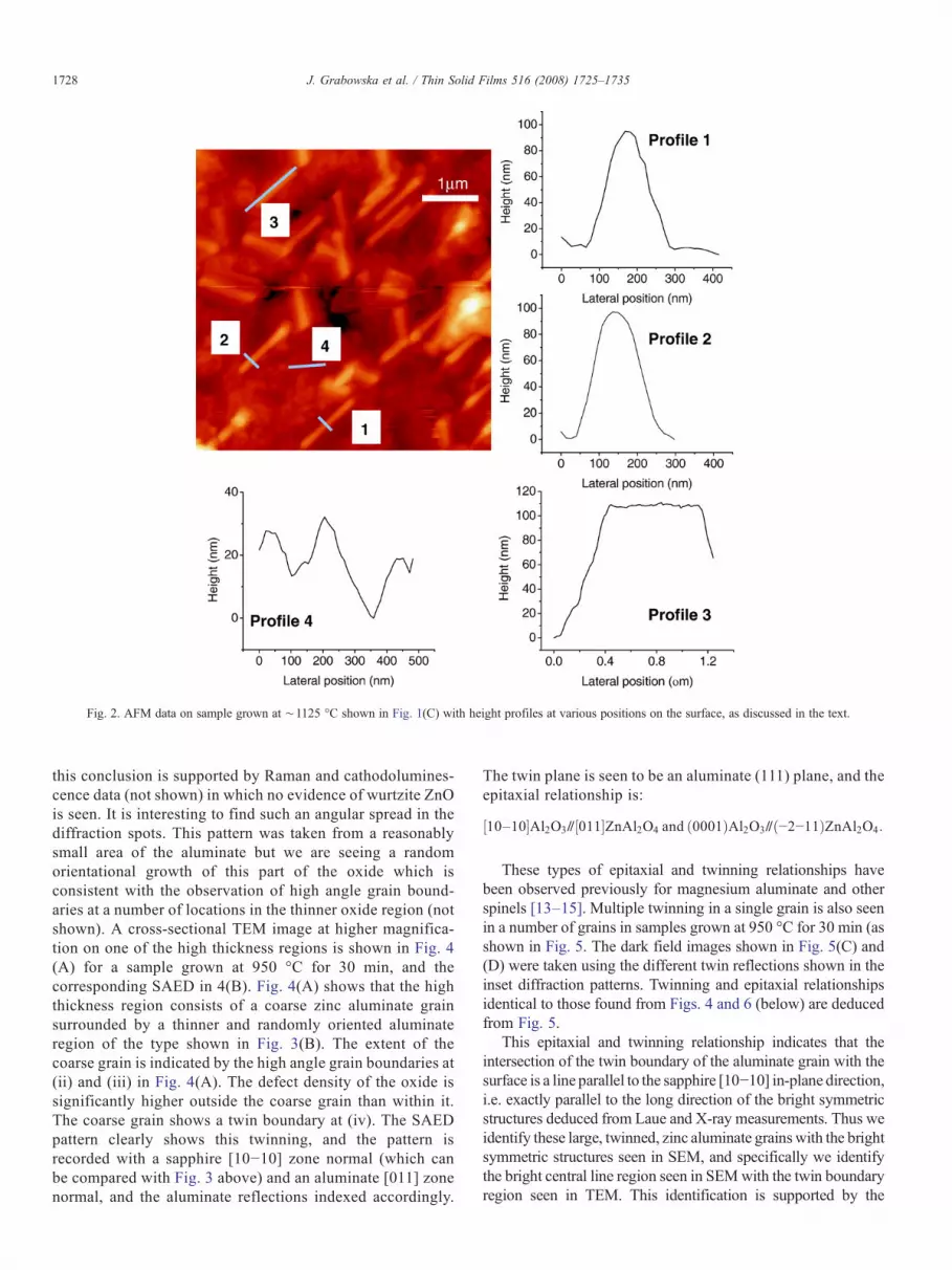
Fig. 2. AFM data on sample grown at ∼1125 °C shown in Fig. 1(C) with height profiles at various positions on the surface, as discussed in the text.
1728 J. Grabowska et al. / Thin Solid Films 516 (2008) 1725–1735
this conclusion is supported by Raman and cathodolumines-cence data (not shown) in which no evidence of wurtzite ZnOis seen. It is interesting to find such an angular spread in thediffraction spots. This pattern was taken from a reasonablysmall area of the aluminate but we are seeing a randomorientational growth of this part of the oxide which isconsistent with the observation of high angle grain bound-aries at a number of locations in the thinner oxide region (notshown). A cross-sectional TEM image at higher magnifica-tion on one of the high thickness regions is shown in Fig. 4(A) for a sample grown at 950 °C for 30 min, and thecorresponding SAED in 4(B). Fig. 4(A) shows that the highthickness region consists of a coarse zinc aluminate grainsurrounded by a thinner and randomly oriented aluminateregion of the type shown in Fig. 3(B). The extent of thecoarse grain is indicated by the high angle grain boundaries at(ii) and (iii) in Fig. 4(A). The defect density of the oxide issignificantly higher outside the coarse grain than within it.The coarse grain shows a twin boundary at (iv). The SAEDpattern clearly shows this twinning, and the pattern isrecorded with a sapphire [1010] zone normal (which canbe compared with Fig. 3 above) and an aluminate [011] zonenormal, and the aluminate reflections indexed accordingly.
The twin plane is seen to be an aluminate (111) plane, and theepitaxial relationship is:
½10–10�Al2O3$½011�ZnAl2O4 and ð0001ÞAl2O3$ð−2−11ÞZnAl2O4:
These types of epitaxial and twinning relationships havebeen observed previously for magnesium aluminate and otherspinels [13–15]. Multiple twinning in a single grain is also seenin a number of grains in samples grown at 950 °C for 30 min (asshown in Fig. 5. The dark field images shown in Fig. 5(C) and(D) were taken using the different twin reflections shown in theinset diffraction patterns. Twinning and epitaxial relationshipsidentical to those found from Figs. 4 and 6 (below) are deducedfrom Fig. 5.
This epitaxial and twinning relationship indicates that theintersection of the twin boundary of the aluminate grain with thesurface is a line parallel to the sapphire [1010] in-plane direction,i.e. exactly parallel to the long direction of the bright symmetricstructures deduced from Laue and X-ray measurements. Thus weidentify these large, twinned, zinc aluminate grainswith the brightsymmetric structures seen in SEM, and specifically we identifythe bright central line region seen in SEMwith the twin boundaryregion seen in TEM. This identification is supported by the

Fig. 3. (A) Bright field cross-sectional TEM data for a sample grown at 950 °Cfor 30 min, at low magnification; (B) SAED pattern from lower thicknessregions of the deposited layer ([10–10] sapphire zone normal, with sapphirereflections indexed, as indicated by dashed lines).
Fig. 4. (A) Bright field cross-sectional TEM image at higher magnification onhigh thickness grain region; (B) SAED pattern of region in (A), with reflectionsof aluminate twins indexed at a sapphire [1010] zone normal and an aluminate[011] zone normal.
1729J. Grabowska et al. / Thin Solid Films 516 (2008) 1725–1735
general topography of the grain structure. Much of the grainstructure lies beneath the surface of the surface substrate and thesurface topography of the grain shown in Fig. 4 appears entirelyconsistent with AFM data presented earlier, in terms of height,width and the surface roughness of surrounding regions. Theobservation of multiply twinned grains, with twin boundariesclosely spaced parallel to each other, is entirely consistent withSEM observations of side by side, parallel microstructures shownin the inset of Fig. 1(B) and specifically is consistent with theidentification of the bright central line region seen in SEM withthe twin boundary region seen in TEM.
Plan view TEM data for a sample grown at 950 °C for 30 minare shown in Fig. 6(A), where the plan view slice extendsbetween positions at depths of ∼140 and 250 nm below thesurface, i.e. below the thin zinc aluminate layer depth,intercepting only the thicker grains and sapphire substrate.Characteristically six sided zinc aluminate grains are seen in thesapphire matrix, each of which contains the type of twinboundary marked at (i). Extended defects in the sapphire arealso clearly visible around the grains. There are three grainvariants for the aluminate, as typified by those marked at (ii),(iii) and (iv). These data are interpreted as a top-view of thegrains discussed above, and the twin boundaries are again seenin all cases, sometimes with multiply twinned grains. SAEDpatterns are shown in Fig. 6(B) which were taken on each grainvariant. These are taken at [−2−11] zone normals for theZnAl2O4 phase, the interface marked at (i) in Fig. 6(A) thusbeing a (111)-type boundary. This is consistent with thepreviously deduced twin relationship and these patterns canbe compared with those shown in Fig. 6(C) and (D). Fig. 6(C)was taken from a localised region of the sapphire that containednone of the coarse grained aluminate and shows a [0001] Al2O3
zone normal. Fig. 6(D) shows a combination of the substrateand the three grain variants of the oxide with a wide aperture,with the contribution of each variant labelled. Double
diffraction also makes a partial contribution to the patternresulting in some doubling of spots [16].
TEM measurements on samples grown at 1125 °C for 30 minshow similar results to those on samples grown at 950 °C for30 min, consistent with their similar appearances in SEM images.
3.2. 60 min growth duration
The microstructure of the deposited layer is strongly affectedby the growth duration, particularly at the higher growthtemperature. Fig. 1(E) shows field emission FE-SEM data froma sample grown 1125 °C for 60 min. In Fig. 1(E) and (F) athigher magnification) the strong contrast of the central lineportion of the microstructure is gone, although the three-foldsymmetry of micro-structures remains apparent and a clearfaceting of the structures is now apparent. The long direction ofthe structures are again parallel to b10−10N-type sapphire in-plane directions, in all cases. The width of the microstructuresseen in Fig. 1(F) is much closer to the width measured by AFMline profiles for samples grown for shorter durations shown inFig. 2, ∼200 nm, indicating a change in the nature of the SEMcontrast for samples grown at 1125 °C for 60 min, comparedwith samples grown at lower temperature or for shorterdurations. Cross-sectional TEM data have been recorded forsamples grown at 1125 °C for 60 min and are shown in Fig. 7.The first point of interest from Fig. 7(A) is that the sapphire

Fig. 5. (A) Bright field cross-sectional TEM image on high thicknessmultiply twinned region of a sample grown at 950 °C for 30min (edges of regionmarked at (iv) and(v), twins at (i), (ii) and (iii)). The inset of Fig. 1(B) shows a FE-SEM image of the same sample; (B) SAED pattern of region in A at a sapphire [1010] zone normal andan aluminate [011] zone normal showing twinned spots; (C) and (D) dark field images of region shown in (A) taken using the different twin reflections shown in the insetdiffraction patterns, with grain region edges marked by a “⁎”. The contribution of different twin portions of the grain due to different twin reflections is clearly visible.
1730 J. Grabowska et al. / Thin Solid Films 516 (2008) 1725–1735
substrate shows a significantly lower defect content, due toannealing of extended defects during the growth period. Fig. 7(A) shows an area where a low defect, high thickness aluminategrain (marked at (ii)) has been formed. The grain itself is veryreminiscent of parts of the aluminate formed in some of theprevious samples with a twin boundary running through itscentre and has high angle grain boundaries on both sides,marked at (i) and (iii), while the surrounding material is athinner layer of high defect content. However, in this case thegrain shows much clearer evidence of faceting at the sides andbase, and also at the top portion, which is shown in the inset.The SAED pattern in Fig. 7(B) is recorded with a sapphire [1010] zone normal and aluminate [0–11] zone normal, with thealuminate reflections indexed accordingly. The twin plane is analuminate (−211) plane in this case (different to the situation forsamples grown at 950 °C for 30 min), and the epitaxialrelationship is:
½1–210�Al2O3$½−211�ZnAl2O4 and ð0001ÞAl2O3$ð111ÞZnAl2O4:
Again these types of epitaxial and twinning relationshipshave been observed previously for the magnesium aluminateand other spinels, and the epitaxy of the (111) ZnAl2O4 plane onthe (0001) Al2O3 plane is often seen in such systems due to thethree-fold symmetry of both surfaces [13–17]. These epitaxialand twinning relationships indicate that the intersection of thetwin boundary of the aluminate grain with the surface is a lineparallel to the sapphire [1010] in-plane direction, parallel tothe long direction of the symmetric structures seen in Fig. 1(F).
We again identify these large, twinned, zinc aluminate grainswith the symmetric structures seen in SEM, and note that thisidentification is supported by the observation of the facettednature of the grains seen both in TEM in Fig. 7(A) and in SEM(inset of Fig. 7(A)). A slight (∼2.5°) misalignment of the (111)zinc aluminate plane from the sapphire (0001) plane, is seen,indicated in Fig. 7(B). Other regions of this sample show adeposited aluminate layer, akin to that in Fig. 3 for the samplegrown at 950 °C for 30 min, but which now shows someevidence of an epitaxial relationship to the substrate.
3.3. Effects of substrate preparation
The perfection of the substrate is an extremely importantfactor in the growth of the symmetric microstructures shownabove. Fig. 8(A) shows a SEM image of a sample grown at950 °C for 30 min, but on a substrate pre-annealed at 1000 °Cfor 30 min. Similar SEM data are obtained on samples pre-annealed at 1000 °C for 17.5 h and on samples grown onstarting substrate material of higher crystalline quality. Thesesamples have a very different appearance in SEM images, withvery few instances of the high contrast three-fold symmetricstructures. It appears that the presence of the symmetricmicrostructures is critically dependent on the initial crystallinequality of the substrate. Fig. 8(B) shows a dark-field cross-sectional TEM image, for a sample grown at 950 °C for 30 min(similar to that in Fig. 1(A)), of the substrate and deposited layerclose to a high thickness grain, marked (i), and the highsubstrate defect density is easily seen around the grain. Laue

Fig. 6. (A) Bright field plan view TEM data for a sample grown at 950 °C for30 min; (B) SAED patterns on each grain variant at an aluminate [−2−11] zonenormal; (C) SAED patterns on sapphire at an [0001] Al2O3 zone normal;(D) wide aperture SAED pattern which is a combination of the substrate and thethree grain variants of the oxide.
Fig. 7. (A) Bright field cross-sectional TEM image at high magnification on asample grown at 1125 °C for 60 min (inset shows SEM image of symmetricstructures seen on this sample); (B) SAED pattern of region in A, withreflections of aluminate twins indexed at a sapphire [1010] zone normal and analuminate [0–11] zone normal.
1731J. Grabowska et al. / Thin Solid Films 516 (2008) 1725–1735
pattern measurements of unannealed substrates show asignificant broadening of the reflection spots (inset of Fig. 8(B)), associated with the poor crystal quality of the startingmaterial and specifically the presence of slightly misorientedsub-crystals, grain boundaries and extended defects. Lauemeasurements on annealed substrates and other startingmaterials show much more sharply defined spots, indicating areduction in the extended defect content of the material. Thepresence of the three-fold symmetric line structures is thereforecritically dependent on the presence of extended defects in thestarting substrate material. It should also be noted that such highthickness grains do not appear at every location where thesubstrate defect density is high, and conversely these largethickness grains are seen occasionally in regions where thesubstrate defect density is lower. Thus there is no one-to-oneevidence of a connection between specific extended defects inthe substrate and nucleation of specific high thickness grains.However, a comparison of Fig. 8(B) with a cross-sectional TEMimage of the sample shown in Fig. 8(A) above is very revealing(Fig. 8(C)). Part of the region that was thinned to electrontransparency is shown at relatively low magnification in Fig. 8(C) (again formed from a montage) and one sees that thesubstrate marked at (i) has a significantly lower defect density
than in Fig. 8(B), as a consequence of the pre-anneal (thecontrast marked at (iv) and (v) is strain related). The zincaluminate layer shown in Fig. 8(C) shows an epitaxialrelationship with the substrate and does not appear to bepolycrystalline. It is possible to make a distinction between thetwo regions marked at (ii) and (iii) where there is a difference inlayer thickness (both regions b100 nm thick), but there is noindication of the growth of very thick regions like those in Fig. 8(B). The evidence from Fig. 8 indicates that the growth of thehigh thickness twinned grains with three-fold symmetry is onlyseen on sapphire with a relatively low crystal quality. Annealedsapphire or starting sapphire substrates of better quality do notshow significant amounts of these microstructures afterdeposition. We have attempted to conclusively test thishypothesis by taking pre-annealed (1000 °C for 2 h) substrates(with low extended defect concentrations) and introducingmechanical damage to the crystal in a number of ways and thendepositing zinc aluminate and looking for evidence ofsymmetric microstructure growth. The crudest method usedwas to mechanically stress a pre-annealed substrate to the pointof fracture. Close to fracture locations (and also at sample edgeswhere the substrate was cut with a saw) we see the characteristicsymmetric microstructures, and in some cases these clusteralong a crack location. We believe that these nucleate due to the

Fig. 8. (A) Sample grown at 950 °C for 30 min on pre-annealed substrate, with low symmetric microstructure coverage; (B) Dark field cross-sectional TEM data for asample grown at 950 °C for 30 min, showing a high thickness grain marked at (i), and the highly defective substrate below this (substrate is in lower half of image). Theregion marked (ii) is a type of large hole, similar to the feature marked (vi) in Fig. 3(A). The inset shows a Laue pattern for the substrate with one spot magnified toillustrate broadening; (C) Bright field cross-sectional TEM data for sample shown in (A).
1732 J. Grabowska et al. / Thin Solid Films 516 (2008) 1725–1735
generation of extended defects in the sapphire at or close to thepoint of fracture. Reference pre-annealed samples not subjectedto mechanical stress before growth show very little evidence ofthis microstructure after aluminate growth. More controllable,localised, attempts to alter the substrate surface have includedwet chemical etching (in an acidic solution for 1 h), plasmaetching (leading to a substantial increase in surface roughness)and laser ablation (both surface and sub-surface) of thesapphire. In these cases we have not observed enhanced growthof these microstructures after the substrate treatment (above thelow level seen on an untreated substrate), though this work isongoing. Based on the totality of the evidence presented webelieve that the connection between extended defects in thesapphire and nucleation of symmetric aluminate microstructuresis convincingly demonstrated.
4. Discussion
The growth mechanisms of aluminate spinels due to reactionbetween metal oxides and alumina is a topic which has beenwidely studied, both by observing the reaction between solidmetal oxides and alumina and by observing spinel growth byvapour phase deposition of the metal oxide and subsequentreaction with the substrate [13,14,18]. This latter mechanismappears to be the origin of the growth in our samples. InitiallyZnO is deposited on the c-sapphire surface by vapour–solid(VS) deposition, and this ZnO layer reacts with the substrate toform zinc aluminate, according to the formula:
ZnO þ Al2O3→ZnAl2O4:
This growth mode has been observed previously formagnesium aluminate, cobalt aluminate and nickel aluminateand appears to be the most plausible growth mode in our casealso [13,14,16,19]. We see growth of characteristically twinned,epitaxially oriented zinc aluminate grains only for furnace
temperatures above 950 °C and see no growth of such grains attemperatures greater than 1125 °C. We attribute the lowertemperature limit to the onset of carbothermal reduction of ZnOin the source powder. Below this temperature ZnO will bedeposited at a very low rate and the reaction with the substrate toform aluminate will also proceed much more slowly at thesetemperatures [20]. The higher temperature limit we believe ismost likely due to sample heating which tends to annealdislocations out quickly at such temperatures (as shown in Fig.8); hence the twinned, epitaxially oriented grains cannotnucleate. However it is also possible that a reduction in thesticking coefficient of the incident vapour flux at highertemperatures (leading to diffusion on the surface and re-evaporation) contributes to this high temperature limit. Studiesof growth at and above 1125 °C are planned to ascertain if zincaluminate layers are formed at these temperatures, and theassociated growth rate, to distinguish between thesepossibilities.
The nucleation and evolution mechanisms of the symmetricmicrostructures at extended defects in the substrate are bothinteresting questions. Previous studies on twinned nickelaluminate spinels grown by reaction of a vapour depositedlayer of NiO on sapphire have attributed the origin of the twins inthe aluminate to the presence of twins in the deposited NiO layerprior to reaction with the sapphire [21], and there was noevidence that substrate-dependent effects were seen. Thetwinning of the initially deposited NiO layer may have occurredto reduce stress in the film. We propose a similar mechanism forthe nucleation of the symmetric microstructures we observe, butthe mechanism must account for the relationship betweenextended defects in the sapphire and the nucleation of thesymmetric microstructures in our case. ZnO grows epitaxiallywithout twinning on single crystal c-sapphire [22], but it may bethe case that the deposited ZnO layer will grow in a locallydifferent fashion close to positions on the substrate whereextended defects intersect the surface, due to local alterations in

Fig. 10. (A) Field emission SEM image of structures grown at 1125 °C for30 min, showing three-fold symmetric microstructures with high SEM contrast;(B) Sample grown under identical conditions as (A) but with additional 40 minanneal at 1125 °C.
Fig. 9. (A) Cross-sectional TEM showing Fresnel effects as a function ofdefocus conditions for a sample grown at 950 °C for 30 min; (B) Fresnel effectsas a function of defocus conditions for a sample grown at 1125 °C for 60 min.
1733J. Grabowska et al. / Thin Solid Films 516 (2008) 1725–1735
the surface structure. The initial ZnO layer may grow in atwinned fashion in such regions, leading to the characteristicallytwinned zinc aluminate grains after reaction with the sapphire.This would explain the presence of multiple twins in terms ofregions where the local defect content and surface structurecause a multiple twinned ZnO layer to nucleate. The range ofsize of the twinned microstructures is most likely due to therange of sizes of the original nucleation sites. Our experimentaldata do not allow us to test this hypothesis any further at present,as the combined effects of the aluminate growth into the sapphireand annealing of sapphire during growth mean that the initialnucleating structures disappear during subsequent growth.
The growth rate of the aluminate deposit after nucleation isclearly quite different for the polycrystalline layer region (i.e. thelow thickness (b50 nm) region shown in Fig. 3), compared to thelarger, epitaxially oriented, aluminate grain structure shown inFig. 4. A number of previous studies of growth of zinc aluminateon sapphire are reported in the recent literature [20,23,24]. Forgrowth at lower temperatures (680 °C) [23,24] the growth isreported to be diffusion-limited (following a parabolic thicknessvs. time relation), with Zn as the diffusing species and anassociated interfacial layer of different stoichoimetry (Zndeficient) is observed [24]. Growth at higher temperatures it isreported to be interface-limited (following a linear thickness vs.time relation) and no Zn deficient interfacial layer is reported [20].These reports are not contradictory since the diffusion constant ofthe reacting species, e.g. Zn, would be expected to increase athigher temperatures, changing the nature of the rate limiting step
in the reaction. In addition the crystallographic nature of thereacting interfaces may also alter the rate limiting step in thereaction. In Ref. [20] the thickness of aluminate layers formed bythe reaction of ZnO layers with sapphire at temperatures of∼1000 °C in 30min is∼40 nm,which is quite consistentwith ourdata for the thin polycrystalline layer seen in Fig. 3 for a samplegrown at 950 °C for 30min. However, the much greater thicknessof the larger grains (∼400 nm) seen in these samples impliesdifferent growth kinetics for these microstructures. Cross-sectional TEM images shown in Fig. 9(A) of the twin boundaryin a sample grown at 950 °C for 30 min show strong Fresneleffects as a function of a change in defocus conditions and thesense of the contrast change indicates that this region of the oxideis of lower density than the material lying to its sides [25]. Thewidth of the boundary was acquired from a measurement of thefringe spacing in the in-focus image and is in the region of∼2 nm.The lower density “open” twin boundary region will enableenhanced diffusional transport for source material to thesapphire–aluminate interface, leading to much higher reactionand growth rates close to twin boundaries, as seen in our samples.Previous reports provide evidence for a similar effect close to zincaluminate grain boundaries [20]. The twin boundary in samplesgrown at 1125 °C for 60 min also shows Fresnel effects withchanges in defocus conditions (Fig. 9(B)), indicating an opennature to this boundary also. A detailed quantitative analysis ofthe Fresnel effects associated with both twin boundary types is in

Fig. 11. Field emission SEM image of structures grown at 1125 °C for 30 min,showing evidence of an intermediate structure.
1734 J. Grabowska et al. / Thin Solid Films 516 (2008) 1725–1735
progress and will be published elsewhere. The reason why thelarger grains grow with an epitaxial relationship to the substratewhile the thinner layer is polycrystalline is at present unclear.
The evolution of the large, twinned grain structures as afunction of growth time has been presented above in Figs. 1 and7. These data show that the morphology of the large grains insamples grown at 1125 °C for 60 min differs markedly from thatof grains in samples grown at 950 °C for 30 min, with asubstantially more facetted appearance and exhibiting differenttwinning and epitaxial relationships to the substrate. The factthat the direction of the long axis of the symmetric structuresseen in SEM is identical in both cases, and that the topographyof the microstructures seen in samples grown at 1125 °C for30 min are so similar to those seen in samples grown at 950 °Cfor 30 min leads us to conclude that the large, unfaceted,twinned grains seen in growths at shorter durations evolve withincreasing growth time to the facetted, twinned grains seen insamples grown at 1125 °C for 60 min, through a transformationdue to annealing effects during growth. Experiments examiningthe effects of annealing on samples grown at 1125 °C for 30 minconfirm this conclusion. Fig. 10 shows SEM images of twosamples prepared under identical conditions (1125 °C growthfor 30 min), except that the image in Fig. 10(B) is taken from asample which had an additional annealing step in argon gas (nosource material in tube) for 40 min after aluminate growth. Fig.10(A) shows the presence of symmetric microstructures withhigh SEM contrast typical of growths for shorter duration, whileFig. 10(B) shows a facetted microstructure consistent with thelonger duration growths shown above. These data indicate thatthe evolution between the two microstructures is due to theannealing effects associated with longer growth durations. The2.5° misalignment commented on in relation to Fig. 7(B) maybe due in part to an effort accommodate misfit at the interface(as seen in cobalt spinels [16]), but may also be due, at leastpartially, to an incomplete transformation of this nature. SEMimages of symmetric structures, some of which appear to be inan intermediate stage of transformation support this view, asshown in Fig. 11. The data from Figs. 10 and 11 taken togetherindicate that the [1–210] Al2O3$ [−211] ZnAl2O4 and (0001)Al2O3$ (111) ZnAl2O4) epitaxial relationship is the most stableconfiguration at growth temperatures of 1125 °C and demon-
strate that the symmetric microstructures evolve towards thisconfiguration due to thermal annealing effects.
Finally, we note that the physical origin of the dramaticdifference in SEM contrast observed between samples grown at1125 °C for 60min and that of samples grown at 950 °C for 30min,and the relationship to the type of twin boundary, in terms of bothcrystallography and degree of openness, is a subject of ongoingstudy and will be discussed in detail in a future publication.
5. Conclusions
Epitaxially ordered zinc aluminate domains with sub-microndimensions have been grown on bare c-sapphire substratesusing vapour phase transport at various temperatures and forvarious growth durations. Zinc aluminate layers form byreaction of the source materials (Zn and O) with the substrate.A significant fraction of the deposit is found to be polycrys-talline for lower temperature growths, but a substantial amountgrows with a well-defined epitaxial relationship on the sapphirein the form of characteristically twinned (singly or multiply)grains with sub-micron dimensions. These grains display threevariants, consistent with the c-sapphire substrate symmetrywhose structure and epitaxial relation to the substrate has beenestablished via TEM measurements, in cross-section and plan-view, in addition to SEM and other techniques. The growth ofthese grains is associated with extended defects in the sapphiresubstrate, and can be seeded by mechanical damage to thesubstrate. A possible nucleation and growth mechanism,consistent with our experimental data, is outlined.
For samples grown at higher temperatures for longer timesour data indicate that the twinned grains undergo a transforma-tion, leading to a more facetted structure with different twinboundary and epitaxial relationships, compared to samplesgrown at lower temperature or for shorter times. Our data showthat it is possible to grow epitaxially ordered sub-micron zincaluminate grains on sapphire and to control the morphology,degree of faceting, epitaxial relationship and nature of twinboundaries in the grains by controlling the growth parameters.This may enable the targeted use of this functional materialsystem in e.g. catalytic and other applications.
Acknowledgements
We acknowledge financial support from SFI (Grant # 02/IN1/I95), the Irish HEA under the NDP and substantial internalfunding from the NCPST, DCU. We gratefully acknowledgeDr. Stephen Daniels (DCU) for plasma etching sapphiresubstrates, Mr. Ahmed Issa (DCU) for laser ablation ofsapphire substrates and Dr. Martin Schmidbauer (ICG Berlin,Germany) for making a number of Laue pattern measurementson sapphire substrates.
References
[1] D.C. Look, Mater. Sci. Eng., B, Solid-State Mater. Adv. Technol. 80(2001) 383.
[2] S.J. Pearton, D.P. Norton, K. Ip, Y.W. Heo, T. Steiner, J. Vac. Sci. Technol.,B 22 (2004) 932.

1735J. Grabowska et al. / Thin Solid Films 516 (2008) 1725–1735
[3] S.K. Sampath, D.G. Kanhere, R. Pandey, J. Phys. Condens. Matter 11(1999) 3635.
[4] H.J. Fan, M. Knez, R. Scholz, K. Nielsch, E. Pippel, D. Hesse, M.Zacharias, U. Gosele, Nat. Matters 5 (2006) 627.
[5] R. Pandey, J.D. Gale, S.K. Sampath, J.M. Recio, J. Am. Ceram. Soc. 82(1999) 3337.
[6] B. Cheng, S. Qu, H. Zhou, Z. Wang, Nanotechnology 17 (2006) 2982.[7] T. El-Nabarawy, A.A. Attia, N. Alaya, Mater. Lett. 24 (1995) 319.[8] J. Wrzyszcz, M. Zawadzki, J. Trawczynski, H. Grabowska, W. Mista,
Appl. Catal., A Gen. 210 (2001) 263.[9] P.L. Hansen, J.B. Wagner, S. Helvig, J.R. Rostrup-Nielsen, B.S. Clausen,
H. Topsoe, Science 295 (2002) 2053.[10] J. Grabowska, A. Meaney, K.K. Nanda, J.-P. Mosnier, M.O. Henry, J.-R.
Duclère, E. McGlynn, Phys. Rev., B 71 (2005) article #115439.[11] S.B. Newcomb, in: S. McVitie, D. McComb (Eds.), Inst. Phys. Conf. Ser.,
No., vol. 179, Inst. Phys., Bristol, UK, 2004, p. 357.[12] R. Rantamaki, T. Tuomi, Z.R. Zytkiewicz, P.J. McNally, A.N. Danilewsky,
J. X-ray Sci. Technol. 8 (2000) 277.[13] C.B. Carter, Y.K. Rasmussen, Acta Metall. Mater. 42 (1994) 2729.
[14] C.B. Carter, Y.K. Rasmussen, Acta Metall. Mater. 42 (1994) 2741.[15] T.M. Shaw, C.B. Carter, Scr. Metall. 16 (1982) 1431.[16] C.B. Carter, H. Schmalzried, Philos. Mag., A 52 (1985) 207.[17] D.X. Li, P. Pirouz, A.H. Heuer, S. Yadavalli, C.P. Flynn, Philos. Mag., A
65 (1992) 403.[18] Z. Bi, R. Zang, X. Wang, S. Gu, B. Shen, Z. Y. Shi, Y. Liu, J. Am. Ceram.
Soc. 86 (2003) 2059.[19] L. Navias, J. Am. Ceram. Soc. 44 (1961) 434.[20] C.R. Gorla, W.E. Mayo, S. Liang, Y. Lu, J. Appl. Phys. 87 (2000) 3736.[21] P.G. Kotula, C.B. Carter, J. Am. Ceram. Soc. 78 (1995) 248.[22] J. Narayan, B.C. Larsen, J. Appl. Phys. 93 (2003) 278.[23] Y. Wang, K. Wu, J. Am. Chem. Soc. 127 (2005) 9686.[24] Y. Wang, Q. Liao, H. Lei, X. Zhang, X. Ai, J. Zhang, K. Wu, Adv. Mater.
18 (2006) 943.[25] S.B. Newcomb, F.M. Ross, D. Ozkaya, W.M. Stobbs, in: M.J. Bennett,
G.W. Lorimer (Eds.), The Uses of the Fresnel Method in the Study ofOxidation, Proceedings of Microscopy of Oxidation, Institute of Metals,London (UK), 1991, p. 395.


